Embed Size (px)
Citation preview
3092 JOURNAL OF LIGHTWAVE TECHNOLOGY, VOL. 27, NO. 15, AUGUST 1, 2009
Optical Signal Processor Using Electro-OpticPolymer Waveguides
Byoung-Joon Seo, Seongku Kim, Bart Bortnik, Harold Fetterman, Fellow, IEEE, Dan Jin, and Raluca Dinu
Abstract—We have investigated an optical signal processorusing electro-optic polymer waveguides operating at a wavelengthof 1.55 m. Due to recent developments, many useful opticaldevices have become available such as optical filters, modulators,switches, and multiplexers. It will be useful to have a single opticaldevice, which is reconfigurable to implement all of these func-tions. We call such a device an “optical signal processor,” whichwill play a similar role to digital signal processors in electricalcircuits. We realize such an optical device in a planar lightwavecircuit. Since the planar lightwave circuits are based on the mul-tiple interference of coherent light and can be integrated withsignificant complexity, they have been implemented for variouspurposes of optical processing such as optical filters. However,their guiding waveguides are mostly passive, and the only viablemechanism to reconfigure their functions is thermal effects, whichis slow and cannot be used for high-speed applications such asoptical modulators or optical packet switches. On the other hand,electro-optic polymer has a very high electro-optic coefficient anda good velocity match between electrical and optical signals, thus,permitting the creation of high-speed optical devices with highefficiency. Therefore, we have implemented a planar lightwavecircuit using the electro-optic polymer waveguides. As a result, thestructure is complex enough to generate arbitrary functions andfast enough to obtain high data rates. Using the optical signal pro-cessor, we investigate interesting applications including arbitrarywaveform generators.
Index Terms—Electrooptic waveguides, optical filter, opticalsignal processor (OSP), ring resonator.
I. INTRODUCTION
T HE structure and features of the investigated optical signalprocessor (OSP) are based on optical delay line circuits
or planar lightwave circuits (PLC) in a more general term. Op-tical delay line circuits have been intensively studied for lastfew decades. A number of different structures have been pro-posed and demonstrated both theoretically and experimentallywith many useful applications such as optical filters [1]–[5],multi/demultiplexers used in wavelength division multiplexing(WDM) systems [6], dispersion compensators [2], [7], pulsecode generators [8], and convolution calculators [8].
Manuscript received November 09, 2007; revised June 26, 2008. First pub-lished April 17, 2009; current version published July 09, 2009. This work wassupported in part by the Air Force Office of Scientific Research and by the De-fense Advanced Research Projects Agency MORPH Program.
B. Seo was with the Department of Electrical Engineering, University of Cali-fornia, Los Angeles, CA 90095 USA. He is now with Jet Propulsion Laboratory,Pasadena, CA 91109 USA (e-mail: [email protected]).
S. Kim, B. Bortnik, and H. Fetterman are with the Department of ElectricalEngineering, University of California, Los Angeles, CA 90095 USA.
D. Jin and R. Dinu are with Lumera Corporation, Bothell, WA 98041 USA.Digital Object Identifier 10.1109/JLT.2008.2005916
In early days of optical delay line circuit research, opticalfiber was widely used as an optical signal delay line medium be-cause of its low loss and low dispersion characteristics [8]. How-ever, the optical signals using optical fibers are mostly treatedas incoherent, because it is difficult to adjust the lengths of theoptical delay lines with wavelength order accuracy. The shortestdelay line has to be longer than the coherent length of the opticalsource. The signal processing dealing with incoherent opticalsignals has only positive coupling coefficients because only op-tical power coupling is considered [9], [10]. As a consequence,its applications are limited. For example, the transfer functionsthat can be implemented with only positive coefficients are verylimited and only allow the realization of low-pass filters [9].
To overcome this limitation and have negative coefficients,several methods have been proposed. Some use optical ampli-fiers [9], while others use a differential photo-detection scheme[10]. Among these solutions, one of the most promising andeffective ways to have negative coefficients is using coherentinterference in optical waveguides. Optical delay line circuitsusing coherent interference utilize optical phase as well as op-tical power, and hence can express arbitrary coefficients. Thisenables the processing of signals in a more general way. Further-more, optical delay line circuits based on optical waveguidesare intrinsically smaller than using fibers. In addition, the delaylength can be precisely determined so that it can effectivelyhandle high-speed broadband signals. Optical signals processedin waveguide result in more stable operation since they are lesssensitive to external perturbation.
Considerable amount of work using optical waveguides hasbeen done to implement optical delay line circuits. Most of themuse silica-based waveguides [6], [11]–[14]. The advantages ofsilica-based waveguide circuits include low propagation loss(0.01 dB/cm), good fiber coupling loss (0.1 dB for low indexcontrast waveguides), and ease of defining complex structuressuch as AWGs and Mach–Zehnder arrays. However, they are ba-sically passive structures. The only viable phase control mecha-nism intrinsically available is the thermooptic modulation of theindex, which is slow ( few MHz) and inconvenient. Becauseof their slow modulation characteristic, an optical delay line cir-cuit with silica-based waveguides cannot be used for high-speedoperations such as modulators and optical packet switches.
On the other hand, the electrooptic polymer is an excellentelectrooptic material with a high Pockels’ coefficient and hasa good optical/microwave velocity match. The capability ofthe materials has already been demonstrated for a period ofyears implementing high-speed amplitude modulators andphase modulators with low half-wave voltages, a digital opticalswitch, and more complex devices such as photonic radiofrequency phase shifters [15]–[20]. In addition to generating
0733-8724/$25.00 © 2009 IEEE
SEO et al.: OPTICAL SIGNAL PROCESSOR USING ELECTRO-OPTIC POLYMER WAVEGUIDES 3093
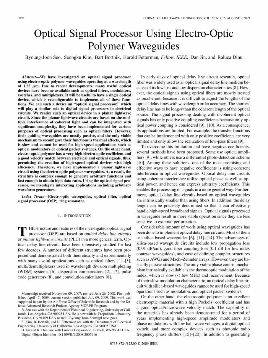
Fig. 1. Example block diagrams of OSP circuits. The input is split into multiplewaveguides. The individual optical signal experiences equally different time de-lays represented by � , and amplitude and phase changes represented by the� � � � � , and � coefficients. At the output port, they are combined again togenerate an output signal. (a) Transverse form. (b) Lattice form.
arbitrary and complex functionality by employing PLC struc-tures, use of the electrooptic polymer OSP permits operation athigh speed. Therefore, not only an electrooptic polymer OSPcan be used for the same applications as a PLC, but the OSP isalso well suited for high-speed devices and applications.
II. OSP THEORY
The fundamental enabling concept of the OSP stems from themultiple and temporal interference of delayed optical signals.By controlling the amplitude and the phase of the interfered sig-nals, the optical signal can be processed in any arbitrary way.Example block diagrams of OSP circuits are shown in Fig. 1.The input optical signal is launched on the left side and splitinto multiple waveguides. The individual optical signal experi-ences equally different time delays represented by and inthe diagrams, and amplitude and phase changes represented bythe , and coefficients. At the output port located onthe right side of the diagram, they are combined again to gen-erate an output signal.
Two typical configuration structures are distinguished;transversal form [21] and lattice form [4], [5] as can be seen inFig. 1(a) and (b), respectively. The transversal form is a parallelstructure since the signal is processed in a parallel way, whilethe lattice form is a serial structure where signals are processedin series. If we define a waveguide branch arm, an arm can beclassified into two types: forward feeding arm and backwardfeeding arm. Since the response of forward feeding arms isfinite in time, it is called finite impulse response (FIR). In a
similar way, the response of backward feeding arms is calledinfinite impulse response (IIR) since it is infinite. The numberof the forward feeding arms and of backward feeding armsrepresent the order of FIR and IIR, respectively. The origin ofthis terminology is from the digital filter theory in electronics[22]. According to this theory, any arbitrarily response can beobtained when FIR and IIR are combined together. The orderof FIR and IIR is associated with how arbitrary an OSP candescribe the response.
Several physical values are important for characterizing anOSP. These are the unit delay time, , and the number of armsthat split or combine light ( and in Fig. 1(a)). The unitdelay time of an OSP is analogous to the sampling time in dis-crete time signal processing. It represents a time resolution forthe OSP to process a signal. Due to this time resolution, the fre-quency response of an OSP is periodic and the period is propor-tional to . This period is called the free spectral range (FSR).The number of optical splitting and combining arms determinesthe spectral resolution of the OSP within an FSR. As the numberof arms increases, a sharper frequency response can be obtainedand hence a more arbitrary response is possible. In that sense, itis analogous to the number of eigenfunctions in the frequencydomain because the overall frequency response of an OSP is aresponse combination of the individual arms.
If and denote the input and output signal, respec-tively, an OSP performs as an operator to transform into
. Several modes can be used for describing an OSP. Thefirst method is to use a characteristic equation, already shown inFig. 1(a). If an OSP has the number of forward feeding armsand the number of backward feeding arms, the characteristicequation of the processor can be generally written as (1)
(1)
where the coefficients, and , stand for the amplitude andphase changes of the th forward feeding arm and the th back-ward feeding arm, respectively. The coefficients are complexvalues in general because the signals, and , stand forcoherent optical fields, and thus have both amplitude and phase.The amplitude and the phase of a coefficient correspond to theamplitude and phase change of an individual signal.
The second method for describing this system is the transferfunction representation. In general, the coefficients, and ,and the delay time, , in (1) can be functions of time as well if wechange (or modulate) those parameters in time. If their varyingrate is comparable to that of the optical signal such as in elec-trooptic polymer waveguides, their time-dependent effect mustbe considered. We sometimes apply time-varying signals to thetime-delay lines to effectively change in our experiments inSection VI. However, we assume that the time-varying rate issmall enough or the delay control mode (defined later in thissection) is only considered in the OSP operation in this paper. Inthis case, the OSP becomes a linear system and is similar to thedigital filter in many ways. Indeed, the OSP has the same trans-mission characteristics and features as those of a correspondingdigital filter. Therefore, the conventional Z transform analysis,which is frequently used with digital filters, can be applied to

3094 JOURNAL OF LIGHTWAVE TECHNOLOGY, VOL. 27, NO. 15, AUGUST 1, 2009
the analysis of the OSP. In Z transformation, the transfer func-tion is represented as the rational functions of Z.
If we calculate the Fourier transformation of (1) with respectto the eigenfunctions of where is any integer and isthe optical angular frequency and replace the with ,we obtain the transfer function, , in the Z domain
(2)
where stands for one unit delay in the Z domain.Another convenient and more visual way to describe an OSP
is to use a pole/zero diagram [23]. Because the transfer function,, is a complex function of the complex variable, , the
value of can be plotted on the complex Z space. The zerosare the values which make and the poles are theones that make . Then, another form of canbe written as
(3)
where and are the th zero and th pole, and is theamplitude factor.
In general, the coefficients, and , and the delay time, ,in (1) can be functions of time as well as the input light signal.Three different methods are possible to operate the OSP, de-pending on which parameters are used for optical processing.They are the coefficient control mode, delay control mode, andfrequency control mode.
The coefficient control mode performs optical processing viacontrolling the coefficients, or . When a typical contin-uous wavelength light is input, the output light can be processedby modulating or controlling these coefficients. The delay con-trol mode is via controlling the delay time, . For a continuous orvarying wavelength light input, the delay time can be controlledor modulated to generated processed output light. The frequencycontrol mode utilizes frequency dependence of the OSP due toits delay lines.
Most PLC structures using silica waveguides regard the coef-ficients and the delay time as constant variables, since their con-trolling method (mostly thermal tuning) is much slower than theoptical light signal. Therefore, the silica waveguides mostly usethe frequency control mode for their optical signal processing,such as in optical filters [2], [7], [21]. However, if the time-varying or modulating rate of the coefficients or the delay time iscomparable to the propagation of the optical signal through theOSP, such as in electrooptic polymer waveguides, their time-de-pendent effect will be useful and should be considered.
We investigate the OSP applications using the delay controlmode rather than the frequency control mode or the coefficientscontrol mode when we discuss its applications in Section VI.If the frequency control mode is used in an OSP with the elec-trooptic polymer waveguides, the OSP can tune such optical fil-ters much faster. However, the filter performance will be lim-ited if electrooptic polymers are used in place of silica wave-guides due to its intrinsic optical loss. Furthermore, operatingour polymer OSP in the coefficients control mode is not partic-ularly interesting. The OSP we investigate is classified into the
Fig. 2. Unit block of OSP. It is a two-port input and two-port output systemconsisting of a symmetric Mach–Zehnder interferometer and a racetrack struc-ture. Four electrodes control the locations of a zero and a pole.
lattice form the structure. In the lattice form structure, theand coefficients in Fig. 1(b) are complex functions of actualelectrical biases, which makes it difficult to find the relation-ship between its output function and the electrical biases [4],[5]. In addition, we have not found any useful and unique appli-cations using this mode partly because the optical loss in poly-mers limits the performance of the OSP building blocks.
One can find that the frequency control mode is based on thesame principle as the delay control mode. In (2), the delay time
and the optical frequency are multiplied together. There-fore, either affects the transfer function in the same way. We canchange the delay time using the electrooptic effect with a fixedinput optical frequency (wavelength) or the optical frequencycan be changed using a fixed delay time. Either approach willgenerate the same output response. This is the basic concept forthe arbitrary waveform generator, we investigate in Section VI,and it becomes clear with the driving formula of (5).
III. OSP DESIGN
A. Structure
Since multiple power splitting is hard to obtain and not effec-tive in the optical waveguide, the lattice form structure is con-sidered for the implementation of our OSP. The lattice form is aseries structure with a certain type of a unit block. The unit blockwhich we have chosen consists of a symmetric Mach–Zehnderinterferometer and a racetrack waveguide as shown in Fig. 2.“Symmetric” means that the lengths of the two waveguide armsof the Mach–Zehnder interferometer are the same. A racetrackstructure is used so that the straight waveguide section has anextended coupling region for coupling outside of the ring.
This unit block, originally proposed by Jinguji [5], has twoinput and two output ports. Any input port can be used for op-eration, while the two output ports are related to each other bya conjugate power relation. A conjugate power relation meansthat the total sum of two output powers is the same as the inputpower if the system is lossless.
This structure generates one zero and one pole simultane-ously. The degree of freedom to locate a zero or a pole in theZ space is 2 because a zero or a pole is a complex value, andhence has both amplitude and phase. The locations of the zeroand the pole in the Z space are controlled by the four differentelectrodes. Note that and are functionally redundant.
A multiple-block OSP consists of cascaded multiple unitblocks as shown in Fig. 3. With N cascades of unit blocks,our OSP can generate N zeros and pole pairs. Therefore, thedegree of freedom of the N cascaded OSP is , whichare controlled by electrodes on top of the waveguides.

SEO et al.: OPTICAL SIGNAL PROCESSOR USING ELECTRO-OPTIC POLYMER WAVEGUIDES 3095
Fig. 3. Multiple structure of OSP. It consists of N cascaded unit blocks.
In the strict sense, the definition of the unit block in Fig. 2 iswrong if the multiple block is considered. It should be one ofthe divided sections in Fig. 3 except the first block, which isjust a configurable coupler. To avoid confusion, we name thestructure in Fig. 2 as a “one-block OSP” and one of the dividedsections in Fig. 3 as a “unit block.”
The unit block contains two configurable couplers and twophase shifters. They are the “splitting coupler,” the “racetrackcoupler,” the “Mach–Zehnder phase shifter,” and the “racetrackphase shifter,” labeled as , and , respectively, shownin Fig. 2. They are used for configuring one zero and one polegenerated by a unit block and controlled by microstrip elec-trodes located on top of the waveguides via the electroopticeffect.
In order to have a useful phase shift at the racetrack phaseshifter, the perimeter of the racetrack must be large enough. Onthe other hand, the round trip loss of the racetrack will be toolarge if the perimeter is large. Therefore, we design the radius ofthe racetrack to be 1.2 mm. The interaction lengths of the race-track coupler and the splitting coupler are designed as 2 mmand 6 mm, respectively. The detail design parameters of the in-dividual building blocks or components are discussed later inthis section.
B. Optical Waveguides and Fabrication
The optical waveguide is a crucial part of the OSP. Whileconfining the light inside, it is the basis of the delay lines andcouplers. We need to consider two requirements when selectingthe type and dimensions of the waveguides. First, they should behighly confined waveguides because of the bending structure inthe racetrack. Second, their confinement is low enough so thata reasonable amount of energy can be coupled. Note that thesetwo factors are competing against each other. Furthermore, thewaveguides should also be of single mode to ensure no signaldegradation occurs via modal dispersion.
For the electrooptic polymer core material, DH6/APC(Lumera Co.) was used. Single-layer films of DH6/APC haveshown a high electrooptic coefficient of 70 pm/V at 1.31 m[24]. For lower and upper cladding polymers, UV15LV (MasterBond Co.) and UFC170A (Uray Co.) are used. The indexes at1.55 m of the core are measured to be 1.61, and the lowerand upper claddings have been measured to be 1.51 and 1.49,respectively [25].
We consider the inverted rib waveguide structure, which isknown to be effective in minimizing the scattering loss fromsidewall roughness [26]. Fig. 4 shows the cross section of the de-signed waveguides at a coupler region. The rib width, rib height,and slab thickness are designed to be 2 m, 1 m, and 1 m,respectively. Using the known indexes of the polymer material,
Fig. 4. Cross section of the designed optical waveguide. It is a single-modewaveguide whose confinement is high enough to support a 1 mm radius bendingyet low enough to be coupled to an adjacent waveguide.
Fig. 5. Top view photograph of fabricated devices. The bright yellow regionsare where the driving electrodes are located. The rectangular shape electrodesare DC pads for electric connections using DC contact probes.
we numerically calculate the propagation modes, optical cou-pling, and bending loss for this optical waveguide structures andfind that this waveguide can support 1 m bending with negli-gible bending loss and yet can couple effectively to an adjacentwaveguide. Similar waveguide structures using similar polymermaterials are also used in [27], where bending waveguides witha 1 mm bending radius have a loss of approximately 4 dB/cmat 1.3 m. Optical waveguide modes were simulated by a com-mercial software package, Fimmwave (Photo Design Inc.). Bothnumerical simulations and experiment show that this waveguidesupports a single mode.
Fig. 5 shows the top view photograph of the fabricated de-vice. The bright regions (yellow if colored) are where the drivingelectrodes are located. The rectangular shape electrodes are DCpads for electric connections by DC contact probes. Note thathigh-frequency design features are not considered in this work.
C. Waveguide Bending
There are three different optical loss mechanism in opticalwaveguides: material loss, scattering loss, and bending loss. Ma-terial loss is power loss absorbed inside the material due to ab-sorptions and imperfections in the bulk waveguiding material.Scattering loss is due to imperfect surface roughness scatteringat the interface of the core and cladding in both straight andcurved waveguides. Bending loss is power leakage when thewaveguide is bent and primarily determined by the waveguideconfinement factor.
In calculating the bending loss of a bending waveguides,several approaches have been used. Yamamoto and Koshiba[28], used the finite element method (FEM) for the computa-tional window of the bending waveguides and found the steady

3096 JOURNAL OF LIGHTWAVE TECHNOLOGY, VOL. 27, NO. 15, AUGUST 1, 2009
state solution of an outgoing leaky wave, where the leaky wavewas depicted by the Henkel function of the second kind [28].Even though this method calculates a very rigorous solution,the computation time can be long due to recursive iterations.The perfectly matched layer (PML) has also been used forcalculating the bending loss [29]. The advantages of the PMLmethod include that the formulation is based on Maxwell’sequations rather than a modified set of equations, and that theapplication to the finite difference time domain (FDTD) methodis more computationally efficient, and that it can be extended tononorthogonal and unstructured grid techniques. However, it isdifficult and critical to find a perfectly matched layer boundarycondition.
We use the finite different method (FDM) and conformaltransformation technique [30] in order to find the optimalradius and the bending loss of the bending waveguide. The zeroboundary condition is assumed for all the boundaries exceptthe leaky side of the waveguide (where the energy is leaking).In the leaky side, we apply a plane-wave boundary condition[31]. As a result, we calculate the bending loss as 0.02 dB/cmwhen the bending radius is 1 mm. This bending loss is muchsmaller than the propagation loss of the straight waveguide.Therefore, we ignore the bending loss if the bending radius islarger than 1 mm.
D. Configurable Couplers
The cross section of the configurable couplers is shown inFig. 4. The waveguides are located sep distance apart. The en-ergies carried by the two waveguides are coupled to each other.The driving electrode on top of only one waveguide applies anelectric field to change the refractive index of the waveguide andto tune the amount of coupling. In order to optimize the opera-tion of the configurable couplers, the waveguide separation andtheir interaction length should be designed properly.
We have utilized the change in the velocity match for the cou-pling mechanism rather than the change in the overlap of themodes. By a change in the index due to the applied electric field,both effects will influence the coupling coefficients. The refrac-tive index of the electrooptic core material used is around 1.6,and its maximum index change, we have utilized in this work,is around . Using numerical waveguide modal simula-tions, we have found that the velocity match effect is much moredominant than modal overlapping change with this small indexchange.
We have two different types of configurable couplers for theOSP structure. We name them the “racetrack coupler” and the“splitting coupler.” The racetrack coupler is located at the in-terface between the straight waveguide and the racetrack wave-guide and is labeled as in Fig. 2. The splitting couplers arelocated in and out of the Mach–Zehnder structure and are la-beled as and in Fig. 2.
The purpose of the racetrack coupler is to tune the amountof resonance in the racetrack and hence to configure the ampli-tude of the pole. There are two requirements for the racetrackcoupler. First is that its interaction length should be small to re-duce the optical loss. Since the total optical round trip loss ofthe racetrack includes the optical loss of the racetrack coupler,
it is important to minimize its optical loss, and hence the inter-action length. Second is that it should be designed at the criticalcoupling state of the racetrack. Since the racetrack is most sen-sitive to the tuning of the racetrack coupler in its critical cou-pling state [32], it would be ideal that the transmission coeffi-cient of the racetrack coupler is matched to the round triploss factor of the racetrack. The round trip loss factor ofthe racetrack is expected to be around 0.6–0.7. Therefore, theracetrack coupler should be compact in size and designed suchthat its transmission coefficient becomes around 0.6–0.7.Using optical simulation, we design its interaction length andseparation near 2 mm and 4.5 m, respectively.
The splitting coupler is for controlling the energy splitting be-tween two branches of light at the input port and to the outputport. Since the splitting couplers tune the location of the zero,they should be as configurable as possible. Using optical simula-tion, we design its interaction length and separation near 6 mmand 5.1 m, respectively.
IV. ONE-BLOCK OSP ANALYSIS
As discussed earlier, the one-block OSP generates a singlezero and a single pole simultaneously. The degrees of freedomto locate a zero or a pole in the Z space is two since a zero or apole is a complex value, and thus has both amplitude and phase.Their locations in the Z space are controlled by the four dif-ferent electrodes shown by the shaded bars (red if colored) inFig. 2. With N cascades of the unit block, an OSP can generate Nnumber of zero and pole pairs as shown Fig. 3. The poles of thewhole OSP system are the same as those of the individual unitblocks. On the other hand, the zeros of the whole system are notthe same as those of the unit blocks since both the output powerand the conjugated power of a unit block are cascaded to the nextunit block by coupling each other. Because of this problem, itis not trivial to identify the zeros of a multiply cascaded struc-ture. Jinguji demonstrated a synthesis algorithm for analyzingthese structures [5]. However, their technique cannot be appliedgenerally to a lossy system since their technique assumed thatthe unit structure is lossless. Thus, a synthesis method for ourstructure that includes loss factor has been developed by modi-fying Jinguji’s algorithm, which is not included here due to itsmathematical complexity.
However, dealing with just an one-block OSP is relativelyeasy and straight forward. By using the scattering matrices, wecan derive the scattering parameters, which are useful to under-stand the operation of the one-block OSP. First, before derivingthe scattering matrices, we define the scattering matrices of theindividual components. And then, we cascade their matrices tofind the scattering matrices of the entire one-block OSP. Havingdefined the individual scattering matrices for the one-block OSP,the scattering matrix, , for an one-block OSP shown again inFig. 6 is the multiplication of the individual scattering matrices
(4)
where and are the scattering matrices for the two split-ting couplers, and is the Mach–Zehnder section as shown in

SEO et al.: OPTICAL SIGNAL PROCESSOR USING ELECTRO-OPTIC POLYMER WAVEGUIDES 3097
Fig. 6. Unit block of OSP with appropriate symbols for mathematical anal-ysis. The individual scattering matrix transfer function consists of two differentterms. One, labeled as “Path A,’” is associated with the light beam which propa-gates through the racetrack and the other, labeled as ‘‘Path B’”, is with the lightbeam which propagates through the other Mach–Zehnder arm.
Fig. 6. The calculation is straightforward, and the scattering pa-rameters can be summarized as
(5)
where
(6)
where and are the transmission and cou-pling ratio of each coupler, and represents the optical lossesinside the corresponding coupler. is the total roundtrip time, and is the total round trip loss.and are the optical loss factor and the phase shift in theMach–Zehnder phase shifter. and are the transition timein the racetrack coupler and in the racetrack, and arethe optical loss factor in the racetrack coupler and in the race-track, respectively. The optical loss factors represent the electricfield attenuation on a linear scale and become unity in losslesswaveguides.
As seen in the under brackets in (5), the individual scatteringmatrix transfer function consists of two different terms. One,labeled as “Path A,” is associated with the light beam whichpropagates through the racetrack and the other, labeled as “PathB,” is for the light beam which propagates through the otherMach–Zehnder arm. The Path A and terms correspond to twopaths indicated in Fig. 6. Therefore, the Path A term containsthe transfer function of the racetrack while the Path B term isindependent of the optical delay line formed by the racetrack.
The two terms are summed at the output port depending onthe coupling ratio of the two splitting couplers. The amplitude of
stands for the normalized intensity of Path B with respectto the maximum intensity of Path A. Note that the amplitudeand the phase of Path B beam of light are controlled by thetwo splitting couplers and the electrode, respectively andthat the transfer function and the resonant wavelength of theracetrack (Path A light beam) are controlled by the and the
electrodes, respectively. The mathematical representation in(5) is useful for an intuitive and physical understanding of theone-block OSP structure and it is used when we verify the OSPexperimentally later in Section V.
Another useful and more mathematical way to represent thescattering matrices is using the concept of poles and zeros. Fur-ther simplification of (5) results in
(7)
where
(8)
All transfer functions have the same pole, , while is thezero obtained from the scattering matrix element.
Note that the phase of defined in (7) is not configurable.The definition of the pole should include as well as eitheror in (7) because the two terms contribute the pole phase.However, we define our pole as shown in (7) since it is con-venient to understand two similar operation modes; frequencycontrol mode or delay control mode. In this way, the similaritybetween two operation modes of the OSP, as we discussed inSection II, becomes clear. In the frequency control mode,term in (7) is varying and represents the unit delay in theZ space. In this case, the actual pole becomes , thus, thepole phase is controlled by the electrode. From a practicalpoint of view, the frequency response of the OSP is periodicwith respect to the FSR and the response shifts in the frequencydomain with respect to the value. On the other hand, in thedelay control mode, the delay is controlled by in (7), whichrepresents the unit delay in the Z space. In this case, the ac-tual pole becomes , thus, the pole phase is controlled bythe input optical frequency . With a similar analogy from apractical point of view, the amplitude and phase response of theOSP is periodic with respect to and the response shifts inthe (or voltage) domain with respect to the input optical fre-quency. Note also that the phase of the zero also depends on bothparameters in the same manner. By changing any of two param-eters, the phases of both pole and zero are changing in the sameamount. However, the zero has additional configurable degreesof freedom such as and as seen in (7).
If the zero can be located in entire space and the pole canbe located in any region within the unit circle in the Z space,the generality condition is satisfied. The amplitude of a pole de-pends on the total round trip loss factor and transmissioncoefficient of the racetrack coupler as seen in (7). In thelossless case when becomes unity, the pole can be locatedat any point within the unit circle if can be adjusted from 0

3098 JOURNAL OF LIGHTWAVE TECHNOLOGY, VOL. 27, NO. 15, AUGUST 1, 2009
Fig. 7. Experimental setup and spectral response of a racetrack which has thesame design as the OSP used. The free spectral range (FSR), extinction ratio,finesse, and Q-factor are measured 0.12 nm (15.5 GHz), 18 dB, 3.36, and ������� , respectively. (a) Experimental setup. (b) Measured and simulated spectralresponse.
to 1. However, polymer waveguides intrinsically have a certainamount of intrinsic optical loss and the configurable amount of
is difficult to design to have complete configurability. In thiscase, the actual implementable amplitude of the pole locationsbecomes limited. The phase of the pole depends on the opticalphase change controlled by the phase shifter. Since the inter-action length of the is designed 9.12 mm, 360 of the opticalphase change can be obtain with applied voltage, hence any ar-bitrary phase of the pole is possible.
Once we determine the pole location, the zero depends on thetransmission coefficients of the splitting couplers and opticalphase shift in the Mach–Zehnder phase shifter as seen in (7).Since the splitting couplers are designed long enough to have aslarge tuning ratio as possible and the interaction length for the
electrode is relatively long (5 mm), the phase and amplitudeof the zero can cover almost entire range of the Z space. Wediscuss the generality of the fabricated OSP with experimentaldata later in Section V.
V. COMPONENTS VERIFICATION
There are several individual components or building blocksof the OSP. They are the racetracks, configurable couplers, andphase shifters. The OSP will function correctly once all thesecomponents are working correctly. Therefore, it is important tocharacterize and verify the individual components before inte-grating them. In order to verify the components, we also fabri-cate individual components.
First, we characterize the racetrack. Fig. 7 shows the spectralresponse of a racetrack and its experimental measurement setup.
Fig. 8. Experimental setup and spectral response of a racetrack when���V isapplied to the racetrack coupler. By fitting the measured response, we find that� becomes ������ ���� with an applied voltage to the racetrack coupler of��� V. (a) Experimental setup. (b) Measured spectral response.
The racetrack measured has the same design as the OSP, wherethe bending radius of the racetrack is 1.2 mm and the interactionlength of the racetrack coupler is 2 mm. An AQ4321D (Ando)is used for the tunable laser source at 1.55 m with TM modepolarization control. As seen in Fig. 7(b), the measurement isdone in a 0.6 nm wavelength span and the free spectral range(FSR), extinction ratio, finesse and Q-factor (loaded) are mea-sured 0.12 nm (15.5 GHz), 18 dB, 3.36 and , respec-tively. Using these values, the effective group refractive index,
value, value, total round trip optical loss and the opticalloss inside the ring are calculated as 1.66, 0.608, 0.535, 4.4 dBand 3.85 dB/cm, respectively. Fig. 7(b) also shows the simu-lated spectral response using these values. Since the propaga-tion loss of the straight waveguide is measured around 2 dB/cm,the excess loss inside the racetrack is expected to be from scat-tering loss due to the roughness at the interface between core andcladding materials. A similar propagation loss inside the race-track has been obtained using 1 mm bending radius and similarelectrooptic polymer material [27].
We applied voltages of V on the electrode to verifythe operation of the racetrack coupler as seen in Fig. 8(a).Fig. 8(b) shows the spectral response while varying the drivingvoltages. The spectral response when no voltage is applied isshown as well for purpose of comparison. As seen in Fig. 8(b),the response (extinction ratio) is changed depending on thevoltage. By fitting the measured response, we find thatbecomes with an applied voltage to the racetrackcoupler of V. We also find that the local minima shift withapplied voltage.

SEO et al.: OPTICAL SIGNAL PROCESSOR USING ELECTRO-OPTIC POLYMER WAVEGUIDES 3099
Fig. 9. Intensity response of a racetrack when ��� V peak-to peak triangularsignal is applied to the racetrack phase shifter. The measurement shows that thehalf-wave voltage �� � of the � phase shifter is 18.3 V. The corresponding �coefficient is also calculated as 23 pm/V. (a) Experimental setup. (b) Measuredintensity.
For verification of the racetrack phase shifter, we fix the inputoptical wavelength at 1.55 m and apply V peak-to-peaktriangular signal to the electrode. Its experimental setup andresponse are shown in Fig. 9(a) and (b), respectively. The mea-surement shows that the half-wave voltage of the racetrackphase shifter is 18.3 V. The corresponding coefficient is alsocalculated as 23 pm/V.
Two different types of couplers are considered in the OSP aswe discuss in Section III. They are the racetrack couplers andthe splitting couplers. For the racetrack couplers, the separationwidths of 4.5 m, 4.6 m and, 4.5 m are considered betweentwo waveguides and their interaction length is 2 mm. The split-ting coupler has a separation of 5.1 m and interaction lengthof 6 mm. Fig. 10 shows the measured and responsesof the racetrack couplers. From the measured response, we cal-culate the transmission coefficients for the couplers, which arealso shown in Fig. 10(d). Comparing to the simulated coupler inSection III, the measurements show that the measured transmis-sion coefficients are smaller than the simulated values. Further-more, the different polarity of voltages leads to different outputresponse even though output responses should be even functionswith respect to applied voltages since the waveguides are sym-metric. This implies that two waveguides inside the couplers aremismatched already due to imperfect fabrication, which has alsobeen found in conventional electrooptic Mach–Zehnder devices[33].
Fig. 11 shows measured and responses of the splittingcouplers. Since the interaction length is designed large enough
(6 mm), both outputs reach their maximum and minimum inten-sities during the application of the triangular voltage waveformon the electrodes. The turn on/off voltage of the splitting coupleris 30 V and its extinction ratio is approximately 10 dB, implyingthat its transmission coefficient, or , can be configurable be-tween 0.4 and 0.9 with an applied voltage of 30 V.
The Mach–Zehnder phase shifter (or phase shifter)is for tuning the phase of Path B in Fig. 6. For verificationof the Mach–Zehnder phase shifter, we also apply a Vpeak-to-peak triangular signal to the electrode. Its ex-perimental setup and response are shown in Fig. 12(a) and(b), respectively. The measurement shows that the half-wavevoltage of the Mach–Zehnder phase shifter is 33 V. Thecorresponding coefficient is calculated as 20 pm/V.
Based on the earlier discussion in this section, we summarizethe parameters and their configurable range with applied volt-ages in Fig. 13.
1) The FSR of the racetrack is 0.12 nm (15.5 GHz) and thevalue is 0.608. The transmission coefficient, , varies
between and with V appliedvoltage to the electrode.
2) The phase, , can be fully configurable (0 to ) withV applied voltage to the electrode.
3) The phase, , of the Mach–Zehnder phase shifter can befully configurable (0 to ) with V applied voltage tothe electrode.
4) The splitting coupler, and , can be configurable be-tween 0.4 and 0.9 with 30 V.
Based on measurements summarized in Fig. 13 and (7), wecan find possible locations of the pole and the zero of the fab-ricated one-block OSP. We find the amplitude of the polecan be between 0.17 and 0.48 and the phase of the pole can befully configured with either or depending on the operationmode. Therefore, the pole can be located and configured insidethe shaded area in Fig. 14.
On the other hand, location of the zero depends on that ofthe pole. According to (7), the zero has an offset from the pole;
. Since this offset is a complexnumber as well, it is a vector in the Z space. Location of the zerois determined by this offset vector. The offset vector depends ontwo parameters; and . First, assume that is infinityimplying all the input light goes through Path B and there is nopower flow in Path A. Path A and Path B are shown in Fig. 6.In this case, the offset vector becomes 1 and the location of thezero is same as that of the pole, thus the zero cancels the poleand there will be no zero and no pole. If is 0, then, theoffset vector becomes real number and the zero will be
, which is the same zero which the transfer function ofthe racetrack structure represents.
However, is bounded due to the bounded transmissioncoefficients of the splitting couplers. As in (5), is the elec-tric field amplitude ratio between Path A and Path B, which isconfigured by the splitting couplers. From the bounded trans-mission coefficients of the splitting couplers, we find the max-imum and minimum values of as
(9)

3100 JOURNAL OF LIGHTWAVE TECHNOLOGY, VOL. 27, NO. 15, AUGUST 1, 2009
Fig. 10. Experimental measurements of � and � scattering parameters for the different racetrack couplers. (a) Sep � ��� �m. (b) Sep � ��� �m. (c) Sep ���� �m. (d) Measured � .
Fig. 11. Experimental measurements of � and � scattering parameters forthe splitting coupler.
On the other hand, the phase of depends on . Sincecan be configured completely from 0 to by V as shownin Fig. 13, the phase of is also configured completely from0 to . Therefore, the zero can be located in the entire Z space
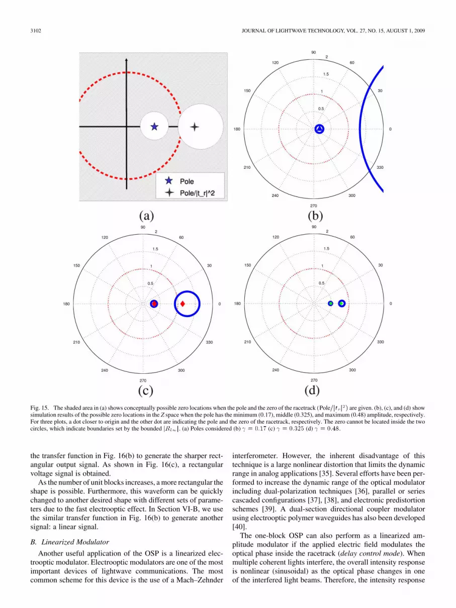
except near two points, which are the pole and the zero of theracetrack . The shaded area in Fig. 15(a) shows con-ceptually possible zero locations when the pole and the zeroof the racetrack are given as shown. We use computer simu-lations to find the possible locations of the zeros that can beimplemented by the fabricated one-block OSP. Fig. 15(b), (c)and (d) show their results in the Z space when the pole has theminimum (0.17), middle (0.325), and maximum (0.48) possibleamplitude, respectively. For three plots, a dot closer to the originand the other dot are indicating the pole and the zero of the race-track, respectively. The zero cannot be located inside the twocircles, which indicate boundaries set by the bounded . Asthe pole locates near to the unit circle, the zero can be locatedthroughout the entire Z space.
VI. APPLICATIONS OF OSP
Due to its intrinsic arbitrariness, the OSP can be used formany applications. As for the potential high-speed analog ap-plications, we investigate Arbitrary waveform generators andLinearized modulators using our one-block OSP.

SEO et al.: OPTICAL SIGNAL PROCESSOR USING ELECTRO-OPTIC POLYMER WAVEGUIDES 3101
Fig. 12. Intensity response of a racetrack when a ��� V peak-to peak trian-gular signal is applied to the � electrode. The measurement shows that thehalf-wave voltage �� � of the Mach–Zehnder phase shifter is 33 V. The cor-responding � coefficient is calculated as 20 pm/V. (a) Experimental setup.(b) Measured intensity.
Fig. 13. Summary of one-block OSP. Based on the measurement of individualcomponents, configurable parameters are summarized with their configurableamount and driving voltages.
A. Arbitrary Waveform Generator
It is known to be possible to implement arbitrary optical fil-ters using PLC structures such as a notch filter, a linear disper-sion filter, and a bandpass filter [2]–[5]. Such filters have beenexperimentally investigated in silica waveguides, where thermaltuning was used to change the index of refraction. Since the OSPemploys the PLC for its structure and it is based on the fast elec-trooptic effect, much higher data rates (more than tens of giga-hertz rate) can be accessible using the OSP. Therefore, not onlyis the OSP useful in fast reconfigurable optical filters, but alsothe OSP can be used for high-speed arbitrary waveform gener-ators. High-speed arbitrary waveform generators are useful formodulator linearization and correction of amplifier distortion.
Fig. 14. Pole locations in Z space which can be implemented by one-blockOSP. The amplitude of poles is bounded from 0.17 to 0.48 while the pole phaseis configured from 0 to �� as indicated in the shaded region.
Assume that we apply a sawtooth signal to an one-block OSPat the electrode and its peak-to-peak voltage is two times thehalf-wave voltage of the racetrack phase shifter. Then, duringone cycle of the voltage signal, the output amplitude responseof the OSP takes on the optical filter shape as a function of time.By changing other biases, the output response will also change,and hence the OSP generates arbitrary waveforms. The degreeof arbitrariness of the generated signal depends on the numberof unit blocks if a multiple block OSP is used and the generalityof the OSP.
The detailed concept and theory of the arbitrary waveformgenerators have been investigated by Fetterman and Fetterman[34]. If we summarize [34], its principle of operation is basedon the similarity of two operation modes of the OSP as we dis-cussed in Section II; frequency control mode and delay controlmode. According to (5), the transfer functions, , depend onboth optical frequency and . If the OSP is operated with afixed value and varying optical frequency (frequency controlmode), the OSP performs optical filter as described in [2]–[5].On the other hand, if the OSP is operated with a fixed opticalfrequency and varying value (delay control mode), the re-sponse of the OSP with respect to should be the same as anoptical filter shape.
Since the OSP is based on high-speed electrooptic polymer,it can generate high-speed arbitrary waveforms. However, asawtooth signal is difficult to obtain at high frequencies withhigh power [17]. Instead, we examine a simple sinusoidal signalinput. Using a sinusoidal input, the OSP generates the desiredoutput shape with proper adjustment of the parameters; ,and .
Fig. 16 shows a measured rectangular signal generated by theone-block OSP and its experimental setup. The continuous lasersource at 1.55 m is applied to the one-block OSP with polar-ization control and the TM mode output of is measured bythe photodetector and the oscilloscope. First, we apply a Vpeak-to-peak sinusoidal voltage input to the electrode. Whenthe other biases are properly adjusted by voltage supplies asshown in Fig. 16(a), we obtain the OSPs transfer function asa function of the applied voltage as shown in Fig. 16(b). Wethen apply a V peak-to-peak sinusoidal voltage input witha proper offset bias to the electrode while the other biasesare properly adjusted. We utilize the sharp transition region in
3102 JOURNAL OF LIGHTWAVE TECHNOLOGY, VOL. 27, NO. 15, AUGUST 1, 2009
Fig. 15. The shaded area in (a) shows conceptually possible zero locations when the pole and the zero of the racetrack �Pole��� � � are given. (b), (c), and (d) showsimulation results of the possible zero locations in the Z space when the pole has the minimum (0.17), middle (0.325), and maximum (0.48) amplitude, respectively.For three plots, a dot closer to origin and the other dot are indicating the pole and the zero of the racetrack, respectively. The zero cannot be located inside the twocircles, which indicate boundaries set by the bounded �� �. (a) Poles considered (b) � � ���� (c) � � ���� (d) � � ���.
the transfer function in Fig. 16(b) to generate the sharper rect-angular output signal. As shown in Fig. 16(c), a rectangularvoltage signal is obtained.
As the number of unit blocks increases, a more rectangular theshape is possible. Furthermore, this waveform can be quicklychanged to another desired shape with different sets of parame-ters due to the fast electrooptic effect. In Section VI-B, we usethe similar transfer function in Fig. 16(b) to generate anothersignal: a linear signal.
B. Linearized Modulator
Another useful application of the OSP is a linearized elec-trooptic modulator. Electrooptic modulators are one of the mostimportant devices of lightwave communications. The mostcommon scheme for this device is the use of a Mach–Zehnder
interferometer. However, the inherent disadvantage of thistechnique is a large nonlinear distortion that limits the dynamicrange in analog applications [35]. Several efforts have been per-formed to increase the dynamic range of the optical modulatorincluding dual-polarization techniques [36], parallel or seriescascaded configurations [37], [38], and electronic predistortionschemes [39]. A dual-section directional coupler modulatorusing electrooptic polymer waveguides has also been developed[40].
The one-block OSP can also perform as a linearized am-plitude modulator if the applied electric field modulates theoptical phase inside the racetrack (delay control mode). Whenmultiple coherent lights interfere, the overall intensity responseis nonlinear (sinusoidal) as the optical phase changes in oneof the interfered light beams. Therefore, the intensity response

SEO et al.: OPTICAL SIGNAL PROCESSOR USING ELECTRO-OPTIC POLYMER WAVEGUIDES 3103
Fig. 16. Rectangular signal generation using an one-block OSP and its experimental setup. (a) A��� V peak-to-peak sinusoidal voltage input with a proper offsetbias is applied to the � electrode and other biases are properly adjusted by voltage supplies. (b) We obtain a proper transfer function for the rectangular signalgeneration. (c) We utilize the sharp transition region in the transfer function to generate a rectangular output signal. (a) Experimental setup. (b) Transfer functionmeasured. (c) Rectangular signal generated.
in a simple Mach–Zehnder structure is always nonlinear sincethe applied electric filed changes the optical phase of theinterfered lights in “linear” way. The fundamental concept inthe linearized modulator using the one-block OSP lies in theOSP’s “nonlinear” response of the optical phase to the appliedelectric field. The optical phase change inside the racetrackrecursively changes the overall optical phase leading to a non-linear response, which compensates the nonlinear response ofthe phase modulation under proper conditions, thus, generatinga “linear” intensity response overall. Note that this principleis analogous to that of the arbitrary waveform generator asdiscussed in Section VI-A. The linear amplitude response is aspecific kind of arbitrary waveform generation.
A ring resonator assisted Mach–Zehnder (RAMZ) structure,which is similar to the one-block OSP, has been proposed tofunction as a linearized modulator [41] and is studied in detailincluding the influence of optical loss [42]. They found that thehigher order nonlinear harmonic terms can vanish (up to 5thorder) with proper design of the waveguide structures. As seenin (7), the transfer function with respect to the phase change
depends on the pole and the zero. Therefore, its linearity canbe calculated by a common Taylor expansion technique usingvarious poles and zeros. The first and higher order harmonicterms are calculated by
(10)
where is the th high-order harmonic term and is an in-teger larger than 0. Instead of using the analytical Taylor expan-sion technique, we utilize a numerical method to calculate thehigh-order nonlinear harmonic terms with various poles, zerosand biases. As a result, we find the most linear region of theresponse (in terms of smallest higher order terms [42]) whenthe pole, the zero, and the bias are radand 2.2019 rad, respectively. In this case, the third, fourth, andfifth harmonic terms vanish while the first and second harmonicterms are calculated as 0.287/rad , 0.001/rad , respectively. Thecalculation shows that the most linearized modulation occursaway from the pole location, implying that a small resonance is

3104 JOURNAL OF LIGHTWAVE TECHNOLOGY, VOL. 27, NO. 15, AUGUST 1, 2009
Fig. 17. Linear signal generation using an one-block OSP and its experimental setup. (a) A��� V peak-to-peak triangular voltage input with a proper offset biasis applied to the � electrode and the other biases are properly adjusted by voltage supplies. (b) We obtain a proper transfer function for linear signal generation.(c) We utilize the linear transition region in the transfer function to generate a linear output signal. (a) Experimental setup. (b) Transfer function measured. (c) Linearsignal generated.
required for linearization. The relatively small correction of thenonlinear response from phase change is sufficient. Therefore,the optical loss issue is somewhat mitigated in the linearizedmodulator.
In order to demonstrate a linearized modulator, we use thesame experimental setup as shown in Fig. 16 except that weutilize the linear slope of the transfer function and we apply atriangular signal rather than a sinusoidal signal since a trian-gular signal allows easier verification of linearity. As shown inFig. 17(c), the output response linearly follows the input signal.More rigorous methods should be applied to check the linearityof a modulator such as two-tone test measurement method [43].However, our purpose is to demonstrate the various features ofthe OSP.
VII. CONCLUSION
We have investigated an optical signal processor usingelectrooptic polymer waveguides. We have also shown that
practical applications can be made using the current state ofpolymer technology. Since the OSP is based on both polymers’high-speed and PLCs’ complex features, it is expected to be apowerful technology for optical communications and opticalcomputing.
However, the optical signal processor investigated in thiswork is limited in terms of structural complexity and operationspeed; only an one-block OSP is considered for its imple-mentation and our experiment is done at low frequencies.Similar electrooptic polymers have been used to obtain signalbandwidth more than 100 GHz [17]–[19], [44]. Therefore,the potential operation speed of the fabricated device in thework is comparable to that of those devices. In order to have ahigh-speed feature, we need to additionally consider high-speeddesign of the microtrip electrodes, such as electrode width forimpedance matching and electrode thickness for reducingconductor losses at high frequency. However, due to intrinsicgood velocity match characteristics of electrooptic polymers,

SEO et al.: OPTICAL SIGNAL PROCESSOR USING ELECTRO-OPTIC POLYMER WAVEGUIDES 3105
designing of high-speed electrodes is not a major challengefor high-speed operation. Our actual next step is to buildmultiple blocks of OSP. After that, we can integrate them withhigh-speed microstrip design for higher speed.
In order to realize more complex (or multiple) OSP struc-tures, it is important to reduce optical propagation losses inelectrooptic polymer waveguides. Since the OSP consideredin this work has a racetrack structure to implement the in-finite impulse response (IIR), the high optical loss not onlydegrades the total insertion loss but also leads to a restrictionin implementing a general OSP. Current propagation lossesof the straight waveguide are around 1.1–1.7 dB/cm [26]. Toovercome the propagating loss limitation of the electroopticpolymer, a passive-to-active transition technique has beenproposed [45]. This technique uses the hybrid silica/polymerstructure with a vertical adiabatic transition between the silicaand electrooptical polymer materials. Another approach is touse low loss polymer material with an adiabatic transition inthe same layer [46]. This method is expected to reduce thecoupling loss due to an excessive index mismatch between thetwo materials. If the index of the passive material is similar tothe active material, standard butt coupling is also promising[47]. Furthermore, recently development of polymers with veryhigh electrooptic coefficients of more than 300 pm/V havebeen investigated. The coefficient of 300 pm/V is more thana factor of 10 larger than the one in this work. This developmentposes the promising possibility of implementing much morecompact and complex OSP structures.
REFERENCES
[1] C. K. Madsen and J. H. Zhao, Optical Filter Design and Analysis: ASignal Processing Approach. NJ: Wiley-Interscience, 1999.
[2] C. K. Madsen and G. Lenz, “Optical all-pass filters for phase responsedesign with applications for dispersion compensation,” IEEE Photon.Technol. Lett., vol. 10, no. 7, pp. 994–996, Jul. 1998.
[3] C. K. Madsen, “General IIR optical filter design for WDM applica-tions using all-pass filters,” IEEE J. Lightw. Technol., vol. 18, no. 6,pp. 860–868, Jun. 2000.
[4] K. Jinguji and M. Kawachi, “Synthesis of coherent two-port lattice-form optical delay-line circuit,” IEEE J. Lightw. Technol., vol. 13, no.1, pp. 73–82, Jan. 1995.
[5] K. Jinguji, “Synthesis of coherent two-port optical delay-line circuitwith ring waveguides,” IEEE J. Lightw. Technol., vol. 14, no. 8, pp.1882–1898, Aug. 1996.
[6] N. Takato, T. Kominato, A. Sugita, K. Jinguji, H. Toba, and M.Kawachi, “Silica-based integrated optic Mach–Zehnder multi/demul-tiplexer family with channel spacing of 0.01–250 nm,” IEEE J. Sel.Areas Commun., vol. 8, no. 6, pp. 1120–1127, Aug. 1990.
[7] G. Lenz, B. J. Eggleton, C. K. Madsen, and R. E. Slusher, “Opticaldelay lines based on optical filters,” IEEE J. Quantum Electron., vol.37, no. 4, pp. 525–532, Apr. 2001.
[8] K. P. Jackson, S. A. Newton, B. Moslehi, M. Tur, C. C. Cutler, J. W.Goodman, and H. J. Shaw, “Optical fiber delay-line signal processing,”IEEE Trans. Microw. Theory Tech., vol. MTT-33, no. 3, pp. 193–210,Mar. 1985.
[9] B. Moslehi and J. W. Goodman, “Novel amplified fiber-optic recircu-lating delay line processor,” IEEE J. Lightw. Technol., vol. 10, no. 8,pp. 1142–1147, Aug. 1992.
[10] J. Capmany, J. Cascbn, J. L. Martin, S. Sales, D. Pastor, and J. Marti,“Synthesis of fiber delay line filters,” IEEE J.Lightw. Technol., vol. 13,no. 10, pp. 2003–2012, Oct. 1995.
[11] Y. P. Li and C. H. Henry, “Silica-based optical integrated circuits,” IEEProc. Optoelectron., vol. 143, no. 5, pp. 263–280, 1996.
[12] K. Kato and Y. Tohmori, “PLC hybrid integration technology and itsapplication to photonic components,” IEEE J. Sel. Topics QuantumElectron., vol. 6, no. 1, pp. 4–13, Jan./Feb. 2000.
[13] T. Miya, “Silica-based planar lightwave circuits: Passive and thermallyactive devices,” IEEE J. Sel. Topics Quantum Electron., vol. 6, no. 1,pp. 38–45, Jan./Feb. 2000.
[14] R. Adar, C. H. Henry, R. F. Kazarinov, R. C. Kistler, and G. R. Weber,“Adiabatic 3-dB couplers, filters, and multiplexers made with silicawaveguides on silicon,” J. Lightw. Technol., vol. 10, no. 1, pp. 46–50,Jan. 1992.
[15] C. Zhang, L. R. Dalton, M. C. Oh, H. Zhang, and W. Steier, “Low �electrooptic modulators from CLD-1: Chromophore design and syn-thesis, material processing, and characterization,” Chem. Mater., vol.13, pp. 3043–3050, 2001.
[16] H. Zhang, M.-C. Oh, A. Szep, W. H. Steier, C. Zhang, L. R. Dalton,D. H. Chang, and H. R. Fetterman, “Push-pull electro-optic polymermodulators with low half-wave voltage and low loss at both 1310 and1550 nm,” Appl. Phys. Lett., vol. 78, no. 20, pp. 3136–3138, 2001.
[17] I. Y. Poberezhskiy, B. Bortnik, S.-K. Kim, and H. R. Fetterman,“Electro-optic polymer frequency shifter activated by input opticalpulses,” Opt. Lett., vol. 28, no. 17, pp. 1570–1572, Sep. 2003.
[18] D. H. Chang, H. Erlig, M. Oh, C. Zhang, W. H. Steier, L. R. Dalton,and H. R. Fetterman, “Time stretching of 102-ghz millimeter wavesusing novel 1.55 mu m polymer electrooptic modulator,” IEEE Photon.Technol. Lett., vol. 12, no. 5, pp. 537–539, May 2000.
[19] B. Bortnik, Y.-C. Hung, H. Tazawa, B.-J. Seo, J. Luo, A. K.-Y. Jen, W.H. Steier, and H. R. Fetterman, “Electrooptic polymer ring resonatormodulation up to 165 ghz,” IEEE J. Sel. Topics Quantum Electron., vol.13, no. 1, pp. 104–110, Jan./Feb. 2007.
[20] J. Han, B.-J. Seo, S.-K. Kim, H. Zhang, and H. R. Fetterman, “Single-chip integrated electro-optic polymer photonic RF phase shifter array,”J. Lightw. Technol., vol. 21, no. 12, pp. 3257–3261, Dec. 2003.
[21] K. Sasayama, M. Okuno, and K. Habara, “Coherent optical transversalfilter using silica-based waveguides for high-speed signal processing,”J. Lightw. Technol., vol. 9, no. 10, pp. 1225–1230, Oct. 1991.
[22] A. V. Oppenheim and R. W. Schafer, Discrete-Time Signal Pro-cessing. New York: Prentice-Hall, 1989.
[23] C. J. Kaalund and G.-D. Peng, “Pole-zero diagram approach to thedesign of ring resonator-based filters for photonic applications,” J.Lightw. Technol., vol. 22, no. 6, pp. 1548–1559, Jun. 2004.
[24] C. C. Tengi and H. T. Man, “A simple reflection technique for mea-suring the electro-optic coefficient of poled polymers,” Appl. Phys.Lett., vol. 56, pp. 1734–1736, 1990.
[25] P. Rabiei, W. H. Steier, C. Zhang, and L. R. Dalton, “Polymer micro-ring filters and modulators,” J. Lightw. Technol., vol. 20, no. 11, pp.1968–1975, Nov. 2002.
[26] S.-K. Kim, H. Zhang, D. H. Chang, C. Zhang, C. Wang, W. H. Steier,and H. R. Fetterman, “Electrooptic polymer modulators with an in-verted-rib waveguide structure,” IEEE Photon. Technol. Lett., vol. 15,no. 2, pp. 218–220, Feb. 2003.
[27] H. Tazawa, Y.-H. Kuo, I. Dunayevskiy, J. Luo, A. K.-Y. Jen, H.R. Fetterman, and W. H. Steier, “Ring resonator-based electroopticpolymer traveling-wave modulator,” J. Lightw. Technol., vol. 24, no.9, pp. 3514–3519, Sep. 2006.
[28] T. Yamamoto and M. Koshiba, “Numerical analysis of curvature loss inoptical waveguides by the finite-element method,” J. Lightw. Technol.,vol. 11, no. 10, pp. 1594–1583, Oct. 1993.
[29] N.-N. Feng, G.-R. Zhou, C. Xu, and W.-P. Huang, “Computation offull-vector modes for bending waveguide using cylindrical perfectlymatched layers,” J. Lightw. Technol., vol. 20, no. 11, pp. 1976–1980,Nov. 2002.
[30] M. Heiblum and J. Harris, “Analysis of curved optical waveguides byconformal transformation,” IEEE J. Quantum Electron., vol. QE-11,no. 2, pp. 75–83, Feb. 1975.
[31] A. Nesterov and U. Troppenz, “Plane-wave boundary method for anal-ysis of bent optical waveguides,” J. Lightw. Technol., vol. 21, no. 10,pp. 1–4, Oct. 2003.
[32] J. M. Choi, “Ring fiber resonators based on fused-fiber grating add-drop filters: Application to resonator coupling,” Opt. Lett., vol. 27, no.18, pp. 1598–1600, Sep. 2002.
[33] K. Geary, S.-K. Kim, B.-J. Seo, and H. R. Fetterman, “Mach–Zehndermodulator arm length mismatch measurement technique,” J. Lightw.Technol., vol. 23, no. 3, pp. 1273–1277, Mar. 2005.
[34] M. R. Fetterman and H. R. Fetterman, “Optical device design with ar-bitrary output intensity as a function of input voltage,” IEEE Photon.Technol. Lett., vol. 17, no. 1, pp. 97–99, Jan. 2005.
[35] T. R. Halemane and S. K. Korotky, “Distortion characteristics ofoptical directional coupler modulators,” IEEE Trans. Microw. TheoryTech., vol. 38, no. 5, pp. 669–673, May 1990.

3106 JOURNAL OF LIGHTWAVE TECHNOLOGY, VOL. 27, NO. 15, AUGUST 1, 2009
[36] L. M. Johnson and H. V. Roussell, “Reduction of intermodulation dis-tortion in interferometric optical modulators,” Opt. Lett., vol. 13, no.10, pp. 928–930, Oct. 1998.
[37] D. J. M. Sabido, M. Tabara, T. K. Fong, C.-L. Lu, and L. G. Kazovsky,“Improving the dynamic range of a coherent am analog optical linkusing a cascaded linearized modulator,” IEEE Photon. Technol. Lett.,vol. 7, no. 7, pp. 813–815, Jul. 1995.
[38] J. L. Brooks, G. S. Maurer, and R. A. Becker, “Implementation andevaluation of a dual parallel linearization system for am-scm videotransmission,” J. Lightw. Technol., vol. 11, no. 1, pp. 34–41, Jan. 1993.
[39] R. B. Childs and V. A. O’Byrne, “Multichannel AM video transmissionusing a high-power Nd:YAG laser and linearized external modulator,”IEEE J. Sel. Areas Commun., vol. 8, no. 7, pp. 1369–1376, Sep. 1990.
[40] Y.-C. Hung and H. R. Fetterman, “Polymer-based directional couplermodulator with high linearity,” IEEE Photon. Technol. Lett., vol. 17,no. 12, pp. 2565–2567, Dec. 2005.
[41] X. Xie, J. Khurgin, J. Kang, and F.-S. Chow, “LinearizedMach–Zehnder intensity modulator,” IEEE Photon. Technol. Lett., vol.15, no. 4, pp. 531–533, Apr. 2003.
[42] J. Yang, F. Wang, X. Jiang, H. Qu, M. Wang, and Y. Wang, “Inuenceof loss on linearity of microring-assisted Mach–Zehnder modulator,”Opt. Exp., vol. 12, no. 18, pp. 4178–4188, Sep. 2004.
[43] P.-L. Liu, B. J. Li, and Y. S. Trisno, “In search of a linear electroopticamplitude modulator,” IEEE Photon. Technol. Lett., vol. 3, no. 2, pp.144–146, Feb. 1991.
[44] D. Chen, H. R. Fetterman, A. Chen, W. H. Steier, L. R. Dalton, W.Wang, and Y. Shi, “Demonstration of 110 ghz electro-optic polymermodulators,” Appl. Phys. Lett., vol. 70, no. 25, pp. 3335–3337, 1997.
[45] D. H. Chang, T. Azfar, S.-K. Kim, H. R. Fetterman, C. Zhang, and W.H. Steier, “Vertical adiabatic transition between a silica planar wave-guide and an electro-optic polymer fabricated with gray-scale lithog-raphy,” Opt. Lett., vol. 28, no. 11, pp. 869–871, Jun. 2003.
[46] K. Geary, S.-K. Kim, B.-J. Seo, Y.-C. Huang, W. Yuan, and H. R. Fet-terman, “Photobleached refractive index tapers in electrooptic polymerrib waveguides,” IEEE Photon. Technol. Lett., vol. 18, no. 1, pp. 64–66,Jan. 2006.
[47] W. Yuan, S. Kim, H. R. Fetterman, W. H. Steier, D. Jin, and R. Dinu,“Hybrid integrated cascaded 2-bit electrooptic digital optical switches(doss),” IEEE Photon. Technol. Lett., vol. 19, no. 7, pp. 519–521, Apr.2007.
Byoung-Joon Seo received the B.A. degree in electrical engineering from SeoulNational University, Seoul, Korea, in 1998 and the M.S. and Ph.D. degrees fromthe University of California, Los Angeles, in 2001 and 2007, respectively, bothin electrical engineering.
He was a Research Engineer with Woori Technology, Seoul, Korea, from1998 to 2001. Since April 2007, he has been with Jet Propulsion Laboratory,Pasadena, CA, where his research has concentrated on optical telescopes.
Seongku Kim, photograph and biography not available at the time ofpublication.
Bart Bortnik, photograph and biography not available at the time ofpublication.
Harold Fetterman, photograph and biography not available at the time ofpublication.
Dan Jin, photograph and biography not available at the time of publication.
Raluca Dinu, photograph and biography not available at the time of publication.


