Embed Size (px)
Citation preview

Seediscussions,stats,andauthorprofilesforthispublicationat:https://www.researchgate.net/publication/249922472
Nanostructured,multifunctionaltribologicalcoatings
ARTICLEinINTERNATIONALJOURNALOFNANOMANUFACTURING·OCTOBER2007
DOI:10.1504/IJNM.2007.013694
READS
49
11AUTHORS,INCLUDING:
In-WookPark
KoreaInstituteofIndustrialTechnology
24PUBLICATIONS329CITATIONS
SEEPROFILE
JianliangLin
SouthwestResearchInstitute
66PUBLICATIONS912CITATIONS
SEEPROFILE
KwangHoKim
PusanNationalUniversity
324PUBLICATIONS3,356CITATIONS
SEEPROFILE
GaryDoll
UniversityofAkron
145PUBLICATIONS2,009CITATIONS
SEEPROFILE
Allin-textreferencesunderlinedinbluearelinkedtopublicationsonResearchGate,
lettingyouaccessandreadthemimmediately.
Availablefrom:AndreyAVoevodin
Retrievedon:05February2016

Int. J. Nanomanufacturing, Vol. 1, No. 3, 2007 399
Copyright © 2007 Inderscience Enterprises Ltd.
Nanostructured, multifunctional tribological coatings
In-Wook Park, Jianliang Lin, William C. Moerbe, Brajendra Mishra and John J. Moore* Advanced Coatings and Surface Engineering Laboratory (ACSEL), Colorado School of mines, Golden, CO 80401, USA E-mail: [email protected] E-mail: [email protected] E-mail: [email protected] E-mail: [email protected] E-mail: [email protected] *Corresponding author
Jennifer M. Anton NIST,325 Broadway St., MS 853, Boulder, CO 80305, USA E-mail: [email protected]
William D. Sproul Reactive Sputtering Consulting LCC, Fort Collins, CO 80525, USA E-mail: [email protected]
Kwang Ho Kim School of Materials Science and Engineering, Pusan National University, Keumjung-Ku, Busan 609-735, South Korea E-mail: [email protected]
Andrey A. Voevodin Air Force Research Laboratory, MLBT, Materials Directorate, WPAFB, OH 45433, USA E-mail: [email protected]
Evgeny A. Levashov Moscow State Institute for Steels and Alloys, Moscow 119-049, Russia E-mail: [email protected]
400 I-W. Park et al.
Gary L. Doll Timken Research, RES-04, Canton, OH 44706, USA E-mail: [email protected]
Abstract: A number of multicomponents, nanostructured coatings have been produced for a range of tribological applications. This paper will discuss four such nanocomposite coating systems: (i) Ti–Si–B–C–N; (ii) Cr–B–N; (iii) TiC–C and (iv) Cr–Al–N produced by Unbalanced Magnetron Sputtering (UBMS) in which the deposition parameters have been varied to control the structure and properties of the films. In each case, the coating system needs to exhibit a range of tribological properties to meet the required application, such as high wear resistance, low coefficient of friction, self-lubrication, high oxidation and/or corrosion resistance. In particular, the effect of the film chemistry, pulsing the magnetron and utilising a closed field configuration will be discussed as suitable control parameters in tailoring the structure and properties of the coatings to meet specific tribological applications.
Keywords: nanocomposite; multifunction; multicomponent; Ti–Si–B–C–N; Cr–B–N; TiC–C; Cr–Al–N; Unbalanced Magnetron Sputtring; UBMS; Poised Ciosed-Fied UBMS; P-CFUBMS; tribological applications.
Reference to this paper should be made as follows: Park, I-W., Lin, J., Moerbe, W.C., Mishra, B., Moore, J.J., Anton, J.M., Sproul, W.D., Kim, K.H., Voevodin, A.A., Levashov, E.A. and Doll, G.L. (2007) ‘Nanostructured, multifunctional tribological coatings’, Int. J. Nanomanufacturing, Vol. 1, No. 3, pp.399–438.
Biographical notes: In-Wook Park is currently PhD student in the Department of Metallurgical and Materials Engineering at Colorado School of Mines. His current research focuses on a novel multifunctional and adaptive nanocomposite thin films for tribological applications.
Jianliang Lin is currently PhD student in the Department of Metallurgical and Materials Engineering at Colorado School of Mines. His current research focuses on a novel multifunctional and adaptive nanocomposite thin films for tribological applications.
William C. Moerbe is currently PhD student in the Department of Metallurgical and Materials Engineering at Colorado School of Mines. His current research focuses on a novel multifunctional and adaptive nanocomposite thin films for tribological applications.
Brajendra Mishra is a Professor and an Associate Director of Advanced Coatings and Surface Engineering Laboratory at the Colorado School of Mines. He received his BTech from the Indian Institute of Technology and his MS and PhD from the University of Minnesota. He joined CSM in 1997 as a Professor in Corrosion and Physico-chemical Processing of Materials.
John J. Moore is the Trustees’ Professor and the Head of the Department of Metallurgical and Materials Engineering at the Colorado School of Mines, where he is also the Director of the Advanced Coatings and Surface Engineering Laboratory (ACSEL). He received a PhD in Industrial Metallurgy from the University of Birmingham, UK, in 1969 and a DEng from the School of Materials of the University of Birmingham, UK, in 1996. Prior to his appointment at the Colorado School of Mines, he served as a Professor and the Head of the Department of Chemical and Materials Engineering, University of Auckland, New Zealand, from 1986 to 1989. He was a Professor of Metallurgical Engineering at the University of Minnesota, USA, from 1979 to
Nanostructured, multifunctional tribological coatings 401
1986. From 1969 to 1974, he was the Manager-Industrial Engineering and Production Control at Birmingham Aluminium Castings Co. Ltd., Smethwick, UK.
Jennifer M. Anton is a National Research Council postdoctoral associate at the National Institute of Standards and Technology. She received a BS from the University of Arizona (1998) and a PhD from the Colorado School of Mines (2005), both in Materials Science. Her research in industry and academia has focused on surface engineering and characterisation at the nanoscale for electrical, tribological and biomedical applications.
William D. Sproul is the founder of Reactive Sputtering Consulting, LLC. He is the inventor of the high rate reactive sputtering process, which he used along with pulsed DC power and multicathode unbalanced sputtering for the development tribological and insulating films. He is a co-editor for Surface and Coatings Technology.
Kwang Ho Kim is a Professor of School of Materials Science and Engineering at Pusan National University in Korea (1996–2006), is also the Director of National Core Research Center (NCRC) for Hybrid Materials Solution (since 2006) and the Director of National Research Laboratory (NRL) for Hard Coatings (2001–2006) in Korea. He received his BS from the Seoul National Univercity in Korea (1980), MS and PhD from the Korea Advanced Institute of Science and Engineering (1986) in Korea.
Andrey A. Voevodin is developing wear protective coatings and vacuum deposition processes for surface engineering since 1984. He graduated in 1986 and received his doctorate in 1991. Since 1994, he is in Air Force Research Laboratory, WPAFB, OH. He is currently a Leader of Tribology Research Group.
Evgeny A. Levashov is a Professor of Moscow State Institute of Steel and Alloys (Technological University) (MISA) in Russia, where he is also the Vice-Rector of MISA (2004-present), Head of Department of Rare Metals and Powder Metallurgy (2005-present) and Head of Self-propagating High-temperature Synthesis (SHS) Center (1989-present). He received his BS (1982), MS and PhD (1987) from the Moscow State Institute of Steel and Alloys in Russia.
Gary L. Doll is the Chief Technologist of Tribology at the TimkenTechnical Center in Canton, Ohio and an Adjunct Professor in Chemical Engineering at Case Western Reserve University in Cleveland, Ohio. He received a BS in Physics from Marshall University and an MS and a PhD in Physics from the University of Kentucky. Prior to joining the Timken Company, he was a Postdoctoral Fellow in the Physics Department at the Massachusetts Institute of Technology and a Staff Scientist in the Physics Department at the General Motors Research Laboratories.
1 Introduction
Nanostructured coatings have recently attracted increasing interest because of the possibilities of synthesising materials with unique physical–chemical properties (Voevodin et al., 2005). Highly sophisticated surface related properties, such as optical, magnetic, electronic, catalytic, mechanical, chemical and tribological properties can be obtained by advanced nanostructured coatings. There are many types of design models for nanostructured coatings, such as three-dimensional nanocomposite coatings,
402 I-W. Park et al.
nano-scale multilayer coatings, functionally graded coatings, etc. Design of nanostructured coatings needs consideration of many factors, e.g. ion energy and ion flux of depositing species, the interface volume, crystallite size, single layer thickness, surface and interfacial energy, texture, epitaxial stress and strain, etc., all of which depend significantly on materials selection, deposition methods and process parameters.
On the other hand, a pulsed reactive magnetron deposition technique has explored, more recently, since it could have very high ion energy without arcing problems during deposition. It can also change the plasma constituents, increase the ion energy and ion flux and facilitate ion bombardment (Kelly et al., 2001). The applications of pulsing in reactive magnetron sputtering opens up considerable opportunities for engineering ion energy and ion flux to optimise the deposition process and tailor the as deposited coating structure and properties.
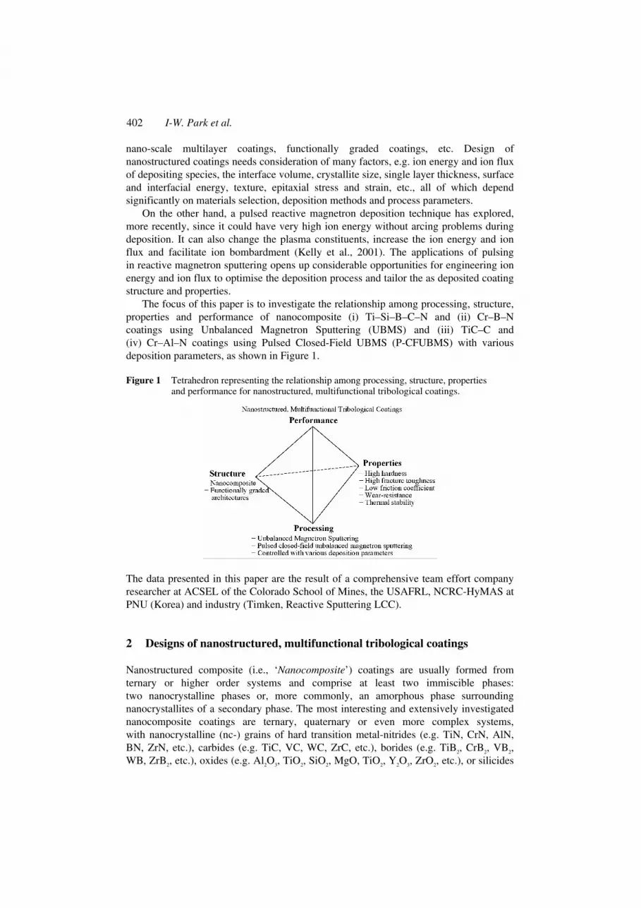
The focus of this paper is to investigate the relationship among processing, structure, properties and performance of nanocomposite (i) Ti–Si–B–C–N and (ii) Cr–B–N coatings using Unbalanced Magnetron Sputtering (UBMS) and (iii) TiC–C and (iv) Cr–Al–N coatings using Pulsed Closed-Field UBMS (P-CFUBMS) with various deposition parameters, as shown in Figure 1.
Figure 1 Tetrahedron representing the relationship among processing, structure, properties and performance for nanostructured, multifunctional tribological coatings.
The data presented in this paper are the result of a comprehensive team effort company researcher at ACSEL of the Colorado School of Mines, the USAFRL, NCRC-HyMAS at PNU (Korea) and industry (Timken, Reactive Sputtering LCC).
2 Designs of nanostructured, multifunctional tribological coatings
Nanostructured composite (i.e., ‘Nanocomposite’) coatings are usually formed from ternary or higher order systems and comprise at least two immiscible phases: two nanocrystalline phases or, more commonly, an amorphous phase surrounding nanocrystallites of a secondary phase. The most interesting and extensively investigated nanocomposite coatings are ternary, quaternary or even more complex systems, with nanocrystalline (nc-) grains of hard transition metal-nitrides (e.g. TiN, CrN, AlN, BN, ZrN, etc.), carbides (e.g. TiC, VC, WC, ZrC, etc.), borides (e.g. TiB2, CrB2, VB2, WB, ZrB2, etc.), oxides (e.g. Al2O3, TiO2, SiO2, MgO, TiO2, Y2O3, ZrO2, etc.), or silicides
Nanostructured, multifunctional tribological coatings 403
(e.g. TiSi2, CrSi2, ZrSi2, etc.) surrounded by amorphous (a-) matrices (e.g. Si3N4, BN, C, etc.). The synthesis of such nanocomposite (nc-/a-) coatings critically depends on the ability to co-deposit both the nanocrystalline and amorphous phases, such as Ti–Si–N (nc-TiN/nc-and a-TiSi2/a-Si3N4)
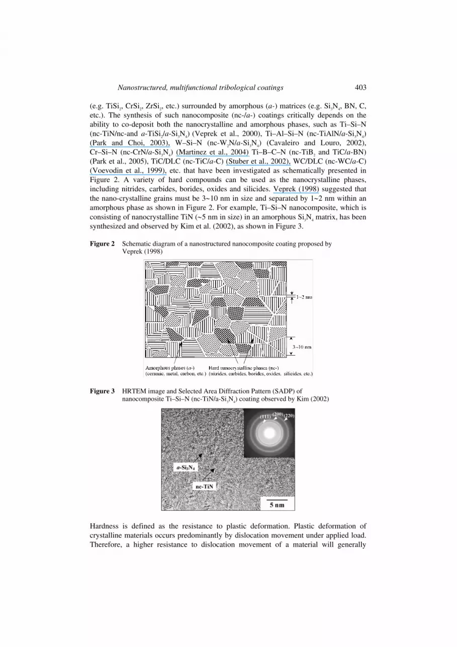
(Veprek et al., 2000), Ti–Al–Si–N (nc-TiAlN/a-Si3N4) (Park and Choi, 2003), W–Si–N (nc-W2N/a-Si3N4) (Cavaleiro and Louro, 2002), Cr–Si–N (nc-CrN/a-Si3N4) (Martinez et al., 2004), Ti–B–C–N (nc-TiB2 and TiC/a-BN) (Park et al., 2005), TiC/DLC (nc-TiC/a-C) (Stuber et al., 2002), WC/DLC (nc-WC/a-C) (Voevodin et al., 1999), etc. that have been investigated as schematically presented in Figure 2. A variety of hard compounds can be used as the nanocrystalline phases, including nitrides, carbides, borides, oxides and silicides. Veprek (1998) suggested that the nano-crystalline grains must be 3∼10 nm in size and separated by 1∼2 nm within an amorphous phase as shown in Figure 2. For example, Ti–Si–N nanocomposite, which is consisting of nanocrystalline TiN (∼5 nm in size) in an amorphous Si3N4 matrix, has been synthesized and observed by Kim et al. (2002), as shown in Figure 3.
Figure 2 Schematic diagram of a nanostructured nanocomposite coating proposed by Veprek (1998)
Figure 3 HRTEM image and Selected Area Diffraction Pattern (SADP) of nanocomposite Ti–Si–N (nc-TiN/a-Si
3N
4) coating observed by Kim (2002)
Hardness is defined as the resistance to plastic deformation. Plastic deformation of crystalline materials occurs predominantly by dislocation movement under applied load. Therefore, a higher resistance to dislocation movement of a material will generally
404 I-W. Park et al.
enhance its hardness. An approach to obtain high resistance to dislocation movement and plastic deformation is to preclude the formation of stable dislocations. ‘Superhard’ coatings, with a hardness value in excess of 40 GPa, have attracted significantly increasing interest during the past 10∼15 years (Shizhi et al., 1992). A concept for superhard nanocomposite coatings was suggested by Veprek and Reiprich (1995). The increase in hardness of nanocomposites in comparison to single phase coatings was based on the suppression of dislocation operation by using small 3∼10 nm grains and inducing grain incoherence strains when using 1∼2 thin amorphous matrix for grain separation. In the absence of dislocation activity in such small grains, Griffith’s equation for crack propagation was proposed (Dieter et al, 1976) as a simple description of the composite strength, σ :
2 s
o
E
a
γσ
π= (1)
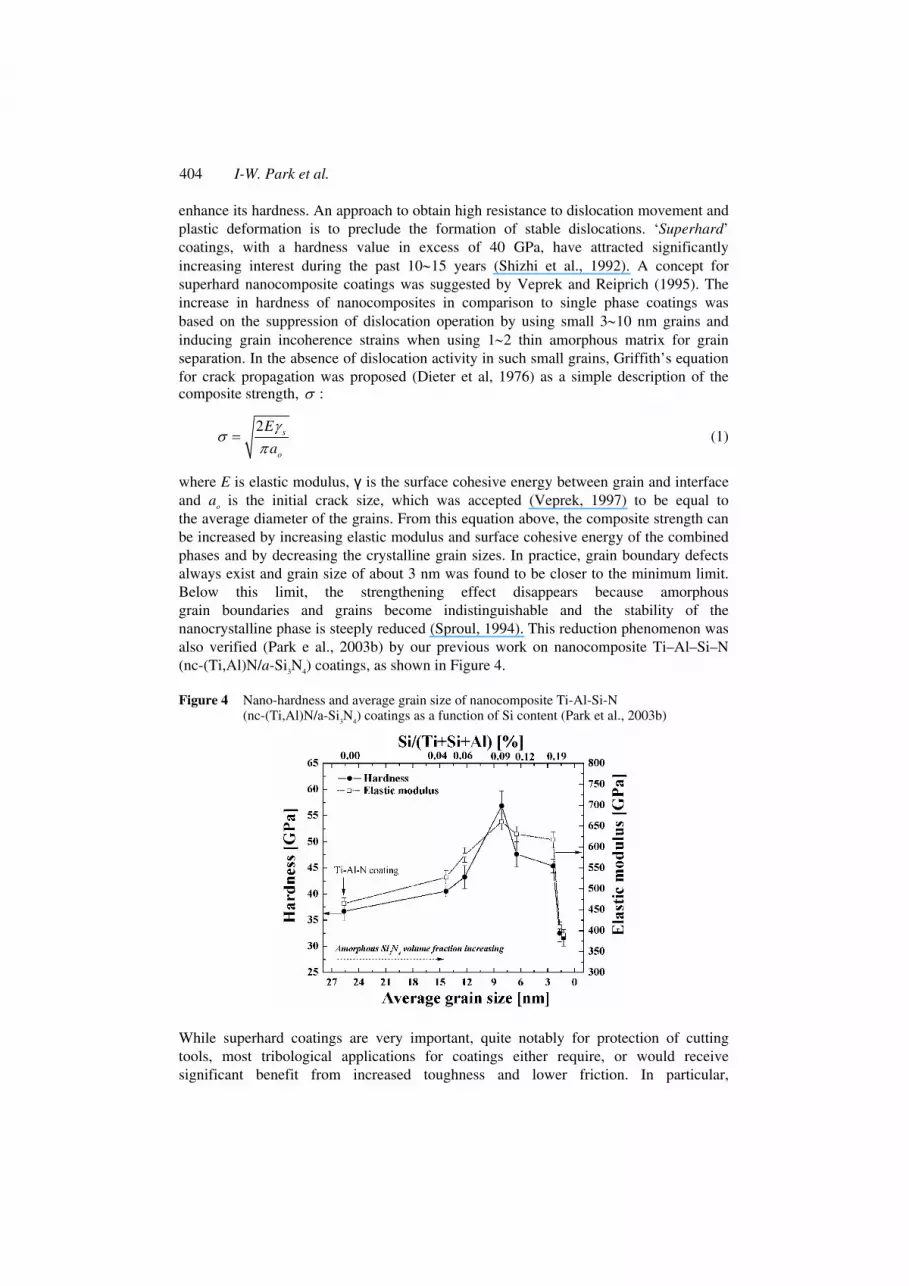
where E is elastic modulus, γ is the surface cohesive energy between grain and interface and ao is the initial crack size, which was accepted (Veprek, 1997) to be equal to the average diameter of the grains. From this equation above, the composite strength can be increased by increasing elastic modulus and surface cohesive energy of the combined phases and by decreasing the crystalline grain sizes. In practice, grain boundary defects always exist and grain size of about 3 nm was found to be closer to the minimum limit. Below this limit, the strengthening effect disappears because amorphous grain boundaries and grains become indistinguishable and the stability of the nanocrystalline phase is steeply reduced (Sproul, 1994). This reduction phenomenon was also verified (Park e al., 2003b) by our previous work on nanocomposite Ti–Al–Si–N (nc-(Ti,Al)N/a-Si3N4) coatings, as shown in Figure 4.
Figure 4 Nano-hardness and average grain size of nanocomposite Ti-Al-Si-N (nc-(Ti,Al)N/a-Si
3N
4) coatings as a function of Si content (Park et al., 2003b)
While superhard coatings are very important, quite notably for protection of cutting tools, most tribological applications for coatings either require, or would receive significant benefit from increased toughness and lower friction. In particular,

Nanostructured, multifunctional tribological coatings 405
‘High Fracture Toughness’ is necessary for applications where high contact loads and, hence, significant substrate deformations, are encountered (Voevodin and Zabinski, 2000). A material is generally considered tough if it possesses both high strength and high ductility. High hardness (H) is directly related to high elastic modulus (E) and high yield strength, but it is very challenging to add a measure of ductility to hard coatings. For example, the superhard coating designs, as stated earlier, prevent dislocation activity, essentially eliminating one common mechanism for ductility. Therefore, designs that increase ductility must also be considered to provide tough tribological coatings. Pharr (1998) has suggested that an indication of fracture toughness (i.e. H/E ratio) can be obtained by examining the surface radial cracks created during indentation, described by the equation.
1/ 2
1 3 / 2c
E PK
H cα ⎛ ⎞ ⎛ ⎞= ⎜ ⎟ ⎜ ⎟
⎝ ⎠ ⎝ ⎠ (2)
where P is the peak indentation load, c the radial crack length and α1 an empirical constant related to the indenter geometry. Kc describes the ‘critical stress intensity’ for crack propagation, but it is not an intrinsic parameter that can be used to measure fracture toughness directly. However, it is proportional to fracture toughness. Thus, fracture toughness of coatings would appear to be improved by both a high hardness and a ‘Low Elastic Modulus.’ In this work, the H/E values were calculated and discussed relatively for each coating (Leyland and Matthews, 2000).
For tribological prevention, there are additional requirements related to the normal (load) and tangential (friction) forces. In general terms, a tough ‘Wear-resistant’ coating must support high loads in sliding or rolling contact without failure by wear, cohesive fracture and loss of adhesion (delamination). A ‘Low Friction Coefficient’ reduces friction losses and may increase load capability. Tribological coatings where a low friction coefficient is also required may be obtained by producing nanocomposite coatings with a mix of hard and lubricating phase, in which a hard primary phases (e.g. nitrides, carbides, or borides, etc.) provides wear-resistance and load-bearing capability and a lubricating secondary phases (e.g. a-C, a-Si3N4, a-BN, etc.) reduces the friction between two contacting components. Finally, ‘Thermal Stability’ is required to optimise coating performance and lifetime. The amorphous phases in grain boundaries can act as diffusion barriers (e.g. a-Si3N4, a-SiO2, etc.) for improved thermal stability. For instance, nc-TiN/a-Si3N4 coatings with amorphous Si3N4 matrix did not show grain growth at temperatures up to 1050°C as well as superhardness of about 45 GPa (Veprek, 1997). Moreover, silicon nitride acts as an efficient barrier against oxygen diffusion at the grain boundaries and also by forming an oxidation resistant SiO2 surface layer and thus resulting in excellent thermal stability.
In summary, in addition to high hardness, other aspects such as, high toughness, low friction coefficient and high thermal stability are decisive characteristics of nanocomposite coatings for their potential as protective tribological coatings.

406 I-W. Park et al.
3 Deposition processes and conditions
Four nanostructured coating systems have been examined: (i) Ti–Si–B–C–N and (ii) Cr–B–N systems deposited by UBMS and (iii)Cr–Al–N and (iv) TiC–C systems deposited by P-CFUBMS.
3.1 UBMS of Ti–Si–B–C–N and Cr–B–N coatings
Ti–Si–B–C–N and Cr–B–N coatings were prepared from a TiB2–TiC composite target (80mol%TiB2–20mol%TiC) with silicon target and CrB2 target, respectively, using UBMS system in an argon-nitrogen atmosphere. A schematic diagram of the apparatus is depicted in Figure 5. The TiB2–TiC composite target and CrB2 target was synthesised using a one-step SHS (self-propagating high-temperature synthesis) consolidation method (Levashov et al., 1997). Before being placed into the chamber for deposition, all substrates were ultrasonically cleaned in acetone, ethanol and deionised water for 10, 15 and 10 min, respectively. Substrates were further cleaned in the deposition chamber by ion bombardment using a bias voltage range from −250 to −350 V under Ar atmosphere of 8.8 Pa (65mTorr) for 30 min. Typical deposition conditions for Ti–Si–B–C–N and Cr–B–N coatings are summarised in Table 1.
Figure 5 Schematic diagram of the UBMS system for Ti–Si–B–C–N and Cr–B–N coatings
3.2 P-CFUBMS of TiC–C and Cr–Al–N coatings
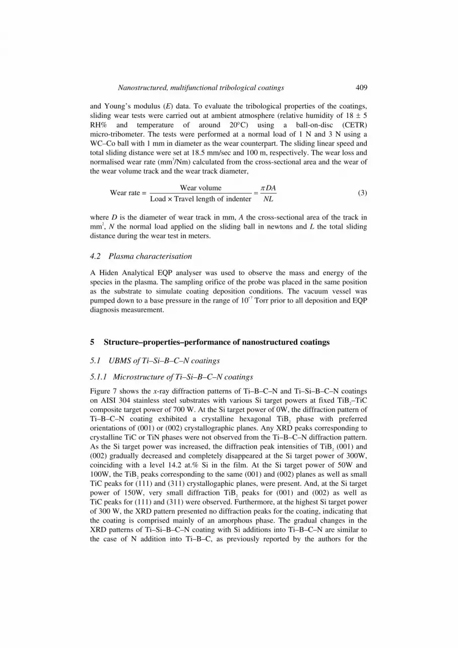
Nanostructured TiC–C and Cr–Al–N coatings were prepared from a Ti target and graphite target and a Cr target and Al target, respectively, using a P-CFUBMS system in an argon- nitrogen atmosphere. A schematic diagram of the apparatus is depicted in Figure 6. Typical deposition conditions for TiC–C and Cr–Al–N coatings are summarised in Table 2.
Nanostructured, multifunctional tribological coatings 407
Table 1 Typical deposition conditions of Ti–Si–B–C–N and Cr–B–N coatings by UBMS
Process Parameter Ti–Si–B–C–N coatings Cr–B–N coatings
Sputter etching
Bias voltage
Ar Pressure
Time
−250 V
8.8 Pa
30 min
−350 V
8.8 Pa
30 min
Deposition Target
Substrate
Sub.-to-target distance
Base pressure
Working pressure
Deposition temperature
Bias voltage
N2 / (Ar+N
2) gas ratio
Target sputter power (1)
Target sputter power (2)
Deposition time
80/20 TiB2-TiC
Pure Si target
AISI 304 SS
153 mm
< 6.7 × 10⁻⁴ Pa
4 × 10⁻¹ Pa
Room temperature
−50 V
1 %
700 W (TiB2-TiC)
0 W ∼ 300 W (Si)
2 hr
CrB2
–
AISI 304 SS
130 mm
< 4.6 × 10⁻⁴ Pa
4 × 10⁻¹ Pa
Room temperature
−50 V
1% ∼ 9%
400 W ∼ 600 W (CrB
2)
–
1 hr
Figure 6 Schematic diagram of the P-CFUBMS system equipped with a Hiden Elecrostatic Quadrupole Plasma (EQP) analyser for TiC–C and Cr–Al–N coatings.

408 I-W. Park et al.
Table 2 Typical deposition conditions of TiC–C and Cr–Al–N coatings by P-CFUBMS
Process Parameter TiC–C coatings Cr–Al–N coatings
Sputter etching
Bias voltage
Ar Pressure
Time
−400 V
0.93 Pa
10 min
–400V
0.93 Pa
10 min
Deposition Target
Substrate
Sub.-to-target distance
Base pressure
Working pressure
Deposition temperature
Bias voltage
N2/(Ar+N
2) gas ratio
Target-1 sputter power
Frequency
Reverse time
Target-2 sputter power
Frequency
Reverse time
Deposition time
Ti and Graphite
AISI 304 SS
200 mm
< 2.67 × 10⁻⁴ Pa
3.3 × 10⁻¹ Pa
Room temperature
−50 V
•
450 W (Ti)
0 and 100 kHz
1″
1000 W (Graphite)
0 and 100 kHz
1″
2 hr
Cr and Al
AISI 304 SS
127 and 208 mm
< 1.3 × 10⁻⁴ Pa
2.6 × 10⁻¹ Pa
Room temperature
–50 V
75 %
200 W (Cr)
100 and 350 kHz
0.4~1.4″
200 W ~ 1400 W (Al)
100 and 350 kHz
0.4~1.4″
2hr
4 Characterisation
4.1 Coating characterisation
The coating thickness was measured using a stylus (α–STEP) profilometer and scanning electron microscopy (SEM, Hitachi, S–4200). The crystallinity of coatings was analysed by x–ray diffraction (XRD, PHILIPS, X’Pert–MPD System) using CuK α radiation. X–ray photoelectron spectroscopy (XPS, PHI XPS Systems, 5600LS) using a monochromatic Al source was also performed to determine the level of present in bonding status of each element the coatings. The XPS spectra were obtained after removing the surface layer by sputtering with Ar+ ions (4 keV) for 40 min and were calibrated using Cu and Au peaks at 932.67 eV and 84.0 eV, respectively. A Phillips/FEI CM 200 Transmission Electron Microscope (TEM) operating at 200 kV was used to evaluate the grain size and nanostructure of the coatings. Holey carbon TEM grids were coated directly in the chamber with the coating of interest, using a thinner titanium adhesion layer of only about 7 nm. A MTS nano-indenter XPII equipped with a Berkovich diamond indenter was used to perform depth sensing nanoindentation testing on the coatings and to obtain values of nanohardness and Young’s modulus with a Poisson’s ratio of 0.25. The H/E ratio was calculated from the obtained hardness (H)
Nanostructured, multifunctional tribological coatings 409
and Young’s modulus (E) data. To evaluate the tribological properties of the coatings, sliding wear tests were carried out at ambient atmosphere (relative humidity of 18 ± 5 RH% and temperature of around 20°C) using a ball-on-disc (CETR) micro-tribometer. The tests were performed at a normal load of 1 N and 3 N using a WC–Co ball with 1 mm in diameter as the wear counterpart. The sliding linear speed and total sliding distance were set at 18.5 mm/sec and 100 m, respectively. The wear loss and normalised wear rate (mm3/Nm) calculated from the cross-sectional area and the wear of the wear volume track and the wear track diameter,
Wear volumeWear rate =
Load × Travel length of indenter
DA
NL
π= (3)
where D is the diameter of wear track in mm, A the cross-sectional area of the track in mm2, N the normal load applied on the sliding ball in newtons and L the total sliding distance during the wear test in meters.
4.2 Plasma characterisation
A Hiden Analytical EQP analyser was used to observe the mass and energy of the species in the plasma. The sampling orifice of the probe was placed in the same position as the substrate to simulate coating deposition conditions. The vacuum vessel was pumped down to a base pressure in the range of 10• 7 Torr prior to all deposition and EQP diagnosis measurement.
5 Structure–properties–performance of nanostructured coatings
5.1 UBMS of Ti–Si–B–C–N coatings
5.1.1 Microstructure of Ti–Si–B–C–N coatings
Figure 7 shows the x-ray diffraction patterns of Ti–B–C–N and Ti–Si–B–C–N coatings on AISI 304 stainless steel substrates with various Si target powers at fixed TiB2–TiC composite target power of 700 W. At the Si target power of 0W, the diffraction pattern of Ti–B–C–N coating exhibited a crystalline hexagonal TiB2 phase with preferred orientations of (001) or (002) crystallographic planes. Any XRD peaks corresponding to crystalline TiC or TiN phases were not observed from the Ti–B–C–N diffraction pattern. As the Si target power was increased, the diffraction peak intensities of TiB2 (001) and (002) gradually decreased and completely disappeared at the Si target power of 300W, coinciding with a level 14.2 at.% Si in the film. At the Si target power of 50W and 100W, the TiB2 peaks corresponding to the same (001) and (002) planes as well as small TiC peaks for (111) and (311) crystallogaphic planes, were present. And, at the Si target power of 150W, very small diffraction TiB2 peaks for (001) and (002) as well as TiC peaks for (111) and (311) were observed. Furthermore, at the highest Si target power of 300 W, the XRD pattern presented no diffraction peaks for the coating, indicating that the coating is comprised mainly of an amorphous phase. The gradual changes in the XRD patterns of Ti–Si–B–C–N coating with Si additions into Ti–B–C–N are similar to the case of N addition into Ti–B–C, as previously reported by the authors for the
410 I-W. Park et al.
Ti–B–C–N nanocomposite system (Park et al., 2005). In the latter report, it was revealed that the crystallites in the Ti–B–C–N coating were composed of solid-solution (Ti,C,N)B2 and Ti(C,N) crystallites (~10 nm in size). Addition of nitrogen into the Ti–B–C coating led to grain refinement of (Ti,C,N)B2 and Ti(C,N) crystallites and their distribution is coupled with a percolation phenomenon of amorphous BN and carbon phase.
Figure 7 XRD patterns of Ti–B–C–N and Ti–Si–B–C–N coating on AISI 304 stainless steel substrates with various Si target powers at fixed TiB
2–TiC composite target power of
700 W
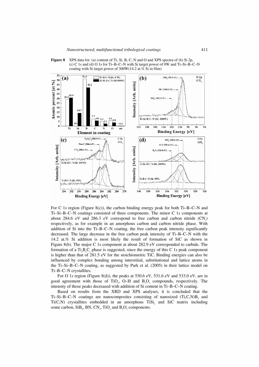
In order to determine the chemical composition and to investigate the bonding status of Ti–Si–B–C–N coating, x-ray Photoelectron Spectroscopy (XPS) was performed on Ti–B–C–N and Ti–Si–B–C–N coatings deposited at different Si target powers. Figure 8(a) provides the content of each element in the Ti–Si–B–C–N coating with two different Si target powers and a fixed TiB2–TiC target power of 700 W. As the Si target power of 300W was introduced the Ti–B–C–N coating, the Si content was increased in Ti–Si–B–C–N coating from 0 to 14.2 at.%. The content of boron steeply decreased relatively with increasing silicon content in the Ti–Si–B–C–N coating. The oxygen contents were also observed to be about 6.1 at.% and 3.8 at.% in Ti–B–C–N and Ti–Si–B–C–N coatings, respectively. It is believed that the majority of oxygen is induced from the target (Levashov et al., 1997). This type of oxygen contamination can possibly be reduced by pretreatment of the reactant powders prior to the synthesis of the target, e.g. using a hydrogen reduction pretreatment. Figures 8(b)–(d) present the XPS spectra binding energies of Si (Figure 8(b)), C (Figure 8(c)) and O (Figure 8(d)) for the Ti–B–C–N and Ti–Si(14.2 at.%)–B–C–N coatings.
For Si 2p region (Figure 8(b)), the major peak at 99.3 eV, which corresponds to TiSi2 compound, is clearly present in the Ti–Si(14.2 at.%)–B–C–N coating. At a higher binding energy, a shoulder had developed for the peak at 100.3 eV, which corresponds to the formation of SiC. Another peak, which corresponds to the formation of SiB4, was observed at 101.9 eV on the Si 2p XPS spectra. Analyses of the B 1s and N 1s peaks helped to identify the produced phases.
Nanostructured, multifunctional tribological coatings 411
Figure 8 XPS data for: (a) content of Ti, Si, B, C, N and O and XPS spectra of (b) Si 2p, (c) C 1s and (d) O 1s for Ti–B–C–N with Si target power of 0W and Ti–Si–B–C–N coating with Si target power of 300W(14.2 at.% Si in film)
For C 1s region (Figure 8(c)), the carbon binding energy peak for both Ti–B–C–N and Ti–Si–B–C–N coatings consisted of three components. The minor C 1s components at about 284.6 eV and 286.3 eV correspond to free carbon and carbon nitride (CNx) respectively, as for example in an amorphous carbon and carbon nitride phase. With addition of Si into the Ti–B–C–N coating, the free carbon peak intensity significantly decreased. The large decrease in the free carbon peak intensity of Ti–B–C–N with the 14.2 at.% Si addition is most likely the result of formation of SiC as shown in Figure 8(b). The major C 1s component at about 282.9 eV corresponded to carbide. The formation of a TixByCz phase is suggested, since the energy of this C 1s peak component is higher than that of 281.5 eV for the stoichiometric TiC. Binding energies can also be influenced by complex bonding among interstitial, substitutional and lattice atoms in the Ti–Si–B–C–N coating, as suggested by Park et al. (2005) in their lattice model on Ti–B–C–N crystallites.
For O 1s region (Figure 8(d)), the peaks at 530.6 eV, 531.6 eV and 533.0 eV, are in good agreement with those of TiO2, O–H and B2O3 compounds, respectively. The intensity of those peaks decreased with addition of Si content in Ti–B–C–N coating.
Based on results from the XRD and XPS analyses, it is concluded that the Ti–Si–B–C–N coatings are nanocomposites consisting of nanosized (Ti,C,N)B2 and Ti(C,N) crystallites embedded in an amorphous TiSi2 and SiC matrix including some carbon, SiB4, BN, CNx, TiO2 and B2O3 components.
412 I-W. Park et al.
5.1.2 Mechanical properties of Ti–Si–B–C–N coatings
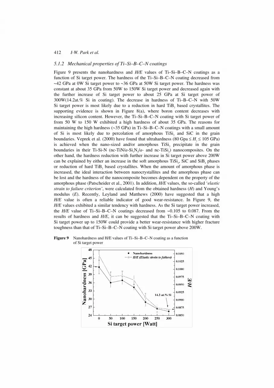
Figure 9 presents the nanohardness and H/E values of Ti–Si–B–C–N coatings as a function of Si target power. The hardness of the Ti–Si–B–C–N coating decreased from ∼42 GPa at 0W Si target power to ∼36 GPa at 50W Si target power. The hardness was constant at about 35 GPa from 50W to 150W Si target power and decreased again with the further increase of Si target power to about 25 GPa at Si target power of 300W(14.2at.% Si in coating). The decrease in hardness of Ti–B–C–N with 50W Si target power is most likely due to a reduction in hard TiB2 based crystallites. The supporting evidence is shown in Figure 8(a), where boron content decreases with increasing silicon content. However, the Ti–Si–B–C–N coating with Si target power of from 50 W to 150 W exhibited a high hardness of about 35 GPa. The reasons for maintaining the high hardness (∼35 GPa) in Ti–Si–B–C–N coatings with a small amount of Si is most likely due to percolation of amorphous TiSi2 and SiC in the grain boundaries. Veprek et al. (2000) have found that ultrahardness (80 Gpa ≤ Hv ≤ 105 GPa) is achieved when the nano-sized and/or amorphous TiSi2 precipitate in the grain boundaries in their Ti-Si-N (nc-TiN/a-Si3N4/a- and nc-TiSi2) nanocomposites. On the other hand, the hardness reduction with further increase in Si target power above 200W can be explained by either an increase in the soft amorphous TiSi2, SiC and SiB4 phases or reduction of hard TiB2 based crystallites. When the amount of amorphous phase is increased, the ideal interaction between nanocrystallites and the amorphous phase can be lost and the hardness of the nanocomposite becomes dependent on the property of the amorphous phase (Patscheider et al., 2001). In addition, H/E values, the so-called ‘elastic strain to failure criterion’, were calculated from the obtained hardness (H) and Young’s modulus (E). Recently, Leyland and Matthews (2000) have suggested that a high H/E value is often a reliable indicator of good wear-resistance. In Figure 9, the H/E values exhibited a similar tendency with hardness. As the Si target power increased, the H/E value of Ti–Si–B–C–N coatings decreased from ∼0.105 to 0.087. From the results of hardness and H/E, it can be suggested that the Ti–Si–B–C–N coating with Si target power up to 150W could provide a better wear-resistance with higher fracture toughness than that of Ti–Si–B–C–N coating with Si target power above 200W.
Figure 9 Nanohardness and H/E values of Ti–Si–B–C–N coating as a function of Si target power
Nanostructured, multifunctional tribological coatings 413
5.1.3 Tribological performance of Ti–Si–B–C–N coatings
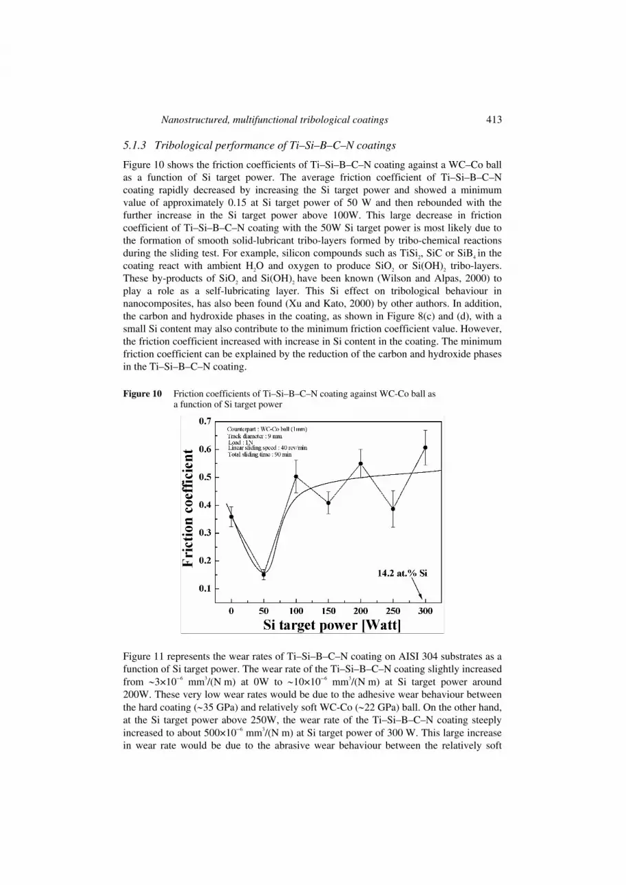
Figure 10 shows the friction coefficients of Ti–Si–B–C–N coating against a WC–Co ball as a function of Si target power. The average friction coefficient of Ti–Si–B–C–N coating rapidly decreased by increasing the Si target power and showed a minimum value of approximately 0.15 at Si target power of 50 W and then rebounded with the further increase in the Si target power above 100W. This large decrease in friction coefficient of Ti–Si–B–C–N coating with the 50W Si target power is most likely due to the formation of smooth solid-lubricant tribo-layers formed by tribo-chemical reactions during the sliding test. For example, silicon compounds such as TiSi2, SiC or SiB4 in the coating react with ambient H2O and oxygen to produce SiO2 or Si(OH)2 tribo-layers. These by-products of SiO2 and Si(OH)2 have been known (Wilson and Alpas, 2000) to play a role as a self-lubricating layer. This Si effect on tribological behaviour in nanocomposites, has also been found (Xu and Kato, 2000) by other authors. In addition, the carbon and hydroxide phases in the coating, as shown in Figure 8(c) and (d), with a small Si content may also contribute to the minimum friction coefficient value. However, the friction coefficient increased with increase in Si content in the coating. The minimum friction coefficient can be explained by the reduction of the carbon and hydroxide phases in the Ti–Si–B–C–N coating.
Figure 10 Friction coefficients of Ti–Si–B–C–N coating against WC-Co ball as a function of Si target power
Figure 11 represents the wear rates of Ti–Si–B–C–N coating on AISI 304 substrates as a function of Si target power. The wear rate of the Ti–Si–B–C–N coating slightly increased from ∼3×10⁻⁶ mm3/(N m) at 0W to ∼10×10−6 mm3/(N m) at Si target power around 200W. These very low wear rates would be due to the adhesive wear behaviour between the hard coating (∼35 GPa) and relatively soft WC-Co (∼22 GPa) ball. On the other hand, at the Si target power above 250W, the wear rate of the Ti–Si–B–C–N coating steeply increased to about 500×10−6 mm3/(N m) at Si target power of 300 W. This large increase in wear rate would be due to the abrasive wear behaviour between the relatively soft

414 I-W. Park et al.
coating (∼25 GPa) and the WC-Co ball. Combining the results of the H/E (Figure 9) values and wear rates (Figure 11), the Ti–Si–B–C–N coating with a higher H/E had a better wear-resistance against WC-Co ball in agreement with Leyland and Matthews (2000).
Figure 11 Wear rates of Ti–Si–B–C–N coating on AISI 304 substrates as a function of Si target power
5.2 UBMS of Cr–B–N coatings
5.2.1 Microstructure of Cr–B–N coatings
Figure 12 shows the x-ray diffraction patterns of Cr–B–N coatings on AISI 304 stainless steel substrates with different N2 amount in argon-nitrogen atmospheres at a CrB2 target power of 500W. At a N2 amount of 1% in the chamber, the diffraction pattern of the Cr–B–N coating(7.2 at.% N in film) exhibited a weak hexagonal CrB2 phase consisting of (001), (101) and (002) crystallographic planes. In addition to their presence, the shapes of the peaks were fairly broad, which is an indication of peak broadening, which is believed to originate from the diminution of grain size or the residual stress induced in the crystal lattice (Cullity, 1978). Any XRD peaks corresponding to crystalline CrN, Cr2N or BN phases were not observed from the Cr–B–N diffraction patterns. Above the N2 amount of 5% in the chamber, all the diffraction peaks of CrB2 completely disappeared, indicating the presence of an amorphous phase at N2 amounts above 5% in the chamber.
Figure 13 shows the x-ray diffraction patterns of Cr–B–N coatings with different CrB2 target powers at N2 amounts of 1%, in the argon-nitrogen atmosphere. At a CrB2 target power of 400W, the diffraction pattern of the Cr–B–N coating exhibited a hexagonal CrB2 phase with (001) and (002) crystallographic orientations. As the target power was increased to 500W, the peak intensity of the CrB2 (001) orientation decreased slightly and the CrB2 (101) orientation appeared. With further increase in the target power to 600 W, the diffraction peak intensity of the CrB2 (001) increased again and the CrB2 (101) peak decreased.

Nanostructured, multifunctional tribological coatings 415
Figure 12 XRD patterns of Cr−B−N coatings on AISI stainless steel substrates with different N
2/(N
2+Ar) gas ratios at fixed CrB
2 target power of 500 W
Figure 13 XRD patterns of Cr−B−N coatings on AISI stainless steel substrates with different CrB
2 target powers at fixed N
2/(N
2+Ar) gas ratio of 1%(7.2 at.% N in film)
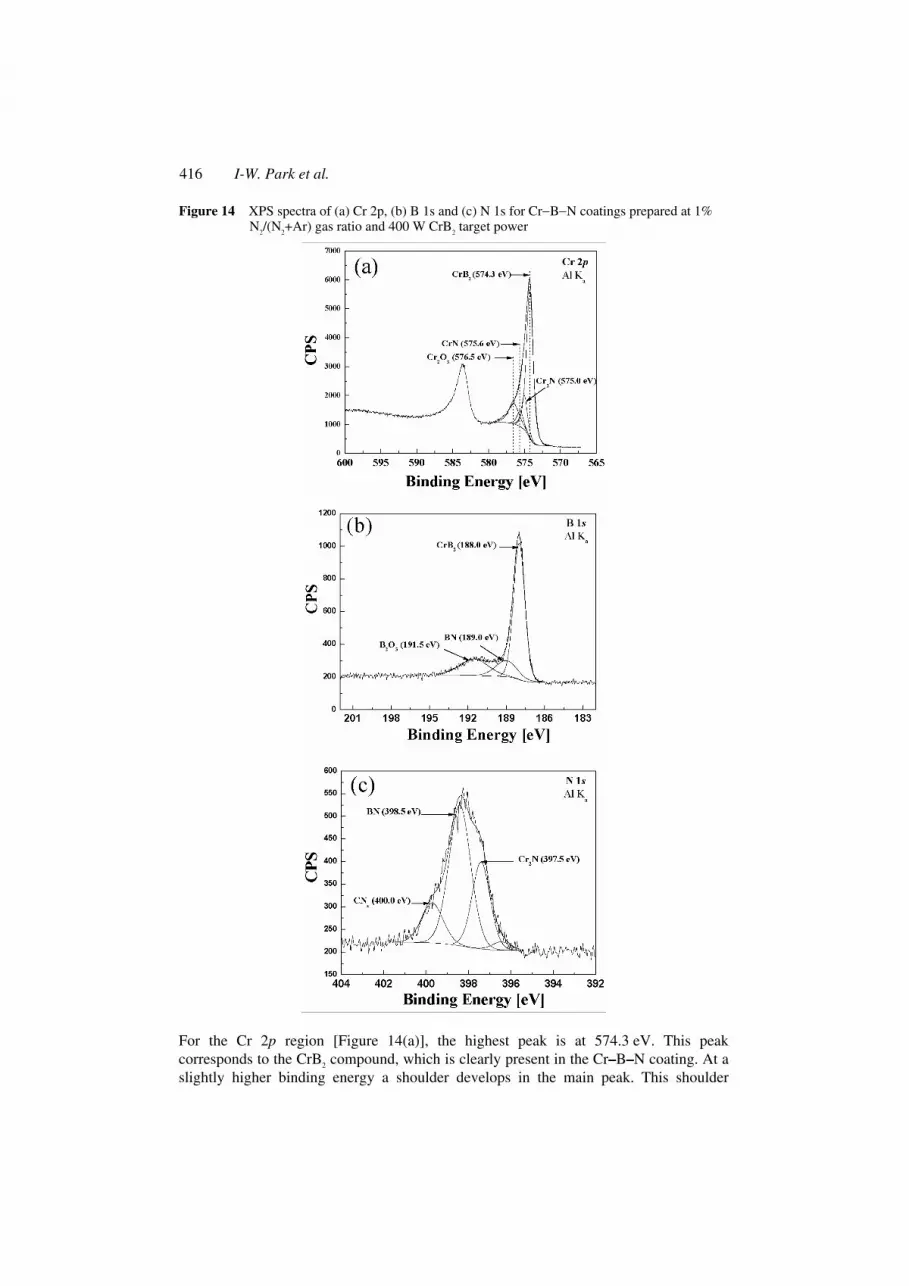
In order to determine the chemical composition and to investigate the bonding status of the Cr–B–N coating, x-ray photoelectron spectroscopy (XPS) was performed on the Cr–B–N coating prepared at 1% N2/(N2+Ar) gas ratio and 400 W CrB2 target power. The chemical composition for each element present in the coating is as follows: Cr (37.9 at%), B (51.4 at.%), N (7.2 at.%), O (2.4 at.%) and C (1.1 at.%). Figures 14(a)–(c) represents the XPS spectra for binding energies of Cr (Figure 14(a)), B (Figure 14(b)) and N (Figure 14(c)) for the Cr–B–N coatings.
416 I-W. Park et al.
Figure 14 XPS spectra of (a) Cr 2p, (b) B 1s and (c) N 1s for Cr−B−N coatings prepared at 1% N
2/(N
2+Ar) gas ratio and 400 W CrB
2 target power
For the Cr 2p region [Figure 14(a)], the highest peak is at 574.3 eV. This peak corresponds to the CrB2 compound, which is clearly present in the Cr–B–N coating. At a slightly higher binding energy a shoulder develops in the main peak. This shoulder
Nanostructured, multifunctional tribological coatings 417
consists of the following binding energies: 575.0, 575.6 and 576.5 eV. These binding energies correspond to the formation of Cr2N, CrN, Cr2O3, respectively. Analyses of the B 1s and N 1s peaks helped to identify the formation of phases. For the B 1s region (Figure 14(b)), the boron binding energy peak consisted of three components. The major B 1s component at about 188.0 eV corresponded to CrB2. The minor B 1s components at about 189.0 eV and 191.5 eV correspond to amorphous Boron Nitride (BN) and amorphous boron oxide (B2O3) phases, respectively. For the N 1s region [Figure 14(c)], the peaks at 379.5 eV, 398.5 eV and 400.0 eV, are in good agreement with that of Cr2N, BN and CNx compounds, respectively.
Based on results from the XRD and XPS analyses, it is concluded that the Cr–B–N coatings consist of very small-sized CrB2 crystallites with an amorphous Cr2N and BN matrix including some components of Cr2O3, CNx, CrN and B2O3 components.
5.2.2 Mechanical properties of Cr–B–N coatings
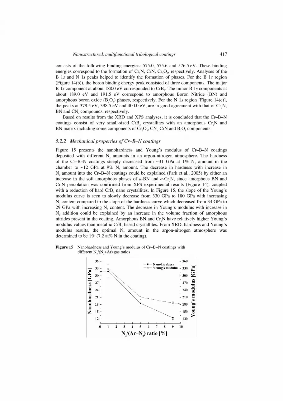
Figure 15 presents the nanohardness and Young’s modulus of Cr–B–N coatings deposited with different N2 amounts in an argon-nitrogen atmosphere. The hardness of the Cr–B–N coatings steeply decreased from ∼31 GPa at 1% N2 amount in the chamber to ∼12 GPa at 9% N2 amount. The decrease in hardness with increase in N2 amount into the Cr–B–N coatings could be explained (Park et al., 2005) by either an increase in the soft amorphous phases of a-BN and a-Cr2N, since amorphous BN and Cr2N percolation was confirmed from XPS experimental results (Figure 14), coupled with a reduction of hard CrB2 nano crystallites. In Figure 15, the slope of the Young’s modulus curve is seen to slowly decrease from 330 GPa to 180 GPa with increasing N2 content compared to the slope of the hardness curve which decreased from 34 GPa to 29 GPa with increasing N2 content. The decrease in Young’s modulus with increase in N2 addition could be explained by an increase in the volume fraction of amorphous nitrides present in the coating. Amorphous BN and Cr2N have relatively higher Young’s modulus values than metallic CrB2 based crystallites. From XRD, hardness and Young’s modulus results, the optimal N2 amount in the argon-nitrogen atmosphere was determined to be 1% (7.2 at% N in the coating).
Figure 15 Nanohardness and Young’s modulus of Cr−B−N coatings with different N
2/(N
2+Ar) gas ratios

418 I-W. Park et al.
Figure 16 shows the nanohardness and Young’s modulus of Cr–B–N coatings with different CrB2 target powers at N2 amount of 1% in argon-nitrogen atmosphere. The hardness of the Cr–B–N coatings decreased from ∼34 GPa at 400 W target power to ∼29 GPa at 600 W target power. On the other hand, the Young’s modulus increased from ∼320 GPa at 400W to ~330 GPa at 500 W CrB2 target power and then decreased again with further increase in the target power.
Figure 16 Nanohardness and Young’s modulus of Cr−B−N coatings with different CrB
2 target powers at fixed N
2/(N
2+Ar) gas ratio of 1%
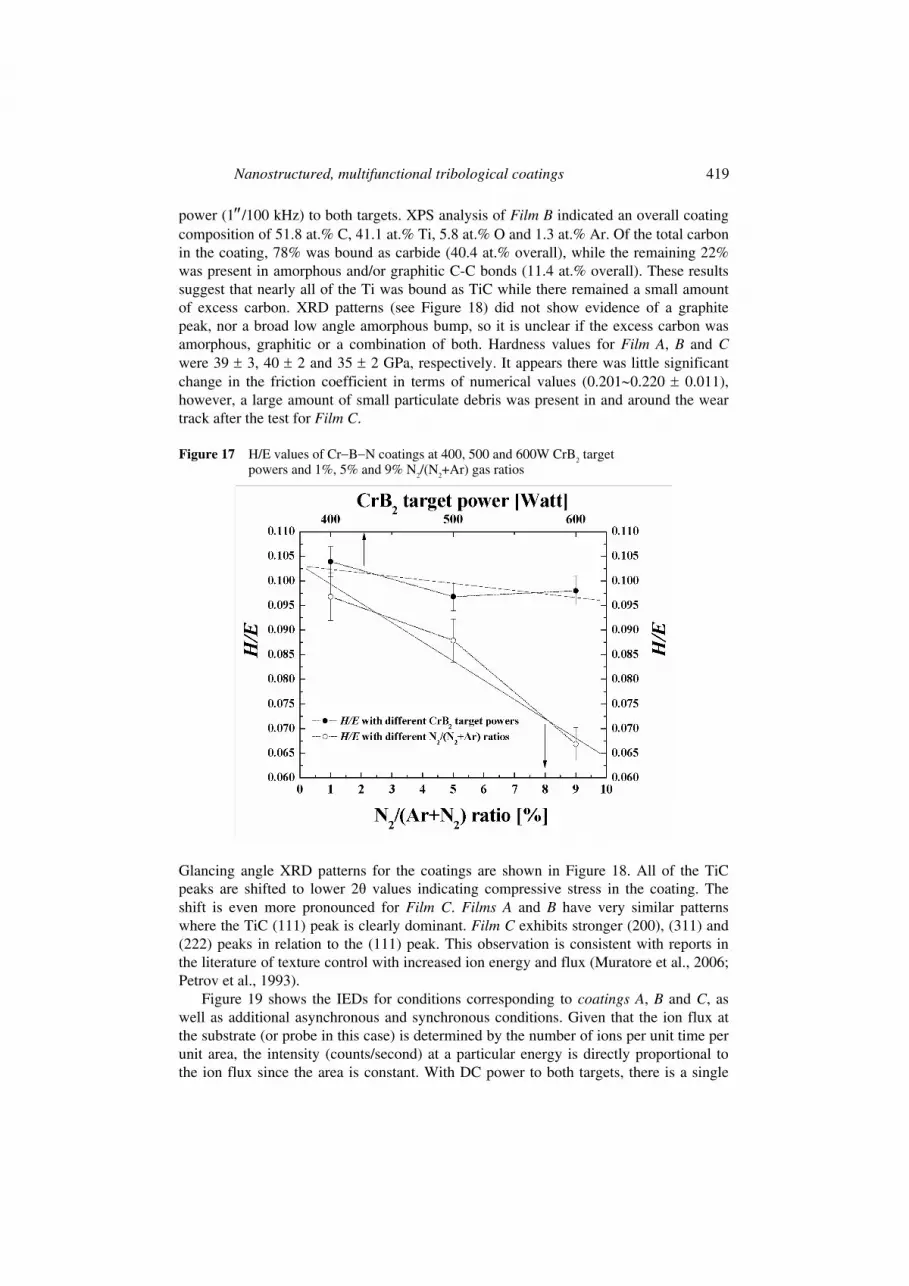
Figure 17 represents the H/E values of Cr–B–N coatings at varying CrB2 target powers (400, 500, 600 W) and varying N2/(N2+Ar) gas ratios (1, 5, 9%). The H/E values were calculated from the data presented in Figures 15 and 16. As the CrB2 target power is increased, the H/E value of the Cr–B–N coatings gradually decreased from ∼0.105 to 0.098. On the other hand, the H/E values of Cr–B–N coatings steeply decreased (from ∼0.097 to 0.065) with an increase in the N2/(N2+Ar) gas ratios in the chamber. Therefore, the H/E value was more affected by N2/(N2+Ar) gas ratio than by the target power as is shown in Figure 17. The highest H/E value (~0.105) was obtained for the Cr–B–N coating with 1% N2/(N2+Ar) gas ratio and 400W CrB2 target power (37.9 at.% Cr, 51.4 at.% B,7.2 at.% N in the coating). From the results of hardness (Figure 15 and 16) and H/E (Figure 17), it is suggested that the Cr–B–N coating deposited with 1% N2/(N2+Ar) gas ratio and 400 W CrB2 target power may provide a better wear-resistance with higher fracture toughness than that of the Cr–B–N coating deposited with a CrB2 target power above 500W and N2/(N2+Ar) gas ratio above 5%.
5.3 P-CFUBMS of TiC–C coatings
Three primary coatings of interest were deposited as follows: Film A was deposited with DC power to both targets, Film B was deposited with DC power to the graphite target and pulsed power (at a reverse time of 1″ and a frequency of 100 kHz, hereafter denoted as 1″/100 kHz) to the titanium target, Film C was deposited with synchronous pulsed
Nanostructured, multifunctional tribological coatings 419
power (1″/100 kHz) to both targets. XPS analysis of Film B indicated an overall coating composition of 51.8 at.% C, 41.1 at.% Ti, 5.8 at.% O and 1.3 at.% Ar. Of the total carbon in the coating, 78% was bound as carbide (40.4 at.% overall), while the remaining 22% was present in amorphous and/or graphitic C-C bonds (11.4 at.% overall). These results suggest that nearly all of the Ti was bound as TiC while there remained a small amount of excess carbon. XRD patterns (see Figure 18) did not show evidence of a graphite peak, nor a broad low angle amorphous bump, so it is unclear if the excess carbon was amorphous, graphitic or a combination of both. Hardness values for Film A, B and C were 39 ± 3, 40 ± 2 and 35 ± 2 GPa, respectively. It appears there was little significant change in the friction coefficient in terms of numerical values (0.201∼0.220 ± 0.011), however, a large amount of small particulate debris was present in and around the wear track after the test for Film C.
Figure 17 H/E values of Cr−B−N coatings at 400, 500 and 600W CrB2 target
powers and 1%, 5% and 9% N2/(N
2+Ar) gas ratios
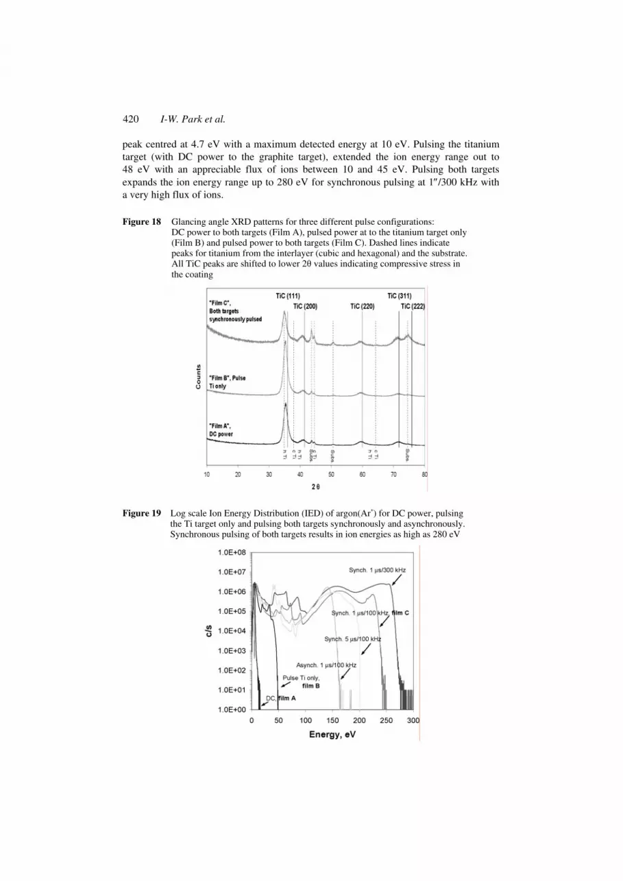
Glancing angle XRD patterns for the coatings are shown in Figure 18. All of the TiC peaks are shifted to lower 2θ values indicating compressive stress in the coating. The shift is even more pronounced for Film C. Films A and B have very similar patterns where the TiC (111) peak is clearly dominant. Film C exhibits stronger (200), (311) and (222) peaks in relation to the (111) peak. This observation is consistent with reports in the literature of texture control with increased ion energy and flux (Muratore et al., 2006; Petrov et al., 1993).
Figure 19 shows the IEDs for conditions corresponding to coatings A, B and C, as well as additional asynchronous and synchronous conditions. Given that the ion flux at the substrate (or probe in this case) is determined by the number of ions per unit time per unit area, the intensity (counts/second) at a particular energy is directly proportional to the ion flux since the area is constant. With DC power to both targets, there is a single
420 I-W. Park et al.
peak centred at 4.7 eV with a maximum detected energy at 10 eV. Pulsing the titanium target (with DC power to the graphite target), extended the ion energy range out to 48 eV with an appreciable flux of ions between 10 and 45 eV. Pulsing both targets expands the ion energy range up to 280 eV for synchronous pulsing at 1″/300 kHz with a very high flux of ions.
Figure 18 Glancing angle XRD patterns for three different pulse configurations: DC power to both targets (Film A), pulsed power at to the titanium target only (Film B) and pulsed power to both targets (Film C). Dashed lines indicate peaks for titanium from the interlayer (cubic and hexagonal) and the substrate. All TiC peaks are shifted to lower 2θ values indicating compressive stress in the coating
Figure 19 Log scale Ion Energy Distribution (IED) of argon(Ar+) for DC power, pulsing the Ti target only and pulsing both targets synchronously and asynchronously. Synchronous pulsing of both targets results in ion energies as high as 280 eV
Nanostructured, multifunctional tribological coatings 421
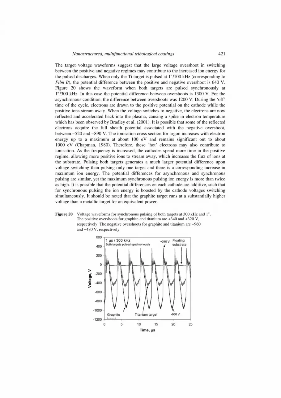
The target voltage waveforms suggest that the large voltage overshoot in switching between the positive and negative regimes may contribute to the increased ion energy for the pulsed discharges. When only the Ti target is pulsed at 1″/100 kHz (corresponding to Film B), the potential difference between the positive and negative overshoot is 640 V. Figure 20 shows the waveform when both targets are pulsed synchronously at 1″/300 kHz. In this case the potential difference between overshoots is 1300 V. For the asynchronous condition, the difference between overshoots was 1200 V. During the ‘off’ time of the cycle, electrons are drawn to the positive potential on the cathode while the positive ions stream away. When the voltage switches to negative, the electrons are now reflected and accelerated back into the plasma, causing a spike in electron temperature which has been observed by Bradley et al. (2001). It is possible that some of the reflected electrons acquire the full sheath potential associated with the negative overshoot, between −520 and −890 V. The ionisation cross section for argon increases with electron energy up to a maximum at about 100 eV and remains significant out to about 1000 eV (Chapman, 1980). Therefore, these ‘hot’ electrons may also contribute to ionisation. As the frequency is increased, the cathodes spend more time in the positive regime, allowing more positive ions to stream away, which increases the flux of ions at the substrate. Pulsing both targets generates a much larger potential difference upon voltage switching than pulsing only one target and there is a corresponding increase in maximum ion energy. The potential differences for asynchronous and synchronous pulsing are similar, yet the maximum synchronous pulsing ion energy is more than twice as high. It is possible that the potential differences on each cathode are additive, such that for synchronous pulsing the ion energy is boosted by the cathode voltages switching simultaneously. It should be noted that the graphite target runs at a substantially higher voltage than a metallic target for an equivalent power.
Figure 20 Voltage waveforms for synchronous pulsing of both targets at 300 kHz and 1″. The positive overshoots for graphite and titanium are +340 and +320 V, respectively. The negative overshoots for graphite and titanium are −960 and −480 V, respectively
422 I-W. Park et al.
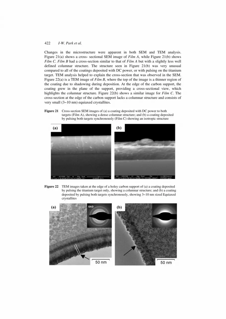
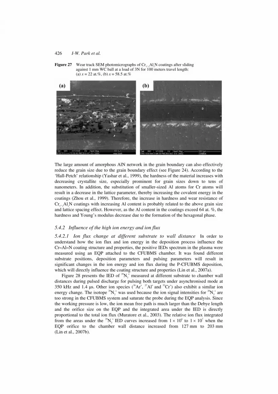
Changes in the microstructure were apparent in both SEM and TEM analysis. Figure 21(a) shows a cross- sectional SEM image of Film A, while Figure 21(b) shows Film C. Film B had a cross-section similar to that of Film A but with a slightly less well defined columnar structure. The structure seen in Figure 21(b) was very unusual compared to all of the coatings deposited with DC power, or with pulsing on the titanium target. TEM analysis helped to explain the cross-section that was observed in the SEM. Figure 22(a) is a TEM image of Film B, where the top of the image is a thinner region of the coating due to shadowing during deposition. At the edge of the carbon support, the coating grew in the plane of the support, providing a cross-sectional view, which highlights the columnar structure. Figure 22(b) shows a similar image for Film C. The cross-section at the edge of the carbon support lacks a columnar structure and consists of very small (3∼10 nm) equiaxed crystallites.
Figure 21 Cross-section SEM images of (a) a coating deposited with DC power to both targets (Film A), showing a dense columnar structure; and (b) a coating deposited by pulsing both targets synchronously (Film C) showing an isotropic structure
Figure 22 TEM images taken at the edge of a holey carbon support of (a) a coating deposited by pulsing the titanium target only, showing a columnar structure; and (b) a coating deposited by pulsing both targets synchronously, showing 3∼10 nm sized Equiaxed crystallites

Nanostructured, multifunctional tribological coatings 423
The high ion energy (up to 280 eV) produced by pulsing both targets synchronously had a distinct and significant influence on the microstructure of the TiC coatings. It is likely that the substantial amount of energy has induced a considerable defect density in the growing coating resulting in a high rate of re-nucleation. This occurrence has been observed in the growth of TiN coatings with ion energies in excess of 160 eV (Petrov et al., 2003). While possessing a hardness value in line with the other coatings in this study (35±2 GPa), Film C did not perform well in other tribological tests, such as the wear test and scratch test. In both cases a significant amount of particulate debris was generated. It is probable that the coating was under considerable levels of stress (indicated by the shift in the XRD peaks) and failed at the grain boundaries, causing particles of coating to separate from the bulk. This coating was not optimised for composition and it is possible that additional carbon may alleviate these issues.
5.4 P-CFUBMS of Cr–Al–N coatings
5.4.1 Influence of the Al concentration
When the Al atoms are incorporated into the cubic CrN lattice, they will substitute the Cr lattice sites to form Cr1−xAlxN ternary phase (Lin et al., 2006). Figure 23 illustrates the GIXRD patterns for Cr1-xAlxN (0 ≤ x ≤ 68%) coatings. For Al contents lesser than 64 at.%, the Cr1−xAlxN coatings exhibit a B1 cubic structure having (111), (200) and (220) peaks. Addition of Al beyond 64 at.% results in a change in crystal structure from B1 cubic to B4 hexagonal phase. The coexistence of cubic and hexagonal phases was observed when the Al concentration in the coating is beyond 64 at.%. As the Al concentration increased in Cr1−xAlxN coatings, the (111) and (200) peaks gradually shifted to a higher diffraction angle. Such XRD shift to a higher angle, in general, is an indication of a decrease in the lattice parameter of the coating structure due to the substitution of Al atoms into the Cr lattice sites. In addition, the (111) and (200) peaks became wider with an increase in the Al concentration, indicating a decrease in the grain size of the coatings.
Figure 23 The XRD patterns for Cr1-x
AlxN coatings with different Al concentrations
(Lin et al., 2006)

424 I-W. Park et al.
The cross-section SEM photomicrographs of Cr1−xAlxN coatings at different Al concentrations are provided in Figure 24. All Cr1−xAlxN coatings exhibit a dense columnar structure. A significant decrease of the grain size accompanied by a dense structure was observed with an increase in the Al concentration in the coatings. The columnar size of Cr1−xAlxN coatings decreased from 100 nm to a range of 40–60 nm as x values increased from 0 to 58.5% (Figures 24a–d). The surface roughness of the CrN coating is about 16.3 nm. A decrease of the surface roughness was observed with an increase in the Al content in Cr1−xAlxN coatings and reached the low values of 7 and 6 nm at 35.8 at.% and 61.8 at.%, respectively. The decrease in surface roughness is related to the decrease in grain size as the Al content increases in the Cr1−xAlxN coatings. From a thermodynamic point of view, the decrease in the roughness in the growing coatings is also possibly caused by the high energetic ion bombardment in the P-CFUBMS system with an increase in the Al target power during deposition.
Figure 24 Scanning electron photomicrographs of cross section of Cr1−x
AlxN coatings on
silicon substrate with different Al concentrations: (a) x = 0 at.%, (b) x =22 at.%, (c) x = 35.8 at.%, (d) x = 58.5 at.% (Lin et al., 2006)
The improved microstructure of Cr–Al–N coatings with Al concentration results in significant improvement in the mechanical and tribological properties. The hardness and Young’s modulus values are plotted as a function of Al concentration in Figure 25. As Al is incorporated into the coating, the hardness and Young’s modulus values of the Cr1−xAlxN coatings increase and both reach the maximum values of 36.3 GPa and 369.9 GPa, respectively, at x = 58.5 at.%. A further increase in Al concentration results in a decrease in both hardness and Young’s modulus due to the cubic to hexagonal phase transformation.

Nanostructured, multifunctional tribological coatings 425
Figure 25 The hardness and Young’s modulus as a function of the Al concentration in the Cr
1−xAl
xN coatings (Lin et al., 2006)
The friction coefficient value and calculated wear rate of Cr1−xAlxN coatings are plotted as a function of Al content in Figure 26. The CrN coating exhibits a lower friction coefficient value (0.28) than all of Cr1−xAlxN coatings possibly due to the oxide layer on the surface, which has low shear strength. Adding a small amount of Al into Cr1−xAlxN coatings (x = 22 at.%) will result in a sudden increase in friction coefficient to 0.55, which is possibly due to the low hardness and less dense structure in the coating. The coating exhibited a poor wear resistance (Figure 27(a)). Further increasing the Al content in the coating, the friction coefficient of Cr1−xAlxN coatings decrease to the lowest value of 0.37 at x = 58.5 at.% and no obvious defects observed in the wear track (Figure 27(b)). The wear rate exhibits a similar trend compared with the friction coefficient change in Cr1−xAlxN coatings (Figure 26). Overall, a higher friction coefficient results in a higher wear rate. The improved wear resistance is contributed to the increased hardness and large amount of amorphous AlN network formed in the grain boundary at high Al content which can reduce the grain boundary sliding ability. However, the friction coeffcient and wear rate increased when hexagonal AlN phase was formed in the coatings.
Figure 26 Friction coefficient and wear rate as a function of the Al concentration in the Cr
1−xAl
xN coatings (Lin et al., 2006)
426 I-W. Park et al.
Figure 27 Wear track SEM photomicrographs of Cr1−x
AlxN coatings after sliding
against 1 mm WC ball at a load of 3N for 100 meters travel length: (a) x = 22 at.%, (b) x = 58.5 at.%
The large amount of amorphous AlN network in the grain boundary can also effectively reduce the grain size due to the grain boundary effect (see Figure 24). According to the ‘Hall-Petch’ relationship (Yashar et al., 1999), the hardness of the material increases with decreasing crystallite size, especially prominent for grain sizes down to tens of nanometers. In addition, the substitution of smaller-sized Al atoms for Cr atoms will result in a decrease in the lattice parameter, thereby increasing the covalent energy in the coatings (Zhou et al., 1999). Therefore, the increase in hardness and wear resistance of Cr1−xAlxN coatings with increasing Al content is probably related to the above grain size and lattice spacing effect. However, as the Al content in the coatings exceed 64 at. %, the hardness and Young’s modulus decrease due to the formation of the hexagonal phase.
5.4.2 Influence of the high ion energy and ion flux
5.4.2.1 Ion flux change at different substrate to wall distance In order to understand how the ion flux and ion energy in the deposition process influence the Cr–Al–N coating structure and properties, the positive IEDs spectrum in the plasma were measured using an EQP attached to the CFUBMS chamber. It was found different substrate positions, deposition parameters and pulsing parameters will result in significant changes in the ion energy and ion flux during the P-CFUBMS deposition, which will directly influence the coating structure and properties (Lin et al., 2007a).
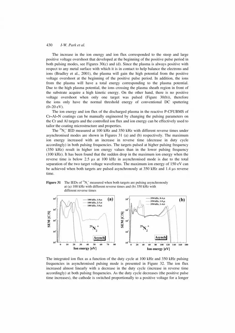
Figure 28 presents the IED of 29N2
+ measured at different substrate to chamber wall distances during pulsed discharge for pulsing both targets under asynchronised mode at 350 kHz and 1.4 µs. Other ion species (36Ar+, 27Al+ and 52Cr+) also exhibit a similar ion energy change. The isotope 29N2
+ was used because the ion signal intensities for 28N2
+ are too strong in the CFUBMS system and saturate the probe during the EQP analysis. Since the working pressure is low, the ion mean free path is much larger than the Debye length and the orifice size on the EQP and the integrated area under the IED is directly proportional to the total ion flux (Muratore et al., 2003). The relative ion flux integrated from the areas under the 29N2
+ IED curves increased from 1 × 10⁶ to 1 × 10⁷ when the EQP orifice to the chamber wall distance increased from 127 mm to 203 mm (Lin et al., 2007b).
Nanostructured, multifunctional tribological coatings 427
Figure 28 The IEDs of 29N2+ as a function of the distance of the probe from the chamber wall for
pulsing both targets asynchronised at 350 kHz and 1.4 µs (Lin et al., 2007b)
In the closed field system, the magnetic field lines close in across the chamber. Sputtered atoms following these field lines are available to undergo ionising collisions and maintain a high plasma density in the substrate region. If the substrate is too close to the magnetrons, the ionisation ratio of the sputtered atoms may be too small, resulting in a low ion flux. When the substrate distance increases, more ions will be ionised in the plasma due to the ionising collisions and the ion flux will increase. During reactive magnetron sputtering deposition, the substrate does not directly face the targets but maintains a certain angle. Therefore, the angle of incidence of arriving particles is another important factor that needs to be considered. At a small substrate distance (127 mm), the angle of incidence of arriving particles is very small with respect to the substrate and will limit the amount of arriving ions due to the shadowing effect. Therefore, the ion flux is low. As the substrate distance increases, the shadowing effect will be greatly reduced thereby resulting in an increase in ion flux. Using a planetary rotation system for coating deposition will break the limitation of the angle of incidence and allow the substrate to receive even ion bombardment during the deposition process, thereby maintaining high ion flux even at a close substrate distance. There are several factors influencing the grain growth during the P-CFUBMS deposition process. The arriving energetic ion flux of an intermediate energy level will have the most important influence on the grain growth behaviour in the coating. The increased ion flux by changing the substrate positions can facilitate the ion bombardment on the substrate, increase the mobility of the atoms on the substrate surface, thereby resulting in a denser coating with reduced grain size.
The improved Cr–Al–N coating microstructure has been studied by the two-dimensional AFM (Figure 29). Coating surface smoothening is achieved by an increase in the ion flux. The morphology of coating deposited at 127 mm indicates separated mounds of relatively large lateral and vertical size, which indicate a large average grain size and porous structure with a surface roughness of about 23.45 nm (Figure 29(a)). On the other hand, the mounds become smaller, more continuous in the

428 I-W. Park et al.
coating deposited at a substrate to wall distance of 203 mm, thereby showing more nuclei and a denser microstructure (Figure 29(b)). The Cr–Al–N coating deposited at 203 mm also exhibits a nanocrystallised grain size with a high hardness of 30 GPa and a low friction coefficient of 0.35.
Figure 29 Two-dimensional AFM images of Cr–Al–N coatings deposition at (a) 127 mm, (b) 203 mm substrate to wall distance (Lin et al., 2007b)
5.4.2.2 Ion energy and ion flux change at different pulsing parameters Not only the ion flux but also the ion energy will change the kinetic behaviour of the ions and increase the ion bombardment on the substrate. In the P-CFUBMS system, the voltage

Nanostructured, multifunctional tribological coatings 429
waveforms of two (or more) targets can be operated in either asynchronised mode, which means the voltage waveforms of the two targets are out of phase (Figure 30(c)), or in-phase in the synchronised mode (Figure 30(b)). Both pulsing modes will generate different ion energies and ion fluxes in the plasma, is also shown in the previously discussed TiC–C films.
Figure 30 (a) The IED of 29N2
+ during pulsed discharge for pulsing only Al target and pulsing both targets synchronously and asynchronously at 350 kHz, 1.4 µs. (b) The voltage waveforms of targets for pulsing the Al target at 350 kHz, 1.4 µs and keeping the Cr target in a DC discharge. (c) The voltage waveforms of targets for pulsing both targets asynchronously at 350 kHz, 1.4 µs. (d) The voltage waveforms of targets for pulsing both targets synchronised at 350 kHz, 1.4 µs. (Lin et al., 2007a)
Figure 30a exhibits the IED of 29N2
+ measured during the pulsing of one target, while the other target was operated in a conventional DC power mode and pulsing both Cr and Al targets asynchronously and synchronously at 350 kHz and 1.4µs reverse time in agreement with EQP data generated for the TiC–C films, a significant increase in the ion energy (up to 170 eV in the synchronised mode) and ion flux was observed when both the Cr and Al targets are running in pulsing conditions compared with the low ion energy (0∼20 eV) and ion flux when only one target (either the Cr or Al target) is operated in pulsed mode and the other in DC mode, Other ion species (36Ar+, 27Al+ and 52Cr+) exhibit similar ion energy and flux changes and the same trend is also observed with other pulsing parameters.
430 I-W. Park et al.
The increase in the ion energy and ion flux corresponded to the steep and large positive voltage overshoot that developed at the beginning of the positive pulse period in both pulsing modes, see Figures 30(c) and (d). Since the plasma is always positive with respect to any metal surface with which it is in contact to help balance the electrons and ions (Bradley et al., 2001), the plasma will gain the high potential from the positive voltage overshoot at the beginning of the positive pulse period. In addition, the ions from the plasma will have a total energy corresponding to the plasma potential. Due to the high plasma potential, the ions crossing the plasma sheath region in front of the substrate acquire a high kinetic energy. On the other hand, there is no positive voltage overshoot when only one target was pulsed (Figure 30(b)), therefore the ions only have the normal threshold energy of conventional DC sputtering (0∼20 eV).
The ion energy and ion flux of the discharged plasma in the reactive P-CFUBMS of Cr–Al–N coatings can be manually engineered by changing the pulsing parameters on the Cr and Al targets and the controlled ion flux and ion energy can be effectively used to tailor the coating microstructure and properties.
The 29N2
+ IED measured at 100 kHz and 350 kHz with different reverse times under asynchronised modes are shown in Figures 31 (a) and (b) respectively. The maximum ion energy increased with an increase in reverse time (decrease in duty cycle accordingly) in both pulsing frequencies. The targets pulsed at higher pulsing frequency (350 kHz) result in higher ion energy values than in the lower pulsing frequency (100 kHz). It has been found that the sudden drop in the maximum ion energy when the reverse time is below 2.5 µs at 100 kHz in asynchronised mode is due to the total separation of the two target voltage waveforms. The maximum ion energy of 150 eV can be achieved when both targets are pulsed asynchronouly at 350 kHz and 1.4 µs reverse time.
Figure 31 The IEDs of 29N2
+ measured when both targets are pulsing asynchronouly at (a) 100 kHz with different reverse times and (b) 350 kHz with different reverse times
The integrated ion flux as a function of the duty cycle at 100 kHz and 350 kHz pulsing frequencies in asynchronised pulsing mode is presented in Figure 32. The ion flux increased almost linearly with a decrease in the duty cycle (increase in reverse time accordingly) at both pulsing frequencies. As the duty cycle decreases (the positive pulse time increases), the cathode is switched proportionally to a positive voltage for a longer
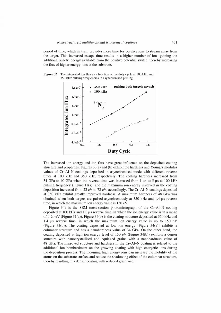
Nanostructured, multifunctional tribological coatings 431
period of time, which in turn, provides more time for positive ions to stream away from the target. This increased escape time results in a higher number of ions gaining the additional kinetic energy available from the positive potential switch, thereby increasing the flux of higher energy ions at the substrate.
Figure 32 The integrated ion flux as a function of the duty cycle at 100 kHz and 350 kHz pulsing frequencies in asynchronised pulsing
The increased ion energy and ion flux have great influence on the deposited coating structure and properties. Figures 33(a) and (b) exhibit the hardness and Young’s modulus values of Cr–Al–N coatings deposited in asynchronised mode with different reverse times at 100 kHz and 350 kHz, respectively. The coating hardness increased from 34 GPa to 40 GPa when the reverse time was increased from 1 µs to 5 µs at 100 kHz pulsing frequency (Figure 11(a)) and the maximum ion energy involved in the coating deposition increased from 22 eV to 72 eV, accordingly. The Cr–Al–N coatings deposited at 350 kHz exhibit greatly improved hardness. A maximum hardness of 48 GPa was obtained when both targets are pulsed asynchronously at 350 kHz and 1.4 µs reverse time, in which the maximum ion energy value is 150 eV.
Figure 34a is the SEM cross-section photomicrograph of the Cr–Al–N coating deposited at 100 kHz and 1.0 µs reverse time, in which the ion energy value is in a range of 0-20 eV (Figure 31(a)). Figure 34(b) is the coating structure deposited at 350 kHz and 1.4 µs reverse time, in which the maximum ion energy value is up to 150 eV (Figure 31(b)). The coating deposited at low ion energy [Figure 34(a)] exhibits a columnar structure and has a nanohardness value of 34 GPa. On the other hand, the coating deposited at high ion energy level of 150 eV (Figure 34(b)) exhibits a denser structure with nanocrystallised and equiaxed grains with a nanohardness value of 48 GPa. The improved structure and hardness in the Cr–Al–N coating is related to the additional ion bombardment on the growing coating with high energetic ions during the deposition process. The incoming high energy ions can increase the mobility of the atoms on the substrate surface and reduce the shadowing effect of the columnar structure, thereby resulting in a denser coating with reduced grain size.

432 I-W. Park et al.
Figure 33 The hardness and Young’s modulus values of Cr–Al–N coatings deposited in asynchronised mode with different reverse times at (a) 100 kHz and (b) 350 kHz, respectively
Figure 34 Scanning electron micrographs of cross sections of Cr–Al–N coatings deposited at: (a) pulsing the Al target at 100 kHz and 1.0 µs and keeping the Cr target in a DC discharge and (b) pulsing both targets asynchronously at 350 kHz and 1.4 µs

Nanostructured, multifunctional tribological coatings 433
The steady-state friction coefficient value and calculated wear rate of Cr–Al–N coatings deposited in asynchronised mode with different reverse times at 100 kHz and 350 kHz are plotted in Figures 35a and b, respectively. The friction coefficient of Cr–Al–N coatings deposited at both frequencies increased with an increase in the reverse time, which means the coatings deposited at higher ion energy and ion flux values have higher friction coefficient values. The wear rate values of the coatings deposited at 100 kHz and different reverse times are all in the 3 to 3.5 × 10⁻⁶ mm3/(Nm) range, which usually indicates good wear resistance of the coatings. However, the coatings deposited at 350 kHz and different reverse times exhibit higher wear rate values compared to all the coatings deposited at 100 kHz.
Figure 35 Friction coefficient of Cr–Al–N coatings deposited in asynchronised mode with different reverse times at (a) 100 kHz and (b) 350 kHz, respectively
Figure 36 exhibits the wear track optical photomicrographs of CrAlN coatings deposited at different ion energy values after sliding against 1mm WC ball at a load of 3N for 100 meters travel length. The maximum ion energy values are labelled in the figures

434 I-W. Park et al.
to indicate the ion energy level increased by pulsing during the deposition. The coatings deposited at 100 kHz and 5.0 µs reverse time with a maximum ion energy value of 72 eV exhibit good wear resistance and there are no obvious defects inside the wear tracks (Figures 36a). On the other hand, the coatings deposited at 350 kHz and 1.4 µs reverse time exhibit extensively abrasive wear (black area) and cracking in the wear track (Figure 36b). It was found a high residual stress (−13 GPa) was developed in the coating deposited at 350 kHz and 1.4 µs reverse time. The high stress is possibly due to the excessive ion bombardment from the high ion energy (150 eV). The high residual stress can reduce the coating toughness and increase the brittleness of the coating. Therefore, extensive cracking was formed in the wear track of the coating deposited at high ion energy (150 eV in this case).
Figure 36 Wear track optical photomicrographs of Cr–Al–N coatings deposited at different asynchronous pulsing parameters (a) 100 kHz and 5.0 µs reverse time and (b) 350 kHz and 1.4 µs reverse time
Nanostructured, multifunctional tribological coatings 435
Examination of the wear track confirmed that the black area contains high W and O content, indicating the WC ball wear is incorporated into the top layer of Cr–Al–N coatings. The super hard Cr–Al–N coatings deposited at high ion energy and ion flux (hardness above 40 GPa) can change the wear behaviour between the coating and the WC ball. Since the hardness of the WC ball (16∼20 GPa) is much lower than the super hard Cr–Al–N coatings (48 GPa in this case), the main abrasive wear body can switch from the coating to the WC ball and this was confirmed from observation of the WC ball after the wear test. Therefore, the increased contact surface between the WC ball and the coatings due to the ball wear can result in an increase in the friction coefficient of the coatings. Nevertheless the coating can still have a low wear rate due to the super hardness of the coating (e.g. 100 kHz and 5.0 µs). It is possible to control the pulsing ion energy and the deposition condition to achieve both good hardness and wear resistance in the coating, for example, deposited compositionally graded multilayer coating (Cr/CrN/Cr–Al–N) to accommodate the high residual stress developed in the coating while maintaining the benefits of the high ion energy and ion flux to obtain dense nanostructured coatings with good properties.
6 Conclusion and future works
Ti–Si–B–C–N coating were deposited on AISI 304 stainless steel substrates using a DC UBMS technique with both an 80 mol% TiB2–20 mol% TiC composite target and pure Si target in an Ar-N2 atmosphere. XRD and XPS analyses revealed that the synthesized Ti–Si–B–C–N coating were composed of nanocomposites consisting of nanosized (Ti,C,N)B2 and Ti(C,N) crystallites embedded in an amorphous TiSi2 and SiC matrix including some of carbon, SiB4, BN, CNx, TiO2 and B2O3 components. The addition of Si to the Ti–B–C–N coating led to percolation of amorphous TiSi2,, SiC and SiB4 phases. The Ti–Si–B–C–N coating with up to 200W Si target power exhibited high hardness and H/E value of approximately 35 GPa and 0.097, respectively, indicating a high fracture toughness. The hardness and H/E value of Ti–Si–B–C–N coating steeply decreased with the further increase in Si target power of above 250 W. Furthermore, the Ti–Si–B–C–N coating with up to 200 W Si target power exhibited a low wear rate of from ∼3 to ∼10 × 10−6 mm3/(N m). The minimum friction coefficient in Ti–Si–B–C–N coating was approximately 0.15 at Si target power 50 W. Such a combination of high hardness and H/E, coupled with a low wear rate and friction coefficient would indicate the considerable potential of this coating for applications in mechanical components. However, further research is necessary to investigate the nanostructure of these coatings using transmission electron microscopy of these coating.
Cr–B–N coatings were deposited on AISI 304 stainless steel substrates using an UBMS technique with a CrB2 target in an Ar-N2 atmosphere. XRD and XPS analyses revealed that the synthesized Cr–B–N coatings were composed of a composite consisting of nanocrystalline CrB2 embedded in an amorphous Cr2N and BN matrix including some components of Cr2O3, CNx, CrN, and B2O3. The addition of nitrogen to the Cr–B–N coating led to the percolation of amorphous Cr2N, BN, CrN and CNx phases. The Cr–B–N coatings deposited with 400 W CrB2 target power and 1% N2/(N2+Ar) gas ratio (7.2 at. % N in the film) exhibited the highest hardness of approximately 34 GPa and H/E ratio 0.105. Such a combination of high fracture toughness, coupled with a high

436 I-W. Park et al.
hardness (∼34 GPa) would indicate the considerable potential of this coating for applications in mechanical components. However, further research is necessary to investigate the tribological and high temperature properties of these coatings.
Nanocomposite TiC–C coatings have been deposited by pulsed DC closed field UBMS under a variety of pulsing conditions. Pulsing both targets has a significant effect on the ion energies in the plasma, generating ions up to 280 eV for the conditions investigated here. It appears that the increase in ion energy for synchronous pulsing is associated with the large change in target potentials. Small, equiaxed grains were produced as a result of the high ion energy and flux with negative consequences to the properties of the coating. Based on studies of TiN coatings, it has been suggested that a high flux of mid-energy ions (∼20 eV) is ideal for beneficial thin coating structure modification including increased density and reduced surface roughness. These conditions can be achieved for the co-sputtering of TiC–C coatings by adjusting the pulsing parameters and target voltages. Understanding how the pulsing parameters determine the IED within the plasma for a particular chamber geometry can aid in the design of thin nanostructured coatings for specific tribological applications.
Nanocrystallised Cr–Al–N coatings with high hardness and good wear resistance have been developed using P-CFUBMS. The Cr1-xAlxN coatings exhibit decreased grain size, decreased surface roughness and improved nanostructure and properties with an increase in the Al content in the coatings up to 58.5 at.%. Increasing the substrate to chamber wall distance can significantly increase the ion flux in front of the substrate, thereby producing dense nanostructure in the Cr–Al–N coating with the additional ion bombardment. However rotation of the substrate minimises this later effect.
Pulsing both the magnetrons in the CFUBMS has a significant effect on both ion energies and ion flux within the plasma. The positive voltage overshoot and the positive pulse voltage developed on both targets during the reverse voltage period increases the plasma potential and thereby increases the overall extended ion energy range. Cr–Al–N coatings were deposited in asynchronised mode for a range of reverse times at 100 kHz and 350 kHz, in which different ion energy levels and ion flux were incorporated in the deposition. It was found the ion energy and ion flux increased with a decrease in the duty cycle at fixed frequency in asynchronised mode. The increased ion energy and ion flux in the plasma can be used to increase the ion bombardment and ion mobility in the CFUBMS deposition, thereby forming a nanocrystallised, dense equiaxed grain structure in the Cr–Al–N coating of super hardness (above 40 GPa). However, the high residual stress developed in the coating deposited at high ion energy (130 eV to 150 eV in this study) can result in a decrease in the toughness and wear resistance of the Cr–Al–N coatings. Therefore, the increased ion energy and ion flux level by pulsing need to be properly controlled. Cr–Al–N coatings deposited at 100 kHz and 5.0 µs reverse time (with maximum ion energy of 72 eV) exhibits both super hardness and good wear resistance.
Acknowledgements
The authors thank the support provided for this research proceeds by USAFRL, The Timken Company, North America Die Casting Association (NADCA), DOE-OIT, Li Foundation and NCRC Program (R15-2006-022-01001-0, MOST in Korea).

Nanostructured, multifunctional tribological coatings 437
References
Bradley, J.W., Backer, H., Kelly, P.J. and Arnell, R.D. (2001) ‘Space and time resolved langmuir probe measurements in a 100 kHz pulsed rectangular magnetron system’, Surface and Coatings Technology, Vol. 142–144, pp.337–341.
Cavaleiro, A. and Louro, C. (2002) ‘Nanocrystalline structure and hardness of thin coatings’, Vacuum, Vol. 64, No. 3, pp.211–218.
Chapman, B. (1980) Glow Discharge Process, New York: John Wiley & Sons, Inc., p.29.
Cullity, B.D. (1978) Elements of X-ray Diffraction, 2nd edition Addison-Wesly Publishing Company, Inc., pp.101–103.
Dieter, G.E. (1976) Mechanical Metallurgy, 2nd edition, New York: McGrow-Hill.
Kelly, P.J., Hall, R., Brien, J.O., Bradley, J.W., Henderson, P., Roche, G. and Arnell, R.D. (2001) ‘Studies of mid-frequency pulsed dc biasing’, Journal of Vacuum Science and Technology A, Vol. 19, pp.2856–2865.
Kim, S.H., Kim, J.K. and Kim, K.H. (2002) ‘Influence of deposition conditions on the microstructure and mechanical properties of Ti-Si-N coatings by DC reactive magnetron sputtering’, Thin Solid Coatings, Vol. 420–421, pp.360–365.
Levashov, E.A., Kosayanin, V.I., Krukova, L.M., Moore, J.J. and Olson, D.L. (1997) ‘Structure and properties of Ti-C-B composite thin coatings produced by sputtering of composite TiC-TiB2 targets’, Surface and Coatings Technology, Vol. 92, pp.34–41.
Leyland, A. and Matthews, A. (2000) ‘On the significant of the H/E ratio in wear control: a nanocomposite coating approach to optimised tribological behaviour’, Wear, Vol. 246, pp.1–11.
Lin, J., Mishra, B., Moore, J.J. and Sproul, W.D. (2006) ‘Microstructure, mechanical and tribological properties of Cr
1• xAl
xN films deposited by pulsed-closed field unbalanced
magnetron sputtering (P-CFUBMS)’, Surface and Coatings Technology, Vol. 201, pp.4329–4334.
Lin, J., Moore, J.J., Mishra, B., Sproul, W.D. and Rees, J.A. (2007a) ‘Examination of the pulsing phenomena in pulsed-closed field unbalanced magnetron sputtering (P-CFUBMS) of Cr–Al–N thin films’, Surface and Coatings Technology, Vol. 201, pp.4640–4652.
Lin, J., Mishra, B., Moore, J.J., Sproul, W.D. and Rees, J.A. (2007b) ‘Effects of substrate to chamber wall distance on structure and properties of CrAlN coatings deposited by pulsed -closed field unbalanced magnetron sputtering (P-CFUBMS)’, Surface and Coatings Technology, Vol. 201, pp.6960–6969.
Martinez, E., Sanjinés, R., Karimi, A., Esteve, J. and Lévy, F. (2004) ‘Mechanical properties of nanocomposite and multilayered Cr–Si–N sputtered thin coatings’, Surface and Coatings Technology, Vol. 180–181, pp.570–574.
Muratore, C., Moore, J.J. and Rees, J.A. (2003) ‘Electrostatic quadrupole plasma mass spectrometer and langmuir probe measurements of mid-frequency pulsed DC magnetron discharges’, Surface and Coatings Technology, Vol. 163–164, pp.12–18.
Muratore, C., Walton, S.G., Leonhardt, D. and Fernsler, R.F. (2006) ‘Control of plasma flux composition incident on TiN films during reactive magnetron sputtering and the effect on film microstructure’, Journal of Vacuum Science and Technology A, Vol. 24, No. 1, pp.25–29.
Park, I-W., Choi, S.R., Lee, M-H. and Kim, K.H. (2003a) ‘Effects of Si addition on the microstructural evolution and hardness of Ti–Al–Si–N coatings prepared by the hybrid system of arc ion plating and sputtering techniques’, Journal of Vacuum Science and Technology A, Vol. 21, No. 4, pp.895–899.
Park, I-W., Kim, K.H., Suh, J.H., Park, C-G. and Lee, M-H. (2003b) ‘Role of amorphous Si3N
4 in
the microhardness of Ti–Al–Si–N nanocomposite coatings’, Journal of the Korean Physical Society, Vol. 42, No. 6, pp.783–786.
Park, I-W., Kim, K.H., Kunrath, A.O., Zhong, D., Moore, J.J., Voevodin, A.A. and Levashov, E.A.(2005) ‘Microstructure and mechanical properties of superhard Ti–B–C–N
438 I-W. Park et al.
coatings deposited by dc unbalanced magnetron sputtering’, Journal of Vacuum Science and Technology B, Vol. 23, No. 2, pp.588–593.
Patscheider, J., Zehnder, T. and Diserens, M. (2001) ‘Structure–performance relations in nanocomposite coatings’, Surface and Coatings Technology, Vol. 146, pp.201–208.
Petrov, I., Adibi, F., Greene, J.E., Hultman, L. and Sundgren, J-E. (1993) ‘Average energy deposited per atom: A universal parameter for describing ion-assisted film growth?’, Applied Physics Letter, Vol. 63, No.1, pp.36–38.
Petrov, I., Barna, P.B., Hultman, L. and Greene, J.E. (2003) ‘Microstructural evolution during film growth’, Journal of Vacuum Science and Technology A, Vol. 21, No. 5, pp.S117–S128.
Pharr, G.M. (1998) ‘Measurement of mechanical properties by ultra-low load indentation’, Materials Science and Engineering A, Vol. 253, pp.151–159.
Shizhi, L., Yulong, S. and Hongrui, P. (1992) ‘Ti–Si–N coatings prepared by plasma–enhanced chemical vapor deposition’, Plasma Chemistry and Plasma Processing, Vol. 12, No. 3, pp.287–297.
Sproul, W.D. (1994) ‘Multilayer, multicomponent, and multiphase physical deposition coatings for enhanced performance’, Journal of Vacuum Science and Technology A, Vol. 12, No. 4, pp.1595–1601.
Stuber, M., Leiste, H., Ulrich, S., Holleck, H. and Schild, D. (2002) ‘Microstructure and properties of low friction TiC–C nanocomposite coatings deposited by magnetron sputtering’, Surface and Coatings Technology, Vol. 150, pp.218–226.
Veprek, S. and Reiprich, S. (1995) ‘A concept for the design of novel superhard coatings’, Thin Solid Coatings, Vol. 268, pp.64–71.
Veprek, S. (1997) ‘Conventional and new approaches toward the design of novel superhard materials’, Surface and Coatings Technology, Vol. 97, pp.15–22.
Veprek, S., Nesladek, P., Niederhofer, A., Glatz, F., Jilek, M. and Sima, M. (1998) ‘Recent progress in the superhard nanocrystalline composites: towards their industrialization and understanding of the origin of the superhardness’, Surface and Coatings Technology, Vol. 108–109, pp.138–147.
Veprek, S., Niederhofer, A., Moto, K., Bolom, T., Mannling, H.-D., Nesladek, P., Dollinger, G. and Bergmaier, A. (2000) ‘Composition, nanostructure and origin of the ultrahardness in nc-TiN/a-Si
3N
4/a- and nc-TiSi
2 nanocomposite with H
v = 80 to 105 GPa’, Surface and
Coatings Technology, Vol. 133–134, pp.152–159.
Voevodin, A.A., O’Neill, J.P., Prasad, S.V. and Zabinski, J.S. (1999) ‘Nanocrystalline WC and WC/a-C composite coatings produced from interselected plasma fluxes at low deposition temperatures’, Journal of Vacuum Science and Technology A, Vol. 17, No. 3, pp.986–992.
Voevodin, A.A. and Zabinski, J.S. (2000) ‘Supertough wear-resistanct coatings with chameleon surface adaptation’, Thin Solid Coatings, Vol. 370, pp.223–231.
Voevodin, A.A., Zabinski, J.S. and Muratore, C. (2005) ‘Recent advanced in hard, tough, and low friction nanocomposite coatings’, Tsinghua Science and Technology, Vol. 10, No. 6, pp.665−679.
Wilson, S. and Alpas, A.T. (2000) ‘Tribo–layer formation during sliding wear of TiN coatings’, Wear, Vol. 245, pp.223–229.
Xu, J. and Kato, K. (2000) ‘Formation of tribochemical layer of ceramics sliding in water and its role for low friction’, Wear, Vol. 245, pp. 61–75.
Yashar, P.C. and Sproul, W.D. (1999) ‘Nanometer scale multilayered hard coatings’, Vacuum, Vol. 55, No. 3–4, pp.179–190.
Zhou, M., Makino, Y., Nose, M. and Nogi, K. (1999) ‘Phase transition and properties of Ti-Al-N thin coatings prepared by r.f.-plasma assisted magnetron sputtering’, Thin Solid Coatings, Vol. 339, pp.203–208.


