Embed Size (px)
Citation preview

1
Microsystem Technologies Vol.15 (2009) 101-107
Modelling of interfacial intermetallic
compounds in the application of very fine
lead-free solder interconnections
ZHIHENG HUANG
Wolfson School of Mechanical and Manufacturing Engineering, Loughborough
University, Loughborough, Leicestershire, United Kingdom, LE11 3TU
Present address: Department of Microstructure Physics and Metal Forming, Max-Planck-Institut fuer Eisenforschung GmbH, Max-Planck-Str. 1, 40237 Düsseldorf, Germany
Email: [email protected] Phone: +49 (0) 211 6792 331 Fax: +49 (0) 211 6792 333
PAUL P. CONWAY
Wolfson School of Mechanical and Manufacturing Engineering, Loughborough
University, Loughborough, Leicestershire, United Kingdom, LE11 3TU
Email: [email protected]
RONGSHAN QIN
Graduate Institute of Ferrous Technology, Pohang University of Science and
Technology, Hyojia-Dong San 31, Pohang 790-784, South Korea
Email: [email protected]

2
Abstract
Intermetallic compounds (IMCs) are formed between lead-free solders and base
metals during soldering processes. The morphology as well as the amount of the
IMCs, in particular the interfacial IMCs, are important to mechanical performance
of the solder joints in their service environment. This is especially the case in
state-of-art ultrafine-pitch wafer-level packaging, in which solder joints could
become as small as 50 microns in diameter or even less. However, research
addressing growth kinetics of the IMCs in the existing literature has concentrated
on fitting experimental data onto a simple parabolic growth equation, which
cannot account for all the complicated physics involved in the process of IMC
formation. There are a few models based on Fick's diffusion equations in the
literature, which assume the growing IMC interface is planar. A combined
thermodynamic-kinetic model has been derived from the relationships amongst
some thermodynamic parameters, however, this model is only one dimension (1-
D) in nature. 2-D models have also been proposed, e.g. an implicit boundary
tracking method, and a phase field model. This paper reviews the modelling
techniques in the literature for both the growth kinetics and morphology of the
interfacial IMCs, under the context of lead-free soldering in very fine
interconnections. The advantages and disadvantages of each method are
discussed. Possible solutions to include the geometrical features of micro solder
joints in the modelling of growth kinetics of interfacial IMC are presented.

3
1 Introduction
The formation and growth of an IMC is a critical issue for the mechanical
properties of solder joints and therefore the integrity of entire electronic products.
Figure 1 shows the micrograph of a cross section of a Plastic Ball Grid Array
(PBGA) flip chip joint (Sn-3.8Ag-0.7Cu) as well as typical materials present in
each layer. The wafer level and board level metallizations in this case are
electroless nickel and copper, respectively. The solder reaction with
metallizations at the chip and substrate side in flip chip technology presents a
dilemma. On one hand, a rapid solder reaction is required in order to achieve the
joining of thousands of interconnections simultaneously. On the other hand, it is
also desirable that the solder reactions stop immediately after joining, since the
thin film Under Bump Metallization (UBM) is too thin to allow prolonged
reaction. However, the manufacturing of a device usually requires these solder
joints to endure several sequential reflow processes, in which the total period of a
solder bump in the molten state can be several minutes (Tu et al. 2001). Hence,
the solder-thin film reaction is a critical issue in electronic manufacturing. As a
result of the interactions between the solder and chip/board level metallizations,
some intermetallic compounds (IMCs) form during the manufacturing processes
and in-service life, e.g. (Cu,Ni)6Sn5 and Cu6Sn5 IMCs at the electroless nickel-
solder and copper-solder interfaces respectively.
The miniaturization of microelectronic products requires the use of increasingly
dense arrays of interconnects with increasingly fine solder joints. The
miniaturization of the solder joints raises several issues that need to be addressed
to enable the design of reliable packaging. In particular, when the solder joints
are very small, i.e. with a diameter of 100 microns or even less, the morphology
as well as the thickness of the interfacial IMC play an important role in controling
the mechnical integrity of the joints. Recent experimental and modelling work
(e.g. Huang et al. 2006; Ho et al. 2006; Huang et al. 2005; Kinyanjui et al. 2005;
Huang et al. 2004) suggest that the solder joint size and geometry could influence

4
kinetics of the interfacial IMC formation. Therefore, a high fidelity analytical
tool, which is capable of describing the entire growth history of the IMC layers, is
needed to accurately predict the relationship between the manufacturing process,
long-term reliability and the features of the IMCs.
This paper reviews the current modelling techniques in the literature describing
the growth kinetics of interfacial IMCs. The possible solutions to incorporate the
geometrical information into the models for predicting the growth kinetics of the
interfacial IMCs present in ultrafine lead free solder joints are also discussed. The
paper begins with a critical review of the different modelling techniques in the
literature and then discusses the possible solutions to incorporate geometrical
parameters to accurately predict the growth kinetics of interfacial IMCs in very
fine solder interconnections.
2 Modelling of IMC growth kinetics
Study of the growth kinetics of the interfacial IMCs is of great significance for the
application of lead-free solders. For the fast growing electronics manufacturing
industries, tedious studies of the growth kinetics of the interfacial IMCs for
different lead-free solders/substrates combinations, chemical compositions, and
process conditions by experiments are simply not affordable. As a result,
different modelling techniques populate the literature for addressing the interfacial
IMCs in solder applications. This section compiles and critically reviews those
models.
2.1 Curve-fitting method
The curve-fitting method is commonly used in the existing literature (e.g. Yu et al.
2005; Kim et al. 2005). This method uses IMC growth kinetics data obtained
from a series of experiments to fit the following equation:
W = k t n + A (1)
where W is the thickness of IMC layer, k the growth rate constant, n the time
exponent, t the reaction time and A the layer thickness at t=0. The fitted growth
rate constant k is then used to calculate the growth activation energy of the IMCs,
which can be used to compare the diffusion mechanisms in different

5
solder/substrate systems. This method is not sufficiently comprehensive to
account for the complex underlying mechanisms of the IMC formation.
2.2 One and two dimensional analytical models
There are one dimensional (1-D) and two dimensional (2-D) analytical models,
which are based on the Fick’s diffusion equations and normally assume that:
(1) The growing IMC interface is planar;
(2) The intrinsic diffusion coefficients are constants within each individual phase;
(3) The volume change on the formation of the IMCs is negligible;
(4) Thermodynamic equilibrium is maintained at the growing IMC interfaces.
The moving interface positions can then be tracked using the mass balance
equation at the interface ξ:
ξβξα
ξβξα
ξ
ii
ii
CC
JJv
−
−= (2)
where ξv is the moving velocity of the interface, ξαiC , ξβ
iC are the concentrations
of elements i in α and β phases respectively, ξαiJ , ξβ
iJ are the corresponding
fluxes. The 1-D analytical model is exemplified by Mei (Mei et al. 1992),
Erickson (Erickson et al. 1994), Lee (Lee et al. 1999), and Huh (Huh et al. 2004).
A study by Erickson (Erickson et al. 1998) used a 2-D implicit boundary tracking
method to model the solid-state IMC formation between a Sn-Pb solder and a
porous substrate coating. To date, this model has not been extended to consider
the solder joint size and geometry effects.
2.3 Energetics method
If the growth of the IMC is controlled by bulk diffusion only, the growth kinetics
of the IMC can be described by:
x
k
dt
dx
2
2
= (3)
where x is the thickness of the growing IMC and k2 is the temperature dependent
reaction constant. For the case of 1-D growth of an IMC layer in a planar
geometry, the heat flow, dH/dt, is directly proportional to the reaction rate, dx/dt:

6
dt
dx
M
HA
dt
dH r∆=
ρ (4)
where M, ρ, and ∆Hr are the molar mass, density and the heat of reaction
respectively, A is the interfacial area which is calculated from measurements of
layer thickness. Integrating Equations (3) and (4), gives:
t
H
HA
Mk
r
222 )(
∆=
ρ (5)
It is possible to measure the heat flow, dH/dt, of the interfacial reaction by using
differential scanning calorimetry (DSC). Thus, by first integrating the
measurement of the heat flow as a function of time to obtain the integrated heat
flow, H, and plotting H2 versus time, the reaction constant, k2, may be calculated
(Chromik et al. 1996; Dreyer et al. 1996; Chromik et al. 1997). This method is
experimentally intensive, i.e. experiments must be carried out for every new
solder-substrate system, and as such it is not efficient during the product design
stage.
2.4 Dual-phase-lag model
The dual-phase-lag diffusion (DPLD) model was first developed for predicting the
growth of the interfacial phase compound in metal matrix composites (Chen et al.
1999) and thin films (Chen et al. 2000). In view of the similarity between the
kinetics of interfacial phase growth in MMC and solder joints, Chen (Chen et al.
2001) also applied the DPLD to modeling the IMC growth in solder joints, e.g.
IMC growth in a 100Sn/Cu system at 170 °C. Li (Li et al. 2003) further applied
the DPLD model to predict the growth of the interfacial IMC for the Sn-3.5Ag/Cu
and Sn-3.5Ag-0.7Cu/Cu systems during reflow. This model can be used to
explain some of the phenomena of the IMC growth in solder joints, however, it is
a one-dimensional model in nature.
2.5 Combined thermodynamic and kinetic modeling
Combined thermodynamic and kinetic modeling provides useful information on
the stabilities of phases, driving forces for chemical reactions, and growth rates of
reaction products occurring in interconnections or thin-film structures during
processing, testing, and in long-term use of electronic devices (Kivilahti 2002).
Rönkä (Rönkä et al. 1998) assumed that interfacial IMC growth is diffusion

7
controlled and proposed a 1-D combined thermodynamic-kinetic model based on
the following three relationships:
(1) The relationship between the integrated diffusion coefficient and the IMC
layer thickness;
(2) The relationship between the integrated and tracer diffusion coefficients;
(3) The relationship between the tracer diffusion coefficient and the driving force
for IMC formation.
This is a general model that can be equally applied to other solder-substrate
systems, as long as the thermodynamic data for the system are available.
However, the disadvantage of this model is that experimental data with respect to
the growth kinetics of the IMCs for a particular material system under
consideration are required to retrieve constants for the model.
In theory, computational thermodynamics and kinetics tools such as Thermo-
Calc (Sundman et al. 1985) and DICTRA (Borgenstram et al. 2000) can be used
to simulate the growth kinetics of the interfacial IMCs. However, to the best
knowledge of the authors, a comprehensive kinetic database specialized for lead-
free solders is not yet available. In addition, there is no agreement yet on the
diffusion mechanisms controlling the formation of the interfacial IMCs in
different lead-free solders/substrates systems (Laurila et al. 2005). Ghosh (Ghosh
2001) has done some work using DICTRA to simulate the dissolution kinetics of
Ag in molten solder, which is a process less complicated than the interfacial IMCs
formation. It is worth noting that although some simple geometries can be
assumed in DICTRA, the kinetics predicted by DICTRA are essentially 1D.
Huang (Huang et al. 2006) have extended Rönkä’s model to a 2D scenario. 3D
combined thermodynamic and kinetic modelling is also possible with the latest
development in the linkage between a thermodynamic calculation software
package and third party numerical computing tools (Huang et al. 2007).
2.6 Phase field models
Phase field models can simulate morphology and morphology evolution, which is
an ideal technique for modelling the interfacial IMCs present in very fine lead-
free solder interconnects, where the morphology as well as the thickness of the
interfacial IMCs are of interest. Huh (Huh et al. 2004) is the first one to use the
phase field modelling technique to study the 2D IMC growth during soldering

8
reactions, although the original model was developed by Kim (Kim et al. 2004)
for different material systems. The formulation of the free energy of the system in
Huh’s phase field model uses a “double obstacle potential” in contrast to a
“double well potential”.
In a phase field model, the effects of grain boundary diffusion, solder/IMC
interface energy as well as the solder composition on the IMC growth can be
incorporated into the phase field model. However, due to lack of information,
such as thermodynamic and kinetic data for the material system, even creating a
first input to the phase field model will require a lot of work when initializing a
new calculation. In addition, some material data such as interfacial energy and
mobilities are difficult or even impossible to measure, or find in the existing
literature. Computation efficiency could be another challenge, in particular when
the phase field model is coupled with the CALPHAD (CALculation of PHAse
Diagrams) method or the scale of the simulation system is large, e.g. a larger
number of IMC grains present in the system.
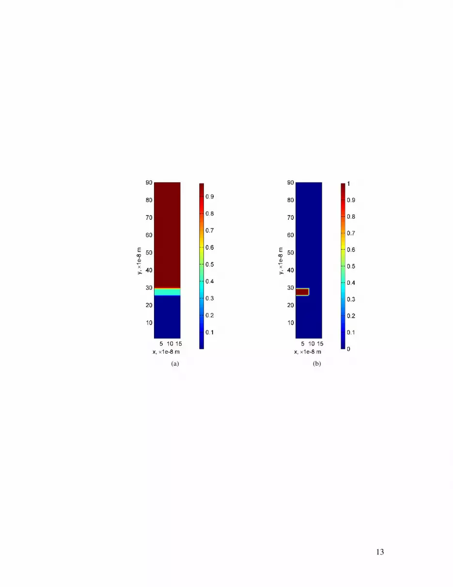
3 A geometrical issue
Both experimental and modelling results have suggested that solder bump size
and geometries could influence the growth kinetics and the morphology of the
interfacial IMCs present in very fine lead-free solder interconnects. Looking at all
the modeling techniques reviewed above, phase field models are the most
promising and incorporate more physics for addressing growth kinetics of the
interfacial IMCs. Using Huh’s model, Figure 2 presents the modelling results for
the Tin-Copper binary system with four initial Cu6Sn5 IMC grains (only two
grains are simulated due to symmetry). A majority of the phase field models
(equations) are solved numerically by the finite difference method with a
rectangular geometry. The geometries of interest in soldering are not rectangular
(Huang and Conway 2007). Although it is possible to use the finite difference
method to solve phase field equations on non-rectangular domains, the finite
volume method or finite element methods are better alternatives to deal with
complex geometries. A previous study (Huang and Conway 2007) compared the
computational efficiency of using different numerical methods and computational
tools for the same set of phase field equations of solidification.

9
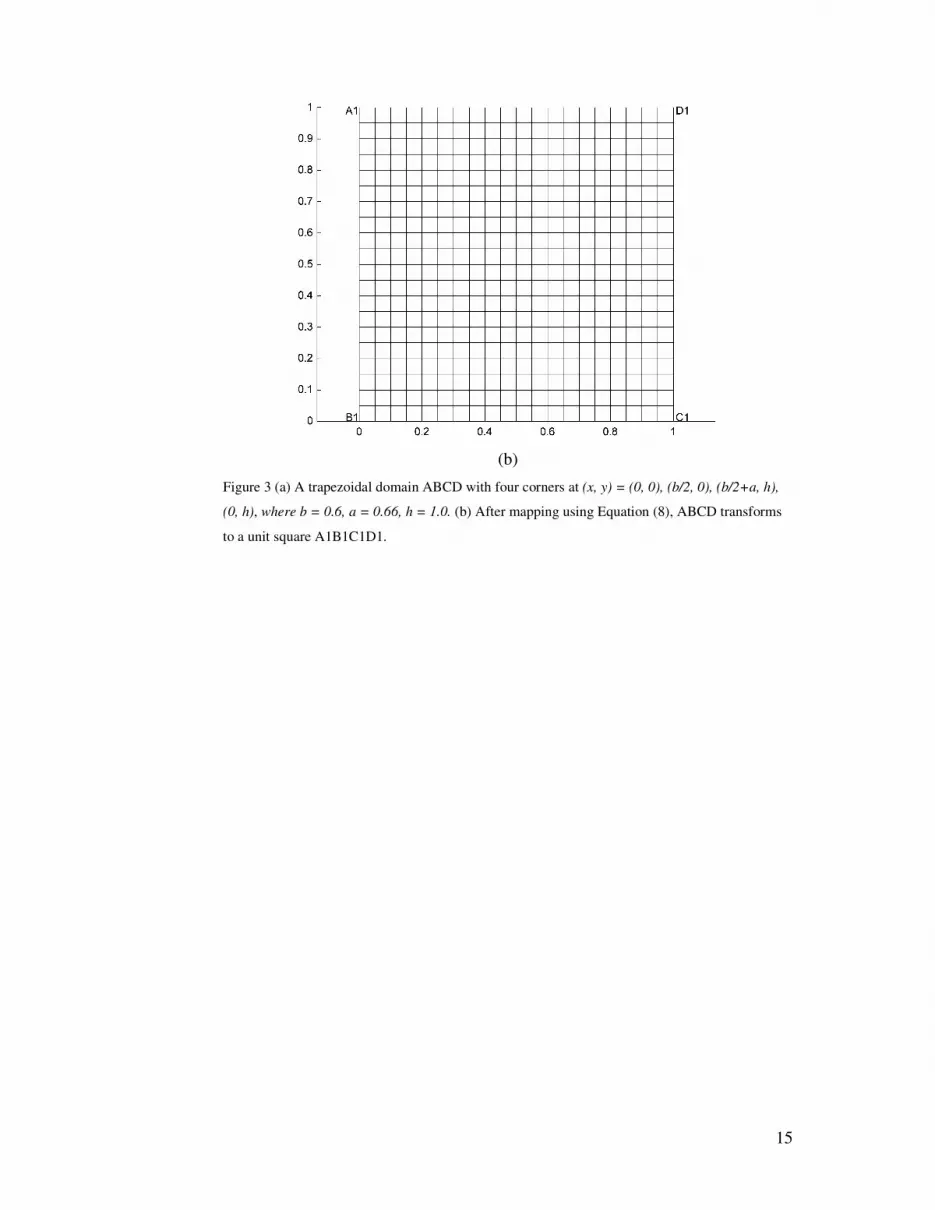
In this paper, a different approach is proposed to use the finite difference
method to solve partial differential equations on simple non-rectangular
geometries ranging from trapezoidal to triangular domains. The basic idea is to
construct a mapping between a rectangular region and the domain of interests.
Depending on the complexity of the geometry, devising this mapping may be very
difficult or simply not possible (Thompson et al. 1999). However, for simple
geometries such as trapezoids and triangles, the mapping is possible. In contrast
to rectangular geometries, trapezoids and triangles can represent, to some extent,
the geometrical variation from the solder bump/substrate interface to the top of the
solder bumps, which influences the kinetics of the inter-diffusion between the
chemical elements in the solders and the substrates and thus the growth kinetics of
the interfacial IMCs. After the mapping, the domain of interest is transformed to
a rectangular geometry and then the transformed partial differential equations
(with transformed boundary conditions) can be readily solved using the finite
difference method.
To illustrate the idea, a simple equation, i.e. Poisson’s equation is considered
2 1u−∇ = (6)
on a trapezoidal domain ABCD is shown in Figure 3a, subjected to the boundary
conditions
0u
n
∂=
∂ in AB and AD and 0u = in BC and CD (7)
The four corners in the physical domain are located at (x, y) = (0, 0), (b/2, 0),
(b/2+a, h), (0, h). A mapping between the coordinates in the transformed
coordinate system (ξ, η) on the unit square and (x, y) is
( / 2 )x b a
y h
η ξ
η
= +
= (8)
After mapping, the trapezoidal domain ABCD transforms to a unit square
A1B1C1D1. The transformed partial differential equations are then solved by a
standard finite difference method and the result is shown in Figure 4.
10
4 Summary
This paper discusses the advantages and disadvantages of different modelling
techniques in the literature on the growth kinetics of interfacial IMCs in lead-free
soldering applications. Phase field models are recommended for the prediction of
the growth kinetics of the interfacial IMCs presented in very fine lead-free solder
interconnects, where the morphology as well as the thickness of the IMCs is of
significance. A mapping method has been proposed such that phase field
equations on domains of trapezoidal or triangular shapes can be solved by
standard finite difference method.
Acknowledgments
The authors wish to acknowledge financial support from the UK’s EPSRC-
IMCRC at Loughborough University. One of the authors, Z. Huang, would also
like to acknowledge the Graduate Institute of Ferrous Technology at Pohang
University of Science and Technology in South Korea for providing a visiting
academic position for one month during January to February 2007 to carry out
part of the work presented in this paper. Useful discussions with Professor J.Y.
Huh at Korea University in South Korea are also gratefully acknowledged.
References
• Borgenstam A, Engström A, Höglund L, Ågren J (2000) DICTRA, a tool for simulation of diffusional
transformations in alloys. Journal of Phase Equilibria 21(3): 269-280
• Chen JK, Beraun JE, Tzou DY (1999) A dual-phase-lag diffusion model for interfacial layer growth in
metal matrix composites. Journal of Materials Science 34(24): 6183-6187
• Chen JK, Beraun JE, Tzou DY (2000) A dual-phase-lag diffusion model for predicting thin film
growth. Semiconductor Science and Technology 15(3): 235-241
• Chen JK, Beraun JE, Tzou DY (2001) A dual-phase-lag diffusion model for predicting intermetallic
compound layer growth in solder joints. Journal of Electronic Packaging 123(1): 52-57
• Chromik RR, Cotts EJ (1996) A Study of the kinetics and energetics of solid state reactions in Pd/Sn
diffusion couples. In: Materials Research Society Symposium Proceedings 398, pp 307-312
• Chromik RR, Cotts EJ (1997) Thermodynamic and kinetic study of phase transformations in
solder/metal systems. In: Materials Research Society Symposium Proceedings 445, pp 31-36
• Dreyer KF, Neils WK, Chromik RR, Grosman D, Cotts EJ (1996) Calorimetric study of the energetics
and kinetics of interdiffusion in Cu/Cu6Sn5 thin film diffusion couples. In: Materials Research Society
Symposium Proceedings 398, pp 313-318
• Erickson KL, Hopkins PL, Vianco PT (1994) Solid-state intermetallic compound growth between
copper and high-temperature, tin-rich solders-Part II - modeling. Journal of Electronic Materials 23(8):

11
729-734
• Erickson KL, Hopkins PL, Vianco PT (1998) Modeling the solid-state reaction between Sn-Pb solder
and a porous substrate coating. Journal of Electronic Materials 27(11): 1177-1192
• Ghosh G (2001) Dissolution and interfacial reactions of thin-film Ti/Ni/Ag metallizations in solder
joints. Acta Materialia 49: 2609-2624
• Ho CE, Liu YW, Yang SC, Kao CR, Jiang DS (2006) Effects of limited Cu supply on soldering
reactions between SnAgCu and Ni. Journal of Electronic Materials 35(5): 1017-1024
• Huang ZH, Conway PP (2007) A comparative study of numerical methods and computational tools for
phase field equations of solidification. In: 2007 TMS Annual Meeting & Exhibition, Advances in
Computational Materials Science and Engineering Methods, pp 1-9
• Huang ZH, Conway PP, Jung E, Thomson RC, Liu CQ, Loeher T, Minkus M (2006) Reliability issues
in Pb-free solder joint miniaturization. Journal of Electronic Materials 35(9): 1761-1772
• Huang ZH, Conway PP, Liu CQ, Thomson RC (2004) The effect of microstructural and geometrical
features on the reliability of ultrafine flip chip microsolder joints. Journal of Electronic Materials
33(19): 1227-1235
• Huang ZH, Conway PP, Liu CQ, Thomson RC (2005) Effect of solder bump geometry on the
microstructure of Sn-3.5 wt% Ag on electroless nickel immersion gold during solder dipping. Journal
of Materials Research 20(3): 649-658
• Huang ZH, Conway PP, Thomson RC, Dinsdale AT, Robinson JAJ (2007) A computational interface
for thermodynamic calculations software MTDATA. Computer Coupling of Phase Diagrams and
Thermochemistry. DOI: 10.1016/j.calphad.2007.07.003
• Huh JY, Han SU, Park CY (2004) Effect of bismuth on the growth kinetics of intermetallic compounds
in Sn-3.5Ag solder joints - A growth kinetic model. Metals and Materials International 10(2): 123-131
• Huh JY, Hong KK, Kim YB, Kim KT (2004) Phase field simulations of intermetallic compound
growth during soldering reactions. Journal of Electronic Materials 33(10): 1161-1170
• Kim DG, Jung SB (2005) Interfacial reactions and growth kinetics for intermetallic compound layer
between In-48Sn solder and bare Cu substrate. Journal of Alloys and Compounds 386 (1-2): 151-156
• Kim SG, Kim WT, Suzuki T, Ode M (2004) Phase-field modeling of eutectic solidification. Journal of
Crystal Growth 261(1): 135-158
• Kinyanjui R, Lehman LP, Zavalij L, Cotts E (2005) Effect of sample siye on the solidification
temperature and microstructure of SnAgCu near eutectic alloys. Journal of Materials Research 20(11):
2914-2918
• Kivilahti JK (2002) The chemical modeling of electronic materials and interconnections. JOM 54(12):
52-57
• Laurila T, Vuorinen V, Kivilahti JK (2005) Interfacial reactions between lead-free solders and common
base materials. Materials Science and Engineering R-Reports 49(1-2): 1-60
• Lee YG, Duh JG (1999) Interfacial morphology and concentration profile in the unleaded solder/Cu
joint assembly. Journal of Materials Science - Materials in Electronics 10(1): 33-43
• Li GY, Chen BL (2003) Formation and growth kinetics of interfacial intermetallics in Pb-free solder
joint. IEEE Transactions on Components and Packaging Technologies 26(3): 651-658
• Mei Z, Sunwoo AJ, Morris JW (1992) Analysis of low-temperature intermetallic growth in copper-tin
diffusion couples. Metallurgical and Materials Transactions A 23(3): 857-864
• Rönkä KJ, Van Loo FJJ, Kivilahti JK (1998) A diffusion-kinetic model for predicting solder/conductor
interactions in high density interconnections. Metallurgical and Materials Transactions A 29(12): 2951-
2956

12
• Sundman B, Jansson B, Andersson JO (1985). The Thermo-Calc databank system. CALPHAD 9(2):
153-190
• Thompson JF, Soni BK, Weatherill NP (1999) Handbook of grid generation. CRC Press
• Tu KN, Zeng K (2001) Tin-lead (SnPb) solder reaction in flip chip technology. Materials Science and
Engineering R 34(1): 1-58
• Yu DQ, Wu CML, Law CMT, Wang L, Lai JKL (2005) Intermetallic compounds growth between Sn-
3.5Ag lead-free solder and Cu substrate by dipping method. Journal of Alloys and Compounds 392 (1-
2): 192-199
Figure 1 A micrograph showing a cross section of Plastic Ball Grid Array (PBGA) flip chip joint
(Sn-3.8Ag-0.7Cu) as well as typical materials present in each layer (courtesy of Dr. R.M. Horsley
of Celestica).
13
(a) (b)

14
(c) (d)
Figure 2 Phase field modelling of tin-copper binary system with four initial Cu6Sn5 IMC grains
(only two grains are simulated due to symmetry) (a) Initial composition map; (b) Initial order
parameter map for one IMC grain; (c) Composition map after 50 time steps (the same time step as
in Huh et al. 2004 was used); and (d) Order parameter map for the IMC grain after 50 time steps.
(a)
15
(b)
Figure 3 (a) A trapezoidal domain ABCD with four corners at (x, y) = (0, 0), (b/2, 0), (b/2+a, h),
(0, h), where b = 0.6, a = 0.66, h = 1.0. (b) After mapping using Equation (8), ABCD transforms
to a unit square A1B1C1D1.

16
Figure 4 Solution to the Poisson’s equation, i.e. Equation 6, with boundary conditions of Equation
(7) using standard finite difference method. The numbers in the figure are contour labels.


