Embed Size (px)
Citation preview

Mocha Chip: A Graphical Programming System for IC Module Assembly
Robert Nelson Mayo
December 14, 1987
Computer Science Division (EECS) University of California
Berkeley, California 94720
Submitted in partial satisfaction of the requirements for the degree of
Doctor of Philosophy in Computer Science.
Report Documentation Page Form ApprovedOMB No. 0704-0188
Public reporting burden for the collection of information is estimated to average 1 hour per response, including the time for reviewing instructions, searching existing data sources, gathering andmaintaining the data needed, and completing and reviewing the collection of information. Send comments regarding this burden estimate or any other aspect of this collection of information,including suggestions for reducing this burden, to Washington Headquarters Services, Directorate for Information Operations and Reports, 1215 Jefferson Davis Highway, Suite 1204, ArlingtonVA 22202-4302. Respondents should be aware that notwithstanding any other provision of law, no person shall be subject to a penalty for failing to comply with a collection of information if itdoes not display a currently valid OMB control number.
1. REPORT DATE 14 DEC 1987 2. REPORT TYPE
3. DATES COVERED 00-00-1987 to 00-00-1987
4. TITLE AND SUBTITLE Mocha Chip: A Graphical Programming System for IC Module Assembly
5a. CONTRACT NUMBER
5b. GRANT NUMBER
5c. PROGRAM ELEMENT NUMBER
6. AUTHOR(S) 5d. PROJECT NUMBER
5e. TASK NUMBER
5f. WORK UNIT NUMBER
7. PERFORMING ORGANIZATION NAME(S) AND ADDRESS(ES) University of California at Berkeley,Department of ElectricalEngineering and Computer Sciences,Berkeley,CA,94720
8. PERFORMING ORGANIZATIONREPORT NUMBER
9. SPONSORING/MONITORING AGENCY NAME(S) AND ADDRESS(ES) 10. SPONSOR/MONITOR’S ACRONYM(S)
11. SPONSOR/MONITOR’S REPORT NUMBER(S)
12. DISTRIBUTION/AVAILABILITY STATEMENT Approved for public release; distribution unlimited
13. SUPPLEMENTARY NOTES
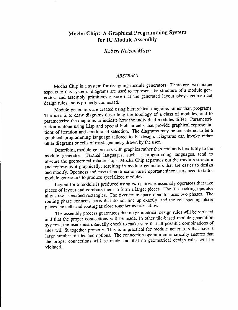
14. ABSTRACT Mocha Chip is a system for designing module generators. There are two unique aspects to this system:diagrams are used to represent the the structure of a module generator, and assembly primitives ensurethat the generated layout obeys geometrical design rules and is properly connected. Module generators arecreated using hierarchical diagrams rather than programs. The idea is to draw diagrams describing thetopology of a class of modules, and to parameterize the diagrams to indicate how the individual modulesdiffer. Parameterization is done using Lisp and special built-in cells that provide graphical representationsof iteration and conditional selection. The diagrams may be considered to be a graphical programminglanguage tailored to IC design. Describing module generators with graphics rather than text addsflexibility to the module generator. Textual languages, such as programming languages, tend to obscure thegeometrical relationships. Mocha Chip separates out the module structure and represents it graphically,resulting in module generators that are easier to design and modify. Openness and ease of modification areimportant since users need to tailor module generators to produce specialized modules. Layout for amodule is produced using two pairwise assembly operators that take pieces of layout and combine them toform a larger piece. The tile-packing operator aligns user-specified rectangles. The river-route-spaceoperator uses two phases. The routing phase connects ports that do not line up exactly, and the cell spacingphase places the cells and routing as close together as rules allow. The assembly process guarantees that nogeometrical design rules will be violated and that the proper connections will be made. In other tile-basedmodule generation systems, the user must manually check to make sure that all possible combinations oftiles will fit together properly. This is impractical for module generators that have a large number of tilesand options. The connection operator automatically ensures that the proper connections will be made andthat no geometrical design rules will be violated.
15. SUBJECT TERMS

16. SECURITY CLASSIFICATION OF: 17. LIMITATION OF ABSTRACT Same as
Report (SAR)
18. NUMBEROF PAGES
168
19a. NAME OFRESPONSIBLE PERSON
a. REPORT unclassified
b. ABSTRACT unclassified
c. THIS PAGE unclassified
Standard Form 298 (Rev. 8-98) Prescribed by ANSI Std Z39-18
Mocha Chip: A Graphical Programming System for IC Module Assembly
Copyright © 1987 by
Robert N. Mayo
All rights reserved.
Mocha Chip: A Graphical Programming System for IC Module Assembly
Robert Nelson Mayo
ABSTRACT
Mocha Chip is a system for designing module generators. There are two unique
aspects to this system: diagrams are used to represent the structure of a module gen
erator, and assembly primitives ensure that the generated layout obeys geometrical
design rules and is properly connected.
Module generators are created using hierarchical diagrams rather than programs.
The idea is to draw diagrams describing the topology of a class of modules, and to
parameterize the diagrams to indicate how the individual modules differ. Parameteri
zation is done using Lisp and special built-in cells that provide graphical representa
tions of iteration and conditional selection. The diagrams may be considered to be a
graphical programming language tailored to IC design. Diagrams can invoke either
other diagrams or cells of mask geometry drawn by the user.
Describing module generators with graphics rather than text adds flexibility to the
module generator. Textual languages, such as programming languages, tend to
obscure the geometrical relationships. Mocha Chip separates out the module structure
and represents it graphically, resulting in module generators that are easier to design
and modify. Openness and ease of modification are important since users need to tailor
module generators to produce specialized modules.
Layout for a module is produced using two pairwise assembly operators that take
pieces of layout and combine them to form a larger pieces. The tile-packing operator
aligns user-specified rectangles. The river-route-space operator uses two phases. The
routing phase connects ports that do not line up exactly, and the cell spacing phase
places the cells and routing as close together as rules allow.
The assembly process guarantees that no geometrical design rules will be violated
and that the proper connections will be made. In other tile-based module generation
systems, the user must manually check to make sure that all possible combinations of
tiles will fit together properly. This is impractical for module generators that have a
large number of tiles and options. The connection operator automatically ensures that
the proper connections will be made and that no geometrical design rules will be
violated.
i
Acknowledgments
Many thanks go to John Ousterhout, whose drive and ambition serves as a model
for all. I've enjoyed working with him immensely.
I'd like to acknowledge a number of other colleagues for their help and technical
insights. All the members of the Magic team deserve special thanks: Gordon Hama
chi, Walter Scott, George Taylor, and of course John Ousterhout. Randy Katz and
Charles Woodson, as members of my qualifying exam committee, reviewed my work
at various stages and provided useful guidance. The previous tool builders at Berkeley
made life much easier for me, and helped point me in the right direction. The past and
present occupants of 508-7 Evans Hall deserve a special round of applause for the
interesting discussions: Michael Arnold, Gordon Hamachi, John Hartman, Paul Heck
bert, Mike Hohmeyer, Barry Roitblat, Ken Shirriff, George Taylor, Steve Viavant, and
Tara Weber. There are many other people in the EECS department at Berkeley that
made it a great place. I'd like to thank them all.
Finally, I would like to express my gratitude to several people for their personal
support and encouragement. Many thanks go to my parents for their guidance, and to
my brothers and sisters. Thanks are also due to Gordon Hamachi, _Herb Ko, and Paula
Peters for their lasting friendship.
This research was funded, in part, by the Defense Advanced Research Projects
Agency under contracts N00039-83-C-0107 and N00039-87-C-0182. I'd like to thank
IBM Corporation for their Graduate Fellowship for two of my years at Berkeley.
11
Table of Contents
CHAPTER 1 Introduction .............................................................................................. 1
1.1 IC DESIGN ..................................................................................................... 1
1.2 MOCHA ClllP OVERVIEW ......................................................................... 3
1.3 COMPONENTS OF A MODULE GENERATOR ........................................ 5
1.4 TlfESIS ORGANIZATION ............................................................................ 8
1.5 REFERENCES .............................................................................................. 10
CHAPTER 2 Generator Specification .......................................................................... 11
2.1 INTRODUCTION ........................................................................................ 11
2.2 TILES ............................................................................................................ 12
2.3 PARAMETERIZATION OF TILES ............................................................ 15
2.4 ASSEMBLY DIAGRAt-.1S ........................................................................... 17
2.5 PARAMETERIZATION OF DIAGRAMS .................................................. 22
2.6 SUt-.1MARY .................................................................................................. 28
2. 7 REFERENCES .... .. ....... ..... ..... ..... ............ ..... ................ .......... ....... ... .... ......... 29
CHAPTER 3 Related Work .......................................................................................... 30
3.1 INTRODUCTION ........................................................................................ 30
3.2 PROGRAMMING ........................................................................................ 31
3.3 GRAPHICAL SYSTEMS ............................................................................. 34
iii
3.4 TILING ............................. ....... ..... .......... ......... ............ ........ ....... .................. 36
3.5 REGULAR-STRUCTURE GENERATOR .................................................. 38
3.6 ARRAY -STRUCTURE TE}.fPLA TES ........................................................ 41
3.7 DISCUSSION ............................................................................................... 42
3.8 REFERENCES .............................................................................................. 44
CHAPTER 4 System Overview .................................................................................... 47
4.1 SYSTEMSTRUCTURE ............................................................................... 47
4.2 MOCHA DRAW ........................................................................................... 51
4.3 COMMUNICATION WITI-1 LISP ............................................................... 54
4.4 MOCHA EV AL ............................................................................................ 55
4.5 MOCHA ASSEM ......................................................................................... 57
4.6 SUI\1MARY .................................................................................................. 58
4. 7 REFERENCES .... .................................... ..... ...................................... ....... .... 59
CHAPTER 5 Pair\\·ise Assembly .................................................................................. 60
5.1 INTRODUCTION ........................................................................................ 60
5.2 THE TILE PACKING OPERA TOR ............................................................ 62
5.3 THE RIVER-ROUTE-SPACE OPERATOR ............................................... 63
5.4 MAGIC'S DESIGN RULES ........................................................................ 64
5.5 RIVER ROUTER .......................................................................................... 69
5.6 SPACER ........................................................................................................ 70
5. 7 CONCLUSIONS ........................................................................................... 73
5.8 REFERENCES .............................................................................................. 73
lV
CHAPTER 6 An Example PLA Generator ................................................................. 75
6.1 INTRODUCTION ........................................................................................ 75
6.2 COl'v1PONENTS OF MCPLA ....................................................................... 80
6.3 HOW MCPLA WORKS ............................................................................... 81
6.4 MPLA ............................................................................................................ 92
6.5 DISCUSSION AND LIMITATIONS ........................................................... 94
6.6 REFERENCES .............................................................................................. 97
CHAPTER 7 Future Work ........................................................................................... 98
7.1 INTRODUCTION ........................................................................................ 98
7.2 GENERATOR COMPILATION .................................................................. 99
7.3 PITCH-MATCHING ................................................................... : ................ 99
7.4 GENERAL ROUTING ............................................................................... 100
7.5 PARA}vlETERIZED NETLISTS ................................................................ 101
7.6 FLEXIBLE PARAMETER PASSING ....................................................... 103
7.7 SUMMARY ................................................................................................ 104
7.8 REFERENCES ............................................................................................ 105
CHAPTER 8 Pitch Matching ...................................................................................... 106
8.1 INTRODUCTION ...................................................................................... 106
8.2 STRETCH GRAPHS .................................................................................. 107
8.3 SOLVING THE GRAPHS .......................................................................... 112
8.4 DISCUSSION ............................................................................................. 118
8.5 REFERENCES ............................................................................................ 119
v
CHAPTER 9 Discussion .............................................................................................. 120
9.1 DISCUSSION ............................................................................................. 120
APPENDIX A Manual Pages ···············································································-···· 123
A.1 ARRAY BUILT-IN CELL ........................................................................ 124
A.2 CASE BUILT-IN CELL ........................ .' ................................................... 126
A.3 MCPLA PLA GENERATOR .................................................................... 128
A.4 MOCHA CIDP ........................................................................................... 131
APPENDIX B Tutorials ............................................................................................... 140
B.l USING A MOCHA CHIP MODULE GENERA TOR .............................. 141
B.1.1 INTRODUCTION ................................................................................... 141
B.1.2 HOW TO GET HELP AND REPORT PROBLEMS ............................. 142
B.1.3 STARTING UP MOCHA CHIP ............................................................. 142
B.1.4 APLAEXAMPLE .................................................................................. 143
B.1.5 CONCLUDING REMARKS .................................................................. 147
B.2 DESIGNING MODULE GEr--.'ERATORS WITH MOCHA CHIP ........... 148
B.2.1 INTRODUCTION ................................................................................... 148
B.2.2 AN EXAMPLE DIAGRA~1 ................................................................... 149
B.2.3 CREATING MOCHA CHIP DIAGRAMS ............................................ 152
B.2.4 THE ARRAY AND CASE CELLS ........................................................ 155
B.2.5 ADDING PARAMETERIZATION ........................................................ 157
B.2.6 SUMMARY ............................................................................................ 159
1 INTRODUCTION
1.1. IC DESIGN
Integrated circuits (!Cs) are electronic circuits etched onto silicon wafers using
patterns of material on several different layers, called mask layers because a photo
graphic mask is used to manufacture them. The design of the patterns is called layout
design, and is usually a time-consuming manual task. The layout designer implements
the circuit by choosing patterns for the mask layers, following electrical design rules
that ensure the proper functioning of the circuit. In addition to implementing an electr
ically correct circuit, the pattern of mask layers must obey another set of rules, called
Chapter 1 2
geometrical design rules, that ensure that the resulting patterns can be reliably fabri
cated.
Geometrical design rules specify which patterns can be reliably fabricated, and
which patterns cannot be. A typical rule specifies the minimum spacing between pieces
of material, to prevent accidental shorts, or the minimum width of a wire, to prevent
accidental gaps. Additional rules describe the proper construction of transistors and
contacts, in terms of required overlaps and separations.
Layout designers often employ programs called module generators to help them
design their ICs. Module generators generate standard building blocks from a set of
parameters, freeing the designer to concentrate on the unique aspects of the design.
Like layout design, the design of a new module generator is also a time-consuming
manual task.
Module generators consist of two phases: a phase called behavioral processing
that maps the behavioral specification into a structural description showing the approx
imate position of components, and a phase called layout generation that maps the
structural description into a set of mask patterns. Both phases have traditionally been
implemented with textual programs. For the latter phase, this is -an error-prone
method, since textual languages are not well-suited to the specification of topological
information. Mocha Chip addresses this phase using a more intuitive scheme: an
extensible graphical programming language to specify topology and special operators
to assemble layout using the geometrical design rules.
Chapter 1 3
1.2. MOCHA CHIP OVERVIEW
There are two key ideas of this research: a graphical specification language for
module generators, and interconnection operators for creating larger structures out of
smaller components. This combination allows the structure of the module to be
specified graphically, and ensures that the resulting module will obey geometrical
design rules. The approach solves many of the problems associated with the layout
generation phase of a module generator.
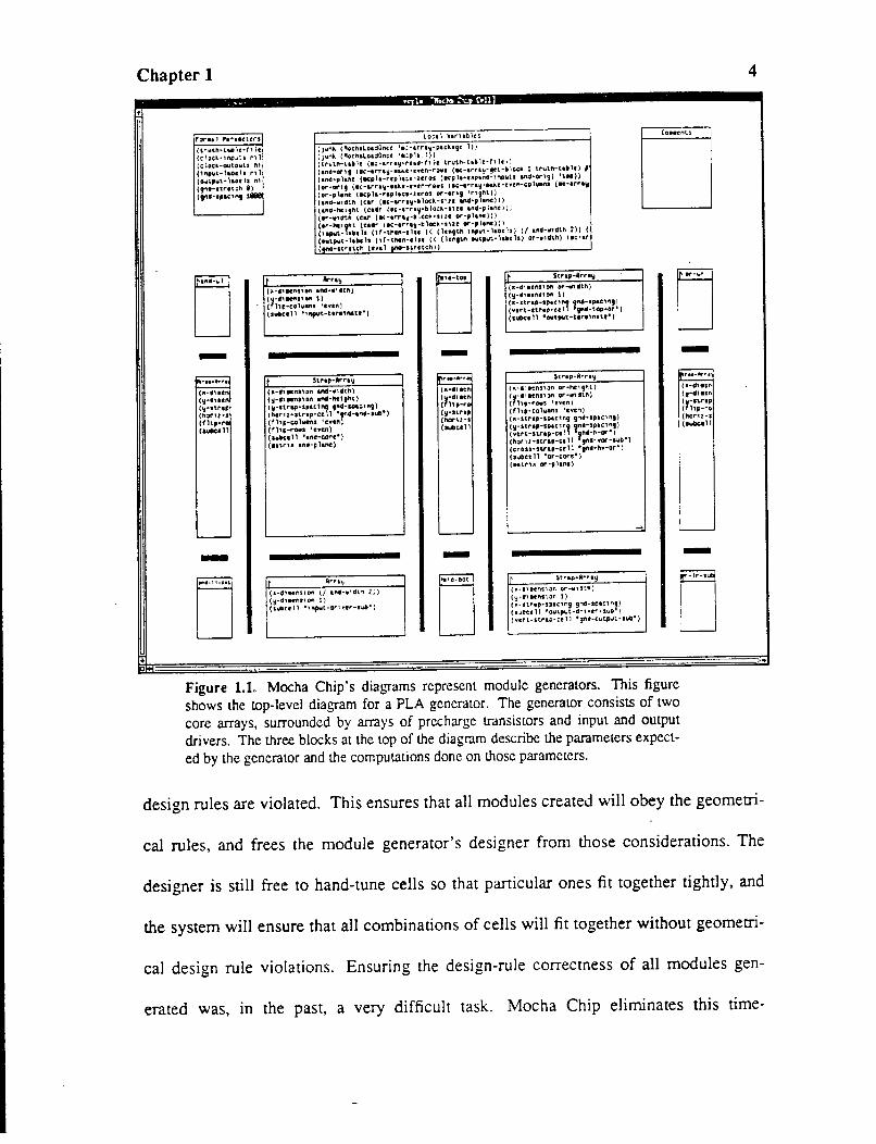
Mocha Chip encourages a style where module generators are designed with
diagrams rather than programs (Figure 1.1 ). Each diagram shows the organization of a
class of modules, and parameters specify the differences between individual modules.
The parameterization is done using Lisp and special built-in cells that provide two
dimensional analogues of iteration and conditional selection. The diagrams constitute
a graphical programming language tailored to IC design.
By separating out the module structure and representing it graphically, module
generators are easier to design and modify. This is important since module generators
are currently designed by programmers rather than the IC designers, often resulting in
generators that don't produce exactly what the IC designer needs in a given situation.
With Mocha Chip, IC designers can tailor module generators to fit their particular
needs, and can also design their own simple generators from scratch.
In addition to diagrams, Mocha Chip provides pairwise assembly operators that
create layout by pairing together two smaller pieces of layout, such as basic tiles, to
form larger pieces. The pairing is done in a way that ensures that no geometrical
0
Chapter 1
f':Jrltl ,., .... ettrs
(t"'lltl'l·t•Dh·h lc {c1c.c~·1np.o~:a 1"11 (clock·owtowu n1 (11'lpe.t·l&Dch ,,1 (o"'~'"'t·laDch n1
~:~:::;;:;~; ~~
lo:a \ 'hrntJ lrs
(J""""' (,.OChtL.Ot~Onu '•:·trrt~-p"ktgt. 1)) (Jun• (l'toctr.al..oUOncc •a:plt. 1))
{\r\tti'H.ailc <•:·arra~·ruG-f11t tr~th-ta•h·fllc•i
{ano-or11 l•c-trray-•a-.c·tYCn .. r~•a (ec-arrt~-~t-bicck 1 trl.ftf"'·ta•1c) I (anc·phnc (Kph·rcpla;c-uros [OCJllt·upanG-lnp~o~ts anQ•Orlg) 1
\.,))
(or·ortg \IC·•ri"&IJ·•alr.t-c•tn-rowl toc-a"'ray·•lr.c·c'f't:n-col..-na (IC·arr•~
; =~~~~:;~" (~~:;·,::~~;:~~:;: .. ~~:;':n~~; ,:~;)) ~~~;~~~"~,~~·~;, ~=~;:~~:~;~~~~~;:' :: .. :~:;: :~~·)) ' ~~;:~t:!.~!'i;r~:~;~~;~~;i:~~;:~~~nO:;:~!~~!~h) (f an4-.-tdtll 2)) (
D D -
-D
(ht~Wt·ltMla (tf-tncn-clu (< {lcng1.h owt,wt·laDcla) or••l«U.h) (lc;·ar
(;M:nrt\cl'l (cn1 inf-nrctch))
(A•f1-tiSIOft 8nd••\dtf'l)
(IJ·dl•nsun and·ttt1gl'lt) ("·str&p·&pltl:1 tnd-ap~:1ng)
~ ~~~;~;:~:::;c~ .~.,:ro-.,... awt~• >
(fhfj-NNI 1 tYCn) ( au1Kt1 1 'and-COF"t'} (lttru ani-plane)
(A·d1HtiS10rl (/ and·•ldt., 1;) (~·d1Ktll10rl 1) (Siolllctll '1"PUt·Qr'1\"Ct'•IYI'1 )
D -
-D
(111•d11ttiS1~rl Or-llf11UI)
(~-•, ~ensun 1)
::;::~:~;::~~;~~ 7;!;~~:~=~ll (IUOCt 11 •outfl"it·tlt'11nnt•)
(~<~·•·-•cnsun or-l'le19rtt)
:~;~~~:; 3~ ,:~~~l,tft) (fhp-coluans 'eve.,) (J~·strap-spu1ng g.,i-spaClrtiJ)
~~;;:~:~::~~~;1 ~~;~~~~z') (hGt1l•ltriSI·Ctl1 ~gtld-'t'OI"'-aYII') (crou-svap-cell 'tM·h•·or'} (sto6bce11 •or-core') <•uru. or-phne}
(J.·III,•ens,on or-w1:1tft; (~·d11fRSlOn 1) (J.·SV•p·Sp1Cif'l9 g"HH·tFICl.,g) (S.lDct 11 •o~o~tpt..t·d .. , .. ,,..suo•! (vert· ltrap·ce 11 ·~nd-~ut.p.,.~·tutl')
Figure 1.1. Mocha Chip's diagrams represent module generators. This figure
shows the top-level diagram for a PLA generator. The generator consists of two
core arrays, surrounded by arrays of prccharge transistors and input and output
drivers. The three blocks at the top of the diagram describe the parameters expect
ed by the generator and the computations done on those parameters.
D -<•·Cilltn {y·diaen
~~,~~~: (ftCirH-s (a.-ell
-
4
design rules are violated. This ensures that all modules created will obey the geometri-
cal rules, and frees the module generator's designer from those considerations. The
designer is still free to hand-tune cells so that particular ones fit together tightly, and
the system will ensure that all combinations of cells will fit together without geometri-
cal design rule violations. Ensuring the design-rule correctness of all modules gen-
erated was, in the past, a very difficult task. Mocha Chip eliminates this time-
Chapter 1 5
consuming phase, making it easier for module generators to be designed by IC
designers.
1.3. COMPONENTS OF A MODULE GENERATOR
Module generators generally consist of two parts (Figure 1.2): a part that maps a
specification of the module's behavior into structural information (called behavioral
processing), and a part that maps the structural information into actual mask
geometries (called layout generation). The first part is problem-specific and involves
manipulations of symbolic, algebraic information rather than spatial information. It is
best handled by a general-purpose programming language. The second part, however,
involves spatial operations that are common to all module generators. It is in this area
that Mocha Chip seeks to improve the design process. Traditional techniques use a
programming language for this part, while Mocha Chip makes use of graphics.
An example will be used to illustrate the distinction between the two parts. The
example chosen is a Programmable Logic Array (PLA) generator. A PLA is a com
binatorial circuit that takes a set of boolean input variables and produces as output a
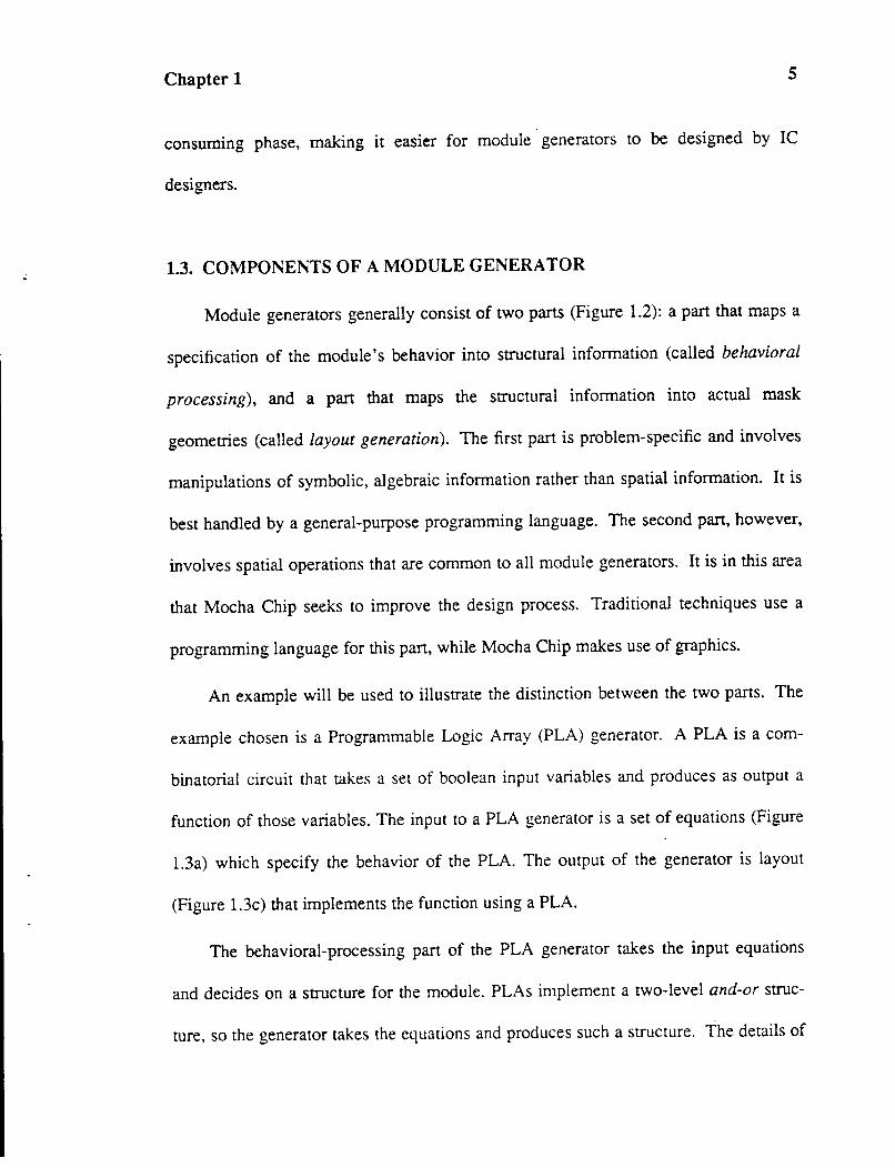
function of those variables. The input to a PLA generator is a set of equations (Figure
1.3a) which specify the behavior of the PLA. The output of the generator is layout
(Figure 1.3c) that implements the function using a PLA.
The behavioral-processing part of the PLA generator takes the input equations
and decides on a structure for the module. PLAs implement a two-level and-or struc
ture, so the generator takes the equations and produces such a structure. The details of

Chapter 1
Behavioral
Portion
Module
Generator
Layout
Portion , .,, ......
I ' .,.. I '
- - - ;,....:'- - - I - - - - ~,- ----
I
/
I
' '
I ..,. I - - - --- - - -, 'Diagrams: L--------
-----L----, I
I Lisp : L--------
' ' ' ' ' ~--------,
1 Tiles : L--------
- - - - - - ____ }'tocha Ch!Q ____ - - - - - --------
Figure 1.2. A module generator typically is composed of two parts: one that
creates a structural description from a specification of the desired behavior, and
one that creates mask layout from the structural description. Mocha Chip makes
the design of the second part easier, breaking it down imo three parts: diagrams,
which represent the structure of a class of modules; Lisp code, which specifies how
the individual instances differ; and tiles of mask layout, which form the basic
building blocks of the module.
' ' I
6
this structure are not important for this discussion; the important idea is that the new
structure is close to the structure of the final layout. For example, if we represent the
structure as a table, as in Figure 1.3b, each position in the table might correspond to a
particular cell or combination of cells in the final layout. The final layout will prob-
ably also contain many cells of a housekeeping nature - ones that aren't a direct
consequence of the input specification but are rather part of the electrical design of the
structure. Tnis mapping of behavior to structure is problem-specific, and is best han-
died with a general-purpose programming language.
Chapter 1
out1 = in1 and in3; out2 = in2 or in1;
(a)
-1
I)(
f -r,z ,-
(c)
J ,., ~.
n .~.'
12'
- 1 - 0 1 1 0 1 1 - 1 1 0
(b)
101 101
- ~ ,-
DC: .!XI
Figure 1.3. The equations in Figure 1.3a specify the desired behavior, and arc
translated into the table shown in Figure 1.3b. The table represents the structure of
a module, and is a close match to the actual layout in Figure 1.3c. The layout con
sists of two small core areas (outlined by thick lines) which are programmed ac
cording to the table, and the surrounding buffers, precharge transistors, and power
busses, which are provided automatically by the generator.
7
After deciding on the structure, the module generator produces layout. In the past,
the popular methods of producing layout from a structural description were to use a
general-purpose programming language or to use tiles (small cells) of mask layout
combined with a programming language. In Mocha Chip, the layout-generation phase
is implemented with three items: tiles of mask layout that form the basic components
Chapter 1 8
to be assembled, diagrams showing the structure of the modules to be generated, and
Lisp code which parameterizes the diagrams.
This method eliminates many of the problems of past approaches. The tiles of
mask layout are the basic building blocks of the module, and are drawn graphically by
the module generator designer. The pairwise assembly operators built into the system
automate much of the error-prone task of assembling the tiles. The diagrams, called
assembly diagrams, specify graphically the overall structure of the class of modules to
be generated, and are clearer and more visually expressive than textual programs. The
diagrams are parameterized by Lisp code that specifies how the individual modules
differ. Calls to arbitrary user-defined Lisp functions may be used, giving a convenient
way to implement the behavioral-processing phase.
1.4. THESIS ORGANIZATION
The next chapter describes the graphical language used by Mocha Chip and how
it is evaluated, or executed, to produce an instantiated module. As mentioned previ
ously, the graphical language makes modules generators easier to design and modify,
and is Mocha Chip's main contribution.
Chapter 3 reviews previous module generator design techniques, discussing their
pitfalls and how each new technique improves upon the previous techniques. I'll com
pare Mocha Chip with these techniques and show why it is an improvement.
Chapter 4 describes how the system is organized and implemented. The system
is implemented in three parts: a front end built into the Magic[l] IC layout system, an
Chapter 1 9
evaluation system written in Lisp[2], and a layout assembly system also built into
Magic.
Chapter 5 describes the two interconnection operators and their implementation.
The packing operator, a simple operator that does not guarantee design-rule correct
ness, is described, as is the river-route-space operator, which does guarantee design
rule correctness. Both operators are useful in specific situations, but it appears that
pitch-matching needs to be added in order for the river-route-space operator to have
general applicability.
Chapter 6 reports on an example PLA generator built with Mocha Chip. This
chapter demonstrates that non-trivial module generators can be built using the graphi
cal constructs present in Mocha Chip. The chapter concludes by comparing the gen
erator with similar generators built without Mocha Chip. The comparisons are based
on the number of lines of code written by the generator designer, the number of
diagrams drawn, and the number of tiles drawn.
Chapter 7 presents some ideas for future work. The ideas fall into three
categories: usability improvements, to make the system faster and easier to use; inter
connection operators, to increase the flexibility of the layout process; and language
improvements, to extend the class of modules that can be easily described with Mocha
Chip.
Chapter 8 _ presents some thoughts on the pitch-matching problem. Pitch
matching fits well into the Mocha Chip framework, since Mocha Chip was designed
with it in mind. However, due to time limitations the pitch-matcher wasn't
Chapter 1 10
implemented. This chapter gives some ideas on how it could be done.
Finally, Chapter 9 presents concluding remarks about the system, both advan
tages and disadvantages. The main disadvantages are that Mocha Chip runs more
slowly than some other systems, and that pitch-matching seems to be required in many
situations. The main advantage is that Mocha Chip's graphical diagrams work well for
regular modules such as PLAs, ROMs, and datapaths, although they are less useful for
more irregular modules. The example PLA generator compares favorably with exist
ing PLA generators, proving that Mocha Chip's extensible graphical programming
language is sufficient to specify real-world module generators. In addition, the idea of
using assembly operators provides a means of assuring design-rule correctness; this is
something that previous module generator systems have had problems with.
1.5. REFERENCES
1. J. K. Ousterhout, G. T. Hamachi, R.N. Mayo, W. S. Scott and G. S. Taylor, The
Magic VLSI Layout System, IEEE Design & Test of Computers, February,
1985.
2. G. L. Steele, Jr., Common Lisp, The Language, Digital Press, 1984.
2 GENERATOR SPECIFICATION
2.1. INTRODUCTION
11
A module generator is specified in Mocha Chip with three parts: tiles of layout
that are the basic building blocks of the module, assembly diagrams that show the
overall structure of the class of modules to be generated, and Lisp code that parameter
izes the diagrams and tiles to indicate how the individual modules differ. This Lisp
code may include calls to user-defined Lisp functions, giving a convenient way to
incorporate the behavioral-processing part of the module generator.
Chapter 2 12
This chapter will present each of the three parts in detail. It will begin with tiles,
then present Lisp parameterization, and conclude with a discussion of assembly
diagrams.
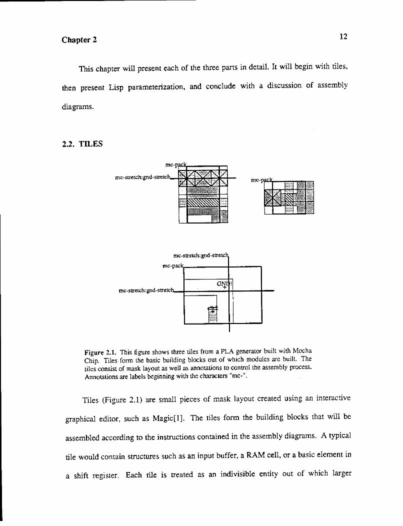
2.2. TILES
me-stretch: gnd-stretct
me -pac'k
me-streteh:gnd-stretc h_ Gt:j_I !
~ .
Figure 2.1. This figure shows three tiles from a PLA generator built with Mocha
Chip. Tiles form the basic building blocks out of which modules are built. The
tiles consist of mask layout as well as annotations to control the assembly process.
Annotations are labels beginning with the characters "me-".
Tiles (Figure 2.1) are small pieces of mask layout created using an interactive
graphical editor, such as Magic[l]. The tiles form the building blocks that will be
assembled according to the instructions contained in the assembly diagrams. A typical
tile would contain structures such as an input buffer, a RAM cell, or a basic element in
a shift register. Each tile is treated as an indivisible entity out of which larger
Chapter 2
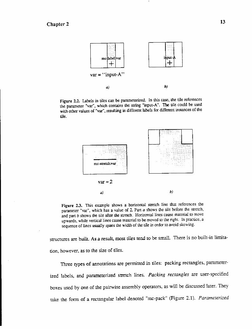
me label var
+ i~ut~ 1\
+ var = "input-A"
a) b)
Figure 2.2. Labels in tiles can be parameterized. In this case, the tile references
the parameter "var", which contains the string "input-A". The tile could be used
with other values of "var", resulting in different labels for different instances of the
tile.
var=2
a) b)
Figure 2.3. This example shows a horizontal stretch line that references the
parameter "var", which has a value of 2. Part a shows the tile before the stretch,
and part b shows the tile after the stretch. Horizontal lines cause material to move
upwards, while vertical lines cause material to be moved to the right. In practice, a
sequence of lines usually spans the width of the tile in order to avoid skewing.
13
structures are builL As a result, most tiles tend to be small. There is no built-in limita-
tion, however, as to the size of tiles.
Three types of annotations are permitted in tiles: packing rectangles, parameter-
ized labels, and parameterized stretch lines. Packing rectangles are user-specified
boxes used by one of the pairwise assembly operators, as will be discussed later. They
take the form of a rectangular label denoted "me-pack" (Figure 2.1). Parameterized
Chapter 2 14
labels are labels of the form "mc-label:text". The text after the colon names a parame-
ter that contains the text to be used as the label (Figure 2.2). Tiles can be invoked with
different values for this parameter, resulting in several different versions of the same
tile, each containing a different label. One example of how this can be used is to label
the inputs to a structure, where each input consists of the same tile but the labels on the
input terminals differ.
mc-stretch:v ar
mc-stretch:var
var= 1
a) b)
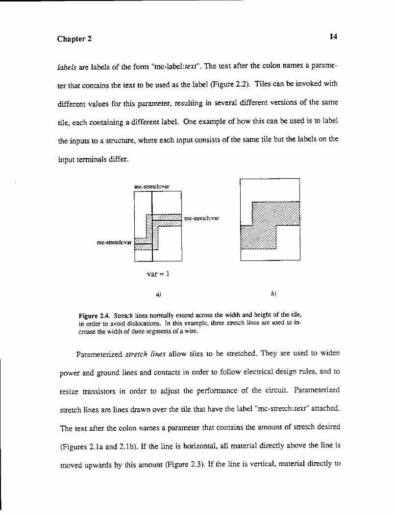
Figure 2.4. Stretch lines nonnally extend across the width and height of the tile,
in order to avoid dislocations. In this example, three stretch lines are used to in
crease the width of three segments of a wire.
Parameterized stretch lines allow tiles to be stretched. They are used to widen
power and ground lines and contacts in order to follow electrical design rules, and to
resize transistors in order to adjust the performance of the circuit. Parameterized
stretch lines are lines drawn over the tile that have the label "mc-stretch:text" attached.
The text after the colon names a parameter that contains the amount of stretch desired
(Figures 2.1 a and 2.1 b). If the line is horizontal, all material directly above the line is
moved upwards by this amount (Figure 2.3). If the line is vertical, material directly to
Chapter 2 15
the right of the line is moved to the right by this amount. Care must be taken that the
lines don't skew or distort the material in undesired ways. A simple guideline, applied
to horizontal lines, is to ensure that each vertical slice through the tile crosses the same
number of horizontal stretch lines. A similar rule can be applied to vertical lines. Fig
ure 2.4 shows an example of a tile with stretch lines that follow these guidelines.
The parameter mechanisms allow tiles to be parameterized, but I have not yet dis
cussed how parameters are computed. The next section covers this aspect.
2.3. PARAMETERIZATION OF TILES
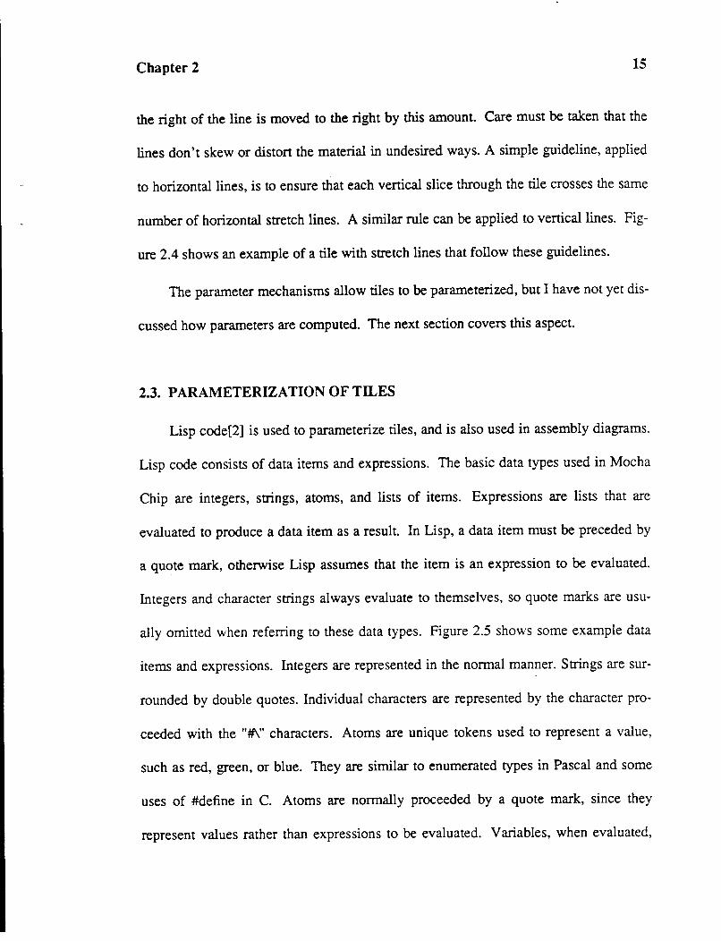
Lisp code[2] is used to parameterize tiles, and is also used in assembly diagrams.
Lisp code consists of data items and expressions. The basic data types used in Mocha
Chip are integers, strings, atoms, and lists of items. Expressions are lists that are
evaluated to produce a data item as a result. In Lisp, a data item must be preceded by
a quote mark, otherwise Lisp assumes that the item is an expression to be evaluated.
Integers and character strings always evaluate to themselves, so quote marks are usu
ally omitted when referring to these data types. Figure 2.5 shows some example data
items and expressions. Integers are represented in the normal manner. Strings are sur
rounded by double quotes. Individual characters are represented by the character pro
ceeded with the "#\" characters. Atoms are unique tokens used to represent a value,
such as red, green, or blue. They are similar to enumerated types in Pascal and some
uses of #define in C. Atoms are normally proceeded by a quote mark, since they
represent values rather than expressions to be evaluated. Variables, when evaluated,
Chapter 2
Data TYl'_e Exam_Qle
integer 492
string "hello world"
character '#
atom 'blue
variable foo
list '(234 round 98 "bear")
'(3 5 6 (8 9 0))
expression (multiply 3 4)
(concat "one" "word")
Figure 2.5. These are the Lisp data types that are commonly used in Mocha Chip.
The table shows each data type along with an example of the syntax. Lists may
contain any number of items, of any data type. The second list is an example of a
list that contains another list Expressions are lists where the first item is the name
of a function. The remaining elements in the list form the arguments to the func
tion. For example, the "multiply" expression evaluates to 12 and the "concat"
expression evaluates to "oneword".
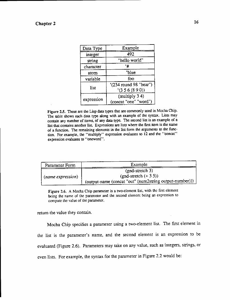
Parameter Form Examp_le
(gnd-stretch 3)
(name expression) (gnd-stretch ( + 3 5)) (output-name (concat "out" (num2string output-number)))
Figure 2.6. A Mocha Chip parameter is a two-element list, with the first element
being the name of the parameter and the second element being an expression to
compute the value of the parameter.
return the value they contain.
16
Mocha Chip specifies a parameter using a two-element list. The first element in
the list is the parameter's name, and the second element is an expression to be
evaluated (Figure 2.6). Parameters may take on any value, such as integers, strings, or
even lists. For example, the syntax for the parameter in Figure 2.2 would be:
Chapter 2 17
(var "input-A")
while the syntax for the parameter in Figure 2.3 would be
(var 2).
Of course, the values could be computed rather than being constants. A similar
mechanism is used with assembly diagrams to provide parameterization.
As we will see later, Mocha Chip provides a way to execute expressions that are
not direct computations of parameters. These expressions can be used as a general
purpose mechanism to escape to Lisp code. For example, an expression such as:
(result (load "myfunc.l"))
can be used to load in a file of Lisp code. These newly provided functions can then be
used to compute parameters. This mechanism is typically used to write the
behavioral-processing portion of the module generator.
2.4. ASSEMBLY DIAGRAMS
Mocha Chip uses diagrams, called assembly diagrams, to specify the structure of
the modules to be produced. These diagrams are drawn by the designer of the module
generator, and replace much of the code that is traditionally written for the structural
assembly portion of a module generator. The diagrams constitute a graphical program
ming language tailored to IC design. They are drawn using a special-purpose interac
tive editor built into the Magic IC layout editor.
Chapter 2 18
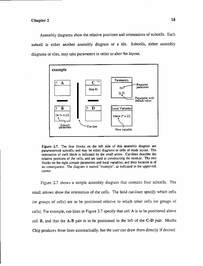
Assembly diagrams show the relative positions and orientations of subcells. Each
subcell is either another assembly diagram or a tile. Subcells, either assembly
diagrams or tiles, may take parameters in order to alter the layout.
example
D § Parameters
(x)----Required
parameter )
(y~ --- Parameter with
default value
~ B u Local Variables
(w(+xy)) (tw\ >2)) 't..____
I ~Cut-line Subcell parameter
New variable
Figure 2. 7. The four blocks on the left side of this assembly diagram are parameterized subcells, and may be either diagrams or cells of mask layout. The orientation of each block is indicated by the small arrow. Cut-lines describe the relative positions of the cells, and are used in constructing the module. The two
blocks on the right contain parameters and local variables, and their location is of no consequence. The diagram is named "example", as indicated in the upper-left
comer.
Figure 2.7 shows a simple assembly diagram that contains four subcells. The
small arrows show the orientation of the cells. The bold cut-lines specify which cells
(or groups of cells) are to be positioned relative to which other cells (or groups of
cells). For example, cut-lines in Figure 2.7 specify that cell A is to be positioned above
cell B, and that the A-B pair is to be positioned to the left of the C-D pair. Mocha
Chip produces these lines automatically, but the user can draw them directly if desired.
Chapter 2
DO DD 1
BB 1
EEJ a)
DD DD 1
[]] []]
1 8B
b)
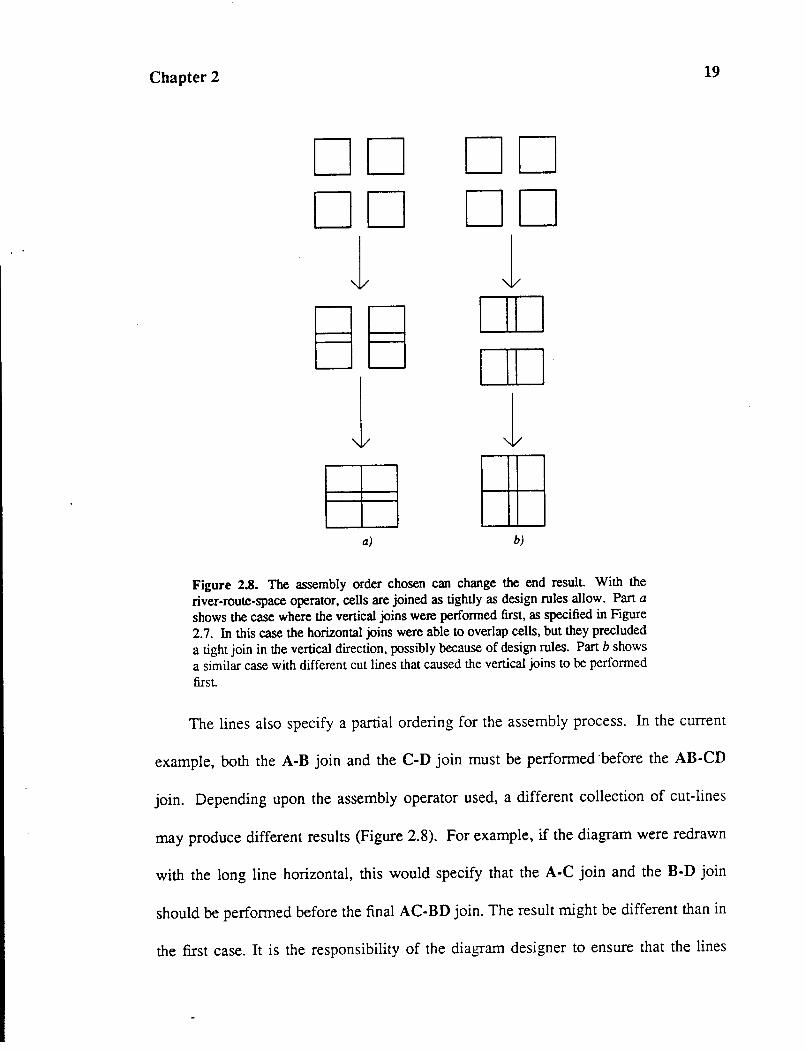
Figure 2.8. The assembly order chosen can change the end result. With the
river-route-space operator, cells are joined as tightly as design rules allow. Part a
shows the case where the vertical joins were performed first, as specified in Figure
2.7. In this case the horizontal joins were able to overlap cells, but they precluded
a tight join in the vertical direction, possibly because of design rules. Part b shows
a similar case with different cut lines that caused the vertical joins to be performed
first.
19
The lines also specify a partial ordering for the assembly process. In the current
example, both the A-B join and the C-D join must be performed ·before the AB-CD
join. Depending upon the assembly operator used, a different collection of cut-lines
may produce different results (Figure 2.8). For example, if the diagram were redrawn
with the long line horizontal, this would specify that the A-C join and the B-D join
should be performed before the final AC-BD join. The result might be different than in
the first case. It is the responsibility of the diagram designer to ensure that the lines

Chapter 2
a)
b)
me-pack
c)
Figure 2.9. The packing operator assembles tiles by abutting their user-specified
packing rectangles, denoted by the "me-pack" label (part a). The operator ignores
design rules and connectivity constraints, as shown in part b. This gives added
flexibility, but may result in errors. The sides of the packing rectangles to be abut
ted must be of the same length, or an error is reported (part c).
chosen will work correctly with the assembly operator chosen.
20
Assembly operators are chosen by tagging each cut-line with the name of the
operator. Currently three tags are recognized: pack, river, and default. The pack
operator (Figure 2.9) combines tiles by packing together their user-specified packing
rectangles, ignoring connectivity and design-rule violations. Tiles are usually designed
so that they pack together correctly irrespective of the assembly order. If an error
occurs due to incorrect packing rectangles, it is likely that the end result is dependent

Chapter 2
b)~ river route ~
Figure 2.10. The river operator joins tiles together in two phases: river routing
and spacing. The river routing phase ensures that the proper connectivity is creat
ed, while the spacing phase compacts the result according to geometrical design
rules. The operator will eliminate routing entirely if the terminals align properly
and design rules allow connection by overlap or abuttment.
21
on the assembly order since the system makes a "best guess" at the alignment and
proceeds. The location of the error in the layout is tagged with a special marker that is
easy to find. The river operator joins tiles by river routing and spacing, ensuring that
design rules are met (Figure 2.10). If spacing rules allow, the operator may eliminate
the routing and make the entire join using abuttment or overlap. This operator is
dependent upon the assembly order, since it attempts to squeeze out as much space as
possible during each join. It is the responsibility of the diagram designer to chose an
order that produces the desired result. The default tag instructs Mocha Chip to inspect
a global variable in order to pick an assembly operator. This variable will contain
either the tag pack or the tag river. Using the default tag makes it possible to delay
the choice of an assembly operator until after the diagrams are designed. For example,
a module generator could be built with many of the cut-lines tagged with default. The
user of the generator could set the default variable to either pack or river in order to
experiment with different layouts of the module.
Chapter 2 22
2.5. PARAMETERIZATION OF DIAGRAMS
Assembly diagrams also take parameters, to control the layout of the module.
The parameters and variables are put into the diagrams by pointing to a block or sub
cell in the diagram and invoking a text editor. These parameters could be as complex
as a truth table, in the case of a PLA generator, or as simple as the size for an inverter.
Assembly diagrams can also compute local variables and pass new values down to
subcells.
Figure 2. 7 shows how parameters are declared, local variables computed, and
new values passed to subcells. The "Parameters" block specifies two parameters: x
andy. The x parameter has no default value, so it must be defined at some higher
level. The y parameter has a default value of 3, which is used if y is not defined when
the diagram is invoked.
Subcells may also access parameters and variables defined at higher levels of the
hierarchy, using Lisp's dynamic scoping rules. When a diagram is evaluated, the
parameters block is evaluated first, followed by the variables block and then the
parameters for each individual subcell. The parameters block simply checks to make
sure that the parameters are currently defined at some higher level in the hierarchy or
have values supplied by defaults. If defaults are used, a new nested scope is created
that contains those values. A new scope is then created for the variables block, which
is evaluated. Lastly, each subcell in the diagram is then evaluated one at a time, in a
scope that includes its parameters.
Chapter 2
A B -
(x 3)
1/ "" B c
(y 4)
"" l/ c .... ---------, I Parameters I I I I (x) I I I
I (y) I
L----------'
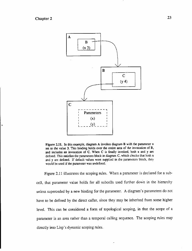
Figure 2.11. In this example, diagram A invokes diagram B with the parameter x
set to the value 3. This binding holds over the entire area of the invocation of B,
and includes an invocation of C. When C is finally invoked, both x and y are
defined. This satisfies the parameters block in diagram C, which checks that both x
and y are defined. If default values were supplied in the parameters block, they
would be used if the parameter was undefined.
23
Figure 2.11 illustrates the scoping rules. When a parameter is declared for a sub-
cell, that parameter value holds for all subcells used further down in the hierarchy
unless superceded by a new binding for the parameter. A diagram's parameters do not
have to be defined by the direct caller, since they may be inherited from some higher
level. This can be considered a form of topological scoping, in that the scope of a
parameter is an area rather than a temporal calling sequence. The scoping rules map
directly into Lisp's dynamic scoping rules.
Chapter 2 24
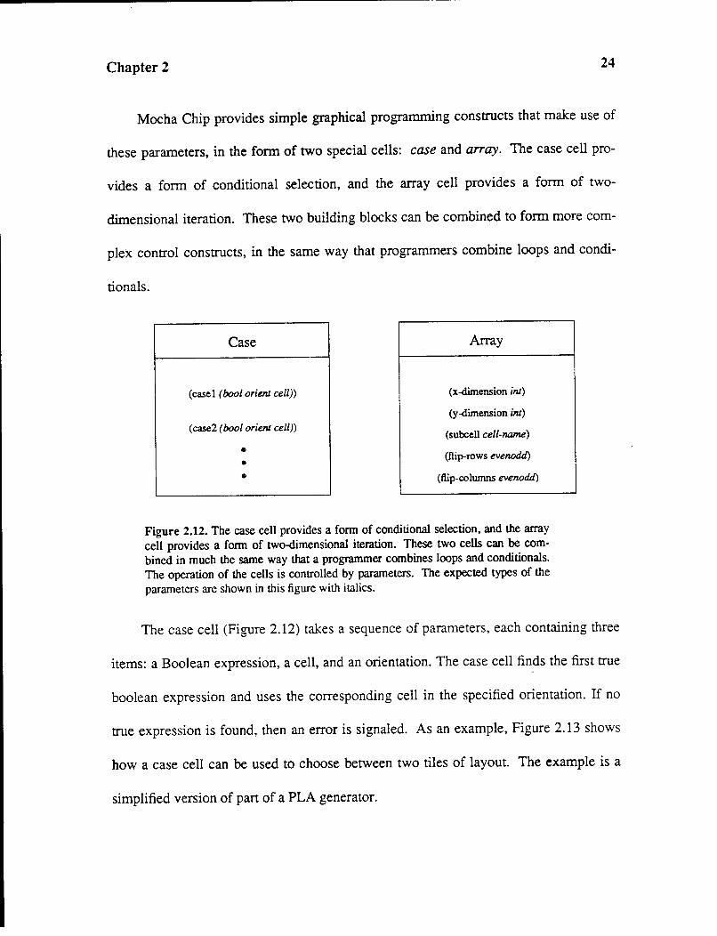
Mocha Chip provides simple graphical programming constructs that make use of
these parameters, in the form of two special cells: case and array. The case cell pro-
vides a form of conditional selection, and the array cell provides a form of two-
dimensional iteration. These two building blocks can be combined to form more com-
plex control constructs, in the same way that programmers combine loops and condi-
tionals.
Case
(easel (bool orient cell))
(case2 (bool orient cell))
• • •
Array
(x-dimension int)
(y-dimension int)
(subcell cell-name)
(flip-rows evenodcl)
(flip-columns evenoda)
Figure 2.12. The case cell provides a form of conditional selection, and the array
cell provides a form of two-dimensional iteration. These two cells can be com
bined in much the same way that a programmer combines loops and conditionals.
The operation of the cells is controlled by parameters. The expected types of the
parameters are shown in this figure with italics.
The case cell (Figure 2.12) takes a sequence of parameters, each containing three
items: a Boolean expression, a cell, and an orientation. The case cell finds the first true
boolean expression and uses the corresponding cell in the specified orientation. If no
true expression is found, then an error is signaled. As an example, Figure 2.13 shows
how a case cell can be used to choose between two tiles of layout. The example is a
simplified version of part of a PLA generator.
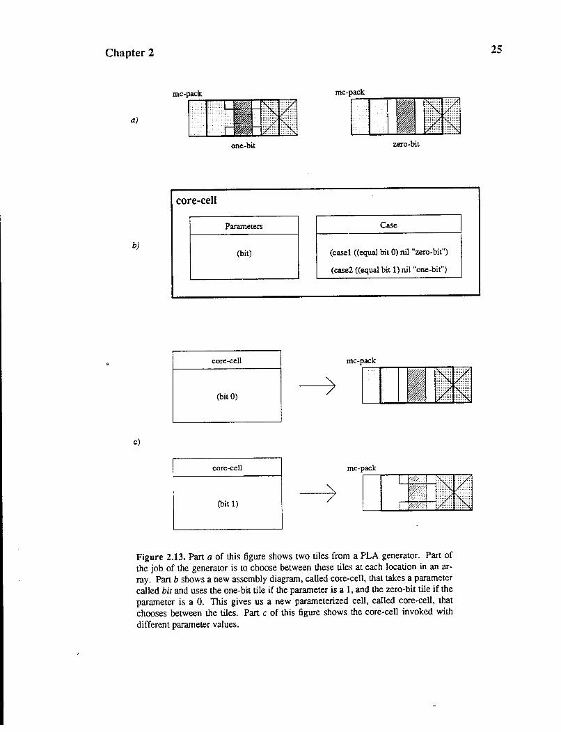
Chapter 2
a)
one-bit
core-cell
Parameters
b) (bit)
core-cell
(bit 0)
c)
core-cell
(bit 1)
zero-bit
Case
(easel ((equal bit 0) nil "zero-bit")
(case2 ((equal bit 1) nil "one-bit")
>
me-pack r-~--~~~~~~~
Figure 2.13. Part a of this figure shows two tiles from a PLA generator. Part of
the job of the generator is to choose between these tiles at each location in an ar
ray. Part b shows a new assembly diagram, called core-cell, that takes a parameter
called bit and uses the one-bit tile if the parameter is a 1, and the zero-bit tile if the
parameter is a 0. This gives us a new parameterized cell, called core-cell, that
chooses between the tiles. Part c of this figure shows the core-cell invoked with
different parameter values.
25
Chapter 2
a)
b)
pia-array
core-bit
Parameters
(matrix)
Parameters
(matrix) (x-index) (y-index)
pia-array
(matrix (0 1 0) (11 0) (0 0 1)
Array
(x-dimension (width matrix)) (y-dimension (height matrix))
(subcell "core-bit") (flip-rows 'none)
(flip-columns 'even)
core-cell
(bit (get-array-element matrix x-index y-index))
)
Figure 2.14. The array cell creates a two-dimensional array, invoking either a tile
or an assembly diagram at each point. In this example, the diagram pia-array takes a parameter called matrix and creates an array of the diagram core-bit. This di
agram uses its own indices to reference a position in the matrix, and passes this
value to core-cell to select a tile.
26
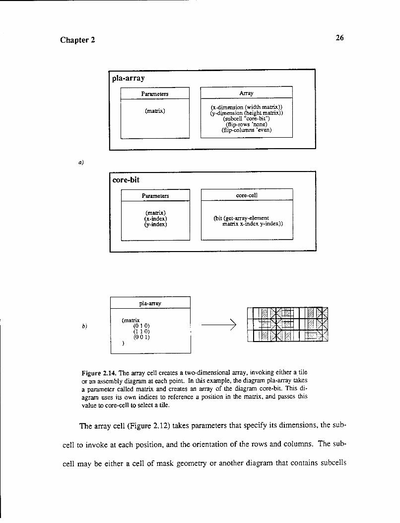
The array cell (Figure 2.12) takes parameters that specify its dimensions, the sub-
cell to invoke at each position, and the orientation of the rows and columns. The sub-
cell may be either a cell of mask geometry or another diagram that contains subcells
Chapter 2 27
- including, perhaps, array and case cells. Subcells may determine their structure
using the current x and y index (provided to them by the array cell) as well as addi-
tional parameters defined by the caller of the array cell. The orientation of rows and
columns are controlled by two flags, each of which takes on one of four values: none,
even, odd, all. The flag allows even or odd rows (or columns) to be flipped upside-
down (or sideways). Figure 2.14 gives an example of an array cell.
Array n.
(x-dimension) (y-dimension)
(flip-rows 'none) (flip-co)UiliilS 'none)
(mirror-subcell)
simole-arrav
(subcell "mirror-sub")
mirror-sub
Parameters
(x-index) (y-index)
mirror-subcell)
Variables
(doflip-rows ... ) (doflip-colurnns ... )
(doflip ... )
Case
(easel (t mirror-subcell doflip nil))
Figure 2.15. Two diagrams can implement our array cell using only a simpler
array cell and a case cell. To do this, a diagram called array is drawn, and the
appropriate parameters are declared. The simpler array cell is used to provide
iteration, and the case cell is used to select the orientation of the cell at each posi
tion in the array. The actual computation of orientation is done using Lisp code in
the variables block. The code has been eliminated from this figure due to lack of
space, but it is easy to see how it would work. For example, the code for doftip
rows needs only to inspect the current y coordinate y-index and the parameter
Oip-rows to see if there is a match. A similar computation is done for the
columns. The two are combined to form an overall orientation that is stored in
doftip. The Case cell selects among the alternatives, but in this instance the alter
natives are chosen by using variables instead of multiple branches with constant
expressions.
Chapter 2 28
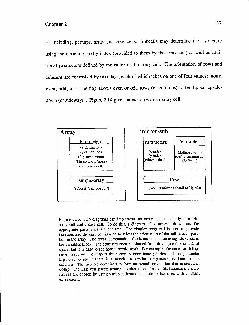
The case and array cells are general-purpose control constructs, and can be com
bined to build new control constructs in the same way that loops and conditionals may
be combined. This can be demonstrated by synthesizing the flipping capability of the
array cell using only the case cell and a non-flipping version of the array cell. Figure
2.15 shows how this could be done using two assembly diagrams containing the case
cell and a hypothetical simple-array cell. The flipping capability in Mocha Chip's
array cell ability is only an optimization to speed up the assembly process.
2.6. SUMMARY
Mocha Chip's assembly diagrams provide a means of graphically representing
the structure of a module. The diagrams replace the code that is traditionally written
for this purpose. The parameter seeping mechanism is similar to dynamic seeping in
Lisp, and can best be thought of as a form of topological seeping. The case and array
cells provide what may be thought of as two-dimensional control constructs. These
cells may be composed to form new constructs, in the same way that programmers
combine loops and conditionals. The end result is that parameterized diagrams may be
composed to form more complex diagrams that generate the modules we see in VLSI
chips.
Chapter 2 29
2.7. REFERENCES
1. J. K. Ousterhout, G. T. Hamachi, R.N. Mayo, W. S. Scott and G. S. Taylor, The
Magic VLSI Layout System, IEEE Design & Test of Computers, February,
1985.
2. G. L. Steele, Jr., Common Lisp, The Language, Digital Press, 1984.
3 RELATED WORK
3.1. INTRODUCTION
30
In the past, several techniques have been developed for the design of module gen-
erators. The ideal system would provide visually intuitive mechanisms for expressing
geometrical relationships, and allow for flexible parameterization of the structures.
Graphics works well for describing geometrical relationships, but is hard to parameter-
ize. Textual programming languages express parameterization well, but make the
structure hard to visualize. This interplay of text and graphics is at the heart of the
development of module-generator systems. The following sections survey the .
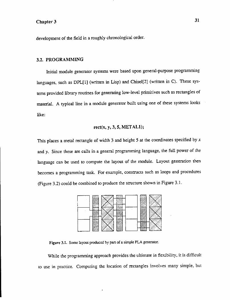
Chapter 3 31
development of the field in a roughly chronological order.
3.2. PROGRAMMING
Initial module generator systems were based upon general-purpose programming
languages, such as DPL[l] (written in Lisp) and Chisel[2] (written in C). These sys
tems provided library routines for generating low-level primitives such as rectangles of
material. A typical line in a module generator built using one of these systems looks
like:
rect(x, y, 3, S, MET ALl);
This places a metal rectangle of width 3 and height 5 at the coordinates specified by x
andy. Since these are calls in a general programming language, the full power of the
language can be used to compute the layout of the module. Layout generation then
becomes a programming task. For example, constructs such as loops and procedures
(Figure 3.2) could be combined to produce the structure shown in Figure 3.1.
Figure 3.1. Some layout produced by part of a simple PLA generator.
While the programming approach provides the ultimate in flexibility, it is difficult
to use in practice. Computing the location of rectangles involves many simple, but
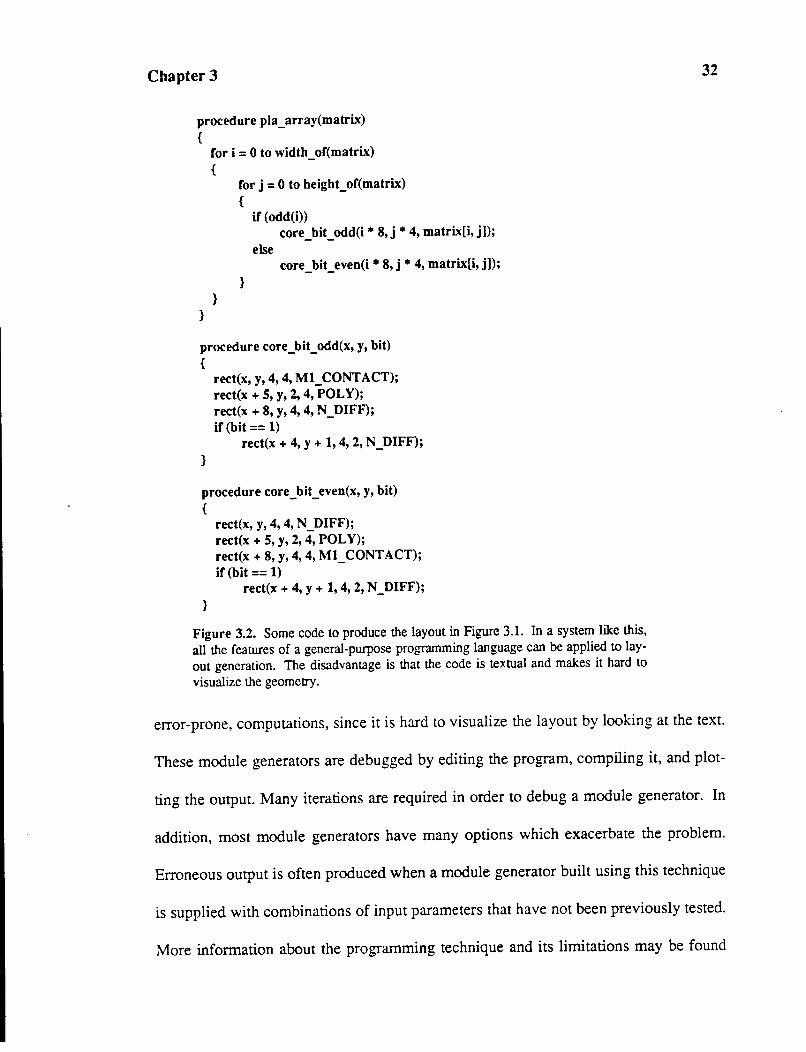
Chapter 3
procedure pia_ array(matrix) {
}
fori= 0 to widtb_of(matrix) {
}
for j = 0 to heigbt_of(matrix) {
}
if (odd(i)) core_ bit_ odd(i * 8, j * 4, matrix[i, j]);
else core_bit_even(i * 8,j * 4, matrix[i,j]);
procedure core_bit_odd(x, y, bit) {
}
rect(x, y, 4, 4, M1_CONTACT); rect(x + S, y, 2, 4, POLY); rect(x + 8, y, 4, 4, N_DIFF); if (bit== 1)
rect(x + 4, y + 1, 4, 2, N _ DIFF);
procedure core_bit_even(x, y, bit) {
}
rect(x, y, 4, 4, N_DIFF); rect(x + S, y, 2, 4, POLY); rect(x + 8, y, 4, 4, M1_CONTACT); if (bit== 1)
rect(x + 4, y + 1, 4, 2, N_DIFF);
Figure 3.2. Some code to produce the layout in Figure 3.1. In a system like this,
all the features of a general-purpose programming language can be applied to lay
out generation. The disadvantage is that the code is textual and makes it hard to
visualize the geometry.
32
error-prone, computations, since it is hard to visualize the layout by looking at the text.
These module generators are debugged by editing the program, compiling it, and plot-
ring the output. Many iterations are required in order to debug a module generator. In
addition, most module generators have many options which exacerbate the problem.
Erroneous output is often produced when a module generator built using this technique
is supplied with combinations of input parameters that have not been previously tested.
More information about the programming technique and its limitations may be found
Chapter 3 33
in Chapter 6 of Steve Trimberger's book[3] and Chapter 8 of Steve Rubin's book[4].
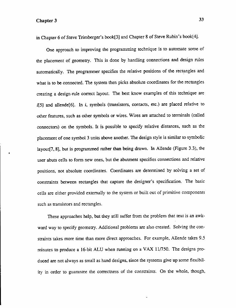
One approach to improving the programming technique is to automate some of
the placement of geometry. This is done by handling connections and design rules
automatically. The programmer specifies the relative positions of the rectangles and
what is to be connected. The system then picks absolute coordinates for the rectangles
creating a design-rule correct layout. The best know examples of this technique are
i[5] and allende[6]. In i, symbols (transistors, contacts, etc.) are placed relative to
other features, such as other symbols or wires. Wires are attached to terminals (called
connectors) on the symbols. It is possible to specify relative distances, such as the
placement of one symbol 3 units above another. The design style is similar to symbolic
layout[?, 8], but is programmed rather than being drawn. In Allende (Figure 33), the
user abuts cells to form new ones, but the abutment specifies connections and relative
positions, not absolute coordinates. Coordinates are determined by solving a set of
constraints between rectangles that capture the designer's specification. The basic
cells are either provided externally to the system or built out of primitive components
such as transistors and rectangles.
These approaches help, but they still suffer from the problem that text is an awk
ward way to specify geometry. Additional problems are also created. Solving the con
straints takes more time than more direct approaches. For example, Allende takes 9.5
minutes to produce a 16-bit ALU when running on a VAX 11nso. The designs pro
duced are not always as small as hand designs, since the systems give up some flexibil
ity in order to guarantee the correctness of the constraints. On the whole, though,
Chapter 3
procedure pla_array(matrix) {
}
begincell('pla_array'); fori= 0 to widtb_of(matrix) {
}
begincell(' '); for j = 0 to beigbt_of(matrix) {
}
if (odd(i)) place(FLIPPEDO);
if (matrix[i, j] == 1) extcell('onebit');
else extcell('zerobit');
if (j != beigbt_of(matrix)) place(ABOVE);
endcell(' '); if (i != widtb_of(matrix)) place(RIGHT);
endcell(' ');
Figure 3.3. This figure presents Allende code that is equivalent to the previous ex
ample. Allende generates a set of constraints on rectangles that, when solved, will
implement this specification.
34
constraint-based layout seems to be an improvement over the direct programming of
actual coordinates, in that design-rule errors are eliminated.
3.3. GRAPHICAL SYSTEMS
Graphical systems such as Caesar[9], Chipmonk[lO], and Magic[ll] were first
developed as an intuitive means of specifying non-parameterized geometry. The layout
is simply drawn rather than programmed. This provides a better user interface, since
what the designer sees on the screen is identical to the conceptual image in the
designer's head. The problem, of course, is that these graphics systems don't provide
programmability. Without programmability, we cannot create module generators and
all layout must be drawn manually.
Chapter 3 35
Some graphical systems have features to partially compensate for their lack of
programmability. In some systems, such as Chipmonk[lO] and Electric[4], wires are
attached to other pieces of material and move around when the attached pieces move,
to maintain connectivity. Symbolic layout systems such as Mulga[7] and Vivid[8] take
this one step further, providing a graphical version of the design style we encountered
with constraint-generating programming languages. In the symbolic layout style, cir
cuit elements and wires are drawn in their relative positions and the system solves con
straints to determine the absolute coordinates.
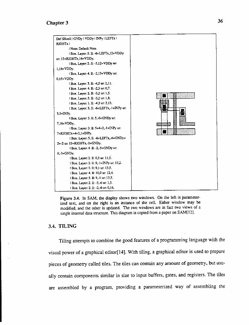
Two systems, SAM[12] and Daedalus[13], combine a graphical display with a
textual programming language. In SAM, the two displays are simply two views of a
single qata structure (Figure 3.4). This greatly aids the writing of programs for layout
generation, providing something that is best thought of as instant plotting with the abil
ity to make small graphical changes. The user can edit either of the views, and the
corresponding changes appear in the other view. The graphical display only shows
one instance of the module to be generated, in effect instantiating the program with a
fixed set of parameters. When the graphical layout corresponding to parameterized
text is edited, there in ambiguity in how the text should be updated, since several
parameterized texts can generate a single graphical layout. The users of these systems
must use and understand two different but linked representations. While this works
well for the layout of low-level cells, it does not greatly aid the higher-level narameter
ization of a module generator.
Chapter 3
Def SRce111 GNDy I VDDy I INPy I LEFrx I
RIGHTxl
I Note: Default Note.
I Box. Layer. 5.11: -6+LEFTx,12+VDDy
ur. 13+RIGHTx,16+VDDy.
I Box. Layer. 2.11: -3,12+VDDy ur.
1,16+VDDy.
I Box. Layer. 4. 11: -2,13+ VDDy ur:
0,15+VDDy.
I Box. Layer. 3. 11: -4,5 ur. 2,11.
I Box. Layer. 4. 11: -2,3 ur. 0,7.
I Box. Layer. 2. 11: -3,2 ur. 1,5.
I Box. Layer. 5. 11: -3,2 ur. 1,8.
I Box. Layer. 1.11: -4,3 ur: 2,13.
I Box. Layer: 3.11: -6+LEFrx,-1+~'"Py ur:
3,1+INPy.
I Box. Layer: 3.11: 5,-6+GNDyur:
7,16+VDDy.
I Box. Layer: 3.11: 5+4+2,-1+INPy ur:
7+RIGHTx+4+2,1=~'"Py.
I Box. Layer: 5.11: -6+LEFTx,-6+GNDy+
2+-2 ur: 13+RIGHTx,-2+GNDy.
I Box. Layer: 4. 11: -2,-5+GNDy ur:
0,-3+GNDy.
I Box. Layer: 2.11: 0,3 ur: 11,5.
I Box. Layer: 3.11: 9,-1+:Tho'"Py ur: 13,2.
I Box. Layer: 2.11: 9,1 ur: 13,5.
I Box. Layer. 4.11: 10,0 ur: 12,4.
I Box. Layer: 5.11: 9,-1 ur: 13,5.
I Box. Layer: 2.11: -3,-6 ur: 1,3.
I Box. Layer: 2.11: -2,-6 ur: 0,16.
Figure 3.4. In SAM, the display shows two windows. On the left is parameter
ized text, and on the right is an instance of the cell. Either window may be
modified, and the other is updated. The two windows are in fact two views of a
single internal data structure. This diagram is copied from a paper on SAM[12].
3.4. TILING
36
Tiling attempts to combine the good features of a programming language with the
visual power of a graphical editor[14]. With tiling, a graphical editor is used to prepare
pieces of geometry called tiles. The tiles can contain any amount of geometry, but usu-
ally contain components similar in size to input buffers, gates, and registers. The tiles
are assembled by a program, providing a parameterized way of assembling the
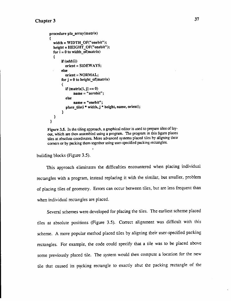
Chapter 3
procedure pia _array( matrix) {
}
width= WIDTH_OF("onebit"); height =HEIGHT_ OF("onebit"); fori= 0 to width_of(matrix) {
}
if (odd(i)) orient = SIDEWAYS;
else orient = NORMAL;
for j = 0 to height_of(matrix) {
if (matrix[i, j] == 0) name= "zerobit";
else name= "onebit";
place_tile(i * width,j *height, name, orient); }
Figure 3.5. In the tiling approach, a graphical editor is used to prepare tiles of lay
out, which are then assembled using a program. The program in this figure places
tiles at absolute coordinates. More advanced systems placed tiles by aligning their
comers or by packing them together using user-specified packing rectangles.
building blocks (Figure 3.5).
37
This approach eliminates the difficulties encountered when placing individual
rectangles with a program, instead replacing it with the similar, but smaller, problem
of placing tiles of geometry. Errors can occur between tiles, but are less frequent than
when individual rectangles are placed.
Several schemes were developed for placing the tiles. The earliest scheme placed
tiles at absolute positions (Figure 3.5). Correct alignment was difficult with this
scheme. A more popular method placed tiles by aligning their user-specified packing
rectangles. For example, the code could specify that a tile was to be placed above
some previously placed tile. The system would then compute a location for the new
tile that caused its p~cking rectangle to exactly abut the packing rectangle of the
Chapter 3 38
previously placed tile.
TPACK[14], my Master's Project, developed a more powerful scheme. In
TPACK, tiles are aligned by their corners. This is more general, since special empty
spacing tiles can be defined whose corners are used to control the alignment of other
tiles (Figure 3.6). This allows placement of a new tile at an arbitrary offset from some
previously placed tile, something that is not possible with the packing rectangle
approach. However, there is a price paid for this additional flexibility. The informa
tion about which corners are used for alignment is contained in the program code.
This means that the tile designer must either look at the program code when designing
spacing tiles, or read documentation that describes the code's behavior. With the
packing-rectangle approach, there is no variation in the assembly method, resulting in
a simpler interface for the tile designer. My experience over the past few years indi
cates that the additional flexibility provided by TPACK is not worth the added com
plexity for the tile designer.
3.5. REGULAR-STRUCTURE GENERATOR
Bamji's Regular-Structure Generator[l5] attempts to solve the problem of assem
bling tiles. Bamji defines an interface, which is a legal relative position for two tiles.
The set of interfaces is defined by the user by placing examples in a diagram and
numbering them (Figure 3.7). The system ensures that when tiles are placed only pre
specified interfaces are used. This allows the user to verify the interfaces in advance, in
turn ensuring that the resulting layout only contains verified interfaces.
Chapter 3
(0, 0)
procedure pia_ array( matrix) {
}
fori= 0 to width_of(matrix) { if (odd(i)) {
}
zero_tile = "zerobit-ftipped"; one_tile = "onebit-ftipped";
} else {
}
zero_tile = "zerobit"; one_tile = "onebit";
for j = 0 to height_of(matrix) { if (matrix[i, j] == 0)
}
new_ tile = zero_ tile; else
. new_tile =one_ tile; if (i == 0 AND j == 0) 1• Place first tile at (0, 0). •1
last_tile = place_tile(new_tile, ORIGIN);
if (j == 0) 1• Start new column to right of previous column. •1 last_tile = place_tile(new_tile,
align(lower _left( new _tile), lower _right(prev _column)));
else 1• Place new tile above previous one. •1 last_tile = place_tile(name,
align (lower _left( new_ tile), upper _left(last_ tile)));
if (j == 0) prev _column= last_tile;
Figure 3.6. TP ACK uses comer alignment to place tiles. Each new tile has a
comer aligned with a previously placed tile, as is indicated by heavy bars in this
this figure. The bars are numbered sequentially in the order that the tiles where
placed. Spacing tiles could be used to provide arbitrary offsets, but this is not
needed for this example. The tile-packing method recognizes this, and uses pack
ing rectangles instead of specifying comers in the code. The result is much the
same, but simplifies both the code and the design of tiles, since the tile designer
never needs to know which comers are used for alignment. Some flexibility is
lost, however, since arbitrary offsets cannot be provided through the use of spacing
tiles.
39
Chapter 3
one_cell
IIR ·······
base_cell
~ base_cell
~ base_cell
~~ base_cell
~ interface 1
I base_cell 11
base_cell
one_cell
L interface 2 interface 1
a) b)
procedure pla_array(matrix) {
}
fori= 0 to width_of(matrix) {
}
for j = 0 to height_of(matrix) {
}
if (i == 0 AND j == 0) I* Place first tile at arbitrary location. *I last_tile = place_tile("base_ceU", nil, nil);
if (j == 0)
else
I* Start new column to right of previous column (interface #2). *I
last_tile = place_tile("base_ceU", prev _column, 2);
I* Place new tile above previous one (interface #1). *I last_tile = place_tile("base_ceU", last_tile, 1);
I* Program cell to a '1' if needed. *I if (matrix[i, j] == 1)
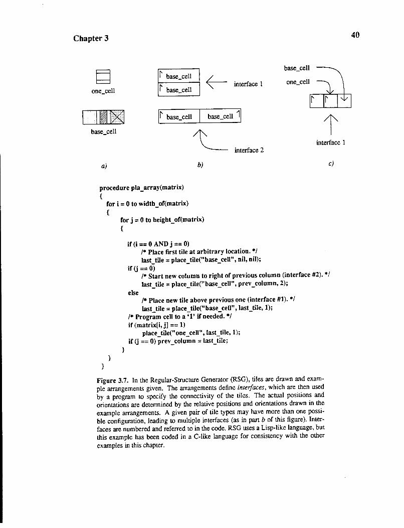
place_tile("one_cell", last_tile, 1); if(j == 0) prev_column = last_tile;
Figure 3.7. In the Regular-Structure Generator (RSG), tiles are drawn and exam
ple arrangements given. The arrangements define interfaces, which are then used
by a program to specify the connectivity of the tiles. The actual positions and
orientations are determined by the relative positions and orientations drawn in the
example arrangements. A given pair of tile types may have more than one possi
ble configuration, leading to multiple interfaces (as in part b of this figure). Inter
faces are numbered and referred to in the code. RSG uses a Lisp-like language, but
this example has been coded in a C-like language for consistency with the other
examples in this chapter.
c)
40
Chapter 3 41
The technique does not work well for generators that have a large number of
optional tiles for a certain location, as is common in practice. An interface must be
defined for each possible combination of tiles, leading to an exponential rise in the
number of interfaces to be defined and checked. This problem is partially, but not
completely, overcome by allowing tiles to be stacked on top of each other, allowing a
single tile to be ''programmed'' by the presence of other tiles on top.
3.6. ARRAY -STRUCTURE TEMPLATES
SDA's Structure Compiler uses array-structure templates[16] to specify graphi
cally the global structure of a module. The user can draw arrays whose contents are
determined by personality matrices and pieces of code (Figure 3.8). The system has no
graphical representation of conditional selection, and doesn't allow arrays to be nested.
These features would be needed in order to make the system complete, in the sense of
allowing arbitrary structures to be built graphically and re-used as if they were primi
tive components.
Module assembly proceeds in three steps. In the first step, each block is pro
cessed, creating a map of symbols based upon a personality matrix an.d rules attached
to the block. The second step executes user-supplied code that manipulates the map.
In the final step, each block is assembled by translating the symbols into tiles, packing
the tiles together (using user-specified packing rectangles), and joining the resulting
blocks as specified by the array-structure template.
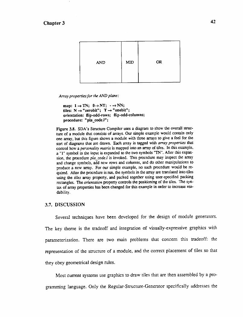
Chapter 3
AND MID
Array properties for the AND plane:
map: 1--+ TN; 0--+ NT; ---+ NN; tiles: N--+ "zerobit"; T--+ "onebit"; orientation: flip-odd-rows; flip-odd-columns;
procedure: "pla_code.l";
OR
Figure 3.8. SDA's Structure Compiler uses a diagram to show the overall struc
ture of a module that consists of arrays. Our simple example would contain only
one array, but this figure shows a module with three arrays to give a feel for the
sort of diagrams that are drawn. Each array is tagged with array properties that
control how a personality matrix is mapped into an array of tiles. In this example,
a "1" symbol in the input is expanded to the two symbols "1N". After this expan
sion, the procedure pla_code.l is invoked. This procedure may inspect the array
and change symbols, add new rows and columns, and do other manipulations to
produce a new array. For our simple example, no such procedure would be re
quired. After the procedure is run, the symbols in the array are translated into tiles
using the tiles array property, and packed together using user-specified packing
rectangles. The orientation property controls the positioning of the tiles. The syn
tax of array properties has been changed for this example in order to increase rea
dability.
3.7. DISCUSSION
42
Several techniques have been developed for the design of module generators.
The key theme is the tradeoff and integration of visually-expressive graphics with
parameterization. There are two main problems that concern this tradeoff: the
representation of the structure of a module, and the correct placement of tiles so that
they obey geometrical design rules.
Most current systems use graphics to draw tiles that are then assembled by a pro-
gramming language. Only the Regular-Structure-Generator specifically addresses the
Chapter 3 43
problem of correctly placing tiles. It, however, requires the legal interfaces to be
drawn by the user, which can be impractical if a large number of tiles can fill a given
position, resulting in an exponentially large number of interfaces. Mocha Chip takes a
different approach: tiles are assembled by assembly operators rather than directly
placed. The simplest of these operators, the packing-rectangle operator, provides no
help with the correct placement of tiles. The river-route-space operator, however,
places tiles so that they obey geometrical design rules and connectivity rules. As a
result, placement is guaranteed to be correct without forcing the module generator
designer to verify an exponentially large set of tile interfaces.
The other main concern is the representation of the overall structure of a module.
Both array-structure templates and Mocha Chip provide a means of using graphics to
specify this structure. Array-structure templates are limited to the specification of the
top-level array structure of a module. Mocha Chip, however, is an extensible program
ming system that has graphical representations of both conditional selection and itera
tion. In addition, Mocha Chip diagrams can be used in other diagrams in the same way
that tiles are, resulting in a system that can express hierarchical module generators
using graphics. Thus, Mocha Chip diagrams are used to specify the structure of all
levels of a module, not just the top-level overall structure.
Mocha Chip is an advance in both areas addressed by previous systems: the
representation of the module's structure and the placement of individual tiles. A new
graphical programming language is used to represent the structure of a module. The
language is complete in the sense that it provides graphical representations of iteration ,
Chapter 3 44
and conditional selection that can be combined to form new control constructs. Mocha
Chip's assembly operators represent a new approach to the second problem: the place
ment of tiles. In Mocha Chip, the river-route-space assembly operator guarantees
proper connectivity and ensures that geometrical design rules are not violated. This
automatic placement of tiles frees the module generator designer from having to manu
ally verify that all possible tile interfaces are valid. The end result is a powerful
module generation system that eases the module design process.
3.8. REFERENCES
1. J. Batali and A. Hartheimer, The Design Procedure Language, VLSI Memo 80-
31, MIT, September, 1980.
2. K. Karplus, CHISEL: An Extension to the Programming Language C for VLSI
Layout, Report No. STAN-CS-82-959, PhD Thesis, Stanford University, 1983.
3. S. M. Trimberger, An Introdution to CAD for VLSI, Kluwer Academic
Publishers, 1987.
4. S.M. Rubin, Computer Aids for VLSI Design, Addison-Wesley, 1987.
5. S. Johnson and S. Browning, The LSI Design Language i, Technical
memorandum 1980-1273-10, Bell Laboratories, November 18, 1980.
6. J. M. Mata, A Methodology for VLSI Design and a Contraint-Based Layout
Language, PhD Thesis, Princeton University, October, 1984.
Chapter 3 45
7. N. Weste and B. Ackland, A Pragmatic Approach to Topological Symbolic IC
Design, in VLSI '81, Academic Press, 1981, pp. 117-129.
8. J. Rosenberg, D. Boyer, J. Dallen, S. Daniel, C. Poirier, J. Poulton, D. Rogers
and N. Weste, A Vertically Integrated VLSI Design Environment, Proc. 20th
Design Automation Conference, 1983, pp. 31-38.
9. J. K. Ousterhout, The User Interface and Implementation of an IC Layout Editor,
IEEE Transactions on Computer-Aided Design CAD-3, 3 (July, 1984).
10. P. Petit, Chipmonk: An Interactive VLSI Layout Tool, Digest of Papers,
Compcon 82, 1982, pp. 302-304.
11. J. K. Ousterhout, G. T. Hamachi, R.N. Mayo, W. S. Scott and G. S. Taylor, The
Magic VLSI Layout System, IEEE Design & Test of Computers, February,
1985.
12. S. Trimberger, Combining Graphics and a Layout Language in a Single
Interative System, Proc. 18th Design Automation Conference, 1981, pp. 234-
239.
13. J. Batali, N. Mayle, H. Shrobe, G. Sussman and D. Weise, The DPL/Daedalus
Design Environment, in VLSI '81, Academic Press, 1981, pp. 183-192.
14. R. Mayo and J. Ousterhout, Pictures with Parentheses: Combining Graphics and
Procedures in a VLSI Layout Tool, Proc. 20th Design Automation Conference,
1983, pp. 270-276.
Chapter 3 46
15. C. Bamji, C. Hauck and J. Allen, A Design by Example Regular Structure
Generator, Proc. 22nd Design Automation Conference, 1985, pp. 16-22.
16. H. Law and J. Mosby, An Intelligent Composition Tool for Regular and Semi
Regular VLSI Structures, IEEE International Conference on Computer Aided
Design, 1985, pp. 169-171.
4 SYSTEM OVERVIEW
4.1. SYSTEM STRUCTURE
47
The Mocha Chip implementation contains four components (Figure 4.1). Three of
the components correspond to three issues that Mocha Chip addresses: the use of
graphics to draw parameterized diagrams, the evaluation of those diagrams to produce
an instantiated module, and the assembly of mask layout for that module. Graphics are
handled by the Mocha Draw module, instantiation by the Mocha Eval module, and
assembly by the Mocha Assem module. The fourth module, Mocha Lisp, provides a
communication mechanism between C and Lisp, as will be discussed later.
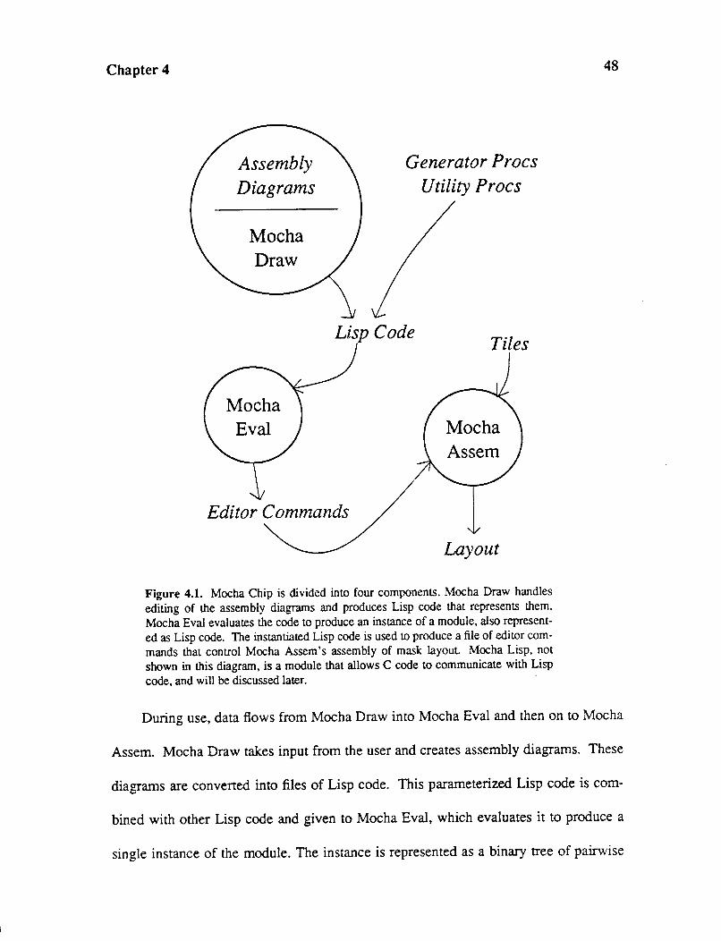
Chapter 4
Assembly Diagrams
Mocha Draw
Generator Procs Utility Procs
Lisp Code Tiles
Editor Commands
Layout
Figure 4.1. Mocha Chip is divided into four components. Mocha Draw handles
editing of the assembly diagrams and produces Lisp code that represents them.
Mocha Eval evaluates the code to produce an instance of a module, also represent
ed as Lisp code. The instantiated Lisp code is used to produce a file of editor com
mands that control Mocha Assem's assembly of mask layout. Mocha Lisp, not
shown in this diagram, is a module that allows C code to communicate with Lisp
code, and will be discussed later.
48
During use, data flows from Mocha Draw into Mocha Eval and then on to Mocha
Assern. Mocha Draw takes input from the user and creates assembly diagrams. These
diagrams are converted into files of Lisp code. This parameterized Lisp code is com-
bined with other Lisp code and given to Mocha Eval, which evaluates it to produce a
single instance of the module. The instance is represented as a binary tree of pairwise
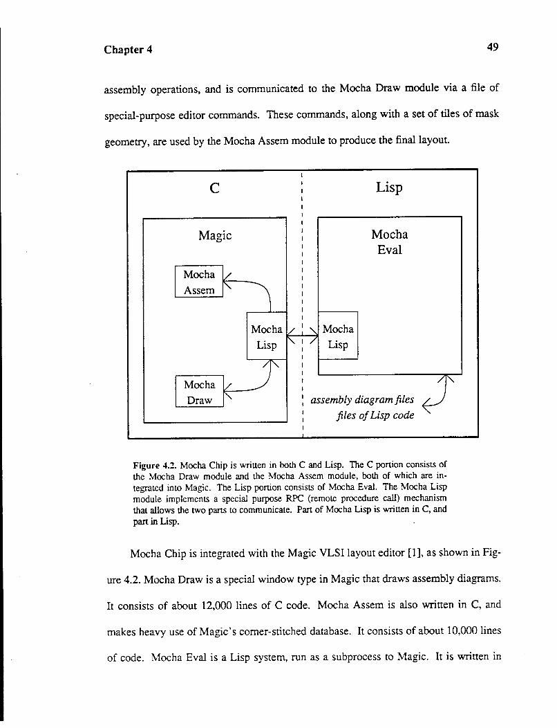
Chapter 4 49
assembly operations, and is communicated to the Mocha Draw module via a file of
special-purpose editor commands. These commands, along with a set of tiles of mask
geometry, are used by the Mocha Assem module to produce the final layout.
c Lisp
I
Magic I Mocha I I Eval I I
Mocha lL. I I
Assem f'\.
~ I I I I I
Mocha vi" Mocha
Lisp 1"'- I / Lisp I I
J I I
Mocha v I ;r I
Draw I' I assembly diagram files I I files of Lisp code I
Figure 4.2. Mocha Chip is written in both C and Lisp. The C portion consists of
the Mocha Draw module and the Mocha Assem module, both of which are in
tegrated into Magic. The Lisp portion consists of Mocha Eval. The Mocha Lisp
module implements a special purpose RPC (remote procedure call) mechanism
that allows the two parts to communicate. Part of Mocha Lisp is written inC, and
part in Lisp.
Mocha Chip is integrated with the Magic VLSI layout editor [1], as shown in Fig-
ure 4.2. Mocha Draw is a special window type in Magic that draws assembly diagrams.
It consists of about 12,000 lines of C code. Mocha Assem is also written in C, and
makes heavy use of Magic's corner-stitched database. It consists of about 10,000 lines
of code. Mocha Eval is a Lisp system, run as a subprocess to Magic. It is written in
Chapter 4 50
about 8,000 lines of Lisp code, and communicates with Magic via a special-purpose
RPC (remote procedure call) as well as with files. The RPC mechanism is written in
both C and Lisp, and is contained in the Mocha Lisp module.
Mocha Chip was written in two languages to facilitate the integration with Magic
and the interpretation of code written interactively. The latter requirement comes from
the fact that diagrams are drawn and parameterized interactively, and then need to be
evaluated. Lisp was chosen as a common and easily understandable language for
interactive interpretation of expressions. C was chosen for the rest of the system, so
that Mocha Chip could make use of Magic's graphics routines and Magic's comer
stitched layout database.
Mocha Chip is an open system in the sense that the user may elect to use only
part of it. I expect that users will draw assembly diagrams in order to specify modules,
but it is possible to write the Lisp code directly. This provides a means of determining
if the assembly diagrams are really a convenient specification. If not, I would expect
to see users writing Lisp code instead of drawing assembly diagrams. It is also possible
to generate the file of editor commands directly, bypassing the Lisp system entirely.
This retains the use of the pairwise assembly operator, but allows for the development
of different front ends for module specification.
The next sections discuss the implementation of the modules.
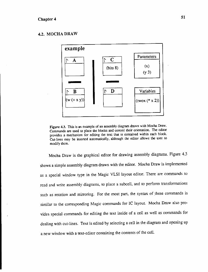
Chapter 4
4.2. MOCHADRAW
example
~ B (w(+xy))
~ ~
Parameters
(x)
(y 3)
Variables
(twox (* x 2))
Figure 4.3. This is an example of an assembly diagram drawn with Mocha Draw.
Commands are used to place the blocks and conuol their orientation. The editor
provides a mechanism for editing the text that is contained within each block.
Cut-lines may be inserted automatically, although the editor allows the user to
modify them.
51
Mocha Draw is the graphical editor for drawing assembly diagrams. Figure 4.3
shows a simple assembly diagram drawn with the editor. Mocha Draw is implemented
as a special window type in the Magic VLSI layout editor. There are commands to
read and write assembly diagrams, to place a subcell, and to perform transformations
such as rotation and mirroring. For the most part, the syntax of these commands is
similar to the corresponding Magic commands for IC layout. Mocha Draw also pro-
vides special commands for editing the text inside of a cell as well as commands for
dealing with cut-lines. Text is edited by selecting a cell in the diagram and opening up
a new window with a text-editor containing the contents of the cell.
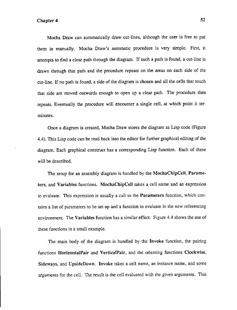
Chapter 4 52
Mocha Draw can automatically draw cut-lines, although the user is free to put
them in manually. Mocha Draw's automatic procedure is very simple. First, it
attempts to find a clear path through the diagram. If such a path is found, a cut-line is
drawn through that path and the procedure repeats on the areas on each side of the
cut-line. If no path is found, a side of the diagram is chosen and all the cells that touch
that side are moved outwards enough to open up a clear path. The procedure then
repeats. Eventually the procedure will encounter a single cell, at which point it ter
minates.
Once a diagram is created, Mocha Draw stores the diagram as Lisp code (Figure
4.4). This Lisp code can be read back into the editor for further graphical editing of the
diagram. Each graphical construct has a corresponding Lisp function. Each of these
will be described.
The setup for an assembly diagram is handled by the MochaChipCell, Paramea
ters, and Variables functions. MochaChipCell takes a cell name and an expression
to evaluate. This expression is usually a call to the Parameters function, which con
tains a list of parameters to be set up and a function to evaluate in the new referencing
environment. The Variables function has a similar effect. Figure 4.4 shows the use of
these functions in a small example.
The main body of the diagram is handled by the Invoke function, the pairing
functions HorizontaiPair and VerticalPair, and the orienting functions Clockwise,
Sideways, and UpsideDown. Invoke takes a cell name, an instance name, and some
arguments for the cell. The result is the cell evaluated with the given arguments. This
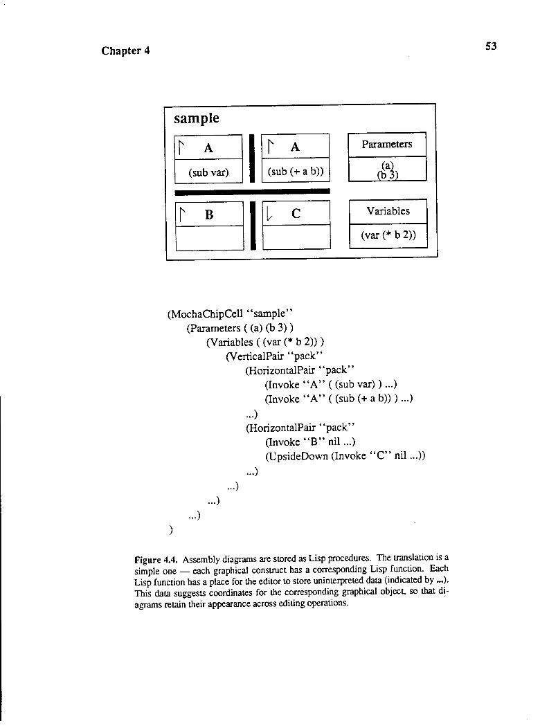
Chapter 4
sample
~ A I ~ A Parameters
(sub var) (sub(+ a b)) ~a~)
~ B I ~ c Variables
(var (* b 2))
(MochaChipCell ''sample''
)
(Parameters ((a) (b 3))
... )
(Variables ( (var (* b 2)))
... )
(V erticalPair "pack" (HorizontalPair "pack"
... )
... )
(Invoke "A" ((sub var)) ... )
(Invoke "A" ((sub(+ a b))) ... )
(HorizontalPair ''pack'' (Invoke "B" nil ... ) (UpsideDown (Invoke "C" nil ... ))
... )
Figure 4.4. Assembly diagrams are stored as Lisp procedures. The translation is a
simple one - each graphical construct has a corresponding Lisp function. Each
Lisp function has a place for the editor to store uninterpreted data (indicated by ••• ).
This data suggests coordinates for the corresponding graphical object, so that di
agrams retain their appearance across editing operations.
53
Chapter 4 54
cell may be transformed using the Clockwise, Sideways, and UpsideDown functions.
Clockwise rotates by a multiple of 90 degrees, while Sideways and UpsideDown pro
vide mirroring operations. Each cut-line in the diagram corresponds to a call to either
HorizontaiPair or VerticaiPair. The first argument to these functions is the text
associated with the cut-line, and specifies which pairwise assembly operator to use.
Additional information, indicated in Figure 4.4 by ellipses, is provided by the
graphical editor. This information contains suggestions about the size and placement
of components on the screen. It is used to ensure that diagrams don't change in
appearance across editing sessions. If the information is omitted or inconsistent,
Mocha Draw provides reasonable values.
Assembly diagrams are read into Mocha Draw by executing them in a special
Lisp environment. The procedures in this environment invoke procedures in Mocha
Draw via a special-purpose RPC mechanism. These procedures construct and place
the corresponding graphical objects to create the assembly diagram represented by the
Lisp code.
4.3. COMMUNICATION WITH LISP
A text-based and line-oriented RPC mechanism is used to communicate between
the C and Lisp portions of Mocha Chip. For a call to Lisp, C sends a line to Lisp. Lisp
sends back lines containing messages to be printed, a return value, and a then a
prompt. The line immediately before the prompt line is assumed to be the return
value. Errors are recognized by the special prompt that Lisp prints out after an error.
Chapter 4 55
For a call to C from Lisp, Lisp prints out a special message line that is recognized by
the C part of the system. The line contains a special prefix followed by the name of the
function to invoke and textual arguments. C looks this up in a table and calls the
appropriate routine. The return value of the routine is sent to Lisp as a text string
which sets a Lisp variable. The calls may be nested, so Lisp can call C and vice-versa
to any depth.
4.4. MOCHA EV AL
Mocha Eval's task is to take the code produced by Mocha Draw and produce an
instantiated module. This is done by executing (or in Lisp terminology, "evaluating")
the code in a special Lisp execution environment. Two phases are used. The output of
the first phase is a tree of diagrams. These diagrams correspond to the assembly
diagrams drawn by the user (Figure 4.5a), except that parameters have been eliminated
and unique names have been assigned to the resulting versions of the diagrams (Figure
4.5b). In the second phase, this tree of diagrams is translated into commands to control
the assembly process (Figure 4.5c ).
The Mocha Eval code is written in Common Lisp, which is readily portable. The
user may, however, parameterize assembly diagrams with Lisp code that is not port
able. It is important that the user avoid non-portable code if the generator is to be port
able.
If a Lisp error occurs during evaluation (e. g. because of improper code specified
by the user), information about the error is passed to the user along with the name of
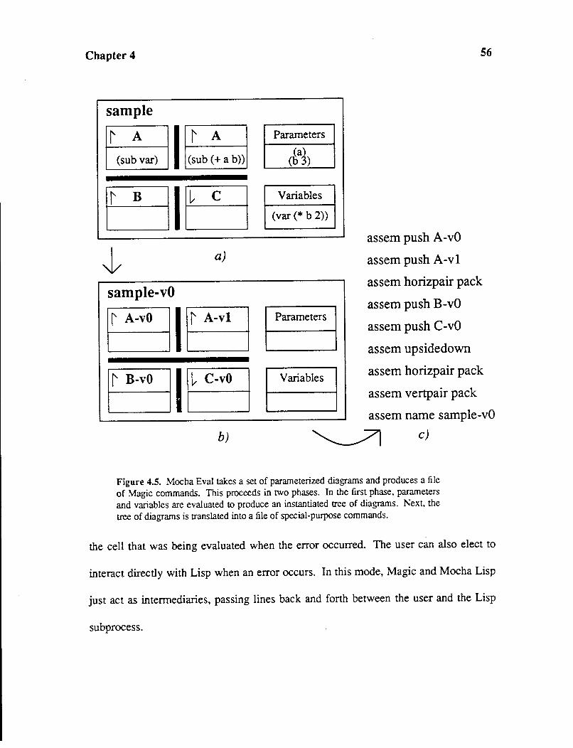
Chapter 4
sample
t-~-(s-ub-~-ar-) ___, I (~ub ~ a b))
DID a)
sample-vO
~~~
b)
Parameters
Variables
(var (* b 2))
56
assem push A-vO
assem push A-vl
assem horizpair pack
assem push B-vO
assem push C-vO
assem upsidedown
assem horizpair pack
assem vertpair pack
assem name sample-vO
~ c)
Figure 4.5. Mocha Eva! takes a set of parameterized diagrams and produces a file
of Magic commands. This proceeds in two phases. In the first phase, parameters
and variables are evaluated to produce an instantiated tree of diagrams. Next, the
tree of diagrams is translated into a file of special-purpose commands.
the cell that was being evaluated when the error occurred. The user can also elect to
interact directly with Lisp when an error occurs. In this mode, Magic and Mocha Lisp
just act as intermediaries, passing lines back and forth between the user and the Lisp
subprocess.
Chapter 4 57
In the first phase, Mocha Eval starts with the name of the topmost cell of the
module. The procedure with this name (corresponding to an assembly diagram) is exe
cuted, and the procedure may explicitly load in files of Lisp code containing user
specified functions. When subcells are invoked, Mocha Eval finds the corresponding
file-of code and loads it. The subcells are then executed, and the process recurses. The
result (function return value) of the execution of a cell is another cell that has all the
parameters and variables instantiated (Figure 4.4b). This new cell may contain fully
instantiated subcells, also produced by the cell evaluation process.
Cells are located using Magic's search path. Each directory in the path is
inspected in turn to see if it contains the desired cell. The first cell found is used. This
mechanism allows for the easy modification of generators. A user can override the
description of a subcell of a module generator by designing a special version of that
subcell and arranging for it to appear earlier in the search path.
In the second phase, Mocha Eval executes the instantiated cells. Each function
call creates a command for the assembly process. As an example, an invoke command
is issued for each subcell reference, and a horizpair command is created for each Hor
izontaiPair function call.
4.5. MOCHA ASSEM
Mocha Assem assembles the mask layout for a module. It does this using a stack
and a collection of pairwise assembly operators and orientation operators. Cells are
pushed onto the stack, and the operators manipulate the items on the top of the stack.
Chapter 4 58
Special purpose Magic commands control the assembly process. Figure 4.5c shows a
simple file of commands.
The most interesting commands are the borizpair and vertpair commands. Con
ceptually, they invoke a pairwise assembly operator using the two items on the top of
the stack as arguments. The operator joins these two pieces of layout together, forming
a third, larger, piece. This piece is pushed onto the stack for use in the remaining com
mands. In actuality, Mocha Assem delays the operation; instead it creates a tree struc
ture that indicates the joins required. This allows for future enhancements to the sys
tem that may require knowledge of the overall structure before a join can be made.
The pairwise assembly operators are discussed more fully in Chapter 5.
4.6. SUMMARY
Mocha Chip is divided into four parts: Mocha Draw, Mocha Eval, Mocha
Assem, and Mocha Lisp. The drawing editor Mocha Draw provides a graphical inter
face for drawing assembly diagrams. Mocha Draw stores these diagrams in files as
pieces of Lisp code. Mocha Eval executes these files of Lisp code to produce a list of
commands for the Mocha Assem module. This module takes the commands and pro
duces mask layout using pairwise assembly operators. Lisp is used for Mocha Eval,
while C is used for Mocha Draw and Mocha Assem. Mocha Lisp provides an RPC
like interface between the two languages. The entire system is integrated with the
Magic IC layout system.
Chapter 4 59
4.7. REFERENCES
1. J. K. Ousterhout, G. T. Hamachi, R. N. Mayo, W. S. Scott and G. S. Taylor,
Magic: A VLSI Layout System, Proceedings of the 21st Design Automation
Conference, 1984.
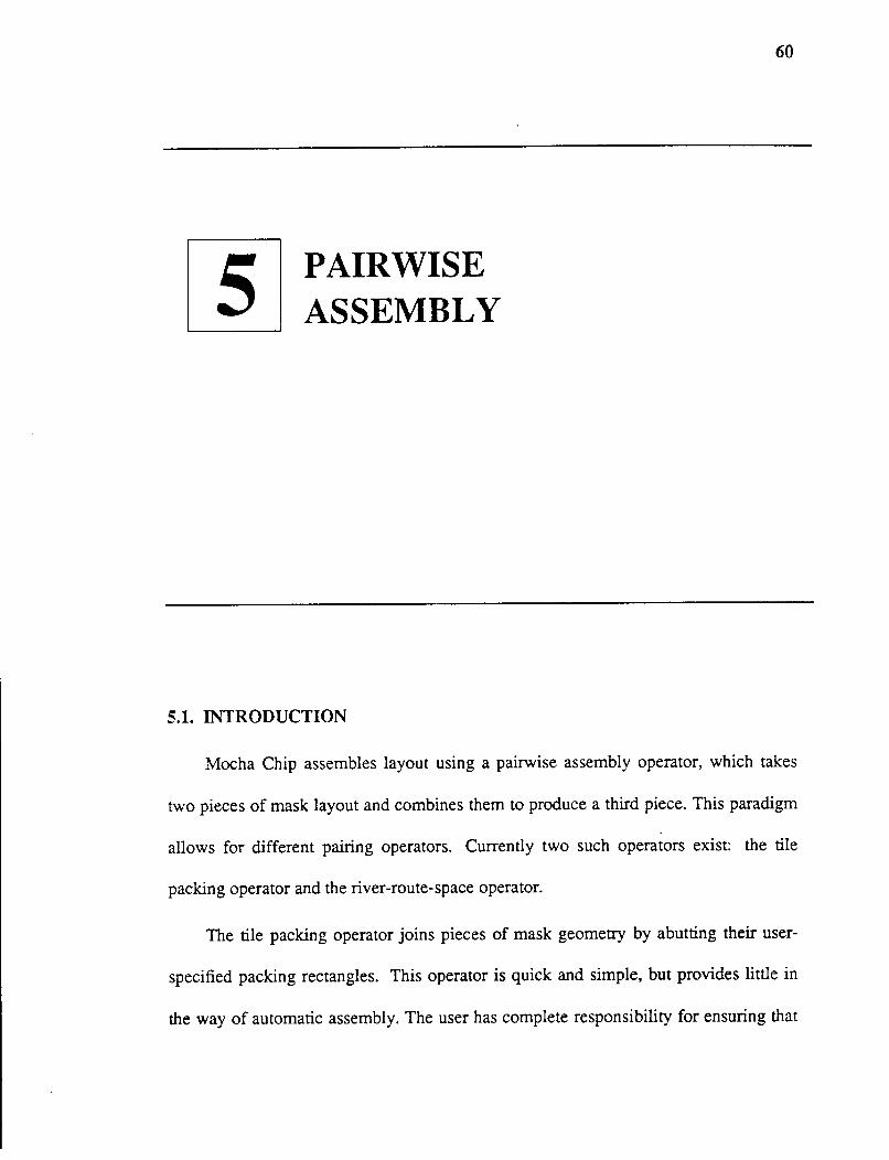
5 PAIRWISE ASSEMBLY
5.1. INTRODUCTION
60
Mocha Chip assembles layout using a pairwise assembly operator, which takes
two pieces of mask layout and combines them to produce a third piece. This paradigm
allows for different pairing operators. Currently two such operators exist: the tile
packing operator and the river-route-space operator.
The tile packing operator joins pieces of mask geometry by abutting their user
specified packing rectangles. This operator is quick and simple, but provides little in
the way of automatic assembly. The user has complete responsibility for ensuring that
Chapter 5 61
the packing of the rectangles will result in a correct layout. This operator is similar to
many current tile-based layout systems.
The river-route-space operator provides more in the way of automatic assistance.
It combines two pieces of geometry, making sure that the terminals on the pieces are
connected even if they don't line up properly. The operator also ensures that design
rules are met. Thus, the combination is correct-by-construction, as far as connectivity
and design rules are concerned. In the simple case of straight-across routing, the
river-route-space operator produces layout similar in density to the tile-packing opera
tor.
Future operators can provide more automatic assembly. Such operators might
provide more powerful routing capabilities, or other functions such as pitch-matching.
The use of a pairwise assembly operator specified in the graphical diagram gives
the user a range of control over the layout assembly process. Using the tile packing
operator gives the user complete control, while use of a more powerful operator pro
vides greater automation.
The following sections describe Mocha Chip's operators in more detail. Each
operator implements a horizontal pairing. Vertical pairings are handled by rotating the
cells before being given to the operator, and then rotating the result back to the original
orientation.
Chapter 5
5.2. THE TILE PACKING OPERATOR
Figure 5.1. The tile packing operator abuts the packing rectangles of two pieces
of geometry and produces a third, larger piece. The packing rectangle of the new
piece is the union of the original packing rectangles. No design rules are checked,
and no attempt is made to ensure proper connections.
62
The tile packing operator joins pieces of mask geometry by abutting their user-
specified packing rectangles (Figure 5.1). The abutting sides of the packing rectangles
must be of the same length, to ensure that their union is a rectangle. This new rectan-
gle forms the packing rectangle for the new piece of layout. An error is reported if the
packing rectangles do not abut properly.
This operator requires the designer to ensure that the resulting layout is correct.
As such, it allows complete flexibility at the expense of automatic correctness by

Chapter 5
construction.
5.3. THE RIVER-ROUTE-SPACE OPERATOR
Figure 5.2. The river-route-space operator joins two pieces of geometry together,
ensuring that connections are made and that no design rules are violated. Overlap
ping is used if it makes the proper connections. In this figure, the letter a marks a
separation that must be maintained, limiting the amount of overlap. In many cases,
the river-route-space operator uses no more area than the packing operator.
63
The river-route-space operator also joins two pieces of geometry to produce a
third. However, it guarantees that no design rules are violated and that the proper con-
nections are made (Figure 5.2). It tries to conserve area, so that in cases where overlap
or abuttment suffices the result will be the same as that produced by the packing rec-
tangle operator.
Chapter 5 64
The interconnection scheme uses a river router followed by a compaction step.
The two sides to be connected must have the same number of terminals, and each pair
of terminals must be on a single layer. The river router connects these pairs of termi
nals together using a wide spacing for the cells. After the river-routing phase, a com
pactor eliminates excess space. The cells will be overlapped if design rules allow. It
is possible that some of the connections will be made by overlap, in which case part of
the routing is eliminated.
Currently, the river-route-space operator aligns the two pieces of geometry by
their midpoints before doing routing. This may lead to unnecessary jogs, which could
be eliminated by a different positioning. This problem has been studied by Ron
Pinter[ I], and his work presents alternative alignment schemes.
The next four sections describe the implementation of the river-route-space
operator. Section 5.4 presents Magic's design rules, which are used for the router and
spacer. A data structure called blockage planes is presented in this section. This data
structure is used by the river-routing algorithm, presented in Section 5.5, and the
spacer, presented in Section 5.6.
5.4. MAGIC'S DESIGN RULES
Magic stores layout for a cell in a set of planes, and Magic's design rules are
designed to be applied to each of these planes[2]. An example of a plane is shown in
Figure 5.3. Each plane stores interacting types of material. The figure shows a plane
from the CMOS technology, containing polysilicon and ndiffusion. A different type of
Chapter 5
Figure 5.3. Magic stores related material in a plane, with overlapping layers being
represented by a new type of material. This example, from the CMOS technology,
shows ndiffusion and polysilicon. The overlap region is represented by material of
type nfet. Each region is broken down into rectangles that are linked together at
their corners by pointers. A cell consists of several of these planes, one for each set
of related material.
65
material, called nfet, is used to represent the overlap region. Additional planes are used
for other sets of material that do not interact with material on this plane. In CMOS
there are two more such planes: one for the first layer of metal and one for the second
layer.
The comer-stitching data structure[3] is used to store the material in each plane.
In comer-stitching, each region of material is broken into a set of nonoverlapping rec-
tangles. The empty regions between material are also broken into a set of rectangles.
Pointers at the corners of the rectangles link them together, allowing efficient searches
Chapter 5 66
and updates. Magic traverses this structure, using the edges between different rectan-
gles of material to trigger design rules that need to be checked.
cornerTypesr ......... ------;
TcornerDist
type] type2
OK types
dist )
Figure 5.4. Magic's design rules are triggered by edges in the layout, creating con
straint regions that are checked for the presence of invalid material. In this figure,
the rule is triggered by an edge between type] and type2. A region to the right of
the edge, of width dist, is checked to make sure that it only contains the material
listed in OKtypes. The region is extended upwards by the amount cornerDist if
material corner Types appears immediately to the upper left of the edge.
Figure 5.4 shows the format of a design rule. A rule is triggered by an edge
between two different types of material, labeled type] and type2 in the figure. A
region of width width to the right of the edge is checked for the presence of layers not
in OK types that are in a specified plane plane. Any such material constitutes a design-
rule violation. In addition, if the area above and just to the left of the edge contains
material in cornerTypes, then a square region above and to the right of the edge is
checked for layers not in OK types. The width of this region is cornerDist.
ChapterS
Figure 5.5. Blockage planes specify the legal regions for new material. In this figure, the dark shaded regions are existing material, the light shaded regions are areas where new material is disallowed, and the empty regions are areas where new material is allowed. The regions are generated by applying each of Magic's
design rules and recording the constraint regions in a comer-stitched plane.
Terminals are handled specially: each pair of terminals to be connected is as
signed a number. This number is also assigned to all constraint regions generated by edges of the largest rectangle that contains the terminal. Constraint regions that overlap are tagged with a special number, a, indicating that they were generated
by multiple terminals. Regions generated by edges that are not part of a terminal
are also tagged with this special number. This tagging scheme facilitates routing
to terminals.
67
Mocha Chip uses the design rules to compute blockage planes, which record
regions where material is disallowed. There is one blockage plane for each type of
material in the technology. Regions in the blockage planes are created by applying
Magic's design rules to the material, recording the constraint regions generated. Fig-
ure 5.5 shows one blockage plane generated by two pieces of material. If the comer-

Chapter 5 68
check is not triggered there are two possible ways to handle the comer region: we can
either record blockage information that will prevent the comer-check from being trig
gered by the addition of new material later, or we can record blockage information that
prevents the addition of new material in the untriggered comer region so that the rule
is obeyed even if the comer-check is triggered at some future time. Mocha Chip uses
the latter scheme, since experiments with several design rules indicated that the
approach gave good results.
Regions in the blockage planes are tagged to indicate how they were generated, in
order to facilitate routing to terminals. Each pair of terminals to be connected by the
river router is assigned a unique number. For the purposes of blockage planes, a termi
nal is considered to be the largest rectangle that includes the label that names the ter
minal. Each constraint region generated by an edge of a terminal is tagged with the
terminal's number. When regions from different terminals overlap, the overlap region
is tagged with a special number, a., to indicate that the area was generated from multi
ple terminals. Constraint regions from non-terminal edges are also tagged with a..
New material will never be allowed in these specially-tagged regions. Regions tagged
with a terminal number will accept material only if it connects to the corresponding
terminal. Material may be freely placed in the open areas between constraint regions,
as long as the material does not create any design rule violations with recently-placed
material.
Chapter 5
5.5. RIVER ROUTER
. .
····-··········
::;:::::::::r:
~- ... ·:::::;:;:::;::::::::::::;::::;:::.
layerl
~ ....... =""""~ ....... ~
..........•••...
~ layer2
h blockage panes
~
Figure 5.6. The river router connects pairs of terminals, indicated in this figure by
thick lines, using simple three-segment wires. Connections may be made to the ter
minal anywhere along the rectangle of material that encloses the terminal. The
router starts with the bottom pair, working upwards connecting one pair at a time.
Blockage planes are used to determine how close jogs can be to terminals. The
lightly shaded areas in this figure show the blockage planes for layerl that were
generated from the material on layer2. At the point labeled a, the blockage planes
showed that the jog could overlap the cell. At point b, however, the blockage
planes showed that a separation was required in order to avoid conflicts with ma
terial within the right hand cell.
69
The river-route-space operator uses a simple river-routing algorithm (Figure 506).
The router places the cells a large distance apart and then connects the bottom termi-
nals on each cell. This connection is made by running a wire from the lowest terminal
to the other side of the channel, jogging to the level of the second terminal, and then
running directly to the terminal. This results in a wire consisting of at most three

ChapterS 70
segments. The blockage planes are incrementally updated after each segment, so that
later routing will take them into account. The position of the jog is placed as close to
the second terminal as possible, using the blockage planes to determine where material
can be legally placed. The jog will be allowed to overlap the terminal to save space if
the blockage planes allow it. After the bottom terminals are connected, the next higher
pair of terminals are connected in a similar manner. The process is repeated until all
the terminals are routed. An error is reported if there are unconnected terminals left
over on one side.
5.6. SPACER
The second phase of the river-route-space operator uses a spacing algorithm to
squeeze out excess space caused by the initially large cell separation. By looking at
the blockage planes, which are derived from the layout and design rules, Mocha Chip
can determine the amount of excess space in the center of the cell. This space is elim
inated, resulting in a compact join. It is possible that the design rules will even allow
the cells to overlap.
Blockage planes have an added feature that aids the spacer: certain areas are
tagged as compressible. This is done as follows. The system places a vertical line in
the middle of the routing region, and all constraint regions generated from horizontal
edges that cross the line are tagged as compressible (Figure 5.7). If a compressible
region and a non-compressible region overlap, the intersection is tagged as being non
compressible. Edges that cross the vertical line are potential candidates for
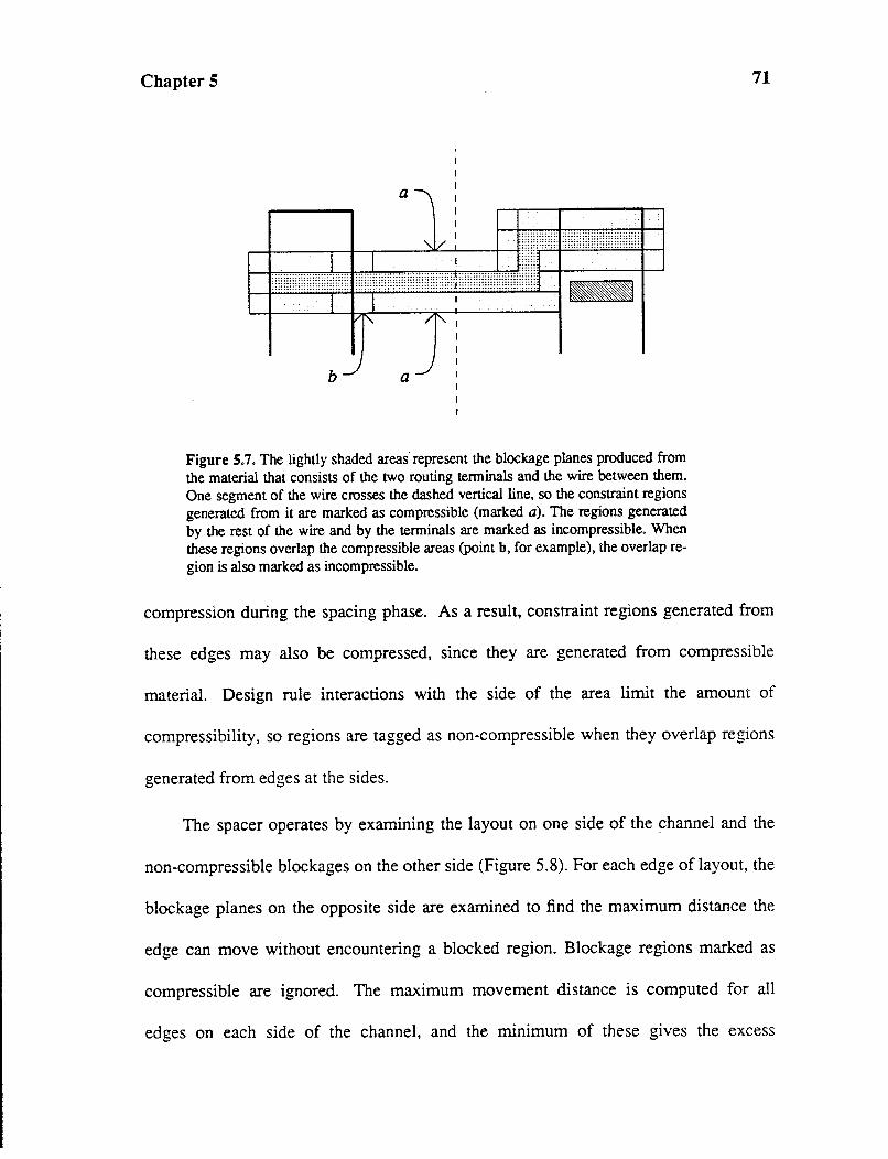
Chapter 5
a
I •
r-l----.,..---f-..,...---'-..:.viL-~....' --+--tF!!!W< TUHU!!Y!!!iii!i l I ......................................................................................... r-+-----+---'
~i~'H~Hi~H~Hi~~~it~:'~HI~Hii~Ii_Hi~'H~H~iH~~P~:H~iH~iiH'~:HH_Hi~H~~
I'
b a
Figure 5.7. The lightly shaded areas represent the blockage planes produced from
the material that consists of the two routing tenninals and the wire between them.
One segment of the wire crosses the dashed vertical line, so the constraint regions
generated from it are marked as compressible (marked a). The regions generated by the rest of the wire and by the tenninals are marked as incompressible. When these regions overlap the compressible areas (point b, for example), the overlap re
gion is also marked as incompressible.
71
compression during the spacing phase. As a result, constraint regions generated from
these edges may also be compressed, since they are generated from compressible
material. Design rule interactions with the side of the area limit the amount of
compressibility, so regions are tagged as non-compressible when they overlap regions
generated from edges at the sides.
The spacer operates by examining the layout on one side of the channel and the
non-compressible blockages on the other side (Figure 5.8). For each edge of layout, the
blockage planes on the opposite side are examined to find the maximum distance the
edge can move without encountering a blocked region. Blockage regions marked as
compressible are ignored. The maximum movement distance is computed for all
edges on each side of the channel, and the minimum of these gives the excess
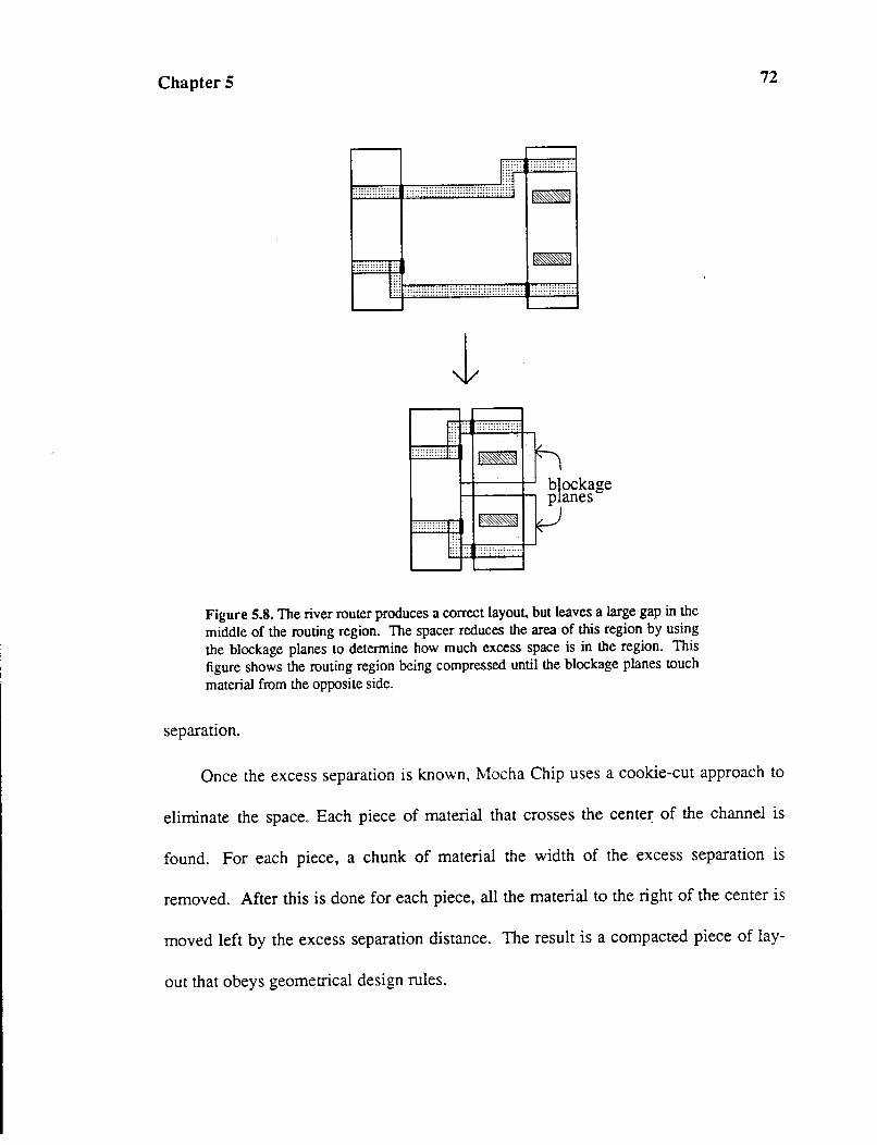
Chapter 5
:::;::;:::::t;:
In:"'''':<'''"''':''"''':::::::::''::=:
.... ·····•·••··•
~ 1-+----t......J b}ockage
panes
:::::::::;r I§~ ~ I:::H:-~--"""'"'···· .,.,.,.,. _____ +-'_
Figure 5.8. The river router produces a correct layout, but leaves a large gap in the
middle of the routing region. The spacer reduces the area of this region by using
the blockage planes to determine how much excess space is in the region. This
figure shows the routing region being compressed until the blockage planes touch
material from the opposite side.
separation.
72
Once the excess separation is known, Mocha Chip uses a cookie-cut approach to
eliminate the space. Each piece of material that crosses the center: of the channel is
found. For each piece, a chunk of material the width of the excess separation is
removed. After this is done for each piece, all the material to the right of the center is
moved left by the excess separation distance. The result is a compacted piece of lay-
out that obeys geometrical design rules.
Chapter 5 73
5.7. CONCLUSIONS
Mocha Chip uses a pairwise assembly operator to create layout. This operator
joins two pieces of geometry together to form a third, larger, piece. Two such opera-
tors are incorporated in the system.
The operators give the user a range of control over the assembly process. The
packing rectangle operator gives the user complete control, but provides no assurance
of correctness. The river-route-space operator assures correctness by river-routing and
spacing, generating and spacing layout automatically.
The river-route-space operator is able to guarantee design rule correctness,
without wasting much area. The algorithm places the cells are large distance apart,
routes them, and then compacts the result. By using this process, the river-route-space '
operator is able to produce compact connections, even overlapping cells if geometrical
design rules allow.
5.8. REFERENCES
1. R. Y. Pinter, The Impact of Layer Assignment Methods on Layout Algorithms
for Integrated Circuits, VLSI MEMO 82-130, Massachusettes Institute of
Technology, December 1982.
2. G. S. Taylor and J. K. Ousterhout, Magic's Incremental Design Rule Checker,
Proceedings of the 21st Design Automation Conference, 1984.
Chapter 5 74
3. J. K. Ousterhout, Comer Stitching: A Data-Structuring Technique for VLSI
Layout Tools, IEEE Transactions on Computer-Aided Design CAD-3, 1
(January, 1984).

6 AN EXAMPLE PLA GENERATOR
6.1. INTRODUCTION
75
An example module generator has been built with Mocha Chip, in order to evalu
ate the system and to prove that is is useful for actual applications. This chapter
describes the generator and compares it with a traditional generator that performs the
identical function. The generators produce PLAs, which implement combinational
logic in a two-level AND-OR configuration. The operation of the Mocha Chip genera
tor, called MCPLA[l], is explained by presenting each of its parts and working
through the operation of some representative pieces. The other PLA generator, called
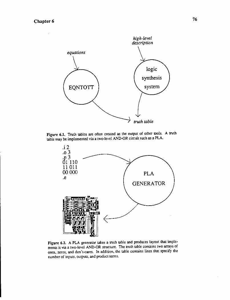
Chapter 6
equations
high-level description
\_ logic
synthesis
truth table
Figure 6.1. Truth tables are often created as the output of other tools. A truth
table may be implemented via a two-level AND-OR circuit such as a PLA .
.i2
.0 3
.p 3 01110 11 011 00000 .e
PLA
GENERATOR
Figure 6.2. A PLA generator takes a truth table and produces layout that imple
ments it via a two-level AND-OR structure. The truth table contains two arrays of
ones, zeros, and don't-cares. In addition, the table contains lines that specify the
number of inputs, outputs, and product terms.
76
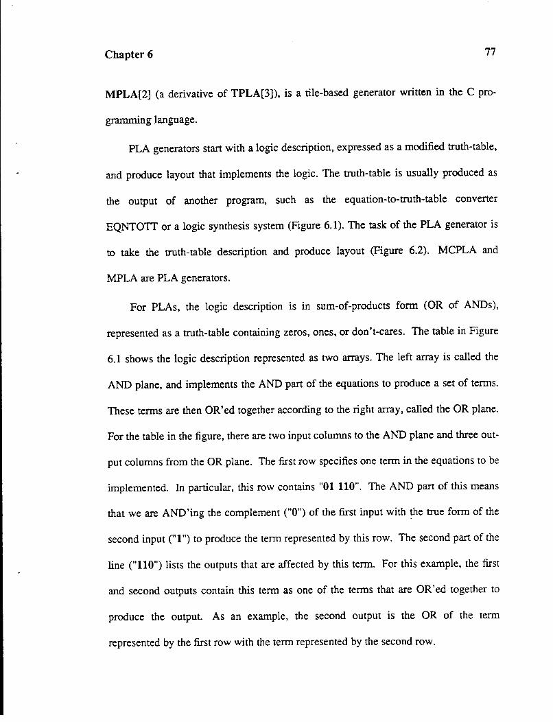
Chapter 6 77
MPLA[2] (a derivative of TPLA[3]), is a tile-based generator written in the C pro
gramming language.
PLA generators start with a logic description, expressed as a modified truth-table,
and produce layout that implements the logic. The truth-table is usually produced as
the output of another program, such as the equation-to-truth-table converter
EQNTOTI or a logic synthesis system (Figure 6.1). The task of the PLA generator is
to take the truth-table description and produce layout (Figure 6.2). MCPLA and
MPLA are PLA generators.
For PLAs, the logic description is in sum-of-products form (OR of ANDs),
represented as a truth-table containing zeros, ones, or don't-cares. The table in Figure
6.1 shows the logic description represented as two arrays. The left array is called the
AND plane, and implements the AND part of the equations to produce a set of terms.
These terms are then OR'ed together according to the right array, called the OR plane.
For the table in the figure, there are two input columns to the AND plane and three out
put columns from the OR plane. The first row specifies one term in the equations to be
implemented. In particular, this row contains "01 110". The AND part of this means
that we are AND'ing the complement ("0") of the first input with ~e true form of the
second input ("1") to produce the term represented by this row. The second part of the
line ("110") lists the outputs that are affected by this term. For this example, the first
and second outputs contain this term as one of the terms that are OR'ed together to
produce the output. As an example, the second output is the OR of the term
represented by the first row with the term represented by the second row.
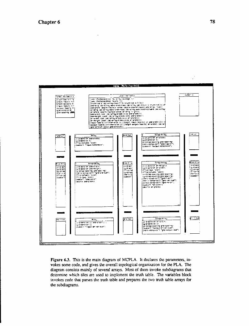
Chapter 6
rJrttl Pt.~Urlf'' 51
1 t ~wtPI-taclc- f, lei (c; lot~-'"'"':s ,., 1 (c1oc~·autouu n1 (1"1p .. a-1&Dtls r1l
(Ooi~Pwt·lucls n1
a~:::~;:!~~ ~Jw
-
-)
i
~----------------~'~·,~·~'~·~·'~'~··~'~··~-----------------: 1wr.t.. { .,~tntL.Otj~n(C ··~ ·&rrto;·;at~t')C 1)'
;pmk (,oct.tL.OtjQn,c 'a.;plt l)J .
i H~oth·taa. ;c (l;•al'"rt~j•ru~-flle trutft-ldllt-f111: '~ .
(tnct·orlt uc·t·r&IJ·Itke·C'I'Cn·r~ws (lt·&rrt~-ge~-O•t'"- 1 tr~otn-tt~·t) I (tM·pltne {..-:,lo·rcpla:c-u:ros {acp\a·r:llipt.rd-1"9\IU an~·ong) 'top))
(or·or1g (ac-&r"t!II·Hkt·e•cr-rows (ac·a~"n~st·ltH·cnn-c:~lwellS (ec·arra!l
(or·pla"'c {acplt·rct:ltcc-uros rn-·ortg •r·,n.)) (ano-w1i:h (ctr (ac-trr&!f·•loc:t-.·sta anJ·pltnt)l)
{ttui-IW!gh\ (cur (ac.·a"'rav·olo: .. ·uu ane~-~ ltnc) 1; \or·•H1tl'l (tar (at·tl"ra~-lll·c:ck-suc or-phnt)))
1~~::~,:!, \:·~:f:~~~;~:;t :~(i!~::" o:~~:~!;~ 1,) U tni-wlO~h 2))
1 ~!~~;~:::1~~~:~-~~;:::~e~~ l ( lc"gth •wtjN\· hMla) or-•l•t.n) (le-ar
Str-u-Arra~
(A•01KnS101'\ tncl••lCS~r1)
(y·dlKI"'~\01'1 and·tleu;l'l~)
~ ~~~~:~:;~:::~;, 1 ~~:;~~~~:~a·> (fl,~-colw•,: 'e .. en: (f'llf:·r"O•S 1 f•tn)
(swDc.en •ano-eo'"e': (•ILrlll tf'lt-~lll"'f)
-
-
(ll·•~•tnno" or-wlll!h: (!:f•t"lfflll~n 1)
~:;;:~:~:=~~;~~ ';:;~~=~:~!) (loiDCf 11 •o~ttl"'t·Uf"IH"•tt•)
(.•.•11' eens1:1t1 or-fteiJtlt)
~ fi~~~~:~ l~ ,:;~~~ 11~11: (f11p·co1w•ns •cve"') t~o·strep·s~ac.lng g"'i·s~ac,.,g,
i~;:~::~;::~~;;, ¥"'~;~~~~:i' (h:~r·t-svap-tt:11 itnO·•or·s~o~t") (C"OSS•strtp•tcll 1 f"d·t'l'f'•:ll' 1 )
(so~Oct11 ":»r-core") (Q:.n .. or-plane)
D '(~·diHPISIOI'\ (/ tnCI••112l"' ~;)
(~·OIHI"'SlDI'I 1) D (ll·t~~ftSl:ln or-.,l:r.; (y·t•~rns, :~n 1)
(a•strtp·S:IIC11"9 9"~1:1·1:~1t,.lg I
(S40CI11 •:~utp~o.t•d""l•tr-swo• .' \lwDCtll "1"ffU~·IIr'1Vtr"•IJ0 1 ;
( ¥trt·stl"•p-et 11 • ~no-cutpJ: ·1\otl• l
D
-......... ~.~ , l'··dl•!nj ! (ij·CI,.'!I'I1
: ~~,~~:!~ : (ftcr-1:-s ! (lloo&lelll
-
78
a ' ----,,~
Figure 6.3. This is the main diagram of MCPLA. It declares the parameters, in
vokes some code, and gives the overall topological organization for the PLA. The
diagram consists mainly of several arrays. Most of them invoke subdiagrams that
determine which tiles are used to implement the truth table. The variables block
invokes code that parses the truth table and prepares the two truth table arrays for
the subdiagrams.
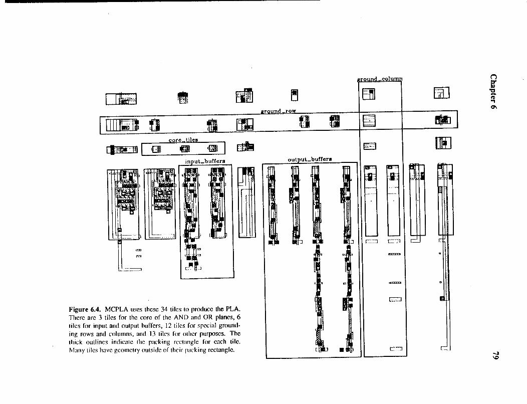
I lliW3 1ft Ed
LU!r=ll 9 ~ core_tiles
IIMM-MJI €111 g Q I -
~Ut ,,..11 alj' ~
j===b I ~~----~1
= =
L~=-~== c~n:J
Figure 6.4. MCPLA uses these 34 tiles to produce the PLA.
There are 3 tiles for the core of the AND and OR planes, 6
tiles for input and output buffers, 12 tiles for special ground
ing rows and columns, and 13 tiles for other purposes. The
thick outlines indicate the packing rectangle for each tile.
Many tiles have geometry outside of their packing rectangle.
[!I round row
tJ fJ
umn
~
~
E)
:] C::::J c::3
~
~
c=J
C::::J
[ill
ft!lJ
00
c
a
a
(') ::r &I)
"0 .... t'D .., 0'\
...:a ~
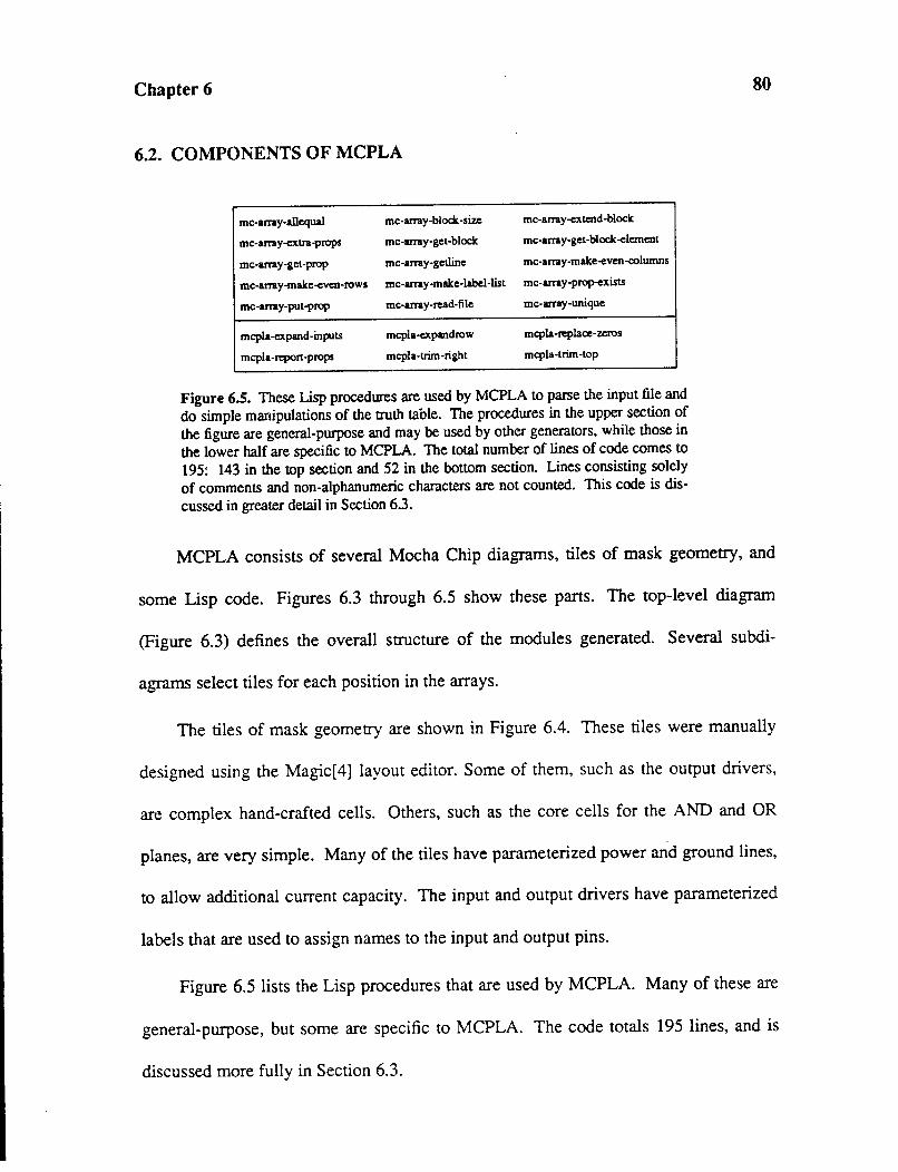
Chapter 6
6.2. COMPONENTS OF MCPLA
me-array-allcqual me-array-block -size me-array-extend-block
me-array-extra-props me-array-get-block me-array-get-block-element
me-array-get-prop me-array-getline me-array-make-even-columns
me-array-make-even-rows me-array-make-label-list me-array-prop-exists
me-array-put-prop me-array-read-file me-array-unique
mcpla-expand-inputs mcpla-expandrow mcpla-replace-zcros
mcpla-report -props mcpla-trim-right mcpla-trim-top
Figure 6.5. These Lisp procedw-es are used by MCPLA to parse the input file and
do simple manipulations of the truth table. The procedures in the upper section of
the figure are general-purpose and may be used by other generators, while those in
the lower half are specific to MCPLA. The total number of lines of code comes to
195: 143 in the top section and 52 in the bottom section. Lines consisting solely
of comments and non-alphanumeric characters are not counted. This code is dis
cussed in greater detail in Section 6.3.
80
MCPLA consists of several Mocha Chip diagrams, tiles of mask geometry, and
some Lisp code. Figures 6.3 through 6.5 show these parts. The top-level diagram
(Figure 6.3) defines the overall structure of the modules generated. Several subdi-
agrams select tiles for each position in the arrays.
The tiles of mask geometry are shown in Figure 6.4. These tiles were manually
designed using the Magic[4] layout editor. Some of them, such as the output drivers,
are complex hand-crafted cells. Others, such as the core cells for the AND and OR
planes, are very simple. Many of the tiles have parameterized power and ground lines,
to allow additional current capacity. The input and output drivers have parameterized
labels that are used to assign names to the input and output pins.
Figure 6.5 lists the Lisp procedures that are used by MCPLA. Many of these are
general-purpose, but some are specific to MCPLA. The code totals 195 lines, and is
discussed more fully in Section 6.3.

Chapter 6
1 (truth-table-file)
2 (clock-inputs nil)
3 (clock-outputs nil)
4 (input-labels nil)
5 (output-labels nil)
6 (gnd-stretch 0)
7 (gnd-spacing 10000)
Figure 6.6. The lines found in MCPLA's parameters block. Default values are
given for most parameters. There is no default value for the truth-table file.
6.3. HOW MCPLA WORKS
81
The parameter block declares the parameters used by MCPLA (Figure 6.6). The
truth-table-file parameter is the most important - it names a file that contains the truth
table to be implemented by this PLA. The other parameters specify options for the pia.
Clock-inputs, if true, adds dynamic latches to the input lines. Clock-outputs performs
a similar function for the outputs. The size of the power and ground busses is con-
trolled by gnd-stretch, which is a Lisp expression representing a function to compute
the additional size needed, in lambda. The size of the busses is a function of the peak
current required by the PLA, which is in tum a function of its size. Because of this
requirement, the Lisp function is evaluated in the variables block after the truth table is
read in, so that the function may make use of computed quantities such as the number
of inputs and outputs. Input-labels and output-labels are lists of labels for the input
and output pins. If no labels are supplied, MCPLA will generate unique identifiers.
Having these pins labeled can aid in simulation, circuit extraction, and routing. The
gnd-spacing parameter controls how many rows or columns can be placed before a
special ground row or column is placed. The extra rows and columns supply additional
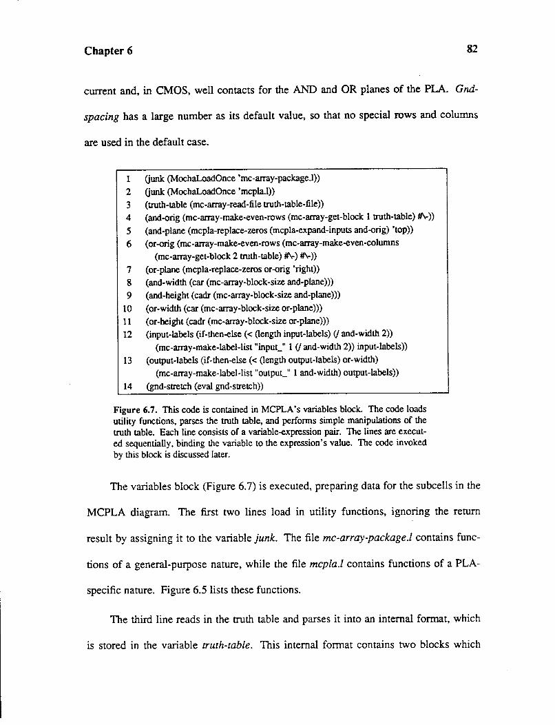
Chapter 6 82
current and, in CMOS, well contacts for the AND and OR planes of the PLA. Gnd-
spacing has a large number as its default value, so that no special rows and columns
are used in the default case.
I (junk (MochaLoadOnce 'mc-array-package.l))
2 (junk (MochaLoadOnce 'mcpla.l))
3 (truth-table (me-array-read-file truth-table-file))
4 (and-orig (me-array-make-even-rows (me-array-get-block 1 truth-table) If\-))
5 (and-plane (mcpla-replace-zeros (mcpla-expand-inputs and-orig) 'top))
6 (or-orig (me-array-make-even-rows (me-array-make-even-columns
(me-array-get-block 2 truth-table) If\-)#\-))
7 (or-plane (mcpla-replace-zeros or-orig 'right))
8 (and-width (car (me-array-block-size and-plane)))
9 (and-height (cadr (me-array-block-size and-plane)))
10 (or-width (car (me-array-block-size or-plane)))
11 (or-height (cadr (me-array-block-size or-plane)))
12 (input-labels (if-then-else(< (length input-labels) (j and-width 2))
(me-array-make-label-list "input_" 1 (j and-width 2)) input-labels))
13 (output-labels (if-then-else(< (length output-labels) or-width)
(me-array-make-label-list "output_" 1 and-width) output-labels))
14 (gnd-stretch (eval gnd-stretch))
Figure 6.7. This code is contained in MCPLA's variables block. The code loads utility functions, parses Lie truth table, and performs simple manipulations of the truth table. Each line consists of a variable-expression pair. The lines are executed sequentially, binding the variable to the expression's value. The code invoked by this block is discussed later.
The variables block (Figure 6.7) is executed, preparing data for the subcells in the
MCPLA diagram. The first two lines load in utility functions, ignoring the return
result by assigning it to the variable junk. The file me-array-package .I contains func-
tions of a general-purpose nature, while the file mcpla.l contains functions of a PLA-
specific nature. Figure 6.5 lists these functions.
The third line reads in the truth table and parses it into an internal format, which
is stored in the variable truth-table. This internal format contains two blocks which
Chapter 6 83
represent the AND and the OR planes of the PLA.
Three simple manipulations of the AND truth table are performed in lines 4 and
5. First, the AND plane is fetched from the internal format, and forced to have an even
number of rows, adding a row of dashes if needed (line 4). PLAs with an even number
of rows are simpler to design. Line 5 takes this table and expands the input columns.
Each input column corresponds to two columns of mask layout, one for the uncomple-
mented variable and one for its complement. Each truth table bit is expanded accord-
ing to the following rules:
--+ 00 0 --+ 01 1 --+ 10
This transformed table directly corresponds to the layout to be generated. A 1
corresponds to a transistor, while a 0 corresponds to no transistor. In order to improve
the performance of the PLA, it is desirable to run the input signals up through the array
only as far as the last place they are used. The mcpla-replace-zeros procedure starts at
the top of a table and changes zeros, representing no transistor but rather an extension
of the input signal, to dashes, representing no transistor and no extension. This process
stops when a one, representing a transistor, is found in a column. Here is an example
transformation:
0010 --1-0100 --+ -10-1011 1011 0010 0010
Chapter 6 84
Similar transformations occur with the OR plane. The OR plane is forced to have
an even number of rows and columns, to simplify layout. The zero-trimming function
is then invoked in a manner similar to the AND plane, except that trimming starts from
the right and works left. In the OR plane, product terms (the result of ANDing in the
AND plane) enter from the left.
The rest of the lines set up simple variables. Lines 8 through 11 simply count the
number of rows and columns in the AND and OR planes. Lines 12 and 13 prepare
default labels for the inputs and outputs if they weren't specified by the user. Line 14
evaluates the ground-stretching expression to determine the amount of stretching
needed for this particular PLA. This expression is free to reference the previous vari
ables, such as and-height.
The comments block is not used in MCPLA. The comments block can contain
expressions which are evaluated after the variables block and then attached to the
corresponding Magic cell. This is used mostly for debugging purposes, but could be
used, for example, to attach the truth table to the Magic cell that is generated.
The AND plane and the input drivers will be used as examples to demonstrate
Mocha Chip's features in detail. The AND plane block (Figure 6.8), the large block on
the left in Figure 6.3, represents an array of tiles. Each tile is selected according to the
truth table bit that corresponds to its position (Figure 6.10). In addition to the tiles that
implement the truth table, horizontal rows of ground wires are added every few rows.
This ensures that ground is adequately distributed and, in CMOS, that the wells are
properly grounded.
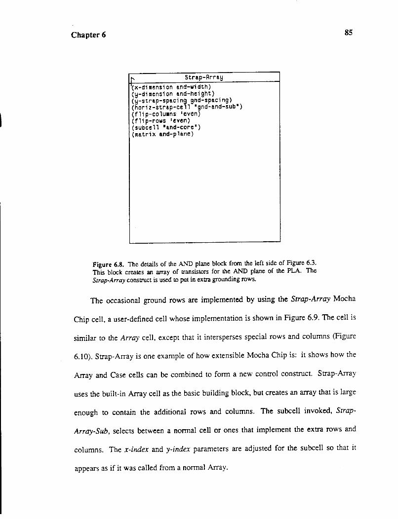
Chapter 6
It' Strap-Arra~:~
(x-dimension and-width) (y-dimension and-height) (y-strap-spacing gnd-spacing) (horiz-strap-ce11 •gnd-and-sub") (flip-colulns •even) (flip-rows •even) (subcel1 •and-core") (matrix and-plane)
Figure 6.8. The details of the AA"D plane block from the left side of Figure 6.3.
This block creates an array of transistors for the AND plane of the PLA. The
Strap-Array construct is used to put in extra grounding rows.
85
The occasional ground rows are implemented by using the Strap-Array Mocha
Chip cell, a user-defined cell whose implementation is shown in Figure 6.9. The cell is
similar to the Array cell, except that it intersperses special rows and columns (Figure
6.10). Strap-Array is one example of how extensible Mocha Chip is: it shows how the
Array and Case cells can be combined to form a new control construct. Strap-Array
uses the built-in Array cell as the basic building block, but creates an array that is large
enough to contain the additional rows and columns. The subcell invoked, Strap-
Array-Sub, selects between a normal cell or ones that implement the extra rows and
columns. The x-index and y-index parameters are adjusted for the subcell so that it
appears as if it was called from a normal Array.
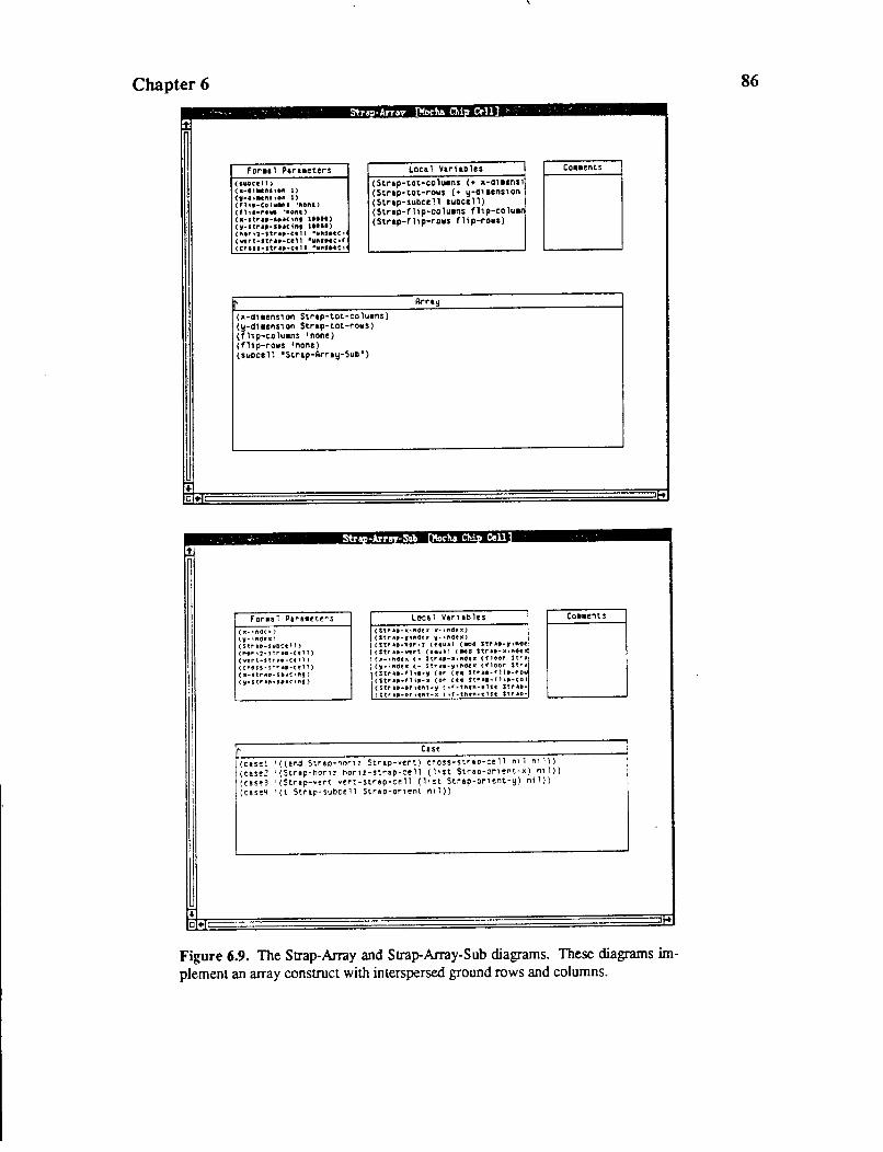
Chapter 6
,
• o•
(JitDCtll) (•·41Mni\Oft 1) (ti•CiiMUIOII 1) (f1 it-CO HI• I •aont) C f t 't-rows •ftonc > (X•stl"•t-I•I'Ciftt 11111) cv-str-••·•uc;at , .... ) <"or 11-lt,.•t-ct II •unsttC, (Wrt•Jtrlt-Ctll •u•ntc•f ccrou-rtru-ctl 1 •wnsttC,
Local Yariab les
(Strap-tot-co lu•ns ( • x-d•••nsl (Strap-tot-rows (• y-d,.onsion ( Strap-subco11 subcoll) (Strap-flip-colu•ns fhp-colu• (Strap-r11p-ro11s fhp-roiiS)
Rrra~
<•-d' .en!1 on Strap-tot-co lu•ns) (~-di .ens1 on Strap-tot-ro•s) (f11p-co1u•ns 'none) ( f 11 p-rows • none) ( suoco11 'Strap-Rrra~-Sub')
_ . ~ . Str -Arr -Sub ella C'l1i Cdl
(11- lflljt•)
cv- lr~or•)
< Strar-suDct 11) (hO,. 'l•S'T:I'.IIO•Ctl 1) (vtrt-str-,.•-ct 1 l) (CP'OSS-St"'AII•Ctl 1) (•-StP"AD•S'II.ICUtf) <v-suo••·SD.IC,ftf)
Local Yarubles (Str.tt·•,nOt-.: x·•f'IOtw)
C Str.llt·VtftOt.· v- ""'''0 < Str ••-ftor,: c uu• 1 c acG st,. ••-v ,not (StrAt•Wrt U•wal (MQ ttr' .. •X!ftGCJ
{:li•!IIOCX (• StrAt•lllllnOu:: (floor Str"
(V·,nCtiC (· Str.tt•VHtdf1t (floor Str'il (:l:ti"At-11tt·v (or <r• ttf"At·'lt.-ro• (StP'It•fltD•X (Of' (tel $tf'AP•fltt•C01
< t'l:r at-or 1tftt -!II c, f ·tfltft·t 1st Stru<ttrat-or,cnt-:J~ ( •f-ttltfl-tiSt Str.uJ-
Case
D (easel '((and Strap·hOnz Strap-vert) cross-strap-cell n11 n1l)) (~aseZ '(Strap-honz hor1Z-strap-ce11 (1•st Strap·onent·•) m 1)) (cas•3 '(Strap-vert vert-strap-cell (l1 st Strap-orllnt·y) n1l)) (~ose4 '(t Strap-subce11 Strao·or1ent n1l))
Figure 6.9. The Strap-Array and Strap-Array-Sub diagrams. These diagrams im
plement an array construct with interspersed ground rows and columns.
86
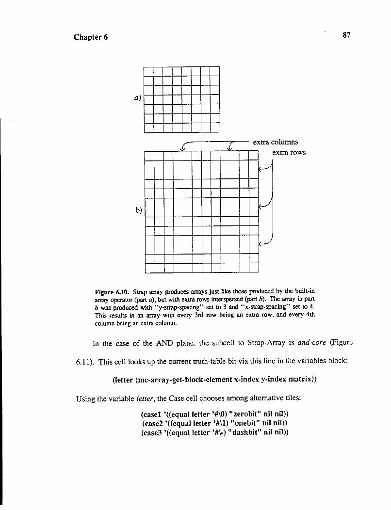
Chapter6
a)
£ l
b)
extra c olumns
extra rows
v
v
~
Figure 6.10. Strap array produces arrays just like those produced by the built-in
array operator (part a), but with extra rows interspersed (part b). The array in part
b was produced with "y-strap-spacing" set to 3 and "x-strap-spacing" set to 4.
This results in an array with every 3rd row being an extra row, and every 4th
column being an extra column.
87
In the case of the AND plane, the subcell to Strap-Array is and-core (Figure
6.11). This cell looks up the current truth-table bit via this line in the variables block:
(letter (me-array-get-block-element x-index y-index matrix))
Using the variable letter, the Case cell chooses among alternative tiles:
(easel '((equal letter '#\0) "zerobit" nil nil)) (case2 '((equal letter '#\1) "onebit" nil nil)) (case3 '((equal letter'#\-) "dashbit" nil nil))

Chapter 6
For•al Para•eters (utr1x) (x-index) (!,j·index)
Local Variables
(letter <•c-arr&!,j·get-block-ele•ent
lr- Case
(easel '((equal letter '1\8) •zerobit• n11 n1l)) (case2 '((equal letter 11\1) •onebit" nil nil)) (case3 '((equal letter '1\-) "dashb1t" nil n1l))
Figure 6.11. The diagram and-core, which selects a tile based upon the truth
table bit for the position. Another diagram is used in the special ground rows in
the AND plane.
88
+
These three tiles, zerobit, onebit, and dash bit (Figure 6.12), form the core of the
AND plane as well as the core of the OR plane. In the AND pl~e, alternating
columns are flipped sideways so that the tiles may share contacts and ground busses.
Each of the tiles has a packing rectangle, indicated by me-pack. It is this rectangle that
controls the spacing between tiles. The OR plane is built in the same manner as the
AND plane, and then rotated by ninety degrees.
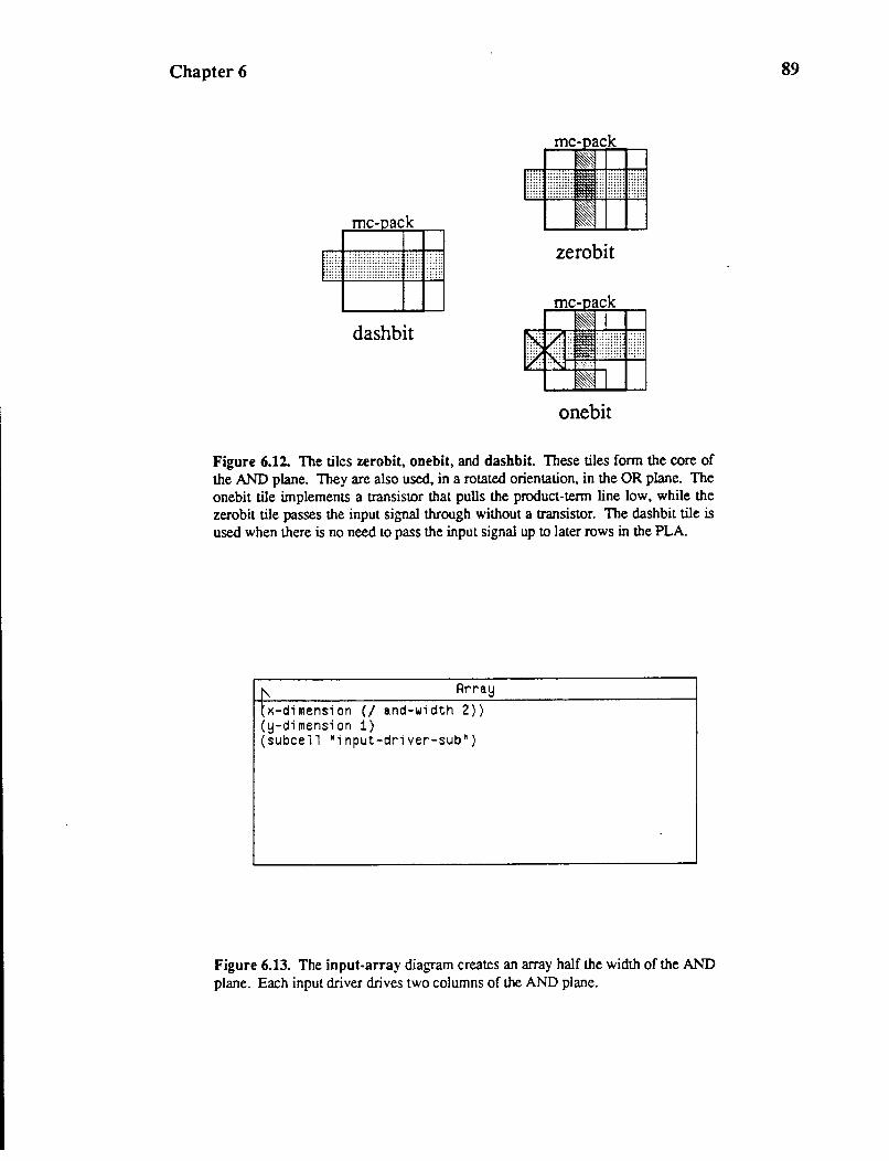
Chapter 6
me- ack
zero bit
dash bit
one bit
Figure 6.12. The tiles zerobit, onebit, and dasbbit. These tiles fonn the core of the AND plane. They are also used, in a rotated orientation, in the OR plane. The onebit tile implements a transistor that pulls the product-tenn line low, while the zerobit tile passes the input signal through without a transistor. The dashbit tile is used when there is no need to pass the input signal up to later rows in the PLA.
~ Rrra~
tx-dimension (/ and-width 2)) (y-dimension 1) (subcell "input-driver-sub")
Figure 6.13. The input-array diagram creates an array half the width of the AND plane. Each input driver drives two columns of the AND plane.
89
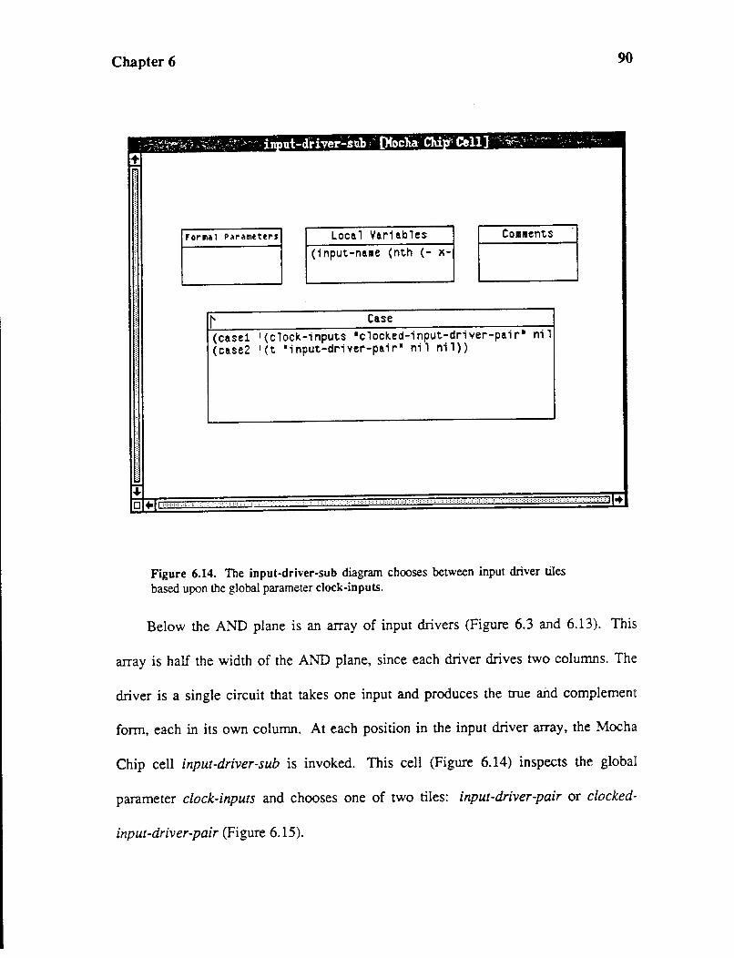
Chapter 6
Formal Parameters Local Variables C0111ents
(input-na•e (nth (- x-
Case (easel 1 (clock-inputs •clocked-input-driver-pair• nil (case2 '(t •;nput-driver-pair• nil nil))
Figure 6.14. The input-driver-sub diagram chooses between input driver tiles
based upon the global parameter clock-inputs.
90
Below the AND plane is an array of input drivers (Figure 6.3 and 6.13). This
array is half the width of the AND plane, since each driver drives two columns. The
driver is a single circuit that takes one input and produces the true and complement
form, each in its own column. At each position in the input driver array, the Mocha
Chip cell input-driver-sub is invoked. This cell (Figure 6.14) inspects the global
parameter clock-inputs and chooses one of two tiles: input-driver-pair or clocked-
input-driver-pair (Figure 6.15).
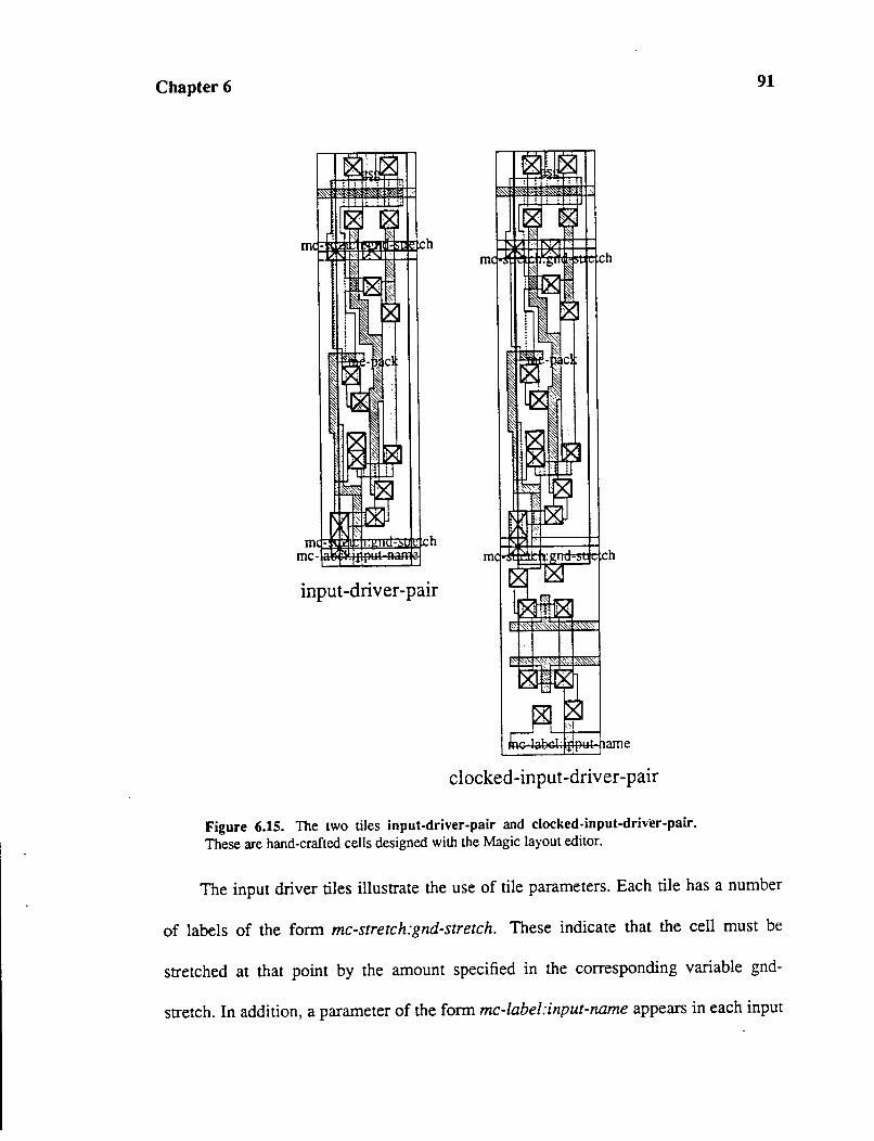
Chapter 6
input-driver-pair
clocked-input-driver-pair
Figure 6.15. The two tiles input-driver-pair and clocked-input-driver-pair.
These are hand-crafted cells designed with the Magic layout editor.
91
The input driver tiles illustrate the use of tile parameters. Each tile has a number
of labels of the form mc-stretch:gnd-stretch. These indicate that the cell must be
stretched at that point by the amount specified in the corresponding variable gnd-
stretch. In addition, a parameter of the form mc-label:input-name appears in each input
Chapter 6 92
driver. This is a parameterized label. The value of input-name, declared in input
driver-sub, is used as a new label that is substituted for mc-label:input-name.
The AND plane and the input drivers give a good overview of how MCPLA is
built. The other sections of MCPLA are similar in nature. Most blocks consist of
arrays of sub-cells, where the subcells make a selection among several alternative tiles.
6.4. MPLA
MPLA is a C program that was written to produce PLAs, and also goes by the
name TPLA. MCPLA is designed to accept exactly the same options and produce the
same PLAs as MPLA. The two will be compared with respect to the number of lines of
code, number of diagrams drawn, and number of tiles used.
MPLA consists of C code and a set of tiles. The tiles are shown in Figure 6.16.
MPLA uses the MPACK library[3] to assemble layout. The library includes pro
cedures for aligning the comers of tiles, in order to pack them together or, with the aid
of spacing tiles, to provide overlap (see Section 3.4). The library does not include
rotation procedures, so separate tiles are used for the AND and OR planes. In addition
to the functions that directly generate layout, MPLA includes procedures to parse the
input file and manipulate the truth tables, and overhead functions. These functions are
similar to those executed in the variables block of MCPLA.
MPLA generates layout by aligning a comer of a tile with the comer of another
tile. In cases where overlap is needed, a special tile called a space tile is used for
alignment. Figure 6.17 shows some typical lines from MPLA.
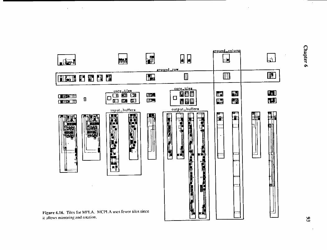
~ ~ fj ----·----··-
LiLLi! ~ 1m ~ rJ1 fm s:ore"'tiles
I•MiiW--n 1 BCH ~ ~J ma 0 llft'bic-fl1 orE:!_ml_ mJ ~
Figure 6.16. Tiles for MPLA. MCPLA uses fewer Liles since
il allows mirroring and rotation.
g
QQ ,row
IIIl
G11J 1m touLbuff
- ~ r-"'1 = = ."' ~
~ ~ ~
I
j -J ~ '---
"' ~
""
I I
I .J ; ~ -1
r· VMJ~U1UJJM1 kJ
I ffiJ])
I (IJ
n a Ill]
llml n 1111
n ::r Cl)
"0 .... nl .., 0\
\C) w
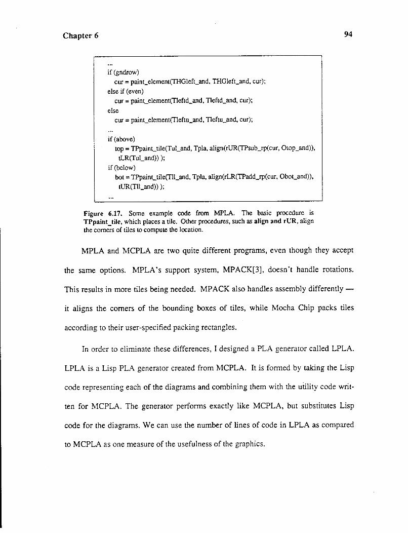
Chapter 6
if (gndrow)
cur= paint_element(THGleft_and, THGleft_and, cur);
else if (even)
cur = paint_element(Tleftd_and, Tleftd_and, cur);
else cur = paint_element(Tleftu_and, Tleftu_and, cur);
if (above)
top= TPpaint_tile(Tul_and, Tpla, align(rUR(TPsub_rp(cur, Otop_and)),
tl.R(Tul_and)) );
if (below)
bot= TPpaint_tile(Tll_and, Tpla, align(rLR(TPadd_rp(cur, Obot_and)),
tUR(Tll_and)) );
Figure 6.17. Some example code from MPLA. The basic procedure is TPpaint_tile, which places a tile. Other procedures, such as align and rUR, align the corners of tiles to compute the location.
94
MPLA and MCPLA are two quite different programs, even though they accept
the same options. MPLA's support system, MPACK[3], doesn't handle rotations.
This results in more tiles being needed. MPACK also handles assembly differently -
it aligns the corners of the bounding boxes of tiles, while Mocha Chip packs tiles
according to their user-specified packing rectangles.
In order to eliminate these differences, I designed a PLA generator called LPLA.
LPLA is a Lisp PLA generator created from MCPLA. It is formed by taking the Lisp
code representing each of the diagrams and combining them with the utility code writ-
ten for MCPLA. The generator performs exactly like MCPLA, but substitutes Lisp
code for the diagrams. We can use the number of lines of code in LPLA as compared
to MCPLA as one measure of the usefulness of the graphics.
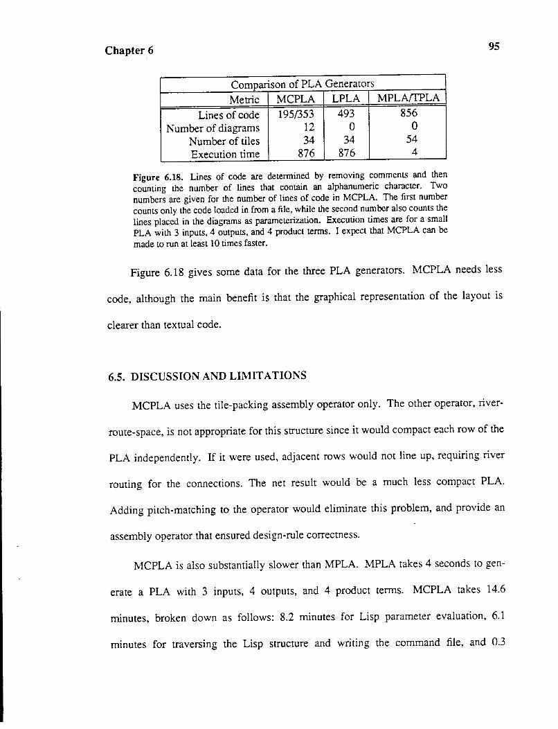
Chapter 6
Comparison of PLA Generators
Metric MCPLA LPLA MPLA{fPLA
Lines of code 195/353 493 856
Number of diagrams 12 0 0 Number of tiles 34 34 54
Execution time 876 876 4
Figure 6.18. Lines of code are determined by removing comments and then
counting the number of lines that contain an alphanumeric character. Two
numbers are given for the number of lines of code in MCPLA. The first number
counts only the code loaded in from a file, while the second number also counts the
lines placed in the diagrams as parameterization. Execution times are for a small
PLA with 3 inputs, 4 outputs, and 4 product terms. I expect that MCPLA can be
made to run at least 10 times faster.
95
Figure 6.18 gives some data for the three PLA generators. MCPLA needs less
code, although the main benefit is that the graphical representation of the layout is
clearer than textual code.
6.5. DISCUSSION AND LIMITATIONS
MCPLA uses the tile-packing assembly operator only. The other operator, river-
route-space, is not appropriate for this structure since it would compact each row of the
PLA independently. If it were used, adjacent rows would not line up, requiring river
routing for the connections. The net result would be a much less compact PLA.
Adding pitch-matching to the operator would eliminate this problem, and provide an
assembly operator that ensured design-rule correctness.
MCPLA is also substantially slower than MPLA. MPLA takes 4 seconds to gen-
erate a PLA with 3 inputs, 4 outputs, and 4 product terms. MCPLA takes 14.6
minutes, broken down as follows: 8.2 minutes for Lisp parameter evaluation, 6.1
minutes for traversing the Lisp structure and writing the command file, and 0.3
Chapter 6 96
minutes for assembly of the layout. Since almost all of the time is spent during Lisp
evaluation of the diagrams, I expect that execution times could be improved substan
tially by tuning and compiling the Lisp code before execution. The Lisp code only has
to evaluate parameters and communicate the resulting structure to Mocha Assem, so it
seems reasonable that a greater than ten times speedup could be had.
A benefit of Mocha Chip is the tile stretching mechanism. In Mocha Chip, tiles
may be stretched along lines that have jogs in them. In MP ACK, the lines must run
straight across. The straight across lines result in wasted area. The PLAs generated by
MCPLA are somewhat smaller due to the more flexible stretching mechanism. This is
not of fundamental importance, however, because this feature could be added to
MPACK also.
MCPLA requires fewer tiles than MPLA due to the use of the mirroring and rota
tion operator. This makes the module generator design easier.
The most dramatic improvement of MCPLA over MPLA is the representation of
the overall topology of the design. In MCPLA, the topology is represented as a
diagram; in MPLA it is a section of code. This diagrammatic representation is more
visually intuitive and is easier to navigate. For example, a user wa!lting to modify
MCPLA to select among four input drivers would have no trouble finding and modify
ing the cell responsible for that action, since the topology of the top-level diagram
directly corresponds to the user's image of what a PLA looks like. In MPLA, the user
would have to read and understand code that had no direct relationship to his visual
image.
Chapter 6 97
6.6. REFERENCES
1. R. Mayo, Mocha Chip: A System for the Graphical Design of VLSI Module
Generators, IEEE International Conference on Computer Aided Design, 1986.
2. W. S. Scott, R. N. Mayo, G. T. Hamachi and J. K. Ousterhout, editors. 1986
VLSI Tools: Still More Works by the Original Artists, Report UCB/CSD
86/272, Computer Science Division, University of California at Berkeley,
December, 1985.
3. R. Mayo and J. Ousterhout, Pictures with Parentheses: Combining Graphics and
Procedures in a VLSI Layout Tool, Proc. 20th Design Automation Conference,
1983, pp. 270-276.
4. J. K. Ousterhout, G. T. Hamachi, R.N. Mayo, W. S. Scott and G. S. Taylor, The
Magic VLSI Layout System, IEEE Design & Test of Computers, February,
1985.
7 FUTURE WORK
7.1. INTRODUCTION
98
There are three directions for future work on Mocha Chip: usability improve
ments, improvements in the layout quality, and improvements in the language aspects.
The system can be made more usable by allowing generators to be compiled for faster
execution. Layout quality could be improved with pitch-matching and general routing
techniques. The language aspects of Mocha Chip could be enhanced by more flexible
parameter passing mechanisms and parameterized netlists for specifying routing.
Chapter 7 99
7.2. GENERATOR COMPILATION
When Mocha Chip executes, most of the time is spent evaluating the Lisp code
that forms a module generator. A significant speedup could be obtained by compiling
this code. The disadvantage of compilation is that debugging information is lost, so
compilation would only be useful for fully-debugged module generators. Implement
ing compilation would appear at first to be a simple process, since a Mocha Chip gen
erator is just a Lisp program that produces a file of commands for Magic. However,
Mocha Chip loads cells, or Lisp procedures, using a search path mechanism. This
makes it difficult to determine in advance exactly which cells are part of the module
generator. The solution to this problem is to compile a cell dynamically the first time it
is used.
7.3. PITCH-MATCHING
Pitch-matching refers to the stretching of tiles in order to make their terminals
line up more closely. Pitch-matching can save area as compared with river routing.
PLAs are an example of this. A good pitch-matcher should be able to produce PLAs
that are as compact as those produced with the tile packing operator, but with a
guarantee of design rule correctness. Figure 7.1 shows an example of how pitch
matching can be used to connect tiles. Even though pitch-matching is not imple
mented in the current version of Mocha Chip, many of the details about how it would
work have been considered. Chapter 8 discusses these thoughts on pitch-matching.
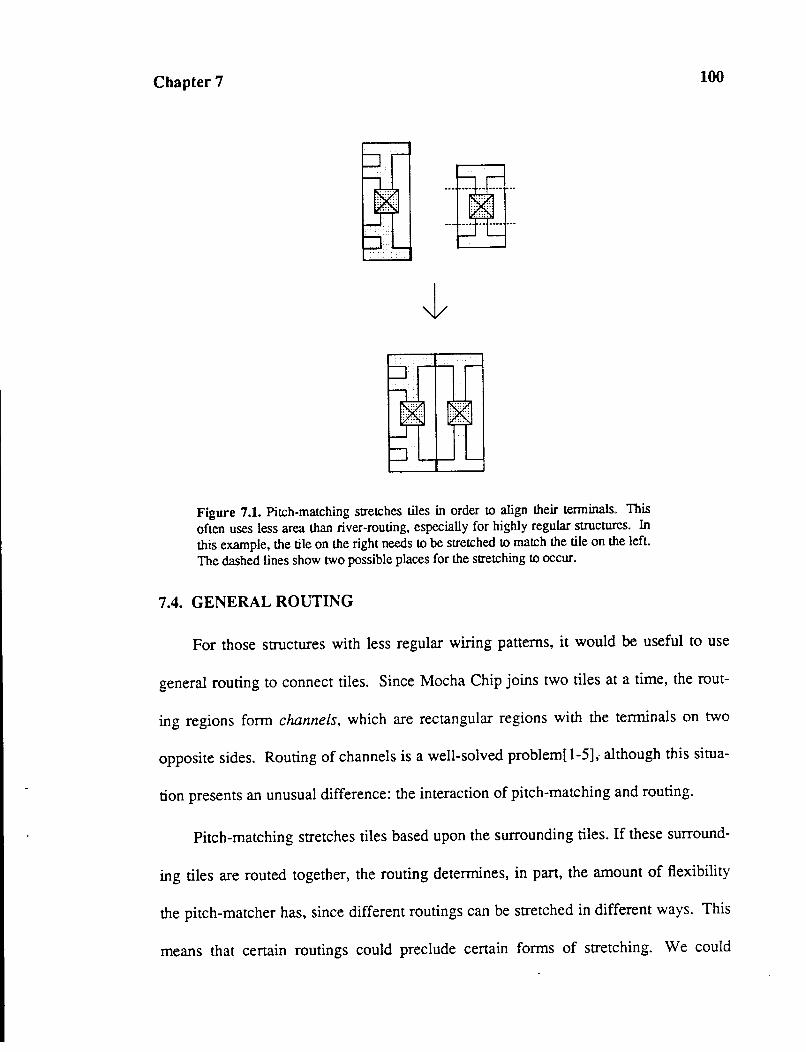
Chapter 7
Figure 7.1. Pitch-matching stretches tiles in order to align their terminals. This
often uses less area than river-routing, especially for highly regular structures. In
this example, the tile on the right needs to be stretched to match the tile on the left.
The dashed lines show two possible places for the stretching to occur.
7.4. GENERAL ROUTING
100
For those structures with less regular wiring patterns, it would be useful to use
general routing to connect tiles. Since Mocha Chip joins two tiles at a time, the rout-
ing regions form channels, which are rectangular regions with the terminals on two
opposite sides. Routing of channels is a well-solved problem[l-5],- although this situa-
tion presents an unusual difference: the interaction of pitch-matching and routing.
Pitch-matching stretches tiles based upon the surrounding tiles. If these surround-
ing tiles are routed together, the routing determines, in part, the amount of flexibility
the pitch-matcher has, since different routings can be stretched in different ways. This
means that certain routings could preclude certain forms of stretching. We could
Chapter 7 101
handle this by either not using those routings, or by removing the stretch lines that are
in conflict with the routing. Either of these two techniques could result in a loss of
area. An alternative scheme would be to use a pitch-matching algorithm that decides
on the stretch amounts for all tiles before any routing is done. Since when two pairs of
tiles are joined by routing the location of the terminals is not known until the routing is
completed, this pitch-matching algorithm would have to predict in advance the loca
tion of the terminals. If we use an upper bound on the area required by the routing, we
can pitch-match as if exactly that amount of area was required. After this is done, the
routing could be generated in the areas left open. Much of this routing would take less
area than the maximum allowed, and a compaction step would be needed to remove
this excess area.
A major problem with routing in Mocha Chip is the specification of the routing.
This is difficult to do, since every cell in Mocha Chip can be parameterized and thus
have a variable number of terminals. Parameterized netlists are a solution to this prob
lem.
7 .5. PARAMETERIZED NET LISTS
Since each Mocha Chip module can have the number of terminals vary according
to parameters, netlists used for general routing must exhibit the same degree of flexi
bility. Noticing that Mocha Chip cells behave like programs leads to the idea that net
lists should also behave like programs. One idea is to draw netlist as in a schematic
editor, but provide programmability for each terminal of the net. This
Chapter 7 102
programmability would allow the drawn net to represent several actual nets. The pro
grammability would be provided by a piece of code that is executed in order to pro
duce a list of terminals. This could could contain operators that generate the list based
upon the terminals that appear on the actual module. One list would be geJ!erated for
each end of the net, and all such lists would be of the same length. The first line in
each of the files specifies the first actual net represented by the drawn net, and subse
quent lines determine their nets in the same fashion.
In the general case the complete programmability of a general-purpose program
ming language would be needed, although simple pattern-matching operators would
suffice in most cases. For example, the"*" character would be sufficient to create bus
structures. Each end of the drawn net could contain code similar to (pattern "bit*"),
which matches in alphabetical order all terminals that begin with the prefix "bit". If
the drawn net is a 32-bit bus between two points, the left end of bus would be con
nected to a module that would be expected to have terminals labeled "bitO" through
"bit31", among other things. At the right end of the bus we would expect to find
another module with terminals of the same names. The same structure would work if a
16-bit module was being generated; the "bit*" pattern would just match half as many
terminals. Additional functions could be provided for common operations such as rev
ersing a list. In this case, it would allow the bits in the bus to be reversed, connecting
"bitO" to the last bit. Such a construct might take the form (reverse (pattern "bit*")),
and would be attached to one one of the drawn netlist. General-purpose programma
bility would be provided by allowing user-defined functions. For example, the user
Chapter 7 103
could write a function my-func that takes as input the list of all terminals on the side
of the module and produces a new list containing the terminals that are to participate in
this net The code attached to an end of the drawn netlist would be (my-func (pattern
"*")).
There may be better ways to parameterize netlists. Modern schematic editors
have special constructs for conveniently dealing with busses; perhaps this case is fre
quent enough to warrant special attention. In any case, it appears that the full general
ity of a programming language must be available to handle complex specifications.
7.6. FLEXIDLE PARAMETER PASSING
Mocha Chip uses top-down parameter passing, but other methods might be better
for some applications. A common situation is that one part of a module depends upon
characteristics of another part, as in the case of a PLA driver that depends upon the
number of rows in the AND plane. In Mocha Chip, the parameters for the driver are
calculated in the parent cell of the driver from information that is available. If parame
ters could be passed up and down the hierarchy, it would be possible to generate the
AND plane first, and then generate the drivers based upon a value provided by the
AND plane. With this more general parameter passing-mechanism, it would be possi
ble to incorporate information about the actual layout, such as the capacitance of a cer
tain line, in order to influence later parts of the module.
The more general parameter-passing mechanisms could be had by using a
language such as Prolog instead of Lisp. In Prolog, the system determines how
Chapter 7 104
variables should be bound in order to satisfy the constraints specified by the program.
The net effect is that parameters may be either passed into or out of functions, with the
actual direction and the order of evaluation being automatically determined. Using
Prolog in Mocha Chip would provide these more general mechanisms by passing
Prolog's semantics through to Mocha Chip's diagrams. A potential problem with this
approach is the interaction with the assembly process. If layout-dependent values,
such as capacitance, are produced, they may change as pitch-matching or routing con
straints change. I propose that estimates should provide enough preciseness and that
actual values would not be needed in most cases.
7.7. SUMMARY
Three types of enhancements could be made to Mocha Chip: usability enhance
ments, improved layout operators, and more flexible parameter passing. Usability
enhancements include compilation of module generators to improve performance and
the detection of identical cells to improve storage use. Layout can be improved
through the use of pitch-matching and more general routing techniques. Parameters
could be passed in a non-top-down manner in order to allow one part of a module to be
generated based upon the structure of another part. This could be implemented by
using a different language for the diagrams and their parameters.
Chapter 7 105
7.8. REFERENCES
1. H. Shin and A. Sangiovanni-Vincentelli, MIGHTY: A 'Rip-Up and Reroute'
Detailed Router, IEEE International Conference on Computer Aided Design,
1986.
2. A. Sangiovanni-Vincentelli, M. Santomauro and J. Reed, A New Gridless
Channel Router: Yet Another Channel Router the Second (YACR-ll), IEEE
International Conference on Computer Aided Design, 1984.
3. T. Yoshimura and E. Kuh, Efficient Algorithms for Channel Routing, IEEE
Transactions on Computer-Aided Design CAD-I, 1 (January, 1982).
4. G. T. Hamachi and J. K. Ousterhout, Magic's Obstacle-Avioding Global Router,
1985 Chapel Hill Conference on VLSI, 1985.
5. R. L. Rivest and C. M. Fiduccia, A Greedy Channel Router, Proc. 19th Design
Automation Conference, 1982.
8 PITCH MATCHING
8.1. INTRODUCTION
106
Pitch-matching refers to the stretching of tiles in order to make their terminals
line up more closely. It provides another automatic interconnection operator like the
river-route-space operator, and as such can guarantee that the resulting layout will
obey geometrical design rules. For highly regular structures, pitch-matching may save
area with respect to the river-route-space operator. A good pitch-matcher should be
able to produce PLAs that are as compact as those produced with the tile-packing
operator, but with a guarantee of design rule correctness. There are two aspects to any
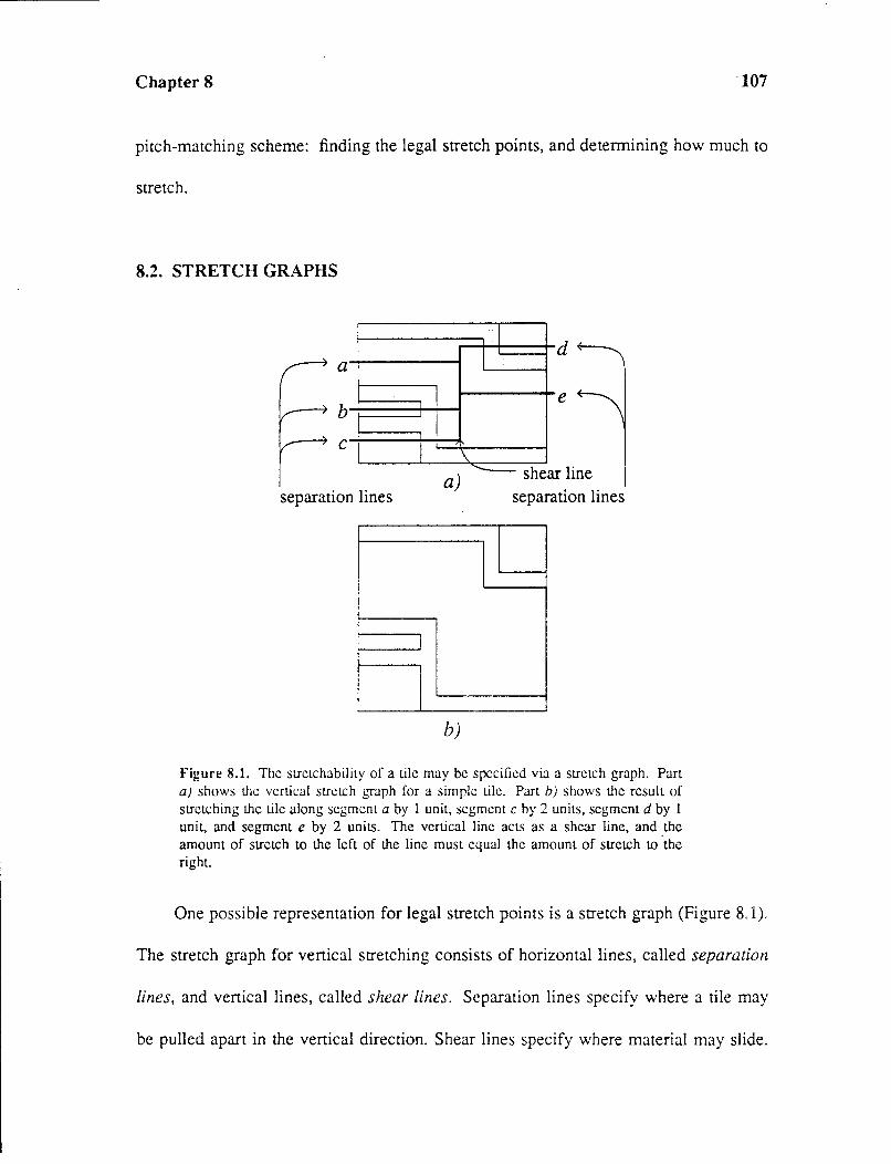
Chapter 8 107
pitch-matching scheme: finding the legal stretch points, and determining how much to
stretch.
8.2. STRETCH GRAPHS
a
b
c I
separation lines a)
b)
\
j I d
e
--- shear line separation lines
Figure 8.1. The suetchability of a tile may be specified via a suetch graph. Part a) shows the vertical suetch graph for a simple tile. Part b) shows the result of suetching the tile along segment a by 1 unit, segment c by 2 units, segment d by 1 unit, and segment e by 2 units. The vertical line acts as a shear line, and _the amount of stretch to the left of the line must equal the amount of stretch to the right.
One possible representation for legal stretch points is a stretch graph (Figure 8.1).
The stretch graph for vertical stretching consists of horizontal lines, called separation
lines, and vertical lines, called shear lines. Separation lines specify where a tile may
be pulled apart in the vertical direction. Shear lines specify where material may slide.
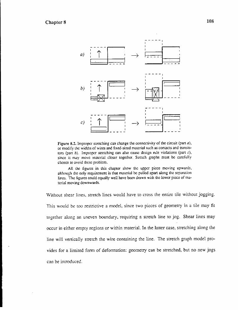
Chapter 8
-----1 I
-----a) i --7 l I
I---- J J
-----
-----1 I
I
b) --7
-----
-----1 I
!I I c) --7 ,_- I
-----
Figure 8.2. Improper stretching can change the connectivity of the circuit (part a),
or modify the widths of wires and fixed-sized material such as contacts and transis
tors (part b). Improper stretching can also cause design rule violations (part c),
since it may move material closer together. Stretch graphs must be carefully
chosen to avoid these problem.
All the figures in this chapter show the upper piece moving upwards,
although the only requirement is that material be pulled apart along the separation
lines. The figures could equally well have been drawn with the lower piece of ma
terial moving downwards.
108
Without shear lines, stretch lines would have to cross the entire tile without jogging.
This would be too restrictive a model, since two pieces of geometry in a tile may fit
together along an uneven boundary, requiring a stretch line to jog. Shear lines may
occur in either empty regions or within material. In the latter case, stretching along the
line will vertically stretch the wire containing the line. The stretch graph model pro-
vides for a limited form of deformation: geometry can be stretched, but no new jogs
can be introduced.
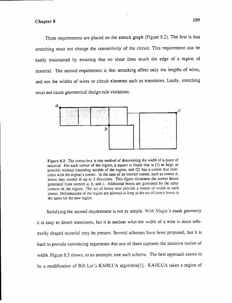
Chapter 8 109
Three requirements are placed on the stretch graph (Figure 8.2). The first is that
stretching must not change the connectivity of the circuit. This requirement can be
easily maintained by ensuring that no shear lines touch the edge of a region of
material. The second requirement is that stretching affect only the lengths of wires,
and not the widths of wires or circuit elements such as transistors. Lastly, stretching
must not cause geometrical design rule violations.
1---;o--------ofiCC
b
Figure 8.3. The comer-box is one method of determining the width of a piece of
material. For each corner of the region, a square is found that is (1) as large as
possible without extending outside of the region, and (2) has a comer that coin
cides with the region's corner. In the case of an interior corner, such as corner b,
boxes may extend in up to 3 directions. This figure illustrates the corner boxes
generated from corners a, b, and c. Additional boxes are generated by the other
corners of the region. The set of boxes now provide a notion of width at each
comer. Deformations of the region are allowed as long as the set of comer boxes is
the same for the new region.
Satisfying the second requirement is not as simple. With Magic's mask geometry
it is easy to detect transistors, but it is unclear what the width of a wire is since arbi-
trarily shaped material may be present. Several schemes have been proposed, but it is
hard to provide convincing arguments that any of them captures the intuitive notion of
width. Figure 8.3 shows, as an example, one such scheme. The best approach seems to
be a modification of Bill Lin's KAHLUA algorithm[ I]. KAHLUA takes a region of
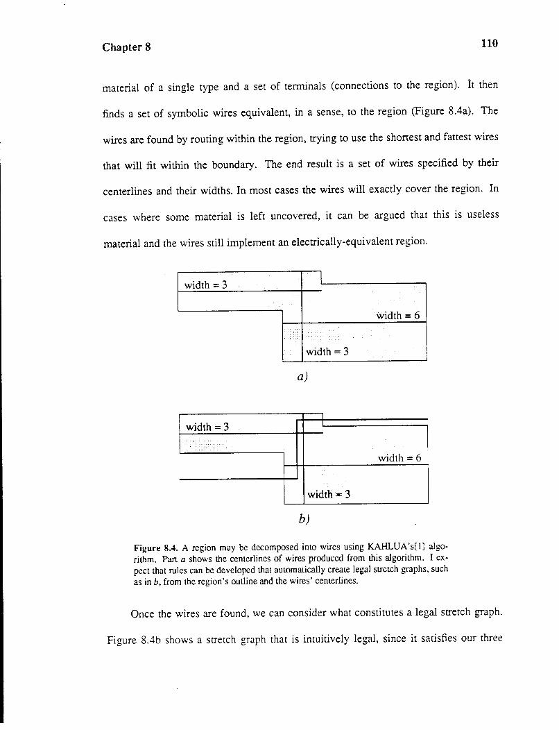
Chapter 8 110
material of a single type and a set of terminals (connections to the region). lt then
finds a set of symbolic wires equivalent, in a sense, to the region (Figure 8.4a). The
wires are found by routing within the region, trying to use the shortest and fattest wires
that will fit within the boundary. The end result is a set of wires specified by their
centerlines and their widths. In most cases the wires will exactly cover the region. In
cases where some material is left uncovered, it can be argued that this is useless
material and the wires still implement an electrically-equivalent region.
width= 3 I
width= 6
I width= 3
a)
width= 3
' :··
width= 6 I
width= 3
b)
Figure 8.4. A region may be decomposed into wires using KAHLUA's[l] algo
rithm. Pan a shows the centerlines of wires produced from this algorithm. I ex
pect that rules can be developed that automatically create legal stretch graphs, such
as in b, from the region's outline and the wires' centerlines.
Once the wires are found, we can consider what constitutes a legal stretch graph.
Figure 8.4b shows a stretch graph that is intuitively legal, since it satisfies our three
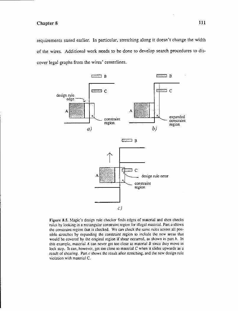
Chapter 8 111
requirements stated earlier. In particular, stretching along it doesn't change the width
of the wires. Additional work needs to be done to develop search procedures to dis-
cover legal graphs from the wires' centerlines.
design rule edge~
r,q~,~ I B
f1'\K'O%J c
,.,...--+--,
A
a)
A
constraint region
c)
E''M;; ''l B
A
b)
w~' ,J B
design rule error
constraint region
c
expanded constraint region
Figure 8.5. Magic's design rule checker finds edges of material and then checks
rules by looking in a rectangular constraint region for illegal material. Part a shows
the constraint region that is checked. We can check the same rules across all pos
sible stretches by expanding the constraint region to include the new areas that
would be covered by the original region if shear occurred, as shown in part b. In
this example, material A can never get too close to material B since they move in
lock step. It can, however, get too close to material C when it slides upwards as a
result of shearing. Part c shows the result after stretching, and the new design rule
violation with material C.
Chapter 8 112
The last remaining requirement is the preservation of geometrical design rules.
Figure 8.2 shows how shearing can violate minimum spacing rules. These violations
can be avoided by checking in advance using a modified design rule checker. The
checker takes a stretch graph and a layout and detects design rule violations that could
occur if the layout was stretched along the lines in the graph. The checker is based
upon Magic's design rule checker (Section 5.4) which checks constraint regions for the
presence of illegal material (Figure 8.5a). We can modify the design rule checker to
stretch the constraints so that they cover the region that the original region would pass
over as it was stretched. Stretching up to the end of the shear line is sufficient, since
material past the end of the shear line moves with the edge that generated the con
straint region. It is also necessary to take into account the interactions between nearby
shear lines, since one may shear while another one doesn't. I have not investigated
this issue.
8.3. SOLVI~G THE GRAPHS
The second major problem to be solved in pitch-matching is to determine the
stretch amounts needed to join tiles together (Figure 8.6). A stretch graph can be
represented by a directed graph similar to that in Figure 8.7. Each arc corresponds to a
separation line, and each node to a shear line. An integer value, si, is assigned to each
arc i, indicating the amount of stretching to be done along that separation line. Each
node j is assigned an integer value, Aj, which is always zero for the purposes of the
immediate discussion. Any valid set of stretch amounts must have the same amount of
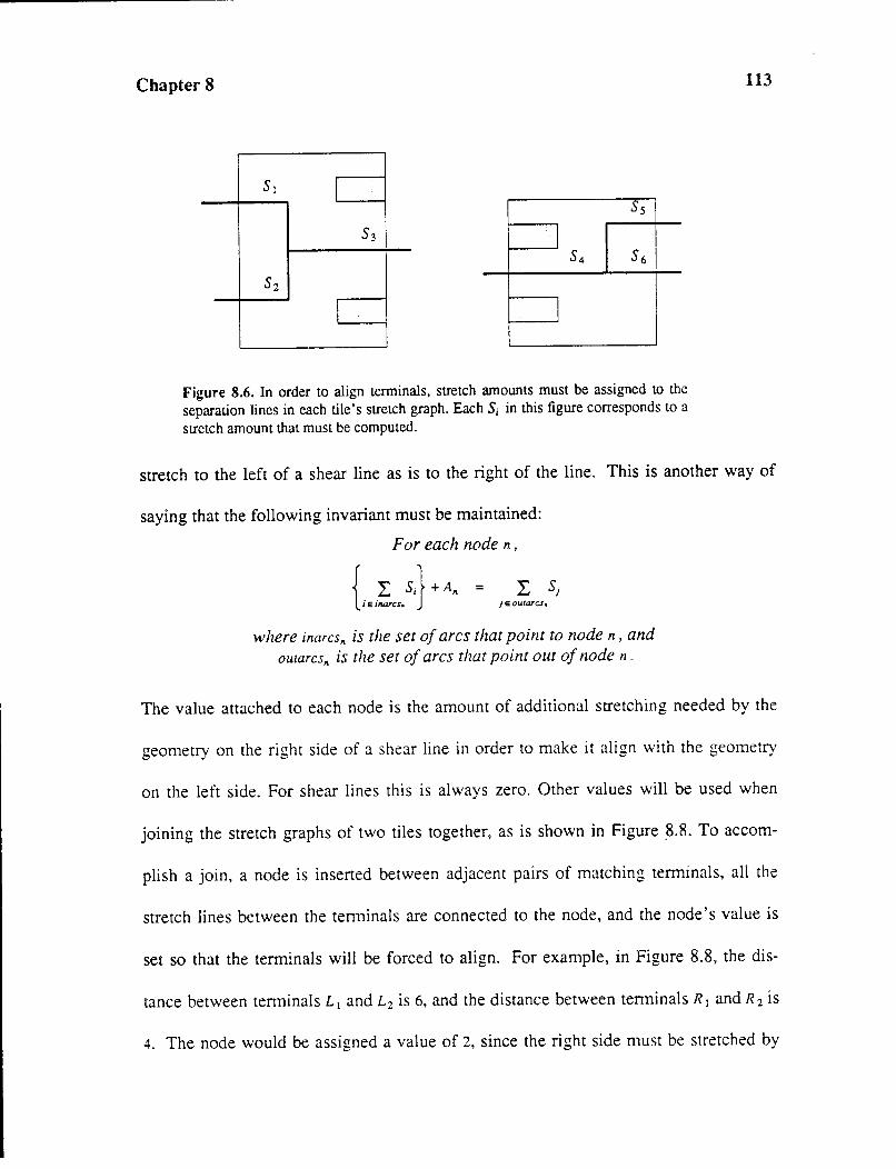
Chapter 8
St I Ss
s3 I s4 s6
Sz
I I
Figure 8.6. In order to align terminals, stretch amounts must be assigned to the
separation lines in each tile's stretch graph. Each Si in this figure corresponds to a
stretch amount that must be computed.
113
stretch to the left of a shear line as is to the right of the line. This is another way of
saying that the following invariant must be maintained:
For each node n,
{ I si} +A,. = I s, i e inarcs. j e outarcse
where inarcs,. is the set of arcs that point to node n, and outarcs,. is the set of arcs that point out of node n.
The value attached to each node is the amount of additional stretching needed by the
geometry on the right side of a shear line in order to make it align with the geometry
on the left side. For shear lines this is always zero. Other values will be used when
joining the stretch graphs of two tiles together, as is shown in Figure _8.8. To accom-
plish a join, a node is inserted between adjacent pairs of matching terminals, all the
stretch lines between the tem1inals are connected to the node, and the node's value is
set so that the terminals will be forced to align. For example, in Figure 8.8, the dis-
tance between terminals L 1 and L 2 is 6, and the distance between terminals R 1 and R 2 is
4. The node would be assigned a value of 2, since the right side must be stretched by
Chapter 8
I l d
a
e b
.:o<,
c > .::::.:
a)
b)
Figure 8.7. A directed graph is used to represent a stretch graph. Each arc corresponds to a separation stretch line, and has a weight indicating how much it should be stretched. Each node corresponds to a shear line, and has a value of zero indicating that the amount of stretch to the left of the node must be equal to the amount of stretch to the right.
two more units than the left side if the terminals are to align properly.
114
The separation of two tiles of geometry depends, in part1 on how they are
stretched, due to design rule interactions (Figure 8.9). This presents difficulties, since
the separation must be known in order to set up the stretch graph for alignment in the
other direction. Because of this interaction, it is not possible to assemble the complete
vertical and horizontal graphs for a module and then solve them independently.
Chapter 8
a)
b)
Figure 8.8. Stretch graphs are joined together by intermediate nodes. These nodes have a value which states how much extra stretching should appear on the right side of the node in order to pitch-match the underlying geometries. Part a shows two tiles and their corresponding graphs. The terminals on the left tile have a separation that is two units greater than that of the terminals on the right tile. The intermediate node, shown in part b, has a value of 2 to force the terminals to align when the graph is solved.
115
Other approaches will work, however. One approach is to join two tiles together
using the minimum separation allowed for the specific amount of stretch needed for
the join, without regard for additional stretching that will be needed later on. New vert-
ical and horizontal stretch graphs are then prepared for use in further joins. These
graphs include a stretch line along the seam between the two tiles, so that they may be
pulled apart to fit the needs of later joins. The result of this operation is a larger tile
with a stretch graph that can be used in operations just like a primitive tile. In Figure
Chapter 8
tile 1
tile 2
B j:::;::::;:;::;;: ::::1
tile 3
Figure 8.9. The vertical and horizontal stretch graphs are interdependent As an
example, tile 2 must be stretched to make its terminals align with those of tile 1.
This stretching causes material B to move closer to material A , resulting in a
greater spacing for distance d 1. Distance d 1o in tum, determines stretch S 2, thus
part of the venical stretch graph (S 1) affects part of the horizontal stretch graph
(S ~· Distance d 1 also determines how close material C is to material D, which
then partially determines distance d 2. Distance d 2 may affect the horizontal
stretch when these tiles are joined to other tiles in the horizontal direction. Thus,
the vertical and horizontal stretch graphs are interdependent and cannot be solved
independently.
116
8.9, this amounts to joining tile 1 with tile 2 and fixing distance d 1, so that the pair can
be joined with tile 3. A new stretch line is added between tiles 1 and 2, so that they
may be pulled apart if S 2 is stretched in some later join.
One problem with this approach is that it can waste area. It may be necessary to
either (1) eliminate certain stretch lines, because use of them would require a larger
separation in the future, or to (2) initially make the separation large enough to handle
any future stretching. In the example, after fixing distance d 1 it is no longer possible to
increase the stretch along S 1, because that would move material B and require an
Chapter 8 117
increase of distance d 1• Under plan (1), this would be solved by deleting S 1 from the
stretch graph after the join. This might waste area because that degree of freedom
would no longer be available. Under plan (2), the separation d 1 would be made large
enough from the very beginning, so that additional movement of material B would
never be a problem. This plan would also waste area, because d 1 might be larger than
needed. Another problem with this overall approach is that it stretches each tile many
times, as much as once for each join in the entire module. This could lead to poor per
formance.
Another approach is to assemble the graphs for the entire module, and then solve
them while leaving open the possibility of errors that will need to be corrected later.
Each separation distance is assumed to be the minimum separation possible over the
set of all possible stretches. With these assumptions, one graph, say the vertical stretch
graph, is solved. This provides a set of stretch amounts for the vertical direction, and
thus allows exact horizontal separations to be determined. These horizontal separa
tions can be used to prepare and solve an exact stretch graph for the other direction.
Solving this graph determines the vertical separation distances, and may or may not
match the separation assumption made when solving the first graph. If the distances
need to be increased, the new separations are used in the original graph and and the
process repeats, alternately solving vertical and horizontal graphs until it converges.
The process is guaranteed to converge, since separation distances are only increased
and the largest geometrical design rule serves as an upper bound for separation. How
ever, this approach may be slow due to the iteration involved.
Chapter 8 118
The most promising solution appears to be a modification of one of the plans dis
cussed earlier. The approach is to assume the maximum separation for each join
between tiles, over all possible stretches of those tiles. The vertical and horizontal
graphs can be solved independently under this assumption, since it is not possible to
later find that a separation is greater than the assumed separation. After solution, the
size of the module may be decreased by removing excess space from some of the
separations. This involves finding a path through the entire stretch graph where all the
edges have stretch values greater than zero and each separation between tiles has
excess space. It is likely that compressing a separation in one direction will preclude
compression of other separations in the perpendicular direction. I suggest that in most
modules one dimension is the most critical, so it makes sense to compress the max
imum amount in that direction followed by compression in the other direction.
None of these approaches considers what happens when no solution is possible,
as would be the case, for example, if two terminals were too close together and there
were not any stretch lines between them. Geometrically, it is easy to river route pins
that do not line up correctly, but it is unclear how to incorporate this capability into the
algorithm that solves the stretch graphs.
8.4. DISCUSSION
Several pitch-matching algorithms have been presented, but they need more
study. There may be better approaches to solving the stretch graphs and handling the
interactions between the horizontal and vertical graphs. A careful study of symbolic
Chapter 8 119
layout compaction algorithms may reveal similarities to the pitch-matching problem.
Perhaps some of the compaction work will provide new insights or solutions.
Adding pitch matching to Mocha Chip would allow it to guarantee design rule
correctness for regular structures without the waste of area that the river-route-space
operator produces for those structures. If this were done, structures such as PLAs
could be built that use the same amount of area as those built with the tile-packing
operator, but with a guarantee of design rule correctness.
8.5. REFERENCES
1. B. Lin and R. Newton, KAHLUA: A Hierarchical Circuit Disassembler, Proc.
24th Design Automation Conference, 1987, pp. 311-317.
120
9 DISCUSSION
9.1. DISCUSSION
There are two major problems with past approaches to building module genera
tors: the specification of the structure of the module was obscured, and no guarantees
of design rule correctness were made. Mocha Chip addresses each of these problems:
graphical diagrams are used to represent the module's structure in a visually intuitive
form, and pairwise assembly operators provide an assurance of design rule correctness.
Mocha Chip's module generators are graphical diagrams, with a simple geometri
cal correspondence between the diagrams and the layout that is to be produced. These
Chapter 9 121
diagrams are closer to the two-dimensional image in the IC designer's mind, and thus
are easier to comprehend.
The diagrams may be considered to be a graphical programming language for IC
module generation. The language provides array and case cells which are analogs of
loops and conditionals in a textual programming language. Pairwise assembly opera
tors and tile stretching form the primitive computations in this language, and
correspond to things like assignment and arithmetic operations in a programming
language.
Using graphical diagrams solves a major problem with previous module genera
tor systems: that they are textual. However, in addition to obscuring the overall struc
ture of a module, textual languages have another problem: they are not an intuitive
way to specify low-level geometry, leading to design-rule errors in cases that have not
been heavily tested. Mocha Chip's diagrams, by themselves, don't solve the problem
of interconnecting low-level geometry. Instead, Mocha Chip provides assembly opera
tors that automate the interconnection process, providing a guarantee of design-rule
correctness.
Several assembly operators are implemented or envisioned. T~e tile-packing
operator is simple and produces space-efficient designs, but provides no assurance of
design-rule correctness. The river-route-space operator guarantees that design rules
are not violated, and ensures that pins are connected together even if they don't align
exactly. Other more complex assembly operators, such as pitch-matching and general
routing, can be implemented within Mocha Chip's framework to provide better layout.
Chapter 9 122
The ability of some assembly operators to guarantee design rule correctness leads to
more robust generators, and solves this long-standing problem with past module gen
eration systems.
Mocha Chip's framework provides room for future expansion. I've already men
tioned the ability to add new pairwise assembly operators, such as pitch-matching and
routing. The graphical language can also be extended to provide parameterized net
lists and to allow a more powerful parameter passing mechanism. Such a mechanism
would provide non-top down parameter passing, and would allow one part of a module
to be generated based upon the results of the generation of another part.
There are two main limitations to Mocha Chip as it now stands: the system runs
more slowly than other systems, and pitch-matching appears to be required for most
regular modules. In Chapter 7 I've suggested ways that Mocha Chip could be made
faster, and in Chapter 8 I've detailed possible methods of adding pitch-matching.
Mocha Chip's graphical language is powerful enough to build module generators
for structures like PLAs. As we consider more and more irregular modules, Mocha
Chip looks less and less useful, requiring multiple diagrams and extensive use of the
Case cell. Mocha Chip works well for structures of the comple_xity of PLAs, and
would probably work well for slightly more complex structures such as ALUs and
datapaths. It would likely not be appropriate for more random forms of control con
structs. However, structures of the complexity of PLA abound; RAMs, ROMs, ALUs,
and shifters are examples. Mocha Chip works well for these and provides a robust,
intuitive, and easy-to-understand means of specifying these generators graphically.
A L______J
MANUAL PAGES
123
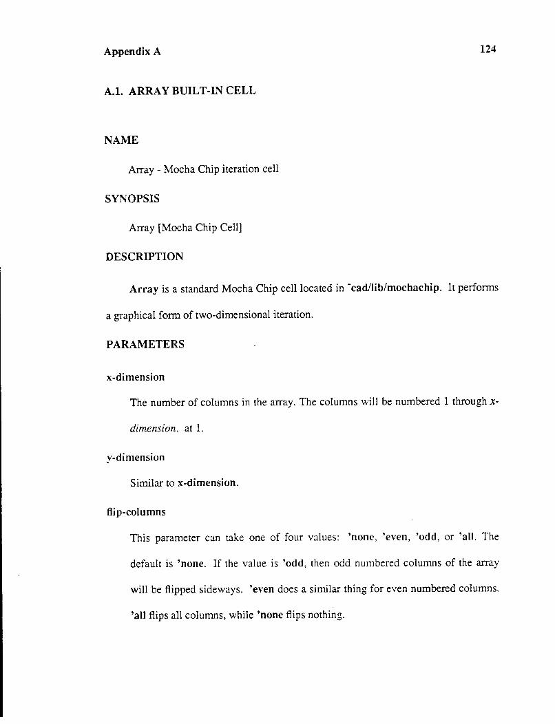
Appendix A
A.l. ARRAY BUILT-IN CELL
NAME
Array - Mocha Chip iteration cell
SYNOPSIS
Array [Mocha Chip Cell]
DESCRIPTION
124
Array is a standard Mocha Chip cell located in ·cad/lib/mochachip. It perlorms
a graphical form of two-dimensional iteration.
PARAMETERS
x-dimension
The number of columns in the array. The columns will be numbered 1 through x
dimension. at 1.
y-dimension
Similar to x-dimension.
fti p-col u mns
This parameter can take one of four values: 'none, 'even, 'odd, or 'all. The
default is 'none. If the value is 'odd, then odd numbered columns of the array
will be flipped sideways. 'even does a similar thing for even numbered columns.
'all flips all columns, while 'none flips nothing.
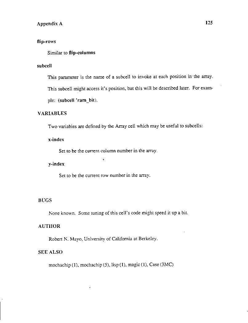
Appendix A 125
flip-rows
Similar to flip-columns
subcell
This parameter is the name of a subcell to invoke at each position in· the array.
This subcell might access it's position, but this will be described later. For exam
ple: (subcell 'ram_bit).
VARIABLES
Two variables are defined by the Array cell which may be useful to subcells:
x-index
Set to be the current column number in the array.
y-index
Set to be the current row number in the array.
BUGS
None known. Some tuning of this cell's code might speed it up a bit.
AUTHOR
Robert N. Mayo, University of California at Berkeley.
SEE ALSO
mochachip (1), mochachip (5), lisp (1), magic (1), Case (3MC)
Appendix A
A.2. CASE BUILT-IN CELL
NAME
Case - Mocha Chip conditional selection cell
SYNOPSIS
Case [Mocha Chip Cell]
DESCRIPTION
126
Case is a standard Mocha Chip cell located in ·cad/lib/mochachip. It performs a
graphical form of conditional selection.
PARAMETERS
easel ... caseN
This cell takes an arbitrary number of parameters of the form caseN, where N is a
positive integer. The parameters contain the different cases to be evaluated,
much in the same way as Lisp's cond expression or Pascal's case construct. The
syntax of a single case is:
(caseN '(e..tpr cellname orientation parameters))
where N is a positive integer, expr is a boolean-valued Lisp expression, eel/name
is the name of a subcell, and orientation is a list (or nil) that gives the orientation
of the cell. The orientation list is a sequence of atoms from the set {0, 90, 180,
Appendix A 127
270, upsidedown, sideways}. The atoms name operations that are applied to the
cell, starting with the leftmost named operation. The numerical atoms indicate
rotation of a number of degrees, while the other two atoms indicate a mirroring
functions. Parameters is a list of parameters and values for this cell.
The cases are evaluated in order, with the first true case being used. An error is
reported if no case is true. An example case parameter might look like this:
(easel '((equal x-pos 3) "decode cell" '(90 sidewavs) nil)). - .
BUGS
Some tuning of this cell's code might speed it up-a bit.
AUTHOR
Robert N. Mayo, University of California at Berkeley.
SEE ALSO
mochachip (1), mochachip (5), lisp (1), magic (1), Array (3MC)
Appendix A
A.3. MCPLA PLA GENERATOR
NAME
mcpla - Mocha Chip PLA generator
SYNOPSIS
mcpla [Mocha Chip Cell]
DESCRIPTION
128
mcpla is a Mocha Chip module generator for PLAs. It takes truth tables in the
pla(5) format, and produces mask geometry in Magic format. The generator is
invoked from the Mocha Chip system, which is built into the Magic layout editor.
PARAMETERS
truth-table-file
The filename of the truth table file.
clock-inputs
If non-nil, mcpla will provide clocks for the input buffers.
clock-outputs
If non-nil, mcpla will provide clocks for the output buffers.
input-labels
This parameter should contain a list of the names of the inputs to the PLA. If the
list is not long enough, or is nil, mcpla generates names for the remaining inputs.

Appendix A 129
output-labels
This parameter should contain a list of the names of the outputs to the PLA. If
the list is not long enough, or is nil, mcpla generates names for the remaining out
puts.
gnd-stretch
The number of coordinates (usually lambda) to stretch tiles by. This is used to
increase the width of ground lines to the PLA.
gnd-spacing
If gnd-spacing is set to N, every Nth row in the AND plane and every Nth row
and column in the OR plane will contain an extra ground line, in order to assist
distribution of power to the array.
TILES
The layout produced is controlled by a set of Magic cells called tiles. Tiles for
mcpla may be found in the subdirectories of -cad/Iib/mcpla. Currently the following
sets of tiles exist:
scmosA sample set of tiles for the scmos technology. Both clocked input and
output drivers are supported.
To use a set of tiles called foo, set up Mocha Chip's MochaCeiiPath parameter
to access -cad/lib/mcpla/faa. For example: (Mocha Cell Path '("."
n-cad/Iib/mcpla/faa") ).
Appendix A 130
AUTHOR
Robert N. Mayo, University of California at Berkeley.
SEE ALSO
pla (5), eqntott (1), espresso (5), mochachip (1), magic (1), lisp (1)
Appendix A 131
A.4. MOCHA CHIP
NAME
mocha chip - module generation system for Magic
SYNOPSIS
:specialopen mochachip
DESCRIPTION
Mocha Chip is an interactive module generation system built into the Magic
VLSI layout editor. Mocha Chip allows the user to create module generators by draw
ing a diagram of the desired layout and then parameterizing it so that it specifies many
different, but similar, modules.
To get an idea of what a Mocha Chip generator looks like, open up a Mocha Chip
window with the Magic command :specialopen mochachip. After this is done, point
to the window and type :load mcpla. This will load in the mcpla PLA generator.
Looking at this will give you a feel for the sort of things that Mocha Chip can do.
COMMANDS
box [dir [amount]]
Same as Magic's box command.
clockwise [degrees]
Rotate the selected objects and the box clockwise in such a way that the lower
left corner of the selection remains unchanged. Degrees should be a positive
Appendix A 132
multiple of 90 degrees.
create [magiclmochachi plonelevel]
Create a module from the diagram underneath the cursor. The resulting magic
cell will have the same name as the diagram underneath the cursor. The new
module will overwrite any similarly named Magic or Mocha Chip cell. The
module can be generated in one of three forms: magic, mochachip, or onelevel,
with magic being the default. The magic form specifies that the module will be
generated as a collection of Magic cells. As a side effect, Mocha Chip cells are
produced as with the mochachip option. The mochachip form specifies that a
collection of Mocha Chip diagrams is to be produced instead of actual layout.
These diagrams are similar to the Mocha Chip diagrams that produced the
module, except that the parameters, variables, and comments have all been
evaluated (instantiated). The top-level Mocha Chip cell will have the same name
as the module but with -vO added on the end. The onelevel form is similar to
mochachip, except that only the topmost level of the module is generated. This
is useful for debugging parameterization.
decompose
Recursively split the diagram under the cursor into pieces. Mocha Chip requires
that diagrams be split up in this manner. If the automatic decomposition does not
give the desired results, then the user can erase some of the decomposition lines
and put in new ones with the getdecompline command. If the user does this, the
decompose command should be run afterwards to tidy things up.
Appendix A 133
The decomposition is important since it specifies the manner in which the module
is built. The lines show how to divide the module into smaller and smaller
pieces. When assembling the module, the reverse process takes place: small
pieces are paired up forming larger pieces until the complete module is generated.
deleteThe current selection is deleted from the diagram.
destroy [cellname]
The specified cell (if none, then the one under the cursor), is deleted. Even the
file on disk is removed, so be careful when using this command. This command
is usually used when you want Mocha Chip to use a Magic cell instead of the
Mocha Chip cell by the same name.
eval expr
Evaluate a Lisp expression. If the expression contains any blanks or special char
acters it will have to be surrounded by double quotes. The system will detect and
report any errors encountered during the evaluation process.
expand [toggle]
Expand (show internals) of everything under the box or, if toggle is specified,
toggle the expansion state of all selected objects in the diagram under the cursor.
findbox [zoom]
Same as Magic's findbox command.
flush [cellname]
Reload the specified Mocha Chip cell from disk or, if none was specified, the one
under the cursor. Any changes made to the cell are discarded.
Appendix A 134
getcell cellname
Put a subcell into the diagram under the cursor.
getdecompline
Put in a new decomposition line. The box must have two sides coincident so that
it forms a line rather than a rectangle or point.
grid [xSpacing [ySpacing [xOrigin yOrigin]]]
grid off
Same as Magic's grid command.
identify usename
Set the use name for the selected subcell.
lisp [ onloff]
With no arguments, go into interactive Lisp mode. Otherwise, with the on option
interactive Lisp mode is entered whenever Mocha Chip encounters an error. The
off option disables this. Interactive Lisp mode may be terminated with the Lisp,
(bve) command.
load cellname
Load the specified cell into the window, replacing the cell that is currently there.
The replaced cell remains in Mocha Chip, and can be viewed with another load
command.
loglisp [filename]
Start logging lisp interactions to filename. If the filename is omitted, then stop
Appendix A 135
logging. Text sent to Lisp is written to the file immediately, while text sent from
Lisp to Mocha Chip is written to the file when Mocha Chip reads it.
moveMove the currently selected objects so that their lower· left corner coincides with
the lower· left corner of the box tool.
path path
Same as Magic's path command. The path set with this command is used for
finding both Magic and Mocha Chip cells.
save [filename]
Save the current cell to disk. If filename is specified, the cell is save to that file
and the cell's name is changed to match the filename.
select [optionlhelp]
Select an object. Current options are:
select [more]
Put the object under the cursor into the list of selected objects. If more is not
specified, then the selection is cleared first.
select [more] area
Put all objects that overlap the area of the box into the list of selected
objects. If more is not specified, then the selection is cleared first.
select clear
Clear the list of selected objects.
Appendix A
select help
Print out a brief synopsis of these options.
sideways
Flip the selection and the box sideways, keeping it in the same position.
size Resize all selected objects so that they fit within the box exactly.
synclisp
136
Bring Mocha Chip back in synchronization with the Lisp system. They should
never get out of sync in the first case, so this command is only a sort of
''insurance".
text edit
Invoke an editor on the contents of the selected object. The program run is called
"mochaChipTextEditor". On a Sun, this program opens up a new window and
runs the editor specified by the "EDITOR" environment variable. If the environ
ment variable is not found, the program runs "/usr/ucb/vi" in the window. The
user can place a program called ''mochaChipTextEditor" in the current directory
if some other action is desired.
Syntax errors in the text can make a cell unreadable after it is· written out. If this
happens, you should fix the syntax error using a text editor on the file.
unexpand
Unexpand all cells under the box.

Appendix A 137
upsidedown
Flip the selected objects and the box upsidedown. The objects remain in the
same location.
whatPrint out information about what objects are selected.
writeall [force]
Write out all Mocha Chip cells that have changed. Unless force is specified, the
user is asked for permission before each cell is written.
SPECIAL FUNCTIONS & VARIABLES
Various special functions and variables may be used which modify the behavior
of Mocha Chip. The follow describes each of these.
MochaCellPath
Mocha Chip first searches through the path listed in l\1ochaCellPath when look
ing for Mocha Chip or Magic cells during the generation of a module. If it can't
find a cell that way, it then looks through the directories in Mocha Chip's search
path (set via :path).
MochaCeiiPath is initially set to nil. If desired, a module generator may redefine
this variable in the Local Variables or Parameters section to cause different
directories to be searched. For example, a module generator that has some tiles in
-cad/lib/hap _gen might look there for tiles after first checking the current direc
tory. This could be done by placing the following line in the local variables sec
tion:
Appendix A 138
(MochaCellPath '(" ." "-cad/lib/hap_gen"))
Note that the path must be a list, not just a single directory. It is possible to
include Mocha Chip's default search path as part of the MochaCellPath list.
Mocha Chip's default search path is stored in the variable MochaMagicPath.
For example:
(MochaCeliPath (appendl MochaMagicPath '(" ." "-cad/lib/hap_gen")))
will cause Mocha Chip's search path to be searched before the two specified
directories.
MochaFileDir
If set to non-nil in a Local Variables or Parameters block, then all generated
cells will be placed in the specified directory. This variable doesn't obey normal
scoping rules -- it should be set once and then all cells for this module will be
placed in that directory. Example:
(MochaFileDir "decode_pla")
will cause all files for this module to be placed in the directory decode_pla. If
this is done, it is handy to set Magic's path so that the files can be accessed later!
See the :path command of magic(l) for more details.
MochaMagicPath
This is Mocha Chip's search path, which is searched after MochaCellPath. See
the description of that variable for more information.
-Appendix A 139
BUGS
No doubt there are many bugs. Please report them to "[email protected]".
Mocha Chip requires at least 8 megabytes of real memory, or it will thrash and run
very s-1-o-w-1-y.
AUTHOR
Robert N. Mayo, University of California at Berkeley.
SEE ALSO
magic (1), mochachip (5), lisp (1)
140
B TUTORIALS
Appendix B
B.l. USING A MOCHA CHIP MODULE GENERATOR
Mocha Chip Tutorial #1:
Using a Mocha Chip Module Generator
Robert N. Mayo
Computer Science Division
Electrical Engineering and Computer Sciences
University of California
Berkeley, CA 94720
B.1.1. INTRODUCTION
141
Mocha Chip is a system for building semi-regular modules such as PLAs, barrel
shifters, and decoders. This tutorial tells you how to start up Mocha Chip and use
module generators that have already been designed. However, you will probably want
to develop some of your own specialized module generators. Mocha Chip tries to
Appendix B 142
make this especially easy, and you are encouraged to read "Mocha Chip Tutorial #2"
which tells you how to build module generators.
8.1.2. HOW TO GET HELP AND REPORT PROBLEMS
Mocha Chip is built into the Magic layout editor, but is being built by only one
member of the Magic team: myself. For this reason, please send bug repons, sugges
tions, and complaints directly to me at [email protected]. If you are
reporting a bug, please give me enough information so that I can repeat the problem.
In some cases this may involve sending me the cells that you were using and the
sequence of commands that lead up to the error.
Mocha Chip is currently (November, 1987) a young system. I welcome your
comments so that I can improve the system. By reporting problems, you will make life
much easier for those that follow in your footsteps.
Magic bug reports and comments that are not specific to Mocha Chip should be
sent to [email protected], as always.
8.1.3. STARTING UP MOCHA CHIP
I'm going to assume that you are already familiar with Magic and that you have
Magic running with the cmos technology. If this is not the case, you should start up
Magic, referring to Magic Tutorial #1: Getting Started as needed.
The first thing that needs to be done is to open up a Mocha Chip window. Type:
Appendix B 143
:specialopen mochachip
and you will see a new window appear. The caption of this window indicates that it
contains a Mocha Chip cell -- in this case the unnamed one.
Notice that the cell isn't completely empty. You will see three objects in the cell:
a Parameters block, a Local Variables block, and a Comments block. The second
tutorial will show how these are used to provide programmability and parameterization
when building a module generator. We won't concern ourselves with these blocks
now, because we are just going to use an existing module generator rather than design
a new one.
B.l.4. A PLA EXAMPLE
Let's create a PLA as an example. Assume that we want the PLA to be called
decode_pla. Our first step is to load in a new Mocha Chip cell by that name. This can
be done by pointing to the Mocha Chip window and typing:
:load decode _pia
Mocha Chip won't be able to find this cell (unless you made it before), so it will tell
you that and create a new cell.
We'll use the mcpla module generator to create the PLA for us. The first thing
that needs to be done is to put the generator into our search path. Type :addpath
-cad/lib/mcpla. You will probably want to put this command (without the ':') into
your .magic file so that you won't have to type it each time. The curious among you
Appendix B 144
might want to see what the mcpla generator looks like internally. To do this, open up
another Mocha Chip window and type :load mcpla. The generator is just another
diagram, but with text in the cells to provide parameterization.
Now we will put mcpla to use. Move the box into the lower part of the window
containing the decode _pia Mocha Chip cell. Make the box a comfortable size, and
type: :getcell mcpla. This tells the system that we are going to use the mcpla genera
tor to create the contents of decode_pla. Now type :expand or the macro 'x' to
expand the cell. At this point, we need to supply a truth table and other parameters to
mcpla.
mcpla takes a single parameter, truth-table-file. This can be detemrined by
looking at the manual page for mcpla or, better yet, looking at mcpla directly. I've
created a sample truth table file for you, and it's name is decode pla.tt and can be
found in the same directory as mcpla Ccad/lib/mcpla). We need to pass this filename
in as a parameter to mcpla. Point to the mcpla subcell and type :select. Now type
:textedit. A text editor should pop up. Insert the following line into the file:
(truth-table-file "-cadllib/mcpla/decode _pla.tt")
This tells the system that the parameter truth-table-file is to be set to the value
·cad/lib/mcpla/decode_pla.tt. The quote marks specify that the value is a constant,
rather than an expression that is computed. This syntax is the same as Lisp, and in fact
the value can be any arbitrary Lisp expression.
Appendix B 145
There is another parameter that we might want to define. The parameter
MochaFileDir specifies the directory into which to put files. Some module generators
can create lots of files, so it is often convenient to put them into a single directory.
Let's say that we want the files to go into the directory called pla_stuff. We can do
this by adding the line:
(MochaFileDir "pia stufr')
to the file that we are editing. Now we can save the file (using :wq for the vi editor),
and you will see that Mocha Chip has put the text into the selected cell.
We must prepare for the new files that will be created. To do this, suspend Magic
with a AZ and type mkdir pla_stuff to create a directory for the files. Now continue
Magic with fg, and type :addpath pia _stuff to put the new directory into the search
path.
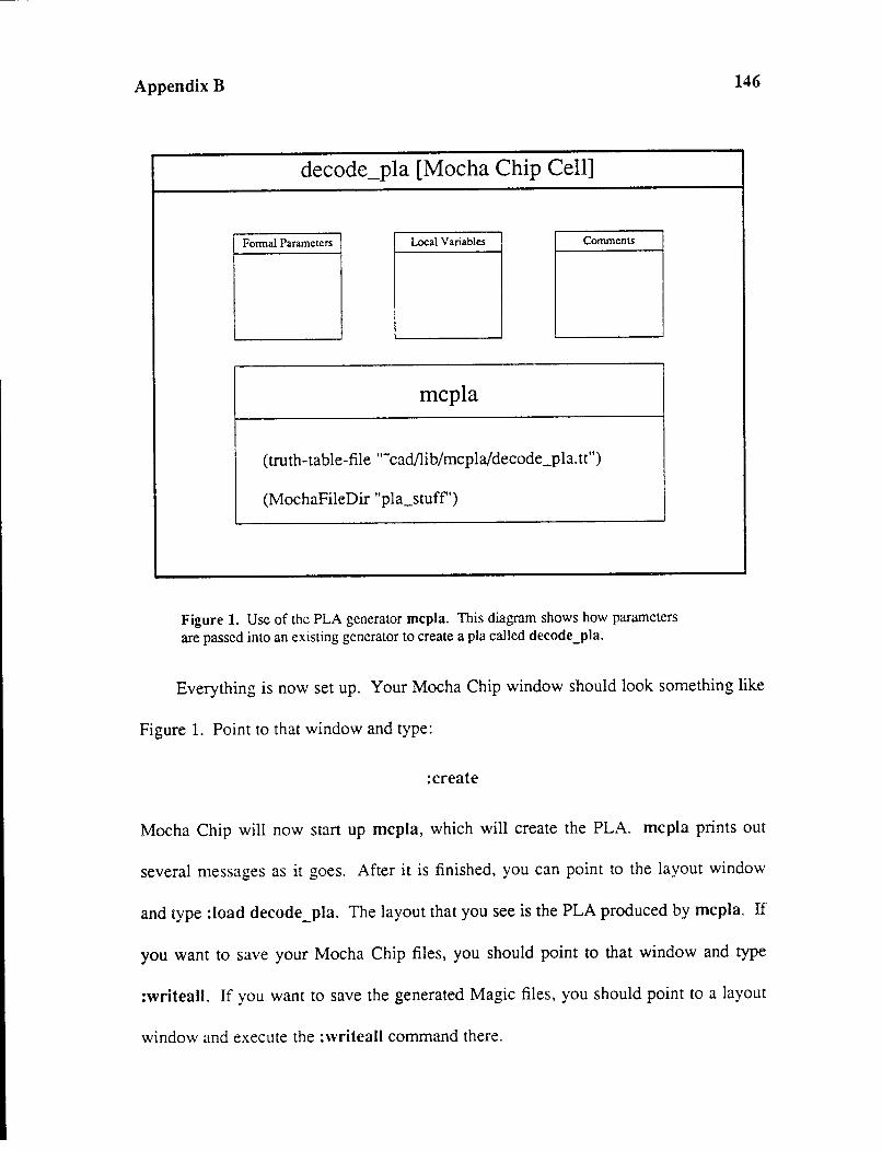
Appendix B
decode_pla [Mocha Chip Cell]
Formal Parameters Local Variables Conunents
mcpla
(truth-table-file "-cad/lib/mcpla/decode_pla.tt")
(MochaFileDir "pla_stuff')
Figure 1. Usc of the PLA generator mcpla. This diagram shows how parameters
are passed into an existing generator to create a pia called decode_pla.
146
Everything is now set up. Your Mocha Chip window should look something like
Figure 1. Point to that window and type:
:create
Mocha Chip will now start up mcpla, which will create the PLA. mcpla prints out
several messages as it goes. After it is finished, you can point to the layout window
and type :load decode_pla. The layout that you see is the PLA produced by mcpla. If
you want to save your Mocha Chip files, you should point to that window and type
:writeall. If you want to save the generated Magic files, you should point to a layout
window and execute the :writeall command there.
Appendix B 147
B.l.5. CONCLUDING REMARKS
This concludes the use of Mocha Chip module generators. The parameterization
required for each generator is documented in the generator's manual page. Certain
parameters, such as the MochaFileDir parameter, are system wide and. are docu
mented in the Mocha Chip manual page.
I hope that you had a chance to look at the internals of the mcpla generator by
typing :load mcpla. One of the reasons for building Mocha Chip was to make design
ing module generators easier. It is hoped that the ability to draw portions of the
module generator rather than write code will encourage designers to create their own
module generators.
Appendix B
B.2. DESIGNING MODULE GENERATORS WITH MOCHA CHIP
Mocha Chip Tutorial #2:
Designing Module Generators with Mocha Chip
Robert N. Mayo
Computer Science Division
Electrical Engineering and Computer Sciences
University of California
Berkeley, CA 94 720
B.2.1. INTRODUCTION
148
In the first tutorial you saw how to use an existing Mocha Chip module generator.
In this tutorial I'll show you how to design your own module generator. Unlike most
module generator systems, Mocha Chip allows you to draw a diagram of the overall
structure of the class of modules that you want to generate. You can then parameterize
Appendix B 149
this diagram to tell Mocha Chip how different modules differ. You can think of
Mocha Chip as a sort of graphical programming language tailored specifically to the
generation of IC layouts.
Mocha Chip also gives you some powerful interconnection operations to use. The
tiles (or basic subcells) of your module can be connected together using abutment,
pitch-matching or river routing. {NOTE: No pitch-matching exists in the current
release.) Abutment aligns user-specified packing rectangles so that they are adjacent.
Overlap of cells is possible by making the user-specified packing rectangles smaller
than the cell itself. Pitch-matching stretches cells so their pons line up more closely,
while river-routing is a simple form of routing that can be used where wires don't need
to change layers or jump over each other. In the future I might add more general rout
ing capabilities.
B.2.2. AN EXAMPLE DIAGRAM
I assume that you have read the first Mocha Chip tutorial, and that you have
Magic running on your workstation with the cmos technology. Let's start by opening
up a Mocha Chip window and loading in the tut2a cell.
You will see on the screen a Mocha Chip diagram that contains two subcells:
mochatut2 and mochatutl. The two subcells contain Magic layout. You can use one of
Magic's layout windows to look at them. Do this, and you will see that mochatutl
contains a contact and some metall and poly. Mochatut2, on the other hand, contains
a length of metall with a few diffusion wires crossing it.
Appendix B 150
Notice the small arrows on the subcells in the Mocha Chip window. The arrows
indicate the orientation of the subcell. Mochatut2' s arrow is pointing north, with the
little flag on the right. This indicates the normal orientation of the cell. Mochatutl, on
the other hand, has the arrow pointing right. This is because the subcell was rotated
clockwise by 90 degrees and then flipped upside down.
The thick bar is called a decomposition line. This line tells Mocha Chip to take
the cell(s) on one side of it and join them to the cell(s) on the other side. Point at the
decomposition line and type :select. Now, type :what. Mocha Chip will tell you that
you have selected a decomposition line of type pack. This means that the cell(s) on
the right (in this case, only the cell mochatutl) will be joined to the cell(s) to the left
by abutting their packing rectangles. In the future, there will be other types of lines
such as pitch-matching lines and river-routing lines, but for now the only type is pack.
Now you know all there is to know about the Mocha Chip cell tut2a; let's gen
erate some layout. Point to the Mocha Chip window and type
:create
This command tells Mocha Chip to generate layout for the module. Mocha Chip will
print out some messages while it is assembling the module. The most interesting of
these messages are the ones that describe the phases that Mocha Chip goes through in
producing a module. The first phase is the instantiate phase. In this phase, Mocha
Chip evaluates the parameters in the diagram and creates a Lisp data structure that
indicates what Magic cells need to be put together. After the instantiation phase,
Mocha Chip enters the describe phase, in which the Lisp system tells Magic about the
Appendix B 151
structure that it created. Magic takes this structure and, in the assemble phase, turns
the abstract structure into actual layout.
Now that we have generated a module, let's load it into a Magic window. Point
to a Magic window and load in the newly created cell tut2a. You will see that it con
tains two subcells, just like the Mocha Chip diagram. Furthermore, they have been
oriented according to the arrows on the subcells in the Mocha Chip diagram, and they
have been placed in the same relative positions. Notice that the size of the cells in the
Mocha Chip diagram need not bear any direct correspondence to the size of the actual
cells. You can think of the Mocha Chip diagram as being a sketch of how the cells are
to be assembled.
The pack decomposition line actually is a bit more powerful that I've described
so far. The packing rectangles for a cell can be specified by the user. To do this, edit
one of the Magic cells and place down a rectangular label called "me-pack". The
area of this label will be used as the packing rectangle of the cell instead of it's bound-
ing box.
Now is a good time to experiment with the features presented so far. You can
modify the packing rectangles of the Magic cells to produce different amounts of over
lap. Notice an error is reported if the packing rectangle of a cell doesn't line up
exactly with the packing rectangle of another cell. You can also try rotating and
flipping cells in the Mocha Chip diagram using :clockwise, :sideways, and :upside
down.
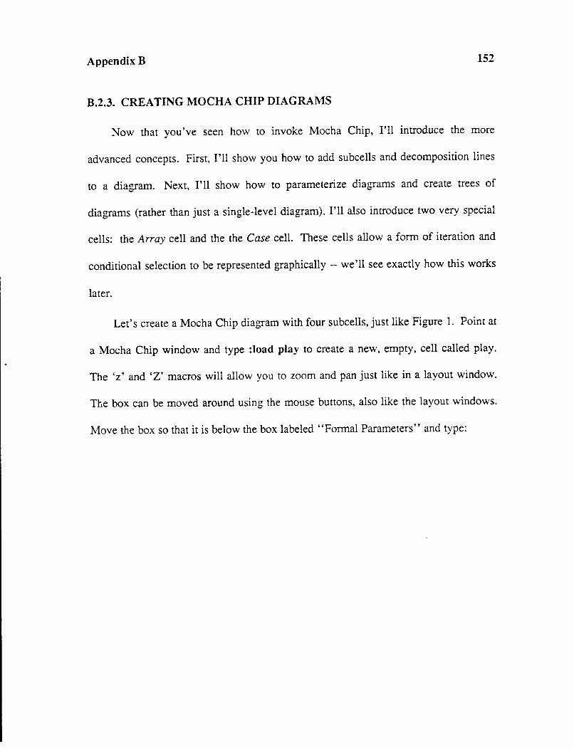
Appendix B 152
B.2.3. CREATING MOCHA CHIP DIAGRAMS
Now that you've seen how to invoke Mocha Chip, I'll introduce the more
advanced concepts. First, I'll show you how to add subcells and decomposition lines
to a diagram. Next, I'll show how to parameterize diagrams and create trees of
diagrams (rather than just a single-level diagram). I'll also introduce two very special
cells: the Array cell and the the Case cell. These cells allow a form of iteration and
conditional selection to be represented graphically -- we '11 see exactly how this works
later.
Let's create a Mocha Chip diagram with four subcells, just like Figure 1. Point at
a Mocha Chip window and type :load play to create a new, empty, cell called play.
The 'z' and 'Z' macros will allow you to zoom and pan just like in a layout window.
The box can be moved around using the mouse buttons, also like the layout windows.
Move the box so that it is below the box labeled "Formal Parameters" and type:
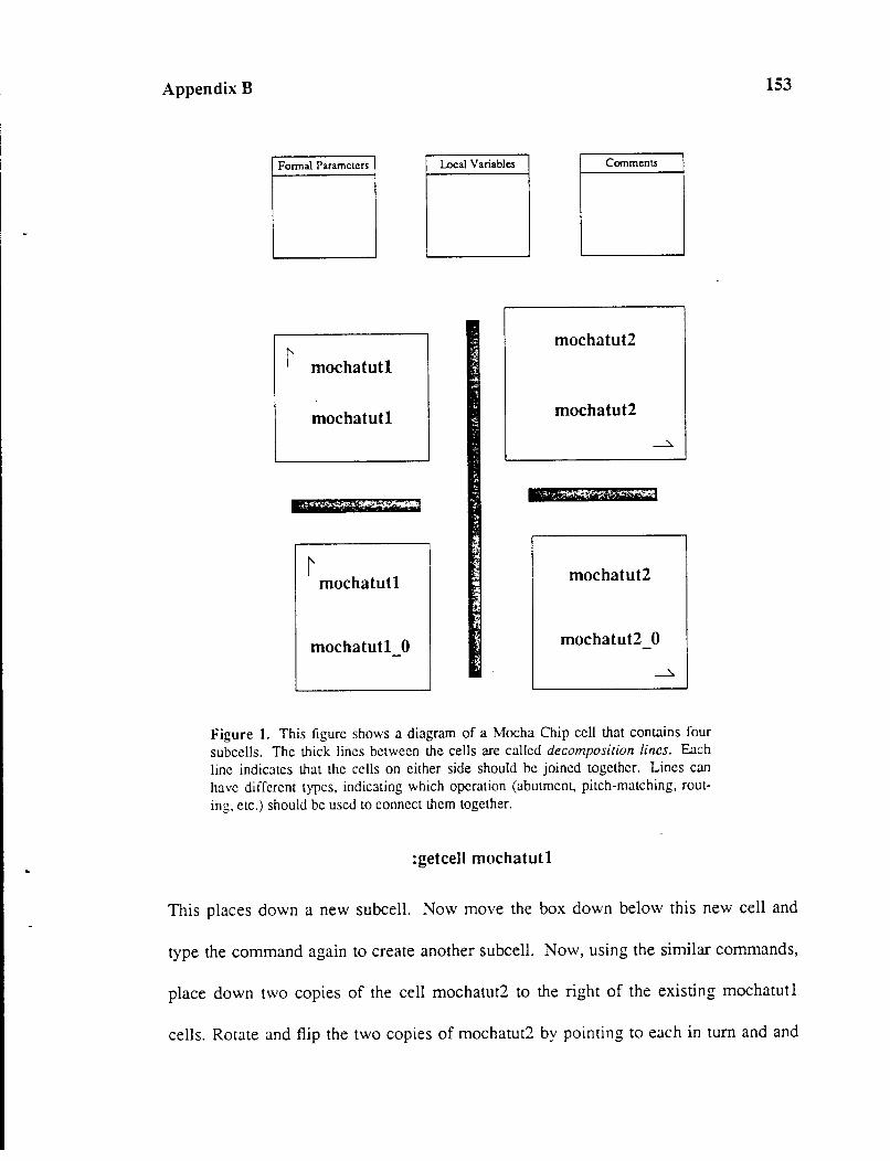
Appendix B
Formal Parameters Local Variables Comments
mochatut2
mochatutl
mochatutl mochatut2
I mochatutl mochatut2
mochatutl 0 mochatut2 0
Figure 1. This figure shows a diagram of a Mocha Chip cell that contains four
subcells. The thick lines between the cells are called decomposition lines. Each
line indicates that the cells on either side should be joined together. Lines can
have different types, indicating which operation (abutment, pitch-matching, rout
ing, etc.) should be used to connect them together.
:getcell mochatutl
153
This places down a new subcell. Now move the box down below this new cell and
type the command again to create another subcell. Now, using the similar commands,
place down two copies of the cell mochatut2 to the right of the existing mochatutl
cells. Rotate and flip the two copies of mochatut2 by pointing to each in turn and and
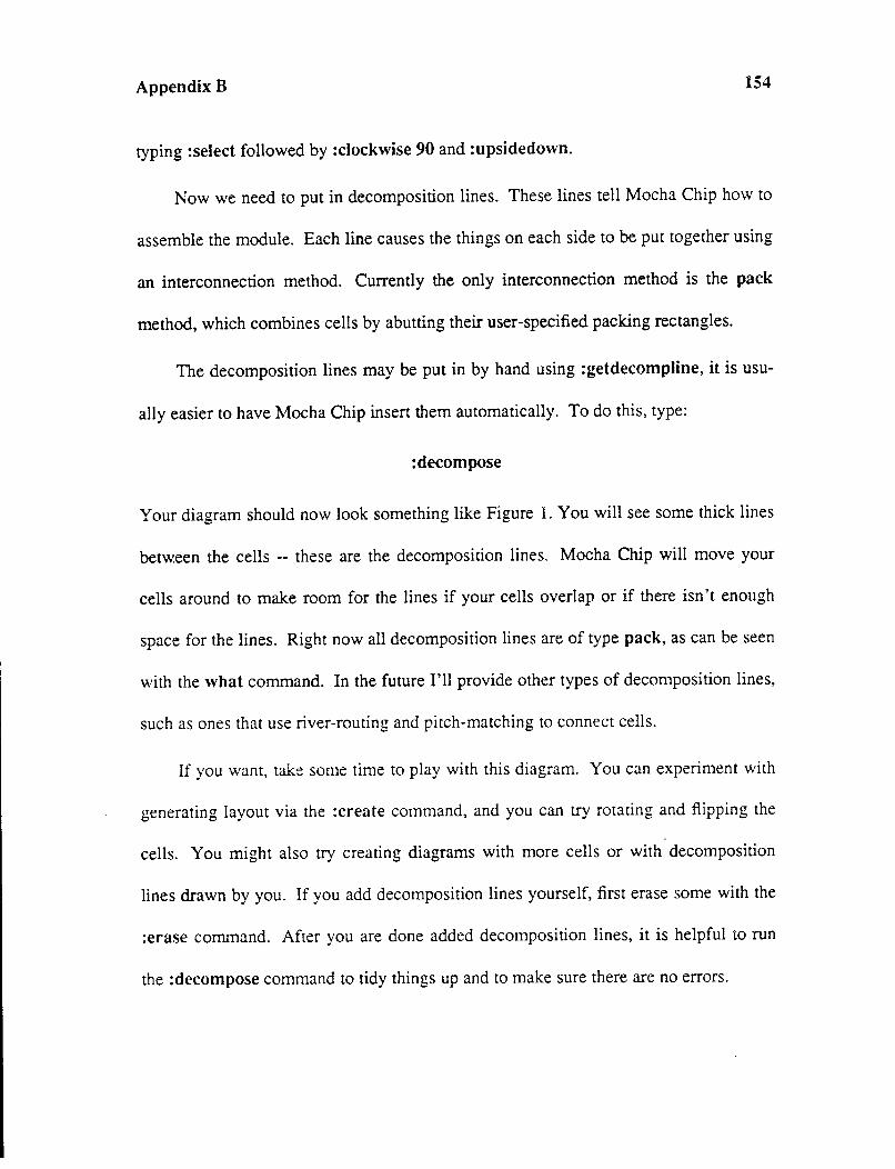
Appendix B 154
typing :select followed by :clockwise 90 and :upsidedown.
Now we need to put in decomposition lines. These lines tell Mocha Chip how to
assemble the module. Each line causes the things on each side to be put together using
an interconnection method. Currently the only interconnection method is the pack
method, which combines cells by abutting their user-specified packing rectangles.
The decomposition lines may be put in by hand using :getdecompline, it is usu
ally easier to have Mocha Chip insert them automatically. To do this, type:
:decompose
Your diagram should now look something like Figure 1. You will see some thick lines
betw.een the cells -- these are the decomposition lines. Mocha Chip will move your
cells around to make room for the lines if your cells overlap or if there isn't enough
space for the lines. Right now all decomposition lines are of type pack, as can be seen
with the what command. In the future I'll provide other types of decomposition lines,
such as ones that use river-routing and pitch-matching to connect cells.
If you want, take some time to play with this diagram. You can experiment with
generating layout via the :create command, and you can try rotating and flipping the
cells. You might also try creating diagrams with more cells or with decomposition
lines drawn by you. If you add decomposition lines yourself, first erase some with the
:erase command. After you are done added decomposition lines, it is helpful to run
the :decompose command to tidy things up and to make sure there are no errors.
Appendix B 155
B.2.4. THE ARRAY AND CASE CELLS
The diagram that we have constructed can only do one thing: put down four cells
of the specified type in the specified orientation. We'd like diagrams to be more flexi
ble, and that is what the Array and Case cells are for.
I'll introduce the cells by way of an example. Load in the new cell play2. Now
put down an instance of the cell Array via the :getcell Array command. The Array
cell is a predefined cell located in the Mocha Chip library area Ccad!lib/mochachip).
It takes parameters, just like the PLA generator that you saw in tutorial #1.
Two of the parameters set the dimensions of the array. Pop up an editor window,
using :select, :expand, and :textedit on the Array cell. We'll create a 2 X 2 array, so
enter the following parameter lines:
(x-dimension 2)
(y-dimension 2)
The first line says that the columns will be numbered from 1 to 2, and the second line
does a similar thing for the rows. We'll need to tell Array what subcell to use at each
position. Add the following line to the parameters:
(subcell 'play_sub)
That's all the parameters, so write them out and leave the editor (using :wq for vi).
Now we need to design the subcell play _sub. Create a Magic cell called
play _sub and put down some material, such as metal and poly. Go back to the Mocha
Chip window containing play2, and type :create. This will produce a layout
Appendix B 156
containing 4 cells, which may be viewed by loading play2 into a layout window.
What if we don't want to put the same cell at each position in the array? We can
create a diagram that uses the Case cell. Mocha Chip cells can look at variables and
parameters of all their parents in the hierarchy, and the Array cell defines two useful
ones: x-pos and y-pos.
Create a new Mocha Chip cell called play _sub. Mocha Chip cells are always
used in preference to Magic cells, so this new one will override the Magic cell
designed earlier. Put down a Case cell, and pop up an editor on it's parameters. As an
example, let's use the contact cell along the diagonal of the array, and the cross cell
elsewhere. We can do this with the following parameters to Case:
(easel '((equal x-pos y-pos) contact nil nil))
(case2 '(t cross nil nil))
Case takes parameters of the form caseXX where XX is a positive integer. In this case
(no pun intended), we supply two options. Case looks at each option in order, until it
finds one whose first expression evaluates to true. Then it uses the second pan as the
name of the cell to use. The third part is a list of parameters to the cell. This is usually
unused, because cells can inherit parameters from the parents. To do this, just define
additional parameters in the case cell, or any other cell above it in the hierarchy. Cells
will ignore parameters that they don't know about, and cells deeper in the hierarchy
that do recognize the parameters will use them.
Appendix B 157
easel looks at the inherited variables x-pos and y-pos to see if they are equal.
These two variables are defined by the Array cell. If the two are equal, then the con
tact cell is used. case2 has t as its expression, which Lisp always evaluates to true.
This means that the second case will catch anything that passed by the first case. If
Mocha Chip can't find any case that is true, it will give you an error message.
Now we need to create the cells contact and cross. They could be Mocha Chip
diagrams, but we '11 make it simple by making them Magic cells: Go over to a layout
window and create the two cells. I'd suggest putting down a vertical metall wire and a
horizontal poly wire in each cell. In the contact cell, connect the two wires with a
polycontact, and leave them unconnected in the cross cell. You'll probably want to
make the cells the same size so that they pack together nicely.
We are ready to generate layout. Load the top cell (play2) into the Mocha Chip
window and type :create. The Magic cell play2 will now contain four cells, with the
contact cell along the diagonal.
B.2.5. ADDING PARAMETERIZATION
The diagram that we produced still doesn't act like a module· generator-- it only
produces one thing. We'd like to have it be able to produce a whole bunch of modules,
each different according to some parameter. For this example, we '11 make the size of
the array a parameter. Load the play2 cell into Mocha Chip and select the parameter's
block. Type :textedit, and add the following line:

Appendix B 158
(size 3)
This specifies that play2 takes one parameter, size, and it has a default value of 3. The
default value may be omitted, if desired. Save the file, and pop up a text editor on the
Array cell. Change the following lines:
so that they read like:
(x-dimension 2)
(y-dimension 2)
(x-dimension size)
(y-dimension size)
list is Lisp's way of creating a list from separate values. In the previous example we
could just use the constant list '(1 2), but in the current example the list changes
depending upon the parameters, so we have to compute the list each time. As you
might have guessed, an arbitrary Lisp expression can be used for this value -- or for
any other Mocha Chip parameter or variable expression.
play2 is now a module generator. We can use it in the same way that we used
mcpla in Mocha Chip tutorial #1. Let's create a new Mocha Cbip cell called
use _play2 via :load use _play2. Put down a subcell called play2, and used :textedit
to define the parameter size as shown here:
(size 3)
Now we can use :create to create a Magic cell with a 3 x 3 matrix of subcells, with
contacts along the diagonal. We can change the size parameter to something else, say
Appendix B 159
8, to produce a new module. We have produced a very simple generator. More com
plicated generators may have more parameters, and may do more complex computa
tions.
The "Local Variables" section is useful for doing computations. A line such as:
(foobar (big-function paramx))
invokes the Lisp function big-function on the parameter or variable paramx. big
function could be a large Lisp function that you write to produce a new Lisp data
structure, which gets stored in foobar. It can be stored in a separate file, and loaded
into Lisp as needed. See the mochachip(l) manual page for details. The lines in the
"Local Variables" section are evaluated sequentially, so an expression may use vari
ables computed in earlier lines.
B.2.6. SUMMARY
As we have seen, Mocha Chip allows you to design module generators by draw
ing diagrams. The subcells in these diagrams may be parameterized, and may invoke
either Magic cells or other Mocha Chip diagrams. The parameterization may contain
arbitrary Lisp parameterization. Special fom1s of iteration and conditional selection
are represented graphically via the Array and Case cells.
I hope that the simple examples in this tutorial give you a feel for the system.
More complicated collections of diagrams may be created, and more complicated Lisp
functions may be written. You are welcome to look that the mcpla Mocha Chip gen
erator as an example -- it is in the directory -cad/lib/mcpla. The Mocha Chip manual
Appendix B 160
page also describes some useful functions and variables that were not covered in the
tutorial.


