Embed Size (px)
Citation preview

This material is posted here with permission of the IEEE. Such permission of the IEEE does not in any way imply IEEE endorsement of any of Helsinki University of Technology's products or services. Internal or personal use of this material is permitted. However, permission to reprint/republish this material for advertising or promotional purposes or for creating new collective works for resale or redistribution must be obtained from the IEEE by writing to [email protected]. By choosing to view this document, you agree to all provisions of the copyright laws protecting it.
IEEE TRANSACTIONS ON MICROWAVE THEORY AND TECHNIQUES, VOL. 52, NO. 1, JANUARY 2004 29
Microreplicated RF Toroidal InductorVladimir Ermolov, Tomas Lindström, Heikki Nieminen, Mikael Olsson, Michael Read, Tapani Ryhänen,
Samuli Silanto, and Simon Uhrberg
Abstract—This paper reports on the modeling and fabricationof a truly three-dimensional high-quality-factor toroidal inductorusing polymer replication processes. The critical dimensions arein the micrometer range, and the applied manufacturing methodis based on polymer replication. Electrical measurements showthat the inductor with an inductance of 6.0 nH exhibits a peakquality factor of 50 at a frequency of 3 GHz. Model verified bythe measurement results shows that further improvement is stillpossible. Furthermore, the applied manufacturing technique canbe extended to become a flexible packaging platform.
Index Terms—Inductors, micromachining, plastics, RFmicroelectromechanical system (MEMS), transformer.
I. INTRODUCTION
THERE IS AN increasing need for high-performancelow-cost inductors in the telecommunication industry.
High-performance RF inductors are key components forimplementing low-noise RF voltage-controlled oscillators,low-loss impedance matching circuits, low-loss passive filters,and inductive loads. Critical parameters of an inductor includeinductance value, quality ( ) factor, and self-resonance fre-quency.
For inductors, the fabrication method is normally eitherthin-film processing or wire winding [1]–[3]. Thin-film spiralinductors use integrated-circuit (IC) technology and are moreeasily miniaturized and integrated than wire wound inductors.However, spiral inductors implemented by silicon micro-machining processes suffer from several power-dissipationmechanisms, leading to a poor inductor . The mechanismsthat reduce the include losses from coil resistance, lossesfrom eddy currents circulating below the spiral in the siliconsubstrate, and self-resonance of the coil. In order to increase the
of the spiral inductor, several approaches have been reported,e.g., having a thick metallization or multilayer metallization[4], [5], a patterned ground shield below the inductor [6], athick dielectric layer to separate the spiral from the substrate[7], using high-resistivity 4 k silicon [4], or fabricating asuspended inductor by etching the substrate underneath [8], [9].
Recently, three-dimensional (3-D) on-chip inductors havebeen proposed as an alternative solution for high-performanceinductors. These inductors have been made using 3-D laserlithography [10], by deformation of a sacrificial polymer underthe coil [11], by the technique of self-assembled inductors
Manuscript received January 21, 2003; revised May 28, 2003. This work wassupported by the Finnish National Technology Agency.
V. Ermolov, H. Nieminen, T. Ryhänen, and S. Silanto are withthe Nokia Research Center, Helsinki FIN-00045, Finland (e-mail:[email protected]).
T. Lindström, M. Olsson, M. Read, and S. Uhrberg are with Åmic AB,SE-75183 Uppsala, Sweden (e-mail: [email protected]).
Digital Object Identifier 10.1109/TMTT.2003.821236
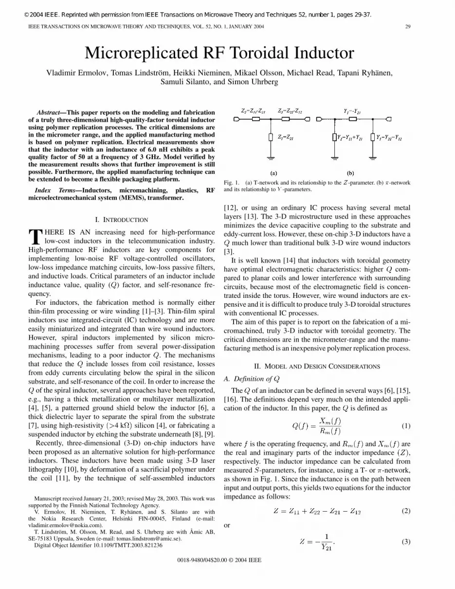
Fig. 1. (a) T-network and its relationship to the Z-parameter. (b) �-networkand its relationship to Y -parameters.
[12], or using an ordinary IC process having several metallayers [13]. The 3-D microstructure used in these approachesminimizes the device capacitive coupling to the substrate andeddy-current loss. However, these on-chip 3-D inductors have a
much lower than traditional bulk 3-D wire wound inductors[3].
It is well known [14] that inductors with toroidal geometryhave optimal electromagnetic characteristics: higher com-pared to planar coils and lower interference with surroundingcircuits, because most of the electromagnetic field is concen-trated inside the torus. However, wire wound inductors are ex-pensive and it is difficult to produce truly 3-D toroidal structureswith conventional IC processes.
The aim of this paper is to report on the fabrication of a mi-cromachined, truly 3-D inductor with toroidal geometry. Thecritical dimensions are in the micrometer-range and the manu-facturing method is an inexpensive polymer replication process.
II. MODEL AND DESIGN CONSIDERATIONS
A. Definition of
The of an inductor can be defined in several ways [6], [15],[16]. The definitions depend very much on the intended appli-cation of the inductor. In this paper, the is defined as
(1)
where is the operating frequency, and and arethe real and imaginary parts of the inductor impedance ,respectively. The inductor impedance can be calculated frommeasured -parameters, for instance, using a T- or -network,as shown in Fig. 1. Since the inductance is on the path betweeninput and output ports, this yields two equations for the inductorimpedance as follows:
(2)
or
(3)
0018-9480/04$20.00 © 2004 IEEE

30 IEEE TRANSACTIONS ON MICROWAVE THEORY AND TECHNIQUES, VOL. 52, NO. 1, JANUARY 2004
It should be noted that both of these two ways neglect the effectof some parasitic losses on the inductor impedance.
B. Dependency of on Device Parameters
The behavior of an inductor at frequencies below the self-resonance can be thought to be composed of three factors
substrate loss factor self-resonance factor
(4)
The first factor is the geometrical quality factor of the coil,where depends on the frequency is the induc-tance, and is the series resistance. The substrate loss andself-resonance factor of the coil depend on the resistivity of thesubstrate and the parasitic capacitance of the coil, respectively.Optimization of the first term of (4) for a planar inductor on alow-loss substrate leads to linear dependence between the coilarea and [17] as follows:
- (5)
where is the outer diameter of the coil, and is the skindepth. For example, a planar coil with a 1-mm area optimallyhas a of approximately 50 at 1 GHz [12]. Similar dependencyof the on the device geometry can also be derived for thetoroidal coil. The inductance of the toroidal coil is
(6)
and
(7)
where is the number of turns, is the radius of the toruscross section, is the radius of the coil, is the vacuumpermeability, and is the relative magnetic permeability. Theseries resistance, when the thickness of the wire is much lessthan the width of the wire, is
(8)
where is a coefficient taking into account current crowdingeffects, is the resistivity, and is the separation betweenthe turns of the coil. The current crowding effect is the tendencyof the current in neighboring conductors to change the currentdistribution inside the conductor. This increases the series resis-tance. In addition, the skin effect has a well-known frequencydependency
(9)
By combining (5)–(9), the maximum estimate for a toroidal coilat low frequencies can be derived as follows:
(10)
As a result, the of the toroidal inductor is found to depend on. Fig. 2 shows the at 0.9 GHz as a function of the radius
Fig. 2. Q at 0.9 GHz as a function of the radius of the torus cross section. Thedashed line is the Q of an inductor made of gold and the solid line is the Q ofan inductor made of copper. The dimensions of the coils are D = 1 mm,s = 15 �m, and the metal thickness is 8 �m. The number of turns wasvaried to keep the inductance at 5 nH.
Fig. 3. Q versus the outer diameter of an optimized planar (dashed line) andtoroidal (solid line) inductor at a frequency of 1 GHz. The inductance is 5 nHfor both devices and the gold thickness is 8 �m. There is ratio of 0.2 between2r and D .
of the torus cross section. The dashed line depicts a coil made ofgold -m and the continuous line depictsa coil made of copper m . Both havedimensions mm and m, and the metalthickness is 8 m. The number of turns was varied to keep theinductance at 5 nH.
Fig. 3 shows the of a toroidal and a planar coil as a functionof the outer diameter. The of the planar coil was plotted using(5). In the case of a toroidal coil, we attempted to design a 5-nHcoil with a ratio of 0.2 between and . Both coilsare made of gold. The height of the conductor is 8 m and thefrequency is 1 GHz.
It can be seen that the of the toroidal inductor exceeds theof the optimized planar coil with a similar outer diameter
by approximately a factor two. For example, of 180 can bereached for an ideal toroidal inductor with mm and
m.
C. Equivalent-Circuit Model of Toroidal Coil
The calculated using (10) does not, however, take intoaccount parasitic losses. An equivalent-circuit model of thetoroidal inductor that includes the effects of the parasitics is

ERMOLOV et al.: MICROREPLICATED RF TOROIDAL INDUCTOR 31
Fig. 4. Equivalent circuit of a toroidal inductor. The circuit representing oneturn of the coil is inside the dashed line. The parameters are defined in the abovetext.
shown in Fig. 4. The model describes each turn of the coil withinductance , series resistance , capacitancebetween the adjacent turns, capacitance of the singlecoil turn to ground, substrate losses , and capacitiveground path losses . In addition, there is inductance
from the leads and capacitance as coupling betweenthe first and last turns of the coil. Consequently, has thesame value as .
At high frequencies, the series resistance of the coil dependsprimarily on the skin depth, which limits the penetration of thefield into the conductor and, secondly, on the current crowdingin the coil turns. It is known that, in the case of a toroidal in-ductor, the current is concentrated mainly on the internal sur-face and at the edges of the coil turns. The series resistance ofthe coil at frequencies from dc to 10 GHz can be estimated by
(11)
and
(12)
where is the total series resistance of the coil at dc, isthe critical frequency, and and are the coefficients relatedto skin depth and current crowding, respectively. The values of
and can be estimated using very simple approxima-tions
(13)
and
(14)
Capacitance is calculated from [18]
(15)
where is the permittivity of the substrate material, is thethickness of the substrate material, is velocity of light, and
is the diameter of the torus cross section. A numericalsimulation program, i.e., QvalueC, modified for a solenoidcoil, was used to calculate of the inductor [17]. The in-
Fig. 5. Visualization of the proposed method of fabrication. (a) Horizontalsplit of the toroidal inductor. (b) Joining of two halves to achieve the finalgeometry.
ductor model was implemented in an APLAC circuit simulator(APLAC Solutions Corporation, Espoo, Finland).
III. DETAILS OF FABRICATION
A. Design of Toroidal Inductor
The chosen design of the inductor was a compromisebetween minimizing electrical losses due to ohmic losses,dielectric losses, and parasitic coupling, as well as obeying therestraints and limitations that are determined by the manufac-turing process. In short, it was decided to fabricate a 15-turntoroidal inductor with a 20- m electrode separation, an innerdiameter of 520 m, an outer diameter of 1000 m, and a torusdiameter of 240 m. The electrode material can be chosen fromseveral conductors; in this study, gold was used. The metalthickness should be thick enough to match the skin effect in theproposed frequency region, which was 8 GHz.
In order to achieve full 3-D geometry, the design was sepa-rated into two halves, as shown in Fig. 5. The idea was to fab-ricate each half separately and then join the two to make thefinal component. For this procedure to work, overlapping con-tact zones had to be introduced to increase the contact area be-tween the two halves; the width of these contact zones was ap-proximately 20 m.

32 IEEE TRANSACTIONS ON MICROWAVE THEORY AND TECHNIQUES, VOL. 52, NO. 1, JANUARY 2004
Fig. 6. Manufacturing process steps for the toroidal inductor.
B. Substrate Manufacturing
The idea with polymer replication is to use the accuracyand small features available, for example, in silicon micro-machining processes, in combination with the productioneconomy from the optical data storage industry (cf. CD/DVDfabrication technology) [19], [20]. The manufacturing processsteps for the toroidal inductor are illustrated in Fig. 6. Typically,a master structure is produced in silicon or glass with thedesired geometry. Electroforming a negative copy of the masterthen creates a mould insert. Finally, polymer replicas can beproduced in large quantities by using these inserts in differentreplication methods such as injection moulding, casting, or hotembossing [21].
Depending on the physical and chemical requirements of thefinal product, there is a wide range of thermoplastic and ther-mosetting polymer materials to choose from. In this study, wehave chosen to work with injection moulded thermoplastics.The reason for this is twofold. Firstly, the dielectric propertiesfor some of the thermoplastic polymers is superior to thermoset-ting materials. This is specifically the case for the cyclo-olefinpolymer (COP) used in this investigation. Secondly, it is easierto obtain flat and stress-free wafers by injection moulding com-pared to casting with thermosetting polymers. Also, if one addsthe aspect of production economy, injection moulding is to befavored.
Fig. 7. (a) Example of an isotropically etched profile in silicon. This structurewas later transferred into a metallic negative by electroforming. (b) Example ofa polymer substrate with gold electrodes metallized over 90 corners.
C. Master Fabrication
The masters were produced by isotropic silicon etching[22]. In order to achieve high isotropy, it is necessary to etchwithout stirring and with the wafer lying horizontally and theetch features upwards. We choose to work with a 96 : 4 or 91 : 9HNO (69%) : HF (50%) solution. Thus, no acetic acid wasused. This gives a polishing etch with smooth surfaces. In ourcase, we achieved an etch rate of approximately 1 m/minat room temperature. The final etch depth was 120 m. Theisotropy attained, or width : depth ratio was approximately1 : 0.96. Fig. 7(a) depicts one of the silicon masters used in thisinvestigation.
D. Replication Step
The silicon master structure was transferred into a300- m-thick metallic counterpart by electroforming. Thiswas achieved by plating nickel from a sulfamate electrolyte.Obviously, the obtained mould insert has the negative structureof the original. The substrates were then injection moulded intwo different polymers, i.e., polycarbonate (PC) (Makrolon DP

ERMOLOV et al.: MICROREPLICATED RF TOROIDAL INDUCTOR 33
1–1265 from Bayer Polymers, Leverkusen, Germany) and COP(Zeonex 480R from ZEON Corporation, Tokyo, Japan).
These materials exhibit different electrical properties: the di-electric constant of PC is approximately 3.5 at 1 MHz, and theloss tangent is approximately 0.01. In comparison, the COP ma-terial has a dielectric constant of 2.3 for COP and a loss tangentof 0.0002. The moulder used was a modified injection-mouldingmachine from the CD/DVD industry (Alpha Swden, Sundby-berg, Sweden).
E. Electrode Metallization
Electrode patterning can be done by various methodsdepending on the required accuracy. In this study, the elec-trodes were defined lithographically by applying a conformalphoto resist layer (PEPR 2400 from the Shipley Company,Marlborough, MA) onto the polymer substrates. After resistdevelopment, electronic-quality pure gold was deposited byelectroplating (potassium gold cyanide-system, Aurall 292,Shipley Company) into the sidewall resist structures. Thegold thickness was approximately 4–6 m. Fig. 7(b) depictsexample of metallized electrodes over a 90 corner. Prior topatterning, the substrates were sputtered with a 50-nm-thickgold seed layer. After the electroplating, this seed layer wasetched in cold 4 : 4 : 9 HCI : HNO : H 0 in order to isolate thestructures.
Four-point probe measurements were conducted on elec-troplated gold samples to measure the electrical resistivity.A constant current was applied and the voltage was recordedwith a cryostat system (Maglab 2000, Oxford Instruments,Eynsham, U.K.). Thickness measurements were performedusing a mechanical stylus profilometer (Alpha-Step 200, KLATencor, San Jose, CA). The electrical resistivity was found tobe 2.60 10 m, which is close to the tabulated value forbulk gold [23], 2.20 10 m.
F. Assembly of Inductor
In order to obtain a complete functional inductor, two metal-lized substrates have to be bonded. This was achieved by thermocompression (at 75-bar pressure) with a heat-curing adhesive(EpoTek OG198-50, Epoxy Technology, Billerica, MA, curedat 120 C for 15 min). The aim is to achieve a low contact resis-tance by ensuring a proper metal–metal contact at the gold in-terfaces. The inductor will exhibit a serial resistance containingcontributions from both contact points, as well as intrinsic ma-terial properties of the electroplated gold. The contact resistanceis also affected by alignment errors. Fig. 8 shows an example ofan assembled inductor and an 8 : 8 coreless transformer.
IV. RESULTS
The components were measured using a Rohde & SchwarzZVC network analyzer and a Karl Süss PA200 probe station.The two-port -parameters were measured on-chip with the RFprobes over a frequency range from 10 MHz to 8 GHz. Duringthe measurements, the polymer chip containing the coil wasresting on the metallic measurement chuck. A set of uncon-nected pads was measured to determine the parasitics. The par-asitics from the unconnected pads were deembedded from the
(a)
(b)
Fig. 8. Light optical microscope photograph of: (a) an assembled inductor and(b) an 8 : 8 coreless transformer.
measurement data by subtracting the -parameters of the un-connected pads from the -parameters of the inductor and con-verting the results back to -parameters. In addition, the leadsjoining the pads to the component were measured. The induc-tance from the leads was 0.56 nH.
The dimensions of the measured components werem, mm, m, metal thickness 4 m,
and the number of turns 15. Fig. 9 shows the results, when theequivalent circuit presented in Fig. 4 is fitted to the measured
-parameters. The series resistance in the fitted equivalent cir-cuit behaves according to (11). The coefficient used in(11) is 0.8. The coefficient value is in good agreement with pre-vious results [24], [25]. The fitted equivalent-circuit parametersare shown in Table I. For comparison, Table I also shows ana-

34 IEEE TRANSACTIONS ON MICROWAVE THEORY AND TECHNIQUES, VOL. 52, NO. 1, JANUARY 2004
Fig. 9. Diagrams show measured (points) and simulated (solid lines) magnitude and phase versus frequency for: (a) S -parameters, (b) S -parameters,(c) S -parameters, and (d) S -parameters.
TABLE IEQUIVALENT-CIRCUIT MODEL PARAMETERS
lytical values for the equivalent circuit that are calculated from(11)–(15).
To calculate and , the inductor impedance must be cal-culated from the measured -parameters. Fig. 10 shows mea-sured and simulated real and imaginary parts of the inductorimpedance as a function of frequency. These are calculated ac-cording to (2) and (3) for T- and -networks, respectively. Fromthe imaginary part of the impedance, the inductance of the coilis calculated to be 6.61 nH at 1 GHz, including the leads.
It was stated in Section II that the calculation of the inductorimpedance using T- and -networks neglects some parasitic
Fig. 10. Measured (points) and simulated (solid lines) imaginary and real partsof the impedance (Z) of the toroidal inductor as a function of frequency. TheZ is calculated from measured and simulated S-parameters using both T- and�-network configurations.
losses. In addition, if the equivalent circuit needed for the in-ductor modeling is more complicated than the T-or -network,the behavior of the impedance can be unpredictable. For in-stance, Fig. 10 shows that the parasitic capacitance to ground
and substrate losses are important. Theof the -network does not include this kind of behavior. Thismakes the real part of the impedance calculated using the -net-work negative. Therefore, the T-network model is selected to

ERMOLOV et al.: MICROREPLICATED RF TOROIDAL INDUCTOR 35
Fig. 11. Measured (points) and simulated (solid line) Q of the toroidalinductor as a function of frequency.
Fig. 12. Measured temperature dependency of the Q as a function offrequency. The solid line is measured Q at 110 C and the points are measuredQ at �25 C.
represent the inductor and (2) is used to calculate the impedanceof the inductor. Fig. 11 shows measured results and simulated
of the inductor.The effect of temperature on the inductor performance
was studied. The inductor -parameters were measured overthe temperature range 25 C to 110 C. Results show thatthe inductance value has a small temperature dependency of30 ppm/K. Temperature dependence is due to geometricalchanges that are caused by the thermal expansion and contrac-tion of the polymer substrate and the metal electrodes. Fig. 12shows the temperature dependence of the inductor . Analysisof the measurement results showed that the changes are mainlydue to the real part of the impedance. This means that thechange of the is caused by the temperature dependence ofmetal conductivity.
One of the advantages of the toroidal coil is that the elec-tromagnetic field is mostly contained inside the coil. However,some of the field still leaks outside the toroid and, thus, the sub-strate has an effect on the behavior. Fig. 13 compares thebehavior between PC and COP substrates. The lower after4 GHz in the PC substrate is due to the higher substrate losses.
Measurements show that the dc current handling capacity ofthe coil is 0.3 A. The current handling capacity of the toroidalinductor is limited at the moment by the polymer substrate. Thepolymer substrate cannot stand temperatures over 150 C. Whencurrent flows in the coil, the resistive loss heats the substrate.
Fig. 13. Effect of the substrate on the Q of the inductor as a function offrequency. The solid line is the measured Q of an inductor (L = 5:63 nH)on the COP substrate (loss tangent = 0:0002 and " = 2:3 at 1 MHz). Thepoints are the measured Q of an inductor (L = 6:61 nH) on the PC substrate(loss tangent = 0:01 and " = 3:5 at 1 MHz).
The thermal conductance of the polymer defines how well thisheat is dissipated.
It should be pointed out that the manufacturing technologypresented here is not limited to RF inductors. It can be adapted,for example, for fabrication of RF transformers. A fabricatedtest structure to evaluate a 3-D coreless transformer with turnratio 8 : 8 is shown in Fig. 8(b).
The comparison of the measured and simulated for acoreless transformer with an 8 : 8 turn ratio is depicted in Fig. 14.The dimensions of the transformer under the test are: 1) outerdiameter of the coil, 1 mm; 2) radius of the cross section of acoil turn, 120 m; 3) thickness of the gold, 5 m; 4) separa-tion between the turns, 20 m; and 5) thickness of the polymersubstrate, 1.2 mm. Agilent HFSS was used as a simulation tool.Measured and simulated insertion losses are 12.1 and 6.5 dBat 1 GHz, respectively. The large discrepancy between simulatedand measured results is due to the model limitations. Since theratio between the size of the coil and thickness of the metal islarge, the model cannot take into account the thickness of themetal. As a result, current crowding effects are not included inthe model. The observed high insertion loss is due to large elec-tromagnetic field leakage. This leads to weak coupling betweenthe transformer primary and secondary windings.
The use of a ferrite core is a traditional way to improve cou-pling between primary and secondary windings of transformers.Fig. 14 shows simulated behavior for an 8 : 8 transformercontaining a ferrite core with a magnetic permeability of 15. Itcan be seen from this simulation that the insertion loss of thetransformer could be reduced considerably.
V. SUMMARY AND DISCUSSION
The possibility to manufacture truly 3-D toroidal structuresin metal has been shown. There are several advantages of usingmicroreplication technology, which are: 1) truly 3-D structurescan be integrated in a chip scale package of an RF IC; 2) it is pos-sible to integrate arrays of components at the wafer level, whilepackaging of the MEMS component takes place at wafer level;3) clearly higher quality factors compared to planar coils arepossible; 4) there is low interference with the surrounding cir-cuits because most of the electromagnetic field is concentrated

36 IEEE TRANSACTIONS ON MICROWAVE THEORY AND TECHNIQUES, VOL. 52, NO. 1, JANUARY 2004
Fig. 14. Measured (points) and simulated (solid lines) S -parametersas function of frequency for 8 : 8 coreless transformer (� = 1) and fortransformer with ferrite core (� = 15).
inside the torus; and 5) the fabrication technique is well suitedfor high-volume manufacturing.
The reported manufacturing technique can also be extendedto become a flexible packaging platform. By embedding dif-ferent components (not only inductors) in the polymer substrateand surface-mounted discrete circuits or ICs, a flexible andmultifunctional packaging platform is created, i.e., it enables alow-cost system-in-a-package approach.
The main drawback with the current solution is that the poly-mers used are not compatible with the temperature cycle in sol-dering reflow processes. There are, however, polymers availablethat exhibit both low dielectric constant and high heat resistance.Future research will address these kinds of materials.
There is also the issue of environmental testing. Initial tests inhumidity chambers and with thermal cycling looks promising.However, more work needs to be done in this area. Specifically,properties like thermal conductivity and expansion have to becarefully analyzed.
ACKNOWLEDGMENT
The authors acknowledge the participation of H.-O. Scheck,Nokia, Helsinki, Finland, O. Öhman, Åmic AB, Uppsala,Sweden, P. Siukonen, Nokia, and M. Andersson, Nokia. Theauthors further acknowledge V. Hurskainen, Nokia, for makingthe HFSS simulation.
REFERENCES
[1] N. M. Nguyen and R. G. Meyer, “Si IC-compatible inductors andLC-passive filters,” IEEE J. Solid-State Circuits, vol. 25, pp. 1028–1031,Aug. 1990.
[2] J. N. Burghartz, D. C. Edelstein, M. Soyuer, H. A. Ainspan, and K. A.Jenkins, “RF circuit design aspects of spiral inductors on silicon,” IEEEJ. Solid-State Circuits, vol. 33, pp. 2028–2034, Dec. 1998.
[3] Product Catalog for RF Inductors, Coilcraft Inc., Cary, IL. [Online].Available: http://www.coilcraft.com/prod_rf.cfm.
[4] K. B. Ashby, I. A. Koullians, W. C. Finley, J. J. Bastek, and S. Moinian,“High Q inductors for wireless applications in a complementary sil-icon bipolar process,” IEEE J. Solid-State Circuits, vol. 31, pp. 4–9, Jan.1996.
[5] J. N. Burghartz, D. C. Edelstein, K. A. Jenkins, and M. D. Hulvey,“High-Q inductors in standard silicon interconnect technology and itsapplication to an integrated RF power amplifier,” in Int. Electron De-vices Meeting Tech. Dig., Dec. 1995, pp. 1015–1017.
[6] C. P. Yue and S. S. Wong, “On-chip spiral inductors with patternedground shields for Si-based RF ICs,” IEEE J. Solid-State Circuits, vol.33, pp. 743–752, May 1998.
[7] J. N. Burghartz, D. C. Edelstein, K. A. Jenkins, and M. D. Hulvey, “Mi-crowave inductors and capacitors in standard multilevel interconnect sil-icon technology,” IEEE Trans. Microwave Theory Tech., vol. 44, pp.100–104, Jan. 1996.
[8] J. Y.-C. Chang, A. A. Abidi, and M. Gaitan, “Large suspended inductorson silicon and their use in a 2 �m CMOS RF amplifier,” IEEE ElectronDevice Lett., vol. 14, pp. 246–248, May 1993.
[9] J. Y. Park and M. G. Allen, “Packaging-compatible high Q microin-ductors and microfilters for wireless applications,” IEEE Trans. Adv.Packag., vol. 22, pp. 207–213, May 1999.
[10] D. J. Young, V. Malba, J.-J. Ou, A. F. Bernhards, and B. E. Boser,“Monolithic high-performance three-dimensional coil inductors forwireless communication applications,” in Int. Electron Devices MeetingTech. Dig., Dec. 1997, pp. 67–70.
[11] N. Chomnawang and J.-B. Lee, “On-chip 3D air core micro-inductor forhigh-frequency applications using deformation of sacrificial polymer,”Proc. SPIE, vol. 4334, pp. 54–62, 2001.
[12] G. W. Dahlmann and E. M. Yeatman, “Microwave characteristics of me-ander inductors fabricated by 3D self-assembly,” in IEEE Electron De-vices Meeting Conf., Nov. 13–14, 2000, pp. 128–133.
[13] J. B. Yoon, B. K. Kim, C. H. Han, E. Yoon, and C. K. Kim, “Surfacemicromachined solenoid on-Si and on-glass inductors for RF applica-tions,” IEEE Electron Device Lett., vol. 20, pp. 487–489, Sept. 1999.
[14] F. W. Grover, Inductance Calculations. New York: Dover, 1973.[15] A. M. Niknejad and R. G. Meyer, “Analysis, design and optimization
of spiral inductors and transformers for Si RF ICs,” IEEE J. Solid-StateCircuits, vol. 33, pp. 1470–1481, Oct. 1998.
[16] H. Lakdawala, X. Zhu, H. Luo, S. Santhanam, L. R. Carley, and G. K.Fedder, “Micromachined high Q inductors in a 0.18-�m copper inter-connect low-K dielectric CMOS process,” IEEE J. Solid-State Circuits,vol. 37, pp. 394–403, Mar. 2002.
[17] “Optimising planar inductors,” VTT Automation, Helsinki, Finland,Res. Notes 2017, 2000.
[18] R. Rhea, “Filters and oscillator using a new solenoid model,” in Appl.Microwave Wireless, 2000, pp. 30–42.
[19] O. Öhman, H. Sjödin, B. Ekström, and G. Jacobsson, “Microfluidicstructure and process for its manufacture,” Pharmacia Biosensor, Up-psala, Sweden, Int. Publication WO 91/16 966, Dec. 27, 1994.
[20] , “Microfluidic structure and process for its manufacture,” U.S.Patent 5 376 252, Dec. 27, 1994.
[21] O. Rötting, W. Röpke, H. Becker, and C. Gärtner, “Polymer microfabri-cation technologies,” Microsyst. Technol., vol. 8, pp. 32–36, 2002.
[22] C.-H. Han and E.-S. Kim, “Study of self-limiting etching behavior in wetisotropic etching of silicon,” Jpn. J. Appl. Phys., vol. 37, pp. 6939–6941,1998.
[23] G. T. Meaden, Electrical Resistance of Metals. New York: Plenum,1965, p. 1.
[24] B. L. Ooin, D.-X. Xu, P.-S. Kooi, and F.-J. Lin, “An improved predictionof series resistance in spiral inductor modeling with eddy-current effect,”IEEE Trans. Microwave Theory Tech., vol. 50, pp. 2202–2206, Sept.2002.
[25] V. Ermolov, H. Nieminen, K. Nybergh, T. Ryhänen, and S. Silanto, “Mi-crosystem technologies for mobile communication products,” SurfaceMount Technol. Int. 2001, pp. 710–717, 2001.
Vladimir Ermolov received the M.Sc. and Ph.D. de-grees from the Moscow Engineering Physics Univer-sity (MEPhI), Moscow, Russia, in 1981 and 1986, re-spectively, both in engineering physics.
From 1981 to 1998, he was a Senior ResearchAssociate with the Laboratory of Dielectric Devices,MEPhI, during which time he was a VisitingResearcher numerous times with the Department ofPhysics, Helsinki University, Helsinki, Finland, andthe Fraunhofer Institute of Nondestructive Testing,Saarbrücken, Germany. In 1998, he joined the Nokia
Research Center, Helsinki, Finland, as a Senior Research Engineer, where hehas been a Project Manager for several MEMS projects. During his professionalcareer, he has been involved in the areas of sensors for measurements ofocean parameters, acoustic devices for signal processing, surface acousticwave (SAW) devices, variable acoustic devices, acoustic effects in magneticmaterials and their technical applications, nonlinear effects in solid-stateacoustical and nondestructive evaluation, and MEMS. He has authored andcoauthored 47 scientific publications. He holds and co-holds 22 patents.

ERMOLOV et al.: MICROREPLICATED RF TOROIDAL INDUCTOR 37
Tomas Lindström received the M.Sc. degree in engineering physics and Ph.D.degree in solid-state physics from Uppsala University, Uppsala, Sweden, in1992 and 2000, respectively. His thesis concerned spectroscopic light scatteringmeasurements on thin films and roughness growth.
From 1992 to 1995, he was with Sandvik Coromant, Sandviken, Sweden,where he was involved with metal-cutting technology. He is currently with ÅmicAB, Uppsala, Sweden, where he is involved with lab-on-a-chip technologies forthe biotechnical industry. His research interest includes metallization on poly-mers.
Heikki Nieminen received the Master of Science(Tech.) degree in engineering physics from theHelsinki University of Technology (HUT), Espoo,Finland, in 1999, and is currently working towardthe Doctor of Science (Tech.) degree at HUT.
He is currently a Research Engineer with the NokiaResearch Center, Helsinki, Finland. His research in-terests are focused on the design of microelectrome-chanical devices and reconfigurable RF circuits. Heholds one patent.
Mikael Olsson received the M.Sc. degree in engineering physics from UppsalaUniversity, Uppsala, Sweden, in 2000.
He is currently with Åmic AB, Uppsala, Sweden, where he is involved withlab-on-a-chip technologies for the biotechnical industry. His research interestincludes microstructuring polymers.
Michael Read received the B.Sc. degree in industrial chemistry from the Uni-versity of Wales, Wales, U.K., in 1985, and the Ph.D. degree in inorganic chem-istry from the Royal Institute of Technology, Stockholm, Sweden, in 1991.
He was involved with process engineering and development with PilkingtonGlass, Ericsson, and Toolex Alpha, where he was Technical Manager. He is cur-rently Vice President of Marketing and Applications with Åmic AB, Uppsala,Sweden.
Tapani Ryhänen was born in Helsinki, Finland, on July 7, 1959. He received theMaster of Science (Tech.) degree in engineering physics and Doctor of Science(Tech) degree in applied electronics from the Helsinki University of Technology(HUT), Espoo, Finland, in 1986 and 1992, respectively.
From 1992 to 1995, he was with Vaisala Technologies Inc., where he de-signed micromechanical pressure and angular rate sensors. In February 1995,he joined Nokia Telecommunications, where he was a Research and Develop-ment Manager and a Senior Product Manager. In December 1998, he joined theNokia Research Center, Helsinki, Finland, as a Principal Scientist, where he wasresponsible for the MEMS research program. Since April 2000, he has headedthe Microsystem Technologies Group as a Senior Research Manager. He hasauthored or coauthored several publications on the theory, design, and charac-terization of ultra-low-noise superconducting thin-film magnetometers and mi-croelectromechanical sensors, actuators, and systems. He holds six patents withseveral pending, which are related to micromechanical devices and systems. Hiscurrent research focus is in the fields of RF MEMS, sensors, and integration ofmicrosystems into portable electronics.
Samuli Silanto, photograph and biography not available at time of publication.
Simon Uhrberg received the B.Sc. degree in mechanical engineering from Up-psala University, Uppsala, Sweden, in 1998.
He was a mechanical consultant prior to joining Åmic AB, Uppsala, Sweden,in late 1998. He is currently involved with design and application developmentof polymeric biochips.


