Embed Size (px)
Citation preview
Xudong Wu1*Yuejun Kang2*Yao-Nan Wang3
Dongyan Xu2
Deyu Li2
Dongqing Li2
1Department ofBiomedical Engineering,Chongqing University,Chongqing, P. R. China
2Department ofMechanical Engineering,Vanderbilt University,Nashville, TN, USA
3Department ofMechanical Engineering,National Cheng-Kung University,Tainan, Taiwan
Received December 14, 2007Revised February 13, 2008Accepted February 15, 2008
Research Article
Microfluidic differential resistivepulse sensors
This study demonstrates an on-chip resistive pulse-sensing scheme with a design of sym-metric mirror channels, which significantly reduces the noise and achieves better signal-to-noise ratio. Polystyrene particles of different sizes have been detected with the developedsensing scheme and a record low volume ratio of the particle to the sensing channel, or0.0004%, has been detected with particles of 520 nm in diameter in a sensing aperture of50616620 mm3. This volume ratio is about ten times lower than the lowest volume ratioreported in the literature including that specified for commercial Coulter counters.
Keywords:
Differential amplification / Lab-on-a-chip / Microfluidics / Particle detection /Resistive pulse sensing DOI 10.1002/elps.200700912
2754 Electrophoresis 2008, 29, 2754–2759
1 Introduction
Coulter-type resistive pulse sensing is a classic methodologyof detecting biological particles and reagents, such as cells,microbes, macromolecules, multi-analyte and other ionicspecies [1–3]. The most successful application so far is theCoulter counter device, which has been used for decades tocount and size small bioparticles and remains a mainstay ofthe clinical laboratory. Compared with later flow cytometers,such as the FACS (fluorescence-activated cell sorting) sys-tem, Coulter counters can realize label-free detection and areof much lower manufacturing and operational cost.
In particle analysis using the Coulter principle, thetranslocation of a non-conducting particle through an elec-trolyte-filled small aperture leads to an increase in the resis-tance, or equivalently, a decrease in the conductance of theaperture. The frequency and amplitude of the resultingtrans-aperture voltage or ionic current modulations providecritical information about the number and size of the parti-cles of interest.
With rapid development of microfluidic and nanofluidictechnologies, Coulter principle has found extensive applica-tions in advanced biological detection in recent years. A sur-
vey of the recent literature on Coulter-type sensors showedtwo major trends. One is to use nanoscale apertures such asnaturally occurring protein nanopores [4–6] or artificialnanopores [7–15] to detect biopolymers, such as deoxyr-ibonucleic acid (DNA) and proteins. However, there aresome inherent limitations associated with the naturallyoccurring or the synthetic nanopores: (i) fragility and life-time of natural biological membranes; (ii) more robust arti-ficial nanopores lack the ease of fabrication and pose signifi-cant challenges to integration for on-chip devices. There aresome efforts underway using hybrid approaches to solveboth problems by nanotechnology. The other trend is to usemultiple channel networks to improve the system through-put [16, 17] or to use instrument amplifications and noisereduction from fluid circuit and electronic sensing system todetect small particles inside relatively large microscale aper-tures that can be easily fabricated using soft lithography [18,19].
In a recent report, the authors of this work demonstrateda microfluidic technique to detect the translocation of smallparticles through a relatively large aperture [19]. The per-centage modulation of the trans-aperture voltage disturbanceis amplified by a MOSFET (metal oxide semiconductor fieldeffect transistor) and sensed as a MOSFET drain currentdrop. A minimum volume ratio of 0.006% was achieved,which is ten times more sensitive than those reported in theliterature. As a real application, the authors further furbishedthis system with a fluorescence optical detection functionand realized on-chip counting of the total number and the
Correspondence: Professor Dongqing Li, Department of Mechan-ical Engineering, Vanderbilt University, Nashville, TN, 37235,USAE-mail: [email protected]: 11-615-343-6687
Abbreviations: CMRR, common-mode rejection ratio; CMV, com-mon-mode voltage; DEV, differential error voltage * These authors have contributed equally to this work.
© 2008 WILEY-VCH Verlag GmbH & Co. KGaA, Weinheim www.electrophoresis-journal.com
Electrophoresis 2008, 29, 2754–2759 Microfluidics and Miniaturization 2755
percentage of the fluorescence-labeled cluster of differentia-tion 4 (CD41) T cells [20]. In this paper, we report anotherresistive pulse-sensing scheme using a symmetric mirror-channel structure and differential amplifiers. We demon-strate that this unique design can significantly reduce noisethrough common mode rejection and achieve a better S/N.Using a two-stage differential amplification scheme, wedetected a minimum volume ratio of 0.0004% (particles of520 nm in diameter inside a sensing aperture of50616620 mm3), which, to our best knowledge, is ten timessmaller than the current commercial Coulter counter(0.0037%) (technical specifications of Beckman Coulter®
Multisizer™ 3. Available at: www.beckmancoulter.com/MS3.The dynamic range of the aperture is 27 000:1 by volume,which corresponds to a volume ratio about 0.0037%.) andsimilar devices reported in the literature (0.006%) [19].
2 Materials and methods
2.1 System setup
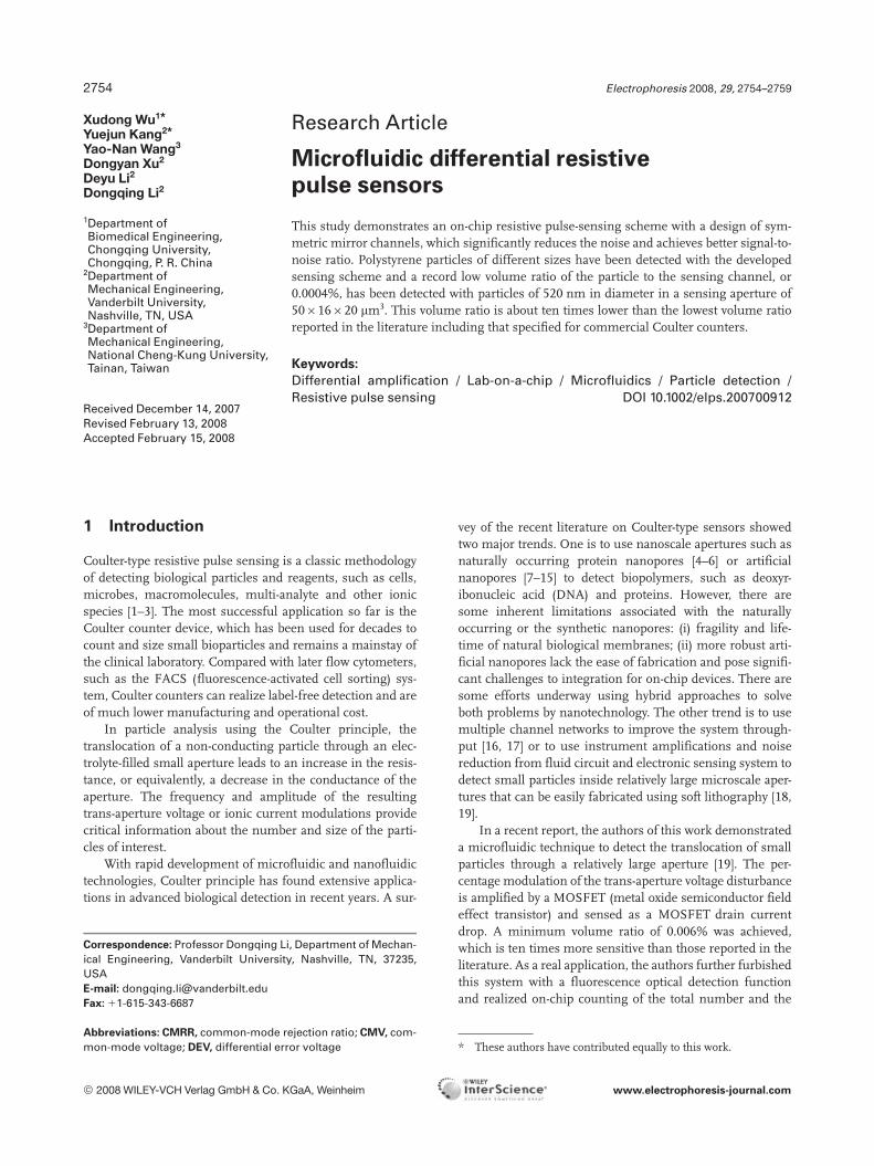
The PDMS microfluidic chip was fabricated on a glass sub-strate (2466063 mm, VWR International) following thestandard soft lithography protocol. The chip consists of a pairof mirror-symmetric channels (with sensing apertures) thatare separated by a wall of 100 mm in thickness and share thesame sample input (A) and waste reservoirs (B), as shown inFig. 1. The fluidic conduit is connected to the electronic cir-cuits by platinum-wire electrodes submerged in four reser-voirs. A DC bias (V1 –V–) was applied across the channel toinduce the EOF, which drove the particles through the sen-sing apertures from reservoir A to reservoir B. There are twogate branches connected to the differential amplifier(AD620, Analog Devices, Norwood, MA) at the upstreamends of both sensing apertures to detect the trans-aperturevoltage modulation when particles are translocated. The sig-nals were collected by a custom-made LABVIEW® codethrough a data-acquisition board (PCI 6281, NationalInstruments, Austin, TX). An aluminum Faraday cage wasused to shield the microchip and the sensing electronicsfrom the environmental electromagnetic interference. Thesensing electronics, power source, and the data acquisitionsystem are all connected using BNC connecters and coaxialcables.
2.2 Differential resistive pulse sensing
The trans-aperture voltage modulation is detected by themechanism of differential amplification. The S/N is signifi-cantly improved by the unique symmetric dual channeldesign and other electronic methods.
For microchip-detection system as developed in thisstudy, there are two major types of noise sources. One is thefrom the electrical power system, such as the system powersupply and the ambient illumination, which has a character-
Figure 1. Chip design and system setup for one-stage differentialamplification. A DC voltage (V1 – V–) is applied to drive the parti-cles from A to B. Trans-aperture voltage (VD1 and VD2) modulationare sensed by the two gate branches to C and D, which are thepositive and negative inputs of the differential amplifier, respec-tively. The resistances of the three sections in the main channelare denoted by R1, R2, R3, respectively.
istic frequency of 60 Hz. The other is from the intrinsic noiseof the electronic components, such as the thermal fluctua-tion in a resistor, which can generate various interferencesfrom several hundred hertz to over several megahertz. Themajor advantage of the symmetric dual channel design inFig. 1 lies in that it renders identical noise level for the out-put signals (VD1 and VD2) from both gate branches. The volt-age component common to the amplifier inputs (Vin1 andVin2) are called “common-mode voltage” (CMV). Obviously,the various noises coupled in VD1 and VD2 constitute theCMV of the amplifier. When the two branches are connectedto a differential amplifier of high “common-mode rejectionratio” (CMRR), the noise comprised in the CMV can berejected significantly at the final output (Vout).
The basic principle of a differential amplifier with highCMRR is described by
Vout ¼ AGainðV inþ � V in�Þ ¼ AGainDV (1)
where Vout is the amplified voltage output from the differ-ential amplifier; AGain is the differential amplification factor(gain). Vin1 and Vin2 are the voltage inputs from the two gatebranches, respectively (Fig. 1). According to the definition,the CMRR is a measure of how well the device rejects acommon-mode signal, and is simply the ratio of differentialgain AGain over the common-mode gain ACM [CMRR = AGain/ACM or in decibels 20 log10ðAGain=ACMÞ]. Different fromEq. (1), the output of a real differential amplifier is betterdescribed as
Vout ¼ AGainðV inþ � V in�Þ þ ACMðV inþ þ V in�Þ=2
The second term in this equation implies that the common-mode signal, and hence the coupled noise, can be amplified
© 2008 WILEY-VCH Verlag GmbH & Co. KGaA, Weinheim www.electrophoresis-journal.com
2756 X. Wu et al. Electrophoresis 2008, 29, 2754–2759
by the common-mode gain. However, for an amplifier withhigh CMRR (100 dB for AD620), this term is negligible andthe effect of the CMV can be significantly reduced.
When there is no particle passing through either of thetwo sensing apertures, ideally Vin1 is equal to Vin2 in ampli-tude for a perfectly symmetric fluid circuit. Thus, the twoinputs will cancel each other and the amplified output iszero. However, for a real microchip, an original voltage dif-ference exists between VD1 and VD2. It is commonly referredto as “differential error voltage” (DEV), which is mainly dueto the not perfectly symmetric nature of the dual channelsfrom fabrication errors. In addition, other variations in fluidconditions, such as ionic concentration, temperature fluc-tuation, etc., in distinct channels may contribute to the DEVas well. The DEV can be amplified by the differential gainand thus the amplifier has a non-zero final output. When aparticle passes through either one (but only one at the samemoment) of the two sensing apertures, on top of the DEV, theresulting voltage modulation causes an additional input dif-ference DV between Vin1 and Vin2, which is amplified by thedifferential gain. According to Eq. (1), the voltage outputs ofthe amplifier for particles translocated through distinct sen-sing apertures are opposite in polarity, and hence, the resis-tive pulses will show opposite profiles (upward or down-ward).
In addition, the voltage modulation can be optimized byproper design of the resistance distribution of the fluid cir-cuit. The resistance change DR because of the presence of aparticle inside the aperture leads to a voltage change DV atthe corresponding detecting branch, which can be easilyderived as
DV ¼ R1DR
R1 þ R2 þ R3ð Þ2þ R1 þ R2 þ R3ð ÞDRðV� � VþÞ (2)
where R1, R2, R3 are the resistances of the three sections inthe main channel (Fig. 1). Because of the substantially highinput impedance (10 GO for AD620) of the amplifier com-pared with the fluid circuit (about 2 MO for our microchip),the resistance of the detecting gate channel can be ignored.Assuming R1 ¼ kðR2 þ R3Þ ¼ kR (k is a positive propor-tional factor) and DR55R1 þ R2 þ R3, from Eq. (2) one canobtain
DV � k
kþ 1ð Þ2DRR
V� � Vþð Þ ¼ f kð ÞDRR
V� � Vþð Þ (3)
It can be easily inferred that function f (k) reaches its max-imum when k equals to 1, i.e. R1 ¼ R2 þ R3. Therefore amaximum voltage modulation can be achieved by varyingthe length and width, and hence the resistance of each sec-tion of the fluid conduit. For the microchip used in thisstudy, the dimension of the three major sections (Fig. 1) are:800 mm66000 mm for the upstream channel (R1),16 mm650 mm for the sensing aperture (R2),800 mm65000 mm for the downstream channel (R3). All ofthe fluid conduits have the same depth of 20 mm.
3 Results and discussion
3.1 One-stage differential amplification
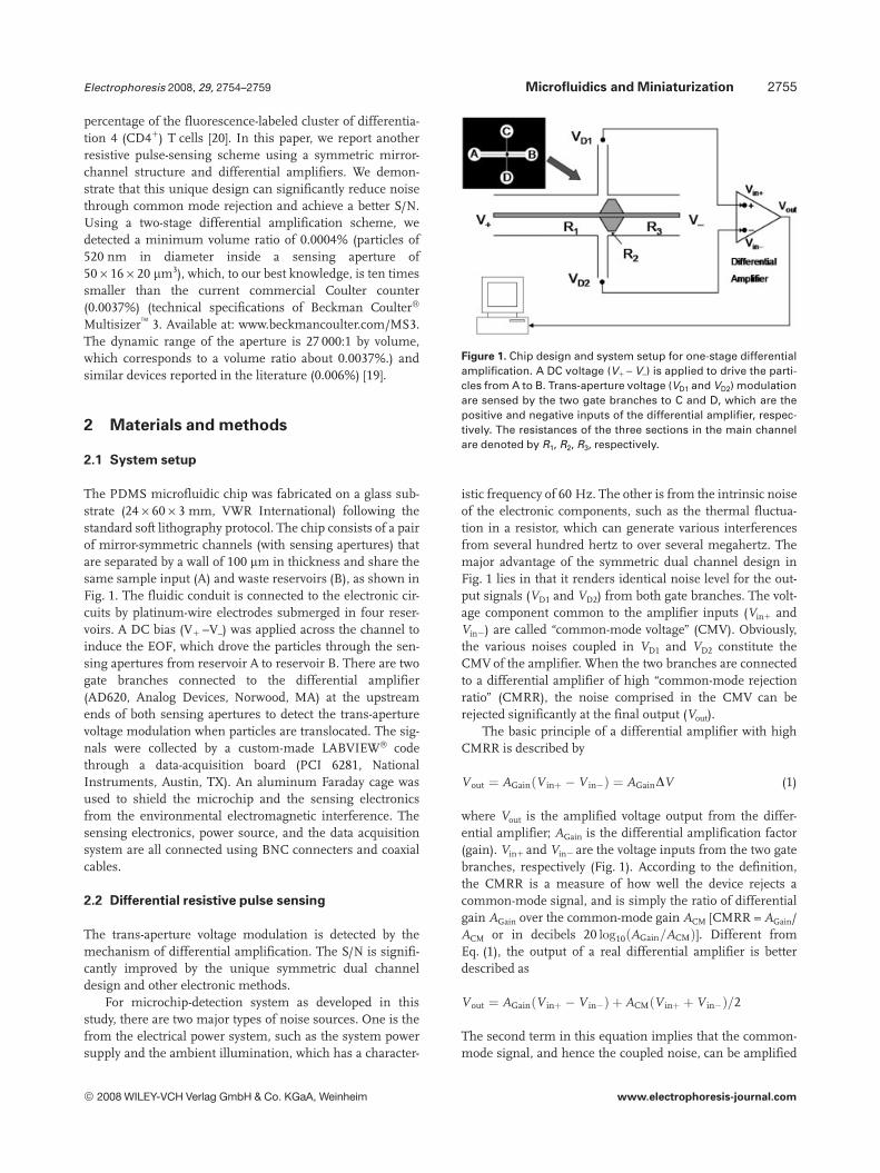
Figure 2 shows the detection of 1-, 2-, and 4.84-mm (in diam-eter) particles suspended in 7.5 mM sodium borate buffer.Each spike denotes a single particle, verified by concurrentobservation with an optical microscope. The upward anddownward pulses denote the particles translocated throughtwo different sensing apertures, respectively. The amplitude
Figure 2. Resistive pulses of 1, 2, and 4.84 mmparticles in 7.5 mM sodium borate buffer. Themagnified inset shows the signal strength of 1and 2 mm particles. The gain of the differentialamplifier was set at 100 V/V. The applied voltageacross the main channel was set to be 35 V.
© 2008 WILEY-VCH Verlag GmbH & Co. KGaA, Weinheim www.electrophoresis-journal.com
Electrophoresis 2008, 29, 2754–2759 Microfluidics and Miniaturization 2757
of the spike is dependent on the size of the particle. Thehighest spikes, which correspond to the 4.84 mm particles,have an average amplitude of 3.09 V, whereas the smallestspikes (inset of Fig. 2), which correspond to the 1-mm parti-cles, have an average amplitude of 33 mV. The baselinethickness (fluctuation because of the noise) is about 10 mVin Fig. 2. The S/N for the 1-mm particle is about 10.37 dB(33 mV:10 mV). The amplified DEV is about 3.2 V in Fig. 2.Since the differential gain is 100 V/V, one can infer that theactual DEV for the two gate branches is about 32 mV.
Early research showed that the increase in the apertureresistance because of the presence of a particle inside is afunction of the aperture dimension and the particle size [21].In the limit of d ,, D, the function can be expressed as
DR ¼ 4Rd3
pD4 1þ 2d3
3D2Lþ 2d3
3D2L
� �2
þ:::" #
(4)
where r is the resistivity of the suspending fluid, d is theparticle diameter, and D and L are the diameter (or hydraulicdiameter for non-circular aperture) and the length of theaperture, respectively. For the present case of very small par-ticle inside a relatively large microaperture, the higher ordercorrections in above expression are negligible. Thus theresistance change is proportional to the particle volume, andhence, the volume ratio for an aperture of fixed dimension.Important information such as the frequency and the sizedistribution of the particles translocated through the sensingaperture can be derived from the resistive pulse monitoring.In addition, the residence time of the particle inside thesensing aperture can be analyzed from the time scale. Fur-ther study shows that the ratio of peak amplitudes (1:3.82:94)and the volume ratio (1:8:113) for the three different particlesdo not satisfy a strict linear relationship. We attribute thisfailure to the fact that the particles are relatively large com-pared with the aperture, which makes the assumption forEq. (4) invalid. However, we still cannot explain why the peakstrength for 2-mm particles is more away from the linearrelationship than that for 4.8-mm particles.
3.2 Two-stage differential amplification
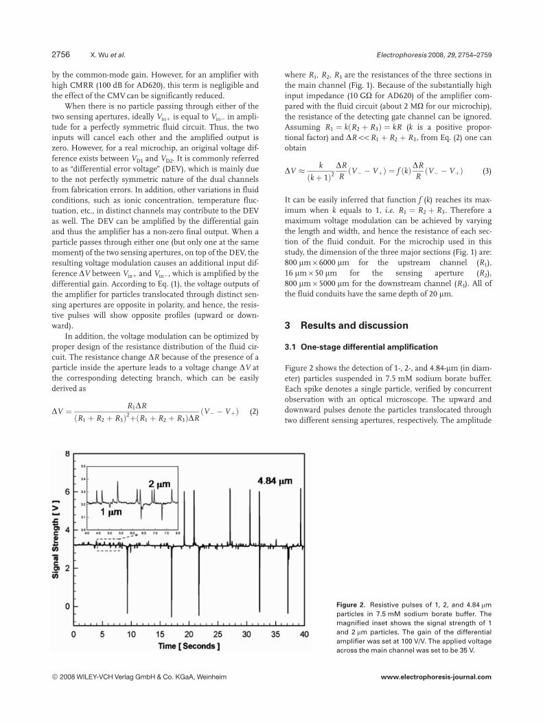
The smallest particles we could detect using the above one-stage amplification are 1 mm in diameter. It is impractical ifone wants to increase the sensitivity solely by increasing thedifferential gain, because the amplified DEV could be sig-nificantly high and will cause the final output to exceed thedetection limit of the amplifier (about 12 V for AD620). Tocircumvent this problem and achieve a higher sensitivity, weimplemented a two-stage amplification scheme using threeamplifiers to reject the DEV in the one-stage amplification(Fig. 3). In this scheme, the DEV can be offset by adjustingthe reference of the amplifiers in the first stage, which are setat low differential gain. Therefore, we applied a lower gainfor the first stage (A1 = 25) and a higher gain for the second
Figure 3. Design of two-stage differential amplification scheme.Since the original outputs from fluid circuit (VD1 and VD2) areconnected to the inputs of opposite polarity of the two amplifiersin the first-stage, the final gain of the two-stage amplification isAGain=2A1A2, which is twice of the multiplication (A1A2) of thegains of the individual amplifiers in both stages.
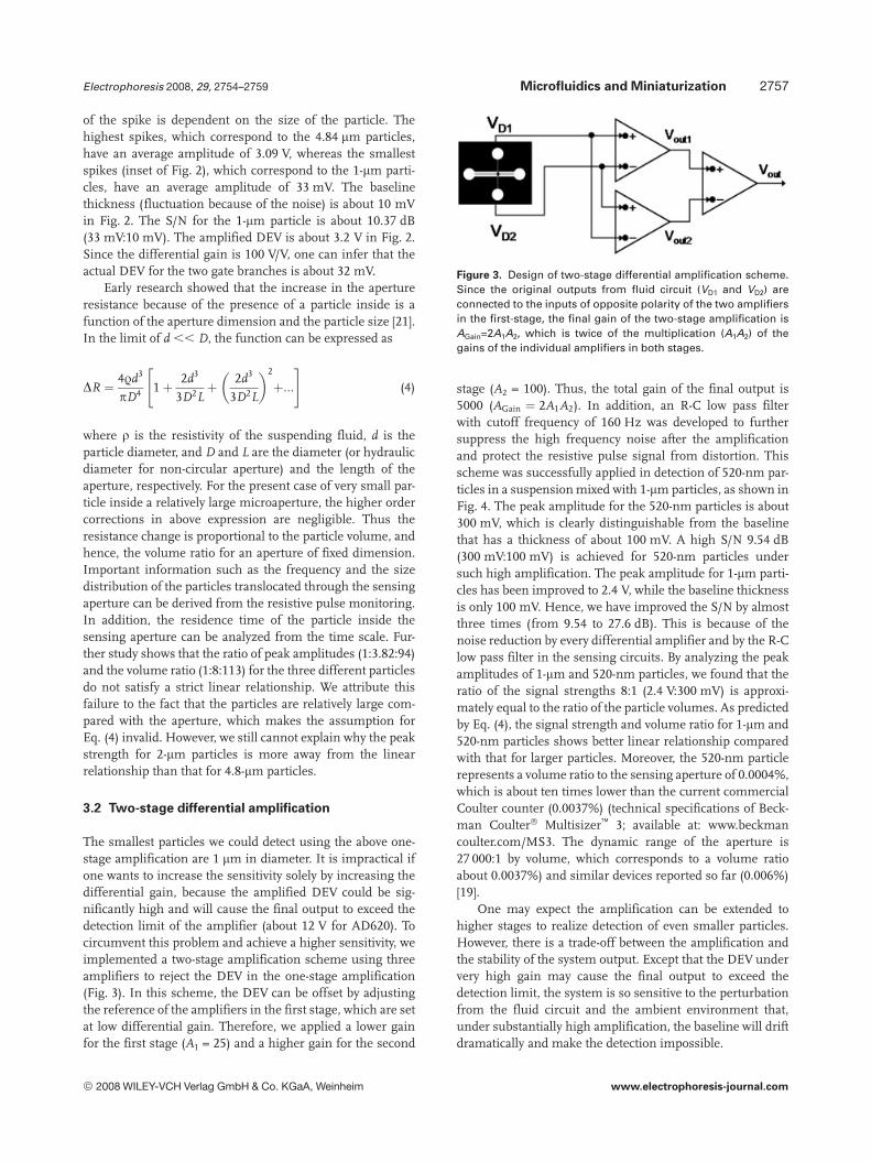
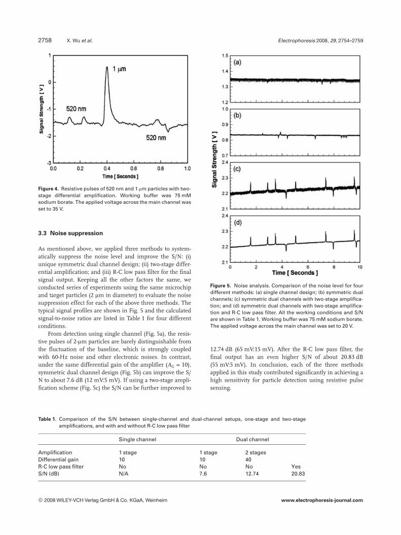
stage (A2 = 100). Thus, the total gain of the final output is5000 (AGain ¼ 2A1A2). In addition, an R-C low pass filterwith cutoff frequency of 160 Hz was developed to furthersuppress the high frequency noise after the amplificationand protect the resistive pulse signal from distortion. Thisscheme was successfully applied in detection of 520-nm par-ticles in a suspension mixed with 1-mm particles, as shown inFig. 4. The peak amplitude for the 520-nm particles is about300 mV, which is clearly distinguishable from the baselinethat has a thickness of about 100 mV. A high S/N 9.54 dB(300 mV:100 mV) is achieved for 520-nm particles undersuch high amplification. The peak amplitude for 1-mm parti-cles has been improved to 2.4 V, while the baseline thicknessis only 100 mV. Hence, we have improved the S/N by almostthree times (from 9.54 to 27.6 dB). This is because of thenoise reduction by every differential amplifier and by the R-Clow pass filter in the sensing circuits. By analyzing the peakamplitudes of 1-mm and 520-nm particles, we found that theratio of the signal strengths 8:1 (2.4 V:300 mV) is approxi-mately equal to the ratio of the particle volumes. As predictedby Eq. (4), the signal strength and volume ratio for 1-mm and520-nm particles shows better linear relationship comparedwith that for larger particles. Moreover, the 520-nm particlerepresents a volume ratio to the sensing aperture of 0.0004%,which is about ten times lower than the current commercialCoulter counter (0.0037%) (technical specifications of Beck-man Coulter® Multisizer™ 3; available at: www.beckmancoulter.com/MS3. The dynamic range of the aperture is27 000:1 by volume, which corresponds to a volume ratioabout 0.0037%) and similar devices reported so far (0.006%)[19].
One may expect the amplification can be extended tohigher stages to realize detection of even smaller particles.However, there is a trade-off between the amplification andthe stability of the system output. Except that the DEV undervery high gain may cause the final output to exceed thedetection limit, the system is so sensitive to the perturbationfrom the fluid circuit and the ambient environment that,under substantially high amplification, the baseline will driftdramatically and make the detection impossible.
© 2008 WILEY-VCH Verlag GmbH & Co. KGaA, Weinheim www.electrophoresis-journal.com
2758 X. Wu et al. Electrophoresis 2008, 29, 2754–2759
Figure 4. Resistive pulses of 520 nm and 1 mm particles with two-stage differential amplification. Working buffer was 75 mMsodium borate. The applied voltage across the main channel wasset to 35 V.
3.3 Noise suppression
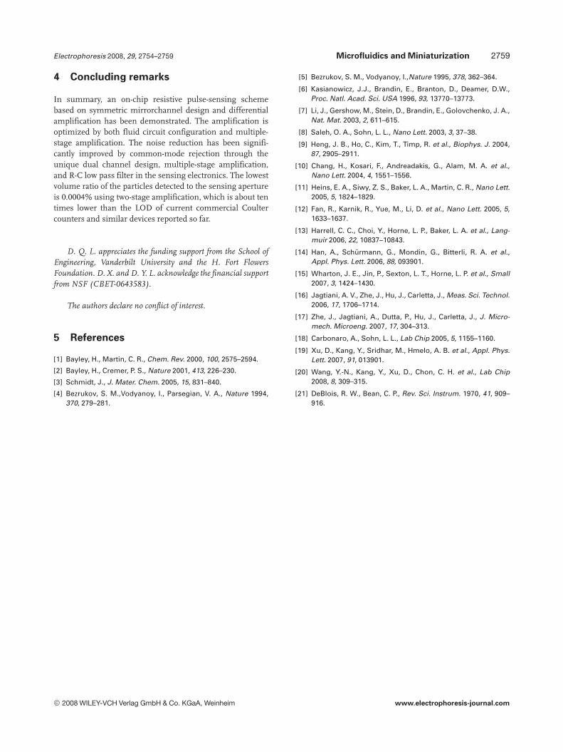
As mentioned above, we applied three methods to system-atically suppress the noise level and improve the S/N: (i)unique symmetric dual channel design; (ii) two-stage differ-ential amplification; and (iii) R-C low pass filter for the finalsignal output. Keeping all the other factors the same, weconducted series of experiments using the same microchipand target particles (2 mm in diameter) to evaluate the noisesuppression effect for each of the above three methods. Thetypical signal profiles are shown in Fig. 5 and the calculatedsignal-to-noise ratios are listed in Table 1 for four differentconditions.
From detection using single channel (Fig. 5a), the resis-tive pulses of 2-mm particles are barely distinguishable fromthe fluctuation of the baseline, which is strongly coupledwith 60-Hz noise and other electronic noises. In contrast,under the same differential gain of the amplifier (AG = 10),symmetric dual channel design (Fig. 5b) can improve the S/N to about 7.6 dB (12 mV:5 mV). If using a two-stage ampli-fication scheme (Fig. 5c) the S/N can be further improved to
Figure 5. Noise analysis. Comparison of the noise level for fourdifferent methods: (a) single channel design; (b) symmetric dualchannels; (c) symmetric dual channels with two-stage amplifica-tion; and (d) symmetric dual channels with two-stage amplifica-tion and R-C low pass filter. All the working conditions and S/Nare shown in Table 1. Working buffer was 75 mM sodium borate.The applied voltage across the main channel was set to 20 V.
12.74 dB (65 mV:15 mV). After the R-C low pass filter, thefinal output has an even higher S/N of about 20.83 dB(55 mV:5 mV). In conclusion, each of the three methodsapplied in this study contributed significantly in achieving ahigh sensitivity for particle detection using resistive pulsesensing.
Table 1. Comparison of the S/N between single-channel and dual-channel setups, one-stage and two-stageamplifications, and with and without R-C low pass filter
Single channel Dual channel
Amplification 1 stage 1 stage 2 stagesDifferential gain 10 10 40R-C low pass filter No No No YesS/N (dB) N/A 7.6 12.74 20.83
© 2008 WILEY-VCH Verlag GmbH & Co. KGaA, Weinheim www.electrophoresis-journal.com
Electrophoresis 2008, 29, 2754–2759 Microfluidics and Miniaturization 2759
4 Concluding remarks
In summary, an on-chip resistive pulse-sensing schemebased on symmetric mirrorchannel design and differentialamplification has been demonstrated. The amplification isoptimized by both fluid circuit configuration and multiple-stage amplification. The noise reduction has been signifi-cantly improved by common-mode rejection through theunique dual channel design, multiple-stage amplification,and R-C low pass filter in the sensing electronics. The lowestvolume ratio of the particles detected to the sensing apertureis 0.0004% using two-stage amplification, which is about tentimes lower than the LOD of current commercial Coultercounters and similar devices reported so far.
D. Q. L. appreciates the funding support from the School ofEngineering, Vanderbilt University and the H. Fort FlowersFoundation. D. X. and D. Y. L. acknowledge the financial supportfrom NSF (CBET-0643583).
The authors declare no conflict of interest.
5 References
[1] Bayley, H., Martin, C. R., Chem. Rev. 2000, 100, 2575–2594.
[2] Bayley, H., Cremer, P. S., Nature 2001, 413, 226–230.
[3] Schmidt, J., J. Mater. Chem. 2005, 15, 831–840.
[4] Bezrukov, S. M.,Vodyanoy, I., Parsegian, V. A., Nature 1994,370, 279–281.
[5] Bezrukov, S. M., Vodyanoy, I.,Nature 1995, 378, 362–364.
[6] Kasianowicz, J.J., Brandin, E., Branton, D., Deamer, D.W.,Proc. Natl. Acad. Sci. USA 1996, 93, 13770–13773.
[7] Li, J., Gershow, M., Stein, D., Brandin, E., Golovchenko, J. A.,Nat. Mat. 2003, 2, 611–615.
[8] Saleh, O. A., Sohn, L. L., Nano Lett. 2003, 3, 37–38.
[9] Heng, J. B., Ho, C., Kim, T., Timp, R. et al., Biophys. J. 2004,87, 2905–2911.
[10] Chang, H., Kosari, F., Andreadakis, G., Alam, M. A. et al.,Nano Lett. 2004, 4, 1551–1556.
[11] Heins, E. A., Siwy, Z. S., Baker, L. A., Martin, C. R., Nano Lett.2005, 5, 1824–1829.
[12] Fan, R., Karnik, R., Yue, M., Li, D. et al., Nano Lett. 2005, 5,1633–1637.
[13] Harrell, C. C., Choi, Y., Horne, L. P., Baker, L. A. et al., Lang-muir 2006, 22, 10837–10843.
[14] Han, A., Schürmann, G., Mondin, G., Bitterli, R. A. et al.,Appl. Phys. Lett. 2006, 88, 093901.
[15] Wharton, J. E., Jin, P., Sexton, L. T., Horne, L. P. et al., Small2007, 3, 1424–1430.
[16] Jagtiani, A. V., Zhe, J., Hu, J., Carletta, J., Meas. Sci. Technol.2006, 17, 1706–1714.
[17] Zhe, J., Jagtiani, A., Dutta, P., Hu, J., Carletta, J., J. Micro-mech. Microeng. 2007, 17, 304–313.
[18] Carbonaro, A., Sohn, L. L., Lab Chip 2005, 5, 1155–1160.
[19] Xu, D., Kang, Y., Sridhar, M., Hmelo, A. B. et al., Appl. Phys.Lett. 2007, 91, 013901.
[20] Wang, Y.-N., Kang, Y., Xu, D., Chon, C. H. et al., Lab Chip2008, 8, 309–315.
[21] DeBlois, R. W., Bean, C. P., Rev. Sci. Instrum. 1970, 41, 909–916.
© 2008 WILEY-VCH Verlag GmbH & Co. KGaA, Weinheim www.electrophoresis-journal.com


