Embed Size (px)
Citation preview
MiCOM P438
Rail Catenary Protection Device
P438/UK M/Ae7 (AFSV.12.11060 EN)
Version P438 -305 -409/410/411 -615 P438 -307 -412/413/414 -615
Technical Manual


!
Warning When electrical equipment is in operation dangerous voltage will be present in certain parts of the equipment. Failure to observe warning notices, incorrect use or improper use may endanger personnel and equipment and cause personal injury or physical damage.
Before working in the terminal strip area, the device must be isolated. Where stranded conductors are used, insulated crimped wire end ferrules must be employed.
The signals 'Main: B locked/ fau l ty ' and 'SFMON: Warning (LED) ' (permanently assigned to the LEDs labeled 'OUT OF SERVICE' and 'ALARM') can be assigned to output relays to indicate the health of the device. Schneider Electric strongly recommends that these output relays are hardwired into the substation's automation system, for alarm purposes.
Any modifications to this device must be in accordance with the manual. If any other modification is made without the express permission of Schneider Electric, it will invalidate the warranty, and may render the product unsafe.
Proper and safe operation of this device depends on appropriate shipping and handling, proper storage, installation and commissioning, and on careful operation, maintenance and servicing.
For this reason only qualified personnel may work on or operate this device.
The User should be familiar with the warnings in the Safety Guide (SFTY/4LM/G11 or later version), with the warnings in Chapters 5, 9, 10 and 11 and with the content of Chapter 13, before working on the equipment. If the warnings are disregarded, it will invalidate the warranty, and may render the product unsafe.
Installation of the DHMI:
A protective conductor (ground/earth) of at least 1.5 mm2 must be connected to the DHMI protective conductor terminal to link the DHMI and the main relay case; these must be located within the same substation.
To avoid the risk of electric shock the DHMI communication cable must not be in contact with hazardous live parts.
The DHMI communication cable must not be routed or placed alongside high-voltage cables or connections. Currents can be induced in the cable which may result in electromagnetic interference.
Qualified Personnel are individuals who
are familiar with the installation, commissioning and operation of the device and of the system to which it is being connected;
are able to perform switching operations in accordance with safety engineering standards and are authorized to energize and de-energize equipment and to isolate, ground and label it;
are trained in the care and use of safety apparatus in accordance with safety engineering standards;
are trained in emergency procedures (first aid).
Note The operating manual for this device gives instructions for its installation, commissioning and operation. However, the manual cannot cover all conceivable circumstances or include detailed information on all topics. In the event of questions or specific problems, do not take any action without proper authorization. Contact the appropriate Schneider Electric technical sales office and request the necessary information.
Any agreements, commitments, and legal relationships and any obligations on the part of Schneider Electric, including settlement of warranties, result solely from the applicable purchase contract, which is not affected by the contents of the operating manual.
3
Notes:
This manual (P438/EN M/Ae7) is based on the P438-305/307-409/410/411-613 full manual (P438/EN M/Bd7) but incorporates all the changes up to (and including) version P438-305-409/410/411-615.
All parts of this manual that are not affected by the product upgrade have not been modified in any way and therefore still show the -613 version in the footer.
Software version -615 is compatible with two different hardware versions, -305 and -307, which are therefore both covered in this manual. The only difference is that hardware version -307 is designed for another communication module, the “Dual Redundant Ethernet Board” (REB). At the time of publishing this manual, however, the REB module has not been released yet.
4 P438/UK M/Ae7 // AFSV.12.11060 EN /// P438-305-409/410/411-615 + P438-307-412/413/414-615

Changes after going to press
P438/EN M/Ad7 // AFSV.12.10470 D /// P438-305-409/410/411-613 + P438-307-412/413/414-613


Contents
1 Application and Scope 1-1
2 Technical Data 2-1 2.1 Conformity 2-1 2.2 General Data 2-1 2.3 Tests 2-2 2.3.1 Type Tests 2-2 2.3.2 Routine Tests 2-5 2.4 Environmental Conditions 2-5 2.5 Inputs and Outputs 2-6 2.6 Interfaces 2-8 2.7 Information Output 2-10 2.8 Settings 2-10 2.9 Deviations 2-11 2.9.1 Deviations of the Operate Values 2-11 2.9.2 Deviations of the Timer Stages 2-12 2.9.3 Deviations of Measured Data Acquisition 2-13 2.9.4 Resolution of the fault value recording 2-14 2.10 Recording Functions 2-15 2.11 Power supply 2-16 2.12 Current Transformer Specifications 2-17
3 Operation 3-1 3.1 Modular Structure 3-1 3.2 Operator-Machine Communication 3-3 3.3 Configuration of the Measured
Value Panels (Function Group HMI) 3-4
3.4 Serial Interfaces 3-8 3.4.1 PC interface (Function Group PC) 3-8 3.4.2 Communication Interface 1 (Function Group COMM1) 3-10 3.4.3 Communication Interface 2 (Function Group COMM2) 3-19 3.4.4 Communication Interface 3 (Function Group COMM3) 3-22 3.4.5 Communication Interface
IEC 61850 (Function Groups IEC GOOSE and GSSE)
3-27
3.5 IRIG-B Clock Synchronization (Function Group IRIGB) 3-34 3.6 Configurable Function Keys (Function Group F_KEY) 3-35 3.7 Configuration and Operating Mode
of the Binary Inputs (Function Group INP) 3-38
3.8 Measured Data Input (Function Group RTDmA) 3-40 3.8.1 Direct Current Input 3-41 3.8.2 Input for Connection of a
Resistance Thermometer 3-45
3.9 Configuration, Operating Mode, and Blocking of the Output Relays
(Function Group OUTP) 3-46
3.10 Measured Data Output (Function Group mA_OP) 3-49 3.10.1 BCD Measured Data Output 3-52 3.10.2 Analog Measured Data Output 3-54 3.10.3 Output of ‘External’ Measured Data 3-60 3.11 Configuration and Operating Mode
of the LED Indicators (Function Group LED) 3-61
3.12 Main Functions of the P438 (Function Group MAIN) 3-64 3.12.1 Conditioning of the Measured
Values 3-64
3.12.2 Operating Data Measurement 3-68 3.12.3 Configuring and Enabling the
Protection Functions 3-77
P438/EN M/Ad7 // AFSV.12.10470 D /// P438-305-409/410/411-613 + P438-307-412/413/414-613 7
Contents (continued)
8 P438/EN M/Ad7 // AFSV.12.10470 D /// P438-305-409/410/411-613 + P438-307-412/413/414-613
3.12.4 Inrush stabilization (Harmonic restraint)
3-79
3.12.5 Directional Voltage Memory 3-82 3.12.6 Multiple Blocking 3-83 3.12.7 Blocked/Faulty 3-84 3.12.8 Close Command 3-85 3.12.9 Fault Direction Signal 3-87 3.12.10 Starting Signals and Trip Logic 3-88 3.12.11 Time Tagging and Clock
Synchronization 3-96
3.12.12 Resetting Mechanisms 3-98 3.12.13 Assigning the Rear Port
Communications Interfaces to Physical Communications Channels
3-101
3.12.14 Test Mode 3-102 3.13 Setting group selection (Function Group GROUP) 3-103 3.14 Self-Monitoring (Function Group CHECK) 3-105 3.15 Operating Data Recording (Function Group OP_RC) 3-108 3.16 Monitoring Signal Recording (Function Group MT_RC) 3-109 3.17 Overload Data Acquisition (Function Group OL_DA) 3-110 3.18 Overload Recording (Function Group OL_RC) 3-112 3.19 Fault Data Acquisition (Function Group FT_DA) 3-114 3.20 Fault Recording (Function Group FT_RC) 3-125 3.21 Distance protection (Function Group DIST) 3-130 3.21.1 Base Point Release for Impedance
and Direction Determination 3-135
3.21.2 Distance and Direction Measurement
3-136
3.21.3 Impedance-Time Characteristics 3-153 3.21.4 Train Start-Up Detection di/dt, dv/dt
and dϕ/dt 3-155
3.21.5 Wrong Phase Coupling Protection 3-158 3.21.6 Multiple Signaling of Distance
Protection 3-162
3.22 High Impedance Protection (Function Group DELTA) 3-163 3.22.1 Minimum Current and Voltage
Enabling of High Impedance Protection
3-165
3.22.2 Reactance-Limiting of High Impedance Protection
3-166
3.22.3 Checking for Changes of the Phase Angle (Sudden Angle Change Detection)
3-167
3.22.4 Harmonics Stabilization for Load Variations
3-168
3.22.5 Starting and Tripping of the High Impedance Protection Function
3-169
3.23 VT and CT Supervision (Function Group C&VTS) 3-171 3.24 Backup Time-Delayed Overcurrent
Protection (Function Group BUOC) 3-176
3.25 Switch on to Fault Protection (Function Group SOTF) 3-179 3.26 Auto-Reclose (Function Group RECLS) 3-182 3.26.1 Auto-Reclose Trip Times 3-186 3.26.2 High-Speed Reclosure (HSR) 3-197 3.26.3 Time-Delayed Reclosure (TDR) 3-202

Contents (continued)
3.26.4 Zone Extension 3-205 3.26.5 Auto-Reclose Control Function after
Trip by Thermal Overload Protection
3-206
3.26.6 Auto-Reclose Control Function with Parallel Protection Device
3-207
3.26.7 Auto-Reclose Counters 3-210 3.27 Definite-Time Overcurrent
Protection (Function Group DTOC) 3-211
3.28 Inverse-Time Overcurrent Protection
(Function Group IDMT) 3-219
3.29 Defrost Protection (Function Group DFRST) 3-223 3.30 Thermal Overload Protection (Function Group THERM) 3-236 3.31 Under- and Overvoltage Protection (Function Group V<>) 3-248 3.32 Circuit Breaker Failure Protection (Function Group CBF) 3-251 3.33 Circuit Breaker Monitoring (Function Group CBM) 3-255 3.34 Limit Value Monitoring (Function Group LIMIT) 3-266 3.35 Programmable Logic (Function Group LOGIC) 3-277
4 Design 4-1 4.1 Designs (Case Types) 4-2 4.2 Dimensional Drawings 4-4 4.2.1 Surface-Mounted Case 4-4 4.2.2 Flush-Mounted Case 4-5 4.2.3 Device View of Connection for the Detached User Interface (HMI) 4-7 4.3 Modules 4-8
5 Installation and Connection 5-1 5.1 Unpacking and Packing 5-1 5.2 Checking the Nominal Data and the Design Version 5-2 5.3 Location Requirements 5-3 5.4 Installation 5-4 5.5 Protective Grounding 5-12 5.6 Connection 5-13 5.6.1 Connecting Measuring and Auxiliary Circuits 5-13 5.6.2 Connecting the IRIG-B Interface 5-18 5.6.3 Connecting the Serial Interfaces 5-18
5.7 Location Diagrams P438 -305 5-22 5.8 Connection Diagrams P438 -305 5-23
5.9 Location Diagrams P438 -307 5-25
5.10 Connection Diagrams P438 -307 5-26
6 User Interface (HMI) 6-1 6.1 Display and Keypad 6-2 6.2 Changing Between Display Levels 6-7 6.3 Illumination of the Display 6-8 6.4 Configurable Function Keys F1 to Fx (general) 6-8 6.5 Control at the Panel Level 6-10 6.6 Control at the Menu Tree Level 6-11 6.6.1 Navigation of the Menu Tree 6-11 6.6.2 Switching Between Address Mode and Plain Text Mode 6-12 6.6.3 Setting Change Enabling 6-13 6.6.4 Changing Settings 6-16 6.6.5 Setting a List Setting 6-17
P438/EN M/Ad7 // AFSV.12.10470 D /// P438-305-409/410/411-613 + P438-307-412/413/414-613 9

Contents (continued)
10 P438/EN M/Ad7 // AFSV.12.10470 D /// P438-305-409/410/411-613 + P438-307-412/413/414-613
6.6.6 Memory Readout 6-18 6.6.7 Resetting 6-22 6.8 Password-Protected Control Actions 6-24 6.6.9 Changing the Password 6-25
7 Settings 7-1 7.1 Parameters 7-1 7.1.1 Device Identification 7-2 7.1.2 Configuration Parameters 7-6 7.1.3 Function Settings 7-52 7.1.3.1 Global 7-52 7.1.3.2 General Functions 7-56 7.1.3.3 Setting Groups 7-66
8 Information and Control Functions 8-1 8.1 Healthy 8-2 8.1.1 Cyclic Values 8-2 8.1.1.1 Measured Operating Data 8-2 8.1.1.2 Physical State Signals 8-7 8.1.1.3 Logic State Signals 8-15 8.1.2 Control and Testing 8-35 8.1.3 Operating Data Recording 8-40 8.2 Events 8-41 8.2.1 Event Counters 8-41 8.2.2 Measured Event Data 8-42 8.2.3 Event Recording 8-44
9 Commissioning 9-1 9.1 Safety Instructions 9-1 9.2 Commissioning Tests 9-3
10 Troubleshooting 10-1
11 Maintenance 11-1
12 Storage 12-1
13 Accessories and Spare Parts 13-1
14 Order Information 14-1
Appendix
TERMINOLOGY NOTE: The P438 menu texts ("Data Model") referred to throughout this manual are regional texts which have been customised for the UK market. Most diagrams contained in this manual use the same terminology. Some diagrams however contain standard English menu texts when those were very similar to the "regional" ones and modifying those diagrams was not deemed essential to comprehension. In those diagrams, references are made to "Parameter Set(s)": This is the direct equivalent to the regional term "Setting Group(s)". Similarly, the terms "PSx", "PS1", "PS2", "PS3" and "PS4" are respectively equivalent to "SGx", "SG1", "SG2", "SG3" and "SG4".
1 Application and Scope
P438/EN M/Ad7 // AFSV.12.10470 D /// P438-305-409/410/411-613 + P438-307-412/413/414-613 1-1
1 Application and Scope
The catenary protection device MiCOM P438 is designed for selective short-circuit and overload protection of catenaries. This device is designed for the protection of classic- or autotransformer-fed catenaries in single- or multi-voltage systems with nominal frequencies of 25, 50 or 60 Hz (settable).
The MiCOM P438 ensures fast and selective short circuit protection as well as protection from excessive catenary overloading.
The multitude of protection functions incorporated into the device enable the user to cover a wide range of applications in the protection of catenary systems.
Moreover there are numerous backup protection and automatic control functions available.
The relevant protection parameters are stored in four independent setting groups in order to adapt the device to various operating and power system management states.
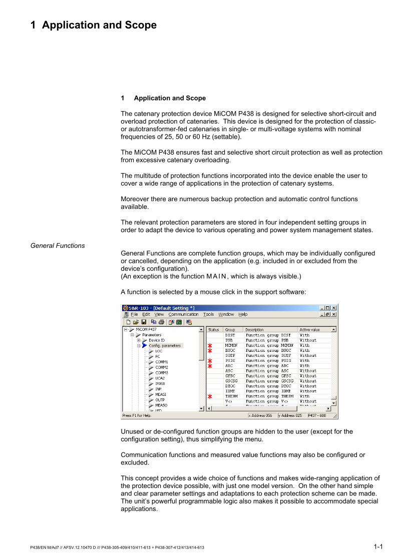
General Functions General Functions are complete function groups, which may be individually configured or cancelled, depending on the application (e.g. included in or excluded from the device’s configuration). (An exception is the function M A I N , which is always visible.)
A function is selected by a mouse click in the support software:
Unused or de-configured function groups are hidden to the user (except for the configuration setting), thus simplifying the menu.
Communication functions and measured value functions may also be configured or excluded.
This concept provides a wide choice of functions and makes wide-ranging application of the protection device possible, with just one model version. On the other hand simple and clear parameter settings and adaptations to each protection scheme can be made. The unit’s powerful programmable logic also makes it possible to accommodate special applications.
1 Application and Scope (continued)
1-2 P438/EN M/Ad7 // AFSV.12.10470 D /// P438-305-409/410/411-613 + P438-307-412/413/414-613
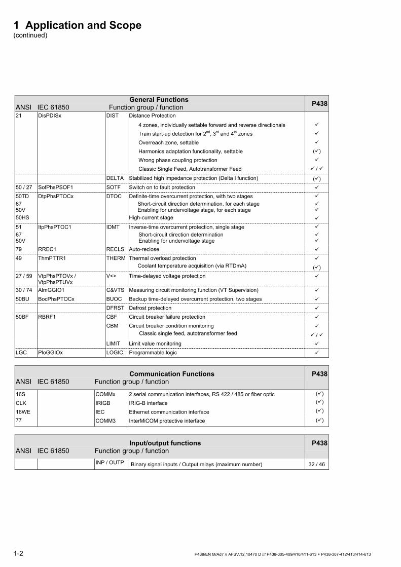
General Functions ANSI IEC 61850 Function group / function P438 21 DisPDISx DIST Distance Protection
4 zones, individually settable forward and reverse directionals Train start-up detection for 2nd, 3rd and 4th zones Overreach zone, settable Harmonics adaptation functionality, settable Wrong phase coupling protection Classic Single Feed, Autotransformer Feed
( )
/
DELTA Stabilized high impedance protection (Delta I function) ( ) 50 / 27 SofPhsPSOF1 SOTF Switch on to fault protection
50TD 67 50V 50HS
DtpPhsPTOCx DTOC Definite-time overcurrent protection, with two stages Short-circuit direction determination, for each stage Enabling for undervoltage stage, for each stage High-current stage
51 67 50V
ItpPhsPTOC1 IDMT Inverse-time overcurrent protection, single stage Short-circuit direction determination Enabling for undervoltage stage
79 RREC1 RECLS Auto-reclose
49 ThmPTTR1 THERM Thermal overload protection Coolant temperature acquisition (via RTDmA)
( ) 27 / 59 VtpPhsPTOVx /
VtpPhsPTUVx V<> Time-delayed voltage protection
30 / 74 AlmGGIO1 C&VTS Measuring circuit monitoring function (VT Supervision)
50BU BocPhsPTOCx BUOC Backup time-delayed overcurrent protection, two stages
DFRST Defrost protection
50BF RBRF1 CBF Circuit breaker failure protection
CBM Circuit breaker condition monitoring Classic single feed, autotransformer feed
/ LIMIT Limit value monitoring
LGC PloGGIOx LOGIC Programmable logic
Communication Functions ANSI IEC 61850 Function group / function
P438
16S CLK 16WE
COMMx IRIGB IEC
2 serial communication interfaces, RS 422 / 485 or fiber optic IRIG-B interface Ethernet communication interface
( ) ( ) ( )
77 COMM3 InterMiCOM protective interface ( )
Input/output functions ANSI IEC 61850 Function group / function
P438
INP / OUTP Binary signal inputs / Output relays (maximum number) 32 / 46
1 Application and Scope (continued)
P438/EN M/Ad7 // AFSV.12.10470 D /// P438-305-409/410/411-613 + P438-307-412/413/414-613 1-3
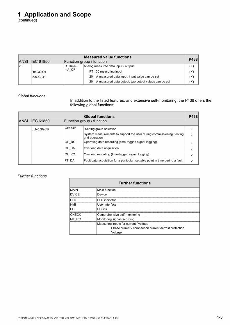
Measured value functions ANSI IEC 61850 Function group / function P43826
RtdGGIO1 IdcGGIO1
RTDmA / mA_OP
Analog measured data input / output
PT 100 measuring input 20 mA measured data input, input value can be set 20 mA measured data output, two output values can be set
( )
( ) ( ) ( )
Global functions In addition to the listed features, and extensive self-monitoring, the P438 offers the following global functions:
Global functions ANSI IEC 61850 Function group / function
P438
LLN0.SGCB GROUP Setting group selection
System measurements to support the user during commissioning, testing and operation
OP_RC Operating data recording (time-tagged signal logging)
OL_DA Overload data acquisition
OL_RC Overload recording (time-tagged signal logging)
FT_DA Fault data acquisition for a particular, settable point in time during a fault
Further functions
Further functions MAIN Main function DVICE Device
LED LED indicator HMI User interface PC PC link
CHECK Comprehensive self-monitoring MT_RC Monitoring signal recording Measuring inputs for current / voltage
Phase current / comparison current defrost protection Voltage
1 Application and Scope (continued)
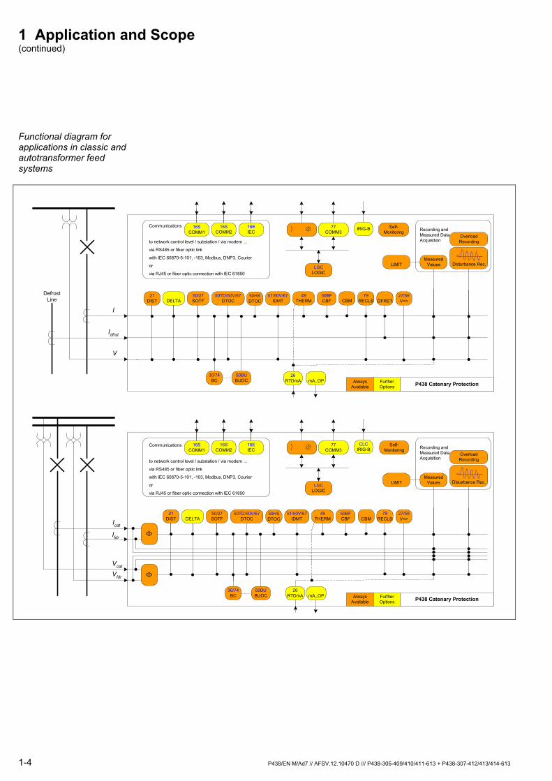
Functional diagram for applications in classic and autotransformer feed systems
LIMIT
OverloadRecording
Recording andMeasured DataAcquisition
Disturbance Rec.LGC
LOGIC
50BUBUOC
Idfrst
MeasuredValues
IRIG-BCommunications
to network control level / substation / via modem ...
via RS485 or fiber optic link
with IEC 60870-5-101, -103, Modbus, DNP3, Courier
or
via RJ45 or fiber optic connection with IEC 61850
16SCOMM1
16SCOMM2
16EIEC
27/59V<>
mA_OP
79RECLS
30/74BC
V
I
DefrostLine DFRST
77COMM3
26RTDmA
50TD/50V/67DTOC
51/50V/67IDMT
50/27SOTF
21DIST CBM
50BFCBF
50HSDTOC
49THERMDELTA
P438 Catenary ProtectionFurtherOptions
AlwaysAvailable
Icat
LIMIT
OverloadRecording
Recording andMeasured DataAcquisition
Disturbance Rec.LGC
LOGIC
50BUBUOC
MeasuredValues
CLCIRIG-B
Communications
to network control level / substation / via modem ...
via RS485 or fiber optic link
with IEC 60870-5-101, -103, Modbus, DNP3, Courier
or
via RJ45 or fiber optic connection with IEC 61850
16SCOMM1
16SCOMM2
16EIEC
27/59V<>
mA_OP
79RECLS
30/74BC
77COMM3
50TD/50V/67DTOC
51/50V/67IDMT
50/27SOTF
21DIST CBM
50BFCBF
50HSDTOC
49THERM
Φ
Φ
DELTA
P438 Catenary ProtectionFurtherOptions
AlwaysAvailable
26RTDmA
Ifdr
Vcat
Vfdr
Self-Monitoring
Self-Monitoring
1-4 P438/EN M/Ad7 // AFSV.12.10470 D /// P438-305-409/410/411-613 + P438-307-412/413/414-613
1 Application and Scope (continued)
P438/EN M/Ad7 // AFSV.12.10470 D /// P438-305-409/410/411-613 + P438-307-412/413/414-613 1-5
Design The P438 is modular in design. The plug-in modules are housed in a robust aluminum case and electrically interconnected via one analog module and one digital module.
Inputs and outputs The P438 has the following inputs and outputs:
3 current-measuring inputs
2 voltage-measuring inputs (depending on order).
Up to 32 binary signal inputs (opto-couplers) with user-definable function assignment
Up to 46 output relays with user-definable function assignment
1 PT 100 input (optional)
1 input, 0 to 20 mA (optional)
2 outputs, 0 to 20 mA (optional)
A special rapid-response output module with 4 Triac-assisted output relays can be utilized to speed up trip commands, particularly for close-up faults in the vicinity of busbars (Triac: bidirectional triode thyristor).
The nominal current and voltage values of the measuring inputs on the P438 can be set with the function parameters.
The nominal voltage range of the optical coupler inputs is 24 to 250 V DC. As an option binary signal input modules with a higher operate threshold are available.
The auxiliary voltage input for the power supply is also designed for an extended range. The nominal voltage ranges are 48 to 250 V DC and 100 to 230 V AC. A 24 V DC version is also available.
All output relays can be utilized for signaling and command purposes.
The optional PT 100 input is lead-compensated, balanced and linearized for PT 100 resistance thermometers as per IEC 751.
The optional 0 to 20 mA input provides open-circuit and overload monitoring, zero suppression defined by a setting, plus the option of linearizing the input variable via 20 adjustable interpolation points.
Two selectable measured variables (cyclically updated measured operating data and stored measured fault data) can be output as a burden-independent direct current via the two optional 0 to 20 mA outputs. The characteristics are defined via 3 adjustable interpolation points allowing a minimum output current (4 mA, for example) for slave-side open-circuit monitoring, knee-point definition for fine scaling, and a limitation to lower nominal currents (10 mA, for example). Where sufficient output relays are available, a selectable measured variable can be output in BCD-coded form by contacts.
1 Application and Scope (continued)
1-6 P438/EN M/Ad7 // AFSV.12.10470 D /// P438-305-409/410/411-613 + P438-307-412/413/414-613
Local control and display User interface (HMI)
23 LED indicators, 18 with user-definable functional assignment
PC interface
Communication interfaces (optional)
Information interfaces Information is exchanged through the user interface (HMI), the PC interface, or two optional communication interfaces (channel 1 and channel 2).
Using the first communication interface, the numerical protection device can be linked either to the substation control system or to a telecontrol system. The first communication interface is available with selectable protocols (per IEC 60870-5-103, IEC 870-5-101, DNP 3.0, MODBUS or COURIER).
The second communication interface (communication protocol per IEC 60870-5-103 only) is designed for remote control.
External clock synchronization can be accomplished by means of the optional IRIG-B input.
A direct communication link can be established with another MiCOM protection device using the optional InterMiCOM teleprotection interface (channel 3).

2 Technical Data
P438/EN M/Ad7 // AFSV.12.10470 D /// P438-305-409/410/411-613 + P438-307-412/413/414-613 2-1
2 Technical Data
2.1 Conformity
Notice Applicable to P438 version P438-305-409/410/411-613 and P438-307-412/413/414-613.
Declaration of conformity
CE symbol
This product has been designed and manufactured in conformance with the following major EC Directives: EMC Directive 2004/108/EC Low Voltage Directive 2006/95/EC
2.2 General Data
General device data Design Surface-mounted case suitable for wall installation or flush-mounted case for 19" cabinets and for control panels.
Installation Position Vertical ± 30°.
Degree of Protection Per DIN VDE 0470 and EN 60529 or IEC 529 IP 52 for the front of the device Flush-mounted case IP 50 for the case (excluding rear connection space) IP 20 for the rear connection space with pin-terminal connection IP 10 for the rear connection space with ring-terminal connection Surface-mounted case IP 50 for the case IP 50 for the enclosed connection space when the rubber grommets included with delivery are applied.
Weight 40TE case: approx. 7 kg; 84TE case: approx. 11 kg
Dimensions and Connections See Dimensional Drawings (Chapter 4) and Terminal Connection Diagrams (Chapter 5).
2 Technical Data (continued)
2-2 P438/EN M/Ad7 // AFSV.12.10470 D /// P438-305-409/410/411-613 + P438-307-412/413/414-613
Terminals PC interface (X6): EIA RS232 (DIN 41652) connector, type D-Sub, 9-pin. Communication interfaces COMM1, COMM2, COMM 3 Optical fibers (X7 and X8): F-SMA optical fiber connection per IEC 60874-2 (for plastic fiber) or optical fiber connection BFOC-ST® connector 2.5
per IEC 60874-10-1 (for glass fiber)
(ST® is a registered trademark of AT&T Lightguide Cable Connectors) or Wire leads (X9 and X10): M2 threaded terminal ends for wire cross-sections up to 1.5 mm2
or (only for InterMiCOM): RS 232 (X34): DIN 41652 connector, type D-Sub, 9-pin.
IEC communication interface: Optical fibers (X7 and X8): optical fiber connection BFOC-ST® connector 2.5
per IEC 60874-10 (for glass fiber)
(ST® is a registered trademark of AT&T Lightguide Cable Connectors) or optical fiber (X13) (1): SC connector per IEC 60874-14-4 (for glass fiber)and wire leads (X12) (1): RJ45 connector per ISO/IEC 8877 IRIG-B Interface (X11): BNC plug.
Current Measuring Inputs: M5 threaded terminals for pin-terminal connection, self-centering with cage clamp to protect conductor cross-sections ≤ 4 mm2
or threaded terminals M4 for ring-terminal connection.
Other Inputs and Outputs: M3 threaded terminals for pin-terminal connection, self-centering with cage clamp to protect conductor cross-sections from 0.2 to 2.5 mm2
or threaded terminals M4 for ring-terminal connection.
Creepage Distances and Clearances Per EN 61010-1 and IEC 664-1. Pollution degree 3, working voltage 250 V, overvoltage category III, impulse test voltage 5 kV.
1 Option is not available with redundant design of the Ethernet module.
2 Technical Data (continued)
P438/EN M/Ad7 // AFSV.12.10470 D /// P438-305-409/410/411-613 + P438-307-412/413/414-613 2-3
2.3 Tests
2.3.1 Type Tests
Type tests All tests per EN 60255-6, IEC 255-6 or EN 50121-5.
Electromagnetic compatibility (EMC)
Interference Suppression Per EN 55022 or IEC CISPR 22, Class A.
Immunity to Damped Oscillatory Waves Per IEC 61000-4-12, Class III: 100 kHz damped oscillatory wave Common-mode test voltage: 2.5 kV Differential test voltage: 1.0 kV Test duration: > 2 s, Source impedance: 200 Ω Per IEC 255 Part 22-1 or IEC 60255-22-1, Class III: 1 MHz damped oscillatory wave Common-mode test voltage: 2.5 kV Differential test voltage: 1.0 kV Test duration: > 2 s, Source impedance: 200 Ω
Immunity to Electrostatic Discharge Per EN 60255-22-2 or IEC 60255-22-2, severity level 3. Contact discharge, single discharges: > 10 Holding time: > 5 s Test voltage: 6 kV Test generator: 50 to 100 MΩ, 150 pF / 330 Ω
Immunity to Radiated Electromagnetic Energy Per EN 61000-4-3 and ENV 50204, severity level 3. Antenna distance to tested device: > 1 m on all sides Test field strength, frequency band 80 to 1000 MHz: 10 V / m Test using AM: 1 kHz / 80 % Single test at 900 MHz AM 200 Hz / 100 %
2 Technical Data (continued)
2-4 P438/EN M/Ad7 // AFSV.12.10470 D /// P438-305-409/410/411-613 + P438-307-412/413/414-613
Immunity to Electrical Fast Transient / Burst Immunity Per IEC 60255-22-4, Class B. Power supply: Amplitude: 2 kV, Burst frequency: 5 kHz Inputs / outputs: Amplitude: 2 kV, Burst frequency: 5 kHz Communications: Amplitude: 1 kV, Burst frequency: 5 kHz Per DIN EN 61000-4-4, severity level 4. Power supply: Amplitude: 4 kV, Burst frequency: 2.5 kHz and 5 kHz Inputs / outputs: Amplitude: 2 kV, Burst frequency: 5 kHz Communications: Amplitude: 2 kV, Burst frequency: 5 kHz Rise time of one pulse: 5 ns Impulse duration (50% value): 50 ns Burst duration: 15 ms, Burst period: 300 ms, Source impedance: 50 Ω
Power Frequency Immunity Per IEC 60255-22-7, Class A. Phase-to-phase: RMS value 150 V, Coupling resistance 100 Ω, Coupling capacitor 0.1 µF, for 10 s. Phase-to-GROUND: RMS value 300 V, Coupling resistance 220 Ω, Coupling capacitor 0.47 µF, for 10 s.
Current/Voltage Surge Immunity Test Per EN 61000-4-5 or IEC 61000-4-5, insulation class 4. Testing of circuits for power supply and asymmetrical or symmetrical lines. Open-circuit voltage, front time / time to half-value: 1.2 / 50 µs Fault current: 8 / 20 µs Amplitude: 4 / 2 kV, Pulse frequency: > 5 / min, Source impedance: 12 / 42 Ω
Immunity to Conducted Disturbances Induced by Radio Frequency Fields Per EN 61000-4-6§ or IEC 61000-4-6, severity level 3. Test voltage: 10 V
Power Frequency Magnetic Field Immunity Per EN 61000-4-8§ or IEC 61000-4-8, severity level 4. Frequencies: 50 Hz Test field strength: 30 A / m, 100 A / m
Alternating Component (Ripple) in DC Auxiliary Energizing Quantity Per IEC 255-11. 12 %
2 Technical Data (continued)
P438/EN M/Ad7 // AFSV.12.10470 D /// P438-305-409/410/411-613 + P438-307-412/413/414-613 2-5
Insulation Voltage Test Per DIN EN 61010 or IEC 255-5. 2 kV AC, 60 s.
Direct voltage (2.8 kV DC) must be used for the voltage test of the power supply inputs. The PC interface must not be subjected to the voltage test.
Impulse Voltage Withstand Test Per IEC 255-5. Front time: 1.2 µs Time to half-value: 50 µs Peak value: 5 kV Source impedance: 500 Ω
Corrosion resistance Flowing Mixed Gas Corrosion Test Per IEC 60068-2-60: 1995, part 2, test Ke, severity level 3
21 days at 75 % relative humidity and 30 °C with reaction to increased concentrations of H2S, NO2, Cl2 and SO2
2 Technical Data (continued)
2-6 P438/EN M/Ad7 // AFSV.12.10470 D /// P438-305-409/410/411-613 + P438-307-412/413/414-613
Mechanical robustness 1(**)
Vibration Test Per EN 60255-21-1§ or IEC 255-21-1, test severity class 1. Frequency range in operation: 10 to 60 Hz, 0.035 mm and 60 to 150 Hz, 0.5 g Frequency range during transport: 10 to 150 Hz, 1 g
Shock Response and Withstand Test, Bump Test Per EN 60255-21-2 or IEC 255-21-2, acceleration and pulse duration: Shock response tests are carried out to verify full operability (during operation), test severity class 1, 5 g for 11 ms, Shock withstand tests are carried out to verify the endurance (during transport), test severity class 1, 15 g for 11 ms Seismic Test Per EN 60255-21-3 or IEC 60255-21-3, test procedure A, class 1 Frequency range: 5 to 8 Hz, 3.5 mm / 1.5 mm, 8 to 35 Hz, 10 / 5 m/s2, 3 x 1 cycle.
Mechanical robustness 2(**)
Vibration Test Per EN 60255-21-1 or IEC 255-21-1, test severity class 2. Frequency range in operation: 10 to 60 Hz, 0.075 mm and 60 to 150 Hz, 1.0 g Frequency range during transport: 10 to 150 Hz, 2 g
Shock Response and Withstand Test, Bump Test Per EN 60255-21-2 or IEC 255-21-2, acceleration and pulse duration: Shock response tests are carried out to verify full operability (during operation), test severity class 2, 10 g for 11 ms, Shock withstand tests are carried out to verify the endurance (during transport), test severity class 1, 15 g for 11 ms, Shock withstand tests are carried out to verify the endurance (during transport), test severity class 1, 10 g for 16 ms Seismic Test Per EN 60255-21-3 or IEC 60255-21-3, test procedure A, class 2 Frequency range: 5 to 8 Hz, 3.5 mm / 7.5 mm, 8 to 35 Hz, 20 / 10 m/s2, 3 x 1 cycle.
(*) Mechanical robustness 1: Applicable to the following case variants: Flush mounted case, flush-mounting method 1 (without angle brackets and frame)
(**) Mechanical robustness 2: Applicable to the following case variants: Flush mounted case, flush-mounting method 2 (with angle brackets and frame) Surface-mounted case
2 Technical Data (continued)
Routine Tests
All tests per EN 60255-6 or IEC 255-6 Voltage Test Per IEC 255-5. 2.2 kV AC, 1 s.
Direct voltage (2.8 kV DC) must be used for the voltage test of the power supply inputs. The PC interface must not be subjected to the voltage test.
Additional Thermal Test 100% controlled thermal endurance test, inputs loaded.
2.4 Environmental Conditions
Environment Temperatures Recommended temperature range: -5 °C to +55 °C [+23 °F to +131 °F] Limit temperature range: -25 °C to +70 °C [-13°F to +158°F] Humidity ≤ 75 % relative humidity (annual mean), 56 days at ≤ 95 % relative humidity and 40°C (104°F), condensation not permissible.
Solar Radiation Direct solar radiation on the front of the device must be avoided.
P438/EN M/Bd7 // AFSV.12.10471 D /// P438-305-409/410/411-613 + P438-307-412/413/414-613 2-7
2 Technical Data (continued)
2-8 P438/EN M/Ad7 // AFSV.12.10470 D /// P438-305-409/410/411-613 + P438-307-412/413/414-613
2.5 Inputs and Outputs
Measuring inputs Current Rated current: 1 or 5 A AC (settable). Nominal burden per phase: < 0.1 VA at In Load rating: continuous: 4 In for 10 s: 30 In for 1 s: 100 In Nominal surge current: 250 In
Voltage Nominal voltage Vn: 50 to 130 V AC (settable) Nominal burden per phase: < 0.3 VA at Vn = 130 V AC Load rating: continuous 150 V AC
Frequency Nominal frequency fn: 25 Hz, 50 Hz and 60 Hz (settable) Operating range: 0.95 to 1.05 fn
Binary (opto) signal inputs Threshold Pickup and Drop-off Points as per Ordering Option 18V standard variant (VA,nom: = 24 to 250 V DC): Switching threshold in the range 14 V ... 19 V DC
Special variant with switching thresholds from 58 to 72 % of the nominal supply voltage (i.e. definitively 'low’ for VA < 58 % of the nominal supply voltage, definitively 'high’ for VA > 72 % of the nominal supply voltage)
"Special variant 73 V": Nominal supply voltage 110 V DC "Special variant 90 V": Nominal supply voltage 127 V DC "Special variant 146 V": Nominal supply voltage 220 V DC "Special variant 155 V": Nominal supply voltage 250 V DC
Power consumption per input (as per Ordering Option) Standard variant: VA = 19 to 110 V DC: 0.5 W ± 30 %, VA > 110 V DC: VA • 5 mA ± 30 %.
Special variant: Vin > Switching threshold: VA • 5 mA ± 30 %.
Notes The standard variant of binary signal inputs (opto-couplers) is recommended in most applications, as these inputs operate with any voltage from 19 V. Special versions with higher pick-up/drop-off thresholds are provided for applications where a higher switching threshold is expressly required.
The maximum voltage permitted for all binary signal inputs is 300 V DC.
2 Technical Data (continued)
P438/EN M/Ad7 // AFSV.12.10470 D /// P438-305-409/410/411-613 + P438-307-412/413/414-613 2-9
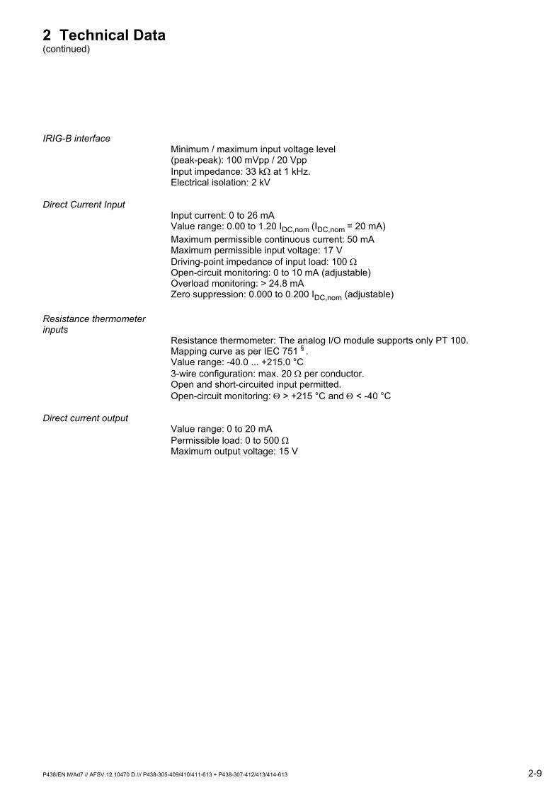
IRIG-B interface Minimum / maximum input voltage level (peak-peak): 100 mVpp / 20 Vpp Input impedance: 33 kΩ at 1 kHz. Electrical isolation: 2 kV
Direct Current Input Input current: 0 to 26 mA Value range: 0.00 to 1.20 IDC,nom (IDC,nom = 20 mA) Maximum permissible continuous current: 50 mA Maximum permissible input voltage: 17 V Driving-point impedance of input load: 100 Ω Open-circuit monitoring: 0 to 10 mA (adjustable) Overload monitoring: > 24.8 mA Zero suppression: 0.000 to 0.200 IDC,nom (adjustable)
Resistance thermometer inputs
Resistance thermometer: The analog I/O module supports only PT 100. Mapping curve as per IEC 751 § . Value range: -40.0 ... +215.0 °C 3-wire configuration: max. 20 Ω per conductor. Open and short-circuited input permitted. Open-circuit monitoring: Θ > +215 °C and Θ < -40 °C
Direct current output Value range: 0 to 20 mA Permissible load: 0 to 500 Ω Maximum output voltage: 15 V
2 Technical Data (continued)
2-10 P438/EN M/Ad7 // AFSV.12.10470 D /// P438-305-409/410/411-613 + P438-307-412/413/414-613
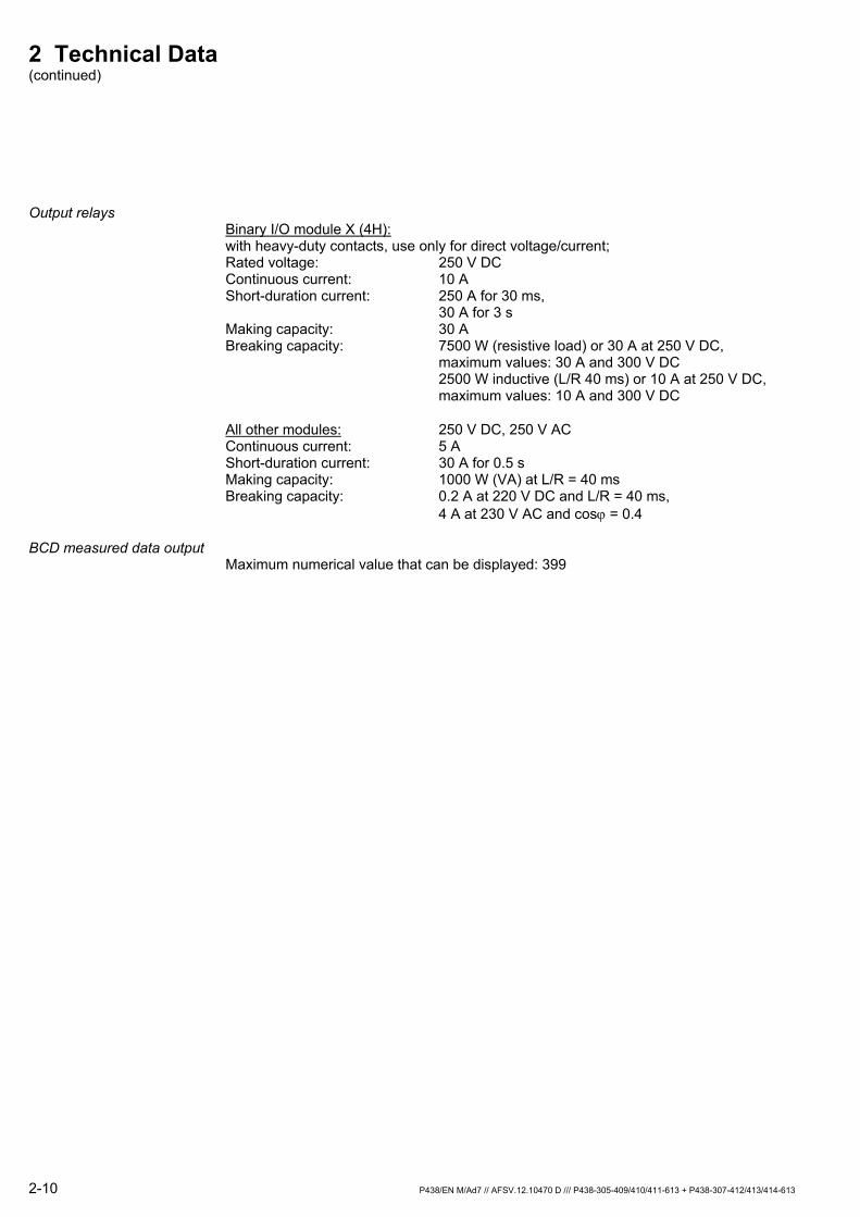
Output relays Binary I/O module X (4H): with heavy-duty contacts, use only for direct voltage/current; Rated voltage: 250 V DC Continuous current: 10 A Short-duration current: 250 A for 30 ms, 30 A for 3 s Making capacity: 30 A Breaking capacity: 7500 W (resistive load) or 30 A at 250 V DC, maximum values: 30 A and 300 V DC 2500 W inductive (L/R 40 ms) or 10 A at 250 V DC, maximum values: 10 A and 300 V DC
All other modules: 250 V DC, 250 V AC Continuous current: 5 A Short-duration current: 30 A for 0.5 s Making capacity: 1000 W (VA) at L/R = 40 ms Breaking capacity: 0.2 A at 220 V DC and L/R = 40 ms, 4 A at 230 V AC and cosϕ = 0.4
BCD measured data output Maximum numerical value that can be displayed: 399
2 Technical Data (continued)
P438/EN M/Ad7 // AFSV.12.10470 D /// P438-305-409/410/411-613 + P438-307-412/413/414-613 2-11
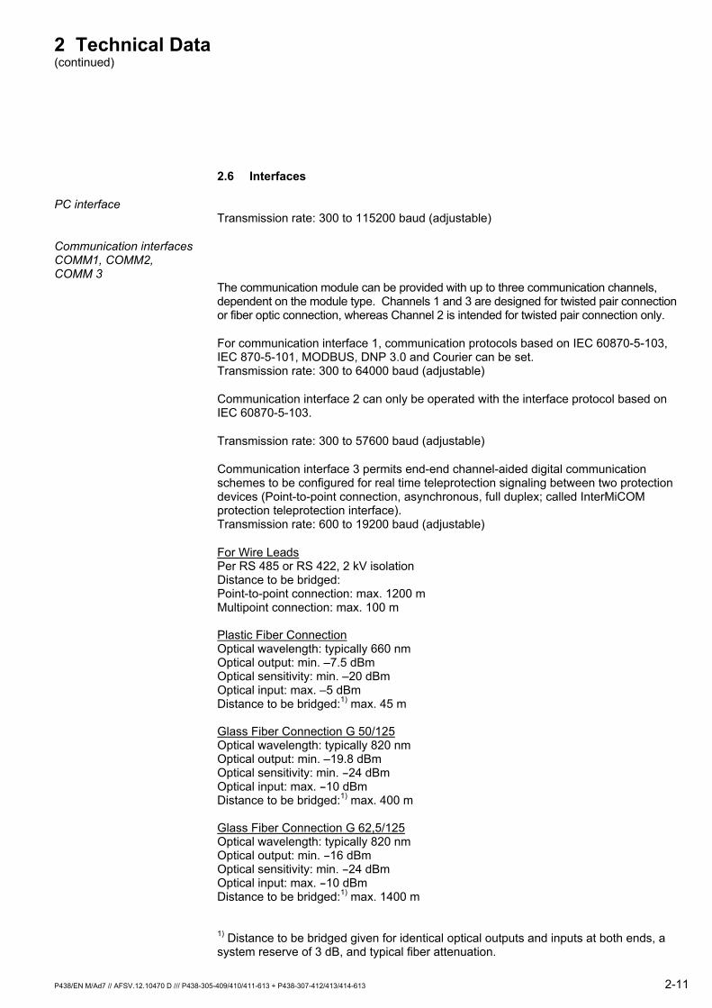
2.6 Interfaces
PC interface Transmission rate: 300 to 115200 baud (adjustable)
Communication interfaces COMM1, COMM2, COMM 3
The communication module can be provided with up to three communication channels, dependent on the module type. Channels 1 and 3 are designed for twisted pair connection or fiber optic connection, whereas Channel 2 is intended for twisted pair connection only.
For communication interface 1, communication protocols based on IEC 60870-5-103, IEC 870-5-101, MODBUS, DNP 3.0 and Courier can be set. Transmission rate: 300 to 64000 baud (adjustable)
Communication interface 2 can only be operated with the interface protocol based on IEC 60870-5-103.
Transmission rate: 300 to 57600 baud (adjustable)
Communication interface 3 permits end-end channel-aided digital communication schemes to be configured for real time teleprotection signaling between two protection devices (Point-to-point connection, asynchronous, full duplex; called InterMiCOM protection teleprotection interface). Transmission rate: 600 to 19200 baud (adjustable)
For Wire Leads Per RS 485 or RS 422, 2 kV isolation Distance to be bridged: Point-to-point connection: max. 1200 m Multipoint connection: max. 100 m Plastic Fiber Connection Optical wavelength: typically 660 nm Optical output: min. –7.5 dBm Optical sensitivity: min. –20 dBm Optical input: max. –5 dBm Distance to be bridged:1) max. 45 m Glass Fiber Connection G 50/125 Optical wavelength: typically 820 nm Optical output: min. –19.8 dBm Optical sensitivity: min. -24 dBm Optical input: max. -10 dBm Distance to be bridged:1) max. 400 m Glass Fiber Connection G 62,5/125 Optical wavelength: typically 820 nm Optical output: min. -16 dBm Optical sensitivity: min. -24 dBm Optical input: max. -10 dBm Distance to be bridged:1) max. 1400 m 1) Distance to be bridged given for identical optical outputs and inputs at both ends, a system reserve of 3 dB, and typical fiber attenuation.

2 Technical Data (continued)
2-12 P438/EN M/Ad7 // AFSV.12.10470 D /// P438-305-409/410/411-613 + P438-307-412/413/414-613
IEC communication interface:
For Wire Leads IEC 61850-compliant, Ethernet-based communications: Transmission rate: 10 or 100 Mbit/s RJ45, 1.5 kV isolation Maximum distance: 100 m for optical fibers (100 Mbit/s) IEC 61850-compliant, Ethernet-based communications: ST connector or SC connector Optical wavelength: typically 1300 nm Glass fiber G50/125: Optical output: min. –23,5 dBm Optical sensitivity: min. –31 dBm Optical input: max. –14 dBm Glass fiber G62.5/125: Optical output: min. –20 dBm Optical sensitivity: min. –31 dBm Optical input: max. –14 dBm
IRIG-B interface B122 format Amplitude-modulated signal Carrier frequency: 1 kHz Date in binary coded decimal (BCD)
User interface (HMI) Input or output: via 13 keys and a liquid crystal display (LCD) with 4 x 20 characters
State and fault signals: 23 LED indicators (5 fixed assignment, 18 freely configurable)
2 Technical Data (continued)
P438/EN M/Ad7 // AFSV.12.10470 D /// P438-305-409/410/411-613 + P438-307-412/413/414-613 2-13
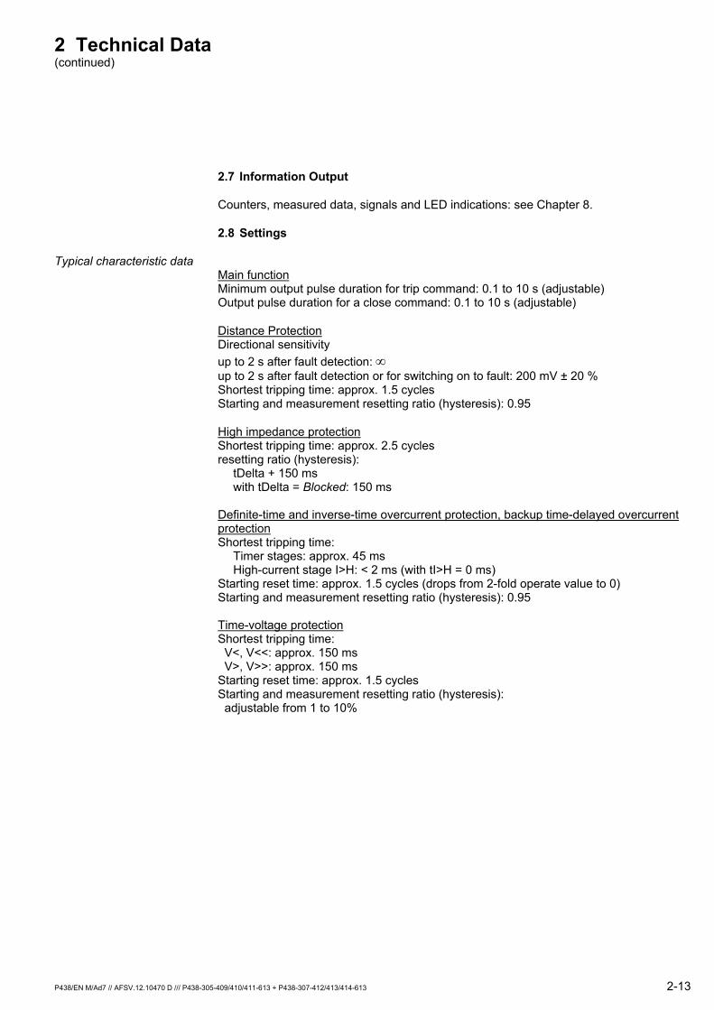
2.7 Information Output
Counters, measured data, signals and LED indications: see Chapter 8.
2.8 Settings
Typical characteristic data Main function Minimum output pulse duration for trip command: 0.1 to 10 s (adjustable) Output pulse duration for a close command: 0.1 to 10 s (adjustable)
Distance Protection Directional sensitivity up to 2 s after fault detection: ∞ up to 2 s after fault detection or for switching on to fault: 200 mV ± 20 % Shortest tripping time: approx. 1.5 cycles Starting and measurement resetting ratio (hysteresis): 0.95
High impedance protection Shortest tripping time: approx. 2.5 cycles resetting ratio (hysteresis): tDelta + 150 ms with tDelta = Blocked: 150 ms Definite-time and inverse-time overcurrent protection, backup time-delayed overcurrent protection Shortest tripping time: Timer stages: approx. 45 ms High-current stage I>H: < 2 ms (with tI>H = 0 ms) Starting reset time: approx. 1.5 cycles (drops from 2-fold operate value to 0) Starting and measurement resetting ratio (hysteresis): 0.95 Time-voltage protection Shortest tripping time: V<, V<<: approx. 150 ms V>, V>>: approx. 150 ms Starting reset time: approx. 1.5 cycles Starting and measurement resetting ratio (hysteresis): adjustable from 1 to 10%
2 Technical Data (continued)
2-14 P438/EN M/Ad7 // AFSV.12.10470 D /// P438-305-409/410/411-613 + P438-307-412/413/414-613
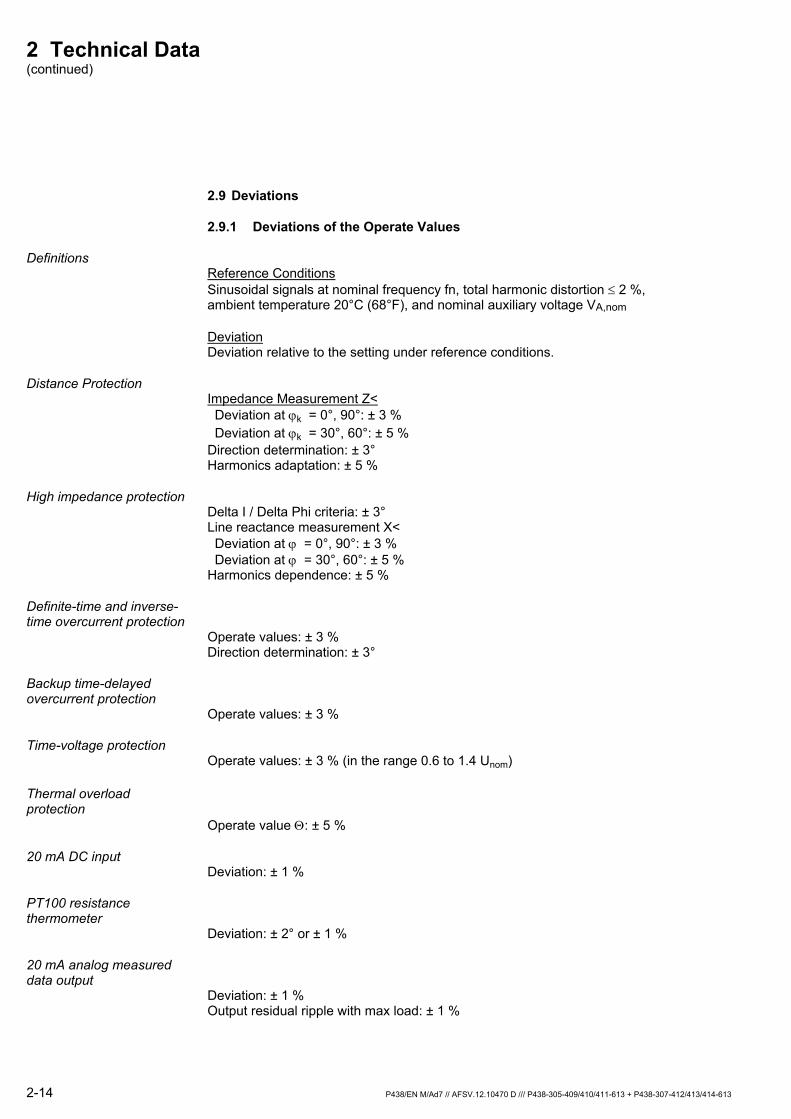
2.9 Deviations
2.9.1 Deviations of the Operate Values
Definitions Reference Conditions Sinusoidal signals at nominal frequency fn, total harmonic distortion ≤ 2 %, ambient temperature 20°C (68°F), and nominal auxiliary voltage VA,nom
Deviation Deviation relative to the setting under reference conditions.
Distance Protection Impedance Measurement Z< Deviation at ϕk = 0°, 90°: ± 3 % Deviation at ϕk = 30°, 60°: ± 5 % Direction determination: ± 3° Harmonics adaptation: ± 5 %
High impedance protection Delta I / Delta Phi criteria: ± 3° Line reactance measurement X< Deviation at ϕ = 0°, 90°: ± 3 % Deviation at ϕ = 30°, 60°: ± 5 % Harmonics dependence: ± 5 %
Definite-time and inverse-time overcurrent protection
Operate values: ± 3 % Direction determination: ± 3°
Backup time-delayed overcurrent protection
Operate values: ± 3 %
Time-voltage protection Operate values: ± 3 % (in the range 0.6 to 1.4 Unom)
Thermal overload protection
Operate value Θ: ± 5 %
20 mA DC input Deviation: ± 1 %
PT100 resistance thermometer
Deviation: ± 2° or ± 1 %
20 mA analog measured data output
Deviation: ± 1 % Output residual ripple with max load: ± 1 %
2 Technical Data (continued)
P438/EN M/Ad7 // AFSV.12.10470 D /// P438-305-409/410/411-613 + P438-307-412/413/414-613 2-15
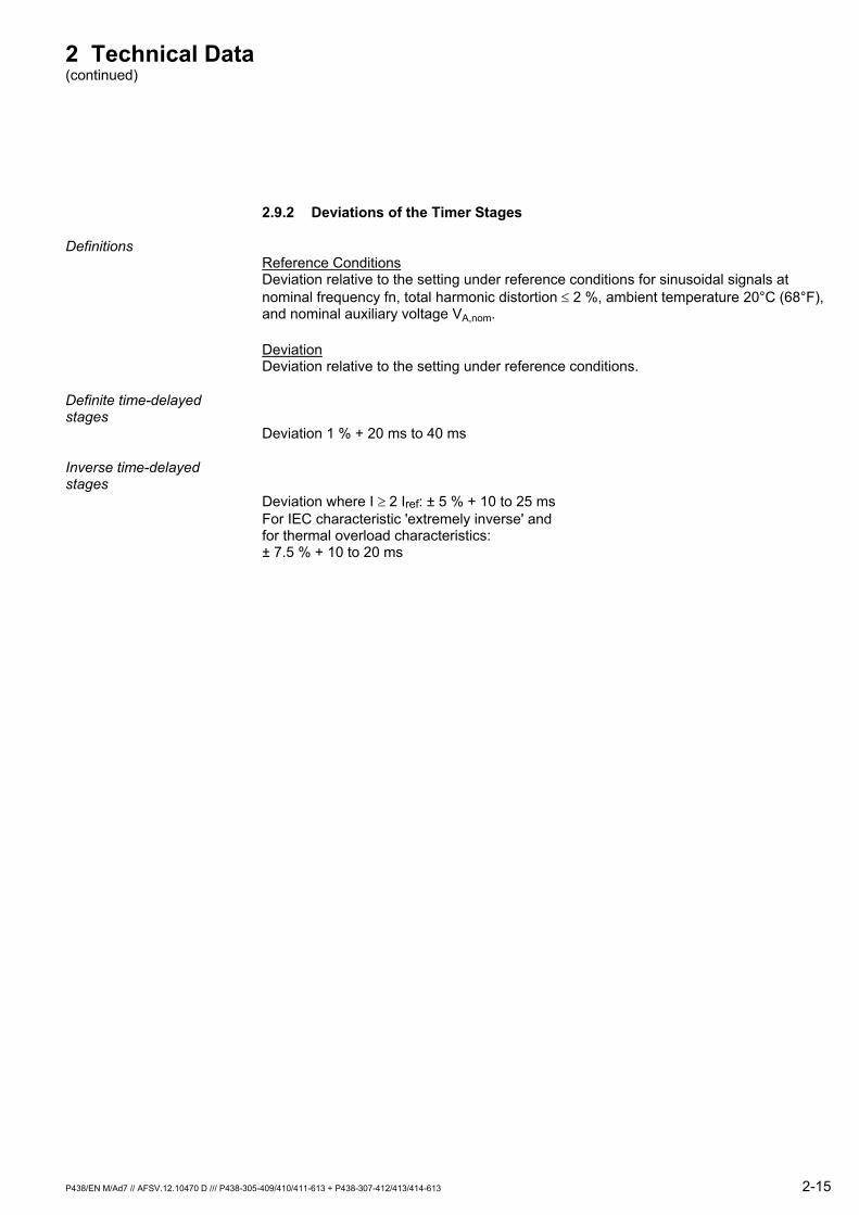
2.9.2 Deviations of the Timer Stages
Definitions Reference Conditions Deviation relative to the setting under reference conditions for sinusoidal signals at nominal frequency fn, total harmonic distortion ≤ 2 %, ambient temperature 20°C (68°F), and nominal auxiliary voltage VA,nom.
Deviation Deviation relative to the setting under reference conditions.
Definite time-delayed stages
Deviation 1 % + 20 ms to 40 ms
Inverse time-delayed stages
Deviation where I ≥ 2 Iref: ± 5 % + 10 to 25 ms For IEC characteristic 'extremely inverse' and for thermal overload characteristics: ± 7.5 % + 10 to 20 ms
2 Technical Data (continued)
2-16 P438/EN M/Ad7 // AFSV.12.10470 D /// P438-305-409/410/411-613 + P438-307-412/413/414-613
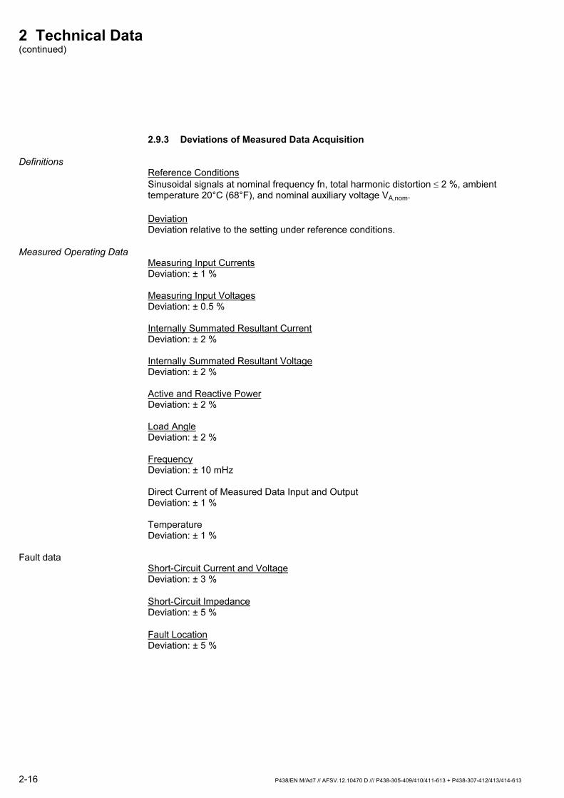
2.9.3 Deviations of Measured Data Acquisition
Definitions Reference Conditions Sinusoidal signals at nominal frequency fn, total harmonic distortion ≤ 2 %, ambient temperature 20°C (68°F), and nominal auxiliary voltage VA,nom.
Deviation Deviation relative to the setting under reference conditions.
Measured Operating Data Measuring Input Currents Deviation: ± 1 % Measuring Input Voltages Deviation: ± 0.5 % Internally Summated Resultant Current Deviation: ± 2 % Internally Summated Resultant Voltage Deviation: ± 2 % Active and Reactive Power Deviation: ± 2 % Load Angle Deviation: ± 2 % Frequency Deviation: ± 10 mHz Direct Current of Measured Data Input and Output Deviation: ± 1 % Temperature Deviation: ± 1 %
Fault data Short-Circuit Current and Voltage Deviation: ± 3 %
Short-Circuit Impedance Deviation: ± 5 %
Fault Location Deviation: ± 5 %
2 Technical Data (continued)
P438/EN M/Ad7 // AFSV.12.10470 D /// P438-305-409/410/411-613 + P438-307-412/413/414-613 2-17
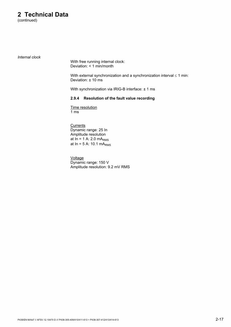
Internal clock With free running internal clock: Deviation: < 1 min/month
With external synchronization and a synchronization interval ≤ 1 min: Deviation: ± 10 ms
With synchronization via IRIG-B interface: ± 1 ms
2.9.4 Resolution of the fault value recording
Time resolution 1 ms
Currents Dynamic range: 25 In Amplitude resolution at In = 1 A: 2.0 mARMS at In = 5 A: 10.1 mARMS
Voltage Dynamic range: 150 V Amplitude resolution: 9.2 mV RMS
2 Technical Data (continued)
2-18 P438/EN M/Ad7 // AFSV.12.10470 D /// P438-305-409/410/411-613 + P438-307-412/413/414-613
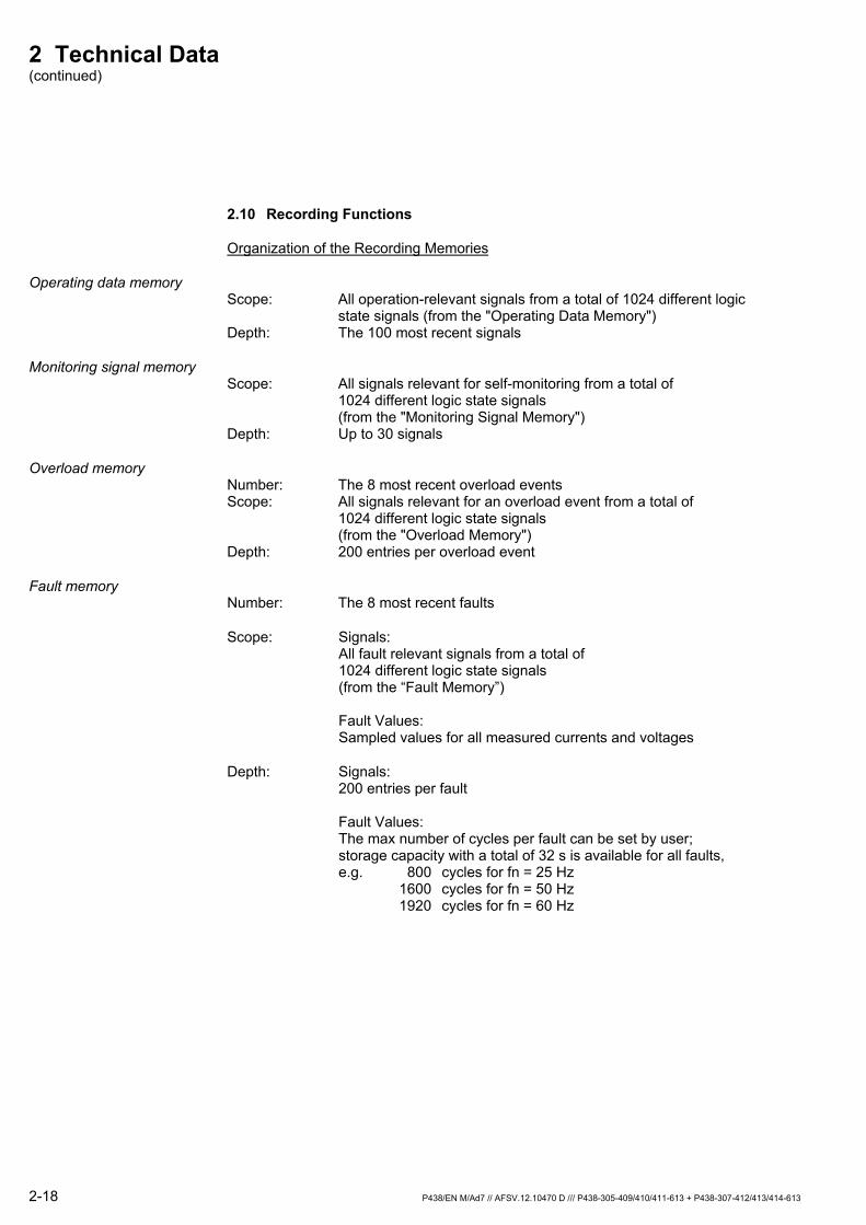
2.10 Recording Functions
Organization of the Recording Memories
Operating data memory Scope: All operation-relevant signals from a total of 1024 different logic state signals (from the "Operating Data Memory") Depth: The 100 most recent signals
Monitoring signal memory Scope: All signals relevant for self-monitoring from a total of 1024 different logic state signals (from the "Monitoring Signal Memory") Depth: Up to 30 signals
Overload memory Number: The 8 most recent overload events Scope: All signals relevant for an overload event from a total of 1024 different logic state signals (from the "Overload Memory") Depth: 200 entries per overload event
Fault memory Number: The 8 most recent faults
Scope: Signals: All fault relevant signals from a total of 1024 different logic state signals (from the “Fault Memory”) Fault Values: Sampled values for all measured currents and voltages
Depth: Signals: 200 entries per fault Fault Values: The max number of cycles per fault can be set by user; storage capacity with a total of 32 s is available for all faults, e.g. 800 cycles for fn = 25 Hz 1600 cycles for fn = 50 Hz 1920 cycles for fn = 60 Hz
2 Technical Data (continued)
P438/EN M/Ad7 // AFSV.12.10470 D /// P438-305-409/410/411-613 + P438-307-412/413/414-613 2-19
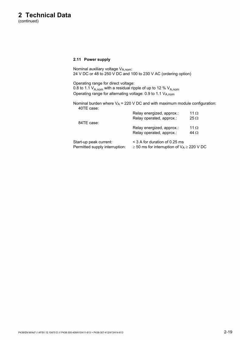
2.11 Power supply
Nominal auxiliary voltage VA,nom: 24 V DC or 48 to 250 V DC and 100 to 230 V AC (ordering option)
Operating range for direct voltage: 0.8 to 1.1 VA,nom with a residual ripple of up to 12 % VA,nom Operating range for alternating voltage: 0.9 to 1.1 VA,nom
Nominal burden where VA = 220 V DC and with maximum module configuration: 40TE case: Relay energized, approx.: 11 Ω Relay operated, approx.: 25 Ω 84TE case: Relay energized, approx.: 11 Ω Relay operated, approx.: 44 Ω Start-up peak current: < 3 A for duration of 0.25 ms Permitted supply interruption: ≥ 50 ms for interruption of VA ≥ 220 V DC
2 Technical Data (continued)
2-20 P438/EN M/Ad7 // AFSV.12.10470 D /// P438-305-409/410/411-613 + P438-307-412/413/414-613
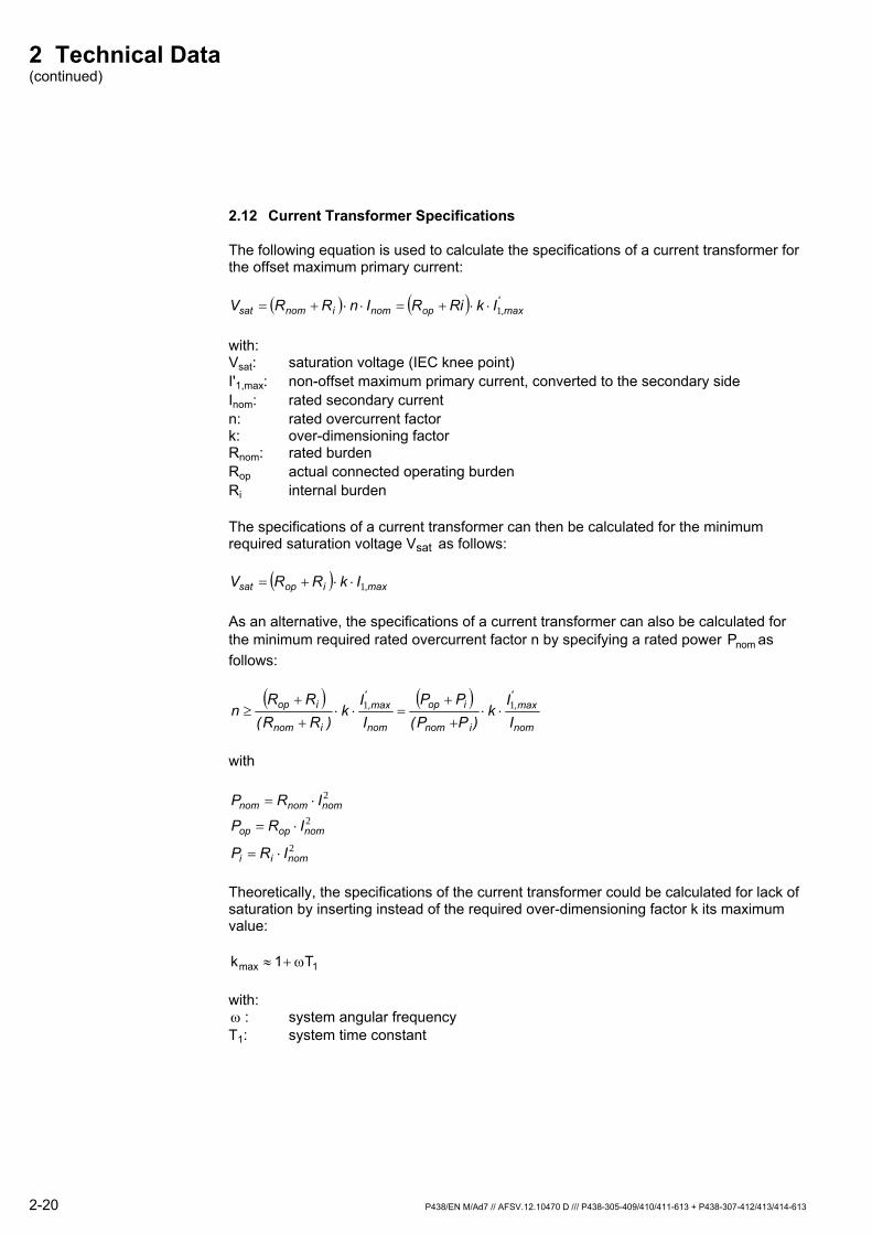
2.12 Current Transformer Specifications
The following equation is used to calculate the specifications of a current transformer for the offset maximum primary current:
( ) ( ) 'max,opnominomsat IkRiRInRRV 1⋅⋅+=⋅⋅+=
with: Vsat: saturation voltage (IEC knee point) I'1,max: non-offset maximum primary current, converted to the secondary side Inom: rated secondary current n: rated overcurrent factor k: over-dimensioning factor Rnom: rated burden Rop actual connected operating burden Ri internal burden
The specifications of a current transformer can then be calculated for the minimum required saturation voltage Vsat as follows:
( ) max,iopsat IkRRV 1⋅⋅+=
As an alternative, the specifications of a current transformer can also be calculated for the minimum required rated overcurrent factor n by specifying a rated power Pnom as follows:
( ) ( )nom
',max
inom
iop
nom
',max
inom
iop
II
k)PP(
PPII
k)RR(
RRn 11 ⋅⋅
+
+=⋅⋅
+
+≥
with
2
2
2
nomii
nomopop
nomnomnom
IRP
IRP
IRP
⋅=
⋅=
⋅=
Theoretically, the specifications of the current transformer could be calculated for lack of saturation by inserting instead of the required over-dimensioning factor k its maximum value:
k Tmax ≈ +1 1ω
with: ω : system angular frequency T1: system time constant
2 Technical Data (continued)
P438/EN M/Ad7 // AFSV.12.10470 D /// P438-305-409/410/411-613 + P438-307-412/413/414-613 2-21
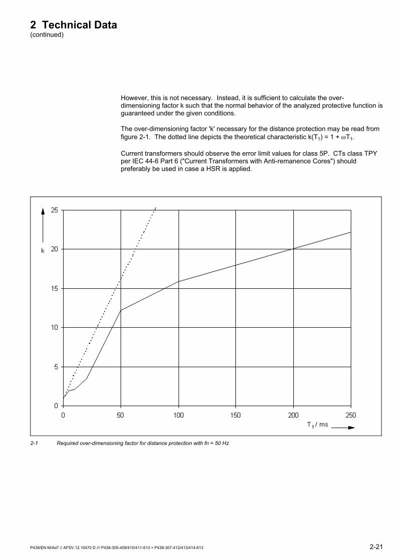
However, this is not necessary. Instead, it is sufficient to calculate the over-dimensioning factor k such that the normal behavior of the analyzed protective function is guaranteed under the given conditions.
The over-dimensioning factor 'k' necessary for the distance protection may be read from figure 2-1. The dotted line depicts the theoretical characteristic k(T1) = 1 + ωT1.
Current transformers should observe the error limit values for class 5P. CTs class TPY per IEC 44-6 Part 6 ("Current Transformers with Anti-remanence Cores") should preferably be used in case a HSR is applied.
2-1 Required over-dimensioning factor for distance protection with fn = 50 Hz

2-22 P438/EN M/Ad7 // AFSV.12.10470 D /// P438-305-409/410/411-613 + P438-307-412/413/414-613
3 Operation
P438/EN M/Ad7 // AFSV.12.10470 D /// P438-305-409/410/411-613 + P438-307-412/413/414-613 3-1
3 Operation
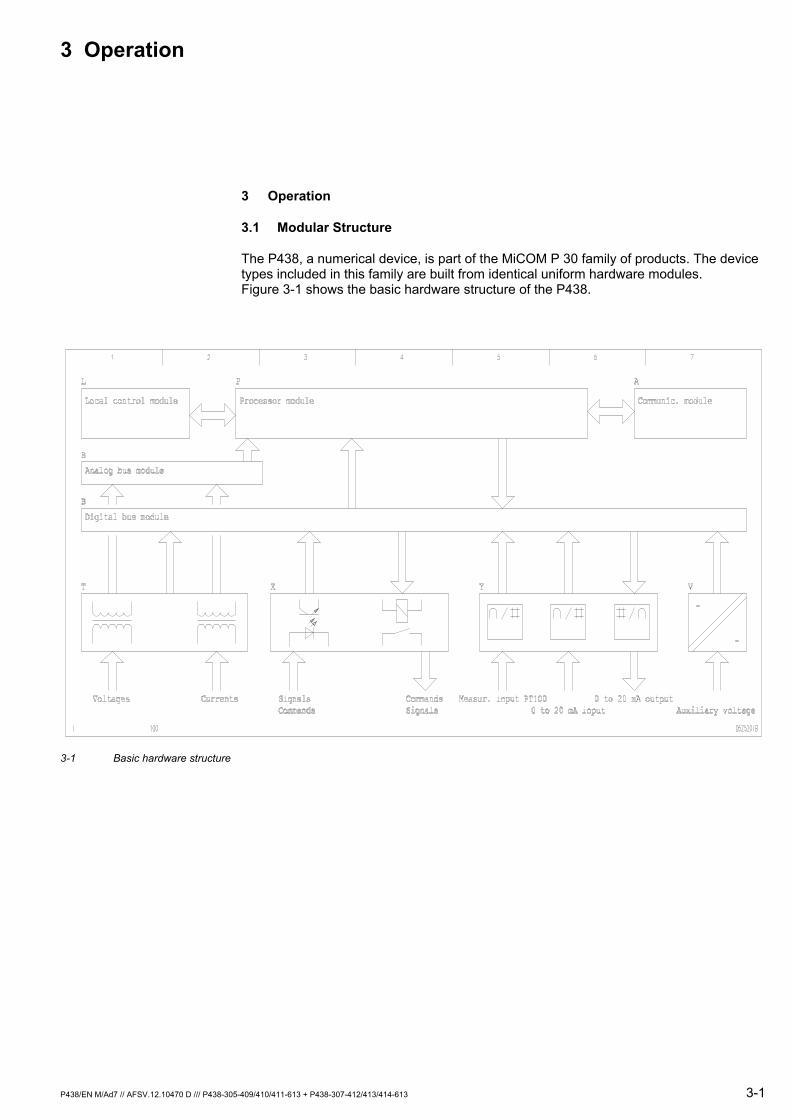
3.1 Modular Structure
The P438, a numerical device, is part of the MiCOM P 30 family of products. The device types included in this family are built from identical uniform hardware modules. Figure 3-1 shows the basic hardware structure of the P438.
3-1 Basic hardware structure
3 Operation (continued)
3-2 P438/EN M/Ad7 // AFSV.12.10470 D /// P438-305-409/410/411-613 + P438-307-412/413/414-613
The external analog and binary quantities – electrically isolated – are converted to the internal processing levels by the peripheral modules: T, Y, and X. Commands and signals internally generated by the device are connected to the external plant via contacts through binary I/O modules X. The external auxiliary voltage is applied to power supply module V, which in turn supplies the auxiliary voltages that are required internally.
Analog data is transferred from the transformer module T via the analog bus module B to the processor module P. The processor module contains all the elements necessary for the conversion of measured analog values, including multiplexers and analog/digital converters. The analog data conditioned by the analog I/O module Y is transferred to the processor module P via the digital bus module. Binary signals are fed to the processor module by the binary I/O modules X via the digital bus module. The processor handles the processing of digitized analog vaues and of binary signals, generates the protective trip and signals, and transfers them to the binary I/O modules X via the digital bus module. The processor module also handles overall device communication. As an option, communication module A can be mounted on the processor module to provide serial communication with substation control systems.
The control and display elements of the integrated user interface (HMI) and the integrated PC interface are housed on control module L.
3 Operation (continued)
P438/EN M/Ad7 // AFSV.12.10470 D /// P438-305-409/410/411-613 + P438-307-412/413/414-613 3-3
3.2 Operator-Machine Communication
The following interfaces are available for the exchange of information between the user and the device:
Integrated local control panel (HMI)
PC interface
Rear communication interface
All settings and signals as well as all measurements and control functions are arranged within the branches of the menu tree following a scheme that is uniform throughout the device family. The main branches are:
‘Settings’ branch All settings are contained in this branch. This branch carries all settings, including the device identification data, the configuration parameters for adapting the device's interfaces to the system, and the function parameters for adapting the device functions to the process. All values in this group are stored in non-volatile memory, which means that the values will be preserved even if the power supply fails.
‘Measurement and Tests’ branch
This branch includes all information relevant for operation such as measured operating data and binary signal states. This information is updated periodically and consequently is not stored. In addition, various controls are grouped here, for example those for resetting counters, memories and displays.
‘Fault and Events’ branch The third branch is reserved for the recording of events. All information in this group is therefore stored. In particular, the start/end signals during a fault, the measured fault data, and the sampled fault waveforms are stored here and can be read out when required.
Settings and signals are displayed either in plain text or as addresses, in accordance with the user’s choice. Chapters 7, 8 and 10 describe the settings, signals and measured values available with the P438. The possible setting values can be found in the P438's data model file associated with the PC support software (MiCOM S1).
The configuration of the user interface (HMI) also permits the installation of Measured Value 'Panels’ on the LCD display. Different Panels are automatically displayed for specific system operating conditions. Priority increases from normal operation to operation under overload conditions to operation during a ground fault to operation following a short circuit in the system. Thus the P438 provides the measured data relevant for the prevailing conditions.
3 Operation (continued)
3-4 P438/EN M/Ad7 // AFSV.12.10470 D /// P438-305-409/410/411-613 + P438-307-412/413/414-613
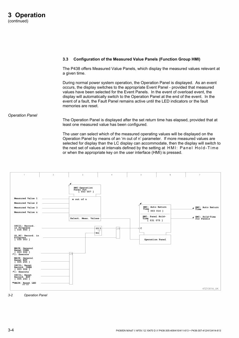
3.3 Configuration of the Measured Value Panels (Function Group HMI)
The P438 offers Measured Value Panels, which display the measured values relevant at a given time.
During normal power system operation, the Operation Panel is displayed. As an event occurs, the display switches to the appropriate Event Panel - provided that measured values have been selected for the Event Panels. In the event of overload event, the display will automatically switch to the Operation Panel at the end of the event. In the event of a fault, the Fault Panel remains active until the LED indicators or the fault memories are reset.
Operation Panel The Operation Panel is displayed after the set return time has elapsed, provided that at least one measured value has been configured.
The user can select which of the measured operating values will be displayed on the Operation Panel by means of an ‘m out of n’ parameter. If more measured values are selected for display than the LC display can accommodate, then the display will switch to the next set of values at intervals defined by the setting at H M I : P a n e l H o l d - T i m e or when the appropriate key on the user interface (HMI) is pressed.
47Z1301A_UK
HMI:OperationPanel Fct [ 053 007 ]
OSCIL: Record.in Progress[ 035 000 ]
Measured Value 1
Measured Value 2
Measured Value 3
Measured Value n
Select. Meas. Values
m out of n
OL_RC: Record. inProgress[ 035 003 ]
MAIN: Reset LED306 020
1: Execute
MAIN: GeneralReset EXT[ 005 255 ]OSCIL: ResetRecord. USER[ 003 006 ]1: Execute
MAIN: GeneralReset USER[ 003 002 ]
≥1
OSCIL: ResetRecord. EXT[ 005 243 ]
≥1
R1
S1 1
Operation Panel
HMI: Auto ReturnTime [ 003 014 ]
HMI: Panel Hold-Time [ 031 075 ]
C
HMI: Auto ReturnTime
HMI: Hold-Timefor Panels
3-2 Operation Panel
3 Operation (continued)
P438/EN M/Ad7 // AFSV.12.10470 D /// P438-305-409/410/411-613 + P438-307-412/413/414-613 3-5
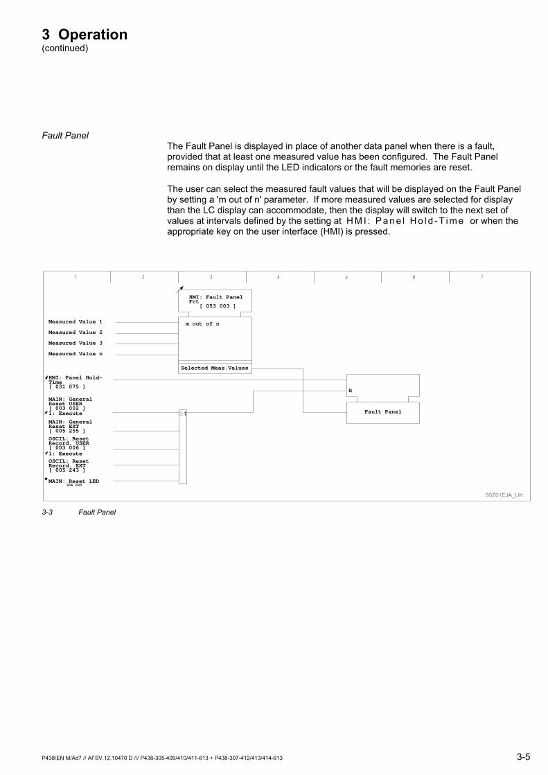
Fault Panel The Fault Panel is displayed in place of another data panel when there is a fault, provided that at least one measured value has been configured. The Fault Panel remains on display until the LED indicators or the fault memories are reset.
The user can select the measured fault values that will be displayed on the Fault Panel by setting a 'm out of n' parameter. If more measured values are selected for display than the LC display can accommodate, then the display will switch to the next set of values at intervals defined by the setting at H M I : P a n e l H o l d - T i m e or when the appropriate key on the user interface (HMI) is pressed.
50Z01EJA_UK
MAIN: Reset LED306 020
1: Execute
MAIN: GeneralReset EXT[ 005 255 ]OSCIL: ResetRecord. USER[ 003 006 ]1: Execute
MAIN: GeneralReset USER[ 003 002 ]
≥1
OSCIL: ResetRecord. EXT[ 005 243 ]
HMI: Fault PanelFct [ 053 003 ]
Measured Value 1
Measured Value 2
Measured Value 3
Measured Value n
Selected Meas.Values
m out of n
Fault Panel
R
HMI: Panel Hold-Time[ 031 075 ]
3-3 Fault Panel
3 Operation (continued)
3-6 P438/EN M/Ad7 // AFSV.12.10470 D /// P438-305-409/410/411-613 + P438-307-412/413/414-613
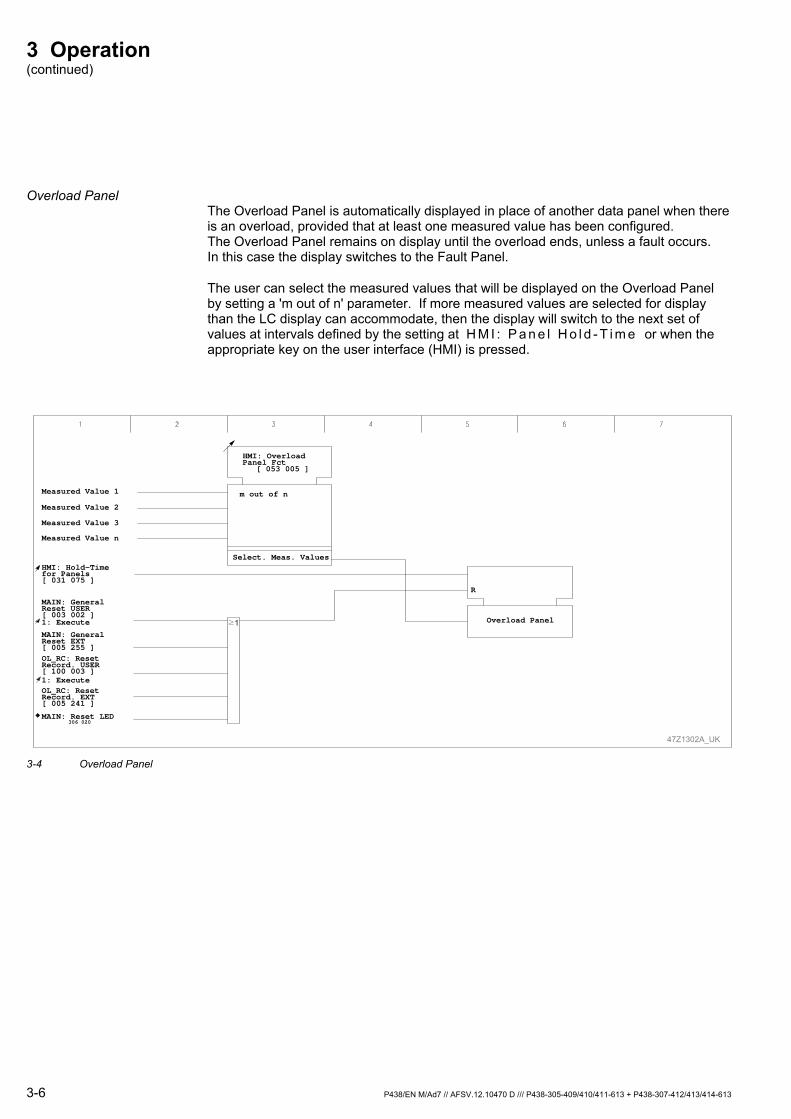
Overload Panel The Overload Panel is automatically displayed in place of another data panel when there is an overload, provided that at least one measured value has been configured. The Overload Panel remains on display until the overload ends, unless a fault occurs. In this case the display switches to the Fault Panel.
The user can select the measured values that will be displayed on the Overload Panel by setting a 'm out of n' parameter. If more measured values are selected for display than the LC display can accommodate, then the display will switch to the next set of values at intervals defined by the setting at H M I : P a n e l H o l d - T i m e or when the appropriate key on the user interface (HMI) is pressed.
47Z1302A_UK
MAIN: Reset LED306 020
1: Execute
MAIN: GeneralReset EXT[ 005 255 ]OL_RC: ResetRecord. USER[ 100 003 ]1: Execute
MAIN: GeneralReset USER[ 003 002 ]
≥1
OL_RC: ResetRecord. EXT[ 005 241 ]
HMI: OverloadPanel Fct
[ 053 005 ]
HMI: Hold-Timefor Panels[ 031 075 ]
Overload Panel
R
Measured Value 1
Measured Value 2
Measured Value 3
Measured Value n
Select. Meas. Values
m out of n
3-4 Overload Panel
3 Operation (continued)
P438/EN M/Ad7 // AFSV.12.10470 D /// P438-305-409/410/411-613 + P438-307-412/413/414-613 3-7
Function keys on the user interface HMI
The user interface HMI is fitted with 6 freely configurable function keys. Either a single function, one of the two group resetting functions or one of the two menu jump lists may be assigned to each of these function keys with the setting at F _ K e y : F c t . F x A s s i g n (Fx: F1 to F6).
As an example the operation of function key F1 is shown in the figure in section 'Configurable Function Keys (Function Group F_KEY)'. Function key F1 is enabled only after the associated password, as defined at F _ K E Y : P a s s w o r d F u n c t . K e y 1 , has been entered. After the password has been entered the function key will remain active for the time period set at F _ K E Y : F c n K e y R e t u r n T i m e . Thereafter, the function key is disabled until the password is entered again. The same is valid for function keys F2 to F6.
Additional information pertaining to function keys and their application can be found in section 'Configurable Function Keys (Function Group F_KEY)' and section 'Resetting Actions' of Chapter 3 and in section 'Configurable Function Keys F1 to Fx (general)' of Chapter 6.
Note: Each of the 6 keys has an LED indicator situated next to it which is freely configurable, like the other 12 LED indicators, but independent of the configuration of the function keys (i.e. the function assignment is for red and green light emission).
Configuration of the READ key
Similarly to the setting at H M I : F c t . M e n u J m p L i s t x up to 16 functions may also be selected from the menu jump list at H M I : F c t R e a d K e y . They are triggered in sequence by repeated pressing of the "READ" key.
Configuration of the CLEAR key ('C')
Similarly to the setting at M A I N : F c t . A s s i g n . R e s e t x up to 10 reset functions may be selected from a list at H M I : F k t R e s e t K e y . These are carried out by pressing the "CLEAR" C key. Additional information pertaining to reset functions can be found in sub-section 'Resetting Actions' in section 'Main Functions of the P438 (Function Group MAIN) of Chapter 3.
3 Operation (continued)
3-8 P438/EN M/Ad7 // AFSV.12.10470 D /// P438-305-409/410/411-613 + P438-307-412/413/414-613
3.4 Serial Interfaces
The P438 has a front port PC link as standard. Optionally a communication module A providing two communication channels is available. Communication between the P438 and SCADA is done through communication module A. Setting and interrogation is possible through all the P438’s interfaces.
Two rear port communications interfaces may be fitted. The settings of rear port communications interface 1 (COMM1) may be assigned to the physical communications channels 1 or 2 (see function group "MAIN"). If the COMM1 settings have been assigned to communications channel 2, then the settings of communications interface 2 (COMM2) will automatically be active for communications channel 1. Communication channel 2 can only be used to transmit data to and from the P438 if its PC link has been de-activated. As soon as the PC link is used to transmit data, communication channel 2 becomes "dead". It will be enabled again only after the PC interface “Time-out” has elapsed.
If tests are run on the P438, the user is advised to activate the test mode. In this way the PC or the control system will recognize all incoming test signals accordingly (see function group "MAIN").
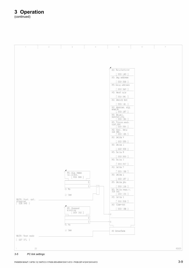
3.4.1 PC Link (Function Group PC)
Communication between the device and a PC is done through the PC link. In order for data transfer between the P438 and the PC to function, several settings must be made in the P438.
There is an operating program available as an accessory for control of the P438 (see Chapter 13).
3 Operation (continued)
P438/EN M/Ad7 // AFSV.12.10470 D /// P438-305-409/410/411-613 + P438-307-412/413/414-613 3-9
Relay
3-5 PC link settings

3 Operation (continued)
3-10 P438/EN M/Ad7-S // AFSV.12.10470 D /// P438-305-409/410/411-613 + P438-307-412/413/414-613
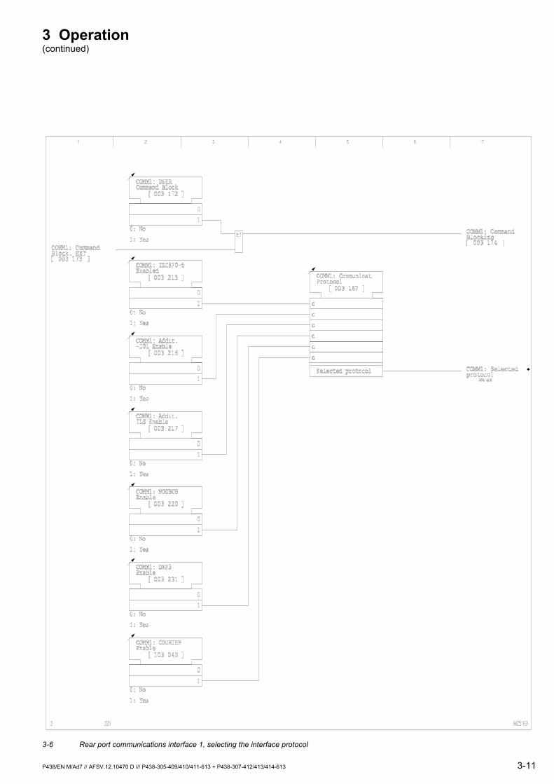
3.4.2 Rear Port Communications Interface 1 (Function Group COMM1)
Communication between the P438 and the control station’s computer is done through the communications interface. Several interface protocols are available at the rear port communications interface 1. The IEC 60870-5-103 protocol is always supported. The following user-selected interface protocols are available for use with the P438:
IEC 60870-5-103, “Transmission protocols - Companion standard for the informative interface of protection equipment, first edition, 1997-12 (corresponds to VDEW / ZVEI Recommendation, “Protection communication companion standard 1, compatibility level 2”, February 1995 edition) with additions covering control and monitoring
IEC 870-5-101, "Telecontrol equipment and systems - Part 5: Transmission protocols - Section 101 Companion standard for basic telecontrol tasks," first edition 1995-11
ILS-C, internal protocol of Schneider Electric
MODBUS
DNP 3.0
COURIER
In order for data transfer to function properly, several settings must be entered in the P438.
The rear port communications interface can be blocked through a binary signal input. In addition, a signal or measured-data block can also be imposed through a binary signal input.
3 Operation (continued)
P438/EN M/Ad7 // AFSV.12.10470 D /// P438-305-409/410/411-613 + P438-307-412/413/414-613 3-11
3-6 Rear port communications interface 1, selecting the interface protocol
3 Operation (continued)
3-12 P438/EN M/Ad7 // AFSV.12.10470 D /// P438-305-409/410/411-613 + P438-307-412/413/414-613
COMM1: Selectedprotocol
COMM1: IEC60870-5-103
MAIN: Test mode
COMM1: Generalenable USER
COMM1: Commandblocking
COMM1: Sig./meas.Block EXT
MAIN: Prot. Ext.disabled
COMM1: Sig./meas.Block.USER
0: No
1: Yes
COMM1: Baude rate
COMM1: Parity bit
COMM1: Select.spontan.sig.
COMM1: Transm.enab.cycl.dat
COMM1: Cycl. dataILS tel.
COMM1: Delta V
COMM1: Delta I
COMM1: Delta P
COMM1: Delta f
COMM1: Delta T
COMM1: Delta Z
COMM1: Delta phi
COMM1: Deltameas.v.ILS tel
COMM1: Delta t
Commun. interface
COMM1: Sig./meas.val.block.
48Z50FFA_EN
COMM1: Line idlestate
COMM1: Dead timemonitoring
COMM1: Mon. Timepolling
COMM1: Octet comm.address
COMM1: Testmonitor on
COMM1: Name ofmanufacturer
COMM1: Octetaddress ASDU
COMM1: Spontan.sig. enable
COMM1: Contin.general scan
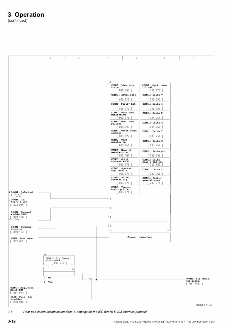
3-7 Rear port communications interface 1, settings for the IEC 60870-5-103 interface protocol
3 Operation (continued)
P438/EN M/Ad7 // AFSV.12.10470 D /// P438-305-409/410/411-613 + P438-307-412/413/414-613 3-13
COMM1: Selectedprotocol
COMM1: IEC60870-5-101
COMM1: Generalenable USER
COMM1: Commandblocking
MAIN: Test mode
COMM1: Sig./meas.Block.USER
0: No
1: Yes
COMM1: Sig./meas.Block EXT
MAIN: Prot. Ext.disabled
Commun. interface
COMM1: Line idlestate
COMM1: Baude rate
COMM1: Parity bit
COMM1: Dead timemonitoring
COMM1: Mon. timepolling
COMM1: Octetcomm. address
COMM1: Testmonitor on
COMM1: Name ofmanufacturer
COMM1: Octetaddress ASDU
COMM1: Spontan.sig. enable
COMM1: Select.spontan.sig.
COMM1: Transm.enab.cycl.dat
COMM1: Cycl. dataILS tel.
COMM1: Delta V
COMM1: Delta I
COMM1: Delta P
COMM1: Delta f
COMM1: Delta T
COMM1: Delta Z
COMM1: Delta phi
COMM1: Deltameas.v.ILS tel
COMM1: Delta t
COMM1: Sig./meas.val.block.
COMM1: Contin.general scan
COMM1: Comm.address length
COMM1: Octet 2comm. Addr.
COMM1: Causetransm. length
COMM1: Addresslength ASDU
COMM1: Octet 2addr. ASDU
COMM1: Addr.length inf.obj.
COMM1: Oct.3addr. inf.obj.
COMM1: Inf.No.<->funct.type
COMM1: Time taglength
COMM1: ASDU1 /ASDU20 conv.
COMM1: ASDU2conversion
COMM1: Initializ.signal
COMM1: Balancedoperation
COMM1: Directionbit
COMM1: Time-outinterval
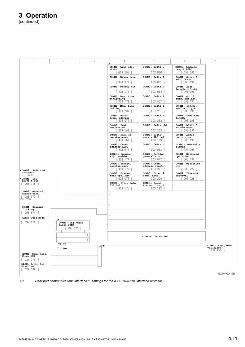
48Z50FGA_EN 3-8 Rear port communications interface 1, settings for the IEC 870-5-101 interface protocol
3 Operation (continued)
3-14 P438/EN M/Ad7 // AFSV.12.10470 D /// P438-305-409/410/411-613 + P438-307-412/413/414-613
COMM1: Selectedprotocol
COMM1: IEC60870-5, ILS
COMM1: Generalenable USER
COMM1: Commandblocking
MAIN: Test mode
COMM1: Sig./meas.Block.USER
COMM1: Sig./meas.Block EXT
0: No
1: Yes
COMM1: Line idlestate
COMM1: Baude rate
COMM1: Parity bit
COMM1: Dead timemonitoring
COMM1: Mon. timepolling
COMM1: Octetcomm. address
COMM1: Testmonitor on
COMM1: Name ofmanufacturer
COMM1: Octetaddress ASDU
COMM1: Spontan.sig. enable
COMM1: Select.spontan.sig.
COMM1: Transm.enab.cycl.dat
COMM1: Cycl. dataILS tel.
COMM1: Delta V
COMM1: Delta I
COMM1: Delta P
COMM1: Delta f
COMM1: Delta T
COMM1: Delta Z
COMM1: Delta phi
COMM1: Deltameas.v.ILS tel
COMM1: Delta t
COMM1: Contin.general scan
Commun. interface
COMM1: Sig./meas.val.block.
1: Yes
MAIN: Prot. Ext.disabled
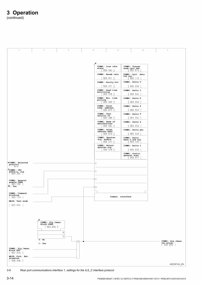
48Z50FHA_EN 3-9 Rear port communications interface 1, settings for the ILS_C interface protocol
3 Operation (continued)
P438/EN M/Ad7 // AFSV.12.10470 D /// P438-305-409/410/411-613 + P438-307-412/413/414-613 3-15
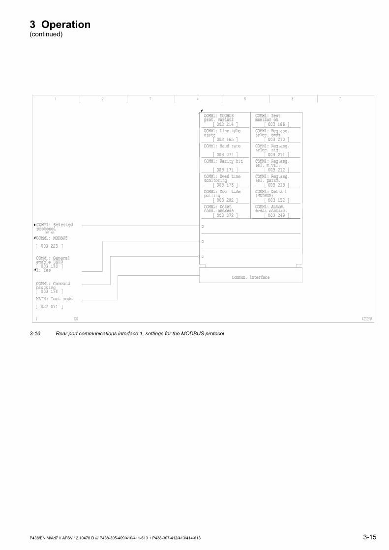
3-10 Rear port communications interface 1, settings for the MODBUS protocol
3 Operation (continued)
3-16 P438/EN M/Ad7 // AFSV.12.10470 D /// P438-305-409/410/411-613 + P438-307-412/413/414-613
Octet 2
Ph-Ph
PhasePhase
Comm.Add DNP3
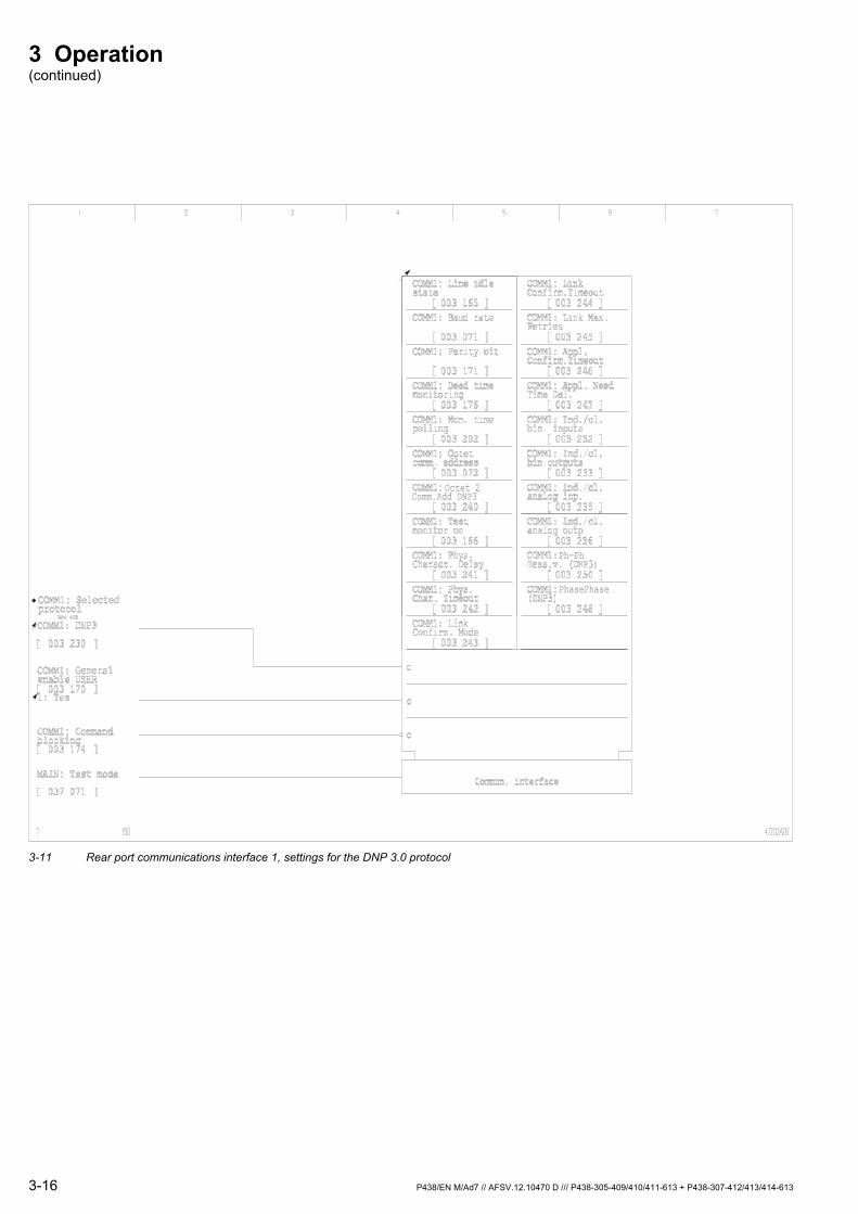
3-11 Rear port communications interface 1, settings for the DNP 3.0 protocol
3 Operation (continued)
P438/EN M/Ad7 // AFSV.12.10470 D /// P438-305-409/410/411-613 + P438-307-412/413/414-613 3-17
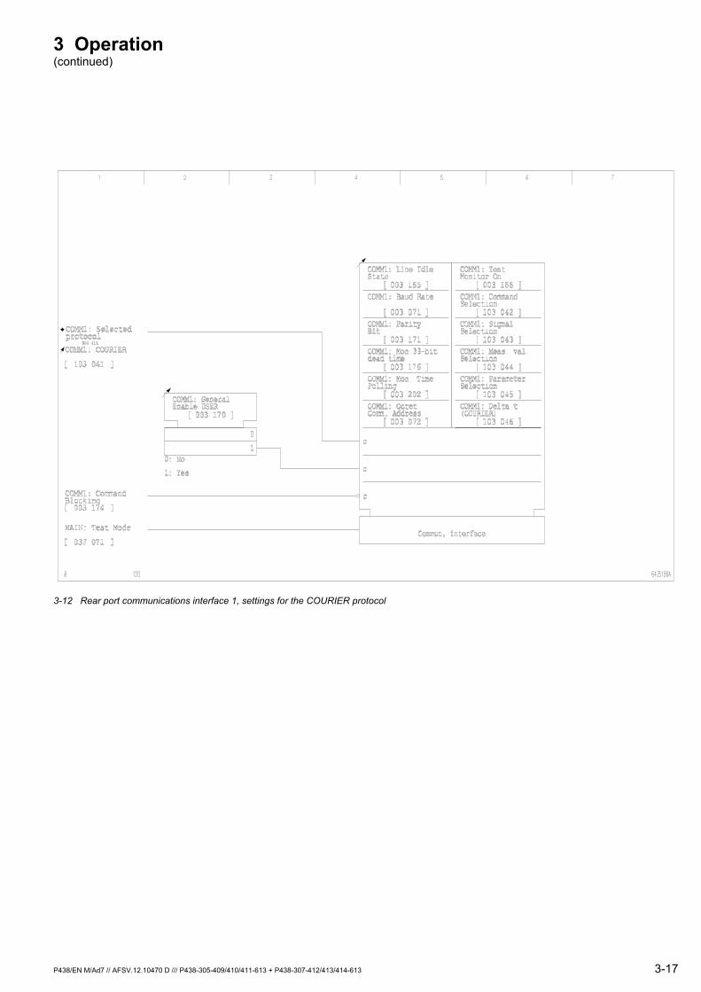
3-12 Rear port communications interface 1, settings for the COURIER protocol
3 Operation (continued)
3-18 P438/EN M/Ad7 // AFSV.12.10470 D /// P438-305-409/410/411-613 + P438-307-412/413/414-613
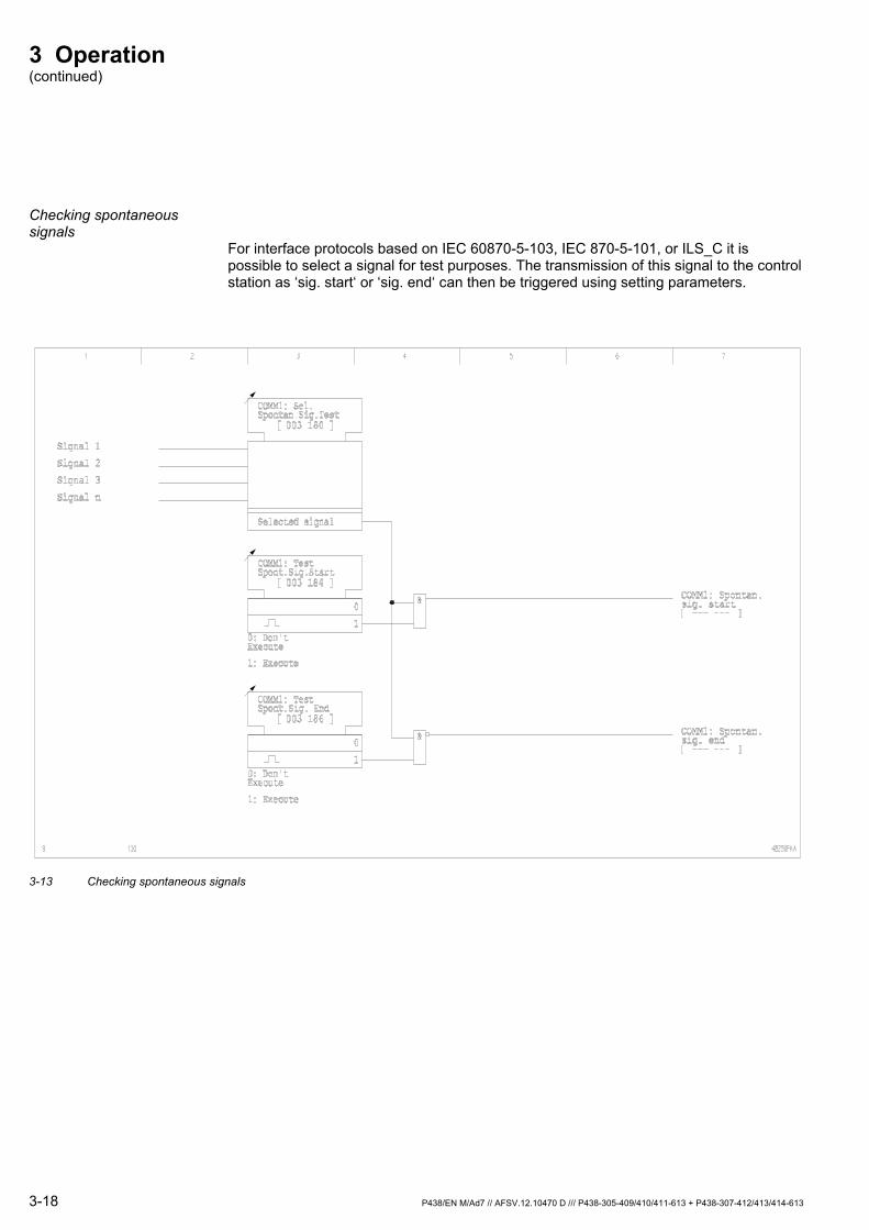
Checking spontaneous signals
For interface protocols based on IEC 60870-5-103, IEC 870-5-101, or ILS_C it is possible to select a signal for test purposes. The transmission of this signal to the control station as ‘sig. start‘ or ‘sig. end‘ can then be triggered using setting parameters.
3-13 Checking spontaneous signals

3 Operation (continued)
P438/EN M/Ad7 // AFSV.12.10470 D /// P438-305-409/410/411-613 + P438-307-412/413/414-613 3-19
3.4.3 Rear Port Communications Interface 2 (Function Group COMM2)
Rear port communications interface 2 supports the interface protocol based on IEC 60870-5-103.
In order for data transfer to function properly, several settings must be made in the P438.
3 Operation (continued)
3-20 P438/EN M/Ad7 // AFSV.12.10470 D /// P438-305-409/410/411-613 + P438-307-412/413/414-613
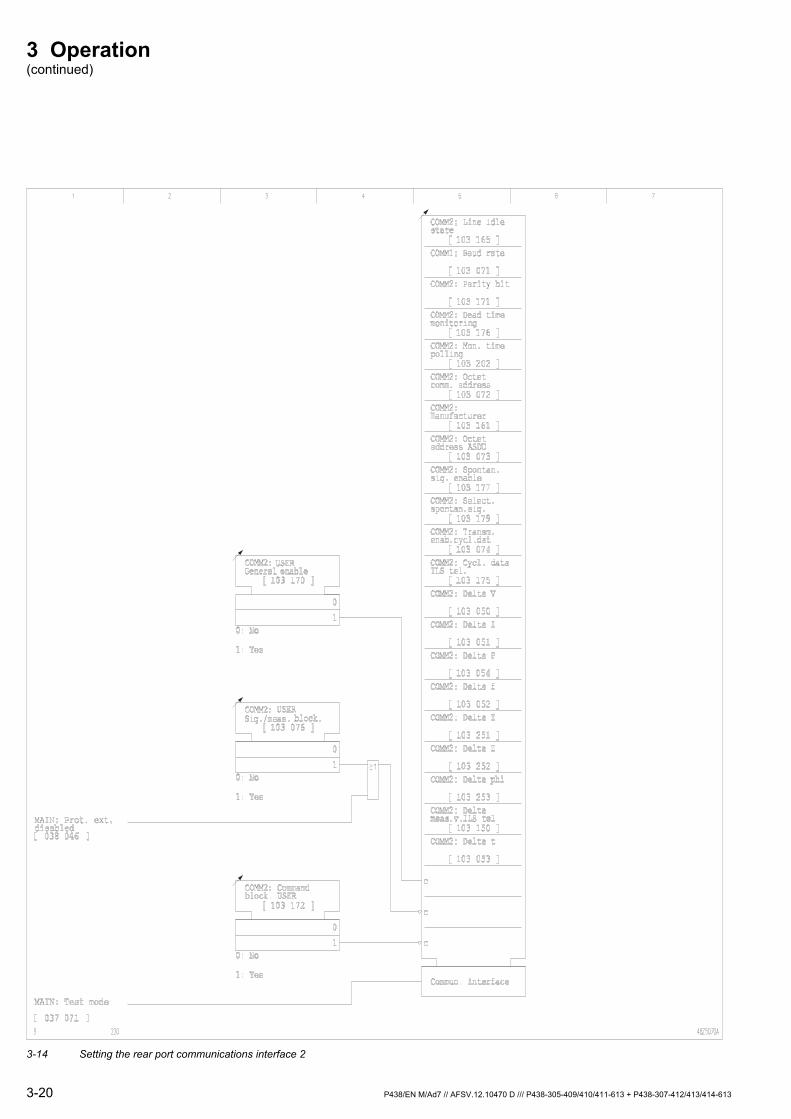
3-14 Setting the rear port communications interface 2
3 Operation (continued)
P438/EN M/Ad7 // AFSV.12.10470 D /// P438-305-409/410/411-613 + P438-307-412/413/414-613 3-21
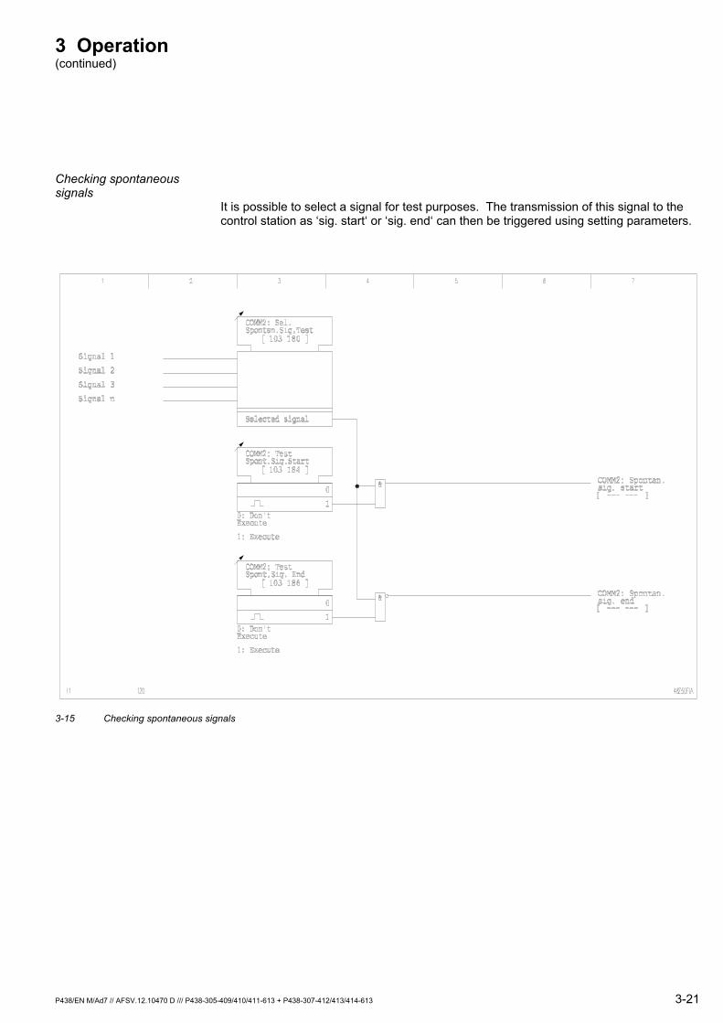
Checking spontaneous signals
It is possible to select a signal for test purposes. The transmission of this signal to the control station as ‘sig. start‘ or ‘sig. end‘ can then be triggered using setting parameters.
3-15 Checking spontaneous signals
3 Operation (continued)
3-22 P438/EN M/Ad7 // AFSV.12.10470 D /// P438-305-409/410/411-613 + P438-307-412/413/414-613
3.4.4 Communications Interface 3 (Function Group COMM3)
Application Communications interface 3 is designed to establish a digital communication link between two MiCOM devices over which up to 8 binary protection signals may be transmitted. Whereas communications interfaces 1 and 2 are designed as information interfaces to connect to data acquisition subsystems and for remote access, communication interface 3 is designed as a protection signaling interface that will transmit real time signals (InterMiCOM teleprotection interface). Communications interface 3 is mainly used to exchange information for teleprotection (protective signaling). In addition, any other internal or external binary signals may also be transmitted.
Physical medium Communications interface 3 is provided as an asynchronous, full-duplex communication interface. The following physical media are available for data transmission:
Direct link without use of external supplementary equipment:
Glass fiber (e.g. via 2 x G62.5/125 up to max. 1.4 km)
Twisted pair (RS 422 up to max. 1.2 km)
Use of external transmission equipment:
FO module (e.g. OZD 485 BFOC-1300 / Hirschmann up to max. 8/14/20 km)
Universal modem (e.g. PZ 511 via twisted pair 2x2x0.5 mm up to max. 10 km)
Voice frequency modem (e.g. TD-32 DC / Westermo up to max. 20 km)
Digital network:
Asynchronous data interface of primary multiplexing equipment
Activating and Enabling In order to use InterMiCOM, communication interface COMM3 has to be configured using the parameter C O M M 3 : F u n c t i o n G r o u p C O M M 3 . This setting parameter is visible only if the relevant optional communication module is fitted. After activation of COMM3, all addresses associated with this function group (setting parameters, binary state signals etc.) become visible. The function can then be enabled or disabled by setting C O M M 3 : G e n e r a l E n a b l e U S E R .
Telegram configuration The communication baud rate is settable (C O M M 3 : B a u d R a t e ) to adapt to the transmission channel's requirements. Sending and receiving addresses (C O M M 3 : S o u r c e A d d r e s s and C O M M 3 : R e c e i v i n g A d d r e s s can be set to different values, thus avoiding that the device communicate with itself.
The InterMiCOM teleprotection interface provides independent transmission of eight binary signals in each direction. For the send signals (C O M M 3 : F c t . S e n d x A s s i g n , with x = 1 to 8) any signal from the selection table of the binary outputs (OUTP) can be chosen. For the receive signals (C O M M 3 : F c t . R e c . x A s s i g n , with x = 1 to 8) any signal from the selection table of the binary inputs (INP) can be chosen.
3 Operation (continued)
P438/EN M/Ad7 // AFSV.12.10470 D /// P438-305-409/410/411-613 + P438-307-412/413/414-613 3-23
For each receive signal, an individual operating mode can be set ( C O M M 3 : O p e r . M o d e R e c e i v e x , with x = 1 t o 8 ) , thus defining the required checks for accepting the received binary signal. In addition a specifically selected telegram structure subdivides the 8 binary signals into two groups. The signal encoding along with the set operating mode for the telegram check defines the actual balance of "Speed", "Security" and "Dependability" for each signal:
Binary signals 1 to 4: Operating mode settable to 'Blocking' or 'Direct Intertrip'
Binary signals 5 to 8: Operating mode settable to 'Permissive' or 'Direct Intertrip'
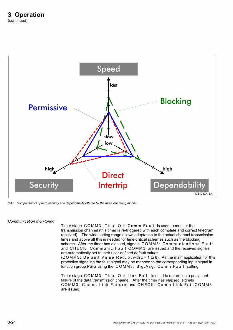
EN 60834-1 classifies 3 categories of command-based teleprotection schemes according to their specific requirements (see figure 3-16). By selection of a binary signal and by setting its operating mode appropriately, these requirements can be fulfilled as follows:
Direct transfer trip or intertripping: Preference: Security Implication: No spurious pickup in the presence of channel noise. Recommended setting: Select the binary signal from groups 1 to 4 or 5 to 8 and set the operating mode to 'Direct Intertrip'
Permissive teleprotection scheme: Preference: Dependability. Implication: Maximizes probability of signal transmission in the presence of channel noise. Recommended setting: Select the binary signal from groups 5 to 8 and set the operating mode to 'Permissive'
Permissive teleprotection scheme: Preference: Dependability. Implication: Maximizes probability of signal transmission in the presence of channel noise. Recommended setting: Select the binary signal from groups 1 to 8 and set the operating mode to 'Permissive'
3 Operation (continued)
3-24 P438/EN M/Ad7 // AFSV.12.10470 D /// P438-305-409/410/411-613 + P438-307-412/413/414-613
Speed
DependabilitySecurity
Blocking
DirectIntertrip
Permissive
slow
fast
high high
low
47Z1030A_EN
3-16 Comparison of speed, security and dependability offered by the three operating modes.
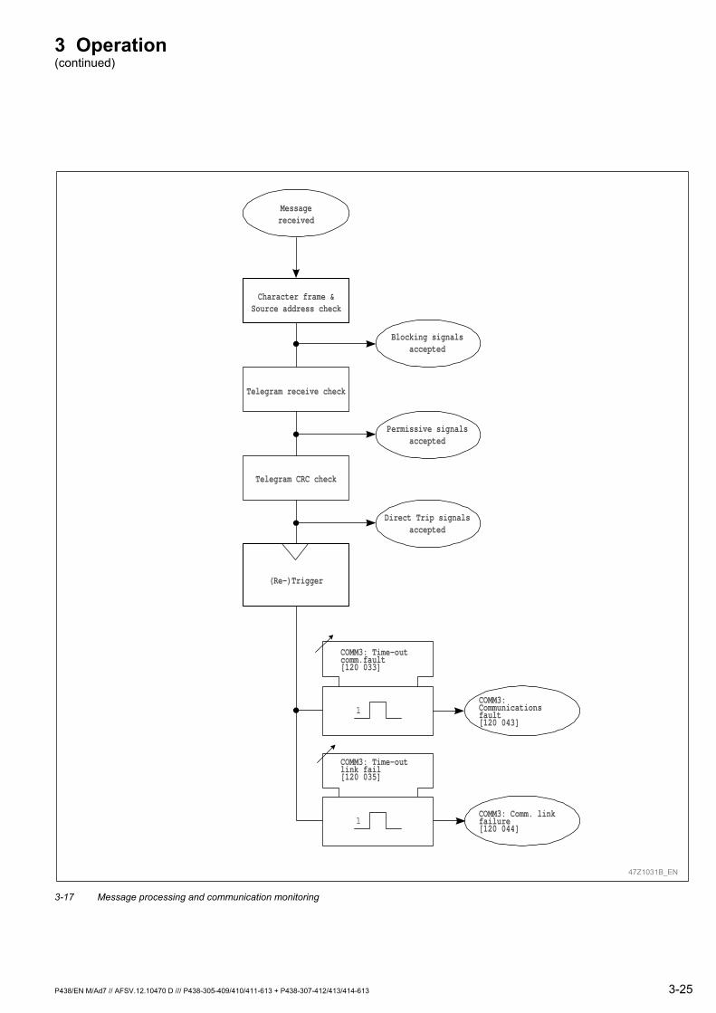
Communication monitoring Timer stage C O M M 3 : T i m e - O u t C o m m . F a u l t is used to monitor the transmission channel (this timer is re-triggered with each complete and correct telegram received). The wide setting range allows adaptation to the actual channel transmission times and above all this is needed for time-critical schemes such as the blocking scheme. After the timer has elapsed, signals C O M M 3 : C o m m u n i c a t i o n s F a u l t and C H E C K : C o m m u n i c . F a u l t C O M M 3 are issued and the received signals are automatically set to their user-defined default values (C O M M 3 : D e f a u l t V a l u e R e c . x , with x = 1 to 8). As the main application for this protective signaling the fault signal may be mapped to the corresponding input signal in function group PSIG using the C O M M 3 : S i g . A s g . C o m m . F a u l t setting.
Timer stage C O M M 3 : T i m e - O u t L i n k F a i l . is used to determine a persistent failure of the data transmission channel. After the timer has elapsed, signals C O M M 3 : C o m m . L i n k F a i l u r e and C H E C K : C o m m . L i n k F a i l . C O M M 3 are issued.
3 Operation (continued)
P438/EN M/Ad7 // AFSV.12.10470 D /// P438-305-409/410/411-613 + P438-307-412/413/414-613 3-25
47Z1031B_EN
Character frame &Source address check
Telegram receive check
Telegram CRC check
Blocking signalsaccepted
Permissive signalsaccepted
Direct Trip signalsaccepted
Messagereceived
1
1
(Re-)Trigger
COMM3: Comm. linkfailure[120 044]
COMM3:Communicationsfault[120 043]
COMM3: Time-outcomm.fault[120 033]
COMM3: Time-outlink fail[120 035]
3-17 Message processing and communication monitoring
3 Operation (continued)
3-26 P438/EN M/Ad7 // AFSV.12.10470 D /// P438-305-409/410/411-613 + P438-307-412/413/414-613
Supervision of communication link quality
After a syntax check of each received message, InterMiCOM updates the ratio of incorrectly received messages, based on a total of the last 1000 received messages. The result is provided as an updating measured value C O M M 3 : N o . T e l . E r r o r s p . u . and the overall maximum ratio can be read from C O M M 3 : N o . T . E r r . , M a x , S t o r e d . If the set threshold C O M M 3 : L i m i t T e l e g r . E r r o r s is exceeded the corresponding signals C O M M 3 : L i m . E x c e e d . , T e l . E r r . and C H E C K : L i m . E x c e e d . , T e l . E r r . will be issued. All the corrupted telegrams are counted (C O M M 3 : N o . T e l e g r a m E r r o r s ) . This counter as well as the stored maximum ratio of corrupted messages can be reset using C O M M 3 : R s e t . N o . T l g . E r r . U S E R (as well as via the binary signal C O M M 3 : R e s e t N o . T l g . E r r . E X T ).
Commissioning tools The actual values of send and receive signals can be read from the device as physical state signals (C O M M 3 : S t a t e S e n d x and C O M M 3 : S t a t e R e c e i v e x , with x = 1 to 8). In addition, InterMiCOM provides 2 test facilities for the commissioning of the protection interface.
For a loop-back test, the send output is directly linked back to the receive input. After setting the desired bit pattern (as an equivalent decimal number at C O M M 3 : L o o p B a c k S e n d ) the test can be triggered using C O M M 3 : L o o p B a c k T e s t . This bit pattern is sent for the duration of the hold time set at C O M M 3 : H o l d T i m e f o r T e s t . For this test only, the source address is set to ' 0 '; this value is not used for regular end-to-end communication. The test result can be checked as long as the hold-time is running by reading the measured operating data C O M M 3 : L o o p B a c k R e s u l t and C O M M 3 : L o o p B a c k R e c e i v e . As soon as the hold-time has expired, the loopback test is terminated and InterMiCOM reverts to the normal send mode (e.g. sending the actual values of the configured send signals, using the set source address).
Thus, in case of problems with the InterMiCOM teleprotection interface, the loopback test can be used to verify or to exclude a defective device. The transmission channel including the receiving device can be checked manually by setting individual binary signals (C O M M 3 : S e n d S i g n a l f o r T e s t ) to user-defined test values (C O M M 3 : L o g . S t a t e f o r T e s t ). After triggering the test by C O M M 3 : S e n d S i g n a l , T e s t , the preset binary signal is sent with the preset value for the set hold time C O M M 3 : H o l d T i m e f o r T e s t . The 7 remaining binary signals are not affected by this test procedure and remain to be sent with their actual values. During the hold time, a received signal can be checked at the receiving device, e.g. by reading the physical state signal. After the hold time has expired, the test mode is automatically reset and the actual values of all 8 signals are transmitted again.
3 Operation (continued)
P438/EN M/Ad7 // AFSV.12.10470 D /// P438-305-409/410/411-613 + P438-307-412/413/414-613 3-27
3.4.5 Communications Interface IEC 61850 (Function Groups IEC GOOSE and GSSE)
The IEC 61850 communication protocol is implemented by these function groups and the Ethernet module.
Note:
Function group IEC is only available as an alternative to function group COMM1 (hardware ordering option!).
3.4.5.1 Communications Interface IEC 61850 (Function Group IEC)
IEC 61850 IEC 61850 was created jointly by users and manufacturers as an international standard. The main target of IEC 61850 is interoperability of devices. This includes the capability of two or more intelligent electronic devices (IED), manufactured by the same company or different companies, to exchange data for combined operation.
Now the new IEC 61850 communication standard has created an open and common basis for communication from the process control level down to the network control level, for the exchange of signals, data, measured values and commands.
For a standardized description of all information and services available in a field device a data model, which lists all visible functions, is created. Such a data model, specifically created for each device, is used as a basis for an exchange of data between the devices and all process control installations interested in such information. In order to facilitate engineering at the process control level a standardized description file of the device, based on XML, is created with the help of the data model. This file can be imported and processed further by the relevant configuration program used by the process control device. This makes possible an automated creation of process variables, substations and signal images.
The following documentation, with the description of the IEC 61850 data model used with the P438, is available:
IDC file based on XML in the SCL (Substation Configuration Description Language) with a description of the data, properties and services, available from the device, that are to be imported into the system configurator.
PICS_MICS_ADL file with the following contents:
PICS (Protocol Implementation Conformance Statement) with an overview of available services.
MICS (Model Implementation Conformance Statement) with an overview of available object types.
ADL (Address Assignment List) with an overview of the assignment of parameter addresses (signals, measuring values, commands, etc.) used by the device with the device data model as per IEC 61850.
3 Operation (continued)
3-28 P438/EN M/Ad7 // AFSV.12.10470 D /// P438-305-409/410/411-613 + P438-307-412/413/414-613
Ethernet Module The optional Ethernet module provides an RJ45 connection and a fiber optic interface where an Ethernet network can be connected. The selection of which of the two interfaces is to be used to connect to the Ethernet network is made by setting the I E C : E t h e r n e t M e d i a parameter. For the optical interface on the Ethernet communications module the user may either select as an ordering option the ST connector or the SC connector with 100 Mbit/s and 1300 nm. The RJ45 connector supports 10 Mbit/s and 100 Mbit/s.
The optional Ethernet module additionally provides an RS485 interface for remote access with the MiCOM S1 support software (function group COMM2).
Notes: The P438 can be equipped with the optional Ethernet module only as an alternative to the standard optional communication module. Therefore the IEC 61850 Ethernet-based communication protocol is available only as an alternative to function group COMM1.
Activating and Enabling Function group IEC can be activated by setting the I E C : I E C 6 1 8 5 0 C o m m u n i c . parameter. This parameter is visible only if the optional Ethernet communication module is fitted to the device. After activation of IEC, all data points associated with this function group (setting parameters, binary state signals etc.) become visible. The function can then be enabled or disabled by setting I E C : G e n e r a l E n a b l e U S E R .
The setting parameters for function groups IEC, GOOSE and GSSE are not automatically activated in the device. Activation occurs either when the I E C : E n a b l e C o n f i g u r a t i o n command is executed, or automatically when the device is switched online at M A I N : P r o t e c t i o n E n a b l e d .
Client Log-on Ethernet communications no longer occur in a restrictive master slave system, as is common with other protocols. Instead, server or client functionalities, as defined in the 'Abstract Communication Service Interface' (ACSI, IEC 61870-7-2), are assigned to the devices. A 'server' is always that device which provides information to other devices. A client may log-on to this server so as to receive information, for instance 'reports'. In a network a server can supply any number of clients with spontaneous or cyclic information.
In its function as server the P438 can supply up to 16 clients with information.
3 Operation (continued)
P438/EN M/Ad7 // AFSV.12.10470 D /// P438-305-409/410/411-613 + P438-307-412/413/414-613 3-29
Clock Synchronization With IEC 61850, clock synchronization is effected via the SNTP protocol, defined as standard for Ethernet. Here the P438 functions as a SNTP client.
For clock synchronization one can select between operating modes Broadcast from SNTP Server or Request from Server. With the first operating mode synchronization is effected via a broadcast message sent from the SNTP server to all devices in the network, and in the second operating mode the P438 requests the device specific time signal during a settable cycle.
Two SNTP servers may be set. In this case, clock synchronization is preferably performed by the first server. The second server is used only when messages are no longer received from the first server.
When looking at the source priority for clock synchronization, which is set at the MAIN function then, by selecting "COMM1", synchronization per IEC 61850 is automatically active but only if this communication protocol is applied.
Fault Transmission Transmission of fault files is supported per "File Transfer".
Transmission of "Goose Messages"
The so-called "Goose Message" is a particular form of data transmission. Whereas normal server-client-services are transmitted at the MMS and TCP/IP level, the "Goose Message" is transmitted directly at the Ethernet level with a high transmission priority. Furthermore these "Goose Messages" can be received by all participants in the respective sub-network, independently of their server or client function. In IEC 61850 "Goose Messages" are applied for the accelerated transmission of information between two or more devices. Application fields are, for example, reverse interlocking, transfer tripping or decentralized substation interlocking. In the future the "Goose Message" will therefore replace a wired or serial protective interface.
According to IEC 61850 there are two types of "Goose Messages", GSSE and IEC-GOOSE. GSSE is used to transmit binary information with a simple configuration by 'bit pairs', and it is compatible with UCA2. However IEC-GOOSE enables transmission of all data formats available in the data model, such as binary information, integer values or even analog measured values. But this will require more extensive configuration with the help of the data model from the field unit situated on the opposite side. With IEC-GOOSE the P438 at this time supports sending and receiving of binary information.
Communication with the MiCOM S1 support software via the Ethernet Interface
Direct access by the MiCOM S1 support software via the Ethernet interface on the device may occur through the "tunneling principle". Transmission is carried out by an Ethernet Standard Protocol, but this is only supported by the associated MiCOM S1 support software (specific manufacturer solution). Such transmission is accomplished over the same hardware for the network, which is used for server-client communication and "Goose Messages". Available are all the familiar functions offered by the MiCOM S1 support software such as reading/writing of setting parameters or retrieving stored data.
The various settings, measured values and signals for function group IEC are described in chapters 7 and 8.
3 Operation (continued)
3-30 P438/EN M/Ad7 // AFSV.12.10470 D /// P438-305-409/410/411-613 + P438-307-412/413/414-613
3.4.5.2 Generic Object Oriented Substation Event (Function Group GOOSE)
For high-speed exchange of information between individual IEDs (intelligent electronic devices) in a local network, the P438 provides function group GOOSE (IEC-GOOSE) as defined in the IEC 61850 standard. GOOSE makes it possible to transmit, quickly and securely, trip commands, blocking, contacts' position and enabling signals as well as other signals.
"Goose Messages" are transmitted only by switches but not by routers. "Goose Messages" therefore remain in the local network to which the device is logged-on.
Activating and Enabling Function group GOOSE can be activated by setting the parameter G O O S E : G e n . O b j O r . S u b s t E v e n t . This parameter is only visible if the optional Ethernet communication module is fitted to the device. After activation of GOOSE, all data points associated with this function group (setting parameters, binary state signals etc.) become visible. The function can then be enabled or disabled by setting G O O S E : G e n e r a l E n a b l e U S E R .
The setting parameters for function groups IEC, GOOSE and GSSE in the device are not automatically activated. Activation occurs either when the I E C : E n a b l e C o n f i g u r a t i o n command is executed or automatically when the device is switched online with M A I N : P r o t e c t i o n E n a b l e d . In addition function group IEC must be configured and enabled.
Sending GOOSE With GOOSE, up to 32 logic binary state signals from the P438 can be sent. Selection of binary state signals is made by setting G O O S E : O u t p u t n F c t . A s s i g . (n = 1 to 32). The assignment of data object indexes to logic state signals is made in the range from 1 to 32 according to the assignment to GOOSE outputs.
A GOOSE message is automatically sent with each new state change of a configured binary state signal or an external device. There are numerous sending repetitions in fixed ascending time periods (10 ms, 20 ms, 50 ms, 100 ms, 500 ms, 1000 ms, and 2000 ms). If after 2 seconds there is no further state change apparent, the GOOSE message is then sent cyclically at 2-second intervals.
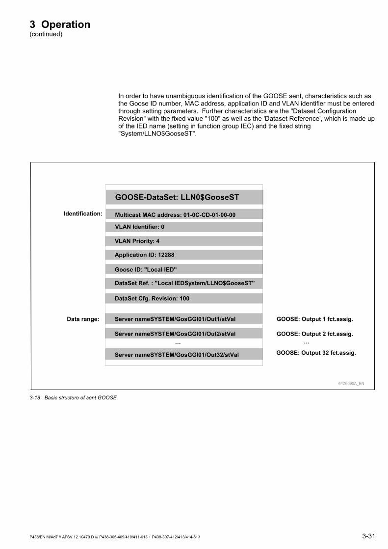
3 Operation (continued)
P438/EN M/Ad7 // AFSV.12.10470 D /// P438-305-409/410/411-613 + P438-307-412/413/414-613 3-31
In order to have unambiguous identification of the GOOSE sent, characteristics such as the Goose ID number, MAC address, application ID and VLAN identifier must be entered through setting parameters. Further characteristics are the "Dataset Configuration Revision" with the fixed value "100" as well as the 'Dataset Reference', which is made up of the IED name (setting in function group IEC) and the fixed string "System/LLNO$GooseST".
GOOSE-DataSet: LLN0$GooseST
Goose ID: "Local IED"
Server nameSYSTEM/GosGGI01/Out1/stVal
Multicast MAC address: 01-0C-CD-01-00-00
VLAN Identifier: 0
GOOSE: Output 1 fct.assig.
… …GOOSE: Output 2 fct.assig.
GOOSE: Output 32 fct.assig.
64Z6090A_EN
Server nameSYSTEM/GosGGI01/Out2/stVal
Server nameSYSTEM/GosGGI01/Out32/stVal
Identification:
Data range:
Application ID: 12288
DataSet Cfg. Revision: 100
DataSet Ref. : "Local IEDSystem/LLNO$GooseST"
VLAN Priority: 4
3-18 Basic structure of sent GOOSE
3 Operation (continued)
3-32 P438/EN M/Ad7 // AFSV.12.10470 D /// P438-305-409/410/411-613 + P438-307-412/413/414-613
With GOOSE up to 16 logic binary state signals can be received. Configuration of the logic state signals received (G O O S E : I n p u t n F c t . A s s i g . , where n = 1 to 16) is made on the basis of the selection table of the binary inputs (opto coupler inputs).
For each state signal to be received the GOOSE message is selected by setting the GOOSE ID, Application ID and 'DataSet Reference' which includes the information wanted. With the further setting of the data object index and the data attribute index through parameters, the required information from the chosen GOOSE will be selected. The device will not evaluate the identification features VLAN identifier and ‘Dataset Configuration Revision’ that are also included in the GOOSE received.
Each GOOSE message includes time information on the validity of its information. This corresponds to the double time period to the next GOOSE repetition. If the validity period has elapsed before this GOOSE message is received again (i.e. because of a fault in communication), the received signals will automatically be set to their respective default values at G O O S E : I n p u t n D e f a u l t .
The various settings, measured values and signals for function group GOOSE are described in chapters 7 and 8.
3.4.5.3 Generic Substation State Event (Function Group GSSE)
For high-speed exchange of information between individual IEDs (intelligent electronic devices) in a local network, the P438 provides, as an additional functionality, the GSSE function group (UCA2.0-GOOSE) as defined in the IEC 61850 standard. GSSE makes it possible to transmit, quickly and securely, logic binary state signals such as trip commands, blocking and enabling signals as well as other signals.
Activating and Enabling Function Group GSSE can be activated by setting the parameter G S S E : G e n . S u b s t . S t a t . E v e n t . This parameter is only visible if the optional Ethernet communication module is fitted to the device. After activation of GSSE, all data points associated with this function group (setting parameters, binary state signals etc.) become visible. The function can then be enabled or disabled by setting G S S E : G e n e r a l E n a b l e U S E R .
The setting parameters for function groups IEC, GOOSE and GSSE in the device are not automatically activated. Activation occurs either when the I E C : E n a b l e C o n f i g u r a t i o n command is executed or automatically when the device is switched on-line at M A I N : P r o t e c t i o n E n a b l e d . In addition the IEC function group must be configured and enabled.
3 Operation (continued)
P438/EN M/Ad7 // AFSV.12.10470 D /// P438-305-409/410/411-613 + P438-307-412/413/414-613 3-33
Sending GSSE With GSSE up to 32 logic binary state signals can be sent. Selection of binary state signals is made by setting G S S E : O u t p u t n F c t . A s s i g . (n = 1 to 32). Each selected state signal is to be assigned to a bit pair in GSSE (G S S E : O u t p u t n B i t P a i r (n = 1 to 32)), which will transmit this state signal.
A GSSE message is automatically sent with each state change of a selected state signal. There will be multiple send repetitions at ascending time periods. The first send repetition occurs at the given cycle time set for G S S E : M i n . C y c l e . The cycles for the following send repetitions result from a conditional equation with the increment set using the G S S E : I n c r e m e n t parameter. Should no further state changes occur up to the time when the maximum cycle time has elapsed (G S S E : M a x . C y c l e ) , then the GSSE will be sent cyclically at intervals as set for the max. cycle time.
In order to have unambiguous identification of a sent GSSE message, the IED name is used which was set in function group IEC.
Receiving GSSE With GSSE up to 32 logic binary state signals can be received. Configuration of the logic binary state signals received (G S S E : I n p u t n F c t . A s s i g . , where n = 1 to 32) is made on the basis of the selection table of the binary inputs (opto coupler inputs).
For each state signal to be received, the GSSE message, which will include the required information, must be selected by setting the IED name (G S S E : I E D N a m e ) . Selection of information wanted from the selected GSSE will occur by setting the bit pair (G S S E : B i t P a i r ) .
Each GSSE message includes time information on the validity of its information. This corresponds to the double time period to the next GSSE repetition. If the validity period has elapsed before this GSSE message is received again (i.e. because of a communications fault), the signals received will automatically be set to their respective default values ( G S S E : I n p u t n D e f a u l t (n = 1 to 32)).
The various settings and signals for function group GOOSE are described in chapters 7 and 8.
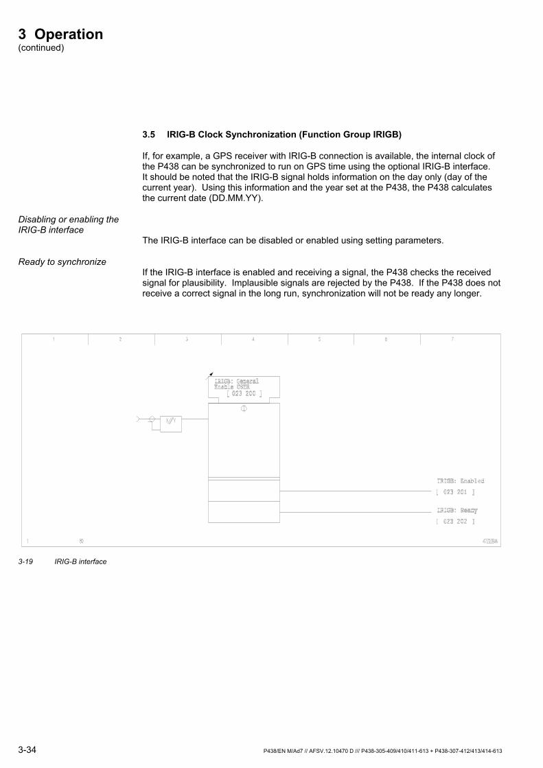
3 Operation (continued)
3.5 IRIG-B Clock Synchronization (Function Group IRIGB)
If, for example, a GPS receiver with IRIG-B connection is available, the internal clock of the P438 can be synchronized to run on GPS time using the optional IRIG-B interface. It should be noted that the IRIG-B signal holds information on the day only (day of the current year). Using this information and the year set at the P438, the P438 calculates the current date (DD.MM.YY).
Disabling or enabling the IRIG-B interface
The IRIG-B interface can be disabled or enabled using setting parameters.
Ready to synchronize If the IRIG-B interface is enabled and receiving a signal, the P438 checks the received signal for plausibility. Implausible signals are rejected by the P438. If the P438 does not receive a correct signal in the long run, synchronization will not be ready any longer.
3-19 IRIG-B interface
3-34 P438/EN M/Ad7 // AFSV.12.10470 D /// P438-305-409/410/411-613 + P438-307-412/413/414-613
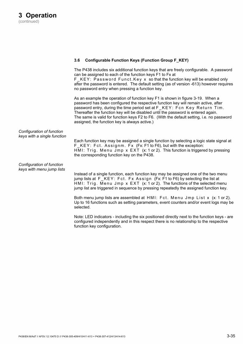
3 Operation (continued)
3.6 Configurable Function Keys (Function Group F_KEY)
The P438 includes six additional function keys that are freely configurable. A password can be assigned to each of the function keys F1 to Fx at F _ K E Y : P a s s w o r d F u n c t . K e y x so that the function key will be enabled only after the password is entered. The default setting (as of version -613) however requires no password entry when pressing a function key.
As an example the operation of function key F1 is shown in figure 3-19. When a password has been configured the respective function key will remain active, after password entry, during the time period set at F _ K E Y : F c n K e y R e t u r n T i m . Thereafter the function key will be disabled until the password is entered again. The same is valid for function keys F2 to F6. (With the default setting, i.e. no password assigned, the function key is always active.)
Configuration of function keys with a single function
Each function key may be assigned a single function by selecting a logic state signal at F _ K E Y : F c t . A s s i g n m . F x (Fx: F1 to F6), but with the exception: H M I : T r i g . M e n u J m p x E X T (x: 1 or 2). This function is triggered by pressing the corresponding function key on the P438.
Configuration of function keys with menu jump lists
Instead of a single function, each function key may be assigned one of the two menu jump lists at F _ K E Y : F c t . F x A s s i g n (Fx: F1 to F6) by selecting the list at H M I : T r i g . M e n u J m p x E X T (x: 1 or 2). The functions of the selected menu jump list are triggered in sequence by pressing repeatedly the assigned function key.
Both menu jump lists are assembled at H M I : F c t . M e n u J m p L i s t x (x: 1 or 2). Up to 16 functions such as setting parameters, event counters and/or event logs may be selected.
Note: LED indicators - including the six positioned directly next to the function keys - are configured independently and in this respect there is no relationship to the respective function key configuration.
P438/EN M/Ad7 // AFSV.12.10470 D /// P438-305-409/410/411-613 + P438-307-412/413/414-613 3-35

3 Operation (continued)
Configuration of the READ key
Similarly to the setting at H M I : F c t . M e n u J m p L i s t x up to 16 functions can also be selected from the menu jump list at H M I : F c t . R e a d K e y . They are triggered in sequence by pressing repeatedly the "READ" key.
Operating mode of the function keys
For each function key the operating mode can be selected at F _ K E Y : O p e r a t i n g M o d e F x (Fx: F1 to F6). Here it is possible to select whether the function key operates as a key or as a switch. In the operating mode 'Key' the selected function is active while the function key is pressed. In the operating mode 'Switch' the selected function is switched on or off every time the function key is pressed. The state of the function keys can be displayed.
Handling keys If the LCD backlight is switched off it will automatically light up again when a function key or the "READ" key is pressed. The assigned function will be triggered only when the respective key is pressed a second time. This is also valid for the other keys.
3-36 P438/EN M/Ad7 // AFSV.12.10470 D /// P438-305-409/410/411-613 + P438-307-412/413/414-613

3 Operation (continued)
40Z5003C_UK
F_KEY: Fct. F1 Assign
[ 080 112 ]
Selected Function
1: Key2: Switch
1
2
Function 1 EXT
Function 2 EXT
Function 3 EXT
Function n EXT
F_KEY: Operating Mode F1
[ 080 132 ]
Activate Function
F_KEY: State F1 [ 080 122 ]
1) Keys, local control
3-20 Configuration and operating mode of function keys. The assigned function is either a single function, one of the two group resetting
functions or a menu jump list.
P438/EN M/Ad7 // AFSV.12.10470 D /// P438-305-409/410/411-613 + P438-307-412/413/414-613 3-37
3 Operation (continued)
3.7 Configuration and Operating Mode of the Binary Inputs (Function Group INP)
The P438 has optical coupler inputs for processing binary signals from the system. The functions that will be activated in the P438 by triggering these binary signal inputs are defined by the configuration of the binary signal inputs. The typical response time is less than 10 ms, although for reliability it is recommended that the initiating signal is maintained for at least 20 ms so that it will be reliably detected by the P438. When a general start is apparent this response time may be extended to 40 ms under unfavorable conditions.
Configuring the binary inputs
One function can be assigned to each binary signal input by configuration. The same function can be assigned to several binary signal inputs. Thus one function can be activated from several control points having different signal voltages.
In this manual, we assume that the required functions (marked 'EXT' in the address description) have been assigned to binary signal inputs by configuration.
It should be noted that time-critical applications such as time synchronization commands are not mapped to the binary signal inputs of the analog module as these have an increased reaction time due to internal processing.
Operating mode of the binary inputs
The operating mode for each binary signal input can be defined. The user can specify whether the presence ('Active "High"' mode) or the absence ('Active "Low"' mode) of a voltage should be interpreted as the logic ' 1 ' signal. The display of the state of a binary signal input - 'Low' or 'High' - is independent of the setting for the operating mode of the binary signal input.
Filter function An additional filter function may be enabled in order to suppress transient interference peaks at the logic signal inputs (operating modes 'Active "High", Filt.' or 'Active "Low", Filt.'). Where this function is enabled a status change at the binary logic input is signaled only when the input signal remains at a steady signal level during a set number of sampling steps (sampling step size = period / 20). The number of sampling steps is set at I N P : F i l t e r .
3-38 P438/EN M/Ad7 // AFSV.12.10470 D /// P438-305-409/410/411-613 + P438-307-412/413/414-613
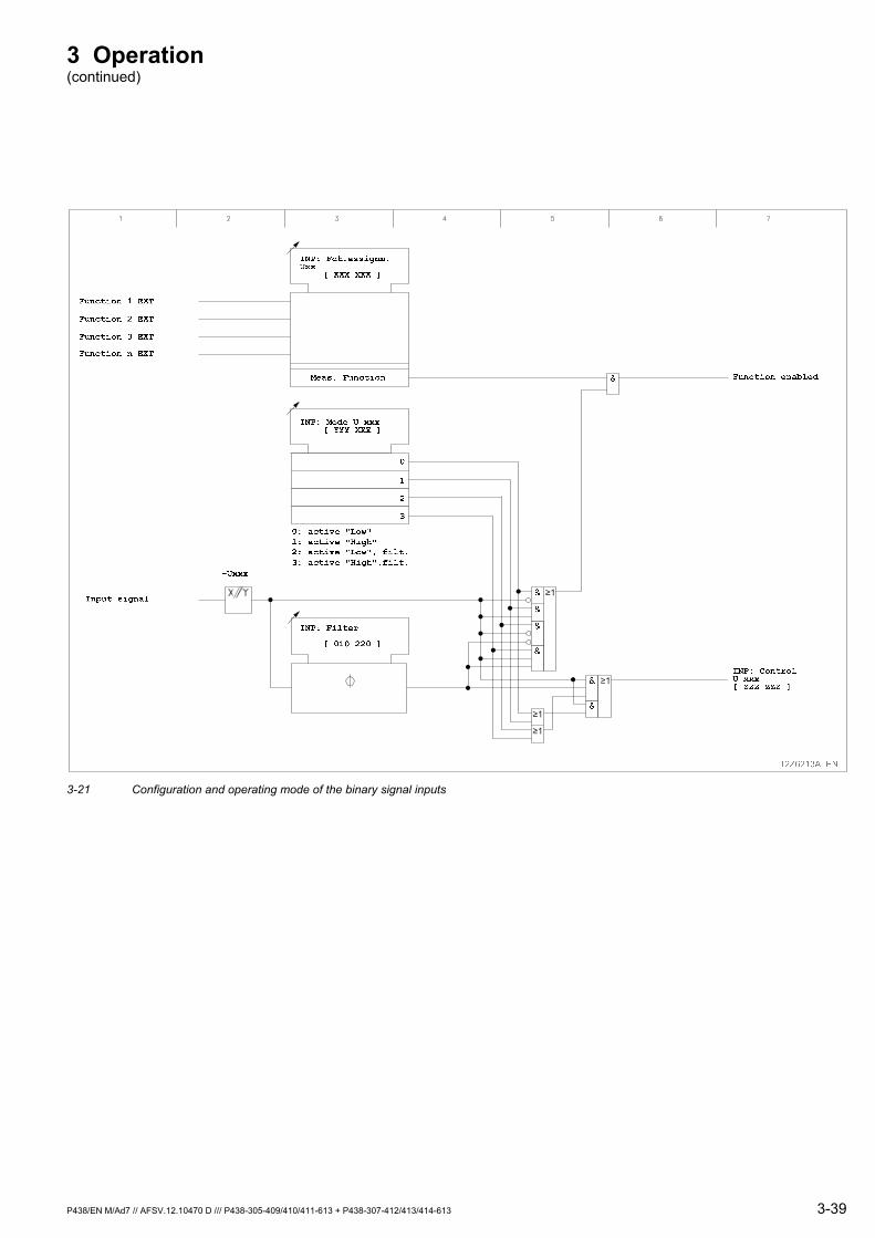
3 Operation (continued)
3-21 Configuration and operating mode of the binary signal inputs
P438/EN M/Ad7 // AFSV.12.10470 D /// P438-305-409/410/411-613 + P438-307-412/413/414-613 3-39
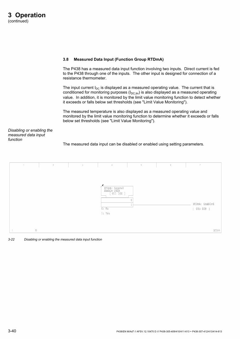
3 Operation (continued)
3.8 Measured Data Input (Function Group RTDmA)
The P438 has a measured data input function involving two inputs. Direct current is fed to the P438 through one of the inputs. The other input is designed for connection of a resistance thermometer.
The input current IDC is displayed as a measured operating value. The current that is conditioned for monitoring purposes (IDC,lin) is also displayed as a measured operating value. In addition, it is monitored by the limit value monitoring function to detect whether it exceeds or falls below set thresholds (see "Limit Value Monitoring").
The measured temperature is also displayed as a measured operating value and monitored by the limit value monitoring function to determine whether it exceeds or falls below set thresholds (see "Limit Value Monitoring").
Disabling or enabling the measured data input function
The measured data input can be disabled or enabled using setting parameters.
3-22 Disabling or enabling the measured data input function
3-40 P438/EN M/Ad7 // AFSV.12.10470 D /// P438-305-409/410/411-613 + P438-307-412/413/414-613
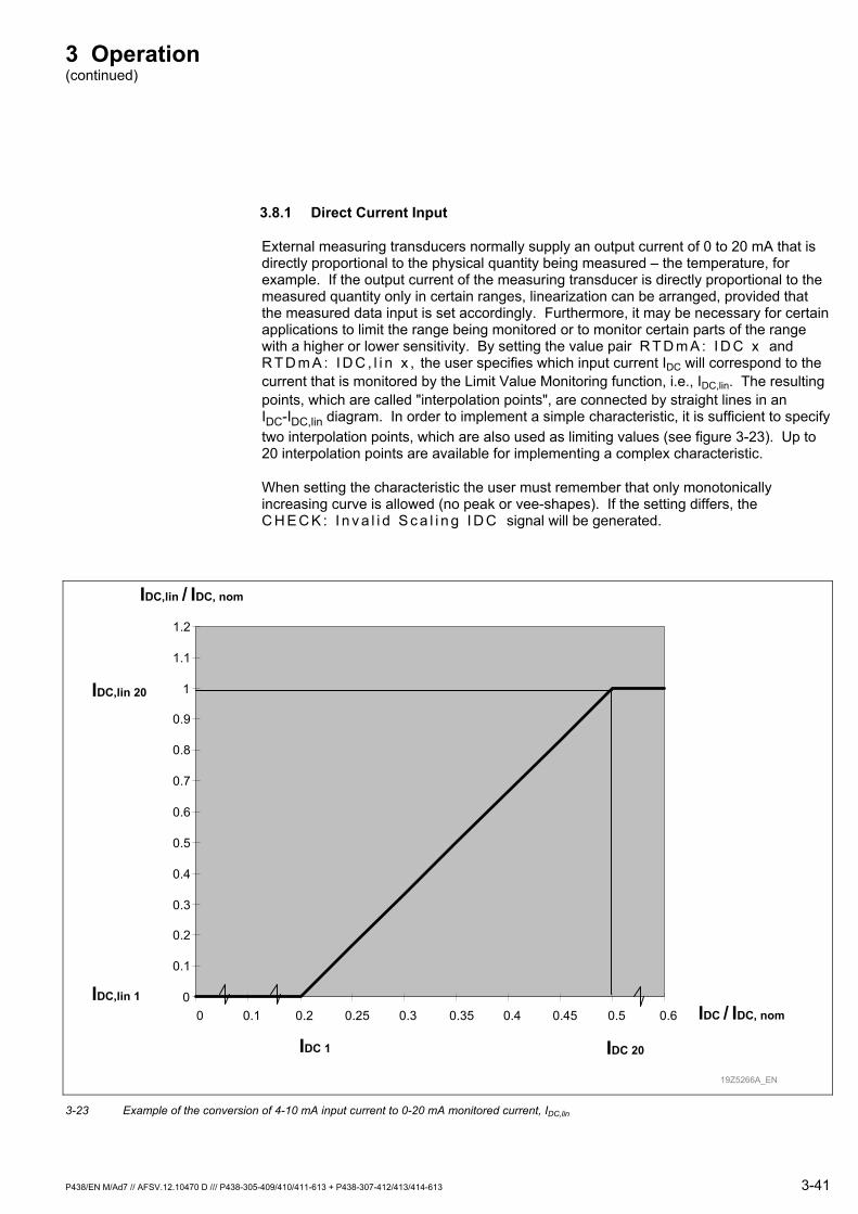
3 Operation (continued)
3.8.1 Direct Current Input
External measuring transducers normally supply an output current of 0 to 20 mA that is directly proportional to the physical quantity being measured – the temperature, for example. If the output current of the measuring transducer is directly proportional to the measured quantity only in certain ranges, linearization can be arranged, provided that the measured data input is set accordingly. Furthermore, it may be necessary for certain applications to limit the range being monitored or to monitor certain parts of the range with a higher or lower sensitivity. By setting the value pair R T D m A : I D C x and R T D m A : I D C , l i n x , the user specifies which input current IDC will correspond to the current that is monitored by the Limit Value Monitoring function, i.e., IDC,lin. The resulting points, which are called "interpolation points", are connected by straight lines in an IDC-IDC,lin diagram. In order to implement a simple characteristic, it is sufficient to specify two interpolation points, which are also used as limiting values (see figure 3-23). Up to 20 interpolation points are available for implementing a complex characteristic.
When setting the characteristic the user must remember that only monotonically increasing curve is allowed (no peak or vee-shapes). If the setting differs, the C H E C K : I n v a l i d S c a l i n g I D C signal will be generated.
0
0.1
0.2
0.3
0.4
0.5
0.6
0.7
0.8
0.9
1
1.1
1.2
0 0.1 0.2 0.25 0.3 0.35 0.4 0.45 0.5 0.6 IDC / IDC, nom
IDC,lin / IDC, nom
IDC 1 IDC 20
IDC,lin 1
IDC,lin 20
D5Z52KDA19Z5266A_EN
3-23 Example of the conversion of 4-10 mA input current to 0-20 mA monitored current, IDC,lin
P438/EN M/Ad7 // AFSV.12.10470 D /// P438-305-409/410/411-613 + P438-307-412/413/414-613 3-41

3 Operation (continued)
0
0.1
0.2
0.3
0.4
0.5
0.6
0.7
0.8
0 0.1 0.2 0.3 0.4 0.5 0.6 0.7 0.8 0.9 1 1.1 1.2
IDC / IDC,nom
IDC,lin / IDC,nom
D5Z52KEC_UK
IDC1 IDC2 IDC3 IDC4 IDC20
IDC,lin1
IDC,lin2
IDC,lin3
IDC,lin4
IDC,lin20
Enable IDC p.u.
Interpolation points
3-24 Example of a characteristic having five interpolation points (characteristic with zero suppression setting of 0.1 IDC,nom is shown as a
broken line)
Zero suppression Zero suppression is defined by setting R T D m A : E n a b l e I D C p . u . If the direct current does not exceed the set threshold, the per-unit input current IDC p.u. and the current IDC,lin will be displayed as having a value of ‘ 0 ’.
Open-circuit and overload monitoring
The device is equipped with an open-circuit monitoring function. If current IDC falls below the set threshold, R T D m A : I D C < O p e n C i r c u i t , the R T D m A : O p e n C i r c . 2 0 m A i n p . signal is issued.
The input current is monitored in order to protect the 20 mA input against overloading. If it exceeds the fixed threshold of 24.8 mA, the R T D m A : O v e r l o a d 2 0 m A I n p u t signal is issued.
3-42 P438/EN M/Ad7 // AFSV.12.10470 D /// P438-305-409/410/411-613 + P438-307-412/413/414-613
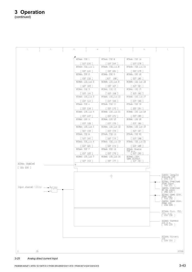
3 Operation (continued)
3-25 Analog direct current input
P438/EN M/Ad7 // AFSV.12.10470 D /// P438-305-409/410/411-613 + P438-307-412/413/414-613 3-43
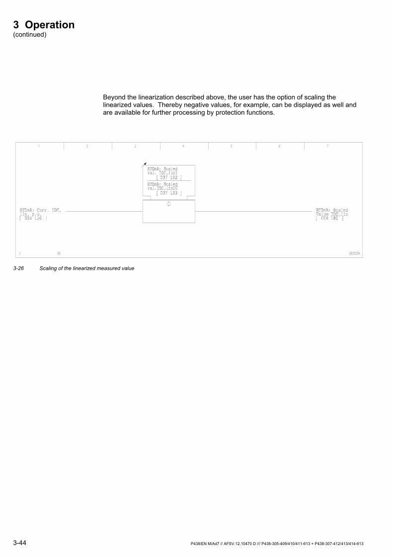
3 Operation (continued)
Beyond the linearization described above, the user has the option of scaling the linearized values. Thereby negative values, for example, can be displayed as well and are available for further processing by protection functions.
3-26 Scaling of the linearized measured value
3-44 P438/EN M/Ad7 // AFSV.12.10470 D /// P438-305-409/410/411-613 + P438-307-412/413/414-613
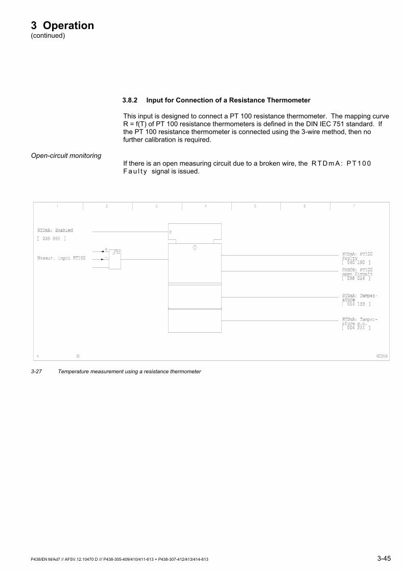
3 Operation (continued)
3.8.2 Input for Connection of a Resistance Thermometer
This input is designed to connect a PT 100 resistance thermometer. The mapping curve R = f(T) of PT 100 resistance thermometers is defined in the DIN IEC 751 standard. If the PT 100 resistance thermometer is connected using the 3-wire method, then no further calibration is required.
Open-circuit monitoring If there is an open measuring circuit due to a broken wire, the R T D m A : P T 1 0 0 F a u l t y signal is issued.
3-27 Temperature measurement using a resistance thermometer
P438/EN M/Ad7 // AFSV.12.10470 D /// P438-305-409/410/411-613 + P438-307-412/413/414-613 3-45
3 Operation (continued)
3.9 Configuration, Operating Mode, and Blocking of the Output Relays (Function Group OUTP)
The P438 has output relays for the output of binary signals. The binary signal assignment is freely configured by the user..
Configuration of the output relays
One binary signal can be assigned to each output relay. The same binary signal can be assigned to several output relays by configuration.
Operating mode of the output relays
The user can set an operating mode for each output relay that determines whether the output relay operates in a normally open arrangement (NO) or normally closed arrangement (NC) and whether it operates in latching mode. Latching can be disabled either manually using a setting parameter, or by an appropriately configured binary signal input, at the onset of a new fault or of a new system disturbance, depending on the selected operating mode.
Blocking the output relays The P438 offers the option of blocking all output relays using a setting parameter or by way of an appropriately configured binary signal input. The output relays are likewise blocked if the device is disabled using appropriately configured binary inputs.
In these cases the relays are treated according to their set operating mode, i.e. relays in a normally open arrangement (NO) are not triggered, whereas relays in a normally closed arrangement (NC) are triggered.
This does not apply to the relays associated with the C H E C K : A l a r m ( r e l a y ) or M A I N : B l o c k e d / f a u l t y signals. Self-monitoring alarms are thus correctly indicated.
If the self-monitoring feature detects a serious hardware fault (see error messages in Chapter 10, which will lead to a blocking of protection), all output relays are reset regardless of the set operating mode or signal configuration.
3-46 P438/EN M/Ad7 // AFSV.12.10470 D /// P438-305-409/410/411-613 + P438-307-412/413/414-613
3 Operation (continued)
m out of n
OUTP: Fct. K xxxAssign [ yyy xxx ]
Selected Signals
Signal 1Signal 2Signal 3Signal n
OUTP: USER OutpRel Block
[ 021 014 ]
0: No1: Yes
0
1
0: Don't Execute
OUTP: ResetLatch. USER[ 021 009 ]
0
1
1: Execute
1100 ms
1
R1
S1 1
OUTP: ResetLatch. EXT[ 040 015 ]
OUTP: BlockOutp.Rel. EXT[ 040 014 ]MAIN: Prot. Ext.Disabled[ 038 046 ]CHECK: HardwareFault
304 950
≥ 1
≥ 1
≥ 1 ≥ 1
OSCIL: Record.in Progress[ 035 000 ]
1: ExecuteMAIN: GeneralReset EXT[ 005 255 ]
MAIN: GeneralReset USER[ 003 002 ]
OSCIL: SystemDisturb. runn[ 035 004 ]
&
&
&
OUTP: Oper. ModeK xxx [ xxx xxx ]
1: Follower
2: Follower Latching
3: Follower Rst on Flt
4: Follower Rst onStart
5: Inverted
6: Inverted Latching
50Z0141A_UK
OUTP: LatchingReset[ 040 088 ]
OUTP: State K xxx[ zzz zzz ]≥ 1
≥ 1
1
2
3
4
5
6
-K xxx
OUTP: Outp.Relays Blocked[ 021 015 ]
&
&&
&
&
≥ 1
≥ 1
≥ 1
≥ 1
3-28 Configuration, setting the operating mode, and blocking the output relays
P438/EN M/Ad7 // AFSV.12.10470 D /// P438-305-409/410/411-613 + P438-307-412/413/414-613 3-47
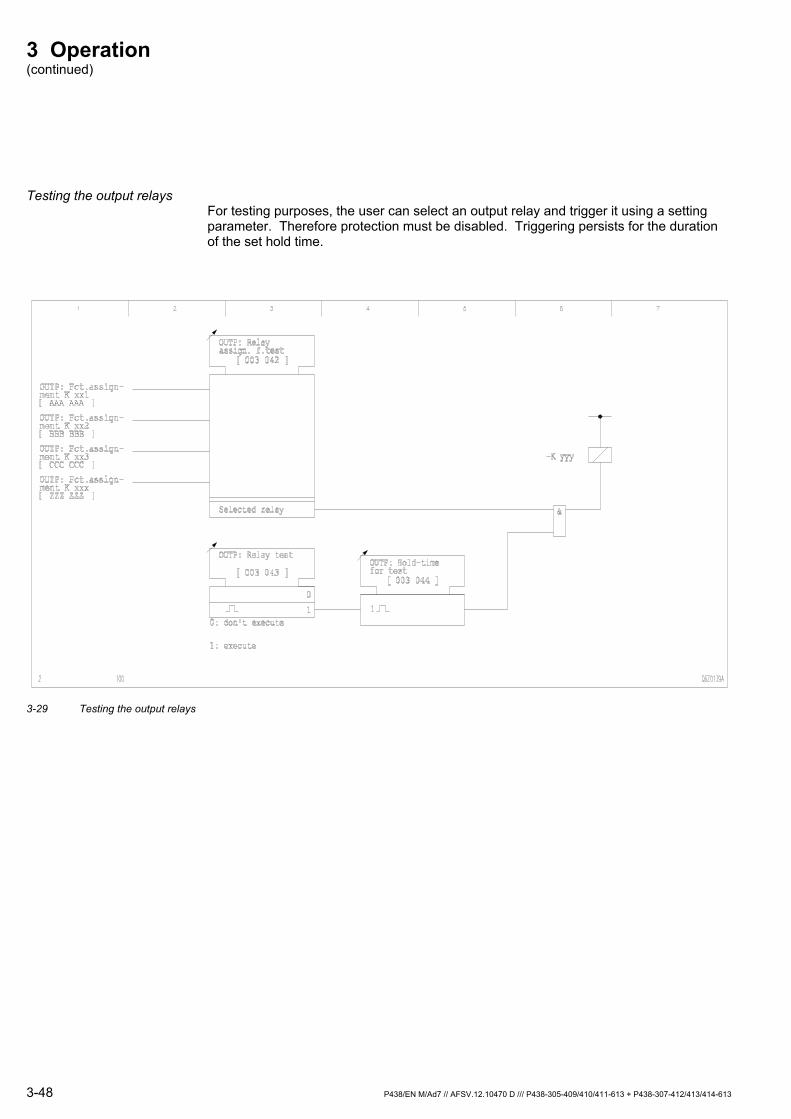
3 Operation (continued)
Testing the output relays For testing purposes, the user can select an output relay and trigger it using a setting parameter. Therefore protection must be disabled. Triggering persists for the duration of the set hold time.
3-29 Testing the output relays
3-48 P438/EN M/Ad7 // AFSV.12.10470 D /// P438-305-409/410/411-613 + P438-307-412/413/414-613

3 Operation (continued)
3.10 Measured Data Output (Function Group mA_OP)
Measured values made available by the P438 can be provided in BCD (binary coded decimal) form through output relays or in analog form as direct current output. Output as direct current can only occur if the device is equipped with analog module Y. BCD-coded output, however, is possible, regardless of whether the device is equipped with analog module Y or not.
Disabling or enabling the measured data output function
Measured data output can be disabled or enabled using a setting parameter.
3-30 Disabling or enabling the measured data output function
P438/EN M/Ad7 // AFSV.12.10470 D /// P438-305-409/410/411-613 + P438-307-412/413/414-613 3-49
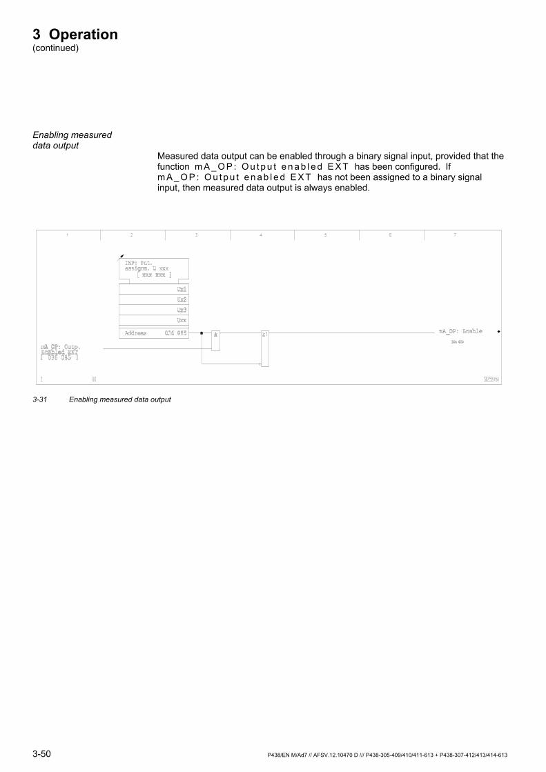
3 Operation (continued)
Enabling measured data output
Measured data output can be enabled through a binary signal input, provided that the function m A _ O P : O u t p u t e n a b l e d E X T has been configured. If m A _ O P : O u t p u t e n a b l e d E X T has not been assigned to a binary signal input, then measured data output is always enabled.
3-31 Enabling measured data output
3-50 P438/EN M/Ad7 // AFSV.12.10470 D /// P438-305-409/410/411-613 + P438-307-412/413/414-613
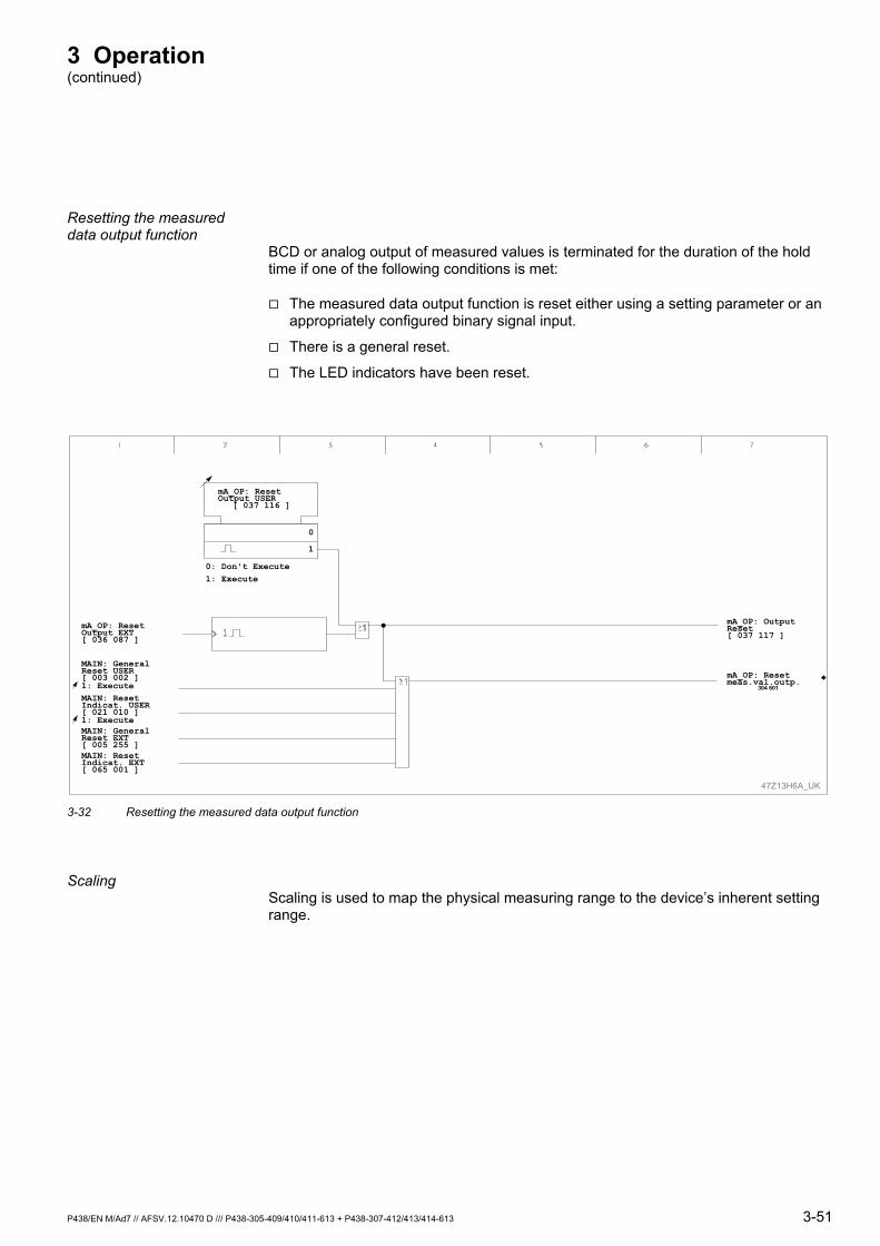
3 Operation (continued)
Resetting the measured data output function
BCD or analog output of measured values is terminated for the duration of the hold time if one of the following conditions is met:
The measured data output function is reset either using a setting parameter or an appropriately configured binary signal input.
There is a general reset.
The LED indicators have been reset.
47Z13H6A_UK
1: Execute
MAIN: GeneralReset EXT[ 005 255 ]
MAIN: GeneralReset USER[ 003 002 ]
1: Execute
MAIN: ResetIndicat. USER[ 021 010 ]
MAIN: ResetIndicat. EXT[ 065 001 ]
mA_OP: ResetOutput EXT[ 036 087 ]
mA_OP: ResetOutput USER
[ 037 116 ]
0: Don't Execute1: Execute
1
0
mA_OP: OutputReset[ 037 117 ]
mA_OP: Resetmeas.val.outp.
304 601
3-32 Resetting the measured data output function
Scaling Scaling is used to map the physical measuring range to the device’s inherent setting range.
P438/EN M/Ad7 // AFSV.12.10470 D /// P438-305-409/410/411-613 + P438-307-412/413/414-613 3-51

3 Operation (continued)
3.10.1 BCD Measured Data Output
The user can select a measured value for output in BCD form by assigning output relays.
The selected measured value is available in BCD-coded form for the duration of the set hold time m A _ O P : H o l d T i m e O u t p u t B C D . If the selected variable was not measured, then there is no output of a measured value value.
Output of measured event values
If the measured event value is updated during the hold time, the measured value output memory is cleared and the hold time is re-started. This leads to an immediate output of the updated value.
Output of measured operating values
The selected measured operating value is available for the duration of the set hold time. After the hold time has elapsed, the current value is saved and the hold time is re-started. If the hold time has been set to ’Blocked’, the measured operating value that has been output will be stored until the measured data output function is reset.
Scaling of BCD output The resolution for measured data output is defined by setting the scaling factor. The scaling factor should be selected so that the value 399 is not exceeded by the maximum measured value to be output. If this should occur or if the measured value is outside the acceptable measuring range, then the value for "Overflow" (all relays triggered) is transmitted.
FactorScalingM
M xscalx
max,, =
where:
: scaled measured value
maximum transmitted value for the selected measured value scalxM ,
Mx,max
3-52 P438/EN M/Ad7 // AFSV.12.10470 D /// P438-305-409/410/411-613 + P438-307-412/413/414-613
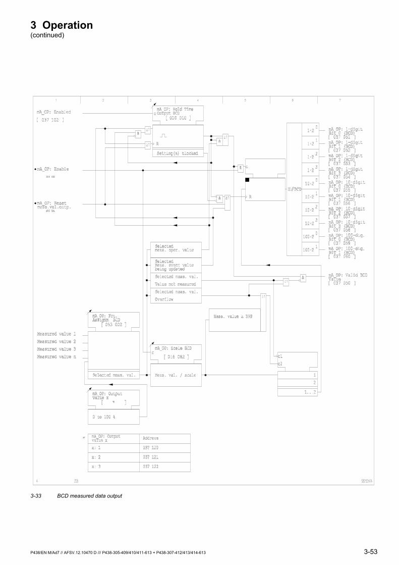
3 Operation (continued)
3-33 BCD measured data output
P438/EN M/Ad7 // AFSV.12.10470 D /// P438-305-409/410/411-613 + P438-307-412/413/414-613 3-53
3 Operation (continued)
3.10.2 Analog Measured Data Output
Analog output of measured data is two-channel.
The user can select two of the measured values available in the P438 for output in the form of load-independent direct current. Three interpolation points per channel can be defined for specific adjustments such as adjustment to the scaling of a measuring instrument. The direct current that is output is displayed as a measured operating value.
The selected measured value is output as direct current for the duration of the set hold time m A _ O P : H o l d T i m e O u t p u t A - x . If the selected variable was not measured, then there is no output of a measured value value.
Output of measured event values
If the measured event value is updated during the hold time, the measured value output memory is cleared and the hold time is re-started. This leads to an immediate output of the updated value.
Output of measured operating values
The selected measured operating value is available for the duration of the set hold time. After the hold time has elapsed, the current value is saved and the hold time is re-started. If the hold time has been set to ’Blocked’, the measured operating value that has been output will be stored until the measured data output function is reset.
Configuration of output relays assigned to the output channels
The user must keep in mind that direct current output only occurs when the output relays assigned to the output channels are configured for m A _ O P : V a l u e A - x O u t p u t , since the output channels would otherwise remain short-circuited (see terminal connection diagrams).
3-54 P438/EN M/Ad7 // AFSV.12.10470 D /// P438-305-409/410/411-613 + P438-307-412/413/414-613
3 Operation (continued)
Scaling the analog display
In order to define the resolution for measured data output the measured value range in scaled form and the associated display range have to be set. One additional value for the knee point must also be defined. In this way the user can obtain an analog output characteristic similar to the characteristic shown in Figure 3-34.
Measured value range to be output
The measured value range to be output is (Mx,min ... Mx,knee ... Mx,max), with: Mx,min: Minimum value to be output Mx,knee: Knee point value for the measured value range to be output Mx,max: Maximum value to be output
This measured value range to be output is defined by setting the following parameters:
m A _ O P : S c a l e d M i n . V a l . A - x m A _ O P : S c a l e d K n e e V a l . A - x
m A _ O P : S c a l e d M A X . v a l . A - x
Scaling is made with reference to the complete range of values for the selected measured value (variable Mx). The complete range of values is defined by their end values Mx,RL1 and Mx,RL2. (Mx,RL1 and Mx,RL2 are listed in the operating program S&R-103 - PC Support Software MiCOM S1 - under "minimum" and "maximum".)
Measured values Range
Measured values of the variable Mx
Mx,RL1 ... Mx,RL2
Associated scaled measured values
0 ... 1
Measured values to be output
Range
Measured values with knee-point to be output
Mx,min ... Mx,knee ... Mx,max
Scaled measured values with a scaled knee-point to be output
Mx,scal,min ... Mx,scal,knee ... Mx,scal,max
with:
Mx,scal,min = (Mx,min - Mx,RL1) / (Mx,RL2 - Mx,RL1
Mx,scal,knee = (Mx,knee - Mx,RL1) / (Mx,RL2 - Mx,RL1)
Mx,scal,max = (Mx,max - Mx,RL1) / (Mx,RL2 - Mx,RL1
Designation of the set values in the data model
"Scal. min. value Ax" ... ... "Scal. knee-point Ax" ... ... "Scal. max. value Ax"
P438/EN M/Ad7 // AFSV.12.10470 D /// P438-305-409/410/411-613 + P438-307-412/413/414-613 3-55

3 Operation (continued)
Associated display range
The associated display range is defined by setting the following parameters:
m A _ O P : A n O u t M i n . V a l . A - x
m A _ O P : A n O u t K n e e P o i n t A - x
m A _ O P : A n O u t M a x . V a l . A - x
Measured values Analog display values
Measured values in the range "Measured values to be output"
"AnOut min. val. A-x" ... ... "AnOut knee point A-x" ... ... ... "AnOut max. val. A-x" (Value A-x valid)
Measured values: Mx,RL1 = Mx = Mx,min
"AnOut min. val." (Value A-x not valid)
Measured values Mx: Mx,max = Mx = Mx,RL2
"AnOut max. val." (Value A-x not valid)
Measured values Mx: Mx < Mx,RL1 or Mx > Mx,RL2
"AnOut max. val." (Overflow)
3-56 P438/EN M/Ad7 // AFSV.12.10470 D /// P438-305-409/410/411-613 + P438-307-412/413/414-613
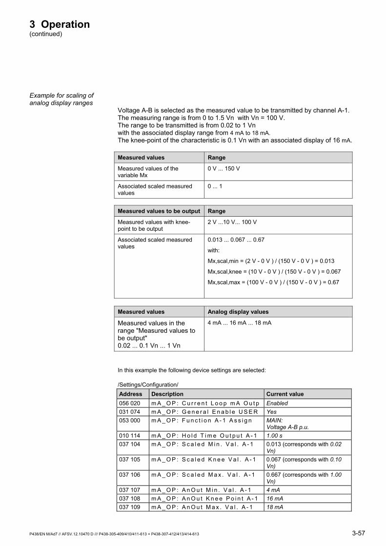
3 Operation (continued)
Example for scaling of analog display ranges
Voltage A-B is selected as the measured value to be transmitted by channel A-1. The measuring range is from 0 to 1.5 Vn with Vn = 100 V. The range to be transmitted is from 0.02 to 1 Vn with the associated display range from 4 mA to 18 mA. The knee-point of the characteristic is 0.1 Vn with an associated display of 16 mA.
Measured values Range
Measured values of the variable Mx
0 V ... 150 V
Associated scaled measured values
0 ... 1
Measured values to be output Range
Measured values with knee-point to be output
2 V ...10 V... 100 V
Associated scaled measured values
0.013 ... 0.067 ... 0.67
with:
Mx,scal,min = (2 V - 0 V ) / (150 V - 0 V ) = 0.013
Mx,scal,knee = (10 V - 0 V ) / (150 V - 0 V ) = 0.067
Mx,scal,max = (100 V - 0 V ) / (150 V - 0 V ) = 0.67
Measured values Analog display values
Measured values in the range "Measured values to be output" 0.02 ... 0.1 Vn ... 1 Vn
4 mA ... 16 mA ... 18 mA
In this example the following device settings are selected:
/Settings/Configuration/ Address Description Current value 056 020 m A _ O P : C u r r e n t L o o p m A O u t p Enabled 031 074 m A _ O P : G e n e r a l E n a b l e U S E R Yes 053 000 m A _ O P : F u n c t i o n A - 1 A s s i g n MAIN:
Voltage A-B p.u. 010 114 m A _ O P : H o l d T i m e O u t p u t A - 1 1.00 s 037 104 m A _ O P : S c a l e d M i n . V a l . A - 1 0.013 (corresponds with 0.02
Vn) 037 105 m A _ O P : S c a l e d K n e e V a l . A - 1 0.067 (corresponds with 0.10
Vn) 037 106 m A _ O P : S c a l e d M a x . V a l . A - 1 0.667 (corresponds with 1.00
Vn) 037 107 m A _ O P : A n O u t M i n . V a l . A - 1 4 mA 037 108 m A _ O P : A n O u t K n e e P o i n t A - 1 16 mA 037 109 m A _ O P : A n O u t M a x . V a l . A - 1 18 mA
P438/EN M/Ad7 // AFSV.12.10470 D /// P438-305-409/410/411-613 + P438-307-412/413/414-613 3-57
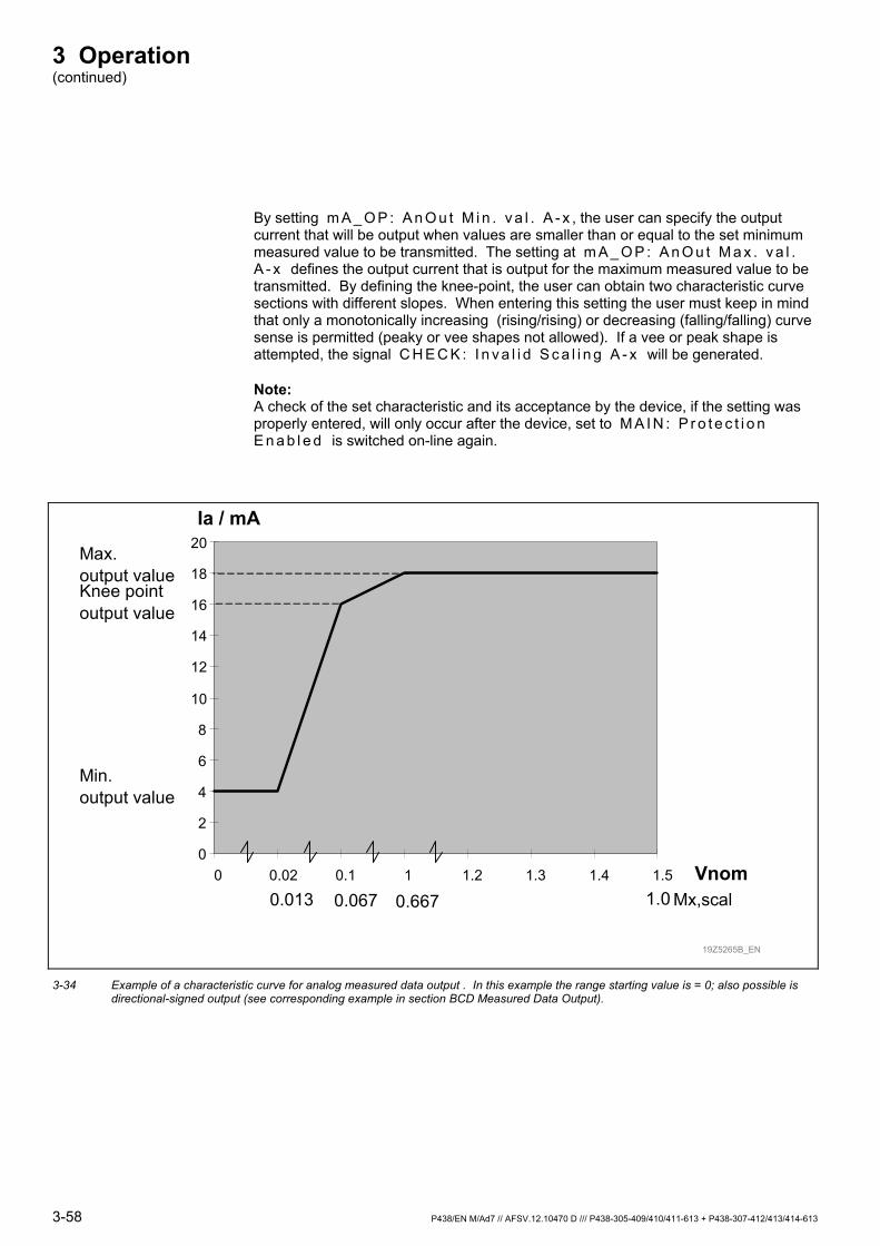
3 Operation (continued)
By setting m A _ O P : A n O u t M i n . v a l . A - x , the user can specify the output current that will be output when values are smaller than or equal to the set minimum measured value to be transmitted. The setting at m A _ O P : A n O u t M a x . v a l . A - x defines the output current that is output for the maximum measured value to be transmitted. By defining the knee-point, the user can obtain two characteristic curve sections with different slopes. When entering this setting the user must keep in mind that only a monotonically increasing (rising/rising) or decreasing (falling/falling) curve sense is permitted (peaky or vee shapes not allowed). If a vee or peak shape is attempted, the signal C H E C K : I n v a l i d S c a l i n g A - x will be generated.
Note: A check of the set characteristic and its acceptance by the device, if the setting was properly entered, will only occur after the device, set to M A I N : P r o t e c t i o n E n a b l e d is switched on-line again.
0
2
4
6
8
10
12
14
16
18
20
0 0.02 0.1 1 1.2 1.3 1.4 1.5
Ia / mA
D5Z52KFA
Min.output value
Knee pointoutput value
Max.output value
Mx,scal0.013 0.067 0.667Vnom
1.0
19Z5265B_EN
3-34 Example of a characteristic curve for analog measured data output . In this example the range starting value is = 0; also possible is directional-signed output (see corresponding example in section BCD Measured Data Output).
3-58 P438/EN M/Ad7 // AFSV.12.10470 D /// P438-305-409/410/411-613 + P438-307-412/413/414-613

3 Operation (continued)
3-35 Analog measured data output
P438/EN M/Ad7 // AFSV.12.10470 D /// P438-305-409/410/411-613 + P438-307-412/413/414-613 3-59
3 Operation (continued)
3.10.3 Output of ‘External’ Measured Data
Measured data from external devices, which must be scaled to 0 ... 100%, can be written to the following parameters of the P438 using the communications interface.
m A _ O P : O u t p u t V a l u e 1
m A _ O P : O u t p u t V a l u e 2
m A _ O P : O u t p u t V a l u e 3
These "external" measured values are output by the P438 either in BCD data form or as load-independent direct current, provided that the BCD measured data output function or the channels of the analog measured data output function are configured accordingly.
3-60 P438/EN M/Ad7 // AFSV.12.10470 D /// P438-305-409/410/411-613 + P438-307-412/413/414-613

3 Operation (continued)
P438/EN M/Ad7-S // AFSV.12.10470 D /// P438-305-409/410/411-613 + P438-307-412/413/414-613 3-61
3.11 Configuration and Operating Mode of the LED Indicators (Function Group LED)
The P438 has 17 LED indicators for the indication of binary signals. Four of the LED indicators are permanently assigned to fixed functions. The other 12 LED indicators are freely configurable. These freely configurable multicolor LED indicators may be set to emit red, green or amber light, but amber cannot be configured individually as it results from the LED indicator simultaneously emitting both red and green light.
Configuring the LED indicators
One binary signal can be assigned to each of the red and green LED color indications. The same binary signal can be assigned to several LED indicators (or colors), if required.
LED indicator Label Configuration
H 1 (green) 'HEALTHY' Not configurable. H 1 indicates the operational readiness of the device (supply voltage is present).
H 17 (red) 'EDIT MODE' Not configurable. H 17 indicates the input mode. Only when the device is in this mode, can setting parameters be changed by pressing the
and keys. (See Chapter 6, section 'Display and Keypad')
H 2 (amber) 'OUT OF SERVICE' Permanently configured with function M A I N : B l o c k e d / f a u l t y .
H 3 (amber) 'ALARM' Permanently configured with function C H E C K : A l a r m ( L E D ) .
H 4 (red) 'TRIP' With the P438 this LED indicator is assigned the M A I N : G e n . T r i p S i g n a l function by default. This assignment can be modified.
H 4 (green) ---- This LED indicator may be freely configured to emit green light.
H 5 to H 16 ---- Both colors (red & green) may be configured individually and freely for these LED indicators.
The figure below shows the layout of the LED indicators situated on the front panel user interface (HMI) of the 40TE & 84TE cases.
12 Z6100B_EN
H4H3H2H1H17H5H6H7H8H9H10H11H12H13H14H15H16
G
GG
G
G
G
TRIPALARMOUT OF SERVICEHEALTHYEDIT MODE
G
C
F1
F2
F3
F4
F5
F6
H18
H19
H20
H21
H22
H23
3-36 Layout of the LED indicators situated on the front panel user interface (HMI)
3 Operation (continued)
Operating mode of the LED indicators
For each of the freely configurable LED indicators, the operating mode can be selected separately. This setting will determine whether the LED indicator will operate either in energize-on-signal (ES) or normally-energized (NE) mode, whether it will be flashing and whether it will be in latching mode. Latching is disabled either manually using a setting parameter or through an appropriately configured binary signal input (see "Main Functions of the P438"), at the onset of a new fault or of a new system disturbance, depending on the selected operating mode.
Therefore the operating modes turn out to be the 23=8 possible combinations of the following components:
• flashing / continuous, • energize-on-signal (ES) / normally-energized (NE), • updating / latching with manual reset,
in addition to these there are the following 4 operating modes
• energize-on-signal (ES) with reset after new fault (flashing / continuous) and • energize-on-signal (ES) with reset after new system disturbance (flashing /
continuous),
so that there are 12 possible operating modes in total.
3-62 P438/EN M/Ad7 // AFSV.12.10470 D /// P438-305-409/410/411-613 + P438-307-412/413/414-613
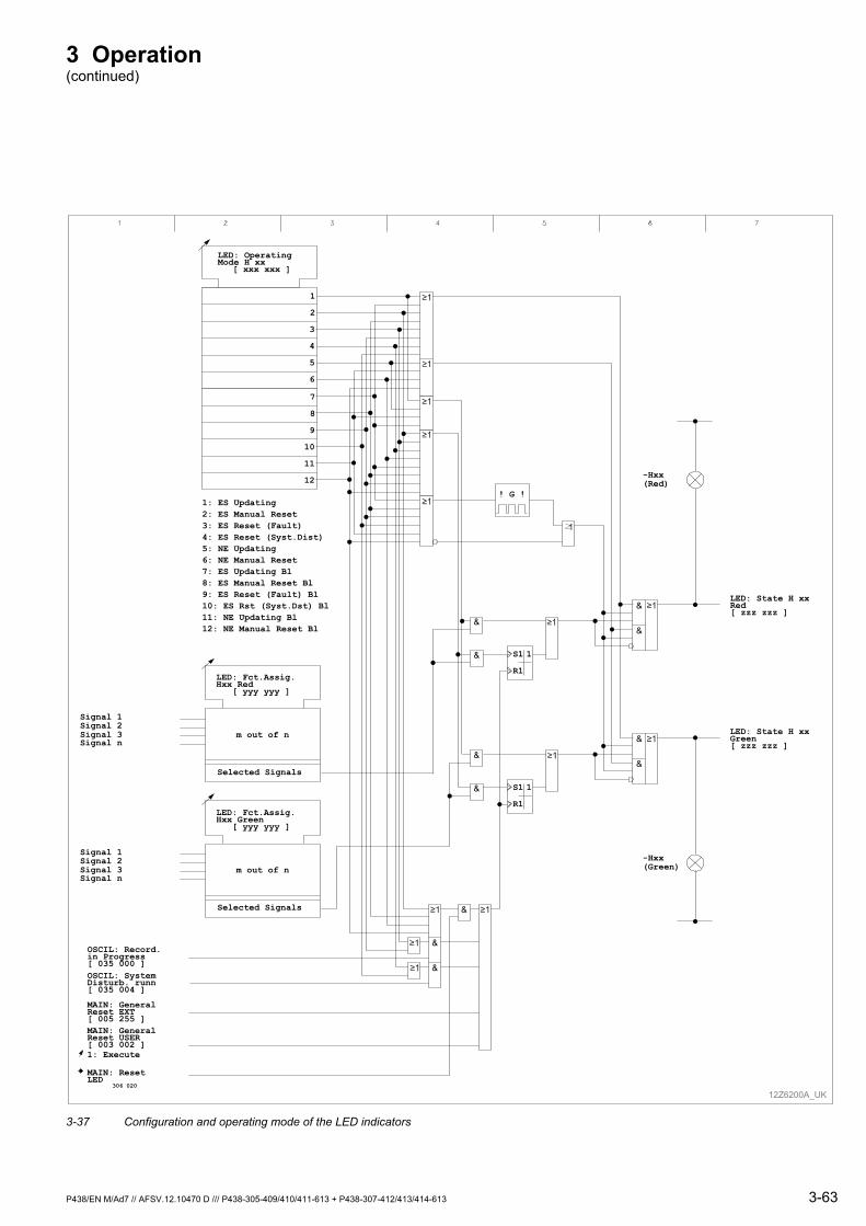
3 Operation (continued)
m out of n
LED: Fct.Assig.Hxx Red [ yyy yyy ]
Selected Signals
Signal 1Signal 2Signal 3Signal n
R1
S1 1
OSCIL: Record.in Progress[ 035 000 ]
1: Execute
MAIN: GeneralReset EXT[ 005 255 ]MAIN: GeneralReset USER[ 003 002 ]
OSCIL: SystemDisturb. runn[ 035 004 ]
&
&
&
LED: OperatingMode H xx
[ xxx xxx ]
1: ES Updating2: ES Manual Reset3: ES Reset (Fault)4: ES Reset (Syst.Dist)5: NE Updating6: NE Manual Reset7: ES Updating Bl8: ES Manual Reset Bl9: ES Reset (Fault) Bl10: ES Rst (Syst.Dst) Bl11: NE Updating Bl12: NE Manual Reset Bl
12Z6200A_UK
LED: State H xxRed[ zzz zzz ]
1
2
3
4
5
6
-Hxx(Red)
&
&&
&
MAIN: ResetLED
306 020
m out of n
LED: Fct.Assig.Hxx Green [ yyy yyy ]
Selected Signals
Signal 1Signal 2Signal 3Signal n
R1
S1 1
LED: State H xxGreen[ zzz zzz ]
&
&&
&
-Hxx(Green)
7
8
9
10
11
12
! G !
≥1
3-37 Configuration and operating mode of the LED indicators
P438/EN M/Ad7 // AFSV.12.10470 D /// P438-305-409/410/411-613 + P438-307-412/413/414-613 3-63

3 Operation (continued)
3.12 Main Functions of the P438 (Function Group MAIN)
3.12.1 Conditioning of the Measured Values
The secondary phase currents and voltages of the system transformers are fed into the P438 and are – electrically isolated – converted to standardized electronics levels. The analog quantities are digitized and are thus available for further processing.
Settings that do not refer to nominal quantities are converted by the P438 to nominal quantities. The user must therefore set the secondary nominal currents and voltages of the system transformers.
The connection arrangement of the measuring circuits on the P438 must also be set. Figures 3-38 and 3-40 show the standard connection. The phase of the digitized currents is rotated by 180° by this setting.
The P438 is designed for operation in Classic single feed or Autotransformer feed modes. Figure 3-38 shows the connection in Classic single feed mode and figure 3-39 the connection in Autotransformer feed mode.
3-64 P438/EN M/Ad7 // AFSV.12.10470 D /// P438-305-409/410/411-613 + P438-307-412/413/414-613
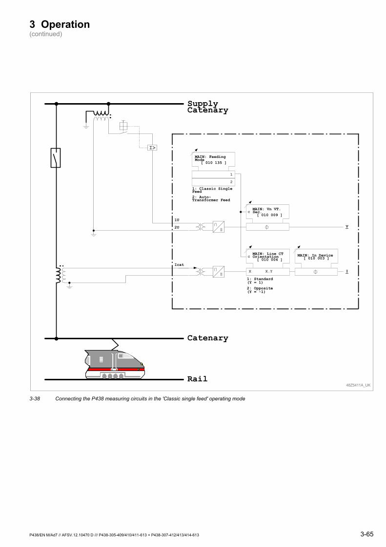
3 Operation (continued)
Catenary
Rail
V
I
I>
Icat
1U
2U
MAIN: FeedingMode
[ 010 135 ]
1
2
1: Classic SingleFeed2: Auto-Transformer Feed
MAIN: Vn VT.Sec.[ 010 009 ]
MAIN: In Device[ 010 003 ]
MAIN: Line CTOrientation[ 010 004 ]
X X.Y
1: Standard(Y = 1)2: Opposite(Y = -1)
48Z5411A_UK
c
c
SupplyCatenary
3-38 Connecting the P438 measuring circuits in the 'Classic single feed' operating mode
P438/EN M/Ad7 // AFSV.12.10470 D /// P438-305-409/410/411-613 + P438-307-412/413/414-613 3-65
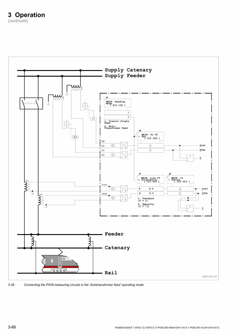
3 Operation (continued)
Catenary
Vcat
Ifdr
2U
Feeder
Supply CatenarySupply Feeder
3U
4U
Vfdr
VS
-+
Icat
Icat
Ifdr
IS
-+
I>
I>
Rail
MAIN: FeedingMode
[ 010 135 ]
1
2
1: Classic SingleFeed2: Auto-Transformer Feed
1U
MAIN: Vn VT.Sec.[ 010 009 ]
c
MAIN: Line CTOrientation[ 010 004 ]
X X.Y
1: Standard(Y = 1)2: Opposite(Y = -1)
c
X X.Y
MAIN: InDevice[ 010 003 ]
c
48Z5412A_UK
3-39 Connecting the P438 measuring circuits in the 'Autotransformer feed' operating mode
3-66 P438/EN M/Ad7 // AFSV.12.10470 D /// P438-305-409/410/411-613 + P438-307-412/413/414-613
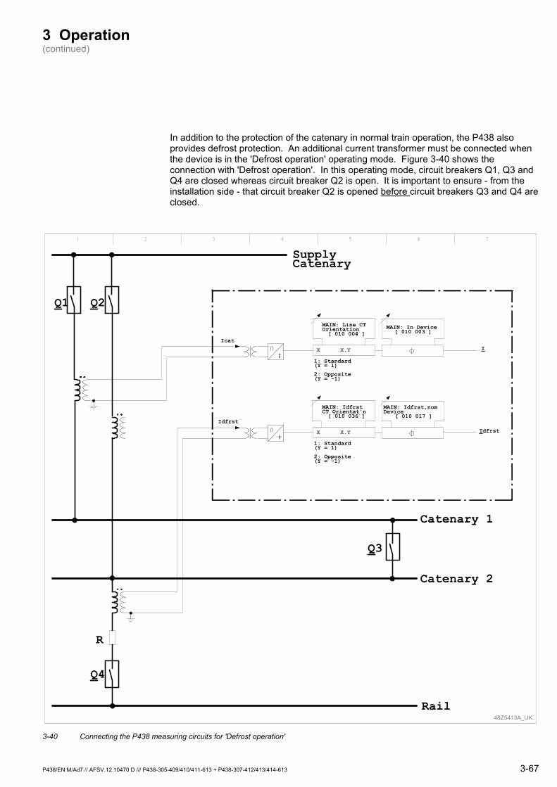
3 Operation (continued)
In addition to the protection of the catenary in normal train operation, the P438 also provides defrost protection. An additional current transformer must be connected when the device is in the 'Defrost operation' operating mode. Figure 3-40 shows the connection with 'Defrost operation'. In this operating mode, circuit breakers Q1, Q3 and Q4 are closed whereas circuit breaker Q2 is open. It is important to ensure - from the installation side - that circuit breaker Q2 is opened before circuit breakers Q3 and Q4 are closed.
48Z5413A_UK
Idfrst
Q3
Catenary 1
Catenary 2
Q4
Rail
R
SupplyCatenary
Q1 Q2
IcatI
Idfrst
MAIN: Idfrst,nomDevice
[ 010 017 ]
MAIN: IdfrstCT Orientat'n[ 010 036 ]
X X.Y
1: Standard(Y = 1)
2: Opposite(Y = -1)
MAIN: In Device[ 010 003 ]
MAIN: Line CTOrientation[ 010 004 ]
X X.Y
1: Standard(Y = 1)
2: Opposite(Y = -1)
3-40 Connecting the P438 measuring circuits for 'Defrost operation'
P438/EN M/Ad7 // AFSV.12.10470 D /// P438-305-409/410/411-613 + P438-307-412/413/414-613 3-67
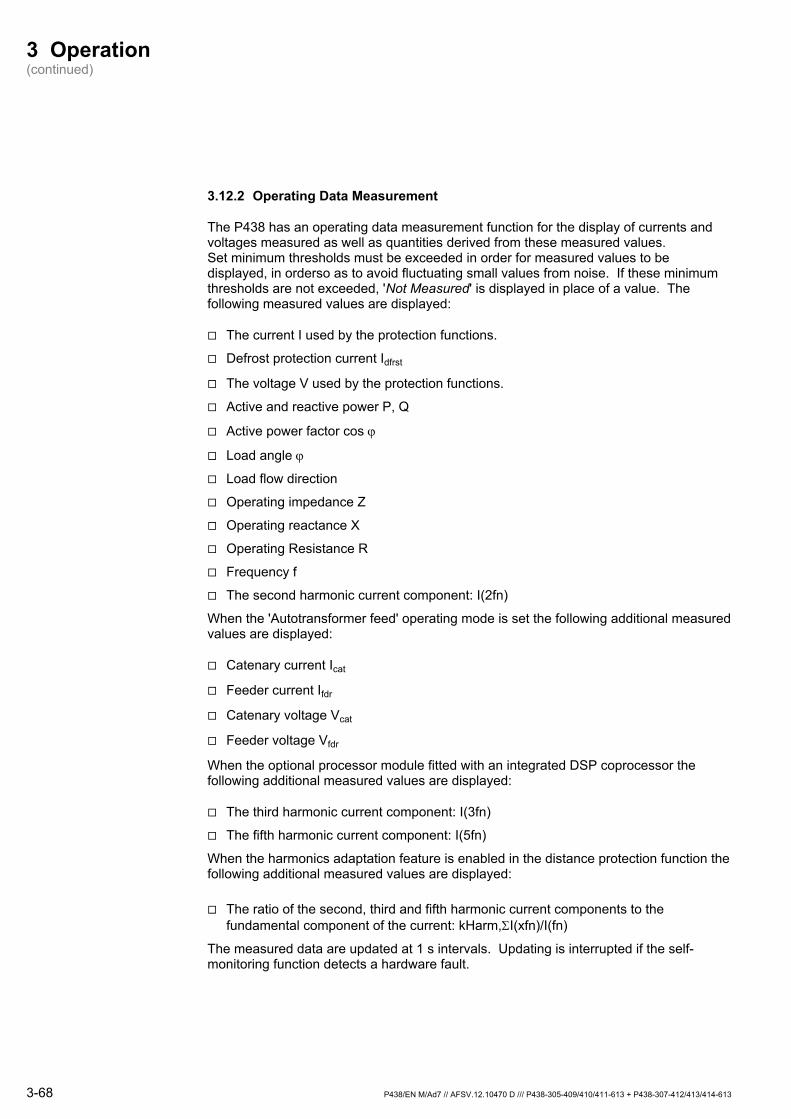
3 Operation (continued)
3.12.2 Operating Data Measurement
The P438 has an operating data measurement function for the display of currents and voltages measured as well as quantities derived from these measured values. Set minimum thresholds must be exceeded in order for measured values to be displayed, in orderso as to avoid fluctuating small values from noise. If these minimum thresholds are not exceeded, 'Not Measured' is displayed in place of a value. The following measured values are displayed:
The current I used by the protection functions.
Defrost protection current Idfrst
The voltage V used by the protection functions.
Active and reactive power P, Q
Active power factor cos ϕ
Load angle ϕ
Load flow direction
Operating impedance Z
Operating reactance X
Operating Resistance R
Frequency f
The second harmonic current component: I(2fn)
When the 'Autotransformer feed' operating mode is set the following additional measured values are displayed:
Catenary current Icat
Feeder current Ifdr
Catenary voltage Vcat
Feeder voltage Vfdr
When the optional processor module fitted with an integrated DSP coprocessor the following additional measured values are displayed:
The third harmonic current component: I(3fn)
The fifth harmonic current component: I(5fn)
When the harmonics adaptation feature is enabled in the distance protection function the following additional measured values are displayed:
The ratio of the second, third and fifth harmonic current components to the fundamental component of the current: kHarm,ΣI(xfn)/I(fn)
The measured data are updated at 1 s intervals. Updating is interrupted if the self-monitoring function detects a hardware fault.
3-68 P438/EN M/Ad7 // AFSV.12.10470 D /// P438-305-409/410/411-613 + P438-307-412/413/414-613
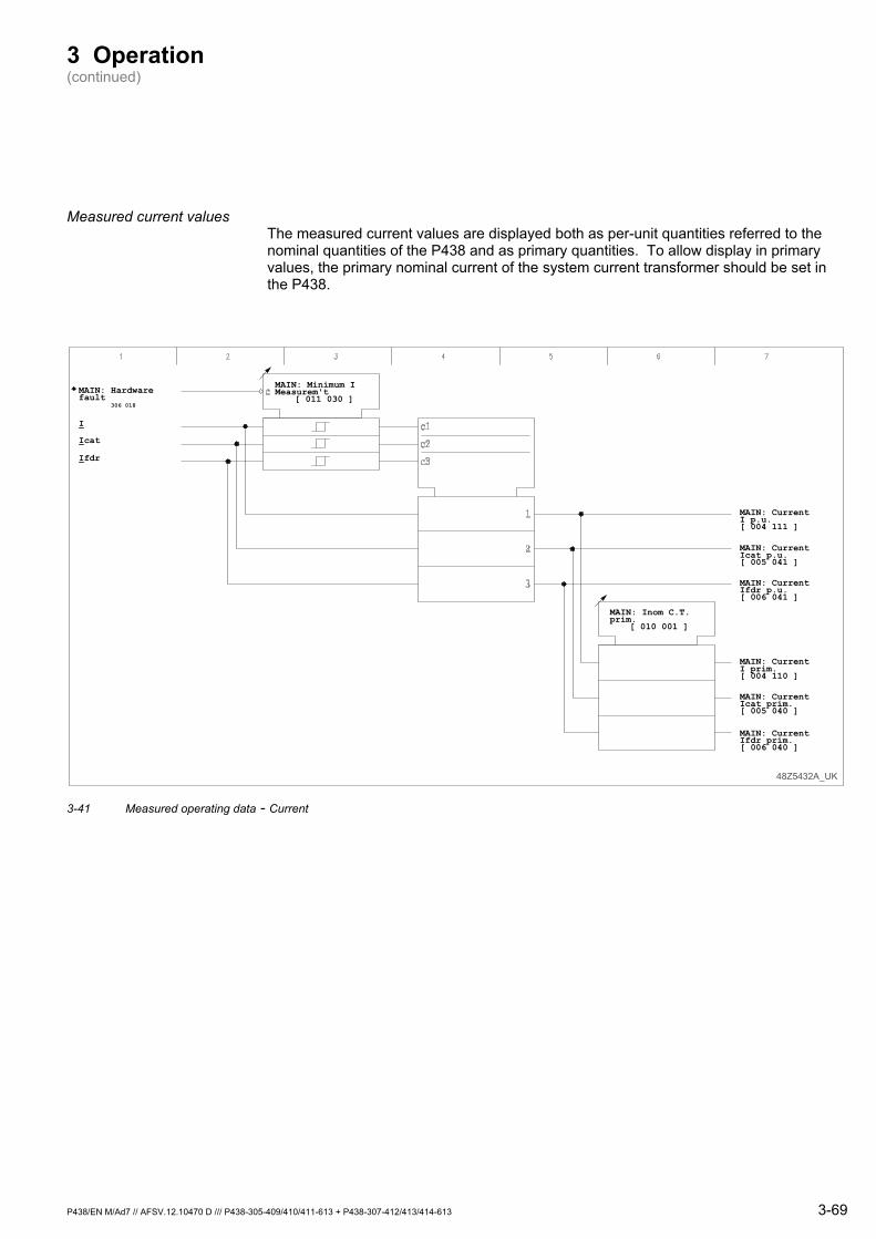
3 Operation (continued)
Measured current values The measured current values are displayed both as per-unit quantities referred to the nominal quantities of the P438 and as primary quantities. To allow display in primary values, the primary nominal current of the system current transformer should be set in the P438.
48Z5432A_UK
MAIN: Hardwarefault 306 018
Ifdr
Icat
I
MAIN: CurrentI prim.[ 004 110 ]
MAIN: CurrentIcat prim.[ 005 040 ]
MAIN: CurrentIfdr prim.[ 006 040 ]
MAIN: CurrentI p.u.[ 004 111 ]
MAIN: CurrentIcat p.u.[ 005 041 ]
MAIN: CurrentIfdr p.u.[ 006 041 ]
MAIN: Inom C.T.prim.
[ 010 001 ]
MAIN: Minimum IMeasurem't
[ 011 030 ]
3-41 Measured operating data - Current
P438/EN M/Ad7 // AFSV.12.10470 D /// P438-305-409/410/411-613 + P438-307-412/413/414-613 3-69
3 Operation (continued)
Harmonic current components
The harmonic current components are displayed both as per-unit quantities referred to the nominal quantities of the P438 and as primary quantities. When the optional processor module with an integrated DSP coprocessor is fitted the additional third and fifth harmonic current components are displayed both as per-unit quantities referred to the nominal quantities of the P438 and as primary quantities. To allow display in primary values, the primary nominal current of the system current transformer should be set in the P438.
When distance protection is operated with the harmonics adaptation feature enabled then dynamic harmonics factor M A I N : k H a r m . Σ I ( x f n ) / I ( f n ) is displayed.
3-70 P438/EN M/Ad7 // AFSV.12.10470 D /// P438-305-409/410/411-613 + P438-307-412/413/414-613

3 Operation (continued)
3-42 Measured operating data - Harmonic current components and harmonics factor for distance protection
P438/EN M/Ad7 // AFSV.12.10470 D /// P438-305-409/410/411-613 + P438-307-412/413/414-613 3-71
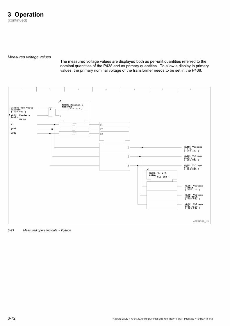
3 Operation (continued)
Measured voltage values The measured voltage values are displayed both as per-unit quantities referred to the nominal quantities of the P438 and as primary quantities. To allow a display in primary values, the primary nominal voltage of the transformer needs to be set in the P438.
48Z5433A_UK
MAIN: VoltageV prim.[ 004 112 ]
MAIN: VoltageVcat prim.[ 005 042 ]
MAIN: VoltageVfdr prim.[ 006 042 ]
MAIN: VoltageV p.u.[ 004 113 ]
MAIN: VoltageVcat p.u.[ 005 043 ]
MAIN: VoltageVfdr p.u.[ 006 043 ]
MAIN: Minimum VMeas'mt
[ 011 032 ]
MAIN: Hardwarefault 306 018
Vfdr
Vcat
V
MAIN: Vn V.T.prim.
[ 010 002 ]
C&VTS: VTS VoltsFailure[ 038 023 ]
3-43 Measured operating data - voltage
3-72 P438/EN M/Ad7 // AFSV.12.10470 D /// P438-305-409/410/411-613 + P438-307-412/413/414-613
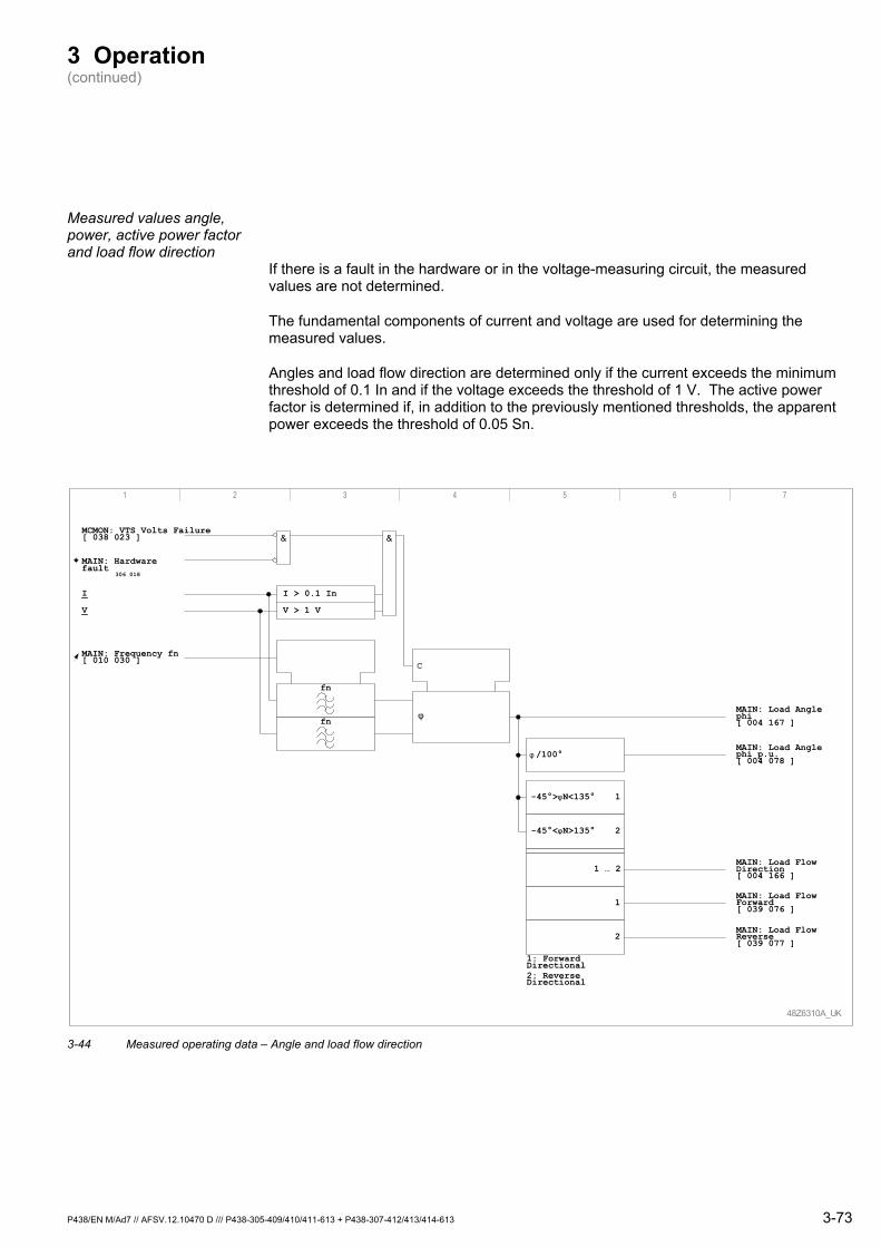
3 Operation (continued)
Measured values angle, power, active power factor and load flow direction
If there is a fault in the hardware or in the voltage-measuring circuit, the measured values are not determined.
The fundamental components of current and voltage are used for determining the measured values.
Angles and load flow direction are determined only if the current exceeds the minimum threshold of 0.1 In and if the voltage exceeds the threshold of 1 V. The active power factor is determined if, in addition to the previously mentioned thresholds, the apparent power exceeds the threshold of 0.05 Sn.
MAIN: Load Anglephi[ 004 167 ]
MAIN: Hardwarefault
306 018
1 2 3 4 5 6 7
MAIN: Frequency fn[ 010 030 ]
MCMON: VTS Volts Failure[ 038 023 ]
48Z6310A_UK
I > 0.1 In
V > 1 V
I
V
fn
fn
C
/100°MAIN: Load Anglephi p.u.[ 004 078 ]
-45°> N<135° 1
-45°< N>135° 2
1 … 2
1
2
1: ForwardDirectional2: ReverseDirectional
MAIN: Load FlowDirection[ 004 166 ]
MAIN: Load FlowForward[ 039 076 ]
MAIN: Load FlowReverse[ 039 077 ]
& &
3-44 Measured operating data – Angle and load flow direction
P438/EN M/Ad7 // AFSV.12.10470 D /// P438-305-409/410/411-613 + P438-307-412/413/414-613 3-73
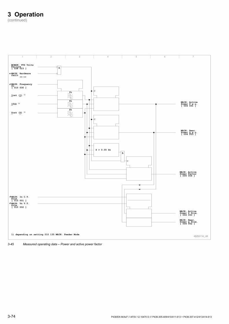
3 Operation (continued)
MAIN: Hardwarefault
306 018
1 2 3 4 5 6 7
MAIN: Frequencyfn[ 010 030 ]
MCMON: VTS VoltsFailure[ 038 023 ]
48Z6311A_UK
Icat (I) 1)
Vcat (V) 1)
fn
fn
C
fn
C
S > 0.05 Sn
C
MAIN: ActivePower P p.u.[ 004 051 ]
MAIN: Reac.Power Q p.u.[ 004 053 ]
MAIN: ActivePower Factor[ 004 054 ]
MAIN: ActivePower P Prim.[ 004 050 ]
MAIN: Reac.Power Q Prim.[ 004 052 ]
MAIN: In C.T.Prim.[ 010 001 ]MAIN: Vn V.T.Prim.[ 010 002 ]
1) depending on setting 010 135 MAIN: Feeder Mode
Ifdr 1)
&
&
3-45 Measured operating data – Power and active power factor
3-74 P438/EN M/Ad7 // AFSV.12.10470 D /// P438-305-409/410/411-613 + P438-307-412/413/414-613
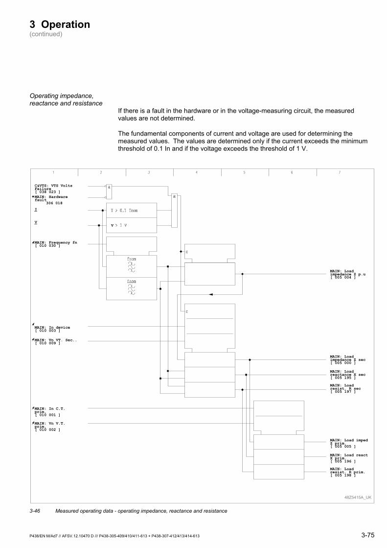
3 Operation (continued)
Operating impedance, reactance and resistance
If there is a fault in the hardware or in the voltage-measuring circuit, the measured values are not determined.
The fundamental components of current and voltage are used for determining the measured values. The values are determined only if the current exceeds the minimum threshold of 0.1 In and if the voltage exceeds the threshold of 1 V.
48Z5415A_UK
MAIN: Load reactX prim.[ 005 196 ]
MAIN: Loadresist. R prim.[ 005 198 ]
MAIN: Load impedZ prim.[ 005 005 ]
MAIN: Loadreactance X sec[ 005 195 ]
MAIN: Loadresist. R sec[ 005 197 ]
MAIN: Loadimpedance Z sec[ 005 000 ]
MAIN: Loadimpedance Z p.u[ 005 004 ]
MAIN: Frequency fn[ 010 030 ]
MAIN: Hardwarefault
306 018
C&VTS: VTS VoltsFailure[ 038 023 ]
I
V
MAIN: In C.T.prim.[ 010 001 ]
MAIN: Vn V.T.prim.[ 010 002 ]
MAIN: In device[ 010 003 ]
MAIN: Vn VT. Sec..[ 010 009 ]
V
3-46 Measured operating data - operating impedance, reactance and resistance
P438/EN M/Ad7 // AFSV.12.10470 D /// P438-305-409/410/411-613 + P438-307-412/413/414-613 3-75

3 Operation (continued)
Frequency The P438 determines the frequency from the voltage. The frequency is determined only if the voltage exceeds a minimum threshold of 10 V and if there is no fault in the voltage-measuring circuit.
48Z5416A_UK
MAIN: Frequency f[ 004 040 ]
MAIN: Frequencyf p.u.[ 004 070 ]
MAIN: Hardwarefault
306 018
C&VTS: VTS VoltsFailure[ 038 023 ]
V
C&VTS: Frequencyfn[ 010 030 ]
3-47 Frequency measurement
3-76 P438/EN M/Ad7 // AFSV.12.10470 D /// P438-305-409/410/411-613 + P438-307-412/413/414-613

3 Operation (continued)
3.12.3 Configuring and Enabling the Protection Functions
The device can be adapted to the requirements of a specific high-voltage system by configuring the available function range. By including the relevant protection functions in the configuration and cancelling all the others, the user creates an individually configured device adapted to the specific application. Parameters, signals and measured values of cancelled protection functions are not displayed on the user interface (HMI). Functions of general applicability such as operating data recording (OP_RC) or main functions (MAIN) cannot be cancelled.
Cancelling a protection function
The following conditions must be met before a protection function can be cancelled:
The protection function in question must be disabled.
None of the elements of the protection function being cancelled are assigned to a binary input.
None of the signals of the protection function are assigned to a binary output or an LED indicator.
No signal or measured value of the protection function to be cancelled are selected in a list setting.
If the above conditions are met, proceed through the Configuration branch of the menu tree to access the setting relevant for the protection function to be cancelled. If, for example, the "LIMIT" function group is to be cancelled, access the L I M I T : L i m i t T h r e s h o l d s I < > parameter and set its value to 'Disabled'. To re-include the "LIMIT" function in the device configuration, access the same parameter and set its value to 'Enabled'.
The protection function to which a setting, a signal, or a measured value belongs is defined by the function group designation (for example: “LIMIT”) In the following description of the protection functions, it is presumed that this protection function is included in the configuration.
P438/EN M/Ad7 // AFSV.12.10470 D /// P438-305-409/410/411-613 + P438-307-412/413/414-613 3-77
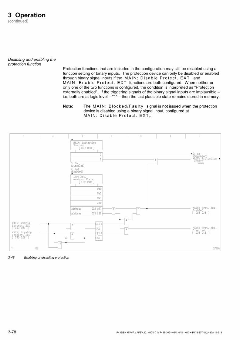
3 Operation (continued)
Disabling and enabling the protection function
Protection functions that are included in the configuration may still be disabled using a function setting or binary inputs. The protection device can only be disabled or enabled through binary signal inputs if the M A I N : D i s a b l e P r o t e c t . E X T and M A I N : E n a b l e P r o t e c t . E X T functions are both configured. When neither or only one of the two functions is configured, the condition is interpreted as "Protection externally enabled". If the triggering signals of the binary signal inputs are implausible – i.e. both are at logic level = "1" – then the last plausible state remains stored in memory.
Note: The M A I N : B l o c k e d / F a u l t y signal is not issued when the protection device is disabled using a binary signal input, configured at M A I N : D i s a b l e P r o t e c t . E X T ,.
3-48 Enabling or disabling protection
3-78 P438/EN M/Ad7 // AFSV.12.10470 D /// P438-305-409/410/411-613 + P438-307-412/413/414-613

3 Operation (continued)
3.12.4 Inrush Stabilization (Harmonic Restraint)
Turning an autotransformer on or reclosing a circuit breaker on a locomotive, after passing through a neutral section, could lead to inrush currents that are interpreted as starting criteria by the protection device P438. The inrush stabilization fonction detects such inrush currents and can selectively prevent starting of selected protection functions.
Blocking inrush stabilization
Inrush stabilization is blocked if M A I N : I n r . I ( 2 f n ) / I ( f n ) S G x is set to 'Blocked' or if an external blocking signal has been triggered.
MAIN: Inrush Restr. Ready[ 041 024 ]
MAIN: Protection Active
306 001
1 2 3 4 5 6 7
MAIN: Inr. I(2fn)/I(fn)SGx[ * ]
48Z6313A_UK
MAIN: Block.Inrush RstrEXT[ 039 169 ]
Blocked
Group 1
Group 2
017 098
MAIN: Inr. I(2fn)/I(fn)SGx
001 091
001 092
001 093
Group 3
Group 4
Setting
&
*
3-49 Blocking inrush stabilization
P438/EN M/Ad7 // AFSV.12.10470 D /// P438-305-409/410/411-613 + P438-307-412/413/414-613 3-79
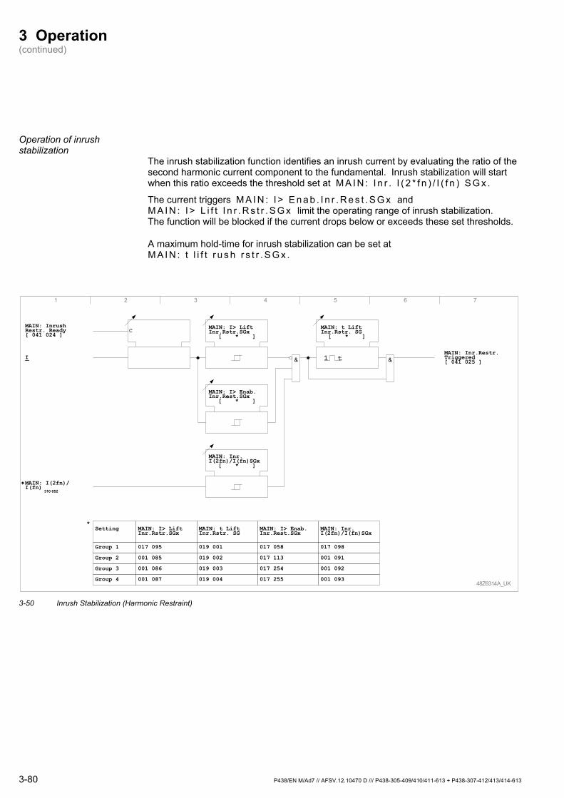
3 Operation (continued)
Operation of inrush stabilization
The inrush stabilization function identifies an inrush current by evaluating the ratio of the second harmonic current component to the fundamental. Inrush stabilization will start when this ratio exceeds the threshold set at M A I N : I n r . I ( 2 * f n ) / I ( f n ) S G x .
The current triggers M A I N : I > E n a b . I n r . R e s t . S G x and M A I N : I > L i f t I n r . R s t r . S G x limit the operating range of inrush stabilization. The function will be blocked if the current drops below or exceeds these set thresholds.
A maximum hold-time for inrush stabilization can be set at M A I N : t l i f t r u s h r s t r . S G x .
MAIN: Inr.Restr. Triggered[ 041 025 ]
I
1 2 3 4 5 6 7
MAIN: Inrush Restr. Ready[ 041 024 ]
MAIN: I> LiftInr.Rstr.SGx
[ * ]
Group 1
Group 2
017 095
MAIN: I> LiftInr.Rstr.SGx
001 085
001 086
001 087
Group 3
Group 4
Setting
48Z6314A_UK
C
MAIN: I> Enab.Inr.Rest.SGx
[ * ]
MAIN: Inr. I(2fn)/I(fn)SGx
[ * ]
MAIN: I(2fn)/I(fn)
310 052
017 058
MAIN: I> Enab.Inr.Rest.SGx
017 113
017 254
017 255
017 098
MAIN: Inr. I(2fn)/I(fn)SGx
001 091
001 092
001 093
019 001
MAIN: t LiftInr.Rstr. SG
019 002
019 003
019 004
MAIN: t LiftInr.Rstr. SG
[ * ]
1 t
*
& &
3-50 Inrush Stabilization (Harmonic Restraint)
3-80 P438/EN M/Ad7 // AFSV.12.10470 D /// P438-305-409/410/411-613 + P438-307-412/413/414-613
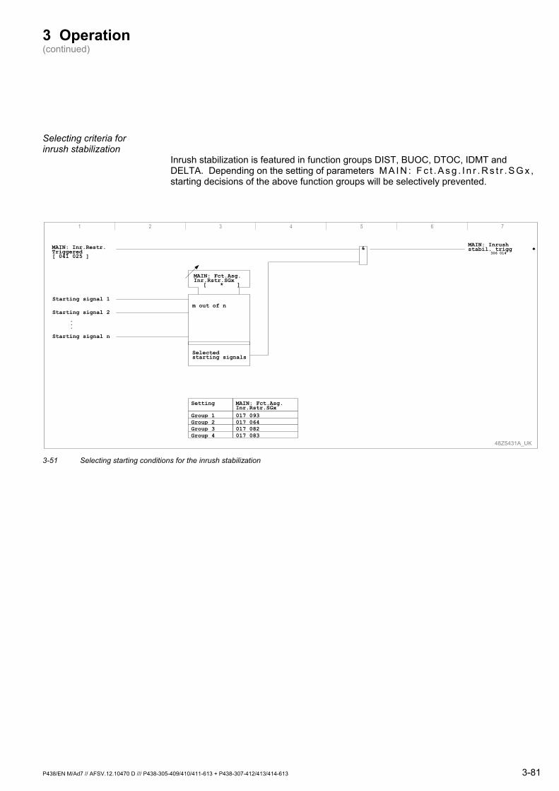
3 Operation (continued)
Selecting criteria for inrush stabilization
Inrush stabilization is featured in function groups DIST, BUOC, DTOC, IDMT and DELTA. Depending on the setting of parameters M A I N : F c t . A s g . I n r . R s t r . S G x , starting decisions of the above function groups will be selectively prevented.
48Z5431A_UK
Starting signal 1
MAIN: Fct.Asg.Inr.Rstr.SGx
[ * ]
m out of n
MAIN: Inrushstabil. trigg
306 014&
Starting signal 2
Starting signal n
Selectedstarting signals
...
1 2 3 4 5 6 7
Setting
Group 1Group 2Group 3Group 4
MAIN: Fct.Asg.Inr.Rstr.SGx017 093017 064017 082017 083
MAIN: Inr.Restr.Triggered[ 041 025 ]
3-51 Selecting starting conditions for the inrush stabilization
P438/EN M/Ad7 // AFSV.12.10470 D /// P438-305-409/410/411-613 + P438-307-412/413/414-613 3-81
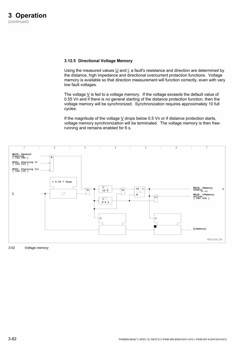
3 Operation (continued)
3.12.5 Directional Voltage Memory
Using the measured values U and I, a fault's resistance and direction are determined by the distance, high impedance and directional overcurrent protection functions. Voltage memory is available so that direction measurement will function correctly, even with very low fault voltages.
The voltage V is fed to a voltage memory. If the voltage exceeds the default value of 0.55 Vn and if there is no general starting of the distance protection function, then the voltage memory will be synchronized. Synchronization requires approximately 10 full cycles.
If the magnitude of the voltage V drops below 0.5 Vn or if distance protection starts, voltage memory synchronization will be terminated. The voltage memory is then free-running and remains enabled for 6 s.
MAIN: tVmemoryactive[ 040 034 ]
1 2 3 4 5 6 7
MAIN: Generalstarting[ 036 000 ]
48Z6318A_EN
1
BUOC: Starting I>[ 036 013 ]
BUOC: Starting I>>[ 036 115 ]
> 0.55 * Vnom
S1
R
10 T
16.0 s
C C
1
V
MAIN: Vmemoryenable
305 049
V(memory)
&&
&
3-52 Voltage memory
3-82 P438/EN M/Ad7 // AFSV.12.10470 D /// P438-305-409/410/411-613 + P438-307-412/413/414-613
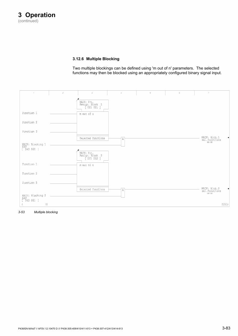
3 Operation (continued)
3.12.6 Multiple Blocking
Two multiple blockings can be defined using 'm out of n' parameters. The selected functions may then be blocked using an appropriately configured binary signal input.
3-53 Multiple blocking
P438/EN M/Ad7 // AFSV.12.10470 D /// P438-305-409/410/411-613 + P438-307-412/413/414-613 3-83
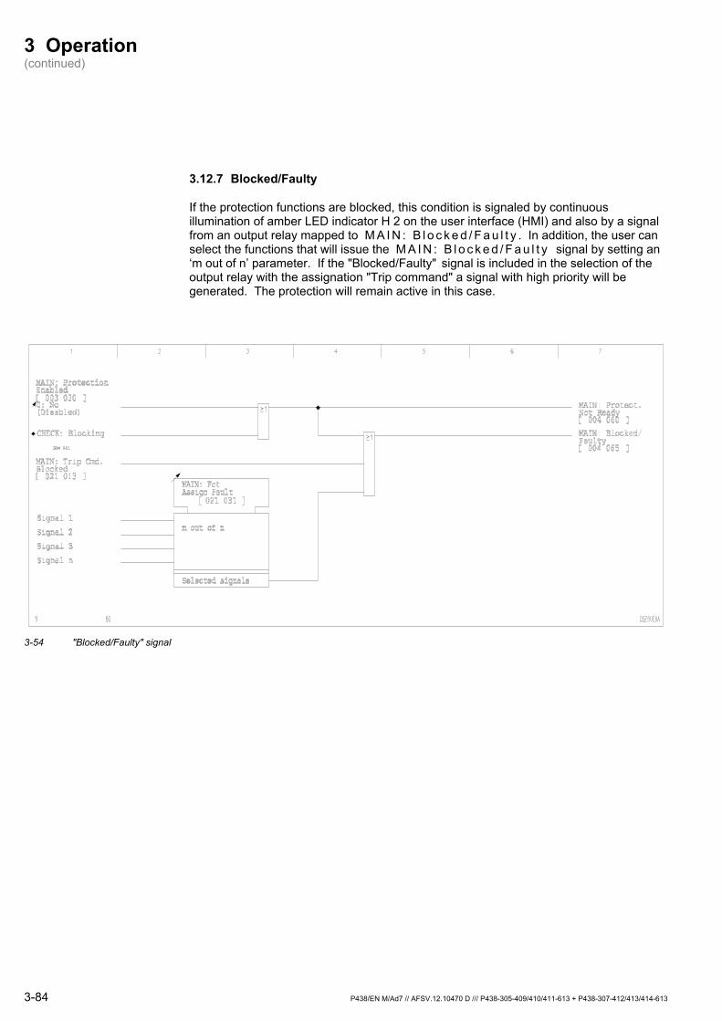
3 Operation (continued)
3.12.7 Blocked/Faulty
If the protection functions are blocked, this condition is signaled by continuous illumination of amber LED indicator H 2 on the user interface (HMI) and also by a signal from an output relay mapped to M A I N : B l o c k e d / F a u l t y . In addition, the user can select the functions that will issue the M A I N : B l o c k e d / F a u l t y signal by setting an ‘m out of n’ parameter. If the "Blocked/Faulty" signal is included in the selection of the output relay with the assignation "Trip command" a signal with high priority will be generated. The protection will remain active in this case.
3-54 "Blocked/Faulty" signal
3-84 P438/EN M/Ad7 // AFSV.12.10470 D /// P438-305-409/410/411-613 + P438-307-412/413/414-613
3 Operation (continued)
3.12.8 Close Command
As of version –606 the circuit breaker may be closed either by the auto-reclose function (RECLS) integrated in the P438, by a setting or by an appropriately configured binary signal input. The close command issued from the user interface (HMI), the setting parameter or the binary signal input will only be executed if there is no main-trip or re-trip command present at the P438. Moreover an appropriate enable condition must be met. Additionally the close command is not executed when, with the setting of M A I N : C l C m d I n h i b . b y C B C l to 'Yes', there is a "CB closed" position signal present.
The duration of the close command can be set. The close command is terminated when a main-trip command or re-trip command is issued.
Close command counter The number of close commands is counted. This counter and the trip command counter may be reset together or by "General Reset".
P438/EN M/Ad7 // AFSV.12.10470 D /// P438-305-409/410/411-613 + P438-307-412/413/414-613 3-85
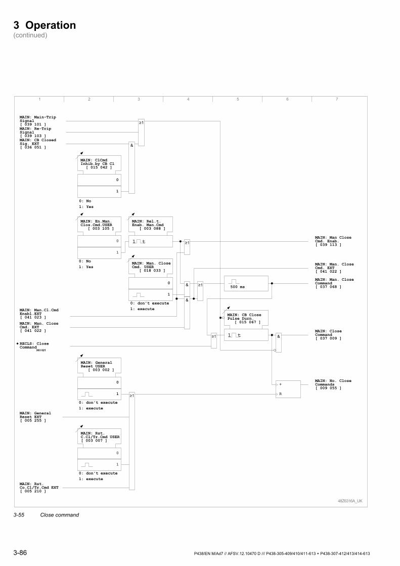
3 Operation (continued)
1 2 3 4 5 6 7
48Z6316A_UK
MAIN: Main-Trip Signal[ 039 101 ]
MAIN: General Reset EXT [ 005 255 ]
MAIN: Re-Trip Signal[ 039 103 ]
+
R
MAIN: Man CloseCmd. Enab.[ 039 113 ]
MAIN: Rst.C.Cl/Tr.Cmd USER[ 003 007 ]
0
1
0: don't execute1: execute
MAIN: Rst.Co.Cl/Tr.Cmd EXT[ 005 210 ]
MAIN: General Reset USER
[ 003 002 ]
0
1
0: don't execute1: execute
MAIN: CB Closed Sig. EXT[ 036 051 ]
MAIN: ClCmd Inhib.by CB Cl
[ 015 042 ]
0
1
MAIN: En.Man.Clos.Cmd.USER
[ 003 105 ]
0
1
0: No1: Yes
MAIN: Rel.t. Enab. Man.Cmd
[ 003 088 ]
MAIN: Man. Close Cmd. USER
[ 018 033 ]
0
1
0: don't execute1: execute
1 t
MAIN: Man.Cl.CmdEnabl.EXT[ 041 023 ]
MAIN: Man. Close Cmd. EXT[ 041 022 ]
MAIN: Man. Close Cmd. EXT[ 041 022 ]
500 ms
MAIN: Man. Close Command[ 037 068 ]
MAIN: CB Close Pulse Durn.
[ 015 067 ]
1 tMAIN: Close Command[ 037 009 ]
MAIN: No. Close Commands[ 009 055 ]
RECLS: Close Command
303 021
&
&
&
&
0: No1: Yes
3-55 Close command
3-86 P438/EN M/Ad7 // AFSV.12.10470 D /// P438-305-409/410/411-613 + P438-307-412/413/414-613

3 Operation (continued)
3.12.9 Fault Direction Signal
The direction decisions of the distance protection function are signaled.
reverse
3-56 Fault direction signal
P438/EN M/Ad7 // AFSV.12.10470 D /// P438-305-409/410/411-613 + P438-307-412/413/414-613 3-87
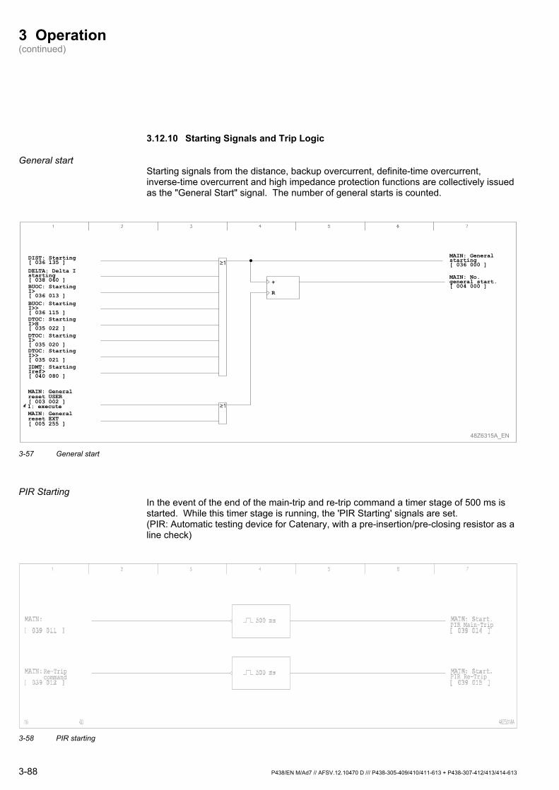
3 Operation (continued)
3.12.10 Starting Signals and Trip Logic
General start Starting signals from the distance, backup overcurrent, definite-time overcurrent, inverse-time overcurrent and high impedance protection functions are collectively issued as the "General Start" signal. The number of general starts is counted.
1: execute
MAIN: Generalreset USER[ 003 002 ]
MAIN: Generalreset EXT[ 005 255 ]
48Z6315A_EN
R
+
MAIN: Generalstarting[ 036 000 ]
MAIN: No.general start.[ 004 000 ]
DIST: Starting[ 036 135 ]
BUOC: StartingI>[ 036 013 ]BUOC: StartingI>>[ 036 115 ]DTOC: StartingI>H[ 035 022 ]DTOC: StartingI>[ 035 020 ]DTOC: StartingI>>[ 035 021 ]IDMT: StartingIref>[ 040 080 ]
DELTA: Delta Istarting[ 038 060 ]
3-57 General start
PIR Starting In the event of the end of the main-trip and re-trip command a timer stage of 500 ms is started. While this timer stage is running, the 'PIR Starting' signals are set. (PIR: Automatic testing device for Catenary, with a pre-insertion/pre-closing resistor as a line check)
Re-Tripcommand PIR Re-Trip
PIR Main-Trip
3-58 PIR starting
3-88 P438/EN M/Ad7 // AFSV.12.10470 D /// P438-305-409/410/411-613 + P438-307-412/413/414-613
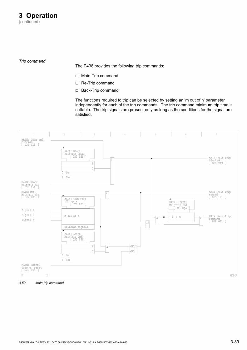
3 Operation (continued)
Trip command The P438 provides the following trip commands:
Main-Trip command
Re-Trip command
Back-Trip command
The functions required to trip can be selected by setting an 'm out of n' parameter independently for each of the trip commands. The trip command minimum trip time is settable. The trip signals are present only as long as the conditions for the signal are satisfied.
Main-Trip
Main-Trip
Main-Trip
tDWELLMainTrip Cmd
Main-Trip'OR' gate
Block.MainTrip EXT
Man.MainTrip sig.
LatchMainTrip Cmd?
BlockMainTrip USER
3-59 Main-trip command
P438/EN M/Ad7 // AFSV.12.10470 D /// P438-305-409/410/411-613 + P438-307-412/413/414-613 3-89

3 Operation (continued)
Re-Trip
Re-Trip
Re-Trip
tDWELLReTrip Cmd
Re-Trip'OR' gate
LatchReTrip Cmd?
BlockReTrip USER
Block.ReTrip EXT
Man.ReTrip signal
3-60 Re-trip command
3-90 P438/EN M/Ad7 // AFSV.12.10470 D /// P438-305-409/410/411-613 + P438-307-412/413/414-613
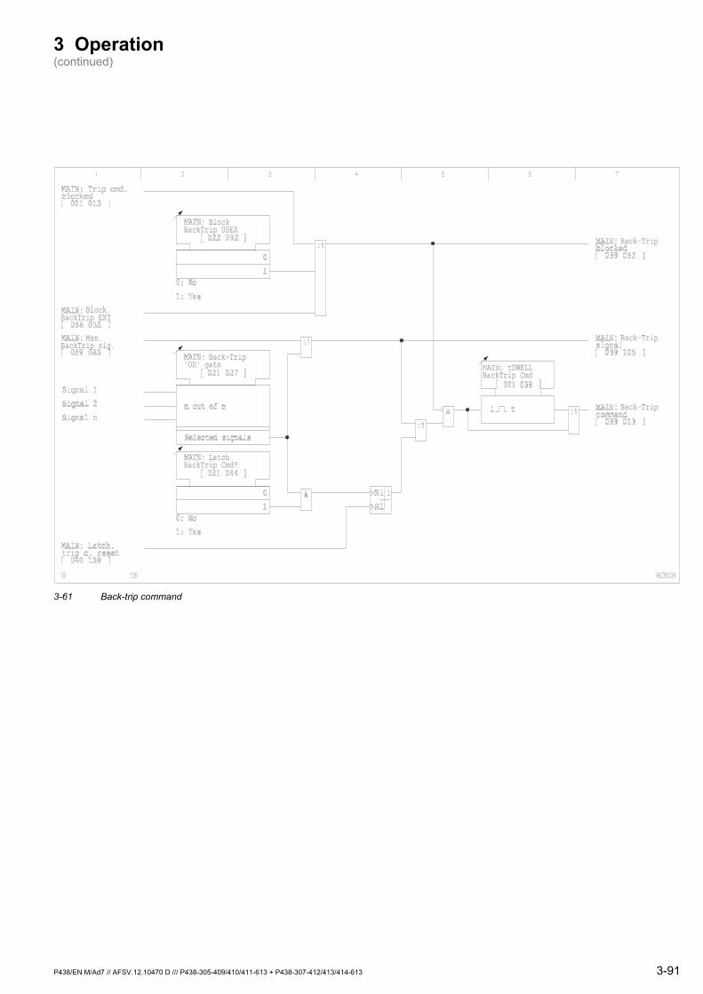
3 Operation (continued)
Back-Trip
Back-Trip
Back-Trip
tDWELLBackTrip Cmd
Back-Trip'OR' gate
BlockBackTrip USER
Block.BackTrip EXT
Man.BackTrip sig.
LatchBackTrip Cmd?
3-61 Back-trip command
P438/EN M/Ad7 // AFSV.12.10470 D /// P438-305-409/410/411-613 + P438-307-412/413/414-613 3-91
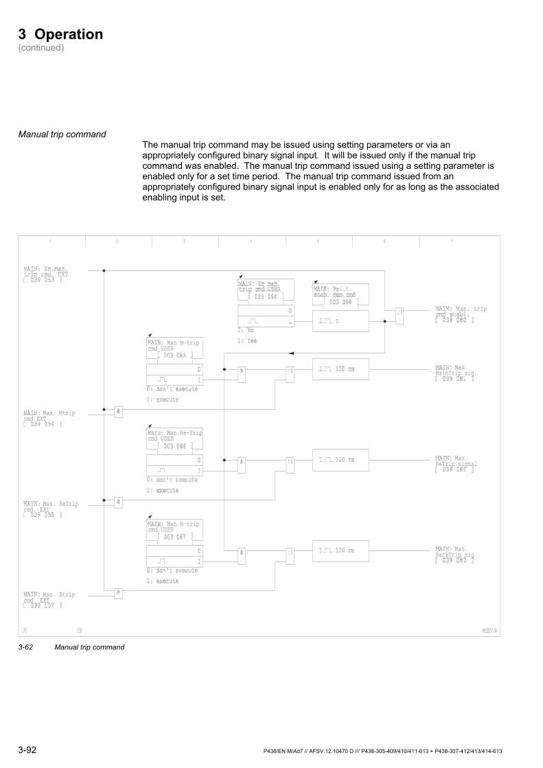
3 Operation (continued)
Manual trip command The manual trip command may be issued using setting parameters or via an appropriately configured binary signal input. It will be issued only if the manual trip command was enabled. The manual trip command issued using a setting parameter is enabled only for a set time period. The manual trip command issued from an appropriately configured binary signal input is enabled only for as long as the associated enabling input is set.
Man. Mtripcmd EXT
Man.M-tripcmd USER
Man.MainTrip sig.
Man.ReTrip signal
Man.BackTrip sig.
Man.Re-Tripcmd USER
Man.B-tripcmd USER
Man. ReTripcmd. EXT
Man. Btripcmd. EXT
3-62 Manual trip command
3-92 P438/EN M/Ad7 // AFSV.12.10470 D /// P438-305-409/410/411-613 + P438-307-412/413/414-613
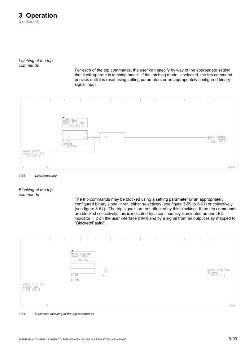
3 Operation (continued)
Latching of the trip commands
For each of the trip commands, the user can specify by way of the appropriate setting that it will operate in latching mode. If the latching mode is selected, the trip command persists until it is reset using setting parameters or an appropriately configured binary signal input.
3-63 Latch resetting
Blocking of the trip commands
The trip commands may be blocked using a setting parameter or an appropriately configured binary signal input, either selectively (see figure 3-59 to 3-61) or collectively (see figure 3-64). The trip signals are not affected by this blocking. If the trip commands are blocked collectively, this is indicated by a continuously illuminated amber LED indicator H 2 on the user interface (HMI) and by a signal from an output relay mapped to "Blocked/Faulty".
3-64 Collective blocking of the trip commands
P438/EN M/Ad7 // AFSV.12.10470 D /// P438-305-409/410/411-613 + P438-307-412/413/414-613 3-93
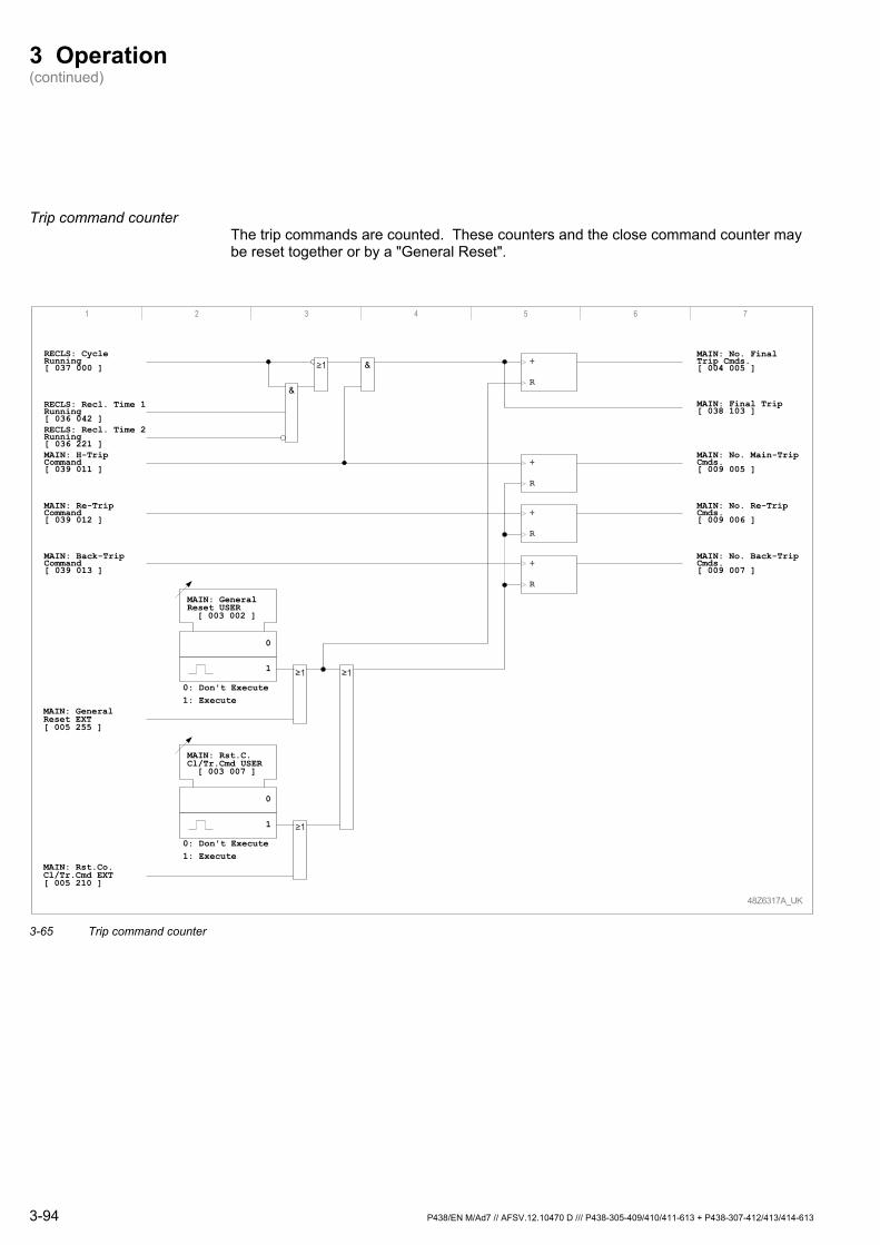
3 Operation (continued)
Trip command counter The trip commands are counted. These counters and the close command counter may be reset together or by a "General Reset".
MAIN: No. FinalTrip Cmds.[ 004 005 ]
RECLS: Recl. Time 2Running[ 036 221 ]
1 2 3 4 5 6 7
RECLS: CycleRunning[ 037 000 ]
48Z6317A_UK
+
R
MAIN: H-TripCommand[ 039 011 ]
RECLS: Recl. Time 1Running[ 036 042 ]
MAIN: Final Trip[ 038 103 ]
+
R
MAIN: No. Main-TripCmds.[ 009 005 ]
MAIN: Re-TripCommand[ 039 012 ]
+
R
+
R
MAIN: Back-TripCommand[ 039 013 ]
MAIN: No. Re-TripCmds.[ 009 006 ]
MAIN: No. Back-TripCmds.[ 009 007 ]
0
1
0
1
&
&
MAIN: GeneralReset EXT[ 005 255 ]
MAIN: Rst.C.Cl/Tr.Cmd USER[ 003 007 ]
0: Don't Execute1: Execute
MAIN: Rst.Co.Cl/Tr.Cmd EXT[ 005 210 ]
MAIN: GeneralReset USER[ 003 002 ]
0: Don't Execute1: Execute
3-65 Trip command counter
3-94 P438/EN M/Ad7 // AFSV.12.10470 D /// P438-305-409/410/411-613 + P438-307-412/413/414-613
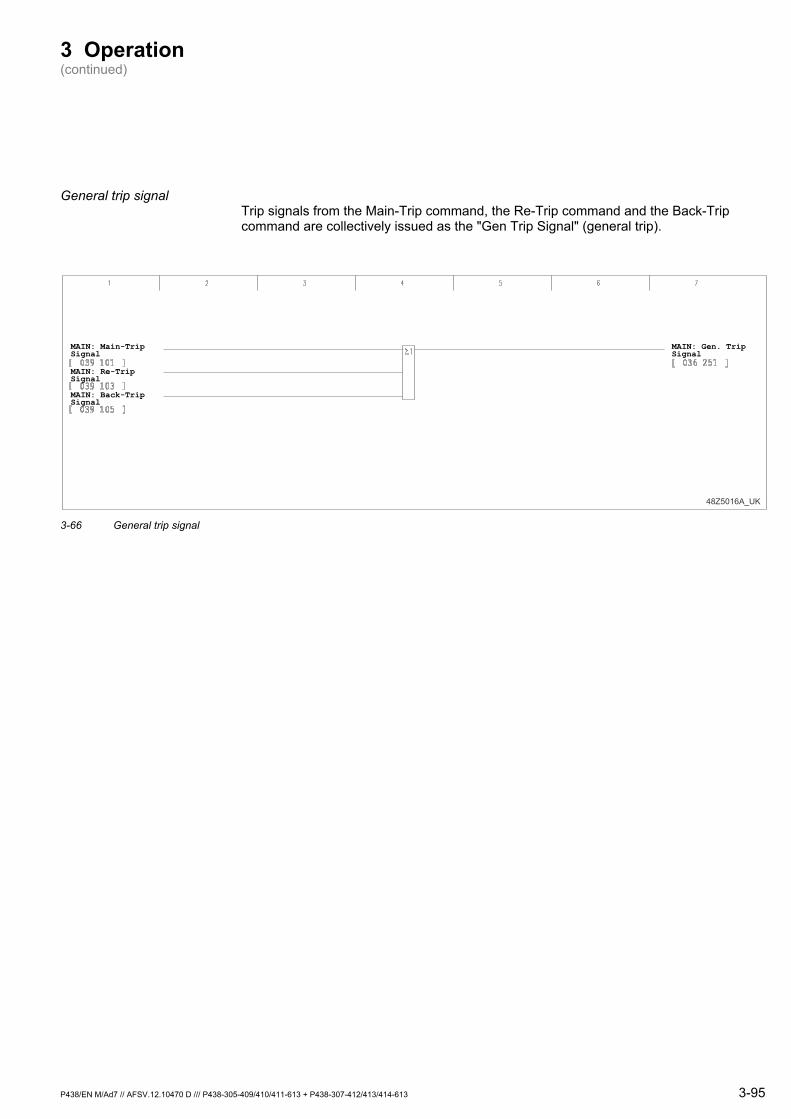
3 Operation (continued)
General trip signal Trip signals from the Main-Trip command, the Re-Trip command and the Back-Trip command are collectively issued as the "Gen Trip Signal" (general trip).
MAIN: Gen. TripSignal
48Z5016A_UK
MAIN: Main-TripSignal
MAIN: Re-TripSignal
MAIN: Back-TripSignal
3-66 General trip signal
P438/EN M/Ad7 // AFSV.12.10470 D /// P438-305-409/410/411-613 + P438-307-412/413/414-613 3-95
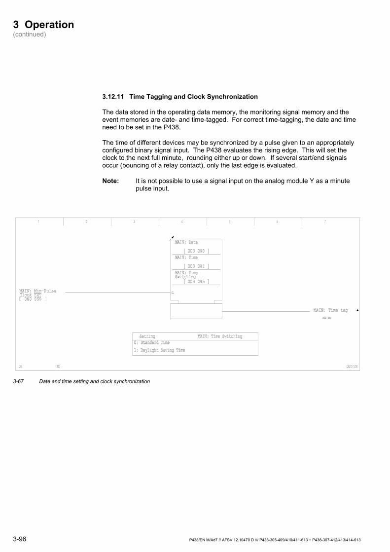
3 Operation (continued)
3.12.11 Time Tagging and Clock Synchronization
The data stored in the operating data memory, the monitoring signal memory and the event memories are date- and time-tagged. For correct time-tagging, the date and time need to be set in the P438.
The time of different devices may be synchronized by a pulse given to an appropriately configured binary signal input. The P438 evaluates the rising edge. This will set the clock to the next full minute, rounding either up or down. If several start/end signals occur (bouncing of a relay contact), only the last edge is evaluated.
Note: It is not possible to use a signal input on the analog module Y as a minute pulse input.
3-67 Date and time setting and clock synchronization
3-96 P438/EN M/Ad7 // AFSV.12.10470 D /// P438-305-409/410/411-613 + P438-307-412/413/414-613
3 Operation (continued)
Synchronization source The P438 provides numerous options to synchronize the internal clock:
o Telegram including the time of day received via communication interface COMM1/IEC (full time)
o Telegram including the time of day received via communication interface COMM2/PC (full time)
o IRIG-B signal (IRIGB; time of day only)
o Minute signal pulse presented to a binary signal input (MAIN), see figure 3-67 and the paragraph above this figure.
With older device versions these interfaces had equal ranking i.e. clock synchronization was carried out regardless of which sub-function initiated triggering. No conflicts have to be taken into account as long as synchronization sources (communication master, IRIG-B and minute pulse source) operate at the same time of day. Should the synchronization sources operate with a different time basis unwanted step changes in the internal clock may occur. On the other hand a redundant time of day synchronization is often used so as to sustain time synchronization via IRIG-B interface even if and while the SCADA communication is out of service.
For such applications the current device versions provide a selectable primary source and back-up source for time of day synchronization that feature all of the four options listed above.
M A I N : P r i m . S o u r c e T i m e S y n c
M A I N : B a c k u p S o u r c e T i m e S y n c
Synchronization is carried out from the primary source only as long as repeated synchronization telegrams (or minute signal pulses) are received within the timeout period set at M A I N : T i m e S y n c . T i m e - O u t . The backup source is required if after the set time-out there is no synchronization through the primary source.
When selecting the time telegram via IEC as the primary source the device will expect time synchronization telegrams from server SNTP2 after server SNTP 1 has become defective, before it will switch over to the backup source.
Time synchronization occurs solely from the primary source when the time-out stage is blocked.
P438/EN M/Ad7 // AFSV.12.10470 D /// P438-305-409/410/411-613 + P438-307-412/413/414-613 3-97
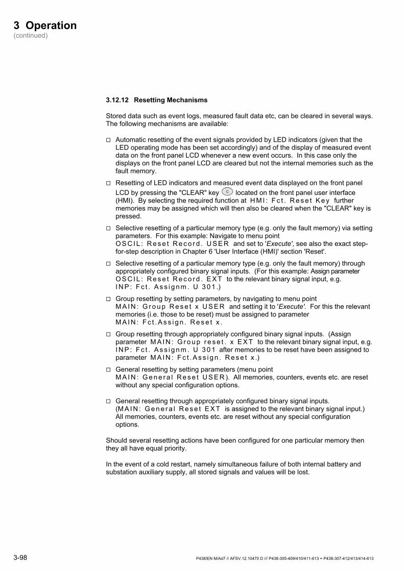
3 Operation (continued)
3.12.12 Resetting Mechanisms
Stored data such as event logs, measured fault data etc, can be cleared in several ways. The following mechanisms are available:
Automatic resetting of the event signals provided by LED indicators (given that the LED operating mode has been set accordingly) and of the display of measured event data on the front panel LCD whenever a new event occurs. In this case only the displays on the front panel LCD are cleared but not the internal memories such as the fault memory.
Resetting of LED indicators and measured event data displayed on the front panel LCD by pressing the "CLEAR" key C located on the front panel user interface (HMI). By selecting the required function at H M I : F c t . R e s e t K e y further memories may be assigned which will then also be cleared when the "CLEAR" key is pressed.
Selective resetting of a particular memory type (e.g. only the fault memory) via setting parameters. For this example: Navigate to menu point O S C I L : R e s e t R e c o r d . U S E R and set to 'Execute', see also the exact step-for-step description in Chapter 6 'User Interface (HMI)' section 'Reset'.
Selective resetting of a particular memory type (e.g. only the fault memory) through appropriately configured binary signal inputs. (For this example: Assign parameter O S C I L : R e s e t R e c o r d . E X T to the relevant binary signal input, e.g. I N P : F c t . A s s i g n m . U 3 0 1 .)
Group resetting by setting parameters, by navigating to menu point M A I N : G r o u p R e s e t x U S E R and setting it to 'Execute'. For this the relevant memories (i.e. those to be reset) must be assigned to parameter M A I N : F c t . A s s i g n . R e s e t x .
Group resetting through appropriately configured binary signal inputs. (Assign parameter M A I N : G r o u p r e s e t . x E X T to the relevant binary signal input, e.g. I N P : F c t . A s s i g n m . U 3 0 1 after memories to be reset have been assigned to parameter M A I N : F c t . A s s i g n . R e s e t x .)
General resetting by setting parameters (menu point M A I N : G e n e r a l R e s e t U S E R ). All memories, counters, events etc. are reset without any special configuration options.
General resetting through appropriately configured binary signal inputs. (M A I N : G e n e r a l R e s e t E X T is assigned to the relevant binary signal input.) All memories, counters, events etc. are reset without any special configuration options.
Should several resetting actions have been configured for one particular memory then they all have equal priority.
In the event of a cold restart, namely simultaneous failure of both internal battery and substation auxiliary supply, all stored signals and values will be lost.
3-98 P438/EN M/Ad7 // AFSV.12.10470 D /// P438-305-409/410/411-613 + P438-307-412/413/414-613

3 Operation (continued)
Further resetting possibilities are basically not distinct resetting actions but make access especially easy to one of the resetting actions described above i.e. by configuring them to a function key.
Function keys may be configured in such a way that resetting of a specific memory is assigned. Technically this is similar to resetting through an appropriately configured binary signal input. When a function key is pressed a signal to a binary signal input is simulated. (See section 'Configurable Function Keys'.)
Similarly to this, but one step less direct, is the possibility to assign one of the two menu jump lists (L O C : T r i g . M e n u J m p x E X T ) to a function key and to include the relevant menu point for a resetting action (e.g. O U T P : R e s e t L a t c h . U S E R ) in the definition (L O C : F c t . M e n u J m p L i s t x ) of the selected menu jump list.
The same may be achieved with the "READ" key by assigning it a menu point for a resetting action through H M I : F c t . R e a d K e y .
3-68 General reset, LED reset and measured event data reset from the user interface (HMI)
P438/EN M/Ad7 // AFSV.12.10470 D /// P438-305-409/410/411-613 + P438-307-412/413/414-613 3-99
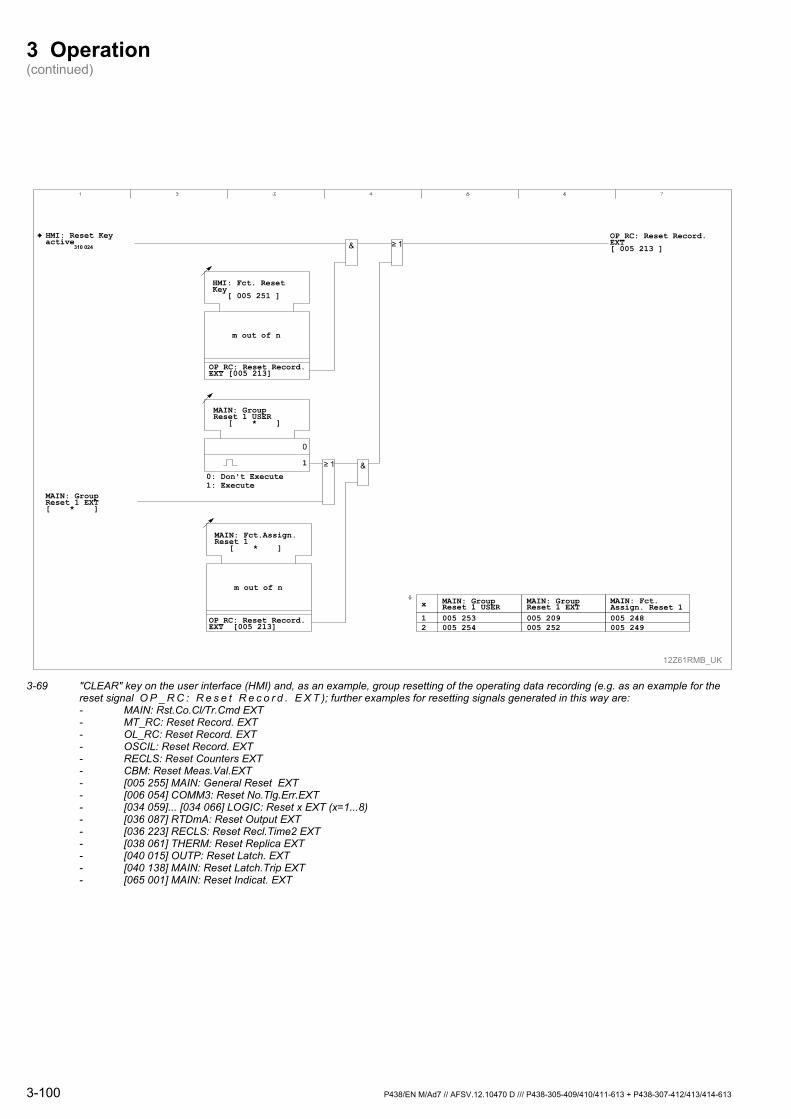
3 Operation (continued)
0
1
0: Don't Execute1: Execute
&
MAIN: GroupReset 1 EXT[ * ]
≥ 1
m out of n
HMI: Fct. ResetKey [ 005 251 ]
OP_RC: Reset Record.EXT [005 213]
m out of n
MAIN: Fct.Assign.Reset 1 [ * ]
MAIN: GroupReset 1 USER [ * ]
MAIN: Fct.Assign. Reset 1005 248005 249
MAIN: GroupReset 1 EXT005 209005 252
MAIN: GroupReset 1 USER005 253005 254
x
12
HMI: Reset Keyactive
310 024 & ≥ 1OP_RC: Reset Record.EXT[ 005 213 ]
12Z61RMB_UK
OP_RC: Reset Record.EXT [005 213]
3-69 "CLEAR" key on the user interface (HMI) and, as an example, group resetting of the operating data recording (e.g. as an example for the
reset signal O P _ R C : R e s e t R e c o r d . E X T ); further examples for resetting signals generated in this way are: - MAIN: Rst.Co.Cl/Tr.Cmd EXT - MT_RC: Reset Record. EXT - OL_RC: Reset Record. EXT - OSCIL: Reset Record. EXT - RECLS: Reset Counters EXT - CBM: Reset Meas.Val.EXT - [005 255] MAIN: General Reset EXT - [006 054] COMM3: Reset No.Tlg.Err.EXT - [034 059]... [034 066] LOGIC: Reset x EXT (x=1...8) - [036 087] RTDmA: Reset Output EXT - [036 223] RECLS: Reset Recl.Time2 EXT - [038 061] THERM: Reset Replica EXT - [040 015] OUTP: Reset Latch. EXT - [040 138] MAIN: Reset Latch.Trip EXT - [065 001] MAIN: Reset Indicat. EXT
3-100 P438/EN M/Ad7 // AFSV.12.10470 D /// P438-305-409/410/411-613 + P438-307-412/413/414-613
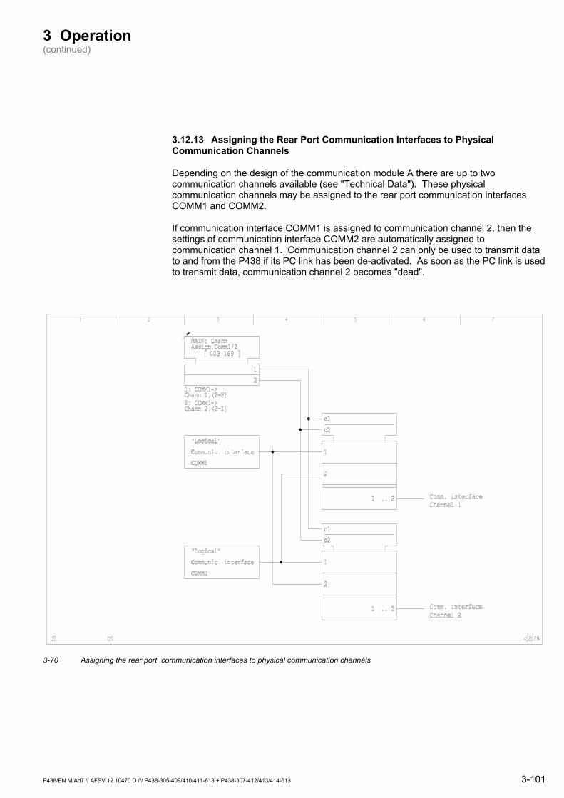
3 Operation (continued)
3.12.13 Assigning the Rear Port Communication Interfaces to Physical Communication Channels
Depending on the design of the communication module A there are up to two communication channels available (see "Technical Data"). These physical communication channels may be assigned to the rear port communication interfaces COMM1 and COMM2.
If communication interface COMM1 is assigned to communication channel 2, then the settings of communication interface COMM2 are automatically assigned to communication channel 1. Communication channel 2 can only be used to transmit data to and from the P438 if its PC link has been de-activated. As soon as the PC link is used to transmit data, communication channel 2 becomes "dead".
3-70 Assigning the rear port communication interfaces to physical communication channels
P438/EN M/Ad7 // AFSV.12.10470 D /// P438-305-409/410/411-613 + P438-307-412/413/414-613 3-101
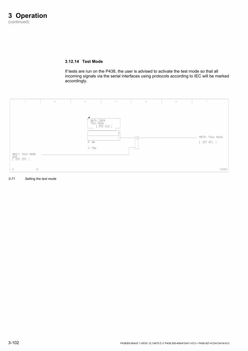
3 Operation (continued)
3-102 P438/EN M/Ad7 // AFSV.12.10470 D /// P438-305-409/410/411-613 + P438-307-412/413/414-613
3.12.14 Test Mode
If tests are run on the P438, the user is advised to activate the test mode so that all incoming signals via the serial interfaces using protocols according to IEC will be marked accordingly.
3-71 Setting the test mode
3 Operation (continued)
P438/EN M/Ad7 // AFSV.12.10470 D /// P438-305-409/410/411-613 + P438-307-412/413/414-613 3-103
3.13 Setting Group Selection (Function Group GROUP)
With the P438, four independent setting groups may be pre-set. The user may switch between setting groups during operation without interrupting the protection function.
Selecting the setting group The control path determining the active setting group (function setting or binary signal input) may be selected using the function setting G R O U P : C o n t r o l v i a U S E R or the external signal G R O U P : C o n t r o l V i a U s e r E X T . Correspondingly, the setting group is selected either in accordance with the pre-set function setting G R O U P : S e t t i n g G r p S e l U S E R or in accordance with external signals. The setting group actually active at a particular time may be determined by scanning logic state signals G R O U P : A c t u a l S e t t i n g G r o u p or G R O U P : G r o u p x A c t i v e .
Selecting the setting group using binary inputs
If the binary signal inputs are to be used for setting group selection, then the P438 first checks to determine whether at least two binary inputs are configured for setting group selection. If this is not the case, then the setting group selected using the function setting will be active. The P438 also checks whether the signals present at the binary signal inputs allow an unambiguous setting group selection. This is only true when only one binary signal input is set to a logic level of ' 1 '. If more than one signal input is set to a logic level of ' 1 ', then the setting group previously selected remains active. Should a dead interval occur while switching between setting groups (this is the case if all binary signal inputs have a logic level of ' 0 '), then the stored hold time is started. While this timer stage is running, the previously selected setting group remains active. As soon as a signal input has a logic level of ' 1 ', the associated setting group becomes active. If, after the stored time has elapsed, there is still no signal input with a logic level of ' 1 ', the setting group selected using the function parameter becomes active.
If, after the supply voltage is turned on, no logic level of ' 1 ' is present at any of the binary signal inputs selected for the setting group selection, then the setting group selected using the function parameter will become active once the stored time has elapsed. The previous setting group remains active while the stored hold timer stage is running.
Setting group selection may also occur during a general starting condition. In this case, the settings of all protection functions, for example the Impedance-Time Characteristics of the distance protection, are immediately updated. For setting group selection, a maximum inherent delay of approximately 100 ms must be taken into account. This must be considered for the duration of the triggering signal when binary signal inputs are used for setting group selection.
Settings for which only one address is given in the following sections are equally effective for all four setting groups.
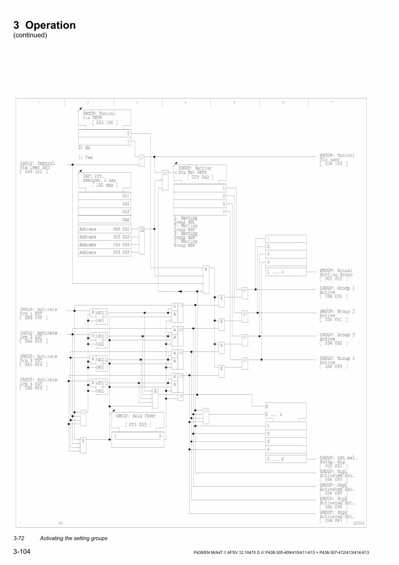
3 Operation (continued)
3-104 P438/EN M/Ad7 // AFSV.12.10470 D /// P438-305-409/410/411-613 + P438-307-412/413/414-613
3-72 Activating the setting groups

3 Operation (continued)
P438/EN M/Ad7 // AFSV.12.10470 D /// P438-305-409/410/411-613 + P438-307-412/413/414-613 3-105
3.14 Self-Monitoring (Function Group CHECK)
Comprehensive monitoring routines in the P438 ensure that internal faults are detected and do not lead to malfunctions.
Tests during start-up After the supply voltage has been turned on, various tests are carried out to verify full operability of the P438. If the P438 detects a fault in one of the tests, then start-up is terminated. The display shows which test was running when termination occurred. No control actions may be carried out. A new attempt to start up the P438 can only be initiated by turning the supply voltage off and then on again.
Cyclic tests After start-up has been successfully completed, cyclic self-monitoring tests will be run during operation. In the event of a positive test result, a specified monitoring signal will be issued and stored in a non-volatile memory – the monitoring signal memory – along with the assigned date and time (see also Monitoring Signal Recording).
The self-monitoring function monitors the built-in battery for any drop below the minimum acceptable voltage level. If the associated monitoring signal is displayed, then the battery should be replaced within a month, since otherwise there is the danger of data loss if the supply voltage should fail. Chapter 11 gives further instructions on battery replacement.
Peripheral fault By setting an 'm out of n' parameter, a peripheral fault can generate an alarm in addition to the self-monitoring signals.
Signal The monitoring signals are also signaled via the output relay mapped to C H E C K : A l a r m . The output relay operates as long as an internal fault is detected.
3-73 Monitoring signals
3 Operation (continued)
3-106 P438/EN M/Ad7 // AFSV.12.10470 D /// P438-305-409/410/411-613 + P438-307-412/413/414-613
Device response The response of the P438 depends on the type of monitoring signal. The following responses are possible:
Signaling Only If there is no malfunction associated with the monitoring signal, then only a signal is issued, and there are no further consequences. This situation exists, for example, when internal data acquisition memories overflow.
Selective Blocking If a fault is diagnosed solely in an area that does not affect the protection functions, then only the affected area is blocked. This would apply, for example, to the detection of a fault on the communication module or in the area of the PC interface.
Warm Restart If the self-monitoring function detects a fault that might be eliminated by a system restart – such as a fault in the hardware –, then a procedure called a warm restart is automatically initiated. During this procedure, as with any start-up, the computer system is reset to a defined state. A warm restart is characterized by the fact that no stored data and, in particular, no settings are affected by the procedure. A warm restart can also be triggered manually by a control action. During a warm restart sequence the protection functions and the communication through serial interfaces will be blocked. If the same fault is detected after a warm restart has been triggered by the self-monitoring function, then the protection functions remain blocked but communication through the serial interfaces will usually be possible again.
Cold Restart If a corrupted setting group is diagnosed during the checksum test, which is part of the self-monitoring procedure, then a cold restart is carried out. This is necessary because the protection device cannot identify which setting in the group is corrupted. A cold restart causes all internal memories to be reset to a defined state. This means that all the device's settings are also erased after a cold restart. In order to establish a safe initial state, the default values have been selected so that the protection functions are blocked. Both the monitoring signal that triggered the cold restart and the value indicating settings loss are entered in the monitoring signal memory.
3 Operation (continued)
P438/EN M/Ad7 // AFSV.12.10470 D /// P438-305-409/410/411-613 + P438-307-412/413/414-613 3-107
Monitoring signal memory (as of version P438 -606)
Depending on the type of internal fault detected the device will respond by trying to eliminate the problem with a warm restart. (See above; for further details read also about device behavior with problems in Chapter 10 'Troubleshooting’.) Whether or not this measure will suffice can only be determined if the monitoring signal has not already been stored in the monitoring signal memory because of a previous fault. If it was already stored and a second fault is detected then, depending on the type of fault detected, the device will be blocked after the second warm restart. Previously this occurred independently of the time duration that had passed since the first monitoring signal was issued.
The behavior caused by sporadic faults could lead to an unwanted blocking of the device if the monitoring signal memory has not been reset in the interim, for example, because the substation is difficult to reach in wintertime or display and clearing of the monitoring signal memory via the communication interfaces was not enabled. A "memory retention time" timer has been introduced to defuse this problem.
C H E C K : M o n . S i g . R e t e n t i o n
Now device blocking only occurs when the same internal device fault is detected twice during this time duration. Otherwise, the device will continue to operate normally after a warm restart. This timer is blocked is blocked by default so that, when an internal fault is detected, the device will operate in the same way as the previous versions.
Monitoring signal memory time tagging (as of version P438 -606)
Because of these changes the significance of the time tag for entries to the monitoring signal memory has been re-defined. The time when the device fault occurred first was previously recorded. As of version P438 -606 the time when the device fault occurred last is now recorded.

3 Operation (continued)
3-108 P438/EN M/Ad7 // AFSV.12.10470 D /// P438-305-409/410/411-613 + P438-307-412/413/414-613
3.15 Operating Data Recording (Function Group OP_RC)
For the continuous recording of processes in system operation as well as of events, a non-volatile memory is provided (cyclic buffer). The "operationally relevant" signals, each fully tagged with date and time at signal start and signal end, are entered in chronological order. The signals relevant for operation include control actions such as function disabling and enabling and triggers for testing and resetting. The onset and end of events in the system that represent a deviation from normal operation such as overloads or short circuits are also recorded. The operating data memory can be cleared/reset.
Counter for signals relevant to system operation
The signals stored in the operating data memory are counted.
12Z61CMB_EN
MAIN: Generalreset USER[ 003 002 ]1: execute
OP_RC: Resetrecord. USER
[ 100 001 ]
0: don't execute
0
1
1: execute
Operating memory
OP_RC: Operat.data record.
[ 003 024 ]
MAIN: Oper.-relev.signal
306 024
OP_RC: No. oper.data sig.[ 100 002 ]
OP_RC: Resetrecord. EXT[ 005 213 ]
MAIN: Generalreset EXT[ 005 255 ]
R
+
R
3-74 Operating data recording and counter for signals relevant to system operation
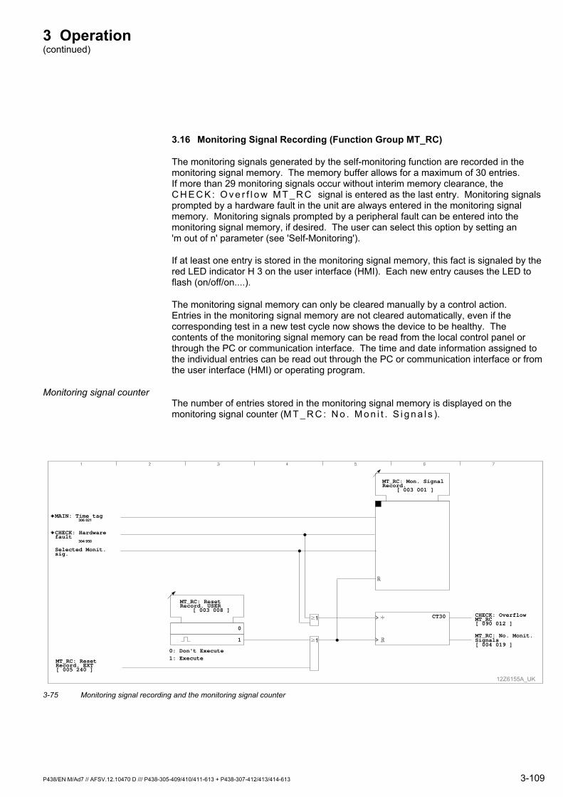
3 Operation (continued)
P438/EN M/Ad7 // AFSV.12.10470 D /// P438-305-409/410/411-613 + P438-307-412/413/414-613 3-109
3.16 Monitoring Signal Recording (Function Group MT_RC)
The monitoring signals generated by the self-monitoring function are recorded in the monitoring signal memory. The memory buffer allows for a maximum of 30 entries. If more than 29 monitoring signals occur without interim memory clearance, the C H E C K : O v e r f l o w M T _ R C signal is entered as the last entry. Monitoring signals prompted by a hardware fault in the unit are always entered in the monitoring signal memory. Monitoring signals prompted by a peripheral fault can be entered into the monitoring signal memory, if desired. The user can select this option by setting an 'm out of n' parameter (see 'Self-Monitoring').
If at least one entry is stored in the monitoring signal memory, this fact is signaled by the red LED indicator H 3 on the user interface (HMI). Each new entry causes the LED to flash (on/off/on....).
The monitoring signal memory can only be cleared manually by a control action. Entries in the monitoring signal memory are not cleared automatically, even if the corresponding test in a new test cycle now shows the device to be healthy. The contents of the monitoring signal memory can be read from the local control panel or through the PC or communication interface. The time and date information assigned to the individual entries can be read out through the PC or communication interface or from the user interface (HMI) or operating program.
Monitoring signal counter The number of entries stored in the monitoring signal memory is displayed on the monitoring signal counter (M T _ R C : N o . M o n i t . S i g n a l s ).
12Z6155A_UK
MT_RC: ResetRecord. USER
[ 003 008 ]
0: Don't Execute
0
1
1: Execute
MAIN: Time tag306 021
CHECK: OverflowMT_RC[ 090 012 ]
CHECK: Hardwarefault
304 950
Selected Monit.sig.
MT_RC: No. Monit.Signals[ 004 019 ]
CT30
MT_RC: Mon. SignalRecord.
[ 003 001 ]
MT_RC: ResetRecord. EXT[ 005 240 ]
≥1
≥1
3-75 Monitoring signal recording and the monitoring signal counter

3 Operation (continued)
3-110 P438/EN M/Ad7 // AFSV.12.10470 D /// P438-305-409/410/411-613 + P438-307-412/413/414-613
3.17 Overload Data Acquisition (Function Group OL_DA)
Overload Duration In the event of an overload, the P438 determines the overload duration. The overload duration is defined as the time between the start and end of the OL_ R C : R e c o r d . i n P r o g r e s s signal.
1: execute
MAIN: General reset USER[ 003 002 ]
MAIN: General reset EXT[ 005 255 ]
1: execute
OL_RC: Reset record. USER[ 100 003 ]
50Z0137A_EN
R
+OL_DA: Overload duration[ 004 102 ]
OL_RC: Reset record. EXT[ 005 241 ]
OL_RC: Record. in progress[ 035 003 ]
3-76 Overload duration

3 Operation (continued)
P438/EN M/Ad7 // AFSV.12.10470 D /// P438-305-409/410/411-613 + P438-307-412/413/414-613 3-111
Measurement data stored for the overload
During the overload, the device will store measurements relating to the circuit's thermal state – using data from the thermal overload protection function. They are stored at the end of the overload event.
1: execute
MAIN: General reset USER [ 003 002 ]
MAIN: General reset EXT[ 005 255 ]
1: execute
OL_RC: Reset record. USER[ 100 003 ]
12Z6238A_EN
≥1
OL_RC: Reset record. EXT[ 005 241 ]
OL_DA: Status THERM replica[ 004 147 ]
OL_RC: Record. in progress [ 035 003 ]
OL_DA: Load current THER[ 004 058 ]
OL_DA: Pre-trip t.leftTHERM[ 004 148 ]
OL_DA: Offset THERM replica[ 004 154 ]
R
R
R
R
C
THERM: I305 202
THERM: Pre-trip time left [ 004 139 ]
THERM: Temp. offset replica[ 004 109 ]
THERM: Status THERM replica[ 004 016 ]
OL_DA: Object temp. THERM [ 004 035 ]
R
THERM: Object temperature [ 004 137 ]
OL_DA: Coolant temp. THERM [ 004 036 ]
R
THERM: Coolant temperature[ 004 149 ]
3-77 Measured overload data of thermal overload protection

3 Operation (continued)
3-112 P438/EN M/Ad7 // AFSV.12.10470 D /// P438-305-409/410/411-613 + P438-307-412/413/414-613
3.18 Overload Recording (Function Group OL_RC)
Start of overload recording An overload exists and overload recording starts if the current exceeds the set threshold: T H E R M : S t a r t . F a c t . O L _ R C S G x . In this case, the P438 issues the T H E R M : S t a r t i n g k * I r e f > signal.
Counting overload events Overload events are counted and identified by sequential numbers.
1: execute
MAIN: Generalreset USER[ 003 002 ]
MAIN: Generalreset EXT[ 005 255 ]
1: execute
OL_RC: Resetrecord. USER[ 100 003 ]
45Z63DXA_EN
R
+OL_RC: No.overload[ 004 101 ]
OL_RC: Record. in progress[ 035 003 ]
OL_RC: Resetrecord. EXT[ 005 241 ]
THERM: Startingk*Iref>[ 041 108 ]
3-78 Counting overload events
Time tagging The date of each overload event is stored. The overload start or end signals are likewise time-tagged by the internal clock. The date and time assigned to an overload event when the event begins can be read out from the overload memory on the local control panel or through the PC and communication interfaces. The time information (relative to the onset of the overload) can be retrieved from the overload memory or through the PC or communication interfaces.
Overload logging Protection signals during an overload event are logged in chronological order with reference to the specific event. A total of eight overload events, each involving a maximum of 200 start or end signals, can be stored in the non-volatile overload memories. After eight overload events have been logged, the oldest overload log will be overwritten, unless memories have been cleared in the interim. If more than 199 start or end signals have occurred during a single overload event, then OL_ R C : O v e r l . M e m . O v e r f l o w will be entered as the last signal.
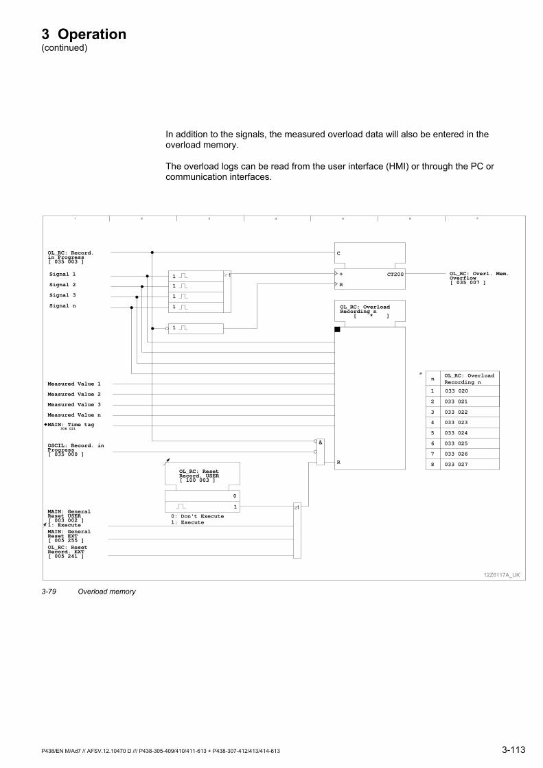
3 Operation (continued)
P438/EN M/Ad7 // AFSV.12.10470 D /// P438-305-409/410/411-613 + P438-307-412/413/414-613 3-113
In addition to the signals, the measured overload data will also be entered in the overload memory.
The overload logs can be read from the user interface (HMI) or through the PC or communication interfaces.
12Z6117A_UK
R
n
1
2
3
4
5
6
7
8
OL_RC: OverloadRecording n
033 020
033 021
033 022
033 023
033 024
033 025
033 026
033 027
OL_RC: Overl. Mem.Overflow[ 035 007 ]R
+ CT200
C
OL_RC: OverloadRecording n
[ * ]
1
1
1
1
1
OL_RC: ResetRecord. USER[ 100 003 ]
OL_RC: Record.in Progress[ 035 003 ]
Signal 1
Signal 2
Signal 3
Signal n
Measured Value 1
Measured Value 2
Measured Value 3
Measured Value n
MAIN: Time tag306 021
OSCIL: Record. inProgress[ 035 000 ]
≥1
OL_RC: ResetRecord. EXT[ 005 241 ]
1: Execute
0
1
0: Don't Execute1: Execute
≥1MAIN: GeneralReset USER[ 003 002 ]
MAIN: GeneralReset EXT[ 005 255 ]
&
3-79 Overload memory
3 Operation (continued)
3.19 Fault Data Acquisition (Function Group FT_DA)
When there is a primary system fault, the P438 collects the following measured fault data:
Running Time
Fault Duration
Fault Determination
Run Time to Measurement
Fault current
Fault voltage (short-circuit voltage)
Fault angle
Primary and secondary fault reactance
Primary and secondary fault resistance
Fault location in km or percentage of the protected line
Catenary current (only in ‘Autotransformer feed’ operating mode)
Feeder current (only in ‘Autotransformer feed’ operating mode)
Current which determines the defrost protection
Voltage of the catenary (only in ‘Autotransformer feed’ operating mode)
Voltage of the feeder (only in ‘Autotransformer feed’ operating mode)
The ratio of the second, third and fifth harmonic current components to the fundamental component of the current, kHarmΣI(xfn)/I(fn) (only in ‘Autotransformer feed’ operating mode and with the optional processor module with an integrated DSP coprocessor fitted and if the harmonics adaptation feature is enabled in the distance protection function)
3-114 P438/EN M/Ad7 // AFSV.12.10470 D /// P438-305-409/410/411-613 + P438-307-412/413/414-613
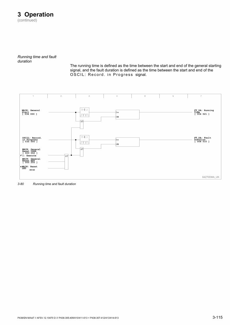
3 Operation (continued)
Running time and fault duration
The running time is defined as the time between the start and end of the general starting signal, and the fault duration is defined as the time between the start and end of the O S C I L : R e c o r d . i n P r o g r e s s signal.
64Z70DMA_UK
R
+
FT_DA: RunningTime[ 004 021 ]
R
+
FT_DA: FaultDuration[ 008 010 ]
MAIN: GeneralReset USER[ 003 002 ]1: Execute
MAIN: ResetLED
306 020
MAIN: GeneralReset EXT[ 005 255 ]
OSCIL: Record.in Progress[ 035 000 ]
MAIN: GeneralStart[ 036 000 ]
3-80 Running time and fault duration
P438/EN M/Ad7 // AFSV.12.10470 D /// P438-305-409/410/411-613 + P438-307-412/413/414-613 3-115
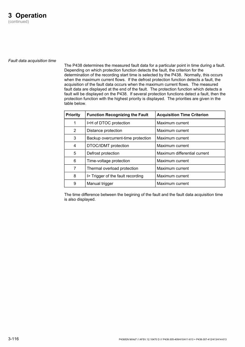
3 Operation (continued)
Fault data acquisition time The P438 determines the measured fault data for a particular point in time during a fault. Depending on which protection function detects the fault, the criterion for the determination of the recording start time is selected by the P438. Normally, this occurs when the maximum current flows. If the defrost protection function detects a fault, the acquisition of the fault data occurs when the maximum current flows. The measured fault data are displayed at the end of the fault. The protection function which detects a fault will be displayed on the P438. If several protection functions detect a fault, then the protection function with the highest priority is displayed. The priorities are given in the table below.
Priority Function Recognizing the Fault Acquisition Time Criterion
1 I>H of DTOC protection Maximum current
2 Distance protection Maximum current
3 Backup overcurrent-time protection Maximum current
4 DTOC/IDMT protection Maximum current
5 Defrost protection Maximum differential current
6 Time-voltage protection Maximum current
7 Thermal overload protection Maximum current
8 I> Trigger of the fault recording Maximum current
9 Manual trigger Maximum current The time difference between the begining of the fault and the fault data acquisition time is also displayed.
3-116 P438/EN M/Ad7 // AFSV.12.10470 D /// P438-305-409/410/411-613 + P438-307-412/413/414-613
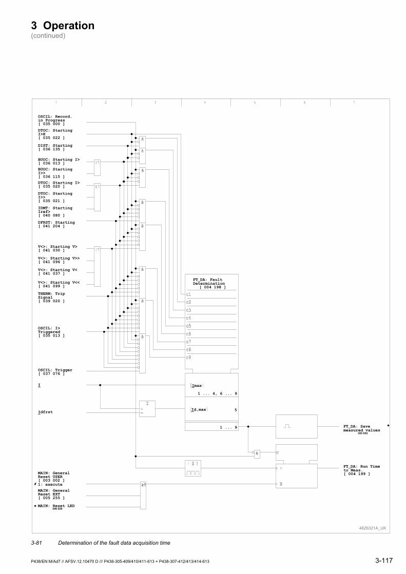
3 Operation (continued)
48Z6321A_UK
OSCIL: Record. in Progress[ 035 000 ]
DTOC: StartingI>H[ 035 022 ]
DIST: Starting[ 036 135 ]
BUOC: Starting I>[ 036 013 ]BUOC: Starting I>>[ 036 115 ]DTOC: Starting I>[ 035 020 ]
DTOC: Starting I>>[ 035 021 ]
IDMT: Starting Iref>[ 040 080 ]
V<>: Starting V>[ 041 030 ]
DFRST: Starting[ 041 204 ]
V<>: Starting V>>[ 041 096 ]
V<>: Starting V<[ 041 037 ]
V<>: Starting V<<[ 041 099 ]
THERM: Trip Signal[ 039 020 ]
OSCIL: I> Triggered[ 035 013 ]
OSCIL: Trigger[ 037 076 ]
Idfrst
FT_DA: Save measured values
305 052
FT_DA: Run Time to Meas.[ 004 199 ]
FT_DA: Fault Determination
[ 004 198 ]
Imax
Id,max
1 ... 4, 6 ... 9
1 ... 9
5
I
MAIN: General Reset USER[ 003 002 ]1: execute
MAIN: Reset LED306 020
MAIN: General Reset EXT [ 005 255 ]
3-81 Determination of the fault data acquisition time
P438/EN M/Ad7 // AFSV.12.10470 D /// P438-305-409/410/411-613 + P438-307-412/413/414-613 3-117
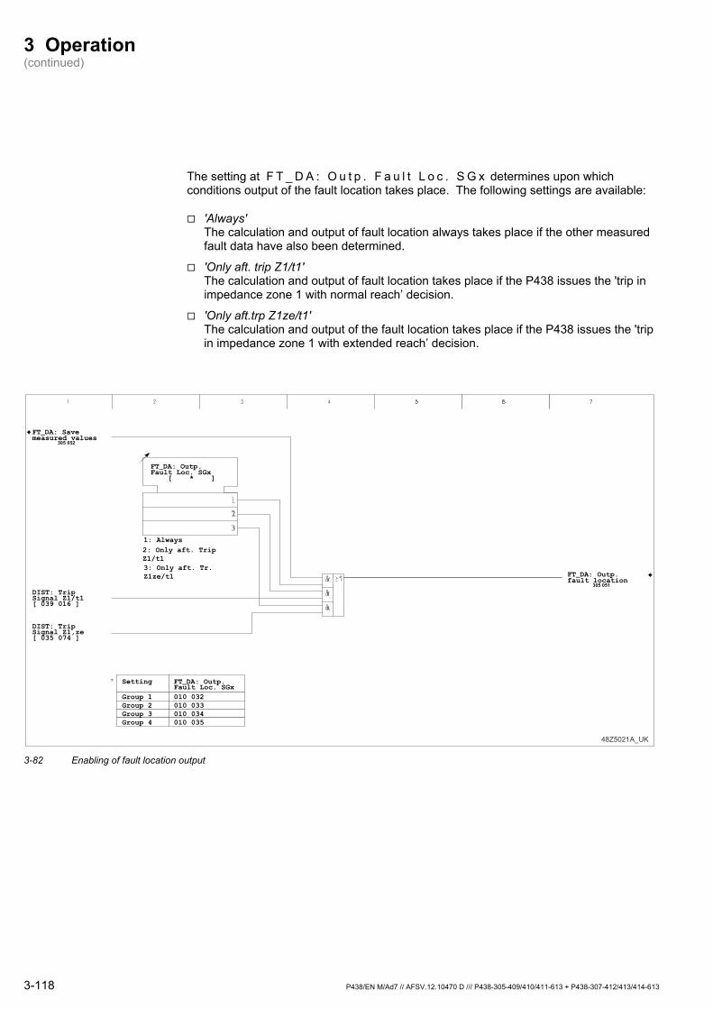
3 Operation (continued)
The setting at F T _ D A : O u t p . F a u l t L o c . S G x determines upon which conditions output of the fault location takes place. The following settings are available:
'Always' The calculation and output of fault location always takes place if the other measured fault data have also been determined.
'Only aft. trip Z1/t1' The calculation and output of fault location takes place if the P438 issues the 'trip in impedance zone 1 with normal reach’ decision.
'Only aft.trp Z1ze/t1' The calculation and output of the fault location takes place if the P438 issues the 'trip in impedance zone 1 with extended reach’ decision.
FT_DA: Outp. Fault Loc. SGx
[ * ]
1: Always 2: Only aft. TripZ1/t1
3: Only aft. Tr.Z1ze/t1
48Z5021A_UK
FT_DA: Outp. Fault Loc. SGx010 032010 033010 034010 035
Setting
Group 1Group 2Group 3Group 4
DIST: Trip Signal Z1/t1[ 039 016 ]
DIST: Trip Signal Z1,ze[ 035 074 ]
FT_DA: Save measured values
305 052
FT_DA: Outp. fault location
305 051
3-82 Enabling of fault location output
3-118 P438/EN M/Ad7 // AFSV.12.10470 D /// P438-305-409/410/411-613 + P438-307-412/413/414-613
3 Operation (continued)
Acquisition of short circuit data
The P438 stores the fault's current and voltage data determined at the time of acquisition, as well as the calculated values of the fault reactance, fault impedance and fault angle. The P438 additionally stores – if it operates in Autotransformer feed mode –the current and voltage values of the catenary and the feeder. For 'Defrost operation', the current evaluated by the defrost protection is stored.
If the fault is detected by the Backup DTOC protection, the fault voltage, the voltage of the catenary and feeder, as well as the fault reactance, the fault impedance and the fault angle cannot be determined.
The currents and voltages are displayed as per-unit quantities referred to In and Vn If the measured or calculated values are outside of the acceptable measuring range, ‘Overflow’ is displayed.
P438/EN M/Ad7 // AFSV.12.10470 D /// P438-305-409/410/411-613 + P438-307-412/413/414-613 3-119

3 Operation (continued)
48Z6322A_EN
FT_DA: Record.in progress[ 035 000 ]
MAIN: Generalreset USER[ 003 002 ]1: execute
MAIN: Reset LED306 020
R
C
MAIN: Generalreset EXT[ 005 255 ]
FT_DA: Savemeasured values
305 052
R
R
R
R
R
R
C1
C
FT_DA: Faultcurrent p.u.[ 004 025 ]
FT_DA: Faultvoltage p.u.[ 004 026 ]
FT_DA: Faultloop angle[ 004 024 ]
FT_DA: Faultreactance,sec.[ 004 028 ]
FT_DA: Faultimpedance,sec.[ 004 023 ]
FT_DA: Faultreactance,prim[ 004 029 ]
FT_DA: Faultimpedance,prim[ 004 176 ]
BUOC: Starting I>[ 036 013 ]
BUOC: StartingI>>[ 036 115 ]
MAIN: Inom C.T.prim.[ 010 001 ]
MAIN: Vnom V.T.prim.[ 010 002 ]
I
V
R
MAIN: I(xfn)/I(fn)
310 053 1)
Σ FT_DA: kHarm, I(xfn)/I(fn) [ 008 217 ] 1)
Σ
1) only if the processor module with DSP co-processor (optional) is fitted.
3-83 Acquisition of the fault currents and voltage, fault angles, fault reactance and impedance
3-120 P438/EN M/Ad7 // AFSV.12.10470 D /// P438-305-409/410/411-613 + P438-307-412/413/414-613
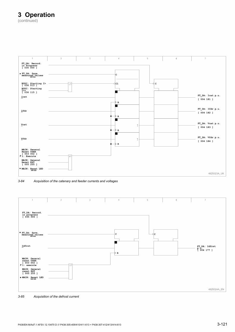
3 Operation (continued)
Ifdr
Vcat
Icat
Vfdr
FT_DA: Record.in Progress[ 035 000 ]
FT_DA: Savemeasured Values
305 052
BUOC: Starting I>[ 036 013 ]BUOC: StartingI>>[ 036 115 ]
MAIN: GeneralReset USER[ 003 002 ]1: Execute
MAIN: Reset LED306 020
MAIN: GeneralReset EXT[ 005 255 ]
48Z6323A_UK
FT_DA: Icat p.u.
[ 004 181 ]
FT_DA: Ifdr p.u.
[ 004 182 ]
FT_DA: Vcat p.u.
[ 004 183 ]
FT_DA: Vfdr p.u.
[ 004 184 ]
C
R
C1
R
R
R
C
3-84 Acquisition of the catenary and feeder currents and voltages
Idfrst
FT_DA: Record.in progress[ 035 000 ]
FT_DA: Savemeasured values
305 052
1: execute
MAIN: Reset LED306 020
MAIN: Generalreset EXT[ 005 255 ]
MAIN: Generalreset USER[ 003 002 ]
48Z6324A_EN
FT_DA: Idfrstp.u.[ 004 177 ]
C
R
C
3-85 Acquisition of the defrost current
P438/EN M/Ad7 // AFSV.12.10470 D /// P438-305-409/410/411-613 + P438-307-412/413/414-613 3-121
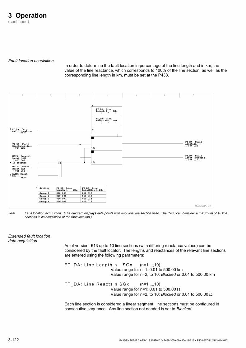
3 Operation (continued)
Fault location acquisition In order to determine the fault location in percentage of the line length and in km, the value of the line reactance, which corresponds to 100% of the line section, as well as the corresponding line length in km, must be set at the P438.
FT_DA: Outp. fault location
305 051
FT_DA: Fault Reactance,Sec.[ 004 028 ]
MAIN: General Reset USER[ 003 002 ]1: execute
MAIN: ResetLED
306 020
MAIN: General Reset EXT [ 005 255 ]
48Z63DQA_UK
FT_DA: Fault Location[ 004 022 ]
FT_DA: Fault Locat. Percent[ 004 027 ]
C
R
R
FT_DA: Line Length 1 SGx
[ * ]
FT_DA: Line ReactXSec 1 SGx010 012010 013010 014010 015
FT_DA: Line Length 1 SGx010 005010 006010 007010 008
Setting
Group 1Group 2Group 3Group 4
FT_DA: Line ReactXSec 1 SGx
[ * ]
3-86 Fault location acquisition. (The diagram displays data points with only one line section used. The P438 can consider a maximum of 10 line
sections in its acquisition of the fault location.)
Extended fault location data acquisition
As of version -613 up to 10 line sections (with differing reactance values) can be considered by the fault locator. The lengths and reactances of the relevant line sections are entered using the following parameters:
F T _ D A : L i n e L e n g t h n S G x (n=1,...,10) Value range for n=1: 0.01 to 500.00 km Value range for n=2, to 10: Blocked or 0.01 to 500.00 km
F T _ D A : L i n e R e a c t s n S G x (n=1,...,10) Value range for n=1: 0.01 to 500.00 Ω Value range for n=2, to 10: Blocked or 0.01 to 500.00 Ω
Each line section is considered a linear segment; line sections must be configured in consecutive sequence. Any line section not needed is set to Blocked.
3-122 P438/EN M/Ad7 // AFSV.12.10470 D /// P438-305-409/410/411-613 + P438-307-412/413/414-613
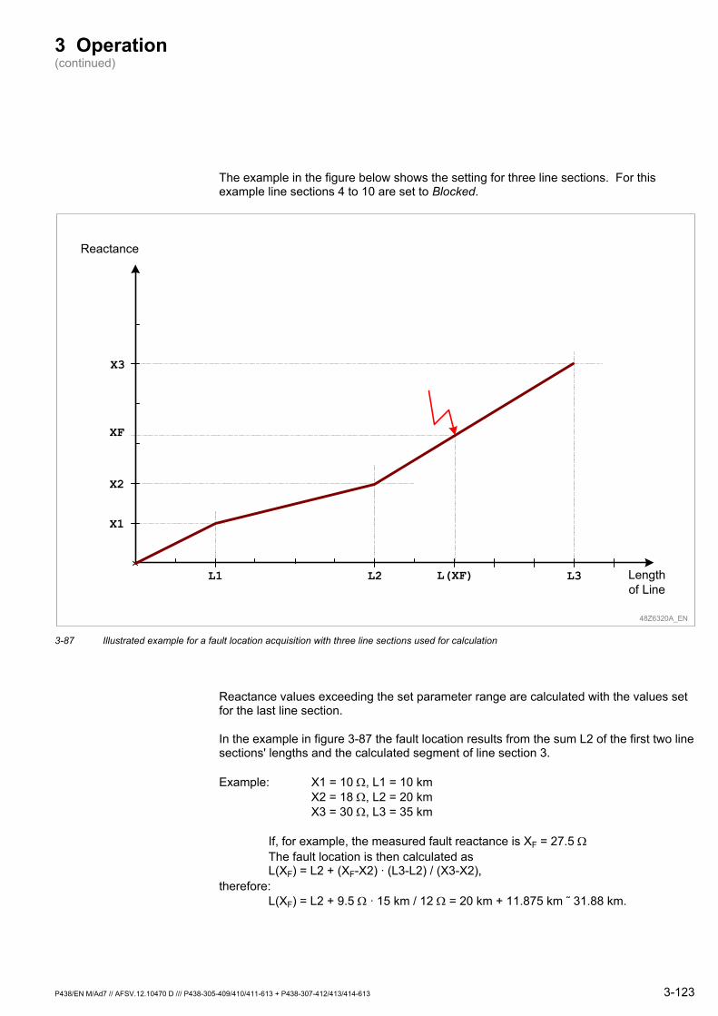
3 Operation (continued)
The example in the figure below shows the setting for three line sections. For this example line sections 4 to 10 are set to Blocked.
Lengthof Line
Reactance
L1 L2 L3
X1
X2
X3
48Z6320A_EN
XF
L(XF)
3-87 Illustrated example for a fault location acquisition with three line sections used for calculation
Reactance values exceeding the set parameter range are calculated with the values set for the last line section.
In the example in figure 3-87 the fault location results from the sum L2 of the first two line sections' lengths and the calculated segment of line section 3.
Example: X1 = 10 Ω, L1 = 10 km X2 = 18 Ω, L2 = 20 km X3 = 30 Ω, L3 = 35 km
If, for example, the measured fault reactance is XF = 27.5 Ω The fault location is then calculated as L(XF) = L2 + (XF-X2) · (L3-L2) / (X3-X2), therefore: L(XF) = L2 + 9.5 Ω · 15 km / 12 Ω = 20 km + 11.875 km ˜ 31.88 km.
P438/EN M/Ad7 // AFSV.12.10470 D /// P438-305-409/410/411-613 + P438-307-412/413/414-613 3-123
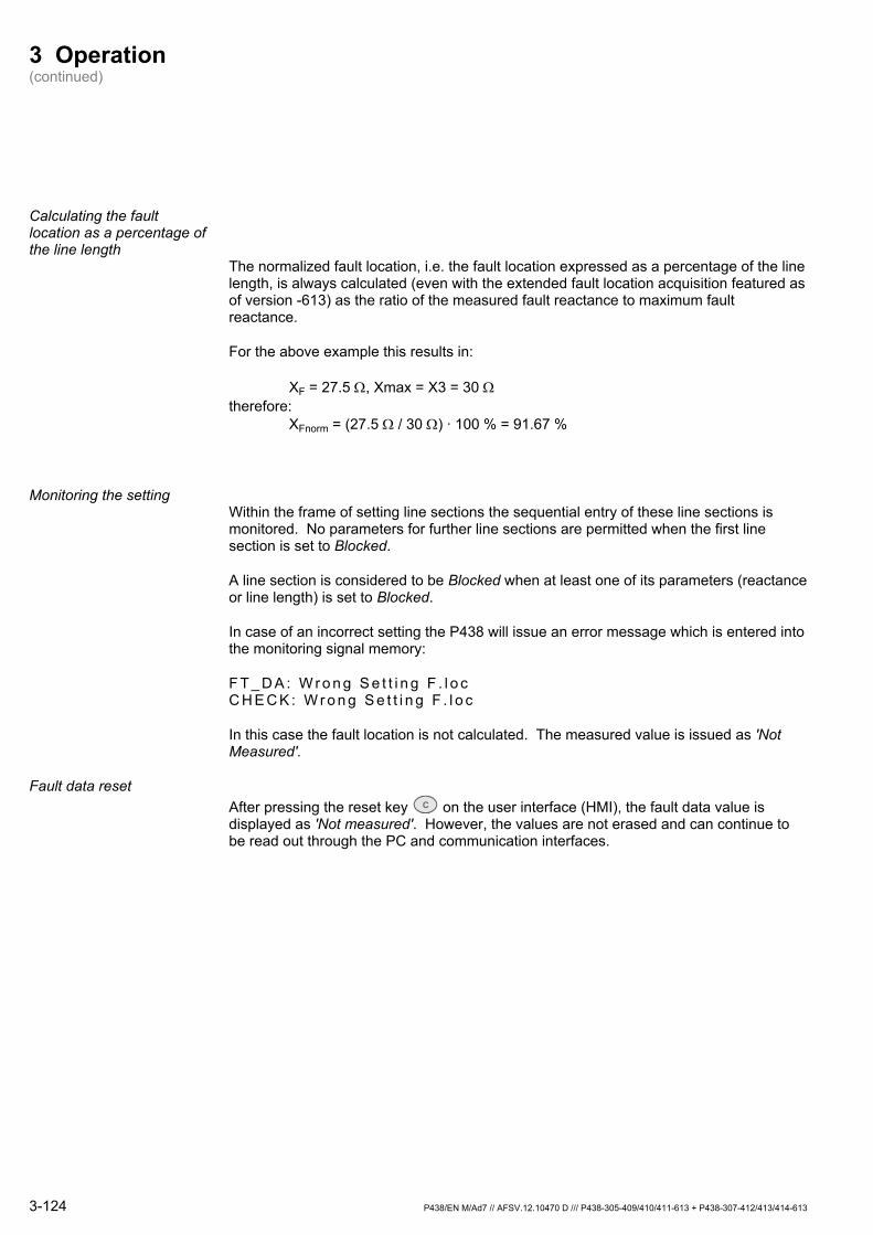
3 Operation (continued)
Calculating the fault location as a percentage of the line length
The normalized fault location, i.e. the fault location expressed as a percentage of the line length, is always calculated (even with the extended fault location acquisition featured as of version -613) as the ratio of the measured fault reactance to maximum fault reactance.
For the above example this results in:
XF = 27.5 Ω, Xmax = X3 = 30 Ω therefore: XFnorm = (27.5 Ω / 30 Ω) · 100 % = 91.67 %
Monitoring the setting Within the frame of setting line sections the sequential entry of these line sections is monitored. No parameters for further line sections are permitted when the first line section is set to Blocked.
A line section is considered to be Blocked when at least one of its parameters (reactance or line length) is set to Blocked.
In case of an incorrect setting the P438 will issue an error message which is entered into the monitoring signal memory:
F T _ D A : W r o n g S e t t i n g F . l o c C H E C K : W r o n g S e t t i n g F . l o c
In this case the fault location is not calculated. The measured value is issued as 'Not Measured'.
Fault data reset After pressing the reset key C on the user interface (HMI), the fault data value is displayed as 'Not measured'. However, the values are not erased and can continue to be read out through the PC and communication interfaces.
3-124 P438/EN M/Ad7 // AFSV.12.10470 D /// P438-305-409/410/411-613 + P438-307-412/413/414-613

3 Operation (continued)
3.20 Fault Recording (Function Group OSCIL)
Start of fault recording A fault exists and therefore fault recording begins if at least one of the following signals is present:
O S C I L : I >
O S C I L : T r i g g e r
In addition, the user can set a logical "OR" combination of logic signals ('m out of n' setting) which appearance will trigger fault recording.
Fault counting Faults are counted and identified by sequential numbers.
48Z6325A_UK
1: execute
MAIN: General Reset EXT [ 005 255 ]OSCIL: Reset Record. USER[ 003 006 ]1: execute
MAIN: General Reset USER[ 003 002 ]
OSCIL: Reset Record. EXT[ 005 243 ]
OSCIL: No. of Faults[ 004 020 ]
OSCIL: No. SystemDisturb.[ 004 010 ]
R
+
R
+
OSCIL: Fct Assig. Trigger
[ 003 085 ]
m out of n
Signal 1
Signal 2
Signal 3
Signal n
Selected signals
OSCIL: Trigger USER
[ 003 041 ]
0
1
0: don’t execute1: execute
OSCIL: Trigger EXT[ 036 089 ]
OSCIL: I>
[ 016 013 ]
I OSCIL: I> Triggered[ 035 013 ]
OSCIL: Trigger[ 037 076 ]
OSCIL: Record. in Progress[ 035 000 ]
OSCIL: System Disturb. Runn[ 035 004 ]
3-88 Start of fault recording and fault counter
P438/EN M/Ad7 // AFSV.12.10470 D /// P438-305-409/410/411-613 + P438-307-412/413/414-613 3-125
3 Operation (continued)
Time tagging The date that is assigned to each fault by the internal clock is stored. A fault’s individual start or end signals are likewise time-tagged. The date and time assigned to a fault when the fault begins can be read out from the fault memory on the HMI or through the PC and communication interfaces. The time information (relative to the onset of the fault) that is assigned to the signals can be retrieved from the fault memory or through the PC or communication interfaces.
Fault recordings Protection signals, including the signals during the settable pre-fault and post-fault windows, are logged in chronological order with reference to the specific fault. A total of eight faults, each involving a maximum of 200 start or end signals, can be stored in the non-volatile fault memories. After eight faults have been recorded, the oldest fault recording will be overwritten, unless memories have been cleared in the interim. If more than 199 start or end signals have occurred during a single fault, then O S C I L : F a u l t M e m . O v e r f l o w will be entered as the last signal. If the time and date are changed during the pre-fault time, the O S C I L : F a u l t y T i m e T a g signal is generated.
In addition to the fault signals, the RMS measured fault data will also be entered in the fault memory.
The fault recordings can be read from the user interface (HMI) or through the PC or communication interfaces.
3-126 P438/EN M/Ad7 // AFSV.12.10470 D /// P438-305-409/410/411-613 + P438-307-412/413/414-613
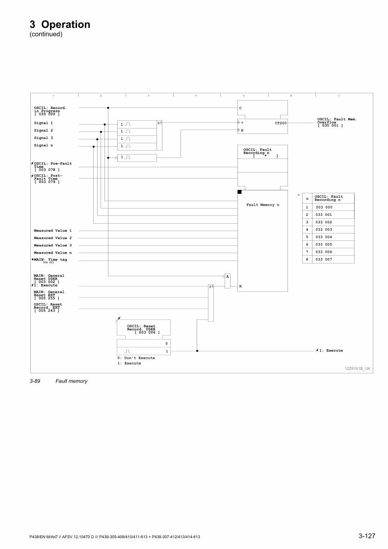
3 Operation (continued)
12Z6161B_UK
R
n
1
2
3
4
5
6
7
8
003 000
033 001
033 002
033 003
033 004
033 005
033 006
033 007
OSCIL: Fault Mem.Overflow[ 035 001 ]
R
+ CT200
C
OSCIL: FaultRecording n
[ * ]1
1
1
1
1
OSCIL: ResetRecord. USER [ 003 006 ]
OSCIL: Record.in Progress[ 035 000 ]
Signal 1
Signal 2
Signal 3
Signal n
Measured Value 1
Measured Value 2
Measured Value 3
Measured Value n
MAIN: Time tag306 021
OSCIL: ResetRecord. EXT[ 005 243 ]
1: Execute
0
1
0: Don't Execute1: Execute
MAIN: GeneralReset USER[ 003 002 ]
MAIN: GeneralReset EXT[ 005 255 ]
&
OSCIL: Pre-FaultTime[ 003 078 ]OSCIL: Post-Fault Time[ 003 079 ]
1: Execute
Fault Memory n
OSCIL: FaultRecording n
3-89 Fault memory
P438/EN M/Ad7 // AFSV.12.10470 D /// P438-305-409/410/411-613 + P438-307-412/413/414-613 3-127

3 Operation (continued)
Fault value recording The following analog signals are recorded by the P438:
The catenary current
The feeder current
The defrost current
The catenary voltage
The feeder voltage.
The signals are recorded before, during and after a fault. The window length for disturbance recording before and after the fault can be set. A maximum time period of 32 s - independent of system frequency - is available for recording. This period can be divided among a maximum of eight faults. The maximum recording time per fault can be set. If a fault, including the set pre-fault and post-fault times, lasts longer than the set maximum recording time, then recording will terminate when the set maximum recording time is reached.
The pre-fault time is exactly adhered to if it is shorter than the set maximum recording time. Otherwise the pre-fault time is set to the maximum recording time minus a sampling increment, and the post-fault time is set to zero.
If the maximum recording time of 32 s is exceeded, the analog values for the oldest fault are overwritten, but not the binary values. If more than eight faults have occurred since the last reset, then all data for the oldest fault are overwritten.
The analog waveform data of the fault record can only be read out through the PC or communication interfaces.
When the supply voltage is interrupted or after a warm restart, the values of all faults remain stored.
3-128 P438/EN M/Ad7 // AFSV.12.10470 D /// P438-305-409/410/411-613 + P438-307-412/413/414-613
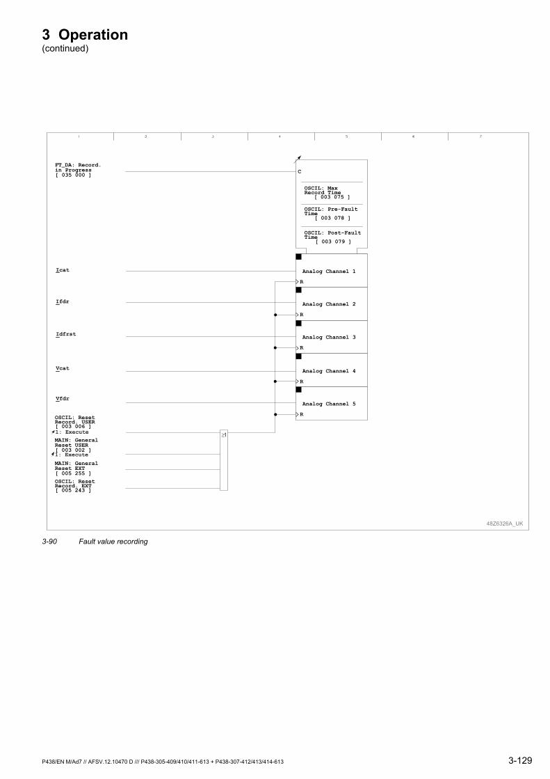
3 Operation (continued)
OSCIL: ResetRecord. USER[ 003 006 ]1: Execute
48Z6326A_UK
FT_DA: Record.in Progress[ 035 000 ]
Icat
Ifdr
OSCIL: MaxRecord Time
[ 003 075 ]
OSCIL: Pre-FaultTime
[ 003 078 ]
OSCIL: Post-FaultTime
[ 003 079 ]
C
R
Analog Channel 1
R
Analog Channel 2
R
Analog Channel 3
R
Analog Channel 4
R
Analog Channel 5Vfdr
OSCIL: ResetRecord. EXT[ 005 243 ]
1: Execute
≥1MAIN: GeneralReset USER[ 003 002 ]
MAIN: GeneralReset EXT[ 005 255 ]
Idfrst
Vcat
3-90 Fault value recording
P438/EN M/Ad7 // AFSV.12.10470 D /// P438-305-409/410/411-613 + P438-307-412/413/414-613 3-129
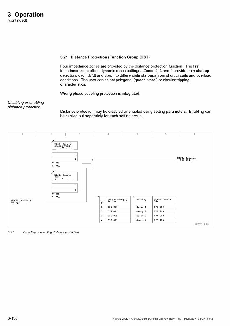
3 Operation (continued)
3.21 Distance Protection (Function Group DIST)
Four impedance zones are provided by the distance protection function. The first impedance zone offers dynamic reach settings. Zones 2, 3 and 4 provide train start-up detection, di/dt, dv/dt and dϕ/dt, to differentiate start-ups from short circuits and overload conditions. The user can select polygonal (quadrilateral) or circular tripping characteristics.
Wrong phase coupling protection is integrated.
Disabling or enabling distance protection
Distance protection may be disabled or enabled using setting parameters. Enabling can be carried out separately for each setting group.
48Z6331A_UK
DIST: Generalenable USER[ 031 073 ]
0
1
DIST: EnableSGx[ * ]
0
1
0: No1: Yes
GROUP: Group yActive[ ** ]
DIST: Enabled[ 036 104 ]
1 2 3 4 5 6 7
1
y
2
3
4
036 090
GROUP: Group yActive
036 091
036 092
036 093
Group 1
Group 2
072 200
DIST: EnableSGx
073 200
074 200
075 200
Group 3
Group 4
Setting
&
** *
0: No1: Yes
3-91 Disabling or enabling distance protection
3-130 P438/EN M/Ad7 // AFSV.12.10470 D /// P438-305-409/410/411-613 + P438-307-412/413/414-613

3 Operation (continued)
Distance protection blocking
Distance protection is blocked if one of the following conditions occurs:
Distance protection has not been enabled.
The voltage transformer m.c.b. has tripped.
Monitoring (VT supervision) has detected a fault in the voltage-measuring circuit.
Distance protection is not set correctly.
C&VTS
3-92 Distance protection blocking
P438/EN M/Ad7 // AFSV.12.10470 D /// P438-305-409/410/411-613 + P438-307-412/413/414-613 3-131
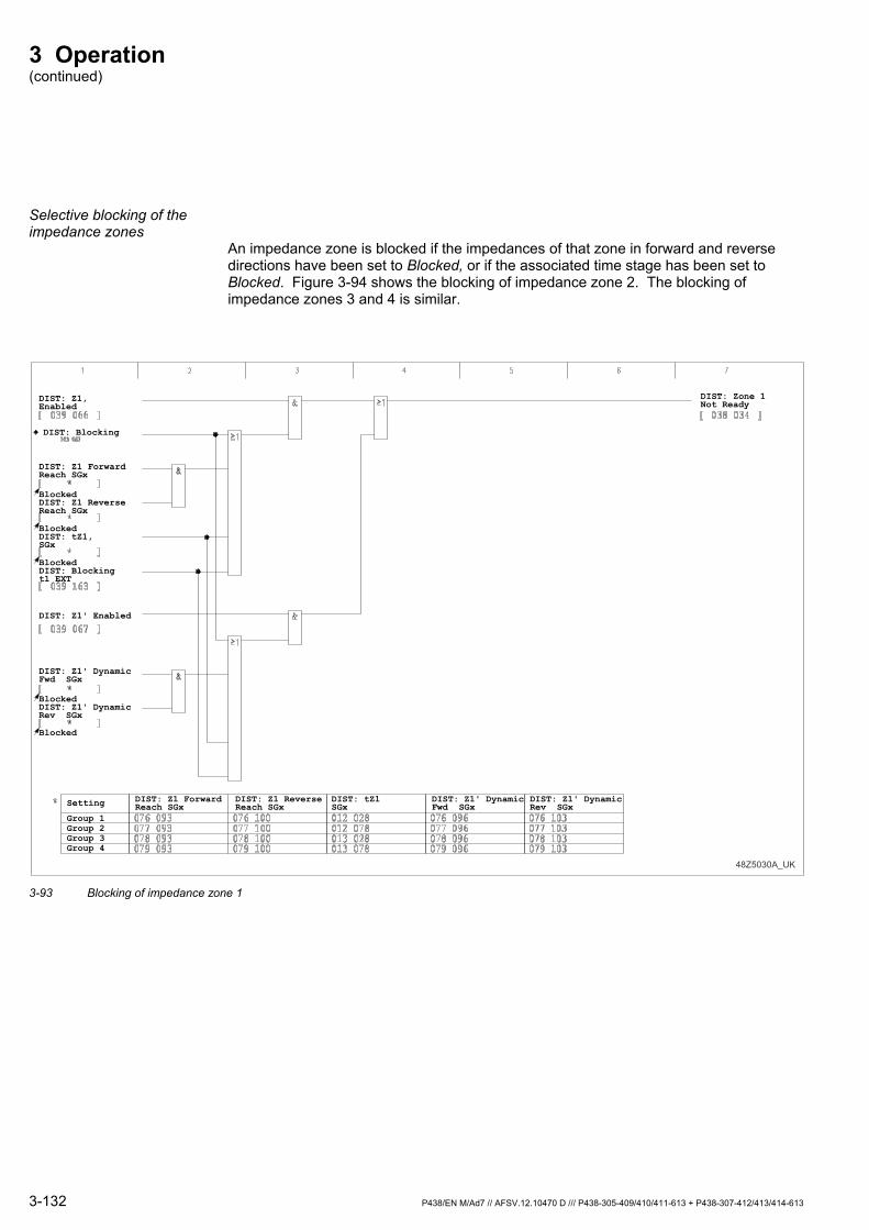
3 Operation (continued)
Selective blocking of the impedance zones
An impedance zone is blocked if the impedances of that zone in forward and reverse directions have been set to Blocked, or if the associated time stage has been set to Blocked. Figure 3-94 shows the blocking of impedance zone 2. The blocking of impedance zones 3 and 4 is similar.
Setting
Group 1Group 2Group 3Group 4
DIST: Z1 ForwardReach SGx
DIST: Z1 ReverseReach SGx
DIST: tZ1SGx
DIST: Z1' DynamicRev SGx
DIST: Z1' DynamicFwd SGx
DIST: Z1,Enabled
DIST: Blocking
DIST: Z1 ForwardReach SGx
BlockedDIST: Z1 ReverseReach SGx
BlockedDIST: tZ1,SGx
BlockedDIST: Blockingt1 EXT
DIST: Z1' Enabled
DIST: Z1' DynamicFwd SGx
BlockedDIST: Z1' DynamicRev SGx
Blocked
DIST: Zone 1Not Ready
48Z5030A_UK 3-93 Blocking of impedance zone 1
3-132 P438/EN M/Ad7 // AFSV.12.10470 D /// P438-305-409/410/411-613 + P438-307-412/413/414-613

3 Operation (continued)
48Z5410C_UK
DIST: Z2 Enabled[ 039 068 ]
DIST: Zone 2 not ready[ 038 035 ]
1 2 3 4 5 6 7
1≥
&
DIST: Blocking303 667
Setting
Group 4Group 3Group 2Group 1
DIST: Z2 ReverseReach SGx
DIST: tZ2S ShortDelay SGx
DIST: Z2 ForwardReach SGx
076 094077 094078 094079 094
076 101077 101078 101079 101
076 097077 097078 097079 097
012 029012 079013 029013 079
076 104077 104078 104079 104
blocked
DIST: Z2 Forward ReachSGx[ * ]
DIST: Z2 Reverse ReachSGx[ * ]
blocked
DIST: Z2´ Enabled[ 039 069 ]
&
blocked
DIST: Z2' Dynamic FwdSGx[ * ]
DIST: Z2' Dynamic RevSGx[ * ]
blocked
blocked
DIST: tZ2S Short DelaySGx[ * ]
DIST: Blocking t2K EXT[ 039 164 ]
1≥
blocked
DIST: tZ2L Long DelaySGx[ * ]
DIST: Blocking t2L EXT[ 039 165 ]
0: Disabled
DIST: Z2 Op.Mode dx/dtSGx[ * ]
&
blocked
DIST: Z2Delta I(di/dt)SGx[ * ]
blocked
DIST: Z2Delta V(dv/dt)SGx[ * ]
blocked
DIST: Z2D.phi(dphi/dt)SGx[ * ]
&
1≥
1≥
&
&
1≥
Setting
Group 4Group 3Group 2Group 1
DIST: Z2 Op.Modedx/dt SGx
DIST: Z2DeltaV(dv/dt) SGx
DIST: Z2DeltaI(di/dt) SGx
DIST: Z2D.phi(dphi/dt) SGx
DIST: tZ2L LongDelay SGx
012 190012 191012 192012 193
072 107073 107074 107075 107
072 198073 198074 198075 198
072 206073 206074 206075 206
072 139073 139074 139075 139
DIST: Z2'Dynamic Rev SGx
DIST: Z2'Dynamic Fwd SGx
3-94 Blocking of impedance zone 2
P438/EN M/Ad7 // AFSV.12.10470 D /// P438-305-409/410/411-613 + P438-307-412/413/414-613 3-133
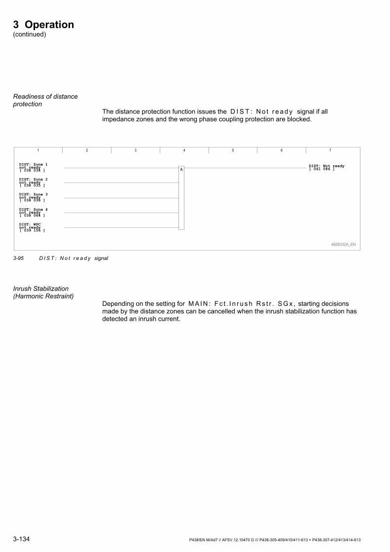
3 Operation (continued)
Readiness of distance protection
The distance protection function issues the D I S T : N o t r e a d y signal if all impedance zones and the wrong phase coupling protection are blocked.
DIST: Not ready[ 041 086 ]
1 2 3 4 5 6 7
DIST: Zone 1not ready[ 038 034 ]
48Z6332A_EN
DIST: Zone 2not ready[ 038 035 ]
DIST: Zone 3not ready[ 038 036 ]
DIST: Zone 4not ready[ 038 064 ]
DIST: WPCnot ready[ 039 156 ]
&
3-95 D I S T : N o t r e a d y signal
Inrush Stabilization (Harmonic Restraint)
Depending on the setting for M A I N : F c t . I n r u s h R s t r . S G x , starting decisions made by the distance zones can be cancelled when the inrush stabilization function has detected an inrush current.
3-134 P438/EN M/Ad7 // AFSV.12.10470 D /// P438-305-409/410/411-613 + P438-307-412/413/414-613
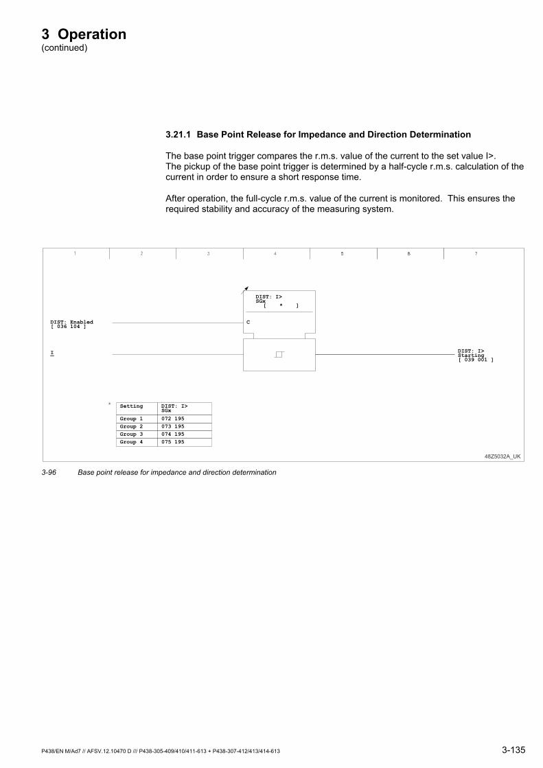
3 Operation (continued)
3.21.1 Base Point Release for Impedance and Direction Determination
The base point trigger compares the r.m.s. value of the current to the set value I>. The pickup of the base point trigger is determined by a half-cycle r.m.s. calculation of the current in order to ensure a short response time.
After operation, the full-cycle r.m.s. value of the current is monitored. This ensures the required stability and accuracy of the measuring system.
48Z5032A_UK
Group 1Group 2Group 3Group 4
Setting
072 195
DIST: I>SGx
073 195074 195075 195
DIST: Enabled[ 036 104 ]
I DIST: I>Starting[ 039 001 ]
DIST: I>SGx
[ * ]
C
3-96 Base point release for impedance and direction determination
P438/EN M/Ad7 // AFSV.12.10470 D /// P438-305-409/410/411-613 + P438-307-412/413/414-613 3-135
3 Operation (continued)
3.21.2 Distance and Direction Measurement
The P438 determines the fault impedance and the fault direction using the measured variables V and I. In order for direction measurement to function correctly, even at very small fault voltage values, the information stored in the voltage memory is also put to use in these cases.
Direction measurement The following applies to direction measurement:
Forward direction: -45° < ϕ < +135°
Reverse direction: -45° > ϕ > +135°
For very low fault voltages, the voltage from the voltage memory is used in place of the measured voltage in order to avoid erroneous direction decisions. The direction decision is dependent on the following conditions:
VF > 0.1 Vn The direction decision is issued on the basis of the fault current and the measured fault voltage VF.
VF < 0.1 Vn Voltage memory enabled: The direction decision is issued on the basis of the fault current and the voltage stored in the voltage memory. Voltage memory not enabled: The direction decision is issued on the basis of the fault current and the measured fault voltage down to a minimum value of 1 V. If the fault voltage drops to a value of less than approximately 1 V, an accurate direction determination is no longer possible. In this case, a Fault forward decision is issued - independent of the actual fault direction.
3-136 P438/EN M/Ad7 // AFSV.12.10470 D /// P438-305-409/410/411-613 + P438-307-412/413/414-613
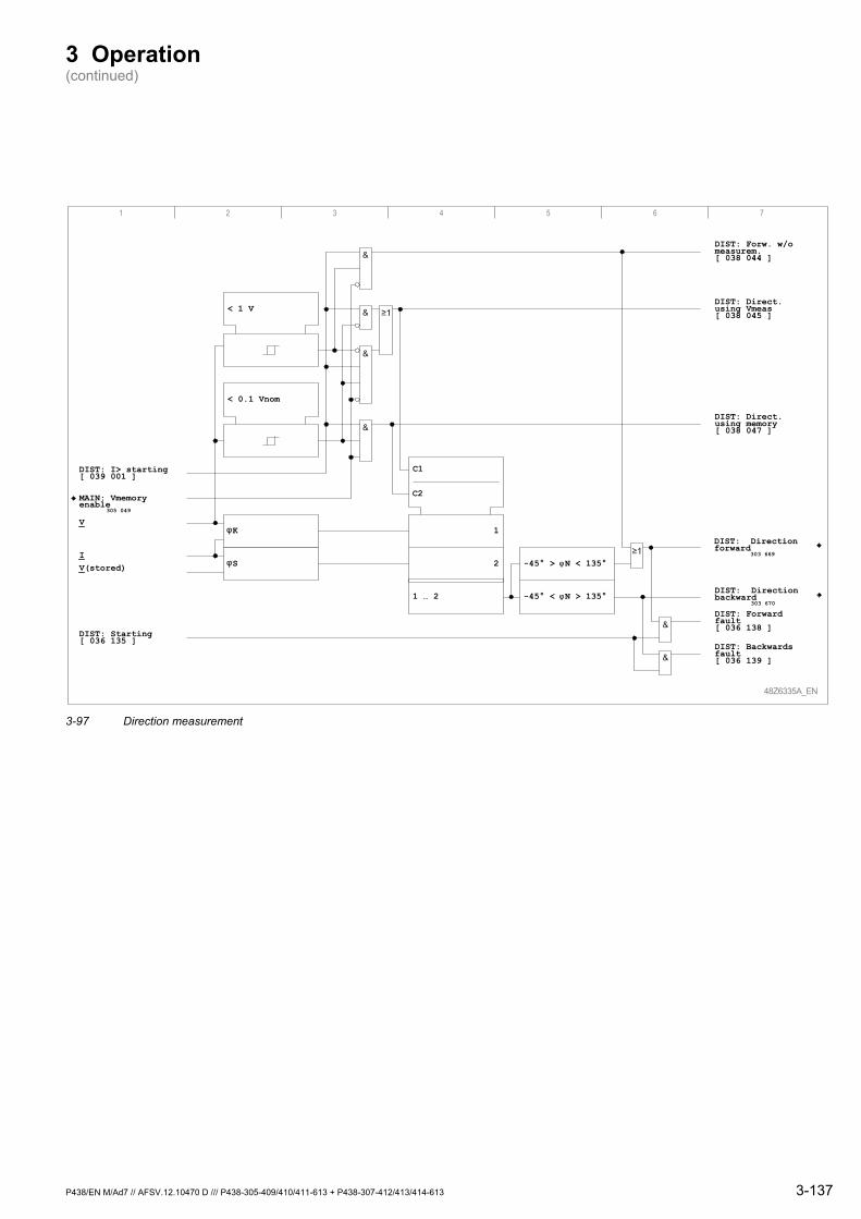
3 Operation (continued)
1 2 3 4 5 6 7
48Z6335A_EN
DIST: Direct.using Vmeas[ 038 045 ]
< 1 V
DIST: I> starting[ 039 001 ]
DIST: Directionforward
303 669
MAIN: Vmemoryenable
305 049
C2
< 0.1 Vnom
K
SV(stored)
V
I
DIST: Forw. w/omeasurem.[ 038 044 ]
DIST: Direct.using memory[ 038 047 ]
1
2
1 … 2
C1
-45° > N < 135°
-45° < N > 135°DIST: Directionbackward
303 670
DIST: Starting[ 036 135 ]
DIST: Forwardfault[ 036 138 ]
DIST: Backwardsfault[ 036 139 ]
&
&
&
&
&
&
3-97 Direction measurement
P438/EN M/Ad7 // AFSV.12.10470 D /// P438-305-409/410/411-613 + P438-307-412/413/414-613 3-137
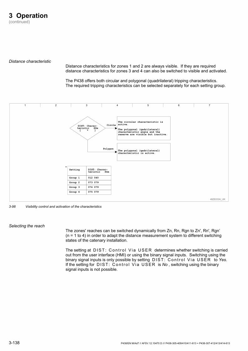
3 Operation (continued)
Distance characteristic Distance characteristics for zones 1 and 2 are always visible. If they are required distance characteristics for zones 3 and 4 can also be switched to visible and activated.
The P438 offers both circular and polygonal (quadrilateral) tripping characteristics. The required tripping characteristics can be selected separately for each setting group.
1 2 3 4 5 6 7
48Z6333A_UK
Polygon
DIST: Charac-teristic SGx[ * ]
Circle
The polygonal (qadrilateral) characteristic is active.
The circular characteristic is active.
The polygonal (qadrilateral) characteristic angle and the reserve are visible but inactive.
Group 1
Group 2
012 040
DIST: Charac-teristic SGx
073 079
074 079
075 079
Group 3
Group 4
Setting*
3-98 Visibility control and activation of the characteristics
Selecting the reach The zones' reaches can be switched dynamically from Zn, Rn, Rgn to Zn', Rn', Rgn’ (n = 1 to 4) in order to adapt the distance measurement system to different switching states of the catenary installation.
The setting at D I S T : C o n t r o l V i a U S E R determines whether switching is carried out from the user interface (HMI) or using the binary signal inputs. Switching using the binary signal inputs is only possible by setting D I S T : C o n t r o l V i a U S E R to Yes. If the setting for D I S T : C o n t r o l V i a U S E R is No , switching using the binary signal inputs is not possible.
3-138 P438/EN M/Ad7 // AFSV.12.10470 D /// P438-305-409/410/411-613 + P438-307-412/413/414-613
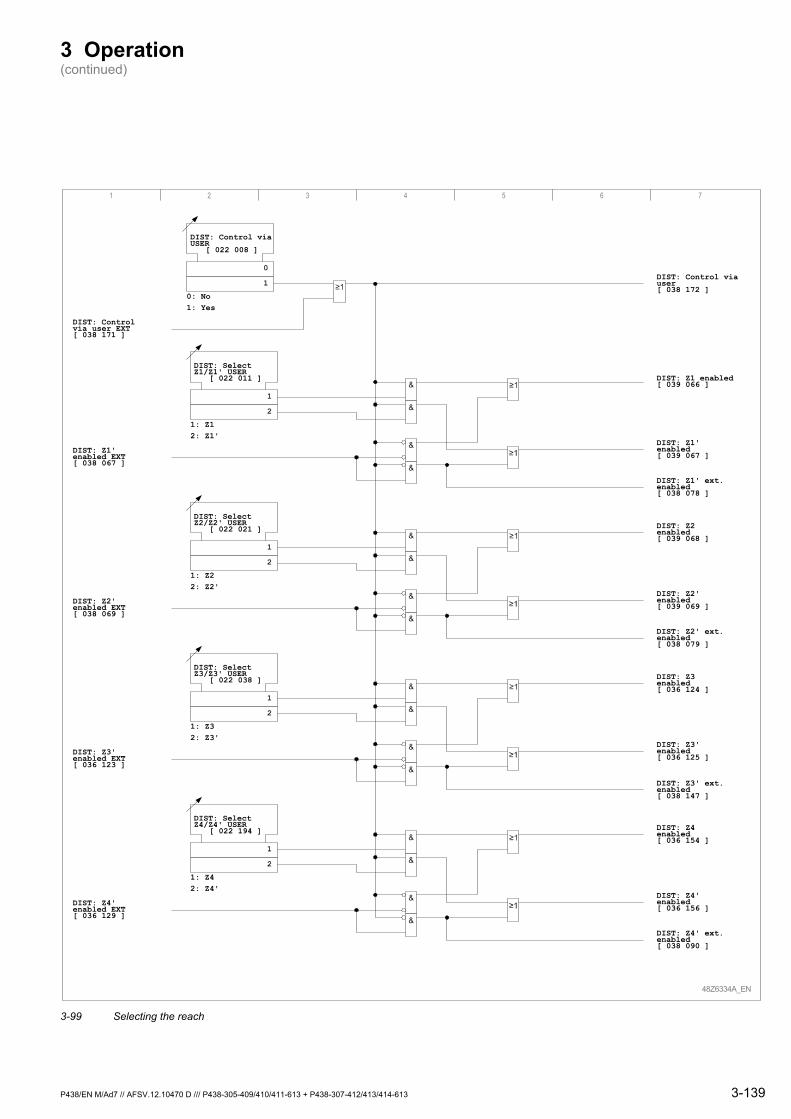
3 Operation (continued)
1 2 3 4 5 6 7
48Z6334A_EN
DIST: Control viauser[ 038 172 ]
DIST: Control viaUSER
[ 022 008 ]
0
0: No1: Yes
DIST: Controlvia user EXT[ 038 171 ]
1
DIST: SelectZ1/Z1' USER
[ 022 011 ]
1
1: Z1
2
2: Z1'
DIST: Z1'enabled EXT[ 038 067 ]
DIST: Z1 enabled[ 039 066 ]
DIST: Z1'enabled[ 039 067 ]
DIST: Z1' ext.enabled[ 038 078 ]
DIST: SelectZ2/Z2' USER
[ 022 021 ]
1
1: Z2
2
2: Z2'
DIST: Z2'enabled EXT[ 038 069 ]
DIST: Z2enabled[ 039 068 ]
DIST: Z2'enabled[ 039 069 ]
DIST: Z2' ext.enabled[ 038 079 ]
DIST: SelectZ3/Z3' USER
[ 022 038 ]
1
1: Z3
2
2: Z3'
DIST: Z3'enabled EXT[ 036 123 ]
DIST: Z3enabled[ 036 124 ]
DIST: Z3'enabled[ 036 125 ]
DIST: Z3' ext.enabled[ 038 147 ]
DIST: SelectZ4/Z4' USER
[ 022 194 ]
1
1: Z4
2
2: Z4'
DIST: Z4'enabled EXT[ 036 129 ]
DIST: Z4enabled[ 036 154 ]
DIST: Z4'enabled[ 036 156 ]
DIST: Z4' ext.enabled[ 038 090 ]
&
&
&
&
&
&
&
&
&
&
&
&
&
&
&
&
3-99 Selecting the reach
P438/EN M/Ad7 // AFSV.12.10470 D /// P438-305-409/410/411-613 + P438-307-412/413/414-613 3-139
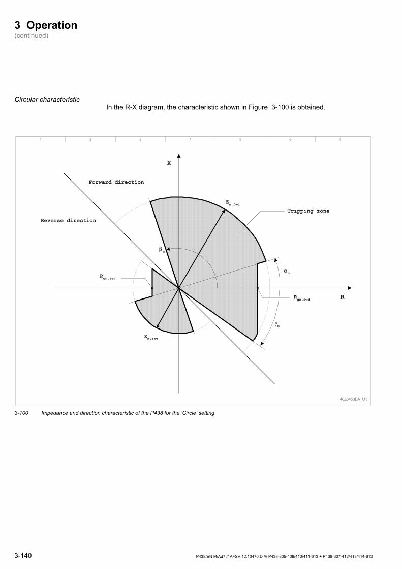
3 Operation (continued)
Circular characteristic In the R-X diagram, the characteristic shown in Figure 3-100 is obtained.
1 2 3 4 5 6 7
48Z5453BA_UK
Forward direction
X
αn
βn
γn
Reverse direction
Tripping zone
R
Zn,fwd
Rgn,fwd
Zn,rev
Rgn,rev
3-100 Impedance and direction characteristic of the P438 for the 'Circle' setting
3-140 P438/EN M/Ad7 // AFSV.12.10470 D /// P438-305-409/410/411-613 + P438-307-412/413/414-613
3 Operation (continued)
Circular characteristic, settings
The characteristic is determined by the settings listed below. It can be set separately for all four zones (n: 1 to 4).
Impedance Zn or Zn' in forward direction. Impedance Zn or Zn' in reverse direction
The impedance limits the maximum reach of the circular characteristic. If the setting is Blocked, the zone in the corresponding direction is ineffective.
Resistance limit Rgn or Rgn' in forward direction. Resistance limit Rgn or Rgn' in reverse direction.
Therefore the tripping zone is limited to the resistances within the load blinder – i.e. lower than Rgn (Rgn’). For this setting, the condition: Rgn ≤ Zn must be met for all enabled zones (all 4 setting groups, all unblocked Z and Z´ zones). If the condition is not satisfied, a warning indication and the device blocking alarm are issued.
Load blinding angle αn This setting is only applied if the resistive limit line, defined by Rgn, falls within the Z circle (this is the case for α < arccos (Rgn/Zn) or α < arccos (Rgn‘/Zn‘)). At fault impedance angles outside of the blinder cone region, the circle characteristic operates unaffected (non-blinded).
Angle βn Angle γn
These angles limit the tripping area in quadrants 2 and 4.. Angle γn defines areas with the form of a triangle in the 2nd and 4th quadrants. The limit in the R-direction is given either by Rgn or by Zn, depending on the value leading to the smaller zone.
The P438 checks whether the impedance locus is within the defined tripping area or not. Since the reach for forward and reverse direction can be selected separately, the direction decision determines the quadrilateral segment where the measured impedance locus must be located so that a distance decision is issued. If the short-circuit voltages are lower than 10 V, angles αn, βn and γn are not taken into account. The dashed characteristic in Figure 3-100 results.
Circular characteristic, harmonics adaptation
If distance protection operates while the harmonics adaptation feature is enabled (D I S T : H a r m . A d a p t . A v a i l . = Yes) then impedance and reactance settings for all zones are processed with dynamic harmonics factor M A I N : k H a r m . Σ I ( x f n ) / I ( f n ) . In this case distance zone boundaries are reduced dynamically:
n.Harm
Harm.n, Zk11Z ⋅
+= or 'Z
k11'Z n
.HarmHarm.n, ⋅
+=
gn.Harm
Harm.gn, Rk11R ⋅
+= or 'R
k11'R gn
.HarmHarm.gn, ⋅
+=
P438/EN M/Ad7 // AFSV.12.10470 D /// P438-305-409/410/411-613 + P438-307-412/413/414-613 3-141

3 Operation (continued)
Circular characteristic, zone 1, Zone extensions
For zone 1, the impedance reach can be extended by the zone extension factor kze. Valid impedance and reactance values are extended for each of the set directions.
1zekze1, ZkZ ⋅= or ´Zk´Z 1zekze1, ⋅=
g1zekzeg1, RkR ⋅= or ´Rk´R g1zekzeg1, ⋅= Impedance reach is extended using the following parameters:
Zone extension factor for high-speed reclosure (D I S T : k z e E x t e n d e d H S R S G x )
Impedance reach is extended by the set factor if the internal auto-reclose function permits a zone extension during high-speed reclosures (R E C L S : Z o n e E x t n o n H S R S G x ). Depending on the setting, zone extension may remain active until the reclosure command (R E C L S : Z o n e E x t . D u r . R C S G x ) is terminated.
Zone extension factor for time-delay reclosure (D I S T : k z e E x t e n d e d T D R S G x )
Impedance reach is extended by the set factor if the internal auto-reclose function permits a zone extension during time-delayed reclosures (R E C L S : Z o n e E x t n o n T D R S G x ). Depending on the setting, zone extension may remain active until the reclosure command (R E C L S : Z o n e E x t . D u r . R C S G x ) is terminated.
Zone extension factor for external extension or tripping by the switch on to a fault protection (D I S T : k z e S O T F / E X T S G x ).
Impedance reach is extended by the set factor if switch on to fault protection (S O T F : Z 1 E x t e n d e d ) has been activated or an external signal (D I S T : Z o n e E x t e n s i o n E X T ) is set.
Figure 3-101 shows the formation of distance decisions of the first impedance zone for the circular characteristic operating mode.
Circular characteristic, Zones 2, 3 and 4
Figure 3-102 shows the formation of the distance decisions for impedance zone 2. This will apply similarly to impedance zones 3 and 4.
3-142 P438/EN M/Ad7 // AFSV.12.10470 D /// P438-305-409/410/411-613 + P438-307-412/413/414-613
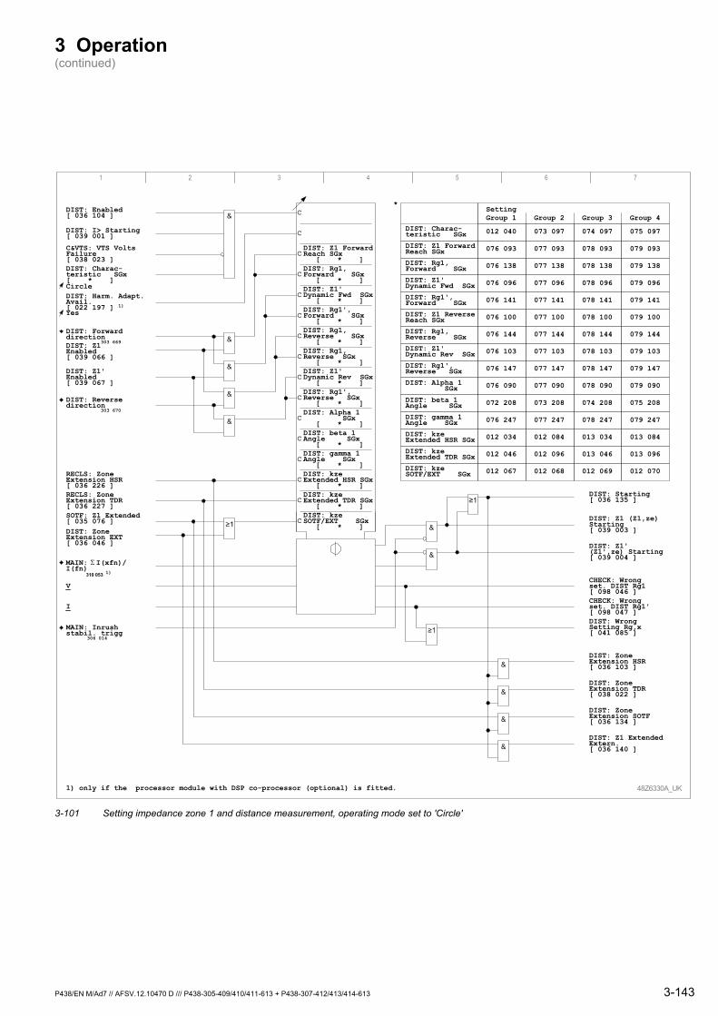
3 Operation (continued)
1 2 3 4 5 6 7
48Z6330A_UK
DIST: Enabled[ 036 104 ] C
DIST: Z1 ForwardReach SGx
[ * ]C
DIST: Rg1,Forward SGx
[ * ]C
DIST: Z1'Dynamic Fwd SGx
[ * ]C
DIST: Rg1',Forward SGx
[ * ]C
DIST: Rg1,Reverse SGx
[ * ]C
DIST: Rg1,Reverse SGx
[ * ]C
DIST: Z1'Dynamic Rev SGx
[ * ]C
DIST: Rg1',Reverse SGx
[ * ]C
DIST: Alpha 1 SGx
[ * ]C
DIST: beta 1Angle SGx
[ * ]C
DIST: gamma 1Angle SGx
[ * ]C
DIST: kzeExtended HSR SGx
[ * ]C
C
DIST: kzeExtended TDR SGx
[ * ]C
DIST: kzeSOTF/EXT SGx
[ * ]C
DIST: I> Starting[ 039 001 ]
DIST: Charac-teristic SGx[ * ]Circle
C&VTS: VTS VoltsFailure[ 038 023 ]
DIST: Harm. Adapt.Avail.[ 022 197 ] 1)Yes
DIST: Forwarddirection
303 669DIST: Z1Enabled[ 039 066 ]
DIST: Z1'Enabled[ 039 067 ]
DIST: Reversedirection
303 670
012 040DIST: Charac-teristic SGx
DIST: Z1 ForwardReach SGx
DIST: Rg1,Forward SGx
DIST: Z1'Dynamic Fwd SGx
DIST: Rg1',Forward SGx
DIST: Z1 ReverseReach SGx
DIST: Rg1,Reverse SGx
DIST: Z1'Dynamic Rev SGx
DIST: Rg1',Reverse SGx
DIST: Alpha 1 SGx
DIST: beta 1Angle SGx
DIST: gamma 1Angle SGx
DIST: kzeExtended HSR SGx
DIST: kzeExtended TDR SGx
DIST: kzeSOTF/EXT SGx
073 097 074 097 075 097
SettingGroup 1 Group 2 Group 3 Group 4
RECLS: ZoneExtension HSR[ 036 226 ]RECLS: ZoneExtension TDR[ 036 227 ]SOTF: Z1 Extended[ 035 076 ]DIST: ZoneExtension EXT[ 036 046 ]
V
I
MAIN: Inrushstabil. trigg
306 014
DIST: Z1 ExtendedExtern.[ 036 140 ]
DIST: ZoneExtension SOTF[ 036 134 ]
DIST: ZoneExtension TDR[ 038 022 ]
DIST: ZoneExtension HSR[ 036 103 ]
CHECK: Wrongset. DIST Rg1'[ 098 047 ]
CHECK: Wrongset. DIST Rg1[ 098 046 ]
DIST: WrongSetting Rg,x[ 041 085 ]
DIST: Z1 (Z1,ze)Starting[ 039 003 ]
DIST: Z1'(Z1',ze) Starting[ 039 004 ]
076 093 077 093 078 093 079 093
076 138 077 138 078 138 079 138
076 096 077 096 078 096 079 096
076 141 077 141 078 141 079 141
076 100 077 100 078 100 079 100
076 144 077 144 078 144 079 144
076 103 077 103 078 103 079 103
076 147 077 147 078 147 079 147
076 090 077 090 078 090 079 090
072 208 073 208 074 208 075 208
076 247 077 247 078 247 079 247
012 034 012 084 013 034 013 084
012 046 012 096 013 046 013 096
012 067 012 068 012 069 012 070
1) only if the processor module with DSP co-processor (optional) is fitted.
DIST: Starting[ 036 135 ]
&
&
&
&
&
&
&
&
&
&
&
*
MAIN: I(xfn)/I(fn)
310 053 1)
Σ
3-101 Setting impedance zone 1 and distance measurement, operating mode set to 'Circle'
P438/EN M/Ad7 // AFSV.12.10470 D /// P438-305-409/410/411-613 + P438-307-412/413/414-613 3-143

3 Operation (continued)
1 2 3 4 5 6 7
48Z6341A_UK
DIST: Enabled[ 036 104 ] C
DIST: Z2 ForwardReach SGx
[ * ]C
DIST: Rg2, Forward SGx
[ * ]C
DIST: Z2'Dynamic Fwd SGx
[ * ]C
DIST: Rg2', Forward SGx
[ * ]C
DIST: Z2 ReverseReach SGx
[ * ]C
DIST: Rg2, Reverse SGx
[ * ]C
DIST: Z2'Dynamic Rev SGx
[ * ]C
DIST: Rg2', Reverse SGx
[ * ]C
DIST: Alpha 2 SGx
[ * ]C
DIST: beta 2Angle SGx
[ * ]C
DIST: gamma 2 Angle SGx
[ * ]C
CDIST: I> Starting[ 039 001 ]
DIST: Charac-teristic SGx[ * ]Circle
C&VTS: VTS VoltsFailure[ 038 023 ]
DIST: Harm.- 1)
Adapt. Avail.[ 022 197 ] Yes
DIST: Forward direction
303 669DIST: Z2 Enabled[ 039 068 ]
DIST: Z2' Enabled[ 039 069 ]
DIST: Reversedirection
303 670
V
I
MAIN: Inrush stabil. trigg
306 014
CHECK: Wrong set. DIST Rg2'[ 098 049 ]
CHECK: Wrong set.DIST Rg2[ 098 048 ]
DIST: WrongSetting Rg,x [ 041 085 ]
DIST: Z2 Starting[ 039 005 ]
DIST: Z2' Starting[ 039 006 ]
1) only if the processor module with DSP co-processor (optional) is fitted.
DIST: Starting[ 036 135 ]
Group 1Group 2
012 040
DIST: Charac-teristic SGx
073 097074 097075 097
Group 3Group 4
Setting
076 139
DIST: Rg2, Forward SGx
077 139078 139079 139
076 097
DIST: Z2'Dynamic Fwd SGx
077 097078 097079 097
076 094
DIST: Z2 ForwardReach SGx
077 094078 094079 094
076 142
DIST: Rg2', Forward SGx
077 142078 142079 142
076 101
DIST: Z2 ReverseReach SGx
077 101078 101079 101
Group 1Group 2
076 145
DIST: Rg2, Reverse SGx
077 145078 145079 145
Group 3Group 4
Setting
076 148
DIST: Rg2', Reverse SGx
077 148078 148079 148
076 091
DIST: Alpha 2 SGx
077 091078 091079 091
076 104
DIST: Z2'Dynamic Rev SGx
077 104078 104079 104
072 209
DIST: beta 2Angle SGx
073 209074 209075 209
076 248
DIST: gamma 2 Angle SGx
077 248078 248079 248
*
*
&
&
&
&
&
MAIN: I(xfn)/I(fn)
310 053 1)
Σ
&
&
3-102 Setting impedance zone 2 and distance measurement, operating mode set to 'Circle'
3-144 P438/EN M/Ad7 // AFSV.12.10470 D /// P438-305-409/410/411-613 + P438-307-412/413/414-613
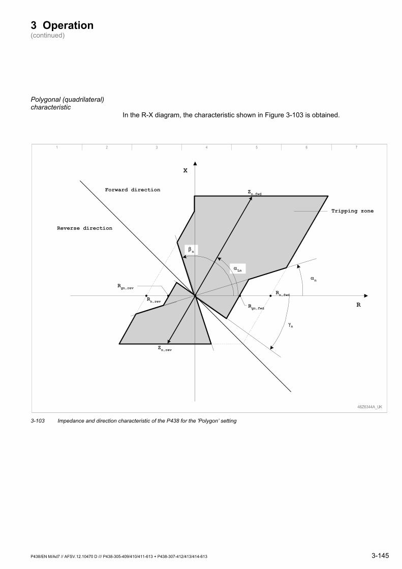
3 Operation (continued)
Polygonal (quadrilateral) characteristic
In the R-X diagram, the characteristic shown in Figure 3-103 is obtained.
1 2 3 4 5 6 7
48Z6344A_UK
Zn,fwdForward direction
X
Rgn,fwd
αn
βn
γn
Reverse direction
Tripping zone
R
Zn,rev
Rgn,rev
αLn
Rn,fwdRn,rev
3-103 Impedance and direction characteristic of the P438 for the 'Polygon’ setting
P438/EN M/Ad7 // AFSV.12.10470 D /// P438-305-409/410/411-613 + P438-307-412/413/414-613 3-145
3 Operation (continued)
Polygonal (quadrilateral) characteristic, settings
The characteristic is determined by the settings listed below. It can be set separately for all four zones (n: 1 to 4).
Impedance Zn or Zn' in forward direction. Impedance Zn or Zn' in reverse direction Line impedance angle αLn.
The maximum X-reach of the polygonal characteristic is calculated using the impedance and the line angle. If the impedance setting is Blocked, the zone in the corresponding direction is disabled.
Resistance Rn or Rn' in forward direction. Resistance Rn or Rn' in reverse direction
Therefore the R-reach of the tripping zones is limited. The gradient of the resistive reach line is also defined by the line angle αLn.
Resistance limit Rgn or Rgn' in forward direction. Resistance limit Rgn or Rgn' in reverse direction.
Therefore the tripping zone is limited to the resistances within the load blinder – i.e. lower than Rgn (Rgn’). For this setting, the condition: Rgn ≤ Rn must be met for all enabled zones (all 4 setting groups, all unblocked Z and Z´ zones). If the condition is not satisfied, a warning indication and the device blocking alarm are issued.
Load blinding angle αn At fault impedance angles outside of the blinder cone region, the circular characteristic operates unaffectedly (non-blinded).
Angle βn Angle γn
These angles limit the tripping area in quadrants 2 and 4..
The P438 checks whether the impedance locus is within the defined tripping area or not. Since the reaches for forward and reverse directions can be selected separately, the directional decision determines the quadrilateral segment where the measured impedance locus must be located so that a distance decision is issued. If the short-circuit voltage is lower than 10 V, angles αn, βn and γn are not taken into account. The dashed characteristic in Figure 3-103 results.
3-146 P438/EN M/Ad7 // AFSV.12.10470 D /// P438-305-409/410/411-613 + P438-307-412/413/414-613
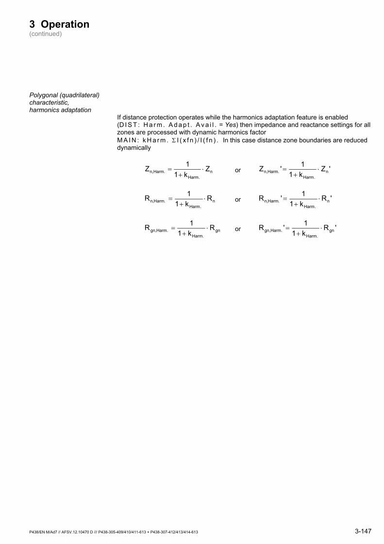
3 Operation (continued)
Polygonal (quadrilateral) characteristic, harmonics adaptation
If distance protection operates while the harmonics adaptation feature is enabled (D I S T : H a r m . A d a p t . A v a i l . = Yes) then impedance and reactance settings for all zones are processed with dynamic harmonics factor M A I N : k H a r m . Σ I ( x f n ) / I ( f n ) . In this case distance zone boundaries are reduced dynamically
n.Harm
Harm.n, Zk11Z ⋅
+= or 'Z
k11'Z n
.HarmHarm.n, ⋅
+=
n.Harm
Harm.n, Rk11R ⋅
+= or 'R
k11'R n
.HarmHarm.n, ⋅
+=
gn.Harm
Harm.gn, Rk11R ⋅
+= or 'R
k11'R gn
.HarmHarm.gn, ⋅
+=
P438/EN M/Ad7 // AFSV.12.10470 D /// P438-305-409/410/411-613 + P438-307-412/413/414-613 3-147
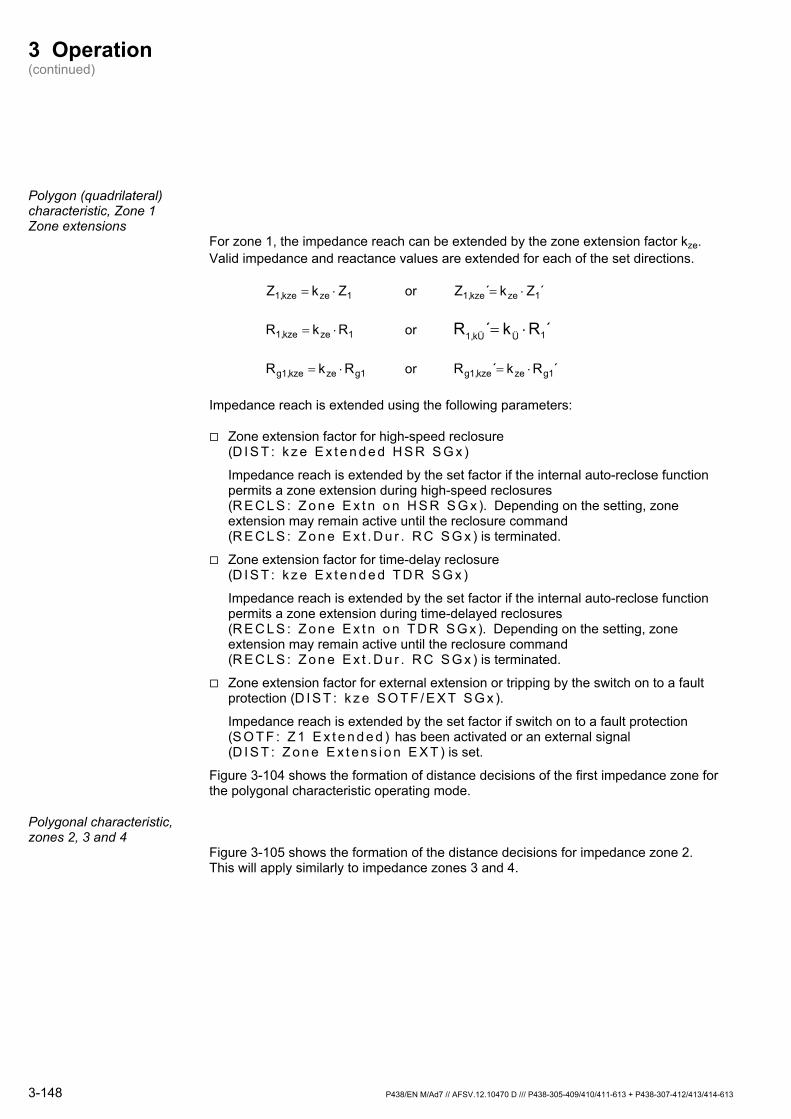
3 Operation (continued)
Polygon (quadrilateral) characteristic, Zone 1 Zone extensions
For zone 1, the impedance reach can be extended by the zone extension factor kze. Valid impedance and reactance values are extended for each of the set directions.
1zekze1, ZkZ ⋅= or ´Zk´Z 1zekze1, ⋅=
1zekze1, RkR ⋅= or ´Rk´R 1ÜkÜ1, ⋅=
g1zekzeg1, RkR ⋅= or ´Rk´R g1zekzeg1, ⋅=
Impedance reach is extended using the following parameters:
Zone extension factor for high-speed reclosure (D I S T : k z e E x t e n d e d H S R S G x )
Impedance reach is extended by the set factor if the internal auto-reclose function permits a zone extension during high-speed reclosures (R E C L S : Z o n e E x t n o n H S R S G x ). Depending on the setting, zone extension may remain active until the reclosure command (R E C L S : Z o n e E x t . D u r . R C S G x ) is terminated.
Zone extension factor for time-delay reclosure (D I S T : k z e E x t e n d e d T D R S G x )
Impedance reach is extended by the set factor if the internal auto-reclose function permits a zone extension during time-delayed reclosures (R E C L S : Z o n e E x t n o n T D R S G x ). Depending on the setting, zone extension may remain active until the reclosure command (R E C L S : Z o n e E x t . D u r . R C S G x ) is terminated.
Zone extension factor for external extension or tripping by the switch on to a fault protection (D I S T : k z e S O T F / E X T S G x ).
Impedance reach is extended by the set factor if switch on to a fault protection (S O T F : Z 1 E x t e n d e d ) has been activated or an external signal (D I S T : Z o n e E x t e n s i o n E X T ) is set.
Figure 3-104 shows the formation of distance decisions of the first impedance zone for the polygonal characteristic operating mode.
Polygonal characteristic, zones 2, 3 and 4
Figure 3-105 shows the formation of the distance decisions for impedance zone 2. This will apply similarly to impedance zones 3 and 4.
3-148 P438/EN M/Ad7 // AFSV.12.10470 D /// P438-305-409/410/411-613 + P438-307-412/413/414-613
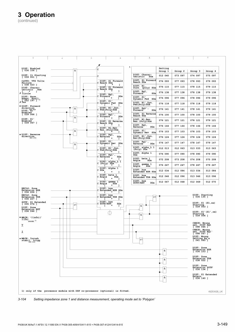
3 Operation (continued)
48Z6342B_UK
DIST: Enabled[ 036 104 ] C
DIST: Z1 Forward Reach SGx
[ * ]C
DIST: Rg1, Forward SGx
[ * ]C
DIST: Z1' Dynamic Fwd SGx
[ * ]C
DIST: Rg1', Forward SGx
[ * ]C
DIST: Z1 Reverse Reach SGx
[ * ]C
DIST: Rg1, Reverse SGx
[ * ]C
DIST: Z1' Dynamic Rev SGx
[ * ]C
DIST: Rg1', Reverse SGx
[ * ]C
DIST: Alpha 1 SGx
[ * ]C
DIST: beta 1 Angle SGx
[ * ]C
DIST: gamma 1 Angle SGx
[ * ]C
DIST: kze Extended HSR SGx
[ * ]C
C
DIST: kze Extended TDR SGx
[ * ]C
DIST: kze SOTF/EXT SGx
[ * ]C
DIST: I> Starting[ 039 001 ]
DIST: Charac-teristic SGx[ * ]Circle
C&VTS: VTS Volts Failure [ 038 023 ]
DIST: Harm. Adapt. Avail. [ 022 197 ] 1)Yes
DIST: Forward direction
303 669DIST: Z1 Enabled[ 039 066 ]
DIST: Z1' Enabled[ 039 067 ]
DIST: Reverse direction
303 670
012 040DIST: Charac-teristic SGx
DIST: Z1 Forward Reach SGx
DIST: Rg1, Forward SGx
DIST: Z1' Dynamic Fwd SGx
DIST: Rg1', Forward SGx
DIST: Z1 Reverse Reach SGx
DIST: Rg1, Reverse SGx
DIST: Z1' Dynamic Rev SGx
DIST: Rg1', Reverse SGx
DIST: Alpha 1 SGx
DIST: beta 1 Angle SGx
DIST: gamma 1 Angle SGx
DIST: kze Extended HSR SGx
DIST: kze Extended TDR SGx
DIST: kze SOTF/EXT SGx
073 097 074 097 075 097
SettingGroup 1 Group 2 Group 3 Group 4
RECLS: Zone Extension HSR[ 036 226 ]RECLS: Zone Extension TDR[ 036 227 ]SOTF: Z1 Extended[ 035 076 ]DIST: Zone Extension EXT[ 036 046 ]
V
I
MAIN: Inrush stabil. trigg
306 014
DIST: Z1 ExtendedExtern.[ 036 140 ]
DIST: Zone Extension SOTF[ 036 134 ]
DIST: Zone Extension TDR[ 038 022 ]
DIST: Zone Extension HSR[ 036 103 ]
CHECK: Wrong set. DIST Rg1'[ 098 047 ]
CHECK: Wrong set. DIST Rg1[ 098 046 ]
DIST: Wrong Setting Rg,x [ 041 085 ]
DIST: Z1 (Z1,ze)Starting[ 039 003 ]
DIST: Z1'(Z1',ze)Starting[ 039 004 ]
076 093 077 093 078 093 079 093
076 138 077 138 078 138 079 138
076 096 077 096 078 096 079 096
076 141 077 141 078 141 079 141
076 100 077 100 078 100 079 100
076 144 077 144 078 144 079 144
076 103 077 103 078 103 079 103
076 147 077 147 078 147 079 147
076 090 077 090 078 090 079 090
072 208 073 208 074 208 075 208
076 247 077 247 078 247 079 247
012 034 012 084 013 034 013 084
012 046 012 096 013 046 013 096
012 067 012 068 012 069 012 070
1) only if the processor module with DSP co-processor (optional) is fitted.
DIST: Starting[ 036 135 ]
DIST: Z1 Forward Reach SGx
[ * ]C
DIST: R1',Dyn. Fwd(Poly)SGx
[ * ]C
DIST: R1,Rev. Res.(Poly)SGx
[ * ]C
DIST: R1',Dyn. Fwd(Poly)SGx
[ * ]C
DIST: alpha_L 1 (Poly) SGx
[ * ]C
DIST: R1,forw. (poly) SGx 076 115 077 115 078 115 079 115
DIST: R1',Dyn. Fwd(Poly)SGx 076 118 077 118 078 118 079 118
DIST: R1,Rev. Res.(Poly)SGx 076 121 077 121 078 121 079 121
DIST: R1',Dyn. Rev(Poly)SGx 076 124 077 124 078 124 079 124
DIST: alpha_L 1 (Poly) SGx 012 013 012 063 013 033 013 063
MAIN: I(xfn)/I(fn)
310 053 1)
&
&
&
&
&
&
&
&
&
&
&
*
3-104 Setting impedance zone 1 and distance measurement, operating mode set to ‘Polygon’
P438/UK M/Ae7 // AFSV.12.11060 EN /// P438-305-409/410/411-615 + P438-307-412/413/414-615 3-149
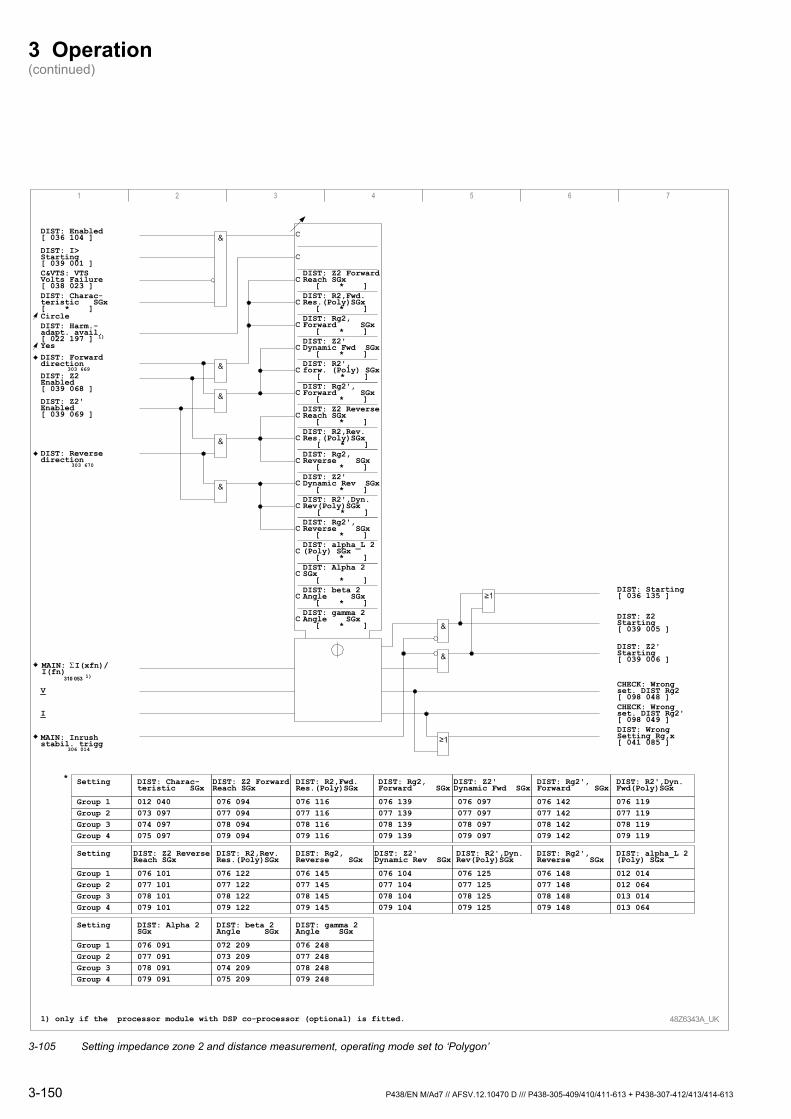
3 Operation (continued)
1 2 3 4 5 6 7
48Z6343A_UK
DIST: Enabled[ 036 104 ] C
C
C
C
DIST: I>Starting[ 039 001 ]
DIST: Charac-teristic SGx[ * ]Circle
C&VTS: VTSVolts Failure[ 038 023 ]
DIST: Harm.-adapt. avail.[ 022 197 ] 1)YesDIST: Forwarddirection
303 669DIST: Z2Enabled[ 039 068 ]
DIST: Z2'Enabled[ 039 069 ]
DIST: Reversedirection
303 670
V
I
MAIN: Inrushstabil. trigg
306 014
CHECK: Wrongset. DIST Rg2'[ 098 049 ]
CHECK: Wrongset. DIST Rg2[ 098 048 ]
DIST: WrongSetting Rg,x[ 041 085 ]
DIST: Z2Starting[ 039 005 ]
DIST: Z2'Starting[ 039 006 ]
1) only if the processor module with DSP co-processor (optional) is fitted.
DIST: Starting[ 036 135 ]
Group 1Group 2
012 040
DIST: Charac-teristic SGx
073 097074 097075 097
Group 3Group 4
Setting
076 139
DIST: Rg2,Forward SGx
077 139078 139079 139
076 097
DIST: Z2'Dynamic Fwd SGx
077 097078 097079 097
076 094
DIST: Z2 ForwardReach SGx
077 094078 094079 094
076 142
DIST: Rg2',Forward SGx
077 142078 142079 142
076 101
DIST: Z2 ReverseReach SGx
077 101078 101079 101
Group 1Group 2Group 3Group 4
Setting
076 091
DIST: Alpha 2SGx
077 091078 091079 091
072 209
DIST: beta 2Angle SGx
073 209074 209075 209
076 248
DIST: gamma 2Angle SGx
077 248078 248079 248
C
C
C
C
C
C
C
C
C
DIST: R2,Fwd.Res.(Poly)SGx
[ * ]C
DIST: R2',forw. (Poly) SGx
[ * ]C
DIST: R2,Rev.Res.(Poly)SGx
[ * ]C
DIST: R2',Dyn.Rev(Poly)SGx
[ * ]C
C
Group 1Group 2Group 3Group 4
Setting
076 116
DIST: R2,Fwd.Res.(Poly)SGx
077 116078 116079 116
076 119
DIST: R2',Dyn.Fwd(Poly)SGx
077 119078 119079 119
076 145
DIST: Rg2,Reverse SGx
077 145078 145079 145
076 148
DIST: Rg2',Reverse SGx
077 148078 148079 148
076 104
DIST: Z2'Dynamic Rev SGx
077 104078 104079 104
076 122
DIST: R2,Rev.Res.(Poly)SGx
077 122078 122079 122
076 125
DIST: R2',Dyn.Rev(Poly)SGx
077 125078 125079 125
012 014
DIST: alpha_L 2(Poly) SGx
012 064013 014013 064
MAIN: I(xfn)/I(fn)
310 053 1)
Σ
&
&
&
&
&
&
&
*
DIST: Alpha 2SGx
[ * ]DIST: beta 2Angle SGx
[ * ]DIST: gamma 2Angle SGx
[ * ]
DIST: Z2 ForwardReach SGx
[ * ]
DIST: Rg2,Forward SGx
[ * ]DIST: Z2'Dynamic Fwd SGx
[ * ]
DIST: Rg2',Forward SGx
[ * ]DIST: Z2 ReverseReach SGx
[ * ]
DIST: Rg2,Reverse SGx
[ * ]DIST: Z2'Dynamic Rev SGx
[ * ]
DIST: Rg2',Reverse SGx
[ * ]DIST: alpha_L 2(Poly) SGx
[ * ]
3-105 Setting impedance zone 2 and distance measurement, operating mode set to ‘Polygon’
3-150 P438/EN M/Ad7 // AFSV.12.10470 D /// P438-305-409/410/411-613 + P438-307-412/413/414-613
3 Operation (continued)
Distance measurement If the base point current is exceeded, the inductive and resistive components (X and R) of the loop impedance (Z) are calculated continuously even during normal operation. The algorithm is based on solving the first-order line differential equation according to "Bonard-Bastide".
The X and R components are calculated from the 0.5 ms instantaneous values of current and voltage and updated every 2 ms.
In the event of a line fault there is the danger of a transient overreach and an incorrect angle measurement since the measured impedance can be lower than the static fault impedance for a period longer than a cycle.
In order to avoid unwanted operation or failure to operate, the following optimization measures have been implemented in the distance protection system so as to ensure stable operation:
Monitoring the Current and Voltage Values: The RMS values of current and voltage are monitored for a sudden increase or decrease. Any such change is regarded as occurrence of a fault and a dead time is started.
Monitoring of the current for a sudden step increase: For I ≤ 0.25 In: ΔI = 0.1 In For I > 0.25 In: ΔI = 0.17 I
Monitoring of the voltage for a sudden step decrease: For V < 0.5 Vn: ΔV = 0.1 Vn For V ≥ 0.5 Vn: ΔV = 0.06 V
Dead time for a setting of tZ1 = 0 s: For I < 0.75 In: 53 ms For 0.75 In < I < 3.5 In: 32 ms For I > 3.5 In: 28 ms For a setting of tZ1 > 0 s, the dead time is 45 ms.
Impedance measurements taken during the dead time are rejected. Impedance measurements taken after the end of the dead time are valid. These measures ensure the selectivity of impedance and direction for any zones with zero, or short applied time delays.
Switching on to a Line Without Voltage: In this event, impedance measurement can temporarily yield undefined measured values. In order to avoid unwanted tripping, the impedance comparison is interrupted for 75 ms after a voltage rise above a threshold value voltage of 0.008 Vn. After this period of 75 ms, the voltage gradient must have fallen to less than 3 %. If this is not the case, the dead time is extended until the voltage gradient falls below this value.
P438/EN M/Ad7 // AFSV.12.10470 D /// P438-305-409/410/411-613 + P438-307-412/413/414-613 3-151
3 Operation (continued)
Isolation of a Line: When a faulty or healthy line is isolated externally, the impedance measurement can also temporarily yield undefined values. The danger of an unwanted tripping is eliminated by a special di/dt stage that will block distance measurement if a negative current gradient of approx. 8 % within a half-cycle occurs with a simultaneous voltage drop (breaker open blocking).
These optimization measures provide stable operation of the device in normal operation of the installation.
The distance measurement system exhibits the following time response:
For a timer stage setting of tZ1 = 0 s, the trip command times in zone 1 are approx. 1.5 cycles in the 'core region'. For the P438, the 'core region' is defined as 0 to 95 % of the set tripping area.
Outside the 'core region', the trip times are longer. For fault currents < 0.8 In the calculation window is extended to achieve a stable response.
3-152 P438/EN M/Ad7 // AFSV.12.10470 D /// P438-305-409/410/411-613 + P438-307-412/413/414-613
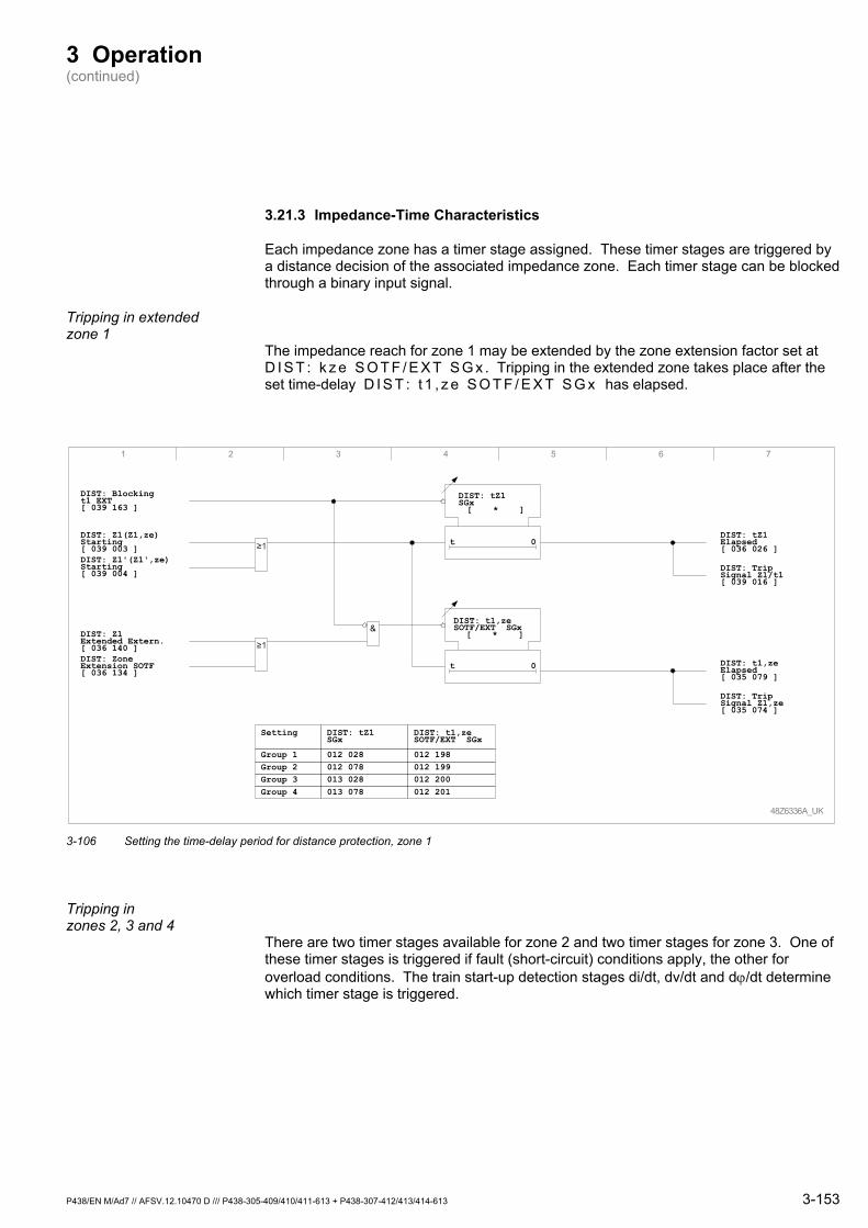
3 Operation (continued)
3.21.3 Impedance-Time Characteristics
Each impedance zone has a timer stage assigned. These timer stages are triggered by a distance decision of the associated impedance zone. Each timer stage can be blocked through a binary input signal.
Tripping in extended zone 1
The impedance reach for zone 1 may be extended by the zone extension factor set at D I S T : k z e S O T F / E X T S G x . Tripping in the extended zone takes place after the set time-delay D I S T : t 1 , z e S O T F / E X T S G x has elapsed.
1 2 3 4 5 6 7
48Z6336A_UK
DIST: tZ1 Elapsed[ 036 026 ]
DIST: tZ1SGx[ * ]
DIST: Blocking t1 EXT[ 039 163 ]
t 0
DIST: Trip Signal Z1/t1[ 039 016 ]
DIST: t1,ze SOTF/EXT SGx
[ * ]
t 0
DIST: Z1 Extended Extern.[ 036 140 ]DIST: Zone Extension SOTF[ 036 134 ]
DIST: Z1(Z1,ze) Starting[ 039 003 ]DIST: Z1'(Z1',ze)Starting[ 039 004 ]
DIST: t1,ze Elapsed[ 035 079 ]
DIST: Trip Signal Z1,ze[ 035 074 ]
Group 1Group 2
012 028
DIST: tZ1SGx
012 078013 028013 078
Group 3Group 4
Setting
012 198
DIST: t1,ze SOTF/EXT SGx
012 199012 200012 201
&
3-106 Setting the time-delay period for distance protection, zone 1
Tripping in zones 2, 3 and 4
There are two timer stages available for zone 2 and two timer stages for zone 3. One of these timer stages is triggered if fault (short-circuit) conditions apply, the other for overload conditions. The train start-up detection stages di/dt, dv/dt and dϕ/dt determine which timer stage is triggered.
P438/EN M/Ad7 // AFSV.12.10470 D /// P438-305-409/410/411-613 + P438-307-412/413/414-613 3-153
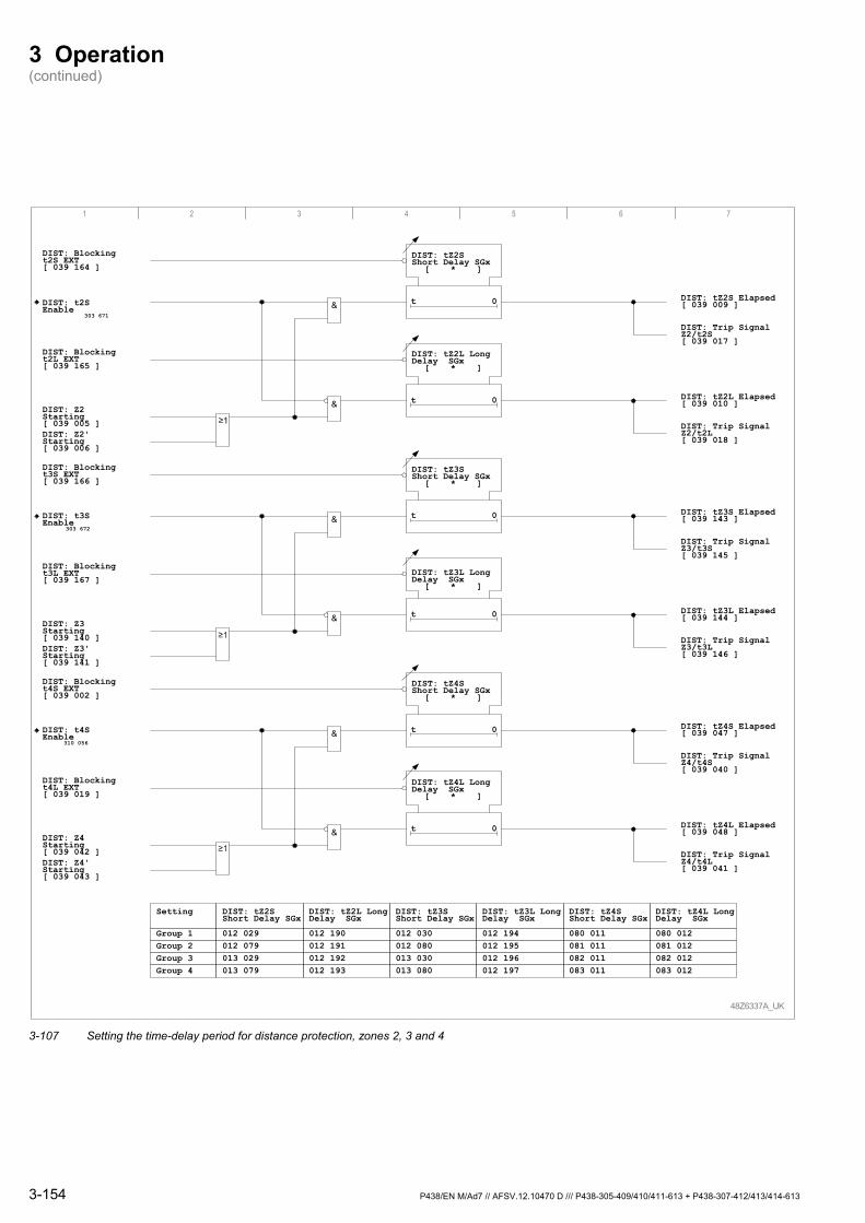
3 Operation (continued)
1 2 3 4 5 6 7
48Z6337A_UK
DIST: Blockingt2S EXT[ 039 164 ]
t 0
DIST: Blockingt2L EXT[ 039 165 ]
t 0DIST: Z2Starting[ 039 005 ]DIST: Z2'Starting[ 039 006 ]
DIST: tZ2S Elapsed[ 039 009 ]
DIST: Trip SignalZ2/t2S[ 039 017 ]
DIST: tZ2L Elapsed[ 039 010 ]
DIST: Trip SignalZ2/t2L[ 039 018 ]
DIST: t2SEnable
303 671
DIST: Blockingt3S EXT[ 039 166 ]
t 0
DIST: Blockingt3L EXT[ 039 167 ]
t 0DIST: Z3Starting[ 039 140 ]DIST: Z3'Starting[ 039 141 ]
DIST: tZ3S Elapsed[ 039 143 ]
DIST: Trip SignalZ3/t3S[ 039 145 ]
DIST: tZ3L Elapsed[ 039 144 ]
DIST: Trip SignalZ3/t3L[ 039 146 ]
DIST: t3SEnable
303 672
DIST: Blockingt4S EXT[ 039 002 ]
t 0
DIST: Blockingt4L EXT[ 039 019 ]
t 0DIST: Z4Starting[ 039 042 ]DIST: Z4'Starting[ 039 043 ]
DIST: tZ4S Elapsed[ 039 047 ]
DIST: Trip SignalZ4/t4S[ 039 040 ]
DIST: tZ4L Elapsed[ 039 048 ]
DIST: Trip SignalZ4/t4L[ 039 041 ]
DIST: t4SEnable
310 056
Group 1Group 2
012 029
DIST: tZ2SShort Delay SGx
012 079013 029013 079
Group 3Group 4
Setting
012 190
DIST: tZ2L LongDelay SGx
012 191012 192012 193
012 030
DIST: tZ3SShort Delay SGx
012 080013 030013 080
012 194
DIST: tZ3L LongDelay SGx
012 195012 196012 197
080 011
DIST: tZ4SShort Delay SGx
081 011082 011083 011
080 012
DIST: tZ4L LongDelay SGx
081 012082 012083 012
&
&
&
&
&
&
DIST: tZ2SShort Delay SGx
[ * ]
DIST: tZ2L LongDelay SGx
[ * ]
DIST: tZ3SShort Delay SGx
[ * ]
DIST: tZ3L LongDelay SGx
[ * ]
DIST: tZ4SShort Delay SGx
[ * ]
DIST: tZ4L LongDelay SGx
[ * ]
3-107 Setting the time-delay period for distance protection, zones 2, 3 and 4
3-154 P438/EN M/Ad7 // AFSV.12.10470 D /// P438-305-409/410/411-613 + P438-307-412/413/414-613
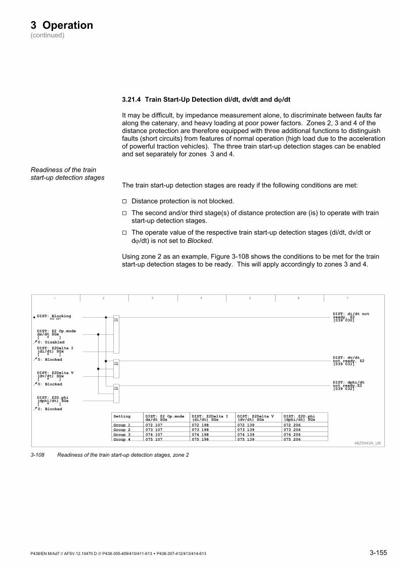
3 Operation (continued)
3.21.4 Train Start-Up Detection di/dt, dv/dt and dϕ/dt
It may be difficult, by impedance measurement alone, to discriminate between faults far along the catenary, and heavy loading at poor power factors. Zones 2, 3 and 4 of the distance protection are therefore equipped with three additional functions to distinguish faults (short circuits) from features of normal operation (high load due to the acceleration of powerful traction vehicles). The three train start-up detection stages can be enabled and set separately for zones 3 and 4.
Readiness of the train start-up detection stages
The train start-up detection stages are ready if the following conditions are met:
Distance protection is not blocked.
The second and/or third stage(s) of distance protection are (is) to operate with train start-up detection stages.
The operate value of the respective train start-up detection stages (di/dt, dv/dt or dϕ/dt) is not set to Blocked.
Using zone 2 as an example, Figure 3-108 shows the conditions to be met for the train start-up detection stages to be ready. This will apply accordingly to zones 3 and 4.
>1
DIST: di/dt notready, Z2[039 030]
DIST: dv/dtnot ready, Z2[039 031]
DIST: dphi/dtnot ready,Z2[039 032]
>1
>1
DIST: Z2 Op.modedx/dt SGx[ * ]0: Disabled
DIST: Blocking303 667
DIST: Z2Delta I(di/dt) SGx[ * ]0: Blocked
DIST: Z2Delta V(dv/dt) SGx[ * ]0: Blocked
DIST: Z2D.phi(dphi/dt) SGx[ * ]0: Blocked
Setting
Group 1Group 2Group 3Group 4
DIST: Z2Delta I(di/dt) SGx072 198073 198074 198075 198
DIST: Z2 Op.modedx/dt SGx072 107073 107074 107075 107
DIST: Z2Delta V(dv/dt) SGx072 139073 139074 139075 139
DIST: Z2D.phi(dphi/dt) SGx072 206073 206074 206075 206
48Z5443A_UK 3-108 Readiness of the train start-up detection stages, zone 2
P438/EN M/Ad7 // AFSV.12.10470 D /// P438-305-409/410/411-613 + P438-307-412/413/414-613 3-155

3 Operation (continued)
Operation of the train start-up detection stages
The maximum change in measured values D e l t a I , D e l t a U and D e l t a ϕ during sampling intervals D e l t a t = 9 0 m s can be set separately for zones 2, 3 and 4. A short circuit is detected if the following conditions are met during a sampling interval:
The current rises by more than the set D e l t a I AND/OR
The voltage falls by more than the set D e l t a V AND/OR
The angle changes by more than the set D e l t a ϕ and the current has exceeded a 0.2 Inom threshold.
The P438 user can select by setting whether all three criteria (AND operation) or just one criterion (OR operation) must be met for a short-circuit detection. If not all the criteria are used, the P438 will set outputs of the blocked stages according to the operation selected such that a switch between overload and short-circuit mode can be effected by the remaining stages, as required. If all three delta criteria are set to Blocked, short time-delays tZ2S, tZ3S or tZ4S are always used regardless of the operation criteria (WITHOUT, OR, AND).
If a short-circuit is detected, short time-delays tZ2S, tZ3S or tZ4S are used; if an overload is detected, long time-delays tZ2L, tZ3L or tZ4L are used. If no dx/dt stage is enabled, time delays tZ2S, tZ3S or tZ4S are always used.
The dx/dt decisions remain stored for the duration of the distance protection start.
Figure 3-109 shows the operation of the train start-up detection stages, using zone 2 as an example. This will apply similarly to zones 3 and 4.
3-156 P438/EN M/Ad7 // AFSV.12.10470 D /// P438-305-409/410/411-613 + P438-307-412/413/414-613
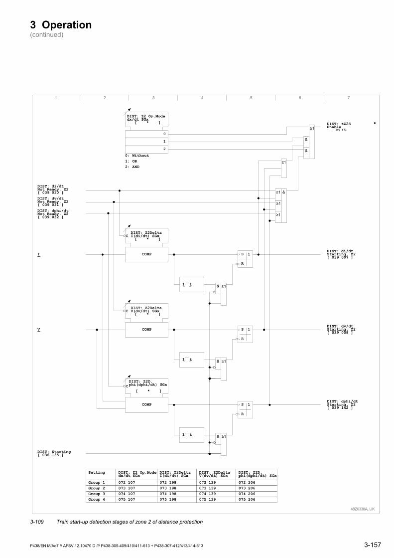
3 Operation (continued)
1 2 3 4 5 6 7
48Z6338A_UK
DIST: Z2Delta I(di/dt) SGx[ * ]
DIST: di/dt Not Ready, Z2 [ 039 030 ]
COMP
Group 1Group 2
072 107
DIST: Z2 Op.Modedx/dt SGx
073 107074 107075 107
Group 3Group 4
Setting
072 198
DIST: Z2Delta I(di/dt) SGx
073 198074 198075 198
072 139
DIST: Z2Delta V(dv/dt) SGx
073 139074 139075 139
072 206
DIST: Z2D.phi(dphi/dt) SGx
073 206074 206075 206
S
R
1
1 t
DIST: Z2 Op.Modedx/dt SGx
[ * ]
1
0: Without
2
1: OR
C
0
2: AND
DIST: dv/dt Not Ready, Z2[ 039 031 ]DIST: dphi/dt Not Ready, Z2[ 039 032 ]
DIST: Z2Delta V(dv/dt) SGx[ * ]
COMP S
R
1
C
I
V
DIST: tZ2SEnable
303 671
DIST: di/dt Starting, Z2[ 039 007 ]
DIST: dv/dt Starting, Z2[ 039 008 ]
DIST: Z2D.phi(dphi/dt) SGx
[ * ]
COMP S
R
1
C
DIST: dphi/dt Starting, Z2[ 039 142 ]
DIST: Starting[ 036 135 ]
&
&
&
&
&
&
1 t
1 t
3-109 Train start-up detection stages of zone 2 of distance protection
P438/EN M/Ad7 // AFSV.12.10470 D /// P438-305-409/410/411-613 + P438-307-412/413/414-613 3-157
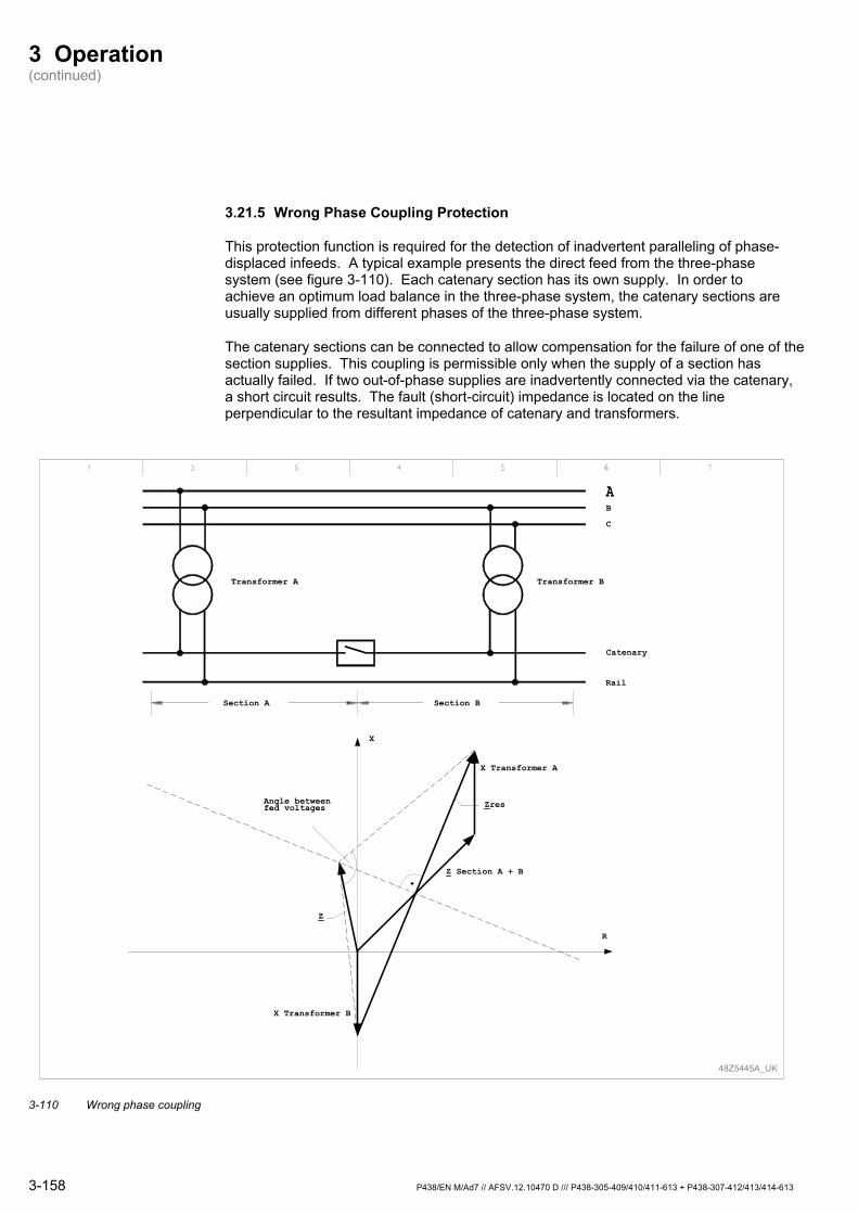
3 Operation (continued)
3.21.5 Wrong Phase Coupling Protection
This protection function is required for the detection of inadvertent paralleling of phase-displaced infeeds. A typical example presents the direct feed from the three-phase system (see figure 3-110). Each catenary section has its own supply. In order to achieve an optimum load balance in the three-phase system, the catenary sections are usually supplied from different phases of the three-phase system.
The catenary sections can be connected to allow compensation for the failure of one of the section supplies. This coupling is permissible only when the supply of a section has actually failed. If two out-of-phase supplies are inadvertently connected via the catenary, a short circuit results. The fault (short-circuit) impedance is located on the line perpendicular to the resultant impedance of catenary and transformers.
48Z5445A_UK
Angle betweenfed voltages
R
X
Z Section A + B
Zres
X Transformer A
X Transformer B
Catenary
Rail
Transformer BTransformer A
Section A Section B
AB
C
Z
3-110 Wrong phase coupling
3-158 P438/EN M/Ad7 // AFSV.12.10470 D /// P438-305-409/410/411-613 + P438-307-412/413/414-613
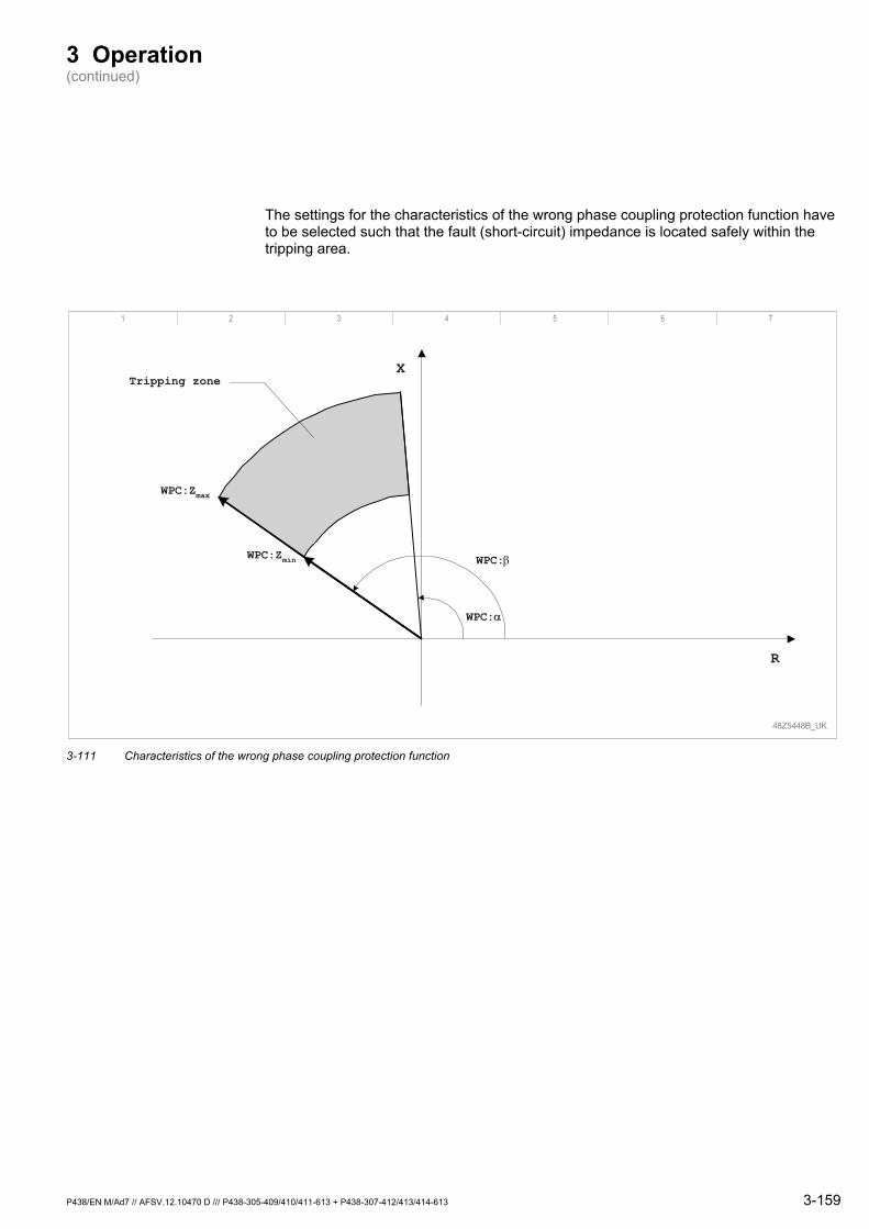
3 Operation (continued)
The settings for the characteristics of the wrong phase coupling protection function have to be selected such that the fault (short-circuit) impedance is located safely within the tripping area.
1 2 3 4 5 6 7
48Z5448B_UK
X
WPC:α
Tripping zone
R
WPC:Zmax
WPC:WPC:Zmin β
3-111 Characteristics of the wrong phase coupling protection function
P438/EN M/Ad7 // AFSV.12.10470 D /// P438-305-409/410/411-613 + P438-307-412/413/414-613 3-159
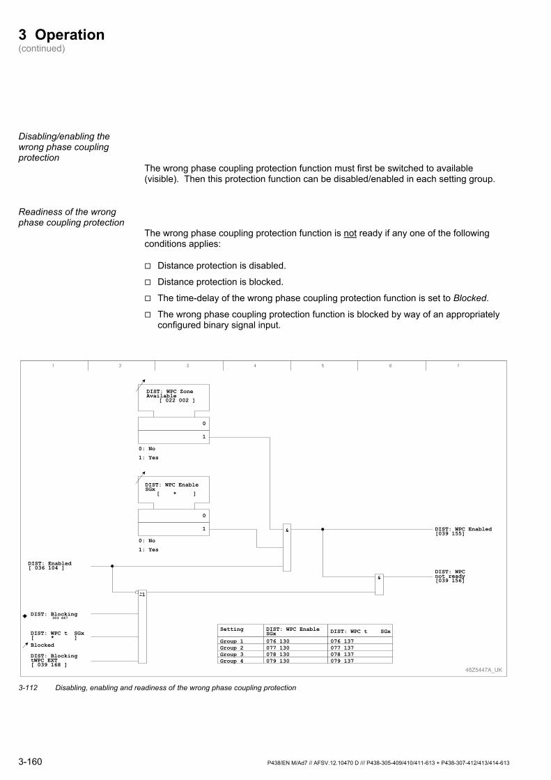
3 Operation (continued)
Disabling/enabling the wrong phase coupling protection
The wrong phase coupling protection function must first be switched to available (visible). Then this protection function can be disabled/enabled in each setting group.
Readiness of the wrong phase coupling protection
The wrong phase coupling protection function is not ready if any one of the following conditions applies:
Distance protection is disabled.
Distance protection is blocked.
The time-delay of the wrong phase coupling protection function is set to Blocked.
The wrong phase coupling protection function is blocked by way of an appropriately configured binary signal input.
DIST: Enabled[ 036 104 ]
DIST: WPC Enabled[039 155]
DIST: WPC ZoneAvailable
[ 022 002 ]
0
1
0: No
1: Yes
&
DIST: WPC EnableSGx
[ * ]
0
1
0: No
1: Yes
DIST: Blocking303 667
Blocked
DIST: WPC t SGx[ * ]
DIST: BlockingtWPC EXT[ 039 168 ]
>1
DIST: WPCnot ready[039 156]&
48Z5447A_UK
Setting
Group 1Group 2Group 3Group 4
DIST: WPC EnableSGx076 130077 130078 130079 130
DIST: WPC t SGx
076 137077 137078 137079 137
3-112 Disabling, enabling and readiness of the wrong phase coupling protection
3-160 P438/EN M/Ad7 // AFSV.12.10470 D /// P438-305-409/410/411-613 + P438-307-412/413/414-613
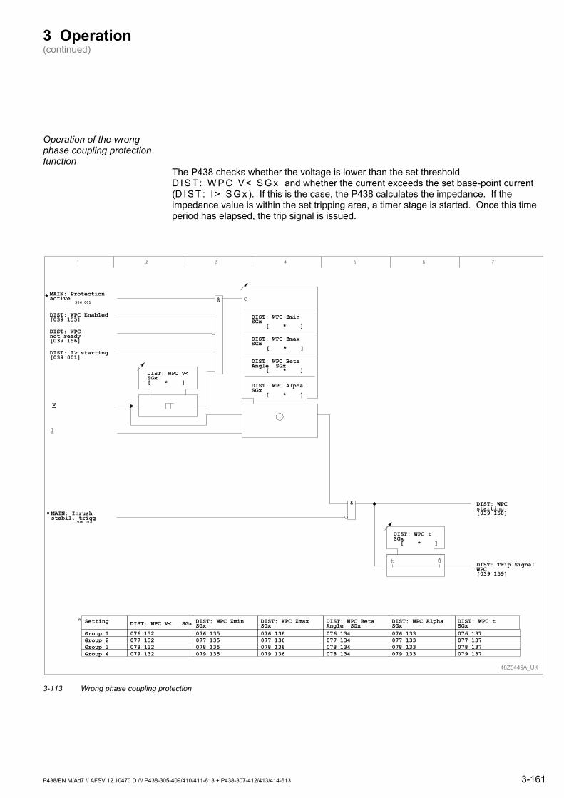
3 Operation (continued)
Operation of the wrong phase coupling protection function
The P438 checks whether the voltage is lower than the set threshold D I S T : W P C V < S G x and whether the current exceeds the set base-point current (D I S T : I > S G x ). If this is the case, the P438 calculates the impedance. If the impedance value is within the set tripping area, a timer stage is started. Once this time period has elapsed, the trip signal is issued.
MAIN: Protectionactive
306 001
&
MAIN: Inrushstabil. trigg
306 014
48Z5449A_UK
Setting
Group 1Group 2Group 3Group 4
DIST: WPC ZmaxSGx076 136077 136078 136079 136
DIST: WPC ZminSGx076 135077 135078 135079 135
DIST: WPC V< SGx
076 132077 132078 132079 132
DIST: WPC BetaAngle SGx076 134077 134078 134078 134
DIST: WPC AlphaSGx076 133077 133078 133079 133
DIST: WPC tSGx076 137077 137078 137079 137
DIST: WPC V<SGx[ * ] DIST: WPC Alpha
SGx[ * ]
DIST: WPC BetaAngle SGx
[ * ]
DIST: WPC ZminSGx
[ * ]
DIST: WPC ZmaxSGx
[ * ]
DIST: WPC tSGx[ * ]
DIST: WPCstarting[039 158]
DIST: Trip SignalWPC[039 159]
DIST: WPC Enabled[039 155]
DIST: WPCnot ready[039 156]
DIST: I> starting[039 001]
V
3-113 Wrong phase coupling protection
P438/EN M/Ad7 // AFSV.12.10470 D /// P438-305-409/410/411-613 + P438-307-412/413/414-613 3-161

3 Operation (continued)
3.21.6 Multiple Signaling of Distance Protection
The starting and trip signals generated by the distance protection function are grouped together to form multiple (composite) signals.
1 2 3 4 5 6 7
48Z6339A_EN
DIST: Z1 (Z1,ze)starting[ 039 003 ]DIST: Z2starting[ 039 005 ]
DIST: Starting[ 036 135 ]
DIST: Z3starting[ 039 140 ]DIST: Z4startingn[ 039 042 ]DIST: Z1'(Z1',ze) starting[ 039 004 ]DIST: Z2'starting[ 039 006 ]DIST: Z3'starting[ 039 141 ]DIST: Z4'starting[ 039 043 ]DIST: WPCstarting[ 039 158 ]
3-114 Starting signals of distance protection
1 2 3 4 5 6 7
48Z6340A_EN
DIST: Trip signalZ1/t1[ 039 016 ]DIST: Trip signalZ1,ze[ 039 074 ]
DIST: Starting[ 036 135 ]
DIST: Trip signalZ2/t2S[ 039 017 ]DIST: Trip signalZ2/t2L[ 039 018 ]DIST: Trip signalZ3/t3S[ 039 145 ]DIST: Trip signalZ3/t3L[ 039 146 ]DIST: Trip signalZ4/t4S[ 039 040 ]DIST: Trip signalZ4/t4L[ 039 041 ]DIST: Trip signalWPC[ 039 159 ]
3-115 Trip signal of distance protection
3-162 P438/EN M/Ad7 // AFSV.12.10470 D /// P438-305-409/410/411-613 + P438-307-412/413/414-613
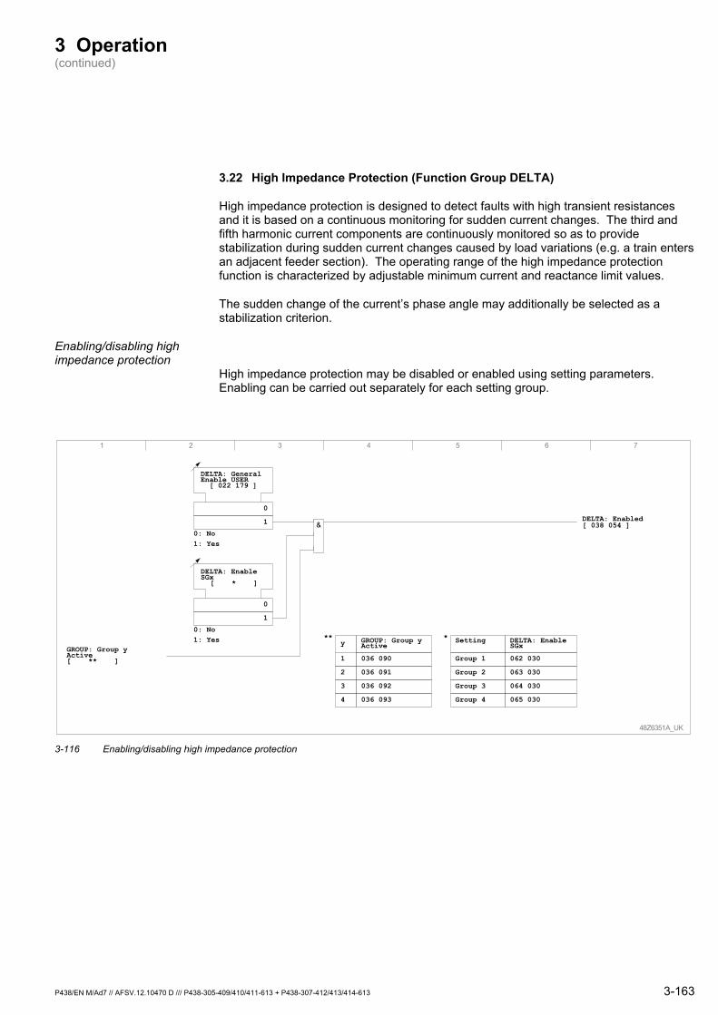
3 Operation (continued)
P438/EN M/Ad7 // AFSV.12.10470 D /// P438-305-409/410/411-613 + P438-307-412/413/414-613 3-163
3.22 High Impedance Protection (Function Group DELTA)
High impedance protection is designed to detect faults with high transient resistances and it is based on a continuous monitoring for sudden current changes. The third and fifth harmonic current components are continuously monitored so as to provide stabilization during sudden current changes caused by load variations (e.g. a train enters an adjacent feeder section). The operating range of the high impedance protection function is characterized by adjustable minimum current and reactance limit values.
The sudden change of the current’s phase angle may additionally be selected as a stabilization criterion.
Enabling/disabling high impedance protection
High impedance protection may be disabled or enabled using setting parameters. Enabling can be carried out separately for each setting group.
48Z6351A_UK
DELTA: General Enable USER[ 022 179 ]
0
1
0: No1: Yes
DELTA: EnableSGx
[ * ]
0
1
0: No1: Yes
GROUP: Group yActive[ ** ]
DELTA: Enabled[ 038 054 ]
1 2 3 4 5 6 7
1
y
2
3
4
036 090
GROUP: Group yActive
036 091
036 092
036 093
Group 1
Group 2
062 030
DELTA: Enable SGx
063 030
064 030
065 030
Group 3
Group 4
Setting
&
** *
3-116 Enabling/disabling high impedance protection
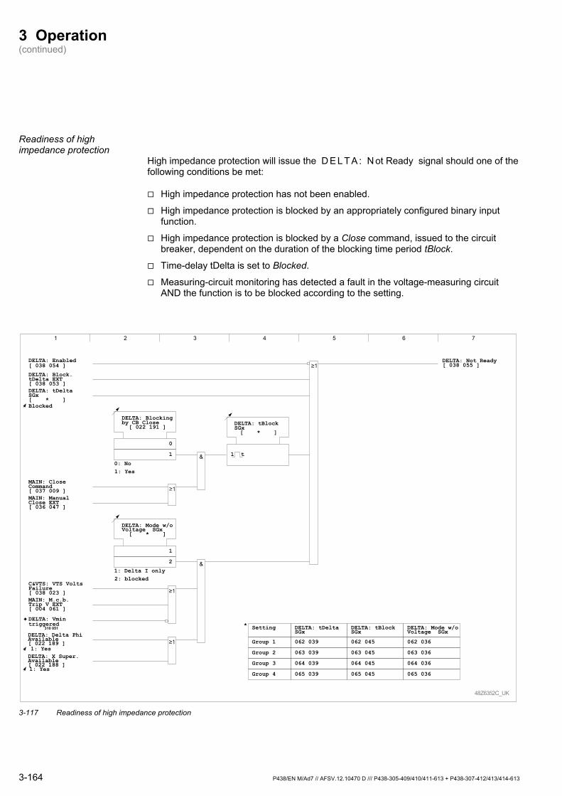
3 Operation (continued)
3-164 P438/EN M/Ad7 // AFSV.12.10470 D /// P438-305-409/410/411-613 + P438-307-412/413/414-613
Readiness of high impedance protection
High impedance protection will issue the D E L T A : N ot Ready signal should one of the following conditions be met:
High impedance protection has not been enabled.
High impedance protection is blocked by an appropriately configured binary input function.
High impedance protection is blocked by a Close command, issued to the circuit breaker, dependent on the duration of the blocking time period tBlock.
Time-delay tDelta is set to Blocked.
Measuring-circuit monitoring has detected a fault in the voltage-measuring circuit AND the function is to be blocked according to the setting.
DELTA: Not Ready[ 038 055 ]
DELTA: Block. tDelta EXT[ 038 053 ]
1 2 3 4 5 6 7
C&VTS: VTS VoltsFailure[ 038 023 ]
DELTA: Enabled[ 038 054 ]
Group 1
Group 2
Group 3
Group 4
Setting
48Z6352C_UK
DELTA: tDelta SGx[ * ]Blocked
062 045
DELTA: tBlock SGx
063 045
064 045
065 045
MAIN: M.c.b. Trip V EXT[ 004 061 ]
DELTA: Mode w/oVoltage SGx
[ * ]
1
2
1: Delta I only2: blocked
DELTA: Blocking by CB Close
[ 022 191 ]
0
1
0: No1: Yes
MAIN: Close Command[ 037 009 ]MAIN: Manual Close EXT[ 036 047 ]
DELTA: tBlock SGx[ * ]
1 t
062 036
DELTA: Mode w/oVoltage SGx
063 036
064 036
065 036
DELTA: Vmin triggered
310 051
062 039
DELTA: tDelta SGx
063 039
064 039
065 039
&
&
*
DELTA: Delta PhiAvailable [ 022 189 ]1: YesDELTA: X Super. Available[ 022 188 ]1: Yes
3-117 Readiness of high impedance protection
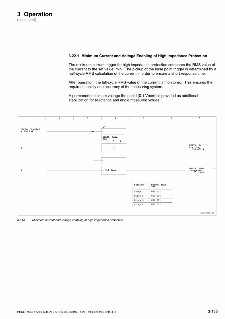
3 Operation (continued)
P438/EN M/Ad7 // AFSV.12.10470 D /// P438-305-409/410/411-613 + P438-307-412/413/414-613 3-165
3.22.1 Minimum Current and Voltage Enabling of High Impedance Protection
The minimum current trigger for high impedance protection compares the RMS value of the current to the set value Imin. The pickup of the base point trigger is determined by a half-cycle RMS calculation of the current in order to ensure a short response time.
After operation, the full-cycle RMS value of the current is monitored. This ensures the required stability and accuracy of the measuring system.
A permanent minimum voltage threshold (0.1 Vnom) is provided as additional stabilization for reactance and angle measured values.
DELTA: Imin Starting[ 038 059 ]
1 2 3 4 5 6 7
DELTA: Enabled[ 038 054 ]
Group 1
Group 2
062 031
DELTA: Imin SGx
063 031
064 031
065 031
Group 3
Group 4
Setting
48Z6353B_UK
I
DELTA: Imin SGx
[ * ]
c
c
> 0.1 VnomVDELTA: Vmin Triggered
310 051
3-118 Minimum current and voltage enabling of high impedance protection
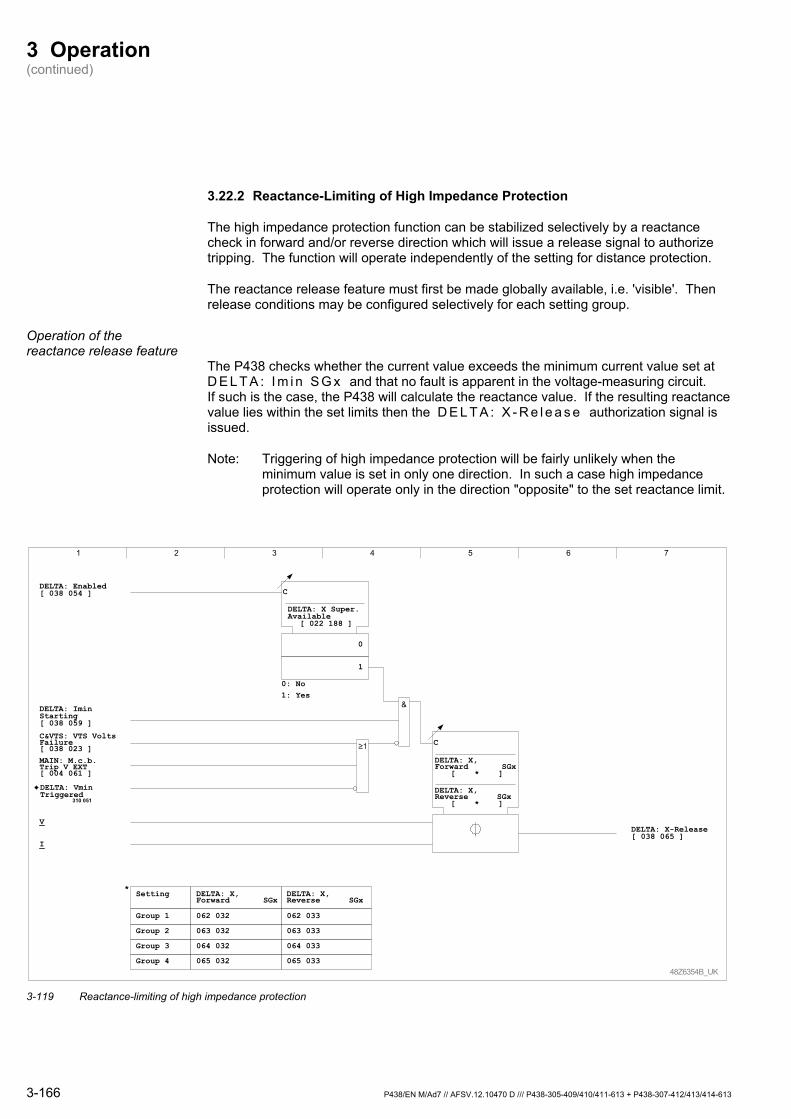
3 Operation (continued)
3-166 P438/EN M/Ad7 // AFSV.12.10470 D /// P438-305-409/410/411-613 + P438-307-412/413/414-613
3.22.2 Reactance-Limiting of High Impedance Protection
The high impedance protection function can be stabilized selectively by a reactance check in forward and/or reverse direction which will issue a release signal to authorize tripping. The function will operate independently of the setting for distance protection.
The reactance release feature must first be made globally available, i.e. 'visible'. Then release conditions may be configured selectively for each setting group.
Operation of the reactance release feature
The P438 checks whether the current value exceeds the minimum current value set at D E L T A : I m i n S G x and that no fault is apparent in the voltage-measuring circuit. If such is the case, the P438 will calculate the reactance value. If the resulting reactance value lies within the set limits then the D E L T A : X - R e l e a s e authorization signal is issued.
Note: Triggering of high impedance protection will be fairly unlikely when the minimum value is set in only one direction. In such a case high impedance protection will operate only in the direction "opposite" to the set reactance limit.
DELTA: X-Release[ 038 065 ]
1 2 3 4 5 6 7
Group 1
Group 2
062 032
DELTA: X, Forward SGx
063 032
064 032
065 032
Group 3
Group 4
Setting
48Z6354B_UK
I
DELTA: X, Forward SGx
[ * ]
C
DELTA: Imin Starting[ 038 059 ]
DELTA: X, Reverse SGx
[ * ]
V
062 033
DELTA: X, Reverse SGx
063 033
064 033
065 033
DELTA: Enabled[ 038 054 ]
DELTA: X Super. Available
[ 022 188 ]
C
C&VTS: VTS VoltsFailure[ 038 023 ]
0
1
0: No1: Yes
MAIN: M.c.b. Trip V EXT[ 004 061 ]
&
*
DELTA: Vmin Triggered
310 051
3-119 Reactance-limiting of high impedance protection
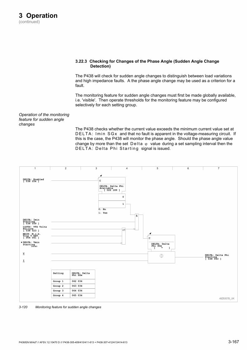
3 Operation (continued)
P438/EN M/Ad7 // AFSV.12.10470 D /// P438-305-409/410/411-613 + P438-307-412/413/414-613 3-167
3.22.3 Checking for Changes of the Phase Angle (Sudden Angle Change Detection)
The P438 will check for sudden angle changes to distinguish between load variations and high impedance faults. A the phase angle change may be used as a criterion for a fault.
The monitoring feature for sudden angle changes must first be made globally available, i.e. 'visible'. Then operate thresholds for the monitoring feature may be configured selectively for each setting group.
Operation of the monitoring feature for sudden angle changes
The P438 checks whether the current value exceeds the minimum current value set at D E L T A : I m i n S G x and that no fault is apparent in the voltage-measuring circuit. If this is the case, the P438 will monitor the phase angle. Should the phase angle value change by more than the set D e l t a ϕ value during a set sampling interval then the D E L T A : D e l t a P h i S t a r t i n g signal is issued.
DELTA: Delta Phi Starting[ 038 063 ]
1 2 3 4 5 6 7
Group 1
Group 2
062 034
DELTA: Delta Phi SGx
063 034
064 034
065 034
Group 3
Group 4
Setting
48Z6357B_UK
I
C
DELTA: Imin Starting[ 038 059 ]
V
DELTA: Enabled[ 038 054 ]
DELTA: Delta Phi Available
[ 022 189 ]
C
C&VTS: VTS VoltsFailure[ 038 023 ]
0
1
0: No1: Yes
MAIN: M.c.b. Trip V EXT[ 004 061 ]
DELTA: Delta Phi SGx[ * ]
&
DELTA: Vmin Starting
310 051
3-120 Monitoring feature for sudden angle changes
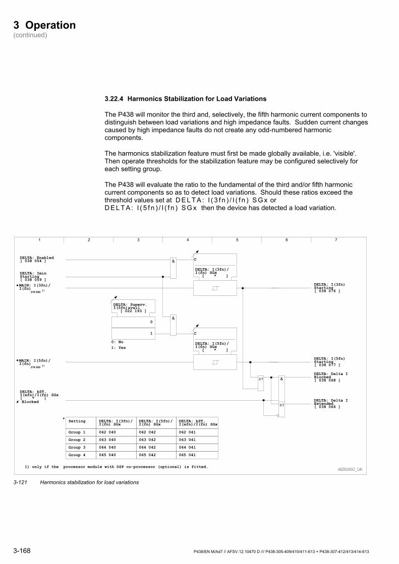
3 Operation (continued)
3-168 P438/EN M/Ad7 // AFSV.12.10470 D /// P438-305-409/410/411-613 + P438-307-412/413/414-613
3.22.4 Harmonics Stabilization for Load Variations
The P438 will monitor the third and, selectively, the fifth harmonic current components to distinguish between load variations and high impedance faults. Sudden current changes caused by high impedance faults do not create any odd-numbered harmonic components.
The harmonics stabilization feature must first be made globally available, i.e. 'visible'. Then operate thresholds for the stabilization feature may be configured selectively for each setting group.
The P438 will evaluate the ratio to the fundamental of the third and/or fifth harmonic current components so as to detect load variations. Should these ratios exceed the threshold values set at D E L T A : I ( 3 f n ) / I ( f n ) S G x or D E L T A : I ( 5 f n ) / I ( f n ) S G x then the device has detected a load variation.
1 2 3 4 5 6 7
Group 1
Group 2
062 040
DELTA: I(3fn)/I(fn) SGx
063 040
064 040
065 040
Group 3
Group 4
Setting
48Z6355C_UK
DELTA: Imin Starting[ 038 059 ]
062 042
DELTA: I(5fn)/I(fn) SGx
063 042
064 042
065 042
DELTA: Enabled[ 038 054 ]
DELTA: I(3fn)/I(fn) SGx
[ * ]
C
DELTA: I(3fn) Starting[ 038 076 ]
DELTA: Superv. I(5fn)avail
[ 022 193 ]
0
1
0: No1: Yes
DELTA: I(5fn)Starting[ 038 077 ]
DELTA: kST,I(xfn)/I(fn) SGx[ * ]Blocked
DELTA: Delta I Blocked[ 038 068 ]
DELTA: Delta I Extended[ 038 066 ]
062 041
DELTA: kST,I(xfn)/I(fn) SGx
063 041
064 041
065 041
DELTA: I(5fn)/I(fn) SGx
[ * ]
C
&
&
&
MAIN: I(3fn)/I(fn)
310 054 1)
MAIN: I(5fn)/I(fn)
310 055 1)
*
1) only if the processor module with DSP co-processor (optional) is fitted.
3-121 Harmonics stabilization for load variations
3 Operation (continued)
P438/EN M/Ad7 // AFSV.12.10470 D /// P438-305-409/410/411-613 + P438-307-412/413/414-613 3-169
3.22.5 Starting and Tripping of the High Impedance Protection Function
The sudden current change criterion of by the high impedance protection function monitors the fundamental component of the current during a set sampling interval. With this feature the setting of the sudden current change criterion can be handled dynamically according to the harmonics stabilization setting. The high impedance protection function is either blocked or stabilized (dynamically extended by multiplication with the set factor) in accordance with the setting of parameter D E L T A : k S t , I ( x f n ) / I ( f n ) S G x .
Starting of the high impedance protection function
The sudden current change criterion represents the stabilized starting criterion and is considered to be satisfied when the following conditions are met:
The minimum current threshold enabling the high impedance protection function has been triggered.
The setting-dependent harmonics stabilization block is not active.
Reactance limits monitoring has been triggered OR is not configured.
Sudden angle change monitoring has been triggered OR is not configured.
Measuring-circuit monitoring of the voltage has not been triggered OR a setting-dependent enabling of the sudden current change function has been issued with a faulty voltage measuring-circuit.
A sudden current change, D e l t a I , (possibly stabilized) has been detected.
Starting of the high impedance protection function is recorded. Recording is reset when minimum current enabling and reactance limit monitoring have dropped out. Additionally recording is reset when both the tDelta time-delay and a 100 ms pulse duration have elapsed.
Note: When tDelta is set to Blocked then resetting of the recorded start is carried out after the 100 ms pulse duration.
Inrush stabilization Depending on the settings of the TM A I N : F c t . I n r u s h . R s t r . S G x T parameters starting decisions issued by the high impedance protection function can be cancelled when the inrush stabilization function has detected an inrush current.
Tripping of the high impedance protection function
tDelta is triggered when the high impedance protection function operates. Once the starting time has elapsed, a trip signal is generated.
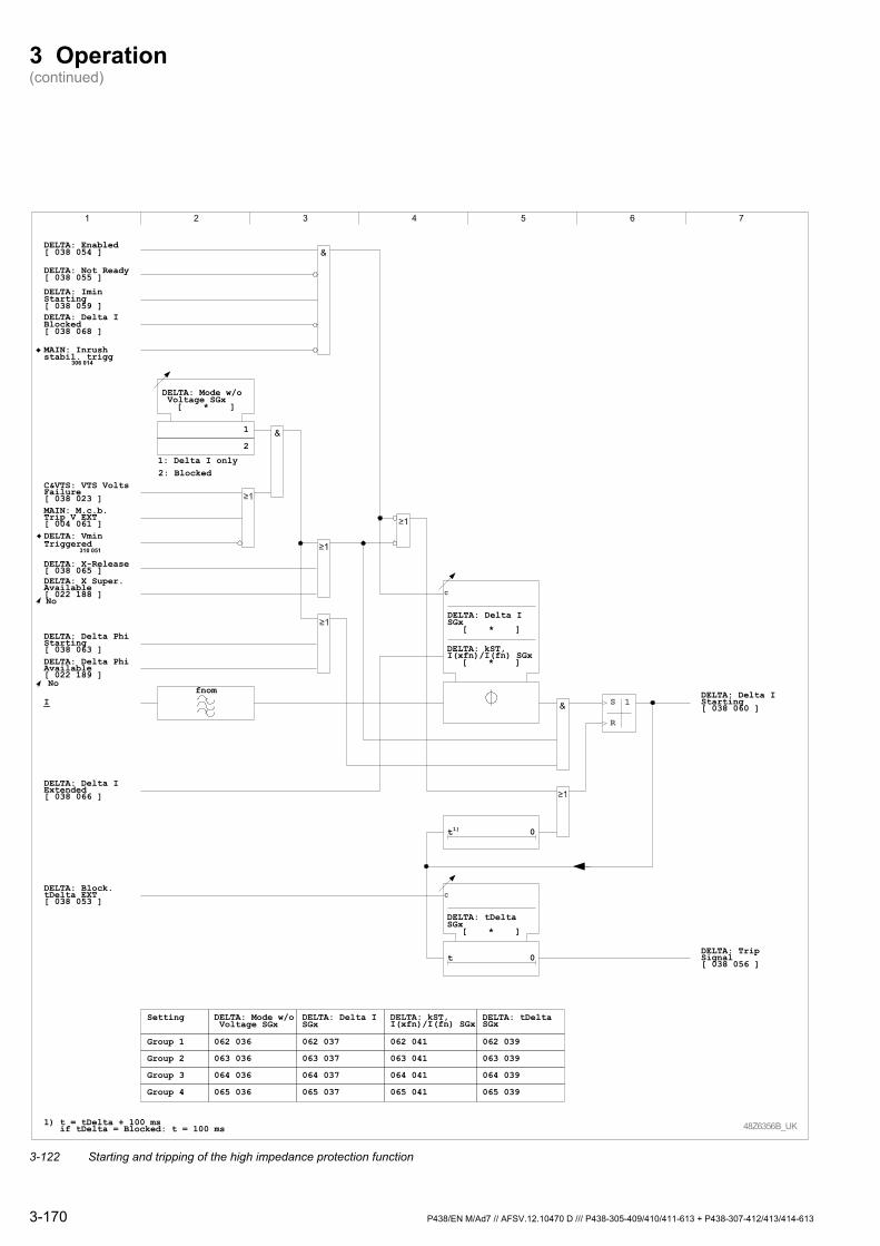
3 Operation (continued)
3-170 P438/EN M/Ad7 // AFSV.12.10470 D /// P438-305-409/410/411-613 + P438-307-412/413/414-613
1 2 3 4 5 6 7
Group 1
Group 2
062 036
DELTA: Mode w/o Voltage SGx
063 036
064 036
065 036
Group 3
Group 4
Setting
48Z6356B_UK
DELTA: Imin Starting[ 038 059 ]
DELTA: X Super. Available[ 022 188 ]No
062 041
DELTA: kST,I(xfn)/I(fn) SGx
063 041
064 041
065 041
DELTA: X-Release[ 038 065 ]
C&VTS: VTS VoltsFailure[ 038 023 ]
1
2
1: Delta I only2: Blocked
MAIN: M.c.b. Trip V EXT [ 004 061 ]
DELTA: Mode w/o Voltage SGx
[ * ]
C
DELTA: kST,I(xfn)/I(fn) SGx
[ * ]
DELTA: Delta I SGx
[ * ]
fnom
DELTA: Block. tDelta EXT[ 038 053 ]
I
DELTA: TripSignal[ 038 056 ]
062 037
DELTA: Delta I SGx
063 037
064 037
065 037
DELTA: Enabled[ 038 054 ]
DELTA: Delta PhiAvailable [ 022 189 ]No
DELTA: Delta Phi Starting[ 038 063 ]
DELTA: Delta I Blocked[ 038 068 ]
DELTA: tDelta SGx
[ * ]
C
t1) 0
MAIN: Inrush stabil. trigg
306 014
062 039
DELTA: tDelta SGx
063 039
064 039
065 039
S
R
1DELTA: Delta I Starting[ 038 060 ]
DELTA: Delta I Extended[ 038 066 ]
1) t = tDelta + 100 ms if tDelta = Blocked: t = 100 ms
t 0
DELTA: Not Ready[ 038 055 ]
&
&
&
DELTA: Vmin Triggered
310 051
3-122 Starting and tripping of the high impedance protection function
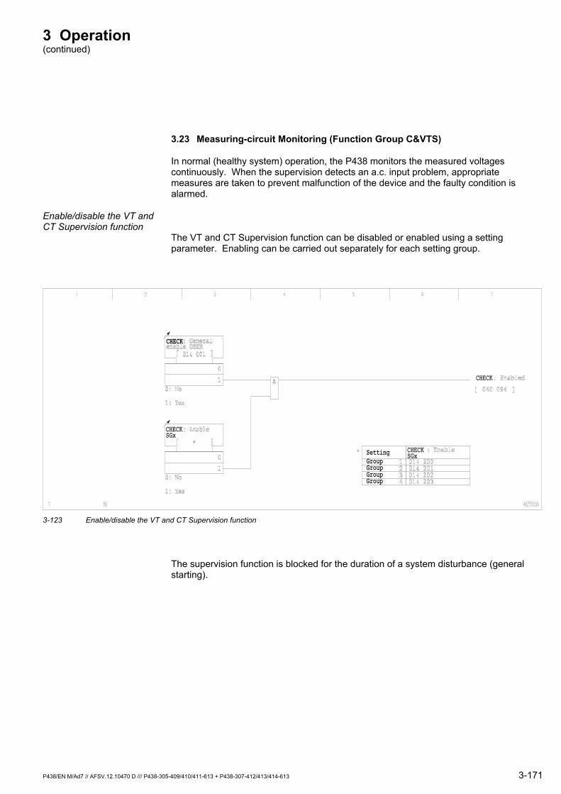
3 Operation (continued)
3.23 Measuring-circuit Monitoring (Function Group C&VTS)
In normal (healthy system) operation, the P438 monitors the measured voltages continuously. When the supervision detects an a.c. input problem, appropriate measures are taken to prevent malfunction of the device and the faulty condition is alarmed.
Enable/disable the VT and CT Supervision function
The VT and CT Supervision function can be disabled or enabled using a setting parameter. Enabling can be carried out separately for each setting group.
CHECK
CHECK
Setting
GroupGroupGroupGroup
CHECKSGx
CHECKSGx
3-123 Enable/disable the VT and CT Supervision function
The supervision function is blocked for the duration of a system disturbance (general starting).
P438/EN M/Ad7 // AFSV.12.10470 D /// P438-305-409/410/411-613 + P438-307-412/413/414-613 3-171
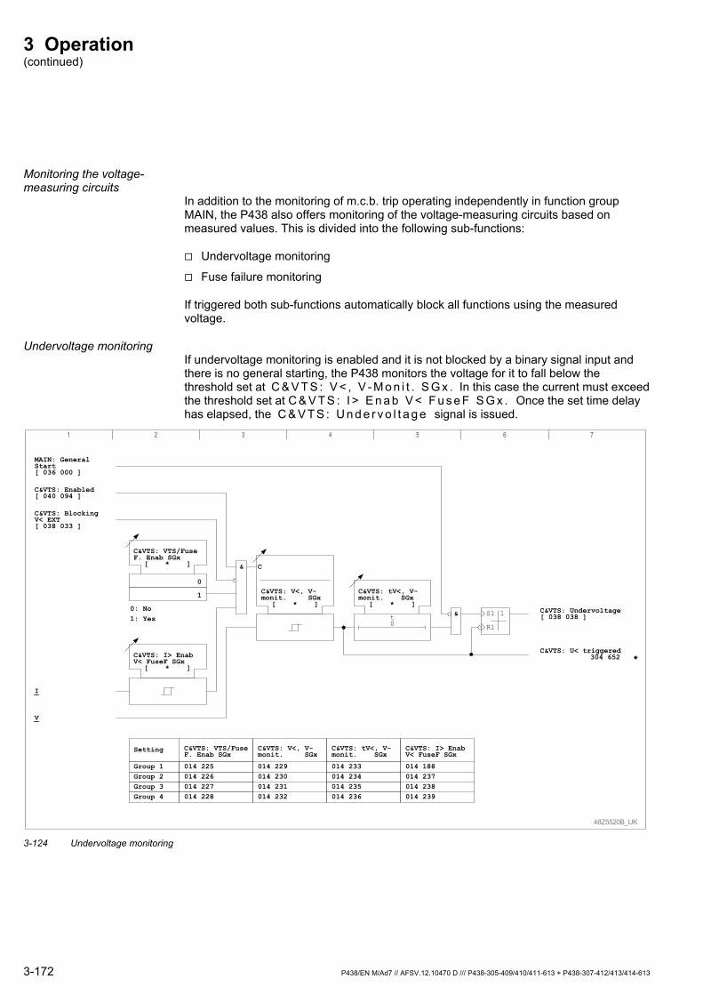
3 Operation (continued)
Monitoring the voltage-measuring circuits
In addition to the monitoring of m.c.b. trip operating independently in function group MAIN, the P438 also offers monitoring of the voltage-measuring circuits based on measured values. This is divided into the following sub-functions:
Undervoltage monitoring
Fuse failure monitoring
If triggered both sub-functions automatically block all functions using the measured voltage.
Undervoltage monitoring If undervoltage monitoring is enabled and it is not blocked by a binary signal input and there is no general starting, the P438 monitors the voltage for it to fall below the threshold set at C & V T S : V < , V - M o n i t . S G x . In this case the current must exceed the threshold set at C & V T S : I > E n a b V < F u s e F S G x . Once the set time delay has elapsed, the C & V T S : U n d e r v o l t a g e signal is issued.
48Z5520B_UK
V
1 2 3 4 5 6 7
C&VTS: VTS/FuseF. Enab SGx
[ * ]
Setting
Group 4Group 3Group 2Group 1
C&VTS: tV<, V-monit. SGx
C&VTS: VTS/FuseF. Enab SGx
014 225014 226014 227014 228
014 233014 234014 235014 236
C&VTS: I> EnabV< FuseF SGx
014 188014 237014 238014 239
C&VTS: Undervoltage[ 038 038 ]
&
C&VTS: V<, V-monit. SGx
014 229014 230014 231014 232
C&VTS: BlockingV< EXT[ 038 033 ]
MAIN: GeneralStart[ 036 000 ]
C&VTS: Enabled[ 040 094 ]
0
1
0: No1: Yes
C
C&VTS: V<, V-monit. SGx
[ * ]
C&VTS: I> EnabV< FuseF SGx
[ * ]
I
C&VTS: tV<, V-monit. SGx
[ * ]
t0
S1
R1
1&
C&VTS: U< triggered304 652
3-124 Undervoltage monitoring
3-172 P438/EN M/Ad7 // AFSV.12.10470 D /// P438-305-409/410/411-613 + P438-307-412/413/414-613
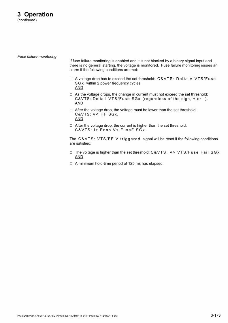
3 Operation (continued)
Fuse failure monitoring If fuse failure monitoring is enabled and it is not blocked by a binary signal input and there is no general starting, the voltage is monitored. Fuse failure monitoring issues an alarm if the following conditions are met:
A voltage drop has to exceed the set threshold: C & V T S : D e l t a V V T S / F u s e S G x within 2 power frequency cycles. AND
As the voltage drops, the change in current must not exceed the set threshold: C&VTS: Del ta I V T S / F u s e SGx ( regard less of the s ign, + or -) . AND
After the voltage drop, the voltage must be lower than the set threshold: C&VTS: V<, FF SGx. AND
After the voltage drop, the current is higher than the set threshold: C & V T S : I > E n a b V < F u s e F S G x .
The C & V T S : V T S / F F V t r i g g e r e d signal will be reset if the following conditions are satisfied:
The voltage is higher than the set threshold: C & V T S : V > V T S / F u s e F a i l S G x AND
A minimum hold-time period of 125 ms has elapsed.
P438/EN M/Ad7 // AFSV.12.10470 D /// P438-305-409/410/411-613 + P438-307-412/413/414-613 3-173
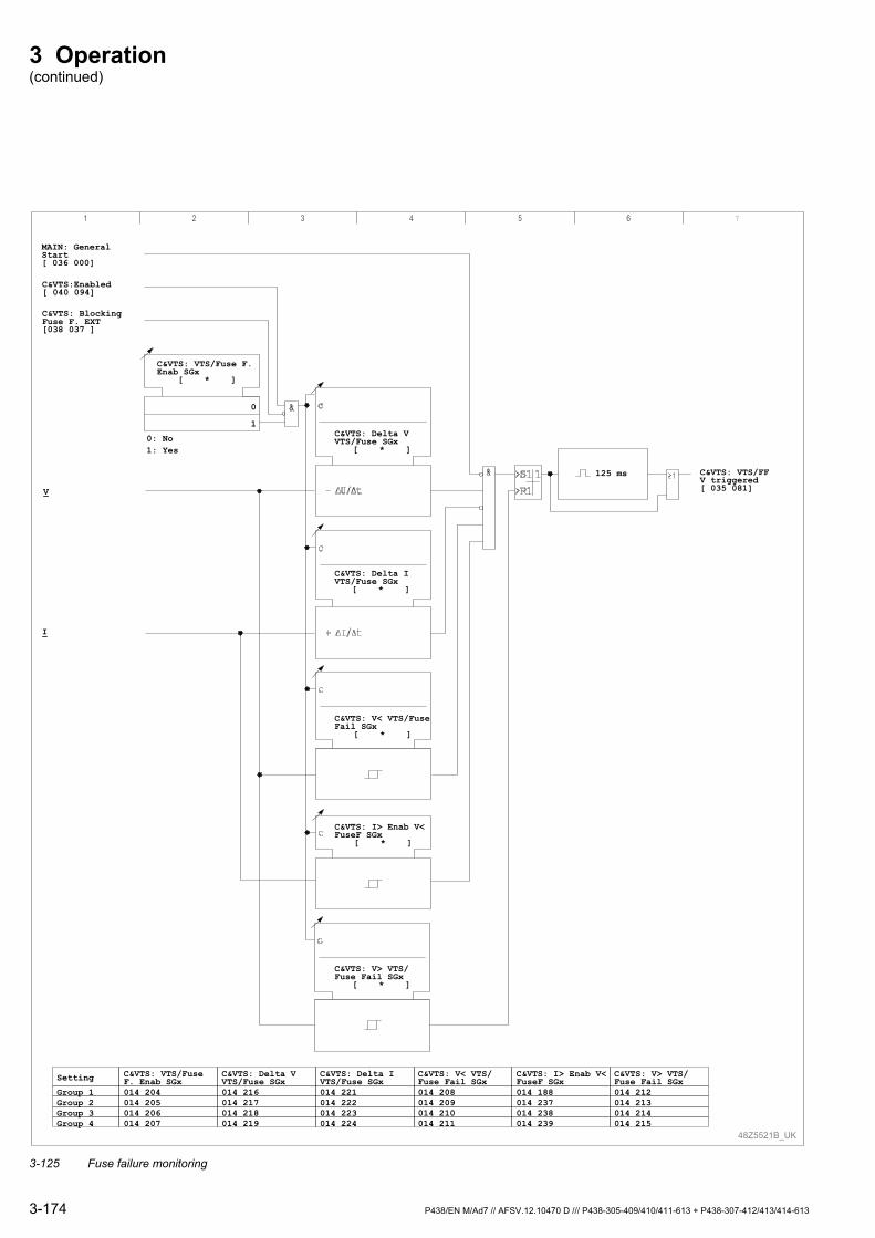
3 Operation (continued)
C&VTS: BlockingFuse F. EXT[038 037 ]
C&VTS: I> Enab V<FuseF SGx
[ * ]
48Z5521B_UK
Setting
Group 1Group 2Group 3Group 4
C&VTS: Delta IVTS/Fuse SGx014 221014 222014 223014 224
C&VTS: Delta VVTS/Fuse SGx014 216014 217014 218014 219
C&VTS: VTS/FuseF. Enab SGx014 204014 205014 206014 207
C&VTS: V< VTS/Fuse Fail SGx014 208014 209014 210014 211
C&VTS: I> Enab V<FuseF SGx014 188014 237014 238014 239
C&VTS: V> VTS/Fuse Fail SGx014 212014 213014 214014 215
C&VTS: VTS/Fuse F.Enab SGx
[ * ]
C&VTS: Delta VVTS/Fuse SGx
[ * ]
C&VTS: Delta IVTS/Fuse SGx
[ * ]
C&VTS: V> VTS/Fuse Fail SGx
[ * ]
C&VTS: V< VTS/FuseFail SGx
[ * ]
C&VTS:Enabled[ 040 094]
MAIN: GeneralStart[ 036 000]
C&VTS: VTS/FFV triggered[ 035 081]
0: No1: Yes
1
0
125 ms
1 2 3 4 5 6 7
V
I
3-125 Fuse failure monitoring
3-174 P438/EN M/Ad7 // AFSV.12.10470 D /// P438-305-409/410/411-613 + P438-307-412/413/414-613
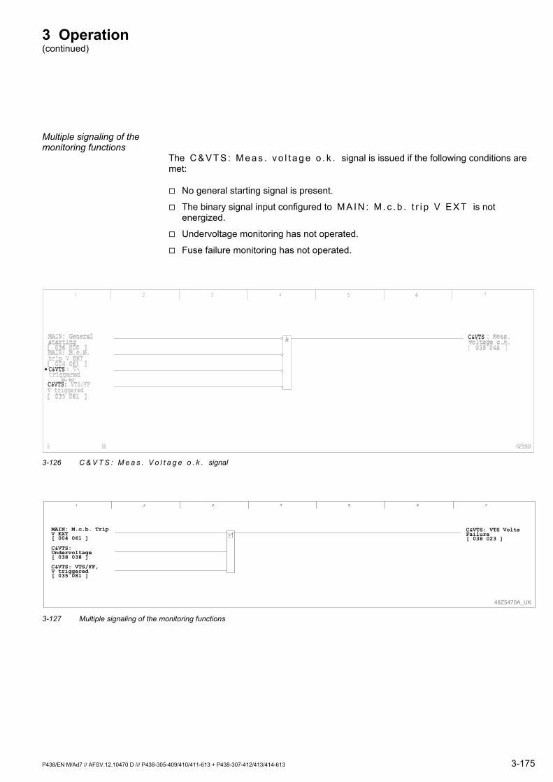
3 Operation (continued)
Multiple signaling of the monitoring functions
The C & V T S : M e a s . v o l t a g e o . k . signal is issued if the following conditions are met:
No general starting signal is present.
The binary signal input configured to M A I N : M . c . b . t r i p V E X T is not energized.
Undervoltage monitoring has not operated.
Fuse failure monitoring has not operated.
C&VTS: VTS/FFV triggered
C&VTS
C&VTS
3-126 C & V T S : M e a s . V o l t a g e o . k . signal
48Z5470A_UK
C&VTS: VTS VoltsFailure[ 038 023 ]
C&VTS: VTS/FF,V triggered[ 035 081 ]
C&VTS:Undervoltage[ 038 038 ]
MAIN: M.c.b. TripV EXT[ 004 061 ]
3-127 Multiple signaling of the monitoring functions
P438/EN M/Ad7 // AFSV.12.10470 D /// P438-305-409/410/411-613 + P438-307-412/413/414-613 3-175
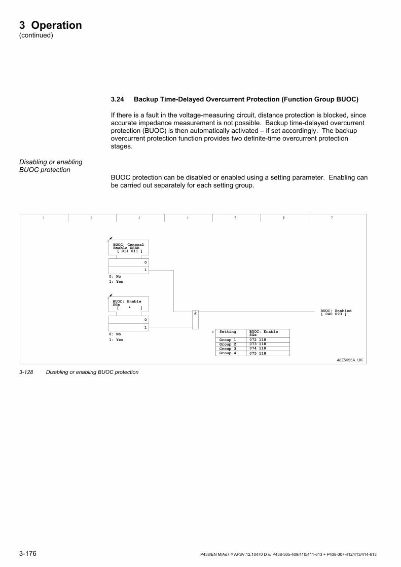
3 Operation (continued)
3.24 Backup Time-Delayed Overcurrent Protection (Function Group BUOC)
If there is a fault in the voltage-measuring circuit, distance protection is blocked, since accurate impedance measurement is not possible. Backup time-delayed overcurrent protection (BUOC) is then automatically activated – if set accordingly. The backup overcurrent protection function provides two definite-time overcurrent protection stages.
Disabling or enabling BUOC protection
BUOC protection can be disabled or enabled using a setting parameter. Enabling can be carried out separately for each setting group.
BUOC: EnableSGx
Setting
Group 1Group 2Group 3Group 4
0: No1: Yes
0: No1: Yes
BUOC: Enabled[ 040 093 ]
48Z5055A_UK
072 118
075 118074 118073 118
BUOC: GeneralEnable USER[ 014 011 ]
BUOC: EnableSGx[ * ]
0
1
0
1
3-128 Disabling or enabling BUOC protection
3-176 P438/EN M/Ad7 // AFSV.12.10470 D /// P438-305-409/410/411-613 + P438-307-412/413/414-613
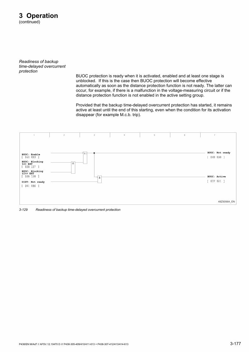
3 Operation (continued)
Readiness of backup time-delayed overcurrent protection
BUOC protection is ready when it is activated, enabled and at least one stage is unblocked. If this is the case then BUOC protection will become effective automatically as soon as the distance protection function is not ready. The latter can occur, for example, if there is a malfunction in the voltage-measuring circuit or if the distance protection function is not enabled in the active setting group.
Provided that the backup time-delayed overcurrent protection has started, it remains active at least until the end of this starting, even when the condition for its activation disappear (for example M.c.b. trip).
BUOC: Enable
BUOC: BlockingtI> EXT
BUOC: BlockingtI>> EXT
DIST: Not ready
BUOC: Not ready
BUOC: Active
48Z5056A_EN 3-129 Readiness of backup time-delayed overcurrent protection
P438/EN M/Ad7 // AFSV.12.10470 D /// P438-305-409/410/411-613 + P438-307-412/413/414-613 3-177
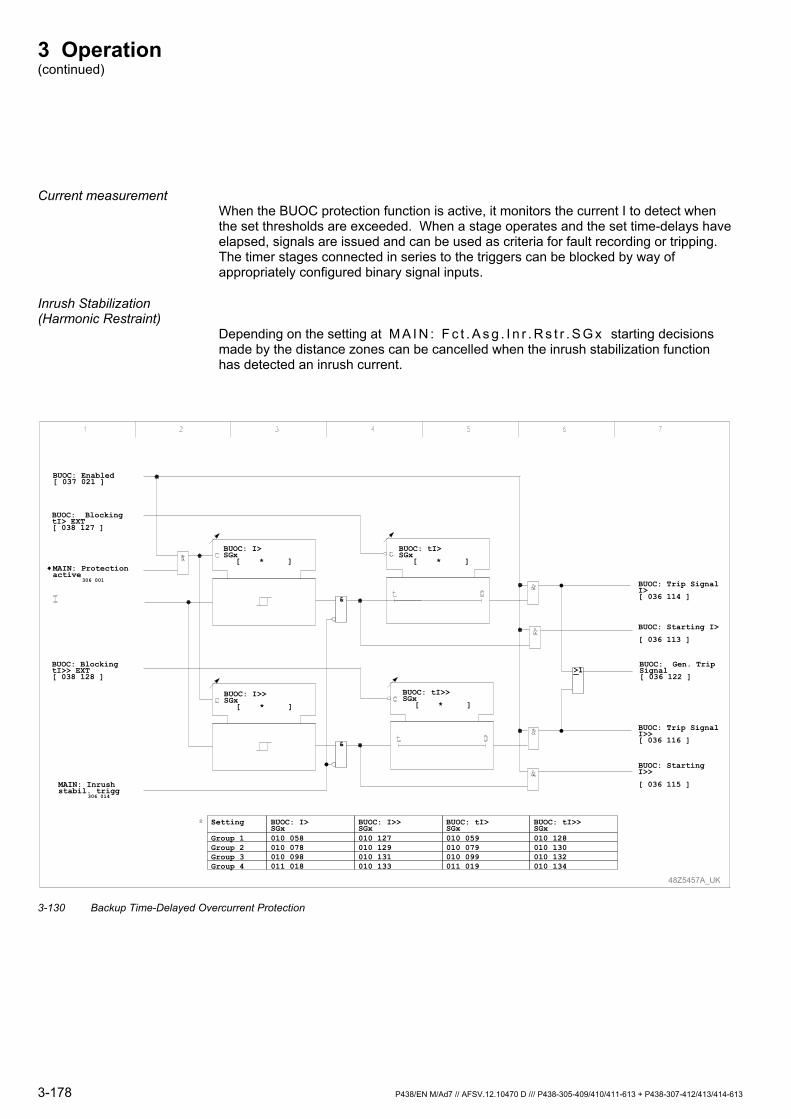
3 Operation (continued)
Current measurement When the BUOC protection function is active, it monitors the current I to detect when the set thresholds are exceeded. When a stage operates and the set time-delays have elapsed, signals are issued and can be used as criteria for fault recording or tripping. The timer stages connected in series to the triggers can be blocked by way of appropriately configured binary signal inputs.
Inrush Stabilization (Harmonic Restraint)
Depending on the setting at M A I N : F c t . A s g . I n r . R s t r . S G x starting decisions made by the distance zones can be cancelled when the inrush stabilization function has detected an inrush current.
BUOC: Gen. TripSignal[ 036 122 ]
&
&
MAIN: Inrushstabil. trigg
306 014
48Z5457A_UK
>1
BUOC: tI>>SGx010 128010 130010 132010 134
Setting
Group 1Group 2Group 3Group 4
BUOC: tI>SGx010 059010 079010 099011 019
BUOC: I>>SGx010 127010 129010 131010 133
BUOC: I>SGx010 058010 078010 098011 018
BUOC: I>SGx
[ * ]
BUOC: I>>SGx
[ * ]
BUOC: tI>>SGx
[ * ]
BUOC: tI>SGx
[ * ]
BUOC: Trip SignalI>>[ 036 116 ]
BUOC: StartingI>>
[ 036 115 ]
BUOC: Starting I>
[ 036 113 ]
BUOC: Trip SignalI>[ 036 114 ]
BUOC: Enabled[ 037 021 ]
BUOC: BlockingtI> EXT[ 038 127 ]
MAIN: Protectionactive
306 001
BUOC: BlockingtI>> EXT[ 038 128 ]
3-130 Backup Time-Delayed Overcurrent Protection
3-178 P438/EN M/Ad7 // AFSV.12.10470 D /// P438-305-409/410/411-613 + P438-307-412/413/414-613
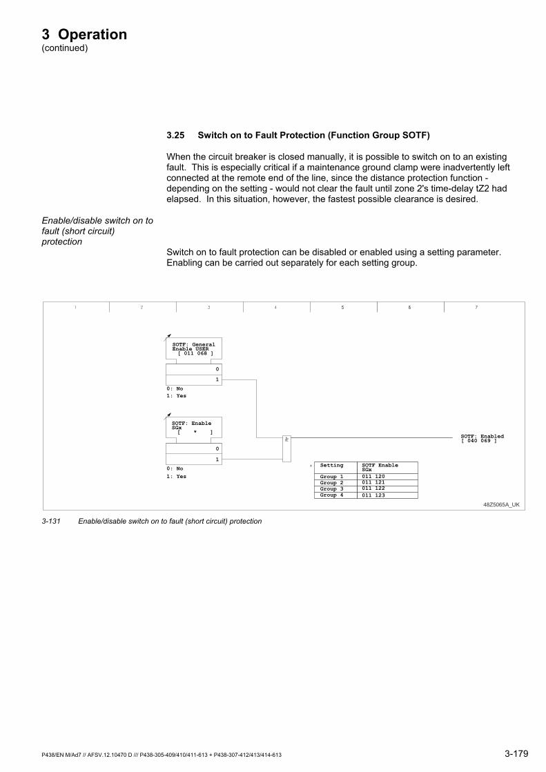
3 Operation (continued)
3.25 Switch on to Fault Protection (Function Group SOTF)
When the circuit breaker is closed manually, it is possible to switch on to an existing fault. This is especially critical if a maintenance ground clamp were inadvertently left connected at the remote end of the line, since the distance protection function - depending on the setting - would not clear the fault until zone 2's time-delay tZ2 had elapsed. In this situation, however, the fastest possible clearance is desired.
Enable/disable switch on to fault (short circuit) protection
Switch on to fault protection can be disabled or enabled using a setting parameter. Enabling can be carried out separately for each setting group.
SOTF EnableSGx
Setting
Group 1Group 2Group 3Group 4
0: No 1: Yes
0: No 1: Yes
SOTF: Enabled[ 040 069 ]
48Z5065A_UK
011 120
011 123011 122011 121
SOTF: GeneralEnable USER[ 011 068 ]
SOTF: EnableSGx[ * ]
0
1
0
1
3-131 Enable/disable switch on to fault (short circuit) protection
P438/EN M/Ad7 // AFSV.12.10470 D /// P438-305-409/410/411-613 + P438-307-412/413/414-613 3-179
3 Operation (continued)
Blocking of switch on to fault protection
As of version –606 switch on to fault protection may be blocked if the following conditions are met:
an external blocking command signal, present at the binary signal input configured at SOTF: B l o c k i n g E X T
an external auto-reclose signal, present at the binary signal input configured at S O T F : P a r . A R C R u n n i n g E X T
a reclose command issued by the internal auto-reclose control function
Pulse duration of manual closing
To ensure fast fault clearance upon manual closing, the manual close signal must be applied not only to the circuit breaker but also to the P438. The manual close signal is converted to an internal pulse, of settable duration. The user may specify whether the following shall occur while this timer is running: The setting S O T F : O p e r a t i n g M o d e S G x allows the user to choose between the following operating modes:
the occurrence of a general start while a timer stage is running shall cause a trip (S O T F : T r i p s i g n a l ) (See section 'Starting Signals and Tripping Logic' for a definition of general starting)
OR
While this timer is running, a zone 1 extension shall occur (S O T F : Z 1 E x t e n d e d ) .
3-180 P438/EN M/Ad7 // AFSV.12.10470 D /// P438-305-409/410/411-613 + P438-307-412/413/414-613
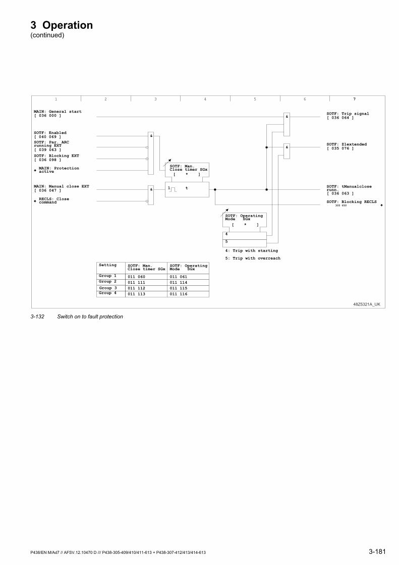
3 Operation (continued)
48Z5321A_UK
SOTF: Enabled[ 040 069 ]
SOTF: OperatingMode SGx
[ * ]
4
5
4: Trip with starting
5: Trip with overreach
SOTF: tManualcloserunn.[ 036 063 ]
SOTF: Par. ARCrunning EXT[ 039 063 ]
MAIN: General start[ 036 000 ]
&
1 2 3 4 5 6 7
SOTF: Blocking RECLS 305 650
MAIN: Protectionactive
SOTF: Blocking EXT[ 036 098 ]
SOTF: Man.Close timer SGx[ * ]
1 tMAIN: Manual close EXT[ 036 047 ]
RECLS: Closecommand
&
&
&
SOTF: Trip signal[ 036 064 ]
SOTF: Z1extended[ 035 076 ]
Setting
Group 4Group 3
Group 2Group 1
SOTF: OperatingMode SGx
SOTF: Man.Close timer SGx
011 060011 111011 112011 113
011 061011 114011 115011 116
3-132 Switch on to fault protection
P438/EN M/Ad7 // AFSV.12.10470 D /// P438-305-409/410/411-613 + P438-307-412/413/414-613 3-181
3 Operation (continued)
3.26 Auto-Reclose Control (Function Group RECLS)
As of version –606 the auto-reclose control function (RECLS) will cause an automatic reclosure on a line, previously cleared by a protection device, after certain faults have occurred.
The auto-reclose control function of the P438 allows triggering of trip times by different starting signals. Once the trip times have elapsed, a trip signal is generated. The auto-reclose control function of the P438 permits multiple reclosing sequences. A reclosing sequence begins with a high-speed reclosure (HSR). If the fault is not cleared after reclosure by a HSR, then successive attempt(s) can be made to clear the fault with time-delayed reclosure(s) (TDR).
Enabling and disabling the auto-reclose function
The function is globally made available (independently of setting groups) using R E C L S : G e n e r a l E n a b l e U S E R . It is enabled as a function of a setting group using R E C L S : E n a b l e S G x . If these enabling functions have been activated, the auto-reclose control function can be disabled or enabled using setting parameters or through appropriately configured binary signal inputs. The front panel user interface (HMI) or the MiCOM S1 support software and the binary signal inputs have equal status in this regard. If only the R E C L S : E n a b l e E X T setting is assigned to a binary signal input, then auto-recloser will be enabled by a positive edge (pick-up) of the input signal and disabled by a negative edge (drop-off). If only the R E C L S : D i s a b l e E X T setting has been assigned to a binary signal input, then a signal at this input will have no effect.
3-182 P438/EN M/Ad7 // AFSV.12.10470 D /// P438-305-409/410/411-613 + P438-307-412/413/414-613
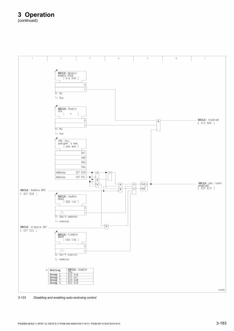
3 Operation (continued)
RECLS:
RECLS:
RECLS:
RECLS:
RECLS:
RECLS:
RECLS:
RECLS:
RECLS:SettingGroupGroupGroupGroup
3-133 Disabling and enabling auto-reclosing control
P438/EN M/Ad7 // AFSV.12.10470 D /// P438-305-409/410/411-613 + P438-307-412/413/414-613 3-183

3 Operation (continued)
Auto-reclose blocking The auto-recloser is blocked and the R E C L S : B l o c k e d signal will be issued if the following conditions are met:
A manual close has occurred,
A trip signal is present at the circuit breaker’s re-trip input (only relevant with setting R E C L S : W i t h R e - T r i p = 'No'),
A trip signal is present at the back-up circuit breaker / the back-up protection device.
A manual trip command has been issued.
The current measured at the instant of tripping exceeds the threshold value R E C L S : B l o c k . A R C f . I > S G x .
A signal is present at the binary signal input configured to R E C L S : B l o c k i n g E X T .
When all blocking conditions have been removed, the associated blocking timer stage is triggered. Auto-reclose blocking is cancelled when both blocking time-delays have elapsed.
48Z5352A_UK
RECLS: With Re-Trip
[ 015 018 ]
0
1
RECLS: Blocked[ 004 069 ]
RECLS: Enabled[ 015 064 ]
& RECLS: Block. TimeRunning[ 037 004 ]
1 2 3 4 5 6 7
1
RECLS: Blocking EXT[ 036 050 ]
SOTF: Blocking RECLS305 650
RECLS: Block.ARC f. I> SGx
[ * ]
I
RECLS: Block.time int. SGx
[ * ]
1 t
RECLS: Block.time ext. SGx
[ * ]
1 t
1
1
RECLS: Block.ARC f. I> SGx RECLS: Block.
time int. SGxRECLS: Block.time ext. SGx
RECLS: Blocked by I> [ 037 126 ]
MAIN: Man. BackTrip sig.
MAIN: Re-Trip signal
MAIN: Back-Trip signal
MAIN: Man. MainTrip sig.
MAIN: Man. ReTrip signal
[ 039 083 ]
[ 039 103 ]
[ 039 105 ]
[ 039 081 ]
[ 039 082 ]
Setting
Group 4Group 3Group 2Group 1 015 104
016 104017 104020 104
015 043024 021024 081025 041
015 058024 032024 092025 052
0: No1: Yes
3-134 Auto-reclose blocking
3-184 P438/EN M/Ad7 // AFSV.12.10470 D /// P438-305-409/410/411-613 + P438-307-412/413/414-613
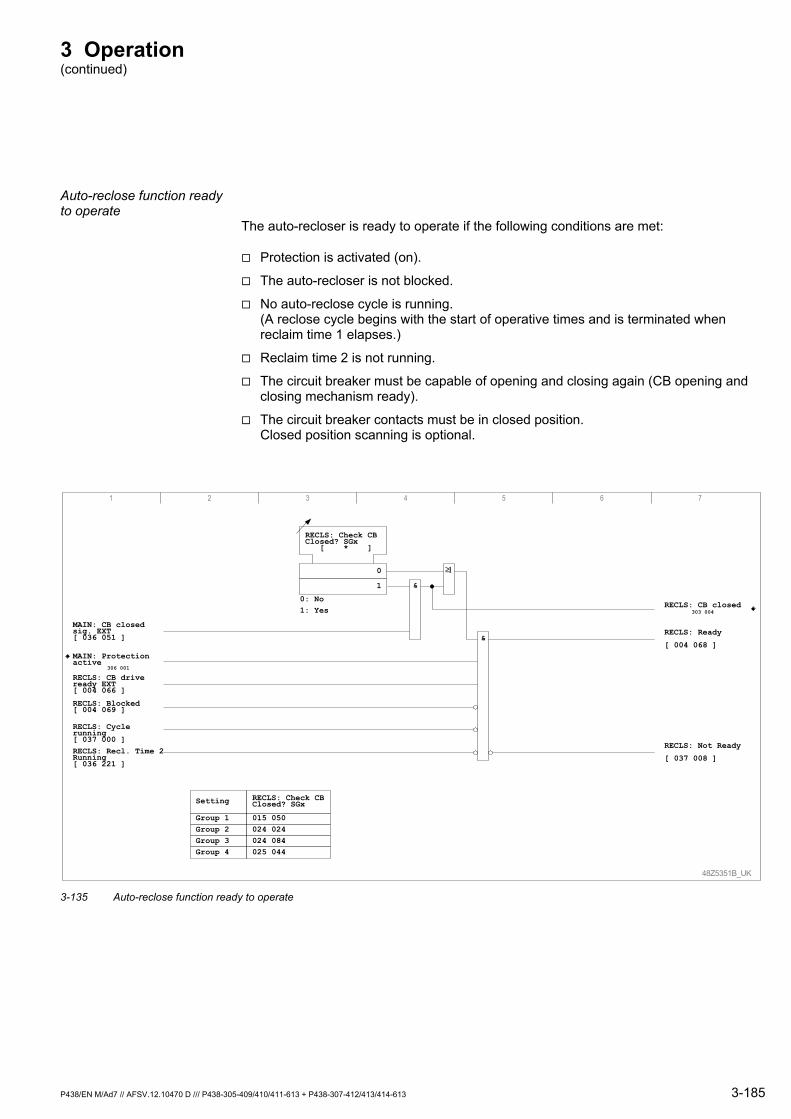
3 Operation (continued)
Auto-reclose function ready to operate
The auto-recloser is ready to operate if the following conditions are met:
Protection is activated (on).
The auto-recloser is not blocked.
No auto-reclose cycle is running. (A reclose cycle begins with the start of operative times and is terminated when reclaim time 1 elapses.)
Reclaim time 2 is not running.
The circuit breaker must be capable of opening and closing again (CB opening and closing mechanism ready).
The circuit breaker contacts must be in closed position. Closed position scanning is optional.
48Z5351B_UK
RECLS: CB driveready EXT[ 004 066 ]
RECLS: Check CBClosed? SGx
[ * ]
0
1
0: No1: Yes
RECLS: Ready
[ 004 068 ]
RECLS: Blocked[ 004 069 ]
MAIN: CB closedsig. EXT[ 036 051 ]
&
RECLS: Not Ready
[ 037 008 ]
1 2 3 4 5 6 7
1≥
RECLS: CB closed303 004
&
MAIN: Protectionactive
306 001
RECLS: Cyclerunning[ 037 000 ]RECLS: Recl. Time 2Running[ 036 221 ]
Setting
Group 4Group 3Group 2Group 1 015 050
024 024024 084025 044
RECLS: Check CBClosed? SGx
3-135 Auto-reclose function ready to operate
P438/EN M/Ad7 // AFSV.12.10470 D /// P438-305-409/410/411-613 + P438-307-412/413/414-613 3-185
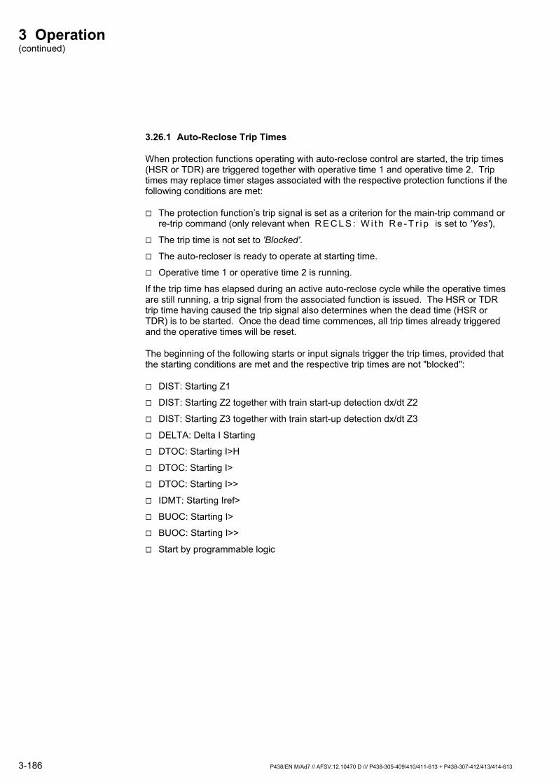
3 Operation (continued)
3.26.1 Auto-Reclose Trip Times
When protection functions operating with auto-reclose control are started, the trip times (HSR or TDR) are triggered together with operative time 1 and operative time 2. Trip times may replace timer stages associated with the respective protection functions if the following conditions are met:
The protection function’s trip signal is set as a criterion for the main-trip command or re-trip command (only relevant when R E C L S : W i t h R e - T r i p is set to 'Yes'),
The trip time is not set to 'Blocked'.
The auto-recloser is ready to operate at starting time.
Operative time 1 or operative time 2 is running.
If the trip time has elapsed during an active auto-reclose cycle while the operative times are still running, a trip signal from the associated function is issued. The HSR or TDR trip time having caused the trip signal also determines when the dead time (HSR or TDR) is to be started. Once the dead time commences, all trip times already triggered and the operative times will be reset.
The beginning of the following starts or input signals trigger the trip times, provided that the starting conditions are met and the respective trip times are not "blocked":
DIST: Starting Z1
DIST: Starting Z2 together with train start-up detection dx/dt Z2
DIST: Starting Z3 together with train start-up detection dx/dt Z3
DELTA: Delta I Starting
DTOC: Starting I>H
DTOC: Starting I>
DTOC: Starting I>>
IDMT: Starting Iref>
BUOC: Starting I>
BUOC: Starting I>>
Start by programmable logic
3-186 P438/EN M/Ad7 // AFSV.12.10470 D /// P438-305-409/410/411-613 + P438-307-412/413/414-613
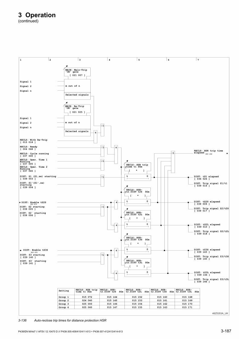
3 Operation (continued)
48Z5353A_UK
RECLS: HSR triptime t1 SGx
1 2 3 4 5 6 7
C
1DIST: Z1 (Z1,ze) starting
DIST: Z1'(Z1',ze)starting
DIST: Trip signal Z1/t1
&
C
C
DIST: Trip signal Z2/t2S
DIST: Trip signal Z2/t2L
&
&
C
C
DIST: Trip signal Z3/t3S
DIST: Trip signal Z3/t3L
&
RECLS: HSR-tr.DIST t3L SGx
RECLS: HSR-tr.DIST t2L SGx
RECLS: HSR-tr.DIST t2S SGx
RECLS: HSR-tr.DIST t3S SGx
RECLS: HSR triptime t1 SGx
1
1DIST: Z2 starting[ 039 005 ]
DIST: Z2´ starting[ 039 006 ]
RECLS: Cycle running
RECLS: Oper. Time 1Running
RECLS: Oper. Time 2Running
MAIN: Main-Trip'OR' gate
[ 021 007 ]
MAIN: Re-Trip'OR' gate
[ 021 025 ]
&
RECLS: With Re-Trip
1
1
1
&
1RECLS: HSR trip timeelapsed
303 152
DIST: Enable tZ2S303 671
Signal 1
Signal 2
Signal n
Signal 1
Signal 2
Signal n
Selected signals
Selected signals
m out of n
m out of n
[ 039 003 ]
[ 039 004 ]
RECLS: Ready[ 004 068 ]
[ 037 000 ]
[ 037 005 ]
[ 037 065 ]
[ 015 018 ]
DIST: Z3 starting[ 039 140 ]
DIST: Z3´ starting[ 039 141 ]
DIST: Enable tZ3S303 672
Setting
Group 4Group 3Group 2Group 1 015 072
024 040025 000025 060
015 144015 145015 146015 147
015 152015 153015 154015 155
015 160015 161015 162015 163
015 168015 169015 170015 171
t 0
t 0
t 0
t 0
t 0
[ * ]
[ * ]
[ * ]
[ * ]
[ * ]
[ 036 026 ]
[ 039 016 ]
[ 039 009 ]
[ 039 017 ]
[ 039 010 ]
[ 039 018 ]
[ 039 143 ]
[ 039 145 ]
[ 039 144 ]
[ 039 146 ]
DIST: tZ1 elapsed
DIST: tZ2S elapsed
DIST: tZ2L elapsed
DIST: tZ3S elapsed
DIST: tZ3L elapsed
RECLS: HSR-tr.DIST t2S SGx
RECLS: HSR-tr.DIST t2L SGx
RECLS: HSR-tr.DIST t3S SGx
RECLS: HSR-tr.DIST t3L SGx
3-136 Auto-reclose trip times for distance protection HSR
P438/EN M/Ad7 // AFSV.12.10470 D /// P438-305-409/410/411-613 + P438-307-412/413/414-613 3-187

3 Operation (continued)
RECLS: TDR-Tr.DIST t1 SGx
[ * ]
t 0 DIST: t1Z Elapsed[ 036 026 ]
1 2 3 4 5 6 7
C
DIST: Z1 (Z1,ze)Starting[ 039 003 ]DIST: Z1´(Z1´,ze)Starting[ 039 004 ]
DIST: Trip Signal Z1/t1[ 039 016 ]
RECLS: TDR-Tr.DIST t2S SGx
[ * ]
t 0 DIST: tZ2S Elapsed[ 039 009 ]
C
RECLS: TDR-Tr.DIST t2L SGx
[ * ]
t 0
C
DIST: Trip Signal Z2/t2S[ 039 017 ]
DIST: tZ2L Elapsed[ 039 010 ]
DIST: Trip Signal Z2/t2L[ 039 018 ]
RECLS: TDR-Tr.DIST t3S SGx
[ * ]
t 0 DIST: tZ3S Elapsed[ 039 143 ]
C
RECLS: TDR-Tr.DIST t3L SGx
[ * ]
t 0
C
DIST: Trip Signal Z3/t3S[ 039 145 ]
DIST: tZ3L Elapsed[ 039 144 ]
DIST: Trip Signal Z2/t3L[ 039 146 ]
RECLS: Ready[ 004 068 ]
DIST: Z3 Starting[ 039 140 ]
DIST: Z3´ Starting[ 039 141 ]
DIST: tZ3S Enable303 672
DIST: Z2 Starting[ 039 005 ]
DIST: Z2´ Starting[ 039 006 ]
DIST: Enable tZ2S303 671
RECLS: Cycle Running[ 037 000 ]RECLS: Oper. Time 1Running[ 037 005 ]RECLS: Oper. Time 2Running[ 037 065 ]
MAIN: Main-Trip’OR’ Gate
[ 021 007 ]
m out of n
Selected signals
MAIN: Re-Trip ’OR’ Gate
[ 021 025 ]
m out of n
Selected signals
Signal 1
Signal 2
Signal n
Signal 1
Signal 2
Signal n
RECLS: With Re-trip[ 015 018 ]
RECLS: TDR trip time elapsed
303 153
48Z5354B_UK
Setting
Group 4Group 3Group 2Group 1
RECLS: TDR-Tr.DIST t3L SGx
RECLS: TDR-Tr.DIST t2L SGx
RECLS: TDR-Tr.DIST t2S SGx
RECLS: TDR-Tr.DIST t3S SGx
RECLS: TDR-Tr.DIST t1 SGx
015 073024 041025 001025 061
015 148015 149015 150015 151
015 164015 165015 166015 167
015 172015 173015 174015 175
015 156015 157015 158015 159
&
&
&
&
&
&
3-137 Auto-reclose trip times for distance protection TDR
3-188 P438/EN M/Ad7 // AFSV.12.10470 D /// P438-305-409/410/411-613 + P438-307-412/413/414-613

3 Operation (continued)
RECLS: HSR-Tr.DELTA tD. SGx
[ * ]
t 0
1 2 3 4 5 6 7
C
DELTA: TripSignal[ 038 056 ]
Setting
Group 4Group 3Group 2Group 1
RECLS: Ready[ 004 068 ]
RECLS: CycleRunning[ 037 000 ]
MAIN: Main-Trip'OR' Gate
[ 021 007 ]
m out of n
Selected Signals
MAIN: Re-Trip'OR' Gate
[ 021 025 ]
m out of n
Selected Signals
Signal 1
Signal 2
Signal n
Signal 1
Signal 2
Signal n
RECLS: With Re-Trip[ 015 018 ]
DELTA: Delta IStarting[ 038 060 ]
48Z6366A_UK
RECLS: TDR-Tr.DELTA tD. SGx
[ * ]
t 0
C
RECLS: TDR-Tr.DELTA tD. SGx
RECLS: HSR-Tr.DELTA tD. SGx
008 192008 193008 194008 195
008 196008 197008 198008 199
*
&
&
RECLS: Oper. Time 1Running[ 037 005 ]RECLS: Oper. Time 2Running[ 037 065 ]
RECLS: Trip timeHSR elaps
303 152
RECLS: Trip timeTDR elaps.
303 153
3-138 HSR and TDR auto-reclose trip times for high impedance protection
P438/EN M/Ad7 // AFSV.12.10470 D /// P438-305-409/410/411-613 + P438-307-412/413/414-613 3-189

3 Operation (continued)
48Z5355A_UK
RECLS:HSR-tr.DTOC tI>H SGx
DTOC: Trip signal tI>H
1 2 3 4 5 6 7
C
RECLS: HSR-tr.DTOC tI> SGx
DTOC: tI> Elapsed
C
RECLS: HSR-tr.DTOC tI>> SGxC
DTOC: Trip signal tI>
RECLS: HSR-tr.IDMT kIrefSGxC
RECLS: HSR-tr.DTOC tI>> SGx
RECLS: HSR-tr.DTOC tI> SGx
RECLS: HSR-tr.IDMT kIrefSGx
RECLS: HSR-tr.DTOC tI>H SGx
MAIN: Main-Trip'OR' gate
[ 021 007 ]
MAIN: Re-Trip 'OR'gate
[ 021 025 ]
&
1
1
1
&
1RECLS: HSR trip timeelapsed
DTOC: tI>> Elapsed
DTOC: Trip signal tI>>
IDMT: Trip signal tIref
[ 035 022 ]
RECLS: Ready[ 004 068 ]
[ 037 000 ]
[ 037 005 ]
[ 037 065 ]
Signal 1
Signal 2
Signal n
Signal 1
Signal 2
Signal n
[ 015 018 ]
[ 035 020 ]
[ 035 021 ]
[ 040 080 ]
DTOC: Starting I>H
RECLS: Cycle running
RECLS: Oper. Time 1Running
RECLS: Oper. Time 2Running
RECLS: With Re-Trip
m out of n
Selected signals
m out of n
Selected signals
DTOC: Starting I>
DTOC: Starting I>>
IDMT: Starting Iref>
Setting
Group 4Group 3Group 2Group 1 015 069
024 052024 053024 054
015 105020 105021 105022 105
015 074020 107021 107022 107
015 094020 113021 113022 113
t 0
t 0
t 0
t 0
[ * ]
[ * ]
[ * ]
[ * ]
[ 040 076 ]
[ 040 010 ]
[ 041 020 ]
303 152
[ 040 106 ]
[ 040 011 ]
[ 040 084 ]
3-139 Auto-reclose trip times for DTOC and IDMT protection HSR
3-190 P438/EN M/Ad7 // AFSV.12.10470 D /// P438-305-409/410/411-613 + P438-307-412/413/414-613
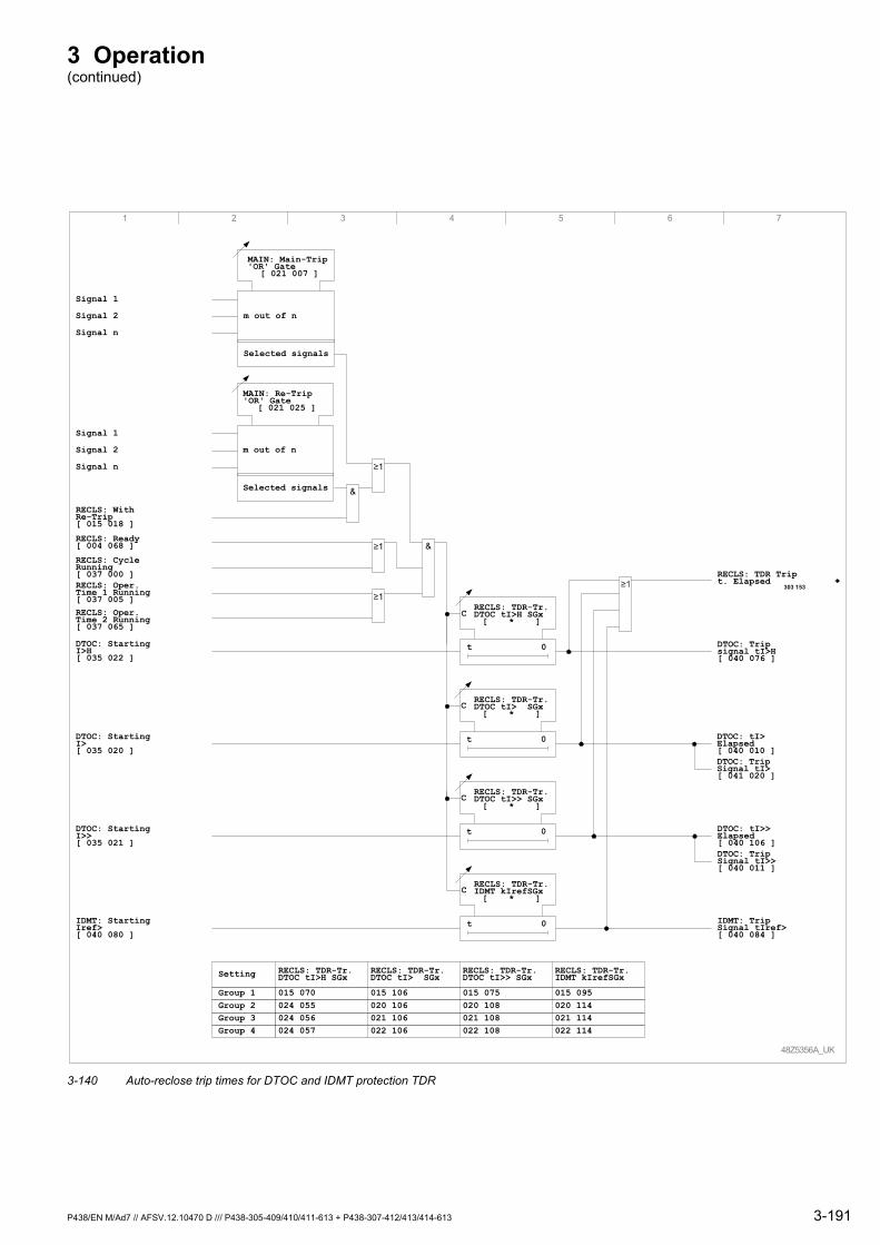
3 Operation (continued)
48Z5356A_UK
RECLS: TDR-Tr.DTOC tI>H SGx[ * ]
t 0 DTOC: Trip signal tI>H[ 040 076 ]
1 2 3 4 5 6 7
C
DTOC: Starting I>H[ 035 022 ]
RECLS: TDR-Tr.DTOC tI> SGx[ * ]
t 0 DTOC: tI> Elapsed[ 040 010 ]
C
RECLS: TDR-Tr.DTOC tI>> SGx[ * ]
t 0
C
DTOC: Trip Signal tI>[ 041 020 ]
RECLS: TDR-Tr.IDMT kIrefSGx[ * ]
t 0
C
Setting
Group 4Group 3Group 2Group 1
RECLS: TDR-Tr.DTOC tI>> SGx
RECLS: TDR-Tr.DTOC tI> SGx
RECLS: TDR-Tr.IDMT kIrefSGx
RECLS: TDR-Tr.DTOC tI>H SGx
015 070024 055024 056024 057
015 106020 106021 106022 106
015 095020 114021 114022 114
015 075020 108021 108022 108
RECLS: Ready[ 004 068 ]
RECLS: Cycle Running[ 037 000 ]RECLS: Oper. Time 1 Running[ 037 005 ]RECLS: Oper. Time 2 Running[ 037 065 ]
MAIN: Main-Trip'OR' Gate
[ 021 007 ]
m out of n
Selected signals
MAIN: Re-Trip'OR' Gate
[ 021 025 ]
m out of n
Selected signals
Signal 1
Signal 2
Signal n
Signal 1
Signal 2
Signal n
RECLS: With Re-Trip[ 015 018 ]
RECLS: TDR Trip t. Elapsed
303 153
DTOC: Starting I> [ 035 020 ]
DTOC: Starting I>>[ 035 021 ]
IDMT: Starting Iref> [ 040 080 ]
DTOC: tI>> Elapsed[ 040 106 ]DTOC: Trip Signal tI>>[ 040 011 ]
IDMT: Trip Signal tIref>[ 040 084 ]
&
&
3-140 Auto-reclose trip times for DTOC and IDMT protection TDR
P438/EN M/Ad7 // AFSV.12.10470 D /// P438-305-409/410/411-613 + P438-307-412/413/414-613 3-191
3 Operation (continued)
RECLS: HSR-tr.BUOC tI> SGx
[ * ]
t 0
1 2 3 4 5 6 7
C
RECLS: HSR-tr.BUOC tI>> SGx
[ * ]
t 0
C
BUOC: Trip signalI>[ 036 014 ]
Setting
Group 4Group 3Group 2Group 1
RECLS: HSR-tr.BUOC tI>> SGx
RECLS: HSR-tr.BUOC tI> SGx
015 109020 109022 109023 109
015 111020 111021 111022 111
RECLS: Ready[ 004 068 ]
RECLS: Cycle running[ 037 000 ]
RECLS: Oper. Time 1Running[ 037 005 ]RECLS: Oper. Time 2Running[ 037 065 ]
MAIN: Main-Trip'OR' gate
[ 021 007 ]
m out of n
Selected signals
MAIN: Re-Trip'OR' gate
[ 021 025 ]
m out of n
Selected signals
Signal 1
Signal 2
Signal n
Signal 1
Signal 2
Signal n
&
RECLS: With Re-Trip[ 015 018 ]
1≥
1≥
1≥
&
RECLS: HSR triptime elapsed
303 152
BUOC: Starting I>[ 036 013 ]
BUOC: Trip signalI>>[ 036 116 ]
BUOC: Starting I>>[ 036 115 ]
48Z5357B_UK
RECLS: TDR-tr.BUOC tI> SGx
[ * ]
t 0
C
RECLS: TDR-tr.BUOC tI>> SGx
[ * ]
t 0
C
1≥ RECLS: TDR triptime elapsed
303 153
RECLS: TDR-tr.BUOC tI>> SGx
RECLS: TDR-tr.BUOC tI> SGx
015 110020 110021 110022 110
015 112020 112021 112022 112
1≥
1≥
1≥
3-141 Auto-reclose trip times for BUOC protection HSR and TDR
3-192 P438/EN M/Ad7 // AFSV.12.10470 D /// P438-305-409/410/411-613 + P438-307-412/413/414-613
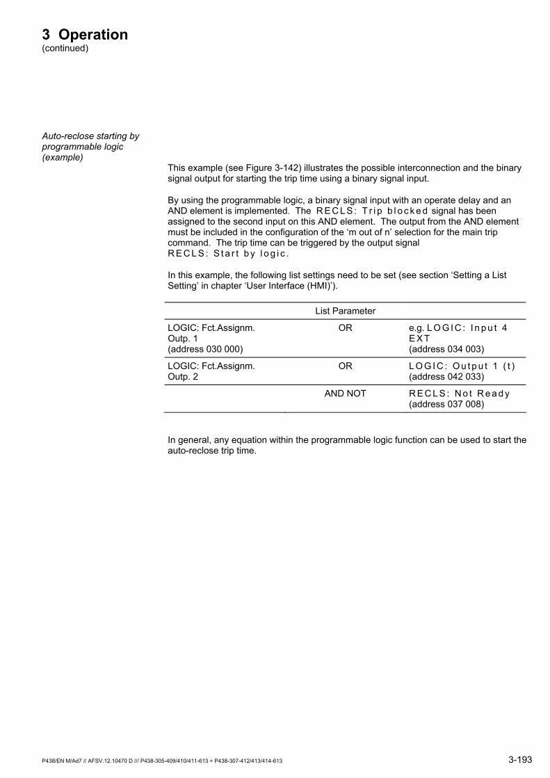
3 Operation (continued)
Auto-reclose starting by programmable logic (example)
This example (see Figure 3-142) illustrates the possible interconnection and the binary signal output for starting the trip time using a binary signal input.
By using the programmable logic, a binary signal input with an operate delay and an AND element is implemented. The R E C L S : T r i p b l o c k e d signal has been assigned to the second input on this AND element. The output from the AND element must be included in the configuration of the ‘m out of n’ selection for the main trip command. The trip time can be triggered by the output signal R E C L S : S t a r t b y l o g i c .
In this example, the following list settings need to be set (see section ‘Setting a List Setting’ in chapter ‘User Interface (HMI)’).
List Parameter
LOGIC: Fct.Assignm. Outp. 1 (address 030 000)
OR e.g. L O G I C : I n p u t 4 E X T (address 034 003)
LOGIC: Fct.Assignm. Outp. 2
OR L O G I C : O u t p u t 1 ( t ) (address 042 033)
AND NOT R E C L S : N o t R e a d y (address 037 008)
In general, any equation within the programmable logic function can be used to start the auto-reclose trip time.
P438/EN M/Ad7 // AFSV.12.10470 D /// P438-305-409/410/411-613 + P438-307-412/413/414-613 3-193

3 Operation (continued)
1 2 3 4 5 6 7
LOGIC: Op. Mode tOutput 1
[ 030 001 ]
m out of n
LOGIC: Output 1
Signal 1
Signal 2
Signal n
48Z5366A_UK
t 0RECLS: Start byLOGIC[ 037 078 ]
LOGIC: Fct.Assignm. Outp. 1
[ 030 000 ]
LOGIC:Output 1 (t)
1 out of n
RECLS: Fct.assignm. tLOGIC
[ 015 033 ]
LOGIC: Op. Mode tOutput 2
[ 030 005 ]
m out of n
LOGIC: Output 2
LOGIC: Fct.Assignm. Outp. 2
[ 030 004 ]
LOGIC:Output 2 (t)
&1³
LOGIC: Output 2 (t)[ 042 035 ]
RECLS: Not Ready[ 037 008 ]
3-142 Example of programmable logic in the auto-reclose control function
3-194 P438/EN M/Ad7 // AFSV.12.10470 D /// P438-305-409/410/411-613 + P438-307-412/413/414-613
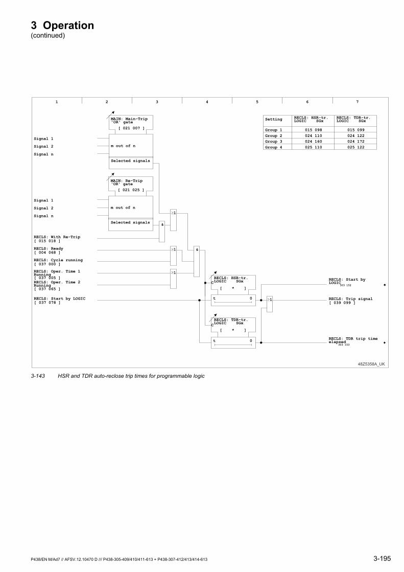
3 Operation (continued)
RECLS: HSR-tr.LOGIC SGx
1 2 3 4 5 6 7
C
RECLS: TDR-tr.LOGIC SGx
RECLS: HSR-tr.LOGIC SGxMAIN: Main-Trip
'OR' gate
MAIN: Re-Trip'OR' gate
&
1
1
1
&
RECLS: Start byLOGIC
48Z5358A_UK
RECLS: TDR-tr.LOGIC SGxC
RECLS: Trip signal1
RECLS: TDR trip timeelapsed
[ 004 068 ]
[ 037 000 ]
[ 037 005 ]
[ 037 065 ]
Signal 1
Signal 2
Signal n
Signal 1
Signal 2
Signal n
[ 015 018 ]
[ 037 078 ]
RECLS: Cycle running
RECLS: Oper. Time 1Running
RECLS: Oper. Time 2Running
RECLS: With Re-Trip
RECLS: Start by LOGIC
RECLS: Ready
m out of n
Selected signals
m out of n
Selected signals
[ 021 007 ]
[ 021 025 ]
t 0
t 0
Setting
Group 4Group 3Group 2Group 1 015 098
024 110024 160025 110
015 099024 122024 172025 122
303 152
[ 039 099 ]
303 153
[ * ]
[ * ]
3-143 HSR and TDR auto-reclose trip times for programmable logic
P438/EN M/Ad7 // AFSV.12.10470 D /// P438-305-409/410/411-613 + P438-307-412/413/414-613 3-195
3 Operation (continued)
Auto-reclose cycle When the auto-recloser is ready, an auto-reclose cycle is started by one of the following functions:
Starting of protection functions that have a trip time configured and thus allow reclosing
Starting or tripping of an external protection device, if it has been configured accordingly (R E C L S : P a r a l l e l T r i p S G x )
A test HSR
As the auto-reclose cycle runs, the R E C L S : R e a d y signal is no longer taken into account.
The auto-reclose cycle consists in:
Operative time 1 or operative time 2 is running.
Dead time HSR, dead time TDR or maximum dead time is running.
Reclaim time 1 is running.
The R E C L S : D e f . r e c l . t i m e r u n n . signal is issued with the last reclose command in the auto-reclose cycle. Simultaneously the last, uninterruptible reclaim time 1 is triggered. An auto-reclose cycle is terminated when this last reclaim time 1 has elapsed.
If there is a new protection start during the last reclaim time 1, the auto-recloser is also blocked for the duration of the starting pulse. The R E C L S : L o c k f . G e n . S t a r t i n g signal is issued.
3-196 P438/EN M/Ad7 // AFSV.12.10470 D /// P438-305-409/410/411-613 + P438-307-412/413/414-613
3 Operation (continued)
3.26.2 High-speed Reclosure (HSR)
If the starting conditions are met then any auto-recloser-relevant protection start will trigger an auto-reclose cycle. Any start will trigger the associated trip times, operative time 1 and operative time 2. Operative time 1 and operative time 2 have equal status when they are running. Starting conditions for an auto-reclose cycle must be released while operative timer stages are running. This means that the circuit breaker has opened (start and trip signals of the function have dropped out) so that a dead time may be triggered. Which dead time is triggered depends on which operative time has elapsed.
Voltage-independent reclosure
When the start signal is reset, operative time 1 is terminated and the HSR dead time begins. If there is no starting during the HSR dead time, a reclose command is issued once the HSR dead time has elapsed. Simultaneously reclaim time 1 is triggered. If there is no starting during reclaim time 1, the R E C L S : R e c l o s u r e s u c c e s s f u l signal will be issued when reclaim time 1 has elapsed. The auto-reclose cycle is complete.
Voltage-dependent reclosure
Should starting conditions for an auto-reclose cycle drop out after operative time 1 has elapsed but not before operative time 2 has elapsed, the maximum dead time (R E C L S : D e a d T i m e M a x S G x ) will be triggered. With the triggering of the maximum dead time a reclosure of the line from the far end will be expected. A reclose command is issued and the maximum dead time is reset when the voltage criterion (R E C L S : V > S G x ) is met and the associated time delay (R E C L S : t V > S G x ) has elapsed. Simultaneously reclaim time 1 is triggered. If no start occurs during reclaim time 1, the R E C L S : R e c l o s u r e S u c c e s s f u l signal will be issued when reclaim time 1 has elapsed. The auto-reclose cycle is complete.
HSR rejection Reclaim time 1 is triggered should the circuit breaker fail to clear the fault during the operative times. All protection timer stages are enabled again simultaneously, provided that their trip time was not set to 'Blocked'.
If operative times elapse without the protection having reached a decision to trip, the RECLS function is ready again immediately after the relevant starting condition has dropped out.
P438/EN M/Ad7 // AFSV.12.10470 D /// P438-305-409/410/411-613 + P438-307-412/413/414-613 3-197
3 Operation (continued)
Unsuccessful high-speed reclosure
If the HSR does not succeed and another protection start occurs then a time-delayed reclosure (TDR) is started if at least one TDR is permitted. If no TDR is permitted after a HSR then the reclaim time 1 presently running is the last reclaim time 1 of the auto-reclose cycle. All trip times are reset when reclaim time 1 has elapsed. Simultaneously all protection timer stages are enabled again. If a trip signal is issued during the last reclaim time 1 then it will be regarded as a final trip. The auto-reclose cycle is complete after the last reclaim time 1 has elapsed.
The final trip will trigger reclaim time 2. The auto-reclose control function remains blocked while reclaim time 2 is running after an unsuccessful reclose attempt. Auto-reclose blocking may be removed if one of the following conditions is met:
Reclaim time 2 has elapsed (if it was not set to 'Blocked'),
Reclaim time 2 was reset by a setting parameter or by an appropriately configured binary signal input.
Suppressing CB trip signals
When the R E C L S : C y c l e R u n n i n g signal appears, the R E C L S : S i g . I n t e r r . C B T r i p signal (interruption of breaker trip signal) is issued and it is reset after the final HSR or TDR of the current auto-reclose cycle, once the close command pulse time has elapsed. When the R E C L S : B l o c k e d signal is issued during an auto-reclose cycle, the signal is likewise reset immediately.
3-198 P438/EN M/Ad7 // AFSV.12.10470 D /// P438-305-409/410/411-613 + P438-307-412/413/414-613
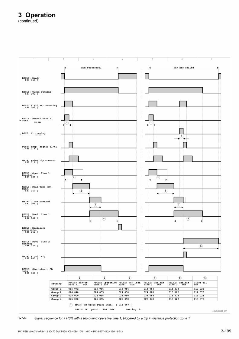
3 Operation (continued)
48Z5359B_UK
1 2 3 4 5 6 7
DIST: Z1(Z1,ze) starting[ 039 003 ]
Setting
Group 4Group 3Group 2Group 1
RECLS: ReclaimTime 2 SGx
RECLS: HSR DeadTime SGx
RECLS: OperativeTime 1 SGx
RECLS: ReclaimTime 1 SGx
RECLS: HSR-tr.DIST t1 SGx
015 072024 040025 000025 060
015 066024 035024 095025 055
015 054024 028024 088025 048
015 124015 125015 126015 127
015 056024 030024 090025 050
RECLS: Ready[ 004 068 ]
RECLS: HSR-tr.DIST t1runn.
310 021
RECLS: Cycle running[ 037 000 ]
RECLS: Oper. Time 1Running[ 037 005 ]
MAIN: Main-Trip command[ 039 011 ]
DIST: t1 running310 023
DIST: Trip signal Z1/t1[ 039 016 ]
RECLS: Dead Time HSRRunn.[ 037 067 ]
MAIN: Close command[ 037 009 ]
RECLS: Recl. Time 1Running[ 036 042 ]
RECLS: Recl. Time 2Running[ 036 221 ]
RECLS: Reclosuresuccessful[ 036 062 ]
MAIN: Final trip[ 038 103 ]
RECLS: Sig.interr. CBtrip[ 036 040 ]
HSR successful
4
7
3
2
1
HSR has failed
4
7
3
2
1
5
6
654321
DIST: tZ1SGx
012 028012 078013 028013 078
MAIN: CB Close Pulse Durn. [ 015 067 ]7
RECLS: No. permit. TDR SGx Setting: 0
3-144 Signal sequence for a HSR with a trip during operative time 1, triggered by a trip in distance protection zone 1
P438/EN M/Ad7 // AFSV.12.10470 D /// P438-305-409/410/411-613 + P438-307-412/413/414-613 3-199

3 Operation (continued)
48Z5360C_UK
1 2 3 4 5 6 7
DIST: Z1(Z1,ze) starting[ 039 003 ]
Setting
Group 4Group 3Group 2Group 1
RECLS: tV> SGxRECLS: Dead TimeMax SGx
RECLS: OperativeTime 2 SGx RECLS: V> SGxRECLS: HSR-tr.
DIST t1 SGx
015 072024 040025 000025 060
015 083024 042025 002025 062
015 128015 129015 138015 139
015 140015 141015 142015 143
015 084024 043025 003025 063
RECLS: Ready[ 004 068 ]
RECLS: Cycle running[ 037 000 ]
RECLS: Oper. Time 2Running[ 037 005 ]
MAIN: Main-Trip command[ 039 011 ]
DIST: Trip signal Z1/t1[ 039 016 ]
RECLS: Max. Dead TimeRunn.[ 037 069 ]
MAIN: Close command[ 037 009 ]
RECLS: Recl. Time 1Running[ 036 042 ]
RECLS: Reclosuresuccessful[ 036 062 ]
RECLS: Sig.interr. CBtrip[ 036 040 ]
HSR successful
6
7
3
2
1
HSR has failed
654321
MAIN: CB Close Pulse Durn. [ 015 067 ]7
RECLS: No. permit. TDR SGx Setting: 0
RECLS: V> starting
RECLS: tV> running5
4
RECLS: ReclaimTime 1 SGx
015 054024 028024 088025 048
6
3
2
1RECLS: HSR-tr.DIST t1runn.
310 021
DIST: t1 running310 023
3-145 Signal sequence for a HSR with a trip during operative time 2, triggered by a trip in distance protection zone 1
3-200 P438/EN M/Ad7 // AFSV.12.10470 D /// P438-305-409/410/411-613 + P438-307-412/413/414-613
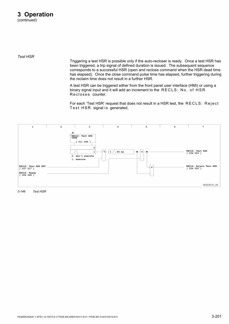
3 Operation (continued)
Test HSR Triggering a test HSR is possible only if the auto-recloser is ready. Once a test HSR has been triggered, a trip signal of defined duration is issued. The subsequent sequence corresponds to a successful HSR (open and reclose command when the HSR dead time has elapsed). Once the close command pulse time has elapsed, further triggering during the reclaim time does not result in a further HSR.
A test HSR can be triggered either from the front panel user interface (HMI) or using a binary signal input and it will add an increment to the R E C L S : N o . o f H S R R e c l o s e s counter.
For each ‘Test HSR’ request that does not result in a HSR test, the R E C L S : R e j e c t T e s t H S R signal i s generated.
48Z5361A_UK
1 2 3 4 5 6 7
RECLS: Test HSRUSER
[ 011 066 ]
0
1 &1 80 ms1
&[ 037 017 ]
RECLS: Ready
RECLS: Test HSR EXT
[ 004 068 ]
0: don't execute1: execute
[ 034 023 ]
[ 036 055 ]
RECLS: Test HSR
RECLS: Reject Test HSR
3-146 Test HSR
P438/EN M/Ad7 // AFSV.12.10470 D /// P438-305-409/410/411-613 + P438-307-412/413/414-613 3-201
3 Operation (continued)
3.26.3 Time-Delayed Reclosure (TDR)
Multiple reclosures using TDRs are possible if the operating mode is set accordingly. A TDR may be performed after a HSR if reclosure has occurred as the result of the HSR. This is possible only if the setting f o r R E C L S : N o . P e r m i t . T D R S G x (number of permitted TDRs) is not zero.
If the starting conditions are met then any start by a protection function associated with the auto-recloser will trigger the associated trip times. Simultaneously operative time 1 and operative time 2 are also triggered.
Voltage independent reclosure
When the start signal is reset, operative time 1 is terminated and the TDR dead time begins. If there is no starting during the TDR dead time, a reclose command is issued once the TDR dead time period has elapsed. Simultaneously reclaim time 1 is triggered. If there is no starting during reclaim time 1, the R E C L S : R e c l o s u r e s u c c e s s f u l signal will be issued when reclaim time 1 has elapsed. The auto-reclose cycle is complete.
Voltage-dependent reclosure
Should starting conditions for an auto-reclose cycle drop out after operative time 1 has elapsed but not before operative time 2 has elapsed, the maximum dead time (R E C L S : D e a d T i m e M a x S G x ) will be triggered. With the triggering of the maximum dead time a reclosure of the line from the far end will be expected. A reclose command is issued and the maximum dead time is reset when the voltage criterion (R E C L S : V > S G x ) is met and the associated time delay (R E C L S : t V > S G x ) has elapsed. Simultaneously reclaim time 1 is triggered. If no start occurs during reclaim time 1, the R E C L S : R e c l o s u r e S u c c e s s f u l signal will be issued when reclaim time 1 has elapsed. The auto-reclose cycle is complete.
TDR rejection Reclaim time 1 is triggered should the circuit breaker fail to clear the fault during the operative times. All protection timer stages are enabled again simultaneously, provided that their trip time was not set to 'Blocked'. The auto-reclose cycle is complete when reclaim time 1 has elapsed.
If operative times elapse while the protection function has not reached a trip decision, reclaim time 1 is triggered. The auto-reclose cycle is complete when reclaim time 1 has elapsed.
3-202 P438/EN M/Ad7 // AFSV.12.10470 D /// P438-305-409/410/411-613 + P438-307-412/413/414-613
3 Operation (continued)
Unsuccessful time-delayed reclosure
If there is a new protection start during reclaim time 1 and at least one TDR is still permitted, then reclaim time 1 is terminated and, when the trip time has elapsed, another trip command is issued to begin a new reclosure attempt. If no further TDR is permitted then the reclaim time 1 presently running is the last reclaim time 1 of the auto-reclose cycle. All trip times are reset when reclaim time 1 has elapsed. Simultaneously all protection timer stages are enabled again. If a trip signal is issued during the last reclaim time 1 then it will be regarded as a final trip. The auto-reclose cycle is complete after the last reclaim time 1 has elapsed.
The final trip will trigger reclaim time 2. The auto-reclose control function remains blocked while reclaim time 2 is running after an unsuccessful reclose attempt. Auto-reclose blocking may be removed if one of the following conditions is met:
Reclaim time 2 has elapsed (if it was not set to 'Blocked'),
Reclaim time 2 was reset by a setting parameter or by an appropriately configured binary signal input.
Reclaim time 1 is triggered should the circuit breaker fail to clear the fault during the operative times. Simultaneously all protection timer stages are enabled again. If operative times are elapsing without the protection having reached a decision for a trip command, the RECLS function is immediately ready again after the relevant starting has dropped out.
Suppressing CB trip signals
When the R E C L S : C y c l e r u n n i n g signal appears, the R E C L S : S i g . i n t e r r . C B t r i p signal (interruption of breaker trip signal) is issued and it is reset after the final HSR or TDR of the current auto-reclose cycle, once the close command pulse time has elapsed. When the R E C L S : B l o c k e d signal is issued during an auto-reclose cycle, the signal is likewise reset immediately.
P438/EN M/Ad7 // AFSV.12.10470 D /// P438-305-409/410/411-613 + P438-307-412/413/414-613 3-203
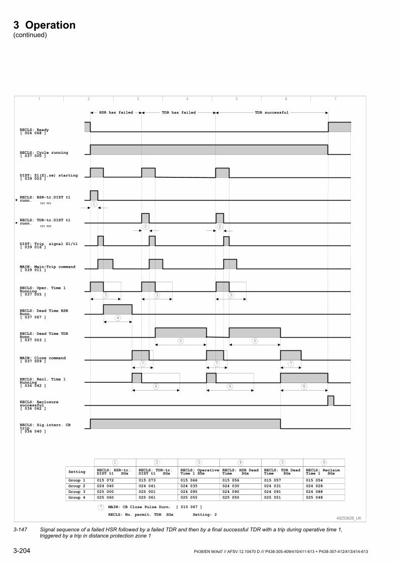
3 Operation (continued)
48Z5362B_UK
1 2 3 4 5 6 7
DIST: Z1(Z1,ze) starting[ 039 003 ]
Setting
Group 4Group 3Group 2Group 1
RECLS: HSR DeadTime SGx
RECLS: OperativeTime 1 SGx
RECLS: HSR-tr.DIST t1 SGx
015 072024 040025 000025 060
015 066024 035024 095025 055
015 056024 030024 090025 050
RECLS: Ready[ 004 068 ]
RECLS: Cycle running[ 037 000 ]
RECLS: Oper. Time 1Running[ 037 005 ]
MAIN: Main-Trip command[ 039 011 ]
DIST: Trip signal Z1/t1[ 039 016 ]
RECLS: Dead Time HSRRunn.[ 037 067 ]
MAIN: Close command[ 037 009 ]
RECLS: Recl. Time 1Running[ 036 042 ]
RECLS: Reclosuresuccessful[ 036 062 ]
RECLS: Sig.interr. CBtrip[ 036 040 ]
HSR has failed
6
4
3
1
2
654321
MAIN: CB Close Pulse Durn. [ 015 067 ]7
RECLS: No. permit. TDR SGx Setting: 2
RECLS: Dead Time TDRRunn.[ 037 003 ] 5
6
2
5
6
3 3
TDR has failed TDR successful
7 7 7
RECLS: ReclaimTime 1 SGx
015 054024 028024 088025 048
RECLS: TDR DeadTime SGx
015 057024 031024 091025 051
RECLS: TDR-tr.DIST t1 SGx
015 073024 041025 001025 061
RECLS: HSR-tr.DIST t1runn.
310 021
RECLS: TDR-tr.DIST t1runn.
310 022
3-147 Signal sequence of a failed HSR followed by a failed TDR and then by a final successful TDR with a trip during operative time 1,
triggered by a trip in distance protection zone 1
3-204 P438/EN M/Ad7 // AFSV.12.10470 D /// P438-305-409/410/411-613 + P438-307-412/413/414-613

3 Operation (continued)
3.26.4 Zone Extension
A zone extension of impedance zone 1 generally occurs when the respective parameters have been enabled. The extension is made for impedance and resistance values of the forward and reverse directional zone settings.
High-speed reclosures and time-delayed reclosures will enable different zone extension factors.
Zone extension on high-speed reclosure
Depending on the condition that the auto-recloser is ready and that the parameter R E C L S : Z o n e E x t n o n H S R S G x is set to 'Yes', the reach of zone 1 is then extended by zone extension factor D I S T : k z e E x t e n d e d H S R . Zone extension remains valid while the first operative time 1 or operative time 2 is running.
Zone extension on time-delayed reclosure
A zone extension on time-delayed reclosure is then possible only if the setting for R E C L S : Z o n e e x t n o n T D R S G x is 'Yes'. If, during a multiple HSR/TDR, at least one further reclosure is permitted then the reach of impedance zone 1 is extended by zone extension factor D I S T : k z e , T D R S G x when the first dead time commences. Zone extension remains valid until the last operative time 1 or operative time 2 has elapsed.
Zone extension during reclosure
A zone extension during reclosure is applied to detect faults in the respective extended zone after the reclose command from a high-speed reclosure or after the last reclose command from a multiple HSR/TDR was issued.
With a multiple HSR/TDR the parameter R E C L S : Z o n e E x t . D u r . R C S G x will be active only during the last time-delayed reclosure. The following settings are possible:
Setting for R E C L S : Z o n e E x t . D u r . R C S G x = 'No': At the beginning of the last dead time possible the extended reach for impedance zone 1 is removed.
Setting for R E C L S : Z o n e E x t . D u r . R C S G x = 'Following HSR': The zone extension for the high-speed reclosure is retained until the close command pulse time has elapsed.
Setting for R E C L S : Z o n e E x t . D u r . R C S G x = 'Following TDR': After the last possible operative time 1 or 2 has elapsed the zone extension for the time-delayed reclosure is retained until the close command pulse time has elapsed.
Setting for R E C L S : Z o n e e x t . d u r . R C S G x = 'Following HSR/TDR': When a high-speed reclosure is being carried out without a further time-delayed reclosure the zone extension for the high-speed reclosure is retained until the close command pulse time has elapsed. After the last possible operative time 1 or 2 has elapsed during a multiple HSR or TDR the zone extension for the time-delayed reclosure is retained until the close command pulse time has elapsed
P438/EN M/Ad7 // AFSV.12.10470 D /// P438-305-409/410/411-613 + P438-307-412/413/414-613 3-205
3 Operation (continued)
3.26.5 Auto-Reclose Control Function after Trip by Thermal Overload Protection
The thermal overload protection trip signal may be included in the auto-reclose functional sequence.
Parameter R E C L S : R C f . T H E R M t r i p S G x must be set for a reclosure to be effected after a thermal overload protection trip. If this parameter is set to 'Yes' a reclose command will be issued and reclaim time 1 triggered when the thermal overload protection trip signal is reset. In addition the following conditions apply for a reclosure to be effected after a thermal overload protection trip:
The thermal overload protection’s trip signal is set as a criterion for the main-trip command or re-trip command (only relevant when R E C L S : W i t h R e - T r i p is set to 'Yes').
The auto-recloser is ready to operate at starting time.
3-206 P438/EN M/Ad7 // AFSV.12.10470 D /// P438-305-409/410/411-613 + P438-307-412/413/414-613
3 Operation (continued)
3.26.6 Auto-Reclose Control Function with Parallel Protection Device
The trip signal from a second protection device operating in parallel to the P438 may be included in the auto-reclose functional sequence.
In order to have a protection device, operating in parallel, trigger the RECLS function, binary signal inputs have to be configured appropriately and the parameter R E C L S : P a r a l l e l t r i p S G x must be set. When this parameter is set to 'With Start ARC' the starting or the trip command issued by the protection device, operating in parallel, is included in the auto-reclose functional sequence. In addition the following conditions apply to have the RECLS function triggered by the protection device, operating in parallel:
The trip signal of the parallel protection device is set as a criterion for the main-trip command or re-trip command (only relevant when R E C L S : W i t h R e - T r i p is set to 'Yes').
The auto-recloser is ready to operate at starting time.
Operative time 1 or operative time 2 is running.
Depending on the configured binary signal inputs, operative times are triggered by the starting or the trip command issued by the protection device, operating in parallel.
P438/EN M/Ad7 // AFSV.12.10470 D /// P438-305-409/410/411-613 + P438-307-412/413/414-613 3-207
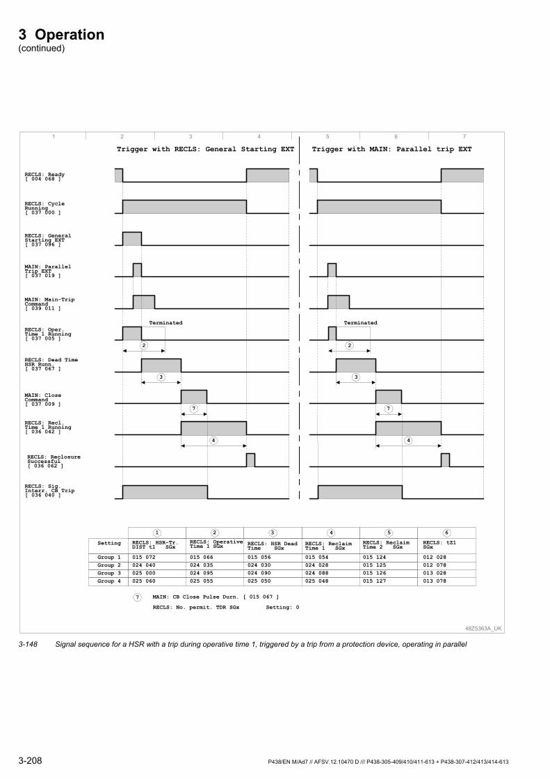
3 Operation (continued)
48Z5363A_UK
1 2 3 4 5 6 7
RECLS: General Starting EXT[ 037 096 ]
Setting
Group 4Group 3Group 2Group 1
RECLS: HSR-Tr.DIST t1 SGx
015 072024 040025 000025 060
015 066024 035024 095025 055
015 054024 028024 088025 048
015 124015 125015 126015 127
015 056024 030024 090025 050
RECLS: Ready[ 004 068 ]
RECLS: Cycle Running[ 037 000 ]
RECLS: Oper. Time 1 Running[ 037 005 ]
MAIN: Main-Trip Command[ 039 011 ]
MAIN: Parallel Trip EXT[ 037 019 ]
RECLS: Dead Time HSR Runn.[ 037 067 ]
MAIN: Close Command[ 037 009 ]
RECLS: Recl. Time 1 Running[ 036 042 ]
RECLS: ReclosureSuccessful[ 036 062 ]
Trigger with RECLS: General Starting EXT
4
7
3
2
Terminated
6 5 4 3 2 1
012 028012 078013 028013 078
MAIN: CB Close Pulse Durn. [ 015 067 ]7 RECLS: No. permit. TDR SGx Setting: 0
RECLS: Sig.Interr. CB Trip[ 036 040 ]
Trigger with MAIN: Parallel trip EXT
4
7
3
2
Terminated
RECLS: Reclaim Time 1 SGx
RECLS: Operative Time 1 SGx RECLS: HSR Dead
Time SGxRECLS: tZ1SGx
RECLS: Reclaim Time 2 SGx
3-148 Signal sequence for a HSR with a trip during operative time 1, triggered by a trip from a protection device, operating in parallel
3-208 P438/EN M/Ad7 // AFSV.12.10470 D /// P438-305-409/410/411-613 + P438-307-412/413/414-613
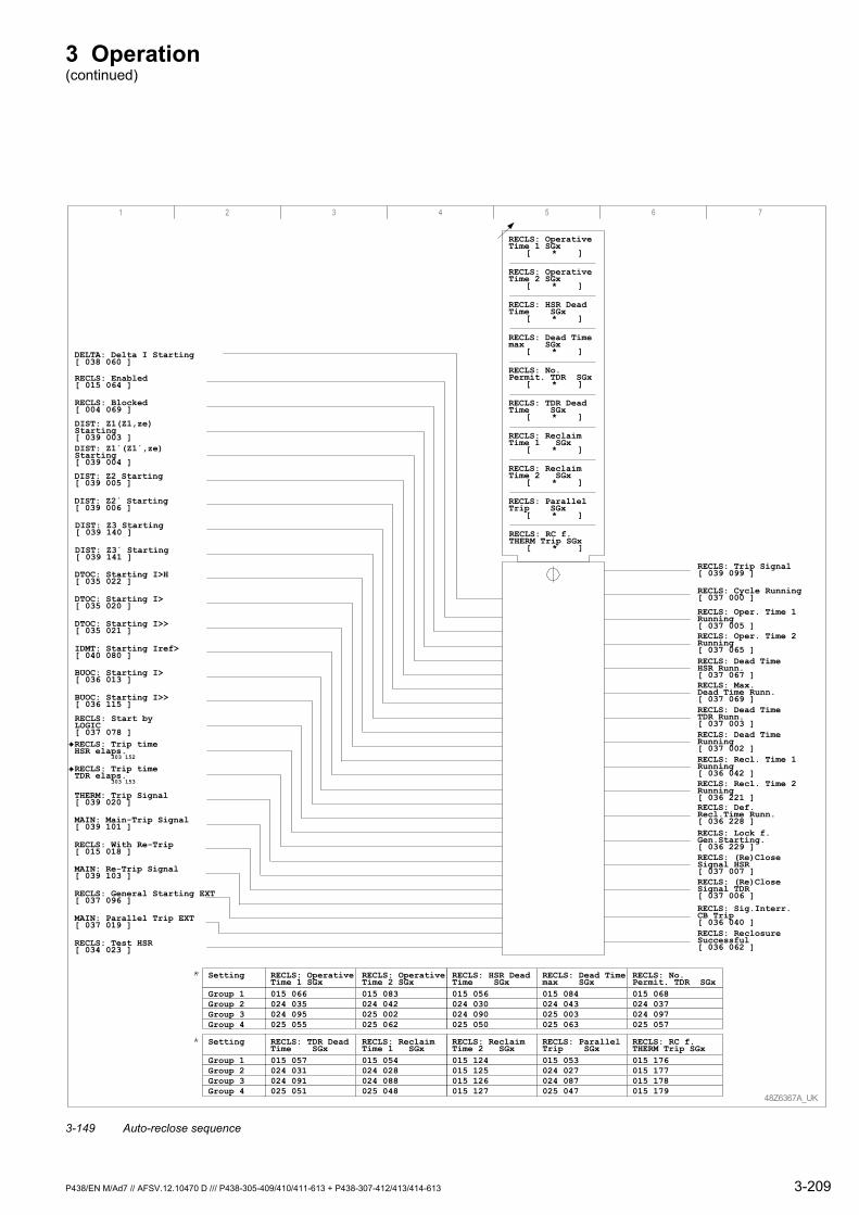
3 Operation (continued)
1 2 3 4 5 6 7
DIST: Z1(Z1,ze)Starting[ 039 003 ]DIST: Z1´(Z1´,ze)Starting[ 039 004 ]
RECLS: ReclosureSuccessful[ 036 062 ]
DIST: Z3 Starting[ 039 140 ]
DIST: Z3´ Starting[ 039 141 ]
DIST: Z2 Starting[ 039 005 ]
DIST: Z2´ Starting[ 039 006 ]
RECLS: With Re-Trip[ 015 018 ]
48Z6367A_UK
RECLS: OperativeTime 1 SGx
[ * ]
RECLS: OperativeTime 2 SGx
[ * ]
RECLS: HSR DeadTime SGx
[ * ]
RECLS: TDR DeadTime SGx
[ * ]
RECLS: Dead Timemax SGx
[ * ]
RECLS: ReclaimTime 1 SGx
[ * ]
RECLS: ReclaimTime 2 SGx
[ * ]
RECLS: No.Permit. TDR SGx
[ * ]
RECLS: ParallelTrip SGx
[ * ]
RECLS: Enabled[ 015 064 ]
RECLS: Blocked[ 004 069 ]
DTOC: Starting I>H[ 035 022 ]
DTOC: Starting I>[ 035 020 ]
DTOC: Starting I>>[ 035 021 ]
IDMT: Starting Iref>[ 040 080 ]
RECLS: Start byLOGIC[ 037 078 ]
BUOC: Starting I>[ 036 013 ]
BUOC: Starting I>>[ 036 115 ]
MAIN: Main-Trip Signal[ 039 101 ]
MAIN: Re-Trip Signal[ 039 103 ]
MAIN: Parallel Trip EXT[ 037 019 ]
RECLS: General Starting EXT[ 037 096 ]
RECLS: Test HSR[ 034 023 ]
RECLS: Sig.Interr.CB Trip[ 036 040 ]
RECLS: (Re)CloseSignal TDR[ 037 006 ]
RECLS: (Re)CloseSignal HSR[ 037 007 ]
RECLS: Recl. Time 2Running[ 036 221 ]
RECLS: Recl. Time 1Running[ 036 042 ]
RECLS: Dead TimeRunning[ 037 002 ]
RECLS: Dead TimeTDR Runn.[ 037 003 ]
RECLS: Max.Dead Time Runn.[ 037 069 ]
RECLS: Dead TimeHSR Runn.[ 037 067 ]
RECLS: Oper. Time 2Running[ 037 065 ]
RECLS: Oper. Time 1Running[ 037 005 ]
RECLS: Cycle Running[ 037 000 ]
RECLS: Trip Signal[ 039 099 ]
RECLS: RC f.THERM Trip SGx
[ * ]
THERM: Trip Signal[ 039 020 ] RECLS: Def.
Recl.Time Runn.[ 036 228 ]RECLS: Lock f.Gen.Starting.[ 036 229 ]
DELTA: Delta I Starting[ 038 060 ]
RECLS: ReclaimTime 2 SGx015 124015 125015 126015 127
RECLS: ReclaimTime 1 SGx015 054024 028024 088025 048
RECLS: TDR DeadTime SGx015 057024 031024 091025 051
RECLS: ParallelTrip SGx015 053024 027024 087025 047
RECLS: RC f.THERM Trip SGx015 176015 177015 178015 179
Setting
Group 1Group 2Group 3Group 4
RECLS: HSR DeadTime SGx015 056024 030024 090025 050
RECLS: OperativeTime 2 SGx015 083024 042025 002025 062
RECLS: OperativeTime 1 SGx015 066024 035024 095025 055
RECLS: Dead Timemax SGx015 084024 043025 003025 063
RECLS: No.Permit. TDR SGx015 068024 037024 097025 057
Setting
Group 1Group 2Group 3Group 4
RECLS: Trip timeHSR elaps.
303 152
RECLS: Trip timeTDR elaps.
303 153
3-149 Auto-reclose sequence
P438/EN M/Ad7 // AFSV.12.10470 D /// P438-305-409/410/411-613 + P438-307-412/413/414-613 3-209
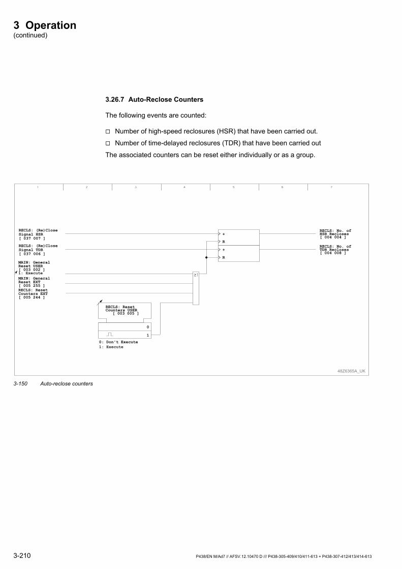
3 Operation (continued)
3.26.7 Auto-Reclose Counters
The following events are counted:
Number of high-speed reclosures (HSR) that have been carried out.
Number of time-delayed reclosures (TDR) that have been carried out
The associated counters can be reset either individually or as a group.
48Z6365A_UK
0
1
R
+
R
+
RECLS: ResetCounters USER
[ 003 005 ]
RECLS: ResetCounters EXT[ 005 244 ]
1: Execute
0: Don't Execute1: Execute
MAIN: GeneralReset USER[ 003 002 ]
MAIN: GeneralReset EXT[ 005 255 ]
RECLS: (Re)CloseSignal HSR[ 037 007 ]
RECLS: (Re)CloseSignal TDR[ 037 006 ]
RECLS: No. ofHSR Recloses[ 004 004 ]
RECLS: No. ofTDR Recloses[ 004 008 ]
3-150 Auto-reclose counters
3-210 P438/EN M/Ad7 // AFSV.12.10470 D /// P438-305-409/410/411-613 + P438-307-412/413/414-613
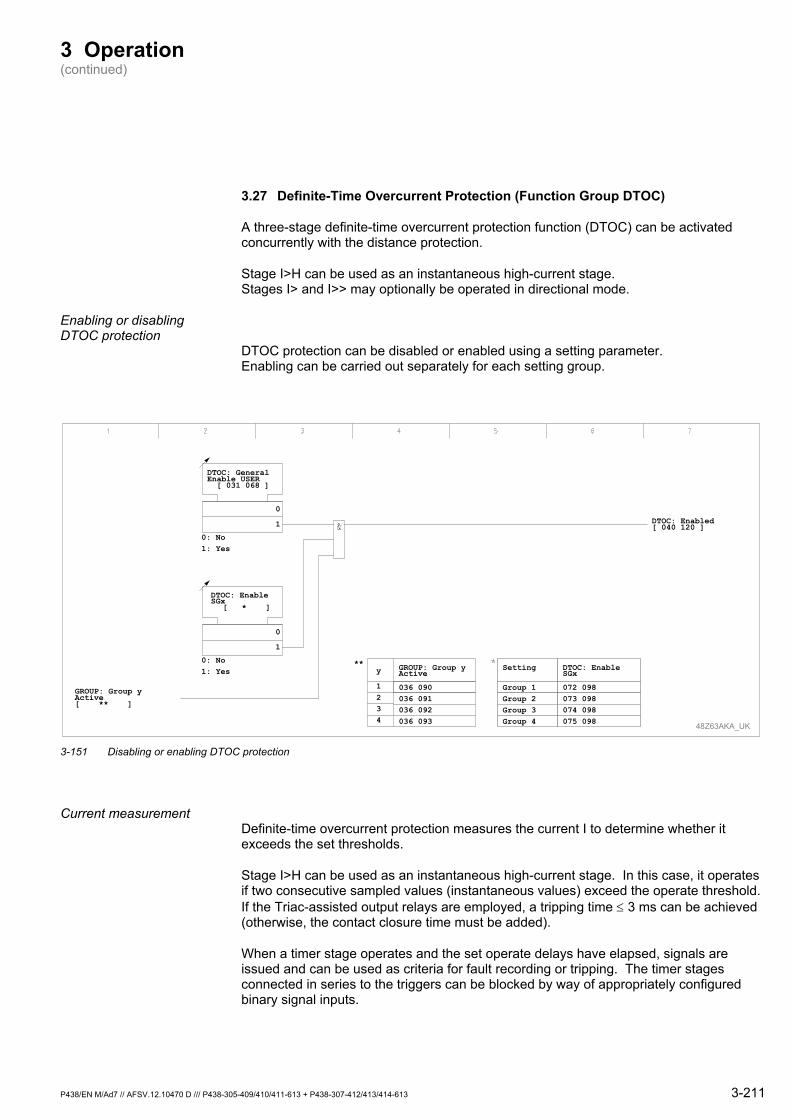
3 Operation (continued)
3.27 Definite-Time Overcurrent Protection (Function Group DTOC)
A three-stage definite-time overcurrent protection function (DTOC) can be activated concurrently with the distance protection.
Stage I>H can be used as an instantaneous high-current stage. Stages I> and I>> may optionally be operated in directional mode.
Enabling or disabling DTOC protection
DTOC protection can be disabled or enabled using a setting parameter. Enabling can be carried out separately for each setting group.
DTOC: General Enable USER[ 031 068 ]
48Z63AKA_UK
DTOC: Enable SGx
[ * ]
0
1
0: No1: Yes
0
1
0: No1: Yes
DTOC: Enabled[ 040 120 ]
DTOC: Enable SGx
072 098073 098074 098075 098
Setting
Group 1Group 2Group 3Group 4
GROUP: Group y Active[ ** ]
y
1
GROUP: Group y Active
036 090036 091036 092036 093
234
**
3-151 Disabling or enabling DTOC protection
Current measurement Definite-time overcurrent protection measures the current I to determine whether it exceeds the set thresholds.
Stage I>H can be used as an instantaneous high-current stage. In this case, it operates if two consecutive sampled values (instantaneous values) exceed the operate threshold. If the Triac-assisted output relays are employed, a tripping time ≤ 3 ms can be achieved (otherwise, the contact closure time must be added).
When a timer stage operates and the set operate delays have elapsed, signals are issued and can be used as criteria for fault recording or tripping. The timer stages connected in series to the triggers can be blocked by way of appropriately configured binary signal inputs.
P438/EN M/Ad7 // AFSV.12.10470 D /// P438-305-409/410/411-613 + P438-307-412/413/414-613 3-211
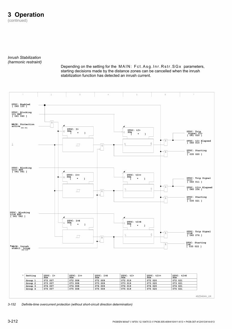
3 Operation (continued)
Inrush Stabilization (harmonic restraint)
Depending on the setting for the M A I N : F c t . A s g . I n r . R s t r . S G x parameters, starting decisions made by the distance zones can be cancelled when the inrush stabilization function has detected an inrush current.
MAIN: Inrushstabil. trigg
306 014
48Z5464A_UK
DTOC: BlockingtI>H EXT[ 041 062 ]
DTOC: tI>SGx072 019073 019074 019075 019
Setting
Group 1Group 2Group 3Group 4
DTOC: I>HSGx072 009073 009074 009075 009
DTOC: I>>SGx072 008073 008074 008075 008
DTOC: I>SGx072 007073 007074 007075 007
DTOC: tI>>SGx072 020073 020074 020075 020
DTOC: tI>HSGx072 021073 021074 021075 021
DTOC: BlockingtI>> EXT[ 041 061 ]
DTOC: BlockingtI> EXT[ 041 060 ]
DTOC: Enabled[ 040 120 ]
MAIN: Protectionactive
306 001
DTOC: Trip SignaltI>>[ 040 011 ]
DTOC: tI>> Elapsed[ 040 106 ]
DTOC: StartingI>>[ 035 021 ]
DTOC: Trip SignaltI>H[ 040 076 ]
DTOC: StartingI>H[ 035 022 ]
DTOC: I>SGx
[ * ]DTOC: tI>SGx
[ * ]
DTOC: tI>>SGx
[ * ]
DTOC: I>>SGx
[ * ]
DTOC: I>HSGx
[ * ]DTOC: tI>HSGx
[ * ]
DTOC: Trip Signal tI>[ 041 020 ]
DTOC: tI> Elapsed[ 040 010 ]
DTOC: StartingI>[ 035 020 ]
3-152 Definite-time overcurrent protection (without short-circuit direction determination)
3-212 P438/EN M/Ad7 // AFSV.12.10470 D /// P438-305-409/410/411-613 + P438-307-412/413/414-613

3 Operation (continued)
Direction measurement The short-circuit direction determination function is available in the P438 as ofsoftware version –604. It is enabled at D T O C : D i r e c t i o n m e a s u r e m . All settings relevant to short-circuit direction determination can be set separately for stages I> and I>>. When a starting signal is issued by I> or I>> and the measured voltage level has dropped below the value for V< the fault angle ϕ is calculated and the short-circuit direction is determined. The short-circuit characteristic is defined by the angles β and γ. The algorithm decides that the fault direction is forward when the calculated angle ϕ lies within the range given by γ ≤ ϕ ≤ β.
In order for direction measurement to function correctly, even at very small fault voltage values, the information stored in the voltage memory is also put to use in these cases.
Using the D T O C : T i m e S t a r t t I > S G x and D T O C : T i m e S t a r t t I > > S G x settings it is possible to select separately for each stage whether the timer stage is started with the triggering of current thresholds I> or I>> or, additionally, with a directional signal. The starting signal for each stage is formed according to the starting conditions selected for the timer stages.
The direction determination and the starting of the respective stage are only enabled if the measured voltage value is below a settable undervoltage threshold V<. Setting the undervoltage threshold V< to Blocked will disable this voltage scan and tripping will be permanently enabled.
For very low fault voltages, the voltage from the voltage memory is used in place of the measured voltage in order to avoid erroneous direction decisions. The direction decision is dependent on the following conditions:
VF > 0.1 Vn The direction decision is issued on the basis of the fault current and the measured fault voltage Vf.
VF < 0.1 Vn Voltage memory enabled: The direction decision is issued on the basis of the fault current and the voltage values stored in the voltage memory. Voltage memory not enabled: The direction decision is issued on the basis of the fault current and the measured fault voltage down to a minimum value of 1 V. If the fault voltage drops to a value of less than approximately 1 V, an accurate direction determination is no longer possible. In this case, a Fault forward decision is issued - independently of the actual fault direction.
Another setting is used to determine whether a failure of the voltage-measuring circuit will either lead to the DTOC protection operating non-directionally or to it becoming blocked.
The starting direction may be freely set.
P438/EN M/Ad7 // AFSV.12.10470 D /// P438-305-409/410/411-613 + P438-307-412/413/414-613 3-213
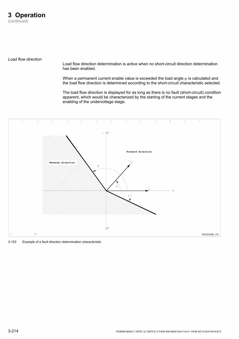
3 Operation (continued)
Load flow direction Load flow direction determination is active when no short-circuit direction determination has been enabled.
When a permanent current enable value is exceeded the load angle ϕ is calculated and the load flow direction is determined according to the short-circuit characteristic selected.
The load flow direction is displayed for as long as there is no fault (short-circuit) condition apparent, which would be characterized by the starting of the current stages and the enabling of the undervoltage stage.
Forward direction
Reverse direction
68Z50ABB_UK 3-153 Example of a fault direction determination characteristic
3-214 P438/EN M/Ad7 // AFSV.12.10470 D /// P438-305-409/410/411-613 + P438-307-412/413/414-613
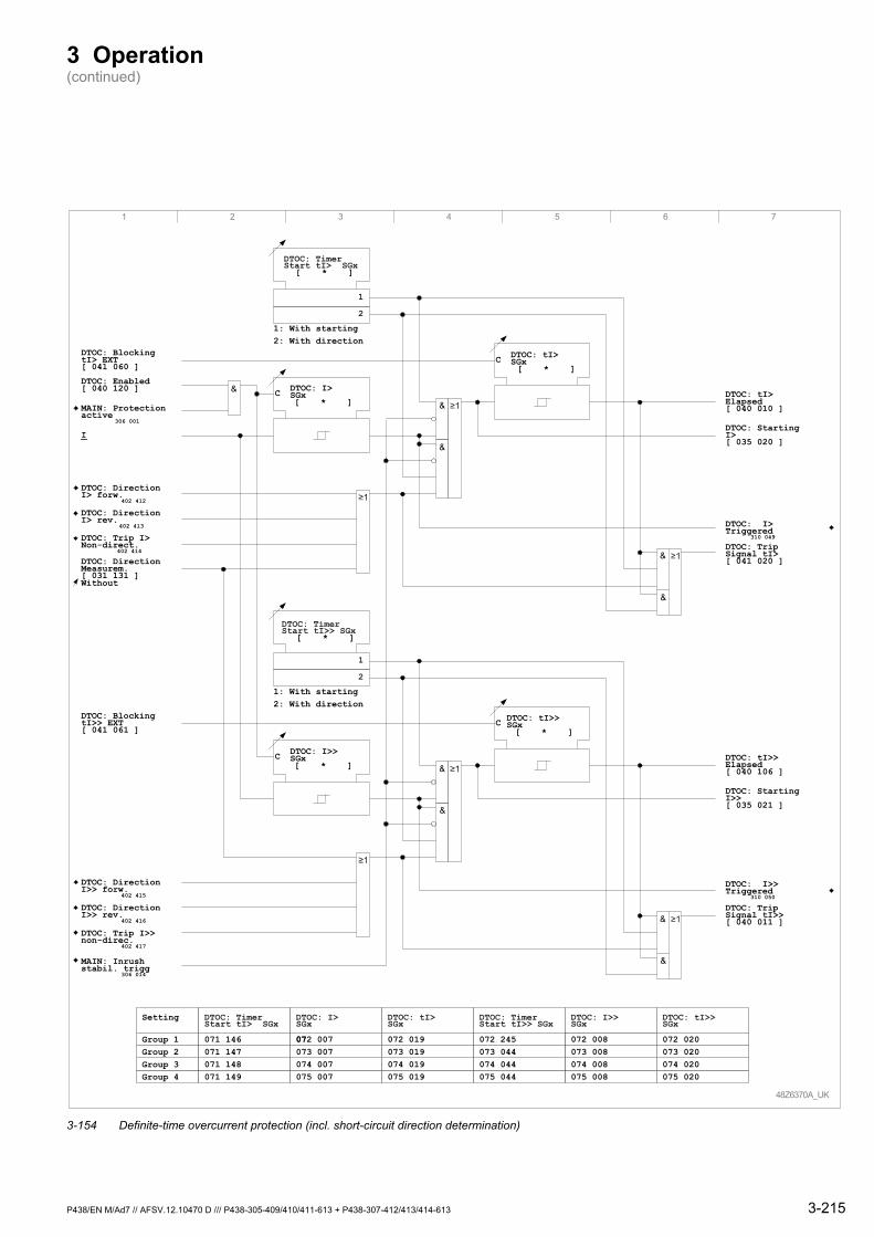
3 Operation (continued)
1 2 3 4 5 6 7
48Z6370A_UK
DTOC: tI> Elapsed[ 040 010 ]
Parameter-Setting
Group 4Group 3Group 2Group 1
DTOC: Timer Start tI> SGx
071 146071 147071 148071 149
DTOC: I> SGx
07072 007073 007074 007075 007
DTOC: tI> SGx
072 008073 008074 008075 008
DTOC: Blocking tI> EXT[ 041 060 ]
DTOC: I> SGx[ * ]
DTOC: Timer Start tI> SGx
[ * ]
1
1: With starting2: With direction
2
DTOC: I> Triggered
310 049
CDTOC: Enabled[ 040 120 ]
MAIN: Protection active
306 001
I
DTOC: Direction I> forw.
402 412
DTOC: Direction I> rev.
402 413
DTOC: Trip I> Non-direct.
402 414
DTOC: Direction Measurem.[ 031 131 ]Without
DTOC: tI> SGx[ * ]
C
DTOC: Starting I> [ 035 020 ]
DTOC: Trip Signal tI>[ 041 020 ]
DTOC: tI>> Elapsed[ 040 106 ]
DTOC: Blocking tI>> EXT[ 041 061 ]
DTOC: I>> SGx[ * ]
DTOC: Timer Start tI>> SGx
[ * ]
1
1: With starting2: With direction
2
DTOC: I>> Triggered
310 050
C
DTOC: Direction I>> forw.
402 415
DTOC: Direction I>> rev.
402 416
DTOC: Trip I>> non-direc.
402 417
DTOC: tI>> SGx[ * ]
C
DTOC: Starting I>> [ 035 021 ]
DTOC: Trip Signal tI>>[ 040 011 ]
DTOC: Timer Start tI>> SGx
072 245073 044074 044075 044
DTOC: I>> SGx
072 019073 019074 019075 019
DTOC: tI>> SGx
072 020073 020074 020075 020
MAIN: Inrush stabil. trigg
306 014
&
&
&
&
&
&
&
&
&
3-154 Definite-time overcurrent protection (incl. short-circuit direction determination)
P438/EN M/Ad7 // AFSV.12.10470 D /// P438-305-409/410/411-613 + P438-307-412/413/414-613 3-215
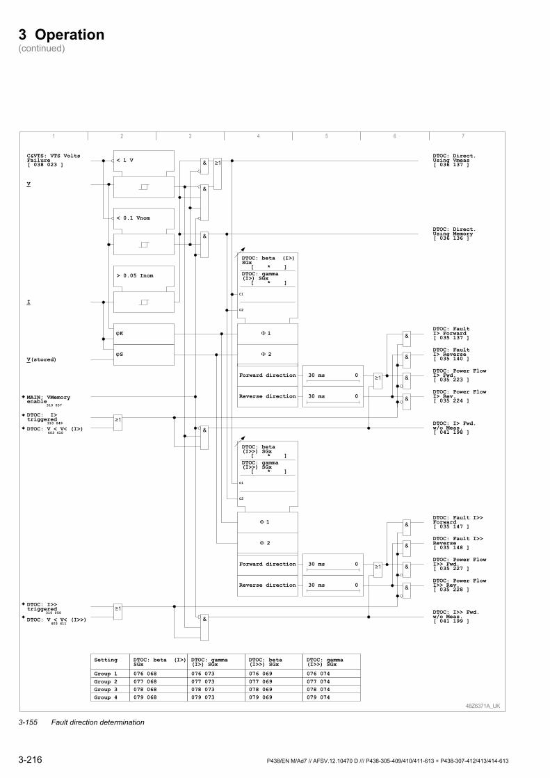
3 Operation (continued)
1 2 3 4 5 6 7
48Z6371A_UK
DTOC: Direct.Using Vmeas[ 036 137 ]
< 1 V
DTOC: I>triggered
310 049
< 0.1 Vnom
K
SV(stored)
I
DTOC: I> Fwd.w/o Meas.[ 041 198 ]
DTOC: Direct.Using Memory[ 036 136 ]
> 0.05 Inom
V
DTOC: beta (I>)SGx
[ * ]DTOC: gamma(I>) SGx
[ * ]
Forward direction
1
2
MAIN: VMemoryenable
310 057
DTOC: V < V< (I>)403 410
DTOC: Power FlowI> Fwd.[ 035 223 ]
DTOC: Power FlowI> Rev.[ 035 224 ]
DTOC: FaultI> Forward[ 035 137 ]
DTOC: FaultI> Reverse[ 035 140 ]
Reverse direction
30 ms 0
30 ms 0
DTOC: I>>triggered
310 050 DTOC: I>> Fwd.w/o Meas.[ 041 199 ]
DTOC: beta(I>>) SGx
[ * ]
C1
DTOC: gamma(I>>) SGx
[ * ]
C2
Forward direction
DTOC: V < V< (I>>)403 411
DTOC: Power FlowI>> Fwd.[ 035 227 ]
DTOC: Power FlowI>> Rev.[ 035 228 ]
DTOC: Fault I>>Forward[ 035 147 ]
DTOC: Fault I>>Reverse[ 035 148 ]
Reverse direction
30 ms 0
30 ms 0
Setting-Setting
Group 4Group 3Group 2Group 1
DTOC: beta (I>)SGx
076 068077 068078 068079 068
DTOC: gamma(I>) SGx
076 073077 073078 073079 073
DTOC: beta(I>>) SGx
076 069077 069078 069079 069
DTOC: gamma(I>>) SGx
076 074077 074078 074079 074
C1
C2
C&VTS: VTS VoltsFailure[ 038 023 ] &
&
&
&
&
&
&
&
&
&
&
&
&
Φ
Φ
1
2
Φ
Φ
3-155 Fault direction determination
3-216 P438/EN M/Ad7 // AFSV.12.10470 D /// P438-305-409/410/411-613 + P438-307-412/413/414-613
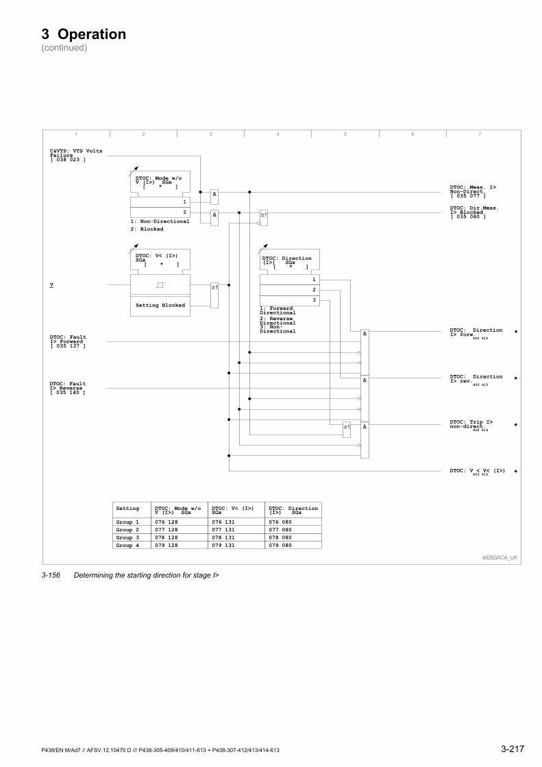
3 Operation (continued)
1 2 3 4 5 6 7
48Z63ACA_UK
DTOC: Meas. I>Non-Direct.[ 035 077 ]
Setting-Setting
Group 4Group 3Group 2Group 1
DTOC: Mode w/oV (I>) SGx
076 128077 128078 128079 128
DTOC: V< (I>)SGx
076 131077 131078 131079 131
DTOC: Direction(I>) SGx
076 080077 080078 080079 080
C&VTS: VTS VoltsFailure[ 038 023 ]
DTOC: Mode w/oV (I>) SGx[ * ]
1
1: Non-Directional2: Blocked
2
DTOC: V< (I>)SGx
[ * ]
Setting Blocked
DTOC: Dir.Meas.I> Blocked[ 035 080 ]
DTOC: FaultI> Forward[ 035 137 ]
DTOC: Direction(I>) SGx
[ * ]
1
2
3
DTOC: FaultI> Reverse[ 035 140 ]
DTOC: DirectionI> forw.
402 412
DTOC: DirectionI> rev.
402 413
DTOC: Trip I>non-direct.
402 414
DTOC: V < V< (I>)403 410
V
&
&
&
&
&
1: ForwardDirectional2: ReverseDirectional3: Non-Directional
3-156 Determining the starting direction for stage I>
P438/EN M/Ad7 // AFSV.12.10470 D /// P438-305-409/410/411-613 + P438-307-412/413/414-613 3-217

3 Operation (continued)
1 2 3 4 5 6 7
48Z63ADA_UK
DTOC: Meas. I>>Non-Direct[ 035 078 ]
Setting-Setting
Group 4Group 3Group 2Group 1
C&VTS: VTS VoltsFailure[ 038 023 ]
DTOC: Mode w/oV (I>>) SGx
[ * ]
1
2
DTOC: U< (I>>)SGx
[ * ]
Setting Blocked
DTOC: Dir.Meas.I>> Blocked[ 035 133 ]
DTOC: Fault I>>Forward[ 035 147 ]
DTOC: Direction(I>>) SGx
[ * ]
1
2
3
DTOC: Fault I>>Reverse[ 035 148 ]
DTOC: DirectionI>> forw..
402 415
DTOC: DirectionI>> rev.
402 416
DTOC: Trip I>>Non-Direct.
402 417
DTOC: V < V< (I>>)403 411
DTOC: Mode w/oV (I>>) SGx
076 129077 129078 129079 129
DTOC: V< (I>>)SGx
076 150077 150078 150079 150
DTOC: Direction(I>>) SGx
076 088077 088078 088079 088
V
&
&
&
&
&
1: ForwardDirectional2: ReverseDirectional3: Non-Directional
1: Non-Directional2: Blocked
3-157 Determining the starting direction for stage I>>
3-218 P438/EN M/Ad7 // AFSV.12.10470 D /// P438-305-409/410/411-613 + P438-307-412/413/414-613

3 Operation (continued)
3.28 Inverse-Time Overcurrent Protection (Function Group IDMT)
The P438 provides a single-stage inverse-time overcurrent protection function. This IDMT function can be activated concurrently with the other protection functions.
Inverse overcurrent protection may optionally be operated with short-circuit direction determination.
Disabling or enabling IDMT protection
IDMT protection can be disabled or enabled using a setting parameter. Enabling can be carried out separately for each setting group.
48Z6377A_EN
IDMT: Generalenable USER[ 017 096 ]
0
1
0: No1: Yes
IDMT: EnablePSx[ * ]
0
1
0: No1: Yes
PSS: PS yactive[ ** ]
IDMT: Enabled[ 040 100 ]
1 2 3 4 5 6 7
1
Y
2
3
4
036 090
PSS: PS yactive
036 091
036 092
036 093
set 1
set 2
072 000
IDMT: EnablePSx
073 000
074 000
075 000
set 3
set 4
Parameter
&
** *
3-158 Disabling or enabling IDMT protection
Inrush stabilization (Harmonic restraint)
Depending on the settings for M A I N : F c t . A s g . I n r . R s t r . S G x starting decisions made by the distance zones can be cancelled when the inrush stabilization function has detected an inrush current.
Time-dependent characteristics The user can select from a large number of characteristics (see table below). The measured value is current I.
The tripping characteristics available for selection are shown in figures Fehler! Verweisquelle konnte nicht gefunden werden. to Fehler! Verweisquelle konnte nicht gefunden werden..
P438/EN M/Ad7 // AFSV.12.10470 D /// P438-305-409/410/411-613 + P438-307-412/413/414-613 3-219
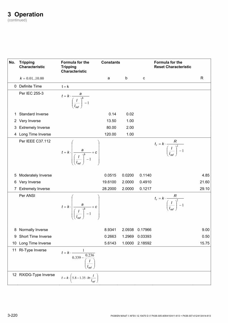
3 Operation (continued)
No. Tripping
Characteristic Formula for the Tripping Characteristic
Constants Formula for the Reset Characteristic
0010010 .....k = a b c R
0 Definite Time t k=
Per IEC 255-3
1−⎟⎟⎠
⎞⎜⎜⎝
⎛⋅= b
refII
akt
1 Standard Inverse 0.14 0.02
2 Very Inverse 13.50 1.00
3 Extremely Inverse 80.00 2.00
4 Long Time Inverse 120.00 1.00
Per IEEE C37.112
⎟⎟⎟⎟⎟⎟
⎠
⎞
⎜⎜⎜⎜⎜⎜
⎝
⎛
+
−⎟⎟⎠
⎞⎜⎜⎝
⎛⋅= c
II
akt b
ref1
12
−⎟⎟⎠
⎞⎜⎜⎝
⎛⋅=
ref
r
II
Rkt
5 Moderately Inverse 0.0515 0.0200 0.1140 4.85
6 Very Inverse 19.6100 2.0000 0.4910 21.60
7 Extremely Inverse 28.2000 2.0000 0.1217 29.10
Per ANSI
⎟⎟⎟⎟⎟⎟
⎠
⎞
⎜⎜⎜⎜⎜⎜
⎝
⎛
+
−⎟⎟⎠
⎞⎜⎜⎝
⎛⋅= c
II
akt b
ref1
12
−⎟⎟⎠
⎞⎜⎜⎝
⎛⋅=
ref
r
II
Rkt
8 Normally Inverse 8.9341 2.0938 0.17966 9.00
9 Short Time Inverse 0.2663 1.2969 0.03393 0.50
10 Long Time Inverse 5.6143 1.0000 2.18592 15.75
11 RI-Type Inverse
⎟⎟⎠
⎞⎜⎜⎝
⎛−
⋅=
refII
..kt 23603390
1
12 RXIDG-Type Inverse ⎟⎟⎠
⎞⎜⎜⎝
⎛⋅−⋅=
refIIln..kt 35185
3-220 P438/EN M/Ad7 // AFSV.12.10470 D /// P438-305-409/410/411-613 + P438-307-412/413/414-613
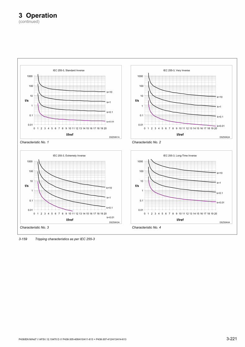
3 Operation (continued)
0 1 2 3 4 5 6 7 8 9 10 11 12 13 14 15 16 17 18 19 20
I/Iref
t/s
D5Z50K1A
k=1
k=10
k=0.1
k=0.01
IEC 255-3, Standard Inverse
1000
100
10
1
0.1
0.01
0 1 2 3 4 5 6 7 8 9 10 11 12 13 14 15 16 17 18 19 20
I/Iref
t/s
D5Z50K2A
k=1
k=10
k=0.1
k=0.01
IEC 255-3, Very Inverse
1000
100
10
1
0.1
0.01
Characteristic No. 1 Characteristic No. 2
0 1 2 3 4 5 6 7 8 9 10 11 12 13 14 15 16 17 18 19 20
I/Iref
t/s
D5Z50K3A
k=1
k=10
k=0.1
k=0.01
IEC 255-3, Extremely Inverse
1000
100
10
1
0.1
0.01
0 1 2 3 4 5 6 7 8 9 10 11 12 13 14 15 16 17 18 19 20
I/Iref
t/s
D5Z50K4A
k=1
k=10
k=0.1
k=0.01
IEC 255-3, Long-Time Inverse
1000
100
10
1
0.1
0.01
Characteristic No. 3 Characteristic No. 4
3-159 Tripping characteristics as per IEC 255-3
P438/EN M/Ad7 // AFSV.12.10470 D /// P438-305-409/410/411-613 + P438-307-412/413/414-613 3-221
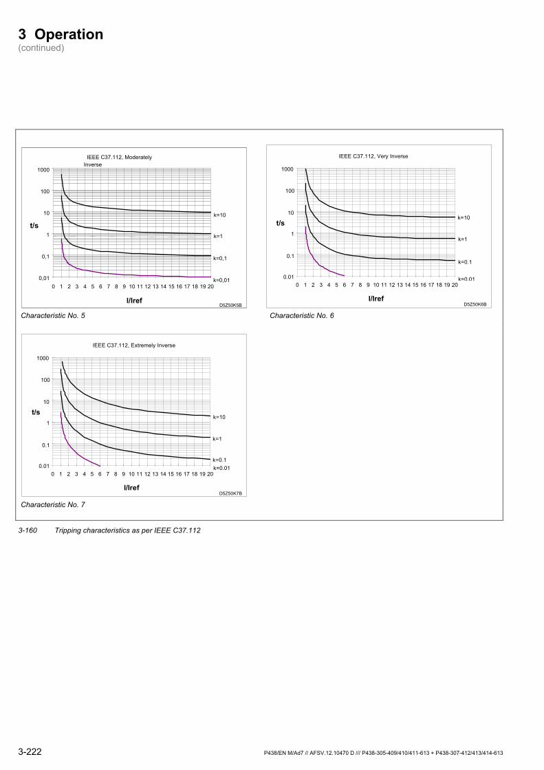
3 Operation (continued)
0,01
0,1
1
10
100
1000
0 1 2 3 4 5 6 7 8 9 10 11 12 13 14 15 16 17 18 19 20
I/Iref
t/s
D5Z50K5B
k=1
k=10
k=0,1
k=0,01
IEEE C37.112, ModeratelyInverse
0 1 2 3 4 5 6 7 8 9 10 11 12 13 14 15 16 17 18 19 20
I/Iref
t/s
D5Z50K6B
k=1
k=10
k=0.1
k=0.01
IEEE C37.112, Very Inverse
1000
100
10
1
0.1
0.01
Characteristic No. 5 Characteristic No. 6
0 1 2 3 4 5 6 7 8 9 10 11 12 13 14 15 16 17 18 19 20
I/Iref
t/s
D5Z50K7B
k=1
k=10
k=0.1k=0.01
IEEE C37.112, Extremely Inverse
1000
100
10
1
0.1
0.01
Characteristic No. 7
3-160 Tripping characteristics as per IEEE C37.112
3-222 P438/EN M/Ad7 // AFSV.12.10470 D /// P438-305-409/410/411-613 + P438-307-412/413/414-613
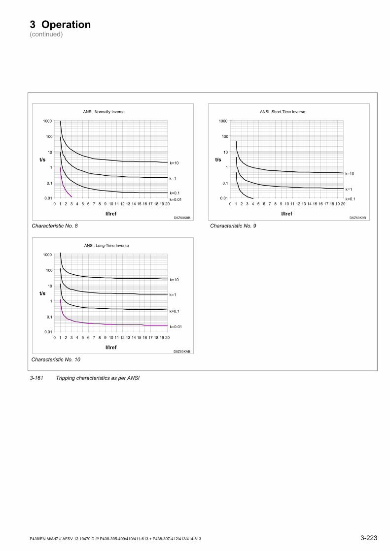
3 Operation (continued)
0 1 2 3 4 5 6 7 8 9 10 11 12 13 14 15 16 17 18 19 20
I/Iref
t/s
D5Z50K8B
k=1
k=10
k=0.1
k=0.01
ANSI, Normally Inverse
1000
100
10
1
0.1
0.01
0 1 2 3 4 5 6 7 8 9 10 11 12 13 14 15 16 17 18 19 20
I/Iref
t/s
D5Z50K9B
k=1
k=10
k=0.1
ANSI, Short-Time Inverse
1000
100
10
1
0.1
0.01
Characteristic No. 8 Characteristic No. 9
0 1 2 3 4 5 6 7 8 9 10 11 12 13 14 15 16 17 18 19 20
I/Iref
t/s
D5Z50KAB
k=1
k=10
k=0.1
k=0.01
ANSI, Long-Time Inverse
1000
100
10
1
0.1
0.01
Characteristic No. 10
3-161 Tripping characteristics as per ANSI
P438/EN M/Ad7 // AFSV.12.10470 D /// P438-305-409/410/411-613 + P438-307-412/413/414-613 3-223

3 Operation (continued)
0 1 2 3 4 5 6 7 8 9 10 11 12 13 14 15 16 17 18 19 20
I/Iref
t/s
D5Z50KBA
k=1
k=10
k=0.1
k=0.01
RI-Type Inverse
1000
100
10
1
0.1
0.01
0 1 2 3 4 5 6 7 8 9 10 11 12 13 14 15 16 17 18 19 20
I/Iref
t/s
D5Z50KCA
k=1
k=10
k=0.1
k=0.01
RXIDG-Type Inverse
1000
100
10
1
0.1
0.01
Characteristic No. 11 Characteristic No. 12
3-162 RI-type inverse and RXIDG-type inverse tripping characteristics
Determining the trip time The P438 checks whether the current value exceeds an adjustable threshold. The IDMT protection function is triggered if 1.05 times the set current reference is exceeded. The P438 will determine the trip time according to the set characteristic and the current level value. Additionally, a minimum trip time can be set, independently of the current level, which will in no case be under-run.
The inverse time-delayed stage may be blocked using an appropriately configured binary signal input.
3-224 P438/EN M/Ad7 // AFSV.12.10470 D /// P438-305-409/410/411-613 + P438-307-412/413/414-613
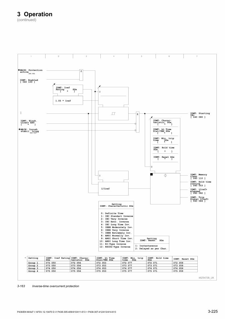
3 Operation (continued)
MAIN: Inrushstabil. trigg
306 014
48Z5472B_UK
IDMT: Min. triptime SGx072 077073 077074 077075 077
Setting
Group 1Group 2Group 3Group 4
IDMT: kt TimeDial/TMS SGx072 053073 053074 053075 053
IDMT: Charac-teristic SGx072 056073 056074 056075 056
IDMT: Iref RatingSGx072 050073 050074 050075 050
IDMT: Reset SGx
072 059073 059074 059075 059
IDMT: Hold timeSGx072 071073 071074 071075 071
MAIN: Protectionactive
306 001
IDMT: Enabled[ 040 100 ]
IDMT: Block.tIref> EXT[ * ]
IDMT: IrefRating SGx
[ * ]
IDMT: Charac-teristic SGx
[ * ]
IDMT: kt TimeDial/TMS SGx
[ * ]
IDMT: Min. triptime SGx
[ * ]
IDMT: Hold timeSGx
[ * ]
IDMT: Reset SGx[ * ]
IDMT: StartingIB>[ 040 080 ]
IDMT: Memoryclear[ 040 110 ]
IDMT: Hold timerunning[ 040 053 ]
IDMT: tIref>elapsed[ 040 082 ]
IDMT: TripSignal tIref>[ 040 084 ]
SettingIDMT: Characteristic SGx
0: Definite Time 1: IEC Standart Inverse 2: IEC Very Inverse 3: IEC Extr. Inverse 4: IEC Long Time Inv. 5: IEEE Moderately Inv. 6: IEEE Very Inverse 7: IEEE Extremely Inv. 8: ANSI Normally Inv. 9: ANSI Short Time Inv.10: ANSI Long Time Inv.11: RI-Type Inverse12: RXIDG-Type Inverse
SettingIDMT: Reset SGx
1: Instantaneous2: Delayed as per Char.
I/Iref
1.05 * Iref
3-163 Inverse-time overcurrent protection
P438/EN M/Ad7 // AFSV.12.10470 D /// P438-305-409/410/411-613 + P438-307-412/413/414-613 3-225

3 Operation (continued)
Direction measurement The short-circuit direction determination function is available in the P438 as of software version –604. It is enabled with I D M T : D i r e c t i o n M e a s u r e m . When a starting signal is issued and the measured voltage level has dropped below the value for V<, the fault angle ϕ is calculated and the fault direction is determined. The short-circuit characteristic is defined by the angles β and γ. The software decides that the fault direction is ”forward“ when the calculated angle ϕ lies within the range given by γ ≤ ϕ ≤ β.
In order for direction measurement to function correctly, even at very small fault voltage values, the information stored in the voltage memory is also put to use in these cases.
The setting at I D M T : T i m e r S t a . t I r e f > S G x defines whether the timer stage is started when IDMT protection is triggered or, if a directional signal is also required. The starting signal is also formed according to the starting conditions.
Direction determination and starting are enabled only if the measured voltage value is below a settable undervoltage threshold, V<. Setting undervoltage threshold V< to Blocked will disable this voltage scan and tripping will be permanently enabled.
For very low fault voltages, the voltage from the voltage memory is used in place of the measured voltage in order to avoid erroneous direction decisions. The directional decision is dependent on the following conditions:
VF > 0.1 Vn The directional decision is issued on the basis of the fault current and the measured fault voltage VF.
VF < 0.1 Vn Voltage memory enabled: The directional decision is issued on the basis of the fault current and the voltage value stored in the voltage memory. Voltage memory not enabled: The directional decision is issued on the basis of the fault current and the measured fault voltage down to a minimum value of 1 V. If the fault voltage drops to a value of less than approximately 1 V, an accurate direction determination is no longer possible. In this case, a Fault forward decision is issued - independently of the actual fault direction.
Another setting is used to determine whether a failure of the voltage measuring circuit will either lead to DTOC protection operating non-directionally or to it becoming blocked.
The starting direction may be freely set.
3-226 P438/EN M/Ad7 // AFSV.12.10470 D /// P438-305-409/410/411-613 + P438-307-412/413/414-613
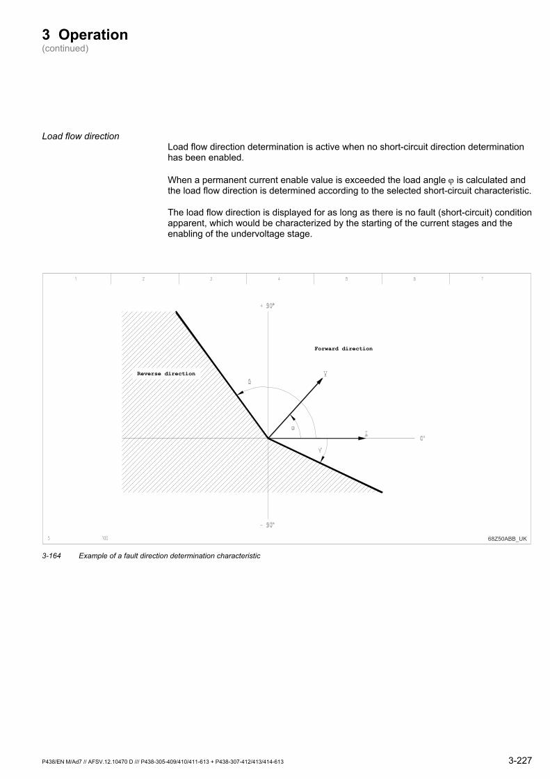
3 Operation (continued)
Load flow direction Load flow direction determination is active when no short-circuit direction determination has been enabled.
When a permanent current enable value is exceeded the load angle ϕ is calculated and the load flow direction is determined according to the selected short-circuit characteristic.
The load flow direction is displayed for as long as there is no fault (short-circuit) condition apparent, which would be characterized by the starting of the current stages and the enabling of the undervoltage stage.
Forward direction
Reverse direction
68Z50ABB_UK 3-164 Example of a fault direction determination characteristic
P438/EN M/Ad7 // AFSV.12.10470 D /// P438-305-409/410/411-613 + P438-307-412/413/414-613 3-227

3 Operation (continued)
1 2 3 4 5 6 7
48Z6375A_EN
IDMT: Block.tIB> EXT[ 040 101 ]
IDMT: IrefPSx[ * ]
UIDMT: Timer Sta.tIref>PSx
[ * ]
1
1: With starting2: With direction
2
IDMT: Iref>triggered
310 038
C
IDMT: Enabled[ 040 100 ]
MAIN: Protectionactive
306 001
I
IDMT: Directionforward
307 104
IDMT: Directionbackward
307 105
IDMT: Trip Non-direction
307 106IDMT: Directionmeasurem.[ 017 109 ]Without
CIDMT: StartingIref>[ 040 080 ]
IDMT: Trip signaltIref>[ 040 084 ]
1.05 * Iref
C
I / Iref
IDMT: Min. triptime PSx
[ * ]IDMT: Hold time PSx
[ * ]
C
IDMT: Charac-teristic PSx
[ * ]IDMT: Char.factor kt PSx
[ * ]
IDMT: Reset PSx
[ * ]
IDMT: Memoryclear[ 040 110 ]IDMT: Hold timerunning[ 040 053 ]
IDMT: tIref>elapsed[ 040 082 ]
MAIN: Inrushstabil. trigg
306 014
Parameter
set 4set 3set 2set 1
IDMT: Timer Sta.tIref>PSx
006 061006 062006 063006 064
IDMT: IrefPSx
072 050073 050074 050075 050
IDMT: Charac-teristic PSx
072 056073 056074 056075 056
IDMT: Char.factor kt PSx
072 053073 053074 053075 053
IDMT: Min. triptime PSx
072 077073 077074 077075 077
IDMT: Hold time PSx
072 071073 071074 071075 071
IDMT: Characteristic PSxSetting
0:1:2:3:4:5:6:7:8:9:
10:11:12:
Definite TimeIEC Standard InverseIEC Very InverseIEC Extr. InverseIEC Long Time Inv.IEEE Moderately Inv.IEEE Very InverseIEEE Extremely Inv.ANSI Normally Inv.ANSI Short Time Inv.ANSI Long Time Inv.RI-Type InverseRXIDG Inverse
IDMT: Reset PSxSetting
1:2:
Without delayDelayed as per char.
IDMT: Reset PSx
072 059073 059074 059075 059
Parameter
set 4set 3set 2set 1
&&
&
&
&
3-165 IDMT protection (including short-circuit direction determination)
3-228 P438/EN M/Ad7 // AFSV.12.10470 D /// P438-305-409/410/411-613 + P438-307-412/413/414-613
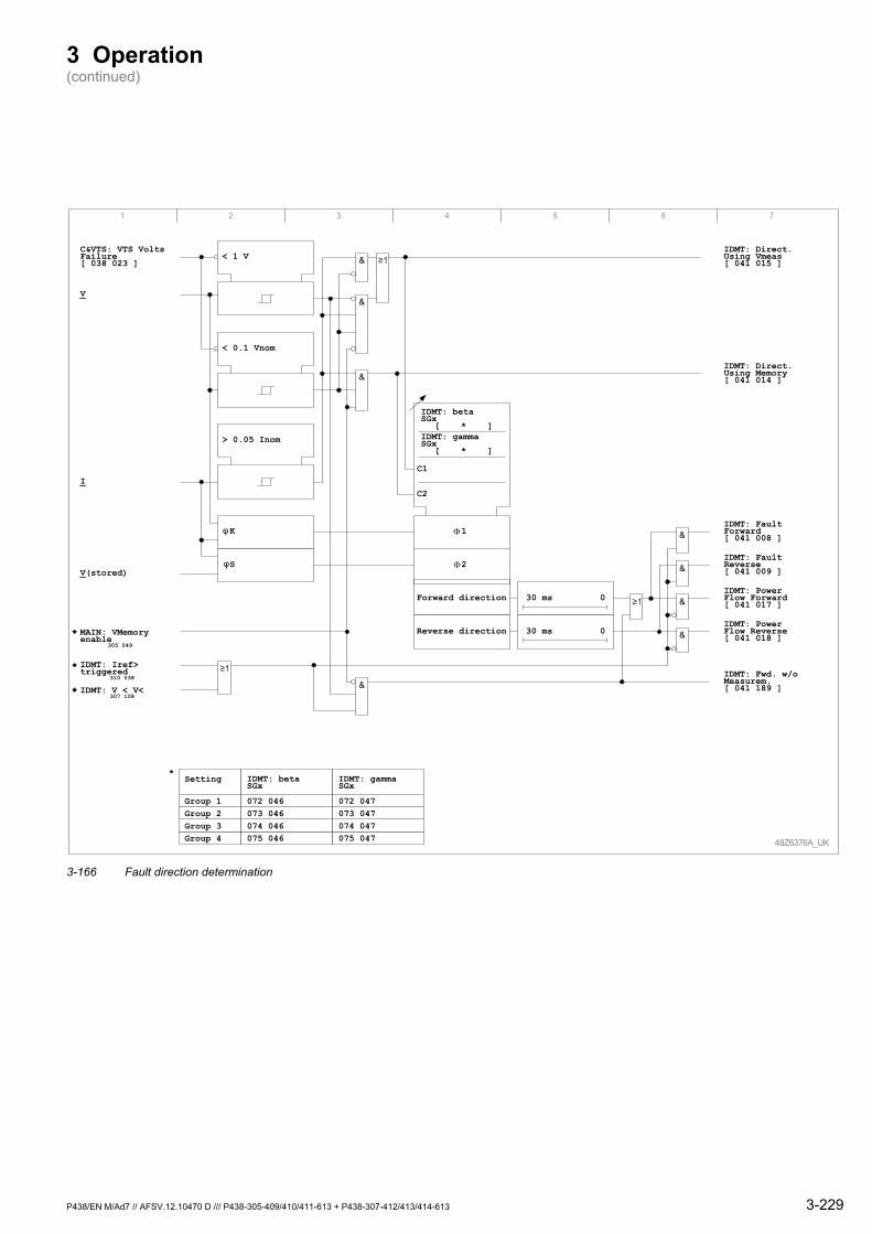
3 Operation (continued)
48Z6376A_UK
IDMT: Direct.Using Vmeas[ 041 015 ]
< 1 V
IDMT: Iref>triggered
310 038
< 0.1 Vnom
K
SV(stored)
I
IDMT: Fwd. w/oMeasurem.[ 041 189 ]
IDMT: Direct.Using Memory[ 041 014 ]
> 0.05 Inom
V
IDMT: betaSGx
[ * ]IDMT: gammaSGx
[ * ]
Forward direction
1
2
MAIN: VMemoryenable
305 049
IDMT: V < V<307 108
IDMT: PowerFlow Forward[ 041 017 ]
IDMT: PowerFlow Reverse[ 041 018 ]
IDMT: FaultForward[ 041 008 ]
IDMT: FaultReverse[ 041 009 ]
Reverse direction
30 ms 0
30 ms 0
Setting-Setting
Group 4Group 3Group 2Group 1
IDMT: betaSGx
072 046073 046074 046075 046
IDMT: gammaSGx
072 047073 047074 047075 047
C1
C2
C&VTS: VTS VoltsFailure[ 038 023 ]
1 2 3 4 5 6 7
*
&
&
&
&
&
&
&
&
Φ
Φ
3-166 Fault direction determination
P438/EN M/Ad7 // AFSV.12.10470 D /// P438-305-409/410/411-613 + P438-307-412/413/414-613 3-229
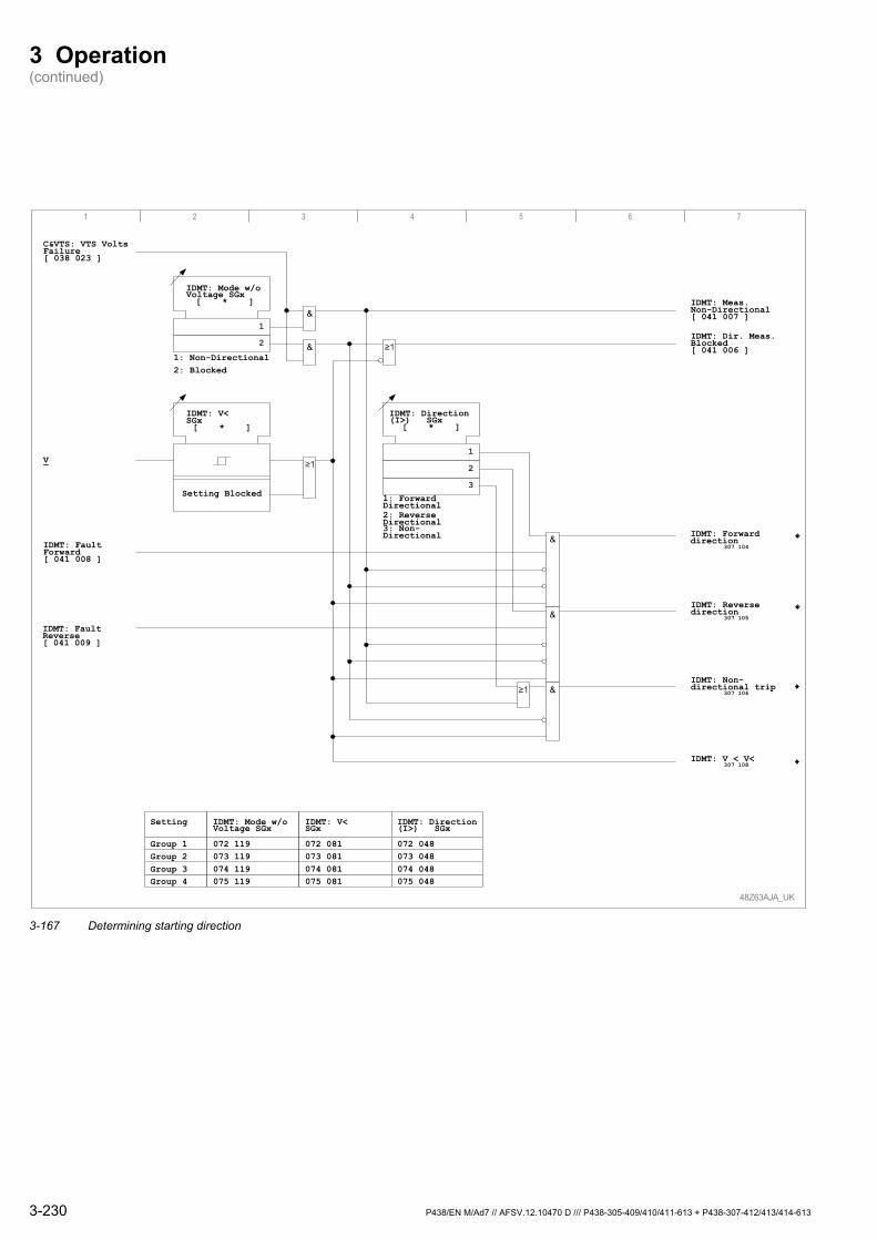
3 Operation (continued)
1 2 3 4 5 6 7
48Z63AJA_UK
IDMT: Meas.Non-Directional[ 041 007 ]
Setting-Setting
Group 4Group 3Group 2Group 1
IDMT: Mode w/oVoltage SGx
072 119073 119074 119075 119
IDMT: V<SGx
072 081073 081074 081075 081
IDMT: Direction(I>) SGx
072 048073 048074 048075 048
C&VTS: VTS VoltsFailure[ 038 023 ]
IDMT: Mode w/oVoltage SGx[ * ]
1
1: Non-Directional2: Blocked
2
IDMT: V<SGx[ * ]
Setting Blocked
IDMT: Dir. Meas.Blocked[ 041 006 ]
IDMT: FaultForward[ 041 008 ]
IDMT: Direction(I>) SGx
[ * ]
1
1: ForwardDirectional2: ReverseDirectional
2
3
3: Non-Directional
IDMT: FaultReverse[ 041 009 ]
V
&
&
&
&
&
IDMT: Forwarddirection
307 104
IDMT: Reversedirection
307 105
IDMT: Non-directional trip
307 106
IDMT: V < V<307 108
3-167 Determining starting direction
3-230 P438/EN M/Ad7 // AFSV.12.10470 D /// P438-305-409/410/411-613 + P438-307-412/413/414-613

3 Operation (continued)
Holding time The P438 determines the trip time according to the current flow, and a timer stage is started. The setting for the holding time defines the period for the IDMT starting time to be stored after the starting signal has dropped out. Should the starting signal return while the holding timer elapses, then the new starting time value is added to the stored starting time. If the sum of the starting times reaches the trip time determined by the P438, then the appropriate signal is issued. If the starting signal does not return while the holding timer elapses, then the memory storing the sum of the starting times will – in accordance with the setting – be cleared either without delay or according to the set characteristic. The phase current stage serves as an example to illustrate the effect of the holding time in Figure Fehler! Verweisquelle konnte nicht gefunden werden..
P438/EN M/Ad7 // AFSV.12.10470 D /// P438-305-409/410/411-613 + P438-307-412/413/414-613 3-231

3 Operation (continued)
3-168 The effect of the holding time
Case A: The determined Trip time is not reached. Case B: The determined Trip time is reached.
3-232 P438/EN M/Ad7 // AFSV.12.10470 D /// P438-305-409/410/411-613 + P438-307-412/413/414-613

3 Operation (continued)
3.29 Defrost Protection (Function Group DFRST)
Under certain operating conditions (no load, cold winter nights) catenaries can ice over. In order to prevent this, two catenaries each are connected in series and heated with a comparatively low current. The defrost protection function measures the feed and return current and processes these current values in a differential protection function for sensitive short-circuit protection.
Enabling or disabling defrost protection
Defrost protection may be disabled or enabled using setting parameters. Enabling can be carried out separately for each setting group.
DFRST: EnableSGx
Setting
Group 1Group 2Group 3Group 4
0: No1: Yes
0: No1: Yes
DFRST: Enabled[ 041 203 ]
48Z5058A_UK
019 130
019 133
019 132019 131
DFRST: GeneralEnable USER[ 019 096 ]
DFRST: EnableSGx[ * ]
0
1
0
1
3-169 Disabling or enabling defrost protection
Transformer matching Current transformers for the acquisition of the catenary and defrost currents can be dimensioned within a certain range. From the CT transformation ratio data, the P438 calculates a matching factor.
fII
X prim
OL prim= ,
,
The matching factor is limited to a range of 1/32 at the minimum and 32 at the maximum. If it is outside these limits, the P438 generates an error message.
P438/EN M/Ad7 // AFSV.12.10470 D /// P438-305-409/410/411-613 + P438-307-412/413/414-613 3-233
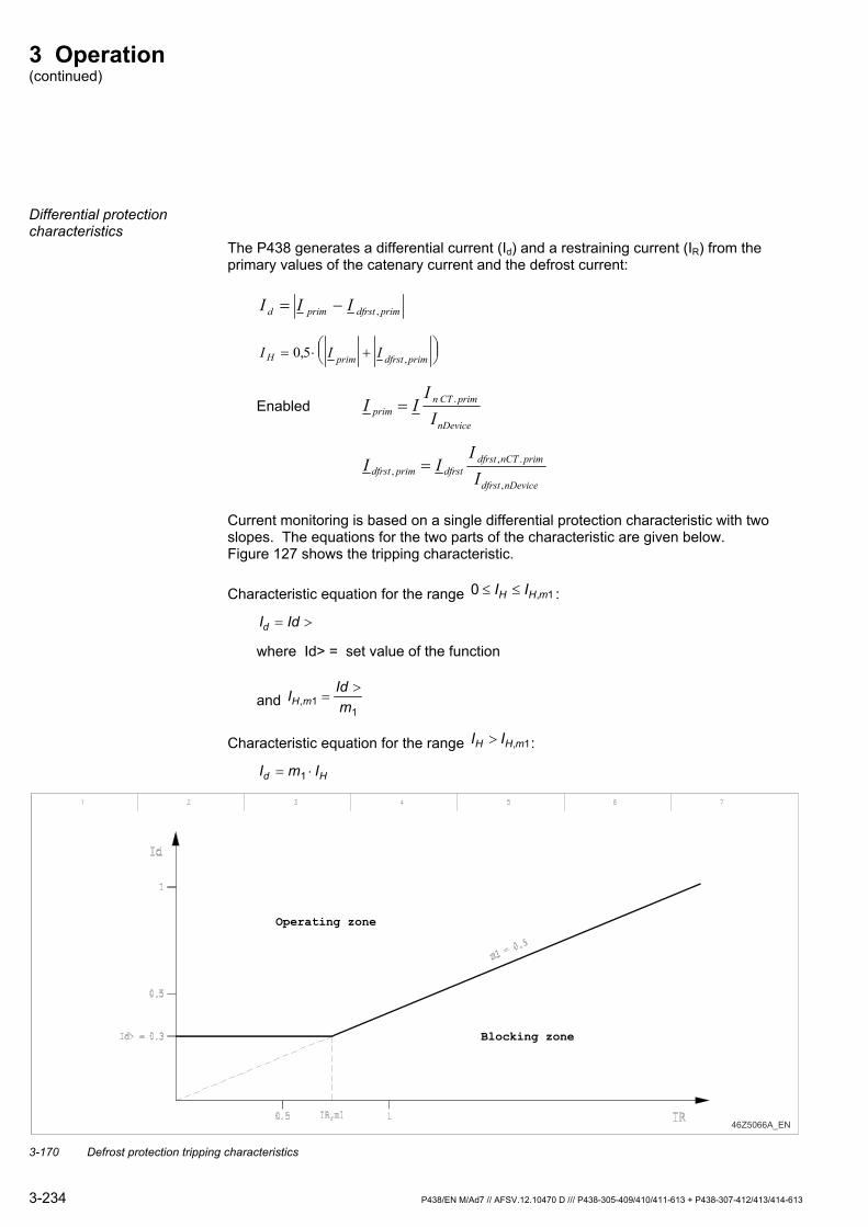
3 Operation (continued)
Differential protection characteristics
The P438 generates a differential current (Id) and a restraining current (IR) from the primary values of the catenary current and the defrost current:
primdfrstprimd III ,−=
I I IH prim dfrst prim= ⋅ +⎛⎝⎜
⎞⎠⎟0 5, ,
Enabled nDevice
primCTnprim I
III .=
nDevicedfrst
primnCTdfrstdfrstprimdfrst I
III
,
.,, =
Current monitoring is based on a single differential protection characteristic with two slopes. The equations for the two parts of the characteristic are given below. Figure 127 shows the tripping characteristic.
Characteristic equation for the range 0 1≤ ≤I IH H m, :
I Idd = >
where Id> = set value of the function
and I IdmH m, 1
1=
>
Characteristic equation for the range I IH H m> , 1:
I m Id H= ⋅1
Operating zone
Blocking zone
46Z5066A_EN 3-170 Defrost protection tripping characteristics
3-234 P438/EN M/Ad7 // AFSV.12.10470 D /// P438-305-409/410/411-613 + P438-307-412/413/414-613
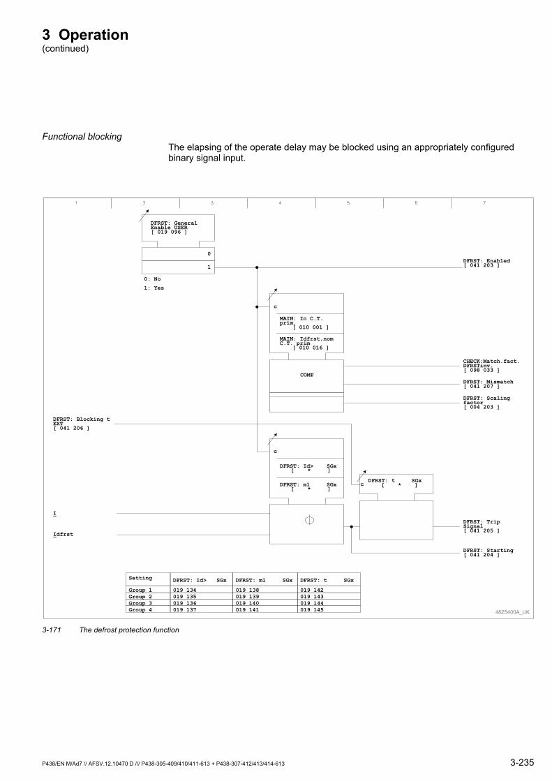
3 Operation (continued)
Functional blocking The elapsing of the operate delay may be blocked using an appropriately configured binary signal input.
48Z5400A_UK
MAIN: In C.T.prim.
[ 010 001 ]
I
Idfrst
MAIN: Idfrst,nomC.T. prim
[ 010 016 ]
COMP
c
DFRST: Mismatch[ 041 207 ]
DFRST: Id> SGx[ * ]
DFRST: m1 SGx[ * ]
c
CHECK:Match.fact.DFRSTinv.[ 098 033 ]
DFRST: Scalingfactor[ 004 203 ]
DFRST: GeneralEnable USER[ 019 096 ]
0
1
0: No
1: Yes
DFRST: Enabled[ 041 203 ]
DFRST: t SGx[ * ]c
DFRST: Blocking tEXT[ 041 206 ]
DFRST: TripSignal[ 041 205 ]
DFRST: Starting[ 041 204 ]
Setting
Group 1Group 2Group 3Group 4
DFRST: Id> SGx
019 134019 135019 136019 137
DFRST: m1 SGx
019 138019 139019 140019 141
DFRST: t SGx
019 142019 143019 144019 145
3-171 The defrost protection function
P438/EN M/Ad7 // AFSV.12.10470 D /// P438-305-409/410/411-613 + P438-307-412/413/414-613 3-235
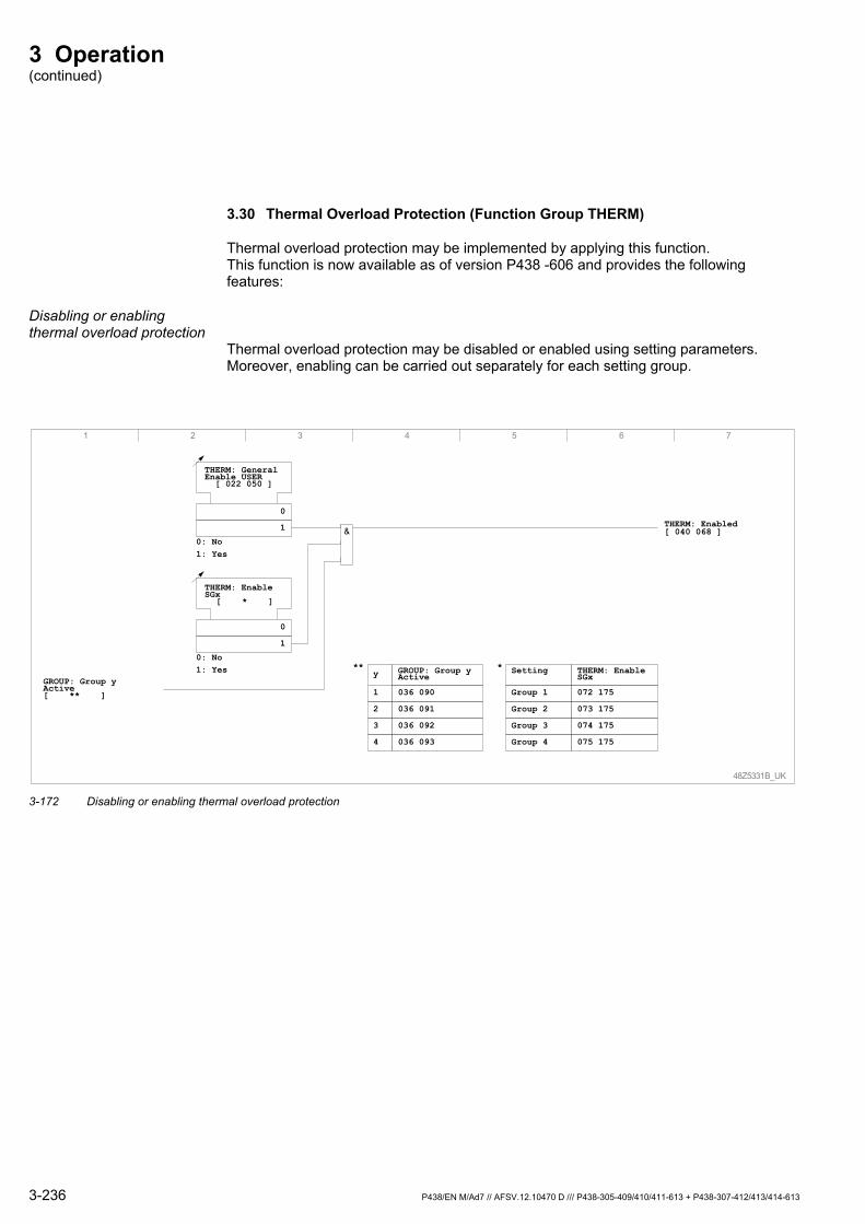
3 Operation (continued)
3.30 Thermal Overload Protection (Function Group THERM)
Thermal overload protection may be implemented by applying this function. This function is now available as of version P438 -606 and provides the following features:
Disabling or enabling thermal overload protection
Thermal overload protection may be disabled or enabled using setting parameters. Moreover, enabling can be carried out separately for each setting group.
48Z5331B_UK
THERM: General Enable USER[ 022 050 ]
0
1
0: No1: Yes
THERM: EnableSGx
[ * ]
0
1
0: No1: Yes
GROUP: Group yActive[ ** ]
THERM: Enabled[ 040 068 ]
1 2 3 4 5 6 7
1
y
2
3
4
036 090
GROUP: Group yActive
036 091
036 092
036 093
Group 1
Group 2
072 175
THERM: Enable SGx
073 175
074 175
075 175
Group 3
Group 4
Setting
&
** *
3-172 Disabling or enabling thermal overload protection
3-236 P438/EN M/Ad7 // AFSV.12.10470 D /// P438-305-409/410/411-613 + P438-307-412/413/414-613
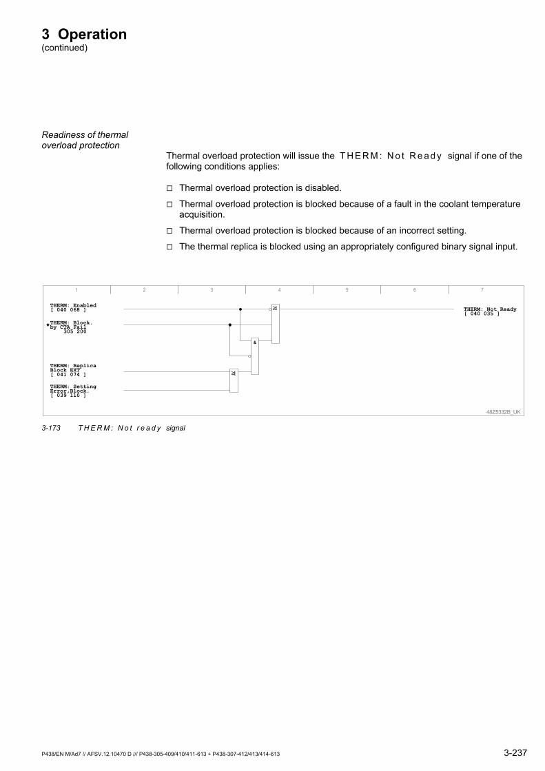
3 Operation (continued)
Readiness of thermal overload protection
Thermal overload protection will issue the T H E R M : N o t R e a d y signal if one of the following conditions applies:
Thermal overload protection is disabled.
Thermal overload protection is blocked because of a fault in the coolant temperature acquisition.
Thermal overload protection is blocked because of an incorrect setting.
The thermal replica is blocked using an appropriately configured binary signal input.
48Z5332B_UK
&
THERM: Enabled[ 040 068 ]
THERM: Block.by CTA Fail
305 200
1 2 3 4 5 6 7
1≥
1≥THERM: ReplicaBlock EXT[ 041 074 ]
THERM: SettingError,Block.[ 039 110 ]
THERM: Not Ready[ 040 035 ]
3-173 T H E R M : N o t r e a d y signal
P438/EN M/Ad7 // AFSV.12.10470 D /// P438-305-409/410/411-613 + P438-307-412/413/414-613 3-237
3 Operation (continued)
Operating modes Two operating modes can be selected for thermal overload protection.
Relative Replica
Absolute Replica
Either operating mode can be enabled or disabled individually. Only one of the operating modes at a time may be enabled for thermal overload protection. However, if both operating modes are enabled at the same time, the thermal overload protection is blocked and an error message is generated by the P438: T H E R M : S e t t i n g E r r o r , B l o c k .
Parallel line switching Thermal overload protection can be adapted to differing switching states in the catenary system by varying the effective reference current Iref by multiplication with the parallel line factors, T H E R M : F a c t o r 2 P a r a l l . S G x and T H E R M : F a c t o r 3 P a r a l l . S G x .
The setting for T H E R M : C o n t r o l v i a U S E R determines whether parallel line switching is carried out from the local HMI or using the binary signal inputs. Switching using the binary signal inputs requires that T H E R M : Control via USER is set to 'No'. If the setting for T H E R M : C o n t r o l v i a U S E R is 'Yes' , switching using the binary signal inputs is not possible.
3-238 P438/EN M/Ad7 // AFSV.12.10470 D /// P438-305-409/410/411-613 + P438-307-412/413/414-613
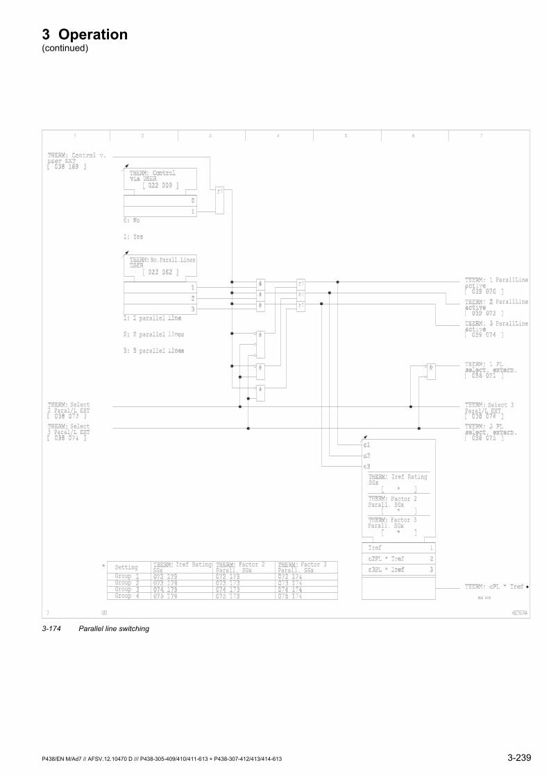
3 Operation (continued)
ParallLine
ParallLine
ParallLine
Select 3Paral/L EXT
Iref RatingSGx
Iref RatingSGx
Factor 2Parall. SGx
Factor 2Parall. SGx
Factor 3Parall. SGx
Factor 3Parall. SGx
Setting
GroupGroupGroupGroup
Select2 Paral/L EXT
Select3 Paral/L EXT
parallel
parallel
parallel
No.Parall.Lines
3-174 Parallel line switching
P438/EN M/Ad7 // AFSV.12.10470 D /// P438-305-409/410/411-613 + P438-307-412/413/414-613 3-239
3 Operation (continued)
Influence of coolant temperature
To permit ambient temperature correction, the analog I/O module Y must be fitted. There are two possible means available to measure coolant temperatures:
Direct measurement by PT 100 sensor fitted on the external device The measured temperature value is used directly to determine the tripping time.
20 mA measurements with external measuring transducers The characteristics for transducers applied must be set in function group RTDmA. Calculated temperature values are used to determine the tripping time.
Open measuring circuits, due to a broken wire or an overload on the 20 mA analog measuring input, are determined by the measured value input (function group RTDmA). This will result in the issuance of these signals:
R T D m A : O v e r l o a d 2 0 m A I n p u t
R T D m A : O p e n C i r c . 2 0 m A i n p .
R T D m A : P T 1 0 0 O p e n C i r c u i t
The thermal model uses these signals as a criterion to determine a fault in the coolant temperature measurement. A fault at the selected measuring point will lead to the issuance of the T H E R M : C T A E r r o r signal.
3-240 P438/EN M/Ad7 // AFSV.12.10470 D /// P438-305-409/410/411-613 + P438-307-412/413/414-613
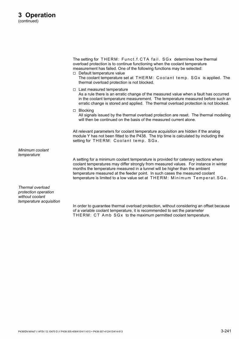
3 Operation (continued)
The setting for T H E R M : F u n c t . f . C T A f a i l . S G x determines how thermal overload protection is to continue functioning when the coolant temperature measurement has failed. One of the following functions may be selected:
Default temperature value The coolant temperature set at T H E R M : C o o l a n t t e m p . S G x is applied. The thermal overload protection is not blocked.
Last measured temperature As a rule there is an erratic change of the measured value when a fault has occurred in the coolant temperature measurement. The temperature measured before such an erratic change is stored and applied. The thermal overload protection is not blocked.
Blocking All signals issued by the thermal overload protection are reset. The thermal modeling will then be continued on the basis of the measured current alone.
All relevant parameters for coolant temperature acquisition are hidden if the analog module Y has not been fitted to the P438. The trip time is calculated by including the setting for T H E R M : C o o l a n t t e m p . S G x .
Minimum coolant temperature
A setting for a minimum coolant temperature is provided for catenary sections where coolant temperatures may differ strongly from measured values. For instance in winter months the temperature measured in a tunnel will be higher than the ambient temperature measured at the feeder point. In such cases the measured coolant temperature is limited to a low value set at T H E R M : M i n i m u m T e m p e r a t . S G x .
Thermal overload protection operation without coolant temperature acquisition
In order to guarantee thermal overload protection, without considering an offset because of a variable coolant temperature, it is recommended to set the parameter T H E R M : C T A m b S G x to the maximum permitted coolant temperature.
P438/EN M/Ad7 // AFSV.12.10470 D /// P438-305-409/410/411-613 + P438-307-412/413/414-613 3-241
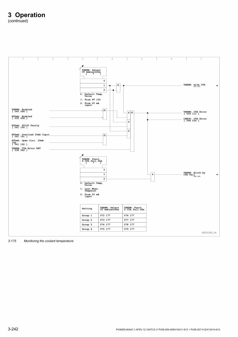
3 Operation (continued)
48Z5333B_UK
THERM: SelectCT AmbientSGx
[ * ]
0
1
0: Default Temp. Value1: From PT 100
THERM: with CTA303 201
&
THERM: CTA Error[ 039 111 ]
1 2 3 4 5 6 7
1≥
2: From 20 mA input
2
&
1≥
RTDmA: PT100 Faulty[ 041 190 ]
RTDmA: Overload 20mA Input[ 041 191 ]
RTDmA: Open Circ. 20mAinp.[ 041 192 ]
1≥
THERM: CTA Error EXT[ 038 062 ]
CHECK: CTA Error[ 098 034 ]
THERM: Funct.f.CTA fail.SGx
[ * ]
0
1
0: Default Temp. Value
1: Last Meas. Temperat
2: From 20 mA input
2
&THERM: Block.byCTA Fail
305 200
Group 1
Group 2
072 177
THERM: SelectCT AmbientSGx
073 177
074 177
075 177
Group 3
Group 4
Setting
076 177
THERM: Funct.f.CTA fail.SGx
077 177
078 177
079 177
RTDmA: Enabled[ 035 008 ]
&THERM: Enabled[ 040 068 ] 1≥
3-175 Monitoring the coolant temperature
3-242 P438/EN M/Ad7 // AFSV.12.10470 D /// P438-305-409/410/411-613 + P438-307-412/413/414-613
3 Operation (continued)
Relative replica The rated operating current of the protected object and its overload tolerance for maximum coolant (ambient) temperature are the basis of the relative thermal replica.
In the "Relative replica" operating mode, the following settings have to be made for thermal overload protection:
The rated operating current of the protected object T H E R M : I r e f R a t i n g S G x
The tripping threshold Δϑtrip is set at T H E R M : T > T r i p R e s e t , % S G x .
If coolant temperature (ambient) acquisition is used, the following parameters must be set:
The maximum permissible temperature of the protected object is set at Θmax T H E R M : M a x P e r m O b j T m p . S G x .
The maximum temperature of the coolant (maximum ambient) is set at Θa,max T H E R M : M a x P e r m C o o l T m p S G x .
Absolute replica
The thermal limit current of the protected object is the reference current of the absolute thermal replica. For this limit current, an over-temperature results at the maximum coolant temperature.
In the "Absolute replica" operating mode, the following parameters have to be set for thermal overload protection:
The thermal limit current of the protected object T H E R M : I r e f R a t i n g S G x
The limit temperature for tripping is set as Θmax T H E R M : M a x p e r m o b j t m p . S G x .
The over-temperature as a result of a persistent limit current (Θmax - Θa,max ) T H E R M : O / T f . I r e f p e r s . S G x
Note: The maximum permissible coolant temperature Θa,max is derived from the difference between the settings for T H E R M : M a x . p e r m . o b j . t m p . S G x and T H E R M : O / T f . I r e f p e r s . S G x
Tripping characteristics
The maximum r.m.s. phase current I is used to track a first-order thermal replica as specified in IEC 255-8. In addition to the operating mode-dependent settings, the following parameters will govern the trip time:
The set thermal time constant of the protected object τ T H E R M : T i m . C o n s t 1 ( H e a t ) S G x
The accumulated thermal load Δϑ0.
The current measured coolant temperature Θa.
P438/EN M/Ad7 // AFSV.12.10470 D /// P438-305-409/410/411-613 + P438-307-412/413/414-613 3-243
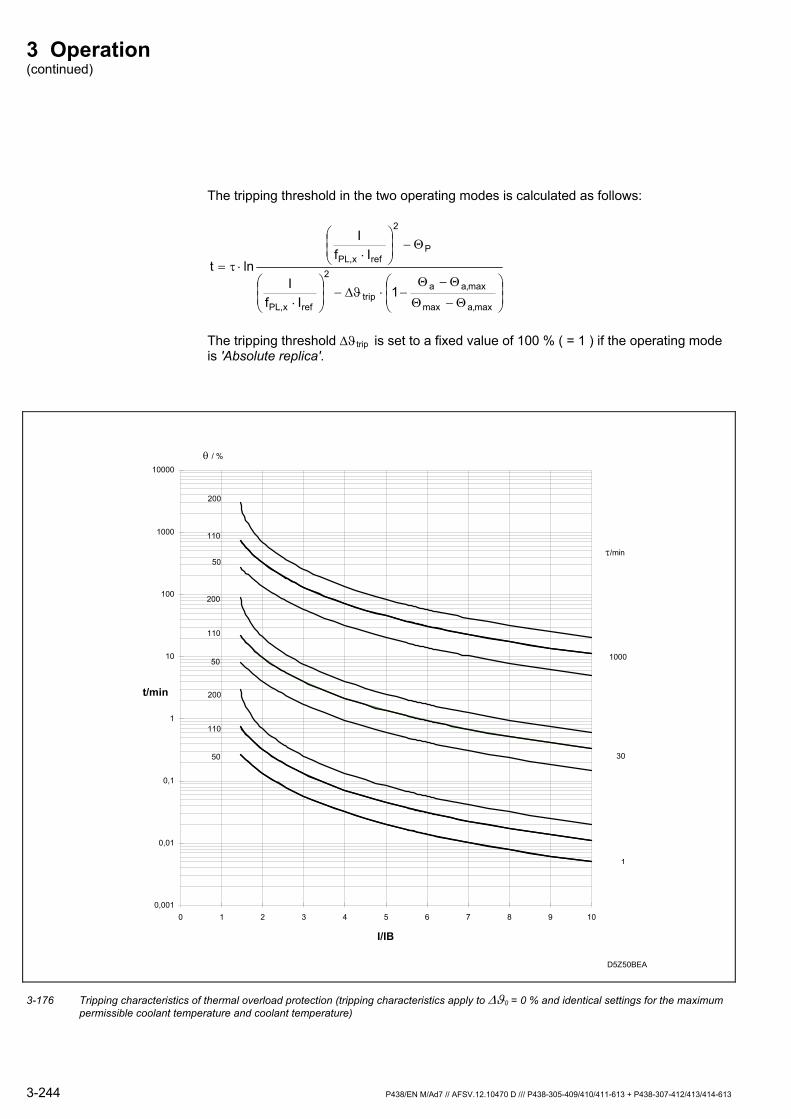
3 Operation (continued)
The tripping threshold in the two operating modes is calculated as follows:
⎟⎟⎠
⎞⎜⎜⎝
⎛
Θ−Θ
Θ−Θ−⋅ϑΔ−⎟
⎟⎠
⎞⎜⎜⎝
⎛
⋅
Θ−⎟⎟⎠
⎞⎜⎜⎝
⎛
⋅⋅τ=
max,amax
max,aatrip
2
refx,PL
P
2
refx,PL
1If
I
IfI
lnt
The tripping threshold Δϑtrip is set to a fixed value of 100 % ( = 1 ) if the operating mode is 'Absolute replica'.
0,001
0,01
0,1
1
10
100
1000
10000
0 1 2 3 4 5 6 7 8 9 10
I/IB
t/min
D5Z50BEA
30
1000
1
τ/min
200
110
50
200
110
110
50
50
θ / %
200
3-176 Tripping characteristics of thermal overload protection (tripping characteristics apply to Δϑ0 = 0 % and identical settings for the maximum permissible coolant temperature and coolant temperature)
3-244 P438/EN M/Ad7 // AFSV.12.10470 D /// P438-305-409/410/411-613 + P438-307-412/413/414-613
3 Operation (continued)
Alarm Depending on the selected operating mode, a warning signal can be set at one of the following parameters:
Relative replica: T H E R M : T > A l a r m R e s e t , % S G x
Absolute replica: T H E R M : A l a r m T e m p . S G x
Additionally, a pre-trip time limit can be set; when the time left until tripping falls below this pre-trip limit, a warning will be issued.
Trip
The trip threshold is set according to the selected operating mode with the following parameters:
Relative replica: T H E R M : T > T r i p R e s e t , % S G x
Absolute replica: THERM: Max Perm Obj Tmp.SGx
If a trip command is issued, the trip signal is maintained until the status of the thermal replica has decreased by the value T H E R M : T r i p H y s t e r e s i s S G x , at least for a fixed time of 5 s.
Cooling
If the current falls below the default threshold of 0.1 Iref, the thermal replica is applied with the set time constant T H E R M : T i m . C o n s t . 2 ( C o o l ) S G x . This element in the thermal model takes into account the cooling characteristics of stopped motors.
Note: These two time constants should be set to the same value for transformers and power lines.
P438/EN M/Ad7 // AFSV.12.10470 D /// P438-305-409/410/411-613 + P438-307-412/413/414-613 3-245
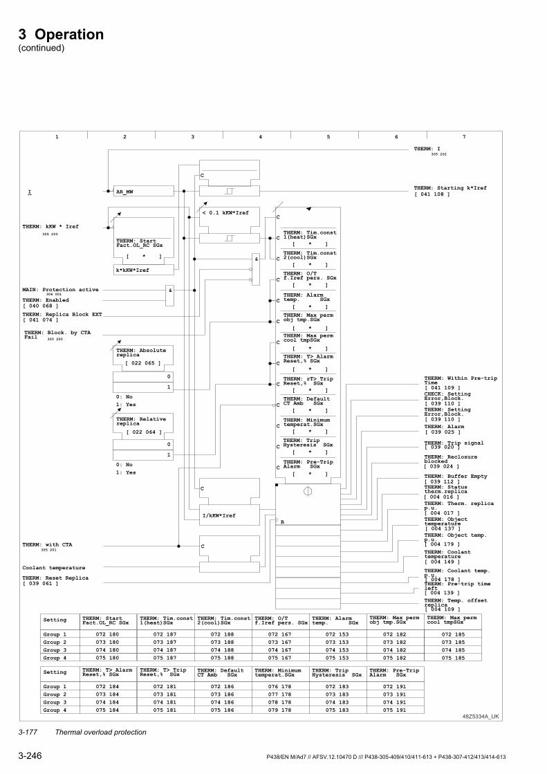
3 Operation (continued)
48Z5334A_UK
1 2 3 6 7
&
THERM: Pre-TripAlarm SGx
C
C
C
C
C
C
C
C
C
C
C
C
C
THERM: Therm. replicap.u.
[ 004 017 ]
THERM: DefaultCT Amb SGx
THERM: TripHysteresis SGx
THERM: Object temp.p.u.
[ 004 179 ]
THERM: Coolant temp.p.u.[ 004 178 ]
THERM: Temp. offsetreplica[ 004 109 ]
THERM: Pre-trip timeleft
[ 004 139 ]
THERM: Coolanttemperature
[ 004 149 ]
THERM: Objecttemperature [ 004 137 ]
THERM: Statustherm.replica
[ 004 016 ]
THERM: Buffer Empty [ 039 112 ]
THERM: Reclosureblocked
[ 039 024 ]
THERM: Trip signal [ 039 020 ]
THERM: Alarm [ 039 025 ]
THERM: SettingError,Block.[ 039 110 ]
CHECK: SettingError,Block.[ 039 110 ]
THERM: Starting k*Iref[ 041 108 ]
< 0.1 kKW*Iref
C
AR_MW
4 5
I
THERM: I305 202
THERM: StartFact.OL_RC SGx
[ * ]
k*kKW*Iref
THERM: Within Pre-tripTime[ 041 109 ]
THERM: kKW * Iref305 203
THERM: Enabled
&
THERM: Replica Block EXT
THERM: Absolutereplica
0
1
THERM: Relativereplica
0
1
I/kKW*Iref
C
C
R
THERM: with CTA305 201
Coolant temperature
THERM: Reset Replica[ 039 061 ]
THERM: Tim.const1(heat)SGx
THERM: Tim.const2(cool)SGx
THERM: O/Tf.Iref pers. SGx
THERM: Alarmtemp. SGx
THERM: Max permobj tmp.SGx
THERM: Max permcool tmpSGx
THERM: T> TripReset,% SGx
THERM: Pre-TripAlarm SGx
THERM: Minimumtemperat.SGx
THERM: DefaultCT Amb SGx
THERM: TripHysteresis SGx
THERM: T> AlarmReset,% SGx
THERM: StartFact.OL_RC SGx
306 001
[ 040 068 ]
[ 041 074 ]
305 200
MAIN: Protection active
THERM: Block. by CTAFail
0: No1: Yes
0: No1: Yes
[ 022 065 ]
[ 022 064 ]
Setting
Setting
Group 4Group 3Group 2Group 1
Group 4Group 3Group 2Group 1
072 180073 180074 180075 180
072 184073 184074 184075 184
072 187073 187074 187075 187
072 181073 181074 181075 181
072 188073 188074 188075 188
072 186073 186074 186075 186
072 167073 167074 167075 167
076 178077 178078 178079 178
072 153073 153074 153075 153
072 183073 183074 183075 183
072 182073 182074 182075 182
072 191073 191074 191075 191
072 185073 185074 185075 185
[ * ]
[ * ]
[ * ]
[ * ]
[ * ]
[ * ]
[ * ]
[ * ]
[ * ]
[ * ]
[ * ]
[ * ]
THERM: rT> TripReset,% SGx
THERM: Minimumtemperat.SGx
THERM: Max permobj tmp.SGx
THERM: Max permcool tmpSGx
THERM: T> AlarmReset,% SGx
THERM: Tim.const1(heat)SGx
THERM: Tim.const2(cool)SGx
THERM: O/Tf.Iref pers. SGx
THERM: Alarmtemp. SGx
3-177 Thermal overload protection
3-246 P438/EN M/Ad7 // AFSV.12.10470 D /// P438-305-409/410/411-613 + P438-307-412/413/414-613

3 Operation (continued)
Reset The thermal replica may be reset either using a setting parameter or an appropriately configured binary signal input. Resetting is possible even when thermal overload protection is disabled. Thermal overload protection can be blocked using an appropriately configured binary signal input.
48Z5335A_UK
THERM: Reset Replica[ 039 061 ]
THERM: ResetReplica USER
[ 022 061 ]
0
1
THERM: Reset Replica EXT
1 2 3 4 5 6 7
1
THERM: Enabled[ 040 068 ]
[ 038 061 ]
0: don't execute1: execute
3-178 Resetting the thermal replica
P438/EN M/Ad7 // AFSV.12.10470 D /// P438-305-409/410/411-613 + P438-307-412/413/414-613 3-247
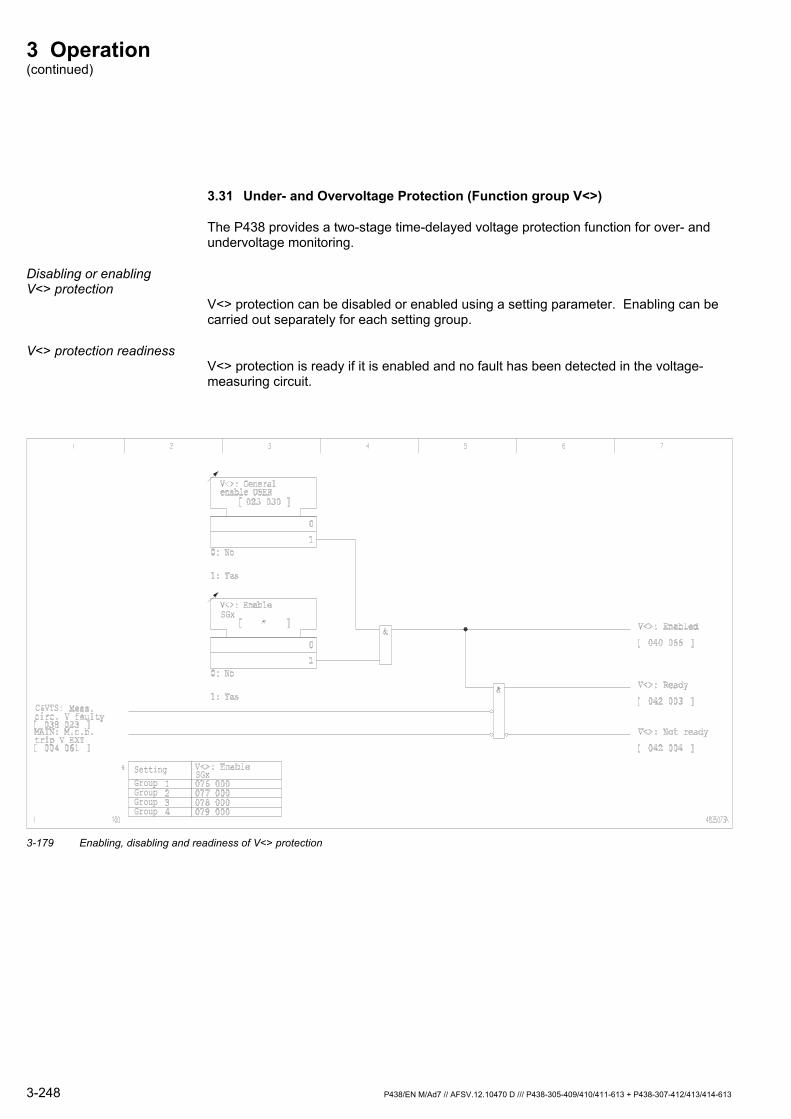
3 Operation (continued)
3.31 Under- and Overvoltage Protection (Function group V<>)
The P438 provides a two-stage time-delayed voltage protection function for over- and undervoltage monitoring.
Disabling or enabling V<> protection
V<> protection can be disabled or enabled using a setting parameter. Enabling can be carried out separately for each setting group.
V<> protection readiness V<> protection is ready if it is enabled and no fault has been detected in the voltage-measuring circuit.
C&VTS:
SGx
SGx
Setting
GroupGroupGroupGroup
3-179 Enabling, disabling and readiness of V<> protection
3-248 P438/EN M/Ad7 // AFSV.12.10470 D /// P438-305-409/410/411-613 + P438-307-412/413/414-613
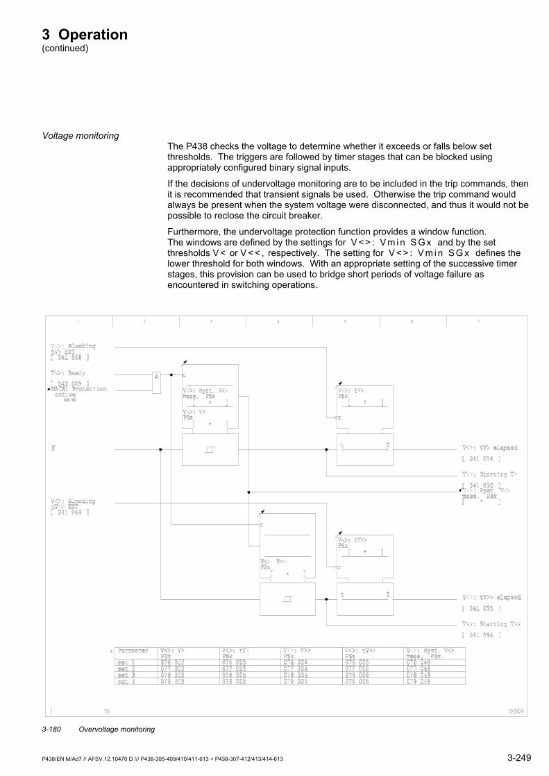
3 Operation (continued)
Voltage monitoring The P438 checks the voltage to determine whether it exceeds or falls below set thresholds. The triggers are followed by timer stages that can be blocked using appropriately configured binary signal inputs.
If the decisions of undervoltage monitoring are to be included in the trip commands, then it is recommended that transient signals be used. Otherwise the trip command would always be present when the system voltage were disconnected, and thus it would not be possible to reclose the circuit breaker.
Furthermore, the undervoltage protection function provides a window function. The windows are defined by the settings for V < > : V m i n S G x and by the set thresholds V < or V < < , respectively. The setting for V < > : V m i n S G x defines the lower threshold for both windows. With an appropriate setting of the successive timer stages, this provision can be used to bridge short periods of voltage failure as encountered in switching operations.
3-180 Overvoltage monitoring
P438/EN M/Ad7 // AFSV.12.10470 D /// P438-305-409/410/411-613 + P438-307-412/413/414-613 3-249

3 Operation (continued)
3-181 Undervoltage monitoring
3-250 P438/EN M/Ad7 // AFSV.12.10470 D /// P438-305-409/410/411-613 + P438-307-412/413/414-613
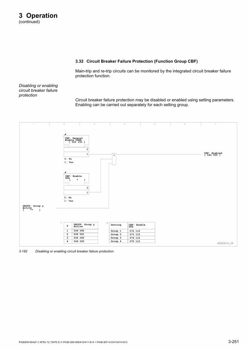
3 Operation (continued)
3.32 Circuit Breaker Failure Protection (Function Group CBF)
Main-trip and re-trip circuits can be monitored by the integrated circuit breaker failure protection function.
Disabling or enabling circuit breaker failure protection
Circuit breaker failure protection may be disabled or enabled using setting parameters. Enabling can be carried out separately for each setting group.
48Z6361A_UK
CBF: General Enable USER
[ 022 100 ]
CBF: EnableSGx
[ * ]
CBF: Enabled[ 040 055 ]
0
1
0: No1: Yes
0
1
0: No1: Yes
GROUP: Group y Active[ ** ]
y
1
GROUP: Group y Active
036 090036 091036 092036 093
234
Setting
Group 1Group 2Group 3Group 4
CBF: EnableSGx
072 110073 110074 110075 110
3-182 Disabling or enabling circuit breaker failure protection
P438/EN M/Ad7 // AFSV.12.10470 D /// P438-305-409/410/411-613 + P438-307-412/413/414-613 3-251
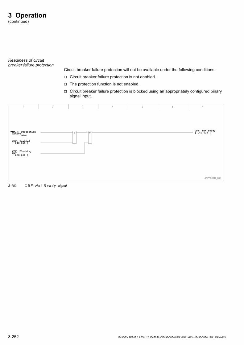
3 Operation (continued)
Readiness of circuit breaker failure protection
Circuit breaker failure protection will not be available under the following conditions :
Circuit breaker failure protection is not enabled.
The protection function is not enabled.
Circuit breaker failure protection is blocked using an appropriately configured binary signal input.
48Z5062B_UK
CBF: Not Ready [ 040 025 ]
CBF: Blocking EXT [ 038 058 ]
CBF: Enabled [ 040 055 ]
MAIN: Protection active
306 001
3-183 C B F : N o t R e a d y signal
3-252 P438/EN M/Ad7 // AFSV.12.10470 D /// P438-305-409/410/411-613 + P438-307-412/413/414-613
3 Operation (continued)
CB failure protection Circuit breaker failure protection is started by the main-trip command or by the trip command of an external protection device (wired to an appropriate binary input). These commands start a timer stage. Once this has elapsed, a re-trip results unless the current monitored by the circuit breaker failure protection function has fallen below the set threshold. Only the fundamental component of the current is monitored here.
If the fault is still present once the first timer stage (C B F : t B F 1 I n i t R e T r i p S G x ) has elapsed, the signal C B F : R e - T r i p s i g n a l is issued to trigger the re-trip.
If the fault is still present once the second timer stage (C B F : t B F 2 I n i t B a c k T r . S G x ) has elapsed, the signal C B F : B a c k - T r i p s i g n a l is issued to trigger the trip of an upstream circuit breaker ("back-trip").
When the signal CBF: Re-Tr ip s ignal or the signal CBF: Back-Tr ip s ignal is issued, the multiple signal C B F : C B F a i l u r e is issued as of version P438 -607 as an additional spontaneous signal.
CB monitoring Additionally, the circuit breaker auxiliary contact can be monitored. This is only possible if a binary signal input has been set to M A I N : C h e c k C B C l o s e d ? E X T . The pickup of the circuit breaker auxiliary contact starts a timer stage. If the monitored current exceeds C B F : I m i n < , then a C B F : C B f a i l u r e alarm results.
Auxiliary contact supervision is active only for the set operative time. This ensures that no C B F : C B f a i l u r e signal (which might lead to switching off the entire plant) will be issued during protection injection testing.
P438/EN M/Ad7 // AFSV.12.10470 D /// P438-305-409/410/411-613 + P438-307-412/413/414-613 3-253
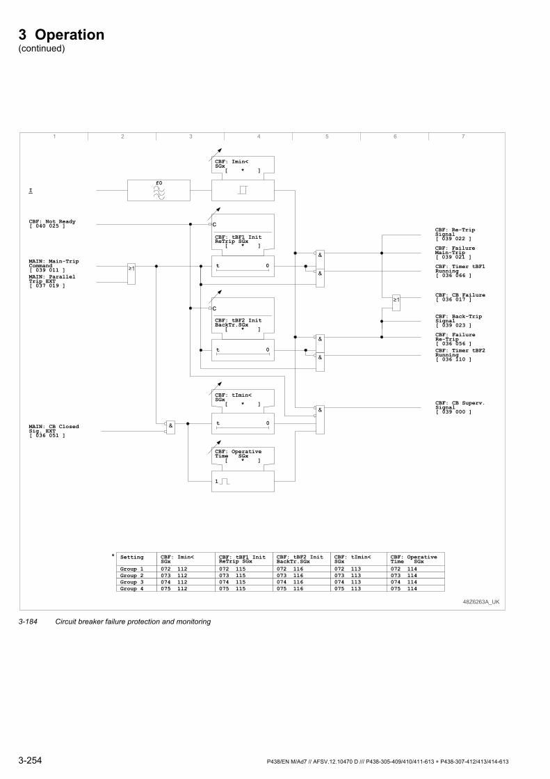
3 Operation (continued)
1 2 3 4 5 6 7
48Z6263A_UK
If0
CBF: Imin< SGx
[ * ]
CBF: tBF1 Init ReTrip SGx
[ * ]
c
CBF: tBF2 Init BackTr.SGx
[ * ]
c
CBF: Not Ready[ 040 025 ]
CBF: tImin< SGx
[ * ]
CBF: Operative Time SGx
[ * ]
MAIN: Main-Trip Command[ 039 011 ]
MAIN: CB Closed Sig. EXT[ 036 051 ]
t 0
CBF: CB Superv.Signal[ 039 000 ]
CBF: Timer tBF2Running[ 036 110 ]
CBF: Failure Re-Trip[ 036 056 ]
CBF: Back-Trip Signal[ 039 023 ]
CBF: Timer tBF1Running[ 036 066 ]
CBF: Failure Main-Trip[ 039 021 ]
CBF: Re-Trip Signal[ 039 022 ]
1
t 0
t 0
CBF: CB Failure[ 036 017 ]
MAIN: Parallel Trip EXT[ 037 019 ]
&
&
&
&
&
&
CBF: tBF2 Init BackTr.SGx072 116073 116074 116075 116
CBF: tBF1 Init ReTrip SGx072 115073 115074 115075 115
CBF: Imin< SGx072 112073 112074 112075 112
CBF: tImin< SGx072 113073 113074 113075 113
Setting
Group 1Group 2Group 3Group 4
CBF: Operative Time SGx072 114073 114074 114075 114
*
3-184 Circuit breaker failure protection and monitoring
3-254 P438/EN M/Ad7 // AFSV.12.10470 D /// P438-305-409/410/411-613 + P438-307-412/413/414-613
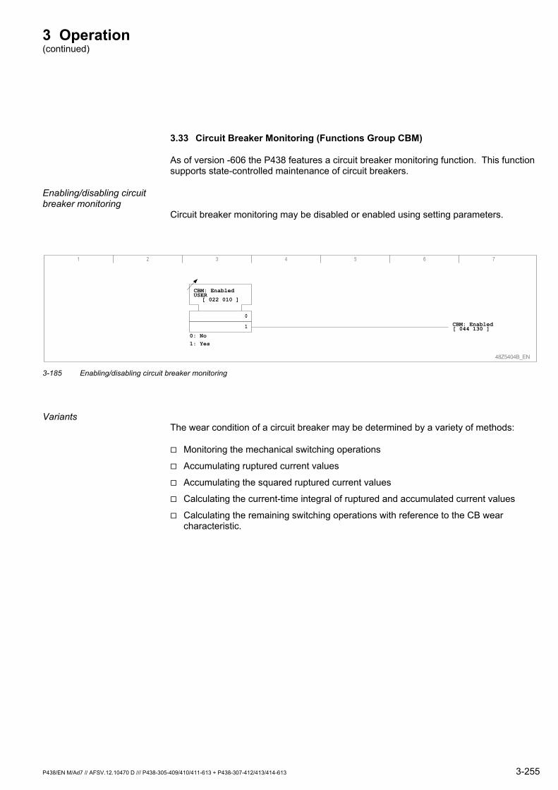
3 Operation (continued)
P438/EN M/Ad7 // AFSV.12.10470 D /// P438-305-409/410/411-613 + P438-307-412/413/414-613 3-255
3.33 Circuit Breaker Monitoring (Functions Group CBM)
As of version -606 the P438 features a circuit breaker monitoring function. This function supports state-controlled maintenance of circuit breakers.
Enabling/disabling circuit breaker monitoring
Circuit breaker monitoring may be disabled or enabled using setting parameters.
48Z5404B_EN
CBM: EnabledUSER
[ 022 010 ]
0
1
0: No1: Yes
CBM: Enabled[ 044 130 ]
1 2 3 4 5 6 7
3-185 Enabling/disabling circuit breaker monitoring
Variants The wear condition of a circuit breaker may be determined by a variety of methods:
Monitoring the mechanical switching operations
Accumulating ruptured current values
Accumulating the squared ruptured current values
Calculating the current-time integral of ruptured and accumulated current values
Calculating the remaining switching operations with reference to the CB wear characteristic.
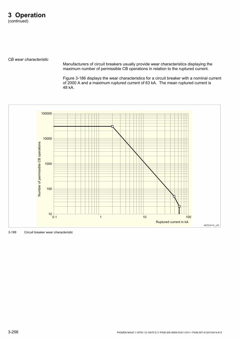
3 Operation (continued)
3-256 P438/EN M/Ad7 // AFSV.12.10470 D /// P438-305-409/410/411-613 + P438-307-412/413/414-613
CB wear characteristic Manufacturers of circuit breakers usually provide wear characteristics displaying the maximum number of permissible CB operations in relation to the ruptured current.
Figure X3-186X displays the wear characteristics for a circuit breaker with a nominal current of 2000 A and a maximum ruptured current of 63 kA. The mean ruptured current is 48 kA.
48Z5341A_UK
10
100
1000
10000
100000
0.1 1 10 100 Ruptured current in kA
Num
ber o
f per
mis
sibl
e C
B op
erat
ions
3-186 Circuit breaker wear characteristic
3 Operation (continued)
P438/EN M/Ad7 // AFSV.12.10470 D /// P438-305-409/410/411-613 + P438-307-412/413/414-613 3-257
The knee points in figure X3-186X are necessary to set the wear characteristic for the circuit breaker:
The circuit breaker’s nominal current (C B M : I n o m , C B CC) and the number of permitted CB operations at nominal current (C B M : P e r m . C B o p . I n o m , C B CC)
The circuit breaker's mean ruptured current C B M : M e d . c u r r . I t r i p , C B CC and the number of permitted CB operations at mean ruptured current (C B M : P e r m . C B o p . I m e d , C B CC)
The circuit breaker’s maximum ruptured current (C B M : M a x . c u r r . I t r i p , C B CC) and the number of permitted CB operations at maximum ruptured current (C B M : P e r m . C B o p . I m a x , C B CC)
The mean ruptured current is not available for all types of circuit breakers. In such a case the parameters for this knee-point are to be set to 'Blocked'. A knee-point is not considered in the characteristic when at least one of the parameters for the knee-point is set to 'Blocked'.
For proper performance of circuit breaker monitoring it should be observed that the knee-points must be applied in a logically correct sequence (continuously descending). When setting currents and numbers of CB operations that are not plausible according to the characteristic, the P438 will issue the C B M : S e t t i n g e r r o r C B M error message and block circuit breaker monitoring.
Calculating the CB wear state
The current wear state of the circuit breaker is given as the number of remaining CB operations at nominal current conditions. The number of remaining CB operations nrem(Inom,CB) is calculated and displayed phase selectively by the P438. Calculation is per this equation:
( ) ( ) ( )( )CB,d
CB,nomCB,nom0,remCB,nomrem In
InInIn −=
With:
Inom,CB: Nominal current of the CB
n(Inom,CB): Maximum number of permitted CB operations at Inom,CB
Id,CB: Ruptured current
n(Id,CB): Number of permitted CB operations at Id,CB according to wear characteristics
nrem,0(Inom,CB): Number of remaining CB operations at Inom,CB UbeforeU
disconnection
nrem,(Inom,CB): Number of remaining CB operations at Inom,CB UafterU
disconnection
3 Operation (continued)
3-258 P438/EN M/Ad7 // AFSV.12.10470 D /// P438-305-409/410/411-613 + P438-307-412/413/414-613
Operating modes The condition under which the function will be triggered is selected using the C B M : O p e r a t i n g m o d e CC parameter:
With Tr ip Cmd. Only : Function triggered only by the main trip command
With CB Sig. EXT Only: Function triggered by the CB open signal generated by an auxiliary contact
CB Sig. EXT or Tr ip : Function triggered by the main trip command or the CB open signal generated by an auxiliary contact
These correction values can be set to determine the exact trip time:
C B M : C o r r . A c q u . t . T r i p A positive correction time value can be set to offset the delay between issuing the trip command and opening of the CB contacts.
C B M : C o r r . A c q u . t . C B S i g . A positive or negative correction time value can be set when leading or lagging auxiliary contacts are in use.
Cycle for circuit breaker monitoring
The circuit breaker monitoring cycle is defined pole-selectively. During an active cycle the signal C B M : C y c l e R u n n i n g C a t or C B M : C y c l e R u n n i n g F d r is issued.
The cycle is started by a trigger criterion. Definition for the end of a cycle: The remaining time of a power cycle duration has elapsed after the last detected current zero crossing. The signal C B M : C a t C u r r e n t D e a d or C B M : F d r C u r r e n t D e a d is then issued.
The maximum cycle time duration is defined with 220 ms. The start of the cycle time is corrected by the settable correction times. A fault on a CB pole is considered to be apparent if further current zero crossings are detected after the maximum cycle time has elapsed. Measured values from the respective CB tripping are cancelled and the signal C B M : t m a x > C a t or C B M : t m a x > F d r is issued.
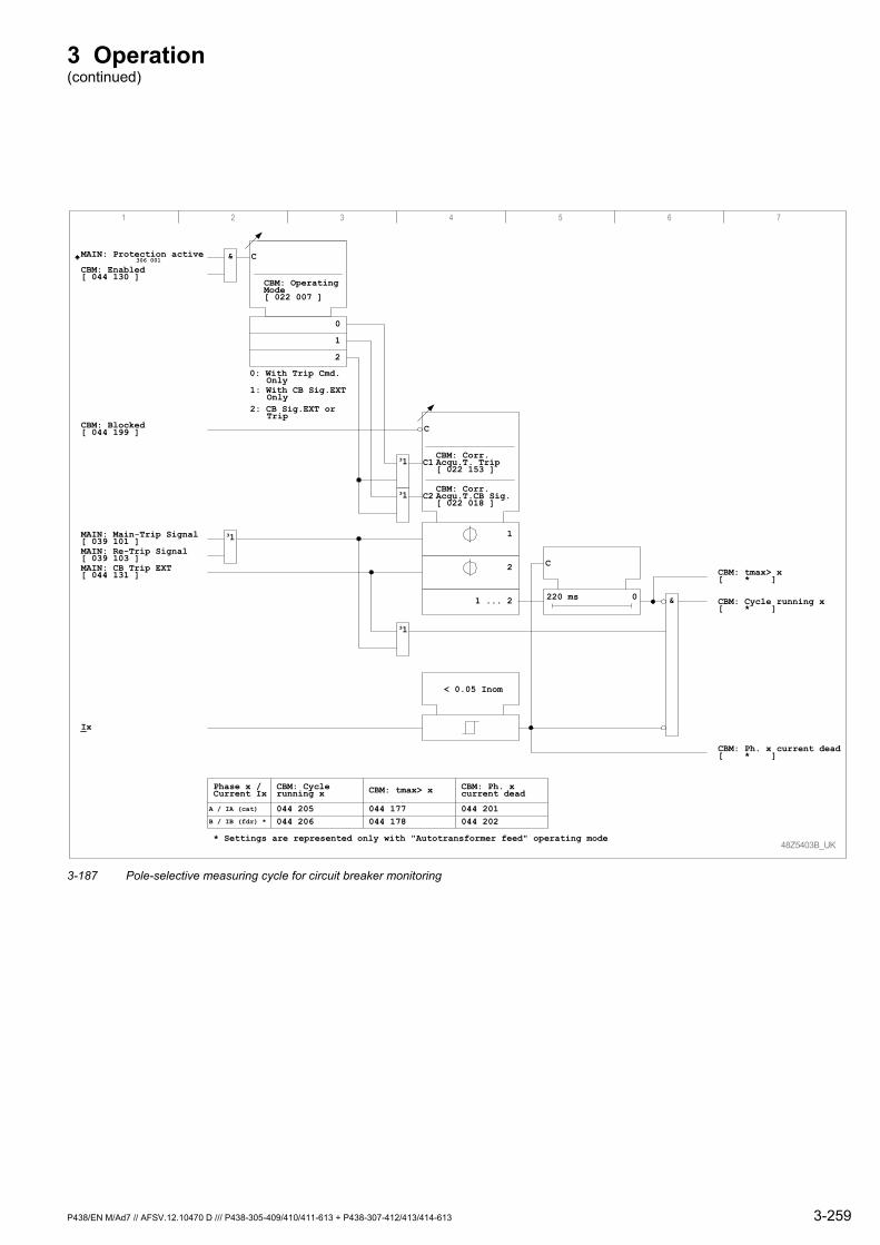
3 Operation (continued)
P438/EN M/Ad7 // AFSV.12.10470 D /// P438-305-409/410/411-613 + P438-307-412/413/414-613 3-259
48Z5403B_UK
1 2 3 6 7
CBM: Corr.Acqu.T.CB Sig.[ 022 018 ]
C
4 5
CBM: Cycle running x[ * ]
C11³
CBM: OperatingMode[ 022 007 ]
C
0: With Trip Cmd.Only
1: With CB Sig.EXTOnly
2: CB Sig.EXT orTrip
0
1
2
1³
Ix
MAIN: CB Trip EXT[ 044 131 ]
MAIN: Re-Trip Signal[ 039 103 ]
MAIN: Main-Trip Signal[ 039 101 ]
CBM: Blocked[ 044 199 ]
&
CBM: Enabled[ 044 130 ]
MAIN: Protection active306 001
CBM: Corr.Acqu.T. Trip[ 022 153 ]
1³ C2
&220 ms 0
CBM: tmax> x[ * ]
< 0.05 Inom
CBM: Ph. x current dead[ * ]
1
2
1 ... 2
C
CBM: tmax> x CBM: Ph. xcurrent dead
CBM: Cyclerunning x
044 205044 206
044 177044 178
044 201044 202
Phase x /Current Ix
B / IB (fdr) *
A / IA (cat)
* Settings are represented only with "Autotransformer feed" operating mode
1³
3-187 Pole-selective measuring cycle for circuit breaker monitoring

3 Operation (continued)
3-260 P438/EN M/Ad7 // AFSV.12.10470 D /// P438-305-409/410/411-613 + P438-307-412/413/414-613
Pole-selective measured values and counter values
Depending on the set operating mode, the P438 evaluates the conductor currents separately and generates an individual wear presentation for each circuit breaker or CB pole.
The following measured values are presented pole selectively, and per-unit values refer to the CB’s nominal current:
Primary ruptured current This value is applied to evaluate wear with reference to the CB wear characteristic.
Per-unit ruptured current
Squared per-unit ruptured current
Sum of the per-unit ruptured currents
Sum of the squared per-unit ruptured currents
Current-time integral of the per-unit ruptured current
Sum of the current-time integrals of the per-unit ruptured currents
The ruptured current is derived from the r.m.s. current value generated during the function cycle.
The integral of the current-time area is calculated during the function cycle. An example for calculation of the current-time integral is displayed in figure X3-188X.
The following counter values are presented pole selectively:
Number of mechanical switching operations carried out
Number of remaining CB operations at CB nominal current This value is derived by evaluating wear with reference to the CB’s wear characteristic.
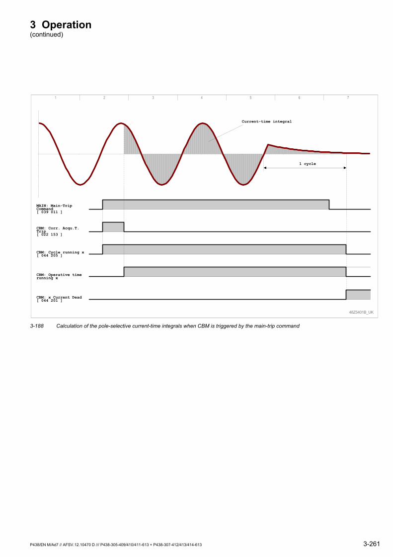
3 Operation (continued)
P438/EN M/Ad7 // AFSV.12.10470 D /// P438-305-409/410/411-613 + P438-307-412/413/414-613 3-261
48Z5401B_UK
1 2 3 4 5 6 7
CBM: Corr. Acqu.T.Trip[ 022 153 ]
MAIN: Main-TripCommand[ 039 011 ]
CBM: x Current Dead[ 044 201 ]
CBM: Operative timerunning x
Current-time integral
1 cycle
CBM: Cycle running x[ 044 205 ]
3-188 Calculation of the pole-selective current-time integrals when CBM is triggered by the main-trip command
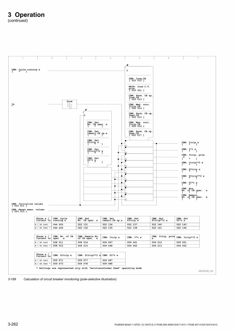
3 Operation (continued)
3-262 P438/EN M/Ad7 // AFSV.12.10470 D /// P438-305-409/410/411-613 + P438-307-412/413/414-613
48Z5402B_UK
1 2 3 6 7
CBM: Max. curr.Itrip,CB[ 022 016 ]
S
CBM: Perm. CB op.Imax,CB[ 022 017 ]
Phase x /Current Ix
CBM: Remain.No. of CB oper. x[ * ]
B / IB (fdr) *
A / IA (cat)
4 5
CBM: Setremain.CB op.x
CBM: SetSItrip x
CBM: SetSItrip**2 x
CBM: SetSI*t x
CBM: No. of CBoper. x
CBM: Remain.No.of CB oper. x CBM: I*t x
CBM: SItrip**2 x
CBM: Itrip**2 xCBM: Itrip, primx
CBM: SItrip x
CBM: Itrip x
022 131022 132
022 134022 135
CBM: SetNo. CB oper. x
022 137022 138
022 140022 141
022 143022 144
008 011008 012
008 014008 015
009 047009 048
009 061009 062
009 212009 213
009 071009 073
009 077009 078
009 051009 052
CBM: Anz.No. of CB oper. x[ * ]
CBM: SI*t x[ * ]
CBM: SItrip**2 x[ * ]
CBM: SItrip x[ * ]
CBM: Itrip**2 x[ * ]
CBM: Itrip, prim x[ * ]
CBM: I*t x[ * ]
CBM: Itrip x[ * ]
S
S
S
S
R
R
R
R
CBM: Perm. CB op.Imed,CB[ 022 015 ]
CBM: Med. curr.Itrip,CB[ 022 014 ]
CBM: Perm. CB op.Inom,CB[ 022 013 ]
MAIN: Inom C.T.prim.[ 010 001 ]
CBM: Inom,CB[ 022 012 ]
C
CBM: SetSI*t x[ * ]
C
CBM: SetSItrip**2 x[ * ]
CBM: SetSItrip x[ * ]
CBM: Setremain.CB op.x[ * ]
CBM: SetNo. CB oper. x[ * ]
CBM: SI*t x
009 087009 088
fnom
CBM: Reset meas. values[ 003 013 ]
CBM: Initialize values[ 003 011 ]
Ix
CBM: Cycle running x[ * ]
Phase x /Current Ix
B / IB (fdr) *
A / IA (cat)
* Settings are represented only with "Autotransformer feed" operating mode
CBM: Cyclerunning x
044 205044 206
Phase x /Current Ix
B / IB (fdr) *
A / IA (cat)
3-189 Calculation of circuit breaker monitoring (pole-selective illustration)

3 Operation (continued)
P438/EN M/Ad7 // AFSV.12.10470 D /// P438-305-409/410/411-613 + P438-307-412/413/414-613 3-263
Resetting measured values Measured values from the respective last CB trip may be reset using the interfaces of the device. Accumulated measured values are not affected by such a reset operation.
Setting measured values Setting measured values in the circuit breaker monitoring function is necessary when the respective CB has already been exposed to operating conditions or has been replaced. The available interfaces on the device may be used to set measured values in the circuit breaker monitoring function.
Note: Only such measured values and counter values in the P438 may be set to new values that do not have their default values set to ‘Blocked‘. The stored value will remain unchanged if the default value is set to ‘Blocked‘. Executing the set command results in initializing all default values in the P438 to ‘Blocked‘.
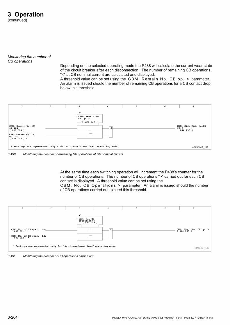
3 Operation (continued)
3-264 P438/EN M/Ad7 // AFSV.12.10470 D /// P438-305-409/410/411-613 + P438-307-412/413/414-613
Monitoring the number of CB operations
Depending on the selected operating mode the P438 will calculate the current wear state of the circuit breaker after each disconnection. The number of remaining CB operations "<" at CB nominal current are calculated and displayed. A threshold value can be set using the C B M : R e m a i n N o . C B o p . < CC parameter. An alarm is issued should the number of remaining CB operations for a CB contact drop below this threshold.
48Z5344A_UK
CBM: Sig. Rem. No.CBop.<[ 044 136 ]
CBM: Remain No.CB op. <
[ 022 020 ]
CBM: Remain.No. CBop.cat
1 2 3 4 5 6 7
1
CBM: Remain.No. CBop.fdr
* Settings are represented only with "Autotransformer feed" operating mode
[ 008 014 ]
[ 008 015 ] *
3-190 Monitoring the number of remaining CB operations at CB nominal current
At the same time each switching operation will increment the P438’s counter for the number of CB operations. The number of CB operations ">" carried out for each CB contact is displayed. A threshold value can be set using the C B M : N o . C B O p e r a t i o n s > CC parameter. An alarm is issued should the number of CB operations carried out exceed this threshold.
48Z5345B_UK
CBM: Sig. No. CB op. >[ 044 135 ]
CBM: No. CBoperations >
[ 022 019 ]
CBM: No. of CB oper. cat[ 008 011 ]
1 2 3 4 5 6 7
1≥
CBM: No. of CB oper. fdr[ 008 012 ] *
* Settings are represented only for "Autotransformer feed" operating mode.
3-191 Monitoring the number of CB operations carried out
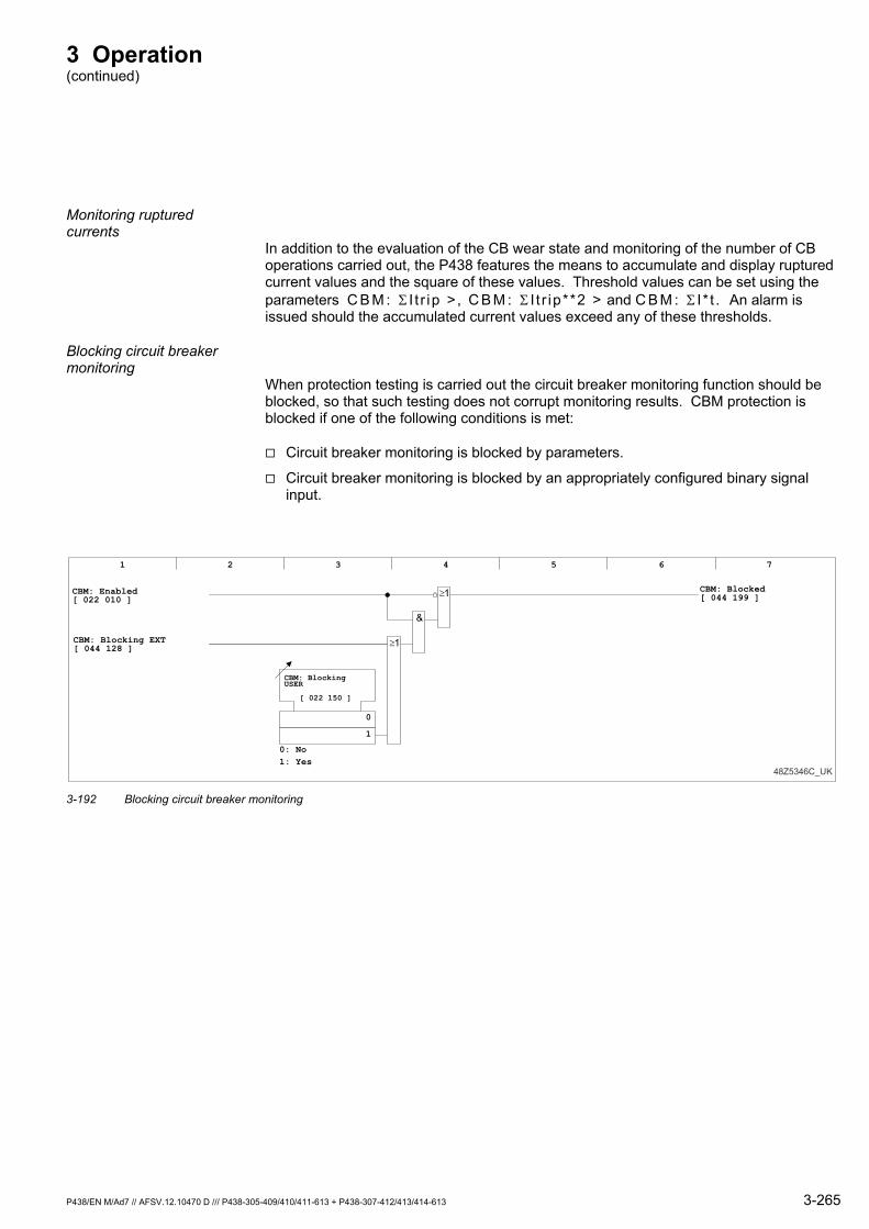
3 Operation (continued)
P438/EN M/Ad7 // AFSV.12.10470 D /// P438-305-409/410/411-613 + P438-307-412/413/414-613 3-265
Monitoring ruptured currents
In addition to the evaluation of the CB wear state and monitoring of the number of CB operations carried out, the P438 features the means to accumulate and display ruptured current values and the square of these values. Threshold values can be set using the parameters C B M : Σ I t r ip > CC, C B M : Σ I t r ip**2 > CC and C B M : Σ I * t CC. An alarm is issued should the accumulated current values exceed any of these thresholds.
Blocking circuit breaker monitoring
When protection testing is carried out the circuit breaker monitoring function should be blocked, so that such testing does not corrupt monitoring results. CBM protection is blocked if one of the following conditions is met:
Circuit breaker monitoring is blocked by parameters.
Circuit breaker monitoring is blocked by an appropriately configured binary signal input.
CBM: Enabled[ 022 010 ]
CBM: Blocked[ 044 199 ]
CBM: Blocking EXT[ 044 128 ]
48Z5346C_UK
1 2 3 4 5 6 7
1
&
1
CBM: BlockingUSER
[ 022 150 ]
0
1
0: No1: Yes
3-192 Blocking circuit breaker monitoring

3 Operation (continued)
3.34 Limit Value Monitoring (Function Group LIMIT)
To support normal operation, a multitude of currents, voltages, temperatures and the frequency can be monitored for falling below or exceeding limit set points. If this is the case, a signal is issued once the set operate time-delays have elapsed. These limit value monitoring elements are based on operating data measurement and cannot therefore be employed as protection functions.
Disabling/enabling and readiness of limit value monitoring
Limit value monitoring can be disabled or enabled using setting parameters. Enabling can be carried out separately for each setting group.
Limit value monitoring will not be available under the following conditions:
Limit value monitoring is not enabled.
Protection is not enabled.
48Z5405A_UK
Setting
Group 1Group 2Group 3Group 4
LIMIT: EnableSGx072 240073 240074 240075 240
LIMIT: Enabled[ 040 074 ]
LIMIT: EnableSGx
[ * ]
LIMIT: GeneralEnable USER
[ 014 010 ]
0: No
1: Yes
0: No
1: Yes
1
0
1
0
LIMIT: Not Ready[ 041 043 ]
MAIN: Protectionactive
306 001
3-193 Disabling or enabling circuit breaker failure protection
3-266 P438/EN M/Ad7 // AFSV.12.10470 D /// P438-305-409/410/411-613 + P438-307-412/413/414-613
3 Operation (continued)
Monitoring of the phase currents and voltages
The P438 offers the possibility of monitoring of the following measured values in order to determine whether they exceed set upper limit values or fall below set lower limit values:
Current: I>, I>>
Catenary currents: Icat>, Icat>>
Feeder currents: Ifdr>, Ifdr>>
Defrost currents: Idfrst>, Idfrst>>
Voltage: V<, V<<, V>, V>>
Catenary voltages: Vcat<, Vcat<<, Vcat>, Vcat>>
Feeder voltages: Vfdr<, Vfdr<<, Vfdr>, Vfdr>>
Frequencies: f<, f<<, f>, f>>
Linearized 20mA currents: IDC,lin<, IDC,lin<<, IDC,lin>, IDC,lin>>
Measured temperatures: T<, T<<. T>, T>>.
If measured values exceed or fall below one of the set upper or lower limit values, respectively, a signal is issued once a set time-delay has elapsed.
P438/EN M/Ad7 // AFSV.12.10470 D /// P438-305-409/410/411-613 + P438-307-412/413/414-613 3-267

3 Operation (continued)
Measured current value monitoring
The measured current value is monitored by two stages to determine whether it exceeds set thresholds. If any of the thresholds are exceeded a signal is issued after a set time-delay has elapsed.
48Z5406A_UK
LIMIT: tI>Elapsed[ 004 062 ]
MAIN: Protectionactive
306 001
LIMIT: tI>>Elapsed[ 040 157 ]
LIMIT: I>SGx
[ * ]
LIMIT: I>>SGx
[ * ]
LIMIT: tI>>SGx
[ * ]
LIMIT: tI>SGx
[ * ]
Setting
Group 1Group 2Group 3Group 4
LIMIT: I>SGx072 241073 241074 241075 241
LIMIT: Enabled[ 040 074 ]
LIMIT: I>>SGx072 242073 242074 242075 242
LIMIT: tI>SGx072 243073 243074 243075 243
LIMIT: tI>>SGx072 244073 244074 244075 244
I
3-194 Measured current value monitoring
3-268 P438/EN M/Ad7 // AFSV.12.10470 D /// P438-305-409/410/411-613 + P438-307-412/413/414-613
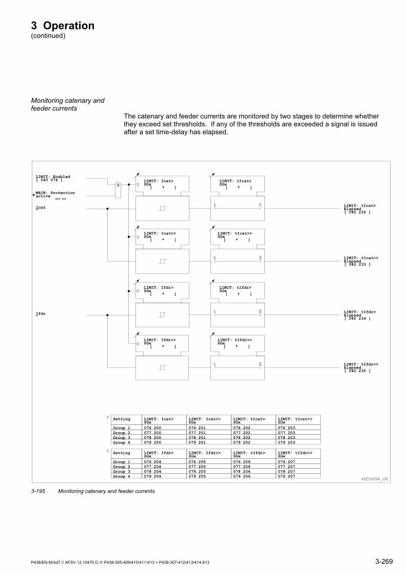
3 Operation (continued)
Monitoring catenary and feeder currents
The catenary and feeder currents are monitored by two stages to determine whether they exceed set thresholds. If any of the thresholds are exceeded a signal is issued after a set time-delay has elapsed.
LIMIT: tIcat>Elapsed[ 040 232 ]
MAIN: Protectionactive
306 001
LIMIT: tIcat>>Elapsed[ 040 233 ]
LIMIT: Icat>SGx
[ * ]
LIMIT: Icat>>SGx
[ * ]
LIMIT: tIcat>>SGx
[ * ]
LIMIT: tIcat>SGx
[ * ]
LIMIT: Enabled[ 040 074 ]
Icat
LIMIT: Ifdr>SGx
[ * ]
LIMIT: Ifdr>>SGx
[ * ]
LIMIT: tIfdr>>SGx
[ * ]
LIMIT: tIfdr>SGx
[ * ]
LIMIT: tIfdr>Elapsed[ 040 234 ]
LIMIT: tIfdr>>Elapsed[ 040 235 ]
Setting
Group 1Group 2Group 3Group 4
LIMIT: Icat>SGx076 200077 200078 200079 200
LIMIT: Icat>>SGx076 201077 201078 201079 201
LIMIT: tIcat>SGx076 202077 202078 202079 202
LIMIT: tIcat>>SGx076 203077 203078 203079 203
48Z5409A_UK
Setting
Group 1Group 2Group 3Group 4
LIMIT: Ifdr>SGx076 204077 204078 204079 204
LIMIT: Ifdr>>SGx076 205077 205078 205079 205
LIMIT: tIfdr>SGx076 206077 206078 206079 206
LIMIT: tIfdr>>SGx076 207077 207078 207079 207
Ifdr
3-195 Monitoring catenary and feeder currents
P438/EN M/Ad7 // AFSV.12.10470 D /// P438-305-409/410/411-613 + P438-307-412/413/414-613 3-269
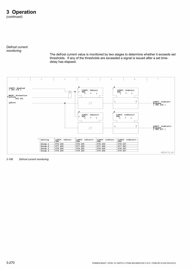
3 Operation (continued)
Defrost current monitoring
The defrost current value is monitored by two stages to determine whether it exceeds set thresholds. If any of the thresholds are exceeded a signal is issued after a set time-delay has elapsed.
48Z5417A_UK
LIMIT: tIdfrst>Elapsed[ 040 236 ]
MAIN: Protectionactive
306 001
LIMIT: tIdfrst>>Elapsed[ 040 237 ]
LIMIT: Idfrst>SGx
[ * ]
LIMIT: Idfrst>>SGx
[ * ]
LIMIT: tIdfrst>>SGx
[ * ]
LIMIT: tIdfrst>SGx
[ * ]
Setting
Group 1Group 2Group 3Group 4
LIMIT: Idfrst>SGx076 224077 224078 224079 224
LIMIT: Enabled[ 040 074 ]
LIMIT: Idfrst>>SGx076 225077 225078 225079 225
LIMIT: tIdfrst>SGx076 226077 226078 226079 226
LIMIT: tIdfrst>>SGx076 227077 227078 227079 227
Idfrst
3-196 Defrost current monitoring
3-270 P438/EN M/Ad7 // AFSV.12.10470 D /// P438-305-409/410/411-613 + P438-307-412/413/414-613
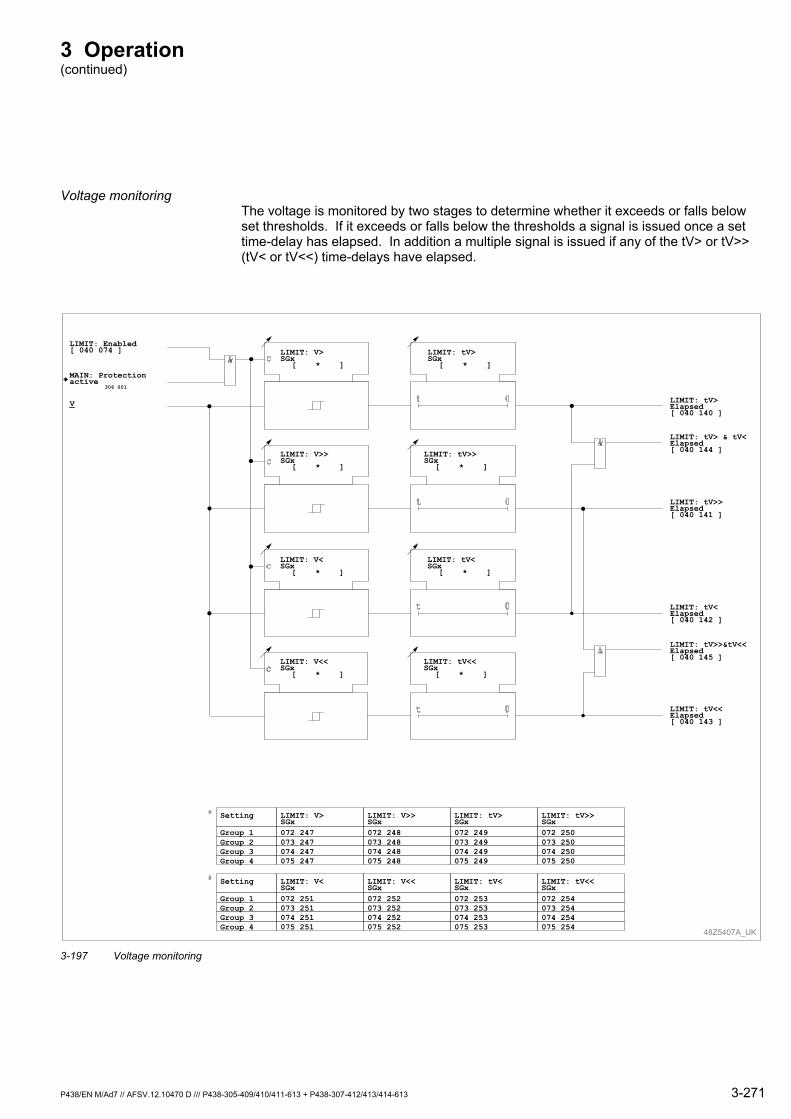
3 Operation (continued)
Voltage monitoring The voltage is monitored by two stages to determine whether it exceeds or falls below set thresholds. If it exceeds or falls below the thresholds a signal is issued once a set time-delay has elapsed. In addition a multiple signal is issued if any of the tV> or tV>> (tV< or tV<<) time-delays have elapsed.
LIMIT: tV>Elapsed[ 040 140 ]
MAIN: Protectionactive
306 001
LIMIT: tV>>Elapsed[ 040 141 ]
LIMIT: V>SGx
[ * ]
LIMIT: V>>SGx
[ * ]
LIMIT: tV>>SGx
[ * ]
LIMIT: tV>SGx
[ * ]
LIMIT: Enabled[ 040 074 ]
V
LIMIT: V<SGx
[ * ]
LIMIT: V<<SGx
[ * ]
LIMIT: tV<<SGx
[ * ]
LIMIT: tV<SGx
[ * ]
LIMIT: tV<Elapsed[ 040 142 ]
LIMIT: tV<<Elapsed[ 040 143 ]
Setting
Group 1Group 2Group 3Group 4
LIMIT: V>SGx072 247073 247074 247075 247
LIMIT: V>>SGx072 248073 248074 248075 248
LIMIT: tV>SGx072 249073 249074 249075 249
LIMIT: tV>>SGx072 250073 250074 250075 250
48Z5407A_UK
Setting
Group 1Group 2Group 3Group 4
LIMIT: V<SGx072 251073 251074 251075 251
LIMIT: V<<SGx072 252073 252074 252075 252
LIMIT: tV<SGx072 253073 253074 253075 253
LIMIT: tV<<SGx072 254073 254074 254075 254
LIMIT: tV>>&tV<<Elapsed[ 040 145 ]
LIMIT: tV> & tV<Elapsed[ 040 144 ]
3-197 Voltage monitoring
P438/EN M/Ad7 // AFSV.12.10470 D /// P438-305-409/410/411-613 + P438-307-412/413/414-613 3-271

3 Operation (continued)
Monitoring catenary and feeder voltages
The catenary and feeder voltages are monitored by two stages to determine whether they exceed or fall below set thresholds. If it exceeds or falls below the thresholds a signal is issued once a set time-delay has elapsed. In addition a multiple signal is issued if either of the tVcat> or tVcat< time-delays (or, respectively, stages tVcat>> or tVcat<<, tVfdr> or tVfdr<, tVfdr>> or tVfdr<<) have elapsed.
3-272 P438/EN M/Ad7 // AFSV.12.10470 D /// P438-305-409/410/411-613 + P438-307-412/413/414-613
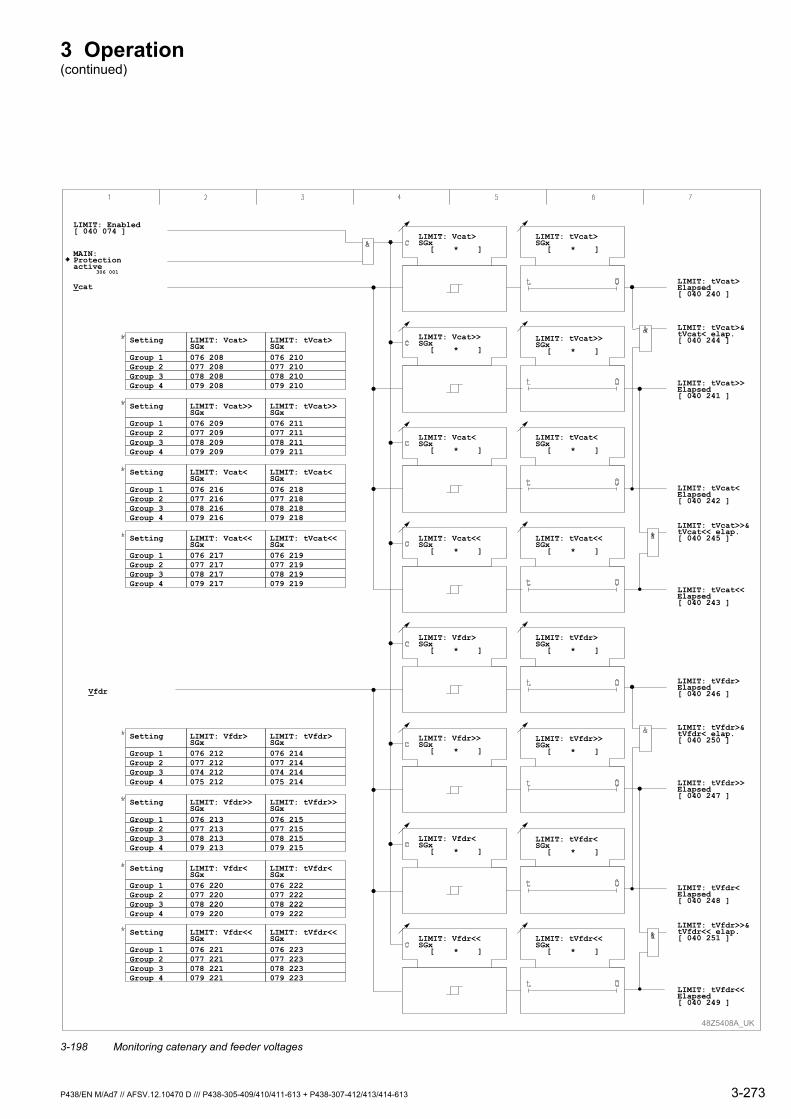
3 Operation (continued)
Setting
Group 1Group 2Group 3Group 4
LIMIT: Vcat>SGx076 208077 208078 208079 208
LIMIT: tVcat>SGx076 210077 210078 210079 210
Setting
Group 1Group 2Group 3Group 4
LIMIT: Vcat>>SGx076 209077 209078 209079 209
LIMIT: tVcat>>SGx076 211077 211078 211079 211
Setting
Group 1Group 2Group 3Group 4
LIMIT: Vcat<SGx076 216077 216078 216079 216
LIMIT: tVcat<SGx076 218077 218078 218079 218
Setting
Group 1Group 2Group 3Group 4
LIMIT: Vcat<<SGx076 217077 217078 217079 217
LIMIT: tVcat<<SGx076 219077 219078 219079 219
Vcat
Vfdr
Setting
Group 1Group 2Group 3Group 4
LIMIT: Vfdr>SGx076 212077 212074 212075 212
LIMIT: tVfdr>SGx076 214077 214074 214075 214
Setting
Group 1Group 2Group 3Group 4
LIMIT: Vfdr<<SGx076 221077 221078 221079 221
LIMIT: tVfdr<<SGx076 223077 223078 223079 223
Setting
Group 1Group 2Group 3Group 4
LIMIT: Vfdr>>SGx076 213077 213078 213079 213
LIMIT: tVfdr>>SGx076 215077 215078 215079 215
Setting
Group 1Group 2Group 3Group 4
LIMIT: Vfdr<SGx076 220077 220078 220079 220
LIMIT: tVfdr<SGx076 222077 222078 222079 222
LIMIT: tVcat>Elapsed[ 040 240 ]
MAIN:Protectionactive
306 001
LIMIT: tVcat>>Elapsed[ 040 241 ]
LIMIT: Vcat>SGx
[ * ]
LIMIT: Vcat>>SGx
[ * ]LIMIT: tVcat>>SGx
[ * ]
LIMIT: tVcat>SGx
[ * ]
LIMIT: Enabled[ 040 074 ]
LIMIT: Vcat<SGx
[ * ]
LIMIT: Vcat<<SGx
[ * ]
LIMIT: tVcat<<SGx
[ * ]
LIMIT: tVcat<SGx
[ * ]
LIMIT: tVcat<Elapsed[ 040 242 ]
LIMIT: tVcat<<Elapsed[ 040 243 ]
LIMIT: tVcat>>&tVcat<< elap.[ 040 245 ]
LIMIT: tVcat>&tVcat< elap.[ 040 244 ]
LIMIT: tVfdr>Elapsed[ 040 246 ]
LIMIT: tVfdr>>Elapsed[ 040 247 ]
LIMIT: Vfdr>SGx
[ * ]
LIMIT: Vfdr>>SGx
[ * ]
LIMIT: tVfdr>>SGx
[ * ]
LIMIT: tVfdr>SGx
[ * ]
LIMIT: Vfdr<SGx
[ * ]
LIMIT: Vfdr<<SGx
[ * ]
LIMIT: tVfdr<<SGx
[ * ]
LIMIT: tVfdr<SGx
[ * ]
LIMIT: tVfdr<Elapsed[ 040 248 ]
LIMIT: tVfdr<<Elapsed[ 040 249 ]
LIMIT: tVfdr>>&tVfdr<< elap.[ 040 251 ]
LIMIT: tVfdr>&tVfdr< elap.[ 040 250 ]
48Z5408A_UK 3-198 Monitoring catenary and feeder voltages
P438/EN M/Ad7 // AFSV.12.10470 D /// P438-305-409/410/411-613 + P438-307-412/413/414-613 3-273
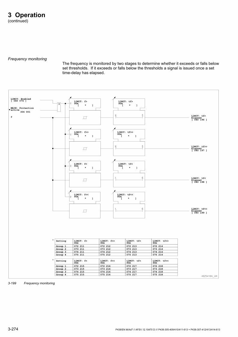
3 Operation (continued)
Frequency monitoring The frequency is monitored by two stages to determine whether it exceeds or falls below set thresholds. If it exceeds or falls below the thresholds a signal is issued once a set time-delay has elapsed.
LIMIT: tf>Elapsed[ 040 196 ]
MAIN: Protectionactive
306 001
LIMIT: tf>>Elapsed[ 040 197 ]
LIMIT: f>SGx
[ * ]
LIMIT: f>>SGx
[ * ]
LIMIT: tf>>SGx
[ * ]
LIMIT: tf>SGx
[ * ]
LIMIT: Enabled[ 040 074 ]
f
LIMIT: f<SGx
[ * ]
LIMIT: f<<SGx
[ * ]
LIMIT: tf<<SGx
[ * ]
LIMIT: tf<SGx
[ * ]
LIMIT: tf<Elapsed[ 040 198 ]
LIMIT: tf<<Elapsed[ 040 199 ]
Setting
Group 1Group 2Group 3Group 4
LIMIT: f>SGx072 211073 211074 211075 211
LIMIT: f>>SGx072 212073 212074 212075 212
LIMIT: tf>SGx072 213073 213074 213075 213
LIMIT: tf>>SGx072 214073 214074 214075 214
48Z5418A_UK
Setting
Group 1Group 2Group 3Group 4
LIMIT: f<SGx072 215073 215074 215075 215
LIMIT: f<<SGx072 216073 216074 216075 216
LIMIT: tf<SGx072 217073 217074 217075 217
LIMIT: tf<<SGx072 218073 218074 218075 218
3-199 Frequency monitoring
3-274 P438/EN M/Ad7 // AFSV.12.10470 D /// P438-305-409/410/411-613 + P438-307-412/413/414-613
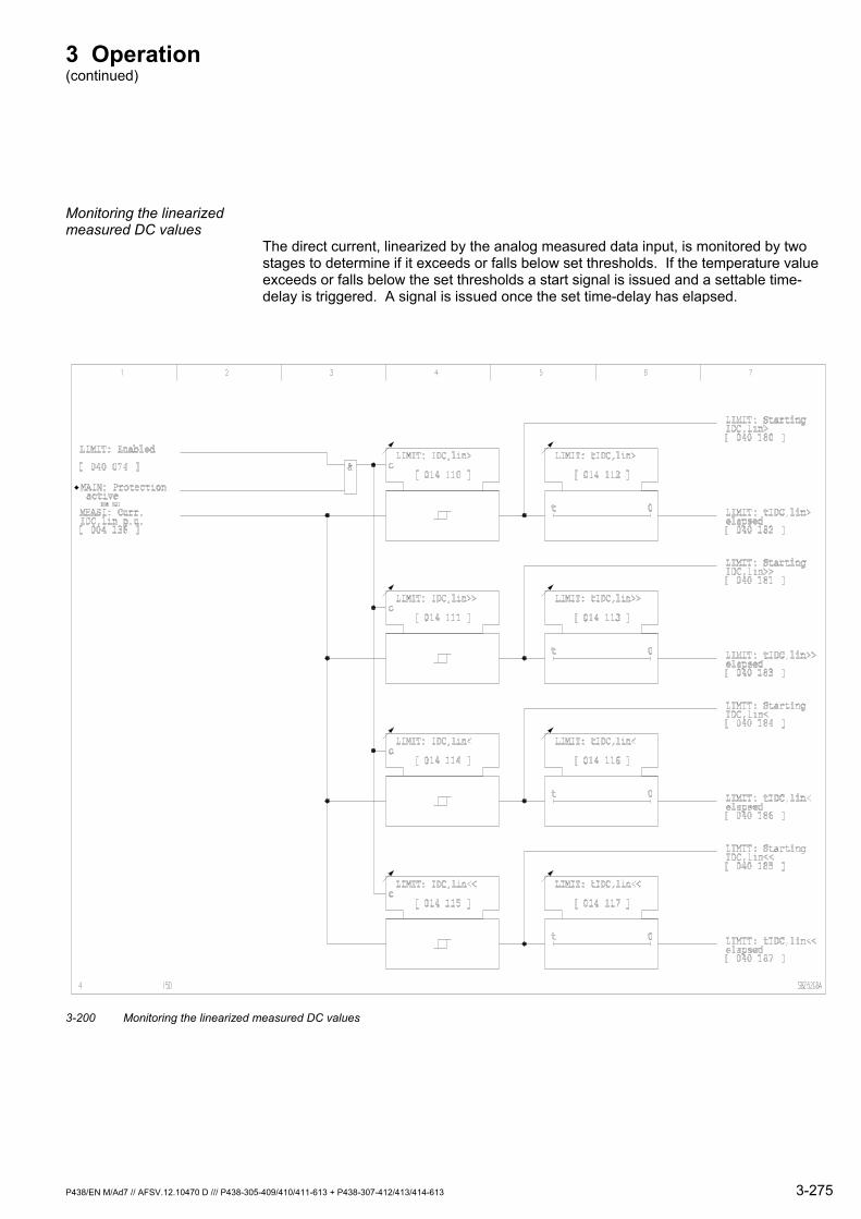
3 Operation (continued)
Monitoring the linearized measured DC values
The direct current, linearized by the analog measured data input, is monitored by two stages to determine if it exceeds or falls below set thresholds. If the temperature value exceeds or falls below the set thresholds a start signal is issued and a settable time-delay is triggered. A signal is issued once the set time-delay has elapsed.
3-200 Monitoring the linearized measured DC values
P438/EN M/Ad7 // AFSV.12.10470 D /// P438-305-409/410/411-613 + P438-307-412/413/414-613 3-275
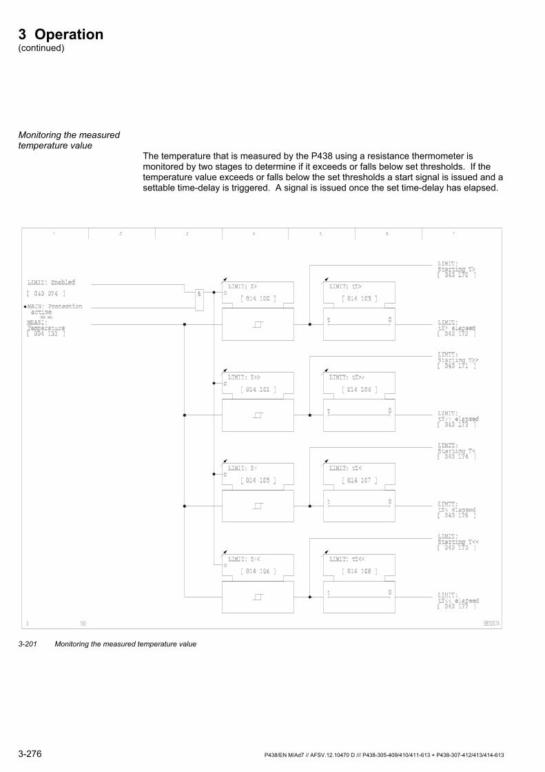
3 Operation (continued)
Monitoring the measured temperature value
The temperature that is measured by the P438 using a resistance thermometer is monitored by two stages to determine if it exceeds or falls below set thresholds. If the temperature value exceeds or falls below the set thresholds a start signal is issued and a settable time-delay is triggered. A signal is issued once the set time-delay has elapsed.
3-201 Monitoring the measured temperature value
3-276 P438/EN M/Ad7 // AFSV.12.10470 D /// P438-305-409/410/411-613 + P438-307-412/413/414-613
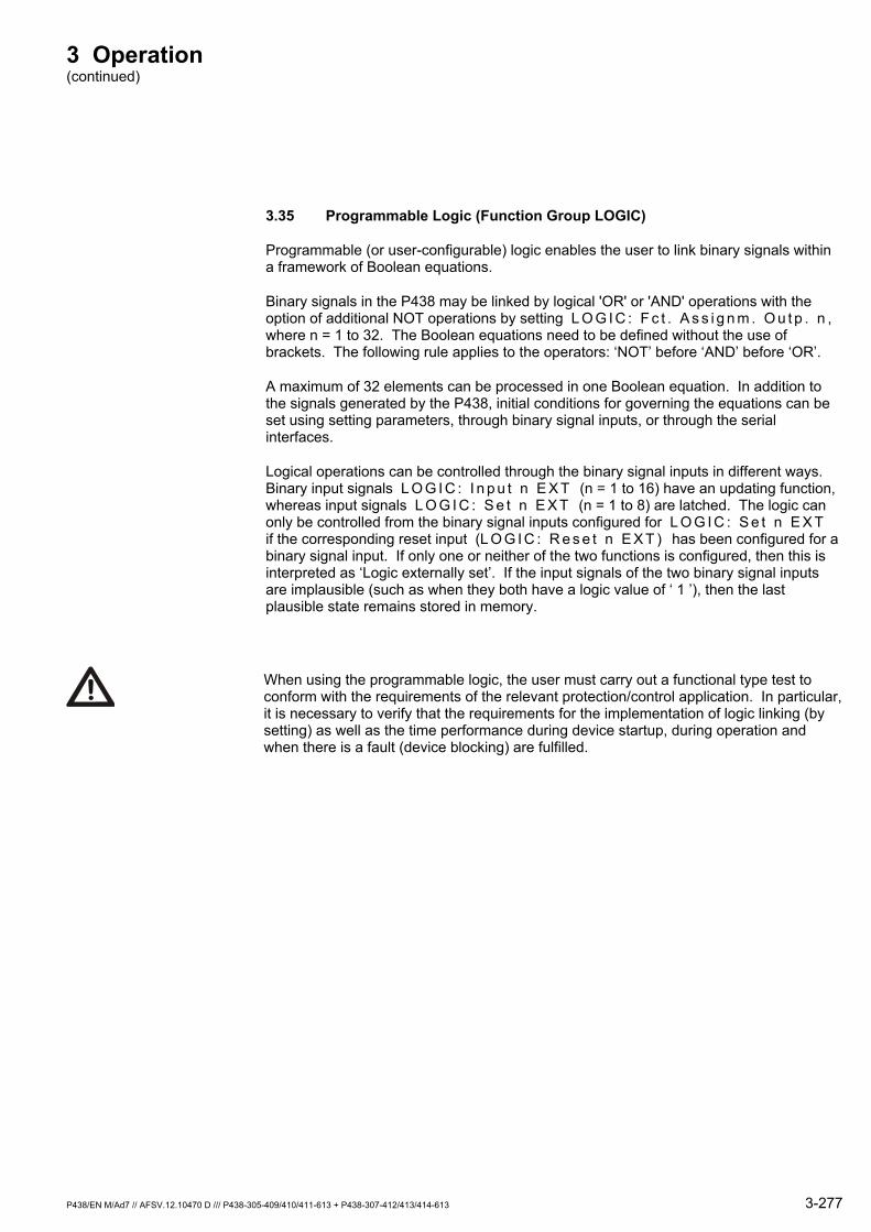
3 Operation (continued)
3.35 Programmable Logic (Function Group LOGIC)
Programmable (or user-configurable) logic enables the user to link binary signals within a framework of Boolean equations.
Binary signals in the P438 may be linked by logical 'OR' or 'AND' operations with the option of additional NOT operations by setting L O G I C : F c t . A s s i g n m . O u t p . n , where n = 1 to 32. The Boolean equations need to be defined without the use of brackets. The following rule applies to the operators: ‘NOT’ before ‘AND’ before ‘OR’.
A maximum of 32 elements can be processed in one Boolean equation. In addition to the signals generated by the P438, initial conditions for governing the equations can be set using setting parameters, through binary signal inputs, or through the serial interfaces.
Logical operations can be controlled through the binary signal inputs in different ways. Binary input signals L O G I C : I n p u t n E X T (n = 1 to 16) have an updating function, whereas input signals L O G I C : S e t n E X T (n = 1 to 8) are latched. The logic can only be controlled from the binary signal inputs configured for L O G I C : S e t n E X T if the corresponding reset input (L O G I C : R e s e t n E X T ) has been configured for a binary signal input. If only one or neither of the two functions is configured, then this is interpreted as ‘Logic externally set’. If the input signals of the two binary signal inputs are implausible (such as when they both have a logic value of ‘ 1 ’), then the last plausible state remains stored in memory.
When using the programmable logic, the user must carry out a functional type test to conform with the requirements of the relevant protection/control application. In particular, it is necessary to verify that the requirements for the implementation of logic linking (by setting) as well as the time performance during device startup, during operation and when there is a fault (device blocking) are fulfilled.
P438/EN M/Ad7 // AFSV.12.10470 D /// P438-305-409/410/411-613 + P438-307-412/413/414-613 3-277
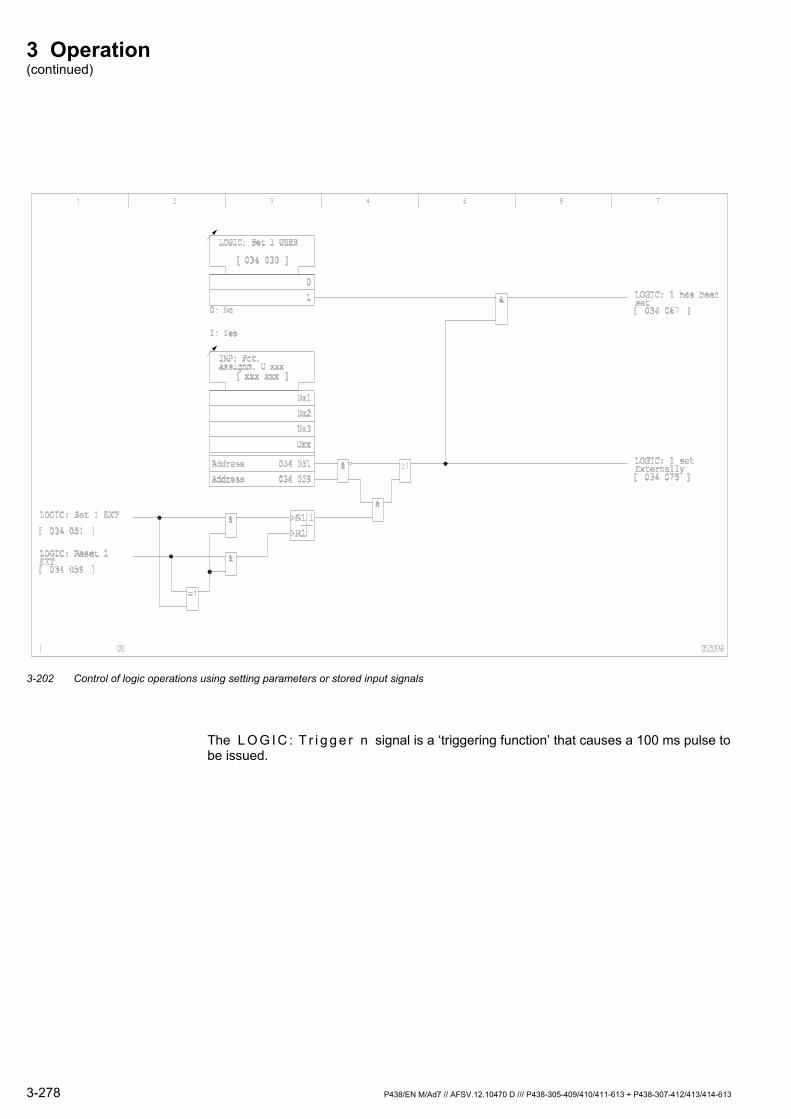
3 Operation (continued)
3-202 Control of logic operations using setting parameters or stored input signals
The L O G I C : T r i g g e r n signal is a ‘triggering function’ that causes a 100 ms pulse to be issued.
3-278 P438/EN M/Ad7 // AFSV.12.10470 D /// P438-305-409/410/411-613 + P438-307-412/413/414-613

3 Operation (continued)
3-203 Setting options for programmable logic (shown here for output 1)
P438/EN M/Ad7 // AFSV.12.10470 D /// P438-305-409/410/411-613 + P438-307-412/413/414-613 3-279

3 Operation (continued)
The output signal of an equation can be fed into a further, higher order, equation as an input signal thus creating a sequence of interlinked Boolean equations. The equations are processed in the sequence defined by the order of each equation. It should be noted that in the case of overlapping equations, the result is provided by the equation with the highest order.
The output signal of each equation is fed to a separate timer stage with two timer elements and a choice of operating modes. This offers the possibility of assigning a freely configurable time characteristic to the output signal of each Boolean equation. In the Minimum Dwell operating mode, the setting of timer stage tZ2 has no effect. Figures 3-204 to 3-208 show the time characteristics for the various timer stage operating modes.
Note: If the device is switched to "offline" the equations are not processed and all outputs are set to the ' 0 ' logic level.
3-204 Operating mode 1: Pickup/reset delay
3-280 P438/EN M/Ad7 // AFSV.12.10470 D /// P438-305-409/410/411-613 + P438-307-412/413/414-613
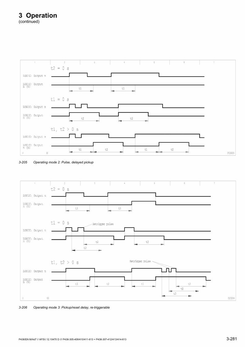
3 Operation (continued)
3-205 Operating mode 2: Pulse, delayed pickup
3-206 Operating mode 3: Pickup/reset delay, re-triggerable
P438/EN M/Ad7 // AFSV.12.10470 D /// P438-305-409/410/411-613 + P438-307-412/413/414-613 3-281
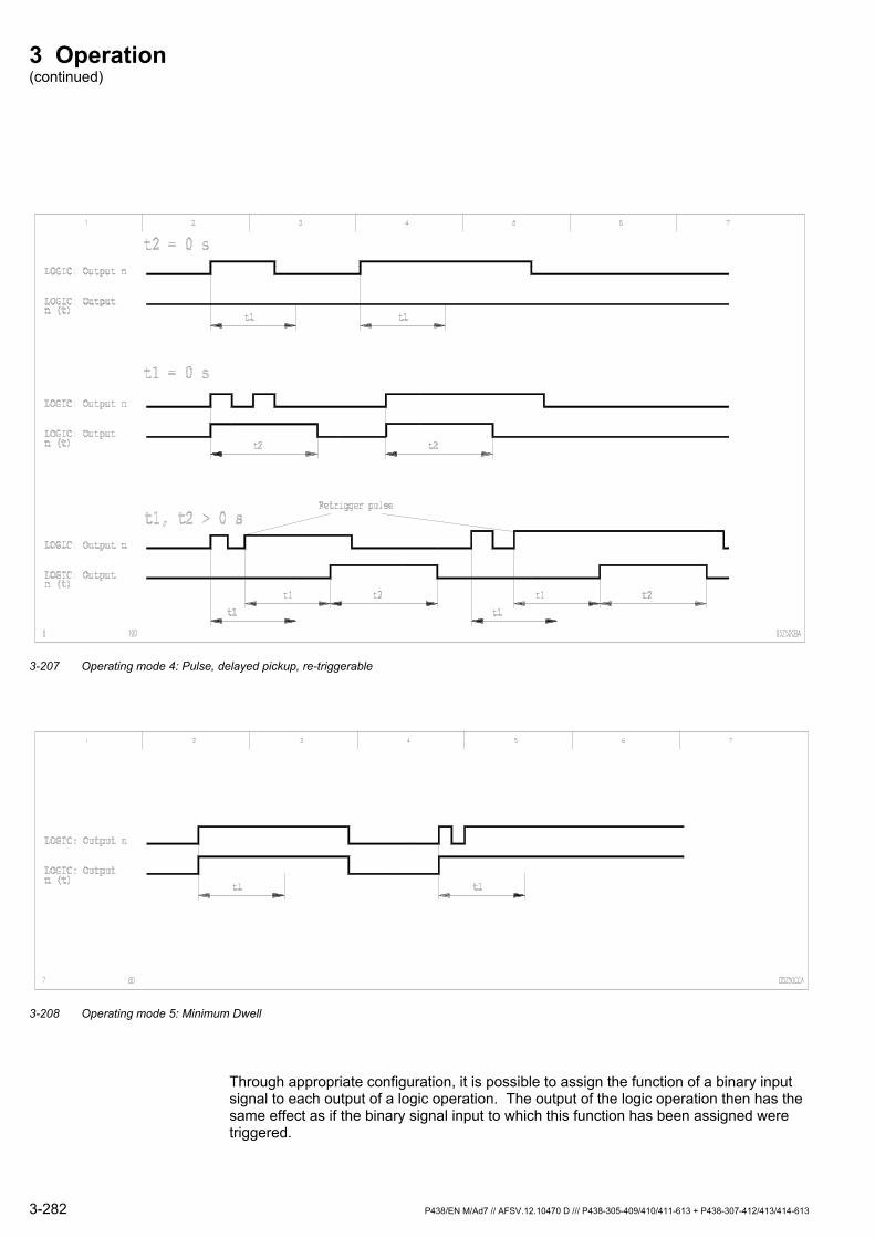
3 Operation (continued)
3-207 Operating mode 4: Pulse, delayed pickup, re-triggerable
3-208 Operating mode 5: Minimum Dwell
Through appropriate configuration, it is possible to assign the function of a binary input signal to each output of a logic operation. The output of the logic operation then has the same effect as if the binary signal input to which this function has been assigned were triggered.
3-282 P438/EN M/Ad7 // AFSV.12.10470 D /// P438-305-409/410/411-613 + P438-307-412/413/414-613
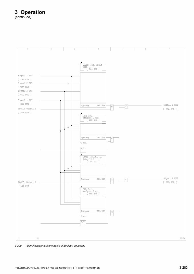
3 Operation (continued)
3-209 Signal assignment to outputs of Boolean equations
P438/EN M/Ad7 // AFSV.12.10470 D /// P438-305-409/410/411-613 + P438-307-412/413/414-613 3-283

3-284 P438/EN M/Ad7 // AFSV.12.10470 D /// P438-305-409/410/411-613 + P438-307-412/413/414-613
4 Design
P438/EN M/Ad7 // AFSV.12.10470 D /// P438-305-409/410/411-613 + P438-307-412/413/414-613 4-1
4 Design
The P438 is available in different types of cases and with different combinations of modules.
The P438 – like all other device types in the MiCOM Px30 range – is equipped with the standard user interface (HMI). Depending on the order the user interface (HMI) is fitted either permanently to the case front panel or is detachable. The user interface is covered with a tough film so that the specified degree of IP protection will be maintained. In addition to the essential control and display elements, a parallel display consisting of a total of 17 LED indicators is also incorporated. The designation of the various LED indicators is shown in plain text on a label strip.
The PC interface (9-pin D-Sub female connector) is located under the hinged cover at the bottom of the user interface.
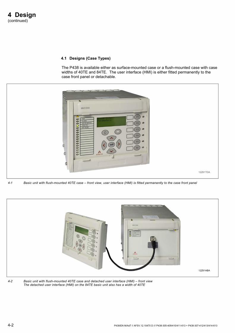
4 Design (continued)
4-2 P438/EN M/Ad7 // AFSV.12.10470 D /// P438-305-409/410/411-613 + P438-307-412/413/414-613
4.1 Designs (Case Types)
The P438 is available either as surface-mounted case or a flush-mounted case with case widths of 40TE and 84TE. The user interface (HMI) is either fitted permanently to the case front panel or detachable.
12Z61TDA
4-1 Basic unit with flush-mounted 40TE case – front view, user interface (HMI) is fitted permanently to the case front panel
12Z61ABA
4-2 Basic unit with flush-mounted 40TE case and detached user interface (HMI) – front view The detached user interface (HMI) on the 84TE basic unit also has a width of 40TE
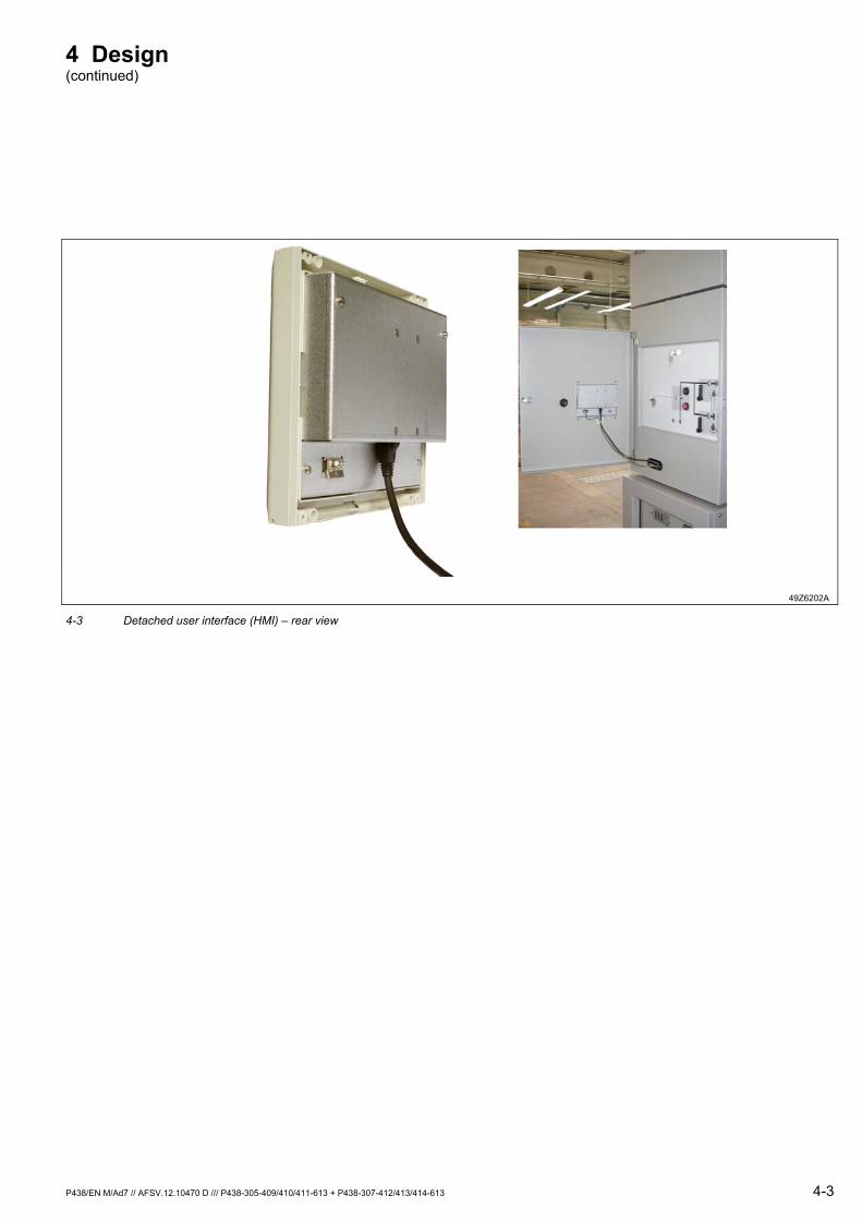
4 Design (continued)
P438/EN M/Ad7 // AFSV.12.10470 D /// P438-305-409/410/411-613 + P438-307-412/413/414-613 4-3
49Z6202A 4-3 Detached user interface (HMI) – rear view
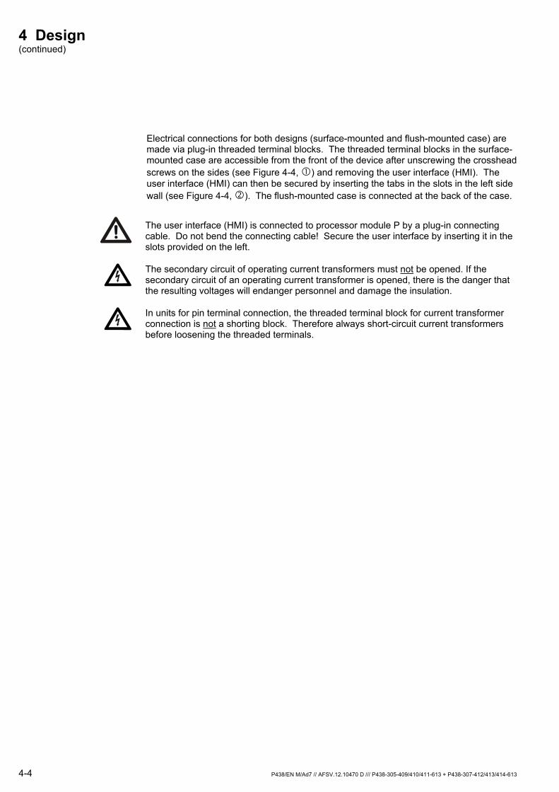
4 Design (continued)
4-4 P438/EN M/Ad7 // AFSV.12.10470 D /// P438-305-409/410/411-613 + P438-307-412/413/414-613
Electrical connections for both designs (surface-mounted and flush-mounted case) are made via plug-in threaded terminal blocks. The threaded terminal blocks in the surface-mounted case are accessible from the front of the device after unscrewing the crosshead screws on the sides (see Figure 4-4, ) and removing the user interface (HMI). The user interface (HMI) can then be secured by inserting the tabs in the slots in the left side wall (see Figure 4-4, ). The flush-mounted case is connected at the back of the case.
The user interface (HMI) is connected to processor module P by a plug-in connecting cable. Do not bend the connecting cable! Secure the user interface by inserting it in the slots provided on the left.
The secondary circuit of operating current transformers must not be opened. If the secondary circuit of an operating current transformer is opened, there is the danger that the resulting voltages will endanger personnel and damage the insulation.
In units for pin terminal connection, the threaded terminal block for current transformer connection is not a shorting block. Therefore always short-circuit current transformers before loosening the threaded terminals.
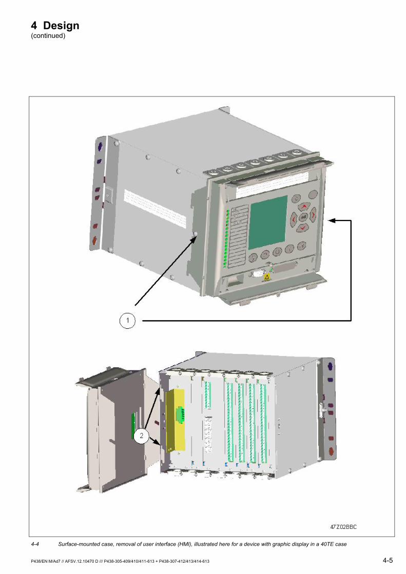
4 Design (continued)
P438/EN M/Ad7 // AFSV.12.10470 D /// P438-305-409/410/411-613 + P438-307-412/413/414-613 4-5
4-4 Surface-mounted case, removal of user interface (HMI), illustrated here for a device with graphic display in a 40TE case
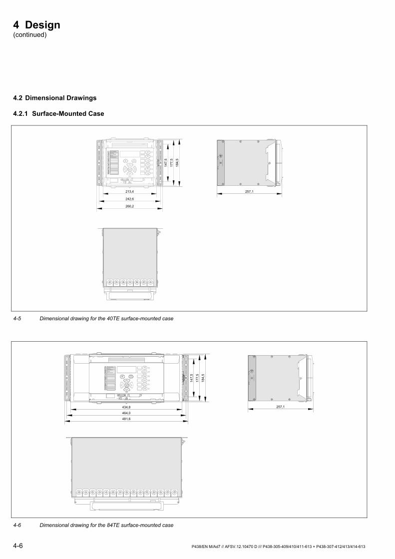
4 Design (continued)
4-6 P438/EN M/Ad7 // AFSV.12.10470 D /// P438-305-409/410/411-613 + P438-307-412/413/414-613
4.2 Dimensional Drawings
4.2.1 Surface-Mounted Case
213,4
242,6
260,2
257,1
147,
5
177,
5
184,
5
Aus-Kommando
Warnung
Block./Störung
Betrieb
Änderungsmod.
4-5 Dimensional drawing for the 40TE surface-mounted case
147,
5
177,
5
184,
5
434,8
464,0
481,6
257,1
Aus-Kommando
Warnung
Block./Störung
Betrieb
Änderungsmod.
4-6 Dimensional drawing for the 84TE surface-mounted case
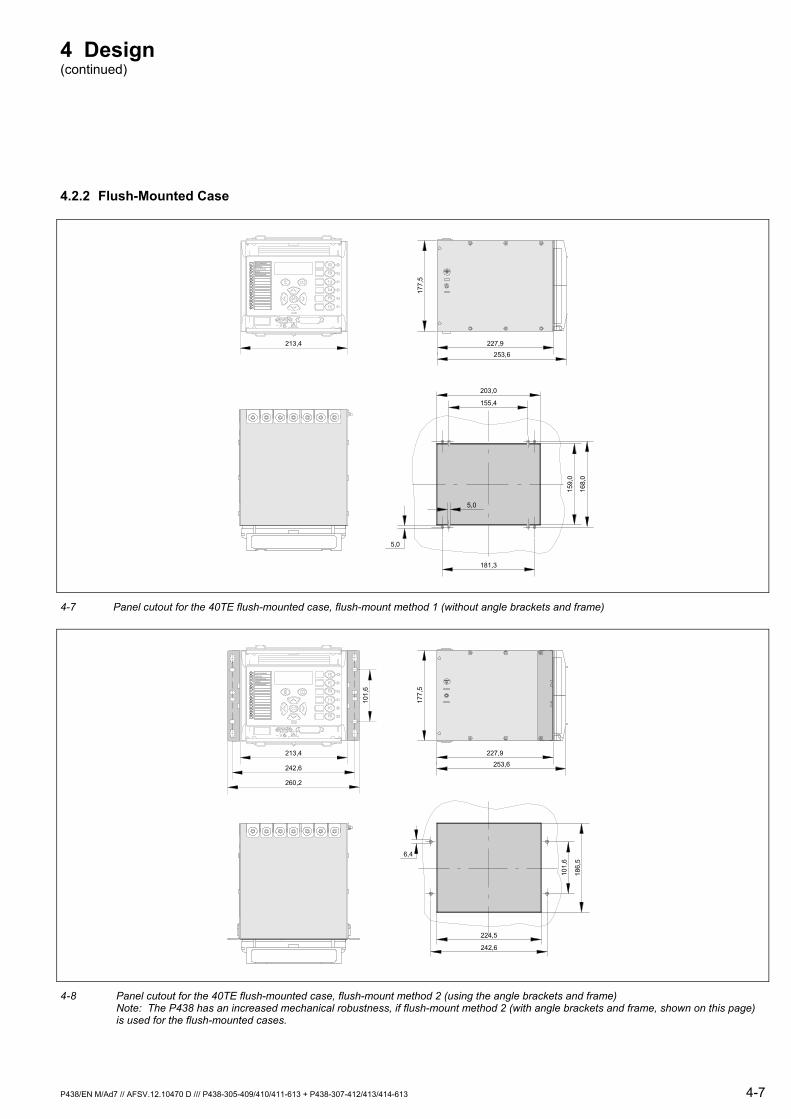
4 Design (continued)
P438/EN M/Ad7 // AFSV.12.10470 D /// P438-305-409/410/411-613 + P438-307-412/413/414-613 4-7
4.2.2 Flush-Mounted Case
227,9
253,6
177,
5
213,4
203,0
155,4
5,0
5,0
181,315
9,0
168,
0
Aus-Kommando
WarnungBlock./Störung
Betrieb
Änderungsmod.
4-7 Panel cutout for the 40TE flush-mounted case, flush-mount method 1 (without angle brackets and frame)
227,9
253,6
177,
5
101,
6
6,4
224,5
242,6
101,
6
186,
5
213,4
242,6
260,2
Aus-Kommando
Warnung
Block./Störung
Betrieb
Änderungsmod.
4-8 Panel cutout for the 40TE flush-mounted case, flush-mount method 2 (using the angle brackets and frame)
Note: The P438 has an increased mechanical robustness, if flush-mount method 2 (with angle brackets and frame, shown on this page) is used for the flush-mounted cases.
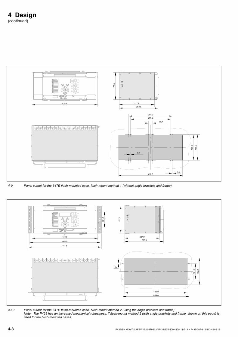
4 Design (continued)
4-8 P438/EN M/Ad7 // AFSV.12.10470 D /// P438-305-409/410/411-613 + P438-307-412/413/414-613
227,9
253,6
177,
5
434,8
284,9259,0
5,0
159,
0
168,
0
5,0
25,9
410,0
Aus-Kommando
Warnung
Block./Störung
Betrieb
Änderungsmod.
4-9 Panel cutout for the 84TE flush-mounted case, flush-mount method 1 (without angle brackets and frame)
227,9
253,6
177,
5
101,
6
6,4
445,9
464,0
101,
6
186,
5
434,8
464,0
481,6
Aus-Kommando
Warnung
Block./Störung
Betrieb
Änderungsmod.
4-10 Panel cutout for the 84TE flush-mounted case, flush-mount method 2 (using the angle brackets and frame)
Note: The P438 has an increased mechanical robustness, if flush-mount method 2 (with angle brackets and frame, shown on this page) is used for the flush-mounted cases.
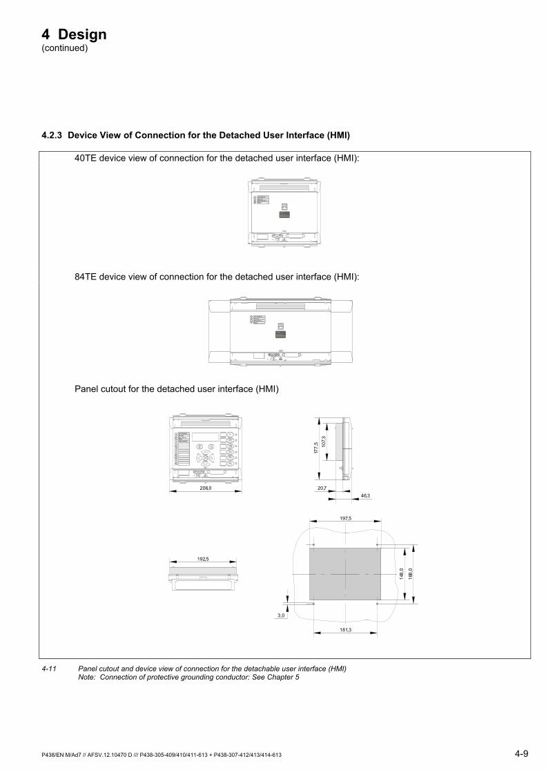
4 Design (continued)
P438/EN M/Ad7 // AFSV.12.10470 D /// P438-305-409/410/411-613 + P438-307-412/413/414-613 4-9
4.2.3 Device View of Connection for the Detached User Interface (HMI)
40TE device view of connection for the detached user interface (HMI):
Aus-KommandoWarnungBlock./ StörungBetrieb
ACHTUNG:
Anschluss nur fürabgesetztes Bedienfeld. Kein Netzwerkanschluss!
84TE device view of connection for the detached user interface (HMI):
Aus- KommandoWarnungBlock./ StörungBetr ieb
ACHTUNG:
Anschluss nur fürabgesetztes Bedienfeld. Kein Netzwerkanschluss!
Panel cutout for the detached user interface (HMI)
206,0 20,746,3
177,
5
197,5
3,0
181,3
148,
0
168,
0
107,
3
192,5
Aus- KommandoWarnungBlock./ StörungBetr iebÄnderungsmod.
4-11 Panel cutout and device view of connection for the detachable user interface (HMI)
Note: Connection of protective grounding conductor: See Chapter 5
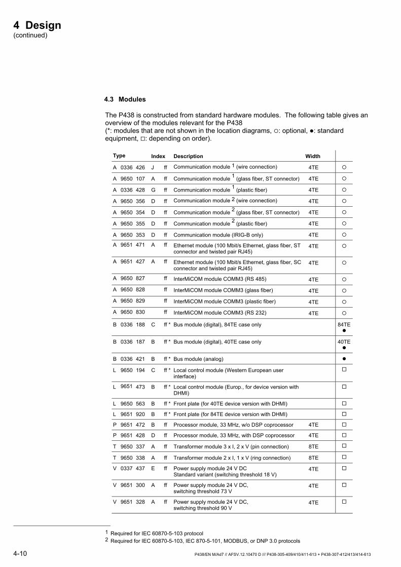
4 Design (continued)
4-10 P438/EN M/Ad7 // AFSV.12.10470 D /// P438-305-409/410/411-613 + P438-307-412/413/414-613
4.3 Modules
The P438 is constructed from standard hardware modules. The following table gives an overview of the modules relevant for the P438 (*: modules that are not shown in the location diagrams, : optional, : standard equipment, : depending on order).
Type Index Description Width
A 0336 426 J ff Communication module 1 (wire connection) 4TE
A 9650 107 A ff Communication module 1 (glass fiber, ST connector) 4TE
A 0336 428 G ff Communication module 1 (plastic fiber) 4TE
A 9650 356 D ff Communication module 2 (wire connection) 4TE
A 9650 354 D ff Communication module 2 (glass fiber, ST connector) 4TE
A 9650 355 D ff Communication module 2 (plastic fiber) 4TE
A 9650 353 D ff Communication module (IRIG-B only) 4TE
A 9651 471 A ff Ethernet module (100 Mbit/s Ethernet, glass fiber, ST connector and twisted pair RJ45)
4TE
A 9651 427 A ff Ethernet module (100 Mbit/s Ethernet, glass fiber, SC connector and twisted pair RJ45)
4TE
A 9650 827 ff InterMiCOM module COMM3 (RS 485) 4TE
A 9650 828 ff InterMiCOM module COMM3 (glass fiber) 4TE
A 9650 829 ff InterMiCOM module COMM3 (plastic fiber) 4TE
A 9650 830 ff InterMiCOM module COMM3 (RS 232) 4TE
B 0336 188 C ff * Bus module (digital), 84TE case only 84TE
B 0336 187 B ff * Bus module (digital), 40TE case only 40TE
B 0336 421 B ff * Bus module (analog)
L 9650 194 C ff * Local control module (Western European user interface)
L 9651 473 B ff * Local control module (Europ., for device version with DHMI)
L 9650 563 B ff * Front plate (for 40TE device version with DHMI)
L 9651 920 B ff * Front plate (for 84TE device version with DHMI)
P 9651 472 B ff Processor module, 33 MHz, w/o DSP coprocessor 4TE
P 9651 428 D ff Processor module, 33 MHz, with DSP coprocessor 4TE
T 9650 337 A ff Transformer module 3 x I, 2 x V (pin connection) 8TE
T 9650 338 A ff Transformer module 2 x I, 1 x V (ring connection) 8TE
V 0337 437 E ff Power supply module 24 V DC Standard variant (switching threshold 18 V)
4TE
V 9651 300 A ff Power supply module 24 V DC, switching threshold 73 V
4TE
V 9651 328 A ff Power supply module 24 V DC, switching threshold 90 V
4TE
1 Required for IEC 60870-5-103 protocol 2 Required for IEC 60870-5-103, IEC 870-5-101, MODBUS, or DNP 3.0 protocols
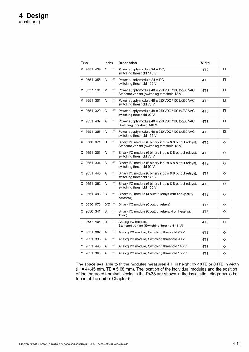
4 Design (continued)
P438/EN M/Ad7 // AFSV.12.10470 D /// P438-305-409/410/411-613 + P438-307-412/413/414-613 4-11
Type Index Description Width
V 9651 439 A ff Power supply module 24 V DC, switching threshold 146 V
4TE
V 9651 356 A ff Power supply module 24 V DC, switching threshold 155 V
4TE
V 0337 191 M ff Power supply module 48 to 250 VDC / 100 to 230 VAC Standard variant (switching threshold 18 V)
4TE
V 9651 301 A ff Power supply module 48 to 250 VDC / 100 to 230 VAC switching threshold 73 V
4TE
V 9651 329 A ff Power supply module 48 to 250 VDC / 100 to 230 VAC switching threshold 90 V
4TE
V 9651 437 A ff Power supply module 48 to 250 VDC / 100 to 230 VAC Switching threshold 146 V
4TE
V 9651 357 A ff Power supply module 48 to 250 VDC / 100 to 230 VAC switching threshold 155 V
4TE
X 0336 971 D ff Binary I/O module (6 binary inputs & 8 output relays), Standard variant (switching threshold 18 V)
4TE
X 9651 306 A ff Binary I/O module (6 binary inputs & 8 output relays), switching threshold 73 V
4TE
X 9651 334 A ff Binary I/O module (6 binary inputs & 8 output relays), switching threshold 90 V
4TE
X 9651 445 A ff Binary I/O module (6 binary inputs & 8 output relays), switching threshold 146 V
4TE
X 9651 362 A ff Binary I/O module (6 binary inputs & 8 output relays), switching threshold 155 V
4TE
X 9651 493 B ff Binary I/O module (4 output relays with heavy-duty contacts)
4TE
X 0336 973 B/D ff Binary I/O module (6 output relays) 4TE
X 9650 341 B ff Binary I/O module (6 output relays, 4 of these with Triac)
4TE
Y 0337 406 D ff Analog I/O module, Standard variant (Switching threshold 18 V)
4TE
Y 9651 307 A ff Analog I/O module, Switching threshold 73 V 4TE
Y 9651 335 A ff Analog I/O module, Switching threshold 90 V 4TE
Y 9651 446 A ff Analog I/O module, Switching threshold 146 V 4TE
Y 9651 363 A ff Analog I/O module, Switching threshold 155 V 4TE
The space available to fit the modules measures 4 H in height by 40TE or 84TE in width (H = 44.45 mm, TE = 5.08 mm). The location of the individual modules and the position of the threaded terminal blocks in the P438 are shown in the installation diagrams to be found at the end of Chapter 5.

P438/EN M/Ad7 // AFSV.12.10470 D /// P438-305-409/410/411-613 + P438-307-412/413/414-613 4-12
5 Installation and Connection
P438/EN M/Ad7 // AFSV.12.10470 D /// P438-305-409/410/411-613 + P438-307-412/413/414-613 5-1
5 Installation and Connection
Only qualified personnel, familiar with content on the "Warning" page at the beginning of this operating manual, may work on or operate this device.
The instructions given in the “Protective and Operational Grounding” section should be noted. In particular, check that the protective ground connection is secured with a tooth lock washer, as per the diagram “Installing the protective grounding conductor terminal”. If a cable screen is added to this connection or removed from it, then the protective grounding should be checked again.
The RJ45 twisted wire and glass fiber SC connector on the Ethernet module may not be both connected at the same time. (The setting at I E C : E t h e r n e t M e d i a must be observed.)
5.1 Unpacking and Packing
All P438 units are packaged separately in their own cartons and shipped inside outer packaging. Use special care when opening cartons and unpacking units, and do not use force. In addition, make sure to remove supporting documents and the type identification label supplied with each individual device from the inside carton.
The design revision level of each module included in the unit when shipped can be determined from the list of components (assembly list). This list should be carefully saved.
After unpacking each unit, inspect it visually to make sure it is in proper mechanical condition.
If the P438 needs to be shipped, both inner and outer packaging must be used. If the original packaging is no longer available, make sure that packaging conforms to DIN ISO 2248 specifications for a drop height ≤ 0.8 m.
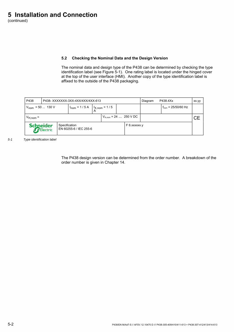
5 Installation and Connection (continued)
5-2 P438/EN M/Ad7-S // AFSV.12.10470 D /// P438-305-409/410/411-613 + P438-307-412/413/414-613
5.2 Checking the Nominal Data and the Design Version
The nominal data and design type of the P438 can be determined by checking the type identification label (see Figure 5-1). One rating label is located under the hinged cover at the top of the user interface (HMI). Another copy of the type identification label is affixed to the outside of the P438 packaging.
P438 P438- XXXXXXX-3XX-4XX/4XX/4XX-613 Diagram P438.4Xx xx.yy Vnom = 50 ... 130 V Inom = 1 / 5 A IX,nom = 1 / 5
A fnom = 25/50/60 Hz
VH,nom = VA,nom = 24 ... 250 V DC CE
Specification EN 60255-6 / IEC 255-6
F 6.xxxxxx.y
5-1 Type identification label
The P438 design version can be determined from the order number. A breakdown of the order number is given in Chapter 14.
5 Installation and Connection (continued)
P438/EN M/Ad7 // AFSV.12.10470 D /// P438-305-409/410/411-613 + P438-307-412/413/414-613 5-3
5.3 Location Requirements
The P438 is designed to be conform to DIN 57 435 Part 303. Therefore it is important when choosing the installation location to make certain that it provides the operating conditions as specified in above DIN norm sections 3.2 to 3.4. Several important conditions are listed below.
Climatic conditions Ambient temperature: -5 °C to +55 °C [+23 °F to +131 °F]
Air pressure: 800 to 1100 hPa
Relative humidity: The relative humidity must not result in the formation of either condensed water or ice in the P438.
Ambient air: The ambient air must not be significantly polluted by dust, smoke, gases or vapors, or salt.
Solar Radiation: Direct solar radiation on the front of the device must be avoided to ensure that the LC-display remains readable.
Mechanical conditions Vibration stress: 10 to 60 Hz, 0.035 mm and 60 to 150 Hz, 0.5 g or 10 to 60 Hz, 0.075 mm and 60 to 150 Hz, 1.0 g depending on the installation type (see Chapter 2, paragraph 'Mechanical robustness')
Earthquake resistance: 5 to 8 Hz, 3.5 mm / 1.5 mm, 8 to 35 Hz, 5 m/s2, 3 x 1 cycle
Electrical conditions for auxiliary voltage for the power supply
Operating range: 0,8 to 1.1 VH,nom with a residual ripple of up to 12 % VH,nom
Electromagnetic conditions Appropriate measures taken in substations must correspond to the best of modern practices.
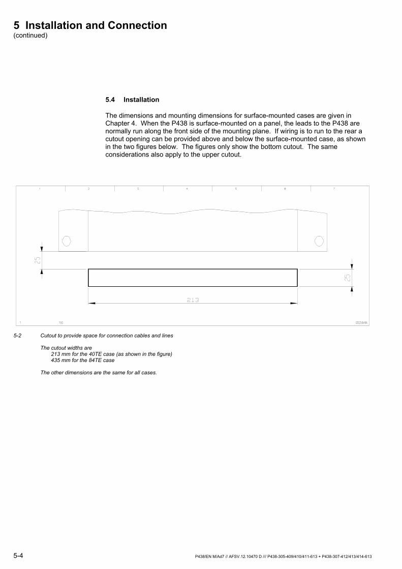
5 Installation and Connection (continued)
5-4 P438/EN M/Ad7 // AFSV.12.10470 D /// P438-305-409/410/411-613 + P438-307-412/413/414-613
5.4 Installation
The dimensions and mounting dimensions for surface-mounted cases are given in Chapter 4. When the P438 is surface-mounted on a panel, the leads to the P438 are normally run along the front side of the mounting plane. If wiring is to run to the rear a cutout opening can be provided above and below the surface-mounted case, as shown in the two figures below. The figures only show the bottom cutout. The same considerations also apply to the upper cutout.
5-2 Cutout to provide space for connection cables and lines
The cutout widths are 213 mm for the 40TE case (as shown in the figure) 435 mm for the 84TE case The other dimensions are the same for all cases.
5 Installation and Connection (continued)
P438/EN M/Ad7 // AFSV.12.10470 D /// P438-305-409/410/411-613 + P438-307-412/413/414-613 5-5
Flush-mounted cases are designed to be flush-mounted in control panels. The dimensions and mounting dimensions are given in Chapter 4. When the P438 is mounted in a cabinet door, special sealing measures are necessary to provide the degree of protection required for the cabinet (IP 51).
For connection of the protective ground/earth terminal see section 5.5 'Protective Grounding'.
Instructions for selecting the flush-mount method: The P438 has increased mechanical robustness if either the surface-mounted case or – for the flush-mounted case – flush-mount method 2 (with angle brackets and frame) is used. In this case, test severity class 2 of the vibration test, test severity class of the shock resistance test on operability as well as test severity class 1 of the shock resistance test on permanent shock is applied additionally.
Instructions for dimensioning a panel cutout: Dimensional drawings for panel cutouts for the P438 with all mounting methods can be found in Chapter 4, section 'Dimensional Drawings'
If the units are to be installed in accordance with flush-mount method 1 (without the angle brackets and frame), follow the steps described below.
Before the P438 can be installed in the control panel, the user interface (HMI) must be removed. The procedure is as follows:
Remove the hinged covers at the top and bottom of the user interface. (Open the hinged covers by flipping them up or down 180°. Hold them in the middle and bend them slightly. The side mountings of the covers can then be disengaged.)
Remove the M3 screws (see Figures 5-3 and 5-4).
Remove the user interface.
The user interface (HMI) is connected to processor module P by a plug-in connecting cable. Make sure the connector position is correct. Do not bend the connecting cable!
Then remove the lower M4 screws and loosen the upper M4 screws (see Figures 5-3 and 5-4). Insert the P438 into the panel opening from the rear so that the upper M4 screws fit into the corresponding slots. Then tighten all the M4 screws. After this, replace the user interface (HMI).
Note: If the control panel thickness is ≥ 2 mm, longer M3 and M4 bolts must be used. Longer screws are enclosed within the device packing.
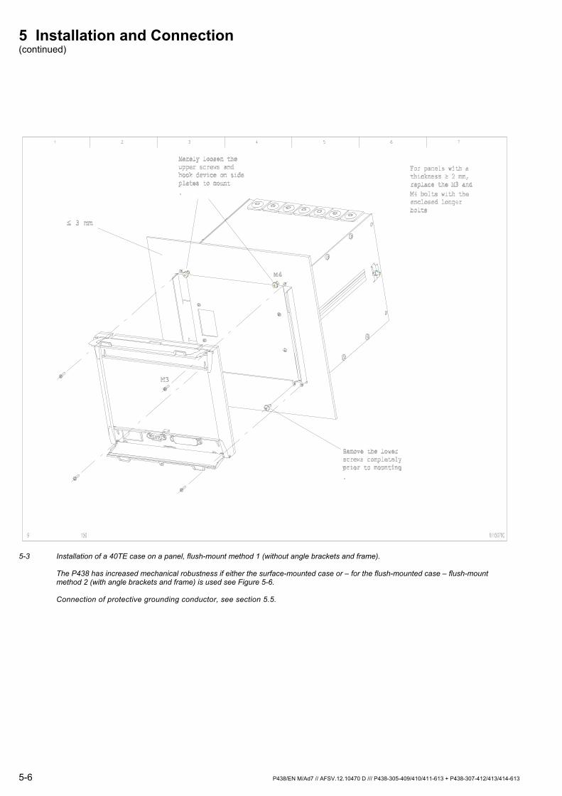
5 Installation and Connection (continued)
5-6 P438/EN M/Ad7 // AFSV.12.10470 D /// P438-305-409/410/411-613 + P438-307-412/413/414-613
5-3 Installation of a 40TE case on a panel, flush-mount method 1 (without angle brackets and frame).
The P438 has increased mechanical robustness if either the surface-mounted case or – for the flush-mounted case – flush-mount method 2 (with angle brackets and frame) is used see Figure 5-6. Connection of protective grounding conductor, see section 5.5.
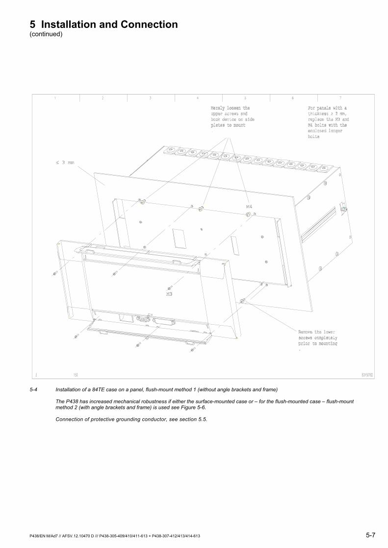
5 Installation and Connection (continued)
P438/EN M/Ad7 // AFSV.12.10470 D /// P438-305-409/410/411-613 + P438-307-412/413/414-613 5-7
5-4 Installation of a 84TE case on a panel, flush-mount method 1 (without angle brackets and frame)
The P438 has increased mechanical robustness if either the surface-mounted case or – for the flush-mounted case – flush-mount method 2 (with angle brackets and frame) is used see Figure 5-6. Connection of protective grounding conductor, see section 5.5.
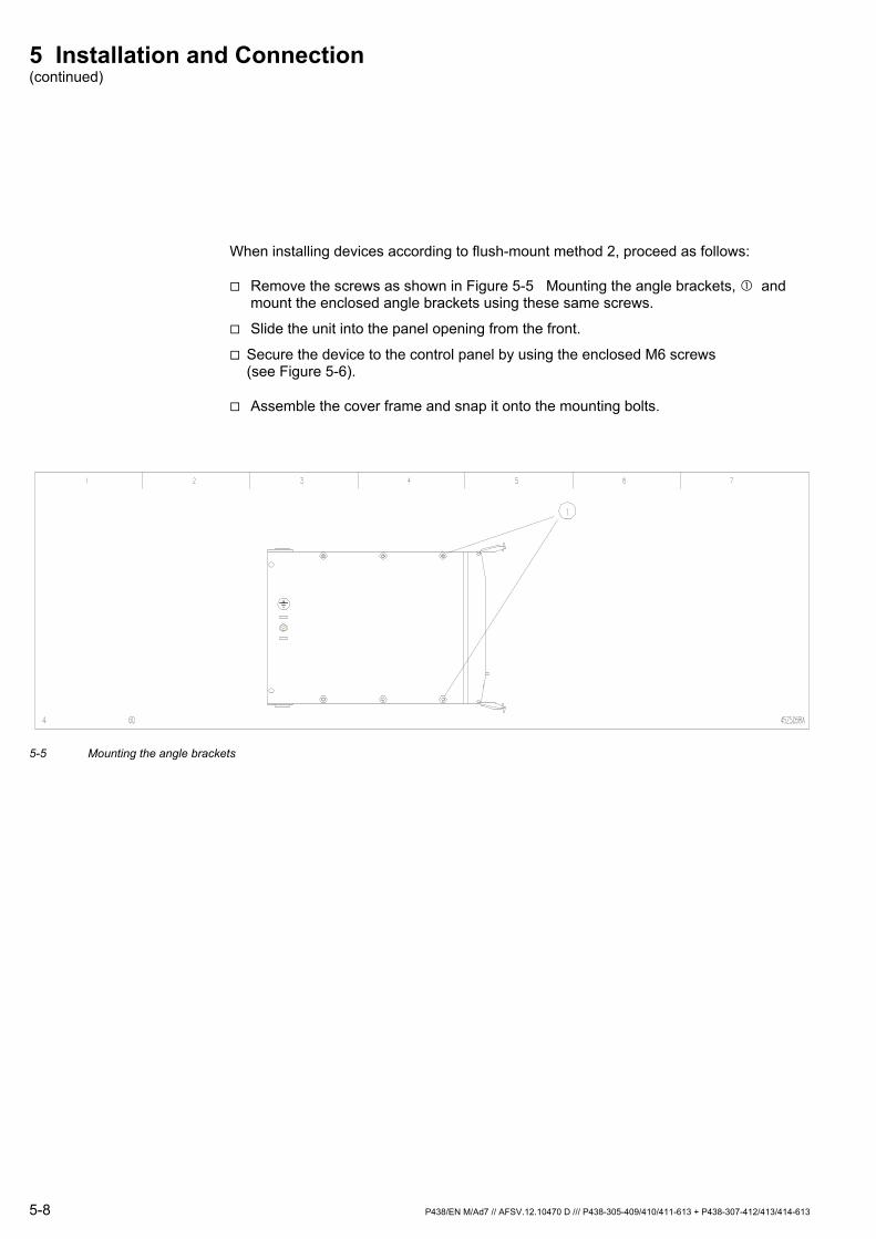
5 Installation and Connection (continued)
5-8 P438/EN M/Ad7 // AFSV.12.10470 D /// P438-305-409/410/411-613 + P438-307-412/413/414-613
When installing devices according to flush-mount method 2, proceed as follows:
Remove the screws as shown in Figure 5-5 Mounting the angle brackets, and mount the enclosed angle brackets using these same screws.
Slide the unit into the panel opening from the front.
Secure the device to the control panel by using the enclosed M6 screws (see Figure 5-6).
Assemble the cover frame and snap it onto the mounting bolts.
5-5 Mounting the angle brackets

5 Installation and Connection (continued)
P438/EN M/Ad7 // AFSV.12.10470 D /// P438-305-409/410/411-613 + P438-307-412/413/414-613 5-9
Width: 280 mm for the
40TE flush-mounted case
Hei
ght:
204
mm
Angle brackets
Frame
12Y6183 B_EN
6.4
M6 x 15
M6B6
5-6 Installation of a case into a control panel, flush-mount method 2 (with angle brackets and frame).
Example for a device in a 40TE case The width of the frame for the 84TE case comes to 486 mm The device has an increased mechanical robustness, if flush-mount method 2 (with angle brackets and frame, shown on this page) is used for the flush-mounted cases. Connection of protective grounding conductor, see section 5.5.
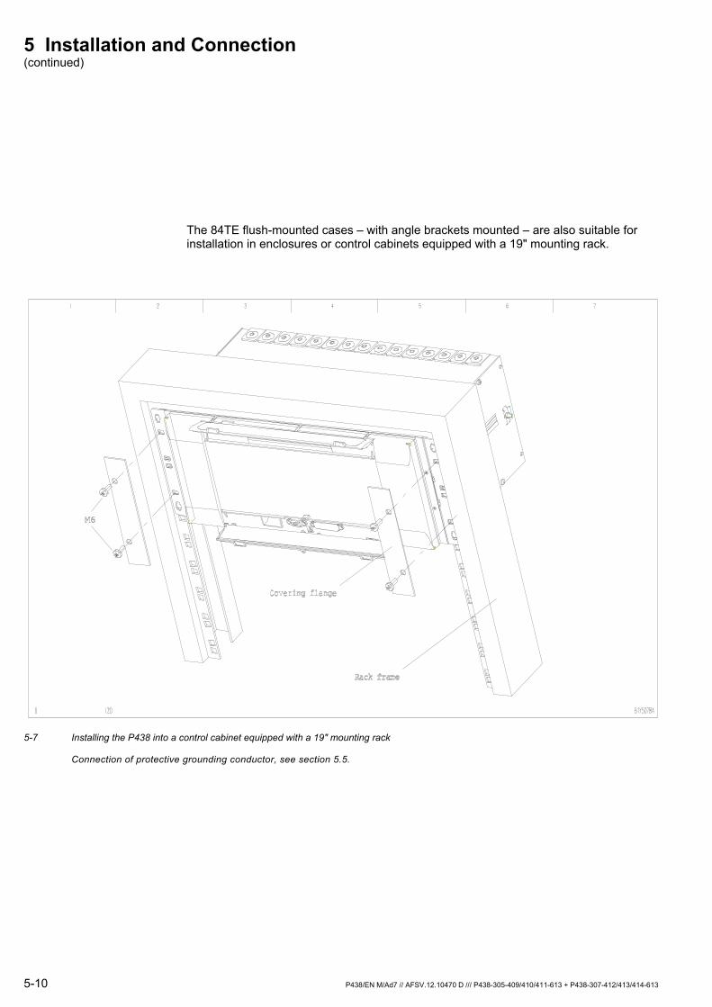
5 Installation and Connection (continued)
5-10 P438/EN M/Ad7 // AFSV.12.10470 D /// P438-305-409/410/411-613 + P438-307-412/413/414-613
The 84TE flush-mounted cases – with angle brackets mounted – are also suitable for installation in enclosures or control cabinets equipped with a 19" mounting rack.
5-7 Installing the P438 into a control cabinet equipped with a 19" mounting rack
Connection of protective grounding conductor, see section 5.5.
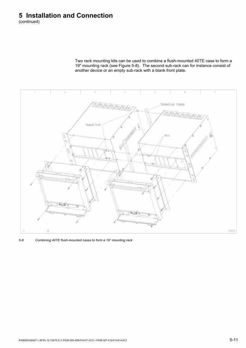
5 Installation and Connection (continued)
P438/EN M/Ad7 // AFSV.12.10470 D /// P438-305-409/410/411-613 + P438-307-412/413/414-613 5-11
Two rack mounting kits can be used to combine a flush-mounted 40TE case to form a 19" mounting rack (see Figure 5-8). The second sub-rack can for instance consist of another device or an empty sub-rack with a blank front plate.
5-8 Combining 40TE flush-mounted cases to form a 19” mounting rack

5 Installation and Connection (continued)
5-12 P438/EN M/Ad7 // AFSV.12.10470 D /// P438-305-409/410/411-613 + P438-307-412/413/414-613
5.5 Protective Grounding
The device must be reliably grounded to meet protective equipment grounding requirements. The surface-mounted case is grounded using the appropriate bolt and nut as the ground connection. The flush-mounted case must be grounded in the area of the rear sidepieces at the location provided. The cross-sectional area of this ground conductor must also conform to applicable national standards. A minimum conductor cross section of 2.5 mm2 is required.
In addition, a protective ground connection at the terminal contact on the power supply module (identified by the letters "PE" on the terminal connection diagram) is also required for proper operation of the device. The cross-sectional area of this ground conductor must also conform to applicable national standards. A minimum cross section of 1.5 mm2 is required.
The grounding connection at both locations must be low-inductance, i.e., as short as possible.
19Y5220A_EN 5-9 Installing the protective grounding conductor terminal
The protective grounding (earth) conductor must always be connected to the protective grounding conductor terminal, so as to ensure the safety provided by the device’s design. The bracket on the terminal is marked with the protective ground symbol: .
5 Installation and Connection (continued)
P438/EN M/Ad7 // AFSV.12.10470 D /// P438-305-409/410/411-613 + P438-307-412/413/414-613 5-13
5.6 Connection
The P438 must be connected in accordance with the terminal connection diagram indicated on the type identification label. Terminal connection diagrams relevant for the P438 can be found at the end of this chapter.
Copper leads having a 2.5 mm2 cross-section are generally suitable as the connecting leads between the current transformers and the P438. To reduce CT knee-point voltage requirements, it may be necessary to install shorter copper conductors with a greater cross section between the system current transformers and the current inputs on the P438. Copper leads having a 1.5 mm2 cross section are adequate for connecting the binary signal inputs, the signaling and triggering circuits, and the power supply input.
All connections run into the system must always have a defined potential. Connections that are pre-wired but not used should preferably be grounded when binary inputs and output relays are isolated. When binary inputs and output relays are connected to a common potential, the pre-wired but unused connections should be connected to the common potential of the grouped connections.
5.6.1 Connecting Measuring and Auxiliary Circuits
Power supply Before connecting the auxiliary voltage VA for the P438 power supply, it must be ensured that the nominal value of the auxiliary device voltage corresponds with the nominal value of the auxiliary system voltage.
Current-measuring inputs When connecting the system transformers, it must be ensured that the secondary nominal currents of the system and the device correspond.
The secondary circuit of operating current transformers must not be opened. If the secondary circuit of an operating current transformer is opened, there is the danger that the resulting voltages will endanger personnel and damage the insulation.
In units for pin terminal connection, the threaded terminal block for current transformer connection is not a shorting block. Therefore always short-circuit current transformers before loosening the threaded terminals.
Connecting the measuring circuits
The system current transformers must be connected in accordance with the standard schematic diagram shown in Figures 5-10 Connecting the P438 measuring circuits in the 'Classic single feed' operating mode to 5-12. It is essential that the CT grounding configuration shown in the diagram be followed. If the CT or VT connection is reversed, this can be taken into account when making settings (see Chapter 7).

5 Installation and Connection (continued)
5-14 P438/EN M/Ad7 // AFSV.12.10470 D /// P438-305-409/410/411-613 + P438-307-412/413/414-613
Catenary
Rail
V
I
I>
Icat
1U
2U
MAIN: FeedingMode
[ 010 135 ]
1
2
1: Classic SingleFeed2: Auto-Transformer Feed
MAIN: Vn VT.Sec.[ 010 009 ]
MAIN: In Device[ 010 003 ]
MAIN: Line CTOrientation[ 010 004 ]
X X.Y
1: Standard(Y = 1)2: Opposite(Y = -1)
48Z5411A_UK
c
c
SupplyCatenary
5-10 Connecting the P438 measuring circuits in the 'Classic single feed' operating mode
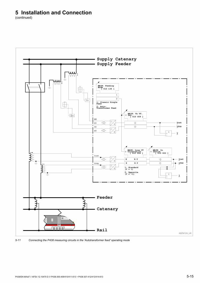
5 Installation and Connection (continued)
P438/EN M/Ad7 // AFSV.12.10470 D /// P438-305-409/410/411-613 + P438-307-412/413/414-613 5-15
Catenary
Vcat
Ifdr
2U
Feeder
Supply CatenarySupply Feeder
3U
4U
Vfdr
VS
-+
Icat
Icat
Ifdr
IS
-+
I>
I>
Rail
MAIN: FeedingMode
[ 010 135 ]
1
2
1: Classic SingleFeed2: Auto-Transformer Feed
1U
MAIN: Vn VT.Sec.[ 010 009 ]
c
MAIN: Line CTOrientation[ 010 004 ]
X X.Y
1: Standard(Y = 1)
2: Opposite(Y = -1)
c
X X.Y
MAIN: InDevice[ 010 003 ]
c
48Z5412A_UK
5-11 Connecting the P438 measuring circuits in the 'Autotransformer feed' operating mode
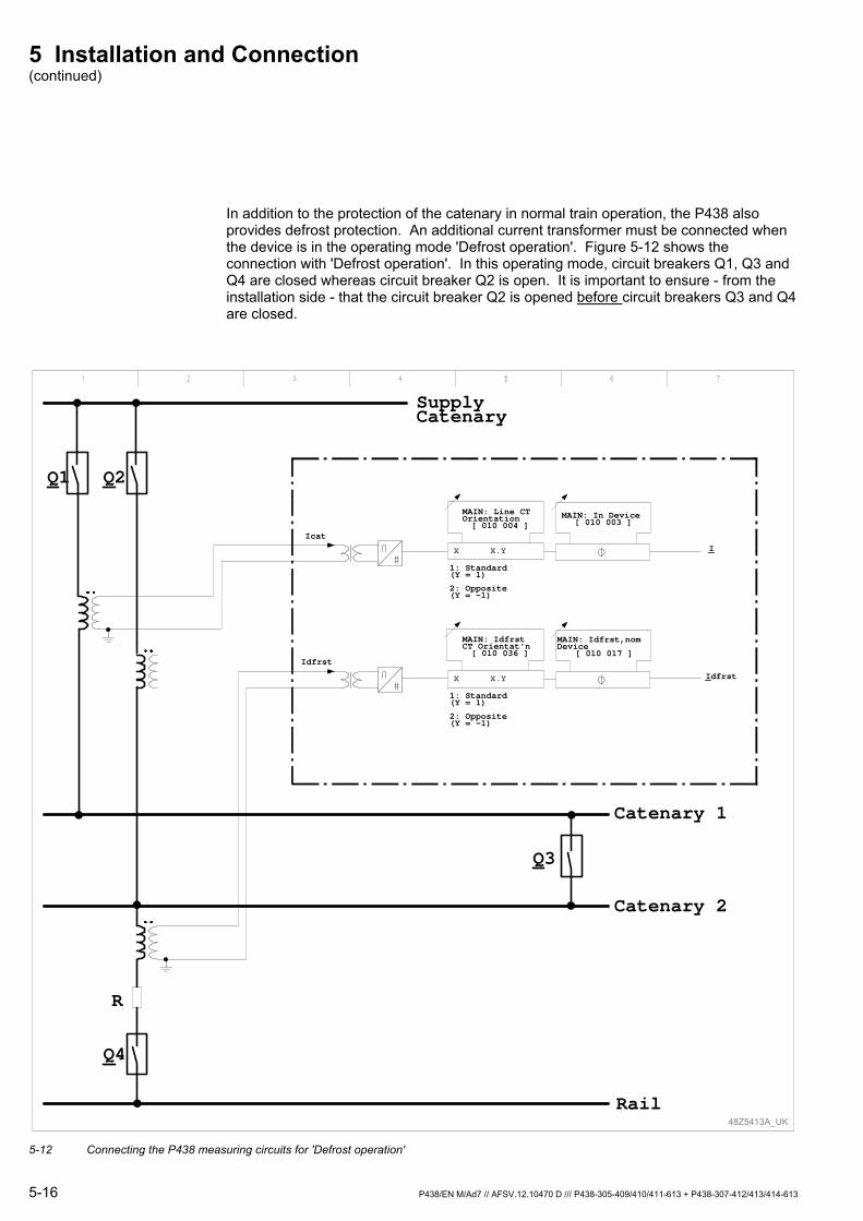
5 Installation and Connection (continued)
5-16 P438/EN M/Ad7 // AFSV.12.10470 D /// P438-305-409/410/411-613 + P438-307-412/413/414-613
In addition to the protection of the catenary in normal train operation, the P438 also provides defrost protection. An additional current transformer must be connected when the device is in the operating mode 'Defrost operation'. Figure 5-12 shows the connection with 'Defrost operation'. In this operating mode, circuit breakers Q1, Q3 and Q4 are closed whereas circuit breaker Q2 is open. It is important to ensure - from the installation side - that the circuit breaker Q2 is opened before circuit breakers Q3 and Q4 are closed.
48Z5413A_UK
Idfrst
Q3
Catenary 1
Catenary 2
Q4
Rail
R
SupplyCatenary
Q1 Q2
IcatI
Idfrst
MAIN: Idfrst,nomDevice
[ 010 017 ]
MAIN: IdfrstCT Orientat'n[ 010 036 ]
X X.Y
1: Standard(Y = 1)
2: Opposite(Y = -1)
MAIN: In Device[ 010 003 ]
MAIN: Line CTOrientation[ 010 004 ]
X X.Y
1: Standard(Y = 1)
2: Opposite(Y = -1)
5-12 Connecting the P438 measuring circuits for 'Defrost operation'

5 Installation and Connection (continued)
P438/EN M/Ad7 // AFSV.12.10470 D /// P438-305-409/410/411-613 + P438-307-412/413/414-613 5-17
Connecting a resistance thermometer
If the analog I/O module Y is fitted, a resistance thermometer can be connected. This analog I/O module input is designed to connect a PT 100 resistance thermometer. The PT 100 should be connected using the 3-wire method (see Figure 5-13). No supply conductor compensation is required in this case.
5-13 Connecting a PT 100 using the 3-wire method
Connecting binary inputs and output relays
The binary inputs and output relays are freely configurable.
The terminal connection diagrams give a polarity for connection of the binary signal inputs. However, this is only a recommendation. Connection to binary inputs can be made as desired.
5 Installation and Connection (continued)
5-18 P438/EN M/Ad7 // AFSV.12.10470 D /// P438-305-409/410/411-613 + P438-307-412/413/414-613
5.6.2 Connecting the IRIG-B Interface
An IRIG-B-interface for time synchronization may be installed as an optional feature. It is connected by a BNC connector. A coaxial cable having a characteristic impedance of 50 Ω must be used as the connecting cable.
5.6.3 Connecting the Serial Interfaces
PC interface The PC interface is provided in order to operate the unit from a personal computer (PC).
The PC interface is not designed as a permanent connection. Consequently, the female connector does not have the extra insulation from circuits connected to the system that is required per VDE 0106 Part 101.
Communication interfaces
Communication interfaces are provided for permanent connection of the unit to a control system for substations or to a central substation unit. Depending on the type, communication interface 1 on the device is connected either by a special fiber-optic connector or a RS 485 interface with twisted pair copper wires. Connection to channel 2 is always by way of an RS 485 interface.
The selection and assembly of a properly cut fiber-optic connecting cable requires special knowledge and expertise and is therefore not covered in this operating manual.
The fiber-optic interface may only be connected or disconnected when the supply voltage for the unit is shut off.

5 Installation and Connection (continued)
P438/EN M/Ad7-S // AFSV.12.10470 D /// P438-305-409/410/411-613 + P438-307-412/413/414-613 5-19
A communication link consisting of a communication master and several slaves can be established using the RS 485 interface. The communication master can be a control station, for example. The devices connected to the communication master, such as the P438, are the communication slaves.
The RS 485 interface available on the P438 was designed so that data transfer in a full duplex transmission mode is possible using a 4-wire data link between devices. However, communication through the RS 485 interface is always in the half-duplex mode of operation. To connect the RS 485 communication interface the following must be observed:
Always use twisted-pair shielded cables only, the kind used for telecommunications systems.
At least one symmetrically twisted core pair will be required.
Strip cable cores and cable shield right at the connection point and connect properly in accordance with specifications.
Ground all shields at both ends (large-area grounding).
Ground free (unshielded) cores at one end only.
As another option, a 2-wire or 4-wire connection is also possible. For the 4-wire connection, a cable with two symmetrically twisted core pairs is required. A 2-wire data link is shown in Figure 5-14, and a 4-wire data link is shown in Figure 5-15 as an example for channel 2 on the communication module. If channel 1 of the communication module is designed as an RS 485 interface, then the same arrangement would apply.
2-wire data link: The transmitter must be bridged with the receiver on all devices equipped electrically with a full duplex communication interface, e.g. the P438. In the two units that form the physical ends of the line, the pair of leads must be terminated by a 200 to 220 Ω resistor. In most Schneider Electric units, and also in the P438, a 220 Ω resistor is integrated into the RS 485 interface and can be connected by means of a wire jumper. An external resistor is therefore not necessary.
4-wire data link: Transmitter and receiver must be bridged in the device situated on one far end of the data transmission conductor. The receivers of the slaves that have a full-duplex interface as part of their electrical system (like the P438, for example) are connected to the transmitter of the communication master, and the transmitters of the slaves are connected to the receiver of the master. Units that only have a half-duplex interface are connected to the transmitter of the communication master. In the last physical participant (master or slave) of the communication link, the transmitter and receiver must each be terminated by a 200 to 220 Ω resistor. In most Schneider Electric units, and also in the P438, a 220 Ω resistor is integrated into the RS 485 interface and can be connected by a wire jumper. An external resistor is therefore not necessary. The second resistor must be connected externally to the device (resistor order number see Chapter 13).
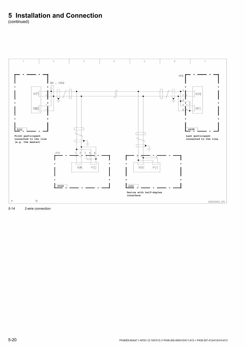
5 Installation and Connection (continued)
5-20 P438/EN M/Ad7 // AFSV.12.10470 D /// P438-305-409/410/411-613 + P438-307-412/413/414-613
First participantconnected to the line(e.g. the master)
Last participantconnected to the line
Device with half-duplexinterface
P438
P438
48Z5480A_EN 5-14 2-wire connection

5 Installation and Connection (continued)
P438/EN M/Ad7 // AFSV.12.10470 D /// P438-305-409/410/411-613 + P438-307-412/413/414-613 5-21
First participantconnected to the line(e.g. the master)
Last participantconnected to the line
Device with half-duplexinterface
P438
P438
48Z5481A_EN 5-15 4-wire connection

5 Installation and Connection (continued)
5-22 P438/EN M/Ad7 // AFSV.12.10470 D /// P438-305-409/410/411-613 + P438-307-412/413/414-613
5.7 Location Diagrams P438 -305
01
01
02
02
03
03
04
04
05
05
06
06
07
07
08
08
09
09
10
10
TAP XY
alt.
VX4I6I
8O 6OCH1CH2
4I8O
ETHCH2
3J2V
A
A
alt.
X4H
CH3X6I8O
5-16 P438 in 40TE case, transformer module with ring-terminal connection, other modules with pin-terminal connection, diagram P438-305-409
01
01
02
02
03
03
04
04
05
05
06
06
07
07
08
08
09
09
10
10
11
11
12
12
13
13
14
14
15
15
16
16
17
17
18
18
19
19
20
20
21
21
TAP X
alt.
VX6I8O 6O
3J2V
CH1CH2
4I8O
ETHCH2
A
A
alt.
X4H
X6I8O
XY4ICH3
X6I8O
6I8O
5-17 P438 in 84TE case with pin-terminal connection, diagram P438-305-410
01
01
02
02
03
03
04
04
05
05
06
06
07
07
08
08
09
09
10
10
11
11
12
12
13
13
14
14
15
15
16
16
17
17
18
18
19
19
20
20
21
21
TAP
alt.
3J2V
CH1CH2
ETHCH2
A
X X V
Xalt.
6I8O
4I8O6O
4H
Y4I 6I
8O
XACH3 6I
8O
X6I8O
X
5-18 P438 in 84TE case with pin-terminal connection, diagram P438-305-411
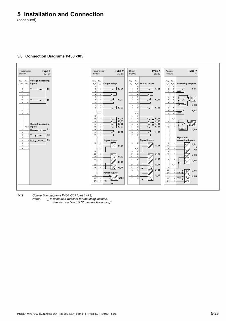
5 Installation and Connection (continued)
P438/EN M/Ad7 // AFSV.12.10470 D /// P438-305-409/410/411-613 + P438-307-412/413/414-613 5-23
5.8 Connection Diagrams P438 -305
X041
13
14
15
16
17
18
11
12
1
2
3
4
5
6
7
8
Ring
Type T
Pin
X042
1
2
3
4
5
6
7
8
Current measuringinputs
VA
VB
IA
IB
Idfrst
T1
T2
T3
Voltage measuringinputs
3J / 2VTransformermodule
T5
T6
X041
1
2
3
4
5
6
7
8
X_1
1
2
3
4
5
6
7
8
9
X_1
1
2
3
4
5
6
7
8
9
10
11
12
13
14
15
16
17
18
19
20
21
22
23
24
25
26
27
Ring
K_01
K_02
K_03
K_04K_05K_06K_07
K_08
Power supply
Type V
U100
Power supplymodule
Signal inputs
U_01
U_02
U_03
U_04
Output relaysPin
X_3
1
2
3
4
5
6
7
8
9
X_2
1
2
3
4
5
6
7
8
9 Vin
Vin
Vin
Vin
PE
Vaux
4I / 8O
+-
X_1
1
2
3
4
5
6
7
8
9
X_1
1
2
3
4
5
6
7
8
9
10
11
12
13
14
15
16
17
18
19
20
21
22
23
24
25
26
27
Ring
K_01
K_02
K_03
K_04K_05K_06K_07
K_08
Binarymodule
U_01
U_02
U_03
U_04
U_05
U_06
Output relaysPin
X_3
1
2
3
4
5
6
7
8
9
X_2
1
2
3
4
5
6
7
8
9
Type X6I / 8O
Signal inputs
Vin
Vin
Vin
Vin
Vin
Vin
X_3
1
2
3
4
5
6
X_2
1
2
3
4
5
6
7
8
9
X_1
1
2
3
4
5
6
7
8
9
X_1
1
2
3
4
5
6
7
8
9
10
11
12
13
14
15
16
17
18
19
20
21
22
23
24
Ring
Analogmodule
U_01U
_02
U_03
U_04
Pin
Type Y4I
Signal andmeasuring inputs
Measuring outputs
K_01
U_080..20 mA
valid
K_02
U_090..20 mA
valid
U
#U
#
U_05
U_06
U
#
U
#
0..20 mA
PT100
Vin
Vin
Vin
Vin
5-19 Connection diagrams P438 -305 (part 1 of 2) Notes: ‘_’ is used as a wildcard for the fitting location. See also section 5.5 "Protective Grounding"
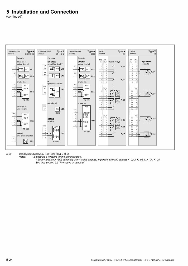
5 Installation and Connection (continued)
5-24 P438/EN M/Ad7 // AFSV.12.10470 D /// P438-305-409/410/411-613 + P438-307-412/413/414-613
X11
1
X8
1
Type A
Channel 1optical fiber link
Per order
##
IRIG-Btime synchronization
Channel 2wire link only
or wire link
X//Y
RS 485
D2[R]
X10
1
2
3
4
5 D1[T]U20
X//Y
RS 485
D2[R]
X9
1
2
3
4
5 D1[T]U19
U17X//Y
U18X//Y
X7
1
U21
Communicationmodule CH1 / CH2
X8
TX
Type A
IEC 61850optical fiber link ST
Per order
COMM2wire link
oroptical fiber link SC
X//Y
RS 485
D2[R]
X10
1
2
3
4
5 D1[T]U20
U17X/Y
U18X/Y
X7
RX
Communicationmodule ETH / CH2
X12
1
U26X/Y
U25X//Y
X13
RX
TX
and wire link
RJ45
X32
1
Type A
COMM3optical fiber link
Per order
or wire link
or wire link
X//Y
RS 485
D2[R]
X33
1
2
3
4
5 D1[T]U24
U22X//Y
U23X//Y
X31
1
Communicationmodule CH3
U27
D1[T]D2[R]
RS 232
E2[G]
X//Y
M5[DCD]
+UB
X34
1
2
3
4
5
7
E
X_1
1
2
3
4
5
6
7
8
9
X_1
1
2
3
4
5
6
7
8
9
10
11
12
13
14
15
16
17
18
19
20
21
22
23
24
25
26
27
Ring
Output relaysPin
X_3
1
2
3
4
5
6
7
8
9
X_2
1
2
3
4
5
6
7
8
9
K_01
K_02
K_03
K_04
K_05
K_06
1)
1)
1)
1)
Type X 6O
Binarymodule
X_1
1
2
3
4
5
6
7
8
9
X_1
1
2
3
4
5
6
7
8
9
10
11
12
13
14
15
16
17
18
19
20
21
22
23
24
25
26
27
Ring
Type X
High-breakcontacts
Pin
X_3
1
2
3
4
5
6
7
8
9
X_2
1
2
3
4
5
6
7
8
9
K_01
4H
K_02
K_04
K_03
+
+
+
+
Binarymodule
5-20 Connection diagrams P438 -305 (part 2 of 2) Notes: ‘_’ is used as a wildcard for the fitting location. 1) Binary module X (6O) optionally with 4 static outputs, in parallel with NO contact K_02.2, K_03.1, K_04, K_05. See also section 5.5 "Protective Grounding".
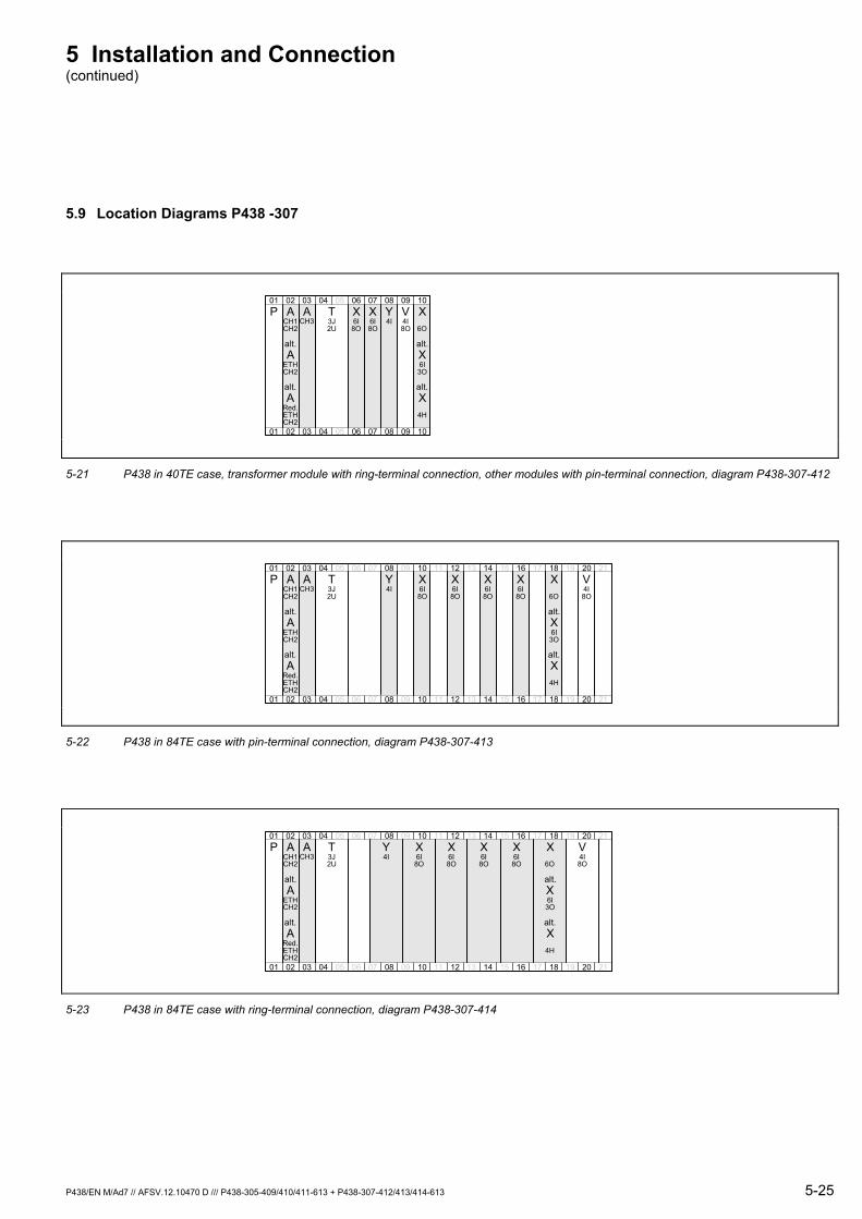
5 Installation and Connection (continued)
P438/EN M/Ad7 // AFSV.12.10470 D /// P438-305-409/410/411-613 + P438-307-412/413/414-613 5-25
5.9 Location Diagrams P438 -307
01
01
02
02
03
03
04
04
05
05
06
06
07
07
08
08
09
09
10
10
alt.
CH1CH2
A
ETHCH2
alt.
A
ARed.ETHCH2
AP T X X XVYCH3 3J
2U6I8O
6I8O
4I 4I8O 6O
alt.
alt.
6I3O
X
X4H
5-21 P438 in 40TE case, transformer module with ring-terminal connection, other modules with pin-terminal connection, diagram P438-307-412
01
01
02
02
03
03
04
04
05
05
06
06
07
07
08
08
09
09
10
10
11
11
12
12
13
13
14
14
15
15
16
16
17
17
18
18
19
19
20
20
21
21
alt.
CH1CH2
A
ETHCH2
alt.
A
ARed.ETHCH2
AP T X X X VYCH3 3J
2U6I8O
6I8O
4I 4I8O6O
alt.
alt.
6I3O
X
X4H
X X6I8O
6I8O
5-22 P438 in 84TE case with pin-terminal connection, diagram P438-307-413
01
01
02
02
03
03
04
04
05
05
06
06
07
07
08
08
09
09
10
10
11
11
12
12
13
13
14
14
15
15
16
16
17
17
18
18
19
19
20
20
21
21
alt.
CH1CH2
A
ETHCH2
alt.
A
ARed.ETHCH2
AP T X X VYCH3 3J
2U6I8O
4I 4I8O6O
alt.
alt.
6I3O
X
X4H
X6I8O
X6I8O
X6I8O
5-23 P438 in 84TE case with ring-terminal connection, diagram P438-307-414
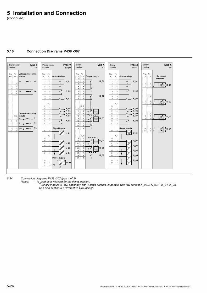
5 Installation and Connection (continued)
5-26 P438/EN M/Ad7 // AFSV.12.10470 D /// P438-305-409/410/411-613 + P438-307-412/413/414-613
5.10 Connection Diagrams P438 -307
X041
13
14
15
16
17
18
1
2
3
4
5
6
Ring
Type T
Pin
X042
1
2
3
4
5
6
Current measuringinputs
VA
VB
IA
IB
Idfrst
T1
T2
T3
Voltage measuringinputs
3J / 2VTransformermodule
T5
T6
X041
1
2
3
4
5
6
X_1
1
2
3
4
5
6
7
8
9
X_1
1
2
3
4
5
6
7
8
9
10
11
12
13
14
15
16
17
18
19
20
21
22
23
24
25
26
27
Ring
K_01
K_02
K_03
K_04K_05K_06K_07
K_08
Power supply
Type V
U100
Power supplymodule
Signal inputs
U_01
U_02
U_03
U_04
Output relaysPin
X_3
1
2
3
4
5
6
7
8
9
X_2
1
2
3
4
5
6
7
8
9 Vin
Vin
Vin
Vin
PE
Vaux
4I / 8O
+-
X_1
1
2
3
4
5
6
7
8
9
X_1
1
2
3
4
5
6
7
8
9
10
11
12
13
14
15
16
17
18
19
20
21
22
23
24
25
26
27
Ring
Output relaysPin
X_3
1
2
3
4
5
6
7
8
9
X_2
1
2
3
4
5
6
7
8
9
K_01
K_02
K_03
K_04
K_05
K_06
1)
1)
1)
1)
Type X 6O
Binarymodule
X_1
1
2
3
4
5
6
7
8
9
X_1
1
2
3
4
5
6
7
8
9
10
11
12
13
14
15
16
17
18
19
20
21
22
23
24
25
26
27
Ring
K_01
K_02
K_03
K_04K_05K_06K_07
K_08
Binarymodule
U_01
U_02
U_03
U_04
U_05
U_06
Output relaysPin
X_3
1
2
3
4
5
6
7
8
9
X_2
1
2
3
4
5
6
7
8
9
Type X6I / 8O
Signal inputs
Vin
Vin
Vin
Vin
Vin
Vin
X_1
4
5
X_1
4
5
11
12
19
20
26
27
Ring
Type X
High-breakcontacts
Pin
X_3
1
2
8
9
X_2
2
3
K_01
4H
K_02
K_04
K_03
+
+
+
+
Binarymodule
5-24 Connection diagrams P438 -307 (part 1 of 2) Notes: ‘_’ is used as a wildcard for the fitting location. 1) Binary module X (6O) optionally with 4 static outputs, in parallel with NO contact K_02.2, K_03.1, K_04, K_05. See also section 5.5 "Protective Grounding".
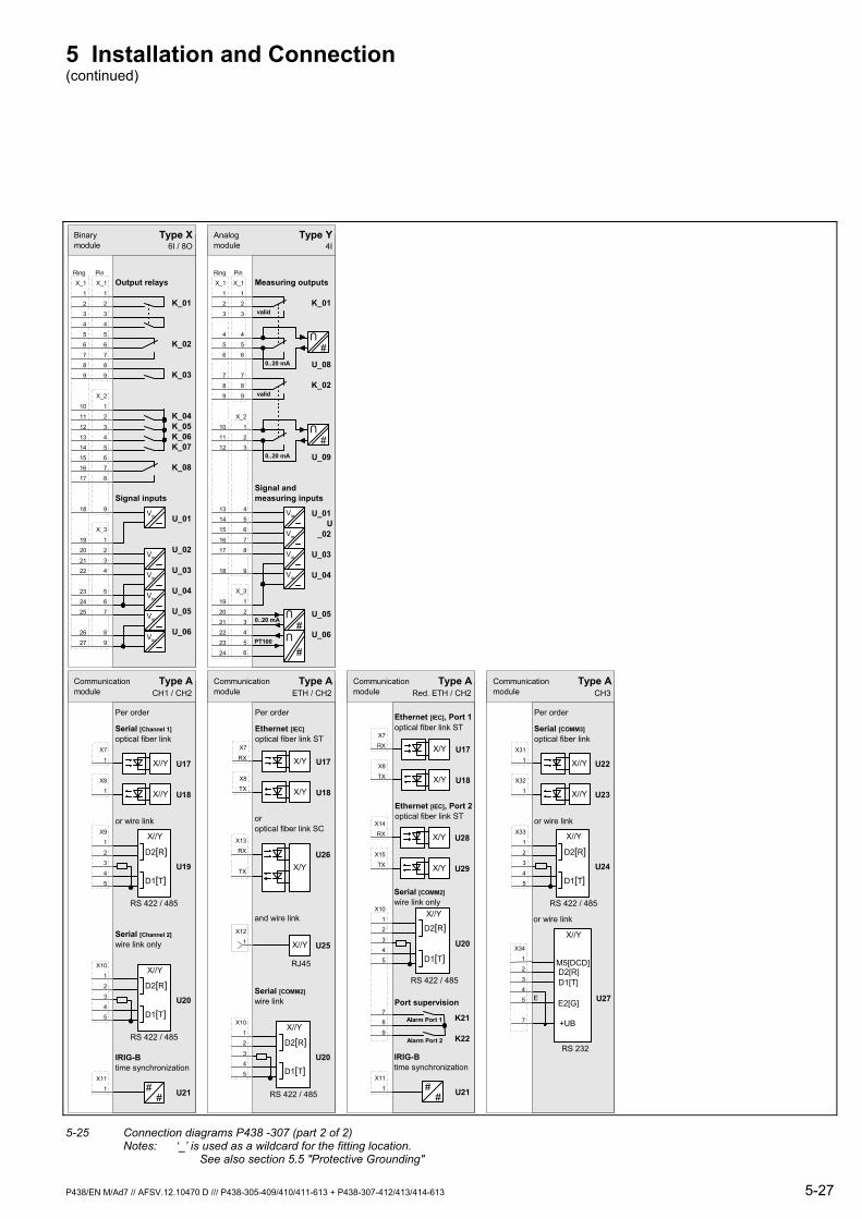
5 Installation and Connection (continued)
P438/EN M/Ad7 // AFSV.12.10470 D /// P438-305-409/410/411-613 + P438-307-412/413/414-613 5-27
X_1
1
2
3
4
5
6
7
8
9
X_1
1
2
3
4
5
6
7
8
9
10
11
12
13
14
15
16
17
18
19
20
21
22
23
24
25
26
27
Ring
K_01
K_02
K_03
K_04K_05K_06K_07
K_08
Binarymodule
U_01
U_02
U_03
U_04
U_05
U_06
Output relaysPin
X_3
1
2
3
4
5
6
7
8
9
X_2
1
2
3
4
5
6
7
8
9
Type X6I / 8O
Signal inputs
Vin
Vin
Vin
Vin
Vin
Vin
X_3
1
2
3
4
5
6
X_2
1
2
3
4
5
6
7
8
9
X_1
1
2
3
4
5
6
7
8
9
X_1
1
2
3
4
5
6
7
8
9
10
11
12
13
14
15
16
17
18
19
20
21
22
23
24
Ring
Analogmodule
U_01U
_02
U_03
U_04
Pin
Type Y4I
Signal andmeasuring inputs
Measuring outputs
K_01
U_080..20 mA
valid
K_02
U_090..20 mA
valid
U
#U
#
U_05
U_06
U
#
U
#
0..20 mA
PT100
Vin
Vin
Vin
Vin
X11
1
X8
1
Type A
Serial [Channel 1]optical fiber link
Per order
##
IRIG-Btime synchronization
Serial [Channel 2]wire link only
or wire link
X//Y
D2[R]
X10
1
2
3
4
5 D1[T]U20
X//Y
RS 422 / 485
D2[R]
X9
1
2
3
4
5 D1[T]U19
U17X//Y
U18X//Y
X7
1
U21
Communicationmodule CH1 / CH2
RS 422 / 485
X8
TX
Type A
Ethernet [IEC]optical fiber link ST
Per order
Serial [COMM2]wire link
oroptical fiber link SC
X//Y
D2[R]
X10
1
2
3
4
5 D1[T]U20
U17X/Y
U18X/Y
X7
RX
Communicationmodule ETH / CH2
X12
1
U26X/Y
U25X//Y
X13
RX
TX
and wire link
RJ45
RS 422 / 485
X8
TX
Type A
Ethernet [IEC], Port 1optical fiber link ST
U17X/Y
U18X/Y
X7
RX
Communicationmodule Red. ETH / CH2
Serial [COMM2]wire link only
X//Y
RS 422 / 485
D2[R]
X10
1
2
3
4
5
7
8
9
D1[T]U20
X11
1 ##
IRIG-Btime synchronization
U21
X15
TX
U28X/Y
U29X/Y
X14
RX
Ethernet [IEC], Port 2optical fiber link ST
Alarm Port 1 K21
K22
Port supervision
Alarm Port 2
X32
1
Type A
Serial [COMM3]optical fiber link
Per order
or wire link
or wire link
X//Y
RS 422 / 485
D2[R]
X33
1
2
3
4
5 D1[T]U24
U22X//Y
U23X//Y
X31
1
Communicationmodule CH3
U27
D1[T]D2[R]
RS 232
E2[G]
X//Y
M5[DCD]
+UB
X34
1
2
3
4
5
7
E
5-25 Connection diagrams P438 -307 (part 2 of 2)
Notes: ‘_’ is used as a wildcard for the fitting location. See also section 5.5 "Protective Grounding"

5-28 P438/EN M/Ad7 // AFSV.12.10470 D /// P438-305-409/410/411-613 + P438-307-412/413/414-613

6 User Interface (HMI)
P438/EN M/Ad7 // AFSV.12.10470 D /// P438-305-409/410/411-613 + P438-307-412/413/414-613 6-1
6 User Interface (HMI)
User interface (HMI) All data required for operation of the protection device is entered from the local control panel, and the data important for system management is read out there as well. The following tasks can be handled from the local control panel:
Readout and modification of settings
Readout of cyclically updated measured operating data and logic status signals
Readout of operating data logs and of monitoring signal logs
Readout of event logs after overload situations, ground faults, or short circuits in the power system
Device resetting and triggering of additional control functions used in testing and commissioning
Control through the PC interface is also possible. This requires a suitable PC and operating program (MiCOM S1).
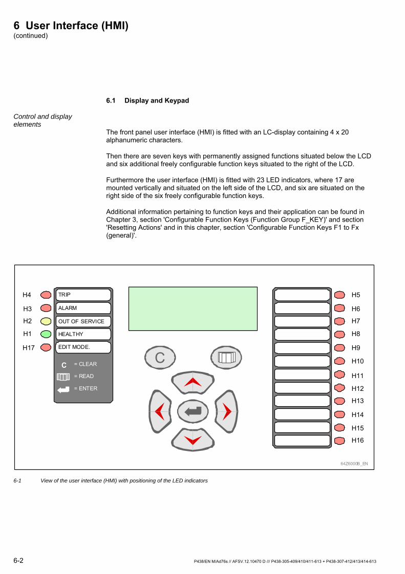
6 User Interface (HMI) (continued)
6-2 P438/EN M/Ad76s // AFSV.12.10470 D /// P438-305-409/410/411-613 + P438-307-412/413/414-613
6.1 Display and Keypad
Control and display elements
The front panel user interface (HMI) is fitted with an LC-display containing 4 x 20 alphanumeric characters.
Then there are seven keys with permanently assigned functions situated below the LCD and six additional freely configurable function keys situated to the right of the LCD.
Furthermore the user interface (HMI) is fitted with 23 LED indicators, where 17 are mounted vertically and situated on the left side of the LCD, and six are situated on the right side of the six freely configurable function keys.
Additional information pertaining to function keys and their application can be found in Chapter 3, section 'Configurable Function Keys (Function Group F_KEY)' and section 'Resetting Actions' and in this chapter, section 'Configurable Function Keys F1 to Fx (general)'.
C
TRIP
ALARM
OUT OF SERVICE
HEALTHY
GG
EDIT MODE.
= CLEAR
= ENTER
= READ
C
H4
H3
H2
H1
H17
H5
H6
H7
H8
H9
H16
H15
H14
H13
H12
H11
H10
64Z6000B_EN
6-1 View of the user interface (HMI) with positioning of the LED indicators
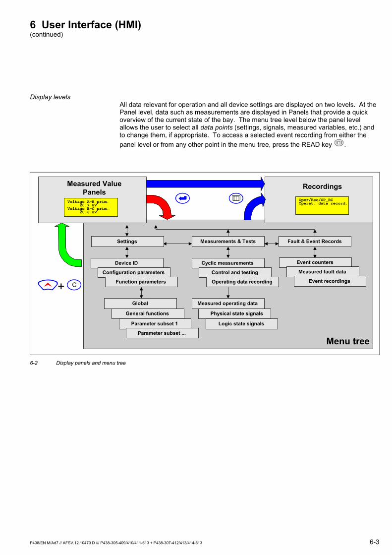
6 User Interface (HMI) (continued)
P438/EN M/Ad7 // AFSV.12.10470 D /// P438-305-409/410/411-613 + P438-307-412/413/414-613 6-3
Display levels All data relevant for operation and all device settings are displayed on two levels. At the Panel level, data such as measurements are displayed in Panels that provide a quick overview of the current state of the bay. The menu tree level below the panel level allows the user to select all data points (settings, signals, measured variables, etc.) and to change them, if appropriate. To access a selected event recording from either the panel level or from any other point in the menu tree, press the READ key .
Menu tree
Measurements & Tests
Device ID
Configuration parameters
Function parameters
Fault & Event Records
Global Measured operating data
+
General functions
Parameter subset 1
Parameter subset ...
Logic state signals
Cyclic measurements
Control and testing
Operating data recording
Event counters
Measured fault data
Event recordings
Physical state signals
Oper/Rec/OP_RCOperat. data record.
Recordings
Settings
C
Voltage A-B prim. 20.7 kVVoltage B-C prim. 20.6 kV
Measured ValuePanels
6-2 Display panels and menu tree

6 User Interface (HMI) (continued)
6-4 P438/EN M/Ad7 // AFSV.12.10470 D /// P438-305-409/410/411-613 + P438-307-412/413/414-613
Display panels The P438 can display 'Measured Value Panels' which are selected automatically by the device according to system conditions.
Selected measured values are displayed on the Measured Value Panels. The system condition determines which Panel is called up (examples are the Operation Panel and the Fault Panel). Only the Measured Value Panels relevant for the particular design version of the given device and its associated range of functions are actually available. The Operation Panel is always provided.
Menu tree and data points All data points (setting values, signals, measured values, etc.) are selected using a menu tree. As the user navigates through the menu tree, the first two lines of the LCD display always show the branch of the menu tree that is active, as selected by the user. The data points are accessed at the lowest level of a menu tree branch. They are displayed either with their plain text description or in numerically coded form, as selected by the user. The value associated with the selected data point, its meaning, and its unit of measurement is displayed in the line below.
List data points List data points are a special category. In contrast to other data points, list data points generally have more than one value element associated with them. This category includes tripping matrices, programmable logic functions, and event logs. When a list data point is selected, the symbol ‘↓‘ is displayed in the bottom line of the LCD, indicating that a sub-level is situated below this displayed level. The individual value elements of a list data point are found at the lower level. In the case of a list setting, the individual value elements are linked by operators such as ‘OR’.
6 User Interface (HMI) (continued)
P438/EN M/Ad7 // AFSV.12.10470 D /// P438-305-409/410/411-613 + P438-307-412/413/414-613 6-5
Keys ‘Up’ and ‘Down’ Keys
G
/ Panel Level: The ‘up’/‘down’ keys switch between the pages of the Measured Value Panel. Menu Tree Level: Press the ‘up’ and ‘down’ keys to navigate up and down through the menu tree in a vertical direction. If the unit is in input mode, the ‘up’ and ‘down’ keys have a different function. Input mode: Settings can only be changed in the input mode, which is signaled by the LED indicator labeled EDIT MODE. Press the ‘up’ and ‘down’ keys in this mode to change the setting value. (‘Up’ key: the next higher value is selected. ‘Down’ key: the next lower value is selected.) With list settings, press the ‘up’ and ‘down’ key to change the logic operator of the value element.
‘Left’ and ‘Right’ Keys / Menu Tree Level: Press the ‘left’ and ‘right’ keys to navigate through the menu tree in a horizontal direction. If the unit is in input mode, the ‘left’ and ‘right’ keys have a different function. Input mode: Settings can only be changed in the input mode, which is signaled by the LED indicator labeled EDIT MODE. When the ‘left’ and ‘right’ keys are pressed, the cursor positioned below one of the digits in the change-enabled value moves one digit to the right or left. (‘Left’ key: the cursor moves to the next digit on the left. ‘Right’ key: the cursor moves to the next digit on the right.) In the case of a list setting, press the ‘left’ and ‘right’ keys to navigate through the list of items available for selection.
ENTER Key G Panel Level: Press the ENTER key at the Panel level to go to the menu tree. Menu Tree Level: Press the ENTER key to enter the input mode. Press the ENTER key a second time to accept the changes as entered and exit the input mode. The LED indicator labeled EDIT MODE signals that the input mode is active.
CLEAR Key C Press the CLEAR key to reset the LED indicators and clear all measured event data. The records in the recording memories are not affected by this action. Input mode: Press the CLEAR key to reject the changes entered and exit the input mode.
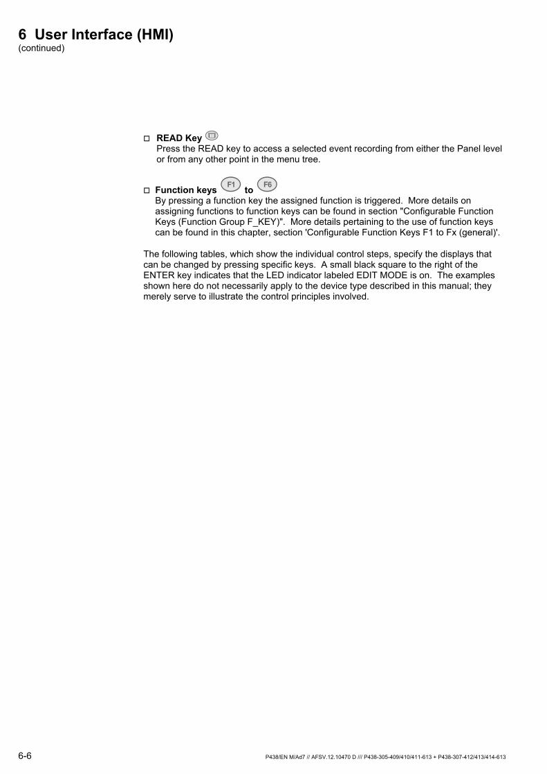
6 User Interface (HMI) (continued)
6-6 P438/EN M/Ad7 // AFSV.12.10470 D /// P438-305-409/410/411-613 + P438-307-412/413/414-613
READ Key Press the READ key to access a selected event recording from either the Panel level or from any other point in the menu tree.
Function keys F1 to F6 By pressing a function key the assigned function is triggered. More details on assigning functions to function keys can be found in section "Configurable Function Keys (Function Group F_KEY)". More details pertaining to the use of function keys can be found in this chapter, section 'Configurable Function Keys F1 to Fx (general)'.
The following tables, which show the individual control steps, specify the displays that can be changed by pressing specific keys. A small black square to the right of the ENTER key indicates that the LED indicator labeled EDIT MODE is on. The examples shown here do not necessarily apply to the device type described in this manual; they merely serve to illustrate the control principles involved.
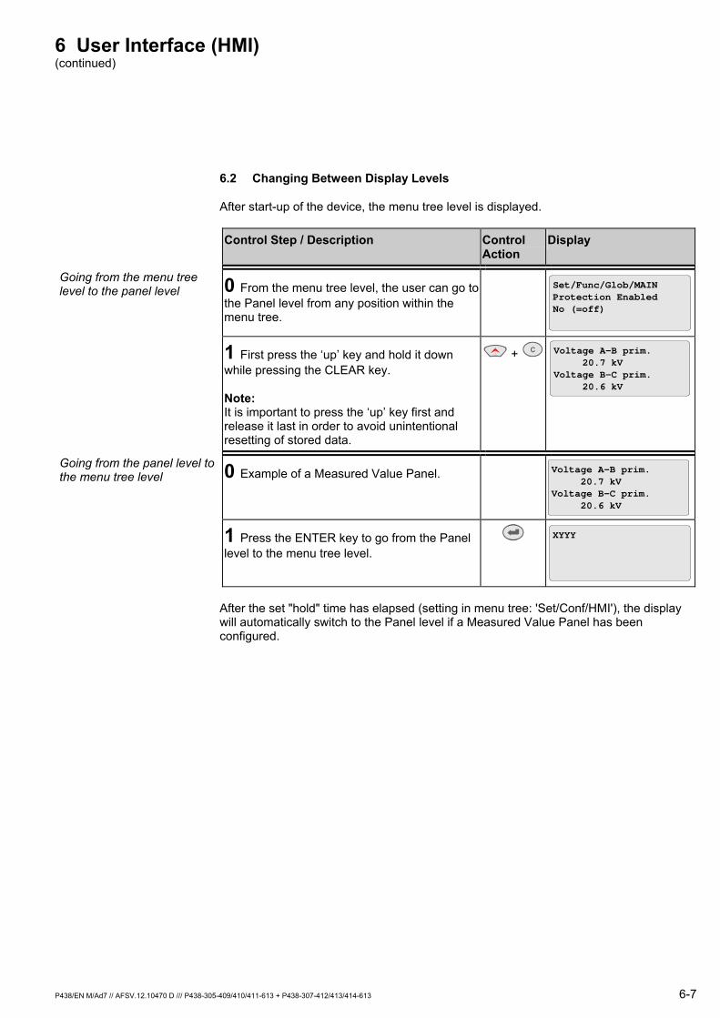
6 User Interface (HMI) (continued)
P438/EN M/Ad7 // AFSV.12.10470 D /// P438-305-409/410/411-613 + P438-307-412/413/414-613 6-7
6.2 Changing Between Display Levels
After start-up of the device, the menu tree level is displayed.
Control Step / Description Control Action
Display
Going from the menu tree level to the panel level 0 From the menu tree level, the user can go to
the Panel level from any position within the menu tree.
Set/Func/Glob/MAINProtection EnabledNo (=off)
1 First press the ‘up’ key and hold it down while pressing the CLEAR key. Note: It is important to press the ‘up’ key first and release it last in order to avoid unintentional resetting of stored data.
G
+ C Voltage A-B prim. 20.7 kVVoltage B-C prim. 20.6 kV
Going from the panel level to the menu tree level 0 Example of a Measured Value Panel. Voltage A-B prim.
20.7 kVVoltage B-C prim. 20.6 kV
1 Press the ENTER key to go from the Panel level to the menu tree level.
G XYYY
After the set "hold" time has elapsed (setting in menu tree: 'Set/Conf/HMI'), the display will automatically switch to the Panel level if a Measured Value Panel has been configured.
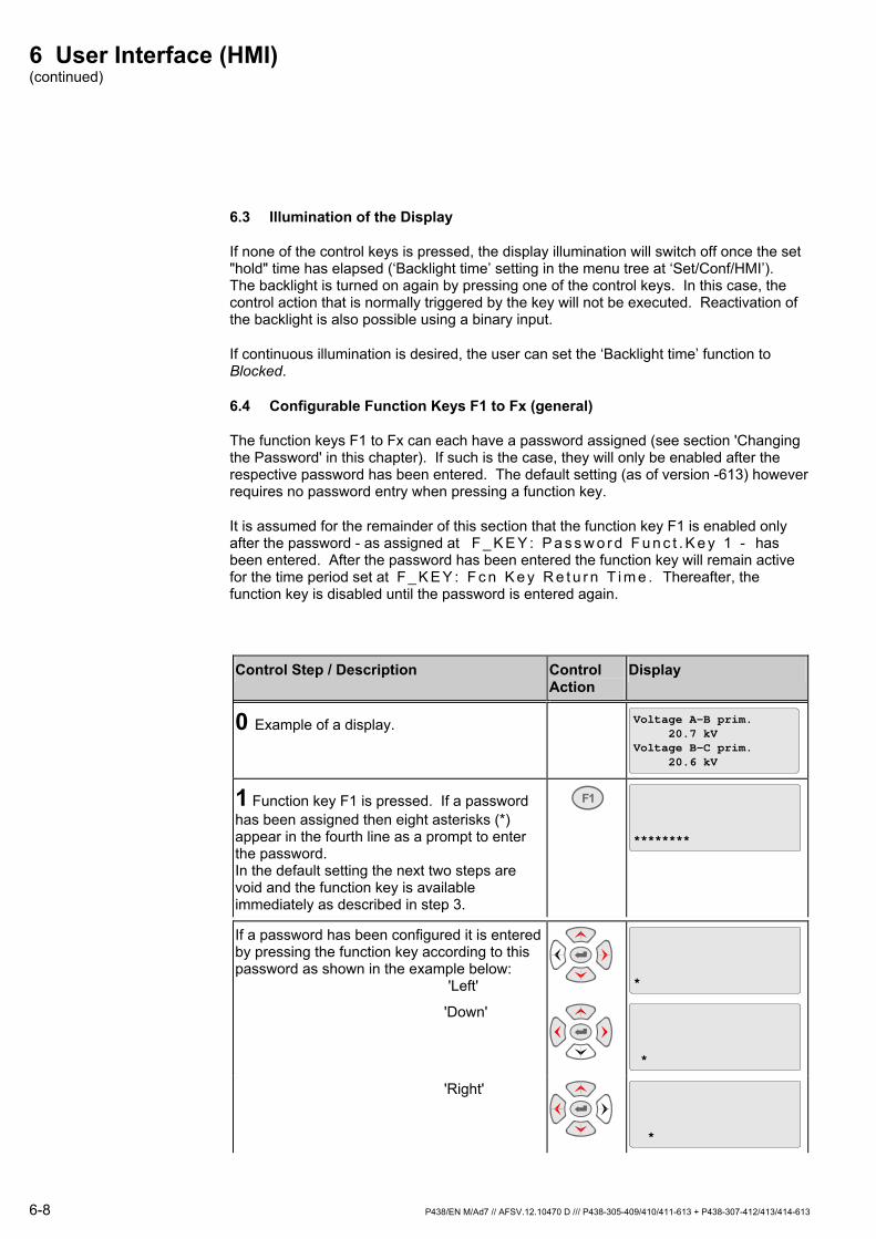
6 User Interface (HMI) (continued)
6-8 P438/EN M/Ad7 // AFSV.12.10470 D /// P438-305-409/410/411-613 + P438-307-412/413/414-613
6.3 Illumination of the Display
If none of the control keys is pressed, the display illumination will switch off once the set "hold" time has elapsed (‘Backlight time’ setting in the menu tree at ‘Set/Conf/HMI’). The backlight is turned on again by pressing one of the control keys. In this case, the control action that is normally triggered by the key will not be executed. Reactivation of the backlight is also possible using a binary input.
If continuous illumination is desired, the user can set the ‘Backlight time’ function to Blocked.
6.4 Configurable Function Keys F1 to Fx (general)
The function keys F1 to Fx can each have a password assigned (see section 'Changing the Password' in this chapter). If such is the case, they will only be enabled after the respective password has been entered. The default setting (as of version -613) however requires no password entry when pressing a function key.
It is assumed for the remainder of this section that the function key F1 is enabled only after the password - as assigned at F _ K E Y : P a s s w o r d F u n c t . K e y 1 - has been entered. After the password has been entered the function key will remain active for the time period set at F _ K E Y : F c n K e y R e t u r n T i m e . Thereafter, the function key is disabled until the password is entered again.
Control Step / Description Control Action
Display
0 Example of a display.
Voltage A-B prim. 20.7 kVVoltage B-C prim. 20.6 kV
1 Function key F1 is pressed. If a password has been assigned then eight asterisks (*) appear in the fourth line as a prompt to enter the password. In the default setting the next two steps are void and the function key is available immediately as described in step 3.
F1
********
If a password has been configured it is entered by pressing the function key according to this password as shown in the example below: 'Left'
G
G
*
'Down'
G
G
*
'Right'
G
G
*

6 User Interface (HMI) (continued)
P438/EN M/Ad7 // AFSV.12.10470 D /// P438-305-409/410/411-613 + P438-307-412/413/414-613 6-9
'Up' The display will change as shown in the column on the right.
G
G
*
Now press the ENTER key. If the correct password has been entered, the active display will re-appear. Function key F1 is now active for the set return time. (No password is required with the default setting and function key F1 is available at all times. Each function key is protected by its own password, and the return time elapses individually for each function key after the correct password has been entered!) If an invalid password has been entered, the display shown above in step 1 will appear.
Voltage A-B prim. 20.7 kVVoltage B-C prim. 20.6 kV
2b This control step can be cancelled at any time by pressing the CLEAR key before the ENTER key is pressed.
C Voltage A-B prim. 20.7 kVVoltage B-C prim. 20.6 kV
3 Press F1 again. The function configured to this function key is carried out.
F1 Voltage A-B prim. 20.7 kVVoltage B-C prim. 20.6 kV
4 When function keys are pressed while the return time period of the function key is elapsing, then the configured function is carried out directly, e.g. without again checking for the password. (With the default setting this step is void as no password is required and the function key is available at all times.)
Fx Voltage A-B prim. 20.7 kVVoltage B-C prim. 20.6 kV

6 User Interface (HMI) (continued)
6-10 P438/EN M/Ad7 // AFSV.12.10470 D /// P438-305-409/410/411-613 + P438-307-412/413/414-613
6.5 Control at the Panel Level
The measured values that will be displayed on the Measured Value Panels can first be selected in the menu tree under Set/Conf/HMI. The user can select different sets of measured values for the Operation Panel, the Overload Panel, the Ground Fault Panel, and the Fault Panel. Only the Measured Value Panels relevant for the particular design version of the given device and its associated range of functions are actually available. The menu for the Operation Panel is always present. The remarks in "Setting a List Setting" apply to this selection. If the M A I N : D i s a b l e d setting has been selected for a given panel, then that panel is disabled.
The Measured Value Panels are called up according to system conditions. If, for example, the device detects an overload or a ground fault, then the corresponding Measured Value Panel will be displayed as long as the overload or ground fault situation exists. If the device detects a fault, then the Fault Panel is displayed and remains active until the measured fault values are reset, by pressing the CLEAR key, for example.
Control Step / Description Control Action
Display
0 Up to six selected measured values can be displayed simultaneously on the Panel.
Voltage A-B prim. 20.7 kVVoltage B-C prim. 20.6 kV
1 If more than two measured values have been selected, they can be viewed one page at a time by pressing the ‘up’ or ’down’ keys. The device will also show the next page of the Measured Value Panel after the set Panel Hold-time (setting in menu tree: "Set/Conf/HMI") has elapsed.
G
or
Voltage C-A prim. 20.8 kVCurrent A prim. 415 A

6 User Interface (HMI) (continued)
P438/EN M/Ad7 // AFSV.12.10470 D /// P438-305-409/410/411-613 + P438-307-412/413/414-613 6-11
6.6 Control at the Menu Tree Level
6.6.1 Navigation of the Menu Tree
Folders and function groups
All data points are organized in different folders based on practical control requirements.
At the root of the menu tree is the unit type; the tree branches into the three main folders ‘Settings’, ‘Measurements & Tests’ and ‘Fault & Event Records’, which form the first folder level. Up to two further folder levels follow so that the entire folder structure consists of three main branches and a maximum of three folder levels.
At the end of each branch of folders are the various function groups in which the individual data points (settings) are combined.
PX yyy
PX yyySettings
PX yyyMeasurements & Tests
PX yyyFault & Event Records
Oper/Cyclic measurements
Oper/Cycl/Meas. operating data
Oper/Cycl/Data/MAIN
Folderlevel 1
Folderlevel 2
Folderlevel 3
Functiongroups
Datapoints
Oper/Cycl/Data/MAINDate 01.01.99 dd.mm.yy
Unittype
6-3 Basic menu tree structure

6 User Interface (HMI) (continued)
6-12 P438/EN M/Ad7 // AFSV.12.10470 D /// P438-305-409/410/411-613 + P438-307-412/413/414-613
6.6.2 Switching Between Address Mode and Plain Text Mode
The display on the user interface (HMI) can be switched between address mode and plain text mode. In the address mode the display shows settings, signals, and measured values in numerically coded form, that is, as addresses. In plain text mode the settings, signals, and measured values are displayed in the form of plain text descriptions. In either case, control is guided by the menu tree. The active branch of the menu tree is displayed in plain text in both modes. In the following examples, the display is shown in plain text mode only.
Control Step / Description Control Action
Display
0 In this example, the user switches from plain text mode to address mode.
Set/Func/Glob/MAINProtection enabledNo (=off)
1 To switch from address mode to plain text mode or vice versa, press the CLEAR key and either the ‘left’ key or the ‘right’ key simultaneously. This can be done at any point in the menu tree.
C + or
C +
Set/Func/Glob/MAIN003.030 0
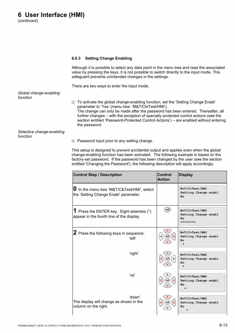
6 User Interface (HMI) (continued)
P438/EN M/Ad7 // AFSV.12.10470 D /// P438-305-409/410/411-613 + P438-307-412/413/414-613 6-13
6.6.3 Setting Change Enabling
Although it is possible to select any data point in the menu tree and read the associated value by pressing the keys, it is not possible to switch directly to the input mode. This safeguard prevents unintended changes in the settings.
There are two ways to enter the input mode.
Global change-enabling function
To activate the global change-enabling function, set the ‘Setting Change Enabl’ parameter to ‘Yes’ (menu tree: ‘M&T/CtrlTest/HMI’). The change can only be made after the password has been entered. Thereafter, all further changes – with the exception of specially protected control actions (see the section entitled ‘Password-Protected Control Actions’) – are enabled without entering the password.
Selective change-enabling function
Password input prior to any setting change.
This setup is designed to prevent accidental output and applies even when the global change-enabling function has been activated. The following example is based on the factory-set password. If the password has been changed by the user (see the section entitled 'Changing the Password'), the following description will apply accordingly.
Control Step / Description Control Action
Display
0 In the menu tree ‘M&T/C&Test/HMI’, select the ‘Setting Change Enabl’ parameter.
M+T/C+Test/HMISetting Change enablNo
1 Press the ENTER key. Eight asterisks (*) appear in the fourth line of the display.
G M+T/C+Test/HMISetting Change enablNo********
2 Press the following keys in sequence: ‘left’
G
G
M+T/C+Test/HMISetting Change enablNo *
‘right’
G
G
M+T/C+Test/HMISetting Change enablNo *
‘up’
G
G
M+T/C+Test/HMISetting Change enablNo *
‘down’ The display will change as shown in the column on the right.
G
G
M+T/C+Test/HMISetting Change enablNo *
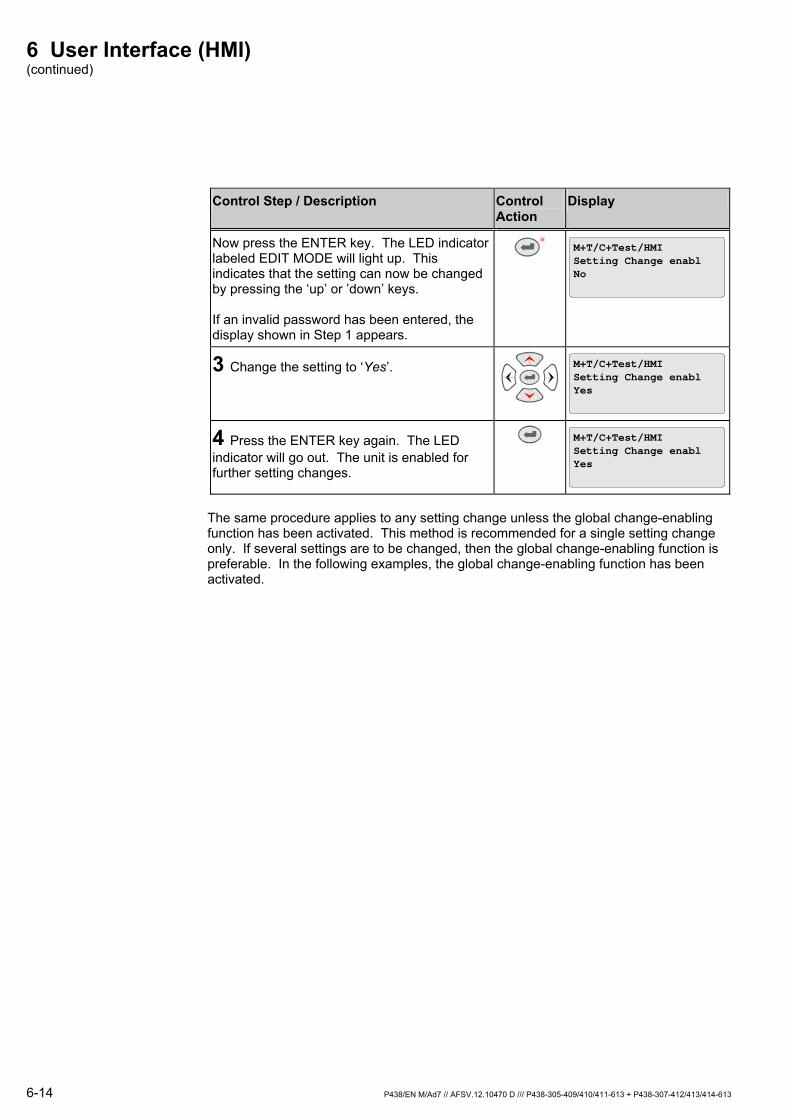
6 User Interface (HMI) (continued)
6-14 P438/EN M/Ad7 // AFSV.12.10470 D /// P438-305-409/410/411-613 + P438-307-412/413/414-613
Control Step / Description Control Action
Display
Now press the ENTER key. The LED indicator labeled EDIT MODE will light up. This indicates that the setting can now be changed by pressing the ‘up’ or ’down’ keys. If an invalid password has been entered, the display shown in Step 1 appears.
M+T/C+Test/HMISetting Change enablNo
3 Change the setting to ‘Yes’.
G
G
M+T/C+Test/HMISetting Change enablYes
4 Press the ENTER key again. The LED indicator will go out. The unit is enabled for further setting changes.
G M+T/C+Test/HMISetting Change enablYes
The same procedure applies to any setting change unless the global change-enabling function has been activated. This method is recommended for a single setting change only. If several settings are to be changed, then the global change-enabling function is preferable. In the following examples, the global change-enabling function has been activated.
6 User Interface (HMI) (continued)
P438/EN M/Ad7 // AFSV.12.10470 D /// P438-305-409/410/411-613 + P438-307-412/413/414-613 6-15
Automatic return The automatic return function prevents the change-enabling function from remaining activated after a change of settings has been completed. Once the set return time (menu tree ‘Set/Conf/HMI’) has elapsed, the change-enabling function is automatically deactivated, and the display switches to a Measured Value Panel corresponding to the current system condition. The return time is restarted when any of the control keys is pressed.
Forced return The return described above can be forced from the user interface (HMI) by first pressing the ‘up’ key and then holding it down while pressing the CLEAR key.
Note: It is important to press the ‘up’ key first and release it last in order to avoid unintentional deletion of stored data.
Even when the change-enabling function is activated, not all settings can be changed. For some settings it is also necessary to disable the protective function (menu tree: Set/Func/Glob/MAIN, 'Protection Enabled'). Such settings include the configuration settings, by means of which the device interfaces can be adapted to the system.
The device is factory-set so that the protective function is disabled.
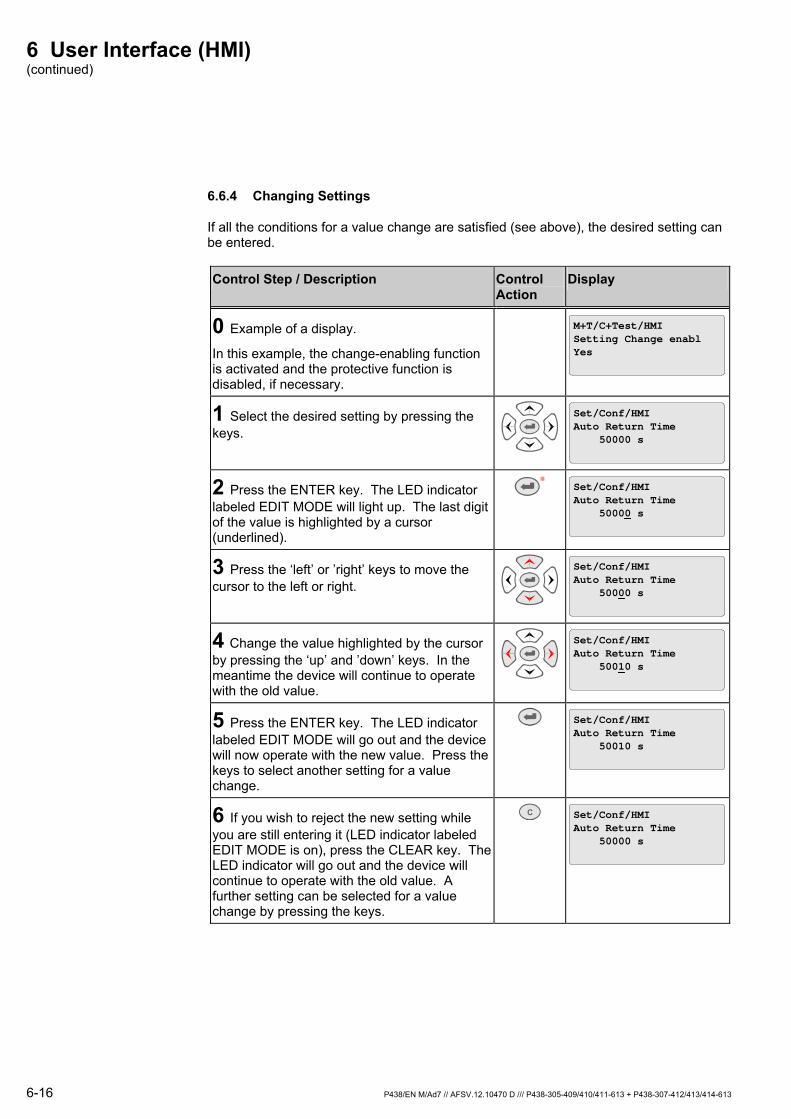
6 User Interface (HMI) (continued)
6-16 P438/EN M/Ad7 // AFSV.12.10470 D /// P438-305-409/410/411-613 + P438-307-412/413/414-613
6.6.4 Changing Settings
If all the conditions for a value change are satisfied (see above), the desired setting can be entered.
Control Step / Description Control Action
Display
0 Example of a display.
In this example, the change-enabling function is activated and the protective function is disabled, if necessary.
M+T/C+Test/HMISetting Change enablYes
1 Select the desired setting by pressing the keys.
G
G
Set/Conf/HMIAuto Return Time 50000 s
2 Press the ENTER key. The LED indicator labeled EDIT MODE will light up. The last digit of the value is highlighted by a cursor (underlined).
Set/Conf/HMIAuto Return Time 50000 s
3 Press the ‘left’ or ’right’ keys to move the cursor to the left or right. G
G
Set/Conf/HMIAuto Return Time 50000 s
4 Change the value highlighted by the cursor by pressing the ‘up’ and ’down’ keys. In the meantime the device will continue to operate with the old value.
G
G
Set/Conf/HMIAuto Return Time 50010 s
5 Press the ENTER key. The LED indicator labeled EDIT MODE will go out and the device will now operate with the new value. Press the keys to select another setting for a value change.
G Set/Conf/HMIAuto Return Time 50010 s
6 If you wish to reject the new setting while you are still entering it (LED indicator labeled EDIT MODE is on), press the CLEAR key. The LED indicator will go out and the device will continue to operate with the old value. A further setting can be selected for a value change by pressing the keys.
C Set/Conf/HMI
50000 sAuto Return Time

6 User Interface (HMI) (continued)
P438/EN M/Ad7 // AFSV.12.10470 D /// P438-305-409/410/411-613 + P438-307-412/413/414-613 6-17
6.6.5 Setting a List Setting
Using list settings, the user is able to select several elements from a list in order to perform tasks such as defining a trip command or defining the measurements that will be displayed on Measured Value Panels. As a rule, the selected elements are linked by an ‘OR’ operator. Other operators (NOT, OR, AND, NOT OR and NOT AND) are available in the LOGIC function group for linking the selected list items. In this way binary signals and binary input signals can be processed in a Boolean equation tailored to meet user requirements. For the DNP 3.0 communication protocol, the user defines the class of a setting instead of assigning operators. The definition of a trip command shall be used here as an illustration.
Control Step / Description Control Action
Display
0 Select a list setting (in this example, the parameter 'Main-Trip 'OR' gate' at ‘Set/Func/Glob/ MAIN’ in the menu tree). The down arrow ( ) indicates that a list setting has been selected.
Set/Func/Glob/MAINMain-Trip 'OR' gate
1 Press the ‘down’ key. The first function and the first selected signal will appear in the third and fourth lines, respectively. The symbol ‘#01’ in the display indicates the first item of the selection. If 'MAIN: Disabled’ appears for the first item, then this means that no function assignment has been made yet.
G
G
Set/Func/Glob/MAINMain-Trip 'OR' gate #01 DISTTrip signal Z1/t1
2 Scroll through the list of assigned functions by pressing the ‘right’ and ’left’ keys. G
G
Set/Func/Glob/MAINMain-Trip 'OR' gateOR #02 DISTTrip signal Z2/t2L
Once the end of the list is reached, the display shown on the right will appear.
Set/Func/Glob/MAINMain-Trip 'OR' gate #05 MAIN?????
3 Press the ENTER key at any position in the list. The LED indicator labeled EDIT MODE will light up.
Set/Func/Glob/MAINMain-Trip 'OR' gate #02 DISTTrip signal Z2/t2L
4 Scroll through the assignable functions by pressing the ‘right’ and ‘left’ keys in the input mode.
G
G
Set/Func/Glob/MAINMain-Trip 'OR' gate #02 DISTTrip signal Z3/t3S
5 Select the operator or the class using the ‘up’ and ’down’ keys. In this particular case, only the ‘OR’ operator can be selected. There is no limitation on the selection of classes.
G
G
Set/Func/Glob/MAINMain-Trip 'OR' gateOR #02 DISTTrip signal Z3/t3S
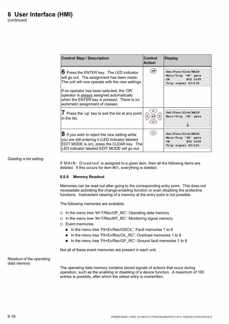
6 User Interface (HMI) (continued)
6-18 P438/EN M/Ad7 // AFSV.12.10470 D /// P438-305-409/410/411-613 + P438-307-412/413/414-613
Control Step / Description Control Action
Display
6 Press the ENTER key. The LED indicator will go out. The assignment has been made. The unit will now operate with the new settings. If no operator has been selected, the ‘OR’ operator is always assigned automatically when the ENTER key is pressed. There is no automatic assignment of classes.
G Set/Func/Glob/MAINMain-Trip 'OR' gateOR #02 DISTTrip signal Z3/t3S
7 Press the ‘up’ key to exit the list at any point in the list. G
G
Set/Func/Glob/MAINMain-Trip 'OR' gate
8 If you wish to reject the new setting while you are still entering it (LED indicator labeled EDIT MODE is on), press the CLEAR key. The LED indicator labeled EDIT MODE will go out.
C Set/Func/Glob/MAINMain-Trip 'OR' gateOR #02 DISTTrip signal Z2/t2L
Deleting a list setting
If ‘M A I N : D i s a b l e d ’ is assigned to a given item, then all the following items are deleted. If this occurs for item #01, everything is deleted.
6.6.6 Memory Readout
Memories can be read out after going to the corresponding entry point. This does not necessitate activating the change-enabling function or even disabling the protective functions. Inadvertent clearing of a memory at the entry point is not possible.
The following memories are available:
In the menu tree ‘M+T/Rec/OP_RC’: Operating data memory In the menu tree ‘M+T/Rec/MT_RC’: Monitoring signal memory Event memories
In the menu tree ‘Flt+Ev/Rec/OSCIL’: Fault memories 1 to 8 In the menu tree ‘Flt+Ev/Rec/OL_RC’: Overload memories 1 to 8 In the menu tree ‘Flt+Ev/Rec/GF_RC’: Ground fault memories 1 to 8
Not all of these event memories are present in each unit.
Readout of the operating data memory
The operating data memory contains stored signals of actions that occur during operation, such as the enabling or disabling of a device function. A maximum of 100 entries is possible, after which the oldest entry is overwritten.
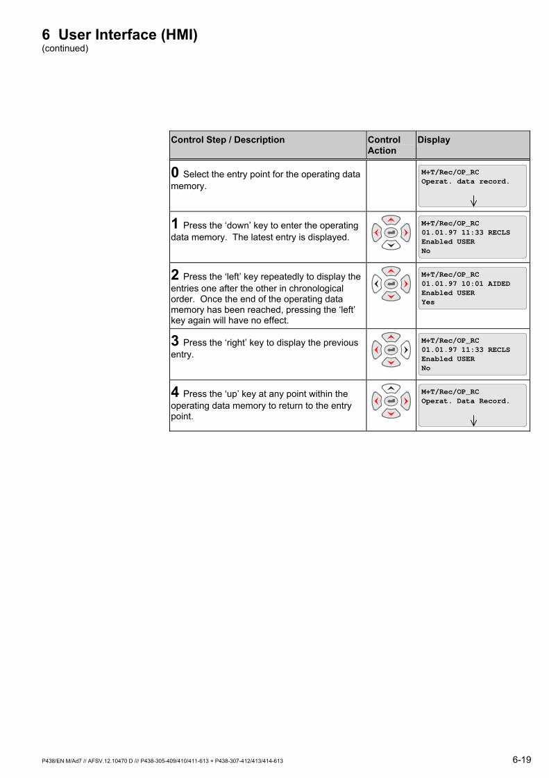
6 User Interface (HMI) (continued)
P438/EN M/Ad7 // AFSV.12.10470 D /// P438-305-409/410/411-613 + P438-307-412/413/414-613 6-19
Control Step / Description Control Action
Display
0 Select the entry point for the operating data memory.
M+T/Rec/OP_RCOperat. data record.
1 Press the ‘down’ key to enter the operating data memory. The latest entry is displayed.
G
G
M+T/Rec/OP_RC01.01.97 11:33 RECLSEnabled USERNo
2 Press the ‘left’ key repeatedly to display the entries one after the other in chronological order. Once the end of the operating data memory has been reached, pressing the ‘left’ key again will have no effect.
G
G
M+T/Rec/OP_RC01.01.97 10:01 AIDEDEnabled USERYes
3 Press the ‘right’ key to display the previous entry. G
G
M+T/Rec/OP_RC01.01.97 11:33 RECLSEnabled USERNo
4 Press the ‘up’ key at any point within the operating data memory to return to the entry point.
GG
M+T/Rec/OP_RCOperat. Data Record.
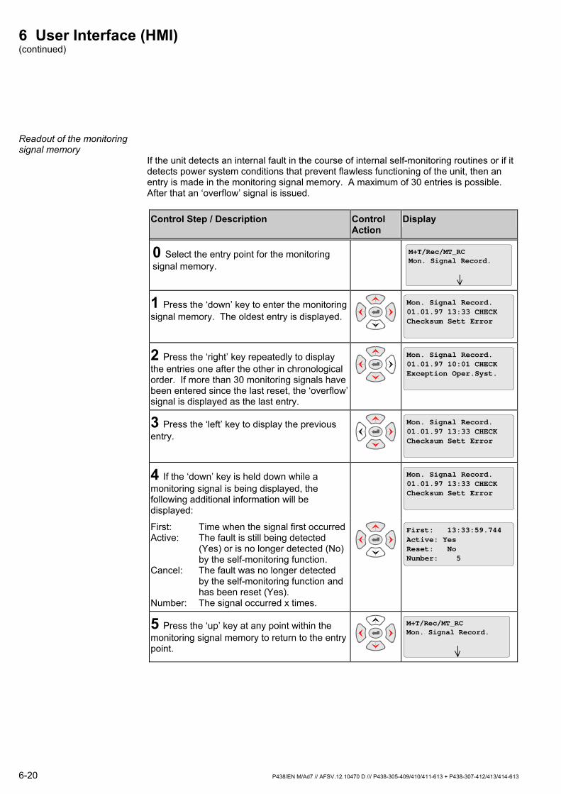
6 User Interface (HMI) (continued)
6-20 P438/EN M/Ad7 // AFSV.12.10470 D /// P438-305-409/410/411-613 + P438-307-412/413/414-613
Readout of the monitoring signal memory
If the unit detects an internal fault in the course of internal self-monitoring routines or if it detects power system conditions that prevent flawless functioning of the unit, then an entry is made in the monitoring signal memory. A maximum of 30 entries is possible. After that an ‘overflow’ signal is issued.
Control Step / Description Control Action
Display
0 Select the entry point for the monitoring signal memory.
M+T/Rec/MT_RCMon. Signal Record.
1 Press the ‘down’ key to enter the monitoring signal memory. The oldest entry is displayed.
G
G
Mon. Signal Record.01.01.97 13:33 CHECKChecksum Sett Error
2 Press the ‘right’ key repeatedly to display the entries one after the other in chronological order. If more than 30 monitoring signals have been entered since the last reset, the ‘overflow’ signal is displayed as the last entry.
G
G
Mon. Signal Record.01.01.97 10:01 CHECKException Oper.Syst.
3 Press the ‘left’ key to display the previous entry. G
G
Mon. Signal Record.01.01.97 13:33 CHECKChecksum Sett Error
4 If the ‘down’ key is held down while a monitoring signal is being displayed, the following additional information will be displayed:
Mon. Signal Record.01.01.97 13:33 CHECKChecksum Sett Error
First: Time when the signal first occurred Active: The fault is still being detected (Yes) or is no longer detected (No) by the self-monitoring function. Cancel: The fault was no longer detected by the self-monitoring function and has been reset (Yes). Number: The signal occurred x times.
G
G
First: 13:33:59.744Active: YesReset: NoNumber: 5
5 Press the ‘up’ key at any point within the monitoring signal memory to return to the entry point.
G
G
M+T/Rec/MT_RCMon. Signal Record.
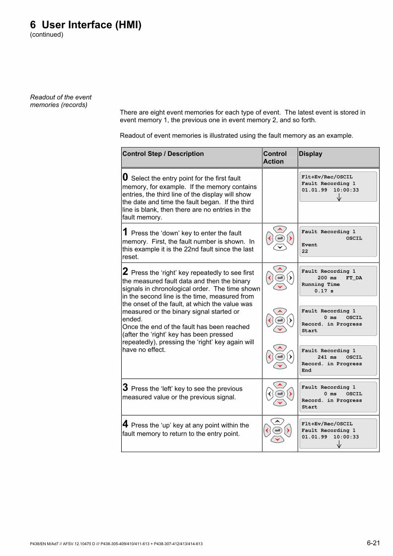
6 User Interface (HMI) (continued)
P438/EN M/Ad7 // AFSV.12.10470 D /// P438-305-409/410/411-613 + P438-307-412/413/414-613 6-21
Readout of the event memories (records)
There are eight event memories for each type of event. The latest event is stored in event memory 1, the previous one in event memory 2, and so forth.
Readout of event memories is illustrated using the fault memory as an example.
Control Step / Description Control Action
Display
0 Select the entry point for the first fault memory, for example. If the memory contains entries, the third line of the display will show the date and time the fault began. If the third line is blank, then there are no entries in the fault memory.
Flt+Ev/Rec/OSCILFault Recording 101.01.99 10:00:33
1 Press the ‘down’ key to enter the fault memory. First, the fault number is shown. In this example it is the 22nd fault since the last reset.
G
G
Fault Recording 1 OSCILEvent22
2 Press the ‘right’ key repeatedly to see first the measured fault data and then the binary signals in chronological order. The time shown in the second line is the time, measured from the onset of the fault, at which the value was measured or the binary signal started or ended. Once the end of the fault has been reached (after the ‘right’ key has been pressed repeatedly), pressing the ‘right’ key again will have no effect.
G
G
G
G
G
G
Fault Recording 1 200 ms FT_DARunning Time 0.17 s
Fault Recording 1 0 ms OSCILRecord. in ProgressStart
Fault Recording 1 241 ms OSCILRecord. in ProgressEnd
3 Press the ‘left’ key to see the previous measured value or the previous signal.
G
G
Fault Recording 1 0 ms OSCILRecord. in ProgressStart
4 Press the ‘up’ key at any point within the fault memory to return to the entry point.
G
G
Flt+Ev/Rec/OSCILFault Recording 101.01.99 10:00:33

6 User Interface (HMI) (continued)
6-22 P438/EN M/Ad7 // AFSV.12.10470 D /// P438-305-409/410/411-613 + P438-307-412/413/414-613
6.6.7 Resetting
All information memories – including the event memories and the monitoring signal memory – as well as the LED indicators can be reset manually. In addition, the LED indicators are automatically cleared and initialized at the onset of a new fault – provided that the appropriate operating mode has been selected – so that they always indicate the latest fault.
The LED indicators can also be reset manually by pressing the CLEAR key, which is always possible in the standard control mode. This action also triggers an LED indicator test and an LCD display test. The event memories are not affected by this action, so that inadvertent deletion of the records associated with the reset signal pattern is reliably prevented.
Because of the ring structure of the event memories, the data for eight consecutive events are updated automatically so that manual resetting should not be necessary, in principle.
However, in the event memories need to be cleared completely, as would be the case after functional testing, then this can be done after selecting the appropriate parameter, and in this case group resetting for several memories may also be configured. An overview on all available resetting methods can be found in Chapter 3, section 'Resetting Actions'.
The method for resetting a single memory from the front panel user interface is described in the following with the example of a fault memory. In this example the global change-enabling function has already been activated.
Control Step / Description Control Action
Display
0 Select the reset setting. Line 3 of the display shows the number of faults since the last reset, 10 in this example.
M+T/C+Test/OSCILReset Recording 10
1 Press the ENTER key. The LED indicator labeled EDIT MODE will light up.
Reset Recording 10Don't execute
M+T/C+Test/OSCIL
2 Press the ‘up’ or ’down’ keys to change the setting to ‘Execute’.
G
G
Reset Recording 10Execute
M+T/C+Test/OSCIL
3 Press the ENTER key. The LED indicator labeled EDIT MODE will go out. The value in line 3 is reset to ‘0’.
G M+T/C+Test/OSCILReset Recording 0
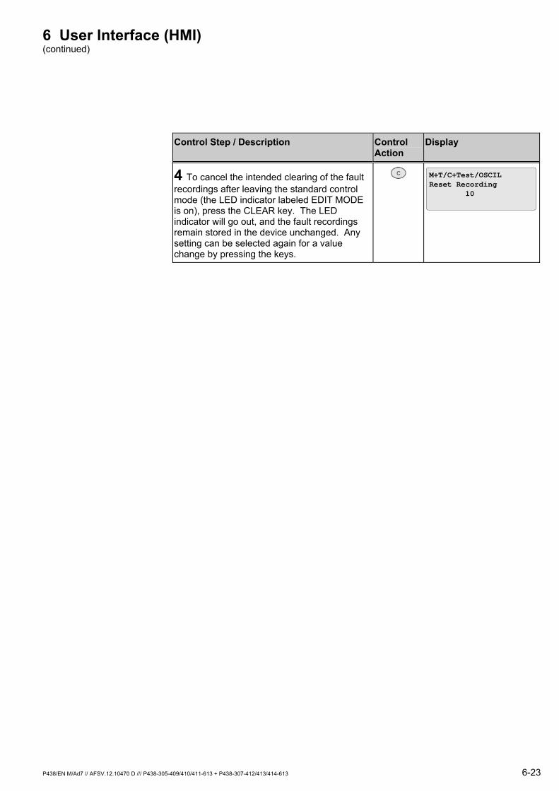
6 User Interface (HMI) (continued)
P438/EN M/Ad7 // AFSV.12.10470 D /// P438-305-409/410/411-613 + P438-307-412/413/414-613 6-23
Control Step / Description Control Action
Display
4 To cancel the intended clearing of the fault recordings after leaving the standard control mode (the LED indicator labeled EDIT MODE is on), press the CLEAR key. The LED indicator will go out, and the fault recordings remain stored in the device unchanged. Any setting can be selected again for a value change by pressing the keys.
C M+T/C+Test/OSCILReset Recording 10
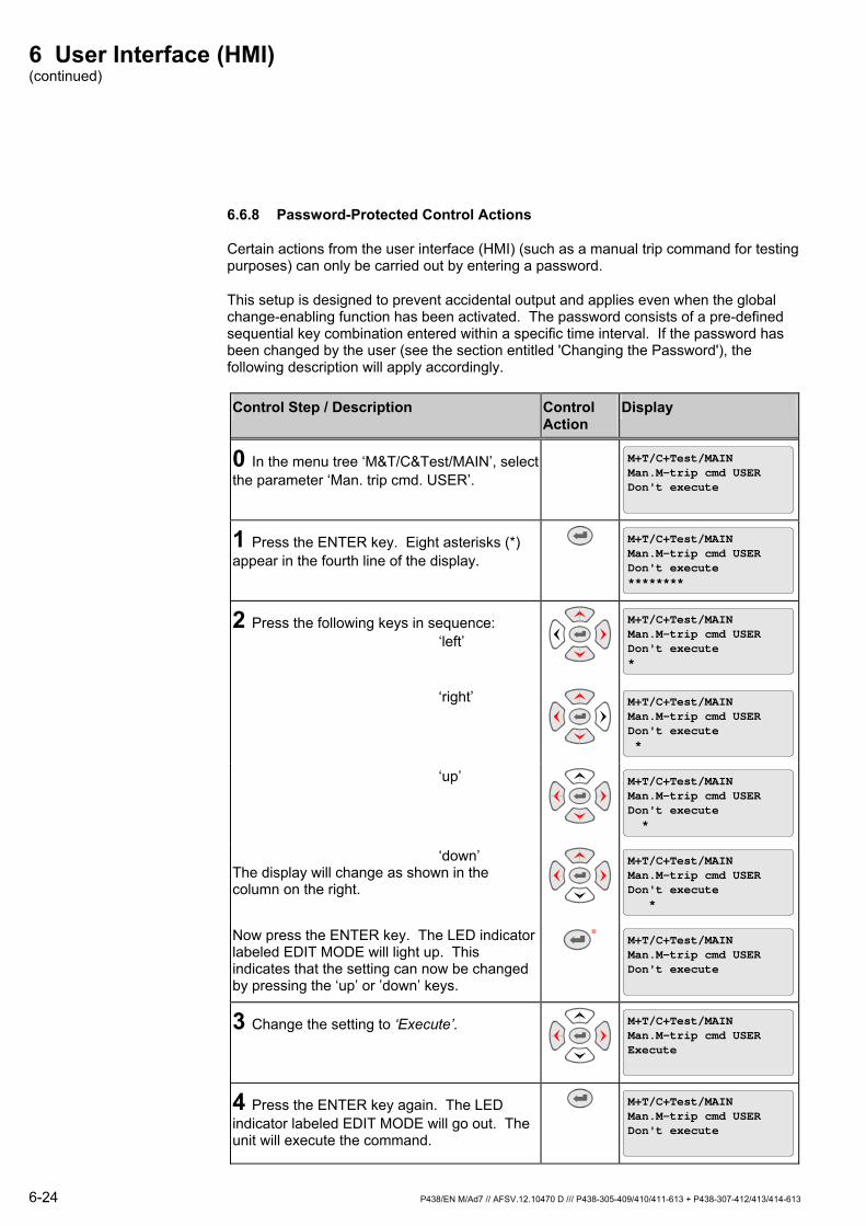
6 User Interface (HMI) (continued)
6-24 P438/EN M/Ad7 // AFSV.12.10470 D /// P438-305-409/410/411-613 + P438-307-412/413/414-613
6.6.8 Password-Protected Control Actions
Certain actions from the user interface (HMI) (such as a manual trip command for testing purposes) can only be carried out by entering a password.
This setup is designed to prevent accidental output and applies even when the global change-enabling function has been activated. The password consists of a pre-defined sequential key combination entered within a specific time interval. If the password has been changed by the user (see the section entitled 'Changing the Password'), the following description will apply accordingly.
Control Step / Description Control Action
Display
0 In the menu tree ‘M&T/C&Test/MAIN’, select the parameter ‘Man. trip cmd. USER’.
M+T/C+Test/MAINMan.M-trip cmd USERDon't execute
1 Press the ENTER key. Eight asterisks (*) appear in the fourth line of the display.
G M+T/C+Test/MAINMan.M-trip cmd USERDon't execute********
2 Press the following keys in sequence: ‘left’
G
G
M+T/C+Test/MAINMan.M-trip cmd USERDon't execute*
‘right’
G
G
M+T/C+Test/MAINMan.M-trip cmd USERDon't execute *
‘up’
G
G
M+T/C+Test/MAINMan.M-trip cmd USERDon't execute *
‘down’ The display will change as shown in the column on the right.
G
G
M+T/C+Test/MAINMan.M-trip cmd USERDon't execute *
Now press the ENTER key. The LED indicator labeled EDIT MODE will light up. This indicates that the setting can now be changed by pressing the ‘up’ or ’down’ keys.
M+T/C+Test/MAINMan.M-trip cmd USERDon't execute
3 Change the setting to ‘Execute’.
G
G
M+T/C+Test/MAINMan.M-trip cmd USERExecute
4 Press the ENTER key again. The LED indicator labeled EDIT MODE will go out. The unit will execute the command.
G M+T/C+Test/MAINMan.M-trip cmd USERDon't execute
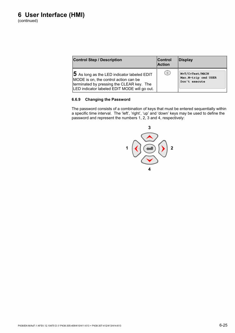
6 User Interface (HMI) (continued)
P438/EN M/Ad7 // AFSV.12.10470 D /// P438-305-409/410/411-613 + P438-307-412/413/414-613 6-25
Control Step / Description Control Action
Display
5 As long as the LED indicator labeled EDIT MODE is on, the control action can be terminated by pressing the CLEAR key. The LED indicator labeled EDIT MODE will go out.
C M+T/C+Test/MAINMan.M-trip cmd USERDon't execute
6.6.9 Changing the Password
The password consists of a combination of keys that must be entered sequentially within a specific time interval. The ‘left’, ’right’, ‘up’ and ‘down’ keys may be used to define the password and represent the numbers 1, 2, 3 and 4, respectively:
G
G
1 2
3
4

6 User Interface (HMI) (continued)
6-26 P438/EN M/Ad7 // AFSV.12.10470 D /// P438-305-409/410/411-613 + P438-307-412/413/414-613
The password can be changed by the user at any time. The procedure for this change is described below. The starting point is the factory-set password.
Control Step / Description Control Action
Display
0 In the menu tree ‘Set/Conf/HMI’, select the ‘Password’ setting.
Set/Conf/HMIPassword********
1 Press the ENTER key. Eight asterisks appear in the fourth line of the display.
G Set/Conf/HMIPassword****************
2 Press the ‘left’, ’right’, ‘up’ and ’down’ keys to enter the valid password. The display will change as shown in the column on the right.
G
G
Set/Conf/HMIPassword*********
G
G
Set/Conf/HMIPassword******** *
GG
Set/Conf/HMIPassword******** *
G
G
Set/Conf/HMIPassword******** *
3 Now press the ENTER key. The LED indicator labeled EDIT MODE will light up. The third line shows an underscore character ( _ ) as the prompt for entering a new password.
Set/Conf/HMIPassword_
4 Enter the new password, which in this example is done by pressing the UP key followed by the DOWN key.
G
G
G
G
Set/Conf/HMIPassword*
Set/Conf/HMIPassword**
5 Press the ENTER key again. Asterisks appear in the third line, and a cursor (underscore) in the fourth line prompts the user to enter the new password again.
Set/Conf/HMIPassword**_

6 User Interface (HMI) (continued)
P438/EN M/Ad7 // AFSV.12.10470 D /// P438-305-409/410/411-613 + P438-307-412/413/414-613 6-27
Control Step / Description Control Action
Display
6 Re-enter the password.
G
G
G
G
Set/Conf/HMIPassword***
Set/Conf/HMIPassword****
7a Press the ENTER key again. If the password has been re-entered correctly, the LED indicator labeled EDIT MODE goes out and the display appears as shown on the right. The new password is now valid.
G Set/Conf/HMIPassword********
7b If the password has been re-entered incorrectly, the LED indicator labeled EDIT MODE remains on and the display shown on the right appears. The password has to be re-entered. It is also possible to cancel the change in password by pressing the CLEAR key (see Step 8).
Set/Conf/HMIPassword**_
8 The change in password can be canceled at any time before Step 7 by pressing the CLEAR key. If this is done, the original password continues to be valid.
C Set/Conf/HMIPassword********
Operation from the user interface (HMI) without password protection is also possible. To select this option, immediately press the ENTER key a second time in steps 4 and 6 without entering anything else. This will configure the user interface (HMI) without password protection, and no control actions involving changes will be possible until the global change-enabling function has been activated (see the section entitled ‘Change-Enabling Function’).
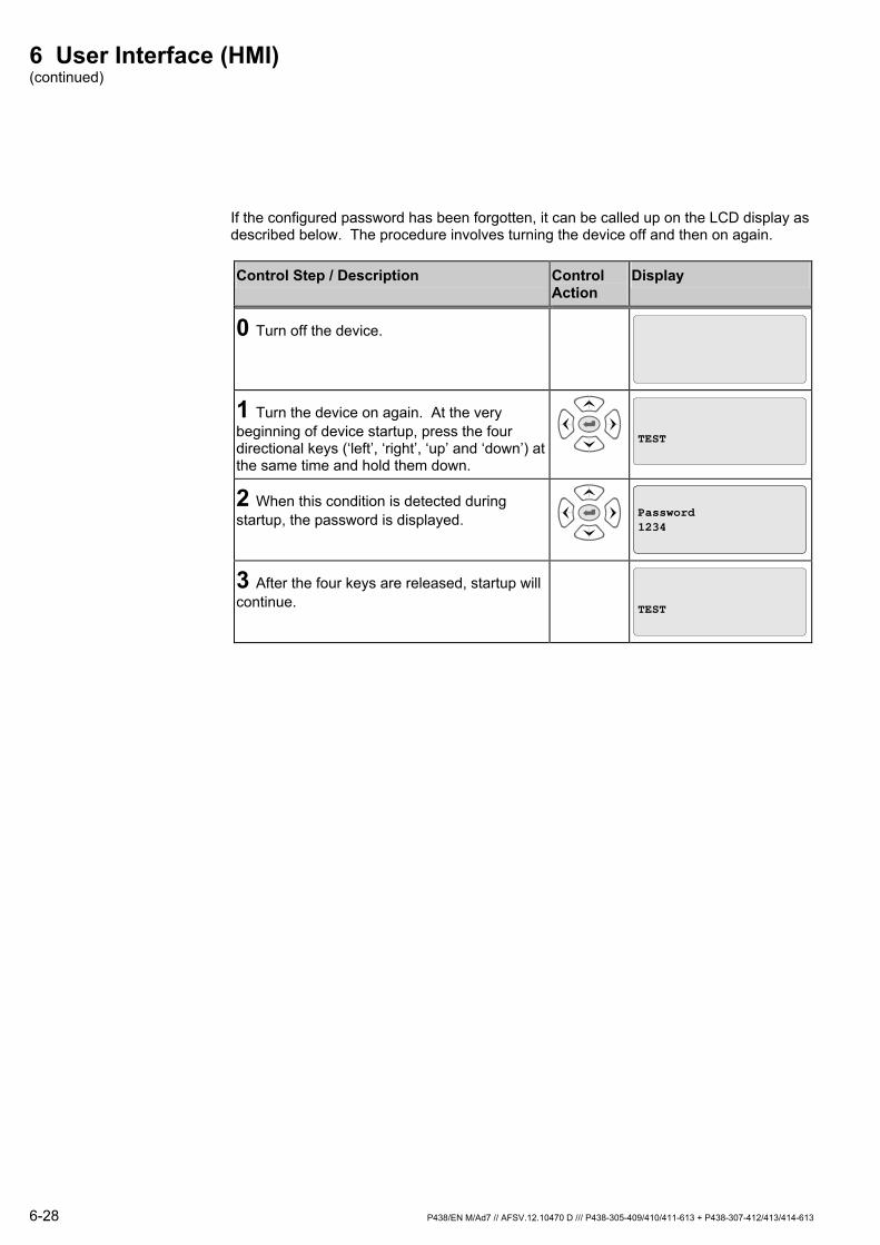
6 User Interface (HMI) (continued)
6-28 P438/EN M/Ad7 // AFSV.12.10470 D /// P438-305-409/410/411-613 + P438-307-412/413/414-613
If the configured password has been forgotten, it can be called up on the LCD display as described below. The procedure involves turning the device off and then on again.
Control Step / Description Control Action
Display
0 Turn off the device.
1 Turn the device on again. At the very beginning of device startup, press the four directional keys (‘left’, ‘right’, ‘up’ and ‘down’) at the same time and hold them down.
G
G
TEST
2 When this condition is detected during startup, the password is displayed.
G
G
Password1234
3 After the four keys are released, startup will continue.
TEST
7 Settings
P438/EN M/Ad7 // AFSV.12.10470 D /// P438-305-409/410/411-613 + P438-307-412/413/414-613 7-1
7 Settings
7.1 Parameters
The P438 must be adjusted to the system and to the protected equipment by appropriate settings. This chapter gives instructions for determining the settings, which are located in the folder entitled ‘Settings’ in the menu tree. The sequence in which the settings are listed and described in this chapter corresponds to their sequence in the menu tree.
The default settings given in the Address List are activated after a cold restart. The P438 is blocked in that case. All settings must be re-entered after a cold restart.
Note:
In the following tables (except for function group DVICE) the location of the corresponding function description is indicated in the right hand side column. "Figure: 3-xxx" refers to a logic diagram which displays the address, "Figure*: 3-xxx" to a figure subtitle or figure report sheet, "Page: 3-xxx" to a page.

7 Settings (continued)
7-2 P438/EN M/Ad7 // AFSV.12.10470 D /// P438-305-409/410/411-613 + P438-307-412/413/414-613
7.1.1 Device Identification
The device identification settings are used to record the ordering information and the design version of the P438. They have no effect on the device's functions. These settings should be changed only if the design version of the P438 is modified.
Device DVICE: Device Type 000 000
The device type is displayed. This display cannot be altered.
DVICE: Software Version 002 120
Software version for the device. This display cannot be altered.
DVICE: SW Date 002 122
Date the software was created. This display cannot be altered.
DVICE: SW Version Communic. 002 103
Software version for the device's communication software. This display cannot be altered.
DVICE: DM IEC 61850 Version 002 059
Software version for the device's communication software, based on the IEC 61850 protocol. This display cannot be altered.
DVICE: Text Vers Data Model 002 121
The description text of the settings can be changed by the "text replacement tools" of the operating program and can be loaded into the device. These user-specific data models obtain a setting which is defined by the setting of the data model created by the user and displayed at this location. Standard data models are marked with a ‘0’ (delivery condition).
DVICE: Language Version 002 123
Setting for the change level of the data model text. This display cannot be altered.
DVICE: Serial Number 002 124
The Serial Number is the serial number of the device. This display cannot be altered.
DVICE: AFS Order No. 001 000
DVICE: PCS Order No. 001 200
Order number for the device. This number cannot be altered by the user.
DVICE: Order Ext. No. 1 000 003
DVICE: Order Ext. No. 2 000 004
DVICE: Order Ext. No. 3 000 005
DVICE: Order Ext. No. 4 000 006
DVICE: Order Ext. No. 5 000 007
DVICE: Order Ext. No. 6 000 008
DVICE: Order Ext. No. 7 000 009
DVICE: Order Ext. No. 8 000 010
DVICE: Order Ext. No. 9 000 011
DVICE: Order Ext. No. 10 000 012
DVICE: Order Ext. No. 11 000 013
DVICE: Order Ext. No. 12 000 014
DVICE: Order Ext. No. 13 000 015
DVICE: Order Ext. No. 14 000 016
DVICE: Order Ext. No. 15 000 017

7 Settings (continued)
P438/EN M/Ad7 // AFSV.12.10470 D /// P438-305-409/410/411-613 + P438-307-412/413/414-613 7-3
DVICE: Order Ext. No. 16 000 018
DVICE: Order Ext. No. 17 000 019
DVICE: Order Ext. No. 18 000 020
DVICE: Order Ext. No. 19 000 021
DVICE: Order Ext. No. 20 000 022
DVICE: Order Ext. No. 21 000 023
DVICE: Order Ext. No. 22 000 024
DVICE: Order Ext. No. 23 000 025
DVICE: Order Ext. No. 24 000 026
DVICE: Order Ext. No. 25 000 027
DVICE: Order Ext. No. 26 000 028
DVICE: Order Ext. No. 27 000 029
Order extension numbers for the device.
DVICE: Module Var. Slot 1 086 050
DVICE: Module Var. Slot 2 086 051
DVICE: Module Var. Slot 3 086 052
DVICE: Module Var. Slot 4 086 053
DVICE: Module Var. Slot 5 086 054
DVICE: Module Var. Slot 6 086 055
DVICE: Module Var. Slot 7 086 056
DVICE: Module Var. Slot 8 086 057
DVICE: Module Var. Slot 9 086 058
DVICE: Module Var. Slot 10 086 059
DVICE: Module Var. Slot 11 086 060
DVICE: Module Var. Slot 12 086 061
DVICE: Module Var. Slot 13 086 062
DVICE: Module Var. Slot 14 086 063
DVICE: Module Var. Slot 15 086 064
DVICE: Module Var. Slot 16 086 065
DVICE: Module Var. Slot 17 086 066
DVICE: Module Var. Slot 18 086 067
DVICE: Module Var. Slot 19 086 068
DVICE: Module Var. Slot 20 086 069
DVICE: Module Var. Slot 21 086 070
Item number of the module inserted in the respective slot 1 to 21. The display always shows the actual component configuration at any given time.
DVICE: Module Vers. Slot 1 086 193
DVICE: Module Vers. Slot 2 086 194
DVICE: Module Vers. Slot 3 086 195
DVICE: Module Vers. Slot 4 086 196
DVICE: Module Vers. Slot 5 086 197
DVICE: Module Vers. Slot 6 086 198
DVICE: Module Vers. Slot 7 086 199
DVICE: Module Vers. Slot 8 086 200
DVICE: Module Vers. Slot 9 086 201
DVICE: Module Vers. Slot 10 086 202
DVICE: Module Vers. Slot 11 086 203
DVICE: Module Vers. Slot 12 086 204
DVICE: Module Vers. Slot 13 086 205
DVICE: Module Vers. Slot 14 086 206
DVICE: Module Vers. Slot 15 086 207

7 Settings (continued)
7-4 P438/EN M/Ad7 // AFSV.12.10470 D /// P438-305-409/410/411-613 + P438-307-412/413/414-613
DVICE: Module Vers. Slot 16 086 208
DVICE: Module Vers. Slot 17 086 209
DVICE: Module Vers. Slot 18 086 210
DVICE: Module Vers. Slot 19 086 211
DVICE: Module Vers. Slot 20 086 212
DVICE: Module Vers. Slot 21 086 213
Index letter specifying the version of the module inserted in the respective slot.
DVICE: Variant of Module A 086 047
Item number of module A in this design version.
DVICE: Version of Module A 086 190
Index letter specifying the version of module A.
DVICE: MAC Address Module A 104 061
Network hardware MAC address for the Ethernet module. This read-only address is assigned during production.
DVICE: Variant of Module L 086 048
Item number of module L in this design version.
DVICE: Version of Module L 086 191
Index letter specifying the version of module L.
DVICE: Variant of Module B 086 049
Item number of digital bus module B in this design version.
DVICE: Version of Module B 086 192
Index letter specifying the version of digital bus module B.
DVICE: Variant Module B (a) 086 046
Item number of analog bus module B.
DVICE: Version Module B (a) 086 189
Index letter specifying the version of analog bus module B.
DVICE: Customer ID Data 1 000 040
DVICE: Customer ID Data 2 000 041
DVICE: Customer ID Data 3 000 042
DVICE: Customer ID Data 4 000 043
DVICE: Customer ID Data 5 000 044
DVICE: Customer ID Data 6 000 045
DVICE: Customer ID Data 7 000 046
DVICE: Customer ID Data 8 000 047
Set your numerically-coded user data here for your records.
DVICE: Device ID 000 035
ID code used by the operating program for identification purposes. See description of the relevant operating program for more detailed setting instructions.
DVICE: Substation ID 000 036
ID code used by the operating program for identification purposes. See description of the relevant operating program for more detailed setting instructions.
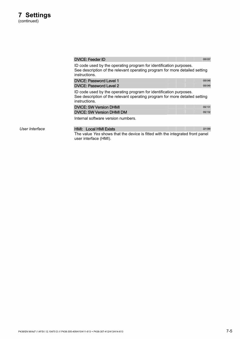
7 Settings (continued)
P438/EN M/Ad7 // AFSV.12.10470 D /// P438-305-409/410/411-613 + P438-307-412/413/414-613 7-5
DVICE: Feeder ID 000 037
ID code used by the operating program for identification purposes. See description of the relevant operating program for more detailed setting instructions.
DVICE: Password Level 1 000 048
DVICE: Password Level 2 000 049
ID code used by the operating program for identification purposes. See description of the relevant operating program for more detailed setting instructions.
DVICE: SW Version DHMI 002 131
DVICE: SW Version DHMI DM 002 132
Internal software version numbers.
User Interface HMI: Local HMI Exists 221 099
The value Yes shows that the device is fitted with the integrated front panel user interface (HMI).
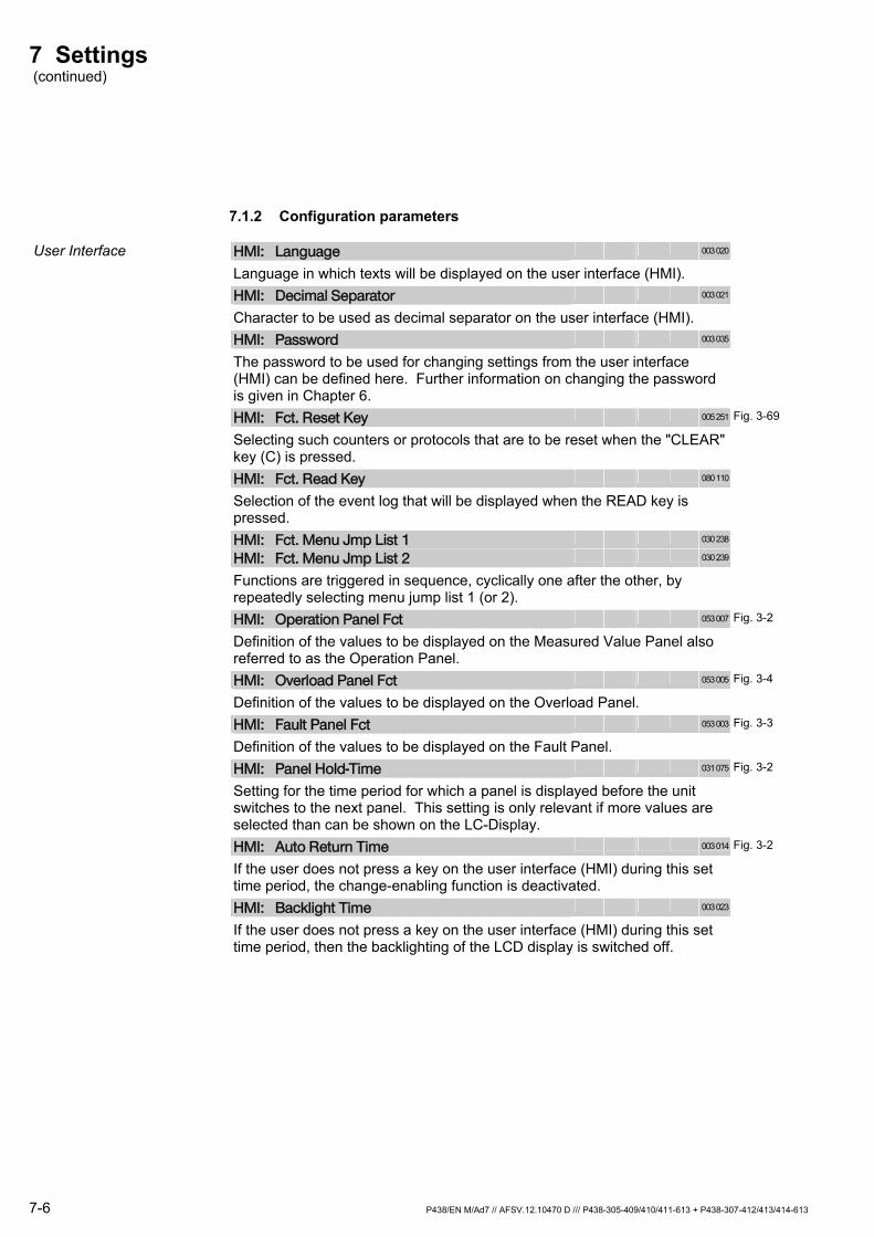
7 Settings (continued)
7-6 P438/EN M/Ad7 // AFSV.12.10470 D /// P438-305-409/410/411-613 + P438-307-412/413/414-613
7.1.2 Configuration parameters
User Interface HMI: Language 003 020
Language in which texts will be displayed on the user interface (HMI).
HMI: Decimal Separator 003 021
Character to be used as decimal separator on the user interface (HMI).
HMI: Password 003 035
The password to be used for changing settings from the user interface (HMI) can be defined here. Further information on changing the password is given in Chapter 6.
HMI: Fct. Reset Key 005 251 Fig. 3-69
Selecting such counters or protocols that are to be reset when the "CLEAR" key (C) is pressed.
HMI: Fct. Read Key 080 110
Selection of the event log that will be displayed when the READ key is pressed.
HMI: Fct. Menu Jmp List 1 030 238
HMI: Fct. Menu Jmp List 2 030 239
Functions are triggered in sequence, cyclically one after the other, by repeatedly selecting menu jump list 1 (or 2).
HMI: Operation Panel Fct 053 007 Fig. 3-2
Definition of the values to be displayed on the Measured Value Panel also referred to as the Operation Panel.
HMI: Overload Panel Fct 053 005 Fig. 3-4
Definition of the values to be displayed on the Overload Panel.
HMI: Fault Panel Fct 053 003 Fig. 3-3
Definition of the values to be displayed on the Fault Panel.
HMI: Panel Hold-Time 031 075 Fig. 3-2
Setting for the time period for which a panel is displayed before the unit switches to the next panel. This setting is only relevant if more values are selected than can be shown on the LC-Display.
HMI: Auto Return Time 003 014 Fig. 3-2
If the user does not press a key on the user interface (HMI) during this set time period, the change-enabling function is deactivated.
HMI: Backlight Time 003 023
If the user does not press a key on the user interface (HMI) during this set time period, then the backlighting of the LCD display is switched off.
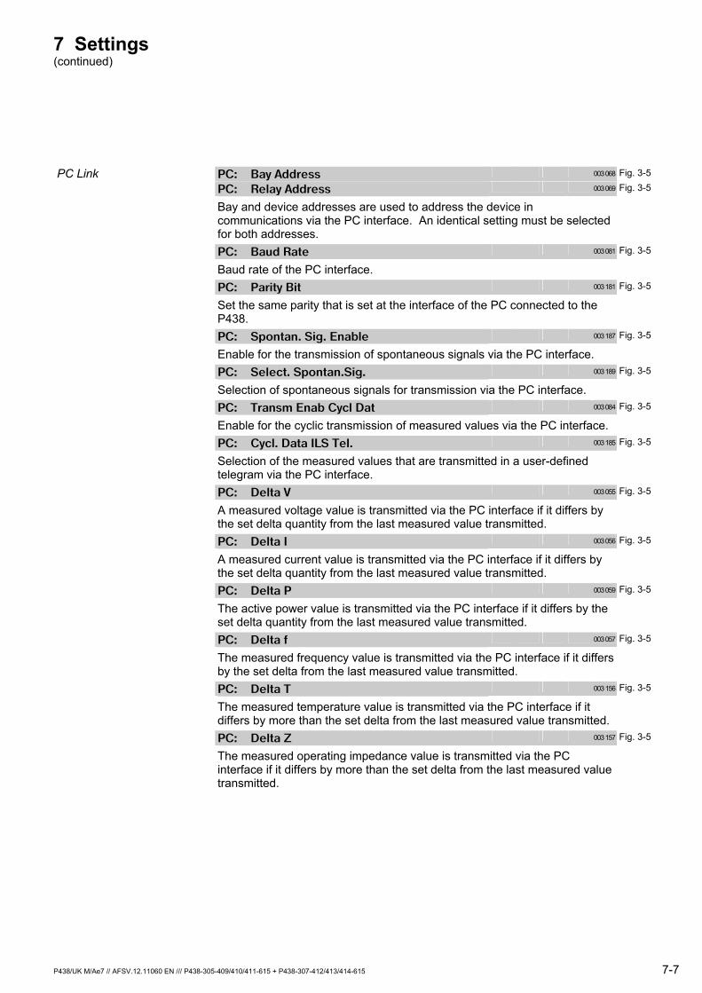
7 Settings (continued)
P438/UK M/Ae7 // AFSV.12.11060 EN /// P438-305-409/410/411-615 + P438-307-412/413/414-615 7-7
PC Link PC: Bay Address 003 068 Fig. 3-5
PC: Relay Address 003 069 Fig. 3-5
Bay and device addresses are used to address the device in communications via the PC interface. An identical setting must be selected for both addresses.
PC: Baud Rate 003 081 Fig. 3-5
Baud rate of the PC interface.
PC: Parity Bit 003 181 Fig. 3-5
Set the same parity that is set at the interface of the PC connected to the P438.
PC: Spontan. Sig. Enable 003 187 Fig. 3-5
Enable for the transmission of spontaneous signals via the PC interface.
PC: Select. Spontan.Sig. 003 189 Fig. 3-5
Selection of spontaneous signals for transmission via the PC interface.
PC: Transm Enab Cycl Dat 003 084 Fig. 3-5
Enable for the cyclic transmission of measured values via the PC interface.
PC: Cycl. Data ILS Tel. 003 185 Fig. 3-5
Selection of the measured values that are transmitted in a user-defined telegram via the PC interface.
PC: Delta V 003 055 Fig. 3-5
A measured voltage value is transmitted via the PC interface if it differs by the set delta quantity from the last measured value transmitted.
PC: Delta I 003 056 Fig. 3-5
A measured current value is transmitted via the PC interface if it differs by the set delta quantity from the last measured value transmitted.
PC: Delta P 003 059 Fig. 3-5
The active power value is transmitted via the PC interface if it differs by the set delta quantity from the last measured value transmitted.
PC: Delta f 003 057 Fig. 3-5
The measured frequency value is transmitted via the PC interface if it differs by the set delta from the last measured value transmitted.
PC: Delta T 003 156 Fig. 3-5
The measured temperature value is transmitted via the PC interface if it differs by more than the set delta from the last measured value transmitted.
PC: Delta Z 003 157 Fig. 3-5
The measured operating impedance value is transmitted via the PC interface if it differs by more than the set delta from the last measured value transmitted.

7 Settings (continued)
7-8 P438/UK M/Ae7 // AFSV.12.11060 EN /// P438-305-409/410/411-615 + P438-307-412/413/414-615
PC: Delta phi 003 158 Fig. 3-5
The measured load angle value is transmitted via the PC interface if it differs by more than the set delta from the last measured value transmitted.
PC: Delta Meas.v.ILS Tel 003 155 Fig. 3-5
The telegram is transmitted if a measured value differs by the set delta quantity from the last measured value transmitted.
PC: Delta t 003 058 Fig. 3-5
All measured values are transmitted again via the PC interface after this time period has elapsed – provided that transmission has not been triggered by the other delta conditions.
PC: Time-Out 003 188 Fig. 3-5
Setting for the time that will elapse after the last telegram traffic via the PC interface before the second communication channel of communication module A is activated.
Rear Port Communications Interface
COMM1: Remote Comms Port1 056 026
Cancelling function group COMM1 or including it in the configuration. If the function group is cancelled from the configuration, then all associated settings and signals are hidden, with the exception of this setting.
COMM1: General Enable USER 003 170 Fig. 3-7, 3-12
Enabling/disabling communication interface 1.
COMM1: IEC870-5 Enabled 003 215 Fig. 3-6
Common settings for enabling all protocols based on IEC 870-5-xxx.
COMM1: Addit. -101 Enable 003 216 Fig. 3-6
Enabling additional settings that are relevant for the protocol based on IEC 870-5-101.
COMM1: Addit. ILS Enable 003 217 Fig. 3-6
Enabling additional settings that are relevant for the ILS protocol.
COMM1: MODBUS Enable 003 220 Fig. 3-6
Enabling settings relevant for the MODBUS protocol.
COMM1: DNP3 Enable 003 231 Fig. 3-6
Enabling settings that are relevant for the DNP 3.0 protocol.
COMM1: COURIER Enable 103 040 Fig. 3-6
Enabling settings that are relevant for the COURIER protocol.
COMM1: Communicat Protocol 003 167 Fig. 3-6
Selecting the communication protocol that shall be used for the communication interface.
COMM1: MODBUS Variant 003 214 Fig. 3-10
The user may select either the Private or the Compatible variant of the MODBUS protocol.
Note: This setting is hidden unless the MODBUS protocol is enabled. The Compatible variant corresponds to the MODBUS implementation of MiCOM Px20 and Px40 devices. The Private variant corresponds to the first implementation of the MODBUS protocol.

7 Settings (continued)
P438/EN M/Ad7 // AFSV.12.10470 D /// P438-305-409/410/411-613 + P438-307-412/413/414-613 7-9
COMM1: Line Idle State 003 165 Fig. 3-7, 3-8, 3-9, 3-10, 3-11, 3-12
Setting for the line idle state indication.
COMM1: Baud Rate 003 071 Fig. 3-7, 3-8, 3-9, 3-10, 3-11, 3-12
Baud rate of the communication interface.
COMM1: Parity Bit 003 171 Fig. 3-7, 3-8, 3-9, 3-10, 3-11, 3-12
Setting the same parity that is set at the interface of the control system connected to the P438.
COMM1: Dead Time Monitoring 003 176 Fig. 3-7, 3-8, 3-9, 3-10, 3-11, 3-12
The P438 monitors telegram transmission to make sure that no excessive pause occurs within a telegram. This monitoring function can be disabled if it is not required.
Note: This setting is necessary for modem transmission only.
COMM1: Mon. Time Polling 003 202 Fig. 3-7, 3-8, 3-9, 3-10, 3-11, 3-12
The time between two polling calls from the communication master must be less than the time set here.
COMM1: Octet Comm. Address 003 072 Fig. 3-7, 3-8, 3-9, 3-10,3-11, 3-12
The communication address and the ASDU address are used to identify the device in communication via the interface. An identical setting must be selected for both addresses.
Note: The former designation for 'C O M M 1 : O c t e t C o m m . A d d r e s s ' w a s ' I L S A : B a y A d d r e s s
"ASDU": Application Service Data Unit
COMM1: Octet 2 Com.Add DNP3 003 240 Fig. 3-11
In the DNP 3.0 protocol, a 16-bit address is used to identify devices. The address that can be set here is the higher-order octet, whereas the address set at C O M M 1 : O c t e t C o m m . A d d r e s s is the lower-order octet of the DNP address.
Note: This setting is hidden unless the DNP 3.0 protocol is enabled.
COMM1: Test Monitor On 003 166 Fig. 3-7, 3-8, 3-9, 3-10, 3-11, 3-12
Setting specifying whether data shall be recorded for service activities.

7 Settings (continued)
7-10 P438/UK M/Ae7 // AFSV.12.11060 EN /// P438-305-409/410/411-615 + P438-307-412/413/414-615
COMM1: Manufacturer 003 161 Fig. 3-7, 3-8, 3-9
Setting for the name of the manufacturer. This setting can be changed to any free text to ensure compatibility. The default value is SE. However, it can be necessary in special cases to set the value to something different.
Note: This parameter can be changed to any text of max. 8 characters length. Any longer text entered is truncated to 8 characters internally. However, changes can be carried out only via the operating program, not using the integrated local control panel. This setting is hidden unless an IEC 870-5 protocol is enabled.
COMM1: Octet Address ASDU 003 073 Fig. 3-7, 3-8, 3-9
The communication address and the ASDU address are used to identify the device in communication via the interface. An identical setting must be selected for both addresses.
Note:
This setting is hidden unless an IEC 870-5 protocol is enabled.
The former designation for 'C O M M 1 : O c t e t A d d r e s s A S D U ' was 'ILSA: R e l a y A d d r e s s '.
"ASDU": Application Service Data Unit
COMM1: Spontan. Sig. Enable 003 177 Fig. 3-7, 3-8, 3-9
Enable for the transmission of spontaneous signals via the communication interface.
Note: This setting is hidden unless an IEC 870-5 protocol is enabled.
COMM1: Select. Spontan.Sig. 003 179 Fig. 3-7, 3-8, 3-9
Selection of spontaneous signals for transmission via communication interface 1.
COMM1: Transm Enab Cycl Dat 003 074 Fig. 3-7, 3-8,3-9
Enabling cyclic transmission of measured values via the communication interface.
Note: This setting is hidden unless an IEC 870-5 protocol is enabled.
COMM1: Cycl. Data ILS Tel. 003 175 Fig. 3-7, 3-8, 3-9
Selection of the measured values that are transmitted in a user-defined telegram via the communication interface.
Note: This setting is hidden unless an IEC 870-5 protocol is enabled.
COMM1: Delta V 003 050 Fig. 3-7, 3-8, 3-9
A measured voltage value is transmitted via the communication interface if it differs by the set delta quantity from the last measured value transmitted.
Note: This setting is hidden unless an IEC 870-5 protocol is enabled.
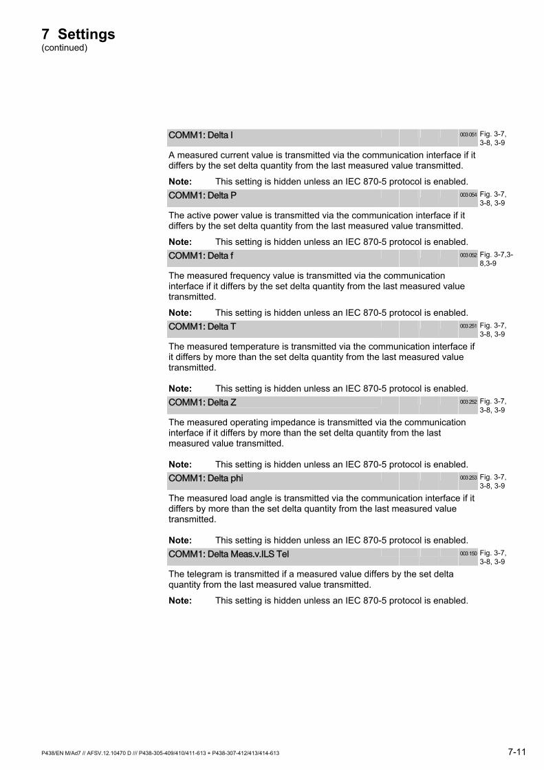
7 Settings (continued)
P438/EN M/Ad7 // AFSV.12.10470 D /// P438-305-409/410/411-613 + P438-307-412/413/414-613 7-11
COMM1: Delta I 003 051 Fig. 3-7, 3-8, 3-9
A measured current value is transmitted via the communication interface if it differs by the set delta quantity from the last measured value transmitted.
Note: This setting is hidden unless an IEC 870-5 protocol is enabled.
COMM1: Delta P 003 054 Fig. 3-7, 3-8, 3-9
The active power value is transmitted via the communication interface if it differs by the set delta quantity from the last measured value transmitted.
Note: This setting is hidden unless an IEC 870-5 protocol is enabled.
COMM1: Delta f 003 052 Fig. 3-7,3-8,3-9
The measured frequency value is transmitted via the communication interface if it differs by the set delta quantity from the last measured value transmitted.
Note: This setting is hidden unless an IEC 870-5 protocol is enabled.
COMM1: Delta T 003 251 Fig. 3-7, 3-8, 3-9
The measured temperature is transmitted via the communication interface if it differs by more than the set delta quantity from the last measured value transmitted. Note: This setting is hidden unless an IEC 870-5 protocol is enabled.
COMM1: Delta Z 003 252 Fig. 3-7, 3-8, 3-9
The measured operating impedance is transmitted via the communication interface if it differs by more than the set delta quantity from the last measured value transmitted. Note: This setting is hidden unless an IEC 870-5 protocol is enabled.
COMM1: Delta phi 003 253 Fig. 3-7, 3-8, 3-9
The measured load angle is transmitted via the communication interface if it differs by more than the set delta quantity from the last measured value transmitted. Note: This setting is hidden unless an IEC 870-5 protocol is enabled.
COMM1: Delta Meas.v.ILS Tel 003 150 Fig. 3-7, 3-8, 3-9
The telegram is transmitted if a measured value differs by the set delta quantity from the last measured value transmitted.
Note: This setting is hidden unless an IEC 870-5 protocol is enabled.
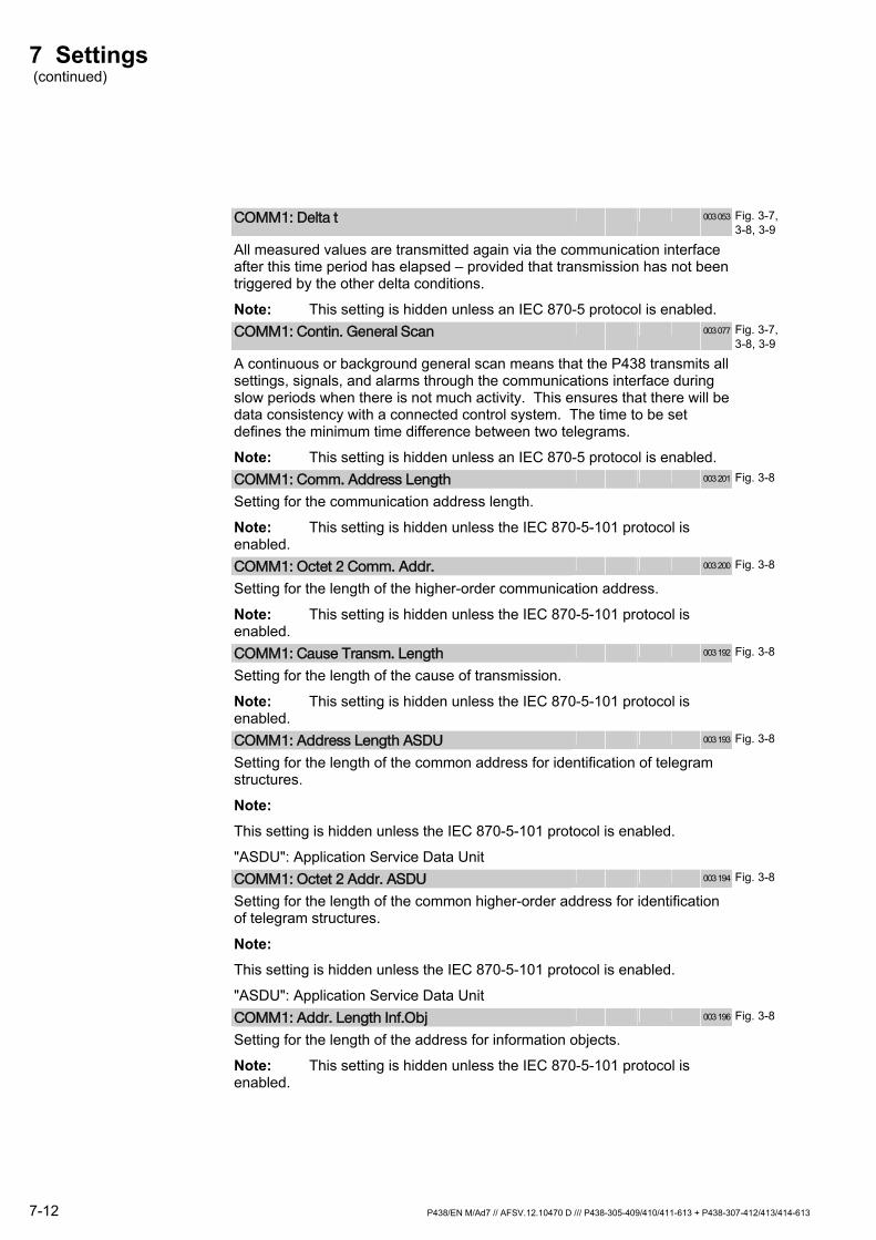
7 Settings (continued)
7-12 P438/EN M/Ad7 // AFSV.12.10470 D /// P438-305-409/410/411-613 + P438-307-412/413/414-613
COMM1: Delta t 003 053 Fig. 3-7, 3-8, 3-9
All measured values are transmitted again via the communication interface after this time period has elapsed – provided that transmission has not been triggered by the other delta conditions.
Note: This setting is hidden unless an IEC 870-5 protocol is enabled.
COMM1: Contin. General Scan 003 077 Fig. 3-7, 3-8, 3-9
A continuous or background general scan means that the P438 transmits all settings, signals, and alarms through the communications interface during slow periods when there is not much activity. This ensures that there will be data consistency with a connected control system. The time to be set defines the minimum time difference between two telegrams.
Note: This setting is hidden unless an IEC 870-5 protocol is enabled.
COMM1: Comm. Address Length 003 201 Fig. 3-8
Setting for the communication address length.
Note: This setting is hidden unless the IEC 870-5-101 protocol is enabled.
COMM1: Octet 2 Comm. Addr. 003 200 Fig. 3-8
Setting for the length of the higher-order communication address.
Note: This setting is hidden unless the IEC 870-5-101 protocol is enabled.
COMM1: Cause Transm. Length 003 192 Fig. 3-8
Setting for the length of the cause of transmission.
Note: This setting is hidden unless the IEC 870-5-101 protocol is enabled.
COMM1: Address Length ASDU 003 193 Fig. 3-8
Setting for the length of the common address for identification of telegram structures.
Note:
This setting is hidden unless the IEC 870-5-101 protocol is enabled.
"ASDU": Application Service Data Unit
COMM1: Octet 2 Addr. ASDU 003 194 Fig. 3-8
Setting for the length of the common higher-order address for identification of telegram structures.
Note:
This setting is hidden unless the IEC 870-5-101 protocol is enabled.
"ASDU": Application Service Data Unit
COMM1: Addr. Length Inf.Obj 003 196 Fig. 3-8
Setting for the length of the address for information objects.
Note: This setting is hidden unless the IEC 870-5-101 protocol is enabled.
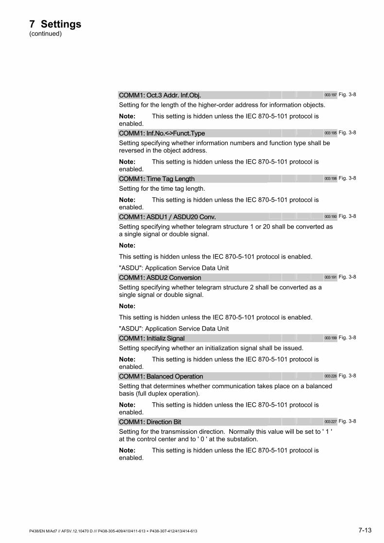
7 Settings (continued)
P438/EN M/Ad7 // AFSV.12.10470 D /// P438-305-409/410/411-613 + P438-307-412/413/414-613 7-13
COMM1: Oct.3 Addr. Inf.Obj. 003 197 Fig. 3-8
Setting for the length of the higher-order address for information objects.
Note: This setting is hidden unless the IEC 870-5-101 protocol is enabled.
COMM1: Inf.No.<->Funct.Type 003 195 Fig. 3-8
Setting specifying whether information numbers and function type shall be reversed in the object address.
Note: This setting is hidden unless the IEC 870-5-101 protocol is enabled.
COMM1: Time Tag Length 003 198 Fig. 3-8
Setting for the time tag length.
Note: This setting is hidden unless the IEC 870-5-101 protocol is enabled.
COMM1: ASDU1 / ASDU20 Conv. 003 190 Fig. 3-8
Setting specifying whether telegram structure 1 or 20 shall be converted as a single signal or double signal.
Note:
This setting is hidden unless the IEC 870-5-101 protocol is enabled.
"ASDU": Application Service Data Unit
COMM1: ASDU2 Conversion 003 191 Fig. 3-8
Setting specifying whether telegram structure 2 shall be converted as a single signal or double signal.
Note:
This setting is hidden unless the IEC 870-5-101 protocol is enabled.
"ASDU": Application Service Data Unit
COMM1: Initializ Signal 003 199 Fig. 3-8
Setting specifying whether an initialization signal shall be issued.
Note: This setting is hidden unless the IEC 870-5-101 protocol is enabled.
COMM1: Balanced Operation 003 226 Fig. 3-8
Setting that determines whether communication takes place on a balanced basis (full duplex operation).
Note: This setting is hidden unless the IEC 870-5-101 protocol is enabled.
COMM1: Direction Bit 003 227 Fig. 3-8
Setting for the transmission direction. Normally this value will be set to ' 1 ' at the control center and to ' 0 ' at the substation.
Note: This setting is hidden unless the IEC 870-5-101 protocol is enabled.
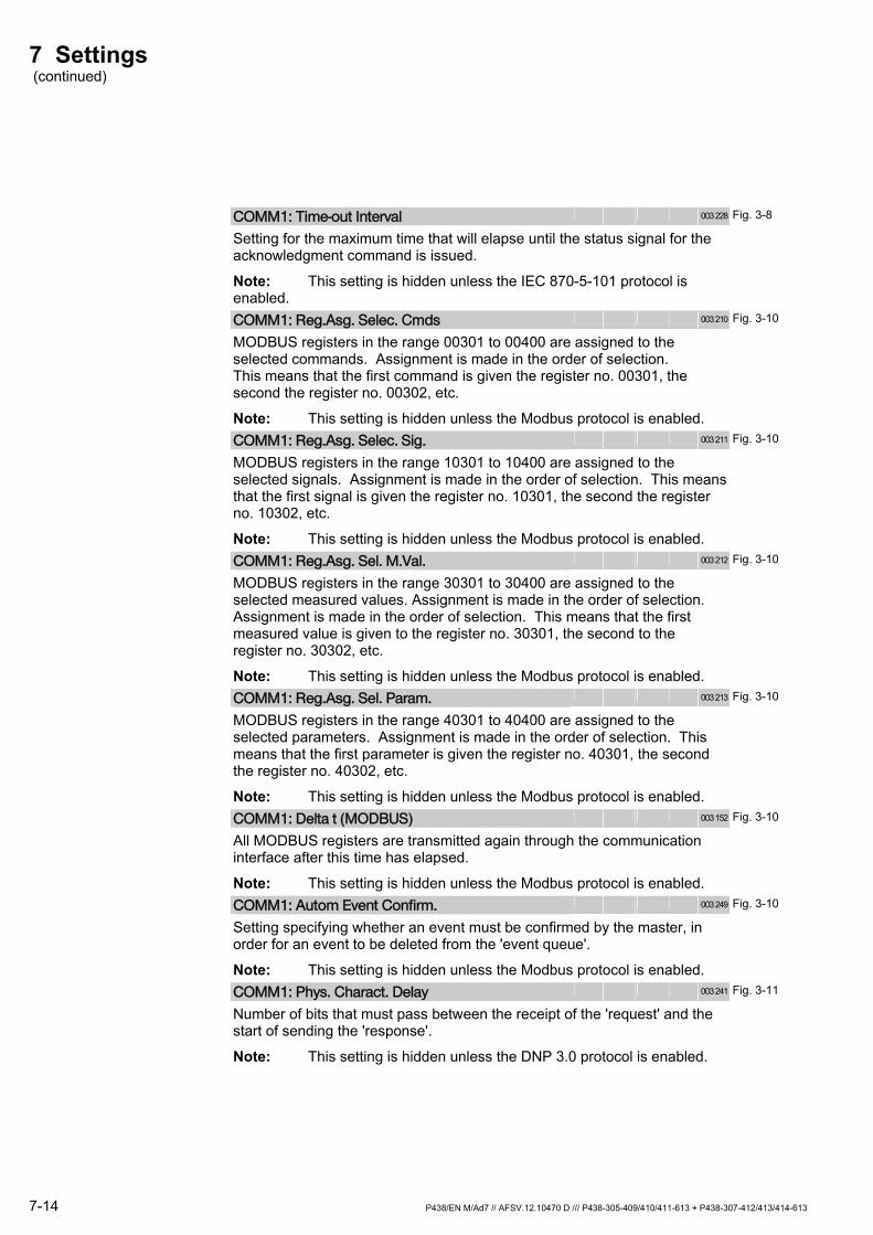
7 Settings (continued)
7-14 P438/EN M/Ad7 // AFSV.12.10470 D /// P438-305-409/410/411-613 + P438-307-412/413/414-613
COMM1: Time-out Interval 003 228 Fig. 3-8
Setting for the maximum time that will elapse until the status signal for the acknowledgment command is issued.
Note: This setting is hidden unless the IEC 870-5-101 protocol is enabled.
COMM1: Reg.Asg. Selec. Cmds 003 210 Fig. 3-10
MODBUS registers in the range 00301 to 00400 are assigned to the selected commands. Assignment is made in the order of selection. This means that the first command is given the register no. 00301, the second the register no. 00302, etc.
Note: This setting is hidden unless the Modbus protocol is enabled.
COMM1: Reg.Asg. Selec. Sig. 003 211 Fig. 3-10
MODBUS registers in the range 10301 to 10400 are assigned to the selected signals. Assignment is made in the order of selection. This means that the first signal is given the register no. 10301, the second the register no. 10302, etc.
Note: This setting is hidden unless the Modbus protocol is enabled.
COMM1: Reg.Asg. Sel. M.Val. 003 212 Fig. 3-10
MODBUS registers in the range 30301 to 30400 are assigned to the selected measured values. Assignment is made in the order of selection. Assignment is made in the order of selection. This means that the first measured value is given to the register no. 30301, the second to the register no. 30302, etc.
Note: This setting is hidden unless the Modbus protocol is enabled.
COMM1: Reg.Asg. Sel. Param. 003 213 Fig. 3-10
MODBUS registers in the range 40301 to 40400 are assigned to the selected parameters. Assignment is made in the order of selection. This means that the first parameter is given the register no. 40301, the second the register no. 40302, etc.
Note: This setting is hidden unless the Modbus protocol is enabled.
COMM1: Delta t (MODBUS) 003 152 Fig. 3-10
All MODBUS registers are transmitted again through the communication interface after this time has elapsed.
Note: This setting is hidden unless the Modbus protocol is enabled.
COMM1: Autom Event Confirm. 003 249 Fig. 3-10
Setting specifying whether an event must be confirmed by the master, in order for an event to be deleted from the 'event queue'.
Note: This setting is hidden unless the Modbus protocol is enabled.
COMM1: Phys. Charact. Delay 003 241 Fig. 3-11
Number of bits that must pass between the receipt of the 'request' and the start of sending the 'response'.
Note: This setting is hidden unless the DNP 3.0 protocol is enabled.
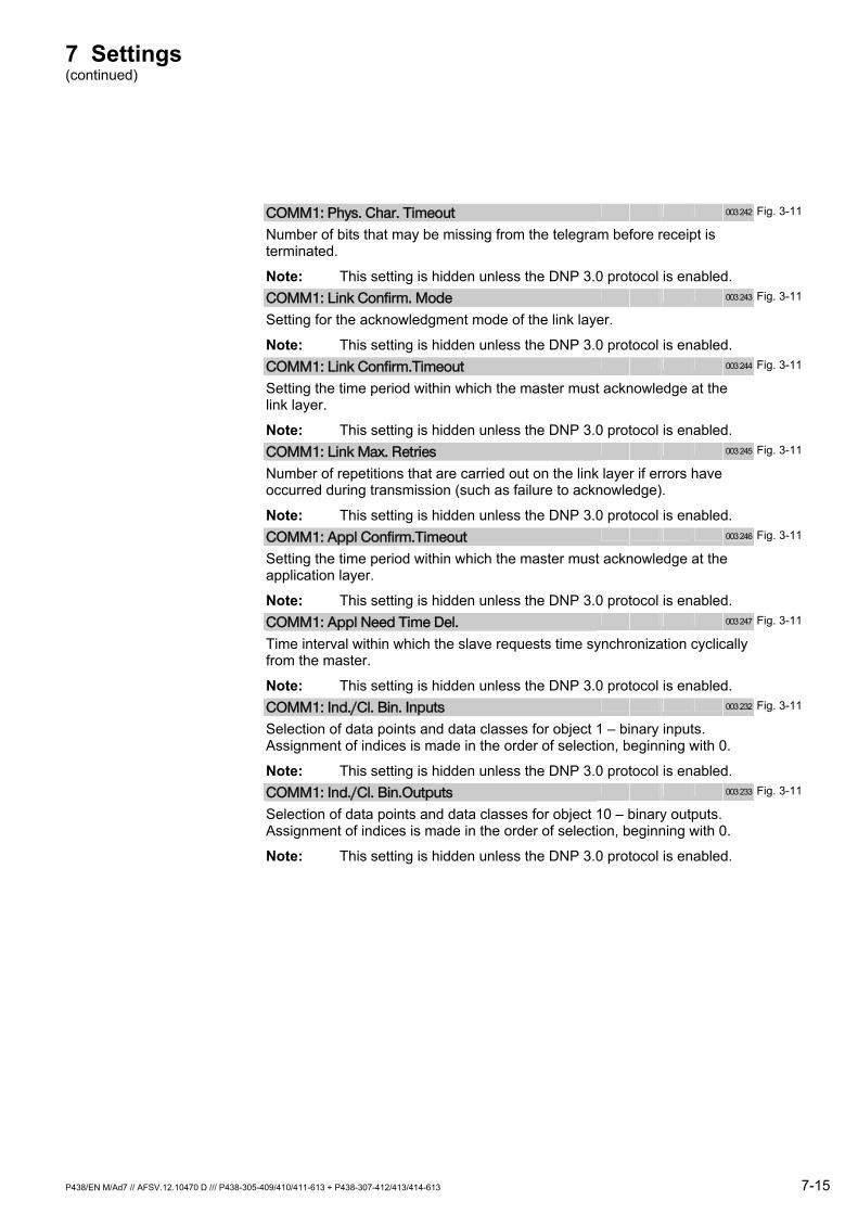
7 Settings (continued)
P438/EN M/Ad7 // AFSV.12.10470 D /// P438-305-409/410/411-613 + P438-307-412/413/414-613 7-15
COMM1: Phys. Char. Timeout 003 242 Fig. 3-11
Number of bits that may be missing from the telegram before receipt is terminated.
Note: This setting is hidden unless the DNP 3.0 protocol is enabled.
COMM1: Link Confirm. Mode 003 243 Fig. 3-11
Setting for the acknowledgment mode of the link layer.
Note: This setting is hidden unless the DNP 3.0 protocol is enabled.
COMM1: Link Confirm.Timeout 003 244 Fig. 3-11
Setting the time period within which the master must acknowledge at the link layer.
Note: This setting is hidden unless the DNP 3.0 protocol is enabled.
COMM1: Link Max. Retries 003 245 Fig. 3-11
Number of repetitions that are carried out on the link layer if errors have occurred during transmission (such as failure to acknowledge).
Note: This setting is hidden unless the DNP 3.0 protocol is enabled.
COMM1: Appl Confirm.Timeout 003 246 Fig. 3-11
Setting the time period within which the master must acknowledge at the application layer.
Note: This setting is hidden unless the DNP 3.0 protocol is enabled.
COMM1: Appl Need Time Del. 003 247 Fig. 3-11
Time interval within which the slave requests time synchronization cyclically from the master.
Note: This setting is hidden unless the DNP 3.0 protocol is enabled.
COMM1: Ind./Cl. Bin. Inputs 003 232 Fig. 3-11
Selection of data points and data classes for object 1 – binary inputs. Assignment of indices is made in the order of selection, beginning with 0.
Note: This setting is hidden unless the DNP 3.0 protocol is enabled.
COMM1: Ind./Cl. Bin.Outputs 003 233 Fig. 3-11
Selection of data points and data classes for object 10 – binary outputs. Assignment of indices is made in the order of selection, beginning with 0.
Note: This setting is hidden unless the DNP 3.0 protocol is enabled.
7 Settings (continued)
7-16 P438/EN M/Ad7 // AFSV.12.10470 D /// P438-305-409/410/411-613 + P438-307-412/413/414-613
COMM1: Ind./Cl. Analog Inp. 003 235 Fig. 3-11
Selection of data points and data classes for object 30 – analog inputs. Assignment of indices is made in the order of selection, beginning with 0.
Note: This setting is hidden unless the DNP 3.0 protocol is enabled.
COMM1: Ind./Cl. Analog Outp 003 236 Fig. 3-11
Selection of data points and data classes for object 40 – analog outputs. Assignment of indices is made in the order of selection, beginning with 0.
Note: This setting is hidden unless the DNP 3.0 protocol is enabled.
COMM1: Ph-Ph Meas V.(DNP3) 003 250 Fig. 3-11
Initialization value of threshold values for transmission of measured values in object 30. The threshold values can be changed separately by the master for each measured value by writing to object 34, 'analog input reporting dead band'.
Note: This setting is hidden unless the DNP 3.0 protocol is enabled.
COMM1: PhasePhase t (DNP3) 003 248 Fig. 3-11
Cycle time for updating DNP object 30 (analog inputs).
Note: This setting is hidden unless the DNP 3.0 protocol is enabled.
COMM1: Command Selection 103 042 Fig. 3-12
Selecting the commands that can be issued via the COURIER protocol.
Note: This setting is hidden unless the COURIER protocol is enabled.
COMM1: Signal Selection 103 043 Fig. 3-12
Selecting the signals that can be transmitted via the COURIER protocol.
Note: This setting is hidden unless the COURIER protocol is enabled.
COMM1: Meas. Val. Selection 103 044 Fig. 3-12
Selecting the measured values that can be transmitted via the COURIER protocol.
Note: This setting is hidden unless the COURIER protocol is enabled.
COMM1: Parameter Selection 103 045 Fig. 3-12
Selecting the settings that can be changed via the COURIER protocol.
Note: This setting is hidden unless the COURIER protocol is enabled.
COMM1: Delta t (COURIER) 103 046 Fig. 3-12
A selected measured value is re-transmitted after this cycle time period has elapsed.
Note: This setting is hidden unless the COURIER protocol is enabled.
7 Settings (continued)
P438/UK M/Ae7 // AFSV.12.11060 EN /// P438-305-409/410/411-615 + P438-307-412/413/414-615 7-17
Communication Interface 2 COMM2: Remote Comms Port2 056 057
Cancelling function group COMM2 or including it in the configuration. If the function group is cancelled from the configuration, then all associated settings and signals are hidden, with the exception of this setting.
COMM2: General Enable USER 103 170 Fig. 3-14
Enabling/disabling communication interface 2.
COMM2: Line Idle State 103 165 Fig. 3-14
Setting for the line idle state indication.
COMM2: Baud Rate 103 071 Fig. 3-14
Baud rate of the communication interface.
COMM2: Parity Bit 103 171 Fig. 3-14
Setting the same parity that is set at the interface of the control system connected to the P438.
COMM2: Dead Time Monitoring 103 176 Fig. 3-14
The P438 monitors telegram transmission to make sure that no excessive pause occurs within a telegram. This monitoring function can be disabled if it is not required.
Note: This setting is only necessary for modem transmission.
COMM2: Mon. Time Polling 103 202 Fig. 3-14
The time between two polling calls from the communication master must be less than the time set here.
COMM2: Positive Ackn. Fault 103 203
This parameter is used to set whether or not faults can be positively acknowledged after transmission (and consequently deleted from the fault overview at the COMM2/PC interface).
COMM2: Octet Comm. Address 103 072 Fig. 3-14
The communication address and the ASDU address are used to identify the device in communication via the interface. An identical setting must be selected for both addresses.
"ASDU": Application Service Data Unit
COMM2: Manufacturer 103 161 Fig. 3-14
Setting for the name of the manufacturer. This setting can be changed to any free text to ensure compatibility. The default value is SE. However, it can be necessary in special cases to set the value to something different.
Note: This parameter can be changed to any text of max. 8 characters length. Any longer text entered is truncated to 8 characters internally. However, changes can be carried out only via the operating program, not using the integrated local control panel.
COMM2: Octet Address ASDU 103 073 Fig. 3-14
The communication address and the ASDU address are used to identify the device in communication via the interface. An identical setting must be selected for both addresses.
"ASDU": Application Service Data Unit

7 Settings (continued)
7-18 P438/EN M/Ad7 // AFSV.12.10470 D /// P438-305-409/410/411-613 + P438-307-412/413/414-613
COMM2: Spontan. Sig. Enable 103 177 Fig. 3-14
Enable for the transmission of spontaneous signals via the communication interface.
COMM2: Select. Spontan.Sig. 103 179 Fig. 3-14
Selection of spontaneous signals for transmission via communication interface 2.
COMM2: Transm Enab Cycl Dat 103 074 Fig. 3-14
Enabling cyclic transmission of measured values via the communication interface.
COMM2: Cycl. Data ILS Tel. 103 175 Fig. 3-14
Selection of the measured values that are transmitted in a user-defined telegram via the communication interface.
COMM2: Delta V 103 050 Fig. 3-14
A measured voltage value is transmitted via the communication interface if it differs by the set delta quantity from the last measured value transmitted.
COMM2: Delta I 103 051 Fig. 3-14
A measured current value is transmitted via the communication interface if it differs by the set delta quantity from the last measured value transmitted.
COMM2: Delta P 103 054 Fig. 3-14
The active power value is transmitted via the communication interface if it differs by the set delta quantity from the last measured value transmitted.
COMM2: Delta f 103 052 Fig. 3-14
The measured frequency value is transmitted via the communication interface if it differs by the set delta quantity from the last measured value transmitted.
COMM2: Delta T 103 251 Fig. 3-14
The measured temperature is transmitted via the communication interface if it differs by more than the set delta quantity from the last measured value transmitted.
COMM2: Delta Z 103 252 Fig. 3-14
The measured operating impedance is transmitted via the communication interface if it differs by more than the set delta quantity from the last measured value transmitted.
COMM2: Delta phi 103 253 Fig. 3-14
The measured load angle is transmitted via the communication interface if it differs by more than the set delta quantity from the last measured value transmitted.
COMM2: Delta Meas.v.ILS Tel 103 150 Fig. 3-14
The telegram is transmitted if a measured value differs by the set delta quantity from the last measured value transmitted.
COMM2: Delta t 103 053 Fig. 3-14
All measured values are transmitted again via the communication interface after this time period has elapsed – provided that transmission has not been triggered by the other delta conditions.

7 Settings (continued)
P438/EN M/Ad7 // AFSV.12.10470 D /// P438-305-409/410/411-613 + P438-307-412/413/414-613 7-19
Communication Interface 3 COMM3: Function Group COMM3 056 058
Cancelling function group COMM3 or including it in the configuration.
This setting parameter is only visible if the relevant optional communication module is fitted.
If the function group is cancelled from the configuration, then all associated settings and signals are hidden, with the exception of this setting.
COMM3: General Enable USER 120 030
Enabling/disabling communication interface 3.
COMM3: Baud Rate 120 038
Adjustment of the baud rate for telegram transmission via the teleprotection interface (InterMiCOM interface) so as to meet the requirements of the transmission carrier.
COMM3: Source Address 120 031
Address for send signals.
COMM3: Receiving Address 120 032
Address for receive signals.
COMM3: Fct. Send 1 Assign 121 001
COMM3: Fct. Send 2 Assign 121 003
COMM3: Fct. Send 3 Assign 121 005
COMM3: Fct. Send 4 Assign 121 007
COMM3: Fct. Send 5 Assign 121 009
COMM3: Fct. Send 6 Assign 121 011
COMM3: Fct. Send 7 Assign 121 013
COMM3: Fct. Send 8 Assign 121 015
Assignment of functions for the 8 send signals.
COMM3: Fct. Rec. 1 Assign 120 001
COMM3: Fct. Rec. 2 Assign 120 004
COMM3: Fct. Rec. 3 Assign 120 007
COMM3: Fct. Rec. 4 Assign 120 010
COMM3: Fct. Rec. 5 Assign 120 013
COMM3: Fct. Rec. 6 Assign 120 016
COMM3: Fct. Rec. 7 Assign 120 019
COMM3: Fct. Rec. 8 Assign 120 022
Configuration (assignment of functions) for the 8 receive signals
COMM3: Oper. Mode Receive 1 120 002
COMM3: Oper. Mode Receive 2 120 005
COMM3: Oper. Mode Receive 3 120 008
COMM3: Oper. Mode Receive 4 120 011
Selection of 'Blocking' or 'Direct Intertrip' for the operating mode of receive signals 1 to 4 (single-bit transmission).
COMM3: Oper. Mode Receive 5 120 014
COMM3: Oper. Mode Receive 6 120 017
COMM3: Oper. Mode Receive 7 120 020
COMM3: Oper. Mode Receive 8 120 023
Selection of 'Permissive' or 'Direct Intertrip' for the operating mode of receive signals 5 to 8 (bit-pair transmission).
7 Settings (continued)
7-20 P438/EN M/Ad7 // AFSV.12.10470 D /// P438-305-409/410/411-613 + P438-307-412/413/414-613
COMM3: Default Value Rec. 1 120 060
COMM3: Default Value Rec. 2 120 061
COMM3: Default Value Rec. 3 120 062
COMM3: Default Value Rec. 4 120 063
COMM3: Default Value Rec. 5 120 064
COMM3: Default Value Rec. 6 120 065
COMM3: Default Value Rec. 7 120 066
COMM3: Default Value Rec. 8 120 067
Definition of the default value for the 8 receive signals.
COMM3: Time-Out Comm.Fault 120 033 Fig. 3-17
This timer triggers the C O M M 3 : C o m m u n i c a t i o n s F a u l t C H E C K : C o m m u n i c . F a u l t C O M M 3 alarm signals and sets the received signals to their user-defined default values. Time-out occurs when the set time has elapsed since the most recent 100% valid telegram was received.
COMM3: Time-Out Link Fail. 120 035 Fig. 3-17
Time indicating a persistent failure of the transmission channel. These signals are issued when the set time-delay has elapsed: C O M M 3 : C o m m . L i n k F a i l u r e and C H E C K : C o m m . L i n k F a i l . C O M M 3
COMM3: Limit Telegr. Errors 120 036
Percentage of corrupted messages compared to total messages transmitted before an alarm is raised: C O M M 3 : L i m . E x c e e d . , T e l . E r r . and C H E C K : L i m . E x c e e d . , T e l . E r r . When this threshold is exceeded, the receive signals are set to their user-defined default values.
IEC 61850 Communication IEC: IEC 61850 Communic. 056 059
Cancelling function group IEC or including it in the configuration. If the function group is cancelled from the configuration, then all associated settings and signals are hidden.
IEC: General Enable USER 104 000
Enabling and disabling function group IEC.
IEC: Enable Configuration 104 058
This parameter can only be sent individually. In order to maintain consistency of all parameters in function groups IEC, GSSE and GOOSE, they are only enabled mutually by this parameter. After this command is sent to the device, the actual state of the previously changed parameter setting of the three function groups is enabled in the communication data model of the connected device. This function is carried out automatically with the off-line/on-line switching of the device.
IEC: Ethernet Media 104 056
Selecting the physical communication channel on the Ethernet module from either wired (RJ45) or optical fiber (ST/SC connector depending on ordering option) connection.
IEC: IED Name 104 057
Name of the device (IED has server function). This device name serves as device identification in the IEC 61850 system, it is included in the Logical Device Name in the IEC data model and must therefore be unambiguous. All devices logged-on to the network should have non-recurring IED names.

7 Settings (continued)
P438/EN M/Ad7 // AFSV.12.10470 D /// P438-305-409/410/411-613 + P438-307-412/413/414-613 7-21
IEC: TCP Keep-Alive Timer 104 062
This defines a "heart-beat" time interval used to actively monitor a communication link to a logged-on client.
IEC: IP Address 104 001
IEC: IP Address 1 104 002
IEC: IP Address 2 104 003
IEC: IP Address 3 104 004
IP address for the device (IED has server function).
Note: The complete IP address is shown in the S&R-103 operating program at I E C : I P A d d r e s s . The device’s front panel display only shows the IP address distributed to these four data model addresses
IEC: Subnet Mask 104 005
IEC: Subnet Mask 1 104 006
IEC: Subnet Mask 2 104 007
IEC: Subnet Mask 3 104 008
The subnet mask defines which part of the IP address is addressed by the sub-network and which part by the device that is logged-on to the network.
Note: The complete IP address is shown in the S&R-103 operating program at I E C : S u b n e t M a s k . The device’s front panel display only shows the IP address distributed to these four data model addresses
IEC: Gateway Address 104 011
IEC: Gateway Address 1 104 012
IEC: Gateway Address 2 104 013
IEC: Gateway Address 3 104 014
This parameter defines the IPv4 address of the network gateway of a communication link to a client outside of the local network.
Note: The complete IP address is shown in the S&R-103 operating program at I E C : G a t e w a y A d d r e s s . The device’s front panel display only shows the IP address distributed to these four data model addresses
IEC: SNTP Operating Mode 104 200
Operating mode for the time synchronization telegram. When set to Broadcast, synchronization occurs cyclically with the clock server transmitting a broadcast signal and, when set to Request from Server, each device (IED has client function) individually requests a synchronization signal after its own cycle time.
IEC: SNTP Poll Cycle Time 104 201
Device (IED) poll cycle time for time synchronization when the operating mode is set to Request from Server.
IEC: SNTP Server 1 IP 104 202
IEC: SNTP Server 1 IP 1 104 203
IEC: SNTP Server 1 IP 2 104 204
IEC: SNTP Server 1 IP 3 104 205
IP address of the synchronizing clock server.
Note: The complete IP address is shown in the S&R-103 operating program at I E C : S N T P S e r v e r 1 I P . The device’s front panel display only shows the IP address distributed to these four data model addresses
7 Settings (continued)
7-22 P438/EN M/Ad7 // AFSV.12.10470 D /// P438-305-409/410/411-613 + P438-307-412/413/414-613
IEC: SNTP Server 2 IP 104 210
IEC: SNTP Server 2 IP 1 104 211
IEC: SNTP Server 2 IP 2 104 212
IEC: SNTP Server 2 IP 3 104 213
IP address of the synchronizing clock server.
Note: The complete IP address is shown in the S&R-103 operating program at I E C : S N T P S e r v e r 2 I P . The device’s front panel display only shows the IP address distributed to these four data model addresses
IEC: Diff. Local Time 104 206
Time difference between UTC and local time at the devices' substation (IED).
IEC: Diff. Dayl.Sav. Time 104 207
Time difference when changing to daylight saving time.
IEC: Switch.Dayl.Sav.Time 104 219
This setting defines whether an automatic switching to daylight saving time is wanted.
IEC: Dayl.Sav.Time Start 104 220
IEC: Dayl.Sav.Time St. d 104 221
IEC: Dayl.Sav.Time St. m 104 222
These three parameters define the date (e.g. at what day of the year) for switching from standard time over to daylight saving time. Available for I E C : D a y l . S a v . T i m e S t a r t are the values "first", "second", "third", "fourth", and "last"; for I E C : D a y l . S a v . T i m e S t . d the seven weekdays are available so that for example a setting like "on the last Sunday in March" may be used.
IEC: Dayl.Sav.t.St.0:00 + 104 223
This defines the time difference and the time of day (on the specific changeover day) when the clock is to be switched to daylight saving time. The time is given in the number of minutes after midnight, e.g. when the clock changeover to 3:00 AM always occurs at 2:00 AM, then the value to be entered at I E C : D a y l . S a v . t . S t . 0 : 0 0 + is 120 [minutes] and at I E C : D i f f . D a y l . S a v . T i m e it is 60 [minutes].
IEC: Dayl.Sav.Time End 104 225
IEC: Dayl.Sav.Time End d 104 226
IEC: Dayl.Sav.Time End m 104 227
IEC: Dayl.Sav.t.End 0:00+ 104 228
This parameter defines the date and time of day for the clock changeover from daylight saving time to standard time. The setting is similar to that for the clock changeover to daylight saving time.
IEC: Update Measurements 104 229
Time period between two transmissions of all measured value Report Control Blocks (RCB) except the measured value for energy.
IEC: Dead Band IP 104 230
Setting to calculate the filter value for all IP Report Control Blocks (RCB). Should a change occur in one of the IP measured values, which is greater than the filter value, the RCB is again sent to all clients. The filter value for each measured value is calculated according to this formula: step size measured value • setting I E C : D e a d B a n d I P
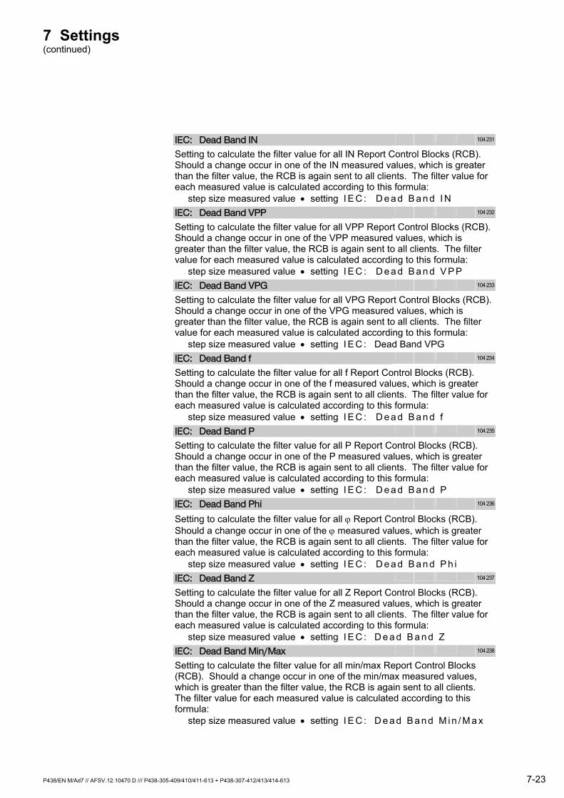
7 Settings (continued)
P438/EN M/Ad7 // AFSV.12.10470 D /// P438-305-409/410/411-613 + P438-307-412/413/414-613 7-23
IEC: Dead Band IN 104 231
Setting to calculate the filter value for all IN Report Control Blocks (RCB). Should a change occur in one of the IN measured values, which is greater than the filter value, the RCB is again sent to all clients. The filter value for each measured value is calculated according to this formula: step size measured value • setting I E C : D e a d B a n d I N
IEC: Dead Band VPP 104 232
Setting to calculate the filter value for all VPP Report Control Blocks (RCB). Should a change occur in one of the VPP measured values, which is greater than the filter value, the RCB is again sent to all clients. The filter value for each measured value is calculated according to this formula: step size measured value • setting I E C : D e a d B a n d V P P
IEC: Dead Band VPG 104 233
Setting to calculate the filter value for all VPG Report Control Blocks (RCB). Should a change occur in one of the VPG measured values, which is greater than the filter value, the RCB is again sent to all clients. The filter value for each measured value is calculated according to this formula: step size measured value • setting I E C : Dead Band VPG
IEC: Dead Band f 104 234
Setting to calculate the filter value for all f Report Control Blocks (RCB). Should a change occur in one of the f measured values, which is greater than the filter value, the RCB is again sent to all clients. The filter value for each measured value is calculated according to this formula: step size measured value • setting I E C : D e a d B a n d f
IEC: Dead Band P 104 235
Setting to calculate the filter value for all P Report Control Blocks (RCB). Should a change occur in one of the P measured values, which is greater than the filter value, the RCB is again sent to all clients. The filter value for each measured value is calculated according to this formula: step size measured value • setting I E C : D e a d B a n d P
IEC: Dead Band Phi 104 236
Setting to calculate the filter value for all ϕ Report Control Blocks (RCB). Should a change occur in one of the ϕ measured values, which is greater than the filter value, the RCB is again sent to all clients. The filter value for each measured value is calculated according to this formula: step size measured value • setting I E C : D e a d B a n d P h i
IEC: Dead Band Z 104 237
Setting to calculate the filter value for all Z Report Control Blocks (RCB). Should a change occur in one of the Z measured values, which is greater than the filter value, the RCB is again sent to all clients. The filter value for each measured value is calculated according to this formula: step size measured value • setting I E C : D e a d B a n d Z
IEC: Dead Band Min/Max 104 238
Setting to calculate the filter value for all min/max Report Control Blocks (RCB). Should a change occur in one of the min/max measured values, which is greater than the filter value, the RCB is again sent to all clients. The filter value for each measured value is calculated according to this formula: step size measured value • setting I E C : D e a d B a n d M i n / M a x
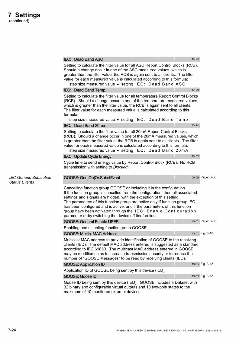
7 Settings (continued)
7-24 P438/EN M/Ad7 // AFSV.12.10470 D /// P438-305-409/410/411-613 + P438-307-412/413/414-613
IEC: Dead Band ASC 104 239
Setting to calculate the filter value for all ASC Report Control Blocks (RCB). Should a change occur in one of the ASC measured values, which is greater than the filter value, the RCB is again sent to all clients. The filter value for each measured value is calculated according to this formula: step size measured value • setting I E C : D e a d B a n d A S C
IEC: Dead Band Temp. 104 240
Setting to calculate the filter value for all temperature Report Control Blocks (RCB). Should a change occur in one of the temperature measured values, which is greater than the filter value, the RCB is again sent to all clients. The filter value for each measured value is calculated according to this formula: step size measured value • setting I E C : D e a d B a n d T e m p .
IEC: Dead Band 20ma 104 241
Setting to calculate the filter value for all 20mA Report Control Blocks (RCB). Should a change occur in one of the 20mA measured values, which is greater than the filter value, the RCB is again sent to all clients. The filter value for each measured value is calculated according to this formula: step size measured value • setting I E C : D e a d B a n d 2 0 m A
IEC: Update Cycle Energy 104 060
Cycle time to send energy value by Report Control Block (RCB). No RCB transmission with setting to Blocked!
IEC Generic Substation Status Events
GOOSE: Gen.ObjOr.SubstEvent 056 068 Page: 3-30
Cancelling function group GOOSE or including it in the configuration. If the function group is cancelled from the configuration, then all associated settings and signals are hidden, with the exception of this setting. The parameters of this function group are active only if function group IEC has been configured and is active, and if the parameters of this function group have been activated through the I E C : E n a b l e C o n f i g u r a t i o n parameter or by switching the device off-line/on-line.
GOOSE: General Enable USER 106 001 Page: 3-30
Enabling and disabling function group GOOSE.
GOOSE: Multic. MAC Address 106 003 Fig. 3-18
Multicast MAC address to provide identification of GOOSE to the receiving clients (IED). The default MAC address entered is suggested as a standard according to IEC 61850. The multicast MAC address entered in GOOSE may be modified so as to increase transmission security or to reduce the number of "GOOSE Messages" to be read by receiving clients (IED).
GOOSE: Application ID 106 004 Fig. 3-18
Application ID of GOOSE being sent by this device (IED).
GOOSE: Goose ID 106 002 Fig. 3-18
Goose ID being sent by this device (IED). GOOSE includes a Dataset with 32 binary and configurable virtual outputs and 10 two-pole states to the maximum of 10 monitored external devices
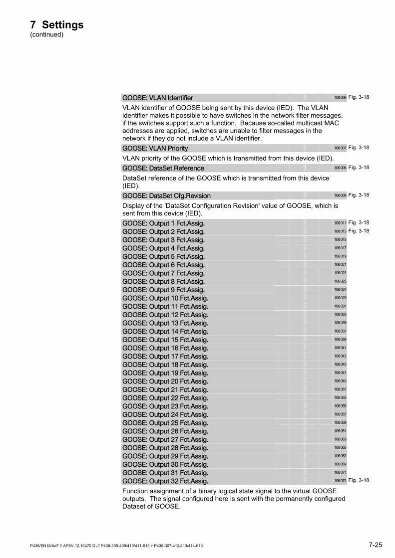
7 Settings (continued)
P438/EN M/Ad7 // AFSV.12.10470 D /// P438-305-409/410/411-613 + P438-307-412/413/414-613 7-25
GOOSE: VLAN Identifier 106 006 Fig. 3-18
VLAN identifier of GOOSE being sent by this device (IED). The VLAN identifier makes it possible to have switches in the network filter messages, if the switches support such a function. Because so-called multicast MAC addresses are applied, switches are unable to filter messages in the network if they do not include a VLAN identifier.
GOOSE: VLAN Priority 106 007 Fig. 3-18
VLAN priority of the GOOSE which is transmitted from this device (IED).
GOOSE: DataSet Reference 106 008 Fig. 3-18
DataSet reference of the GOOSE which is transmitted from this device (IED).
GOOSE: DataSet Cfg.Revision 106 009 Fig. 3-18
Display of the 'DataSet Configuration Revision' value of GOOSE, which is sent from this device (IED).
GOOSE: Output 1 Fct.Assig. 106 011 Fig. 3-18
GOOSE: Output 2 Fct.Assig. 106 013 Fig. 3-18
GOOSE: Output 3 Fct.Assig. 106 015
GOOSE: Output 4 Fct.Assig. 106 017
GOOSE: Output 5 Fct.Assig. 106 019
GOOSE: Output 6 Fct.Assig. 106 021
GOOSE: Output 7 Fct.Assig. 106 023
GOOSE: Output 8 Fct.Assig. 106 025
GOOSE: Output 9 Fct.Assig. 106 027
GOOSE: Output 10 Fct.Assig. 106 029
GOOSE: Output 11 Fct.Assig. 106 031
GOOSE: Output 12 Fct.Assig. 106 033
GOOSE: Output 13 Fct.Assig. 106 035
GOOSE: Output 14 Fct.Assig. 106 037
GOOSE: Output 15 Fct.Assig. 106 039
GOOSE: Output 16 Fct.Assig. 106 041
GOOSE: Output 17 Fct.Assig. 106 043
GOOSE: Output 18 Fct.Assig. 106 045
GOOSE: Output 19 Fct.Assig. 106 047
GOOSE: Output 20 Fct.Assig. 106 049
GOOSE: Output 21 Fct.Assig. 106 051
GOOSE: Output 22 Fct.Assig. 106 053
GOOSE: Output 23 Fct.Assig. 106 055
GOOSE: Output 24 Fct.Assig. 106 057
GOOSE: Output 25 Fct.Assig. 106 059
GOOSE: Output 26 Fct.Assig. 106 061
GOOSE: Output 27 Fct.Assig. 106 063
GOOSE: Output 28 Fct.Assig. 106 065
GOOSE: Output 29 Fct.Assig. 106 067
GOOSE: Output 30 Fct.Assig. 106 069
GOOSE: Output 31 Fct.Assig. 106 071
GOOSE: Output 32 Fct.Assig. 106 073 Fig. 3-18
Function assignment of a binary logical state signal to the virtual GOOSE outputs. The signal configured here is sent with the permanently configured Dataset of GOOSE.
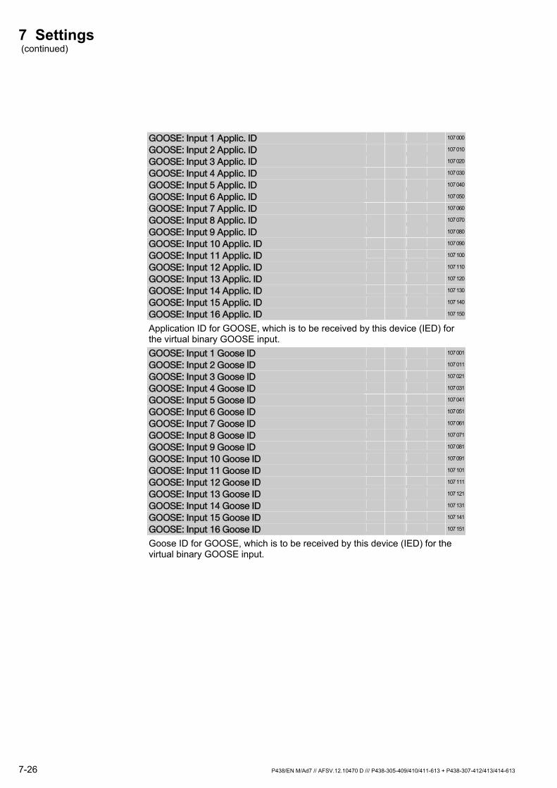
7 Settings (continued)
7-26 P438/EN M/Ad7 // AFSV.12.10470 D /// P438-305-409/410/411-613 + P438-307-412/413/414-613
GOOSE: Input 1 Applic. ID 107 000
GOOSE: Input 2 Applic. ID 107 010
GOOSE: Input 3 Applic. ID 107 020
GOOSE: Input 4 Applic. ID 107 030
GOOSE: Input 5 Applic. ID 107 040
GOOSE: Input 6 Applic. ID 107 050
GOOSE: Input 7 Applic. ID 107 060
GOOSE: Input 8 Applic. ID 107 070
GOOSE: Input 9 Applic. ID 107 080
GOOSE: Input 10 Applic. ID 107 090
GOOSE: Input 11 Applic. ID 107 100
GOOSE: Input 12 Applic. ID 107 110
GOOSE: Input 13 Applic. ID 107 120
GOOSE: Input 14 Applic. ID 107 130
GOOSE: Input 15 Applic. ID 107 140
GOOSE: Input 16 Applic. ID 107 150
Application ID for GOOSE, which is to be received by this device (IED) for the virtual binary GOOSE input.
GOOSE: Input 1 Goose ID 107 001
GOOSE: Input 2 Goose ID 107 011
GOOSE: Input 3 Goose ID 107 021
GOOSE: Input 4 Goose ID 107 031
GOOSE: Input 5 Goose ID 107 041
GOOSE: Input 6 Goose ID 107 051
GOOSE: Input 7 Goose ID 107 061
GOOSE: Input 8 Goose ID 107 071
GOOSE: Input 9 Goose ID 107 081
GOOSE: Input 10 Goose ID 107 091
GOOSE: Input 11 Goose ID 107 101
GOOSE: Input 12 Goose ID 107 111
GOOSE: Input 13 Goose ID 107 121
GOOSE: Input 14 Goose ID 107 131
GOOSE: Input 15 Goose ID 107 141
GOOSE: Input 16 Goose ID 107 151
Goose ID for GOOSE, which is to be received by this device (IED) for the virtual binary GOOSE input.
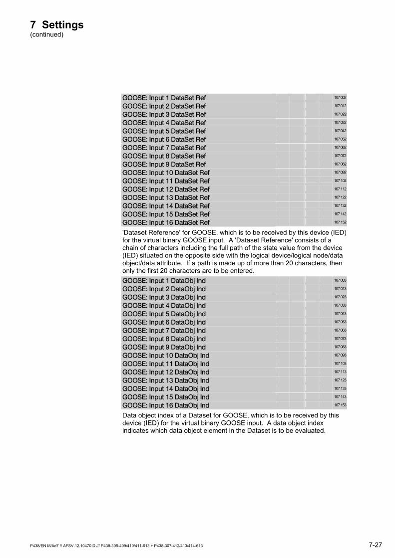
7 Settings (continued)
P438/EN M/Ad7 // AFSV.12.10470 D /// P438-305-409/410/411-613 + P438-307-412/413/414-613 7-27
GOOSE: Input 1 DataSet Ref 107 002
GOOSE: Input 2 DataSet Ref 107 012
GOOSE: Input 3 DataSet Ref 107 022
GOOSE: Input 4 DataSet Ref 107 032
GOOSE: Input 5 DataSet Ref 107 042
GOOSE: Input 6 DataSet Ref 107 052
GOOSE: Input 7 DataSet Ref 107 062
GOOSE: Input 8 DataSet Ref 107 072
GOOSE: Input 9 DataSet Ref 107 082
GOOSE: Input 10 DataSet Ref 107 092
GOOSE: Input 11 DataSet Ref 107 102
GOOSE: Input 12 DataSet Ref 107 112
GOOSE: Input 13 DataSet Ref 107 122
GOOSE: Input 14 DataSet Ref 107 132
GOOSE: Input 15 DataSet Ref 107 142
GOOSE: Input 16 DataSet Ref 107 152
'Dataset Reference' for GOOSE, which is to be received by this device (IED) for the virtual binary GOOSE input. A 'Dataset Reference' consists of a chain of characters including the full path of the state value from the device (IED) situated on the opposite side with the logical device/logical node/data object/data attribute. If a path is made up of more than 20 characters, then only the first 20 characters are to be entered.
GOOSE: Input 1 DataObj Ind 107 003
GOOSE: Input 2 DataObj Ind 107 013
GOOSE: Input 3 DataObj Ind 107 023
GOOSE: Input 4 DataObj Ind 107 033
GOOSE: Input 5 DataObj Ind 107 043
GOOSE: Input 6 DataObj Ind 107 053
GOOSE: Input 7 DataObj Ind 107 063
GOOSE: Input 8 DataObj Ind 107 073
GOOSE: Input 9 DataObj Ind 107 083
GOOSE: Input 10 DataObj Ind 107 093
GOOSE: Input 11 DataObj Ind 107 103
GOOSE: Input 12 DataObj Ind 107 113
GOOSE: Input 13 DataObj Ind 107 123
GOOSE: Input 14 DataObj Ind 107 133
GOOSE: Input 15 DataObj Ind 107 143
GOOSE: Input 16 DataObj Ind 107 153
Data object index of a Dataset for GOOSE, which is to be received by this device (IED) for the virtual binary GOOSE input. A data object index indicates which data object element in the Dataset is to be evaluated.
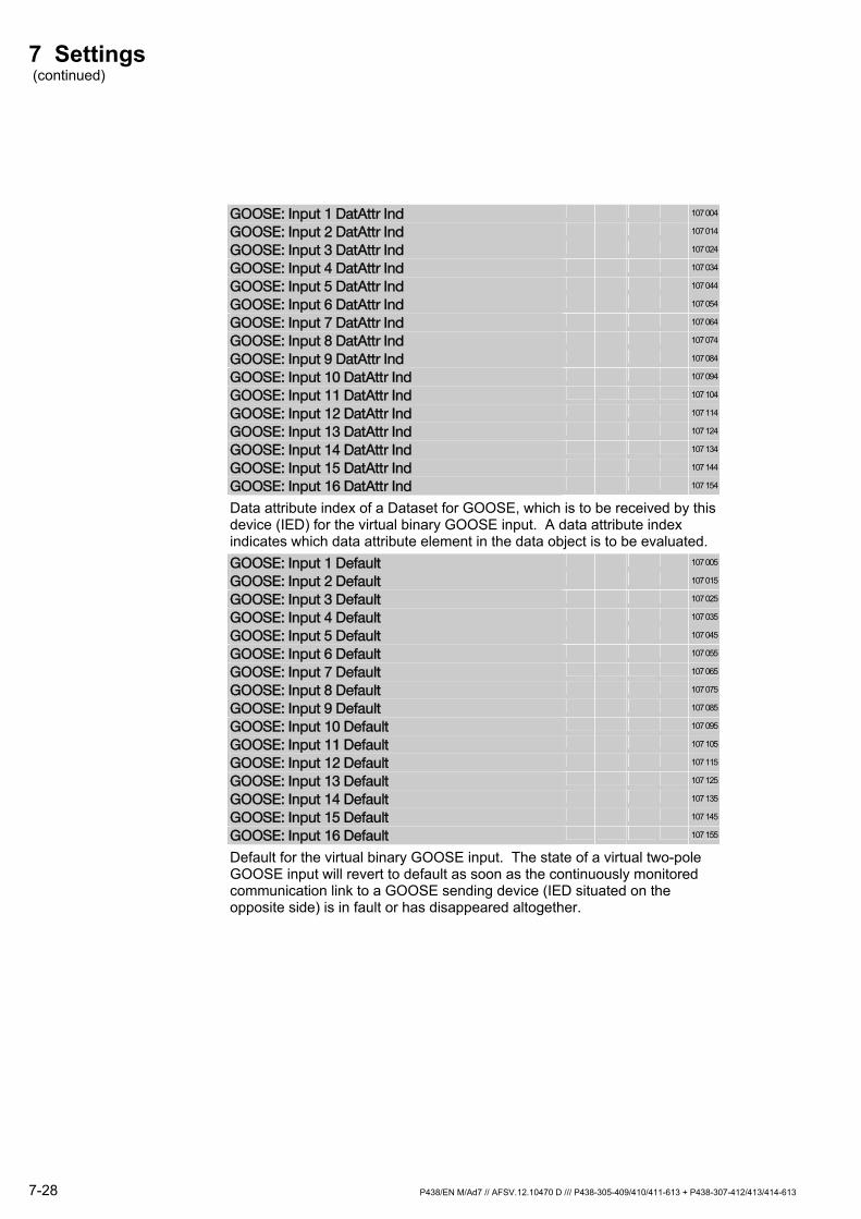
7 Settings (continued)
7-28 P438/EN M/Ad7 // AFSV.12.10470 D /// P438-305-409/410/411-613 + P438-307-412/413/414-613
GOOSE: Input 1 DatAttr Ind 107 004
GOOSE: Input 2 DatAttr Ind 107 014
GOOSE: Input 3 DatAttr Ind 107 024
GOOSE: Input 4 DatAttr Ind 107 034
GOOSE: Input 5 DatAttr Ind 107 044
GOOSE: Input 6 DatAttr Ind 107 054
GOOSE: Input 7 DatAttr Ind 107 064
GOOSE: Input 8 DatAttr Ind 107 074
GOOSE: Input 9 DatAttr Ind 107 084
GOOSE: Input 10 DatAttr Ind 107 094
GOOSE: Input 11 DatAttr Ind 107 104
GOOSE: Input 12 DatAttr Ind 107 114
GOOSE: Input 13 DatAttr Ind 107 124
GOOSE: Input 14 DatAttr Ind 107 134
GOOSE: Input 15 DatAttr Ind 107 144
GOOSE: Input 16 DatAttr Ind 107 154
Data attribute index of a Dataset for GOOSE, which is to be received by this device (IED) for the virtual binary GOOSE input. A data attribute index indicates which data attribute element in the data object is to be evaluated.
GOOSE: Input 1 Default 107 005
GOOSE: Input 2 Default 107 015
GOOSE: Input 3 Default 107 025
GOOSE: Input 4 Default 107 035
GOOSE: Input 5 Default 107 045
GOOSE: Input 6 Default 107 055
GOOSE: Input 7 Default 107 065
GOOSE: Input 8 Default 107 075
GOOSE: Input 9 Default 107 085
GOOSE: Input 10 Default 107 095
GOOSE: Input 11 Default 107 105
GOOSE: Input 12 Default 107 115
GOOSE: Input 13 Default 107 125
GOOSE: Input 14 Default 107 135
GOOSE: Input 15 Default 107 145
GOOSE: Input 16 Default 107 155
Default for the virtual binary GOOSE input. The state of a virtual two-pole GOOSE input will revert to default as soon as the continuously monitored communication link to a GOOSE sending device (IED situated on the opposite side) is in fault or has disappeared altogether.
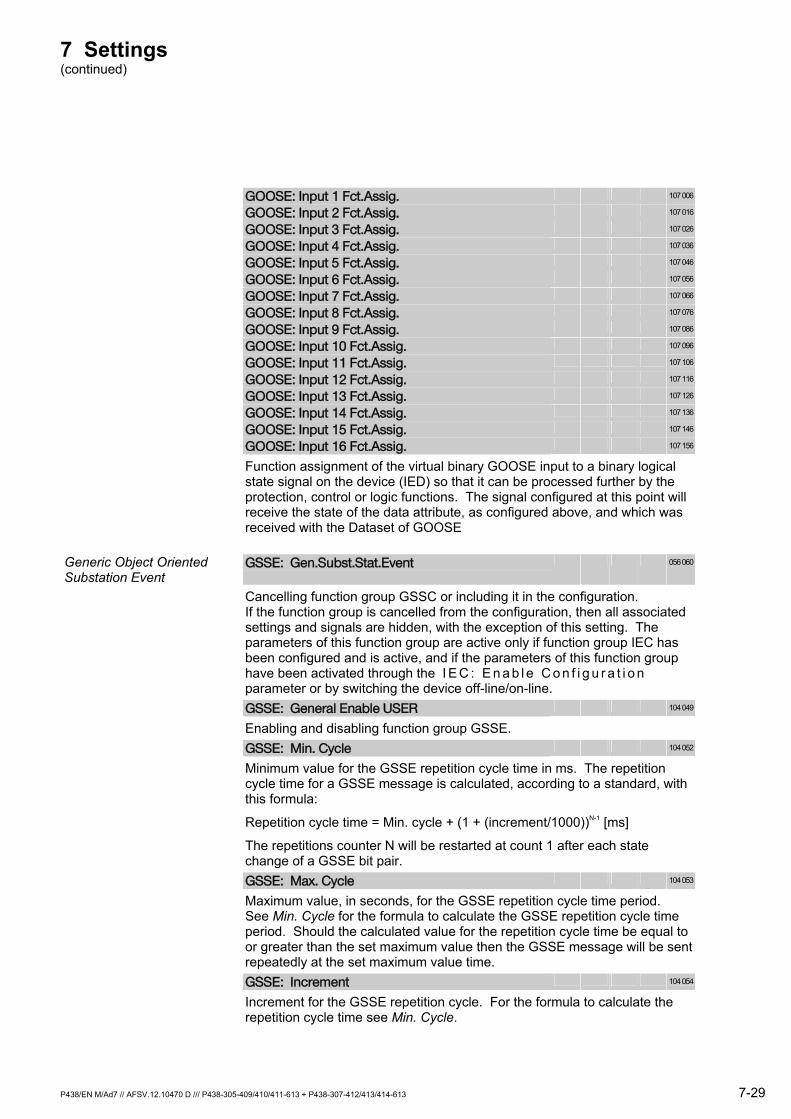
7 Settings (continued)
P438/EN M/Ad7 // AFSV.12.10470 D /// P438-305-409/410/411-613 + P438-307-412/413/414-613 7-29
GOOSE: Input 1 Fct.Assig. 107 006
GOOSE: Input 2 Fct.Assig. 107 016
GOOSE: Input 3 Fct.Assig. 107 026
GOOSE: Input 4 Fct.Assig. 107 036
GOOSE: Input 5 Fct.Assig. 107 046
GOOSE: Input 6 Fct.Assig. 107 056
GOOSE: Input 7 Fct.Assig. 107 066
GOOSE: Input 8 Fct.Assig. 107 076
GOOSE: Input 9 Fct.Assig. 107 086
GOOSE: Input 10 Fct.Assig. 107 096
GOOSE: Input 11 Fct.Assig. 107 106
GOOSE: Input 12 Fct.Assig. 107 116
GOOSE: Input 13 Fct.Assig. 107 126
GOOSE: Input 14 Fct.Assig. 107 136
GOOSE: Input 15 Fct.Assig. 107 146
GOOSE: Input 16 Fct.Assig. 107 156
Function assignment of the virtual binary GOOSE input to a binary logical state signal on the device (IED) so that it can be processed further by the protection, control or logic functions. The signal configured at this point will receive the state of the data attribute, as configured above, and which was received with the Dataset of GOOSE
Generic Object Oriented Substation Event
GSSE: Gen.Subst.Stat.Event 056 060
Cancelling function group GSSC or including it in the configuration. If the function group is cancelled from the configuration, then all associated settings and signals are hidden, with the exception of this setting. The parameters of this function group are active only if function group IEC has been configured and is active, and if the parameters of this function group have been activated through the I E C : E n a b l e C o n f i g u r a t i o n parameter or by switching the device off-line/on-line.
GSSE: General Enable USER 104 049
Enabling and disabling function group GSSE.
GSSE: Min. Cycle 104 052
Minimum value for the GSSE repetition cycle time in ms. The repetition cycle time for a GSSE message is calculated, according to a standard, with this formula:
Repetition cycle time = Min. cycle + (1 + (increment/1000))N-1 [ms]
The repetitions counter N will be restarted at count 1 after each state change of a GSSE bit pair.
GSSE: Max. Cycle 104 053
Maximum value, in seconds, for the GSSE repetition cycle time period. See Min. Cycle for the formula to calculate the GSSE repetition cycle time period. Should the calculated value for the repetition cycle time be equal to or greater than the set maximum value then the GSSE message will be sent repeatedly at the set maximum value time.
GSSE: Increment 104 054
Increment for the GSSE repetition cycle. For the formula to calculate the repetition cycle time see Min. Cycle.
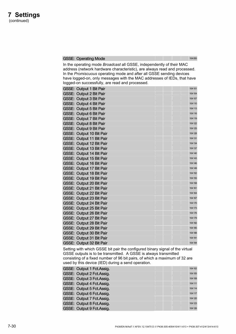
7 Settings (continued)
7-30 P438/EN M/Ad7 // AFSV.12.10470 D /// P438-305-409/410/411-613 + P438-307-412/413/414-613
GSSE: Operating Mode 104 055
In the operating mode Broadcast all GSSE, independently of their MAC address (network hardware characteristic), are always read and processed. In the Promiscuous operating mode and after all GSSE sending devices have logged-on, only messages with the MAC addresses of IEDs, that have logged-on successfully, are read and processed.
GSSE: Output 1 Bit Pair 104 101
GSSE: Output 2 Bit Pair 104 104
GSSE: Output 3 Bit Pair 104 107
GSSE: Output 4 Bit Pair 104 110
GSSE: Output 5 Bit Pair 104 113
GSSE: Output 6 Bit Pair 104 116
GSSE: Output 7 Bit Pair 104 119
GSSE: Output 8 Bit Pair 104 122
GSSE: Output 9 Bit Pair 104 125
GSSE: Output 10 Bit Pair 104 128
GSSE: Output 11 Bit Pair 104 131
GSSE: Output 12 Bit Pair 104 134
GSSE: Output 13 Bit Pair 104 137
GSSE: Output 14 Bit Pair 104 140
GSSE: Output 15 Bit Pair 104 143
GSSE: Output 16 Bit Pair 104 146
GSSE: Output 17 Bit Pair 104 149
GSSE: Output 18 Bit Pair 104 152
GSSE: Output 19 Bit Pair 104 155
GSSE: Output 20 Bit Pair 104 158
GSSE: Output 21 Bit Pair 104 161
GSSE: Output 22 Bit Pair 104 164
GSSE: Output 23 Bit Pair 104 167
GSSE: Output 24 Bit Pair 104 170
GSSE: Output 25 Bit Pair 104 173
GSSE: Output 26 Bit Pair 104 176
GSSE: Output 27 Bit Pair 104 179
GSSE: Output 28 Bit Pair 104 182
GSSE: Output 29 Bit Pair 104 185
GSSE: Output 30 Bit Pair 104 188
GSSE: Output 31 Bit Pair 104 191
GSSE: Output 32 Bit Pair 104 194
Setting with which GSSE bit pair the configured binary signal of the virtual GSSE outputs is to be transmitted. A GSSE is always transmitted consisting of a fixed number of 96 bit pairs, of which a maximum of 32 are used by this device (IED) during a send operation.
GSSE: Output 1 Fct.Assig. 104 102
GSSE: Output 2 Fct.Assig. 104 105
GSSE: Output 3 Fct.Assig. 104 108
GSSE: Output 4 Fct.Assig. 104 111
GSSE: Output 5 Fct.Assig. 104 114
GSSE: Output 6 Fct.Assig. 104 117
GSSE: Output 7 Fct.Assig. 104 120
GSSE: Output 8 Fct.Assig. 104 123
GSSE: Output 9 Fct.Assig. 104 126
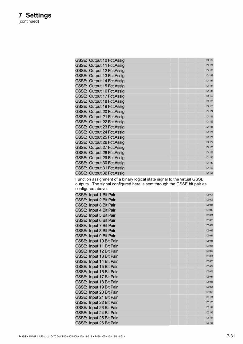
7 Settings (continued)
P438/EN M/Ad7 // AFSV.12.10470 D /// P438-305-409/410/411-613 + P438-307-412/413/414-613 7-31
GSSE: Output 10 Fct.Assig. 104 129
GSSE: Output 11 Fct.Assig. 104 132
GSSE: Output 12 Fct.Assig. 104 135
GSSE: Output 13 Fct.Assig. 104 138
GSSE: Output 14 Fct.Assig. 104 141
GSSE: Output 15 Fct.Assig. 104 144
GSSE: Output 16 Fct.Assig. 104 147
GSSE: Output 17 Fct.Assig. 104 150
GSSE: Output 18 Fct.Assig. 104 153
GSSE: Output 19 Fct.Assig. 104 156
GSSE: Output 20 Fct.Assig. 104 159
GSSE: Output 21 Fct.Assig. 104 162
GSSE: Output 22 Fct.Assig. 104 165
GSSE: Output 23 Fct.Assig. 104 168
GSSE: Output 24 Fct.Assig. 104 171
GSSE: Output 25 Fct.Assig. 104 174
GSSE: Output 26 Fct.Assig. 104 177
GSSE: Output 27 Fct.Assig. 104 180
GSSE: Output 28 Fct.Assig. 104 183
GSSE: Output 29 Fct.Assig. 104 186
GSSE: Output 30 Fct.Assig. 104 189
GSSE: Output 31 Fct.Assig. 104 192
GSSE: Output 32 Fct.Assig. 104 195
Function assignment of a binary logical state signal to the virtual GSSE outputs. The signal configured here is sent through the GSSE bit pair as configured above.
GSSE: Input 1 Bit Pair 105 001
GSSE: Input 2 Bit Pair 105 006
GSSE: Input 3 Bit Pair 105 011
GSSE: Input 4 Bit Pair 105 016
GSSE: Input 5 Bit Pair 105 021
GSSE: Input 6 Bit Pair 105 026
GSSE: Input 7 Bit Pair 105 031
GSSE: Input 8 Bit Pair 105 036
GSSE: Input 9 Bit Pair 105 041
GSSE: Input 10 Bit Pair 105 046
GSSE: Input 11 Bit Pair 105 051
GSSE: Input 12 Bit Pair 105 056
GSSE: Input 13 Bit Pair 105 061
GSSE: Input 14 Bit Pair 105 066
GSSE: Input 15 Bit Pair 105 071
GSSE: Input 16 Bit Pair 105 076
GSSE: Input 17 Bit Pair 105 081
GSSE: Input 18 Bit Pair 105 086
GSSE: Input 19 Bit Pair 105 091
GSSE: Input 20 Bit Pair 105 096
GSSE: Input 21 Bit Pair 105 101
GSSE: Input 22 Bit Pair 105 106
GSSE: Input 23 Bit Pair 105 111
GSSE: Input 24 Bit Pair 105 116
GSSE: Input 25 Bit Pair 105 121
GSSE: Input 26 Bit Pair 105 126
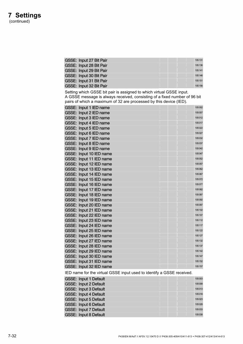
7 Settings (continued)
7-32 P438/EN M/Ad7 // AFSV.12.10470 D /// P438-305-409/410/411-613 + P438-307-412/413/414-613
GSSE: Input 27 Bit Pair 105 131
GSSE: Input 28 Bit Pair 105 136
GSSE: Input 29 Bit Pair 105 141
GSSE: Input 30 Bit Pair 105 146
GSSE: Input 31 Bit Pair 105 151
GSSE: Input 32 Bit Pair 105 156
Setting which GSSE bit pair is assigned to which virtual GSSE input. A GSSE message is always received, consisting of a fixed number of 96 bit pairs of which a maximum of 32 are processed by this device (IED).
GSSE: Input 1 IED name 105 002
GSSE: Input 2 IED name 105 007
GSSE: Input 3 IED name 105 012
GSSE: Input 4 IED name 105 017
GSSE: Input 5 IED name 105 022
GSSE: Input 6 IED name 105 027
GSSE: Input 7 IED name 105 032
GSSE: Input 8 IED name 105 037
GSSE: Input 9 IED name 105 042
GSSE: Input 10 IED name 105 047
GSSE: Input 11 IED name 105 052
GSSE: Input 12 IED name 105 057
GSSE: Input 13 IED name 105 062
GSSE: Input 14 IED name 105 067
GSSE: Input 15 IED name 105 072
GSSE: Input 16 IED name 105 077
GSSE: Input 17 IED name 105 082
GSSE: Input 18 IED name 105 087
GSSE: Input 19 IED name 105 092
GSSE: Input 20 IED name 105 097
GSSE: Input 21 IED name 105 102
GSSE: Input 22 IED name 105 107
GSSE: Input 23 IED name 105 112
GSSE: Input 24 IED name 105 117
GSSE: Input 25 IED name 105 122
GSSE: Input 26 IED name 105 127
GSSE: Input 27 IED name 105 132
GSSE: Input 28 IED name 105 137
GSSE: Input 29 IED name 105 142
GSSE: Input 30 IED name 105 147
GSSE: Input 31 IED name 105 152
GSSE: Input 32 IED name 105 157
IED name for the virtual GSSE input used to identify a GSSE received.
GSSE: Input 1 Default 105 003
GSSE: Input 2 Default 105 008
GSSE: Input 3 Default 105 013
GSSE: Input 4 Default 105 018
GSSE: Input 5 Default 105 023
GSSE: Input 6 Default 105 028
GSSE: Input 7 Default 105 033
GSSE: Input 8 Default 105 038
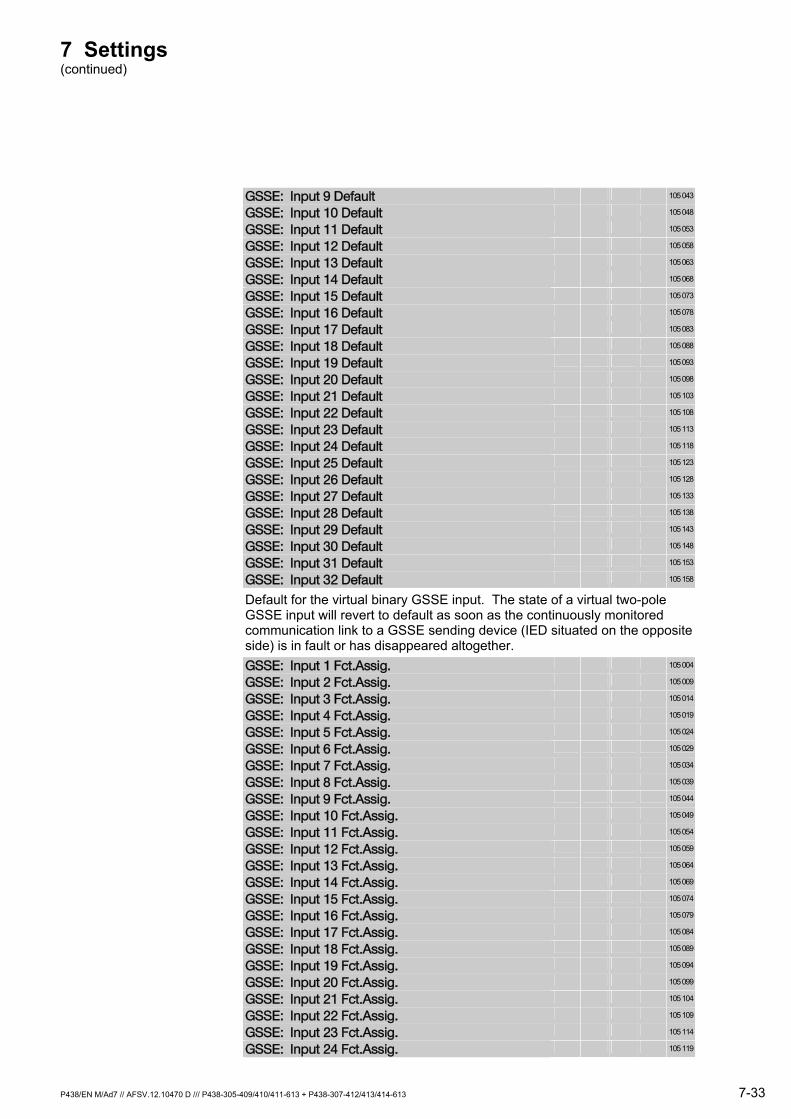
7 Settings (continued)
P438/EN M/Ad7 // AFSV.12.10470 D /// P438-305-409/410/411-613 + P438-307-412/413/414-613 7-33
GSSE: Input 9 Default 105 043
GSSE: Input 10 Default 105 048
GSSE: Input 11 Default 105 053
GSSE: Input 12 Default 105 058
GSSE: Input 13 Default 105 063
GSSE: Input 14 Default 105 068
GSSE: Input 15 Default 105 073
GSSE: Input 16 Default 105 078
GSSE: Input 17 Default 105 083
GSSE: Input 18 Default 105 088
GSSE: Input 19 Default 105 093
GSSE: Input 20 Default 105 098
GSSE: Input 21 Default 105 103
GSSE: Input 22 Default 105 108
GSSE: Input 23 Default 105 113
GSSE: Input 24 Default 105 118
GSSE: Input 25 Default 105 123
GSSE: Input 26 Default 105 128
GSSE: Input 27 Default 105 133
GSSE: Input 28 Default 105 138
GSSE: Input 29 Default 105 143
GSSE: Input 30 Default 105 148
GSSE: Input 31 Default 105 153
GSSE: Input 32 Default 105 158
Default for the virtual binary GSSE input. The state of a virtual two-pole GSSE input will revert to default as soon as the continuously monitored communication link to a GSSE sending device (IED situated on the opposite side) is in fault or has disappeared altogether.
GSSE: Input 1 Fct.Assig. 105 004
GSSE: Input 2 Fct.Assig. 105 009
GSSE: Input 3 Fct.Assig. 105 014
GSSE: Input 4 Fct.Assig. 105 019
GSSE: Input 5 Fct.Assig. 105 024
GSSE: Input 6 Fct.Assig. 105 029
GSSE: Input 7 Fct.Assig. 105 034
GSSE: Input 8 Fct.Assig. 105 039
GSSE: Input 9 Fct.Assig. 105 044
GSSE: Input 10 Fct.Assig. 105 049
GSSE: Input 11 Fct.Assig. 105 054
GSSE: Input 12 Fct.Assig. 105 059
GSSE: Input 13 Fct.Assig. 105 064
GSSE: Input 14 Fct.Assig. 105 069
GSSE: Input 15 Fct.Assig. 105 074
GSSE: Input 16 Fct.Assig. 105 079
GSSE: Input 17 Fct.Assig. 105 084
GSSE: Input 18 Fct.Assig. 105 089
GSSE: Input 19 Fct.Assig. 105 094
GSSE: Input 20 Fct.Assig. 105 099
GSSE: Input 21 Fct.Assig. 105 104
GSSE: Input 22 Fct.Assig. 105 109
GSSE: Input 23 Fct.Assig. 105 114
GSSE: Input 24 Fct.Assig. 105 119
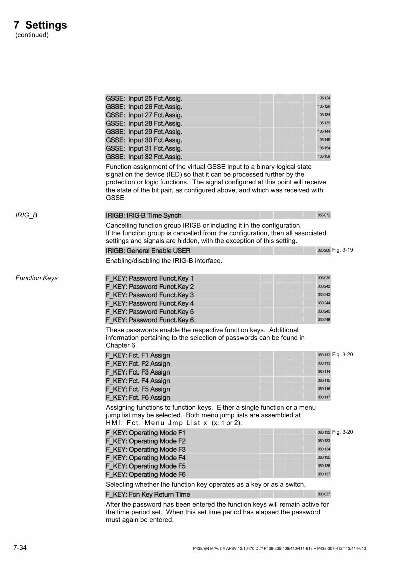
7 Settings (continued)
7-34 P438/EN M/Ad7 // AFSV.12.10470 D /// P438-305-409/410/411-613 + P438-307-412/413/414-613
GSSE: Input 25 Fct.Assig. 105 124
GSSE: Input 26 Fct.Assig. 105 129
GSSE: Input 27 Fct.Assig. 105 134
GSSE: Input 28 Fct.Assig. 105 139
GSSE: Input 29 Fct.Assig. 105 144
GSSE: Input 30 Fct.Assig. 105 149
GSSE: Input 31 Fct.Assig. 105 154
GSSE: Input 32 Fct.Assig. 105 159
Function assignment of the virtual GSSE input to a binary logical state signal on the device (IED) so that it can be processed further by the protection or logic functions. The signal configured at this point will receive the state of the bit pair, as configured above, and which was received with GSSE
IRIG_B IRIGB: IRIG-B Time Synch 056 072
Cancelling function group IRIGB or including it in the configuration. If the function group is cancelled from the configuration, then all associated settings and signals are hidden, with the exception of this setting.
IRIGB: General Enable USER 023 200 Fig. 3-19
Enabling/disabling the IRIG-B interface.
Function Keys F_KEY: Password Funct.Key 1 003 036
F_KEY: Password Funct.Key 2 030 242
F_KEY: Password Funct.Key 3 030 243
F_KEY: Password Funct.Key 4 030 244
F_KEY: Password Funct.Key 5 030 245
F_KEY: Password Funct.Key 6 030 246
These passwords enable the respective function keys. Additional information pertaining to the selection of passwords can be found in Chapter 6.
F_KEY: Fct. F1 Assign 080 112 Fig. 3-20
F_KEY: Fct. F2 Assign 080 113
F_KEY: Fct. F3 Assign 080 114
F_KEY: Fct. F4 Assign 080 115
F_KEY: Fct. F5 Assign 080 116
F_KEY: Fct. F6 Assign 080 117
Assigning functions to function keys. Either a single function or a menu jump list may be selected. Both menu jump lists are assembled at H M I : F c t . M e n u J m p L i s t x (x: 1 or 2).
F_KEY: Operating Mode F1 080 132 Fig. 3-20
F_KEY: Operating Mode F2 080 133
F_KEY: Operating Mode F3 080 134
F_KEY: Operating Mode F4 080 135
F_KEY: Operating Mode F5 080 136
F_KEY: Operating Mode F6 080 137
Selecting whether the function key operates as a key or as a switch.
F_KEY: Fcn Key Return Time 003 037
After the password has been entered the function keys will remain active for the time period set. When this set time period has elapsed the password must again be entered.
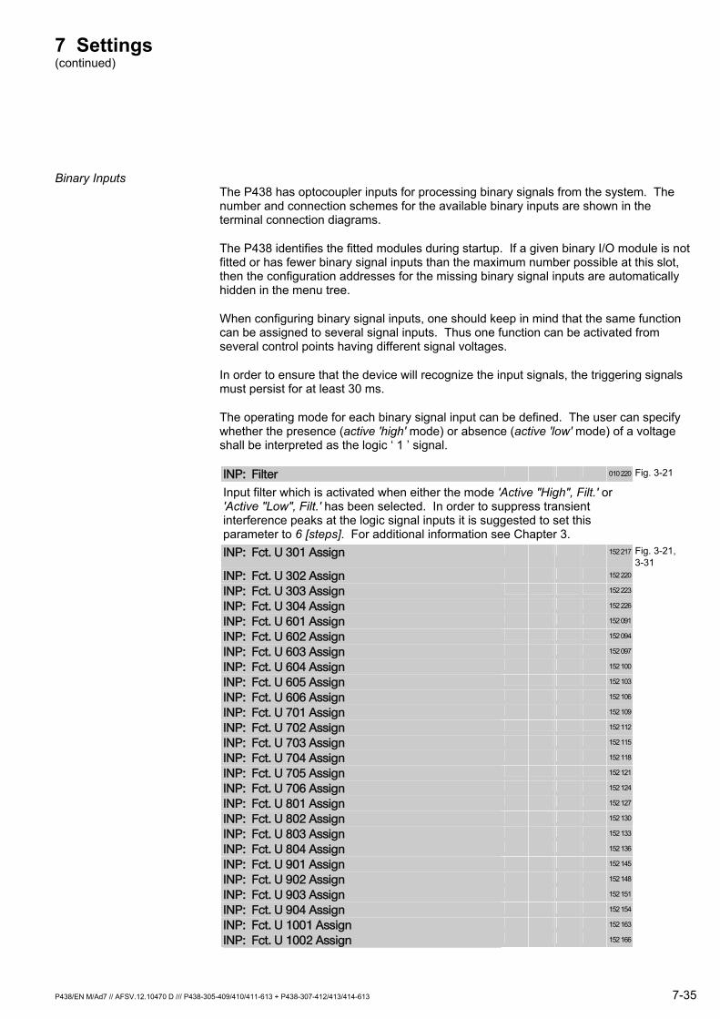
7 Settings (continued)
P438/EN M/Ad7 // AFSV.12.10470 D /// P438-305-409/410/411-613 + P438-307-412/413/414-613 7-35
Binary Inputs The P438 has optocoupler inputs for processing binary signals from the system. The number and connection schemes for the available binary inputs are shown in the terminal connection diagrams.
The P438 identifies the fitted modules during startup. If a given binary I/O module is not fitted or has fewer binary signal inputs than the maximum number possible at this slot, then the configuration addresses for the missing binary signal inputs are automatically hidden in the menu tree.
When configuring binary signal inputs, one should keep in mind that the same function can be assigned to several signal inputs. Thus one function can be activated from several control points having different signal voltages.
In order to ensure that the device will recognize the input signals, the triggering signals must persist for at least 30 ms.
The operating mode for each binary signal input can be defined. The user can specify whether the presence (active 'high' mode) or absence (active 'low' mode) of a voltage shall be interpreted as the logic ‘ 1 ’ signal.
INP: Filter 010 220 Fig. 3-21
Input filter which is activated when either the mode 'Active "High", Filt.' or 'Active "Low", Filt.' has been selected. In order to suppress transient interference peaks at the logic signal inputs it is suggested to set this parameter to 6 [steps]. For additional information see Chapter 3.
INP: Fct. U 301 Assign 152 217 Fig. 3-21, 3-31
INP: Fct. U 302 Assign 152 220
INP: Fct. U 303 Assign 152 223
INP: Fct. U 304 Assign 152 226
INP: Fct. U 601 Assign 152 091
INP: Fct. U 602 Assign 152 094
INP: Fct. U 603 Assign 152 097
INP: Fct. U 604 Assign 152 100
INP: Fct. U 605 Assign 152 103
INP: Fct. U 606 Assign 152 106
INP: Fct. U 701 Assign 152 109
INP: Fct. U 702 Assign 152 112
INP: Fct. U 703 Assign 152 115
INP: Fct. U 704 Assign 152 118
INP: Fct. U 705 Assign 152 121
INP: Fct. U 706 Assign 152 124
INP: Fct. U 801 Assign 152 127
INP: Fct. U 802 Assign 152 130
INP: Fct. U 803 Assign 152 133
INP: Fct. U 804 Assign 152 136
INP: Fct. U 901 Assign 152 145
INP: Fct. U 902 Assign 152 148
INP: Fct. U 903 Assign 152 151
INP: Fct. U 904 Assign 152 154
INP: Fct. U 1001 Assign 152 163
INP: Fct. U 1002 Assign 152 166

7 Settings (continued)
7-36 P438/EN M/Ad7 // AFSV.12.10470 D /// P438-305-409/410/411-613 + P438-307-412/413/414-613
INP: Fct. U 1003 Assign 152 169
INP: Fct. U 1004 Assign 152 172
INP: Fct. U 1005 Assign 152 175
INP: Fct. U 1006 Assign 152 178
INP: Fct. U 1201 Assign 152 199
INP: Fct. U 1202 Assign 152 202
INP: Fct. U 1203 Assign 152 205
INP: Fct. U 1204 Assign 152 208
INP: Fct. U 1205 Assign 152 211
INP: Fct. U 1206 Assign 152 214
INP: Fct. U 1401 Assign 190 002
INP: Fct. U 1402 Assign 190 006
INP: Fct. U 1403 Assign 190 010
INP: Fct. U 1404 Assign 190 014
INP: Fct. U 1405 Assign 190 018
INP: Fct. U 1406 Assign 190 022
INP: Fct. U 1601 Assign 192 002
INP: Fct. U 1602 Assign 192 006
INP: Fct. U 1603 Assign 192 010
INP: Fct. U 1604 Assign 192 014
INP: Fct. U 1605 Assign 192 018
INP: Fct. U 1606 Assign 192 022
INP: Fct. U 1801 Assign 194 002
INP: Fct. U 1802 Assign 194 006
INP: Fct. U 1803 Assign 194 010
INP: Fct. U 1804 Assign 194 014
INP: Fct. U 1805 Assign 194 018
INP: Fct. U 1806 Assign 194 022
INP: Fct. U 2001 Assign 153 087
INP: Fct. U 2002 Assign 153 090
INP: Fct. U 2003 Assign 153 093
INP: Fct. U 2004 Assign 153 096
Assignment of functions to binary signal inputs.
INP: Oper. Mode U 301 152 218 Fig. 3-21
INP: Oper. Mode U 302 152 221
INP: Oper. Mode U 303 152 224
INP: Oper. Mode U 304 152 227
INP: Oper. Mode U 601 152 092
INP: Oper. Mode U 602 152 095
INP: Oper. Mode U 603 152 098
INP: Oper. Mode U 604 152 101
INP: Oper. Mode U 605 152 104
INP: Oper. Mode U 606 152 107
INP: Oper. Mode U 701 152 110
INP: Oper. Mode U 702 152 113
INP: Oper. Mode U 703 152 116
INP: Oper. Mode U 704 152 119
INP: Oper. Mode U 705 152 122
INP: Oper. Mode U 706 152 125
INP: Oper. Mode U 801 152 128
INP: Oper. Mode U 802 152 131
INP: Oper. Mode U 803 152 134

7 Settings (continued)
P438/EN M/Ad7 // AFSV.12.10470 D /// P438-305-409/410/411-613 + P438-307-412/413/414-613 7-37
INP: Oper. Mode U 804 152 137
INP: Oper. Mode U 901 152 146
INP: Oper. Mode U 902 152 149
INP: Oper. Mode U 903 152 152
INP: Oper. Mode U 904 152 155
INP: Oper. Mode U 1001 152 164
INP: Oper. Mode U 1002 152 167
INP: Oper. Mode U 1003 152 170
INP: Oper. Mode U 1004 152 173
INP: Oper. Mode U 1005 152 176
INP: Oper. Mode U 1006 152 179
INP: Oper. Mode U 1201 152 200
INP: Oper. Mode U 1202 152 203
INP: Oper. Mode U 1203 152 206
INP: Oper. Mode U 1204 152 209
INP: Oper. Mode U 1205 152 212
INP: Oper. Mode U 1206 152 215
INP: Oper. Mode U 1401 190 003
INP: Oper. Mode U 1402 190 007
INP: Oper. Mode U 1403 190 011
INP: Oper. Mode U 1404 190 015
INP: Oper. Mode U 1405 190 019
INP: Oper. Mode U 1406 190 023
INP: Oper. Mode U 1601 192 003
INP: Oper. Mode U 1602 192 007
INP: Oper. Mode U 1603 192 011
INP: Oper. Mode U 1604 192 015
INP: Oper. Mode U 1605 192 019
INP: Oper. Mode U 1606 192 023
INP: Oper. Mode U 1801 194 003
INP: Oper. Mode U 1802 194 007
INP: Oper. Mode U 1803 194 011
INP: Oper. Mode U 1804 194 015
INP: Oper. Mode U 1805 194 019
INP: Oper. Mode U 1806 194 023
INP: Oper. Mode U 2001 153 088
INP: Oper. Mode U 2002 153 091
INP: Oper. Mode U 2003 153 094
INP: Oper. Mode U 2004 153 097
Selection of operating mode for binary signal inputs.
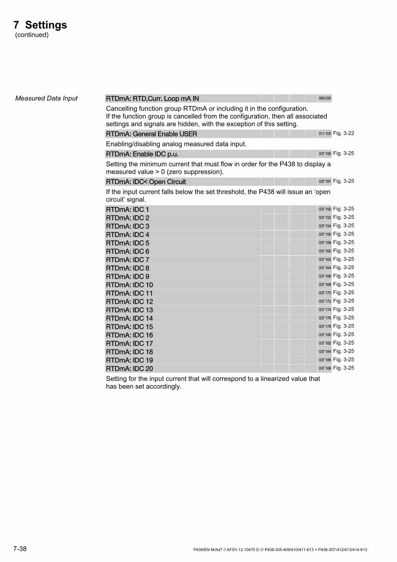
7 Settings (continued)
7-38 P438/EN M/Ad7 // AFSV.12.10470 D /// P438-305-409/410/411-613 + P438-307-412/413/414-613
Measured Data Input RTDmA: RTD,Curr. Loop mA IN 056 030
Cancelling function group RTDmA or including it in the configuration. If the function group is cancelled from the configuration, then all associated settings and signals are hidden, with the exception of this setting.
RTDmA: General Enable USER 011 100 Fig. 3-22
Enabling/disabling analog measured data input.
RTDmA: Enable IDC p.u. 037 190 Fig. 3-25
Setting the minimum current that must flow in order for the P438 to display a measured value > 0 (zero suppression).
RTDmA: IDC< Open Circuit 037 191 Fig. 3-25
If the input current falls below the set threshold, the P438 will issue an ‘open circuit’ signal.
RTDmA: IDC 1 037 150 Fig. 3-25
RTDmA: IDC 2 037 152 Fig. 3-25
RTDmA: IDC 3 037 154 Fig. 3-25
RTDmA: IDC 4 037 156 Fig. 3-25
RTDmA: IDC 5 037 158 Fig. 3-25
RTDmA: IDC 6 037 160 Fig. 3-25
RTDmA: IDC 7 037 162 Fig. 3-25
RTDmA: IDC 8 037 164 Fig. 3-25
RTDmA: IDC 9 037 166 Fig. 3-25
RTDmA: IDC 10 037 168 Fig. 3-25
RTDmA: IDC 11 037 170 Fig. 3-25
RTDmA: IDC 12 037 172 Fig. 3-25
RTDmA: IDC 13 037 174 Fig. 3-25
RTDmA: IDC 14 037 176 Fig. 3-25
RTDmA: IDC 15 037 178 Fig. 3-25
RTDmA: IDC 16 037 180 Fig. 3-25
RTDmA: IDC 17 037 182 Fig. 3-25
RTDmA: IDC 18 037 184 Fig. 3-25
RTDmA: IDC 19 037 186 Fig. 3-25
RTDmA: IDC 20 037 188 Fig. 3-25
Setting for the input current that will correspond to a linearized value that has been set accordingly.

7 Settings (continued)
P438/EN M/Ad7 // AFSV.12.10470 D /// P438-305-409/410/411-613 + P438-307-412/413/414-613 7-39
RTDmA: IDC,lin 1 037 151 Fig. 3-25
RTDmA: IDC,lin 2 037 153 Fig. 3-25
RTDmA: IDC,lin 3 037 155 Fig. 3-25
RTDmA: IDC,lin 4 037 157 Fig. 3-25
RTDmA: IDC,lin 5 037 159 Fig. 3-25
RTDmA: IDC,lin 6 037 161 Fig. 3-25
RTDmA: IDC,lin 7 037 163 Fig. 3-25
RTDmA: IDC,lin 8 037 165 Fig. 3-25
RTDmA: IDC,lin 9 037 167 Fig. 3-25
RTDmA: IDC,lin 10 037 169 Fig. 3-25
RTDmA: IDC,lin 11 037 171 Fig. 3-25
RTDmA: IDC,lin 12 037 173 Fig. 3-25
RTDmA: IDC,lin 13 037 175 Fig. 3-25
RTDmA: IDC,lin 14 037 177 Fig. 3-25
RTDmA: IDC,lin 15 037 179 Fig. 3-25
RTDmA: IDC,lin 16 037 181 Fig. 3-25
RTDmA: IDC,lin 17 037 183 Fig. 3-25
RTDmA: IDC,lin 18 037 185 Fig. 3-25
RTDmA: IDC,lin 19 037 187 Fig. 3-25
RTDmA: IDC,lin 20 037 189 Fig. 3-25
Setting for the linearized current that will correspond to an input current that has been set accordingly.
RTDmA: Scaled Val. IDC,lin1 037 192 Fig. 3-26
Setting for the scaled value of IDC,lin1.
RTDmA: Scaled Val. IDC,lin2 037 193 Fig. 3-26
Setting for the scaled value of IDC,lin20.
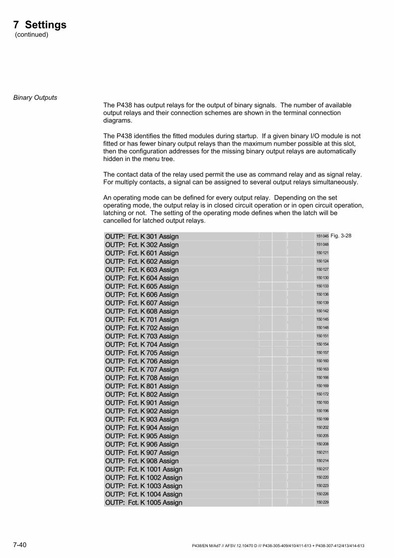
7 Settings (continued)
7-40 P438/EN M/Ad7 // AFSV.12.10470 D /// P438-305-409/410/411-613 + P438-307-412/413/414-613
Binary Outputs The P438 has output relays for the output of binary signals. The number of available output relays and their connection schemes are shown in the terminal connection diagrams.
The P438 identifies the fitted modules during startup. If a given binary I/O module is not fitted or has fewer binary output relays than the maximum number possible at this slot, then the configuration addresses for the missing binary output relays are automatically hidden in the menu tree.
The contact data of the relay used permit the use as command relay and as signal relay. For multiply contacts, a signal can be assigned to several output relays simultaneously.
An operating mode can be defined for every output relay. Depending on the set operating mode, the output relay is in closed circuit operation or in open circuit operation, latching or not. The setting of the operating mode defines when the latch will be cancelled for latched output relays.
OUTP: Fct. K 301 Assign 151 045 Fig. 3-28
OUTP: Fct. K 302 Assign 151 048
OUTP: Fct. K 601 Assign 150 121
OUTP: Fct. K 602 Assign 150 124
OUTP: Fct. K 603 Assign 150 127
OUTP: Fct. K 604 Assign 150 130
OUTP: Fct. K 605 Assign 150 133
OUTP: Fct. K 606 Assign 150 136
OUTP: Fct. K 607 Assign 150 139
OUTP: Fct. K 608 Assign 150 142
OUTP: Fct. K 701 Assign 150 145
OUTP: Fct. K 702 Assign 150 148
OUTP: Fct. K 703 Assign 150 151
OUTP: Fct. K 704 Assign 150 154
OUTP: Fct. K 705 Assign 150 157
OUTP: Fct. K 706 Assign 150 160
OUTP: Fct. K 707 Assign 150 163
OUTP: Fct. K 708 Assign 150 166
OUTP: Fct. K 801 Assign 150 169
OUTP: Fct. K 802 Assign 150 172
OUTP: Fct. K 901 Assign 150 193
OUTP: Fct. K 902 Assign 150 196
OUTP: Fct. K 903 Assign 150 199
OUTP: Fct. K 904 Assign 150 202
OUTP: Fct. K 905 Assign 150 205
OUTP: Fct. K 906 Assign 150 208
OUTP: Fct. K 907 Assign 150 211
OUTP: Fct. K 908 Assign 150 214
OUTP: Fct. K 1001 Assign 150 217
OUTP: Fct. K 1002 Assign 150 220
OUTP: Fct. K 1003 Assign 150 223
OUTP: Fct. K 1004 Assign 150 226
OUTP: Fct. K 1005 Assign 150 229
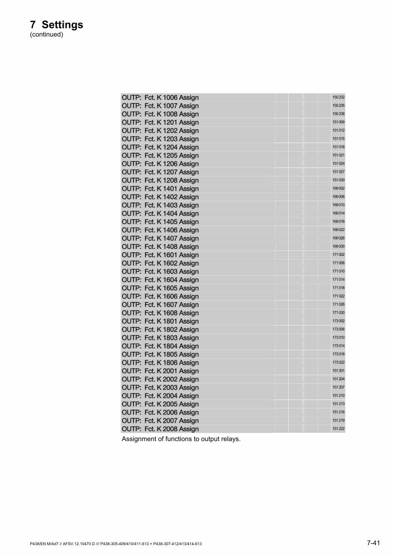
7 Settings (continued)
P438/EN M/Ad7 // AFSV.12.10470 D /// P438-305-409/410/411-613 + P438-307-412/413/414-613 7-41
OUTP: Fct. K 1006 Assign 150 232
OUTP: Fct. K 1007 Assign 150 235
OUTP: Fct. K 1008 Assign 150 238
OUTP: Fct. K 1201 Assign 151 009
OUTP: Fct. K 1202 Assign 151 012
OUTP: Fct. K 1203 Assign 151 015
OUTP: Fct. K 1204 Assign 151 018
OUTP: Fct. K 1205 Assign 151 021
OUTP: Fct. K 1206 Assign 151 024
OUTP: Fct. K 1207 Assign 151 027
OUTP: Fct. K 1208 Assign 151 030
OUTP: Fct. K 1401 Assign 169 002
OUTP: Fct. K 1402 Assign 169 006
OUTP: Fct. K 1403 Assign 169 010
OUTP: Fct. K 1404 Assign 169 014
OUTP: Fct. K 1405 Assign 169 018
OUTP: Fct. K 1406 Assign 169 022
OUTP: Fct. K 1407 Assign 169 026
OUTP: Fct. K 1408 Assign 169 030
OUTP: Fct. K 1601 Assign 171 002
OUTP: Fct. K 1602 Assign 171 006
OUTP: Fct. K 1603 Assign 171 010
OUTP: Fct. K 1604 Assign 171 014
OUTP: Fct. K 1605 Assign 171 018
OUTP: Fct. K 1606 Assign 171 022
OUTP: Fct. K 1607 Assign 171 026
OUTP: Fct. K 1608 Assign 171 030
OUTP: Fct. K 1801 Assign 173 002
OUTP: Fct. K 1802 Assign 173 006
OUTP: Fct. K 1803 Assign 173 010
OUTP: Fct. K 1804 Assign 173 014
OUTP: Fct. K 1805 Assign 173 018
OUTP: Fct. K 1806 Assign 173 022
OUTP: Fct. K 2001 Assign 151 201
OUTP: Fct. K 2002 Assign 151 204
OUTP: Fct. K 2003 Assign 151 207
OUTP: Fct. K 2004 Assign 151 210
OUTP: Fct. K 2005 Assign 151 213
OUTP: Fct. K 2006 Assign 151 216
OUTP: Fct. K 2007 Assign 151 219
OUTP: Fct. K 2008 Assign 151 222
Assignment of functions to output relays.

7 Settings (continued)
7-42 P438/EN M/Ad7 // AFSV.12.10470 D /// P438-305-409/410/411-613 + P438-307-412/413/414-613
OUTP: Oper. Mode K 301 151 046 Fig. 3-28
OUTP: Oper. Mode K 302 151 049
OUTP: Oper. Mode K 601 150 122
OUTP: Oper. Mode K 602 150 125
OUTP: Oper. Mode K 603 150 128
OUTP: Oper. Mode K 604 150 131
OUTP: Oper. Mode K 605 150 134
OUTP: Oper. Mode K 606 150 137
OUTP: Oper. Mode K 607 150 140
OUTP: Oper. Mode K 608 150 143
OUTP: Oper. Mode K 701 150 146
OUTP: Oper. Mode K 702 150 149
OUTP: Oper. Mode K 703 150 152
OUTP: Oper. Mode K 704 150 155
OUTP: Oper. Mode K 705 150 158
OUTP: Oper. Mode K 706 150 161
OUTP: Oper. Mode K 707 150 164
OUTP: Oper. Mode K 708 150 167
OUTP: Oper. Mode K 801 150 170
OUTP: Oper. Mode K 802 150 173
OUTP: Oper. Mode K 901 150 194
OUTP: Oper. Mode K 902 150 197
OUTP: Oper. Mode K 903 150 200
OUTP: Oper. Mode K 904 150 203
OUTP: Oper. Mode K 905 150 206
OUTP: Oper. Mode K 906 150 209
OUTP: Oper. Mode K 907 150 212
OUTP: Oper. Mode K 908 150 215
OUTP: Oper. Mode K 1001 150 218
OUTP: Oper. Mode K 1002 150 221
OUTP: Oper. Mode K 1003 150 224
OUTP: Oper. Mode K 1004 150 227
OUTP: Oper. Mode K 1005 150 230
OUTP: Oper. Mode K 1006 150 233
OUTP: Oper. Mode K 1007 150 236
OUTP: Oper. Mode K 1008 150 239
OUTP: Oper. Mode K 1201 151 010
OUTP: Oper. Mode K 1202 151 013
OUTP: Oper. Mode K 1203 151 016
OUTP: Oper. Mode K 1204 151 019
OUTP: Oper. Mode K 1205 151 022
OUTP: Oper. Mode K 1206 151 025
OUTP: Oper. Mode K 1207 151 028
OUTP: Oper. Mode K 1208 151 031
OUTP: Oper. Mode K 1401 169 003
OUTP: Oper. Mode K 1402 169 007
OUTP: Oper. Mode K 1403 169 011
OUTP: Oper. Mode K 1404 169 015
OUTP: Oper. Mode K 1405 169 019
OUTP: Oper. Mode K 1406 169 023
OUTP: Oper. Mode K 1407 169 027
OUTP: Oper. Mode K 1408 169 031
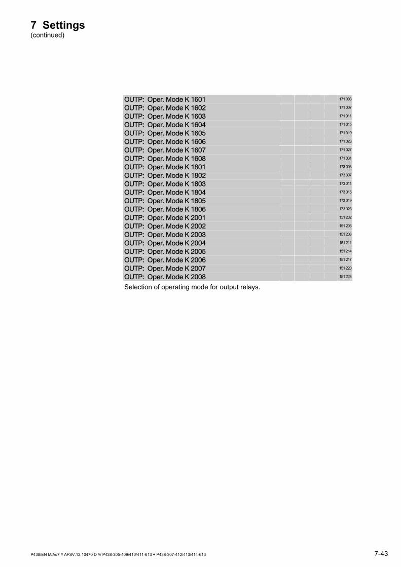
7 Settings (continued)
P438/EN M/Ad7 // AFSV.12.10470 D /// P438-305-409/410/411-613 + P438-307-412/413/414-613 7-43
OUTP: Oper. Mode K 1601 171 003
OUTP: Oper. Mode K 1602 171 007
OUTP: Oper. Mode K 1603 171 011
OUTP: Oper. Mode K 1604 171 015
OUTP: Oper. Mode K 1605 171 019
OUTP: Oper. Mode K 1606 171 023
OUTP: Oper. Mode K 1607 171 027
OUTP: Oper. Mode K 1608 171 031
OUTP: Oper. Mode K 1801 173 003
OUTP: Oper. Mode K 1802 173 007
OUTP: Oper. Mode K 1803 173 011
OUTP: Oper. Mode K 1804 173 015
OUTP: Oper. Mode K 1805 173 019
OUTP: Oper. Mode K 1806 173 023
OUTP: Oper. Mode K 2001 151 202
OUTP: Oper. Mode K 2002 151 205
OUTP: Oper. Mode K 2003 151 208
OUTP: Oper. Mode K 2004 151 211
OUTP: Oper. Mode K 2005 151 214
OUTP: Oper. Mode K 2006 151 217
OUTP: Oper. Mode K 2007 151 220
OUTP: Oper. Mode K 2008 151 223
Selection of operating mode for output relays.
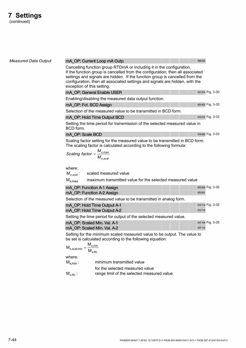
7 Settings (continued)
7-44 P438/EN M/Ad7 // AFSV.12.10470 D /// P438-305-409/410/411-613 + P438-307-412/413/414-613
Measured Data Output mA_OP: Current Loop mA Outp 056 020
Cancelling function group RTDmA or including it in the configuration. If the function group is cancelled from the configuration, then all associated settings and signals are hidden. If the function group is cancelled from the configuration, then all associated settings and signals are hidden, with the exception of this setting.
mA_OP: General Enable USER 031 074 Fig. 3-30
Enabling/disabling the measured data output function.
mA_OP: Fct. BCD Assign 053 002 Fig. 3-33
Selection of the measured value to be transmitted in BCD form.
mA_OP: Hold Time Output BCD 010 010 Fig. 3-33
Setting the time period for transmission of the selected measured value in BCD form.
mA_OP: Scale BCD 016 082 Fig. 3-33
Scaling factor setting for the measured value to be transmitted in BCD form. The scaling factor is calculated according to the following formula:
scalx
x
MM
factorScaling,
max,=
where:
scalxM , : scaled measured value Mx,max maximum transmitted value for the selected measured value
mA_OP: Function A-1 Assign 053 000 Fig. 3-35
mA_OP: Function A-2 Assign 053 001
Selection of the measured value to be transmitted in analog form.
mA_OP: Hold Time Output A-1 010 114 Fig. 3-35
mA_OP: Hold Time Output A-2 010 115
Setting the time period for output of the selected measured value.
mA_OP: Scaled Min. Val. A-1 037 104 Fig. 3-35
mA_OP: Scaled Min. Val. A-2 037 110
Setting for the minimum scaled measured value to be output. The value to be set is calculated according to the following equation:
RL,x
min,xmin,scal,x M
MM =
where: Mx,min : minimum transmitted value for the selected measured value
RL,xM : range limit of the selected measured value
7 Settings (continued)
P438/EN M/Ad7 // AFSV.12.10470 D /// P438-305-409/410/411-613 + P438-307-412/413/414-613 7-45
mA_OP: Scaled Knee Val. A-1 037 105 Fig. 3-35
mA_OP: Scaled Knee Val. A-2 037 111
Setting for the scaled measured value for output that defines the knee point of the characteristic. The value to be set is calculated according to the following equation:
RL,x
knee,xknee,scal,x M
MM =
where: knee,xM : knee point value to be transmitted for selected measured
value RL,xM : range limit of the selected measured value
mA_OP: Scaled Max. Val. A-1 037 106 Fig. 3-35
mA_OP: Scaled Max. Val. A-2 037 112
After conversion via a characteristic the selected measured value Ax (x=1, 2) is to be issued as an output current. For this purpose a range "measured values to be issued" is defined. In this range the characteristic has two linear sections, which are separated by a knee point.
Measurands Range
Measurands of the variable Mx Mx, RL1 ... Mx, RL2
Associated scaled measurands 0 ... 1
Measurands to be output Range
Measurands to be output Mx,min ... Mx,max
Scaled measurands to be output Mx,scal,min ... Mx,scal,max
Designation of the set values "Scal. min. value Ax" ... in the data model ... "Scal. max. value Ax"
with:
Mx,scal,min = (Mx,min - Mx,RL1) / (Mx,RL2 - Mx,RL1
Mx,scal,max = (Mx,max - Mx,RL1) / (Mx,RL2 - Mx,RL1
Knee point for characteristic Description
Value for knee point Mx,knee
Scaled knee point value Mx,scal,knee
Designation of this set value "Scaled knee val. Ax" ... in the data model
with:
Mx,scal,knee = (Mx,min - Mx,RL1) / (Mx,RL2 - Mx,RL1
7 Settings (continued)
7-46 P438/EN M/Ad7 // AFSV.12.10470 D /// P438-305-409/410/411-613 + P438-307-412/413/414-613
mA_OP: AnOut Min. Val. A-1 037 107 Fig. 3-35
mA_OP: AnOut Min. Val. A-2 037 113
Setting for the output current that is output for measured values smaller than or equal to the minimum measured value setting.
mA_OP: AnOut Knee Point A-1 037 108 Fig. 3-35
mA_OP: AnOut Knee Point A-2 037 114
Setting for the output current that is output if the measured value is on the knee point of the characteristic.
mA_OP: AnOut Max. Val. A-1 037 109 Fig. 3-35
mA_OP: AnOut Max. Val. A-2 037 115
Display values Designation in the data model
Output current range "AnOut min. val. Ax" ... for measured values in the range ... "AnOut max. val. Ax" "measured values to be issued"
Output current to be set "AnOut min. val. Ax" for measured values = Mx,min.
Output current to be set "AnOut max. val. Ax" for measured values = Mx,max.
Output current to be set "AnOut knee point Ax" for measured values = Mx,knee
with:
Mx,min ... Mx,max : measured values to be issued
mA_OP: Output Value 1 037 120 Fig. 3-35
mA_OP: Output Value 2 037 121 Fig. 3-35
mA_OP: Output Value 3 037 122 Fig. 3-35
Measured values of external devices, which must be scaled to 0 to 100%, can be issued.
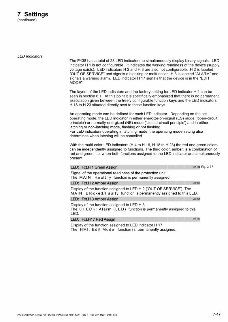
7 Settings (continued)
P438/EN M/Ad7 // AFSV.12.10470 D /// P438-305-409/410/411-613 + P438-307-412/413/414-613 7-47
LED Indicators The P438 has a total of 23 LED indicators to simultaneously display binary signals. LED indicator H 1 is not configurable. It indicates the working readiness of the device (supply voltage exists). LED indicators H 2 and H 3 are also not configurable. H 2 is labeled "OUT OF SERVICE" and signals a blocking or malfunction; H 3 is labeled "ALARM" and signals a warning alarm. LED indicator H 17 signals that the device is in the "EDIT MODE".
The layout of the LED indicators and the factory setting for LED indicator H 4 can be seen in section 6.1. At this point it is specifically emphasized that there is no permanent association given between the freely configurable function keys and the LED indicators H 18 to H 23 situated directly next to these function keys.
An operating mode can be defined for each LED indicator. Depending on the set operating mode, the LED indicator in either energize-on-signal (ES) mode ('open-circuit principle') or normally-energized (NE) mode ('closed-circuit principle') and in either latching or non-latching mode, flashing or not flashing. For LED indicators operating in latching mode, the operating mode setting also determines when latching will be cancelled.
With the multi-color LED indicators (H 4 to H 16, H 18 to H 23) the red and green colors can be independently assigned to functions. The third color, amber, is a combination of red and green, i.e. when both functions assigned to the LED indicator are simultaneously present.
LED: Fct.H 1 Green Assign 085 184 Fig. 3-37
Signal of the operational readiness of the protection unit. The M A I N : H e a l t h y function is permanently assigned.
LED: Fct.H 2 Amber Assign 085 001
Display of the function assigned to LED H 2 (‘OUT OF SERVICE’). The M A I N : B l o c k e d / F a u l t y function is permanently assigned to this LED.
LED: Fct.H 3 Amber Assign 085 004
Display of the function assigned to LED H 3. The C H E C K : A l a r m ( L E D ) function is permanently assigned to this LED.
LED: Fct.H17 Red Assign 085 185
Display of the function assigned to LED indicator H 17. The H M I : E d i t M o d e function i s permanently assigned.
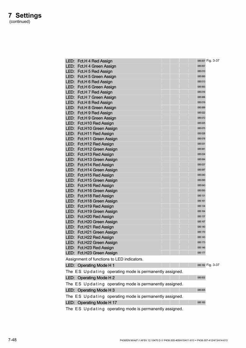
7 Settings (continued)
7-48 P438/EN M/Ad7 // AFSV.12.10470 D /// P438-305-409/410/411-613 + P438-307-412/413/414-613
LED: Fct.H 4 Red Assign 085 007 Fig. 3-37
LED: Fct.H 4 Green Assign 085 057
LED: Fct.H 5 Red Assign 085 010
LED: Fct.H 5 Green Assign 085 060
LED: Fct.H 6 Red Assign 085 013
LED: Fct.H 6 Green Assign 085 063
LED: Fct.H 7 Red Assign 085 016
LED: Fct.H 7 Green Assign 085 066
LED: Fct.H 8 Red Assign 085 019
LED: Fct.H 8 Green Assign 085 069
LED: Fct.H 9 Red Assign 085 022
LED: Fct.H 9 Green Assign 085 072
LED: Fct.H10 Red Assign 085 025
LED: Fct.H10 Green Assign 085 075
LED: Fct.H11 Red Assign 085 028
LED: Fct.H11 Green Assign 085 078
LED: Fct.H12 Red Assign 085 031
LED: Fct.H12 Green Assign 085 081
LED: Fct.H13 Red Assign 085 034
LED: Fct.H13 Green Assign 085 084
LED: Fct.H14 Red Assign 085 037
LED: Fct.H14 Green Assign 085 087
LED: Fct.H15 Red Assign 085 040
LED: Fct.H15 Green Assign 085 090
LED: Fct.H16 Red Assign 085 043
LED: Fct.H16 Green Assign 085 093
LED: Fct.H18 Red Assign 085 131
LED: Fct.H18 Green Assign 085 161
LED: Fct.H19 Red Assign 085 134
LED: Fct.H19 Green Assign 085 164
LED: Fct.H20 Red Assign 085 137
LED: Fct.H20 Green Assign 085 167
LED: Fct.H21 Red Assign 085 140
LED: Fct.H21 Green Assign 085 170
LED: Fct.H22 Red Assign 085 143
LED: Fct.H22 Green Assign 085 173
LED: Fct.H23 Red Assign 085 146
LED: Fct.H23 Green Assign 085 177
Assignment of functions to LED indicators.
LED: Operating Mode H 1 085 182 Fig. 3-37
The E S U p d a t i n g operating mode is permanently assigned.
LED: Operating Mode H 2 085 002
The E S U p d a t i n g operating mode is permanently assigned.
LED: Operating Mode H 3 085 005
The E S U p d a t i n g operating mode is permanently assigned.
LED: Operating Mode H 17 085 183
The E S U p d a t i n g operating mode is permanently assigned.
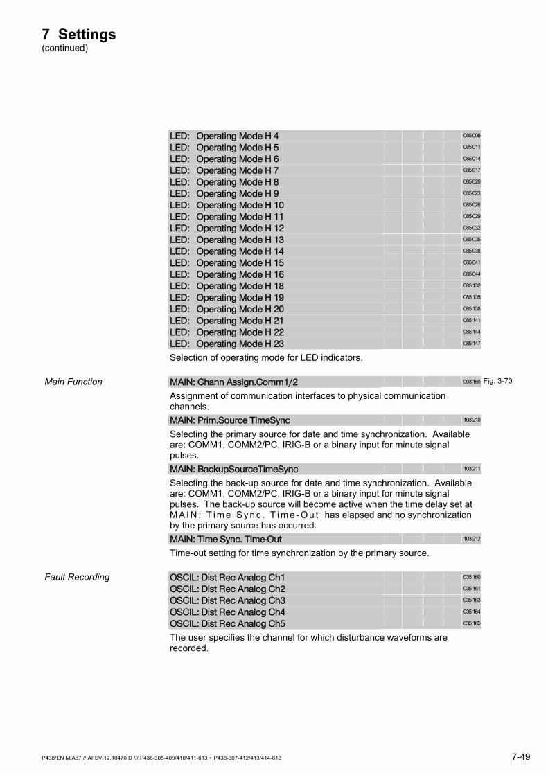
7 Settings (continued)
P438/EN M/Ad7 // AFSV.12.10470 D /// P438-305-409/410/411-613 + P438-307-412/413/414-613 7-49
LED: Operating Mode H 4 085 008
LED: Operating Mode H 5 085 011
LED: Operating Mode H 6 085 014
LED: Operating Mode H 7 085 017
LED: Operating Mode H 8 085 020
LED: Operating Mode H 9 085 023
LED: Operating Mode H 10 085 026
LED: Operating Mode H 11 085 029
LED: Operating Mode H 12 085 032
LED: Operating Mode H 13 085 035
LED: Operating Mode H 14 085 038
LED: Operating Mode H 15 085 041
LED: Operating Mode H 16 085 044
LED: Operating Mode H 18 085 132
LED: Operating Mode H 19 085 135
LED: Operating Mode H 20 085 138
LED: Operating Mode H 21 085 141
LED: Operating Mode H 22 085 144
LED: Operating Mode H 23 085 147
Selection of operating mode for LED indicators.
Main Function MAIN: Chann Assign.Comm1/2 003 169 Fig. 3-70
Assignment of communication interfaces to physical communication channels.
MAIN: Prim.Source TimeSync 103 210
Selecting the primary source for date and time synchronization. Available are: COMM1, COMM2/PC, IRIG-B or a binary input for minute signal pulses.
MAIN: BackupSourceTimeSync 103 211
Selecting the back-up source for date and time synchronization. Available are: COMM1, COMM2/PC, IRIG-B or a binary input for minute signal pulses. The back-up source will become active when the time delay set at M A I N : T i m e S y n c . T i m e - O u t has elapsed and no synchronization by the primary source has occurred.
MAIN: Time Sync. Time-Out 103 212
Time-out setting for time synchronization by the primary source.
Fault Recording OSCIL: Dist Rec Analog Ch1 035 160
OSCIL: Dist Rec Analog Ch2 035 161
OSCIL: Dist Rec Analog Ch3 035 163
OSCIL: Dist Rec Analog Ch4 035 164
OSCIL: Dist Rec Analog Ch5 035 165
The user specifies the channel for which disturbance waveforms are recorded.
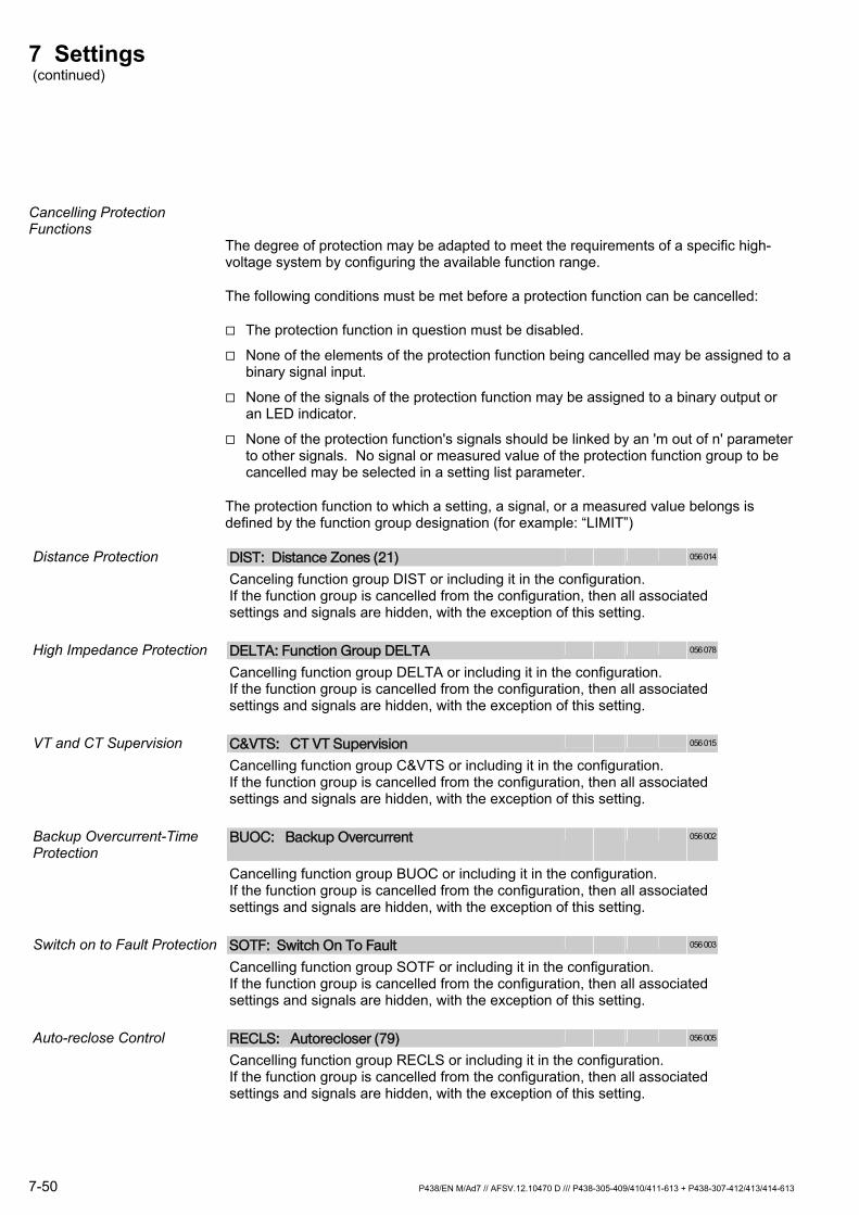
7 Settings (continued)
7-50 P438/EN M/Ad7 // AFSV.12.10470 D /// P438-305-409/410/411-613 + P438-307-412/413/414-613
Cancelling Protection Functions
The degree of protection may be adapted to meet the requirements of a specific high-voltage system by configuring the available function range.
The following conditions must be met before a protection function can be cancelled:
The protection function in question must be disabled.
None of the elements of the protection function being cancelled may be assigned to a binary signal input.
None of the signals of the protection function may be assigned to a binary output or an LED indicator.
None of the protection function's signals should be linked by an 'm out of n' parameter to other signals. No signal or measured value of the protection function group to be cancelled may be selected in a setting list parameter.
The protection function to which a setting, a signal, or a measured value belongs is defined by the function group designation (for example: “LIMIT”)
Distance Protection DIST: Distance Zones (21) 056 014
Canceling function group DIST or including it in the configuration. If the function group is cancelled from the configuration, then all associated settings and signals are hidden, with the exception of this setting.
High Impedance Protection DELTA: Function Group DELTA 056 078
Cancelling function group DELTA or including it in the configuration. If the function group is cancelled from the configuration, then all associated settings and signals are hidden, with the exception of this setting.
VT and CT Supervision C&VTS: CT VT Supervision 056 015
Cancelling function group C&VTS or including it in the configuration. If the function group is cancelled from the configuration, then all associated settings and signals are hidden, with the exception of this setting.
Backup Overcurrent-Time Protection
BUOC: Backup Overcurrent 056 002
Cancelling function group BUOC or including it in the configuration. If the function group is cancelled from the configuration, then all associated settings and signals are hidden, with the exception of this setting.
Switch on to Fault Protection SOTF: Switch On To Fault 056 003
Cancelling function group SOTF or including it in the configuration. If the function group is cancelled from the configuration, then all associated settings and signals are hidden, with the exception of this setting.
Auto-reclose Control RECLS: Autorecloser (79) 056 005
Cancelling function group RECLS or including it in the configuration. If the function group is cancelled from the configuration, then all associated settings and signals are hidden, with the exception of this setting.
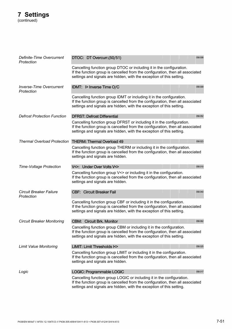
7 Settings (continued)
P438/EN M/Ad7 // AFSV.12.10470 D /// P438-305-409/410/411-613 + P438-307-412/413/414-613 7-51
Definite-Time Overcurrent Protection
DTOC: DT Overcurr.(50/51) 056 008
Cancelling function group DTOC or including it in the configuration. If the function group is cancelled from the configuration, then all associated settings and signals are hidden, with the exception of this setting.
Inverse-Time Overcurrent Protection
IDMT: I> Inverse Time O/C 056 009
Cancelling function group IDMT or including it in the configuration. If the function group is cancelled from the configuration, then all associated settings and signals are hidden, with the exception of this setting.
Defrost Protection Function DFRST: Defrost Differential 056 052
Cancelling function group DFRST or including it in the configuration. If the function group is cancelled from the configuration, then all associated settings and signals are hidden, with the exception of this setting.
Thermal Overload Protection THERM: Thermal Overload 49 056 023
Cancelling function group THERM or including it in the configuration. If the function group is cancelled from the configuration, then all associated settings and signals are hidden.
Time-Voltage Protection V<>: Under Over Volts V<> 056 010
Cancelling function group V<> or including it in the configuration. If the function group is cancelled from the configuration, then all associated settings and signals are hidden.
Circuit Breaker Failure Protection
CBF: Circuit Breaker Fail 056 040
Cancelling function group CBF or including it in the configuration. If the function group is cancelled from the configuration, then all associated settings and signals are hidden, with the exception of this setting.
Circuit Breaker Monitoring CBM: Circuit Brk. Monitor 056 062
Cancelling function group CBM or including it in the configuration. If the function group is cancelled from the configuration, then all associated settings and signals are hidden, with the exception of this setting.
Limit Value Monitoring LIMIT: Limit Thresholds I<> 056 025
Cancelling function group LIMIT or including it in the configuration. If the function group is cancelled from the configuration, then all associated settings and signals are hidden.
Logic LOGIC: Programmable LOGIC 056 017
Cancelling function group LOGIC or including it in the configuration. If the function group is cancelled from the configuration, then all associated settings and signals are hidden, with the exception of this setting.
7 Settings (continued)
7-52 P438/EN M/Ad7 // AFSV.12.10470 D /// P438-305-409/410/411-613 + P438-307-412/413/414-613
7.1.3 Function Settings
7.1.3.1 Global
PC Link PC: Command Blocking 003 182 Fig. 3-5
This prevents any settings or commands from being sent to the relay from the PC interface.
PC: Sig/Meas. Val.Block 003 086 Fig. 3-5
When signal and measured value blocking is activated, no signals or measured data are transmitted through the PC interface.
Rear Port Communications Interface 1
COMM1: USER Command Block 003 172 Fig. 3-6
This prevents any settings or commands from being sent to the relay from the COMM1 interface.
COMM1: USER Sig/Meas Block 003 076 Fig. 3-7,3-8,3-9
When signal and measured value blocking user is activated, no signals or measured data are transmitted through communication interface COMM1.
Rear Port Communications Interface 2
COMM2: USER Command Block 103 172 Fig. 3-14
This prevents any settings or commands from being sent to the relay from the COMM2 interface.
COMM2: USER Sig/Meas Block 103 076 Fig. 3-14
When signal and measured value blocking user is activated, no signals or measured data are transmitted through communication interface COMM2.
Binary Output OUTP: USER Outp Rel Block 021 014 Fig. 3-28
When this blocking is activated, all output relays are blocked.
Main Function MAIN: Protection Enabled 003 030 Fig. 3-48
Switching the device off-line or on-line. Some settings can be changed only when the device is off-line (i.e. set to 'No (Disabled)').
MAIN: USER Test Mode 003 012 Fig. 3-71
When the test mode user is activated, signals or measured data for PC and communication interfaces are labeled 'test mode'.
MAIN: Frequency fn 010 030 Fig. 3-44, 3-46, 3-47
Setting for the nominal frequency of the protected system.
MAIN: In C.T. Prim. 010 001 Fig. 3-41, 3-42, 3-188
Setting for the primary nominal current of the main current transformers for measurement of phase currents.
MAIN: Idfrst,nom C.T. Prim 010 016 Fig. 3-170
Setting for the primary nominal current of the main current transformer for measurement of defrost current.
7 Settings (continued)
P438/EN M/Ad7 // AFSV.12.10470 D /// P438-305-409/410/411-613 + P438-307-412/413/414-613 7-53
MAIN: Vn V.T. Prim. 010 002 Fig. 3-43
Setting for the primary nominal voltage of the system transformer for measurement of phase-to-ground and phase-to-phase voltages.
MAIN: In Device 010 003 Fig. 3-38, 3-39, 3-40
Setting for the secondary nominal current of the line CT for measurement of phase currents. This also corresponds to the nominal device current.
MAIN: Idfrst,nom Device 010 017 Fig. 3-40
Setting for the secondary nominal current of the CT for measurement of defrost current.
MAIN: Vn VT. Sec. 010 009 Fig. 3-38, 3-39
Setting for the secondary nominal voltage of the voltage transformer for measurement of phase-to-ground and phase-to-phase voltages.
MAIN: Line CT Orientation 010 004 Fig. 3-38, 3-39,3-40
Short-circuit direction determination depends on the connection of the measuring circuits. If the connection is as shown in Chapter 5, then this parameter must be set to 'Standard', if the P438’s 'Forward' decision is to be in the direction of the catenary. If the connection direction is reversed or – given a connection scheme according to Chapter 5 – if the ‘forward’ decision is to be in the feeder direction, it must be set to 'Reversed’.
MAIN: Idfrst CT Orientat'n 010 036 Fig. 3-40
If the connection is as shown in Chapter 5, then the setting must be 'Standard'. If the connection direction is reversed then the setting must be 'Reversed'.
MAIN: Feeding Mode 010 135 Fig. 3-38, 3-39
For use with single-voltage systems select the Classic single feed setting, for use with dual-voltage systems select the Autotransformer feed setting.
MAIN: Minimum I Measurem't 011 030 Fig. 3-41, 3-42
Setting for the minimum current that must be exceeded so that measured operating values of the phase currents and, if applicable, derived currents are displayed.
MAIN: Minimum V Meas'mt 011 032 Fig. 3-43
Setting for the minimum voltage that must be exceeded so that measured operating values of the phase-to-ground voltages, phase-to-phase voltages, and, if applicable, derived voltages are displayed.
MAIN: Fct.Assign. Reset 1 005 248 Fig. 3-69
Assigning such memories and counters that are reset together if M A I N : G r o u p R e s e t 1 U S E R is set to 'Execute'.
MAIN: Fct.Assign. Reset 2 005 249 Fig. 3-69
Assigning such memories and counters that are reset together if M A I N : G r o u p R e s e t 2 U S E R is set to 'Execute'.
MAIN: Fct.Assign. Block 1 021 021 Fig. 3-53
Assignment of functions that will be blocked together when blocking input 1 (M A I N : B l o c k i n g 1 E X T ) is activated.
7 Settings (continued)
7-54 P438/UK M/Ae7 // AFSV.12.11060 EN /// P438-305-409/410/411-615 + P438-307-412/413/414-615
MAIN: Fct.Assign. Block 2 021 022 Fig. 3-53
Assignment of functions that will be blocked together when blocking input 2 (M A I N : B l o c k i n g 2 E X T ) is activated.
MAIN: Trip Cmd.Block USER 021 012 Fig. 3-64
Blocking of the trip commands from the user interface (HMI).
MAIN: Block MainTrip USER 022 090 Fig. 3-59
Blocking of the main-trip commands from the user interface (HMI).
MAIN: Block ReTrip USER 022 091 Fig. 3-60
Blocking of the re-trip commands from the user interface (HMI).
MAIN: Block BackTrip USER 022 092 Fig. 3-61
Blocking of the back-trip commands from the user interface (HMI).
MAIN: Main-Trip 'OR' Gate 021 007 Fig. 3-59, 3-137
Assignment of the signals leading to a main-trip command.
MAIN: Re-Trip 'OR' Gate 021 025 Fig. 3-60, 3-137
Assignment of the signals leading to a re-trip command.
MAIN: Back-Trip 'OR' Gate 021 027 Fig. 3-61
Assignment of the signals leading to a back-trip command.
MAIN: tDWELL MainTrip Cmd 021 034 Fig. 3-59
Setting for the minimum duration of the main-trip command.
MAIN: tDWELL ReTrip Cmd 021 036 Fig. 3-60
Setting for the minimum duration of the re-trip command.
MAIN: tDWELL BackTrip Cmd 021 038 Fig. 3-61
Setting for the minimum duration of the back-trip command.
MAIN: Latch MainTrip Cmd? 021 040 Fig. 3-59
Specification as to whether the main-trip command should latch.
MAIN: Latch ReTrip Cmd? 021 042 Fig. 3-60
Specification as to whether the re-trip command should latch.
MAIN: Latch BackTrip Cmd? 021 044 Fig. 3-61
Specification as to whether the back-trip command should latch.
MAIN: CB Close Pulse Durn. 015 067 Fig. 3-55
Setting for the duration of the close command.
MAIN: ClCmd Inhib.by CB Cl 015 042 Fig. 3-55
This setting determines whether the reclose command will be inhibited as soon as the "Circuit breaker closed" signal starts.
MAIN: Rel.t. Enab. Man.Cmd 003 088 Fig. 3-55, 3-62
Setting for the release time of the enable for both the manual trip command and the manual close command.
MAIN: Fct Assign Fault 021 031 Fig. 3-54
Selection of the signals to be signaled as Blocked/Faulty in addition to the messages that always result in the message Blocked/Faulty. The device is blocked in both cases.
7 Settings (continued)
P438/EN M/Ad7 // AFSV.12.10470 D /// P438-305-409/410/411-613 + P438-307-412/413/414-613 7-55
Setting Group Selection GROUP: Control via USER 003 100 Fig. 3-72
If setting group selection is to be handled from the HMI panel rather than via the binary signal inputs, set to ‘Yes’.
GROUP: Setting Grp Sel USER 003 060 Fig. 3-72
Selection of the setting group from the local control HMI panel.
GROUP: Hold Timer 003 063 Fig. 3-72
The setting of this timer stage is relevant only if setting group selection is carried out via the binary signal inputs. Any voltage-free pause that may occur during selection is bridged. If, after this time period has elapsed, no binary signal input has yet been set, then the setting group selected from the user interface (HMI) shall apply.
CHECK: Fct Assign. Alarm 021 030 Fig. 3-73
Selection of the signals whose appearance shall result in the signals ‘Alarm (LED)’ and ‘Alarm (relay) and in the activation of the LED indicator labeled ‘ALARM’. Signals caused by faulty hardware and leading to blocking of the device are not configurable. They always result in the above signals and indication.
CHECK: Mon. Sig. Retention 021 018 Page: 3-107
This setting determines how long monitoring signals remain in the monitoring signal memory before a reset occurs.
OSCIL: Fct Assig. Trigger 003 085 Fig. 3-88
This setting defines the signals that will trigger disturbance recording.
OSCIL: I> 016 013 Fig. 3-88
This setting defines the threshold value of the phase current that will trigger disturbance recording.
OSCIL: Pre-Fault Time 003 078 Fig. 3-90
Setting for the time during which data will be recorded before the onset of a fault (pre-fault recording time).
OSCIL: Post-Fault Time 003 079 Fig. 3-90
Setting for the time during which data will be recorded after the end of a fault (post-fault recording time).
OSCIL: Max Record Time 003 075 Fig. 3-90
Setting for the maximum recording time per fault. This includes pre-fault and post-fault recording times.
7 Settings (continued)
7-56 P438/EN M/Ad7 // AFSV.12.10470 D /// P438-305-409/410/411-613 + P438-307-412/413/414-613
7.1.3.2 General Functions
Distance Protection DIST: General Enable USER 031 073 Fig. 3-91
Enabling/disabling distance protection.
DIST: Harm. Adapt. Avail. 022 197
Making the harmonics adaptation feature "visible", i.e. available.
Note: This feature is only available if the optional processor module with an integrated DSP coprocessor is fitted.
DIST: Zone 3 Available 022 195
DIST: Zone 4 Available 022 196
Making the 3rd and 4th distance protection zones "visible", i.e. available.
DIST: WPC Zone Available 022 002 Fig. 3-111
Making the setting parameters for wrong phase coupling "visible", i.e. available.
DIST: Control via USER 022 008 Fig. 3-99
Enabling switching of distance protection zone reaches via the user interface (HMI).
DIST: Select Z1/Z1' USER 022 011 Fig. 3-99
DIST: Select Z2/Z2' USER 022 021 Fig. 3-99
DIST: Select Z3/Z3' USER 022 038 Fig. 3-99
DIST: Select Z4/Z4' USER 022 194 Fig. 3-99
Switching the zone reaches of the distance zones.
High Impedance Protection DELTA: General Enable USER 022 179
Enabling/disabling high impedance protection.
Note: This high impedance protection function is available only if the optional processor module with an integrated DSP coprocessor is fitted.
DELTA: X Super. Available 022 188 Fig. 3-118
Making reactance release globally visible, i.e. available.
DELTA: Delta Phi Available 022 189 Fig. 3-119
Making sudden angle change monitoring globally visible, i.e. available.
DELTA: Superv. I(5fn)avail. 022 193 Fig. 3-120
Making the harmonics stabilization feature globally visible, i.e. available.
DELTA: Blocking by CB Close 022 191 Fig. 3-116
High impedance protection is blocked by a Close command, issued to the circuit breaker, which depends on the duration of the tBlock time delay.
VT and CT Supervision C&VTS: General Enable USER 014 001 Fig. 3-122
Enabling/disabling the measuring-circuit monitoring function.
Backup Overcurrent-Time Protection
BUOC: General Enable USER 014 011 Fig. 3-127
Enabling/disabling BUOC protection.
7 Settings (continued)
P438/EN M/Ad7 // AFSV.12.10470 D /// P438-305-409/410/411-613 + P438-307-412/413/414-613 7-57
Switch on to Fault Protection SOTF: General Enable USER 011 068 Fig. 3-130
Enabling/disabling the switch on to fault (short circuit) protection.
Auto-Reclose Control RECLS: General Enable USER 015 060 Fig. 3-132
Enabling/disabling the auto-reclosing control.
RECLS: With Re-Trip 015 018 Fig. 3-135
Specify whether the re-trip command is included in the auto-recloser.
RECLS: Fct. tLOGIC Assign 015 033 Fig. 3-141
Assignment of functions to tLOGIC.
Definite-Time Overcurrent Protection
DTOC: General Enable USER 031 068 Fig. 3-150
Enabling/disabling the definite-time overcurrent protection function.
DTOC: Direction Measurem. 031 131
The user may select a definite-time overcurrent protection with or without direction measurement.
Inverse-Time Overcurrent Protection
IDMT: General Enable USER 017 096 Fig. 3-157
Enabling/disabling the inverse-time overcurrent protection function.
IDMT: Direction Measurem. 017 109
The user may select a definite-time overcurrent protection with or without direction measurement.
Defrost Protection DFRST: General Enable USER 019 096 Fig. 3-168
Enabling/disabling defrost protection.
DFRST: Scaling Factor 004 203 Fig. 3-170
Display of the calculated matching factor for defrost protection.
7 Settings (continued)
7-58 P438/EN M/Ad7 // AFSV.12.10470 D /// P438-305-409/410/411-613 + P438-307-412/413/414-613
Thermal Overload Protection THERM: General Enable USER 022 050 Fig. 3-171
Enabling/disabling thermal overload protection.
THERM: Relative Replica 022 064 Fig. 3-176
Enabling/disabling the Relative replica mode of operation.
THERM: Absolute Replica 022 065 Fig. 3-176
Enabling/disabling the Absolute replica mode of operation.
THERM: Control via USER 022 009 Fig. 3-173
Enabling parallel line switching via the user interface (HMI).
THERM: No.Parall.Lines USER 022 062 Fig. 3-173
Setting for the number of parallel lines via the user interface (HMI).
THERM: No. of Parall. Lines 022 069
Display of the number of active parallel lines.
THERM: No. Parall.Lines EXT 022 074
Display of the number of parallel lines pre-selected via binary inputs.
THERM: O/T f. Iref Persist 004 138
Display of over-temperature as a result of persisting Iref. Note: This display is visible only in the Relative replica mode of operation.
Time-Delayed Voltage Protection
V<>: General Enable USER 023 030 Fig. 3-178
Enabling/disabling time-delayed voltage protection.
Circuit Breaker Failure Protection
CBF: General Enable USER 022 100 Fig. 3-181
Enabling/disabling circuit breaker failure protection.
Circuit Breaker Monitoring CBM: General Enable USER 022 010 Fig. 3-184
Enabling/disabling circuit breaker condition monitoring.
CBM: Blocking USER 022 150 Fig. 3-191
Setting for temporary blocking of circuit breaker condition monitoring when protection injection testing is being carried out.
CBM: Operating Mode 022 007 Fig. 3-186
Setting for start criteria for circuit breaker condition monitoring. Set to ’With Trip Cmd. Only’ in order to view all trip signals issued by the catenary protection device. Set to ‘CB Sig. EXT or Trip’ and use a CB auxiliary contact to obtain the additional view of trip signals issued because of excessive catenary overloading.
CBM: Inom,CB 022 012 Fig. 3-188
Setting for the circuit breakers nominal current.
CBM: Perm. CB Op. Inom,CB 022 013 Fig. 3-188
Setting the permitted number of CB operations at nominal current.
7 Settings (continued)
P438/EN M/Ad7 // AFSV.12.10470 D /// P438-305-409/410/411-613 + P438-307-412/413/414-613 7-59
CBM: Med. Curr. Itrip,CB 022 014 Fig. 3-188
Setting for the mean ruptured current for the CB. Note: Generally valid only for pneumatically operated circuit breakers.
CBM: Perm. CB Op. Imed,CB 022 015 Fig. 3-188
Setting for the permitted number of CB operations at mean ruptured current. Note: Generally valid only for pneumatically operated circuit breakers.
CBM: Max. Curr. Itrip,CB 022 016 Fig. 3-188
Setting for the maximum ruptured current for the CB.
CBM: Perm. CB Op. Imax,CB 022 017 Fig. 3-188
Setting for the permitted number of CB operations at maximum ruptured current.
CBM: No. CB Operations > 022 019
Setting for the maximum permitted number of mechanical switching operations of the CB.
CBM: Remain No. CB Op. < 022 020 Fig. 3-189
Setting for the warning stage threshold for the number of remaining CB operations at CB nominal current.
CBM: ΣItrip> 022 022 Page: 3-265
Setting for the warning stage threshold for the accumulated ruptured current values.
CBM: ΣItrip**2> 022 081 Page: 3-265
Setting for the warning stage threshold for the second power of the accumulated ruptured current values.
CBM: ΣI*t> 022 096 Page: 3-265
Setting for the warning stage threshold for the sum of the current-time integral of the ruptured currents.
CBM: Corr. Acqu.t. Trip 022 153 Fig. 3-186
Correction of the delay period between the forming of the device internal trip command and the actual opening of the CB contacts.
CBM: Corr. Acqu.t.CB Sig. 022 018 Fig. 3-186
Correction of time tolerances by leading or lagging auxiliary contacts of the circuit breaker.
7 Settings (continued)
7-60 P438/EN M/Ad7 // AFSV.12.10470 D /// P438-305-409/410/411-613 + P438-307-412/413/414-613
Limit Value Monitoring LIMIT: General Enable USER 014 010 Fig. 3-192
Enabling/disabling limit value monitoring.
LIMIT: IDC,lin> 014 110 Fig. 3-199
Setting for operate threshold IDC,lin> for monitoring the linearized direct current.
LIMIT: IDC,lin>> 014 111 Fig. 3-199
Setting for operate threshold IDC,lin>> for monitoring the linearized direct current.
LIMIT: tIDC,lin> 014 112 Fig. 3-199
Setting for the operate delay of overcurrent stage IDC,lin>.
LIMIT: tIDC,lin>> 014 113 Fig. 3-199
Setting for the operate delay of overcurrent stage IDC,lin>>.
LIMIT: IDC,lin< 014 114 Fig. 3-199
Setting for operate threshold IDC,lin< for monitoring the linearized direct current.
LIMIT: IDC,lin<< 014 115 Fig. 3-199
Setting for operate threshold IDC,lin<< for monitoring the linearized direct current.
LIMIT: tIDC,lin< 014 116 Fig. 3-199
Setting for the operate delay of undercurrent stage IDC,lin<.
LIMIT: tIDC,lin<< 014 117 Fig. 3-199
Setting for the operate delay of the undercurrent stage IDC,lin<<.
LIMIT: T> 014 100 Fig. 3-200
Setting for the operate threshold of temperature monitoring T>.
LIMIT: T>> 014 101 Fig. 3-200
Setting for the operate threshold of temperature monitoring T>>.
LIMIT: tT> 014 103 Fig. 3-200
Setting for the operate delay of temperature monitoring T>.
LIMIT: tT>> 014 104 Fig. 3-200
Setting for the operate delay of temperature monitoring T>>.
LIMIT: T< 014 105 Fig. 3-200
Setting for the operate threshold of temperature monitoring T<.
LIMIT: T<< 014 106 Fig. 3-200
Setting for the operate threshold of temperature monitoring T<<.
LIMIT: tT< 014 107 Fig. 3-200
Setting for the operate delay of temperature monitoring T<.
LIMIT: tT<< 014 108 Fig. 3-200
Setting for the operate delay of temperature monitoring T<<.
7 Settings (continued)
P438/EN M/Ad7 // AFSV.12.10470 D /// P438-305-409/410/411-613 + P438-307-412/413/414-613 7-61
Logic LOGIC: General Enable USER 031 099 Fig. 3-202
Enabling/disabling the logic function.
LOGIC: Set 1 USER 034 030 Fig. 3-201, 3-202
LOGIC: Set 2 USER 034 031
LOGIC: Set 3 USER 034 032
LOGIC: Set 4 USER 034 033
LOGIC: Set 5 USER 034 034
LOGIC: Set 6 USER 034 035
LOGIC: Set 7 USER 034 036
LOGIC: Set 8 USER 034 037 Fig. 3-202
These settings define the static input conditions for the logic function.
LOGIC: Fct.Assignm. Outp. 1 030 000 Fig. 3-202
LOGIC: Fct.Assignm. Outp. 2 030 004 Fig. 3-141
LOGIC: Fct.Assignm. Outp. 3 030 008
LOGIC: Fct.Assignm. Outp. 4 030 012
LOGIC: Fct.Assignm. Outp. 5 030 016
LOGIC: Fct.Assignm. Outp. 6 030 020
LOGIC: Fct.Assignm. Outp. 7 030 024
LOGIC: Fct.Assignm. Outp. 8 030 028
LOGIC: Fct.Assignm. Outp. 9 030 032
LOGIC: Fct.Assignm. Outp.10 030 036
LOGIC: Fct.Assignm. Outp.11 030 040
LOGIC: Fct.Assignm. Outp.12 030 044
LOGIC: Fct.Assignm. Outp.13 030 048
LOGIC: Fct.Assignm. Outp.14 030 052
LOGIC: Fct.Assignm. Outp.15 030 056
LOGIC: Fct.Assignm. Outp.16 030 060
LOGIC: Fct.Assignm. Outp.17 030 064
LOGIC: Fct.Assignm. Outp.18 030 068
LOGIC: Fct.Assignm. Outp.19 030 072
LOGIC: Fct.Assignm. Outp.20 030 076
LOGIC: Fct.Assignm. Outp.21 030 080
LOGIC: Fct.Assignm. Outp.22 030 084
LOGIC: Fct.Assignm. Outp.23 030 088
LOGIC: Fct.Assignm. Outp.24 030 092
LOGIC: Fct.Assignm. Outp.25 030 096
LOGIC: Fct.Assignm. Outp.26 031 000
LOGIC: Fct.Assignm. Outp.27 031 004
LOGIC: Fct.Assignm. Outp.28 031 008
LOGIC: Fct.Assignm. Outp.29 031 012
LOGIC: Fct.Assignm. Outp.30 031 016
LOGIC: Fct.Assignm. Outp.31 031 020
LOGIC: Fct.Assignm. Outp.32 031 024
These settings assign functions to the outputs.
LOGIC: Op. Mode t Output 1 030 001 Fig. 3-202
LOGIC: Op. Mode t Output 2 030 005 Fig. 3-141
LOGIC: Op. Mode t Output 3 030 009
LOGIC: Op. Mode t Output 4 030 013
LOGIC: Op. Mode t Output 5 030 017
LOGIC: Op. Mode t Output 6 030 021

7 Settings (continued)
7-62 P438/EN M/Ad7 // AFSV.12.10470 D /// P438-305-409/410/411-613 + P438-307-412/413/414-613
LOGIC: Op. Mode t Output 7 030 025
LOGIC: Op. Mode t Output 8 030 029
LOGIC: Op. Mode t Output 9 030 033
LOGIC: Op. Mode t Output 10 030 037
LOGIC: Op. Mode t Output 11 030 041
LOGIC: Op. Mode t Output 12 030 045
LOGIC: Op. Mode t Output 13 030 049
LOGIC: Op. Mode t Output 14 030 053
LOGIC: Op. Mode t Output 15 030 057
LOGIC: Op. Mode t Output 16 030 061
LOGIC: Op. Mode t Output 17 030 065
LOGIC: Op. Mode t Output 18 030 069
LOGIC: Op. Mode t Output 19 030 073
LOGIC: Op. Mode t Output 20 030 077
LOGIC: Op. Mode t Output 21 030 081
LOGIC: Op. Mode t Output 22 030 085
LOGIC: Op. Mode t Output 23 030 089
LOGIC: Op. Mode t Output 24 030 093
LOGIC: Op. Mode t Output 25 030 097
LOGIC: Op. Mode t Output 26 031 001
LOGIC: Op. Mode t Output 27 031 005
LOGIC: Op. Mode t Output 28 031 009
LOGIC: Op. Mode t Output 29 031 013
LOGIC: Op. Mode t Output 30 031 017
LOGIC: Op. Mode t Output 31 031 021
LOGIC: Op. Mode t Output 32 031 025
These settings define the operating modes for the output timer stages.
LOGIC: Time t1 Output 1 030 002 Fig. 3-202
LOGIC: Time t1 Output 2 030 006
LOGIC: Time t1 Output 3 030 010
LOGIC: Time t1 Output 4 030 014
LOGIC: Time t1 Output 5 030 018
LOGIC: Time t1 Output 6 030 022
LOGIC: Time t1 Output 7 030 026
LOGIC: Time t1 Output 8 030 030
LOGIC: Time t1 Output 9 030 034
LOGIC: Time t1 Output 10 030 038
LOGIC: Time t1 Output 11 030 042
LOGIC: Time t1 Output 12 030 046
LOGIC: Time t1 Output 13 030 050
LOGIC: Time t1 Output 14 030 054
LOGIC: Time t1 Output 15 030 058
LOGIC: Time t1 Output 16 030 062
LOGIC: Time t1 Output 17 030 066
LOGIC: Time t1 Output 18 030 070
LOGIC: Time t1 Output 19 030 074
LOGIC: Time t1 Output 20 030 078
LOGIC: Time t1 Output 21 030 082
LOGIC: Time t1 Output 22 030 086
LOGIC: Time t1 Output 23 030 090
LOGIC: Time t1 Output 24 030 094
LOGIC: Time t1 Output 25 030 098

7 Settings (continued)
P438/EN M/Ad7 // AFSV.12.10470 D /// P438-305-409/410/411-613 + P438-307-412/413/414-613 7-63
LOGIC: Time t1 Output 26 031 002
LOGIC: Time t1 Output 27 031 006
LOGIC: Time t1 Output 28 031 010
LOGIC: Time t1 Output 29 031 014
LOGIC: Time t1 Output 30 031 018
LOGIC: Time t1 Output 31 031 022
LOGIC: Time t1 Output 32 031 026
Settings for timer stage t1 of the respective outputs.
LOGIC: Time t2 Output 1 030 003 Fig. 3-202
LOGIC: Time t2 Output 2 030 007
LOGIC: Time t2 Output 3 030 011
LOGIC: Time t2 Output 4 030 015
LOGIC: Time t2 Output 5 030 019
LOGIC: Time t2 Output 6 030 023
LOGIC: Time t2 Output 7 030 027
LOGIC: Time t2 Output 8 030 031
LOGIC: Time t2 Output 9 030 035
LOGIC: Time t2 Output 10 030 039
LOGIC: Time t2 Output 11 030 043
LOGIC: Time t2 Output 12 030 047
LOGIC: Time t2 Output 13 030 051
LOGIC: Time t2 Output 14 030 055
LOGIC: Time t2 Output 15 030 059
LOGIC: Time t2 Output 16 030 063
LOGIC: Time t2 Output 17 030 067
LOGIC: Time t2 Output 18 030 071
LOGIC: Time t2 Output 19 030 075
LOGIC: Time t2 Output 20 030 079
LOGIC: Time t2 Output 21 030 083
LOGIC: Time t2 Output 22 030 087
LOGIC: Time t2 Output 23 030 091
LOGIC: Time t2 Output 24 030 095
LOGIC: Time t2 Output 25 030 099
LOGIC: Time t2 Output 26 031 003
LOGIC: Time t2 Output 27 031 007
LOGIC: Time t2 Output 28 031 011
LOGIC: Time t2 Output 29 031 015
LOGIC: Time t2 Output 30 031 019
LOGIC: Time t2 Output 31 031 023
LOGIC: Time t2 Output 32 031 027
Settings for timer stage t2 of the respective outputs.
Note: This setting has no effect in the ‘minimum dwell’ operating mode.
7 Settings (continued)
7-64 P438/EN M/Ad7 // AFSV.12.10470 D /// P438-305-409/410/411-613 + P438-307-412/413/414-613
LOGIC: Sig. Assig Outp. 1 044 000 Fig. 3-208
LOGIC: Sig. Assig Outp. 2 044 002
LOGIC: Sig. Assig Outp. 3 044 004
LOGIC: Sig. Assig Outp. 4 044 006
LOGIC: Sig. Assig Outp. 5 044 008
LOGIC: Sig. Assig Outp. 6 044 010
LOGIC: Sig. Assig Outp. 7 044 012
LOGIC: Sig. Assig Outp. 8 044 014
LOGIC: Sig. Assig Outp. 9 044 016
LOGIC: Sig. Assig Outp. 10 044 018
LOGIC: Sig. Assig Outp. 11 044 020
LOGIC: Sig. Assig Outp. 12 044 022
LOGIC: Sig. Assig Outp. 13 044 024
LOGIC: Sig. Assig Outp. 14 044 026
LOGIC: Sig. Assig Outp. 15 044 028
LOGIC: Sig. Assig Outp. 16 044 030
LOGIC: Sig. Assig Outp. 17 044 032
LOGIC: Sig. Assig Outp. 18 044 034
LOGIC: Sig. Assig Outp. 19 044 036
LOGIC: Sig. Assig Outp. 20 044 038
LOGIC: Sig. Assig Outp. 21 044 040
LOGIC: Sig. Assig Outp. 22 044 042
LOGIC: Sig. Assig Outp. 23 044 044
LOGIC: Sig. Assig Outp. 24 044 046
LOGIC: Sig. Assig Outp. 25 044 048
LOGIC: Sig. Assig Outp. 26 044 050
LOGIC: Sig. Assig Outp. 27 044 052
LOGIC: Sig. Assig Outp. 28 044 054
LOGIC: Sig. Assig Outp. 29 044 056
LOGIC: Sig. Assig Outp. 30 044 058
LOGIC: Sig. Assig Outp. 31 044 060
LOGIC: Sig. Assig Outp. 32 044 062
These settings assign the function of a binary input signal to the output of the logic equation.

7 Settings (continued)
P438/EN M/Ad7 // AFSV.12.10470 D /// P438-305-409/410/411-613 + P438-307-412/413/414-613 7-65
LOGIC: Sig.Assig.Outp. 1(t) 044 001 Fig. 3-208
LOGIC: Sig.Assig.Outp. 2(t) 044 003
LOGIC: Sig.Assig.Outp. 3(t) 044 005
LOGIC: Sig.Assig.Outp. 4(t) 044 007
LOGIC: Sig.Assig.Outp. 5(t) 044 009
LOGIC: Sig.Assig.Outp. 6(t) 044 011
LOGIC: Sig.Assig.Outp. 7(t) 044 013
LOGIC: Sig.Assig.Outp. 8(t) 044 015
LOGIC: Sig.Assig.Outp. 9(t) 044 017
LOGIC: Sig. Assig Outp10(t) 044 019
LOGIC: Sig. Assig Outp11(t) 044 021
LOGIC: Sig. Assig Outp12(t) 044 023
LOGIC: Sig. Assig Outp13(t) 044 025
LOGIC: Sig. Assig Outp14(t) 044 027
LOGIC: Sig. Assig Outp15(t) 044 029
LOGIC: Sig. Assig Outp16(t) 044 031
LOGIC: Sig. Assig Outp17(t) 044 033
LOGIC: Sig. Assig Outp18(t) 044 035
LOGIC: Sig. Assig Outp19(t) 044 037
LOGIC: Sig. Assig Outp20(t) 044 039
LOGIC: Sig. Assig Outp21(t) 044 041
LOGIC: Sig. Assig Outp22(t) 044 043
LOGIC: Sig. Assig Outp24(t) 044 045
LOGIC: Sig. Assig Outp24(t) 044 047
LOGIC: Sig. Assig Outp25(t) 044 049
LOGIC: Sig. Assig Outp26(t) 044 051
LOGIC: Sig. Assig Outp27(t) 044 053
LOGIC: Sig. Assig Outp28(t) 044 055
LOGIC: Sig. Assig Outp29(t) 044 057
LOGIC: Sig. Assig Outp30(t) 044 059
LOGIC: Sig. Assig Outp31(t) 044 061
LOGIC: Sig. Assig Outp32(t) 044 063
These settings assign the function of a binary input signal to the output of the logic equation.
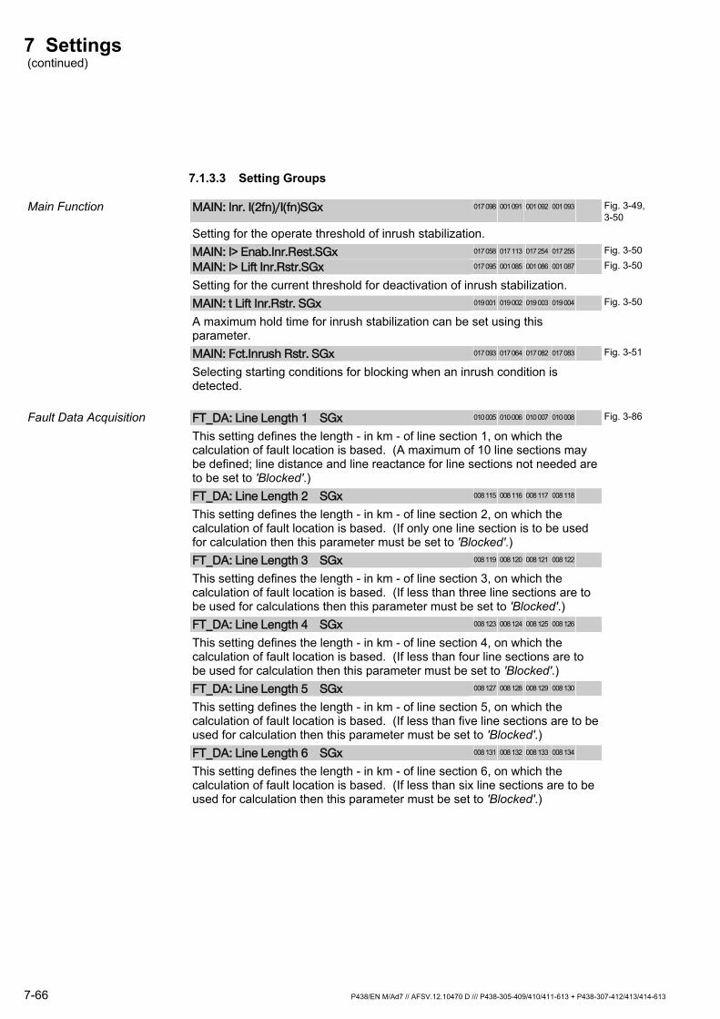
7 Settings (continued)
7-66 P438/EN M/Ad7 // AFSV.12.10470 D /// P438-305-409/410/411-613 + P438-307-412/413/414-613
7.1.3.3 Setting Groups
Main Function MAIN: Inr. I(2fn)/I(fn)SGx 017 098 001 091 001 092 001 093 Fig. 3-49, 3-50
Setting for the operate threshold of inrush stabilization.
MAIN: I> Enab.Inr.Rest.SGx 017 058 017 113 017 254 017 255 Fig. 3-50
MAIN: I> Lift Inr.Rstr.SGx 017 095 001 085 001 086 001 087 Fig. 3-50
Setting for the current threshold for deactivation of inrush stabilization.
MAIN: t Lift Inr.Rstr. SGx 019 001 019 002 019 003 019 004 Fig. 3-50
A maximum hold time for inrush stabilization can be set using this parameter.
MAIN: Fct.Inrush Rstr. SGx 017 093 017 064 017 082 017 083 Fig. 3-51
Selecting starting conditions for blocking when an inrush condition is detected.
Fault Data Acquisition FT_DA: Line Length 1 SGx 010 005 010 006 010 007 010 008 Fig. 3-86
This setting defines the length - in km - of line section 1, on which the calculation of fault location is based. (A maximum of 10 line sections may be defined; line distance and line reactance for line sections not needed are to be set to 'Blocked'.)
FT_DA: Line Length 2 SGx 008 115 008 116 008 117 008 118
This setting defines the length - in km - of line section 2, on which the calculation of fault location is based. (If only one line section is to be used for calculation then this parameter must be set to 'Blocked'.)
FT_DA: Line Length 3 SGx 008 119 008 120 008 121 008 122
This setting defines the length - in km - of line section 3, on which the calculation of fault location is based. (If less than three line sections are to be used for calculations then this parameter must be set to 'Blocked'.)
FT_DA: Line Length 4 SGx 008 123 008 124 008 125 008 126
This setting defines the length - in km - of line section 4, on which the calculation of fault location is based. (If less than four line sections are to be used for calculation then this parameter must be set to 'Blocked'.)
FT_DA: Line Length 5 SGx 008 127 008 128 008 129 008 130
This setting defines the length - in km - of line section 5, on which the calculation of fault location is based. (If less than five line sections are to be used for calculation then this parameter must be set to 'Blocked'.)
FT_DA: Line Length 6 SGx 008 131 008 132 008 133 008 134
This setting defines the length - in km - of line section 6, on which the calculation of fault location is based. (If less than six line sections are to be used for calculation then this parameter must be set to 'Blocked'.)
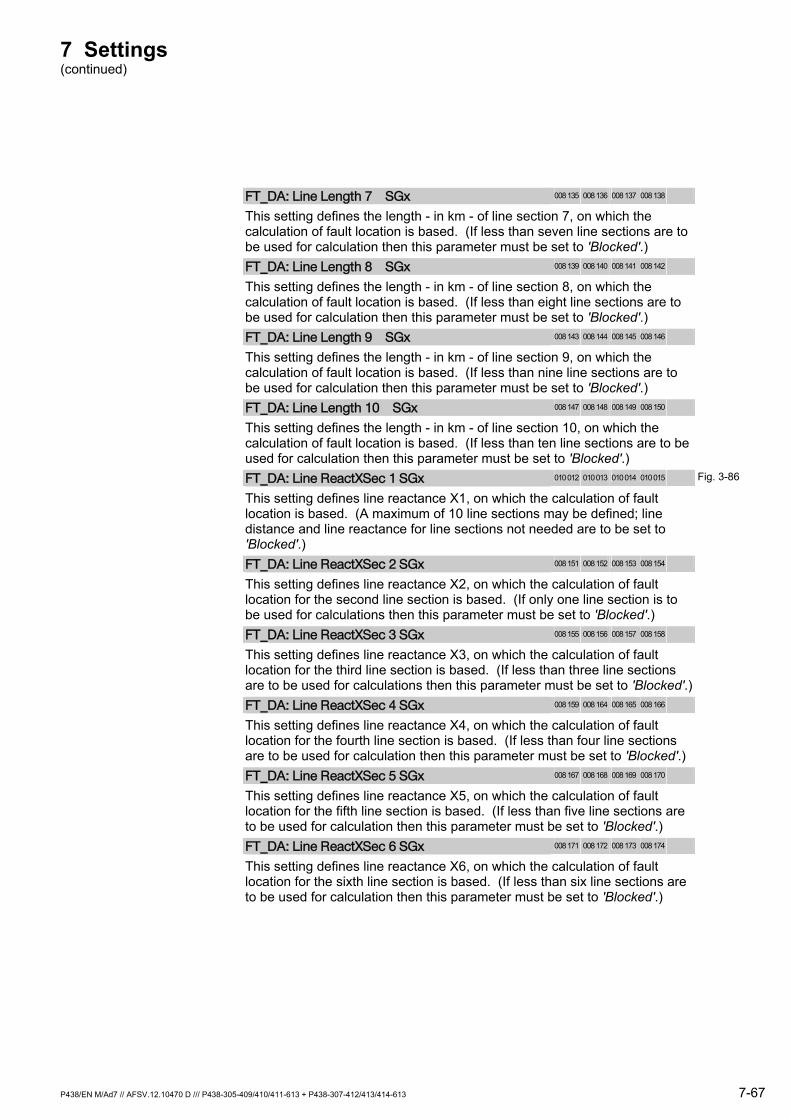
7 Settings (continued)
P438/EN M/Ad7 // AFSV.12.10470 D /// P438-305-409/410/411-613 + P438-307-412/413/414-613 7-67
FT_DA: Line Length 7 SGx 008 135 008 136 008 137 008 138
This setting defines the length - in km - of line section 7, on which the calculation of fault location is based. (If less than seven line sections are to be used for calculation then this parameter must be set to 'Blocked'.)
FT_DA: Line Length 8 SGx 008 139 008 140 008 141 008 142
This setting defines the length - in km - of line section 8, on which the calculation of fault location is based. (If less than eight line sections are to be used for calculation then this parameter must be set to 'Blocked'.)
FT_DA: Line Length 9 SGx 008 143 008 144 008 145 008 146
This setting defines the length - in km - of line section 9, on which the calculation of fault location is based. (If less than nine line sections are to be used for calculation then this parameter must be set to 'Blocked'.)
FT_DA: Line Length 10 SGx 008 147 008 148 008 149 008 150
This setting defines the length - in km - of line section 10, on which the calculation of fault location is based. (If less than ten line sections are to be used for calculation then this parameter must be set to 'Blocked'.)
FT_DA: Line ReactXSec 1 SGx 010 012 010 013 010 014 010 015 Fig. 3-86
This setting defines line reactance X1, on which the calculation of fault location is based. (A maximum of 10 line sections may be defined; line distance and line reactance for line sections not needed are to be set to 'Blocked'.)
FT_DA: Line ReactXSec 2 SGx 008 151 008 152 008 153 008 154
This setting defines line reactance X2, on which the calculation of fault location for the second line section is based. (If only one line section is to be used for calculations then this parameter must be set to 'Blocked'.)
FT_DA: Line ReactXSec 3 SGx 008 155 008 156 008 157 008 158
This setting defines line reactance X3, on which the calculation of fault location for the third line section is based. (If less than three line sections are to be used for calculations then this parameter must be set to 'Blocked'.)
FT_DA: Line ReactXSec 4 SGx 008 159 008 164 008 165 008 166
This setting defines line reactance X4, on which the calculation of fault location for the fourth line section is based. (If less than four line sections are to be used for calculation then this parameter must be set to 'Blocked'.)
FT_DA: Line ReactXSec 5 SGx 008 167 008 168 008 169 008 170
This setting defines line reactance X5, on which the calculation of fault location for the fifth line section is based. (If less than five line sections are to be used for calculation then this parameter must be set to 'Blocked'.)
FT_DA: Line ReactXSec 6 SGx 008 171 008 172 008 173 008 174
This setting defines line reactance X6, on which the calculation of fault location for the sixth line section is based. (If less than six line sections are to be used for calculation then this parameter must be set to 'Blocked'.)
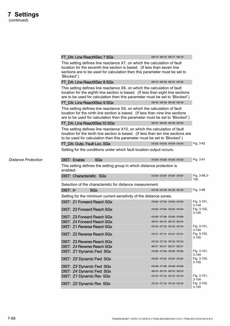
7 Settings (continued)
7-68 P438/EN M/Ad7 // AFSV.12.10470 D /// P438-305-409/410/411-613 + P438-307-412/413/414-613
FT_DA: Line ReactXSec 7 SGx 008 175 008 176 008 177 008 178
This setting defines line reactance X7, on which the calculation of fault location for the seventh line section is based. (If less than seven line sections are to be used for calculation then this parameter must be set to 'Blocked'.)
FT_DA: Line ReactXSec 8 SGx 008 179 008 180 008 181 008 182
This setting defines line reactance X8, on which the calculation of fault location for the eighth line section is based. (If less than eight line sections are to be used for calculation then this parameter must be set to 'Blocked'.)
FT_DA: Line ReactXSec 9 SGx 008 183 008 184 008 185 008 186
This setting defines line reactance X9, on which the calculation of fault location for the ninth line section is based. (If less than nine line sections are to be used for calculation then this parameter must be set to 'Blocked'.)
FT_DA: Line ReactXSec10 SGx 008 187 008 188 008 189 008 190
This setting defines line reactance X10, on which the calculation of fault location for the tenth line section is based. (If less than ten line sections are to be used for calculation then this parameter must be set to 'Blocked'.)
FT_DA: Outp. Fault Loc. SGx 010 032 010 033 010 034 010 035 Fig. 3-82
Setting for the conditions under which fault location output occurs.
Distance Protection DIST: Enable SGx 072 200 073 200 074 200 075 200 Fig. 3-91
This setting defines the setting group in which distance protection is enabled.
DIST: Characteristic SGx 012 040 073 097 074 097 075 097 Fig. 3-98,3-102
Selection of the characteristic for distance measurement.
DIST: I> SGx 072 195 073 195 074 195 075 195 Fig. 3-96
Setting for the minimum current sensitivity of the distance zones.
DIST: Z1 Forward Reach SGx 076 093 077 093 078 093 079 093 Fig. 3-101, 3-104
DIST: Z2 Forward Reach SGx 076 094 077 094 078 094 079 094 Fig. 3-102, 3-105
DIST: Z3 Forward Reach SGx 076 095 077 095 078 095 079 095
DIST: Z4 Forward Reach SGx 080 015 081 015 082 015 083 015
DIST: Z1 Reverse Reach SGx 076 100 077 100 078 100 079 100 Fig. 3-101, 3-104
DIST: Z2 Reverse Reach SGx 076 101 077 101 078 101 079 101 Fig. 3-102, 3-105
DIST: Z3 Reverse Reach SGx 076 102 077 102 078 102 079 102
DIST: Z4 Reverse Reach SGx 080 017 081 017 082 017 083 017
DIST: Z1' Dynamic Fwd SGx 076 096 077 096 078 096 079 096 Fig. 3-101, 3-104
DIST: Z2' Dynamic Fwd SGx 076 097 077 097 078 097 079 097 Fig. 3-102, 3-105
DIST: Z3' Dynamic Fwd SGx 076 098 077 098 078 098 079 098
DIST: Z4' Dynamic Fwd SGx 080 016 081 016 082 016 083 016
DIST: Z1' Dynamic Rev SGx 076 103 077 103 078 103 079 103 Fig. 3-101, 3-104
DIST: Z2' Dynamic Rev SGx 076 104 077 104 078 104 079 104 Fig. 3-102, 3-105
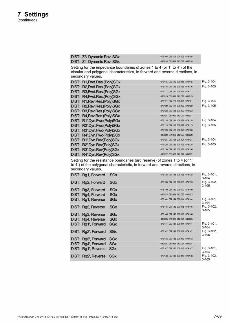
7 Settings (continued)
P438/EN M/Ad7 // AFSV.12.10470 D /// P438-305-409/410/411-613 + P438-307-412/413/414-613 7-69
DIST: Z3' Dynamic Rev SGx 076 105 077 105 078 105 079 105
DIST: Z4' Dynamic Rev SGx 080 018 081 018 082 018 083 018
Setting for the impedance boundaries of zones 1 to 4 (or 1´ to 4´) of the circular and polygonal characteristics, in forward and reverse directions, in secondary values.
DIST: R1,Fwd.Res.(Poly)SGx 076 115 077 115 078 115 079 115 Fig. 3-104
DIST: R2,Fwd.Res.(Poly)SGx 076 116 077 116 078 116 079 116 Fig. 3-105
DIST: R3,Fwd.Res.(Poly)SGx 076 117 077 117 078 117 079 117
DIST: R4,Fwd.Res.(Poly)SGx 080 019 081 019 082 019 083 019
DIST: R1,Rev.Res.(Poly)SGx 076 121 077 121 078 121 079 121 Fig. 3-104
DIST: R2,Rev.Res.(Poly)SGx 076 122 077 122 078 122 079 122 Fig. 3-105
DIST: R3,Rev.Res.(Poly)SGx 076 123 077 123 078 123 079 123
DIST: R4,Rev.Res.(Poly)SGx 080 021 081 021 082 021 083 021
DIST: R1',Dyn.Fwd(Poly)SGx 076 118 077 118 078 118 079 118 Fig. 3-104
DIST: R2',Dyn.Fwd(Poly)SGx 076 119 077 119 078 119 079 119 Fig. 3-105
DIST: R3',Dyn.Fwd(Poly)SGx 076 120 077 120 078 120 079 120
DIST: R4',Dyn.Fwd(Poly)SGx 080 020 081 020 082 020 083 020
DIST: R1',Dyn.Rev(Poly)SGx 076 124 077 124 078 124 079 124 Fig. 3-104
DIST: R2',Dyn.Rev(Poly)SGx 076 125 077 125 078 125 079 125 Fig. 3-105
DIST: R3',Dyn.Rev(Poly)SGx 076 126 077 126 078 126 079 126
DIST: R4',Dyn.Rev(Poly)SGx 080 022 081 022 082 022 083 022
Setting for the resistance boundaries (arc reserve) of zones 1 to 4 (or 1´ to 4´) of the polygonal characteristic, in forward and reverse directions, in secondary values.
DIST: Rg1, Forward SGx 076 138 077 138 078 138 079 138 Fig. 3-101, 3-104
DIST: Rg2, Forward SGx 076 139 077 139 078 139 079 139 Fig. 3-102, 3-105
DIST: Rg3, Forward SGx 076 140 077 140 078 140 079 140
DIST: Rg4, Forward SGx 080 023 081 023 082 023 083 023
DIST: Rg1, Reverse SGx 076 144 077 144 078 144 079 144 Fig. 3-101, 3-104
DIST: Rg2, Reverse SGx 076 145 077 145 078 145 079 145 Fig. 3-102, 3-105
DIST: Rg3, Reverse SGx 076 146 077 146 078 146 079 146
DIST: Rg4, Reverse SGx 080 025 081 025 082 025 083 025
DIST: Rg1', Forward SGx 076 141 077 141 078 141 079 141 Fig. 3-101, 3-104
DIST: Rg2', Forward SGx 076 142 077 142 078 142 079 142 Fig. 3-102, 3-105
DIST: Rg3', Forward SGx 076 143 077 143 078 143 079 143
DIST: Rg4', Forward SGx 080 024 081 024 082 024 083 024
DIST: Rg1', Reverse SGx 076 147 077 147 078 147 079 147 Fig. 3-101, 3-104
DIST: Rg2', Reverse SGx 076 148 077 148 078 148 079 148 Fig. 3-102, 3-105
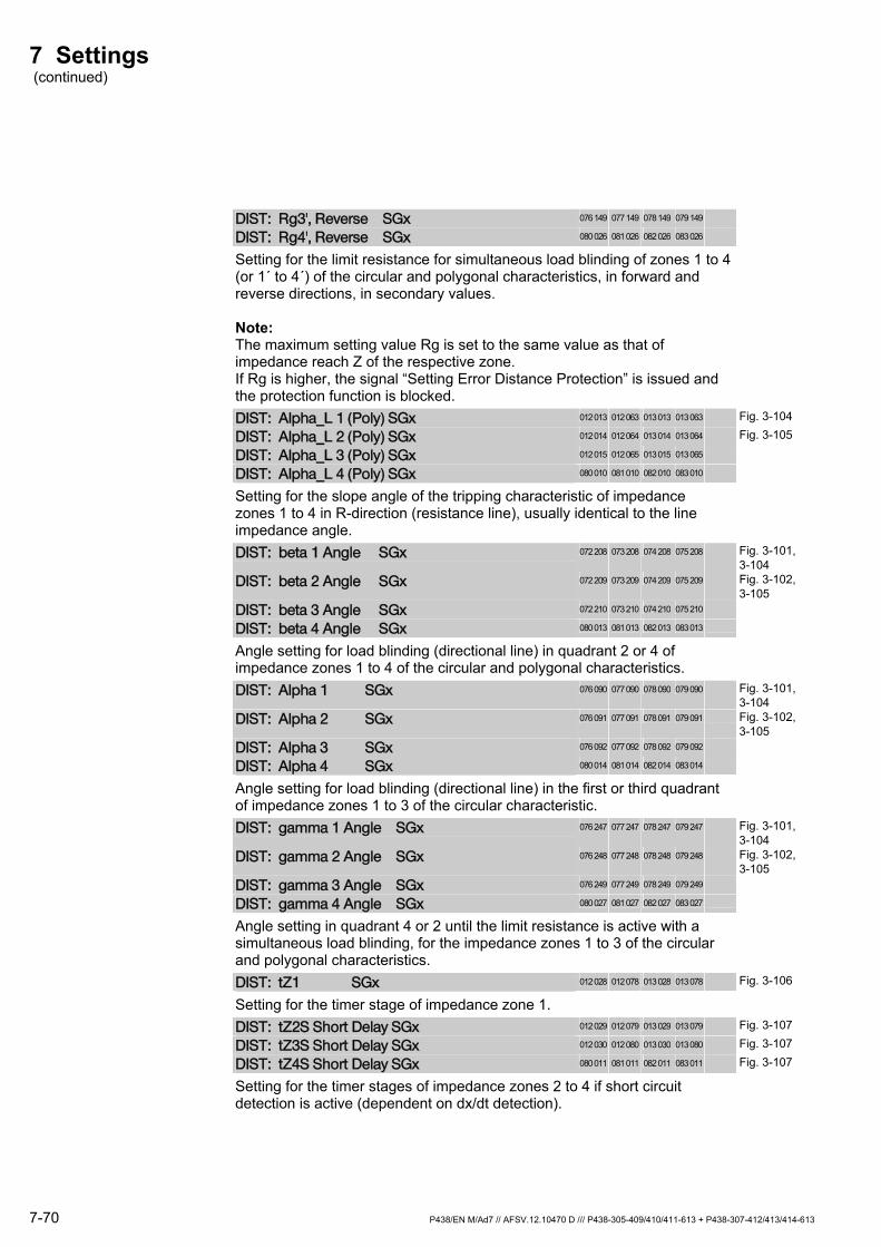
7 Settings (continued)
7-70 P438/EN M/Ad7 // AFSV.12.10470 D /// P438-305-409/410/411-613 + P438-307-412/413/414-613
DIST: Rg3', Reverse SGx 076 149 077 149 078 149 079 149
DIST: Rg4', Reverse SGx 080 026 081 026 082 026 083 026
Setting for the limit resistance for simultaneous load blinding of zones 1 to 4 (or 1´ to 4´) of the circular and polygonal characteristics, in forward and reverse directions, in secondary values. Note: The maximum setting value Rg is set to the same value as that of impedance reach Z of the respective zone. If Rg is higher, the signal “Setting Error Distance Protection” is issued and the protection function is blocked.
DIST: Alpha_L 1 (Poly) SGx 012 013 012 063 013 013 013 063 Fig. 3-104
DIST: Alpha_L 2 (Poly) SGx 012 014 012 064 013 014 013 064 Fig. 3-105
DIST: Alpha_L 3 (Poly) SGx 012 015 012 065 013 015 013 065
DIST: Alpha_L 4 (Poly) SGx 080 010 081 010 082 010 083 010
Setting for the slope angle of the tripping characteristic of impedance zones 1 to 4 in R-direction (resistance line), usually identical to the line impedance angle.
DIST: beta 1 Angle SGx 072 208 073 208 074 208 075 208 Fig. 3-101, 3-104
DIST: beta 2 Angle SGx 072 209 073 209 074 209 075 209 Fig. 3-102, 3-105
DIST: beta 3 Angle SGx 072 210 073 210 074 210 075 210
DIST: beta 4 Angle SGx 080 013 081 013 082 013 083 013
Angle setting for load blinding (directional line) in quadrant 2 or 4 of impedance zones 1 to 4 of the circular and polygonal characteristics.
DIST: Alpha 1 SGx 076 090 077 090 078 090 079 090 Fig. 3-101, 3-104
DIST: Alpha 2 SGx 076 091 077 091 078 091 079 091 Fig. 3-102, 3-105
DIST: Alpha 3 SGx 076 092 077 092 078 092 079 092
DIST: Alpha 4 SGx 080 014 081 014 082 014 083 014
Angle setting for load blinding (directional line) in the first or third quadrant of impedance zones 1 to 3 of the circular characteristic.
DIST: gamma 1 Angle SGx 076 247 077 247 078 247 079 247 Fig. 3-101, 3-104
DIST: gamma 2 Angle SGx 076 248 077 248 078 248 079 248 Fig. 3-102, 3-105
DIST: gamma 3 Angle SGx 076 249 077 249 078 249 079 249
DIST: gamma 4 Angle SGx 080 027 081 027 082 027 083 027
Angle setting in quadrant 4 or 2 until the limit resistance is active with a simultaneous load blinding, for the impedance zones 1 to 3 of the circular and polygonal characteristics.
DIST: tZ1 SGx 012 028 012 078 013 028 013 078 Fig. 3-106
Setting for the timer stage of impedance zone 1.
DIST: tZ2S Short Delay SGx 012 029 012 079 013 029 013 079 Fig. 3-107
DIST: tZ3S Short Delay SGx 012 030 012 080 013 030 013 080 Fig. 3-107
DIST: tZ4S Short Delay SGx 080 011 081 011 082 011 083 011 Fig. 3-107
Setting for the timer stages of impedance zones 2 to 4 if short circuit detection is active (dependent on dx/dt detection).
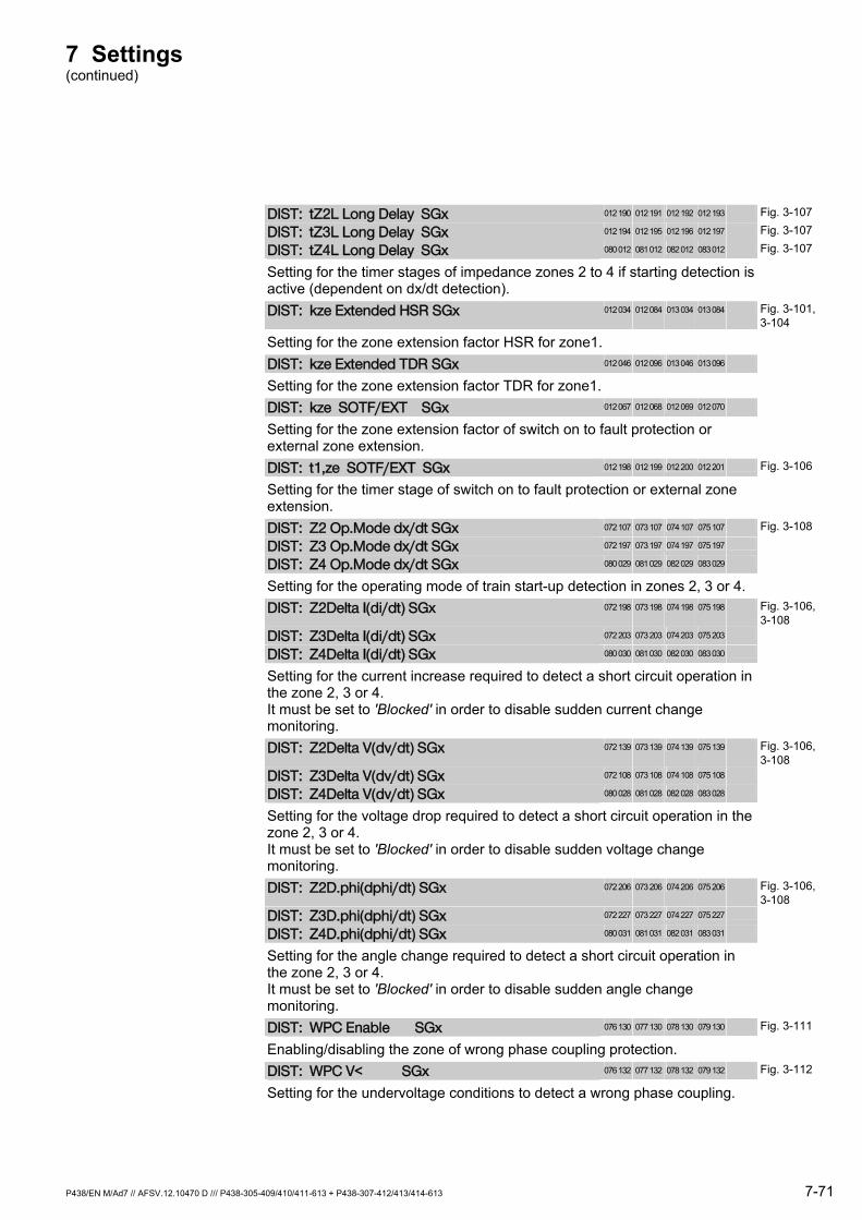
7 Settings (continued)
P438/EN M/Ad7 // AFSV.12.10470 D /// P438-305-409/410/411-613 + P438-307-412/413/414-613 7-71
DIST: tZ2L Long Delay SGx 012 190 012 191 012 192 012 193 Fig. 3-107
DIST: tZ3L Long Delay SGx 012 194 012 195 012 196 012 197 Fig. 3-107
DIST: tZ4L Long Delay SGx 080 012 081 012 082 012 083 012 Fig. 3-107
Setting for the timer stages of impedance zones 2 to 4 if starting detection is active (dependent on dx/dt detection).
DIST: kze Extended HSR SGx 012 034 012 084 013 034 013 084 Fig. 3-101, 3-104
Setting for the zone extension factor HSR for zone1.
DIST: kze Extended TDR SGx 012 046 012 096 013 046 013 096
Setting for the zone extension factor TDR for zone1.
DIST: kze SOTF/EXT SGx 012 067 012 068 012 069 012 070
Setting for the zone extension factor of switch on to fault protection or external zone extension.
DIST: t1,ze SOTF/EXT SGx 012 198 012 199 012 200 012 201 Fig. 3-106
Setting for the timer stage of switch on to fault protection or external zone extension.
DIST: Z2 Op.Mode dx/dt SGx 072 107 073 107 074 107 075 107 Fig. 3-108
DIST: Z3 Op.Mode dx/dt SGx 072 197 073 197 074 197 075 197
DIST: Z4 Op.Mode dx/dt SGx 080 029 081 029 082 029 083 029
Setting for the operating mode of train start-up detection in zones 2, 3 or 4.
DIST: Z2Delta I(di/dt) SGx 072 198 073 198 074 198 075 198 Fig. 3-106, 3-108
DIST: Z3Delta I(di/dt) SGx 072 203 073 203 074 203 075 203
DIST: Z4Delta I(di/dt) SGx 080 030 081 030 082 030 083 030
Setting for the current increase required to detect a short circuit operation in the zone 2, 3 or 4. It must be set to 'Blocked' in order to disable sudden current change monitoring.
DIST: Z2Delta V(dv/dt) SGx 072 139 073 139 074 139 075 139 Fig. 3-106, 3-108
DIST: Z3Delta V(dv/dt) SGx 072 108 073 108 074 108 075 108
DIST: Z4Delta V(dv/dt) SGx 080 028 081 028 082 028 083 028
Setting for the voltage drop required to detect a short circuit operation in the zone 2, 3 or 4. It must be set to 'Blocked' in order to disable sudden voltage change monitoring.
DIST: Z2D.phi(dphi/dt) SGx 072 206 073 206 074 206 075 206 Fig. 3-106, 3-108
DIST: Z3D.phi(dphi/dt) SGx 072 227 073 227 074 227 075 227
DIST: Z4D.phi(dphi/dt) SGx 080 031 081 031 082 031 083 031
Setting for the angle change required to detect a short circuit operation in the zone 2, 3 or 4. It must be set to 'Blocked' in order to disable sudden angle change monitoring.
DIST: WPC Enable SGx 076 130 077 130 078 130 079 130 Fig. 3-111
Enabling/disabling the zone of wrong phase coupling protection.
DIST: WPC V< SGx 076 132 077 132 078 132 079 132 Fig. 3-112
Setting for the undervoltage conditions to detect a wrong phase coupling.
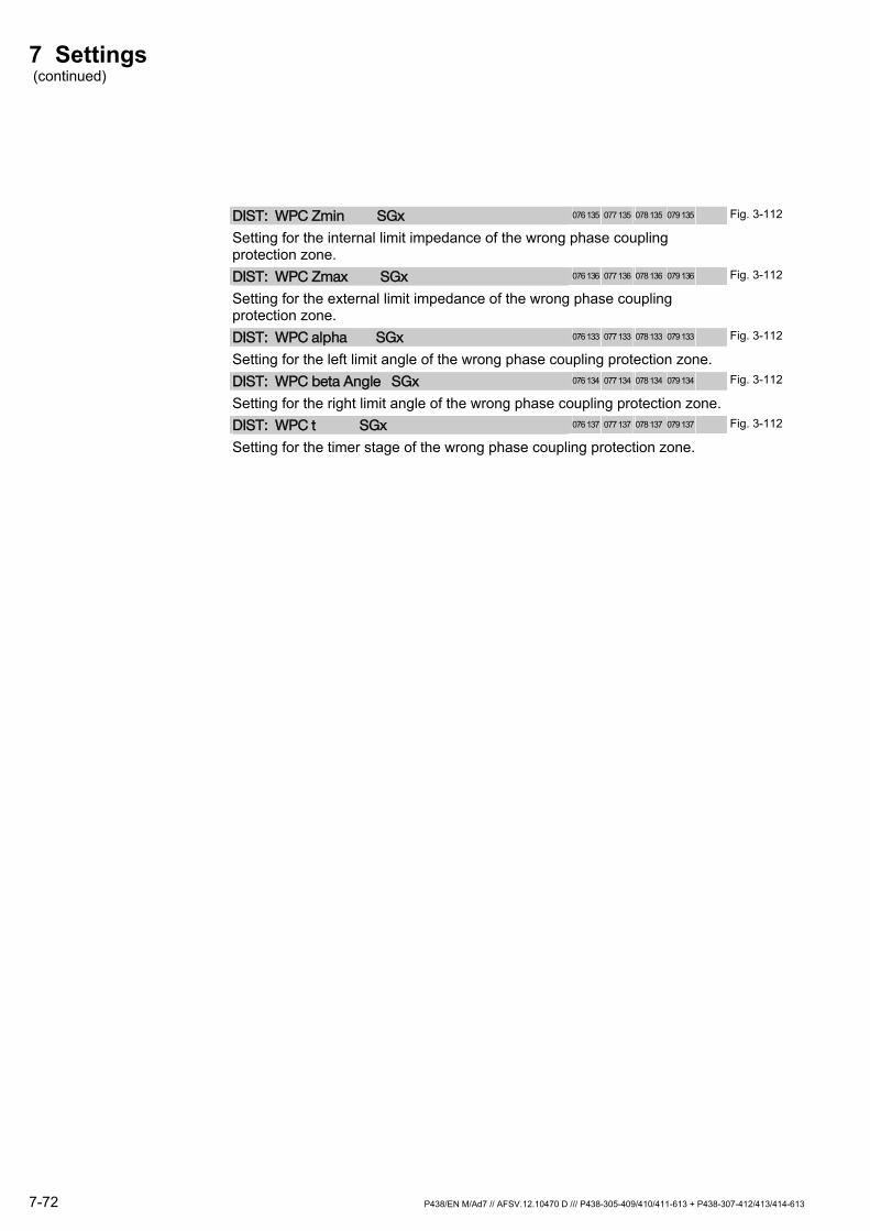
7 Settings (continued)
7-72 P438/EN M/Ad7 // AFSV.12.10470 D /// P438-305-409/410/411-613 + P438-307-412/413/414-613
DIST: WPC Zmin SGx 076 135 077 135 078 135 079 135 Fig. 3-112
Setting for the internal limit impedance of the wrong phase coupling protection zone.
DIST: WPC Zmax SGx 076 136 077 136 078 136 079 136 Fig. 3-112
Setting for the external limit impedance of the wrong phase coupling protection zone.
DIST: WPC alpha SGx 076 133 077 133 078 133 079 133 Fig. 3-112
Setting for the left limit angle of the wrong phase coupling protection zone.
DIST: WPC beta Angle SGx 076 134 077 134 078 134 079 134 Fig. 3-112
Setting for the right limit angle of the wrong phase coupling protection zone.
DIST: WPC t SGx 076 137 077 137 078 137 079 137 Fig. 3-112
Setting for the timer stage of the wrong phase coupling protection zone.
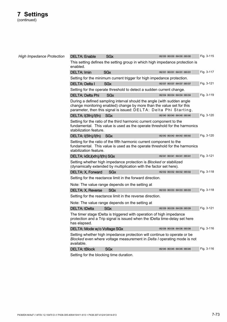
7 Settings (continued)
P438/EN M/Ad7 // AFSV.12.10470 D /// P438-305-409/410/411-613 + P438-307-412/413/414-613 7-73
High Impedance Protection DELTA: Enable SGx 062 030 063 030 064 030 065 030 Fig. 3-115
This setting defines the setting group in which high impedance protection is enabled.
DELTA: Imin SGx 062 031 063 031 064 031 065 031 Fig. 3-117
Setting for the minimum current trigger for high impedance protection.
DELTA: Delta I SGx 062 037 063 037 064 037 065 037 Fig. 3-121
Setting for the operate threshold to detect a sudden current change.
DELTA: Delta Phi SGx 062 034 063 034 064 034 065 034 Fig. 3-119
During a defined sampling interval should the angle (with sudden angle change monitoring enabled) change by more than the value set for this parameter, then this signal is issued: D E L T A : D e l t a P h i S t a r t i n g .
DELTA: I(3fn)/I(fn) SGx 062 040 063 040 064 040 065 040 Fig. 3-120
Setting for the ratio of the third harmonic current component to the fundamental. This value is used as the operate threshold for the harmonics stabilization feature.
DELTA: I(5fn)/I(fn) SGx 062 042 063 042 064 042 065 042 Fig. 3-120
Setting for the ratio of the fifth harmonic current component to the fundamental. This value is used as the operate threshold for the harmonics stabilization feature.
DELTA: kSt,I(xfn)/I(fn) SGx 062 041 063 041 064 041 065 041 Fig. 3-121
Setting whether high impedance protection is Blocked or stabilized (dynamically extended by multiplication with the factor set here).
DELTA: X, Forward SGx 062 032 063 032 064 032 065 032 Fig. 3-118
Setting for the reactance limit in the forward direction.
Note: The value range depends on the setting at
DELTA: X, Reverse SGx 062 033 063 033 064 033 065 033 Fig. 3-118
Setting for the reactance limit in the reverse direction.
Note: The value range depends on the setting at
DELTA: tDelta SGx 062 039 063 039 064 039 065 039 Fig. 3-121
The timer stage tDelta is triggered with operation of high impedance protection and a Trip signal is issued when the tDelta time-delay set here has elapsed.
DELTA: Mode w/o Voltage SGx 062 036 063 036 064 036 065 036 Fig. 3-116
Setting whether high impedance protection will continue to operate or be Blocked even where voltage measurement in Delta I operating mode is not available.
DELTA: tBlock SGx 062 045 063 045 064 045 065 045 Fig. 3-116
Setting for the blocking time duration.
7 Settings (continued)
7-74 P438/EN M/Ad7 // AFSV.12.10470 D /// P438-305-409/410/411-613 + P438-307-412/413/414-613
VT and CT Supervision C&VTS: Enable SGx 014 200 014 201 014 202 014 203 Fig. 3-122
This setting defines the setting group in which CT and VT Supervision is enabled.
C&VTS: I> Enab V< FuseF SGx 014 188 014 237 014 238 014 239 Fig. 3-123, 3-124
Enabling undervoltage and fuse failure monitoring.
C&VTS: V-Monit. Enabled SGx 014 225 014 226 014 227 014 228 Fig. 3-123
Disabling/enabling undervoltage monitoring.
C&VTS: V<, V-Monit. SGx 014 229 014 230 014 231 014 232 Fig. 3-123
Setting for the operate threshold of undervoltage monitoring.
C&VTS: tV<, V-Monit. SGx 014 233 014 234 014 235 014 236 Fig. 3-123
Setting for the time delay of undervoltage monitoring.
C&VTS: VTS/Fuse F. Enab SGx 014 204 014 205 014 206 014 207 Fig. 3-124
Enabling/disabling “fuse failure” monitoring.
C&VTS: V< VTS/Fuse Fail SGx 014 208 014 209 014 210 014 211 Fig. 3-124
Setting for the enable value V< of “fuse failure” monitoring.
C&VTS: V> VTS/Fuse Fail SGx 014 212 014 213 014 214 014 215 Fig. 3-124
Setting for the reset value V> of “fuse failure” monitoring.
C&VTS: Delta V VTS/Fuse SGx 014 216 014 217 014 218 014 219 Fig. 3-124
Setting for the minimum voltage change for the detection of a “fuse failure” condition.
C&VTS: Delta I VTS/Fuse SGx 014 221 014 222 014 223 014 224 Fig. 3-124
Setting for the maximum current change for the detection of a “fuse failure” condition.
Backup Overcurrent-Time Protection
BUOC: Enable SGx 072 118 073 118 074 118 075 118 Fig. 3-127
This setting defines the setting group in which backup overcurrent-time protection is enabled.
BUOC: I> SGx 010 058 010 078 010 098 011 018 Fig. 3-129
Setting for operate threshold I> of the current of the backup overcurrent-time protection.
BUOC: I>> SGx 010 127 010 129 010 131 010 133 Fig. 3-129
Setting for operate threshold I>> of the current of the backup overcurrent-time protection.
BUOC: tI> SGx 010 059 010 079 010 099 011 019 Fig. 3-129
Setting for the operate delay of stage I> of the backup overcurrent-time protection.
BUOC: tI>> SGx 010 128 010 130 010 132 010 134 Fig. 3-129
Setting for the operate delay of stage I>> of the backup overcurrent-time protection.

7 Settings (continued)
P438/EN M/Ad7 // AFSV.12.10470 D /// P438-305-409/410/411-613 + P438-307-412/413/414-613 7-75
Switch on to Fault Protection SOTF: Enable SGx 011 120 011 121 011 122 011 123 Fig. 3-130
This setting defines the setting group in which switch on to fault protection is enabled.
SOTF: Operating Mode SGx 011 061 011 114 011 115 011 116 Fig. 3-131
The setting of the operating mode defines whether a general start shall cause a trip while a timer stage is running ("trip with starting") or if the measuring range of the impedance zone 1 is extended by the set zone extension factor D I S T : k z e E x t e n d e d H S R S G x ("trip with overreach").
SOTF: Man. Close Timer SGx 011 060 011 111 011 112 011 113 Fig. 3-131
Setting for the timer stage which is started by the manual close signal.
Auto-Reclose Control RECLS: Enable SGx 015 046 015 047 015 048 015 049 Fig. 3-132
This setting defines the parameter subset in which ARC is enabled.
RECLS: Check CB Closed? SGx 015 050 024 024 024 084 025 044 Fig. 3-134
This setting defines whether the CB closed position will be scanned or not. If the setting is 'Enabled', a binary signal input must be configured accordingly.
RECLS: Parallel Trip SGx 015 053 024 027 024 087 025 047 Fig. 3-148
This setting defines whether the trip commands of a protection device operating together with the P438 will affect operation of the ARC function. For further details see the section entitled ‘Parallel Blocking’ in Chapter 3.
RECLS: Operative Time 1 SGx 015 066 024 035 024 095 025 055 Fig. 3-148
Setting for operative time 1.
RECLS: Operative Time 2 SGx 015 083 024 042 025 002 025 062 Fig. 3-148
Setting for operative time 2.
RECLS: V> SGx 015 128 015 129 015 138 015 139
Voltage enabling of reclosure when operative time 2 is used.
RECLS: tV> SGx 015 140 015 141 015 142 015 143
Time delay of voltage enabling.
RECLS: HSR-Tr.DIST t1 SGx 015 072 024 040 025 000 025 060 Fig. 3-135
Setting for the HSR tripping timer stage initiated by a distance protection zone 1 start.
RECLS: HSR-Tr.DIST t2S SGx 015 144 015 145 015 146 015 147 Fig. 3-135
RECLS: HSR-Tr.DIST t2L SGx 015 152 015 153 015 154 015 155 Fig. 3-135
Setting for the HSR tripping timer stage initiated by a distance protection zone 2 start together with train start-up detection dx/dt in zone 2.
RECLS: HSR-Tr.DIST t3S SGx 015 160 015 161 015 162 015 163 Fig. 3-135
RECLS: HSR-Tr.DIST t3L SGx 015 168 015 169 015 170 015 171 Fig. 3-135
Setting for the HSR tripping timer stage initiated by a distance protection zone 3 start together with train start-up detection dx/dt in zone 3.
7 Settings (continued)
7-76 P438/EN M/Ad7 // AFSV.12.10470 D /// P438-305-409/410/411-613 + P438-307-412/413/414-613
RECLS: HSR-Tr.DIST t4S SGx 015 180 015 181 015 182 015 183
RECLS: HSR-Tr.DIST t4L SGx 015 188 015 189 015 190 015 191
Setting for the HSR tripping timer stage initiated by a distance protection zone 4 start together with train start-up detection dx/dt in zone 4.
RECLS: HSR-Tr.DELTA tD. SGx 008 192 008 193 008 194 008 195 Fig. 3-137
Setting for the HSR tripping timer stage initiated by a start of the high impedance protection.
RECLS: HSR-Tr.DTOC tI>H SGx 015 069 024 052 024 053 024 054 Fig. 3-138
Setting for the HSR tripping timer stage initiated by a start of the DTOC high-current stage.
RECLS: HSR-Tr.DTOC tI> SGx 015 105 020 105 021 105 022 105 Fig. 3-138
RECLS: HSR-Tr.DTOC tI>> SGx 015 074 020 107 021 107 022 107 Fig. 3-138
Setting for the HSR tripping timer stage initiated by a start of the DTOC 1st or 2nd high-current stage.
RECLS: HSR-Tr.IDMT kIrefSGx 015 094 020 113 021 113 022 113 Fig. 3-138
Setting for the HSR tripping timer stage initiated by a start of the IDMT Ikref stage.
RECLS: HSR-Tr.BUOC tI> SGx 015 109 020 109 022 109 023 109 Fig. 3-140
RECLS: HSR-Tr.BUOC tI>> SGx 015 111 020 111 021 111 022 111 Fig. 3-140
Setting for the HSR tripping timer stage initiated by a start of the BUOC 1st or 2nd high-current stage.
RECLS: HSR-Tr. LOGIC SGx 015 098 024 110 024 160 025 110 Fig. 3-142
Setting for the HSR tripping timer stage initiated by a programmable logic start.
RECLS: HSR Dead Time SGx 015 056 024 030 024 090 025 050 Fig. 3-148
Dead time setting for a three-pole HSR.
RECLS: Dead Time Max SGx 015 084 024 043 025 003 025 063 Fig. 3-148
Setting for the maximum dead time.
RECLS: Zone Extn on HSR SGx 015 059 024 033 024 093 025 053 Page: 3-205
This setting determines whether the measuring range shall be extended by the zone extension factor kze HSR during normal system operation and while the operative times are elapsing. Note: This setting is active only if protective signaling is not ready.
RECLS: No. Permit. TDR SGx 015 068 024 037 024 097 025 057 Fig. 3-148
Setting for the number of time-delayed reclosures permitted. With the ‘0’ setting, only one HSR is carried out.
RECLS: TDR-Tr.DIST t1 SGx 015 073 024 041 025 001 025 061 Fig. 3-136
Setting for the TDR tripping timer stage initiated by a distance protection zone 1 start.
RECLS: TDR-Tr.DIST t2S SGx 015 148 015 149 015 150 015 151 Fig. 3-136
RECLS: TDR-Tr.DIST t2L SGx 015 156 015 157 015 158 015 159 Fig. 3-136
Setting for the TDR tripping timer stage initiated by a distance protection zone 2 start together with train start-up detection dx/dt in zone 2.
RECLS: TDR-Tr.DIST t3S SGx 015 164 015 165 015 166 015 167 Fig. 3-136
RECLS: TDR-Tr.DIST t3L SGx 015 172 015 173 015 174 015 175 Fig. 3-136
Setting for the TDR tripping timer stage initiated by a distance protection zone 3 start together with train start-up detection dx/dt in zone 3.
7 Settings (continued)
P438/EN M/Ad7 // AFSV.12.10470 D /// P438-305-409/410/411-613 + P438-307-412/413/414-613 7-77
RECLS: TDR-Tr.DIST t4S SGx 015 184 015 185 015 186 015 187
RECLS: TDR-Tr.DIST t4L SGx 015 192 015 193 015 194 015 195
Setting for the TDR tripping timer stage initiated by a distance protection zone 4 start together with train start-up detection dx/dt in zone 4.
RECLS: TDR-Tr.DELTA tD. SGx 008 196 008 197 008 198 008 199 Fig. 3-137
Setting for the TDR tripping timer stage initiated by a start of the high impedance protection.
RECLS: TDR-Tr.DTOC tI>H SGx 015 070 024 055 024 056 024 057 Fig. 3-139
Setting for the TDR tripping timer stage initiated by a start of the DTOC high-current stage.
RECLS: TDR-Tr.DTOC tI> SGx 015 106 020 106 021 106 022 106 Fig. 3-139
RECLS: TDR-Tr.DTOC tI>> SGx 015 075 020 108 022 108 023 108 Fig. 3-139
Setting for the TDR tripping timer stage initiated by a start of the DTOC 1st or 2nd high-current stage.
RECLS: TDR-Tr.IDMT kIrefSGx 015 095 020 114 021 114 022 114 Fig. 3-139
Setting for the TDR tripping timer stage initiated by a start of the IDMT Ikref stage.
RECLS: TDR-Tr.BUOC tI> SGx 015 110 020 110 021 110 022 110 Fig. 3-140
RECLS: TDR-Tr.BUOC tI>> SGx 015 112 020 112 021 112 022 112 Fig. 3-140
Setting for the TDR tripping timer stage initiated by a start of the BUOC 1st or 2nd high-current stage.
RECLS: TDR-Tr. LOGIC SGx 015 099 024 122 024 172 025 122 Fig. 3-142
Setting for the TDR tripping timer stage initiated by a programmable logic start.
RECLS: TDR Dead Time SGx 015 057 024 031 024 091 025 051 Fig. 3-148
Setting for the TDR dead time.
RECLS: Zone Extn on TDR SGx 015 071 024 039 024 099 025 059 Page: 3-205
This setting determines whether the measuring range shall be extended prior to a TDR.
RECLS: Reclaim Time 1 SGx 015 054 024 028 024 088 025 048 Fig. 3-148
Setting for reclaim time 1.
RECLS: Reclaim Time 2 SGx 015 124 015 125 015 126 015 127 Fig. 3-148
Setting for reclaim time 2.
RECLS: Block. ARC f. I> SGx 015 104 016 104 017 104 020 104 Fig. 3-133
Setting for the current threshold via which the auto-recloser is blocked.
RECLS: Block. Time Int. SGx 015 043 024 021 024 081 025 041 Fig. 3-133
Setting for the time that will elapse before the auto-recloser will be ready again after cancellation of the blocks set by the P438.
RECLS: Block. Time Ext. SGx 015 058 024 032 024 092 025 052 Fig. 3-133
Setting for the time that will elapse before the auto-recloser will be ready again after blocking by a binary signal input.
RECLS: Zone Ext.Dur. RC SGx 015 088 024 047 025 007 025 067 Page: 3-205
This setting defines whether the following takes place: A zone extension will be carried out during a close command by a HSR
without check synchronism. Zone extension will occur with each reclose command.
7 Settings (continued)
7-78 P438/EN M/Ad7 // AFSV.12.10470 D /// P438-305-409/410/411-613 + P438-307-412/413/414-613
RECLS: RC f. THERM Trip SGx 015 176 015 177 015 178 015 179 Fig. 3-148
This setting determines whether a reclose command shall be issued for a thermal overload protection trip signal.
Definite-Time Overcurrent Protection
DTOC: Enable SGx 072 098 073 098 074 098 075 098 Fig. 3-150
This setting defines the setting group in which definite-time overcurrent protection is enabled.
DTOC: I>H SGx 072 009 073 009 074 009 075 009 Fig. 3-151
Setting for the threshold of the instantaneous high-set stage I>H.
DTOC: I> SGx 072 007 073 007 074 007 075 007 Fig. 3-151
Setting for operate threshold I>.
DTOC: I>> SGx 072 008 073 008 074 008 075 008 Fig. 3-151
Setting for operate threshold I>>.
DTOC: tI>H SGx 072 021 073 021 074 021 075 021 Fig. 3-151
Setting for the operate delay of instantaneous high-set stage I>H.
DTOC: tI> SGx 072 019 073 019 074 019 075 019 Fig. 3-151
Setting for the operate delay of overcurrent stage I>.
DTOC: tI>> SGx 072 020 073 020 074 020 075 020 Fig. 3-151
Setting for the operate delay of overcurrent stage I>>.
DTOC: Timer Start tI> SGx 071 146 071 147 071 148 071 149 Fig. 3-153
This setting defines whether timer stage tI> is started with triggering of current thresholds I> or, additionally, with a directional signal.
DTOC: beta (I>) SGx 076 068 077 068 078 068 079 068 Fig. 3-154
Angles β and γ set the range in which the I> starting signal logic determines that the direction is "forward".
DTOC: gamma (I>) SGx 076 073 077 073 078 073 079 073 Fig. 3-154
Angles β and γ set the range in which the I> starting signal logic determines that the direction is "forward".
DTOC: Direction (I>) SGx 076 080 077 080 078 080 079 080 Fig. 3-155
Setting for the measuring direction for which a tI> trip signal is sent: forward, reverse or non-directional.
DTOC: V< (I>) SGx 076 131 077 131 078 131 079 131 Fig. 3-155
The tI> trip signal is enabled only if the voltage is lower than the set value. Enabling is permanent if it is set to 'Blocked'.
DTOC: Mode w/o V (I>) SGx 076 128 077 128 078 128 079 128 Fig. 3-155
This setting defines whether, for a voltage measuring circuit failure, the I> overcurrent stage should operate non-directionally or should be blocked.
DTOC: Timer Start tI>> SGx 072 245 073 044 074 044 075 044 Fig. 3-153
This setting defines whether timer stage tI>> is started with the triggering of current thresholds I>> or, additionally, with a directional signal.
7 Settings (continued)
P438/EN M/Ad7 // AFSV.12.10470 D /// P438-305-409/410/411-613 + P438-307-412/413/414-613 7-79
DTOC: beta (I>>) SGx 076 069 077 069 078 069 079 069 Fig. 3-154
Angles β and γ set the range in which the I>> starting signal logic determines that the direction is "forward".
DTOC: gamma (I>>) SGx 076 074 077 074 078 074 079 074 Fig. 3-154
Angles β and γ set the range in which the I>> starting signal logic determines that the direction is "forward".
DTOC: Direction (I>>) SGx 076 088 077 088 078 088 079 088 Fig. 3-156
Setting for the measuring direction for which a tI>> trip signal is sent: forward, reverse or non-directional.
DTOC: V< (I>>) SGx 076 150 077 150 078 150 079 150 Fig. 3-156
The tI>> trip signal is enabled only if the voltage is lower than the set value. Enabling is permanent if it is set to ’Blocked’.
DTOC: Mode w/o V (I>>) SGx 076 129 077 129 078 129 079 129 Fig. 3-156
This setting defines whether, for a voltage measuring circuit failure, the I>> overcurrent stage should operate non-directionally or should be blocked.
Inverse-Time Overcurrent Protection
IDMT: Enable SGx 072 000 073 000 074 000 075 000 Fig. 3-157
This setting defines the setting group in which IDMT protection is enabled.
IDMT: Iref Rating SGx 072 050 073 050 074 050 075 050 Fig. 3-162, 3-164
Setting for the reference current of the curve.
IDMT: Characteristic SGx 072 056 073 056 074 056 075 056 Fig. 3-162, 3-164
Setting for the tripping characteristic.
IDMT: kt Time Dial/TMS SGx 072 053 073 053 074 053 075 053 Fig. 3-162, 3-164
Setting for the characteristic time multiplier.
IDMT: Min. Trip Time SGx 072 077 073 077 074 077 075 077 Fig. 3-162, 3-164
Setting for the minimum trip time.
IDMT: Hold Time SGx 072 071 073 071 074 071 075 071 Fig. 3-162, 3-164, 3-167
Setting for the hold time or intermittent faults.
IDMT: Reset SGx 072 059 073 059 074 059 075 059 Fig. 3-162, 3-164
Setting for the release or reset characteristic.
IDMT: Timer Sta. tIref>SGx 006 061 006 062 006 063 006 064 Fig. 3-164
This setting defines whether timer stage tIref> is started with the triggering of IDMT protection or, additionally, with a directional signal.
IDMT: beta SGx 072 046 073 046 074 046 075 046 Fig. 3-165
Angles β and γ set the range in which the inverse-time overcurrent starting signal logic determines that the direction is "forward".
IDMT: gamma SGx 072 047 073 047 074 047 075 047 Fig. 3-165
Angles β and γ set the range in which the inverse-time overcurrent starting signal logic determines that the direction is "forward".
7 Settings (continued)
7-80 P438/EN M/Ad7 // AFSV.12.10470 D /// P438-305-409/410/411-613 + P438-307-412/413/414-613
IDMT: Direction (I>) SGx 072 048 073 048 074 048 075 048 Fig. 3-166
Setting for the measuring direction for which a tIref> trip signal is sent: forward, reverse or non-directional.
IDMT: V< SGx 072 081 073 081 074 081 075 081 Fig. 3-166
The tIref> trip signal is enabled only if the voltage is lower than the set value. Enabling is permanent if it is set to ’Blocked’.
IDMT: Mode w/o Voltage SGx 072 119 073 119 074 119 075 119 Fig. 3-166
This setting defines whether, in case of voltage measuring circuit failure, the definite-time overcurrent protection function should operate non-directionally or should be blocked.
Defrost Protection DFRST: Enable SGx 019 130 019 131 019 132 019 133 Fig. 3-168
This setting defines the setting group in which defrost protection is enabled.
DFRST: Id> SGx 019 134 019 135 019 136 019 137 Fig. 3-170
Setting for the pickup threshold of the differential characteristic of the defrost protection function.
DFRST: m1 SGx 019 138 019 139 019 140 019 141 Fig. 3-170
Setting for the gradient of the differential characteristic of the defrost protection function.
DFRST: t SGx 019 142 019 143 019 144 019 145 Fig. 3-170
Setting for the operate delay of the defrost protection function.
Thermal Overload Protection THERM: Enable SGx 072 175 073 175 074 175 075 175 Fig. 3-171
This setting defines the setting group in which thermal overload protection is enabled.
THERM: Iref Rating SGx 072 179 073 179 074 179 075 179 Fig. 3-173
Setting for the reference current.
THERM: Start Fact.OL_RC SGx 072 180 073 180 074 180 075 180 Fig. 3-176
Setting for the starting factor to trigger overload recording.
THERM: Tim.Const 1(Heat)SGx 072 187 073 187 074 187 075 187 Fig. 3-176
Setting for the thermal time constants of the protected object with current flow (heating time constant).
THERM: Tim.Const 2(Cool)SGx 072 188 073 188 074 188 075 188 Fig. 3-176
Setting for the thermal time constants of the protected object without current flow (cooling time constant). Note: This setting option is only relevant when machines are running. In all other cases, time constant 2 must be set equal to time constant 1.
THERM: O/T f.Iref Pers. SGx 072 167 073 167 074 167 075 167 Fig. 3-176
Setting for the over-temperature resulting from persistent thermal limit current. Note: This setting is enabled only in the Absolute replica operating mode.
THERM: T> Alarm Reset,% SGx 072 184 073 184 074 184 075 184 Fig. 3-176
Setting for the operate threshold of the warning stage. Note: This setting is enabled only in the Relative replica operating mode.
7 Settings (continued)
P438/EN M/Ad7 // AFSV.12.10470 D /// P438-305-409/410/411-613 + P438-307-412/413/414-613 7-81
THERM: T> Trip Reset,% SGx 072 181 073 181 074 181 075 181 Fig. 3-176
Setting for the operate threshold of the trip stage. Note: This setting is enabled only in the Relative replica operating mode.
THERM: Alarm Temp. SGx 072 153 073 153 074 153 075 153 Fig. 3-176
Setting for the temperature (in °C) to trigger a warning alarm. Note: This setting is enabled only in the Absolute replica operating mode.
THERM: Max Perm Obj Tmp.SGx 072 182 073 182 074 182 075 182 Fig. 3-176
Setting for the maximum permissible temperature of the protected object.
THERM: Max Perm Cool TmpSGx 072 185 073 185 074 185 075 185 Fig. 3-176
Setting for the maximum permissible coolant temperature. Note: This setting is active only if the coolant temperature is measured via the PT 100 or the 20 mA input.
THERM: Select CT AmbientSGx 072 177 073 177 074 177 075 177 Fig. 3-174
This setting defines whether coolant temperature (ambient) shall be measured and, if so, whether data acquisition shall take place via the PT 100 or the 20 mA input.
THERM: Default CT Amb SGx 072 186 073 186 074 186 075 186 Fig. 3-176
Setting for the default coolant temperature to be used for calculation of the trip time if coolant temperature is not measured.
THERM: Funct.f.CTA Fail.SGx 076 177 077 177 078 177 079 177 Fig. 3-174
This setting specifies how the thermal overload protection function will continue to operate in the event of faulty coolant temperature acquisition.
THERM: Minimum Temperat.SGx 076 178 077 178 078 178 079 178 Fig. 3-176
Setting for the minimum coolant temperature to be used to calculate the tripping time if the catenary section is situated in a long tunnel.
THERM: Trip Hysteresis SGx 072 183 073 183 074 183 075 183 Fig. 3-176
Setting for the hysteresis of the trip stage.
THERM: Pre-Trip Alarm SGx 072 191 073 191 074 191 075 191 Fig. 3-176
An alarm will be raised in advance of the trip. The time difference between the alarm and the trip time is set here.
THERM: Factor 2 Parall. SGx 072 173 073 173 074 173 075 173 Fig. 3-173
THERM: Factor 3 Parall. SGx 072 174 073 174 074 174 075 174 Fig. 3-173
Setting for the parallel line factors for 2- or 3-parallel line operation.
Time-Delayed Voltage Protection
V<>: Enable SGx 076 000 077 000 078 000 079 000 Fig. 3-178
This setting defines the setting group in which V<> protection is enabled.
V<>: V> SGx 076 003 077 003 078 003 079 003 Fig. 3-179
Setting for operate threshold V>.
V<>: V>> SGx 076 004 077 004 078 004 079 004 Fig. 3-179
Setting for operate threshold V>>.
V<>: tV> SGx 076 005 077 005 078 005 079 005 Fig. 3-179
Setting for the operate delay of overvoltage stage V>.
7 Settings (continued)
7-82 P438/EN M/Ad7 // AFSV.12.10470 D /// P438-305-409/410/411-613 + P438-307-412/413/414-613
V<>: tV>> SGx 076 006 077 006 078 006 079 006 Fig. 3-179
Setting for the operate delay of overvoltage stage V>>.
V<>: V< SGx 076 007 077 007 078 007 079 007 Fig. 3-180
Setting for operate threshold V<.
V<>: V<< SGx 076 008 077 008 078 008 079 008 Fig. 3-180
Setting for operate threshold V<<.
V<>: Vmin SGx 076 046 077 046 078 046 079 046 Fig. 3-180
Setting for the lower threshold of the window function.
V<>: tV< SGx 076 009 077 009 078 009 079 009 Fig. 3-180
Setting for the operate delay of undervoltage stage V<.
V<>: tV<< SGx 076 010 077 010 078 010 079 010 Fig. 3-180
Setting for the operate delay of undervoltage stage V<<.
V<>: tTransient SGx 076 029 077 029 078 029 079 029 Fig. 3-180
Setting for the time limit of the signals generated by the undervoltage stages.
V<>: Hyst. V<> Meas. SGx 076 048 077 048 078 048 079 048 Fig. 3-179
Setting for the hysteresis of the trigger stages for monitoring measured voltages.
Circuit Breaker Failure Protection
CBF: Enable SGx 072 110 073 110 074 110 075 110 Fig. 3-181
This setting defines the setting group in which breaker failure protection is enabled.
CBF: Imin< SGx 072 112 073 112 074 112 075 112 Fig. 3-183
Setting for the Imin< current threshold. Current falling below this threshold will be interpreted as breaker opening, and reset the CBF timers.
CBF: tImin< SGx 072 113 073 113 074 113 075 113 Fig. 3-183
Setting for the operate delay of CB auxiliary contact monitoring.
CBF: Operative Time SGx 072 114 073 114 074 114 075 114 Fig. 3-183
Setting for the operative time of CB auxiliary contact monitoring.
CBF: tBF1 Init ReTrip SGx 072 115 073 115 074 115 075 115 Fig. 3-183
Setting for the monitoring time of the main-trip command before issuing a re-trip.
CBF: tBF2 Init BackTr.SGx 072 116 073 116 074 116 075 116 Fig. 3-183
Setting for the monitoring time of the re-trip command before issuing a back-trip.
Limit Value Monitoring LIMIT: Enable SGx 072 240 073 240 074 240 075 240 Fig. 3-192
This setting defines the setting group in which the limit value monitoring function is enabled.
LIMIT: I> SGx 072 241 073 241 074 241 075 241 Fig. 3-193
Setpoint limit of the first overcurrent stage.
LIMIT: I>> SGx 072 242 073 242 074 242 075 242 Fig. 3-193
Setpoint limit of the second overcurrent stage.
LIMIT: tI> SGx 072 243 073 243 074 243 075 243 Fig. 3-193
Setting for the operate delay of the first overcurrent stage.
7 Settings (continued)
P438/EN M/Ad7 // AFSV.12.10470 D /// P438-305-409/410/411-613 + P438-307-412/413/414-613 7-83
LIMIT: tI>> SGx 072 244 073 244 074 244 075 244 Fig. 3-193
Setting for the operate delay of the second overcurrent stage.
LIMIT: Icat> SGx 076 200 077 200 078 200 079 200 Fig. 3-194
Setpoint limit of the first overcurrent stage of the catenary current. Note: Valid only with setting M A I N : F e e d i n g M o d e 'Autotransformer feed'.
LIMIT: Icat>> SGx 076 201 077 201 078 201 079 201 Fig. 3-194
Setpoint limit value of the second overcurrent stage of the catenary current.Note: Valid only with setting M A I N : F e e d i n g M o d e 'Autotransformer feed'.
LIMIT: tIcat> SGx 076 202 077 202 078 202 079 202 Fig. 3-194
Setting for the operate delay of the first overcurrent stage of the catenary current. Note: Valid only with setting M A I N : F e e d i n g M o d e 'Autotransformer feed'.
LIMIT: tIcat>> SGx 076 203 077 203 078 203 079 203 Fig. 3-194
Setting for the operate delay of the second overcurrent stage of the catenary current. Note: Valid only with setting M A I N : F e e d i n g M o d e 'Autotransformer feed'.
LIMIT: Ifdr> SGx 076 204 077 204 078 204 079 204 Fig. 3-194
Setpoint limit value of the first overcurrent stage of the feeder current. Note: Valid only with setting M A I N : F e e d i n g M o d e 'Autotransformer feed'.
LIMIT: Ifdr>> SGx 076 205 077 205 078 205 079 205 Fig. 3-194
Setpoint limit value of the second overcurrent stage of the feeder current. Note: Valid only with setting M A I N : F e e d i n g M o d e 'Autotransformer feed'.
LIMIT: tIfdr> SGx 076 206 077 206 078 206 079 206 Fig. 3-194
Setting for the operate delay of the first overcurrent stage of the feeder current. Note: Valid only with setting M A I N : F e e d i n g M o d e 'Autotransformer feed'.
LIMIT: tIfdr>> SGx 076 207 077 207 078 207 079 207 Fig. 3-194
Setting for the operate delay of the second overcurrent stage of the feeder current. Note: Valid only with setting M A I N : F e e d i n g M o d e 'Autotransformer feed'.
LIMIT: Idfrst> SGx 076 224 077 224 078 224 079 224 Fig. 3-195
Setting for the operate delay of the first overcurrent stage of the defrost current.
LIMIT: Idfrst>> SGx 076 225 077 225 078 225 079 225 Fig. 3-195
Setting for the operate delay of the first overcurrent stage of the defrost current.

7 Settings (continued)
7-84 P438/EN M/Ad7 // AFSV.12.10470 D /// P438-305-409/410/411-613 + P438-307-412/413/414-613
LIMIT: tIdfrst> SGx 076 226 077 226 078 226 079 226 Fig. 3-195
Setting for the operate delay of the first overcurrent stage of the defrost current.
LIMIT: tIdfrst>> SGx 076 227 077 227 078 227 079 227 Fig. 3-195
Setting for the operate delay of the second overcurrent stage of the defrost current.
LIMIT: V> SGx 072 247 073 247 074 247 075 247 Fig. 3-196
Setting for operate threshold V>.
LIMIT: V>> SGx 072 248 073 248 074 248 075 248 Fig. 3-196
Setting for operate threshold V>>.
LIMIT: tV> SGx 072 249 073 249 074 249 075 249 Fig. 3-196
Setting for the operate delay of overvoltage stage V>.
LIMIT: tV>> SGx 072 250 073 250 074 250 075 250 Fig. 3-196
Setting for the operate delay of overvoltage stage V>>.
LIMIT: V< SGx 072 251 073 251 074 251 075 251 Fig. 3-196
Setting for operate threshold V<.
LIMIT: V<< SGx 072 252 073 252 074 252 075 252 Fig. 3-196
Setting for operate threshold V<<.
LIMIT: tV< SGx 072 253 073 253 074 253 075 253 Fig. 3-196
Setting for the operate delay of undervoltage stage V<.
LIMIT: tV<< SGx 072 254 073 254 074 254 075 254 Fig. 3-196
Setting for the operate delay of undervoltage stage V<<.
LIMIT: Vcat> SGx 076 208 077 208 078 208 079 208 Fig. 3-197
Setting for the operate threshold of the first overvoltage stage of the catenary voltage. Note: Valid only with setting M A I N : F e e d i n g M o d e ‘Autotransformer feed’.
LIMIT: Vcat>> SGx 076 209 077 209 078 209 079 209 Fig. 3-197
Setting for the operate threshold of the second overvoltage stage of the catenary voltage. Note: Valid only with setting M A I N : F e e d i n g M o d e ‘Autotransformer feed’.
LIMIT: tVcat> SGx 076 210 077 210 078 210 079 210 Fig. 3-197
Setting for the operate delay of the first overvoltage stage of the catenary voltage. Note: Valid only with setting M A I N : F e e d i n g M o d e ‘Autotransformer feed’.
LIMIT: tVcat>> SGx 076 211 077 211 078 211 079 211 Fig. 3-197
Setting for the operate delay of the second overvoltage stage of the catenary voltage. Note: Valid only with setting M A I N : F e e d i n g M o d e ‘Autotransformer feed’.
LIMIT: Vcat< SGx 076 216 077 216 078 216 079 216 Fig. 3-197
Setting for the operate threshold of the first undervoltage stage of the catenary voltage. Note: Valid only with setting M A I N : F e e d i n g M o d e ‘Autotransformer feed’.
7 Settings (continued)
P438/EN M/Ad7 // AFSV.12.10470 D /// P438-305-409/410/411-613 + P438-307-412/413/414-613 7-85
LIMIT: Vcat<< SGx 076 217 077 217 078 217 079 217 Fig. 3-197
Setting for the operate threshold of the second undervoltage stage of the catenary voltage. Note: Valid only with setting M A I N : F e e d i n g M o d e ‘Autotransformer feed’.
LIMIT: tVcat< SGx 076 218 077 218 078 218 079 218 Fig. 3-197
Setting for the operate delay of the first undervoltage stage of the catenary voltage. Note: Valid only with setting M A I N : F e e d i n g M o d e ‘Autotransformer feed’.
LIMIT: tVcat<< SGx 076 219 077 219 078 219 079 219 Fig. 3-197
Setting for the operate delay of the second undervoltage stage of the catenary voltage. Note: Valid only with setting M A I N : F e e d i n g M o d e ‘Autotransformer feed’.
LIMIT: Vfdr> SGx 076 212 077 212 078 212 079 212 Fig. 3-197
Setting for the operate threshold of the first overvoltage stage of the feeder voltage. Note: Valid only with setting M A I N : F e e d i n g M o d e ‘Autotransformer feed’.
LIMIT: Vfdr>> SGx 076 213 077 213 078 213 079 213 Fig. 3-197
Setting for the operate threshold of the second overvoltage stage of the feeder voltage. Note: Valid only with setting M A I N : F e e d i n g M o d e ‘Autotransformer feed’.
LIMIT: tVfdr> SGx 076 214 077 214 078 214 079 214 Fig. 3-197
Setting for the operate delay of the first overvoltage stage of the feeder voltage. Note: Valid only with setting M A I N : F e e d i n g M o d e ‘Autotransformer feed’.
LIMIT: tVfdr>> SGx 076 215 077 215 078 215 079 215 Fig. 3-197
Setting for the operate delay of the second overvoltage stage of the feeder voltage. Note: Valid only with setting M A I N : F e e d i n g M o d e ‘Autotransformer feed’.
LIMIT: Vfdr< SGx 076 220 077 220 078 220 079 220 Fig. 3-197
Setting for the operate threshold of the first undervoltage stage of the feeder voltage. Note: Valid only with setting M A I N : F e e d i n g M o d e ‘Autotransformer feed’.
LIMIT: Vfdr<< SGx 076 221 077 221 078 221 079 221 Fig. 3-197
Setting for the operate threshold of the second undervoltage stage of the feeder voltage. Note: Valid only with setting M A I N : F e e d i n g M o d e ‘Autotransformer feed’.
LIMIT: tVfdr< SGx 076 222 077 222 078 222 079 222 Fig. 3-197
Setting for the operate delay of the first undervoltage stage of the feeder voltage. Note: Valid only with setting M A I N : F e e d i n g M o d e ‘Autotransformer feed’.
7 Settings (continued)
7-86 P438/EN M/Ad7 // AFSV.12.10470 D /// P438-305-409/410/411-613 + P438-307-412/413/414-613
LIMIT: tVfdr<< SGx 076 223 077 223 078 223 079 223 Fig. 3-197
Setting for the operate delay of the second undervoltage stage of the feeder voltage. Note: Valid only with setting M A I N : F e e d i n g M o d e ‘Autotransformer feed’.
LIMIT: f> SGx 072 211 073 211 074 211 075 211 Fig. 3-198
Setting for operate threshold f>.
LIMIT: f>> SGx 072 212 073 212 074 212 075 212 Fig. 3-198
Setting for operate threshold f>>.
LIMIT: tf> SGx 072 213 073 213 074 213 075 213 Fig. 3-198
Setting for the operate delay of f>.
LIMIT: tf>> SGx 072 214 073 214 074 214 075 214 Fig. 3-198
Setting for the operate delay of f>>.
LIMIT: f< SGx 072 215 073 215 074 215 075 215 Fig. 3-198
Setting for operate threshold f<.
LIMIT: f<< SGx 072 216 073 216 074 216 075 216 Fig. 3-198
Setting for operate threshold f<<.
LIMIT: tf< SGx 072 217 073 217 074 217 075 217 Fig. 3-198
Setting for the operate delay of f<.
LIMIT: tf<< SGx 072 218 073 218 074 218 075 218 Fig. 3-198
Setting for the operate delay of f<<.
8 Information and Control Functions
P438/EN M/Ad7 // AFSV.12.10470 D /// P438-305-409/410/411-613 + P438-307-412/413/414-613 8-1
8 Information and Control Functions
The P438 generates a large number of signals, processes binary input signals, and acquires measured data during fault-free operation of the protected object as well as fault-related data. A number of counters are maintained for statistical purposes. This information can be read out from the integrated user interface. All this information can be found in the ‘Operation’ and ‘Events’ folders in the menu tree.
Note:
In the following tables the localization of the corresponding function description is indicated in the right hand side column. "Figure: 3-xxx" refers to a logic diagram which displays the address, "Figure*: 3-xxx" to a figure subtitle or figure report sheet, "Page: 3-xxx" to a page.
8 Information and Control Functions (continued)
8-2 P438/EN M/Ad7 // AFSV.12.10470 D /// P438-305-409/410/411-613 + P438-307-412/413/414-613
8.1 Operation
8.1.1 Cyclic Values
8.1.1.1 Measured Operating Data
Communication Interface 3 COMM3: No. Tel. Errors p.u. 120 040
Display of the updated measured operating value for the number of corrupted messages within the last 1000 received messages.
COMM3: No.T.Err.,Max,Stored 120 041
Display of the maximum value for the proportion of corrupted messages within the last 1000 received messages.
COMM3: Loop Back Result 120 057
COMM3: Loop Back Receive 120 056
While the hold time is running, the loop-back test results can be checked by reading out these values.
Measured Data Input RTDmA: Current IDC 004 134 Fig. 3-25
Display of the milliamp current loop input current.
RTDmA: Current IDC p.u. 004 135 Fig. 3-25
Display of the current loop input current referred to IDC,nom.
RTDmA: Curr. IDC,lin. p.u. 004 136 Fig. 3-25
Display of the linearized current loop input current referred to IDC,nom.
RTDmA: Scaled Value IDC,lin 004 180 Fig. 3-26
Display of the scaled linearized value.
RTDmA: Temperature 004 133 Fig. 3-27
Display of the temperature measured by the resistance thermometer.
RTDmA: Temperature p.u. 004 221 Fig. 3-27
Display of the temperature measured by the resistance thermometer referred to 100°C.
mA_OP: Current A-1 005 100 Fig. 3-35
mA_OP: Current A-2 005 099
Display of the current on the analog measured data output (A1: channel 1, A-2: channel 2).
8 Information and Control Functions (continued)
P438/EN M/Ad7 // AFSV.12.10470 D /// P438-305-409/410/411-613 + P438-307-412/413/414-613 8-3
Main Function MAIN: Date 003 090 Fig. 3-67
Date display.
Note: The date can also be set here.
MAIN: Time 003 091 Fig. 3-67
Display of the time (real time clock).
Note: The time can also be set here.
MAIN: Time Switching 003 095 Fig. 3-67
Setting for standard time or daylight saving time.
This setting is necessary in order to avoid misinterpretation of the times assigned to signals and event data that can be read out through the PC or communication interfaces.
Note: The time can be set here for standard time or daylight saving time.
In the case of clock synchronization via the clock synchronization telegram from a central control system or a central device, this setting will be overwritten each time a new clock synchronization telegram is received. With a free-running clock or synchronization by minute pulse through a binary input, the time of day setting and the time switching setting in the device must be plausible. The two settings do not affect each other.
MAIN: Frequency f 004 040 Fig. 3-47
Measurement of system frequency.
MAIN: Current I Prim. 004 110 Fig. 3-41
Display of phase current as a primary quantity.
MAIN: Current Icat Prim. 005 040 Fig. 3-41
Display of catenary current as a primary quantity. Note: Valid only with setting M A I N : F e e d i n g M o d e 'Autotransformer feed'.
MAIN: Current Ifdr Prim. 006 040 Fig. 3-41
Display of feeder current as a primary quantity. Note: Valid only with setting M A I N : F e e d i n g M o d e 'Autotransformer feed'.
MAIN: Current I(2fn) Prim 008 095 Fig. 3-42
Display of the second harmonic current component as a primary quantity.
MAIN: Current I(3fn) Prim 008 097 Fig. 3-42
Display of the third harmonic current component as a primary quantity. Note: Valid only with setting M A I N : F e e d i n g M o d e 'Autotransformer Feed' and with the optional processor module with an integrated DSP coprocessor fitted.
8 Information and Control Functions (continued)
8-4 P438/EN M/Ad7 // AFSV.12.10470 D /// P438-305-409/410/411-613 + P438-307-412/413/414-613
MAIN: Current I(5fn) Prim 008 099 Fig. 3-42
Display of the fifth harmonic current component as a primary quantity. Note: Valid only with setting M A I N : F e e d i n g M o d e 'Autotransformer Feed' and with the optional processor module with an integrated DSP coprocessor fitted.
MAIN: Voltage V Prim. 004 112 Fig. 3-43
Display of the updated voltage as a primary quantity.
MAIN: Voltage Vcat Prim. 005 042 Fig. 3-43
Display of the updated value for the catenary voltage as a primary quantity. Note: Valid only with setting M A I N : F e e d i n g M o d e 'Autotransformer feed'.
MAIN: Voltage Vfdr Prim. 006 042 Fig. 3-43
Display of the updated value for the feeder voltage as a primary quantity. Note: Valid only with setting M A I N : F e e d i n g M o d e 'Autotransformer feed'.
MAIN: Active Power P Prim. 004 050 Fig. 3-44, 3-45
Display of the updated active power value as a primary quantity.
MAIN: Reac. Power Q Prim. 004 052 Fig. 3-44, 3-45
Display of the updated reactive power value as a primary quantity.
MAIN: Load Imped Z Prim. 005 005 Fig. 3-46
Display of the updated load impedance value as a primary quantity.
MAIN: Load React X Prim. 005 196 Fig. 3-46
Display of the updated load reactance value as a primary quantity.
MAIN: Load Resist. R Prim. 005 198 Fig. 3-46
Display of the updated load resistance value as a primary quantity.
MAIN: Load Flow Direction 004 166
Display of the load flow direction.
MAIN: Load Angle phi 004 167
Display of the load angle (power factor angle).
MAIN: Frequency f p.u. 004 070 Fig. 3-47
Display of system frequency referred to fn.
MAIN: Current I p.u. 004 111 Fig. 3-41
Display of the current referred to In.
MAIN: Current Icat p.u. 005 041 Fig. 3-41
Display of the catenary current referred to In.
MAIN: Current Ifdr p.u. 006 041 Fig. 3-41
Display of the feeder current referred to In.
MAIN: Current I(2fn) p.u. 008 096 Fig. 3-42
Display of the second harmonic current component referred to In.
8 Information and Control Functions (continued)
P438/EN M/Ad7 // AFSV.12.10470 D /// P438-305-409/410/411-613 + P438-307-412/413/414-613 8-5
MAIN: Current I(3fn) p.u. 008 098 Fig. 3-42
Display of the third harmonic current component referred to In. Note: Valid only with setting M A I N : F e e d i n g M o d e 'Autotransformer Feed' and with the optional processor module with an integrated DSP coprocessor fitted.
MAIN: Current I(5fn) p.u. 008 100 Fig. 3-42
Display of the fifth harmonic current component referred to In. Note: Valid only with setting M A I N : F e e d i n g M o d e 'Autotransformer Feed' and with the optional processor module with an integrated DSP coprocessor fitted.
MAIN: Voltage V p.u. 004 113 Fig. 3-43
Display of the voltage referred to Vn.
MAIN: Voltage Vcat p.u. 005 043 Fig. 3-43
Display of the updated catenary voltage referred to Vn.
MAIN: Voltage Vfdr p.u. 006 043 Fig. 3-43
Display of the updated feeder voltage referred to Vn.
MAIN: Active Power P p.u. 004 051 Fig. 3-44, 3-45
Display of the updated value for active power referred to nominal apparent power Sn.
MAIN: Reac. Power Q p.u. 004 053 Fig. 3-44, 3-45
Display of the updated value for reactive power referred to nominal apparent power Sn.
MAIN: Load Impedance Z p.u 005 004 Fig. 3-45, 3-46
Display of the updated operating impedance referred to Zn = 300 Ω.
MAIN: Load Angle phi p.u. 004 078
Display of the updated value for the load angle referred to ϕn = 100°.
MAIN: Active Power Factor 004 054 Fig. 3-44
Display of the updated active power factor.
MAIN: Load Impedance Z Sec 005 000 Fig. 3-46
Display of the updated value for the load impedance as secondary quantity.
MAIN: Load Reactance X Sec 005 195 Fig. 3-46
Display of the updated value for the load reactance as secondary quantity.
MAIN: Load Resist. R Sec 005 197 Fig. 3-46
Display of the updated value for the load resistance as secondary quantity.
MAIN: kHarm, ΣI(xfn)/I(fn) 008 216 Fig. 3-42
The ratio of the second, third and fifth harmonic current components to the fundamental component of the current. Note: Valid only with setting M A I N : F e e d i n g M o d e 'Autotransformer Feed' and with the optional processor module with an integrated DSP coprocessor fitted, and with the harmonics adaptation feature enabled in the distance protection.
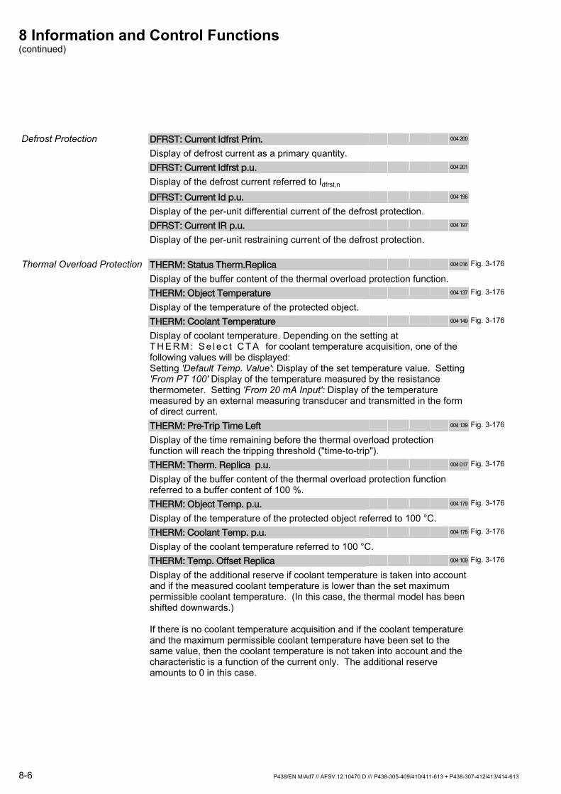
8 Information and Control Functions (continued)
8-6 P438/EN M/Ad7 // AFSV.12.10470 D /// P438-305-409/410/411-613 + P438-307-412/413/414-613
Defrost Protection DFRST: Current Idfrst Prim. 004 200
Display of defrost current as a primary quantity.
DFRST: Current Idfrst p.u. 004 201
Display of the defrost current referred to Idfrst,n
DFRST: Current Id p.u. 004 196
Display of the per-unit differential current of the defrost protection.
DFRST: Current IR p.u. 004 197
Display of the per-unit restraining current of the defrost protection.
Thermal Overload Protection THERM: Status Therm.Replica 004 016 Fig. 3-176
Display of the buffer content of the thermal overload protection function.
THERM: Object Temperature 004 137 Fig. 3-176
Display of the temperature of the protected object.
THERM: Coolant Temperature 004 149 Fig. 3-176
Display of coolant temperature. Depending on the setting at T H E R M : S e l e c t C T A for coolant temperature acquisition, one of the following values will be displayed: Setting 'Default Temp. Value': Display of the set temperature value. Setting 'From PT 100' Display of the temperature measured by the resistance thermometer. Setting 'From 20 mA Input': Display of the temperature measured by an external measuring transducer and transmitted in the form of direct current.
THERM: Pre-Trip Time Left 004 139 Fig. 3-176
Display of the time remaining before the thermal overload protection function will reach the tripping threshold ("time-to-trip").
THERM: Therm. Replica p.u. 004 017 Fig. 3-176
Display of the buffer content of the thermal overload protection function referred to a buffer content of 100 %.
THERM: Object Temp. p.u. 004 179 Fig. 3-176
Display of the temperature of the protected object referred to 100 °C.
THERM: Coolant Temp. p.u. 004 178 Fig. 3-176
Display of the coolant temperature referred to 100 °C.
THERM: Temp. Offset Replica 004 109 Fig. 3-176
Display of the additional reserve if coolant temperature is taken into account and if the measured coolant temperature is lower than the set maximum permissible coolant temperature. (In this case, the thermal model has been shifted downwards.) If there is no coolant temperature acquisition and if the coolant temperature and the maximum permissible coolant temperature have been set to the same value, then the coolant temperature is not taken into account and the characteristic is a function of the current only. The additional reserve amounts to 0 in this case.
8 Information and Control Functions (continued)
P438/EN M/Ad7 // AFSV.12.10470 D /// P438-305-409/410/411-613 + P438-307-412/413/414-613 8-7
8.1.1.2 Physical State Signals
Communication Interface 3 COMM3: State Receive 1 120 000
COMM3: State Receive 2 120 003
COMM3: State Receive 3 120 006
COMM3: State Receive 4 120 009
COMM3: State Receive 5 120 012
COMM3: State Receive 6 120 015
COMM3: State Receive 7 120 018
COMM3: State Receive 8 120 021
Display of the relevant receive signal.
COMM3: State Send 1 121 000
COMM3: State Send 2 121 002
COMM3: State Send 3 121 004
COMM3: State Send 4 121 006
COMM3: State Send 5 121 008
COMM3: State Send 6 121 010
COMM3: State Send 7 121 012
COMM3: State Send 8 121 014
Display of the updated value for the relevant send signal.

8 Information and Control Functions (continued)
8-8 P438/EN M/Ad7 // AFSV.12.10470 D /// P438-305-409/410/411-613 + P438-307-412/413/414-613
Generic Object Oriented Substation Event
GOOSE: Output 1 State 106 010
GOOSE: Output 2 State 106 012
GOOSE: Output 3 State 106 014
GOOSE: Output 4 State 106 016
GOOSE: Output 5 State 106 018
GOOSE: Output 6 State 106 020
GOOSE: Output 7 State 106 022
GOOSE: Output 8 State 106 024
GOOSE: Output 9 State 106 026
GOOSE: Output 10 State 106 028
GOOSE: Output 11 State 106 030
GOOSE: Output 12 State 106 032
GOOSE: Output 13 State 106 034
GOOSE: Output 14 State 106 036
GOOSE: Output 15 State 106 038
GOOSE: Output 16 State 106 040
GOOSE: Output 17 State 106 042
GOOSE: Output 18 State 106 044
GOOSE: Output 19 State 106 046
GOOSE: Output 20 State 106 048
GOOSE: Output 21 State 106 050
GOOSE: Output 22 State 106 052
GOOSE: Output 23 State 106 054
GOOSE: Output 24 State 106 056
GOOSE: Output 25 State 106 058
GOOSE: Output 26 State 106 060
GOOSE: Output 27 State 106 062
GOOSE: Output 28 State 106 064
GOOSE: Output 29 State 106 066
GOOSE: Output 30 State 106 068
GOOSE: Output 31 State 106 070
GOOSE: Output 32 State 106 072
Display of the virtual binary GOOSE output state.
GOOSE: Input 1 State 106 200
GOOSE: Input 2 State 106 201
GOOSE: Input 3 State 106 202
GOOSE: Input 4 State 106 203
GOOSE: Input 5 State 106 204
GOOSE: Input 6 State 106 205
GOOSE: Input 7 State 106 206
GOOSE: Input 8 State 106 207
GOOSE: Input 9 State 106 208
GOOSE: Input 10 State 106 209
GOOSE: Input 11 State 106 210
GOOSE: Input 12 State 106 211
GOOSE: Input 13 State 106 212
GOOSE: Input 14 State 106 213
GOOSE: Input 15 State 106 214
GOOSE: Input 16 State 106 215
Display of the virtual binary GOOSE input state.
8 Information and Control Functions (continued)
P438/EN M/Ad7 // AFSV.12.10470 D /// P438-305-409/410/411-613 + P438-307-412/413/414-613 8-9
IEC Generic Substation Status Events
GSSE: Output 1 State 104 100
GSSE: Output 2 State 104 103
GSSE: Output 3 State 104 106
GSSE: Output 4 State 104 109
GSSE: Output 5 State 104 112
GSSE: Output 6 State 104 115
GSSE: Output 7 State 104 118
GSSE: Output 8 State 104 121
GSSE: Output 9 State 104 124
GSSE: Output 10 State 104 127
GSSE: Output 11 State 104 130
GSSE: Output 12 State 104 133
GSSE: Output 13 State 104 136
GSSE: Output 14 State 104 139
GSSE: Output 15 State 104 142
GSSE: Output 16 State 104 145
GSSE: Output 17 State 104 148
GSSE: Output 18 State 104 151
GSSE: Output 19 State 104 154
GSSE: Output 20 State 104 157
GSSE: Output 21 State 104 160
GSSE: Output 22 State 104 163
GSSE: Output 23 State 104 166
GSSE: Output 24 State 104 169
GSSE: Output 25 State 104 172
GSSE: Output 26 State 104 175
GSSE: Output 27 State 104 178
GSSE: Output 28 State 104 181
GSSE: Output 29 State 104 184
GSSE: Output 30 State 104 187
GSSE: Output 31 State 104 190
GSSE: Output 32 State 104 193
Display of the virtual binary GSSE output state.
GSSE: Input 1 State 105 000
GSSE: Input 2 State 105 005
GSSE: Input 3 State 105 010
GSSE: Input 4 State 105 015
GSSE: Input 5 State 105 020
GSSE: Input 6 State 105 025
GSSE: Input 7 State 105 030
GSSE: Input 8 State 105 035
GSSE: Input 9 State 105 040
GSSE: Input 10 State 105 045
GSSE: Input 11 State 105 050
GSSE: Input 12 State 105 055
GSSE: Input 13 State 105 060
GSSE: Input 14 State 105 065
GSSE: Input 15 State 105 070
GSSE: Input 16 State 105 075
GSSE: Input 17 State 105 080

8 Information and Control Functions (continued)
8-10 P438/EN M/Ad7 // AFSV.12.10470 D /// P438-305-409/410/411-613 + P438-307-412/413/414-613
GSSE: Input 18 State 105 085
GSSE: Input 19 State 105 090
GSSE: Input 20 State 105 095
GSSE: Input 21 State 105 100
GSSE: Input 22 State 105 105
GSSE: Input 23 State 105 110
GSSE: Input 24 State 105 115
GSSE: Input 25 State 105 120
GSSE: Input 26 State 105 125
GSSE: Input 27 State 105 130
GSSE: Input 28 State 105 135
GSSE: Input 29 State 105 140
GSSE: Input 30 State 105 145
GSSE: Input 31 State 105 150
GSSE: Input 32 State 105 155
Display of the virtual binary GSSE input state.
Configurable Function Keys F_KEY: State F1 080 122 Fig. 3-20
F_KEY: State F2 080 123
F_KEY: State F3 080 124
F_KEY: State F4 080 125
F_KEY: State F5 080 126
F_KEY: State F6 080 127
The state of the function keys is displayed as follows:
'Disabled': No function is assigned to the function key. 'Off': The function key is in the "Off" position. 'On': The function key is in the "On" position.
8 Information and Control Functions (continued)
P438/EN M/Ad7 // AFSV.12.10470 D /// P438-305-409/410/411-613 + P438-307-412/413/414-613 8-11
Binary Input INP: State U 301 152 216 Fig. 3-21
INP: State U 302 152 219
INP: State U 303 152 222
INP: State U 304 152 225
INP: State U 601 152 090
INP: State U 602 152 093
INP: State U 603 152 096
INP: State U 604 152 099
INP: State U 605 152 102
INP: State U 606 152 105
INP: State U 701 152 108
INP: State U 702 152 111
INP: State U 703 152 114
INP: State U 704 152 117
INP: State U 705 152 120
INP: State U 706 152 123
INP: State U 801 152 126
INP: State U 802 152 129
INP: State U 803 152 132
INP: State U 804 152 135
INP: State U 901 152 144
INP: State U 902 152 147
INP: State U 903 152 150
INP: State U 904 152 153
INP: State U 1001 152 162
INP: State U 1002 152 165
INP: State U 1003 152 168
INP: State U 1004 152 171
INP: State U 1005 152 174
INP: State U 1006 152 177
INP: State U 1201 152 198
INP: State U 1202 152 201
INP: State U 1203 152 204
INP: State U 1204 152 207
INP: State U 1205 152 210
INP: State U 1206 152 213
INP: State U 1401 190 001
INP: State U 1402 190 005
INP: State U 1403 190 009
INP: State U 1404 190 013
INP: State U 1405 190 017
INP: State U 1406 190 021
INP: State U 1601 192 001
INP: State U 1602 192 005
INP: State U 1603 192 009
INP: State U 1604 192 013
INP: State U 1605 192 017
INP: State U 1606 192 021
INP: State U 1801 194 001
INP: State U 1802 194 005
INP: State U 1803 194 009
INP: State U 1804 194 013
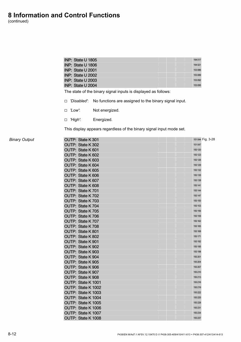
8 Information and Control Functions (continued)
8-12 P438/EN M/Ad7 // AFSV.12.10470 D /// P438-305-409/410/411-613 + P438-307-412/413/414-613
INP: State U 1805 194 017
INP: State U 1806 194 021
INP: State U 2001 153 086
INP: State U 2002 153 089
INP: State U 2003 153 092
INP: State U 2004 153 095
The state of the binary signal inputs is displayed as follows:
'Disabled': No functions are assigned to the binary signal input.
'Low': Not energized.
'High': Energized. This display appears regardless of the binary signal input mode set.
Binary Output OUTP: State K 301 151 044 Fig. 3-28
OUTP: State K 302 151 047
OUTP: State K 601 150 120
OUTP: State K 602 150 123
OUTP: State K 603 150 126
OUTP: State K 604 150 129
OUTP: State K 605 150 132
OUTP: State K 606 150 135
OUTP: State K 607 150 138
OUTP: State K 608 150 141
OUTP: State K 701 150 144
OUTP: State K 702 150 147
OUTP: State K 703 150 150
OUTP: State K 704 150 153
OUTP: State K 705 150 156
OUTP: State K 706 150 159
OUTP: State K 707 150 162
OUTP: State K 708 150 165
OUTP: State K 801 150 168
OUTP: State K 802 150 171
OUTP: State K 901 150 192
OUTP: State K 902 150 195
OUTP: State K 903 150 198
OUTP: State K 904 150 201
OUTP: State K 905 150 204
OUTP: State K 906 150 207
OUTP: State K 907 150 210
OUTP: State K 908 150 213
OUTP: State K 1001 150 216
OUTP: State K 1002 150 219
OUTP: State K 1003 150 222
OUTP: State K 1004 150 225
OUTP: State K 1005 150 228
OUTP: State K 1006 150 231
OUTP: State K 1007 150 234
OUTP: State K 1008 150 237

8 Information and Control Functions (continued)
P438/EN M/Ad7 // AFSV.12.10470 D /// P438-305-409/410/411-613 + P438-307-412/413/414-613 8-13
OUTP: State K 1201 151 008
OUTP: State K 1202 151 011
OUTP: State K 1203 151 014
OUTP: State K 1204 151 017
OUTP: State K 1205 151 020
OUTP: State K 1206 151 023
OUTP: State K 1207 151 026
OUTP: State K 1208 151 029
OUTP: State K 1401 169 001
OUTP: State K 1402 169 005
OUTP: State K 1403 169 009
OUTP: State K 1404 169 013
OUTP: State K 1405 169 017
OUTP: State K 1406 169 021
OUTP: State K 1407 169 025
OUTP: State K 1408 169 029
OUTP: State K 1601 171 001
OUTP: State K 1602 171 005
OUTP: State K 1603 171 009
OUTP: State K 1604 171 013
OUTP: State K 1605 171 017
OUTP: State K 1606 171 021
OUTP: State K 1607 171 025
OUTP: State K 1608 171 029
OUTP: State K 1801 173 001
OUTP: State K 1802 173 005
OUTP: State K 1803 173 009
OUTP: State K 1804 173 013
OUTP: State K 1805 173 017
OUTP: State K 1806 173 021
OUTP: State K 2001 151 200
OUTP: State K 2002 151 203
OUTP: State K 2003 151 206
OUTP: State K 2004 151 209
OUTP: State K 2005 151 212
OUTP: State K 2006 151 215
OUTP: State K 2007 151 218
OUTP: State K 2008 151 221
The state of the output relays is displayed as follows:
'Disabled': No functions are assigned to the output relay.
'Low': The output relay is not energized.
'High': The output relay is energized. This display appears regardless of the output relay mode set.
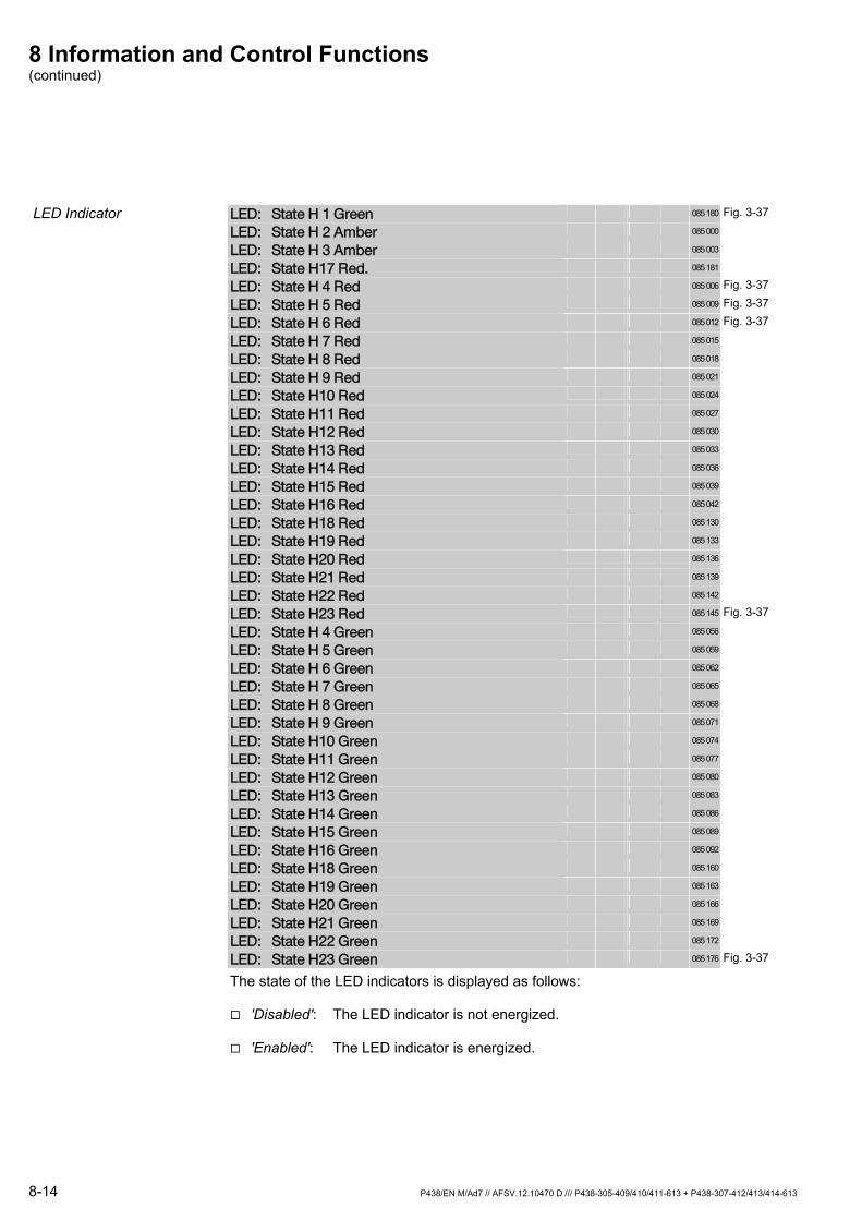
8 Information and Control Functions (continued)
8-14 P438/EN M/Ad7 // AFSV.12.10470 D /// P438-305-409/410/411-613 + P438-307-412/413/414-613
LED Indicator LED: State H 1 Green 085 180 Fig. 3-37
LED: State H 2 Amber 085 000
LED: State H 3 Amber 085 003
LED: State H17 Red. 085 181
LED: State H 4 Red 085 006 Fig. 3-37
LED: State H 5 Red 085 009 Fig. 3-37
LED: State H 6 Red 085 012 Fig. 3-37
LED: State H 7 Red 085 015
LED: State H 8 Red 085 018
LED: State H 9 Red 085 021
LED: State H10 Red 085 024
LED: State H11 Red 085 027
LED: State H12 Red 085 030
LED: State H13 Red 085 033
LED: State H14 Red 085 036
LED: State H15 Red 085 039
LED: State H16 Red 085 042
LED: State H18 Red 085 130
LED: State H19 Red 085 133
LED: State H20 Red 085 136
LED: State H21 Red 085 139
LED: State H22 Red 085 142
LED: State H23 Red 085 145 Fig. 3-37
LED: State H 4 Green 085 056
LED: State H 5 Green 085 059
LED: State H 6 Green 085 062
LED: State H 7 Green 085 065
LED: State H 8 Green 085 068
LED: State H 9 Green 085 071
LED: State H10 Green 085 074
LED: State H11 Green 085 077
LED: State H12 Green 085 080
LED: State H13 Green 085 083
LED: State H14 Green 085 086
LED: State H15 Green 085 089
LED: State H16 Green 085 092
LED: State H18 Green 085 160
LED: State H19 Green 085 163
LED: State H20 Green 085 166
LED: State H21 Green 085 169
LED: State H22 Green 085 172
LED: State H23 Green 085 176 Fig. 3-37
The state of the LED indicators is displayed as follows:
'Disabled': The LED indicator is not energized.
'Enabled': The LED indicator is energized.
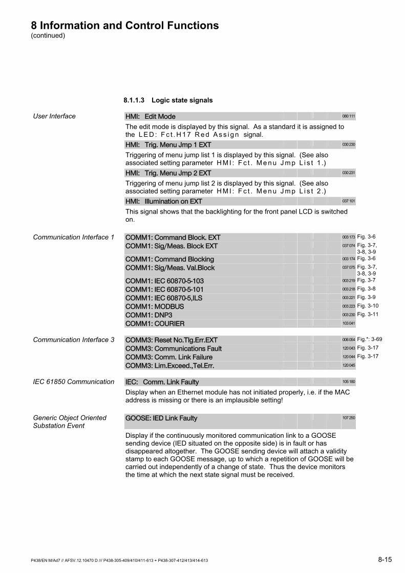
8 Information and Control Functions (continued)
P438/EN M/Ad7 // AFSV.12.10470 D /// P438-305-409/410/411-613 + P438-307-412/413/414-613 8-15
8.1.1.3 Logic state signals
User Interface HMI: Edit Mode 080 111
The edit mode is displayed by this signal. As a standard it is assigned to the L E D : F c t . H 1 7 R e d A s s i g n signal.
HMI: Trig. Menu Jmp 1 EXT 030 230
Triggering of menu jump list 1 is displayed by this signal. (See also associated setting parameter H M I : F c t . M e n u J m p L i s t 1 .)
HMI: Trig. Menu Jmp 2 EXT 030 231
Triggering of menu jump list 2 is displayed by this signal. (See also associated setting parameter H M I : F c t . M e n u J m p L i s t 2 .)
HMI: Illumination on EXT 037 101
This signal shows that the backlighting for the front panel LCD is switched on.
Communication Interface 1 COMM1: Command Block. EXT 003 173 Fig. 3-6
COMM1: Sig/Meas. Block EXT 037 074 Fig. 3-7, 3-8, 3-9
COMM1: Command Blocking 003 174 Fig. 3-6
COMM1: Sig/Meas. Val.Block 037 075 Fig. 3-7, 3-8, 3-9
COMM1: IEC 60870-5-103 003 219 Fig. 3-7
COMM1: IEC 60870-5-101 003 218 Fig. 3-8
COMM1: IEC 60870-5,ILS 003 221 Fig. 3-9
COMM1: MODBUS 003 223 Fig. 3-10
COMM1: DNP3 003 230 Fig. 3-11
COMM1: COURIER 103 041
Communication Interface 3 COMM3: Reset No.Tlg.Err.EXT 006 054 Fig.*: 3-69
COMM3: Communications Fault 120 043 Fig. 3-17
COMM3: Comm. Link Failure 120 044 Fig. 3-17
COMM3: Lim.Exceed.,Tel.Err. 120 045
IEC 61850 Communication IEC: Comm. Link Faulty 105 180
Display when an Ethernet module has not initiated properly, i.e. if the MAC address is missing or there is an implausible setting!
Generic Object Oriented Substation Event
GOOSE: IED Link Faulty 107 250
Display if the continuously monitored communication link to a GOOSE sending device (IED situated on the opposite side) is in fault or has disappeared altogether. The GOOSE sending device will attach a validity stamp to each GOOSE message, up to which a repetition of GOOSE will be carried out independently of a change of state. Thus the device monitors the time at which the next state signal must be received.
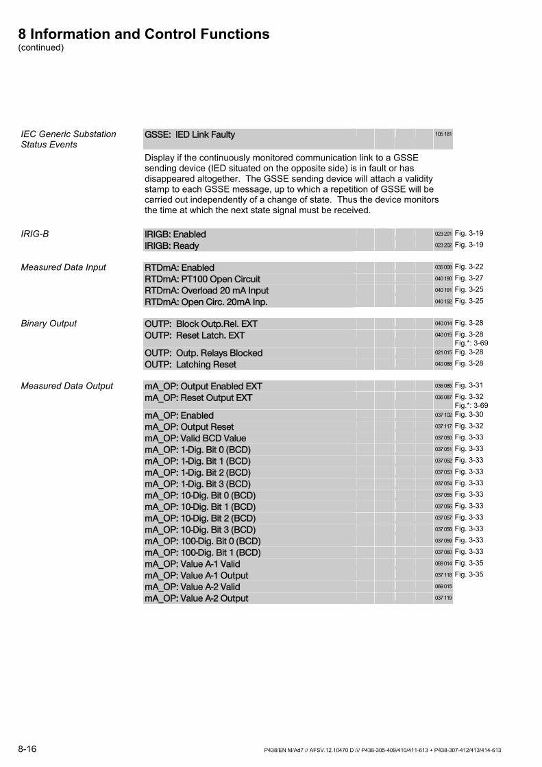
8 Information and Control Functions (continued)
8-16 P438/EN M/Ad7 // AFSV.12.10470 D /// P438-305-409/410/411-613 + P438-307-412/413/414-613
IEC Generic Substation Status Events
GSSE: IED Link Faulty 105 181
Display if the continuously monitored communication link to a GSSE sending device (IED situated on the opposite side) is in fault or has disappeared altogether. The GSSE sending device will attach a validity stamp to each GSSE message, up to which a repetition of GSSE will be carried out independently of a change of state. Thus the device monitors the time at which the next state signal must be received.
IRIG-B IRIGB: Enabled 023 201 Fig. 3-19
IRIGB: Ready 023 202 Fig. 3-19
Measured Data Input RTDmA: Enabled 035 008 Fig. 3-22
RTDmA: PT100 Open Circuit 040 190 Fig. 3-27
RTDmA: Overload 20 mA Input 040 191 Fig. 3-25
RTDmA: Open Circ. 20mA Inp. 040 192 Fig. 3-25
Binary Output OUTP: Block Outp.Rel. EXT 040 014 Fig. 3-28
OUTP: Reset Latch. EXT 040 015 Fig. 3-28 Fig.*: 3-69
OUTP: Outp. Relays Blocked 021 015 Fig. 3-28
OUTP: Latching Reset 040 088 Fig. 3-28
Measured Data Output mA_OP: Output Enabled EXT 036 085 Fig. 3-31
mA_OP: Reset Output EXT 036 087 Fig. 3-32 Fig.*: 3-69
mA_OP: Enabled 037 102 Fig. 3-30
mA_OP: Output Reset 037 117 Fig. 3-32
mA_OP: Valid BCD Value 037 050 Fig. 3-33
mA_OP: 1-Dig. Bit 0 (BCD) 037 051 Fig. 3-33
mA_OP: 1-Dig. Bit 1 (BCD) 037 052 Fig. 3-33
mA_OP: 1-Dig. Bit 2 (BCD) 037 053 Fig. 3-33
mA_OP: 1-Dig. Bit 3 (BCD) 037 054 Fig. 3-33
mA_OP: 10-Dig. Bit 0 (BCD) 037 055 Fig. 3-33
mA_OP: 10-Dig. Bit 1 (BCD) 037 056 Fig. 3-33
mA_OP: 10-Dig. Bit 2 (BCD) 037 057 Fig. 3-33
mA_OP: 10-Dig. Bit 3 (BCD) 037 058 Fig. 3-33
mA_OP: 100-Dig. Bit 0 (BCD) 037 059 Fig. 3-33
mA_OP: 100-Dig. Bit 1 (BCD) 037 060 Fig. 3-33
mA_OP: Value A-1 Valid 069 014 Fig. 3-35
mA_OP: Value A-1 Output 037 118 Fig. 3-35
mA_OP: Value A-2 Valid 069 015
mA_OP: Value A-2 Output 037 119
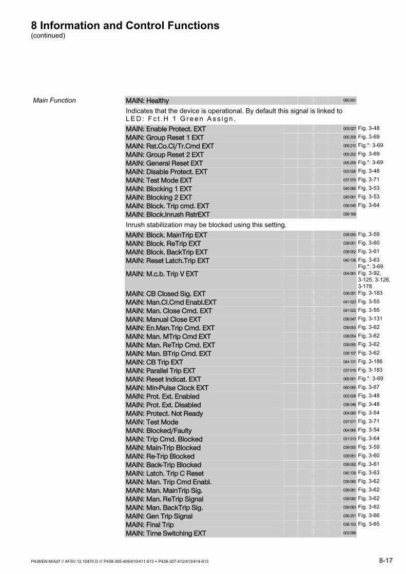
8 Information and Control Functions (continued)
P438/EN M/Ad7 // AFSV.12.10470 D /// P438-305-409/410/411-613 + P438-307-412/413/414-613 8-17
Main Function MAIN: Healthy 060 001
Indicates that the device is operational. By default this signal is linked to L E D : F c t . H 1 G r e e n A s s i g n .
MAIN: Enable Protect. EXT 003 027 Fig. 3-48
MAIN: Group Reset 1 EXT 005 209 Fig. 3-69
MAIN: Rst.Co.Cl/Tr.Cmd EXT 005 210 Fig.*: 3-69
MAIN: Group Reset 2 EXT 005 252 Fig. 3-69
MAIN: General Reset EXT 005 255 Fig.*: 3-69
MAIN: Disable Protect. EXT 003 026 Fig. 3-48
MAIN: Test Mode EXT 037 070 Fig. 3-71
MAIN: Blocking 1 EXT 040 060 Fig. 3-53
MAIN: Blocking 2 EXT 040 061 Fig. 3-53
MAIN: Block. Trip cmd. EXT 036 045 Fig. 3-64
MAIN: Block.Inrush RstrEXT 039 169
Inrush stabilization may be blocked using this setting.
MAIN: Block. MainTrip EXT 038 050 Fig. 3-59
MAIN: Block. ReTrip EXT 038 051 Fig. 3-60
MAIN: Block. BackTrip EXT 038 052 Fig. 3-61
MAIN: Reset Latch.Trip EXT 040 138 Fig. 3-63 Fig.*: 3-69
MAIN: M.c.b. Trip V EXT 004 061 Fig. 3-92, 3-125, 3-126, 3-178
MAIN: CB Closed Sig. EXT 036 051 Fig. 3-183
MAIN: Man.Cl.Cmd Enabl.EXT 041 023 Fig. 3-55
MAIN: Man. Close Cmd. EXT 041 022 Fig. 3-55
MAIN: Manual Close EXT 036 047 Fig. 3-131
MAIN: En.Man.Trip Cmd. EXT 039 053 Fig. 3-62
MAIN: Man. MTrip Cmd EXT 039 054 Fig. 3-62
MAIN: Man. ReTrip Cmd. EXT 039 055 Fig. 3-62
MAIN: Man. BTrip Cmd. EXT 039 107 Fig. 3-62
MAIN: CB Trip EXT 044 131 Fig. 3-186
MAIN: Parallel Trip EXT 037 019 Fig. 3-183
MAIN: Reset Indicat. EXT 065 001 Fig.*: 3-69
MAIN: Min-Pulse Clock EXT 060 060 Fig. 3-67
MAIN: Prot. Ext. Enabled 003 028 Fig. 3-48
MAIN: Prot. Ext. Disabled 038 046 Fig. 3-48
MAIN: Protect. Not Ready 004 060 Fig. 3-54
MAIN: Test Mode 037 071 Fig. 3-71
MAIN: Blocked/Faulty 004 065 Fig. 3-54
MAIN: Trip Cmd. Blocked 021 013 Fig. 3-64
MAIN: Main-Trip Blocked 039 050 Fig. 3-59
MAIN: Re-Trip Blocked 039 051 Fig. 3-60
MAIN: Back-Trip Blocked 039 052 Fig. 3-61
MAIN: Latch. Trip C Reset 040 139 Fig. 3-63
MAIN: Man. Trip Cmd Enabl. 039 080 Fig. 3-62
MAIN: Man. MainTrip Sig. 039 081 Fig. 3-62
MAIN: Man. ReTrip Signal 039 082 Fig. 3-62
MAIN: Man. BackTrip Sig. 039 083 Fig. 3-62
MAIN: Gen Trip Signal 036 251 Fig. 3-66
MAIN: Final Trip 038 103 Fig. 3-65
MAIN: Time Switching EXT 003 096
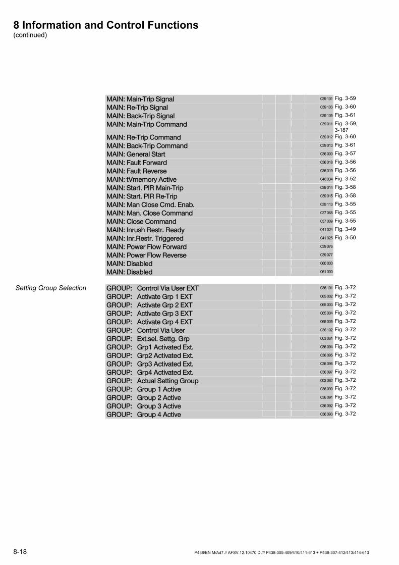
8 Information and Control Functions (continued)
8-18 P438/EN M/Ad7 // AFSV.12.10470 D /// P438-305-409/410/411-613 + P438-307-412/413/414-613
MAIN: Main-Trip Signal 039 101 Fig. 3-59
MAIN: Re-Trip Signal 039 103 Fig. 3-60
MAIN: Back-Trip Signal 039 105 Fig. 3-61
MAIN: Main-Trip Command 039 011 Fig. 3-59, 3-187
MAIN: Re-Trip Command 039 012 Fig. 3-60
MAIN: Back-Trip Command 039 013 Fig. 3-61
MAIN: General Start 036 000 Fig. 3-57
MAIN: Fault Forward 036 018 Fig. 3-56
MAIN: Fault Reverse 036 019 Fig. 3-56
MAIN: tVmemory Active 040 034 Fig. 3-52
MAIN: Start. PIR Main-Trip 039 014 Fig. 3-58
MAIN: Start. PIR Re-Trip 039 015 Fig. 3-58
MAIN: Man Close Cmd. Enab. 039 113 Fig. 3-55
MAIN: Man. Close Command 037 068 Fig. 3-55
MAIN: Close Command 037 009 Fig. 3-55
MAIN: Inrush Restr. Ready 041 024 Fig. 3-49
MAIN: Inr.Restr. Triggered 041 025 Fig. 3-50
MAIN: Power Flow Forward 039 076
MAIN: Power Flow Reverse 039 077
MAIN: Disabled 060 000
MAIN: Disabled 061 000
Setting Group Selection GROUP: Control Via User EXT 036 101 Fig. 3-72
GROUP: Activate Grp 1 EXT 065 002 Fig. 3-72
GROUP: Activate Grp 2 EXT 065 003 Fig. 3-72
GROUP: Activate Grp 3 EXT 065 004 Fig. 3-72
GROUP: Activate Grp 4 EXT 065 005 Fig. 3-72
GROUP: Control Via User 036 102 Fig. 3-72
GROUP: Ext.sel. Settg. Grp 003 061 Fig. 3-72
GROUP: Grp1 Activated Ext. 036 094 Fig. 3-72
GROUP: Grp2 Activated Ext. 036 095 Fig. 3-72
GROUP: Grp3 Activated Ext. 036 096 Fig. 3-72
GROUP: Grp4 Activated Ext. 036 097 Fig. 3-72
GROUP: Actual Setting Group 003 062 Fig. 3-72
GROUP: Group 1 Active 036 090 Fig. 3-72
GROUP: Group 2 Active 036 091 Fig. 3-72
GROUP: Group 3 Active 036 092 Fig. 3-72
GROUP: Group 4 Active 036 093 Fig. 3-72
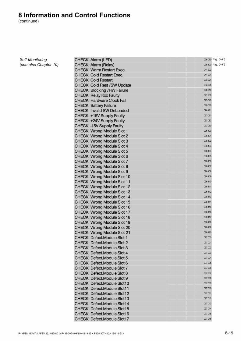
8 Information and Control Functions (continued)
P438/EN M/Ad7 // AFSV.12.10470 D /// P438-305-409/410/411-613 + P438-307-412/413/414-613 8-19
Self-Monitoring CHECK: Alarm (LED) 036 070 Fig. 3-73
(see also Chapter 10) CHECK: Alarm (Relay) 036 100 Fig. 3-73
CHECK: Warm Restart Exec. 041 202
CHECK: Cold Restart Exec. 041 201
CHECK: Cold Restart 093 024
CHECK: Cold Rest /SW Update 093 025
CHECK: Blocking /HW Failure 090 019
CHECK: Relay Kxx Faulty 041 200
CHECK: Hardware Clock Fail 093 040
CHECK: Battery Failure 090 010
CHECK: Invalid SW DnLoaded 096 121
CHECK: +15V Supply Faulty 093 081
CHECK: +24V Supply Faulty 093 082
CHECK: -15V Supply Faulty 093 080
CHECK: Wrong Module Slot 1 096 100
CHECK: Wrong Module Slot 2 096 101
CHECK: Wrong Module Slot 3 096 102
CHECK: Wrong Module Slot 4 096 103
CHECK: Wrong Module Slot 5 096 104
CHECK: Wrong Module Slot 6 096 105
CHECK: Wrong Module Slot 7 096 106
CHECK: Wrong Module Slot 8 096 107
CHECK: Wrong Module Slot 9 096 108
CHECK: Wrong Module Slot 10 096 109
CHECK: Wrong Module Slot 11 096 110
CHECK: Wrong Module Slot 12 096 111
CHECK: Wrong Module Slot 13 096 112
CHECK: Wrong Module Slot 14 096 113
CHECK: Wrong Module Slot 15 096 114
CHECK: Wrong Module Slot 16 096 115
CHECK: Wrong Module Slot 17 096 116
CHECK: Wrong Module Slot 18 096 117
CHECK: Wrong Module Slot 19 096 118
CHECK: Wrong Module Slot 20 096 119
CHECK: Wrong Module Slot 21 096 120
CHECK: Defect.Module Slot 1 097 000
CHECK: Defect.Module Slot 2 097 001
CHECK: Defect.Module Slot 3 097 002
CHECK: Defect.Module Slot 4 097 003
CHECK: Defect.Module Slot 5 097 004
CHECK: Defect.Module Slot 6 097 005
CHECK: Defect.Module Slot 7 097 006
CHECK: Defect.Module Slot 8 097 007
CHECK: Defect.Module Slot 9 097 008
CHECK: Defect.Module Slot10 097 009
CHECK: Defect.Module Slot11 097 010
CHECK: Defect.Module Slot12 097 011
CHECK: Defect.Module Slot13 097 012
CHECK: Defect.Module Slot14 097 013
CHECK: Defect.Module Slot15 097 014
CHECK: Defect.Module Slot16 097 015
CHECK: Defect.Module Slot17 097 016

8 Information and Control Functions (continued)
8-20 P438/EN M/Ad7 // AFSV.12.10470 D /// P438-305-409/410/411-613 + P438-307-412/413/414-613
CHECK: Defect.Module Slot18 097 017
CHECK: Defect.Module Slot19 097 018
CHECK: Defect.Module Slot20 097 019
CHECK: Defect.Module Slot21 097 020
CHECK: Module A DPR Faulty 093 070
CHECK: Module A RAM Faulty 093 071
CHECK: Module Y DPR Faulty 093 110
CHECK: Module Y RAM Faulty 093 111
CHECK: IRIGB Faulty 093 117
CHECK: Error K 301 097 046
CHECK: Error K 302 097 047
CHECK: Error K 601 097 070
CHECK: Error K 602 097 071
CHECK: Error K 603 097 072
CHECK: Error K 604 097 073
CHECK: Error K 605 097 074
CHECK: Error K 606 097 075
CHECK: Error K 607 097 076
CHECK: Error K 608 097 077
CHECK: Error K 701 097 078
CHECK: Error K 702 097 079
CHECK: Error K 703 097 080
CHECK: Error K 704 097 081
CHECK: Error K 705 097 082
CHECK: Error K 706 097 083
CHECK: Error K 707 097 084
CHECK: Error K 708 097 085
CHECK: Error K 801 097 086
CHECK: Error K 802 097 087
CHECK: Error K 901 097 094
CHECK: Error K 902 097 095
CHECK: Error K 903 097 096
CHECK: Error K 904 097 097
CHECK: Error K 905 097 098
CHECK: Error K 906 097 099
CHECK: Error K 907 097 100
CHECK: Error K 908 097 101
CHECK: Error K 1001 097 102
CHECK: Error K 1002 097 103
CHECK: Error K 1003 097 104
CHECK: Error K 1004 097 105
CHECK: Error K 1005 097 106
CHECK: Error K 1006 097 107
CHECK: Error K 1007 097 108
CHECK: Error K 1008 097 109
CHECK: Error K 1201 097 118
CHECK: Error K 1202 097 119
CHECK: Error K 1203 097 120
CHECK: Error K 1204 097 121
CHECK: Error K 1205 097 122
CHECK: Error K 1206 097 123
CHECK: Error K 1207 097 124
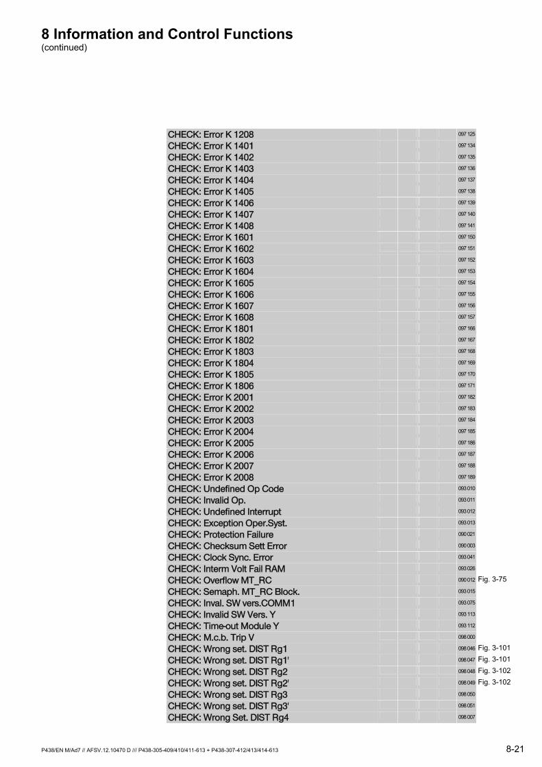
8 Information and Control Functions (continued)
P438/EN M/Ad7 // AFSV.12.10470 D /// P438-305-409/410/411-613 + P438-307-412/413/414-613 8-21
CHECK: Error K 1208 097 125
CHECK: Error K 1401 097 134
CHECK: Error K 1402 097 135
CHECK: Error K 1403 097 136
CHECK: Error K 1404 097 137
CHECK: Error K 1405 097 138
CHECK: Error K 1406 097 139
CHECK: Error K 1407 097 140
CHECK: Error K 1408 097 141
CHECK: Error K 1601 097 150
CHECK: Error K 1602 097 151
CHECK: Error K 1603 097 152
CHECK: Error K 1604 097 153
CHECK: Error K 1605 097 154
CHECK: Error K 1606 097 155
CHECK: Error K 1607 097 156
CHECK: Error K 1608 097 157
CHECK: Error K 1801 097 166
CHECK: Error K 1802 097 167
CHECK: Error K 1803 097 168
CHECK: Error K 1804 097 169
CHECK: Error K 1805 097 170
CHECK: Error K 1806 097 171
CHECK: Error K 2001 097 182
CHECK: Error K 2002 097 183
CHECK: Error K 2003 097 184
CHECK: Error K 2004 097 185
CHECK: Error K 2005 097 186
CHECK: Error K 2006 097 187
CHECK: Error K 2007 097 188
CHECK: Error K 2008 097 189
CHECK: Undefined Op Code 093 010
CHECK: Invalid Op. 093 011
CHECK: Undefined Interrupt 093 012
CHECK: Exception Oper.Syst. 093 013
CHECK: Protection Failure 090 021
CHECK: Checksum Sett Error 090 003
CHECK: Clock Sync. Error 093 041
CHECK: Interm Volt Fail RAM 093 026
CHECK: Overflow MT_RC 090 012 Fig. 3-75
CHECK: Semaph. MT_RC Block. 093 015
CHECK: Inval. SW vers.COMM1 093 075
CHECK: Invalid SW Vers. Y 093 113
CHECK: Time-out Module Y 093 112
CHECK: M.c.b. Trip V 098 000
CHECK: Wrong set. DIST Rg1 098 046 Fig. 3-101
CHECK: Wrong set. DIST Rg1' 098 047 Fig. 3-101
CHECK: Wrong set. DIST Rg2 098 048 Fig. 3-102
CHECK: Wrong set. DIST Rg2' 098 049 Fig. 3-102
CHECK: Wrong set. DIST Rg3 098 050
CHECK: Wrong set. DIST Rg3' 098 051
CHECK: Wrong Set. DIST Rg4 098 007
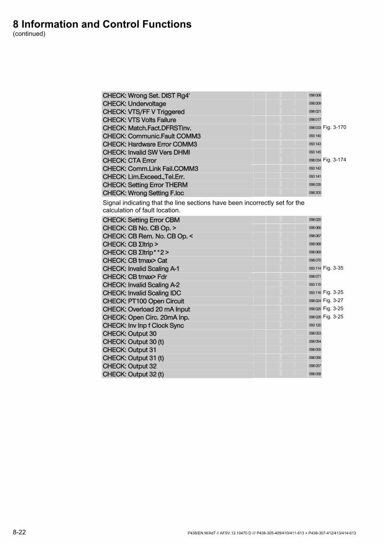
8 Information and Control Functions (continued)
8-22 P438/EN M/Ad7 // AFSV.12.10470 D /// P438-305-409/410/411-613 + P438-307-412/413/414-613
CHECK: Wrong Set. DIST Rg4' 098 008
CHECK: Undervoltage 098 009
CHECK: VTS/FF V Triggered 098 021
CHECK: VTS Volts Failure 098 017
CHECK: Match.Fact.DFRSTinv. 098 033 Fig. 3-170
CHECK: Communic.Fault COMM3 093 140
CHECK: Hardware Error COMM3 093 143
CHECK: Invalid SW Vers DHMI 093 145
CHECK: CTA Error 098 034 Fig. 3-174
CHECK: Comm.Link Fail.COMM3 093 142
CHECK: Lim.Exceed.,Tel.Err. 093 141
CHECK: Setting Error THERM 098 035
CHECK: Wrong Setting F.loc 098 200
Signal indicating that the line sections have been incorrectly set for the calculation of fault location.
CHECK: Setting Error CBM 098 020
CHECK: CB No. CB Op. > 098 066
CHECK: CB Rem. No. CB Op. < 098 067
CHECK: CB ΣItrip > 098 068
CHECK: CB ΣItrip**2 > 098 069
CHECK: CB tmax> Cat 098 070
CHECK: Invalid Scaling A-1 093 114 Fig. 3-35
CHECK: CB tmax> Fdr 098 071
CHECK: Invalid Scaling A-2 093 115
CHECK: Invalid Scaling IDC 093 116 Fig. 3-25
CHECK: PT100 Open Circuit 098 024 Fig. 3-27
CHECK: Overload 20 mA Input 098 025 Fig. 3-25
CHECK: Open Circ. 20mA Inp. 098 026 Fig. 3-25
CHECK: Inv Inp f Clock Sync 093 120
CHECK: Output 30 098 053
CHECK: Output 30 (t) 098 054
CHECK: Output 31 098 055
CHECK: Output 31 (t) 098 056
CHECK: Output 32 098 057
CHECK: Output 32 (t) 098 058
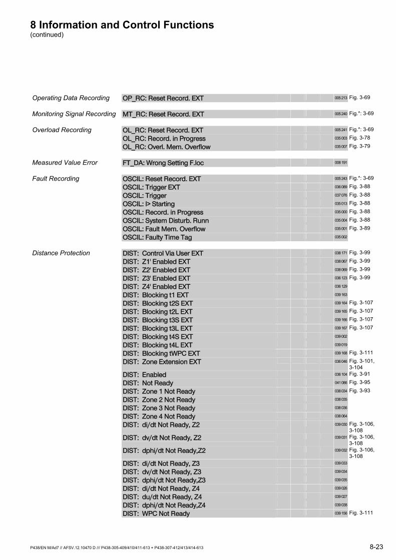
8 Information and Control Functions (continued)
P438/EN M/Ad7 // AFSV.12.10470 D /// P438-305-409/410/411-613 + P438-307-412/413/414-613 8-23
Operating Data Recording OP_RC: Reset Record. EXT 005 213 Fig. 3-69
Monitoring Signal Recording MT_RC: Reset Record. EXT 005 240 Fig.*: 3-69
Overload Recording OL_RC: Reset Record. EXT 005 241 Fig.*: 3-69
OL_RC: Record. in Progress 035 003 Fig. 3-78
OL_RC: Overl. Mem. Overflow 035 007 Fig. 3-79
Measured Value Error FT_DA: Wrong Setting F.loc 008 191
Fault Recording OSCIL: Reset Record. EXT 005 243 Fig.*: 3-69
OSCIL: Trigger EXT 036 089 Fig. 3-88
OSCIL: Trigger 037 076 Fig. 3-88
OSCIL: I> Starting 035 013 Fig. 3-88
OSCIL: Record. in Progress 035 000 Fig. 3-88
OSCIL: System Disturb. Runn 035 004 Fig. 3-88
OSCIL: Fault Mem. Overflow 035 001 Fig. 3-89
OSCIL: Faulty Time Tag 035 002
Distance Protection DIST: Control Via User EXT 038 171 Fig. 3-99
DIST: Z1' Enabled EXT 038 067 Fig. 3-99
DIST: Z2' Enabled EXT 038 069 Fig. 3-99
DIST: Z3' Enabled EXT 036 123 Fig. 3-99
DIST: Z4' Enabled EXT 036 129
DIST: Blocking t1 EXT 039 163
DIST: Blocking t2S EXT 039 164 Fig. 3-107
DIST: Blocking t2L EXT 039 165 Fig. 3-107
DIST: Blocking t3S EXT 039 166 Fig. 3-107
DIST: Blocking t3L EXT 039 167 Fig. 3-107
DIST: Blocking t4S EXT 039 002
DIST: Blocking t4L EXT 039 019
DIST: Blocking tWPC EXT 039 168 Fig. 3-111
DIST: Zone Extension EXT 036 046 Fig. 3-101, 3-104
DIST: Enabled 036 104 Fig. 3-91
DIST: Not Ready 041 086 Fig. 3-95
DIST: Zone 1 Not Ready 038 034 Fig. 3-93
DIST: Zone 2 Not Ready 038 035
DIST: Zone 3 Not Ready 038 036
DIST: Zone 4 Not Ready 038 064
DIST: di/dt Not Ready, Z2 039 030 Fig. 3-106, 3-108
DIST: dv/dt Not Ready, Z2 039 031 Fig. 3-106, 3-108
DIST: dphi/dt Not Ready,Z2 039 032 Fig. 3-106, 3-108
DIST: di/dt Not Ready, Z3 039 033
DIST: dv/dt Not Ready, Z3 039 034
DIST: dphi/dt Not Ready,Z3 039 035
DIST: di/dt Not Ready, Z4 039 026
DIST: du/dt Not Ready, Z4 039 027
DIST: dphi/dt Not Ready,Z4 039 038
DIST: WPC Not Ready 039 156 Fig. 3-111
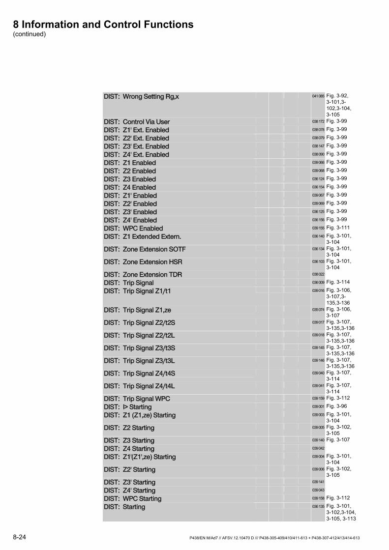
8 Information and Control Functions (continued)
8-24 P438/EN M/Ad7 // AFSV.12.10470 D /// P438-305-409/410/411-613 + P438-307-412/413/414-613
DIST: Wrong Setting Rg,x 041 085 Fig. 3-92, 3-101,3-102,3-104, 3-105
DIST: Control Via User 038 172 Fig. 3-99
DIST: Z1' Ext. Enabled 038 078 Fig. 3-99
DIST: Z2' Ext. Enabled 038 079 Fig. 3-99
DIST: Z3' Ext. Enabled 038 147 Fig. 3-99
DIST: Z4' Ext. Enabled 038 090 Fig. 3-99
DIST: Z1 Enabled 039 066 Fig. 3-99
DIST: Z2 Enabled 039 068 Fig. 3-99
DIST: Z3 Enabled 036 124 Fig. 3-99
DIST: Z4 Enabled 036 154 Fig. 3-99
DIST: Z1' Enabled 039 067 Fig. 3-99
DIST: Z2' Enabled 039 069 Fig. 3-99
DIST: Z3' Enabled 036 125 Fig. 3-99
DIST: Z4' Enabled 036 156 Fig. 3-99
DIST: WPC Enabled 039 155 Fig. 3-111
DIST: Z1 Extended Extern. 036 140 Fig. 3-101, 3-104
DIST: Zone Extension SOTF 036 134 Fig. 3-101, 3-104
DIST: Zone Extension HSR 036 103 Fig. 3-101, 3-104
DIST: Zone Extension TDR 038 022
DIST: Trip Signal 036 009 Fig. 3-114
DIST: Trip Signal Z1/t1 039 016 Fig. 3-106, 3-107,3-135,3-136
DIST: Trip Signal Z1,ze 035 074 Fig. 3-106, 3-107
DIST: Trip Signal Z2/t2S 039 017 Fig. 3-107, 3-135,3-136
DIST: Trip Signal Z2/t2L 039 018 Fig. 3-107, 3-135,3-136
DIST: Trip Signal Z3/t3S 039 145 Fig. 3-107, 3-135,3-136
DIST: Trip Signal Z3/t3L 039 146 Fig. 3-107, 3-135,3-136
DIST: Trip Signal Z4/t4S 039 040 Fig. 3-107, 3-114
DIST: Trip Signal Z4/t4L 039 041 Fig. 3-107, 3-114
DIST: Trip Signal WPC 039 159 Fig. 3-112
DIST: I> Starting 039 001 Fig. 3-96
DIST: Z1 (Z1,ze) Starting 039 003 Fig. 3-101, 3-104
DIST: Z2 Starting 039 005 Fig. 3-102, 3-105
DIST: Z3 Starting 039 140 Fig. 3-107
DIST: Z4 Starting 039 042
DIST: Z1'(Z1',ze) Starting 039 004 Fig. 3-101, 3-104
DIST: Z2' Starting 039 006 Fig. 3-102, 3-105
DIST: Z3' Starting 039 141
DIST: Z4' Starting 039 043
DIST: WPC Starting 039 158 Fig. 3-112
DIST: Starting 036 135 Fig. 3-101, 3-102,3-104, 3-105, 3-113
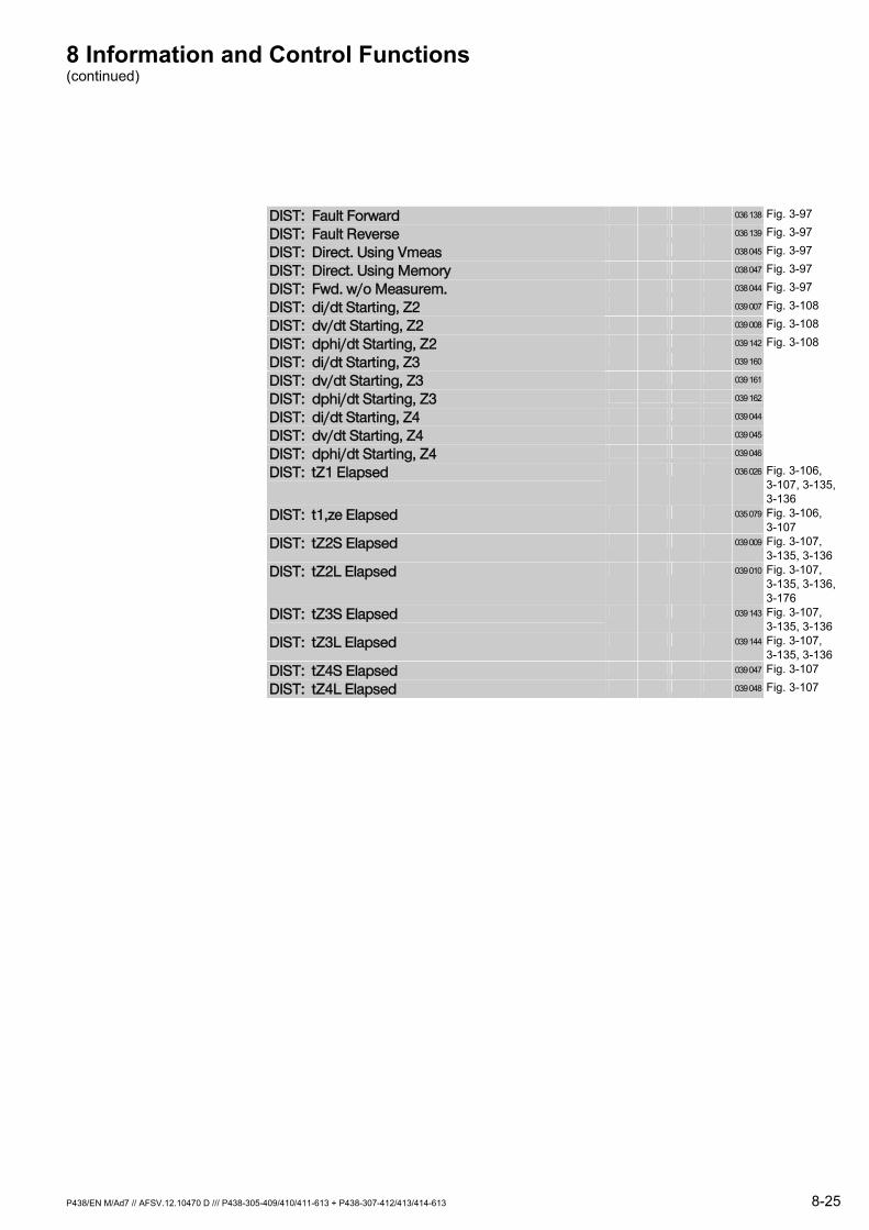
8 Information and Control Functions (continued)
P438/EN M/Ad7 // AFSV.12.10470 D /// P438-305-409/410/411-613 + P438-307-412/413/414-613 8-25
DIST: Fault Forward 036 138 Fig. 3-97
DIST: Fault Reverse 036 139 Fig. 3-97
DIST: Direct. Using Vmeas 038 045 Fig. 3-97
DIST: Direct. Using Memory 038 047 Fig. 3-97
DIST: Fwd. w/o Measurem. 038 044 Fig. 3-97
DIST: di/dt Starting, Z2 039 007 Fig. 3-108
DIST: dv/dt Starting, Z2 039 008 Fig. 3-108
DIST: dphi/dt Starting, Z2 039 142 Fig. 3-108
DIST: di/dt Starting, Z3 039 160
DIST: dv/dt Starting, Z3 039 161
DIST: dphi/dt Starting, Z3 039 162
DIST: di/dt Starting, Z4 039 044
DIST: dv/dt Starting, Z4 039 045
DIST: dphi/dt Starting, Z4 039 046
DIST: tZ1 Elapsed 036 026 Fig. 3-106, 3-107, 3-135, 3-136
DIST: t1,ze Elapsed 035 079 Fig. 3-106, 3-107
DIST: tZ2S Elapsed 039 009 Fig. 3-107, 3-135, 3-136
DIST: tZ2L Elapsed 039 010 Fig. 3-107, 3-135, 3-136, 3-176
DIST: tZ3S Elapsed 039 143 Fig. 3-107, 3-135, 3-136
DIST: tZ3L Elapsed 039 144 Fig. 3-107, 3-135, 3-136
DIST: tZ4S Elapsed 039 047 Fig. 3-107
DIST: tZ4L Elapsed 039 048 Fig. 3-107
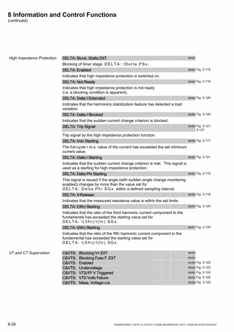
8 Information and Control Functions (continued)
8-26 P438/EN M/Ad7 // AFSV.12.10470 D /// P438-305-409/410/411-613 + P438-307-412/413/414-613
High Impedance Protection DELTA: Block. tDelta EXT 038 053
Blocking of timer stage D E L T A : t D e l t a P S x .
DELTA: Enabled 038 054 Fig. 3-115
Indicates that high impedance protection is switched on.
DELTA: Not Ready 038 055 Fig. 3-116
Indicates that high impedance protection is not ready (i.e. a blocking condition is apparent).
DELTA: Delta I Extended 038 066 Fig. 3-120
Indicates that the harmonics stabilization feature has detected a load variation.
DELTA: Delta I Blocked 038 068 Fig. 3-120
Indicates that the sudden current change criterion is blocked.
DELTA: Trip Signal 038 056 Fig. 3-121, 3-137
Trip signal by the high impedance protection function.
DELTA: Imin Starting 038 059 Fig. 3-117
The full-cycle r.m.s. value of the current has exceeded the set minimum current value.
DELTA: Delta I Starting 038 060 Fig. 3-121
Indicates that the sudden current change criterion is met. This signal is used as a starting for high impedance protection.
DELTA: Delta Phi Starting 038 063 Fig. 3-119
This signal is issued if the angle (with sudden angle change monitoring enabled) changes by more than the value set for D E L T A : D e l t a P h i S G x within a defined sampling interval.
DELTA: X-Release 038 065 Fig. 3-118
Indicates that the measured reactance value is within the set limits.
DELTA: I(3fn) Starting 038 076 Fig. 3-120
Indicates that the ratio of the third harmonic current component to the fundamental has exceeded the starting value set for D E L T A : I ( 3 f n ) / I ( f n ) S G x .
DELTA: I(5fn) Starting 038 077 Fig. 3-120
Indicates that the ratio of the fifth harmonic current component to the fundamental has exceeded the starting value set for D E L T A : I ( 5 f n ) / I ( f n ) S G x .
VT and CT Supervision C&VTS: Blocking V< EXT 038 033
C&VTS: Blocking Fuse F. EXT 038 037
C&VTS: Enabled 040 094 Fig. 3-122
C&VTS: Undervoltage 038 038 Fig. 3-123
C&VTS: VTS/FF V Triggered 035 081 Fig. 3-124
C&VTS: VTS Volts Failure 038 023 Fig. 3-126
C&VTS: Meas. Voltage o.k. 038 048 Fig. 3-125
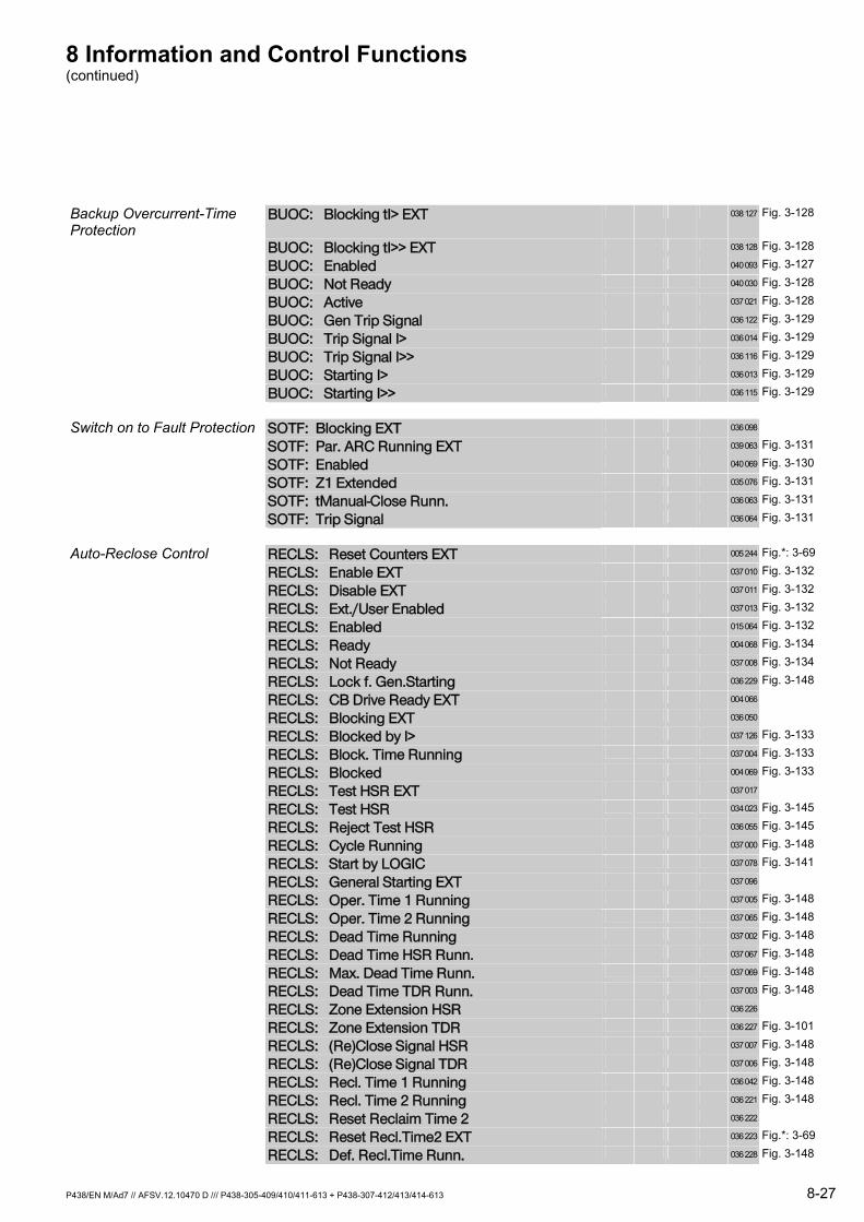
8 Information and Control Functions (continued)
P438/EN M/Ad7 // AFSV.12.10470 D /// P438-305-409/410/411-613 + P438-307-412/413/414-613 8-27
Backup Overcurrent-Time Protection
BUOC: Blocking tI> EXT 038 127 Fig. 3-128
BUOC: Blocking tI>> EXT 038 128 Fig. 3-128
BUOC: Enabled 040 093 Fig. 3-127
BUOC: Not Ready 040 030 Fig. 3-128
BUOC: Active 037 021 Fig. 3-128
BUOC: Gen Trip Signal 036 122 Fig. 3-129
BUOC: Trip Signal I> 036 014 Fig. 3-129
BUOC: Trip Signal I>> 036 116 Fig. 3-129
BUOC: Starting I> 036 013 Fig. 3-129
BUOC: Starting I>> 036 115 Fig. 3-129
Switch on to Fault Protection SOTF: Blocking EXT 036 098
SOTF: Par. ARC Running EXT 039 063 Fig. 3-131
SOTF: Enabled 040 069 Fig. 3-130
SOTF: Z1 Extended 035 076 Fig. 3-131
SOTF: tManual-Close Runn. 036 063 Fig. 3-131
SOTF: Trip Signal 036 064 Fig. 3-131
Auto-Reclose Control RECLS: Reset Counters EXT 005 244 Fig.*: 3-69
RECLS: Enable EXT 037 010 Fig. 3-132
RECLS: Disable EXT 037 011 Fig. 3-132
RECLS: Ext./User Enabled 037 013 Fig. 3-132
RECLS: Enabled 015 064 Fig. 3-132
RECLS: Ready 004 068 Fig. 3-134
RECLS: Not Ready 037 008 Fig. 3-134
RECLS: Lock f. Gen.Starting 036 229 Fig. 3-148
RECLS: CB Drive Ready EXT 004 066
RECLS: Blocking EXT 036 050
RECLS: Blocked by I> 037 126 Fig. 3-133
RECLS: Block. Time Running 037 004 Fig. 3-133
RECLS: Blocked 004 069 Fig. 3-133
RECLS: Test HSR EXT 037 017
RECLS: Test HSR 034 023 Fig. 3-145
RECLS: Reject Test HSR 036 055 Fig. 3-145
RECLS: Cycle Running 037 000 Fig. 3-148
RECLS: Start by LOGIC 037 078 Fig. 3-141
RECLS: General Starting EXT 037 096
RECLS: Oper. Time 1 Running 037 005 Fig. 3-148
RECLS: Oper. Time 2 Running 037 065 Fig. 3-148
RECLS: Dead Time Running 037 002 Fig. 3-148
RECLS: Dead Time HSR Runn. 037 067 Fig. 3-148
RECLS: Max. Dead Time Runn. 037 069 Fig. 3-148
RECLS: Dead Time TDR Runn. 037 003 Fig. 3-148
RECLS: Zone Extension HSR 036 226
RECLS: Zone Extension TDR 036 227 Fig. 3-101
RECLS: (Re)Close Signal HSR 037 007 Fig. 3-148
RECLS: (Re)Close Signal TDR 037 006 Fig. 3-148
RECLS: Recl. Time 1 Running 036 042 Fig. 3-148
RECLS: Recl. Time 2 Running 036 221 Fig. 3-148
RECLS: Reset Reclaim Time 2 036 222
RECLS: Reset Recl.Time2 EXT 036 223 Fig.*: 3-69
RECLS: Def. Recl.Time Runn. 036 228 Fig. 3-148

8 Information and Control Functions (continued)
8-28 P438/EN M/Ad7 // AFSV.12.10470 D /// P438-305-409/410/411-613 + P438-307-412/413/414-613
RECLS: Reclosure Successful 036 062 Fig. 3-143
RECLS: Trip Signal 039 099 Fig. 3-142, 3-148
RECLS: Sig.Interr. CB Trip 036 040 Fig. 3-148
Definite-Time Overcurrent Protection
DTOC: Blocking tI>H EXT 041 062 Fig. 3-148, 3-151
DTOC: Blocking tI> EXT 041 060 Fig. 3-151
DTOC: Blocking tI>> EXT 041 061 Fig. 3-151
DTOC: Enabled 040 120 Fig. 3-150
DTOC: Not Ready 040 027
DTOC: Trip Signal tI>H 040 076 Fig. 3-138, 3-139, 3-151
DTOC: Trip Signal tI> 041 020 Fig. 3-138, 3-139, 3-151, 3-153
DTOC: Trip Signal tI>> 040 011 Fig. 3-138, 3-139, 3-151, 3-153
DTOC: Starting I>H 035 022 Fig. 3-151
DTOC: Starting I> 035 020 Fig. 3-151, 3-153
DTOC: Starting I>> 035 021 Fig. 3-151, 3-153
DTOC: tI> Elapsed 040 010 Fig. 3-138, 3-139, 3-151, 3-153
DTOC: tI>> Elapsed 040 106 Fig. 3-138, 3-139, 3-151 3-153
DTOC: Direct. Using Vmeas 036 137 Fig. 3-154
DTOC: Direct. Using Memory 036 136 Fig. 3-154
DTOC: Dir.Meas. I> Blocked 035 080 Fig. 3-155
DTOC: Meas. I> Non-Direct. 035 077 Fig. 3-155
DTOC: Fault I> Forward 035 137 Fig. 3-154
DTOC: Power Flow I> Fwd. 035 223 Fig. 3-154
DTOC: Fault I> Reverse 035 140 Fig. 3-154
DTOC: Power Flow I> Rev. 035 224 Fig. 3-154
DTOC: Dir.Meas. I>> Block. 035 133 Fig. 3-156
DTOC: Meas. I>> Non-Direct 035 078 Fig. 3-156
DTOC: Fault I>> Forward 035 147 Fig. 3-154
DTOC: Power Flow I>> Fwd. 035 227 Fig. 3-154
DTOC: Fault I>> Reverse 035 148 Fig. 3-154
DTOC: Power Flow I>> Rev. 035 228 Fig. 3-154
DTOC: I> Fwd. w/o Meas. 041 198 Fig. 3-154
DTOC: I>> Fwd. w/o Meas. 041 199 Fig. 3-154
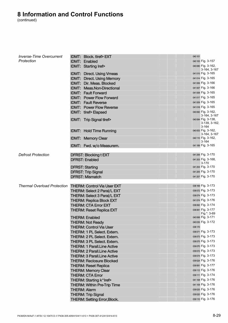
8 Information and Control Functions (continued)
P438/EN M/Ad7 // AFSV.12.10470 D /// P438-305-409/410/411-613 + P438-307-412/413/414-613 8-29
IDMT: Block. tIref> EXT 040 101 Inverse-Time Overcurrent Protection IDMT: Enabled 040 100 Fig. 3-157
IDMT: Starting Iref> 040 080 Fig. 3-162, 3-164, 3-167
IDMT: Direct. Using Vmeas 041 015 Fig. 3-165
IDMT: Direct. Using Memory 041 014 Fig. 3-165
IDMT: Dir. Meas. Blocked 041 006 Fig. 3-166
IDMT: Meas.Non-Directional 041 007 Fig. 3-166
IDMT: Fault Forward 041 008 Fig. 3-165
IDMT: Power Flow Forward 041 017 Fig. 3-165
IDMT: Fault Reverse 041 009 Fig. 3-165
IDMT: Power Flow Reverse 041 018 Fig. 3-165
IDMT: tIref> Elapsed 040 082 Fig. 3-162, 3-164, 3-167
IDMT: Trip Signal tIref> 040 084 Fig. 3-138, 3-139, 3-162, 3-164
IDMT: Hold Time Running 040 053 Fig. 3-162, 3-164, 3-167
IDMT: Memory Clear 040 110 Fig. 3-162, 3-164
IDMT: Fwd. w/o Measurem. 041 189 Fig. 3-165
DFRST: Blocking t EXT 041 206 Fig. 3-170 Defrost Protection DFRST: Enabled 041 203 Fig. 3-168,
3-170 DFRST: Starting 041 204 Fig. 3-170
DFRST: Trip Signal 041 205 Fig. 3-170
DFRST: Mismatch 041 207 Fig. 3-170
Thermal Overload Protection THERM: Control Via User EXT 038 169 Fig. 3-173
THERM: Select 2 Paral/L EXT 038 072 Fig. 3-173
THERM: Select 3 Paral/L EXT 038 074 Fig. 3-173
THERM: Replica Block EXT 041 074 Fig. 3-176
THERM: CTA Error EXT 038 062 Fig. 3-174
THERM: Reset Replica EXT 038 061 Fig. 3-177 Fig.*: 3-69
THERM: Enabled 040 068 Fig. 3-171
THERM: Not Ready 040 035 Fig. 3-172
THERM: Control Via User 038 170
THERM: 1 PL Select. Extern. 038 071 Fig. 3-173
THERM: 2 PL Select. Extern. 038 073 Fig. 3-173
THERM: 3 PL Select. Extern. 038 075 Fig. 3-173
THERM: 1 Parall.Line Active 039 070 Fig. 3-173
THERM: 2 Parall.Line Active 039 072 Fig. 3-173
THERM: 3 Parall.Line Active 039 074 Fig. 3-173
THERM: Reclosure Blocked 039 024 Fig. 3-176
THERM: Reset Replica 039 061 Fig. 3-177
THERM: Memory Clear 039 112 Fig. 3-176
THERM: CTA Error 039 111 Fig. 3-174
THERM: Starting k*Iref> 041 108 Fig. 3-176
THERM: Within Pre-Trip Time 041 109 Fig. 3-176
THERM: Alarm 039 025 Fig. 3-176
THERM: Trip Signal 039 020 Fig. 3-176
THERM: Setting Error,Block. 039 110 Fig. 3-176
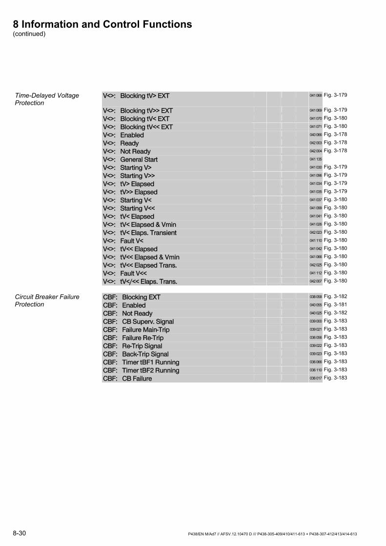
8 Information and Control Functions (continued)
8-30 P438/EN M/Ad7 // AFSV.12.10470 D /// P438-305-409/410/411-613 + P438-307-412/413/414-613
Time-Delayed Voltage Protection
V<>: Blocking tV> EXT 041 068 Fig. 3-179
V<>: Blocking tV>> EXT 041 069 Fig. 3-179
V<>: Blocking tV< EXT 041 070 Fig. 3-180
V<>: Blocking tV<< EXT 041 071 Fig. 3-180
V<>: Enabled 040 066 Fig. 3-178
V<>: Ready 042 003 Fig. 3-178
V<>: Not Ready 042 004 Fig. 3-178
V<>: General Start 041 135
V<>: Starting V> 041 030 Fig. 3-179
V<>: Starting V>> 041 096 Fig. 3-179
V<>: tV> Elapsed 041 034 Fig. 3-179
V<>: tV>> Elapsed 041 035 Fig. 3-179
V<>: Starting V< 041 037 Fig. 3-180
V<>: Starting V<< 041 099 Fig. 3-180
V<>: tV< Elapsed 041 041 Fig. 3-180
V<>: tV< Elapsed & Vmin 041 026 Fig. 3-180
V<>: tV< Elaps. Transient 042 023 Fig. 3-180
V<>: Fault V< 041 110 Fig. 3-180
V<>: tV<< Elapsed 041 042 Fig. 3-180
V<>: tV<< Elapsed & Vmin 041 066 Fig. 3-180
V<>: tV<< Elapsed Trans. 042 025 Fig. 3-180
V<>: Fault V<< 041 112 Fig. 3-180
V<>: tV</<< Elaps. Trans. 042 007 Fig. 3-180
CBF: Blocking EXT 038 058 Fig. 3-182 Circuit Breaker Failure
Protection CBF: Enabled 040 055 Fig. 3-181
CBF: Not Ready 040 025 Fig. 3-182
CBF: CB Superv. Signal 039 000 Fig. 3-183
CBF: Failure Main-Trip 039 021 Fig. 3-183
CBF: Failure Re-Trip 036 056 Fig. 3-183
CBF: Re-Trip Signal 039 022 Fig. 3-183
CBF: Back-Trip Signal 039 023 Fig. 3-183
CBF: Timer tBF1 Running 036 066 Fig. 3-183
CBF: Timer tBF2 Running 036 110 Fig. 3-183
CBF: CB Failure 036 017 Fig. 3-183
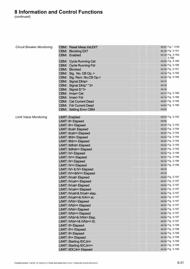
8 Information and Control Functions (continued)
P438/EN M/Ad7 // AFSV.12.10470 D /// P438-305-409/410/411-613 + P438-307-412/413/414-613 8-31
Circuit Breaker Monitoring CBM: Reset Meas.Val.EXT 005 247 Fig.*: 3-69
CBM: Blocking EXT 044 128 Fig. 3-191
CBM: Enabled 044 130 Fig. 3-184, 3-186
CBM: Cycle Running Cat 044 205 Fig. 3-188
CBM: Cycle Running Fdr 044 206 Fig. 3-188
CBM: Blocked 044 199 Fig. 3-191
CBM: Sig. No. CB Op. > 044 135 Fig. 3-190
CBM: Sig. Rem. No.CB Op.< 044 136 Fig. 3-189
CBM: Signal ΣItrip> 044 137
CBM: Signal ΣItrip**2> 044 138
CBM: Signal ΣI*t> 044 139
CBM: tmax> Cat 044 177 Fig. 3-186
CBM: tmax> Fdr 044 178 Fig. 3-186
CBM: Cat Current Dead 044 201 Fig. 3-186
CBM: Fdr Current Dead 044 202 Fig. 3-186
CBM: Setting Error CBM 044 204
Limit Value Monitoring LIMIT: Enabled 040 074 Fig. 3-192
LIMIT: tI> Elapsed 004 062
LIMIT: tI>> Elapsed 040 157 Fig. 3-193
LIMIT: tIcat> Elapsed 040 232 Fig. 3-194
LIMIT: tIcat>> Elapsed 040 233 Fig. 3-194
LIMIT: tIfdr> Elapsed 040 234 Fig. 3-194
LIMIT: tIfdr>> Elapsed 040 235 Fig. 3-194
LIMIT: tIdfrst> Elapsed 040 236 Fig. 3-195
LIMIT: tIdfrst>> Elapsed 040 237 Fig. 3-195
LIMIT: tV> Elapsed 040 140 Fig. 3-196
LIMIT: tV>> Elapsed 040 141 Fig. 3-196
LIMIT: tV< Elapsed 040 142 Fig. 3-196
LIMIT: tV<< Elapsed 040 143 Fig. 3-196
LIMIT: tV> & tV< Elapsed 040 144
LIMIT: tV>>&tV<< Elapsed 040 145
LIMIT: tVcat> Elapsed 040 240 Fig. 3-197
LIMIT: tVcat>> Elapsed 040 241 Fig. 3-197
LIMIT: tVcat< Elapsed 040 242 Fig. 3-197
LIMIT: tVcat<< Elapsed 040 243 Fig. 3-197
LIMIT: tVcat>& tVcat< elap. 040 244 Fig. 3-197
LIMIT: tVcat>>& tVA<< el. 040 245 Fig. 3-197
LIMIT: tVfdr> Elapsed 040 246 Fig. 3-197
LIMIT: tVfdr>> Elapsed 040 247 Fig. 3-197
LIMIT: tVfdr< Elapsed 040 248 Fig. 3-197
LIMIT: tVfdr<< Elapsed 040 249 Fig. 3-197
LIMIT: tVfdr>& tVfdr< Elap. 040 250 Fig. 3-197
LIMIT: tVfdr>>& tVfdr<< El. 040 251 Fig. 3-197
LIMIT: tf> Elapsed 040 196 Fig. 3-198
LIMIT: tf>> Elapsed 040 197 Fig. 3-198
LIMIT: tf< Elapsed 040 198 Fig. 3-198
LIMIT: tf<< Elapsed 040 199 Fig. 3-198
LIMIT: Starting IDC,lin> 040 180 Fig. 3-199
LIMIT: Starting IDC,lin>> 040 181 Fig. 3-199
LIMIT: tIDC,lin> Elapsed 040 182 Fig. 3-199
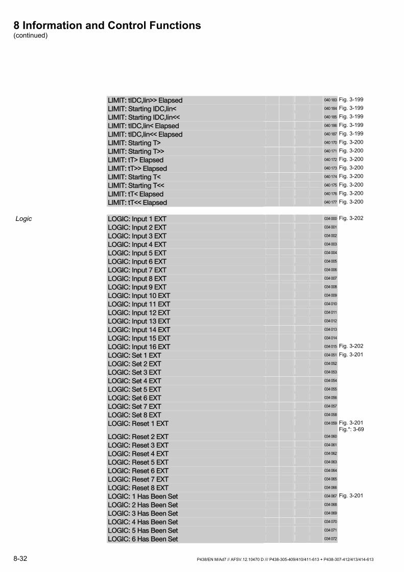
8 Information and Control Functions (continued)
8-32 P438/EN M/Ad7 // AFSV.12.10470 D /// P438-305-409/410/411-613 + P438-307-412/413/414-613
LIMIT: tIDC,lin>> Elapsed 040 183 Fig. 3-199
LIMIT: Starting IDC,lin< 040 184 Fig. 3-199
LIMIT: Starting IDC,lin<< 040 185 Fig. 3-199
LIMIT: tIDC,lin< Elapsed 040 186 Fig. 3-199
LIMIT: tIDC,lin<< Elapsed 040 187 Fig. 3-199
LIMIT: Starting T> 040 170 Fig. 3-200
LIMIT: Starting T>> 040 171 Fig. 3-200
LIMIT: tT> Elapsed 040 172 Fig. 3-200
LIMIT: tT>> Elapsed 040 173 Fig. 3-200
LIMIT: Starting T< 040 174 Fig. 3-200
LIMIT: Starting T<< 040 175 Fig. 3-200
LIMIT: tT< Elapsed 040 176 Fig. 3-200
LIMIT: tT<< Elapsed 040 177 Fig. 3-200
Logic LOGIC: Input 1 EXT 034 000 Fig. 3-202
LOGIC: Input 2 EXT 034 001
LOGIC: Input 3 EXT 034 002
LOGIC: Input 4 EXT 034 003
LOGIC: Input 5 EXT 034 004
LOGIC: Input 6 EXT 034 005
LOGIC: Input 7 EXT 034 006
LOGIC: Input 8 EXT 034 007
LOGIC: Input 9 EXT 034 008
LOGIC: Input 10 EXT 034 009
LOGIC: Input 11 EXT 034 010
LOGIC: Input 12 EXT 034 011
LOGIC: Input 13 EXT 034 012
LOGIC: Input 14 EXT 034 013
LOGIC: Input 15 EXT 034 014
LOGIC: Input 16 EXT 034 015 Fig. 3-202
LOGIC: Set 1 EXT 034 051 Fig. 3-201
LOGIC: Set 2 EXT 034 052
LOGIC: Set 3 EXT 034 053
LOGIC: Set 4 EXT 034 054
LOGIC: Set 5 EXT 034 055
LOGIC: Set 6 EXT 034 056
LOGIC: Set 7 EXT 034 057
LOGIC: Set 8 EXT 034 058
LOGIC: Reset 1 EXT 034 059 Fig. 3-201 Fig.*: 3-69
LOGIC: Reset 2 EXT 034 060
LOGIC: Reset 3 EXT 034 061
LOGIC: Reset 4 EXT 034 062
LOGIC: Reset 5 EXT 034 063
LOGIC: Reset 6 EXT 034 064
LOGIC: Reset 7 EXT 034 065
LOGIC: Reset 8 EXT 034 066
LOGIC: 1 Has Been Set 034 067 Fig. 3-201
LOGIC: 2 Has Been Set 034 068
LOGIC: 3 Has Been Set 034 069
LOGIC: 4 Has Been Set 034 070
LOGIC: 5 Has Been Set 034 071
LOGIC: 6 Has Been Set 034 072

8 Information and Control Functions (continued)
P438/EN M/Ad7 // AFSV.12.10470 D /// P438-305-409/410/411-613 + P438-307-412/413/414-613 8-33
LOGIC: 7 Has Been Set 034 073
LOGIC: 8 Has Been Set 034 074 Fig. 3-202
LOGIC: 1 Set Externally 034 075 Fig. 3-201
LOGIC: 2 Set Externally 034 076
LOGIC: 3 Set Externally 034 077
LOGIC: 4 Set Externally 034 078
LOGIC: 5 Set Externally 034 079
LOGIC: 6 Set Externally 034 080
LOGIC: 7 Set Externally 034 081
LOGIC: 8 Set Externally 034 082 Fig. 3-202
LOGIC: Enabled 034 046 Fig. 3-202
LOGIC: Output 1 042 032 Fig. 3-202
LOGIC: Output 2 042 034
LOGIC: Output 3 042 036
LOGIC: Output 4 042 038
LOGIC: Output 5 042 040
LOGIC: Output 6 042 042
LOGIC: Output 7 042 044
LOGIC: Output 8 042 046
LOGIC: Output 9 042 048
LOGIC: Output 10 042 050
LOGIC: Output 11 042 052
LOGIC: Output 12 042 054
LOGIC: Output 13 042 056
LOGIC: Output 14 042 058
LOGIC: Output 15 042 060
LOGIC: Output 16 042 062
LOGIC: Output 17 042 064
LOGIC: Output 18 042 066
LOGIC: Output 19 042 068
LOGIC: Output 20 042 070
LOGIC: Output 21 042 072
LOGIC: Output 22 042 074
LOGIC: Output 23 042 076
LOGIC: Output 24 042 078
LOGIC: Output 25 042 080
LOGIC: Output 26 042 082
LOGIC: Output 27 042 084
LOGIC: Output 28 042 086
LOGIC: Output 29 042 088
LOGIC: Output 30 042 090
LOGIC: Output 31 042 092
LOGIC: Output 32 042 094
LOGIC: Output 1 (t) 042 033 Fig. 3-202
LOGIC: Output 2 (t) 042 035 Fig. 3-141
LOGIC: Output 3 (t) 042 037
LOGIC: Output 4 (t) 042 039
LOGIC: Output 5 (t) 042 041
LOGIC: Output 6 (t) 042 043
LOGIC: Output 7 (t) 042 045
LOGIC: Output 8 (t) 042 047
LOGIC: Output 9 (t) 042 049
8 Information and Control Functions (continued)
8-34 P438/EN M/Ad7 // AFSV.12.10470 D /// P438-305-409/410/411-613 + P438-307-412/413/414-613
LOGIC: Output 10 (t) 042 051
LOGIC: Output 11 (t) 042 053
LOGIC: Output 12 (t) 042 055
LOGIC: Output 13 (t) 042 057
LOGIC: Output 14 (t) 042 059
LOGIC: Output 15 (t) 042 061
LOGIC: Output 16 (t) 042 063
LOGIC: Output 17 (t) 042 065
LOGIC: Output 18 (t) 042 067
LOGIC: Output 19 (t) 042 069
LOGIC: Output 20 (t) 042 071
LOGIC: Output 21 (t) 042 073
LOGIC: Output 22 (t) 042 075
LOGIC: Output 23 (t) 042 077
LOGIC: Output 24 (t) 042 079
LOGIC: Output 25 (t) 042 081
LOGIC: Output 26 (t) 042 083
LOGIC: Output 27 (t) 042 085
LOGIC: Output 28 (t) 042 087
LOGIC: Output 29 (t) 042 089
LOGIC: Output 30 (t) 042 091
LOGIC: Output 31 (t) 042 093
LOGIC: Output 32 (t) 042 095
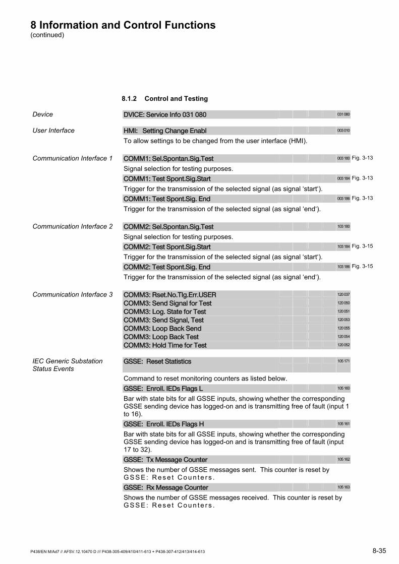
8 Information and Control Functions (continued)
P438/EN M/Ad7 // AFSV.12.10470 D /// P438-305-409/410/411-613 + P438-307-412/413/414-613 8-35
8.1.2 Control and Testing
Device DVICE: Service Info 031 080 031 080
User Interface HMI: Setting Change Enabl 003 010
To allow settings to be changed from the user interface (HMI).
Communication Interface 1 COMM1: Sel.Spontan.Sig.Test 003 180 Fig. 3-13
Signal selection for testing purposes.
COMM1: Test Spont.Sig.Start 003 184 Fig. 3-13
Trigger for the transmission of the selected signal (as signal ‘start‘).
COMM1: Test Spont.Sig. End 003 186 Fig. 3-13
Trigger for the transmission of the selected signal (as signal ‘end‘).
Communication Interface 2 COMM2: Sel.Spontan.Sig.Test 103 180
Signal selection for testing purposes.
COMM2: Test Spont.Sig.Start 103 184 Fig. 3-15
Trigger for the transmission of the selected signal (as signal ‘start‘).
COMM2: Test Spont.Sig. End 103 186 Fig. 3-15
Trigger for the transmission of the selected signal (as signal ‘end‘).
Communication Interface 3 COMM3: Rset.No.Tlg.Err.USER 120 037
COMM3: Send Signal for Test 120 050
COMM3: Log. State for Test 120 051
COMM3: Send Signal, Test 120 053
COMM3: Loop Back Send 120 055
COMM3: Loop Back Test 120 054
COMM3: Hold Time for Test 120 052
IEC Generic Substation Status Events
GSSE: Reset Statistics 105 171
Command to reset monitoring counters as listed below.
GSSE: Enroll. IEDs Flags L 105 160
Bar with state bits for all GSSE inputs, showing whether the corresponding GSSE sending device has logged-on and is transmitting free of fault (input 1 to 16).
GSSE: Enroll. IEDs Flags H 105 161
Bar with state bits for all GSSE inputs, showing whether the corresponding GSSE sending device has logged-on and is transmitting free of fault (input 17 to 32).
GSSE: Tx Message Counter 105 162
Shows the number of GSSE messages sent. This counter is reset by G S S E : R e s e t C o u n t e r s .
GSSE: Rx Message Counter 105 163
Shows the number of GSSE messages received. This counter is reset by G S S E : R e s e t C o u n t e r s .
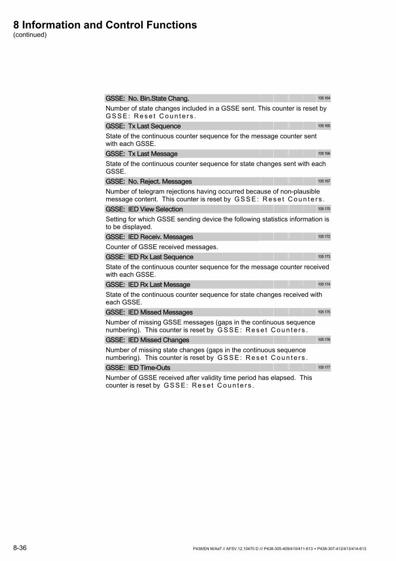
8 Information and Control Functions (continued)
8-36 P438/EN M/Ad7 // AFSV.12.10470 D /// P438-305-409/410/411-613 + P438-307-412/413/414-613
GSSE: No. Bin.State Chang. 105 164
Number of state changes included in a GSSE sent. This counter is reset by G S S E : R e s e t C o u n t e r s .
GSSE: Tx Last Sequence 105 165
State of the continuous counter sequence for the message counter sent with each GSSE.
GSSE: Tx Last Message 105 166
State of the continuous counter sequence for state changes sent with each GSSE.
GSSE: No. Reject. Messages 105 167
Number of telegram rejections having occurred because of non-plausible message content. This counter is reset by G S S E : R e s e t C o u n t e r s .
GSSE: IED View Selection 105 170
Setting for which GSSE sending device the following statistics information is to be displayed.
GSSE: IED Receiv. Messages 105 172
Counter of GSSE received messages.
GSSE: IED Rx Last Sequence 105 173
State of the continuous counter sequence for the message counter received with each GSSE.
GSSE: IED Rx Last Message 105 174
State of the continuous counter sequence for state changes received with each GSSE.
GSSE: IED Missed Messages 105 175
Number of missing GSSE messages (gaps in the continuous sequence numbering). This counter is reset by G S S E : R e s e t C o u n t e r s .
GSSE: IED Missed Changes 105 176
Number of missing state changes (gaps in the continuous sequence numbering). This counter is reset by G S S E : R e s e t C o u n t e r s .
GSSE: IED Time-Outs 105 177
Number of GSSE received after validity time period has elapsed. This counter is reset by G S S E : R e s e t C o u n t e r s .
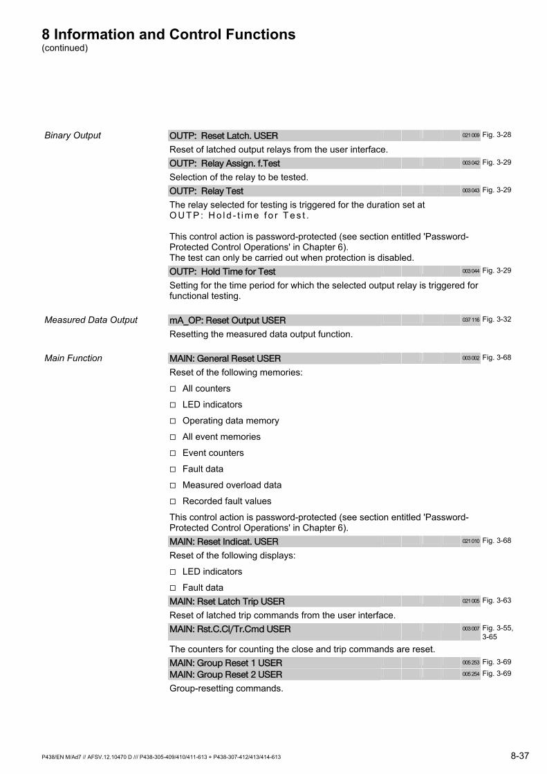
8 Information and Control Functions (continued)
P438/EN M/Ad7 // AFSV.12.10470 D /// P438-305-409/410/411-613 + P438-307-412/413/414-613 8-37
Binary Output OUTP: Reset Latch. USER 021 009 Fig. 3-28
Reset of latched output relays from the user interface.
OUTP: Relay Assign. f.Test 003 042 Fig. 3-29
Selection of the relay to be tested.
OUTP: Relay Test 003 043 Fig. 3-29
The relay selected for testing is triggered for the duration set at O U T P : H o l d - t i m e f o r T e s t . This control action is password-protected (see section entitled 'Password-Protected Control Operations' in Chapter 6). The test can only be carried out when protection is disabled.
OUTP: Hold Time for Test 003 044 Fig. 3-29
Setting for the time period for which the selected output relay is triggered for functional testing.
Measured Data Output mA_OP: Reset Output USER 037 116 Fig. 3-32
Resetting the measured data output function.
Main Function MAIN: General Reset USER 003 002 Fig. 3-68
Reset of the following memories:
All counters
LED indicators
Operating data memory
All event memories
Event counters
Fault data
Measured overload data
Recorded fault values
This control action is password-protected (see section entitled 'Password-Protected Control Operations' in Chapter 6).
MAIN: Reset Indicat. USER 021 010 Fig. 3-68
Reset of the following displays:
LED indicators
Fault data
MAIN: Rset Latch Trip USER 021 005 Fig. 3-63
Reset of latched trip commands from the user interface.
MAIN: Rst.C.Cl/Tr.Cmd USER 003 007 Fig. 3-55, 3-65
The counters for counting the close and trip commands are reset.
MAIN: Group Reset 1 USER 005 253 Fig. 3-69
MAIN: Group Reset 2 USER 005 254 Fig. 3-69
Group-resetting commands.
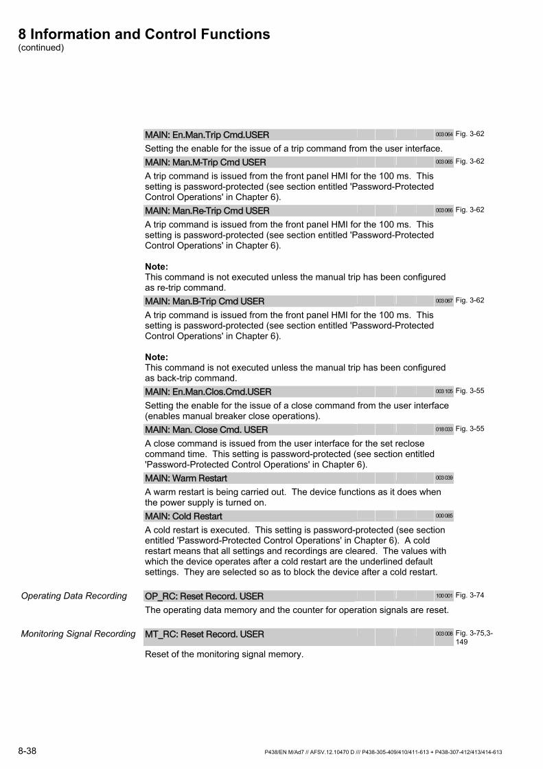
8 Information and Control Functions (continued)
8-38 P438/EN M/Ad7 // AFSV.12.10470 D /// P438-305-409/410/411-613 + P438-307-412/413/414-613
MAIN: En.Man.Trip Cmd.USER 003 064 Fig. 3-62
Setting the enable for the issue of a trip command from the user interface.
MAIN: Man.M-Trip Cmd USER 003 065 Fig. 3-62
A trip command is issued from the front panel HMI for the 100 ms. This setting is password-protected (see section entitled 'Password-Protected Control Operations' in Chapter 6).
MAIN: Man.Re-Trip Cmd USER 003 066 Fig. 3-62
A trip command is issued from the front panel HMI for the 100 ms. This setting is password-protected (see section entitled 'Password-Protected Control Operations' in Chapter 6). Note: This command is not executed unless the manual trip has been configured as re-trip command.
MAIN: Man.B-Trip Cmd USER 003 067 Fig. 3-62
A trip command is issued from the front panel HMI for the 100 ms. This setting is password-protected (see section entitled 'Password-Protected Control Operations' in Chapter 6). Note: This command is not executed unless the manual trip has been configured as back-trip command.
MAIN: En.Man.Clos.Cmd.USER 003 105 Fig. 3-55
Setting the enable for the issue of a close command from the user interface (enables manual breaker close operations).
MAIN: Man. Close Cmd. USER 018 033 Fig. 3-55
A close command is issued from the user interface for the set reclose command time. This setting is password-protected (see section entitled 'Password-Protected Control Operations' in Chapter 6).
MAIN: Warm Restart 003 039
A warm restart is being carried out. The device functions as it does when the power supply is turned on.
MAIN: Cold Restart 000 085
A cold restart is executed. This setting is password-protected (see section entitled 'Password-Protected Control Operations' in Chapter 6). A cold restart means that all settings and recordings are cleared. The values with which the device operates after a cold restart are the underlined default settings. They are selected so as to block the device after a cold restart.
Operating Data Recording OP_RC: Reset Record. USER 100 001 Fig. 3-74
The operating data memory and the counter for operation signals are reset.
Monitoring Signal Recording MT_RC: Reset Record. USER 003 008 Fig. 3-75,3-
149 Reset of the monitoring signal memory.
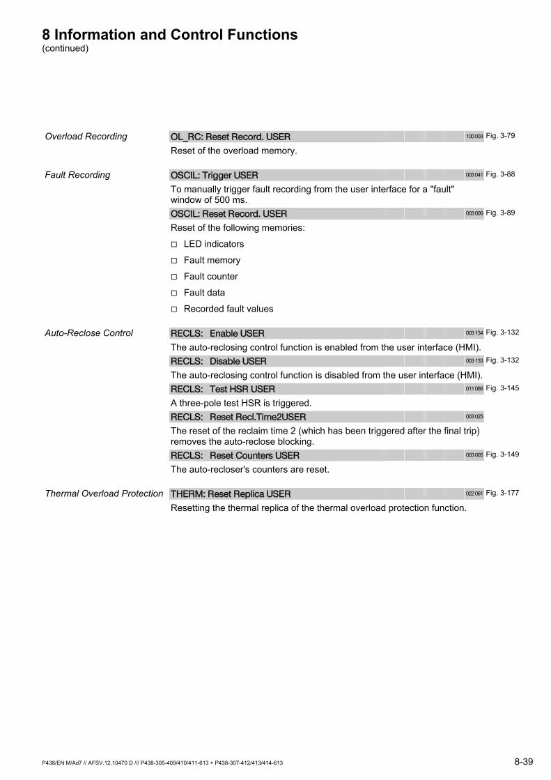
8 Information and Control Functions (continued)
P438/EN M/Ad7 // AFSV.12.10470 D /// P438-305-409/410/411-613 + P438-307-412/413/414-613 8-39
Overload Recording OL_RC: Reset Record. USER 100 003 Fig. 3-79
Reset of the overload memory.
Fault Recording OSCIL: Trigger USER 003 041 Fig. 3-88
To manually trigger fault recording from the user interface for a "fault" window of 500 ms.
OSCIL: Reset Record. USER 003 006 Fig. 3-89
Reset of the following memories:
LED indicators
Fault memory
Fault counter
Fault data
Recorded fault values
Auto-Reclose Control RECLS: Enable USER 003 134 Fig. 3-132
The auto-reclosing control function is enabled from the user interface (HMI).
RECLS: Disable USER 003 133 Fig. 3-132
The auto-reclosing control function is disabled from the user interface (HMI).
RECLS: Test HSR USER 011 066 Fig. 3-145
A three-pole test HSR is triggered.
RECLS: Reset Recl.Time2USER 003 025
The reset of the reclaim time 2 (which has been triggered after the final trip) removes the auto-reclose blocking.
RECLS: Reset Counters USER 003 005 Fig. 3-149
The auto-recloser's counters are reset.
Thermal Overload Protection THERM: Reset Replica USER 022 061 Fig. 3-177
Resetting the thermal replica of the thermal overload protection function.

8 Information and Control Functions (continued)
8-40 P438/EN M/Ad7 // AFSV.12.10470 D /// P438-305-409/410/411-613 + P438-307-412/413/414-613
Circuit Breaker Monitoring CBM: Initialize Values 003 011 Fig. 3-188
Values are initialized to trigger circuit breaker condition monitoring.
CBM: Reset Meas.Val. USER 003 013 Fig. 3-188
Resetting circuit breaker condition monitoring
CBM: Set No. CB Oper. Cat 022 131 Fig. 3-188
CBM: Set No. CB Oper. Fdr 022 132 Fig. 3-188
CBM: Set Remain.CB Op.Cat 022 134 Fig. 3-188
CBM: Set Remain.CB Op.Fdr 022 135 Fig. 3-188
CBM: Set ΣItrip Cat 022 137 Fig. 3-188
CBM: Set ΣItrip Fdr 022 138 Fig. 3-188
CBM: Set ΣItrip**2 Cat 022 140 Fig. 3-188
CBM: Set ΣItrip**2 Fdr 022 141 Fig. 3-188
CBM: Set ΣI*t Cat 022 143 Fig. 3-188
CBM: Set ΣI*t Fdr 022 144 Fig. 3-188
Setting the actual circuit breaker condition.
Logic LOGIC: Trigger 1 034 038 Fig. 3-202
LOGIC: Trigger 2 034 039
LOGIC: Trigger 3 034 040
LOGIC: Trigger 4 034 041
LOGIC: Trigger 5 034 042
LOGIC: Trigger 6 034 043
LOGIC: Trigger 7 034 044
LOGIC: Trigger 8 034 045 Fig. 3-202
Intervention in the logic at the appropriate point by a 100 ms pulse.
8.1.3 Operating Data Recording
Operating Data Recording OP_RC: Operat. Data Record. 003 024 Fig. 3-74
Point of entry into the operating data log.
Monitoring Signal Recording MT_RC: Mon. Signal Record. 003 001 Fig. 3-75
Point of entry into the monitoring signal log.
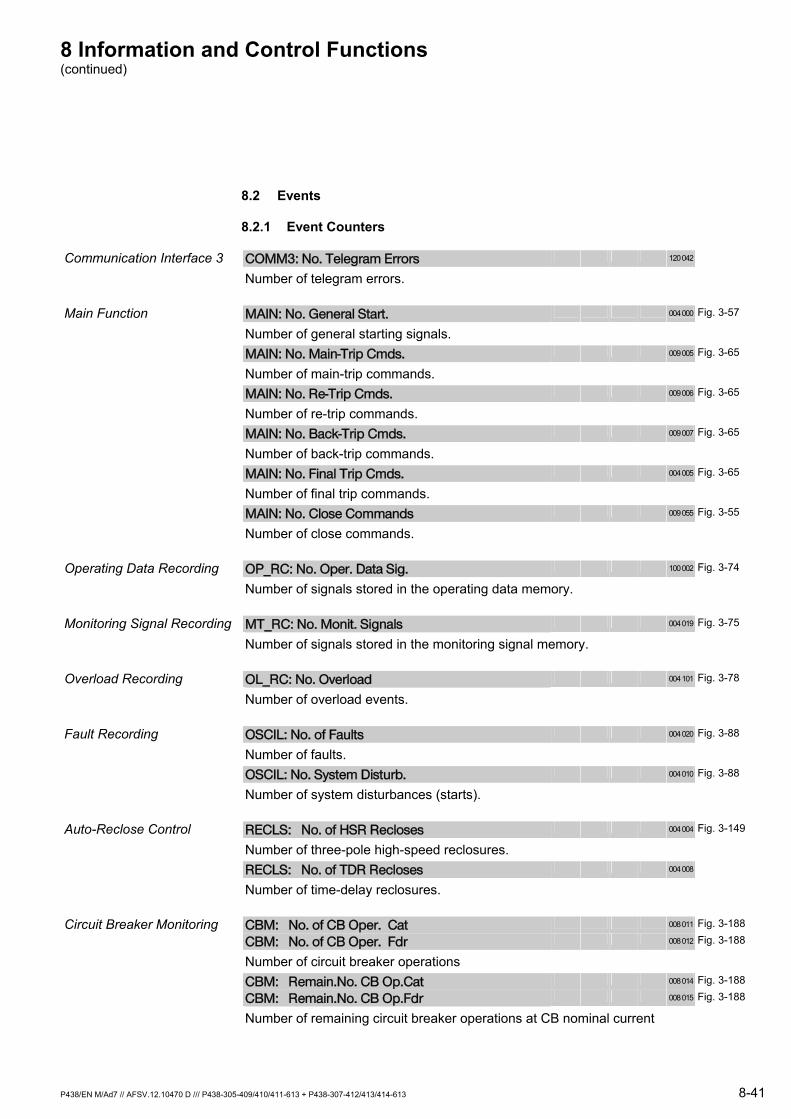
8 Information and Control Functions (continued)
P438/EN M/Ad7 // AFSV.12.10470 D /// P438-305-409/410/411-613 + P438-307-412/413/414-613 8-41
8.2 Events
8.2.1 Event Counters
Communication Interface 3 COMM3: No. Telegram Errors 120 042
Number of telegram errors.
Main Function MAIN: No. General Start. 004 000 Fig. 3-57
Number of general starting signals.
MAIN: No. Main-Trip Cmds. 009 005 Fig. 3-65
Number of main-trip commands.
MAIN: No. Re-Trip Cmds. 009 006 Fig. 3-65
Number of re-trip commands.
MAIN: No. Back-Trip Cmds. 009 007 Fig. 3-65
Number of back-trip commands.
MAIN: No. Final Trip Cmds. 004 005 Fig. 3-65
Number of final trip commands.
MAIN: No. Close Commands 009 055 Fig. 3-55
Number of close commands.
Operating Data Recording OP_RC: No. Oper. Data Sig. 100 002 Fig. 3-74
Number of signals stored in the operating data memory.
Monitoring Signal Recording MT_RC: No. Monit. Signals 004 019 Fig. 3-75
Number of signals stored in the monitoring signal memory.
Overload Recording OL_RC: No. Overload 004 101 Fig. 3-78
Number of overload events.
Fault Recording OSCIL: No. of Faults 004 020 Fig. 3-88
Number of faults.
OSCIL: No. System Disturb. 004 010 Fig. 3-88
Number of system disturbances (starts).
Auto-Reclose Control RECLS: No. of HSR Recloses 004 004 Fig. 3-149
Number of three-pole high-speed reclosures.
RECLS: No. of TDR Recloses 004 008
Number of time-delay reclosures.
Circuit Breaker Monitoring CBM: No. of CB Oper. Cat 008 011 Fig. 3-188
CBM: No. of CB Oper. Fdr 008 012 Fig. 3-188
Number of circuit breaker operations
CBM: Remain.No. CB Op.Cat 008 014 Fig. 3-188
CBM: Remain.No. CB Op.Fdr 008 015 Fig. 3-188
Number of remaining circuit breaker operations at CB nominal current
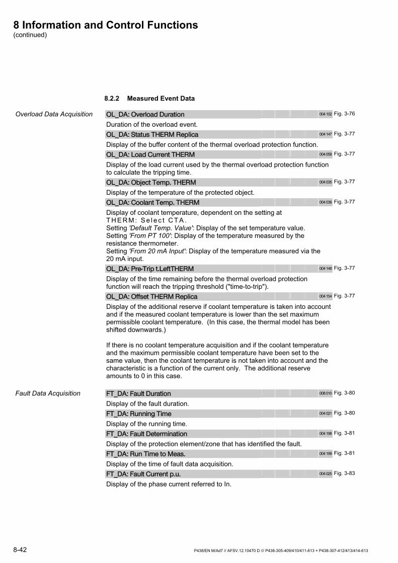
8 Information and Control Functions (continued)
8-42 P438/EN M/Ad7 // AFSV.12.10470 D /// P438-305-409/410/411-613 + P438-307-412/413/414-613
8.2.2 Measured Event Data
Overload Data Acquisition OL_DA: Overload Duration 004 102 Fig. 3-76
Duration of the overload event.
OL_DA: Status THERM Replica 004 147 Fig. 3-77
Display of the buffer content of the thermal overload protection function.
OL_DA: Load Current THERM 004 058 Fig. 3-77
Display of the load current used by the thermal overload protection function to calculate the tripping time.
OL_DA: Object Temp. THERM 004 035 Fig. 3-77
Display of the temperature of the protected object.
OL_DA: Coolant Temp. THERM 004 036 Fig. 3-77
Display of coolant temperature, dependent on the setting at T H E R M : S e l e c t C T A . Setting 'Default Temp. Value': Display of the set temperature value. Setting 'From PT 100': Display of the temperature measured by the resistance thermometer. Setting 'From 20 mA Input': Display of the temperature measured via the 20 mA input.
OL_DA: Pre-Trip t.LeftTHERM 004 148 Fig. 3-77
Display of the time remaining before the thermal overload protection function will reach the tripping threshold ("time-to-trip").
OL_DA: Offset THERM Replica 004 154 Fig. 3-77
Display of the additional reserve if coolant temperature is taken into account and if the measured coolant temperature is lower than the set maximum permissible coolant temperature. (In this case, the thermal model has been shifted downwards.) If there is no coolant temperature acquisition and if the coolant temperature and the maximum permissible coolant temperature have been set to the same value, then the coolant temperature is not taken into account and the characteristic is a function of the current only. The additional reserve amounts to 0 in this case.
Fault Data Acquisition FT_DA: Fault Duration 008 010 Fig. 3-80
Display of the fault duration.
FT_DA: Running Time 004 021 Fig. 3-80
Display of the running time.
FT_DA: Fault Determination 004 198 Fig. 3-81
Display of the protection element/zone that has identified the fault.
FT_DA: Run Time to Meas. 004 199 Fig. 3-81
Display of the time of fault data acquisition.
FT_DA: Fault Current p.u. 004 025 Fig. 3-83
Display of the phase current referred to In.

8 Information and Control Functions (continued)
P438/EN M/Ad7 // AFSV.12.10470 D /// P438-305-409/410/411-613 + P438-307-412/413/414-613 8-43
FT_DA: FaultVoltage p.u. 004 026 Fig. 3-83
Display of the calculated neutral-point displacement voltage referred to Vn .
FT_DA: Fault Loop Angle 004 024 Fig. 3-83
Display of the fault angle.
FT_DA: Fault Reactance,Prim 004 029 Fig. 3-83
Display of the fault reactance as a primary quantity.
FT_DA: Fault Impedance,Prim 004 176 Fig. 3-83
Display of the fault impedance as a primary quantity.
FT_DA: Fault Reactance,Sec. 004 028 Fig. 3-83
Display of the fault reactance as a secondary quantity.
FT_DA: Fault Impedance,Sec. 004 023 Fig. 3-83
Display of the fault impedance as a secondary quantity.
FT_DA: Fault Locat. Percent 004 027 Fig. 3-86
Display of the fault location of the last fault (in %) referred to the setting at F T _ D A : L i n e R e a c t X S e c 1 S G x .
FT_DA: Fault Location 004 022 Fig. 3-86
Display of the fault location of the last fault (in km).
FT_DA: Icat p.u. 004 181 Fig. 3-84
Display of the catenary current referred to In.
FT_DA: Ifdr p.u. 004 182 Fig. 3-84
Display of the feeder current referred to In.
FT_DA: Idfrst p.u. 004 177 Fig. 3-85
Display of the defrost current referred to In.
FT_DA: kHarm, ΣI(xfn)/I(fn) 008 217 Fig. 3-83
Displays the ratio of the second, third and fifth harmonic current components to the fundamental component of the current. Note: Valid only with setting M A I N : F e e d i n g M o d e 'Autotransformer Feed' and with the optional processor module with an integrated DSP coprocessor fitted, and with the harmonics adaptation feature enabled in the distance protection.
FT_DA: Vcat p.u. 004 183 Fig. 3-84
Display of the catenary voltage referred to Vn.
FT_DA: Vfdr p.u. 004 184 Fig. 3-84
Display of the feeder voltage referred to Vn.
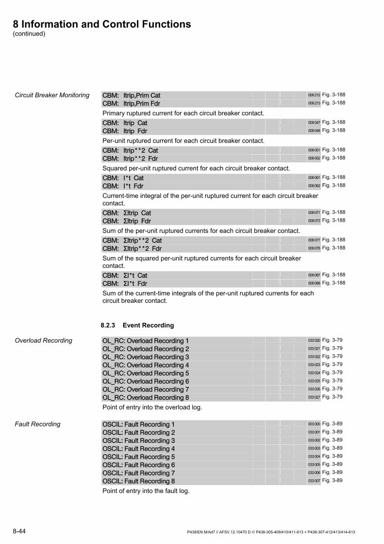
8 Information and Control Functions (continued)
8-44 P438/EN M/Ad7 // AFSV.12.10470 D /// P438-305-409/410/411-613 + P438-307-412/413/414-613
Circuit Breaker Monitoring CBM: Itrip,Prim Cat 009 212 Fig. 3-188
CBM: Itrip,Prim Fdr 009 213 Fig. 3-188
Primary ruptured current for each circuit breaker contact.
CBM: Itrip Cat 009 047 Fig. 3-188
CBM: Itrip Fdr 009 048 Fig. 3-188
Per-unit ruptured current for each circuit breaker contact.
CBM: Itrip**2 Cat 009 051 Fig. 3-188
CBM: Itrip**2 Fdr 009 052 Fig. 3-188
Squared per-unit ruptured current for each circuit breaker contact.
CBM: I*t Cat 009 061 Fig. 3-188
CBM: I*t Fdr 009 062 Fig. 3-188
Current-time integral of the per-unit ruptured current for each circuit breaker contact.
CBM: ΣItrip Cat 009 071 Fig. 3-188
CBM: ΣItrip Fdr 009 073 Fig. 3-188
Sum of the per-unit ruptured currents for each circuit breaker contact.
CBM: ΣItrip**2 Cat 009 077 Fig. 3-188
CBM: ΣItrip**2 Fdr 009 078 Fig. 3-188
Sum of the squared per-unit ruptured currents for each circuit breaker contact.
CBM: ΣI*t Cat 009 087 Fig. 3-188
CBM: ΣI*t Fdr 009 088 Fig. 3-188
Sum of the current-time integrals of the per-unit ruptured currents for each circuit breaker contact.
8.2.3 Event Recording
Overload Recording OL_RC: Overload Recording 1 033 020 Fig. 3-79
OL_RC: Overload Recording 2 033 021 Fig. 3-79
OL_RC: Overload Recording 3 033 022 Fig. 3-79
OL_RC: Overload Recording 4 033 023 Fig. 3-79
OL_RC: Overload Recording 5 033 024 Fig. 3-79
OL_RC: Overload Recording 6 033 025 Fig. 3-79
OL_RC: Overload Recording 7 033 026 Fig. 3-79
OL_RC: Overload Recording 8 033 027 Fig. 3-79
Point of entry into the overload log.
Fault Recording OSCIL: Fault Recording 1 003 000 Fig. 3-89
OSCIL: Fault Recording 2 033 001 Fig. 3-89
OSCIL: Fault Recording 3 033 002 Fig. 3-89
OSCIL: Fault Recording 4 033 003 Fig. 3-89
OSCIL: Fault Recording 5 033 004 Fig. 3-89
OSCIL: Fault Recording 6 033 005 Fig. 3-89
OSCIL: Fault Recording 7 033 006 Fig. 3-89
OSCIL: Fault Recording 8 033 007 Fig. 3-89
Point of entry into the fault log.

9 Commissioning
P438/EN M/Ad7 // AFSV.12.10470 D /// P438-305-409/410/411-613 + P438-307-412/413/414-613 9-1
9 Commissioning
9.1 Safety Instructions
Only qualified personnel, familiar with content on the "Warning" page at the beginning of this operating manual, may work on or operate this device.
The warning notices at the beginning of Chapter 5 must be observed during installation and connection of this device.
The device must be reliably grounded before auxiliary voltage is turned on.
The surface-mounted case is grounded using the appropriate bolt and nut as the ground connection. The flush-mounted case must be grounded in the area of the rear sidepieces at the location provided. The cross-sectional area of this ground conductor must also conform to applicable national standards. A minimum conductor cross section of 2.5 mm2 is required.
In addition, a protective ground connection at the terminal contact on the power supply module (identified by the letters "PE" on the terminal connection diagram) is also required for proper operation of the device. The cross-sectional area of this ground conductor must also conform to applicable national standards. A minimum cross section of 1.5 mm2 is required.
Before working on the device itself or in the space where the device is connected, always disconnect the device from the power supply.
The secondary circuit of operating current transformers must not be opened. If the secondary circuit of an operating current transformer is opened, there is the danger that the resulting voltages will endanger personnel and damage the insulation.
In units for pin terminal connection, the threaded terminal block for current transformer connection is not a shorting block. Therefore always short-circuit current transformers before loosening the threaded terminals.
The power supply must be turned off for at least 5 s before power supply module V is removed. Otherwise there is the danger of an electric shock.
The fiber-optic interface may only be connected or disconnected when the supply voltage for the unit is shut off.
The PC interface is not designed for permanent connection. Consequently, the female connector does not have the extra insulation from circuits connected to the system that is required per VDE 0106 Part 101. Therefore, when connecting the prescribed connecting cable, technicians must be careful not to touch the socket contacts.
9 Commissioning (continued)
9-2 P438/EN M/Ad7 // AFSV.12.10470 D /// P438-305-409/410/411-613 + P438-307-412/413/414-613
Application of analog signals to the measuring inputs must be in compliance with the maximum permissible rating of the measuring inputs (see chapter entitled 'Technical Data')
When using the programmable logic (function group LOGIC), the user must carry out a functional type test to conform with the requirements of the relevant protection/control application. In particular, it is necessary to verify that the requirements for the implementation of logic linking (by setting) as well as the time performance during device startup, during operation and when there is a fault (device blocking) are fulfilled.
9 Commissioning (continued)
P438/EN M/Ad7 // AFSV.12.10470 D /// P438-305-409/410/411-613 + P438-307-412/413/414-613 9-3
9.2 Commissioning Test
Preparation After the P438 has been installed and connected as described in Chapter 5, the commissioning procedure can begin.
Before turning on the power supply voltage, the following items must be checked again:
Is the protection device connected to the protective ground at the specified location?
Does the nominal voltage of the battery agree with the nominal auxiliary voltage of the protection device?
Are the current and voltage transformer connections, grounding, and phase sequences correct?
After the wiring work is completed, check the system to make sure it is properly isolated. The conditions given in VDE 0100 must be satisfied.
Once all checks have been made, the power supply voltage may be turned on. After voltage has been applied, the device starts up. During startup, various startup tests are carried out (see section entitled ‘Self-Monitoring’ in Chapter 3). The LED indicators for ‘Operation’ (H1) and ‘Blocked/Faulty’ (H2) will light up. After approximately 15 s, the P438 is ready for operation. Upon delivery or when the device is energized after a cold restart the device type, "P438", and the time of day are shown on the first line of the front panel LCD.
Once the change enabling command has been issued (see section entitled ‘Change-Enabling Function’ in Chapter 6), all settings can be entered. The procedure for entering settings from the integrated user interface (HMI) is described in Chapter 6.
9 Commissioning (continued)
9-4 P438/EN M/Ad7 // AFSV.12.10470 D /// P438-305-409/410/411-613 + P438-307-412/413/414-613
If either the PC interface or the communication interfaces will be used for setting the P438 and reading out event records, then the following settings must first be made from the integrated user interface (HMI).
‘Set/DvID/’ folder:
D V I C E : P a s s w o r d L e v e l 1
D V I C E : P a s s w o r d L e v e l 2
‘Set/Conf/’ folder:
P C : M a n u f a c t u r e r
P C : B a y A d d r e s s
P C : R e l a y A d d r e s s
P C : B a u d R a t e
P C : P a r i t y B i t
C O M M 1 : R e m o t e C o m m s P o r t 1
C O M M 1 : G e n e r a l E n a b l e U S E R
C O M M 1 : M a n u f a c t u r e r
C O M M 1 : L i n e I d l e S t a t e
C O M M 1 : B a u d R a t e
C O M M 1 : P a r i t y B i t
C O M M 1 : C o m m u n i c a t P r o t o c o l
C O M M 1 : O c t e t C o m m . A d d r e s s
C O M M 1 : O c t e t A d d r e s s A S D U
C O M M 2 : R e m o t e C o m m s P o r t 2
C O M M 2 : G e n e r a l E n a b l e U S E R
C O M M 2 : M a n u f a c t u r e r
C O M M 2 : L i n e I d l e S t a t e
C O M M 2 : B a u d R a t e
C O M M 2 : P a r i t y B i t
C O M M 2 : O c t e t C o m m . A d d r e s s
C O M M 2 : O c t e t A d d r e s s A S D U
C O M M 3 : F u n c t i o n G r o u p C O M M 3 C O M M 3 : G e n e r a l E n a b l e U S E R C O M M 3 : B a u d R a t e
9 Commissioning (continued)
P438/EN M/Ad7 // AFSV.12.10470 D /// P438-305-409/410/411-613 + P438-307-412/413/414-613 9-5
‘Set/Func/Glob/’ folder:
P C : C o m m a n d B l o c k i n g
P C : S i g / M e a s . V a l . B l o c k
C O M M 1 : U S E R C o m m a n d B l o c k
C O M M 1 : U S E R S i g / M e a s B l o c k
C O M M 2 : U S E R C o m m a n d B l o c k
C O M M 2 : U S E R S i g / M e a s B l o c k
Further instructions on these settings are given in Chapters 7 and 8.
Note: The settings given above apply to the IEC 60870-5-103 communication protocol. If another protocol is being used for the communication interface, additional settings may be necessary. See Chapter 7 for further details.
After the settings have been made, the following checks should be carried out again before the blocking is canceled:
Does the function assignment of the binary signal inputs agree with the terminal connection diagram?
Has the correct operating mode been selected for the binary signal inputs?
Does the function assignment of the output relays agree with the terminal connection diagram?
Has the correct operating mode been selected for the output relays?
Have all settings been made correctly?
Now blocking can be cleared as follows (‘Set/Func/Glob/’ folder):
M A I N : P r o t e c t i o n E n a b l e d 'yes (on)'
9 Commissioning (continued)
9-6 P438/EN M/Ad7 // AFSV.12.10470 D /// P438-305-409/410/411-613 + P438-307-412/413/414-613
Tests By using the signals and displays generated by the P438, it is possible to determine whether the P438 is correctly set and properly interconnected with the station. Signals are signaled by output relays and LED indicators and entered into the event memory. In addition, the signals can be checked by selecting the appropriate signal in the menu tree.
If the user does not wish the trip coils of the circuit breaker or the higher-level protection device to operate during testing, the trip commands can be blocked through M A I N : T r i p C m d . B l o c k U S E R (‘Set/Func/Glob/’ folder) or an appropriately configured binary signal input. Furthermore, it is possible to block each trip command separately for testing purposes. This is implemented using the parameters M A I N : B l o c k M a i n T r i p U S E R , M A I N : B l o c k R e T r i p U S E R or M A I N : B l o c k B a c k T r i p U S E R ('Set/Func/Glob/' folder) or through the appropriately configured binary signal inputs.
If a test of the individual commands is required, there is the option of issuing each individual command for a set time after activating a M A I N : E n . M a n . T r i p C m d . U S E R enable (in the 'M+T/C+Test/' folder) for a limited time. The parameters M A I N : M a n . M - t r i p U S E R , M A I N : M a n . R e - t r i p U S E R or M A I N : M a n . B - t r i p U S E R ('M+T/C+Test/' folder) are used. Simultaneously, the individual commands can be issued via appropriately configured signal inputs.
Selection of the trip command from the integrated user interface (HMI) is password-protected (see section entitled ‘Password-Protected Control Operations’ in Chapter 6).
Note: The manual trip commands are executed whether or not they have been configured via selection tables for main trip, re-trip or back-trip.
If the P438 is connected to a control station, the user is advised to activate the test mode via M A I N : U S E R T e s t M o d e (folder ‘Set/Func/Glob’) or an appropriately configured binary signal input. The telegrams are then identified accordingly (reason for transmission: test mode).
9 Commissioning (continued)
P438/EN M/Ad7 // AFSV.12.10470 D /// P438-305-409/410/411-613 + P438-307-412/413/414-613 9-7
Checking the binary signal inputs
By selecting the corresponding state signal (‘M+T/Meas/IO’ folder), it is possible to determine whether the signal that is present is recognized correctly by the protection device. The values displayed have the following meanings:
'Low': Not energized.
'High': Energized.
'Disabled': No functions are assigned to the binary signal input.
This display appears regardless of the binary signal input mode selected.
Checking the output relays It is possible to trigger the output relays for a settable time period for test purposes (time setting at O U T P : H o l d - T i m e f o r T e s t in ‘M+T/C+Test/’ folder). First select the output relay to be tested (O U T P : R e l a y A s s i g n . f . T e s t , ‘M+T/C+Test/’ folder). Test triggering then occurs via O U T P : R e l a y T e s t (‘M+T/C+Test/’ folder). It is password-protected (see section entitled ‘Password-Protected Control Operations’ in Chapter 6).
Note: Checking the output relays is possible only if the P438 has been switched off-line at M A I N : P r o t e c t i o n E n a b l e d [JE47] ('Set/Func/Glob/' folder) beforehand.
Before starting the test, open any triggering circuits for external devices so that no inadvertent switching operations will take place.
Checking the communications interfaces signals
When using the IEC 60870-5-103, IEC 870-5-101 or ILS-C interface protocols, each signal generated in the P438 can be transmitted to the connected control station for test purposes. First select the signal to be tested (C O M M x : S e l . S p o n t a n . S i g . T e s t , ‘M+T/C+Test/’ folder). The relevant signal is transmitted according to C O M M x : T e s t S p o n t . S i g . S t a r t or C O M M x : T e s t S p o n t . S i g . E n d (‘M+T/CtrlTest/’ folder). Signal generation is password-protected (see section entitled 'Password-Protected Control Operations' in Chapter 6).
9 Commissioning (continued)
Checking the transformer connections
The user can check to make sure connection to the system's current and voltage transformers involves the correct phase by consulting the operating data displays for load angle or for active/reactive power in the 'M+T/Meas/Record/' folder. The load angle is only determined if at least 10% of the nominal device current is flowing.
Checking the protection function
Four setting groups are stored in the P438, one of which is activated. Before checking the protective function, the user should determine which setting group is activated. The active setting group is displayed at G R O U P : A c t u a l S e t t i n g G r o u p (‘M+T/Meas/Log/' folder).
Checking distance protection
Before checking the distance protection function, set an adequate pre-fault time (> 11 periods at nominal voltage) in order to ensure exact synchronization of the voltage memory.
In order to check the distance protection function the value at D I S T : I > S G x must be exceeded. Commonly, double the operate threshold is used. At the same time, one needs to take into account that, at low voltages, the load blinding by the angles D I S T : B e t a n A n g l e S G x and D I S T : G a m m a n A n g l e S G x is reduced.
Furthermore, the signal at the binary signal input configured for M A I N : M . c . b . t r i p V E X T must have a logic value of 0 before checking all the distance zones.
Characteristics With the P438, the user may choose between a polygonal and a circular tripping characteristic. This selection of the tripping characteristic will then govern calculation of the testing impedances. Functional testing at significant fault angles (for example, 0°, line impedance angle, 90°), in each case at the zone boundary (tripping impedances +5% or -5%), is recommended.
Checking the voltage memory
The voltage stored by the voltage memory is used in certain cases for direction determination.
The voltage memory is enabled if the following two conditions are satisfied for at least 11 periods (minimum synchronization time):
The voltage is above 0.65 Vn.
The frequency is in the range 0.95 fn < f < 1.05 fn.
With the starting, the voltage memory is decoupled and the stored voltage can be used for directional measurement for 6 s maximum.
9-8 P438/UK M/Ae7 // AFSV.12.11060 EN /// P438-305-409/410/411-615 + P438-307-412/413/414-615

9 Commissioning (continued)
P438/EN M/Ad7 // AFSV.12.10470 D /// P438-305-409/410/411-613 + P438-307-412/413/414-613 9-9
Checking the Switch On To Fault protection function
In order to check the 'switch on to fault protection' function, the signal at the binary signal input configured for M A I N : M a n u a l C l o s e E X T must have a logic value of 1. During the set time S O T F : M a n . C l o s e t i m e r S G x , tripping proceeds either with general starting or with operation of the dynamic reach stage of distance protection - depending on the operating mode setting at S O T F : O p e r a t i n g M o d e S G x .
Checking VT and CT Supervision
The voltage-measuring circuit are monitored. Operation of the monitoring functions can be observed by selecting the logic state signals C & V T S : V T S V o l t s F a i l u r e (M+T/Meas/Log/' folder). The monitoring signals can also be entered into the monitoring signal memory and identified by reading out the monitoring signal memory.
Undervoltage monitoring operates if there is no general starting (the distance protection starting or the overcurrent protection starting can be avoided by a zero current supply) and the voltage falls below the operate value.
A trip signal is issued once the set operate delay has elapsed.
Fuse failure monitoring (VT supervision)
Fuse failure monitoring identifies a fault in the voltage-measuring circuit by the monitoring of current and voltage in the absence of general starting. If the voltage falls below the operate threshold of the undervoltage limit, a sudden voltage decrease without a sudden current increase has to be detected at the same time.
When checking the function, the current operate value of D I S T : I > S G x should not be exceeded.

9 Commissioning (continued)
9-10 P438/EN M/Ad7 // AFSV.12.10470 D /// P438-305-409/410/411-613 + P438-307-412/413/414-613
Checking backup overcurrent-time protection
The switch to backup overcurrent-time protection (BUOC) – provided it has been appropriately set – is brought about by the internal measuring-circuit monitoring function or, if the voltage transformer miniature circuit breaker trips, by the binary input signal M A I N : M . c . b . T r i p V E X T .
If the current exceeds the threshold operate value set at B U O C : I > S G x , then the timer stage is started. After the set time delay (B U O C : t I > S G x ) has elapsed, the P438 trips. The second stage of the BUOC function operates in the same manner.
Checking definite-time overcurrent protection
In order to check definite-time overcurrent protection, appropriate test currents are applied. If the current exceeds the threshold operate value set at D T O C : I > S G x , then the timer stage is started. Once the set delay D T O C : t I > S G x has elasped, the P438 issues a trip. The second DTOC stage is equivalent.
In order to check the instantaneous high-current stage DTOC: I > H S G x , an adequately high current should be added at maximum amplitude after an appropriate preceding event. Accelerated tripping can only result if the associated time delay DTOC: t I > H S G x has been set to zero delay.
Caution! Application of analog signals to the measuring inputs must be in compliance with the maximum permissible rating of the measuring inputs (see chapter entitled 'Technical Data')
Checking inverse-time overcurrent protection
In order to check inverse-time overcurrent protection, appropriate test currents are applied. The tripping times are determined by the set tripping characteristics (see Chapter 3 'Operation').
Caution! Application of analog signals to the measuring inputs must be in compliance with the maximum permissible rating of the measuring inputs (see chapter entitled 'Technical Data')
Testing the voltage-time protection function
In order to check the voltage-time protection function, appropriate test voltages are applied. If the voltage exceeds the set operate value V < > : V > S G x or falls below the set operate value V < > : V < S G x then the associated timer stage is started. Once the set time delay V < > : t V > S G x or V < > : t V < S G x has elapsed, the P438 issues a trip. The second stage of the V<> function operates in the same manner.
If using the window function for the undervoltage is used, the voltage must not fall below the set minimum value V < > : V m i n S G x .
9 Commissioning (continued)
P438/EN M/Ad7 // AFSV.12.10470 D /// P438-305-409/410/411-613 + P438-307-412/413/414-613 9-11
Testing the thermal overload protection function
In order to test the thermal overload protection function, first reset the thermal replica T H E R M : R e s e t R e p l i c a U S E R in the 'M+T/C+Test/' folder.
The test should be carried out with maximum coolant temperature. The test current (value ≥ 0.1 Iref) should be applied abruptly. In accordance with the set test current, tripping by the thermal overload protection function is issued in keeping with the calculations set out in Chapter 3 'Operation'.
Caution! Application of analog signals to the measuring inputs must be in compliance with the maximum permissible rating of the measuring inputs (see chapter entitled 'Technical Data')
Checking circuit breaker failure protection
Check circuit breaker failure protection by blocking the main-trip or re-trip function (M A I N : B l o c k . M a i n T r i p U S E R or M A I N : B l o c k . R e T r i p U S E R in the 'Set/Func/Glob/' folder). Once the protection criterion has been formed, the Re-trip or Back-trip command generation can be tested.
Completion of commissioning
Before the protection device is released for operation, the user should make sure that the following steps have been taken:
All memories have been reset. (Reset at M A I N : G e n e r a l R e s e t (password-protected) and M T _ R C : R e s e t R e c o r d i n g , both in ‘M+T/C+Test/’ folder.)
Blocking of output relays has been cancelled. (O U T P : U S E R O u t p . r e l . B l o c k , ‘Set/Func/Glob/’ folder, setting ‘No’.)
Blocking of the trip command has been cancelled. (M A I N : T r i p C m d . B l o c k . U S E R , ‘Set/Func/Glob/’ folder, setting ‘No’.)
Protection has been activated (‘on’). (M A I N : P r o t e c t i o n E n a b l e d , ‘Set/Func/Glob/’ folder, setting ‘Yes’ (on).)
After completion of commissioning, only the green LED indicator signaling ‘Operation’ (H 1) should be on.

9-12 P438/EN M/Ad7 // AFSV.12.10470 D /// P438-305-409/410/411-613 + P438-307-412/413/414-613
10 Troubleshooting
P438/EN M/Ad7 // AFSV.12.10470 D /// P438-305-409/410/411-613 + P438-307-412/413/414-613 10-1
10 Troubleshooting
This chapter describes problems that might be encountered, their causes, and possible methods for their elimination. It is intended as a general orientation only, and in cases of doubt it is better to return the P438 to the manufacturer. Please follow the packaging instructions in the section entitled ‘Unpacking and Packing’ in Chapter 5 when returning equipment to the manufacturer.
Problem:
Lines of text are not displayed on the user interface (HMI).
Check that the supply voltage is present at the device connection points.
Check that the value of the auxiliary voltage is correct. The P438 is protected against damage resulting from polarity reversal.
Before checking further, disconnect the P438 from the power supply.
The following instructions apply to surface-mounted cases:
The user interface (HMI) is connected to processor module P by a plug-in connecting cable. Make sure the connector position is correct. Do not bend the connecting cable!
Check to make sure that fuse F1 on power supply module V is O.K.
If the fuse is defective, it should not be replaced without determining the cause of failure. If a fuse is replaced without eliminating the problem, there is the danger that the damage will spread. Required Fuses: VA,nom = 24 V DC: Type M3.5-250V VA,nom = 48 to 250 V DC and 100 to 230 V AC: Type M2-250V
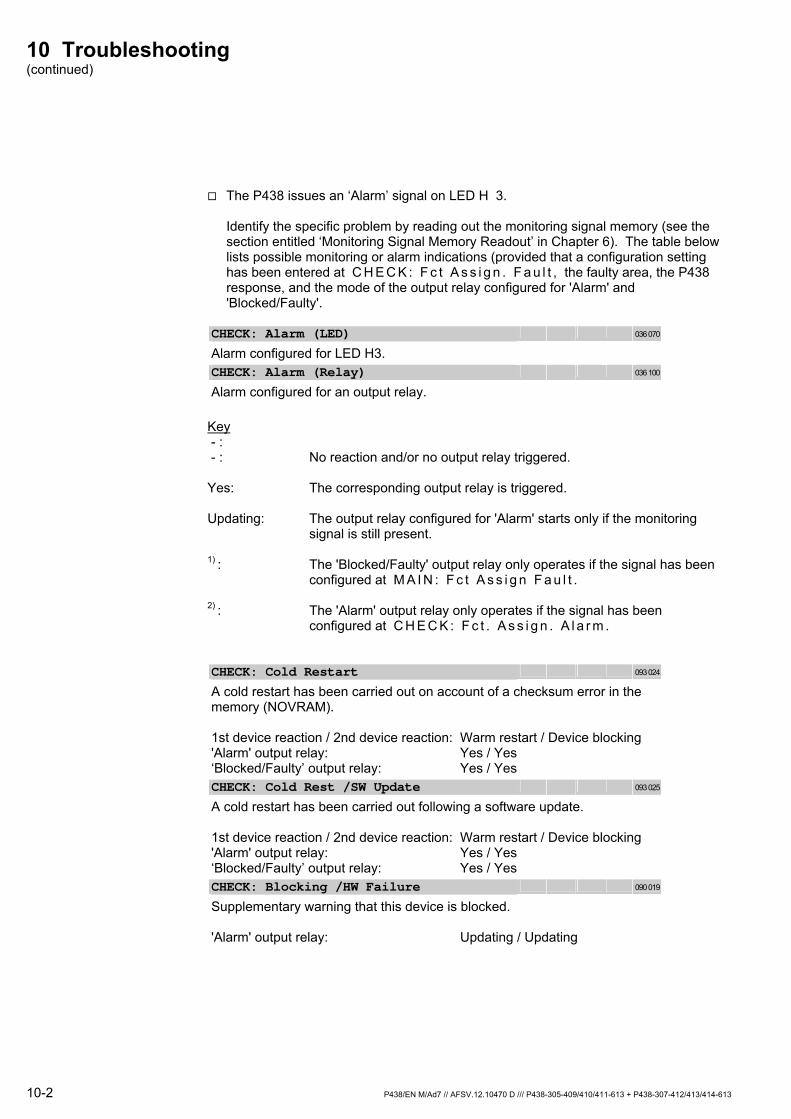
10 Troubleshooting (continued)
10-2 P438/EN M/Ad7 // AFSV.12.10470 D /// P438-305-409/410/411-613 + P438-307-412/413/414-613
The P438 issues an ‘Alarm’ signal on LED H 3. Identify the specific problem by reading out the monitoring signal memory (see the section entitled ‘Monitoring Signal Memory Readout’ in Chapter 6). The table below lists possible monitoring or alarm indications (provided that a configuration setting has been entered at C H E C K : F c t A s s i g n . F a u l t , the faulty area, the P438 response, and the mode of the output relay configured for 'Alarm' and 'Blocked/Faulty'.
CHECK: Alarm (LED) 036 070
Alarm configured for LED H3. CHECK: Alarm (Relay) 036 100
Alarm configured for an output relay. Key - : - : No reaction and/or no output relay triggered. Yes: The corresponding output relay is triggered. Updating: The output relay configured for 'Alarm' starts only if the monitoring signal is still present. 1) : The 'Blocked/Faulty' output relay only operates if the signal has been configured at M A I N : F c t A s s i g n F a u l t . 2) : The 'Alarm' output relay only operates if the signal has been configured at C H E C K : F c t . A s s i g n . A l a r m .
CHECK: Cold Restart 093 024
A cold restart has been carried out on account of a checksum error in the memory (NOVRAM). 1st device reaction / 2nd device reaction: Warm restart / Device blocking 'Alarm' output relay: Yes / Yes ‘Blocked/Faulty’ output relay: Yes / Yes
CHECK: Cold Rest /SW Update 093 025
A cold restart has been carried out following a software update. 1st device reaction / 2nd device reaction: Warm restart / Device blocking 'Alarm' output relay: Yes / Yes ‘Blocked/Faulty’ output relay: Yes / Yes
CHECK: Blocking /HW Failure 090 019
Supplementary warning that this device is blocked. 'Alarm' output relay: Updating / Updating

10 Troubleshooting (continued)
P438/EN M/Ad7 // AFSV.12.10470 D /// P438-305-409/410/411-613 + P438-307-412/413/414-613 10-3
CHECK: Relay Kxx Faulty 041 200
Multiple signaling: output relay defective. 1st device reaction / 2nd device reaction: - / - 'Alarm' output relay: Updating / Updating 'Blocked/Faulty' output relay: Yes / Yes 1)
CHECK: Hardware Clock Fail 093 040
The hardware clock has failed. 1st device reaction / 2nd device reaction: - / - 'Alarm' output relay: Yes / Yes ‘Blocked/Faulty’ output relay: - / -
CHECK: Battery Failure 090 010
Battery voltage too low. Replace battery. 1st device reaction / 2nd device reaction: - / - 'Alarm' output relay: Updating / Updating 'Blocked/Faulty' output relay: - / -
CHECK: Invalid SW DnLoaded 096 121
Wrong or invalid software has been downloaded. 1st device reaction / 2nd device reaction: Warm restart / Device blocking 'Alarm' output relay: Yes / Yes ‘Blocked/Faulty’ output relay: Yes / Yes
CHECK: +15V Supply Faulty 093 081
The +15 V internal supply voltage has dropped below a minimum value. 1st device reaction / 2nd device reaction: Warm restart / Device blocking 'Alarm' output relay: Yes / Yes ‘Blocked/Faulty’ output relay: Yes / Yes
CHECK: +24V Supply Faulty 093 082
The + 24 V internal supply voltage has dropped below a minimum value. 1st device reaction / 2nd device reaction: Warm restart / Device blocking 'Alarm' output relay: Yes / Yes ‘Blocked/Faulty’ output relay: Yes / Yes
CHECK: -15V Supply Faulty 093 080
The - 15 V internal supply voltage has dropped below a minimum value. 1st device reaction / 2nd device reaction: Warm restart / Device blocking 'Alarm' output relay: Yes / Yes ‘Blocked/Faulty’ output relay: Yes / Yes
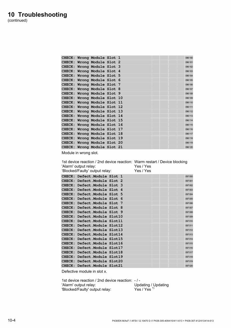
10 Troubleshooting (continued)
10-4 P438/EN M/Ad7 // AFSV.12.10470 D /// P438-305-409/410/411-613 + P438-307-412/413/414-613
CHECK: Wrong Module Slot 1 096 100 CHECK: Wrong Module Slot 2 096 101 CHECK: Wrong Module Slot 3 096 102 CHECK: Wrong Module Slot 4 096 103 CHECK: Wrong Module Slot 5 096 104 CHECK: Wrong Module Slot 6 096 105 CHECK: Wrong Module Slot 7 096 106 CHECK: Wrong Module Slot 8 096 107 CHECK: Wrong Module Slot 9 096 108 CHECK: Wrong Module Slot 10 096 109 CHECK: Wrong Module Slot 11 096 110 CHECK: Wrong Module Slot 12 096 111 CHECK: Wrong Module Slot 13 096 112 CHECK: Wrong Module Slot 14 096 113 CHECK: Wrong Module Slot 15 096 114 CHECK: Wrong Module Slot 16 096 115 CHECK: Wrong Module Slot 17 096 116 CHECK: Wrong Module Slot 18 096 117 CHECK: Wrong Module Slot 19 096 118 CHECK: Wrong Module Slot 20 096 119 CHECK: Wrong Module Slot 21 096 120
Module in wrong slot. 1st device reaction / 2nd device reaction: Warm restart / Device blocking 'Alarm' output relay: Yes / Yes ‘Blocked/Faulty’ output relay: Yes / Yes
CHECK: Defect.Module Slot 1 097 000 CHECK: Defect.Module Slot 2 097 001 CHECK: Defect.Module Slot 3 097 002 CHECK: Defect.Module Slot 4 097 003 CHECK: Defect.Module Slot 5 097 004 CHECK: Defect.Module Slot 6 097 005 CHECK: Defect.Module Slot 7 097 006 CHECK: Defect.Module Slot 8 097 007 CHECK: Defect.Module Slot 9 097 008 CHECK: Defect.Module Slot10 097 009 CHECK: Defect.Module Slot11 097 010 CHECK: Defect.Module Slot12 097 011 CHECK: Defect.Module Slot13 097 012 CHECK: Defect.Module Slot14 097 013 CHECK: Defect.Module Slot15 097 014 CHECK: Defect.Module Slot16 097 015 CHECK: Defect.Module Slot17 097 016 CHECK: Defect.Module Slot18 097 017 CHECK: Defect.Module Slot19 097 018 CHECK: Defect.Module Slot20 097 019 CHECK: Defect.Module Slot21 097 020
Defective module in slot x. 1st device reaction / 2nd device reaction: - / - 'Alarm' output relay: Updating / Updating 'Blocked/Faulty' output relay: Yes / Yes 1)

10 Troubleshooting (continued)
P438/EN M/Ad7 // AFSV.12.10470 D /// P438-305-409/410/411-613 + P438-307-412/413/414-613 10-5
CHECK: Module A DPR Faulty 093 070
Dual-Port-RAM fault on communication module A. This fault is only detected during device startup. 1st device reaction / 2nd device reaction: - / - 'Alarm' output relay: Yes / Yes ‘Blocked/Faulty’ output relay: - / -
CHECK: Module A RAM Faulty 093 071
RAM fault on communication module A. 1st device reaction / 2nd device reaction: - / - 'Alarm' output relay: Yes / Yes ‘Blocked/Faulty’ output relay: - / -
CHECK: Module Y DPR Faulty 093 110
The checksum feature of analog I/O module Y has detected a fault in the data transmission of the Dual-Port-RAM. 1st device reaction / 2nd device reaction: - / - 'Alarm' output relay: Yes / Yes ‘Blocked/Faulty’ output relay: - / -
CHECK: Module Y RAM Faulty 093 111
Fault in the program or data memory of the analog I/O module. 1st device reaction / 2nd device reaction: - / - 'Alarm' output relay: Yes / Yes ‘Blocked/Faulty’ output relay: - / -
CHECK: IRIGB Faulty 093 117
Although the IRIGB interface is enabled, there is no plausible input signal. 1st device reaction / 2nd device reaction: - / - 'Alarm' output relay: Yes / Yes ‘Blocked/Faulty’ output relay: - / -
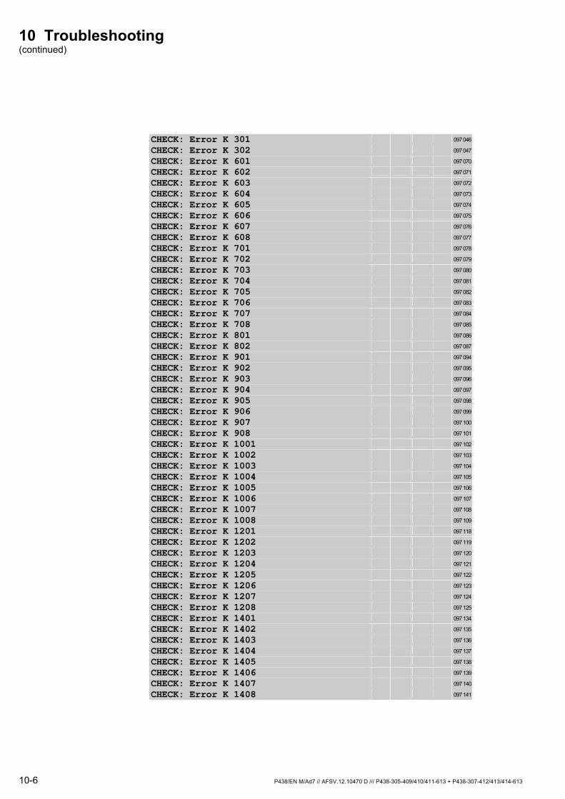
10 Troubleshooting (continued)
10-6 P438/EN M/Ad7 // AFSV.12.10470 D /// P438-305-409/410/411-613 + P438-307-412/413/414-613
CHECK: Error K 301 097 046 CHECK: Error K 302 097 047 CHECK: Error K 601 097 070 CHECK: Error K 602 097 071 CHECK: Error K 603 097 072 CHECK: Error K 604 097 073 CHECK: Error K 605 097 074 CHECK: Error K 606 097 075 CHECK: Error K 607 097 076 CHECK: Error K 608 097 077 CHECK: Error K 701 097 078 CHECK: Error K 702 097 079 CHECK: Error K 703 097 080 CHECK: Error K 704 097 081 CHECK: Error K 705 097 082 CHECK: Error K 706 097 083 CHECK: Error K 707 097 084 CHECK: Error K 708 097 085 CHECK: Error K 801 097 086 CHECK: Error K 802 097 087 CHECK: Error K 901 097 094 CHECK: Error K 902 097 095 CHECK: Error K 903 097 096 CHECK: Error K 904 097 097 CHECK: Error K 905 097 098 CHECK: Error K 906 097 099 CHECK: Error K 907 097 100 CHECK: Error K 908 097 101 CHECK: Error K 1001 097 102 CHECK: Error K 1002 097 103 CHECK: Error K 1003 097 104 CHECK: Error K 1004 097 105 CHECK: Error K 1005 097 106 CHECK: Error K 1006 097 107 CHECK: Error K 1007 097 108 CHECK: Error K 1008 097 109 CHECK: Error K 1201 097 118 CHECK: Error K 1202 097 119 CHECK: Error K 1203 097 120 CHECK: Error K 1204 097 121 CHECK: Error K 1205 097 122 CHECK: Error K 1206 097 123 CHECK: Error K 1207 097 124 CHECK: Error K 1208 097 125 CHECK: Error K 1401 097 134 CHECK: Error K 1402 097 135 CHECK: Error K 1403 097 136 CHECK: Error K 1404 097 137 CHECK: Error K 1405 097 138 CHECK: Error K 1406 097 139 CHECK: Error K 1407 097 140 CHECK: Error K 1408 097 141

10 Troubleshooting (continued)
P438/EN M/Ad7 // AFSV.12.10470 D /// P438-305-409/410/411-613 + P438-307-412/413/414-613 10-7
CHECK: Error K 1601 097 150 CHECK: Error K 1602 097 151 CHECK: Error K 1603 097 152 CHECK: Error K 1604 097 153 CHECK: Error K 1605 097 154 CHECK: Error K 1606 097 155 CHECK: Error K 1607 097 156 CHECK: Error K 1608 097 157 CHECK: Error K 1801 097 166 CHECK: Error K 1802 097 167 CHECK: Error K 1803 097 168 CHECK: Error K 1804 097 169 CHECK: Error K 1805 097 170 CHECK: Error K 1806 097 171 CHECK: Error K 2001 097 182 CHECK: Error K 2002 097 183 CHECK: Error K 2003 097 184 CHECK: Error K 2004 097 185 CHECK: Error K 2005 097 186 CHECK: Error K 2006 097 187 CHECK: Error K 2007 097 188 CHECK: Error K 2008 097 189
Output relay K xxxx defective. 1st device reaction / 2nd device reaction: - / - 'Alarm' output relay: Updating / Updating 'Blocked/Faulty' output relay: Yes / Yes 1)
CHECK: Undefined Op Code 093 010
Undefined operation code, i.e. software error. 1st device reaction / 2nd device reaction: Warm restart / Device blocking 'Alarm' output relay: Yes / Yes ‘Blocked/Faulty’ output relay: Yes / Yes
CHECK: Invalid Op. 093 011
Invalid arithmetic operation, i.e. software error. 1st device reaction / 2nd device reaction: Warm restart / Device blocking 'Alarm' output relay: Yes / Yes ‘Blocked/Faulty’ output relay: Yes / Yes
CHECK: Undefined Interrupt 093 012
Undefined interrupt, i.e. software error. 1st device reaction / 2nd device reaction: Warm restart / Device blocking 'Alarm' output relay: Yes / Yes ‘Blocked/Faulty’ output relay: Yes / Yes
CHECK: Exception Oper.Syst. 093 013
Interrupt of the operating system. 1st device reaction / 2nd device reaction: Warm restart / Device blocking 'Alarm' output relay: Yes / Yes ‘Blocked/Faulty’ output relay: Yes / Yes
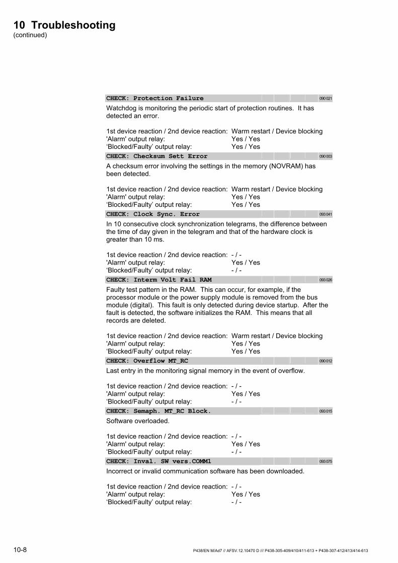
10 Troubleshooting (continued)
10-8 P438/EN M/Ad7 // AFSV.12.10470 D /// P438-305-409/410/411-613 + P438-307-412/413/414-613
CHECK: Protection Failure 090 021
Watchdog is monitoring the periodic start of protection routines. It has detected an error. 1st device reaction / 2nd device reaction: Warm restart / Device blocking 'Alarm' output relay: Yes / Yes ‘Blocked/Faulty’ output relay: Yes / Yes
CHECK: Checksum Sett Error 090 003
A checksum error involving the settings in the memory (NOVRAM) has been detected. 1st device reaction / 2nd device reaction: Warm restart / Device blocking 'Alarm' output relay: Yes / Yes ‘Blocked/Faulty’ output relay: Yes / Yes
CHECK: Clock Sync. Error 093 041
In 10 consecutive clock synchronization telegrams, the difference between the time of day given in the telegram and that of the hardware clock is greater than 10 ms. 1st device reaction / 2nd device reaction: - / - 'Alarm' output relay: Yes / Yes ‘Blocked/Faulty’ output relay: - / -
CHECK: Interm Volt Fail RAM 093 026
Faulty test pattern in the RAM. This can occur, for example, if the processor module or the power supply module is removed from the bus module (digital). This fault is only detected during device startup. After the fault is detected, the software initializes the RAM. This means that all records are deleted. 1st device reaction / 2nd device reaction: Warm restart / Device blocking 'Alarm' output relay: Yes / Yes ‘Blocked/Faulty’ output relay: Yes / Yes
CHECK: Overflow MT_RC 090 012
Last entry in the monitoring signal memory in the event of overflow. 1st device reaction / 2nd device reaction: - / - 'Alarm' output relay: Yes / Yes ‘Blocked/Faulty’ output relay: - / -
CHECK: Semaph. MT_RC Block. 093 015
Software overloaded. 1st device reaction / 2nd device reaction: - / - 'Alarm' output relay: Yes / Yes ‘Blocked/Faulty’ output relay: - / -
CHECK: Inval. SW vers.COMM1 093 075
Incorrect or invalid communication software has been downloaded. 1st device reaction / 2nd device reaction: - / - 'Alarm' output relay: Yes / Yes ‘Blocked/Faulty’ output relay: - / -
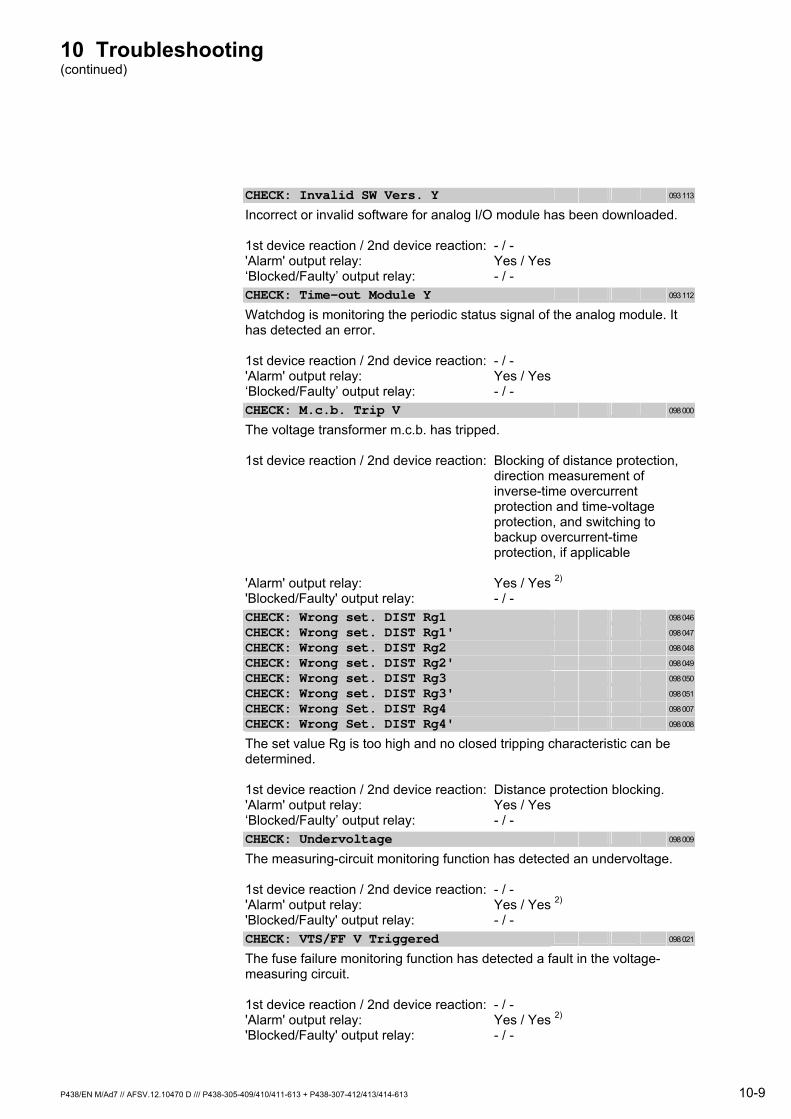
10 Troubleshooting (continued)
P438/EN M/Ad7 // AFSV.12.10470 D /// P438-305-409/410/411-613 + P438-307-412/413/414-613 10-9
CHECK: Invalid SW Vers. Y 093 113
Incorrect or invalid software for analog I/O module has been downloaded. 1st device reaction / 2nd device reaction: - / - 'Alarm' output relay: Yes / Yes ‘Blocked/Faulty’ output relay: - / -
CHECK: Time-out Module Y 093 112
Watchdog is monitoring the periodic status signal of the analog module. It has detected an error. 1st device reaction / 2nd device reaction: - / - 'Alarm' output relay: Yes / Yes ‘Blocked/Faulty’ output relay: - / -
CHECK: M.c.b. Trip V 098 000
The voltage transformer m.c.b. has tripped. 1st device reaction / 2nd device reaction: Blocking of distance protection, direction measurement of inverse-time overcurrent protection and time-voltage protection, and switching to backup overcurrent-time protection, if applicable 'Alarm' output relay: Yes / Yes 2) 'Blocked/Faulty' output relay: - / -
CHECK: Wrong set. DIST Rg1 098 046 CHECK: Wrong set. DIST Rg1' 098 047 CHECK: Wrong set. DIST Rg2 098 048 CHECK: Wrong set. DIST Rg2' 098 049 CHECK: Wrong set. DIST Rg3 098 050 CHECK: Wrong set. DIST Rg3' 098 051 CHECK: Wrong Set. DIST Rg4 098 007 CHECK: Wrong Set. DIST Rg4' 098 008
The set value Rg is too high and no closed tripping characteristic can be determined. 1st device reaction / 2nd device reaction: Distance protection blocking. 'Alarm' output relay: Yes / Yes ‘Blocked/Faulty’ output relay: - / -
CHECK: Undervoltage 098 009
The measuring-circuit monitoring function has detected an undervoltage. 1st device reaction / 2nd device reaction: - / - 'Alarm' output relay: Yes / Yes 2) 'Blocked/Faulty' output relay: - / -
CHECK: VTS/FF V Triggered 098 021
The fuse failure monitoring function has detected a fault in the voltage-measuring circuit. 1st device reaction / 2nd device reaction: - / - 'Alarm' output relay: Yes / Yes 2) 'Blocked/Faulty' output relay: - / -
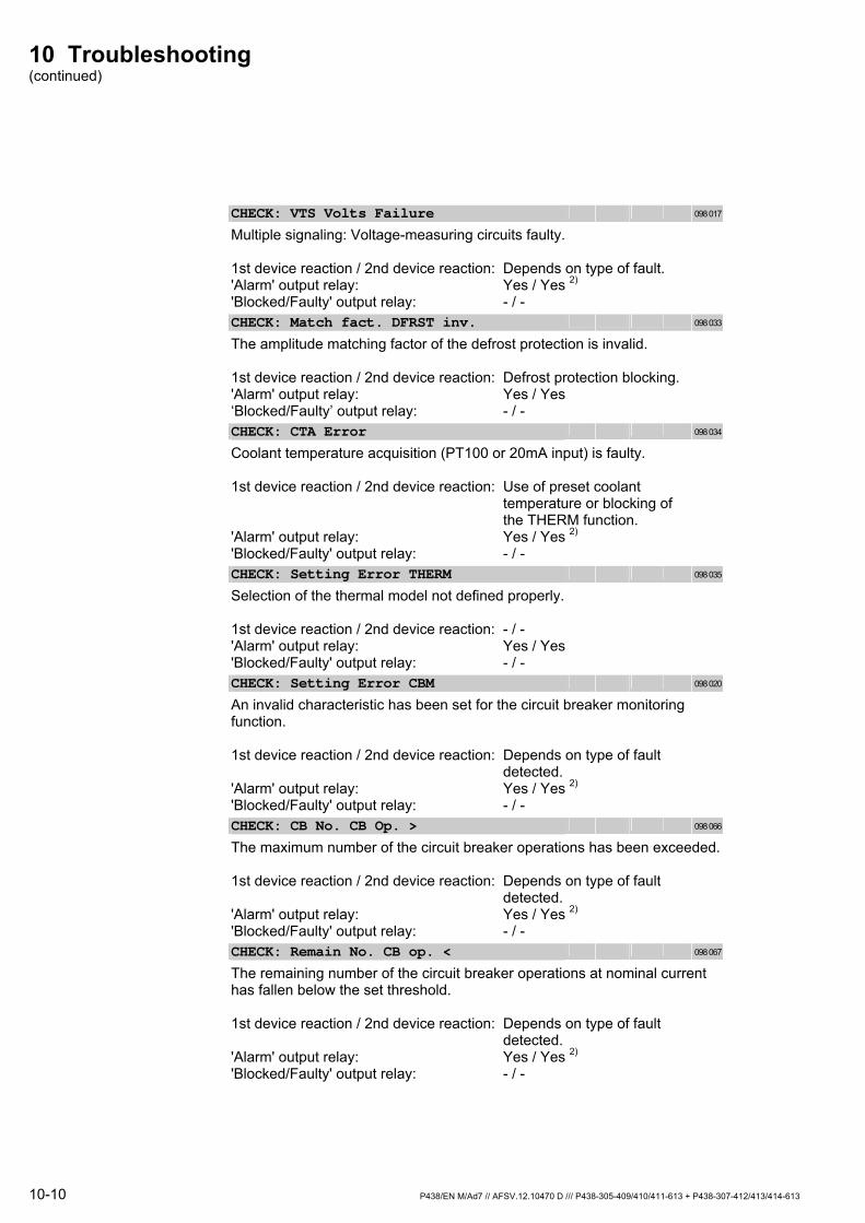
10 Troubleshooting (continued)
10-10 P438/EN M/Ad7 // AFSV.12.10470 D /// P438-305-409/410/411-613 + P438-307-412/413/414-613
CHECK: VTS Volts Failure 098 017
Multiple signaling: Voltage-measuring circuits faulty. 1st device reaction / 2nd device reaction: Depends on type of fault. 'Alarm' output relay: Yes / Yes 2) 'Blocked/Faulty' output relay: - / -
CHECK: Match fact. DFRST inv. 098 033
The amplitude matching factor of the defrost protection is invalid. 1st device reaction / 2nd device reaction: Defrost protection blocking. 'Alarm' output relay: Yes / Yes ‘Blocked/Faulty’ output relay: - / -
CHECK: CTA Error 098 034
Coolant temperature acquisition (PT100 or 20mA input) is faulty. 1st device reaction / 2nd device reaction: Use of preset coolant temperature or blocking of the THERM function. 'Alarm' output relay: Yes / Yes 2) 'Blocked/Faulty' output relay: - / -
CHECK: Setting Error THERM 098 035
Selection of the thermal model not defined properly. 1st device reaction / 2nd device reaction: - / - 'Alarm' output relay: Yes / Yes 'Blocked/Faulty' output relay: - / -
CHECK: Setting Error CBM 098 020
An invalid characteristic has been set for the circuit breaker monitoring function. 1st device reaction / 2nd device reaction: Depends on type of fault detected. 'Alarm' output relay: Yes / Yes 2) 'Blocked/Faulty' output relay: - / -
CHECK: CB No. CB Op. > 098 066
The maximum number of the circuit breaker operations has been exceeded. 1st device reaction / 2nd device reaction: Depends on type of fault detected. 'Alarm' output relay: Yes / Yes 2) 'Blocked/Faulty' output relay: - / -
CHECK: Remain No. CB op. < 098 067
The remaining number of the circuit breaker operations at nominal current has fallen below the set threshold. 1st device reaction / 2nd device reaction: Depends on type of fault detected. 'Alarm' output relay: Yes / Yes 2) 'Blocked/Faulty' output relay: - / -
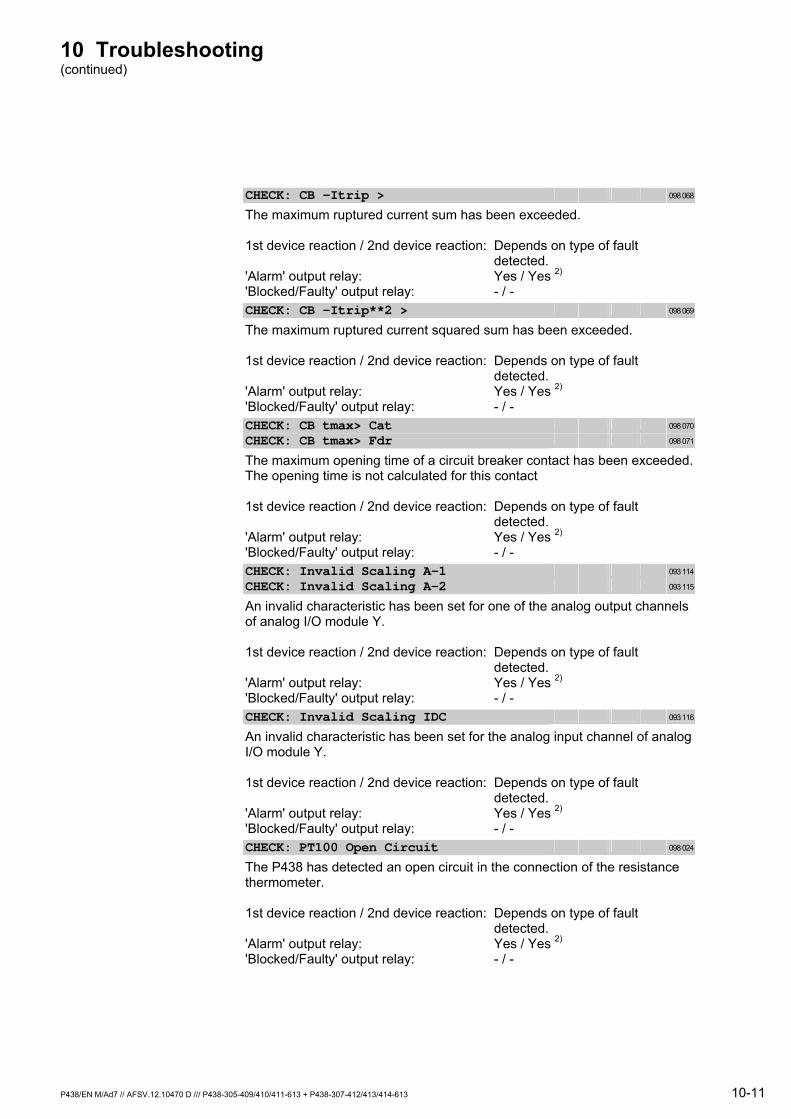
10 Troubleshooting (continued)
P438/EN M/Ad7 // AFSV.12.10470 D /// P438-305-409/410/411-613 + P438-307-412/413/414-613 10-11
CHECK: CB –Itrip > 098 068
The maximum ruptured current sum has been exceeded. 1st device reaction / 2nd device reaction: Depends on type of fault detected. 'Alarm' output relay: Yes / Yes 2) 'Blocked/Faulty' output relay: - / -
CHECK: CB –Itrip**2 > 098 069
The maximum ruptured current squared sum has been exceeded. 1st device reaction / 2nd device reaction: Depends on type of fault detected. 'Alarm' output relay: Yes / Yes 2) 'Blocked/Faulty' output relay: - / -
CHECK: CB tmax> Cat 098 070 CHECK: CB tmax> Fdr 098 071
The maximum opening time of a circuit breaker contact has been exceeded. The opening time is not calculated for this contact 1st device reaction / 2nd device reaction: Depends on type of fault detected. 'Alarm' output relay: Yes / Yes 2) 'Blocked/Faulty' output relay: - / -
CHECK: Invalid Scaling A-1 093 114 CHECK: Invalid Scaling A-2 093 115
An invalid characteristic has been set for one of the analog output channels of analog I/O module Y. 1st device reaction / 2nd device reaction: Depends on type of fault detected. 'Alarm' output relay: Yes / Yes 2) 'Blocked/Faulty' output relay: - / -
CHECK: Invalid Scaling IDC 093 116
An invalid characteristic has been set for the analog input channel of analog I/O module Y. 1st device reaction / 2nd device reaction: Depends on type of fault detected. 'Alarm' output relay: Yes / Yes 2) 'Blocked/Faulty' output relay: - / -
CHECK: PT100 Open Circuit 098 024
The P438 has detected an open circuit in the connection of the resistance thermometer. 1st device reaction / 2nd device reaction: Depends on type of fault detected. 'Alarm' output relay: Yes / Yes 2) 'Blocked/Faulty' output relay: - / -
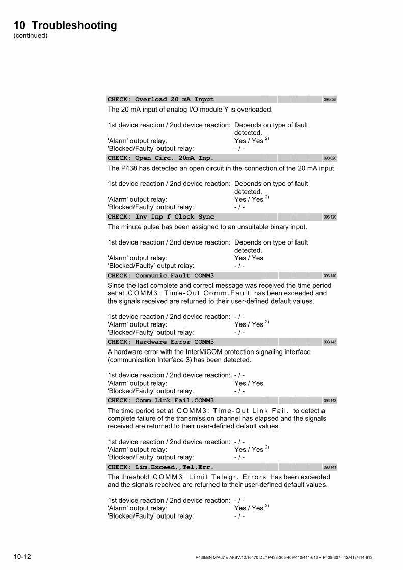
10 Troubleshooting (continued)
10-12 P438/EN M/Ad7 // AFSV.12.10470 D /// P438-305-409/410/411-613 + P438-307-412/413/414-613
CHECK: Overload 20 mA Input 098 025
The 20 mA input of analog I/O module Y is overloaded. 1st device reaction / 2nd device reaction: Depends on type of fault detected. 'Alarm' output relay: Yes / Yes 2) 'Blocked/Faulty' output relay: - / -
CHECK: Open Circ. 20mA Inp. 098 026
The P438 has detected an open circuit in the connection of the 20 mA input. 1st device reaction / 2nd device reaction: Depends on type of fault detected. 'Alarm' output relay: Yes / Yes 2) 'Blocked/Faulty' output relay: - / -
CHECK: Inv Inp f Clock Sync 093 120
The minute pulse has been assigned to an unsuitable binary input. 1st device reaction / 2nd device reaction: Depends on type of fault detected. 'Alarm' output relay: Yes / Yes ‘Blocked/Faulty’ output relay: - / -
CHECK: Communic.Fault COMM3 093 140
Since the last complete and correct message was received the time period set at C O M M 3 : T i m e - O u t C o m m . F a u l t has been exceeded and the signals received are returned to their user-defined default values. 1st device reaction / 2nd device reaction: - / - 'Alarm' output relay: Yes / Yes 2) 'Blocked/Faulty' output relay: - / -
CHECK: Hardware Error COMM3 093 143
A hardware error with the InterMiCOM protection signaling interface (communication Interface 3) has been detected. 1st device reaction / 2nd device reaction: - / - 'Alarm' output relay: Yes / Yes 'Blocked/Faulty' output relay: - / -
CHECK: Comm.Link Fail.COMM3 093 142
The time period set at C O M M 3 : T i m e - O u t L i n k F a i l . to detect a complete failure of the transmission channel has elapsed and the signals received are returned to their user-defined default values. 1st device reaction / 2nd device reaction: - / - 'Alarm' output relay: Yes / Yes 2) 'Blocked/Faulty' output relay: - / -
CHECK: Lim.Exceed.,Tel.Err. 093 141
The threshold C O M M 3 : L i m i t T e l e g r . E r r o r s has been exceeded and the signals received are returned to their user-defined default values. 1st device reaction / 2nd device reaction: - / - 'Alarm' output relay: Yes / Yes 2) 'Blocked/Faulty' output relay: - / -
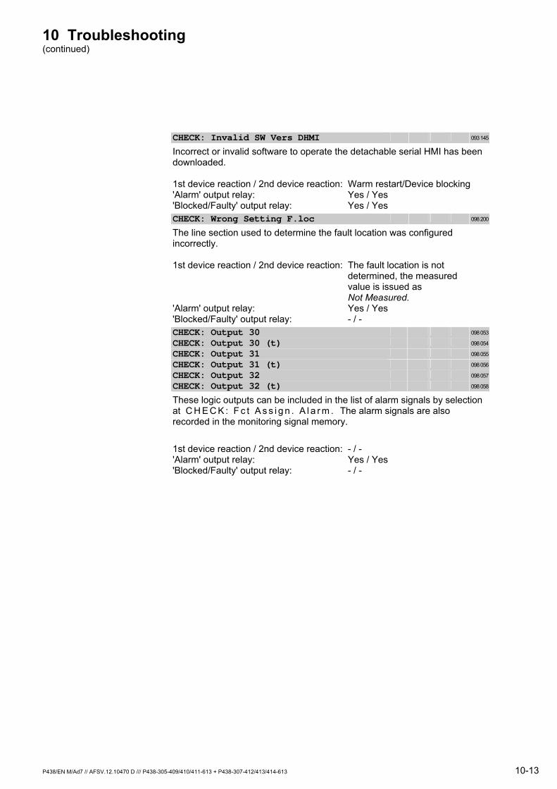
10 Troubleshooting (continued)
P438/EN M/Ad7 // AFSV.12.10470 D /// P438-305-409/410/411-613 + P438-307-412/413/414-613 10-13
CHECK: Invalid SW Vers DHMI 093 145
Incorrect or invalid software to operate the detachable serial HMI has been downloaded. 1st device reaction / 2nd device reaction: Warm restart/Device blocking 'Alarm' output relay: Yes / Yes 'Blocked/Faulty' output relay: Yes / Yes
CHECK: Wrong Setting F.loc 098 200
The line section used to determine the fault location was configured incorrectly. 1st device reaction / 2nd device reaction: The fault location is not determined, the measured value is issued as Not Measured. 'Alarm' output relay: Yes / Yes 'Blocked/Faulty' output relay: - / -
CHECK: Output 30 098 053 CHECK: Output 30 (t) 098 054 CHECK: Output 31 098 055 CHECK: Output 31 (t) 098 056 CHECK: Output 32 098 057 CHECK: Output 32 (t) 098 058
These logic outputs can be included in the list of alarm signals by selection at C H E C K : F c t A s s i g n . A l a r m . The alarm signals are also recorded in the monitoring signal memory.
1st device reaction / 2nd device reaction: - / - 'Alarm' output relay: Yes / Yes 'Blocked/Faulty' output relay: - / -

10-14 P438/EN M/Ad7 // AFSV.12.10470 D /// P438-305-409/410/411-613 + P438-307-412/413/414-613
11 Maintenance
P438/EN M/Ad7 // AFSV.12.10470 D /// P438-305-409/410/411-613 + P438-307-412/413/414-613 11-1
11 Maintenance
Only qualified personnel, familiar with the "Warning" page at the beginning of this manual, may work on or operate this device.
The P438 is a low-maintenance device. The components used in the units are selected to meet exacting requirements. Recalibration is not necessary.
Maintenance procedures in the power supply area
Electrolytic capacitors are installed in the power supply area because of dimensioning requirements. The useful life of these capacitors is significant from a maintenance standpoint. When the equipment is operated continuously at the upper limit of the recommended temperature range (+55°C or 131°F), the useful life of these components is 80,000 hours, or more than 9 years. Under these conditions, replacement of the electrolytic capacitors is recommended after a period of 8 to 10 years. With operating temperatures of +45 °C inside the device the required maintenance interval may be extended by one year.
The P438 is equipped with a lithium battery for non-volatile storage of fault data and for keeping the internal clock running in the event of failure of the auxiliary power supply. Loss of capacity due to module-internal self-discharging amounts to less than 1% per year over a period of availability of 10 years. Since the terminal voltage remains virtually constant until capacity is exhausted, usefulness is maintained until a very low residual capacity is reached. With a nominal capacity of 850 mAh and discharge currents of only a few µA during device storage or in the range of the self-discharge current during device operation, the result is a correspondingly long service life. It is therefore recommended that the lithium battery only be replaced after the maintenance interval cited above.
Replacement of the maintenance-related components named above is not possible without soldering. Maintenance work must be carried out by trained personnel, and the auxiliary voltage must be turned off while the work is being performed.
Always turn off the power (supply voltage) before removing a hardware module.
The power supply must be turned off for at least 5 s before power supply module V is removed. Otherwise there is the danger of an electric shock!
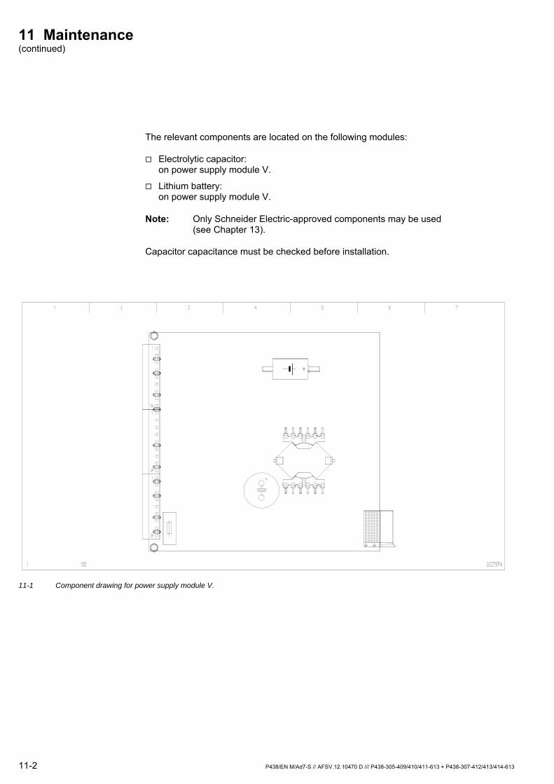
11 Maintenance (continued)
11-2 P438/EN M/Ad7-S // AFSV.12.10470 D /// P438-305-409/410/411-613 + P438-307-412/413/414-613
The relevant components are located on the following modules:
Electrolytic capacitor: on power supply module V.
Lithium battery: on power supply module V.
Note: Only Schneider Electric-approved components may be used (see Chapter 13).
Capacitor capacitance must be checked before installation.
11-1 Component drawing for power supply module V.
11 Maintenance (continued)
P438/EN M/Ad7 // AFSV.12.10470 D /// P438-305-409/410/411-613 + P438-307-412/413/414-613 11-3
There is a danger of explosion if the electrolytic capacitor and battery are not properly replaced. Always check to make sure that the polarity of the electrolytic capacitor and the battery is correct.
The following instructions apply to surface-mounted cases:
The user interface (HMI) is connected to processor module P by a plug-in connecting cable. Make sure the connector position is correct. Do not bend the connecting cable!
Note: The replaced components (electrolytic capacitor and battery) must be disposed of in compliance with applicable national regulations.
After the maintenance procedures described above have been completed, new commissioning tests as described in Chapter 9 must be carried out.
11 Maintenance (continued)
11-4 P438/EN M/Ad7 // AFSV.12.10470 D /// P438-305-409/410/411-613 + P438-307-412/413/414-613
Routine functional testing The P438 is used as a safety device and must therefore be routinely injection tested for proper operation. The first functional tests should be carried out approximately 6 to 12 months after commissioning. Functional tests should be performed at intervals of 2 to 3 years – 4 years at the maximum.
The P438 incorporates in its system a very extensive self-monitoring function for hardware and software. The internal structure guarantees, for example, that communication within the processor system will be checked on a continuing basis.
Nonetheless, there are a number of sub-functions that cannot be checked by the self-monitoring feature without injection testing from the device terminals. The respective device-specific properties and settings must be observed in such cases.
In particular, none of the control and signaling circuits that are run to the device from the outside are checked by the self-monitoring function.
Analog input circuits The analog inputs are fed through an analog preprocessing feature (anti-aliasing filtering) to a common analog-to-digital converter. In conjunction with the self-monitoring function, the CT/VT supervision function that is available for the device’s general functions can detect deviations in many cases. However, it is still necessary to test from the device terminals in order to make sure that the analog measuring circuits are functioning correctly.
The best way to carry out a static test of the analog input circuits is to check the primary measured operating data using the operating data measurement function or to use a suitable testing instrument. A "small" measured value (such as the nominal current in the current path) and a "large" measured value (such as the nominal voltage in the voltage path) should be used to check the measuring range of the A/D converter. This makes it possible to check the entire dynamic range.
The accuracy of operating data measurement is <1 %. An important factor in evaluating device performance is long-term performance based on comparison with previous measurements.
Additional analog testing of such factors as the impedance characteristic or the starting characteristic is not necessary, in our opinion, since information processing is completely digital and is based on the measured analog current and voltage values. Proper operation was checked in conjunction with type testing.
Binary opto inputs The binary inputs are not checked by the self-monitoring function. However, a testing function is integrated into the software so that the trigger state of each input can be read out (‘M+T/Meas/IO’ folder). This check should be performed for each input being used and can be done, if necessary, without disconnecting any device wiring.

11 Maintenance (continued)
P438/EN M/Ad7 // AFSV.12.10470 D /// P438-305-409/410/411-613 + P438-307-412/413/414-613 11-5
Binary outputs With respect to binary outputs, the integrated self-monitoring function includes even two-phase triggering of the relay coils of all the relays. There is no monitoring function for the external contact circuit. In this case, the all-or-nothing relays must be triggered by way of device functions or integrated test functions. For these testing purposes, triggering of the output circuits is integrated into the software through a special control function (‘M+T/C+Test/’ folder).
Before starting the test, open any triggering circuits for external devices so that no inadvertent switching operations will take place.
Serial interfaces The integrated self-monitoring function for the PC or communication interface also includes the communication module. The complete communication system, including connecting link and fiber-optic module (if applicable), is always totally monitored as long as a link is established through the control program or the communication protocol.

11-6 P438/EN M/Ad7 // AFSV.12.10470 D /// P438-305-409/410/411-613 + P438-307-412/413/414-613
12 Storage
P438/EN M/Ad7 // AFSV.12.10470 D /// P438-305-409/410/411-613 + P438-307-412/413/414-613 12-1
12 Storage
Devices must be stored in a dry and clean environment. A temperature range of -25°C to +70°C (-13°F to +158°F) must be maintained during storage (see chapter entitled 'Technical Data'). The relative humidity must be controlled so that neither condensation nor ice formation will result.
If the units are stored without being connected to auxiliary voltage, then the electrolytic capacitors in the power supply area need to be recharged every 4 years. Recharge the capacitors by connecting auxiliary voltage to the P438 for approximately 10 minutes.
If the units are stored during a longer time, the battery of the power supply module is used for the continuous buffering of the event data in the working memory of the processor module. Therefore the battery is permanently required and discharges rapidly. In order to avoid this continuous discharge, it is recommended to remove the power supply module from the mounting rack during long storage periods. The contents of the event memory should be previously read out and stored separately!

12-2 P438/EN M/Ad7 // AFSV.12.10470 D /// P438-305-409/410/411-613 + P438-307-412/413/414-613
13 Accessories and Spare Parts
P438/EN M/Ad7 // AFSV.12.10470 D /// P438-305-409/410/411-613 + P438-307-412/413/414-613 13-1
13 Accessories and Spare Parts
The P438 is supplied with standard labeling for the LED indicators. LED indicators that are not already configured and labeled can be labeled using the label strips supplied. Affix the label strips to the front of the unit at the appropriate location.
The label strips can be filled in using a Stabilo brand pen containing water-resistant ink (Type OH Pen 196 PS).
Description Order No.
Cable bushings 88512-4-0337414-301
Lithium battery, Type 1/2 AA 3.6 V
Electrolytic capacitor 100 µF, 385 V DC Only the following brands of capacitor are permitted: Philips Type PUL-SI/159/222215946101 Panasonic Type TS-HA/ECOS 2GA 101 Nichicon Type LGQ 2G 101 MHSZ Nichicon Type LGU 2G 101 MHLZ
Fuse for VA,nom = 24 V DC: M3.5-250V
Fuse for VA,nom = 48 to 250 V DC and 100 to 230 V AC: M2-250 V
Resistor 200 Ω 255.002.696
84TE frame 88512-4-9650723-301
Operating program for Windows On request (MiCOM S1)

13-2 P438/EN M/Ad7 // AFSV.12.10470 D /// P438-305-409/410/411-613 + P438-307-412/413/414-613

14 Order Information
14 Order Information
The P438 (as described here with software version -615) is available with two different hardware variants. The order information is given separately in sections 14.1 and 14.2 below.
The notices below apply to both variants:
Notice 2) Switching is by parameter, the default setting is underlined!
4) Second language provided is in brackets.
5) For the 84TE version only
8) The standard variant is recommended where a higher switching threshold is not expressly required
17) High impedance protection (DELTA) function requires fitting of the optional processor module with an integrated DSP coprocessor
P438/UK M/Ae7 // AFSV.12.11060 EN /// P438-305-409/410/411-615 + P438-307-412/413/414-615 14-1
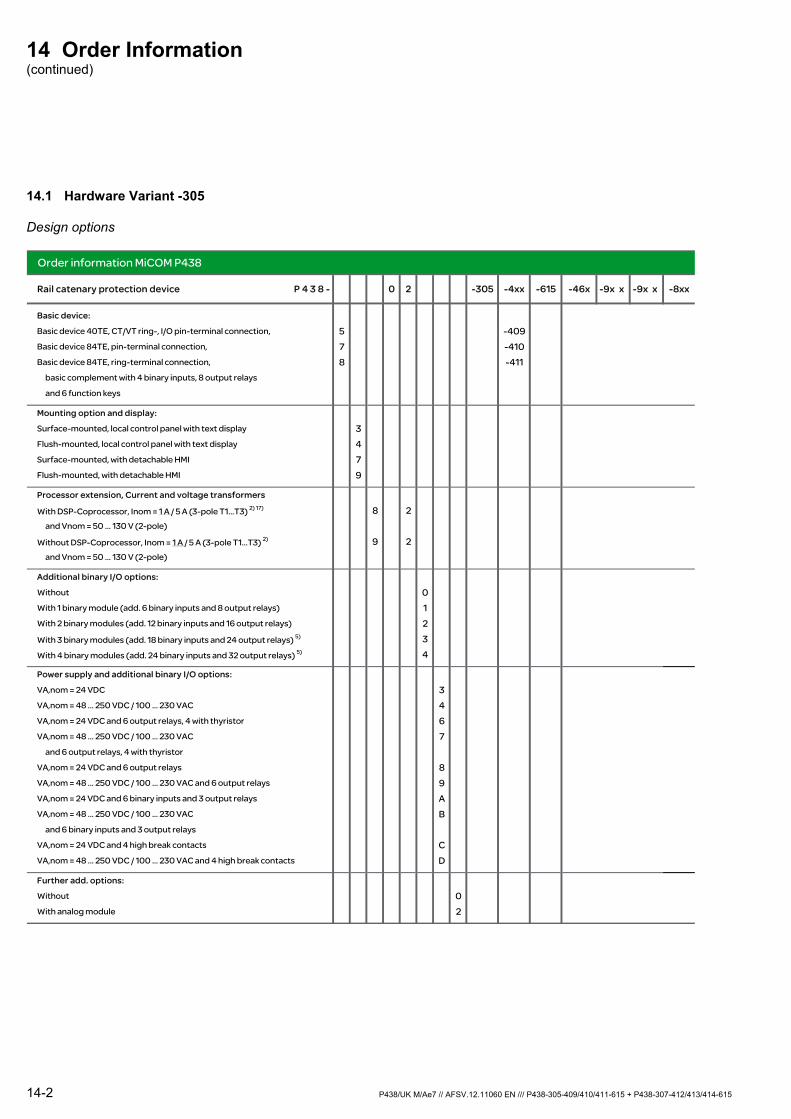
14 Order Information (continued)
14.1 Hardware Variant -305
Design options
Order information MiCOM P438
Rail catenary protection device P 4 3 8 - 0 2 -305 -4xx -615 -46x -9x x -9x x -8xx
Basic device:
Basic device 40TE, CT/VT ring-, I/O pin-terminal connection, 5 -409Basic device 84TE, pin-terminal connection, 7 -410Basic device 84TE, ring-terminal connection, 8 -411
basic complement with 4 binary inputs, 8 output relays
and 6 function keys
Mounting option and display:
Surface-mounted, local control panel with text display 3Flush-mounted, local control panel with text display 4Surface-mounted, with detachable HMI 7Flush-mounted, with detachable HMI 9
Processor extension, Current and voltage transformers
With DSP-Coprocessor, Inom = 1 A / 5 A (3-pole T1...T3) 2) 17) 8 2and Vnom = 50 ... 130 V (2-pole)
Without DSP-Coprocessor, Inom = 1 A / 5 A (3-pole T1...T3) 2) 9 2and Vnom = 50 ... 130 V (2-pole)
Additional binary I/O options:
Without 0With 1 binary module (add. 6 binary inputs and 8 output relays) 1With 2 binary modules (add. 12 binary inputs and 16 output relays) 2With 3 binary modules (add. 18 binary inputs and 24 output relays) 5) 3With 4 binary modules (add. 24 binary inputs and 32 output relays) 5) 4
Power supply and additional binary I/O options:
VA,nom = 24 VDC 3VA,nom = 48 ... 250 VDC / 100 ... 230 VAC 4VA,nom = 24 VDC and 6 output relays, 4 with thyristor 6VA,nom = 48 ... 250 VDC / 100 ... 230 VAC 7
and 6 output relays, 4 with thyristor
VA,nom = 24 VDC and 6 output relays 8VA,nom = 48 ... 250 VDC / 100 ... 230 VAC and 6 output relays 9VA,nom = 24 VDC and 6 binary inputs and 3 output relays AVA,nom = 48 ... 250 VDC / 100 ... 230 VAC B
and 6 binary inputs and 3 output relays
VA,nom = 24 VDC and 4 high break contacts CVA,nom = 48 ... 250 VDC / 100 ... 230 VAC and 4 high break contacts D
Further add. options:
Without 0With analog module 2
14-2 P438/UK M/Ae7 // AFSV.12.11060 EN /// P438-305-409/410/411-615 + P438-307-412/413/414-615

14 Order Information (continued)
Further options
Order information MiCOM P438
Rail catenary protection device P 4 3 8 - 0 2 -305 -4xx -615 -46x -9x x -9x x -8xx
Switching threshold on binary inputs:
>18 V (standard variant) Without order extension No.>90 V (60...70% of VA,nom = 125...150 V) 8) -461>155 V (60...70% of VA,nom = 220...250 V) 8) -462>73 V (67% of VA,nom = 110 V) 8) -463>146 V (67% of VA,nom = 220 V) 8) -464
With communication / information interface:
Without Without order extension No.Protocol can be switched between: -92
IEC 60870-5-101/-103, Modbus, DNP3, Courier
and IRIG-B input for clock synchronization
and 2nd interface (RS485, IEC 60870-5-103)
For connection to wire, RS485, isolated 1For connection to plastic fiber, FSMA connector 2For connection to glass fiber, ST connector 4Protocol IEC61850, single connection -94For connection to 100 Mbit/s Ethernet, glass fiber SC and wire RJ45 6
and 2nd interface (RS485, IEC 60870-5-103)
For connection to 100 Mbit/s Ethernet, glass fiber ST and wire RJ45 7and 2nd interface (RS485, IEC 60870-5-103)
With guidance / protection interface:
Without Without order extension No.Protocol InterMiCOM -95For connection to wire, RS485, isolated 1For connection to plastic fiber, FSMA connector 2For connection to glass fiber 820 nm Multimode, ST connector 4
Language:
English (German) 4) Without order extension No.German (English) 4) -801French (English) 4) Not yet available - on request -802Spanish (English) 4) Not yet available - on request -803
2) Switching via parameter, default setting is underlined!
4) Second included language in brackets
5) For 84TE version only
8) Standard variant recommended if higher pickup threshold not explicitly required by the application
17) High impedance fault detection (DELTA) requires DSP-Coprocessor
P438/UK M/Ae7 // AFSV.12.11060 EN /// P438-305-409/410/411-615 + P438-307-412/413/414-615 14-3
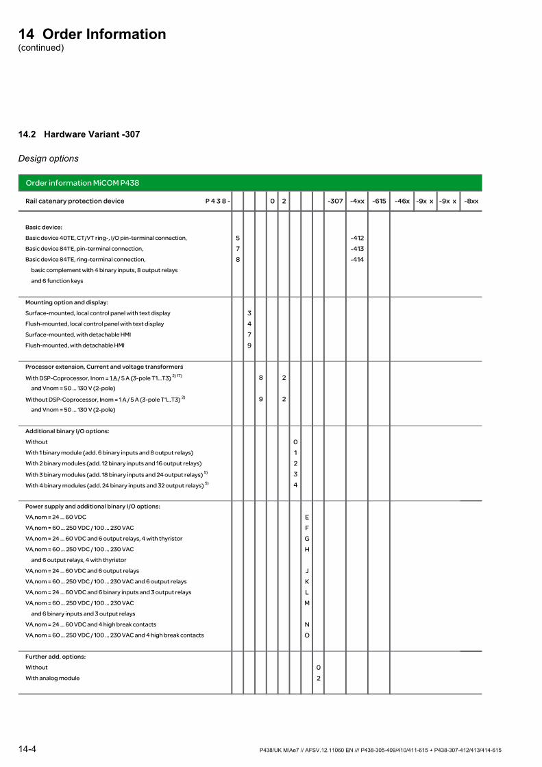
14 Order Information (continued)
14.2 Hardware Variant -307
Design options
Order information MiCOM P438
Rail catenary protection device P 4 3 8 - 0 2 -307 -4xx -615 -46x -9x x -9x x -8xx
Basic device:
Basic device 40TE, CT/VT ring-, I/O pin-terminal connection, 5 -412Basic device 84TE, pin-terminal connection, 7 -413Basic device 84TE, ring-terminal connection, 8 -414
basic complement with 4 binary inputs, 8 output relays
and 6 function keys
Mounting option and display:
Surface-mounted, local control panel with text display 3Flush-mounted, local control panel with text display 4Surface-mounted, with detachable HMI 7Flush-mounted, with detachable HMI 9
Processor extension, Current and voltage transformers
With DSP-Coprocessor, Inom = 1 A / 5 A (3-pole T1...T3) 2) 17) 8 2and Vnom = 50 ... 130 V (2-pole)
Without DSP-Coprocessor, Inom = 1 A / 5 A (3-pole T1...T3) 2) 9 2and Vnom = 50 ... 130 V (2-pole)
Additional binary I/O options:
Without 0With 1 binary module (add. 6 binary inputs and 8 output relays) 1With 2 binary modules (add. 12 binary inputs and 16 output relays) 2With 3 binary modules (add. 18 binary inputs and 24 output relays) 5) 3With 4 binary modules (add. 24 binary inputs and 32 output relays) 5) 4
Power supply and additional binary I/O options:
VA,nom = 24 … 60 VDC EVA,nom = 60 ... 250 VDC / 100 ... 230 VAC FVA,nom = 24 … 60 VDC and 6 output relays, 4 with thyristor GVA,nom = 60 ... 250 VDC / 100 ... 230 VAC H
and 6 output relays, 4 with thyristor
VA,nom = 24 ... 60 VDC and 6 output relays JVA,nom = 60 ... 250 VDC / 100 ... 230 VAC and 6 output relays KVA,nom = 24 … 60 VDC and 6 binary inputs and 3 output relays LVA,nom = 60 ... 250 VDC / 100 ... 230 VAC M
and 6 binary inputs and 3 output relays
VA,nom = 24 … 60 VDC and 4 high break contacts NVA,nom = 60 ... 250 VDC / 100 ... 230 VAC and 4 high break contacts O
Further add. options:
Without 0With analog module 2
14-4 P438/UK M/Ae7 // AFSV.12.11060 EN /// P438-305-409/410/411-615 + P438-307-412/413/414-615
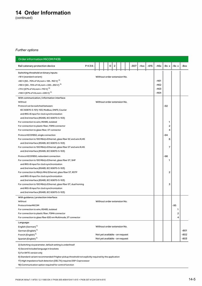
14 Order Information (continued)
Further options
Order information MiCOM P438
Rail catenary protection device P 4 3 8 - 0 2 -307 -4xx -615 -46x -9x x -9x x -8xx
Switching threshold on binary inputs:
>18 V (standard variant) Without order extension No.>90 V (60...70% of VA,nom = 125...150 V) 8) -461>155 V (60...70% of VA,nom = 220...250 V) 8) -462>73 V (67% of VA,nom = 110 V) 8) -463>146 V (67% of VA,nom = 220 V) 8) -464
With communication / information interface:
Without Without order extension No.Protocol can be switched between: -92
IEC 60870-5-101/-103, Modbus, DNP3, Courier
and IRIG-B input for clock synchronization
and 2nd interface (RS485, IEC 60870-5-103)
For connection to wire, RS485, isolated 1For connection to plastic fiber, FSMA connector 2For connection to glass fiber, ST connector 4
Protocol IEC61850, single connection -94For connection to 100 Mbit/s Ethernet, glass fiber SC and wire RJ45 6
and 2nd interface (RS485, IEC 60870-5-103)
For connection to 100 Mbit/s Ethernet, glass fiber ST and wire RJ45 7and 2nd interface (RS485, IEC 60870-5-103)
Protocol IEC61850, redundant connection -98For connection to 100 Mbit/s Ethernet, glass fiber ST, SHP 1
and IRIG-B input for clock synchronization
and 2nd interface (RS485, IEC 60870-5-103)
For connection to Mbit/s MHz Ethernet, glass fiber ST, RSTP 2and IRIG-B input for clock synchronization
and 2nd interface (RS485, IEC 60870-5-103)
For connection to 100 Mbit/s Ethernet, glass fiber ST, dual homing 3and IRIG-B input for clock synchronization
and 2nd interface (RS485, IEC 60870-5-103)
With guidance / protection interface:
Without Without order extension No.Protocol InterMiCOM -95For connection to wire, RS485, isolated 1For connection to plastic fiber, FSMA connector 2For connection to glass fiber 820 nm Multimode, ST connector 4
Language:
English (German) 4) Without order extension No.German (English) 4) -801French (English) 4) Not yet available - on request -802Spanish (English) 4) Not yet available - on request -803
2) Switching via parameter, default setting is underlined!
4) Second included language in brackets
5) For 84TE version only
8) Standard variant recommended if higher pickup threshold not explicitly required by the application
17) High impedance fault detection (DELTA) requires DSP-Coprocessor
18) Communication option required for control function
P438/UK M/Ae7 // AFSV.12.11060 EN /// P438-305-409/410/411-615 + P438-307-412/413/414-615 14-5

14-6 P438/EN M/Ad7 // AFSV.12.10470 D /// P438-305-409/410/411-613 + P438-307-412/413/414-613

Appendix
P438/EN M/Ad7 // AFSV.12.10470 D /// P438-305-409/410/411-613 + P438-307-412/413/414-613 AP-1
A Glossary
B Signal List
C Overview of Changes
Appendix (continued)
Ap-2 P438/EN M/Ad7 // AFSV.12.10470 D /// P438-305-409/410/411-613 + P438-307-412/413/414-613
A Glossary A-1A 1 Function Groups A-1A 2 Modules A-2A 3 Symbols A-3A 4 Examples of Signal Names A-10A 5 Symbols Used A-11
B List of Signals B-1B 1 Internal Signal Names B-1B 2 Telecontrol Interface per EN 60870-5-101 or IEC 870-5-
101 (Companion Standard) B-3
B 2.1 Interoperability B-3B 2.1.1 Network Configuration (Network-Specific Parameters) B-3B 2.1.2 Physical Layer (Network-Specific Parameters) B-4B 2.1.3 Link Layer (Network-Specific Parameters) B-5B 2.1.4 Application Layer B-6B 2.1.5 Basic Application Functions B-12
B 3 Communication Interface per IEC 60870-5-103 B-15B 3.1 Interoperability B-15B 3.1.1 Physical Layer B-15B 3.1.1.1 Electrical Interface B-15B 3.1.1.2 Optical Interface B-15B 3.1.1.3 Transmission Rate B-15B 3.1.2 Link Layer B-16B 3.1.3 Application Layer B-16B 3.1.3.1 Transmission Mode for Application Data B-16B 3.1.3.2 Common Address of ASDU B-16B 3.1.3.3 Selection of Standard Information Numbers in Monitor
Direction B-16
B 3.1.3.3.1 System Functions in Monitor Direction B-16B 3.1.3.3.2 Status Indications in Monitor Direction B-17B 3.1.3.3.3 Monitoring Signals (Supervision Indications) in Monitor
Direction B-18
B 3.1.3.3.4 Earth Fault Indications in Monitor Direction B-19B 3.1.3.3.5 Fault Indications in Monitor Direction B-20B 3.1.3.3.6 Auto-Reclosure Indications in Monitor Direction B-22B 3.1.3.3.7 Measurands in Monitor Direction B-22B 3.1.3.3.8 Generic Functions in Monitor Direction B-23B 3.1.3.4 Selection of Standard Information Numbers in Control
Direction B-24
B 3.1.3.4.1 System Functions in Control Direction B-24B 3.1.3.4.2 General Commands in Control Direction B-24B 3.1.3.4.3 Generic Functions in Control Direction B-25B 3.1.3.5 Basic Application Functions B-26B 3.1.3.6 Miscellaneous B-26
Appendix (continued)
P438/EN M/Ad7 // AFSV.12.10470 D /// P438-305-409/410/411-613 + P438-307-412/413/414-613 AN-3
C Overview of Changes C-1
P438-301-401/402-601 C-1 P438-301-401/402-602 C-1 P438-301-401/402-603 C-1 P438-301-401/402-603-701 C-3 P438-301-401/402-603-702 C-4 P438-301-401/402-603-703 C-4 P438-301-401/402-604 C-4 P438-301-401/402-604-704 C-5 P438-301-401/402-604-705 C-5 P438-301-401/402-605 C-5 P438-301-401/402-605-706 C-6 P438-301-401/402-605-707 C-6 P438-301-401/402-605-708 C-6 P438-301-401/402-606 C-6 P438-302-403/404/405-607 C-9 P438-302-403/404/405-608 C-10 P438-303-406/407/408-610 C-11 P438-304-409/410/411-611 C-13 P438-304-409/410/411-611-709 C-14 P438-304-409/410/411-612 C-14 P438-305-409/410/411-613 C-15 P438-306-412/413/414 -612-710 C-18 P438-307-412/413/414-613 C-18

Ap-4 P438/EN M/Ad7 // AFSV.12.10470 D /// P438-305-409/410/411-613 + P438-307-412/413/414-613

Appendix A - Glossary
A 1 Function Groups
Data Model Regional Language (as used in this manual)
Data Model Reference Language
BUOC: Backup Overcurrent-Time Protection BUOC: Backup Overcurrent-Time Protection C&VTS: VT and CT Supervision MCMON: Measuring-Circuit Monitoring CBF: Circuit Breaker Failure Protection CBF: Circuit Breaker Failure Protection CBM: Circuit Breaker Monitoring CBM: Circuit Breaker Monitoring CHECK: Self-Monitoring SFMON: Self-Monitoring COMM1: “Logical” Communication Interface 1 COMM1: “Logical” Communication Interface 1 COMM2: “Logical” Communication Interface 2 COMM2: “Logical” Communication Interface 2 COMM3: “Logical” Communication Interface 3
(InterMiCOM) COMM3: “Logical” Communication Interface 3
(InterMiCOM) DELTA: High-Impedance Protection DELTA: High-Impedance Protection DFRST: Defrost Protection DFRST: Defrost Protection DIST: Distance Protection DIST: Distance Protection DTOC: Definite-Time Overcurrent Protection DTOC: Definite-Time Overcurrent Protection DVICE: Device DVICE: Device F_KEY: Function Keys F_KEY: Function Keys FT_DA: Fault Data Acquisition FT_DA: Fault Data Acquisition GOOSE: Generic Object Oriented Substation Event GOOSE: Generic Object Oriented Substation Event GROUP: Setting Group Selection PSS: Parameter Subset Selection GSSE: Generic Substation State Event GSSE: Generic Substation State Event HMI: User Interface LOC: Local Control Panel IDMT: Inverse-Time Overcurrent Protection IDMT: Inverse-Time Overcurrent Protection IEC: Communication Interface IEC 61850 IEC: Communication Interface IEC 61850 INP: Binary Input INP: Binary Input IRIGB: IRIG-B Interface IRIGB: IRIG-B Interface LED: LED Indicator LED: LED Indicator LIMIT: Limit Value Monitoring LIMIT: Limit Value Monitoring LOGIC: Logic LOGIC: Logic mA_OP: Measured Data Output MEASO: Measured Data Output MAIN: Main Function MAIN: Main Function MT_RC: Monitoring Signal Recording MT_RC: Monitoring Signal Recording OL_DA: Overload Data Acquisition OL_DA: Overload Data Acquisition OL_RC: Overload Recording OL_RC: Overload Recording OP_RC: Operating Data Recording OP_RC: Operating Data Recording OSCIL: Fault Recording FT_RC: Fault Recording OUTP: Binary Output OUTP: Binary Output PC: PC Link PC: PC Link RECLS Auto-Reclose Control ARC: Auto-Reclosing Control RTDmA: Measured Data Input MEASI: Measured Data Input SOTF: Switch on to Fault Protection SOTF: Switch on to Fault Protection THERM: Thermal Overload Protection THERM: Thermal Overload Protection V<>: Under- and Overvoltage Protection V<>: Under- and Overvoltage Protection
P438/UK M/Ae7 // AFSV.12.11060 EN /// P438-305-409/410/411-615 + P438-307-412/413/414-615 A-1
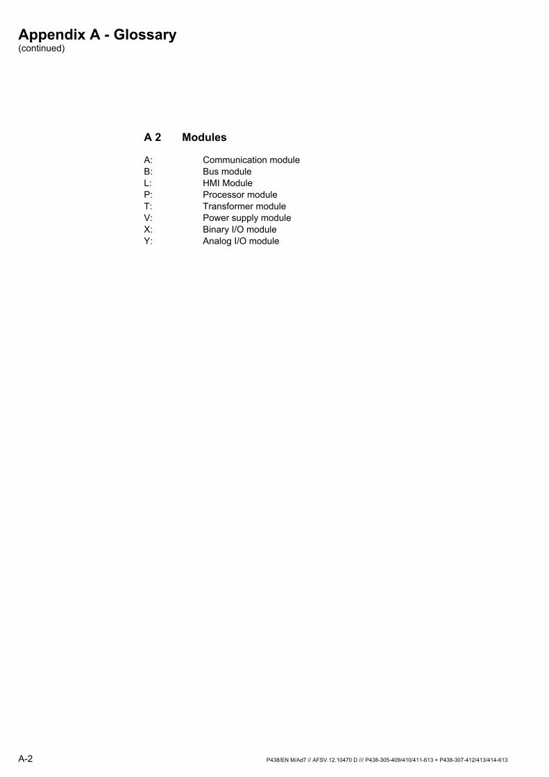
Appendix A - Glossary (continued)
A-2 P438/EN M/Ad7 // AFSV.12.10470 D /// P438-305-409/410/411-613 + P438-307-412/413/414-613
A 2 Modules
A: Communication module B: Bus module L: HMI Module P: Processor module T: Transformer module V: Power supply module X: Binary I/O module Y: Analog I/O module

Appendix A - Glossary (continued)
P438/EN M/Ad7 // AFSV.12.10470 D /// P438-305-409/410/411-613 + P438-307-412/413/414-613 A-3
A 3 Symbols
Graphic symbols for block diagrams Binary elements in compliance with DIN 40900 part 12, September 1992, IEC 617-12: modified 1991 Analog information processing in compliance with DIN 40900 part 13, January 1981 To document the linking of analog and binary signals, additional symbols have been used, taken from several DIN documents. As a rule, direction of the signal flow is from left to right and from top to bottom. Other flow directions are marked by an arrow. Input signals are listed on the left side of the signal flow, output signals on the right side.
Symbol General Description
=
To obtain more space for representing a group of related elements, contours of the elements may be joined or cascaded if the following rules are met: There is no functional linkage between elements whose common contour line is oriented in the signal flow direction. Note: This rule does not necessarily apply to configurations with two or more signal flow directions, such as for symbols with a control block and an output block. There exists at least one logical link between elements whose common contour line runs perpendicularly to the signal flow direction.
Components of a symbol A symbol consists of a contour or contour combination and one or more qualifiers.
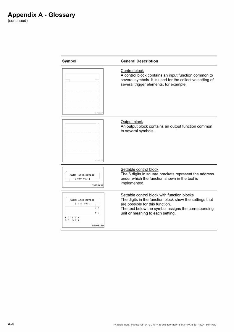
Appendix A - Glossary (continued)
A-4 P438/EN M/Ad7 // AFSV.12.10470 D /// P438-305-409/410/411-613 + P438-307-412/413/414-613
Symbol General Description
Control block A control block contains an input function common to several symbols. It is used for the collective setting of several trigger elements, for example.
Output block An output block contains an output function common to several symbols.
MAIN: Inom Device
[ 010 003 ]
D5Z08X5B
Settable control block The 6 digits in square brackets represent the address under which the function shown in the text is implemented.
MAIN: Inom Device
[ 010 003 ]
1.0
1.0: 1.0 A 5.0: 5.0 A
5.0
D5Z08X6B
Settable control block with function blocks The digits in the function block show the settings that are possible for this function. The text below the symbol assigns the corresponding unit or meaning to each setting.
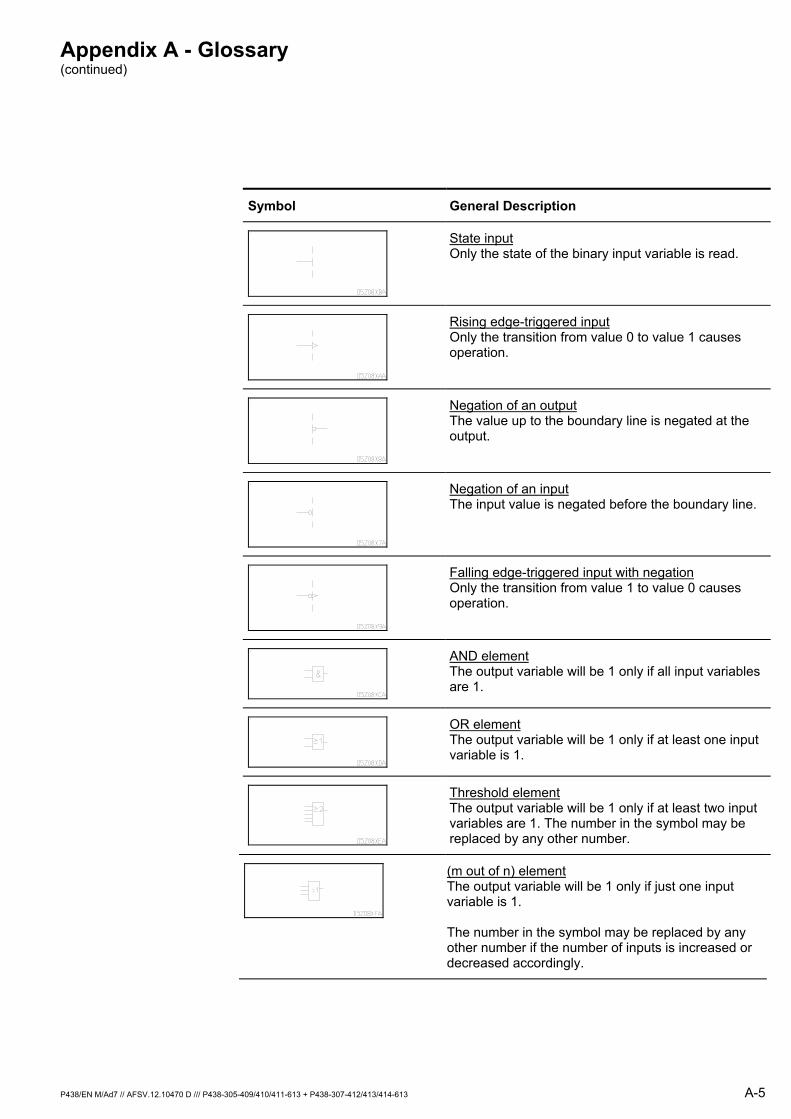
Appendix A - Glossary (continued)
P438/EN M/Ad7 // AFSV.12.10470 D /// P438-305-409/410/411-613 + P438-307-412/413/414-613 A-5
Symbol General Description
State input Only the state of the binary input variable is read.
Rising edge-triggered input Only the transition from value 0 to value 1 causes operation.
Negation of an output The value up to the boundary line is negated at the output.
Negation of an input The input value is negated before the boundary line.
Falling edge-triggered input with negation Only the transition from value 1 to value 0 causes operation.
AND element The output variable will be 1 only if all input variables are 1.
OR element The output variable will be 1 only if at least one input variable is 1.
Threshold element The output variable will be 1 only if at least two input variables are 1. The number in the symbol may be replaced by any other number.
(m out of n) element The output variable will be 1 only if just one input variable is 1. The number in the symbol may be replaced by any other number if the number of inputs is increased or decreased accordingly.
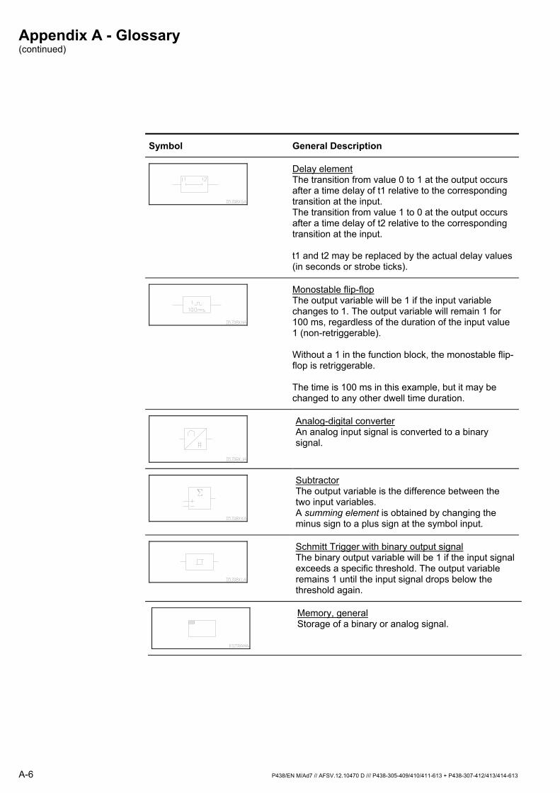
Appendix A - Glossary (continued)
A-6 P438/EN M/Ad7 // AFSV.12.10470 D /// P438-305-409/410/411-613 + P438-307-412/413/414-613
Symbol General Description
Delay element The transition from value 0 to 1 at the output occurs after a time delay of t1 relative to the corresponding transition at the input. The transition from value 1 to 0 at the output occurs after a time delay of t2 relative to the corresponding transition at the input. t1 and t2 may be replaced by the actual delay values (in seconds or strobe ticks).
Monostable flip-flop The output variable will be 1 if the input variable changes to 1. The output variable will remain 1 for 100 ms, regardless of the duration of the input value 1 (non-retriggerable). Without a 1 in the function block, the monostable flip-flop is retriggerable. The time is 100 ms in this example, but it may be changed to any other dwell time duration.
Analog-digital converter An analog input signal is converted to a binary signal.
Subtractor The output variable is the difference between the two input variables. A summing element is obtained by changing the minus sign to a plus sign at the symbol input.
Schmitt Trigger with binary output signal The binary output variable will be 1 if the input signal exceeds a specific threshold. The output variable remains 1 until the input signal drops below the threshold again.
Memory, general Storage of a binary or analog signal.
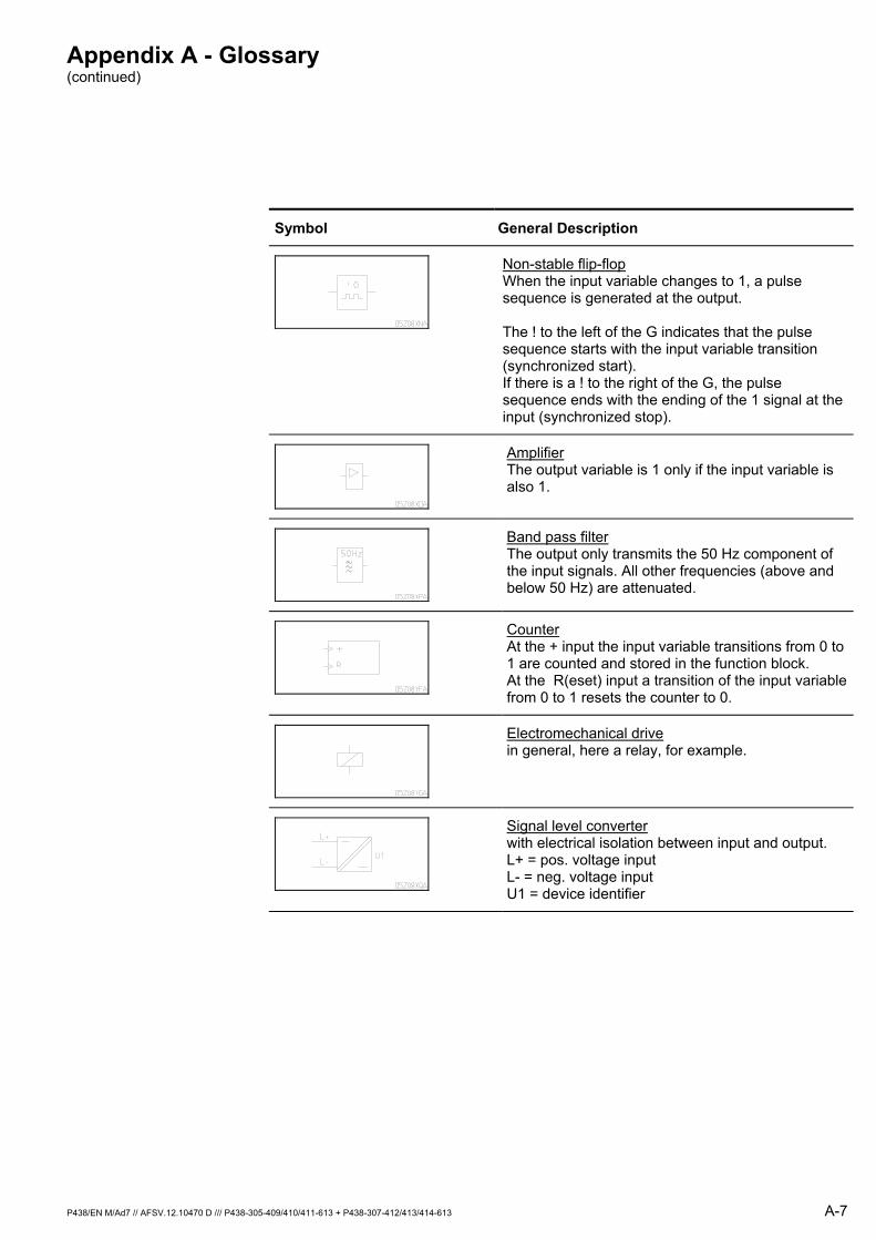
Appendix A - Glossary (continued)
P438/EN M/Ad7 // AFSV.12.10470 D /// P438-305-409/410/411-613 + P438-307-412/413/414-613 A-7
Symbol General Description
Non-stable flip-flop When the input variable changes to 1, a pulse sequence is generated at the output. The ! to the left of the G indicates that the pulse sequence starts with the input variable transition (synchronized start). If there is a ! to the right of the G, the pulse sequence ends with the ending of the 1 signal at the input (synchronized stop).
Amplifier The output variable is 1 only if the input variable is also 1.
Band pass filter The output only transmits the 50 Hz component of the input signals. All other frequencies (above and below 50 Hz) are attenuated.
Counter At the + input the input variable transitions from 0 to 1 are counted and stored in the function block. At the R(eset) input a transition of the input variable from 0 to 1 resets the counter to 0.
Electromechanical drive in general, here a relay, for example.
Signal level converter with electrical isolation between input and output. L+ = pos. voltage input L- = neg. voltage input U1 = device identifier

Appendix A - Glossary (continued)
A-8 P438/EN M/Ad7 // AFSV.12.10470 D /// P438-305-409/410/411-613 + P438-307-412/413/414-613
Symbol General Description
Input transducer with conductor and device identifiers (according to DIN EN 60445) Conductor identifiers for current inputs: for A: A1 and A2 for B: B1 and B2 for C: C1 and C2 for N: N1 and N2 Conductor identifiers for voltage inputs via transformer 1: for A: 1U for B: 1V for C: 1W for N: 1N via transformer 2: for A: 2U for B: 2V Device identifiers for current transformers: for A: T1 for B: T2 for C: T3 for N: T4 for voltage transformer 1: for A: T5 for B: T6 for C: T7 for N: T8 for VG-N transformer: T90 for voltage transformer 2: for A: T15
Change-over contact with device identifier
Special symbol Output relay in normally-energized arrangement (‘closed-circuit operation’).

Appendix A - Glossary (continued)
P438/EN M/Ad7 // AFSV.12.10470 D /// P438-305-409/410/411-613 + P438-307-412/413/414-613 A-9
Symbol General Description
PC interface with pin connections
Multiplier The output variable is the result of the multiplication of the two input variables.
Divider The output variable is the result of the division of the two input variables.
Comparator The output variable becomes 1 only if the input variable(s) are equal to the function in the function block.
Formula block The output variable becomes 1 only if the input variable(s) satisfy the equation in the function block
Appendix A - Glossary (continued)
A-10 P438/EN M/Ad7 // AFSV.12.10470 D /// P438-305-409/410/411-613 + P438-307-412/413/414-613
A 4 Examples of Signal Names
All settings and signals relevant for protection are shown in the block diagrams of Chapter 3 as follows:
Signal Name General Description
OSCIL: Fault recording n 305 100
Internal signal names are not coded by a data model address. In the block diagrams they are marked with a diamond. The small figure underneath the signal name represents a code that is irrelevant to the user. The internal signal names used and their origins are listed in Appendix B.
DIST: VNG>> triggered [ 036 015 ]
Signal names coded by a data model address are represented by their address (shown in square brackets). Their origin is given in Chapters 7 and 8.
MAIN: General Reset BED [ 003 002 ] 1: Execute
A specific setting to be used later on is shown with its signal name, address, and the setting preceded by the setting arrow.

Appendix A - Glossary (continued)
P438/EN M/Ad7 // AFSV.12.10470 D /// P438-305-409/410/411-613 + P438-307-412/413/414-613 A-11
A 5 Symbols Used
Symbol Meaning
t Time duration
V Voltage, potential difference
V Complex voltage
I Electrical current
I Complex current
Z Complex impedance
Z Modulus of complex impedance
f Frequency
δ Temperature in °C
Σ Sum, result
Ω Unit of electrical resistance
α Angle
ϕ Phase angle. With subscripts: specific angle between a defined current and a defined voltage.
τ Time constant
∆T Temperature difference in K (oC)

A-12 P438/EN M/Ad7 // AFSV.12.10470 D /// P438-305-409/410/411-613 + P438-307-412/413/414-613
Appendix B - Signal List (continued)
P438/EN M/Ad7 // AFSV.12.10470 D /// P438-305-409/410/411-613 + P438-307-412/413/414-613 B-1
B 1 Internal Signal Names
Internal signal names are not associated to an external address. In the block (logic) diagrams they are marked with a square (—).
Internal Signal Figure No.
C&VTS: V< triggered Fig. 3-123
COMM1: Selected protocol Fig. 3-6
DELTA: Vmin triggered Fig. 3-117
DIST: Blocking Fig. 3-92
DIST: Enable t2S Fig. 3-108
DIST: Enable t3S Fig. 3-108
DIST: Enable t4S Fig. 3-108
DIST: Forward direction Fig. 3-97
DIST: Reverse direction Fig. 3-97
DTOC: I> forward-direct. Fig. 3-155
DTOC: I> non-directional Fig. 3-155
DTOC: I> reverse-direct. Fig. 3-155
DTOC: I> Starting Fig. 3-153
DTOC: I>> forward-direct. Fig. 3-156
DTOC: I>> non-directional Fig. 3-156
DTOC: I>> reverse-direct. Fig. 3-156
DTOC: I>> triggered Fig. 3-153
DTOC: V < V< (I>) Fig. 3-155
DTOC: V < V< (I>>) Fig. 3-156
FT_DA: Outp. fault location Fig. 3-82
FT_DA: Save measured values Fig. 3-81
IDMT: Forward trip Fig. 3-166
IDMT: Iref> Triggered Fig. 3-164
IDMT: Non-directional trip Fig. 3-166
IDMT: Reverse trip Fig. 3-166
IDMT: V < V< Fig. 3-166
IDMT: V > Vmin Fig. 3-166
mA_OP: Enable Fig. 3-31
mA_OP: Reset meas.val.outp. Fig. 3-32
MAIN: Blck. 1 sel.functions Fig. 3-53
MAIN: Blck. 2 sel.functions Fig. 3-53
MAIN: Hardware fault Fig. 3-41, -42, -43,-44......
MAIN: I(2fn)/I(fn Fig. 3-42
MAIN: I(3fn)/I(fn Fig. 3-42
MAIN: I(5fn)/I(fn Fig. 3-42
MAIN: Inrush stabil. trigg Fig. 3-51
MAIN: Protection active Fig. 3-48
MAIN: Reset LED Fig. 3-68
MAIN: Time tag Fig. 3-67
MAIN: Voltage mem. enabled Fig. 3-52,
MAIN: ΣI(xfn)/I(fn) Fig. 3-42
RECLS: CB closed Fig. 3-134
RECLS: HSR trip time elapsed Fig. 3-135, 3-138, 3-140, 3-142
Appendix B - Signal List (continued)
B-2 P438/EN M/Ad7 // AFSV.12.10470 D /// P438-305-409/410/411-613 + P438-307-412/413/414-613
RECLS: HSR-tr.DIST t1 runn. Fig. 3-143 3-149
RECLS: t1 running Fig. 3-143
RECLS: TDR trip time elapsed Fig. 3-136, 3-139, 3-140, 3-142
RECLS: TDR-tr.DIST t1 runn. Fig. 3-149
SOTF: AR blocked Fig. 3-131
THERM: Block. by CTA error Fig. 3-174
THERM: cPL * Iref Fig. 3-153
THERM: I Fig. 3-176
THERM: With CTA Fig. 3-174
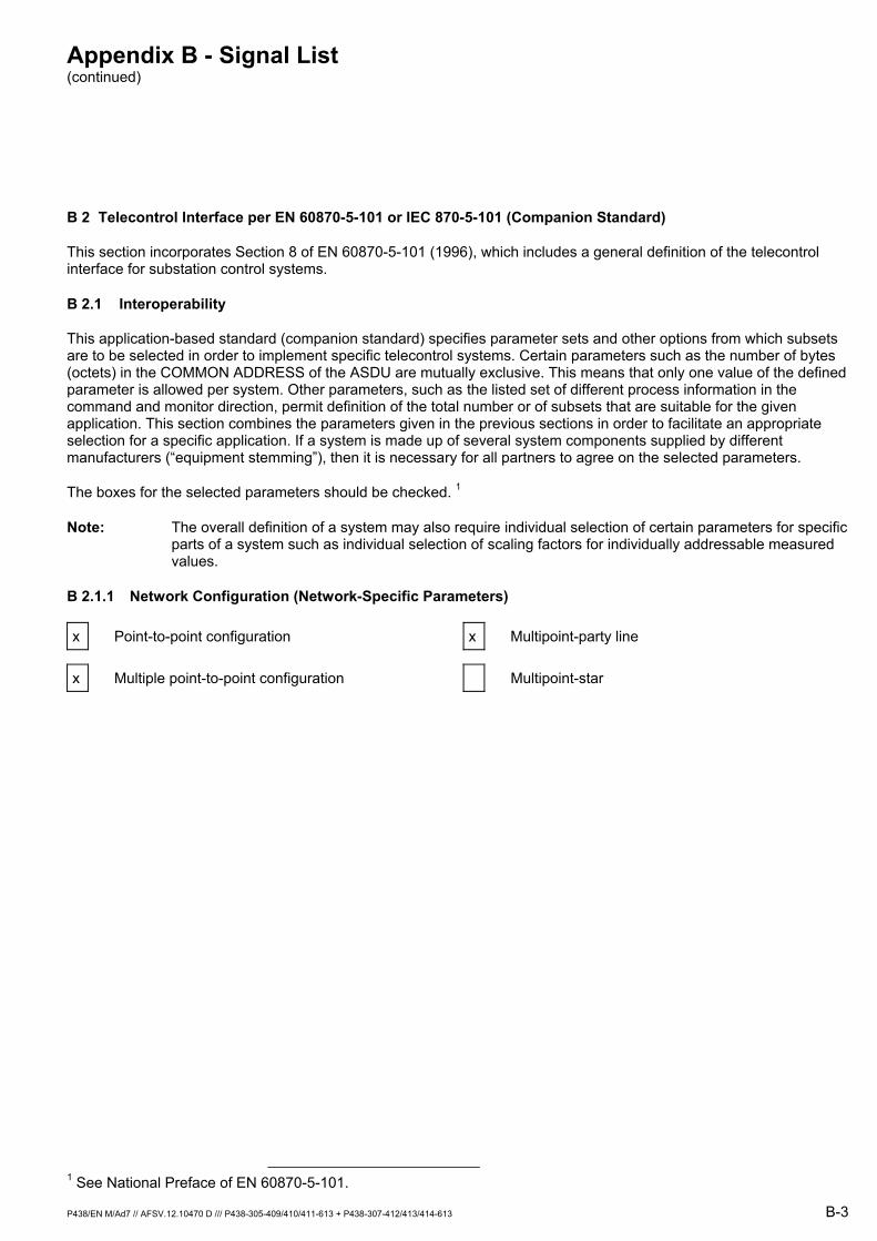
Appendix B - Signal List (continued)
P438/EN M/Ad7 // AFSV.12.10470 D /// P438-305-409/410/411-613 + P438-307-412/413/414-613 B-3
B 2 Telecontrol Interface per EN 60870-5-101 or IEC 870-5-101 (Companion Standard)
This section incorporates Section 8 of EN 60870-5-101 (1996), which includes a general definition of the telecontrol interface for substation control systems.
B 2.1 Interoperability
This application-based standard (companion standard) specifies parameter sets and other options from which subsets are to be selected in order to implement specific telecontrol systems. Certain parameters such as the number of bytes (octets) in the COMMON ADDRESS of the ASDU are mutually exclusive. This means that only one value of the defined parameter is allowed per system. Other parameters, such as the listed set of different process information in the command and monitor direction, permit definition of the total number or of subsets that are suitable for the given application. This section combines the parameters given in the previous sections in order to facilitate an appropriate selection for a specific application. If a system is made up of several system components supplied by different manufacturers (“equipment stemming”), then it is necessary for all partners to agree on the selected parameters.
The boxes for the selected parameters should be checked. 1
Note: The overall definition of a system may also require individual selection of certain parameters for specific parts of a system such as individual selection of scaling factors for individually addressable measured values.
B 2.1.1 Network Configuration (Network-Specific Parameters)
x Point-to-point configuration x Multipoint-party line
x Multiple point-to-point configuration Multipoint-star
1 See National Preface of EN 60870-5-101.
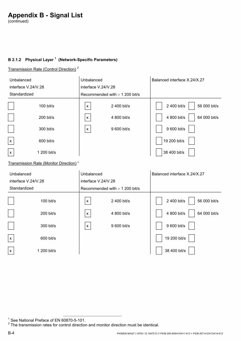
Appendix B - Signal List (continued)
B-4 P438/EN M/Ad7 // AFSV.12.10470 D /// P438-305-409/410/411-613 + P438-307-412/413/414-613
B 2.1.2 Physical Layer 1 (Network-Specific Parameters)
Transmission Rate (Control Direction) 2
Unbalanced
interface V.24/V.28
Standardized
Unbalanced
interface V.24/V.28
Recommended with > 1 200 bit/s
Balanced interface X.24/X.27
100 bit/s x 2 400 bit/s 2 400 bit/s 56 000 bit/s
200 bit/s x 4 800 bit/s 4 800 bit/s 64 000 bit/s
300 bit/s x 9 600 bit/s 9 600 bit/s
x 600 bit/s 19 200 bit/s
x 1 200 bit/s 38 400 bit/s
Transmission Rate (Monitor Direction) 2
Unbalanced
interface V.24/V.28
Standardized
Unbalanced
interface V.24/V.28
Recommended with > 1 200 bit/s
Balanced interface X.24/X.27
100 bit/s x 2 400 bit/s 2 400 bit/s 56 000 bit/s 200 bit/s x 4 800 bit/s 4 800 bit/s 64 000 bit/s 300 bit/s x 9 600 bit/s 9 600 bit/s x 600 bit/s 19 200 bit/s x 1 200 bit/s 38 400 bit/s
1 See National Preface of EN 60870-5-101. 2 The transmission rates for control direction and monitor direction must be identical.
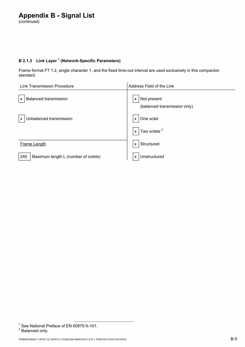
Appendix B - Signal List (continued)
P438/EN M/Ad7 // AFSV.12.10470 D /// P438-305-409/410/411-613 + P438-307-412/413/414-613 B-5
B 2.1.3 Link Layer 1 (Network-Specific Parameters)
Frame format FT 1.2, single character 1, and the fixed time-out interval are used exclusively in this companion standard.
Link Transmission Procedure Address Field of the Link x Balanced transmission x Not present
(balanced transmission only) x Unbalanced transmission x One octet x Two octets 2 Frame Length x Structured 240 Maximum length L (number of octets) x Unstructured
1 See National Preface of EN 60870-5-101. 2 Balanced only.
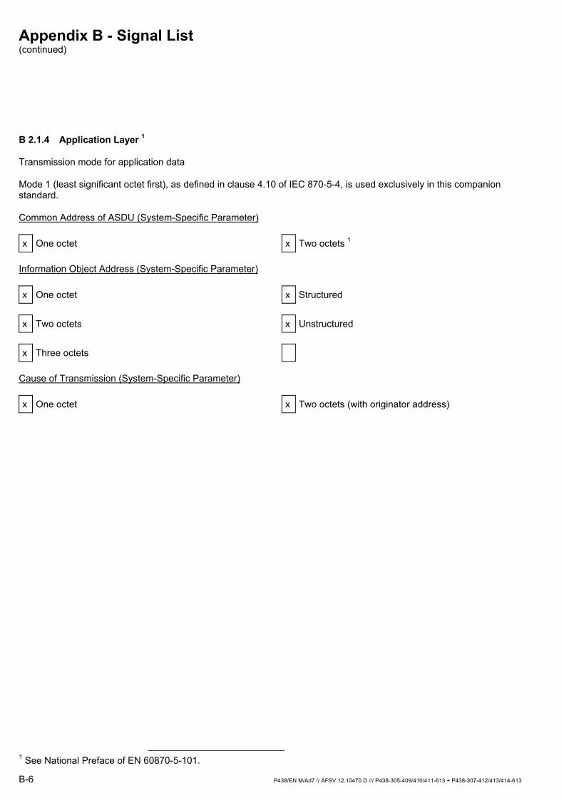
Appendix B - Signal List (continued)
B-6 P438/EN M/Ad7 // AFSV.12.10470 D /// P438-305-409/410/411-613 + P438-307-412/413/414-613
B 2.1.4 Application Layer 1
Transmission mode for application data
Mode 1 (least significant octet first), as defined in clause 4.10 of IEC 870-5-4, is used exclusively in this companion standard.
Common Address of ASDU (System-Specific Parameter)
x One octet x Two octets 1
Information Object Address (System-Specific Parameter)
x One octet x Structured x Two octets x Unstructured x Three octets
Cause of Transmission (System-Specific Parameter)
x One octet x Two octets (with originator address)
1 See National Preface of EN 60870-5-101.
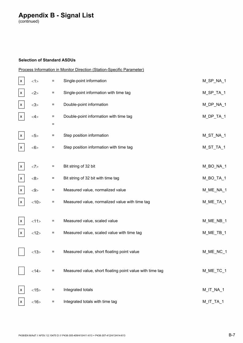
Appendix B - Signal List (continued)
P438/EN M/Ad7 // AFSV.12.10470 D /// P438-305-409/410/411-613 + P438-307-412/413/414-613 B-7
Selection of Standard ASDUs
Process Information in Monitor Direction (Station-Specific Parameter)
x <1> = Single-point information M_SP_NA_1
x <2> = Single-point information with time tag M_SP_TA_1
x <3> = Double-point information M_DP_NA_1
x <4> = Double-point information with time tag M_DP_TA_1
=
x <5> = Step position information M_ST_NA_1
x <6> = Step position information with time tag M_ST_TA_1
x <7> = Bit string of 32 bit M_BO_NA_1
x <8> = Bit string of 32 bit with time tag M_BO_TA_1
x <9> = Measured value, normalized value M_ME_NA_1
x <10> = Measured value, normalized value with time tag M_ME_TA_1
x <11> = Measured value, scaled value M_ME_NB_1
x <12> = Measured value, scaled value with time tag M_ME_TB_1
<13> = Measured value, short floating point value M_ME_NC_1
<14> = Measured value, short floating point value with time tag M_ME_TC_1
x <15> = Integrated totals M_IT_NA_1
x <16> = Integrated totals with time tag M_IT_TA_1

Appendix B - Signal List (continued)
B-8 P438/EN M/Ad7 // AFSV.12.10470 D /// P438-305-409/410/411-613 + P438-307-412/413/414-613
x <17> = Event of protection equipment with time tag M_EP_TA_1
x <18> = Packed start events of protection equipment with time tag ME_EP_TB_1
x <19> = Packed output circuit information of protection equipment with time tag M_EP_TC_1
<20> = Packed single-point information with status change detection M_PS_NA_1
<21> = Measured value, normalized value without quality descriptor M_ME_ND_1
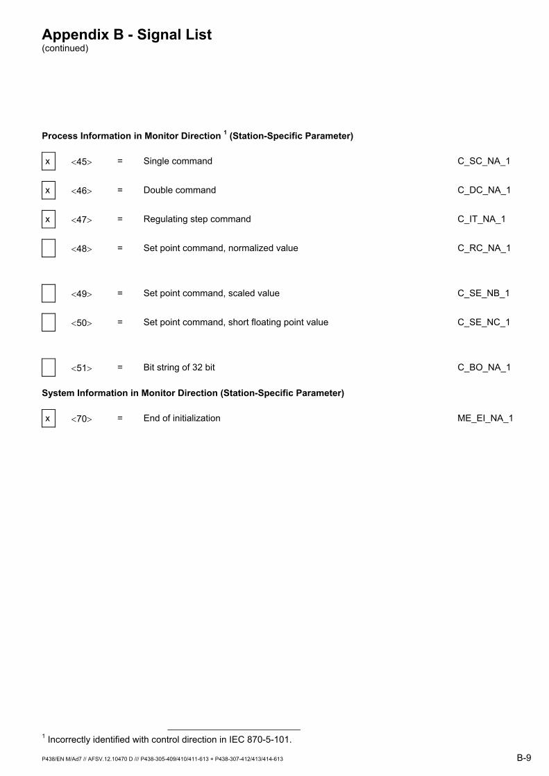
Appendix B - Signal List (continued)
P438/EN M/Ad7 // AFSV.12.10470 D /// P438-305-409/410/411-613 + P438-307-412/413/414-613 B-9
Process Information in Monitor Direction 1 (Station-Specific Parameter)
x <45> = Single command C_SC_NA_1 x <46> = Double command C_DC_NA_1 x <47> = Regulating step command C_IT_NA_1 <48> = Set point command, normalized value C_RC_NA_1
<49> = Set point command, scaled value C_SE_NB_1 <50> = Set point command, short floating point value C_SE_NC_1
<51> = Bit string of 32 bit C_BO_NA_1
System Information in Monitor Direction (Station-Specific Parameter)
x <70> = End of initialization ME_EI_NA_1
1 Incorrectly identified with control direction in IEC 870-5-101.

Appendix B - Signal List (continued)
B-10 P438/EN M/Ad7 // AFSV.12.10470 D /// P438-305-409/410/411-613 + P438-307-412/413/414-613
System Information in Control Direction (Station-Specific Parameter)
x <100> = Interrogation command C_IC_NA_1 x <101> = Counter interrogation command C_CI_NA_1 x <102> = Read command C_RD_NA_1 x <103> = Clock synchronization command 1 C_CS_NA_1 x <104> = Test command C_TS_NB_1 <105> = Reset process command C_RP_NC_1 <106> = Delay acquisition command C_CD_NA_1
1 The command procedure is formally processed, but there is no change in the local time in the station. 2 See National Preface of EN 60870-5-101.
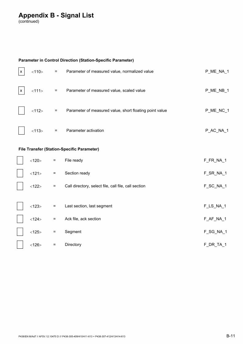
Appendix B - Signal List (continued)
P438/EN M/Ad7 // AFSV.12.10470 D /// P438-305-409/410/411-613 + P438-307-412/413/414-613 B-11
Parameter in Control Direction (Station-Specific Parameter)
x <110> = Parameter of measured value, normalized value P_ME_NA_1
x <111> = Parameter of measured value, scaled value P_ME_NB_1
<112> = Parameter of measured value, short floating point value P_ME_NC_1
<113> = Parameter activation P_AC_NA_1
File Transfer (Station-Specific Parameter)
<120> = File ready F_FR_NA_1 <121> = Section ready F_SR_NA_1 <122> = Call directory, select file, call file, call section F_SC_NA_1
<123> = Last section, last segment F_LS_NA_1 <124> = Ack file, ack section F_AF_NA_1 <125> = Segment F_SG_NA_1 <126> = Directory F_DR_TA_1
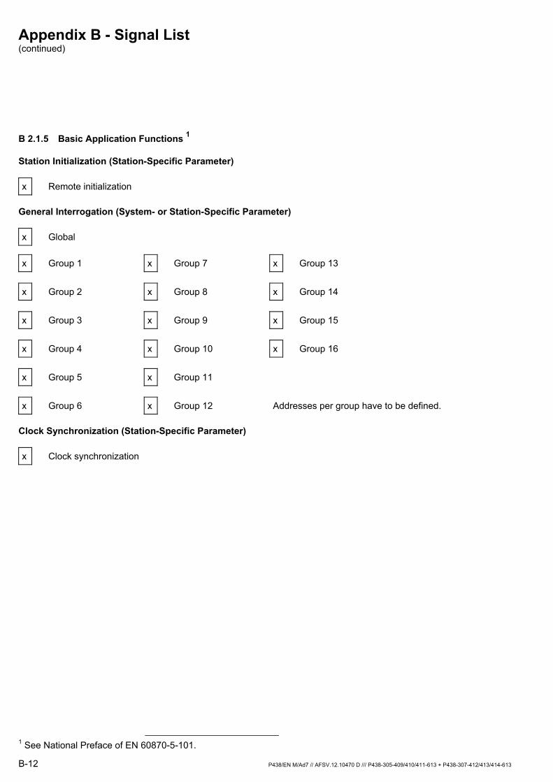
Appendix B - Signal List (continued)
B-12 P438/EN M/Ad7 // AFSV.12.10470 D /// P438-305-409/410/411-613 + P438-307-412/413/414-613
B 2.1.5 Basic Application Functions 1
Station Initialization (Station-Specific Parameter)
x Remote initialization
General Interrogation (System- or Station-Specific Parameter)
x Global
x Group 1 x Group 7 x Group 13 x Group 2 x Group 8 x Group 14 x Group 3 x Group 9 x Group 15 x Group 4 x Group 10 x Group 16 x Group 5 x Group 11 x Group 6 x Group 12 Addresses per group have to be defined.
Clock Synchronization (Station-Specific Parameter)
x Clock synchronization
1 See National Preface of EN 60870-5-101.
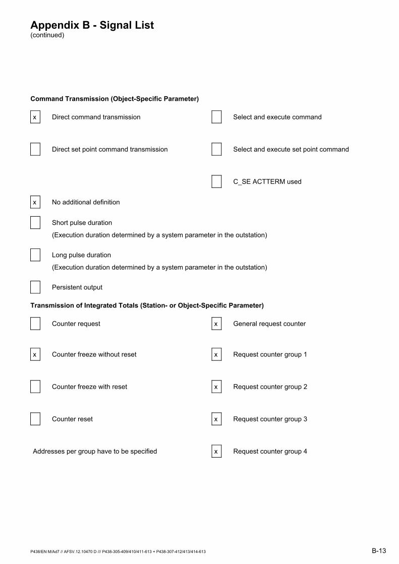
Appendix B - Signal List (continued)
P438/EN M/Ad7 // AFSV.12.10470 D /// P438-305-409/410/411-613 + P438-307-412/413/414-613 B-13
Command Transmission (Object-Specific Parameter)
x Direct command transmission Select and execute command
Direct set point command transmission Select and execute set point command
C_SE ACTTERM used x No additional definition
Short pulse duration
(Execution duration determined by a system parameter in the outstation) Long pulse duration
(Execution duration determined by a system parameter in the outstation) Persistent output
Transmission of Integrated Totals (Station- or Object-Specific Parameter)
Counter request x General request counter
x Counter freeze without reset x Request counter group 1
Counter freeze with reset x Request counter group 2
Counter reset x Request counter group 3
Addresses per group have to be specified x Request counter group 4
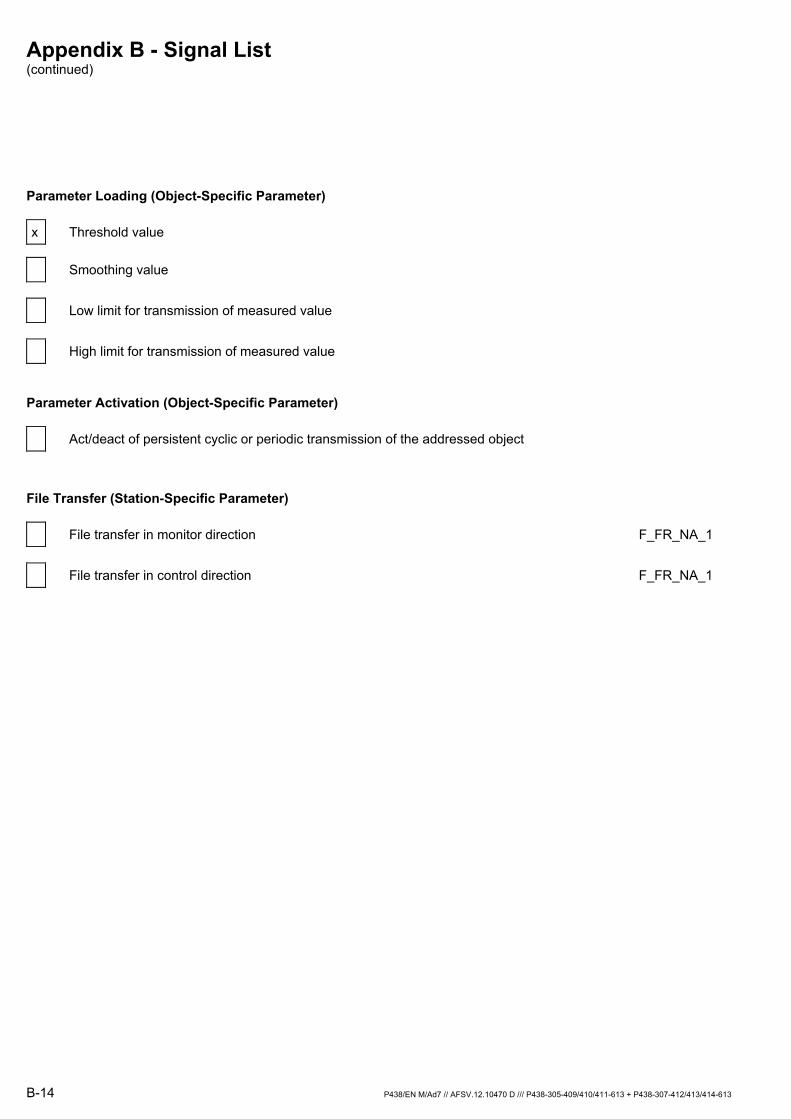
Appendix B - Signal List (continued)
B-14 P438/EN M/Ad7 // AFSV.12.10470 D /// P438-305-409/410/411-613 + P438-307-412/413/414-613
Parameter Loading (Object-Specific Parameter)
x Threshold value
Smoothing value Low limit for transmission of measured value High limit for transmission of measured value
Parameter Activation (Object-Specific Parameter)
Act/deact of persistent cyclic or periodic transmission of the addressed object
File Transfer (Station-Specific Parameter)
File transfer in monitor direction F_FR_NA_1 File transfer in control direction F_FR_NA_1
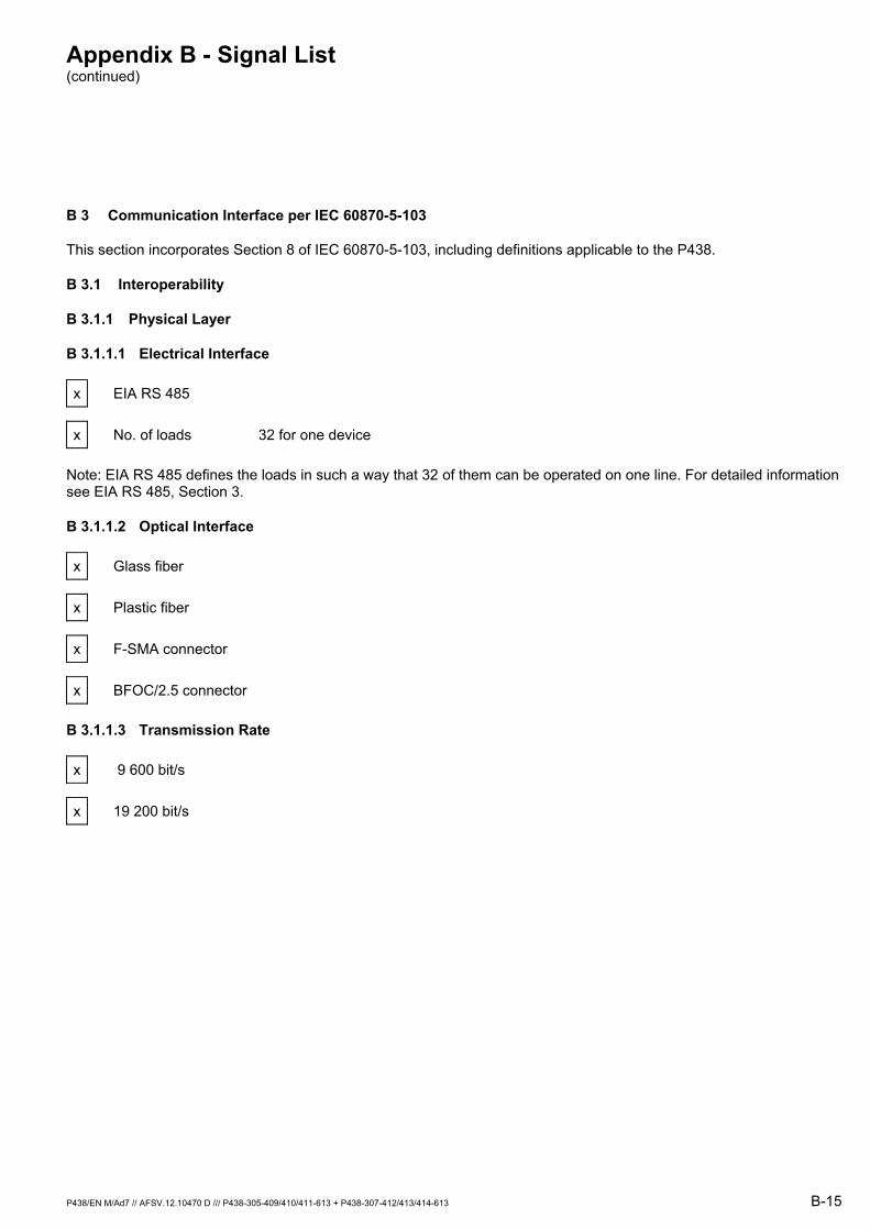
Appendix B - Signal List (continued)
P438/EN M/Ad7 // AFSV.12.10470 D /// P438-305-409/410/411-613 + P438-307-412/413/414-613 B-15
B 3 Communication Interface per IEC 60870-5-103
This section incorporates Section 8 of IEC 60870-5-103, including definitions applicable to the P438.
B 3.1 Interoperability
B 3.1.1 Physical Layer
B 3.1.1.1 Electrical Interface
x EIA RS 485
x No. of loads 32 for one device
Note: EIA RS 485 defines the loads in such a way that 32 of them can be operated on one line. For detailed information see EIA RS 485, Section 3.
B 3.1.1.2 Optical Interface
x Glass fiber
x Plastic fiber
x F-SMA connector
x BFOC/2.5 connector
B 3.1.1.3 Transmission Rate
x 9 600 bit/s
x 19 200 bit/s
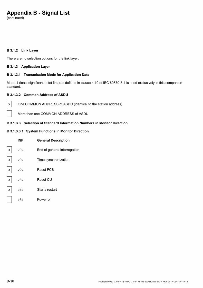
Appendix B - Signal List (continued)
B-16 P438/EN M/Ad7 // AFSV.12.10470 D /// P438-305-409/410/411-613 + P438-307-412/413/414-613
B 3.1.2 Link Layer
There are no selection options for the link layer.
B 3.1.3 Application Layer
B 3.1.3.1 Transmission Mode for Application Data
Mode 1 (least significant octet first) as defined in clause 4.10 of IEC 60870-5-4 is used exclusively in this companion standard.
B 3.1.3.2 Common Address of ASDU
x One COMMON ADDRESS of ASDU (identical to the station address)
More than one COMMON ADDRESS of ASDU
B 3.1.3.3 Selection of Standard Information Numbers in Monitor Direction
B 3.1.3.3.1 System Functions in Monitor Direction
INF General Description
x <0> End of general interrogation
x <0> Time synchronization
x <2> Reset FCB
x <3> Reset CU
x <4> Start / restart
<5> Power on
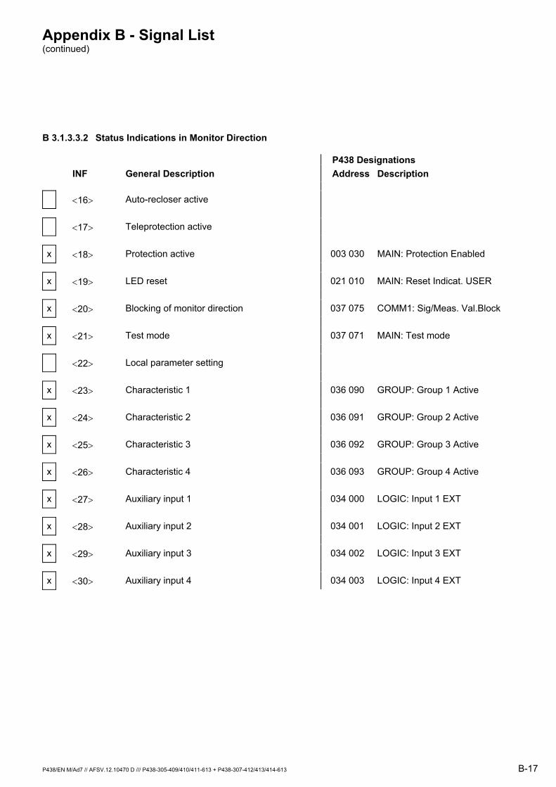
Appendix B - Signal List (continued)
P438/EN M/Ad7 // AFSV.12.10470 D /// P438-305-409/410/411-613 + P438-307-412/413/414-613 B-17
B 3.1.3.3.2 Status Indications in Monitor Direction
P438 Designations INF General Description Address Description
<16> Auto-recloser active
<17> Teleprotection active
x <18> Protection active 003 030 MAIN: Protection Enabled
x <19> LED reset 021 010 MAIN: Reset Indicat. USER
x <20> Blocking of monitor direction 037 075 COMM1: Sig/Meas. Val.Block
x <21> Test mode 037 071 MAIN: Test mode
<22> Local parameter setting
x <23> Characteristic 1 036 090 GROUP: Group 1 Active
x <24> Characteristic 2 036 091 GROUP: Group 2 Active
x <25> Characteristic 3 036 092 GROUP: Group 3 Active
x <26> Characteristic 4 036 093 GROUP: Group 4 Active
x <27> Auxiliary input 1 034 000 LOGIC: Input 1 EXT
x <28> Auxiliary input 2 034 001 LOGIC: Input 2 EXT
x <29> Auxiliary input 3 034 002 LOGIC: Input 3 EXT
x <30> Auxiliary input 4 034 003 LOGIC: Input 4 EXT

Appendix B - Signal List (continued)
B-18 P438/EN M/Ad7 // AFSV.12.10470 D /// P438-305-409/410/411-613 + P438-307-412/413/414-613
B 3.1.3.3.3 Monitoring Signals (Supervision Indications) in Monitor Direction
P438 Designations INF General Description Address Description
<32> Measurand supervision I
x <33> Measurand supervision V 038 023 C&VTS: VTS Volts Failure
<35> Phase sequence supervision
x <36>1 Trip circuit supervision 041 200 CHECK: Relay Kxx Faulty
x <37> I>> back-up operation 037 021 BUOC: Active
x <38> VT fuse failure 004 061 MAIN: M.c.b. Trip V EXT
<39> Teleprotection disturbed
x <46> Group warning 036 100 CHECK: Alarm (relay)
x <47> Group alarm 004 065 MAIN: Blocked/Faulty
1 The message content is formed from the OR operation of the individual signals

Appendix B - Signal List (continued)
P438/EN M/Ad7 // AFSV.12.10470 D /// P438-305-409/410/411-613 + P438-307-412/413/414-613 B-19
B 3.1.3.3.4 Earth Fault Indications in Monitor Direction
P438 Designations INF General Description Address Description
<48> Earth fault L1
<49> Earth fault L2
<50> Earth fault L3
<51> Earth fault forward, i.e. line
<52> Earth fault reverse, i.e. busbar
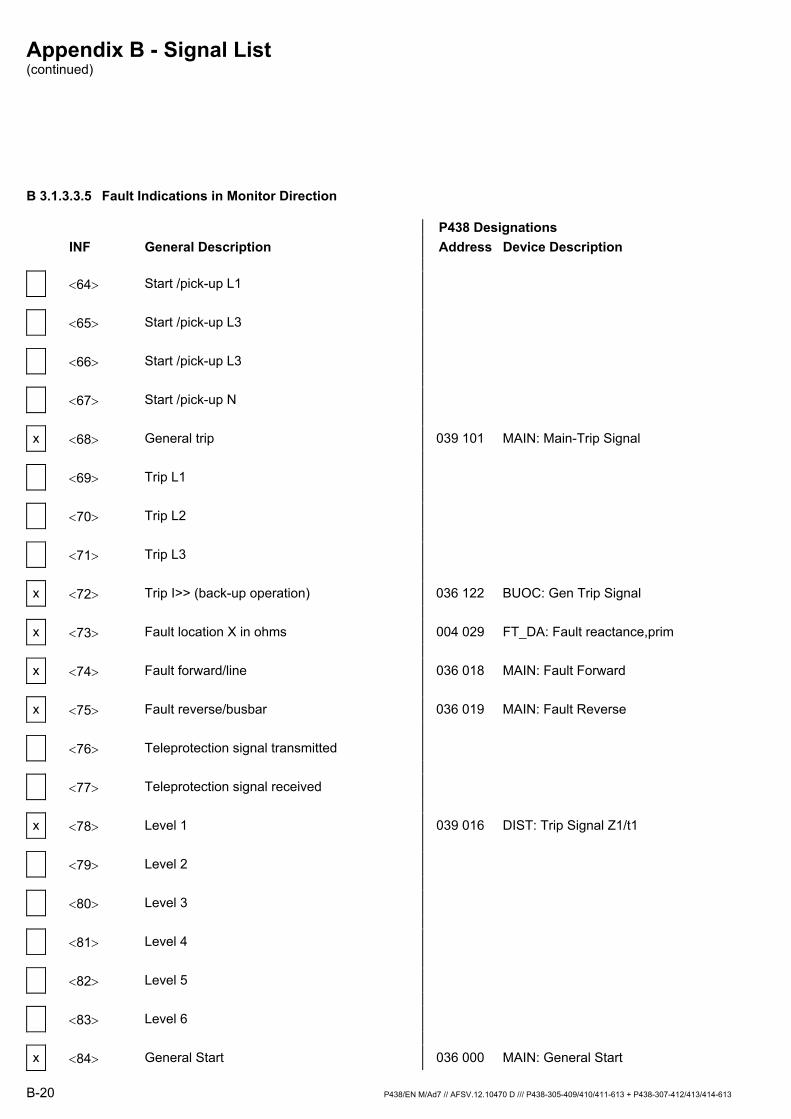
Appendix B - Signal List (continued)
B-20 P438/EN M/Ad7 // AFSV.12.10470 D /// P438-305-409/410/411-613 + P438-307-412/413/414-613
B 3.1.3.3.5 Fault Indications in Monitor Direction
P438 Designations INF General Description Address Device Description
<64> Start /pick-up L1
<65> Start /pick-up L3
<66> Start /pick-up L3
<67> Start /pick-up N
x <68> General trip 039 101 MAIN: Main-Trip Signal
<69> Trip L1
<70> Trip L2
<71> Trip L3
x <72> Trip I>> (back-up operation) 036 122 BUOC: Gen Trip Signal
x <73> Fault location X in ohms 004 029 FT_DA: Fault reactance,prim
x <74> Fault forward/line 036 018 MAIN: Fault Forward
x <75> Fault reverse/busbar 036 019 MAIN: Fault Reverse
<76> Teleprotection signal transmitted
<77> Teleprotection signal received
x <78> Level 1 039 016 DIST: Trip Signal Z1/t1
<79> Level 2
<80> Level 3
<81> Level 4
<82> Level 5
<83> Level 6
x <84> General Start 036 000 MAIN: General Start
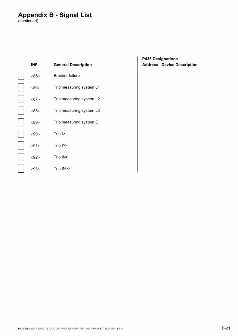
Appendix B - Signal List (continued)
P438/EN M/Ad7 // AFSV.12.10470 D /// P438-305-409/410/411-613 + P438-307-412/413/414-613 B-21
P438 Designations INF General Description Address Device Description
<85> Breaker failure
<86> Trip measuring system L1
<87> Trip measuring system L2
<88> Trip measuring system L3
<89> Trip measuring system E
<90> Trip I>
<91> Trip I>>
<92> Trip IN>
<93> Trip IN>>
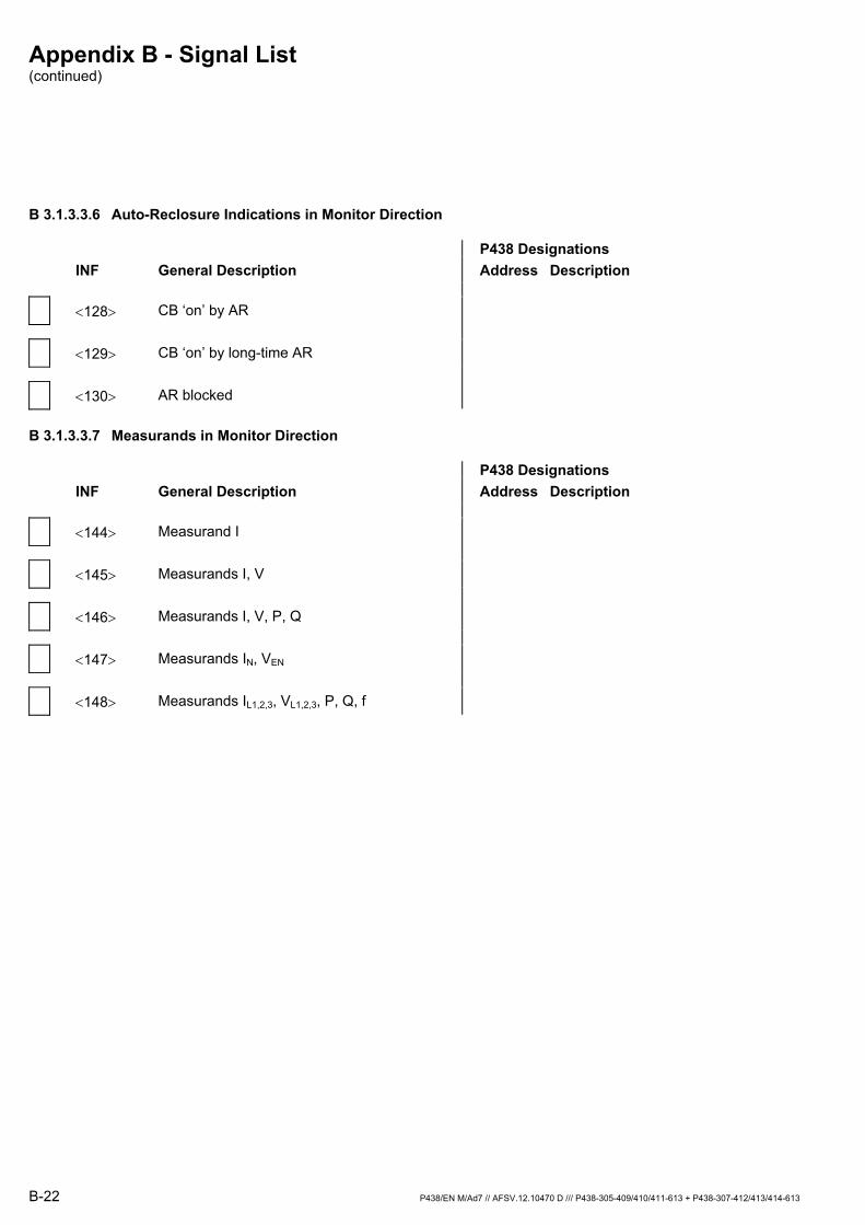
Appendix B - Signal List (continued)
B-22 P438/EN M/Ad7 // AFSV.12.10470 D /// P438-305-409/410/411-613 + P438-307-412/413/414-613
B 3.1.3.3.6 Auto-Reclosure Indications in Monitor Direction
P438 Designations INF General Description Address Description
<128> CB ‘on’ by AR
<129> CB ‘on’ by long-time AR
<130> AR blocked
B 3.1.3.3.7 Measurands in Monitor Direction
P438 Designations INF General Description Address Description
<144> Measurand I
<145> Measurands I, V
<146> Measurands I, V, P, Q
<147> Measurands IN, VEN
<148> Measurands IL1,2,3, VL1,2,3, P, Q, f
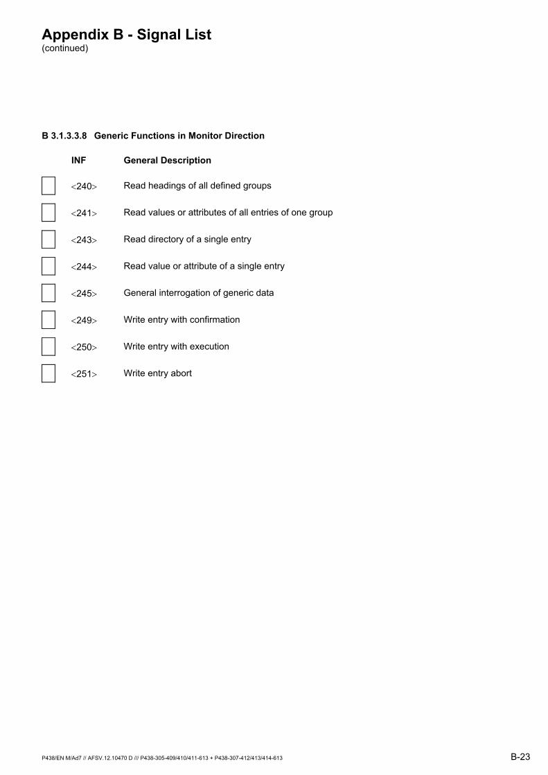
Appendix B - Signal List (continued)
P438/EN M/Ad7 // AFSV.12.10470 D /// P438-305-409/410/411-613 + P438-307-412/413/414-613 B-23
B 3.1.3.3.8 Generic Functions in Monitor Direction
INF General Description
<240> Read headings of all defined groups
<241> Read values or attributes of all entries of one group
<243> Read directory of a single entry
<244> Read value or attribute of a single entry
<245> General interrogation of generic data
<249> Write entry with confirmation
<250> Write entry with execution
<251> Write entry abort
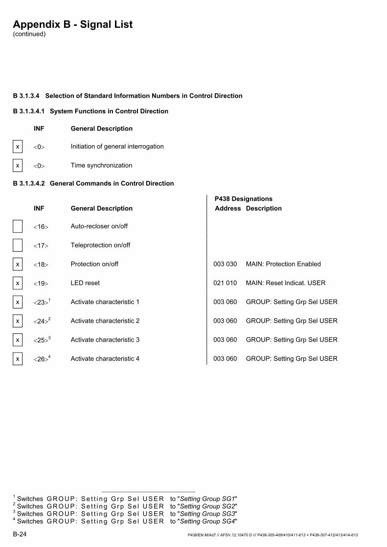
Appendix B - Signal List (continued)
B-24 P438/EN M/Ad7 // AFSV.12.10470 D /// P438-305-409/410/411-613 + P438-307-412/413/414-613
B 3.1.3.4 Selection of Standard Information Numbers in Control Direction
B 3.1.3.4.1 System Functions in Control Direction
INF General Description
x <0> Initiation of general interrogation
x <0> Time synchronization
B 3.1.3.4.2 General Commands in Control Direction
P438 Designations INF General Description Address Description
<16> Auto-recloser on/off
<17> Teleprotection on/off
x <18> Protection on/off 003 030 MAIN: Protection Enabled
x <19> LED reset 021 010 MAIN: Reset Indicat. USER
x <23>1 Activate characteristic 1 003 060 GROUP: Setting Grp Sel USER
x <24>2 Activate characteristic 2 003 060 GROUP: Setting Grp Sel USER
x <25>3 Activate characteristic 3 003 060 GROUP: Setting Grp Sel USER
x <26>4 Activate characteristic 4 003 060 GROUP: Setting Grp Sel USER
1 Switches G R O U P : S e t t i n g G r p S e l U S E R to "Setting Group SG1" 2 Switches G R O U P : S e t t i n g G r p S e l U S E R to "Setting Group SG2" 3 Switches G R O U P : S e t t i n g G r p S e l U S E R to "Setting Group SG3" 4 Switches G R O U P : S e t t i n g G r p S e l U S E R to "Setting Group SG4"

Appendix B - Signal List (continued)
P438/EN M/Ad7 // AFSV.12.10470 D /// P438-305-409/410/411-613 + P438-307-412/413/414-613 B-25
B 3.1.3.4.3 Generic Functions in Control Direction
INF General Description
<240> Read headings of all defined groups
<241> Read values or attributes of all entries of one group
<243> Read directory of a single entry
<244> Read value or attribute of a single entry
<245> General interrogation of generic data
<248> Write entry
<249> Write entry with confirmation
<250> Write entry with execution
<251> Write entry abort
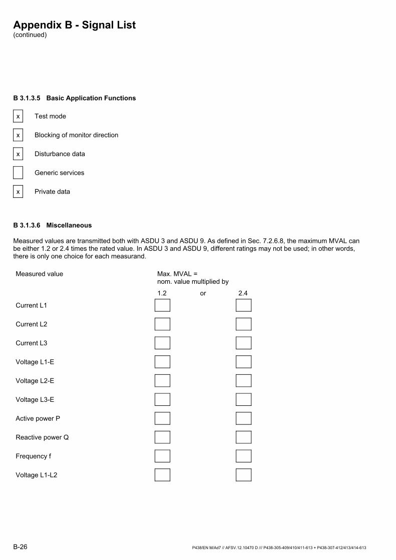
Appendix B - Signal List (continued)
B-26 P438/EN M/Ad7 // AFSV.12.10470 D /// P438-305-409/410/411-613 + P438-307-412/413/414-613
B 3.1.3.5 Basic Application Functions
x Test mode
x Blocking of monitor direction
x Disturbance data
Generic services
x Private data
B 3.1.3.6 Miscellaneous
Measured values are transmitted both with ASDU 3 and ASDU 9. As defined in Sec. 7.2.6.8, the maximum MVAL can be either 1.2 or 2.4 times the rated value. In ASDU 3 and ASDU 9, different ratings may not be used; in other words, there is only one choice for each measurand.
Measured value
Max. MVAL = nom. value multiplied by
1.2 or 2.4
Current L1
Current L2
Current L3
Voltage L1-E
Voltage L2-E
Voltage L3-E
Active power P
Reactive power Q
Frequency f
Voltage L1-L2
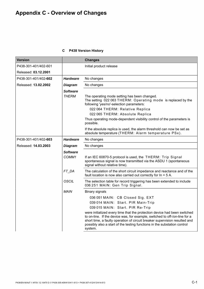
Appendix C - Overview of Changes
P438/EN M/Ad7 // AFSV.12.10470 D /// P438-305-409/410/411-613 + P438-307-412/413/414-613 C-1
C P438 Version History
Version Changes
P438-301-401/402-601 Initial product release
Released: 03.12.2001
P438-301-401/402-602 Hardware No changes
Released: 13.02.2002 Diagram No changes
Software THERM The operating mode setting has been changed.
The setting 022 063 THERM: Operat ing mode is replaced by the following 'yes/no'-selection parameters:
022 064 THERM: Relat ive Repl ica 022 065 THERM: Absolute Repl ica
Thus operating mode-dependent visibility control of the parameters is possible.
If the absolute replica is used, the alarm threshold can now be set as absolute temperature (THERM: Alarm temperature PSx).
P438-301-401/402-603 Hardware No changes
Released: 14.03.2003 Diagram No changes
Software COMM1 If an IEC 60870-5 protocol is used, the THERM: Tr ip Signal
spontaneous signal is now transmitted via the ASDU 1 (spontaneous signal without relative time).
FT_DA The calculation of the short circuit impedance and reactance and of the fault location is now also carried out correctly for In = 5 A.
OSCIL The selection table for record triggering has been extended to include 036 251 MAIN: Gen Tr ip Signal .
MAIN Binary signals
036 051 MAIN: CB Closed Sig. EXT 039 014 MAIN: Star t . PIR Main-Tr ip 039 015 MAIN: Star t . PIR Re-Tr ip
were initialized every time that the protection device had been switched to on-line. If the device was, for example, switched to off-/on-line for a short time, a faulty operation of circuit breaker supervision resulted and possibly also a start of the testing functions in the substation control system.
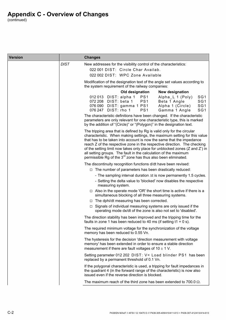
Appendix C - Overview of Changes (continued)
C-2 P438/EN M/Ad7 // AFSV.12.10470 D /// P438-305-409/410/411-613 + P438-307-412/413/414-613
Version Changes
DIST New addresses for the visibility control of the characteristics: 022 001 DIST: Circ le Char Avai lab. 022 002 DIST: WPC Zone Avai lable
Modification of the designation text of the angle set values according to the system requirement of the railway companies:
Old designation New designation012 013 DIST: a lpha 1 PS1 Alpha_L 1 (Poly) SG1 072 208 DIST: beta 1 PS1 Beta 1 Angle SG1 076 090 DIST: gamma 1 PS1 Alpha 1 (Circ le) SG1 076 247 DIST: rho 1 PS1 Gamma 1 Angle SG1
The characteristic definitions have been changed. If the characteristic parameters are only relevant for one characteristic type, this is marked by the addition of “(Circle)” or “(Polygon)” in the designation text.
The tripping area that is defined by Rg is valid only for the circular characteristic. When making settings, the maximum setting for this value that has to be taken into account is now the same that the impedance reach Z of the respective zone in the respective direction. The checking of the setting limit now takes only place for unblocked zones (Z and Z’) in all setting groups. The fault in the calculation of the maximum permissible Rg of the 3rd zone has thus also been eliminated.
The discontinuity recognition functions d/dt have been revised: The number of parameters has been drastically reduced:
- The sampling interval duration ∆t is now permanently 1.5 cycles. - Setting the delta value to 'blocked' now disables the respective
measuring system. Also in the operate mode 'OR' the short time is active if there is a
simultaneous blocking of all three measuring systems. The dphi/dt measuring has been corrected. Signals of individual measuring systems are only issued if the
operating mode dx/dt of the zone is also not set to 'disabled'.
The direction stability has been improved and the tripping time for the faults in zone 1 has been reduced to 40 ms (if setting t1 = 0 s).
The required minimum voltage for the synchronization of the voltage memory has been reduced to 0.55 Vn.
The hysteresis for the decision 'direction measurement with voltage memory' has been extended in order to ensure a stable direction measurement if there are fault voltages of 10 ± 1 V.
Setting parameter 012 202 DIST: V< Load bl inder PS1 has been replaced by a permanent threshold of 0.1 Vn.
If the polygonal characteristic is used, a tripping for fault impedances in the quadrant 4 (in the forward range of the characteristic) is now also issued even if the reverse direction is blocked.
The maximum reach of the third zone has been extended to 700.0 Ω.
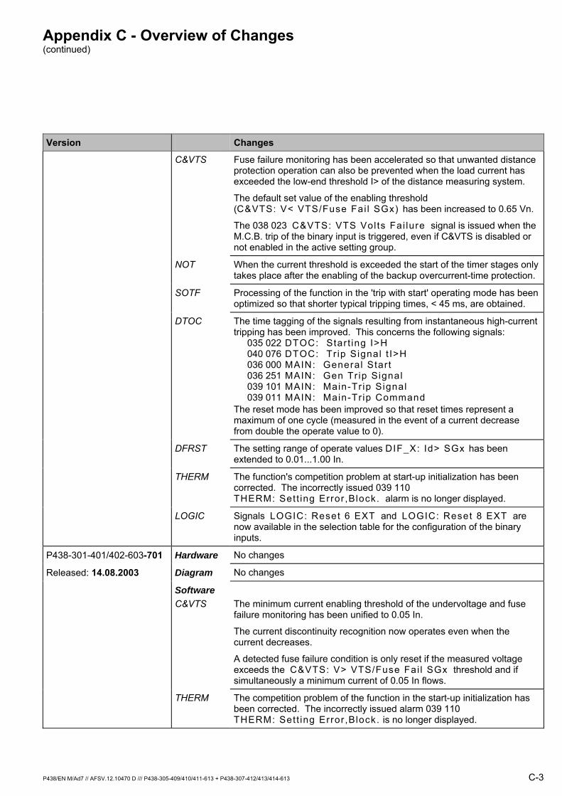
Appendix C - Overview of Changes (continued)
P438/EN M/Ad7 // AFSV.12.10470 D /// P438-305-409/410/411-613 + P438-307-412/413/414-613 C-3
Version Changes
C&VTS Fuse failure monitoring has been accelerated so that unwanted distance protection operation can also be prevented when the load current has exceeded the low-end threshold I> of the distance measuring system.
The default set value of the enabling threshold (C&VTS: V< VTS/Fuse Fai l SGx) has been increased to 0.65 Vn.
The 038 023 C&VTS: VTS Vol ts Fai lure signal is issued when the M.C.B. trip of the binary input is triggered, even if C&VTS is disabled or not enabled in the active setting group.
NOT When the current threshold is exceeded the start of the timer stages only takes place after the enabling of the backup overcurrent-time protection.
SOTF Processing of the function in the 'trip with start' operating mode has been optimized so that shorter typical tripping times, < 45 ms, are obtained.
DTOC The time tagging of the signals resulting from instantaneous high-current tripping has been improved. This concerns the following signals:
035 022 DTOC: Star t ing I>H 040 076 DTOC: Tr ip Signal t I>H 036 000 MAIN: General Start 036 251 MAIN: Gen Tr ip Signal 039 101 MAIN: Main-Tr ip Signal 039 011 MAIN: Main-Tr ip Command
The reset mode has been improved so that reset times represent a maximum of one cycle (measured in the event of a current decrease from double the operate value to 0).
DFRST The setting range of operate values DIF_X: Id> SGx has been extended to 0.01...1.00 In.
THERM The function's competition problem at start-up initialization has been corrected. The incorrectly issued 039 110 THERM: Sett ing Error ,Block. alarm is no longer displayed.
LOGIC Signals LOGIC: Reset 6 EXT and LOGIC: Reset 8 EXT are now available in the selection table for the configuration of the binary inputs.
P438-301-401/402-603-701 Hardware No changes
Released: 14.08.2003 Diagram No changes
Software C&VTS The minimum current enabling threshold of the undervoltage and fuse
failure monitoring has been unified to 0.05 In.
The current discontinuity recognition now operates even when the current decreases.
A detected fuse failure condition is only reset if the measured voltage exceeds the C&VTS: V> VTS/Fuse Fai l SGx threshold and if simultaneously a minimum current of 0.05 In flows.
THERM The competition problem of the function in the start-up initialization has been corrected. The incorrectly issued alarm 039 110 THERM: Sett ing Error ,Block. is no longer displayed.

Appendix C - Overview of Changes (continued)
C-4 P438/EN M/Ad7 // AFSV.12.10470 D /// P438-305-409/410/411-613 + P438-307-412/413/414-613
Version Changes
P438-301-401/402-603-702 Hardware No changes
Released: 18.09.2003 Diagram No changes
Software C&VTS Bug fixing:
Fuse failure monitoring was enabled too early during device initialization, which caused unwanted starting.
THERM The dead time for very fast alterations of the coolant temperature has been extended to 1.5 s in order to correct competition problems with measuring-circuit monitoring of the analog module (for example the 040 190 RTDmA: PT100 Faul ty signal was not always issued in time in order to exclude an unwanted operation).
P438-301-401/402-603-703 Hardware No changes
Released: 04.11.2003 Diagram No changes
Software CHECK Bug fixing:
When using the analog module, the 093 112 CHECK: Time-out Module Y time-out fault occurred after approx. 24.8 days.
P438-301-401/402-604 Hardware No changes
Released: 03.12.2003 Diagram No changes
Software OP_RC The list of the following entries has been modified as follows.
Those added: 038 073 THERM: 2 PL Select . Extern. 040 145 LIMIT: tV>> & tV<< Elapsed 040 197 LIMIT: t f>> Elapsed 004 062 LIMIT: t I>> Elapsed
Those removed: 039 076 MAIN: Power Flow Forward 039 077 MAIN: Power Flow Reverse 041 085 DIST: Wrong Sett ing Rg,x 040 170 LIMIT: Star t ing T> 040 171 LIMIT: Star t ing T>> 040 174 LIMIT: Star t ing T< 040 175 LIMIT: Star t ing T<< 040 180 LIMIT: Star t ing IDC,l in> 040 181 LIMIT: Star t ing IDC,l in>> 040 184 LIMIT: Star t ing IDC,l in< 040 185 LIMIT: Star t ing IDC,l in<<
Thus the LIMIT stages do not enter starting signals, but only the signal “timer stage elapsed”.
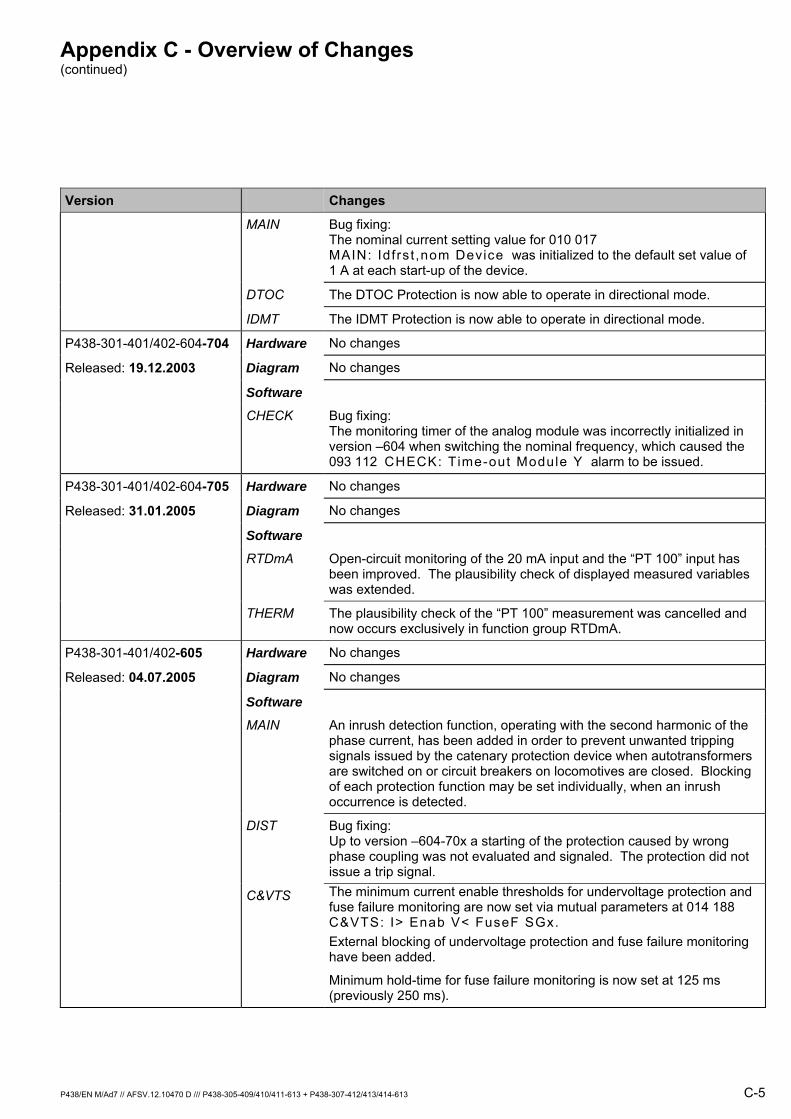
Appendix C - Overview of Changes (continued)
P438/EN M/Ad7 // AFSV.12.10470 D /// P438-305-409/410/411-613 + P438-307-412/413/414-613 C-5
Version Changes
MAIN Bug fixing: The nominal current setting value for 010 017 MAIN: Idfrst ,nom Device was initialized to the default set value of 1 A at each start-up of the device.
DTOC The DTOC Protection is now able to operate in directional mode.
IDMT The IDMT Protection is now able to operate in directional mode.
P438-301-401/402-604-704 Hardware No changes
Released: 19.12.2003 Diagram No changes
Software
CHECK Bug fixing: The monitoring timer of the analog module was incorrectly initialized in version –604 when switching the nominal frequency, which caused the 093 112 CHECK: Time-out Module Y alarm to be issued.
P438-301-401/402-604-705 Hardware No changes
Released: 31.01.2005 Diagram No changes
Software
RTDmA Open-circuit monitoring of the 20 mA input and the “PT 100” input has been improved. The plausibility check of displayed measured variables was extended.
THERM The plausibility check of the “PT 100” measurement was cancelled and now occurs exclusively in function group RTDmA.
P438-301-401/402-605 Hardware No changes
Released: 04.07.2005 Diagram No changes
Software
MAIN An inrush detection function, operating with the second harmonic of the phase current, has been added in order to prevent unwanted tripping signals issued by the catenary protection device when autotransformers are switched on or circuit breakers on locomotives are closed. Blocking of each protection function may be set individually, when an inrush occurrence is detected.
DIST Bug fixing: Up to version –604-70x a starting of the protection caused by wrong phase coupling was not evaluated and signaled. The protection did not issue a trip signal.
C&VTS The minimum current enable thresholds for undervoltage protection and fuse failure monitoring are now set via mutual parameters at 014 188 C&VTS: I> Enab V< FuseF SGx. External blocking of undervoltage protection and fuse failure monitoring have been added.
Minimum hold-time for fuse failure monitoring is now set at 125 ms (previously 250 ms).
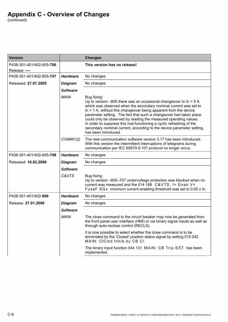
Appendix C - Overview of Changes (continued)
C-6 P438/EN M/Ad7 // AFSV.12.10470 D /// P438-305-409/410/411-613 + P438-307-412/413/414-613
Version Changes
P438-301-401/402-605-706 Release: ----
This version has no release!
P438-301-401/402-605-707 Hardware No changes
Released: 27.07.2005 Diagram No changes
Software
MAIN Bug fixing: Up to version –605 there was an occasional changeover to In = 5 A which was observed when the secondary nominal current was set to In = 1 A, without this changeover being apparent from the device parameter setting. The fact that such a changeover had taken place could only be observed by reading the measured operating values. In order to suppress this mal-functioning a cyclic refreshing of the secondary nominal current, according to the device parameter setting, has been introduced.
COMM1(2) The new communication software version 3.17 has been introduced. With this version the intermittent interruptions of telegrams during communication per IEC 60870-5-101 protocol no longer occur.
P438-301-401/402-605-708 Hardware No changes
Released: 10.02.2006 Diagram No changes
Software
C&VTS Bug fixing: Up to version –605–707 undervoltage protection was blocked when no current was measured and the 014 188 C&VTS: I> Enab V< FuseF SGx minimum current enabling threshold was set to 0.00 x In.
P438-301-401/402-606 Hardware No changes
Release: 27.01.2006 Diagram No changes
Software
MAIN The close command to the circuit breaker may now be generated from the front panel user interface (HMI) or via binary signal inputs as well as through auto-reclose control (RECLS).
It is now possible to select whether the close command is to be terminated by the 'Closed' position status signal by setting 015 042 MAIN: ClCmd Inhib.by CB Cl.
The binary input function 044 131 MAIN: CB Tr ip EXT has been implemented.
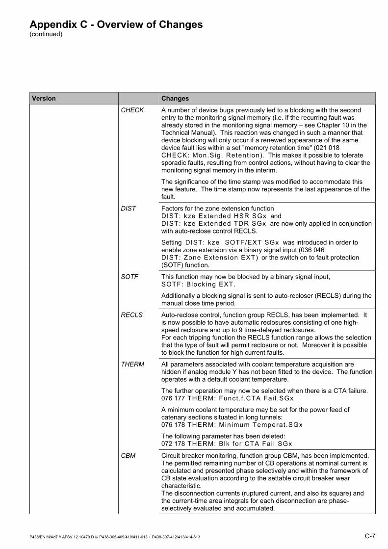
Appendix C - Overview of Changes (continued)
P438/EN M/Ad7 // AFSV.12.10470 D /// P438-305-409/410/411-613 + P438-307-412/413/414-613 C-7
Version Changes
CHECK A number of device bugs previously led to a blocking with the second entry to the monitoring signal memory (i.e. if the recurring fault was already stored in the monitoring signal memory – see Chapter 10 in the Technical Manual). This reaction was changed in such a manner that device blocking will only occur if a renewed appearance of the same device fault lies within a set "memory retention time" (021 018 CHECK: Mon.Sig. Retent ion). This makes it possible to tolerate sporadic faults, resulting from control actions, without having to clear the monitoring signal memory in the interim.
The significance of the time stamp was modified to accommodate this new feature. The time stamp now represents the last appearance of the fault.
DIST Factors for the zone extension function DIST: kze Extended HSR SGx and DIST: kze Extended TDR SGx are now only applied in conjunction with auto-reclose control RECLS.
Setting DIST: kze SOTF/EXT SGx was introduced in order to enable zone extension via a binary signal input (036 046 DIST: Zone Extension EXT) or the switch on to fault protection (SOTF) function.
SOTF This function may now be blocked by a binary signal input, SOTF: Blocking EXT.
Additionally a blocking signal is sent to auto-recloser (RECLS) during the manual close time period.
RECLS Auto-reclose control, function group RECLS, has been implemented. It is now possible to have automatic reclosures consisting of one high-speed reclosure and up to 9 time-delayed reclosures. For each tripping function the RECLS function range allows the selection that the type of fault will permit reclosure or not. Moreover it is possible to block the function for high current faults.
THERM All parameters associated with coolant temperature acquisition are hidden if analog module Y has not been fitted to the device. The function operates with a default coolant temperature.
The further operation may now be selected when there is a CTA failure. 076 177 THERM: Funct. f .CTA Fai l .SGx
A minimum coolant temperature may be set for the power feed of catenary sections situated in long tunnels: 076 178 THERM: Minimum Temperat.SGx
The following parameter has been deleted: 072 178 THERM: Blk for CTA Fai l SGx
CBM Circuit breaker monitoring, function group CBM, has been implemented. The permitted remaining number of CB operations at nominal current is calculated and presented phase selectively and within the framework of CB state evaluation according to the settable circuit breaker wear characteristic. The disconnection currents (ruptured current, and also its square) and the current-time area integrals for each disconnection are phase-selectively evaluated and accumulated.

Appendix C - Overview of Changes (continued)
C-8 P438/EN M/Ad7 // AFSV.12.10470 D /// P438-305-409/410/411-613 + P438-307-412/413/414-613
Version Changes
mA_OP The listing of possible entries for the analog measured data output with either BCD or 20 mA (outputs A-1 & A-2) has been extended. The following measured values may now be additionally output:
005 004 MAIN: Load Impedance Z p.u 005 005 MAIN: Load Imped Z Pr im. 005 000 MAIN: Load Impedance Z Sec 005 196 MAIN: Load React X Pr im. 005 195 MAIN: Load Reactance X Sec 005 198 MAIN: Load Resist . R Pr im. 005 197 MAIN: Load Resist . R Sec 004 053 MAIN: Reac. Power Q p.u. 004 052 MAIN: Reac. Power Q pr im. 004 070 MAIN: Frequency f p.u. 004 166 MAIN: Load Flow Direct ion 004 167 MAIN: Load Angle phi 004 078 MAIN: Load Angle phi p.u. 004 113 MAIN: Vol tage V p.u. 004 112 MAIN: Vol tage V Pr im. 004 111 MAIN: Current I p.u. 004 110 MAIN: Current I Pr im. 004 051 MAIN: Act ive Power P p.u. 005 040 MAIN: Act ive Power P Pr im. 004 054 MAIN: Act ive Power Factor 009 087 CBM: Σ I * t Cat 009 061 CBM: I* t Cat 009 088 CBM: Σ I * t Fdr 009 062 CBM: I* t Fdr 009 071 CBM: Σ I t r ip Cat 009 047 CBM: I t r ip Cat 009 073 CBM: Σ I t r ip Fdr 009 048 CBM: I t r ip Cat 009 077 CBM: Σ I t r ip**2 Cat 009 051 CBM: I t r ip**2 Cat 009 078 CBM: Σ I t r ip**2 Fdr 009 052 CBM: I t r ip**2 Cat 009 212 CBM: I t r ip,Pr im Cat 009 213 CBM: I t r ip,Pr im Fdr 004 221 RTDmA: Temperature p.u. 004 022 FT_DA: Faul t Locat ion 004 027 FT_DA: Faul t Locat. Percent 004 177 FT_DA: Idfrst p.u. 004 176 FT_DA: Faul t Impedance,Pr im 004 023 FT_DA: Faul t Impedance,Sec. 004 029 FT_DA: Faul t Reactance,Pr im 004 028 FT_DA: Faul t Reactance,Sec. 004 026 FT_DA: Faul t Vol tage p.u. 004 025 FT_DA: Faul t Current p.u. 004 023 FT_DA: Faul t Loop Angle 004 198 FT_DA: Faul t Determinat ion 004 178 THERM: Coolant Temp. p.u. 004 179 THERM: Object Temp. p.u. 004 017 THERM: Therm. Repl ica p.u.
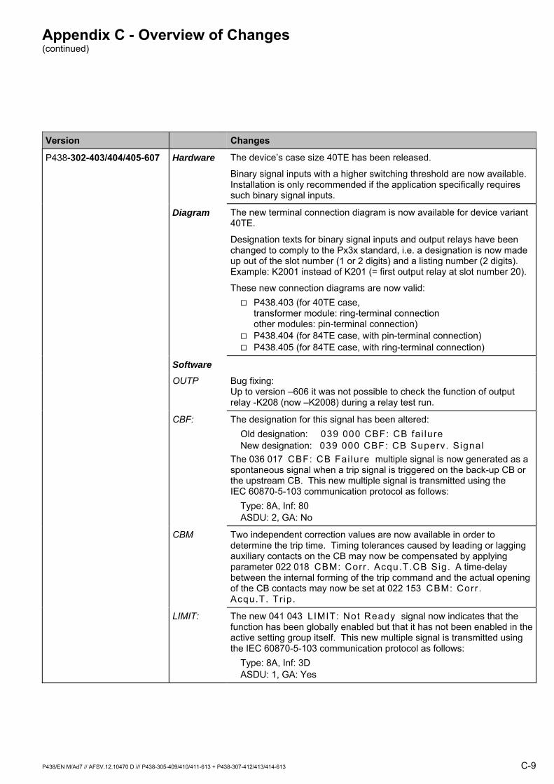
Appendix C - Overview of Changes (continued)
P438/EN M/Ad7 // AFSV.12.10470 D /// P438-305-409/410/411-613 + P438-307-412/413/414-613 C-9
Version Changes
P438-302-403/404/405-607 Hardware The device’s case size 40TE has been released.
Binary signal inputs with a higher switching threshold are now available. Installation is only recommended if the application specifically requires such binary signal inputs.
Diagram The new terminal connection diagram is now available for device variant 40TE.
Designation texts for binary signal inputs and output relays have been changed to comply to the Px3x standard, i.e. a designation is now made up out of the slot number (1 or 2 digits) and a listing number (2 digits). Example: K2001 instead of K201 (= first output relay at slot number 20).
These new connection diagrams are now valid: P438.403 (for 40TE case,
transformer module: ring-terminal connection other modules: pin-terminal connection)
P438.404 (for 84TE case, with pin-terminal connection) P438.405 (for 84TE case, with ring-terminal connection)
Software
OUTP Bug fixing: Up to version –606 it was not possible to check the function of output relay -K208 (now –K2008) during a relay test run.
CBF: The designation for this signal has been altered: Old designation: 039 000 CBF: CB fai lure New designation: 039 000 CBF: CB Superv. Signal
The 036 017 CBF: CB Fai lure multiple signal is now generated as a spontaneous signal when a trip signal is triggered on the back-up CB or the upstream CB. This new multiple signal is transmitted using the IEC 60870-5-103 communication protocol as follows:
Type: 8A, Inf: 80 ASDU: 2, GA: No
CBM Two independent correction values are now available in order to determine the trip time. Timing tolerances caused by leading or lagging auxiliary contacts on the CB may now be compensated by applying parameter 022 018 CBM: Corr . Acqu.T.CB Sig. A time-delay between the internal forming of the trip command and the actual opening of the CB contacts may now be set at 022 153 CBM: Corr . Acqu.T. Tr ip.
LIMIT: The new 041 043 LIMIT: Not Ready signal now indicates that the function has been globally enabled but that it has not been enabled in the active setting group itself. This new multiple signal is transmitted using the IEC 60870-5-103 communication protocol as follows:
Type: 8A, Inf: 3D ASDU: 1, GA: Yes
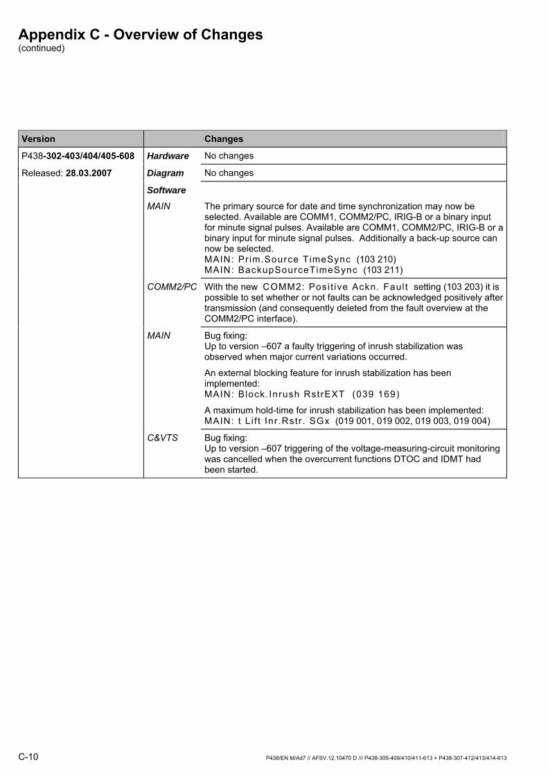
Appendix C - Overview of Changes (continued)
C-10 P438/EN M/Ad7 // AFSV.12.10470 D /// P438-305-409/410/411-613 + P438-307-412/413/414-613
Version Changes
P438-302-403/404/405-608 Hardware No changes
Released: 28.03.2007 Diagram No changes
Software
MAIN The primary source for date and time synchronization may now be selected. Available are COMM1, COMM2/PC, IRIG-B or a binary input for minute signal pulses. Available are COMM1, COMM2/PC, IRIG-B or a binary input for minute signal pulses. Additionally a back-up source can now be selected. MAIN: Pr im.Source TimeSync (103 210) MAIN: BackupSourceTimeSync (103 211)
COMM2/PC With the new COMM2: Posi t ive Ackn. Faul t setting (103 203) it is possible to set whether or not faults can be acknowledged positively after transmission (and consequently deleted from the fault overview at the COMM2/PC interface).
MAIN Bug fixing: Up to version –607 a faulty triggering of inrush stabilization was observed when major current variations occurred.
An external blocking feature for inrush stabilization has been implemented: MAIN: Block. Inrush RstrEXT (039 169)
A maximum hold-time for inrush stabilization has been implemented: MAIN: t L i f t Inr .Rstr . SGx (019 001, 019 002, 019 003, 019 004)
C&VTS Bug fixing: Up to version –607 triggering of the voltage-measuring-circuit monitoring was cancelled when the overcurrent functions DTOC and IDMT had been started.
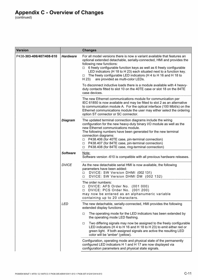
Appendix C - Overview of Changes (continued)
P438/EN M/Ad7 // AFSV.12.10470 D /// P438-305-409/410/411-613 + P438-307-412/413/414-613 C-11
Version Changes
P438-303-406/407/408-610 Hardware For all model versions there is now a variant available that features an optional extended detachable, serially-connected, HMI and provides the following new functions:
6 freely configurable function keys as well as 6 freely configurable LED indicators (H 18 to H 23) each situated next to a function key.
The freely configurable LED indicators (H 4 to H 16 and H 18 to H 23) are provided as multi-color LEDs.
To disconnect inductive loads there is a module available with 4 heavy-duty contacts fitted to slot 10 on the 40TE case or slot 18 on the 84TE case devices.
The new Ethernet communications module for communication per IEC 61850 is now available and may be fitted to slot 2 as an alternative to communication module A. For the optical interface (100 Mbit/s) on the Ethernet communications module the user may either select the ordering option ST connector or SC connector.
Diagram The updated terminal connection diagrams include the wiring configuration for the new heavy-duty binary I/O module as well as the new Ethernet communications module. The following numbers have been generated for the new terminal connection diagrams:
P438.406 (for 40TE case, pin-terminal connection) P438.407 (for 84TE case, pin-terminal connection) P438.408 (for 84TE case, ring-terminal connection)
Software Note: Software version -610 is compatible with all previous hardware releases.
DVICE As the new detachable serial HMI is now available, the following parameters have been added:
DVICE: SW Vers ion DHMI (002 131) DVICE: SW Version DHMI DM (002 132)
The order numbers: DVICE: AFS Order No. (001 000) DVICE: PCS Order No. (001 200)
may now be entered as an alphanumeric var iable contain ing up to 20 characters.
LED The new detachable, serially-connected, HMI provides the following extended display functions:
The operating mode for the LED indicators has been extended by the operating mode LED flashing.
Two differing signals may now be assigned to the freely configurable LED indicators (H 4 to H 16 and H 18 to H 23) to emit either red or green light. If both assigned signals are active the resulting LED color will be 'amber' (yellow).
Configuration, operating mode and physical state of the permanently configured LED indicators H 1 and H 17 are now displayed via configuration parameters and physical state signals.
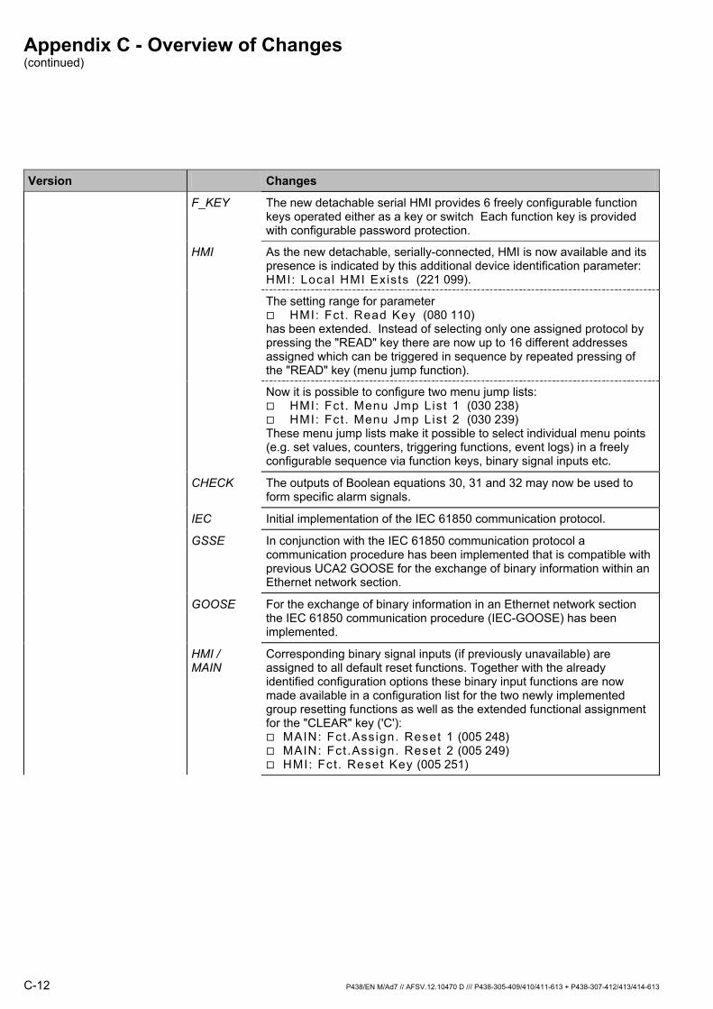
Appendix C - Overview of Changes (continued)
C-12 P438/EN M/Ad7 // AFSV.12.10470 D /// P438-305-409/410/411-613 + P438-307-412/413/414-613
Version Changes
F_KEY The new detachable serial HMI provides 6 freely configurable function keys operated either as a key or switch Each function key is provided with configurable password protection.
HMI As the new detachable, serially-connected, HMI is now available and its presence is indicated by this additional device identification parameter: HMI: Local HMI Exists (221 099).
The setting range for parameter HMI: Fct . Read Key (080 110)
has been extended. Instead of selecting only one assigned protocol by pressing the "READ" key there are now up to 16 different addresses assigned which can be triggered in sequence by repeated pressing of the "READ" key (menu jump function).
Now it is possible to configure two menu jump lists: HMI: Fct . Menu Jmp List 1 (030 238) HMI: Fct . Menu Jmp List 2 (030 239)
These menu jump lists make it possible to select individual menu points (e.g. set values, counters, triggering functions, event logs) in a freely configurable sequence via function keys, binary signal inputs etc.
CHECK The outputs of Boolean equations 30, 31 and 32 may now be used to form specific alarm signals.
IEC Initial implementation of the IEC 61850 communication protocol.
GSSE In conjunction with the IEC 61850 communication protocol a communication procedure has been implemented that is compatible with previous UCA2 GOOSE for the exchange of binary information within an Ethernet network section.
GOOSE For the exchange of binary information in an Ethernet network section the IEC 61850 communication procedure (IEC-GOOSE) has been implemented.
HMI / MAIN
Corresponding binary signal inputs (if previously unavailable) are assigned to all default reset functions. Together with the already identified configuration options these binary input functions are now made available in a configuration list for the two newly implemented group resetting functions as well as the extended functional assignment for the "CLEAR" key ('C'):
MAIN: Fct .Assign. Reset 1 (005 248) MAIN: Fct .Assign. Reset 2 (005 249) HMI: Fct . Reset Key (005 251)
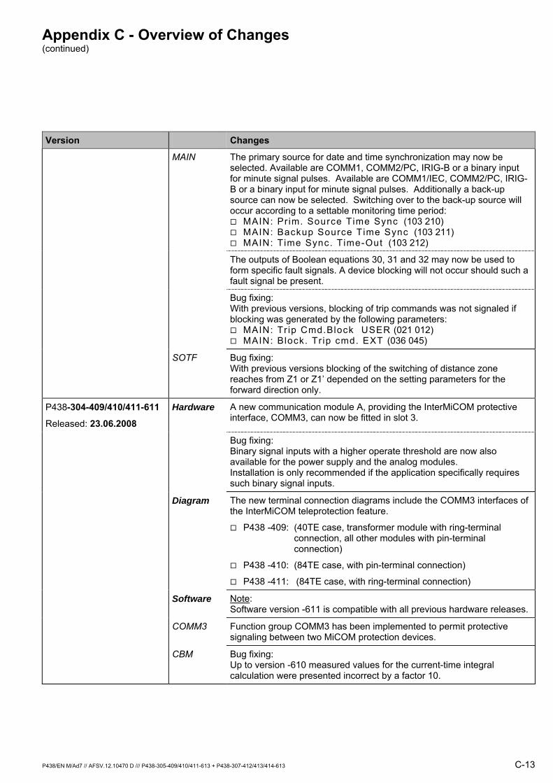
Appendix C - Overview of Changes (continued)
P438/EN M/Ad7 // AFSV.12.10470 D /// P438-305-409/410/411-613 + P438-307-412/413/414-613 C-13
Version Changes
MAIN The primary source for date and time synchronization may now be selected. Available are COMM1, COMM2/PC, IRIG-B or a binary input for minute signal pulses. Available are COMM1/IEC, COMM2/PC, IRIG-B or a binary input for minute signal pulses. Additionally a back-up source can now be selected. Switching over to the back-up source will occur according to a settable monitoring time period:
MAIN: Pr im. Source Time Sync (103 210) MAIN: Backup Source Time Sync (103 211) MAIN: Time Sync. Time-Out (103 212)
The outputs of Boolean equations 30, 31 and 32 may now be used to form specific fault signals. A device blocking will not occur should such a fault signal be present.
Bug fixing: With previous versions, blocking of trip commands was not signaled if blocking was generated by the following parameters:
MAIN: Tr ip Cmd.Block USER (021 012) MAIN: Block. Tr ip cmd. EXT (036 045)
SOTF Bug fixing: With previous versions blocking of the switching of distance zone reaches from Z1 or Z1’ depended on the setting parameters for the forward direction only.
P438-304-409/410/411-611
Released: 23.06.2008
Hardware A new communication module A, providing the InterMiCOM protective interface, COMM3, can now be fitted in slot 3.
Bug fixing: Binary signal inputs with a higher operate threshold are now also available for the power supply and the analog modules. Installation is only recommended if the application specifically requires such binary signal inputs.
Diagram The new terminal connection diagrams include the COMM3 interfaces of the InterMiCOM teleprotection feature.
P438 -409: (40TE case, transformer module with ring-terminal connection, all other modules with pin-terminal connection)
P438 -410: (84TE case, with pin-terminal connection)
P438 -411: (84TE case, with ring-terminal connection)
Software Note: Software version -611 is compatible with all previous hardware releases.
COMM3 Function group COMM3 has been implemented to permit protective signaling between two MiCOM protection devices.
CBM Bug fixing: Up to version -610 measured values for the current-time integral calculation were presented incorrect by a factor 10.
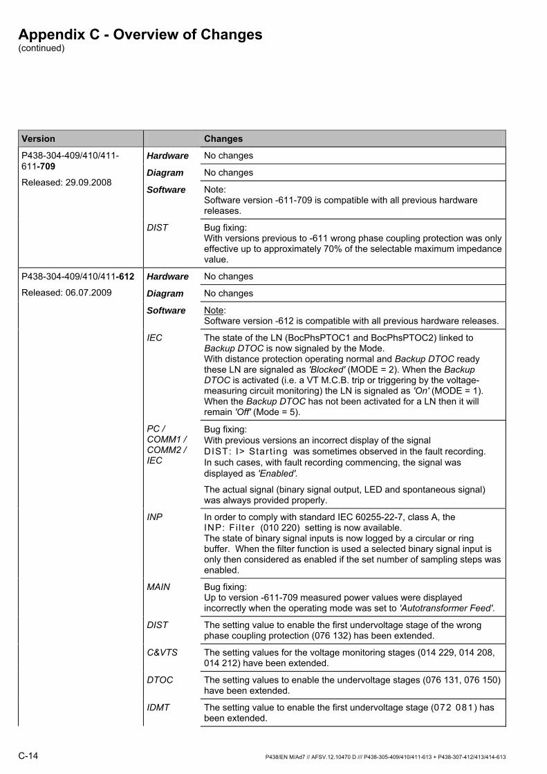
Appendix C - Overview of Changes (continued)
C-14 P438/EN M/Ad7 // AFSV.12.10470 D /// P438-305-409/410/411-613 + P438-307-412/413/414-613
Version Changes
Hardware No changes
Diagram No changes
P438-304-409/410/411- 611-709
Released: 29.09.2008 Software Note:
Software version -611-709 is compatible with all previous hardware releases.
DIST Bug fixing: With versions previous to -611 wrong phase coupling protection was only effective up to approximately 70% of the selectable maximum impedance value.
Hardware No changes P438-304-409/410/411-612
Released: 06.07.2009 Diagram No changes
Software Note: Software version -612 is compatible with all previous hardware releases.
IEC The state of the LN (BocPhsPTOC1 and BocPhsPTOC2) linked to Backup DTOC is now signaled by the Mode. With distance protection operating normal and Backup DTOC ready these LN are signaled as 'Blocked' (MODE = 2). When the Backup DTOC is activated (i.e. a VT M.C.B. trip or triggering by the voltage-measuring circuit monitoring) the LN is signaled as 'On' (MODE = 1). When the Backup DTOC has not been activated for a LN then it will remain 'Off' (Mode = 5).
PC / COMM1 / COMM2 / IEC
Bug fixing: With previous versions an incorrect display of the signal DIST: I> Star t ing was sometimes observed in the fault recording. In such cases, with fault recording commencing, the signal was displayed as 'Enabled'.
The actual signal (binary signal output, LED and spontaneous signal) was always provided properly.
INP In order to comply with standard IEC 60255-22-7, class A, the INP: Fi l ter (010 220) setting is now available. The state of binary signal inputs is now logged by a circular or ring buffer. When the filter function is used a selected binary signal input is only then considered as enabled if the set number of sampling steps was enabled.
MAIN Bug fixing: Up to version -611-709 measured power values were displayed incorrectly when the operating mode was set to 'Autotransformer Feed'.
DIST The setting value to enable the first undervoltage stage of the wrong phase coupling protection (076 132) has been extended.
C&VTS The setting values for the voltage monitoring stages (014 229, 014 208, 014 212) have been extended.
DTOC The setting values to enable the undervoltage stages (076 131, 076 150) have been extended.
IDMT The setting value to enable the first undervoltage stage (072 081) has been extended.
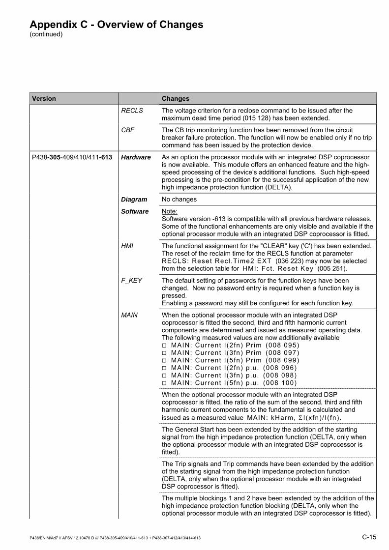
Appendix C - Overview of Changes (continued)
P438/EN M/Ad7 // AFSV.12.10470 D /// P438-305-409/410/411-613 + P438-307-412/413/414-613 C-15
Version Changes
RECLS The voltage criterion for a reclose command to be issued after the maximum dead time period (015 128) has been extended.
CBF The CB trip monitoring function has been removed from the circuit breaker failure protection. The function will now be enabled only if no trip command has been issued by the protection device.
Hardware As an option the processor module with an integrated DSP coprocessor is now available. This module offers an enhanced feature and the high-speed processing of the device’s additional functions. Such high-speed processing is the pre-condition for the successful application of the new high impedance protection function (DELTA).
P438-305-409/410/411-613
Diagram No changes
Software Note: Software version -613 is compatible with all previous hardware releases. Some of the functional enhancements are only visible and available if the optional processor module with an integrated DSP coprocessor is fitted.
HMI The functional assignment for the "CLEAR" key ('C') has been extended. The reset of the reclaim time for the RECLS function at parameter RECLS: Reset Recl .Time2 EXT (036 223) may now be selected from the selection table for HMI: Fct . Reset Key (005 251).
F_KEY The default setting of passwords for the function keys have been changed. Now no password entry is required when a function key is pressed. Enabling a password may still be configured for each function key.
MAIN When the optional processor module with an integrated DSP coprocessor is fitted the second, third and fifth harmonic current components are determined and issued as measured operating data. The following measured values are now additionally available
MAIN: Current I (2fn) Pr im (008 095) MAIN: Current I (3fn) Pr im (008 097) MAIN: Current I (5fn) Pr im (008 099) MAIN: Current I (2fn) p.u. (008 096) MAIN: Current I (3fn) p.u. (008 098) MAIN: Current I (5fn) p.u. (008 100)
When the optional processor module with an integrated DSP coprocessor is fitted, the ratio of the sum of the second, third and fifth harmonic current components to the fundamental is calculated and issued as a measured value MAIN: kHarm, Σ I (xfn) / I ( fn) .
The General Start has been extended by the addition of the starting signal from the high impedance protection function (DELTA, only when the optional processor module with an integrated DSP coprocessor is fitted).
The Trip signals and Trip commands have been extended by the addition of the starting signal from the high impedance protection function (DELTA, only when the optional processor module with an integrated DSP coprocessor is fitted).
The multiple blockings 1 and 2 have been extended by the addition of the high impedance protection function blocking (DELTA, only when the optional processor module with an integrated DSP coprocessor is fitted).
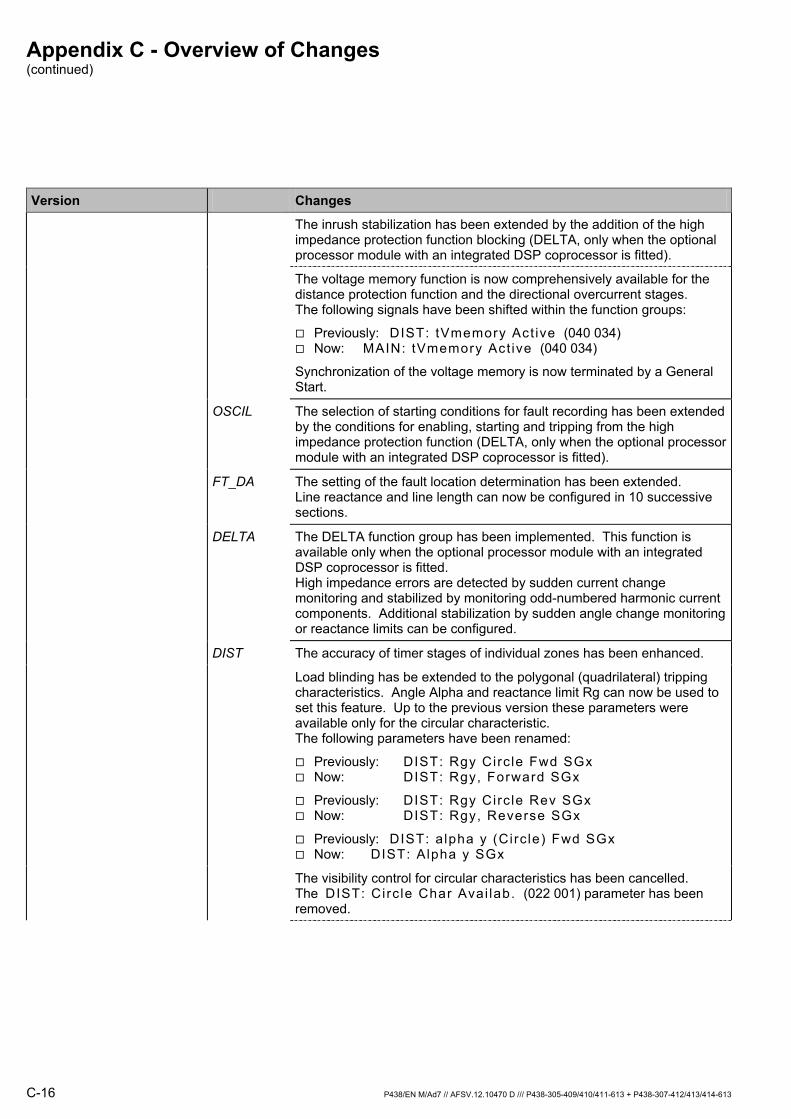
Appendix C - Overview of Changes (continued)
C-16 P438/EN M/Ad7 // AFSV.12.10470 D /// P438-305-409/410/411-613 + P438-307-412/413/414-613
Version Changes
The inrush stabilization has been extended by the addition of the high impedance protection function blocking (DELTA, only when the optional processor module with an integrated DSP coprocessor is fitted).
The voltage memory function is now comprehensively available for the distance protection function and the directional overcurrent stages. The following signals have been shifted within the function groups:
Previously: DIST: tVmemory Act ive (040 034) Now: MAIN: tVmemory Act ive (040 034)
Synchronization of the voltage memory is now terminated by a General Start.
OSCIL The selection of starting conditions for fault recording has been extended by the conditions for enabling, starting and tripping from the high impedance protection function (DELTA, only when the optional processor module with an integrated DSP coprocessor is fitted).
FT_DA The setting of the fault location determination has been extended. Line reactance and line length can now be configured in 10 successive sections.
DELTA The DELTA function group has been implemented. This function is available only when the optional processor module with an integrated DSP coprocessor is fitted. High impedance errors are detected by sudden current change monitoring and stabilized by monitoring odd-numbered harmonic current components. Additional stabilization by sudden angle change monitoring or reactance limits can be configured.
DIST The accuracy of timer stages of individual zones has been enhanced.
Load blinding has be extended to the polygonal (quadrilateral) tripping characteristics. Angle Alpha and reactance limit Rg can now be used to set this feature. Up to the previous version these parameters were available only for the circular characteristic. The following parameters have been renamed:
Previously: DIST: Rgy Circ le Fwd SGx Now: DIST: Rgy, Forward SGx
Previously: DIST: Rgy Circ le Rev SGx Now: DIST: Rgy, Reverse SGx
Previously: DIST: a lpha y (Circ le) Fwd SGx Now: DIST: Alpha y SGx
The visibility control for circular characteristics has been cancelled. The DIST: Circ le Char Avai lab. (022 001) parameter has been removed.

Appendix C - Overview of Changes (continued)
P438/EN M/Ad7 // AFSV.12.10470 D /// P438-305-409/410/411-613 + P438-307-412/413/414-613 C-17
Version Changes
A fourth distance stage with train start-up detection dx/dt has been implemented.
A visibility control for zones 3 and 4 has been added. Parameters:
DIST: Zone 3 Avai lable (022 195) DIST: Zone 4 Avai lable (022 196)
are used to render visible input, output and setting parameters for the respective zones. Zones are always without effect unless their respective availability has been set.
Bug fixing: Up to the previous version the WPC zone was processed even when the corresponding availability had been not set.
When the optional processor module with an integrated DSP coprocessor is fitted then the distance protection measured values (Z, R, X) may be corrected by harmonics factor kHarm, ΣI(xfn)/I(fn). Distance zone reaches are reduced dynamically according to the second, third and fifth harmonic current components.
DTOC / IDMT
Starting timer stages in the directional mode can now be freely selected. It is now possible to select whether a time delay is started when a stage start is issued or with an additional directional criterion.
Direction determination by overcurrent stages are now stabilized by the voltage memory function (function group MAIN). If voltage memory is not enabled a Fault forward decision is issued, independently of the actual fault direction, when the short-circuit voltages are < 1.0 V.
A load flow direction is now displayed when the short-circuit direction determination function is available.
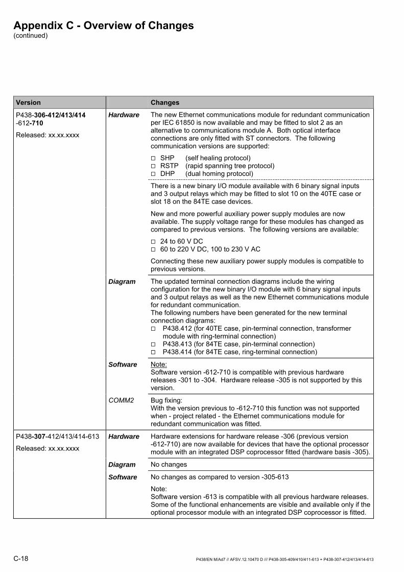
Appendix C - Overview of Changes (continued)
C-18 P438/EN M/Ad7 // AFSV.12.10470 D /// P438-305-409/410/411-613 + P438-307-412/413/414-613
Version Changes
Hardware The new Ethernet communications module for redundant communication per IEC 61850 is now available and may be fitted to slot 2 as an alternative to communications module A. Both optical interface connections are only fitted with ST connectors. The following communication versions are supported:
SHP (self healing protocol) RSTP (rapid spanning tree protocol) DHP (dual homing protocol)
P438-306-412/413/414 -612-710
Released: xx.xx.xxxx
There is a new binary I/O module available with 6 binary signal inputs and 3 output relays which may be fitted to slot 10 on the 40TE case or slot 18 on the 84TE case devices.
New and more powerful auxiliary power supply modules are now available. The supply voltage range for these modules has changed as compared to previous versions. The following versions are available:
24 to 60 V DC 60 to 220 V DC, 100 to 230 V AC
Connecting these new auxiliary power supply modules is compatible to previous versions.
Diagram The updated terminal connection diagrams include the wiring configuration for the new binary I/O module with 6 binary signal inputs and 3 output relays as well as the new Ethernet communications module for redundant communication. The following numbers have been generated for the new terminal connection diagrams:
P438.412 (for 40TE case, pin-terminal connection, transformer module with ring-terminal connection)
P438.413 (for 84TE case, pin-terminal connection) P438.414 (for 84TE case, ring-terminal connection)
Software Note: Software version -612-710 is compatible with previous hardware releases -301 to -304. Hardware release -305 is not supported by this version.
COMM2 Bug fixing: With the version previous to -612-710 this function was not supported when - project related - the Ethernet communications module for redundant communication was fitted.
Hardware Hardware extensions for hardware release -306 (previous version -612-710) are now available for devices that have the optional processor module with an integrated DSP coprocessor fitted (hardware basis -305).
P438-307-412/413/414-613
Released: xx.xx.xxxx
Diagram No changes
Software No changes as compared to version -305-613
Note: Software version -613 is compatible with all previous hardware releases. Some of the functional enhancements are visible and available only if the optional processor module with an integrated DSP coprocessor is fitted.
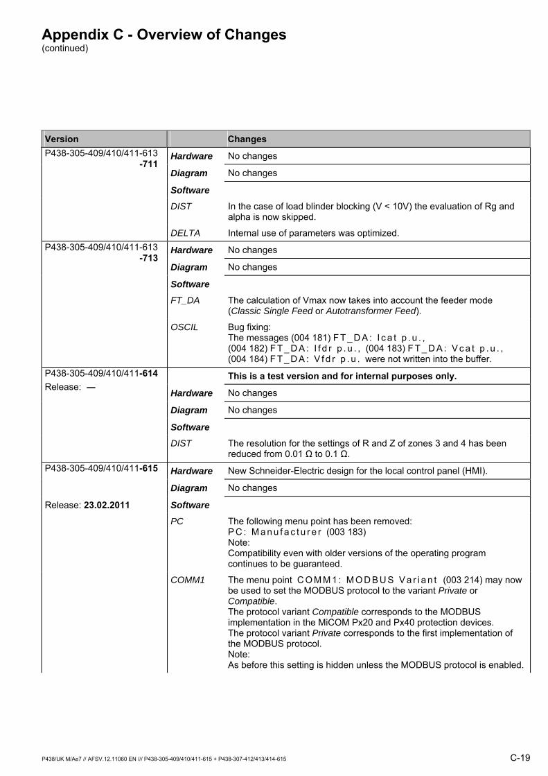
Appendix C - Overview of Changes (continued)
Version Changes
Hardware No changes P438-305-409/410/411-613 -711
No changes Diagram
Software In the case of load blinder blocking (V < 10V) the evaluation of Rg and
alpha is now skipped. DIST
Internal use of parameters was optimized. DELTA
Hardware No changes P438-305-409/410/411-613 -713
No changes Diagram
Software The calculation of Vmax now takes into account the feeder mode
(Classic Single Feed or Autotransformer Feed). FT_DA
Bug fixing: The messages (004 181) F T _ D A : I c a t p . u . , (004 182) F T _ D A : I f d r p . u . , (004 183) F T _ D A : V c a t p . u . , (004 184) F T _ D A : V f d r p . u . were not written into the buffer.
OSCIL
This is a test version and for internal purposes only. P438-305-409/410/411-614 Release: ― No changes Hardware
No changes Diagram
Software
DIST The resolution for the settings of R and Z of zones 3 and 4 has been reduced from 0.01 Ω to 0.1 Ω.
Hardware New Schneider-Electric design for the local control panel (HMI). P438-305-409/410/411-615
No changes Diagram
Release: 23.02.2011 Software The following menu point has been removed:
P C : M a n u f a c t u r e r (003 183) Note: Compatibility even with older versions of the operating program continues to be guaranteed.
PC
The menu point C O M M 1 : M O D B U S V a r i a n t (003 214) may now be used to set the MODBUS protocol to the variant Private or Compatible. The protocol variant Compatible corresponds to the MODBUS implementation in the MiCOM Px20 and Px40 protection devices. The protocol variant Private corresponds to the first implementation of the MODBUS protocol. Note: As before this setting is hidden unless the MODBUS protocol is enabled.
COMM1
P438/UK M/Ae7 // AFSV.12.11060 EN /// P438-305-409/410/411-615 + P438-307-412/413/414-615 C-19
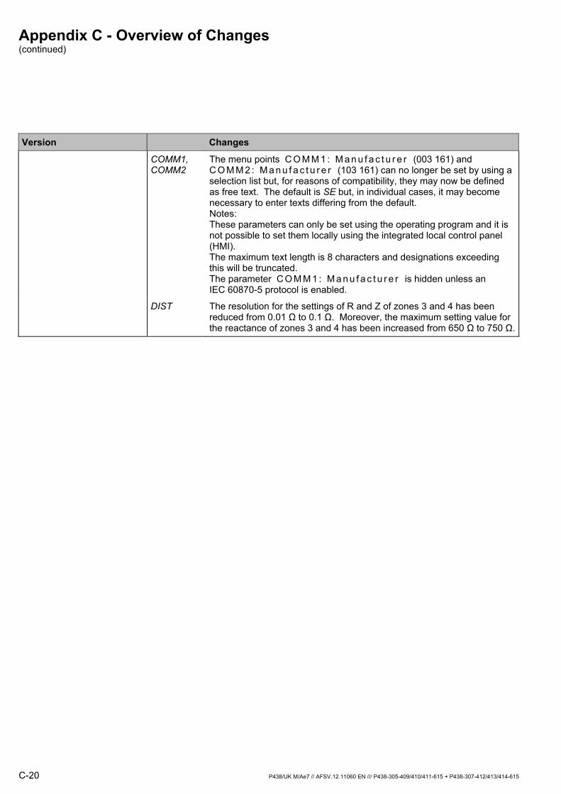
Appendix C - Overview of Changes (continued)
Version Changes The menu points C O M M 1 : M a n u f a c t u r e r (003 161) and
C O M M 2 : M a n u f a c t u r e r (103 161) can no longer be set by using a selection list but, for reasons of compatibility, they may now be defined as free text. The default is SE but, in individual cases, it may become necessary to enter texts differing from the default. Notes: These parameters can only be set using the operating program and it is not possible to set them locally using the integrated local control panel (HMI). The maximum text length is 8 characters and designations exceeding this will be truncated. The parameter C O M M 1 : M a n u f a c t u r e r is hidden unless an IEC 60870-5 protocol is enabled.
COMM1, COMM2
The resolution for the settings of R and Z of zones 3 and 4 has been reduced from 0.01 Ω to 0.1 Ω. Moreover, the maximum setting value for the reactance of zones 3 and 4 has been increased from 650 Ω to 750 Ω.
DIST
C-20 P438/UK M/Ae7 // AFSV.12.11060 EN /// P438-305-409/410/411-615 + P438-307-412/413/414-615


Customer Care Centre
http://www.schneider-electric.com/CCC
© 2
011
Sch
neid
er E
lect
ric. A
ll rig
hts
rese
rved
.
Schneider Electric 35 rue Joseph Monier 92506 Rueil-Malmaison FRANCE
Phone: +33 (0) 1 41 29 70 00 Fax: +33 (0) 1 41 29 71 00 www.schneider-electric.com Publishing: Schneider ElectricPublication: P438/UK M/Ae7 // AFSV.12.11060 EN /// P438-305-409/410/411-615 + P438-307-412/413/414-615 05/2011


