Embed Size (px)
Citation preview
N! d'ordre 1253
«N/CPK 80-09
présentée
A I' U.E.R. DES SCIENCES DE LA MATIERE
DE L'UNIVERSITE LOUIS PASTEUR DE STRASBOURG
pour obtenir le grade de
DOCTEUR ÈS-SCIENCES PHYSIQUES
par
Makram HAGE-ALI
CONTRIBUTION A LA CARACTERISATION OU TELLURURE DE CADMIUM
PAR LES FAISCEAUX IONIQUE ET LA DETECTION NUCLEAIRE
Soutenue le 25 Juin 1980 devant la Commission d'Examen:
MM.R.ARMBRVSTER
P.CHEVALLŒR
Mme H.LANGEVIN
J.TOUSSET
P.SIFFERT
THESE
President
Examinateurs
UIIIVEflSITÉ LOUIS WTEUR STHASMURG I CDITION FÉVRIER 1110
LISTE DES PROFESSEURS, MAITRES DE CONFÉRENCES DIRECTEURS I T MAITRES DE RECHERCHES CNRS ET INSERM
Pré: dent Professeur F M A R C O U X
Vio-Présidents Professeur Professeur
J.H.WEIL Ph.ROPARTZ
Président* Honoraires
Sec ôtaire Général
Professeurs G.OURISSON - P.KARL
Monsleu> G.KIEHL
lU .HR, JËTSCIENCES MÉDICALESl
U.E.R. te Schmts Médicales Directeur Mere DOB HER
U.E.R. to Sciences B i M l M i u e t t Directeur \wéti KIRN
DOYENS HONORAIRES : J CALLOT - J.CLAVERT - : r . lSCH.
PROFESSEURS HONORAIRES J J.BENOIT - J . C A L L O " - E.FORSTER - G . G R E I N E f l - Ch.GROSS - A J U N G - C h . K A Y S E R - P.MANDEL -H.METZGER - J.NORDMANN - A.ROHMER - F.SCHM1D - E.SCHNEEGANS - J.SEROR - J.STAHL - J .VEDRINE - P VINTEMBERGER -J.WARTER - G-WINCKLER
.PROFESSEURS : M ADLOFF N. APROSIO C A R ON L. A3CH A. BASSET A. 3ATZENSCHLAGEP P 3EYER P 3LOCH H. 3LDCH R SOCKEL C! SOL LACK A BRINI A. PRONNER P BUCK G. BURGHARO P. CHAMBQN J. CHAMBRON M CHAMPY A. CHAUMONT J. C L A V E R T
C CONRAUX k', DORNER R. EBTINGER R GANDAR P. GAUTHEH-LAFAYE
Chirurgie générale Anatomie normale Histologic Rhumatologie Ciin.Derm.et Syphiligr. Ana t.Pathologique Ciin.Pédiatet Puéric l Electrorediologie Pharmacologie Clin. Médicale B Cnir.UroUPev.Chir.AI Clin.ophtalmologique Clm.Ophtalmologique Clin.Chir.des Enfants pneumc-Phtisiologie Chimie biologique Physique biologique SnmetChir.MBK.Faaete Méd.Légaleet Sociale Embr.et Morph.Expér. Clin-Oto Rhino Laryng. Clin-Médicale 8 Ci in.Psychiatrique Clin.Gvnécol.et Obs.1 Anesthésîologie
J. GRENIER
J. HERAN L. HOLLENDER Fr 1SCH L. ISRAEL H JAHN J. JUIF T r .KAMMERER P. KARL I B KELLER I. KEMPF R KIENY A K IRN J.G.KORITKE M KREMER J. L A V U A U R E I X Y LEGAL J U L E V Y J M M A N T Z F MAf lCOUX J. MARESCAUX a MARX S. MAYER
Chlr.Gôn.Serv.de Consult. Ext.etd ' lnvest ig. Chir. Pathologie expérimentale CrwJ3gaK.AGIe-Serv.Cnir.Gle lit Réfct.Fonet.et Electromyogr Cl in. Psychiatrique Néphrologie et Hémodyaiise Pédiat. et Puériculture Cl in. Psychiatrique Neurophysiologie Gyn. et Obstétrique If Or th . et Traumatologie Petti et Clin. Semiol. ChiugceW Virologie
Artatomio normale Partait, et Pathol. Tropicale Méd. Prév. et Hygiène Anatomie Pathologique Institut de Puériculture Réanimation Médicale Médecine du Travail Histologte Physiologie Hématologie
PROFESSEUR ASSOCIE : F DEFEUDIS (Biochimie)
PROFESSEURS CONVENTIONNES : A. PETRQVIC IPr biologie) - E. WEIL (Toxicologie industrielle)
MAITRES DE CONFÉRENCES AGRÉGÉS :
S BABIN P BAREISS P. 10URJAT JC 8RECHENMACHER JM.BRÛGARD F &UCHHEIT M COLLARD F DELLENBACH 3 d lSENMANN K: FABRE L. FINCKER j P LAMENT . GEISERT JP GERHARD E. GROSSHANS P HABEREY J L IMBS M IMLER D. JAECK
O n hoped re et traumat I Médecine Interne Electro-Radiologie Cardiologie Clin. Médicale B Neurochirurgie Neurologie u n . Gynécologique 11 CNr.Cardic-Vaseulaire HiSTologie Clin. Médicale Ophtalmologie Pédieirie et PuértunJll CUn.Ophtalmologique Cim. Derma to logique physio1ogie Pharmacologie Clin. Médicale B Chirurgie générale
; A JAEGER j M JESEL j P. KËHR
R KEIL ING | F KEMPF
J. KEMPF | T K IENTRUONG I G KLOTZ
F KUNTZMANN r D KURTZ I G LANG ! J.H.LANG
D " A I T R O T J . I .MANOEL
I J, MARK J. MESSER
• G METHL IN C MEYER H MONTEIL
Réanimation Médicale Rééduc. Fonctionnelle Orthop. et Traumatologie Cancérologie Eledro-Radio'ogie Chimie Biologique Parasitologic Oto-Rhino- Laryngologue Médecine Interne Clin. Neurologique Orthop etTraumatologîe Clin.dsMaladBsdu Sang Neurochirurgie Chimie Biologique Chimie Biologique Pédiatrie Physique Biologique Chirurgie Gale I I I Bactériol. Virologie
J. MEHL B. METZ R.MINCK P. M U L L 6 R E. PHILIPPE R. RENAUD
E. ROEGEL F. ROHMER J. RUCH Y. RUMPLER A . ÏACREZ G. SCHAFF 6. SCHVINGT J. SCHWARTZ A. S IBILLY L. SINGER F. STEPHAN D. STORCK G. VINCENDON R. VOEGTLIN A . WACKENHE1M P. WARTER
4P. WEILL 0- W I L L A R O JJ3. WITZ
G. MORAND F. OBEULING J.COTTFNI G. PAUl I P. REVILLE P. BEYS J. RITTER M ROOS P. SAUVAGE G. SA V A JP.SCHIEBER G.SCHLAEDER H. SICK C. STOLL JD.TEMPE J. TONGIO JP. WALTER JMWARTER
MAITRES DE CONFÉRENCES CONVENTIONNÉS:
DIRECTEUR DE RECHERCHE : A. PETROVIC
UAtTRES DE RECHERCHE :
M R . E L O Y ' Endocrinologie 3. GOMBOS * Neurochimie K_ HAFFEN-STENGER ' endocrinologie M. JACOB - Neurochimie
A. M M LAN (Physiol. Resp.) - J.J. VOGT IThermophysiologie)
IPhy lOlogiol
G LECLERC *• Pharmacologie G R E B E L * Neurochimie R RECHENMANN • Biophys. os Rayonnements W SENSENBRENNER^Neurochinve
Médecine du Travan Phys<ologie appliquée Bâclé' Viroi.Immund.Génâralc Cl in.Gynécol .etObstéi ' n Anatomie Pathologique Gynécologie Pneumo-Phtisioiogie Clin. Neurologique Biologie Medicate Embryologie Cardiologie Physiologie
Orthopéd. et Traumaiol Pharm. et M6d. Expônm Urgence et Policlinique Clin. Psychiatrique Paihol.Gén.et Exparim Clin. Médicale A Chimie Biologique Thérapeutique Icardioi ' E lee t ro-R ariiol og« Electro Radiologie Hydroi.Thérap.erClimatd Serv de Pédiatrie IV Chirurgie Thorecique
Chirurgie Thoracique Cl in desMaladiesduSann Anesihésiologie Pneumo-Phiisiologie EndccnruVétabolei NumtKn Chirurgie Générale CI-n.GynécoletObsrét' Embryologie Clm.Chirurg. ds Enfants Chirurgie Générale H Physiologie Gynécol- etObStétr I AnaTomie Normale Insi. de Puériculture Réanimation Médicale Electro-Radiologie Electro-Radiologie Neurologie
J. V E L L Y * Pharmacologie N VtRMAUX-COLIN» Neurochimie JJ. VOGT -r The r mophysio A WAKSMANN + Neurochimie
[ U.E-B. ITODOMTOLOCIEI
DirecMur : Robtft FRANK
PROFESSEURS DE GRADE EXCEPTIONNEL
M. DOCQ DeniislirpiOpÉMan R. FRANK Biol, et MM. Fondem.
P. KLEVANSKY Parodontologie J. L IT2LEI Prothèse
PROFESSEUR* DE PREMIER GRADE :
M BASTIAN Pro the* A. COMTE OvMimOpira to l i * R. HAAG Pathol etThfcap. dant
OL LACOSTE M. LANGER
Orthopédrt dtnto-facttrt Prothèae
P. NICOLA î A . SCHLIEUGER
f V h o l . « t T r * v daman Prothèse
PROFESSEURS OE DEUXIEME QftADE :
C- ALLEMANN OeniisterieOparatoire w. BACON Onhopédiadanlo-faclale Cn BO LENDER O n hoped ia dante-faclele P.MCAHEN Siol.et Mat. Fondam.
J.P-CHARLIER fi. KAESS M. LEIZ6
Orthopédia dtftto-taelala Pathol etThérapaut damairta Prothèse
JJ .ROTH J. SOMMERMATÉR H . T E N E N 6 A U M
Parodontologie Pédodonue prévar'.ian Parodontologie
U.E.R. DES SCIENCES PHARMACEUTIQUES
J.P-CHARLIER fi. KAESS M. LEIZ6
Orthopédia dtftto-taelala Pathol etThérapaut damairta Prothèse
JJ .ROTH J. SOMMERMATÉR H . T E N E N 6 A U M
Directeur PÏBfTa M ET Al S
DOYENS HONORAIRES : P. DUOUENOIS • V HASSELMANN - G. DIRHEIMER
PROFESSEURS HONORAIRES : P. CORDIER J.P. EBEL - G. GAZ ET du CHATELIER • P. JAEGER • R. SARTCM s*
PROFESSEURS :
R. ANTON R CARBIENER G. DIRHEIMER G. FERARD A. GA1RARD D GERARD M. HASSELMANN
"harmacognosie Botanique Toxicologie Chimie Biologique Physiologie Phys. et Biophysique Own, And. et Brarwtl
a a K O F F É L H. LAM1 Y. LANORY C. LAPP P. LAUGEL G. LAUSTRIAT J. MALGRAS C. MATHIS P. MÊTA1S
Pharm. chimique Mathématiques Pharmacologie Chlm Gèn ai Minérale Chimie Analytique Physique Immunologie Pharmacie Galénique Biochimie
B. PESSON PHPOINORDN J. SCHflElUER A. STAHL A. STAMM OCSTOCLET a V I DON CGWERMUTH
Pams f loiooie Viroloo'e Chim. Organique Bioch. Pharmaceutique Pharmacie Galénique Pharmacodynamie Bactériologie Chrrrne Organique
PROFESSEUR CONVENTIONNÉ ; 8. ROTR-SCHECHTER (Pharmacodynamie)
MAITREtDÊ RECHERCHE : I.N.S.E.R.M. : JB IETH (Eraymolooia) - C.N.R.S. : G. KEITH (Chfmie Bt cri trique)
I U.E.R. DE SCIENCES HUMAINES |
U.E.R. 4* Gityiphii U.E.R. dat Sciences du CowBWtaanant «t 4tfEnvirowiwjiit
PROFESSEUR HONORAIRE : Et .JUILLARD
PROFESSEURS :
MICHEL . MOLES
NONN
Géographie Psychologie sociale Géographie
R. RAYNAL I H. REYMOND I R. SCHWAB
oiraetaur. P iam MICHEL Diraetaur: Sruno WILL
Géog. aphia Géographie Géographie
A. TABOURET-KELLER Psychologie M. TARDY Psvcho-Pedagooie
| J. TRI CAP T Géographie
DIRECTEUR OE RECHERCHEON.R.S. : S. RIMBERT (Géographie
IU.E.R. DES SCIENCES ECONOMIQUES!
Directeur Rodolphe ÛOS SANTOS FERREIRA
DOYENS HONORAIRES: P. CHAMLEY . J.P. FITOUSSI
PROFESSEUR HONORAIRE : P.L. REYNAUD
PROFESSEURS :
Ph.ARTZNER F. 3ILGER A CHABERT - CHAMLEY
Mathématiques Se Economiques =c Économiques Se Economiques
R. DOS SANTOS G. KOENIC FERREIRA Se. Économiques JJ OBRECl T
Jft FITOUSSI Se. Économiques Idét.J JP POLLIrv LAGERARD-VARET Se. Economiques
Se Économiques Gestion Se. Economiques
PROFESSEURS ASSOCIÉS : W. BEA2ER - A. LEIJONHUFVUD
PROFESSEUR CONVENTIONNE : H. CULMANN
CHARGES DE CONFÉRENCES : R. ERBES - A. LOSSER
Mathématique! Directeur :
Sciaticas Phyiiquat f t Chtmiquat Directeur :
Sciatica» da la Matière Directeur :
SciancM da la Via t t da la Tarn Dkactaur :
Scîincai du Componamtnt i t a* rEmrifonrmntnt Directeur :
Ecoto d'Application da* Hautt f o l y m a m Directeur :
ECOM Nalionala Sapériaun da Chimia Directeur :
Observatoire Directeur:
Phynqua du Globe Directeur :
Xavier PERN1QUE {Ht intérim)
Henri BENOIT
JaanJoaé PRIED
Yve» BOULANGER
Bruno WILL Constant WtrTLEf)
MareOAIftE
Mphonai FLORSCH
Roland SCHLICH
DOYENS HONORAIRES : P. l A C R O U T E - J.H. V IV IEN - G. Ml LLOT
PROFESSEURS HONORAIRES : J. BRENET - J. SYE • H. CARTAN - C. CHABAUTY - A . CHRETIEN - J. DENY • Mita S. G I L L E T • S.GORODET2KY R. H O C A R T - P . J O L V - P . LACROUTE - R. LECOLAZET - G. LEMEE - P. L ' H E R I T I E R - A . L ICHNEROWICZ-A . M A I L L A R D • L NEEL • J . °ARROD R. HOHMER • J.P. FlOTHE • L SACKMANN - Ch. SAORON - H. SAUCIER - F. STUTINSKY • H. V I L L A T • Et. WOLFF
MAITRE DE CONFERENCES HONORAIRE : R. WEIL
PROFESSEURS
OP. ADLOPP R ARMBRUSTER V. AVANISSIAN G. BARBANCON F BÊCKER fV. BEFORE 'del) CL BENEZRA H. BENOIT P BENVENISTE D. BERNARD i C B E R N I E R J BONNIN Y BOULANGER JF.BOUTOT M. B R I M J BROSSAS C. BURGGRAF H BURNAGE R CERF P CHARTIER P. CHEVALLIER A. CLAUSS A COCHE M OAIHE M. OANAN E DANIEL M. DAUNE J DEMAND A. DELU2ARCHE G. DUNOYERde
SEGONZAC H DURANTON dP. EBEL IP. EBERHART V. ERN
Chimie Nucléaire Physique Analyse supérieure Mathématiques Phys. Methémat. B'ochimie Dermato- Chimie P h ysicoc h i m. Mec rom. Physiologie végétale Mé th. Math do la Phys. Chimia Générale Gëoph. interne Chimie biologique Mathématiques Ch.mie Chimie macromol Minéralogie '^écan. ds Fiutoes Physique générale Chimie Physique " * i m e Physique nucléaire CnmPhyi IndUMtScdiMat f t vsABm «Phyidu Solids Phvs. expérimentale Biophysique Chimie générale Ch.mie
Géologie Botanique -him. Biologique Minéralogie Physique
J. PARAUT P. FEDERLIN P. FELTZ X. FERNIQUE IG.HSCHER D. FOATA E. FOLLENIUS A i FRIEO D. FROELICH A. FUCHS A . GAG NI EU J .CGALL A. G A L L M A N N F. GAUTIER R. GERARD G. GLAESER Cl GODBILLON M. GO UNO T M. GROSMANN M. GROSS L. HIRTH C. JASCHÉK iP . JOUANOLOU T. JUTEAU R. KIRSCH F. LACROUTE J.CLAFÛN G. LEBEURIER J. LEITE-LOPES M. LEROY J. LUCAS D. MAG NAC J. MARTINET P. M I A L H E
A. MICHARD
PROFESSEUR ADJOINT : J .SITTLER (Géolog>el
PROFESSEURS ASSOCIÉS :
A- BANOERET E A.H.P, B. BOURROUILK Géophysique G. BUCHANAN Chimie J. BUONICK Physique MECONSTANTIN Cn.mie
Mathématiques Chimie Physiol. Animale Mathématiques
Mathématiques Zoologie Méc ds Fluides Chrm.Gén.Chim.Phys-Macan. rationnelle Botanique Géologie Physique Physique Mathématiques Mathématiques Mathématiques Botanique Physique Chimie Microbiologie Astronomie Mathématiques Minéralogie Zoologie Biologie végétah Inform. App l . Microbiologie P h ys. nu ci .et corpusc. Chimie Géologie Physique Mathématiques Physiol, animale Géologie
R. DUCKETT R. HOLMES J. HONNOREZ P. MARGARETHA T. MIZOGUCHI
Géologie Chimie Physique
M. MIGNOTTE G. Ml LLOT G. MONSONEGO B. MORIN G. OURISSON JJ>. R A M IS G. REEB Ph RICHARD JJ .R IEHL CL ROBERT A. ROCHE Ph. ROPARTZ J. ROUX
F. SC H A L L E R G. SCHIFFMANN A . SCHM1TT JP.SCHWING MJ.SCHWING
M. SIESKI JD G. SOLLA3 IE J. SOMMFR G. SUTTE ï Q i T A N I E I . I A N J. TERRûiSE JJ .THIEBOLD D. V I A U O J H V I V I Eh R. V O L T Z JH.WEIL G. WEILL R. WEISS PL. WEN DEL 8. WILL
C. WIPPL6R J WUCHCR 8 WURTJ
J. OSBOR I C. SAVOY Y. SIBUY£ L. WILL IAMS S. W I L L I A M ^ S O N
rnformatiaua GéoL et Paléontologie Physique théorique Mathématiques l Chimie Math, générales T écologie Physiol animale Chimie Physique Physique du Globe Psy c i o-Physiologie Botanique Biologie générale Mathématiques Phvsique Chimie Chimie Physique Physique Chimie organique Chimie appliquée Phys Électroniaue Chimie Chimie Biologie animale Mathématiques Zool et Embryol Expenm Physique théorique Chimie biologique Physique Chimie Physique Psy ch o-oh y s iol og i e Phys'cochim.des Hts Po lv Physique Chimie biologique
Chimie minérale Physiaue Mathématiques Biochimie Mathématiques
PROFESSEURS CONVENTIONNÉS : P. BOUVEROT (Physiologie respiratoire) - P. DE JOURS (Physiologie r e * ifatoire)
ASTRONOME ADJOINT : A FLORSCH (Astronomie)
DIRECTEURS OE RECHERCHE CMJiS. :
1F.BIELLMANN P. BOUVEROT P DEJOURS A (CNIPPER A. KO VACS J. MARCHAL PAJvIEYER AJP. MEYER
Physiologie respiratoire ^nysiologje respiratoire anys«iue nucléaire ei corpuscule ire "hysicochimie macromo'éculaire •'"• vsicochimie maergmoléculaire
^Thématiques hysique
J . MEYER A. PORTE P. REMPP R. SCHLICH A . SKOULIOS M. VAN REGENMDRTEL A. V E I L L A R D A. ZUKER
Botanique Biologie cai uiaire Physicochinie macromolôajiairi Géophysiqu * marine Physicochinie maeromalôculair' Virologie Chimie mqhculaire Physique théorique
MAITRES DE RECHERCHE CMMS.
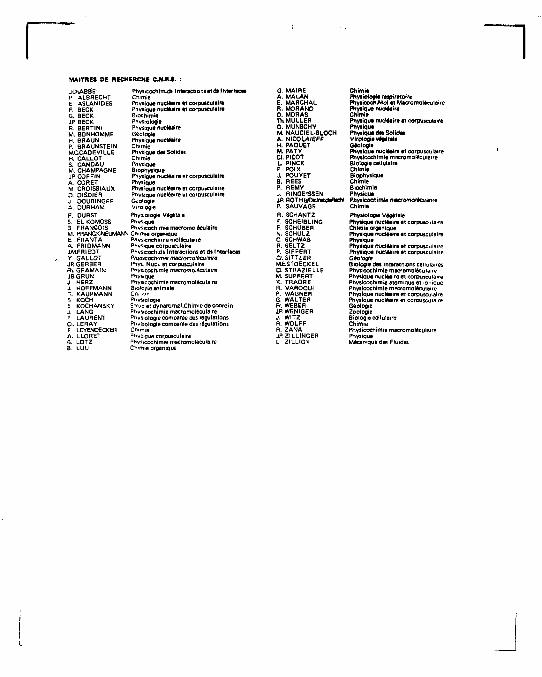
JC-iABBE P AL8RECHT E ASLANIDES F. BECK G. BECK 4P BECK R. BERTINI M. BONHOMME H. BRAUN P. BRAUNSTEIN MCCADEVILLE H. CALLOT S. CANDAU M. CHAMPAGNE iP . COFFIN A. COR ET M. CROISSIAUX O. OISDIER j DOUBINGER A. DURHAM F. DURST S. EL KOMOSS 3 FRANCOIS M. FRANCK-NEUMANN E. FRANTA A. FRIDMANN JM.FRIEDT Y GALLOT JRGERBER R i G R A M A I N JB.GRUN J. HERZ J. HOFFMANN T KAUFMANN B KOCH E KOCHANSKY J. LANG P LAURENT Ct. LERAY F LEYENDECKER A. LLORET 8. LOTZ B LUU
Physicochim,di Interactions et delMerfecei Chimie Physique nucléaire * i eorpuiculelra Physique nucléaire «t corpusculaire Biochimie Physiologie Physique nucléaire Géologie Physique nucléaire Chimie Physique desSolides Chimie Physique Biophysique Physique nucléaire et corpusculaire Physique Physique nucléaire et corpu*culaire Pnysjque nucléaire et corpusculaire Géologie Virologie Physiologie Végétale Phvstque Physicochimie macromoléculaire Chimie organique Physicochimie moléculaire Physique corpusculaire Phvsicoch.ds Interactions et ds InteHaces Physicochimie macromoléculaira Phvs. NucL et corpusculaire Physicochimie macromoléculaire Physique Physicochimie macromolécu faire Bioionie animale
Pnysiologie Srruc et dynam mol. Chimie de coord in Physicochimie macromoléculaire physiologie comparée des régulations Physiologie comparée des régulations Chimie -hvSiaue corpusculaire Phvsicochimie macromoléculaire Chimie organique
G. MAIRE A . M A L À N E. MARCH A L R. MORAND D. MORAS THMULLER G. MUNSCHY M. N A U C I E L B L O C H A. N ICOLAIEFF H. PAQUET M. PATY Cl. PICOT L. PINCK P POIX J. POUYET B. REES P. REMY J. RINGEtSSEN JP. ROTHfoOrJrawtfRacM P. SAUVAGE R . S C H A N T Z
F. SCHEIBLING F. SCHUBER N, SCHUL2 C. SCHWAB R. SELT2 P. SIFFERT Cl .SITTLER MESTOECKEL a STRAZIELLE M. SUFFERT K. TRAORE R. VAROOU1 P. WAGNER G. WALTER Fr. WEBER JLP.WENIGER J. WITZ H. WOLFF R. ZANA OP. Z ILL INGER L Z ILL IOX
Chimie Physiologie respiratoire Ptiysicoch.Mo1 «1 Macromolecuieire Physique nucléaire Chimie Phyiiqua nucléaire et corpusculaire Phyiique Physique de* Solides Virologie végétale Géologie Physique nucleeire at corpusculaire Physicochimie mocromolecuisire Biologie cellulaire Chimie Biophysique Chimie Biochimie Physique PhyifcochiriWe maeromoiécuiaire Chimie
Physiologie Végétale Physique nucléaire «t corpusculaire Chimie orgenique Physique nucleeire et corpusculaire Physique Physique nucléaire et corpusculaire Physique nucléaire et corpusculaire Géologie Biologie des Interactions cellulaires Phy i kxehimie macromolécu lai re Physique nucléaire et corpusculaire Physicochimie atomique et ionique Physicochimie macromoléculaire Physique nucléaire et corpusculaire Physique nucléaire et corpusculaire Géologie Zoologie Biologie collutoire Chimie Physicochimie macromoléculaire Physique Mécanique des Fluides
1
A ma f i l le, pour qu'elle vive un monde plus heureux.
A ma femme,pour son affection et sa patience ; elle n'a pas ménagé ses encouragements, ni son soutien matériel et moral.
A mes parents, frères et soeur, qui ont su me motiver et dresser les jalons matériels et moraux du chemin où je me suis engagé.
A mon pays d'origine le Liban, pulsse-t-î l trouver un jou r la paix dans un havre de l iberté, d'égalité et de j us t i ce . . .
REMERCIEMENTS
Ce travail a été effectué au Centre de Recherches Nucléa ires de
Strasbourg (C. R.N. ) au groupe de Physique et Applications des Semiconducteurs
(PHASE).
Je tiens d'abord à remercier Monsieur le Professeur A. COCHE
de m'avuîr accueilli au C. R. N. lors de mon arrivée a Strasbourg.
Monsieur le Professeur R. ARMQRUSTER a accepté de présider
le jury de cette thèse ; Monsieur le Professeur P. CHEVALLIER, Madame
H. LANGEVIN, Directeur de Recherches au C.N. R. S . , qui m'a déjà fait l'honneur
de diriger mes travaux de Doctorat de 3e cycle, Monsieur le Professeur
J. TOUSSET, malgré un emploi de temps très chargé, ont accepté de faire
partie du jury. Je leur adresse ici mes plus vifs remerciements.
Monsieur P. SIFFERT, Mattre de Recherches au C.N. R. S. m'a
accueilli au sein de son groupe, m'a proposé et pris une part active ;à ce travail
et bien d'autres, dirigé et encouragé avec patience ; je lui suis infiniment re
connaissant de son aide amicale et quotidienne.
Mes amis et collègues ; Mme A. GROB, Messieurs J. J. GROB ,
J. P. PONPON, B. RABIN, C. SCHARAGER, R. STUCK, M. TOULEMONDE.
Messieurs 1. V. MITCHELL, A. PAPE, A. SAXENA, A. CORNET, B. SCHAUB,
F. V. WALD et R. o. BELL de différents laboratoires et pays, m'ont fait le
olaisir de collaborer à différentes expériences de ce travail ; je les remercie tous
pour leur aide et leur sympathie.
Mesdames F. KLOTZ, C. WEYMANN, Messieurs J. M. KOEBEL,
J. KUREK, R. REGAL ont assuré, chacun dans sa spécialité, le support technique
de ce t ravai l qui aurai t été di f f ic i le à mener sans leur concours eff icace. Ûu : ; .s
trouvent Ici ma reconnaissance et mon amitié.
Messieurs W. B A D E R , P . B O R D E T , R. O I S S E R T , et en p a r t i c u
l a r J . S E R G I E R , ainsi que l'ensemble du personnel de l 'a te l ier central , ont
assuré la conception et la réal isat ion de l'équipement mécanique avec précision
et compétence ; j e les remerc ie chaleureusement.
J . P . R E S C H , R. M E I S S , H. V O G L E R , H . H U B R E C H T et l ' en
semble du service d 'accélérateurs ont assuré avec eff icacité la lourde charge du
fonctionnement et de la maintenance des accé léra teurs . Qu' i ls trouvent i c i mes
remerciements amicaux.
Comment ne pas remerc ier Madame A . R U H L M A N N pour sa gent i l
lesse et sa disponibil i té ; e l le a assuré la frappe de la majeure par t ie de cette
thèse avec cé lér i té , ainsi que Madame M. G O E T 2 pour son précieux concours
et comment ne pas c i te r le t ravai l i r réprochable de Monsieur S , L I E S S dans l ' exé
cution des différents travaux photographiques, ainsi que le personnel du serv ice
d' Imprimerie pour le soin qu'i ls ont apporté à la présentation de ce t ravai l , Qu' i ls
acceptent tous ici mes remerciements.
J 'ai commencé cette thèse en tant que boursier du C . N . R. S . du
Liban, ensuite comme boursier du Ministère f rançais des Af fa i res Etrangères ;
je leur en suis vraiment reconnaissant. Je tiens également à remerc ie r la D, R. E, T .
(D. R. M, E. ) pour leur concours et leur soutien matér ie l .
C O N T R I B U T I O N A L A CARAC.TERISATION DU
T E L L U R U R E D E C A D V I U M P A R L E S F A I S C E A U X I O N I Q U E S
E T L A D E T E C T I O N N U C L E A I R E
I N T R O D U C T I O N 1
I - Thermodynamique du système C a d m i u m - T e l l u r e 2
1 - P r o j e c t i o n t e m p é r a t u r e - c o m p o s i t i o n
2 - Domaine d 'ex i s tence dé C d T e 3
3 - P r o j e c t i o n p r e s s i o n - t e m p é r a t u r e
4 - Re la t ions d ' é q u i l i b r e s o l i d e - v a p e u r 4
t l - C r i s t a l logénèse 5
1 - Syn thèse
2 - P u r i f i c a t i o n du maté r iau 6
3 - C r o i s s a n c e des c r i s t a u x :
a. Fus ion de zone 8
b. Br idgmann
c. C r o i s s a n c e en so lvant
I I I - Compensat ion du maté r iau 9
C H A P I T R E 1 : Ana l yse p a r r é t r o d î f f u s i o n de p a r t i c u l e s chargées 25
1 _ § C a r a c t é r ï s a t ï o n des su r f aces de semiconduc teu rs b i n a i r e s pa r
r é t r o d î f f u s i o n de haute r é s o l u t i o n 29
§ Analyse électrostat ique des surfaces de semiconducteur par
rétrodiffuslon d'ions lourds. 37
1 - Résolution de masse
2 - Résolution d'épaisseur
3 - L 'analyseur électrostatique
4 - Résultats expérimentaux 1 A
Il - P e r t e d'énergie et dispersion de H et He dans Z n T e et CdTe 69
- Résultats théoriques et expérimentaux
C H A P I T R E il : Analyse de surface de CdTe 75
1 - Spectrométr ie à ions secondaires (S IMS)
2 - E l l ipsométr ie
3 - Rétrodiffusion Rutherford (RBS)
4 - Surfaces : c l ivées, rodées, décapées chimiquement, oxydées
5 - Résultats et discussions
C H A P I T R E I I I : S t ructures Diodes
I - Diffusion des ions lourds {Au, Bi) dans CdTe
1 - Analyse par (RBS)
2 - Analyse par sonde ionique
II - L 'hétérostructure InSb-CdTe
1 - Mesures électr iques et photoélectriques
2 - Mesures par (SIMS)
II I - Contacts par implantation ionique
1 - Conditions d'implantation
2 - Etudes des défauts et des recui ts thermiques
3 - Résultat en détection de part icules
103
105
106
112
1 15
C H A P I T R E I V : Les spectromètres nucléaire» C d T e 153
I - Corré la t ion entre le traitement de surface et la qualité de détection ,ô5
1 - Surfaces : rodées» décapées chimiquement, oxydées
2 - Analyses par ( R B S ) , (S IMS) et el l lpsométrie
3 - Détection :
- <* de 2 * ' A m
II - Polar isat ion
1 - L'étude de la polarisat ion : or ig ine, modèles et méthodes de
suppression 177
2 - Matériau non polarisant IS I
C O N C L U S I O N 195
I N T R O D U C T I O N
i
L e te l lurure de cadmium, un semiconducteur b inai re de type M - V I ,
présente un intérêt certain dans plusieurs domaines de pointe : détecteur
de photons y et X , capable de fonctionner à température ambiante, photopïle
convertissant directement l 'énergie sola i re en é lec t r ic i té , modulateur
électro-optique, fenêtre de lasers infrarouge, substrat pour la croissance de
Cd Hg, j T e pour la préparat ion de détecteurs I n f r a - r o u g e . . . Toutefois, à
l 'heure actuelle ce composé n'a pas encore trouvé le développement Industriel
que ses applications laisseraient supposer. Ceci résul te certainement, pour
une large par t , de la complexité de ce matér iau, sans aucune comparaison
avec le sil icium ou le germanium. Di f férentes équipes, disséminées à t ravers
le monde se sont f ixées comme objectif d'approfondir les connaissances de
CdTe et par la même de contribuer à une mei l leure co.npréhension des maté
r iaux binaires et des semiconducteurs en généra l . N o t r e laboratoire fait
par t ie ce ce groupe et ce t ravai l s ' inscr i t dans une sé r i e , déjà longue, de
recherches que nous avons entrepr ises sur C d T e . Mais alors que les thèses
présentées antérieurement s' intéressaient essentiellement à l 'élaboration des
monocristaux et à leur caractér isât ion de volume, nous avons cherché à
approfondir lf>s phénomènes de surface.
1
L'existence chimique du te l lu ru re de cadmium est connue depuis le
siècle dernier [ 1 ] et dès 1911, KC BAY A S HI [ 2 ] avait déterminé un premier
diagramme température-composition du système cadmium-te l lure , mais II a
fal lu attendre 1954 pour é tab l i r ses propr ié tés semlconductrices [ 3 - 4 ] . L a
contribution expérimentale la plus importante à ces premières recherches
est Incontestablement due à D E N O B E L [ 5 ] . Depuis l o r s , de nombreux
travaux ont été consacrés à ce matériau à la fois pour explorer ses
propr iétés fondamentales et pour explorer ses applications. Une vue d'ensem
ble de ces recherches peut fctre obtenue à p a r t i r des compte-rendus des
deux congrès Internatîonanux qui se sont tenus à Strasbourg [ 6 , 7 3 ,
1. THERMODYNAMIQUE DU SYSTEME CADMIUM-TELLURE
Pour déterminer les conditions thermodynamiques optimales en vue
de la croissance des monocristaux de CdTe II faut, tout d'abord établ i r le
diagramme de » phases» qui est une fonction tr idimensionnelle de la température
(T ) , de la composition (x) et de la pression (P) . Nous nous l imiterons ici
aux projections T - x et P - T .
1, Project ion température-composition
E l l e a été étudiée par de nombreux auteurs tant théoriquement
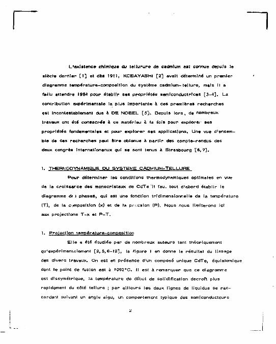
qu'expérimentalement [ 2 , 5 , 8 - 1 2 ] , la f igure 1 en donne le résultat du lissage
des divers travaux. On est en présence d'un composé unique CdTe , équiatomique
dont le point de fusion est à 1092°C. Il est à remarquer que ce diagramme
est dissymétrique, la température de début de solidif ication décroît plus
rapidement du côté te l lure ; par a i l leurs les deux lignes de lîquidus se r a c
cordent suivant un angle aîgu, un comportement typique des semiconducteurs
2
I I - V I , dû au carac tère nettement plus Ionique des Malsons que dans les
semiconducteurs l l l - V par exemple.
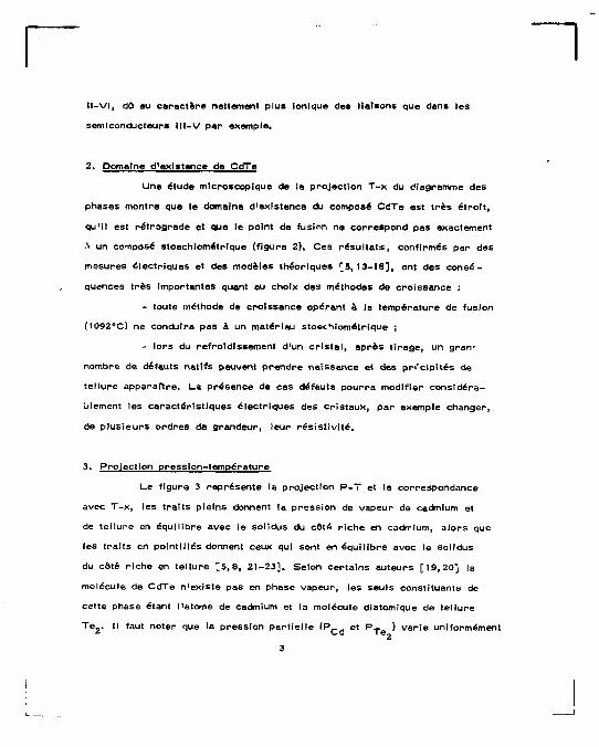
2 . Domaine d'existence de CdTe
Une étude microscopique de la project ion T - x du diagramme des
phases montre que le domaine d'existence du composé C c T e est t rès é t ro i t ,
qu'i l est ré t rograde et que le point de fusion ne correspond pas exactement
A un composé stoechiométrique (f igure 2) . Ces résu l ta ts , confirmés par des
mesures électr iques et des modèles théoriques [ 5 , 1 3 - 1 6 ] , ont des c o n s é
quences très Importantes quant au choix des méthodes de croissance :
- toute méthode de croissance opérant à la température de fusion
(1092°C) ne conduira pas à un matériau stoechiométrique ;
- lors du refroidissement d'un c r i s t a l , après t i rage , un gran '
nombre de défauts natifs peuvent prendre naissance et des précipi tés de
te l lure apparaî t re . L a présence de ces défauts pourra modifier considéra
blement les caractér ist iques électr iques des cr istaux, par exemple changer,
de p lus ieurs ordres de grandeur, leur rés is t lv l té .
3. Project ion pression-température
La f igure 3 représente la projection P - T et la correspondance
avec T - x , les t ra i ts pleins donnent ta pression de vapeur de cadmium et
de te l lure en équil ibre avec le solîdus du côté r iche en cadmium, a lors que
les t ra i ts en pointi l lés donnent ceux qui sont en équi l ibre avec le solîdus
du côté r iche en te l lure [ 5 , 8 , 2 1 - 2 3 ] . Selon certains auteurs [ 1 9 , 2 0 ] la
molécule de CdTe n'existe pas en phase vapeur, les seuls constituants de
cette phase étant l'atome de cadmium et la molécule diatomique de te l lure
T e 2 . Il faut noter que la pression par t ie l le ( P V J et P T ) v a r i e uniformément
3
i
L i
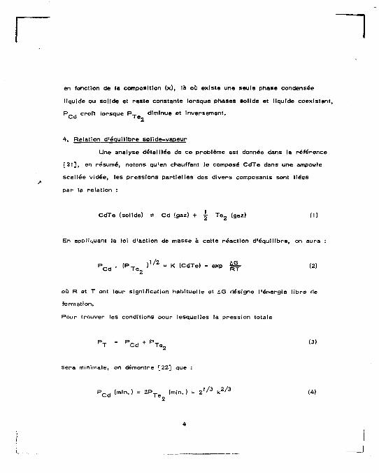
en fonction de la composition (x) , là où existe une seule phase condensée
liquide ou solide et reste constante lorsque phases solide et liquide coexistent,
P . croft lorsque P T diminue et inversement.
4. Relation d'équil ibre sol ide-vapeur
Une analyse détai l lée de ce problème est donnée dans la ré férence
[ 2 1 ] , en résumé, notons qu'en chauffant le composé CdTe dans une ampoule
scellée vidée, les pressions par t ie l les des divers composants sont liées
par la relat ion :
CdTe (solide) s Cd (gaz) + | T e 2 (gaz) (1)
En appliquant la loi d'action de masse à cette réact ion d 'équi l ibre , on aura :
P C d • ( P T e ) 1 / 2 " K ( C d T e ) = e x p RT ( 2 )
où R et T ont leur signification habituelle et AG désigne l 'énergie l ibre de
formation.
Pour trouver les conditions pour lesquelles la pression totale
P T " P C d + P T e 2 (3>
sera minimale, on démontre [ 2 2 ] que
P c d (min.) = 2 P T e (min.) = 2 , / ' 3 k 2 / 3 (4)
A
et log P T e (min.) - - 10 . - ^ - + 6,346 <<0
Les égalités (4) et (5) sont représentées sur la figure 3 par les
droites de sublimation congruente, qui donne l'ensemble des points où la
vapeur et le solide ont la même composition. Ce résultat est donc d'importance
pour les méthodes de préparation de films de CdTe par evaporation du
solide.
La relation (3) permet de f ixer les conditions de recuit de cristaux
sous contrôle de la pression part iel le d'un des composants.
I I . CRISTALLOGENESE
Les conditions de préparation, détermineront dans une large mesure
les propriétés du cr is ta l . Ainsi que nous "avons déjà mentionné, le
diagramme des phases assez complexe conduit à des conditions d'élaboration
des cristaux bien plus délicates que celles existant pour les semiconducteurs
conventionnels silicium ou germanium.
L'élaboration des cristaux passe toujours par les trois étapes de
synthèse du composé, purification et cr istal l isat ion proprement dite.
1. Synthèse
Cadmium et tel lure commencent à réagir chimiquement entre eux
à part i r de 600°C par une réaction très exothermique (14 000 cal/mole)
pour former CdTe, Pour éviter la sublimation du composé, la synthèse devra
se faire dans un tube de quartz scellé. Pour éviter toute réaction chimique
entre l'oxyde de cadmium, toujours présent et le quartz pour former SF0- Cd
[27] on dépose un mince film de carbone à l ' intérieur du tube par cracking
du méthane ou du benzène sous vide et à haute température.
5
2. Purif ication du matériau
Les composants Cd et Te de départ, bien que de pureté 5 ou 6 N >
comportant un degré d'impuretés résiduelles incompatible avec la qualité
"semiconducteur", de plus les surfaces sont oxydées ou contaminées par
d'éventuels traitements de décapage. Une purif ication soignée s'impose donc.
De nombreuses méthodes ont été employés, en laboratoire, les résultats
les meilleurs ont été obtenus par réduction sous hydrogène à température
convenable de Cdf o, suivis par une fusion de zone portant sur une vingtaine
de passages. Le principe de cette dernière méthode, établi par PFANN [29 ]
repose sur le fait que la solubilité d'une impureté n'est pas la même en
phase solide et liquide, généralement elle est plus élevée dans .a phase
liquide. En déplaçant une zone liquide de longueur (l) le long d'un lingot de
longueur x, la concentration d'impureté dans la phase solide sera après
un passage :
C S = C o t 1 + (K - H exp ( - j - ) ] (6)
où C est la concentration init iale et K le coefficient de ségrégation. Le
Tableau 1 résume les valeurs de K pour les principales impuretés rencontrées,
3, Croissance des cristaux
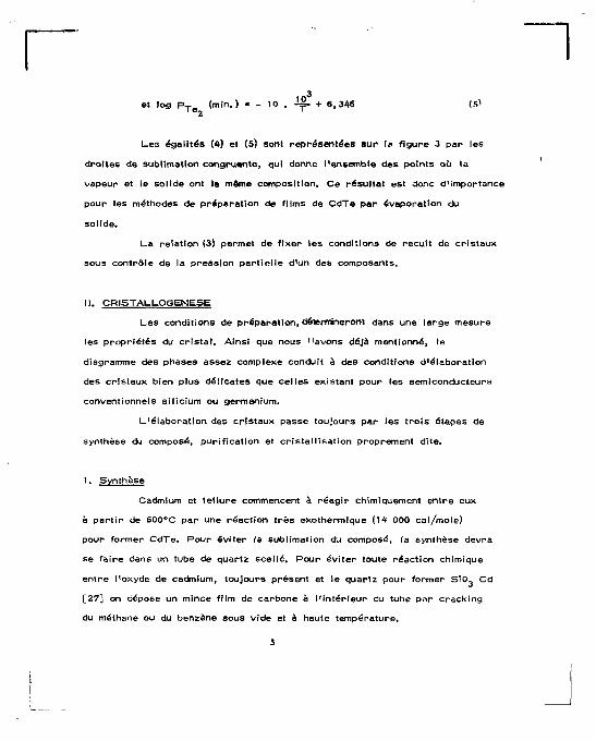
De nombreuses méthodes de croissance de cristaux massifs ou en
films minces ont été publiés dans la l i t térature. Une bibliographie complète
se trouve dans [ 2 1 , 2 8 ] , Notons que les conditions de croissance déterminent
dans une très large mesure les propriétés des cristaux (figure A), Nous nous
limiterons aux techniques employées à l'heure actuelle pour l'élaboration
de cristaux de haute résîstïvité,
6 ; I
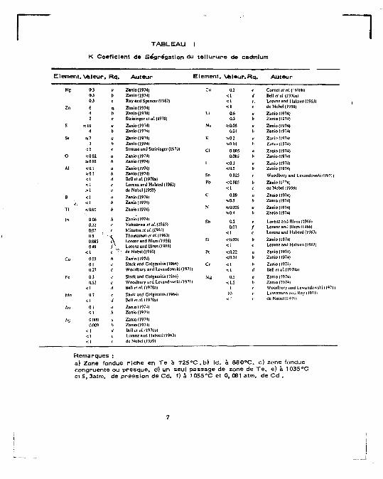
T A B L E A U I
K Coeflcient de ségrégat ion du te l lu rure de cadmium
Element Vfeleur. Rq. Auteur Element, Vfeleur Rq. Auteur
K E 0.3 „ Z in to (1974) Cu 0.2 C Cornet « A/, {1970b) 0.3 b Zanio (1974) •c l d Bell cl ai (1970a) 0.3 c Ray i n d Spencer (1967) < 1 c. Lorenz and Halsled (195J)
Zn 6 a Zanîo (1974) < 1 c de Nobel (1959)
4 b Zanio (1974) L i 0.6 a Zanio (1974) 2 c Steinînger er af. (197D) 0 3 b Zanio( l974)
S = 10 a Zanio (1974) Na =s0.05 a Zanio (1974) 4 b Zanio (1974, Ù01 b Zanio (1974)
Se :s7 a Zanio (19741 K * 0 . 2 a Zanio (19741 2 b Zanio (1974) fc(J.UI h Zanii>tI974)
- t l c Strauss und Sieiningcr (1970) C l aoo5 a Zanio (1974) O = 002 a Zanio (1974) 0.005 h Zanio (1974|
=0.02 b Zanio (1974) 1 <0.1 a Zanio (19741 Al 3:0.1 a Zanio (1974) •=0.5 b Zanio (1974)
sO.l
< l
b il
Zanio (1974) Dél iera/ . (1970a)
Sn 0.025 c Woodbury and LevandowsVi( l97!)
< 1 c Lorcnz and Halsted (1963) Pb <C005 b Z k n i o l F ' M )
> 1 c de Nobel (1959) < 1 c OC Nobel 11959)
B < 1 a
Zanio (1974) C 0.09 a Zanio 11974)
- < l b Zatii6{1974) %0.5 b Zanio (1974)
T l <;0.01 b Zanio (1974) N * 0.005
3:0.4 à Zanio (1974) Znnio( l974)
In 0.06 b Zanio (19741 Sb 0.2 l a r c i n and Blum 119661
011 c Yoko ïawac î m*. (1965) 001 f Lorert7»m] B l u m l l 9 « i |
0.07 0.5 '
c Thoinasscn rf of. |1963|
< 1 c Lottnz and IfalMcd (l'J63i
0.083
c
Larenz and Blum (1966) Ri < 0.001 b Zanio (19741
0.49
c
Lorenzand Mlum(l966) <: <•' Lorcnz and Hnkted (196.1)
< l c de Nobel (1959) Pt <0.02 a Zanio (1974)
Co 0.03 h Zanio (1974) <0.0 l b Zanio ( 1974)
0.1 c Slack and Galginnilis (1964) Cr < 1 b Zanio (1971)
0.21 c Woodbury and Lcvnndowski ( I97 | ) < l il Bell M «t. (19711a)
Fc 0.3 c Slack and Gnlgii iaii is (I964) M g 0 J a Zanio (I974>
IU3 c WaoJburyund Levatidowski (19711 <1.5 b Zanio (1974)
< 1 d B i l l t-rn/. (1970a) l c Woodbury and Lewundowski < 1 •»"» • »
Mn 0.7 d
Slack and Galg inu i lMI964)
Bell n al. (1970a]
10 < 1
c Luwrcnson :md Ray l I V l ) de Nobel ( l ' W |
0!K» 0.009
Zanio (1974] Zanio (1974)
Zanio(1974| Zanio(1974) Bell i t «(.(1970:0 Lorcnz and Halsied(1963] de Nobel (1959)
Remarques : a) Zone fondue r iche en T e à 7 2 5 ° C . b ) Id. à 8 8 0 ° C . c) zone fondue congruente ou presque, d) un seul passage de zone de T e . e) à 1035°C et 5, 3atm. de pression de Cd. f) à 1 05S°C et 0, 061 atm. de Cd .
A. Mé node pap fusion de zone
L 'apparei l lage de purif icat ion par fusion de zone peut ê t re employé,
après purif ication à la cr is ta l l isat ion du composé. La f igure S en indique
les éléments essentiels. Les cristaux obtenus sont du type N , de résist îv î té
100-500 A . cm, la mobilité des por teurs , notamment à basse température est
élevée. L a vitesse de croissance est de l 'ordre de 2 mm/h.
B. Méthode de Bridgmann-Stockbarger
E l l e est ut i l isée par plusieurs groupes soit horizontalement
[ 3 2 , 3 3 ] ou vert icalement [ 3 4 , 3 5 ] et schématisée sur la f igure 6 : le lingot
de CdTe est fondu dans un tube de quartz graphité sce l lé , puis sol idif ié à
par t i r d'un germe ou d'une forme appropr iée. Pour maintenir une stoechiométrie
convenable, on établit une pression par t ie l l e de T e ou Cd au moyen d'un
four aux i l l i a i re . L a vitesse, de croissance et de l 'ordre de S mm/h . P a r
addition de dopants ou d'impuretés compensatrices (in notamment) on peut
obtenir la conductivité souhaitée dans des cr istaux de grundes dimensions.
C. Croissance en solvant
Plusieurs var ié tés de croissance en solvant sont mises en oeuvre.
E l l e s découlent toutes du procédé T G 2 M ("température gradient zone melting")
[ 4 2 ] dont le pr incipe est i l lustré par la f igure 7 : un gradient thermique
est é ta l i i dans le solvant tel que T > T . , la concentration ds CdTe à ces
deux températures passent de C . I C j | C . > C . ) ; pour une longueur Z du
solvant un flux f de CdTe d'établit tel que •.
* " f < C , " C2> W
8
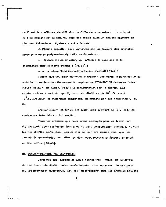
où D est le coefficient de diffusion de CdTe dans le solvant. Le solvant
le plus courant est le tel lure, puis des essais avec un solvant cadmium ou
d'autres éléments ont également été effectués.
A l'heure actuelle, deux variantes ont les faveurs des cr is ta l lo -
graphes pour la préparation de CdTe semi-isolant :
- l'épuisement de solution, qui effectue la synthèse et la
croissance dans le même ensemble [36,37] ;
- la technique THM (travelling heater method) [39-41] .
Notons que ces deux méthodes entraînent une certaine purif ication du
matériau, que leur fonctionnement à température (700-900BC) nettement infé
r ieure au point de fusion, réduit la contamination par le quartz. Les
cristaux obtenus sont de type P, leur résistivîté va de !0 J~l .cm à 9
10 -n..cm pour les matériaux compensés, notamment par des halogènes Cl ou
Br.
L'inconvénient majeur de ces techniques provient de la vitesse de
croissance très faible =- 0. 1 mm/h.
Tous les cristaux que nous avons employés pour ce travail ont
été préparés par la méthode THM avec ou sans compensation chimique, suivant
les résîstîvîtés souhaitées. Les détails de leur croissance ainsi que les
propriétés essentielles sont décrites dans deux travaux antérieurs effectués
au laboratoire [30,45] .
I I I . COMPENSATION PU MATERIAU
Certaines applications de CdTe nécessitent l'emploi de matériaux
de très haute résïstrvité, voire semi-isolants, c'est notamment le cas pour
les spectromètres nucléaires. Or, les imperfections dans les cristaux peuvent
9
jouer un rô le é lectr ique, modifiant considérablement les concentrations
de charges. La première estimation théorique des défauts dans un cr is ta l
pur a été faîte par D E N O B E L [ S ] pour une température de 700 < > C en
fonction de la pression par t ie l le de cadmium. En 1965, KROGER [ 4 6 ] a
général isé ce modèle en considérant l 'existence d'une association simple
entre les lacunes doublement chargées et une impureté chimique. Cet auteur
aboutit à une sér ie d'équations non l inéai res , qu' i l put résoudre moyennant
certaines hypothèses s impl i f icatr ices. Plus récemment, B E L L et W A L D [ 4 7 ]
ont considéré l 'existence d'associations entre une lacune de cadmium V _ .
et deux atomes dopants X . Une étude approfondie de la compensation. dans les
matériaux purs et dopés a été effectuée au laboratoire à la fois d'un point
de vue fondamental et expérimental .
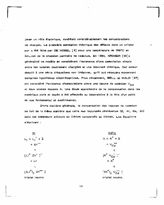
D'une manière générale, la compensation des lacunes de cadmium
se fait de la même manière que ce l le des impuretés résiduel les (B, A l , Ga, Zn)
dans tes compteurs sil icium ou lithium compensés au lithium. Les équations
s'écrivent :
C d T e
[ L i + Z n " ] " [ X + V ] "
tl 11
[ ( L i + ) 2 Z n " " ] [ < X + > 2 V c ~ ]
t r ip let neutre t r ip let neutre
10
Les éléments X les plus efficaces sont les halogènes Cl puis
Br {colonne VII) et l'aluminium (colonne Ml).
Le calcul développé au laboratoire tient compte de toutes les réactions
d'association et d'ionisation des Imperfections. Les énergies d'ionisation
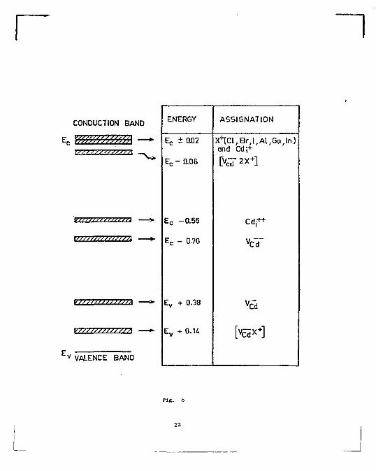
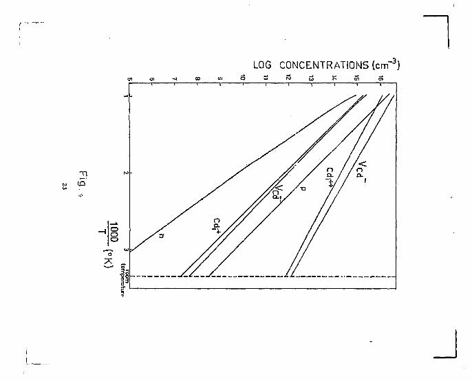
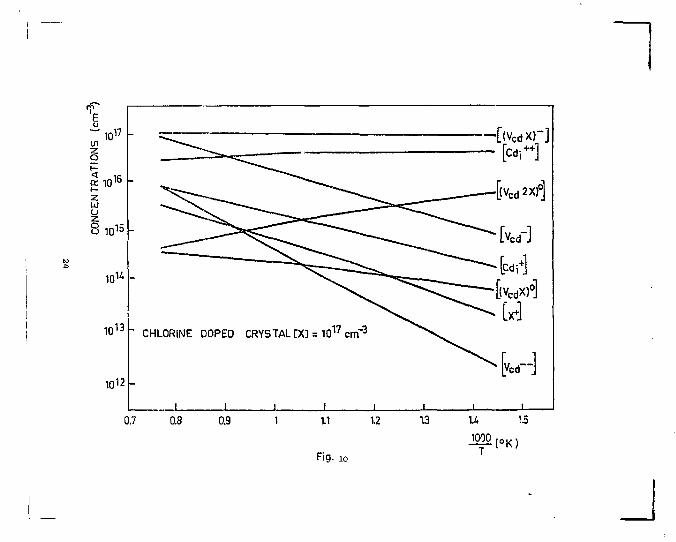
des défauts ont dû être mesurées, i ls Introduisent les niveaux représenté
par Ja figure 8 dans la bande interdite. Les résultats obtenus pour un
17 -3 cr istal pur et pour une compensation par 20 cm de chlore sont reportés
sur les figures 9 et 10, On remarquera la profonde perturbation introduite
par la présence de chlore à I •équilibre des différentes imperfections.
Après ce bref rappel des propriétés thermodynamiques du système
cadmium-tellure, des procédés de cristallogénèse et de compensation, nous
étudierons dans le premier chapitre les méthodes d'analyse de surface par
rétrediffusion Rutherford (RBS) que nous avons développées, l'optimallsation
des résolutions en masse et en profondeur de cette technique, la conception
et la réalisation d'un analyseur électrostatique de haute performance, ainsi
que les mesures de perte d'énergie et de dispersion des ions dans le CdTe»
Dans le deuxième chapitre nous abordons l'analyse proprement dite
des surfaces de CdTe après différents traitements de surface et par d i f
férentes méthodes expérimentales : RBS, 31MS, et ellipsométrïe.
Dans le troisième chapitre nous étudierons diverses méthodes de
réalisation de diodes , notamment ; la diffusion thermique de l'or et du
bismuth, l'implantation ionique ainsi que l'hétérostructure InSb-CdTe.
Enfin dans le dernier chapitre nous nous intéressons aux
détecteurs nucléaires CdTe en mettant un accent particulier sur les p ro
blèmes de la polarisation.
M
REFERENCES
[1] M. OPPENHEIM , J . Prakt. Chem. 71 (18S7) 196.
[ 2 ] M. KOBAYASHI, Z. Anorg. Chem. 69 (1911) 1.
[3 ] J . APPEL, Zeitch. fOr Naturf. 9a (1954) 265.
[4 ] D.A. JENNY, R.H. BUBE, Phys. Rev. 96, 5 (1954) 1190.
[ 5 ] D. DE NOBEL., Phil ips Res. Repts. 14 (1959) 361 et 430
(Thèse Université de Leyde Mai I95S).
[6 ] Proceedings International Symposium on Cadmium Tel lur lde (1971)
STRASBOURG, P. SIFFERT, A. CORNET éditeurs.
[ 7 ] 2nd International Symposium on CdTe , June-July 1976 Strasbourg,
Rev. Phys. Appliquée 12 (1977) n° 2.
[ 8 ] M. R. LORENZ, J . Phys. Chem. Solids 23 (1962) 939.
[9 ] B.M. KUL.WICKI, Thèse (1963) Université du Michigan USA.
[10] J. STE1NINGER, A. J . STRAUSS, R. F. BREBRICK, J. Electrochem.
Soc. 117 (1970) 1305.
[11] R. F. BREBRICK, voir réf. (6) I.
[12] A. S. JORDAN, Met. Trans. 1 (1970) 239.
[13] F . T . J . SMITH, Met. Trans. 1 (1970) 617.
[14] R,C. WHELAN, D. SHAW, Phys. Stat. Sol. 29 (1968) 145.
[15] K. ZANIO, J. Appl. Phys. 41 (1970) 1935.
[16] G. HERSHMAN.F. A. KROGER, voi r réf. (6) I.
[17] O. A. MATVEEV, Yu. V. RUD 1, K. V. SANIN, Sov. Phys. Semicond.
3(1969) 779.
[18] A. ALBERS "Physical Chemistry of Defects11 Chapitre 4 de Physics i_ .d
Chemistry of l l -VI Compounds, D. G. THOMAS Ed. Benjamin, New York
(1967).
[19] J. DROWART, F .J . GOLDFINGER, J. Chem. Phys. 55 (195B) 721.
[20] P.J. GOLDFINGER, M. JEUNEHOMME, Trans. Faraday Soc., 59 (1963)
2851).
[21] A. J. STRAUSS, voir réf. (6) I.
[22] R. F. BREBRICK, A. J. STRAUSS, J. Phys. Chem. Solids 25 (1964) 1441.
[23] A .S . JORDAN, R . R . ZUPP, J. Electrochem. Soc. 116, 9 (1969)1285.
[24] A .J . STRAUSS, Rev. Phys. Appl. 12 (1977) 167.
[25] W. Van ROESBROECK and W. SHOCKLEY, Phys. Rev. 94 (1954), 1558.
[26] F.V. WALD, Rev. Phys. Appl. 12 (1977) 277.
[27] R. TR1BOULET, These Paris 1972.
[28] M. R. LORENZ, in Physics and Chemistry of II—VI compounds (M. Aven
and J. S. Prener ; North Holland (1967) ch. 2).
[29] W. G. PFANN, Zone Melting (Wiley, New York, 1958).
[30] A. CORNET, Thesis Strasbourg (1977).
[31] K.R. ZANIO, A. I .M.A. Materials Conference (1973).
[32] O.A. MATVEEV, S.V. PROKOFIEV and Yu. V. Rud, Inorg. Mat. 5 (1969)
1175.
[33] E.N. ARKADEVA and O.A. MATVEEV, Sov. Phys. Semicond. 10 (1976)
1278.
[34] N.R. KYLE, J. Electrochem. Soc. 118 (1971) 1790.
[35] K. ZANIO, J. NEELAND and H. MONTANO, IEEE Trans. Nucl. Sci.
NS 17 (1970) 287.
[36] M. RUBENSTEIN, J. of Crystal Growth 3, 4 (1968) 309.
13
[37] K.R. 2ANIO, J. Electron. Mater. 3, (1974) 327.
[38] M. WEINSTEIN, A. I. MLAVSKY, J. Appl. Phys. 35 (1964) 1892.
[39] R.O. BELL, N. HEMMAT, F. WALD, Phys. Stat. Sol(a)l(1970) 375.
[40] F. WALD, R.O. BELL, A. A. MENNA, Interim Technical Report
Contrat USAEC N ' AT (30-0-4202 (1971).
[41] G.A. WOLFF, A . I . MLAVSKY dans Crystal Growth, Théorie and Techni
ques, volume I . C . H . L. GOODMAN Ed. Plenum Press, New York (1974).
[42] W.G. PFANN, Trans. Met. Soc. AIME 203 (195S) 961.
[43] .-LO. BELL, J. Electrochem. Soc. 121 (1974) 1366.
[44] F.V. WALO and R.O. BELL, J. Crystal Growth 30 (1975) 29.
[45] R. STUCK, Thèse Université Louis Pasteur , Strasbourg (avril 1976).
[46] F. A. KROGER, J. Phys. Chem. Solids 26 (1965) 1717.
[47] R.O. BELL, F. WALD, C. CANALI, F. NAVA, G. OTTAVIANI,
IEEE Trans. Nucl. Sel. NS 21 (1974) 331.
14
50 60 70 80 90. 100 FRACTION MOUIRE x DE TELLURE (%)
Fig.
T{°K)"
uoo :
1200-
1000-
800 4.IQUID SOLID
600
400
V* Cd EXCESS (cm -3)
10 .18 Te EXCESS (cm - 3 )
pig.
Cd l o =0 5 b l b Te W 5 plied) W 2
Fig.
» TPB(Te) 1 , 10 —•P(bors)
J
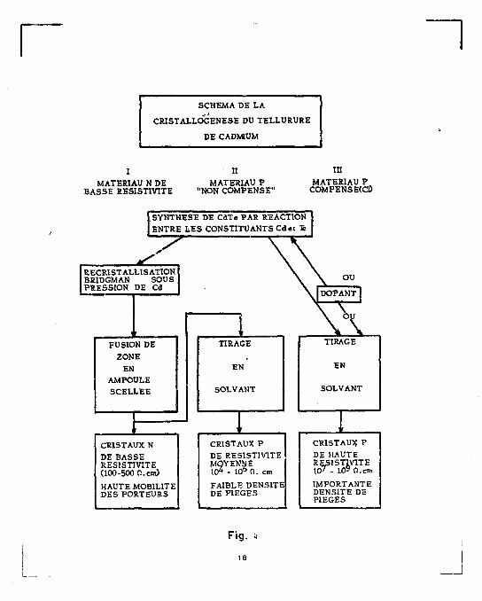
SCHEMA DE LA
CRISTALLOGENESE DU TELLURURE
DE CADMUM
MATERIAU N DE BASSE RESISTIVITE
MATERIAU P "NON COMPENSE"
III MATERIAU P
COMFENSE(Cl)
SYNTHESE DE CdTe PAR REACTION ENTRE LES CONSTITUANTS Cdet %
"7^ *S
RECRISTAL BR1DGMAN PRESSION
LISATION SOUS
DE Cd
1 1 ' FUSION DE
ZONE EN
AMPOULE SCELLEE
TIRAGE
EN
SOLVANT
1 1
CRISTAUX N CRISTAUX P DE BASSE RESISTIVITE (100-500 G. cm)
DE RESISTIVITE MOYENNE 1 0 4 - 10& 0 . cm
HAUTE MOBILITE DES PORTEURS
FAIBLE DENSITE DE PIEGES
CRISTAUX P DE HAUTE RESISTIVITE 10 ' - 10? Cl. cm IMPORTANTE DENSITE DE PIEGES
18
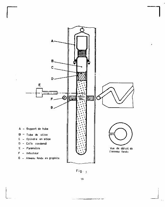
A - Support de tube
B — Tube de silice
C - Cylindre en silica
D - CdTe condensé
E - Pyromètre
F - Inducteur
6 - Anneau fendu en graphite
Vue de détail de l'anneau fendu
Fig.
19
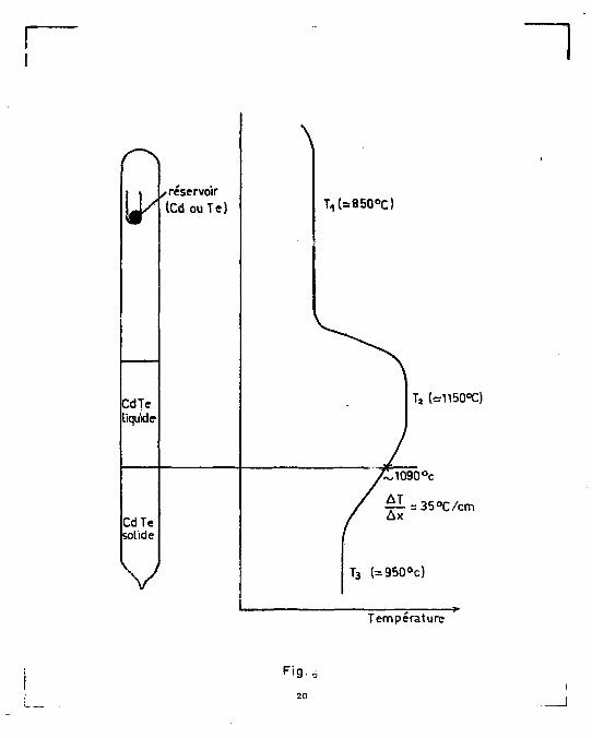
r~\
LK< reservoir (Cd ou Te)
CdTe liquide
CdTe solide
V
\
T, (=850°C)
T2 («n50°C)
1090°c
£I=35°C/cm Ax
T3 (=950°c)
Température
Fig-6
20
TEMPERATURE ,
CdTe
" A Tl Tl
i
z Solvent
J ,B T2 T2
1 • - • -
C
1 • - • -%Te
Fig. 7
-2 L 1 COMPOSITION
% Cd-
J
CONDUCTION BAND
EC YmVMWA -
vzzzzzzzzzzzzm
vzzzzzzzzzzzzzz
zzzzzzzzzzœa
" v VALENCE BAND
ENERGY ASSIGNATION
Ec ± 0 0 2 X + (C l ,B r , l ,A l ,Ga , l n ) ond Cd]+
Ec - 0.06 [vcT2x+]
E c -0.56 Cdj++
E c - 0.70 vcT
E v + 0.38 vc"d
E v + 0.1A focâ**]
Flg. fe
LOG CONCENTRATIONS (cm - 3)
J
(°K) Fïg.
CHAPITRE 1
ANALYSE DE SURFACE PAR RETRODIFFUSION
DE PARTICULES CHARGEES
INTRODUCTION
Les méthodes de caractér îsat îon des matériaux semiconducteurs
sont multiples. Dans le cas préc is de CdTe techniques optiques, é l e c t r i q u e s . . .
n'avaient été mises en oeuvre jusqu'Ici que pour approfondir les propr iétés
de volume, a lors que les effets de surface avalent été négligés. Au sein
du Centre de Recherches Nucléaires nous disposons d'accélérateurs de p a r t i
cules de type Van de Graoff permettant d'étendre les techniques d'analyse
de surfaces, par rétrodiffusîon de part icules chargées, hors et en conditions
de canalisation, à l ' investigation de ce matériau b ina i re . En effet, la
rétrodiffusîon Rutherfords'ost avérée ê t re un instrument de choix des zones
superf iciel les des cristaux semiconducteurs : analyse de masse qualitative
et quantitative, mesure d'épaisseur de perturbat ions, prof i ls de dommages,
d'impuretés, qualités cristal lographiques, locallsationsd'impuretés dans le
25
réseau pouvant ê t re établies d'une façon non destructive (cf. réf . de [ 1 ] ) .
1. ANALYSE PAR RETRODIFFUSION DE PARTICULES CHARGEES
L a f igure 6 de la ré f . [ 1 ] donne le schéma de pr incipe a lors
que les relat ions ( l ï , (2) , et (6) expriment les moyens de son ut i l isat ion.
Un faisceau d'îons d'énergie E et de masse M . bombarde une cible de masse
M„. Les project i les rétrodlffusées Immédiatement à la surface auront une
énergie K E , ceux rétrodif fusés plus profondément dans le volume K E , soit
après une perte d'énergie AE - E - E. Habituellement, ces project i les
rétrodiffusés sont détectés par une diode à b a r r i è r e de surface ayant une
4 + résolution en énergie de 16 kev* pour des faisceaux de He de quelques
MeV, ce qui permet une résolution en masse de 50 uma pour Au et 6 pour
Ga. Un spectre typique obtenu pour un cr is ta l de C d T e , dans ces conditions,
est représenté sur la f igure 2 du troisième a r t i c l e du dernier chapitre. Si
ces conditions de fonctionnement sont suffisantes pour étudier les qualités
cr ista l l ines de la cible» el les deviennent notoirement insuffisantes lorsqu' i l
s'agit d'étudier une surface tant la résolution en profondeur qu'en masse
sont trop faibles. Pour amél iorer les performances de la technique de r é t r o -
dîffusion Rutherford(appelée couramment R. B. S . } plusieurs auteurs ont
suggéré l'emploi de project i les plus lourds. Toutefois, dans ces conditions,
les performances des diodes à b a r r i è r e de surface se dégradent t rès rap ide
ment (mauvaise résolution en énergie , non l inéar i té de réponse, dégradation
par le bombardement ionique). Pour pa l l ie r -as inconvénients, nous avons
développé un analyseur électrostatique t rès performant capable de fonctionner
avec des project i les légers et lourds jusqu'à des énergies de î MeV, capable
d'une résolution en masse de 1 uma au moins et une résolution en profondeur
10 fols mei l leure que les systèmes uti l isés au préalable [ 1 - 2 ] .
26
I I . P E R T E S D ' E N E R G I E
Peur effectuer une analyse préc ise par R B S , il est nécessaire
de connaître avec précision le pouvoir d 'ar rê t des différents project i les
mis en oeuvre en fonction de l 'énergie, ainsi que les fluctuations de per te
d'énergie ("straggling") . Ceci apparaft clairement dans la formule (6) de la
réf . [ 1 ] ou la relat ion (10) et la f igure 9 de la réf . [ 2 ] : les valeurs s . ,
s„ et s de la per te d'énergie sont les facteurs essentiels affectant la
transformation de l 'échelle d'énergie en échelle d'épaisseur. Lorsque ces
travaux ont débuté, seules des valeurs calculées semi-empiriques étaient
connues ainsi qu'un t ravai l sur InSb (de 2 moyen 50 comme CdTe) datant de
1956 [ 3 ] , Nous avons donc dû entreprendre l'étude systématique des pouvoirs
1 + 4 + d'arrêt pour H et He dans le domaine énergétique 0 f 5 - 3 MeV. Af in
de nous assurer de l 'exactitude de notre approche, nous avons simultanément
mesuré pour les mêmes project i les les pertes d'énergie dans Z n T e , pour
lequel un t ravai l expérimental récent existait [ 4 ] ,
Les valeurs expérimentales trouvées sont en assez bon accord
1 + 4 + avec les modèles semi-empiriques pour Z n T e à la fois pour H et He
ainsi que pour CdTe et des project i les H . Des écarts apparaissent pour
H e + dans CdTe surtout avec les modèles de W I L L I A M S O N , BOUJOT,
P I C A R D [ 5 ] qu'avec celui de L I N D H A R D , S C H A R F et S C H I O T T . Notons
toutefois, que les valeurs expérimentales trouvées sont systématiquement plus
grandes que cel les prévues par tous ces modèles. Ces écarts peuvent, peut
ê t re , ê t re interprêtés à la lumière d'un modèle de B R A N D T [ 5 ] qui tient
compte de l'effet de l 'existence de la bande interdi te , dans le semiconducteur,
sur le pouvoir d 'ar rê t ; E L KOMOS et P A P E [ 7 ] ont tenté tout récemment
de vé r i f i e r ce modèle [ our 2 n T e , U et C avec plus ou moins de bonheur :
27
l'allure des courbes suivait les prévisions théoriques, mais les valeurs
trouvées étalent nettement plus Importantes que celles trouvées expérimenta
lement, très probablement a cause d'une surestimation du noml ,-e des
électrons mis en jeu dans le modèle.
Les fluctuations de perte d'énergie que nous avons pu établir, sont,
à notre connaissance, les premières portant sur ces semiconducteurs
binaires î elles revêtent évidemment une grande importance, puisqu'elles
fixeront les résolutions en profondeur que pourra donner !a méthode RBS.
REFERENCES
[1] M. HAGE-ALI, P. SIFFERT, Nucl. tnstr. and Meth. 166 (1979) 411.
[2] M. HAGE-ALI, P. SIFFERT, à paraître dans Radiation Effects.
[3] G. W. GOBELl, Phys. Rev. 103 (1956) 275.
[4 ] A, BONTEMPS, E. LIGEON and FONTENILLE, Rad. Effects 21(1974)181.
[5] C F . WILLIAMSON, J .P. BOUJOT and J. PICARD, CEA Report R 3042
Sac lay (1966).
[6] W. BRANDT, J. REINHEIMER, Phys. Rev. B2, 3104 (1970).
[71 S. G. EL KOMOS, A. PAPE, Communication privée.
28
COMPOUND SEMICONDUCTORS SURFACE CHARACTERIZATION BY HIGH RESOLUTION RUTHERFORD BACKSCATTERING
M. HAGE-ALI and P. SIFFEKT
Centre de Recherches Sucféaires. Croupe ée Phytiqve et Appticalfons des Semietniductevrs. (Phase). 67037 Strasbourg - Cedex, Frmce
Received 20 July 1979
For the surface analysis of compound semiconductor crystals, classical Rutherford btckscattering conditions are too poor, especially with respect to the mass resolution, mainly as a result of the limited resolution of solid state detectors. To overcome this difficulty, we have developed an electrostatic analyzer operating up to 1 MeV energy, with an energy resolution nf up to Q.4%. The optimum operating conditions will be discussed for RBS measurements performed with 4 Ht*. 'Li*. "C ' projectiles, since this set-up ts much less sensitive to degradation by the heavier ions as compared with the sem .conductor diodes. The capabilities and limitations of this system will be investigated and discussed for GaAs and CdTe coûtais: in particular, the conditions for optimal mass resolution will be considered in some detail.
1. Introduction Rutherford backscatlering (RBS) and channeling
of light particles, like ' H + or 4 H e + , has become a quite popular technique for investigating both metals and semiconductors near the surface1-3). However, the ultimate performance of this nuclear technique is for to be reached in most of the experimental arrangements, which make use, mainly for simplicity, of solid slate detectors, essentially Schonky gold-silicon surface barriers, which do not give the highest possible energy resolution and the performance •".." which quickly degrades for heavier projectiles, oonte authors4"*) improved the possibilities of the system by making use of magnetic analyzers (for example of Cuechner type) which are quite heavy, space and lime consuming systems; some others, including ourselves, investigated the possibilities of electrostatic analyzers (ESA). In general the latter are limited to an energy domain below 300-500 keV *-•), which is quite correct for investigating a matrix of mono-atomic composition (Si), but which is ?oain not sufficient for compound semiconductors K e GaAs, CdTe, InP..., which are of increasing importance in solid slate electronics.
Here, we show that is is possible to extend ESA up to the MeV energy range. But, before considering the later we will, examine in some detail the optimal mass and depth resolution problems in RB5
2. Basic considerations
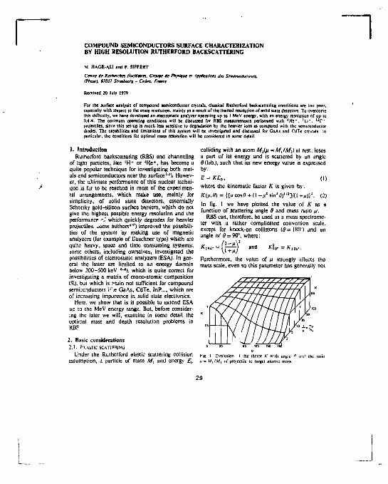
2.1 . ELASTIC SCATTERING
Under the Rutherford elastic scattering collision assumption, a particle of mass M] and energy £ 0
colliding with an atom M^iji =• Mt/M2) at rest, loses a part of its energy and is scattered by an angle 0(lab.), such that its new energy value is expressed by:
E = KE0, <i)
where the kinematic factor K is given by:
KO'.") = {tftcosO+ (]-»* sin10)i!lH(i+v)}2. (2)
In fig. I we have plotted the value of K as a function of scattering angle B and mass ratio it.
RBS can, therefore, be used as a mass spectrometer with a rather complicated convert ion scale, except for knock-on collisions (0= 180") and an angle of 6 = 90°, where :
* • - ( & ) ' : ^ 1 8 (
Furthermore, the value of fi strongly affects the mass scale, even so this parameter has generally not
Fig. I Evolution f ihe factor A.' with angle fl ;inil ihc ratio (i - My/Mj of projectile to target atomic mas-i
M. HAGE-ALI AND P. SIFFËRT
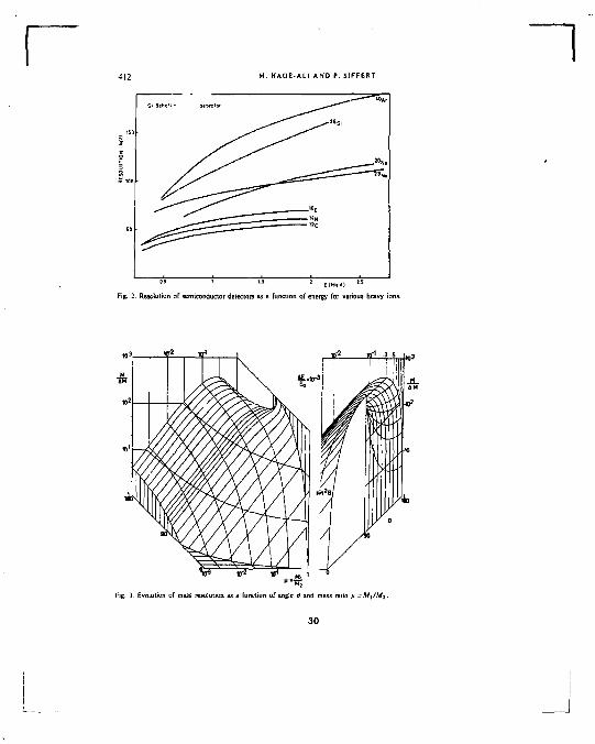
' E IM«VJ " Fig. 1. Resolution of semiconductor detectors as a function of energy for various heavy ions.
y g . . nH
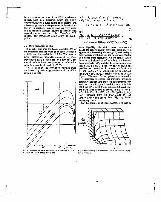
Fig. 3. Evolution of mass resolution as a function of angle 6 and mass ratio /i=Mt/Mj.
30
been considered in most of the RBS experiments. Indeed, solid state detectors, which are mostly employed, exhibit a pulse height defect (PHD)9) and a fast energy resolution degradation for heavier ions (Tig. 2). In addition, ihese counters are very sensitive to radiation damage induced by heavier ions, especially when they are cooled. Therefore, ESA suggests new possibilities which justify its investigation.
2.2. MASS RESOLUTION IN RBS
It is quite clear that the beam resolution J £ 0 of the impinging particles must be as good as possible lo fully use the capabilities of RBS. The Van de Graaff accelerators generally employed for these experiments have a resolution of a few keV, but several methods have been proposed to reduce this value lo a couple of hundred eV l Q).
Let us establish the correlation between mass resolution âM2 and energy resolution AE, by differentiating eq. (1):
9 : 150" i
*& *'/ / / / w
/ / . i . 1. . , . I
AE_ E a 2p[ ( l - ; i ' s irr0) l ; ' + jicosO] AM, " M, ( 1 + / I ) J ( 1 - / J J sin*©)"1 *
x [ l+ ) j - cosO{( l -p J s in J 0)" 2 +^cos : 0} ] ,
M, £ 0 2n[{\-nlAn'0)ul -Mcos01 AM3 AE ( l + ^ d - ^ s i n ' O ) 1 " x
( 4 )
x [l+zi-cose^l-^sin^J'^+^cos 1»)],
where MJAMi is the relative mass resolution and E„/AE the relative energy resolution. From eq. (4) it appears that increasing the energy £0 and having a better energy resolution AE are factors contributing to a better mass resolution. All the spread factors have to be included in AE especially, the inlrinsic beam resolution AE„ and the detection set-up resolution 6E. Figure 3 gives, for any situation the possible mass resolution. It appears that for 8 close to <90° and p = 1 the best results can be achieved: for EIAE= 101, M,IAM, reaches values up to 1000 if ju = I. Therefore, for an optimal mass resolution it is necessary to choose the incoming projectile, especially heavier ions than the conventional 'H-and 4He*. If this optimal condition cannot be full-filled but 90°<9<180° and 0 . 2 « i < 0 . 4 conditions are quite satisfactory: as shown in fig. 4, for El AE = 0.Sx\0\ 9=150°, A/j = 70 (gallium), M,/ AM} increases from 88 0 ^ = 0.8) to 195 ( 4 ^ = 0.36) when going from «He- to '"Ne" impinging beams.
For the optimal conditions 9=180°, it should be
'" '" » B = H , / M
4. Variation of mass resolution as a function of ( 150° for various energy résolutions.
Fig. 5. Bacfcscattenng ditTerentiat cross section <J<r/di? as a function of 6 and ti.
414 M. HAGE-AL1 AND P. SIFFERT
mentioned thai the energy of the backscatiered particles is very low and that the backscattering differential cross section, expressed by:
[(l-/< 3 sin a f>) 1 / 2 4-co5e] a , _ (hh£X-(î-tsûifey1
dff
dfi
also becomes small (fig. 5) when 0 . 1 < / J < 1 . These conditions are, therefore, not realistic. But, for p. < 1 and 0<9O°, dff/di2 becomes quite interesting us well as M2/AMj (fig. 3). With the ESA system and vdg having heavy ion beams, this domain can now be explored.
2.3. DEPTH RESOLUTION RBS
The depth resolution corresponds to the smallest distance at which two layers (or a distribution) must be to t e seen by the system with resolution AE in energy: from the geometry shown in fig. 6, it is possible to write:
AE » £ 0 - £ | =
x r = C(K,e)St, (6) in which S; and S2 are the energy loss or the impinging and backscatiered particle, 5 is the mean energy loss, C a factor depending on K and Q.
ÔE = C5ôt, btft = àEjâE. (7)
The conditions for the best depth resolution are : (A) Increase in the layer thickness i: in general / cannol be changed, however, by using glancing angle geometry 0=85° it is possible lo strongiy increase the real thickness seen by the beam. From fig, 6 <•, = //cos 0\ can multiply the apparent thick
ness up to 20. It should be noticed that glancing angle geometry requires, quite perfect surf" i pla-narity, precise angular measurements... (B) Use of an energy £ 0 corresponding to the maximum of stopping power; to reach the maximum value of AE it is necessary that 5, and 5, are the highest possible. As shown in fig. 7 this value depends on the nature of the projectile, the stopping medium and the energy: it reaches its optimum at 100 keV for 'H + /Si, at 500 keV for 4 H eV Si + and at around 3 MeV for | 3C*/Si. The 5 values corresponding to the extreme A/, range from a few eVA~' up to several hundred. As a result the absolute AE value can be increased 4-5 times when using heavy projectiles.
(C) Reducing the energy straggling: as previously indicated it is possible to improve the energy resolution of the Van de Graaff accelerators to about 600-700 eV at 1 MeV. - Use high resolution detectors: cooled- solid state detectors can be used only for light projectiles, whereas ESA is a better choice especially for heavier ions, since resolution up to 4 keV at 1 MeV can be reached. - Stragsling of the energy as a function of depth: This constitutes a fundamental limitation of this analysis techniques. The depth straggling can be expressed as:
St = 2.35(47tZfZ 2 e4 a e /VC K l # )" 2 -/ I / 2 /S,
where <rc is a correction factor due to Chu and Mayer") and N is the target density.
For heavy targets, after a penetration of 0.1 p, the resolution becomes approximately equal to that of a solid stale detector under 4He~ bombardment.
Since all contributions to energy peak broadening
0700
060D " ^ S ? , V^c ^ < i ^ t>
asm
Slopping pow«f j ^ -0(00
Fig. 6. Schematic, of surface analysis by RBS. Fig. 7. Evolution or stopping power with energy in various
32
are added in a quadratic manner, for rather deep layers the use of sophisticated detection systems does not improve the possibilities or this technique. - Plural scattering: the probability between single />, and double diffusion Pt is expressed by :
P 2 /P, =2nNx 0 F(« a . l B )ZjZ2**/i6£ a . where a is the diffusion angle in the center of mass system.
This ratio PlfPx reduces to less than i% if e ( in LSS units) is in excess of 30. Since e = 10£(keV)/ Z{Z2, £ (keV)>3Z,Z 2 .
h becomes clear that for heavier ions, higher energies must be used in order to reduce plural scattering. - Charge state; solid slate detectors are not sensitive to the charge state of the particles they detect. In electrostatic analysis, for high precision measurements the charge state effect of the backscattered particles should be considered. Figure 8 gives some information1 1 , 1 3). For heavier projectiles the problem becomes more sophisticated and it would be desirable to use a detector able to resolve the various charge states of the projectiles.
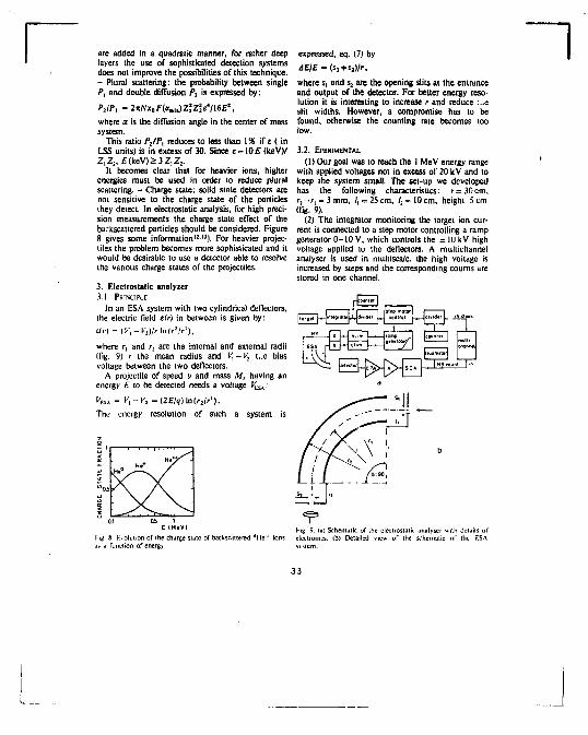
3. Electrostatic analyzer 3.1 PRINCIPLE
In an ESA system with two cylindrical deflectors, the electric field e(r) in between is given by: £(,-) = ( r , - ^ ) / r l n ( r V ) ,
where rL and r2 are the internal and external radii (fig. 9) r the mean radius and C , - ^ t,.e bias voltage between the two deflectors.
A projectile of speed u and mass M2 having an energy £ to be detected needs a voltage V^ :
Vzs* = yi~V2=(2Etq)ln(r2lrl). The energy resolution of such a system is
hg. 8 Evolution of the charge state of backscattered 4 He* ions as a function of energy.
expressed, eq. <7) by / ! £ / £ - (st+s2)lr,
where s, and s2 are the opening slits at the entrance and output of the detector. For better energy resolution it is interesting to increase r and reduce ...e slit widths. However, a compromise has to be found, otherwise the counting rate becomes too low.
3.2. EPERIMENTAL
(1) Our goal was to reach the 1 MeV energy range with applied voltages not in excess of 20 kV and to keep the system small. The set-up we developed has the following characteristics: r=3ftcm, rj-/-[ = 3mm, /, = 25 cm, / j = l 0 c m , height 5 cm (fig. 9).
(2) The integrator monitoring the target ion current is connected to a step motor controlling a ramp generator 0-10 V, which controls the ± 10 kV high voltage applied to the deflectors. A multichannel analyser is used in muitiscale, the high voltage is increased by steps and the corresponding counts are stored in one channel.
hg 9. la] Schematic of the elecirostaik analyser with details ol electronics, ft» Detailed view of the schematic of the P.SA system.
33
416 M. HAGE-ALI AND P. SIFFERT
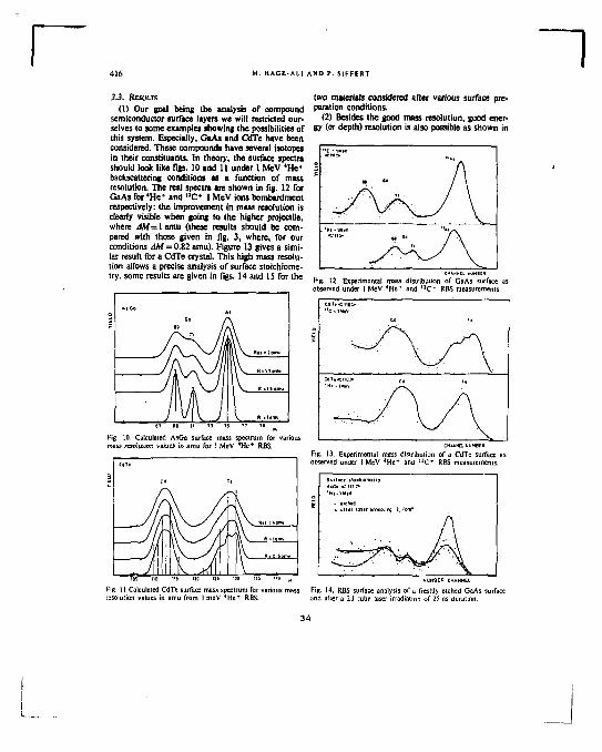
3.3. RESULTS (1) Our goal being the analysis of compound
semiconductor surface layers we will restricted ourselves to some examples showing the possibilities of this system. Especially, GaAs and CdTe have been considered. These compounds have several isotopes in their constituants. In theory, the surface spectra should look like fits. 10 and 11 under 1 MeV 'He* backscattering conditions as a function or mass resolution. The real spectra are shown in fig. 12 for GaAs for 'He* and "C* 1 MeV ions bombardment respectively: the improvement in mass resolution is clearly visible when going to the higher projectile, where AM-1 amu (these results should be compared with those given in fig. 3, where, for our conditions AM = 0,82 amu). Figure 13 gives a similar result for a CdTe crystal. This high mass resolution allows a precise analysis of surface stoichiome-try, some results are given in figs. 14 and 15 for the
A ) CO Al 00 / \
• / A \
/, M ^ » M . ! « ~ 1 M ,. R-IT»« 1 \ , M _A V \ ! 1 . . . t .™.
Fig. 10. Calculated AsGa surface mass spectrum Tor various mass resolution values in amu Tor 1 MeV 4 H e + [IBS,
two materials considered after various surface preparation conditions.
(2) Besides the good mass resolution, good energy (or depth) resolution is also possible as shown in
Fig. 12. Experimental mass distribution or GaAs surface as observed under 1 MeV *He + and T I C f RBS measurements.
CrJI«<l10> "c-IMlV
CO It
cai.<iiQ> Cd la
CHANNEL NUMBt* Fig. 13. Experimental mass distribution of a CdTe surface as
RBS measurements.
NUMBER CHANNEL
Fig. 11 Calculated CdTe surface mass spectrum for various mass resolution values in amu from 1 meV 4 H e + RBS.
Fig. 14. RBS surface analysis of a freshly etched GaAs surface and after a 2J ruby laser irradiation of 25 ns duration.
34
U T • <11B> 1) eUtrrt
a - 71 tthidllriih) a 1) • (JnMhi)
C* I t
' 3 _//£^, \ it" • 1
An i«vir JT»i *H«-1M«V
• • !»•
t — «1%
«*/ \ ~ V J | J \ ~ V J | J
CHANNCL NUHIEH CHMMCL MK*Ck
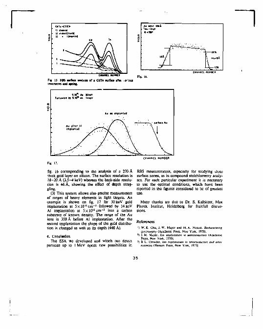
Fig. 15. RBS surface anajyiit of a CdTe surface arte. Ji^oua ueaimenu and agckif.
Fi». 16.
S.KT AM XtMV Followid by 5.W* Al UhiV
Au « mpientri
\l
Fig. 17.
fig. 16 corresponding to the analysis of a 270 À thick gold layer on silicon. The surface resolution is 18-20 À (3.5-4 keV) whereas the back-side resolution is 46 A, showing the effect of depth straggling.
(3) This system allows also precise measurement of ranges of heavy elements in light targets. An example is shown on fig. 17 for 30keV gold implantation at 5 x l O 1 5 c m - 2 followed by 14keV AI implantation at 5 x 1 0 " c m - 2 into a carbon substrate of known density. The range of the Au ions is 350 À before Ai implantation. After the second implantation the shape of the gold distribution is changed as well as its depth (440 À}.
4. Conclusion The E5A we developed and which can detect
particles up to 1 MeV opens new possibilities in
CHANNEL NUMBER
RBS measurements, especially for studying close surface zones, as in compound stoichiometry analyses. For each particular experiment it is necessary to use the optimal conditions, which have been reported in the figures considered to be of greatest use.
Many thanks are due to Dr. S. Kalbitzer, Max Planck Institut, Heidelberg for fruitful! discussions.
References
') W. K. Chu, J. W. Mayer and M, A. Nicolei. Backscattehng spectrometry (Academic Press. New York. ! 978).
3) J. M. Mayer, ton implantation in semiconductors (Academic Press. New York, 1970).
3) B. L. Crowder, Ion implantation in semiconductors and other materials (Plenum Press. New York, 1973).
35
~1 M. HAGE-AL1 AND P. S1FPERT
*) J. K. Hirvonen and G. K. HuWer In Ion beam surface byer *> A. Grot», J.J. On*. P. SilTert, Nucl. InMr. ami î*îeih. 132 anabsis (ed. 0. Meyer (Plenum Press, New York, 1976X
' ) E. Begh, Rid EfT. 12 (1972) 13. *) A. V. Wijngurden, B - Miremadï and W. Baylis, Can. J.
Phys. 49 (1971) 2440. J ) A. Fcuersiein, H. Grahmann, S. Kalbiizer and H. Oeizmann.
ret 4 p. 471. 8 ) I. Bergstrom, K. Bjdrkvist, B. Domej, G. Flidda and S.
Andersen, Can. J. Phys. 46 (1968) 2679.
(1976) 273. l û ) G. Amsel, J. P. Nadii, E. D'Arwmire. D. David, E. Girard
and J. Moulin, Nucl. Insir. and Meih. ȕ H970 48I. ") J. W. Mayer and W. K. Chu, Catania working data: "Energy
toss and energy straggling " (1974). ") J . C Armstrong, Proc. Phys. Soc. M (1%S| 1283. I J I A. U n e , IBMRC 5816 Report (1976).
3 6
ELECTROSTATIC ANALYSIS OF BACKSCATTERED
HEAVY IONS FCR SEMICONDUCTOR SURFACE
INVESTIGATION
M.HAGE-ALI, P. SIFFERT
CENTRE DE RECHERCHES NUCLEAIRES Croupe de Physique et Applications des Semiconducteurs (PHASE)
23, rue du Loess 67037 STRASBOURG-CEDEX (FRANCE)
ABSTRACT
The capabilities of Rutherford backscattertng in surface analysis
ts limited by the energy resolution of the solid state detectors and their
rapid degradation for heavier project i les. Here, we investigate the possi
bi l i t ies of an electrostatic aniyzer (ESA) detecting heavy projecti les
( L I , C ) backscattered from various compound semiconductor surfaces,
essentially, with respect to mass and depth resolution.
37
ELECTROSTATIC ANALYSIS OF BACKSCATTERED HEAVY IONS FOR SEMICONDUCTOR SURFACE INVESTIGATION
I . INTRODUCTION
Surface analysis by means of ion beams in the keV-MeV energy range becomes a very powerful method for investigating solids. Among the various techniques employed, Rutherford backscattering (RBS) of V or 4He + ions in the 1-5 HeV range, the detector being a si l icon Schottky barr ier, offers many advantages : non destructabi l i ty, absolute concentration and location of impurities, etc. Many publication on the subject are available, especially concerning semiconductor surfaces [ 1-3 ] . The l ight project i les, mentioned above have been chosen essentially for t ie easy bbam production in the Van de Graaff accelerator and the good detection capabilities of s i l icon Schottky diodes for these part icles. In pr inciple, however, heavier ions should.offer several advantages [ 4 ] , part icularly better mass a.id depth resolution and high cross section. Therefore, several groups have tr ied to employ either C+ [ 5-8 ] , N+ [9-111,
0 + C 12] or even L i + [ 13-15 ] beams. But, several problem arise when sol id state detectors are used with heavy ions [16,17] :
- the detector degrades quickly due to the radiation damage induced in the s i l icon and the Schottky barrier (F ig. l ) ;
- the energy resolution is much poorer for heavy ion than for protons ( f ig.2) due to fluctuations in energy loss by nuclear col l is ions, which give no electron-hole pairs ;
- the amplitude of the signal is smaller and depends on the type of particle,because of window effects and nuclear coll isions ( f i g . 3 ) .
To improve the resolution of RBS, some authors suggested the use of magnetic analyzers [ 18-19 ] , which are rather cumbersome systems or electrostat i c analyzers (ESA), which are usually l imited to use with low energy ions (< 500 keV) (7, 21, 22).
Here,we consider the possibi l i t ies of ESA for " l igh t " heavy projectiles of energies up to 1 MeV and also the advantages attending the use of the heavier ions when the drawbacks due to other detection systems are eliminated.
38
I I . ION SCATTERING
1. Ki nemati cs Under the Rutherford elastic scattering col l is ion assumption, a
project i le of energy E and mass M, scattered at a lab angle 8 from an atom M2 at rest (u = Mj/M^ looses part of i t s i n i t i a l energy, such that i t s new value is :
E = K E 0 , ( 1 )
where the factor K is expressed by :
K(p,9) = { [ ucos 9 + (1 - u 2 s i n 2 9 ) 1 / 2 ] / ( l + u ) j 2 , (2)
with sin 8 < 1/u . (3)
The evolution of K as a function of 1/u and 9 i s shown in f i g .4 .
RBS i s , therefore, useful for mass analysis with a rather complicated conversion scale K, except for two angles 9 = 90 and 180°, where :
K180° = ' ~ ' * K90° = K180° (* '
In f ig.4 we have also plotted the K values for u 2 1 even though this condition is generally not used in RBS, but which nevertheless constitues a domain of interest in some situations as w i l l be considered la ter . I t is interesting to notice at this point that for relative l ight elements ( l / i i -2 } , K is rather uniform for a l l '-.Ovalues, leading to a rather poor mass resolution. For heavy ions ( l / ; : « ) , K changes more drast ical ly, especially for particular (9) and (p) values. I t i s , therefore interesting to evaluate the mass resolution.
2. Mass resolution in RBS Let us establish the relationship existing between the energy
resolution AE and the mass resolution AM„. By di f ferent iat ing eq.( l ) we can write :
A E = A K - E o = | M 2
i H 2 - E o - (5)
39
From eq. 2 , we have :
iK = - 2 [(1-u 2 sin 2 B) 1 / 2 + ucos 9]fl+g - cos 6 [(l-u 2sin 28) 1 / , 2+g cos 6 ) j \ ( 6 )
(1 + u) 3 (1 - u 2 s i n 2 9 ) 1 / 2
^ % 2 - - v r 2 - <*>
Combining eq. 5-7, eq. 5 becomes :
A E = ( ^ X - H ; ) i M 2 - E o
and
E 0 ,.. M . „2c-in2mV2 i M 2 i E (1+ M) (1-M s i n ^ B ) 1 ' ^ I J
Figure 5 gives the evolution of mass resolution versus (8) and (y) for a relative resolution in energy AE/E =10 . I t should be pointed out that the maximum in mass resolution increases from 380 to 1000 when (y)increases from 0.26 to 1 and 9 varies from 180 to 90° for ,i> 1 and 0°< 9 < 90°, S reaches very high values, going to <*> for
9 = arc sin ± . As mentioned above£hese conditions are not used in RBS today.
The backscattering cross section, expressed by : 2
dci , Z 1 Z 2 e , 2 J, [ (1 - u 2 s i n 2 9 ) 1 / 2 + cos9] 2 , 0 , d ! 4 E Q sin*9 (1 - u 2 s i n 2 9 ) 1 / Z
is showr: on (f ig.6) the values for the 0° < 9 < 90° and y ~ 1 conditions one s t i l l better than at 9 = 180°.
A specific example,perhaps,shows the improvement better : From Fig.7 i t appears that for Mj = 70 (gallium), 9 = 150°, ^ - = 4°/oo,
40
J j increases from 43 with \e*imz = 1.6) to 98 for a 1 2 C + beam (AM2 = 0.7)
and 4M, reaches even 6 for He+ ion and a conventional surface barrier detector {-£• = 1.7 %).
o Further conclusion can be drawn from eq. (8) :
- the impinging beam should have as high as possible energy E - the resolution i£ shoud be the best. I t should be mentioned that a few hundred (eV) beam energy dispersion are attainable today U 23 3 with Van de Graaff accelerators. Ideally .a detection system should be able to measure t h i s , which.of course .is not (the case) with solid state detectors, as indicated above.
III. DEPTH RESOLUTION IN RBS
For an energy resolution AE, the depth resolution - = can be calculated by considering f ig .8
SE = V E * <c^©7 S l + H5sV2> D <10>
in which S, and S, are the energy loss of the project i le in the impinging and backscattered direct ion. To simplify,we can choose a mean energy loss 5 such that :
and
SE -~ E„ - E =(K - — J SD ' ( 1 1 )
o c o s g
D <K " 35ff> * D
u _ m a r . . . . 3D SE * ( 1 2 )
D C- u cos 8 +(1 - y 2 s i n 2 9 ) 1 / 2 , z 1 \ ,5D> , . , , 5D~ = { c
1 + ) J
] " co55-J («E") • ( " >
As we did previously for the mass resolution, we report on f ig.9 the evolution of depth resolution versus 9 and p. When going from l ight to heavy project i les, the kinematics depth resolution degrades at least
41
! • i
a factor of two at 9 » 180", for u going from 10 to u » 1 but in reality, this value must be multiplied by the stopping power ? and divided by the energy resolution. The optimum depth resolution is , therefore, achieved when the following conditions are ful l f i led :
- a good energy resolution <5E - as large a thickness. D. as possible. This can be art i f ic ial ly
obtained by using glancing angle geometry - use of particules and energy E corresponding to the maximum
stopping power 5. This maximum starts around 100 keV for H +
and Increases with the mass of the projectile (fig.10) being 12 +
around 3 MeV for C . I t i s , therefore, advantageous to use an ESA operating at high energy. 7 Increases fro» 6 eV/A° for 1 H + to 30 eV/A° for 4He + and 120 eV/A* for 1 Z C + , in Al • »11 projectiles having 1 MeV energy. This value Is even higher, by a factor 2-3, for heavy targets like Au or Hi.
- reduction in the energy straggling (20). The energy fluctuation of the machine must be as small as possible. However, after a penetration of about 1000 A°, the beam straggling becomes equivalent to the resolution of a solid state detector ; therefore, sophisticated ESA is really of full use in investigating close surface layers.
IV. THE ELECTROSTATIC ANALYSER (ESA)
The principle and practical realization of our ESA, which operates up to 1 HeV for all particles have been published elsewhere (20). For theory see ref (24-26). Here we restrict ourself to fig.10 and 11 showing the schematic of the system.
V. RESULTS As previously indicated, an ESA system using heavy ions in the
42 ! J
MeV range is best suited for surface analysis at depths less than 1000 A. As an example of its capabilities (see fig. 13 ? and b) and we show the stoichiometry of compound semiconductors Ga As and CdTe after surface treatment. These compounds are comprised of several isotopes. Depending on the mass resolution of the apparatus and the nature of the projectile, the theoretical spectra are those reported on fig.14 and 15 with ions backseattered from Ga As and CdTe surfaces. The equivalent experimental spectra are given on fig.16 and 19, first with light projectiles and then for Li + and C + beams. For Ga As, the mass resolution AM 2 improves from 1.7 for 4 H e + , to 1.4 for 7 L i + and 0.8 for C*. In the case of CdTe, the values go from 5 to 2 for the same projectiles (with a Schottty barrier the mass resolution would be 17 for an detector energy resolution of 16 keV).
When channelling conditions are requested, the use of heavy ions constitutes a further advantage since the critical angles become larger, as shown on fig.20 for CdTe and Li for ex. the theoretical values (27,28) are also reported.
CONCLUSION The combination of ESA and heavy 1on projectiles open new
possibilities of RBS in surface analysis, both in depth or mass resolution. The main drawback of this technique is the long counting time/several hours per spectrum/ for low cross section elements. Besides the stoichiometry measurements we have shown this procedure is also of importance for measuring heavy ions diffusion (fig.13b) range of particles in light targets [ 14,21 :
43
References
1. J.W.Mayer ; ion implantation in semiconductors (Academic Press, New York, 1970)
2. B.L.Crowder, Ion Implantation in Semiconductors and Other Materials (Plenum Press, New York, 1973)
3. U.K.Chu, J.W.Mayer and M.A.Nicolet, Backscattering Spectrometry (Academic Press, New York, 1978).
4. J.H.Mayer, L.Eriksson, J.A.Davies, Ion implantation in Semiconductors (Academic Press, London 1970) p. 143
5. L.C.Feldmann, E.N.Kaufmann, J.W.Mingay, W.M.Augustyniak, Phys.Rev.Let. 27 (1971) 1145
6. L.Erifksson, G.Fladda , K.Bjorkqvist, Appl. Phys.Lett.24 (1969) 195 7. I.Bergstrom, K.Bjorkvist, B.DaseTj , G.Fladda, Can.J.Phys.46(1968)2679. 8. F.Abel, G.Amsel, M.Bruneaux, C.Cohen, B.Maurel, S.Rigo, J.Roussel,
J.Radioanal.Chem. 16 (1973)587. 9. L.C.Feldman, D.E.Murnick, Phys.Rev.85 (1972) 1 10. R.B.Alexander, Ph.O.Thesis, Oxford 1971, AERE Report 6849 11. Bogh. Proc.Roy.Soc.A311 (1969) 35 12. Ref.(4), p. 145 13. J.P.Thomas, A.Cachard, M.Fallavier, I.Tardy, S.Marsaud et J.Pivot,
Rev. Phys.Appliquée U_(1976) 65. 14. i d . ion beam surface Layer analysis (Meyer, Linker, Ka'ppeler) Plenum
Press (1976) p.425 15. J.L'Ecuyer, C.Brassard, C.Cardinal, L.Deschene, Y.Jutras, J.P.Lôbrie
Nucl. Instr. and Meth. WO (1977) 305. 16. A.Groo, J.J.Grob, P.Sif fert , Nucl. Instr . Meth. 132 (1976) 273. 17. J.J.Grob, Thesis Université de Strasbourg (1979) (f ig.44) 18. J.K.Hirvonen, G.K.Hubler.réf.14 , p. 457. 19. E.Begh Radi Effects 12 (1972) 13 20. M.Hage A l i , P.Sif fert , Nucl. Instr . Meth. 166 (1979) 411 21. A.V.Wijngaarden, B.Miranadi, W.Baylis, Can.J.Phys.49 (1971)2440 22. A.Feuerstein, H.Grahmann, S.Kalbitzer and Oetzmann ref .14, page 471. 23. G.Amsel, J.P.hadai, E.D'Arteirare, D.David, E.Girard, J.Moulain
Nucl. Instr. Meth. 92 (1971) 481. 24. E.Durand "Electrostatique Tome I I " éd. Masson Paris (1966) 25. R.Jayaram "Mass spectrometry" (Plenum press, New York, 1966) p.22 26. C.A.McDowell "Mass spectrometry" (Mc Graw-Hill New York (1963) p. 151 27. J.W.Mayer, E.Rimini "Ion Beam Handbook for Material Analysis "
44
(Academic Press, New York, 1977), p. 71
28 J.O.Grob 3è cycle Thesis page 11 Strasbourg (197 )
FIGURE CAPTIONS
F ig . 1 : Resolution degradation of implanted si l icon detectors versus various
heavy Ion doses.
F ig . 2 ; Evolution of si l icon detector energy resolution.with ions species as
a function of energy.
F ig. 3 : Effect of nuclear coll isions on pulse amplitude delivered by a si l icon
detector versus energy for various heavy Ions.
F ig. 4 : Evolution of kinematic factor K versus laboratory angle 9 and mass
ratio 1/n ,
F ig . 5 : Evolution of the resolution in mass M« / AM« as a function of angle 8
mass ratio p. for AE/E = 10~ f with extension to M .> M~ .
F ig . 6 : Evolution of the relative backseat tering cross-section versus 9 and p. .
F iy , 7 : Evolution of mass resolution M„ / A M~ as a function of ratio g, and
energy resolution A E / E 0 for an angle 6 « 150 °, Notice the progress
when going from Schottky si l icon detector ( res ..ution 2<fo ) to the
electrostatic system ( resolution 4 ° / 0 0 ) .
Fig. 8 ; Principle of backscattterîng analysis.
F ig . 9 : Evolution of depth resolution versus 9 and v..
Fig. 10 : Stopping power of various ions in aluminium! arrows and brackets give
maximum stopping power for some heavier targets ( Be>Ti, Ag, Au.Nî) e
expressed in eV /A .
F ig. 11 ; Schematic drawing of our electrostatic analyzer.
Fig. 12 : Electronic set-up used in E. S. A. analysis system.
F ig . 13 : (a) ESA analysis of a gold layer 270 A thick , showing the surface and
depth resolution,
(b) Comparison of ESA =, id Schottky bar r ie r detector performance in
analyzing a diffused gold layer into si l icon.
Fig. 14 -.Calculated surface spectrum of AsGa as seen by backscattering under
channelling conditions for various mass resolutions.
F ig. 15 : Calculated surface spectrum of CdTe as seen by backscattering under
channelling conditions for various mass resolut ion 5 •
F ig . 16-17: Experimental spectra obtained on GaAs observed by backscattering wi th
l M e V , 2 C + , V , 7 U + i o n s . 12 + F ig. Ï8 : Backscattering spectrum obtained with C ions impinging under random
incidence on GaAs .
F ig. 19 : 5urface analysis of CdTe under channelling conditions as seen with 1 MeV 1 2 + 4 +
C and He projecti les. F ig , 20 : Angular scanning of an <T 11 0> axis of CdTe as seen by 1 MeV 7 L i + ions.
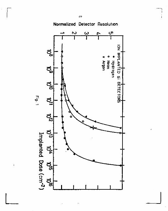
i.V
Normalized Detector Resolution
- » NJ CO 4N (SI
o 00
«3,
%
o . -
q , ro
3 e l <*>
T3
n> O ,
(D *» CL
(D
O
3 o.
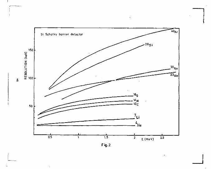
E(MeV)
_ i
> «I T
THOMSEN CAUCULATIONS
Exp-
10 èL J I 2.10" 10
Fig. 3
10 ENERGIE (MeV)
J
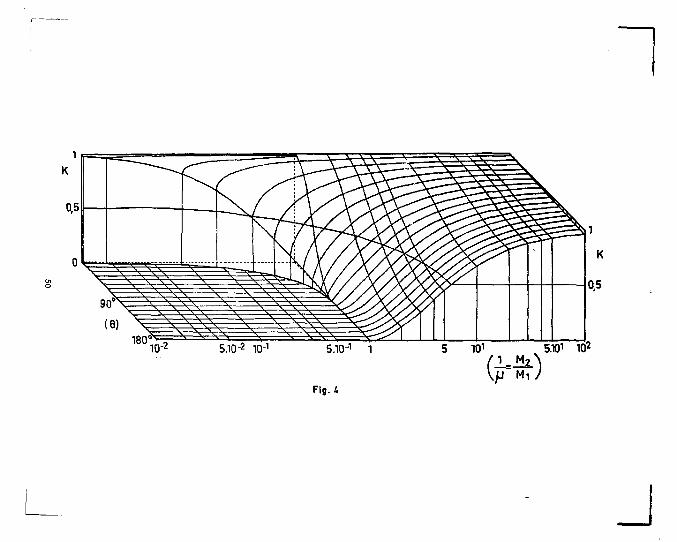
Fig. 4
J
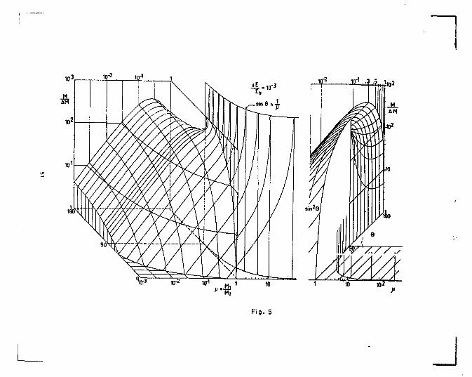
F ig . 5
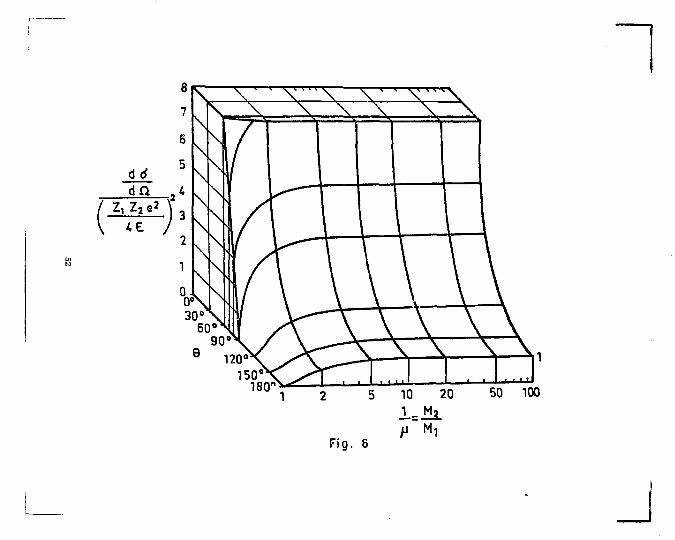
Fig. 6
i J
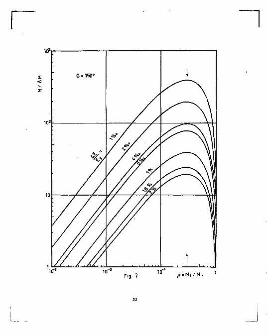
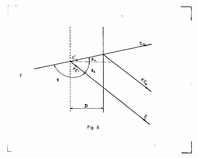
Fig. 8
J
Fig. 9
J
TO
MeV.cm^ mg
! STOPPING POWER IN 2 7 A I
MeV Fig. 10
Fig. 11
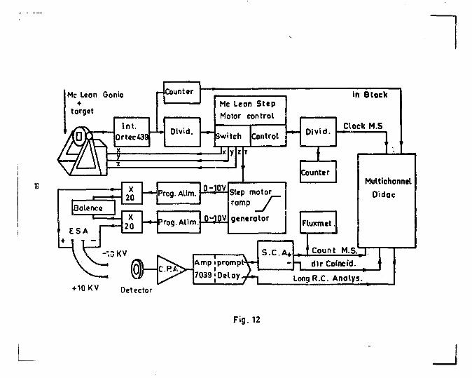
Mc Leon Gonio +
target
Int. Ortec439
4Counter
Dlvid.
Mc Lean Step Motor control
Switch
Prog. Alim. 0-)0V
•-Prog. Alim 0-JOV
Control
Step motor ramp f
generator
Divid.
IE
in Block
Clock M.S
Counter
Fluxmet.
+ 10 KV Detector
arv^Tm7y P7o^Y W | ^>^^7039 ;De loy . /> 1
S.C.A* Count M.S
Multichonnd Oidac
J - | dirCoincid. i .
LongR.C. Anolys.
Fig. 12
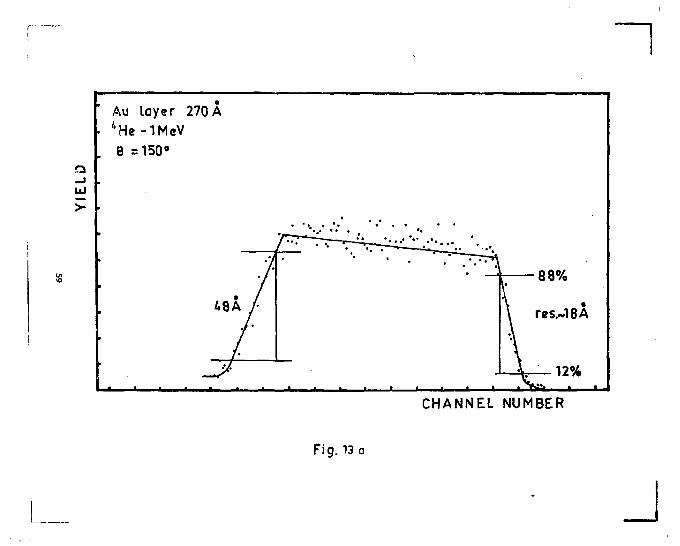
Au layer 270 À 4He-1MeV 6 =150°
L - i 1 — i — i 1 • -» -̂» CHANNEL NUMBER
Fig. 13 a
J
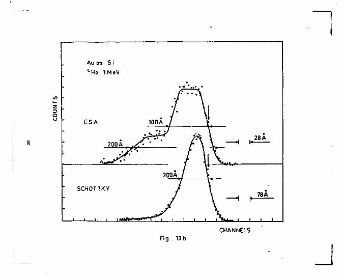
Au on S i'
'•He 1MeV
Z o u ESA
SCHOTTK
K 28 A
78A
ba-J I I L
CHANNELS Fig . 13 b
J
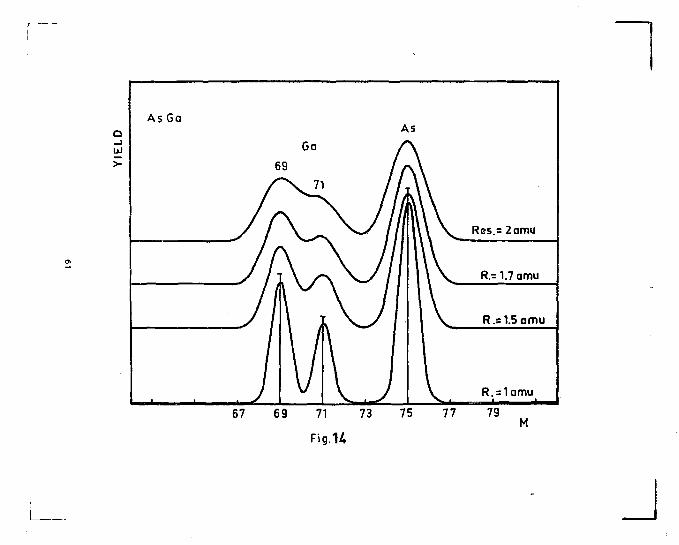
As 6a o UJ
>-
Res.= 2amu
R/=1.7amu
R.= 1.5amu
R.=1amu
79 M
Fi g. H
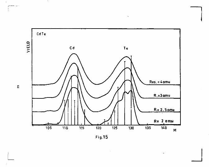
CdTe
§ Cd Te
Res. = 6amu
R.=3amu
R.= 2.5 amu
R= 2 amju
140 M
J
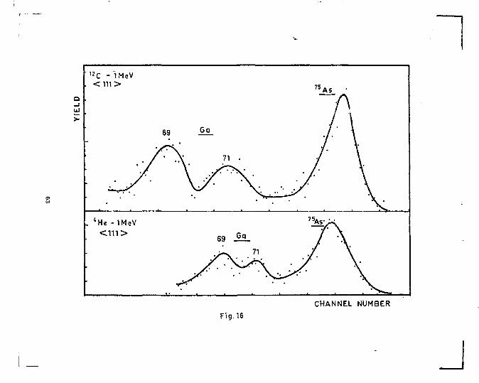
1 2 C - IMeV Y
IEL
D
. < 1 1 1 >
69 Go
71 •
7lAf_ •
. ' H e - I M e V < 1 1 1 > 69 1°.
71
' — < \
CHANNEL NUMBER Fig.16
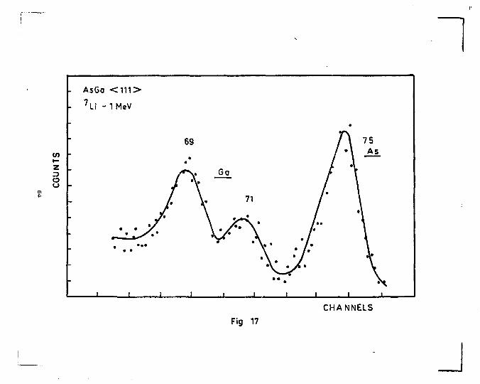
As6o 7 U - IMeV
69
•
A 75
CO
UN
TS
-
/ •
* •
V
Go
71 / •
/ \ —
-
i
7*
• •
i
•
•
* \ * • \ \ •
• •
„..J .
*
• 1
• •
/« • / / •
1
• 1
A*
., i . , J —
CHANNELS Fig 17
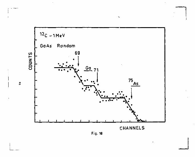
1 2 C -1MeV
GaAs Random
i— z O o
69
• • • ' • I * • • - • \ » #
75 As
• «v» • • • • • * • • *
W- » .»
J I i i i i i i i t i i SZtxl
Fig. 18 CHANNELS
CdTe<110> 12
>
C -1MeV
Cd Te
CdTe<110> 'He- IMeV
fig.19
CHANNEL NUMBER
m t—
2 O
CdTe < 1 1 0 > 7 Li -1MeV
1E0RY *H« "Li
* 1 1,3» 1,8»
J
Radiation Effect j 1977, Vol. 33,193-197
© Cordon and Breach Science Publishers Ltd., 1977 Printed in (Jre.il Britain
STOPPING POWER AND STRAGGLING OF !H AND 4He IN ZnTe AND CdTe
A. PAPE, M. HAGE-ALI, S. M. REFAEI, P. S1FFERT anil E. L. COOPERMANt Centre de Recherches Nucléaires and Université Louis Pasteur, 67037 Strasbourg Cedex, France
(Received April 12, 1977)
Stopping power measurements have been made for ZnTe and CdTe for ptotDm and a-paiticles over the energy ran^u 500-2800 keV. Results were derived from transmission energy losses in thin films. Comparisons with theoretical and other experimental data are made. Proton energy straggle values in ZnTe and CdTe have also been obtained. The* uppcar constant over the energy range investigated.
[ INTRODUCTION II EXPERIMENTAL
Besides the fundamenca; interest of energy loss and straggling determinations of charged particles in solids, there is a need for better evaluation of these quantities for practical reasons. These needs result from the application of nuclear methods to the analysis of materials. For example, in the Rutherford backscattering technique, the energy-to-depth scale conversion and the ultimate depth resolution are directly connected to the energy loss and straggle values.
There are numerous calculations and experiments which give the energy loss of protons and tt-particles in solid and gaseous media, but only few straggling measurements have appeared, probably due to experimental difficulties {poor accuracy). In general, these results have been achieved on elemental targets. For the compound semiconductors we are concerned with here the situation is less clear, since the validity of Bragg's Rule is not yet fully established.
In this paper, we present measurements of the stopping power e of protons and a-particles, as well as prnton energy straggling S22p/rV(eV2 * cmVmolecule) in zinc telluride (ZnTe) and cadmium telluride (CdTe) targets for energies between 500 and 2800 keV. These n-VT semiconductors are the subject of increasing interest because of their possibilities as optical (light emitting) or nuclear (detector) devices. To our knowledge, the only other existing information on these compounds consists of several ea and proton and a-particle range measurements in the case of ZnTe between 300 and 2000 keV (Ref. 1), and calculations of e and range for different charged panicles in CdTe (Ref. 2, 3).
Targets Targets consisted of ZnTc and CdTe evaporated from a tantalum boat on to 20 ± I fig/cm1 self-supporting carbon backing. The most uniform targets were selected. For the a-particle measurements, targets of 50-220 /jg/cm1 were used; for the proton work, 160-760 jug/cm1. The areal thicknesses <lr were determined by weighing with a precision of I M -̂
The stoichiometry and purity of the compounds were verified by elastic scattering (Rutherford back-scattering) on separate targets at several incident energies. Within (he experimental sensitivity, no oxygen was observed even after the targets had been stored for weeks in a desiccator. By comparing the backscattcring spectra from the thin targets with that observed on thick non-oriented crystals (Figures I
FIGURE 1 Alpha particle bucksu-attenn}; sinicir-i iumi ,i n.<n-jligned ZnT« cnitaland an evaporated target toi ihc vmw integrated charg>. The dashed curves represent a dcLiim])i>vilu> of the thin target spectrum into the two compuncnit
t Permanent address: California State University, FuUerton, CA 92634
193
6 9
CUT
î l
• i A C K S C A T T Ê K D 5 K C 1 I U OF
1) M O N O U m T a L L M C WUfCR I M N O M I
CUT
î l C V A P M A U O T H M L«EB
CUT
î l C V A P M A U O T H M L«EB
'* \
CUT
î l
'* \ CHAML turn*
FIGURE 2 S U M U Fifurt 1, but for CdT«-
and 2), it appears that the distributions at the high energy edges are identical. The nue separation foi CdTe is, however, too imitU to conclude definitely, whereas the ZnTe films show tlte correct stoichio* metry. To further verify the stokhiometry of the CdTe films, analyses by secondary ion mas» spectroscopy (SIMS) have been performed. It appears (Figure 3) that the composition of the films is close to that of the bulk material.
SIMS RESULTS
4 * L*g[A]-U5g[8] « L
Beam
The beam were delivered by the Strasbourg 3 MV van de Graaff accelerator. All « and ft*IN measuremer* wen mad* by tansmMon with a beam elasticaUy scattered at 90* from a thin cold layer (10-20 j*g/cma) evaporated on to a 20 pf/cm* self-supporting carbon backing. The experimental set-up was similar to that described in Réf. 4. The number of particles hitting the siicon surface barrier detector was thus never enough to deenaeje It, and presumably not enough to modify appreciably the structure of the targets during the experimeem. Typically the resolution (FWHM) of the detected proton peak was about 10 keV.
Energy Loss
The energy loss, ù£t of the charged particles upon traversing a target was obtained from the shift in the center of gravity of the detected proton or aeparticle peak between measurements on the carbon backing and a carbon backing covered with the ZnTe or CdTe film.
«VSTAL
EÏ KB S * g * 3 5 ft* 3 5 " MASS " ~ "" MASS
FIGURE 3 Portions of SIMS mais ipectra measured for bulk ind evsporttcd materials.
7 0
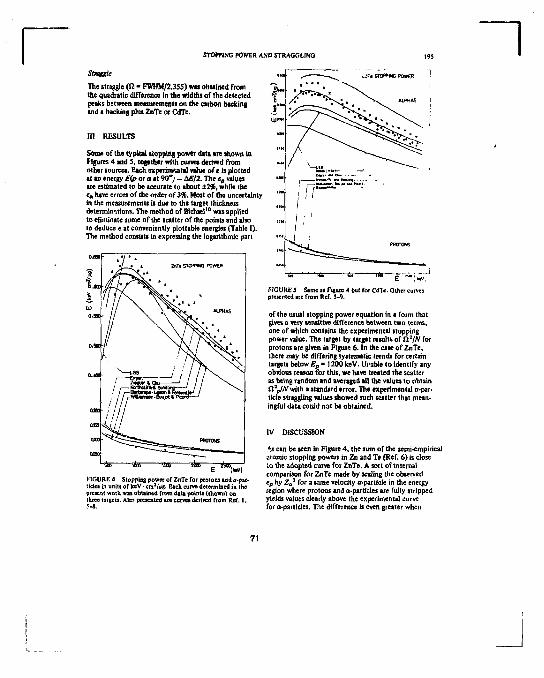
STOWING POWER AND STRAGGLING 195
Straggle
The straggle (SI = FWHM/2.3SS) was obtained from the quadratic difference in the widths o f the detected peaks between measurements on the carbon backing and a backing plus ZnTe or CdTc
i n RESULTS
Some of the typical stopping power data are shown in Figures 4 and 5, together with curves derived from other sources. Each experimental value of e is plotted at a* energy E<p or a at 90° ) - ÛE/2. The ep values are estimated to be accurate to about ±236, while the ea have errors of the order of 3%. Most of the uncertainty in the measurements Is due to the target thickness determinations. The method of Bichsel 1 0 was applied to eliminate some of the scatter of the points and also to deduce € at conveniently plottable energies (Table I). The method consista in expressing the logarithmic pan
Tto -Tria rèw sin—_ ato, ,' E M
FIGURE 4 Stopping power of ZnTe for protons and a-par-tidet in units of keV - cm1/(*g. Each curve determined in the preaenC work w a obtained front data pointa (shown) on three targets. Also presented are carve* derived from Ref. 1, 5-*.
FIGURE 5 Same a* Heure 4 but for CdTc. Other curves presented are from Ref. 3-9.
of the usual stopping power equation in a form that gives a very sensitive difference between two terms, one of which contains the experimental stopping power value. The target by target résulta of SI1 IN for protons are given in Figure 6. In the case of ZnTe, there may be differing systematic trends for certain targets below Ep - 1200 keV. Uf<sMe to identify any obvious reason for this, we have treated the scatter as being random and averaged afj the values t o obtain £!*p//V with a standard error. The experimental a-par-ticle straggling values showed such scatter that meaningful data could not be obtained.
IV DISCUSSION
As can be seen in Figure 4 , the sum of the semi-empirical atomic stopping powers in Zn and Te (Réf. 6) is close to the adopted curve for ZnTe. A sort of internal comparison for ZnTe nude by scaling the observed e
P ty 2^ for a same velocity ft-particle in the energy region where protons and a-particles are fully stripped yields values clearly above the experimental curve for a-particles. The difference is even greater when
71
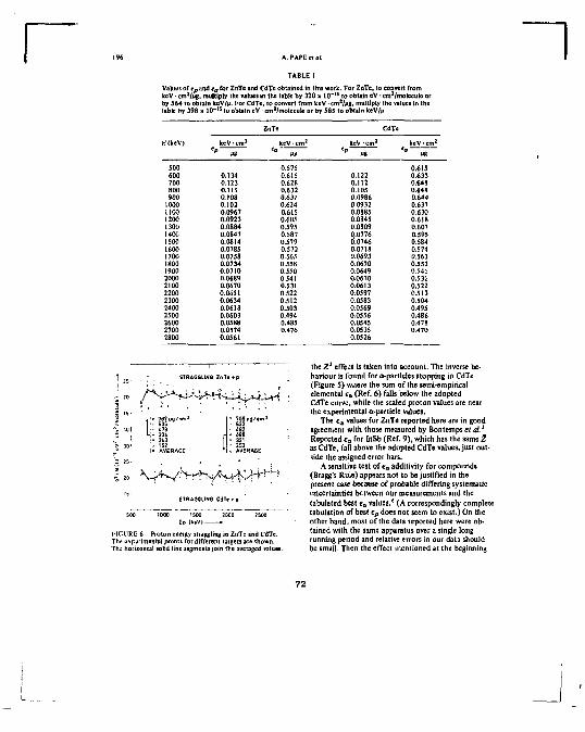
A. PAPE el al.
Values of cp
kcV • cm Vug and e a for ZnTe and CdTc obtained In thb wotk. Foi ZnTe, to convtrt from Values of cp
kcV • cm Vug , multiply the values in the tabic by 320 x 10~ 1 ! to obtain eV cm /molecule or by 564 to oblain kcV/ti. [or CdTc . to convert from keV • cm3/ua, multiply Ihc values In the libit by 398 » 10-" to obtain eV cm'/moleculc Dt by S85 tD obtain keV/p
ZnTe CdTe
fc'fkeV) kcV • cm 1 key • cm 3 k e V c m 3 kev • cm 1
" UH '" m " U8
500 0.575 0.615 600 0.134 0.615 0.122 0.633 700 0.123 0.628 0.112 0.64B 800 0.1 IS 0.632 0 105 0.64B 900 0.108 0.631 0.0986 0.644
1000 0.102 0.624 0.0932 0.637 lira 0.0967 0.615 0.0885 0.630 1200 0.0923 0.6CI5 0.084S 0.618 1300 0.0884 0.595 0.0809 0.607 I40C 0.0847 0.587 0.0776 0.S95 1500 O.08I4 0.579 0.0746 0.584 1600 0.0785 0.572 0.0718 0.574 1700 0.0758 0.565 0.0693 0.563 1800 0.0734 0.558 0.0670 0.552 1900 0.0710 0.550 0.0649 0.541 2000 0.0689 0.541 0.0630 0.531 2100 0.0670 0.531 0.0613 0.522 2200 0.0351 0.522 0.0597 0.513 2300 0.0634 0.512 0.0583 0.504 2400 0.0618 0.503 0.0569 0.495 2S00 0.0603 0.494 0.0556 0.486 2600 0.0588 0.485 0.0545 0.478 2700 0.0574 0.476 0.0535 0.470 2800 0.0561 0.0526
—1 ~ t h e Z 1 effect is taken into account. The i STRAGGLING ZnT.+p havtou r is found for 0>partlcle5 stopping
,Â^'^~^^V^+KÙ44^4-U-Î
I" \ H > N / ^ ^ j A H 4 C > r - H - ;
STRAGGLING CdTe* p
500 1000 1500 20C0 ÎS00 £p Ik.Vi »
I IGV'RC 6 Proton enemy straggling in ZnTe and CdTc, Tin-or cimentai points for different targets art shown. The horizontal solid line segments join the averaged values.
(Figure 5) wnefe the sum of the semi-empirical elemental e„ (Ref. 6) fails below the adopted CdTe curve, while the scaled proton values are near the experimental û-parttcle values.
The € a values for ZnTe reported here are in good agreement with those measured by Bontemps et al. l_ Reported e 0 for InSb (Ref. 9), which has the same Z as CdTe, fall above the adopted CdTe values, just outside the assigned error bars.
A sensitive test of e* addltivity for compounds (Bragg'5 Ru>) appears not to be justified in the present case because of probable differing systematic uncertainties between our measurements and the tabulated best eQ values.6 (A correspondingly complete tabulation of best ep does not seem to exist.) On the other hand, most of the data reported here were obtained with the same apparatus over a single long running period and relative errors in our data should be small. Then the effect mentioned at the beginning
72
STOITINC POWER 'HD STRACOUNC
of this section, Ramery the opposite behaviour in ZnTe end CdTe of the icaled e, mi t„ would appear to be reel end would merit further expérimente] mention. Calculation! ere underway uekaj the atop-ping theory propoeed by Brandt" which explicitly include! the effect of the aeardtterawctor gap.11
The itraggliag reeulu very little over the energy range itudied for both ZaTe end CdTe. There k no deer indication of e dMniiMn( Op'IN with decreasing energy t> predicted by the elaborate calculations of Chu and Mayer." The valuec for CdTe, when ex-pteued on a per atom beeie, ere ever thaw reported at f p - 1000 keV for Sb(Ref. I«) for which Z - 5 1 , being about 75* of the value celculMee) with the Bohr formula for light wbttancci." Value» of atraggk deduced from the curveigiven by Clarice w are much larger than thcee observed here.
ACKNOWLEDGEMENTS
We wish to thank Mrs. Aadree Mesas for preeeriag Ike targets.
REFERENCES
I. A. Bontemps, E. Ligeon and J. FonteniUe. Red. Eft- en 21.181 (1974).
2. H. V. Gepta ma A. K. Cheakay, Atei Inn,. Met*. KM, 339<1»7».
3. A. K. Canker and H. V. Gafta. Ret. toys. App. 12, 321 (1»77).
4. S. Corodetaky, A. Chevalier, A. rape. 1. C. Sent, A. M. hwedolt, M, >rei aad R. Arrnoriiiur, Ate/, Pnyt. Atl , 133 (1967).
S.J. Llnlhard, M. ScharTf seat II. E. SchhMt, Ktl. Chmkc 'TeVsufeee. Ware», Ku.-rn M«U. 33,1 (1963).
6. J. F. Zlaajereild W. K. Oui, At. DtutndNucl. DIM 7fcMnl3,4<3(l*74).
7. L. C. Nonndsfft end ». F. ScMllira), Hud. Dm TMcs 7.233(1*70).
t. C. F. Taaemmn J. p. eo»Jo< end J. Pteard, CEA Report R 3042, ledey (INC).
9. G. W. CoWe.ffiM Ret. 1(3,275 (1956). 10. H. Ucteal, "A Critical Review or t . . '.rrmcnisl Slopping
Power aid Rasa* Data", in JtaeVrr In Pnctntton of aurmrtrtkktmmtw. Peetkatfcn 1133, NAS-NRC. WaelinrarUM, D.C., or Amarieea Innltute of Physics Haadbook (McGraw-Hill, New York. 1972) section 8.
11. W. headland J. Retoheiavir./tyr. Ret. B2, 3104 (1970). 12. S. El KomoM, Pkyilcs Department, University of Stiu.
botua (private coramuelcatioa). 13. W. K. Ow aad J. W.Mayer, Cuuile Vorktm Dsu
lii.pubUaW). 14. E. Lemlaen and A. Antllle,̂ tMR. Acad. Sclent. Fenn.
AVI, No. 370 (1971), asqaolad In Ref. 13. 15. N. don,, Ktl. Dmke Vtdeiuktb. Selsklh. Mai.Fys
Uedd. 11,1(194»), 16. N M. Clarke./VueJ. Intlr. Htlh. 96,497 (1971).
73
C H A P I T R E II
A N A L Y S E D E S S U R F A C E S D E CdTe
I l est bien connu que les propr ié tés de surface déterminent dans
une large mesure les propr iétés des dispositifs semiconducteurs. L e
te l lurure de cadmium n'échappe pas à cette règ le , encore que, pour ce
matériau, tous les auteurs ont observé de mei l leures performances é lect r ique:
lorsque les surfaces sont simplement rodées ou pol ies, a lors que pour tous le-
autres cr istaux un cl ivage ou décapage chimique s 'avéra i t p ré fé rab le .
P a r a i l l eurs , nous avions observé certaines évolutions des p e r
formances des détecteurs nucléaires lors de leur viei l l issement a l 'a i r ,
entraînant une dégradation de leurs performances. Cette dégradation était la
plus importante pour les structures oxydées en surface et entraînait un impor
tant accroissement de la polar isat ion.
Comme aucune étude des surfaces de C d T e n'était disponible dans
la l i t téra ture , nous avons été amenés à entreprendre leur étude systématique
pour les diverses surfaces habituellement mises en oeuvre : rodées ou pol ies,
75
décapées chimiquement (brome methanol) avec ou sans oxydation au
perhydrol .
Essentiellement t ro is méthodes d'analyse ont été mises en oeuvre :
- la rétrodlffuslon de part icules chargées en et hors conditions de
canalisation ("Rétrodlffuslon Rutherford") ;
- la spectrométrie d'Ions secondaires (SIMS) ;
- l 'e l l ipsométrle, dont le pr incipe est décri t dans la référence
[ I ] ainsi que les ar t ic les de ce chapitre.
Les résultats marquants sont les suivants :
- une surface décapée chimiquement (brome-méthanol) paraft r iche
en cadmium, progressivement un oxyde de te l lure croft a l 'a i r , sa composi
tion T e O x tend progresslvment vers T e 0 2 ;
- une surface décapée chimiquement et oxydée par HeO- conduit
probablement a la formation de te l lurates CdTe 0 . en plus de T e 0 - .
Deux ar t ic les récents [ 2 , 3 ] trai tent de l 'analyse des surfaces de
CdTe aprfts décapage chimique (brome-méthanol) par X P S , les conclusions que
leurs auteurs en t irent sont assez divergentes puisque l'un observe un e n
richissement de la surface en T e [ 2 ] a lors que l 'autre [ 3 ] note un excès
de cadmium. Probablement que les conditions dans lesquelles les attaques
chimiques sont effectuées jouent un rôle plus important qu'escompté.
76
i !
REFERENCES
[ I ] M. HAGE-ALI, R. STUCK, C. SCHARAGER, P. SIFFERT
Correlation batween surface properties and datactlon characteristics
of CdTe detectors, IEEE Trans. Nucl. Sci. NS 33 (1979)
[2] V. SOLZBACH, H.J. RICHTER
Sputter cleaning and dry oxidation of CdT , HgTe and H g x Cd. Te
surfaces, (à paraftre).
[3] M.H. PATTERSON, R. H. WILLIAMS
J. Phys. D 11 (1978) L 83.
AppLPhys. 19. 25-33(1979) Applied Physics
© by Springer-Verlag 1979
Studies of CdTe Surfaces with Secondary Ion Mass Spectrometry Rutherford Backscattering and Ellipsometry M. Hage-Ali, R. Stuck, A. N. Saxena* and P. Siffert
Centre de Recherches Nucléaires Groupe de Physique et Applications des Semiconducteurs, (Phase) F-67037 Strasbourg-Cedex, France
Received 26 October 1978/Àccepttd )8 Jinuary 1979
Abatract. The composition and the stability of chemically etched, mechanically polished and oxidized surfaces of single crystals of cadraium-telluride were studied by secondary ion mass spectroscopy (SIMS), Rutherford backscattering (RBS) and ellipsometry. CdTe surfaces etched using a solution of bromine in methanol were found to be enriched in cadmium but a film, identified to be an oxide of tellurium, was observed to grow on it at room temperatu re and in air. The thickness of this film increased over long periods of time t linearly versus h r. Mechanically polished samples and also chemically etched surfaces which were oxidized in a solution of hydrogen peroxide in amoniac were found to be stable.
PACS:68.90ry, 79J0Nc
Due to its large bandgap (£,= 1.45eV) and its high atomic numbers ( Z u = 4 8 , Z T , = 52), cadmium tel-luride (CdTef has the potential for high efficiency y and X rays detectors at room temperature. However, such devices have not become practical and popular so far, mainly because they are not stable when operated for a long period of time. This phenomenon, generally termed as the polarization effect [1-3] has been shown to be related to the metal contacu and even more strongly to the preparation of the CdTe surface before the deposition of the metaL The instability in the CdTe detectors, due to the polarization effect, is generally found to be worst when mechanically polished surfaces are used, to be less when chemically etched samples are employed, and to disappear almost completely when oxidized surfaces are used to fabricate the detectors [4]. Nevertheless, these results could not be explained so far, aainly because of the lack of understanding of the surface properties of cadmium tcOuride. Therefore, a systematic investigation of the various surfaces obtained by these procedures was undertaken using secondary ion mass spectroscopy (SIMS), ellipsometry and Rutherford backscattering (RBS).
* Interntlional Science Co. Palo Alto. CA 94306, USA
1. Experiaertal T« /./. Sample Preparation
Cadmium telluride single-crystals were grown by the travelling heater method (THM) [5]. They were compensated by adding about 10"-10 1 9 chlorine atoms c m ' 3 during growth, the concentration of the halogen really incorporated lies in the range I0 l 6 -10 l 7 cm~ 3 . as seen by mass spectroscopy in the first half of the cryst-'i T ne crystal's resistivity is rather high, in the range 10s to 107 ohm-cm, as measured by the Van der Pauw technique. Slices oriented parallel to the < 110> plane were cut by a winr saw. They were then lapped with silicon carbide powders of various grades having particle sizes from 20 um to 5 urn in diameter. Polishing of the CdTe crystals was done by using alumina powders having par icles of sizes less than 0.3 um in diameter. After poli Jung, the samples were rinsed in methanol
Etched surfaces of CdTe were obtained by immersion of the lapped samples for min in a bromine in methanol solution containing about 12% of bromine. The etching was quenched by excess methanol, rinsed in methanol, the sample was fina'iy blown dry with nitrogen. A similar techniqut was used on polished
0340-3793 79/0H9/0025 -S01.K0
M, Hage-Ali ci al
wafers and the results were the same as those on lapped samples. Oxidized samples were obtained by treating the etched samples in a solution of 4 parts H z 0 2 and 1 part NH4OH at boiling temperature. Reproducible blue colored films were obtained with this procedure. When (he oxidation was done with the same solution at room temperature, varying layer thicknesses were obtained, corresponding to red to purple colors. Only blue colored samples were usrd in the present study.
1.2. Secondary Ion Mass Spectrometry (SIMS)
Secondary Ion Mass Spectrometry [6, 7] was used to determine the elemental composition of the various kinds of CdTe surfaces. The measurements were performed with an apparatus in which both positive and negative ions sputtered off the surface under argon ion bombardment were analyzed with a quadrupole mass filter. The current density of the primary 3 keV Ar + ion beam was kept low enough (<l\iA-cm~2) so that only a thin layer of about 20 À in thickness was sputtered off during the measurement. Thus, only the fi.st atomic layers were analyzed. To reduce the absorption of residual gas molecules on the surface, the pressure in the experiment chamber was kept lower *han 10" * Torr. Due to the low primary beam density xistd no space charge effects [8] were encountered although the investigated samples were semi-insulating.
1.3. ElUpsometry
Ellipsometry measurements on oxidized CdTe surfaces were made to determine the thickness and refractive index of the surface films. This technique determines the changes in the phases and amplitudes of the parallel and perpendicular components of a monochromatic polarized light when it is reflected from the surface being studied [91. OIK of the major advantage of this procedure is that it allows continuous monitoring of the film growth in room ambiant. Details about this method can be found in the literature [10]. Here, we used a He-Ne laser light source emitting at a wavelength of 6328 A, the angle of incidence of the light on the sample was 70c. The compensation (A/4 plate) was fixed at +45°. viz. its fast axis was fixed at +45 r with respect to the plane of incidence. Polarizer and analyzer were rotated to perform the two-zone measurement!,. The data were analyzed using the exact equations of ellipsometry [9], the film thicknesses and their refractive indexes were calculated.
1.4. Ruthertord Backscattering (RBS)
Rutherford backscattering under channelling conditions [11] was used to analyze the crystal damage
and the elemental composition near the surface of the various samples. The oriented crystal samples having had various surface treatement; have been mounted on a three axes goniometer and have been bombaredt,u
with *He + ions of I MeV energy, the energy of the backscattered particles being measured wi'h a high resolution electrostatic anuly;cr. having an energy, and therefore, depth resolution of aboul icn times belter than the conventional systems using surface harrier detectors. In the case of a compound semiconductor, the aligned RBS spectrum {>ield vs. energy of the backscattered pa nicies I reveals the presence of two distinct surface peaks due to the collisions on each kind of atoms at the surface. Thus, the ratio of the area under these two peaks is related to the surface stoichiometry. However, the interpretation of these measurements may be difficult if the surface is covered either by a film or strongly damaged, since the dechannelling level of ihe spectra is then increased. In this case, the areac of hoth peaks are affected in a different manner and a correction becomes necessary.
2. Results
2.1. Freshly Etched Surfaces
The S'MS spectra recorded c>n freshly etched CdTe samples are reported in Figs. 1 and 2. the subscripts a and b refer to the detection of negative and positive ions, respectively. Figure 1 concerns the top surface region about 20À thick, when as Fig. 2 results from a layer located deeper, this la ter can. therefore, be assumed to correspond to the bulk material. The following observations can be made from these data: - the surface is slightly oxidize», since the oxygen peak is more important on the first figure: - other contaminants are près nt in both surface and hulk regions: if Ar is excluded, since it comes from the ion beam used, the following bulk impurities are observed: C. Na. Al, Fc, F, Cl. The first three are introduced during the crystal growth in graphite-coated quartz tubes, the last has been introduced to compensate the crystals, as indicated above. The origin of Fe is less cleai. whereas F if. due to some cleaning process employed. Other impur ties are present in close surface vicinity: 'Ta, Na, Cu, ( r , they arc introduced either during thi handling of the samples or result from the impuriiies included in the chemicals (CH,. Cul. It should l>e mentionned that some of these surface impurities- may have a very strong influence on the fuiure device characteristics;
- 110 conclusion about surface stoichiometrv can be taken from these spectra, because of Ihe selective sputtering effects and of enhancement phenomena.
60
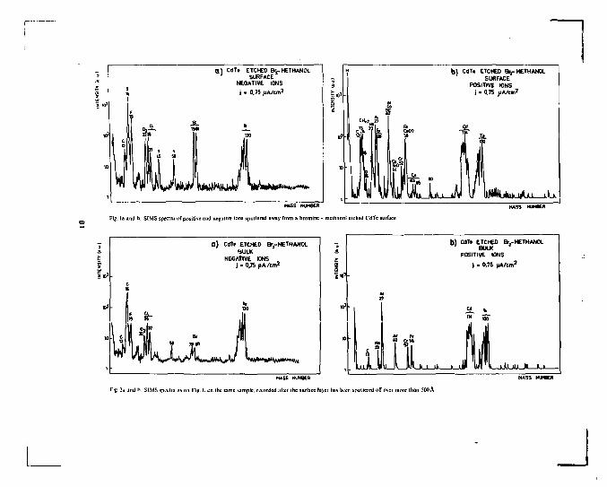
3
O l CdTè ETCHED Bt-METHANOL ' 5URFACE
NEGATIVE IONS
1 m 3
a 1 j • 0,75 pA/cm 2
to2
I 13
a
Il a i
10
i
II y L J I W ^ rwss NUMBER
Fig. la and b. SIMS Spectru of positive and negative ions up uttered away from a bromine - methanol etched CdTe surface
il
HASS MJHKR
b ) COT» ETCHED B j - M E T t M N O .
POSITIVE IONS
J - 0,75 ( > » / c m 2
Pip. ! i and h. SIMS spectra ,
MASS NUMBER
l Fip. 1. on ihe same sample, recorded after the surface layer hat been sputtered off over more than 50» A
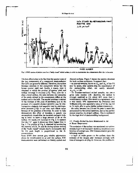
• M. H*fe-Alf ci al.
CdTt ETCHED Br.-METHANOUbodly rlnitd) POSITIVE IONS JOÉ uA/cm2
MASS NUMBER Fig. 3. SIMS spectra of positive ions Tor a "badly rinsed" etched surface, in order to demonstrate the enhancement effect due 10 bromine
The first effect is due to the fact that the sputter rates of the two components of a compound semiconductor like CdTe are generally different. Therefore, the surface becomes enriched in the component which has the lowest sputter yield and, finally, a steady state is obtained in which the product of sputter yield and surface coverage is constant [12], Thus, even for a clean crystal surface, the ratio between tbe intensities of the peaks related to the components differs at the surface and in the bulk. The second problem is related to the increase of the yield of secondary ions in the presence of a reactive element (positive ions by electronegative elements and negative ions by electropositive elements [13]). [n our case, such effects occur because of the presence of bromine. In order to fully demonstrate this effect of bromine, a sample was uncompleted rinsed after the bromine methanol etching in order to leave a large amount of Br at the surface, the results are reported on Fig. 3. It appears that the Cd ' peak is about ten times higher than in Fig. 1. The profiles of Fig. 4, obtained by monitoring the intensity of Cd, Te, and Br during sputter etching of the "badly rinsed" sample clearly demonstrate that the Cd peak height is proportional to the Br concern ration.
Since SIMS data cannot give reliable information about the stoichiometry at or near the surface, RBS measurements were performed on freshly etched and
cleaved surfaces. Figure 5 shows the spectra obtained for both surface conditions. It appears that: - on cleaved samples, the an ae A^ and A7t of the Cd and Te peaks, after substra :ting the contribution of the dechanneling effect, are nearly identical: ACJAT, = \M: - on bromine-met hanol etched samples, the nhf-ve given ratio reaches 1.58; Jicrefore, the surface is strongly enriched in Cd, about 46% more than a stoichiometry surface. This result is in agreement with a very recent XPS measurement by Patterson and Williams [14}, who reported a value of 1.5 for the Cd Co Te ratio, after a quite similar surface treatement ; - the valley between the Cd and Te peak is much less pronounced in the etched spectrum, due to less perfect crystal structure on etched surfaces. This is confirmed by the high level of dechannelling background.
2.2. Freshly Etched Surfaces Maintained in Air at Room Temperature The evolution of the surface was monitored on various samples kept in air (normal k boratory conditions) as a function of storage time. SIfc S measurements gave the following results: - a layer of oxide grows en the surface, since the intensity of the oxygen peal increases strongly with time of storage in air (Fig. 6). However, the profiles do
82
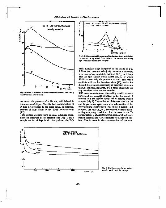
CdTe Surface» with Secondary Ion Mus Spectrometry
CdTc ETCHED Brf Methanol «bodly rinsed»
Fig. 4. Profiles as measured by SIMS or various dements on a "badly rinsed" surface, after etching
not reveal the presence of a discrete, well defined in thickness, oxide layer. Also, the bulk concentration of O does not converge to the same value, as expected, because of edge effects in the SIMS measurements [15]. - the surface growing films contain tellurium oxide, since the spectrum of the negative ions {Fig. 7) on a sample left for 14 days in air, clearly shows the TeO
- Cdî» <nfl> ETCHEO ••j-ME'TTUNDi. |frnh . CdT» Ot0> CLEWED
CHANNEL NUMtE*
Fig. 5. RBSspcOn(yicldvienersyoflkebackKitiemlparbc]e5)c>r cle ved and fffhty etched CdTe surfaces. The detector was a very high resolution electrostatic analyzer
peak, especially when compared to the results on Fig. 3. Since TeO does not exist [16], the oxide is probably a mixture of uncoropletely oxidized Te0 2 , as it happens on thin silicon oxide layers (SiOJ, for which SIMS reveals only the presence of SiO. This result conflicts with earlier literature data [17], which indicated the presence, essential)} of cadmium oxide on the CdTe surface. By SIMS, it w is never possible to see any cadmium oxide on our samples. RBS measurements under channelling conditions were performed on samples oxidized in air (or about 3 months and the results comp; red to freshly etched samples (Fig. 8). The evolution - if the area A of the Cd and Te peaks was again made a ter substractîon of the dechannelling contribution. Fcr these 3 months old samples, the ratio AçjAlt bec* unes 0.76 under channelling analyzing conditions. 1 he increase in the Te concentration is about 108 % when compared to freshly etched samples and 42% compared to a cleaved surface. The increase in the concentration of the non-
PflOFILE 0-IOHS WT« ETCHED %H*thanol
DEPTH \k)
Fig. 6. SI vlS spectrum for an etched sample "aged" in air Tor 14 days
6 3
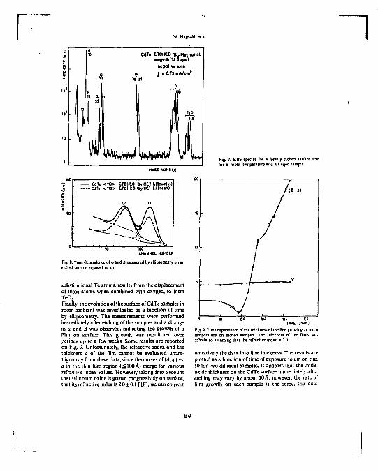
M. Hife-Mi el il.
Cdl» tTCHtO Bc-Mtthonol «at«e>(ulays]
ira
ntgatlvt tor» j > O.TSjiA/cm'
19 0,
f WHW MASS HUM!M
CflTt <110> ETCHED t9h-MeTH.|3rr«nthi} Cdlt <110> ETCHED fe-METH.t f r i th)
***1 Fig. 7. RBS spectra for a freihty etched surface and I Tor a room temperature and air aged sample
CHANNEL NUMBER
Fig. 8. Time dependence of \p and A measured by ellipsometry on an eiched sample exposed to air
substitutional Te atoms, results from the displacement of these atoms when combined with oxygen, to form Te0 2 . Finally, the evolution of the surface of CdTe samples in room ambiant was investigated as a function of time by ellipsometry. The measurements were performed immediately after etching of the samples and a change in y and J was observed, indicating the growth of a film on surface. This growth was monitored over periods up to a few weeks. Some results are reported on Fig. 9. Unfortunately, the refractive index and the thickness d of the film cannot be evaluated unambiguously from these data, since the curves of («d, y I vs. d in the ihin film region (£100À) merge for various refractive index values. However; taking into account that tellurium oxide is grown progressively on surface, that its refractive index is 2,0±0.t [18], we can convert
Fig. 9, Time dependence of the thickness of the film growing ai room temperature on etched samples. The thickness of the films was calculated assuming that the refractive indei is 2.0
tentatively the data into film thickness. The results are plotted as a function of time of exposure to air on Fig. 10 for two different samples. It appears that the initial oxide thickness on the CdTe surface immediately after etching may vary by about 10 A, however, the rate of film growth on each sample is the same, :he data
84
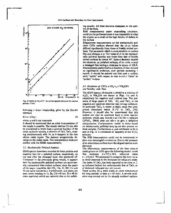
CdTe Surface* with Secondary Ion Ma» Spectrometry
M î t EVCHEO l^-MEIHAHOL
1 0 1 to ft sb 4 sh &—, OXYDE THICKNESS A)
Fig. 10. SIMS profile of O " for eiched samples left in air for various periods or time
following a linear relationship, given by the Elovich equation rf=o + Mogf. (1) where a and b are constants. It should be mentioned that an oiher interpretation of the results is possible. The simple relation (1) can also be considered to result from a gradîial increase of the oxide molecule density, a mixture of TeO, Te0 2 existing simultaneously with Te, as it happens in the thin silicon oxide layers. The mixture progressively develops to the stable oxide. This interpretation does not conflict with the SIMS measurements.
2-3. Mechanically Polished Surfaces SIMS spectra have been recorded for both positive and negative ions for a polished surface, respectively, on top and after the damaged layer was sputtered off. Compared to the previously given results, it appears that the mechanically polished surfaces are more heavily contamined than etched surfaces, since the peaks of the major imputities like CH„, Na, A), SÎC, Cr and Fe are more intense here. Furthermore, new peaks are seen, corresponding to Ti, Ba, Cd+40 and Te+40 (in mass numbers), which are certainly due to the polish
ing powder. All these elements disappear on the spectra of the bulk. RBS measurements under channelling condition, could not be performed since it was impossible lo align the crystal, as a result of Che high density of defects at the surface. Ellipsometer measurements on the mechanically polished CdTe surfaces showed that the (J,q>) values differed significantly from those of freshly etched surfaces. The parameter which is more sensitive to surface film and damage is A. The value of â on the mechanically polished samples was lower than that of freshly etched surfaces by about 40°. Such a decrease implies the existence, on polished surfaces, of an oxide or/and a damaged film having a thickness in excess of 100 À. Measurements performed as a function of time showed no significative evolution, over periods exceeding I month. It should be pointed out that such a surface, while "stable" with respect to time is not a "clean" or "perfect" surface.
2.4, Oxidation of CdTe m (Hj( )2 + NH4OHI and Stability with Time The SIMS spectra of samples o tidized in a solution of H 2 Ô 2 in NH 4OH are shown in Figs, lia and b, respectively for negative and | ositive ions. The presence of large peaks of TeO, ' eO a and TeO, in the negative-ion spectrum demonsi 'ates strong oxidation. In particular Te0 3 is rather ui likely, since this compound dissociates below 3C)°C to TeOj [16]. However, it should also be emembered that this radical can also be sputtered from a more heavier molecule, which may include a.so Cd, like a tcllurate CdTeOj. SIMS does not alio v to give a definitive interpretation. Contaminants Mmilar to those found on mechanically polished samples are also present on these samples. Furthermore, a peak attributed to Sn is seen in Fig. 11, it constitutes ar impurity of our H , 0 2
solution. The RBS measurements could not be interpreted lo draw any meaningful corclusions. Due to the presence of an amorphous surface layer the aligned spectra were distorted. The ellipsometer measurements of the blue colored oxide grown on CdTe gave the following results : oxide film thickness d = 757 + 70 Â, refractive index n = 2.0+0.1. We attempted to compare this later value to those reported in the literature Tor tellurium oxide. The index of Te0 2 has been reported to be close to 2, as indicated before, but unfortunately that of TeO, or of cadmium tellurates are noi known. These surface films were stable at room temperature for long periods of time (t > I03min). A second oxidation step carried out in the already oxidized surfaces
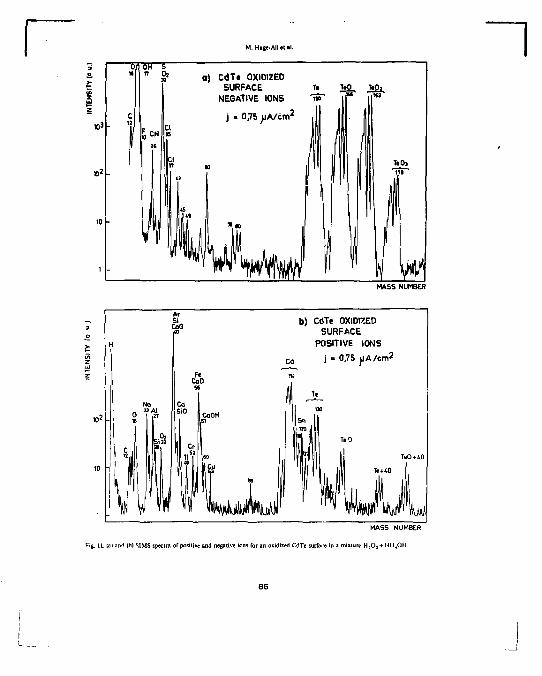
M. Hlge-Ali et il.
-5K
«3 h
Bin -" g » o) CdTt OXIDIZED
I SURFACE Tt Tja, Jtgi, NEGATIVE IONS "vT •& •'*»
MASS NUMBER
MASS NUMBER
L. la) and (b) SIMS spectra or positive and negative ions Tor an oxidized CdTe surface in a mixture H ; 0 : + NH4OH
TdTc Surfaces wilh Secondary Jon Masi Spectrometry
did not change the film thickness, but increased the refractive index up to 22. This result suggests a minor dcnsification ofthe film.
3. Discussion
This study has shown that the surrace of cadmium tslluridc is strongly sensitive to both chemical treate-mem and ambiant conditions. Freshly hromine-methanol etched surfaces are strongly enriched in Cd, the Te atoms are partly oxidized in a compound TcOA with v close to unity. If this surface is maintained in air for long periods of time (;> 10* min) a film has grown on surface, increasing as In/. Our measurements do not allow to distinguish between the following possibilities:
the TeO, film grows in thickness; the TeO, progressively becomes stable oxide TeO, : the TeO, combines with Cd to give a tellurate.
It is probable that the two First possibilities occur simultaneously. It should be mentionned that during this evolution the Cd concentration remains constant. H or perhydrol oxidized surfaces, a stable film is grown, the thickness of which depends on the duration, temperature, dilution of the oxidizing solution. The thickness can bo much greater than for air-oxidized samples (500-1000 A. compared to 10-60À). The nature ofthe film is probably a mixture of Te0 2 and a cadmium tellurate.
The mechanically polished samples of CdTe have an oxidized and.'or a damaged layer on top, they arc heavily contamined with the elements present in the polishing powders. Due to this film, the ellipsometer measurements gave no evolution ofthe surface proper-tics with lime. What is the influence that the different surfaces treate-ments ha\e on the electrical as well as on the nuclear detection properties when detectors are prepared? As indicated in ihe introduction, the various treatements have a ver\ strong effect both on the 1-V characteristics as on the detection performance. The latter will be published in some detail elsewhere [19], Concerning the leakage current, its evolution with time, it seems to us that the presence of Cu has a strong influence The film thickness of a perhydrol oxidized surface, fnr example, remains quite constant as a function oj time of storage in air, however, our
measurements in nuclear detection show a progressive degradation ofthe breakdown voltage as well as ofthe noise level, which may be due to some migration copper under the cc:.;aet region in close surface vicinity. The presence of Cu may also affect the h;irricr properties on etched samples. Further experiments arc necessary to verify this hypothesis.
Conclusion
lo our knowledge, this constitutes the first rather systematic investigation or the Cdfe surfaces after various treatments. Three different investigation methods have been used, however they are not sufficient, due to (he high degree of complexity of the phenomena occuxing. However, the change in stoichiometry the oxidation process in air has been demonstrated for the various surface conditions investigated here The presence of some impurities like Cu after the chemical etching has been shown ; this contaminant can play an important role in the behaviour of devices prepared aftcrwurds on these surfaces.
References
1 P. Siffcrt. R. Berger. C. Scharager, A. Cornet, B. Stuck ll-EF Trans. NS-23, 1959(1976)
2. H.L. Malm. M. Martini: Caa J. Phys. 51, 2336 ( f r i j 3. R.O. BeJL O. Eminc H.B. Serrera: Nud. Inslr. Moil. 117 267
(1974) 4. P.Siffe«,M.HateAli.R.Stuck.A.Carne(:Rev.Ph>-i Appl 2.135
(1977) 5. R.O. Bell, N. Hemmat, F.V. Wj.ld: Phys. Stai. Snl. AI. 375
(1970) 6. G. Slodzian: Ai n. Phys. 9. 591 (1364) 7 H.W. Werner: vacuum 24. 4M ( 974) K H.W, Werner, / .E . Morgan: J. , ppl. Phys. 47, 12.12 il97h| '>. A.N. Saxcna: J. Opt. Soc. Am. 5:., 1061 (1965)
III Mc. Crackin: J. Res. N.B.S. (Phy. and Chem.)67A '6.111963) 11 See. for fixampk : Ion Beam Suifa e Layer Analyst*. «1. bj I W
Mayer. J.F. Ziejder (Elsevier, Umanne 1974) 12 H.W. Wenier. N. Warmoltz: Sur. Sci. 57, 706 (lv7f.i 13 M Bernheim, C. Slodzian: Surf ici. 40, 169(1973i 14 M.H. Patterson R.H.Williams:.) Phys. D(App). I 'hwi l l . L83
[1970) 15 M. Crase.1 : R«v Technique Than ion-CSF 3. 19 <i->"h 16. P. Pascal: fiaioem Ttiitè de 'himie Minérale tenu- XIII
iMasson, Paris 961) 17 A.T. Akobirova. L.V. Maslova.C .A. Matveev, K. K h usai no v
SOY, Phys. Semioond. 8. 1103 11975) IS lUmdbtmk ,>f Chemislrr uml Physics \CRC Prcv* W«M Palm
Bench 1974| B145 \t M.HageAli.R.Sluck.C.Scharager.P.SilTeri:inM lmnvNS-33
'February 19791
ETUDE DE LA SURFACE DE CdTe PAP ELLIPSOMETRIE SIMS ET RBS
R. STUCK, M. HAGE-ALI, A . N . SAXENA*. A. GROB, P. SIFFERT Centre de Recherche* Nucléaires Groupe de Physique et Applications des Semiconducteurs (PHASE) STRASBOURG - Prance.
Colloque Européen "Surface-Vide-Métallurgie", Mal 1978, STRASBOURG.
RESUME
Afin de mieux comprendre le mécanisme de redressement au :ontnct métal-tellurure de cadmium, on a entrepris une étude des surfaces obtenues par un décapage au brome-méthanol de cristaux de CdTe en uttllsan des méthodes d'investigation nouvelles telles que Mellipsométrle, la «poctr orné tr ie de masse d'Ions secondaires (SIMS) et la rétrodlffuslon Rutherford de sartlcules chargées (RBS). Les résultats montrent que de telles surfaces sont ccntamlnées par des traces de brome et qu'elles se recouvrent d'une couche n'oxyde de tellure d'épaisseur croissante en fonction du temps . La composition de ce film a pu être analysée aux différents stades de l'évolution.
ABSTRACT
For a better understanding of the mechanisms Involved In th>? rectification of metal-cadmium telluride contacts, we Investigated the surface of bromlne-methanol atched CdTe crystals by means of elllpsometry, secondary Ions mass spectroscopy (SIMS) and Rutherford backscatterlng of charged particles (RBS). The results show that these surfaces are contaminée with bromine and that a tellurium surface oxide layer grows, its thickness Increasing with time. This surface layer composition has been analyzed at different steps of Its evolution.
» A .N. SAXENA- International Semiconductors, PALO A L " 0 , USA.
8»
I. INTRODUCTION
Le te l lurure de cadmium (CdTe) présente une bande Interdite arge (1,45 eV)
ainsi qu'un numéro atomique élevé (48, 52) et constitue de ce fait un excellent
matériau pour la fabrication de détecteurs de rayonnementsyce for te efficacité
pouvant fonctionne,' à température ambiante. Malheureusemen: ces disposit i fs
n'ont pas connu beaucoup d'applications jusqu'à présent car 1 s sont affectés
d'une instabil i té dans le temps connue sous le nom de polarisation [ ! ] . Des t r a
vaux récents [2 ] ont cependant montré que cet effet était lié i la nature des
contacts ut i l isés, en part icul ier à la préparation des surface Ï avant dépôt des
électrodes, qui consiste généralement en un décapage au brone - methanol,.
Comme les rares publications, généralement anciennes [^4] cul traitent des
problèmes de surface de CdTe ne nous ont pas permis de com >rendre ces phéno
mènes nous avons entrepris une étude systématique de ces su-faces en ut i l isant
les méthodes modernes d'investigation : spectrométrie de masse d'ions secon
daires, ellipsométrie et rétrodlffusion de particules chargée .
I I . METHODES EXPERIMENTALES UTILISEES
A) Spectrométrie de masse d'ions secondaires (SIMS)
Rappelons que cette méthode consiste à bombarder un échanti Ion par des ions
lourds de faible énergie et à effectuer la spectrométrie de im sse des ions
secondaires émis par la surface i r radiée [5 , 6 ] . Dans l'appa eîllage que nous
uti l isons (fîg. l) le faisceau primaire sst constitué d'Ions Ar d'énergie 3 keV,
son diamètre est de 5 mm et sa densité de courant (qui est un forme ."sur toute la
section du faisceau) peut var ier entre 5 y A/cm et 50 ^A /cm* . Les Ions secon
daires posit i fs ou négatifs qui sont émis sont analysés par un spectromètre de
masse de haute sensibil ité comportant une optique d'entrée, m f i l t r e quadrupo-
laïre, un multiplicateur d'électrons et une chaîne de détection. L'expérience
est effectuée sous un vide élevé (pression résiduelle 10 t->rr) entretenu par
une pompe turbomolécuaîire et un piège à azote liquide. L'instrument peut être
ut i l isé en mode statique en choisissant un faisceau primaire r eu intense, qui
n'érode que très superficiellement la surface de manière à ot-tenir le spectre
de masse des ions émis dans les toutes premières couches atomiques du c r i s ta l .
Il est possible aussi d'employer l'appareil en mode dynamique c'est à dire de
90
bombarder le cristal par un faisceau Intense et de suivre l'Intensité des raies liées a certains éléments en fonction du temps d'attaque. SI on connaît la re lation entre l'épaisseur de la couche pulvérisée et le temps (vitesse d'érosion) on obtient le profil de la zone superficielle du cristal. Dans le cas du CdTe nous avons déterminé la vitesse d'érosion par une masure électro-mécanique de la profondeur du cratère (résolution en profondeur < 50 A . Pour le faisceau d'ions Ar employé Ici cette vitesse est égale a 4 A/m n. SI la densité de courant est de I (lA/cm la résolution spatiale dans les mesures de profil dépend de l'épaisseur de la couche enlevée mais peut atteindre 10 A si cette dernière est suffisamment faible.
L'application de cette technique a CdTe pose cependant deux p-oblèmes :
- le premier est du au fait que le matériau est composé. Dans ie tels cristaux les probabilités d'émission des deux éléments sont généralement différentes ce qui donne naissance à une topographie de surface à l'échelle aomlque, la surface s'appauvrissant du composant ayant le taux d'émission le plus £levé [ ? ] . Après un certain temps d'attaque on atteint un état d'équilibre caractérisé par une concentration constante des différents éléments. Nous verrons que nos expériences ne nous ont pas permis de mettre en évidence de tels effets.
- le second problème est lié à la réststîvité des échantillons, lorsqu'elle est élevée la surface peut se charger sous l'influence du bombard.ment et la charge d'espace ainsi créée peut empêcher l'émission d'Ions secondaires positifs et dévier le faisceau incident [ 8 ] . Nous avons éliminé ces effets en n'analysant que des cristaux de résistlvlté suffisamment faible et en utilisant des faisceaux d'ions primaires peu intenses.
B) E l l ipsométr ie
L'ellipsométrie est une méthode optique d'analyse de couches superficielles consistant à mesurer le changement de polarisation d'une lumière monochromatique après réflexion sur une surface que l'on veut étudier [ 9 ] .
On détemrine ainsi deux paramètres, l'angle azîmuthal $ et la différence de phase A quî sont reliés à l'épaisseur d et à l'Indice de ré/fract on du film n. déposé sur un substrat par la relation :
tang * e ' A - f (2nA d ( n , Z - nQ
2 sln < f ) ' / 2 )
91
où f est une fonction tabulée, n l'Indice du milieu ambiant, 4 l'angle d'Incidence du faisceau lumineux, de longueur d'onde \ .
On peut donc trouver l'indice de refraction et l'épals«eur du film en resolvant cette équation par une méthode d'Itération. Ceci se fait généralement au moyen d'un programme de calcul assez complexe [10] . On obtient ainsi des réseaux de courbes reliant (• et 4 è l'épaisseur du film pour différentes valeurs de l'indice de réfraction. Toutefois,on peut aussi employer les formules approchées proposées dans un arcticle antérieur [11] .
L'ellîpsométrle constitue une méthode très sensible et très précise d'investigation de films minces formés à la surface des semiconducteurs puisque des épaisseurs inférieures à 10 A ont pu être mesurées. En outre,elle a l'avantage d'être non destructive, de pouvoîr être mise en oeuvre dans l'air et de permettre de suivre la croissance d'un film en continu.
o
L'instrument employé dans ce travail, utilisait un laser He-Ne ! X • 6328 A) et un angle d'incidence de 70°. Il comporte (fig. 2) un polariseur rotatif (prisme Glan-Thomson) qui polarise la lumière linéairement, un compensateur qui permet une polarisation elliptique, un analyseur à prisme et un photodétecteur.
C) Rétrodiffuslon de particules chargées (diffusion Rutherford) L'expérience de rétrodiffusîon consistée bombarder un échantillon monté,sous vide,dans un goniomètre au moyen de particules chargées dont l'énergie est de quelques MeV et d'étudier les particules rétrodiffusés lors des collisions élastiques qui se produisent [12] , Ces dernières obéissent aux lois de conservation de l'énergie et du moment cinétique ; la section efficace de diffusion peut donc être calculée simplement. Si les ions du faisceau primaire ont une masse M. et
une énergie E et si M-est la masse de la cible, les ions rétrodiffusés dans une o 2
direction fermant un angle 8 avec celle du faisceau Incident ont pour énergie :
E = k E Q
où k est uniquement fonction de M. M_ et S .
Les ions qui ont pénétré plus profondément dans la cible et qui sont ensuite
rétrodiffusés dans cette même direction, ont une énergie proportionnelle à la
92
profondeur x à laquelle s'est produite la collision. Cette techrïque permet donc une analyse des Impuretés en fonction de leur localisation par rapport è la surface. De plus,on peut se placer en condition de canalisation des Ions [ 1 3 ] , c'est a dire faire pénétrer les particules Incidentes le long d'une dlrectlor principale du réseau cristallin. Ces derniers sont alors focalisés entre les rangée"» atomiques et ne subissent plus de collisions avec des atomes cibles. De ce fal le rendement de rétrodiffuslon est considérablement réduit (d'un facteur 10 dars le cas de CdTe); par contre tous les défauts ou Impuretés placés dans le canal "ont interagir avec les ions primaires et apparaître sur la distribution en énergie des Ions rétrodîf-fusés.
En particulier, la couche superficielle plus ou moins amorphe quî existe sur tous tes matériaux va former sur le spectre un "pic de surface " dont l'aire est liée à la quantité et à la localisation de ces défauts en surface. Dans le cas d'un matériau binaire deux pics de surface apparaissent et le rappe rt entre leurs aires (ou entre leurs hauteurs) respectives fournît une ïnformition sur la stoechio-métrie du composé en surface.
Toutefois, il convient d'être prudent dans l'Interprétation de telles expériences car l'aire des pics dépend aussi de la température du fait que les vibrations thermiques peuvent accrortre la probabilité de rétrodiffusîon. Le pic relatif à un des composés peut alors être affecté plus fortement que celui de l'autre. t_a méthode ne permet donc pas la mesure absolue de la stoechiométrîe mais seulement la comparaison des stoechiométries des deux surfaces â une température donnée.
En pratique nous utilisons un accélérateur VAN DE GRAAF dt livrant des tons 4 + He d'énergie comprise entre I et 4 MeV. L'énergie des particules rétrodiffusée est mesurée soit par des détecteurs à barrière de surface au silicium, soit par un secteur électrostatique (fig. 3).
III. RESULTATS EXPERIMENTAUX
Les surfaces ques nous avons étudiées ont été rodées avec de Ja poudre de carbure de silicium (diamètre des grains 5 à 20 ^) puis décapées par un mélange de brome methanol,enfin rincées aux ultra-sons dans du methanol. La concentration de brome dans le methanol est de 12 % (cette valeur a été choisie car elle donne la plus faible rugosité de surface pour un temps d'attaque de 1 à 2 minutes
[14] . 13
A) Sur faces fraîchement préparées
Les f igures 4 et 5 montrent les spectres S I M S mesurés avec un faisceau de
densité 0, 7 ^ A / c m en sur face (plus exactement dans la couche s i tuée à moins
de 20 A de la sur face) et en volume (après une attaque durant 3 h c'est à d i r e
pulvér isat ion d'une couche d'épaisseur voisine de 500 A ) . Cn remarque tout
d'abord que dans tous les spectres S I M S du fait de sa configuration é lect ronique
le cadmium n 'appara î t qu'en Ions posit i fs a lors que le t e l l u r e apparaî t aussi bien
en négatif qu'en posit i f . S u r les spectres négatifs on voit essentiel lement l 'oxygène
et les halogènes et un bru i t de fond plus ou moins Intense dû au> e~ secondai res .
L a comparaison des spectres en sur face et en volume montre qu'en sur face
le t e l lu ru re de cadmium est oxydé et contaminé par les radicaux C H dus p r o
bablement au methanol et au séchage sur le papier f i l t r e , ainsi que par des
t races de brome provenant de la solution d'attaque. On remarqi. e aussi que le
rapport des intensités des pics re la t i f s à Cd et T e v a r i e en profondeur, le pic
de cadmium étant environ 2 fois plus grand au voisinage de la sur face qu'en
volume. Cet effet qui a déjà été signalé dans un t rava i l antér ïe i r [ 1 5] peut
avoir p lusieurs or ig ines :
a) enrichissement effectif de la surface en cadmium ;
b) pulvér isat ion d i f fé rent ie l le ;
c) exhaltatïon du pic de cadmium en présence d'un élément contaminant la
surface.
Examinons tour à tour ces hypothèses :
a) Pour étudier la stoechiométrle en surface nous avons comparé les spectres
de rétrodï' ' fusion (obtenus en conditions de canal isat ion) d'une surface décapée
chimiquement et d'une sur face c l ivée qui est représenta t ive de a situation en
volume. L a f ig . 6 montre que si l'on ne tient pas compte du bru t de fond les
hauteurs h, mesurées en unités a r b i t r a i r e s des pics l iés à T e et à Cd sont
égales respectivement à 34 et 39 (rapport r*—— = o, 87 ) pour ! échanti l lon cd h j e
cl ivé , a lo rs qu'e l les sont égales a 44 et 59 ( rapport T- = 0, 74 ) pour n c d
l 'échanti l lon décapé chimiquement. Ceci «îdnif ie que sur une sur face pol ie c h i miquement M y a effectivement environ 15 c,o plus de cadmium q t ' e n volume et que la couche perturbée- est notablement plus importante. Toutefois cet e n r i c h i s s e ment en cadmium est insuffisant pour expl iquer les var ia t ions observées en S l M S .
94
b) La deuxième explication possible est une pulvérisation différentielle. Dans ce cas le rapport entre les pics de cadmium et de tellurure en surface serait celui correspondant à la concentration effective des éléments dans le cristal et la surface s'appauvrirait en cadmium durant le bombardement par le faisceau primaire parce que le cadmium aurait une section efficace de pulvérisation plus élevée que le tellure. Ces taux de pulvérisation sous un faisceau d'argon de
3 keV ne sont malheureusement pas connus et pour confirmer OJ Infirmer cette hypothèse nous avons fait appel a la rétrodiffuslon d'ions pour mesurer la stoechiométrie en surface d'une surface bombardée par le falsi:eau d'icns p r i maires du SIMS ( j - 25 |iA/cm ) . Le spectre obtenu (fig. 7) montre que les hauteurs des pics relatifs à Te et Cd sont égales respectivement a 55 et 65. Ces valeurs sont donc plus élevées que celles obtenues dans les autres cas, ce qui est normal puisque le bombardement augmente la quantité de défauts en surface,
mais elles sont dans le même rapport que pour une surface clivée { r—— = 0. 85) h Cd
ce qui signifie que la stoechiométrie de surface n'est pas affectée par le bombardement et que la pulvérisation différentielle n'intervient pas.
c) ta seule explication possible est donc l'exhaltation des raie: obtenues par SIMS par un élément étranger.
Cet effet ayant été observé en présence d'oxygène [16] , nous ivons do^c ^registre les spectres en présence d'une pression partielle d'oxyjène de 10" torr; aucune exhaltation n'est apparue. Toutefois, les halogènes étant susceptibles de créer le même phénomène, nous avons étudié un échantillon dont le rinçage avait été négligé intentionnellement afin que la concentration de brome en surface soit très élevée. Le spectre SIMS des ions positifs (fig. 3) montre eue le pic de cadmium est alors près de dix fois plus important que OTIUÏ de teliure et que de nombreux composés bromes sont formés. Le profil d-- l'échantillon {fîg. 9) confirme que la hauteur du pic de cadmium est bien iiéi* à celle de brome. Ce résultat peut être dû à ce que le cadmium, qui a deux électrons sur sa couche externe 5s, peut céder un électron à un halogène tel que Br- et perdre le second en s'îonisanï pour que les couches de cadmium et de brome soisnt complètes. Sous l'effet du bombardement les liaisons ïor.iques entre Cd et Br p-ïuvent être rompues avec formation d'ions Cd et Br . Plus il y aura ds brome en surface plus la hauteur de Cd Br , de Cd et bien évidemment de Br augmentera. L'accrois-
sèment du pic de cadmium en surface des échantillons décapés ,,u brome et bien
rincés a donc certainement la mtm» origine puisque le spectre SIMS en ions
négatifs montré qu'il subsist* toujours des traces superficielles de brome.
B) Evolution de la surface Les expériences précédentes ont été effectuées sur des surfaces fraîchement préparées. Les mesures d'ellipsométrle Indiquent cependant que sur une telle surface laissée a l 'airl l se forme une couche d'oxyde dont l'épaisseur continue de crortre plusieurs mots après l'attaque. La figure 10 montre que l'épaisseur initiale est très variable d'un échantillon à l'autre, mais que tous suivent après quelques heures la même loi d'accroissement de la couche superficielle, qui paut s'exprimer par :
d = t + a, IS Log t o n t dépenHsnt de l'échantillon
d = épaisseur. o
L'indice de réfraction de cette couche d'oxyde est voisin de 2 jour X - 6328 A ce qui tend à démontrer qu'elle est formée d'oxyde de tellure puisque les indices de TeO- sont compris entre 2 et 2,35 [13] ,
Les expériences SIMS confirment ces résultats puisque les prafîls d'oxygène de la figure 11 montrent que la concentration d'oxygène en surface est d'autant plus importante que l'échantillon est plus âgé. Toutefois, il n'apparaît pas sur ces profils une véritable couche d'oxyde. Ceci est dû,peut être, i une mauvaise résolution en profondeur. En outre on peut remarquer que la concentration en oxygène ne revient pas au même niveau pour les trois échantillons, ce qui ne s'explique que par des effets de bord de l'appareillage [ IB],
Par ailleurs, le spectre de l'échantillon âgé de 14 jours (fîg. 12) confirme que l'oxyde formé en surface est de l'oxyde de tellure et non de l'oxyde de cadmium comme Pont suggéré d'autres auteurs [19] . Enfin,un spectre c!e rétrodîffusîon (fîg. 13) mesuré sur un échantillon vieux de 3 mois montre que la surface s'enrichît en tellure. En effet pour un tel échantillon les hauteurs des pics relatifs
h ye à Te et Cd sont de 58 et 60 respectivement, soit un rapport r = 0, 98.
n C d
96
r CONCLUSION
Nos expériences montrent que la surface du CdTe polie chimie uement par une attaque au brome methanol est contaminée par des traces d'Impjretés tels que CH, Br , et qu'elle n'est pas stable dans le temps puisqu'elle se recouvre d'une couche d'oxyde de tellure dont l'épaisseur croît même après ces temps supérieurs a plusieurs mois. Ce travail met ainsi en évidence l'tn érêt de méthodes telles que le SIMS, l'elllpsométrlo et la rétrodlffuslon, qui sont très cotnp I ém entai res.
REFERENCES
1 ) P. SIFFERT, R. BERGER, C. SCHARAGER, A. CORNET et R. STUCK, I . E . E . E . Trans. Nucl . Se l . NS 23 (1976) I9S9.
2) P. SIFFERT, M. HAGE-ALI , R. STUCK, et A. CORNET, Revue de Physlquo Appliquée, 2 (1977) 335.
3) H. C. MONTGOMERY, Sol id State Electronics 7 (1964) 147 4) T. FUKUROl, S. TANUMA, S. TOBISAWA, Tokohw. Univ. Sc i . Rep.
4 ('19S2)..2S3. 5) G. SLODZIAN, Ann. Phys. 9 (1964) 591. 6 )H .W. WERNER, Vacuum, 24, n° 10(1974)493. 7) H. W. WERNER et N. WARMOLTZ, Surface Science 57(1976) 706. 8) H. W. WERNER et A. E. MORGAN, J . A. P. vo l . 47 n° 4 (1976) 1232. 9) R. J . ARCHER et G. W. GOBELI, J . Phys. Chem. Solids 26(1965) 343.
10) F.Me. CRACKIN, NBS Technical Note 479, Apr i l 1969. l t ) A . N . SAXENA, Journal of the Optical Society of America, Vo l . 55, n ' 3
(1965) 1061. 12) Voir par exemple ION BEAM SURFACE LAYER ANALYSIS, Edite par
J.W. MAYER et J . F. ZIEGLER, Elsevier Co Lausanne (1974). 13) CHANNELING, Edité par D.V. MORGAN J. Wiley et Sons (1973). 14) J. STELZHAMMER, P. KOKOSCH1NEGG, résultats non publiés. 15) J .P . PONPON et P. SIFFERT, Revue de Physique Appliquée, 2 (1977) 427. 16) M. BERNHEIM et G. SLODZIAN, Surface Science 40 (1973) 169. 17) HANDBOOK OF CHEMISTRY and PHYSICS - CRC Press - (1974) B 145. 18) M. CROSET, Revue Tech. Thomson CSF 3(1971) 13. 19) A. T. AKOBIROVA, L. V. MASLOVA, O. A. MATVEEV et A. K. KHUSAINOV,
Sov. Phys. Semicond. vo l . 8, n° 9(1975) 1103.
98
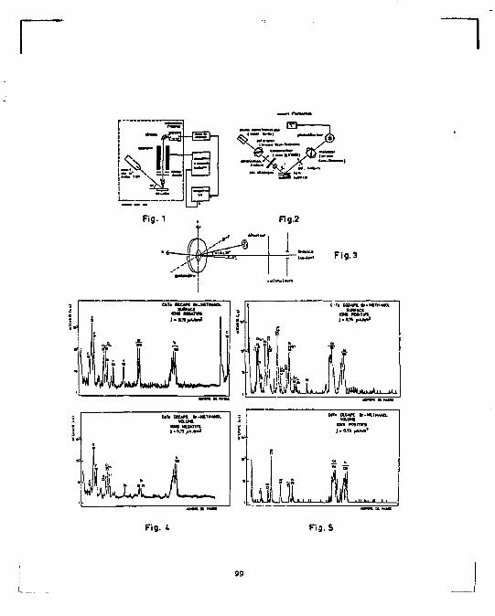
Fig.3
CTt UCAK »-HITHaML SIMMCC
KM KftlM
a «a KfkjJ WUOJAJU-AJU
Ml» CtUK *-KIH*H0L MUM
UNS mitws I > 0.» lAM*
LtAJJLÀ-w > • IL ,_J U n ,.1.1 «_.,
Fig. 4 Fig. S
99
1
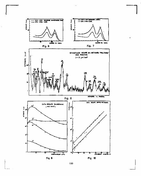
/ \y \\
Fig. 6 Fig. 7
:«u-
ECHAHTILLON DECAK Br-MITHAtO. •MN.RWE-IONS POSITIFS j ~ 1 £ jlA/cm?
ill iS.
W^WJwwù NOMBRE Cl MASSE
UT> oatrc iMM-NclHMOt
Fig. 9
Hb à-i
UMWD» tratvoctAi
Fig. 10
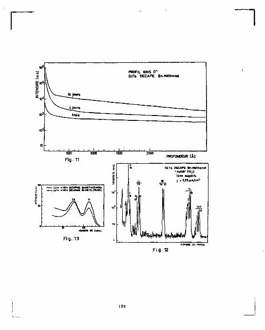
m6
*d 3
PROFIL IONS 0 -CdTt DECAPE Br. Methanol
INTE
NSI
TE
\ > ttjour*
m3 - ^ f rois - ^ f rois
102
o . . i ; . . . . i
500 1000
Rg. 11
MMJW M CANAL
R g . 13
1500 PROFONDEUR (A)
CUT. K C A K Ir.Milnonol •WrIUl- (Hj.) ion* fMgatifi
Br I • 0 , n > l A / e m 1
5TT1
WrW H0HMC QK MASK
Fig T2
101
CHAPITRE III
STRUCTURES DIODES
Quel que soit le type de dispositif envisagé, i l est nécessaire
d'avoir soit des contacts ohmlques, soit des contacts redresseurs sur le
matériau. Dans le cas particuMer des détecteurs de rayonnements nucléaires,
i l est nécessaire de pouvoir appliquer des tensions de polarisation élevées,
afin d'accroître fe champ électrique et par lu même la vitesse de collecte
des porteurs. Essentiellement trois procédés de réalisation de la barr ière
de potentiel ont été étudiées :
- diffusion thermique de dopants
- implantation ionique
- hétérostructures InSb-CdTe
En ce qui concerne le premier procédé, nous nous sommes intéressés;
plus particulièrement aux cas du bismuth et de l'or. En l'absence de toute
information dans la l i t térature, nous avons dû établir les coefficients de
diffusion et les énergies d'activation des processus en jeu.
103
Plusieurs limitations sérieuses sont apparues :
- décomposition de la surface du semiconducteur dès que les
températures dépassaient 400"C environ ;
- la saturation de la diffusion en profondeur , naus avait suggéré
(a formation d'un complexe, hypothèse confirmée récemment [ l ] par l 'u t i l isa
tion de Au Te comme barr ière à la diffusion ;
- performances peu satisfaisantes des caractéris iques étectriques.
L'implantation ionique des éléments suivants a et i réalisée :
P, B, Ag, Cu, Au, Al de 20 à 60 keV, mais l'étude la plus complète a été
effectuée pour des ions Bi . On s'est en part icul ier ïntéres-sé aux doomages
consécutifs à l'implantation, à l'incorporation des dopants et à la guérison
des défauts. Pour mesurer d'éventuels changements de stoe'îhiométrie en
surface, nous avions, en plus des méthodes conventionnelle:;, ut i l isé le
rapport des intensités des raies X - L de Cd et Te sous bombardement
H et He (0,8 - 3 MeV). Mais, nous avons constaté que ce rapport
changeait, suivant que l'excitation se faisait en condition de canalisation ou
non, traduisant la différence d'excitation des différentes orbitales dans les
deux cas ce qui a entraîné une étude fondamentale, pi JS générale, de
cette situation dans les cristaux binaires.
En ce qui concerne l'hétérostructure InSb-CdTe , son intérêt
venait de la possibilité de varier les hauteurs de barr ière d'une façon plus
importante que pour les métaux. En fait, nous avons pu montrer que la
structure n'est pas une hétérojonction idéale, une certaine interpénétration
des deux matériau de départ se produisant.
[1 ] J.M, MACKOWSKI, J. TOUSSET, IPN Lyon, Rapp. Ann. 1979, p. 47.
104
Thin Solid Films. Jpf 1973)409-418 © Ebevier Sequoia S.A., Duuanne—Printed in Switzerland
HEAVY ELEMENT DIFFUSION IN CADMIUM TKLLURIDE*
M. HAGE-AL1, I, V. MITCHELL, J. J. GROB AND P. SlhFERT Centre de Recherches Nucléaires ri Vnkersilà Louis Past air, hihtiratuiredc Phvsiqur des Rayonnements et d'Electronique Nucléaire, 6703? Strasbourg Ctdex (Fntncn (Received Ociobcrl, 1973)
The diffusion behaviour near the surface for gold and bismuth in cadmium telluride has been investigated by the charged particle Rutherford back-scattering and ion microprobe analysis techniques in the temperature range 20XF-450 C.
For all temperatures above 370 "C penetration saturation effects are observed. Preliminary results for the activation energy (1,7 eV for gold. 0.3-0.4 eV for bismuth) and diffusion constants DQ are presented. For comparable temperatures. a much more rapid diffusion of gold occurs in evaporated layers of cadmium telluride than in the crystalline case. It further appears that for near-surface diffusion ( < 1000 Â) the back-scattering technique is more useful, with its higher resolution and its ability to give information on atom location, than the ion microprobe. However, the latter technique shows advantages when information from greater depths is required.
INTRODUCTION
Recent progress in cadmium telluride crystal growing techniques 1 - 3 has opened up interesting possibilities for this large band gap semiconductor. Several potential applications make use of its ab ;lity to operate at high temperature. It becomes important, therefore, to prepare devices which are stable under this condition. Furthermore, annealing studies of the implanted layers in this material demand a knowledge of the relative importance of the diffusion behaviour of the implanted species in the host lattice. Only very few results have been published in the literature and these have been restricted to phosphorus4, copper5- * and gold7. Widi the exception of Mann et a/.6, who used the charged particle back-scattering technique, radiotracer methods have been used.
Here, we have determined the surface and near-surface diffusion behaviour of gold and bismuth, which are often used in connexion with this semiconductor. Several procedures have been investigated, including scanning electron microscopy, proton-induced X-ray excitation, ion probe measurements and charged particle back-scattering. It was found that the first two methods have a poor depth
105
M. H \GE-ALI et al.
resolution (of about 2000 À in the case of our scanning microscope) and they were no longer considered. We therefore restrict our discussions here to the last two methods.
I. DETERMINATION OF THE DIFFUSION COEFFICIENTS BY THE BACK-SCATTERING TECHNIQUE
The samples Semi-insulating crystals prepared by two different methods, tellurium
solution growth (travelling heater method) and the modified (pressure control) Bridgman technique, respectively, were uc«i (referred to below as materials A and B). The A material had a resistivity of I0"fi cm (chlorine compensated), whereas that of B was 10412cm, their dislocation densities being respectively approximately 500 and 3x10* c m - 2 . The crystals were cut perpendicularly to the < l l l > direction, mechanically polished and finally chemically etched in the usual fashion. The crystal quality of the samples was checked in preliminary experiments, and in particular by measuring their fundamental channelling properties, i.e. the critical angle *PC, minimum yield )^,,n and dechannelling versus depth of 2.8 MeV *He + ions impinging along the < 111 > axis*.
In addition, thin amorphous films of CdTc (1 jjm in thickness) were evaporated onto polished silicon wafers oriented along the <110> axis. The stoichio-metry of the CdTe samples was verified from the position of th ; shoulder in random back-scattering spectra.
The experiments Two different methods for measuring the diffusion of gold an I bismuth by
the charged particle back-scattering technique have been used. The first involved profiling the impurity diffusion distribution directly from back-scat' ering spectra recorded in channelling conditions, as was done previously for silicon by Chou et ai.9 The second used a graphical analysis of the spectra recorded under random conditions, as suggested by Mann et al.b
For the first approach, selected samples leading to a minimum yield # m ) n of less than 8% (compared with randomly oriented samples) were employed. Thin gold (250 Â thickness) or bismuth (500 Â) layers were deposited on th? samples by vacuum evaporation. The film thicknesses were monitored with an oscillating quartz. Diffusion was achieved in a furnace, in vacuum in the case of gold and under bismuth and argon pressure ( I atm) in the case of bismuth to prevent its evaporation during the heating. The investigated temperature range was from 2001 to 450 X .
The back-scattering spectra of 2.8 MeV *He + particles from the various samples mounted in a three-axis goniometer were recorded using a surface barrier detector (FAVHM: 18 keV) placed at an angle of 160'.
• ll should be mentioned that X-ray diffraction paiterns generally do not give sufficient information on crystal quality.
106
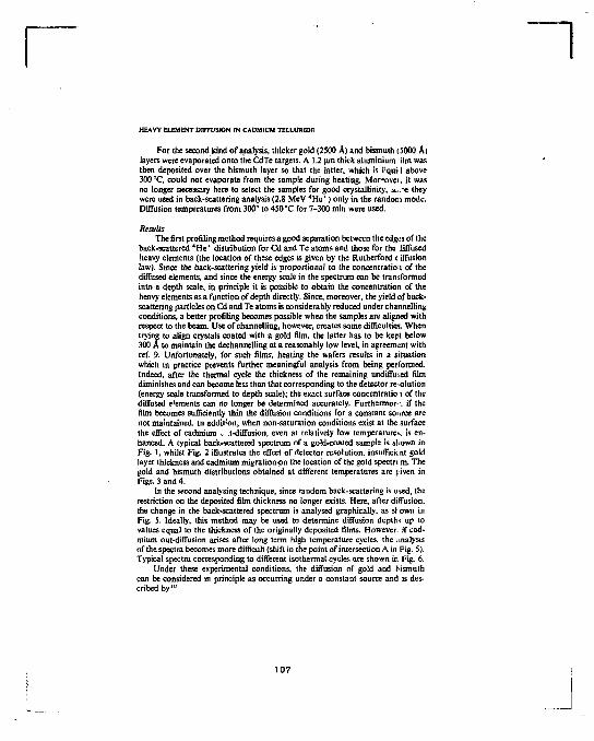
HEAVY ELEMENT DIFFUSION IN CADMIUM TELLURIDE
For the second kind of analysis, thicker gold (2500 À) and bismuth ( 5000 A) layers were evaporated onto the CdTe targets. A 1.2 urn thick aluminium ilm was then deposited over the bismuth layer so that the latter, which is L;qui>J above 300 °C, could not evaporate from the sample during heating. Mor-ovei, it was no longer necessary here to select the samples for good crystallinity, ai..-* they were used in back-scattering analysis (2.8 MeV 4 H e + ) only in the random mode. Diffusion temperatures from 300° to 450 °C for 7-300 min were used.
Results The first profiling method requires a good separation between the edges of the
back-scattered *He* distribution for Cd and Te atoms and those for the diffused heavy elements (the location of these edges is given by the Rutherford c iffusion law). Since the back-scatcering yield in proportional to the concentration of the diffused elements, and since the energy scale in the spectrum can be transformed into a depth scale, in principle it is possible to obtain the concentration of the heavy elements as a function of depth directly. Since, moreover, the yield of back-scattering particles on Cd and Te atoms is considerably reduced under channelling conditions, a better profiling becomes possible when the samples are aligned with respect to the beam. Use of channelling, however, creates some difficulties. When trying to align crystals coated with a gold film, the latter has to be kept below 300 À to maintain the dechannelhng at a reasonably low level, in agreement with ref. 9. Unfortunately, for such films, heating the wafers results in a situation which in practice prevents further meaningful analysis from being performed. Indeed, after the thermal cycle the thickness of the remaining unduTused film diminishes and can become less than that corresponding to the detector rtolution (energy scale transformed to depth scale); the exact surface concentratio t of the diffused e'ements can no longer be determined accurately. Furthermore if the film becomes sufficiently thin the diffusion conditions for a constant source are not maintained. In addit-'on, when non-saturation conditions exist at the surface the effect of cadmium -;, .t-diffusion, even at relatively low temperatures, is enhanced. A typical back-scattered spectrum of a gold-coated sample is shown in Fig. I, whilst Fig. 2 illustrates the effect of detector resolution, insufficient gold layer thickness and cadmium migration pn the location of the gold spectn m. The gold and bismuth distributions obtained at different temperatures are j iven in Figs. 3 and 4.
In the second analysing technique, since random back-scattering is used, the restriction on the deposited film thickness no longer exists. Here, after diffusion, the change in the back-scattered spectrum is analysed graphically, as si own in Fig. 5. Ideally, this method may be used to determine diffusion depth* up to values equal to the thickness of the originally deposited films. However, if cadmium out-diffusion arises after long term high temperature cycles, the analysis of the spectra becomes more difficult (shift in the point of intersection A in Fig. 5). Typical spectra corresponding to different isothermal cycles are shown in Fig. 6.
Under these experimental conditions, the diffusion of gold and bismuth can be considered in principle as occurring under a constant source and is described by 1 0
107
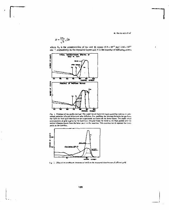
M. HAIit-ALl <'/«/.
where N0 is the concentration of Au and Bi atoms (5.9 x I 0 2 2 and 2.U4x 10-cm" \ respectively) in the deposited layers and A' is the number of diffusing atoms
Pig. I. Principle of ihe profile method. The upper figure shows the back-scattering spectra on yold-coated cadmium telluride before and after diffusion. For profiling, the interface between the goid anL (he CdTe for both gold distributions are superposed, as shown on the lower ligure. The depth UTMIS concentration of gold is given by the horizontal distance from the initial to the final profiles and the vertical distance drawn from the latter point in the base-line. This construction is repealed for cvcr> point on the interface.
OtUittL HHKR
hg. 1 Effect of an inbufficii-ni thickness o[ eold on the measured distribution of diffused gold
•f7\\stt" •f7\\stt" •f7\\stt"
150 no '
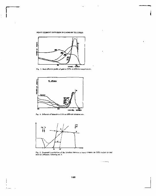
HEAVY ELEMENT DIFFUSION IN CADMIUM TELLURIDE:
CHANNEL NUHKR
Fig. 3. Rcai diffusion profile of gold in CdTe, HI differeni icmncrnturcs.
Bi dtffuttan
J* Eondwn
Sgtfflo» II
SO So ' So" CHANNEL NUMBER
Fig. 4. Diffusion of bismuth in C d T c at different temporal IUVV
IAU JBI OS Te / IAU JBI
11 ; A • / w — / 1
b
v. A ^y[ -M
y i —h 1 ' »
Fig. S. Graphical construction of lhe interface between a heavy clement on CdTc before (a) and after (a') diffusion, following rel'. 6.
109
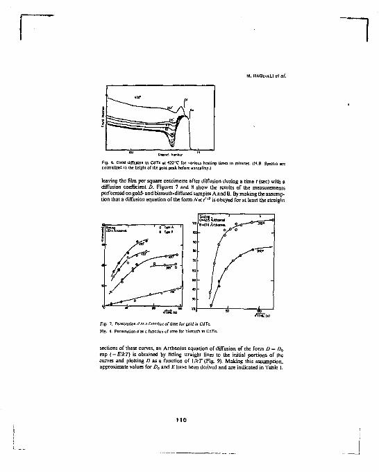
M. HA0E-AL1 er fl/.
Cf*Miil Nwnktr
Fig. 6. Gold diffusion in CdTe «t 420CC for various heating Urnes in minutes. (N.B. Spectra are normalized to the height or the gold peak before annealing.)
leaving the film per square centimetre after diffusion during a time t (sec) with a diffusion coefficient D. Figures 7 and 8 show the results of the measurements performed on gold- and bismuth-diffused samples A and B. By making the assumption that a diffusion equation of the form Noel1'2 is obeyed for at least the straight
VÏÏÏU) <ffi«ft»>
Fig. 7. Penetration rfas a function of time for gold in CdTe,
Fig. B. Penetration à as a function of lime for bismuth in CdTc.
sections of these curves, an Arrhenius equation of diffusion of the form D = DD
exp (-E/kT) is obtained by fitting straight lines to the initial portions of the curves and plotting D as a function of XjkT (Fig. 9). Making this assumption, approximate values for D0 and E have been derived and are indicated in Table I.
no
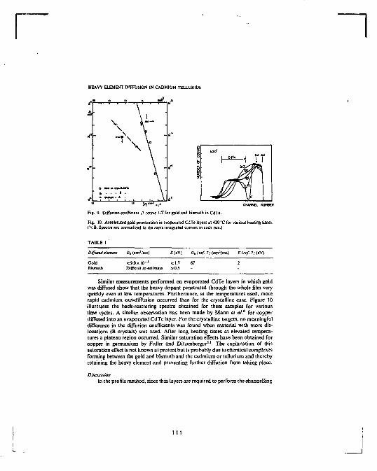
HEAVY ELEMENT DFFFUSION IN CADMIUM TELLURrDE
CHANNEL NUMBER
Fig. 9. Diffusion coefficient 0 versus MT for gold and bismuth in CdTe.
Fig. 10. Accelerated gold penetration in evaporated CdTe layers at 420 X for various heating times. (N.B. Spectra are normalized to the same integrated current in each run.)
TABLE I
Diffused element 0 0 (em'/sec) £(=V) 0» ref. 7: (cm!/secl Eire). ?;(eV)
Gold Bismuth
=9.0x10- ' Difficultly estimate
= 1.7 %0.5
67 2
Similar measurements performed on evaporated CdTe layers in which gold was diffused show that the heavy dopant penetrated through the whole film very quickly even at low temperatures. Furthermore, at the temperatures used, more rapid cadmium out-diffusion occurred than for the crystalline case. Figure 10 illustrates the back-scattering spectra obtained for these samples for various time cycles. A similar observation has been made by Mann et al.6 for copper diffused into an evaporated CdTe layer. For the crystalline targets, no meaningful difference in the diffusion coefficients was found when material with more dislocations {B crystals) was used. After long heating times at elevated temperatures a plateau region occurred. Similar saturation effects have been obtained for copper in germanium by Fuller and Ditzenberger". The explanation of this saturation effect is not known at present but is probably due to chemical complexes forming between the gold and bismuth and the cadmium or tellurium and thereby retaining die heavy element and preventing further diffusion from taking place.
Discussion In the profile method, since thin layers are required to perform the channelling
M. HAGE-AL1 et al.
experiments, the constant source (surface saturation) is difficult to maintain. Furthermore, the presence of cadmium out-diffusion toward the surface can change the profile of the diffused heavy element and may seriously hamper the analysis of the spectra. No precautions are necessary to prevent evaporation of the heavy element (as long as surface saturation exists) since an absolute film thickness is not required. This is in contrast to the second method, where the accurate determination of point A in the spectra needs knowledge of the film thickness. Another difficulty arising from the use of the profile method is that the factor converting the energy scale into a depth scale is a function of the profile itself, whereas the determination of a single scaling factor is sufficient in the graphical method. The major advantage of the first method, however, is that a complete diffusion profile may be determined from a single spectrum.
Lateral pon-uniformities in the evaporated layers after heating can give back-scattering spectra which closely resemble the effects of diffusion and may confuse the diffusion analysis. In particular, it has been reported 1 2 thai whiskers and hillocks appear on annealed films of bismuth on N b 2 0 3 . However, investigation of the surfaces using a scanning electron microscope gave no indication of these effects for bismuth on cadmium lei hi ride and showed the surfaces to be smooth and uniform.
Finally, correct results can be obtained by back-scattering on non-aligned polycrystalline materials up to depths limited only by the thickness of the evaporated layer, whilst the profiling method demands single crystals and channelling conditions. Even then the depth measurements are limited to about 1000 A for heavy elements in CdTe. This technique seems to be of less interest here than it is in the case of silicon8. However, the method can be useful for heavy elements for diffusion depths very close to the surface because of its high resolution capabilities. Moreover, it can give fuller information on the location of the diffused atoms, e.g. at interstitial and substitutional sites, in a more systematic way than considerations based only on the activation energy E.
n . DIFFUSION PROFILE MEASUREMENTS USING THE ION ANALYSER
Experimental conditions The measurements were performed on a CAMECA ion analyser at C.E.N.
Grenoble, on samples identical to those used previously for the back-scattering experiments. A primary beam of argon ions accelerated up to 6 keV bombarded the sample at an angle of 60". In order to reduce errors due to charge accumulation on the surface of the high resistivity samples a reduced oxygen pressure (10 -- 1 torr) was used in the target chamber and a rather large area (1.7 mm 2) was sputtered. A small area of about 30 um of this etched pit was used for the analysis. Under these conditions, the depth resolution was several hundred angstroms.
Results Due to interference with multi-charged atoms sputtered from the cadmium
telluride, it was not possible to evaluate the distribution of gold after diffusion exactly13. The results obtained on the bismuth-diffused samples arc shown in
112
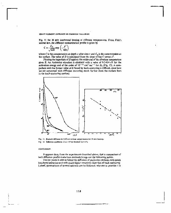
HEAVY ELEMENT DIFFUSION IN CADMIUM TELLURIDE
Fig. 11 for 30 min isochronal heating at different temperatures. From Fick's second law, the diffusant concentration profile is given by
v ^ ? W t P \ ADt) s/nDt where Cis the concentration at depth x after time r and C 0 is the concentration at the surface. The value of D is calculated from the slope of tog C versus x2.
Plotting the logarithm of/? against the reciprocal of the absolute temperature gives E. An Arrhenius equation is obtained with a value of 0.3-0.4 eV for the activation energy and of the order of 10" '"cm 2 sec" 1 for D0 (Fig. !2).Acom-parison with the former value of E found by back-scattering is difficult, since here we are concerned with diffusion occurring much further from the surface than in the back-sea tiering method.
Fig. ! I. Bismuth diffusion in CdTe at various temperatures Tor .10 min healing. Fig. 12. Diffusion coefficient D vs. 1/rfor bismuth in CdTc.
CONCLUSION
It appears then, from the experiments described above, that a comparison of both diffusion profile evaluation methods brings out the following points.
The ion probe is able to follow the diffusion of particular elements with much less depth limitation and with much higher sensitivity than that of back-scattering. Indeed, penetrations of several microns can be followed, whereas in practice it is
113
M. HAGE-ALl et ai
difficult to go deeper than 1000-2000 À in the back-scattering method for cadmium telluride.
The back-scattering technique is limited to heavier elements than the target components, whereas the ion probe can lead to difficulties when interferences with other multi-charged elements occur; furthermore, some errors due to non uniform sputtering exist.
Back-scattering can give information on atom location. Before speculating on the diffusion mechanisms involved for the impurities considered above, further experiments are in progress to determine, by the channelling method, the exact lattice location of these dopants.
ACKNOWLEDGEMENTS
It is a pleasure to thank MM. B. Blanchard and B. Schaub. C.E.N. Grenoble, who performed the ion probe measurements referred to in the article. The authors are grateful to Drs. O. Meyer (Karlsruhe) and H. Mann (Argonne) for stimulating discussions.
REFERENCES
1 N. Kyle, in P. Sifiert and A. Cornel (ed*.|. Prac. Intern. Symp. <m Cadmium Telluride. a Material for y-ray Detectors. Strasbourg, 197), Paper [V.
2 R. O. Bell and F. Wald, in P. Siffert and A. Cornet (cds.l. Proc. Intent. Svmp. on Cadmium Telluride. a Material for y-ray Detectors. Strasbourg. 1971. Paper VI.
3 R. Triboulet, A. Cornet, Y. Marfaing and P. Sifferi. lo be published. 4 R. B. Hall and H. H. Woodbury. J. Appl. Pliys.. .W (19681 5361. 5 H. H. Woodbury and M. Aven. J. Appl. Pltys.. 3Q (1968) 5485. 6 H. Mann. G. Linekerand O. Meyer. Solid State Commun.. U (1972)475. 7 I. Tcramofoand S. Takayanagi. J. Pkys. St»; Japan, /7(I962) 11.17. 8 S. Chou. L. A. Davidson and J. F. Gibbons. Appi Pliys. Letters. 17 ( 1970) 23. 9 J. Mayer. Rad. Effects, 12 (1972) 183.
10 B. I. Boltaks. Diffusion m Semiconductors. Infbsearch. London. I%3. 11 C W. Fuller and J. A. Ditzenbcrger. J. Appl. Phys.. ."tf 11457)40. 12 J. F. Ziegler. IBM J. Res. Decchp.. 16 S (1972) 530. 13 B. Schaub. personal communication. 1973.
1 14
CdTe-lnSb STRUCTURE : INVESTIGATION BY
ELECTRICAL MEASUREMENTS AND BY SIMS
B. RABIN, C. SCHARAGER, M. HAGE-ALI, F. WALD*, P. SIFFERT
CENTRE DE RECHERCHES NUCLEAIRES Groupa de Physique et Applications des Semiconducteurs (PHASE)
67037 STRASBOURG-CEDEX (FRANCE)
Workshop on the I l-Vl Solar Cells, MONTPELLIER, September 17-19/1979.
INTRODUCTION
Due to the value of bandgap (1.45 eV) cadmium tellurlde (CdTe)
is one of the best suited material for photovoltaic converters of solar
energy. However, due to band structure, the absorption coefficient of most
of the photons Is quite high,' therefore, the potential barrier must be pre
pared very close to the surface and the surface recombination velocity must
be well controlled. As a result, all the cells prepared up to now have reduced
conversion efficiencies, below those of silicon cells (1,2). In order to over
come these difficulties, several authors have investigated the possibility of
employing heterostructures (3-5), especially CdS-CdTe contacts (6-7).
However, the lattice constants of these two semiconductors are no; optimal.
As a result, non ideal behaviours have been observed. Here, we Investi
gated the InSb-CdTe structure, for which the lattice constants are identical
within 0.33 % (6.479 and 6.477 A). To our knowledge, only very few pa-
* Mobil Tyco Solar Energy Corporation, 16 Hickory Drive, WALTHAM
Mass. 02154 USA.
115
pers (8 -9 ) have dealed with this contact. Even If this s t ructure Is not wel l
adapted for solar conversion, It seemed of Interest to us, to show that the
same kind of problems a r i s e also with this heterojonctlon, Indicating that the
latt ice mismatch Is not the most Important parameter In these s t ructures .
I I . S A M P L E S P R E P A R A T I O N
N-type CdTe single crysta ls were used, they have been prepared
by the zone melting technique (10), their res is t iv i ty is between 50 -100 a . cm.
Af ter sl icing and conventional lapping, followed by classical cleaning p r o
cedures, etched surfaces w e r e prepared by Immersion of the samples for 1 mn.
in a bromine In methanol solution containing about 12 It of the halogen. The
etching was quenched by excess methanol and the sample was further r insed
In methanol, before being blown dry by n i t rogen. InSb was deposited, Imme
diately af ter etching by vacuum evaporation. Al loying was performed at 550*C
for Smin. under argon atmosphere. The back contact consisted of diffused
indium, prepared p r i o r to the etching.
It should be mentlonned at that time that the freshly etched
CdTe surface Is not stoechlometrlc. Ruther ford backscatterlng measurements
that we performed (11) have shown that the surface Is strongly enriched
in cadmium, about 45 % more cadmium re la t ive to the te l lur ium, when com
pared to the stoechlometrlc surface ( F i g . 1) . Th is non-stoechlometric surface
af ter etching occurs In many compound semiconductors, therefore , it is
anticipated that >i!! b a r r i e r measurements ( l ike Schottky b a r r i e r s ) may be
affected by this effect.
I I I . E X P E R I M E N T A L R E S U L T S
From the Ideal band diagram of the InSb-CdTe contact, it is
116
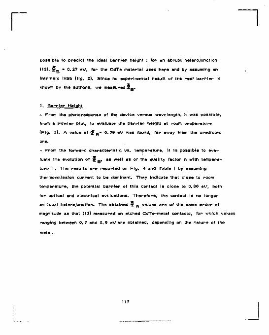
possible to predict the ideal barrier height : for an abrupt heterojunction
(12), § - , - 0.27 «V, for the CcTe material used here and by assuming an
intrinsic InSb (fig. 2). Since no experimental result of the real barrier is
known by the authors, we measured S ~ .
1. Barrier Height
- From the photoresponse of the device versus wavelength, It was possible,
from a Fowler plot, to evaluate the barrier height at room temperature
(Fig. 3). A value of J _« 0.79 eV was found, far away from the predicted
one.
- From the forward characteristic vs. temperature, it is possible to eva
luate the evolution of S _, as well as of the quality factor n with tempera
ture T. The results are reported on Fig. 4 and Table I by assuming
thermoemlsslon current to be dominant. They Indicate that close to room
temperature, the potential barrier of this contact Is close to 0.80 eV, both
for optical and c'ectrlcal evaluations. Therefore, the contact is no longer
an Ideal heterojunction. The obtained $ B values arc of the same order of
magnitude as that (13) measured on etched CdTe-metal contacts, for which values
ranging between 0.7 and 0.9 eV are obtained, depenoîng on the nature of the
metal.
117
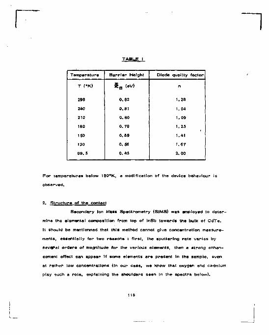
T A B L E I
Temperature B a r r i e r Height Diode quality factor
T CK) $ B (eV) n
298 0 . 8 2 1.28
240 0 .81 1.04
210 0 . 8 0 1.09
180 0 .78 1.25
150 0 .69 1.41
120 0 .56 1 .67
8 9 . 5 0 . 4 5 2 .00
For temperatures below 180*K, a modification of the device behaviour is
observed.
2. S t ruc ture of the contact
Secondary Ion Mass Spectrometry (S IMS) was employed to d e t e r
mine the elemental composition from top of InSb towards the bulk of C d T e .
It should be mentlonned that this method cannot give concentration measure
ments, essentially for two reasons : f i rs t , the sputtering ra te var ies by
sevejral o rders of magnitude for the var ious elements, then a strong enhan
cement effect can appear if some elements a re present In the sample, even
at rather low concentrations (In our case, we know that oxygen and cadmium
play such a ro le , explaining the shoulders seen In the spectra below).
11B
The prof i le» of the var ious element» of interest a r e reported on
F i g . S. Wi th the rest r ic t ion» Just Indicated, It appears that :
- an oxygen layar wi th about 200 A In thickness ex is t * between the two
surfaces (the depth cal ibrat ion has been performed by Talystep measurements).
- Indium diffuses Into C d T e . Since this element acts as a donnor In CdTe , it
is asserta lned that th» surface becomes strongly N- type.
- no strong decomposition of InSb is observed In the top layer .
IV . D I S C U S S I O N
Our experimental resul ts c lear ly show that the I n S b - C d T e s t r u c
ture we rea l ized on an etched crystal does not behave as an Ideel he te ro -
jurc t ion . It I s , therefore , quite c lear that the ideal latt ice mismatch does
not constitute the most important parameter in rea l s t ructures.
The plot 0 " S / T versus 1 / T (F ig . 6) shows that close to room temperature,
the contact behives as a Schottky diode. This Is not estonlshlng, since at
these temperatures, InSb Is a semi-metal and can act as a M - S or M - l - S
contact. However , at least two observations show that it Is not an Ideel
b a r r i e r too : f i rs t , the b a r r i e r height does not have the value calculated
from Schottky's model, then there is a penetrat ion of In Into CdTe , whereas no
such an effect occurs In real Schottky devices. However, since this element
exhibits a doping, It may be possible that It does not disturb too much the
structure .
Comparing the evolution of the saturation current density with
temperature of this st ructure to a more classical A u - C d T e diode ( F i g . 6),
It appears that a similar behaviour is observed, the b a r r i e r heights of the
higher T values being respectively 0.80 and 0 .86 «V. Th is difference is due
to the work function $ , but the InSb contact f i ts the rea l meta l -semlcon-*• m
119
ductor barrier curve (Fig, 7) (13), for temperatures tn excess B m
of 180'K.
Below this temperature on other transport mechanism appears,
which looks like tunnelling. To confirm this hypothesis, we analyzed our
experimental data with respect to the model of CROWELL. and RIDEOUT (14).
Sy assuming a constant donor concentration N In the material, they show
that the current flow changes from pure thermolonic emission If
kT/Eoo » 1 to pure field emission If this ratio is less then unity. E is
a material parameter expressed by :
JM-?-> to 2 m* e
where ref. (14) notations hove been used.
Since In diffusion into CdTe was observed by SIMS In our struc
ture, the exact value of N cannot be deduced from the bulk materials resisti
vity. Therefore, we calculated first for the case kT /e < I the values of
E , N and $ Q both from our experimental l-V curves and from the 00 B computed curves from ref. 14.
The results are reported on Table I I .
120
T A B L E II
Temperature ( °K )
Eoo (eV)
k T / E ' oo N ( c m - 3 ) ^ « • v »
150 1.61 x 1 0 ~ 2 0 . 8 7 . 5 x 1 0 1 7 0.S8
120 1.59 x 1 0 " 2 0 . 6 5 1 7
7 . 4 x 10 ' 0 .91
89. S 1. 47 x 1 0 " 2 0 . 5 2 6 . 3 x 1 0 ' 7 0 . 8 4
It should be mentlonned that the deduced b a r r i e r height values
a re higher than that given In Table I for higher temperatures.
The inverse of slope of the experimental l - V character is t ic
( F i g , 4) has been compared to the value calculated in re f . ( 1 4 ) ,
coth [ - j ^ - ] (2)
by using E • 1.47 x 10 ( 8 9 . 5 °K). The resul ts a r e shown In Table I I I ,
good agreement is obtained :
T A B L E
Temperature CK) ' / £ o Experimental l - V slope
89. 5 6 4 . 7 6 4 . 8
120 61 Ô 5 7 . 8
150 55 .1 5-*. 8
180 50 .3 51 .6
In order to ver i fy If the model Is va l id when k T / E > 1 , we calculated
J _ at 240*K i the value obtained (0 .87 ) eV is higher than that given in
Table I (0 .81 eV ) . However , maximum tunneling Is calculated to occur at
0 . 8 0 eV. This; discrepancy o n j £ B may at least have two or ig ins :
- the donor concentration in the semiconductor Is not constant, as shown
by S I M S , there fore , the parabol ic band approximation used In the model Is no
longer cor rec t .
- the presence of surface effects which have not been taken into account In
the model. In fact, surface states play a predominant ro le in meta l -CdTe
structures as can be deduced from f ig . 7 : the b a r r i e r height shows a small
dependence on metal work function,
V . C O N C L U S I O N
It seems to us thct the following conclusions may be drawn from
these experiments :
- the near ly equal lattice parameters of !nSb and C d T e a r e not the factor
which is determinant when a heterojunctlon Is rea l ised . Th is Is probably the
case for many other compound combinations.
- the b a r r i e r height Is determined by surface stales and between room tem
pera ture and 180*K the I n S b - C d T e contact behaves l ike a rea l S iho t tky
b a r r i e r on this semiconductor. Thermolonic current f low Is dominant :
- at low temperature (below 180 'K ) in the InSb-CdTe contact the current
flow occurs through tunnel l ing;
- the model of C R O W E L L and R I D E O U T (14) explains the general observa
tions, however, the high surface state density Introduces some deviations
In the numerical values.
122
1 REFERENCES
(1) J. MIMILA-ARROYO, Y. MARFAING, G. COHEN-SOLAL, R. TRIBOULET,
Solar Energy Mat. 1 (1979) 171.
(2) J. GU, T. KITAHARA, S. FUJITA, T. SAKAGUCHI, Japan J. Appl.
14 (1975) 499.
(3) A. L. FAHREMBRUCH, J. ARANOVICH, F. COURREGES, T. CHYNO-
WETH, R. H. BUBE, 13th IEEE Photovoltaic Specialists Conference
June 5-8 1978, Washington, p. 281.
(4) J. A. BRAGAGNOLO, 13th IEEE Photovoltaic Specialists Conference
June 5-8 1978, Washington, p. 412,
(5) G. COHEN-SOLAL, L. SV/OB, Y. MARFAING, E. YANIK, E. CASTRO,
9th Photovoltaic Specialists Conference, Sliver Springs, May 1972.
(6) D. BONNET, H. RABINHORST, 9th Photovoltaic Specialists Conference,
Sliver Springs, May 1972.
1,7) F. SUCH , A . L . FAHRENBRUCH, R. H. BUBE, J. Appl. Phys.
48 (1977), 1596.
(6) L. MLAVED, P. KAMADIEV, L. GANTEELEVA, Phys. Statu Sol. 35
(1969) K9.
(9) G. LE FLOCH, Thin Solid Films 2 (1968) 383.
(10) A. CORNET, P. SIFFERT, R. TRIBOULET, Appl. Phys. Lett. 17
(1970) 432.
(11) / M . HAGE-ALI, R. STUCK, A . N . SAXENA, P. SIFFERT, Appl. Phys.
19 (1979) 25.
(12) A.G. MILNES, D.L. FEUCHT, Heterojunctlons and Metal Semiconductor
junctions, Academic Press, N. Y. 1972.
(13) J. P. PONPON, P. SIFFERT, Rev. Phys. Appl. 12 (1977) 427.
(14) C.R. CROWELL, V. L. RIDEOUT, Solid State Elect. 12 (1969) 89.
123
FIGURE CAPTIONS
Fig. 1 Surface analysis of a bromine - methanol etehec CdTe crystal as seen
by Rutherford beekscatterlng of He Ions { 1 MeV) end measured In an
electrostatic analyzer.
Fig. 2 Band diagram of an lots I InSb - CdTe heterostructure.
F'.g. 3 Fowler plot of the ^hotoresponse of the structure.
Fig. 4 Foraward characteristic of the InSb - CdTe structure for various tempera
tures.
Fig. 5 SIMS profile of the various elements of Interest through the heterostructure. P, fi Evolution of J / T versus 1000/T for the heterostructure and a conventional
Schottky Au-CdTe (N) diode.
Fig. 7 Evolution of the barrier height as a function of metal work function as expec
ted from Schottky model and as measured experimentally .
124
I
100 CdTe <110> DECAPAGE Br-METHANOL (frais) CdTc <110> CUVE
2 uJ V—
2 50
100 NUMERO DE CANAL
Fig. 1
s
> «1
U te u z u 4
4 M E c
t.76 E v —
ffi^ 3 1 * po2 " 4 M E c
t.76 E v —
ffi^ 3 1 * po2 " 4 M E c
t.76 E v —
ffi^ 3 1 * po2 " 4 M E c
t.76 E v —
4 M E c
t.76 E v —
5 âE y=0l96.V
InSb CdT* InSb CdT* InSb CdTc
Fig 2
J
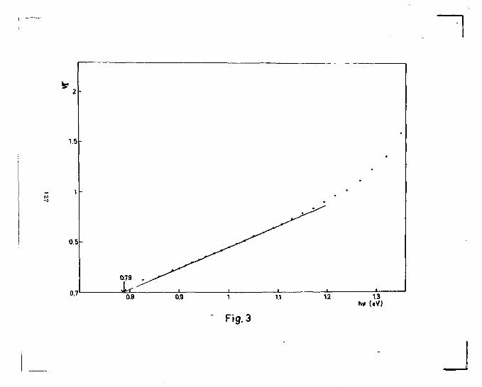
U 1.3 h* (*VJ
Fig. 3
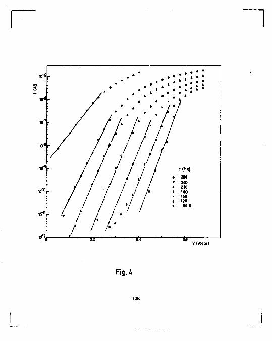
v(vmu)
Fig.4
128
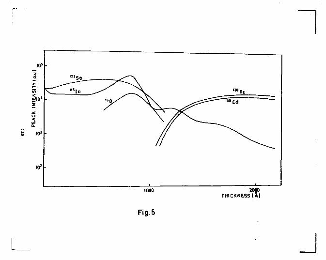
1000 2000 THICKNiSS(A)
Fig. 5
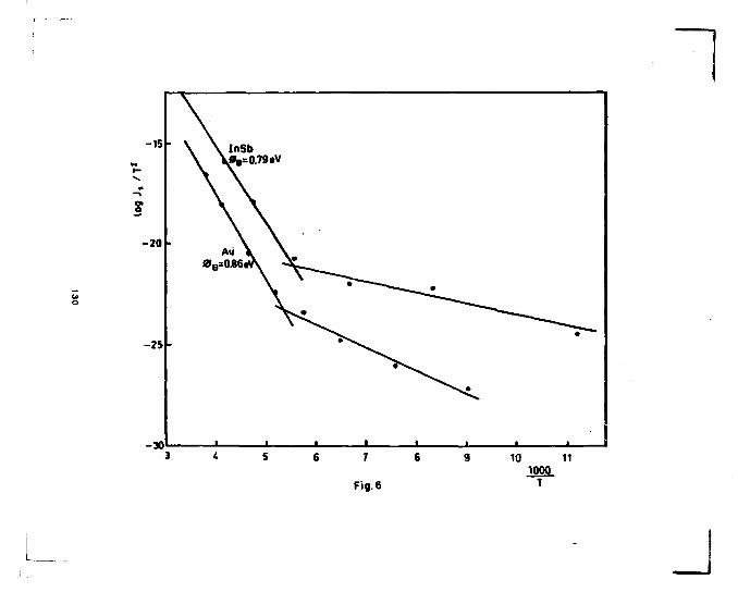
3 4 5 6 7 6 9 10 11 1000
Fig. 6 T
J
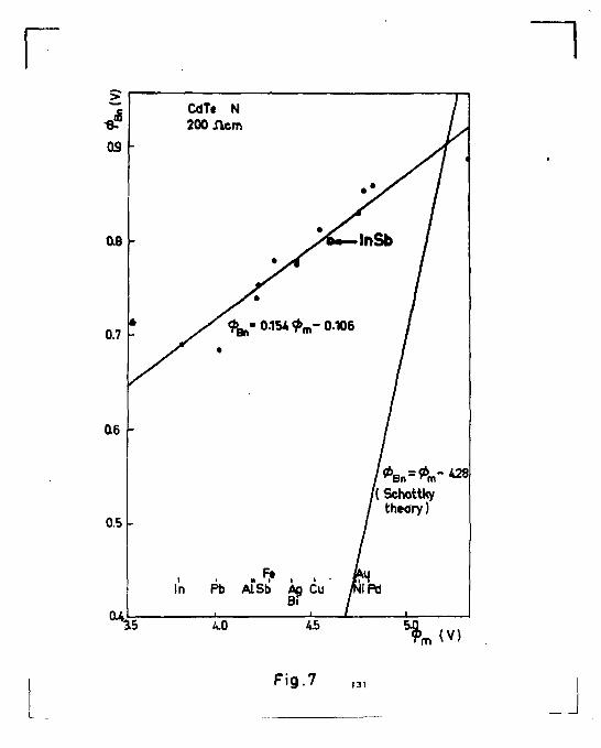
* *
os h
0.8
0.7 |-
06 h
0.5 |-
%
CdT» N / 200 ilcm /
./1 '
*S^ 1
_ /£-\nSb 1 • jg I
^r» I
t y S * ^ 015* <Pm- 0.106 / ^r * /
-
/ * B n = îV-428
-
/( Schottky / theory)
In Pb AlSb Àg Cu Ajiftj Bi /
1 i / i
U) 4.5 \ < V )
Fig.7
XXVI - 1
RESULTS OBTAI^ED^AT CRN STRASBOURG OM CdTe COUNTERS
A . CORNET, M. HAGE-ALI, P . SIFFERT
ABSTRACT :
In 1967 a program has been started in our laboratory in order to develop cadmium telluride nuclear radiation detectors. Here ve restrict our discussion to some recent experiments with ion implanted detectors, which have given a resolution (FVHM) of 32 keV for 5.5 ne1/ <x - particles.
The program initiated in 1967, for the preparation of CdTe crystals and nuclear radiation detectors, covers currently several aspects of the problem. Some are investigated in connection with the UHES Bellevue (MARFAING, TRIBOULET) and the CBN Grenoble (SCHAUB, POTARD). Here, we are essentially concerned with the results obtained recently with ion implanted counters.
I. CRYSTAL GROWING Two different techniques are used for the preparation of the
crystals : - the vertical zone melting as described by LORENZ and
HALSTED [1] and recently by WOODBURY and LEWANDOWSKI [2]. - the traveling heater method (THM) as described by BELL et
al [3, 4]. A third method is in progress : the Czochralski liquid en
capsulation technique. The details of the first procedure we use have been already published [51. Most of the detectors we have made have been prepared starting with crystals grown by zone melting.
II. DETECTORS T'r.s starting material grown either at Bellevue or at Stras
bourg has a resistivity between 10 and 20C n.em (300° K ) . The maxi-•nur, carrier concentration at low température ranges between 5 and 9.104cir,3/v.s.
133
XXVI - 2
A. Surface Barrier Det<»ctors Several surface barrier counters have been prepared and
investigated by a-particles. The main results have been published elsewhere C6], The mean energy required for electron - hole pair generation has been determined by comparison vith that needed in silicon. The values we obtained, 4.46 eV (300° X) and 4.75 eV (77° K) are smaller than that found, by the same experimental approach, by MAYER [7] and ARKAD'EVA [81, but have been confirmed by ALBERIGI - QUARANTA et al [9]. It appears that a high carrier collection efficiency is achieved in our counters, vhich gives a good indication of the crystal quality.
B. Ion Implanted Counters The rectifying contact (8mma area) of several counters h=>s
been prepared by implantation of 30 keV Bismuth ions at doses of 101* - 10 cm - 7 into 75 ">.cm N-type materia 1. A 30 min. annealing treatment at aoO°C in vacuum has been performed in order to reduce the amount of radiation damage. The N ohmic contact was obtained by indium deposit.
The I - V characteristic at room temperature is shown in Fig. 1.
The junction capacitance has been investigated and compared to surface barrier diodes, as a function of voltage, bridge frequency (5 to 500 kHz), ageing time (Fig. 2 ) . The voltage - capacitance characteristic at a fixed frequency was found to be independent of ageing and can be expressed ty CotV , where n =» 0.45. This indicates the presence of an abrupt junction. Since the annealing temperature is rather low, it is not clear at the present time if the junction is due to the electrical activity of the implanted bismuth ions, or to the radiation damage. But the results given by MEYER at this conference indicate that, for lov dose and low energy bismuth implanted layers, the annealing occurs et a temperature close to 200 8C. b) Detection characteristics
The response of these counters to 5.5 MeV ot - particles has been investigated at room temperature. The best result is shown in Fig. 3. The resolution (F.W.H.M.) of 32 keV seems promising, since it corresponds to an improvement by a factor two when compared to our earlier spectra and to those published in the literature.
Ion implantation appears to be an interesting technique, for making thin window nuclear particle detectors. The capabilities of these counters are limited at present time by the quality of the starting material.
%
134
XXVI - 3
ACKNOWLEDGMEHTS The authors wish to thank Mr KOEBEL who has grown the crys
tals, Mr J. KUREK who performed the implantation, Mrs F. KLOTZ and C. V.'BYMANN who prepared the detectors.
REFERENCES
1. M.R. LORENZ and R.E. HALSTED - J. Electrochem. Soc. 4 (1963) 343. 2. H.H. WOODBURY and R.S. LEVANDOWSKI - J. Crystal Growth 10 (1970) 6. 3. R.O. BELL, N. HEMMAT and F. WALD - Phys. Stat. Sol. (a)
1 (1970) 37'}.
4. R.O. BELL, K. HEMMAT and F. WALD - IEEE Trans. Nucl. Sci. NS - 17 (1970) 241.
5. A. .CORNET, P. SIFFERT, A. COCHE - J. Crysta] Growth 7 (1970) 329. 6. A. CORNET, P. SIFFERT, t;. COCME and R. TRIBOULET - Appl. Phy. Let.
17 (1970) 432. 7. J.W. MAYER - J. Appl. Phys. 38 (1967) 296. 8. E.K. ARKAD'EVA. L.V. HASLOVA, O.A. MATVEEV, YU.V. RUD', S.M.
RYVKIN - Soviet Phys. Semicond. 1 (1967) 669. 9. A. ALBERIGI - QUARANTA, C. CANALI, G. OTTAVIANI and K.R. ZANIO
Nuovo Cimento 4 (1970) 908.
FIGURE CAPTIONS
Reverse characteristic of a 8mm 2 Bi + implanted diode without surface protection. Capacitance vs voltage for an implanted diode immediately after preparation and after 3 months storagi; in air. For comparison a similar curve for a surface barrier Au - type Cure is reported. w.iponse to 5 MeV a - particles of an implantea CdTe counter. For comparison the response of a silicon surface barrier is -1 r,o reported.
135
!
Fig. 1 -
Fig. 2 -
Fig. 3 -
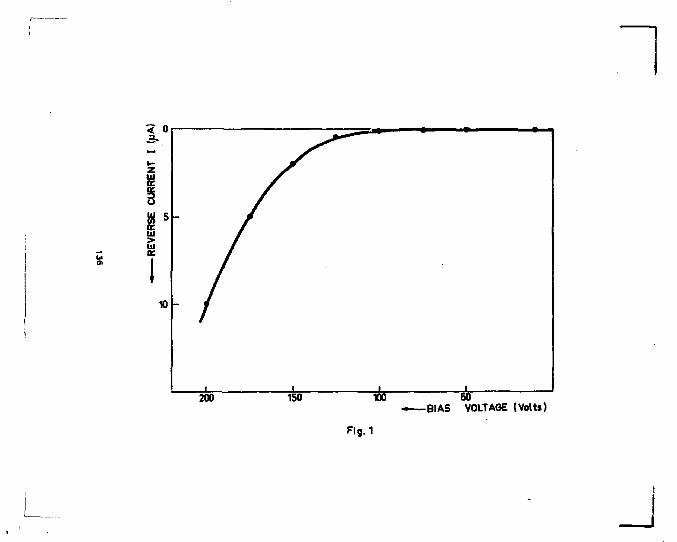
-BIAS VOLTAGE (Volts)
Fig.1
J
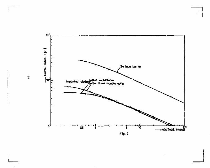
nK
w
io L
Surfoce borricr
Fig. 2 VOLTAGE (Vblts
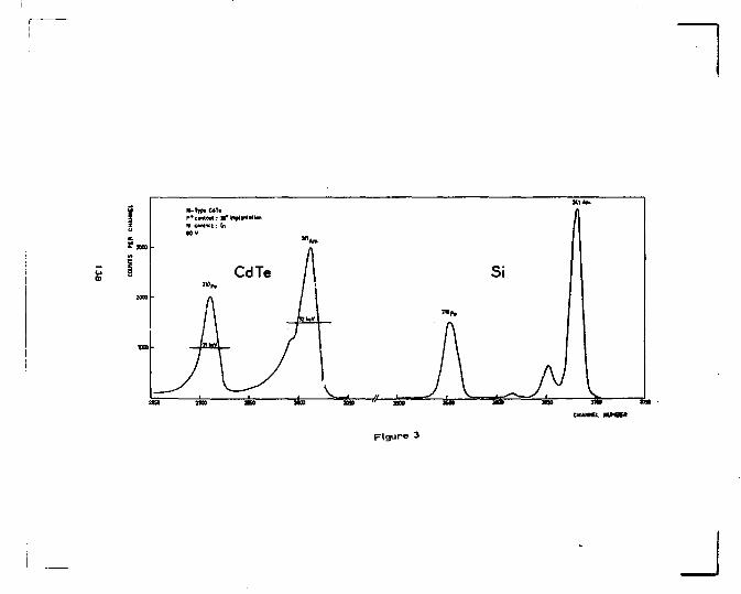
! z u £ JO»
P*£ontotf : • * hflantotkM N cantnet: In •OV
Figure 3
ION IMPLANTED CONTACTS ON CADMIUM TELLURIDE DETECTORS
A.CORNET, M.HAGE-AL1, J.J.GROB, R.STUCK, P.S1FFERT
Centre de Recherches Nucléaires Laboratoire de Physique des Rayonnements
et d'Electronique Nucléaire STRASBOUR3-CRONENBOURG
(FRANCE)
13 Scintillation and Semiconductor Counter Symposium, WASHINGTON(1972). I .E .E .E . Trans. IMucl. Sci. NS 19, n°3 (1972) 358.
SUMMARY Cadmium telluride single crystals have been grown by the vertical
zone melting technique. Wthout added chemical impuriti», they are generally N-type of 10 - 100 ft.cm resistivity. Detectors have been prepared with this material by implanting Bi + ions . The influence of the implant conditions and annealing treatments were studied. A FWHM of 24 keV has been obtained at 300* and 77* K for 5.5 MeV s -particles.
139 I I
I. INTRODUCTION The Interest in the use of cadmium telluride (CdTe) as a highly effi
cient room temperature Y-ray detector is due to the high Z, large band-gap and relatively good carrier mobility of this material. The high resistivity (>10 n.cm) necessary to achieve large absorption depths is generally obtained by compensation of the cadmium vacancies and impurities by In r i | 2 ] or halogens (Br, CI, 1) T3] during the crystal growing. This material still posses^»» trapping sites and inhomogeneities which cause incomplete charge collection and poor resolution. As pointed out by MILLER !"£}, problems associated with the contacts also arise. The emphasis in the paper will be on the preparation of the rectifying contact by ion implantation in uncompensated material.
II. MATERIAL The crystals were grown by a method derived from the Heumar.n -
Lorenz - Halsted technique T57 • Starting with 5N tellurium and cadmium syndesis is done in a. graphite coated quartz tube T6]. Twenty passes at 3cm/ hour of zone refining iu self-sealed T7] quartz tubes are used for purification of the compound. Finally a S mm/hour pass is used for growing the crystals, which are generally N-Type of 10 - 100 O.cm resistivity and of 1 cnr volume. The maximum carrier mobility at low temperature ranges between 5 - 9. Kr*cm / Vs. The crystals are cut and lapped to a thickness of approximately 1 mm. Conventional surface treatments are used.
III. CHOICE OF THE IMPLANT CONDITIONS 1) Sample Sçle5tioji_B^for^Jmplantaiion, The state of disorder existing in the crystal lattice before implanta
tion can be estimated at depths up to a few microns by an analysis of Rutherford backscattered e ions impinging into 'he crystals along channeling directions, as shown previously for CdTe by GETTINGS et al ^8^ and
140
MeyerfC9] - The samples are mounted in a 3 axis goniometer and bombarded
with a highly collimated beam of 2MeV ^He + ions . The backacattered particles
and the generated X-rays are recorded respectively with a surface barrier
detector (14 keV resolution FW HM) and a 250 eV resolution X-ray Si(Li)
counter. Conventional techniques are used for crystal aUgment with respect
to the beam. By measuring the ratio ^min of the yield of backscattered parti
c les when the beam i s channeled to that obtained for random bombardment,
along the trace of the T l e + i o n s in the Ci.ystal, a good indication of the amount
of disorder present in the crystals i s obtained. Some experimental results are
reported on fig. 1. In the c 110> direction at room temperature y,mln at the sur
face i s extrapolated at values between 0 . 0 3 and 0 . 0 5 for hijjh quality single
crysta l s , the theoretical value in the same conditions being about 0 . 0 2 . Only
the crystals with xmin < 0 . 0 5 , are used for implantation. The slope of the
straight line observed in fig 1 . gives further indication of the rate of dechan-
neling through lattice disorder. As smaller this slope i s as better i s the crystal .
2) Jon implantation,
Inversion of conductivity type on N-type samples by chemical doping
through ion implantation has been observed with the following group V e l e
ments : P + C10,X1] , As*[12] and B i + r i 3 ] .
Hi?re we have again chosen bismuth implantation in the range of energy
between 20 - 80 keV.
3) i . a t tù Disorder^ The lattice Tisorder resulting from ion bombardment has been investi -
gated by the same te 'inique as that used for the dechanneling measurement. A typical backscatterev e particles spectrum i s shown in fig-2 as a func -Hon of the implanted dose of 40 keV B i + . The X-ray spectrum (due to inner shells excitation of Cd and Te by the T i e * beam) recorded simultaneously is given in fig 3 . From these curves , the relative concentration of defects
141
as a function of dose was calculated (fig 4 ) . The disorder production rate up to about 3 .10 cm" 2 i s rather small s between 5 .10 and 5 .10 cm a linear dependence on dose Is found. The dose necessary to obtain the saturation i s about 5 • 10 cm . At this value the disorder level i s about 40 % of the random leve l .
The annealing behaviour of the lattice disorder i s dependent on doses :UJ, to 5 . 1 0 ^ c m the reordering occurs below 250°C, for higher doses (fig 5) much higher temperatures are requested.
Finally, the following implant conditions have been chosen for the detector preparation :
- energy : 30 keV - d o s e : 5 . 1 0 1 4 c m " 2
- implant temperature : 20*C - annealing : 200 °C for 30 min.
o - implanted area : 8 mm
IV. DETECTOR PRQSERTIES
The junction capacitance C as a function of reverse bias voltage V can be expressed by 0*V" , where n=*0.45. This indicates the presence of an abrupt junction.
The response of these counters to 5 . 5 MeV a -particles has been investigated from 300* to 77 C K. The resolution (FWHM) i s 23 keV both at room temperature and at liquid nitrogen temperature (fig 6 ) . This i s a d e monstration of the thin window thickness (<1 u) of the implanted detector. A further proof results from the Cf fission fragment spectrum (fig 7) .
It appears that ion implantation is an useful technique for making thin window nuclear particle detectors . The Rutherford backscattering technique . institutes a complementary method for checking the crystal qualify .
142
ACKNOWLEDGMENTS
The authors would like to gratefully acknowledge the technical assistance of Mr J. KUREK, who performed the implantations.
143 I I L _ . _
FIGURE CAPTIONS
Fig . 1 : Ratio ymin of the yield of backscattered T i e ions in channeling and random bombardments as a function of depth below crystal surface.
F ig . 2 : Random and <110> aligned backscattering energy spectra using 2 MeV *He + ions . The dose of 40 keV implanted B i + i ons i s in parameter.
F i e . 3 : L - X ray spectra of Cd and Te as a function of implanted 40 keV Bi + ion dose .
F ig . 4 î Dose dependence of the relative lattice disorder produced by 40 keV B i + ions implantation. The plateau reached at high doses i s arbitrarily normalized to 100 %•
Fig . 5 : Relative lattice disorder versus anneal temperature for a 40 keV 10 cm B i + implanted layer .
F i g . 6 : Po and ^ Am a -spectrum obtained at 40V with a 40 keV implanted Bi + diode .
2S2 F ig . 7 : Cf fission spectrum recorded at room temperature.
144
REFERENCES
1. N.R. KYLE Froc. Internat. Symp. Cadmium Telluride Strasbourg (1971) P. Siffert, A. Cornet Ed. Paper IV
2. R.O. BELL, F. WALD. réf. 1, paper VI.
} . F . WALD, R.O. BELL, paper submitted to Nature.
i. G.L. MILLER. IEEE Trans. Nucl. Sci. Under Press
5. M.R. LORENZ, R.E. HALSTED, J. Electrochem. Soc. 110(1963)343
i. H.H. WOODBURY, R.S. LEWANDOWSKI, J. Crystal Growth, 1ÛC1971) 6 .
'. A. CORNET, P. SIFFERT, A. COCHE, J. Crystal Grovth 7 (1970) 329.
i. M. GETTINGS, K.G. STEPHENS réf. 1 paper XVII bis.
>. O. MEYER réf. 1 paper XVII
.0. G.A. KACHURIN, V.M. ZELEVINSKAYA, L . S . SM1RHOV Sov. Phys. Semicond. 2 (1969) 1527.
.1. N.V. AGRINSKAYA, E.N. ARKAD'EVA, M.I. GUSEVA, L.V. MASLOVA, O.A. MATVEEV, S.M. RYVKIN, V.A. SLADKOVA, K.V. STARININ. réf. 1 paper XVI.
.2. J.P. DONNELLY, A.G. FOYT, E.D. HINKLEY, W.T. LINDLEY, J.O. DIMMOK. Appl. Phys. Lett. 12(1968)303.
-3. A. CORNET, M. HAGE-ALI, P. SIFFERT, réf. 1 paper XXVI.
145
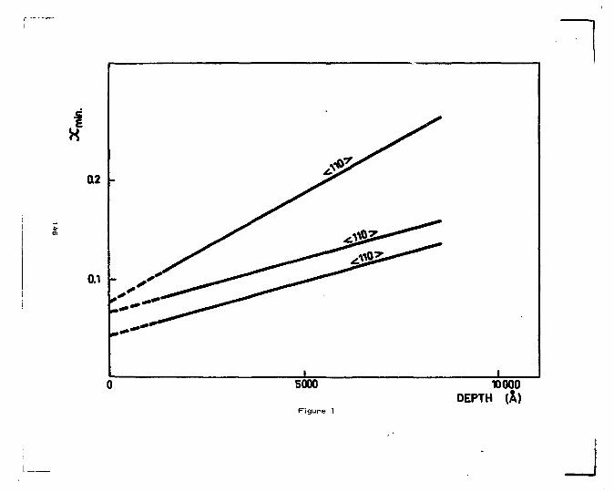
0.2
0.1
J&>
5000
Figure 1
i 10000
DEPTH (Â)
_J
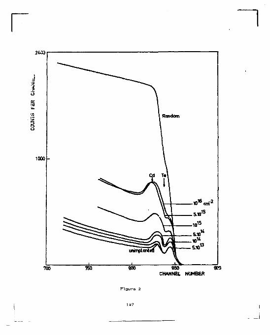
2C30i
3
I Random
1000
700
-W 1 6 o n 2
.5.10 ,«
-10''
.5.10 .U
.10 ,U -5.10 ,13
850 CHANNEL NUMBER
900
Figure 2
147
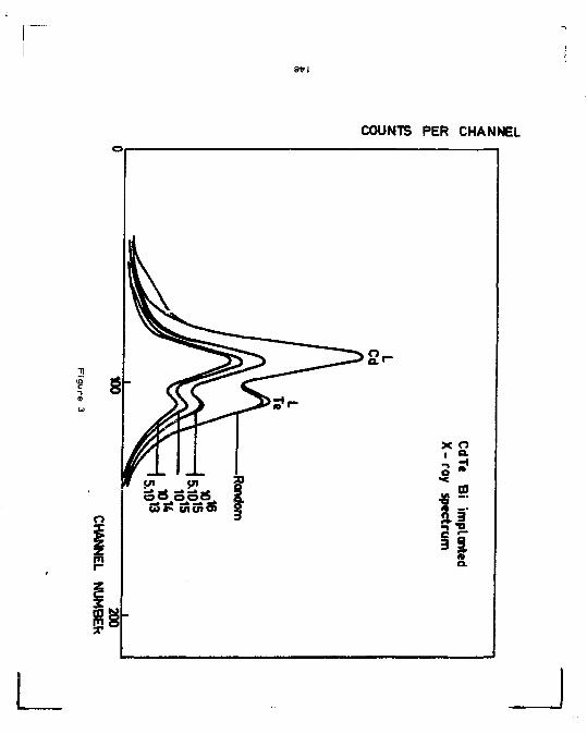
COUNTS PER CHANNEL
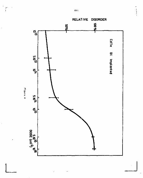
617 1
RELATIVE DISORDER
§ s o i i 1
2 -t
1 CD
i 1 %
• ^ ^ w
V
h \ 1
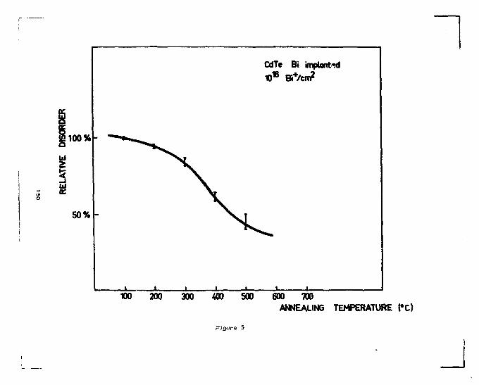
100%
5
50%
CdTe Bi impUmt'îd t ) 1 6 Bî+/citi?
100 200 300 400 500 600 700 ANNEALING TEMPERATURE (*C)
Figure 5
! _J
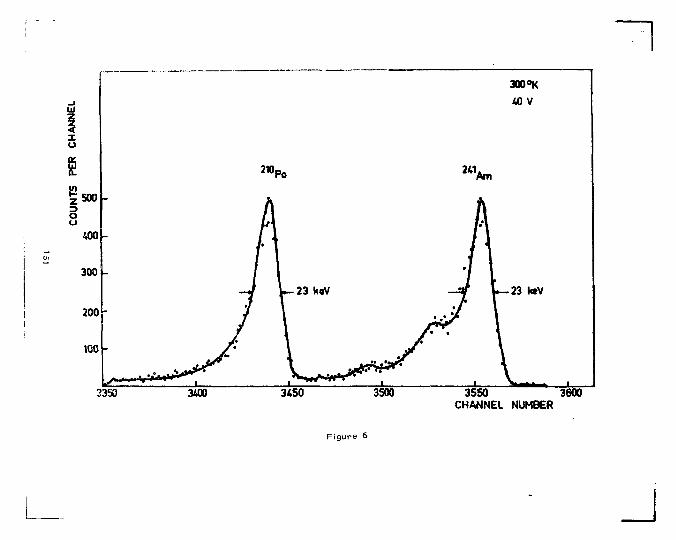
33S0 3400 3450 3500 3550 3600 CHANNEL NUMBER
Figure 6
J
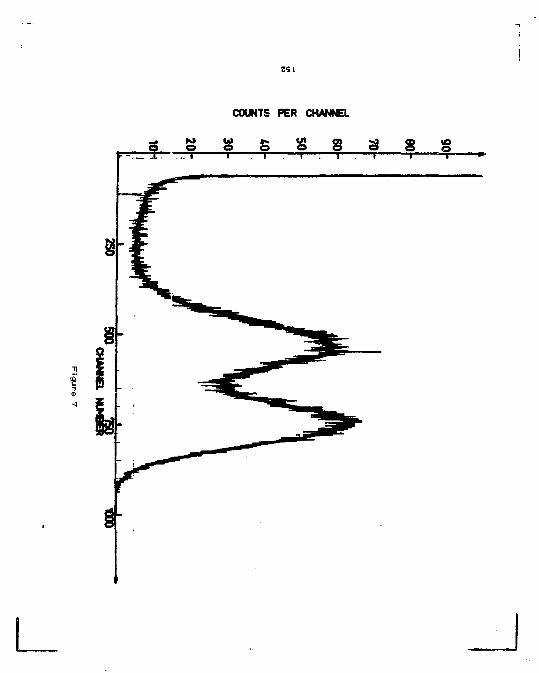
COUNTS PER CHANNEL
L. ? o o s 01 o S s s «D
O T ~ I . 1 1
' i 1 T ~ I . 1
i
CHAPITRE IV
SPECTROMETRIES NUCLEAIRES
La spectrométrïe nucléaire a beaucoup progressé avec l'avène
ment des détecteurs à semiconducteurs. Les diodes à base de germanium
(pur ou compensé au lithium) sont largement employées à l'heure actuelle
même en dehors de la physique nucléaire : par exemple en médecine nu
cléaire des appareils mettant en oeuvre simultanément deux cents spectro-
mêtres Ge H, P. ont été développés.
Le germanium et le si l icium, qui constituent les matériaux ac
tuellement employés pour la préparation des spectromètres de photons,
avaient été retenus Initialement à cause de leur importent degré de dévelop
pement technologique, consécutif aux besoins de Mindustrie électronique. Ils
ne constituent pas les semiconducteurs les mieux adaptés aux applications
considérées i c i . En effet, examinons brièvement les cr i tères qui doivent
être pr is en considération pour le choix du matériau optimal :
153
- numéro atomique Z
Comme seules les Interactions photoélectriques sont Intéressantes et comme
ce l les-c i augmentent rapidement avec le numéro atomique Z du mil ieu absor
bant, on cherchera évidemment a employer le matériau ayant le numéro a to
mique le plus élevé.
- bande interdite Eg
Pour permettre un fonctionnement à température ambiante avec un niveau de
bruit (dû à la génération thermique de porteurs) minimal, Il sera i t intéressant
d'employer des cr istaux ayant une valeur E g élevée. Toutefois, lorsque cette
énergie devient trop grande, la probabi l i té de plégeage et l 'énergie requise
pour c r é e r une pa i re é lec t ron- t rou deviennent prohib i t i fs . Dans la prat ique,
les valeurs optimales se situent entre 1,5 et 2 , 2 e V .
- densité de porteurs l ibres
Pour un matériau de numéro atomique supér ieur a 4 0 une épaisseur de 2mm
absorbera notablement les photons Y . En considérant qu'une te l le zone de
charge d'espace doit ê t r e obtenue pour une va leur raisonnable de la tension
de polarisat ion (par exemple 5 0 0 V ) , on peut calculer que le semiconducteur
doit posséder moins de 10 porteurs par cm3 a température ambiante (d i f
férence entre la concentration de trous et d 'é lectrons) .
- vi tesse de déplacement des por teurs
l_e temps de transît des porteurs a t r a v e r s la zone sensible du compteur est
inversement proportionnel a leurs mobil i tés. Dans les conditions de l'exemple
précédent, une mobil i té de I O O cm / V* s . conduit à des temps de transi t de
l 'ordre de la microseconde. P lus il sera long, plus la probabi l i té de p iégea-
ge sera grande.
154
" densité de pièges, eff icacité de collection
Les matériaux semiconducteurs et plus part icul ièrement les composés con
tiennent des centres de capture associés à la présence d' Impuretés, de dé
fauts de stoechiométrie ou de combinaisons de défauts et d' Impuretés. Ces
pièges, qui Introduisent des niveaux dans la bande interdi te , ont pour effet
de re ten i r les porteurs pendant un temps plus ou moins long, ce qui peut
conduire à une per te de charges qui entraîne une dégradation de l'ampiîtude
et de la résolution du compteur. Deux paramètres caractér isent ces phéno
mènes : fa densité de pièges N._ et la durée de v ie d'un porteur avant c a p
ture , on peut montrer que le piégeage n'a que peu d'influence si N_.<10 cm"
et la durée de v f e T > I O s ,
Quels sont les matér 'aux qui satisfont à l'ensemble de ces c r i t è r e s ?
Parmi le t rès gyand nombre de cr istaux semiconducteurs, i l con
vient évidemment de se l imiter à ceux qu'on est capable de p r é p a r e r avec
un degré de pureté et de perfect ion c r is ta l l ine suffisant. I I ne subsiste a lors
que t rès peu de matériaux, qui sont repor tés sur le Tableau I , E n r i î t , seul
le te l lu rure de cadmium et l ' îodure mercurïque répondent aux c r i t è r e s énoncés
ci -dessus.
Nous nous swTimss intéressés à C d T e . ma : s d'autres :~avai-x sor:
cors~z-*és. à +-'9"»2 a u sein du iat^orstoïre. En p a r t ï c i l i e r , nous avons cherche
à établ i r l ' influence de di f férents traitements de surface sur les performances
de rtf-tectlon (cf. a r t ic les ) . Une attention toute par t i cu l i è re a été portée &u
phénomène de polar isat ion apparaissant dans les cr istaux de t rès haute ré~
sîst îvî té. Rappelons que cet effet se traduit par une diminution progressive
de l'amplitude du signal et de l 'eff icacité de détection lorsque le spectromètre
est en opérat ion. Ces travaux ont fait l'objet de plusieurs publications. Nous
ne rappellerons Ici que les points essentiels :
- la polarisat ion apparaît à p a r t i r d'une cer ta ine rés is t iv i té des cr istaux
THM qu' i ls soient compensés au chlore ou pas. L e seuil cr i t ique de r é s î s -
155
4 tivité se situe a f Ss6. 10 n.cm effective.
- M importance de la polarisation, définie par la constante de temps de dé
croissance de l'efficacité de détection, varie d'un cristal a l'autre, mais
elle est directement liée à l'intensité de la bande de luminescence (fig. 1)
apparaissant a 4,2" K vers 1,42 eV (niveau a 0,15 eV au-dessus de la
bande de valence). Rappelons que ce niveau est lié à un défaut complexe
vacance de Cadmium-donneur (V-,_.-X). Il ne peut être responsable directement
de la polarisation, car sa localisation dans la bande Interdite n'est pas
suffisante. Par contre, le niveau dû à (V„ .-X) est lié à ( V „ j ) localisé
au milieu de la bande interdite. Ainsi que les calculs de compensation ,
effectués au laboratoire, ont pu le montrer, l'incorporation de chlore dans
le cristal accroît considérablement la concentration de ( V _ d ), qui passe
de lO àer10 cm à température ambiante (cf. chapitre I)
- le mécanisme de la polarisation est décrit de la manière suivante :
Lorsque la tension est appliquée au temps t-0 aux bornes du détecteur,
l'extension de la zone de charge d'espace X est :
2^ * ** , où tous les symboles ont leur * " « < N A - N D }
signification habituelle. Par suite de l'émission de trous, une variation pro
gressive des centres ionisés se produit en fonction du temps t : N ,.-N-,+N_(t).
Par conséquent, x décroit avec le temps t et devient :
x 2(0) - x 2 (t) N T [ 1-exp ( - e t ) ] " T
[x(t) - « x ( 0 ) ] 2
E,_ - E x 2 ( — ) 1 q V '
comme dans nos conditions o r « 1 on aura :
156
x j ° 2 _ , [ 1 - exp ( - e t ) ] , •**t*1 M M P
où e est le coefficient d'émîssion du niveau profond donné par p E - E
e p ' a v t h N v e x p ( - kT '
teurs et N le nombre d'états dans la bande de valence.
Nous avons pu constater (flg. 2) que ce modèle est en bon accord
avec les expériences.
Pour supprimer la polarisation, essentiellement cinq voies sont
ouvertes :
- employer un matériau de réslstîvïté faible afin d'éloigner le niveau de
Fermî du niveau profond (fig. 3), de sorte que, lorsque les bandes sont
courbées sous l'action d'une tension appliquée, E_ n'est pas coupé par E . F
- accroftre artificiellement la concentration de porteurs, par exemple en
éclairant le détecteur. Toutefois, ceci entrafhe une dégradation des perfor
mances.
- réduire la courbure de bande à un point tel que E_ ne peut pas croiser
Ep, en d'autres termes, appliquer des contacts quasï-ohmiques. Cette
approche est largement employée grâce aux dépôts spontanés ("electroless11)
d'or ou de platine. Malheureusement, dans ces conditions le courant de fuite
devient prohibitif et la tension d'avalanche devient inférieure à 100 V environ.
- utiliser des structures métal - isolant (ou oxyde) - semiconducteur (MOS ou
MIS), L'idée générale est de trouver un moyen permettant de maintenir une
faible concentration d'électrons au voisinage du contact polarisé positivement,
suffisante pour se recombîner avec les accepteurs ionisés, sans affecter
157
toutefois, le niveau de bru i t . P lus ieurs méthodes ont été tour à tour e s
sayées : le dépôt d'un fi lm de SIO , l ' implantation Ionique et l'oxydation
superf ic ie l le par H , 0 _ . Dans ce dernier cas, des résultats in téressants
ont pu êt re obtenus (Tableau I I ) mais II était impossible de maî t r iser l 'évolu
tion u l té r ieure des surfaces oxydées.
- supprimer le niveau E— responsable de la polar isat ion.
Nous avons employé les cinq voles, mais i l est cer ta in que la
dern ière constitue la mei l leure solution. Après plusieurs années d 'ef forts ,
nous venons de parveni r à la croissance de cr istaux semi- isolants compensés
au chlore dans laquelle la polar isat ion est totalement absente (cf. a r t i c l e ) ,
en jouant sur les conditions de t i rage , de façon à rédu i re les lacunes de
cadmium dans une proport ion suff isante. Nous pensons avoir accompli un pas
décisif dans le développement de ce matér iau .
156
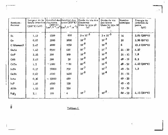
Semiconducteur
Largeur do la bande Interdite (300°K)(eV)
Mobilité" des électrons
C300°K) (cm2.V l.sl:
Mobilité des trou s (300" K)
fcm^V"1..,-1)
Durée de vie des électrons (dans le type p)
(s)
Durée de vie des trous (dans le type N)
(s)
Numéro atomique
Energie de création de paire
(eV)
St 1,12 1500 600 3 x 10" 3 3 x 10 " 3 14 3,61 (300«K)
Ge 0,67 3900 1800 l o - 3 10" 3 32 2,96 O0°K)
C (diamant) 5,47 2000 1550 io- 8 io - 8 6 13,2 (300*K)
GaAs 1,43 8500 420 io - 7 i o - 7 31 - 3 3 4,27
GaP 2,25 300 100 io- 8 io - 8 31 -15 7 . 8
CdS 2.42 300 50 io- 8 io - 8 48 - 16 6 , 3
CdTe 1,5 ~ 1000 ~ 8 0 io- 6 io- 6 48 - 5 2 4,43 (300'K)
InSb 0,17 78000 750 io- 7 io - 7 49 -51 1,2
GaSb 0,67 4000 1400 io - 8 io - 8 3 1 - 5 1
InAs 0,36 ~ 33000 460 49 -3 3
InP 1,27 4600 150 49 - 15
AlSb 1,52 200 550 13 -51
H S l 2 2,1 ]00 • 4 10" 7 io- 8 80 - 5 3 4,15 (300'K)
•o Tableau
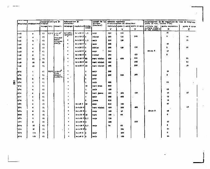
M « e r t m i N > m » e t * u r C a r * C t é r i » t i q u t du c r i s t a l
P r é p a r a t i o n du d - H i e t n i i r
A i P t S t i t U s u r f a c *
f o e t i o n n a x i e a l e d ' u t i l i & a t i o n en d é t e c t e u r
p o l a r i s a t i o n (% a e r é d u c t i o n du t a u x d e coe iptaa i a p r è s ID -nln, s o u r c e 5 7 c o )
d o s a g e t 4 * f . i b s e r v . d é c a p a g e o x y d a t i o n
m ( c o u l e u r ) i n i t i a l e
V
•près 5 mois
V
a p r è s 9 moi:
V
i n i t i a l e s u r s u r f a c e r o d é e ~ e t non o x y d é e A
a p r è s o x y d a t i o n
y. a p r è s 9 n i a i s
X
11*8
1141 • Cl
Cl
6î7<C f i - 3 . tO 7
( V a n d a r
B r ( j •aétl-
m-a n o l
4 + 1 + 5 0 *
4 * 1 * 5 0 <
1.5
5
n o i r
v i o l e t
3 5 0
3 0 0
130
130 5 0 0
15
0 14
IMS b ' Cl PaUv) 4 * 1 * 5 0 < 1 .5 n o i r 1 5 0 130 15
I t41 e C l finVJ» 4 * 1 * 9 0 V a n o i r MO 10
M 4 l c Cl 4 * 1 * 5 0 * 5 v i o l e t 3 0 0 130 150 » 3 0
I H » d Cl 4 . 1 * 5 0 » a n o i r 5 0 0 2 0 - 2 5 * 17
11*1 Cl 4 » 1 . 5 0 < j v i o l e t 3 0 0 120 • i u ( at Cl 4 * 1 * 5 0 11 ta T a r e v i o l e t 4 0 0 4 0 0 4 0 0 2 5
I t 4 » 2 2 Cl 4 » 1 * 5 0 » 9 0 v e r t v i o l â t 4 9 0 - 0 0 2 3
• U » 22 C l 4 * 1 * 5 0 * 20 v e r t v l o u t 4 0 0 2 0 0 30
1174 Cl «oor l . 5 x i 0 6
ft.cm (MiCl) , 4.flBnr/J.
1 n « l r 3 0 0 u
(274
ia?4
Cl
C l
l . 5 x i 0 6
ft.cm (MiCl) , 4.flBnr/J.
S
1
n o i r
n o i r
3 0 0 1 5 0 3 0 0 :
F274 Cl 1 n o i r n o 2 3
1274 Ci 10 v e r t b l e u 2 0 0
1774 Ci 1 n o i r 100 as
1274 Cl 10 v e r t J e u n e I tO 3 0 0 150 10 as
1274 Cl 1 a o l r 3 0 0 4 0 0 u 1374 Cl 5 J e u a o 1 3 0 14
(274 Cl 4 * 1 * 0 « 3 0 n o i r 1 5 0 150 27
1174 cv 4 * 1 * 5 0 < v o i t v i o l â t 4 0 0 too 4 0 0 4 0
1274 Cl 4 * 1 * 5 0 * 1 n o t r I tO 10 3 0 - 3 3 * 2 1
1174 Cl 4 * 1 . 5 0 * 10 v e r t 150 . to 0
1274 Cl 4 + 1 * 5 0 * 0 . 7 n o i r ISO
1214 Cl 4 * 1 * 5 0 * 5 3 0 0 2 5 0 29
1174} 10 Cl 4 * 1 * 5 0 * 0 , 7 n o i r 7 0 < 0 8
1274 10 Cl 4 * 1 * 5 0 * 5 300 21
1274 114 C l 4 . 1 . 0 * 2 n o i r 3 0 0 0
1274 l i b Cl 4 * | * 0 « 2 n o i r 100 2 4
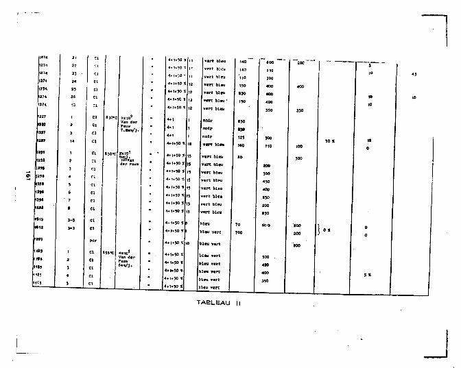
I»74
1274
12 74
1274
1274
1274
1274.
h»?
1227
217
1 2X10' V*n der Pkuv
1291
un 1 2 »
12V»
tan
I 2 f *
I U I
830«C Z* I05 n u c s •
I O T V M
IB «
1113
tK9
l i f t»
11*9
M I S
M M
I Ï Ï 5
4*10° Van der P*uv
4» 1*50 *
« » 1 . M t
4 + 1 * SO ••
4» 1+50 *
4 *1 *50
4*1+50 X
4+1+30 ï
4+1+50 «j
4*1+50 %
4+1+50 « |
4+1*50 t
4+1*50 «I
4+1+50 * |
4+1+50 X
4*1+50 %',
4+1+50 ]t J
4+1+50 T
4+1+50
4 * 1 * 3 0 X
4+1+50 X
4 * 1 * 5 0 *
4*1+50 *
4+1*90 Kj
4 * 1 * 5 0 %\
vert bleu
vert bleu
vert bleu
vert bleu
vert bleu
vert bleu '
vert bleu
noir
noir
noir
v«rt b i n
vert bleu
vert blew
vert bleu
vert bleu
vert bleu
vert bleu
vert bleu
vert bleu
bleu
bleu vert
bleu vert
bleu vert
bleu vert
bleu vert
bleu vert
bleu vert
150
150
t50
•90
123
« ©
70
700
too 250
100
400
400
300
110
300
300
450
400
350
200 '
230
300
430
400
150
300
300
TABLEAU II
J
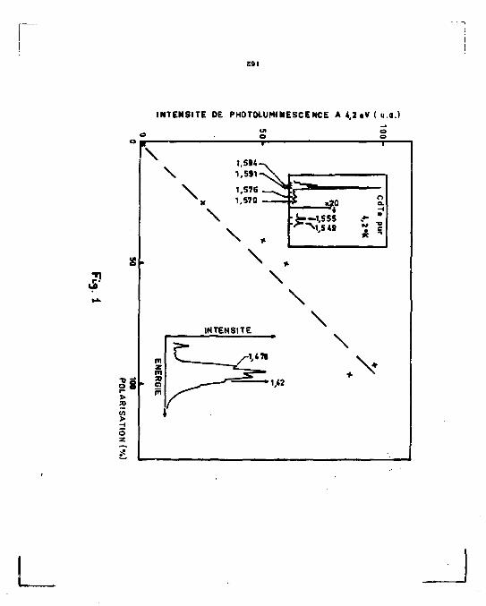
INTENSITE DE PHOTOLUMtNESCENCE A 4,2 «V ( u.a.)
?
\ \
\ 1,576 / * :,
>
>
« 1-570
\ * «; *
\
^—1.555 .*• " ^ 1 , S 4 9 -J ?
\
INTENSITE \
/•V47» \
1>2 A*
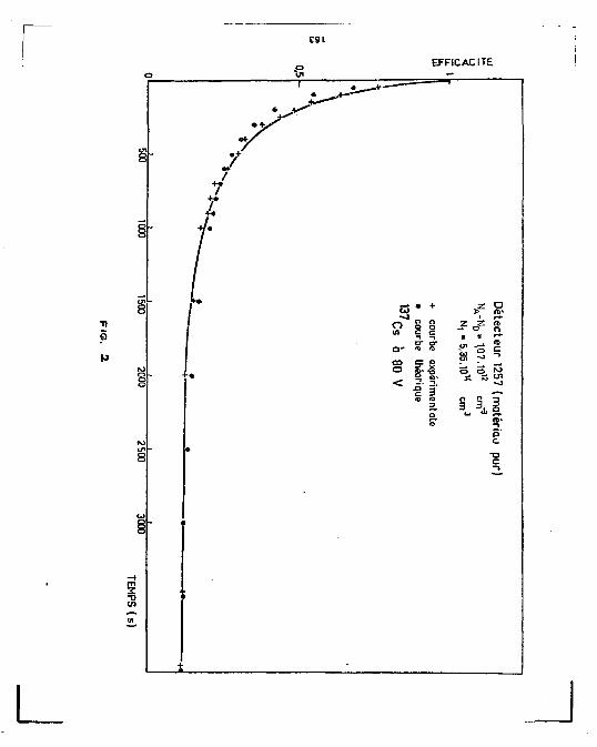
EFFICACITE
Ô
E S ' +
0 * 8 8 10 C C
^ O
X =i i
< 1 I -X S O?
3. 3 3,
S
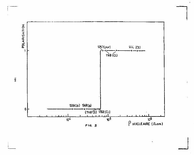
o h-< in cE < _i
£ 1257(pur)
1264(p.) T248(p)
"" +(1H8tT) 1̂ 92 (CI)
X y 1148 (Cl)
• • i i i i i i _!_ ' I i i I i i I
123. (CI) — + — + —
_i i I I i i i 10* 105
FIS. s
1 0 6
P NUCLEAIRE (Jl.cm)
IEEE Transact too» on Nuclear Sciatica, Vol. HS-26, Ko. 1 , February 1979 CORRELATION BETWEEN SURFACE PROPERTIES AND DETECTION
CHARACTERISTICS OF CADMIUM TELLURIDE DETECTORS
M. Hage-Ali , R. Stuck, C. Scharager, P. SIffert Centre de Recherche» Nucléaires
Groupe de Physique at Applications dea Semiconducteur* «7037 Strasbourg-Cedex (France)
SUMMARY
Up to now, only vmry little attention hac been given to the surface properties of cadmium tellurlde detectors, the best reported results being given for lapped surfaces, a result which Is rather strange, when compared to the general behaviour of semiconductors.
In order to better understand the mechanism In volved at a metal-cadmium tellurlde cor,tact, the properties of mechanically polished, chemically etched and also oxidized surfaces of cadmium tellurlde crystals have been Investigated using various methods I n cluding ellipse Tiitry, Rutherford baekscatterlng [n channelling conditions and secondary ion mass spectroscopy. Most Important contaminants have been Identified for each kind of preparation. Furthermore, It could be shown that If polished and certain oxidized surfaces are qt.fte stable In air , etched surface become covered by s tellurium oxide layer, whose thickness Increases even after very long periods of time.
Detectors have been prepared afterwards on identical samples having received the various surface trectments and the main detectors properties Investigated, especially noise, resolution, efficiency and polarization,
INTRODUCTION
Despite of the efforts made in various laboratories no significant improvements in the detection properties of CdTe Y-ray detectors occured during the last two years. However,, up to now most of the r e search was devoted to the improvement of the quality of the material and only little attention has been spent to the surface properties. This Is rather surprising, since H is well established that the detection properties and stability of these devices depend to a large extent on the preparation of the surface before deposition of the contacta K Therefore, we have investigated the properties of mechanically polished, chemically etched and also oxidized surfaces of cadmium tel lurlde using ellipsometry, Rutherford backscatterlng isnder channelling conditions and secondary Ion mass spectroscopy. Counters have also been prepared afterwards on identical samples having had the same surface treatmfi-its. Finally, thelrcharecterlstics (leakage current, noise, resolution, detection efficiency and polarization) have been studied.
EXPERIMENTAL CONDITIONS
Sample preparation Crystal growth : cadmium tel lu ride single crystals were grown by the travelling heater method (THM| 2 . They were either undoped or, more often, chlorine compensated end their resistivities ranged from 10 5 to 108 n-cm. Surface preparation
For the surface studies, slices oriented para I-
0018-9499/79/0200-0281SOO.75(c)1979 I EKE
lei to the < I t o plane were cut by a wire sew end were then topped wUh STC powders of various gradea having particle sizes from 20 p.m to S u.m In diameter.
Polishing of the CdTe crystals was dona by using aluminium powder having. In the latest stage, particles of size less then 0,3 ^m in diameter. After polishing, the samples were carefully cleaned, especially In methanol.
Etched surfaces of CdTe ware prepared by Immersion of the lapped samples for 1 min. in a bro-mln- In methanol solution contanlna about 12% of bro-ml iu. The etcii.ig was quenched .w excess methanol. The samples were finally rinsed In methanol and blown dry with nitrogen.
Oxidized samples of CdTe were obtained by treating etched samples In a solution of 4 parts H 2 0 2
and 1 part NHaOH at 55 ' for 10 min. Reproducible blue colored oxide I I T S were obtained with this pro cedure.
Detector fabrics' Afler the various surface treatments Just des
cribed contacts were deposited : - aluminium and Indium on the lapped or poli -
shed surfaces, by vacuum evaporation ; - gold or platinum by elactroless decomposition
of a chlorine solution ; - aluminium on the oxidized surfaces by vacuum
evaporation.
Surface Investigation techniques Essentially three different methods have been
used to investigate the surface properties after the various treatments described above : Secondary Ions mass spectroscopy (SIMS)
The elemental composition of the various surfaces can be determined by performing a mass analysis of the positive and negative Ions sputtered off the surface under argon bombardment 3 i ^. The apparatus used Is shown schematically on F ig . 1. The current density of the primary 3 koV A r + beam is kept low enough [< t nA/cm^) so that only a thin I ay or of about 20 Â in thickness is sputtered off during the measurement. Thus only the first atomic layers are analyzed. To reduce the absorption of residual gas molecules on'the surface, the pressure in Iht- experimental chamber is kept below TO - 9 torr.
Ellipsometrv El nosometry measurements were made on et
ched and oxidized samples In order to determine the thickness and refractive Index of the surface films. Ellipsometry measures the changes In the phases and the amplitudes of the parallel and perpendicular components of a monochromatic polarized light when it is reflected from the surFaee under analysis 5 . Since this method Is nan destructive a continuous monitoring
165
or the trim growth la possible. A schematic of tha a l -!!piomalar used J» shown In R g . 2. Tha light s o u r » was a Ha-Ne laser amlttlng at a wavelength of 4J2S A.
Pajtharford beckscatterlng (Pals?)
Rutherford beckscatlartng under channeHlng conditions ° waa uaad to analysa tha crystal damage and tha al«marital composition naar tha aurfaca of lha various samp is». As shown on F ig , 3, thaaa samples «vara mounted on a thraa axe* goniometer and bombor-dad with * H e + tons of 1 M*V, tha energy of tha beck-acattarad partie!as being maaaurad with a high reeeki-llon electrostatic analyser. In tha caaa of a coiwpaund aamlconductor, I l keCdTe , tha aligned" W S apactruwi (yield va energy of the beckecattarsd particles) r e -vaals tha presence of two dlatlnet aurfaca peak* duo 10 tha colllslr »s on each kind of stoma, Cd mné Ta , at the surface. Therefore, the ratio of the eras under each peak la related to tha aurfaca alolchlometry. However, In tha case of lapped or OKldlzad aurfacaa, the measurements are difficult due to the high iavel of ^«channelling.
petector measurement»
The detection characteristics of tha varloua devices have been measured using a classical eat-up both for a-partlcles ( 8 4 , A m ) and Y-reys ( * 7 Co) and positiva' and negative side electrode entrance of tha radlatlonf Tha pulse amplitude! have bean calibrated In an absolute scale with a eHlce/1 detector, taking Into account the difference required to croate an electron-hole pair.
RESULTS
Polished surfaces
Surface Investigation
F ig . 4s and 4b ehow the positive Ion spectra respectively for a polished surface and for tha same sample after a layer of «bout 500 A In thickness waa sputtered off. The comparlaon of both Indicates that the surface Is contaminated wf:h elements Ilka CH ( coming from the methanol used In the procedure) , with mass 40 <Ca or SIC) , with T l , Be, Cd + 40, Te + 40 and also Cr, Fo.
RSS measurements could not ba parformad since It was not possible to aligna tha cryatat du* to the high concentration of damago In close aurfaca vicinity.
Etltpsomoter measurements could only Indicate the presence of a thick surface film. Mo evolution of the surface was observed whan tha sample waa exposed to a1<- for times as long as several weeks. Detector properties
l-V characteristics measurement showed thai the In contact on a lapped surface gives a much lower current than A I . Typical values for 200 V bias are I 0 ~ e A For AI contacts and I 0 ~ 9 A for In contacts.
When bombarded with a-parllcles the pulse amplitude .vas low when compared to the theoretical value for positive electrode entering of the radiations. No signal waa observed for negative side entrance {Fig. 5). The remonse was more uniform for deeper penetrating radiations like S 7 C o v-rays (Fig. 6} for which 90 % of the theoretical pulse amplitude was measured.
Strong polarization was present for all counters and the effective depletion layer * was much lower than expected from the resistivity of the starting material. The counting efficiency for the In contact diode was el 122 keV about 100 times lower than that of the AI diode prepared on the same sample. In
contacta give vary thin depletion layers, even If tha barrlar height u vary cln*e to that «f Al.
JK"ttf Hffltltf fwT'tfft ¥*%'tff
Tha SIMs» apectra recorded an freahly etched sample* of CdTa ara shown an F ig , 7ande~.,1iie apactra af F ig . a * and »b ara bath far a M A thick layar eloaa lo tha aurfaca and concerne tha defection of negative and positive lana, respectively. T h e r e -soils reported an F ig , t a anal b ara both fbr.the aurfaca obtained after aputler atoning of a 500 A thick layar from tha original etched aurfaca. It appears that this surface la much laaa contaminated than lha polls-had on* . However, t race* f»f Br and Ch^ radicals due to l b * etching and rlnstne? procedure subsist on surface. Furthermora, tha surface appears to ba slightly oxidized.
Because of differ antral sputtering affects * and enhancement phenomena , SIMS con gtve no reliable Informations about tha aurfaca atolchlomalry of tha compound. Thus, Pass meeourenents wara psrfdrmed and tha raaults compared to those obtained for freshly cleaved surfaces which can ba assumed to bo Ideally stoichiometric. The résulta (F ig . 9) show thst the B r 2 - methanol etch leaves the surface enriched In Cd, since It has about 46 ft mora Cd than tha cleaved surface.
Elllpsometry measurements Indicate that an oxide film grows on such surface* if they ara exposed to air {Fig. 10). It appaara that tha Initial oxide thickness on the surface, Immediately after etching may vry by about 10 A fro sample to sample, but the rate of oxfda growth on each samp te Is tha same. Under normal atmosphere and temperature, the film thickness d grows with t1met 0 following the equation: d(A] - g.25 In t (mini - t D , where t e Is a constant.
SIMS measurements demonstrated thai the film la a tellurium oxide, probably • 4O, as shown on the spectrum ot negative Ions for a i4 days old sample, and not a Cd oxide aa proposed by other authors ' " .
Detector properties
Tha l -V characteristics ot In and AI contacta as well aa of elctrolaae gold or platinum contacts show that tha currant Is typically ten times higher than on polished or lapped surfaces. Under a-par-tlcles bombardement, tha pulse amplitude was close to the theoretical value for negative side bombardment, but was low (20 %) for positive side entry (Fig. IT) . 57co y-rayé gava pulse amplitudes close to the theoretical value both for positive and negative sldebom-bnrdnent(Fig. 12). The full sample thickness ( I mm) Is depleted at rather low voltages and no polarization was visible. However, due to the high value of the leakage current, the noise level Is rather Important.
Oxidized samples
Surface analysis
Tha SIMS spectra of oxidized samples era shown on Fig. 13 a for negative Ions and 13b for positive Ions, The presence of strong peaks of TeO, Teu2, TeÛ3 In the negative Ion spectrum demonstrates that the surface layer Is definitely an oxide of tel lurium, probebly Teû->. Some contaminants are also visible, especially =>ri, which Is a contaminent of H Z 0 2 .
Due to the presence of an amorphous surface layer, It was not possible to draw any conclusion from RBS measurements. The elllpsometer Investigations of the blue colored surface gave the .01 lowing Informations : oxJde film thickness d • 757 + 70 A , refractive Index n - 2 .0 + 0. 1 . We attempted to com-
166
par» this latter value to tellurium oxide Indexe* published In the literature , 0 : TeOj ha* been reported to have an Index between 2.0 and 2.35, that of Te03 Is unknown, Theee oxide fltms w « - f stable at room temperature for rather long perle d of times (t > 10 3 mln). A second oxidation step tar r ied out on the already oxidized CdTe surfaces die not change the oxide thickness but Increased the r-fractlve I n dex to 2, 2. Detector proper!lea
The comparison of the l -V characteristics for a freshly prepared diode and a 4 months aged device indicate» that a strong evolution of the leakage current occurs which may be a reduction as well as an Increase; The pulse amplitude for both a-partlcles and Y-rays are d o » to the theoretical values (Fig». M , 15), Indicating that the total sample thickness ( I mm) Is depleted at rather low voltage. Polar ization , a is absent as long as the leakage current Is not too low. H.-ï\Mev«r, the performance of the diodes Appeared unstable, without possibility to control their evolution.
DISCUSSION
Lei us consider the various characteristics of the detectors prepared with the three sjrface procedures just considered :
Leakage current
Barr ier height measurements performed on lapped, etched and oxidized surfaces for AI and In contacts show lhal the barr ier height Is highest for an oxidized sample and decreases when going to lapped and etched surfaces. For example for AI contacta the following values hava been measured : 0, 95 (oxidized) ; 0.88 (lapped) ; 0.70 eV (etched). Furthermore! guard-ring structures Indicated an Increase of the Eurface conductivity by about a factor 100 when going from lapped to etched surfaces. Both effects are responsible for the strong Increase of the leak
age current on etched samples. Preliminary experiments show also some penetration of the metel Into
the material, probably as a result of some chemical reactivity.
Electro I ess Au or Pt gives a low barr ier height (0. 2 eV>, nearly ohmlc, due to the dissolution of a rather thick surface layer followed by the regrowth of some alloy. The leakage current and breakdown voltage of these structures are, (here-fore, very sensitive to the particular conditions employed during manufacturing and also to the resist ivity of the starting material ; these contacts can be used only for very high resistivity crystals.
Pulse amplitude
The results obtained for the various diodes under the various Irradiation conditions are summarized nn Table !. It appears that the low penetrating radiations give strong pulse height defects on the positive and negative electrode for lapped surfaces and on the positive electrode of etched samples with electroless Pt contact's. A similar result is observed for the evolution of pulse amplitude with applied voltage (Fig. 16} .
On lappe . surfaces a thick (several ^m) layer of high resistivity and short carr ier lifetime exists where the carr iers created are not collected. Fur thermore, the strong polarization reduces or even suppresses the field on the negative biased electrode ana, therefore, any chance to collect the carr iers . Th • strong evolution of pulse height versus voltage on lapped samples results bolh from the Incomplete
charge collection end the series resistance of the undeplsted material (close to the negatively biased electrode).
The low pulse amplitude for a - particles Impinging on the positive b la i id contact Is directly related to the poorer ^T product of holts, who ha*"- .o cross the full length of the de 'Ice,
Polarization
Polarization is present only when th» device leakage current Is low I. e. when a sharp band bending exists "in the contact vicinity: this occurs on lapped and on some oxidized samples. When the bending does not exceed the energy level responsible of polarization no évolution with time Is visible, this occurs In particular when flat band conditions are achieved (ohmlc contacts) as with electro less gold or platinum.
CONCLUSION
This Investigation shows that besides the problems related to the bulk material, strong surface effects are present on high resistivity cadmium teltu-rlde. Al l experimental observations, as the difference in behaviour of AI and In on lapped or etched samples cannot be explained now.
For the preparation of rio.'atlon detectors, since the oxidized surfaces csnno» be controlled fully, the best solution seems to be the use of electro-less Pt or Au contacta on the hlghast possible resist i vity material ; this procedure gives polarization free counters of high efficiency but often of poor resolution However, a batter control of the electroless contact formation would probably Increase the performance of the devices, especially If higher bias voltages could be applied. For email detectors, of low ef f i ciency, the best results are stil l achieved on lapped, undoped materials ' 3 ,
REFERENCES
1. P, Slffert, R. Berger, C. Scharager, A. Cornet and R. Stuck, I .E . E. E. Trans. Nucl. S r i - , NS 2 3 , 1959 | I976).
2. R .O. Bel l , N. Hemmat, F . V . Wald, Phys. Stat. S o i . , A l , 375(1370).
3. G, Slodzlan, Am, Phys. !', 591 (1964).
4. H.W. Werner, Vacuum, 24, 10, 493 (1974).
5. A . N . Saxena, J. Opt. Soc. Am, 55, 1061 (1965).
6. See for example : Ion Beam Surface Layer A n a lysis, J .W. Mayer and J, F. Ziegler Editors, Elsevier Co, Lausanne (1974).
7. P. Si f fer l , B. Rabin, H .Y . Tabatabal, R. Stuck, Nucl. Instr. Melh. 150, 31 (1978).
8. H.W. Werner and N. Warmpllz, Surface Science 57, 706 (1976).
9. M. Bemheim and G. Slodzlan, Surface Science 40, 169 (1973).
10. A . T . Akobfrovo, L . V . Maslova, O. A. Malveev and A, K. Khusalnov, Sov. Phys. Semicond. 8, 9 , U03 (1975).
11. Handbook of Chemistry and Physics, CRC Press, B 145 (1974).
12. P. Slffert, M. Hage-AN, R, Stuck, A. Cornet, Revue de Phys. Appliquée 12, 335(1977).
13. R. Trlboulel, A. Cornet, Y , Marfaing, P. Siffert, J. Appl. Phys. 45, 2759(1974),
167
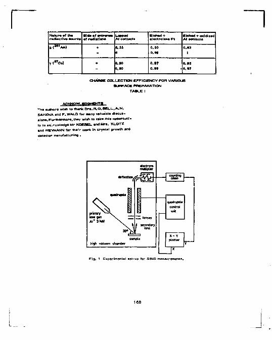
Nakjra of tha radiactlva aourco
• t o o of onlronca of radiation*
Lappad AI contacta
E tchad* •lactrolaos Pt
Elchad + m l d l i a d AI contacta
at3*'*"!) + 0 . »
0
0.20
0 . M
0 . »
I
T ( S 7 C o ) + o.to 0.10
0 .97 0 . * ]
0 . M . 0 . ( 7
C H A R M COLLECTION EFFICIENCY FOR VARIOUS
SURFACE PREPARATION
TABLE I
ACKNOWl gPOMENTS
- h i autttora wlah to thank Dra .R .O.Bea .L . ,A .N .
SAXEKIA and F . WALD for many valuable dlacua-
«lona.Furttiarmora.lhay wloh to ta t» thla opportuni
ty to ai.rowlodgo Mr KOEBEL «nd M M . KLOTZ
and W6YMANN far Iholr work In cryatal growth and
datactor manufacturing .
prmory ^ ~ H M gun Ar*3h»V
hioh vocuu
«HMctton.
tnlbpUK
prmory ^ ~ H M gun Ar*3h»V
hioh vocuu
«HMctton. « l i&d i counfhg ch>n
prmory ^ ~ H M gun Ar*3h»V
hioh vocuu
«HMctton. FïZsàT
counfhg ch>n
prmory ^ ~ H M gun Ar*3h»V
hioh vocuu
8 «ndrapolt J
V= 30«V
8 prmory ^ ~ H M gun Ar*3h»V
hioh vocuu
8 «ndrapolt J
V= 30«V
8 quodnjpote
contrat unit
prmory ^ ~ H M gun Ar*3h»V
hioh vocuu
8 «ndrapolt J
V= 30«V
I _ lenses i stcondary ' ions
,__
quodnjpote
contrat unit
prmory ^ ~ H M gun Ar*3h»V
hioh vocuu
8 «ndrapolt J
V= 30«V
I _ lenses i stcondary ' ions
prmory ^ ~ H M gun Ar*3h»V
hioh vocuu sample
m chombtr
X - Y plotter
Y
l x
Fig. I Experimental Bel-up for SIMS measurements.
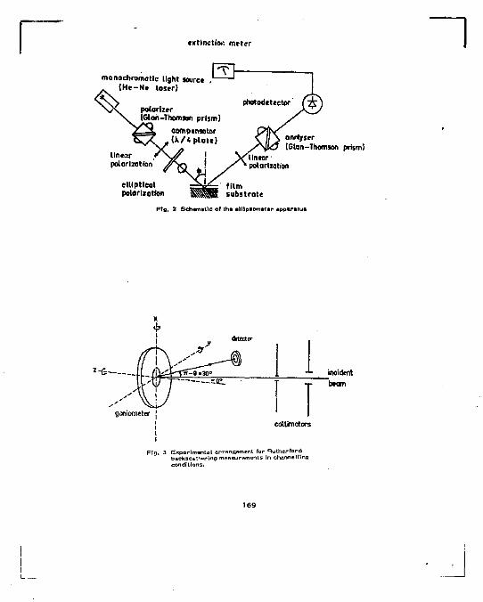
extinction meter
monochromotic light source , ( H e - N e loser)
linear polarization
elliptical polarlzatfon
anrtyser (Glan-Thomson prism!
linear ' polarization
f i lm substrate
Fig. 2 Schematic of tha alllpsometar apparatus
X
z -e-
detector
^i i î^TÎ^8=30o ••- i
! L.̂ \ T ' s"\ goniometer
( ollimator
F ig . 3 Experimental arrangement for Ruther ford backsca!»Rrtng measurements In channell ing condit ions.
169
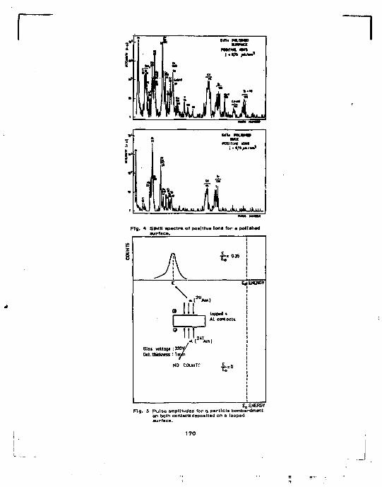
7* J CflTt M . I M 0 M W I
a I
P W I M mn _ £ I j . V I M ^ '
S * .M M 1 .M S *
Sî JL " u
•» L <« "m
M " • • •Iff I f 11 I I m "*•
1 1 Jl 1 u«a li
VÎUï «™ iir ? y 1 m 1 *? • 1 - 1 H ¥ p nnvwui
RWTIVK MM»
JL. Flg , 4 SIMS spactra of poil M va Ions for a poltahad
«urfaca. _ i
\ [ « M . »
looped* Al contacts
I I ! Bios voltoot : 3 M y Ott.thèkntK : 1 | J ^
E, ENERGY Flg, 5 Pulse amplitudes for a particle bombardment
on both contacts deposited on a lapped surface.
170
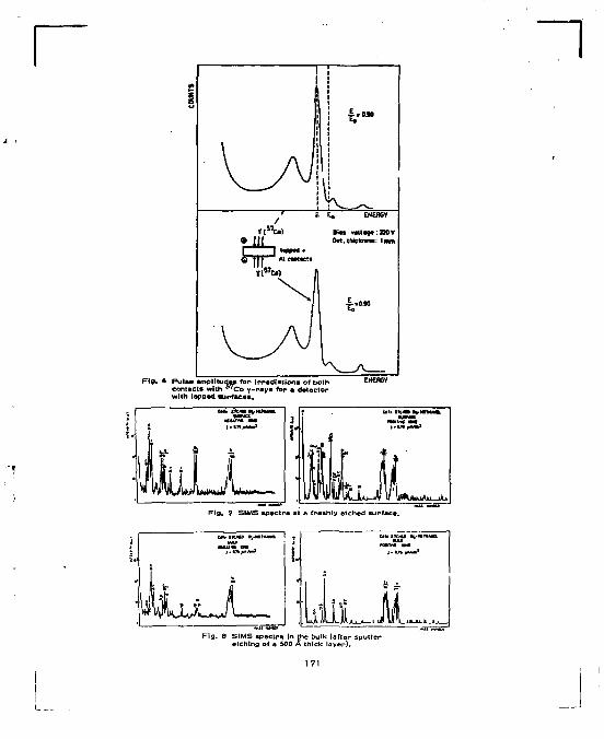
f t 5 , C a ) K « v tU«t«: I»v
G | | f Al contacts
T f l W 0 )
FI0 . 6 Pula» ampMtudjt» fo r I r rad ia t ions of both contacts wi th * 7 C o y - r a y i fo r a detector w i th lapped surfaces.
-JB"
IkLL F ig . 7 SIMS spectra at a f reshly etched sur face.
F ig . 8 SIMS spectra In the bulk (after sputter etching of a 500 A thick layer).
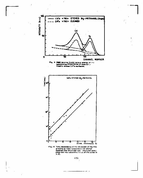
m
3 i 5 0
C4T* <TW> ETCHED " C'Tt <1K> Œ/WED
•^-METHANOL (frMhl
Cd
/ \ T.
i - r - ^ y\ ^ - \ _
so 100
CHANNEL NUM9ER
F ig . t RSS apaclra (yfald var-aua mnmrgy of t * i backscaltar-M' partlclaa of elaavad or fraahly atehad CÏTm aupfaeaa.
1
r
C*JT« ETCHED 1^-METHANOL
»* r
a> r
• ^ r
j f • • ^ r
»' ^ V
/
»o
^ »o V 3& » £0 •il 60 .
ÛKVOt THICKNESS A|
F l g . 10 Time dependence of the thickness of lha f i lm growing at room temperature on etched samples (the thlchness was a leu fated assuming that lha re f rac t i ve innux of the oxide Is 2. of.
.72
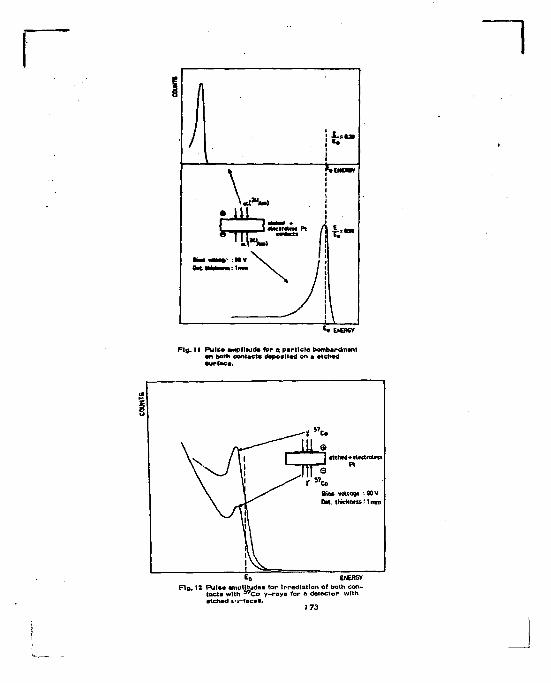
£« EWÊflGY
Fig. 11 Pu J t a Mpl l iuda for a particle bombardment an both contacts deposited on • etched surface.
Vs. \ 1 L III* I «tchtd+clcctnless Vs. \ i i
\ 11
i > ^ —
Ï 5 7 Co
Bio* voltogt : 90V D*t thiehnMSîlmm
£o ENERGY Fig , 12 Pulse amplitudes for Irradiation of both con
tacts with 5 7 C o y-rays for a detector with etched tu^fsce*.
173
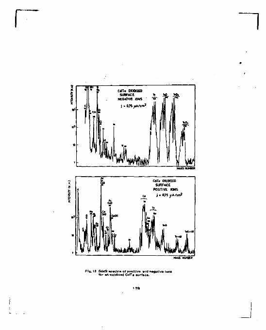
CdTi OXIDIZED SURFACE
H POSITIVE KMS
u j . OJS jjA W
M
s
S M
U
a Cs KO
•
(MM w
wi l l il t>0"*
M ! r Win F i . » v ™ wwWL
Flg.13 StMS spsclrs of positive srtd nsgstlvs tons for sn oxidtzad CdTs surfacs.
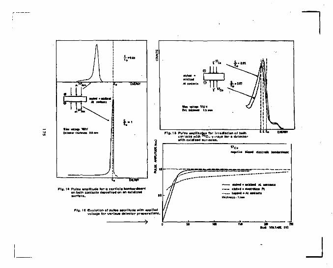
Fig, U Puis* amplltud* fer a par t ie l * bombardment on both contacts deposit!**! en «n oxidized surfac*.
Fig. 19 Evolution of pula* amplltud* with applied voltage for varlnua detector preparations.
m as • u t VOLUK IV)
J
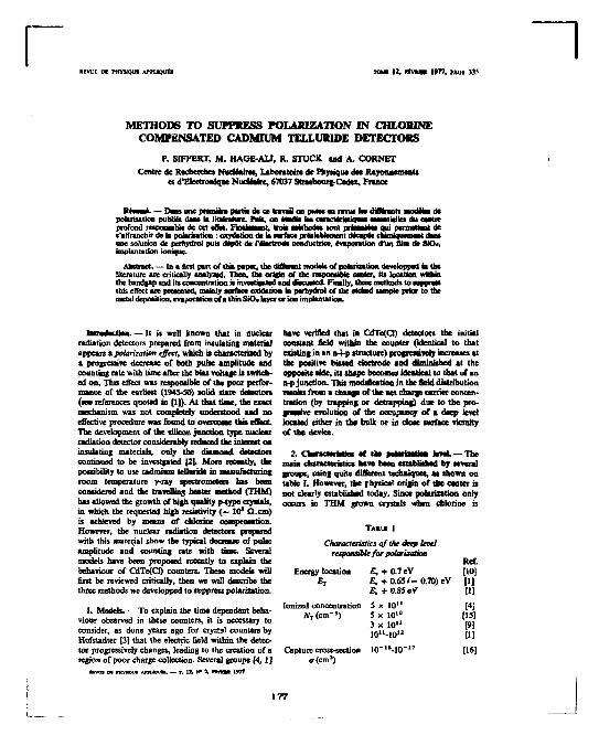
RBVUE DE MfYSIQUI APMJQUE1 IMS 12, pavaa* 1977, PAOE 33?
METHODS TO SUPPRESS POLARIZATION IN CHLORINE COMPENSATED CADMIUM TELLUR1DE DETECTORS
P. SIFFERT, M. HAGE-AU, R. STUCK and A. CORNET
Centre de Recherches Nucléaires, Laboratoire de Physique des Rayonnements et d'Electronique Nucléaire. 6703? Strasbourg-Cedex, France
Résasni. — Dans une pcemîsm partie de ce travail on pusse en revue fas différants modèles de polarisation publiés dans la littérature. Puis, on sendee les csfsctsfistfaMte essentielles du centre profond responsable de cet effet. Fmslemsnt, trois saéthods* sont crlînsilii qui pennetssnt de s'affranchir de la polarisation : oxydation de la surface préalablement décapée chimiquement dans une solution de perhydrol pua dépôt de rsssctrods conductrice, evaporation d'un film de SK>«, implantation ionique.
Abstract. — In a first part of this paper, the different models of polariatwn developped in the literature are critically analysed. Then, the origin of the responsible center, its location within the bandgap and its concentration is investigated and discussed. Finally, three methods to suppress this effect are presented, mainly surface oxidation in parhydrol of the etched sample prior to the metal deposition, evaporation of a thin SX)* layer or ion implantation.
InasaniUsn. — It is well known that in nuclear radiation detectors prepared from insulating material appears a polarization effect, which is characterised by a progressive decrease of both pulse amplitude and counting rate with time after the bias voltage is switched on. This effect was responsible of the poor performance of the earliest (1945-50) solid state detectors (see references quoted in [1]). At that time, the exact mechanism was not completely understood and no effective procedure was found to overcome this effect The development of the silicon junction type nuclear radiation detector considerably reduced the interest on insulating materials,, only the diamond detectors continued to be investjated pi- More recently, the possibility to use cadmium teUuride in nsanutacturing room temperature y-ray spectrometers has been considered and the travelling heater method (THM) has allowed the growth of high quality p-type crystals, in which the requested high resistivity (~ 10* a.cm) is achieved by means of chlorine compensation. However, the nuclear radiation detectors prepared with this materia] show the typical decrease of pulse amplitude and counting rate with time. Several models have been proposed recently to explain the behaviour of CdTc(Cl) counters. These models will first be reviewed critically, then we win describe the three methods we developped to suppress polarization.
1. Models. — To explain the time dependent behaviour observed in these counters, it is necessary to consider, as done years ago for crystal counters by Hofstadter [3] that the electric field within the detector progressively changes, leading to the creation of a region of poor charge collection. Several groups [4,1 ]
ftivtn tm wrrcwi ATMMUte. — T. 12, N* 2, M v n s 1977
bave verified that in CdTe(Cl) detectors the initial constant field within the counter (identical to that existing in an n-i-p structure) pcogreativeiy increases at the positive biased electrode and A«mi^h^A *t the opposite side, its shape becomes identical to that of an n*p junction. This modification in the field distribution results from a change of the net charge carrier concentration (by trapping or detrapping) due to the progressive evolution of the occupancy of a deep level located either in the bulk or in close surface vicinity of the device.
2. Casracsarfatks «f the filiilsallia level. — The main characteristics have been established by several groups, using quite different techniques, as shown on table I. However, the physical origin of the center is not clearly established today. Since polarization only occurs in THM grown crystals when chlorine is
TAKIE I
Characteristics of the deep level responsible for polarization
Ref. Energy location E, + 0.7 eV [10}
Br £; +0.65 f-0.70) eV (1] £ + 0 . 8 5 e V [1)
Ionized concentration 5 x 10 1 1 [4J ATT(cm-3) 5 x 10 1 0 [15]
3 x 10 1 1 [9] 10"-10" [1]
Capture cross-section 1 0 " , R - 1 0 - 1 7 [16] a (cm2)
177
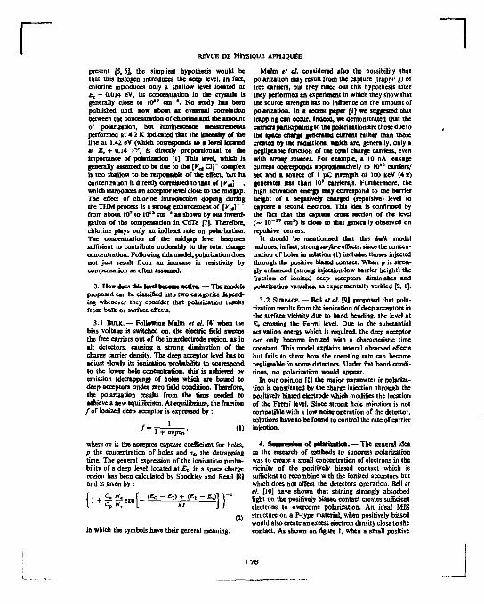
REVUE DE PHYSIQUE APPLIQUÉE
present [5,6], the simpliest hypothesis would be that this halogen introduces the deep level. In fact, chlorine introduces only a shallow level located at Ec - 0.014 eV, its concentration in the crystals is generally close to 10 1 T cm" 3. No study has been published until now about an eveatual correlation between the concentration of chlorine and the amount of polarization, but luminescence measurements performed at 4.2 K indicated that the intensity of the line at 1.42 eV (which corresponds to a 1ère] located at EH + 0.14 ^ is directly proportionnai to the importance of polarization [1]. This level, which is generally assumed to be due to the \VU C1J" complex is too shallow to be responsible of the effect, but its concentration is directly correlated to that of [VJ\ , which introduces an acceptor level close to the midgap. The effect of chlorine introduction doping during the THM process is a strong enhancement of [V^] from about I0 7 to 10 1 2 cm~ s as shown by our investi-gation of the compensation in CdTe p}. Therefore, chlorine plays only an indirect role on polarization. The concentration of the midgap level becomes sufficient to contribute noticeably to the total charge concentration. Following this model, polarization does not just result from an increase in resistivity by compensation as often assumed.
3. How Joes tab level fcteasM active. — The models proposed can be classified into two categories depending whenever they consider that polarization results from bulk or surface effects.
3.1 BULK. — Following Malm et al. [4] when the bias voltage is switched on, the electric field sweeps the free carriers out of the interelectrode region, as in all detectors, causing a strong diminution of the charge carrier density. The deep acceptor level has to adjust slowly its ionization probability to correspond to the lower bole concentration, this is achieved by emission (detrapping) of holes which are bound to deep acceptors under zero field condition. Therefore, the polarization results from the time needed to achieve a new equilibrium. At equilibrium, the fraction / o f ionized deep acceptor is expressed by :
/ = = l + i n r ' « 1 + ffVpto
where ov is the acceptor capture coefficient for holes, p the concentration of holes and T 0 the detrapping time. The general expression of the ionization probability of a deep level located at Ej, in a space charge region has been calculated by Shockley and Read [8] and is given by :
(2)
in which the symbols have their general meaning.
Malm et al. considered also the possibility that polarization may result from the capture (trap™- «;) of free carriers, but they ruled out this hypothesis after they performed an experiment in which they show that the source strength has no influence on the amount of polarization. In a recent paper [1] we suggested that trapping can occur. Indeed, we demonstrated that the carriers participating to the polarization are those due to the space charge generated current rather than those created by the radiations, which are, generally, only a négligeable function of the total charge carriers, even with strong sources. For example, a 10 nA leakage current conespoods approunutively to 10'° carriers/ sec and a source of 1 uC strength of 100 keV ( 4 K) generates less than 10* carriers/s. Furthermore, the high activation energy may correspond to the barrier height of a negatively charged (repulsive) level to capture a second electron. This idea is confirmed by the fact that the capture cross section of the level (~ 1 0 - 1 7 cm 2) is dose to that generally observed on repulsive centers.
It should be menttonned that this tmik model includes, in fact, strong smfare effects, since the concentration of holes in relation (1) includes thoses injected through the positive biased contact. When p is strongly enhanced (strong injection-low barrier height) the fraction of ionized deep acceptors diminishes and polarization vanishes, as experimentally verified [9, I].
3.2 SUKFACE. — Dell et ai. [9] proposed that polarization results from the ionization of deep acceptors in the surface vicinity due to band bending, the level at ET crossing the Fermi level. Due to the substantial activation energy which is required, the deep acceptor can only become ionized with a characteristic time constant. This model explains several observed effects but fails to show how the counting rate can become négligeable in some detectors. Under flat band conditions, no polarization would appear.
In our opinion [1] the major parameter ùi polarization is constituted by the charge injection through the positively biased electrode which modifies the location of the Fermi level. Since strong hole injection is not compatible with a low noise operation of the detector, solutions have to be found to control the rate of carrier injection.
4. ff^prrwlan of pabrixmttoa. — The general idea in the research of methods ta suppress polarization was to create a small concentration of electrons in the vicinity of the positively biased contact which is sufficient to recombine with the ionized acceptors but which does not affect the detectors operation. Bell et al, [10J have shown that shining strongly absorbed light on the positively biased contact creates sufficient electrons to overcome polarization. An ideal MIS structure on a P-type material, when positively biased would also create an excess electron density close to the contact. As shown on figure I, when a small positive
178
METHODS TO SUPPRESS POLARIZATION IN CHLORINE COMPENSATED CdTe DETECTORS
A 3.—£L
\r*-*-*-*-A
© 0_
(® © 0 ©
torr at moderate speed (1 A/i) on the sample at thickness up to 100 A. Under these experimental conditions, the oxide composition, as deduced from backscatter-ing measurements, is about S i O u v . The MIS structure is finally achieved by depositing either a gold or an aluminium electrode.
When used as nuclear detectors, voltages up to 700 V could be applied without any excess noise. However, the process is not yet fully controlled and it appears that more work is requested to fully control the charge flow through the oxide. Furthermore, the trapping center density at the oxide-semiconductor contact has to be carefully controlled to avoid any charge loss on these centers.
5. Bofliaf ia lydrffM pemtMe. — By boiling the etched 'samples during a few minutes in H 2 0 3 an oxidized surface is formed, which is rich in cadmium, as shown by SIMS measurements. It is probable that a semiconductor layer similar to CdO is produced. The charge flow may occur either by bopping or Schottky emission over the interfacial layer. As shown on figure 2,
Fto. ]. — Reverse characteristic of both M-S and MIS CdTe detectors.
voltage is applied the bands bend downwards and the majority carriers are swept out of the zone (depletion structure). When the positive voltage is further increased, the bands bend even more, so that the intrinsic level 2T, crosses the Fermi level, so the number of minority carriers (electrons) in the surface vicinity is larger than that of holes (inversion configuration). However, under ideal MIS conditions, no carrier flow is possible and the charges accumulated progressively diminish the electric field in the depletion zone, as in the structure developped by Eîchinger [11, 12]. In a real integrated MIS structure some carrier flow is possible through the insulating layer. If the later is sufficiently thin, charge tunneling becomes possible. Therefore, we investigated the possibility to realize structures in which some current flow is possible. Three different methods have been considered on bromine-methanol etched samples.
4.1 SILICON OXIDE LAYER.— Several methods have been proposed to deposit SiO* films by vacuum evaporation of SiO. The characteristics of the film strongly depend on the speed of evaporation, the residual pressure, the conditions of forming [13]. The exact mechanism of carrier transport through these films is not well known ; the simplest model [14] considers that some conductive filaments exist through the oxide layer through which some charge flow is possible.
Here, silicon monoxide was evaporated with an electron gun under a residual pressure of about 10""7
- Energy baud diagrams for ideal MIS «rurtures at low (a} and high (6) bias voltage.
this procedure leads to a very strong reduction in diode leakage current and enhancement of the breakdown voltage.
5. 1 ION IMPLANTATION. — The bombardment of compound semiconductor by heavy ions (or even protons) produces radiation damage centers which compensate the carriers existing previously in the material. Contrarily to the predictions of the theoretical models, the damage extends munch deeper into the material that the range of the implanted ions. Therefore, by a proper choice of dopant's energy and dosis it is possible to perform by ion implantation into CdTe both an insulating layer covered by a heavily doped surface film. It has been found that implantation ofphosphorous, copper, gold or aluminium at energies ranging from 20 to 60 keV and doses around 101* cm" 3
followed by an annealing around 200 °C gave the best results.
179
REVUE DE PHYSIQUE APPUQUÊB
6. CoacMaa. — The results presented in this small high performance nuclear counters on these paper show that tbe problem of polarization on materials. However, to fully use the possibilities '-•f chlorine doped THM cadmium telluride crystals CdTe it is still necessary to improve the homogeneity can be solved by a correct choice of the surface treat- of the THM crystals, in order to increase the active ments. Therefore, it becomes now pofaible to realize volumes.
{II S i m » , P., B R O S * . R., SCHAHAOR, G, CORNET, A., [9] BELL, R. O., EHTTNE, G., SBRRBZE, H. B., Nucl. Itutrum. Srocx, R., IEEE Tram, Nucl. Scl. NS 23 (1976) 159. Af«*. 117 (1974) 267.
[21 KOZLOV, S. IL, STUCK, R., H M X - A U , M., SIFFERT, P., [10] BELL, R. O., '.VAIS, F. V., GOLDNER, R. fi., IEEE 7hmi. tEEETrm<i.N*ct.Scl.HSZl'mS)im. NucL Scl. NS 22 (1975) 241.
[31 Ho«r*DrnR,R,N»efcoiitoî, p. S».(1949). (HI EICHINOIR, P., KALLMANN, H„ Z. Namfanch 2ta (1973) [4] MAUI, H. L , MARTINI, M.. On. 1. Phyt. 51 (1973) MM, 1888. id. Appl. Phys. Un. 25 (1974) (76.
id. IEEE Trim. Mirf. Sd. NS 21 (1974) 322. [12) EICHINORR, P.. HALT*», N., KIUMER, J., Nucl. lustrum, [5] TRUOUUT, R., CORNET, A., MARTAINO, Y„ SOTERT, P., Mah. 117 (1974)305.
/ Art!, rhyi. «5 (1974) 2759. id. Name Pltys. Set. 245 [131 HOWES, 1. H„ AwcccE, M. L., Report Hirwell AERE-(1973)12. R6464 (1970).
[6) ZANIO, K., KRAJEKBRINE, P., MONTANC, H., IEEE Trans. [14] DIARNALBY, G., Pltys. Lett. 25A (1967) 760. Nucl. Sd. MS21 (1974) 315. [15] FAIRE, R, NOO-TICH-PHUOC, MARTIN, G. M., ORTEOA. F.,
[71 STUCK, R„ CORNET, A., SCHARAOER, C , SIFTERT, P. J. IEEE nans. Nad. Sd. NS 23 (1976) 182. Pkys. Otm. Solids 37(1976)989. [16) KARPINKO, V. P., KHAIKIMMNOV, P. G„ MATVEEV, O. A„
18] SHOCELIY. W., READ. W. T., Pkys. Rn. «7 (1952) 835. Scv Ptys. Semlcmi/. 4 (1971) 1492.
POLARIZATION FREE SEMI-INSULATING
CHLORINE DOPED CADMIUM TELLURIDE
M. HAGE-ALI, C. SCHARAGER, J.M. KOESEL, P. SIFFERT
CENTRE DE RECHERCHES NUCLEAIRES Groupe de Physique et Applications des Semiconducteurs (PHASE)
67037 STRASBOURG-CEDEX (FRANCE)
A paraître dans Nucl. Instr. Meth. juillet-août 1980.
ABSTRACT
It is shown that by a proper choice of THM growth conditions and
compensation by chlorine, semi-Insulating CdTe crystals can be prepared.
These give detectors free of polarization with aluminium contacts deposited
on lapped surfaces.
181
INTRODUCTION
Nuclear radiation detectors, when prepared on insulators or semî-
insulating semiconductors quite often give rise to polarization effects, which
are characterized by a progressive decrease of pulse amplitude and
counting rate with time of operation (or sometimes with number of counts)
[1 -3 ] , High resistivity cadmium telluride (CdTe) prepared by the travelling
heater method (THM) [4-6] and compensated with chlorine exhibits a similar
effect. As a result, (except for a special low barrier contact structure
mentioned below), spectrometers prepared with this material suffered a
severe handicap up to now. Here, we have been able to overcome this
problem by a correct choice of crystal growth conditions.
II. ORIGIN OF POLARIZATION
Several groups[2,3] have verified that in these detectors, the ini
tially constant electric field within the counter, progressively Increases at
the positive biased electrode and diminishes at the opposite side, reducing
the detector's sensitive width with time of biasing. This modification in the
field distribution results from a change of occupancy of a deep level In the
material [ 7 ] , Several models have considered that this level is located either
in the bulk of the material or in vicinity of the surface.
The depletion width X of a P-N junction is expressed by the familiar
relationship [6,9] :
v
2 2 e V , . i
162
where all the symbols have their usual meaning. When holes are emitted
by a deep level located at E—, a progressive change of ionized centers
is observed :
N A - N D + N T (t> , (2)
in which N-p (t) is the concentration of Ionized deep traps at time t. If
N , , N Q and N T are supposed unlformltlydistrlbuted, the evolution of
depletion thickness from I » 0 to t • t Is given by :
X 2 (0) - X 2 (t) N T
2 " — — — L • - >~>H \-= [x<0 - a x (o)] N A " N D
E F - E 1/2 in which, B - I —Jjy ]
exp <-e„ t) ] , (3)
The material being of high resistivity and E_ found to be close to
midgap [ 7 ] , a < I . 2/„» N.
Therefore X'(0) X 2 ( t ) " A " " D
73-rrr [i - exP<- « o ], w
"„ v.. N. . exp (- — I U), (5) =p u p "th " V k T
in which all symbols again have their usual meaning.
Experimentally, relationship (4 ) Is really followed, as shown in Fig. 1
for a material exhibiting severe polarization. In this particular case,
183
14 - 3
N _ " 5 x 1 0 cm , but more general ly N-p which v a r i e s from crysta l to
crystal l ies between S x 10 and 10 cm" [ 7 ] . T h e r e f o r e , this model
which considersthe presence of a level located close to midgap and d is t r ibu
ted throughout the whole mater ia l , describes the observed phenomena in a
satisfactory way.
III. METHODS OF SUPPRESSING POLARIZATION
In pr incip le , there a r e three genera.! methods that can be considered
to suppress the polar izat ion effect ( f igure 2) :
1. Band bending
As long as the deep level 's bending does not cross the Fermi level
E-p E-p cannot modify i ts population with time. Such a result can be obtained
by putting ohmic contacts on the semi- insulat ing mater ia l . Exper imenta l ly ,
this result is achieved by depositing electro I ess gold or platinum ; the
b a r r i e r height we measured Is as low as 0. 1 eV. However, in this s t ructure ,
the leakage current increases l inear i ly with bias voltage, which limits the
f ield to ra ther low values and, consequently, gives r i se to charge collection
problems.
2 . Fermi level position
F o r a trapping level E-- located close to midgap an eventual crossing
of E _ , for a given band bending, can be avoided by keeping the Fermi
level E _ away from midgap. Th is can be done essential ly by two methods.
134
- by using lower res is t iv i ty materials : we have shown previously [ 5 ]
that for both pure and chlorine compensated crysta ls , as long as tho effective
res is t iv i ty is below 8 x 10 J l . c m , no polar izat ion is v is ib le at room
temperature ;
- by accumulating excess c a r r i e r s in the vicini ty of the electrode by
shining light of the proper wavelength on the contact [ 3 ] ,
3. Suppressing the deep level
This certainly constitutes the most efficient method and we have t r ied
to apply it here . As previously mentioned f the concentration N of the deep T
level at E— has been found to vary from crystal to c rys ta l , depending on
the growth conditions. It has already been discussed in previous papers [ 7 ]
that the level located at E_. probably resul ts from the doubly charged cadmium
vacancy [V— .] . T h e concentration of this level is strongly Increased by
the presence of chlor ine, as we demonstrated through our compensation
model [ 1 0 ] . T h e r e f o r e , by an optima lization of the T H M growth conditions
and doping, it should be possible to minimize the concentration N ~ That is
what we have done ; the results a r e given below.
IV. R E S U L T S
- The resist iv i ty of the chlorine compensated T H M crysta ls when
measured by the Van der Pauw techniques a re as high as 10 XX . cm. The
effective res is t iv i ty [ 1 1 ] l ies around 5 x 10 Si, . c m . There fore , the sens i
t ive thickness, at around 500 V biasing, exceeds 2 mm (equivalent to about
1 cm of germanium for photon absorption).
- The crystals o re sl iced into 1 - 2 mm thick wafers , on which , after
lapping end conventional cleaning procedures, aluminium contacts 3 mm in
diameter a re deposited by vacuum evaporation. It is c lear that , except at
the ear l i e r stages of crystal growth , this procedure ends up in near ly
single crysta l l ine ingots.(Figure 3 ) ,
57 - S p e c t r o m e t r y results a re reported on f igures 4 and 5 for Co and 137
Cs Y - rays . A l s o reported is the evolution of counting rate as a func
tion of time. No polar izat ion effect is visible h e r e for this semi- insulat ing
mater ia l . No stabil i ty problems occured. Due to this increase of res is t iv i ty
without any polar izat ion, the depletion layer width , for a given voltage
is strongly enhanced , when compared to the previous situation, leading
to ah increase in efficiency by a factor of about ten at 150 keV .
C O N C L U S I O N
These results show that one of the major limitations In the use of C d T e
as Y - ray spectrometer , namely the time dependent polar izat ion , can be
suppressed when correct growth conditions a r e employed. Th is result cons
titutes t to our opinion, an important milestone in the development of these
devices. However , for spectroscopic uses , another problem sltH has to be
solved , namely the present day limitation in active area ; the depletion width
is now sufficient for most of the applications.
185
REFERENCES
1. R. HOFSTADTER
Nucleonics 2 (1949) 29.
2. H. I_. MALM, M. MARTINI
Can. J. Phys. Si (1973) 2336. Id. IEEE Trans. Nucl. Sel. NS 21 (1974) 322.
3. P. SIFFERT, R. BERGER, C. SCHARAGER, A. CORNET, R. STUCK
IEEE Trans. Nucl. Sci NS 23 (1976) 159.
4. R.O. BELL, N. HEMMAT, F. WALD
Phys. Stat. Sol. (a) 1 (1973) 375.
5. R. TRIBOULET, A. CORNET, V. MARFAING, P. SIFFERT
Nature Phys. Science 245 n° 140 (1973) 12. Id. J. Appl. Phys. 45 (1974) 2759.
6. T. TAGUCHI, 0. SHIRAFUJI, Y. INUISHI
Rev. Phys. Appl. 12 (1977) 117.
7. P. SIFFERT, M. HAGE-ALI, R. STUCK, A. CORNET
Rev. Phys. Appl. 12 (1977) 335,.
8. M. BLE1CHNER, E. LANGE
Sol. St. Electr. 16 (1973) 375.
9. E. FABRE, NGO-TICH-PHUOC, G.M. MARTIN, F. ORTEGA
IEEE Trans. Nucl. Se. NS 23 (1976) 182.
187
10. R, STUCK, A. CORNET, C. SCHARAGER, P. SIFFERT
J. Phys. Chem. Solids 37 (1976) 989.
11. P. SIFFERT, B. RABIN, H. Y. TABATABA1, R. STUCK
Nucl. Instr. Meth. 150 (1978) 31.
F I G U R E C A P T I O N S
F igure 1 : Evolution with time of the counting rate of a conventional T H M chlor ine
doped detector having aluminium contacts on a lapped surface. Both
calculated and experimental results a re shown.
F igure 2 : Band diagram of a metal - semiconductor contact in presence of a
deep level E— In semT-Insulating mater ia l .
F igure 3 : Photography of CdTe slices cut along a crystal f ree of polar izat ion.
Except at the beginning of the ingot most of the material Is single
crysta l l ine .
57 F igure 4 : Co Y- ray spectrum on a polar izat ion f ree , chlor ine doped s e m i -
insulating detector.
137 F igure S : Cs Y - ray spectrum on a polar izat ion f ree , chlor ine doped semi-
Insulattng detector.
199
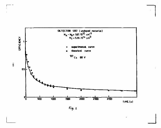
DE. TEC TOR 1257 (undoped material) N A -1^,= 107.10 1 2 cm"3
N T . 5 . 3 6 . 1 0 u c m 3
«• experimental curve • theorical curve
500 1000
137 Cs 80 V
1 - «
1500 2000 2500 3000 TIME (s)
% l
J
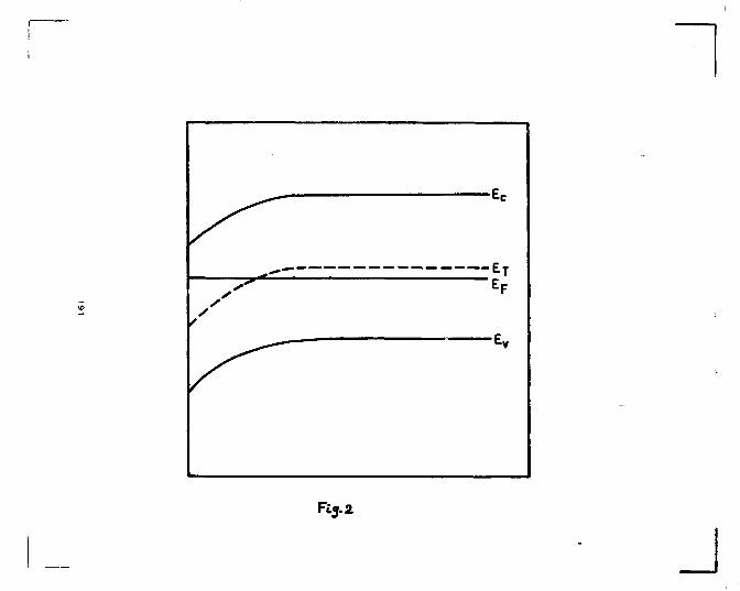
F
/ ^
•-C
^^•~~ — - E T , ' ' tF
/ s f
^
Lv
Rj.2
J
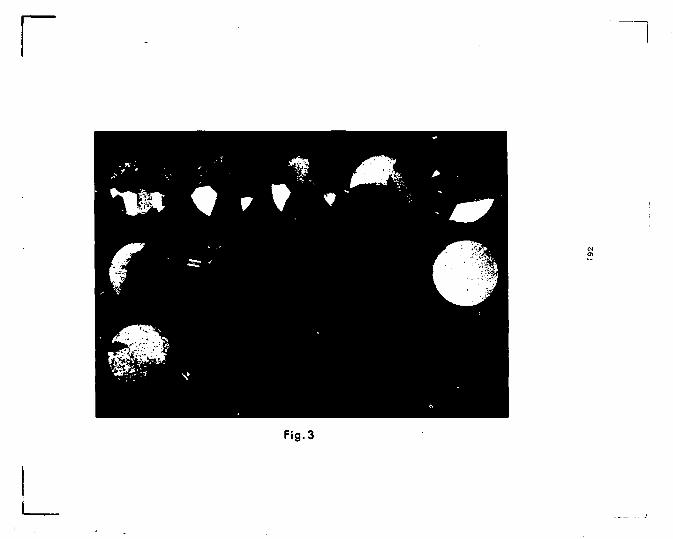
Fig.3
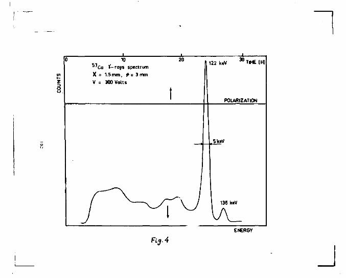
Fi3.4 ENERGY
J
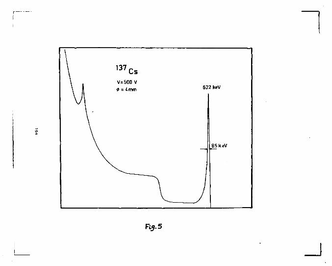
622 keV
8.5 keV
FI5.5
_J
C O N C L U S I O N
Au cours de ce t rava i l , nous avons essentiellement cherché à
amél iorer nos connaissance* des propr iétés de surface du te l lu rure de
cadmium semi-isolant afin de dégager les conditions optimales de
préparat ion de diodes.
Dans une p remiè re par t ie , nous avons cherché à t f r e r le mei l leur
profit de la méthode d'analyse de surface par ré t ro diffus ion de part icules
chargées en et hors conditions de canalisation. Ceci nous a conduit à
formuler avec précision les conditions optimales en vue de l'obtention de la
mei l leure résolution en profondeur ou en masse, permettant une analyse f ine
de la zone superf ic ie l le . Peur mener a bien ce t r a v a i l , il . ous a fallu
1 + 4 + mesurer le pouvoir d 'a r rê t des part icules H et H e ent re 0,4 et 3 MeV
dans CdTe et Z n T e , ce dernier matériau servant de ré férence aux données
expérimentales de la l i t té ra ture . La formulation des conditions optimales
d'analyse par R B 5 montrait clairement l ' imposslblité des techniques conven
tionnelles. En effet» la résolution en énergie ne devrai t pas dépasser
4 + quelques keV et l'emploi de project i les plus lourds que He s 'avérai t
parfois nécessaire. Ces conditions de fonctionnement sont hors de portée des
détecteurs à semiconducteurs, généralement employés dans ce type d'expé-
195
r iences.
Ceci nous a conduit à développer un analyseur électrostat ique
capable de détecter des project i les jusqu'à 1 MeV. Ses performances sont
tout à fait satisfaisantes, puisqu'il permet d'obtenir une résolution en masse
12 + de 2 uma pour un pro ject i le C sur CdTe et une résolution en profondeur,
o 4 +
à la surface de 18 A pour He sur un fi lm d 'or .
Cet instrument nous a permis, associé au S I M S et à des mesures
d'el l ipsométrle, une étude approfondie de divers types de surface de C d T e .
Notons, en par t icu l ier , la mise en évidence de l 'enrichissement en cadmium
après décapage chimique brome-méthanol, la formation d'une pel l icule d'oxyde
en surface, dont l 'épaisseur s 'accroît p rogress ivement . . . Les surfaces ayant
subi un traitement d'oxydation ont également été analysées en détai l , car
leur évolution rapide entraînait une dégradation des performances des
spectromètres nucléaires.
La deuxième par t ie de ce t ravai l a été consacrée à étudier plusieurs
types et procédés d'élaboration d'une structure diode. En effet, nous Avons
successivement abordé certaines méthodes de préparat ion de :
- jonctions diffusées
- jonctions implantées
- hétérostructures InSb-CdTe
- ta st ructure M-O-S
Les conditions d'élaboration, les propr iétés é l e c t r i q u e s . . . de
ces diverses diodes ont été étudiées en détait avec comme objectif essentiel
la mise au point d'un contact à faible bruit supprimant la polarisat ion des
spectromètres y préparés sur les matériaux semi- isolants. Nous avons con
sacré beaucoup d'efforts à la résolution de ce problème ; une première
solution fut trouvée grâce aux structures M - O - S ; malheureusement., leur
196
1 instabil i té entraînait una lent* degradation de sea propr iétés de non-polar isat ion.
Finalement, il fut possible de supprimer tout phénomène de polarisat ion en
préparant des cristaux dans lesquels le niveau responsable de cet effet,
situé à peu près au milieu de la bande interdi te , fut ramené è une
concentration négligeable. Ceci constitue, espérons-nous un grand pas en
avant dans la mise au point des spectromètres y et X k base de C d T e .
Mais plusieurs problèmes restent à résoudre, le plus important est ce r ta i ne
ment l ié à la limitation actuelles des a i res actives des jonctions, dues à
un accroissement rapide du courant de fuite de ces st ructures.
Toutefois, les faibles dimensions de ces détecteurs constituent
quelque fois un avantage et plusieurs applications sont possibles dès à présent
tout autour des réacteurs nucléaires qu'en médecine nucléaire . Au labora
to i re , des sondes de prospection minière par f luorescence X ainsi que des
détecteurs de radioact ivi té d'ambiance ont permis de montrer l ' intérêt de ce
type de détecteur, car son numéro atomique élevé conduit à une eff icacité
environ S fois plus grande qu'un volume égal de germanium !
197

Imprimé a» C«ntr* d«
>acfa«rch*s Nuclâafrvs SlraibQirrg
198p


![İsveç’te Ali Şîr Nevaî’nin İzleri [The Trace of The Ali Şîr Nevaî in Sweden]](https://img.dokumen.tips/doc/110x75/634794d0391b5ca53f0d8d0a/isvecte-ali-sir-nevainin-izleri-the-trace-of-the-ali-sir-nevai-in.jpg)
