Embed Size (px)
Citation preview
Loser techI
SETVICES O"S
Tech n ical Specif icationsand Services.
Lasered Ceramic Substrates for HYBRID MICRO-Electronics.
[I-_]
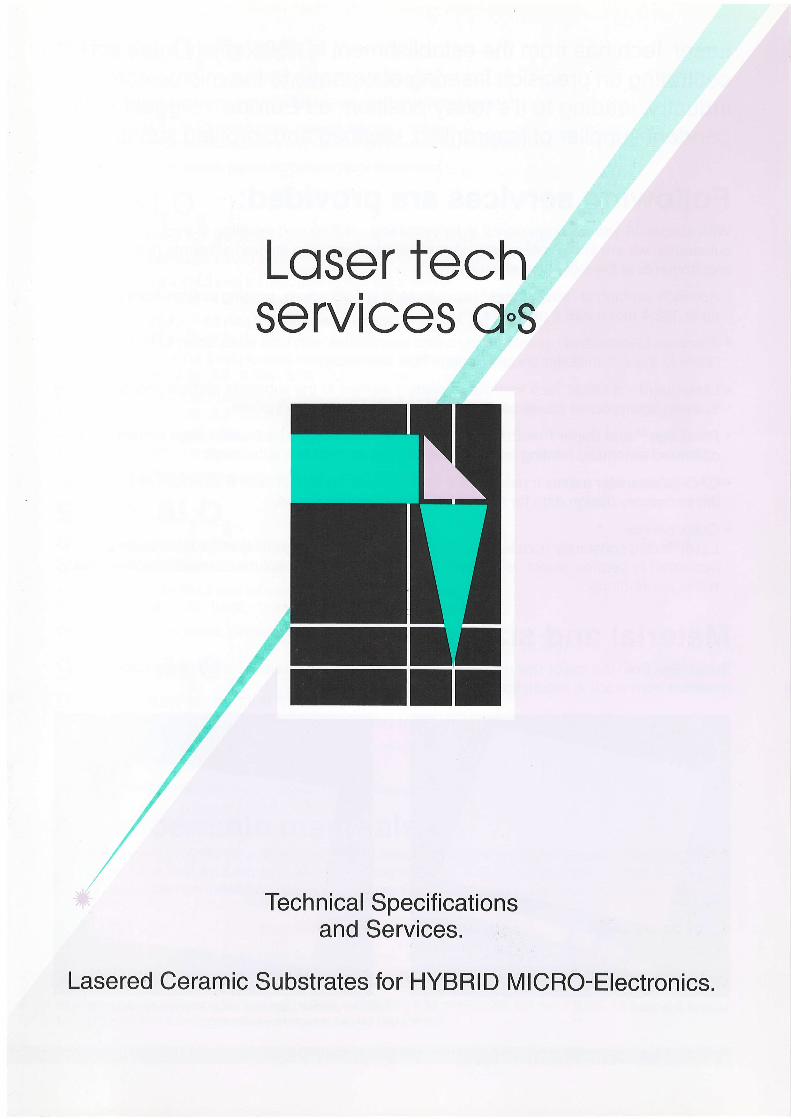
Laser Tech has from the establishment in 1985 solely been con-centrating on precision lasering of ceramic to the microeleetronicindustry, leading to it's today position, as Europe's biggest inde-pendent supplier of laserdrilled, -scribed and -profiled substrates.
Following services are provided:With almost 20 years of experience in laserprofiling, -drilling and -scribing of thick- and thinfilmsubstrates, we are your professional paftner in optimizing your lasered substrate design andrequirements in the most cost effective way.
. Accurate scribing of "snapstrates" to customer's specifications, ranging in sizes from a few mmup to 152,4 mm x 228,6 mm (6" x 9").
. Precision laserscribed, -profiled and -drilled snapstrates with hole sizes down b A Oj mm for"state of the afi" thickfilm printed through hole technology.
. Laserguard - a Laser Tech formulated coating applied to the substrate surface prior to laseringto avoid laserprocess cause ceramic residue on the substrate surface.
. PrimEdgerM and Super PrimEdgerM, the Laser Tech developed substrate edge treatment foroptimized automatic printing and handling of lasered thick film substrates.
. CAD-datatransfer makes it possible for the customer via e-mail [email protected] to transferthe.necessary design data for a safe and fast order turnaround.
. Quick serviceLaser Tech's constantly updated laser technology and laser capacity of 24laser beams,dedicated to ceramic works, allow us to offer prototypes and pilot runs at cost effective rateswithin 24-48 hours.
Material and sizes on stock:Substrates from the major raw material suppliers CoorsTek, CeramTec and Kyocera areavailable from stock in production quantities.
Laser profiled snapstrate drilled for advanced thick filmprinted through hole technology.
Multiple snapstrate
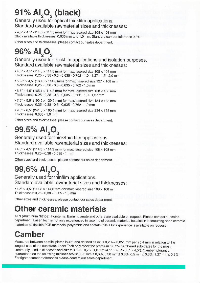
91o/o AI2O' (black)Generally used for optical thickfilm applications.Standard available rawmaterial sizes and thicknesses:.4,5" x 4,5' (114,3 x 114,3 mm)for max. lasered size 108 x 108 mmStock available thicknesses: 0,635 mm and 1 ,0 mm. Standard camber tolerance 0,3%
Other sizes and thicknesses, please contact our sales department.
96o/o Al2O3Generally used for thickfilm applications and isolation purposes.Standard available rawmaterial sizes and thicknesses:. 4,5" x 4,5' (114,3 x 114,3 mm) for max. lasered size 108 x 108 mmThicknesses: 0,25 - 0,38 - 0,5 - 0,635 - 0,762- 1,0 - 1,27 - 1,5- 2,0 mm
. 5,25" x 4,5" (133,3 x 114,3 mm) for max. lasered size 127 x 108 mmThicknesses: 0,25 - 0,38 - 0,5 - 0,635 - 0,762 - 1,0 mm
.6,5" x 4,5" (165,1 x 114,3 mm) for max. lasered size '158 x 108 mmThicknesses: 0,25 -0,38 - 0,5 - 0,635 - 0,762- 1,0 - 1,27 mm
. 7,5" x 5,5" (190,5 x 139,7 mm) for max. lasered size 184 x 133 mmThicknesses:0,25 - 0,38 - 0,5 - 0,635 - 0,762 - 1,0 mm
. 9,5" x 6,5' (241,3 x 165,1 mm) for max. lasered size 234 x 158 mmThicknesses: 0,635 - '1,0 mm
Other sizes and thicknesses, please contact our sales deparlment.
99,5o/o Al2OgGenerally used for thicl</thin film applications.Standard available rawmaterial sizes and thicknesses:. 4,5" x 4,5' (114,3 x 114,3 mm) for max. lasered size 108 x 108 mmThicknesses: 0,25 - 0,38 - 0,635 - 1 mm
Other sizes and thicknesses, please contact our sales department.
99,6o/o Al2O3Generally used for thinfilm applications.Standard available rawmaterial sizes and thicknesses:. 4,5" x 4,5' (114,3 x 114,3 mm) for max. lasered size 108 x 108 mmThicknesses: 0,25 - 0,38 - 0,635 - '1,0 mm
Other sizes and thicknesses, please contact our sales department.
Other ceramic materialsALN (Aluminum Nitride), Forsterite, Bariumtitanate and others are available on request. Please contact our salesdepaftment. Laser Tech is not only experienced in lasering of ceramic material, but also in lasercutting none ceramicmaterials as flexible PCB materials, polyamide and acetate foils. Our experience is available on request.
CamberMeasured between parallel plates in 45'and defined as ex. < O,2o/o - 0,051 mm per 25,4 mm in relation to thelongest side of the substrate. Laser Tech only stock the premium < 0,2/" cambered substrates for the mostcommonly used thicknesses and sizes: 0,635 - 0,76 - 1,0 mm (4,5" x 4,5" - 6,5" x 4,5"). camber tolerancequaranteed on the following thicknesses is: 0,25 mm < 0,67o, 0,38 mm < 0,37o, 0,5 mm < 0,3/o, 1 ,27 mm 10,3o/o.For tighter camber tolerances please contact our sales deparlment.
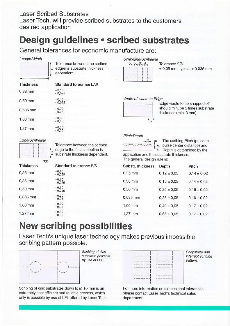
Laser Scribed SubstratesLaser Tech. will provide scribed substrates to the customersdesired application
l.
Tolerance S/S+ 0,05 mm, typical + 0,035 mm
k-------L+Thickness
0,38 mm
0,50 mm
0,635 mm
1,00 mm
1,27 mm
Thickness
0,25 mm
0,38 mm
0,50 mm
0,635 mm
1,00 mm
1,27 mm
Width of waste to
+H+
EdgeEdge waste to be snapped offshould min. be 5 times substratethickness (min.3 mm)
Pitch/Depth*E* +D The scribing Pitch (pulse to*Y
+ f. Oulse center distance) and| ' t Depth is determined by theT
lst application and the substrate thickness.The general design rule is:
Substr.thickness Depth
0,25 mm
0,38 mm
0,50 mm
0,635 mm
1,00 mm
1,27 mm
Laser Tech's unique laser technology makes previous impossiblescribing pattern possible.
I
I
I
I z-:l/
---1ttt\ /
I
I
I
I
t' 'ltt '\\
I------{ }I------{ }----/I/t\ /
I
I
I
New scribing possibilities
Scribing of discsubstrate possibleby use of LFL.
Scribing of disc substrates down to Z 10 mm is anextremely cost efficient and reliable process, whichonly is possible by use of LFL offered by Laser Tech.
0,12 t 0,05
0,15 + 0,05
0,25 t 0,05
0,25 + 0,05
0,40 + 0,05
0,65 + 0,05
Pitch
0,14 t 0,02
0,14 + 0,02
0,16 + 0,02
0,16 + 0,02
0,17 + 0,02
0,17 + 0,02
Snapstrate withinterupt scribingpattern.
lttrl--------t r------t------l t------rF------l F------1F------l F------1l--*----t t-------.1l---*---.1 t-------.1L__*___t L______-lL______t L______.1L______l L______rlttl
For more information on dimensional tolerances,please contact Laser Tech's technical salesdepartment.
Design guidelines . scribed substratesGeneral tolerances for economicLength/Width
Tolerance between the scribededges is substrate thicknessdependent.
Standard tolerance UW+ 0,15- 0,025
+0,15- 0,025
+0,20- 0,05
+0,30- 0,05
+0,30- 0,05
Tolerance between the scribededge to the first scribeline issubstrate thickness dependent.
Standard tolerance E/S
+0,10- 0,025
+0,10- 0,025
+0,10- 0,025
+0,20- 0,05
+0,30- 0,05
+ 0,30- 0,05
manufacture are:Sc ri be I i n e/Sc ri b e I i n e
5S55|<+F+Fi+>l
llttltlltlrlltl
-t-r-r-F-r-
Edge/Scribeline
-l--t-+-ltlttlltl
_I-J-tltl
k+lE/S
I
I
Laserdrilled . Profiled . Scribed substratesLaser Tech will provide the combined laserdrilled, -profiled and -scribedsubstrates to the customers desired specification.
Design guidelines o Laser drilling and profilingGeneral tolerances for optimized economic manufacture are:
Ho le Ce nte r/Hol e C ente rTolerance between the profilededges> 0,050 mm (+ 0,002")typical+ 0,035 mm.
1.k--------------,
Min. drilled hole size
O O,l tolerance 1fl,flff,
Min. hole size (one shot)Z 0,075 mm (0,003")Max. drilled hole size limited by substrate size,tolerance + 0,05 mm (+ 0,002")Hole size is measured on the laser beam exit side.
General design rules for optimizedX > Substrate thicknessDistance between hole edgeand substrate edge should min.be > the substrate thickness.
X > Substrate thicknessHole edge to hole edge distanceshould min. > the substratethickness.
R>0,1 mmAvoid designs with internalsharpcorners, try to design with acorner radius of min. 0,5 x the
economic manufacture are:
Hole Taper
*H*
+l-+-
, ]+X
Tolerance profiled Edge to holeCenter + 0,050 mm (0,002")Hole center to hole centert 0,05 (0,002")
Taper angle = 3o
min.A laser beam exit
X > 0,04 mmAny profiled shape can be cutaccording to the customersrequirement.Min. cut width - to 0,04 mm
X>0,1 mmProfiled disc with holding tags,of minimum 0,1 mm width.(substrate thickness dependent)
substrate thickness to minimize the risk of micro cracking.
With request of improved tolerances and designs in conflict with the generaldesign rules please contact Laser Tech.'s technical sales department for possibleavailable improvements.
Length/Width
Holes
+
X->H+
r\N/,:
avlB I
rl
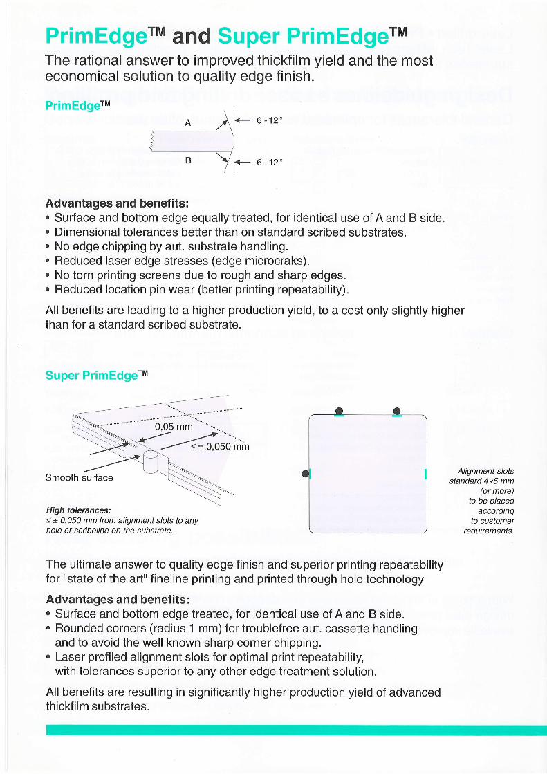
PrimEdge" and Super PrimEdget*The rational answer to improved thickfilm yield and the mosteconomical solution to quality edge finish.
PrimEdgerM6-12'
6 -12"
Advantages and benef its:. Surface and bottom edge equally treated, for identical use of A and B side.. Dimensional tolerances better than on standard scribed substrates.. No edge chipping by aut. substrate handling.. Reduced laser edge stresses (edge microcraks).. No torn printing screens due to rough and sharp edges.. Reduced location pin wear (better printing repeatability).
All benefits are leading to a higher production yield, to a cost only slightly higherthan for a standard scribed substrate.
Super PrimEdgerM
Alignment slotsstandard 4x5 mm
(or more)to be placed
accordingto customer
requirements.
High tolerances:< x 0,050 mm from alignment slots to anyhole or scribeline on the substrate.
The ultimate answer to quality edge finish and superior printing repeatabilityfor "state of the art" fineline printing and printed through hole technology
Advantages and benef its :
. SUrface and bottom edge treated, for identical use of A and B side.
. Rounded corners (radius 1 mm) for troublefree aut. cassette handlingand to avoid the well known sharp corner chipping.
. Laser profiled alignment slots for optimal print repeatability,with tolerances superior to any other edge treatment solution,
All benefits are resulting in significantly higher production yield of advancedthickfilm substrates.
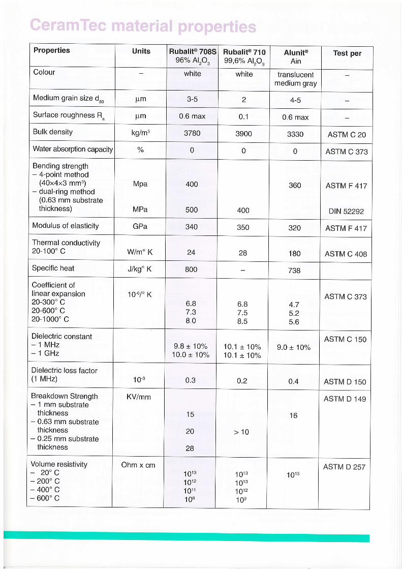
Properties Units Rubalit@ 708596% Al2O3
Rubalit@ 71099,6% Al2O3
Alunit@Ain
Test per
Colour white white translucentmedium gray
Medium grain size d.o pm 3-5 2 4-5
Surface roughness R^ pm 0.6 max 0.1 0.6 max
Bulk density kg/m3 3780 3900 3330 ASTM C 20
Water absorption capacity o//o 0 0 0 ASTM C 373
Bending strength- 4-point method
(40x4x3 mm3)
- dual-ring method(0.63 mm substratethickness)
Mpa
MPa
400
500 400
360 ASTM F 417
DIN 52292
Modulus of elasticity GPa 340 350 320 ASTM F 417
Thermal conductivity20-100" c Wm" K 24 28 180 ASTM C 408
Specific heat J/kg" K 800 738
Coefficient oflinear expansion20-300'c20-600'c20-1000'c
10-6/" K6.87.38.0
6.87.58.5
4.75.25.6
ASTM C 373
Dielectric constant-1MHz-1GHz
9.8 r 10%10.0 t 10%
10.1 t 10%10.1 + 10%
9.0 + 10%ASTM C 150
Dielectric loss factor(1 MHz) 10-3 0.3 0.2 0.4 ASTM D 150
Breakdown Strength- 1 mm substrate
thickness- 0.63 mm substrate
thickness- 0.25 mm substrate
thickness
KV/mm
15
20
28
>10
16
ASTM D 149
Volume resistivity20" c
- 200" c- 400" c- 600" c
Ohm x cm1013
1012
1011
108
1013
1013
1012
10e
1013
ASTM D 257
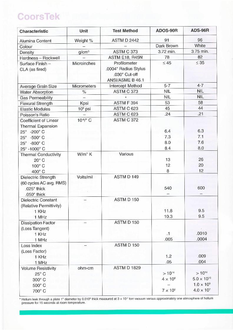
Characteristic Unit Test Method ADOS-gOR AD5.96R
Alumina Content Weiqht % ASTM D 2442 91 96
Colour Dark Brown White
Density g/cm3 ASTM C 373 3.72 min. 3.75 min.
Hardness - Rockwell ASTM E18, R45N 78 82
Surface Finish -CLA (as fired)
Microinches Profilometer.0004" Radius Stylus
.030" Cut-offANSI/ASME B 46.1
<45 <35
Average Grain Size Micrometers lntercept Method 5-7 4-7
Water Absorption o//o ASTM C 373 NIL NIL
Gas Permeability NIL NIL
Flexural Strenqth Kpsi ASTM F 394 53 58
Elastic Modules 106 psi ASTM C 623 45 44
Poisson's Ratio ASTM C 623 .24 .21
Coefficient of Linearfhermal Expansion25" -200" c25" -500'c250 -800'c25' -1000'c
10-6/" C ASTM C 372
6.47.38.08.1
6.37.1
7.68.0
Thermal Conductivity20" c
100" c400" c
Wm" K Various13
12
I
262012
Dielectric Strength(60 cycles AC avg. RMS)
.025" thick
.050" thick
Volts/mil ASTM D 149
540 600
Dielectric Constant(Relative Permittivity)
1 KHz1 MHz
ASTM D 150
11.810.3
9.59.5
Dissipation Factor(Loss Tangent)
1 KHz1 MHz
ASTM D 150
.1
.005
.0010
.0004
Loss lndex(Loss Factor)
1 KHz1 MHz
ASTM D 150
1.2
.05
.009
.004
Volume Resistivity25" C
300'c500" c700'c
ohm-cm ASTM D 1829> 1014
4 x 10⁸
7 x 10⁶
> 1014
5.0 x 10¹⁰
1.0 x 10e
4.0 x 10⁷
. Helium leak through a plate I" diameter by 0.010" thick measured at 3 x 10⁻⁷ torr vacuum versus approximately one atmosphere of helium
pressure for 15 seconds at room temperature.
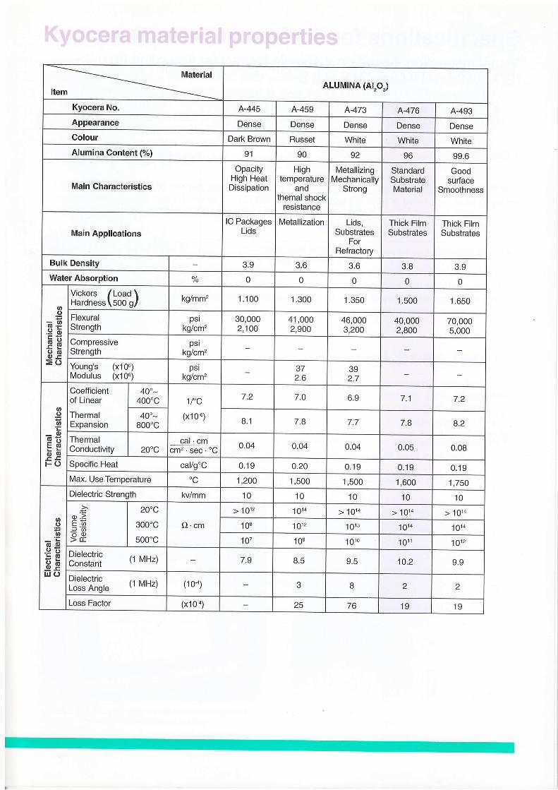
Material
ItemALUMTNA (AI,O3)
Kyocera No. A-445 A-459 A-473 A-476 A-493Appearance Dense Dense Dense Dense DenseColour Dark Brown Russet White White WhiteAlumina Content (%) 91 90 92 96 99.6
Main Characteristics
OpacityHigh HeatDissipation
Hightemperature
andthemal shock
resistance
MetallizingMechanically
Strong
StandardSubstrateMaterial
Goodsurface
Smoothness
Main ApplicationslC Packages
LidsMetallization Lids,
SubstratesFor
Refractory
Thick FilmSubstrates
Thick FilmSubstrates
Bulk Density 3.9 3.6 3.6 3.8 3.9Water Absorption o//o 0 0 0 0 0
oo
8.9.9bEHo(EO-e
=o
Vickers /LoaO \Haroness \soo g/ kg/mm'z 1.100 1.300 1.350 1.500 1.650
FlexuralStrength
psikg/cm2
30,0002,100
41,0002,900
46,0003,200
40,0002,800
70,0005,000
CompressiveStrength
pstkg/cm2
Young's (x106)Modulus (x106)
psikglcm2
372.6
392.7
o.9oL_o
!9()toooEtF()
Coefficientof Linear
ThermalExpansion
400-400'c 1fc
(x106)
7.2 7.0 6.9 7.1 7.2
40"-800'c 8.1 7.8 7.7 7.8 8.2
ThermalConductivity 20"c
cal.cm0.04 0.04 0.04 0.05 0.08cm2 .sec."C
Specific Heat cal/g'C 0.19 0.20 0.19 0.19 0.19Max. Use Temperature oc 1,200 1,500 1,500 1,600 1,750
ooa
(Egl.9E!-G
EEIIJ ()
Dielectric Strength kvlmm 10 10 10 10 10
zo.2tro)aEo>tE
20"c
300'c
500'c
Q.cm
> 1012 1014 >'1014 > 1014 > 1014
108 1012 1013 1014 1014
107 10s 1010 1011 1012
8i"ffili (1 MHz) 7.9 8.5 9.5 10.2 9.9
3J:'siffi," (1 MHz) (1 0") 3 B 2 2
Loss Factor (x10a) zc to 19 19
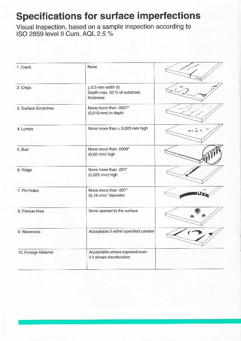
Specifications for surface imperfectionsVisual lnspection, based on a sample inspection according toISO 2859 level ll Cum. AQL 2.5 %
1. Crack
2. Chips
3. Surface Scratches
4. Lumps
6. Ridge
7. Pin Holes
8. Porous Area
9. Waveness
10. Foreign Material
-- 1/
( 0,5 mm width (t)Depth max. 50 % of substratethickness
None more than .0007"(0,018 mm) in depth
None more than < 0,025 mm high
None more than .0008"(0,02 mm) high
None more than .001"(0,025 mm) high
None more than .007"(0,18 mm)"diameter
None opened to the sudace
Acceptable if within specified camber
Acceptable unless exposed evenif it shows discoloration
5. Burr
<t) L n
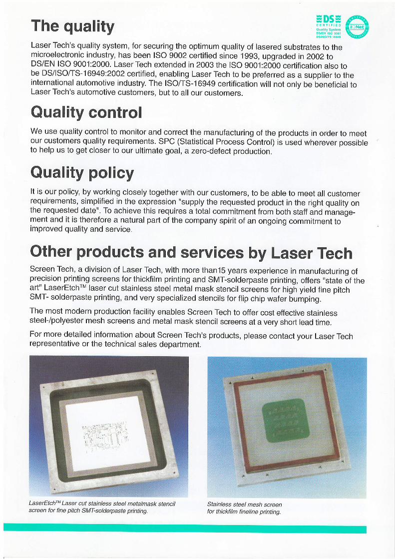
The quality
LaserEtchrM Laser cut stainless steel metalmask stencilscreen for fine pitch SMT-solderpaste printing.
w Ds=CERTIFIEDOualily SystemDS/EN tSO 900ros/sofrs 16949
Laser Tech's quality system, for securing the optimum quality of lasered substrates to themicroelectronic industry, has been ISO 9002 certified since 1993, upgraded in 2002 toDS/EN ISO 9001:2000. Laser Tech extended in 2003 the ISO 9001:20b0 certification also tobe DS/lSOffS-16949:2002 certified, enabling Laser Tech to be preferred as a supplier to theinternational automotive industry. The ISO/TS-16949 certification will not only be beneficial toLaser Tech's automotive customers, but to all our customers.
Quality controlWe use quality control to monitor and correct the manufacturing of the products in order to meetour customers quality requirements. SPC (Statistical Process Control) is used wherever possibleto help us to get closer to our ultimate goal, a zero-defect production.
Quality policyIt is our policy, by working closely together with our customers, to be able to meet all customerrequirements, simplified in the expression "supply the requested product in the right quality onthe requested date". To achieve this requires a total commitment from both staff and manage-ment and it is therefore a natural part of the company spirit of an ongoing commitment toimproved quality and service.
other products and services by Laser TechScreen Tech, a division of Laser Tech, with more than15 years experience in manufacturing ofprecision printing screens for thickfilm printing and SMT-solderpaste printing, offers "state of ttreaft" LaserEtchrM laser cut stainless steel metal mask stencil screens for high yield fine pitchSMT- solderpaste printing, and very specialized stencils for flip chip wafer bumping.
The most modern production facility enables Screen Tech to offer cost effective stainlesssteel-/polyester mesh screens and metal mask stencil screens at a very short lead time.
For more detailed information about Screen Tech's products, please contact your Laser Techrepresentative or the technical sales department.
Stainless steel mesh screenfor thickfilm fineline printing.
I