Embed Size (px)
Citation preview
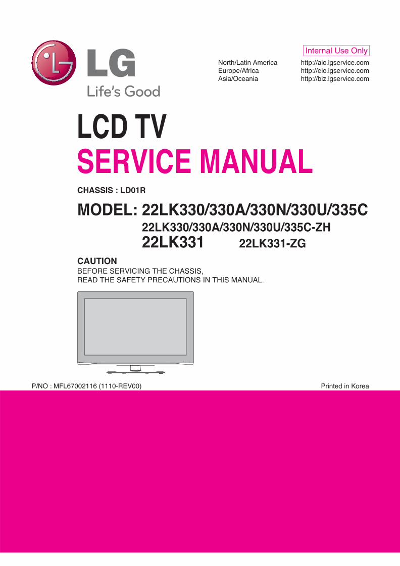
LCD TVSERVICE MANUAL
CAUTIONBEFORE SERVICING THE CHASSIS,READ THE SAFETY PRECAUTIONS IN THIS MANUAL.
CHASSIS : LD01R
MODEL: 22LK330/330A/330N/330U/335CMODEL: 22LK330/330A/330N/330U/335C-ZHMODEL: 22LK331 22LK331-ZG
North/Latin America http://aic.lgservice.comEurope/Africa http://eic.lgservice.comAsia/Oceania http://biz.lgservice.com
Internal Use Only
Printed in KoreaP/NO : MFL67002116 (1110-REV00)
LGE Internal Use OnlyCopyright ©2011 LG Electronics. Inc. All right reserved. Only for training and service purposes
- 2 -
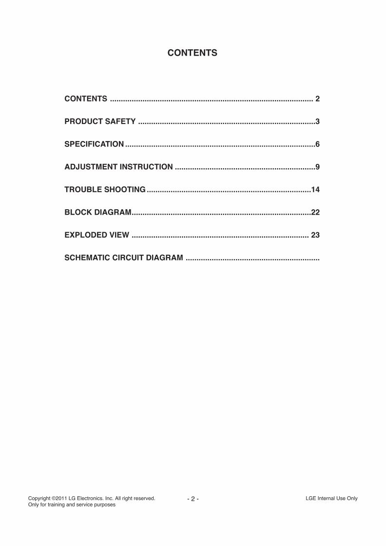
CONTENTS
CONTENTS .............................................................................................. 2
PRODUCT SAFETY ..................................................................................3
SPECIFICATION ........................................................................................6
ADJUSTMENT INSTRUCTION .................................................................9
TROUBLE SHOOTING ............................................................................14
BLOCK DIAGRAM...................................................................................22
EXPLODED VIEW .................................................................................. 23
SCHEMATIC CIRCUIT DIAGRAM ..............................................................
LGE Internal Use OnlyCopyright ©2011 LG Electronics. Inc. All right reserved. Only for training and service purposes
- 3 -
SAFETY PRECAUTIONS
Many electrical and mechanical parts in this chassis have special safety-related characteristics. These parts are identified by in theSchematic Diagram and Exploded View.It is essential that these special safety parts should be replaced with the same components as recommended in this manual to preventShock, Fire, or other Hazards. Do not modify the original design without permission of manufacturer.
General Guidance
An isolation Transformer should always be used during theservicing of a receiver whose chassis is not isolated from the ACpower line. Use a transformer of adequate power rating as thisprotects the technician from accidents resulting in personal injuryfrom electrical shocks.
It will also protect the receiver and it's components from beingdamaged by accidental shorts of the circuitry that may beinadvertently introduced during the service operation.
If any fuse(or Fusible Resistor) in this TV receiver is blown, replaceit with the specified.
When replacing a high wattage resistor (Oxide Metal Film Resistor,over 1 W), keep the resistor 10mm away from PCB.
Keep wires away from high voltage or high temperature parts.
Before returning the receiver to the customer,
always perform an AC leakage current check on the exposedmetallic parts of the cabinet, such as antennas, terminals, etc., tobe sure the set is safe to operate without damage of electricalshock.
Leakage Current Cold Check(Antenna Cold Check)With the instrument AC plug removed from AC source, connect anelectrical jumper across the two AC plug prongs. Place the ACswitch in the on position, connect one lead of ohm-meter to the ACplug prongs tied together and touch other ohm-meter lead in turn toeach exposed metallic parts such as antenna terminals, phonejacks, etc. If the exposed metallic part has a return path to the chassis, themeasured resistance should be between 1 MΩ and 5.2 MΩ. When the exposed metal has no return path to the chassis thereading must be infinite.An other abnormality exists that must be corrected before thereceiver is returned to the customer.
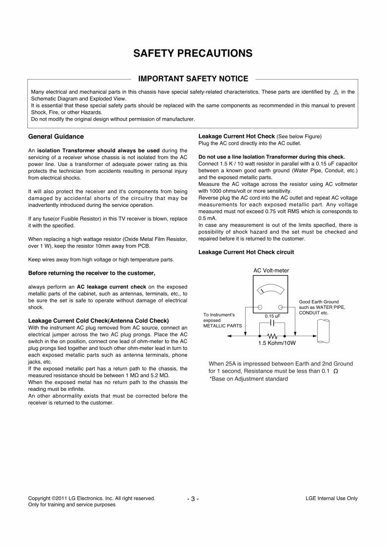
Leakage Current Hot Check (See below Figure) Plug the AC cord directly into the AC outlet.
Do not use a line Isolation Transformer during this check.Connect 1.5 K / 10 watt resistor in parallel with a 0.15 uF capacitorbetween a known good earth ground (Water Pipe, Conduit, etc.)and the exposed metallic parts.Measure the AC voltage across the resistor using AC voltmeterwith 1000 ohms/volt or more sensitivity.Reverse plug the AC cord into the AC outlet and repeat AC voltagemeasurements for each exposed metallic part. Any voltagemeasured must not exceed 0.75 volt RMS which is corresponds to0.5 mA.In case any measurement is out of the limits specified, there ispossibility of shock hazard and the set must be checked andrepaired before it is returned to the customer.
Leakage Current Hot Check circuit
1.5 Kohm/10W
To Instrument’sexposed METALLIC PARTS
Good Earth Groundsuch as WATER PIPE,CONDUIT etc.
AC Volt-meter
When 25A is impressed between Earth and 2nd Groundfor 1 second, Resistance must be less than 0.1*Base on Adjustment standard
IMPORTANT SAFETY NOTICE
0.15 uF
Ω
LGE Internal Use OnlyCopyright ©2011 LG Electronics. Inc. All right reserved. Only for training and service purposes
- 4 -
CAUTION: Before servicing receivers covered by this servicemanual and its supplements and addenda, read and follow theSAFETY PRECAUTIONS on page 3 of this publication.NOTE: If unforeseen circumstances create conflict between thefollowing servicing precautions and any of the safety precautions onpage 3 of this publication, always follow the safety precautions.Remember: Safety First.
General Servicing Precautions1. Always unplug the receiver AC power cord from the AC power
source before;a. Removing or reinstalling any component, circuit board
module or any other receiver assembly.b. Disconnecting or reconnecting any receiver electrical plug or
other electrical connection.c. Connecting a test substitute in parallel with an electrolytic
capacitor in the receiver.CAUTION: A wrong part substitution or incorrect polarityinstallation of electrolytic capacitors may result in anexplosion hazard.
2. Test high voltage only by measuring it with an appropriate highvoltage meter or other voltage measuring device (DVM,FETVOM, etc) equipped with a suitable high voltage probe.Do not test high voltage by "drawing an arc".
3. Do not spray chemicals on or near this receiver or any of itsassemblies.
4. Unless specified otherwise in this service manual, cleanelectrical contacts only by applying the following mixture to thecontacts with a pipe cleaner, cotton-tipped stick or comparablenon-abrasive applicator; 10 % (by volume) Acetone and 90 %(by volume) isopropyl alcohol (90 % - 99 % strength)CAUTION: This is a flammable mixture.Unless specified otherwise in this service manual, lubrication ofcontacts in not required.
5. Do not defeat any plug/socket B+ voltage interlocks with whichreceivers covered by this service manual might be equipped.
6. Do not apply AC power to this instrument and/or any of itselectrical assemblies unless all solid-state device heat sinks arecorrectly installed.
7. Always connect the test receiver ground lead to the receiverchassis ground before connecting the test receiver positivelead.Always remove the test receiver ground lead last.
8. Use with this receiver only the test fixtures specified in thisservice manual.CAUTION: Do not connect the test fixture ground strap to anyheat sink in this receiver.
Electrostatically Sensitive (ES) DevicesSome semiconductor (solid-state) devices can be damaged easilyby static electricity. Such components commonly are calledElectrostatically Sensitive (ES) Devices. Examples of typical ESdevices are integrated circuits and some field-effect transistors andsemiconductor “chip” components. The following techniquesshould be used to help reduce the incidence of componentdamage caused by static by static electricity.1. Immediately before handling any semiconductor component or
semiconductor-equipped assembly, drain off any electrostaticcharge on your body by touching a known earth ground.Alternatively, obtain and wear a commercially availabledischarging wrist strap device, which should be removed toprevent potential shock reasons prior to applying power to theunit under test.
2. After removing an electrical assembly equipped with ESdevices, place the assembly on a conductive surface such asaluminum foil, to prevent electrostatic charge buildup orexposure of the assembly.
3. Use only a grounded-tip soldering iron to solder or unsolder ESdevices.
4. Use only an anti-static type solder removal device. Some solderremoval devices not classified as “anti-static” can generateelectrical charges sufficient to damage ES devices.
5. Do not use freon-propelled chemicals. These can generateelectrical charges sufficient to damage ES devices.
6. Do not remove a replacement ES device from its protectivepackage until immediately before you are ready to install it.(Most replacement ES devices are packaged with leadselectrically shorted together by conductive foam, aluminum foilor comparable conductive material).
7. Immediately before removing the protective material from theleads of a replacement ES device, touch the protective materialto the chassis or circuit assembly into which the device will beinstalled.CAUTION: Be sure no power is applied to the chassis or circuit,and observe all other safety precautions.
8. Minimize bodily motions when handling unpackagedreplacement ES devices. (Otherwise harmless motion such asthe brushing together of your clothes fabric or the lifting of yourfoot from a carpeted floor can generate static electricitysufficient to damage an ES device.)
General Soldering Guidelines1. Use a grounded-tip, low-wattage soldering iron and appropriate
tip size and shape that will maintain tip temperature within therange or 500 °F to 600 °F.
2. Use an appropriate gauge of RMA resin-core solder composedof 60 parts tin/40 parts lead.
3. Keep the soldering iron tip clean and well tinned.4. Thoroughly clean the surfaces to be soldered. Use a mall wire-
bristle (0.5 inch, or 1.25 cm) brush with a metal handle.Do not use freon-propelled spray-on cleaners.
5. Use the following unsoldering techniquea. Allow the soldering iron tip to reach normal temperature.
(500 °F to 600 °F)b. Heat the component lead until the solder melts.c. Quickly draw the melted solder with an anti-static, suction-
type solder removal device or with solder braid.CAUTION: Work quickly to avoid overheating the circuitboard printed foil.
6. Use the following soldering technique.a. Allow the soldering iron tip to reach a normal temperature
(500 °F to 600 °F)b. First, hold the soldering iron tip and solder the strand against
the component lead until the solder melts.c. Quickly move the soldering iron tip to the junction of the
component lead and the printed circuit foil, and hold it thereonly until the solder flows onto and around both thecomponent lead and the foil.CAUTION: Work quickly to avoid overheating the circuitboard printed foil.
d. Closely inspect the solder area and remove any excess orsplashed solder with a small wire-bristle brush.
SERVICING PRECAUTIONS
LGE Internal Use OnlyCopyright ©2011 LG Electronics. Inc. All right reserved. Only for training and service purposes
- 5 -
IC Remove/ReplacementSome chassis circuit boards have slotted holes (oblong) throughwhich the IC leads are inserted and then bent flat against thecircuit foil. When holes are the slotted type, the following techniqueshould be used to remove and replace the IC. When working withboards using the familiar round hole, use the standard techniqueas outlined in paragraphs 5 and 6 above.
Removal1. Desolder and straighten each IC lead in one operation by gently
prying up on the lead with the soldering iron tip as the soldermelts.
2. Draw away the melted solder with an anti-static suction-typesolder removal device (or with solder braid) before removing theIC.
Replacement1. Carefully insert the replacement IC in the circuit board.2. Carefully bend each IC lead against the circuit foil pad and
solder it.3. Clean the soldered areas with a small wire-bristle brush.
(It is not necessary to reapply acrylic coating to the areas).
"Small-Signal" Discrete TransistorRemoval/Replacement1. Remove the defective transistor by clipping its leads as close as
possible to the component body.2. Bend into a "U" shape the end of each of three leads remaining
on the circuit board.3. Bend into a "U" shape the replacement transistor leads.4. Connect the replacement transistor leads to the corresponding
leads extending from the circuit board and crimp the "U" withlong nose pliers to insure metal to metal contact then soldereach connection.
Power Output, Transistor DeviceRemoval/Replacement1. Heat and remove all solder from around the transistor leads.2. Remove the heat sink mounting screw (if so equipped).3. Carefully remove the transistor from the heat sink of the circuit
board.4. Insert new transistor in the circuit board.5. Solder each transistor lead, and clip off excess lead.6. Replace heat sink.
Diode Removal/Replacement1. Remove defective diode by clipping its leads as close as
possible to diode body.2. Bend the two remaining leads perpendicular y to the circuit
board.3. Observing diode polarity, wrap each lead of the new diode
around the corresponding lead on the circuit board.4. Securely crimp each connection and solder it.5. Inspect (on the circuit board copper side) the solder joints of
the two "original" leads. If they are not shiny, reheat them and ifnecessary, apply additional solder.
Fuse and Conventional ResistorRemoval/Replacement1. Clip each fuse or resistor lead at top of the circuit board hollow
stake.2. Securely crimp the leads of replacement component around
notch at stake top.3. Solder the connections.
CAUTION: Maintain original spacing between the replacedcomponent and adjacent components and the circuit board toprevent excessive component temperatures.
Circuit Board Foil RepairExcessive heat applied to the copper foil of any printed circuitboard will weaken the adhesive that bonds the foil to the circuitboard causing the foil to separate from or "lift-off" the board. Thefollowing guidelines and procedures should be followed wheneverthis condition is encountered.
At IC ConnectionsTo repair a defective copper pattern at IC connections use thefollowing procedure to install a jumper wire on the copper patternside of the circuit board. (Use this technique only on ICconnections).
1. Carefully remove the damaged copper pattern with a sharpknife. (Remove only as much copper as absolutely necessary).
2. carefully scratch away the solder resist and acrylic coating (ifused) from the end of the remaining copper pattern.
3. Bend a small "U" in one end of a small gauge jumper wire andcarefully crimp it around the IC pin. Solder the IC connection.
4. Route the jumper wire along the path of the out-away copperpattern and let it overlap the previously scraped end of the goodcopper pattern. Solder the overlapped area and clip off anyexcess jumper wire.
At Other ConnectionsUse the following technique to repair the defective copper patternat connections other than IC Pins. This technique involves theinstallation of a jumper wire on the component side of the circuitboard.
1. Remove the defective copper pattern with a sharp knife.Remove at least 1/4 inch of copper, to ensure that a hazardouscondition will not exist if the jumper wire opens.
2. Trace along the copper pattern from both sides of the patternbreak and locate the nearest component that is directlyconnected to the affected copper pattern.
3. Connect insulated 20-gauge jumper wire from the lead of thenearest component on one side of the pattern break to the leadof the nearest component on the other side.Carefully crimp and solder the connections.CAUTION: Be sure the insulated jumper wire is dressed so theit does not touch components or sharp edges.
LGE Internal Use OnlyCopyright ©2011 LG Electronics. Inc. All right reserved. Only for training and service purposes
- 6 -
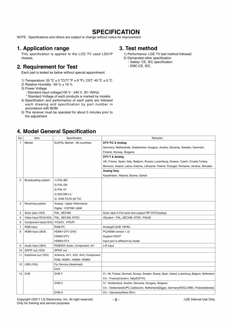
SPECIFICATIONNOTE : Specifications and others are subject to change without notice for improvement.
1. Application rangeThis specification is applied to the LCD TV used LD01Pchassis.
2. Requirement for TestEach part is tested as below without special appointment.
1) Temperature: 25 ºC ± 5 ºC(77 ºF ± 9 ºF), CST: 40 ºC ± 5 ºC2) Relative Humidity : 65 % ± 10 %3) Power Voltage
: Standard input voltage(100 V - 240 V, 50 / 60Hz)* Standard Voltage of each products is marked by models.
4) Specification and performance of each parts are followedeach drawing and specif ication by part number inaccordance with BOM.
5) The receiver must be operated for about 5 minutes prior tothe adjustment.
3. Test method1) Performance: LGE TV test method followed 2) Demanded other specification
- Safety: CE, IEC specification- EMC:CE, IEC
4. Model General SpecificationNo. Item Specification Remarks
1 Market EU(PAL Market - 36 countries) DTV-T/C & Analog
Germany, Netherlands, Switzerland, Hungary, Austria, Slovenia, Sweden, Denmark,
Finland, Norway, Bulgaria
DTV-T & Analog
UK, France, Spain, Italy, Belgium, Russia, Luxemburg, Greece, Czech, Croatia,Turkey,
Morocco, Ireland, Latvia, Estonia, Lithuania, Poland, Portugal, Romania, Ukraine, Slovakia
Analog Only
Kazakhstan, Albania, Bosnia, Serbia
2 Broadcasting system 1) PAL-BG
2) PAL-DK
3) PAL-I/I’
4) SECAM L/L’
5) DVB-T/C/S (ID TV)
3 Receiving system Analog : Upper Heterodyne
Digital : COFDM, QAM
4 Scart Jack (1EA) PAL, SECAM Scart Jack is Full scart and support RF-OUT(analog)
5 Video Input RCA(1EA) PAL, SECAM, NTSC 4System : PAL, SECAM, NTSC, PAL60
6 Component Input(1EA) Y/Cb/Cr, Y/Pb/Pr
7 RGB Input RGB-PC Analog(D-SUB 15PIN)
8 HDMI Input (3EA) HDMI1-DTV (DVI) PC(HDMI version 1.3)
HDMI2-DTV Support HDCP
HDMI3-DTV Input port is different by model
9 Audio Input (3EA) RGB/DVI Audio, Component, AV L/R Input
10 SDPIF out (1EA) SPDIF out
11 Earphone out (1EA) Antenna, AV1, AV2, AV3, Component,
RGB, HDMI1, HDMI2, HDMI3
12 USB (1EA) For Service (download)
DivX
13 DVB DVB-T CI : UK, Finland, Denmark, Norway, Sweden, Russia, Spain, Ireland, Luxemburg, Belgium, Netherland
CI+ : France(Canal+), Italy(DGTVi)
DVB-C CI : Switzerland, Austria, Slovenia, Hungary, Bulgaria
CI+ : Switzerland(UPC,Cablecom), Netherland(Ziggo), Germany(KDG,CWB), Finland(labwise)
DVB-S CI+ : Germany(Astra HD+)
- 7 - LGE Internal Use OnlyCopyright ©2011 LG Electronics. Inc. All right reserved. Only for training and service purposes
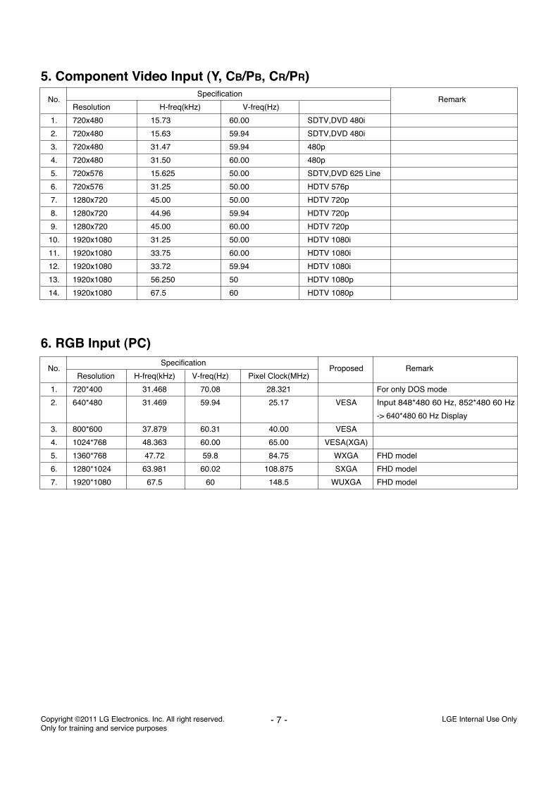
5. Component Video Input (Y, CB/PB, CR/PR)
No.Specification
RemarkResolution H-freq(kHz) V-freq(Hz)
1. 720x480 15.73 60.00 SDTV,DVD 480i
2. 720x480 15.63 59.94 SDTV,DVD 480i
3. 720x480 31.47 59.94 480p
4. 720x480 31.50 60.00 480p
5. 720x576 15.625 50.00 SDTV,DVD 625 Line
6. 720x576 31.25 50.00 HDTV 576p
7. 1280x720 45.00 50.00 HDTV 720p
8. 1280x720 44.96 59.94 HDTV 720p
9. 1280x720 45.00 60.00 HDTV 720p
10. 1920x1080 31.25 50.00 HDTV 1080i
11. 1920x1080 33.75 60.00 HDTV 1080i
12. 1920x1080 33.72 59.94 HDTV 1080i
13. 1920x1080 56.250 50 HDTV 1080p
14. 1920x1080 67.5 60 HDTV 1080p
No.Specification
Proposed RemarkResolution H-freq(kHz) V-freq(Hz) Pixel Clock(MHz)
1. 720*400 31.468 70.08 28.321 For only DOS mode
2. 640*480 31.469 59.94 25.17 VESA Input 848*480 60 Hz, 852*480 60 Hz
-> 640*480 60 Hz Display
3. 800*600 37.879 60.31 40.00 VESA
4. 1024*768 48.363 60.00 65.00 VESA(XGA)
5. 1360*768 47.72 59.8 84.75 WXGA FHD model
6. 1280*1024 63.981 60.02 108.875 SXGA FHD model
7. 1920*1080 67.5 60 148.5 WUXGA FHD model
6. RGB Input (PC)
- 8 - LGE Internal Use OnlyCopyright ©2011 LG Electronics. Inc. All right reserved. Only for training and service purposes
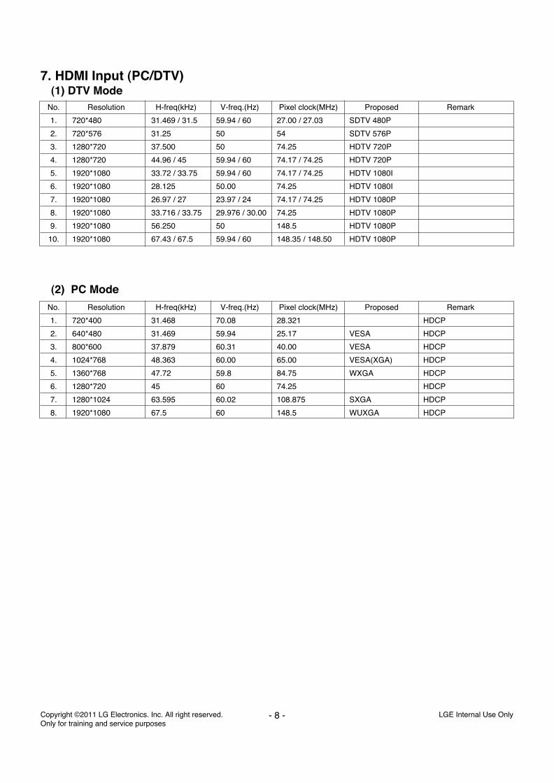
7. HDMI Input (PC/DTV)(1) DTV Mode
No. Resolution H-freq(kHz) V-freq.(Hz) Pixel clock(MHz) Proposed Remark
1. 720*400 31.468 70.08 28.321 HDCP
2. 640*480 31.469 59.94 25.17 VESA HDCP
3. 800*600 37.879 60.31 40.00 VESA HDCP
4. 1024*768 48.363 60.00 65.00 VESA(XGA) HDCP
5. 1360*768 47.72 59.8 84.75 WXGA HDCP
6. 1280*720 45 60 74.25 HDCP
7. 1280*1024 63.595 60.02 108.875 SXGA HDCP
8. 1920*1080 67.5 60 148.5 WUXGA HDCP
(2) PC Mode
No. Resolution H-freq(kHz) V-freq.(Hz) Pixel clock(MHz) Proposed Remark
1. 720*480 31.469 / 31.5 59.94 / 60 27.00 / 27.03 SDTV 480P
2. 720*576 31.25 50 54 SDTV 576P
3. 1280*720 37.500 50 74.25 HDTV 720P
4. 1280*720 44.96 / 45 59.94 / 60 74.17 / 74.25 HDTV 720P
5. 1920*1080 33.72 / 33.75 59.94 / 60 74.17 / 74.25 HDTV 1080I
6. 1920*1080 28.125 50.00 74.25 HDTV 1080I
7. 1920*1080 26.97 / 27 23.97 / 24 74.17 / 74.25 HDTV 1080P
8. 1920*1080 33.716 / 33.75 29.976 / 30.00 74.25 HDTV 1080P
9. 1920*1080 56.250 50 148.5 HDTV 1080P
10. 1920*1080 67.43 / 67.5 59.94 / 60 148.35 / 148.50 HDTV 1080P
LGE Internal Use OnlyCopyright ©2011 LG Electronics. Inc. All right reserved. Only for training and service purposes
- 9 -
ADJUSTMENT INSTRUCTION
1. Application RangeThis specification sheet is applied to all of the LCD TV withLD01P chassis.
2. Designation1) The adjustment is according to the order which is designated
and which must be followed, according to the plan which canbe changed only on agreeing.
2) Power Adjustment: Free Voltage3) Magnetic Field Condition: Nil.4) Input signal Unit: Product Specification Standard5) Reserve after operation: Above 5 Minutes (Heat Run)
Temperature : at 25 ºC ± 5 ºC Relative humidity : 65 % ± 10 %Input voltage : 220 V, 60 Hz
6) Adjustment equipments: Color Analyzer (CA-210 or CA-110), Pattern Generator(MSPG-925L or Equivalent), DDCAdjustment Jig equipment, Service remote control.
7) Push the “IN STOP” key - For memory initialization.
3. Main PCB check process* APC - After Manual-Insert, executing APC
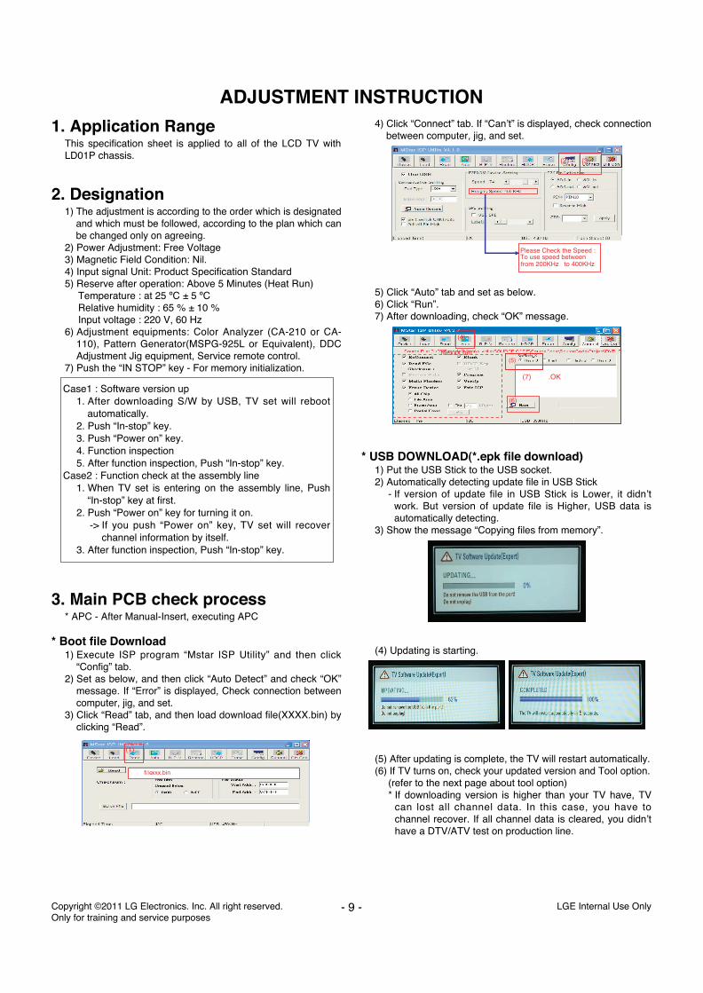
* Boot file Download1) Execute ISP program “Mstar ISP Utility” and then click
“Config” tab.2) Set as below, and then click “Auto Detect” and check “OK”
message. If “Error” is displayed, Check connection betweencomputer, jig, and set.
3) Click “Read” tab, and then load download file(XXXX.bin) byclicking “Read”.
4) Click “Connect” tab. If “Can’t” is displayed, check connectionbetween computer, jig, and set.
5) Click “Auto” tab and set as below.6) Click “Run”.7) After downloading, check “OK” message.
* USB DOWNLOAD(*.epk file download)1) Put the USB Stick to the USB socket.2) Automatically detecting update file in USB Stick
- If version of update file in USB Stick is Lower, it didn’twork. But version of update file is Higher, USB data isautomatically detecting.
3) Show the message “Copying files from memory”.
(4) Updating is starting.
(5) After updating is complete, the TV will restart automatically.(6) If TV turns on, check your updated version and Tool option.
(refer to the next page about tool option)* If downloading version is higher than your TV have, TV
can lost all channel data. In this case, you have tochannel recover. If all channel data is cleared, you didn’thave a DTV/ATV test on production line.
Case1 : Software version up1. After downloading S/W by USB, TV set will reboot
automatically.2. Push “In-stop” key.3. Push “Power on” key.4. Function inspection5. After function inspection, Push “In-stop” key.
Case2 : Function check at the assembly line1. When TV set is entering on the assembly line, Push
“In-stop” key at first.2. Push “Power on” key for turning it on.
-> If you push “Power on” key, TV set will recoverchannel information by itself.
3. After function inspection, Push “In-stop” key.
filexxx.bin
(4)
(7) .OK
(5)
(6)
(1)
fi lexxx.bin
(2) (3)
Please Check the Speed : To use speed between from 200KHz to 400KHz
* After downloading, have to adjust Tool Option again.(1) Push “IN-START” key in service manual control.(2) Select ‘Tool Option 1’ and push ‘OK’ key.(3) Punch in the number. (Each models has their number.)(4) Correction Tool option is completed.
3.1. ADC Process• Enter ‘EZ ADJUST’ mode by pushing ‘ADJ’ key,• Enter Internal ADC mode by pushing ‘G’ key at “7. ADC
Calibration”.
<Caution> Using ‘P-ONLY’ key of the Adjustment remotecontrol, power on TV.
* ADC Calibration Protocol (RS232)
Adjust Sequence• aa 00 00 [Enter Adjust Mode]• xb 00 40 [Component1 Input (480i)]• ad 00 10 [Adjust 480i Comp1]• xb 00 60 [RGB Input (1024*768)]• ad 00 10 [Adjust 1024*768 RGB]• aa 00 90 End Adjust mode* Required equipment : Adjustment Remote control
3.2. EDID Download1) After Enter Service Mode by pushing ‘ADJ’ key,2) Enter EDID D/L mode.3) Enter ‘START’ by pushing ‘OK’ key.
<Caution> Never connect HDMI & D-sub cable when EDIDdownload.
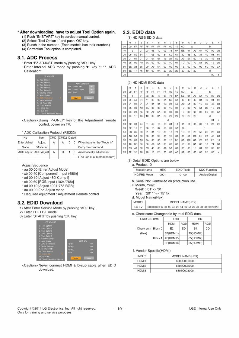
3.3. EDID data(1) HD RGB EDID data
(2) HD HDMI EDID data
(3) Detail EDID Options are belowa. Product ID
b. Serial No: Controlled on production line.c. Month, Year:
Week : ‘01’ -> ‘01’Year : ‘2011’ -> ‘15’ fix
d. Model Name(Hex):
e. Checksum: Changeable by total EDID data.
f. Vendor Specific(HDMI)
- 10 - LGE Internal Use OnlyCopyright ©2011 LG Electronics. Inc. All right reserved. Only for training and service purposes
ADC Calibration
ADC Comp 480i NG
ADC Comp 1080p NG
ADC RGB NG
Start Reset
EZ ADJUST
0. Tool Option1
1. Tool Option2
2. Tool Option3
3. Tool Option4
4. Tool Option5
5. Country Group
6. Area Option
7. ADC Calibration
8. White Balance
9. 10 Point WB
10. Test Pattern
11. EDID D/L
12. Sub B/C
13. Touch Sensitivity Setting
No Item CMD1 CMD2 Data0
Enter Adjust Adjust A A 0 0 When transfer the ‘Mode In’,
Mode ‘Mode In’ Carry the command.
ADC adjust ADC Adjust A D 1 0 Automatically adjustment
(The use of a internal pattern)
HDMI1 OK
HDMI2 OK
HDMI3 OK
RGB OK
Start Reset
EDID D/L
EZ ADJUST
0. Tool Option1
1. Tool Option2
2. Tool Option3
3. Tool Option4
4. Tool Option5
5. Country Group
6. Area Option
7. ADC Calibration
8. White Balance
9. 10 Point WB
10. Test Pattern
11. EDID D/L
12. Sub B/C
13. Touch Sensitivity Setting
0 1 2 3 4 5 6 7 8 9 A B C D E F
00 00 FF FF FF FF FF FF 00 1E 6D a b
10 c 01 03 80 10 09 78 0A EE 91 A3 54 4C 99 26
20 0F 50 54 A1 08 00 81 C0 61 40 45 40 31 40 01 01
30 01 01 01 01 01 01 1B 21 50 A0 51 00 1E 30 48 88
40 35 00 A0 5A 00 00 00 1C 01 1D 00 72 51 D0 1E 20
50 6E 28 55 00 A0 5A 00 00 00 1E 00 00 00 FD 00 3A
60 3E 1F 46 10 00 0A 20 20 20 20 20 20 d
70 d 01 e
80 02 03 24 F1 4E 10 1F 84 13 05 14 03 02 12 20 21
90 22 15 01 26 15 07 50 09 57 07 f
A0 E3 05 03 01 01 1D 80 18 71 1C 16 20 58 2C 25 00
B0 A0 5A 00 00 00 9E 01 1D 00 80 51 D0 0C 20 40 80
C0 35 00 A0 5A 00 00 00 1E 8C 0A D0 8A 20 E0 2D 10
D0 10 3E 96 00 A0 5A 00 00 00 18 02 3A 80 18 71 38
E0 2D 40 58 2C 45 00 A0 5A 00 00 00 1E 01 1D 80 D0
F0 72 1C 16 20 10 2C 25 80 A0 5A 00 00 00 9E 00 e
0 1 2 3 4 5 6 7 8 9 A B C D E F
00 00 FF FF FF FF FF FF 00 1E 6D a b
10 c 01 03 68 10 09 78 0A EE 91 A3 54 4C 99 26
20 0F 50 54 A1 08 00 81 C0 61 40 45 40 31 40 01 01
30 01 01 01 01 01 01 1B 21 50 A0 51 00 1E 30 48 88
40 35 00 A0 5A 00 00 00 1C 01 1D 00 72 51 D0 1E 20
50 6E 28 55 00 A0 5A 00 00 00 1E 00 00 00 FD 00 3A
60 3E 1F 46 10 00 0A 20 20 20 20 20 20 d
70 d 00 e
Model Name HEX EDID Table DDC Function
HD/FHD Model 0001 01 00 Analog/Digital
MODEL MODEL NAME(HEX)
LG TV 00 00 00 FC 00 4C 47 20 54 56 0A 20 20 20 20 20 20 20
EDID C/S data FHD HD
HDMI RGB HDMI RGB
Check sum Block 0 E2 ED B4 CD
(Hex) 5F(HDMI1) 75(HDMI1)
Block 1 4F(HDMI2) 65(HDMI2)
3F(HDMI3) 55(HDMI3)
INPUT MODEL NAME(HEX)
HDMI1 6503C001000
HDMI2 6503C002000
HDMI3 6503C003000
3.4. Function Check(1) Check display and sound
- Check Input and Signal items. (cf. work instructions)1) TV2) AV3) COMPONENT1/2 (480i)4) RGB (PC : 1024 x 768 @ 60hz)5) HDMI6) PC Audio In
* Display and Sound check is executed by remote control.
<Caution> Not to push the INSTOP key after completion if thefunction inspection.
4. Total Assembly line process4.1. Adjustment Preparation
· W/B Equipment conditionCA210- CCFL/EEFL -> CH 9, Test signal : Inner pattern(80 IRE)- LED -> CH 14, Test signal : Inner pattern(80 IRE)
· Above 5 minutes H/run in the inner pattern. (“power on” keyof adjustment remote control)
· Edge LED W/B Table in process of aging time(Only LGDModule)CA210 : CH14, Test signal : Inner patter (80 IRE)
* Connecting picture of the measuring instrument(On Automatic control)Inside PATTERN is used when W/B is controlled. Connect toauto controller or push Adjustment R/C POWER ON -> Enterthe mode of White-Balance, the pattern will come out
* Auto-control interface and directions1) Adjust in the place where the influx of light like floodlight
around is blocked. (illumination is less than 10 lux).2) Adhere closely the Color Analyzer (CA210) to the module
less than 10cm distance, keep it with the surface of theModule and Color Analyzer’s Prove vertically.(80º ~ 100º).
3) Aging time- After aging start, keep the power on (no suspension of
power supply) and heat-run over 15minutes.- Using ‘no signal’ or ‘full white pattern’ or the others, check
the back light on.
• Auto adjustment Map(RS-232C)RS-232C COMMAND[CMD ID DATA]
Wb 00 00 White Balance StartWb 00 ff White Balance End
** Caution **Color Temperature : COOL, Medium, Warm. One of R Gain/G Gain/ B Gain should be kept on 0xC0, andadjust other two lower than C0.(when R/G/B Gain are all C0, it is the FULL Dynamic Rangeof Module)
* Manual W/B process using adjusts Remote control.• After enter Service Mode by pushing “ADJ” key,• Enter White Balance by pushing “G” key at “8. White
Balance”.
* After done all adjustments, Press “In-start” key andcompare Tool option and Area option value with its BOM, ifit is correctly same then unplug the AC cable. If it is notsame, then correct it same with BOM and unplug AC cable.For correct it to the model’s module from factory Jig model.
* Push the “IN STOP” key after completing the functioninspection. And Mechanical Power Switch must be set “ON”.
- 11 - LGE Internal Use OnlyCopyright ©2011 LG Electronics. Inc. All right reserved. Only for training and service purposes
Cool 9,300 K X=0.285(±0.002)
Y=0.293(±0.002) <Test Signal>
Medium 8,000 K X=0.295(±0.002) Inner pattern
Y=0.305(±0.002) (204 gray,80 IRE)
Warm 6,500 K X=0.313(±0.002)
Y=0.329(±0.002)
Aging Time Cool Medium Warm
GP2R (Min.) X Y X Y X Y
269 273 285 293 313 329
1 0-2 279 288 295 308 319 338
2 3-5 278 286 294 306 318 336
3 6-9 277 285 293 305 317 335
4 10-19 276 283 292 303 316 333
5 20-35 274 280 290 300 314 330
6 36-49 272 277 288 297 312 327
7 50-79 271 275 287 295 311 325
8 80-149 270 274 286 294 310 324
9 Over 150 269 273 285 293 309 323
Full White Pattern
COLORANALYZERTYPE: CA-210
RS-232C Communication
CA-210
RS-232C COMMAND MIN CENTER MAX
[CMD ID DATA] (DEFAULT)
Cool Mid Warm Cool Mid Warm
R Gain jg Ja jd 00 172 192 192 255
G Gain jh Jb je 00 172 192 192 255
B Gain ji Jc jf 00 192 192 172 255
R Cut 64 64 64 128
G Cut 64 64 64 128
B Cut 64 64 64 128
White Balance
Color Temp. Cool
R-Gain 172
G-Gain 172
B-Gain 192
R-Cut 64
G-Cut 64
B-Cut 64
Test-Pattern
Backlight
ON
100
Reset To Set
EZ ADJUST
0. Tool Option1
1. Tool Option2
2. Tool Option3
3. Tool Option4
4. Tool Option5
5. Country Group
6. Area Option
7. ADC Calibration
8. White Balance
9. 10 Point WB
10. Test Pattern
11. EDID D/L
12. Sub B/C
13. Touch Sensitivity Settin
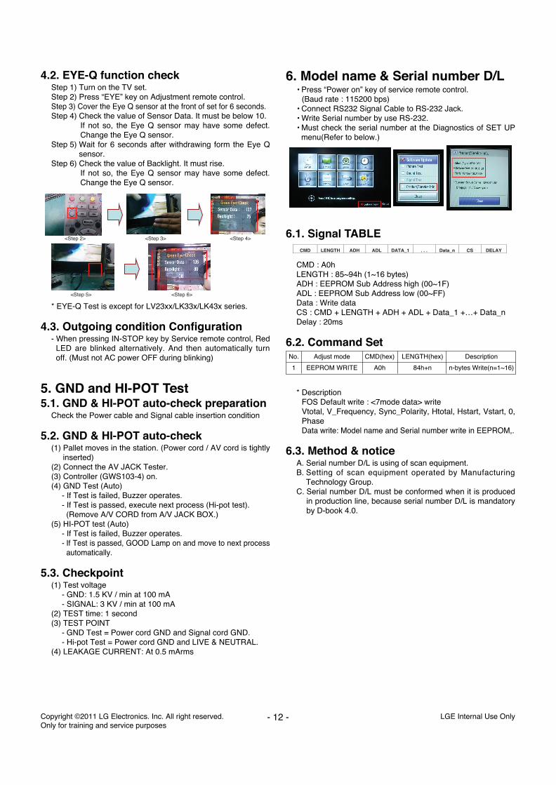
4.2. EYE-Q function checkStep 1) Turn on the TV set.Step 2) Press “EYE” key on Adjustment remote control.Step 3) Cover the Eye Q sensor at the front of set for 6 seconds.Step 4) Check the value of Sensor Data. It must be below 10.
If not so, the Eye Q sensor may have some defect.Change the Eye Q sensor.
Step 5) Wait for 6 seconds after withdrawing form the Eye Qsensor.
Step 6) Check the value of Backlight. It must rise. If not so, the Eye Q sensor may have some defect.Change the Eye Q sensor.
* EYE-Q Test is except for LV23xx/LK33x/LK43x series.
4.3. Outgoing condition Configuration- When pressing IN-STOP key by Service remote control, Red
LED are blinked alternatively. And then automatically turnoff. (Must not AC power OFF during blinking)
5. GND and HI-POT Test5.1. GND & HI-POT auto-check preparation
Check the Power cable and Signal cable insertion condition
5.2. GND & HI-POT auto-check(1) Pallet moves in the station. (Power cord / AV cord is tightly
inserted)(2) Connect the AV JACK Tester.(3) Controller (GWS103-4) on.(4) GND Test (Auto)
- If Test is failed, Buzzer operates.- If Test is passed, execute next process (Hi-pot test).(Remove A/V CORD from A/V JACK BOX.)
(5) HI-POT test (Auto)- If Test is failed, Buzzer operates.- If Test is passed, GOOD Lamp on and move to next process
automatically.
5.3. Checkpoint(1) Test voltage
- GND: 1.5 KV / min at 100 mA- SIGNAL: 3 KV / min at 100 mA
(2) TEST time: 1 second(3) TEST POINT
- GND Test = Power cord GND and Signal cord GND.- Hi-pot Test = Power cord GND and LIVE & NEUTRAL.
(4) LEAKAGE CURRENT: At 0.5 mArms
6. Model name & Serial number D/L• Press “Power on” key of service remote control.
(Baud rate : 115200 bps)• Connect RS232 Signal Cable to RS-232 Jack.• Write Serial number by use RS-232.• Must check the serial number at the Diagnostics of SET UP
menu(Refer to below.)
6.1. Signal TABLE
CMD : A0hLENGTH : 85~94h (1~16 bytes)ADH : EEPROM Sub Address high (00~1F)ADL : EEPROM Sub Address low (00~FF)Data : Write dataCS : CMD + LENGTH + ADH + ADL + Data_1 +…+ Data_nDelay : 20ms
6.2. Command Set
* DescriptionFOS Default write : <7mode data> writeVtotal, V_Frequency, Sync_Polarity, Htotal, Hstart, Vstart, 0,PhaseData write: Model name and Serial number write in EEPROM,.
6.3. Method & noticeA. Serial number D/L is using of scan equipment.B. Setting of scan equipment operated by Manufacturing
Technology Group.C. Serial number D/L must be conformed when it is produced
in production line, because serial number D/L is mandatoryby D-book 4.0.
LGE Internal Use OnlyCopyright ©2011 LG Electronics. Inc. All right reserved. Only for training and service purposes
- 12 -
CMD LENGTH ADH ADL DATA_1 . . . Data_n CS DELAY
<Step 2>
<Step 5> <Step 6>
<Step 3> <Step 4>
No. Adjust mode CMD(hex) LENGTH(hex) Description
1 EEPROM WRITE A0h 84h+n n-bytes Write(n=1~16)
* Manual Download (Model Name and Serial Number)If the TV set is downloaded by OTA or Service man, sometimesmodel name or serial number is initialized.(Not always)There is impossible to download by bar code scan, so It needManual download.1) Press the ‘Instart’ key of Adjustment remote control.2) Go to the menu ‘6.Model Number D/L’ like below photo.3) Input the Factory model name(ex 32LV3400-ZG) or Serial
number like photo.
4) Check the model name Instart menu. -> Factory namedisplayed. (ex 32LV3400-ZG)
5) Check the Diagnostics. (DTV country only) -> Buyer modeldisplayed. (ex 32LV3400)
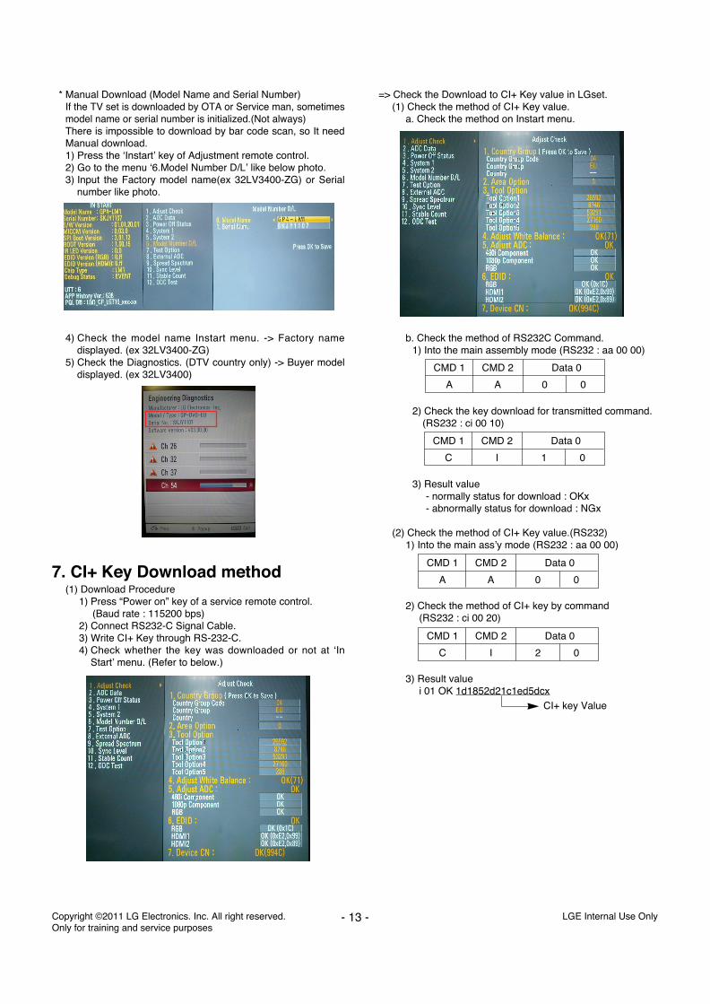
7. CI+ Key Download method(1) Download Procedure
1) Press “Power on” key of a service remote control.(Baud rate : 115200 bps)
2) Connect RS232-C Signal Cable.3) Write CI+ Key through RS-232-C.4) Check whether the key was downloaded or not at ‘In
Start’ menu. (Refer to below.)
=> Check the Download to CI+ Key value in LGset. (1) Check the method of CI+ Key value.
a. Check the method on Instart menu.
b. Check the method of RS232C Command.1) Into the main assembly mode (RS232 : aa 00 00)
2) Check the key download for transmitted command.(RS232 : ci 00 10)
3) Result value- normally status for download : OKx- abnormally status for download : NGx
(2) Check the method of CI+ Key value.(RS232)1) Into the main ass’y mode (RS232 : aa 00 00)
2) Check the method of CI+ key by command(RS232 : ci 00 20)
3) Result valuei 01 OK 1d1852d21c1ed5dcx
- 13 - LGE Internal Use OnlyCopyright ©2011 LG Electronics. Inc. All right reserved. Only for training and service purposes
CMD 1 CMD 2 Data 0
A A 0 0
CMD 1 CMD 2 Data 0
C I 1 0
CMD 1 CMD 2 Data 0
A A 0 0
CMD 1 CMD 2 Data 0
C I 2 0
CI+ key Value
LGE Internal Use OnlyCopyright ©2011 LG Electronics. Inc. All right reserved. Only for training and service purposes
- 14 -
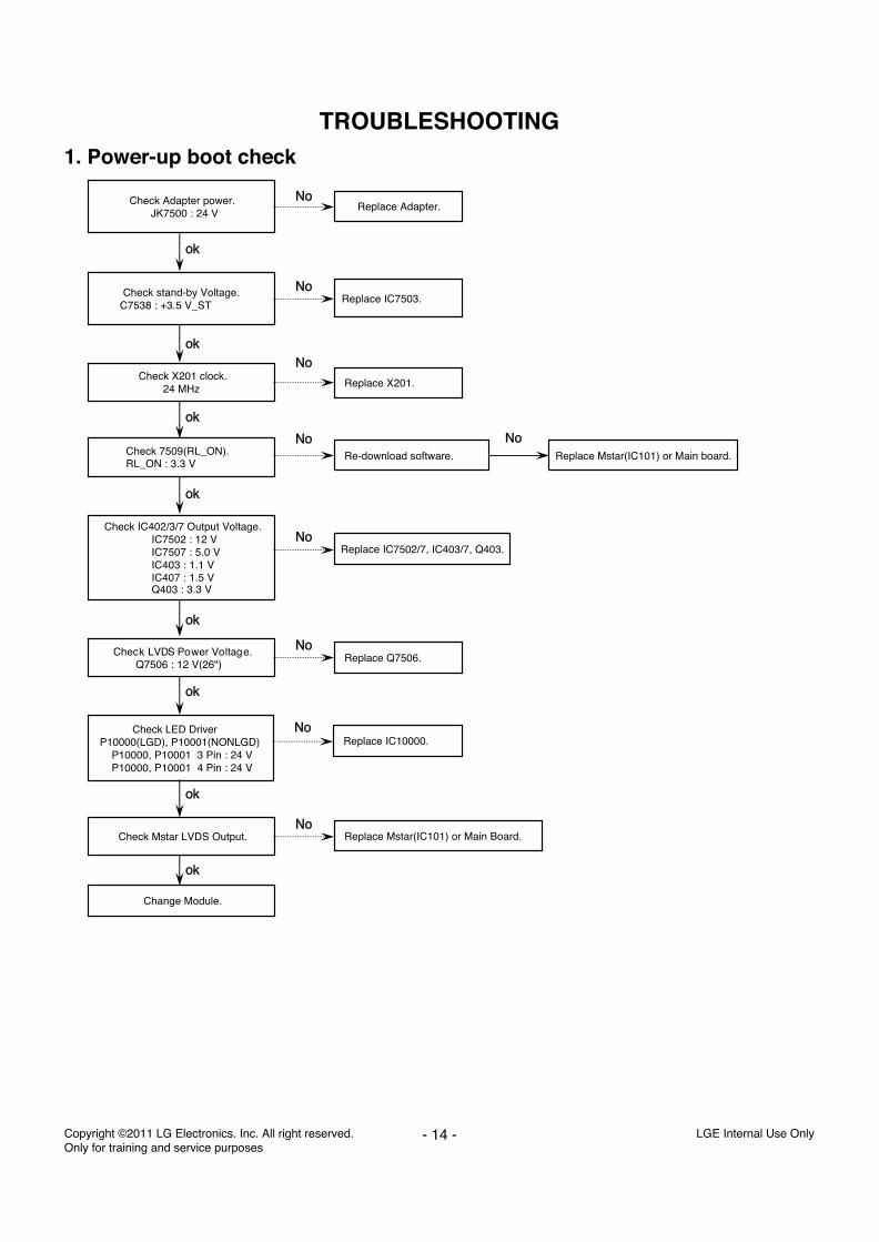
1. Power-up boot check
TROUBLESHOOTING
Check stand-by Voltage.C7538 : +3.5 V_ST
Replace IC7503.
Check X201 clock.24 MHz Replace X201.
Check 7509(RL_ON).RL_ON : 3.3 V
Replace Mstar(IC101) or Main board.
Check LED Driver P10000(LGD), P10001(NONLGD)
P10000, P10001 3 Pin : 24 VP10000, P10001 4 Pin : 24 V
Replace IC10000.
Check IC402/3/7 Output Voltage.IC7502 : 12 VIC7507 : 5.0 VIC403 : 1.1 VIC407 : 1.5 VQ403 : 3.3 V
Replace IC7502/7, IC403/7, Q403.
Re-download software.
Check Adapter power.JK7500 : 24 V
Replace Adapter.
Check LVDS Power Voltage.Q7506 : 12 V(26")
Replace Q7506.
Check Mstar LVDS Output. Replace Mstar(IC101) or Main Board.
Change Module.
ok
ok
ok
ok
ok
ok
ok
No
No
No
No
No
No
No
No
No
ok
LGE Internal Use OnlyCopyright ©2011 LG Electronics. Inc. All right reserved. Only for training and service purposes
- 15 -
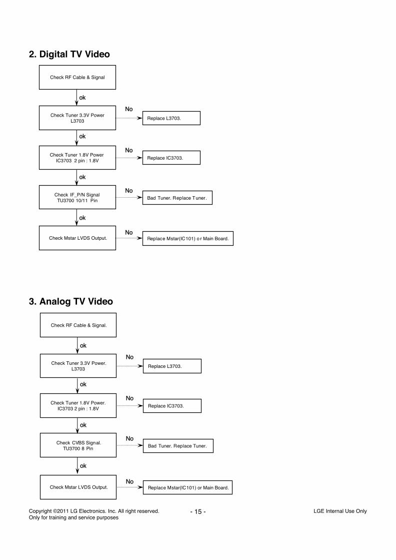
2. Digital TV Video
Check RF Cable & Signal
Check Tuner 3.3V PowerL3703 Replace L3703.
Check Tuner 1.8V Power IC3703 2 pin : 1.8V
Check IF_P/N SignalTU3700 10/11 Pin
Replace IC3703.
Check Mstar LVDS Output. Replace Mstar(IC101) o r Main Board.
ok
ok
ok
ok
No
No
No
No
Bad Tuner. Replace Tuner.
3. Analog TV Video
Check RF Cable & Signal.
Check Tuner 3.3V Power.L3703 Replace L3703.
Check Tuner 1.8V Power.IC3703 2 pin : 1.8V
Check CVBS Signal.TU3700 8 Pin
Replace IC3703.
Check Mstar LVDS Output. Replace Mstar(IC101) or Main Board.
ok
ok
ok
ok
No
No
No
No
Bad Tuner. Replace Tuner.
LGE Internal Use OnlyCopyright ©2011 LG Electronics. Inc. All right reserved. Only for training and service purposes
- 16 -
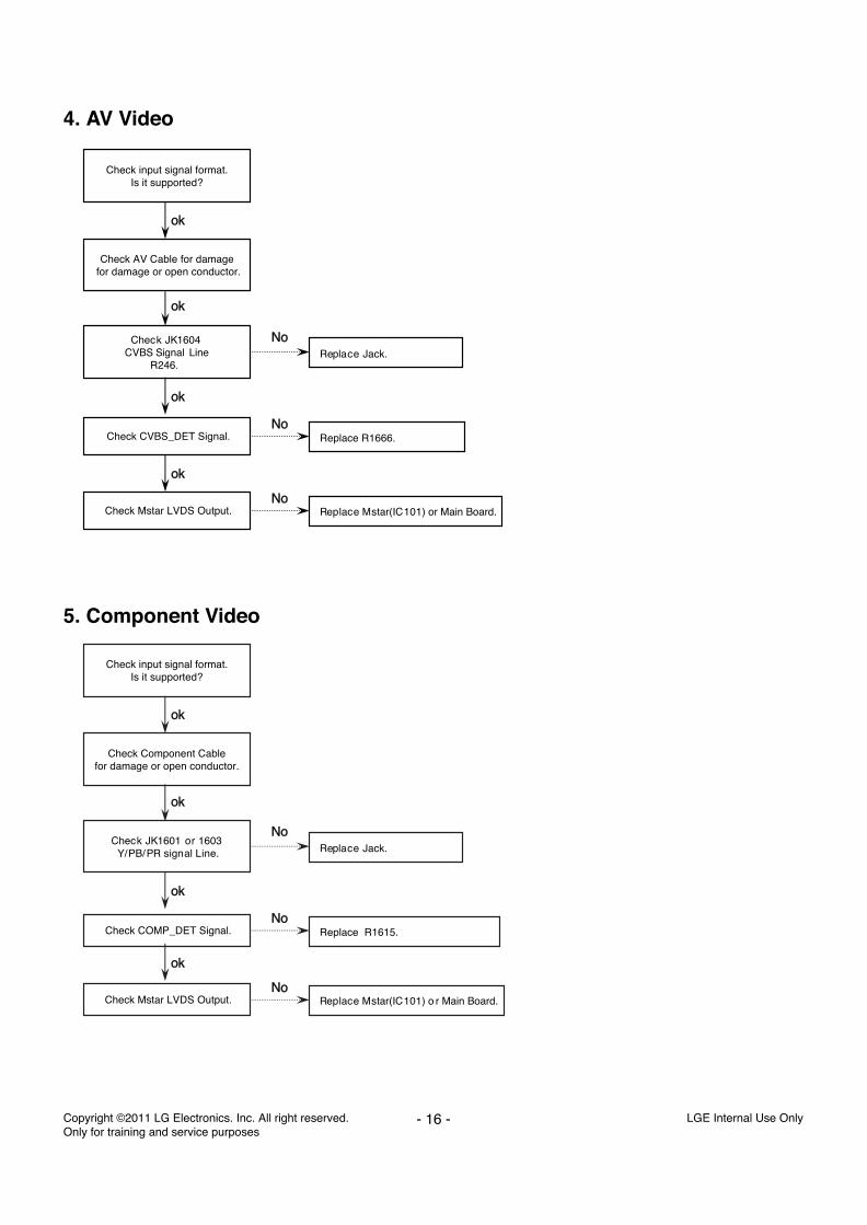
4. AV Video
Check input signal format.Is it supported?
Check AV Cable for damagefor damage or open conductor.
Check JK1604CVBS Signal Line
R246.
ok
ok
ok
NoReplace Jack.
ok
Check CVBS_DET Signal. Replace R1666. No
Check Mstar LVDS Output. Replace Mstar(IC101) or Main Board.No
5. Component Video
Check input signal format.Is it supported?
Check Component Cablefor damage or open conductor.
Check JK1601 or 1603Y/PB/PR signal Line.
ok
ok
ok
NoReplace Jack.
Check COMP_DET Signal. Replace R1615. No
Check Mstar LVDS Output. Replace Mstar(IC101) o r Main Board.
ok
No
- 17 - LGE Internal Use OnlyCopyright ©2011 LG Electronics. Inc. All right reserved. Only for training and service purposes
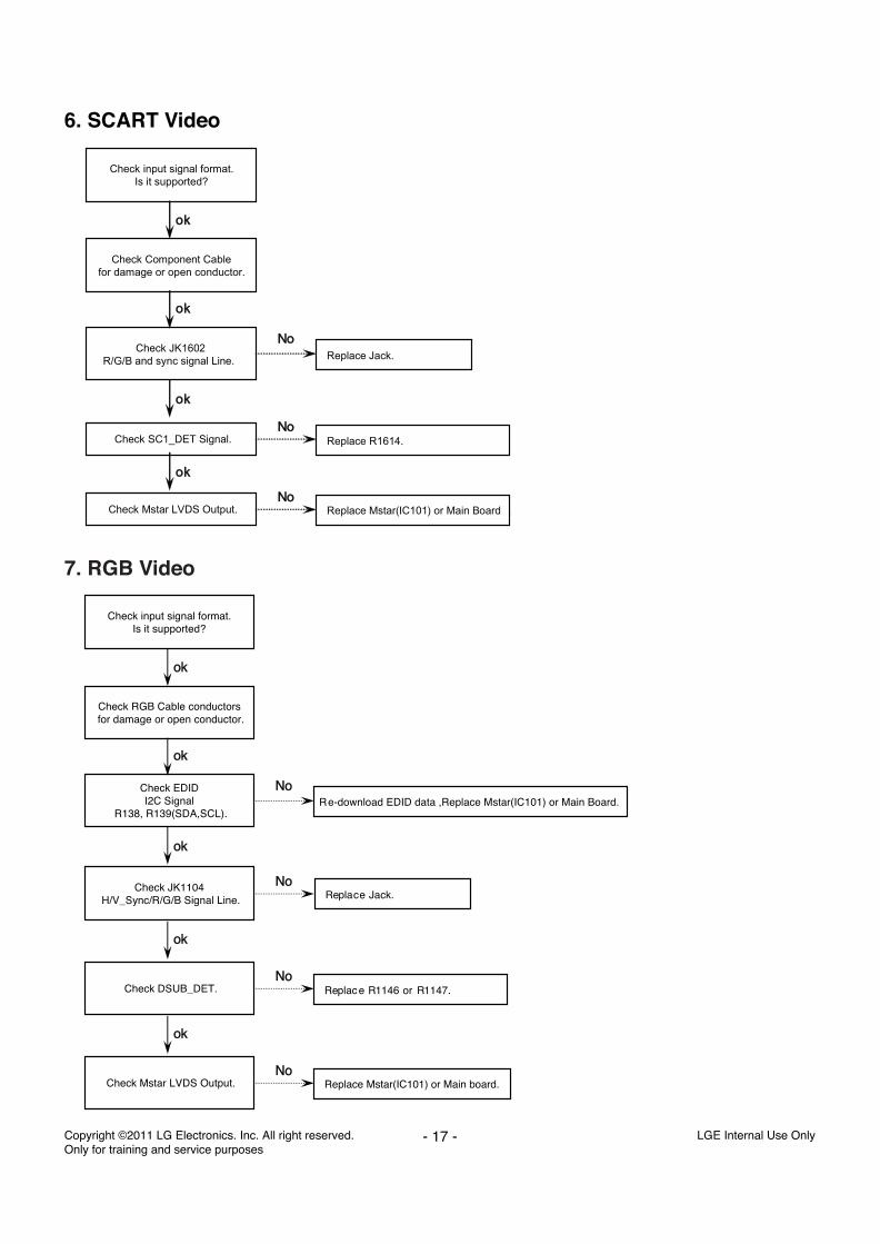
6. SCART Video
Check input signal format.Is it supported?
Check Component Cablefor damage or open conductor.
Check JK1602R/G/B and sync signal Line.
ok
ok
ok
NoReplace Jack.
Check SC1_DET Signal. Replace R1614.No
Check Mstar LVDS Output. Replace Mstar(IC101) or Main Board .
ok
No
7. RGB Video
Check input signal format.Is it supported?
Check RGB Cable conductorsfor damage or open conductor.
Check EDIDI2C Signal
R138, R139(SDA,SCL).
Check JK1104H/V_Sync/R/G/B Signal Line.
ok
ok
ok
No
No
Re-download EDID data ,Replace Mstar(IC101) or Main Board.
ok
Replace Jack.
Check DSUB_DET. Replace R1146 or R1147.No
Check Mstar LVDS Output. Replace Mstar(IC101) or Main board.
ok
No
- 18 - LGE Internal Use OnlyCopyright ©2011 LG Electronics. Inc. All right reserved. Only for training and service purposes
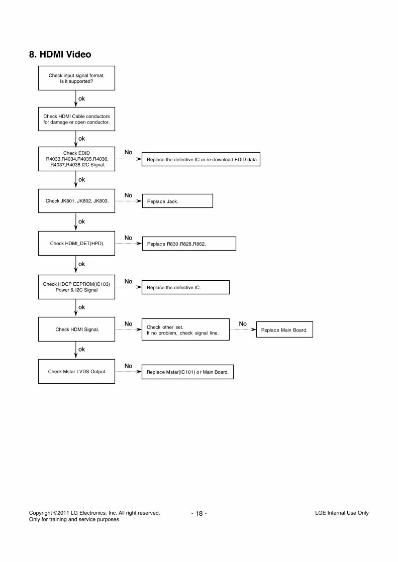
8. HDMI Video
Check input signal format.Is it supported?
Check HDMI Cable conductorsfor damage or open conductor.
Check EDIDR4033,R4034,R4035,R4036,
R4037,R4038 I2C Signal.
Check JK801, JK802, JK803.
ok
ok
ok
No
No
Replace the defective IC or re-download EDID data.
Check HDCP EEPROM(IC103)Power & I2C Signal Replace the defective IC.
ok
No
Replace Jack.
Check HDMI Signal. Check other set.If no problem, check signal line.
ok
No
Check Mstar LVDS Output. Replace Mstar(IC101) o r Main Board.
ok
No
Replace Main Board.No
Check HDMI_DET(HPD).No
ok
Replace R830,R828,R862.
- 19 - LGE Internal Use OnlyCopyright ©2011 LG Electronics. Inc. All right reserved. Only for training and service purposes
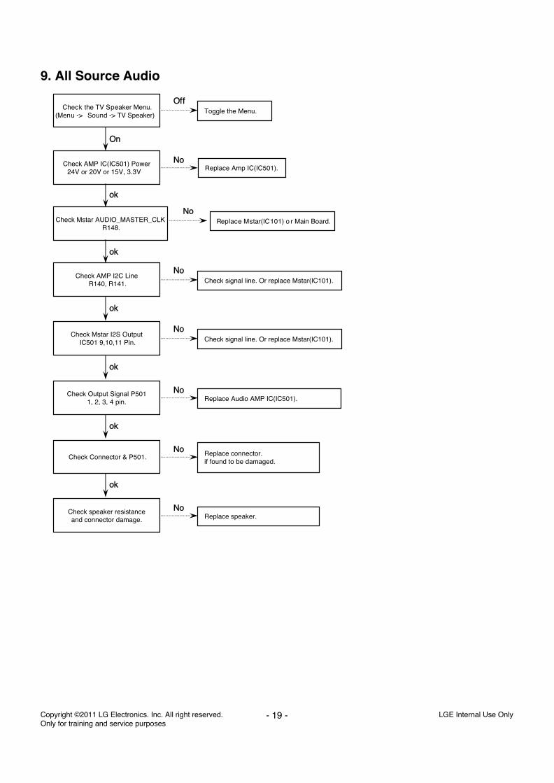
9. All Source Audio
Check the TV Speaker Menu.(Menu -> Sound -> TV Speaker)
On
ok
ok
Check Output Signal P5011, 2, 3, 4 pin. Replace Audio AMP IC(IC501).
ok
No
Check Connector & P501. Replace connector.if found to be damaged.
ok
No
Check speaker resistanceand connector damage. Replace speaker.
ok
No
OffToggle the Menu.
Check AMP IC(IC501) Power24V or 20V or 15V, 3.3V
NoReplace Amp IC(IC501).
Check Mstar I2S OutputIC501 9,10,11 Pin.
NoCheck signal line. Or replace Mstar(IC101).
Check Mstar AUDIO_MASTER_CLKR148.
NoReplace Mstar(IC101) o r Main Board.
ok
Check AMP I2C LineR140, R141.
NoCheck signal line. Or replace Mstar(IC101).
- 20 - LGE Internal Use OnlyCopyright ©2011 LG Electronics. Inc. All right reserved. Only for training and service purposes
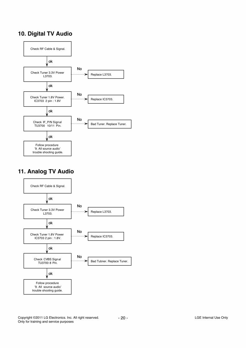
10. Digital TV Audio
Check RF Cable & Signal.
Follow procedure ’9. All source audio’
trouble shooting guide.
ok
Check Tuner 3.3V PowerL3703. Replace L3703.
Check Tuner 1.8V Power. IC3703 2 pin : 1.8V
Check IF_P/N SignalTU3700 10/11 Pin.
Replace IC3703.
ok
ok
ok
No
No
NoBad Tuner. Replace Tuner.
11. Analog TV Audio
Check RF Cable & Signal.
Follow procedure’9. All source audio’
trouble shooting guide.
ok
Check Tuner 3.3V PowerL3703.
Replace L3703.
Check Tuner 1.8V Power IC3703 2 pin : 1.8V.
Check CVBS SignalTU3700 8 Pin.
Replace IC3703.
ok
ok
ok
No
No
NoBad Tubner. Replace Tuner.
- 21 - LGE Internal Use OnlyCopyright ©2011 LG Electronics. Inc. All right reserved. Only for training and service purposes
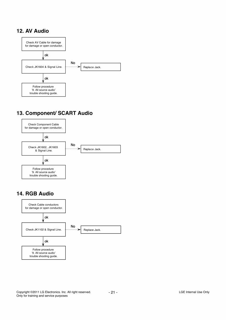
12. AV Audio
Check AV Cable for damagefor damage or open conductor.
Check JK1604 & Signal Line.
ok
ok
NoReplace Jack.
Follow procedure ’9. All source audio’
trouble shooting guide.
13. Component/ SCART Audio
Check Component Cablefor damage or open conductor.
Check JK1602, JK1603 & Signal Line.
ok
ok
NoReplace Jack.
Follow procedure ’9. All source audio’
trouble shooting guide.
14. RGB Audio
Check Cable conductorsfor damage or open conductor.
Check JK1102 & Signal Line.
ok
No
ok
Replace Jack.
Follow procedure ’9. All source audio’
trouble shooting guide.
LGE Internal Use OnlyCopyright ©2011 LG Electronics. Inc. All right reserved. Only for training and service purposes
- 22 -
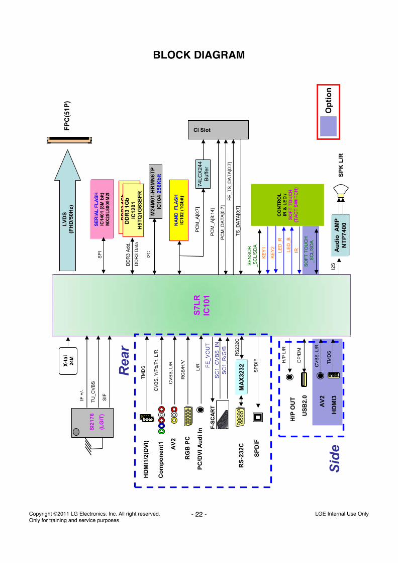
BLOCK DIAGRAM
RG
B P
C
SP
DIF
Co
mp
on
ent1
H/P
OU
T
HD
MI1
/2(D
VI)
SI2
17
6S
I21
76
(LG
IT)
(LG
IT)
PC
/DV
I A
ud
i In
RS
-232
C
IF +
/-
TU
_CV
BS
SIF
L/R
S7L
RIC
101
MA
X32
32M
AX
3232
SE
RIA
L F
LA
SH
IC14
01 (
8M b
it)
MX
25L
8005
M2I
SE
RIA
L F
LA
SH
IC14
01 (
8M b
it)
MX
25L
8005
M2I
LV
DS
(FH
D/5
0Hz)
Au
dio
A
MP
NT
P74
00
US
B2.
0D
P/D
M
SP
K L
/R
X-t
al
24M
FP
C(5
1P)
I2S
SP
DIF H
/P L
/R
CV
BS
, Y
/Pb/
Pr,
L/R
RG
B/H
/V
RS
232C
Rea
rT
MD
S
DD
R3
Add
.
DD
R3
Dat
a
SP
I
AV
2
Sid
e
NA
ND
F
LA
SH
IC10
2 (1
Gb
it)
PC
M_A
[0:7
]
TM
DS
HD
MI3
CV
BS
, L/
R
DD
R3
1Gb
IC1
20
2H
5TQ
1G
63
BF
R
DD
R3
1Gb
IC
12
01
H5T
Q1
G6
3B
FR
CO
NT
RO
LIR
& L
ED
/S
OF
T T
OU
CH
(TA
CT
SW
ITC
H)
SE
NS
OR
_SC
L/S
DA
LED
_R
KE
Y1
KE
Y2
IRLED
_B
SO
FT
TO
UC
H_S
CL/
SD
A
M24
M0
1-H
RM
N6T
PIC
10
4 2
56K
bit
I2C
AV
2C
VB
S,
L/R
Op
tio
n
F-S
CA
RT
SC
1_
CV
BS
_IN
SC
1_
R/G
/B
FE
_VO
UT
CI Slot
74
LCX
24
4B
uffe
r
TS
_DA
TA
[0:7
]
PC
M_D
AT
A[0
:7]
FE
_TS
_DA
TA
[0:7
]
PC
M_A
[8:1
4]
- 23 - LGE Internal Use OnlyCopyright LG Electronics. Inc. All right reserved. Only for training and service purposes
300
200
803
802
511
510
400
801
530
540
401
120
122
500
A2
A5
A21
LV1
402
910 90
0
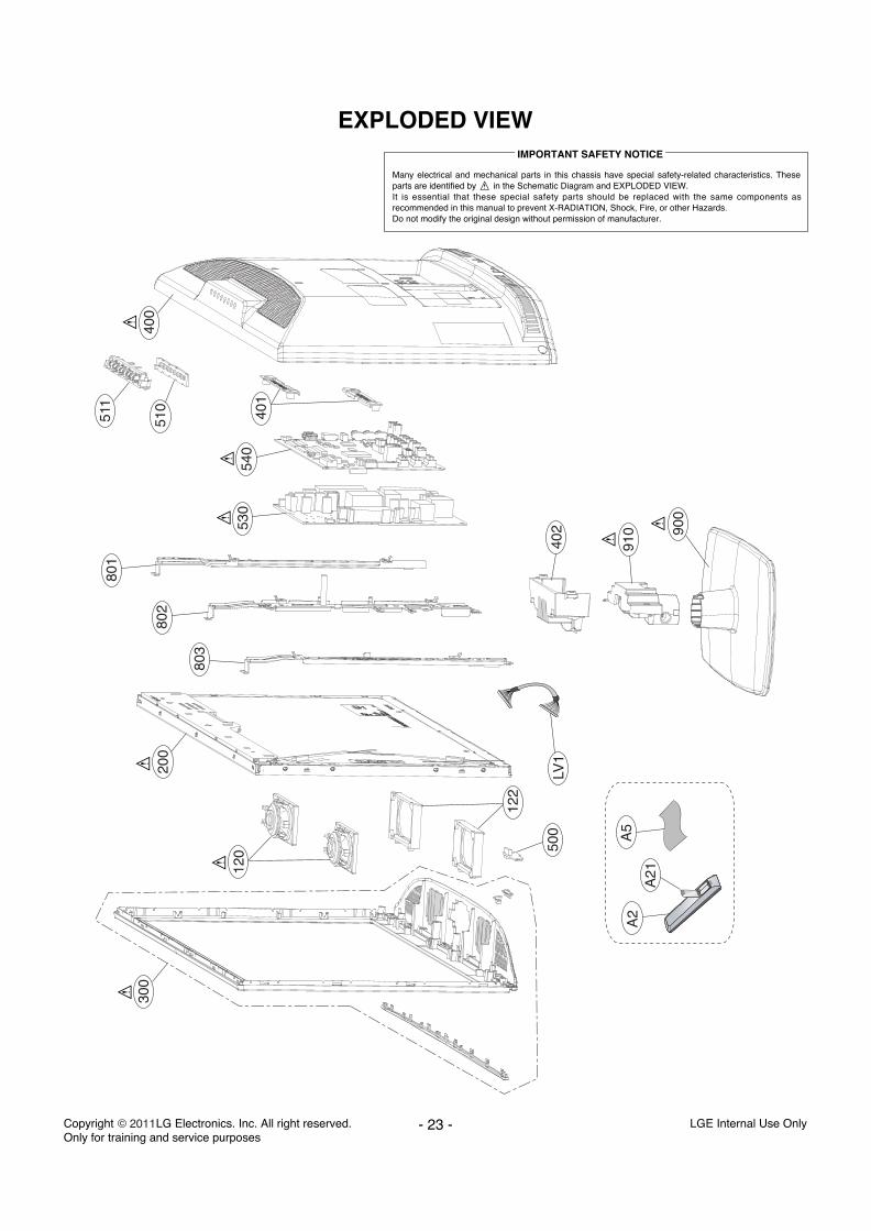
EXPLODED VIEW
Many electrical and mechanical parts in this chassis have special safety-related characteristics. Theseparts are identified by in the Schematic Diagram and EXPLODED VIEW. It is essential that these special safety parts should be replaced with the same components asrecommended in this manual to prevent X-RADIATION, Shock, Fire, or other Hazards. Do not modify the original design without permission of manufacturer.
IMPORTANT SAFETY NOTICE
THE SYMBOL MARK OF THIS SCHEMETIC DIAGRAM INCORPORATESSPECIAL FEATURES IMPORTANT FOR PROTECTION FROM X-RADIATION.FILRE AND ELECTRICAL SHOCK HAZARDS, WHEN SERVICING IF IS ESSENTIAL THAT ONLY MANUFATURES SPECFIED PARTS BE USED FORTHE CRITICAL COMPONENTS IN THE SYMBOL MARK OF THE SCHEMETIC.
FRC_DQU[5]
FRC_DQU[0]
FRC_DQL[0]
FRC_DQU[7]
FRC_A[0]
FRC_DQL[1]
FRC_DQU[4]
FRC_A[6]
FRC_A[10]
FRC_A[4]
FRC_DQL[5]
FRC_A[2]
FRC_A[8]
FRC_A[9]
FRC_A[7]
FRC_A[1]
FRC_A[5]
FRC_A[3]
FRC_DQU[6]
FRC_A[11]
FRC_DQL[2]
FRC_A[12]
FRC_DQU[2]
FRC_A[13]
FRC_DQL[4]
FRC_DQL[3]
FRC_DQU[1]
FRC_DQL[7]
FRC_DQU[3]
FRC_DQL[6]
SPI_DO
AVDD_LVDS_3.3V_M
+1.26V_FRC
PWM1
C1260.1uF
R112
10K
OPT
AVDD33_M
DVDD_DDR_1V_M
AVDD_PLL_M
R105
10K
R115
10K
OPT
C135
0.1uF
AVDD_PLL_M
SPI_SCLK
VDDC10_M
C1320.1uF
C1280.1uF
C1230.1uF
SCL_URSA
VDDC10_M
C10222uF10V
2D/3D_CTL
C1240.1uF
+3.3V_FRC
C1210.1uF
R106
10K
OPT
R113
10K
OPT
FRC_DQSL
URSA_MODEL_OPT_1
AVDD33_M
C1340.1uF
C1170.1uF
C1010.1uF
SPI_DI
C1100.1uF
R154 33
R104
10K
OPT
+1.5V_FRC_DDR_M
R147
1M
R107
10K
OPT
VDD33_M
C1050.1uF
DVDD_DDR_1V_M
SPI_SCLK
FRC_CASB
C1090.1uF
+3.3V_FRC
R102
10K
OPT
+3.3V_FRC
FRC_MCLK
SDA_URSA
R111
10K
OPT
SDA_DEBUG
C1290.1uF
FRC_DQL[0-7]
+3.3V_FRC
FRC_DQSU
URSA_MODEL_OPT_0
FRC_RASB
SCL_DEBUG
FRC_BA0
C1110.1uF
R13433
AVDD_PLL_M
URSA_MODEL_OPT_0FRC_DQSUB
FRC_WEB
PWM0
R101
10K
GPIO[1]
C1220.1uF
R114
10K
OPT
PWM0
C1190.1uF
R123
4.7K
R110
10K
OPT
SDA_DEBUG
GPIO[8]
FRC_ODT
R108
10K
C1130.1uF
+3.3V_FRC
VDD33_M
FRC_DQSLB
C1330.1uF
R109
10K
OPT
C1070.1uF
AVDD_LVDS_3.3V_M
VDDC10_M
URSA_MODEL_OPT_1
+3.3V_FRC
R118 22
URSA5_DEBUG
2D/3D_CTL
+1.26V_FRC
AVDD_LVDS_3.3V_M
FRC_DML
R153 33
SPI_CS
FRC_A[0-13]
C1300.1uF
SPI_DO
R116
10K
OPT
R103
10K
C1310.1uF
SPI_CS
C1250.1uF
+3.3V_FRC
C1160.1uF
FRC_BA1
URSA_MODEL_OPT_2
VDD33_M
FRC_DQU[0-7]
C1060.1uF
URSA_MODEL_OPT_2
C1150.1uF
C1180.1uF
FRC_MCLKB
SDA_URSA
FRC_DMU
FRC_CKE
R117 22
URSA5_DEBUG
R124
10K
PWM1
+3.3V_FRC
SCL_URSA
AVDD33_M
GPIO[1]
R13333
R126
3.3K
SCL_DEBUG
C10322uF10V
SPI_DI
GPIO[8]
FRC_BA2
C1040.22uF6.3V
C1080.22uF6.3V
C1200.22uF6.3V
R1190
URSA5_MP
R1200
URSA5_MP
C137
13pF
C136
13pF
C11422uF10V
FRC_DDR3_RESETB
FRC_RESETR162 33
I2C_SDAI2C_SCL
SCL_DEBUG
SCL_URSA_S
SCL_URSA_M SDA_URSA_M
SDA_URSA_S
SDA_DEBUG
R1210
URSA5_MP
R1220
URSA5_MP
SCL_URSA_M
R127 4.7K
SDA_URSA_M
R12933
+3.3V_FRC
R13033
R128 4.7K
SOFT_RST_R_S
C138
220pF50V
R148 4.7K
R150 1K
S_M_PIF_FC
S_M_PIF_FC_S
OP_SYNC_R_S
OP_SYNC_R
R151 1K
R149 1K
S_M_PIF_CLK
S_M_PIF_CS_S
SOFT_RST_R
S_M_PIF_CLK_S
R152 1K
S_M_PIF_CS
S_M_PIF_DA1_S
S_M_PIF_DA0
S_M_PIF_DA0_S
S_M_PIF_DA1
XTAL_M_OUT
+3.3V_FRC
L/DIM0_VS
L/DIM0_MOSI
L/DIM0_SCLK
LPLL_REFIN_S
+3.3V_FRC
LPLL_REFIN
R1614.7KOPT
R1584.7KOPT
LPLL_REFIN_S
R1604.7KOPT
R1594.7KOPT
RXBCLKN
RXB3P
RXB4P
RXB0P
RXB2P
RXB4N
RXB1P
RXB1N
RXB2N
RXB0N
RXB3N
RXBCLKP
RXA0N
RXA2P
RXA0P
RXA1P
RXA3N
RXACLKP
RXACLKN
RXA1N
RXA3P
RXA4N
RXA2N
RXA4P
URSA5_SLAVE_RESETR163 33
L/DIM1_MOSI
L/DIM1_SCLK
R135
200EXT_TERMI_200
R144
200EXT_TERMI_200
R146
200EXT_TERMI_200
R136
200EXT_TERMI_200
R143
200EXT_TERMI_200
R142
200EXT_TERMI_200
R141
200EXT_TERMI_200
R139
200EXT_TERMI_200
R137
200EXT_TERMI_200
R138
200EXT_TERMI_200
R145
200EXT_TERMI_200
R140
200EXT_TERMI_200
TXC1N
TXC3P
TXD0P
TXD1N
TXD0N
TXDCLKN
TXD4P
TXC0N
TXC0P
TXD1P
TXD2N
TXCCLKN
TXDCLKP
TXC3N
TXD2P
TXD4N
TXCCLKP
TXC1P
TXD3P
TXD3N
TXC2P
TXC2N
TXC4P
TXC4N
TXA3P
TXBCLKP
TXA2P
TXB0P
TXB1N
TXA4P
TXB0N
TXB3N
TXA4N
TXACLKN
TXB4P
TXB3P
TXA0P
TXA2N
TXA1N
TXB1P
TXA0N
TXA1P
TXB2N
TXBCLKN
TXB4N
TXACLKP
TXB2P
TXA3N
+1.5V_FRC_DDR_M+1.5V_FRC_DDR_M
SLAVE_GPIO[8]
R164
0
R165
0
R166
0
R167
0
R168
0
R131 3.9K OPT
R132 3.9K OPT
R16910
R170
10
R171
10
R125
10
R156
33
R157
33
R155
33
C1121uF10V
C1272.2uF10V
R136-*2 120
EXT_TERMI_120
R144-*3 150
EXT_TERMI_150
R135-*2 120
EXT_TERMI_120
R141-*2 120
EXT_TERMI_120
R145-*3 150
EXT_TERMI_150
R139-*2 120
EXT_TERMI_120R146-*1 100
EXT_TERMI_100R140-*3 150
EXT_TERMI_150
R143-*2 120
EXT_TERMI_120
R145-*2 120
EXT_TERMI_120
R141-*3 150
EXT_TERMI_150R136-*3 150
EXT_TERMI_150
R140-*2 120
EXT_TERMI_120
R146-*3 150
EXT_TERMI_150
R139-*1 100
EXT_TERMI_100
R137-*2 120
EXT_TERMI_120
R141-*1 100
EXT_TERMI_100
R139-*3 150
EXT_TERMI_150
R142-*2 120
EXT_TERMI_120
R144-*1 100
EXT_TERMI_100
R138-*1 100
EXT_TERMI_100
R138-*3 150
EXT_TERMI_150
R144-*2 120
EXT_TERMI_120
R142-*1 100
EXT_TERMI_100
R136-*1 100
EXT_TERMI_100
R143-*1 100
EXT_TERMI_100
R146-*2 120
EXT_TERMI_120
R135-*3 150
EXT_TERMI_150
R135-*1 100
EXT_TERMI_100
R137-*3 150
EXT_TERMI_150
R140-*1 100
EXT_TERMI_100
R138-*2 120
EXT_TERMI_120
R142-*3 150
EXT_TERMI_150
R137-*1 100
EXT_TERMI_100
R143-*3 150
EXT_TERMI_150
R145-*1 100
EXT_TERMI_100
P101
12507WR-04L
URSA5_DEBUG
1
2
3
4
5
L101CIC21J501NE
L103CIC21J501NE
L104CIC21J501NE
L106CIC21J501NE
L102CIC21J501NE
L105CIC21J501NE
SW5201JS2235S
URSA5_DEBUG_SWITCH
3
2
1
4
5
6
SW102JS2235S
URSA5_DEBUG_SWITCH
3
2
1
4
5
6
X101
24MHz
IC101
LGE7303C
DDR3_A0/DDR2_NCP14
DDR3_A1/DDR2_A8G15
DDR3_A2/DDR2_NCN14
DDR3_A3/DDR2_A10L15
DDR3_A4/DDR2_A2H15
DDR3_A5/DDR2_A3L14
DDR3_A6/DDR2_A4G14
DDR3_A7/DDR2_A5N12
DDR3_A8/DDR2_A6G13
DDR3_A9/DDR2_A9N13
DDR3_A10/DDR2_RASZH14
DDR3_A11/DDR2_A11F15
DDR3_A12/DDR2_A0H13
DDR3_A13/DDR2_A12P13
DDR3_BA0/DDR2_BA2M12
DDR3_BA1/DDR2_CASZH12
DDR3_BA2/DDR2_A1L13
DDR3_MCLK/DDR2_MCLKF16
DDR3_MCLKZ/DDR2_MCLKZF17
DDR3_CKE/DDR2_ODTJ13
DDR3_ODT/DDR2_CKEK12
DDR3_RASZDDR2_WEZL12
DDR3_CASZ/DDR2_BA1K13
DDR3_WEZ/DDR2_BA0K14
DDR3_RESET/DDR2_A7M14
DDR3_DQSL/DDR2_DQSLN16
DDR3_DQSU/DDR2_DQSUM17
DDR3_DQSBL/DDR2_DQSBLM16
DDR3_DQSBU/DDR2_DQSBUM15
DDR3_DQML/DDR2_DQU5J15
DDR3_DQMU/DDR2_DQU4R16
DDR3_DQL0/DDR2_DQU3R17
DDR3_DQL1/DDR2_DQL0H17
DDR3_DQL2/DDR2_DQL6R15
DDR3_DQL3/DDR2_DQL7J17
DDR3_DQL4/DDR2_DQL3T17
DDR3_DQL5/DDR2_DQL2H16
DDR3_DQL6/DDR2_DQL1T15
DDR3_DQL7/DDR2_DQL5G16
DDR3_DQU0/DDR2_DQU7K15
DDR3_DQU1/DDR2_DQMLN15
DDR3_DQU2/DDR2_DQU2K17
DDR3_DQU3/DDR2_DQU6P17
DDR3_DQU4/DDR2_NCL17
DDR3_DQU5/DDR2_DQU1P16
DDR3_DQU6/DDR2_DQU0K16
DDR3_DQU7/DDR2_DQMUP15
I2CM_SCLD14
I2CM_SDAD15
I2CS_SCLP1
I2CS_SDAP2
DDR3_NC/DDR2_A13F14
DDR3_NC/DDR2_DQL4T16
VSS_1
D6
VSS_2
D7
VSS_3
D8
VSS_4
D9
VSS_5
E6
VSS_6
E7
VSS_7
E8
VSS_8
E9
VSS_9
E10
VSS_10
E16
VSS_11
F3
VSS_12
F6
VSS_13
F7
VSS_14
F8
VSS_15
F9
VSS_16
G1
VSS_17
G2
VSS_18
G4
VSS_19
G5
VSS_20
G6
VSS_21
G7
VSS_22
G8
VSS_23
G9
VSS_24
G17
VSS_25
H1
VSS_26
H2
VSS_27
H4
VSS_28
H5
VSS_29
H6
VSS_30
H7
VSS_31
H8
VSS_32
H9
VSS_33
H10
VSS_34
H11
VSS_35
J4
VSS_36
J5
VSS_37
J6
VSS_38
J7
VSS_39
J8
VSS_40
J9
VSS_41
J10
VSS_42
J11
VSS_43
J12
VSS_44
J14
VSS_45
J16
VSS_46
K4
VSS_47
K5
VSS_48
K6
VSS_49
K7
VSS_50
K8
VSS_51
K11
VSS_52
L6
VSS_53
L7
VSS_54
L8
VSS_55
L11
VSS_56
L16
VSS_57
M6
VSS_58
M7
VSS_59
M8
VSS_60
M11
VSS_61
M13
VSS_62
N6
VSS_63
N7
VSS_64
N8
VSS_65
N17
VSS_66
P3
VSS_67
P4
VSS_68
P5
VSS_69
P6
VSS_70
P7
VSS_71
P12
VSS_72
U16
NC
L9
HW_RESET
J3
TESTPIN_1
D1
TESTPIN_2
D2
TESTPIN_3
D3
TESTPIN_4
E1
TESTPIN_5
E2
TESTPIN_6
E3
TESTPIN_7
F1
TESTPIN_8
F2
M0_SCLK
C17
M0_MOSI
D16
M1_SCLK
D17
M1_MOSI
E15
M2_SCLK
E14
M2_MOSI
E13
M3_SCLK
E12
M3_MOSI
F13
SPI_CK
T9
SPI_CZ
U10
SPI_DI
U9
SPI_DO
T10
TXA0P/GCLK6/BLUE[7]C8
TXA0N/GCLK5/BLUE[6]C9
TXA1P/OPT_N/LK3/BLUE[9]B8
TXA1N/FLK/BLUE[8]A8
TXA2P/GREEN[1]A7
TXA2N/OPT_P/LK2/GREEN[0]B7
TXACLKP/RLV0N/GREEN[3]C6
TXACLKN/RLV0P/GREEN[2]C7
TXA3P/RLV1N/GREEN[5]B6
TXA3N/RLV1P/GREEN[4]A6
TXA4P/RLV2N/GREEN[7]A5
TXA4N/RLV2P/GREEN[6]B5
TXB0P/RLV3N/GREEN[9]C4
TXB0N/RLV3P/GREEN[8]C5
TXB1P/RLVCLKN/RED[1]B4
TXB1N/RLVCLKP/RED[0]A4
TXB2P/RLV4P/RED[3]/EPI_A3PA3
TXB2N/RLV4N/RED[2]/EPI_A3NB3
TXBCLKP/RLV5N/RED[5]/EPI_A2PC2
TXBCLKN/RLV5P/RED[4]/EPI_A2NC3
TXB3P/RLV6N/RED[7]/EPI_A1PB2
TXB3N/RLV6P/RED[6]/EPI_A1N/A2
TXB4P/RLV7N/RED[9]/EPI_A0PC1
TXB4N/RLV7P/RED[8]/EPI_A0NB1
TXC0P/SOEC16
TXC0N/POLB17
TXC1P/GSP_RB16
TXC1N/GSP/VSTA16
TXC2P/GOE/GCLK1A15
TXC2N/GSC/GCLK3B15
TXCCLKP/LLV0NC14
TXCCLKN/LLV0PC15
TXC3P/LLV1NB14
TXC3N/LLV1PA14
TXC4P/LLV2NA13
TXC4N/LLV2PB13
TXD0P/LLV3NC12
TXD0N/LLV3PC13
TXD1P/LLVCLKNB12
TXD1N/LLVCLKPA12
TXD2P/LLV4N/EPI_B3PA11
TXD2N/LLV4P/EPI_B3NB11
TXDCLKP/LLV5N/BLUE[1]/EPI_B2PC10
TXDCLKN/LLV5P/BLUE[0]/EPI_B2NC11
TXD3P/LLV6N/BLUE[3]B10
TXD3N/LLV6P/BLUE[2]/EPI_B1NA10
TXD4P/LLV7N/BLUE[5]/EPI_B0PA9
TXD4N/LLV7P/BLUE[4]/EPI_B0NB9
MOD_GPIO0/VDD_ODD/HSYNCD10
MOD_GPIO1/VDD_EVEN/VSYNCD11
MOD_GPIO2/PWM13/GCLK4/LCKD12
MOD_GPIO3/PWM14/GCLK2/LDED13
PWM0/SCAN_BLK1U12
PWM1/SCAN_BLK2T12
LPLL_FBCLKG3
LPLL_OUTCLKE17
LPLL_REFINH3
AVDD_1
F4
AVDD_2
F5
AVDD_DDR_C_1
F10
AVDD_DDR_C_2
G10
AVDD_DDR_D_1
F11
AVDD_DDR_D_2
F12
AVDD_DDR_D_3
G11
AVDD_DDR_D_4
G12
AVDD_LVDS3.3V_1
D4
AVDD_LVDS3.3V_2
D5
AVDD_LVDS3.3V_3
E4
AVDD_LVDS3.3V_4
E5
AVDD_MPLL3.3V
M5
AVDD_LPLL3.3V
L4
AVDD_PLL3.3V
L5
AVDDL_MOD1.26V
K10
DVDD_DDR_1.26V
L10
DVDD_HF1.26V
K9
VD33_1
M4
VD33_2
N4
VD33_3
N5
VDDC_1.26V_1
M9
VDDC_1.26V_2
M10
VDDC_1.26V_3
N9
VDDC_1.26V_4
N10
VDDC_1.26V_5
N11
VDDC_1.26V_6
P10
VDDC_1.26V_7
P11
RXBCLKP
R2
RXBCLKN
R3
RXB0P
R4
RXB0N
R5
RXB1P
T4
RXB1N
U4
RXB2P
U3
RXB2N
T3
RXB3P
T2
RXB3N
U2
RXB4P
T1
RXB4N
R1
RXACLKP
R6
RXACLKN
R7
RXA0P
R8
RXA0N
R9
RXA1P
T8
RXA1N
U8
RXA2P
U7
RXA2N
T7
RXA3P
T6
RXA3N
U6
RXA4P
U5
RXA4N
T5
XTALO
J1
XTALI
J2
GPIO0/(UART_RX/S_PIF_DA0)
R13
GPIO1
P9
GPIO2/(S_PIF_CLK)
T13
GPIO3/(LTD_DA1)
U15
GPIO4/(LTD_DE)
R14
GPIO5/(LTD_CLK)
K2
GPIO6/(LTD_DA0)
K1
GPIO7(3D_FLAG)
T14
GPIO8
P8
GPIO9/(UART_TX/S_PIF_DA1)
U14
GPIO10/(S_PIF_FC)
U13
GPIO11/(S_PIF_CS)
R12
VSYNC_LIKE
E11
M_S_PIF_CLK
N2
M_S_PIF_CS
M1
M_S_PIF_DA0
N1
M_S_PIF_DA1
N3
M_S_PIF_FC
M3
S_M_PIF_CLK
L1
S_M_PIF_CS
M2
S_M_PIF_DA0
L2
S_M_PIF_DA1
K3
S_M_PIF_FC
L3
SOFT_RST_L
R10
SOFT_RST_R
T11
OP_SYNC_L
R11
OP_SYNC_R
U11
IC102-*1W25X40BVSSIG
URSA5_FLASH_WINBOND_4M
3WP
2DO[IO1]
4GND
1CS
5DI[IO0]
6CLK
7HOLD
8VCC
IC102MX25L4006EM2I-12G
URSA5_FLASH_MACRONIX_4M
3WP#
2SO/SIO1
4GND
1CS#
5SI/S
6SCL
7HOL
8VCC
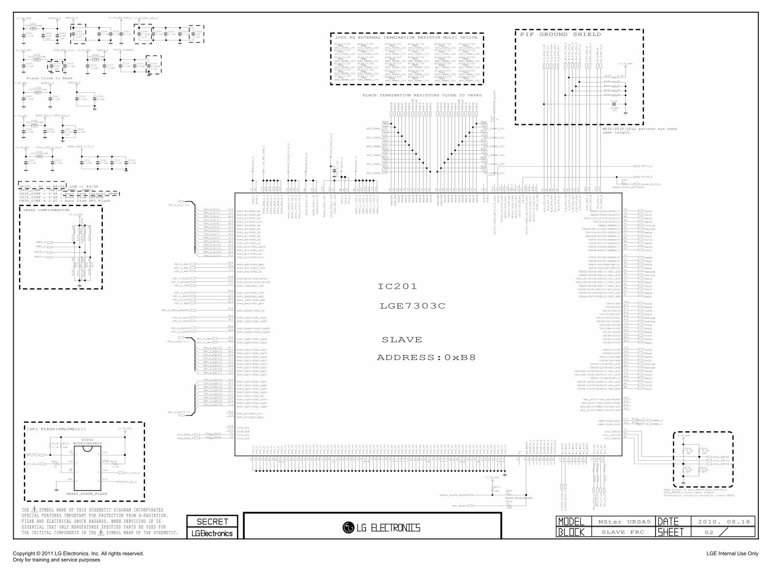
MASTER FRC
MStar URSA5
01
D13
GPIO1 : HI => B8/94, LOW => B4/98
LOW
MODEL_OPT_0
2D/3D_CTL
Debugging for URSA5
CHIP_CONF : GPIO8, PWM1, PWM0CHIP_CONF = 3’d5 : boot from interal SRAMCHIP_CONF = 3’d6 : boot from EEPROMCHIP_CONF = 3’d7 : boot from SPI Flash
PIN NO.
[SPI FLASH(4M&2Mbit)]
D11
D10
D12
RESERVED
MODEL_OPT_2
MODEL OPTION
(VDDP)
HIGHPIN NAME
RESERVED
PLACE TERMINATION RESISTORS CLOSE TO URSA5
MODEL_OPT_1
URSA5 CONFIGURATION
Place Close to Bead
URSA5 H/W OPTION
L/DIM_96BLOCK
MASTER
ADDRESS:0xB4
L/DIM_72BLOCK
PIF GROUND SHIELD
MPIF/SPIF/LPLL pattern are needsame length.
Keep traces of LPLL_REFIN,LPLL_OUTCLK_S,LPLL_FBCLK_S route equal length.Termination resistors should be closed URSA5
RESERVED RESERVED
RESERVED RESERVED
LVDS RX EXTERNAL TERMINATION RESISTOR MULTI OPTION
Copyright © 2011 LG Electronics. Inc. All rights reserved. Only for training and service purposes
LGE Internal Use Only
THE SYMBOL MARK OF THIS SCHEMETIC DIAGRAM INCORPORATESSPECIAL FEATURES IMPORTANT FOR PROTECTION FROM X-RADIATION.FILRE AND ELECTRICAL SHOCK HAZARDS, WHEN SERVICING IF IS ESSENTIAL THAT ONLY MANUFATURES SPECFIED PARTS BE USED FORTHE CRITICAL COMPONENTS IN THE SYMBOL MARK OF THE SCHEMETIC.
FRC_S_DQU[5]
FRC_S_DQU[0]
FRC_S_DQL[0]
FRC_S_DQU[7]
FRC_S_A[0]
FRC_S_DQL[1]
FRC_S_DQU[4]
FRC_S_A[6]
FRC_S_A[10]
FRC_S_A[4]
FRC_S_DQL[5]
FRC_S_A[2]
FRC_S_A[8]
FRC_S_A[9]
FRC_S_A[7]
FRC_S_A[1]
FRC_S_A[5]
FRC_S_A[3]
FRC_S_DQU[6]
FRC_S_A[11]
FRC_S_DQL[2]
FRC_S_A[12]
FRC_S_DQU[2]
FRC_S_A[13]
FRC_S_DQL[4]
FRC_S_DQL[3]
FRC_S_DQU[1]
FRC_S_DQL[7]
FRC_S_DQU[3]
FRC_S_DQL[6]
SPI_DO_S
AVDD_LVDS_3.3V_S
+1.26V_FRC
PWM1_S
C2260.1uF
AVDD33_S
DVDD_DDR_1V_S
AVDD_PLL_S
R205
10K
C235
0.1uF
AVDD_PLL_S
SPI_SCLK_S
VDDC10_S
C2320.1uF
C2280.1uF
C2230.1uF
SCL_URSA_S
VDDC10_S
C20222uF10V
C2240.1uF
+3.3V_FRC
C2210.1uF
R206
10K
OPT
FRC_S_DQSL
AVDD33_S
C2340.1uF
C2170.1uF
C2010.1uF
SPI_DI_S
C2100.1uF
R235 33
R204
10K
SLAVE_BOOT_SRAM
+1.5V_FRC_DDR_S
R207
10K
VDD33_S
C2050.1uF
DVDD_DDR_1V_S
SPI_SCLK_S
R211
33
FRC_S_CASB
C2090.1uF
+3.3V_FRC
R202
10K
OPT
FRC_S_MCLK
C2290.1uF
FRC_S_DQL[0-7]
+3.3V_FRC
FRC_S_DQSU
L201CIC21J501NE
FRC_S_RASB
FRC_S_BA0
C2110.1uF
R21433
AVDD_PLL_S
FRC_S_DQSUB
FRC_S_WEB
PWM0_S
L203CIC21J501NE
R201
10K
GPIO1_S
C2220.1uF
PWM0_S
C2190.1uF
R209
4.7K
GPIO8_S
L204CIC21J501NE
+1.5V_FRC_DDR_S
FRC_S_ODT
R208
10K
OPT
C2130.1uF
VDD33_S
FRC_S_DQSLB
C2330.1uF
C2070.1uF
AVDD_LVDS_3.3V_S
L206CIC21J501NE
VDDC10_S
+3.3V_FRC
L202CIC21J501NE
+1.26V_FRC
AVDD_LVDS_3.3V_S
FRC_S_DML
R234 33
SPI_CS_S
L205CIC21J501NE
FRC_S_A[0-13]
C2300.1uF
SPI_DO_S
R203
10K
SLAVE_BOOT_FLASH
C2310.1uF
SPI_CS_S
C2250.1uF
+1.5V_FRC_DDR_S
+3.3V_FRC
C2160.1uF
FRC_S_BA1
VDD33_S
FRC_S_DQU[0-7]
C2060.1uF
C2150.1uF
C2180.1uF
FRC_S_MCLKB
SDA_URSA_S
FRC_S_DMU
FRC_S_CKE
R210
10K
PWM1_S
+3.3V_FRC
AVDD33_S
GPIO1_S
R21333
R212
3.3K
C20322uF10V
SPI_DI_S
GPIO8_S
FRC_S_BA2
C2040.22uF6.3V
C2080.22uF6.3V
C2200.22uF6.3V
C21422uF10V
FRC_S_DDR3_RESETB
IC202W25X20BVSNIG
URSA5_SLAVE_FLASH
3WP
2DO
4GND
1CS
5DIO
6CLK
7HOLD
8VCC
URSA5_SLAVE_RESET
IC201
LGE7303C
DDR3_A0/DDR2_NCP14
DDR3_A1/DDR2_A8G15
DDR3_A2/DDR2_NCN14
DDR3_A3/DDR2_A10L15
DDR3_A4/DDR2_A2H15
DDR3_A5/DDR2_A3L14
DDR3_A6/DDR2_A4G14
DDR3_A7/DDR2_A5N12
DDR3_A8/DDR2_A6G13
DDR3_A9/DDR2_A9N13
DDR3_A10/DDR2_RASZH14
DDR3_A11/DDR2_A11F15
DDR3_A12/DDR2_A0H13
DDR3_A13/DDR2_A12P13
DDR3_BA0/DDR2_BA2M12
DDR3_BA1/DDR2_CASZH12
DDR3_BA2/DDR2_A1L13
DDR3_MCLK/DDR2_MCLKF16
DDR3_MCLKZ/DDR2_MCLKZF17
DDR3_CKE/DDR2_ODTJ13
DDR3_ODT/DDR2_CKEK12
DDR3_RASZDDR2_WEZL12
DDR3_CASZ/DDR2_BA1K13
DDR3_WEZ/DDR2_BA0K14
DDR3_RESET/DDR2_A7M14
DDR3_DQSL/DDR2_DQSLN16
DDR3_DQSU/DDR2_DQSUM17
DDR3_DQSBL/DDR2_DQSBLM16
DDR3_DQSBU/DDR2_DQSBUM15
DDR3_DQML/DDR2_DQU5J15
DDR3_DQMU/DDR2_DQU4R16
DDR3_DQL0/DDR2_DQU3R17
DDR3_DQL1/DDR2_DQL0H17
DDR3_DQL2/DDR2_DQL6R15
DDR3_DQL3/DDR2_DQL7J17
DDR3_DQL4/DDR2_DQL3T17
DDR3_DQL5/DDR2_DQL2H16
DDR3_DQL6/DDR2_DQL1T15
DDR3_DQL7/DDR2_DQL5G16
DDR3_DQU0/DDR2_DQU7K15
DDR3_DQU1/DDR2_DQMLN15
DDR3_DQU2/DDR2_DQU2K17
DDR3_DQU3/DDR2_DQU6P17
DDR3_DQU4/DDR2_NCL17
DDR3_DQU5/DDR2_DQU1P16
DDR3_DQU6/DDR2_DQU0K16
DDR3_DQU7/DDR2_DQMUP15
I2CM_SCLD14
I2CM_SDAD15
I2CS_SCLP1
I2CS_SDAP2
DDR3_NC/DDR2_A13F14
DDR3_NC/DDR2_DQL4T16
VSS_1
D6
VSS_2
D7
VSS_3
D8
VSS_4
D9
VSS_5
E6
VSS_6
E7
VSS_7
E8
VSS_8
E9
VSS_9
E10
VSS_10
E16
VSS_11
F3
VSS_12
F6
VSS_13
F7
VSS_14
F8
VSS_15
F9
VSS_16
G1
VSS_17
G2
VSS_18
G4
VSS_19
G5
VSS_20
G6
VSS_21
G7
VSS_22
G8
VSS_23
G9
VSS_24
G17
VSS_25
H1
VSS_26
H2
VSS_27
H4
VSS_28
H5
VSS_29
H6
VSS_30
H7
VSS_31
H8
VSS_32
H9
VSS_33
H10
VSS_34
H11
VSS_35
J4
VSS_36
J5
VSS_37
J6
VSS_38
J7
VSS_39
J8
VSS_40
J9
VSS_41
J10
VSS_42
J11
VSS_43
J12
VSS_44
J14
VSS_45
J16
VSS_46
K4
VSS_47
K5
VSS_48
K6
VSS_49
K7
VSS_50
K8
VSS_51
K11
VSS_52
L6
VSS_53
L7
VSS_54
L8
VSS_55
L11
VSS_56
L16
VSS_57
M6
VSS_58
M7
VSS_59
M8
VSS_60
M11
VSS_61
M13
VSS_62
N6
VSS_63
N7
VSS_64
N8
VSS_65
N17
VSS_66
P3
VSS_67
P4
VSS_68
P5
VSS_69
P6
VSS_70
P7
VSS_71
P12
VSS_72
U16
NC
L9
HW_RESET
J3
TESTPIN_1
D1
TESTPIN_2
D2
TESTPIN_3
D3
TESTPIN_4
E1
TESTPIN_5
E2
TESTPIN_6
E3
TESTPIN_7
F1
TESTPIN_8
F2
M0_SCLK
C17
M0_MOSI
D16
M1_SCLK
D17
M1_MOSI
E15
M2_SCLK
E14
M2_MOSI
E13
M3_SCLK
E12
M3_MOSI
F13
SPI_CK
T9
SPI_CZ
U10
SPI_DI
U9
SPI_DO
T10
TXA0P/GCLK6/BLUE[7]C8
TXA0N/GCLK5/BLUE[6]C9
TXA1P/OPT_N/LK3/BLUE[9]B8
TXA1N/FLK/BLUE[8]A8
TXA2P/GREEN[1]A7
TXA2N/OPT_P/LK2/GREEN[0]B7
TXACLKP/RLV0N/GREEN[3]C6
TXACLKN/RLV0P/GREEN[2]C7
TXA3P/RLV1N/GREEN[5]B6
TXA3N/RLV1P/GREEN[4]A6
TXA4P/RLV2N/GREEN[7]A5
TXA4N/RLV2P/GREEN[6]B5
TXB0P/RLV3N/GREEN[9]C4
TXB0N/RLV3P/GREEN[8]C5
TXB1P/RLVCLKN/RED[1]B4
TXB1N/RLVCLKP/RED[0]A4
TXB2P/RLV4P/RED[3]/EPI_A3PA3
TXB2N/RLV4N/RED[2]/EPI_A3NB3
TXBCLKP/RLV5N/RED[5]/EPI_A2PC2
TXBCLKN/RLV5P/RED[4]/EPI_A2NC3
TXB3P/RLV6N/RED[7]/EPI_A1PB2
TXB3N/RLV6P/RED[6]/EPI_A1N/A2
TXB4P/RLV7N/RED[9]/EPI_A0PC1
TXB4N/RLV7P/RED[8]/EPI_A0NB1
TXC0P/SOEC16
TXC0N/POLB17
TXC1P/GSP_RB16
TXC1N/GSP/VSTA16
TXC2P/GOE/GCLK1A15
TXC2N/GSC/GCLK3B15
TXCCLKP/LLV0NC14
TXCCLKN/LLV0PC15
TXC3P/LLV1NB14
TXC3N/LLV1PA14
TXC4P/LLV2NA13
TXC4N/LLV2PB13
TXD0P/LLV3NC12
TXD0N/LLV3PC13
TXD1P/LLVCLKNB12
TXD1N/LLVCLKPA12
TXD2P/LLV4N/EPI_B3PA11
TXD2N/LLV4P/EPI_B3NB11
TXDCLKP/LLV5N/BLUE[1]/EPI_B2PC10
TXDCLKN/LLV5P/BLUE[0]/EPI_B2NC11
TXD3P/LLV6N/BLUE[3]B10
TXD3N/LLV6P/BLUE[2]/EPI_B1NA10
TXD4P/LLV7N/BLUE[5]/EPI_B0PA9
TXD4N/LLV7P/BLUE[4]/EPI_B0NB9
MOD_GPIO0/VDD_ODD/HSYNCD10
MOD_GPIO1/VDD_EVEN/VSYNCD11
MOD_GPIO2/PWM13/GCLK4/LCKD12
MOD_GPIO3/PWM14/GCLK2/LDED13
PWM0/SCAN_BLK1U12
PWM1/SCAN_BLK2T12
LPLL_FBCLKG3
LPLL_OUTCLKE17
LPLL_REFINH3
AVDD_1
F4
AVDD_2
F5
AVDD_DDR_C_1
F10
AVDD_DDR_C_2
G10
AVDD_DDR_D_1
F11
AVDD_DDR_D_2
F12
AVDD_DDR_D_3
G11
AVDD_DDR_D_4
G12
AVDD_LVDS3.3V_1
D4
AVDD_LVDS3.3V_2
D5
AVDD_LVDS3.3V_3
E4
AVDD_LVDS3.3V_4
E5
AVDD_MPLL3.3V
M5
AVDD_LPLL3.3V
L4
AVDD_PLL3.3V
L5
AVDDL_MOD1.26V
K10
DVDD_DDR_1.26V
L10
DVDD_HF1.26V
K9
VD33_1
M4
VD33_2
N4
VD33_3
N5
VDDC_1.26V_1
M9
VDDC_1.26V_2
M10
VDDC_1.26V_3
N9
VDDC_1.26V_4
N10
VDDC_1.26V_5
N11
VDDC_1.26V_6
P10
VDDC_1.26V_7
P11
RXBCLKP
R2
RXBCLKN
R3
RXB0P
R4
RXB0N
R5
RXB1P
T4
RXB1N
U4
RXB2P
U3
RXB2N
T3
RXB3P
T2
RXB3N
U2
RXB4P
T1
RXB4N
R1
RXACLKP
R6
RXACLKN
R7
RXA0P
R8
RXA0N
R9
RXA1P
T8
RXA1N
U8
RXA2P
U7
RXA2N
T7
RXA3P
T6
RXA3N
U6
RXA4P
U5
RXA4N
T5
XTALO
J1
XTALI
J2
GPIO0/(UART_RX/S_PIF_DA0)
R13
GPIO1
P9
GPIO2/(S_PIF_CLK)
T13
GPIO3/(LTD_DA1)
U15
GPIO4/(LTD_DE)
R14
GPIO5/(LTD_CLK)
K2
GPIO6/(LTD_DA0)
K1
GPIO7(3D_FLAG)
T14
GPIO8
P8
GPIO9/(UART_TX/S_PIF_DA1)
U14
GPIO10/(S_PIF_FC)
U13
GPIO11/(S_PIF_CS)
R12
VSYNC_LIKE
E11
M_S_PIF_CLK
N2
M_S_PIF_CS
M1
M_S_PIF_DA0
N1
M_S_PIF_DA1
N3
M_S_PIF_FC
M3
S_M_PIF_CLK
L1
S_M_PIF_CS
M2
S_M_PIF_DA0
L2
S_M_PIF_DA1
K3
S_M_PIF_FC
L3
SOFT_RST_L
R10
SOFT_RST_R
T11
OP_SYNC_L
R11
OP_SYNC_R
U11
C238
220pF50V
R232 1K
S_M_PIF_DA1_S
OP_SYNC_R
S_M_PIF_CS
SOFT_RST_R
SOFT_RST_R_S
R230 1K
OP_SYNC_R_S
S_M_PIF_DA0_S
R231 1K
R229 4.7K
R233 1K
S_M_PIF_CS_S
S_M_PIF_DA0
S_M_PIF_FC
S_M_PIF_CLK_S
S_M_PIF_FC_S
S_M_PIF_CLK
S_M_PIF_DA1
XTAL_M_OUT
+3.3V_FRC
R2424.7KOPT
R2434.7KOPT
+3.3V_FRC
LPLL_REFIN_S
R2444.7KOPT
LPLL_REFIN
LPLL_REFIN
R2414.7KOPT
RXB0N
RXA4P
RXB2P
RXA2P
RXACLKN
RXB0P
RXB1P
RXA0P
RXA1N
RXB3N
RXBCLKP
RXA3P
RXBCLKN
RXB1N
RXA1P
RXB3P
RXB4N
RXA2N
RXA3N
RXB2N
RXB4P
RXA0N
RXA4N
RXACLKP
R226
200EXT_TERMI_200
R218
200EXT_TERMI_200
R215
200EXT_TERMI_200
R221
200EXT_TERMI_200
R225
200EXT_TERMI_200
R219
200EXT_TERMI_200
R224
200EXT_TERMI_200
R223
200EXT_TERMI_200
R216
200EXT_TERMI_200
R220
200EXT_TERMI_200
R222
200EXT_TERMI_200
R217
200EXT_TERMI_200
TXFCLKP
TXF0P
TXH0P
TXF2N
TXE0P
TXF0N
TXG2P
TXF1N
TXH4N
TXG0P
TXE2N
TXF1P
TXF3N
TXF3P
TXHCLKN
TXH3N
TXE4N
TXH2P
TXHCLKP
TXG4N
TXH0N
TXH2N
TXE4P
TXG0N
TXH1P
TXGCLKP
TXE3P
TXG4P
TXE1P
TXH4P
TXE3N
TXH3P
TXG1P
TXFCLKN
TXE1N
TXE2P
TXF4N
TXG3P
TXG3N
TXH1N
TXGCLKN
TXG1N
TXE0N
TXF4P
TXECLKN
TXG2N
TXF2P
TXECLKP
FRC_RESET
R237
10K
+3.3V_FRC
SLAVE_GPIO[8]
R2470
URSA5_SLAVE_WATCHDOG
L/DIM0_MOSI_S
L/DIM0_SCLK_S
R24633
OPT
R24533
RESET_FROM_MASTER
R239
33
R236
33
R238
33
R228
0
C2121uF10V
C2272.2uF10V
R216-*1 100
EXT_TERMI_100
R226-*1 100
EXT_TERMI_100
R219-*1 100
EXT_TERMI_100R220-*1 100
EXT_TERMI_100
R223-*1 100
EXT_TERMI_100
R215-*1 100
EXT_TERMI_100
R221-*1 100
EXT_TERMI_100
R218-*1 100
EXT_TERMI_100
R222-*1 100
EXT_TERMI_100
R225-*1 100
EXT_TERMI_100
R217-*1 100
EXT_TERMI_100R224-*1 100
EXT_TERMI_100
R220-*2 120
EXT_TERMI_120
R220-*3 150
EXT_TERMI_150
R221-*3 150
EXT_TERMI_150
R215-*3 150
EXT_TERMI_150
R219-*2 120
EXT_TERMI_120
R219-*3 150
EXT_TERMI_150
R222-*2 120
EXT_TERMI_120
R225-*2 120
EXT_TERMI_120
R218-*3 150
EXT_TERMI_150
R218-*2 120
EXT_TERMI_120
R223-*2 120
EXT_TERMI_120R224-*3 150
EXT_TERMI_150
R222-*3 150
EXT_TERMI_150
R215-*2 120
EXT_TERMI_120
R226-*3 150
EXT_TERMI_150
R223-*3 150
EXT_TERMI_150
R217-*3 150
EXT_TERMI_150
R221-*2 120
EXT_TERMI_120
R217-*2 120
EXT_TERMI_120
R216-*2 120
EXT_TERMI_120
R226-*2 120
EXT_TERMI_120
R224-*2 120
EXT_TERMI_120
R216-*3 150
EXT_TERMI_150
R225-*3 150
EXT_TERMI_150
SLAVE FRC
MStar URSA5
02
2010. 08.18
GPIO1 : HI => B8/94, LOW => B4/98CHIP_CONF : GPIO8, PWM1, PWM0CHIP_CONF = 3’d5 : boot from interal SRAMCHIP_CONF = 3’d6 : boot from EEPROMCHIP_CONF = 3’d7 : boot from SPI Flash
[SPI FLASH(4M&2Mbit)]
(VDDP)
PLACE TERMINATION RESISTORS CLOSE TO URSA5
URSA5 CONFIGURATION
Place Close to Bead
SLAVE
ADDRESS:0xB8
PIF GROUND SHIELD
MPIF/SPIF/LPLL pattern are needsame length.
Keep traces of LPLL_REFIN,LPLL_OUTCLK_S,LPLL_FBCLK_S route equal length.
Termination resistors should be closed URSA5
LVDS RX EXTERNAL TERMINATION RESISTOR MULTI OPTION
Copyright © 2011 LG Electronics. Inc. All rights reserved. Only for training and service purposes
LGE Internal Use Only
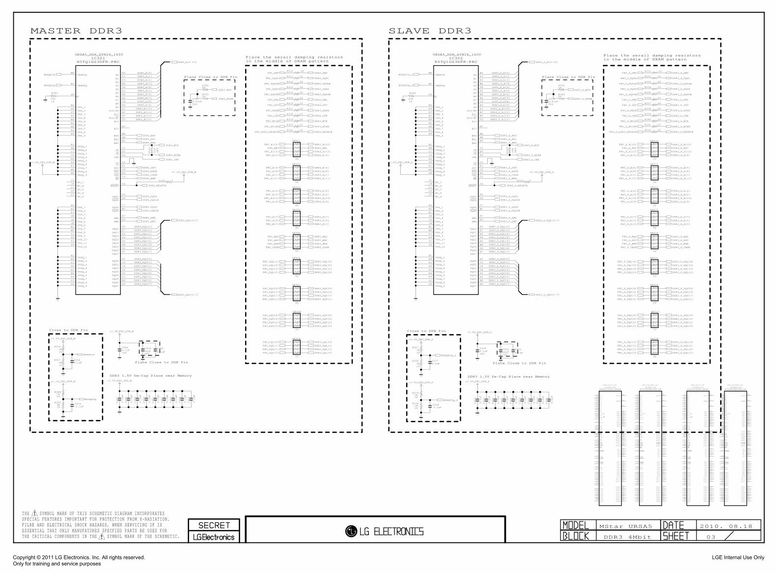
THE SYMBOL MARK OF THIS SCHEMETIC DIAGRAM INCORPORATESSPECIAL FEATURES IMPORTANT FOR PROTECTION FROM X-RADIATION.FILRE AND ELECTRICAL SHOCK HAZARDS, WHEN SERVICING IF IS ESSENTIAL THAT ONLY MANUFATURES SPECFIED PARTS BE USED FORTHE CRITICAL COMPONENTS IN THE SYMBOL MARK OF THE SCHEMETIC.
DDR3_DQU[1]
DDR3_DQL[1]
DDR3_DQL[3]
DDR3_A[8]
DDR3_A[3]
DDR3_A[12]
DDR3_A[13]
DDR3_A[5]
DDR3_DQL[7]
DDR3_A[7]
DDR3_DQL[0]
DDR3_DQL[6]
DDR3_A[11]
DDR3_A[2]
DDR3_DQU[0]
DDR3_A[10]
DDR3_DQU[2]
DDR3_A[9]
DDR3_DQL[4]
DDR3_DQU[6]
DDR3_A[0]
DDR3_A[4]
DDR3_DQL[5]
DDR3_A[6]
DDR3_DQU[4]
DDR3_A[1]
DDR3_DQU[3]
DDR3_DQL[2]
DDR3_DQU[7]
DDR3_DQU[5]
DDR3_S_A[3]
DDR3_S_DQU[6]
DDR3_S_A[11]
DDR3_S_A[8]
DDR3_S_DQL[6]
DDR3_S_DQL[3]
DDR3_S_A[13]
DDR3_S_DQL[1]
DDR3_S_A[6]
DDR3_S_A[1]
DDR3_S_DQL[5]
DDR3_S_DQU[1]
DDR3_S_A[7]
DDR3_S_DQL[4]
DDR3_S_A[12]
DDR3_S_DQU[4]
DDR3_S_A[9]
DDR3_S_DQL[7]
DDR3_S_A[5]
DDR3_S_DQU[2]
DDR3_S_DQU[5]
DDR3_S_DQL[0]
DDR3_S_A[10]
DDR3_S_DQU[0]
DDR3_S_A[2]
DDR3_S_DQU[7]
DDR3_S_A[4]
DDR3_S_A[0]
DDR3_S_DQL[2]
DDR3_S_DQU[3]
FRC_DQL[4]
+1.5V_FRC_DDR_M
FRC_A[10]
FRC_DQSLR311 22
MVREFDQ
FRC_DQSUB
DDR3_DQSLB
DDR3_BA0
DDR3_DQSLB
DDR3_ODT
DDR3_A[10]
FRC_DQL[3]
R30556
R315 22
FRC_DQL[5]
DDR3_CKE
FRC_CASB
FRC_DQU[3]
DDR3_DMU
FRC_DQU[6]
R320 22
FRC_BA2
FRC_DQU[7]
FRC_CKE
C313
0.1uF
AR306
22
DDR3_DQL[6]
FRC_DQL[7]
FRC_DQL[6]
C315
0.1uF
+1.5V_FRC_DDR_M
DDR3_MCK
+1.5V_FRC_DDR_M
DDR3_BA0
FRC_DQL[0]
DDR3_A[6]
DDR3_DQSUB
DDR3_A[2]
AR304
22
DDR3_MCK
DDR3_DQL[0-7]
DDR3_DQSL
DDR3_DQU[2]
AR302
22
DDR3_BA2
DDR3_DQL[0]
FRC_DML
DDR3_DML
DDR3_ODT
DDR3_A[8]
FRC_A[11]
FRC_A[9]
FRC_DQSLB
R3091K1%
DDR3_BA1
DDR3_DQU[0-7]
DDR3_BA1
DDR3_A[9]
DDR3_DQL[4]
DDR3_WEB
DDR3_A[0-13]
FRC_ODT
DDR3_DML
R3071K1%
FRC_BA1
R3061K1%
DDR3_DQU[7]
MVREFDQ
C314
0.1uF
DDR3_DQU[1]
DDR3_RASB
DDR3_DQL[5]
FRC_A[12]
DDR3_DQL[3]
DDR3_DQU[5]
+1.5V_FRC_DDR_M
AR307
22
FRC_A[4]
R319 22
FRC_A[13]
DDR3_A[1]
AR305
22
DDR3_DMU
FRC_DQU[2]
FRC_DQU[0]
DDR3_RASB
DDR3_CASB
FRC_A[8]
DDR3_A[11]
+1.5V_FRC_DDR_M
DDR3_DQSUB
R30456
FRC_A[2]
C306
0.1uF
DDR3_A[12]
DDR3_DQU[6]
DDR3_MCK
DDR3_DQU[0]
DDR3_CASB
FRC_MCLK
FRC_DQU[5]
DDR3_WEB
R312 22
+1.5V_FRC_DDR_M AR309
22
FRC_A[5]
DDR3_A[0]
DDR3_DQU[3]
R316 22
C307
0.1uF
R313 22
FRC_WEB
DDR3_MCKB
C309
0.1uF
R310 22
AR303
22
DDR3_MCKB
FRC_DQU[1]
DDR3_MCKB
DDR3_DQSU
C310
0.1uF
FRC_A[7]
FRC_RASB
FRC_DMU
FRC_A[1]
MVREFCA
AR301
22
C30522uF10V DDR3_DQL[7]
DDR3_A[3]
FRC_DQSU
DDR3_A[13]
C3030.1uF
C311
0.1uF
FRC_BA0
DDR3_BA2
DDR3_CKE
MVREFCA
FRC_A[6]
R317 22
C3040.1uF16V
FRC_DQL[2]
AR308
22
C308
0.1uF
R318 22
DDR3_DQU[4]
C3020.1uF
R3081K1%
DDR3_DQL[1]
C312
0.1uF
FRC_MCLKB
DDR3_A[5]
DDR3_DQL[2]
R314 22
FRC_DQL[1]
DDR3_DQSU
DDR3_DQSL
FRC_A[0]
DDR3_A[7]
FRC_A[3]
DDR3_A[4]
R302
150
OPT
FRC_DQU[4]
R301
2401%
H5TQ1G63DFR-PBCIC301
URSA5_DDR_HYNIX_1600
A0N3
A1P7
A2P3
A3N2
A4P8
A5P2
A6R8
A7R2
A8T8
A9R3
A10/APL7
A11R7
A12/BCN7
A13T3
A15M7
BA0M2
BA1N8
BA2M3
CKJ7
CKK7
CKEK9
CSL2
ODTK1
RASJ3
CASK3
WEL3
RESETT2
DQSLF3
DQSLG3
DQSUC7
DQSUB7
DMLE7
DMUD3
DQL0E3
DQL1F7
DQL2F2
DQL3F8
DQL4H3
DQL5H8
DQL6G2
DQL7H7
DQU0D7
DQU1C3
DQU2C8
DQU3C2
DQU4A7
DQU5A2
DQU6B8
DQU7A3
VREFCAM8
VREFDQH1
ZQL8
VDD_1B2
VDD_2D9
VDD_3G7
VDD_4K2
VDD_5K8
VDD_6N1
VDD_7N9
VDD_8R1
VDD_9R9
VDDQ_1A1
VDDQ_2A8
VDDQ_3C1
VDDQ_4C9
VDDQ_5D2
VDDQ_6E9
VDDQ_7F1
VDDQ_8H2
VDDQ_9H9
NC_1J1
NC_2J9
NC_3L1
NC_4L9
NC_6T7
VSS_1A9
VSS_2B3
VSS_3E1
VSS_4G8
VSS_5J2
VSS_6J8
VSS_7M1
VSS_8M9
VSS_9P1
VSS_10P9
VSS_11T1
VSS_12T9
VSSQ_1B1
VSSQ_2B9
VSSQ_3D1
VSSQ_4D8
VSSQ_5E2
VSSQ_6E8
VSSQ_7F9
VSSQ_8G1
VSSQ_9G9
R303 0
DDR3_RESETB
FRC_DDR3_RESETB DDR3_RESETBR321 22
DDR3_S_A[9]
DDR3_S_A[7]
R340 22
R334 22
+1.5V_FRC_DDR_S
FRC_S_DQL[7]
DDR3_S_DML
DDR3_S_RASB
DDR3_S_BA2
DDR3_S_RESETB
FRC_S_DQL[0]
R332 22
DDR3_S_A[3]
R338 22
DDR3_S_DQSUB
DDR3_S_CASB
FRC_S_MCLKB
FRC_S_A[1]
DDR3_S_DQSU
DDR3_S_DQSLB
FRC_S_CASB
DDR3_S_ODT
R336 22
DDR3_S_MCK
AR310
22
FRC_S_BA1
DDR3_S_DQSUB
FRC_S_DQSUB
DDR3_S_MCKB
DDR3_S_ODT
DDR3_S_MCK
FRC_S_A[0]
FRC_S_A[4]
DDR3_S_BA1
DDR3_S_DQU[1]
DDR3_S_DQU[5]
FRC_S_BA0 DDR3_S_BA0
FRC_S_ODT
AR312
22
FRC_S_DQSL
DDR3_S_DQL[7]
R337 22
FRC_S_A[6]
R322
2401%
FRC_S_A[7]
R333 22
DDR3_S_CKE
FRC_S_CKE
AR318
22
FRC_S_DQSLB
FRC_S_DMU
DDR3_S_DQU[7]
DDR3_S_RASB
FRC_S_A[2]
DDR3_S_DQU[6]
R341 22
DDR3_S_MCKB
MVREFCA_S
DDR3_S_DQU[4]
DDR3_S_DML
MVREFDQ_S
FRC_S_WEB
DDR3_S_DQU[0-7]
DDR3_S_DQSLB
R323
150
OPT
FRC_S_DQL[4]
DDR3_S_A[0-13]
DDR3_S_DQL[3]
AR314
22
AR311
22
R342 22
DDR3_S_DQSL
DDR3_S_DQU[3]
FRC_S_DQU[4]
FRC_S_MCLK
R335 22
R324 0
FRC_S_DQL[5]
FRC_S_DQU[7]
DDR3_S_WEB
FRC_S_A[9]
FRC_S_DQU[0]
DDR3_S_A[12]
FRC_S_RASB
FRC_S_DQU[6]
FRC_S_DQU[1]
R339 22
+1.5V_FRC_DDR_S
FRC_S_A[10]
FRC_S_DML
DDR3_S_BA1
DDR3_S_DQU[2]
DDR3_S_A[4]
R32656
FRC_S_A[12]
DDR3_S_A[1]
AR317
22
DDR3_S_WEB
DDR3_S_RESETB
DDR3_S_A[0]
DDR3_S_A[13]
DDR3_S_DQSU
AR316
22
AR313
22
DDR3_S_DQL[2]
FRC_S_DQU[5]
FRC_S_BA2
FRC_S_A[11]
DDR3_S_CASB
FRC_S_DQU[2]
DDR3_S_A[11]
DDR3_S_DMU
DDR3_S_MCK
DDR3_S_DQL[6]
H5TQ1G63DFR-PBCIC302
URSA5_DDR_HYNIX_1600
A0N3
A1P7
A2P3
A3N2
A4P8
A5P2
A6R8
A7R2
A8T8
A9R3
A10/APL7
A11R7
A12/BCN7
A13T3
A15M7
BA0M2
BA1N8
BA2M3
CKJ7
CKK7
CKEK9
CSL2
ODTK1
RASJ3
CASK3
WEL3
RESETT2
DQSLF3
DQSLG3
DQSUC7
DQSUB7
DMLE7
DMUD3
DQL0E3
DQL1F7
DQL2F2
DQL3F8
DQL4H3
DQL5H8
DQL6G2
DQL7H7
DQU0D7
DQU1C3
DQU2C8
DQU3C2
DQU4A7
DQU5A2
DQU6B8
DQU7A3
VREFCAM8
VREFDQH1
ZQL8
VDD_1B2
VDD_2D9
VDD_3G7
VDD_4K2
VDD_5K8
VDD_6N1
VDD_7N9
VDD_8R1
VDD_9R9
VDDQ_1A1
VDDQ_2A8
VDDQ_3C1
VDDQ_4C9
VDDQ_5D2
VDDQ_6E9
VDDQ_7F1
VDDQ_8H2
VDDQ_9H9
NC_1J1
NC_2J9
NC_3L1
NC_4L9
NC_6T7
VSS_1A9
VSS_2B3
VSS_3E1
VSS_4G8
VSS_5J2
VSS_6J8
VSS_7M1
VSS_8M9
VSS_9P1
VSS_10P9
VSS_11T1
VSS_12T9
VSSQ_1B1
VSSQ_2B9
VSSQ_3D1
VSSQ_4D8
VSSQ_5E2
VSSQ_6E8
VSSQ_7F9
VSSQ_8G1
VSSQ_9G9
DDR3_S_DQL[0]
DDR3_S_MCKB
DDR3_S_DQSL
FRC_S_A[3]
FRC_S_DQL[3]
DDR3_S_DQL[5]
FRC_S_A[13]
DDR3_S_CKE
FRC_S_DQL[2]
DDR3_S_DQL[4]
FRC_S_DQL[6]
FRC_S_DDR3_RESETB
FRC_S_A[5]
DDR3_S_A[6]
FRC_S_DQL[1]
FRC_S_DQSU
AR315
22
DDR3_S_A[2]
R331 22
DDR3_S_A[5]
DDR3_S_A[8]
DDR3_S_DQL[1]
DDR3_S_DQU[0]
FRC_S_A[8]
FRC_S_DQU[3]
DDR3_S_DMU
R32556
DDR3_S_BA2
DDR3_S_DQL[0-7]
DDR3_S_BA0
DDR3_S_A[10]
K4B1G1646G-BCK0IC301-*1
URSA5_DDR_SS_1600
A0N3
A1P7
A2P3
A3N2
A4P8
A5P2
A6R8
A7R2
A8T8
A9R3
A10/APL7
A11R7
A12/BCN7
A13T3
NC_5M7
BA0M2
BA1N8
BA2M3
CKJ7
CKK7
CKEK9
CSL2
ODTK1
RASJ3
CASK3
WEL3
RESETT2
DQSLF3
DQSLG3
DQSUC7
DQSUB7
DMLE7
DMUD3
DQL0E3
DQL1F7
DQL2F2
DQL3F8
DQL4H3
DQL5H8
DQL6G2
DQL7H7
DQU0D7
DQU1C3
DQU2C8
DQU3C2
DQU4A7
DQU5A2
DQU6B8
DQU7A3
VREFCAM8
VREFDQH1
ZQL8
VDD_1B2
VDD_2D9
VDD_3G7
VDD_4K2
VDD_5K8
VDD_6N1
VDD_7N9
VDD_8R1
VDD_9R9
VDDQ_1A1
VDDQ_2A8
VDDQ_3C1
VDDQ_4C9
VDDQ_5D2
VDDQ_6E9
VDDQ_7F1
VDDQ_8H2
VDDQ_9H9
NC_1J1
NC_2J9
NC_3L1
NC_4L9
NC_6T7
VSS_1A9
VSS_2B3
VSS_3E1
VSS_4G8
VSS_5J2
VSS_6J8
VSS_7M1
VSS_8M9
VSS_9P1
VSS_10P9
VSS_11T1
VSS_12T9
VSSQ_1B1
VSSQ_2B9
VSSQ_3D1
VSSQ_4D8
VSSQ_5E2
VSSQ_6E8
VSSQ_7F9
VSSQ_8G1
VSSQ_9G9
K4B1G1646G-BCK0IC302-*1
URSA5_DDR_SS_1600
A0N3
A1P7
A2P3
A3N2
A4P8
A5P2
A6R8
A7R2
A8T8
A9R3
A10/APL7
A11R7
A12/BCN7
A13T3
NC_5M7
BA0M2
BA1N8
BA2M3
CKJ7
CKK7
CKEK9
CSL2
ODTK1
RASJ3
CASK3
WEL3
RESETT2
DQSLF3
DQSLG3
DQSUC7
DQSUB7
DMLE7
DMUD3
DQL0E3
DQL1F7
DQL2F2
DQL3F8
DQL4H3
DQL5H8
DQL6G2
DQL7H7
DQU0D7
DQU1C3
DQU2C8
DQU3C2
DQU4A7
DQU5A2
DQU6B8
DQU7A3
VREFCAM8
VREFDQH1
ZQL8
VDD_1B2
VDD_2D9
VDD_3G7
VDD_4K2
VDD_5K8
VDD_6N1
VDD_7N9
VDD_8R1
VDD_9R9
VDDQ_1A1
VDDQ_2A8
VDDQ_3C1
VDDQ_4C9
VDDQ_5D2
VDDQ_6E9
VDDQ_7F1
VDDQ_8H2
VDDQ_9H9
NC_1J1
NC_2J9
NC_3L1
NC_4L9
NC_6T7
VSS_1A9
VSS_2B3
VSS_3E1
VSS_4G8
VSS_5J2
VSS_6J8
VSS_7M1
VSS_8M9
VSS_9P1
VSS_10P9
VSS_11T1
VSS_12T9
VSSQ_1B1
VSSQ_2B9
VSSQ_3D1
VSSQ_4D8
VSSQ_5E2
VSSQ_6E8
VSSQ_7F9
VSSQ_8G1
VSSQ_9G9
NT5CB64M16DP-DHIC301-*2
URSA5_DDR_NANYA_1600
A0N3
A1P7
A2P3
A3N2
A4P8
A5P2
A6R8
A7R2
A8T8
A9R3
A10/APL7
A11R7
A12N7
NC_6T3
NC_5M7
BA0M2
BA1N8
BA2M3
CKJ7
CKK7
CKEK9
CSL2
ODTK1
RASJ3
CASK3
WEL3
RESETT2
DQSLF3
DQSLG3
DQSUC7
DQSUB7
DMLE7
DMUD3
DQL0E3
DQL1F7
DQL2F2
DQL3F8
DQL4H3
DQL5H8
DQL6G2
DQL7H7
DQU0D7
DQU1C3
DQU2C8
DQU3C2
DQU4A7
DQU5A2
DQU6B8
DQU7A3
VREFCAM8
VREFDQH1
ZQL8
VDD_1B2
VDD_2D9
VDD_3G7
VDD_4K2
VDD_5K8
VDD_6N1
VDD_7N9
VDD_8R1
VDD_9R9
VDDQ_1A1
VDDQ_2A8
VDDQ_3C1
VDDQ_4C9
VDDQ_5D2
VDDQ_6E9
VDDQ_7F1
VDDQ_8H2
VDDQ_9H9
NC_1J1
NC_2J9
NC_3L1
NC_4L9
NC_7T7
VSS_1A9
VSS_2B3
VSS_3E1
VSS_4G8
VSS_5J2
VSS_6J8
VSS_7M1
VSS_8M9
VSS_9P1
VSS_10P9
VSS_11T1
VSS_12T9
VSSQ_1B1
VSSQ_2B9
VSSQ_3D1
VSSQ_4D8
VSSQ_5E2
VSSQ_6E8
VSSQ_7F9
VSSQ_8G1
VSSQ_9G9
NT5CB64M16DP-DHIC302-*2
URSA5_DDR_NANYA_1600
A0N3
A1P7
A2P3
A3N2
A4P8
A5P2
A6R8
A7R2
A8T8
A9R3
A10/APL7
A11R7
A12N7
NC_6T3
NC_5M7
BA0M2
BA1N8
BA2M3
CKJ7
CKK7
CKEK9
CSL2
ODTK1
RASJ3
CASK3
WEL3
RESETT2
DQSLF3
DQSLG3
DQSUC7
DQSUB7
DMLE7
DMUD3
DQL0E3
DQL1F7
DQL2F2
DQL3F8
DQL4H3
DQL5H8
DQL6G2
DQL7H7
DQU0D7
DQU1C3
DQU2C8
DQU3C2
DQU4A7
DQU5A2
DQU6B8
DQU7A3
VREFCAM8
VREFDQH1
ZQL8
VDD_1B2
VDD_2D9
VDD_3G7
VDD_4K2
VDD_5K8
VDD_6N1
VDD_7N9
VDD_8R1
VDD_9R9
VDDQ_1A1
VDDQ_2A8
VDDQ_3C1
VDDQ_4C9
VDDQ_5D2
VDDQ_6E9
VDDQ_7F1
VDDQ_8H2
VDDQ_9H9
NC_1J1
NC_2J9
NC_3L1
NC_4L9
NC_7T7
VSS_1A9
VSS_2B3
VSS_3E1
VSS_4G8
VSS_5J2
VSS_6J8
VSS_7M1
VSS_8M9
VSS_9P1
VSS_10P9
VSS_11T1
VSS_12T9
VSSQ_1B1
VSSQ_2B9
VSSQ_3D1
VSSQ_4D8
VSSQ_5E2
VSSQ_6E8
VSSQ_7F9
VSSQ_8G1
VSSQ_9G9
R3301K1%
+1.5V_FRC_DDR_S
C327
0.1uF
C328
0.1uF
R3281K1%
C325
0.1uF
C323
0.1uF
+1.5V_FRC_DDR_S
MVREFDQ_S
C322
0.1uF
C3190.1uF16V
MVREFCA_S
R3291K1%
C326
0.1uF
C3170.1uF
C32022uF10V
C324
0.1uF
C3180.1uF
R3271K1%
+1.5V_FRC_DDR_S
+1.5V_FRC_DDR_S
C329
0.1uF
C321
0.1uF
C330
0.1uF
C3010.01uF50V
C3160.01uF50V
DDR3 4Mbit 03
MStar URSA5 2010. 08.18
Place Close to DDR Pin
Place Close to DDR Pin
Close to DDR Pin
Place the serail damping resistors in the middle of DRAM pattern
DDR3 1.5V De-Cap Place near Memory
Place Close to DDR Pin
Place the serail damping resistors in the middle of DRAM pattern
Close to DDR Pin
Place Close to DDR Pin
DDR3 1.5V De-Cap Place near Memory
MASTER DDR3 SLAVE DDR3
Copyright © 2011 LG Electronics. Inc. All rights reserved. Only for training and service purposes
LGE Internal Use Only
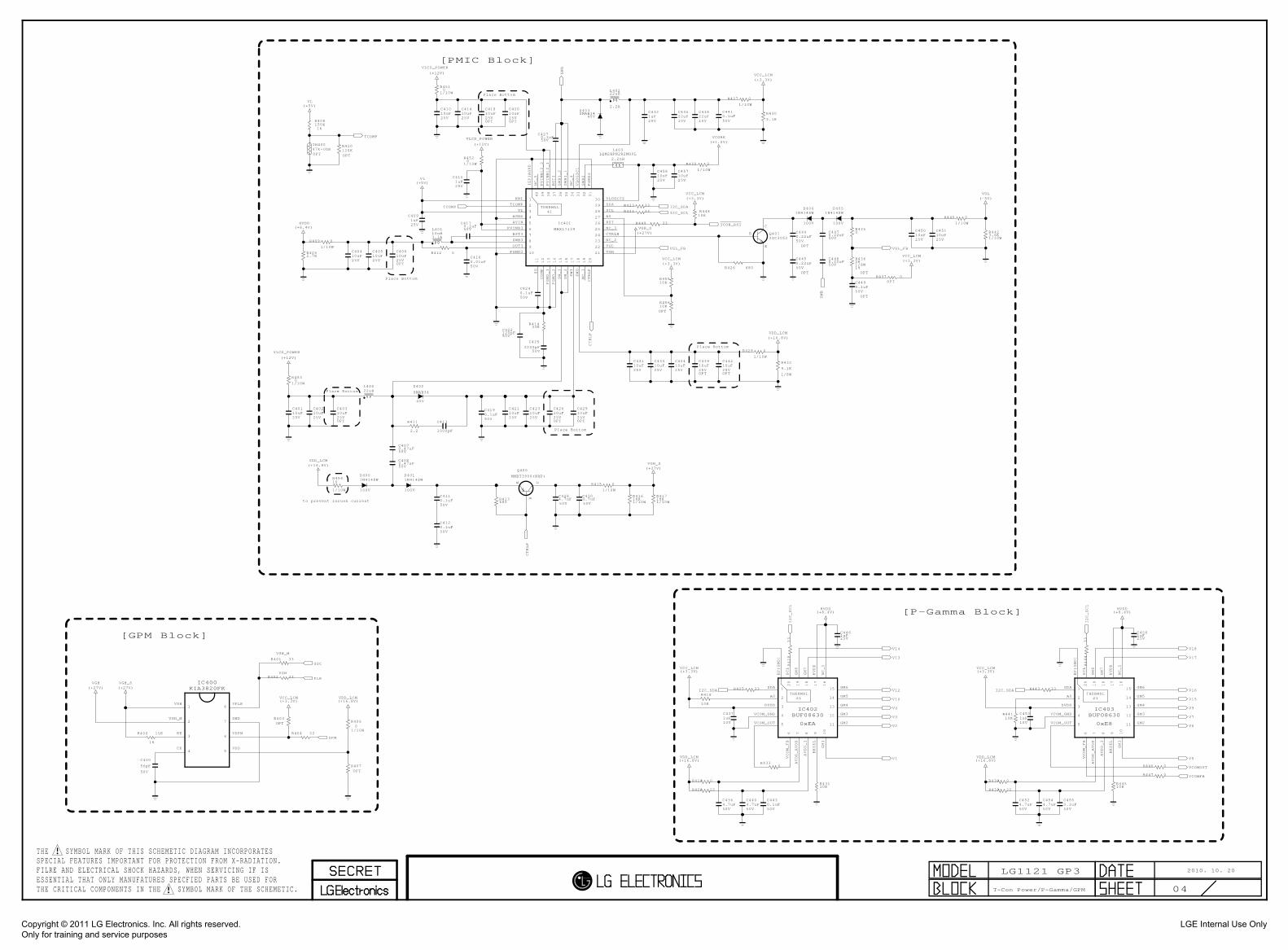
THERMAL
THERMAL THERMAL
THE SYMBOL MARK OF THIS SCHEMETIC DIAGRAM INCORPORATESSPECIAL FEATURES IMPORTANT FOR PROTECTION FROM X-RADIATION.FILRE AND ELECTRICAL SHOCK HAZARDS, WHEN SERVICING IF IS ESSENTIAL THAT ONLY MANUFATURES SPECFIED PARTS BE USED FORTHE CRITICAL COMPONENTS IN THE SYMBOL MARK OF THE SCHEMETIC.
D404
100V
1N4148W
R4423.6K1/10W
C41410uF25V
V4
R443 33
R404 33
TH40047k-ohmOPT
L40110uH3.1A
C4404.7uF50V
VGH_S(+27V)
C4110.1uF50V
C4240.1uF50V
R444
33
C42110uF25V
D405
100V
1N4148W
V13
R4362K1/8W1%
OPT
R411
2.2
FLK
C45010uF25V
Q4012SC3052
E
B
C
C44210uF25VOPT
V17
VCC_LCM(+3.3V)
R432
9.1K
1/8W
V12
V5
HVDD(+8.4V)
VDD_LCM(+16.8V)
VL(+5V)
C4364.7uF50V
C4120.1uF50V
R439 22
C40210uF25V
C43910uF25VOPT
C4190.1uF50V
C4544.7uF50V
V6
C42910uF25VOPT
D402
40V
SMAB34
R428
33
C4321uF25V
R41618K1/10W
C4304.7uF50V
C40510uF25V
V18
R415 0
1/10W
C4430.1uF50V
C4410.1uF50V
C4490.1uF50V
OPT
R401 33
VGH_M
VDD_LCM(+16.8V)
R424 33
C4561uF25V
VCOMOUT
C40310uF25VOPT
R446 0
HVDD(+8.4V)
C43310uF25V
R426 680
VDD_LCM(+16.8V)
V15
C4091uF25V
D403
40VSMAB34
R410120KOPT
VGL(-5V)
C400
56pF
50V
R413680
C4524.7uF50V
SWB
R41718K1/10W
R429 0
1/10W
R43110K
C413
1000pF
HVDD(+8.4V)
V14
R419 0
I2C_SCL
V1
L40222uH
2.2A
D400
100V
1N4148W
VGH_S(+27V)
VGH(+27V)
C4151uF25V
C4531uF10V
C41810uF25VOPT
C4461uF25V
VCC_LCM(+3.3V)
I2C_SDA
C42010uF25VOPT
R438 0
C43110uF25V
R409 0
1/10W
C42310uF25V
R425 33
VDD_LCM(+16.8V)
R403OPT
R400 15K
1%
R437 0OPT
R4330
C42610uF25VOPT
C40410uF25V
C4284.7uF50V
Q400
MMBT3906(NXP)
E
B
C
C4371uF10V
R427 0
1/10W
VCC_LCM(+3.3V)
I2C_SDA
V9
VCC_LCM(+3.3V)
VLCD_POWER
(+12V)
VLCD_POWER
(+12V)
R44510K
R4350
C4550.1uF50V
R4052.7K
R423 33
R4060
1/10W
VCOMFB
C4160.01uF50V
C41010uF25V
R440 0
1/10W
CTRLP
VLCD_POWER
(+12V)
R407OPT
VL(+5V)
D401
100V
1N4148W
C4270.1uF50V
DPM
V7
VDD_LCM(+16.8V)
I2C_SDA
R418
10K
C40110uF25V
R402 33VGH
V16
C40610uF25VOPT
VGH_S(+27V)
R447 0
SWB
R430
5.1K
VCC_LCM(+3.3V)
C4170.1uF50V
I2C_SCL
C45110uF25V
TCOMP
V3
C43410uF25V
R41433K
R420 22
CTRLP
I2C_SCL
TCOMP
R44110K
V10
GSC
V2
VCC_LCM(+3.3V)
R44810K
L40022uH
C45710uF25V
C45810uF25V
VCORE(+1.0V)
TCON_RSTR449 33
VGL_FB VGL_FB
R450 0
1/10W
R4510
1/10W
R4520
1/10W
R4530
1/10W
R408150K1%
C422120pF50V
C4070.47uF50V
C4080.47uF50V
R45410
1/10W
R45510K
R45610KOPT
VCC_LCM(+3.3V)
R412 0
L403
2.2uHLQM2HPN2R2MG0L
C425
2200pF50V
IC401
MAX17139
3VL2TCOMP
4AGND
1EN1
6PVINB35AVIN
7BST3
8SWB3
9OUT3
10PGND3
11
SS
12
COMP
13
PGND_1
14
PGND_2
15
SW_1
16
SW_2
17
SWI
18
SWO
19
NC_1
20
CTRLP
21 VGH22 VGL23 NC_224 CTRLN25 NC_326 RST27 A028 SCL29 SDA30 VLOGIC2
31
PGND2
32
SWB2
33
VLOGIC1
34
NC_4
35
SWB1_1
36
SWB1_2
37
BST1
38
PVINB12_1
39
PVINB12_2
40
NC_5
41
[EP]AGND
IC402BUF08630
1SDA
3DVDD
7AVDD_AVDD
9BKSEL
10
GM1
11 GM2
12 GM3
13 GM4
14 GM5
15 GM6
16
NC_1
17
HVDD
18
GM7
19
GM8
20
SCL
5VCOM_OUT
8AVDD_1
6VCOM_FB
4VCOM_GND
2A0 21
EP[GND]
IC403BUF08630
1SDA
3DVDD
7AVDD_AVDD
9BKSEL
10
GM1
11 GM2
12 GM3
13 GM4
14 GM5
15 GM6
16
NC_1
17
HVDD
18
GM7
19
GM8
20
SCL
5VCOM_OUT
8AVDD_1
6VCOM_FB
4VCOM_GND
2A0 21
EP[GND]
IC400KIA3820FK
3RE
2VGH_M
4CE
1VGH
5VDD
6VDPM
7GND
8VFLK
C43522uF10V
C43822uF10V
C4440.22uF50V
OPT
C4450.22uF50V
OPT
C4480.22uF50V
C4470.22uF50V
T-Con Power/P-Gamma/GPM
2010. 10. 20
04
LG1121 GP3
Place Bottom
Place Bottom
Place Bottom
0xE8
Place Bottom
Place Bottom
[PMIC Block]
0xEA
[P-Gamma Block]
[GPM Block]
to prevent inrush current
Copyright © 2011 LG Electronics. Inc. All rights reserved. Only for training and service purposes
LGE Internal Use Only
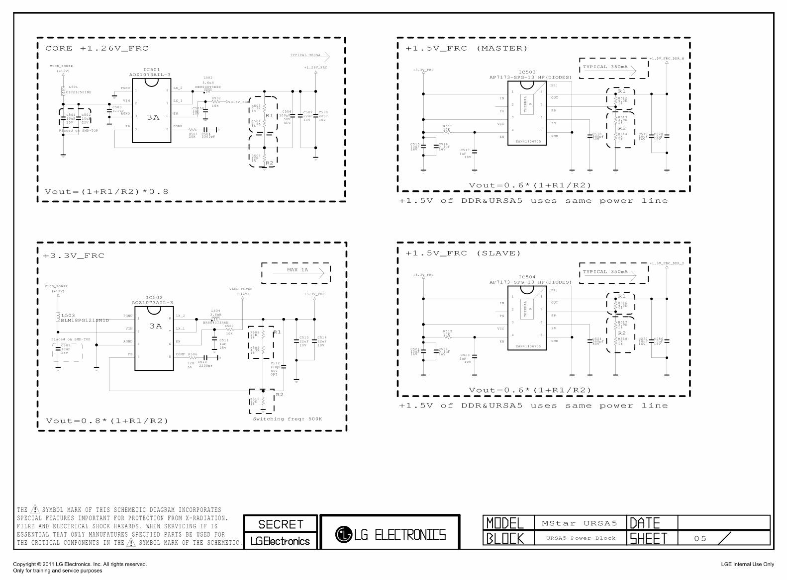
THERMAL
THERMAL
THE SYMBOL MARK OF THIS SCHEMETIC DIAGRAM INCORPORATESSPECIAL FEATURES IMPORTANT FOR PROTECTION FROM X-RADIATION.FILRE AND ELECTRICAL SHOCK HAZARDS, WHEN SERVICING IF IS ESSENTIAL THAT ONLY MANUFATURES SPECFIED PARTS BE USED FORTHE CRITICAL COMPONENTS IN THE SYMBOL MARK OF THE SCHEMETIC.
C50722uF10V
+3.3V_FRCR5033.3K1%
C50581uF10V
+1.26V_FRC
C50822uF10VR504
3.9K1%
L502
3.6uHNR8040T3R6N
C506100pF
50VOPT
R50512K1%
R502
10KC5030.1uF
L501
CIC21J501NE
0.1uFC516
16V
C52010uF16V
R5141K1%
1uFC517
10V
+3.3V_FRC
+1.5V_FRC_DDR_M
R5124.3K1%
C51910uF16V
R5133.9K1%
C51510uF16V
C518560pF50V
R51110K
C5043300pF
R50120K
IC503AP7173-SPG-13 HF(DIODES)
EAN41406705
3
VCC
2
PG
4
EN
1
IN
5
GND
6
SS
7
FB
8
OUT
9
[EP]
C50110uF25V
C50210uF25V
VLCD_POWER
(+12V)
L503BLM18PG121SN1D
C5102200pF
C512100pF50VOPT
R506
12K5%
L5043.6uH
NR8040T3R6N
IC502AOZ1073AIL-3
3AGND
2VIN
4FB
1PGND
5COMP
6EN
7LX_1
8LX_2
+3.3V_FRC
VLCD_POWER
(+12V)VLCD_POWER
(+12V)
R507
10K
R5094.3K1%
R50827K1%
R51010K1%
IC501AOZ1073AIL-3
3AGND
2VIN
4FB
1PGND
5COMP
6EN
7LX_1
8LX_2
C25210uF16V
0.1uFC522
16V
R5181K1%
1uFC523
10V
R51510K
R5173.9K1%
C52110uF16V
C25610uF16V
+3.3V_FRC
+1.5V_FRC_DDR_S
C524560pF50V
R5164.3K1%
IC504AP7173-SPG-13 HF(DIODES)
EAN41406705
3
VCC
2
PG
4
EN
1
IN
5
GND
6
SS
7
FB
8
OUT
9
[EP]
C50910uF25V
C5111uF25V
C51422uF10V
C51322uF10V
URSA5 Power Block 05
MStar URSA5
Vout=(1+R1/R2)*0.8
TYPICAL 980mA
R1
R2
CORE +1.26V_FRC
Placed on SMD-TOP
3A
Vout=0.6*(1+R1/R2)
R1
+1.5V of DDR&URSA5 uses same power line
TYPICAL 350mA
R2
+1.5V_FRC (MASTER)
Switching freq: 500K
MAX 1A
Vout=0.8*(1+R1/R2)
R2
3A
Placed on SMD-TOP
+3.3V_FRC
R1
Vout=0.6*(1+R1/R2)
R2
+1.5V of DDR&URSA5 uses same power line
R1
+1.5V_FRC (SLAVE)
TYPICAL 350mA
Copyright © 2011 LG Electronics. Inc. All rights reserved. Only for training and service purposes
LGE Internal Use Only
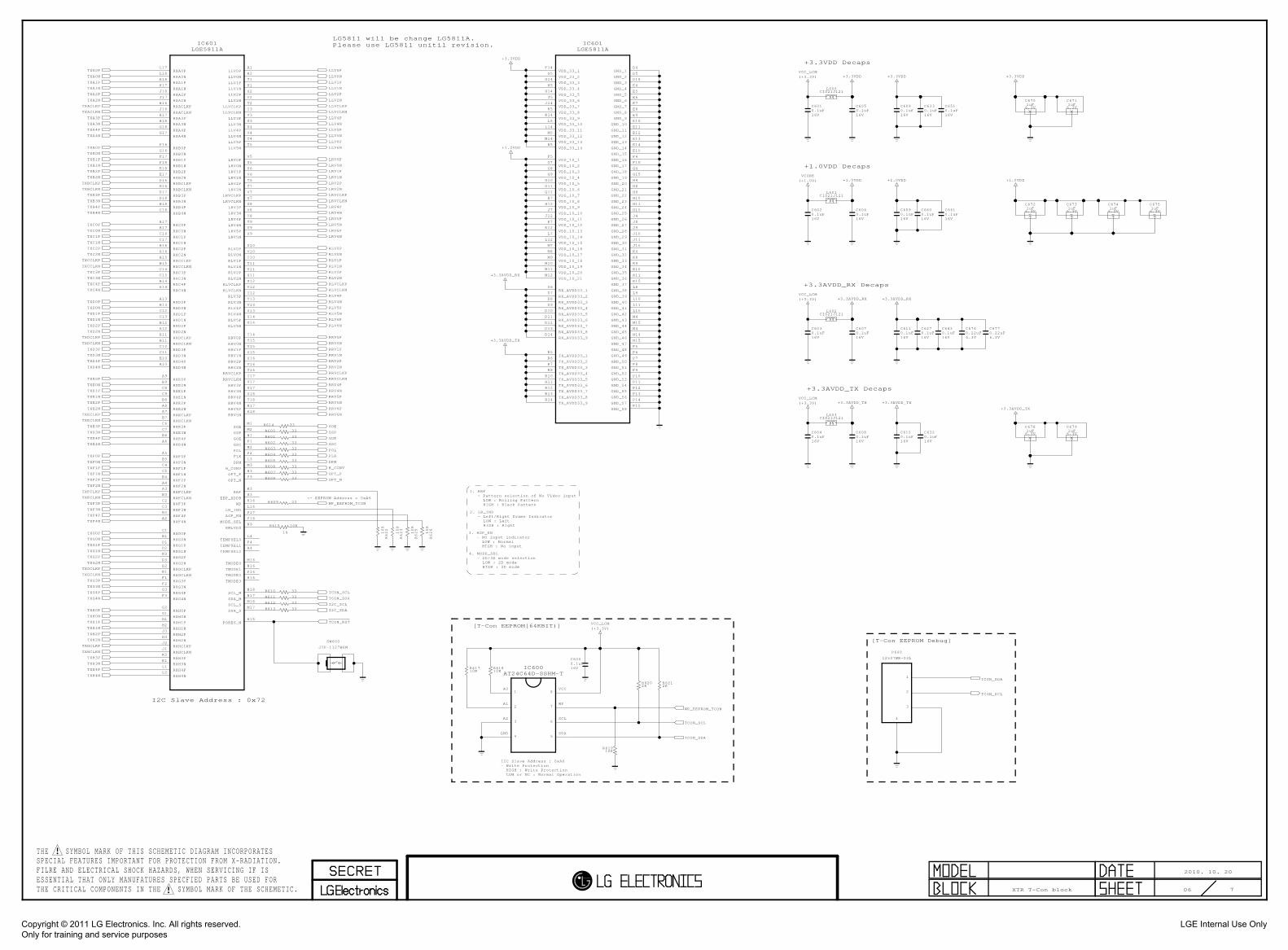
THE SYMBOL MARK OF THIS SCHEMETIC DIAGRAM INCORPORATESSPECIAL FEATURES IMPORTANT FOR PROTECTION FROM X-RADIATION.FILRE AND ELECTRICAL SHOCK HAZARDS, WHEN SERVICING IF IS ESSENTIAL THAT ONLY MANUFATURES SPECFIED PARTS BE USED FORTHE CRITICAL COMPONENTS IN THE SYMBOL MARK OF THE SCHEMETIC.
RLV1N
TXD0P
LLV0P
RRV2N
TXHCLKP
TXE1N
TXH3N
TXA0P
TXH0N
TXG0N
TXCCLKN
LLV4P
TXFCLKP
LLVCLKP
TXD4N
TXD4P
TXB2P
LRV4P
TXA3N
LLV6P
LRV6N
TXG1P
LRV1P
LLV5P
TXE2N
TXH1N
RRV0N
LLV6N
TXH2N
TXG1N
TXG3P
TXD3N
TXH1P
RRV4N
RRVCLKN
TXC0P
TXF0P
LRV4N
RLV4P
TXB1P
RLVCLKN
TXF4P
TXBCLKN
TXG2N
TXE2P
TXH4P
TXF3N
TXC3P
TXD1P
TXDCLKN
TXC3N
TXA0N
TXD0N
LRV2N
TXH4N
TXECLKP
TXB0P
TXDCLKP
LRV2P
RLV2N
TXF3P
TXF1P
RRV0P
TXD2P
RRV6P
TXA4P
RRVCLKP
LLV2N
RLV6N
TXFCLKN
TXHCLKN
TXA3P
TXA4N
TXC2N
TXE3P
TXB4N
RLV6P
TXC4N
LRV5P
TXD2N
TXA2P
TXF1N
RLV0N
TXB4P
TXGCLKN
TXB2N LRV1N
TXE4N
RRV1N
RLV1P
TXE4P
RLV5P
LRVCLKN
SOE
RRV1P
RRV5P
TXACLKN
RRV6N
TXE0N
TXB1N
RRV2P
TXD3P
TXF0N
RLV4N
TXG2P
TXE0P
TXACLKP
LLV1P
TXB3N
TCON_RST
RLV2P
TXF4N
TXGCLKP
RLVCLKP
TXBCLKP
TXH3P
LRV0P
TXG0P
LRV5N
RRV5N
LRV0N
LLVCLKN
TXC2P
TXE3N
TXA2N
RLV0P
TXC1P
TXF2N
TXH0P
TXD1N
TXE1P
TXA1P
RRV4P
TXB0N
TXC1N
I2C_SCL
TXH2P
TXB3P
TXC0N
TXCCLKP
TXF2P
TXG4N
LLV4N
TXC4P
TXG3N
LLV0N
LLV2P
LRVCLKP
TXECLKN
TXA1N
RLV5N
LLV5N
TXG4P
LRV6P
WP_EEPROM_TCON
LLV1N
H_CONV
POL
R602 33
FLK
R601 33
R600 33
R604 33
OPT_N
R606 33
R607 33
GSCR603 33
R614 33
GOE
R608 33
GSP
OPT_P
R609 33
R612 33
R613 33 I2C_SDA
TCON_SDA
TCON_SCL
+3.3VDD
+1.0VDD
+3.3AVDD_RX
+3.3AVDD_TX
C6090.1uF16V
+3.3VDD
C6330.1uF16V
C6510.1uF16V
C6050.1uF16V
L600CIS21J121
+3.3VDD
C6010.1uF16V
+1.0VDD
C6060.1uF16V
L601CIS21J121
C6020.1uF16V
VCC_LCM(+3.3V)
+1.0VDD
C6590.1uF16V
C6610.1uF16V
C6600.1uF16V
C6030.1uF16V
C6070.1uF16V
+3.3AVDD_RX
L602CIS21J121
C6430.1uF16V
C6110.1uF16V
C6270.1uF16V
+3.3AVDD_RX
C6040.1uF16V
C6120.1uF16V
+3.3AVDD_TX+3.3AVDD_TX
L603CIS21J121
C6080.1uF16V
C6320.1uF16V
C6000.1uF16V
R610 33
R611 33
TCON_SDA
TCON_SCL
WP_EEPROM_TCON
R61910K
IC600AT24C64D-SSHM-T
3A2
2A1
4GND
1A0
5SDA
6SCL
7WP
8VCC
P600
12507WR-03L
1
2
3
4
TCON_SDA
TCON_SCL
SW600
JTP-1127WEM
VCC_LCM(+3.3V)
VCC_LCM(+3.3V)
VCORE(+1.0V)
VCC_LCM(+3.3V)
R605 33
R61710K
R61810K
DPM
C6760.22uF6.3V
C6770.22uF6.3V
+3.3VDD
+3.3AVDD_TX
+1.0VDD
C6701uF6.3V
C6711uF6.3V
C6721uF6.3V
C6731uF6.3V
C6741uF6.3V
C6751uF6.3V
C6781uF6.3V
C6791uF6.3V
R6212K
R6202K
IC601LGE5811A
RXA0PL17
RXA0NL18
RXA1PK18
RXA1NK17
RXA2PJ18
RXA2NJ17
RXACLKPH16
RXACLKNJ16
RXA3PH17
RXA3NH18
RXA4PG18
RXA4NG17
RXB0PF16
RXB0NG16
RXB1PF17
RXB1NF18
RXB2PE18
RXB2NE17
RXBCLKPD16
RXBCLKNE16
RXB3PD17
RXB3ND18
RXB4PB18
RXB4NC18
RXC0PA17
RXC0NB17
RXC1PC16
RXC1NC17
RXC2PB16
RXC2NA16
RXCCLKPA15
RXCCLKNB15
RXC3PC14
RXC3NC15
RXC4PB14
RXC4NA14
RXD0PA13
RXD0NB13
RXD1PC12
RXD1NC13
RXD2PB12
RXD2NA12
RXDCLKPA11
RXDCLKNB11
RXD3PC10
RXD3NC11
RXD4PB10
RXD4NA10
RXE0PA9
RXE0NB9
RXE1PC8
RXE1NC9
RXE2PB8
RXE2NA8
RXECLKPA7
RXECLKNB7
RXE3PC6
RXE3NC7
RXE4PB6
RXE4NA6
RXF0PA5
RXF0NB5
RXF1PC4
RXF1NC5
RXF2PB4
RXF2NA4
RXFCLKPA3
RXFCLKNB3
RXF3PC2
RXF3NC3
RXF4PB2
RXF4NA2
RXG0PC1
RXG0NB1
RXG1PD1
RXG1ND2
RXG2PE3
RXG2ND3
RXGCLKPE2
RXGCLKNE1
RXG3PF1
RXG3NF2
RXG4PG3
RXG4NF3
RXH0PG2
RXH0NG1
RXH1PH1
RXH1NH2
RXH2PJ3
RXH2NH3
RXHCLKPJ2
RXHCLKNJ1
RXH3PK2
RXH3NK1
RXH4PL1
RXH4NL2
LLV0PR1
LLV0NR2
LLV1PT1
LLV1NU1
LLV2PU2
LLV2NV2
LLVCLKPT2
LLVCLKNT3
LLV3PV3
LLV3NU3
LLV4PU4
LLV4NV4
LLV5PT4
LLV5NT5
LRV0PV5
LRV0NU5
LRV1PU6
LRV1NV6
LRV2PT6
LRV2NT7
LRVCLKPV7
LRVCLKNU7
LRV3PU8
LRV3NV8
LRV4PT8
LRV4NT9
LRV5PV9
LRV5NU9
RLV0PU10
RLV0NV10
RLV1PT10
RLV1NT11
RLV2PV11
RLV2NU11
RLVCLKPU12
RLVCLKNV12
RLV3PT12
RLV3NT13
RLV4PV13
RLV4NU13
RLV5PU14
RLV5NV14
RRV0PT14
RRV0NT15
RRV1PV15
RRV1NU15
RRV2PU16
RRV2NV16
RRVCLKPT16
RRVCLKNT17
RRV3PV17
RRV3NU17
RRV4PU18
RRV4NT18
RRV5PR17
RRV5NR18
SOEM1
GSPM2
GOEN1
GSCP1
POLN2
FLKP2
DPML3
H_CONVM3
OPT_PN3
OPT_NP3
RBFK3
EEP_ADDRR3
WPK16
LR_INDL16
AGP_ENP17
MODE_SELP18
RMLVDSR9
TEMPSEL0L4
TEMPSEL1P4
TEMPSEL2R4
TMODE0M16
TMODE1N16
TMODE2P16
TMODE3R16
SCL_MN18
SDA_MN17
SCL_SM18
SDA_SM17
PORES_NR15
IC601LGE5811A
VDD_33_1F14
VDD_33_2G5
VDD_33_3G14
VDD_33_4H5
VDD_33_5H14
VDD_33_6J5
VDD_33_7J14
VDD_33_8K5
VDD_33_9K14
VDD_33_10L5
VDD_33_11L14
VDD_33_12M5
VDD_33_13M14
VDD_33_14N5
VDD_10_1F5
VDD_10_2G7
VDD_10_3G8
VDD_10_4G9
VDD_10_5G10
VDD_10_6G11
VDD_10_7G12
VDD_10_8H7
VDD_10_9H12
VDD_10_10J7
VDD_10_11J12
VDD_10_12K7
VDD_10_13K12
VDD_10_14L7
VDD_10_15L12
VDD_10_16M7
VDD_10_17M8
VDD_10_18M9
VDD_10_19M10
VDD_10_20M11
VDD_10_21M12
RX_AVDD33_1D6
RX_AVDD33_2D7
RX_AVDD33_3D8
RX_AVDD33_4D9
RX_AVDD33_5D10
RX_AVDD33_6D11
RX_AVDD33_7D12
RX_AVDD33_8D13
RX_AVDD33_9D14
TX_AVDD33_1R5
TX_AVDD33_2R6
TX_AVDD33_3R7
TX_AVDD33_4R8
TX_AVDD33_5R10
TX_AVDD33_6R11
TX_AVDD33_7R12
TX_AVDD33_8R13
TX_AVDD33_9R14
GND_1D4
GND_2D5
GND_3D15
GND_4E4
GND_5E5
GND_6E6
GND_7E7
GND_8E8
GND_9E9
GND_10E10
GND_11E11
GND_12E12
GND_13E13
GND_14E14
GND_15E15
GND_16F4
GND_17F15
GND_18G4
GND_19G15
GND_20H4
GND_21H8
GND_22H9
GND_23H10
GND_24H11
GND_25H15
GND_26J4
GND_27J8
GND_28J9
GND_29J10
GND_30J11
GND_31J15
GND_32K4
GND_33K8
GND_34K9
GND_35K10
GND_36K11
GND_37K15
GND_38L8
GND_39L9
GND_40L10
GND_41L11
GND_42L15
GND_43M4
GND_44M15
GND_45N4
GND_46N14
GND_47N15
GND_48P5
GND_49P6
GND_50P7
GND_51P8
GND_52P9
GND_53P10
GND_54P11
GND_55P12
GND_56P13
GND_57P14
GND_58P15
R622
10K
R625
10K
R623
10K
R626
10KR615 20K
1%
XTR T-Con block 06 7
2010. 10. 20
+3.3VDD Decaps
+1.0VDD Decaps
+3.3AVDD_RX Decaps
+3.3AVDD_TX Decaps
I2C Slave Address : 0xA6- Write Protection HIGH : Write Protection LOW or NC : Normal Operation
[T-Con EEPROM[64KBIT)]
[T-Con EEPROM Debug]
<- EEPROM Address = 0xA6
2. LR_IND - Left/Right frame Indicator LOW : Left HIGH : Right
3. AGP_EN - NO input indicator LOW : Normal HIGH : No input
4. MODE_SEL - 2D/3D mode selection LOW : 2D mode HIGH : 3D mode
1. RBF - Pattern selection of No Video input LOW : Rolling Pattern HIGH : Black Pattern
I2C Slave Address : 0x72
LG5811 will be change LG5811A.Please use LG5811 unitil revision.
Copyright © 2011 LG Electronics. Inc. All rights reserved. Only for training and service purposes
LGE Internal Use Only
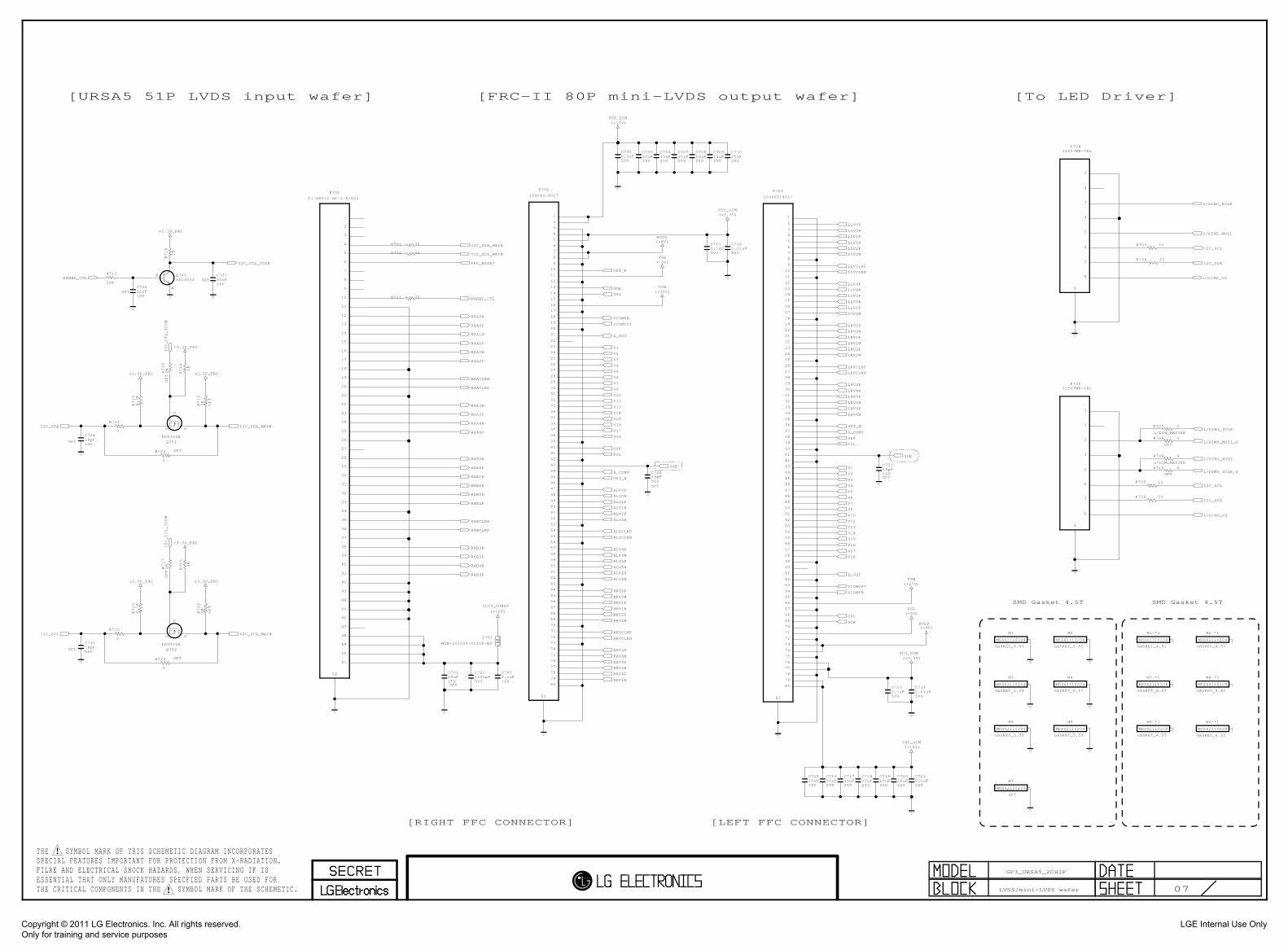
THE SYMBOL MARK OF THIS SCHEMETIC DIAGRAM INCORPORATESSPECIAL FEATURES IMPORTANT FOR PROTECTION FROM X-RADIATION.FILRE AND ELECTRICAL SHOCK HAZARDS, WHEN SERVICING IF IS ESSENTIAL THAT ONLY MANUFATURES SPECFIED PARTS BE USED FORTHE CRITICAL COMPONENTS IN THE SYMBOL MARK OF THE SCHEMETIC.
RLV2P
C70510uF25V
LRV0P
Z_OUT
C71610uF25V
R724
2K
+3.3V_FRC
V7
V14
R718
2K
V3
LRV1N
RRV6P
OPT_N
RRV1N
I2C_SDA_MAIN
MDS62110204
M4
GASKET_5.5T
MDS62110204
M1
GASKET_5.5T
RRV0P
VDD_LCM(+16V)
L/DIM0_VS
R704 33
LLV0P
RXB4N
V13
VGL(-5V)
RLV4P
RXA3N
LRV4PV9
R702 33
I2C_CTL_TCON
V6
V10
HVDD(+8V)
R721 33
P70412507WR-08L
1
2
3
4
5
6
7
8
9
RXBCLKP
GSC
V2
C72418pF50V
OPT
R709 0
L/DIM_MASTER
RLV1N
LRV5P
V1
Q702
FDV301N
G
DS
RXB3N
I2C_SCL
V15
V18
C72518pF50V
OPT
RXB2P
L/DIM0_SCLK
RLVCLKP
C7040.1uF50V
I2C_CTL_TCON
R719
2K
OPT
LRVCLKP
V12
MDS62110208
M4-*1
GASKET_4.5T
R725
2K
+3.3V_FRC
L/DIM0_SCLK_S
MDS62110208
M1-*1
GASKET_4.5T
H_CONV
LLV5N
RLV6P
V17
OPT_PLLVCLKP
P70512507WR-08L
1
2
3
4
5
6
7
8
9
L701
MLB-201209-0120P-N2
C71510uF25V
C72622uF10V
OPT
V5
V2
RLV1P
LLV0N
RXB0N
I2C_CTL_TCON
R720
2K
OPT
C71710uF25V
GSP
C7030.1uF16V
C72722uF10V
OPT
RXA3P
C72010uF25V
RLV4N
C71910uF25V
C70710uF25V
LLVCLKN
R708 0
OPT
RXACLKN
RXB0P
I2C_SDA_MAIN
LRV5N
RRV5P
LLV6P
I2C_SDA
MDS62110204
M6
GASKET_5.5T
P702
104060-8017
1
2
3
4
5
6
7
8
9
10
11
12
13
14
15
16
17
18
19
20
21
22
23
24
25
26
27
28
29
30
31
32
33
34
35
36
37
38
39
40
41
42
43
44
45
46
47
48
49
50
51
52
53
54
55
56
57
58
59
60
61
62
63
64
65
66
67
68
69
70
71
72
73
74
75
76
77
78
79
80
81
RXB4P Z_OUT
MDS62110204
M3
GASKET_5.5T
V7
RLV5P
R711
0
LLV2P
VCOMOUT
V10
VCOMOUT
C71810uF25V
V6
RLV0P
R701 33
LRV6P
L/DIM0_VS
+3.3V_FRC
C72315pF50VOPT
C7021000pF50V
LRV6N
RLVCLKN
RLV0N
V14
POL
V18
RXA2P
R707 0
L/DIM_MASTER
V1
V5
RXA4N
RRV1P
LRV2P
C71010uF25V
RXBCLKN
MDS62110208
M6-*1
GASKET_4.5T
V4
GOE
R716
2K
OPT
I2C_SCL_MAIN
MDS62110208
M5-*1
GASKET_4.5T
RRVCLKP
RXACLKP
GSP
LLV6N
MDS62110204
M7
OPT
C70110uF25VOPT
C7210.1uF50V
PANEL_CTL
RXA1N
I2C_SDA
V13
V16
R706 33
V16
LLV5P
RRV4P
C7130.1uF50V
VCC_LCM(+3.3V)
VGH(+27V)
VCC_LCM(+3.3V)
I2C_SCL
C7110.1uF50V
C72215pF50VOPT
R717
2K
OPT
V4
RLV2N
LRV2N
+3.3V_FRC
R705 33
RRV2N
VLCD_POWER
(+12V)
V9
LLV2N
L/DIM1_MOSI
V12
OPT_NRXB1N
+3.3V_FRC
MDS62110204
M5
GASKET_5.5T
RRV2P
LLV4P
+3.3V_FRC
RXA4P
V15
C70910uF25V
HVDD(+8V)
PANEL_CTL
MDS62110204
M2
GASKET_5.5T
C70810uF25V
RXA0P
RRV4N
LRV1P
I2C_SDA
VGH(+27V)
RXA0N
I2C_SCL_MAIN
R712
0
LLV1P
RRV0N
L/DIM1_SCLK
LLV1N
P701
FI-RE51S-HF-J-R1500
1
2
3
4
5
6
7
8
9
10
11
12
13
14
15
16
17
18
19
20
21
22
23
24
25
26
27
28
29
30
31
32
33
34
35
36
37
38
39
40
41
42
43
44
45
46
47
48
49
50
51
52
SOE
L/DIM0_MOSI_S
SOE
R723
0
OPT
Q7032SC3052
E
B
C
VDD_LCM(+16V)
VGL(-5V)
RRV6N
LRV0N
GOE
V17
VCOMFB
H_CONV
L/DIM0_MOSI
+3.3V_FRC
R703 33
POL
GSC
RLV6N
MDS62110208
M2-*1
GASKET_4.5T
LLV4N
RXB2N
I2C_SCL
MDS62110208
M3-*1
GASKET_4.5T
RXA2N
LRV4N
RRVCLKN
RRV5N
RXA1P
C7120.01uF50V
FRC_RESET
VCOMFB
R713
10K
C70610uF25V
V3
RXB3P
P703
104060-8017
1
2
3
4
5
6
7
8
9
10
11
12
13
14
15
16
17
18
19
20
21
22
23
24
25
26
27
28
29
30
31
32
33
34
35
36
37
38
39
40
41
42
43
44
45
46
47
48
49
50
51
52
53
54
55
56
57
58
59
60
61
62
63
64
65
66
67
68
69
70
71
72
73
74
75
76
77
78
79
80
81
RLV5N
LRVCLKN
R722
0
OPT
RXB1P
Q701
FDV301N
G
DS
R710 0
OPT
C7140.01uF50V
R714
4.7K
R715
4.7K
LVDS/mini-LVDS wafer
GP3_URSA5_2CHIP
[URSA5 51P LVDS input wafer]
[LEFT FFC CONNECTOR]
[FRC-II 80P mini-LVDS output wafer]
07
[To LED Driver]
[RIGHT FFC CONNECTOR]
SMD Gasket 4.5TSMD Gasket 4.5T
Copyright © 2011 LG Electronics. Inc. All rights reserved. Only for training and service purposes
LGE Internal Use Only