Embed Size (px)
Citation preview

July 8, 2009 18:1 00153
NANO: Brief Reports and ReviewsVol. 4, No. 2 (2009) 83–90c© World Scientific Publishing Company
LARGE-AREA GRAPHENE-BASED FLEXIBLETRANSPARENT CONDUCTING FILMS
FETHULLAH GUNES, GANG HEE HAN, KI KANG KIM, EUN SUNG KIM,SEUNG JIN CHAE, MIN HO PARK, HAE-KYUNG JEONG,
SEONG CHU LIM and YOUNG HEE LEE∗BK21 Physics Division, Sungkyunkwan Advanced Institute of Nanotechnology
Center for Nanotubes and Nanostructured CompositesSungkyunkwan University, Suwon, 440-746, Republic of Korea
Received 1 February 2009Revised 18 March 2009
A simple approach by direct synthesis of few-layer graphene sheets and transferring them ontoflexible substrate is demonstrated. The hydrogen effect on the D band intensity of Raman spectrafor few-layer graphene sheets synthesized by chemical vapor deposition (CVD) on Ni-evaporatedsilicon substrate is investigated by optimizing the mixing ratio of C2H4/H2. While the Ni etchantis used to melt away the squeezed Ni layers between graphene sheet and silicon substrate, thegraphene sheet is transferred onto polyethylene terephthalate film by a fishing method. It isfound that the condition of graphene transfer strongly relies on the cooling rate of the filmduring CVD synthesis. The sheet resistance of the film decreases as the film thickness increases.A sheet resistance of 233 Ω/sq is obtained at a transmittance of 62%.
Keywords : Large area graphene; chemical vapor deposition; flexible transparent conducting film.
1. Introduction
Carbon material such as graphite and carbonnanotubes has been proven to be an excellentelectrode material with high chemical stability,high transmittance, high specific surface area, andhigh conductivity.1–4 Recently, the graphene, two-dimensional form of graphite, has opened a possi-bility of variety applications, such as flexible thinfilm transistors and touch panel electrodes, dueto its extraordinary electronic properties of nearlyzero effective mass.5–7 Nevertheless, applicationsare still limited by the complicated sample prepa-ration processes.5,6 For this reason, for transparentconducting film (TCF) applications, graphite oxidehas been prepared to form thin film that was fur-ther reduced by chemical and thermal treatment.8,9
Although large-area reduced graphite oxide film was
realized, the residual oxygen groups resulted in highsheet resistance of the film that failed to meet therequirement for practical applications.
There have been efforts to use chemical vapordeposition to synthesize large-area graphene layersdirectly on metal substrates or metal-deposited Sisubstrates.10–12 The presence of defects and controlof the film thickness of the graphene layers havenot been investigated, which are essential issuesfor many applications.13,14 An additional difficultyarises from the transfer of the graphene film ontoa desired transparent film for applications, in par-ticular, for TCFs. PMMA was used to transfergraphene in which PMMA was removed later.12
The problems often occurs during Ni etching. Theetching of Ni layers by acid treatment and the simul-taneous separation of the graphene film from the
83
July 8, 2009 18:1 00153
84 F. Gunes et al.
underlying substrate have been of challenges, par-ticularly in large-area graphene transfer.
In this report, large area graphene was synthe-sized in atmospheric pressure chemical vapor depo-sition (APCVD) chamber on Ni-film-deposited Sisubstrate. The hydrogen amount in the carbon–hydrogen gas mixture was optimized to reducedefect density and amorphous carbon quantity ofgraphene layers, and furthermore to obtain uniformthickness of graphene layers. We also found that theseparation of graphene layers from Ni for transferwas strongly dependent on the cooling rate of thesample after growth. Hydrophobic graphene film,suspended on the hydrophilic etchant surface afterthe Ni-film was etched away, was successfully trans-ferred onto another hydrophobic film of polyethy-lene terephthalate (PET) by a fishing method. Thethickness of the film was controlled by the APCVDgrowth time. The synthesized graphene size is onlylimited by the chamber and Si wafer size in the CVDapproach.
2. Sample Preparation andExperimental Details
We synthesized graphene layers on Ni-depositedSi/SiO2 substrate by thermal APCVD. A Ni thick-ness of 400 nm was deposited on 4 inches of Si sub-strate by an e-beam evaporator. Since the chambersize limits our sample size up to 2 × 2 cm2, we cutNi-deposited Si wafer into small pieces. The pre-pared substrate was placed in the APCVD chamberwith a few degrees of tilt angle with respect to theincoming gas flow direction to obtain homogeneousgas contact to the Ni surface. The homogeneity ofthe graphene film thickness was degraded when thesubstrate was placed with no tilt angle. The cham-ber was heated to 900C with H2 gas flow and keptfor 10 min. The growth of graphene layers was thencarried out at the same temperature with a flow ofmixture of ethylene and hydrogen gases.
Unlike the epitaxial growth of semiconductormaterials obtained from the typical CVD, carbonatoms deposited from the carbon source were pre-cipitated into the Ni substrate during the gas flow.Graphene formation takes place via a segregationof C atoms out to the Ni surface during coolingafter termination of the incoming gas. Growth hasbeen carried out with different ratios of hydrogenand ethylene gases in order to optimize the con-ditions for high quality graphene with minimumdefect density. The samples were cooled down to
room temperature without any gas introduction tomaintain smooth surface morphology. With a gasintroduction, for instance argon gas, during cool-ing, we observed the negative effect on the surfacemorphology.
Raman spectroscopy (Renishaw RM1000-Invia) with laser excitation energy of 514 nm(2.41 eV) equipped with a notch filter of 50 cm−1
cutoff frequency was used to investigate defect den-sity of graphene samples. Confocal Raman Micro-scope (Witech-CRM200) filtered by a Rayleighrejection filter (< 100 cm−1) with an excitationenergy of 2.33 eV and a focus spot size of 350 nmwas used to measure the uniformity of graphenelayers. Scanning tunneling microscope (Seiko-SPA400) with a DFM mode was used to study mor-phology of the transferred graphene. Field emis-sion scanning electron microscopy (FESEM: 6700F,JEOL) was used to see the morphology of the syn-thesized and transferred graphene. High resolutiontransmission electron microscopy (HRTEM: JEM2100F, JEOL) was used to investigate the numberof layers and the morphology of graphene sheets.For the TEM sample preparation, the synthesizedgraphene on Ni substrate was submerged in dilutednitric acid. Etchant solution, where graphene layeris suspended, was diluted by deionized water afterNi sub-layer was etched away completely. The sus-pended graphene was then transferred onto thecopper grid and dried at room temperature.
3. Results and Discussion
3.1. Quality and morphology ofgraphene sheets
Figure 1(a) shows Raman spectra of graphene lay-ers synthesized with different gas mixing ratios. Thedata were averaged from 10 different locations ofgraphene layers for each plot. To obtain large grainsize graphene layers and to investigate the defectdensity dependence on H2 mixing ratio, sampleswere kept for 10 min. Relatively thick layers up to40 layers were formed. D/G peak intensities withdifferent H2 ratios in Fig. 1(b) and the insets showthat the C2H4/H2 ratio of 10/100 is the best ratiofor graphene layers with lowest defect density andhighest crystallinity. The C1s peak of XPS data inthe inset obtained from our samples with 10/100ratio is similar to that of highly oriented pyrolyticgraphite (HOPG). This indicates that the quality ofgraphene layers obtained from our optimized con-ditions is close to that of HOPG.

July 8, 2009 18:1 00153
Large-Area Graphene-Based Flexible Transparent Conducting Films 85
(a) (b)
(c) (d)
Fig. 1. (a) Raman spectra, with an excitation energy of 2.41 eV, averaged over ten data points at different positions of thesamples grown 10min at 900C. (b) Intensity ratio of D-band to G-band as a function of H2 amount during growth. The leftinset shows the Raman spectra of D and G bands at different H2 amount. The right inset is XPS C1s peaks from CVD grownsample and HOPG. (c) Raman spectra averaged over ten data points taken on graphene after transferred onto SiO2 and PET.(d) Confocal Raman spectra with an excitation energy of 2.33 eV taken on graphene after transfer onto SiO2 showing G′ peakdependence on the number of layers.
To see the quality of thin graphene layers, thesamples were prepared for a growth time of only1min and were transferred to another Si/SiO2 sub-strate and the PET film (the transfer technique willbe discussed later). Several features can be notedfrom Raman spectra in Fig. 1(c): (i) No notice-able D band is observed even for thin graphene lay-ers, (ii) the intensity of G′ band near 2700 cm−1
is comparable to that of G band due to the thingraphene layers, (iii) the peak positions of G andG′ bands are shifted due to the different interactionwith substrate, and (iv) the intensity of G′ band isreduced significantly in the case of PET film. Ourresults indicate that the effect of substrate shouldbe considered in the analysis of Raman spectra, forinstance SiO2 layer can act as a p-type dopant forgraphene similar to carbon nanotubes, where thepeak positions of G band is up-shifted with p-typedoping.15
The uniformity of the thin graphene layers wasinvestigated by the confocal Raman spectroscopy.Figure 1(d) shows confocal Raman spectra with exci-tation energy of 2.33 eV at different positions. Thepeak positions and intensities of G′ band varieswidely from 2690 to 2711 cm−1 depending on thepositions. This indicates inhomogeneous distribu-tion of film thickness. One may extract informa-tion for the film thickness from the peak position.The peak position of G′ band decreases and theintensity ratio G′/G increases as the film thicknessdecreases.16 Although the exact position of G′ bandin correlation to the film thickness vary slightly withsubstrate,17 we can estimate the film thickness basedon the previous results with Si substrate.16 These val-ues are listed in the figure. Peaks near 2690, 2698, and2705 cm−1 are assigned to monolayer, double layer,and triple layer, respectively, while the peak near2711 cm−1 is assigned to 5–10 layers.

July 8, 2009 18:1 00153
86 F. Gunes et al.
Fig. 2. (a), (b) AFM images from the graphene transferred onto SiO2 substrate showing the different thicknesses from mono-layer (∼ 0.7 nm) up to seven layers (∼ 2.5 nm). Arrows shown in the figure indicate the wrapping direction of the graphenelayers at the edges. The numbers in (a) indicate the number of graphene layers with given grain sizes indicated by dashedlines. (c), (d) SEM images from the graphene samples before and after the transfer onto SiO2 substrate. Inset shows graphenesheet (2 × 2 cm2) separated from Si wafer and suspended on the surface of acidic liquid (diluted HNO3).
Figure 2 shows SEM and AFM images ofthe corresponding graphene layers. Several patchesdistinguished by colors indicate different layerthickness. These patches resemble the grains of Nisubstrate layers in terms of their sizes and shapes. Itis noted that the central dark area which is markedas SiO2 is bare SiO2 layer that the graphene layersin this area is completely burned out by laser beamirradiation during confocal Raman spectroscopy.Three-dimensional AFM image clearly shows theabsence of graphene layers in the focused area.Some parts marked by the curved arrows indicatefolding of graphene layers at the edge of open-ing. The thickness of the surrounding graphenegrain was measured with respect to the bare SiO2
layer. The number of layers is marked in eachpatch. The distribution of the number of layersobtained from AFM height measurement is simi-lar to that obtained from confocal Raman spec-tra in Fig. 1(d). The pristine graphene layers onNi substrate are also shown in SEM of Fig. 2.Nonuniform distribution of graphene layers is vis-ible. After transfer to Si substrate, wrinkles areformed. The wrinkle formation is attributed to the
stress release between Ni substrate and suspendedgraphene layers upon Ni etching and/or the surfacestress accumulated between hydrophilic substrateand hydrophobic graphene layers. The inset showsthe suspended graphene sheet floating onto the liq-uid surface after etching of Ni layer.
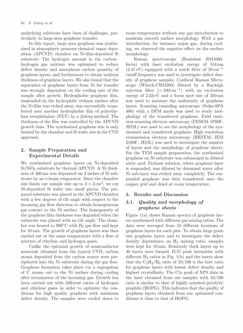
Figure 3 shows the TEM images taken afterthe graphene sheet was transferred onto the CuTEM grid. Combination of grey and white partsof graphene layers in Fig. 3(a) is an evidence of thepresence of different layer thickness. Some foldingphenomenon observed in AFM images of Fig. 2(a)is again visible at the edge of the graphene flakesin Fig. 3(b). These folding at the edge enabled usto measure the graphene thickness, as shown inFig. 3(c). One can clearly observe wide range ofgraphene thicknesses from monolayer up to eightlayers. Electron diffraction patterns taken from dou-ble layer and seven layers are shown in Fig. 2(d).Clear hexagonal spots with alternating spot inten-sities are observed in the case of double layers. Thisindicates a formation of AB stacking order. How-ever in the case of seven layers, a ring-like patternsare observed, which is an evidence of polycrystalline
July 8, 2009 18:1 00153
Large-Area Graphene-Based Flexible Transparent Conducting Films 87
Fig. 3. (a), (b), (c) HRTEM images from the graphene samples after transferred onto Cu TEM grids showing the differentthicknesses from monolayer up to eight layers at the edges. Folded edges or crevices of graphene give information about thenumber of layers. (d) Electron diffraction patterns were shown for two and seven layers of graphene.
phases. This indicates that the grain patches arestitched in different orientations.
3.2. Transfer process of graphenesheets
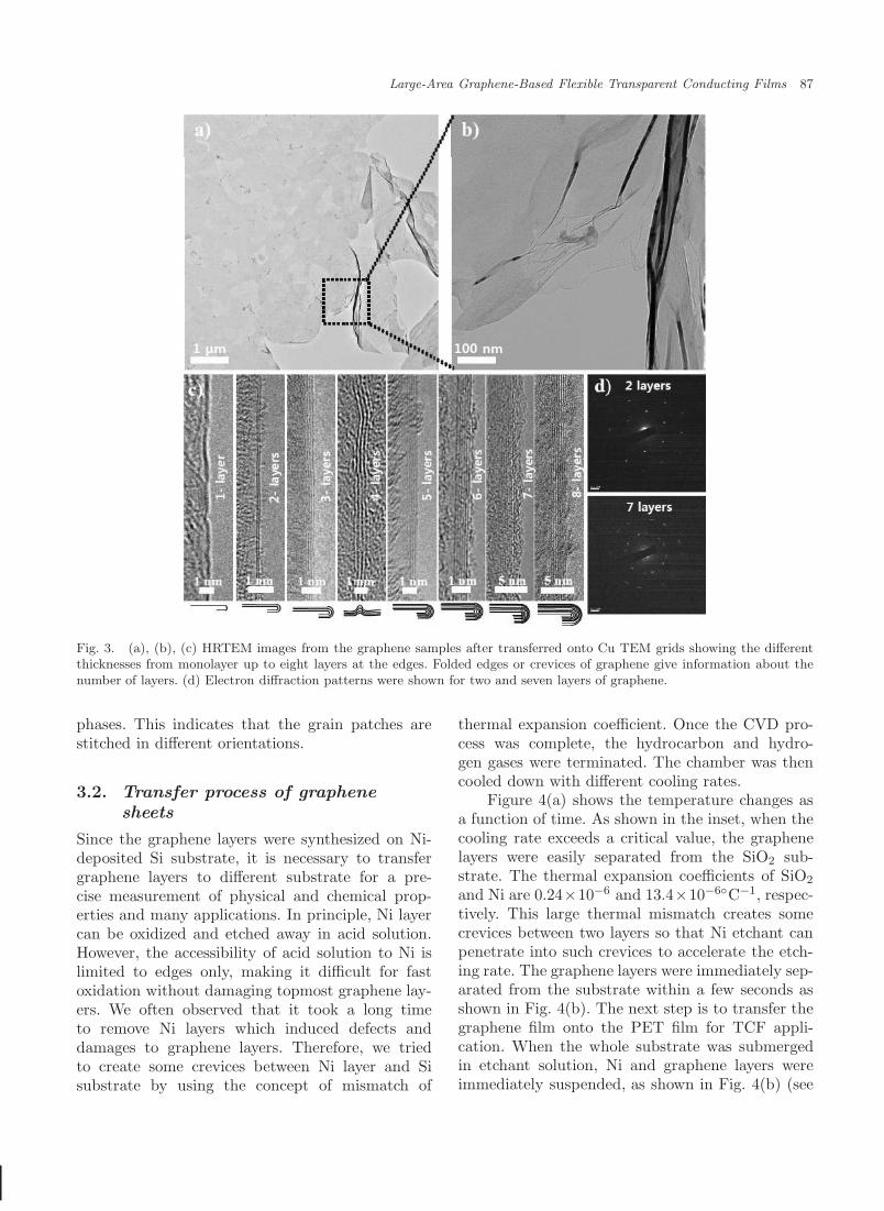
Since the graphene layers were synthesized on Ni-deposited Si substrate, it is necessary to transfergraphene layers to different substrate for a pre-cise measurement of physical and chemical prop-erties and many applications. In principle, Ni layercan be oxidized and etched away in acid solution.However, the accessibility of acid solution to Ni islimited to edges only, making it difficult for fastoxidation without damaging topmost graphene lay-ers. We often observed that it took a long timeto remove Ni layers which induced defects anddamages to graphene layers. Therefore, we triedto create some crevices between Ni layer and Sisubstrate by using the concept of mismatch of
thermal expansion coefficient. Once the CVD pro-cess was complete, the hydrocarbon and hydro-gen gases were terminated. The chamber was thencooled down with different cooling rates.
Figure 4(a) shows the temperature changes asa function of time. As shown in the inset, when thecooling rate exceeds a critical value, the graphenelayers were easily separated from the SiO2 sub-strate. The thermal expansion coefficients of SiO2
and Ni are 0.24×10⁻⁶ and 13.4×10⁻⁶C−1, respec-tively. This large thermal mismatch creates somecrevices between two layers so that Ni etchant canpenetrate into such crevices to accelerate the etch-ing rate. The graphene layers were immediately sep-arated from the substrate within a few seconds asshown in Fig. 4(b). The next step is to transfer thegraphene film onto the PET film for TCF appli-cation. When the whole substrate was submergedin etchant solution, Ni and graphene layers wereimmediately suspended, as shown in Fig. 4(b) (see
July 8, 2009 18:1 00153
88 F. Gunes et al.
(a) (b)
Fig. 4. (a) Graphs showing different cooling rates of the Ni substrates. The shaded region in the inset is the region that theseparation occurs. (b) Time evolution of images taken during the separation of Ni with graphene sheet from Si substrate andetching of Ni layer. After 5min, Ni layer was completely etched away by diluted HNO3.
also video).18 The separated Si substrate was sunkand Ni layer was dissolved after 5min. Becauseof the hydrophobic nature of graphene layers, thegraphene layer was suspended on the etchant sur-face as shown in Fig. 4(b). The graphene layerswas then fished by the underneath PET film. Withthis approach, the folding of graphene layer wasminimized.
3.3. Flexible transparentconducting film
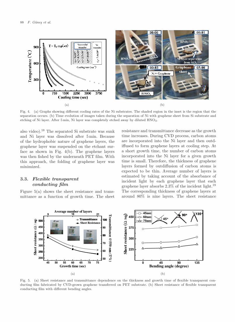
Figure 5(a) shows the sheet resistance and trans-mittance as a function of growth time. The sheet
resistance and transmittance decrease as the growthtime increases. During CVD process, carbon atomsare incorporated into the Ni layer and then outd-iffused to form graphene layers at cooling step. Ata short growth time, the number of carbon atomsincorporated into the Ni layer for a given growthtime is small. Therefore, the thickness of graphenelayers formed by outdiffusion of carbon atoms isexpected to be thin. Average number of layers isestimated by taking account of the absorbance ofincident light by each graphene layer that eachgraphene layer absorbs 2.3% of the incident light.19
The corresponding thickness of graphene layers ataround 80% is nine layers. The sheet resistance
500
189Average number of layers
q)
21
100Transmittance
Tra
75 sec
60 sec
45 sec
400
450
500
ance
(Ω
/ sq
Sheet Resistance
80
90
100Transmittance nsmittance
250
300
350
heet
res
ista
60
70
80 e @550 nm
45 50 55 60 65 70 75
200
250
Growth time (sec)
Sh
50
m (T
%)
) 135o90o
375
450
ance
(Ω
/sq) 60sec
75sec
13590o
45o
225
300
heet
res
ista
0 45 90 135
Sh
Bending angle (degree)
45sec
(a) (b)
Fig. 5. (a) Sheet resistance and transmittance dependence on the thickness and growth time of flexible transparent con-ducting film fabricated by CVD-grown graphene transferred on PET substrate. (b) Sheet resistance of flexible transparentconducting film with different bending angles.

July 8, 2009 18:1 00153
Large-Area Graphene-Based Flexible Transparent Conducting Films 89
Table 1. Comparison of our results with other transparent conducting film propertiesof sheet resistance, transmittance, and thickness.
Transparent conducting Sheet resistance Transmittance Thicknessfilm by (Ω/sq) (T%) (nm) References
CVD graphene 367 80 ∼3272 66 ∼6233 62 ∼7
HOPG (monolayer) 29.4 97.7 0.34 Nair19
Reduced 1800 65 10–11 Wang13
graphite-oxide 1900 90 8.1 Becerril20
Carbon nanotube 50 ∼68 40 Contreras21
30 ∼75 50 Wu22
40–70 70–80 40–60 Geng23
200 85 30 Rowell24
improved with increasing growth time or increasingfilm thickness. The sheet resistance of 233 Ω/sq at atransmittance of 62% is obtained. This film perfor-mance is comparable to those of reported results,12
which is better than that of graphite oxides,13,20
but worse than that of carbon nanotubes.21–24 Thecomparison of our results to the previous works issummarized in Table 1. The optical micrographsexhibit the graphene film (1 × 1 cm2) on the PETfilm and demonstrate the macroscopic uniformityof the film. Control of the defects and uniformity ofthe film in large area are the key factors to improvethe film performance.
Another advantage of graphene film is the flex-ibility. Figure 5(b) shows the sheet resistance of thesame films in Fig. 5(a) with bending angle. Thechange in the sheet resistance becomes apprecia-ble after 90 degrees. Nevertheless, the change is lessthan 15% up to 135 degrees. This implies that noappreciable cracks occur in the film during bend-ing. This excellent flexibility is advantageous overthe conventional indium tin oxide film.
4. Conclusions
We demonstrated a CVD synthesis method of largescale graphene for direct utilization to flexibletransparent conducting film applications. An initialreduction of Ni surface by H2 gas was necessary foruniform growth of the graphene layers. The con-trol of relative content of H2 gas with respect tohydrocarbon gas was also required to minimize thedefects and remove unnecessary carbonaceous parti-cles to decrease the sheet resistance of prepared few-layered graphene. Furthermore, a robust method oftransferring graphene transparent conducting film
on the desired substrate was demonstrated. Ourapproach of large area synthesis of graphene layersand their robust transfer to a desired substrate cre-ates new possibilities for graphene film to be utilizedfor many electronic devices such as sophisticatedhigh speed circuits and conducting films for touchpanels, and common electrodes for flexible displays.
Acknowledgments
This work was financially supported by the STARfaculty project from the Ministry of Education,Science and Technology, the 21st Century Fron-tier R&D Program, AFOSR-MOST, the KOSEFthrough CNNC at SKKU, and by the BK21 program.
References
1. W. Baukal and R. Knoedler, J. Appl. Electrochem.5, 105 (1975).
2. M. Kummer and J. R. Kirchhoff, Electroanalysis 8,524 (1996).
3. L. Hu, D. S. Hecht and G. Gruner, Nano Lett. 4,2513 (2004).
4. Z. C. Wu, Z. H. Chen, X. Du, J. M. Logan, J. Sip-pel, M. Nikolou, K. Kamaras, J. R. Reynolds, D. B.Tanner, A. F. Hebard and A. G. Rinzler, Science305, 1273 (2004).
5. K. S. Novoselov, A. K. Geim, S. V. Morozo, D. Jiang,Y. Zhang, S. V. Dubonos, I. V. Grigorieva and A. A.Firsov, Science 306, 666 (2004).
6. K. S. Novoselov, D. Jiang, F. Schedin, T. Booth,V. V. Khotkevich, S. V. Morozov and A. K. Geim,Proc. Natl. Acad. Sci. USA 102, 10451 (2005).
7. K. S. Novoselov, Z. Jiang, Y. Zhang, S. V. Morozov,H. L. Stormer, U. Zeitler, J. C. Maan, G. S. Boe-binger, P. Kim and A. K. Geim, Science 315, 1379(2007).
July 8, 2009 18:1 00153
90 F. Gunes et al.
8. S. Gilje, S. Han, M. Wang, K. L. Wang and R. B.Kaner, Nano Lett. 7, 3394 (2007).
9. H. C. Schniepp, J. Li, M. J. McAllister, H.Sai, M. Herrera-Alonso, D. H. Adamson, R. K.Prud’homme, R. Car, D. A. Saville and I. A. Aksay,J. Phys. Chem. B 110, 8535 (2006).
10. T. A. Land, T. Michely, R. J. Behm, J. C. Hem-minger and G. Comsa, Surf. Sci. 264, 261 (1992).
11. P. W. Sutter, J. I. Flege and E. A. Sutter, NatureMater. 7, 406 (2008).
12. A. Reina, X. Jia, J. Ho, D. Nezich, H. Son, V.Bulovic, M. S. Dresselhaus and J. Kong, Nano Lett.9, 30 (2009).
13. X. Wang, L. Zhi and K. Mullen, Nano Lett. 8, 323(2008).
14. P. Blake, P. D. Brimicombe, R. R. Nair, T. J. Booth,D. Jiang, F. Schedin, L. A. Ponomarenko, S. V.Morozov, H. F. Gleeson, E. W. Hill, A. K. Geimand K. S. Novoselov, Nano Lett. 8, 1704 (2008).
15. H. Ago, I. Tanaka, M. Tsuji, K. I. Ikeda and S.Mizuno, J. Phys. Chem. C 112, 18350 (2008).
16. A. C. Ferrari, J. C. Meyer, V. Scardaci, C. Casir-aghi, M. Lazzeri, F. Mauri, S. Piscanec, D. Jiang,K. S. Novoselov, S. Roth and A. K. Geim, Phys.Rev. Lett. 97, 187401 (2006).
17. I. Calizo, W. Bao, F. Miao, C. N. Lau and A. A.Balandin, Appl. Phys. Lett. 91, 201904 (2007).
18. See our website for video demonstration of the fish-ing method, http://nanotube.skku.ac.kr/.
19. R. R. Nair, P. Blake, A. N. Grigorenko, K. S.Novoselov, T. J. Booth, T. Stauber, N. M. R. Peresand A. K. Geim, Science 320, 1308 (2008).
20. H. A. Becerril, J. Mao, Z. F. Liu, R. M. Stoltenberg,Z. Bao and Y. Chen, ACS Nano 2, 463 (2008).
21. M. A. Contreras, T. Barnes, J. van de Lagemaat,G. Rumbles, T. J. Coutts, C. Weeks, P. Glatkowski,I. Levitsky, J. Peltola and D. A. Britz, J. Phys.Chem. C 111, 14045 (2007).
22. Z. C. Wu, Z. H. Chen, X. Du, J. M. Logan, J. Sip-pel, M. Nikolou, K. Kamaras, J. R. Reynolds, D. B.Tanner, A. F. Hebard and A. G. Rinzler, Science305, 1273 (2004).
23. H. Z. Geng, K. K. Kim, K. P. So, Y. S. Lee, Y.Chang and Y. H. Lee, J. Am. Chem. Soc. 129, 7758(2007).
24. M. W. Rowell, M. A. Topinka, M. D. McGehee, H.Prall, G. Dennler, N. S. Sariciftci, L. Hu and G.Gruner, Appl. Phys. Lett. 88, 233506/1 (2006).


