Embed Size (px)
Citation preview
2086 IEEE TRANSACTIONS ON ELECTRON DEVICES, VOL. 55, NO. 8, AUGUST 2008
Investigation of the Transport Properties ofSilicon Nanowires Using Deterministic and
Monte Carlo Approaches to the Solutionof the Boltzmann Transport Equation
Marco Lenzi, Pierpaolo Palestri, Member, IEEE, Elena Gnani, Member, IEEE, Susanna Reggiani, Member, IEEE,Antonio Gnudi, Member, IEEE, David Esseni, Senior Member, IEEE, Luca Selmi, Member, IEEE,
and Giorgio Baccarani, Fellow, IEEE
Abstract—We investigate the transport properties of silicon-nanowire FETs by using two different approaches to the solutionof the Boltzmann equation for the quasi-1-D electron gas, namely,the Monte Carlo method and a deterministic numerical solver. Inboth cases, we first solve the coupled Schrödinger–Poisson equa-tions to extract the profiles of the 1-D subbands along the channel;next, the coupled multisubband Boltzmann equations are tackledwith the two different procedures. A very good agreement isachieved between the two approaches to the transport problem interms of mobility, drain–current, and internal physical quantities,such as carrier-distribution functions and average velocities. Somepeculiar features of the low-field mobility as a function of the wirediameter and gate bias are discussed and justified based on thesubband energy and wave-function behavior within the cylindricalgeometry of the nanowire, as well as the heavy degeneracy of theelectron gas at large gate biases.
Index Terms—Boltzmann transport equation, mobility, MonteCarlo, nanowires, simulation, surface roughness.
I. INTRODUCTION
NONPLANAR multigate (i.e., tri-gate and gate-all-around)MOSFET designs have been proposed to achieve effective
suppression of short-channel effects [1]. At the scaling limit,i.e., for channel lengths close to 10 nm, the cross-sectional sizeof these structures has to shrink to the sub-10 × 10 nm2 rangeto maintain good electrostatic control, leading to the design ofdevices that become silicon-nanowire transistors (SNW-FETs),in many cases, featuring an approximately cylindrical crosssection [2], [3].
In spite of the fact that technology has already made availablesamples with dimensions down to about 3 nm [4]–[6], a sys-
Manuscript received November 30, 2007; revised April 29, 2008. This workwas supported in part by the EC through the Network of Excellence SINANOunder Contract 506844 and in part by the PULLNANO Project under GrantFP6 IST-026828-IP. The review of this paper was arranged by Editor M. Reed.
M. Lenzi, E. Gnani, S. Reggiani, A. Gnudi, and G. Baccarani are withthe Advanced Research Center for Electronic Systems (ARCES) and with theDepartment of Electronics (DEIS), University of Bologna—IU.NET, 40136Bologna, Italy.
P. Palestri, D. Esseni, and L. Selmi are with DIEGM, University ofUdine—IU.NET, 33100 Udine, Italy (e-mail: [email protected]).
Color versions of one or more of the figures in this paper are available onlineat http://ieeexplore.ieee.org.
Digital Object Identifier 10.1109/TED.2008.926230
tematic experimental investigation of the transport propertiesof SNW-FETs (e.g., low-field mobility) is still missing, mainlybecause of intrinsic difficulties associated with the small gatecapacitance (a few femtofarads). Therefore, the investigation ofthese devices by means of numerical simulations can be veryinformative, provided that a realistic and complete physicalmodel is employed.
The nanometric wire dimensions and the expectations of aballistic transport have stimulated the interest for full-quantumtransport models, that in many cases have embraced the sim-plifying assumption of a coherent transport regime [7]–[9].However, for decananometer gate lengths, scattering in thechannel is expected to be important for a realistic assessment ofthe on-current, consistently to what is observed in planar MOStransistors [10]. Moreover, recent simulation results suggestthat the phonon-limited mobility in SNWs might not be muchlarger than in planar MOSFETs [11].
Several methodologies have been proposed to include scat-tering effects in the nanowire transport models. A MonteCarlo (MC) approach has been used in [12] to calculatemobility in rectangular SNWs down to 8 × 8 nm2. Mobilitycalculations have also been performed using the momentumrelaxation-time technique [11]. In [13] and [14], instead, carriertransport in nanowires has been investigated using the nonequi-librium Green’s function (NEGF) formalism, including phononscattering for square and Ω-gate devices. As far as surface-roughness (SR) scattering is concerned, an extensive treatmentis found in [15] for ultra-thin-body-silicon-on-insulator FETs,extended later to SNW-FETs in [16], where mobility curvesare computed for different wire diameters and effective fields.An alternative approach to tackle SR in nanowires using theNEGF formalism has been recently proposed in [17]. In thiscontext, it is of the utmost importance to evaluate the potentialof SNW-FETs by using the following: 1) a realistic descriptionof the scattering rates and 2) a simulation approach that canbe used both for the low-field mobility and for a far-from-equilibrium transport regime. In this regard, the exact solu-tion of the coupled Boltzmann transport equations (BTE) foreach subband of the 1-D electron gas (1-DEG) is a promisingapproach even for SNW devices. Moreover, while, for planarMOSFETs, the MC method appears to be the only practical
0018-9383/$25.00 © 2008 IEEE
LENZI et al.: INVESTIGATION OF THE TRANSPORT PROPERTIES OF SILICON NANOWIRES 2087
TABLE IEFFECTIVE MASSES FOR THE 1-DEG IN A CYLINDRICAL SNW
approach to the exact solution of the BTE [18], the reduction ofthe phase-space dimensionality for a 1-DEG makes the directdeterministic solution of the BTE (D-BTE) very attractive[19], [20].
In this paper, we first investigate the behavior of the low-field mobility in cylindrical SNW-FETs as a function of gatebias and wire diameter down to 3 nm using a simplifiedSR-scattering model; next, we compute the drain-currents fordifferent channel lengths and diameters and compare them tothe ballistic limit. To do this, we solve the BTE for the 1-DEGusing both the MC method and a recently developed determin-istic approach [19].
This paper is organized as follows. The simulation ap-proaches are described in Section II. The low-field mobilityfor wires ranging from 3- to 10-nm diameters is investigated inSection III. The drain–current in SNW-FETs with gate lengthsdown to 13 nm is analyzed in Section IV. Conclusions arefinally drawn in Section V.
II. PHYSICAL MODELS
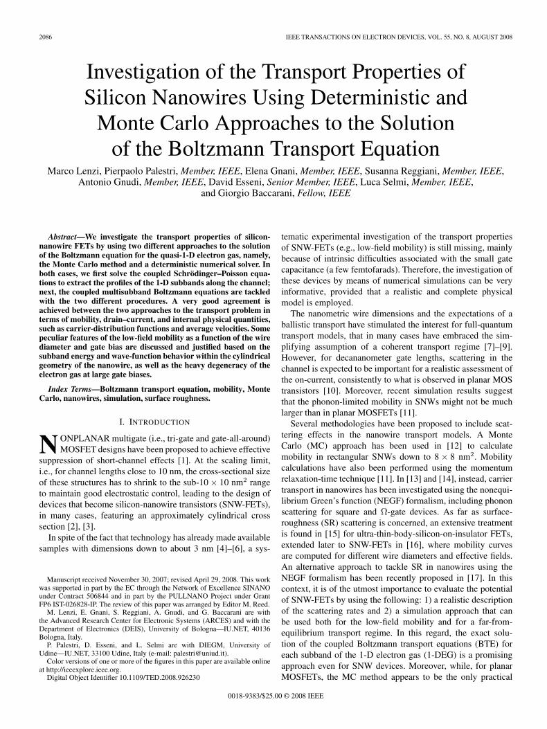
With reference to an SNW with a cylindrical cross sectionand the longitudinal transport direction z along the 〈100〉crystal axis, we assume a cylindrical coordinate system (r, φ, z).Starting from the 3-D quantum–mechanical problem, we firstseparate the transverse (r, φ) and longitudinal (z) componentsof the wave function. The 2-D transverse Schrödinger equa-tion is solved in each cross section by using an isotropicquantization effective mass mr (see Table I) and assumingvanishing wave function at the silicon/dielectric interface. Thelongitudinal motion in the z-direction, instead, is describedwith the semiclassical approach, leading to a system of BTEsin the 2-D phase-space (z, k), where the wave vector k liesin the z-direction. The electric potential ψ(r, φ, z) is obtainedby self-consistently solving the 3-D Poisson equation. Fig. 1shows the solution algorithm. Starting from a first-trial potentialψ0, the Schrödinger equation is solved in each cross section,providing the bottom energy Elmn(z) and the transverse wavefunction χlmn(r, φ, z) of the subband mn in the ladder l, as afunction of z [21]. The index m = 0,±1,±2, . . . is the angularquantization number; n = 1, 2, 3, . . . is the radial quantizationnumber; and l = 1, 2 refers to the subband ladders. With l = 1,we indicate the so-called “unprimed” ladder, resulting from thefour valleys having ellipsoidal energy surfaces with their prin-cipal axes normal to the z-direction; l = 2 indicates, instead,the “primed” ladder, resulting from the two remaining valleys[22]. By assuming a cylindrical symmetry of the problem underconsideration, which implies the use of an isotropic effective
Fig. 1. Flowchart of the solution scheme.
quantization mass (see Table I), the transverse wave function isseparated in the radial and angular components
χlmn(r, φ; z) = ρlmn(r; z), ejmφ. (1)
The normalization of χlmn(r, φ; z) in the device volume im-poses that the function ρlmn(r; z) satisfies the normalizingcondition at any device cross section
2π
R∫0
r |ρlmn(r; z)|2 dr = 1.
Table I collects the effective masses for the two ladders. Inthe case of the unprimed ladder, the square-root average ofthe bulk effective masses has been chosen because, as it canbe easily demonstrated, only with this choice, we recover thedensity of states of the free-electron gas for SNWs featuringlarge diameters.
From now on, unless otherwise specified, the subbands willbe numbered by means of a single index (instead of the threeindexes l, m, n) in order to simplify the notation.
Transport in the longitudinal direction is described by a sys-tem of BTEs in the unknown occupation probabilities fi(z, k),where i is the subband index. The previously computed bottomenergies Ei(z) are used as potential energy profiles. The BTErelative to the ith subband in steady state reads
ui∂fi
∂z− 1
dEi
dz
∂fi
∂k= Ci
in(k) − Ciout(k) (2)
where ui = (1/)(dεi/dk) is the group velocity and εi(k) =
2k2/(2mz,i) is the parabolic energy-dispersion relation. Ciin
and Ciout are the in- and out-scattering integrals, respectively,
relative to the state k of the ith subband. As for the bound-ary conditions (BCs) of (2) at the source and drain, equilib-rium Fermi distributions for the inward-directed electrons areprescribed.
2088 IEEE TRANSACTIONS ON ELECTRON DEVICES, VOL. 55, NO. 8, AUGUST 2008
The in- and out-scattering integrals have the form [13]
Ciin(k) = [1 − fi(k)]
∑i′
Lz
2π
∫Si′i(k′, k)fi′(k′), dk′ (3)
Ciout(k) = fi(k)
∑i′
Lz
2π
∫Sii′(k, k′) [1 − fi′(k′)] dk′ (4)
where Lz is the normalizing length of the physical system inthe z-direction and Sii′(k, k′) is the scattering probability fromstate k in the ith subband to state k′ in the i′th subband. Theterms in square brackets take into account the Pauli exclusionprinciple. Scattering with intravalley acoustic and intervalleyoptical phonons, as well as with SR have been accounted forin our simulations. For intravalley acoustic phonons, the high-temperature scattering rate within the isotropic approximationis given by
Sii′
ac(k, k′) =2π
D2ackBTI ii′
Lzv2l ρSi
δ [εi′(k′) − εi(k)] (5)
where Dac is the deformation potential, vl is the longitudinalsound velocity, ρSi is the silicon density, and δ(x) is the Diracdelta function. The form factor I ii′ is given by
I ii′ = 2π
R∫0
r |ρi(r)|2 |ρi′(r)|2 dr (6)
where R is the SNW radius. The scattering rate for intervalleyoptical phonons is
Sii′
op(k, k′) =∑
ν
πD2op,νgii′
ν I ii′
Lzρων
(Nop(ων)
Nop(ων) + 1
)
×δ [εi′(k′) − εi(k) ∓ ων ] (7)
where the sum extends over the f - and g-type optical-phononmodes, Dop,ν is the optical deformation potential, ων is thephonon-angular frequency, gii′
ν is the multiplicity factor of theνth mode scattering process for the couple of subbands ii′, andNop(ων) is the phonon number given by Bose statistics. Theupper and lower choices correspond to absorption and emissionprocesses, respectively. In the present implementation, the threedominant optical modes are taken into account, with parametersreported in Table II. The phonon-parameter values are takenfrom [23], apart from slight modifications in the phonon energyω for f -type modes, that simplify the deterministic BTEsolution, as discussed in the next section.
As far as SR is concerned, starting from the approach pro-posed in [24] and [25], the SR-scattering treatment has beenextended to the SNW case with cylindrical symmetry. Morespecifically, the Appendix illustrates the derivation of the in-travalley SR matrix element from state k in subband mn to statek′ in subband m′n′ of ladder l, obtained by accounting onlyfor the average variation ∆(z) of the cross-sectional radius R.
TABLE IISCATTERING PARAMETERS USED IN THIS PAPER
The corresponding scattering rate, employed in our simulations,turns out to be
Sii′
SR(k, k′) = δmm′2π
[π
2R
mr
]2 [dρmn
dr(R)
dρm′n′
dr(R)
]2
×S∆(q)Lz
δ [εi′(k′) − εi(k)] (8)
where mr is the quantization effective mass from Table I andS∆(q) is the spectrum of ∆(z), with q = k − k′. For ∆(z), wehave assumed an exponential autocorrelation function [26] sothat the corresponding spectrum is
S∆(q) = ∆2rmsΛ
2√
22 + q2Λ2
. (9)
The parameters ∆rms and Λ are reported in Table II and havebeen calibrated as described in Section III. The screening effectproduced by the 1-DEG has been neglected in our simulations.
Once the BTE is solved, the local electron concentration iscomputed as
n(r, z) =∑
i
|ρi(r; z)|2 22π
∞∫−∞
fi(z, k)dk (10)
where the factor two due to the spin degeneracy has beenleft in evidence. The total electronic charge is then fed intoPoisson’s equation, which is solved for the electrostatic po-tential. Neumann conditions are used at the source and drainboundaries [27]. The entire procedure is iterated until theself-consistent global solution is reached. In order to speedupthe iteration process, a pseudo-Newton algorithm is used, bynumerically computing the diagonal of the Jacobian matrix inPoisson’s equation.
The scattering models and the iterative procedure to achieveself-consistency are the same for both the deterministic solverof the BTE and the MC procedure. The differences are in thesolution of the BTE [(2)] and are described in the followingSections II-A and II-B.
A. Deterministic Approach (D-BTE)
Starting from the unknown distribution function fi(z, k) forthe ith subband in the (z, k) phase-space, we define the twofunctions f+
i (z,H) and f−i (z,H) in the (z,H) space according
LENZI et al.: INVESTIGATION OF THE TRANSPORT PROPERTIES OF SILICON NANOWIRES 2089
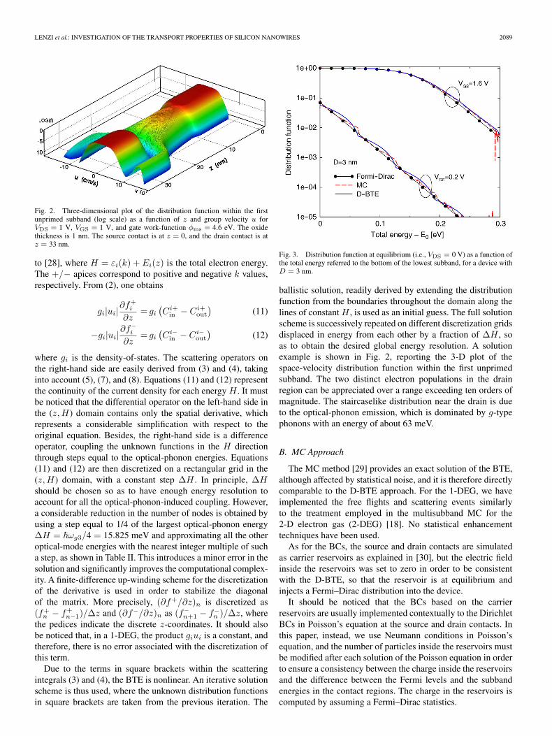
Fig. 2. Three-dimensional plot of the distribution function within the firstunprimed subband (log scale) as a function of z and group velocity u forVDS = 1 V, VGS = 1 V, and gate work-function φms = 4.6 eV. The oxidethickness is 1 nm. The source contact is at z = 0, and the drain contact is atz = 33 nm.
to [28], where H = εi(k) + Ei(z) is the total electron energy.The +/− apices correspond to positive and negative k values,respectively. From (2), one obtains
gi|ui|∂f+
i
∂z= gi
(Ci+
in − Ci+out
)(11)
−gi|ui|∂f−
i
∂z= gi
(Ci−
in − Ci−out
)(12)
where gi is the density-of-states. The scattering operators onthe right-hand side are easily derived from (3) and (4), takinginto account (5), (7), and (8). Equations (11) and (12) representthe continuity of the current density for each energy H . It mustbe noticed that the differential operator on the left-hand side inthe (z,H) domain contains only the spatial derivative, whichrepresents a considerable simplification with respect to theoriginal equation. Besides, the right-hand side is a differenceoperator, coupling the unknown functions in the H directionthrough steps equal to the optical-phonon energies. Equations(11) and (12) are then discretized on a rectangular grid in the(z,H) domain, with a constant step ∆H . In principle, ∆Hshould be chosen so as to have enough energy resolution toaccount for all the optical-phonon-induced coupling. However,a considerable reduction in the number of nodes is obtained byusing a step equal to 1/4 of the largest optical-phonon energy∆H = ωg3/4 = 15.825 meV and approximating all the otheroptical-mode energies with the nearest integer multiple of sucha step, as shown in Table II. This introduces a minor error in thesolution and significantly improves the computational complex-ity. A finite-difference up-winding scheme for the discretizationof the derivative is used in order to stabilize the diagonalof the matrix. More precisely, (∂f+/∂z)n is discretized as(f+
n − f+n−1)/∆z and (∂f−/∂z)n as (f−
n+1 − f−n )/∆z, where
the pedices indicate the discrete z-coordinates. It should alsobe noticed that, in a 1-DEG, the product giui is a constant, andtherefore, there is no error associated with the discretization ofthis term.
Due to the terms in square brackets within the scatteringintegrals (3) and (4), the BTE is nonlinear. An iterative solutionscheme is thus used, where the unknown distribution functionsin square brackets are taken from the previous iteration. The
Fig. 3. Distribution function at equilibrium (i.e., VDS = 0 V) as a function ofthe total energy referred to the bottom of the lowest subband, for a device withD = 3 nm.
ballistic solution, readily derived by extending the distributionfunction from the boundaries throughout the domain along thelines of constant H , is used as an initial guess. The full solutionscheme is successively repeated on different discretization gridsdisplaced in energy from each other by a fraction of ∆H , soas to obtain the desired global energy resolution. A solutionexample is shown in Fig. 2, reporting the 3-D plot of thespace-velocity distribution function within the first unprimedsubband. The two distinct electron populations in the drainregion can be appreciated over a range exceeding ten orders ofmagnitude. The staircaselike distribution near the drain is dueto the optical-phonon emission, which is dominated by g-typephonons with an energy of about 63 meV.
B. MC Approach
The MC method [29] provides an exact solution of the BTE,although affected by statistical noise, and it is therefore directlycomparable to the D-BTE approach. For the 1-DEG, we haveimplemented the free flights and scattering events similarlyto the treatment employed in the multisubband MC for the2-D electron gas (2-DEG) [18]. No statistical enhancementtechniques have been used.
As for the BCs, the source and drain contacts are simulatedas carrier reservoirs as explained in [30], but the electric fieldinside the reservoirs was set to zero in order to be consistentwith the D-BTE, so that the reservoir is at equilibrium andinjects a Fermi–Dirac distribution into the device.
It should be noticed that the BCs based on the carrierreservoirs are usually implemented contextually to the DirichletBCs in Poisson’s equation at the source and drain contacts. Inthis paper, instead, we use Neumann conditions in Poisson’sequation, and the number of particles inside the reservoirs mustbe modified after each solution of the Poisson equation in orderto ensure a consistency between the charge inside the reservoirsand the difference between the Fermi levels and the subbandenergies in the contact regions. The charge in the reservoirs iscomputed by assuming a Fermi–Dirac statistics.
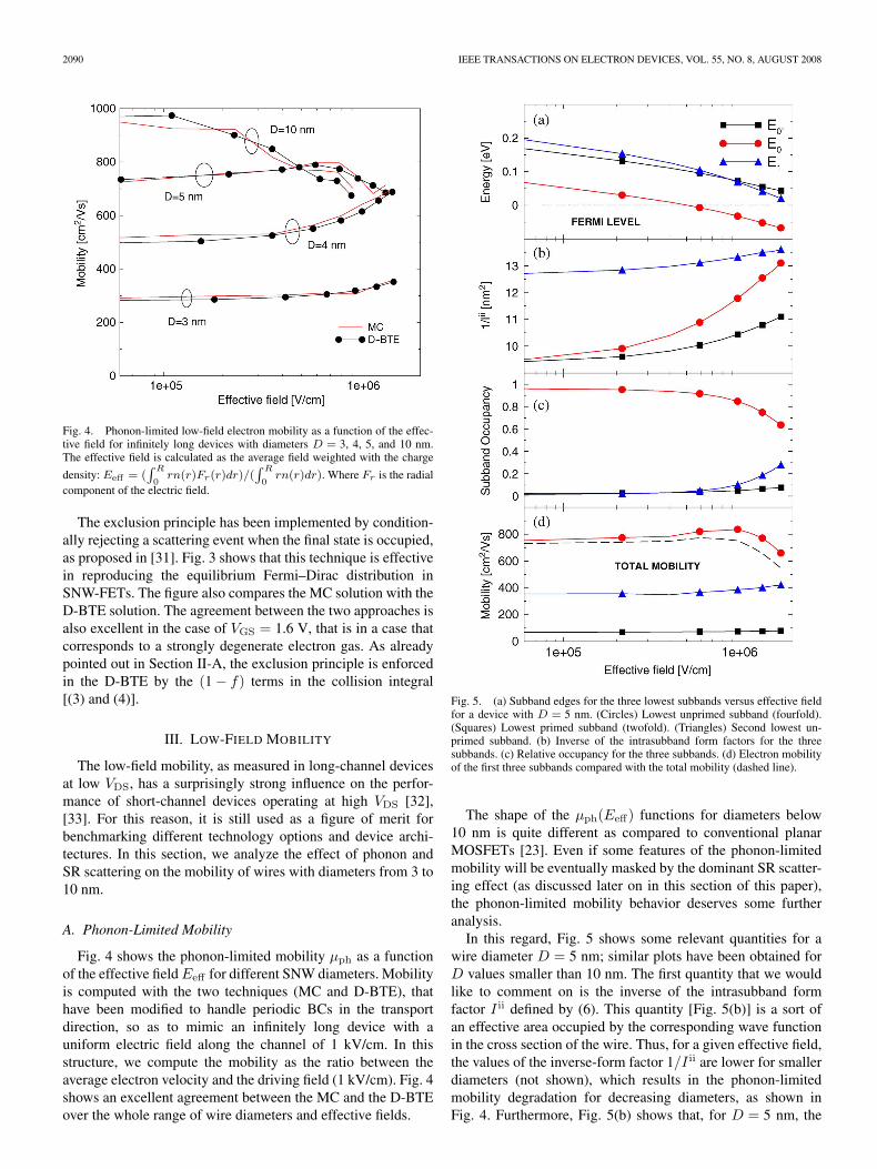
2090 IEEE TRANSACTIONS ON ELECTRON DEVICES, VOL. 55, NO. 8, AUGUST 2008
Fig. 4. Phonon-limited low-field electron mobility as a function of the effec-tive field for infinitely long devices with diameters D = 3, 4, 5, and 10 nm.The effective field is calculated as the average field weighted with the charge
density: Eeff = (∫ R
0rn(r)Fr(r)dr)/(
∫ R
0rn(r)dr). Where Fr is the radial
component of the electric field.
The exclusion principle has been implemented by condition-ally rejecting a scattering event when the final state is occupied,as proposed in [31]. Fig. 3 shows that this technique is effectivein reproducing the equilibrium Fermi–Dirac distribution inSNW-FETs. The figure also compares the MC solution with theD-BTE solution. The agreement between the two approaches isalso excellent in the case of VGS = 1.6 V, that is in a case thatcorresponds to a strongly degenerate electron gas. As alreadypointed out in Section II-A, the exclusion principle is enforcedin the D-BTE by the (1 − f) terms in the collision integral[(3) and (4)].
III. LOW-FIELD MOBILITY
The low-field mobility, as measured in long-channel devicesat low VDS, has a surprisingly strong influence on the perfor-mance of short-channel devices operating at high VDS [32],[33]. For this reason, it is still used as a figure of merit forbenchmarking different technology options and device archi-tectures. In this section, we analyze the effect of phonon andSR scattering on the mobility of wires with diameters from 3 to10 nm.
A. Phonon-Limited Mobility
Fig. 4 shows the phonon-limited mobility µph as a functionof the effective field Eeff for different SNW diameters. Mobilityis computed with the two techniques (MC and D-BTE), thathave been modified to handle periodic BCs in the transportdirection, so as to mimic an infinitely long device with auniform electric field along the channel of 1 kV/cm. In thisstructure, we compute the mobility as the ratio between theaverage electron velocity and the driving field (1 kV/cm). Fig. 4shows an excellent agreement between the MC and the D-BTEover the whole range of wire diameters and effective fields.
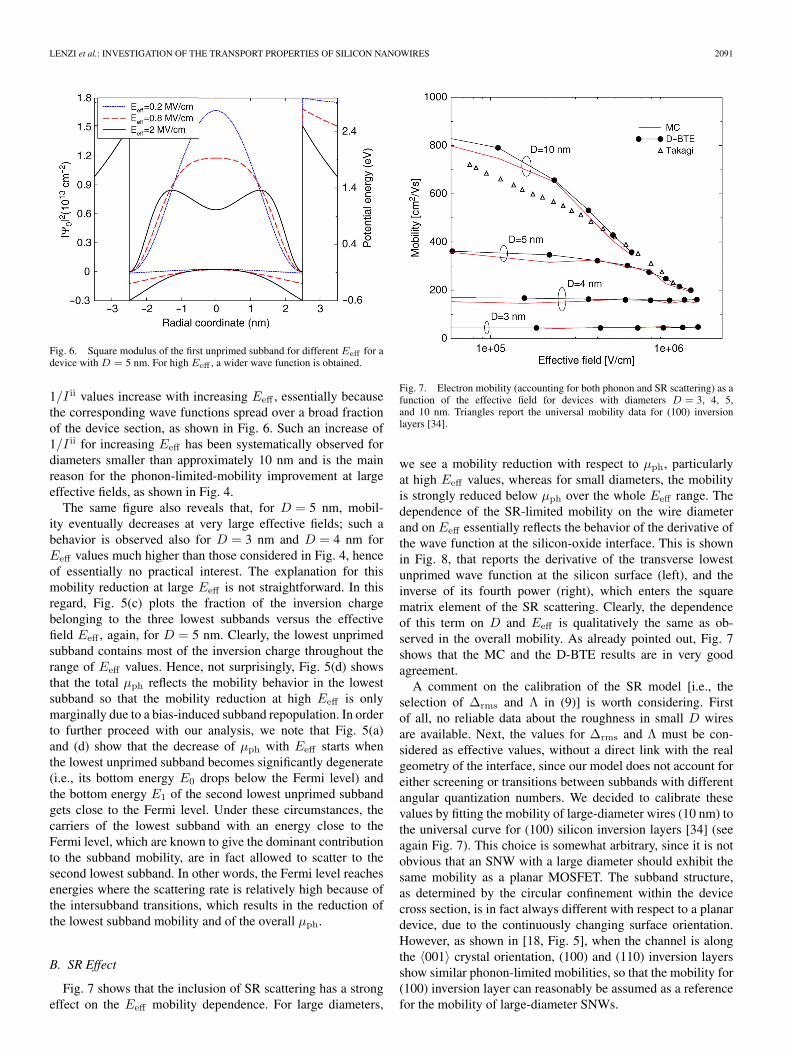
Fig. 5. (a) Subband edges for the three lowest subbands versus effective fieldfor a device with D = 5 nm. (Circles) Lowest unprimed subband (fourfold).(Squares) Lowest primed subband (twofold). (Triangles) Second lowest un-primed subband. (b) Inverse of the intrasubband form factors for the threesubbands. (c) Relative occupancy for the three subbands. (d) Electron mobilityof the first three subbands compared with the total mobility (dashed line).
The shape of the µph(Eeff) functions for diameters below10 nm is quite different as compared to conventional planarMOSFETs [23]. Even if some features of the phonon-limitedmobility will be eventually masked by the dominant SR scatter-ing effect (as discussed later on in this section of this paper),the phonon-limited mobility behavior deserves some furtheranalysis.
In this regard, Fig. 5 shows some relevant quantities for awire diameter D = 5 nm; similar plots have been obtained forD values smaller than 10 nm. The first quantity that we wouldlike to comment on is the inverse of the intrasubband formfactor I ii defined by (6). This quantity [Fig. 5(b)] is a sort ofan effective area occupied by the corresponding wave functionin the cross section of the wire. Thus, for a given effective field,the values of the inverse-form factor 1/I ii are lower for smallerdiameters (not shown), which results in the phonon-limitedmobility degradation for decreasing diameters, as shown inFig. 4. Furthermore, Fig. 5(b) shows that, for D = 5 nm, the
LENZI et al.: INVESTIGATION OF THE TRANSPORT PROPERTIES OF SILICON NANOWIRES 2091
Fig. 6. Square modulus of the first unprimed subband for different Eeff for adevice with D = 5 nm. For high Eeff , a wider wave function is obtained.
1/I ii values increase with increasing Eeff , essentially becausethe corresponding wave functions spread over a broad fractionof the device section, as shown in Fig. 6. Such an increase of1/I ii for increasing Eeff has been systematically observed fordiameters smaller than approximately 10 nm and is the mainreason for the phonon-limited-mobility improvement at largeeffective fields, as shown in Fig. 4.
The same figure also reveals that, for D = 5 nm, mobil-ity eventually decreases at very large effective fields; such abehavior is observed also for D = 3 nm and D = 4 nm forEeff values much higher than those considered in Fig. 4, henceof essentially no practical interest. The explanation for thismobility reduction at large Eeff is not straightforward. In thisregard, Fig. 5(c) plots the fraction of the inversion chargebelonging to the three lowest subbands versus the effectivefield Eeff , again, for D = 5 nm. Clearly, the lowest unprimedsubband contains most of the inversion charge throughout therange of Eeff values. Hence, not surprisingly, Fig. 5(d) showsthat the total µph reflects the mobility behavior in the lowestsubband so that the mobility reduction at high Eeff is onlymarginally due to a bias-induced subband repopulation. In orderto further proceed with our analysis, we note that Fig. 5(a)and (d) show that the decrease of µph with Eeff starts whenthe lowest unprimed subband becomes significantly degenerate(i.e., its bottom energy E0 drops below the Fermi level) andthe bottom energy E1 of the second lowest unprimed subbandgets close to the Fermi level. Under these circumstances, thecarriers of the lowest subband with an energy close to theFermi level, which are known to give the dominant contributionto the subband mobility, are in fact allowed to scatter to thesecond lowest subband. In other words, the Fermi level reachesenergies where the scattering rate is relatively high because ofthe intersubband transitions, which results in the reduction ofthe lowest subband mobility and of the overall µph.
B. SR Effect
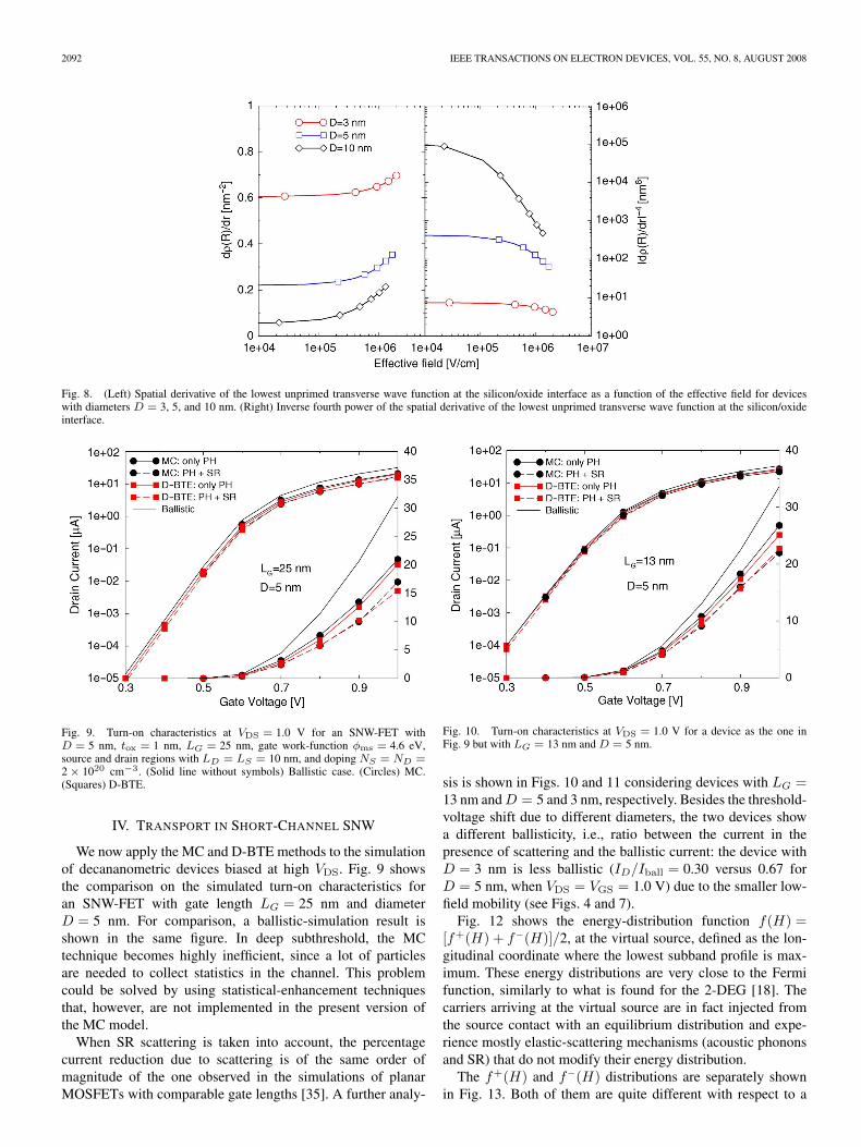
Fig. 7 shows that the inclusion of SR scattering has a strongeffect on the Eeff mobility dependence. For large diameters,
Fig. 7. Electron mobility (accounting for both phonon and SR scattering) as afunction of the effective field for devices with diameters D = 3, 4, 5,and 10 nm. Triangles report the universal mobility data for (100) inversionlayers [34].
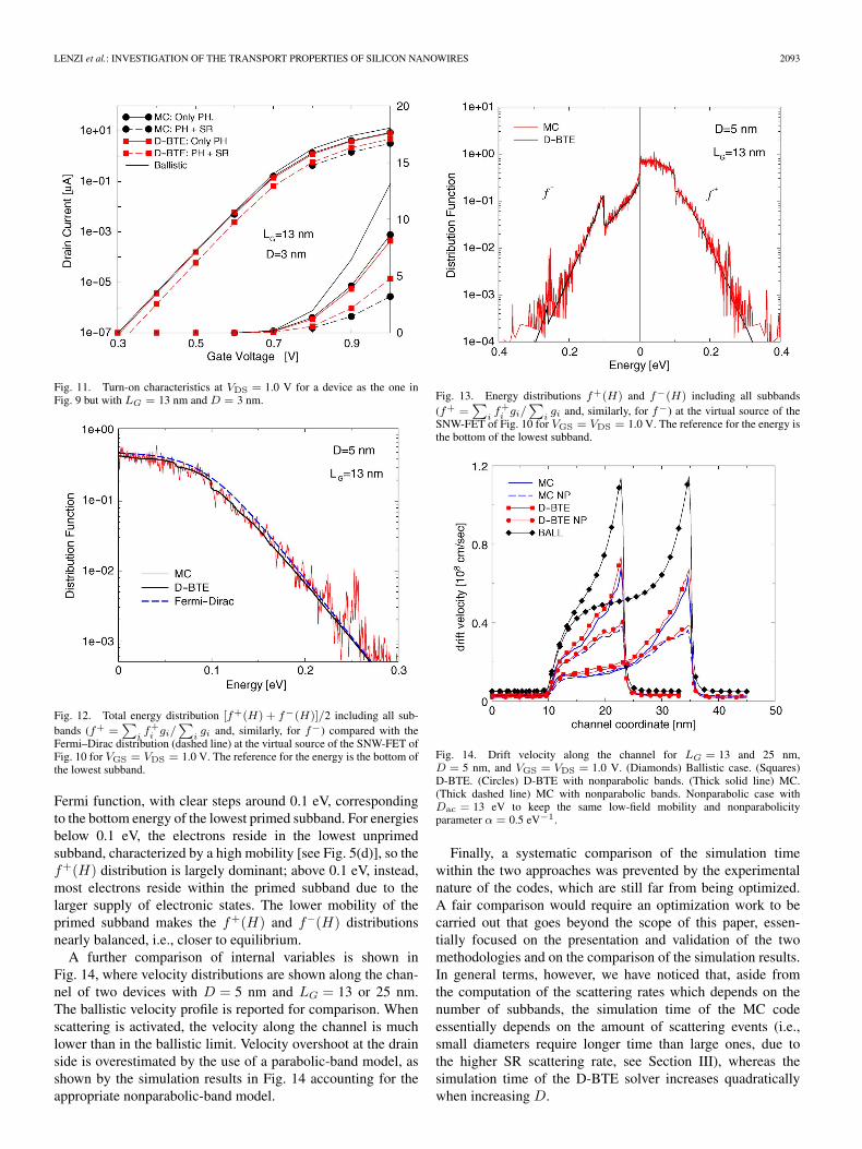
we see a mobility reduction with respect to µph, particularlyat high Eeff values, whereas for small diameters, the mobilityis strongly reduced below µph over the whole Eeff range. Thedependence of the SR-limited mobility on the wire diameterand on Eeff essentially reflects the behavior of the derivative ofthe wave function at the silicon-oxide interface. This is shownin Fig. 8, that reports the derivative of the transverse lowestunprimed wave function at the silicon surface (left), and theinverse of its fourth power (right), which enters the squarematrix element of the SR scattering. Clearly, the dependenceof this term on D and Eeff is qualitatively the same as ob-served in the overall mobility. As already pointed out, Fig. 7shows that the MC and the D-BTE results are in very goodagreement.
A comment on the calibration of the SR model [i.e., theselection of ∆rms and Λ in (9)] is worth considering. Firstof all, no reliable data about the roughness in small D wiresare available. Next, the values for ∆rms and Λ must be con-sidered as effective values, without a direct link with the realgeometry of the interface, since our model does not account foreither screening or transitions between subbands with differentangular quantization numbers. We decided to calibrate thesevalues by fitting the mobility of large-diameter wires (10 nm) tothe universal curve for (100) silicon inversion layers [34] (seeagain Fig. 7). This choice is somewhat arbitrary, since it is notobvious that an SNW with a large diameter should exhibit thesame mobility as a planar MOSFET. The subband structure,as determined by the circular confinement within the devicecross section, is in fact always different with respect to a planardevice, due to the continuously changing surface orientation.However, as shown in [18, Fig. 5], when the channel is alongthe 〈001〉 crystal orientation, (100) and (110) inversion layersshow similar phonon-limited mobilities, so that the mobility for(100) inversion layer can reasonably be assumed as a referencefor the mobility of large-diameter SNWs.
2092 IEEE TRANSACTIONS ON ELECTRON DEVICES, VOL. 55, NO. 8, AUGUST 2008
Fig. 8. (Left) Spatial derivative of the lowest unprimed transverse wave function at the silicon/oxide interface as a function of the effective field for deviceswith diameters D = 3, 5, and 10 nm. (Right) Inverse fourth power of the spatial derivative of the lowest unprimed transverse wave function at the silicon/oxideinterface.
Fig. 9. Turn-on characteristics at VDS = 1.0 V for an SNW-FET withD = 5 nm, tox = 1 nm, LG = 25 nm, gate work-function φms = 4.6 eV,source and drain regions with LD = LS = 10 nm, and doping NS = ND =2 × 1020 cm−3. (Solid line without symbols) Ballistic case. (Circles) MC.(Squares) D-BTE.
IV. TRANSPORT IN SHORT-CHANNEL SNW
We now apply the MC and D-BTE methods to the simulationof decananometric devices biased at high VDS. Fig. 9 showsthe comparison on the simulated turn-on characteristics foran SNW-FET with gate length LG = 25 nm and diameterD = 5 nm. For comparison, a ballistic-simulation result isshown in the same figure. In deep subthreshold, the MCtechnique becomes highly inefficient, since a lot of particlesare needed to collect statistics in the channel. This problemcould be solved by using statistical-enhancement techniquesthat, however, are not implemented in the present version ofthe MC model.
When SR scattering is taken into account, the percentagecurrent reduction due to scattering is of the same order ofmagnitude of the one observed in the simulations of planarMOSFETs with comparable gate lengths [35]. A further analy-
Fig. 10. Turn-on characteristics at VDS = 1.0 V for a device as the one inFig. 9 but with LG = 13 nm and D = 5 nm.
sis is shown in Figs. 10 and 11 considering devices with LG =13 nm and D = 5 and 3 nm, respectively. Besides the threshold-voltage shift due to different diameters, the two devices showa different ballisticity, i.e., ratio between the current in thepresence of scattering and the ballistic current: the device withD = 3 nm is less ballistic (ID/Iball = 0.30 versus 0.67 forD = 5 nm, when VDS = VGS = 1.0 V) due to the smaller low-field mobility (see Figs. 4 and 7).
Fig. 12 shows the energy-distribution function f(H) =[f+(H) + f−(H)]/2, at the virtual source, defined as the lon-gitudinal coordinate where the lowest subband profile is max-imum. These energy distributions are very close to the Fermifunction, similarly to what is found for the 2-DEG [18]. Thecarriers arriving at the virtual source are in fact injected fromthe source contact with an equilibrium distribution and expe-rience mostly elastic-scattering mechanisms (acoustic phononsand SR) that do not modify their energy distribution.
The f+(H) and f−(H) distributions are separately shownin Fig. 13. Both of them are quite different with respect to a
LENZI et al.: INVESTIGATION OF THE TRANSPORT PROPERTIES OF SILICON NANOWIRES 2093
Fig. 11. Turn-on characteristics at VDS = 1.0 V for a device as the one inFig. 9 but with LG = 13 nm and D = 3 nm.
Fig. 12. Total energy distribution [f+(H) + f−(H)]/2 including all sub-bands (f+ =
∑if+
i gi/∑
igi and, similarly, for f−) compared with the
Fermi–Dirac distribution (dashed line) at the virtual source of the SNW-FET ofFig. 10 for VGS = VDS = 1.0 V. The reference for the energy is the bottom ofthe lowest subband.
Fermi function, with clear steps around 0.1 eV, correspondingto the bottom energy of the lowest primed subband. For energiesbelow 0.1 eV, the electrons reside in the lowest unprimedsubband, characterized by a high mobility [see Fig. 5(d)], so thef+(H) distribution is largely dominant; above 0.1 eV, instead,most electrons reside within the primed subband due to thelarger supply of electronic states. The lower mobility of theprimed subband makes the f+(H) and f−(H) distributionsnearly balanced, i.e., closer to equilibrium.
A further comparison of internal variables is shown inFig. 14, where velocity distributions are shown along the chan-nel of two devices with D = 5 nm and LG = 13 or 25 nm.The ballistic velocity profile is reported for comparison. Whenscattering is activated, the velocity along the channel is muchlower than in the ballistic limit. Velocity overshoot at the drainside is overestimated by the use of a parabolic-band model, asshown by the simulation results in Fig. 14 accounting for theappropriate nonparabolic-band model.
Fig. 13. Energy distributions f+(H) and f−(H) including all subbands(f+ =
∑if+
i gi/∑
igi and, similarly, for f−) at the virtual source of the
SNW-FET of Fig. 10 for VGS = VDS = 1.0 V. The reference for the energy isthe bottom of the lowest subband.
Fig. 14. Drift velocity along the channel for LG = 13 and 25 nm,D = 5 nm, and VGS = VDS = 1.0 V. (Diamonds) Ballistic case. (Squares)D-BTE. (Circles) D-BTE with nonparabolic bands. (Thick solid line) MC.(Thick dashed line) MC with nonparabolic bands. Nonparabolic case withDac = 13 eV to keep the same low-field mobility and nonparabolicityparameter α = 0.5 eV−1.
Finally, a systematic comparison of the simulation timewithin the two approaches was prevented by the experimentalnature of the codes, which are still far from being optimized.A fair comparison would require an optimization work to becarried out that goes beyond the scope of this paper, essen-tially focused on the presentation and validation of the twomethodologies and on the comparison of the simulation results.In general terms, however, we have noticed that, aside fromthe computation of the scattering rates which depends on thenumber of subbands, the simulation time of the MC codeessentially depends on the amount of scattering events (i.e.,small diameters require longer time than large ones, due tothe higher SR scattering rate, see Section III), whereas thesimulation time of the D-BTE solver increases quadraticallywhen increasing D.
2094 IEEE TRANSACTIONS ON ELECTRON DEVICES, VOL. 55, NO. 8, AUGUST 2008
V. CONCLUSION
In this paper, we have investigated transport effects inSNW-FETs using the following two different approaches: a1-D MC and a deterministic BTE solver. More specifically,we analyzed the low-field mobility of electrons in cylindricalSNW-FETs and discussed its functional dependence on ef-fective field and wire diameter based on the features of thesubband energy and envelope wave functions and on the heavydegeneracy of the 1-DEG at large gate biases. The turn-oncharacteristics resulting from self-consistent simulations ex-hibit an excellent agreement and so do the electron-distributionfunction at the virtual source of the SNW-FET and the driftvelocity profile along the channel. However, the latter quantityis strongly affected by the model used for the energy dispersionin the transport direction, whose choice is critical for a realisticprediction of the transit time.
APPENDIX
For a variation ∆(z) of the cross-sectional radius R at thelongitudinal abscissa z, the intravalley SR matrix element fromstate k in subband mn to state k′ in subband m′n′ of ladder l isdefined as
Mmm′
nn′ (k, k′) .=⟨
ejkz
√Lz
χmn |δU(r)| ejk′z
√Lz
χm′n′
⟩(13)
where δU(r) = −U0 in [R,R + ∆(z)], U0 is the potential bar-rier at the silicon surface, and δU(r) = 0, elsewhere. The indexl has been dropped for notation simplicity. Using (1), the com-ponent of the matrix element [(13)] due to the integral on thetransverse coordinates can be written to first order in ∆(z) as
〈χmn |δU(r)|χm′n′〉 = 2πRρmn(R)ρm′n′(R)U0∆(z)δmm′ .(14)
We need to derive an expression in the limit U0 → ∞, whenρmn(R) → 0. To this purpose, we observe that the radialcomponent of the wave function for an electron with energyE < U0, for r > R, is the solution of the Schrödinger equation
r2 d2ρm
dr2+ r
dρm
dr− (α2r2 + m2)ρm = 0 (15)
where
α2 =2mr(U0 − E)
2. (16)
The solution ρm(r) can be written as
ρm(r) = cKm(αr) (17)
where Km(x) is the modified Bessel function of second kindof order m and c is a constant with no influence on the ratioρ′m/ρm. For r = R
ρm(R) =1α
(dρm
dr
)R
Km(αR)K ′
m(αR)(18)
where K ′m indicates the derivative of Km with respect to its
argument. In the limit U0 → ∞, by replacing (18) into (14),one obtains
〈χmn |δU |χm′n′〉 =2π
2R
2mr
(dρmn
dr
dρm′n′
dr
)R
∆(z)δmm′
(19)where use has been made of the limit Km(x)/K ′
m(x) → −1for x → ∞. By replacing (19) into (13), we obtain
∣∣∣Mmm′
nn′ (k, k′)∣∣∣2 = δmm′
(π
2R
mr
)2
×(
dρmn
dr
dρm′n′
dr
)2
R
S∆(q)Lz
(20)
where S∆(q) is the spectrum given in (9), with q = k − k′. Byusing Fermi’s rule and the expression for |Mmm′
nn′ (k, k′)|2 givenin (20), we readily obtain the expression for the SR scatteringgiven in (8).
ACKNOWLEDGMENT
The authors would like to thank Profs. E. Sangiorgi andM. Rudan for support.
REFERENCES
[1] J.-T. Park, J.-P. Colinge, and C. H. Diaz, “Pi-Gate SOI MOSFET,” IEEEElectron Device Lett., vol. 22, no. 8, pp. 405–406, Aug. 2001.
[2] F.-L. Yang, D.-H. Lee, H.-Y. Chen, C.-Y. Chang, S.-D. Liu, C.-C. Huang,T.-X. Chung, H.-W. Chen, C.-C. Huang, Y.-H. Liu, C.-C. Wu, C.-C. Chen,S.-C. Chen, Y.-T. Chen, Y.-H. Chen, C.-J. Chen, B.-W. Chan, P.-F. Hsu,J.-H. Shieh, H.-J. Tao, Y.-C. Yeo, Y. Li, J.-W. Lee, P. Chen, M.-S. Liang,and C. Hu, “5 nm-gate nanowire FinFET,” in VLSI Symp. Tech. Dig.,Jun. 15–17, 2004, pp. 196–197.
[3] N. Singh, A. Agarwal, L. K. Bera, T. Y. Liow, R. Yang, S. C. Rustagi,C. H. Tung, R. Kumar, G. Q. Lo, N. Balasubramanian, and D.-L. Kwong,“High-performance fully depleted silicon nanowire (diameter ≤ 5 nm)gate-all-around CMOS devices,” IEEE Electron Device Lett., vol. 27,no. 5, pp. 383–386, May 2006.
[4] H.-C. Lin and C.-J. Su, “High-performance poly-Si nanowire NMOStransistors,” IEEE Trans. Nanotechnol., vol. 6, no. 2, pp. 206–212,Mar. 2007.
[5] N. Singh, F. Y. Lim, W. W. Fang, S. C. Rustagi, L. K. Bera, A. Agarwal,C. H. Tung, K. M. Hoe, S. R. Omampuliyur, D. Tripathi, A. O. Adeyeye,G. Q. Lo, N. Balasubramanian, and D. L. Kwong, “Ultra-narrow siliconnanowire gate-all-around CMOS devices: Impact of diameter, channel-orientation and low temperature on device performance,” in IEDM Tech.Dig., Dec. 11–13, 2006, pp. 1–4.
[6] K. Yeo, S. D. Suk, M. Li, Y.-Y. Yeoh, K. H. Cho, K.-H. Hong, S. K. Yun,M. S. Lee, N. Cho, K. Lee, D. Hwang, B. Park, D.-W. Kim, D. Park,and B.-I. Ryu, “Gate-all-around (GAA) twin silicon nanowire MOSFET(TSNWFET) with 15 nm length gate and 4 nm radius nanowires,” inIEDM Tech. Dig., Dec. 11–13, 2006, pp. 1–4.
[7] J. Wang, E. Polizzi, and M. Lundstrom, “A three-dimensional quantumsimulation of silicon nanowire transistors with the effective-mass approx-imation,” J. Appl. Phys., vol. 96, no. 4, pp. 2192–2203, Aug. 2004.
[8] E. Gnani, S. Reggiani, M. Rudan, and G. Baccarani, “Effects of the band-structure modification in silicon nanowires with small diameters,” in Proc.36th ESSDERC, Montreaux, Switzerland, Sep. 18–22, 2006, pp. 170–173.
[9] M. Bescond, N. Cavassilas, K. Kalna, K. Nehari, L. Raymond, J. Autran,M. Lannoo, and A. Asenov, “Ballistic transport in Si, Ge, and GaAsnanowire MOSFETs,” in IEDM Tech. Dig., 2005, pp. 526–529.
[10] S. Eminente, D. Esseni, P. Palestri, C. Fiegna, L. Selmi, and E. Sangiorgi,“Understanding quasi-ballistic transport in nano-MOSFETs. Part II: Tech-nology scaling along the ITRS,” IEEE Trans. Electron Devices, vol. 52,no. 12, pp. 2736–2743, Dec. 2005.
LENZI et al.: INVESTIGATION OF THE TRANSPORT PROPERTIES OF SILICON NANOWIRES 2095
[11] R. Kotyar, B. Obradovic, P. Matagne, M. Stettler, and M. D. Giles, “As-sesment of room-temperature phonon-limited mobility in gated siliconnanowires,” Appl. Phys. Lett., vol. 84, no. 25, pp. 5270–5272, Jun. 2004.
[12] E. B. Ramayya, D. Vasileska, S. M. Goodnick, and I. Knezevic, “Electronmobility in silicon nanowires,” IEEE Trans. Nanotechnol., vol. 6, no. 1,pp. 113–117, Jan. 2007.
[13] M. Gilbert, R. Akis, and D. Ferry, “Phonon-assisted ballistic to diffusivecrossover in silicon nanowire transistors,” J. Appl. Phys., vol. 98, no. 9,p. 094 303, Nov. 2005.
[14] S. Jin, Y. Park, and H. Min, “A three-dimensional simulation of quantumtransport in silicon nanowire transistor in the presence of electron–phononinteractions,” J. Appl. Phys., vol. 99, no. 12, p. 123 719, Jun. 2006.
[15] S. Jin, M. V. Fischetti, and T. Tang, “Modeling of surface-roughnessscattering in ultrathin-body soi mosfets,” IEEE Trans. Electron Devices,vol. 54, no. 9, pp. 2191–2203, Sep. 2007.
[16] S. Jin, M. V. Fischetti, and T. Tang, “Surface roughness scatteringin gated silicon nanowires,” in Proc. 12th IWCE Book Abstract, 2007.
[17] A. Martinez, M. Bescond, J. Barker, A. Svizhenko, M. Anantran,C. Millar, and A. Asenov, “A self-consistent full 3-D real-space NEGFsimulator for studying nonperturbative effects in nano-MOSFETs,” IEEETrans. Electron Devices, vol. 54, no. 9, pp. 2213–2222, Sep. 2007.
[18] L. Lucci, P. Palestri, D. Esseni, L. Bergagnini, and L. Selmi, “Multi-subband Monte-Carlo study of transport, quantization and electron gasdegeneration in ultra-thin SOI n-MOSFETs,” IEEE Trans. ElectronDevices, vol. 54, no. 5, pp. 1156–1164, May 2007.
[19] M. Lenzi, E. Gnani, S. Reggiani, A. Gnudi, M. Rudan, and G. Baccarani,“A deterministic solution of the Boltzmann transport equation for a one-dimensional electron gas in silicon nanowires,” in Proc. 8th Int. Conf.ULIS, Leuven, Belgium, Mar. 15–16, 2007, pp. 47–50.
[20] M. Lenzi, A. Gnudi, S. Reggiani, E. Gnani, M. Rudan, and G. Baccarani,“Semiclassical transport in silicon cylindrical nanowire FETs includingsurface roughness,” in Proc. 12th IWCE Book Abstract, 2007.
[21] E. Gnani, S. Reggiani, M. Rudan, and G. Baccarani, “On the electro-statics of double-gate and cylindrical nanowire MOSFETs,” J. Comput.Electron., vol. 4, no. 1/2, pp. 71–74, Apr. 2005.
[22] E. Gnani, S. Reggiani, A. Gnudi, P. Parruccini, R. Colle, M. Rudan, andG. Baccarani, “Band-structure effects in ultrascaled silicon nanowires,”IEEE Trans. Electron Devices, vol. 54, no. 9, pp. 2243–2254,Sep. 2007.
[23] D. Esseni, A. Abramo, L. Selmi, and E. Sangiorgi, “Physically based mod-eling of low field electron mobility in ultrathin single-and doublegate SOIn-MOSFETs,” IEEE Trans. Electron Devices, vol. 50, no. 12, pp. 2445–2455, Dec. 2003.
[24] T. Ando, “Screening effect and quantum transport in a silicon inver-sion layer in strong magnetic fields,” J. Phys. Soc. Jpn., vol. 43, no. 5,pp. 1616–1626, 1977.
[25] D. Esseni, “On the modeling of surface roughness limited mobility in soimosfets and its correlation to the transistor effective field,” IEEE Trans.Electron Devices, vol. 51, no. 3, pp. 394–401, Mar. 2004.
[26] S. M. Goodnick, D. K. Ferry, C. W. Wilmsen, Z. Liliental, D. Fathy,and O. L. Krivanek, “Surface roughness at the Si(100)-SiO2 inter-face,” Phys. Rev. B, Condens. Matter, vol. 32, no. 12, pp. 8171–8186,Dec. 1985.
[27] Z. Ren, R. Venugopal, S. Goasguen, S. Datta, and M. S. Lundstrom,“nanoMOS 2.5: A two-dimensional simulator for quantum transport indouble-gate MOSFETs,” IEEE Trans. Electron Devices, vol. 50, no. 9,pp. 1914–1925, Sep. 2003.
[28] H. U. Baranger and J. W. Wilkins, “Ballistic structure in the electrondistribution function of small semiconducting structures: General fea-tures and specific trends,” Phys. Rev. B, Condens. Matter, vol. 36, no. 3,pp. 1487–1502, Jul. 1984.
[29] C. Jacoboni and L. Reggiani, “The Monte Carlo method for the solutionof charge transport in semiconductors with applications to covalent mate-rials,” Rev. Mod. Phys., vol. 55, no. 3, pp. 645–705, Jul. 1983.
[30] I. Riolino, M. Braccioli, L. Lucci, P. Palestri, D. Esseni, C. Fiegna, andL. Selmi, “Monte-Carlo simulation of decananometric double-gate SOIdevices: Multi-subband vs. 3D-electron gas with quantum corrections,”in Proc. 36th ESSDERC, Montreaux, Switzerland, Sep. 18–22, 2006,pp. 162–165.
[31] P. Lugli and D. K. Ferry, “Degeneracy in the ensemble Monte Carlomethod for high field transport in semiconductors,” IEEE Trans. ElectronDevices, vol. ED-32, no. 11, pp. 2431–2437, Nov. 1985.
[32] M. Lundstrom and Z. Ren, “Essential physics of carrier transport innanoscale mosfets,” IEEE Trans. Electron Devices, vol. 49, no. 1, pp. 133–141, Jan. 2002.
[33] P. Palestri, R. Clerc, D. Esseni, L. Lucci, and L. Selmi, “Multi-subband-Monte-Carlo investigation of the mean free path and of the kT layer in
degenerated quasi ballistic nanoMOSFETs,” in IEDM Tech. Dig., 2006,pp. 945–948.
[34] S. Takagi, A. Turiumi, M. Iwase, and H. Tango, “On the universality ofinversion layer mobility in si mosfets: Part I-effects of substrate impurityconcentration,” IEEE Trans. Electron Devices, vol. 41, no. 12, pp. 2357–2362, Dec. 1994.
[35] P. Palestri, D. Esseni, S. Eminente, C. Fiegna, E. Sangiorgi, and L. Selmi,“Understanding quasi-ballistic transport in nano-MOSFETs. Part I: Scat-tering in the channel and in the drain,” IEEE Trans. Electron Devices,vol. 52, no. 12, pp. 2727–2735, Dec. 2005.
Marco Lenzi received the Laurea degree in electrical engineering from theUniversity of Bologna, Bologna, Italy, in 2005.
Since October 2005, he has been with the Department of Electronics (DEIS),University of Bologna, where he has been in the field of investigations onphysics of carrier transport and numerical analysis of semiconductor devices.
Pierpaolo Palestri (M’05) received the Laurea de-gree (summa cum laude) in electronic engineeringfrom the University of Bologna, Bologna, Italy, in1998 and the Ph.D. degree in electronic engineeringfrom the University of Udine, Udine, Italy, in 2003.
In 1998, he was with the Department of Electrical,Mechanical, and Management Engineering, Univer-sity of Udine, where he was a Research Assistantin the field of device simulation. From July 2000to September 2001, he held a postdoctoral positionwith Bell Laboratories, Lucent Technologies (cur-
rently Agere Systems), Murray Hill, NJ, where he worked on high-speedsilicon–germanium bipolar technologies. In October 2001, he was an AssistantProfessor and, since November 2005, has been an Associate Professor withDIEGM, University of Udine. His research interests include the modeling ofcarrier transport in nanoscale devices and the simulation of hot-carrier andtunneling phenomena in scaled MOSFETs and nonvolatile memory cells.
Elena Gnani (M’98) received the Laurea and thePh.D. degrees in electrical engineering from the Uni-versity of Bologna, Bologna, Italy, in 1999 and 2003,respectively.
Since October 1999, she has been with the Depart-ment of Electronics (DEIS), University of Bologna,where she has been in the field of investigations onphysics of carrier transport and numerical analysis ofsemiconductor devices. She is currently also with theAdvanced Research Center for Electronic Systems(ARCES), University of Bologna.
Susanna Reggiani (M’07) received the Laurea andthe Ph.D. degrees in electrical engineering from theUniversity of Bologna, Bologna, Italy, in 1997 and2001, respectively.
In April 1997, she joined with the Department ofElectronics (DEIS), University of Bologna, whereshe has been in the field of the numerical simulationof semiconductor devices and, since 1999, on thesimulation of electron transport in nanoscale devicesapplied to quantum computing, and since 2001, shehas been a Research Associate. She is currently
also with the Advanced Research Center for Electronic Systems (ARCES),University of Bologna.
2096 IEEE TRANSACTIONS ON ELECTRON DEVICES, VOL. 55, NO. 8, AUGUST 2008
Antonio Gnudi (M’98) received the Laurea degreein electrical engineering and the Ph.D. degree inelectrical engineering and computer science from theUniversity of Bologna, Bologna, Italy, in 1983 and1989, respectively.
From 1989 to 1990, he was a Visiting Sci-entist with IBM T. J. Watson Research Center,Yorktown Heights, NY, where he was engaged inthe development of advanced physical models andnumerical-simulation tools for charge transport insemiconductor devices. In 1990, he was a Research
Assistant and, since 1998, has been an Associate Professor of electronics withthe University of Bologna, where he was involved in research and teachingactivities concerning the design of analog CMOS circuits for RF applicationsand the modeling, design, and characterization of RF–MEMS devices for wire-less applications. His current research interests include numerical simulation ofnanometer silicon and carbon devices based on semiclassical as well as full-quantum transport models.
David Esseni (S’98–M’00–SM’06) received theLaurea and Ph.D. degrees in electronic engineeringfrom the University of Bologna, Bologna, Italy, in1994 and 1998, respectively.
In 1999, he was an Assistant Professor and, lateron, an Associate Professor with DIEGM, Universityof Udine, Udine, Italy. In 2000, he was a VisitingScientist with Bell Laboratories, Lucent Technolo-gies (currently Agere Systems), Murray Hill, NJ.His research activities have included characterizationtechniques for electrical parameters in MOS devices
and several aspects related to the hot-electron phenomena in MOSFETs andFlash EEPROMs. In particular, he has investigated low-voltage and substrate-enhanced hot-electron phenomena with an emphasis on their practical implica-tions for Flash EEPROM devices. Furthermore, he has also studied the physicalmechanisms responsible for thin-oxide degradation and the problem of thestatistical dispersion of SILC-related retention characteristics in nonvolatilememory arrays. More recently, he was involved in the experimental charac-terization and in the modeling of low-field mobility in ultrathin silicon-on-insulator MOSFETs and in MOSFETs with ultrathin gate oxides. In the contextof the off-equilibrium transport in nano-MOSFETs, his modeling interests alsoinclude the semiclassical Monte Carlo simulation and the quantization effectsin the inversion layers beyond the effective mass approximation.
Luca Selmi (M’01) was born in Rome, Italy, in 1961.He received the Doctorate degree in electronic engi-neering from the University of Bologna, Bologna,Italy, in 1992.
From April 1989 to June 1990, he was a VisitingScientist with the Microwave Technology Division,Hewlett Packard Company, Palo Alto, CA. Since2000, he has been a Full Professor of electronicswith DIEGM, University of Udine, Udine, Italy. Hisresearch interests are in the field of electron-devicemodeling and characterization, with emphasis on
CMOS scaling, nonvolatile memories, and reliability. He held technical andcoordination responsibility in several national and European research projects(V and VI FP). His research activities have been carried out in cooperationor under contract with the largest semiconductor research laboratories andcompanies worldwide, including Philips Research (Eindhoven and Leuven),Infineon Technologies (Villach and Munich), IMEC, LETI, IBM T. J. WatsonResearch Center, AT&T Bell Laboratories, and Hewlett Packard. He coauthoredapproximately 130 papers in refereed journals and conference proceedingsincluding more than 25 IEDM papers.
Dr. Selmi has been, or still is, a member of the technical program committeesof the major electron device conferences (IEDM—twice, ESSDERC, INFOS,IRPS).
Giorgio Baccarani (S’68–M’80–SM’92–F’00) re-ceived the Laurea degrees in electrical engineeringand in physics from the University of Bologna,Bologna, Italy, in 1967 and 1969, respectively.
In 1969, he was with Bell Laboratories, MurrayHill, NJ, where he was a limited-term Member ofthe Technical Staff, working in the area of electron-device processing. In 1970, he was a ResearchAssistant with the University of Bologna, where heinvestigated the physical properties of MOS struc-tures and transport effects in semiconductor mate-
rials and devices. Since 1972, he has been teaching an annual course onquantum electronics and, in 1980, was a Full Professor of digital electronicswith the University of Bologna, where he is one of the initial proposers,and the Director, of the Advanced Research Center for Electronic Systems(ARCES), in 2001. In 1981, he was on a one-year assignment with theIBM Thomas J. Watson Research Center, Yorktown Heights, NY, where heinvestigated the feasibility of a 1/4-µm MOS process from the standpoint ofthe physical limitations affecting the device performance. In 1983 and 1989, hewas again a Visiting Scientist with IBM, where he was investigating advancedphysical models for device simulation and silicon-based heterojunction bipolartransistors, respectively. Since 1983, he has been heading a group involvedin numerical analysis of semiconductor devices, acting as Partner Leader inthe context of several EEC-supported Projects in the area of computer-aideddesign for very large scale integration. His current research interests includenumerical-device simulation, synthesis of analog circuits, analog and digitalarchitectures for image processing, and integrated-circuit design.


