Embed Size (px)
Citation preview

Electronics Laboratory Manual – 15EEL38
Introduction to Logic gates
Theory Logic gates are circuits used to implement a Boolean function. It is a digital circuit which
may have been more than one input but only one output. It has a set of two elements 0 and 1, with operations are applicable to gate type circuits.
These logic gates which form the fundamental parts of logic circuits are constructed from diodes, resistors and transistors in such a way that the circuit output is a result of basic logic operations performed on the inputs.
Experimentally the logic operations can be tested by verifying its truth table. A truth table is a tabular representation of operation performed by the logic gates.
1. OR – Gate (IC – 7432): The logic symbol along with pin configuration of a dual input OR gate is shown in fig 1.1In an OR gate, the output is high when either of the input or all inputs are high and output is low when all inputs are low. It is represented byA+B .
A B A+B0 0 01 1 11 0 11 1 1
Figure 1.1
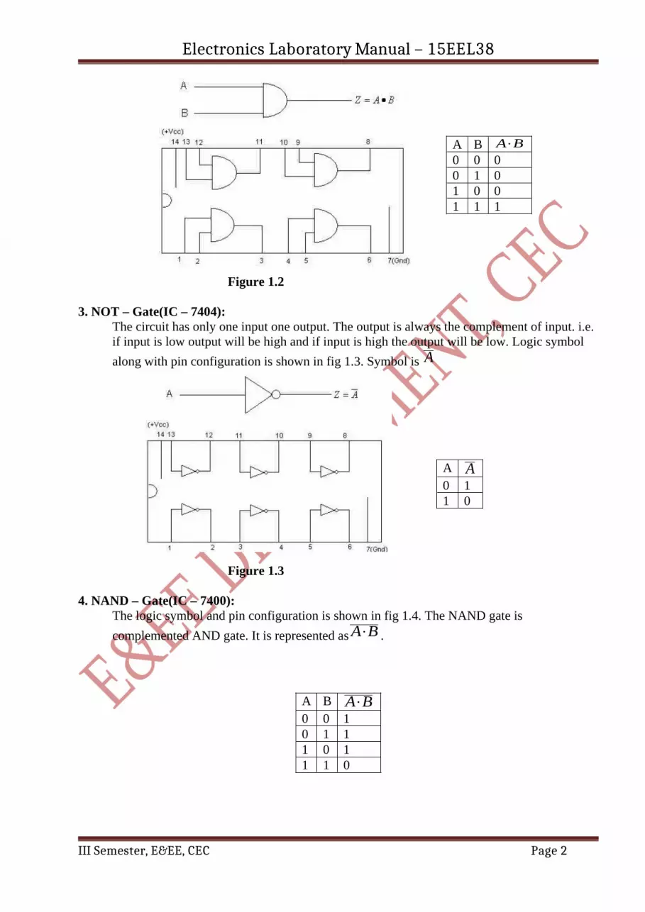
2. AND – Gate(IC – 7408): The logic symbol along with pin diagram of a dual input AND gate is shown in fig 1.2.In an AND gate, the output is high only when all inputs are high and is low when either of the inputs are low. It is represented byA⋅B .
III Semester, E&EE, CEC Page 1
Electronics Laboratory Manual – 15EEL38
Figure 1.2
3. NOT – Gate(IC – 7404): The circuit has only one input one output. The output is always the complement of input. i.e. if input is low output will be high and if input is high the output will be low. Logic symbol along with pin configuration is shown in fig 1.3. Symbol is A
Figure 1.3
4. NAND – Gate(IC – 7400): The logic symbol and pin configuration is shown in fig 1.4. The NAND gate is complemented AND gate. It is represented asA⋅B .
III Semester, E&EE, CEC Page 2
A B A⋅B0 0 00 1 01 0 01 1 1
A A0 11 0
A B A⋅B0 0 10 1 11 0 11 1 0

Electronics Laboratory Manual – 15EEL38
Figure 1.4
5. NOR – Gate (IC – 7402): The logic symbol and pin configuration of a dual input NOR gate is shown in fig 1.5. NOR gate is a complemented OR gate. It is represented by the symbolA+B .
Figure1.5
6. EX-OR – Gate(IC – 7486): The logic symbol and pin diagram are shown in fig 1.6. The output of an EX-OR gate is high only when either of the inputs are high and the output is low when all the inputs are high or
low. The notation used to represent isA⊕B .AB
Figure1.6
III Semester, E&EE, CEC Page 3
A B A+B0 0 10 1 01 0 01 1 0
A B A⊕B0 0 00 1 11 0 11 1 0

Electronics Laboratory Manual – 15EEL38
NAND Gate as Universal Block
1) NOT Gate
2) AND Gate
3) OR Gate
4) EX-OR Gate
III Semester, E&EE, CEC Page 4
Input OutputA A01
10
Input OutputA B Z=A⋅B0 0 00 1 01 0 01 1 1
Input OutputA B Z=A+B0 0 00 1 11 0 11 1 1
Input OutputA B Z=A⊕B0 0 00 1 11 0 11 1 0

Electronics Laboratory Manual – 15EEL38
5) EX-NOR Gate
NOR Gate as Universal Gate
1) NOT Gate
2) OR Gate
III Semester, E&EE, CEC Page 5
Input Output
A B Z=A B+AB0 0 1
0 1 0
1 0 0
1 1 1
Input Output
A A0
1
1
0
Input OutputA B Z=A+B0 0 00 1 11 0 11 1 1

Electronics Laboratory Manual – 15EEL38
3) AND Gate
4) EX-OR Gate
5) EX-NOR Gate
III Semester, E&EE, CEC Page 6
Input Output
A B Z=A⋅B
0 0 0
0 1 0
1 0 0
1 1 1
Input Output
A B Z=A⊕B
0 0 0
0 1 1
1 0 1
1 1 0
Input Output
A B Z=A B+AB0 0 1
0 1 0
1 0 0
1 1 1

Electronics Laboratory Manual – 15EEL38
Exp No: 1DESIGN AND TESTING OF RECTIFIER CIRCUITS
Aim: To determine the ripple factor, efficiency and regulation of the full wave and bridge rectifier circuits with and without capacitor.
Components:Name Description Quantity
Diode BY 127 4
Resistors 1KΩ 1
Capacitors 100μF 1
Function Generator 3MHz 1
DC Voltage source - 1
CRO 20MHz 1
Full Wave Rectifier (Center Tapped) without filter:
V dc=2V m
ΠVm =
V rms=V m
√2VNOLOAD =
V ac=√ (V rms2−V
dc2)
ν=V ac
V dc
PercentageRe gulation=V NOLOAD−V FULLLOAD
V FULLLOADX 100 %
III Semester, E&EE, CEC Page 7

Electronics Laboratory Manual – 15EEL38
η=Pdc
Pac=
Idc2×R
Irms2×R
×100 %
Full Wave Rectifier (Center Tapped) with filter
V dc=Vm−V r ( p−p )
2
V r⋅rms=V r ( p−p)
2√3
ν=V r⋅rms
V dc
ν= 12√3 fRC
V dc=2V m
Π
V rms=V m
√2
V ac=√ (V rms2−V
dc2)
III Semester, E&EE, CEC Page 8

Electronics Laboratory Manual – 15EEL38
Bridge Rectifier without filter
ν=V ac
V dc
PercentageRe gulation=V NOLOAD−V FULLLOAD
V FULLLOADX 100 %
η=Pdc
Pac=
Idc2×R
Irms2×R
×100 %
Bridge Rectifier with filter
V dc=Vm−V r ( p−p )
2
V r⋅rms=V r ( p−p)
2√3
ν=V r⋅rms
V dc
III Semester, E&EE, CEC Page 9

Electronics Laboratory Manual – 15EEL38
Procedure:Without Capacitor Filter1. Rig up the circuit as shown in the circuit diagram.2. To test the transformer, give 230V, 50Hz supply to the primary coil of the transformer and
observe the AC waveform of rated value at the secondary of the transformer on a CRO.3. Connect CRO across the load resistance R.4. Observe the waveform keeping the CRO in DC mode. Note down its amplitude, Vm and
frequency. 5. Switch the CRO to AC mode and observe the waveform. Note down its amplitude Vm,
frequency. 6. Use relevant formula to find Vdc and Vrms for half wave, full wave & bridge rectifiers & draw
the waveforms.7. Calculate the Ripple factor, Regulation and Efficiency by using the formula& compare it with
respective theoretical values.
With Capacitor FilterConnect the capacitor across the load resistance (with polarity of the capacitor as shown in circuit diagram).1. Switch the CRO in DC mode. Measure the peak amplitude with respect to ground reference.
The peak to peak voltage of the ripple is measured from the CRO.2. Calculate the Ripple factor and compare it with theoretical value.
Result:Parameters Full Wave Bridge
Ripple factor
without filter
Theoretical
Practical
Ripple factor
with filter
Theoretical
Practical
Percentage
Efficiency
Theoretical
Practical
Percentage
Regulation
Practical
Conclusion:
VIVA QUESTIONS:1) What is filter?
III Semester, E&EE, CEC Page 10

Electronics Laboratory Manual – 15EEL38
2) What is the efficiency of bridge rectifier?3) What is the value of PIV of a center tapped FWR?4) In filters capacitor is always connected in parallel, why?5) What is the purpose of Center Tapped transformer?6) What is Regulation?7) What is the location of poles of filter in S-plane?8) What is the output of FWR with filter? Is it unidirectional?9) What are the advantages and disadvantages of center tapped full-wave rectifiers compared
with Bridge rectifiers?10) List the Merits and Demerits of Full-wave Rectifier Over Half-Wave Rectifier
Date of completion Signature of Staff Remarks
Rough Work:
Exp No: 2TESTING OF DIODE CLIPPING & CLAMPING CIRCUITS
III Semester, E&EE, CEC Page 11

Electronics Laboratory Manual – 15EEL38
CLIPPING CIRCUITS:Aim: Design and test diode clipping circuits for a given reference voltage.Components:
Name Description Quantity
Diode 1N4007 2
Resistors 100 KΩ 1
Function Generator 3MHz 1
DC Voltage source (Dual) - 1
CRO 20MHz 1
Series Clippers:
a) Positive clipping with given positive reference level
b) Positive clipping with given negative reference level
c) Negative clipping with given positive reference level
III Semester, E&EE, CEC Page 12

Electronics Laboratory Manual – 15EEL38
d) Negative clipping with given Negative reference level
Parallel Clippers:
a) Positive clipping with given positive reference level
b) Positive clipping with given negative reference level
III Semester, E&EE, CEC Page 13

Electronics Laboratory Manual – 15EEL38
c) Negative clipping with given negative reference level
d) Negative clipping with given positive reference level
Double clipper, with given reference level
III Semester, E&EE, CEC Page 14
Electronics Laboratory Manual – 15EEL38
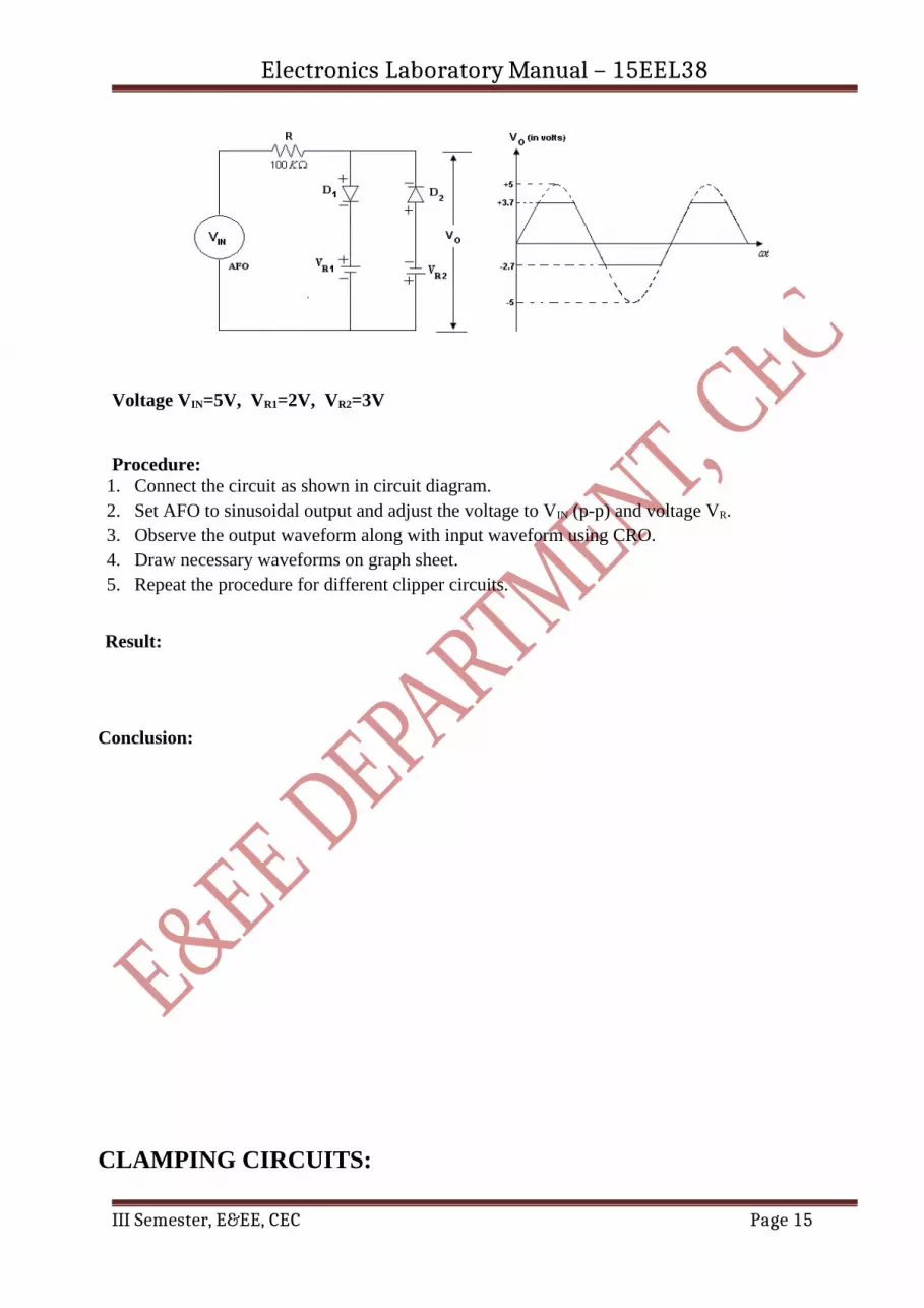
Voltage VIN=5V, VR1=2V, VR2=3V
Procedure:1. Connect the circuit as shown in circuit diagram.2. Set AFO to sinusoidal output and adjust the voltage to VIN (p-p) and voltage VR.3. Observe the output waveform along with input waveform using CRO.4. Draw necessary waveforms on graph sheet.5. Repeat the procedure for different clipper circuits.
Result:
Conclusion:
CLAMPING CIRCUITS:
III Semester, E&EE, CEC Page 15

Electronics Laboratory Manual – 15EEL38
Aim: Design a positive/negative clamping circuits for a given reference voltage.Components:
Name Description Quantity
Diode 1N4007 1
Resistors 100 KΩ 1
Capacitors 0.1 µF 1
Function Generator 3MHz 1
DC Voltage source (Dual) - 1
CRO 20MHz 1
Design:Let the input voltage be 10V (p-p) sine wave at 1 KHzT=1
f=1msec
For Clamping RC>>τLet C=0.1μF
So R>τ
CR>100KΩLet R=100KΩ
a) Positive ClampingClamps the negative peak of the input voltage
Circuit Diagram:
Expected Waveforms:
III Semester, E&EE, CEC Page 16

Electronics Laboratory Manual – 15EEL38
(a) Clamper Output with VR=0(b) Clamper Output with VR>0 (+ve Voltage)(c) Clamper Output with VR<0 (-ve Voltage)
b) Negative ClampingCircuit Diagram:
Expected Waveforms:
(a)Clamper Output with VR=0(b)Clamper Output with VR>0 (+ve Voltage) (c)Clamper Output with VR<0 (-ve Voltage)
Procedure:
III Semester, E&EE, CEC Page 17

Electronics Laboratory Manual – 15EEL38
1. Connect the circuit as shown in circuit diagram.2. Set AFO to sinusoidal output and adjust the voltage to VIN=10V(p-p)3. Set the RPS to voltage approximately to 2V4. Observe the output waveform along with input waveform using CRO.5. Draw necessary waveforms on graph sheet.6. Repeat the procedure for negative and positive clamper circuits.
Result:
Conclusion:
VIVA QUESTIONS:1) What are clipping circuits?
2) Mention the applications of clipping circuits?
3) What are clamping circuits?
4) What is the other name of clamping circuits?
5) Mention the applications of clamping circuits?
Date of completion Signature of Staff Remarks
Rough Work:
Exp No.3
III Semester, E&EE, CEC Page 18

Electronics Laboratory Manual – 15EEL38
RC-COUPLED AMPLIFIERAim: Wiring of a RC coupled single stage BJT amplifier and determination of the gain frequency response, input and output impedances.Components:
Name Description QuantityTransistor BC 107 1Resistors 470
2.2k10k47k820
11111
Capacitors 15F10F
12
Circuit diagram:
Design: Let VCE 2=5V, IC 2=2mA ,VCC =10V. Av=-50, fL = 100Hz.
We have
14 VCC VE
110 VCC.
1. To find the value of RE:-
Let VE=
110 VCC=
110 10V=1V.
RE=
V E
IE
V E
IC 2 =
1V2mA =500
Use RE = 4702. To find the value of RC:- VCE =VCC-ICRC-IERE
RC =
V CC−V CEQ−V E
ICQ
=
10−5−12mA = 2 k.
III Semester, E&EE, CEC Page 19

Electronics Laboratory Manual – 15EEL38
Use RC = 2.2 k3. Use BC107 transistor, Since its minimum guaranteed hFE(=100) is more than the required gain(=50) of the amplifier. IB(dc) =IC or IB (hFE) =IC
ie IB=
IChFE =
2×10¿−3
100 = 20μA.4. Calculations of resistor values R1 and R2 :-
We have IR2 ≥ 10IB
Let IR2 = 10IB
IR2 = 10(20*10¿ 6
) = 200 μA.
Also VB = VE+VBE = 1 V+0.7V
=1.7V
R2= VB/IR2
= 1.7V/200μA = 8.5 k Use R2 = 10 k
R1 = (VCC-VB)/IR2
= (10-1.7)/ 200μA = 41.5 k
Use R1= 47 k
5. Calculation of load resistance RL:AV= - (rc/re)
=-
(Rc||RL )re
=
(Rc||RL )
(26mVIE )
Substitute for RC, IE and AV
RL =850 Use RL =820 6.Selection of capacitors, C1, C2, and CE
Selection of C1:
XC1 ≤ Zi/10, Where Zi = R1|| R2|| hie
=R1|| R2|| hFEre
=R1|| R2|| re
R1=41.5 k , R2=8.5 k , hFE =100
III Semester, E&EE, CEC Page 20

Electronics Laboratory Manual – 15EEL38
re = 26mV/IE 26mV/IC
= (26 mV/2mA) = 12.5
Substituting these, we have Zi=1.1 k
XC1 ≤
1. 1k10
XC1=
12Πf LC1 ≤0.11 k or C1 ≥ 14µF
Select C1 =15µF
Selection of C2:
XC2 ≤
ZO
10 where ZO =RC =2.2 k
XC2 =
12Π fC 2 ≤
ZO
10 =
2. 2k10
C2 ≥7.2µF
Select C2 =10µF
Selection of CE:
XCE ≤
RE
10
12Π fCE ≤
RE
10 or 2ПfCE ≥
10RE
CE ≥
102Π fRE → CE ≥ 3.38µF Select CE= 10µF
Tabular Column:
III Semester, E&EE, CEC Page 21

Electronics Laboratory Manual – 15EEL38
Vin= 1.4 Volts
Sl No Frequency(Hz) Vo(Volts) Gain AV= VO/Vi Gain(db)=20log( VO/Vi)
1. 50
2. 60
3. 70
4. 80
5. 100
6. 150
7. 200
8. 500
9. 700
10. 1k
11. 1.5k
12. 100k
13. 200k
14. 300k
15. 400k
16. 500k
III Semester, E&EE, CEC Page 22

Electronics Laboratory Manual – 15EEL38
Frequency Response Graph:
Input mpedance Measurement:
Output Impedance Measurement :
Procedure: A] Maximum Signal Handling Capacity(Vin max): 1. Connect the circuit as shown in ckt fig. 2. The Vcc and Vin are switched on. 3. The voltage Vo is observed on the CRO. 4. The amplitude of the input is varied and the output is observed. 5. For a particular value of input voltage, the output starts clipping.
III Semester, E&EE, CEC Page 23

Electronics Laboratory Manual – 15EEL38
6. The voltage just before the clipping is noted down. This gives Vinmax. 7. The amplitude of input voltage is reduced. B] Frequency Response 1. Input voltage less than the Vinmax is applied. 2. The amplitude of the input is kept constant and the frequency is varied from 50 Hz to500kHz. 3. Each time the corresponding amplitude of V0 is noted down. 4. The amplitude is reduced to zero and the supply is switched off. 5. Gain in dB is calculated using the formula, Av =20log (Vo/Vin). 6. Frequency response curve is plotted.C] Input Impedance: 1. The amplifier circuit is rigged up. 2. The input frequency is kept constant at 1 KHz, the voltage Vin less than Vinmax is applied. 3. The DRB is connected in series with the input as shown in the figure. 4. The DRB is varied until the output becomes half of the previous value with the same input voltage as in step 2. 5. The DRB resistance will give the input impedance of the amplifier. 6. The input voltage is reduced and supply is switched off.D] Output Impedance: 1. The amplifier circuit is rigged up. 2. The input frequency is kept constant at 1 KHz, the voltage Vin less than Vinmax is applied. 3. The DRB is connected across the output terminals as shown in the figure. 4. The DRB is varied until the output becomes half of the previous value with the same input voltage as in step 2. 5. The DRB resistance will give the output impedance of the amplifier. 6. The input voltage is reduced and supply is switched off.
Result:Maximum signal handling capacity= Mid band gain of the amplifier= Bandwidth of the amplifier= Input impedance= Output impedance=
Conclusion:
VIVA QUESTIONS:1. What is the necessity of cascading?2. What is 3dB bandwidth?3. Why RC coupling is preferred in audio range?4. Which type of coupling is preferred and why?5. Explain various types of Capacitors?6. What is loading effect?7. Why it is known as RC coupling?8. What is the purpose of emitter bypass capacitor?9. Which type of biasing is used in RC coupled amplifier?
III Semester, E&EE, CEC Page 24

Electronics Laboratory Manual – 15EEL38
Date of completion Signature of Staff Remarks
Rough Work:
III Semester, E&EE, CEC Page 25

Electronics Laboratory Manual – 15EEL38
Exp No: 4RC PHASE SHIFT OSCILLATOR
Aim: To design and test the RC Phase shift Oscillator for the given frequency.Components :
Name Description QuantityTransistor BC107 1Resistors 47KΩ
2.2KΩ10KΩ680Ω4.7KΩ
5K POT
111121
Capacitors 10μF0.01μF
13
DC Voltage Source 0-30V 1CRO 20MHz 1
Circuit Diagram :
Vo
Vcc+12V
C410uF
C30.01uF
C20.01uF
C10.01uF
RL5K 90%
R14.7K
R44.7K
RE680
R310K
R247K
RC2.2K
Q1BC107
Design of Amplifier StageVCC= 12V, IC= 2mA, VRC= 40% of VCC = 4.8V
VRE = 10% of VCC 1.2V, VCE = 50% of VCC= 6V
VRC = ICRC= 4.8V⇒ RC= 2.4KΩ ¿ 2.2KΩ
VRE =IERE =1.2V⇒RE =600Ω, ¿ 620Ω
III Semester, E&EE, CEC Page 26

Electronics Laboratory Manual – 15EEL38
IB=IC
hfe=2mA
100=20 μA
VR2 = VBE +VRE = 0.7+1.2 =1.9V
VR2 =9IBR2 =1.9V⇒ R2=10KΩ
VR1=VCC-VR2 =10.1V
VR1 =10IBR1 =10.1V⇒R1=4.7KΩ
rc=RC||RL
rc=25mV2mA
=12 .5
Required Gain =50
RL=845Ω
Calculation of resonance frequency and Beta or feedback factor
Fig: Feedback network for RC oscillator
III Semester, E&EE, CEC Page 27
Vin Vo
RRR
CCC

Electronics Laboratory Manual – 15EEL38
β=Vo(s )Vi( s )
=R³
[6R²Cs
+5R(Cs ) ²
+R³+1(Cs ) ³ ]
β=1
1−5R²C²ω²
− j [6RCϖ−1
(RCϖ ) ³ ] −−−−−−−−−−(1)
Equating imaginary part to zero, we get6RCϖ
−1(RCϖ ) ³
=0
6RCϖ
=1(RCϖ ) ³
ϖ=1√6RC
------------ (2)
f=12 Π √6 RC
−−−−−−−−−−−−(3 )
Substitute eqn(2 ) in eqn (1 ) we get
β (s )=−129
A=1β
=−29
If R=4 .7K and C=0. 01μ F, then using equation(3) f=1 .3 ΚΗ z
Procedure:1. Set up the amplifier part of the oscillator and test the dc condition. Ensure that the transistor is
working as an amplifier with the required gain.2. Connect the feedback network and observe the sine wave on the CRO and measure its amplitude
and frequency.3. Observe the waveform at the base and collector of the transistor simultaneously on the CRO and
notice the phase shift.
Result:Frequency of Oscillations (practical) = Frequency of Oscillations (Theoretical) = Peak value of the signal=
Conclusion:
III Semester, E&EE, CEC Page 28

Electronics Laboratory Manual – 15EEL38
VIVA QUESTIONS:1) What is the frequency of RC phase shift oscillator?2) What is a phase shift oscillator?3) Why RC oscillators cannot generate high frequency oscillations?4) What are the applications of RC phase shift oscillators?5) What phase shift does RC phase shift oscillator produce?6) How is phase angle determined in RC phase shift oscillator?7) Why we need a phase shift between input and output signal?
Date of completion Signature of Staff Remarks
Rough Work:
III Semester, E&EE, CEC Page 29

Electronics Laboratory Manual – 15EEL38
Exp No: 5CRYSTAL OSCILLATOR
Aim: To design and test the performance of BJT - Crystal Oscillator for f0>100 kHz
Components:
Circuit Diagram:
III Semester, E&EE, CEC Page 30
Name Description QuantityTransistor CL100 1
Crystal 2 MHz 1Resistors 2.2kΩ
82kΩ18kΩ470Ω
1kΩpot
11111
Capacitors 0.01µF0.1µF47µF
1 11
DC Voltage Source 0-30V 1CRO - 1

Electronics Laboratory Manual – 15EEL38
Design : Given VCC=10V, β=200, IC=2mA
To findRE
VRE=V cc
10=
1010=1V
IERE=1V
IE=IC
RE=Vℜ
I c=Vℜ
I E=
1V2 X10−3 = 0.5x103=500Ω
Choose RE=470Ω
To findRC
Apply KVLto loop
VCC- IC RC- VCE- VRE=0
10V-2x10⁻³ RC-5V-1V=0[VCE=VCC2
=102
=5V ]4V-2x10⁻³ RC=0
RC=2KΩ
Choose RC=2.2KΩ
From the biasing circuit,
VB=VBE+VRE
VB=0.7+1
VB=1.7V
To find IB
IB=I cβ
=2 X10⁻³
200= 0.01mA
Assume 10 IB flows through R1
R1=V cc−V B
10 IB= 10V−1.7V
10 X 0.01mA=8.3 X10³
0.1=83KΩ
Choose R1=82KΩ
Assume 9 IB flows through R2
R2=VB9 IB= 1.7V
9 X 0.01mA=1.7 X10³
0.09=18KΩ
III Semester, E&EE, CEC Page 31

Electronics Laboratory Manual – 15EEL38
R2=18KΩ
Assume Coupling CapacitorC2=0.001µF ,C1=100PF
Expected Waveform:
f=1/T Hz.Procedure:
1) Make the connections as shown in the circuit diagram.
2) Vary the 1 KΩ potentiometers to get an undistorted sine wave at the output.
3) Note down the frequency of the output wave and compare it with the crystal frequency.
Result:Theoretical frequency: Practical frequency:
Conclusion:
VIVA QUESTIONS:
1) What is crystal osscillator?
2) What is Peizo Electric Effect?
3) What are the merits & demerits of Crystal oscillator?
4) What are the applications of crystal oscillator?
Date of completion Signature of Staff Remarks
III Semester, E&EE, CEC Page 32

Electronics Laboratory Manual – 15EEL38
Exp No: 6CLASS-B PUSH PULL AMPLIFIER
Aim: Testing of a transformer less Class-B push pull amplifier and determine its conversion efficiency.
Components required:
Name Description Quantity
Transistors SL100SK100
11
Resistor 470Ω 2DC power supply 0-30V 1
Ammeter 0-2A 1CRO 20MHz 1
Signal generator 3MHz 1Decade Resistance Box 1
Circuit diagram:
III Semester, E&EE, CEC Page 33

Electronics Laboratory Manual – 15EEL38
Expected waveform:
Procedure:
1. Connect circuit as shown in the diagram. 2. Measure a sine wave signal of 5V, 5 kHz and apply it as input (Vi) to the circuit. 3. Observe the crossover distorted sine wave as shown on the CRO, takedown same waveform on
the tracing sheet. 4. By varying the Value of DRB (RL), note down the value of Vo(p-p) across DRB and calculate
conversion efficiency.
Tabular column:
Sl.No RL(DRB)Ω V0(p-p)V η=πV0(p)/4VCC *1001.2.3.
Result:
Conclusion:
VIVA QUESTIONS:
1) What is cross over distortion?2) Classify Amplifiers?3) What is the drawback of class B amplifier? How is this minimized?
Date of completion Signature of Staff Remarks
III Semester, E&EE, CEC Page 34

Electronics Laboratory Manual – 15EEL38
Rough Work:
III Semester, E&EE, CEC Page 35

Electronics Laboratory Manual – 15EEL38
Exp No: 7
III Semester, E&EE, CEC Page 36

Electronics Laboratory Manual – 15EEL38
SIMPLIFICATION, REALIZATION OF BOOLEAN EXPRESSIONS USING LOGIC GATES/UNIVERSAL GATES
Date :Aim: To study the operation of various logic gates using respective IC’s and verification of truth
table.Apparatus:
Digital Trainer KitPatch cordsDigital IC’s
7432 – OR7408 – AND7404 – NOT7400 – NAND7402 – NOR7486 – EX-OR7410 – NAND 3 INPUT7427 – NOR 3 INPUT
Pin Diagram of Three input NAND Gate
Procedure:1. The
connections are made as per logic diagram.2. The power supply is switched ON.3. Truth table for given expression is verified for the different input combinations.
Simplify the given Boolean expression and build the logic circuit.
III Semester, E&EE, CEC Page 37

Electronics Laboratory Manual – 15EEL38
Kmap Simplification (in both forms):
Realization using basic gates (SOP):
III Semester, E&EE, CEC Page 38

Electronics Laboratory Manual – 15EEL38
Realization using basic gates (POS):
Realization using NAND gates only:
Realization using NOR gates only:
Result:
III Semester, E&EE, CEC Page 39

Electronics Laboratory Manual – 15EEL38
VIVA QUESTIONS:1. Why NAND & NOR gates are called universal gates.
2. Realize the EX – OR gates using minimum number of NAND gates.
3. Give the truth table for EX-NOR and realize using NAND gates?
4. What are the different methods to obtain minimal expression?
5. What is a Minterm and Maxterm.
6. State the difference between SOP and POS.
7. What is meant by canonical representation?
8. What is K-map? Why is it used?
Date of completion Signature of Staff Remarks
Rough Work:
Exp No: 8REALIZATION OF HALF/FULL ADDER AND HALF/FULL SUBTRACTOR
USING LOGIC GATES
III Semester, E&EE, CEC Page 40

Electronics Laboratory Manual – 15EEL38
Date :Aim: To design half adder and full adder using logic gates.Apparatus:
Digital Trainer KitPatch cords.Digital IC’s
7486 – EX-OR7432 – OR7408 – AND7404 – NOT
Half Adder:
Truth Table Logic Circuit:
Sum =Carry =
Full Adder:
Truth TableLogic Circuit:
Sum = Carry = Full adder using NAND gates only:
III Semester, E&EE, CEC Page 41
Input OutputA B Sum Carry0 0 0 00 1 1 01 0 1 01 1 0 1
Input OutputA B C Sum Carry0 0 0 0 00 0 1 1 00 1 0 1 00 1 1 0 11 0 0 1 01 0 1 0 11 1 0 0 11 1 1 1 1

Electronics Laboratory Manual – 15EEL38
Half Subtractor:
Truth Table
Logic Diagram:
Full Subtractor:
Truth Table
III Semester, E&EE, CEC Page 42
Input OutputA B Difference Borrow0 0 0 00 1 1 11 0 1 01 1 0 0

Electronics Laboratory Manual – 15EEL38
Input OutputA B C Difference Borrow0 0 0 0 00 0 1 1 10 1 0 1 10 1 1 0 11 0 0 1 01 0 1 0 01 1 0 0 01 1 1 1 1
Logic Diagram
Full Subtractor using NAND gates only:
Procedure:
1. Connections are made as shown in the figure.
2. Note down the output for different combinations of the input bits.
III Semester, E&EE, CEC Page 43

Electronics Laboratory Manual – 15EEL38
3. Compare it with the truth table and verify the output.
Implementing full adder using Two Half adders:
Expression:
Logic Circuit:
Implementing full Subtractor using Two Half subtractors:
Expression:
Logic Circuit:
III Semester, E&EE, CEC Page 44

Electronics Laboratory Manual – 15EEL38
Result:
VIVA QUESTIONS:1. Draw circuit diagram of Half Adder circuit?2. Draw circuit diagram of Full Adder circuit?3. Draw Full Adder circuit by using Half Adder circuit and minimum no. of logic gate?4. Write Boolean function for half adder? Q.5 Write Boolean function for Full adder?5. Design the half Adder & Full Adder using NAND-NAND Logic.6. Draw circuit diagram of Half Subtractor circuit?7. Draw circuit diagram of Full Subtractor circuit?8. Draw Full Subtractor circuit by using Half Subtractor circuit and minimum no. of logic
gate?9. Write Boolean function for half Subtractor?10. Write Boolean function for Full Subtractor?
Date of completion Signature of Staff Remarks
Rough Work:
Exp No: 9 i) REALIZATION OF PARALLEL ADDER/ SUBTRACTORS USING 7483
CHIP ii) BCD TO EX-3CODE CONVERSION AND VICE VERSA
iii) REALIZATION OF BINARY TO GRAY CODE CONVERSION
III Semester, E&EE, CEC Page 45

Electronics Laboratory Manual – 15EEL38
Date :Aim: Verification of parallel adder/subtractor using IC – 7483 and thereby realize code conversions.Apparatus:
Digital Trainer KitPatch cords.Digital IC’s
7486 – EX-OR7483 – PARALLEL ADDER7432 – OR7408 – AND7404 – NOT7411 – AND 3 I/P
Logic diagram(Refer data sheet for pin diagram of IC 7483)
Truth Table for Adder
Truth Table for Subtractor
Inputs Inputs OutputsA3 A2 A1 A0 B3 B2 B1 B0 Cout S3 S2 S1 S0
III Semester, E&EE, CEC Page 46
Inputs Inputs OutputsA3 A2 A1 A0 B3 B2 B1 B0 Cout S3 S2 S1 S0

Electronics Laboratory Manual – 15EEL38
Procedure:1. The Connections are made as per logic diagram.2. The power supply is switched ON.3. Four bit addition is performed by giving inputs to IC 74LS83.4. Four bit parallel adder/subtractor is designed using EX-OR gates, the input to which are the
four bits of B.5. To perform addition set m=0and to perform subtraction set m=1.
BCD to Excess 3 code conversion:
Truth Table
Excess-3 to BCD ConversionTruth Table
Realization using IC 7483
III Semester, E&EE, CEC Page 47
BCD Excess 3 codeDecima
l B3 B2 B1 B0 E3 E2 E1 E0
0 0 0 0 01 0 0 0 12 0 0 1 03 0 0 1 14 0 1 0 05 0 1 0 16 0 1 1 07 0 1 1 18 1 0 0 09 1 0 0 1
Decimal E3 E2 E1 E0 B3 B2 B1 B0
0 0 0 1 11 0 1 0 02 0 1 0 13 0 1 1 04 0 1 1 15 1 0 0 06 1 0 0 17 1 0 1 08 1 0 1 1 9 1 1 0 0

Electronics Laboratory Manual – 15EEL38
Procedure:1. Apply BCD code as first operand (A) and and binary 3 as second operand(B) and Cin=0 for
realizing BCD to Excess-3-code.2. Apply Excess-3-code as first operand (A) and binary 3 as second operand(B) and Cin=1 for
realizing Excess-3-code to BCD.3. Verify the Truth Table and observe the outputs.
Result:
VIVA QUESTIONS:1. What is Excess-3 code? Why it is called Excess-3 code?2. What is the application of Excess-3 Code? 3. Excess-3 code is Weighted or Unweighted?4. What is the difference between serial and parallel addition/subtraction?5. What is a ripple Adder? What are its disadvantages?
Binary to gray code conversionTruth Table:
D C B A Y3 Y2 Y1 Y0
0 0 0 00 0 0 10 0 1 00 0 1 10 1 0 0
III Semester, E&EE, CEC Page 48

Electronics Laboratory Manual – 15EEL38
0 1 0 10 1 1 00 1 1 11 0 0 01 0 0 11 0 1 01 0 1 11 1 0 01 1 0 11 1 1 01 1 1 1
Y3= Y2=
Y1= Y0= Logic Diagram
III Semester, E&EE, CEC Page 49
B’A’ B’A BA BA’
D’C’
D’C
DC
DC’
B’A’ B’A BA BA’
D’C’
D’C
DC
DC’
B’A’ B’A BA BA’
D’C’
D’C
DC
DC’
B’A’ B’A BA BA’
D’C’
D’C
DC
DC’

Electronics Laboratory Manual – 15EEL38
Gray code to binary conversionTruth Table:
Y3 Y2 Y1 Y0 D C B A0 0 0 0 0 0 0 00 0 0 1 0 0 0 10 1 1 0 0 1 0 00 1 1 1 0 1 0 10 1 0 1 0 1 1 00 1 0 0 0 1 1 11 1 0 0 1 0 0 01 1 0 1 1 0 0 11 1 1 1 1 0 1 01 1 1 0 1 0 1 11 0 1 0 1 1 0 01 0 1 1 1 1 0 11 0 0 1 1 1 1 01 0 0 0 1 1 1 1
Y1’Y0’ Y1’Y0 Y1Y0 Y1Y0’
Y’3Y’2
Y’3Y2
Y3Y2
Y3Y’2
A=B=
III Semester, E&EE, CEC Page 50
Y1’Y0’ Y’1Y0 Y1Y0 Y1Y0’
Y’3Y2’
Y3’Y2
Y3Y2
Y3Y2’

Electronics Laboratory Manual – 15EEL38
Y’1Y0’ Y1’Y0 Y1Y0 Y1Y0’
Y3’Y2’
Y’3Y2
Y3Y2
Y3Y2’
C= D=
Logic Diagram
Procedure:
1. The Connections are made as per given diagram (i).
2. The power supply is switched ON.
3. By applying the different input combinations to the given circuit, the concerning truth table is
verified for binary to gray code conversion.
4. Now the connections are made as per fig (ii)
III Semester, E&EE, CEC Page 51
Y1’Y0’ Y’1Y0 Y1Y0 Y1Y0’
Y3’Y2’
Y3’Y2
Y3Y2
Y3Y2’

Electronics Laboratory Manual – 15EEL38
5. Different input combinations are applied and the truth table for gray code to binary conversions
is now verified.
Result:
VIVA QUESTIONS:1. What are code converters? 2. What is the necessity of code conversions?3. What is gray code?4. Covert a binary number 101101 to its equaling gray code.
Date of completion Signature of Staff Remarks
Rough Work:
Exp No: 10DESIGN AND TESTING OF RING COUNTER/JOHNSON COUNTER
Date :
Aim: To design and implement Ring and Johnson Counter using 4 – bit Shift register.Apparatus: Digital Trainer Kit Patch cords. Digital IC’s IC 7495
III Semester, E&EE, CEC Page 52

Electronics Laboratory Manual – 15EEL38
IC 7404 - NOT
Ring Counter
Logic Diagram
Clock Time OutputsQ3 Q2 Q1 Q0
Clock 2 t0 (Starting State)t1 (after 1st clock)t2 (after 2nd clock)t3 (after 3rd clock)t4 (after 4th clock)
Ds Serial Input data (to be right shifted)D3, D2, D1, D0 Parallel data input to be loaded into the shift registerm Mode control Keep m=1 for loading parallel data and to enable clock2. m=0 to enable clock 2.Clock2 For loading input data and for shift left of dataClock1 For right shift of data.Q3. Q2, Q1, Q0 Parallel output of shift register.
Procedure:1. Mode control is made 12. Parallel inputs say 0001 are given to D3, D2, D1, D0 inputs of 7495.3. Clock 2 is pulsed once. Now D3, D2, D1, D0 parallel inputs appear on Q3, Q2, Q1, Q0 lines.4. Clock 1 of 7495 is connected to pulsar.5. Mode control is made 0.6. When clock pulses are applied ‘1’ circulates around.
III Semester, E&EE, CEC Page 53

Electronics Laboratory Manual – 15EEL38
Johnson Counter
Logic Diagram
Clock Time OutputsQ3 Q2 Q1 Q0
Clock 2 t0 (Starting State)t1 (after 1st clock)t2 (after 2nd clock)t3 (after 3rd clock)t4 (after 4th clock)
Procedure:
1. Mode control is made 12. Parallel inputs say 0000 are given to D3, D2, D1, D0 inputs of 7495.3. Clock 2 is pulsed once. Now D3, D2, D1, D0 parallel inputs appear on Q3, Q2, Q1, Q0, lines.4. Clock 1 of 7495 is connected to the pulsar.5. Mode control is made 0.6. When clock pulses are applied ‘1’ circulates around clock as shown. Result:
VIVA QUESTIONS:1. What is modulus of a number.
2. What is a shift register.
3. Explain how a shift register can be used as ring and Johnson counter
4. Give the applications of Johnson and ring counters.
III Semester, E&EE, CEC Page 54

Electronics Laboratory Manual – 15EEL38
5. What are the other technical names for Johnson counter?
6. A ring counter consisting of five Flip-Flops will have how many states?
7. An eight stage ripple counter uses a flip-flop with propagation delay of 75 nanoseconds. The
pulse width of the strobe is 50ns. The frequency of the input signal which can be used for
proper operation of the counter is approximately?
Date of completion Signature of Staff Remarks
Rough Work:
Exp No: 11
DESIGN AND TESTING OF SEQUENCE GENERATORDate :
Aim: To design and set up a sequence generator using IC-7495
Apparatus:
Digital Trainer Kit
Patch cords.
III Semester, E&EE, CEC Page 55

Electronics Laboratory Manual – 15EEL38
Digital IC’s
IC 7495
IC 7486 – EX-OR
IC 7408 - AND
IC 7404 – NOT
To generate 100010011010111:
K-Map
Y =
Logic Diagram:
III Semester, E&EE, CEC Page 56
No.
of
clocks
Flip Flop Outputs Serial
Output
Q3 Q2 Q1 Q0
1. 1 1 1 1 0
2. 0 1 1 1 0
3. 0 0 1 1 0
4. 0 0 0 1 1
5. 1 0 0 0 0
6. 0 1 0 0 0
7. 0 1 0 0 1
8. 1 0 0 1 1
9. 1 1 0 0 0
10. 0 1 1 0 1
11. 1 0 1 1 0
12. 0 1 0 1 1
13. 1 0 1 0 1
14. 1 1 0 1 1
15. 1 1 1 0 1

Electronics Laboratory Manual – 15EEL38
Procedure:
Given Sequence is 100010011010111:
1. Mode control is made 1.
2. Parallel inputs are given at D3, D2, D1, D0.
3. Clock is pulsed once. The parallel inputs appear at Q3, Q2, Q1, Q0.
4. Mode is made 0.
5. As the pulse is applied, required sequence is observed on Q3 line.
To generate the sequence
0 – 8 – 12 – 14 – 15 – 0
Truth Table:Present State Next State
Q3 Q2 Q1 Q0 D3 D2 D1 D0
0 0 0 0
1 0 0 0
1 1 0 0
1 1 1 0
1 1 1 1
0 0 0 0
III Semester, E&EE, CEC Page 57
Electronics Laboratory Manual – 15EEL38
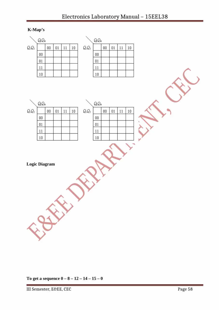
K-Map’s
Logic Diagram
To get a sequence 0 – 8 – 12 – 14 – 15 – 0
III Semester, E&EE, CEC Page 58

Electronics Laboratory Manual – 15EEL38
1. Mode is made 1
2. Clock 2 is pulsed and outputs are observed at Q3, Q2, Q1, Q0
3. Apply continuous clock pulse of frequency 1 KHz and verify the truth table.
4. Observe the waveforms at Q3, Q2, Q1, Q0
Result:
VIVA QUESTIONS:
1. What is the necessity for sequence generation?2. What are PISO, SIPO, and SISO with respect to shift register?3. Differentiate between serial data & parallel data.4. What is the significance of Mode control bit?5. How many Flip-flops are present in IC 7495?
Date of completion Signature of Staff Remarks
Rough Work:
Exp No: 12REALIZATION OF 3 BIT COUNTERS AS A SEQUENTIAL CIRCUIT AND
MOD-N COUNTER DESIGN USING 7490, 74192, 74193
III Semester, E&EE, CEC Page 59

Electronics Laboratory Manual – 15EEL38
Date :
Aim: To design and study various 3 bit synchronous counters using various IC’s and use it as:a) Decade counter with BCD count sequence b) Divide by N counter.
Apparatus:Digital Trainer KitPatch cords.Digital ICs
7490 7400 – NAND7419274193
Pin Diagram of 7490:
Truth Table:
Timing Diagram:
III Semester, E&EE, CEC Page 60
No of clock Q3 Q2 Q1 Q0
012345678910

Electronics Laboratory Manual – 15EEL38
Procedure:
1. Start the count sequence from Q3Q2Q1Q0---0000. MS1 and MS2 inputs are connected to
ground. MR1 is connected to logic 1 and MR2 to logic 0 for count mode.
2. Clock input is given to input A and output Q0 and input B are shorted. Circuit then acts as
mod 10 counter with BCD count sequence.
3. Verify the truth table and observe the waveform
Divide by N counter (MOD 6)
The output Q1 and Q2 are connected to reset inputs MR1 and MR2 through 2NAND gates in series.
As soon as Q1 and Q2 both becomes 1, the counter is reset to 0000.
Logic Diagram:
III Semester, E&EE, CEC Page 61

Electronics Laboratory Manual – 15EEL38
Study of IC 74192:
Function Table:
Load Clear ClockUp Clock Down modeX 1 X X Reset to Zero1 0 1 1 Up count1 0 1 1 Down count0 0 X X Reset1 0 1 1 Stop count
Truth Table for up counter:
No ofclocks Q3 Q2 Q1 Q0
0123456789
Procedure:
Realization of 74192 as a mod-10 counter (UP-counter):
III Semester, E&EE, CEC Page 62

Electronics Laboratory Manual – 15EEL38
a) For up counter, after clearing the counter outputs keep clear=0, load=1.
b) Keep clock down=1 and apply clock to clock up input.
c) Observe the count sequence at the outputs Q3, Q2, Q1, and Q0.
d) If the output changes from 1001 to 0000, carry=0 else carry=1.
Truth Table for down counter:
No ofclocks Q3 Q2 Q1 Q0
0123456789
Realization of 74192 as a mod-10 counter (DOWN-counter):
a) For down counting, after clearing the output keep clear=0, load=1.
b) Keep clock up=1 and apply clock to clock down input.
c) Observe the count sequence at the outputs Q3, Q2, Q1, and Q0.
d) If the outputs Q3, Q2, Q1, Q0 changes from 0000 to 1001 borrow=0, else borrow=1.
III Semester, E&EE, CEC Page 63

Electronics Laboratory Manual – 15EEL38
IC 74193
III Semester, E&EE, CEC Page 64

Electronics Laboratory Manual – 15EEL38
Truth Table for up counter:
No ofclocks Q3 Q2 Q1 Q0
012345678910111213141516
Truth Table for down counter:
No ofclocks Q3 Q2 Q1 Q0
012345678910111213141516
III Semester, E&EE, CEC Page 65

Electronics Laboratory Manual – 15EEL38
Procedure:
Realization of 74193 as UP-counter:
a) For up counter, after clearing the counter outputs keep MR=0, PL=1.
b) Keep clock down (Cpd) =1 and apply clock to clock up (Cpu) input.
c) Observe the count sequence at the outputs Q3, Q2, Q1, and Q0.
d) If the output changes from 1111 to 0000, Tcu=0 else Tcu=1.
Realization of 74193 as DOWN-counter:
a) For down counting, after clearing the output keep MR=0, PL=1.
b) Keep clock up (Cpu) =1 and apply clock to clock down (Cpd) input.
c) Observe the count sequence at the outputs Q3, Q2, Q1, and Q0.
d) If the outputs Q3, Q2, Q1, Q0 changes from 0000 to 1111 Tcd=0 else Tcd=1.
Design up counter for preset value 0010 and N=10
CIRCUIT DIAGRAM:
III Semester, E&EE, CEC Page 66

Electronics Laboratory Manual – 15EEL38
Truth Table:No ofclocks Q3 Q2 Q1 Q0
01234567891011
Design of down counter for preset value 1011 and N=10
CIRCUIT DIAGRAM:
III Semester, E&EE, CEC Page 67

Electronics Laboratory Manual – 15EEL38
Truth Table:
No ofclocks Q3 Q2 Q1 Q0
01234567891011
Result:
VIVA QUESTIONS:
1. What is an asynchronous counter? How is it different from a synchronous counter?
2. What are the advantages of synchronous counters?
3. What is an excitation table?
4. Write the excitation table for D, T FF
5. What is a presettable counter?
6. What are the applications of presettable counters?
7. Explain the working of IC 74193.
Date of completion Signature of Staff Remarks
III Semester, E&EE, CEC Page 68

Electronics Laboratory Manual – 15EEL38
Rough Work:
III Semester, E&EE, CEC Page 69