Embed Size (px)
Citation preview
Indium Antimonide (InSb) Focal Plane Array (FPA) Detection for Near-Infrared Imaging Microscopy
P A T R I C K J . T R E A D O , IRA W. L E V I N , and E. N E l L L E W I S * Laboratory of Chemical Physics, National Institute of Diabetes, Digestive and Kidney Diseases, National Institutes of Health, Bethesda, Maryland 20892 (I. W.L., E.N.L.); and Department of Chemistry, University of Pittsburgh, Pittsburgh, Pennsylvania 15260 (e.J.T.)
Near-infrared spectroscopy is a sensitive, noninvasive method for chem- ical analyses, and its integration with imaging technologies represents a potent tool for the study of a wide range of materials. In this com- munication the use of an indium antimonide (InSb) multichannel imaging detector for near-infrared absorption spectroscopic microscopy is de- scribed. In particular, a 128 x 128 pixel InSb staring array camera has been combined with a refractive optical microscope and an acousto-optic tunable filter (AOTF) to display chemically discriminative, spatially resolved, vibrational spectroscopic images of biological and polymeric systems. AOTFs are computer-controlled bandpass filters that provide high speed, random wavelength access, wide spectral coverage, and high spectral resolution. Although AOTFs inherently have a wide range of spectroscopic applications, we apply this technology to NIR absorption microscopy between 1 and 2.5 ~m. The spectral interval is well matched to the optical characteristics of both the NIR refractive microscope and the AOTF, thereby providing near-diffraction-limited performance with a practical spatial resolution of 1 to 2 ~m. Design principles of this novel instrumentation and representative applications of the technique are presented for various model systems. Index Headings: Near-infrared spectroscopy; Chemical imaging; Bio- logical imaging; Acousto-optics; Acousto-optic tunable filter (AOTF); Indium antimonide; Focal plane array detectors; Multichannel detectors; Infinity-corrected optics.
INTRODUCTION
Near-infrared (NIR) spectroscopy is a powerful ana- lytical method for qualitative and quantitative analysis of chemical samples. ~,2 Analysis is rapid, noninvasive, and nondestructive and provides high signal-to-noise spectra. NIR studies can be performed in either trans- mission or reflectance modes on samples without requir- ing extensive preparation. In contrast to mid-infrared (MIR) methods, refractive optics can be employed to re- duce the cost and complexity of the NIR instrumentation and to provide high-quality imaging capability.
In most NIR spectroscopic applications, macroscopic sampling of multicomponent samples is performed in order to give an average measurement of the analyte, which may be either heterogeneously or homogeneously distributed in the sample matrix. Multivariate statistical methods are then applied to the spectral data set to extract the average concentrations of individual analytes within the sampled volume. 3 For analytes heterogeneously dis- tributed in solid matrices, spatially localized information can be obtained directly with the use of NIR spectral imaging methods. 4 Even microscopic-sized domains
Received 21 September 1993; accepted 21 February 1994. * Author to whom correspondence should be sent. Address for corre-
spondence: National Institutes of Health, Building 5, Room BI-38, Bethesda, MD 20892.
within materials can be readily characterized. These do- mains may take several forms as, for example, cholesterol and lipoprotein deposits in arterial walls 5 and occlusions or defects in semiconductors. 6 In general, chemical im- aging microscopy based on vibrational spectroscopy pro- vides a widely applicable means for chemical visualiza- tion. Vibrational spectroscopic information intrinsic to the sample generates image contrast without the need for potentially invasive staining or tagging.
Vibrational spectroscopic imaging, like vibrational spectroscopy, has embodiments based on MIR and NIR absorption spectroscopy, as well as Raman spectroscopy. At present, MIR functional group imaging 7 is performed by raster scanning a sample beneath a microscope which is coupled to a Fourier transform (FI') interferometer. Vibrational spectroscopic images are then reconstructed from the two-dimensional array of MIR spectra. MIR imaging is particularly attractive because the fundamental vibrational modes which are probed allow straightfor- ward qualitative spectral interpretations. Since MIR im- aging is an absorbance technique employing a reference light source, signal levels are typically high except for highly absorbing or thick samples. Due to the ready avail- ability of FT-IR microspectrometers outfitted with scan- ning accessories, many laboratories have MIR vibrational imaging capability, yet the technique is not widely em- ployed for routine chemical imaging analyses. Point- scanned approaches to vibrational imaging microscopy are time consuming because the signal averaging required at each spatial location limits the total number of pixels that can comprise an image. Thus, image fidelity is ul- timately sacrificed to avoid image collection times ex- tending to hours, or even days. Although reflective Cas- segrain optics are employed to eliminate chromatic aberrations, imaging performance suffers relative to re- fractive microscope optics which do not have center ob- scurations. 8
Despite the experimental challenges associated with Raman spectroscopy, including the need for laser exci- tation and the low-light levels which are often generated, Raman imaging has provided the most efficient means for high-image-fidelity, vibrational spectroscopic micros- copy. Methods based on line-scan imaging, 9 Hadamard transform spatial multiplexing, 1° rotated interference ill- ters, ~ and tunable excitation with narrow-band emission filtering ~2 have been reported. Acousto-optic tunable fil- ters (AOTFs) have been employed by us previously as imaging spectrometers for Raman microscopy. 13
The AOTF is an electronically tunable spectral band- pass filter, whose operation is based on the interaction of
Volume 48, Number 5, 1994 0003-7028/94/4805-060752.00/0 © 1994 Society for Applied Spectroscopy
APPLIED SPECTROSCOPY 607
light with a traveling acoustic wave in an anisotropic crystal :medium. The theory and operating principles of the AOTF have been reviewed in detail. 14 Incident light is diffracted with a narrow spectral bandpass when an rf signal is applied. The wavelength of the diffracted light is tuned simply by changing the applied rf frequency in- put.
Similar to MIR imaging, Raman imaging provides nor- mal mode vibrational information that is readily inter- preted. In contrast to mid-IR analysis, Raman micros- copy typically employs visible laser excitation, allowing the use of high-quality refractive optics to achieve micron spatial resolution imaging performance. In addition, high- sensitivity silicon charge-coupled devices (CCDs), having large pixel array formats (512 x 512/4K x 4K), are avail- able for multichannel detection. The uniformity, sensi- tivity, and high definition provided by silicon CCD de- tectors allow efficient collection of Raman images when the CCD detector is combined with a compatible imaging spectrometer. The greatest disadvantage of Raman meth- ods is the inefficiency of the Raman scattering process, which results in low photon emission levels. Near-real- time Raman microscopy (1 frame/s) typically can be achieved only with strong Raman scatterers unless an enhancement mechanism is available, such as resonance, surface, or coherent anti-Stokes Raman scattering (CARS) techniques. In general, these methods are not applicable or possible for many samples.
Because of the sensitivity and the lack of fluorescence interference, IR absorption methods remain very attrac- tive for vibrational imaging. The availability of moder- ate-cost, high-sensitivity, multichannel imaging detectors suitable for the MIR is not yet a reality. Imaging cameras based on mercury-cadmium-telluride (HgCdTe, MCT) and silicon-doped-with-gallium (Si:Ga) focal plane arrays (FPAs) do exist commercially, but they remain prohibi- tively expensive. These detectors have the potential to impact upon MIR functional group imaging and MIR spectroscopic methods in the same way that silicon CCDs have revolutionized Raman microscopy and spectros- copy.
NIR imaging spectroscopy provides an acceptable compromise between MIR absorption and Raman emis- sion microscopy for performing vibrational spectroscopic imaging. Like MIR imaging, NIR absorption imaging em- ploys an intense broad-band source, and signal-to-noise levels are relatively high. Analogously to Raman mi- croscopy, refractive optics can be used to achieve high spatial resolution (~ 1 um). In addition, multichannel NIR focal plane array detectors and imaging spectrometers, such as AOTFs, are commercially available at a reason- able cost.
We previously demonstrated the use of an AOTF for source spectral tuning in NIR absorption microscopy. ~5 A silicon CCD was utilized in conjunction with a red- wavelength-optimized AOTF to image water OH ab- sorption at 960 nm within lipid vesicle suspensions and to demonstrate the feasability of AOTF source tuning in vibrational absorption imaging.
In this study, we describe the operation of a novel NIR absorption spectroscopic imaging microscope, optimized between 1 and 2 ~zm, which provides several-orders-of- magnitude higher sensitivity for NIR imaging than the
previous generation microscope. The spectral imaging system employs an AOTF, an NIR optimized refractive microscope, and an indium antimonide (InSb) focal plane array detector. Results of chemical imaging studies of model organic systems, as well as intact biological and polymeric materials, are presented.
I N D I U M A N T I M O N I D E FOCAL PLANE ARRAY DETECTORS
InSb FPA detectors are multichannel imaging devices providing sensitive detection between 1 and 5.5 #m. One- dimensional InSb FPAs employing line scanning to gen- erate two-dimensional images have been used in thermal imaging, ~6 as well as in spectroscopic applications in- cluding earth resources remote sensing 17 and the visible infrared mapping spectrometer (VIMS) instrument on the Mars Observer Spacecraft.Is One-dimensional FPAs em- ployed in night-vision applications use rapidly rotating mirrors to scan a target scene sequentially across the linear array. Scanned systems have limited sensitivity due to short dwell times of any one element of the scene on any one sensor pixel.
Two-dimensional InSb stating arrays have existed since the late 1970s 19 and have been employed in the 3-5 # m range for thermal sensing and night-vision applications 2° and IR astronomy. 21 The formats of the early two-di- mensional InSb FPA detectors were limited to 32 × 32 pixel architectures, but, at present, cameras having up to 256 × 256 pixels are commercially available. Two-di- mensional staring FPAs show the advantage of having no moving parts, and the required response time of the de- tector is less stringent. The dwell time of the image on each pixel is increased by a factor of N for an FPA having an N x N geometry which provides a ~ / ~ increase in sensitivity relative to an N element linear array. To the best of the authors' knowledge, this paper includes the first description of an NIR spectral imaging system for microscopic analysis that employs InSb FPA detection in the 1-2.5 #m NIR region.
Detector fabrication involves doping InSb with 1 × 1015 cm -3 tellurium to form n-type bulk material, which is cut into wafers. The n-type wafers are subsequently implanted with 1-3 x 1017 cm -3 beryllium to form p - n junctions. Thermal annealing is then performed and the detector arrays are delineated, leaving an array of mesas which contain the p - n junction of the photodiode. Pas- sivation is then applied, followed by contact metal and indium bump deposition. Wafers are diced, and the InSb is hybridized to a complementary metal-oxide-semicon- ductor (CMOS) silicon multiplexer readout IC to form the hybrid chip assembly by mating the InSb wafer to the silicon multiplexer through aligned arrays of indium bumps located on each component. A mechanical bump bond is then formed by pressing the two components together to form a permanent cold weld. Upon hybrid- ization, the InSb array is thinned to ~ 10 #m, and an anti- reflection coating is typically applied. Figure 1 describes the InSb FPA architecture.
The InSb detector employed here is operated in a pho- tovoltaic mode. The InSb array and multiplexer generate, for every pixel element, an output voltage which is lin- early proportional to the NIR photon flux level across
608 Volume 48, Number 5, 1994

the two-dimensional FPA. In operation, the InSb detector elements are zero-biased and operated in a short-circuit current mode. The multiplexer input structure provides a low-impedance current sink into a capacitor which is reset to initiate each image frame acquisition. NIR pho- tons impinge on the FPA, and photo-generated current is collected through the input structure and integrated for a fraction of the image frame period defined by the elec- tronic timing circuitry. The integrated signal cannot ex- ceed the charge capacity of approximately 50 million car- riers. Upon signal integration, the silicon CMOS multiplexer performs time-division analog signal readout by addressing each element in the array on a row-by- column basis, presenting the signal voltage to a single output line for A/D conversion. After signal readout, the multiplexer dumps the charge-well capacity, and frame integration is repeated.
InSb is not the only detector material available for imaging applications in the NIR. For example, one- and two-dimensional FPAs based on platinum silicide (PtSi), indium gallium arsenide (InGaAs), and germanium (Ge) exist commercially. It is unclear, at present, which type of detector will ultimately prove to be the most satisfac- tory for spectral imaging applications in the NIR. Fun- damental issues such as detector sensitivity, array uni- formity, ease of fabrication, and detector ruggedness are determining factors that govern detector selection.
InSb is employed as the FPA detector material in this study primarily because of its high quantum efficiency, which ranges between 50 and 64% for non-antireflection (AR) coated detectors and 80% for AR-coated FPAs. In microscopy applications, signal levels encountered can be low because of small sample volumes, and the need to maintain image fidelity throughout the optical path pro- duces conditions which are not compatible with efficient light collection and coupling to the detector. InSb detec- tion provides sensitivity superior to that of alternative detector materials and is sufficient for low- to moderate- light-level imaging studies.
The sensitivity of the InSb camera can be characterized by its figure of merit D*, which is >5 x 10 t3 cm Hz u2 W -~ at 77 K. 22 Maximizing D* at a specific wavelength involves maximizing the detector quantum efficiency and minimizing the contributions from background shot noise, readout noise, and detector noise. Background shot noise determines the fundamental noise limit in the absence of signal, while signal shot noise will be the fundamental noise component in the presence of sufficient photon flux. When shot noise is the predominant noise source, the FPA is said to be background limited in performance (BLIP).
Two contributions to readout noise can be distin- guished, including the noise due to the input circuit and the noise generated by analog signal processing and mul- tiplexing. The input circuit contributes the primary read- out noise component, which can be minimized with high detector impedance. Minimization of the thermal noise is also attained by increasing the detector impedance and by reducing the array temperature to liquid N 2 temper- atures (77 K). In practice, thermal noise in the input circuitry is the dominant factor in defining InSb FPA noise performance and limits the effective integration time under dark signal conditions to < 50 ms per frame.
I n-lnSb
1 p-lnSb ~Be implantation) I M~scT
Indium bump 1 Epoxy interconnects
AR Coating i
CMOS Multiplexer
Fi6. I. Schematic diagram of the indium antimonide detector heter- ostructure.
In imaging applications, InSb detector performance is determined, in part, by pixel-to-pixel nonuniformity, which is typically < 3.5%. The nonuniformity can be com- pensated for in absorbance imaging applications, if the detector has sufficient linear dynamic range, by ratioing the detector response against a suitable reference. In pas- sive detection applications, such as remote sensing, as- tronomy, and target identification, detector nonuniform- ity cannot be compensated for as readily. All quantitative measurements performed in this study employ ratioing of the acquired image signals against a reference data set to reduce effects of detector nonuniformity and other in- strument response contributions. While InSb detectors are capable of providing > 16 bits of total dynamic range when appropriately cooled, the instantaneous dynamic range is determined by the A/D converter.
On the basis of the criteria of sensitivity, uniformity, and availability, platinum silicide (PtSi) is another viable camera option. 23 PtSi FPAs benefit from the technological maturity of silicon fabrication methods to yield cameras having large pixel arrays and excellent pixel-to-pixel uni- formity, which are advantageous in passive imaging ap- plications. In low-light-level applications, PtSi perfor- mance is limited due to its low quantum efficiency, typically <5%.
EXPERIMENTAL
The design and operating principles of a near-infrared absorption spectroscopic imaging microscope employing acousto-optic tunable filter technology have been de- scribed previously.15 In a preliminary study, near-infrared and visible absorption imaging was performed with a visible wavelength refractive microscope and a silicon charge-coupled device detector in combination with an
APPLIED SPECTP~OSCOP~ 60~

AOTF optimized for the 0.6-1.2 um interval. The low quantum efficiency of the CCD above 900 nm (<5%), the short optical pathlengths (~ 100 um) of the micro- scopic samples, and the low absorptivities of organic ma- terials in the near-infrared limited the instrument to im- aging OH second-overtone absorptions at 960 nm.
An optimized and more general approach to high-fi- delity vibrational absorption spectroscopic imaging has been constructed around an AOTF, a microscope, and a multichannel detector designed for operation in the NIR (beyond 1 #m). In this study, an NIR AOTF (Brimrose TEAF1.0-2.0H) optimized between 1.0 and 2.0 um and constructed of tellurium dioxide (TeO2) is used to tune a collimated 50-W quartz tungsten halogen lamp source (Newport 780). TeO2 AOTFs optimized for visible wave- length operation have been described in detail else- where. 14 The filter employed in this study is functionally identical to the visible TeO2 AOTFs, with the exception that the piezoelectric transducer and rf drive electronics are optimized for the 87-47 MHz range, which provides spectral tuning between 1 and 2 um. The AOTF calibra- tion, comprised of wavelength response as a function of input rff signal, has been determined by tuning the broad- band source and coupling the filtered light into an NIR FF-interferometer employing InGaAs detection (Bomem DA3).
Macroscopic NIR spectral images are collected by transmitting the approximately monochromatic light se- lected by the AOTF through sample cuvettes and imaging the field using a 50-mm-f.1. (J72) quartz lens coupled to the InSb FPA. Microscopic images are acquired by di- recting the filtered light to an NIR upright metallurgical microscope (Olympus BHSM-IR) in which samples are illuminated in either transmission (Koehler illumination) or diffuse reflectance (epi-illumination) modes. The NIR microscope optics, including the infinity-corrected objectives 24 and projection optics, transmit light between 0.4 and 2.5 um, and are well corrected for chromatic aberrations between 0.6 and 1.8 t~m. Microscope objec- tives having powers of 5 × and 10 x are employed, pro- viding spatial resolutions in combination with the image projection optics of 2.2 and 1.1/~m, respectively. Spectral images are sampled at the exit focal plane of the micro- scope with an InSb FPA detector (Santa Barbara Focal- plane, ImagIR). The image collection is synchronized with AOTF source tuning under computer control.
The InSb detector contains 132 x 132 total pixels with 128 × 128 active pixels on 50-um centers. The detector is operated at 77 K with liquid N 2 cooling. The detector hardware is capable of operating at frame rates between 1 and 240 frames s -1 with integration times ranging from 0.004 to 1 s. The A/D converter defines the detector instantaneous dynamic range of 12 bits, which is in con- trast to the significantly broader dynamic range of the detector material (typically > 16 bits). Two-point cali- brations, which are measured at low-light and high-light levels, determine how the 12-bit dynamic range is allo- cated for any given scene radiance. The dynamic range is allocated by modifying the detector offset and gain controls. If one varies the detector integration time, offset, and gain in separate image acquisitions, > 16-bit perfor- mance can effectively be provided. Nonuniform detector elements that fall outside the calibration range are dis-
played either as dark (0 response) or white (saturated response) pixels in the collected images.
Detector calibration in thermal imaging applications involves exposing the detector to uniform hot and cold temperature scenes, typically temperature-control led blackbody emitters positioned in front of the detector in an out-of-the-focus region. The 12-bit dynamic range of the detector is linearly mapped within the threshold val- ues, and detector intensities are converted to a suitable temperature scale. InSb detectors can readily differentiate IR photon intensities that correspond to temperature changes of 0.01 K.
InSb focal-plane arrays are sensitive from 1 to 5.5 um; however, since the optics and microscope used in these experiments do not transmit beyond 2.5 um, a cold shield was employed to prevent stray radiation beyond 2.5 #m from reaching the detector. Room-temperature black- body emission at >3.3 um contributes significant back- ground radiation and must be eliminated in order to de- tect low-light-level images between 1 and 2.5 vm. Rejection of incident light below 1 um is also performed with the use of a dielectric-coated quartz longpass filter providing transmission between 1 and 2.5 um. UV and visible energy photons are rejected to prevent InSb de- tector flashing, in which high-energy photon-generated charges are semi-permanently embedded in the InSb ma- terial. The latent charge generated by flashing can be re- moved by warming the InSb material to room temper- ature, and in some instances charge elimination requires baking of the InSb array at high temperature (60°C).
The samples employed in this study include carbon tetrachloride and hexadecane (Sigma Chemical Co., re- agent grade), triply distilled water, single layers of onion epidermis, and polymethylmethacrylate (PMMA) film (Reed Plastics). The liquid samples were housed in 400- um-pathlength quartz microcells and positioned for transmission imaging of OH and CH overtone vibrational modes within the immiscible layers. Onion skin was eval- uated for OH content on quartz microscope slides mount- ed under quartz cover slips, while stacked layers of PMMA film were imaged on microscope slides to image CH ab- sorption.
Data collection is performed with an 80386-based com- puter with software written in the C programming lan- guage (Borland C+ + 3.0) to control the InSb camera and automatic AOTF tuning. Spectral image frames are col- lected with 12-bit precision, but are stored as 32-bit float- ing point values to minimize round-off errors during spec- tral image data processing. Final image contrast enhancement and display is performed with a Windows 3.1-based image processing program (BioScan Optimas 4.12). For publication, images are photographed from the computer VGA monitor.
RESULTS
Figure 2 shows an image of water and C C I 4 forming two immiscible layers in a single cuvette. A quartz lens positioned before the InSb FPA was employed for image collection. The images were recorded by integrating the total near-infrared intensity transmitted through the sam- ple from 1 to 2.5 um. AOTF source filtering was not employed in Fig. 2. The image was collected in 15 ms
610 Volume 48, Number 5, 1994

III
• , i ~ ,
ii iii ~ •
J
4 ~
4 ii¢i •
i ¸ ii
Fir. 2. Integrated NIR image (1-2.5 gm) of H20 and CC14 immiscible layers in a l-cm-pathlength quartz cuvette collected with a 50-mm-f.1. quartz lens coupled to the InSb staring FPA detector. The HzO layer is opaque due to OH stretching mode absorption, while the CC14 layer is transparent. Isolated dark pixels correspond to detector elements that do not pass the uniformity tests performed in the calibration sequence.
and illustrates the differences in the near-infrared ab- sorption characteristics of these two materials. HzO is a strong absorber in both the near-infrared and infrared regions of the spectrum, while CC14 is not. The image contrast visualized in Fig. 2 is graphic evidence of the spectral differences between the two chemical species. The chemical differentiation is performed rapidly, noninva- sively, and without the use of stains or dyes that would be required in visible wavelength imaging techniques.
An AOTF is not necessary to differentiate between H20
and C C I 4 because of the lack of C-C1 absorption in the near-infrared spectral region. In most multicomponent systems, however, the differences in NIR sample absorp- tion are not so readily apparent, and an AOTF becomes an essential component of the imaging instrument. Figure 3 shows three images of a 400-/~m-pathlength microcu- vette containing both water and hexadecane in two dis- tinct and immiscible layers. The transmission images were collected with the 50-mm-f.1. quartz lens by averaging 10 frames with an integration time of 31 ms per frame. Each
APPLIED SPECTROSCOPY 611

A B C
FIG. 3. Composite acousto-optic filtered NIR images of H20 and hexadecane immiscible layers in 0.40-mm-pathlength microcuvettes viewed with a 50-mm-f.1. quartz lens coupled to the InSb FPA. (A) Nonabsorbing image at 1340 nm. (B) OH absorption image at 1440 nm. (C) CH absorption image at 1720 nm. Images are ratioed against a constant background image at 1300 nm, a nonabsorbing region, and collected by averaging 10 frames with 31-ms integration time. The size bar corresponds to 250 um.
of the images was divided by an image collected at 1300 nm (background) to normalize contributions of instru- ment response, especially scattering or refractive index differences. Figure 3A was collected at 1340 nm, a back- ground region where neither water or hexadecane absorbs strongly. Figure 3B was acquired with the AOTF tuned to 1440 nm. This wavelength falls within a spectral ab- sorption band corresponding to an OH overtone vibra- tion. The resulting image shows increased contrast within the water layer. The preferential absorption of the 1440- nm light by the water enables us to collect an image which can clearly discern the differences in spatial position and chemical composition of these two immiscible liquids. Figure 3C was collected at 1720 nm, a region correspond- ing to an overtone of a hydrocarbon absorption band. The hydrocarbon layer absorbs the light more strongly than the water and is more opaque. The water layer is still absorbing fairly strongly but appears less transparent than it does in Fig. 3A; however, by collecting images at the appropriate wavelengths and by performing image ratioing, one can readily differentiate the water and hy- drocarbon species in this model system.
Figure 4 displays the NIR images of freshly cut onion epidermis. The image on the left, Fig. 4A, was recorded at 1300 nm, while the image on the right, Fig. 4B, was recorded at 1440 nm. The image data set was acquired with a 10x objective, and 10 images were averaged at each wavelength with the use of an image frame integra- tion time of 31 ms. The contrast observed for the image recorded at 1440 nm is due almost entirely to OH ab- sorption. Although two images are presented here, the complete experimental data set comprised 141 image frames collected between 1000 and 2400 nm at 10-nm increments. The entire data set took approximately 45 s to acquire. These data can be viewed as discrete images at 141 different wavelengths or as 16,384 (128 x 128) spatially resolved spectra each containing 141 data points. A spectrum taken from the center of the image xy co- ordinate is presented in Fig. 5, and near-infrared water absorption bands at 1440 and 1960 nm are clearly pres- ent. The spectrum of Fig. 5 demonstrates that the increase in image contrast observed at 1440 nm is due to OH absorbance and does not arise from scattering and re-
fractive index changes. Often, only by collection of images at many discrete wavelengths can the observed image contrast be unequivocally assigned to vibrational ab- sorption chemical origins.
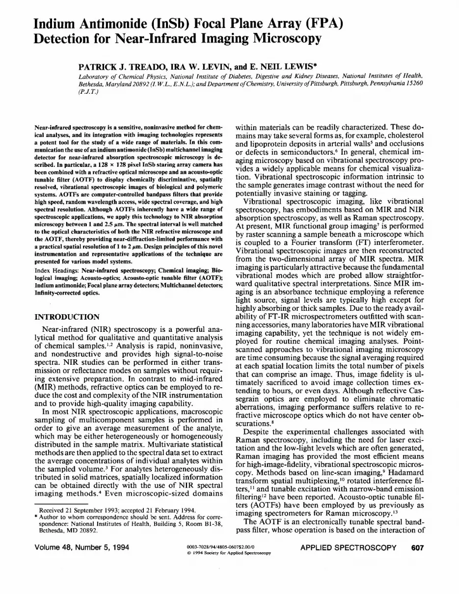
Figure 6A shows an image recorded at 1720 nm of 1-mm-thick polymethylmethacrylate (PMMA) films stacked on a quartz microscope slide. The image shows three distinct spatial regions ranging from almost trans- parent at the bottom to opaque at the top; the image contrast results from absorption of an overtone of a CH stretching vibration. The darker band at the top of the image occurs where two film layers overlap, while the center band corresponds to a single 1-mm-thick layer of PMMA. The more opaque region in the dark band of Fig. 6A is due, in part, to nonuniform sample illumination. An axonometric plot of the NIR image shown in Fig. 6A is given in Fig. 6B. Since the material is chemically ho- mogeneous on the spatial resolution scale of the experi- ment, Fig. 6B is an accurate volume profile of the stacked PMMA films. Figure 6B is significant because it suggests that in transmission, where the sample pathlength can be carefully controlled, quantitative volume imaging can be performed. While not optimized in the current imple- mentation, these results suggest the potential for perform- ing confoca125 NIR spectral imaging of three-dimensional structures.
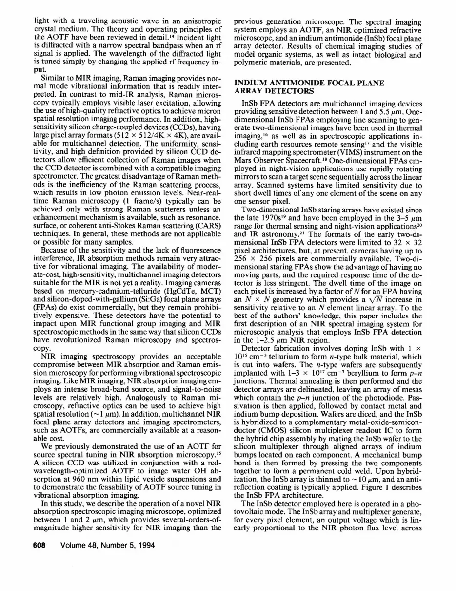
As evidence of the quantitative power of the AOTF NIR imaging method, spectra taken from xy coordinates corresponding to the single and double layers of PMMA film are presented in Figs. 7A and 7B, respectively. The spectra were extracted from the spectral image data set collected from 1540 to 1890 nm, at 10-nm increments, in which 10 frames were averaged per frame. Reproduc- ible features attributable to CH2 absorption at 1720 nm and CH3 absorption at 1660 nm are observed in Fig. 7. Most striking is the excellent agreement of the observed intensities of these spectral features with the relative thicknesses of the material being probed. The magnitude of the absorption band at 1720 nm in Fig. 7B is 1.94 times the intensity observed in Fig. 7A at the same wave- length. This result is in close agreement with the expected value of 2.0 and demonstrates that the NIR imaging tech- nique can provide quantitative as well as qualitative data.
612 Volume 48, Number 5, 1994

A
i
FIG. 4. Composite AOTF NIR images of OH absorption in onion epidermis with the use of a 10x objective and averaging of 10 frames per wavelength increment. (A) Nonabsorbing image collected at 1340 nm. Sample opacity due to scattering and refractive index contributions occur primarily at the epidermal cell membrane interfaces. (B) Vibrational spectral image collected at 1440 nm containing higher relative opacity than Fig. 4A due to OH absorption. Size bar equals 15 #m.
FUTURE DIRECTIONS
The combination of AOTF source tuning and NIR FPA detection provides a unique ability to rapidly and non- invasively obtain spatially resolved information on the intrinsic chemical content of a wide range of materials without the need for sample staining. Samples may be visualized as images arising from specific chemically sig- nificant spectroscopic markers; alternatively, tens of thousands of individual spectra representing spatial do- mains of only a few microns can be collected and observed in only several seconds. This is a very potent combina- tion, indeed, when applied to the molecular character- ization of heterogeneous materials.
AOTF NIR imaging is not without its limitations. The absorptivities associated with overtone and combination bands observed in the NIR are several orders of magni- tude less than fundamental vibrational mode absorptiv- ities. The inherently low extinction coefficients in concert with the small optical pathlengths employed in micros- copy applications limit the sensitivity of the technique. What is advantageous in microscopic sampling of het- erogeneous materials is that analytes are present in higher concentrations within microscopic domains than in bulk sample. Localizing the spectroscopy to these small do- mains often makes high S/N spectral image acquisitions feasible.
Spectral bands of multicomponent samples frequently overlap in the NIR. Multivariate statistical analyses must often be used to extract the contribution of individual components. It is anticipated that chemometric methods of data analysis will have to be employed to resolve con- tributions of individual chemical components in more
complex samples, especially intact biological tissues. The statistical analyses performed in spectral space can be combined with traditional digital image processing meth- ods to enhance the visualization of sample chemistry.
One of the advantages of NIR spectroscopy and NIR imaging is the use of intense sources for sample illumi- nation and the resulting moderate-to-high intensity light levels that are detected. With sufficient detector dynamic range, the relatively small analytical signal (absorbance)
I100 1300 1500 1700 1900
0.03
0.025
0.02
0.015
0.01
0.00~
0 L I
2100 2300
Wavelength (rim)
FIG. 5. NIR spectrum of onion epidermis extracted from the same spectral image data set as in Fig. 4. The spectrum corresponds to a single-pixel xy coordinate corresponding to a sampling area of 1 vm 2. Characteristic OH absorbances at 1440 (OH stretching first overtone) and 1960 (OH combination band) further indicate that the image con- trast seen in Fig. 4B has chemical origins.
APPLIED SPECTROSCOPY 613
0 . 0 3 5
0.03 •
0.025 •
0,02
0.015
0.01
0.005
0
1500 1550 1600 1650 1700 1750 1800 1850 1900
Wavelength (nm)
FIG. 7. (A) NIR spectra of the PMMA double-film-layer region. (B) The single-layer region shown in Fig. 6. Ratioing the 1720-nm peak intensity of the double film layer vs. the single layer yields a value of 1.94.
2 mm
0.26 mm
0.16 mm FIG. 6. (A) Acousto-optic filtered NIR absorption image of stacked polymethylmethacrylate (PMMA) films recorded at 1720 nm (CH stretching mode first overtone), with single image acquisition, no frame averaging, and 31-ms integration time. The opaque region at the top arises from 2-ram-thick PMMA. The center region reflects a 1-mm- thick film. A long-working-distance 5 × objective is employed to keep the entire field of view in focus simultaneously. An edge effect between the glass and polymer surfaces is seen as slightly darker, narrow bands between the individual layers. Size bar equals 25 urn. (B) Axonometfic plot mapping absorbance of the NIR PMMA image from A.
can be detected rapidly even when embedded within an intense background. AOTFs are capable of fast (us-ms) tuning and, when combined with fast FPAs, can capture 250-1000 frames per second, opening the possibility of
performing spectral imaging of dynamic events. Fast spectral image acquisition in combination with commen- surate digital processing capability makes video-frame- rate (30 Hz) NIR spectral imaging possible and real-time visualization of sample chemistry a reality. We envision this technique as a means to study, for example, biological materials at the cellular level in vitro. Since the technique is completely noninvasive and requires limited or no sam- ple preparation, diagnostic in vivo spectral imaging meth- ods can be developed.
We have demonstrated that macroscopic and micro- scopic imaging can be performed with the use of either standard lenses or microscope optics, respectively. We have focused on the microscope imaging studies in this paper, but macroscopic spectral imaging would be es- pecially applicable to real-time process monitoring and control applications in industrial analytical applications. The speed of this technique coupled with a system that contains no moving parts is an additional strength, par- ticularly for process control in hostile environments re- quiting ruggedized (solid-state) instrumentation.
The present study does not take advantage of the fact that InSb FPAs and TeOz AOTFs operate out to 5.5 um (1818 cm-~). Signals from the 3-5.5 um region would allow mid-infrared imaging spectroscopy to be primarily based upon fundamental vibrational stretching mode ab- sorption bands, enhancing the sensitivity of the technique many fold. The current limitations to the MIR approach are the lack of high-quality microscope optics in the 3-5.5 um region and the presence of room-temperature black- body emission contributing high signal backgrounds. Ac- ceptable compromise solutions to these problems would include the use of Cassegrain reflective optics to provide adequate imaging performance; or alternatively, refrac- tive optics based on germanium, silicon, or zinc selenide could be developed. Refractive optics would suffer from severe chromatic aberrations, but would provide optimal spatial resolution and efficiency for specific applications over limited optical bandwidths. Background light limi- tations could be addressed in the same manner as in MIR spectrometers, which employ high-intensity light sources efficiently coupled through the microscope to exceed background light levels. Background and other instru-
614 Volume 48, Number 5, 1994

ment response contributions can then be r emoved through spectral image ratioing against a suitable reference.
For M I R spectral imaging beyond 5.5 um, al ternative A O T F and FPA devices can be utilized. A O T F s based on tha l l ium arsenic selenide (T13AsSe3) and mercurous halides (Hg2C12, HgEBr2) t ransmi t f rom 1.3 to 17 ~tm, 0.35 to 20 u m and 0 .4-30 um, respectively. The high figures- of -mer i t o f the mercurous halides make them particularly at tract ive for M I R applications; however , crystal growth and A O T F fabricat ion remain something of an art. The surfaces o f these mater ia ls mus t be oriented to a tenth o f degree, flat to a fraction o f a wavelength of light, and polished to a scratch-free optical finish. The crystal pol- ishing, in particular, is challenging since these mater ia ls have the rheological propert ies o f cold butter. 26 At pres- ent, these devices are not practical for routine spectral imaging applications.
Two-d imens iona l focal-plane arrays based on mercury c a d m i u m telluride (MCT) (1-15/. tm) 27 and silicon doped with gall ium (Si:Ga) (2-16 tzm) 2s have t remendous po- tential as M I R imaging detectors. The response ranges o f these devices are well suited to use with M I R A O T F s in spectroscopic microscopes. Si:Ga is o f part icular interest because o f the use o f silicon fabricat ion technologies, as with PtSi FPAs, to p rov ide high image fidelity f rom single architecture arrays. While these devices exist c o m m e r - cially, they are presently prohibi t ively expensive. I f suit- able applicat ions can be developed (for example , in bi- ological and po lymer characterization), marke ts for these exotic detectors will be expanded and the devices will become avai lable to the practicing spectroscopist.
An addit ional exciting prospect to be explored is the use o f the InSb FPA as a mul t ichannel imaging detector for N I R laser (Nd:YAG) excitation R a m a n spectroscopy. One could envis ion employing the N I R op t imized A O T F as a modera te- resolu t ion imaging spect rometer in com- bination with holographic filters to reject excitation source intensity. InSb is a suitable choice for the detector in a R a m a n exper iment because o f the high quan tum effi- ciency and suitability to low-light-level applications. We have previously used a v is ib le-wavelength-opt imized A O T F to construct a minia tur ized R a m a n spect rome- ter. 29 The advantages o f the N I R R a m a n approach would be enhanced fluorescence rejection 3° and an ul t ra-com- pact, solid-state ins t rument that would be suitable for process control applications. In the event the A O T F does not p rov ide adequate resolution for some spectroscopic applications, the FPA would be placed in the exit focal plane o f a dispersive m o n o c h r o m a t o r and employed as a convent ional mul t ichannel detector. A G e linear focal plane array has been employed previously in this manne r for N I R R a m a n spectroscopy de tec t ion? ' The mono- ch roma to r could be outfitted with appropr ia te gratings to provide a reasonable c o m p r o m i s e between spectral cov- erage and spectral resolution.
Another area that is being actively pursued is the de- ve lopmen t of the A O T F as a H a d a m a r d t ransform mul- t iplexed imaging spectrometer . The A O T F has the de- c ided a d v a n t a g e o f t un i ng m u l t i p l e spec t ra l b a n d s s imul taneously when dr iven with mult iple r f signals. In the NIR , the classic mult iplex advantage is expected to be obta ined when detector-noise- l imited InSb FPAs are
used. Other advantages include the ability to tailor the bandpass o f the spec t rometer to match exactly the spectral band profile, giving ext raordinary flexibility ove r the res- olution and throughput p rov ided by the AOTF. This ca- pabil i ty is in direct contrast to single-frequency opera t ion o f the A O T F where the resolut ion and throughput o f the device are fixed at the t ime o f crystal fabrication. Future deve lopments in these and other areas will be fo r thcom- ing f rom our laboratories.
ACKNOWLEDGMENTS We wish to thank Brett Rosner of Santa Barbara Focalplane and Chris
Johnston of Amber Engineering for useful discussions regarding InSb fabrication and system design. In addition, we would like to thank Ronald Rosemeier of the Brimrose Corporation of America for the use of an NIR-optimized AOTF, and Richard Baucom of Olympus Cor- poration for the use of an NIR microscope. We would also like to thank Hannah Morris of the University of Pittsburgh for assistance in pre- paring the figures.
1. D. L. Wetzel, Anal. Chem. 55, 1165A (1983). 2. L. G. Weyer, Appl. Spectrosc. Rev. 21, 1 (1985). 3. H. Mark, in Handbook of Near-lnfrared Analysis, D. A. Burns and
E. W. Ciurczak, Eds. (Marcel Dekker, New York, 1992), p. 107. 4. P. J. Treado and M. D. Morris, in Microscopic and Spectroscopic
Imaging of the Chemical State, M. D. Morris, Ed. (Marcel Dekker, New York, 1993). p. 71.
5. L. A. Cassis and R. A. Lodder, Anal. Chem. 65, 1247 (1993). 6. P. C. Montgomery and J. P. Fillard, Meas. Sci. Technol. 1, 120
(1990). 7. M. A. Harthcock and S. C. Atkin, Appl. Spectrosc. 42, 449 (1988). 8. R. G. Messerschmidt, in ASTMSpecial TechnicalPublication 949,
P. B. Roush, Ed. (American Society for Testing and Materials, Philadelphia, 1987), p. 12.
9. M. Bowden, D. J. Gardiner, G. Rice, and D. L. J. Gerrard, J. Raman Spectrosc. 21, 37 (1990).
10. P. J. Treado and M. D. Morris, Appl. Spectrosc. 44, 1 (1990). 11. D.N. Batchelder, C. Cheng, and B. J. E. Smith, Makromol. Chem.,
Makromol. Symp. 46, 171 (1991). 12. G. J. Puppels, M. Grond, and J. Greve, Appl. Spectrosc. 47, 1256
(1993). 13. P. J. Treado, I. W. Levin, and E. N. Lewis, Appl. Spectrosc. 46,
1211 (1992). 14. C. D. Tran, Anal. Chem. 64, 971A (1992). 15. P. J. Treado, I. W. Levin, and E. N. Lewis, Appl. Spectrosc. 46,
553 (1992). 16. H. Fujisada, M. Nakayama, and A. Tanaka, Proc. SPIE 1341, 80
(1992.) 17. G. C. Bailey, K. Matthews, and C. A. Niblack, Proc. SPIE 430, 52
(1983). 18. J. Duvall, Proc. SPIE 685, 121 (1987). 19. G. C. Bailey, Proc. SPIE 197, 83 (1979). 20. W. J. Parrish, J. Blackwell, R. Paulson, and H. Arnold, Proc. SPIE
1512, 68 (1991). 21. W. J. Forrest and J. L. Piphr, NASA Tech. Mem. 88213, 11 (1986). 22. Santa Barbara Focalplane ImaglR Users Manual, Ver. 1.0. (Santa
Barbara Focalplane, Goleta, California, 1992). 23. W. F. Kosonocky, F. V. Shallcross, T. S. Villani, and J. V. Groppe,
IEEE Trans. on Electron Devices 32, 1564 (1985). 24. M. J. Abramowitz, American Lab. 25, 66 (1993). 25. I. J. Cox, C. J. R. Sheppard, and T. Wilson, Optik 60, 391 (1982). 26. J. P. Muzzy, F. M. Ryan, and N. B. Singh, Mat. Sci. Forum 61, 19
(1990). 27. K. Tanikawa and Y. Ito, Proc. SPIE 686, 86 (1986). 28. P. Mottier, P. Angese, and P. O. Lagage, Proc. SPIE 1512, 60 (1991). 29. E. N. Lewis, P. J. Treado, and I. W. Levin, Appl. Spectrosc. 47,
539 (1993). 30. E. N. Lewis, V. F. Kalasinsky, and I. W. Levin, Appl. Spectrosc.
42, 1188 (1988). 31. B. Chase and Y. Talmi, Appl. Spectrosc. 45, 929 (1991).
APPLIED SPECTROSCOPY 615


