Embed Size (px)
Citation preview
22 SUNG MIN KIM et al : HIGHLY MANUFACTURABLE 65NM MCFET (MULTI-CHANNEL FIELD EFFECT TRANSISTOR)…
Manuscript received Jan. 11, 2006; revised Mar. 12, 2006. Device Research Team, R&D Center, Samsung Electronics Co., San 24, Nongseo-Dong, Kiheung-Gu, Yongin-City, Kyungki-Do, Korea, 449-711 E-mail : [email protected]
Highly Manufacturable 65nm McFET (Multi-channel Field Effect Transistor) SRAM Cell with Extremely
High Performance
Sung Min Kim, Eun Jung Yoon, Min Sang Kim, Ming Li, Chang Woo Oh, Sung Young Lee, Kyoung Hwan Yeo, Sung Hwan Kim, Dong Uk Choe,
Sung Dae Suk, Dong-Won Kim, and Donggun Park
Abstract—We demonstrate highly manufacturable Multi-channel Field Effect Transistor (McFET) on bulk Si wafer. McFET shows excellent transistor characteristics, such as 5~6 times higher drive current than planar MOSFET, ideal subthreshold swing, low drain induced barrier lowering (DIBL) without pocket implantation and negligible body bias dependency, maintaining the same source/drain resistance as that of a planar transistor due to the unique feature of McFET. And suitable threshold voltage (VT) for SRAM operation and high static noise margin (SNM) are achieved by using TiN metal gate electrode. Index Terms—McFET, SRAM, TiN, workfunction
I. INTRODUCTION
Due to the high compatibility with conventional device manufacturing process, FinFETs have been on focus among the double-gate transistors[1]. Usually, as a fin width trimming method, a combination of sacrificial oxidation and chemical dry etch has been used. However, these methods inevitably increase the source/drain series resistance by narrowing the width of source/drain region as well as the channel fin region[2]. Moreover, to enhance
the drive current, sophisticated multi-fin layout is required[3]. Due to the pitch limit of lithography tools, it is hard to have narrower pitch than design rule that limits the effective use of the active area for the devices using FinFET. In this work, we introduce a novel process architecture of McFET which can be fabricated without lithographical limit of active patterning and propose a method to achieve CMOS transistor characteristics that are suitable to low voltage and high performance operation using highly manufacturable TiN single metal gate process.
Fig. 1. Schematic illustration and cross-sectional SEM images of channel region of McFET.
JOURNAL OF SEMICONDUCTOR TECHNOLOGY AND SCIENCE, VOL.6, NO.1, MARCH, 2006 23
II. FABRICATION
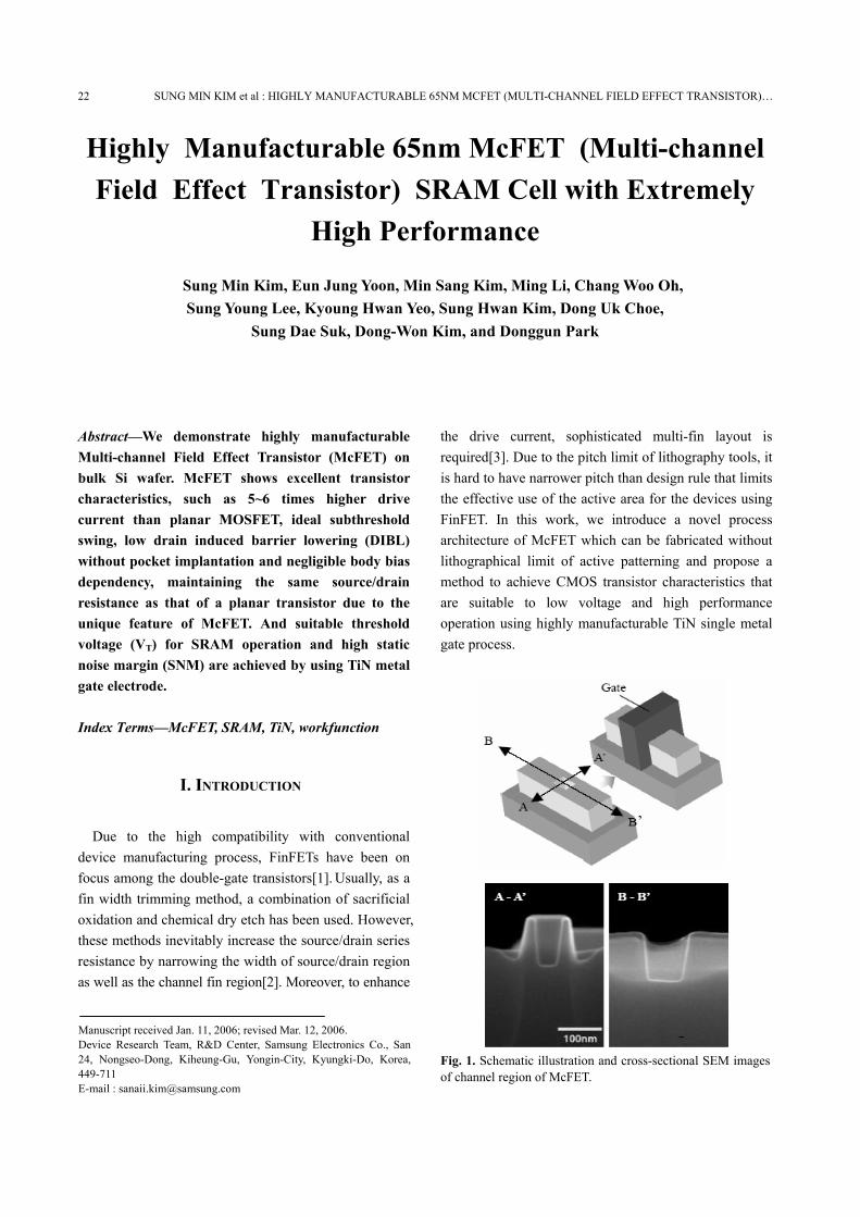
Three-dimensional schematic diagrams of the McFET fabrication process flow are shown in Figure 4[7~8]. As shown in Figure 2~5, the thickness of channel body is 12nm and it is uniform in the whole wafer. The nitrided oxide was grown as a gate dielectric. In order to test the intrinsic strength of the McFET architecture to resist short channel effect (SCE) and DIBL, no pocket
Fig. 2. TEM image of the channel body of fabricated McFET. The height and width of two symmetrical channel bodies are 98nm and 12nm, respectively.
Fig. 3. Top view of McFET active channel formation.
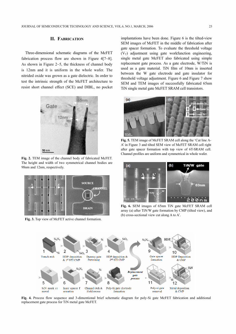
implantations have been done. Figure 6 is the tilted-view SEM images of McFET in the middle of fabrication after gate spacer formation. To evaluate the threshold voltage (VT) adjustment using gate workfunction engineering, single metal gate McFET also fabricated using simple replacement gate process. As a gate electrode, W/TiN is used as a gate material. TiN film of 10nm is inserted between the W gate electrode and gate insulator for threshold voltage adjustment. Figure 6 and Figure 7 show SEM and TEM images of successfully fabricated 65nm TiN single metal gate McFET SRAM cell transistors.
Fig. 5. TEM image of McFET SRAM cell along the ‘Cut line A-A’ in Figure 3 and tilted SEM view of McFET SRAM cell right after gate spacer formation with top view of 6T-SRAM cell. Channel profiles are uniform and symmetrical in whole wafer.
Fig. 6. SEM images of 65nm TiN gate McFET SRAM cell array (a) after TiN/W gate formation by CMP (tilted view), and (b) cross-sectional view cut along A to A’.
Fig. 4. Process flow sequence and 3-dimentional brief schematic diagram for poly-Si gate McFET fabrication and additional replacement gate process for TiN metal gate McFET.
24 SUNG MIN KIM et al : HIGHLY MANUFACTURABLE 65NM MCFET (MULTI-CHANNEL FIELD EFFECT TRANSISTOR)…
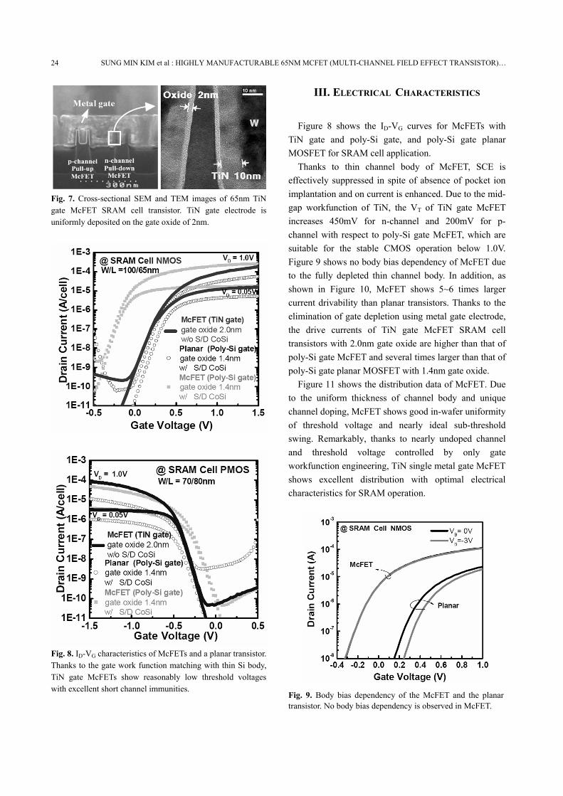
Fig. 7. Cross-sectional SEM and TEM images of 65nm TiN gate McFET SRAM cell transistor. TiN gate electrode is uniformly deposited on the gate oxide of 2nm.
Fig. 8. ID-VG characteristics of McFETs and a planar transistor. Thanks to the gate work function matching with thin Si body, TiN gate McFETs show reasonably low threshold voltages with excellent short channel immunities.
III. ELECTRICAL CHARACTERISTICS
Figure 8 shows the ID-VG curves for McFETs with TiN gate and poly-Si gate, and poly-Si gate planar MOSFET for SRAM cell application.
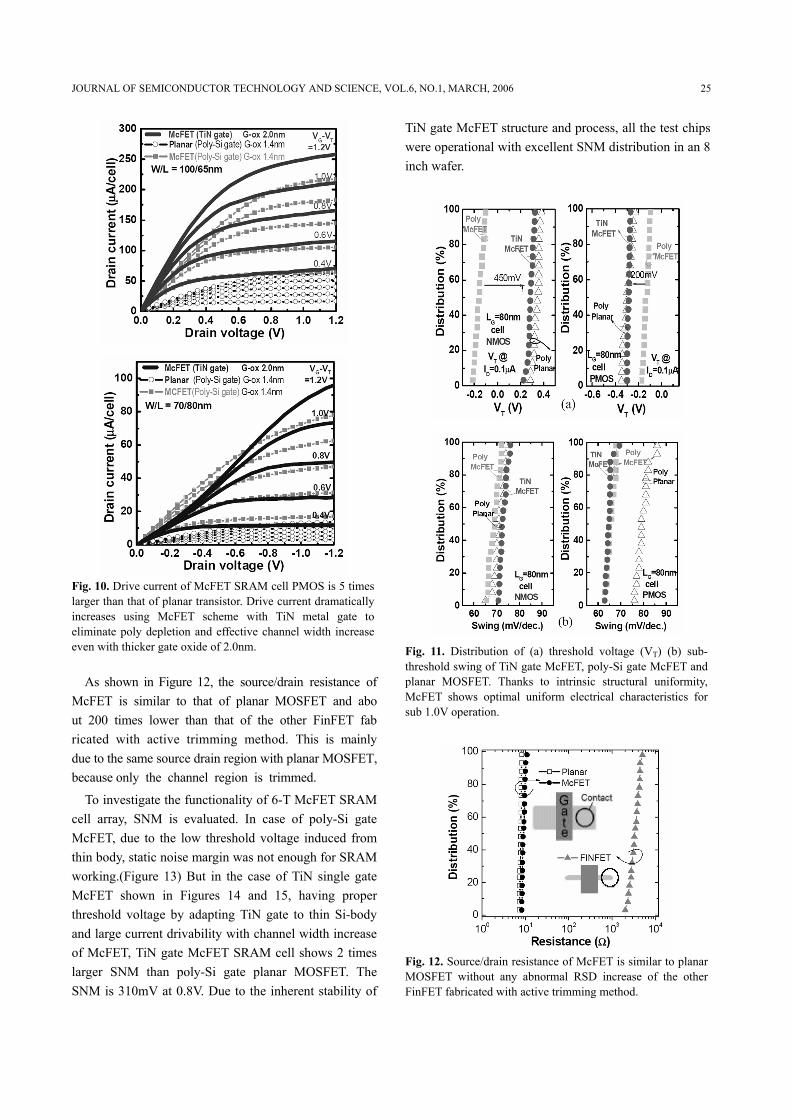
Thanks to thin channel body of McFET, SCE is effectively suppressed in spite of absence of pocket ion implantation and on current is enhanced. Due to the mid-gap workfunction of TiN, the VT of TiN gate McFET increases 450mV for n-channel and 200mV for p-channel with respect to poly-Si gate McFET, which are suitable for the stable CMOS operation below 1.0V. Figure 9 shows no body bias dependency of McFET due to the fully depleted thin channel body. In addition, as shown in Figure 10, McFET shows 5~6 times larger current drivability than planar transistors. Thanks to the elimination of gate depletion using metal gate electrode, the drive currents of TiN gate McFET SRAM cell transistors with 2.0nm gate oxide are higher than that of poly-Si gate McFET and several times larger than that of poly-Si gate planar MOSFET with 1.4nm gate oxide.
Figure 11 shows the distribution data of McFET. Due to the uniform thickness of channel body and unique channel doping, McFET shows good in-wafer uniformity of threshold voltage and nearly ideal sub-threshold swing. Remarkably, thanks to nearly undoped channel and threshold voltage controlled by only gate workfunction engineering, TiN single metal gate McFET shows excellent distribution with optimal electrical characteristics for SRAM operation.
Fig. 9. Body bias dependency of the McFET and the planar transistor. No body bias dependency is observed in McFET.
JOURNAL OF SEMICONDUCTOR TECHNOLOGY AND SCIENCE, VOL.6, NO.1, MARCH, 2006 25
Fig. 10. Drive current of McFET SRAM cell PMOS is 5 times larger than that of planar transistor. Drive current dramatically increases using McFET scheme with TiN metal gate to eliminate poly depletion and effective channel width increase even with thicker gate oxide of 2.0nm.
As shown in Figure 12, the source/drain resistance of
McFET is similar to that of planar MOSFET and about 200 times lower than that of the other FinFET fabricated with active trimming method. This is mainly due to the same source drain region with planar MOSFET, because only the channel region is trimmed.
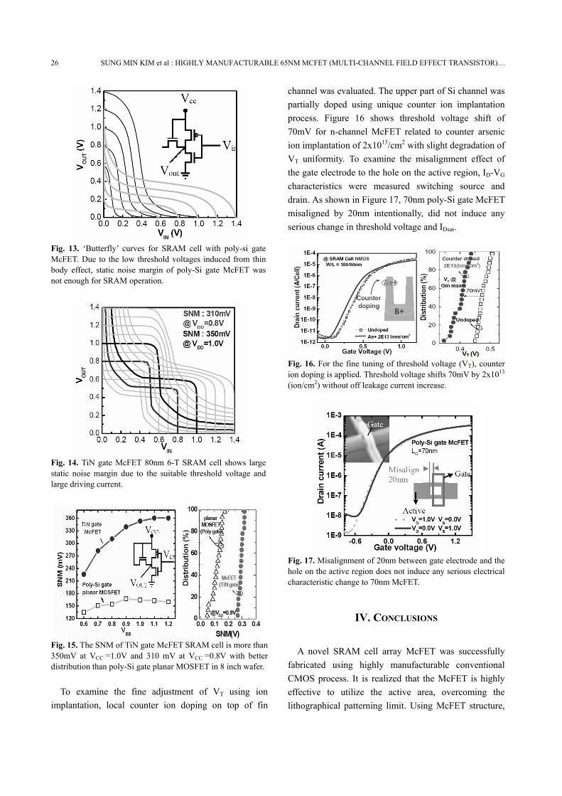
To investigate the functionality of 6-T McFET SRAM cell array, SNM is evaluated. In case of poly-Si gate McFET, due to the low threshold voltage induced from thin body, static noise margin was not enough for SRAM working.(Figure 13) But in the case of TiN single gate McFET shown in Figures 14 and 15, having proper threshold voltage by adapting TiN gate to thin Si-body and large current drivability with channel width increase of McFET, TiN gate McFET SRAM cell shows 2 times larger SNM than poly-Si gate planar MOSFET. The SNM is 310mV at 0.8V. Due to the inherent stability of
TiN gate McFET structure and process, all the test chips were operational with excellent SNM distribution in an 8 inch wafer.
Fig. 11. Distribution of (a) threshold voltage (VT) (b) sub-threshold swing of TiN gate McFET, poly-Si gate McFET and planar MOSFET. Thanks to intrinsic structural uniformity, McFET shows optimal uniform electrical characteristics for sub 1.0V operation.
Fig. 12. Source/drain resistance of McFET is similar to planar MOSFET without any abnormal RSD increase of the other FinFET fabricated with active trimming method.
26 SUNG MIN KIM et al : HIGHLY MANUFACTURABLE 65NM MCFET (MULTI-CHANNEL FIELD EFFECT TRANSISTOR)…
Fig. 13. ‘Butterfly’ curves for SRAM cell with poly-si gate McFET. Due to the low threshold voltages induced from thin body effect, static noise margin of poly-Si gate McFET was not enough for SRAM operation.
Fig. 14. TiN gate McFET 80nm 6-T SRAM cell shows large static noise margin due to the suitable threshold voltage and large driving current.
Fig. 15. The SNM of TiN gate McFET SRAM cell is more than 350mV at VCC =1.0V and 310 mV at VCC =0.8V with better distribution than poly-Si gate planar MOSFET in 8 inch wafer.
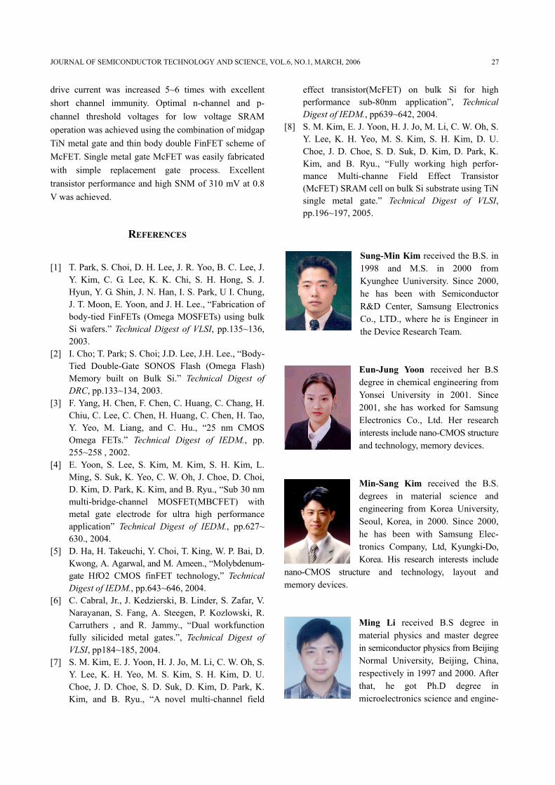
To examine the fine adjustment of VT using ion
implantation, local counter ion doping on top of fin
channel was evaluated. The upper part of Si channel was partially doped using unique counter ion implantation process. Figure 16 shows threshold voltage shift of 70mV for n-channel McFET related to counter arsenic ion implantation of 2x10¹³/cm2 with slight degradation of VT uniformity. To examine the misalignment effect of the gate electrode to the hole on the active region, ID-VG characteristics were measured switching source and drain. As shown in Figure 17, 70nm poly-Si gate McFET misaligned by 20nm intentionally, did not induce any serious change in threshold voltage and IDsat.
Fig. 16. For the fine tuning of threshold voltage (VT), counter ion doping is applied. Threshold voltage shifts 70mV by 2x1013 (ion/cm2) without off leakage current increase.
Fig. 17. Misalignment of 20nm between gate electrode and the hole on the active region does not induce any serious electrical characteristic change to 70nm McFET.
IV. CONCLUSIONS
A novel SRAM cell array McFET was successfully fabricated using highly manufacturable conventional CMOS process. It is realized that the McFET is highly effective to utilize the active area, overcoming the lithographical patterning limit. Using McFET structure,
JOURNAL OF SEMICONDUCTOR TECHNOLOGY AND SCIENCE, VOL.6, NO.1, MARCH, 2006 27
drive current was increased 5~6 times with excellent short channel immunity. Optimal n-channel and p-channel threshold voltages for low voltage SRAM operation was achieved using the combination of midgap TiN metal gate and thin body double FinFET scheme of McFET. Single metal gate McFET was easily fabricated with simple replacement gate process. Excellent transistor performance and high SNM of 310 mV at 0.8 V was achieved.
REFERENCES
[1] T. Park, S. Choi, D. H. Lee, J. R. Yoo, B. C. Lee, J. Y. Kim, C. G. Lee, K. K. Chi, S. H. Hong, S. J. Hyun, Y. G. Shin, J. N. Han, I. S. Park, U I. Chung, J. T. Moon, E. Yoon, and J. H. Lee., “Fabrication of body-tied FinFETs (Omega MOSFETs) using bulk Si wafers.” Technical Digest of VLSI, pp.135~136, 2003.
[2] I. Cho; T. Park; S. Choi; J.D. Lee, J.H. Lee., “Body-Tied Double-Gate SONOS Flash (Omega Flash) Memory built on Bulk Si.” Technical Digest of DRC, pp.133~134, 2003.
[3] F. Yang, H. Chen, F. Chen, C. Huang, C. Chang, H. Chiu, C. Lee, C. Chen, H. Huang, C. Chen, H. Tao, Y. Yeo, M. Liang, and C. Hu., “25 nm CMOS Omega FETs.” Technical Digest of IEDM., pp. 255~258 , 2002.
[4] E. Yoon, S. Lee, S. Kim, M. Kim, S. H. Kim, L. Ming, S. Suk, K. Yeo, C. W. Oh, J. Choe, D. Choi, D. Kim, D. Park, K. Kim, and B. Ryu., “Sub 30 nm multi-bridge-channel MOSFET(MBCFET) with metal gate electrode for ultra high performance application” Technical Digest of IEDM., pp.627~ 630., 2004.
[5] D. Ha, H. Takeuchi, Y. Choi, T. King, W. P. Bai, D. Kwong, A. Agarwal, and M. Ameen., “Molybdenum-gate HfO2 CMOS finFET technology,” Technical Digest of IEDM., pp.643~646, 2004.
[6] C. Cabral, Jr., J. Kedzierski, B. Linder, S. Zafar, V. Narayanan, S. Fang, A. Steegen, P. Kozlowski, R. Carruthers , and R. Jammy., “Dual workfunction fully silicided metal gates.”, Technical Digest of VLSI, pp184~185, 2004.
[7] S. M. Kim, E. J. Yoon, H. J. Jo, M. Li, C. W. Oh, S. Y. Lee, K. H. Yeo, M. S. Kim, S. H. Kim, D. U. Choe, J. D. Choe, S. D. Suk, D. Kim, D. Park, K. Kim, and B. Ryu., “A novel multi-channel field
effect transistor(McFET) on bulk Si for high performance sub-80nm application”, Technical Digest of IEDM., pp639~642, 2004.
[8] S. M. Kim, E. J. Yoon, H. J. Jo, M. Li, C. W. Oh, S. Y. Lee, K. H. Yeo, M. S. Kim, S. H. Kim, D. U. Choe, J. D. Choe, S. D. Suk, D. Kim, D. Park, K. Kim, and B. Ryu., “Fully working high perfor-mance Multi-channe Field Effect Transistor (McFET) SRAM cell on bulk Si substrate using TiN single metal gate.” Technical Digest of VLSI, pp.196~197, 2005.
Sung-Min Kim received the B.S. in 1998 and M.S. in 2000 from Kyunghee Uuniversity. Since 2000, he has been with Semiconductor R&D Center, Samsung Electronics Co., LTD., where he is Engineer in the Device Research Team.
Eun-Jung Yoon received her B.S degree in chemical engineering from Yonsei University in 2001. Since 2001, she has worked for Samsung Electronics Co., Ltd. Her research interests include nano-CMOS structure and technology, memory devices.
Min-Sang Kim received the B.S. degrees in material science and engineering from Korea University, Seoul, Korea, in 2000. Since 2000, he has been with Samsung Elec-tronics Company, Ltd, Kyungki-Do, Korea. His research interests include
nano-CMOS structure and technology, layout and memory devices.
Ming Li received B.S degree in material physics and master degree in semiconductor physics from Beijing Normal University, Beijing, China, respectively in 1997 and 2000. After that, he got Ph.D degree in microelectronics science and engine-
28 SUNG MIN KIM et al : HIGHLY MANUFACTURABLE 65NM MCFET (MULTI-CHANNEL FIELD EFFECT TRANSISTOR)…
ering from Beijing University, Beijing, China, in 2003. Now he works with Samsung Electronics Co. Ltd., Korea. His research interests include process fabrication and physics modeling on novel nano-CMOS devices and memory devices.
Chang Woo Oh was born in Youngyang, Kyungpook, Korea, on January 27, 1971. He received his B. S. degree in electronics from Kyungpook National University in 1996 and his M. S. and Ph. D. degrees in electrical engineering
from Seoul National University in 1998 and 2002, respectively. His doctoral dissertation was related to architecture and reliability of field emission display (FED). Since 2002, he has been a senior engineer in Samsung Electronics Co. He has focused on nano CMOS devices including ultimately scaled planar MOSFET, FinFET, multi-channel MOSFET, and partial SOI MOSFET and also, future memory devices including SONOS memory, nano crystal memory, and e-DRAM. He has authored or co-authored numerous papers on the topics related to nano devices and future memories and holds several Korean and U. S. patents dealing with the topics.
Sung-Young Lee received his B.S. degree and his master degree in materials science and engineering from Korea University in 1990 and 1992, respectively. In 2004, he received Ph. D degree in electrical engineering at SungKyunkwan Univer-
sity. Since 1993, he has worked for Samsung Electronics Co., Ltd. His research interests include nano-CMOS structure and technology, memory devices, and nano-characterization using SPM(Scanning Probe Microscopy).
Kyoung Hwan Yeo received the B.S. degree in materials science and engineering from Pohang University of Science and Technology (POSTECH), Korea, 1992 and the M.S. degree in information and communication engineering at the Sungkyunkwan University, Korea,
2004. After graduation from POSTECH, he has worked at Samsung Electronics since 1995. He worked on the dry etch process development for DRAM, SRAM, and FLASH memory devices. His current research is the fabrication and characteristics analysis of new structure transistor, especially transistor with gate all around structure.
Sung Hwan Kim received the B.S. degrees in electronic engineering from Yeungnam University in 2000. Since 2000, he has been with Samsung Electronics Company, Ltd, Kyungki-Do, Korea. His current major activity is focused on the development of
technologies for nano-scale CMOS and memory devices.
Dong Uk Choe received his B.S. degree in nuclear enginnering and his master degree in physics from Seoul National University in 1990 and 1994, respectively. Since 1994, he has worked for Samsung Electronics Co., Ltd. His research interests are
memory fabrications, memory devices.
Sung Dae Suk received the B.S. degree and M.S. degree in Physics from Yonsei University, Seoul, Korea, in 2001 and 2003, respectively. Since 2004, he has been with Samsung Electronics Company, Ltd, Kyungki-Do, Korea. His research
interests include all kinds of nano science, especially nano-CMOS structure and technology, and memory devices.
JOURNAL OF SEMICONDUCTOR TECHNOLOGY AND SCIENCE, VOL.6, NO.1, MARCH, 2006 29
Dong-Won Kim received the B.S. and M.S. degrees in materials science and engineering from Korea University, Seoul, Korea, and the Ph. D. degree in materials science from the University of Texas, Austin in 2003. His Ph. D. research was the
development of SiGe nanocrystal floating gate memory for future generation of devices. Since he joined Samsung Electronics in 1989, he worked on the process development and the characterization of new semiconductor materials for DRAM and LOGIC devices. After his Ph.D. study, he rejoined Samsung Electronics in 2003 where he is currently a principal engineer in semiconductor R&D center. He is currently active in the areas of 3-demensional nano transistor and novel concept device.
Donggun Park received the B.S., M.S., degrees from Sogang University, Seoul, Korea, and Ph. D. degree from the University of California, Berkeley all in electrical engineering. His Ph.D. study involved plasma charging damage and reliability of thin gate
oxides. Since he joined Samsung Electronics in 1983, he involved in the diffusion process development of 64K and 256K DRAM, and process integration of 1M, 4M, 16 DRAM development until 1993. After his Ph.D study at UC Berkeley, in 1998, he rejoined Samsung Electronics where he is now a vice president of R&D center. After the successful development of 150nm and 130nm 256M DRAMs, 90nm NAND Flash, and 100nm high speed 72M SRAM, in 1999, 2001, 2002, 2003, respectively, he is leading the development projects of nano-CMOS transistor, memory cell transistors, and the advanced technologies for mobile/graphic DRAMs.