Embed Size (px)
Citation preview
Microprocessors and Microcontrollers
(EE-231)
Main Objectives
• Hardware Specs of 8086/8088 Pin Descriptions Clock Generation Buffering and Latching
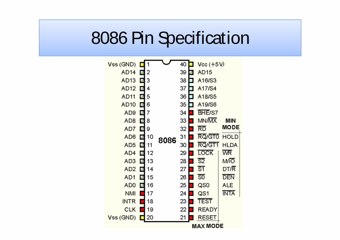
8086 Pin Specification
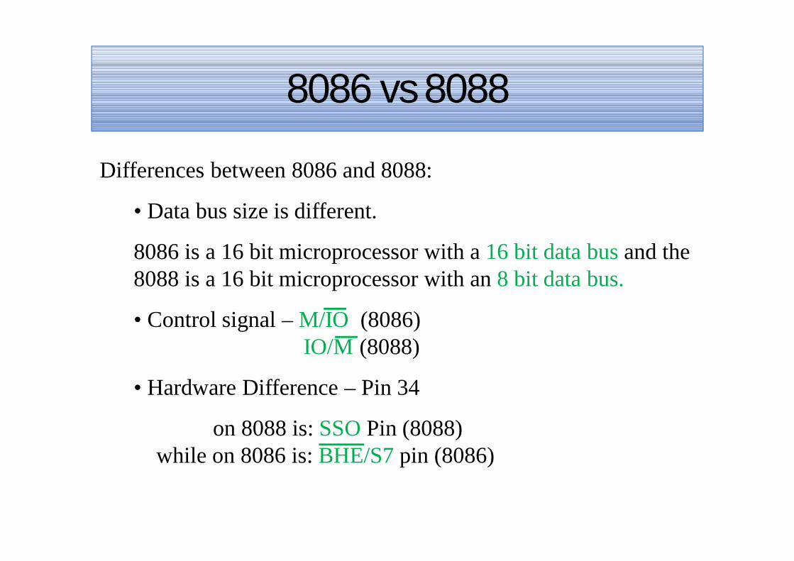
Differences between 8086 and 8088:
• Data bus size is different.
8086 is a 16 bit microprocessor with a 16 bit data bus and the 8088 is a 16 bit microprocessor with an 8 bit data bus.
• Control signal – M/IO (8086) IO/M (8088)
• Hardware Difference – Pin 34
on 8088 is: SSO Pin (8088) while on 8086 is: BHE/S7 pin (8086)
8086 vs 8088
Both Processors require +5.0V with a supply voltage tolerance of 10%.
8086 draws a maximum current supply of 360mA
8088 draws a maximum current supply of 340mA
Ambient temperature for use is 32ºF – 180ºF
There is also a CMOS version, which requires a very low supply current and has an extended temperature range. E.g. 80C88 and 80C86: Current = 10mA , Temp = -40° F to +225° F
Power Requirements
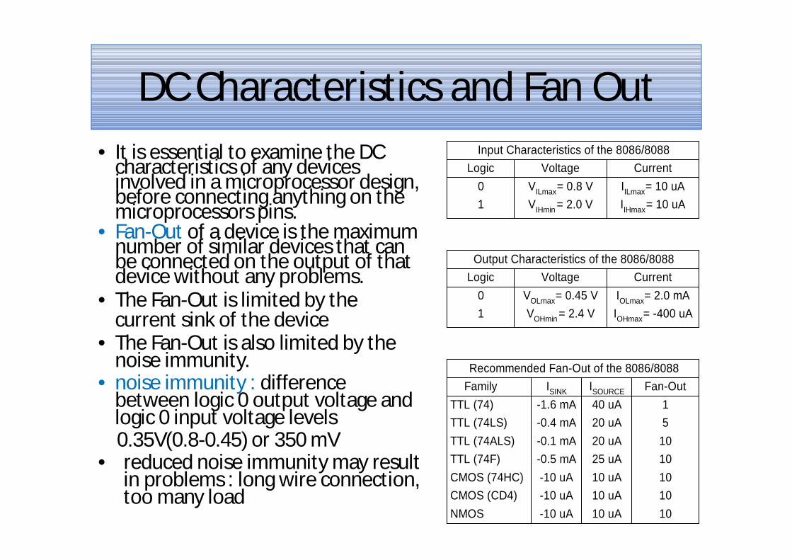
• It is essential to examine the DC characteristics of any devices involved in a microprocessor design, before connecting anything on the microprocessors pins.
• Fan-Out of a device is the maximum number of similar devices that can be connected on the output of that device without any problems.
• The Fan-Out is limited by the current sink of the device
• The Fan-Out is also limited by the noise immunity.
• noise immunity : difference between logic 0 output voltage and logic 0 input voltage levels
0.35V(0.8-0.45) or 350 mV • reduced noise immunity may result
in problems : long wire connection, too many load
Input Characteristics of the 8086/8088Logic Voltage Current
01
VILmax = 0.8 VVIHmin = 2.0 V
IILmax = 10 uAIIHmax = 10 uA
Output Characteristics of the 8086/8088Logic Voltage Current
01
VOLmax = 0.45 VVOHmin = 2.4 V
IOLmax = 2.0 mAIOHmax = -400 uA
Recommended Fan-Out of the 8086/8088Family ISINK Fan-Out
TTL (74)TTL (74LS)
-1.6 mAISOURCE
TTL (74ALS)TTL (74F)CMOS (74HC)CMOS (CD4)NMOS
-0.4 mA-0.1 mA-0.5 mA-10 uA-10 uA-10 uA
40 uA20 uA20 uA25 uA10 uA10 uA10 uA
15
1010101010
DC Characteristics and Fan Out
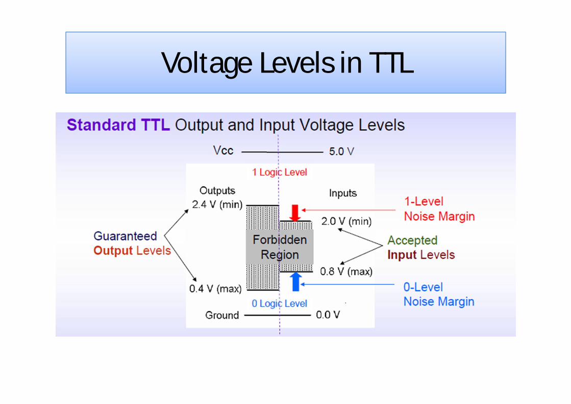
Voltage Levels in TTL
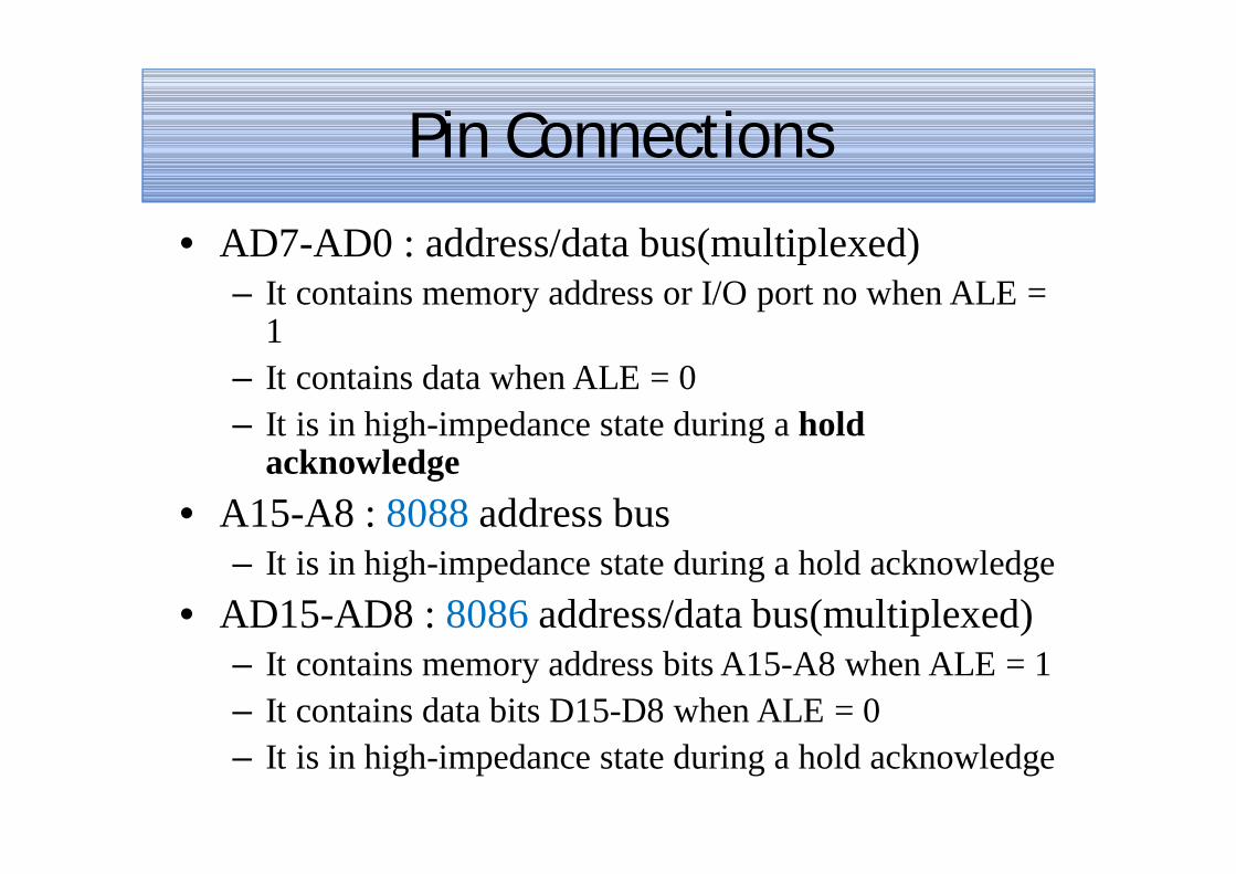
Pin Connections • AD7-AD0 : address/data bus(multiplexed)
– It contains memory address or I/O port no when ALE = 1
– It contains data when ALE = 0 – It is in high-impedance state during a hold
acknowledge • A15-A8 : 8088 address bus
– It is in high-impedance state during a hold acknowledge • AD15-AD8 : 8086 address/data bus(multiplexed)
– It contains memory address bits A15-A8 when ALE = 1 – It contains data bits D15-D8 when ALE = 0 – It is in high-impedance state during a hold acknowledge
9
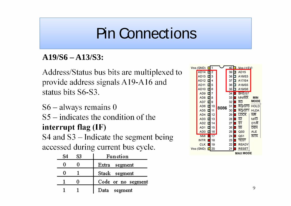
Pin Connections A19/S6 – A13/S3:
Address/Status bus bits are multiplexed to provide address signals A19-A16 and status bits S6-S3.
S6 – always remains 0 S5 – indicates the condition of the interrupt flag (IF) S4 and S3 – Indicate the segment being accessed during current bus cycle.
10
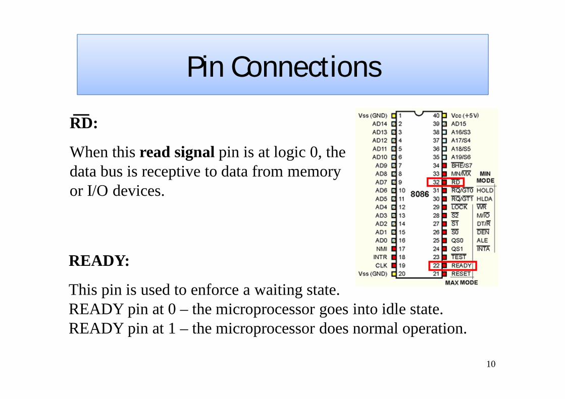
RD:
When this read signal pin is at logic 0, the data bus is receptive to data from memory or I/O devices.
READY:
This pin is used to enforce a waiting state. READY pin at 0 – the microprocessor goes into idle state. READY pin at 1 – the microprocessor does normal operation.
Pin Connections
11
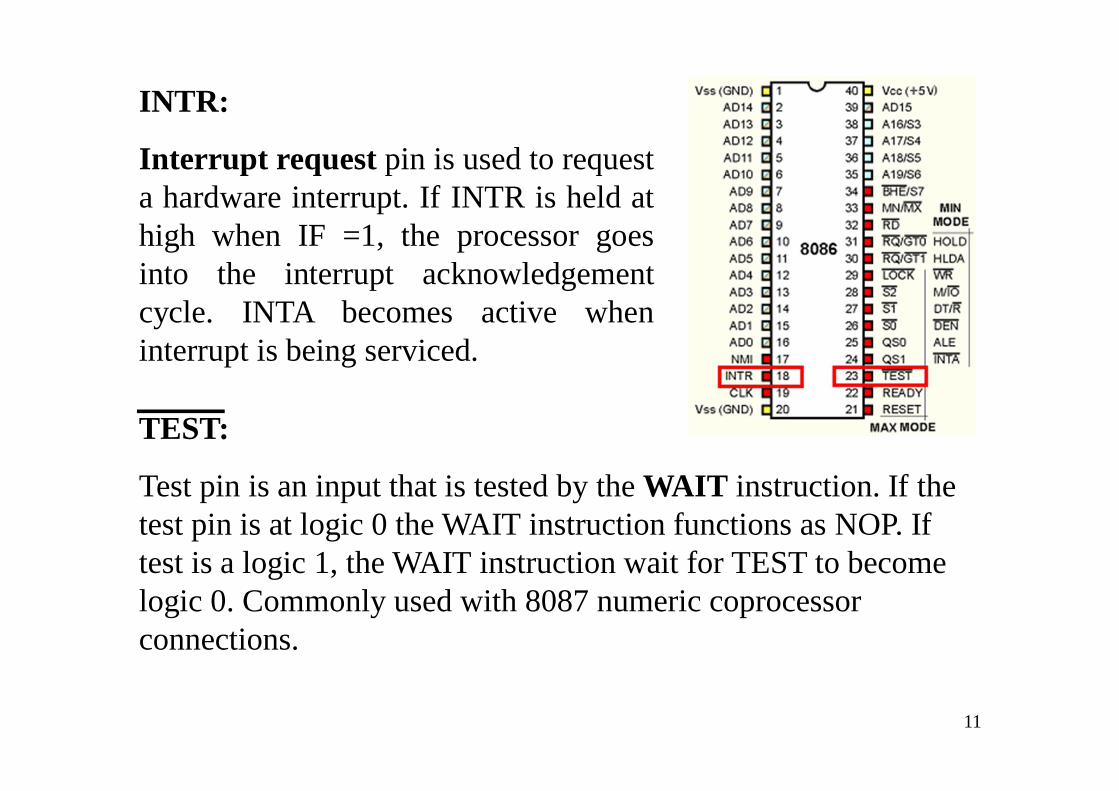
INTR:
Interrupt request pin is used to request a hardware interrupt. If INTR is held at high when IF =1, the processor goes into the interrupt acknowledgement cycle. INTA becomes active when interrupt is being serviced.
TEST:
Test pin is an input that is tested by the WAIT instruction. If the test pin is at logic 0 the WAIT instruction functions as NOP. If test is a logic 1, the WAIT instruction wait for TEST to become logic 0. Commonly used with 8087 numeric coprocessor connections.
12
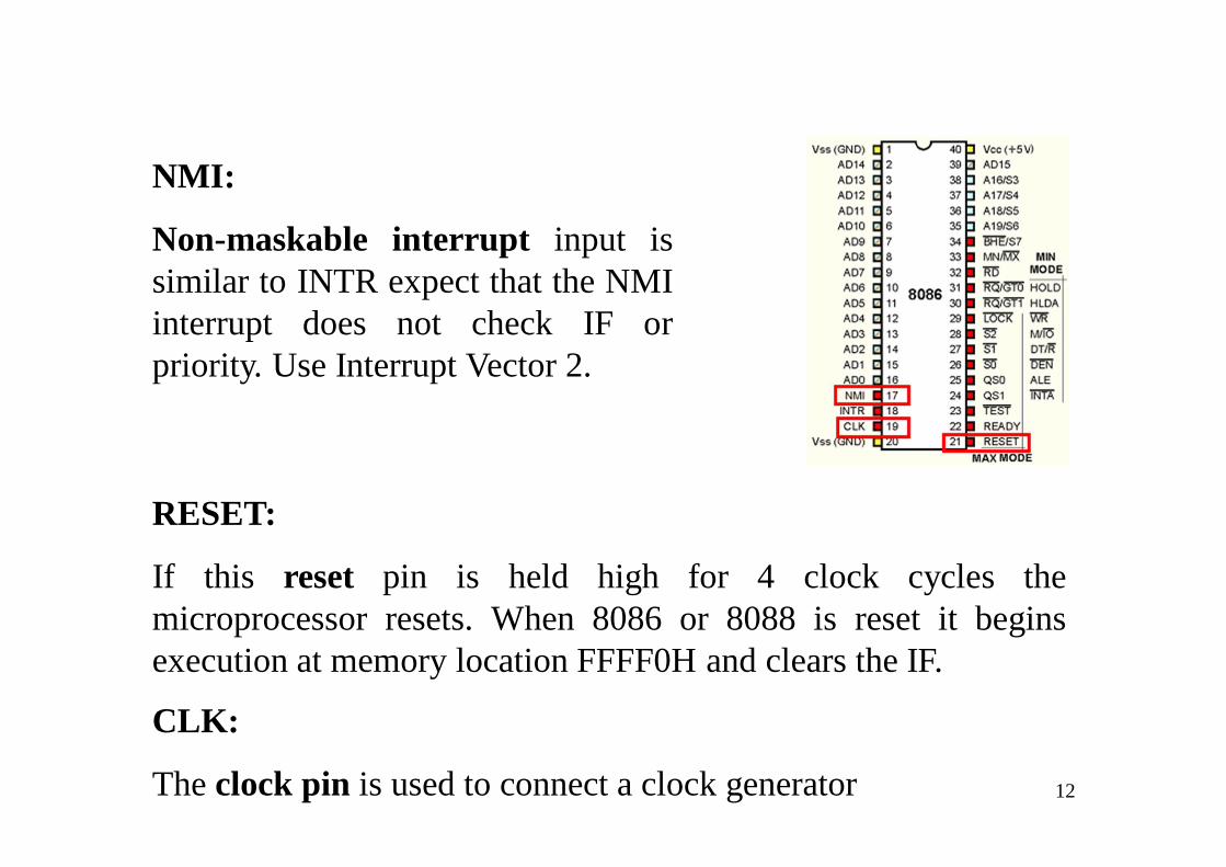
NMI:
Non-maskable interrupt input is similar to INTR expect that the NMI interrupt does not check IF or priority. Use Interrupt Vector 2.
RESET:
If this reset pin is held high for 4 clock cycles the microprocessor resets. When 8086 or 8088 is reset it begins execution at memory location FFFF0H and clears the IF.
CLK:
The clock pin is used to connect a clock generator
13
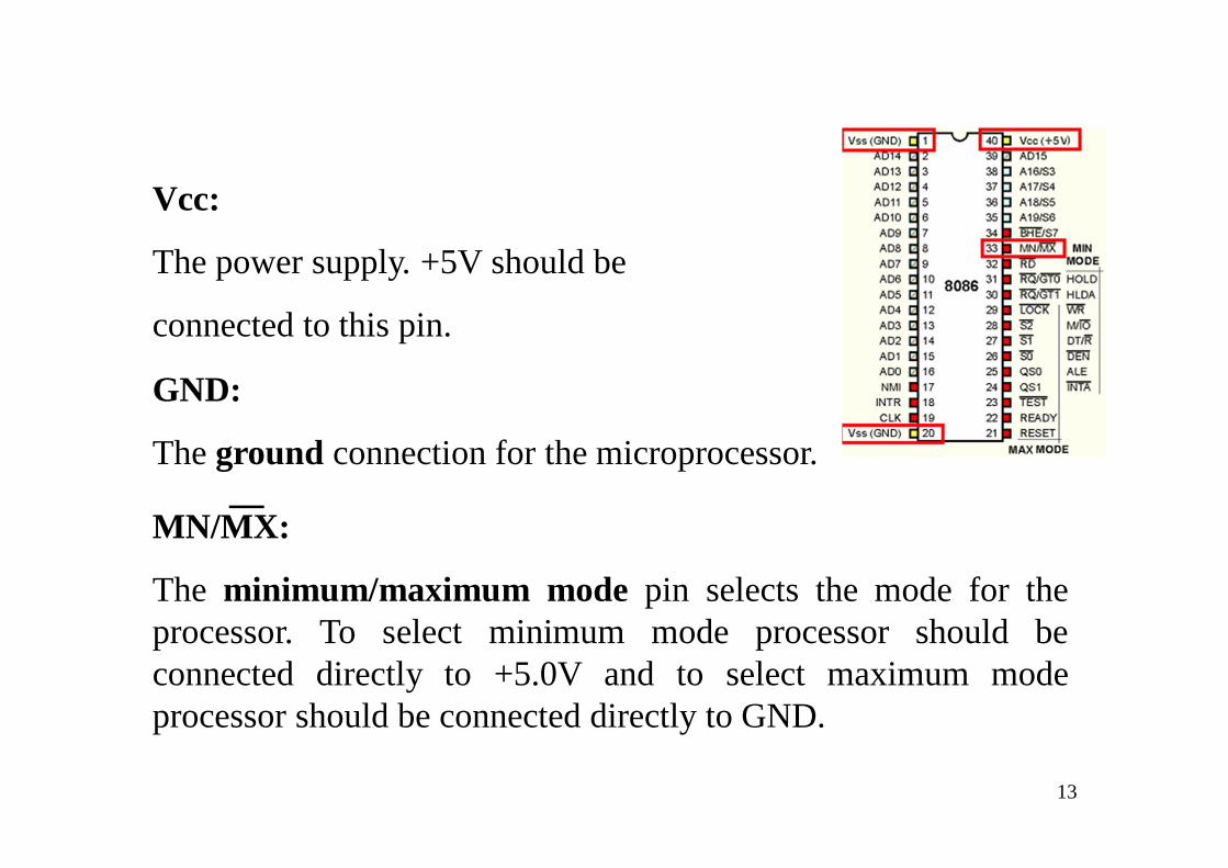
Vcc:
The power supply. +5V should be
connected to this pin.
GND:
The ground connection for the microprocessor.
MN/MX:
The minimum/maximum mode pin selects the mode for the processor. To select minimum mode processor should be connected directly to +5.0V and to select maximum mode processor should be connected directly to GND.
14
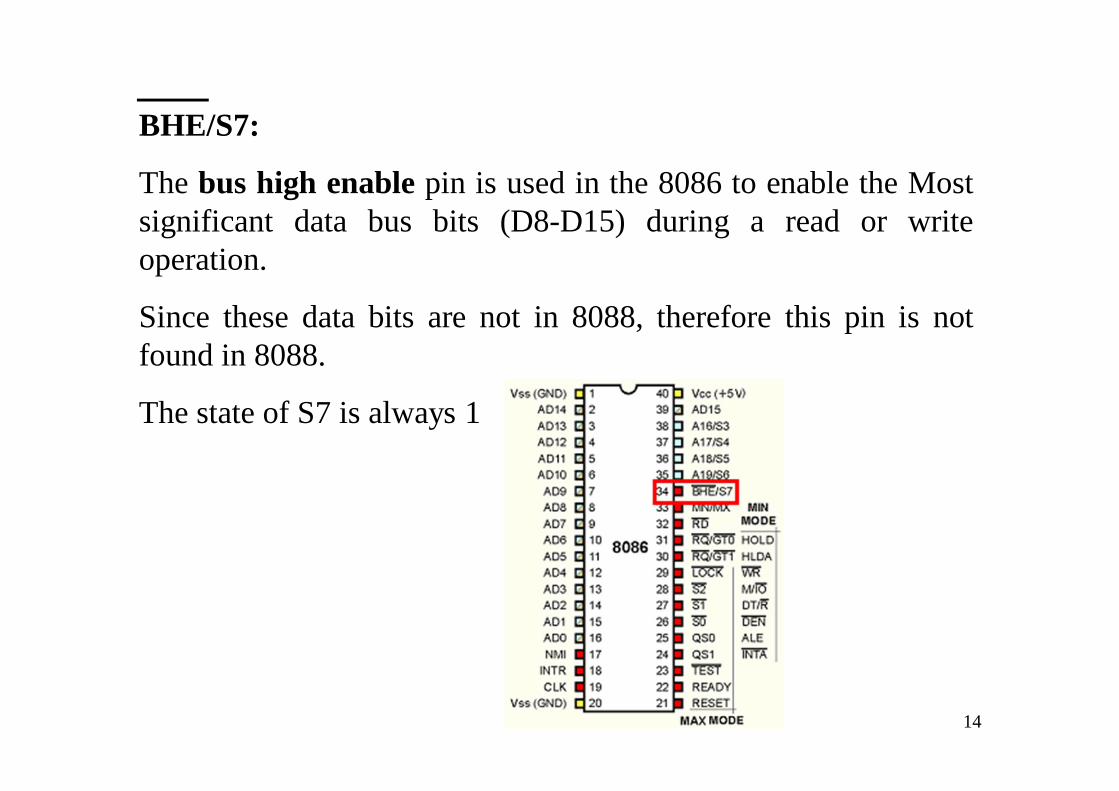
BHE/S7:
The bus high enable pin is used in the 8086 to enable the Most significant data bus bits (D8-D15) during a read or write operation.
Since these data bits are not in 8088, therefore this pin is not found in 8088.
The state of S7 is always 1
15
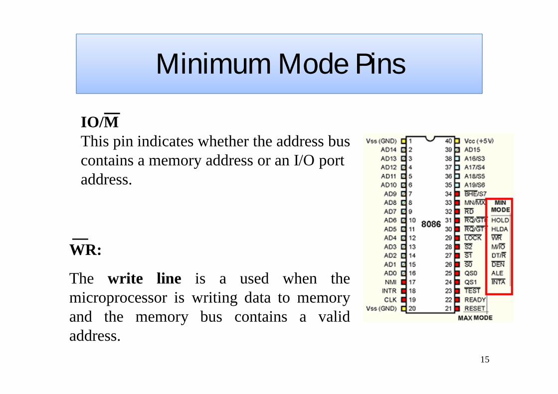
IO/M This pin indicates whether the address bus contains a memory address or an I/O port address.
WR:
The write line is a used when the microprocessor is writing data to memory and the memory bus contains a valid address.
Minimum Mode Pins
16
INTA:
Interrupt acknowledgement signals is a response to INTR input pin. This is used when the interrupt vector is placed on the address bus by the microprocessor.
ALE:
Address Latch enable shows whether the multiplexed AD lines carry address or data.
DT/R:
Data transmit/receive shows that the microprocessor data bus is transmitting(1) or receiving(0) data. This is used to control buffers.
17
DEN:
Data Enable bus activates external data bus buffers.
HOLD:
HOLD pin is used to input request DMA. Hold set to 1 microprocessor gives up control of buses to DMA controller.
SS0:
This is equivalent S0 in the maximum mode pins.
18
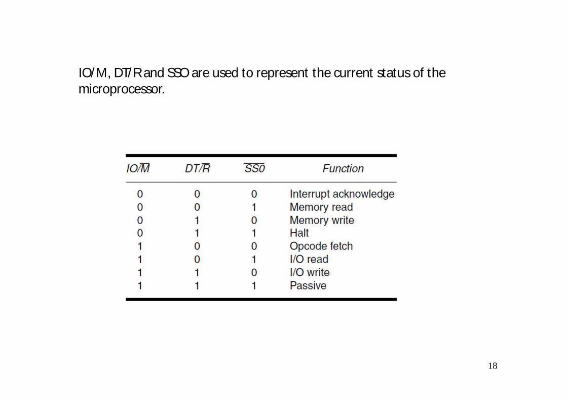
IO/M, DT/R and SSO are used to represent the current status of the microprocessor.
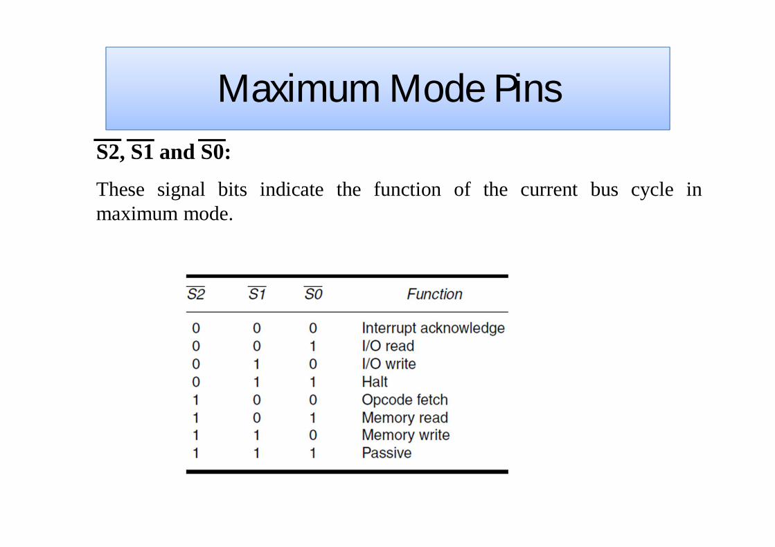
S2, S1 and S0:
These signal bits indicate the function of the current bus cycle in maximum mode.
Maximum Mode Pins
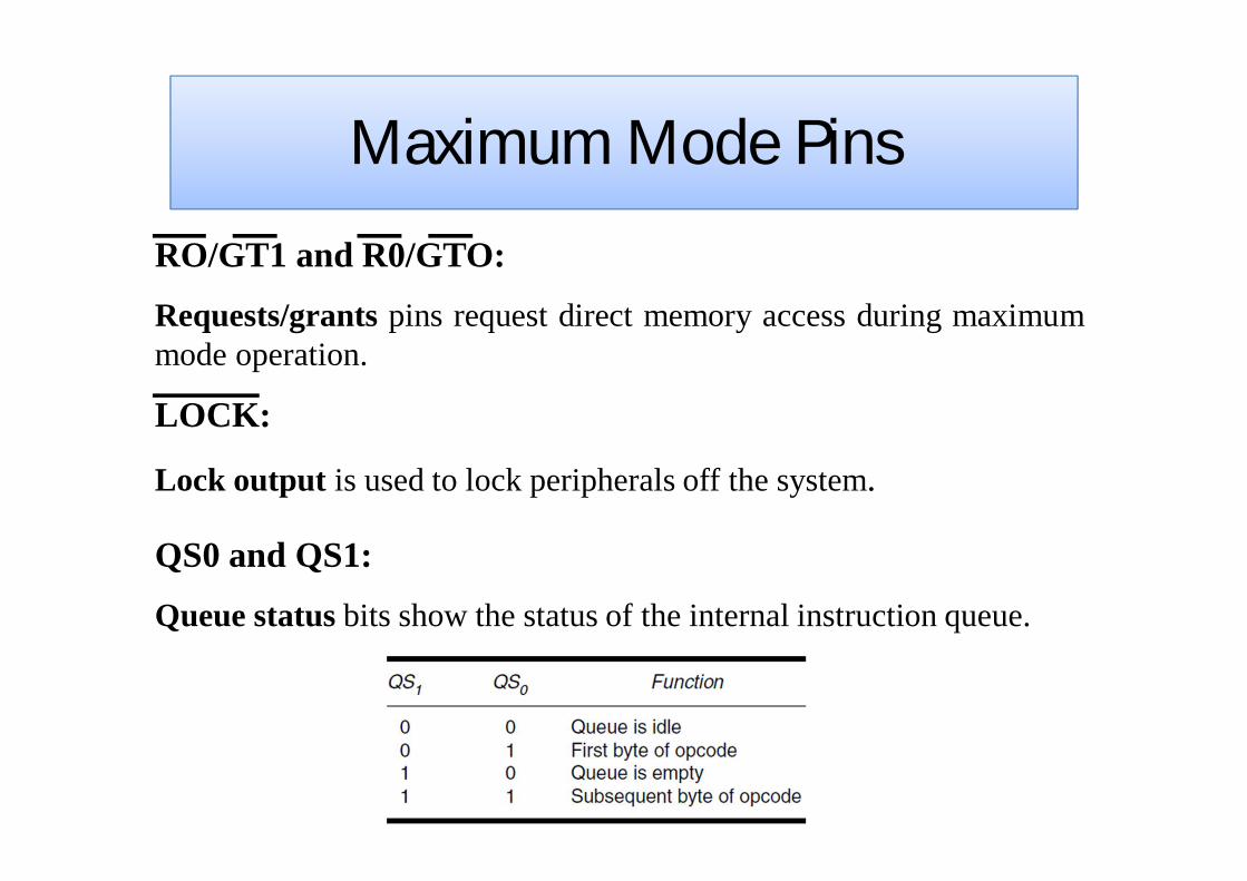
RO/GT1 and R0/GTO:
Requests/grants pins request direct memory access during maximum mode operation.
LOCK:
Lock output is used to lock peripherals off the system.
QS0 and QS1:
Queue status bits show the status of the internal instruction queue.
Maximum Mode Pins
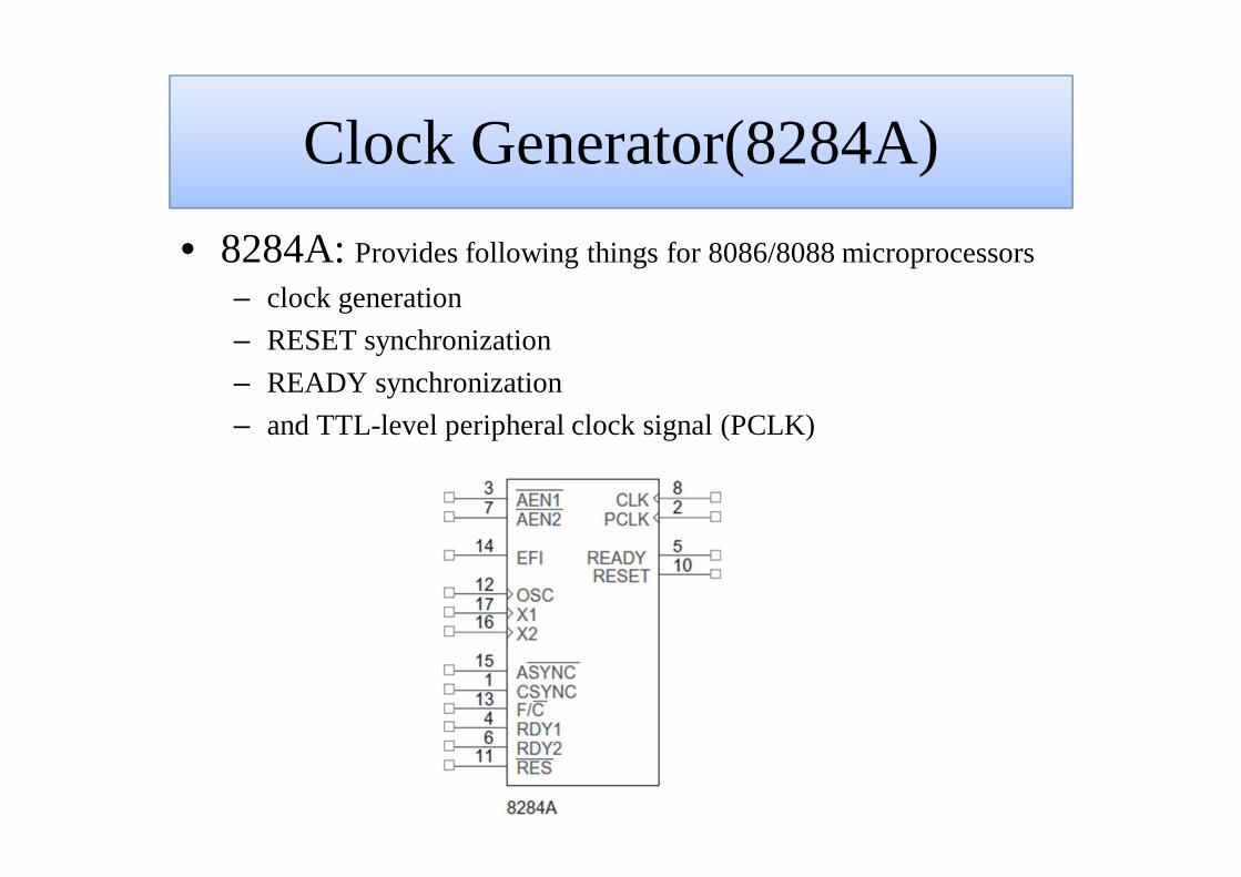
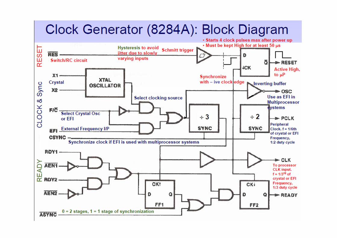
Clock Generator(8284A) • 8284A: Provides following things for 8086/8088 microprocessors
– clock generation – RESET synchronization – READY synchronization – and TTL-level peripheral clock signal (PCLK)
8284A Pin Functions • AEN1’, AEN2’(address enable) : to qualify bus ready signal RDY1, RDY2 • RDY1, RDY2(bus ready) : used in conjunction with AEN1’,AEN2’ pins, to cause wait states • ASYNC’(ready synchronization): it selects either one or two stages of synchronization for RDY1, RDY2 • READY: output pin that connects to 8086/88 READY input • X1, X2(crystal oscillator) :
connected to external crystal which is used as timing source for clock generator
• F/C’(frequency/crystal) input : It choose clocking source according to following scheme. – F/C’=1 : chooses external clock connected at EFI pin, – F/C’=0 : chooses internal crystal oscillator
• EFI(external frequency input) : it supplies the timing whenever F/C’ pin is pulled high (i.e. F/C = 1)
• CLK(clock output) : CLK input to 8086/8088 – Its 1/3 of crystal or EFI input frequency – It has 33% duty cycle which is required by 8086/8088
• PCLK(peripheral clock) : for peripherals – It is 1/6 of crystal or EFI input frequency, 50% duty cycle
• OSC(oscillator output) : This pin has same frequency as crystal or EFI input, it is used as EFI input for other 8284’s in multiprocessor systems.
• RES’(reset input) : It is often connected to RC network that provide power-on resetting.
• RESET it is an output pin connected to 8086/8088 RESET input
• CSYNC(clock synchronization) : – It is used whenever EFI is used to get clock in multi-
processor systems. It provides synchronization . – It must be grounded, if internal crystal oscillator is used
• GND(ground) : connected to ground • VCC(power supply) : +5.0V ±10%
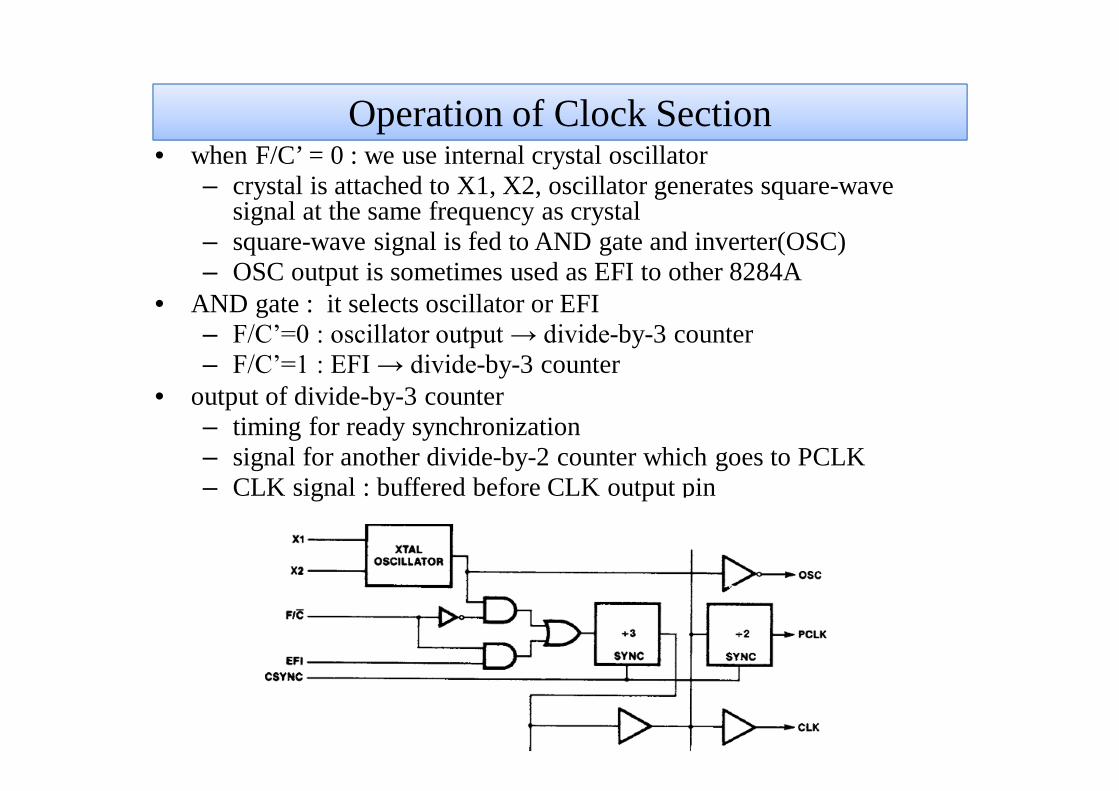
Operation of Clock Section • when F/C’ = 0 : we use internal crystal oscillator
– crystal is attached to X1, X2, oscillator generates square-wave signal at the same frequency as crystal
– square-wave signal is fed to AND gate and inverter(OSC) – OSC output is sometimes used as EFI to other 8284A
• AND gate : it selects oscillator or EFI – F/C’=0 : oscillator output → divide-by-3 counter – F/C’=1 : EFI → divide-by-3 counter
• output of divide-by-3 counter – timing for ready synchronization – signal for another divide-by-2 counter which goes to PCLK – CLK signal : buffered before CLK output pin
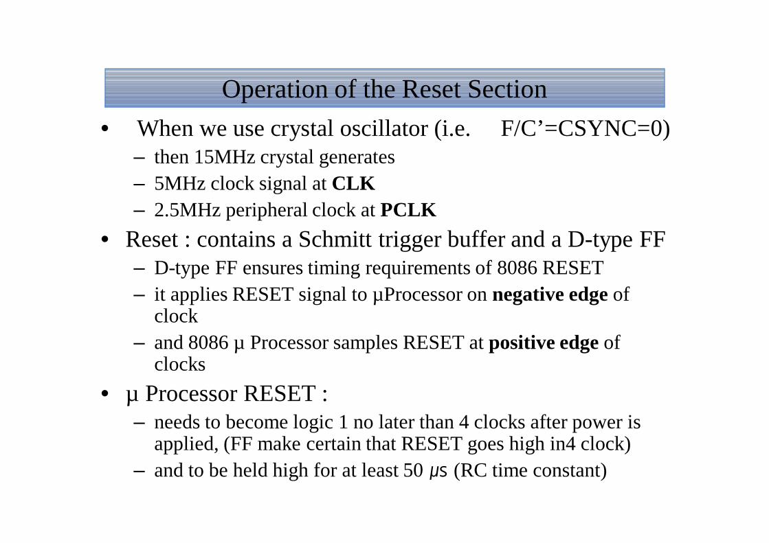
Operation of the Reset Section • When we use crystal oscillator (i.e. F/C’=CSYNC=0)
– then 15MHz crystal generates – 5MHz clock signal at CLK – 2.5MHz peripheral clock at PCLK
• Reset : contains a Schmitt trigger buffer and a D-type FF – D-type FF ensures timing requirements of 8086 RESET – it applies RESET signal to µProcessor on negative edge of
clock – and 8086 µ Processor samples RESET at positive edge of
clocks • µ Processor RESET :
– needs to become logic 1 no later than 4 clocks after power is applied, (FF make certain that RESET goes high in4 clock)
– and to be held high for at least 50 ㎲ (RC time constant)
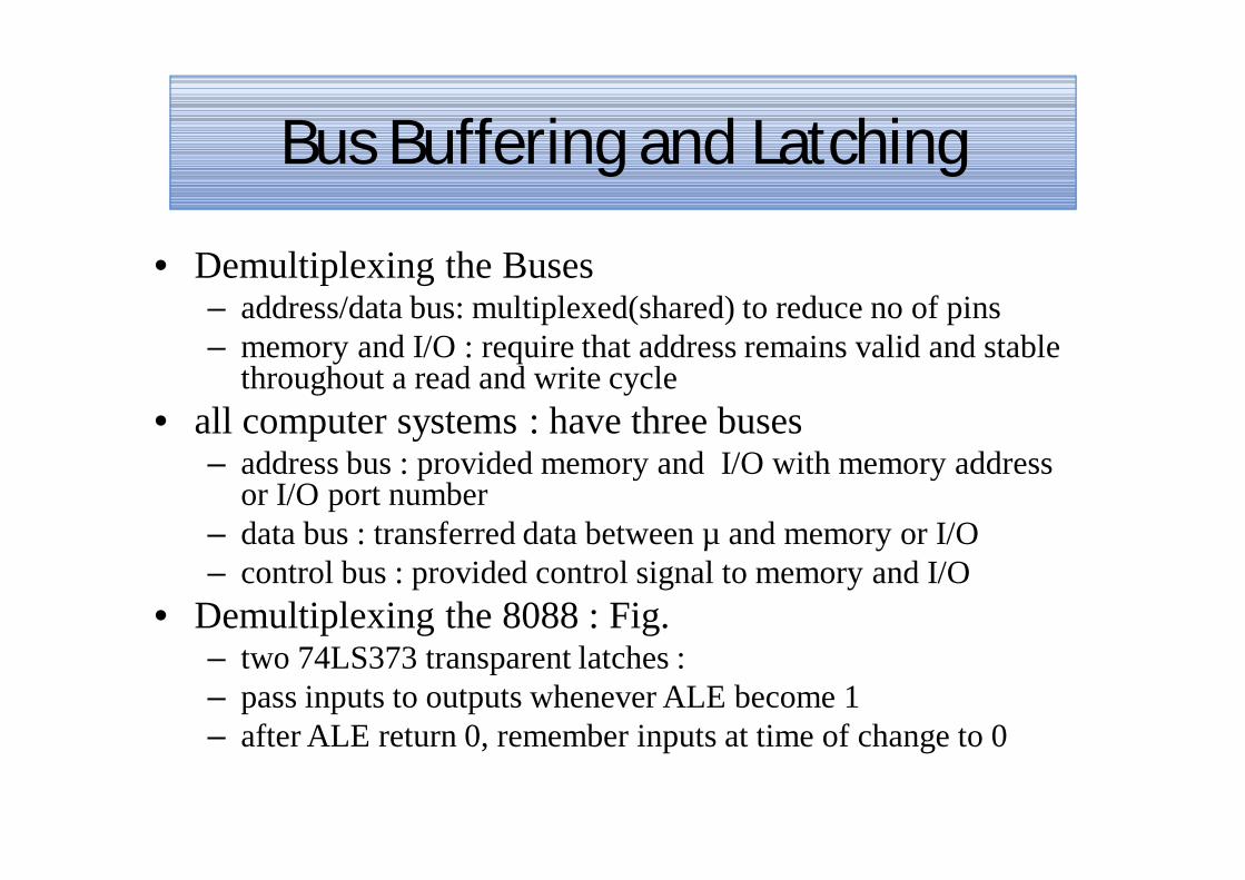
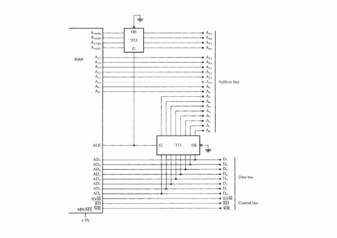
• Demultiplexing the Buses – address/data bus: multiplexed(shared) to reduce no of pins – memory and I/O : require that address remains valid and stable
throughout a read and write cycle • all computer systems : have three buses
– address bus : provided memory and I/O with memory address or I/O port number
– data bus : transferred data between µ and memory or I/O – control bus : provided control signal to memory and I/O
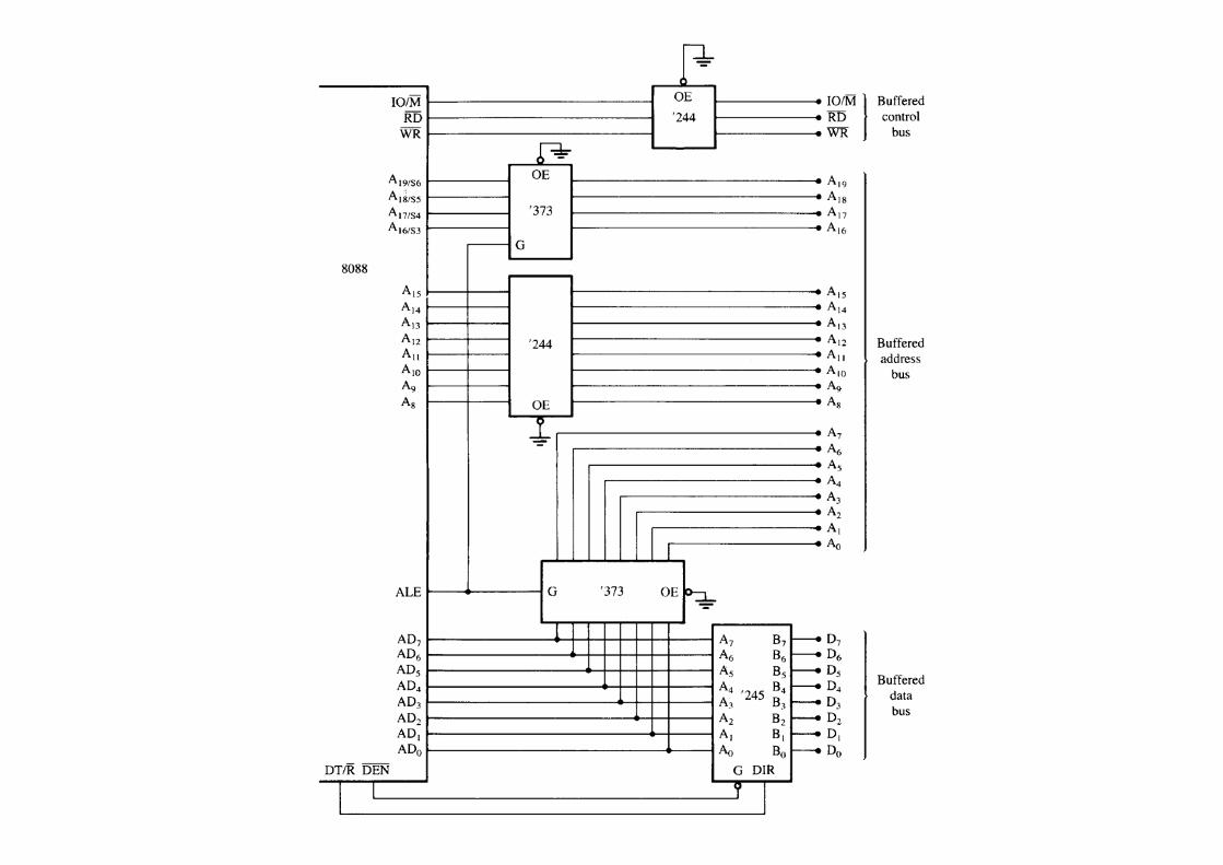
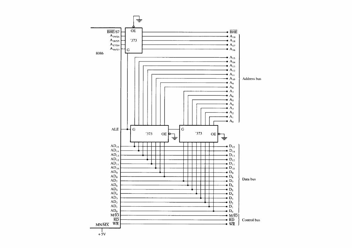
• Demultiplexing the 8088 : Fig. – two 74LS373 transparent latches : – pass inputs to outputs whenever ALE become 1 – after ALE return 0, remember inputs at time of change to 0
Bus Buffering and Latching
Bus Buffering and Latching
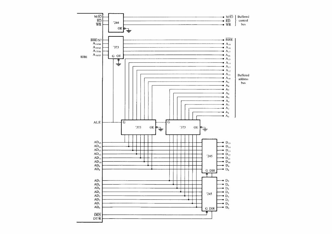
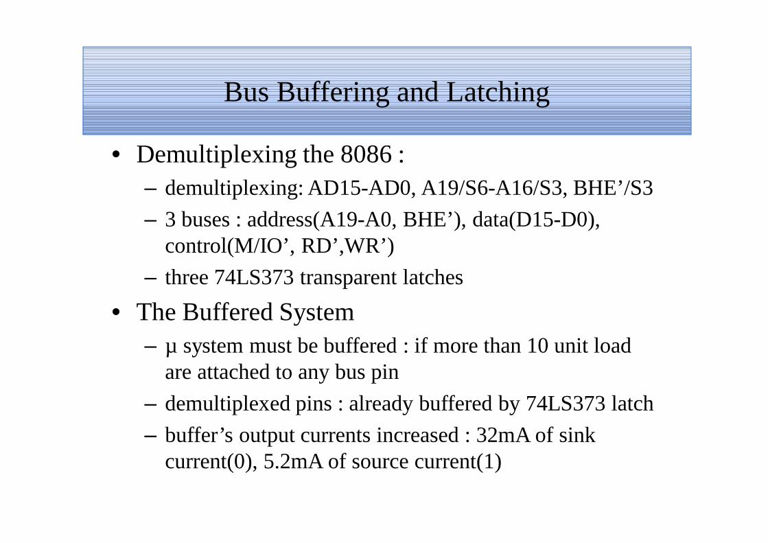
• Demultiplexing the 8086 : – demultiplexing: AD15-AD0, A19/S6-A16/S3, BHE’/S3 – 3 buses : address(A19-A0, BHE’), data(D15-D0),
control(M/IO’, RD’,WR’) – three 74LS373 transparent latches
• The Buffered System – µ system must be buffered : if more than 10 unit load
are attached to any bus pin – demultiplexed pins : already buffered by 74LS373 latch – buffer’s output currents increased : 32mA of sink
current(0), 5.2mA of source current(1)
Bus Buffering and Latching
– fully buffered signal will introduce timing delay – It will cause no difficulty unless memory and I/O
devices are used, which function at near maximum speed of bus
• The fully Buffered 8088 : – 8 address A15-A8 : 74LS244 octal buffer – IO/M’, RD’, WR’ : 74LS244 – 8 data D7-D0 : 74LS245 octal bi-directional bus buffer – direction : controlled by DT/R’, enable : by DEN’
• The fully Buffered 8086 : – data bus : two 74LS245 – IO/M’, RD’, WR’ : 74LS244