Embed Size (px)
Citation preview
GIP-CNFM: a French education network moving from microelectronics to nanotechnologies
CNFM: National Coordination for Education in Microelectronics and nanotechnologies
Prof. Olivier Bonnaud Executive Director of GIP-CNFM Université de Rennes 1 & Supelec
Rennes France [email protected]
Prof. Pierre Gentil
GIP-CNFM, MINATEC, Grenoble, France Pierre.Gentil@ grenoble -inp.fr
Prof. Ahmad Bsiesy,
Director of CNFM center, CIME, MINATEC, Grenoble, France
Prof. Sylvie Retailleau,
Director of CNFM center of Paris-Orsay, PMIPS, Orsay, France
Prof. Elizabeth Dufour-Gergam PMIPS, CNFM center of Paris-Orsay, France
Prof. Jean-Marie Dorkel, Director of CNFM center, AIME,
INSA Toulouse, France [email protected]
Abstract— Microelectronics high education in France is organized through a network composed of twelve centers, six of them having clean-rooms and technological facilities. During the year 2010, some activities moved from microelectronics to nanotechnologies in an effort to adapt our training facilities to the new nanoworld.
Keywords-component; high education, technogical education, national education network, microelectronics, nanotechnologies
I. INTRODUCTION
The education for engineers, master’s and doctorate students in the field of microelectronics is organized since the early 80’s in a network gathering several interuniversity centers spread through the France territory. The acronym of this network CNFM [1] corresponds to national committee for education (formation) in microelectronics [2]. This network allowed developing the practice of microelectronics in design as well as in technology by sharing expensive equipments and tools such as clean rooms or IC design softwares. In 2010, the organization of this network is a “Public Consortium” financially supported by Ministry of High Education and Research, including the twelve institutions having in charge the twelve common centers spread on the France territory and the syndicate of industries in the semiconductor field (SITELESC [3]).
Due to the strong evolution of the microelectronics towards the nanometric sizes and due to the recent explosion of nanosciences in the research and academic world, a national Programme was set-on by the French Ministry of Research during the year 2009. Three centers of the CNFM networks (Paris-Saclay, Grenoble, and Toulouse) were involved in the project by proposing some investment and setting new training
programs in nanoelectronics. Thanks to the previous experience and know-how, new laboratories are now available for some students of this new academic year 2010-2011.
This paper aims to explain the interest of such an educational network and will give details on how its structure and functioning, have evolved to meet the needs of new technologies
II. THE NANOELECTRONICS EVOLUTION
Microelectronics field had a strong evolution since the birth of the transistor in 1948. This evolution follows more or less the well-known Moore’s law [4] that predicted since more than 50 years an increase of performances close to a factor two each 18 months. Figure 1 shows the classical curve displaying this evolution.
It is clear that the device dimensions that are now close to nanometer dimensions (one meter divided by 1 billion) led to the apparition of new phenomena that have to be taken into account, namely the quantum effects. In addition, within very short distances, the ratio of forces changes drastically and induces new behaviors, for example due to Van der Walls forces that vary very strongly as a in function of the distance.
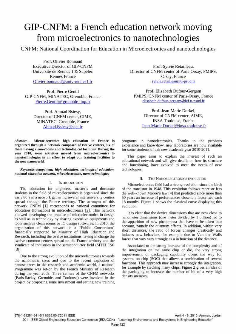
Associated to the strong increase of the complexity and of the integration on the same chip or die, the very strong improvement of packaging capability opens the way for systems on chip (SOC) that allows a combination of several functions. This approach may increase strongly the integration, for example by stacking many chips. Figure 2 gives an idea of the packaging to increase the number of bit of a very high density memory.
978-1-61284-641-5/11/$26.00 ©2011 IEEE 2011 IEEE Global Engineering Education Conference (EDUCON) – "Learning Environments and Ecosystems in Engineering Education"
April 4 - 6, 2010, Amman, Jordan
Page 122
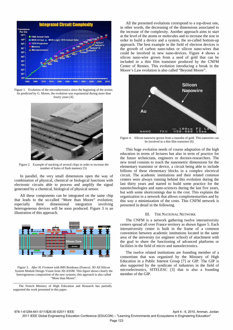
Figure 1. Evolution of the microelectronics since the beginning of the sixties.
As predicted by G. Moore, the evolution was exponential during more than fourty years [4].
Figure 2. Example of stacking of several chips in order to increase the
number of bytes of flash memory [5].
In parallel, the very small dimensions open the way of combination of physical, chemical or biological functions with electronic circuits able to process and amplify the signal generated by a chemical, biological of physical sensor.
All these components can be integrated on the same chip that leads to the so-called “More than Moore” evolution; especially three dimensional integration involving heterogeneous devices will be soon produced. Figure 3 is an illustration of this approach.
Figure 3. After H. Fremont with IMS Bordeaux (France): 3D All Silicon
System Module Design Vision from 3D-ASSM. This figure shows clearly the heterogeneous composition of the new systems; this approach is also called
“More than Moore”.
All the presented evolutions correspond to a top-down one, in other words, the decreasing of the dimensions associated to the increase of the complexity. Another approach aims to start at the level of the atoms or molecules and to increase the size in order to build a device and a system, the so-called bottom-up approach. The best example in the field of electron devices is the growth of carbon nano-tubes or silicon nano-wires that could be involved in new nano-devices. Figure 4 shows a silicon nano-wire grown from a seed of gold that can be included in a thin film transistor produced by the CNFM Center of Rennes. This evolution introducing a break in the Moore’s Law evolution is also called “Beyond Moore”.
Figure 4. Silicon nanowire grown from a nanodot of gold. This nanowire can
be involved in a thin film transistor [6].
This huge evolution needs of course adaptation of the high education in terms of lectures but also in term of practice for the future technicians, engineers or doctors-researchers. The new trend consists to reach the nanometric dimensions for the elementary transistor or device, a circuit being able to include billions of these elementary blocks in a complex electrical circuit. The academic institutions and their related common centers were always running behind this evolution during the last thirty years and started to build some practice for the nanotechnologies and nano-sciences during the last five years, but with some shortcomings due to the cost. This explains the organization in a network that allows complementarities and by this way a minimization of the costs. This CNFM network is presented in detail in the following.
III. THE NATIONAL NETWORK
The CNFM is a network gathering twelve interuniversity centers spread all over France territory as shown figure 5. Each interuniversity center is built in the frame of a common convention between academic institutions located in the same area of the university (or engineer school) of attachment with the goal to share the functioning of advanced platforms or facilities in the field of micro and nanoelectronics.
The twelve related institutions are founding member of a consortium that was organized by the Ministry of High Education in a Public Interest Group [7] or GIP. The GIP is also supported by the syndicate of industries in the field of microelectronics, SITELESC [3] that is also a founding member of the GIP.
SiliconNanowire
Au
The French Ministry of High Education and Research has partially supported the work presented in this paper.
978-1-61284-641-5/11/$26.00 ©2011 IEEE 2011 IEEE Global Engineering Education Conference (EDUCON) – "Learning Environments and Ecosystems in Engineering Education"
April 4 - 6, 2010, Amman, Jordan
Page 123
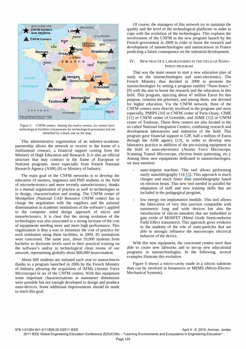
Figure 5. CNFM centers. Among the twelve centers, six centers have technological facilities (cleanrooms for technological processes) and are
identified by a black star on the map.
This administrative organization of an industry-academic partnership allows the network to receive in the frame of a multiannual contract, a financial support coming from the Ministry of High Education and Research. It is also an official structure that may contract in the frame of European or National programs, more especially from French National Research Agency (ANR) [8] or Ministry of Industry.
The main goal of the CNFM networks is to develop the education of masters, engineers and PhD students in the field of microelectronics and more recently nanoelectronics, thanks to a mutual organization of practice as well in technologies as in design, characterization and testing. The CNFM center of Montpellier (National CAD Resource CNFM center) has in charge the negotiation with the suppliers and the national dissemination in academic institutions of the software’s applied to the computer aided design approach of micro and nanoelectronics. It is clear that the strong evolution of the technologies was also associated to a strong increase of the cost of equipments needing more and more high performance. This organization is thus a way to minimize the cost of practice for each institution using these facilities; in 2009, 85 institutions were concerned. The same year, about 10,000 students from bachelor to doctorate levels used in their practical training on the software’s and/or in technological clean rooms of our network, representing globally about 800,000 hours/student.
About 600 students are initiated each year to nanosciences thanks to a program launched in 2006 by the French Ministry of Industry allowing the acquisition of AFMs (Atomic Force Microscope) in six of the CNFM centers. With this equipment some important characterizations at nanometer dimensions were possible but not enough developed to design and produce nano-devices. Some additional improvements should be made to reach this goal.
Of course, the managers of this network try to maintain the quality and the level of the technological platforms in order to cope with the evolution of the technologies. This explains the involvement of the CNFM in the new program launch by the French government in 2009 in order to boost the research and development of nanotechnologies and nanosciences in France predicting a future consequence on the industrial development.
IV. NEW PRACTICE LABORATORIES IN THE FIELD OF NANO-INNOV PROGRAM
That was the main reason to start a new education plan of study on the nanotechnologies and nano-electronics. The French Ministry thus decided in 2009 to promote the nanotechnologies by setting a program entitled “Nano-Innov.” [9] with the aim to boost the research and the education in this field. This program, injecting about 47 million Euros for this purpose, contains ten priorities, and among them, one devoted for higher education. Via the CNFM network, three of the CNFM centers were directly involved in the program and more especially, PMIPS [10] or CNFM center of Paris-Orsay, CIME [11] or CNFM center of Grenoble, and AIME [12] or CNFM center of Toulouse. These three centers are also located in the so-called National Integration Centers, combining research and development laboratories and industries of the field. This program gave financial support to GIP, half a million of Euros through the ANR agency [13], in order to develop new laboratory practice in addition of the pre-existing equipment in the field of nano-electronics (Atomic Force Microscope, Scanning Tunnel Microscope, electron beam patterning, etc.). Among these new equipments dedicated to nanotechnologies, we may mention:
- nano-imprint machine. This tool allows performing easily nanolithography [14-15]. This approach is much cheaper and much faster than nanolithography based on electron beam. This new tool needed in parallel the adaptation of staff and new training skills that are included in the pedagogical program,
- low energy ion implantation module. This tool allows the fabrication of very thin junction compatible with nanometric long and wide devices but also the introduction of silicon nanodots that are embedded in gate oxide of MOSFET (Metal Oxide Semiconductor Field Effect transistors). This approach gives evidence to the students of the role of nano-particles that are able to strongly influence the macroscopic electrical behavior of the device.
With this new equipment, the concerned centers were thus able to create new labworks and to set-up new educational programs in nanotechnologies. In the following, several examples illustrate this evolution.
Figure 6 shows a micro-cavity made in a silicon substrate than can be involved in biosensors or MEMS (Micro-Electro-Mechanical Systems).
Lille
GrenobleBordeaux
Paris-OrsayRennes
CNFM Centerswith techno.
CNFM Centers
ToulouseMarseilleMontpellier
LyonLimoges
Strasbourg
978-1-61284-641-5/11/$26.00 ©2011 IEEE 2011 IEEE Global Engineering Education Conference (EDUCON) – "Learning Environments and Ecosystems in Engineering Education"
April 4 - 6, 2010, Amman, Jordan
Page 124
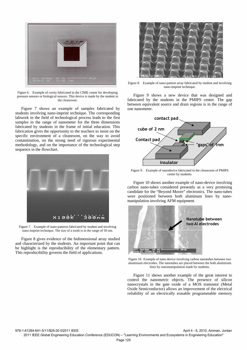
Figure 6. Example of cavity fabricated in the CIME center for developing pressure sensors or biological sensors. This device is made by the student in
the cleanroom.
Figure 7 shows an example of samples fabricated by students involving nano-imprint technique. The corresponding labwork in the field of technological process leads to the first samples in the range of nanometer for the three dimensions fabricated by students in the frame of initial education. This fabrication gives the opportunity to the teachers to insist on the specific environment of a cleanroom, on the way to avoid contamination, on the strong need of rigorous experimental methodology, and on the importance of the technological step sequence in the flowchart.
Figure 7. Example of nano-patterns fabricated by student and involving
nano-imprint technique. The size of a tooth is in the range of 50 nm.
Figure 8 gives evidence of the bidimensional array studied and characterized by the students. An important point that can be highlight is the reproducibility of the elementary pattern. This reproducibility governs the field of applications.
.
Figure 8. Example of nano-pattern array fabricated by student and involving nano-imprint technique.
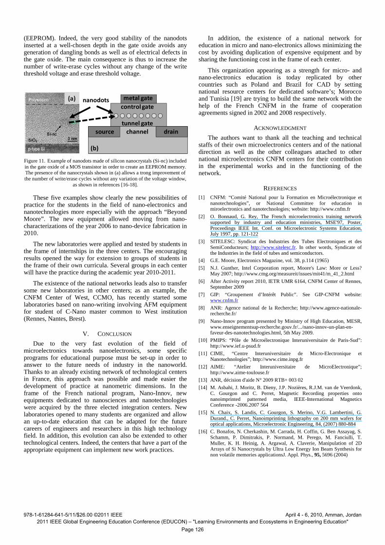
Figure 9 shows a new device that was designed and fabricated by the students in the PMIPS center. The gap between equivalent source and drain regions is in the range of one nanometer.
Figure 9. Example of nanodevice fabricated in the cleanroom of PMIPS
center by students.
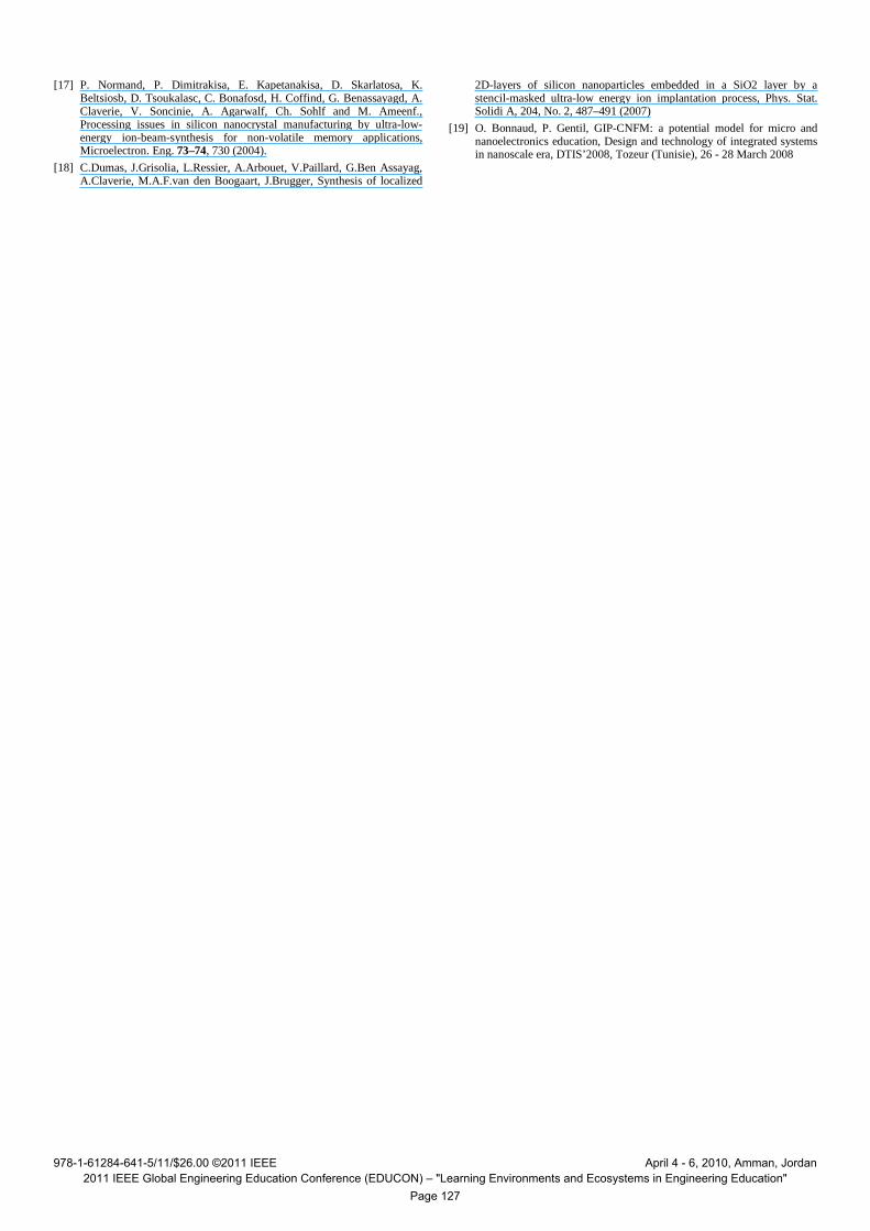
Figure 10 shows another example of nano-device involving carbon nano-tubes considered presently as a very promising candidate for the “Beyond Moore” electronics. The nano-tubes were positioned between both aluminum lines by nano-manipulation involving AFM equipment.
Figure 10. Example of nano device involving carbon nanotubes between two aluminium electrodes. The nanotubes are placed between the both aluminium
lines by nanomanipulation made by students.
Figure 11 shows another example of the great interest to control the nanometric objects. The presence of silicon nanocrystals in the gate oxide of a MOS transistor (Metal Oxide Semiconductor) allows an improvement of the electrical reliability of an electrically erasable programmable memory
cube of 2 nm
insulator
"gaps" of 1nm
contact pad
Contact pad
Nanotube between two Al electrodes
978-1-61284-641-5/11/$26.00 ©2011 IEEE 2011 IEEE Global Engineering Education Conference (EDUCON) – "Learning Environments and Ecosystems in Engineering Education"
April 4 - 6, 2010, Amman, Jordan
Page 125
(EEPROM). Indeed, the very good stability of the nanodots inserted at a well-chosen depth in the gate oxide avoids any generation of dangling bonds as well as of electrical defects in the gate oxide. The main consequence is thus to increase the number of write-erase cycles without any change of the write threshold voltage and erase threshold voltage.
Figure 11. Example of nanodots made of silicon nanocrystals (Si-nc) included in the gate oxide of a MOS transistor in order to create an EEPROM memory. The presence of the nanocrystals shown in (a) allows a trong improvement of the number of write/erase cycles without any variation of the voltage window,
as shown in references [16-18].
These five examples show clearly the new possibilities of practice for the students in the field of nano-electronics and nanotechnologies more especially with the approach “Beyond Moore”. The new equipment allowed moving from nano-characterizations of the year 2006 to nano-device fabrication in 2010.
The new laboratories were applied and tested by students in the frame of internships in the three centers. The encouraging results opened the way for extension to groups of students in the frame of their own curricula. Several groups in each center will have the practice during the academic year 2010-2011.
The existence of the national networks leads also to transfer some new laboratories in other centers; as an example, the CNFM Center of West, CCMO, has recently started some laboratories based on nano-writing involving AFM equipment for student of C-Nano master common to West institution (Rennes, Nantes, Brest).
V. CONCLUSION
Due to the very fast evolution of the field of microelectronics towards nanoelectronics, some specific programs for educational purpose must be set-up in order to answer to the future needs of industry in the nanoworld. Thanks to an already existing network of technological centers in France, this approach was possible and made easier the development of practice at nanometric dimensions. In the frame of the French national program, Nano-Innov, new equipments dedicated to nanosciences and nanotechnologies were acquired by the three elected integration centers. New laboratories opened to many students are organized and allow an up-to-date education that can be adapted for the future careers of engineers and researchers in this high technology field. In addition, this evolution can also be extended to other technological centers. Indeed, the centers that have a part of the appropriate equipment can implement new work practices.
In addition, the existence of a national network for education in micro and nano-electronics allows minimizing the cost by avoiding duplication of expensive equipment and by sharing the functioning cost in the frame of each center.
This organization appearing as a strength for micro- and nano-electronics education is today replicated by other countries such as Poland and Brazil for CAD by setting national resource centers for dedicated software’s; Morocco and Tunisia [19] are trying to build the same network with the help of the French CNFM in the frame of cooperation agreements signed in 2002 and 2008 respectively.
ACKNOWLEDGMENT
The authors want to thank all the teaching and technical staffs of their own microelectronics centers and of the national direction as well as the other colleagues attached to other national microelectronics CNFM centers for their contribution in the experimental works and in the functioning of the network.
REFERENCES [1] CNFM: “Comité National pour la Formation en Microélectronique et
nanotechnologies”, or National Committee for education in miroelectronics and nanotechnologies; website: http://www.cnfm.fr
[2] O. Bonnaud, G. Rey, The French microelectronics training network supported by industry and education ministries, MSE'97, Poster, Proceedings IEEE Int. Conf. on Microelectronic Systems Education, July 1997, pp. 121-122
[3] SITELESC: Syndicat des Industries des Tubes Electroniques et des SemiConducteurs; http://www.sitelesc.fr. In other words, Syndicate of the Industries in the field of tubes and semiconductors.
[4] G.E. Moore, Electronics Magazine, vol. 38, p.114 (1965)
[5] N.J. Gunther, Intel Corporation report, Moore's Law: More or Less? May 2007; http://www.cmg.org/measureit/issues/mit41/m_41_2.html
[6] After Activity report 2010, IETR UMR 6164, CNFM Center of Rennes, September 2009
[7] GIP: “Groupement d’Intérêt Public”. See GIP-CNFM website: www.cnfm.fr
[8] ANR: Agence national de la Recherche; http://www.agence-nationale-recherche.fr/
[9] Nano-Innov program presented by Ministry of High Education, MESR, www.enseignementsup-recherche.gouv.fr/.../nano-innov-un-plan-en-faveur-des-nanotechnologies.html, 5th May 2009.
[10] PMIPS: “Pôle de Microélectronique Interuniversitaire de Paris-Sud”: http://www.ief.u-psud.fr
[11] CIME, “Centre Interuniversitaire de Micro-Electronique et Nanotechnologies”; http://www.cime.inpg.fr
[12] AIME: “Atelier Interuniversitaire de MicroElectronique”; http://www.aime-toulouse.fr
[13] ANR, décision d'aide N° 2009 RTB+ 003 02
[14] M. Asbahi, J. Moritz, B. Dieny, J.P. Nozières, R.J.M. van de Veerdonk, C. Gourgon and C. Perret, Magnetic Recording properties onto nanoimprinted patterned media, IEEE-International Magnetics Conference -2006.2007 564
[15] N. Chaix, S. Landis, C. Gourgon, S. Merino, V.G. Lambertini, G. Durand., C. Perret, Nanoimprinting lithography on 200 mm wafers for optical applications, Microelectronic Engineering, 84, (2007) 880-884
[16] C. Bonafos, N. Cherkashin, M. Carrada, H. Coffin, G. Ben Assayag, S. Schamm, P. Dimitrakis, P. Normand, M. Perego, M. Fanciulli, T. Muller, K. H. Heinig, A. Argawal, A. Claverie, Manipulation of 2D Arrays of Si Nanocrystals by Ultra Low Energy Ion Beam Synthesis for non volatile memories applicationsJ. Appl. Phys., 95, 5696 (2004)
drainsource
metal gate
tunnel gate
channel
control gate
(b)
nanodots
978-1-61284-641-5/11/$26.00 ©2011 IEEE 2011 IEEE Global Engineering Education Conference (EDUCON) – "Learning Environments and Ecosystems in Engineering Education"
April 4 - 6, 2010, Amman, Jordan
Page 126
[17] P. Normand, P. Dimitrakisa, E. Kapetanakisa, D. Skarlatosa, K. Beltsiosb, D. Tsoukalasc, C. Bonafosd, H. Coffind, G. Benassayagd, A. Claverie, V. Soncinie, A. Agarwalf, Ch. Sohlf and M. Ameenf., Processing issues in silicon nanocrystal manufacturing by ultra-low-energy ion-beam-synthesis for non-volatile memory applications, Microelectron. Eng. 73–74, 730 (2004).
[18] C.Dumas, J.Grisolia, L.Ressier, A.Arbouet, V.Paillard, G.Ben Assayag, A.Claverie, M.A.F.van den Boogaart, J.Brugger, Synthesis of localized
2D-layers of silicon nanoparticles embedded in a SiO2 layer by a stencil-masked ultra-low energy ion implantation process, Phys. Stat. Solidi A, 204, No. 2, 487–491 (2007)
[19] O. Bonnaud, P. Gentil, GIP-CNFM: a potential model for micro and nanoelectronics education, Design and technology of integrated systems in nanoscale era, DTIS’2008, Tozeur (Tunisie), 26 - 28 March 2008
978-1-61284-641-5/11/$26.00 ©2011 IEEE 2011 IEEE Global Engineering Education Conference (EDUCON) – "Learning Environments and Ecosystems in Engineering Education"
April 4 - 6, 2010, Amman, Jordan
Page 127