Embed Size (px)
Citation preview
Enhanced Optical Absorption and Spectral Photocurrentin a-Si:H by Single- and Double-Layer SilverPlasmonic Interfaces
Zaki M. Saleh & Hisham Nasser & Engin Özkol &Mete Günöven & Burcu Altuntas & Alpan Bek &
Raşit Turan
Received: 1 August 2013 /Accepted: 7 November 2013 /Published online: 20 November 2013# Springer Science+Business Media New York 2013
Abstract Single and double plasmonic interfaces consistingof silver nanoparticles embedded in media with differentdielectric constants including SiO2, SiNx, and Al:ZnO havebeen fabricated by a self-assembled dewetting technique andintegrated to amorphous silicon films. Single plasmonic inter-faces exhibit plasmonic resonances whose frequency is red-shifted with increasing particle size and with the thickness of adielectric spacer layer. Double plasmonic interfaces consistingof two different particle sizes exhibit resonances consisting ofdouble minima in the transmittance spectra. The optical ex-tinction of a-Si:H deposited on these interfaces is broadenedinto the red indicating higher absorption and/or scattering atwavelengths higher than those typically absorbed by a-Si:Hwithout plasmonic interfaces. While the photocurrent shows
an overall decrease for the samples with the interfaces, signif-icant enhancement of photocurrent is observed near the low-energy edge of the bandgap (600–700 nm). These resultscorrelate well with the broadened extinction spectra of theinterfaces and are interpreted in terms of enhanced absorptionin that region.
Keywords Silver nanoparticles . Dewetting . Plasmonicinterface . Plasmonic resonance . Light trapping . Solar cells
Introduction
Current solar cell technology has shown a great deal of im-provement in recent years, but harvesting of the solar spec-trum is far from optimum. This is especially true for thin-filmsolar cells. In fact, a typical amorphous silicon (a-Si:H) solarcell absorbs less that 50 % of the available solar light suggest-ing that better light management schemes are needed [1].Development should include the optimization of optical ab-sorption by the absorber layer and reduction of reflection[2–5]. Textured surfaces have been successfully used to re-duce reflection and increase light trapping by the absorberlayer, but total utilization of even visible photons is not opti-mum. These schemes do not work well with thin-film devicesbecause the texture size exceeds film thickness [5, 6].Furthermore, low-energy photons pass through the cell struc-ture essentially unutilized. Methods to utilize these photons byconverting two or more of them into one with higher energythrough the so-called up-conversion process have been tested,but conclusive results with significant impact on solar cellshave not been demonstrated [1, 7, 8].
Plasmonic interfaces consisting of metal nanoparticlesplaced at the interfaces of two media with different dielectricconstants or embedded in a dielectric medium have shown a
Z. M. Saleh (*) :H. Nasser : E. Özkol :M. Günöven :B. Altuntas :A. Bek : R. TuranCenter for Solar Energy Research and Applications (GÜNAM),Middle East Technical University, Ankara, Turkeye-mail: [email protected]
Z. M. Salehe-mail: [email protected]
B. Altuntas :A. Bek : R. TuranDepartment of Physics, Middle East Technical University, Ankara,Turkey
Z. M. SalehDepartment of Physics, Arab American University-Jenin, Jenin,Palestine
H. Nasser :M. Günöven :A. Bek : R. TuranMicro and Nanotechnology Program of Graduate School of Naturaland Applied Sciences, Middle East Technical University, Ankara,Turkey
E. ÖzkolDepartment of Chemical Engineering, Middle East TechnicalUniversity, Ankara, Turkey
Plasmonics (2014) 9:357–365DOI 10.1007/s11468-013-9632-9

promising potential for enhancing absorption and photocur-rent in photovoltaic thin films and devices [6–11]. Usingrandom arrays of silver nanoparticles, Pillai et al. demonstrat-ed a 30% increase in photocurrent across the solar spectrum insilicon/oxide solar cells [12]. Schaadt et al. obtained up to80 % enhancement in photocurrent in the 500-nm spectralrange using gold nanoparticles on doped wafer-based solarcells [13]. Stuart and Hall claim a factor of 18 enhancementsin photocurrent around 800 nm by a silver nanoparticle inter-face integrated to a silicon-on-insulator photodetector [14].These reports illustrate the importance of plasmonic interfacesin improving light trapping and consequently the efficiency ofthin film solar cells.
Plasmons are the collective oscillations of free electrons atthe surfaces of the metal nanoparticles excited by incidentlight.When the frequency of incident light matches the naturalfrequency of these oscillating electrons, plasmonic resonancecharacterized by a minimum in the transmittance spectraoccurs and a large increase in the surface enhanced Ramanscattering [15–18]. Plasmonic resonance can also be charac-terized by a maximum in the extinction spectrum (E) definedas the total number of photons absorbed and/or scattered bythe interface and calculated as E = 1 − T − R , where T is thetransmittance and R is the reflectance [9]. For solar energyconversion, we are interested in maximum scattering andminimum absorption by the interface. Light absorbed by theinterface is lost while that scattered may, by proper matchingof thicknesses refractive indices of surrounding media, bepreferentially scattered into the device absorber layer [6, 19].Scattering can be maximized by appropriate selection of sizeand shape of the nanoparticle as well as the dielectric mediumin which it is embedded [6, 20]. One therefore monitors themaximum in the extinction (E) spectrum by the interface tooptimize the probability for scattering by the plasmonic inter-face into the absorber layer. The plasmonic interfaces can beengineered to increase the electric field in the vicinity of theabsorber layer (near field effect) or to preferentially scatterlight into the absorber layer (far-field effect) to enhance thephotocurrent and increase the overall efficiency of PVdevices.
Amorphous Si has a refractive index (n =3.5) sufficientlyhigher than that of most dielectric materials used in the solar cellindustry such as SiO2 (n =1.45–1.55), SiNx (n =2.0–2.1), andtransparent conducting oxides such as Al:ZnO (n =1.8–2.0).Therefore, regardless of their position relative to the absorberlayer, nanoparticles will almost always preferentially scatterlight into silicon increasing absorption in the absorber layerby the far field effect of plasmonic resonance. Placed close tothe absorber layer, these interfaces can enhance photocurrent byresonance-induced gigantic but localized electric fields. Othereffects such as absorption by the interface and destructiveinterference of transmitted and backscattered waves can causean overall reduction in photocurrent and should be minimized
[21]. It is therefore crucial to maximize scattering and minimizeabsorption by selecting the appropriate size of the nanoparticlesto obtain a positive effect of enhanced absorption by the solarcell. It is found that absorption dominates for particles ofdiameter <50 nm while scattering dominates for particles great-er than 100 nm [6, 11].
Numerical studies suggest that plasmonic interfaces inte-grated at the front interface of the absorber layer cause highabsorption losses and are ineffective in enhancing photocur-rent [22]. Other studies suggest that embedding interfaceswithin the absorber layer may increase recombination centersand reduce photocurrent, although one study has demonstrat-ed a slight increase in photocurrent due to enhanced nearinfrared absorption [23]. It is therefore concluded that themost promising position of a plasmonic interface is the rearof the absorber layer [24]. It is interesting to note that Eminianet al. demonstrated a significant photocurrent enhancement inthe 600–800-nm region in a-Si:H based n-i-p solar cell struc-tures due to Au nanoparticles positioned at the rear interface ofthe absorber layer [25]. Most existing plasmonic structuresinvolve a single plasmonic interface, but the added benefits ofselecting the dielectric material and matching of refractiveindices offered by the double or higher interfaces have notbeen thoroughly investigated. Ho et al. integrated a doublelayer of gold nanoparticles to a-Si solar cell and obtained animproved efficiency of 18.4 % [24].
In this work, we investigate the effect of single and doubleplasmonic interfaces using self-assembled Ag nanoparticlesplaced at the interfaces of two different media with variousdielectric constants and integrated at the rear of device qualitya-Si:H films to measure improved light trapping and anycorresponding enhancement in photocurrent. Most studiesuse photodetector or solar-cell modules to measure enhance-ment in photocurrent due to the plasmonic interfaces. Ourstudy employs the enhancement in the spectral dependenceof photocurrent in an isolated thin a-Si:H layer as an indicatorfor a positive plasmonic effect. It gives direct and conclusiveresults for the plasmonic effect before introducing more pos-sible losses in efficiency due to the more complicated realdevice.
Experimental
Three types of plasmonic structures consisting of silver nano-particles positioned at the interfaces between two dielectricmedia with different thicknesses and refractive indices areintegrated to device quality a-Si:H films deposited by thePECVD method. The silver nanoparticles were fabricated bya standard dewetting technique in which a thin silver film of15 nm thickness is sputtered on the substrate and annealed at200–500 °C for 1 h in N2 environment [12, 14, 26]. For thedouble plasmonic interfaces, a high temperature anneal is used
358 Plasmonics (2014) 9:357–365
to fabricate the base layer consisting of larger particles follow-ed by a 10 or 20-nm spacer layer of sputtered SiO2 or SiNx.The dewetting technique is then repeated by sputtering 15 nmAg followed by lower temperature anneals at 200 °C tofabricate the upper (secondary interface).
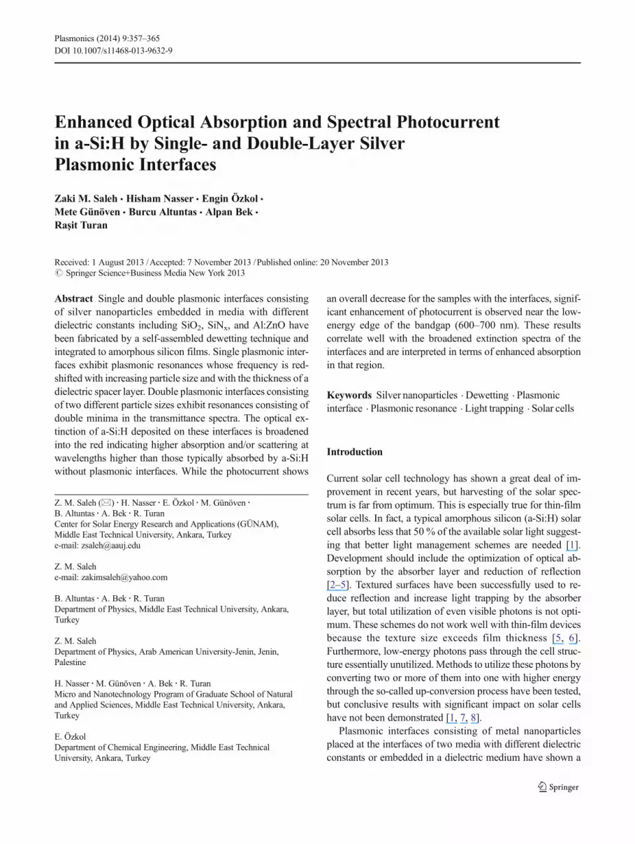
Scanning electron microscope (SEM) images and opticalmeasurements are performed on dedicated samples of the setsat various processing steps. The transmittance and reflectanceover the optical range of 300–1,200 nm was performed usingan optical system as described in a previous publication [27].Optical extinction (E) spectra were calculated from the trans-mittance and reflectance spectra using E = 1 − T − R . Ana-Si:H layer, with or without a spacer layer of SiO2 or SiNx asdescribed in the sample sets below, was deposited on success-fully fabricated interfaces of each structure. Al electrodes ofstandard coplanar geometry with 1.0 cm by 0.3 cm rectanglesseparated by 1.0 mm gaps are evaporated on the a-Si:H side ofthe structure using a shadow mask. The final structure of atypical set ready for photocurrent measurements is depicted inFig. 1. The total photocurrent was measured by illuminatingthe a-Si:H side using a one-sun solar simulator while thespectral dependence of the photocurrent was measured underillumination from a halogen lamp through a monochromator
using 25 nm increments over the spectral range of 300–1,200 nm. Samples prepared by deposition of the same a-Si:H film on bare Corning substrates was used as references.A total of seven sample sets were constructed as shown below.Set PLS-0 consists of samples with 250 nm a-Si:H depositedon Corning substrate as a reference. PLS-01 consists of thesame a-Si:H deposited directly on nanoparticles formed by a200 °C anneal. PLS-03 is the same as PLS-01 except for a20-nm SiO2 spacer layer on top of the Ag nanoparticles.PLS-05 consists of a 250-nm a-Si:H film deposited onAg nanoparticles formed by 400 °C anneal. PLS-06 is adouble interface consisting of two Ag nanoparticles layersformed by 400 °C on glass and by 200 °C anneal separatedby a 20-nm SiO2 and covered by another 10 nm SiO2 spacerlayer under the a-Si:H layer. PLS-07 is the same as PLS-06except that the SiO2 spacer layer separating the two interfacesis reduced to 10 nm. Finally, PLS-08 is the same as PLS-06except SiO2 is replaced by SiNx:
PLS-Si: Corning/250 nm a-Si:H (reference set)PLS-01: Corning/15 nm Ag/200 °C anneal/250 nma-Si:HPLS-03: Corning/15 nm Ag/200 °C anneal/20 nm SiO2/250 nm a-Si:HPLS-05: Corning/15 nm Ag/400 °C anneal/20 nm SiO2/250 nm a-Si:HPLS-06: Corning/15 nm Ag/400 °C anneal/20 nm SiO2/15 nm Ag/200 °C anneal/10 nm SiO2/250 nm a-Si:HPLS-07: Corning/15 nm Ag/400 °C anneal/10 nm SiO2/15 nm Ag/200 °C anneal/10 nm SiO2/250 nm a-Si:HPLS-08: Corning/15 nm Ag/400 °C anneal/20 nm SiNx/15 nm Ag/200°C anneal/10 nm SiNx/250 nm a-Si:H
Results
Dewetting of the 15-nm Ag on Corning glass is successful informing well-separated nearly spherical nanoparticles al-though their size, as characterized by the mean radius, doesnot follow a perfectly random distribution and their shape isnot perfectly spherical. A thorough study of annealing timeand temperature dependence is not available but a window of
Fig. 1 Schematic diagram of a typical plasmonic interface integrated tothe rear of an amorphous silicon (a-Si) thin film for photocurrentmeasurements
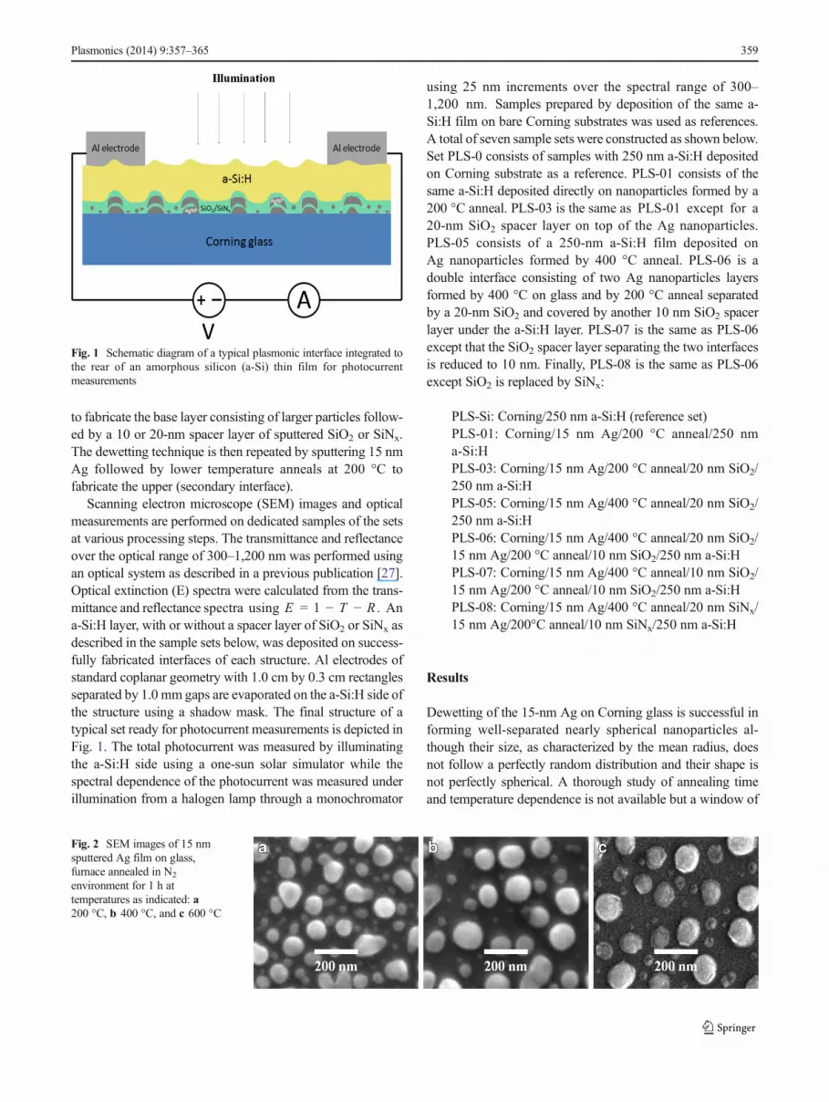
Fig. 2 SEM images of 15 nmsputtered Ag film on glass,furnace annealed in N2
environment for 1 h attemperatures as indicated: a200 °C, b 400 °C, and c 600 °C
Plasmonics (2014) 9:357–365 359
optimal process conditions can be deduced. As shown inFig. 2, the particle size increases and it appears to becomequalitatively more spherical with increasing annealing temper-ature from 200 to 500 °C. Annealing temperature of 600 °Cappears to deform the corning substrate and leave Ag orAg/SiO2 residue in the areas between the Ag nanoparticles.
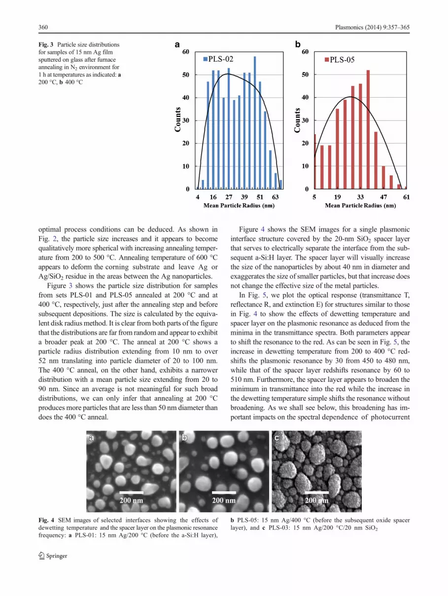
Figure 3 shows the particle size distribution for samplesfrom sets PLS-01 and PLS-05 annealed at 200 °C and at400 °C, respectively, just after the annealing step and beforesubsequent depositions. The size is calculated by the equiva-lent disk radius method. It is clear from both parts of the figurethat the distributions are far from random and appear to exhibita broader peak at 200 °C. The anneal at 200 °C shows aparticle radius distribution extending from 10 nm to over52 nm translating into particle diameter of 20 to 100 nm.The 400 °C anneal, on the other hand, exhibits a narrowerdistribution with a mean particle size extending from 20 to90 nm. Since an average is not meaningful for such broaddistributions, we can only infer that annealing at 200 °Cproduces more particles that are less than 50 nm diameter thandoes the 400 °C anneal.
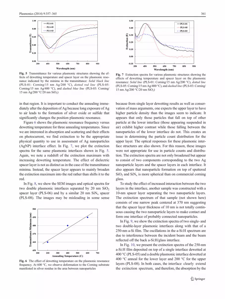
Figure 4 shows the SEM images for a single plasmonicinterface structure covered by the 20-nm SiO2 spacer layerthat serves to electrically separate the interface from the sub-sequent a-Si:H layer. The spacer layer will visually increasethe size of the nanoparticles by about 40 nm in diameter andexaggerates the size of smaller particles, but that increase doesnot change the effective size of the metal particles.
In Fig. 5, we plot the optical response (transmittance T,reflectance R, and extinction E) for structures similar to thosein Fig. 4 to show the effects of dewetting temperature andspacer layer on the plasmonic resonance as deduced from theminima in the transmittance spectra. Both parameters appearto shift the resonance to the red. As can be seen in Fig. 5, theincrease in dewetting temperature from 200 to 400 °C red-shifts the plasmonic resonance by 30 from 450 to 480 nm,while that of the spacer layer redshifts resonance by 60 to510 nm. Furthermore, the spacer layer appears to broaden theminimum in transmittance into the red while the increase inthe dewetting temperature simple shifts the resonance withoutbroadening. As we shall see below, this broadening has im-portant impacts on the spectral dependence of photocurrent
Fig. 3 Particle size distributionsfor samples of 15 nm Ag filmsputtered on glass after furnaceannealing in N2 environment for1 h at temperatures as indicated: a200 °C, b 400 °C
Fig. 4 SEM images of selected interfaces showing the effects ofdewetting temperature and the spacer layer on the plasmonic resonancefrequency: a PLS-01: 15 nm Ag/200 °C (before the a-Si:H layer),
b PLS-05: 15 nm Ag/400 °C (before the subsequent oxide spacerlayer), and c PLS-03: 15 nm Ag/200 °C/20 nm SiO2
360 Plasmonics (2014) 9:357–365
in that region. It is important to conduct the annealing imme-diately after the deposition of Ag because long exposure of Agto air leads to the formation of silver oxide or sulfide thatsignificantly changes the position plasmonic resonance.
Figure 6 shows the plasmonic resonance frequency versusdewetting temperature for three annealing temperatures. Sincewe are interested in absorption and scattering and their effectson photocurrent, we find extinction to be the appropriatephysical quantity to use in assessment of Ag nanoparticles(AgNP) interface effect. In Fig. 7, we plot the extinctionspectra for the same plasmonic interfaces shown in Fig. 5.Again, we note a redshift of the extinction maximum withincreasing dewetting temperature. The effect of dielectricspacer layer is not as distinct as in the case of the transmittanceminima. Instead, the spacer layer appears to mainly broadenthe extinction maximum into the red rather than shifts it to thered.
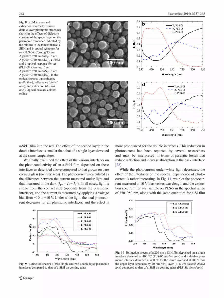
In Fig. 8, we show the SEM images and optical spectra fortwo double plasmonic interfaces separated by 20 nm SiO2
spacer layer (PLS-06) and by a similar 20 nm SiNx spacer(PLS-08). The images may be misleading in some sense
because from single layer dewetting results as well as conser-vation of mass arguments, one expects the upper layer to havehigher particle density than the images seem to indicate. Itappears that only those particles that fall on top of otherparticle at the lower interface (those appearing suspended inair) exhibit higher contrast while those falling between thenanoparticles of the lower interface do not. This creates anissue in determining the particle count distribution for theupper layer. The optical responses for these plasmonic inter-face structures are also shown. For this reason, these imageswere not appropriate for use in particle counts and distribu-tion. The extinction spectra are not only broadened but appearto consist of two components corresponding to the two Agnanoparticle layers and the spacer layers in each interface. Italso appears that nanoparticle formation on top of sputteredSiO2 and SiNx is more spherical than on commercial corningglass.
To study the effect of increased interaction between the twolayers in the interface, another sample was constructed with a10-nm spacer layer separating the two nanoparticle layers.The extinction spectrum of that sample (not shown here)consists of one narrow peak centered at 370 nm suggestingthat the spacer layer thickness of 10 nm is not totally contin-uous causing the two nanoparticle layers to make contact andform one interface of probably connected nanoparticles.
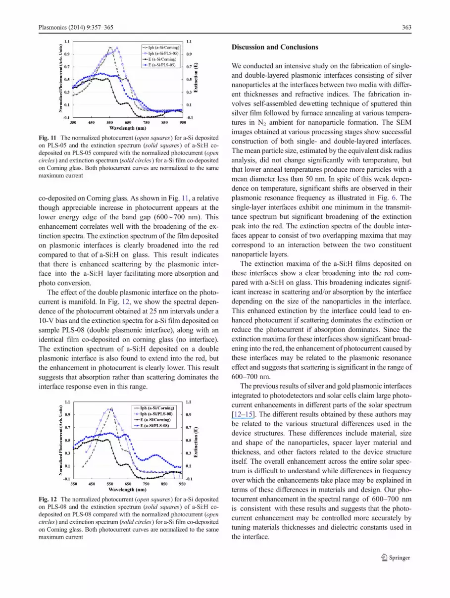
In Fig. 9, we show the extinction spectra of two single- andtwo double-layer plasmonic interfaces along with that of a250-nm a-Si film. The oscillations in the a-Si:H spectrum aredue to interference between the incident beam and the beamreflected off the back a-Si:H/glass interface.
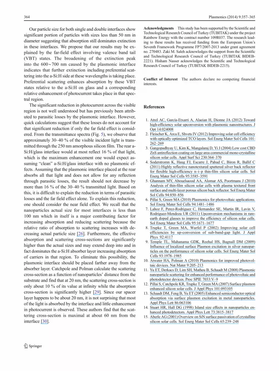
In Fig. 10, we present the extinction spectra of the 250-nma-Si:H film deposited on top of a single interface dewetted at400 °C (PLS-05) and a double plasmonic interface dewetted at400 °C anneal for the lower layer and 200 °C for the upperlayers (PLS-08). In both cases, the interface clearly extendthe extinction spectrum, and therefore, the absorption by the
Fig. 5 Transmittance for various plasmonic structures showing the ef-fects of dewetting temperature and spacer layer on the plasmonic reso-nance indicated by the minima in the transmittance: Solid black line(PLS-01: Corning/15 nm Ag/200 °C), dotted red line (PLS-05:Corning/15 nm Ag/400 °C), and dashed blue line (PLS-03: Corning/15 nm Ag/200 °C/20 nm SiO2)
Fig. 6 The effect of dewetting temperature on the plasmonic resonancefrequency. At 600 °C, we observe deformation to the Corning substratemanifested in silver residue in the area between nanoparticles
Fig. 7 Extinction spectra for various plasmonic structures showing theeffects of dewetting temperature and spacer layer on the plasmonicresonance: Solid line (PLS-01: Corning/15 nm Ag/200 °C), dotted line(PLS-05: Corning/15 nmAg/400 °C), and dashed line (PLS-03: Corning/15 nm Ag/200 °C/20 nm SiO2)
Plasmonics (2014) 9:357–365 361
a-Si:H film into the red. The effect of the second layer in thedouble interface is smaller than that of a single layer dewettedat the same temperature.
We finally examined the effect of the various interfaces onthe photoconductivity of an a-Si:H film deposited on theseinterfaces as described above compared to that grown on barecorning glass (no interfaces). The photocurrent is calculated asthe difference between the current measured under light andthat measured in the dark (Iph = IL− ID). In all cases, light isshone from the contact side (opposite from the plasmonicinterface), and the current is measured by applying a voltagebias from −10 to +10 V. Under white light, the total photocur-rent decreases for all plasmonic interfaces, and the effect is
more pronounced for the double interfaces. This reduction inphotocurrent has been reported by several researchersand may be interpreted in terms of parasitic losses thatreduce reflection and increase absorption at the back interface[28].
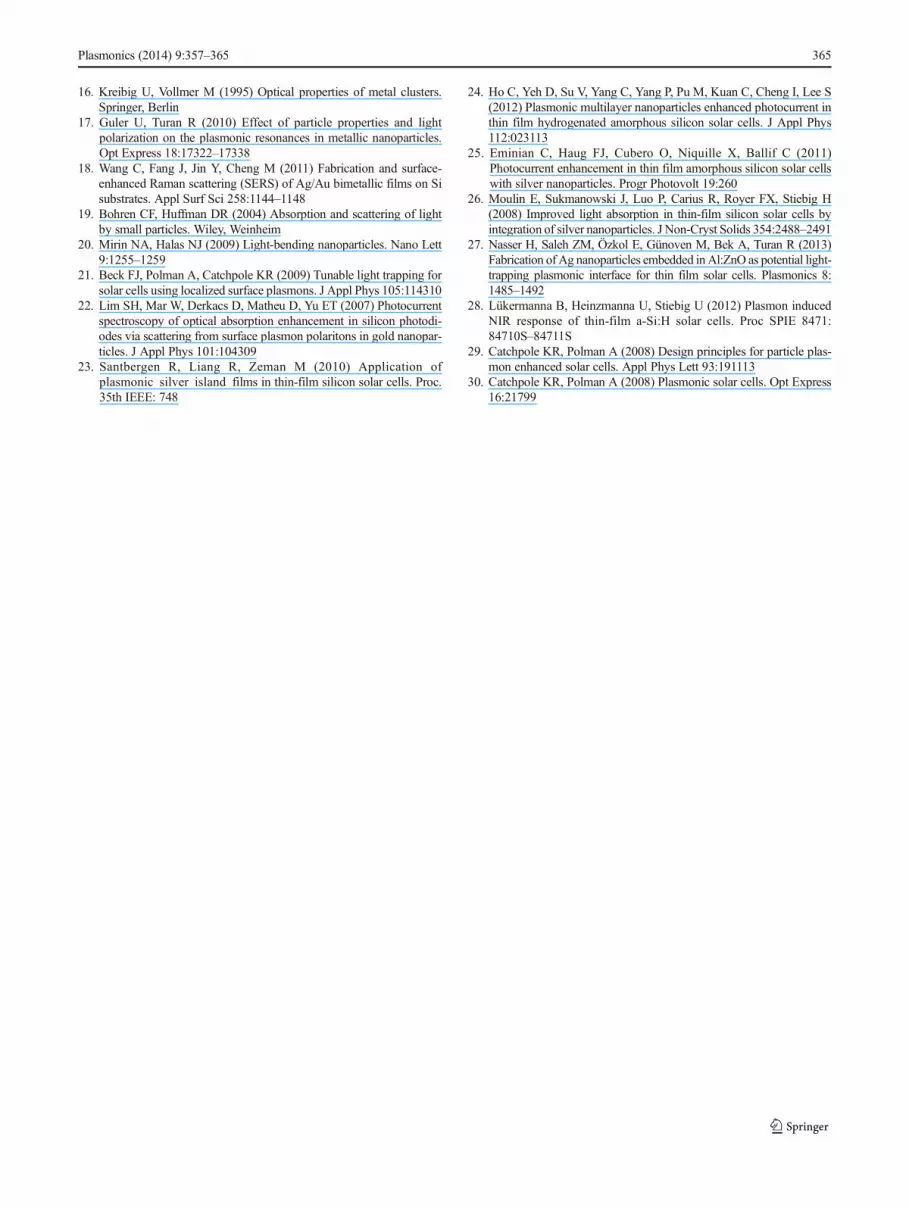
While the photocurrent under white light decreases, theeffect of the interfaces on the spectral dependence of photo-current is rather interesting. In Fig. 11, we plot the photocur-rent measured at 10 V bias versus wavelength and the extinc-tion spectrum for a-Si sample on PLS-5 in the spectral rangeof 350–950 nm, along with the same quantities for a-Si film
Fig. 8 SEM images andextinction spectra for variousdouble layer plasmonic structuresshowing the effects of dielectricconstant of the spacer layer on theplasmonic resonance indicated bythe minima in the transmittance: aSEM and b optical response forset (PLS-06: Corning/15 nmAg/400 °C/20 nm SiO2/15 nmAg/200 °C/10 nm SiO2), c SEMand d optical response for set(PLS-08: Corning/15 nmAg/400 °C/20 nm SiNx/15 nmAg/200 °C/20 nm SiNx). In theoptical spectra: transmittance(solid line), reflectance (dottedline), and extinction (dashedline). Optical data are coloredonline
Fig. 9 Extinction spectra of two single and two double layer plasmonicinterfaces compared to that of a-Si:H on corning glass
Fig. 10 Extinction spectra of a 250-nm a-Si:H film deposited on a singleinterface dewetted at 400 °C (PLS-05 dashed line) and a double plas-monic interface dewetted at 400 °C for the lower layer and at 200 °C forthe upper layer separated by 20 nm SiNx layer (PLS-08: dashed–dottedline) compared to that of a-Si:H on corning glass (PLS-Si: dotted line)
362 Plasmonics (2014) 9:357–365
co-deposited on Corning glass. As shown in Fig. 11, a relativethough appreciable increase in photocurrent appears at thelower energy edge of the band gap (600∼700 nm). Thisenhancement correlates well with the broadening of the ex-tinction spectra. The extinction spectrum of the film depositedon plasmonic interfaces is clearly broadened into the redcompared to that of a-Si:H on glass. This result indicatesthat there is enhanced scattering by the plasmonic inter-face into the a-Si:H layer facilitating more absorption andphoto conversion.
The effect of the double plasmonic interface on the photo-current is manifold. In Fig. 12, we show the spectral depen-dence of the photocurrent obtained at 25 nm intervals under a10-V bias and the extinction spectra for a-Si film deposited onsample PLS-08 (double plasmonic interface), along with anidentical film co-deposited on corning glass (no interface).The extinction spectrum of a-Si:H deposited on a doubleplasmonic interface is also found to extend into the red, butthe enhancement in photocurrent is clearly lower. This resultsuggests that absorption rather than scattering dominates theinterface response even in this range.
Discussion and Conclusions
We conducted an intensive study on the fabrication of single-and double-layered plasmonic interfaces consisting of silvernanoparticles at the interfaces between two media with differ-ent thicknesses and refractive indices. The fabrication in-volves self-assembled dewetting technique of sputtered thinsilver film followed by furnace annealing at various tempera-tures in N2 ambient for nanoparticle formation. The SEMimages obtained at various processing stages show successfulconstruction of both single- and double-layered interfaces.The mean particle size, estimated by the equivalent disk radiusanalysis, did not change significantly with temperature, butthat lower anneal temperatures produce more particles with amean diameter less than 50 nm. In spite of this weak depen-dence on temperature, significant shifts are observed in theirplasmonic resonance frequency as illustrated in Fig. 6. Thesingle-layer interfaces exhibit one minimum in the transmit-tance spectrum but significant broadening of the extinctionpeak into the red. The extinction spectra of the double inter-faces appear to consist of two overlapping maxima that maycorrespond to an interaction between the two constituentnanoparticle layers.
The extinction maxima of the a-Si:H films deposited onthese interfaces show a clear broadening into the red com-pared with a-Si:H on glass. This broadening indicates signif-icant increase in scattering and/or absorption by the interfacedepending on the size of the nanoparticles in the interface.This enhanced extinction by the interface could lead to en-hanced photocurrent if scattering dominates the extinction orreduce the photocurrent if absorption dominates. Since theextinction maxima for these interfaces show significant broad-ening into the red, the enhancement of photocurrent caused bythese interfaces may be related to the plasmonic resonanceeffect and suggests that scattering is significant in the range of600–700 nm.
The previous results of silver and gold plasmonic interfacesintegrated to photodetectors and solar cells claim large photo-current enhancements in different parts of the solar spectrum[12–15]. The different results obtained by these authors maybe related to the various structural differences used in thedevice structures. These differences include material, sizeand shape of the nanoparticles, spacer layer material andthickness, and other factors related to the device structureitself. The overall enhancement across the entire solar spec-trum is difficult to understand while differences in frequencyover which the enhancements take place may be explained interms of these differences in materials and design. Our pho-tocurrent enhancement in the spectral range of 600–700 nmis consistent with these results and suggests that the photo-current enhancement may be controlled more accurately bytuning materials thicknesses and dielectric constants used inthe interface.
Fig. 11 The normalized photocurrent (open squares) for a-Si depositedon PLS-05 and the extinction spectrum (solid squares) of a-Si:H co-deposited on PLS-05 compared with the normalized photocurrent (opencircles) and extinction spectrum (solid circles) for a-Si film co-depositedon Corning glass. Both photocurrent curves are normalized to the samemaximum current
Fig. 12 The normalized photocurrent (open squares) for a-Si depositedon PLS-08 and the extinction spectrum (solid squares) of a-Si:H co-deposited on PLS-08 compared with the normalized photocurrent (opencircles) and extinction spectrum (solid circles) for a-Si film co-depositedon Corning glass. Both photocurrent curves are normalized to the samemaximum current
Plasmonics (2014) 9:357–365 363
Our particle size for both single and double interfaces showsignificant portion of particles with sizes less than 50 nm indiameter suggesting that absorption still dominates extinctionin these interfaces. We propose that our results may be ex-plained by the far-field effect involving valence band tail(VBT) states. The broadening of the extinction peakinto the 600∼700 nm caused by the plasmonic interfaceindicates that further extinction including preferential scat-tering into the a-Si:H side at these wavelengths is taking place.Preferential scattering enhances absorption by these VBTstates relative to the a-Si:H on glass and a correspondingrelative enhancement of photocurrent takes place in that spec-tral region.
The significant reduction in photocurrent across the visibleregion is not well understood but has previously been attrib-uted to parasitic losses by the plasmonic interface. However,quick calculations suggest that these losses do not account forthat significant reduction if only the far field effect is consid-ered. From the transmittance spectra (Fig. 5), we observe thatapproximately 30–40 % of the visible incident light is trans-mitted through the 250 nm amorphous silicon film. The rear a-Si:H/glass interface would at most reflect 16 % of that light,which is the maximum enhancement one would expect as-suming “clean” a-Si:H/glass interface with no plasmonic ef-fects. Assuming that the plasmonic interface placed at the rearabsorbs all that light and does not allow for any reflectionthrough parasitic losses, the result should not decrease bymore than 16 % of the 30–40 % transmitted light. Based onthis, it is difficult to explain the reduction in terms of parasiticlosses and the far field effect alone. To explain this reduction,one should consider the near field effect. We recall that thenanoparticles actual size for most interfaces is less than100 nm which in itself is a major contributing factor forincreasing absorption and reducing scattering because therelative ratio of absorption to scattering increases with de-creasing actual particle size [26]. Furthermore, the effectiveabsorption and scattering cross-sections are significantlyhigher than the actual sizes and may extend deep into and infact dominates the a-Si:H absorber layer increasing absorptionof carriers in that region. To eliminate this possibility, theplasmonic interface should be placed farther away from theabsorber layer. Catchpole and Polman calculate the scatteringcross-section as a function of nanoparticles’ distance from thesubstrate and find that at 20 nm, the scattering cross-section isonly about 10 % of its value at infinity while the absorptioncross-section is significantly higher [29]. Since our spacerlayer happens to be about 20 nm, it is not surprising that mostof the light is absorbed by the interface and little enhancementin photocurrent is observed. These authors find that the scat-tering cross-section is maximal at about 60 nm from theinterface [30].
Acknowledgments This study has been supported by the Scientific andTechnological Research Council of Turkey (TUBITAK) under the projectRainbow Energy with the contract number 109R037. The research lead-ing to these results has received funding from the European Union’sSeventh Framework Programme FP7/2007-2013 under grant agreementno. 270483. Zaki M. Saleh acknowledges the support from the Scientificand Technological Research Council of Turkey (TUBITAK BIDEB-2221). Hisham Nasser acknowledges the Scientific and TechnologicalResearch Council of Turkey (TUBITAK BIDEB-2215).
Conflict of Interest The authors declare no competing financialinterests.
References
1. Atrel AC, García-Etxarri A, Alaeian H, Dionne JA (2012) Towardhigh-efficiency solar upconversion with plasmonic nanostructures. JOpt 14:024008
2. Fleischer K, Arca E, Shvets IV (2012) Improving solar cell efficiencywith optically optimized TCO layers. Sol Energ Mater Sol Cells 101:262–269
3. Gangopadhyay U, Kim K, Mangalaraj D, Yi J (2004) Low cost CBDZnS antireflection coating on large area commercial mono-crystallinesilicon solar cells. Appl Surf Sci 230:364–370
4. Soderstromn K, Haug FJ, Escarre J, Pahud C, Biron R, Ballif C(2011) Highly reflective nanotextured sputtered silver back reflectorfor flexible high-efficiency n–i–p thin-film silicon solar cells. SolEnerg Mater Sol Cells 95:3585–3591
5. Ghannam MY, Abouelsaood AA, Alomar AS, Poortmans J (2010)Analysis of thin-film silicon solar cells with plasma textured frontsurface andmulti-layer porous silicon back reflector. Sol EnergMaterSol Cells 94:850–856
6. Pillai S, Green MA (2010) Plasmonics for photovoltaic applications.Sol Energ Mater Sol Cells 94:1481–1486
7. Lahoz F, Perez-Rodriguez C, Hernandez SE, Martin IR, Lavin V,Rodriguez-Mendoza UR (2011) Upconversion mechanisms in rare-earth doped glasses to improve the efficiency of silicon solar cells.Sol Energ Mater Sol Cells 95:1671–1677
8. Trupke T, Green MA, Wurfel P (2002) Improving solar cellefficiencies by up-conversion of sub-band-gap light. J ApplPhys 92:4117
9. Temple TL, Mahanama GDK, Reehal HS, Bagnall DM (2009)Influence of localized surface Plasmon excitation in silver nanopar-ticles on the performance of silicon solar cells. Sol Energ Mater SolCells 93:1978–1985
10. Atwater HA, Polman A (2010) Plasmonics for improved photovol-taic devices. Nat Mater 9:205–213
11. Yu ET, Derkacs D, Lim SH, Matheu B, Schaadt M (2008) Plasmonicnanoparticle scattering for enhanced performance of photovoltaic andphotodetector devices. Proc SPIE 7033:V–9
12. Pillai S, Catchpole KR, Trupke T, GreenMA (2007) Surface plasmonenhanced silicon solar cells. J Appl Phys 101:093105
13. Schaadt DM, Feng B, Yu ET (2005) Enhanced semiconductor opticalabsorption via surface plasmon excitation in metal nanoparticles.Appl Phys Lett 86:063106
14. Stuart HR, Hall DG (1998) Island size effects in nanoparticles en-hanced photodetectors. Appl Phys Lett 73:3815–3817
15. Aberle AG (2001) Overview on SiN surface passivation of crystallinesilicon solar cells. Sol Energ Mater Sol Cells 65:239–248
364 Plasmonics (2014) 9:357–365
16. Kreibig U, Vollmer M (1995) Optical properties of metal clusters.Springer, Berlin
17. Guler U, Turan R (2010) Effect of particle properties and lightpolarization on the plasmonic resonances in metallic nanoparticles.Opt Express 18:17322–17338
18. Wang C, Fang J, Jin Y, Cheng M (2011) Fabrication and surface-enhanced Raman scattering (SERS) of Ag/Au bimetallic films on Sisubstrates. Appl Surf Sci 258:1144–1148
19. Bohren CF, Huffman DR (2004) Absorption and scattering of lightby small particles. Wiley, Weinheim
20. Mirin NA, Halas NJ (2009) Light-bending nanoparticles. Nano Lett9:1255–1259
21. Beck FJ, Polman A, Catchpole KR (2009) Tunable light trapping forsolar cells using localized surface plasmons. J Appl Phys 105:114310
22. Lim SH, Mar W, Derkacs D, Matheu D, Yu ET (2007) Photocurrentspectroscopy of optical absorption enhancement in silicon photodi-odes via scattering from surface plasmon polaritons in gold nanopar-ticles. J Appl Phys 101:104309
23. Santbergen R, Liang R, Zeman M (2010) Application ofplasmonic silver island films in thin-film silicon solar cells. Proc.35th IEEE: 748
24. Ho C, Yeh D, Su V, Yang C, Yang P, Pu M, Kuan C, Cheng I, Lee S(2012) Plasmonic multilayer nanoparticles enhanced photocurrent inthin film hydrogenated amorphous silicon solar cells. J Appl Phys112:023113
25. Eminian C, Haug FJ, Cubero O, Niquille X, Ballif C (2011)Photocurrent enhancement in thin film amorphous silicon solar cellswith silver nanoparticles. Progr Photovolt 19:260
26. Moulin E, Sukmanowski J, Luo P, Carius R, Royer FX, Stiebig H(2008) Improved light absorption in thin-film silicon solar cells byintegration of silver nanoparticles. J Non-Cryst Solids 354:2488–2491
27. Nasser H, Saleh ZM, Özkol E, Günoven M, Bek A, Turan R (2013)Fabrication of Ag nanoparticles embedded inAl:ZnO as potential light-trapping plasmonic interface for thin film solar cells. Plasmonics 8:1485–1492
28. Lükermanna B, Heinzmanna U, Stiebig U (2012) Plasmon inducedNIR response of thin-film a-Si:H solar cells. Proc SPIE 8471:84710S–84711S
29. Catchpole KR, Polman A (2008) Design principles for particle plas-mon enhanced solar cells. Appl Phys Lett 93:191113
30. Catchpole KR, Polman A (2008) Plasmonic solar cells. Opt Express16:21799
Plasmonics (2014) 9:357–365 365


