Embed Size (px)
Citation preview
Seediscussions,stats,andauthorprofilesforthispublicationat:https://www.researchgate.net/publication/240307693
ElectromechanicalPiezoresistiveSensinginSuspendedGrapheneMembranes
ARTICLEinNANOLETTERS·JULY2013
ImpactFactor:13.59·DOI:10.1021/nl401352k·Source:PubMed
CITATIONS
41
READS
432
12AUTHORS,INCLUDING:
FredrikForsberg
KTHRoyalInstituteofTechnology
32PUBLICATIONS151CITATIONS
SEEPROFILE
D.Esseni
UniversityofUdine
214PUBLICATIONS2,735CITATIONS
SEEPROFILE
P.Palestri
UniversityofUdine
192PUBLICATIONS1,707CITATIONS
SEEPROFILE
MikaelÖstling
KTHRoyalInstituteofTechnology
572PUBLICATIONS4,574CITATIONS
SEEPROFILE
Availablefrom:MaxChristianLemme
Retrievedon:04February2016
This document is the unedited Author’s version of a Submitted Work that was subsequently accepted for publication in Nano Letters, copyright © American Chemical Society after peer review. To access the final edited and published work see http://pubs.acs.org/articlesonrequest/AOR-kGn5XaTPGiC7mYUQfih3.
Electromechanical Piezoresistive Sensing in
Suspended Graphene Membranes
A.D. Smith1, F. Niklaus1, A. Paussa2, S. Vaziri1, A.C. Fischer1, M. Sterner1, F.
Forsberg1, A. Delin1, D. Esseni2, P. Palestri2, M. Östling1, M.C. Lemme1,3,*
1 KTH Royal Institute of Technology, Isafjordsgatan 22, 16440 Kista, Sweden,
2 DIEGM, University of Udine, Via delle Scienze 206, 33100 Udine, Italy
3University of Siegen, Hölderlinstr. 3, 57076 Siegen, Germany
* Corresponding author: max.lemme@uni-‐siegen.de
2
Abstract
Monolayer graphene exhibits exceptional electronic and mechanical properties, making
it a very promising material for nanoelectromechanical (NEMS) devices. Here, we
conclusively demonstrate the piezoresistive effect in graphene in a nano-
electromechanical membrane configuration that provides direct electrical readout of
pressure to strain transduction. This makes it highly relevant for an important class of
nano-electromechanical system (NEMS) transducers. This demonstration is consistent
with our simulations and previously reported gauge factors and simulation values. The
membrane in our experiment acts as a strain gauge independent of crystallographic
orientation and allows for aggressive size scalability. When compared with
conventional pressure sensors, the sensors have orders of magnitude higher sensitivity
per unit area.
Keywords: graphene, pressure sensor, piezoresistive effect, nanoelectromechanical
systems (NEMS), MEMS
3
Graphene is an interesting material for nanoelectromechanical systems (NEMS)
due to its extraordinary thinness (one atom thick), high carrier mobility 1,2, a high
Young’s modulus of about 1 TPa for both pristine (exfoliated) and chemical vapor
deposited (CVD) graphene.3,4 Graphene is further stretchable up to approximately
20%.5 In addition, it shows strong adhesion to SiO2 substrates6 and is nearly
impermeable for gases, including helium.7 In this article, we demonstrate piezoresistive
pressure sensors based on suspended graphene membranes with direct electrical
signal read-out. We utilize a piezoresistive effect induced by mechanical strain in the
graphene, which changes the electronic band structure8 and exploits the fact that the
sensitivity of membrane-based electromechanical transducers strongly correlates with
membrane thickness9. While graphene has been used as a piezoresistive strain gauge
on silicon nitride10 and polymer membranes11, we extend the use of the graphene to
both membrane and electromechanical transduction simultaneously with an average
gauge factor of 2.92. The sensitivity per unit area of our graphene sensor is about 20 to
100s of times higher than that of conventional piezoresistive pressure sensors. The
piezoresistive effect is nearly independent of crystallographic orientation.
In our experiments, graphene membranes made from CVD graphene are
suspended over cavities etched into a SiO2 film on a silicon substrate. The graphene is
electrically contacted and the devices are wire-bonded into a chip package. Process
schematics are shown in Fig. 1a through c, while details of the fabrication process are
described in the methods section. A scanning electron microscope image of a wire-
bonded device and a photograph of a packaged device are shown in Fig. 1d. If a
pressure difference is present between the inside and the outside of the cavity
4
(compare Fig. 1c), the graphene membrane that is sealing the cavity is deflected and
thus strained. This leads to a change of device resistivity due to the piezoresistive effect
in the graphene. Measurements were performed in an argon environment in order to
reduce the effects of adsorbates. If air is used instead of argon for the experiments,
adsorption of non-inert gases and/or molecules on the graphene will affect the resistivity
(see details in supporting information).
In the experiments, the packaged devices are placed inside a vacuum chamber.
The chamber is then evacuated from atmospheric pressure down to 200 mbar, and then
vented back to 1000 mbar. Thus the air sealed inside the cavity presses against the
graphene membrane with a force proportional to the chamber pressure. The resistance
of the graphene sensor is measured in a Wheatstone bridge (see supporting
information), where the graphene membrane is one of the resistors in the bridge. The
Wheatstone bridge is balanced at atmospheric pressure by adjusting a potentiometer to
the same resistance value as the graphene membrane. The bridge is biased with
200mV square wave pulses with durations of 500 µs. These values were chosen to
avoid excessive heating of the graphene device. The voltage output signal from the
Wheatstone bridge is amplified and low pass filtered before being sampled with an
analog-to-digital converter and converted into its corresponding resistance value. The
experimental conditions were chosen to remain within the expected tearing limits of the
graphene membrane.6
The suspended membrane sensors were first compared to devices with identical
dimensions fabricated in parallel, but without cavities. This was done in order to verify
that it is indeed the presence of the cavity and the resulting mechanical bending and
5
straining of the membrane that causes the pressure dependence of the resistance.
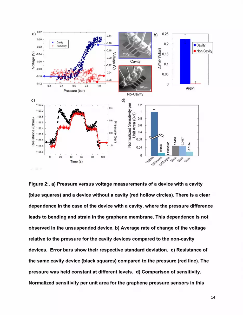
Fig. 2a shows the amplified voltage (with an amplification factor of 870) versus pressure
curve for two devices, one with a cavity and one without. In contrast to the reference
device without the cavity (red hollow circles), the sensor device with the suspended
graphene membrane (blue squares) shows a strong correlation of the resistance with
respect to pressure. The graph includes data of six measurement cycles, where each
cycle represents one pump-down or one venting of the chamber. Fig. 2b shows the
average change in voltage of three cavity devices in comparison to two non-cavity
devices. As can be seen, there is a very strong correlation between the devices’
sensitivity to pressure and the presence of a cavity. Finally, A device was held at
constant pressures in order to investigate potential drift in the sensor signal (Fig. 2c).
While there is a noticeable drift at several pressures, the resistance values generally
follow the pressure. Nevertheless, further studies regarding stability are required.
The sensitivity of piezoresitive membrane-based pressure sensors is given by Eq. 1,
where S is the sensitivity, R is the resistance, V is the voltage, I is the current, and P is
the pressure difference acting on the membrane.12
𝑆 = ∆!!∙!
=∆!!
!! ∙!
= ∆!!∙!
(1)
If the current is held constant, then the sensitivity based on voltage
measurements can be directly compared to the sensitivity based on the maximum
change in resistance for a change in pressure of 477 mbar. The sensitivity of the
piezoresitive graphene pressure sensor in Fig. 2 is measured to be 3.95 µV/V/mmHg.
6
The graphene membrane-based pressure sensor, though much smaller than
conventional piezoresitive pressure sensors, outperforms conventional piezoresitive Si-
based and carbon nanotube (CNT) based pressure sensors reported in literature.13-16
(see Table 2 in the supporting information for details).
In general, the sensitivity S of membrane-based piezoresistve pressure sensors is
dependent on the membrane material characteristics, the membrane thickness and the
membrane area (see supporting information).3,12,17,18 When normalizing the sensitivity of
the pressure sensors from Table 2 of the supporting information to a standard
membrane area, the sensitivity of our graphene sensor is about 20 to 100s of times
higher than the other sensors (Fig. 2d). This and the fact that the graphene sensor is
already smaller in area than any of the other sensors indicate great potential for further
size-reduction of graphene membrane-based sensors.
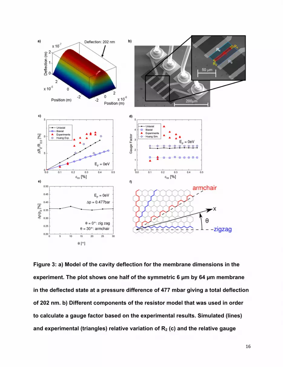
In order to estimate the piezoresistive gauge factor of the graphene transducer in
our sensor, the change in resistance of the cavity region must be determined. A finite
element analysis of the deflection was performed using COMSOL multiphysics and
calibrated using literature data of graphene membrane deflection obtained by atomic
force microscopy.6,7 Material parameters taken from literature were used in the
COMSOL model such as the elastic constant Et = 347 N/m, where E is the Young's
modulus, t is the membrane thickness (t = 0.335 nm) and Poisson's ratio ν = 0.16. A
comparison between the model and measured literature values is shown in Table 2 of
the supporting information. Good agreement is noted both with the measurements of a
2.3 µm radius circular membrane in Koenig et al.6 and with the measurement in Bunch
et al. on a square 4.75 µm x 4.75 µm membrane at a pressure difference of 930 mbar.7
7
The derived model was then applied to the 6 µm by 64 µm cavity used in the current
experiment to estimate the deflection of the membrane. At a pressure difference of 477
mbar, the deflection of the membrane is calculated to be 202 nm (Fig. 3a), which results
in an average strain of 0.290% across the membrane.
An electrically equivalent circuit of the sensor is schematically shown in Fig. 3b
and is described in Eq. 2
𝑅!"! = 𝑅! +!
!!!! !!!! !!!
+ 𝑅! (2)
The total resistance Rtot is taken from resistance measurements at chamber
pressures of 1000 mbar and 523 mbar (Fig. 2a). The resistances R1 through R5
correspond to the resistances of the regions shown in Figure 3b. R2 represents the
resistance of the graphene membrane over the cavity and we assume that only R2
changes as a function of pressure. Using this method (details in supporting information),
R2 is determined to be 0.191 kΩ at 1000 mbar, and the percent resistance change of
the graphene membrane patch (R2) is determined to be 0.59%.
The intrinsic graphene gauge factor in our sensor was then calculated as the
percent change in resistance divided by the percent change in strain to be 3.67. Gauge
factors vary depending on the pressure range measured with a maximum value of 4.33
and an average value of 2.92. Previous literature, by comparison, reports gauge factors
of 1.9 for suspended graphene beams19, about 150 for graphene on SiO220 and nearly
18000 for graphene on a silicon nitride membrane.10
8
Simulations of the change of the graphene pressure sensor resistance due to
strain were carried out in order to interpret the experimental results. For a low electric
field in the transport direction and considering a Fermi level close to the Dirac energy
(𝐸! = 0 eV), the resistance R2 of the graphene foil suspended over the cavity is
expressed as
𝑅! = 𝜌𝐿′𝑊!′
=1
2𝑞𝑁! 𝜀 𝜇! 𝜀(1 + 𝜀!!)𝐿(1 + 𝜀!!)𝑊!
, (3)
where 𝜌 is the resistivity of the suspended graphene sheet, 𝑁! and 𝜇! are respectively
the electron density and the corresponding mobility (that are assumed to be the same
as the hole density and hole mobility, respectively, since we set EF = 0 eV), 𝜀!! and 𝜀!!
are the components of the strain tensor respectively in the direction of the transport and
normal to the transport, and 𝑞 is the positive electron charge. Note that the strain
induced in graphene by the pressure difference between the cavity and the chamber Δ𝑝
influences both the terms 𝐿′ and 𝑊!′ related to the geometry as well as the resistivity 𝜌.
The induced strain can be considered quasi-uniaxial since its component in the direction
of the transport is dominant (𝜀!! ≫ 𝜀!!). If ρ is not modified by strain, the change of 𝐿
and 𝑊! alone is not enough to explain the experimental resistance change with strain.
Then, the influence of strain on 𝜌 has been analyzed by starting with the effect of strain
on the electron density 𝑁!, simulated by employing the strained graphene bandstructure
stemming from the Tight-Binding (TB) Hamiltonian presented in Pereira et al.8,
recalibrated to accurately reproduce DFT results reported by Huang et al.19 (see
supporting information). 𝑁! increases with the strain, which, in contrast with the
experiments (see Fig. 2a), would lead to a decrease of the resistivity (see Eq. 3 and
supporting information). Hence the changes in the graphene charge are not sufficient to

9
explain the observed change of the resistance R2 with the strain. The effect of
capacitive coupling was also explored through simulation and, though present, is found
to cause changes in resistance much lower than those observed experimentally.
For this reason the effect of the strain on the mobility 𝜇! is simulated by solving
the Linearized Boltzmann Transport Equation (LBTE)21. This approach gives the exact
solution of the LBTE even in the presence of anisotropic and non-monotonic energy
dispersion relation and anisotropic scattering rates. In these calculations Neutral
Defects (ND)22 are considered, which are dominant in CVD graphene23. The electron
mobility decreases with increasing Δ𝑝 (see supporting information). Such mobility
degradation more than compensates the 𝑁! enhancement, so that the calculations lead
to an overall R2 increase. The simulated versus measured R2 modulation versus
strain is also compared (Fig. 3c). As can be seen the simulation results do not critically
depend on whether the strain is uniaxial or biaxial and the overall agreement with
experiments is reasonably good. Fig. 3d compares the corresponding calculated and
measured gauge factors; the biaxial or uniaxial nature of the strain has a modest
influence on the gauge factor. Simulation data from Huang et al. are also included for
reference.19 Note also that, due to the flexibility of the approach, the relative variation of
R2 is independent of the graphene orientation with respect to the direction of the
transport (Fig. 3e and 3f), of the defect concentration, and of the considered Fermi level
(i.e. the carrier density). This is an important aspect of our work because it means that
the effect is independent of random crystallographic alignment and multiple grain
graphene flakes.
10
The piezoresistive effect in graphene was demonstrated in graphene–membrane
pressure sensors. The sensitivity of piezoresistive graphene sensors is superior to
silicon and CNT-based sensors and orders of magnitude more sensitive when
normalized for membrane dimensions. This is in line with theoretical considerations that
indicate such a decisive advantage due to graphene’s extraordinary thinness. A finite
element simulation is derived to describe the deflection of graphene membranes over
sealed cavities as a function of pressure and verified with literature data. The estimated
maximum gauge factor for graphene based on this model is 4.33 with values averaging
at 2.92. Tight binding calculations support the experimental data, including only a small
dependence of the observed effect on crystal orientation. This work demonstrates that
thin graphene membranes can be efficiently implemented as piezoresistive transducer
elements for emerging NEMS sensors.
11
Methods
Devices are fabricated on p-type silicon substrates with a thermally grown silicon
dioxide (SiO2) layer of 1.5 µm. Rectangular cavities of 6 µm by 64 µm are etched 650
nm deep into the SiO2 using a resist mask and an Ar and CHF3-based reactive ion
etching (RIE) process at 200mW and 40 mTorr to provide vertical etch profiles. Next,
contact areas are defined by lithography and etched 640 nm into the SiO2 layer using
again an RIE process. The contact cavities are then filled with a 160 nm layer of
titanium followed by a 500 nm layer of gold using metal evaporation so that the contacts
are raised about 20 nm above the surface of the SiO2. The contacts are buried to
prevent wire bonding from ripping the contacts off of the substrate. This has the added
advantage of allowing the graphene to be transferred in a later step, which improves the
cleanliness of the process and reduces the risk of rupturing the graphene membranes
during processing. Also, the graphene-metal contacts are not degraded by polymer
residues in this way. Commercially available chemical vapor deposited (CVD)
monolayer graphene films on copper foils are used. The graphene on one side of the
copper is spin-coated with either a poly(methyl methacrylate) (PMMA) or poly(Bisphenol
A) carbonate (PC) layer in order to act as a mediator between the initial and final
substrate 24-28. The graphene on the backside of the foil is etched using O2 plasma and
the copper foil is subsequently wet etched in FeCl3 and then transferred into de-ionized
water. The bottom left of Fig. 2a shows a contrast enhanced image of graphene with a
polymer coating floating in a solution of FeCl3 after the copper is etched away. The
PMMA/graphene film is picked up with the chip and dried on a hotplate. After drying, the
chip is placed into a solution of Chloroform overnight in order to etch the PC polymer

12
layer. Next, a photoresist layer is applied and exposed in order to pattern the graphene.
Finally, the graphene is etched into the desired shape using an O2 plasma etch and the
photoresist is removed in acetone. Once the devices are fabricated, the chips are
placed into a chip housing and gold wires are bonded from the housing to the contact
pads. The layout of the contacts is shown schematically in Fig. 1c and the wire bonded
device is shown in a scanning electron micrograph in Fig. 1d, Raman spectroscopy and
electrical measurements were performed to verify the presence of graphene (see
supporting information).
ACKNOWLEDGMENTS
Support from the European Commission through an ERC Advanced Investigator Grant (OSIRIS,
No. 228229) and two Starting Grants (M&M’s, No. 277879 and InteGraDe, No. 307311) as well
as the German Research Foundation (DFG, LE 2440/1-1) and the Italian MIUR through the
Cooperlink project (CII11AVUBF) is gratefully acknowledged.
13
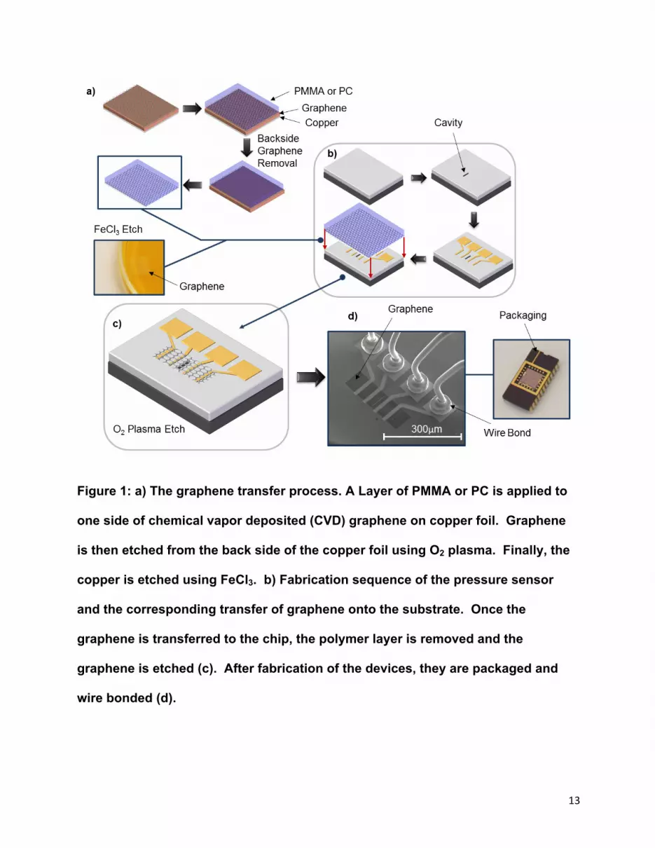
Figure 1: a) The graphene transfer process. A Layer of PMMA or PC is applied to
one side of chemical vapor deposited (CVD) graphene on copper foil. Graphene
is then etched from the back side of the copper foil using O2 plasma. Finally, the
copper is etched using FeCl3. b) Fabrication sequence of the pressure sensor
and the corresponding transfer of graphene onto the substrate. Once the
graphene is transferred to the chip, the polymer layer is removed and the
graphene is etched (c). After fabrication of the devices, they are packaged and
wire bonded (d).
14
Figure 2:. a) Pressure versus voltage measurements of a device with a cavity
(blue squares) and a device without a cavity (red hollow circles). There is a clear
dependence in the case of the device with a cavity, where the pressure difference
leads to bending and strain in the graphene membrane. This dependence is not
observed in the unsuspended device. b) Average rate of change of the voltage
relative to the pressure for the cavity devices compared to the non-cavity
devices. Error bars show their respective standard deviation. c) Resistance of
the same cavity device (black squares) compared to the pressure (red line). The
pressure was held constant at different levels. d) Comparison of sensitivity.
Normalized sensitivity per unit area for the graphene pressure sensors in this

15
paper compared to silicon and carbon nanotube-based sensors.13-16 The
graphene sensor is roughly 20 to 100 times more sensitive per unit area than the
conventional MEMS sensors showing the potential for aggressive scaling.
Tabulated sensitivity values are shown in the supporting information.13-16
16
Figure 3: a) Model of the cavity deflection for the membrane dimensions in the
experiment. The plot shows one half of the symmetric 6 µm by 64 µm membrane
in the deflected state at a pressure difference of 477 mbar giving a total deflection
of 202 nm. b) Different components of the resistor model that was used in order
to calculate a gauge factor based on the experimental results. Simulated (lines)
and experimental (triangles) relative variation of R2 (c) and the relative gauge

17
factor (6d) versus strain. Simulation results by Huang et al. added for reference.19
e) Schematic of the definition of the crystallographic angles used for the
calculations in this work. f) Simulation showing that the strain effect on
resistivity is independent of the strain angle.

18
Supporting Information Available
The supporting information contains Raman and electrical data to demonstrate the presence of
graphene in the devices as well as details of the Wheatstone bridge setup. It further contains
experiments in various gaseous environments to explain how their influence was eliminated and
additional measurements of the piezoresistive effect. The material includes a table with the
calibration of the COMSOL model with literature data, a detailed explanation of the resistor
model we applied and a table comparing the sensitivity of our devices with literature data.
Finally, it contains additional figures with results from the tight-binding model. This material is
available free of charge via the Internet at http://pubs.acs.org.
19
References
1. Bolotin, K. I.; Sikes, K.; Jiang, Z.; Klima, M.; Fudenberg, G.; Hone, J.; Kim, P.; Stormer, H., Ultrahigh electron mobility in suspended graphene. Solid State Communications 2008, 146 (9), 351-‐355. 2. Morozov, S.; Novoselov, K.; Katsnelson, M.; Schedin, F.; Elias, D.; Jaszczak, J.; Geim, A., Giant intrinsic carrier mobilities in graphene and its bilayer. Physical Review Letters 2008, 100 (1), 16602. 3. Lee, C.; Wei, X.; Kysar, J. W.; Hone, J., Measurement of the elastic properties and intrinsic strength of monolayer graphene. Science 2008, 321 (5887), 385-‐388. 4. Lee, G.; Cooper, R. C.; An, S.; Lee, S.; van der Zande, A.; Petrone, N.; Hammerberg, A. G.; Lee, C.; Crawford, B.; Oliver, W.; Kysar, J. W.; Hone, J.; High-‐Strength Chemical-‐Vapor–Deposited Graphene and Grain Boundaries. Science 2013, 340 (6136), 1073-‐1076. 5. Tomori, H.; Kanda, A.; Goto, H.; Ootuka, Y.; Tsukagoshi, K.; Moriyama, S.; Watanabe, E.; Tsuya, D., Introducing Nonuniform Strain to Graphene Using Dielectric Nanopillars. Appl. Phys. Express 4, 075102 2011. 6. Koenig, S. P.; Boddeti, N. G.; Dunn, M. L.; Bunch, J. S., Ultrastrong adhesion of graphene membranes. Nature nanotechnology 2011, 6 (9), 543-‐546. 7. Bunch, J. S.; Verbridge, S. S.; Alden, J. S.; Van Der Zande, A. M.; Parpia, J. M.; Craighead, H. G.; McEuen, P. L., Impermeable atomic membranes from graphene sheets. Nano letters 2008, 8 (8), 2458-‐2462. 8. Pereira, V. M.; Neto, A. C.; Peres, N., Tight-‐binding approach to uniaxial strain in graphene. Physical Review 2009, 80 (4), 045401. 9. Gong, S.-‐C.; Lee, C., Analytical solutions of sensitivity for pressure microsensors. Sensors Journal, IEEE 2001, 1 (4), 340-‐344. 10. Hosseinzadegan, H.; Todd, C.; Lal, A.; Pandey, M.; Levendorf, M.; Park, J. In Graphene has ultra high piezoresistive gauge factor, Micro Electro Mechanical Systems (MEMS), IEEE 25th International Conference 2012, 611-‐614. 11. Kim, K. S.; Zhao, Y.; Jang, H.; Lee, S. Y.; Kim, J. M.; Kim, K. S.; Ahn, J.-‐H.; Kim, P.; Choi, J.-‐Y.; Hong, B. H., Large-‐scale pattern growth of graphene films for stretchable transparent electrodes. Nature 2009, 457 (7230), 706-‐710. 12. Melvås, P. Ultraminiaturized Pressure Sensor for Catheter Based Applications. Ph.D. thesis, KTH Royal Institute of Technology, 2002. 13. Hierold, C.; Jungen, A.; Stampfer, C.; Helbling, T., Nano electromechanical sensors based on carbon nanotubes. Sensors and Actuators A: Physical 2007, 136 (1), 51-‐61. 14. Fung, C. K.; Zhang, M. Q.; Chan, R. H.; Li, W. J. In A PMMA-‐based micro pressure sensor chip using carbon nanotubes as sensing elements, Micro Electro Mechanical Systems 2005. MEMS 18th IEEE International Conference, 251-‐254. 15. Christel, L.; Petersen, K. In A catheter pressure sensor with side vent using multiple silicon fusion bonding, Proc. Int. Conf. Solid-‐State Sensors and Actuators (Trandsucers) 1993; 620-‐623. 16. Kalvesten, E.; Smith, L.; Tenerz, L.; Stemme, G. The first surface micromachined pressure sensor for cardiovascular pressure measurements, Micro Electro Mechanical Systems 1998. MEMS 98. Proceedings., The Eleventh Annual International Workshop, 574-‐579. 17. Clark, S. K.; Wise, K. D.; Wise K. D., Pressure sensitivity in anisotropically etched thin diaphragm pressure sensors. IEEE Transactions on Electron Devices, 26 (12):1887–1896, 1979. 18. Timoshenko, S.; Woinowsky-‐Krieger, S., Theory of Plates and Shells. McGraw-‐Hill Book Company, 1959.
20
19. Huang, M.; Pascal, T. A.; Kim, H.; Goddard III, W. A.; Greer, J. R., Electronic-‐mechanical coupling in graphene from in situ nanoindentation experiments and multiscale atomistic simulations. Nano letters 2011, 11 (3), 1241-‐1246. 20. Chen, X.; Zheng, X.; Kim, J.-‐K.; Li, X.; Lee, D.-‐W., Investigation of graphene piezoresistors for use as strain gauge sensors. Journal of Vacuum Science & Technology B: Microelectronics and Nanometer Structures 2011, 29 (6), 06FE01-‐06FE01-‐5. 21. Paussa, A.; Esseni, D., An exact solution of the linearized Boltzmann transport equation and its application to mobility calculations in graphene bilayers. Journal of Applied Physics 2013, 113, 093702. 22. Bresciani, M.; Paussa, A.; Palestri, P.; Esseni, D.; Selmi, L. Low-‐field mobility and high-‐field drift velocity in graphene nanoribbons and graphene bilayers, Electron Devices Meeting (IEDM), 2010 IEEE International 2010, 32.1. 1-‐32.1. 4. 23. Iyechika, Y., Application of Graphene to High-‐Speed Transistors: Expectations and Challenges. Science and technology trends 2010, 37, 76-‐92. 24. Reina, A.; Son, H.; Jiao, L.; Fan, B.; Dresselhaus, M. S.; Liu, Z.; Kong, J., Transferring and identification of single-‐and few-‐layer graphene on arbitrary substrates. The Journal of Physical Chemistry C 2008, 112 (46), 17741-‐17744. 25. Li, X.; Zhu, Y.; Cai, W.; Borysiak, M.; Han, B.; Chen, D.; Piner, R. D.; Colombo, L.; Ruoff, R. S., Transfer of large-‐area graphene films for high-‐performance transparent conductive electrodes. Nano letters 2009, 9 (12), 4359-‐4363. 26. Jiao, L.; Fan, B.; Xian, X.; Wu, Z.; Zhang, J.; Liu, Z., Creation of nanostructures with poly (methyl methacrylate)-‐mediated nanotransfer printing. Journal of the American Chemical Society 2008, 130 (38), 12612-‐12613. 27. Park, H. J.; Meyer, J.; Roth, S.; Skákalová, V., Growth and properties of few-‐layer graphene prepared by chemical vapor deposition. Carbon 2010, 48 (4), 1088-‐1094. 28. Lin, Y.-‐C.; Jin, C.; Lee, J.-‐C.; Jen, S.-‐F.; Suenaga, K.; Chiu, P.-‐W., Clean transfer of graphene for isolation and suspension. ACS Nano 2011, 2362-‐2368.


