Embed Size (px)
Citation preview

, ’ Pergamon
Ekcrrochmca Acta. Vol. 40. No. IO, pp 1523 1535. 1995 CopyrIght c 1995 Elsewr kence Ltd
Pnnted in Great Bntan. All nghts reserved 0013 4686/95$950 + 0.00
ELECTROCHEMICAL FEATURES OF ELECTRODES MODIFIED WITH MULTIPLE NAN0 CONTACTS (MNCs)
FROM COLLOIDAL NOBLE METAL PARTICLES
ANDREAS MEIER, INGO UHLENDORF and DIETER MEISSNER*
Department of Photoelectrochemistry and New Materials, Institute for Solar Energy Research. Sokelanstr. 5, D-30165 Hannover, Germany
(Received 20 December 1994)
Abstract-The key problem for the direct conversion of solar energy in photoelectrochemical cells is catalysis. The deposition of electrocatalytic metals onto the surface of the semiconductor electrode can provide the necessary catalysis for chemical reactions. In photoelectrochemical devices these reactions are driven by the minority charge carriers produced upon illumination. To avoid a simultaneous increase of the majority carrier transfer-the loss current which decreases the efficiency of the photon energy conver- sion device-a new way of metallizing semiconductor surfaces has been developed. By depositing colloi- dal metal particles onto semiconductor surfaces, well defined Multiple Nano Contacts (MNCs) are prepared. The surface modification by MNCs changes the catalytic properties of the semiconductor surface dramatically with negligible disturbance of the semiconductor surface energetics. This has been verified here by performing electrochemical experiments with gold MNCs of different sizes (66100nm) deposited on p-GaAs electrodes. Calculations and experiments using bulk gold electrodes prove that a very small surface coverage of metal particles is sufficient to prevent charge carrier diffusion problems in the electrolyte. Investigations performed with platinized gold particles elucidate the great influence of the spherical diffusion for the transfer of ions across the diffusion layer. The different electrochemical proper- ties of semiconductor electrodes modified with deposits from metal ion solutions compared to MNC modified electrodes are verified with time resolved potentiostatic measurements. These current/time mea- surements reveal that a gold coverage of less than half a monolayer deteriorates the advantageous properties of the semiconductor/electrolyte interface for energy conversion.
Kq words: photoelectrochemistry, catalysis, semiconductor, hydrogen, microelectrodes.
INTRODUCTION
Photoelectrochemical solar cells possess the unique possibility of converting solar energy directly into hydrogen as the most environmentally friendly sec- ondary energy source[ 11. The maximum theoretical efficiency of direct solar hydrogen production in photoelectrochemical devices depends critically on the overvoltages necessary to drive the anodic and the cathodic partial reactions. The influence is espe- cially pronounced for devices which use one photon per transferred electron. Here, a total overvoltage of only 300mV for both the anodic and the cathodic process decreases the maximum theoretically achiev- able efficiency from 27% to about 18%[2]. As found experimentally at semiconductor electrodes, as at most metals[3], the two electron reduction necessary to evolve hydrogen requires high overvoltages. Therefore catalysis becomes critical if high energy conversion efftciencies are to be achieved.
In many cases the charge transfer process at the semiconductor/electrolyte contact in photoelec- trochemical devices is determined by an electro- chemical rate constant[4]. Since this rate constant
* Author to whom correspondence should be addressed.
can be much higher at a certain metal electrode it was postulated in the very early days of photoelec- trochemistry that metals deposited at the semiconductor/electrolyte interface may act as catalysts[5]. The necessity to do so was since stressed by many authors[6]. However, by depos- iting metals on the semiconductor surface the semiconductor/electrolyte contact is replaced by a solid state Schottky junction. Here the majority carrier transfer probability is known to be unity leading to high loss currents as opposed to the semiconductor/electrolyte contact. where the electro- chemical charge transfer kinetics reduce these loss currents considerably[7]. Some authors therefore investigated very small metal coverages[8]. However, as shown in detailed investigations by Allongue[9], Kiihne[lO], Kelly[l I, 12. 131 and their coworkers the behavior of the electrodes may also in these cases just be described by two types of contacts in parallel, one for the semiconductor/electrolyte and one for the semiconductor/metal/electrolyte (Schottky type) interface. Thereby these authors have tested several different ways to form a metal film at the interface. Nevertheless, according to these inves- tigations, a metal deposit would always lead to an efficiency loss due to the increase in loss currents connected with the formation of a Schottky junction.
1523

1524 A. MEIER et al.
Therefore it seemed to be impossible to solve the problem of catalysis without degrading the highly efficient semiconductor/electrolyte contact into the low efficient semiconductor/metal Schottky contact.
Much of this work had been triggered by several papers published by Nakato, Tsubomura and their coworkers who had shown that there may in theory be the possibility of metallizing the semiconductor surface in a way that combines only the positive properties of both contacts[ 141: by reducing the size of the metal islands deposited, the usually too small metal/semiconductor Schottky junction barrier might be replaced by a much higher effective barrier which is determined by the metal free interface. However, to prove this model experimentally, instead of modifying a semiconductor/electrolyte contact by platinum islands, they covered the metal free surface of their silicon electrodes by an insulat- ing SiO, film. Thereby a perfectly oxide passivated surface was pierced by their platinum contacts, a technique very similar to that used in high efficiency point contact solar cells[lS]. The open circuit voltage for a such constructed PV device as mea- sured by contacting the metal islands either by elec- trolyte (in PEC cells[14]) or by IT0 (in solid state cells[16]) was increased by a factor of about two compared with the non modified semiconductor/ electrolyte device. For the electrolyte contacted Si-cell a solar AM 1.5 efficiency of 16% was repor- ted. But here the whole photoelectrochemical inter- face had actually been replaced by a solid state contact. Therefore the reduction in majority carrier loss currents can just be attributed to the blocking of most of the surface by an insulating oxide layer as has also been pointed out by the authors[14]. For the solid state version of this cell not even the metal needs to be involved[16]. So the intriguing idea described above had actually not yet been validated.
The ideas of Nakato and Tsubomura have orig- inally been developed for a modified electrolyte/ semiconductor interface, ie a semiconductor electrode covered with very small metal islands where the electrolyte contact should control the surface band edge positions whereas the current should flow only through the metal contacts. This situation has now been achieved by the deposition of multiple nano contacts (MNCs) as will be described in the experimental part.
If the charge transfer across the interface occurs only at very small contacts, the current density here may be very high and may now become limited by diffusion of charge carriers towards these contacts. A mathematical treatment of this three dimensional transport problem was developed originally for solid metal contacts[17] and has subsequently been applied to partially blocked electrodes in order to describe the diffusion of ions in an electrolyte[18- 201. We have shown by the following numerical cal- culations based on these theories that the diffusion limited current still remains at 98% of the value obtained at fully active electrodes even if all the current has to pass through 1OOnm wide contacts 4OOnm apart, which corresponds to a total surface coverage below 4%, if no kinetic limitations occur. For 20nm wide islands the same theoretical value is calculated for a surface coverage of much less than
1%. However, for very small contacts the diffusion limited current densities may become so large that the kinetics of the charge transfer reactions involved will become rate limiting. Since these considerations constitute the basis of our experiments on MNC catalysis they will precede the experimental part.
THEORETICAL CONSIDERATIONS
D@sion limited currents at rotating disc electrodes
Only for low current densities is the current flowing through an electrode with a low exchange current-density for the considered reaction deter- mined by the kinetics of the charge transfer pro- cesses. At higher current densities the transport of the redox couple or (under certain conditions) of the charge carriers within the bulk material towards the electrode surface becomes rate limiting. These pro- cesses can be separated into transport by diffusion and (in the case of the electrolyte) transport by con- vection Using a rotating disk electrode (rde) the con- vection term can be kept constant and the diffusion towards the surface can be controlled simply by changing the diffusion layer thickness while changing the rotation speed of the electrode. The thickness of the Nernst diffusion layer is then given by[21]
6 N
= l.61v”6w-‘/2~“3 (1)
with 6, being the thickness of the Nernst diffusion layer, v the kinematic viscosity, w the angular veloc- ity of the rde and D the diffusion coefficient of the redox species considered. With this expression the diffusion limited current density i,, is given by
i,, = 0.62nFv- 1’60112D2’3c,, Age,, (2)
with c,, being the bulk concentration of the redox species and A,,, the surface area of the electrode.
If we now consider the case of a semiconductor surface covered with very small metal islands it is obvious that the assumption for the diffusion limited current, defined by equation (2) is not valid if the current flows mainly or exclusively via metal islands covering only a small portion of the electrode. In this case the concentrations of the redox species in the electrolyte and of the charge carriers below the semi- conductor surface, respectively, will not remain con- stant throughout the electrode surface. In addition to the linear, one dimensional diffusion perpendicu- lar to the electrode surface we also have to take into account a three dimensional diffusion towards the metal islands in order to allow for the higher current density through the metal. Here we will consider the limiting case of zero current density at the uncovered surface.
Diffusion limited current-flow through partially active electrodes
A theoretical model for three dimensional diffu- sion can be derived based on a theory developed in 1953 by Smythe[17]. He investigated a completely analogous problem, ie the electric current flow through a metal cylinder of length 6 and radius r2 towards a small round contact of radius ri. The approximated solution for this conductive cylinder problem was transfered by Nagy et aZ.[18] to the

Electrochemical features of electrodes modified with MNCs 1525
current flow towards a partially active electrode by identifying the length 6 of the cylinder with the thickness of the Nernst diffusion layer 6, as given by equation (1). The model electrode therefore contacts a closed packing of diffusion cylinders through its active sites as shown schematically in Fig. 1. Nagy already used the model to determine the active sites at a platinized platinum rotating disc electrode by investigating the diffusion limited currents of the proton reduction.
The model provides three approximate solutions depending on the thickness of the Nernst diffusion layer 6, (compare [ 173, [ 193): For 6, > rz one gets
1 1.61~“~ 1 -= - ldl nFDc, Age,, = nFDzi3c, Age0
J;;
+ nFDc, A,,, ’
(3)
for 6, < r2
1 6, + f A, tgh(k 4,)
“=I -=
‘dl nFDco Ageo
1.61~” 1 ZZ -
nFD213c A 0 gee &
5 A, tgh(k, 6,)
+ “=l
nFDc, A,,, ’
and for S, < r2
1 -=
‘dl nFDco Ageo
1.61~“~ ZZ
nFD213co Age0 >( l+
Here, k, are the coefficients of the Bessel function and A, the coefficients of the Laplace function which depend on rl and rz. The validity of equations (3) and (5) has been shown experimentally for the reduction of [Fe(CN),13- by Scheller et aI.[19, 201. These authors used a platinum-rde which was par- tially blocked by a photo resist lacquer to give a multiple dot pattern similar to that shown in Fig. 1.
The dependence of the diffusion limited currents on the rotation speed is shown in Fig. 2 as a sche- matic diagram in the usual form of a l/i,, vs. ~/wO’/~ plot. Curve “A” describes the dependence if only a one dimensional diffusion towards the active point contacts is taken into account, ie the surface area is given by the sum of all active areas. Curve “C” would be valid if the whole geometric electrode surface would be active. Experimental investigations performed by the authors led to results which lay just between these two limiting cases as illustrated by curve “B”. This experimental curve “B” can be divided into three parts representing the three cases given by the equations (3), (4), and (5). They will be discussed below in more detail.
Diffusion towards a multiple point contact electrode
The general behavior of the disc electrodes with the metal islands will be explored by using 4 different cases of point contact sizes and distances using the different shapes depicted in curve “B” of Fig. 2:
(a) Small metal coverage with large metal islands. Here the point contacts (or in our case the metal islands) and their distances are large compared with the Nernst diffusion layer (ie S, 4 rJ; we would expect a straight line through the origin with a steep slope as given by section I of curve “B”.
(b) High coverage with large islands. If the distance of the large metal islands approaches zero (& < r2) we expect a curve as in the same section I but with a slope close to that of curve “C” in Fig. 2. Almost the whole geometric area becomes active. Because the thickness of the diffusion layer is usually in the range of 50 to 10pm in rde experiments (with the rotation
l/i,,
111
l/i,--+ ‘1
11 B
I
I c
Fig. 1. Schematic diagram of the surface of a model elec- trode (compare 183): The current flows through multiple point contacts on a disc electrode: The black circles (active sites) have a radius of rIr the grey ones (depicting the cross sections of the diffusion cylinders around every contact) of r2. The white diamond shaped areas between the cylinders (exactly 21.05% of the total area) need separate consider-
ation (compare text).
Fig. 2. Schematic diagram for the rotation dependence of the diffusion limited current at a multiple point contact electrode: (A) current flow just through the active surface area [equation (2)]; (B) current flow through the active area with 3-dimensional diffusion in the electrolyte; (C) current flow if the whole electrode surface would be active
[equation (2)].

1526 A. MEIER et al.
frequency varying from 100 to about 30OOrpm), the sizes of the metal islands should also be in this range.
(c) Small coverage with small islands. If the size of 0.60
the metal islands is very small and their separation large (6, > r2) the curve should be as given in N section III of curve “B” in Fig. 2 with the same slope & 04’ as curve “C” but with a y-intercept (l/o’/’ = 0) at 2 l/ib. For homogeneous electrodes this intercept ‘I would indicate that a current is not limited by diffu- 020
sion but by a limiting homogeneous chemical reac- tion (as to be found for a preceding dissociation reaction). 0.00
(d) High coverage with small island. If the distance of the small point contacts is small (6, $ r2) the intercept becomes neglible and the curve “B” turns into curve “c”.
For the investigation of small metal islands (< 1 pm) only cases (c) and (d), described by equation (3), are of interest. To get insight of currents limited by three dimensional diffusion towards very small active sites, we performed some model calculations (Fig. 3 and Table 1). Here the diffusion limited cur- rents obtainable at a rotating disc electrode covered with 1680, 100 and 20nm metal islands, respectively, are simulated as a function of their distance.
The calculations are performed using equation (3) and the coefficients 1 An/r, as a function of r-,/r2 are taken from Scheller[lB]. These values are listed in Table 1 together with the values of the correspond- ing metal island distances. The distances between the
0.0 0.2 0.4 0.6 0.8 I 0
r,'r2
Fig. 3. Diffusion limited currents obtainable from a rotat- ing (1OOOrpm) MNC covered electrode as given by equa- tion (3) calculated for metal islands of (A) 20nm, (B) 100 nm and (C) 1680 nm radius (rl). The squares (a to [) are obtained as results for the proton reduction at a gold elec- trode covered with different densities of platinized gold MNCs. The distance between the metal islands (2r, - 2r,) determines the ratio rl/rz and is given in Table 1 for the corresponding ratios of the radii. Curve (D) is calculated assuming only one-dimensional diffusion towards the total active area [A,,, = Znr:, equation (2)]. The calculation is performed for a geometrical electrode surface of 1 cm2 and a proton concentration of 2.3 x 10m4M (pH 3.64) with a diffusion coefficient D = 9.9 x 10⁻⁵cmZs-‘, a kinematic
viscosity v = 10-*cmzs-’ and n = 1.
Table 1. Numerical values used for calculating the diffusion limited current values as depicted in Fig. 3 for the particle diameters r, of 1680, 100, and 20nm, respectively. For every value the particle distance can be calculated easily (d =
2r, - 2r,)
Distance
Cnml for the 1.68 pm
particles
Distance
[nml for the 100 nm
particles
Distance
lnml for the 20 nm
particles
Metal coverage
in %
Density
[m-*1 for the 1.68nm
particles
Density [cm-‘] for the 1OOnm
particles
Density [cm - ‘1 for the 20nm
particles
0.02 0.04 0.05 0.10 0.15 0.20 0.25 0.30 0.35 0.40 0.45 0.50 0.55 0.60 0.65 0.70 0.75 0.80 0.85 0.90 0.95 1.00
24.410 17.450 14.570
6.853 4.150 2.805 2.040 1.535 1.170 0.900 0.692 0.535 0.410 0.310 0.229 0.166 0.116 0.077 0.047 0.025 0.010 0.000
84034 42531 31920 15120 9520 6720 5040 3920 3120 2520 2053 1680 1375 1120 905 720 560 420 296 187 88
0
5002 2532 1900 900 567 400 300 233 186 150 122 100 82 67 54 43 33 25 18 11
506 380 180 113 80 60 47 37 30 24 20 16 13 11 9 7 5 3 2
0 0
0.03 1.4 x lo4 3.9 x 10⁶ 9.7 x 10’ 0.11 5.1 x lo4 1.5 x 10’ 3.6 x 10’ 0.20 8.9 x lo4 2.5 x 10’ 6.3 x lo* 0.79 3.6 x lo5 1.0 x 10s 2.5 x lo9 1.78 8.0 x lo5 2.3 x 10s 5.7 x lo9 3.16 1.4 x lo6 4.0 x 10s 1.0 x 10’0 4.94 2.2 x lo6 6.3 x 10’ 1.6 x 10” 7.11 3.2 x lo6 9.1 x 10s 2.3 x 10” 9.67 4.4 x 10⁶ 1.2 x 10⁹ 3.1 x lOL0
12.63 5.7 x lo6 1.6 x lo9 4.0 x lOL0 15.99 7.2 x lo6 2.0 x lo9 5.1 x 1O’O 19.74 8.9 x lo6 2.5 x lo9 6.3 x 10” 23.89 1.1 x 10’ 3.0 x lo9 7.6 x 10” 28.42 1.3 x 10’ 3.6 x lo9 9.1 x lOL0 33.36 1.5 x 10’ 4.3 x 10⁹ 1.1 x 10” 38.70 1.8 x 10’ 4.9 x lo9 1.2 x 10” 44.41 2.0 x 10’ 5.7 x lo9 1.4 x 10” 50.52 2.3 x 10’ 6.4 x lo9 1.6 x 10” 57.05 2.6 x 10’ 7.3 x lo9 1.8 x 10” 63.95 2.9 x 10’ 8.1 x lo9 2.0 x 10” 71.25 3.2 x 10’ 9.1 x lo9 2.3 x 10” 78.95 3.6 x 10’ 1.0 x 10’0 2.5 x 10”
The values for AJr2 are taken from [19]. Metal coverage and particle density are calculated by using a dot pattern as shown in Fig. 1. Here, the area between the diffusion cylinders (compare the white diamond shaped areas in the right drawing of Fig. 1) amounts to 21.05% of the total geometric area and is independent of the number and the size of contacts.

Electrochemical features of electrodes modified with MNCs 1521
metal islands determine the ratio of the radii rl/rz for the 1680nm (curve “C”), 1OOnm (curve “B”) and 20 nm (curve “A”) metal islands.
For comparison, curve “D” in Fig. 3 gives the dif- fusion limited currents as calculated for an electrode with a geometric area as the sum of the areas of all the metal islands used [equation (2)], ie the currents calculated assume only one-dimensional diffusion. Here the current data were corrected for the differ- ence of the total electrode area and the area covered by the diffusion cylinders (compare the white diamond shaped areas in the right drawing of Fig. 1) by adding the constant geometric factor of 21.05% to each current value.
The differences between curve “D” and the curves “A”, “B” and even “c” give an idea of the error from the classical diffusion models for nanostructured rdes. It is found that the influence of the three dimen- sional diffusion is extremely important. According to our calculations the diffusion limited current still remains at 98% of the current expected for a com- pletely active electrode even for a metal island dis- tance of 400 and 180 nm for the 100 and 20 nm particles, corresponding to surface coverages below 4 and l%, respectively! 1680 nm particles need to cover 24% of the surface corresponding to a particle distance of 1375nm in order to allow for 98% of the diffusion limited current. But even for these large particles the diffusion limited current is still 3.2 times larger than the current calculated for the linear diffu- sion.
However, no kinetic limitation of the current density is taken into account for these calculations. This assumption is certaintly not justified if the current densities at the metal/electrolyte interface become very large. A current density of 2.7 mA cm-‘, 20.1 mAcmd2 and 80.4mA cm-’ would be needed to give an overall diffusion limited current density of 0.635mAcm-’ for the 1680nm particles 1375nm apart, for the 1OOnm particles 400nm and for the 20 nm particles 180 nm apart.
The results obtained for a gold bulk electrode covered with different densities of platinized gold MNCs are shown in Fig. 3 as open squares. The results will be discussed later in more detail but it should be mentioned here that the current density for the high coverage (point [, ~2.3 x lo6 contacts cm-2) amounts to lOmAcm_’ while the current density for the low coverage (point a, ~5.0 x lo4 contacts cm-‘) amounts to 57 mA cm-‘,
Therefore, since at these very high current den- sities a kinematic limitation will come into play there should always be an optimum metal coverage (or distance) depending on the metal island size and the current density required.
Determining the number ofgold monolayers deposited electrochemically onto p-GaAs electrodes from dilute gold ion solutions
As will be shown below, there are certain condi- tions required to obtain what we call MNC covered electrodes, ie electrodes with the desired electro- chemical properties. It is important to exclude free ions in the solution while depositing colloidal metal particles. However, this is a serious problem since equilibrium always exists between colloidal metal
particles and free metal ions when the colloidal par- ticles are prepared by reduction of the corresponding ionic solution. When a colloidal gold solution is pre- pared by slow reduction as described in the experi- mental section, the gold ion concentration always depends strongly on parameters such as temperature and time of reduction. As will be shown later even very low gold ion concentrations present during the electrochemical deposition of colloids can change the surface energetics of the electrodes irreversibly due to the codeposition of ions. Therefore it is very important to find a way that allows in situ determi- nation of low gold ion concentrations. This can be done by careful observation of the electrochemical effect of gold deposition from dilute gold ion solu- tions.
The charge Q flowing across the p-GaAsj electrolyte interface is proportional to the number of gold ions deposited and, for a constant current flow, the deposition time. This charge can be calculated using equation (6) which results from an analogous expression for the current[21]:
nFkDc, Q=pt
D+&k ’
in which k is the kinetic constant for the charge transfer reaction [compare also with equations (1) and (2)]. Equation (6) shows that both the kinetics of the charge carrier transfer and the diffusion of gold ions across the diffusion layer control the rate of the deposition reaction. The number of monolayers deposited onto the p-GaAs (100) surface as a func- tion of time can be obtained from equation (6) if the number of GaAs surface atoms is taken into account :
1
N (7)
Manolayers
where NLaAs is the number of GaAs surface atoms per square centimeter and N, is the Avogadro’s con- stant. A closer discussion of the necessary conditions for this equation will follow.
As previously shown by Larrabee[23] there is an irreversible deposition of metal ions on III/V semi- conductors if the redox potential of the ion solution is more positive than the electrochemical potential of the semiconductor. The reversible redox potential of the AuQ/Au3+ system is around + 1.2V(sce)[22]. The position of the valence band edge at the p- GaAs/electrolyte interface is calculated to be around O.OV/sce) at pH 3.5 based on U,, measurements. So the overvoltage of electrons in the valence band for the gold deposition reaction is high and should lead to a high rate constant k for the deposition of gold ions also without an externally applied potential.
Once a certain amount of gold is deposited onto the electrode surface the p-GaAs electrode losses its rectifying behavior. This breakdown of rectification leads to a steep increase of the dark current which can be used to confirm the applicability of the diffu- sion model for rdes. In this case the Levich equation can be used to calculate the number of gold mono- layers deposited in a given time. A more detailed description of this procedure will be given below.

1528 A. MEIER et al.
EXPERIMENTAL
Preparation of coloidal metal particles and dilute gold ion solutions
Preparation of 6 to 8 nm colloidal gold particles. In order to prepare a colloidal solution of small gold particles, 3 ml of a 2.67mM HAuCl, solution are added to 100ml Mini-Q water. While cooling down to 0°C the solution is purged with argon for 10min and for another 5 min after adding 0.5 ml of 0.1 M trisodium citrate. A freshly prepared 20 mM aqueous NaBH, solution is then added dropwise while stir- ring vigorously until the initially dark solution turns light orange (z 7 to 10 drops). The colloidal solution is stored under argon at room temperature.
Preparation of 30 to IOOnm colloidal gold par- ticles. Colloidal gold solutions with a larger particle size are prepared by reducing an aqueous HAuCl, solution with trisodium citrate. In order to get large particles with a small size distribution, the prep- aration is started with an initial solution already containing small gold particles in a concentration of 5 x 10” particles/ml and a size of about 14nm. These colloids are prepared by reducing 5 x 10m3 mM HAuCl, in 95 ml water by adding 7 ml of a 1OmM trisodium citrate solution under reflux following a recipe by D. A. Weitz et al.[24]. After cooling down this ruby-colored solution 100ml of it are mixed with 7ml of 0.1 M trisodium citrate and purged with nitrogen. The flask is transferred into an oil bath with a temperature of 60°C. A 2.67M HAuCl, solution is added slowly with a constant rate of O.l5ml/min while stirring at 400rpm. This technique is used in order to let the particle growth dominate the nucleation reaction which forms new particles[25]. In this case the total amount of gold added controls the final particle size. For an average particle size of 30, 40, and lOOnm, 60, 120 and 500ml of the gold solution are added. All colloidal solutions are stored with slow stirring under argon. Because the colloidal solutions get less stable with higher ion activities, some sedimentation of gold occurs for the solution with the 100 nm particles.
In order to remove all free metal ions, 1 ml of 40mM NaBH, is added to 20ml of the final colloi- dal gold solution 10min before the deposition experiments.
Preparation of 40nm platinized gold colloids. Platinized gold particles are prepared by adding 2 ml of an aqueous 1OmM K,PtCl, and 1 ml of a 0.1 M trisodium citrate to 200ml of the 40nm-particle solution and heating the mixture at 70°C for 24 h. All preparations are carried out under nitrogen. The final solutions are stored with slow stirring under argon. For the experiments using semiconductor substrates, all free metal ions are reduced directly before the deposition experiments as described above. Scanning tunneling microscopy investigations are used to check the deposition of platinum on the gold spheres.
Preparation of gold and platinized gold colloids with particle sizes larger than 100 nm. Colloidal gold solu- tions with a particle size even larger than 1OOnm are prepared following a recipe by R. HernLndez[26]. lOOm1 of the initial 14nm gold particle solution (compare above) are cooled down to 0°C. After
adding 6 ml of a 20mM HAuCl, solution, lOOm1 of a 0.6 mM trisodium citrate solution are added with a constant rate of 0.315 mlmin-’ while stirring. The reduction is then completed at room temperature within 48 h.
A big disadvantage of this method is the very broad size distribution achieved. In order to remove all free metal ions and to reduce the number of small particles, the final colloidal solutions are filtered and washed with Milli-Q water using a 100 nm mem- brane filter. This method provides single crystals of gold with particle sizes up to 2 pm, while the average diameter is around 150nm. These metal particle solutions have been used only for experiments with the bulk gold electrode since they have limited value as MNCs due to their broad size distribution.
Platinized gold particles are prepared by adding 10ml of an aqueous 1OmM K,PtCl, to the final gold solution and boiling the mixture for 12 h under reflux.
Preparation of very dilute gold ion solutions. Very low concentrations of gold ions are produced by diluting aqueous 1OmM HAuCl, solutions with 0.1 M NaClO, (pH 3.5). In order to minimize the concentration error caused by adsorption of ions only glass containers are used. Right before the prep- aration of the gold ion solutions all the glassware is treated with ClSi(CH,), and rinsed twice with Mini-Q water. Only freshly prepared gold solutions are used for the deposition experiments.
Electrodes
Zn doped (1.7 x 10” cm- 3, p-GaAs single crys- tals are purchased from Wacker, Burghausen. From these crystals 4mm round electrodes with (100) orientation (0.125 cm’) are cut. Ohmic back contacts are obtained by evaporating Zn and subsequently Au and annealing at 400°C in a hydrogen atmo- sphere for about 15min. These contacts are con- nected with silver epoxy resin to a copper wire. The discs are then mounted as rotating disk electrodes. The rotating disk electrodes (rde) are polished mechanically using diamond paste of 7, 1 and 0.05 pm Al,O,/H,O suspension, and chemically etched with a NH,/H,O,/H,O (1 : 1 : 15) solution for 30s followed by dipping in 6n HCl solution for 15s before rinsing carefully with high purity water. Experiments with a bulk gold electrode are carried out with a rotating disc electrode cut from a 3mm wide gold rod (99.99%, 7.1 x 10⁻²cm2).
The MNC/p-GaAs electrodes are prepared by dipping the electrodes into the colloidal metal solu- tions while rotating at 200rpm. After the deposition the electrodes are immersed immediately into the electrochemical cell. The preparation of the gold film/p-GaAs electrodes is similar, except that the p-GaAs rdes are polarized at - 0.9 V(sce) in the very dilute gold salt solutions.
Chemicals and equipment
Chemicals used are of highest available grade. The water is purified through a Milli-Q water purifi- cation system (Milli-Ro 15, Millipore, Eschborn) and has a specific conductivity of less than lo-‘* S. The electrochemical setup is a computer controlled stan- dard three electrode setup using a Solartron poten-
Electrochemical features of electrodes modified with MNCs 1529
tiostat 1286 and a Solartron HF Frequency Response Analyzer 1255 (Schlumberger, Munchen). All solutions are flushed with high purity nitrogen (5.0) and all electrochemical experiments are carried out under nitrogen atmosphere. Scanning electron microscopy pictures are taken using a SEM 525 M (Philips, Eindhoven). The counter electrode is a large area platinum net. Potentials are measured vs. a silver/silver chloride or a calomel reference electrode in saturated sodium chloride solution separated by a salt bridge filled with a 2 M NaClO,
RESULTS AND DISCUSSION
Electrochemical properties of metal modified p-GaAs electrodes
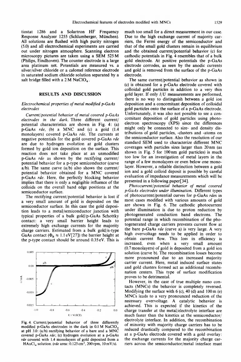
Current/potential behavior of metal covered p-GaAs electrodes in the dark. Three different current/ potential characteristics are shown in Fig. 4: (a) p-GaAs rde, (b) a MNC and (c) a gold (1.4 monolayers) covered p-GaAs rde. The currents at negative potentials for the gold covered p-GaAs rde are due to hydrogen evolution at gold clusters formed by gold ion deposition on the surface. This reaction does not take place at an unmodified p-GaAs rde as shown by the rectifying current/ potential behavior for a p-type semiconductor (curve a/b). The same curve (a/b) also shows the current/ potential behavior obtained for a MNC covered p-GaAs rde. Here, the perfectly blocking behavior implies that there is only a negligible influence of the colloids on the overall band edge positions at the semiconductor surface.
The rectifying current/potential behavior is lost if a very small amount of gold is deposited on the semiconductor surface. In this case the gold deposi- tion leads to a metal/semiconductor junction with typical properties of a bulk gold/p-GaAs Schottky contact: a very small barrier height leads to extremely high exchange currents for the majority charge carriers. Estimated from a bulk gold/n-type GaAs contact (Q, z 1.1 eV[27]) the barrier height at the p-type contact should be around 0.35eV. This is
0 005 I I I I , , ,
I 0 -0 x -0.6 -0 4 -0 2 00
I’/ “,SCE,
Fig. 4. Current/potential behavior of three differently modified p-GaAs electrodes in the dark in 0.1 M NaCIO, at pH 3.0: (a/b) rectifying behavior of a bare and a MNC covered p-GaAs rde; (c) hydrogen evolution at a p-GaAs rde covered with 1.4 monolayers of gold deposited from a
HAuCI, solution. (rde area: 0.125cm2, 2OOrpm, lOmV/s).
much too small for a direct measurement in our case. Due to the high exchange current of majority car- riers, the Fermi energy of the semiconductor and that of the small gold clusters remain in equilibrium and the obtained current/potential behavior (c) for cathodic potentials in Fig. 4 resembles that of a bulk gold electrode. At positive potentials the p-GaAs electrode corrodes, as seen by the anodic currents and gold is removed from the surface of the p-GaAs electrode.
The same current/potential behavior as shown in (c) is obtained for a p-GaAs electrode covered with colloidal gold particles in addition to a very thin gold layer. If only l/U measurements are performed, there is no way to distinguish between a gold ion deposition and a concomitant deposition of colloidal gold particles onto the surface of a p-GaAs electrode. Unfortunately, it was also not possible to see a con- comitant deposition of gold particles using photo- electron spectroscopy (XPS) since the differences might only be connected to size- and density dis- tributions of gold particles, -clusters and -atoms on the semiconductor surface. Also the resolution of our standard SEM used to characterize different MNC coverages with particles sizes larger than 20nm (as shown in Fig. 5 for 1OOnm gold particles) is much too low for an investigation of metal layers in the range of a few monolayers or even below one mono- layer. However, a reliable distinction between a gold ion and a gold colloid deposit is possible by careful evaluation of impedance measurements which will be presented in a following paper[34].
Photocurrentlpotential behavior of metal covered p-GaAs electrodes under illumination. Different types of photocurrent/potential curves for p-GaAs rdes in most cases modified with various amounts of gold are shown in Fig. 6. The cathodic photocurrent under illumination is due to proton reduction by photogenerated conduction band electrons. The potential range in which recombination of the pho- togenerated charge carriers prevents current flow at the bare p-GaAs rde (curve a) is very large. A very high overvoltage needs to be applied in order to obtain current flow. This loss in efficiency is increased, even when a very small amount (0.7 monolayers) of gold is deposited from a gold ion solution (curve b). The recombination losses become more pronounced due to an increased majority carrier current. Here, metal induced surface states and gold clusters formed act as additional recombi- nation centers. This type of surface modification proves to be detrimental.
However, in the case of true multiple nano con- tacts (MNCs) the behavior is completely reversed. Modifying the surface with 6 (c), 40 (d) and 100 m (e) MNCs leads to a very pronounced reduction of the necessary overvoltage. A catalytic behavior is achieved. This is expected if the kinetics of the charge transfer at the metal/electrolyte interface are much faster than the kinetics at the semiconductor/ electrolyte interface. In addition, the recombination of minority with majority charge carriers has to be reduced drastically compared to the recombination at a p-GaAs electrode covered with a gold overlay: the exchange currents for the majority charge car- riers across the semiconductor/metal interface must

1530 A. MEIER et al.
+ 3w + Fig. 5. Colloidal gold particles (1OOnm) deposited with a high (left) and a low (right) surface coverage on
p-GaAs electrodes as observed in the SEM.
be much smaller. The smaller the loss currents at the metal contact the more the photocurrent onset region is shifted towards positive potentials.
It is confirmed by corresponding impedance mea- surements that really the majority charge carrier loss current is drastically reduced at a MNC covered p-GaAs electrode, as predicted here. In addition, the photocurrents of minority charge carriers flow mainly across the metal island as will be demon- strated elsewhere([28] and [34]).
The photocurrent onset region can be shifted towards even more positive potentials (by in total about 400mV) when the charge transfer rate across the electrolyte/metal interface is enhanced even more. This is achieved by using MNC-electrodes made from the platinized gold particles (curve f).
Hydrogen evolution at gold electrodes modified with platinized colloidal gold particles. In order to get some additional confirmation that the charge trans- fer at colloid modified electrodes occurs mainly at particles, another set of experiments was performed
-003 -0 6
I I I I I I
-I 0 -0 9 -0 8 -0.7 -0.6 -05 -04 -0 i
using platinum modified gold colloids. These experi- ments also verify the important influence of the three dimensional diffusion on the transport of ions across the diffusion layer.
Here, platinized colloidal particles have been used to modify a polished gold electrode. Current/ potential curves are recorded for different coverage of the surface obtained by polarizing the gold rde in the colloidal solution for appropriate times (Fig. 7). Because the overpotential of the hydrogen evolution reaction is much smaller at platinum than at gold, the cathodic current starts at a much less cathodic potential at a platinum particle than at the gold surface. Thus, for a low surface coverage, the current flowing via the particles can be distinguished from that passing through the rest of the surface.
Fig. 7 depicts six current/potential curves obtained for different coverages with platinized gold particles. Compared to the unmodified gold electrode (a) the hydrogen evolution starts at potentials more positive by about 200mV. However, since for curve “ tl” the deposition time is only 5 s, the particle density is very
u / V(SCE)
Fig. 6. Photocurrent/potential curves obtained in 0.1 M NaClO, at pH 3.0 under illumination for: (a) a bare p-GaAs rde; (b) a gold plated p-GaAs rde covered with 0.7 monolayers; (c)-(e) p-GaAs rdes covered with 6, 40 and 1OOnm large gold pariicles, respectively; (f) p-GaAs rdes covered with platinized gold MNCs (4Onm). (rde area:
0.125cm2, 2OOrpm, lOmVs-I).
-08r I I I I I I c e I I -0.9 -0 8 -0.7 -0 6 -05 ~0 4 -03
lJ/VISCE)
Fig. 7. Current/potential curves obtained in 0.1 M NaCIO, at pH 3.6, sweep rate 5mV s-l, 1OOOrpm for: (a) a pure gold rde; (b) and for the electrode covered with electro- chemically deposited platinized gold particles (150 nm) with a deposition time of (LX) 5 s, (j?) lOs, (y) 25 s, (S) 2.5 min., (E)
17 min, ([) 47 min.

Electrochemical features of electrodes modified with MNCs 1531
small. Nevertheless, a small but clearly (3D) diffusion limited step occurs at -0.5 V. By increasing the deposition time the density of MNCs on the surface is increased. The diffusion limited current through the platinized particles rises and finally reaches the maximum value as defined by the total electrode area. The latter is represented by curve “r which looks like the current/potential curve of a bulk plati- num electrode. At around -0.85V (Ag/AgCl) the H,O reduction starts at the platinum particles but not at the gold substrate. Curve “r also shows, that the particle density obtained after a deposition time of 47 min is sufhcient to allow for the maximum pos- sible diffusion limited current at the electrode.
For each particle density (c( to [) the current/ potential curves are recorded with different rotation frequencies varying from 200 to 1OOOrpm. According to the theory developed for 3D diffusion as presented in the theoretical chapter, the reciprocal of the diffu- sion limited current “i,,” is plotted against the reciprocal of the square root of the angular fre- quency w, as shown in Fig. 8. To obtain a value for the 3D diffusion limited current from the current/ potential curves at different rotation frequencies, some decisions concerning the potential have to be
0 , I I I I I I I
~5
“5 t
_..r:::_~: 1 . . . . . “--.,_
-..:._ ----a.\ E
*...* --__ .c...
..a... --%__ -----CT
<I.._.. ---Y 0.
-. ----..._ . . -... ----B
-k... “-y...
I I +----bu (I
0.00 0 05 0 10 0 15 0.20 0 25 030 -0 35
IiVOlS”’
Fig. 8. Diffusion limited current values (id,) obtained for a bulk gold electrode modified with different densities of plat- inized gold MNCs as obtained from curves like those in Fig. 7 at -0.54 V(sce) (a, fi, 6, E and 5) and -0.7 V(sce) (co) taken with different rotation frequencies o of the rde. As required by the theory the diffusion limited currents are
given in the form of a l/i,, over l/ Jw plot.
made. As seen in Fig. 7 the current does not really become independent of the potential as required for a diffusion limited current. This might be due to the broad size distribution of the deposited particles or the distribution of platinum islands on the gold par- ticles. At very small particles (eg 5nm platinum particles) a kinetic limitation of the current can occur (compared to the theoretical section) and cause deviations from the expected behavior.
We have chosen a potential of -0.54 V(sce) for comparison of the different results. At this potential the proton reduction at the bare gold surface is still negligibly small and independent of the rotation velocity while the reduction occurs near to the diffu- sion limit at the platinized gold particles, as seen in Fig. 7. However, an evaluation of this experiment is expected to follow the model assumptions only approximately, since the diffusion limited current for curves /I - [ is really reached only at -0.7V(sce). But at this potential there is already a charge trans- fer contribution from the bare gold surface of the electrode which is not independent of the rde rota- tion velocity.
Such nearly diffusion limited currents are deter- mined at different rotation frequencies for six elec- trodes, each covered with a different number of platinized particles. These values are plotted in Fig. 8 as l/i,, over I/Jw. As explained only the data obtained for the highest coverage taken at -0.7V(sce) (as given by the “lo” data) fit to a straight line that has only a negligibly small intercept (compare Table 2) and therefore follows equation (2). This behavior is expected for a fast reaction for which the current is limited only by the diffusion but not by the charge transfer across the interface.
Despite all these deviations, the curves a to E in Fig. 8 still resemble the form of curve “B” in Fig. 2. The values obtained for low rotation velocities, ie when the thickness of Nernst diffusion layer 6, is large, can be fitted by straight lines with slopes as that of curve co. Equation (3) can be applied here as described in the theoretical chapter since the dis- tance of the particles (2r2) is smaller than the thick- ness of 6,. At higher rotation velocities, ie when the thickness of 6, decreases, deviations from the straight lines towards a steeper slope occur. This is observed when the diffusion layer thickness approaches the radius of the diffusion cylinders rZ, ie
Table 2. Data for the platinized gold particles assuming a size of 1.68 pm in diameter for different coverages (a to <)
Polarization time [s]
10 5
145 25
2820 1020 2820
Intercept
l/i, [cm’mA_‘]
14.3 9.1
4.5 6.5
0.33 2.4 (2.5 x lo-‘)
Xlr, r11r2
13.09 16.13 0.043 0.055
11.18 9.21 0.066 0.079
6.53 2.00 0.104 0.254
Distance of Platinized platinized particle particles coverage
[pm1 [%I
37.1 28.7 0.15 0.24
23.7 19.7 0.34 0.49
14.4 4.9 0.86 5.09
Density of platinized particles
[ml
6.7 x IO“ 1.1 x lo5 1.6 x 10’ 2.2 x 10⁵ 3.9 x lo5 2.3 x 10h
The values of the intercept l/i, are taken from Fig. 8. The values for ZA, are obtained using equation (3) with Age0 = 1 cm2, ce = 2.3 x 10e4M (pH 3.64) D = 9.9 x lo-scm* s-r and n = 1. The radius of the diffusion cylinder r2 for a certain coverage is obtained by interpolation of the data for EA,/r, and r,/r2 in Table 1. The particle distance d can be calculated easily with d = 2r, - 2r, and the density is calculated assuming a pattern as shown in Fig. 1.

1532 A. MEIER et al.
at lower rotation velocities (larger l/Jo values) for the electrodes with the lower MNC densities (curve a).
In order to fulfill the condition that rz can become smaller than 6, when the rotation frequency is diminished, the particles have to be larger than 150nm in diameter (as determined with the SEM). However, as described in the experimental part, these large particles have a broad size distribution. Careful analysis of the experimental data shows that good agreement between experiment and theory is achieved only if the average particle radius can be assumed to be on the order of 840nm. This size is considerably larger than that observed for single particles in the SEM if a very dilute colloidal solu- tion is deposited onto a graphite substrate. Such a discrepancy must be attributed to formation of agglomerates. As described in the experimental section these platinized gold particles had been separated from the solution by filtration through a 1OOnm membrane filter in order to minimize the residual concentration of small (5 to 8nm) platinum clusters. But this procedure also increases the prob- ability of particle agglomeration.
For small rotation frequencies (l/Jw + co), when 6, becomes larger than rz, the resulting straight lines have identical slopes for all coverages (c( to [) as expected from theory. In Table 2 the data of the y- intercepts (l/&J of these lines are listed for every coverage as determined from Fig. 8 by extrapolation. The line fits were performed using the slope of curve [,, the fits considered only the diffusion limited cur- rents at low frequencies.
In order to compare these data, the diffusion limited current data at 1OOOrpm from Fig. 7 for every coverage (a to E), with the theoretical calcu- lations summarized in Fig. 3 the following procedure is applied. Equation (3) is used to obtain values for ZA, from these intercepts (l/&J and from the values of D, co, n, Age0 as given in Table 2 or in Fig. 3. From these, values for r2 are derived assuming rI to be 840nm and interpolating the CAJr, and rI/r2 data as given in Table 1. Using the corresponding ratios for the radii r1/r2 such calculated the current data are then plotted as open squares in Fig. 3.
However, the model can only be a crude approx- imation to this experiment due to its very restrictive assumptions (no particle size distribution and no charge transfer at the inactive surface). Nevertheless it is shown by this experiment that two types of cur- rents can be observed at a catalyst particle modified electrode. These currents are through the catalyst islands and through the unmodified surface.
The condition of no charge transfer at the unmod- ified electrode is fulfilled much better for a MNC covered p-GaAs electrode polarized at cathodic potentials in the dark. Here cathodic currents can flow only through the gold particle/p-GaAs contacts since the GaAs itself shows a perfectly rectifying behavior in this potential region. The proton reduction current should then become diffusion limited at sufficiently high overvoltages. Unfor- tunately the exchange currents at the gold particle/p- GaAs interface are small and become rate limiting for the majority charge carriers due to only very small contact areas, so that no reduction currents
are observable in the dark. A 3D diffusion limitation cannot be evaluated in this case.
However, the situation changes upon illumination since here minority charge carriers determine the current flow. The charge transfer of minority charge carriers occurs across the bare p-GaAs/electrolyte and across the gold/electrolyte interface. As on the platinum modified gold electrode, the current flows mainly through the MNC particles as seen in Fig. 6 and as confirmed by impedance measurementsC28, 341. Here, the three-dimensional diffusion of protons towards the particles again becomes very important.
Time resolved gold deposition experiments from dilute gold ion solutions
In order to get an idea about the amount of gold deposited on the p-GaAs surface that is sufficient for irreversibly changing the electrochemical and espe- cially here the rectifying properties, various deposi- tion experiments are performed using low concentrations of HAuCl,. Fig. 9a shows the current/time curves B-E obtained for p-GaAs rdes polarized at - 0.9 V(Ag/AgCl) in HAuCl, solutions of different concentrations (44 to 480nM). The p-GaAs electrodes show a perfectly rectifying behav- ior for more than 1 h if no gold ions are added to the
ci
-7
b I” 00
LO.103
4
; 2.0 10-3
3 0 10-3
40.10~’
Fig. 9. Current/time measurements from p-GaAs rdes pol- arked at -0.9 V(Ag/AgCI) in diluted HAuCI, (0.1 M NaCIOJnH 3.5) solutions: (a) of different concentrations -. . using 4OOrpm: (S) 44nM, (i) 96nM, (6) 24OnM and (E) 480nM; (b) using different rotation velocities of the rde for 480mM HAuCI,: (b) 25rpm, (y) 50rpm, (6) lOOrpm, (E) 200rpm and (5) 400rpm. In both diagrams curve (ar) rep- resents the rectifying behavior of the p-GaAs rde in 0.1 M NaClOJpH 3.5 without any gold ions using a rotation fre-
quency of 400 rpm.

Electrochemical features of electrodes modified with MNCs 1533
0.1 M NaClO, solution as shown by curve c( in Fig. 9a. The same rectifying behavior occurs in p-GaAs electrodes in a colloidal gold solution if all residual gold ions have been eliminated by adding a small amount of NaBH, as described in the experimental section.
Results of an analogous experiment investigating the influence of the rotation velocity is shown in Fig. 9b. Here, the current/time curves (/I - [) are record- ed at - 0.9 V (Ag/AgCl) for a HAuCl, concentration of 480nM but for different rotation velocities of the rde (25 to 400rpm). The current/time curve “CI” is that of the p-GaAs rde just polarized at pH 3.5 without any gold ions. The results of these deposi- tion experiments while changing the rotation veloci- ties are similar to those obtained in the former experiment: the higher the rotation velocity the earlier the breakdown of p-GaAs rectification. This dependence is expected if the metal deposition is controlled by the diffusion of gold ions. Only after this breakdown of rectification the hydrogen forma- tion starts.
The higher the concentration of gold ions or the higher the rotation frequency of the rde the earlier the p-GaAs electrode loses its rectifying behavior. The slopes of the current/time curves increase in the same order. The cathodic currents seen here are due to proton reduction at gold deposited on the GaAs surface. In contrast to the experiments with colloidal gold solutions forming MNCs, very small clusters are formed[l3, 111. In this case the exchange cur- rents of the majority charge carriers across the metal/semiconductor interface are high and the charge transfer currents across the metal/electrolyte interface become rate limiting and measurable. With increasing polarization time the cluster density and the cluster size increase leading to higher exchange currents at the semiconductor/metal and the metal/ electrolyte interface. The proton reduction current increases.
Some suggestions for describing cluster formation and its growth on semiconductor electrodes can be found in the literatureC29, 301. An attempt to simu- late the increase of the proton reduction currents based only on cluster nucleation and growth models must remain inconclusive, since too many param- eters are unknown. It must be expected that the growth of every particle also depends on the current density at this particle due to additional proton reduction[30].
Other gold deposition experiments at p-GaAs electrodes, eg, the experiments of Kelly[ll, 123 and his group, cannot be compared directly with our experiments. The authors have chosen deposition conditions so that the metal deposition is the only reaction yielding Faradaic current. In most cases reported the intention was to form ohmic contacts and the chosen concentrations of gold solutions were about 3 orders of magnitude higher than ours.
In our case the concomitant hydrogen formation makes it impossible to calculate the number of gold monolayers directly by integrating the Faradaic cur- rents, even if these extremely small currents leading to gold reduction could be measured with sufficient accuracy. The currents expected for our p-GaAs rde (area: 0.125cm’. 400rpm) assuming a diffusion
limited reaction are 5.5 and 60nA for a HAuCl, con- centration of 44 and 480 nM, respectively.
However, the experimental conditions chosen in our experiments enable equation (7) to be used to determine the amount of gold deposited. The elec- trodes are polarized at -0.9 V(Ag/AgCl), a potential high enough to make sure that the supposedly differ- ent kinetics of gold reduction on GaAs and on gold island (as formed after some time) should not control the deposition process. The deposition at such a high overvoltage should be purely diffusion limited. According to equation (7) the rate constant k must be very large in order for l/k to vanish. All ions reaching the semiconductor are reduced and remain on the surface as gold metal.
At the gold deposits hydrogen evolution becomes possible, the rate of which should be determined by the amount of gold at the interface. The hydro- gen evolution can then serve as an indicator of the amount of gold deposited. Since the proton concen- tration at pH 3.5 is much higher than that of gold ions, the currents for hydrogen evolution become measurable as they are given in Fig. 9. They increase with increasing amounts of gold deposited, while the gold reduction current remains undetectable due to its small density.
If the hydrogen evolution reaction is only a func- tion of the number of gold atoms deposited (ie, for example in addition that the GaAs/gold alloying rate is negligible), equation (7) can be used to determine the actual amount of gold on the surface at all times of deposition from the recorded hydrogen evolution current. Using this equation, every current density given in Fig. 9 can be converted into a certain amount of gold required to produce this current. The parameters used to calculate these amounts (here given in fractions of monolayers) are given in Fig. 10. The diffusion coefficient for the gold ions has been determined experimentally by measuring the diffu- sion limited currents in 0.1 M NaCIO, , pH 3.5, con- taining 0.25mM HAuCl, as a function of the rotation velocity using a bulk gold electrode.
Figure 10 is obtained by plotting all the current data given in Fig. 9 against the calculated gold surface area (given in parts of a monolayer). Now all curves having different slopes for different gold ion concentrations in the current/time plot of Fig. 9a fall together in the current/monolayers plot of Fig. 10a. The same result is obtained from the data deter- mined for different rotation velocities (Fig. lob). The current/time curves “LX” in Fig. 9 for the “blank” experiment are represented by only one point close to the origins in Fig. 10.
The deviations of curves /r and E in Fig. lob (25 and 200rpm) are assumed to be accidental. For all curves to coincide in the calculations, a rate constant k > 1OOcm s-i for the gold reduction has to be used. Higher values of k (even of an infinite rate constant as assumed above) do not change the position of the curves, but lower values do. This subsequently con- firms our assumption of a diffusion limited process independent of the charge transfer kinetics. All metal ions reaching the semiconductor surface by diffusion are deposited.
On this basis the time which is necessary to deposit a certain number of gold atoms for a given

1534 A. MEIER et al.
0 0.2 0.4 0.6 08 1.0
nominal monolavers
0 0.2 0.4 06 0.8 10
nominal monolayers
Fig. 10. Current/time curves for gold monolayers deposited onto the GaAs (100) surface (0.125cmZ), recalculated from Fig. 9 using equation (7) with D = 8.0 x 10⁻⁶cm2s-1, n = 3. v = 10-2cm2s-‘. i&,. = 6.3 x 10’4atoms/cm2 and assuming a diffusion. con&led reaction (k -+ co): (a) for different concentrations with 400rpm; (b) using different
rotation velocites of the rde for 480 nM HAuCI,
concentration and rotation velocity can be calcu- lated using the modified Levich equation (7). Vice versa, an upper limit can be given for the concentra- tion of gold ions present in our colloidal gold solu- tions used for preparation of the MNC electrodes. As mentioned above the p-GaAs rde still shows a perfectly rectifying behavior for at least one hour after polarization in a colloidal gold solution treated with NaBH, . Even potentiostatic experiments using polarization times of two hours did not reveal any dark currents. This can be the case only if the colloi- dal gold solution contains less than 2ppb of gold ions corresponding to a concentration of less than 1OmM Au . 3 ’ For this estimate the parameters given in Fig. 10 for 0.3 monolayers are used.
As seen in Fig. 10 the breakdown of rectification occurs at gold coverages of around 0.4 monolayers. We assume that the observed dark current is due to the hydrogen evolution at gold clusters formed at the p-GaAs surface. Accordingly, a semiconductor/ metal Schottky contact is already formed for an average gold coverage of 0.4 monolayers. This result coincides very well with UPS measurements per- formed at gold/GaAs samples in ultra high vacuum. A significant shift of the fermi level to the final posi- tion of a bulk metal is already found for evaporated coverages of around 0.1 monolayer[31-331. But the “pinning” of the Fermi level is attributed to the interaction of metal induced gap states and not to
single gold clusters forming a semiconductor/metal contact according to the Schottky model. However, a distinction between a charge transfer via single, located clusters and a transfer reaction via a two dimensional band formed by surface (interface) states is not yet possible from our experiments.
CONCLUSIONS
Deposition of colloidal metal particles leads to the formation of Multiple Nano Contacts (MNCs) at the semiconductor/electrolyte interface. Electrochemical experiments prove that the MNC/semiconductor contact possesses totally different contact properties compared to those obtained with classical metal- lization procedures as eg, electrochemical deposition, thermal evaporation or sputtering.
The ability to vary the metal cluster size indepen- dent from the cluster density while avoiding the usual formation of surface states from electrochemi- cal metal deposits reveals the unique properties of MNC modification.
In contrast, the deposition of gold from very dilute gold ion solutions verify that it is crucial to avoid concomitant metal ion deposition while preparing the MNC/p-GaAs electrodes. A metal like behavior of the gold deposit is already found for a coverage of around 40% of a monolayer, which causes a high recombination of the charge carriers across the inter- face created upon illumination. This metallic pro- perty deteriorates the rectifying properties of the semiconductor/electrolyte junction.
Theoretical and experimental evaluations concern- ing the effect of three dimensional diffusion prove that already a very small MNC coverage is sufficient to give the highest possible diffusion limited current for a given electrode surface.
For semiconductor/electrolyte contacts this means that metal catalysts which change only the rate of the charge transfer reaction can be employed. These metal catalysts will not form a new solid state device and thereby destroy the high efficiency of the semiconductor/electrolyte contact for charge separa- tion. Hence, the direct solar water splitting becomes an interesting goal again, where the reduction of overpotential is crucial to achieve solar efficiencies which can compete with and overcome those achiev- able with PV driven electrolysis.
Acknowledgement-The authors wish to thank all their col- leagues in Hannover for supporting this research and for many valuable discussions. We are especially grateful for microscopic investigations (AFM, STM and SEM) and photoelectron spectroscopy (XPS) performed by Dr. Renate Hiesgen, Barbara Schiine-Harms and Ursula Neff. Very useful support by Professors Dr. R. Memming, Oldenburg, and Dr. B. Kastening, Hamburg, is gratefully acknow- ledged. This work was supported-by the German Federal Minister for Research and Develoument (BMFT) under contract No. 329081A.
REFERENCES
1. D. Meissner, in UIImanns Encyclopedia of Industrial Chemistry, (Edited by B. Elvers, S. Hawkins and G. Schult) 5th ed., A24,400, VCH Weinheim (1993).

Electrochemical features of elec :trodes modified with MNCs 1535
2. R. Reineke, in Elektrochemie in Energie- und Umwelt- technik, (Edited by A. Winsel) Dechema Monographie, 124, 623 (1991).
3. K. Vetter, Elektrochemische Kinetik, Springer-Verlag, Berlin (1961)
4. R. Memming, Topics in Current Chemistry 169, 105 (1994).
5. F. Mollers, H. J. Tolle and R. Memming, J. electro- them. Sot. 121, 1160 (1969).
6. Compare eg H. Gerischer, Ber. Bunsenges. Phys. Chem. 84, 1034 (1980); A. Heller and B. Miller, EIectrochim. Acta 25, 29 (1980); A. Heller, J. Vat. Sci. Technol. 21, 559 (1982); J. O’M. Bockris and R. C. Kainthla, Int. J. Hydrogen Energy 13, 375 (1988).
7. R. Memming, in Photochem. Conversion and Storage of Solar Energy, (Edited by E. Pelizzetti and- M. Schiavello) Kluwer Academic Publ.. Dordrecht. Netherlands, p. 193 (1991).
8. R. N. Dominey, N. S. Lewis, J. A. Bruce, D. C. Book- binder and M. S. Wriahton. J. Am. Chem. Sot. 104. 467 (1982); T. Sakata, K Hashimoto and T. Kawai, J. Phys. Chem. 88, 5214 (1984); A. Heller, Pure Appt. Chem. 58, 1189 (1986).
9. P. Allongue and E. Souteyrand, Electrochim. Acta 34, 1717 (1989); P. Allongue, S. Blankowski and D. Lincot, J. electroanaL Chem. %I, 261 (1991).
10. H. M. Kiihne and J. Schefold. Ber. Bunsenaes. Phvs. Chem. 92, 1430 (1988); J. Eledtrochem. Soc.“137, 568 (1990), and J. efectroanal. Chem. 300,211 (1991).
11. G. Oskam, D. Vanmaekelbergh and J. J. Kelly, Electro- chim. Acta 38,291 and 301 (1993).
12. J. J. Kelly, J. M. G. Rikken, J. W. M. Jacobs and A. Valster, J. Vat. Sci. Technol. B 6,48-52 (1988).
13. J. W. M. Jacobs and J. M. Rikken, J. Electrochem. Sot. 136,3633 and 3641 (1989).
14. For a review of the most relevant papers see: Y. Nakato. K. Ueda. H. Yano and H. Tsubomura. J. Phys. Chem. 92 23 16 (1988).
15. Solarzellen, (Edited by D. Meissner) Vieweg, Braun- schweig (1993).
16. H. Kobayashi, T. Ishida, Y. Nakato and H. Tsubo- mura, J. Appt. Phys. 69, 1736 (1991).
17. W. R. Smythe, J. Appt. Phys. 24, 70 (1953). 18. F. Nagy, Gy. Horanyi and Gy. Vertes, Acta Chim.
Hung. Tomus 34,35 (1962). 19. F. Scheller, S. Mtiller, R. Landsberg and H.-J. Spitzer,
J. eleciroanal. Chem. 19, 187 (1968). 20. F. Scheller, R. Landsberg and S. Miiller, J. electroanal.
Chem. 20,375 (1969). 21. A. J. Bard and L. R. Faulkner, Electrochemical
Methods, Fundamentals and Applications, J. Wiley, New York, p. 283 (1980).
22. J. A. Bard, R. Parsons and J. Jordan, Standard poten- tials in aqueous solutions, Marcel Dekker. New York (1985).
23. Graydon B. Larrabee, J. electrochem. Sot., 108, 1130 (1961).
24. D. A. Weitz, M. Y. Lin and C. J. Sandroff, Surf. Sci., 158, 147 (1985).
25. J. Turkevich, American Scientist, 47, 97 (1959). 26. R. Hernandez, G. Diaz, A. Vazquez, J. Reyes-Gasga
and M. Jose-Yacamin, Langmuir, 7, 1546 (199 1). 27. R. Reineke and R. Memming, Surjace Science, 192,
66-80 (1987).
28. A. Meier, I. Uhlendorf and D. Meissner, in Hydrogen Production, Inc. Energy Agency. thrd. Technical Work- shop, (Edited by Bernd Dieter Struck) Lugano, Switzer- land, p. 31 (1993).
29. J. W. M. Jacobs, J. electroanal. Chem. 247, 135 (1988). 30. P. Allongue and E. Souteyrand. J. electroanat. Chrm.
286,217 (1990). 31. R. H. Williams, Surface Science 251/252, 12 (1991). 32. W. G. Petro, I. A. Babalola, P. Skeath, C. Y. Su, I.
Lindau and W. E. Spicer, J. Vat. Sci. Technol., 21(2), 586 (1982).
33. R. Cao, K. Miyano, T. Kendelewicz, 1. Lindau and W. E. Spicer, J. Vat. Sci. Technol. B, 5, 998 (1987).
34. A. Meier, I. Uhlendorf and D. Meissner, in preparation.


