Embed Size (px)
Citation preview

Thin Solid Films 517 (2009) 2767–2774
Contents lists available at ScienceDirect
Thin Solid Films
j ourna l homepage: www.e lsev ie r.com/ locate / ts f
Effect of LaNiO3 electrodes and lead oxide excess on chemical solution depositionderived Pb(Zrx,Ti1 − x)O3 films
Itzik Shturman, Gennady E. Shter, Aleksey Etin, Gideon S. Grader ⁎Chemical Engineering Department, Technion, Haifa 32000, Israel
⁎ Corresponding author. Tel.: +972 4 8292008; fax: +9E-mail address: [email protected] (G.S.
0040-6090/$ – see front matter © 2008 Elsevier B.V. Aldoi:10.1016/j.tsf.2008.10.007
a b s t r a c t
a r t i c l e i n f oArticle history:
The effects of LaNiO3 (LNO) Received 22 September 2007Received in revised form 26 August 2008Accepted 5 October 2008Available online 15 October 2008Keywords:LaNiO3 (LNO)Pb(Zrx,Ti1 − x)O3 (PZT)Chemical solution deposition (CSD)
and Pt electrodes on the properties of Pb(Zrx,Ti1 − x)O3 (PZT) films were compared.Both LNO and PZT were prepared by chemical solution deposition (CSD) methods. Specifically, themicrostructure of LNO and its influence on the PZT properties were studied as a function of PbO excess.Conditions to minimize the Pyrochlore phase and porosity were found. Remnant polarization, coercive fieldand fatigue limit were improved in the PZT/LNO films relative to the PZT/Pt films. Additionally, the PZTcrystallization temperature over LNO was 500 °C, about ~50 °C lower than over Pt. The crystallizationtemperature reported here is amongst the lowest values for CSD-based PZT films.
© 2008 Elsevier B.V. All rights reserved.
1. Introduction
Thin PbZrxTi1− xO3 (PZT) films have excellent ferroelectric andpiezoelectric propertieswhichmake themuseful for sensors, actuatorsandmemoryapplications [1–4]. Pt is often integrated as an electrode inPZT devices because of its stability at high temperature, low leakagecurrent and high electrical conductivity [5]. However, in addition to itshigh cost, Pt has several disadvantages such as poor adhesion to thesilicon substrate and a large thermal expansion coefficient mismatchwith PZT. The poor adhesion is typically solved by deposition of a Tiintermediate adhesion layer. Themain disadvantage of PZT/Pt device isthe low ferroelectric fatigue limit that causes a severe decrease in theferroelectric properties after 104–107 operating cycles [3,6,7]. The twomain reasons for the fast fatigue in PZT/Pt system are thought to be:formation of oxygen vacancies in the PZT films during operation cycles[7,8] and the presence of Pyrochlore (Py) phase [3] that pinned thedomain switching.
Lanthanumnickel oxide (LNO) is a conducting oxide filmwhich hasattracted great attention in recent years due to its ability to drasticallyimprove the ferroelectric fatigue [7,9] of PZT. LNOhas lattice parameterof 0.384 nmand its typicalfilm resistivity at room temperature is in the300 μΩ⁎cm to 2000 μΩ⁎cm range [10]. Furthermore, LNO structure iscompatiblewith PZT, since both have perovskite ABO3 type unit cell [6]with 0.384 nm and 0.404 nm lattice constant for LNO and PZTrespectively. Hence, LNO is an excellent candidate in couplingwith PZTdevices. The remnant polarization (Pr) and coercive field (Ec) of PZT/LNOhave been reported to improve in comparisonwith PZT/Pt system.
72 4 8295672.Grader).
l rights reserved.
Itwas suggested that the improved ferroelectric propertieswere due tobetter PZT interface with LNO electrodes in comparison with Pt [11]electrodes.
LNO electrodes can bemade by different techniques such as pulsedlaser ablation [12], r.f. magnetron sputtering [6], and chemical solutiondeposition (CSD) methods that include metalorganic decomposition[13] as well as the Sol-Gel route [14]. The CSD method offers severaladvantages over other routes such as easy elemental stoichiometrycontrol which is critical in multi-component ceramic systems, lowprocess costs and high throughput. Only few reports have been madeon a complete CSD approach [15,16], (for both bottom electrode andPZT films), and the analysis of the morphology and ferroelectricproperties is still partially investigated. Specifically, the influence ofPbO content on morphology and ferroelectric properties in PZT/LNOhas not been reported yet.
In the present research both LNO and PZT were prepared by CSD,and results compared with those obtained with Pt bottom electrodes.The microstructure and electrical properties of LNO electrodes andtheir influence on PZT morphology, orientation and ferroelectricbehavior were studied as a function of PbO excess.
2. Experimental details
LNO electrodes were prepared using the CSD method. Solutionprecursors were prepared by dissolving lanthanum acetate hydrateC6H9LaO6⋯xH2O (99.9%, Sigma-Aldrich, Steinheim, Germany) in amixture of distilled water and glacial acetic acid C2H4O2 (99.8%, Gadot,Netanya, Israel) in a molar ratio of 1:15:144 for lanthanum acetatehydrate, distilled water and glacial acetic acid respectively at 75 °C for1 h. An equi-molar amount of nickel acetate tetrahydrate (98% Sigma-Aldrich) was dissolved in glacial acetic acid in a molar ratio of 1:25 for

2768 I. Shturman et al. / Thin Solid Films 517 (2009) 2767–2774
nickel acetate tetrahydrate and acetic acid respectively at 75 °C for 1 h.These solutions were stirred together at 75 °C for 1 h. The green finalprecursor's concentration was 0.2 M and it's assay was 4.5% wt. Theprecursor had a shelf life ofmore thanoneyearwithout any visual phaseseparation and without any changes in the final electrode properties.LNO electrodes were prepared by spin coating at 3000 rpm for 60 s,acceleration of 1000 rpm/s, followed by pyrolysis on a hot plate at 350 °Cfor 2min and afinal annealing step at 700 °C for 20min in Air. Due to therelatively low concentration of the LNO precursor, the resulting filmthickness per cycle was ~25 nm. The deposition cycle was repeated tillthe desired LNO thickness in the range of 25–225 nmwas achieved.
The detailed preparation of the PZT precursors and films isdescribed elsewhere [2–4]. In the present work PZT precursors ofwith 10% and 30% PbO excess were prepared and diluted with 1-octanol in order to deposit defect-free PZT films [4]. The CSD route forPZT deposition over LNO and Pt electrodes was as follows: 3 cycles ofspinning at 3000 rpm for 1 min with acceleration of 1000 rpm/s,pyrolysis on a hot-plate at 300 °C for 1 min, and a final annealing stepat 650–500 °C in air for 10–60 min. Upper Au circular electrodes(500 μm diameter), were deposited by evaporation (Edwards E306A,Crawley, UK), using a contact mask technique. The film surface andcross-sectional microstructure were studied with a high-resolutionfield emission gun equipped with a scanning electron microscope(LEO 982, Cambridge, U.K). Conditions included a 4 kV acceleratingvoltage and a 4 to 5 mmworking distance, using an in-lens detector ofsecondary electrons. The grain size was determined by the equivalentarea method without a correction factor using an image analysissoftware (Image tool, Copyright UTHSCSA) based on the HRSEMpictures. In order to enhance the grain boundary definition, thenanoparticles were analyzed when image is viewed in the thresholdmode. Only particles with well-defined boundaries were consideredas individual grains.
Fig. 1. HRSEM film morphology of LNO at thickness of (a) 75nm, (b)
The crystalline phases were detected by X-ray diffraction (XRD),using a Siemens D5000 powder diffractometer instrument ( Siemens,Karlsruhe , Germany). Atomic force microscopy (AFM) analyses wereperformed at scanning area of 2.5×2.5 μm2 in a non-contactmode usingan Agilent 5500 system (Tempe, USA). For the LNO electrode resistivitymeasurements a four point probe method was used with VeecoFPP5000 system (Tucson, USA) and a distance of 1.59 mm betweenthe probe tips. An elemental distribution depth profile in the LNO filmwas obtained with secondary ion mass spectrometer, SIMS (Camecaims-4 f, Paris, France). The sample was sputtered using a 3 keV Cs+primary ions source by monitoring O, Si, Ni, La, Ti, Zr and Pb secondaryions from a 40 μm2 area. The fatigue and hysteresis measurements weretested using a Sawyer–Tower bridge. The applied voltage was a 15 V(peak to peak) sinewavewith a 1 kHz or 10 kHz frequency for hysteresisand fatigue measurements, respectively.
3. Results and discussion
3.1. Film morphology and resistivity
The surface morphology of LNO electrodes with different thicknessare shown in Fig. 1a-c. It can be seen that the size of the LNO grainsincreases with the thickness. As shown in Fig. 1d, the average LNOgrain size is 38 nm and 58 nm for electrode thickness of 75 nm and225 nm, respectively. For defect-free bulk materials, the grain size (D),is typically proportional to the square root of annealing time [17] (i.e.D α t0.5). Our experimental results indicate that for LNO electrode thegrain size is proportional to 0.4 power of the thickness (Fig. 1d). Theshift in the power value in comparison with the literature [17] can beexplained by two factors: the experimental value is based on an LNOfilm rather than bulk, and the film is probably not defect free. Defectscan pin the grain growth and lead to a smaller than expected grain
125nm, (c) 225nm and (d) grain size vs. thickness; bar-200nm.

Fig. 3. LNO electrical resistivity vs. thickness.
2769I. Shturman et al. / Thin Solid Films 517 (2009) 2767–2774
size. In addition, in the multistage film deposition process, each layerin the film is being heated to successively shorter time — thereforesmaller grains could be expected relative to the bulk case. Both effectsare expected to give rise to lower power dependence relative to thebulk case.
The AFM images of LNOfilms are shown in Fig. 2. As seen in Fig. 2a,bthe LNO particles consist of clusters of grains with a surface variationsof 0–30 nm. The AFM images are consistent with HRSEM pictures(Fig. 1a–c) that showed growth of LNO grains with thickness. The rootmean square (rms) roughness of LNO filmswas found to be 3.1–3.5 nm.The results obtainedhere are slightly better than byDonget al. [14] andLi et al. [18] where an rms roughness ranging from 3.78 to 4.67 nm forCSD derived LNO was reported.
The resistivity as a function of thickness was measured for LNOelectrodes as shown in Fig. 3. The resistivity reaches a constant valueof ~1200 μΩ⁎cm above a film thickness of 75 nm. Although the grainsize increases with thickness, beyond a thickness of 75 nm the grainsize does not influence the resistivity. This points out that the LNOresistivity we measure is not influenced by grain boundary effects.Since the grain boundary area in the film is inversely proportional tothe square of the grain size, the grain boundary area is reduced by afactor of ~5 between a 75 nm film and 175 nm film in Fig. 3. The lack ofsensitivity to this drastic change in grain boundary area indicates thatthe internal grain resistivity is being measured.
At a thickness of 25 nm, the film consists of discrete grains with“gaps” between them (not shown for lack of space), as evident fromthe high resistivity shown in Fig. 3. So the nucleation of the grainsoccurs right at the substrate interface. The second and third layer (upto 75 nm), “fill” the gaps in the film, get it above the percolation limit,beyond which the resistivity becomes constant. Based on theresistivity measurements where the minimal value was obtained at
Fig. 2. AFM of LNO at thickness: (a) 75nm and (b) 225nm; bar-1μm.
~75 nm LNO, this electrode thickness (based on three 25 nmdeposition cycles) was used for all samples discussed below.
In this work we found that the grain size of the LNO film influencesthe resulting grain size of the PZT. The morphology of a 200 nm PZTfilmwith 30% PbO excess deposited over LNO with different thicknessis presented in Fig. 4. The PZT grains grew from 58 nm to 82 nm as theLNO thickness is increased from 75 nm to 225 nm (Fig. 4a,b). Theincrease of the LNO grain size by ~50% with its thickness (Fig. 1) gaverise to a ~40% growth of the PZT grains. The average grain size of PZTfilms (having the same 200 nm PZT thickness) on LNO electrodes issignificantly smaller than the PZT grains on Pt electrodes [3] (58 vs.100 nm [3]). Although the microstructure and grain size of the Ptelectrodes is surely different than that of the LNO electrodes, webelieve that the marked difference in PZT grain size cannot beexplained by the mere morphological differences of the bottomelectrode. As will be shown later, the kinetics of PZT crystallization isfaster over LNO and the crystallization temperature is lower over LNOwhen compared to those over Pt. We therefore believe that theconsiderable decrease of the PZT grain size in PZT/LNO structurecompared to the PZT/Pt analog is mainly due to a higher nucleationdensity on LNO as compared to Pt.
The AFM analysis of PZT\LNO films with 30% PbO excess withsmooth and dense surface is shown in Fig. 5. The white spots areforeign dust particles, which are ignored in the roughness analysis.The rms value of PZT film roughness was 1.5 nm which is half thesurface roughness of the underlying LNO electrode. This value issimilar to that of Chung et al. [19] where an rms roughness rangingfrom 1.7 to 3 nm for different Zr/Ti ratio in CSD derived PZT depositedover Pt electrode was reported.
The pure PZT perovskite structure can be obtained only if a preciseelemental stoichiometry is kept [20]. Stoichiometry deviations,especially in Pb/(Ti+Zr) ratio, will lead to an undesirable Py phase.The PbO component is usually lost during high temperature proces-sing due to its relatively high vapor pressure and its diffusion into thesubstrate [1,3]. In order to keep the requested stoichiometry there is aneed to compensate the PbO loss by adding excess lead to theprecursor. The effect of different PbO excess on the PZT/LNO and PZT/Pt morphology was investigated and discussed below. Fig. 6 shows themorphology of PZT films made with 10% PbO excess on Pt incomparison with PZT on LNO electrodes. In Fig. 6a, two types ofgrains are observed on the film surface: small grains of ~10 nm andlarge grains of ~100 nm. Based on our previous work [2], the smallgrains are ascribed to the Py phase, while large grains are the PZTPerovskite phase. As seen in Fig. 6a, PZT film (with 10% PbO excess)deposited on Pt resultedwithmore than 50% of the area covered by Py.When PZT was deposited over LNO (under the same conditions) weobtained a drastic decrease in Py content as shown in Fig. 6b. The rateof PZT crystallization in these two cases can be used to explain these

Fig. 5. AFM of PZT with 30% PbO excess over LNO; bar-1μm.
Fig. 6. Morphology of PZT with 10% PbO excess on (a) Pt and (b) LNO; bar-200nm.
Fig. 4. Morphology of 200nm PZT film with 30% PbO excess over of (a) LNO 75nm and(b) LNO 225nm and (c) Pt 100nm; bar-200nm.
2770 I. Shturman et al. / Thin Solid Films 517 (2009) 2767–2774
results. It is known that the PZT crystallization rate can stronglyinfluence the Py formation [1]. It was recently found that an increaseof the crystallization rate leads to lower PbO loss and thereforedecreases the Py content in the final film [3]. Thus, based on the datapresented in Fig. 6, it can be concluded that PZT crystallizes faster overLNO than on Pt. Faster crystallization of PZT over LNO is achieved dueto rapid nucleation that is the rate limiting step in growth of PZT films[1]. As a result there was a lower PbO loss leading to a much lower Pycontent in the PZT/LNO system.
Although the Py was drastically decreased in the PZT\LNO systemwith 10% PbO excess, even a small amount of Py can still significantlydeteriorate the ferroelectric properties [3]. Therefore a 30% PbO excesswas used in the next steps. No Py grainswere observed in either PZT/Ptor PZT/LNOwhen PZTwith 30% of PbO excesswas deposited (Fig. 4a,c).
Although, 30% excess of PbO eliminates the formation of Py phase,some nano-pores are observed in the PZT/LNO, as shown in Fig. 4a and
Fig. 7a. We tried long heat treatments at 650 °C for 1 h to see if thenatural grain growth at elevated temperatures can eliminate the poresover time. As seen in Fig. 7b, a significant grain growth occurred, butalthough the number of pores per unit area decreased by porecoarsening (pores merge so that their number decreases but their sizeincreases), they were not eliminated. Therefore, extended annealingtime of the PZT film is not sufficient to eliminate these pores. Thisporosity can be eliminated by using an intermediate level of PbOexcess. Experiments with 25% and 20% PbO excess resulted withporous films similar to the 30% PbO case. As shown Fig. 7c, a densestructure without detectable Py phase was obtained with 15% PbOexcess. It can be concluded that an optimal PbO excess from thestandpoint of dense PZT/LNO morphology is around 15%.

Fig. 8. Time temperature transformation diagram of PZT/LNO and PZT/Pt films.
Fig. 7. PZT (200nm)/LNO with (a) 30% PbO excess after 650 °C, 10 min , (b) 30% PbOexcess after 650 °C, 1 h and (c) 15% PbO excess after 650 °C, 10min; bar-200nm.
2771I. Shturman et al. / Thin Solid Films 517 (2009) 2767–2774
3.2. PZT Crystallization time and temperature
The faster crystallization of PZT films on LNO than on Pt is alsoobserved in a time temperature transformation diagramshown in Fig. 8.It should be noted that the obtained results in Fig. 8were not influencedby the excess of PbO in the PZT films. Above a temperature of 600 °C, theCSD-derived PZTcrystalline phasewas obtained after ~10min over bothelectrodes. In contrast, at 550 °C PZT still crystallizes over LNO in 10min,while it takes 45min to crystallizeoverPtelectrodes. In addition, PZTcancrystallize on LNO at 500 °C in 30 min, while the PZT/Pt system staysamorphous at this temperature, even after an hour. This significantreduction of ~50 °C in the PZT/LNO crystallization temperature relativeto PZT/Pt, is consistent with the effective nucleation of PZT grains overLNO. There is large advantage in the lower annealing temperaturesbecause the undesired diffusion into the substrate and PbO evaporationrates are reduced at lower temperatures. Therefore at lower annealing
temperatures a smaller PbO excess in the PZT precursor can be used.Obtaining a dense and crystalline PZT phase at 500 °C, is amongst thelowest reported values for PZT films in general and CSD films inparticular. L. Che et al. [21] annealed PZT over LNO for 30 min, but at600 °C. The lowest reported annealing temperature of PZT is 550 °C for30 min [19]. In future work, we will concentrate on optimizing the PZTcomposition and PbO excess at this low temperature.
3.3. Cross sectional morphology and elemental depth profile
The cross sectional view of 400 nm PZT films with 30% of PbOexcess, deposited over LNO and Pt electrodes is shown in Fig. 9a and b,respectively. It can be seen that there is no sharp and straight interfacebetween the PZT layer and the LNO electrode (Fig. 9a). This fuzzyinterface should be contrasted to the sharp and well defined interfacebetween PZT and Pt shown in Fig. 9b. The strikingly different micro-structure shows that a mutual diffusion across the PZT/LNO interfaceoccurs, which is supported by the similar perovskite structure of bothPZT and LNO films. This diffusion across the interface region leads tobetter adhesion and electrical contact between PZT and LNO layers.The ill-defined interface between PZT and LNO also is consistent withthe reports of Chae et al [7]. However, it should be pointed that Chae etal [7] have deposited the LNO by magnetron sputtering, whereas inthe current work deposition is made by the CSDmethod. Interestingly,a similar interface structure is obtained in the two different methods.
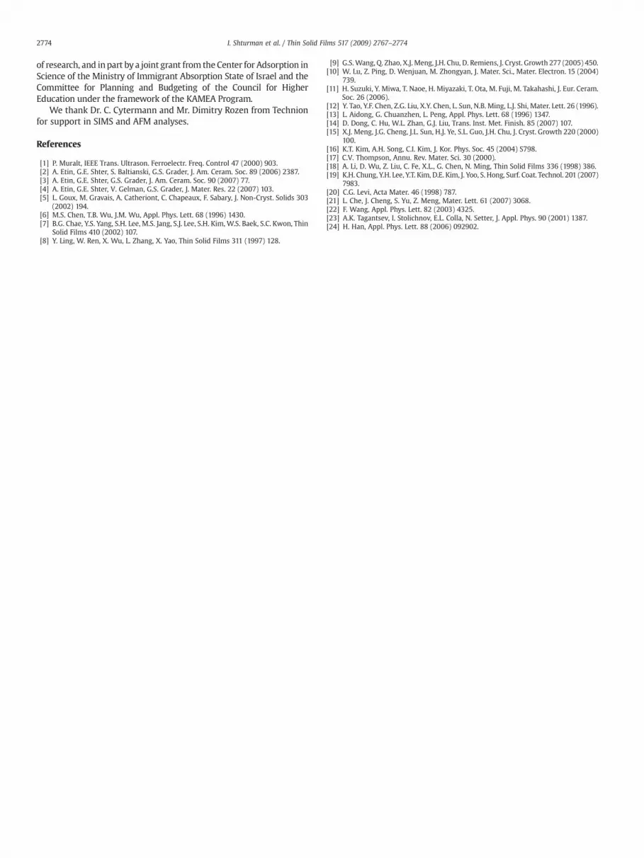
Fig. 10a and b shows the elemental depth profiles of LNO/Si andPZT/LNO/Si, films, respectively. The SIMS analysis was made after finalheat treatments of 700 °C for 20 min and 650 °C for 10 min for theLNO/Si and PZT/LNO/Si systems respectively. Signals from the first 10–20 nm are disregarded since equilibrium is not reached. The x-axis isthe depth into the film, with zero indicating the film outer surface. Asseen in Fig. 10a, no significant penetration of Ni, La and O elementsinto the Si substrate (up to ~20 nm) was observed. The signalsindicating a penetration of Ni, La and O about 20 nm into the Si can beignored due to roughness of the analyzed area that limits the x-axisaccuracy.
As seen in Fig.10b, for the PZT/LNO/Si system, the La and Ni diffusesabout 50 nm into the PZT film. In addition, there is a remarkablediffusion of Pb, Zr and Ti across the entire LNO electrode. This data isconsistent with the morphology of PZT/LNO cross section (Fig. 9a),where the interface was not well defined. The elemental diffusion canbe moderated by lowering the annealing temperature as suggestedpreviously.
3.4. Electrical properties
As discussed above, deposition of 10% excess of PbO in the firstlayer over Pt electrodes results in formation of Py phase (Fig. 6a). It
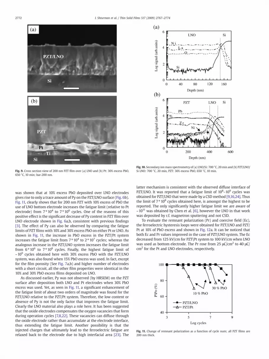
Fig.10. Secondary ionmass spectrometry of (a) LNO/Si: 700 °C, 20min and (b) PZT/LNO/Si LNO: 700 °C, 20 min, PZT: 30% excess PbO, 650 °C, 10 min.Fig. 9. Cross section view of 200 nm PZT film over (a) LNO and (b) Pt: 30% excess PbO,
650 °C, 10 min; bar-200 nm.
Fig. 11. Change of remnant polarization as a function of cycle num; all PZT films are200 nm thick.
2772 I. Shturman et al. / Thin Solid Films 517 (2009) 2767–2774
was shown that at 10% excess PbO deposited over LNO electrodesgives rise to only a trace amount of Py on the PZT/LNO surface (Fig. 6b).Fig. 11, clearly shows that for 200 nm PZT with 10% excess of PbO theuse of LNO bottom electrode increases the fatigue limit (relative to Ptelectrode) from 7⁎104 to 7⁎106 cycles. One of the reasons of thispositive effect is the significant decrease of Py content in PZT film overLNO electrode shown in Fig. 6a,b, consistent with previous findings[3]. The effect of Py can also be observed by comparing the fatiguelimits of PZT filmswith 10% and 30% excess PbO on either Pt or LNO. Asshown in Fig. 11, the increase in PbO excess in the PZT/Pt systemincreases the fatigue limit from 7⁎104 to 2⁎107 cycles; whereas theanalogous increase in the PZT/LNO system increases the fatigue limitfrom 6⁎106 to 7⁎108 cycles. Finally, the highest fatigue limit of~109 cycles obtained here with 30% excess PbO with the PZT/LNOsystem, was also found when 15% PbO excess was used. In fact, exceptfor the film porosity (See Fig. 7a,b) and higher number of electrodeswith a short circuit, all the other film properties were identical in the10% and 30% PbO excess films deposited on LNO.
As discussed earlier, Py was not observed (by HRSEM) on the PZTsurface after deposition both LNO and Pt electrodes when 30% PbOexcess was used. Yet, as seen in Fig. 11, a significant enhancement ofthe fatigue limit of about two orders of magnitude was found for thePZT/LNO relative to the PZT/Pt system. Therefore, the low content orabsence of Py is not the only factor that improves the fatigue limit.Clearly the LNO material also plays a role here. It has been suggestedthat the oxide electrodes compensates the oxygen vacancies that formduring operation cycles [7,8,22]. These vacancies can diffuse throughthe oxide electrode rather than accumulate at the electrode interface,thus extending the fatigue limit. Another possibility is that theinjected charges that ultimately lead to the ferroelectric fatigue arerelaxed back to the electrode due to high interfacial area [23]. The
latter mechanism is consistent with the observed diffuse interface ofPZT/LNO. It was reported that a fatigue limit of 108–109 cycles wasobtained for PZT/LNO that weremade by a CSDmethod [9,16,24]. Thusthe limit of 7⁎108 cycles obtained here, is amongst the highest to bereported. The only significantly higher fatigue limit we are aware of~1011 was obtained by Chen et al. [6], however the LNO in that workwas deposited by r.f. magnetron sputtering and not CSD.
To evaluate the remnant polarization (Pr) and coercive field (Ec),the ferroelectric hysteresis loops were obtained for PZT/LNO and PZT/Pt at 10% of PbO excess and shown in Fig. 12a. It can be noticed thatboth Ec and Pr values improved in the case of PZT/LNO system. The Ecdecreased from 125 kV/cm for PZT\Pt system to 100 kV/cmwhen LNOwas used as bottom electrode. The Pr rose from 25 μC/cm2 to 40 μC/cm2 for the Pt and LNO electrodes, respectively.

Fig. 12. Ferroelectric hysteresis loops for (a) PZT/LNO vs. PZT/Pt systemwith 10% of PbOexcess and (b) PZT/LNO system with 10% and 30% PbO excess.
2773I. Shturman et al. / Thin Solid Films 517 (2009) 2767–2774
The decrease in the Ec value with the LNO electrode can beattributed to lower Py content in comparison to Pt electrode as seen inFig. 6a,b for the 10% excess PbO case. These findings are consistentwith previous work [3] where it was shown that the appearance of Pydegrades the ferroelectric properties of the film. Furthermore, thedecrease in the Ec value can also be related to improved electricalcontact [11] between the PZT film and the LNO electrode.
The hysteresis loops of PZT/LNO with 10% and 30% of PbO excess isshown in Fig. 12b. As the PbO content increases from 10% to 30% the Ecdecreases from 100 kV/cm to 70 kV/cm (Fig. 12b). The Pr increasedfrom 40 μC/cm2 to 50 μC/cm2 for the 10% and 30% PbO excess,respectively. It should be mentioned that the ferroelectric propertiesfor PZT/LNO with 15% and 30% of PbO excess were also examined andfound to be identical. We have also tested the ferroelectric propertiesof PZT/Pt with 30% PbO excess. The Ec value was identical to PZT/LNOin the same conditions but the Pr was 40 μC/cm2 as compared to 50 μC/cm2 in the LNO case.
It should be mentioned that the ferroelectric properties in general,and the Pr values shown in Fig. 12b, in particular, are amongst the bestreported results on CSD derived PZT films. These results support theconfidence in the CSD method as a viable route to obtain high qualityand reliable PZT products.
4. Conclusions
The CSD method was used to prepare both LNO bottom electrodesand overlaying PZT films. The morphology and electrical properties ofLNO electrodes were investigated and the influence on structure andferroelectric properties of PZT/LNO with different PbO excess wereinvestigated in comparison to the PZT/Pt system.
The quantitative dependence of the LNO grain size on the LNOthickness was obtained, where grains grow is proportional to 0.4
power of thickness. A minimal and constant value of the LNO elec-trode resistivity of ~1200 μΩ⁎cm was reached at 75 nm thickness,which indicates that the resistivity reflects is not affected by the grainboundary resistance.
The LNO electrode grain size and thickness significantly influencesthe grain size of the PZT layer: the increase of the LNO grain size by~50% results in an increase of PZTgrain size by ~40%. This effect can beexplained by a decrease in the nucleation density of PZT film on largerLNO grains.
The obtained morphology of PZT/Pt system with 10% PbO excessshowed that more than 50% of the area covered by Py, in contrast toPZT/LNO system where only a trace of Py was detected, under thesame conditions. These results are due to the faster crystallization ofPZT over LNO in comparison with PZT/Pt system. No Py grains wereobserved in both PZT/Pt and PZT/LNOwhen sol with 30% of PbO excesswas deposited, but the PZT/LNO film was found to be porous. Densestructure with no detectable Py phase nor pores was obtained when15% excess of PbO was used in the PZT/LNO system.
The PZT crystalline phase was obtained in ~10 min above 600 °Cregardless of the bottom electrode type. In contrast, at 550 °C PZTcrystallized 4 times faster over LNO than over Pt. In addition,crystallization of PZT over LNO was observed to occur at 500 °Cwhereas theminimal crystallization of PZTwas 550 °C. This significant50 °C reduction in the crystallization temperature is attributed to thehigher affectivity of nucleation of PZT grains over the LNO surface. Thelowest annealing temperature that was reported for dense andcrystalline PZT films by CSD methods was 500 °C.
The interface between PZT and LNO layers was not well defineddue to mutual diffusion of phases, in contrast to the sharply definedinterface between PZT and Pt. The SIMS analysis for LNO/Si showsminor penetration depth of Ni, La and O elements into Si substrate. Incontrast, La and Ni diffuse about 50 nm into the upper PZT film whilewith a remarkable diffusion of Pb, Zr and Ti into the bottom LNOelectrode is observed as well. This effect is surely amplified by thenon-uniform interface where mutual intrusion of PZT and LNO intothe opposing layers seems to take place.
Twomain factors which influence the fatigue limit were discussed:Py content and/or coupling of PZT and LNO films. The fatigueimprovement in PZT/LNO in comparison with PZT/Pt system from7⁎104 to 7⁎106 cycles at 10% excess of PbO was found and explainedby significant decrease of Py content. On the other hand, at 30% PbOexcess the Py was not observed in either system, but the fatigue limitwas enhanced by about two orders of magnitude for the PZT/LNOrelative to the PZT/Pt system. This improvement can be associatedwith the direct influence of LNO material via compensation of theoxygen vacancies at the interface of the PZT.
BothEc and Pr values improved for PZT/LNO in comparisonwithPZT/Pt when 10% of PbO excess was used. The Ec decreased from 125 kV/cmto 100kV/cmwhen LNOwasused asbottomelectrode. In addition the Prrose from 25 to 40 μC/cm2 in PZT/LNO system. The decrease in the Ecvalue in the caseof PZT/LNO, canbe contributed to less Pycontent. As thePbOexcess increased from10% to 30% in PZT/LNO, the Ec decreased from100 to 70 kV/cm and the Pr increased from 40 μC/cm2 to 50 μC/cm2,respectively. The ferroelectric properties of PZT/LNOfilms preparedwith15% and 30% of PbO excess were found to be identical.
In summary, this comprehensive investigation outlines the optimalprocessing conditions and precursors composition for an all-CSDmethod, required for preparation of PZT/LNO films with a densemorphology and improved ferroelectric properties. Additional work isrequired on possible further enhancement of the ferroelectric proper-ties of PZT films prepared at 500–550 °C using LNO bottom electrodes.
Acknowledgements
This investigation was supported by the MOEMS Consortium of theIsrael Ministry of Industry and Trade, Technion's fund for the promotion
2774 I. Shturman et al. / Thin Solid Films 517 (2009) 2767–2774
of research, and inpart by a joint grant from the Center for Adsorption inScience of the Ministry of Immigrant Absorption State of Israel and theCommittee for Planning and Budgeting of the Council for HigherEducation under the framework of the KAMEA Program.
We thank Dr. C. Cytermann and Mr. Dimitry Rozen from Technionfor support in SIMS and AFM analyses.
References
[1] P. Muralt, IEEE Trans. Ultrason. Ferroelectr. Freq. Control 47 (2000) 903.[2] A. Etin, G.E. Shter, S. Baltianski, G.S. Grader, J. Am. Ceram. Soc. 89 (2006) 2387.[3] A. Etin, G.E. Shter, G.S. Grader, J. Am. Ceram. Soc. 90 (2007) 77.[4] A. Etin, G.E. Shter, V. Gelman, G.S. Grader, J. Mater. Res. 22 (2007) 103.[5] L. Goux, M. Gravais, A. Catheriont, C. Chapeaux, F. Sabary, J. Non-Cryst. Solids 303
(2002) 194.[6] M.S. Chen, T.B. Wu, J.M. Wu, Appl. Phys. Lett. 68 (1996) 1430.[7] B.G. Chae, Y.S. Yang, S.H. Lee, M.S. Jang, S.J. Lee, S.H. Kim, W.S. Baek, S.C. Kwon, Thin
Solid Films 410 (2002) 107.[8] Y. Ling, W. Ren, X. Wu, L. Zhang, X. Yao, Thin Solid Films 311 (1997) 128.
[9] G.S.Wang, Q. Zhao, X.J. Meng, J.H. Chu, D. Remiens, J. Cryst. Growth 277 (2005) 450.[10] W. Lu, Z. Ping, D. Wenjuan, M. Zhongyan, J. Mater. Sci., Mater. Electron. 15 (2004)
739.[11] H. Suzuki, Y. Miwa, T. Naoe, H. Miyazaki, T. Ota, M. Fuji, M. Takahashi, J. Eur. Ceram.
Soc. 26 (2006).[12] Y. Tao, Y.F. Chen, Z.G. Liu, X.Y. Chen, L. Sun, N.B. Ming, L.J. Shi, Mater. Lett. 26 (1996).[13] L. Aidong, G. Chuanzhen, L. Peng, Appl. Phys. Lett. 68 (1996) 1347.[14] D. Dong, C. Hu, W.L. Zhan, G.J. Liu, Trans. Inst. Met. Finish. 85 (2007) 107.[15] X.J. Meng, J.G. Cheng, J.L. Sun, H.J. Ye, S.L. Guo, J.H. Chu, J. Cryst. Growth 220 (2000)
100.[16] K.T. Kim, A.H. Song, C.I. Kim, J. Kor. Phys. Soc. 45 (2004) S798.[17] C.V. Thompson, Annu. Rev. Mater. Sci. 30 (2000).[18] A. Li, D. Wu, Z. Liu, C. Fe, X.L., G. Chen, N. Ming, Thin Solid Films 336 (1998) 386.[19] K.H. Chung, Y.H. Lee, Y.T. Kim, D.E. Kim, J. Yoo, S. Hong, Surf. Coat. Technol. 201 (2007)
7983.[20] C.G. Levi, Acta Mater. 46 (1998) 787.[21] L. Che, J. Cheng, S. Yu, Z. Meng, Mater. Lett. 61 (2007) 3068.[22] F. Wang, Appl. Phys. Lett. 82 (2003) 4325.[23] A.K. Tagantsev, I. Stolichnov, E.L. Colla, N. Setter, J. Appl. Phys. 90 (2001) 1387.[24] H. Han, Appl. Phys. Lett. 88 (2006) 092902.


