Embed Size (px)
Citation preview

MF761-03
CMOS 4-BIT SINGLE CHIP MICROCOMPUTER
E0C6256 TECHNICAL MANUAL
E0C6256 Technical Hardware
E0C6256 Technical Software

NOTICE
No part of this material may be reproduced or duplicated in any form or by any means without the writtenpermission of Seiko Epson. Seiko Epson reserves the right to make changes to this material without notice.Seiko Epson does not assume any liability of any kind arising out of any inaccuracies contained in this materialor due to its application or use in any product or circuit and, further, there is no representation that this materialis applicable to products requiring high level reliability, such as medical products. Moreover, no license to anyintellectual property rights is granted by implication or otherwise, and there is no representation or warranty thatanything made in accordance with this material will be free from any patent or copyright infringement of a thirdparty. This material or portions thereof may contain technology or the subject relating to strategic products underthe control of the Foreign Exchange and Foreign Trade Law of Japan and may require an export license fromthe Ministry of International Trade and Industry or other approval from another government agency. Please notethat "E0C" is the new name for the old product "SMC". If "SMC" appears in other manuals understand that itnow reads "E0C".
© SEIKO EPSON CORPORATION 2000 All rights reserved.

PREFACE
This manual is individualy described about the hardware and the software of theE0C6256.
So
ftw
are
Har
dw
are
II. E0C6256 Technical SoftwareThis part explains the programming method of the principal functions of theE0C6256.
I. E0C6256 Technical HardwareThis part explains the function of the E0C6256, the circuit configurations, anddetails the controlling method.


Har
dw
areE0C6256I. Technical Hardware

Har
dw
are
E0C6256 TECHNICAL HARDWARE EPSON I-i
CONTENTS
CONTENTS
CHAPTER 1 OVERVIEW _______________________________________________ I-11.1 Features ....................................................................................................... I-1
1.2 Block Diagram ............................................................................................. I-2
1.3 Pin Layout Diagram..................................................................................... I-3
1.4 Pin Description ............................................................................................ I-4
CHAPTER 2 POWER SUPPLY AND INITIAL RESET ____________________________ I-52.1 Power Supply ............................................................................................... I-5
2.1.1 Supply voltage doubler/halver and operating mode .................................. I-62.1.2 Voltage <VS1> for oscillation circuit and internal circuits ...................... I-62.1.3 Voltage <VL1, VL2 and VL3> for LCD driving .......................................... I-6
2.2 Initial Reset .................................................................................................. I-72.2.1 Reset terminal (RESET) ............................................................................. I-72.2.2 Simultaneous high input to terminals K00–K03 ........................................ I-72.2.3 Oscillation detection circuit ....................................................................... I-82.2.4 Watchdog timer .......................................................................................... I-82.2.5 Internal register at initial resetting ........................................................... I-8
2.3 Test Terminals (TEST, CP) .......................................................................... I-8
CHAPTER 3 CPU, ROM, RAM________________________________________ I-93.1 CPU .............................................................................................................. I-9
3.2 ROM ............................................................................................................. I-9
3.3 RAM ............................................................................................................. I-9
CHAPTER 4 PERIPHERAL CIRCUITS AND OPERATION ________________________ I-104.1 Memory Map ............................................................................................... I-10
4.2 Power Supply and Operating Mode Settings .............................................. I-184.2.1 Operating mode ........................................................................................ I-184.2.2 LCD drive voltage ..................................................................................... I-194.2.3 Control of power supply and operating mode .......................................... I-194.2.4 Programming notes ................................................................................... I-20
4.3 Resetting Watchdog Timer .......................................................................... I-214.3.1 Configuration of watchdog timer .............................................................. I-214.3.2 Mask option ............................................................................................... I-214.3.3 Control of watchdog timer ........................................................................ I-214.3.4 Programming note .................................................................................... I-21
4.4 Oscillation Circuit .......................................................................................I-224.4.1 Configuration of oscillation circuit .......................................................... I-224.4.2 OSC1 oscillation circuit ............................................................................ I-224.4.3 OSC3 oscillation circuit ............................................................................ I-224.4.4 Operating voltage switching ..................................................................... I-234.4.5 Clock frequency and instruction execution time ....................................... I-234.4.6 Control of oscillation circuit ..................................................................... I-244.4.7 Programming notes ................................................................................... I-25
4.5 Input Ports (K00–K03, K10–K13) .............................................................. I-264.5.1 Configuration of input ports ..................................................................... I-264.5.2 Interrupt function ...................................................................................... I-264.5.3 Mask option ............................................................................................... I-274.5.4 Control of input ports ............................................................................... I-284.5.5 Programming notes ................................................................................... I-30

I-ii EPSON E0C6256 TECHNICAL HARDWARE
CONTENTS
4.6 Output Ports (R00–R03, R10–R13) ............................................................ I-314.6.1 Configuration of output ports ................................................................... I-314.6.2 Mask option ............................................................................................... I-314.6.3 High impedance control ............................................................................ I-314.6.4 Special output ........................................................................................... I-314.6.5 Control of output ports ............................................................................. I-334.6.6 Programming notes ................................................................................... I-34
4.7 I/O Ports (P00–P03, P10–P13) .................................................................. I-354.7.1 Configuration of I/O ports ........................................................................ I-354.7.2 I/O control registers and input/output mode ............................................ I-354.7.3 Pull down during input mode .................................................................... I-354.7.4 Mask option ............................................................................................... I-354.7.5 Control of I/O ports .................................................................................. I-364.7.6 Programming note .................................................................................... I-37
4.8 LCD Driver (COM0–COM4, SEG0–SEG59) ............................................. I-384.8.1 Configuration of LCD driver .................................................................... I-384.8.2 LCD drive voltage ..................................................................................... I-384.8.3 LCD display ON/OFF control and duty switching ................................... I-394.8.4 Switching between dynamic and static drive ............................................ I-434.8.5 Display memory area ................................................................................ I-434.8.6 Mask option (segment allocation) ............................................................. I-444.8.7 Control of LCD driver .............................................................................. I-454.8.8 Programming notes ................................................................................... I-47
4.9 Clock Timer ................................................................................................. I-484.9.1 Configuration of clock timer ..................................................................... I-484.9.2 Data reading and hold function ................................................................ I-484.9.3 Interrupt function ...................................................................................... I-484.9.4 Control of clock timer ............................................................................... I-494.9.5 Programming notes ................................................................................... I-51
4.10 Stopwatch Timer ......................................................................................... I-524.10.1 Configuration of stopwatch timer ........................................................... I-524.10.2 Counter and prescaler ............................................................................ I-524.10.3 Capture buffer and hold function ............................................................ I-534.10.4 Stopwatch timer RUN/STOP and reset ................................................... I-534.10.5 Direct input function and key mask ........................................................ I-544.10.6 Interrupt function .................................................................................... I-564.10.7 Control of stopwatch timer ..................................................................... I-584.10.8 Programming notes ................................................................................. I-61
4.11 Programmable Timer .................................................................................. I-624.11.1 Configuration of programmable timer ................................................... I-624.11.2 Input clock and prescaler ....................................................................... I-624.11.3 Operation of programmable timer .......................................................... I-634.11.4 Interrupt function .................................................................................... I-644.11.5 Control of programmable timer .............................................................. I-654.11.6 Programming notes ................................................................................. I-67
4.12 Serial Interface (SIN, SOUT, SCLK, SRDY) ............................................... I-684.12.1 Configuration of serial interface ............................................................ I-684.12.2 Master mode and slave mode of serial interface .................................... I-694.12.3 Data input/output and interrupt function ................................................ I-704.12.4 Mask option ............................................................................................. I-714.12.5 Control of serial interface ....................................................................... I-724.12.6 Programming notes ................................................................................. I-75
4.13 Sound Generator ......................................................................................... I-764.13.1 Configuration of sound generator .......................................................... I-764.13.2 Control of buzzer output ......................................................................... I-764.13.3 Setting of buzzer frequency and sound level ........................................... I-774.13.4 Digital envelope ...................................................................................... I-78

Har
dw
are
E0C6256 TECHNICAL HARDWARE EPSON I-iii
CONTENTS
4.13.5 One-shot output ....................................................................................... I-784.13.6 Control of sound generator ..................................................................... I-794.13.7 Programming notes ................................................................................. I-81
4.14 A/D Converter .............................................................................................I-824.14.1 Configuration of A/D converter .............................................................. I-824.14.2 CR oscillation circuit .............................................................................. I-824.14.3 Operation of A/D conversion .................................................................. I-854.14.4 Interrupt function .................................................................................... I-884.14.5 Control of A/D converter ........................................................................ I-894.14.6 Programming notes ................................................................................. I-93
4.15 SVD (Supply Voltage Detection) Circuit .................................................... I-944.15.1 Configuration of SVD circuit .................................................................. I-944.15.2 Mask option ............................................................................................. I-944.15.3 SVD operation ......................................................................................... I-944.15.4 Control of SVD circuit ............................................................................ I-954.15.5 Programming notes ................................................................................. I-96
4.16 Interrupt and HALT .................................................................................... I-974.16.1 Interrupt factor ....................................................................................... I-994.16.2 Interrupt mask ......................................................................................... I-994.16.3 Interrupt vector ...................................................................................... I-1004.16.4 Control of interrupt ................................................................................ I-1004.16.5 Programming notes ................................................................................ I-102
CHAPTER 5 SUMMARY OF NOTES ______________________________________ I-1035.1 Notes for Low Current Consumption ......................................................... I-103
5.2 Summary of Notes by Function .................................................................. I-104
CHAPTER 6 DIAGRAM OF BASIC EXTERNAL CONNECTIONS ____________________ I-108
CHAPTER 7 ELECTRICAL CHARACTERISTICS _______________________________ I-1097.1 Absolute Maximum Rating ......................................................................... I-109
7.2 Recommended Operating Conditions ........................................................ I-109
7.3 DC Characteristics .................................................................................... I-110
7.4 Analog Characteristics and Consumed Current ........................................ I-111
7.5 Oscillation Characteristics ........................................................................ I-112
7.6 Characteristics Curves ............................................................................... I-113
CHAPTER 8 PACKAGE _______________________________________________ I-1168.1 Plastic Package .......................................................................................... I-116
8.2 Ceramic Package for Test Samples ........................................................... I-118
CHAPTER 9 PAD LAYOUT ____________________________________________ I-1199.1 Diagram of Pad Layout .............................................................................. I-119
9.2 Pad Coordinates ........................................................................................ I-120


E0C6256 TECHNICAL HARDWARE EPSON I-1
CHAPTER 1: OVERVIEW
CHAPTER 1 OVERVIEWThe E0C6256 is a single-chip microcomputer made up of the 4-bit core CPU E0C6200A, ROM (6,144 words,12 bits to a word), RAM (640 words, 4 bits to a word), A/D converter (R/f conversion type), SVD circuit,LCD driver, serial interface, watchdog timer, programmable timer and time base counter.It can realize system to measure temperature and humidity by the internal A/D converter and externallyattached parts.Because of its low-voltage operation and low power consumption, this series is ideal for a wide range ofapplications, and is especially suitable for battery-driven systems.
1.1 Features
OSC1 oscillation circuit ...... Crystal oscillation circuit: 32.768 kHz (Typ.)
OSC3 oscillation circuit ...... CR or ceramic oscillation circuit (*1): 1 MHz (Typ.)
Instruction set ..................... 108 types
Instruction execution time .. During operation at 32 kHz: 153 µsec, 214 µsec, 366 µsec(differ depending on instruction) During operation at 1 MHz: 5 µsec, 7 µsec, 12 µsec
ROM capacity ..................... 6,144 words × 12 bits
RAM capacity ..................... 640 words × 4 bits
Input port ............................ 8 bits (pull down resistors may be supplemented *1)
Output port ......................... 8 bits (BZ, FOUT and PTOVF outputs are possible *2)
I/O port ............................... 8 bits (4 bits are shared with serial input/output port *2)
Serial interface ................... 1 port (8 bits serial, synchronous type clock)
A/D converter ..................... R/f (resistance/frequency) conversion type, 2 channels
LCD driver .......................... 60 segments × 5 / 4 / 3 / 2 commons (*2)LCD drive voltage: 1.05 to 1.40 V, programmable (0.05 V unit)
Time base counter ............. Clock timer: 1 system1/1000 sec stopwatch timer: 1 system
Programmable timer........... Built-in, 1 input × 8 bits, with event counter function
Watchdog timer .................. Built-in (It is possible to exclude *1)
SVD circuit ......................... 1.05 / 1.20 / 1.35 V, programmable (for 1.5 V system, *1)(supply voltage detection) 2.30 / 2.45 / 2.60 V, programmable (for 3.0 V system, *1)
External interrupt ................ Input port interrupt: 2 systems
Internal interrupt ................. Timer interrupt: 3 systemsSerial interface interrupt: 1 systemA/D converter interrupt: 1 system
Supply voltage.................... 0.9–3.6 V (2.2–3.6 V when OSC3 is used, 1.3–3.6 V when A/D converter is used)
Current consumption .......... During HALT: 1.2 µA (1.5 V, 32 kHz, normal mode)(Typ.) 650 nA (3 V, 32 kHz, halver mode)
During operation: 3.5 µA (1.5 V, 32 kHz, normal mode)2.0 µA (3 V, 32 kHz, halver mode)170 µA (3 V, 1 MHz ceramic oscillation)220 µA (3 V, 1 MHz CR oscillation)
Package ............................. QFP5-128pin / QFP5-100pin (plastic) or chip
*1 May be selected with mask option.*2 May be selected with software.

I-2 EPSON E0C6256 TECHNICAL HARDWARE
CHAPTER 1: OVERVIEW
1.2 Block Diagram
COM0–4SEG0–59
OS
C1
OS
C2
RE
SE
T
RAM640 words x 4 bits
ROM6,144 words x 12 bits OSC System Reset
Control
InterruptGenerator
OS
C3
OS
C4
R00–03R10–13
P00–03P10–13
Output Port
I/O Port
Timer
Stopwatch
ProgrammableTimer/Counter
Serial Interface
LCD Driver
Power Controller
SVD
A/D Converter(2 ch)
VDDVL1–3
CA–CDVS1VS2VSS
CPST0CM0SN0WETST1CM1SN1
ADOUTSound
Generator
K00–03K10–13TEST
Input PortTEST Port
Core CPU E0C6200A
Fig. 1.2.1 Block diagram

E0C6256 TECHNICAL HARDWARE EPSON I-3
CHAPTER 1: OVERVIEW
1.3 Pin Layout Diagram
QFP5-128pin (plastic)
1234567891011121314151617181920212223242526272829303132
N.C.SEG27SEG28SEG29COM0COM1COM2COM3COM4CBCAVL3
VL2
VL1
CCCDVS2
VSS
ADOUTSN1WETST1CM1SN0CM0ST0CPVDD
N.C.OSC1OSC2OSC3
Pin No. Pin name
3334353637383940414243444546474849505152535455565758596061626364
OSC4VS1
SEG30SEG31SEG32N.C.N.C.SEG33SEG34SEG35SEG36SEG37SEG38SEG39SEG40SEG41SEG42SEG43SEG44SEG45SEG46SEG47SEG48SEG49SEG50SEG51SEG52SEG53SEG54SEG55SEG56SEG57
Pin No. Pin name
6566676869707172737475767778798081828384858687888990919293949596
SEG58SEG59N.C.N.C.N.C.VDD
RESETTESTK00K01K02K03K10K11K12K13R00R01R02R03R10R11R12R13P00P01P02P03P10P11P12P13
Pin No. Pin name
979899100101102103104105106107108109110111112113114115116117118119120121122123124125126127128
VSS
N.C.N.C.N.C.SEG0SEG1SEG2SEG3SEG4SEG5SEG6SEG7SEG8SEG9SEG10SEG11SEG12SEG13SEG14SEG15SEG16SEG17SEG18SEG19SEG20SEG21SEG22SEG23SEG24SEG25SEG26N.C.
Pin No. Pin name
1 38
39
64
102 65
128
103
Index
Fig. 1.3.1 Pin layout diagram (QFP5-128pin)
QFP5-100pin (plastic)
12345678910111213141516171819202122232425
SEG29COM0COM1COM2COM3COM4CBCAVL3
VL2
VL1
CCCDVS2
ADOUTSN1WETST1CM1SN0CM0ST0CPVDD
OSC1
26272829303132333435363738394041424344454647484950
OSC2OSC3OSC4VS1
SEG30SEG31SEG32SEG34SEG36SEG38SEG40SEG41SEG42SEG43SEG44SEG45SEG46SEG47SEG48SEG49SEG51SEG53SEG55SEG57SEG58
51525354555657585960616263646566676869707172737475
SEG59VDD
RESETTESTK00K01K02K03K10K11K12K13R00R01R02R03R10R11R12R13P00P01P02P03P10
767778798081828384858687888990919293949596979899100
P11P12P13VSS
SEG0SEG1SEG2SEG4SEG6SEG8SEG10SEG12SEG13SEG14SEG15SEG16SEG17SEG18SEG19SEG21SEG23SEG25SEG26SEG27SEG28
Pin No. Pin name Pin No. Pin name Pin No. Pin name Pin No. Pin name
Index
1 30
31
50
80 51
100
81
Fig. 1.3.2 Pin layout diagram (QFP5-100pin)

I-4 EPSON E0C6256 TECHNICAL HARDWARE
CHAPTER 1: OVERVIEW
1.4 Pin Description
Table 1.4.1 Pin description
VDD
VSS
VS1
VS2
VL1
VL2
VL3
CA, CB
CC, CD
OSC1
OSC2
OSC3
OSC4
K00–K03
K10–K13
P00–P03
P10–P13
R00–R03
R10–R13
COM0–COM4
SEG0–SEG59*
CP
ST0
CM0
SN0
WET
ST1
CM1
SN1
ADOUT
RESET
TEST
Pin name
(I)
(I)
O
O
O
O
O
–
–
I
O
I
O
I
I
I/O
I/O
O
O
O
O
O
O
O
I
O
O
O
I
O
I
I
In/Out
Power supply pin (+)
Power supply pin (–)
Oscillation and internal logic system regulated voltage output pin
Supply voltage doubler/halver output pin
LCD system regulated voltage output pin
LCD system booster voltage output pin (VL1 × 2)
LCD system booster voltage output pin (VL1 × 3)
LCD system voltage booster capacitor connecting pin
Supply voltage doubler/halver capacitor connecting pin
Crystal oscillation input pin
Crystal oscillation output pin
Ceramic or CR oscillation input pin (selected by mask option)
Ceramic or CR oscillation output pin (selected by mask option)
Input port pin
Input port pin
I/O port pin
I/O port pin (switching to SIN, SOUT, SCLK, SRDY pin is possible by software)
Output port pin
Output port pin (switching to BZ, PTOVF, FOUT output is possible by software)
LCD common output pin (1/5, 1/4, 1/3, 1/2 duty, programmable)
LCD segment output pin (DC output may be selected by mask option)
A/D converter test output pin
A/D converter CH0 CR oscillation output pin
A/D converter CH0 CR oscillation output pin
A/D converter CH0 CR oscillation input pin
A/D converter CH1 CR oscillation output pin
A/D converter CH1 CR oscillation output pin
A/D converter CH1 CR oscillation output pin
A/D converter CH1 CR oscillation input pin
A/D converter oscillation frequency output pin
Initial reset input pin
Testing input pin
Function
28, 70
18, 97
34
17
14
13
12
11, 10
15, 16
30
31
32
33
73–76
77–80
89–92
93–96
81–84
85–88
5–9
101–127, 2–4
35–37, 40–66
27
26
25
24
21
22
23
20
19
71
72
QFP5-128pin
Pin No.
QFP5-100pin
24, 52
79
29
14
11
10
9
8, 7
12, 13
25
26
27
28
55–58
59–62
71–74
75–78
63–66
67–70
2–6
80–100
1, 30–51
23
22
21
20
17
18
19
16
15
53
54
* The following SEG pins are not included in the QFP5-100pin package, so they cannot be used.
SEG3, SEG5, SEG7, SEG9, SEG11, SEG20, SEG22, SEG24, SEG33, SEG35, SEG37, SEG39,SEG50, SEG52, SEG54, SEG56

E0C6256 TECHNICAL HARDWARE EPSON I-5
CHAPTER 2: POWER SUPPLY AND INITIAL RESET
CHAPTER 2 POWER SUPPLY AND INITIAL RESET
2.1 Power SupplyThe E0C6256 operating power voltage is as follows:
0.9 V to 3.6 V
Note: • When using a supply voltage within the range of 0.9 to 1.4 V, it is necessary to use software tocontrol it.
• When using the OSC3 oscillation circuit, a supply voltage within the range of 2.2 to 3.6 V isrequired.
• When using the A/D converter, a supply voltage within the range of 1.3 to 3.6 V is required.
The E0C6256 operates when a single power supply within the above range is applied between VDD andVSS. The IC itself can generate the voltage necessary for the internal circuits with the following built-inpower supply circuit.
Circuit
Oscillation and internal circuits
LCD driver
Oscillation system regulated voltage circuit,
LCD system regulated voltage circuit
Power supply circuit
Oscillation system regulated voltage circuit
LCD system regulated voltage circuit
Supply voltage doubler/halver circuit
Output voltage
VS1
VL1–VL3
VS2
Note: • External loads cannot be driven by the regulated voltage, voltage booster and voltage doubler/halver circuits' output voltages.
• See Chapter 7, "ELECTRICAL CHARACTERISTICS" for voltage values.
Externalpowersupply
Internalcircuit
Oscillationcircuit
LCD systemvoltage booster
circuit
LCD systemregulated voltage
circuit
Oscillation systemregulated voltage
circuit
VDD
V
VL2
V L3
CACB
VL1
VL2
V L3
V
VL1
OSC1–4
COM0–4
SEG0–59
S1
S1
VL1
LCDdriver
VSS
Supply voltagedoubler/halver
circuit
VS2
CCCD
VS2
+
Fig. 2.1.1 Configuration of power supply
I-6 EPSON E0C6256 TECHNICAL HARDWARE
CHAPTER 2: POWER SUPPLY AND INITIAL RESET
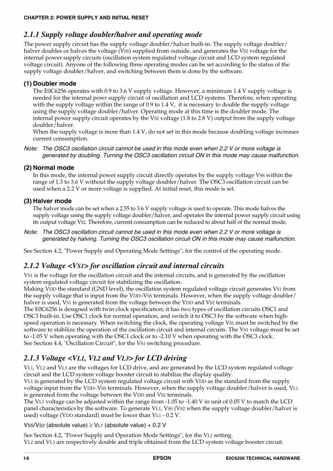
2.1.1 Supply voltage doubler/halver and operating modeThe power supply circuit has the supply voltage doubler/halver built-in. The supply voltage doubler/halver doubles or halves the voltage (VSS) supplied from outside, and generates the VS2 voltage for theinternal power supply circuits (oscillation system regulated voltage circuit and LCD system regulatedvoltage circuit). Anyone of the following three operating modes can be set according to the status of thesupply voltage doubler/halver, and switching between them is done by the software.
(1) Doubler modeThe E0C6256 operates with 0.9 to 3.6 V supply voltage. However, a minimum 1.4 V supply voltage isneeded for the internal powr supply circuit of oscillation and LCD systems. Therefore, when operatingwith the supply voltage within the range of 0.9 to 1.4 V, it is necessary to double the supply voltageusing the supply voltage doubler/halver. Operating mode at this time is the doubler mode. Theinternal power supply circuit operates by the VS2 voltage (1.8 to 2.8 V) output from the supply voltagedoubler/halver.When the supply voltage is more than 1.4 V, do not set in this mode because doubling voltage increasescurrent consumption.
Note: The OSC3 oscillation circuit cannot be used in this mode even when 2.2 V or more voltage isgenerated by doubling. Turning the OSC3 oscillation circuit ON in this mode may cause malfunction.
(2) Normal modeIn this mode, the internal power supply circuit directly operates by the supply voltage VSS within therange of 1.3 to 3.6 V without the supply voltage doubler/halver. The OSC3 oscillation circuit can beused when a 2.2 V or more voltage is supplied. At initial reset, this mode is set.
(3) Halver modeThe halver mode can be set when a 2.55 to 3.6 V supply voltage is used to operate. This mode halves thesupply voltage using the supply voltage doubler/halver, and operates the internal power supply circuit usingits output voltage VS2. Therefore, current consumption can be reduced to about half of the normal mode.
Note: The OSC3 oscillation circuit cannot be used in this mode even when 2.2 V or more voltage isgenerated by halving. Turning the OSC3 oscillation circuit ON in this mode may cause malfunction.
See Section 4.2, "Power Supply and Operating Mode Settings", for the control of the operating mode.
2.1.2 Voltage <VS1> for oscillation circuit and internal circuitsVS1 is the voltage for the oscillation circuit and the internal circuits, and is generated by the oscillationsystem regulated voltage circuit for stabilizing the oscillation.Making VDD the standard (GND level), the oscillation system regulated voltage circuit generates VS1 fromthe supply voltage that is input from the VDD–VSS terminals. However, when the supply voltage doubler/halver is used, VS1 is generated from the voltage between the VDD and VS2 terminals.The E0C6256 is designed with twin clock specification; it has two types of oscillation circuits OSC1 andOSC3 built-in. Use OSC1 clock for normal operation, and switch it to OSC3 by the software when high-speed operation is necessary. When switching the clock, the operating voltage VS1 must be switched by thesoftware to stabilize the operation of the oscillation circuit and internal circuits. The VS1 voltage must be setto -1.05 V when operating with the OSC1 clock or to -2.10 V when operating with the OSC3 clock.See Section 4.4, "Oscillation Circuit", for the VS1 switching procedure.
2.1.3 Voltage <VL1, VL2 and VL3> for LCD drivingVL1, VL2 and VL3 are the voltages for LCD drive, and are generated by the LCD system regulated voltagecircuit and the LCD system voltage booster circuit to stabilize the display quality.VL1 is generated by the LCD system regulated voltage circuit with VDD as the standard from the supplyvoltage input from the VDD–VSS terminals. However, when the supply voltage doubler/halver is used, VL1is generated from the voltage between the VDD and VS2 terminals.The VL1 voltage can be adjusted within the range from -1.05 to -1.40 V in unit of 0.05 V to match the LCDpanel characteristics by the software. To generate VL1, VSS (VS2 when the supply voltage doubler/halver isused) voltage (VDD standard) must be lower than VL1 - 0.2 V.
VSS/VS2 (absolute value) ≥ VL1 (absolute value) + 0.2 V
See Section 4.2, "Power Supply and Operation Mode Settings", for the VL1 setting.VL2 and VL3 are respectively double and triple obtained from the LCD system voltage booster circuit.

E0C6256 TECHNICAL HARDWARE EPSON I-7
CHAPTER 2: POWER SUPPLY AND INITIAL RESET
2.2 Initial ResetTo initialize the E0C6256 circuits, initial reset must be executed. There are four ways of doing this.
(1) External initial reset by the RESET terminal(2) External initial reset by simultaneous high input to terminals K00–K03 (mask option setting)(3) Initial reset by the oscillation detection circuit(4) Initial reset by the watchdog timer (mask option setting)
Be sure to use reset functions (1) or (2) when turning the power on and be sure to initialize securely. Innormal operation, the circuit may be initialized by any of the above four types.
Figure 2.2.1 shows the configuration of the initial reset circuit.
Fig. 2.2.1 Configuration of the initial reset circuit
2.2.1 Reset terminal (RESET)Initial reset can be executed externally by setting the reset terminal to a high level. However, be sure toobserve the following precautions, because the RESET signal passes through the noise reject circuit.When the reset terminal is used for initial resetting during operation, a pulse (high level) of 0.4 msec or lessis considered to be noise by the noise reject circuit. Maintain a high level of 1.5 msec (when the oscillationfrequency fOSC1 = 32 kHz) to securely perform the initial reset. When the reset terminal goes low, the CPUbegins to operate.Since the noise reject circuit does not operate when oscillation is stopped, the noise reject circuit is bypasseduntil it starts oscillation. For this reason, be sure to maintain a high level the reset input in the oscillationstopped status, such as at power-on, until starting oscillation.
2.2.2 Simultaneous high input to terminals K00–K03Another way of executing initial reset externally is to input a high signal simultaneously to the input ports(K00–K03) selected with the mask option.Since this initial reset also passes through the same noise reject circuit as the reset terminal, you shouldmaintain the specified input port terminal at high level for 1.5 msec (when oscillation frequency fOSC1 = 32kHz) or more during operation and until it begins oscillation at times such as when turning the power on.Table 2.2.2.1 shows the combinations of input ports (K00–K03) that can be selected with the mask option.
Table 2.2.2.1 Combinations of input portsWhen, for instance, mask option 2 (K00*K01*K02*K03) isselected, initial reset is executed when the signals input to thefour ports K00–K03 are all high at the same time. The initialreset is done, even when a key entry including a combination ofselected input ports is made.
Further, the time authorize circuit can be selected with the mask option. The time authorize circuit per-forms initial reset, when the input time of the simultaneous high input is authorized and found to be thesame or more than the defined time (1 to 2 sec).If you use this function, make sure that the specified ports do not go high at the same time during ordinaryoperation.
1
2
3
4
Not use
K00*K01*K02*K03
K00*K01*K02
K00*K01
RESET
K00
K01
K02
K03
OSC2
OSC1 OSC1oscillation
circuit
Noiserejectcircuit
Initialreset
Timeauthorize
circuit
Oscillationdetection circuit
Watchdogtimer
VSSMask option
When oscillationstops: HIGH
VSS VSS
VSS

I-8 EPSON E0C6256 TECHNICAL HARDWARE
CHAPTER 2: POWER SUPPLY AND INITIAL RESET
2.2.3 Oscillation detection circuitThe oscillation detection circuit outputs the initial reset signal at power-on until the oscillation circuit startsoscillating, or when the oscillation circuit stops oscillating for some reason.However, this circuit may not operate properly depending on the power-on procedure. Consequently, usea simultaneous high input of the input ports (K00–K03) or reset terminal for the initial reset at power-onand you should not execute it by this function alone.
2.2.4 Watchdog timerIf the CPU runs away for some reason, the watchdog timer will detect this situation and output an initialreset signal. See Section 4.3, "Resetting Watchdog Timer", for details.As with the oscillation detection circuit, you should not do an initial reset at power-on using this function.
2.2.5 Internal register at initial resettingInitial reset initializes the CPU as shown in the table below.
Table 2.2.5.1 Initial values
Program counter step
Program counter page
Program counter bank
New page pointer
New bank pointer
Stack pointer
Index register IX
Index register IY
Register pointer
General-purpose register A
General-purpose register B
Interrupt flag
Decimal flag
Zero flag
Carry flag
CPU core
Name Number of bits
8
4
1
4
1
8
11
11
4
4
4
1
1
1
1
Setting value
00H
1H
0
1H
0
Undefined
Undefined
Undefined
Undefined
Undefined
Undefined
0
0
Undefined
Undefined
Symbol
PCS
PCP
PCB
NPP
NBP
SP
IX
IY
RP
A
B
I
D
Z
C
RAM
Display memory
Other peripheral circuits
Peripheral circuits
Name Number of bits
4
4
—
Setting value
Undefined
Undefined
*
* See Section 4.1, "Memory Map".
2.3 Test Terminals (TEST, CP)These terminals are used at the time of the factory inspection of the IC. During normal operation, connectthe TEST to VSS, and do not connect anything to the CP terminal.

E0C6256 TECHNICAL HARDWARE EPSON I-9
CHAPTER 3: CPU, ROM, RAM
CHAPTER 3 CPU, ROM, RAM3.1 CPUThe E0C6256 employs the 4-bit core CPU E0C6200A for the CPU, so that register configuration, instructionsand so forth are virtually identical to those in other family processors using the E0C6200A.Refer to "E0C6200/6200A Core CPU Manual" for details about the E0C6200A.Note the following points with regard to the E0C6256:
(1) The SLEEP operation is not assumed, so the SLP instruction cannot be used.
(2) RAM is set up to five pages, so only the three low-order bits are valid for the page portion (XP, YP) ofthe index register that specifies addresses. (The one high-order bit is ignored.)
3.2 ROMThe built-in ROM, a mask ROM for loading the program, has a capacity of 6,144 steps, 12 bits each. Theprogram area is divided into two banks. Bank 0 is configured of 16 pages (0–15) with 256 steps each (00H–FFH), and bank 1 of 8 pages (0–7) with 256 steps each. After initial reset, the program beginning address isbank 0, page 1, step 00H. The interrupt vector is allocated to each page 1, steps 01H–0FH.
Program start address
Interruptvectorarea
Page 0Step 00H
Bank 0
Page 1Page 2
Page 3Page 4
Page 5Page 6
Page 7Page 8
Page 9Page 10
Page 11Page 12
Page 13Page 14
Page 15
Step 01H
Step 0FH
Step 10H
Step FFH
12 bits
Interruptvectorarea
Page 0Step 00H
Bank 1
Page 1Page 2
Page 3Page 4
Page 5Page 6
Page 7
Step 01H
Step 0FH
Step 10H
Step FFH
12 bits
Fig. 3.2.1 ROM configuration
3.3 RAMThe RAM, a data memory storing a variety of data, has a capacity of 640 words, each of four bits. Whenprogramming, keep the following points in mind.
(1) Part of the data memory can be used as stack area when subroutine calls and saving registers, so becareful not to overlap the data area and stack area.
(2) Subroutine calls and interrupts take up three words of the stack area.
(3) The data memory 000H–00FH is for the register pointers (RP), and is the addressable memory registerarea.

I-10 EPSON E0C6256 TECHNICAL HARDWARE
CHAPTER 4: PERIPHERAL CIRCUITS AND OPERATION (Memory Map)
CHAPTER 4 PERIPHERAL CIRCUITS AND OPERATIONPeripheral circuits (timer, I/O, and so on) of the E0C6256 are memory mapped, and interfaced with theCPU. Thus, all the peripheral circuits can be controlled by using the memory operation command to accessthe I/O memory in the memory map.The following sections describe how the peripheral circuits operation.
4.1 Memory MapData memory of the E0C6256 has an address space of 795 words (715 words when the display memory isassigned in page 1), of which 80 words are allocated to display memory and 75 words to I/O memory.Figures 4.1.1(a) and (b) present the overall memory maps of the E0C6256, and Tables 4.1.1(a)–(h) theperipheral circuits' (I/O space) memory maps.In the E0C6256 the same I/O memory has been laid out for each page 80H–FFH. As a result, the I/Omemory can be accessed without changing over the data memory page. The same result is obtained for I/Omemory changes and for readable/writable address references, no matter on what page it is done.
Note: • The display memory area can be assigned to 130H–17FH or 530H–57FH by software.
When page 1 (130H–17FH) is selected: read/write is enabled.When page 5 (530H–57FH) is selected: write only is enabled.
If page 1 is selected, RAM (80 words) is used as the display memory area.
• Memory is not mounted in unused area within the memory map and in memory area not indicatedin this chapter. For this reason, normal operation cannot be assured for programs that have beenprepared with access to these areas.
Fig. 4.1.1(a) Memory map
AddressPage High
Low 0 1 2 3 4 5 6 7 8 9 A B C D E F
M0 M1 M2 M3 M4 M5 M6 M7 M8 M9 MA MB MC MD ME MF0123456789ABCDEF
0
RAM (128 words × 4 bits)R/W
I/O memory(75 words × 4 bits)
0123456789ABCDEF
1
RAM (48 words × 4 bits)R/W
Unused area
RAM (80 words × 4 bits) R/Wor
Display memory (80 words × 4 bits) R/W
I/O memory(75 words × 4 bits)
Unused area
Unused area

E0C6256 TECHNICAL HARDWARE EPSON I-11
CHAPTER 4: PERIPHERAL CIRCUITS AND OPERATION (Memory Map)
AddressPage High
Low 0 1 2 3 4 5 6 7 8 9 A B C D E F
0123456789ABCDEF
2
RAM (128 words × 4 bits)R/W
I/O memory(75 words × 4 bits)
Unused area
0123456789ABCDEF
3
RAM (128 words × 4 bits)R/W
I/O memory(75 words × 4 bits)
0123456789ABCDEF
4
RAM (128 words × 4 bits)R/W
I/O memory(75 words × 4 bits)
0123456789ABCDEF
5
Display memory (80 words × 4 bits)W only
I/O memory(75 words × 4 bits)
Unused area
Unused area
Unused area
Unused area
Unused area
Fig. 4.1.1(b) Memory map
I-12 EPSON E0C6256 TECHNICAL HARDWARE
CHAPTER 4: PERIPHERAL CIRCUITS AND OPERATION (Memory Map)
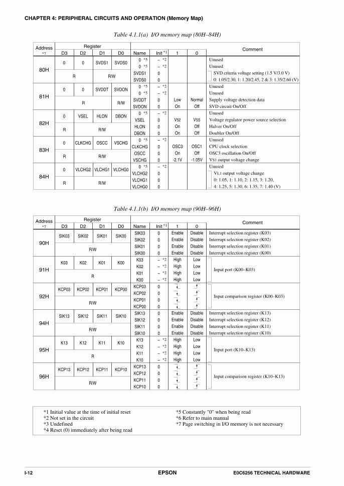
Table 4.1.1(a) I/O memory map (80H–84H)
Address CommentRegister
D3 D2 D1 D0 Name Init 1 0*1
SVDS0
R
00
SVDS1SVDS0
––00
SVDS100
80H
*2
*2
*7
Unused
Unused
SVD criteria voltage setting (1.5 V/3.0 V)
0: 1.05/2.30, 1: 1.20/2.45, 2 & 3: 1.35/2.60 (V)R/W
SVDON
R
00
SVDDTSVDON
––00
LowOn
NormalOff
SVDDT00
81H
*2
*2
Unused
Unused
Supply voltage detection data
SVD circuit On/OffR/W
DBON
R
0VSELHLONDBON
–000
VS2
OnOn
VSS
OffOff
HLONVSEL0
82H
*2 Unused
Voltage regulator power source selection
Halver On/Off
Doubler On/OffR/W
VSCHG
R
0CLKCHG
OSCCVSCHG
–000
OSC3On
-2.1V
OSC1Off
-1.05V
OSCCCLKCHG0
83H
*2 Unused
CPU clock selection
OSC3 oscillation On/Off
VS1 output voltage changeR/W
VLCHG0
R
0VLCHG2VLCHG1VLCHG0
–000
VLCHG1VLCHG20
84H
*2 Unused
VL1 output voltage change
0: 1.05, 1: 1.10, 2: 1.15, 3: 1.20,
4: 1.25, 5: 1.30, 6: 1.35, 7: 1.40 (V)R/W
*5
*5
*5
*5
*5
*5
*5
Table 4.1.1(b) I/O memory map (90H–96H)
D3 D2 D1 D0 Name Init 1 0*1
90HSIK00
SIK03SIK02SIK01SIK00
0000
Interrupt selection register (K03)
Interrupt selection register (K02)
Interrupt selection register (K01)
Interrupt selection register (K00)
EnableEnableEnableEnable
DisableDisableDisableDisable
SIK01SIK02SIK03
91HK00
K03K02K01K00
––––
HighHighHighHigh
LowLowLowLow
K01K02K03*2
*2
*2
*2
92HKCP00
R/W
KCP03KCP02KCP01KCP00
KCP01KCP02KCP030000
*7
R/W
R Input port (K00–K03)
Input comparison register (K00–K03)
94HSIK10
SIK13SIK12SIK11SIK10
0000
Interrupt selection register (K13)
Interrupt selection register (K12)
Interrupt selection register (K11)
Interrupt selection register (K10)
EnableEnableEnableEnable
DisableDisableDisableDisable
SIK11SIK12SIK13
95HK10
K13K12K11K10
––––
HighHighHighHigh
LowLowLowLow
K11K12K13*2
*2
*2
*2
96HKCP10
R/W
KCP13KCP12KCP11KCP10
KCP11KCP12KCP130000
R/W
R Input port (K10–K13)
Input comparison register (K10–K13)
Address CommentRegister
*1 Initial value at the time of initial reset *5 Constantly "0" when being read*2 Not set in the circuit *6 Refer to main manual*3 Undefined *7 Page switching in I/O memory is not necessary*4 Reset (0) immediately after being read

E0C6256 TECHNICAL HARDWARE EPSON I-13
CHAPTER 4: PERIPHERAL CIRCUITS AND OPERATION (Memory Map)
Table 4.1.1(c) I/O memory map (A0H–A3H)
D3 D2 D1 D0 Name Init 1 0*1
A0HR0HIZ
000
R0HIZ
–––0
Unused
Unused
Unused
R0 output high-impedance controlHigh-Z Output
000*2
*2
*2
A1HR00
R03R02R01R00
0000
HighHighHighHigh
LowLowLowLow
R01R02R03
A2HR1HIZ
R/W
000
R1HIZ High-Z Output
000–––0
*2
*2
*2
R10
FOUT
R13R12BZR11
PTOVFR10
FOUT
0000000
HighHighOff
HighOff
HighOff
LowLowOnLowOnLowOn
R11
PTOVF
R12
BZR13
A3H
*7
Unused
Unused
Unused
R1 output high-impedance control
Output port (R13)
Output port (R12)
Buzzer output
Output port (R11)
PTOVF output
Output port (R10)
FOUToutput
R/W
R/W
R/W
Output port (R00–R03)
R
R
Address CommentRegister
*5
*5
*5
*5
*5
*5
Table 4.1.1(d) I/O memory map (B0H–B6H)
D3 D2 D1 D0 Name Init 1 0*1
B0HIOC00
IOC03IOC02IOC01IOC00
0000
OutputOutputOutputOutput
InputInputInputInput
IOC01IOC02IOC03
B1HPUL00
PUL03PUL02PUL01PUL00
1111
OnOnOnOn
OffOffOffOff
PUL01PUL02PUL03
B2HP00
R/W
P03P02P01P00
HighHighHighHigh
LowLowLowLow
P01P02P03––––
*2
*2
*2
*2
*7
R/W
R/W Pull down control register (P00–P03)
I/O port (P00–P03)
I/O control register (P00–P03)
B4H
IOC10IOC13IOC12IOC11IOC10IOC13IOC13IOC12IOC11IOC10
000000000
OutputOutputOutputOutputOutput
1111
InputInputInputInputInput
0000
IOC11IOC12IOC13
B5H
PUL10PUL13PUL12PUL11PUL10PUL13PUL13PUL12PUL12PUL11PUL10
1111111111
OnOnOnOnOn11
On1
On
OffOffOffOffOff00
Off0
Off
PUL11PUL12PUL13
B6H
P10
R/W
P13P12P11P10P13P13P12P11P10
HighHighHighHighHigh
1111
LowLowLowLowLow
0000
P11P12P13–––––––––
*2
*2
*2
*2
*2
*2
*2
*2
*2
R/W
R/W
I/O port (P10–P13)
(ESIF = 0)
Pull down control register (P10–P13)
(ESIF = 0)
I/O control register (P10–P13)
(ESIF = 0)
Address CommentRegister
Master mode: P13 I/O control register
Slave mode: General-purpose register
General-purpose register
Master mode: P13 pull down control register
Slave mode: General-purpose register
Master mode: General-purpose register
Slave mode: SCKL pull down control register
General-purpose register
SIN pull down control register
Master mode: I/O port P13
Slave mode: General-purpose register
General-purpose register
When the serial I/F is used (ESIF = 1):
P10 = SIN (in), P11 = SOUT (out),
P12 = SCLK (master: out, slave: in),
P13 = SRDY (slave: out),
P13 = I/O port (master: in/out)
When the serial I/F is used (ESIF = 1):
P10 = SIN (in), P11 = SOUT (out),
P12 = SCLK (master: out, slave: in),
P13 = SRDY (slave: out),
P13 = I/O port (master: in/out)
When the serial I/F is used (ESIF = 1):
P10 = SIN (in), P11 = SOUT (out),
P12 = SCLK (master: out, slave: in),
P13 = SRDY (slave: out),
P13 = I/O port (master: in/out)

I-14 EPSON E0C6256 TECHNICAL HARDWARE
CHAPTER 4: PERIPHERAL CIRCUITS AND OPERATION (Memory Map)
Table 4.1.1(e) I/O memory map (C0H–CEH)
D3 D2 D1 D0 Name Init 1 0*1
C0HFOFQ0
FOUTE0
FOFQ1FOFQ0
0–00
FOUT output enable
Unused
FOUT frequency selection
0: 512 Hz, 1: 4096 Hz, 2: fOSC1, 3: fOSC3
Enable DisableFOFQ10FOUTE
*2
C1HWDRST
000
WDRST
–––
Reset Reset –
000*2
*2
*2
C2HLDTY0
R/W
LDMSSTCDLDTY1LDTY0
1p(R/W)Static
5p(W)Dynamic
LDTY1STCDLDMS0000
LPWR
R
00
LOFFLPWR
––00
All OffOn
NormalOff
LOFF00
C3H
*2
*2
C4HTMRST
R
00
TMRUNTMRST
––0
Reset
RunReset
Stop–
TMRUN00
C5HTM0
R
TM3TM2TM1TM0
0000
TM1TM2TM3
C6HTM4
R
TM7TM6TM5TM4
0000
Clock timer data (1 Hz)
Clock timer data (2 Hz)
Clock timer data (4 Hz)
Clock timer data (8 Hz)
TM5TM6TM7
C8HPTPS0
00
PTPS1PTPS0
––00
Unused
Unused
Prog. timer prescaler selection
0: 1/1, 1: 1/4, 2: 1/32, 3: 1/256
PTPS100*2
*2
C9HPTPC0
00
PTPC1PTPC0
––00
Unused
Unused
Prog. timer prescaler clock source selection
0: OSC1, 1: OSC3, 2: K02, 3: K02(NR)
PTPC100*2
*2
CAHPTRST
PNRFSPTOE
PTRUNPTRST
000
Rst (reload)
1024HzEnable
Run
256HzDisable
Stop–
PTRUNPTOEPNRFS
R/W
*7
CBHRD0
R/W
RD3RD2RD1RD0
0000
RD1RD3
CCHRD4
RD7RD6RD5RD4
0000
RD5RD6RD7
R/W
R/W
Noise rejector clock frequency selection
PTOVF output enable
Programmable timer Run/Stop
Programmable timer reset (reload)
MSB
Programmable timer reload data
(low-order 4 bits)
LSB
R/W
MSB
Programmable timer reload data
(high-order 4 bits)
LSB
Unused
Unused
Unused
Wachdog timer reset
LCD data memory area selection
LCD drive switch
LCD drive duty selection
0: 1/2, 1: 1/3, 2: 1/4, 3: 1/5
Unused
Unused
LCD display control
LCD power supply On/Off
Unused
Unused
Clock timer Run/Stop
Clock timer reset
Clock timer data (16 Hz)
Clock timer data (32 Hz)
Clock timer data (64 Hz)
Clock timer data (128 Hz)
R
R
RD2
R/W
R
R/W
R/W
RR/W
W
W
W
CDHPT0
R
PT3PT2PT1PT0
0000
PT1PT3
CEHPT4
PT7PT6PT5PT4
0000
PT5PT6PT7
MSB
Programmable timer data
(low-order 4 bits)
LSB
R
MSB
Programmable timer data
(high-order 4 bits)
LSB
PT2
Address CommentRegister
Rst (reload)
*5
*5
*5
*5
*5
*5
*5
*5
*5 *5
*5
*5
*2
*2
*5
*5
*5

E0C6256 TECHNICAL HARDWARE EPSON I-15
CHAPTER 4: PERIPHERAL CIRCUITS AND OPERATION (Memory Map)
Table 4.1.1(f) I/O memory map (D0H–DFH)
D3 D2 D1 D0 Name Init 1 0*1
D0HDKM0
EDIRDKM2DKM1DKM0
0000
Enable direct input function
Direct key mask factor 0: Non, 1: K02,
2: K02-03, 3: K02-03-10, 4: K10, 5: K10-11,
6: K10-11-12, 7: K10-11-12-13
Enable DisableDKM1DKM2EDIR
D1HSWRST
LCURFCRNWFSWRUNSWRST
000
Reset
ReqestRenewal
RunReset
NoNo
Stop–
SWRUNCRNWFLCURF
D2HSWL0
R
SWL3SWL2SWL1SWL0
SWL1SWL2SWL30000
SWM0
R
SWM3SWM2SWM1SWM0
0000
SWM1SWM2SWM3
D3H
D4HSWH0
R
SWH3SWH2SWH1SWH0
0000
SWH1SWH2SWH3
D8H
ESIF
R
00
ESIF
–––00
TriggerRun
SIF port
–Stop
I/O port
SCTRG00*2
*2
*2
D9HSCS0
R/W
SDPSCPSSCS1SCS0
0000
Serial data input/output permutation
Serial interface clock phase selection
Serial interface clock mode selection
0: Slave, 1: PTOVF, 2: CLK/2, 3: CLK
LSB first MSB firstSCS1SCPSSDP
DAHSD0
SD3SD2SD1SD0
––––
SD1SD2SD3*3
*3
*3
*3
DBHSD4
SD7SD6SD5SD4
––––
SD5SD6SD7*3
*3
*3
*3
DCHBZE
ENRTMENRST
ENONBZE
0Reset
00
1secReset
OnEnable
0.5sec–
OffDisable
ENONENRSTENRTM
R/W
*7
DDH
SHTPW
R/W
0BZSTP
SHTPW
–––00
StopTriggerBusy
125msec
––
Ready31.25msec
BZSHT0*2
*2
*2
DEHBZFQ0
0BZFQ2BZFQ1BZFQ0
–000
BZFQ1BZFQ20*2
R/W
R/W
Envelope releasing time
Envelope reset
Envelope On/Off
Buzzer output enable
Unused
1-shot buzzer stop
1-shot buzzer trigger (writing)
1-shot buzzer status (reading)
1-shot buzzer pulse width setting
R/W
Unused
Buzzer frequency selection
0: 4096.0, 1: 3276.8, 2: 2730.7, 3: 2340.6,
4: 2048.0, 5: 1638.4, 6: 1365.3, 7: 1170.3 (Hz)
Lap data carry-up request flag
Capture renewal flag
Stopwatch timer Run/Stop
Stopwatch timer reset
MSB
LSB
Unused
Unused
Serial interface clock trigger (writing)
Serial interface clock status (reading)
P1 port function selection
BZSTP
R
R/W
R
Stopwatch timer data 1/1000 sec (BCD)
R/W W
MSB
LSB
Stopwatch timer data 1/100 sec (BCD)
MSB
LSB
Stopwatch timer data 1/10 sec (BCD)
R/W
SCTRG(W)
SCTRG(R)
MSB
LSB
Serial interface data (low-order 4 bits)
MSB
LSB
Serial interface data (high-order 4 bits)
W R/W
BZSHT(W)
BZSHT(R)
R
DFHBDTY0
0BDTY2BDTY1BDTY0
–000
BDTY1BDTY20*2
*6R/W
Unused
Buzzer signal duty ratio selectionR
Address CommentRegister
W
*5 *5
*5
*5
*5
*5
*5
*5

I-16 EPSON E0C6256 TECHNICAL HARDWARE
CHAPTER 4: PERIPHERAL CIRCUITS AND OPERATION (Memory Map)
Table 4.1.1(g) I/O memory map (E0H–ECH)
D3 D2 D1 D0 Name Init 1 0*1
E0HADMODE
0APWR
SENSELADMODE
–000
Unused
A/D converter power supply On/Off
Sensor/reference resistance selection
A/D converter operation mode selection
OnSensor
OffReference
Normal
SENSELAPWR0*2
E1HADCLK0
WRSEL0
ADCLK1ADCLK0
0–00
OSC3OSC3
ResistanceADCLK10
R
WRSEL
R/W
*2
E2HCHSEL
R/W
000
CHSEL CH1 CH0
000–––0
*2
*2
*2
TC0TC3TC2TC1TC0
––––
TC1TC2TC3
E3H
*3
*3
*3
*3
E4HTC4
TC7TC6TC5TC4
TC5TC6TC7
E5HTC8
R/W
TC11TC10TC9TC8
TC9TC10TC11
E6HTC12
R/W
TC15TC14TC13TC12
TC13TC14TC15
E7HC0
C3C2C1C0
–––– LSB
C1C2C3*3
*3
*3
*3
E8HC4
C7C6C5C4
C5C6C7
E9HC8
C11C10C9C8
C9C10C11
R/W
*7
EAHC12
R/W
C15C14C13C12
C13C15
EBHC16
C19C18C17C16
C17C18C19
R/W
R/W
R/W
CH1 sensor selection (resistance/humidity)
Unused
CH1 clock selection
CH0 clock selection
Unused
Unused
Unused
Channel 1/0 selection
LSB
C14
R/W
R/W
R/W
R/W
Up/down counter data (TC0–TC3)
Continuous
Humidity
OSC1OSC1
R
R
––––
*3
*3
*3
*3
Up/down counter data (TC4–TC7)
––––
*3
*3
*3
*3
Up/down counter data (TC8–TC11)
––––
*3
*3
*3
*3
MSB
Up/down counter data (TC12–TC15)
ECH
ADRUN0
OVF2(R)OVF2(W)OVF1(R)OVF1(W)ADRUN
–0
Reset0
Reset0
YesResetYes
ResetStart
No–
No–
Stop
OVF1OVF20
*2
R
Unused
Up/down counter overflow flag
Up/down counter overflow flag reset
Up-counter overflow flag
Up-counter overflow flag reset
A/D conversion Start/Stop
Up-counter data (C0–C3)
––––
*3
*3
*3
*3
Up-counter data (C4–C7)
––––
*3
*3
*3
*3
Up-counter data (C8–C11)
––––
*3
*3
*3
*3
Up-counter data (C12–C15)
––––
MSB*3
*3
*3
*3
Up-counter data (C16–C19)
R/W
Address CommentRegister
*5
*5
*5
*5
*5
*5

E0C6256 TECHNICAL HARDWARE EPSON I-17
CHAPTER 4: PERIPHERAL CIRCUITS AND OPERATION (Memory Map)
Table 4.1.1(h) I/O memory map (F0H–FEH)
D3 D2 D1 D0 Name Init 1 0*1
F0HEIAD
000
EIAD
–––0
Unused
Unused
Unused
Interrupt mask register (A/D converter)Enable Mask
000*2
*2
*2
F1HEIK1
000
EIK1
–––0 Enable Mask
000*2
*2
*2
F2HEIK0
R
000
EIK0 Enable Mask
000–––0
*2
*2
*2
EISIF
R
000
EISIF
–––0 Enable Mask
000
F3H
*2
*2
*2
F4HEIPT
R
000
EIPT
–––0 Enable Mask
000
F5HEISW0
R/W
EIRUNEILAPEISW1EISW0
0000
EnableEnableEnableEnable
MaskMaskMaskMask
EISW1EILAPEIRUN
F6HEIT0
R/W
EIT3EIT2EIT1EIT0
0000
Interrupt mask register (Clock timer 2 Hz)
Interrupt mask register (Clock timer 8 Hz)
Interrupt mask register (Clock timer 16 Hz)
Interrupt mask register (Clock timer 32 Hz)
EnableEnableEnableEnable
MaskMaskMaskMask
EIT1EIT2EIT3
*7
Unused
Unused
Unused
Interrupt mask register (K10–K13)
Unused
Unused
Unused
Interrupt mask register (K00–K03)
Unused
Unused
Unused
Interrupt mask register (Serial interface)
Unused
Unused
Unused
Interrupt mask register (Programmable timer)
Interrupt mask register (Stopwatch direct RUN)
Interrupt mask register (Stopwatch direct LAP)
Interrupt mask register (Stopwatch 1 Hz)
Interrupt mask register (Stopwatch 10 Hz)
R/W
R
R/W
R/W
R
R/W
R/W
F8HIAD
000
IAD
–––0
Unused
Unused
Unused
Interrupt factor flag (A/D converter)Yes No
000*2
*2
*2
F9HIK1
000
IK1
–––0 Yes No
000*2
*2
*2
FAHIK0
R
000
IK0 Yes No
000–––0
*2
*2
*2
ISIF
R
000
ISIF
–––0 Yes No
000
FBH
*2
*2
*2
FCHIPT
R
000
IPT
–––0 Yes No
000
FDHISW0
R
IRUN ILAP ISW1 ISW0
0000
YesYesYesYes
NoNoNoNo
ISW1ILAPIRUN
FEHIT0
R
IT3IT2IT1IT0
0000
Interrupt factor flag (Clock timer 2 Hz)
Interrupt factor flag (Clock timer 8 Hz)
Interrupt factor flag (Clock timer 16 Hz)
Interrupt factor flag (Clock timer 32 Hz)
YesYesYesYes
NoNoNoNo
IT1IT2IT3
Unused
Unused
Unused
Interrupt factor flag (K10–K13)
Unused
Unused
Unused
Interrupt factor flag (K00–K03)
Unused
Unused
Unused
Interrupt factor flag (Serial interface)
Unused
Unused
Unused
Interrupt factor flag (Programmable timer)
Interrupt factor flag (Stopwatch direct RUN)
Interrupt factor flag (Stopwatch direct LAP)
Interrupt factor flag (Stopwatch 1 Hz)
Interrupt factor flag (Stopwatch 10 Hz)
R
R
Address CommentRegister
*5
*5
*5
*5
*5
*5
*5
*5
*5
*5
*5
*5
*5
*5
*5
*4
*5
*5
*5
*4
*5
*5
*5
*4
*5
*5
*5
*4
*4
*4
*4
*4
*4
*4
*4
*4
*2
*2
*2
*5
*5
*5
*2
*2
*2
*5
*5
*5
*4

I-18 EPSON E0C6256 TECHNICAL HARDWARE
CHAPTER 4: PERIPHERAL CIRCUITS AND OPERATION (Power Supply and Operating Mode Settings)
4.2 Power Supply and Operating Mode SettingsThis section explains the control of the operating mode and the LCD drive voltage. See Section 2.1, "PowerSupply", for the configuration of the power supply circuit.
4.2.1 Operating modeAs explained in Section 2.1, "Power Supply", the supply voltage doubler/halver and the operating modesare set in the E0C6256 to deal with a wide supply voltage range (0.9 to 3.6 V).
Supply voltage
Low voltage operation
Low power operation
Normal operation
High speed operation
Doubler mode
Halver mode
Normal mode
Normal mode (OSC3 oscillation ON)
3.6 V2.55 V2.2 V1.4 V1.3 V0.9 V
Fig. 4.2.1.1 Corresponding between supply voltage and operating mode
The operating mode can be set by the registers VSEL, HLON and DBON.
Table 4.2.1.1 Operating mode setting
VSEL
0
1
1
1
×
HLON
0
1
0
0
1
DBON
0
0
1
0
1
Operating mode
Normal mode
Halver mode
Doubler mode
Supply voltage
1.3 V to 3.6 V
2.55 V to 3.6 V
0.9 V to 1.4 V
Cannot be used
Cannot be used
The HLON register and the DBON registers are used to turn halving and doubling ON or OFF, respec-tively. By turning either one ON, the supply voltage doubler/halver circuit generates VS2.The VSEL register is used to select the drive voltage for the internal power supply circuit (oscillationsystem regulated voltage circuit, LCD system regulated voltage circuit). When it is set to "0", VSS is used asthe drive voltage, and when it is set to "1", VS2 output from the supply voltage doubler/halver circuit isused.After turning the supply voltage doubler/halver ON using the HLON or DBON, about 100 msec is neces-sary until the VS2 voltage stabilizes. Therefore, switching of the operating mode should be done in thefollowing sequence.
Normal mode → Halver/Doubler mode1. Turn the supply voltage doubler/halver ON (Set HLON or DBON to "1")2. Maintain 100 msec or more3. Set VSEL to "1"
Halver/Doubler mode → Normal mode1. Set VSEL to "0"2. Turn the supply voltage doubler/halver OFF (Set HLON or DBON to "0")
Note: • When the supply voltage is out of the specified voltage range of an operating mode, do not switchinto the operating mode. It may cause malfunction or increase current consumption.
• Do not set HLON and DBON to "1" at the same time.
• When switching from the doubler/halver mode to the normal mode, use separate instructions toswitch the mode (VSEL = "0") and turn the supply voltage doubler/halver OFF (HLON = "0" orDBON = "0"). Simultaneous processing with a single instruction may cause malfunction.
E0C6256 TECHNICAL HARDWARE EPSON I-19
CHAPTER 4: PERIPHERAL CIRCUITS AND OPERATION (Power Supply and Operating Mode Settings)
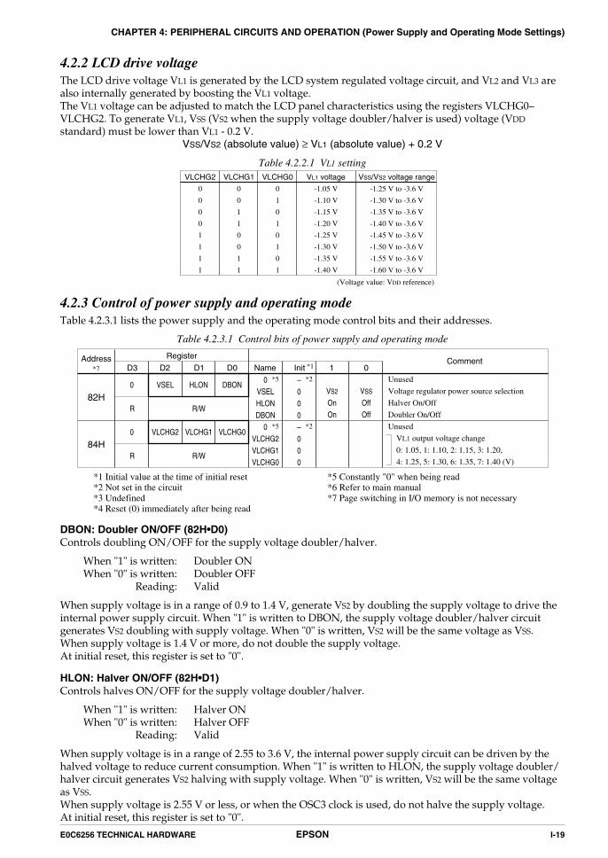
4.2.2 LCD drive voltageThe LCD drive voltage VL1 is generated by the LCD system regulated voltage circuit, and VL2 and VL3 arealso internally generated by boosting the VL1 voltage.The VL1 voltage can be adjusted to match the LCD panel characteristics using the registers VLCHG0–VLCHG2. To generate VL1, VSS (VS2 when the supply voltage doubler/halver is used) voltage (VDD
standard) must be lower than VL1 - 0.2 V.VSS/VS2 (absolute value) ≥ VL1 (absolute value) + 0.2 V
Table 4.2.2.1 VL1 settingVLCHG2
0
0
0
0
1
1
1
1
VLCHG1
0
0
1
1
0
0
1
1
VLCHG0
0
1
0
1
0
1
0
1
VL1 voltage
-1.05 V
-1.10 V
-1.15 V
-1.20 V
-1.25 V
-1.30 V
-1.35 V
-1.40 V
VSS/VS2 voltage range
-1.25 V to -3.6 V
-1.30 V to -3.6 V
-1.35 V to -3.6 V
-1.40 V to -3.6 V
-1.45 V to -3.6 V
-1.50 V to -3.6 V
-1.55 V to -3.6 V
-1.60 V to -3.6 V
(Voltage value: VDD reference)
4.2.3 Control of power supply and operating modeTable 4.2.3.1 lists the power supply and the operating mode control bits and their addresses.
Table 4.2.3.1 Control bits of power supply and operating mode
Address CommentRegister
D3 D2 D1 D0 Name Init 1 0*1*7
DBON
R
0VSELHLONDBON
–000
VS2
OnOn
VSS
OffOff
HLONVSEL0
82H
*2 Unused
Voltage regulator power source selection
Halver On/Off
Doubler On/OffR/W
VLCHG0
R
0VLCHG2VLCHG1VLCHG0
–000
VLCHG1VLCHG20
84H
*2 Unused
VL1 output voltage change
0: 1.05, 1: 1.10, 2: 1.15, 3: 1.20,
4: 1.25, 5: 1.30, 6: 1.35, 7: 1.40 (V)R/W
*5
*5
*1 Initial value at the time of initial reset *5 Constantly "0" when being read*2 Not set in the circuit *6 Refer to main manual*3 Undefined *7 Page switching in I/O memory is not necessary*4 Reset (0) immediately after being read
DBON: Doubler ON/OFF (82H•D0)Controls doubling ON/OFF for the supply voltage doubler/halver.
When "1" is written: Doubler ONWhen "0" is written: Doubler OFF
Reading: Valid
When supply voltage is in a range of 0.9 to 1.4 V, generate VS2 by doubling the supply voltage to drive theinternal power supply circuit. When "1" is written to DBON, the supply voltage doubler/halver circuitgenerates VS2 doubling with supply voltage. When "0" is written, VS2 will be the same voltage as VSS.When supply voltage is 1.4 V or more, do not double the supply voltage.At initial reset, this register is set to "0".
HLON: Halver ON/OFF (82H•D1)Controls halves ON/OFF for the supply voltage doubler/halver.
When "1" is written: Halver ONWhen "0" is written: Halver OFF
Reading: Valid
When supply voltage is in a range of 2.55 to 3.6 V, the internal power supply circuit can be driven by thehalved voltage to reduce current consumption. When "1" is written to HLON, the supply voltage doubler/halver circuit generates VS2 halving with supply voltage. When "0" is written, VS2 will be the same voltageas VSS.When supply voltage is 2.55 V or less, or when the OSC3 clock is used, do not halve the supply voltage.At initial reset, this register is set to "0".

I-20 EPSON E0C6256 TECHNICAL HARDWARE
CHAPTER 4: PERIPHERAL CIRCUITS AND OPERATION (Power Supply and Operating Mode Settings)
VSEL: Voltage regulator power source selection (82H•D2)Selects the power source for two internal power supply circuit (oscillation system regulated voltage circuitand LCD system regulated voltage circuit).
When "1" is written: VS2
When "0" is written: VSS
Reading: Valid
When "1" is written to VSEL, the internal power supply circuit operates with VS2 output from the supplyvoltage doubler/halver circuit. It becomes the doubler mode or the halver mode according to the DBONand HLON settings. When "0" is written to VSEL, the internal power supply circuit operates with VSS and itbecomes the normal mode.When switching from the normal mode to the doubler/halver mode,VSEL should be set to "1" wait 100msec or more for the VS2 to stabilize after setting DBON or HLON to "1".At initial reset, this register is set to "0".
VLCHG0–VLCHG2: VL1 output voltage change (84H•D0–D2)The voltage value of the LCD drive voltage VL1 can be selected from among 8 types as shown in Table4.2.2.1.At initial reset, these registers are set to "0".
4.2.4 Programming notes(1) When the supply voltage is out of the specified voltage range of an operating mode, do not switch into
the operating mode. It may cause malfunction or increase current consumption.
(2) Do not set HLON (halving) and DBON (doubling) to "1" at the same time.
(3) When switching from the normal mode to the doubler/halver mode, VSEL should be set to "1" wait 100msec or more for the VS2 to stabilize after setting DBON or HLON to "1".
(4) When switching from the doubler/halver mode to the normal mode, use separate instructions to switchthe mode (VSEL = "0") and turn the supply voltage doubler/halver OFF (HLON = "0" or DBON = "0").Simultaneous processing with a single instruction may cause malfunction.

E0C6256 TECHNICAL HARDWARE EPSON I-21
CHAPTER 4: PERIPHERAL CIRCUITS AND OPERATION (Resetting Watchdog Timer)
4.3 Resetting Watchdog Timer
4.3.1 Configuration of watchdog timerThe E0C6256 incorporates a watchdog timer as the source oscillator for OSC1 (dividing clock = 256 Hz).The watchdog timer must be reset cyclically by the software. If reset is not executed in at least 3 or 4seconds, the initial reset signal is output automatically for the CPU.Figure 4.3.1.1 is the block diagram of the watchdog timer.
Watchdog timerInitialresetsignal
Watchdog timer reset signal
OSC1dividing circuit
OSC1oscillation circuit
32 kHz 256 Hz
Fig. 4.3.1.1 Watchdog timer block diagram
The watchdog timer, configured of a 10-bit binary counter, generates the initial reset signal internally byoverflow of the last stage (1/4 Hz).Watchdog timer reset processing in the program's main routine enables detection of program overrun, suchas when the main routine's watchdog timer processing is bypassed. Ordinarily this routine is incorporatedwhere periodic processing takes place, just as for the timer interrupt routine.The watchdog timer operates in the HALT mode. If the HALT status continues for 3 or 4 seconds, the initialreset signal restarts operation.
4.3.2 Mask optionYou can select whether or not to use the watchdog timer with the mask option. When "Not use" is selected,there is no need to reset the watchdog timer.
4.3.3 Control of watchdog timerTable 4.3.3.1 lists the watchdog timer's control bit and its address.
Table 4.3.3.1 Control bit of watchdog timer
D3 D2 D1 D0 Name Init 1 0*1
C1HWDRST
000
WDRST
–––
Reset Reset –
000*2
*2
*2
*7
Unused
Unused
Unused
Wachdog timer resetR W
Address CommentRegister
*5
*5
*5 *5
*1 Initial value at the time of initial reset *5 Constantly "0" when being read*2 Not set in the circuit *6 Refer to main manual*3 Undefined *7 Page switching in I/O memory is not necessary*4 Reset (0) immediately after being read
WDRST: Watchdog timer reset (C1H•D0)This is the bit for resetting the watchdog timer.
When "1" is written: Watchdog timer is resetWhen "0" is written: No operation
Reading: Always "0"
When "1" is written to WDRST, the watchdog timer is reset, and the operation restarts immediately afterthis. When "0" is written to WDRST, no operation results.This bit is dedicated for writing, and is always "0" for reading.
4.3.4 Programming noteWhen the watchdog timer is being used, the software must reset it within 3-second cycles.

I-22 EPSON E0C6256 TECHNICAL HARDWARE
CHAPTER 4: PERIPHERAL CIRCUITS AND OPERATION (Oscillation Circuit)
4.4 Oscillation Circuit
4.4.1 Configuration of oscillation circuitThe E0C6256 has two oscillation circuits (OSC1 and OSC3). OSC1 is a crystal oscillation circuit that suppliesthe operating clock to the CPU and peripheral circuits. OSC3 is either a CR or ceramic oscillation circuit.When processing with the E0C6256 requires high-speed operation, the CPU operating clock can beswitched from OSC1 to OSC3. When the OSC3 clock is used, to obtain stable operation, the operatingvoltage VS1 of the internal circuit is changed by the software.Figure 4.4.1.1 is the block diagram of this oscillation system.
Oscillation circuit control signal
CPU clock selection signal
To CPU(and serial interface)
To peripheral circuits
OSC3oscillation circuit
Clockswitch
OSC1oscillation circuit
Operating voltage selection signalVS1Oscillation systemregulated voltage
circuit
Fig. 4.4.1.1 Oscillation system
Selection of either OSC1 or OSC3 for the CPU's operating clock can be made by the software.
4.4.2 OSC1 oscillation circuitThe E0C6256 has a built-in crystal oscillation circuit (OSC1 oscillation circuit). As an external element, theOSC1 oscillation circuit generates the operating clock for the CPU and peripheral circuits by connecting thecrystal oscillator (Typ. 32.768 kHz) and trimmer capacitor (5–25 pF).Figure 4.4.2.1 is the block diagram of the OSC1 oscillation circuit.
VDD CGX
X'ta
l
OSC2
OSC1
R RD
X
CDX
To CPU andperipheral circuits
FX
VDD
Fig. 4.4.2.1 OSC1 oscillation circuit
As Figure 4.4.2.1 indicates, the crystal oscillation circuit can be configured simply by connecting the crystaloscillator (X'tal) between terminals OSC1 and OSC2 to the trimmer capacitor (CGX) between terminalsOSC1 and VDD.
4.4.3 OSC3 oscillation circuitThe E0C6256 has twin clock specification. The mask option enables selection of either the CR or ceramicoscillation circuit (OSC3 oscillation circuit) as the CPU's sub-clock. Because the oscillation circuit itself isbuilt-in, it provides the resistance as an external element when CR oscillation is selected, but when ceramicoscillation is selected both the ceramic oscillator and two capacitors (gate and drain capacitance) arerequired.Figure 4.4.3.1 is the block diagram of the OSC3 oscillation circuit.

E0C6256 TECHNICAL HARDWARE EPSON I-23
CHAPTER 4: PERIPHERAL CIRCUITS AND OPERATION (Oscillation Circuit)
To CPU(and serial interface)
Oscillation circuitcontrol signal
CCR
OSC3
OSC4
RC
R
VDD
CGC
CDC Cer
amic
OSC4
OSC3
R
RDC
To CPU(and serial interface)Oscillation circuitcontrol signal
FC
(a) CR oscillation circuit
(b) Ceramic oscillation circuit
Fig. 4.4.3.1 OSC3 oscillation circuit
As indicated in Figure 4.4.3.1, the CR oscillation circuit can be configured simply by connecting the resistor(RCR) between terminals OSC3 and OSC4 when CR oscillation is selected. When 40 kΩ is used for RCR, theoscillation frequency is about 900 kHz. When ceramic oscillation is selected, the ceramic oscillation circuitcan be configured by connecting the ceramic oscillator (Typ. 1 MHz) between terminals OSC3 and OSC4 tothe two capacitors (CGC and CDC) located between terminals OSC3 and OSC4 and VDD. For both CGC andCDC, connect capacitors that are about 100 pF. To lower current consumption of the OSC3 oscillationcircuit, stop the oscillation by the software when it is not used.
4.4.4 Operating voltage switchingWhen switching the CPU system clock between OSC1 and OSC3 by the software, the operating voltage VS1
for the oscillation circuit must also be switched by the software to obtain stable operation.System clock and the corresponding operating voltage VS1 are shown in Table 4.4.4.1.
Table 4.4.4.1 System clock and operating voltage
System clock Operating voltage VS1
-1.05 V
-2.1 V
OSC1 (32.768 kHz)
OSC3 (1 MHz)
(Operating voltage value: VDD reference)
When using OSC3 as the CPU system clock, it should be done using the software as in the followingprocedure: first switch the operating voltage VS1 to -2.1 V, turn the OSC3 oscillation ON, then after waiting5 msec or more switch the clock for oscillation stabilization. When switching from OSC3 to OSC1, turn theOSC3 oscillation circuit OFF after switching the clock, then set the operating voltage VS1 to -1.05 V.
Note: Switching the operating voltage when the supply voltage is lower than 2.2 V (absolute value) maycause a malfunction. Switch the operating voltage only after making sure that supply voltage is morethan 2.2 V (absolute value) using the SVD circuit.Do not switch the operating voltage during operating in the doubler mode or the halver mode, even ifthe VS2 voltage is more than 2.2 V (absolute value). The OSC3 clock can be used only in the normalmode.
4.4.5 Clock frequency and instruction execution timeTable 4.4.5.1 shows the instruction execution time according to each frequency of the system clock.
Table 4.4.5.1 Clock frequency and instruction execution time
Clock frequency5-clock instruction
152.6
5.0
OSC1: 32.768 kHz
OSC3: 1 MHz
Instruction execution time (µsec)
7-clock instruction
213.6
7.0
12-clock instruction
366.2
12.0

I-24 EPSON E0C6256 TECHNICAL HARDWARE
CHAPTER 4: PERIPHERAL CIRCUITS AND OPERATION (Oscillation Circuit)
4.4.6 Control of oscillation circuitTable 4.4.6.1 lists the control bits and their addresses for the oscillation circuit.
Table 4.4.6.1 Control bits of oscillation circuit
Address CommentRegister
D3 D2 D1 D0 Name Init 1 0*1*7
VSCHG
R
0CLKCHG
OSCCVSCHG
–000
OSC3On
-2.1V
OSC1Off
-1.05V
OSCCCLKCHG0
83H
*2 Unused
CPU clock selection
OSC3 oscillation On/Off
VS1 output voltage changeR/W
*5
*1 Initial value at the time of initial reset *5 Constantly "0" when being read*2 Not set in the circuit *6 Refer to main manual*3 Undefined *7 Page switching in I/O memory is not necessary*4 Reset (0) immediately after being read
VSCHG: VS1 output voltage change (83H•D0)Switches the operating voltage VS1.
When "1" is written: -2.1 VWhen "0" is written: -1.05 V
Reading: Valid
When switching the CPU system clock, the operating voltage VS1 should also be switched according to theclock.When switching from OSC1 to OSC3, first set VS1 to -2.1 V (VSCHG = "1"), then turn the OSC3 oscillationON.When switching from OSC3 to OSC1, set VS1 to -1.05 V (VSCHG = "0") after switching to OSC1 and turningthe OSC3 oscillation OFF.At initial reset, this register is set to "0".
OSCC: OSC3 oscillation ON/OFF (83H•D1)Controls oscillation ON/OFF for the OSC3 oscillation circuit.
When "1" is written: OSC3 oscillation ONWhen "0" is written: OSC3 oscillation OFF
Reading: Valid
When it is necessary to operate the CPU at high speed, set OSCC to "1". At other times, set it to "0" toresume current consumption. Furthermore, when performing this setting, it is necessary to switch theoperating voltage VS1.At initial reset, this register is set to "0".
CLKCHG: CPU clock switch (83H•D2)The CPU's operation clock is selected with this register.
When "1" is written: OSC3 clock is selectedWhen "0" is written: OSC1 clock is selected
Reading: Valid
When the CPU clock is to be OSC3, set CLKCHG to "1"; for OSC1, set CLKCHG to "0".When switching the CPU operation clock from OSC1 to OSC3, do this after a minimum of 5 msec haveelapsed since the OSC3 oscillation went ON (OSCC = "1"). This time is necessary to stabilize the OSC3oscillation.At initial reset, this register is set to "0".

E0C6256 TECHNICAL HARDWARE EPSON I-25
CHAPTER 4: PERIPHERAL CIRCUITS AND OPERATION (Oscillation Circuit)
4.4.7 Programming notes(1) When switching the CPU system clock from OSC1 to OSC3, set VS1 to -2.1 V (VSCHG = "1") before
turning the OSC3 oscillation ON.When switching from OSC3 to OSC1, set VS1 to -1.05 V (VSCHG = "0") after switching to OSC1 andturning the OSC3 oscillation OFF.
(2) It takes at least 5 msec from the time the OSC3 oscillation circuit goes ON until the oscillation stabilizes.Consequently, when switching the CPU operation clock from OSC1 to OSC3, do this after a minimumof 5 msec have elapsed since the OSC3 oscillation went ON.Further, the oscillation stabilization time varies depending on the external oscillator characteristics andconditions of use, so allow ample margin when setting the wait time.
OSC1 → OSC31. Set VSCHG to "1" (-1.05 V → -2.1 V)2. Set OSCC to "1" (OSC3 oscillation ON)3. Maintain 5 msec or more4. Set CLKCHG to "1" (OSC1 → OSC3)
OSC3 → OSC11. Set CLKCHG to "0" (OSC3 → OSC1)2. Set OSCC to "0" (OSC3 oscillation OFF)3. Set VSCHG to "0" (-2.1 V → -1.05 V)
(3) When switching the clock form OSC3 to OSC1, use a separate instruction for turning the OSC3 oscilla-tion OFF. An error in the CPU operation can result if this processing is performed at the same time bythe one instruction.
(4) Switching the operating voltage when the supply voltage is lower than 2.2 V (absolute value) may cause amalfunction. Switch the operating voltage only after making sure that supply voltage is more than 2.2 V(absolute value) using the SVD circuit.Do not switch the operating voltage during operating in the doubler mode or the halver mode, even ifthe VS2 voltage is more than 2.2 V (absolute value). The OSC3 clock can be used only in the normalmode.

I-26 EPSON E0C6256 TECHNICAL HARDWARE
CHAPTER 4: PERIPHERAL CIRCUITS AND OPERATION (Input Ports)
4.5 Input Ports (K00–K03, K10–K13)
4.5.1 Configuration of input portsThe E0C6256 has 8 bits (4-bit × 2) general-purpose input ports. Each of the input port terminals (K00–K03,K10–K13) provides internal pull down resistor. Pull down resistor can be selected for each bit with themask option.Figure 4.5.1.1 shows the configuration of input port.
Kxx
Mask option
Address
VDD
Interruptrequest
Dat
a bu
s
VSS
Fig. 4.5.1.1 Configuration of input port
Selection of "With pull down resistor" with the mask option suits input from the push switch, key matrix,and so forth. When "Gate direct" is selected, the port can be used for slide switch input and interfacing withother LSIs.
4.5.2 Interrupt functionAll 8 bits of the input ports (K00–K03, K10–K13) provide the interrupt function. The conditions for issuingan interrupt can be set by the software. Further, whether to mask the interrupt function can be selected bythe software.Figure 4.5.2.1 shows the configuration of K00–K03 (K10–K13) interrupt circuit.
Dat
a bu
s
Input comparisonregister (KCP00, 10)
K00, 10
Interruptrequest
Interrupt selectionregister (SIK00, 10)
Address
Address
AddressAddress
Interrupt factorflag (IK0, 1)
K01, 11K02, 12
K03, 13
Interrupt maskregister (EIK0, 1)
Address
Fig. 4.5.2.1 Input interrupt circuit configuration

E0C6256 TECHNICAL HARDWARE EPSON I-27
CHAPTER 4: PERIPHERAL CIRCUITS AND OPERATION (Input Ports)
The interrupt selection register (SIK) and input comparison register (KCP) are individually set for the inputports K00–K03 and K10–K13, and can specify the terminal for generating interrupt and interrupt timing.The interrupt selection register (SIK00–SIK03, SIK10–SIK13) select what input of K00–K03 and K10–K13 touse for the interrupt. Writing "1" into an interrupt selection register incorporates that input port into theinterrupt generation conditions. The changing the input port where the interrupt selection register has beenset to "0" does not affect the generation of the interrupt.The input interrupt timing can select that the interrupt be generated at the rising edge of the input or that itbe generated at the falling edge according to the set value of the input comparison register (KCP00–KCP03).By setting these two conditions, the interrupt for K00–K03 and K10–K13 (4 bits unit) are generated when aninput port in which an interrupt has been enabled by the input selection register and the content of theinput comparison register have been changed from matching to no matching.The interrupt mask registers EIK0 and EIK1 enable the interrupt mask to be selected for K00–K03 and K10–K13, respectively.When the interrupt is generated, the interrupt factor flag (IK0 for K00–K03, IK1 for K10–K13) is set to "1".Figure 4.5.2.2 shows an example of an interrupt for K00–K03.
Interrupt selection register Input comparison registerSIK03 SIK02 SIK01 SIK00 KCP03 KCP02 KCP01 KCP00
1 1 1 0 1 0 1 0
With the above setting, the interrupt of K00–K03 is generated under the following condition:
Input port(1) K03 K02 K01 K00
1 0 1 0 (Initial value)↓
(2) K03 K02 K01 K001 0 1 1
↓(3) K03 K02 K01 K00
0 0 1 1 → Interrupt generation↓
(4) K03 K02 K01 K000 1 1 1
Because K00 interrupt is set to disable, interrupt will be generatedwhen no matching occurs between the contents of the 3 bits K01–K03and the 3 bits input comparison register KCP01–KCP03.
Fig. 4.5.2.2 Example of interrupt of K00–K03
K00 interrupt is disabled by the interrupt selection register (SIK00), so that an interrupt does not occur at(2). At (3), K03 changes to "0"; the data of the terminal that is interrupt enabled no longer matches the dataof the input comparison register, so that interrupt occurs. As already explained, the condition for theinterrupt to occur is the change in the port data and contents of the input comparison register from match-ing to no matching. Hence, in (4), when the no matching status changes to another no matching status, aninterrupt does not occur. Further, terminals that have been masked for interrupt do not affect the condi-tions for interrupt generation.
4.5.3 Mask optionInternal pull down resistor can be selected for each of the 8 bits of the input ports (K00–K03, K10–K13) withthe input port mask option.When you have selected "Gate direct", take care that the floating status does not occur for the input. Select"With pull down resistor" for input ports that are not being used.
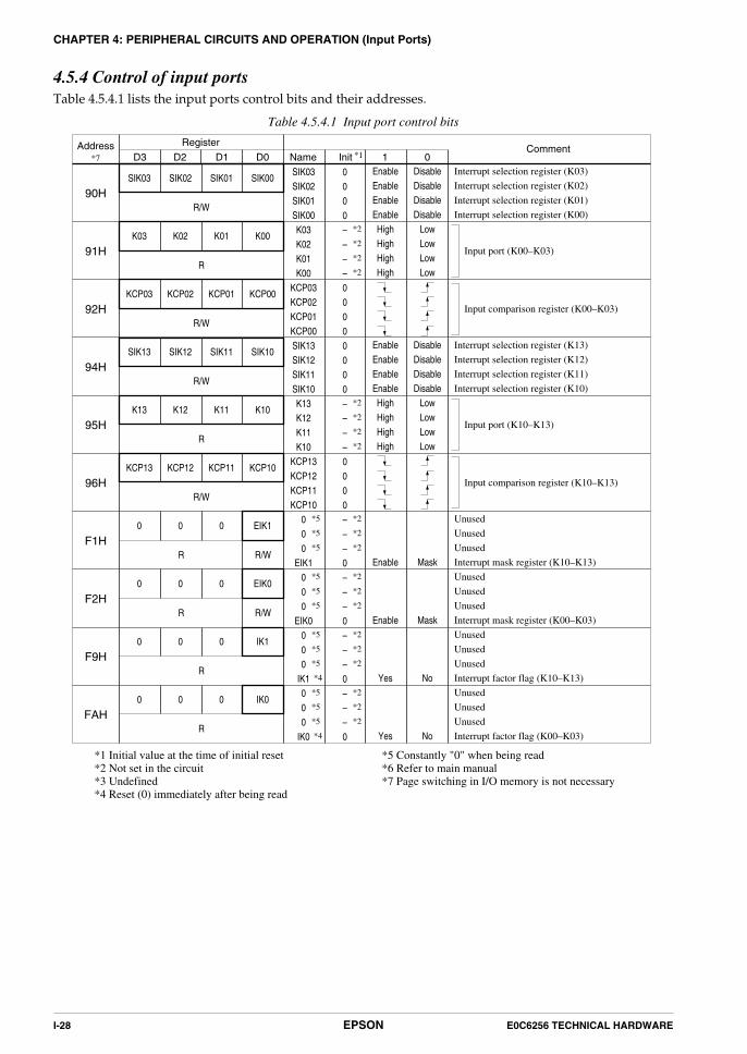
I-28 EPSON E0C6256 TECHNICAL HARDWARE
CHAPTER 4: PERIPHERAL CIRCUITS AND OPERATION (Input Ports)
4.5.4 Control of input portsTable 4.5.4.1 lists the input ports control bits and their addresses.
Table 4.5.4.1 Input port control bits
D3 D2 D1 D0 Name Init 1 0*1
90HSIK00
SIK03SIK02SIK01SIK00
0000
Interrupt selection register (K03)
Interrupt selection register (K02)
Interrupt selection register (K01)
Interrupt selection register (K00)
EnableEnableEnableEnable
DisableDisableDisableDisable
SIK01SIK02SIK03
91HK00
K03K02K01K00
––––
HighHighHighHigh
LowLowLowLow
K01K02K03*2
*2
*2
*2
92HKCP00
R/W
KCP03KCP02KCP01KCP00
KCP01KCP02KCP030000
*7
R/W
R Input port (K00–K03)
Input comparison register (K00–K03)
94HSIK10
SIK13SIK12SIK11SIK10
0000
Interrupt selection register (K13)
Interrupt selection register (K12)
Interrupt selection register (K11)
Interrupt selection register (K10)
EnableEnableEnableEnable
DisableDisableDisableDisable
SIK11SIK12SIK13
95HK10
K13K12K11K10
––––
HighHighHighHigh
LowLowLowLow
K11K12K13*2
*2
*2
*2
96HKCP10
R/W
KCP13KCP12KCP11KCP10
KCP11KCP12KCP130000
R/W
R Input port (K10–K13)
Input comparison register (K10–K13)
Address CommentRegister
F1H
000
EIK1
–––0 Enable Mask
*2
*2
*2
F2HEIK0
R
000
EIK0 Enable Mask
000–––0
*2
*2
*2
Unused
Unused
Unused
Interrupt mask register (K10–K13)
Unused
Unused
Unused
Interrupt mask register (K00–K03)
R
R/W
R/W
*5
*5
*5
*5
*5
*5
EIK1000
F9HIK1
000
IK1
–––0 Yes No
000*2
*2
*2
FAHIK0
R
000
IK0 Yes No
000–––0
*2
*2
*2
Unused
Unused
Unused
Interrupt factor flag (K10–K13)
Unused
Unused
Unused
Interrupt factor flag (K00–K03)
R
*5
*5
*5
*4
*5
*5
*5
*4
*1 Initial value at the time of initial reset *5 Constantly "0" when being read*2 Not set in the circuit *6 Refer to main manual*3 Undefined *7 Page switching in I/O memory is not necessary*4 Reset (0) immediately after being read

E0C6256 TECHNICAL HARDWARE EPSON I-29
CHAPTER 4: PERIPHERAL CIRCUITS AND OPERATION (Input Ports)
K00–K03, K10–K13: Input port data (91H, 95H)Input data of the input port terminals can be read with these registers.
When "1" is read: High levelWhen "0" is read: Low level
Writing: Invalid
The reading is "1" when the terminal voltage of the 8 bits of the input ports (K00–K03, K10–K13) goes high(VDD), and "0" when the voltage goes low (VSS).These bits are dedicated for reading, so writing cannot be done.
KCP00–KCP03, KCP10–KCP13: Input comparison registers (92H, 96H)Interrupt conditions for terminals K00–K03 and K10–K13 can be set with these registers.
When "1" is written: Falling edgeWhen "0" is written: Rising edge
Reading: Valid
The interrupt conditions can be set for the rising or falling edge of input for each of the eight bits (K00–K03and K10–K13), through the input comparison registers (KCP00–KCP03 and KCP10–KCP13).For KCP00–KCP03, a comparison is done only with the ports that are enabled by the interrupt among K00–K03 by means of the SIK00–SIK03 registers. For KCP10–KCP13, a comparison is done only with the portsthat are enabled by the interrupt among K10–K13 by means of the SIK10–SIK13 registers.At initial reset, these registers are set to "0".
SIK00–SIK03, SIK10–SIK13: Interrupt selection registers (90H, 94H)Selects the port to be used for the K00–K03 and K10–K13 input interrupt.
When "1" is written: EnableWhen "0" is written: Disable
Reading: Valid
Enables the interrupt for the input ports (K00–K03, K10–K13) for which "1" has been written into theinterrupt selection register (SIK00–SIK03, SIK10–SIK13). The input port set for "0" does not affect theinterrupt generation condition.At initial reset, these registers are set to "0".
EIK0, EIK1: Interrupt mask registers (F2H•D0, F1H•D0)Masking the interrupt of the input port can be selected with these registers.
When "1" is written: EnableWhen "0" is written: Mask
Reading: Valid
With these registers, masking of the input port can be selected for each of the two systems (K00–K03, K10–K13).At initial reset, these registers are all set to "0".
IK0, IK1: Interrupt factor flags (FAH•D0, F9H•D0)These flags indicate the occurrence of input interrupt.
When "1" is read: Interrupt has occurredWhen "0" is read: Interrupt has not occurred
Writing: Invalid
The interrupt factor flags IK0 and IK1 are associated with K00–K03 and K10–K13, respectively. From thestatus of these flags, the software can decide whether an input interrupt has occurred.These flags are set to "1" by generating the corresponding interrupt factor regardless of the interrupt maskregister setting.Reading of interrupt factor flags is available at EI, but be careful in the following cases.If the interrupt mask register value corresponding to the interrupt factor flags to be read is set to "1", aninterrupt request will be generated by the interrupt factor flags set timing, or an interrupt request will notbe generated.These flags are reset when the software reads them.At initial reset, these flags are set to "0".

I-30 EPSON E0C6256 TECHNICAL HARDWARE
CHAPTER 4: PERIPHERAL CIRCUITS AND OPERATION (Input Ports)
4.5.5 Programming notes(1) When input ports are changed from high to low by pull down resistor, the fall of the waveform is
delayed on account of the time constant of the pull down resistor and input gate capacitance. Hence,when fetching input ports, set an appropriate wait time.Particular care needs to be taken of the key scan during key matrix configuration. Aim for a wait time ofabout 1 msec.
(2) When the input comparison register (KCP00–KCP03, KCP10–KCP13) is set, the interrupt factor flag(IK0, IK1) may be set to "1" depending on the status of the input port terminal. Consequently, whensetting this register, do it in the DI status (interrupt flag = "0") and then read the interrupt factor flag inorder to reset, or after setting the interrupt selection register (SIK00–SIK03, SIK10–SIK13) to the inter-rupt disabled status.
(3) Reading of interrupt factor flags is available at EI, but be careful in the following cases.If the interrupt mask register value corresponding to the interrupt factor flags to be read is set to "1", aninterrupt request will be generated by the interrupt factor flags set timing, or an interrupt request willnot be generated.

E0C6256 TECHNICAL HARDWARE EPSON I-31
CHAPTER 4: PERIPHERAL CIRCUITS AND OPERATION (Output Ports)
4.6 Output Ports (R00–R03, R10–R13)
4.6.1 Configuration of output portsThe E0C6256 has 8 bits (4-bit × 2) general output ports.Output specifications of the output ports can be selected individually with the mask option. Two kinds ofoutput specifications are available: complementary output and Pch open drain output.Further, the output port R10–R12 to be used as special output ports by the software setting.Figure 4.6.1.1 shows the configuration of the output port.
Fig. 4.6.1.1 Configuration of output port
4.6.2 Mask optionOutput specifications of the output ports can be selected with the mask option.Output specifications for the output ports (R00–R03, R10–R13) enable selection of either complementaryoutput or Pch open drain output for each of the 8 bits.However, even when Pch open drain output is selected, voltage exceeding source voltage must not beapplied to the output port.
4.6.3 High impedance controlThe terminal output state of output ports R00–R03 and R10–R13 may be selected for high impedance stateby the software in 4-bit groups. Control is done with the high impedance control registers R0HIZ andR1HIZ.
4.6.4 Special outputIn addition to the regular DC output, special output can be selected for the output ports R10–R12 as shownin Table 4.6.4.1 with the software. Figure 4.6.4.1 shows the configuration of the special output.
Data register
Dat
a bu
s
Address
VDD
VSS
Rxx
Mask option
High impedancecontrol register
Address
Table 4.6.4.1 Special output
Terminal
R10
R11
R12
Special output
FOUT
PTOVF
BZ
Output enable register
FOUTE
PTOE
BZE
Dat
a bu
s
R13RegisterR13
R12
(BZ)
RegisterBZE
RegisterR12
PTOVF
R11
(PTOVF)
RegisterPTOE
RegisterR11
FOUT
R10
(FOUT)
RegisterFOUTE
RegisterR10
BZ
Fig. 4.6.4.1Configuration of special output

I-32 EPSON E0C6256 TECHNICAL HARDWARE
CHAPTER 4: PERIPHERAL CIRCUITS AND OPERATION (Output Ports)
At initial reset, the output terminals are set to low (VSS).When an R10–R12 is used as the special output port, fix the output port register R10–R12 at "0" and turn thesignal ON or OFF using the special output enable register.
Note: Be sure that the output terminal is fixed at a high (VDD) level the same with the DC output if "1" iswritten to the R10–R12 register when the special output has been selected.
• FOUT (R10)FOUT signal can be output from the R10 terminal.FOUT signal is a clock output from the oscillation circuit or a clock that the fOSC1 (32.768 kHz) output fromthe OSC1 oscillation circuit has divided in the internal circuit.When R10 is used for FOUT output, keep R10 register set to "0". ON/OFF of the signal output can becontrolled using the FOUT output enable register FOUTE.The frequency of clock output signal may be selected from among 4 types as Table 4.6.4.2 by setting of theFOFQ0 and FOFQ1 registers. "fOSC3" is the output clock of the OSC3 oscillation circuit.
Table 4.6.4.2 FOUT clock frequency
FOFQ1
0
0
1
1
FOFQ0
0
1
0
1
Clock frequency (Hz)
512
4,096
fOSC1
fOSC3
Note: A hazard may occur when the FOUT signal is turned ON or OFF.
Figure 4.6.4.2 shows the output waveform of FOUT.
R10 register
FOUTE register
FOUT output
0 01
Fixed at 0
Fig. 4.6.4.2 Output waveform of FOUT
• PTOVF (R11)PTOVF signal can be output from the R11 terminal.The PTOVF signal is the output clock of the programmable timer.When R11 is used for PTOVF output, keep R11 register set to "0". ON/OFF of the signal output can becontrolled using the PTOE register. However, control of the programmable timer is necessary.See Section 4.11, "Programmable Timer", for details of the programmable timer.
Note: A hazard may occur when the PTOVF signal is turned ON or OFF.
Figure 4.6.4.3 shows the output waveform of PTOVF.
R11 register
PTOE register
PTOVF output
0 01
Fixed at 0
Fig. 4.6.4.3 Output waveform of PTOVF
• BZ (R12)BZ is the buzzer signal output for driving the piezo-electric buzzer, and it can be output from the R12terminal.When R12 is used for BZ output, keep R12 register set to "0". ON/OFF of the signal output can be control-led by the BZE register.The buzzer frequency and duty ratio may be selected by the software. Moreover, digital envelope may beadded to the buzzer signal.See Section 4.13, "Sound Generator", for details of the buzzer output.

E0C6256 TECHNICAL HARDWARE EPSON I-33
CHAPTER 4: PERIPHERAL CIRCUITS AND OPERATION (Output Ports)
4.6.5 Control of output portsTable 4.6.5.1 lists the output ports' control bits and their addresses.
Table 4.6.5.1 Control bits of output ports
D3 D2 D1 D0 Name Init 1 0*1
A0HR0HIZ
000
R0HIZ
–––0
Unused
Unused
Unused
R0 output high-impedance controlHigh-Z Output
000*2
*2
*2
A1HR00
R03R02R01R00
0000
HighHighHighHigh
LowLowLowLow
R01R02R03
A2HR1HIZ
R/W
000
R1HIZ High-Z Output
000–––0
*2
*2
*2
R10
FOUT
R13R12BZR11
PTOVFR10
FOUT
0000000
HighHighOff
HighOff
HighOff
LowLowOnLowOnLowOn
R11
PTOVF
R12
BZR13
A3H
*7
Unused
Unused
Unused
R1 output high-impedance control
Output port (R13)
Output port (R12)
Buzzer output
Output port (R11)
PTOVF output
Output port (R10)
FOUToutput
R/W
R/W
R/W
Output port (R00–R03)
R
R
Address CommentRegister
*5
*5
*5
*5
*5
*5
C0HFOFQ0
FOUTE0
FOFQ1FOFQ0
0–00
FOUT output enable
Unused
FOUT frequency selection
0: 512 Hz, 1: 4096 Hz, 2: fOSC1, 3: fOSC3
Enable DisableFOFQ10FOUTE
*2
R/WRR/W
*5
CAHPTRST
PNRFSPTOE
PTRUNPTRST
000
Rst (reload)
1024HzEnable
Run
256HzDisable
Stop–
PTRUNPTOEPNRFS
R/W
Noise rejector clock frequency selection
PTOVF output enable
Programmable timer Run/Stop
Programmable timer reset (reload)W
Rst (reload) *5
DCHBZE
ENRTMENRST
ENONBZE
0Reset
00
1secReset
OnEnable
0.5sec–
OffDisable
ENONENRSTENRTM
R/W
Envelope releasing time
Envelope reset
Envelope On/Off
Buzzer output enableW R/W
*5
*1 Initial value at the time of initial reset *5 Constantly "0" when being read*2 Not set in the circuit *6 Refer to main manual*3 Undefined *7 Page switching in I/O memory is not necessary*4 Reset (0) immediately after being read
R0HIZ, R1HIZ: High impedance control registers (A0H•D0, A2H•D0)Controls high impedance loading to output ports R00–R03 and R10–R13 in units of 4 bits groups.
When "1" is written: High impedanceWhen "0" is written: Data output
Reading: Valid
By writing "0" in the control registers (R0HIZ, R1HIZ) corresponding to the groups (R00–R03, R10–R13),the output signal is generated in the terminal; writing "1" will generate high impedance state.At initial reset, these registers are set to "0".
R00–R03, R10–R13: Output port data (A1H, A3H)Sets the output data for the output ports.
When "1" is written: High outputWhen "0" is written: Low output
Reading: Valid
The output port terminals output the data written in the corresponding registers (R00–R03, R10–R13)without changing it. When "1" is written in the register, the output port terminal goes high (VDD), andwhen "0" is written, the output port terminal goes low (VSS).The registers R10–R12 that are used as special output should be fixed at "0".At initial reset, these registers are set to "0".

I-34 EPSON E0C6256 TECHNICAL HARDWARE
CHAPTER 4: PERIPHERAL CIRCUITS AND OPERATION (Output Ports)
FOUTE: FOUT output enable register (C0H•D3)Controls the FOUT output ON or OFF.
When "1" is written: FOUT output enableWhen "0" is written: FOUT output disable
Reading: Valid
By writing "1" to FOUTE when "0" has been set to the R10 register, the FOUT signal is output from the R10terminal. When "0" is written, the R10 terminal goes to a low (VSS) level.When R10 is used for DC output, keep FOUTE register set to "0".At initial reset, this register is set to "0".
FOFQ0, FOFQ1: FOUT frequency selection register (C0H•D0, D1)Selects the FOUT frequency.
Table 4.6.5.2 FOUT clock frequency
FOFQ1
0
0
1
1
FOFQ0
0
1
0
1
Clock frequency (Hz)
512
4,096
fOSC1
fOSC3
At initial reset, these registers are set to "0".
PTOE: PTOVF output enable register (CAH•D2)Controls the PTOVF output ON or OFF.
When "1" is written: PTOVF output enableWhen "0" is written: PTOVF output disable
Reading: Valid
By writing "1" to PTOE when "0" has been set to the R11 register, the PTOVF signal is output from the R11terminal. When "0" is written, the R11 terminal goes to a low (VSS) level.When R11 is used for DC output, keep PTOE register set to "0".At initial reset, this register is set to "0".See Section 4.11, "Programmable Timer" for the PTOVF signal.
BZE: BZ output enable register (DCH•D0)Controls the BZ output ON or OFF.
When "1" is written: BZ output enableWhen "0" is written: BZ output disable
Reading: Valid
By writing "1" to BZE when "0" has been set to the R12 register, the BZ signal is output from the R12terminal. When "0" is written, the R12 terminal goes to a low (VSS) level.When R12 is used for DC output, keep BZE register set to "0".At initial reset, this register is set to "0".See Section 4.13, "Sound Generator" for the buzzer signal.
4.6.6 Programming notes(1) When R10–R12 are used for DC output, the special output enable registers FOUTE (C0H•D3), PTOE
(CAH•D2) and BZE (DCH•D0) should be fixed at "0".
(2) When the special output is selected, the corresponding output port register (R10–R12) should be fixedat "0". Be sure that the output terminal is fixed at a high (VDD) level the same with the DC output if "1"is written to the R10–R12 register when the special output has been selected.
(3) When BZ, FOUT and PTOVF are selected, a hazard may be observed in the output waveform when thedata of the output register changes.
(4) When selecting fOSC3 as the FOUT clock frequency, it is necessary to control the OSC3 oscillation circuitand the oscillation system regulated voltage circuit.See Section 4.4, "Oscillation Circuit" for details of the control.

E0C6256 TECHNICAL HARDWARE EPSON I-35
CHAPTER 4: PERIPHERAL CIRCUITS AND OPERATION (I/O Ports)
4.7 I/O Ports (P00–P03, P10–P13)
4.7.1 Configuration of I/O portsThe E0C6256 has 8 bits (4-bit × 2) general-purpose I/O ports. Figure 4.7.1.1 shows the configuration of theI/O port.The 8 bits of the I/O ports P00–P03 and P10–P13 can be set to either input mode or output mode. Modescan be set by writing data to the I/O control register.Moreover, pull down resistor which is turned ON during input mode can be controlled by the software.
Address
Dataregister
Dat
a bu
s
PAddress
Address
Address
I/O controlregister
Pull downcontrol register
VSS
Fig. 4.7.1.1 Configuration of I/O port
The I/O ports P10–P13 are common used with the input/output ports of the serial interface, and functionof these ports can be selected by the software.See Section 4.12, "Serial Interface", for details of the serial interface.
4.7.2 I/O control registers and input/output modeInput or output mode can be set for the 8 bits of I/O ports P00–P03 and P10–P13 by writing data into thecorresponding I/O control register IOC00–IOC03 and IOC10–IOC13.
To set the input mode, write "0" to the I/O control register. When an I/O port is set to input mode, itbecomes high impedance status and works as an input port.However, when the pull down explained in the following section has been set by software, the input line ispulled down only during this input mode.
The output mode is set when "1" is written to the I/O control register. When an I/O port set to outputmode works as an output port, it outputs a high level (VDD) when the port output data is "1", and a lowlevel (VSS) when the port output data is "0".
If perform the read out in each mode; when output mode, the register value is read out, and when inputmode, the port value is read out.
At initial reset, the I/O control registers are set to "0", and the I/O port enters the input mode.
4.7.3 Pull down during input modeA pull down resistor that operates during the input mode is built into the I/O ports of the E0C6256.Software can set the use or non-use of this pull down. The pull down resistor becomes effective by writing"1" into the pull down control registers PUL00–PUL03 and PUL10–PUL13 that correspond to each of P00–P03 and P10–P13, and the input line is pulled down during the input mode. When "0" has been written, nopull down is done.At initial reset, the pull down control registers are set to "1".
4.7.4 Mask optionOutput specifications during the output mode (IOC = "1") can be selected with the mask option.Output specifications for the I/O ports (P00–P03, P10–P13) enable selection of either complementaryoutput or Pch open drain output for each of the 8 bits.However, even when Pch open drain output is selected, voltage exceeding source voltage must not beapplied to the output port.

I-36 EPSON E0C6256 TECHNICAL HARDWARE
CHAPTER 4: PERIPHERAL CIRCUITS AND OPERATION (I/O Ports)
4.7.5 Control of I/O portsTable 4.7.5.1 lists the I/O ports' control bits and their addresses.
Table 4.7.5.1 Control bits of I/O ports
D3 D2 D1 D0 Name Init 1 0*1
B0HIOC00
IOC03IOC02IOC01IOC00
0000
OutputOutputOutputOutput
InputInputInputInput
IOC01IOC02IOC03
B1HPUL00
PUL03PUL02PUL01PUL00
1111
OnOnOnOn
OffOffOffOff
PUL01PUL02PUL03
B2HP00
R/W
P03P02P01P00
HighHighHighHigh
LowLowLowLow
P01P02P03––––
*2
*2
*2
*2
*7
R/W
R/W Pull down control register (P00–P03)
I/O port (P00–P03)
I/O control register (P00–P03)
B4H
IOC10IOC13IOC12IOC11IOC10IOC13IOC13IOC12IOC11IOC10
000000000
OutputOutputOutputOutputOutput
1111
InputInputInputInputInput
0000
IOC11IOC12IOC13
B5H
PUL10PUL13PUL12PUL11PUL10PUL13PUL13PUL12PUL12PUL11PUL10
1111111111
OnOnOnOnOn11
On1
On
OffOffOffOffOff00
Off0
Off
PUL11PUL12PUL13
B6H
P10
R/W
P13P12P11P10P13P13P12P11P10
HighHighHighHighHigh
1111
LowLowLowLowLow
0000
P11P12P13–––––––––
*2
*2
*2
*2
*2
*2
*2
*2
*2
R/W
R/W
I/O port (P10–P13)
(ESIF = 0)
Pull down control register (P10–P13)
(ESIF = 0)
I/O control register (P10–P13)
(ESIF = 0)
Address CommentRegister
Master mode: P13 I/O control register
Slave mode: General-purpose register
General-purpose register
Master mode: P13 pull down control register
Slave mode: General-purpose register
Master mode: General-purpose register
Slave mode: SCKL pull down control register
General-purpose register
SIN pull down control register
Master mode: I/O port P13
Slave mode: General-purpose register
General-purpose register
When the serial I/F is used (ESIF = 1):
P10 = SIN (in), P11 = SOUT (out),
P12 = SCLK (master: out, slave: in),
P13 = SRDY (slave: out),
P13 = I/O port (master: in/out)
When the serial I/F is used (ESIF = 1):
P10 = SIN (in), P11 = SOUT (out),
P12 = SCLK (master: out, slave: in),
P13 = SRDY (slave: out),
P13 = I/O port (master: in/out)
When the serial I/F is used (ESIF = 1):
P10 = SIN (in), P11 = SOUT (out),
P12 = SCLK (master: out, slave: in),
P13 = SRDY (slave: out),
P13 = I/O port (master: in/out)
*1 Initial value at the time of initial reset *5 Constantly "0" when being read*2 Not set in the circuit *6 Refer to main manual*3 Undefined *7 Page switching in I/O memory is not necessary*4 Reset (0) immediately after being read
P00–P03, P10–P13: I/O port data (B2H, B6H)I/O port data can be read and output data can be set through these ports.
• When writing dataWhen "1" is written: High levelWhen "0" is written: Low level
When an I/O port is set to the output mode, the written data is output unchanged from the I/O portterminal. When "1" is written as the port data, the port terminal goes high (VDD), and when "0" is written,the level goes low (VSS).Port data can be written also in the input mode.

E0C6256 TECHNICAL HARDWARE EPSON I-37
CHAPTER 4: PERIPHERAL CIRCUITS AND OPERATION (I/O Ports)
• When reading data outWhen "1" is read: High levelWhen "0" is read: Low level
When the I/O port is in the input mode the voltage level being input to the port terminal can be read out;in the output mode the register value can be read. When the terminal voltage in the input mode is high(VDD) the port data that can be read is "1", and when the terminal voltage is low (VSS) the data is "0".When PUL register is set to "1", the built-in pull down resister goes ON during input mode, so that the I/Oport terminal is pulled down. The gate floating has not occur by the input control signal even if the PULregister is set to "0" and no pull down register is set.
When the serial input/output function is selected for P10–P13 ports, the registers P10–P13 in the slavemode and the registers P10–P12 in the master mode can be used as a general register having both read andwrite functions, and data of these registers exert no affect on the input/output signal. In the master mode,since P13 is not used for the serial interface and can be used as an I/O port, the P13 register becomes the I/O port data register.
IOC00–IOC03, IOC10–IOC13: I/O control registers (B0H, B4H)The input and output modes of the I/O ports can be set with these registers.
When "1" is written: Output modeWhen "0" is written: Input mode
Reading: Valid
The input and output modes of the I/O ports are set in units of one bit. IOC00–IOC03 and IOC10–IOC13set the mode for P00–P03 and P10–P13, respectively.Writing "1" to the I/O control register makes the corresponding I/O port enter the output mode, andwriting "0" induces the input mode.At initial reset, these registers are set to "0", so the I/O ports are in the input mode.
When the serial input/output function is selected for P10–P13 ports, the registers IOC10–IOC13 in the slavemode and the registers IOC10–IOC12 in the master mode can be used as a general register having bothread and write functions, and data of these registers exert no affect on the input/output signal. In themaster mode, since P13 is not used for the serial interface and can be used as an I/O port, the IOC13register becomes the I/O control register.
PUL00–PUL03, PUL10–PUL13: Pull down control registers (B1H, B5H)The pull down during the input mode can be set with these registers.
When "1" is written: Pull down ONWhen "0" is written: Pull down OFF
Reading: Valid
The built-in pull down resistor which is turned ON during input mode is set to enable in units of one bit.PUL00–PUL03 and PUL10–PUL13 set the pull down for P00–P03 and P10–P13, respectively.By writing "1" to the pull down control register, the corresponding I/O ports are pulled down (duringinput mode), while writing "0" turns the pull down function OFF.At initial reset, these registers are set to "1", so the pull down function is set to ON.
When the serial input/output function is selected for P10–P13 ports, the PUL11 register, the PUL12 registerin the master mode and the PUL13 register in the slave mode can be used as general registers having bothread and write functions, and data of these registers exert no affect on the input/output signal. In themaster mode, since P13 is not used for the serial interface and can be used as an I/O port, the PUL13register becomes the pull down control register.
4.7.6 Programming noteWhen the I/O ports are changed from high to low by pull down resistor during input mode, the fall of thewaveform is delayed on account of the time constant of the pull down resistor and input gate capacitance.Hence, when fetching input data, set an appropriate wait time.Particular care needs to be taken of the key scan during key matrix configuration. Aim for a wait time ofabout 1 msec.

I-38 EPSON E0C6256 TECHNICAL HARDWARE
CHAPTER 4: PERIPHERAL CIRCUITS AND OPERATION (LCD Driver)
4.8 LCD Driver (COM0–COM4, SEG0–SEG59)
4.8.1 Configuration of LCD driverThe E0C6256 has 5 common terminals (COM0–COM4) and 60 segment terminals (SEG0–SEG59), so that itcan drive an LCD with a maximum of 300 (60 × 5) segments.The power for driving the LCD is generated by the internal circuit so that there is no need to apply powerespecially from outside.The driving method is 1/2 duty dynamic drive depending on the four types of potential, VDD, VL1, VL2 andVL3. In addition to the 1/2 duty, 1/3, 1/4 and 1/5 drive duty can be selected by the software. The framefrequency is 25.6 Hz for 1/5 duty, 32 Hz for 1/4 and 1/2 duty, and 42.7 Hz for 1/3 duty (fOSC1 = 32.768 kHz).LCD display ON/OFF may be controlled by the software.
Note: "fOSC1" indicates the oscillation frequency of the OSC1 oscillation circuit.
4.8.2 LCD drive voltageThe LCD drive voltage VL1 is generated by the LCD system regulated voltage circuit, and VL2 and VL3 aregenerated by boosting the VL1 voltage with the LCD system voltage booster circuit.The VL1 voltage can be adjusted to match the LCD panel characteristics using the registers VLCHG0–VLCHG2. To generate VL1, VSS (VS2 when the supply voltage doubler/halver is used) voltage (VDD
standard) must be lower than VL1 - 0.2 V.VSS/VS2 (absolute value) ≥ VL1 (absolute value) + 0.2 V
Table 4.8.2.1 VL1 setting
VLCHG2
0
0
0
0
1
1
1
1
VLCHG1
0
0
1
1
0
0
1
1
VLCHG0
0
1
0
1
0
1
0
1
VL1 voltage
-1.05 V
-1.10 V
-1.15 V
-1.20 V
-1.25 V
-1.30 V
-1.35 V
-1.40 V
VSS/VS2 voltage range
-1.25 V to -3.6 V
-1.30 V to -3.6 V
-1.35 V to -3.6 V
-1.40 V to -3.6 V
-1.45 V to -3.6 V
-1.50 V to -3.6 V
-1.55 V to -3.6 V
-1.60 V to -3.6 V
(Voltage value: VDD reference)
The LCD system power circuit that generates VL1–VL3 is turned ON and OFF by the LCD power controlregister LPWR and the A/D converter power control register APWR.By setting LPWR or APWR to "1", the LCD system power circuit generates VL1–VL3. When LPWR andAPWR are both set to "0", VL1–VL3 becomes VDD level. In this case, all outputs from the COM terminals andSEG terminals go to VDD level. When setting LPWR to "0" and APWR to "1", all outputs from the COMterminals and SEG terminals go to VL1 level.To display the LCD, the LCD drive power must be ON by previously setting LPWR to "1".SEG output ports that are set for DC output by the mask option operate same as the output (R) portregardless of the power ON/OFF control.
Note: The LCD driver cannot be used even if the power is on (when only the A/D converter power controlregister APWR has been set to "1" ), unless the LCD power control register LPWR has been set to"1".
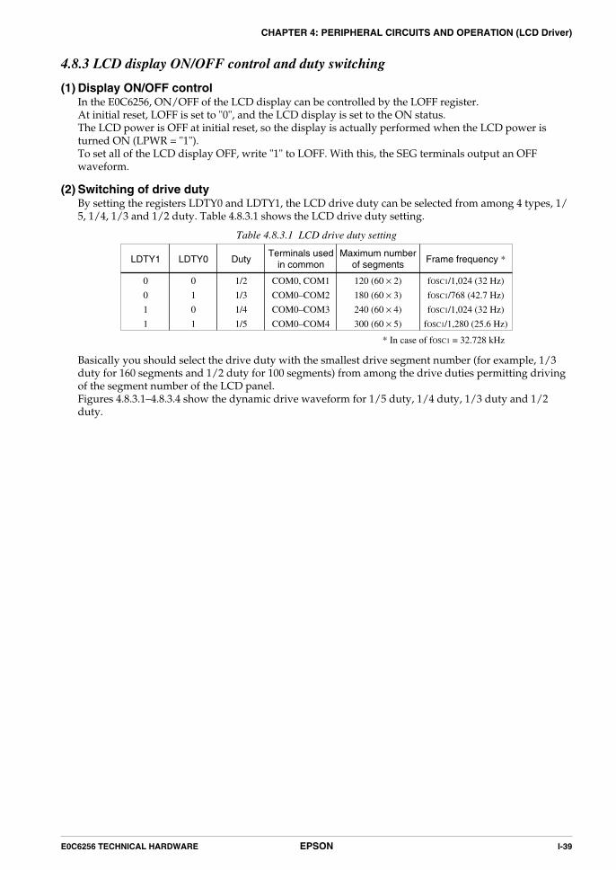
E0C6256 TECHNICAL HARDWARE EPSON I-39
CHAPTER 4: PERIPHERAL CIRCUITS AND OPERATION (LCD Driver)
4.8.3 LCD display ON/OFF control and duty switching
(1) Display ON/OFF controlIn the E0C6256, ON/OFF of the LCD display can be controlled by the LOFF register.At initial reset, LOFF is set to "0", and the LCD display is set to the ON status.The LCD power is OFF at initial reset, so the display is actually performed when the LCD power isturned ON (LPWR = "1").To set all of the LCD display OFF, write "1" to LOFF. With this, the SEG terminals output an OFFwaveform.
(2) Switching of drive dutyBy setting the registers LDTY0 and LDTY1, the LCD drive duty can be selected from among 4 types, 1/5, 1/4, 1/3 and 1/2 duty. Table 4.8.3.1 shows the LCD drive duty setting.
Table 4.8.3.1 LCD drive duty setting
LDTY1
0
0
1
1
LDTY0
0
1
0
1
Duty
1/2
1/3
1/4
1/5
COM0, COM1
COM0–COM2
COM0–COM3
COM0–COM4
Frame frequency *
fOSC1/1,024 (32 Hz)
fOSC1/768 (42.7 Hz)
fOSC1/1,024 (32 Hz)
fOSC1/1,280 (25.6 Hz)
120 (60 × 2)
180 (60 × 3)
240 (60 × 4)
300 (60 × 5)
Terminals usedin common
Maximum numberof segments
* In case of fOSC1 = 32.728 kHz
Basically you should select the drive duty with the smallest drive segment number (for example, 1/3duty for 160 segments and 1/2 duty for 100 segments) from among the drive duties permitting drivingof the segment number of the LCD panel.Figures 4.8.3.1–4.8.3.4 show the dynamic drive waveform for 1/5 duty, 1/4 duty, 1/3 duty and 1/2duty.

I-40 EPSON E0C6256 TECHNICAL HARDWARE
CHAPTER 4: PERIPHERAL CIRCUITS AND OPERATION (LCD Driver)
Fig. 4.8.3.1 Drive waveform for 1/5 duty
COM0
COM1
COM2
COM3
COM4
VVVV
DDL1L2L3
SEG0–SEG59
Frame frequency
Not litLit
LCD lighting status
COM0COM1COM2COM3COM4
SEG0–59VVVV
DDL1L2L3

E0C6256 TECHNICAL HARDWARE EPSON I-41
CHAPTER 4: PERIPHERAL CIRCUITS AND OPERATION (LCD Driver)
COM0
COM1
COM2
COM3
COM4
VVVV
DDL1L2L3
VVVV
DDL1L2L3
SEG0–SEG59
Frame frequency
Not litLit
LCD lighting status
COM0COM1COM2COM3
SEG0–59
Fig. 4.8.3.2 Drive waveform for 1/4 duty

I-42 EPSON E0C6256 TECHNICAL HARDWARE
CHAPTER 4: PERIPHERAL CIRCUITS AND OPERATION (LCD Driver)
COM0
COM1
COM2
COM3
COM4
VVVV
DDL1L2L3
VVVV
DDL1L2L3
Not litLit
SEG0–SEG59
Frame frequency
LCD lighting status
COM0COM1COM2
SEG0–59
COM0
COM1
COM2
COM3
COM4
VVVV
DDL1L2L3
VVVV
DDL1L2L3
Not litLit
SEG0–SEG59
Frame frequency
LCD lighting status
SEG0–59
COM0COM1
Fig. 4.8.3.4 Drive waveform for 1/2 duty
Fig. 4.8.3.3 Drive waveform for 1/3 duty

E0C6256 TECHNICAL HARDWARE EPSON I-43
CHAPTER 4: PERIPHERAL CIRCUITS AND OPERATION (LCD Driver)
4.8.4 Switching between dynamic and static driveThe E0C6256 provides software setting of the LCD static drive.The frame frequency during static driving is fixed at 32 Hz (when fOSC1 = 32.768 kHz) regardless of thedrive duty selection.This function enables easy adjustment (cadence adjustment) of the oscillation frequency of the OSC1oscillation circuit (crystal oscillation circuit).
The procedure for executing static drive of the LCD is as follows:
➀ Write "1" to register STCD at address C2H•D2.
➁ Write the same value to all registers corresponding to COM0–COM4 of the display memory.
Note: • When setting the static drive, all the COM outputs become effective regardless of the drive dutyselection. Hence, for static drive, set the same value to all display memory corresponding toCOM0–COM4 even when a drive duty other than 1/5 duty has been selected.
• For cadence adjustment, set the display data corresponding to COM0–COM4, so that all theLCDs light.
Figure 4.8.4.1 shows the drive waveform for static drive.
VVVV
DDL1L2L3
VVVV
DDL1L2L3
SEG0–SEG59
Frame frequency
LCD lighting status
COM0COM1COM2COM3COM4
SEG0–59
COM0–COM4
(LOFF = "0")
Lit Not lit
(LOFF = "1")
Fig. 4.8.4.1 LCD static drive waveform
4.8.5 Display memory areaThe display memory is allocated in the data memory area, addresses 30H–7FH in page 1 or page 5. Eitherof the areas used can be selected using the software (LDMS register).By setting LDMS to "1", page 1 is selected and addresses 130H–17FH become the display memory. Since aRAM has been allocated in this area, it can be used as the display memory for reading/writing. For thisreason, control in a bit unit can simply be done using an arithmetic instruction. However, this area shouldnot be used for general purpose RAM.At initial reset, LDMS is set to "0" and page 5 (530H–57FH) becomes the display memory. When this area isselected, all the internal RAM (0 to 4 page) can be used as general purpose RAM. However, since thedisplay memory is write only, data modification by arithmetic instructions cannot be done.Correspondence between segment outputs and bits within the display memory can be optionally set by themask option explained in the next section.

I-44 EPSON E0C6256 TECHNICAL HARDWARE
CHAPTER 4: PERIPHERAL CIRCUITS AND OPERATION (LCD Driver)
4.8.6 Mask option (segment allocation)
(1) Segment allocationThe LCD driver has a segment decoder built-in, and the data bit (D0–D3) of the optional address in thedisplay memory area (30H–7FH) can be allocated to the optional segment. This makes design easy byincreasing the degree of freedom with which the liquid crystal panel can be designed.The allocated segment displays when the bit for the display memory is set to "1", and goes out when bitis set to "0".
Figure 4.8.6.1 shows an example of the relationship between the LCD segments (on the panel) and thedisplay memory for the case of 1/3 duty.
a a'
f f'
g'g
e e'
d d'p'p
c'
b'b
c
SEG10 SEG11 SEG12
Common 0 Common 1 Common 2
7AH
7BH
7CH
7DH
Address
d
p
d '
p '
D3
c
g
c '
g '
D2
b
f
b '
f '
D1
a
e
a '
e '
D0
Data
Display memory allocation
SEG10
SEG11
SEG12
7A, D0(a)
7A, D1(b)
7D, D1(f ' )
7B, D1(f )
7B, D2(g)
7A, D2(c)
7B, D0(e)
7A, D3(d)
7B, D3(p)
Pin address allocation
Common 0 Common 1 Common 2
Fig. 4.8.6.1 Segment allocation
(2) Output specification
➀ The segment terminals (SEG0–SEG59) can be selected with the mask option par two terminals foreither segment signal output or DC output (VDD and VSS binary output).When DC output is selected, the data corresponding to COM0 of each segment terminal is output.
➁ When DC output is selected, either complementary output or Pch open drain output can be selectedfor each terminal with the mask option.

E0C6256 TECHNICAL HARDWARE EPSON I-45
CHAPTER 4: PERIPHERAL CIRCUITS AND OPERATION (LCD Driver)
4.8.7 Control of LCD driverTable 4.8.7.1 shows the LCD driver's control bits and their addresses. Figure 4.8.7.1 shows the displaymemory map.
Table 4.8.7.1 LCD driver control bits
Address CommentRegister
D3 D2 D1 D0 Name Init 1 0*1*7
VLCHG0
R
0VLCHG2VLCHG1VLCHG0
–000
VLCHG1VLCHG20
84H
*2 Unused
VL1 output voltage change
0: 1.05, 1: 1.10, 2: 1.15, 3: 1.20,
4: 1.25, 5: 1.30, 6: 1.35, 7: 1.40 (V)R/W
*5
C2HLDTY0
R/W
LDMSSTCDLDTY1LDTY0
1p(R/W)Static
5p(W)Dynamic
LDTY1STCDLDMS0000
LPWR
R
00
LOFFLPWR
––00
All OffOn
NormalOff
LOFF00
C3H
*2
*2
LCD data memory area selection
LCD drive switch
LCD drive duty selection
0: 1/2, 1: 1/3, 2: 1/4, 3: 1/5
Unused
Unused
LCD display control
LCD power supply On/OffR/W
*5
*5
*1 Initial value at the time of initial reset *5 Constantly "0" when being read*2 Not set in the circuit *6 Refer to main manual*3 Undefined *7 Page switching in I/O memory is not necessary*4 Reset (0) immediately after being read
AddressPage High
Low 0 1 2 3 4 5 6 7 8 9 A B C D E F
34567
1or5
Display memory (80 words × 4 bits) Page 1: R/W Page 5: W only
Fig. 4.8.7.1 Display memory map
VLCHG0–VLCHG2: VL1 output voltage change (84H•D0–D2)The voltage value of the LCD drive voltage VL1 can be selected among 8 types as shown in Table 4.8.7.2.
Table 4.8.7.2 VL1 settingVLCHG2
0
0
0
0
1
1
1
1
VLCHG1
0
0
1
1
0
0
1
1
VLCHG0
0
1
0
1
0
1
0
1
VL1 voltage
-1.05 V
-1.10 V
-1.15 V
-1.20 V
-1.25 V
-1.30 V
-1.35 V
-1.40 V
(Voltage value: VDD reference)
At initial reset, these registers are set to "0".
LPWR: LCD power supply ON/OFF (C3H•D0)Controls the LCD power ON and OFF
When "1" is written: Power ONWhen "0" is written: Power OFF
Reading: Valid
By writing "1" to LPWR, the LCD power goes ON.When "0" is written, the LCD power goes OFF and all terminals of the COM output and SEG outputbecome VDD level.When the LCD power is set to OFF and the A/D converter power is set to ON (APWR = "1"), COM andSEG terminals become VL1 level.This control does not affect to SEG terminals that have been set for DC output.At initial reset, this register is set to "0".
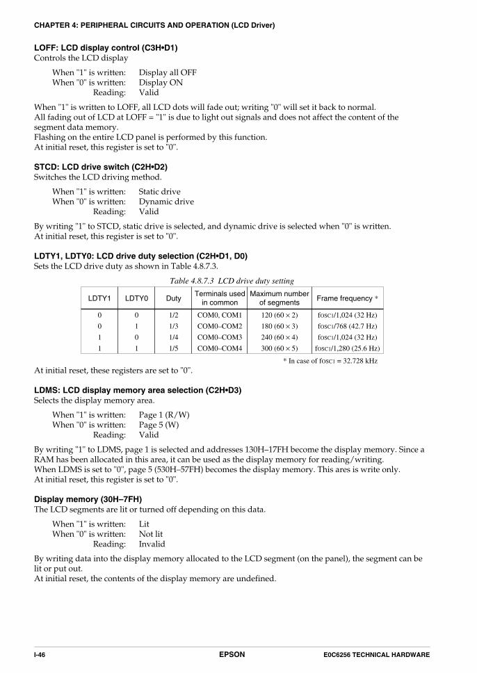
I-46 EPSON E0C6256 TECHNICAL HARDWARE
CHAPTER 4: PERIPHERAL CIRCUITS AND OPERATION (LCD Driver)
LOFF: LCD display control (C3H•D1)Controls the LCD display
When "1" is written: Display all OFFWhen "0" is written: Display ON
Reading: Valid
When "1" is written to LOFF, all LCD dots will fade out; writing "0" will set it back to normal.All fading out of LCD at LOFF = "1" is due to light out signals and does not affect the content of thesegment data memory.Flashing on the entire LCD panel is performed by this function.At initial reset, this register is set to "0".
STCD: LCD drive switch (C2H•D2)Switches the LCD driving method.
When "1" is written: Static driveWhen "0" is written: Dynamic drive
Reading: Valid
By writing "1" to STCD, static drive is selected, and dynamic drive is selected when "0" is written.At initial reset, this register is set to "0".
LDTY1, LDTY0: LCD drive duty selection (C2H•D1, D0)Sets the LCD drive duty as shown in Table 4.8.7.3.
Table 4.8.7.3 LCD drive duty setting
LDTY1
0
0
1
1
LDTY0
0
1
0
1
Duty
1/2
1/3
1/4
1/5
COM0, COM1
COM0–COM2
COM0–COM3
COM0–COM4
Frame frequency *
fOSC1/1,024 (32 Hz)
fOSC1/768 (42.7 Hz)
fOSC1/1,024 (32 Hz)
fOSC1/1,280 (25.6 Hz)
120 (60 × 2)
180 (60 × 3)
240 (60 × 4)
300 (60 × 5)
Terminals usedin common
Maximum numberof segments
* In case of fOSC1 = 32.728 kHzAt initial reset, these registers are set to "0".
LDMS: LCD display memory area selection (C2H•D3)Selects the display memory area.
When "1" is written: Page 1 (R/W)When "0" is written: Page 5 (W)
Reading: Valid
By writing "1" to LDMS, page 1 is selected and addresses 130H–17FH become the display memory. Since aRAM has been allocated in this area, it can be used as the display memory for reading/writing.When LDMS is set to "0", page 5 (530H–57FH) becomes the display memory. This ares is write only.At initial reset, this register is set to "0".
Display memory (30H–7FH)The LCD segments are lit or turned off depending on this data.
When "1" is written: LitWhen "0" is written: Not lit
Reading: Invalid
By writing data into the display memory allocated to the LCD segment (on the panel), the segment can belit or put out.At initial reset, the contents of the display memory are undefined.

E0C6256 TECHNICAL HARDWARE EPSON I-47
CHAPTER 4: PERIPHERAL CIRCUITS AND OPERATION (LCD Driver)
4.8.8 Programming notes(1) The contents of the display memory are undefined until the area is initialized (through, for instance,
memory clear processing by the CPU). Initialize the display memory by executing initial processing.
(2) When page 5 is selected for the display memory area, since the display memory area is write-only,display data cannot be rewritten by arithmetic operations (such as AND, OR, ADD, SUB).
(3) 100 msec or more time is necessary for stabilizing the LCD drive voltages VL1, VL2 and VL3 after settingthe LCD power control register LPWR to "1". Be careful of the segment-on right after the power isturned on.

I-48 EPSON E0C6256 TECHNICAL HARDWARE
CHAPTER 4: PERIPHERAL CIRCUITS AND OPERATION (Clock Timer)
4.9 Clock Timer
4.9.1 Configuration of clock timerThe E0C6256 has a built-in clock timer with OSC1 divided clock as clock source. The clock timer isconfigured of a 8-bit binary counter and the timer data (128–16 Hz and 8–1 Hz) can be read out by thesoftware.Figure 4.9.1.1 is the block diagram for the clock timer.
128 Hz–16 Hz
Data bus
32 Hz, 16 Hz, 8 Hz, 2 Hz
256 Hz
Clock timer reset signal
OSC1dividing circuit
Interrupt requestInterruptcontrol
8 Hz–1 Hz
Clock timer
OSC1oscillation circuit
32 kHz
Fig. 4.9.1.1 Block diagram for the clock timer
Ordinarily, this clock timer is used for all types of timing functions such as clocks.
4.9.2 Data reading and hold functionThe 8 bits timer data are allocated to the address C5H and C6H.
C5H D0: TM0 (128 Hz) D1: TM1 (64 Hz) D2: TM2 (32 Hz) D3: TM3 (16 Hz)C6H D0: TM4 (8 Hz) D1: TM5 (4 Hz) D2: TM6 (2 Hz) D3: TM7 (1 Hz)
Since the clock timer data has been allocated to two addresses, a carry is generated from the low-order datawithin the count (TM0–TM3: 128–16 Hz) to the high-order data (TM4–TM7: 8–1 Hz). When this carry isgenerated between the reading of the low-order data and the high-order data, a content combining the twodoes not become the correct value (the low-order data is read as 0FH and the high-order data becomes thevalue that is counted up 1 from that point).The high-order data hold function in the E0C6256 is designed to operate to avoid this. This functiontemporarily stops the counting up of the high-order data (by carry from the low-order data) at the pointwhere the low-order data has been read and consequently the time during which the high-order data isheld is the shorter of the two indicated here following.
1. Period until it reads the high-order data.2. 0.48–1.5 msec (varies due to the timing of the reading)
Note: When the high-order data has previously been read, since the low-order data is not held, you shouldbe sure to first read from the low-order data.
4.9.3 Interrupt functionThe clock timer can cause interrupts at the falling edge of 32 Hz, 16 Hz, 8 Hz and 2 Hz signals. Softwarecan set whether to mask any of these frequencies.Figure 4.9.3.1 is the timing chart of the clock timer.

E0C6256 TECHNICAL HARDWARE EPSON I-49
CHAPTER 4: PERIPHERAL CIRCUITS AND OPERATION (Clock Timer)
Clock timer timing chartFrequencyRegisterAddress
C6H
D3
D0
D1
D2
4 Hz
2 Hz
16 Hz interrupt request
8 Hz interrupt request
C5H
2 Hz interrupt request
D3 1 Hz
D0
D1
D2
128 Hz
16 Hz
8 Hz
32 Hz
64 Hz
(When fOSC1 = 32.768 kHz)
32 Hz interrupt request
Fig. 4.9.3.1 Timing chart of clock timer
As shown in Figure 4.9.3.1, interrupt is generated at the falling edge of the frequencies (32 Hz, 16 Hz, 8 Hz,2 Hz). At this time, the corresponding interrupt factor flag (IT0, IT1, IT2, IT3) is set to "1". Selection ofwhether to mask the separate interrupts can be made with the interrupt mask registers (EIT0, EIT1, EIT2,EIT3). However, regardless of the interrupt mask register setting, the interrupt factor flag is set to "1" at thefalling edge of the corresponding signal.
4.9.4 Control of clock timerTable 4.9.4.1 shows the clock timer control bits and their addresses.
Table 4.9.4.1 Control bits of clock timer
D3 D2 D1 D0 Name Init 1 0*1
C4HTMRST
R
00
TMRUNTMRST
––0
Reset
RunReset
Stop–
TMRUN00
C5HTM0
R
TM3TM2TM1TM0
0000
TM1TM2TM3
C6HTM4
R
TM7TM6TM5TM4
0000
Clock timer data (1 Hz)
Clock timer data (2 Hz)
Clock timer data (4 Hz)
Clock timer data (8 Hz)
TM5TM6TM7
*7
Unused
Unused
Clock timer Run/Stop
Clock timer reset
Clock timer data (16 Hz)
Clock timer data (32 Hz)
Clock timer data (64 Hz)
Clock timer data (128 Hz)
R/W W
Address CommentRegister
*2
*2
*5
*5
*5
F6HEIT0
R/W
EIT3EIT2EIT1EIT0
0000
Interrupt mask register (Clock timer 2 Hz)
Interrupt mask register (Clock timer 8 Hz)
Interrupt mask register (Clock timer 16 Hz)
Interrupt mask register (Clock timer 32 Hz)
EnableEnableEnableEnable
MaskMaskMaskMask
EIT1EIT2EIT3
FEHIT0
R
IT3IT2IT1IT0
0000
Interrupt factor flag (Clock timer 2 Hz)
Interrupt factor flag (Clock timer 8 Hz)
Interrupt factor flag (Clock timer 16 Hz)
Interrupt factor flag (Clock timer 32 Hz)
YesYesYesYes
NoNoNoNo
IT1IT2IT3 *4
*4
*4
*4
*1 Initial value at the time of initial reset *5 Constantly "0" when being read*2 Not set in the circuit *6 Refer to main manual*3 Undefined *7 Page switching in I/O memory is not necessary*4 Reset (0) immediately after being read

I-50 EPSON E0C6256 TECHNICAL HARDWARE
CHAPTER 4: PERIPHERAL CIRCUITS AND OPERATION (Clock Timer)
TM0–TM7: Timer data (C5H, C6H)The 128 Hz–1 Hz timer data of the clock timer can be read out with these registers. These eight bits are readonly, and writing operations are invalid.By reading the low-order data (C5H), the high-order data (C6H) is held while the shorter of the twoindicated here following.
1. Period until it reads the high-order data.2. 0.48–1.5 msec (varies due to the timing of the reading)
At initial reset, the timer data is initialized to "00H".
TMRST: Clock timer reset (C4H•D0)This bit resets the clock timer.
When "1" is written: Clock timer resetWhen "0" is written: No operation
Reading: Always "0"
The clock timer is reset by writing "1" to TMRST. When the clock timer is reset in the RUN status, operationrestarts immediately. Also, in the STOP status the reset data is maintained.This bit is write-only, and so is always "0" at reading.
TMRUN: Clock timer RUN/STOP (C4H•D1)This bit controls RUN/STOP of the clock timer.
When "1" is written: RUNWhen "0" is written: STOP
Reading: Valid
The clock timer enters the RUN status when "1" is written to TMRUN, and the STOP status when "0" iswritten.In the STOP status, the timer data is maintained until the next RUN status or resets timer. Also, when theSTOP status changes to the RUN status, the data that was maintained can be used for resuming the count.At initial reset, this register is set to "0".
EIT0, EIT1, EIT2, EIT3: Interrupt mask registers (F6H)These registers are used to select whether to mask the clock timer interrupt.
When "1" is written: EnabledWhen "0" is written: Masked
Reading: Valid
The interrupt mask registers (EIT0, EIT1, EIT2, EIT3) are used to select whether to mask the interrupt to theseparate frequencies (32 Hz, 16 Hz, 8 Hz, 2 Hz).At initial reset, these registers are all set to "0".
IT0, IT1, IT2, IT3: Interrupt factor flags (FEH)These flags indicate the status of the clock timer interrupt.
When "1" is read: Interrupt has occurredWhen "0" is read: Interrupt has not occurred
Writing: Invalid
The interrupt factor flags (IT0, IT1, IT2, IT3) correspond to the clock timer interrupts of the respectivefrequencies (32 Hz, 16 Hz, 8 Hz, 2 Hz). The software can judge from these flags whether there is a clocktimer interrupt. However, even if the interrupt is masked, the flags are set to "1" at the falling edge of thesignal.These flags can be reset through being read out by the software.Reading of interrupt factor flags is available at EI, but be careful in the following cases.If the interrupt mask register value corresponding to the interrupt factor flags to be read is set to "1", aninterrupt request will be generated by the interrupt factor flags set timing, or an interrupt request will notbe generated.At initial reset, these flags are set to "0".

E0C6256 TECHNICAL HARDWARE EPSON I-51
CHAPTER 4: PERIPHERAL CIRCUITS AND OPERATION (Clock Timer)
4.9.5 Programming notes(1) Be sure to data reading in the order of low-order data (TM0–TM3) then high-order data (TM4–TM7).
(2) When the clock timer has been reset, the interrupt factor flag (IT) may sometimes be set to "1". Conse-quently, perform flag reading (reset the flag) as necessary at reset.
(3) Reading of interrupt factor flags is available at EI, but be careful in the following cases.If the interrupt mask register value corresponding to the interrupt factor flags to be read is set to "1", aninterrupt request will be generated by the interrupt factor flags set timing, or an interrupt request willnot be generated.
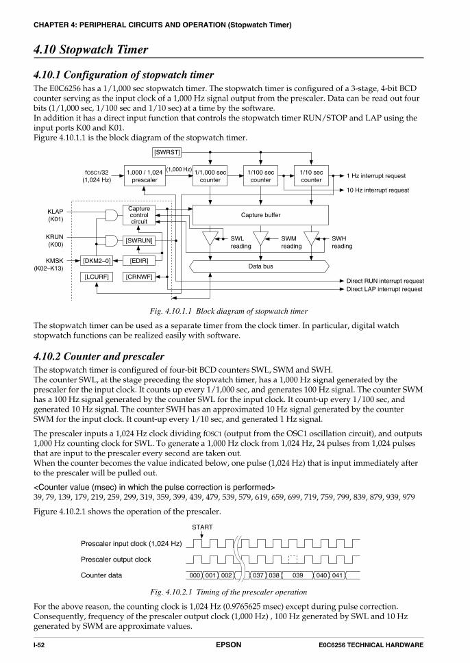
I-52 EPSON E0C6256 TECHNICAL HARDWARE
CHAPTER 4: PERIPHERAL CIRCUITS AND OPERATION (Stopwatch Timer)
4.10 Stopwatch Timer
4.10.1 Configuration of stopwatch timerThe E0C6256 has a 1/1,000 sec stopwatch timer. The stopwatch timer is configured of a 3-stage, 4-bit BCDcounter serving as the input clock of a 1,000 Hz signal output from the prescaler. Data can be read out fourbits (1/1,000 sec, 1/100 sec and 1/10 sec) at a time by the software.In addition it has a direct input function that controls the stopwatch timer RUN/STOP and LAP using theinput ports K00 and K01.Figure 4.10.1.1 is the block diagram of the stopwatch timer.
Data bus
1 Hz interrupt request1,000 / 1,024prescaler
fOSC1/32(1,024 Hz)
1/1,000 seccounter
1/100 seccounter
1/10 seccounter
Capture buffer
SWLreading
SWMreading
SWHreading
[SWRST]
10 Hz interrupt request
Capturecontrolcircuit
[SWRUN]
[EDIR]
[CRNWF]
[DKM2–0]
[LCURF]
KLAP(K01)
KRUN(K00)
KMSK(K02–K13)
Direct RUN interrupt requestDirect LAP interrupt request
(1,000 Hz)
Fig. 4.10.1.1 Block diagram of stopwatch timer
The stopwatch timer can be used as a separate timer from the clock timer. In particular, digital watchstopwatch functions can be realized easily with software.
4.10.2 Counter and prescalerThe stopwatch timer is configured of four-bit BCD counters SWL, SWM and SWH.The counter SWL, at the stage preceding the stopwatch timer, has a 1,000 Hz signal generated by theprescaler for the input clock. It counts up every 1/1,000 sec, and generates 100 Hz signal. The counter SWMhas a 100 Hz signal generated by the counter SWL for the input clock. It count-up every 1/100 sec, andgenerated 10 Hz signal. The counter SWH has an approximated 10 Hz signal generated by the counterSWM for the input clock. It count-up every 1/10 sec, and generated 1 Hz signal.
The prescaler inputs a 1,024 Hz clock dividing fOSC1 (output from the OSC1 oscillation circuit), and outputs1,000 Hz counting clock for SWL. To generate a 1,000 Hz clock from 1,024 Hz, 24 pulses from 1,024 pulsesthat are input to the prescaler every second are taken out.When the counter becomes the value indicated below, one pulse (1,024 Hz) that is input immediately afterto the prescaler will be pulled out.
<Counter value (msec) in which the pulse correction is performed>39, 79, 139, 179, 219, 259, 299, 319, 359, 399, 439, 479, 539, 579, 619, 659, 699, 719, 759, 799, 839, 879, 939, 979
Figure 4.10.2.1 shows the operation of the prescaler.
Fig. 4.10.2.1 Timing of the prescaler operation
For the above reason, the counting clock is 1,024 Hz (0.9765625 msec) except during pulse correction.Consequently, frequency of the prescaler output clock (1,000 Hz) , 100 Hz generated by SWL and 10 Hzgenerated by SWM are approximate values.
Prescaler input clock (1,024 Hz)
Prescaler output clock
Counter data
START
000 001 002 037 038 039 040 041
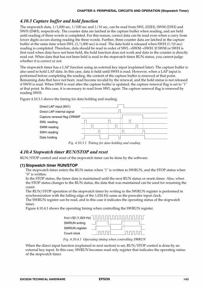
E0C6256 TECHNICAL HARDWARE EPSON I-53
CHAPTER 4: PERIPHERAL CIRCUITS AND OPERATION (Stopwatch Timer)
4.10.3 Capture buffer and hold functionThe stopwatch data, 1/1,000 sec, 1/100 sec and 1/10 sec, can be read from SWL (D2H), SWM (D3H) andSWH (D4H), respectively. The counter data are latched in the capture buffer when reading, and are helduntil reading of three words is completed. For this reason, correct data can be read even when a carry fromlower digits occurs during reading the three words. Further, three counter data are latched in the capturebuffer at the same time when SWL (1/1,000 sec) is read. The data hold is released when SWH (1/10 sec)reading is completed. Therefore, data should be read in order of SWL→SWM→SWH. If SWM or SWH isfirst read when data have not been held, the hold function does not work and data in the counter is directlyread out. When data that has not been held is read in the stopwatch timer RUN status, you cannot judgewhether it is correct or not.
The stopwatch timer has a LAP function using an external key input (explained later). The capture buffer isalso used to hold LAP data. In this case, data is held until SWH is read. However, when a LAP input isperformed before completing the reading, the content of the capture buffer is renewed at that point.Remaining data that have not been read become invalid by the renewal, and the hold status is not releasedif SWH is read. When SWH is read after the capture buffer is updated, the capture renewal flag is set to "1"at that point. In this case, it is necessary to read from SWL again. The capture renewal flag is renewed byreading SWH.
Figure 4.10.3.1 shows the timing for data holding and reading.
Direct LAP input (K01)
Direct LAP internal signal
Capture renewal flag CRNWF
SWL reading
SWM reading
SWH reading
Data holding
Fig. 4.10.3.1 Timing for data holding and reading
4.10.4 Stopwatch timer RUN/STOP and resetRUN/STOP control and reset of the stopwatch timer can be done by the software.
(1) Stopwatch timer RUN/STOPThe stopwatch timer enters the RUN status when "1" is written to SWRUN, and the STOP status when"0" is written.In the STOP status, the timer data is maintained until the next RUN status or resets timer. Also, whenthe STOP status changes to the RUN status, the data that was maintained can be used for resuming thecount.The RUN/STOP operation of the stopwatch timer by writing to the SWRUN register is performed insynchronization with the falling edge of the 1,024 Hz same as the prescaler input clock.The SWRUN register can be read, and in this case it indicates the operating status of the stopwatchtimer.Figure 4.10.4.1 shows the operating timing when controlling the SWRUN register.
fOSC1/32 (1,024 Hz)
SWRUN writing
SWRUN register
Count clock
Fig. 4.10.4.1 Operating timing when controlling SWRUN
When the direct input function (explained in next section) is set, RUN/STOP control is done by anexternal key input. In this case, SWRUN becomes read only register that indicates the operating statusof the stopwatch timer.

I-54 EPSON E0C6256 TECHNICAL HARDWARE
CHAPTER 4: PERIPHERAL CIRCUITS AND OPERATION (Stopwatch Timer)
(2) Stopwatch timer resetThe stopwatch timer is reset when "1" is written to SWRST. With this, the counter value is cleared to"000".Since this resetting does not affect the capture buffer, data that has been held in the capture buffer isnot cleared and is maintained as is.When the stopwatch timer is reset in the RUN status, counting restarts from count "000". Also, in theSTOP status the reset data "000" is maintained until the next RUN.
4.10.5 Direct input function and key maskThe stopwatch timer has a direct input function that can control the RUN/STOP and LAP operation of thestopwatch timer by external key input. This function is set by writing "1" to the EDIR register. When EDIRis set to "0", only the software control is possible as explained in the previous section.
(1) Direct RUNWhen the direct input function is selected, RUN/STOP operation of the stopwatch timer can be control-led by using the key connected to the input port K00. K00 works as a normal input port, but the inputsignal is sent to the stopwatch control circuit. The key input signal from the K00 port works as a toggleswitch. When it is input in STOP status, the stopwatch timer runs, and in RUN status, the stopwatchtimer stops. RUN/STOP status of the stopwatch timer can be checked by reading the SWRUN register.An interrupt is generated by direct RUN input.The sampling for key input signal is performed at the falling edge of 1,024 Hz signal same as theSWRUN control. The chattering judgment is performed at the point where the key turns OFF, and achattering less than 46.8–62.5 msec is removed. Therefore, more time is needed for an interval betweenRUN and STOP key inputs.Figure 4.10.5.1 shows the operating timing for the direct RUN input.
Fig. 4.10.5.1 Operating timing for direct RUN input
(2) Direct LAPControl for the LAP can also be done by key input same as the direct RUN. When the direct inputfunction is selected, the input port K01 becomes the LAP key input port. Sampling for the input signaland the chattering judgment are the same as a direct RUN.By entering the LAP key, the counter data at that point is latched into the capture buffer and is held.The counter continues counting operation. Furthermore, an interrupt occurs by direct LAP input.As stated above, the capture buffer data is held until SWH is read. If the LAP key is input when datahas been already held, it renews the content of the capture buffer. When SWH is read after renewing,the capture renewal flag is set to "1". In this case, the hold status is not released by reading SWH, and itcontinues. Normally the LAP data should be read after the interrupt is generated. After that, be sure tocheck the capture renewal flag. When the capture renewal flag is set, renewed data is held in thecapture buffer. So it is necessary to read from SWL again.The stopwatch timer sets the 1 Hz interrupt factor flag ISW1 to "1" when requiring a carry-up to 1-secdigit by an SWH overflow. If the capture buffer shifts into hold status (when SWL is read or when LAPis input) while the 1 Hz interrupt factor flag ISW1 is set to "1", the lap data carry-up request flag LCURFis set to "1" to indicate that a carry-up to 1-sec digit is required for the processing of LAP input. Innormal software processing, LAP processing may take precedence over 1-sec or higher digits process-ing by a 1 Hz interrupt, therefore carry-up processing using this flag should be used for time display inthe LAP processing to prevent the 1-sec digit data decreasing by 1 second. This flag is renewed whenthe capture buffer shifts into hold status.
Figure 4.10.5.2 shows the operating timing for the direct LAP input, and Figure 4.10.5.3 shows thetimings for data holding and reading during a direct LAP input and reading.
fOSC1/32 (1,024 Hz)
Direct RUN input (K00)
Direct RUN internal signal
SWRUN register
Count clock
Direct RUN interrupt

E0C6256 TECHNICAL HARDWARE EPSON I-55
CHAPTER 4: PERIPHERAL CIRCUITS AND OPERATION (Stopwatch Timer)
Fig. 4.10.5.2 Operating timing for direct LAP input
fOSC1/32 (1,024 Hz)
Direct LAP input (K01)
Direct LAP internal signal
Data holding
Direct LAP interrupt
SWH reading
Direct LAP input (K01)
Capture renewal flag CRNWF
SWL reading
SWM reading
SWH reading
Data holding
1 Hz interrupt factor flag ISW1
Lap data carry-up request flag LCURF
Counter data 999 000
Fig. 4.10.5.3 Timing for data holding and reading during direct LAP input
(3) Key maskIn stopwatch applications, some functions may be controlled by a combination of keys including directRUN or direct LAP. For instance, the RUN key can be used for other functions, such as reset and settinga watch, by pressing the RUN key with another key. In this case, the direct RUN function or direct LAPfunction must be invalid so that it does not function. For this purpose, the key mask function is set sothat it judges concurrence of input keys and invalidates RUN and LAP functions. A combination of thekey inputs for this judgment can be selected using the DKM0–DKM2 registers.
Table 4.10.5.1 Key mask selection
DKM2
0
0
0
0
1
1
1
1
DKM1
0
0
1
1
0
0
1
1
DKM0
0
1
0
1
0
1
0
1
Mask key combination
None (at initial reset)
K02
K02, K03
K02, K03, K10
K10
K10, K11
K10, K11, K12
K10, K11, K12, K13
RUN or LAP inputs become invalid in the following status.
1. The RUN or LAP key is pressed when one or more keys that are included in the selected combina-tion (here in after referred to as mask) are held down.
2. The RUN or LAP key has been pressed when the mask is released.
fOSC1/32 (1,024 Hz)
Direct RUN/LAP input
Key mask
validinvalid
invalidinvalid
Fig. 4.10.5.4 Operation of key mask

I-56 EPSON E0C6256 TECHNICAL HARDWARE
CHAPTER 4: PERIPHERAL CIRCUITS AND OPERATION (Stopwatch Timer)
RUN or LAP inputs become valid in the following status.
1. Either the RUN or LAP key is pressed independently if no other key is been held down.
2. Both the RUN and LAP keys are pressed at the same time if no other key is held down. (RUN andLAP functions are effective.)
3. The RUN or LAP key is pressed if either is held down. (RUN and LAP functions are effective.)
4. Either the RUN or LAP key and the mask key are pressed at the same time if no other key is helddown.
5. Both the RUN and LAP keys and the mask key are pressed at the same time if no other key is helddown. (RUN and LAP functions are effective.)
* Simultaneous key input is referred to as two or more key inputs are sampled at the same fallingedge of 1,024 Hz clock.
4.10.6 Interrupt function
(1) 10 Hz and 1 Hz interruptsThe 10 Hz and 1 Hz interrupts can be generated through the overflow of stopwatch timers SWM andSWH respectively. Also, software can set whether to separately mask the frequencies described earlier.Figure 4.10.6.1 is the timing chart for the counters.
10 Hz interrupt request
1 Hz interrupt request
D4H(1/10 sec BCD)
D3H(1/100 sec BCD)
D0
D1
D2
D3
D0
D1
D2
D3
Address Register Stopwatch timer (SWL) timing chart
D2H(1/1,000 sec BCD)
D0
D1
D2
D3
Address Register Stopwatch timer (SWM) timing chart
Address Register Stopwatch timer (SWH) timing chart
Fig. 4.10.6.1 Timing chart for counters

E0C6256 TECHNICAL HARDWARE EPSON I-57
CHAPTER 4: PERIPHERAL CIRCUITS AND OPERATION (Stopwatch Timer)
As shown in Figure 4.10.6.1, the interrupts are generated by the overflow of their respective counters ("9"changing to "0"). Also, at this time the corresponding interrupt factor flags (ISW0, ISW1) are set to "1".The respective interrupts can be masked separately through the interrupt mask registers (EISW0,EISW1). However, regardless of the setting of the interrupt mask registers, the interrupt factor flags areset to "1" by the overflow of their corresponding counters.
(2) Direct RUN and direct LAP interruptsWhen the direct input function is selected, the direct RUN and direct LAP interrupts can be generated.The respective interrupts occur at the rising edge of the internal signal for direct RUN and direct LAPafter sampling the direct input signal in the falling edge of 1,024 Hz signal. Also, at this time thecorresponding interrupt factor flags (IRUN, ILAP) are set to "1".The respective interrupts can be masked separately through the interrupt mask registers (EIRUN,EILAP). However, regardless of the setting of the interrupt mask registers, the interrupt factor flags areset to "1" by the inputs of the RUN and LAP.
The direct RUN function uses the K00 port and the direct LAP function uses the K01 port. Therefore,the direct input interrupt and the K00–K03 inputs interrupt may generate at the same time dependingon the interrupt condition setting for the input port K00–K03. Consequently, when using the directinput interrupt, set the interrupt selection registers SIK00 and SIK01 to "0" so that the input interruptdoes not generate by K00 and K01 inputs.
fOSC1/32 (1,024 Hz)
SWRST writing
EDIR writing
EDIR register
Direct RUN input
SWRUN writing
SWRUN register
Direct LAP input
Counter data
Capture buffer
SWL reading
SWM reading
SWH reading
CRNWF
1 Hz interrupt factor flag ISW1
LCURF
Direct RUN interrupt
Direct LAP interrupt
10 Hz interrupt
1 Hz interrupt
001 002 003 004 005 006 098 099 100 101 102 000 001 002 003 004 005 006 007 993 994000 995 996 997 998 999 000 001 002 003 004 005 006 007
003 005 995 001 006
Fig. 4.10.6.2 Timing chart for stopwatch timer

I-58 EPSON E0C6256 TECHNICAL HARDWARE
CHAPTER 4: PERIPHERAL CIRCUITS AND OPERATION (Stopwatch Timer)
4.10.7 Control of stopwatch timerTable 4.10.7.1 lists the stopwatch timer control bits and their addresses.
Table 4.10.7.1 Control bits of stopwatch timer
D3 D2 D1 D0 Name Init 1 0*1
D0HDKM0
EDIRDKM2DKM1DKM0
0000
Enable direct input function
Direct key mask factor 0: Non, 1: K02,
2: K02-03, 3: K02-03-10, 4: K10, 5: K10-11,
6: K10-11-12, 7: K10-11-12-13
Enable DisableDKM1DKM2EDIR
D1HSWRST
LCURFCRNWFSWRUNSWRST
000
Reset
ReqestRenewal
RunReset
NoNo
Stop–
SWRUNCRNWFLCURF
D2HSWL0
R
SWL3SWL2SWL1SWL0
SWL1SWL2SWL30000
SWM0
R
SWM3SWM2SWM1SWM0
0000
SWM1SWM2SWM3
D3H
D4HSWH0
R
SWH3SWH2SWH1SWH0
0000
SWH1SWH2SWH3
*7
Lap data carry-up request flag
Capture renewal flag
Stopwatch timer Run/Stop
Stopwatch timer reset
MSB
LSB
R/W
R
Stopwatch timer data 1/1000 sec (BCD)
R/W W
MSB
LSB
Stopwatch timer data 1/100 sec (BCD)
MSB
LSB
Stopwatch timer data 1/10 sec (BCD)
Address CommentRegister
*5
F5HEISW0
R/W
EIRUNEILAPEISW1EISW0
0000
EnableEnableEnableEnable
MaskMaskMaskMask
EISW1EILAPEIRUNInterrupt mask register (Stopwatch direct RUN)
Interrupt mask register (Stopwatch direct LAP)
Interrupt mask register (Stopwatch 1 Hz)
Interrupt mask register (Stopwatch 10 Hz)
FDHISW0
R
IRUN ILAP ISW1 ISW0
0000
YesYesYesYes
NoNoNoNo
ISW1ILAPIRUNInterrupt factor flag (Stopwatch direct RUN)
Interrupt factor flag (Stopwatch direct LAP)
Interrupt factor flag (Stopwatch 1 Hz)
Interrupt factor flag (Stopwatch 10 Hz)
*4
*4
*4
*4
*1 Initial value at the time of initial reset *5 Constantly "0" when being read*2 Not set in the circuit *6 Refer to main manual*3 Undefined *7 Page switching in I/O memory is not necessary*4 Reset (0) immediately after being read
SWL0–SWL3: Stopwatch timer data 1/1,000 sec (D2H)Data (BCD) of the 1/1,000 sec column of the capture buffer can be read out.The hold function of the capture buffer works by reading this data.These 4 bits are read-only, and cannot be used for writing operations.At initial reset, the timer data is set to "0".
SWM0–SWM3: Stopwatch timer data 1/100 sec (D3H)Data (BCD) of the 1/100 sec column of the capture buffer can be read out. These 4 bits are read-only, andcannot be used for writing operations.At initial reset, the timer data is set to "0".
SWH0–SWH3: Stopwatch timer data 1/10 sec (D4H)Data (BCD) of the 1/10 sec column of the capture buffer can be read out. These 4 bits are read-only, andcannot be used for writing operations.At initial reset, the timer data is set to "0".
Note: Be sure to data reading in the order of SWL→SWM→SWH.

E0C6256 TECHNICAL HARDWARE EPSON I-59
CHAPTER 4: PERIPHERAL CIRCUITS AND OPERATION (Stopwatch Timer)
EDIR: Direct input function enable register (D0H•D3)Set the direct input (RUN/LAP) function to enable or disable.
When "1" is written: EnabledWhen "0" is written: Disabled
Reading: Valid
The direct input function is set to enable by writing "1" to EDIR, and then RUN/STOP and LAP control canbe done by external key input. When "0" is written, the direct input function is invalid, and the stopwatchtimer is controlled by the software only.Further the function switching is actually done by synchronizing with the falling edge of fOSC1/32 (1,024Hz) after the data is written to this register (after 977 µsec maximum).At initial reset, this register is set to "0".
DKM2, DKM1, DKM0: Direct key mask factor setting (D0H•D2, D1, D0)Selects a combination of the key inputs for concurrence judgment with RUN and LAP inputs when thedirect input function is set.
Table 4.10.7.2 Key mask selectionDKM2
0
0
0
0
1
1
1
1
DKM1
0
0
1
1
0
0
1
1
DKM0
0
1
0
1
0
1
0
1
Mask key combination
None (at initial reset)
K02
K02, K03
K02, K03, K10
K10
K10, K11
K10, K11, K12
K10, K11, K12, K13
When the concurrence is detected, RUN and LAP inputs cannot be accepted until the concurrence isreleased.At initial reset, these registers are set to "0".
SWRST: Stopwatch timer reset (D1H•D0)This bit resets the stopwatch timer.
When "1" is written: Stopwatch timer resetWhen "0" is written: No operation
Reading: Always "0"
The stopwatch timer is reset when "1" is written to SWRST. When the stopwatch timer is reset in the RUNstatus, operation restarts immediately. Also, in the STOP status the reset data is maintained.Since this reset does not affect the capture buffer, the capture buffer data in hold status is not cleared and ismaintained.This bit is write-only, and is always "0" at reading.
SWRUN: Stopwatch timer RUN/STOP (D1H•D1)This register controls the RUN/STOP of the stopwatch timer, and the operating status can be monitored byreading this register.
• When writing dataWhen "1" is written: RUNWhen "0" is written: STOP
The stopwatch timer enters the RUN status when "1" is written to SWRUN, and the STOP status when "0" iswritten.In the STOP status, the timer data is maintained until the next RUN status or resets timer. Also, when theSTOP status changes to the RUN status, the data that was maintained can be used for resuming the count.RUN/STOP control with this register is valid only when the direct input function is set to disable. Whenthe direct input function is set, it becomes invalid.

I-60 EPSON E0C6256 TECHNICAL HARDWARE
CHAPTER 4: PERIPHERAL CIRCUITS AND OPERATION (Stopwatch Timer)
• When reading dataWhen "1" is read: RUNWhen "0" is read: STOP
Reading is always valid regardless of the direct input function setting. "1" is read when the stopwatch timeris in the RUN status, and "0" is read in the STOP status.At initial reset, this register is set to "0".
LCURF: Lap data carry-up request flag (D1H•D3)This flag indicates a carry that has been generated to 1 sec-digit when the data is held.
When "1" is read: Carry is requiredWhen "0" is read: Carry is not required
Writing: Invalid
If the capture buffer shifts into hold status while the 1 Hz interrupt factor flag ISW1 is set to "1", LCURF isset to "1" to indicate that a carry-up to 1-sec digit is required. When performing a processing such as a LAPinput preceding with 1 Hz interrupt processing, read this flag before processing and check whether carry-up is needed or not.This flag is renewed (set/reset) every time the capture buffer shifts into hold status.At initial reset, this flag is set to "0".
CRNWF: Capture renewal flag (D1H•D2)This flag indicates that the content of the capture buffer has been renewed.
When "1" is read: RenewedWhen "0" is read: Not renewed
Writing: Invalid
The content of the capture buffer is renewed if the LAP key is input when the data held into the capturebuffer has not yet been read. Reading SWH in that status sets this flag to "1", and the hold status is main-tained. Consequently, when data that is held by a LAP input is read, read this flag after reading the SWHand check whether the data has been renewed or not.This flag is renewed when SWH is read.At initial reset, this flag is set to "0".
EIRUN, EILAP, EISW1, EISW0: Interrupt mask registers (F5H)These registers are used to select whether to mask the stopwatch timer interrupt.
When "1" is written: EnabledWhen "0" is written: Masked
Reading: Valid
The interrupt mask registers EIRUN, EILAP, EISW1 and EISW0 are used to separately select whether tomask the direct RUN, direct LAP, 1 Hz and 10 Hz interrupts.At initial reset, these registers are both set to "0".
IRUN, ILAP, ISW1, ISW0: Interrupt factor flags (FDH)These flags indicate the status of the stopwatch timer interrupt.
When "1" is read: Interrupt has occurredWhen "0" is read: Interrupt has not occurred
Writing: Invalid
The interrupt factor flags IRUN, ILAP, ISW0 and ISW1 correspond to the direct RUN, direct LAP, 1 Hz and10 Hz interrupts respectively. With these flags, the software can judge whether a stopwatch timer interrupthas occurred. However, regardless of the interrupt mask register setting, these flags are set to "1" when thetiming condition is established.These flags are reset when read out by the software.Reading of interrupt factor flags is available at EI, but be careful in the following cases.If the interrupt mask register value corresponding to the interrupt factor flags to be read is set to "1", aninterrupt request will be generated by the interrupt factor flags set timing, or an interrupt request will notbe generated.At initial reset, these flags are set to "0".

E0C6256 TECHNICAL HARDWARE EPSON I-61
CHAPTER 4: PERIPHERAL CIRCUITS AND OPERATION (Stopwatch Timer)
4.10.8 Programming notes(1) The interrupt factor flag should be reset after resetting the stopwatch timer.
(2) Be sure to data reading in the order of SWL→SWM→SWH.
(3) When data that is held by a LAP input is read, read the capture buffer renewal flag CRNWF afterreading the SWH and check whether the data has been renewed or not.
(4) When performing a processing such as a LAP input preceding with 1 Hz interrupt processing, read theLAP data carry-up request flag LCURF before processing and check whether carry-up is needed or not.
(5) When the interrupt factor flag ISW1 is set to "1", if reading it (reading FDH) before the capture buffershifts into hold status, the LAP data carry-up request flag is not set to "1". Pay attention to the interruptprocessing.
(6) Reading of interrupt factor flags is available at EI, but be careful in the following cases.If the interrupt mask register value corresponding to the interrupt factor flags to be read is set to "1", aninterrupt request will be generated by the interrupt factor flags set timing, or an interrupt request willnot be generated.
Fig. 4.10.8.1 Flow chart of stopwatch timer interrupt processing
Stopwatchinterrupt routine
Read capture:SWL, SWM, SWH
CRNWF = 1?
Read interrupt factor flag:IRUN, ILAP, ISW1, ISW0
ILAP = 1?
Acquire for lap data
LCURF = 1?
Carry up 1 sec for lap data
IRUN = 1?
Control for RUN/STOP
ISW1 = 1?
Carry up 1 sec forstopwatch data
ISW0 = 1?
10 Hz interrupt (application)
RETURN

I-62 EPSON E0C6256 TECHNICAL HARDWARE
CHAPTER 4: PERIPHERAL CIRCUITS AND OPERATION (Programmable Timer)
4.11 Programmable Timer
4.11.1 Configuration of programmable timerE0C6256 has a programmable timer which is configured with an 8 bits pre-settable down counter.Aside from the count by the built-in clock (fOSC1/fOSC3), this programmable timer also possesses an eventcounter function that performs counting by making the signal input from the input port K02 as the clock.The initial value of count data can be set by software to the reload register; at the point where the down-counter value is "0", the programmable timer reloads the initial value and continues to down-count.In addition, the clock created by the underflow of the down counter can be output to the serial interfaceand to the output port R11.Figure 4.11.1.1 shows the configuration of the programmable timer.
1/256, 1/32,1/4, 1/1K02
SelectorPrescaler
OSC3oscillation circuit
Noiserejectcircuit
Programmable timer reset signal
Programmable timer RUN/STOP signal
Interruptcontrol
Reload register
8-bit down counter
Dat
a bu
s
Interrupt request
OSC1oscillation circuit
PTOVFgeneration
citcuit
To R11andserial interface
256 Hz1,024 Hz
Selector
Fig. 4.11.1.1 Configuration of programmable timer
4.11.2 Input clock and prescaler
(1) Clock source selectionThe counter clock source can be selected among four types shown in Table 4.11.2.1 by registers PTPC0and PTPC1.
Table 4.11.2.1 Clock source selection
PTPC1
0
0
1
1
PTPC0
0
1
0
1
Clock source
fOSC1 (32 kHz)
fOSC3 (1 MHz)
K02 input (direct)
K02 input (with noise reject circuit)
fOSC1 and fOSC3 are the respective output clocks of the OSC1 and OSC3 oscillation circuit.When using fOSC3, you must turn ON the OSC3 oscillation circuit in advance. If the OSC3 oscillationcircuit is ON, counting can be done by fOSC3, even when the CPU clock is fOSC1.
The K02 input is an external input when used as an event counter and when K02 input (with noiserejecter) has been selected it passes through the noise reject circuit. In case such as when counting by akey input, this causes it to eliminate noise such as chattering.This noise reject circuit can perform an input signal sampling using two types of frequencies 256 Hz or1,024 Hz. Either frequency to be used can be selected by the register PNRFS. Further a signal less than 3clocks of the selected frequency is regarded as noise, and it is not input as the count clock.

E0C6256 TECHNICAL HARDWARE EPSON I-63
CHAPTER 4: PERIPHERAL CIRCUITS AND OPERATION (Programmable Timer)
Table 4.11.2.2 Noise reject clock selectionPNRFS
0
1
Frequency
256 Hz
1,024 Hz
Sampling time
12 msec
3 msec
➀ ➁ ➂ ➃
Noise reject clock
Input (K02)
Output
Noiserejectcircuit
➀
➁
➂
➃
High level is less than 3 clocks:
High level is 3 clocks or more:
Low level is less than 3 clocks:
Low level is 3 clocks or more:
the rising edge is not accepted
the rising edge is accepted
the falling edge is not accepted
the falling edge is accepted
Fig. 4.11.2.1 Sampling timing of noise reject circuit
The K02 input (direct) is bypassed by this noise reject circuit. When it inputs a clock of 3 msec or less,you should select direct.
(2) Clock dividing ratio selectionFor the programmable timer, the prescaler is established after the selector for the above mentionedclock source and the input clock dividing ratio can be selected from four types. As shown in Table4.11.2.3, this selection can be done by registers PTPS0 and PTPS1.
Table 4.11.2.3 Clock dividing ratio selection
PTPS1
0
0
1
1
PTPS0
0
1
0
1
Dividing ratio
1/1
1/4
1/32
1/256
4.11.3 Operation of programmable timer
(1) Down-countThe 8-bit down counter counts down the divided input clock explained in the foregoing clause as theclock.The down count timing becomes the falling edge of the clock.
K02 input
fOSC1
fOSC3
Down count
Fig. 4.11.3.1 Timing of down-counts
Run/Stop of the programmable timer can be controlled by register PTRUN.When initiating programmable timer count, perform programming by the following steps:
1. Set the initial data to RD0–RD7.2. Reset the programmable timer by writing "1" to PTRST.3. Start the down-count by writing "1" to PTRUN.
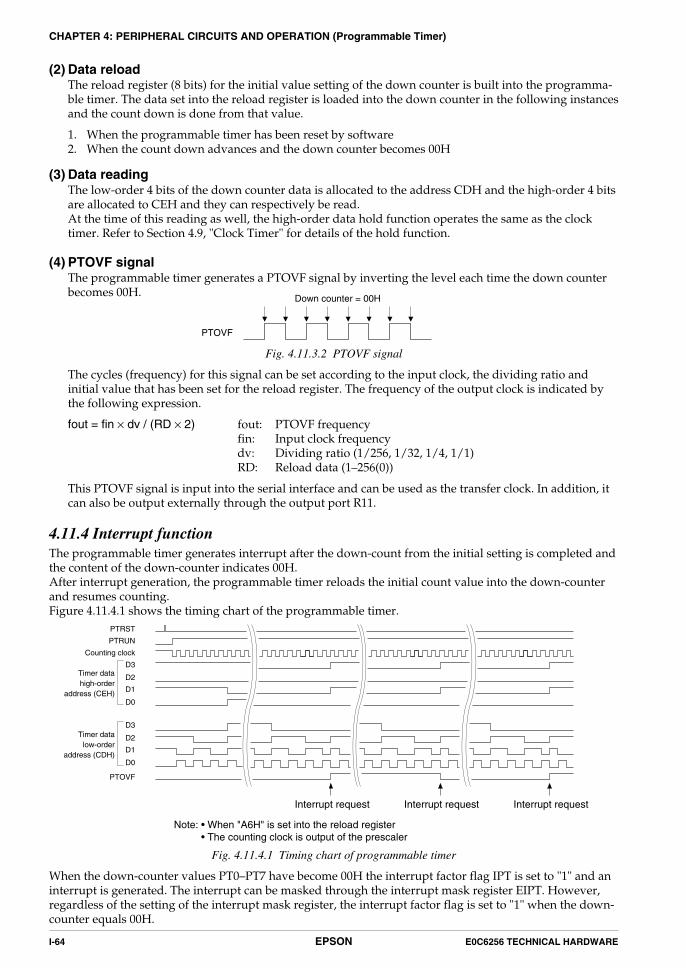
I-64 EPSON E0C6256 TECHNICAL HARDWARE
CHAPTER 4: PERIPHERAL CIRCUITS AND OPERATION (Programmable Timer)
(2) Data reloadThe reload register (8 bits) for the initial value setting of the down counter is built into the programma-ble timer. The data set into the reload register is loaded into the down counter in the following instancesand the count down is done from that value.
1. When the programmable timer has been reset by software2. When the count down advances and the down counter becomes 00H
(3) Data readingThe low-order 4 bits of the down counter data is allocated to the address CDH and the high-order 4 bitsare allocated to CEH and they can respectively be read.At the time of this reading as well, the high-order data hold function operates the same as the clocktimer. Refer to Section 4.9, "Clock Timer" for details of the hold function.
(4) PTOVF signalThe programmable timer generates a PTOVF signal by inverting the level each time the down counterbecomes 00H.
Fig. 4.11.4.1 Timing chart of programmable timer
When the down-counter values PT0–PT7 have become 00H the interrupt factor flag IPT is set to "1" and aninterrupt is generated. The interrupt can be masked through the interrupt mask register EIPT. However,regardless of the setting of the interrupt mask register, the interrupt factor flag is set to "1" when the down-counter equals 00H.
PTOVF
Down counter = 00H
Fig. 4.11.3.2 PTOVF signal
The cycles (frequency) for this signal can be set according to the input clock, the dividing ratio andinitial value that has been set for the reload register. The frequency of the output clock is indicated bythe following expression.
fout = fin × dv / (RD × 2) fout: PTOVF frequencyfin: Input clock frequencydv: Dividing ratio (1/256, 1/32, 1/4, 1/1)RD: Reload data (1–256(0))
This PTOVF signal is input into the serial interface and can be used as the transfer clock. In addition, itcan also be output externally through the output port R11.
4.11.4 Interrupt functionThe programmable timer generates interrupt after the down-count from the initial setting is completed andthe content of the down-counter indicates 00H.After interrupt generation, the programmable timer reloads the initial count value into the down-counterand resumes counting.Figure 4.11.4.1 shows the timing chart of the programmable timer.
Note:
PTRST
PTRUN
Counting clock
D3
D2
D1
D0
D3
D2
D1
D0
Timer datahigh-order
address (CEH)
Timer datalow-order
address (CDH)
PTOVF
Interrupt request Interrupt request Interrupt request
• When "A6H" is set into the reload register• The counting clock is output of the prescaler
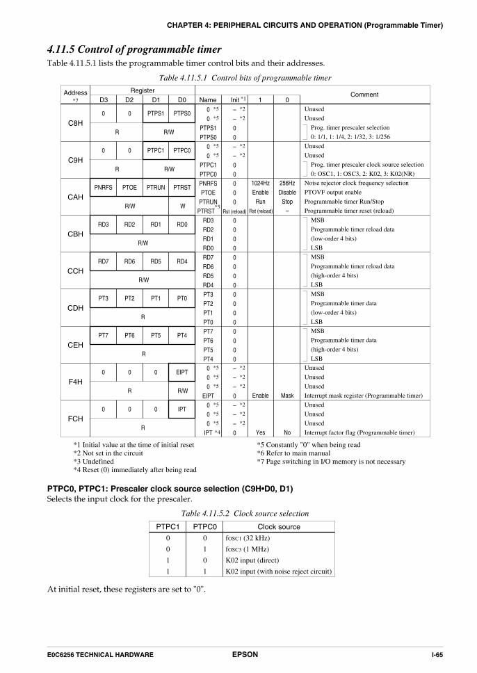
E0C6256 TECHNICAL HARDWARE EPSON I-65
CHAPTER 4: PERIPHERAL CIRCUITS AND OPERATION (Programmable Timer)
4.11.5 Control of programmable timerTable 4.11.5.1 lists the programmable timer control bits and their addresses.
Table 4.11.5.1 Control bits of programmable timer
D3 D2 D1 D0 Name Init 1 0*1
C8HPTPS0
00
PTPS1PTPS0
––00
Unused
Unused
Prog. timer prescaler selection
0: 1/1, 1: 1/4, 2: 1/32, 3: 1/256
PTPS100
F4HEIPT
R
000
EIPT
–––0 Enable Mask
000Unused
Unused
Unused
Interrupt mask register (Programmable timer)R/W
FCHIPT
R
000
IPT
–––0 Yes No
000Unused
Unused
Unused
Interrupt factor flag (Programmable timer)
*2
*2
*2
*5
*5
*5
*2
*2
*2
*5
*5
*5
*4
*2
*2
C9HPTPC0
00
PTPC1PTPC0
––00
Unused
Unused
Prog. timer prescaler clock source selection
0: OSC1, 1: OSC3, 2: K02, 3: K02(NR)
PTPC100*2
*2
CAHPTRST
PNRFSPTOE
PTRUNPTRST
000
Rst (reload)
1024HzEnable
Run
256HzDisable
Stop–
PTRUNPTOEPNRFS
R/W
*7
CBHRD0
R/W
RD3RD2RD1RD0
0000
RD1RD3
CCHRD4
RD7RD6RD5RD4
0000
RD5RD6RD7
R/W
R/W
Noise rejector clock frequency selection
PTOVF output enable
Programmable timer Run/Stop
Programmable timer reset (reload)
MSB
Programmable timer reload data
(low-order 4 bits)
LSB
R/W
MSB
Programmable timer reload data
(high-order 4 bits)
LSB
R
R
RD2
W
CDHPT0
R
PT3PT2PT1PT0
0000
PT1PT3
CEHPT4
PT7PT6PT5PT4
0000
PT5PT6PT7
MSB
Programmable timer data
(low-order 4 bits)
LSB
R
MSB
Programmable timer data
(high-order 4 bits)
LSB
PT2
Address CommentRegister
Rst (reload)
*5
*5
*5
*5
*5
*1 Initial value at the time of initial reset *5 Constantly "0" when being read*2 Not set in the circuit *6 Refer to main manual*3 Undefined *7 Page switching in I/O memory is not necessary*4 Reset (0) immediately after being read
PTPC0, PTPC1: Prescaler clock source selection (C9H•D0, D1)Selects the input clock for the prescaler.
Table 4.11.5.2 Clock source selection
PTPC1
0
0
1
1
PTPC0
0
1
0
1
Clock source
fOSC1 (32 kHz)
fOSC3 (1 MHz)
K02 input (direct)
K02 input (with noise reject circuit)
At initial reset, these registers are set to "0".

I-66 EPSON E0C6256 TECHNICAL HARDWARE
CHAPTER 4: PERIPHERAL CIRCUITS AND OPERATION (Programmable Timer)
PNRFS: Noise reject clock frequency selection (CAH•D3)Selects the noise reject frequency.
When "1" is written: 1,024 HzWhen "0" is written: 256 Hz
Reading: Valid
When K02 (with resistor) is selected as clock source, the frequency of the noise reject clock is selected from1,024 Hz or 256 Hz. By writing "1" to PNRFS, 1,024 Hz is selected and K02 input signal more than 3 msecwill be accepted. When "0" is written to PNRFS, 256 Hz is selected and K02 input signal more than 12 msecwill be accepted.At initial reset, this register is set to "0".
PTPS0, PTPS1: Prescaler dividing ratio selection (C8H•D0, D1)Selects the dividing ratio for input clock.
Table 4.11.5.3 Clock dividing ratio selection
PTPS1
0
0
1
1
PTPS0
0
1
0
1
Dividing ratio
1/1
1/4
1/32
1/256
At initial reset, these registers are set to "0".
RD0–RD3, RD4–RD7: Reload register (CBH, CCH)These are reload registers for setting the initial value of the timer.Sets the low-order 4 bits of the 8 bits timer data to RD0–RD3, and the high-order 4 bits to RD4–RD7.The set timer data is loaded to the down-counter when the programmable timer is reset or when thecontent of the down-counter is "00H".When data of reload registers is set at "00H", the down-counter becomes a 256-value counter.At initial reset, these registers are set to "0".
PTRST: Programmable timer reset (CAH•D0)This bit resets the programmable timer.
When "1" is written: Programmable timer resetWhen "0" is written: No operation
Reading: Always "0"
By writing "1" on PTRST, the programmable timer is reset.The contents set in RD0–RD7 are loaded into the down-counter.When the programmable timer is reset in the RUN mode, it will re-start counting immediately after loadingand at STOP mode, the load data is maintained.Because this bit is only for writing, it is always "0" during reading.
PTRUN: Programmable timer RUN/STOP (CAH•D1)This register controls RUN/STOP of the programmable timer.
When "1" is written: RUNWhen "0" is written: STOP
Reading: Valid
By writing "1" on PTRUN, the programmable timer performs counting operation. Writing "0" will make theprogrammable timer stop counting.Even if the programmable timer is stopped, the timer data at that point is kept.At initial reset, PTRUN is set to "0".
PT0–PT3, PT4–PT7: Programmable timer data (CDH, CEH)Will read the data from the down-counter of the programmable timer.Will read the low-order 4 bits of the 8 bits counter data PT0–PT3, and the high-order 4 bits PT4–PT7.Because these 8 bits are only for reading, writing operation is rendered invalid.By reading the low-order 4 bits, hold function works for the high-order 4 bits.At initial reset, these registers are set to "0".

E0C6256 TECHNICAL HARDWARE EPSON I-67
CHAPTER 4: PERIPHERAL CIRCUITS AND OPERATION (Programmable Timer)
PTOE: PTOVF output enable (CAH•D2)Controls the PTOVF output ON and OFF.
When "1" is written: PTOVF output enableWhen "0" is written: PTOVF output disable (DC output)
Reading: Valid
By writing "1" to PTOE when "0" has been set to the R11 register, the PTOVF signal is output from the R11terminal. When "0" is written, the R11 terminal goes to a low (VSS) level.When R11 is used for DC output, keep PTOE register set to "0".At initial reset, this register is set to "0".
EIPT: Interrupt mask register (F4H•D0)This register is used to select whether to mask the programmable timer interrupt.
When "1" is written: EnabledWhen "0" is written: Masked
Reading: Valid
With this register, masking of the programmable timer can be selected.At initial reset, this register is set to "0".
IPT: Interrupt factor flag (FCH•D0)This is the interrupt factor flag of the programmable timer.
When "1" is read: Interrupt has occurredWhen "0" is read: Interrupt has not occurred
Writing: Invalid
From the status of this flag, the software can decide whether the programmable timer interrupt. Note,however, that even if the interrupt is masked, this flag will be set to "1" by the counter value will become"00H".This flag is reset when read out by the software.Reading of interrupt factor flags is available at EI, but be careful in the following cases.If the interrupt mask register value corresponding to the interrupt factor flags to be read is set to "1", aninterrupt request will be generated by the interrupt factor flags set timing, or an interrupt request will notbe generated.At initial reset, this flag is set to "0".
4.11.6 Programming notes(1) Be sure to read the counter data in the order of low-order data (PT0–PT3) then high-order data (PT4–PT7).
(2) When data of reload registers is set at "00H", the down-counter becomes a 256-value counter.
(3) Set the VS1 voltage to -2.1 V (VSCHG = "1") when using the programmable timer as an event counter.
(4) Reading of interrupt factor flags is available at EI, but be careful in the following cases.If the interrupt mask register value corresponding to the interrupt factor flags to be read is set to "1", aninterrupt request will be generated by the interrupt factor flags set timing, or an interrupt request willnot be generated.

I-68 EPSON E0C6256 TECHNICAL HARDWARE
CHAPTER 4: PERIPHERAL CIRCUITS AND OPERATION (Serial Interface)
4.12 Serial Interface (SIN, SOUT, SCLK, SRDY)
4.12.1 Configuration of serial interfaceThe E0C6256 has a synchronous clock type 8 bits serial interface built-in.The configuration of the serial interface is shown in Figure 4.12.1.1.The CPU, via the 8 bits shift register, can read the serial input data from the SIN terminal. Moreover, viathe same 8 bits shift register, it can convert parallel data to serial data and output it to the SOUT terminal.The synchronous clock for serial data input/output may be set by selecting by software any one of 3 typesof master mode (internal clock mode: when the E0C6256 is to be the master for serial input/output) and atype of slave mode (external clock mode: when the E0C6256 is to be the slave for serial input/output).Also, when the serial interface is used at slave mode, SRDY signal which indicates whether or not the serialinterface is available to transmit or receive can be output to the SRDY terminal.
SD0–SD7
SIN(P10)
SCLK(P12)
SCS0 SCS1
Outputlatch
EISIF
Serial interfaceinterrupt control circuit
ISIF
SOUT(P11)
SRDY(P13)SCTRG
Serial interfaceactivating circuit
System clock
Serial clockcounter
Serial clockselector
Serial clockgenerator
Shift register (8-bit)
PTOVF
SCPS
Fig. 4.12.1.1 Configuration of serial interface
The input/output ports of the serial interface are common used with the I/O ports P10–P13, and functionof these ports can be selected through the software.P10–P13 terminals and serial input/output correspondence are as follows:
Master mode Slave modeP10 = SIN (I) P10 = SIN (I)P11 = SOUT (O) P11 = SOUT (O)P12 = SCLK (O) P12 = SCLK (I)P13 = I/O port (I/O) P13 = SRDY (O)
Note: At initial reset, P10–P13 are set to I/O ports.When using the serial interface, switch the function (ESIF = "1") in the initial routine.

E0C6256 TECHNICAL HARDWARE EPSON I-69
CHAPTER 4: PERIPHERAL CIRCUITS AND OPERATION (Serial Interface)
4.12.2 Master mode and slave mode of serial interfaceThe serial interface of the E0C6256 has two types of operation mode: master mode and slave mode.In the master mode, it uses an internal clock as synchronous clock of the built-in shift register, generatesthis internal clock at the SCLK (P12) terminal and controls the external (slave side) serial device.In the slave mode, the synchronous clock output from the external (master side) serial device is input fromthe SCLK (P12) terminal and uses it as the synchronous clock to the built-in shift register.The master mode and slave mode are selected by writing data to registers SCS1 and SCS0.When the master mode is selected, a synchronous clock may be selected from among 3 types as shown inTable 4.12.2.1.
Table 4.12.2.1 Synchronous clock selection
SCS1
0
0
1
1
SCS0
0
1
0
1
Mode
Slave mode
Master mode
Synchronous clock
External clock
PTOVF
CLK/2
CLK
CLK:
PTOVF:
CPU system clock
Programmable timer output clock (See Section 4.11.)
At initial reset, the slave mode (external clock mode) is selected.Moreover, the synchronous clock, along with the input/output of the 8 bits serial data, is controlled asfollows:
• At master mode, after output of 8 clocks from the SCLK (P12) terminal, clock output is automaticallysuspended and SCLK (P12) terminal is fixed at low level.
• At slave mode, after input of 8 clocks to the SCLK (P12) terminal, subsequent clock inputs are masked.
Note: When using the serial interface in the master mode, CPU system clock is used as the synchronousclock. Accordingly, when the serial interface is operating, system clock switching (fOSC1 ↔ fOSC3)should not be performed.
A sample basic serial input/output portion connection is shown in Figure 4.12.2.1.
E0C6256
SCLK
SOUT
SIN
Input terminal
Externalserial device
CLK
SOUT
SIN
READY
E0C6256
SCLK
SOUT
SIN
SRDY
Externalserial device
CLK
SOUT
SIN
Input terminal
(a) Master mode (b) Slave mode
Fig. 4.12.2.1 Sample basic connection of serial input/output section

I-70 EPSON E0C6256 TECHNICAL HARDWARE
CHAPTER 4: PERIPHERAL CIRCUITS AND OPERATION (Serial Interface)
4.12.3 Data input/output and interrupt functionThe serial interface of E0C6256 can input/output data via the internal 8 bits shift register. The shift registeroperates by synchronizing with either the synchronous clock output from SCLK (P12) terminal (mastermode), or the synchronous clock input to SCLK (P12) terminal (slave mode).The serial interface generates interrupt on completion of the 8 bits serial data input/output. Detection ofserial data input/output is done by the counting of the synchronous clock SCLK; the clock completesinput/output operation when 8 counts (equivalent to 8 cycles) have been made and then generates inter-rupt.The serial data input/output procedure data is explained below:
(1) Serial data output procedure and interruptThe E0C6256 serial interface is capable of outputting parallel data as serial data, in units of 8 bits.By setting the parallel data to 4 bits registers SD0–SD3 (DAH) and SD4–SD7 (DBH) individually andwriting "1" to SCTRG bit (D8H•D1), it synchronizes with the synchronous clock and serial data isoutput at the SOUT (P11) terminal. The synchronous clock used here is as follows: in the master mode,internal clock which is output to the SCLK (P12) terminal while in the slave mode, external clock whichis input from the SCLK (P12) terminal. The serial data to the built-in shift register is shifted with therising edge of the SCLK signal when SCSP register (D9H•D2) is "1" and is shifted with the falling edgeof the SCLK signal when SCSP register is "0".
When the output of the 8 bits data from SD0 to SD7 is completed, the interrupt factor flag ISIF(FBH•D0) is set to "1" and interrupt is generated. Moreover, the interrupt can be masked by the inter-rupt mask register EISIF (F3H•D0). Note, however, that regardless of the setting of the interrupt maskregister, the interrupt factor flag is set to "1" after output of the 8 bits data.
(2) Serial data input procedure and interruptThe E0C6256 serial interface is capable of inputting serial data as parallel data, in units of 8 bits.The serial data is input from the SIN (P10) terminal, synchronizes with the synchronous clock, and issequentially read in the 8 bits shift register. As in the above item (1), the synchronous clock used here isas follows: in the master mode, internal clock which is output to the SCLK (P12) terminal while in theslave mode, external clock which is input from the SCLK (P12) terminal.The serial data to the built-in shift register is read with the rising edge of the SCLK signal when SCPSregister is "1" and is read with the falling edge of the SCLK signal when SCPS register is "0". Moreover,the shift register is sequentially shifted as the data is fetched.
When the input of the 8 bits data from SD0 to SD7 is completed, the interrupt factor flag ISIF is set to "1"and interrupt is generated. Moreover, the interrupt can be masked by the interrupt mask register EISIF.Note, however, that regardless of the setting of the interrupt mask register, the interrupt factor flag isset to "1" after input of the 8 bits data.
The data input in the shift register can be read from data registers SD0–SD7 by software.
(3) Serial data input/output permutationE0C6256 allows the input/output permutation of serial data to be selected by register SDP (D9H•D3) asto either LSB first or MSB first. The block diagram showing input/output permutation in case of LSBfirst and MSB first is provided in Figure 4.12.3.1.
SIN
SIN
Address [DBH]
Address [DAH] Address [DBH]
Address [DAH]Outputlatch
Outputlatch
SOUT
SOUT
SD3 SD2 SD1 SD0
SD4 SD5 SD6 SD7
SD7 SD6 SD5 SD4
SD0 SD1 SD2 SD3
(In case of LSB first)
(In case of MSB first)
Fig. 4.12.3.1 Serial data input/output permutation

E0C6256 TECHNICAL HARDWARE EPSON I-71
CHAPTER 4: PERIPHERAL CIRCUITS AND OPERATION (Serial Interface)
(4) SRDY signalWhen the E0C6256 serial interface is used in the slave mode (external clock mode), SRDY is used toindicate whether the internal serial interface is available to transmit or receive data for the master side(external) serial device. SRDY signal is output from SRDY (P13) terminal.SRDY signal becomes "1" (high) when the E0C6256 serial interface becomes available to transmit orreceive data; normally, it is at "0" (low).SRDY signal changes from "0" to "1" immediately after "1" is written to SCTRG and returns from "1" to"0" when "1" is input to SCLK (P12) terminal (i.e., when the serial input/output begins transmitting orreceiving data). Moreover, when data is read from or written to SD4–SD7, the SRDY signal returns to"0".
(5) Timing chartThe E0C6256 serial interface timing chart is shown in Figure 4.12.3.2.
SCTRG(W)
SCTRG(R)
SCLK
SIN
8-bit shift register
SOUT
ISIF
SRDY(slave mode)
SCTRG(W)
SCTRG(R)
SCLK
SIN
8-bit shift register
SOUT
ISIF
SRDY(slave mode)
(a) When SCPS = "1"
(b) When SCPS = "0"
Fig. 4.12.3.2 Serial interface timing chart
4.12.4 Mask optionSince the input/output terminal of the serial interface is dual used with the I/O ports (P10–P13), the maskoption that selects the output specification for the I/O port is also applied to the serial interface.
The output specification of the terminals SOUT, SCLK (during the master mode) and SRDY (during theslave mode) that is used as output in the input/output port of the serial interface is respectively selected bythe mask options of P11, P12 and P13.Either complementary output or P channel (Pch) open drain as output specification may be selected.However, even if Pch open drain has been selected, application on the terminal of voltage exceeding powersource voltage is not permitted.
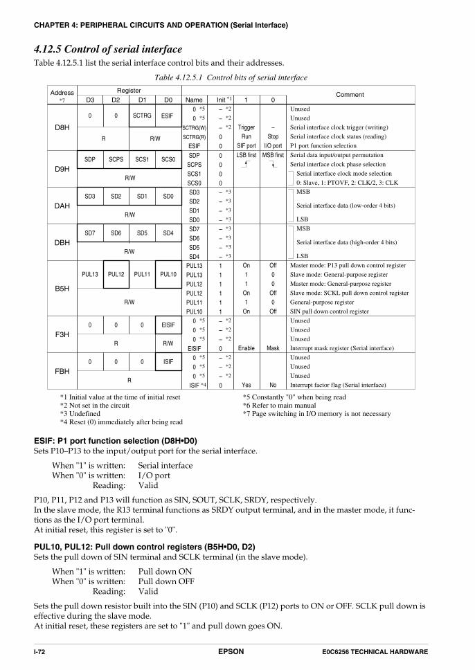
I-72 EPSON E0C6256 TECHNICAL HARDWARE
CHAPTER 4: PERIPHERAL CIRCUITS AND OPERATION (Serial Interface)
4.12.5 Control of serial interfaceTable 4.12.5.1 list the serial interface control bits and their addresses.
Table 4.12.5.1 Control bits of serial interface
D3 D2 D1 D0 Name Init 1 0*1
D8H
ESIF
R
00
ESIF
–––00
TriggerRun
SIF port
–Stop
I/O port
SCTRG00*2
*2
*2
D9HSCS0
R/W
SDPSCPSSCS1SCS0
0000
Serial data input/output permutation
Serial interface clock phase selection
Serial interface clock mode selection
0: Slave, 1: PTOVF, 2: CLK/2, 3: CLK
LSB first MSB firstSCS1SCPSSDP
DAHSD0
SD3SD2SD1SD0
––––
SD1SD2SD3*3
*3
*3
*3
DBHSD4
SD7SD6SD5SD4
––––
SD5SD6SD7*3
*3
*3
*3
*7
R/W
R/W
Unused
Unused
Serial interface clock trigger (writing)
Serial interface clock status (reading)
P1 port function selectionR/W
SCTRG(W)
SCTRG(R)
MSB
LSB
Serial interface data (low-order 4 bits)
MSB
LSB
Serial interface data (high-order 4 bits)
Address CommentRegister
*5
*5
B5H
PUL10PUL13PUL13PUL12PUL12PUL11PUL10
111111
On11
On1
On
Off00
Off0
Off
PUL11PUL12PUL13
R/W
Master mode: P13 pull down control register
Slave mode: General-purpose register
Master mode: General-purpose register
Slave mode: SCKL pull down control register
General-purpose register
SIN pull down control register
EISIF
R
000
EISIF
–––0 Enable Mask
000
F3H
*2
*2
*2
Unused
Unused
Unused
Interrupt mask register (Serial interface)R/W
ISIF
R
000
ISIF
–––0 Yes No
000
FBH
*2
*2
*2
Unused
Unused
Unused
Interrupt factor flag (Serial interface)
*5
*5
*5
*5
*5
*5
*4
*1 Initial value at the time of initial reset *5 Constantly "0" when being read*2 Not set in the circuit *6 Refer to main manual*3 Undefined *7 Page switching in I/O memory is not necessary*4 Reset (0) immediately after being read
ESIF: P1 port function selection (D8H•D0)Sets P10–P13 to the input/output port for the serial interface.
When "1" is written: Serial interfaceWhen "0" is written: I/O port
Reading: Valid
P10, P11, P12 and P13 will function as SIN, SOUT, SCLK, SRDY, respectively.In the slave mode, the R13 terminal functions as SRDY output terminal, and in the master mode, it func-tions as the I/O port terminal.At initial reset, this register is set to "0".
PUL10, PUL12: Pull down control registers (B5H•D0, D2)Sets the pull down of SIN terminal and SCLK terminal (in the slave mode).
When "1" is written: Pull down ONWhen "0" is written: Pull down OFF
Reading: Valid
Sets the pull down resistor built into the SIN (P10) and SCLK (P12) ports to ON or OFF. SCLK pull down iseffective during the slave mode.At initial reset, these registers are set to "1" and pull down goes ON.

E0C6256 TECHNICAL HARDWARE EPSON I-73
CHAPTER 4: PERIPHERAL CIRCUITS AND OPERATION (Serial Interface)
SCS0, SCS1: Synchronous clock selection (D9H•D0, D1)Selects the synchronous clock for the serial interface (SCLK).
Table 4.12.5.2 Synchronous clock selectionSCS1
0
0
1
1
SCS0
0
1
0
1
Mode
Slave mode
Master mode
Synchronous clock
External clock
PTOVF
CLK/2
CLK
CLK:
PTOVF:
CPU system clock
Programmable timer output clock (See Section 4.11.)
Synchronous clock (SCLK) is selected from among the above 4 types: 3 types of internal clock and externalclock.When using the serial interface in the master mode, CPU system clock is used as the synchronous clock.Accordingly, when the serial interface is operating, system clock switching (fOSC1 ↔ fOSC3) should not beperformed.Also, when PTOVF is used, it is necessary to generate a clock on the programmable timer side prior tosending and receiving.At initial reset, external clock is selected.
SCPS: Shift clock phase selection (D9H•D2)Selects the timing for reading in the serial data input from SIN (P10) terminal.
When "1" is written: Rising edge of SCLKWhen "0" is written: Falling edge of SCLK
Reading: Valid
Selects whether the fetching for the serial input data to registers (SD0–SD7) at the rising edge (at "1"writing) or falling edge (at "0" writing) of the SCLK signal.The input data fetching timing may be selected but output timing for output data is fixed at SCLK risingedge.When the internal clock is selected as the synchronous clock (SCLK), a hazard occurs in the synchronousclock (SCLK) when data is written to register SCPS.At initial reset, this register is set to "0".
SDP: Data input/output permutation selection (D9H•D3)Selects the serial data input/output permutation.
When "1" is written: LSB firstWhen "0" is written: MSB first
Reading: Valid
Select whether the data input/output permutation will be MSB first or LSB first.At initial reset, this register is set to "0".
SCTRG: Clock trigger/status (D8H•D1)This is a trigger to start input/output of synchronous clock (SCLK).
• During writing operationWhen "1" is written: TriggerWhen "0" is written: No operation
When this trigger is supplied to the serial interface activating circuit, the synchronous clock (SCLK) input/output is started.As a trigger condition, it is required that data writing or reading on data registers SD0–SD7 be performedprior to writing "1" to SCTRG. (The internal circuit of the serial interface is initiated through data writing/reading on data registers SD0–SD7.)Supply trigger only once every time the serial interface is placed in the RUN state. Refrain from performingtrigger input multiple times, as leads to malfunctioning.Moreover, when the synchronous clock SCLK is external clock, start to input the external clock after thetrigger.

I-74 EPSON E0C6256 TECHNICAL HARDWARE
CHAPTER 4: PERIPHERAL CIRCUITS AND OPERATION (Serial Interface)
• During reading operationWhen "1" is read: RUN statusWhen "0" is read: STOP status
Writing: Invalid
When read out this bit, it indicates the status of serial interface clock.After "1" is written to SCTRG, this value is latched till serial interface clock stops (8 clock counts). There-fore, if "1" is read, it indicates that the synchronous clock is in input/output operation.When the synchronous clock input/output is completed, this latch is reset to "0".At initial reset, this register is set to "0".
SD0–SD3, SD4–SD7: Serial interface data register (DAH, DBH)These registers are used for writing and reading serial data.
• During writing operationWhen "1" is written: High levelWhen "0" is written: Low level
Writes serial data will be output to SOUT (P11) terminal. From the SOUT (P11) terminal, the data convertedto serial data as high (VDD) level bit for bits set at "1" and as low (VSS) level bit for bits set at "0".
• During reading operationWhen "1" is read: High levelWhen "0" is read: Low level
The serial data input from the SIN (P10) terminal can be read by this register.The data converted to parallel data, as high (VDD) level bit "1" and as low (VSS) level bit "0" input from SIN(P10) terminal. Perform data reading only while the serial interface is halted (i.e., the synchronous clock isneither being input or output).
At initial reset, these registers will be undefined.
EISIF: Interrupt mask register (F3H•D0)This is the interrupt mask register of the serial interface.
When "1" is written: EnabledWhen "0" is written: Masked
Reading: Valid
With this register, masking of the serial interface interrupt can be selected.At initial reset, this register is set to "0".
ISIF: Interrupt factor flag (FBH•D0)This is the interrupt factor flag of the serial interface.
When "1" is read: Interrupt has occurredWhen "0" is read: Interrupt has not occurred
Writing: Invalid
From the status of this flag, the software can decide whether the serial interface interrupt.The interrupt factor flag is reset when it has been read out.Note, however, that even if the interrupt is masked, this flag will be set to "1" after the 8 bits data input/output.Reading of interrupt factor flags is available at EI, but be careful in the following cases.If the interrupt mask register value corresponding to the interrupt factor flags to be read is set to "1", aninterrupt request will be generated by the interrupt factor flags set timing, or an interrupt request will notbe generated.At initial reset, this flag is set to "0".

E0C6256 TECHNICAL HARDWARE EPSON I-75
CHAPTER 4: PERIPHERAL CIRCUITS AND OPERATION (Serial Interface)
4.12.6 Programming notes(1) When using the serial interface in the master mode, the synchronous clock uses the CPU system clock.
Accordingly, do not change the system clock (fOSC1 ↔ fOSC3) while the serial interface is operating.
(2) Perform data writing/reading to data registers SD0–SD7 only while the serial interface is halted (i.e.,the synchronous clock is neither being input or output).
(3) As a trigger condition, it is required that data writing or reading on data registers SD0–SD7 be per-formed prior to writing "1" to SCTRG. (The internal circuit of the serial interface is initiated throughdata writing/reading on data registers SD0–SD7.) Supply trigger only once every time the serialinterface is placed in the RUN state. Moreover, when the synchronous clock SCLK is external clock,start to input the external clock after the trigger.
(4) Set the VS1 voltage to -2.1 V (VSCHG = "1") when using the serial interface in slave mode.
(5) Reading of interrupt factor flags is available at EI, but be careful in the following cases.If the interrupt mask register value corresponding to the interrupt factor flags to be read is set to "1", aninterrupt request will be generated by the interrupt factor flags set timing, or an interrupt request willnot be generated.

I-76 EPSON E0C6256 TECHNICAL HARDWARE
CHAPTER 4: PERIPHERAL CIRCUITS AND OPERATION (Sound Generator)
4.13 Sound Generator
4.13.1 Configuration of sound generatorThe E0C6256 has a built-in sound generator for generating buzzer signals.Hence, generated buzzer signals (BZ) can be output from the R12 terminal.Aside permitting the respective setting of the buzzer signal frequency and sound level to 8 stages, itpermits the adding of a digital envelope by means of duty ratio control. It also has a one-shot outputfunction for outputting key operated sounds.Figure 4.13.1.1 shows the configuration of the sound generator.
fOSC1
R12 output circuit
Programmabledividing circuit
256 Hz One-shot buzzercontrol circuit
Duty ratiocontrol circuit
BZFQ0–BZFQ2 BDTY0–BDTY2
Buzzer outputcontrol circuit
Envelopeaddition circuit
ENON
BZE
ENRTM
ENRST
BZSTP
BZSHT
SHTPW
Fig. 4.13.1.1 Configuration of sound generator
4.13.2 Control of buzzer outputA buzzer (BZ) signal can be output from the output port terminal R12.The configuration of the buzzer output port is shown in Figure 4.13.2.1.
Fig. 4.13.2.1 Configuration of buzzer output port
The BZ signal generated by the sound generator is output from the R12 terminal by setting "1" for thebuzzer output enable register BZE when the output port register R12 is set to"0". When "0" is set to BZE, theR12 terminal shifts to the low (VSS) level.
R12(BZ)
RegisterBZE
RegisterR12
Buzzer signal
R12 register
BZ output (R12)
10BZE register
Fixed at 0
0
Fig. 4.13.2.2 Buzzer signal output timing chart
Note: • Pay attention to the output because it is fixed at HIGH level when the R12 register is set to "1".
• Since it generates a BZ signal that is out of synchronization with the BZE register, hazards may attimes be produced when the signal goes ON/OFF due to the setting of the register.

E0C6256 TECHNICAL HARDWARE EPSON I-77
CHAPTER 4: PERIPHERAL CIRCUITS AND OPERATION (Sound Generator)
4.13.3 Setting of buzzer frequency and sound levelThe divide signal of the OSC1 clock (32.768 kHz) is used for the buzzer (BZ) signal and it is set up such that8 types of frequencies can be selected by changing this dividing ratio. Frequency selection is done bysetting the buzzer frequency selection registers BZFQ0–BZFQ2 as shown in Table 4.13.3.1.
Table 4.13.3.1 Buzzer signal frequency setting
BZFQ2
0
0
0
0
1
1
1
1
BZFQ1
0
0
1
1
0
0
1
1
BZFQ0
0
1
0
1
0
1
0
1
Buzzer frequency (Hz)
4096.0
3276.8
2730.7
2340.6
2048.0
1638.4
1365.3
1170.3
The buzzer sound level is changed by controlling the duty ratio of the buzzer signal.The duty ratio can be selected from among the 8 types shown in Table 4.13.3.2 according to the setting ofthe buzzer duty selection registers BDTY0–BDTY2.
Table 4.13.3.2 Duty ratio setting
Duty ratio by buzzer frequency (Hz)2340.6
1170.3
12/28
11/28
10/28
9/28
8/28
7/28
6/28
5/28
Level BDTY2
0
0
0
0
1
1
1
1
BDTY1
0
0
1
1
0
0
1
1
BDTY0
0
1
0
1
0
1
0
1
2730.7
1365.3
12/24
11/24
10/24
9/24
8/24
7/24
6/24
5/24
3276.8
1638.4
8/20
7/20
6/20
5/20
4/20
3/20
2/20
1/20
4096.0
2048.0
8/16
7/16
6/16
5/16
4/16
3/16
2/16
1/16
Level 1 (maximum)
Level 2
Level 3
Level 4
Level 5
Level 6
Level 7
Level 8 (minimum)
When the HIGH level output time has been made TH and when the LOW level output time has been madeTL due to the ratio of the pulse width to the pulse synchronization, the duty ratio becomes TH/(TH+TL).When BDTY0–BDTY2 have all been set to "0", the duty ratio becomes maximum and the sound level alsobecomes maximum. Conversely, when BDTY0–BDTY2 have all been set to "1", the duty ratio becomesminimum and the sound level also becomes minimum.The duty ratio that can be set is different depending on the frequency that has been set, so see Table4.13.3.2.
Level 1 (maximum)
Level 2
Level 3
Level 4
Level 5
Level 6
Level 7
Level 8 (minimum)
TL TH
Fig. 4.13.3.1 Duty ratio of the buzzer signal waveform
Note: When a digital envelope has been added to the buzzer signal, the BDTY0–BDTY2 settings will beinvalid due to the control of the duty ratio.

I-78 EPSON E0C6256 TECHNICAL HARDWARE
CHAPTER 4: PERIPHERAL CIRCUITS AND OPERATION (Sound Generator)
4.13.4 Digital envelopeA digital envelope for duty control can be added to the buzzer signal.The envelope can be controlled by staged changing of the same duty envelope as detailed in Table 4.13.3.2in the preceding item from level 1 (maximum) to level 8 (minimum).The addition of an envelope to the buzzer signal can be done by writing "1" into ENON, but when "0" hasbeen written it is not added.When a buzzer signal output is begun (writing "1" into BZE) after setting ENON, the duty ratio shifts tolevel 1 (maximum) and changes in stages to level 8.When attenuated down to level 8 (minimum), it is retained at that level. The duty ratio can be returned tomaximum, by writing "1" into register ENRST during output of a envelope attached buzzer signal.The envelope attenuation time (time for changing of the duty ratio) can be selected by the register ENRTM.The time for a 1 stage level change is 62.5 msec (16 Hz), when "0" has been written into ENRTM and 125msec (8 Hz), when to "1" has been written. However, there is also a max. 4 msec error from envelope ON,up to the first change.Figure 4.13.4.1 Shows the timing chart of the digital envelope.
BZFQ0–2
ENON
ENRST
ENRTM
BZE
t01t02
t03t04
t05t06
t07
t01t11
t12t13
t14t15
t16t17
Level 1 (MAX)2345678 (MIN)
BZ signalduty ratio
No change of duty level
t01
t02–07
= 62.5 msec= 62.5 msec
+0–4 t11
t12–17
= 125 msec= 125 msec
+0–4
Fig. 4.13.4.1 Timing chart for digital envelope
4.13.5 One-shot outputThe sound generator has a one-shot output function for outputting a short duration buzzer signal for keyoperation sounds and similar effects. Either 125 msec or 31.25 msec can be selected by register SHTPW forbuzzer signal output time.The output of the one-shot buzzer is controlled by writing "1" into the one-shot buzzer trigger BZSHT.When this trigger has been assigned, a buzzer signal in synchronization with the internal 256 Hz signal isoutput from the BZ (R12) terminal. Thereafter, when the set time has elapsed, a buzzer signal in synchroni-zation with the 256 Hz signal goes off in the same manner as for the start of output.The BZSHT also permits reading. When BZSHT is "1", the one-shot output circuit is in operation (duringone-shot output) and when it is "0", it shows that the circuit is in the ready (outputtable) status.
In addition, it can also terminate one-shot output prior to the elapsing of the set time. This is done bywriting a "1" into the one-shot buzzer stop BZSTP. In this case as well, the buzzer signal goes OFF insynchronization with the 256 Hz signal.
The one-shot output cannot add an envelope for short durations. However, the sound level can be set byselecting the duty ratio, and the frequency can also be set.One-shot output is invalid during normal buzzer output.
Figure 4.13.5.1 shows timing chart for one-shot output.

E0C6256 TECHNICAL HARDWARE EPSON I-79
CHAPTER 4: PERIPHERAL CIRCUITS AND OPERATION (Sound Generator)
Fig. 4.13.5.1 Timing chart for one-shot output
4.13.6 Control of sound generatorTable 4.13.6.1 lists the control bits and their addresses for the sound generator.
Table 4.13.6.1 Control bits of sound generator
256 Hz
SHOTPW
BZSHT(W)
BZSHT(R)
BZSTP
BZ output
D3 D2 D1 D0 Name Init 1 0*1
DCHBZE
ENRTMENRST
ENONBZE
0Reset
00
1secReset
OnEnable
0.5sec–
OffDisable
ENONENRSTENRTM
R/W
*7
DDH
SHTPW
R/W
0BZSTP
SHTPW
–––00
StopTriggerBusy
125msec
––
Ready31.25msec
BZSHT0*2
*2
*2
DEHBZFQ0
0BZFQ2BZFQ1BZFQ0
–000
BZFQ1BZFQ20*2
Envelope releasing time
Envelope reset
Envelope On/Off
Buzzer output enable
Unused
1-shot buzzer stop
1-shot buzzer trigger (writing)
1-shot buzzer status (reading)
1-shot buzzer pulse width setting
R/W
Unused
Buzzer frequency selection
0: 4096.0, 1: 3276.8, 2: 2730.7, 3: 2340.6,
4: 2048.0, 5: 1638.4, 6: 1365.3, 7: 1170.3 (Hz)
BZSTP
R
W R/W
BZSHT(W)
BZSHT(R)
R
DFHBDTY0
0BDTY2BDTY1BDTY0
–000
BDTY1BDTY20*2
*6R/W
Unused
Buzzer signal duty ratio selectionR
Address CommentRegister
W
*5 *5
*5
*5
*5
R10
FOUT
R13R12BZR11
PTOVFR10
FOUT
0000000
HighHighOff
HighOff
HighOff
LowLowOnLowOnLowOn
R11
PTOVF
R12
BZR13
A3H
Output port (R13)
Output port (R12)
Buzzer output
Output port (R11)
PTOVF output
Output port (R10)
FOUToutput
R/W
*1 Initial value at the time of initial reset *5 Constantly "0" when being read*2 Not set in the circuit *6 Refer to main manual*3 Undefined *7 Page switching in I/O memory is not necessary*4 Reset (0) immediately after being read
R12: Output port data register (A3H•D2)Fix it at "0" when performing the buzzer signal (BZ) output.At initial reset, this register is set to "0".
BZE: BZ output enable register (DCH•D0)Controls the buzzer (BZ) signal output.
When "1" is written: BZ signal output enableWhen "0" is written: BZ signal output disable
Reading: Valid
By writing "1" to BZE when the R12 register is set to "0", the BZ signal is output from the R12 terminal.When "0" is written, R12 terminal becomes the LOW (VSS) level.When the R12 port is used as the DC output, fix this register at "0".At initial reset, this register is set to "0".

I-80 EPSON E0C6256 TECHNICAL HARDWARE
CHAPTER 4: PERIPHERAL CIRCUITS AND OPERATION (Sound Generator)
BZFQ0–BZFQ2: Buzzer frequency selection (DEH•D0–D2)Selects the buzzer signal frequency.
Table 4.13.6.2 Buzzer signal frequency setting
BZFQ2
0
0
0
0
1
1
1
1
BZFQ1
0
0
1
1
0
0
1
1
BZFQ0
0
1
0
1
0
1
0
1
Buzzer frequency (Hz)
4096.0
3276.8
2730.7
2340.6
2048.0
1638.4
1365.3
1170.3
Select the buzzer frequency from among the above 8 types that have divided the OSC1 clock.At initial reset, these registers are set to "0".
BDTY0–BDTY2: Duty level selection (DFH•D0–D2)Selects the duty ratio of the buzzer signal as shown in Table 4.13.6.3.
Table 4.13.6.3 Duty ratio setting
Duty ratio by buzzer frequency (Hz)2340.6
1170.3
12/28
11/28
10/28
9/28
8/28
7/28
6/28
5/28
Level BDTY2
0
0
0
0
1
1
1
1
BDTY1
0
0
1
1
0
0
1
1
BDTY0
0
1
0
1
0
1
0
1
2730.7
1365.3
12/24
11/24
10/24
9/24
8/24
7/24
6/24
5/24
3276.8
1638.4
8/20
7/20
6/20
5/20
4/20
3/20
2/20
1/20
4096.0
2048.0
8/16
7/16
6/16
5/16
4/16
3/16
2/16
1/16
Level 1 (maximum)
Level 2
Level 3
Level 4
Level 5
Level 6
Level 7
Level 8 (minimum)
The sound level of this buzzer can be set by selecting this duty ratio.However, when the envelope has been set to ON (ENON = "1"), this setting becomes invalid.At initial reset, these registers are set to "0".
ENRST: Envelope reset (DCH•D2)Resets the envelope.
When "1" is written: ResetWhen "0" is written: No operation
Reading: Always "0"
Writing "1" into ENRST resets envelope and the duty ratio becomes maximum. If an envelope has not beenadded (ENON = "0") and if no buzzer signal is being output, the reset becomes invalid. Writing "0" is alsoinvalid.This bit is dedicated for writing, and is always "0" for reading.
ENON: Envelope ON/OFF (DCH•D1)Controls the addition of an envelope onto the buzzer signal.
When "1" is written: ONWhen "0" is written: OFF
Reading: Valid
Writing "1" into the ENON causes an envelope to be added during buzzer signal output. When a "0" hasbeen written, an envelope is not added.At initial reset, this register is set to "0".

E0C6256 TECHNICAL HARDWARE EPSON I-81
CHAPTER 4: PERIPHERAL CIRCUITS AND OPERATION (Sound Generator)
ENRTM: Envelope releasing time selection (DCH•D3)Selects the envelope releasing time that is added to the buzzer signal.
When "1" is written: 1.0 sec (125 msec × 7 = 875 msec)When "0" is written: 0.5 sec (62.5 msec × 7 = 437.5 msec)
Reading: Valid
The releasing time of the digital envelope is determined by the time for converting the duty ratio.When "1" has been written in ENRTM, it becomes 125 msec (8 Hz) units and when "0" has been written, itbecomes 62.5 msec (16 Hz) units.At initial reset, this register is set to "0".
SHTPW: One-shot buzzer pulse width setting (DDH•D0)Selects the output time of the one-shot buzzer.
When "1" is written: 125 msecWhen "0" is written: 31.25 msec
Reading: Valid
Writing "1" into SHTPW causes the one-short output time to be set at 125 msec, and writing "0" causes it tobe set to 31.25 msec. It does not affect normal buzzer output.At initial reset, this register is set to "0".
BZSHT: One-shot buzzer trigger/status (DDH•D1)Controls the one-shot buzzer output.
• During writing operationWhen "1" is written: TriggerWhen "0" is written: No operation
Writing "1" into BZSHT causes the one-short output circuit to operate and a buzzer signal to be output.This output is automatically turned OFF after the time set by SHTPW has elapsed. At this time, the R12register has to be set to "0".The one-shot output is only valid when the normal buzzer output is OFF (BZE = "0") and will be invalidwhen the normal buzzer output is ON (BZE = "1"). When a re-trigger is assigned during a one-shot output,the one-shot output time set with SHTPW is measured again from that point (time extension).
• During reading operationWhen "1" is read: BUSYWhen "0" is read: READY
During reading BZSHT shows the operation status of the one-shot output circuit. During one-shot output,BZSHT becomes "1" and the output goes OFF, it shifts to "0".At initial reset, this bit is set to "0".
BZSTP: One-shot buzzer stop (DDH•D2)Stop the one-shot buzzer output.
When "1" is written: StopWhen "0" is written: No operation
Reading: Always "0"
Writing "1" into BZSTP permits the one-shot buzzer output to be turned OFF prior to the elapsing of thetime set by SHTPW. Writing "0" is invalid and writing "1" is also invalid except during one-shot output.This bit is dedicated for writing, and is always "0" for reading.
4.13.7 Programming notes(1) Pay attention to the output because it is fixed at HIGH level when the R12 register is set to "1".
(2) Since it generates a BZ signal that is out of synchronization with the BZE register, hazards may at timesbe produced when the signal goes ON/OFF due to the setting of the register.
(3) The one-shot output is only valid when the normal buzzer output is OFF (BZE = "0") and will be invalidwhen the normal buzzer output is ON (BZE = "1").

I-82 EPSON E0C6256 TECHNICAL HARDWARE
CHAPTER 4: PERIPHERAL CIRCUITS AND OPERATION (A/D Converter)
4.14 A/D Converter
4.14.1 Configuration of A/D converterThe E0C6256 has CR oscillation type A/D converter.Two systems (channel 0 and channel 1) of CR oscillation circuit are built into this A/D converter, so it ispossible to compose two types of A/D conversion circuits by connecting different sensors to each CRoscillation circuit.Channel 0 can be used as an R/f (resistor/frequency) conversion circuit using a resistive sensor such as athermistor, and channel 1 can be used as an R/f conversion circuit same as channel 0, or an R/f conversioncircuit for humidity conversion using a resistive humidity sensor.The channel to be used and sensor type for channel 1 are selected using software.The built-in up counter counts data that is converted into frequency by the CR oscillation circuit. Byreading the counted value, digital converted data can be obtained.Various sensor circuits such as temperature/humidity measurement circuits can be easily realized usingthis A/D converter.The configuration of the A/D converter is shown in Figure 4.14.1.1.
Fig. 4.14.1.1 Configuration of A/D converter
4.14.2 CR oscillation circuitTwo systems of CR oscillation circuit, channel 0 and channel 1, are built into the A/D converter andperform CR oscillation with external resistor and capacitor.The counter that is used to obtain an A/D converted value is shared with channel 0 and channel 1. There-fore, operation for two systems is realized by switching the CR oscillation circuit that performs A/Dconversion. The channel selection is done using the register CHSEL. When CHSEL is set to "0", channel 0 isselected and when "1" is set, channel 1 is selected.The sensor type to be A/D converted in the channel 1 can also be selected by the software, and it should bepreviously set using the register WRSEL.
Channel selection CHSEL = "0": Channel 0CHSEL = "1": Channel 1
Sensor selection for channel 1 WRSEL = "0": R/f conversion using a resistive sensor such as thermistorWRSEL = "1": R/f conversion using a resistive humidity sensor *
* The operation of the oscillation circuit differs from the normal resistive sensor. (Refer to the following.)
Interruptrequest
OSC1 TC0–TC3
TC4–TC7
TC8–TC11
TC12–TC15
Up/down counter for time measurement
C0–C3
C4–C7
C8–C11
ADRUN
Oscillation/countcontrol circuit
Up-counter for R/f conversion
Data bus
Interruptcontrol circuit
IAD EIAD
VDD
CM0SN0
VSS
ADOUT
Countercontrol
Up
DownA/D conversionStart/Stop
ClockselectionOSC3
ADCLK0ADCLK1
C16–C19
Overflowflag
OVF1OVF2
Countercontrol
Up
Oscillation systemcontrol circuit
CHSELWRSELADMODESENSEL
Ch0 oscillationcontrol circuit
VDD
WETSN1
VSS
ST1 CM1
C12–C15
ST0
Ch1 oscillationcontrol circuit
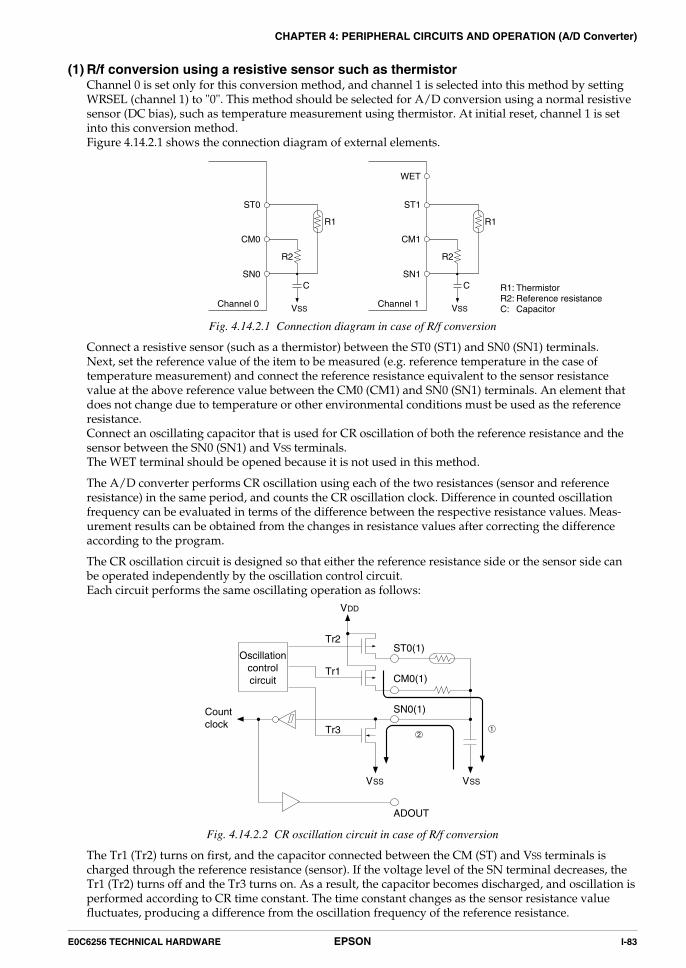
E0C6256 TECHNICAL HARDWARE EPSON I-83
CHAPTER 4: PERIPHERAL CIRCUITS AND OPERATION (A/D Converter)
(1) R/f conversion using a resistive sensor such as thermistorChannel 0 is set only for this conversion method, and channel 1 is selected into this method by settingWRSEL (channel 1) to "0". This method should be selected for A/D conversion using a normal resistivesensor (DC bias), such as temperature measurement using thermistor. At initial reset, channel 1 is setinto this conversion method.Figure 4.14.2.1 shows the connection diagram of external elements.
R1
R2
VSS
C
ST0
CM0
SN0
Channel 0
R1
R2
VSS
C
ST1
WET
CM1
SN1
Channel 1
R1:R2:C:
ThermistorReference resistanceCapacitor
Fig. 4.14.2.1 Connection diagram in case of R/f conversion
Connect a resistive sensor (such as a thermistor) between the ST0 (ST1) and SN0 (SN1) terminals.Next, set the reference value of the item to be measured (e.g. reference temperature in the case oftemperature measurement) and connect the reference resistance equivalent to the sensor resistancevalue at the above reference value between the CM0 (CM1) and SN0 (SN1) terminals. An element thatdoes not change due to temperature or other environmental conditions must be used as the referenceresistance.Connect an oscillating capacitor that is used for CR oscillation of both the reference resistance and thesensor between the SN0 (SN1) and VSS terminals.The WET terminal should be opened because it is not used in this method.
The A/D converter performs CR oscillation using each of the two resistances (sensor and referenceresistance) in the same period, and counts the CR oscillation clock. Difference in counted oscillationfrequency can be evaluated in terms of the difference between the respective resistance values. Meas-urement results can be obtained from the changes in resistance values after correcting the differenceaccording to the program.
The CR oscillation circuit is designed so that either the reference resistance side or the sensor side canbe operated independently by the oscillation control circuit.Each circuit performs the same oscillating operation as follows:
VSS
Tr2
Tr1
Tr3
VSS
ST0(1)
CM0(1)
SN0(1)
VDD
Oscillationcontrolcircuit
ADOUT
Countclock
➁➀
Fig. 4.14.2.2 CR oscillation circuit in case of R/f conversion
The Tr1 (Tr2) turns on first, and the capacitor connected between the CM (ST) and VSS terminals ischarged through the reference resistance (sensor). If the voltage level of the SN terminal decreases, theTr1 (Tr2) turns off and the Tr3 turns on. As a result, the capacitor becomes discharged, and oscillation isperformed according to CR time constant. The time constant changes as the sensor resistance valuefluctuates, producing a difference from the oscillation frequency of the reference resistance.

I-84 EPSON E0C6256 TECHNICAL HARDWARE
CHAPTER 4: PERIPHERAL CIRCUITS AND OPERATION (A/D Converter)
Oscillation waveforms are shaped by the schmitt trigger and transmitted to counter. The clock transmit-ted to the counter is also output from the ADOUT terminal. As a result, oscillation frequency can beidentified by the frequency counter. Since this monitor has no effect on oscillation frequency, it can beused to adjust CR oscillation frequency.Oscillation waveforms and waveforms output from the ADOUT terminal are shown in Figure 4.14.2.3.
SN0/SN1 terminal
ADOUT outputVDD
VSS
VDD
VSS
Fig. 4.14.2.3 Oscillation waveform
(2) R/f conversion using a resistive humidity sensorThis conversion is possible only in channel 1, and this method is selected by setting the register WRSELto "1". This is basically the same as the R/f conversion described above (1), but the AC bias circuitworks for the humidity sensor.Figure 4.14.2.4 shows the connection diagram of external devices.
Fig. 4.14.2.4 Connection diagram of resistive humidity sensor
Connect a humidity sensor between the WET and ST1 terminals, and connect a reference resistancebetween the CM1 and SN1 terminals.Connect an oscillating capacitor that is used for CR oscillation of both the reference resistance and thesensor between the SN1 and VSS terminals.The oscillating operation by reference resistance is the same as the R/f conversion described above (1).The humidity sensor cannot be DC biased for a long time, therefore this method powers the WET andST1 terminals alternately.
VSS
Tr1
Tr2
VSS
CM1
ST1
SN1
VDD
Oscillationcontrolcircuit
ADOUT
Countclock
➀
WET
S1S2
➁
➀
➁
Tr1 = ON, S1 = ON
Tr2 = ON, S2 = ON
R2
VSS
C
ST1
WET
CM1
SN1
Channel 1
R1:R2:C:
Resistive humidity sensorReference resistanceCapasitor
R1
Fig. 4.14.2.5 CR oscillation circuit for resistive humidity sensor
The oscillation waveform is the same as Figure 4.14.2.3.

E0C6256 TECHNICAL HARDWARE EPSON I-85
CHAPTER 4: PERIPHERAL CIRCUITS AND OPERATION (A/D Converter)
4.14.3 Operation of A/D conversion
(1) Power supplyIn the A/D converter, it is necessary to control the power on/off, and it is done by using the registerAPWR. When APWR is set to "1", the power turns on and when set to "0", it turns off. Further, set to "1"for the LPWR register, because the A/D converter uses the LCD power supply.To reduce current consumption, turn the power off if not in use.
(2) CounterThe A/D converter incorporates two types of counters. One is the 20-bit up-counter C0–C19 that countsthe aforementioned oscillation clock, and the other is 16-bit up/down counter TC0–TC15 that countsthe internal clock for reference counting. Each counter permits reading and writing on a 4-bit basis.
The up-counter C0–C19 is used to count the CR oscillation clock by the reference resistance and sensor,and the results of A/D conversion can be obtained by reading this counter.This counter is designed so that it counts serially in order of the reference resistance and the sensor.Also it switches the CR oscillation from reference resistance to sensor at the point an overflow occursduring counting of the reference resistance oscillation. Furthermore, both of the oscillation times of thereference resistance and sensor are designed to be the same by the up/down counter described later.Therefore, by converting a proper initial value for counting of the oscillation of the reference resistanceinto a complement (value subtracted from 0000H) and setting it into the counter before starting tocount, the number of counts for the sensor oscillation is obtained by reading this counter after the A/Dconversion. In other words, the difference between the reference resistance and sensor oscillationfrequencies can be found easily. For instance, if resistance values of the reference resistance and thesensor are equivalent, the same value as the initial value before converting into a complement will beobtained as the result. So this means that the difference between oscillation frequencies is Zero.
The up/down counter TC0–TC15 is a counter to equal both oscillation times for the reference resistanceand the sensor. For the input clock, either OSC1 clock (Typ. 32.768 kHz) or OSC3 clock (Typ. 1 MHz)can be selected using the software. This selection can be done for each channel; the register ADCLK0 isused for channel 0 and the register ADCLK1 for channel 1. When "1" is set to the register, OSC3 clock isselected and when "0" is set, OSC1 clock is selected.This counter must be set to "0000H" before starting the A/D conversion. This is due to the followingreasons. This counter starts counting-up at the same time the up-counter C0–C19 starts counting foroscillation by reference resistance. After that, when the oscillation switches to the sensor side, thiscounter also switches to counting-down mode and counts down oppositely from the value that iscounted during oscillation of the reference resistance. The counting-down continues until the countervalue is "0000H". When the counter becomes "0000H", the counter stops and the sensor oscillation alsostops. In other words, the oscillation times of reference resistance and sensor can be made the same bysetting "0000H" previously to the conversion.
(3) A/D conversion sequenceA/D conversion starts by writing "1" to the register ADRUN.Further the following settings must be done before starting the A/D conversion.
1. Sensor selection (WRSEL) ...When the channel 1 is used.2. Channel selection (CHSEL)3. Turning the A/D converter power on (APWR)4. Clearing the up/down counter TC0–TC155. Initial value setting to the up-counter C0–C19
When A/D conversion is initiated by the ADRUN register, oscillation by the reference resistance beginsfirst, and the up-counter C0–C19 starts counting up according to the oscillation clock. The up/downcounter TC0–TC15 also starts counting up by the internal clock.Timing in starting oscillation and starting counting up are shown in Figure 4.14.3.1.The up-counter C0–C19 is enabled at the falling edge of the first clock after CR oscillation is initiatedand starts counting up from the falling edge of the next clock.The up/down counter TC0–TC15 becomes enable at the falling edge of the internal clock which is inputimmediately after starting the A/D conversion. Then, it starts counting up from the falling edge of thenext internal clock.

I-86 EPSON E0C6256 TECHNICAL HARDWARE
CHAPTER 4: PERIPHERAL CIRCUITS AND OPERATION (A/D Converter)
ADRUN register
SN0/SN1 terminal
ADOUT output
Up-counter enable
Up-counter (C0)
Clock (up/down counter)
Up/down counter enable
Up/down counter (TC0)
Starts counting
Starts counting
Fig. 4.14.3.1 Counting up start timing
If the up-counter C0–C19 becomes "00000H" due to overflow, the oscillation is switched from thereference resistance side to the sensor side, and the up-counter starts counting up according to theoscillation clock on the sensor side.The up/down counter TC0–TC15 shifts to the counting-down mode at this point and starts countingdown from the value that has been counted while the reference resistance was oscillating.Timing in starting counting when oscillation is switched, is same as Figure 4.14.3.1.
When the up/down counter TC0–TC15 has counted down to "0000H", the counting operation of bothcounters and CR oscillation stops, and an interrupt occurs. At the same time, the ADRUN register is setto "0", and the A/D converter circuit stops operation completely.
Since the reference resistance is oscillated until the up-counter C0–C19 overflows, an appropriate initialvalue needs to be set before A/D conversion is started. If a smaller initial value is set, a longer countingperiod is possible, thereby ensuring more accurate detection. However, the up/down counter TC0–TC15 may overflow while counting the oscillation frequency of the reference resistance.If an overflow occurs, CR oscillation and A/D conversion is terminated immediately. Also in suchcases, interrupt occurs. Moreover, the up-counter may overflow while counting the sensor oscillationdepending on initial value setting. If the up-counter overflows, CR oscillation and A/D conversion isterminated at that point and an interrupt occurs.When these overflows occur, the correct value cannot be read. Therefore, the overflow flags are pro-vided to judge whether the read data is correct or an overflow occurs. There are two overflow flags;OVF1 that indicates an up-counter overflow and OVF2 that indicates an up/down counter overflow.These flags are set to "1" if respective counter overflows. When the interrupt occurs, be sure to read theoverflow flags and check overflow.The initial value to be set depends on the measurable range by the sensor or where to set the referenceresistance value within that range.The initial value must be set taking the above into consideration.
Convert the initial value into a complement (value subtracted from 00000H) before setting it on the up-counter C0–C19. Since the data output from the up-counter C0–C19 after A/D conversion matches datadetected by the sensor, process the difference between that value and the initial value before it isconverted into a complement according to the program and calculate the target value.
The above operations are shown in Figure 4.14.3.2.

E0C6256 TECHNICAL HARDWARE EPSON I-87
CHAPTER 4: PERIPHERAL CIRCUITS AND OPERATION (A/D Converter)
Up-counter(C0–C19)
(00000H-n)(1) Set the initial value (00000H-n)
Count up
FFFFFH
0
0
Count up
:
m
Up/down counter(TC0–TC15)
0000H0000H
Count up
:
x
x
0001H
0000H
(2) Start A/D conversion (Set ADRUN to "1")
(3) Read the up-counter and process the m - n value by the program
Setting by softwareSet the complement of the initial value n on the up-counter.Set "0000H" on the up/down counter.
Oscillation byreference resistance
Switch CR oscillation when the up-counter overflows and shift the up/down counter tothe counting-down mode.
When the value of the up/down counter reaches "0000H", oscillation and counting stop, and an interrupt occurs.
Oscillation bysensor
Count down
Fig. 4.14.3.2 Sequence of A/D conversion
Note: • Set the initial value of the up-counter C0–C19 taking into account the measurable range and theoverflow of counters.
• When the up/down counter TC0–TC15 is read after A/D conversion, it may not indicate "0000H".This is not due to incorrect timing in terminating A/D conversion but because the counting downclock is input after the control signal is output to the up-counter to terminate counting.
(4) Operation modeThus far we explained the A/D converter to be operated in the normal mode.The continuous mode is set as an operating mode for the A/D converter in addition to the normalmode, and can be set by writing "1" to the register ADMODE. To return to the normal mode, write "0" tothe ADMODE.The continuous mode is provided for hardware/software debugging. It functions to continuouslyoscillate only the reference resistance side or sensor side. The oscillating operation starts by writing "1"to the ADRUN and is continued until "0" is written to the ADRUN.Whether to oscillate the reference resistance or sensor is selected using the register SENSEL.Settings of the registers WRSEL and CHSEL are valid even in the continuous mode. They should be setaccording to the content of debugging.Further both the up-counter and the up/down counter do not operate for counting in this mode, and aninterrupt does not occur.

I-88 EPSON E0C6256 TECHNICAL HARDWARE
CHAPTER 4: PERIPHERAL CIRCUITS AND OPERATION (A/D Converter)
4.14.4 Interrupt functionThe A/D converter has a function which allows interrupt to occur after A/D conversion.When the up/down counter TC0–TC15 is counted down to "0000H", both counters stop counting. Theinterrupt factor flag IAD is set to "1" at the rising edge of the next clock.If the up/down counter TC0–TC15 overflows during counting of the reference resistance oscillation, or theup-counter C0–C19 overflows during counting of the sensor oscillation, the interrupt factor flag IAD is alsoset to "1".This interrupt factor allows masking by the interrupt mask register EIAD. When the EIAD has been set at"1", an interrupt occurs in the CPU. When the EIAD is set at "0", no interrupt will occur in the CPU even ifthe interrupt factor flag is set to "1".The interrupt factor flag is reset to "0" by reading.Timing of interrupt by the A/D converter is shown in Figure 4.14.4.1.
ADRUN register
ADOUT output
Up-counter data
Up/down counter clock
Up/down counter data
Interrupt
n n+1 n+2
0 1 2 3
FFFFE FFFFF 0
x-3 x-4x-1x-2x-3 x-5 3 2 1 0
mm-1
Oscillation with reference resistance Oscillation with sensor
1 2
x-2x-1x
n n+1 n+2
0 1 2 3
FFFFE FFFFF 0
x-1x-2x-3
01 2 FFFFF
x-3 x-4 x-5x-2x-1x
ADRUN register
ADOUT output
Up-counter data
Up/down counter clock
Up/down counter data
Interrupt (up-counter overflow)
Oscillation with reference resistance Oscillation with sensor
n n+1 n+2
0 1 2 3 FFFFFFFEFFFD 0
ADRUN register
ADOUT output
Up-counter data
Up/down counter clock
Up/down counter data
Interrupt (up/down counter overflow)
Oscillation with reference resistance
Fig. 4.14.4.1 Timing of A/D converter interrupt
Note: When an interrupt occurs by the counter overflow, the same interrupt will occur if the overflow flag(OVF1 or OVF2) is not reset. Be sure to check and reset the overflow flag when the A/D converterinterrupt occurs.

E0C6256 TECHNICAL HARDWARE EPSON I-89
CHAPTER 4: PERIPHERAL CIRCUITS AND OPERATION (A/D Converter)
4.14.5 Control of A/D converterTables 4.14.5.1(a) and (b) list the control bits and their addresses for the A/D converter.
Table 4.14.5.1(a) Control bits of A/D converter
D3 D2 D1 D0 Name Init 1 0*1
E0HADMODE
0APWR
SENSELADMODE
–000
Unused
A/D converter power supply On/Off
Sensor/reference resistance selection
A/D converter operation mode selection
OnSensor
OffReference
Normal
SENSELAPWR0*2
E1HADCLK0
WRSEL0
ADCLK1ADCLK0
0–00
OSC3OSC3
ResistanceADCLK10
R
WRSEL
R/W
*2
E2HCHSEL
R/W
000
CHSEL CH1 CH0
000–––0
*2
*2
*2
TC0TC3TC2TC1TC0
––––
TC1TC2TC3
E3H
*3
*3
*3
*3
E4HTC4
TC7TC6TC5TC4
TC5TC6TC7
E5HTC8
R/W
TC11TC10TC9TC8
TC9TC10TC11
E6HTC12
R/W
TC15TC14TC13TC12
TC13TC14TC15
E7HC0
C3C2C1C0
–––– LSB
C1C2C3*3
*3
*3
*3
E8HC4
C7C6C5C4
C5C6C7
E9HC8
C11C10C9C8
C9C10C11
R/W
*7
EAHC12
R/W
C15C14C13C12
C13C15
EBHC16
C19C18C17C16
C17C18C19
R/W
R/W
R/W
CH1 sensor selection (resistance/humidity)
Unused
CH1 clock selection
CH0 clock selection
Unused
Unused
Unused
Channel 1/0 selection
LSB
C14
R/W
R/W
R/W
R/W
Up/down counter data (TC0–TC3)
Continuous
Humidity
OSC1OSC1
R
R
––––
*3
*3
*3
*3
Up/down counter data (TC4–TC7)
––––
*3
*3
*3
*3
Up/down counter data (TC8–TC11)
––––
*3
*3
*3
*3
MSB
Up/down counter data (TC12–TC15)
ECH
ADRUN0
OVF2(R)OVF2(W)OVF1(R)OVF1(W)ADRUN
–0
Reset0
Reset0
YesResetYes
ResetStart
No–
No–
Stop
OVF1OVF20
*2
R
Unused
Up/down counter overflow flag
Up/down counter overflow flag reset
Up-counter overflow flag
Up-counter overflow flag reset
A/D conversion Start/Stop
Up-counter data (C0–C3)
––––
*3
*3
*3
*3
Up-counter data (C4–C7)
––––
*3
*3
*3
*3
Up-counter data (C8–C11)
––––
*3
*3
*3
*3
Up-counter data (C12–C15)
––––
MSB*3
*3
*3
*3
Up-counter data (C16–C19)
R/W
Address CommentRegister
*5
*5
*5
*5
*5
*5
*1 Initial value at the time of initial reset *5 Constantly "0" when being read*2 Not set in the circuit *6 Refer to main manual*3 Undefined *7 Page switching in I/O memory is not necessary*4 Reset (0) immediately after being read

I-90 EPSON E0C6256 TECHNICAL HARDWARE
CHAPTER 4: PERIPHERAL CIRCUITS AND OPERATION (A/D Converter)
Table 4.14.5.1(b) Control bits of A/D converter
D3 D2 D1 D0 Name Init 1 0*1
F0HEIAD
000
EIAD
–––0
Unused
Unused
Unused
Interrupt mask register (A/D converter)Enable Mask
000*2
*2
*2
*7
R/WR
F8HIAD
000
IAD
–––0
Unused
Unused
Unused
Interrupt factor flag (A/D converter)Yes No
000*2
*2
*2R
Address CommentRegister
*5
*5
*5
*5
*5
*5
*4
*1 Initial value at the time of initial reset *5 Constantly "0" when being read*2 Not set in the circuit *6 Refer to main manual*3 Undefined *7 Page switching in I/O memory is not necessary*4 Reset (0) immediately after being read
APWR: A/D converter power ON/OFF (E0H•D2)Controls the A/D converter power ON and OFF.
When "1" is written: Power ONWhen "0" is written: Power OFF
Reading: Valid
When "1" is written to APWR, the A/D converter power goes ON, and when "0" is written, it goes OFF. Toreduce current consumption, turn the power OFF when it is not necessary.At initial reset, this register is set to "0"
SENSEL: Sensor/reference resistance selection (E0H•D1)Selects an element to be oscillated during the continuous mode.
When "1" is written: SensorWhen "0" is written: reference resistance
Reading: Valid
When "1" is written to SENSEL, sensor is selected, and when "0" is written, reference resistance is selected.This selection is valid only in the continuous mode.At initial reset, this register is set to "0".
ADMODE: Operating mode selection (E0H•D0)Selects the operating mode of the A/D converter.
When "1" is written: Continuous modeWhen "0" is written: Normal mode
Reading: Valid
When "1" is written to ADMODE, the continuous mode is selected, and when "0" is written, the normalmode is selected. When the continuous mode is set, the oscillating operation of the element side selected bythe SENSEL register can be done continuously.At initial reset, this register is set to "0".
ADCLK0, ADCLK1: Input clock selection (E1H•D0, D1)Select an input clock of the up/down counter TC0–TC15.
When "1" is written: OSC3When "0" is written: OSC1
Reading: Valid
Select a clock for the counting operation of the up/down counter TC0–TC15. ADCLK0 is used for channel0, and ADCLK1 is for channel 1. Each channel can use a separate clock.When "1" is written to ADCLK0(1), the OSC3 clock (Typ. 1 MHz) is selected. When "0" is written, the OSC1clock (Typ. 32 kHz) is selected.When the OSC1 clock (32 kHz) is used, up to 2 sec oscillation can be made. When the OSC3 (1 MHz) clockis used, up to 66.5 msec oscillation can be made.The initial value must be set on the up-counter C0–C19 so that the up/down counter TC0–TC15 will notoverflow while CR oscillation is being counted.At initial reset, these registers are set to "0".
E0C6256 TECHNICAL HARDWARE EPSON I-91
CHAPTER 4: PERIPHERAL CIRCUITS AND OPERATION (A/D Converter)
WRSEL: Sensor selection for channel 1 (E1H•D3)Selects a sensor type to be used for channel 1.
When "1" is written: Resistive humidity sensorWhen "0" is written: Resistive sensor
Reading: Valid
When "1" is written to WRSEL, a resistive humidity sensor is selected as the sensor for channel 1. When "0"is written, a normal resistive sensor is selected.At initial reset, this register is set to "0".
CHSEL: Channel selection (E2H•D0)Selects a channel to be A/D converted.
When "1" is written: Channel 1When "0" is written: Channel 0
Reading: Valid
When "1" is written to CHSEL, the channel 1 is selected, and when "0" is written, the channel 0 is selected.At initial reset, this register is set to "0".
TC0–TC15: Up/down counter (E3H–E6H)Writing and reading is possible on a 4-bit basis by the up/down counter that is used to adjust the CRoscillation time between the reference resistance and the sensor.The up/down counter counts up during oscillation of the reference resistance and counts down from thevalue it reached when counting up to "0000H" during oscillation of the sensor."0000H" needs to be entered in the counter prior to A/D conversion in order to adjust the CR oscillatingtime (number of clocks) of both counts.After an initial reset, data in this counter become indefinite.
C0–C19: Up-counter (E7H–EBH)This counter counts up according to the CR oscillation clock. It permits writing and reading on a 4-bit basis.The complement of the number of clocks to be counted by the oscillation of the reference resistance, mustbe entered in this counter prior to A/D conversion.If A/D conversion is initiated, the counter counts up from the set initial value, first according to theoscillation clock of the reference resistance. When the counter reaches "00000H" due to overflow, theoscillation of the reference resistance stops, and the sensor starts oscillating. The counter continues count-ing according to the sensor oscillation clock. Counting time during the CR oscillation of the referenceresistance is calculated by the up/down counter TC0–TC15. Up-counter C0–C19 stops counting when thesame period of time elapses. Number of clocks counted by the sensor oscillation can be evaluated from thevalue indicated by the counter when it stops. Calculate the target value by processing the above countednumber according to the program.Measurable range and the overflow of the counter must be taken into account when setting an initial valueto be entered prior to A/D conversion.After an initial reset, data in this counter become indefinite.
ADRUN: A/D conversion START/STOP (ECH•D0)Starts A/D conversion.
When "1" is written: A/D conversion startsWhen "0" is written: A/D conversion stops
Reading: Valid
When "1" is written to ADRUN, A/D conversion starts. The register remains at "1" during A/D conversionand is set to "0" when A/D conversion is terminated.When "0" is written to ADRUN during A/D conversion, A/D conversion is paused.This register is set to "0" at initial reset, when the up/down counter or up-counter overflows, or whenmeasurement is finished.

I-92 EPSON E0C6256 TECHNICAL HARDWARE
CHAPTER 4: PERIPHERAL CIRCUITS AND OPERATION (A/D Converter)
OVF1: Up-counter overflow flag (ECH•D1)Indicates whether the up-counter has overflown.
When "1" is read: Overflow has occurredWhen "0" is read: Overflow has not occurred
When "1" is written: Flag resetWhen "0" is written: No operation
If an overflow occurs while counting the oscillation of the sensor, OVF1 is set to "1" and the interruptoccurs at the same time.Since this flag is not reset by reading, write "1" to reset by the software. Further it is reset when "1" iswritten to ADRUN.
OVF2: Up/down counter overflow flag (ECH•D2)Indicates whether the up/down counter has overflown.
When "1" is read: Overflow has occurredWhen "0" is read: Overflow has not occurred
When "1" is written: Flag resetWhen "0" is written: No operation
If an overflow occurs while counting the oscillation of the reference resistance, OVF2 is set to "1" and theinterrupt occurs at the same time.Since this flag is not reset by reading, write "1" to reset by the software. Further it is reset when "1" iswritten to ADRUN.
EIAD: Interrupt mask register (F0H•D0)Select whether to mask interrupt with the A/D converter.
When "1" is written: EnableWhen "0" is written: Mask
Reading: Valid
The A/D converter interrupt is permitted when "1" is written to EIAD. When "0" is written, interrupt ismasked.At initial reset, this register is set to "0".
IAD: Interrupt factor flag (F8H•D0)This flag indicates the status of the A/D converter interrupt.
When "1" is read: Interrupt has occurredWhen "0" is read: Interrupt has not occurred
Writing: Invalid
IAD is set to "1" when A/D conversion is terminated (when the up/down counter counted up or down to"0000H"), when the up/down counter TC0–TC15 overflows while counting the oscillation of the referenceresistance, or the up-counter C0–C19 overflows while counting the oscillation of the sensor.From the status of this flag, the software can decide whether an A/D converter interrupt has occurred.Further this flag is set in the above timing regardless of the interrupt mask register setting.This flag is reset when the software has read it.Reading of interrupt factor flag is available at EI, but be careful in the following cases.If the interrupt mask register value corresponding to the interrupt factor flag to be read is set to "1", aninterrupt request will be generated by the interrupt factor flag set timing, or an interrupt request will not begenerated.After an initial reset, this flag is set to "0".

E0C6256 TECHNICAL HARDWARE EPSON I-93
CHAPTER 4: PERIPHERAL CIRCUITS AND OPERATION (A/D Converter)
4.14.6 Programming notes(1) Depending on the initial value of the up-counter C0–C19, the up-counter or the up/down counter may
overflow while the CR oscillation clock is being counted. When setting the initial value, pay attention toCR oscillation frequency, its fluctuation range and the input clock frequency of the up/down counter. Ifan overflow occurs, A/D conversion is terminated immediately. When the A/D conversion result (up-counter value) is read, check the overflow flag.
(2) When the up/down counter TC0–TC15 is read after A/D conversion, it may not indicate "0000H". Thisis not due to incorrect timing in terminating A/D conversion but because the counting down clock isinput after the control signal is output to the up-counter to terminate counting.
(3) When an interrupt occurs by the counter overflow, the same interrupt will occur if the overflow flag(OVF1 or OVF2) is not reset. Be sure to check and reset the overflow flag when the A/D converterinterrupt occurs.
(4) When reading the up-counter data (TC0–TC15), be sure to read from the low-order address first.
(5) Pay attention when using the OSC3 oscillation clock as the input clock for the up/down counter. It isnecessary to switch the VS1 output voltage, control the OSC3 oscillation circuit and switch the CPUclock.
(6) The A/D converter uses the LCD power supply as its power source. If starting A/D conversion whenthe LPWR register (C3H) has been set to "0" and the LCD power is OFF, the LCD power supply circuitactivates at the time of the APWR register is set to "1". In such a case, be sure to secure 100 msec or moretime to stabilize the power. (The LCD power supply is also turned ON by setting the APWR register to"1".)Setting of the APWR register (E0H) is necessary even if the LPWR register (C3H) has been set to "1" andthe LCD power has already been turned ON. Be sure to set "1" prior to A/D conversion.
(7) Reading of interrupt factor flag is available at EI, but be careful in the following cases.If the interrupt mask register value corresponding to the interrupt factor flag to be read is set to "1", aninterrupt request will be generated by the interrupt factor flag set timing, or an interrupt request willnot be generated.
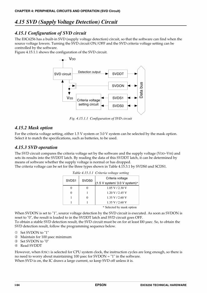
I-94 EPSON E0C6256 TECHNICAL HARDWARE
CHAPTER 4: PERIPHERAL CIRCUITS AND OPERATION (SVD Circuit)
4.15 SVD (Supply Voltage Detection) Circuit
4.15.1 Configuration of SVD circuitThe E0C6256 has a built-in SVD (supply voltage detection) circuit, so that the software can find when thesource voltage lowers. Turning the SVD circuit ON/OFF and the SVD criteria voltage setting can becontrolled by the software.Figure 4.15.1.1 shows the configuration of the SVD circuit.
V
SVD circuitDetection output
Dat
a bu
s
DD
VSS
SVDDT
SVDON
SVDS1
SVDS0
Criteria voltagesetting circuit
Fig. 4.15.1.1 Configuration of SVD circuit
4.15.2 Mask optionFor the criteria voltage setting, either 1.5 V system or 3.0 V system can be selected by the mask option.Select it to match the specifications, such as batteries, to be used.
4.15.3 SVD operationThe SVD circuit compares the criteria voltage set by the software and the supply voltage (VDD–VSS) andsets its results into the SVDDT latch. By reading the data of this SVDDT latch, it can be determined bymeans of software whether the supply voltage is normal or has dropped.The criteria voltage can be set for the three types shown in Table 4.15.3.1 by SVDS0 and SCDS1.
Table 4.15.3.1 Criteria voltage setting
SVDS1
0
0
1
1
SVDS0
0
1
0
1
Criteria voltage
(1.5 V system/ 3.0 V system)*
1.05 V / 2.30 V
1.20 V / 2.45 V
1.35 V / 2.60 V
1.35 V / 2.60 V
* Selected by mask option
When SVDON is set to "1", source voltage detection by the SVD circuit is executed. As soon as SVDON isreset to "0", the result is loaded to in the SVDDT latch and SVD circuit goes OFF.To obtain a stable SVD detection result, the SVD circuit must be on for at least l00 µsec. So, to obtain theSVD detection result, follow the programming sequence below.
➀ Set SVDON to "1"➁ Maintain for 100 µsec minimum➂ Set SVDON to "0"➃ Read SVDDT
However, when fOSC1 is selected for CPU system clock, the instruction cycles are long enough, so there isno need to worry about maintaining 100 µsec for SVDON = "1" in the software.When SVD is on, the IC draws a large current, so keep SVD off unless it is.

E0C6256 TECHNICAL HARDWARE EPSON I-95
CHAPTER 4: PERIPHERAL CIRCUITS AND OPERATION (SVD Circuit)
4.15.4 Control of SVD circuitTable 4.15.4.1 shows the control bits and their addresses for the SVD circuit.
Table 4.15.4.1 Control bits for SVD circuit
Address CommentRegister
D3 D2 D1 D0 Name Init 1 0*1
SVDS0
R
00
SVDS1SVDS0
––00
SVDS100
80H
*2
*2
*7
Unused
Unused
SVD criteria voltage setting (1.5 V/3.0 V)
0: 1.05/2.30, 1: 1.20/2.45, 2 & 3: 1.35/2.60 (V)R/W
SVDON
R
00
SVDDTSVDON
––00
LowOn
NormalOff
SVDDT00
81H
*2
*2
Unused
Unused
Supply voltage detection data
SVD circuit On/OffR/W
*5
*5
*5
*5
*1 Initial value at the time of initial reset *5 Constantly "0" when being read*2 Not set in the circuit *6 Refer to main manual*3 Undefined *7 Page switching in I/O memory is not necessary*4 Reset (0) immediately after being read
SVDS0, SVDS1: SVD criteria voltage setting (80H•D0, D1)Criteria voltage for SVD is set as shown in Table 4.15.4.2.
Table 4.15.4.2 Criteria voltage setting
SVDS1
0
0
1
1
SVDS0
0
1
0
1
Criteria voltage
(1.5 V system/ 3.0 V system)*
1.05 V / 2.30 V
1.20 V / 2.45 V
1.35 V / 2.60 V
1.35 V / 2.60 V
* Selected by mask option
At initial reset, these registers are set to "0".
Note: 1.05 V or 1.20 V of the 1.5 V system criteria voltage must be used in the doubler mode, so thedoubler mode has to be set when using these criteria voltages. Using the normal mode may cause amalfunction or will be unable to detect the supply voltage correctly. See Section 4.2, "Power Supplyand Operating Mode Settings" for the operating mode switching.
SVDON: SVD ON/OFF (81H•D0)Turns the SVD circuit ON and OFF.
When "1" is written: SVD circuit ONWhen "0" is written: SVD circuit OFF
Reading: Valid
When SVDON is set to "1", source voltage detection by the SVD circuit is executed. As soon as SVDON isreset to "0", the result is loaded to in the SVDDT latch. To obtain a stable SVD detection result, the SVDcircuit must be on for at least l00 µsec.At initial reset, this register is set to "0".
SVDDT: SVD data (81H•D1)This is the result of supply voltage detection.
When "0" is read: Supply voltage (VDD–VSS) ≥ Criteria voltageWhen "1" is read: Supply voltage (VDD–VSS) < Criteria voltage
Writing: Invalid
The result of supply voltage detection at time of SVDON is set to "0" can be read from this latch.At initial reset, SVDDT is set to "0".

I-96 EPSON E0C6256 TECHNICAL HARDWARE
CHAPTER 4: PERIPHERAL CIRCUITS AND OPERATION (SVD Circuit)
4.15.5 Programming notes(1) To obtain a stable SVD detection result, the SVD circuit must be on for at least l00 µsec. So, to obtain the
SVD detection result, follow the programming sequence below.
➀ Set SVDON to "1"➁ Maintain for 100 µsec minimum➂ Set SVDON to "0"➃ Read SVDDT
However, when fOSC1 is selected for CPU system clock, the instruction cycles are long enough, so thereis no need to worry about maintaining 100 µsec for SVDON = "1" in the software.
(2) The SVD circuit should normally be turned OFF as the consumption current of the IC becomes largewhen it is ON.
(3) 1.05 V or 1.20 V of the 1.5 V system criteria voltage must be used in the doubler mode, so the doublermode has to be set when using these criteria voltages. Using the normal mode may cause a malfunctionor will be unable to detect the supply voltage correctly. See Section 4.2, "Power Supply and OperatingMode Settings" for the operating mode switching.

E0C6256 TECHNICAL HARDWARE EPSON I-97
CHAPTER 4: PERIPHERAL CIRCUITS AND OPERATION (Interrupt and HALT)
4.16 Interrupt and HALT
<Interrupt types>The E0C6256 provides the following interrupt settings, each of which is maskable.
External interrupt: •Input port interrupt (2 systems)
Internal interrupt: •Clock timer interrupt (4 systems)•Stopwatch timer interrupt (4 systems)•Programmable timer interrupt (1 system)•Serial interface interrupt (1 system)•A/D converter interrupt (1 system)
To authorize interrupt, the interrupt flag must be set to "1" (EI) and the necessary related interrupt maskregisters must be set to "1" (enable).When an interrupt occurs the interrupt flag is automatically reset to "0" (DI), and interrupts after that areinhibited.Figure 4.16.1 shows the configuration of the interrupt circuit.
<HALT>The E0C6256 has HALT function that considerably reduce the current consumption when it is not neces-sary.
The CPU enters the HALT status when the HALT instruction is executed.In the HALT status, the operation of the CPU is stopped. However, the oscillation circuit operates. Reacti-vating the CPU from the HALT status is done by generating an interrupt request. When it does not reacti-vate upon an interrupt request, the watchdog timer will cause it to restart from the initial reset status.(When "Use" is selected in the mask option of the watchdog timer.)

I-98 EPSON E0C6256 TECHNICAL HARDWARE
CHAPTER 4: PERIPHERAL CIRCUITS AND OPERATION (Interrupt and HALT)
Fig. 4.16.1 Configuration of the interrupt circuit
IAD
EIAD
K00
KCP00
SIK00
K01
KCP01
SIK01
K02
KCP02
SIK02
K03
KCP03
SIK03
IK0
EIK0
IPT
EIPT
IT3
EIT3
IT2
EIT2
IT1
EIT1
IT0
EIT0
Interruptvectorgenerationcircuit
Program counter(low-order 4 bits)
INT(interrupt request)
Interrupt factor flag
Interrupt mask register
Input comparison register
Interrupt selection register
Interrupt flag
IRUN
EIRUN
ILAP
EILAP
ISW1
EISW1
ISW0
EISW0
ISIF
EISIF
K10
KCP10
SIK10
K11
KCP11
SIK11
K12
KCP12
SIK12
K13
KCP13
SIK13
IK1
EIK1

E0C6256 TECHNICAL HARDWARE EPSON I-99
CHAPTER 4: PERIPHERAL CIRCUITS AND OPERATION (Interrupt and HALT)
4.16.1 Interrupt factorTable 4.16.1.1 shows the factors for generating interrupt requests.
The interrupt flags are set to "1" depending on the corresponding interrupt factors.The CPU operation is interrupted when any of the conditions below set an interrupt factor flag to "1".
• The corresponding mask register is "1" (enabled)• The interrupt flag is "1" (EI)
The interrupt factor flag is a read-only register, but can be reset to "0" when the register data is read out.At initial reset, the interrupt factor flags are reset to "0".
Table 4.16.1.1 Interrupt factors
Interrupt factor
Clock timer 2 Hz (falling edge)
Clock timer 8 Hz (falling edge)
Clock timer 16 Hz (falling edge)
Clock timer 32 Hz (falling edge)
Stopwatch timer direct RUN (input)
Stopwatch timer direct LAP (input)
Stopwatch timer 1 Hz (falling edge)
Stopwatch timer 10 Hz (falling edge)
Programmable timer (counter = 0)
Serial interface (8-bit data input/output has completed)
K00–K03 input (falling or rising edge)
K10–K13 input (falling or rising edge)
A/D converter (A/D conversion has completed)
Interrupt factor flag
IT3
IT2
IT1
IT0
IRUN
ILAP
ISW1
ISW0
IPT
ISIF
IK0
IK1
IAD
(FEH•D3)
(FEH•D2)
(FEH•D1)
(FEH•D0)
(FDH•D3)
(FDH•D2)
(FDH•D1)
(FDH•D0)
(FCH•D0)
(FBH•D0)
(FAH•D0)
(F9H•D0)
(F8H•D0)
Note: Reading of interrupt factor flags is available at EI, but be careful in the following cases.If the interrupt mask register value corresponding to the interrupt factor flags to be read is set to "1",an interrupt request will be generated by the interrupt factor flags set timing, or an interrupt requestwill not be generated.
4.16.2 Interrupt maskThe interrupt factor flags can be masked by the corresponding interrupt mask registers.The interrupt mask registers are read/write registers. They are enabled (interrupt authorized) when "1" iswritten to them, and masked (interrupt inhibited) when "0" is written to them.At initial reset, the interrupt mask register is set to "0".Table 4.16.2.1 shows the correspondence between interrupt mask registers and interrupt factor flags.
Table 4.16.2.1 Interrupt mask registers and interrupt factor flags
Interrupt mask register Interrupt factor flag
IT3
IT2
IT1
IT0
IRUN
ILAP
ISW1
ISW0
IPT
ISIF
IK0
IK1
IAD
(FEH•D3)
(FEH•D2)
(FEH•D1)
(FEH•D0)
(FDH•D3)
(FDH•D2)
(FDH•D1)
(FDH•D0)
(FCH•D0)
(FBH•D0)
(FAH•D0)
(F9H•D0)
(F8H•D0)
EIT3
EIT2
EIT1
EIT0
EIRUN
EILAP
EISW1
EISW0
EIPT
EISIF
EIK0
EIK1
EIAD
(F6H•D3)
(F6H•D2)
(F6H•D1)
(F6H•D0)
(F5H•D3)
(F5H•D2)
(F5H•D1)
(F5H•D0)
(F4H•D0)
(F3H•D0)
(F2H•D0)
(F1H•D0)
(F0H•D0)

I-100 EPSON E0C6256 TECHNICAL HARDWARE
CHAPTER 4: PERIPHERAL CIRCUITS AND OPERATION (Interrupt and HALT)
4.16.3 Interrupt vectorWhen an interrupt request is input to the CPU, the CPU begins interrupt processing. After the programbeing executed is terminated, the interrupt processing is executed in the following order.
➀ The address data (value of program counter) of the program to be executed next is saved in the stackarea (RAM).
➁ The interrupt request causes the value of the interrupt vector (page 1, 02H–0EH) to be set in the pro-gram counter.
➂ The program at the specified address is executed (execution of interrupt processing routine by soft-ware).
Table 4.16.3.1 shows the correspondence of interrupt requests and interrupt vectors.
Note: The processing in ➀ and ➁ above take 12 cycles of the CPU system clock.
Table 4.16.3.1 Interrupt request and interrupt vectors
Interrupt request
A/D converter
K10–K13 input
K00–K03 input
Serial interface
Programmable timer
Stopwatch timer
Clock timer
Priority
High
↑
↓Low
Interrupt vector
102H
104H
106H
108H
10AH
10CH
10EH
The four low-order bits of the program counter are indirectly addressed through the interrupt request.
4.16.4 Control of interruptTables 4.16.4.1(a) and (b) show the interrupt control bits and their addresses.
Table 4.16.4.1(a) Control bits of interrupt (1)
D3 D2 D1 D0 Name Init 1 0*1
90HSIK00
SIK03SIK02SIK01SIK00
0000
Interrupt selection register (K03)
Interrupt selection register (K02)
Interrupt selection register (K01)
Interrupt selection register (K00)
EnableEnableEnableEnable
DisableDisableDisableDisable
SIK01SIK02SIK03
92HKCP00
R/W
KCP03KCP02KCP01KCP00
KCP01KCP02KCP030000
*7
R/W
Input comparison register (K00–K03)
94HSIK10
SIK13SIK12SIK11SIK10
0000
Interrupt selection register (K13)
Interrupt selection register (K12)
Interrupt selection register (K11)
Interrupt selection register (K10)
EnableEnableEnableEnable
DisableDisableDisableDisable
SIK11SIK12SIK13
96HKCP10
R/W
KCP13KCP12KCP11KCP10
KCP11KCP12KCP130000
R/W
Input comparison register (K10–K13)
Address CommentRegister
*1 Initial value at the time of initial reset *5 Constantly "0" when being read*2 Not set in the circuit *6 Refer to main manual*3 Undefined *7 Page switching in I/O memory is not necessary*4 Reset (0) immediately after being read

E0C6256 TECHNICAL HARDWARE EPSON I-101
CHAPTER 4: PERIPHERAL CIRCUITS AND OPERATION (Interrupt and HALT)
Table 4.16.4.1(b) Control bits of interrupt (2)
D3 D2 D1 D0 Name Init 1 0*1
F0HEIAD
000
EIAD
–––0
Unused
Unused
Unused
Interrupt mask register (A/D converter)Enable Mask
000*2
*2
*2
F1HEIK1
000
EIK1
–––0 Enable Mask
000*2
*2
*2
F2HEIK0
R
000
EIK0 Enable Mask
000–––0
*2
*2
*2
EISIF
R
000
EISIF
–––0 Enable Mask
000
F3H
*2
*2
*2
F4HEIPT
R
000
EIPT
–––0 Enable Mask
000
F5HEISW0
R/W
EIRUNEILAPEISW1EISW0
0000
EnableEnableEnableEnable
MaskMaskMaskMask
EISW1EILAPEIRUN
F6HEIT0
R/W
EIT3EIT2EIT1EIT0
0000
Interrupt mask register (Clock timer 2 Hz)
Interrupt mask register (Clock timer 8 Hz)
Interrupt mask register (Clock timer 16 Hz)
Interrupt mask register (Clock timer 32 Hz)
EnableEnableEnableEnable
MaskMaskMaskMask
EIT1EIT2EIT3
*7
Unused
Unused
Unused
Interrupt mask register (K10–K13)
Unused
Unused
Unused
Interrupt mask register (K00–K03)
Unused
Unused
Unused
Interrupt mask register (Serial interface)
Unused
Unused
Unused
Interrupt mask register (Programmable timer)
Interrupt mask register (Stopwatch direct RUN)
Interrupt mask register (Stopwatch direct LAP)
Interrupt mask register (Stopwatch 1 Hz)
Interrupt mask register (Stopwatch 10 Hz)
R/W
R
R/W
R/W
R
R/W
R/W
F8HIAD
000
IAD
–––0
Unused
Unused
Unused
Interrupt factor flag (A/D converter)Yes No
000*2
*2
*2
F9HIK1
000
IK1
–––0 Yes No
000*2
*2
*2
FAHIK0
R
000
IK0 Yes No
000–––0
*2
*2
*2
ISIF
R
000
ISIF
–––0 Yes No
000
FBH
*2
*2
*2
FCHIPT
R
000
IPT
–––0 Yes No
000
FDHISW0
R
IRUN ILAP ISW1 ISW0
0000
YesYesYesYes
NoNoNoNo
ISW1ILAPIRUN
FEHIT0
R
IT3IT2IT1IT0
0000
Interrupt factor flag (Clock timer 2 Hz)
Interrupt factor flag (Clock timer 8 Hz)
Interrupt factor flag (Clock timer 16 Hz)
Interrupt factor flag (Clock timer 32 Hz)
YesYesYesYes
NoNoNoNo
IT1IT2IT3
Unused
Unused
Unused
Interrupt factor flag (K10–K13)
Unused
Unused
Unused
Interrupt factor flag (K00–K03)
Unused
Unused
Unused
Interrupt factor flag (Serial interface)
Unused
Unused
Unused
Interrupt factor flag (Programmable timer)
Interrupt factor flag (Stopwatch direct RUN)
Interrupt factor flag (Stopwatch direct LAP)
Interrupt factor flag (Stopwatch 1 Hz)
Interrupt factor flag (Stopwatch 10 Hz)
R
R
Address CommentRegister
*5
*5
*5
*5
*5
*5
*5
*5
*5
*5
*5
*5
*5
*5
*5
*4
*5
*5
*5
*4
*5
*5
*5
*4
*5
*5
*5
*4
*4
*4
*4
*4
*4
*4
*4
*4
*2
*2
*2
*5
*5
*5
*2
*2
*2
*5
*5
*5
*4
*1 Initial value at the time of initial reset *5 Constantly "0" when being read*2 Not set in the circuit *6 Refer to main manual*3 Undefined *7 Page switching in I/O memory is not necessary*4 Reset (0) immediately after being read

I-102 EPSON E0C6256 TECHNICAL HARDWARE
CHAPTER 4: PERIPHERAL CIRCUITS AND OPERATION (Interrupt and HALT)
EIT3, EIT2, EIT1, EIT0: Interrupt mask registers (F6H)IT3, IT2, IT1, IT0: Interrupt factor flags (FEH)
....................... See Section 4.9, "Clock Timer".
EIRUN, EILAP, EISW1, EISW0: Interrupt mask registers (F5H)IRUN, ILAP, ISW1, ISW0: Interrupt factor flags (FDH)
....................... See Section 4.10, "Stopwatch Timer".
EIPT: Interrupt mask register (F4H•D0)IPT: Interrupt factor flag (FCH•D0)
....................... See Section 4.11, "Programmable Timer".
EISIF: Interrupt mask register (F3H•D0)ISIF: Interrupt factor flag (FBH•D0)
....................... See Section 4.12, "Serial Interface".
KCP03–KCP00: Input comparison registers (92H)SIK03–SIK00: Interrupt selection registers (90H)EIK0: Interrupt mask register (F2H•D0)IK0: Interrupt factor flag (FAH•D0)
....................... See Section 4.5, "Input Ports".
KCP13–KCP10: Input comparison registers (96H)SIK13–SIK10: Interrupt selection registers (94H)EIK1: Interrupt mask register (F1H•D0)IK1: Interrupt factor flag (F9H•D0)
....................... See Section 4.5, "Input Ports".
EIAD: Interrupt mask register (F0H•D0)IAD: Interrupt factor flag (F8H•D0)
....................... See Section 4.14, "A/D Converter".
4.16.5 Programming notes(1) The interrupt factor flags are set when the timing condition is established, even if the interrupt mask
registers are set to "0".
(2) Reading of interrupt factor flags is available at EI, but be careful in the following cases.If the interrupt mask register value corresponding to the interrupt factor flags to be read is set to "1", aninterrupt request will be generated by the interrupt factor flags set timing, or an interrupt request willnot be generated.

E0C6256 TECHNICAL HARDWARE EPSON I-103
CHAPTER 5: SUMMARY OF NOTES
CHAPTER 5 SUMMARY OF NOTES
5.1 Notes for Low Current ConsumptionThe E0C6256 contains control registers for each of the circuits so that current consumption can be lowered.These control registers lower the current consumption through programs that operate the circuits at theminimum levels.The following text explains the circuits that can control operation and their control registers. Refer to thesewhen putting programs together.
Table 5.1.1 Circuits and control registers
Below are the circuit statuses at initial reset.
CPU: Operating status
CPU operating frequency: Low speed side (CLKCHG = "0"),OSC3 oscillation circuit OFF status (OSCC = "0")
Oscillation system regulated voltage circuit: Low speed side, -1.05 V (VSCHG = "0")
LCD system regulated voltage circuit: OFF status (LPWR = "0", APWR = "0")
Voltage doubler/halver circuit: Regulated circuit is driven by VSS,Normal mode (DBON = "0", HLON = "0", VSEL = "0")
A/D converter: OFF status (APWR = "0")
SVD circuit: OFF status (SVDON = "0")
Also, be careful about panel selection because the current consumption can differ by the order of severalµA on account of the LCD panel characteristics.
Control register
HALT instruction
CLKCHG, OSCC
VSCHG
LPWR, APWR
DBON, HLON, VSEL
APWR
SVDON
Circuit (and Item)
See Chapter 7, "ELECTRICAL CHARACTERISTICS", for order of current consumption.
CPU
CPU operating frequency
Oscillation system regulated voltage circuit
LCD system regulated voltage circuit
Voltage doubler/halver
A/D converter
SVD circuit
I-104 EPSON E0C6256 TECHNICAL HARDWARE
CHAPTER 5: SUMMARY OF NOTES
5.2 Summary of Notes by FunctionHere, the cautionary notes are summed up by function category. Keep these notes well in mind whenprogramming.
Memory
Memory is not mounted in unused area within the memory map and in memory area not indicated in thismanual. For this reason, normal operation cannot be assured for programs that have been prepared withaccess to these areas.
Operating mode and power supply control
(1) When the supply voltage is out of the specified voltage range of an operating mode, do not switch intothe operating mode. It may cause malfunction or increase current consumption.
(2) Do not set HLON (halving) and DBON (doubling) to "1" at the same time.
(3) When switching from the normal mode to the doubler/halver mode, VSEL should be set to "1" wait 100msec or more for the VS2 to stabilize after setting DBON or HLON to "1".
(4) When switching from the doubler/halver mode to the normal mode, use separate instructions to switchthe mode (VSEL = "0") and turn the supply voltage doubler/halver OFF (HLON = "0" or DBON = "0").Simultaneous processing with a single instruction may cause malfunction.
Watchdog timer
When the watchdog timer is being used, the software must reset it within 3-second cycles.
Oscillation circuit
(1) When switching the CPU system clock from OSC1 to OSC3, set VS1 to -2.1 V (VSCHG = "1") beforeturning the OSC3 oscillation ON.When switching from OSC3 to OSC1, set VS1 to -1.05 V (VSCHG = "0") after switching to OSC1 andturning the OSC3 oscillation OFF.
(2) It takes at least 5 msec from the time the OSC3 oscillation circuit goes ON until the oscillation stabilizes.Consequently, when switching the CPU operation clock from OSC1 to OSC3, do this after a minimumof 5 msec have elapsed since the OSC3 oscillation went ON.Further, the oscillation stabilization time varies depending on the external oscillator characteristics andconditions of use, so allow ample margin when setting the wait time.
OSC1 → OSC31. Set VSCHG to "1" (-1.05 V → -2.1 V)2. Set OSCC to "1" (OSC3 oscillation ON)3. Maintain 5 msec or more4. Set CLKCHG to "1" (OSC1 → OSC3)
OSC3 → OSC11. Set CLKCHG to "0" (OSC3 → OSC1)2. Set OSCC to "0" (OSC3 oscillation OFF)3. Set VSCHG to "0" (-2.1 V → -1.05 V)
(3) When switching the clock form OSC3 to OSC1, use a separate instruction for turning the OSC3 oscilla-tion OFF. An error in the CPU operation can result if this processing is performed at the same time bythe one instruction.
(4) Switching the operating voltage when the supply voltage is lower than 2.2 V (absolute value) may causea malfunction. Switch the operating voltage only after making sure that supply voltage is more than 2.2V (absolute value) using the SVD circuit.Do not switch the operating voltage during operating in the doubler mode or the halver mode, even ifthe VS2 voltage is more than 2.2 V (absolute value). The OSC3 clock can be used only in the normalmode.
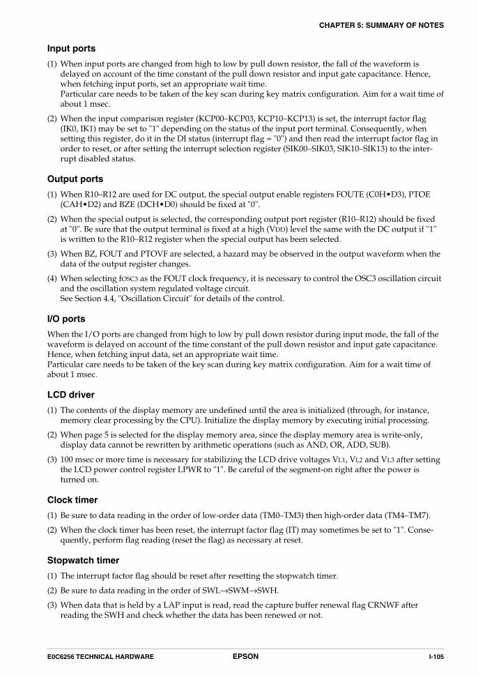
E0C6256 TECHNICAL HARDWARE EPSON I-105
CHAPTER 5: SUMMARY OF NOTES
Input ports
(1) When input ports are changed from high to low by pull down resistor, the fall of the waveform isdelayed on account of the time constant of the pull down resistor and input gate capacitance. Hence,when fetching input ports, set an appropriate wait time.Particular care needs to be taken of the key scan during key matrix configuration. Aim for a wait time ofabout 1 msec.
(2) When the input comparison register (KCP00–KCP03, KCP10–KCP13) is set, the interrupt factor flag(IK0, IK1) may be set to "1" depending on the status of the input port terminal. Consequently, whensetting this register, do it in the DI status (interrupt flag = "0") and then read the interrupt factor flag inorder to reset, or after setting the interrupt selection register (SIK00–SIK03, SIK10–SIK13) to the inter-rupt disabled status.
Output ports
(1) When R10–R12 are used for DC output, the special output enable registers FOUTE (C0H•D3), PTOE(CAH•D2) and BZE (DCH•D0) should be fixed at "0".
(2) When the special output is selected, the corresponding output port register (R10–R12) should be fixedat "0". Be sure that the output terminal is fixed at a high (VDD) level the same with the DC output if "1"is written to the R10–R12 register when the special output has been selected.
(3) When BZ, FOUT and PTOVF are selected, a hazard may be observed in the output waveform when thedata of the output register changes.
(4) When selecting fOSC3 as the FOUT clock frequency, it is necessary to control the OSC3 oscillation circuitand the oscillation system regulated voltage circuit.See Section 4.4, "Oscillation Circuit" for details of the control.
I/O ports
When the I/O ports are changed from high to low by pull down resistor during input mode, the fall of thewaveform is delayed on account of the time constant of the pull down resistor and input gate capacitance.Hence, when fetching input data, set an appropriate wait time.Particular care needs to be taken of the key scan during key matrix configuration. Aim for a wait time ofabout 1 msec.
LCD driver
(1) The contents of the display memory are undefined until the area is initialized (through, for instance,memory clear processing by the CPU). Initialize the display memory by executing initial processing.
(2) When page 5 is selected for the display memory area, since the display memory area is write-only,display data cannot be rewritten by arithmetic operations (such as AND, OR, ADD, SUB).
(3) 100 msec or more time is necessary for stabilizing the LCD drive voltages VL1, VL2 and VL3 after settingthe LCD power control register LPWR to "1". Be careful of the segment-on right after the power isturned on.
Clock timer
(1) Be sure to data reading in the order of low-order data (TM0–TM3) then high-order data (TM4–TM7).
(2) When the clock timer has been reset, the interrupt factor flag (IT) may sometimes be set to "1". Conse-quently, perform flag reading (reset the flag) as necessary at reset.
Stopwatch timer
(1) The interrupt factor flag should be reset after resetting the stopwatch timer.
(2) Be sure to data reading in the order of SWL→SWM→SWH.
(3) When data that is held by a LAP input is read, read the capture buffer renewal flag CRNWF afterreading the SWH and check whether the data has been renewed or not.
I-106 EPSON E0C6256 TECHNICAL HARDWARE
CHAPTER 5: SUMMARY OF NOTES
(4) When performing a processing such as a LAP input preceding with 1 Hz interrupt processing, read theLAP data carry-up request flag LCURF before processing and check whether carry-up is needed or not.
(5) When the interrupt factor flag ISW1 is set to "1", if reading it (reading FDH) before the capture buffershifts into hold status, the LAP data carry-up request flag is not set to "1". Pay attention to the interruptprocessing.
Fig. 5.2.1 Flow chart of stopwatch timer interrupt processing
Programmable timer
(1) Be sure to read the counter data in the order of low-order data (PT0–PT3) then high-order data (PT4–PT7).
(2) When data of reload registers is set at "00H", the down-counter becomes a 256-value counter.
(3) Set the VS1 voltage to -2.1 V (VSCHG = "1") when using the programmable timer as an event counter.
Serial interface
(1) When using the serial interface in the master mode, the synchronous clock uses the CPU system clock.Accordingly, do not change the system clock (fOSC1 ↔ fOSC3) while the serial interface is operating.
(2) Perform data writing/reading to data registers SD0–SD7 only while the serial interface is halted (i.e.,the synchronous clock is neither being input or output).
(3) As a trigger condition, it is required that data writing or reading on data registers SD0–SD7 be per-formed prior to writing "1" to SCTRG. (The internal circuit of the serial interface is initiated throughdata writing/reading on data registers SD0–SD7.) Supply trigger only once every time the serialinterface is placed in the RUN state. Moreover, when the synchronous clock SCLK is external clock,start to input the external clock after the trigger.
(4) Set the VS1 voltage to -2.1 V (VSCHG = "1") when using the serial interface in slave mode.
Stopwatchinterrupt routine
Read capture:SWL, SWM, SWH
CRNWF = 1?
Read interrupt factor flag:IRUN, ILAP, ISW1, ISW0
ILAP = 1?
Acquire for lap data
LCURF = 1?
Carry up 1 sec for lap data
IRUN = 1?
Control for RUN/STOP
ISW1 = 1?
Carry up 1 sec forstopwatch data
ISW0 = 1?
10 Hz interrupt (application)
RETURN

E0C6256 TECHNICAL HARDWARE EPSON I-107
CHAPTER 5: SUMMARY OF NOTES
Sound generator
(1) Pay attention to the output because it is fixed at HIGH level when the R12 register is set to "1".
(2) Since it generates a BZ signal that is out of synchronization with the BZE register, hazards may at timesbe produced when the signal goes ON/OFF due to the setting of the register.
(3) The one-shot output is only valid when the normal buzzer output is OFF (BZE = "0") and will be invalidwhen the normal buzzer output is ON (BZE = "1").
A/D converter
(1) Depending on the initial value of the up-counter C0–C19, the up-counter or the up/down counter mayoverflow while the CR oscillation clock is being counted. When setting the initial value, pay attention toCR oscillation frequency, its fluctuation range and the input clock frequency of the up/down counter. Ifan overflow occurs, A/D conversion is terminated immediately. When the A/D conversion result (up-counter value) is read, check the overflow flag.
(2) When the up/down counter TC0–TC15 is read after A/D conversion, it may not indicate "0000H". Thisis not due to incorrect timing in terminating A/D conversion but because the counting down clock isinput after the control signal is output to the up-counter to terminate counting.
(3) When an interrupt occurs by the counter overflow, the same interrupt will occur if the overflow flag(OVF1 or OVF2) is not reset. Be sure to check and reset the overflow flag when the A/D converterinterrupt occurs.
(4) When reading the up-counter data (TC0–TC15), be sure to read from the low-order address first.
(5) Pay attention when using the OSC3 oscillation clock as the input clock for the up/down counter. It isnecessary to switch the VS1 output voltage, control the OSC3 oscillation circuit and switch the CPU clock.
(6) The A/D converter uses the LCD power supply as its power source. If starting A/D conversion when theLPWR register (C3H) has been set to "0" and the LCD power is OFF, the LCD power supply circuit activatesat the time of the APWR register is set to "1". In such a case, be sure to secure 100 msec or more time tostabilize the power. (The LCD power supply is also turned ON by setting the APWR register to "1".)Setting of the APWR register (E0H) is necessary even if the LPWR register (C3H) has been set to "1" andthe LCD power has already been turned ON. Be sure to set "1" prior to A/D conversion.
SVD circuit
(1) To obtain a stable SVD detection result, the SVD circuit must be on for at least l00 µsec. So, to obtain theSVD detection result, follow the programming sequence below.
➀ Set SVDON to "1"➁ Maintain for 100 µsec minimum➂ Set SVDON to "0"➃ Read SVDDT
However, when fOSC1 is selected for CPU system clock, the instruction cycles are long enough, so thereis no need to worry about maintaining 100 µsec for SVDON = "1" in the software.
(2) The SVD circuit should normally be turned OFF as the consumption current of the IC becomes largewhen it is ON.
(3) 1.05 V or 1.20 V of the 1.5 V system criteria voltage must be used in the doubler mode, so the doublermode has to be set when using these criteria voltages. Using the normal mode may cause a malfunctionor will be unable to detect the supply voltage correctly. See Section 4.2, "Power Supply and OperatingMode Settings" for the operating mode switching.
Interrupt and HALT
(1) The interrupt factor flags are set when the timing condition is established, even if the interrupt maskregisters are set to "0".
(2) Reading of interrupt factor flags is available at EI, but be careful in the following cases.If the interrupt mask register value corresponding to the interrupt factor flags to be read is set to "1", aninterrupt request will be generated by the interrupt factor flags set timing, or an interrupt request willnot be generated.
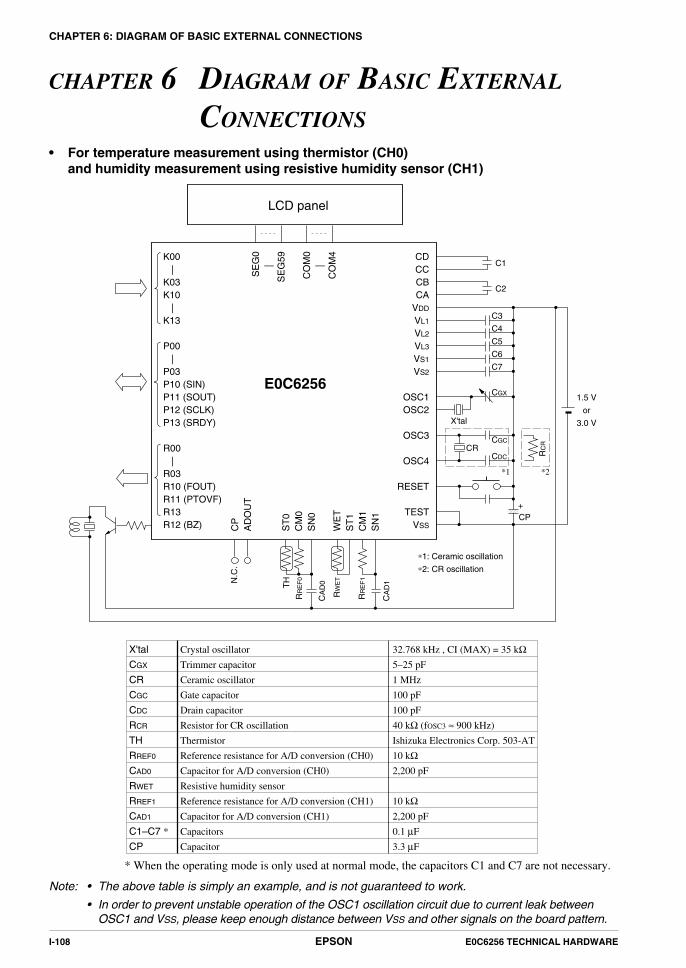
I-108 EPSON E0C6256 TECHNICAL HARDWARE
CHAPTER 6: DIAGRAM OF BASIC EXTERNAL CONNECTIONS
CHAPTER 6 DIAGRAM OF BASIC EXTERNAL
CONNECTIONS• For temperature measurement using thermistor (CH0)
and humidity measurement using resistive humidity sensor (CH1)
CDCCCBCA
VDD
VL1
VL2
VL3
VS1
VS2
OSC1OSC2
OSC3
OSC4
RESET
TESTVSS
C1
C2
C3
C4
C5
C6
C7
CGX
CDC
CP
1.5 V
or
3.0 V
+
X'tal
CR
*1 *2
RC
R
K00 |K03K10 |K13
P00 |P03P10 (SIN)P11 (SOUT)P12 (SCLK)P13 (SRDY)
R00 |R03R10 (FOUT)R11 (PTOVF)R13R12 (BZ)
SE
G0
|
SE
G59
CO
M0
|
CO
M4
CP
AD
OU
T
ST
0C
M0
SN
0
WE
TS
T1
CM
1S
N1
CA
D0
RR
EF
0
TH
E0C6256
LCD panel
∗1: Ceramic oscillation
∗2: CR oscillation
CGC
CA
D1
RR
EF
1
RW
ETN.C
.
Crystal oscillator
Trimmer capacitor
Ceramic oscillator
Gate capacitor
Drain capacitor
Resistor for CR oscillation
Thermistor
Reference resistance for A/D conversion (CH0)
Capacitor for A/D conversion (CH0)
Resistive humidity sensor
Reference resistance for A/D conversion (CH1)
Capacitor for A/D conversion (CH1)
Capacitors
Capacitor
X'tal
CGX
CR
CGC
CDC
RCR
TH
RREF0
CAD0
RWET
RREF1
CAD1
C1–C7 *
CP
32.768 kHz , CI (MAX) = 35 kΩ5–25 pF
1 MHz
100 pF
100 pF
40 kΩ (fOSC3 ≈ 900 kHz)
Ishizuka Electronics Corp. 503-AT
10 kΩ2,200 pF
10 kΩ2,200 pF
0.1 µF
3.3 µF
* When the operating mode is only used at normal mode, the capacitors C1 and C7 are not necessary.
Note: • The above table is simply an example, and is not guaranteed to work.
• In order to prevent unstable operation of the OSC1 oscillation circuit due to current leak betweenOSC1 and VSS, please keep enough distance between VSS and other signals on the board pattern.
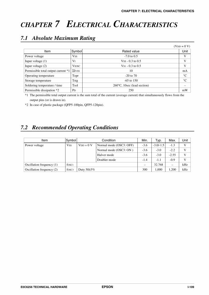
E0C6256 TECHNICAL HARDWARE EPSON I-109
CHAPTER 7: ELECTRICAL CHARACTERISTICS
CHAPTER 7 ELECTRICAL CHARACTERISTICS
7.1 Absolute Maximum Rating
7.2 Recommended Operating Conditions
Item Symbol UnitRated value
Power voltage
Input voltage (1)
Input voltage (2)
Permissible total output current *1
Operating temperature
Storage temperature
Soldering temperature / time
Permissible dissipation *2
*1
*2
VSS
VI
VIOSC
ΣIVSS
Topr
Tstg
Tsol
PD
V
V
V
mA
°C
°C
–
mW
-7.0 to 0.5
VSS - 0.3 to 0.5
VS1 - 0.3 to 0.5
10
-20 to 70
-65 to 150
260°C, 10sec (lead section)
250
The permissible total output current is the sum total of the current (average current) that simultaneously flows from the
output pins (or is drawn in).
In case of plastic package (QFP5-100pin, QFP5-128pin).
(VDD = 0 V)
Item Symbol Min. Typ. Max. UnitCondition
Power voltage
Oscillation frequency (1)
Oscillation frequency (2)
VSS
fOSC1
fOSC3
-3.6
-3.6
-3.6
-1.4
–
300
-3.0/-1.5
-3.0
-3.0
-1.1
32.768
1,000
-1.3
-2.2
-2.55
-0.9
–
1,200
V
V
V
V
kHz
kHz
VDD = 0 V
Duty 50±5%
Normal mode (OSC3: OFF)
Normal mode (OSC3: ON )
Halver mode
Doubler mode
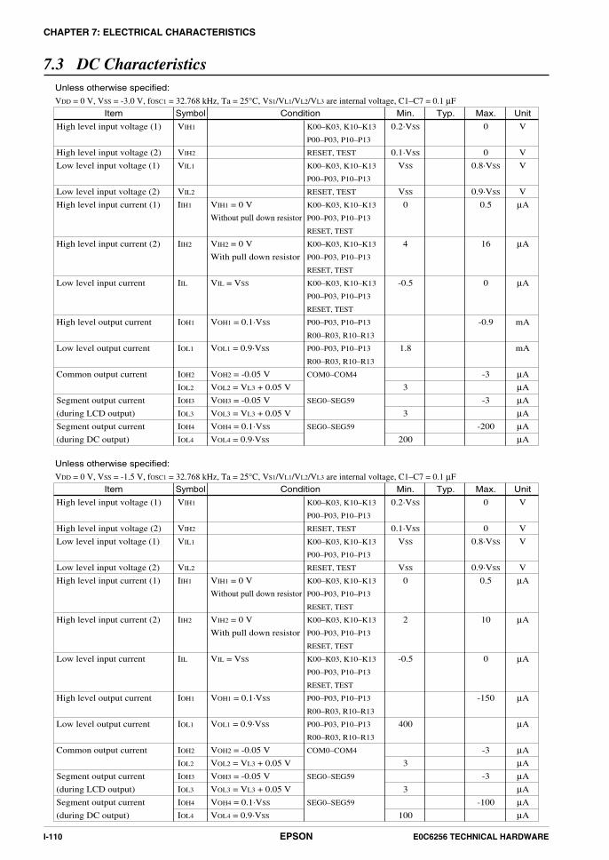
I-110 EPSON E0C6256 TECHNICAL HARDWARE
CHAPTER 7: ELECTRICAL CHARACTERISTICS
7.3 DC Characteristics
Item Symbol Min. Typ. Max. UnitCondition
High level input voltage (1)
High level input voltage (2)
Low level input voltage (1)
Low level input voltage (2)
High level input current (1)
High level input current (2)
Low level input current
High level output current
Low level output current
Common output current
Segment output current
(during LCD output)
Segment output current
(during DC output)
VIH1
VIH2
VIL1
VIL2
IIH1
IIH2
IIL
IOH1
IOL1
IOH2
IOL2
IOH3
IOL3
IOH4
IOL4
0.2·VSS
0.1·VSS
VSS
VSS
0
2
-0.5
400
3
3
100
0
0
0.8·VSS
0.9·VSS
0.5
10
0
-150
-3
-3
-100
V
V
V
V
µA
µA
µA
µA
µA
µA
µA
µA
µA
µA
µA
VIH1 = 0 V
Without pull down resistor
VIH2 = 0 V
With pull down resistor
VIL = VSS
VOH1 = 0.1·VSS
VOL1 = 0.9·VSS
VOH2 = -0.05 V
VOL2 = VL3 + 0.05 V
VOH3 = -0.05 V
VOL3 = VL3 + 0.05 V
VOH4 = 0.1·VSS
VOL4 = 0.9·VSS
K00–K03, K10–K13
P00–P03, P10–P13
RESET, TEST
K00–K03, K10–K13
P00–P03, P10–P13
RESET, TEST
K00–K03, K10–K13
P00–P03, P10–P13
RESET, TEST
K00–K03, K10–K13
P00–P03, P10–P13
RESET, TEST
K00–K03, K10–K13
P00–P03, P10–P13
RESET, TEST
P00–P03, P10–P13
R00–R03, R10–R13
P00–P03, P10–P13
R00–R03, R10–R13
COM0–COM4
SEG0–SEG59
SEG0–SEG59
VDD = 0 V, VSS = -1.5 V, fOSC1 = 32.768 kHz, Ta = 25°C, VS1/VL1/VL2/VL3 are internal voltage, C1–C7 = 0.1 µF
Unless otherwise specified:
Item Symbol Min. Typ. Max. UnitCondition
High level input voltage (1)
High level input voltage (2)
Low level input voltage (1)
Low level input voltage (2)
High level input current (1)
High level input current (2)
Low level input current
High level output current
Low level output current
Common output current
Segment output current
(during LCD output)
Segment output current
(during DC output)
VIH1
VIH2
VIL1
VIL2
IIH1
IIH2
IIL
IOH1
IOL1
IOH2
IOL2
IOH3
IOL3
IOH4
IOL4
0.2·VSS
0.1·VSS
VSS
VSS
0
4
-0.5
1.8
3
3
200
0
0
0.8·VSS
0.9·VSS
0.5
16
0
-0.9
-3
-3
-200
V
V
V
V
µA
µA
µA
mA
mA
µA
µA
µA
µA
µA
µA
VIH1 = 0 V
Without pull down resistor
VIH2 = 0 V
With pull down resistor
VIL = VSS
VOH1 = 0.1·VSS
VOL1 = 0.9·VSS
VOH2 = -0.05 V
VOL2 = VL3 + 0.05 V
VOH3 = -0.05 V
VOL3 = VL3 + 0.05 V
VOH4 = 0.1·VSS
VOL4 = 0.9·VSS
K00–K03, K10–K13
P00–P03, P10–P13
RESET, TEST
K00–K03, K10–K13
P00–P03, P10–P13
RESET, TEST
K00–K03, K10–K13
P00–P03, P10–P13
RESET, TEST
K00–K03, K10–K13
P00–P03, P10–P13
RESET, TEST
K00–K03, K10–K13
P00–P03, P10–P13
RESET, TEST
P00–P03, P10–P13
R00–R03, R10–R13
P00–P03, P10–P13
R00–R03, R10–R13
COM0–COM4
SEG0–SEG59
SEG0–SEG59
VDD = 0 V, VSS = -3.0 V, fOSC1 = 32.768 kHz, Ta = 25°C, VS1/VL1/VL2/VL3 are internal voltage, C1–C7 = 0.1 µF
Unless otherwise specified:

E0C6256 TECHNICAL HARDWARE EPSON I-111
CHAPTER 7: ELECTRICAL CHARACTERISTICS
7.4 Analog Characteristics and Consumed Current
Item Symbol Min. Typ. Max. UnitCondition
LCD drive voltage *6
SVD voltage (1)
SVD voltage (2)
SVD circuit response time
Power current consumption *1
*1
*2
*3
*4
*5
*6
VL1
VL2
VL3
VSVD1
VSVD2
tSVD
IOP
-1.15
-1.20
-1.25
-1.30
-1.35
-1.40
-1.45
-1.50
2·VL1
- 0.1
3·VL1
- 0.1
-1.10
-1.25
-1.40
-1.40
-2.35
-2.50
-2.65
-2.65
-1.05
-1.10
-1.15
-1.20
-1.25
-1.30
-1.35
-1.40
-1.05
-1.20
-1.35
-1.35
-2.30
-2.45
-2.60
-2.60
1.2
650
2.5
3.5
2.0
7.5
100
200
10
170
220
-0.95
-1.00
-1.05
-1.10
-1.15
-1.20
-1.25
-1.30
2·VL1
× 0.9
3·VL1
× 0.9
-1.00
-1.15
-1.30
-1.30
-2.25
-2.40
-2.55
-2.55
100
2.5
1200
5.0
6.0
4.0
15.0
150
300
20
300
350
V
V
V
V
V
V
V
V
V
V
V
V
V
V
V
V
V
V
µsec
µA
nA
µA
µA
µA
µA
µA
µA
µA
µA
µA
Connect 1MΩ load
resistor between
VDD and VL1
(Without panel load)
Connect 1MΩ load resistor between VDD and VL2
(Without panel load)
Connect 1MΩ load resistor between VDD and VL3
(Without panel load)
1.5 V system
3.0 V system
During HALT (32 kHz)
Without panel load, OSCC = "0"
VSCHG = "0"
During execution (32 kHz) *2
Without panel load, OSCC = "0"
VSCHG = "0"
During A/D operation (32 kHz, VSS = -1.5 V) *3
Without panel load, OSCC = "0", VSCHG = "0",
Normal mode
During A/D operation (32 kHz, VSS = -3.0 V) *3
Without panel load, OSCC = "0", VSCHG = "0",
Normal mode
During SVD operation (32 kHz) *4
Without panel load, OSCC = "0", VSCHG = "0",
Normal mode
During execution (1 MHz, ceramic oscillation) *2
Without panel load
During execution (1 MHz, CR oscillation) *2
Without panel load *5
LPWR = "1", VLCHG2–VLCHG0 = "0", within the operating voltage in each operating mode.
The A/D converter and SVD circuit are OFF status.
The SVD circuit is OFF status. Current consumed during HALT (32 kHz, Normal mode) + A/D operating current
The A/D converter is OFF status. Current consumed during HALT (32 kHz, Normal mode) + SVD operating current
The value in χ MHz can be found by the following expression: IOP (fOSC3 = χ MHz) = IOP (fOSC3 = 1 MHz) × χ
VSS/VS2 ≤ VL1 - 0.2 V
Unless otherwise specified: VDD = 0 V, VSS = -1.5 V / -3.0 V, fOSC1 = 32.768 kHz, CG = 25 pF, Ta = 25°C, VS1/VL1/VL2/VL3
are internal voltage, C1–C7 = 0.1 µF, (During A/D operation: C = 2,200 pF, Reference resistance = 10 kΩ, Sensor = 10 kΩ)
VLCHG2–VLCHG0 = "0"
VLCHG2–VLCHG0 = "1"
VLCHG2–VLCHG0 = "2"
VLCHG2–VLCHG0 = "3"
VLCHG2–VLCHG0 = "4"
VLCHG2–VLCHG0 = "5"
VLCHG2–VLCHG0 = "6"
VLCHG2–VLCHG0 = "7"
SVDS1 = "0", SVDS0 = "0"
SVDS1 = "0", SVDS0 = "1"
SVDS1 = "1", SVDS0 = "0"
SVDS1 = "1", SVDS0 = "1"
SVDS1 = "0", SVDS0 = "0"
SVDS1 = "0", SVDS0 = "1"
SVDS1 = "1", SVDS0 = "0"
SVDS1 = "1", SVDS0 = "1"
Normal mode
Halver mode
Doubler mode
Normal mode
Halver mode
Doubler mode

I-112 EPSON E0C6256 TECHNICAL HARDWARE
CHAPTER 7: ELECTRICAL CHARACTERISTICS
7.5 Oscillation CharacteristicsThe oscillation characteristics change depending on the conditions (components used, board pattern, etc.).Use the following characteristics as reference values.
OSC1 crystal oscillation circuit
Item Symbol Min. Typ. Max. UnitCondition
Oscillation start voltage
Oscillation stop voltage
Built-in capacitance (drain)
Frequency/voltage deviation
Frequency/IC deviation
Frequency adjustment range
Harmonic oscillation start voltage
Permitted leak resistance
*1 Parentheses indicate value for operation in the doubler mode.
Vsta
Vstp
CD
∂f/∂V
∂f/∂IC
∂f/∂CG
Vhho
Rleak
-1.35
-1.35
(-0.9) *1
-10
35
200
20
45
5
10
10
-3.5
V
V
pF
ppm
ppm
ppm
ppm
V
MΩ
tsta ≤ 5 sec
tstp ≤ 10 sec
Including incidental capacitance inside IC
VSS = -0.9 to -3.6 V without VSCHG switching
with VSCHG switching
CG = 5 to 25 pF
CG = 5 pF
Between OSC1 and VDD
VDD = 0 V, VSS = -1.5 V / -3.0 V, Crystal: C-002R (CI = 35 kΩ), CG = 25 pF, CD = built-in, Ta = 25°C
Unless otherwise specified:
(VSS)
(VSS)
(VSS)
OSC3 CR oscillation circuit
Item Symbol Min. Typ. Max. UnitCondition
Oscillation frequency dispersion
Oscillation start voltage
Oscillation start time
Oscillation stop voltage
fOSC3
Vsta
tsta
Vstp
-30
-2.2
-2.2
900 kHz 30
3
%
V
msec
V
VSS = -2.2 to -3.6 V
VDD = 0 V, VSS = -3.0 V, RCR = 40 kΩ, Ta = 25°C
Unless otherwise specified:
(VSS)
(VSS)
OSC3 ceramic oscillation circuit
Item Symbol Min. Typ. Max. UnitCondition
Oscillation start voltage
Oscillation start time
Oscillation stop voltage
Vsta
tsta
Vstp
-2.2
-2.2
3
V
msec
V
VSS = -2.2 to -3.6 V
VDD = 0 V, VSS = -3.0 V, Ceramic oscillator: 1 MHz, CGC = CDC = 100 pF, Ta = 25°C
Unless otherwise specified:
(VSS)
(VSS)

E0C6256 TECHNICAL HARDWARE EPSON I-113
CHAPTER 7: ELECTRICAL CHARACTERISTICS
7.6 Characteristics Curves
(1) CR oscillation frequency characteristicThe oscillation characteristics change depending on the conditions (components used, board pattern,etc.). Use the following characteristics as reference values and evaluate the characteristics on the actualproduct.
10k 20k 50k 100k 200k
200k
100k
500k
1M
2M
External resistance RCR [Ω]
CR
osc
illat
ion
freq
uenc
y fO
SC
3 [H
z]
30k 40k
300k
1.2M
Rec
omm
ende
d os
cilla
tion
rang
e
VDD = 0 VVSS = -2.2 to -3.6 VTa = 25°CTyp. value
Fig. 7.6.1 CR oscillation characteristic

I-114 EPSON E0C6256 TECHNICAL HARDWARE
CHAPTER 7: ELECTRICAL CHARACTERISTICS
(2) A/D converter Sensor resistance-Oscillation frequency ratio characteristicFigure 7.6.2 shows the oscillation frequency ratio (ratio of oscillation frequency by the reference resist-ance to oscillation frequency by the sensor resistance) when the following elements are connected.(Typ.)
Reference resistance ............. 10 kΩSensor resistance .................. 10 kΩ to 20 MΩOscillating capacitor ............ 2,200 pF
Note: If the R/f conversion uses a resistive sensor for channel 0 and channel 1, and the R/f conversionuses a resistive humidity sensor for channel 1, both characteristics will be the same.
1k
0.001
Sensor resistance [Ω]
Osc
illat
ion
freq
uenc
y ra
tio
0.01
0.1
1.0
10k 100k 1M 10M
VDD = 0 VVSS = -1.3 to -3.6 VTa = -20 to 70°C
0.0001
Fig. 7.6.2 Sensor resistance-oscillation frequency ratio curve

E0C6256 TECHNICAL HARDWARE EPSON I-115
CHAPTER 7: ELECTRICAL CHARACTERISTICS
(3) A/D converter Resistance-Oscillation frequency characteristicCR oscillation frequency of the A/D converter disperses in each sampling. Therefore, the count numberof the up-counter should be decided after considering the fluctuation margin of the CR oscillationfrequency by the reference resistance and sensor resistance to be used for the measurement. Figure 7.6.3shows the resistance-oscillation frequency curve.
Note: • The following curves are characteristic when the oscillating capacitor is 2,200 pF.
• Typical oscillation frequency is characteristic when VSS = -3.0 V.
• The resistance value applies to both reference resistance and sensor resistance.
• If the R/f conversion uses a resistive sensor for channel 0 and channel 1, and the R/f conversionuses a resistive humidity sensor for channel 1, both characteristics will be the same.
Fig. 7.6.3 Resistance-oscillation frequency curve
1k
0.1
Resistance [Ω]
Osc
illat
ion
freq
uenc
y [k
Hz]
1.0
10
100
10k 100k 1M 10M0.01
VDD = 0 VVSS = -1.3 to -3.6 VTa = -20 to 70°COscillating capacitor: 2,200 pF
MAX
TYP
MIN

I-116 EPSON E0C6256 TECHNICAL HARDWARE
CHAPTER 8: PACKAGE
CHAPTER 8 PACKAGE
8.1 Plastic Package
QFP5-128pin(Unit: mm)
1 38
39
64
102 65
128
103
Index
20.0 ±0.123.6 ±0.4
17.6
±0.4
14.0
±0.1
0.5 0.2 ±0.1
2.7
±0.1
0.15
±0.0
5
1.8
0.8 ±0.2

E0C6256 TECHNICAL HARDWARE EPSON I-117
CHAPTER 8: PACKAGE
QFP5-100pin(Unit: mm)
Index
1 30
31
50
80 51
100
81
0.65 0.30 ±0.1
2.7
±0.1
0.15
±0.0
5
2.8
1.5 ±0.3
20.0 ±0.125.6 ±0.4
19.6
±0.4
14.0
±0.1

I-118 EPSON E0C6256 TECHNICAL HARDWARE
CHAPTER 8: PACKAGE
8.2 Ceramic Package for Test Samples
(Unit: mm)
1 38
39
64
102 65
128
103
20.00 ±0.1823.90 ±0.30
17.9
1±0
.30
14.0
0±0
.14
0.5 0.2
2.79
MA
X
0.76
±0.0
8
0.95
±0.0
8
0.40
±0.0
8
0.80 ±0.20
0.20
TY
P
0.15
GLASS
CERAMIC
Note: The ceramic package is fixed in this form regardless selecting of the plastic package form.
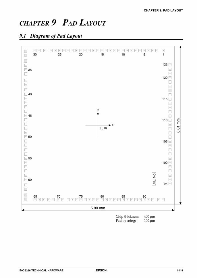
E0C6256 TECHNICAL HARDWARE EPSON I-119
CHAPTER 9: PAD LAYOUT
CHAPTER 9 PAD LAYOUT
9.1 Diagram of Pad Layout
Y
X(0, 0)
1
6.01
mm
5.80 mm
51015202530
35
40
45
50
55
60
65 70 75 80 85 90
95
100
105
110
115
120
123
DIE
No.
Chip thickness: 400 µmPad opening: 100 µm

I-120 EPSON E0C6256 TECHNICAL HARDWARE
CHAPTER 9: PAD LAYOUT
9.2 Pad Coordinates
(Unit: µm)
No.
1
2
3
4
5
6
7
8
9
10
11
12
13
14
15
16
17
18
19
20
21
22
23
24
25
26
27
28
29
30
31
32
33
34
35
36
37
38
39
40
41
Name
SEG30
SEG31
SEG32
SEG33
SEG34
SEG35
SEG36
SEG37
SEG38
SEG39
SEG40
SEG41
SEG42
SEG43
SEG44
SEG45
SEG46
SEG47
SEG48
SEG49
SEG50
SEG51
SEG52
SEG53
SEG54
SEG55
SEG56
SEG57
SEG58
SEG59
—*
—*
—*
VDD
RESET
TEST
K00
K01
K02
K03
K10
X
2486
2236
2076
1915
1755
1594
1434
1274
1114
953
793
632
472
311
151
-10
-170
-330
-490
-651
-811
-972
-1132
-1293
-1453
-1614
-1774
-2021
-2230
-2391
-2742
-2742
-2742
-2732
-2732
-2732
-2732
-2732
-2732
-2732
-2732
Y
2830
2830
2830
2830
2830
2830
2830
2830
2830
2830
2830
2830
2830
2830
2830
2830
2830
2830
2830
2830
2830
2830
2830
2830
2830
2830
2830
2830
2830
2830
2801
2648
2434
2273
2104
1943
1704
1544
1339
1178
1018
No.
42
43
44
45
46
47
48
49
50
51
52
53
54
55
56
57
58
59
60
61
62
63
64
65
66
67
68
69
70
71
72
73
74
75
76
77
78
79
80
81
82
Name
K11
K12
K13
R00
R01
R02
R03
R10
R11
R12
R13
P00
P01
P02
P03
P10
P11
P12
P13
VSS
—*
—*
—*
SEG0
SEG1
SEG2
SEG3
SEG4
SEG5
SEG6
SEG7
SEG8
SEG9
SEG10
SEG11
SEG12
SEG13
SEG14
SEG15
SEG16
SEG17
X
-2732
-2732
-2732
-2732
-2732
-2732
-2732
-2732
-2732
-2732
-2732
-2732
-2732
-2732
-2732
-2732
-2732
-2732
-2732
-2732
-2742
-2742
-2742
-2385
-2224
-2064
-1866
-1706
-1492
-1332
-1125
-965
-804
-644
-484
-324
-163
-3
158
318
479
Y
858
698
537
366
206
45
-115
-276
-436
-597
-757
-936
-1096
-1257
-1417
-1578
-1738
-1898
-2058
-2264
-2434
-2648
-2801
-2830
-2830
-2830
-2830
-2830
-2830
-2830
-2830
-2830
-2830
-2830
-2830
-2830
-2830
-2830
-2830
-2830
-2830
No.
83
84
85
86
87
88
89
90
91
92
93
94
95
96
97
98
99
100
101
102
103
104
105
106
107
108
109
110
111
112
113
114
115
116
117
118
119
120
121
122
123
Name
SEG18
SEG19
SEG20
SEG21
SEG22
SEG23
SEG24
SEG25
SEG26
SEG27
SEG28
SEG29
COM0
COM1
COM2
COM3
COM4
CB
CA
VL3
VL2
VL1
CC
CD
VS2
VSS
ADOUT
SN1
WET
ST1
CM1
SN0
CM0
ST0
CP
VDD
OSC1
OSC2
OSC3
OSC4
VS1
X
639
800
960
1120
1280
1441
1601
1762
1922
2083
2307
2468
2732
2732
2732
2732
2732
2732
2732
2732
2732
2732
2732
2732
2732
2732
2732
2732
2732
2732
2732
2732
2732
2732
2732
2732
2732
2732
2732
2732
2732
Y
-2830
-2830
-2830
-2830
-2830
-2830
-2830
-2830
-2830
-2830
-2830
-2830
-2218
-2058
-1898
-1737
-1577
-1416
-1256
-1095
-935
-774
-614
-454
-293
-133
28
188
348
509
669
830
990
1150
1311
1471
1638
1798
1959
2119
2298
Pad Coordinate Pad Coordinate Pad Coordinate
* Do not bond No. 31–33 and 62–64 pads because they are used only for factory testing.

So
ftw
areE0C6256II. Technical Software


So
ftw
are
E0C6256 TECHNICAL SOFTWARE EPSON II-i
CONTENTS
CONTENTS
CHAPTER 1 INITIAL RESET ___________________________________________ II-11.1 Internal Register Status on Initial Reset ..................................................... II-1
1.2 Initialize Program Example ........................................................................ II-8
CHAPTER 2 OSCILLATION CIRCUITS ____________________________________ II-102.1 Control Registers for Oscillation Circuit ................................................... II-10
2.2 Program Example ...................................................................................... II-10
CHAPTER 3 A/D CONVERTER _________________________________________ II-123.1 Control Registers for A/D Converter ......................................................... II-12
3.2 Control of A/D Converter .......................................................................... II-13
3.3 Software Specification ................................................................................ II-14
3.4 Program Example for Controlling A/D Converter .................................... II-15
APPENDIX A. E0C6256 RAM MAP___________________________________ II-25
B. E0C6256 INSTRUCTION SET ______________________________ II-32
C. PSEUDO-INSTRUCTION TABLE OF THE CROSS ASSEMBLER _________ II-36
D. COMMAND TABLE OF ICE6200____________________________ II-37


E0C6256 TECHNICAL SOFTWARE EPSON II-1
CHAPTER 1: INITIAL RESET
CHAPTER 1 INITIAL RESET
1.1 Internal Register Status on Initial ResetFollowing an initial reset, the internal registers and internal data memory area are initialized to the valuesshown in Tables 1.1.1 and 1.1.2.
Table 1.1.1 Initial values of internal registers
Program counter step
Program counter page
Program counter bank
New page pointer
New bank pointer
Stack pointer
Index register IX
Index register IY
Register pointer
General-purpose register A
General-purpose register B
Interrupt flag
Decimal flag
Zero flag
Carry flag
CPU core
Name Number of bits
8
4
1
4
1
8
11
11
4
4
4
1
1
1
1
Setting value
00H
1H
0
1H
0
Undefined
Undefined
Undefined
Undefined
Undefined
Undefined
0
0
Undefined
Undefined
Symbol
PCS
PCP
PCB
NPP
NBP
SP
IX
IY
RP
A
B
I
D
Z
C
Table 1.1.2 Initial values of internal data memory area
* See Tables 1.1.3(a)–(h)
RAM
Display memory
Other peripheral circuits
Peripheral circuits
Name Number of bits
4
4
—
Setting value
Undefined
Undefined
*

II-2 EPSON E0C6256 TECHNICAL SOFTWARE
CHAPTER 1: INITIAL RESET
Table 1.1.3(a) I/O memory map (80H–84H)
Address CommentRegister
D3 D2 D1 D0 Name Init 1 0*1
SVDS0
R
00
SVDS1SVDS0
––00
SVDS100
80H
*2
*2
*7
Unused
Unused
SVD criteria voltage setting (1.5 V/3.0 V)
0: 1.05/2.30, 1: 1.20/2.45, 2 & 3: 1.35/2.60 (V)R/W
SVDON
R
00
SVDDTSVDON
––00
LowOn
NormalOff
SVDDT00
81H
*2
*2
Unused
Unused
Supply voltage detection data
SVD circuit On/OffR/W
DBON
R
0VSELHLONDBON
–000
VS2
OnOn
VSS
OffOff
HLONVSEL0
82H
*2 Unused
Voltage regulator power source selection
Halver On/Off
Doubler On/OffR/W
VSCHG
R
0CLKCHG
OSCCVSCHG
–000
OSC3On
-2.1V
OSC1Off
-1.05V
OSCCCLKCHG0
83H
*2 Unused
CPU clock selection
OSC3 oscillation On/Off
VS1 output voltage changeR/W
VLCHG0
R
0VLCHG2VLCHG1VLCHG0
–000
VLCHG1VLCHG20
84H
*2 Unused
VL1 output voltage change
0: 1.05, 1: 1.10, 2: 1.15, 3: 1.20,
4: 1.25, 5: 1.30, 6: 1.35, 7: 1.40 (V)R/W
*5
*5
*5
*5
*5
*5
*5
Table 1.1.3(b) I/O memory map (90H–96H)
D3 D2 D1 D0 Name Init 1 0*1
90HSIK00
SIK03SIK02SIK01SIK00
0000
Interrupt selection register (K03)
Interrupt selection register (K02)
Interrupt selection register (K01)
Interrupt selection register (K00)
EnableEnableEnableEnable
DisableDisableDisableDisable
SIK01SIK02SIK03
91HK00
K03K02K01K00
––––
HighHighHighHigh
LowLowLowLow
K01K02K03*2
*2
*2
*2
92HKCP00
R/W
KCP03KCP02KCP01KCP00
KCP01KCP02KCP030000
*7
R/W
R Input port (K00–K03)
Input comparison register (K00–K03)
94HSIK10
SIK13SIK12SIK11SIK10
0000
Interrupt selection register (K13)
Interrupt selection register (K12)
Interrupt selection register (K11)
Interrupt selection register (K10)
EnableEnableEnableEnable
DisableDisableDisableDisable
SIK11SIK12SIK13
95HK10
K13K12K11K10
––––
HighHighHighHigh
LowLowLowLow
K11K12K13*2
*2
*2
*2
96HKCP10
R/W
KCP13KCP12KCP11KCP10
KCP11KCP12KCP130000
R/W
R Input port (K10–K13)
Input comparison register (K10–K13)
Address CommentRegister
*1 Initial value at the time of initial reset *5 Constantly "0" when being read*2 Not set in the circuit *6 Refer to main manual*3 Undefined *7 Page switching in I/O memory is not necessary*4 Reset (0) immediately after being read

E0C6256 TECHNICAL SOFTWARE EPSON II-3
CHAPTER 1: INITIAL RESET
Table 1.1.3(c) I/O memory map (A0H–A3H)
D3 D2 D1 D0 Name Init 1 0*1
A0HR0HIZ
000
R0HIZ
–––0
Unused
Unused
Unused
R0 output high-impedance controlHigh-Z Output
000*2
*2
*2
A1HR00
R03R02R01R00
0000
HighHighHighHigh
LowLowLowLow
R01R02R03
A2HR1HIZ
R/W
000
R1HIZ High-Z Output
000–––0
*2
*2
*2
R10
FOUT
R13R12BZR11
PTOVFR10
FOUT
0000000
HighHighOff
HighOff
HighOff
LowLowOnLowOnLowOn
R11
PTOVF
R12
BZR13
A3H
*7
Unused
Unused
Unused
R1 output high-impedance control
Output port (R13)
Output port (R12)
Buzzer output
Output port (R11)
PTOVF output
Output port (R10)
FOUToutput
R/W
R/W
R/W
Output port (R00–R03)
R
R
Address CommentRegister
*5
*5
*5
*5
*5
*5
Table 1.1.3(d) I/O memory map (B0H–B6H)
D3 D2 D1 D0 Name Init 1 0*1
B0HIOC00
IOC03IOC02IOC01IOC00
0000
OutputOutputOutputOutput
InputInputInputInput
IOC01IOC02IOC03
B1HPUL00
PUL03PUL02PUL01PUL00
1111
OnOnOnOn
OffOffOffOff
PUL01PUL02PUL03
B2HP00
R/W
P03P02P01P00
HighHighHighHigh
LowLowLowLow
P01P02P03––––
*2
*2
*2
*2
*7
R/W
R/W Pull down control register (P00–P03)
I/O port (P00–P03)
I/O control register (P00–P03)
B4H
IOC10IOC13IOC12IOC11IOC10IOC13IOC13IOC12IOC11IOC10
000000000
OutputOutputOutputOutputOutput
1111
InputInputInputInputInput
0000
IOC11IOC12IOC13
B5H
PUL10PUL13PUL12PUL11PUL10PUL13PUL13PUL12PUL12PUL11PUL10
1111111111
OnOnOnOnOn11
On1
On
OffOffOffOffOff00
Off0
Off
PUL11PUL12PUL13
B6H
P10
R/W
P13P12P11P10P13P13P12P11P10
HighHighHighHighHigh
1111
LowLowLowLowLow
0000
P11P12P13–––––––––
*2
*2
*2
*2
*2
*2
*2
*2
*2
R/W
R/W
I/O port (P10–P13)
(ESIF = 0)
Pull down control register (P10–P13)
(ESIF = 0)
I/O control register (P10–P13)
(ESIF = 0)
Address CommentRegister
Master mode: P13 I/O control register
Slave mode: General-purpose register
General-purpose register
Master mode: P13 pull down control register
Slave mode: General-purpose register
Master mode: General-purpose register
Slave mode: SCKL pull down control register
General-purpose register
SIN pull down control register
Master mode: I/O port P13
Slave mode: General-purpose register
General-purpose register
When the serial I/F is used (ESIF = 1):
P10 = SIN (in), P11 = SOUT (out),
P12 = SCLK (master: out, slave: in),
P13 = SRDY (slave: out),
P13 = I/O port (master: in/out)
When the serial I/F is used (ESIF = 1):
P10 = SIN (in), P11 = SOUT (out),
P12 = SCLK (master: out, slave: in),
P13 = SRDY (slave: out),
P13 = I/O port (master: in/out)
When the serial I/F is used (ESIF = 1):
P10 = SIN (in), P11 = SOUT (out),
P12 = SCLK (master: out, slave: in),
P13 = SRDY (slave: out),
P13 = I/O port (master: in/out)

II-4 EPSON E0C6256 TECHNICAL SOFTWARE
CHAPTER 1: INITIAL RESET
Table 1.1.3(e) I/O memory map (C0H–CEH)
D3 D2 D1 D0 Name Init 1 0*1
C0HFOFQ0
FOUTE0
FOFQ1FOFQ0
0–00
FOUT output enable
Unused
FOUT frequency selection
0: 512 Hz, 1: 4096 Hz, 2: fOSC1, 3: fOSC3
Enable DisableFOFQ10FOUTE
*2
C1HWDRST
000
WDRST
–––
Reset Reset –
000*2
*2
*2
C2HLDTY0
R/W
LDMSSTCDLDTY1LDTY0
1p(R/W)Static
5p(W)Dynamic
LDTY1STCDLDMS0000
LPWR
R
00
LOFFLPWR
––00
All OffOn
NormalOff
LOFF00
C3H
*2
*2
C4HTMRST
R
00
TMRUNTMRST
––0
Reset
RunReset
Stop–
TMRUN00
C5HTM0
R
TM3TM2TM1TM0
0000
TM1TM2TM3
C6HTM4
R
TM7TM6TM5TM4
0000
Clock timer data (1 Hz)
Clock timer data (2 Hz)
Clock timer data (4 Hz)
Clock timer data (8 Hz)
TM5TM6TM7
C8HPTPS0
00
PTPS1PTPS0
––00
Unused
Unused
Prog. timer prescaler selection
0: 1/1, 1: 1/4, 2: 1/32, 3: 1/256
PTPS100*2
*2
C9HPTPC0
00
PTPC1PTPC0
––00
Unused
Unused
Prog. timer prescaler clock source selection
0: OSC1, 1: OSC3, 2: K02, 3: K02(NR)
PTPC100*2
*2
CAHPTRST
PNRFSPTOE
PTRUNPTRST
000
Rst (reload)
1024HzEnable
Run
256HzDisable
Stop–
PTRUNPTOEPNRFS
R/W
*7
CBHRD0
R/W
RD3RD2RD1RD0
0000
RD1RD3
CCHRD4
RD7RD6RD5RD4
0000
RD5RD6RD7
R/W
R/W
Noise rejector clock frequency selection
PTOVF output enable
Programmable timer Run/Stop
Programmable timer reset (reload)
MSB
Programmable timer reload data
(low-order 4 bits)
LSB
R/W
MSB
Programmable timer reload data
(high-order 4 bits)
LSB
Unused
Unused
Unused
Wachdog timer reset
LCD data memory area selection
LCD drive switch
LCD drive duty selection
0: 1/2, 1: 1/3, 2: 1/4, 3: 1/5
Unused
Unused
LCD display control
LCD power supply On/Off
Unused
Unused
Clock timer Run/Stop
Clock timer reset
Clock timer data (16 Hz)
Clock timer data (32 Hz)
Clock timer data (64 Hz)
Clock timer data (128 Hz)
R
R
RD2
R/W
R
R/W
R/W
RR/W
W
W
W
CDHPT0
R
PT3PT2PT1PT0
0000
PT1PT3
CEHPT4
PT7PT6PT5PT4
0000
PT5PT6PT7
MSB
Programmable timer data
(low-order 4 bits)
LSB
R
MSB
Programmable timer data
(high-order 4 bits)
LSB
PT2
Address CommentRegister
Rst (reload)
*5
*5
*5
*5
*5
*5
*5
*5
*5 *5
*5
*5
*2
*2
*5
*5
*5
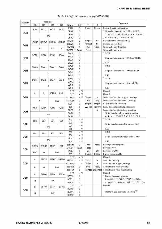
E0C6256 TECHNICAL SOFTWARE EPSON II-5
CHAPTER 1: INITIAL RESET
Table 1.1.3(f) I/O memory map (D0H–DFH)
D3 D2 D1 D0 Name Init 1 0*1
D0HDKM0
EDIRDKM2DKM1DKM0
0000
Enable direct input function
Direct key mask factor 0: Non, 1: K02,
2: K02-03, 3: K02-03-10, 4: K10, 5: K10-11,
6: K10-11-12, 7: K10-11-12-13
Enable DisableDKM1DKM2EDIR
D1HSWRST
LCURFCRNWFSWRUNSWRST
000
Reset
ReqestRenewal
RunReset
NoNo
Stop–
SWRUNCRNWFLCURF
D2HSWL0
R
SWL3SWL2SWL1SWL0
SWL1SWL2SWL30000
SWM0
R
SWM3SWM2SWM1SWM0
0000
SWM1SWM2SWM3
D3H
D4HSWH0
R
SWH3SWH2SWH1SWH0
0000
SWH1SWH2SWH3
D8H
ESIF
R
00
ESIF
–––00
TriggerRun
SIF port
–Stop
I/O port
SCTRG00*2
*2
*2
D9HSCS0
R/W
SDPSCPSSCS1SCS0
0000
Serial data input/output permutation
Serial interface clock phase selection
Serial interface clock mode selection
0: Slave, 1: PTOVF, 2: CLK/2, 3: CLK
LSB first MSB firstSCS1SCPSSDP
DAHSD0
SD3SD2SD1SD0
––––
SD1SD2SD3*3
*3
*3
*3
DBHSD4
SD7SD6SD5SD4
––––
SD5SD6SD7*3
*3
*3
*3
DCHBZE
ENRTMENRST
ENONBZE
0Reset
00
1secReset
OnEnable
0.5sec–
OffDisable
ENONENRSTENRTM
R/W
*7
DDH
SHTPW
R/W
0BZSTP
SHTPW
–––00
StopTriggerBusy
125msec
––
Ready31.25msec
BZSHT0*2
*2
*2
DEHBZFQ0
0BZFQ2BZFQ1BZFQ0
–000
BZFQ1BZFQ20*2
R/W
R/W
Envelope releasing time
Envelope reset
Envelope On/Off
Buzzer output enable
Unused
1-shot buzzer stop
1-shot buzzer trigger (writing)
1-shot buzzer status (reading)
1-shot buzzer pulse width setting
R/W
Unused
Buzzer frequency selection
0: 4096.0, 1: 3276.8, 2: 2730.7, 3: 2340.6,
4: 2048.0, 5: 1638.4, 6: 1365.3, 7: 1170.3 (Hz)
Lap data carry-up request flag
Capture renewal flag
Stopwatch timer Run/Stop
Stopwatch timer reset
MSB
LSB
Unused
Unused
Serial interface clock trigger (writing)
Serial interface clock status (reading)
P1 port function selection
BZSTP
R
R/W
R
Stopwatch timer data 1/1000 sec (BCD)
R/W W
MSB
LSB
Stopwatch timer data 1/100 sec (BCD)
MSB
LSB
Stopwatch timer data 1/10 sec (BCD)
R/W
SCTRG(W)
SCTRG(R)
MSB
LSB
Serial interface data (low-order 4 bits)
MSB
LSB
Serial interface data (high-order 4 bits)
W R/W
BZSHT(W)
BZSHT(R)
R
DFHBDTY0
0BDTY2BDTY1BDTY0
–000
BDTY1BDTY20*2
*6R/W
Unused
Buzzer signal duty ratio selectionR
Address CommentRegister
W
*5 *5
*5
*5
*5
*5
*5
*5
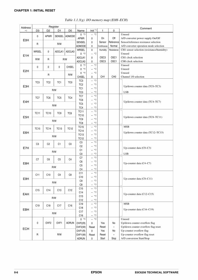
II-6 EPSON E0C6256 TECHNICAL SOFTWARE
CHAPTER 1: INITIAL RESET
Table 1.1.3(g) I/O memory map (E0H–ECH)
D3 D2 D1 D0 Name Init 1 0*1
E0HADMODE
0APWR
SENSELADMODE
–000
Unused
A/D converter power supply On/Off
Sensor/reference resistance selection
A/D converter operation mode selection
OnSensor
OffReference
Normal
SENSELAPWR0*2
E1HADCLK0
WRSEL0
ADCLK1ADCLK0
0–00
OSC3OSC3
ResistanceADCLK10
R
WRSEL
R/W
*2
E2HCHSEL
R/W
000
CHSEL CH1 CH0
000–––0
*2
*2
*2
TC0TC3TC2TC1TC0
––––
TC1TC2TC3
E3H
*3
*3
*3
*3
E4HTC4
TC7TC6TC5TC4
TC5TC6TC7
E5HTC8
R/W
TC11TC10TC9TC8
TC9TC10TC11
E6HTC12
R/W
TC15TC14TC13TC12
TC13TC14TC15
E7HC0
C3C2C1C0
–––– LSB
C1C2C3*3
*3
*3
*3
E8HC4
C7C6C5C4
C5C6C7
E9HC8
C11C10C9C8
C9C10C11
R/W
*7
EAHC12
R/W
C15C14C13C12
C13C15
EBHC16
C19C18C17C16
C17C18C19
R/W
R/W
R/W
CH1 sensor selection (resistance/humidity)
Unused
CH1 clock selection
CH0 clock selection
Unused
Unused
Unused
Channel 1/0 selection
LSB
C14
R/W
R/W
R/W
R/W
Up/down counter data (TC0–TC3)
Continuous
Humidity
OSC1OSC1
R
R
––––
*3
*3
*3
*3
Up/down counter data (TC4–TC7)
––––
*3
*3
*3
*3
Up/down counter data (TC8–TC11)
––––
*3
*3
*3
*3
MSB
Up/down counter data (TC12–TC15)
ECH
ADRUN0
OVF2(R)OVF2(W)OVF1(R)OVF1(W)ADRUN
–0
Reset0
Reset0
YesResetYes
ResetStart
No–
No–
Stop
OVF1OVF20
*2
R
Unused
Up/down counter overflow flag
Up/down counter overflow flag reset
Up-counter overflow flag
Up-counter overflow flag reset
A/D conversion Start/Stop
Up-counter data (C0–C3)
––––
*3
*3
*3
*3
Up-counter data (C4–C7)
––––
*3
*3
*3
*3
Up-counter data (C8–C11)
––––
*3
*3
*3
*3
Up-counter data (C12–C15)
––––
MSB*3
*3
*3
*3
Up-counter data (C16–C19)
R/W
Address CommentRegister
*5
*5
*5
*5
*5
*5

E0C6256 TECHNICAL SOFTWARE EPSON II-7
CHAPTER 1: INITIAL RESET
Table 1.1.3(h) I/O memory map (F0H–FEH)
D3 D2 D1 D0 Name Init 1 0*1
F0HEIAD
000
EIAD
–––0
Unused
Unused
Unused
Interrupt mask register (A/D converter)Enable Mask
000*2
*2
*2
F1HEIK1
000
EIK1
–––0 Enable Mask
000*2
*2
*2
F2HEIK0
R
000
EIK0 Enable Mask
000–––0
*2
*2
*2
EISIF
R
000
EISIF
–––0 Enable Mask
000
F3H
*2
*2
*2
F4HEIPT
R
000
EIPT
–––0 Enable Mask
000
F5HEISW0
R/W
EIRUNEILAPEISW1EISW0
0000
EnableEnableEnableEnable
MaskMaskMaskMask
EISW1EILAPEIRUN
F6HEIT0
R/W
EIT3EIT2EIT1EIT0
0000
Interrupt mask register (Clock timer 2 Hz)
Interrupt mask register (Clock timer 8 Hz)
Interrupt mask register (Clock timer 16 Hz)
Interrupt mask register (Clock timer 32 Hz)
EnableEnableEnableEnable
MaskMaskMaskMask
EIT1EIT2EIT3
*7
Unused
Unused
Unused
Interrupt mask register (K10–K13)
Unused
Unused
Unused
Interrupt mask register (K00–K03)
Unused
Unused
Unused
Interrupt mask register (Serial interface)
Unused
Unused
Unused
Interrupt mask register (Programmable timer)
Interrupt mask register (Stopwatch direct RUN)
Interrupt mask register (Stopwatch direct LAP)
Interrupt mask register (Stopwatch 1 Hz)
Interrupt mask register (Stopwatch 10 Hz)
R/W
R
R/W
R/W
R
R/W
R/W
F8HIAD
000
IAD
–––0
Unused
Unused
Unused
Interrupt factor flag (A/D converter)Yes No
000*2
*2
*2
F9HIK1
000
IK1
–––0 Yes No
000*2
*2
*2
FAHIK0
R
000
IK0 Yes No
000–––0
*2
*2
*2
ISIF
R
000
ISIF
–––0 Yes No
000
FBH
*2
*2
*2
FCHIPT
R
000
IPT
–––0 Yes No
000
FDHISW0
R
IRUN ILAP ISW1 ISW0
0000
YesYesYesYes
NoNoNoNo
ISW1ILAPIRUN
FEHIT0
R
IT3IT2IT1IT0
0000
Interrupt factor flag (Clock timer 2 Hz)
Interrupt factor flag (Clock timer 8 Hz)
Interrupt factor flag (Clock timer 16 Hz)
Interrupt factor flag (Clock timer 32 Hz)
YesYesYesYes
NoNoNoNo
IT1IT2IT3
Unused
Unused
Unused
Interrupt factor flag (K10–K13)
Unused
Unused
Unused
Interrupt factor flag (K00–K03)
Unused
Unused
Unused
Interrupt factor flag (Serial interface)
Unused
Unused
Unused
Interrupt factor flag (Programmable timer)
Interrupt factor flag (Stopwatch direct RUN)
Interrupt factor flag (Stopwatch direct LAP)
Interrupt factor flag (Stopwatch 1 Hz)
Interrupt factor flag (Stopwatch 10 Hz)
R
R
Address CommentRegister
*5
*5
*5
*5
*5
*5
*5
*5
*5
*5
*5
*5
*5
*5
*5
*4
*5
*5
*5
*4
*5
*5
*5
*4
*5
*5
*5
*4
*4
*4
*4
*4
*4
*4
*4
*4
*2
*2
*2
*5
*5
*5
*2
*2
*2
*5
*5
*5
*4

II-8 EPSON E0C6256 TECHNICAL SOFTWARE
CHAPTER 1: INITIAL RESET
1.2 Initialize Program ExampleThe following shows a program example and the flow chart (Figure 1.2.1) for initialization after an initialreset.
Initialization
Set stack pointer
Clear RAM
Select LCD drive duty
Select display memory
Clear display memory
Turn LCD power ON
Turn A/D converter ON
1
1
Wait 100 msec
Reset clock timer
Reset stopwatch timer
Clear up-counter
Clear up/down counter
Enable A/D converter interrupt
Start A/D conversion
EI (enable interrupts)
To next processingFig. 1.2.1 Flow chart
Program example
Label Mnemonic/operand Comment;INIT: LD A,0 ;Sets page 0 with X and Y registers
LD XP,ALD YP,A
;LD A,08H ;Sets stack pointerLD SPH,ALD A,0LD SPL,A
;LD X,00H ;Clears RAM page 0, 00H-7FH
CLRAM0: LBPX MX,0CP XH,8JP NZ,CLRAM0
;LD A,1LD XP,A
;LD X,00H ;Clears RAM page 1, 00H-2FH
CLRAM1: LBPX MX,0CP XH,3JP NZ,CLRAM1
;LD A,2LD XP,A
;LD X,00H ;Clears RAM page 2, 00H-7FH
CLRAM2: LBPX MX,0CP XH,8JP NZ,CLRAM2
;LD A,3LD XP,A
;LD X,00H ;Clears RAM page 3, 00H-7FH
CLRAM3: LBPX MX,0CP XH,8JP NZ,CLRAM3
;LD A,4

E0C6256 TECHNICAL SOFTWARE EPSON II-9
CHAPTER 1: INITIAL RESET
LD XP,A;
LD X,00H ;Clears RAM page 4, 00H-7FHCLRAM4: LBPX MX,0
CP XH,8JP NZ,CLRAM4
;LD A,0LD XP,A
;LD X,0C2H ;Sets LCD duty to 1/4LD MX,1010B ;Sets LCD display memory in page 1
;LD A,1LD XP,A
;LD X,30H ;Turns all LCD dots OFF
CLLCD: LBPX MX,0CP XH,8JP NZ,CLLCD
;LD A,0LD XP,A
;LD X,0C3H ;Turns LCD power ONOR MX,0010B
;LD X,0E0H ;Turns A/D converter ONOR MX,0100B
;LD X,0D1H ;Waits 100 mSLD MX,0001BOR MX,0010B
;WAIT100:LD X,0FDH ;Have 100 mS passed ?
FAN MX,0010BJP Z,WAIT100 ;NO
;LD A,MX
;LD X,0C4H ;Resets clock timerLD MX,0001B
;LD X,0D1H ;Resets stopwatch timerLD MX,0001B
;LD X,0E3H ;Sets up-counter to 0LBPX MX,00H ;Sets up/down counter to 0LBPX MX,00HLBPX MX,00HLBPX MX,00HLD MX,0
;;
LD X,0E7H ;Sets up-counter to 10000DLBPX MX,0F0HLBPX MX,0D8HLD MX,0
;LD X,0F4H ;Enables A/D interruptOR MX,0001B
;LD X,0E0H ;Turns A/D converter to RUN statusOR MX,0001B
;EI
;
The above program is a basic initialization program for the E0C6256. When using this program, add settingitems necessary for each specific application.

II-10 EPSON E0C6256 TECHNICAL SOFTWARE
CHAPTER 2: OSCILLATION CIRCUITS
CHAPTER 2 OSCILLATION CIRCUITS
2.1 Control Registers for Oscillation CircuitTable 2.1.1 shows the control registers for the oscillation circuit.
Table 2.1.1 I/O memory map (oscillation circuit)
Address CommentRegister
D3 D2 D1 D0 Name Init 1 0*1*7
VSCHG
R
0CLKCHG
OSCCVSCHG
–000
OSC3On
-2.1V
OSC1Off
-1.05V
OSCCCLKCHG0
83H
*2 Unused
CPU clock selection
OSC3 oscillation On/Off
VS1 output voltage changeR/W
*5
*1 Initial value at the time of initial reset *5 Constantly "0" when being read*2 Not set in the circuit *6 Refer to main manual*3 Undefined *7 Page switching in I/O memory is not necessary*4 Reset (0) immediately after being read
2.2 Program ExampleThe CPU system clock should be switched by software between OSC1 and OSC3 depending on which oneis used. The following shows a program example and the flow chart (Figure 2.2.1) for the switching.
OSC3ON
Set VS1 to -2.1 V
Turn OSC3 ON
Wait 5 msec
Switch from OSC1 to OSC3
To next processing
Set VSCHG (83H•D0) to "1"
Set OSCC (83H•D1) to "1"
It takes at least 5 msec untilthe oscillation stabilizes
Set CLKCHG (83H•D2) to "1"
OSC3OFF
Switch from OSC3 to OSC1
Turn OSC3 OFF
Set VS1 to -1.05 V
To next processing
Set CLKCHG (83H•D2) to "0"
Set OSCC (83H•D1) to "0"
Set VSCHG (83H•D0) to "0"
• Switching from OSC1 to OSC3 • Switching from OSC3 to OSC1
Fig. 2.2.1 Flow chart
Note: Switching the operating voltage when the supply voltage is lower than 2.2 V (absolute value) maycause a malfunction. Switch the operating voltage only after making sure that supply voltage is morethan 2.2 V (absolute value) using the SVD circuit.Furthermore, do not switch the operating voltage during operating in the doubler mode or the halvermode. The OSC3 clock can be used only in the normal mode.
Program example
• Switching from OSC1 to OSC3
Label Mnemonic/operand Comment
;OSC3ON:
LD X,80H ;SVD checkLD MX,0
;LD X,81HOR MX,0001B
;NOP5 ;100 µS delay
;AND MX,1110B
;FAN MX,0010B

E0C6256 TECHNICAL SOFTWARE EPSON II-11
CHAPTER 2: OSCILLATION CIRCUITS
JP NZ,OSC3ONE;
LD X,83H ;Sets VSCHG to 1OR MX,0001B
;OR MX,0010B ;Sets OSCC to 1
;CALL DLY5MS ;Waits 5 mS
;LD X,83H ;Sets CLKCHG to 1OR MX,0100B
;OSC3ONE:RET;DLY5MS: . ;5 mS delay subroutine
.
.RET
;
• Switching from OSC3 to OSC1
Label Mnemonic/operand Comment;OSC3OFF:
LD X,80H ;SVD checkLD MX,0
;LD X,81HOR MX,0001B
;CALL DLY100U ;100 µS delay
;AND MX,1110B
;FAN MX,0010BJP NZ,OSC3OFE
;LD X,83H ;Sets CLKCHG to 0AND MX,1011B
;LD X,83H ;Sets OSCC to 0AND MX,1101B
;LD X,83H ;Sets VSCHG to 0AND MX,1110B
;OSC3OFE:RET;;DLY100U:. ;100 µS delay subroutine
.
.RET
;

II-12 EPSON E0C6256 TECHNICAL SOFTWARE
CHAPTER 3: A/D CONVERTER
CHAPTER 3 A/D CONVERTER
3.1 Control Registers for A/D ConverterTables 3.1.1(a) and (b) show the control registers for the A/D converter.
Table 3.1.1(a) I/O memory map (A/D converter)
D3 D2 D1 D0 Name Init 1 0*1
E0HADMODE
0APWR
SENSELADMODE
–000
Unused
A/D converter power supply On/Off
Sensor/reference resistance selection
A/D converter operation mode selection
OnSensor
OffReference
Normal
SENSELAPWR0*2
E1HADCLK0
WRSEL0
ADCLK1ADCLK0
0–00
OSC3OSC3
ResistanceADCLK10
R
WRSEL
R/W
*2
E2HCHSEL
R/W
000
CHSEL CH1 CH0
000–––0
*2
*2
*2
TC0TC3TC2TC1TC0
––––
TC1TC2TC3
E3H
*3
*3
*3
*3
E4HTC4
TC7TC6TC5TC4
TC5TC6TC7
E5HTC8
R/W
TC11TC10TC9TC8
TC9TC10TC11
E6HTC12
R/W
TC15TC14TC13TC12
TC13TC14TC15
E7HC0
C3C2C1C0
–––– LSB
C1C2C3*3
*3
*3
*3
E8HC4
C7C6C5C4
C5C6C7
E9HC8
C11C10C9C8
C9C10C11
R/W
*7
EAHC12
R/W
C15C14C13C12
C13C15
EBHC16
C19C18C17C16
C17C18C19
R/W
R/W
R/W
CH1 sensor selection (resistance/humidity)
Unused
CH1 clock selection
CH0 clock selection
Unused
Unused
Unused
Channel 1/0 selection
LSB
C14
R/W
R/W
R/W
R/W
Up/down counter data (TC0–TC3)
Continuous
Humidity
OSC1OSC1
R
R
––––
*3
*3
*3
*3
Up/down counter data (TC4–TC7)
––––
*3
*3
*3
*3
Up/down counter data (TC8–TC11)
––––
*3
*3
*3
*3
MSB
Up/down counter data (TC12–TC15)
ECH
ADRUN0
OVF2(R)OVF2(W)OVF1(R)OVF1(W)ADRUN
–0
Reset0
Reset0
YesResetYes
ResetStart
No–
No–
Stop
OVF1OVF20
*2
R
Unused
Up/down counter overflow flag
Up/down counter overflow flag reset
Up-counter overflow flag
Up-counter overflow flag reset
A/D conversion Start/Stop
Up-counter data (C0–C3)
––––
*3
*3
*3
*3
Up-counter data (C4–C7)
––––
*3
*3
*3
*3
Up-counter data (C8–C11)
––––
*3
*3
*3
*3
Up-counter data (C12–C15)
––––
MSB*3
*3
*3
*3
Up-counter data (C16–C19)
R/W
Address CommentRegister
*5
*5
*5
*5
*5
*5

E0C6256 TECHNICAL SOFTWARE EPSON II-13
CHAPTER 3: A/D CONVERTER
Table 3.1.1(b) I/O memory map (A/D converter)
D3 D2 D1 D0 Name Init 1 0*1
F0HEIAD
000
EIAD
–––0
Unused
Unused
Unused
Interrupt mask register (A/D converter)Enable Mask
000*2
*2
*2
*7
R/WR
F8HIAD
000
IAD
–––0
Unused
Unused
Unused
Interrupt factor flag (A/D converter)Yes No
000*2
*2
*2R
Address CommentRegister
*5
*5
*5
*5
*5
*5
*4
*1 Initial value at the time of initial reset *5 Constantly "0" when being read*2 Not set in the circuit *6 Refer to main manual*3 Undefined *7 Page switching in I/O memory is not necessary*4 Reset (0) immediately after being read
3.2 Control of A/D ConverterThe E0C6256 has CR oscillation type A/D converter.Two systems (channel 0 and channel 1) of CR oscillation circuit are built into this A/D converter, so it ispossible to compose two types of A/D conversion circuit by connecting different sensors to each CRoscillation circuit.
The A/D converter incorporates two types of counters. One is the 16-bit up/down counter TC0–TC15 thatcounts the internal clock for reference counting, and the other is 20-bit up-counter C0–C19 that counts theexternal resistance oscillation clock. Each counter permits reading and writing on a 4-bit basis.
Figure 3.2.1 shows the control and operation flow of the A/D converter, and Figure 3.2.2 shows the timingchart of the operation.
Clear the up/down counterTC0–TC15 (0E3H–0E6H)and the up-counter C0–C19(0E7H–0EBH) to "0".
Set EIAD (0F0H•D0) to "1".
Set an initial value (complement)in the up-counter C0–C19(0E7H–0EBH).
Set ADRUN (0ECH•D0) to "1".
A/D conversion
Clear two countermemories
Reset I (interrupt) flag
A/D interrupt necessary ?
Set interrupt mask registerto ENABLE
Set initial valuein the up-counter C
Start A/D conversion
Up-counter C counts up
Up/down counter TC counts up
Counter C : 0
A
NO
YES
NO
YES
Read the up-counterC0–C19 (0E7H–0EBH)and process the measurementresults.
NO
YES
NO
YES
A
Up/down counter TCcounts down
Up-counter C counts up
Counter TC : 0
Both counter finish counting
Interrupt factor flag IADis set to "1"
A/D interrupt : ENABLE
Interrupt processing
END
Fig. 3.2.1 Flow chart for controlling A/D converter

II-14 EPSON E0C6256 TECHNICAL SOFTWARE
CHAPTER 3: A/D CONVERTER
ADRUN register
ADOUT output
Up-counter data
Up/down counter clock
Up/down counter data
Interrupt
n n+1 n+2
0 1 2 3
FFFFE FFFFF 0
x-3 x-4x-1x-2x-3 x-5 3 2 1 0
mm-1
Oscillation with reference resistance Oscillation with sensor
1 2
x-2x-1x
Fig. 3.2.2 Timing chart of A/D converter operation
Basic control and operation of the A/D converter are described in the flowchart in Figure 3.2.2. In order toprepare a program, add items required according to application.
After A/D conversion, the value counted during oscillation of the sensor is set on the up-counter C0–C9.This value is the sensor oscillation clock number during a time period equal to that during which thereference resistance is oscillated according to the initial value set on the up-counter. The difference betweenthe reference resistance and the sensor resistance value can be obtained indirectly from the initial value andresults.Correct it according to the characteristics of the connected elements and calculate the target measurementresults.
Note: When the up/down counter TC0–TC15 is read after A/D conversion, it may not indicate "0000H".This is not due to incorrect timing in terminating A/D conversion but because the counting downclock is input after the control signal is output to the up-counter to terminate counting.
Since interruption is possible after A/D conversion, reading of the up-counter and data processing arebasically performed using the interrupt function.If interrupt is not used, A/D converter operation can be checked by reading the ADRUN register. After "1"is written to this register to start A/D conversion, the register remains at "1" during A/D conversion and isreset to "0" when the A/D conversion is finished.
3.3 Software SpecificationWhen programming for A/D conversion, be sure to set the initial value of the up-counter after due consid-eration.Figure 3.3.1 shows the relationship between the up-counter and the up/down counter.
fosc:fCR1:fCR2:CUPI:
CUPS:FFFFFH:FFFFH:tA:
Internal clock frequencyCR oscillation frequency on reference sideOscillation frequency on sensor sideCount value of CR oscillation on reference side(complement)Count value of oscillation on sensor sideMax. up-counter valueMax. up/down counter valueCount time
FFFFFH00000H
CUPICUPS
fCR1tA
fCR2 tAUp-counter
➀
➁
FFFFH0000H tA
fosc
Up/down counter
➀fosc
➁
Fig. 3.3.1 Relationship between up-counter and up/down counter
The following conditions should be satisfied during counting-up (➀) and counting-down (➁):
Condition (A): The up/down counter should not overflow during counting-up at ➀.Condition (B): The up-counter should not overflow during counting-down at ➁.
If the above conditions are not satisfied, A/D conversion is terminated at that point and the correct resultcannot be obtained.
When programming, a proper initial value should be set to the up-counter according to these conditions.
E0C6256 TECHNICAL SOFTWARE EPSON II-15
CHAPTER 3: A/D CONVERTER
3.4 Program Example for Controlling A/D ConverterThis section explains a temperature measurement program for a usage example of the A/D converter.The temperature measurement is performed using a thermistor. After comparing the oscillation frequenciesof the thermistor and the reference resistance, the difference is corrected by linear approximation methodand the temperature is found.The following shows the linear approximation equation to derive the temperature.
Temperature (°C) = ( ➀ Up-counter value after A/D conversion- ➁ Count value for minimum temperature within the range )×➂ Linear approximation coefficient+➃ Minimum temperature within the range
<➀ Up-counter value after A/D conversion>
This is the value counted in the up-counter when an A/D conversion is completed.
<➁ Count value for minimum temperature within the range> and <➃ Minimum temperature within the range>
To derive the temperature by the linear approximation, the temperature range must be determined for thelinear approximation. For example, in case of the range of entire measured temperature is -30 to 70°C andthe temperature range is set for every 10°C, the temperature ranges are -30 to -20°C, -20 to -10°C · · · and 60to 70°C. The smallest value of each temperature range segment is the minimum temperature within therange (➃).The count value for minimum temperature within range (➁) is expressed by the following equation:
A/D converter count value = × up-counter initial value
= × up-counter initial value
= × up-counter initial valueR1R2
KCR2 K
CR1
fCR2
fCR1fCR1: Reference oscillation frequencyfCR2: Sensor oscillation frequencyK: Oscillation coefficientC: CapacitanceR1: Reference resistance valueR2: Resistance value of thermistorUp-counter initial value:
Value of which the CR oscillation by thereference resistance has been counted.
By substituting R2 (resistance value of thermistor at minimum temperature within the range), R2 (referenceresistance value), and the up-counter initial value into the equation, the count value for the minimumtemperature within the range is obtained.
<➂ Linear approximation coefficient>
The linear approximation coefficient is the value that shows how many degrees (centigrade) there are forone count in the temperature range.The linear approximation coefficient is expressed by the following equation:
Absolute value of the temperature rangeCount value for maximum Count value for minimum
temperature within the range temperature within the range
As you can see, the temperature range is smaller, the precision is higher.
* However, in the high temperature part, the ON-resistance of the IC's transistor affects the measurementresults because the sensor resistance decreases and chances of error increase. Therefore, correct it usingsoftware if necessary.
These values used in the program example are shown in Table 3.4.1.In the example, 10 kΩ of the external reference resistance and 22,000 pF of capacitor are used, and the initialvalue of the up-counter is set to 10,000.
-Linear approximation coefficient =
II-16 EPSON E0C6256 TECHNICAL SOFTWARE
CHAPTER 3: A/D CONVERTER
Table 3.4.1 Temperature characteristics of thermistor used in example
Temperature
(°C)
-30
-20
-10
0
10
20
30
40
50
60
70
Thermistor
resistance (kΩ)
111.3
67.74
42.45
27.28
17.96
12.09
8.313
5.828
4.161
3.021
2.229
Linear approximation
coefficiant in the measurement
temperature range
0.0173
0.0114
0.00763
0.00526
0.00370
0.00266
0.00195
0.00145
0.00110
0.000850
Up-counter
count value (DEC)
898
1476
2355
3665
5567
8271
12029
17158
24032
33101
44863
The following shows a program example that is created using the values from the above table, and the flowchart (Figure 3.4.1).
NO
YES
NO
YES
After adjusting the position ofthe decimal point, add theproduct calculated to theminimum temperature to
calculate the desired temperature
B
START
Initial processing
Enable A/D interrupt
Clear up/down counter
Set initial value in up-counter
Start A/D conversion
Set to EI (enable interrupts)
HALT
A/D interrupt occurs
Find the temperature range thatincludes the up-counter value
Calculate the difference betweenthe up-counter value and
the minimum count numberwithin the range
A
A
Calculate the product of thepreprocessed difference and
the linear approximationcoefficient
Convert the hexadecimalnumber of preprocessing
result to the decimal number
The minimumtemperature of the range
is minus
After adjusting the position ofthe decimal point, subtract the
product calculated from theabsolute value of the minimum
temperature to calculate thedesired temperature
Display processing
B
Fig. 3.4.1 Flow chart

E0C6256 TECHNICAL SOFTWARE EPSON II-17
CHAPTER 3: A/D CONVERTER
Program example
Label Mnemonic/operand Comment
;*****************************************************************************;* E0C6256 TEMPERATURE MEASUREMENT SOFTWARE *;*****************************************************************************;HEXDEC: MACRO ARG1,ARG2,ARG3
LOCAL HXDC1,HXDC2;;****************************************************************************;* HEC-->DEC 1--13DIGIT *;* *;****************************************************************************;
RST F,8 ;Resets D, Z, C flagsLD A,ARG3ADD A,1 ;Digit ← Digit + 1
;; ***** ARG2 ZERO CLEAR *****; ***** ARG2 DATA <--ARG1 TOP DATA *****;
LD X,ARG1+ARG3-1LD Y,ARG2LD MY,MX ;ARG2 data ← ARG1 dataCP MY,0AHJP C,$+5 ;Jump if ARG2 data < 0AHADD MY,6 ;ARG2 data ← ARG2 data + 6INC Y ;Increments ARG2 address (+1)LDPY MY,1 ;Increments ARG2 data (+1)JP $+3INC YLDPY MY,0 ;Zero clearADD A,0FH ;Decrements digit counter (-1)JP NZ,$-2 ;Jump if digit 0LD B,ARG3-1 ;B register ← Digit - 1CP B,0JP Z,HXDC2 ;Jump if digit = 1
HXDC1: PUSH B;; ***** ARG2 DATA <-- ARG2 DATA * 16D *****;
LD B,4 ;Loop counter settingLD Y,ARG2LD A,ARG3+2 ;A register ← Digit + 2RCF ;Resets C flagSDF ;Resets D flagACPY MY,MY ;ARG2 data ← 2 * ARG2 dataPUSH FADD A,9 ;Decrements A register (-1)JP Z,$+3 ;Jump if A register 0POP FJP $-5POP FADD B,9 ;Decrements loop counter (-1)JP NZ,$-12 ;Jump if loop counter 0
;; ****** ARG DATA <-- ARG DATA + ARG1 1 DIGIT DATA *****;
RST F,8 ;Resets D, Z, C flagsADC XL,0FHADC XH,0FH ;Decrements ARG1 address (-1)LD Y,ARG2LD B,ARG3+1 ;Digit counter setting

II-18 EPSON E0C6256 TECHNICAL SOFTWARE
CHAPTER 3: A/D CONVERTER
CP MX,0AHJP C,$+7 ;Jump if ARG1 data (1 digit) < 0AHADD MX,6 ;ARG1 data (1 digit) + 6SDF ;Sets D flagRCF ;Resets C flagACPY MY,MXADC MY,1 ;ARG2 data ← ARG1 data (1 digit)JP $+5RCF ;Resets C flagSDF ;Sets D flagACPY MY,MX ;ARG2 data ← ARG1 data (1 digit)ADC MY,0 ;Increments if carry is generated (+1)INC YPUSH FADD B,9 ;Decrements digit counter (-1)JP Z,$+3 ;Jump if digit counter 0POP FJP $-6POP F
;; ***** DIGIT DECREMENT *****;
POP BADD B,9 ;Decrements digit number (-1)JP NZ,HXDC1 ;Jump if digit counter 0
HXDC2 RDF ;Resets D flag;
ENDM
;;;
PAGE 1;
ORG 100H;
JP INIT ;Starts program;
JP INT ;Interrupt vectorsJP INTJP INTJP INTJP INTJP INTJP INTJP INTJP INTJP INTJP INTJP INTJP INTJP INTJP INT
;INIT: LD A,0 ;Sets page 0 with X and Y registers
LD XP,ALD YP,A
;LD A,08H ;Sets stack pointerLD SPH,ALD A,0LD SPL,A
;LD X,0C2H ;Sets LCD duty to 1/4

E0C6256 TECHNICAL SOFTWARE EPSON II-19
CHAPTER 3: A/D CONVERTER
LD MX,1010B ;Sets LCD display memory in page 1;
LD X,0C3H ;Turns LCD power ONOR MX,0010B
;LD X,0E0H ;Turns A/D converter ONOR MX,0100B
;LD X,0 ;Clears RAM page 0, 00H-7FH
CLRAM: LBPX MX,0CP XH,8JP NZ,CLRAM
;LD X,0D1H ;Waits 100 mSLD MX,0001BOR MX,0010B
;WAIT100:LD X,0FDH ;Have 100 mS passed ?
FAN MX,0010BJP Z,WAIT100 ;NO
;LD A,MX
;LD A,1LD XP,A
;LD X,30H ;Turns all LCD dots OFF
CLLCD: LBPX MX,0CP XH,8JP NZ,CLLCD
;LD A,0LD XP,A
;LD X,0C4H ;Resets clock timerLD MX,0001B
;LD X,0D1H ;Resets stopwatch timerLD MX,0001B
;LD X,0F0H ;Enables A/D interruptOR MX,0001B
;MAIN:
LD X,0E3H ;Sets up-counter to 0LBPX MX,00H ;Sets up/down counter to 0LBPX MX,00HLBPX MX,00HLBPX MX,00HLD MX,0
;;;
LD X,0E7H ;Sets up-counter to 10000DLBPX MX,0F0HLBPX MX,0D8HLD MX,0FH
;LD X,0ECH ;Turns A/D converter to RUN statusOR MX,0001B
;EIHALTJP MAIN

II-20 EPSON E0C6256 TECHNICAL SOFTWARE
CHAPTER 3: A/D CONVERTER
;INT:
LD X,0F8HLD A,MXFAN A,0001BJP Z,AD3CALL SETTEMP
AD3:RET
;PAGE 2
;SETTEMP:
RST F,8LD A,0LD B,0
READKN:CALL $+3JP READENDRETLD X,10HPSET 3JPBA
READEND:PUSH BLD B,5LD X,0EBHLD Y,14H
COMP:CP MX,MYJP C,MULTIJP Z,$+2JP NC,NEXTRDRCFADC XL,15RCFADC YL,15ADD B,15JP NZ,COMP
; POP BJP MULTI
;NEXTRD:
POP BADD A,7 ;Sets address of following setting valueADC B,0JP READKN
;MULTI:
POP BRCFSBC A,7SBC B,0CALL $+2JP $+4LD X,10HPSET 3JPBALD X,0E7HLD Y,40HLD B,5LDPX MY,MXINC YADD B,15

E0C6256 TECHNICAL SOFTWARE EPSON II-21
CHAPTER 3: A/D CONVERTER
JP NZ,$-3;
RCFLD X,10HLD Y,40HSCPY MY,MXINC XSCPY MY,MXINC XSCPY MY,MXINC XSCPY MY,MXINC XSCPY MY,MX
;;; ************ INITIALIZE WORK MEMORY ************;
LD X,25HLD B,5
WMCLR:LBPX MX,00ADD B,15JP NZ,WMCLR
;; ************ CALCULATE An X K ***************;
LD X,40HLD Y,0AHLD B,5LDPX MY,MXINC YADD B,15JP NZ,$-3LD MY,0LD B,1
MULTI00:LD Y,15H
MULTI01:FAN MY,BLD X,40HPUSH YLJP Z,MULTI02LD X,0AHLD A,2LD YH,ACALL SUBADDLD A,1LD YH,A
MULTI02:POP YLINC YCP YL,9JP NZ,MULTI01RCFRLC BJP C,SUBTRA
;; ************* WORK MEMORY X 2 ***********;
LD X,0AHRCFACPX MX,MXACPX MX,MX

II-22 EPSON E0C6256 TECHNICAL SOFTWARE
CHAPTER 3: A/D CONVERTER
ACPX MX,MXACPX MX,MXACPX MX,MXACPX MX,MXJP MULTI00
;; ************ ADD Bn *************;SUBTRA:
HEXDEC 25H,30H,11 ;8-digit HEX → DECLD X,18H ;Substitutes decimal point positionLD A,MXSDF
;LD X,1CHCP MX,1JP Z,MINUS
;PLUS:
RCFLD X,19HLD Y,30H
PLUS3:LD YL,AACPY MY,MXINC XPUSH FCP XL,0BHJP Z,$+4POP FADD A,1 ;OMJP PLUS3POP FRDFJP ENDPROG+1
;MINUS:
RCFLD X,19HLD Y,30H
MINUS1:PUSH FLD B,YLCP B,AJP Z,MINUS2LD B,0POP FSBC B,MYLD MY,BINC YJP MINUS1
MINUS2:POP FSBC MX,MYLD MY,MXINC XINC Y
;PUSH FCP XL,0BHJP Z,$+2JP MINUS2POP FRDF

E0C6256 TECHNICAL SOFTWARE EPSON II-23
CHAPTER 3: A/D CONVERTER
JP ENDPROG+1;; *********** 16-BIT ADDITION **********;SUBADD:
RCFACPY MY,MXINC XACPY MY,MXINC XACPY MY,MXINC XACPY MY,MXINC XACPY MY,MXINC XACPY MY,MX
;ENDPROG:
RETRET
;PAGE 3
;ORG 300H
;;-30°C TO -20°C
LBPX MX,82H ;K1 = 382 (898)LBPX MX,03HLDPX MX,0LBPX MX,0ADH ;A1 = 40AD (0,0173)LBPX MX,40HLBPX MX,30H ;B1 = 1030 (-30°C)RETD 10H
;;-20°C TO -10°C
LBPX MX,0C4H ;K1 = 5C4 (1476)LBPX MX,05HLDPX MX,0LBPX MX,72H ;A1 = 4072 (0,0114)LBPX MX,40HLBPX MX,20H ;B1 = 1020 (-20°C)RETD 10H
;;-10°C TO 0°C
LBPX MX,33H ;K1 = 933 (2355)LBPX MX,09HLDPX MX,0LBPX MX,0FBH ;A1 = 52FB (0,00763)LBPX MX,52HLBPX MX,10H ;B1 = 1010 (-10°C)RETD 10H
;; 0°C TO 10°C
LBPX MX,51H ;K1 = E51 (3665)LBPX MX,0EHLDPX MX,0LBPX MX,0EH ;A1 = 520E (0,00526)LBPX MX,52HLBPX MX,00H ;B1 = 0000 (0°C)RETD 00H
;; 10°C TO 20°C
LBPX MX,0BFH ;K1 = 15BF (5567)

II-24 EPSON E0C6256 TECHNICAL SOFTWARE
CHAPTER 3: A/D CONVERTER
LBPX MX,15HLDPX MX,0LBPX MX,72H ;A1 = 5172 (0,00370)LBPX MX,51HLBPX MX,10H ;B1 = 0010 (10°C)RETD 00H
;; 20°C TO 30°C
LBPX MX,4FH ;K1 = 204F (8271)LBPX MX,20HLDPX MX,0LBPX MX,0AH ;A1 = 510A (0,00266)LBPX MX,51HLBPX MX,20H ;B1 = 0020 (20°C)RETD 00H
;; 30°C TO 40°C
LBPX MX,0FDH ;K1 = 2EFD (12029)LBPX MX,2EHLDPX MX,0LBPX MX,0C3H ;A1 = 50C3 (0,00195)LBPX MX,50HLBPX MX,30H ;B1 = 0030 (30°C)RETD 00H
;; 40°C TO 50°C
LBPX MX,06H ;K1 = 430 6(17158)LBPX MX,43HLDPX MX,0LBPX MX,91H ;A1 = 5091 (0,00145)LBPX MX,50HLBPX MX,40H ;B1 = 0040 (40°C)RETD 00H
;; 50°C TO 60°C
LBPX MX,0E0H ;K1 = 5DE0 (24032)LBPX MX,5DHLDPX MX,0LBPX MX,6EH ;A1 = 506E (0,00110)LBPX MX,50HLBPX MX,50H ;B1 = 0050 (50°C)RETD 00H
;; 60°C TO 70°C
LBPX MX,4DH ;K1 = 814D (33101)LBPX MX,81HLDPX MX,0LBPX MX,52H ;A1 = 6352 (0,000850)LBPX MX,63HLBPX MX,60H ;B1 = 0060 (60°C)RETD 00H
;; 70°C
LBPX MX,3FH ;K1 = AF3F (44863)LBPX MX,0AFHLDPX MX,0RET
;;
ORG 34DHRETS
;;
END;
E0C6256 TECHNICAL SOFTWARE EPSON II-25
APPENDIX A: E0C6256 RAM MAP
APPENDIX A. E0C6256 RAM MAPRAM map - 1 (000H–07FH)
PPR
OG
RA
M N
AM
E:
HL
00 1 2 3 4 5 6 7
NA
ME
MS
B
LSB
NA
ME
MS
B
LSB
NA
ME
MS
B
LSB
NA
ME
MS
B
LSB
NA
ME
MS
B
LSB
NA
ME
MS
B
LSB
NA
ME
MS
B
LSB
NA
ME
MS
B
LSB
01
23
45
67
89
AB
CD
EF
II-26 EPSON E0C6256 TECHNICAL SOFTWARE
APPENDIX A: E0C6256 RAM MAP
RAM map - 2 (100H–17FH)
PPR
OG
RA
M N
AM
E:
HL
10 1 2 3 4 5 6 7
NA
ME
MS
B
LSB
NA
ME
MS
B
LSB
NA
ME
MS
B
LSB
NA
ME
MS
B
LSB
NA
ME
MS
B
LSB
NA
ME
MS
B
LSB
NA
ME
MS
B
LSB
NA
ME
MS
B
LSB
01
23
45
67
89
AB
CD
EF

E0C6256 TECHNICAL SOFTWARE EPSON II-27
APPENDIX A: E0C6256 RAM MAP
RAM map - 3 (200H–27FH)PP
RO
GR
AM
NA
ME
:
HL
20 1 2 3 4 5 6 7
NA
ME
MS
B
LSB
NA
ME
MS
B
LSB
NA
ME
MS
B
LSB
NA
ME
MS
B
LSB
NA
ME
MS
B
LSB
NA
ME
MS
B
LSB
NA
ME
MS
B
LSB
NA
ME
MS
B
LSB
01
23
45
67
89
AB
CD
EF

II-28 EPSON E0C6256 TECHNICAL SOFTWARE
APPENDIX A: E0C6256 RAM MAP
RAM map - 4 (300H–37FH)
PPR
OG
RA
M N
AM
E:
HL
30 1 2 3 4 5 6 7
NA
ME
MS
B
LSB
NA
ME
MS
B
LSB
NA
ME
MS
B
LSB
NA
ME
MS
B
LSB
NA
ME
MS
B
LSB
NA
ME
MS
B
LSB
NA
ME
MS
B
LSB
NA
ME
MS
B
LSB
01
23
45
67
89
AB
CD
EF

E0C6256 TECHNICAL SOFTWARE EPSON II-29
APPENDIX A: E0C6256 RAM MAP
RAM map - 5 (400H–47FH)PP
RO
GR
AM
NA
ME
:
HL
40 1 2 3 4 5 6 7
NA
ME
MS
B
LSB
NA
ME
MS
B
LSB
NA
ME
MS
B
LSB
NA
ME
MS
B
LSB
NA
ME
MS
B
LSB
NA
ME
MS
B
LSB
NA
ME
MS
B
LSB
NA
ME
MS
B
LSB
01
23
45
67
89
AB
CD
EF

II-30 EPSON E0C6256 TECHNICAL SOFTWARE
APPENDIX A: E0C6256 RAM MAP
Display memory map (530H–57FH, W only)
PPR
OG
RA
M N
AM
E:
HL
53 4 5 6 7
NA
ME
MS
B
LSB
NA
ME
MS
B
LSB
NA
ME
MS
B
LSB
NA
ME
MS
B
LSB
NA
ME
MS
B
LSB
01
23
45
67
89
AB
CD
EF
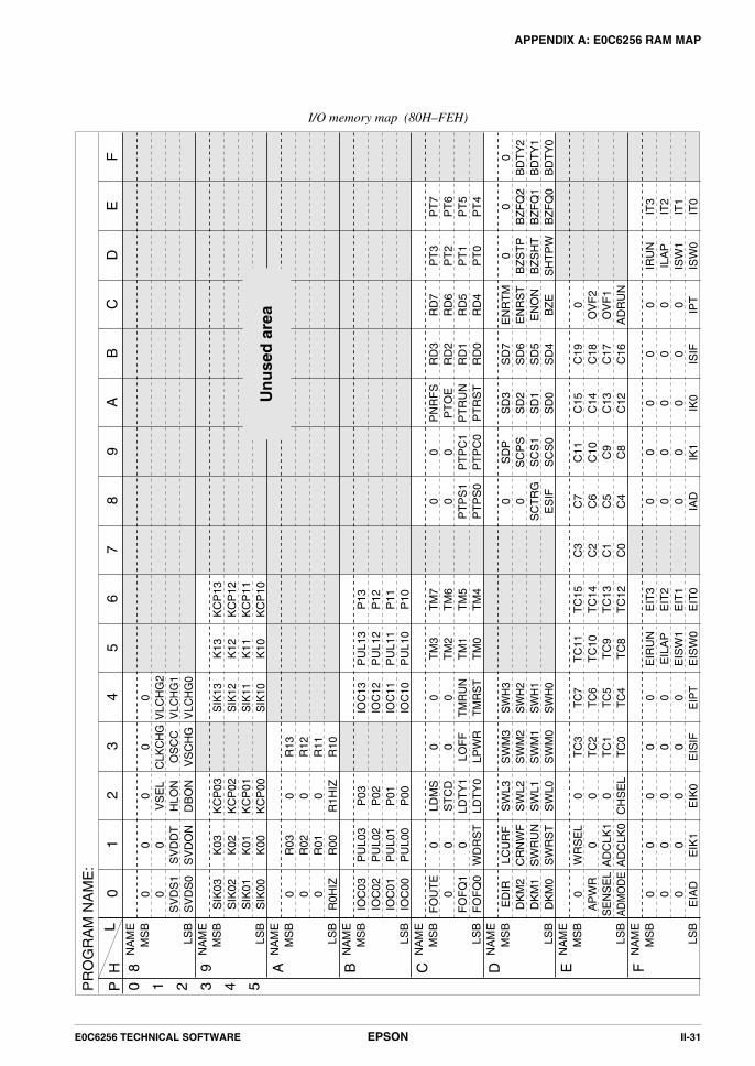
E0C6256 TECHNICAL SOFTWARE EPSON II-31
APPENDIX A: E0C6256 RAM MAP
I/O memory map (80H–FEH)PP
RO
GR
AM
NA
ME
:
HL
0 1 2 3 4 5
8 9 A B C D E F
NA
ME
MS
B
LSB
NA
ME
MS
B
LSB
NA
ME
MS
B
LSB
NA
ME
MS
B
LSB
NA
ME
MS
B
LSB
NA
ME
MS
B
LSB
NA
ME
MS
B
LSB
NA
ME
MS
B
LSB
01
23
45
67
89
AB
CD
EF
PT
3P
T2
PT
1P
T0
0B
ZS
TP
BZ
SH
TS
HT
PW
IRU
NIL
AP
ISW
1IS
W0
PT
7P
T6
PT
5P
T4
0B
ZF
Q2
BZ
FQ
1B
ZF
Q0
IT3
IT2
IT1
IT0
0B
DT
Y2
BD
TY
1B
DT
Y0
RD
7R
D6
RD
5R
D4
EN
RT
ME
NR
ST
EN
ON
BZ
E
0O
VF
2O
VF
1A
DR
UN
0 0 0 IPT
RD
3R
D2
RD
1R
D0
SD
7S
D6
SD
5S
D4
C19
C18
C17
C16 0 0 0
ISIF
PN
RF
SP
TO
EP
TR
UN
PT
RS
T
SD
3S
D2
SD
1S
D0
C15
C14
C13
C12 0 0 0 IK0
0 0P
TP
C1
PT
PC
0
SD
PS
CP
SS
CS
1S
CS
0
C11
C10 C9
C8 0 0 0 IK1
0 0P
TP
S1
PT
PS
0
0 0S
CT
RG
ES
IF
C7
C6
C5
C4 0 0 0 IAD
C3
C2
C1
C0
KC
P13
KC
P12
KC
P11
KC
P10
P13
P12
P11
P10
TM
7T
M6
TM
5T
M4
TC
15T
C14
TC
13T
C12
EIT
3E
IT2
EIT
1E
IT0
K13
K12
K11
K10
PU
L13
PU
L12
PU
L11
PU
L10
TM
3T
M2
TM
1T
M0
TC
11T
C10
TC
9T
C8
EIR
UN
EIL
AP
EIS
W1
EIS
W0
0V
LCH
G2
VLC
HG
1V
LCH
G0
SIK
13S
IK12
SIK
11S
IK10
IOC
13IO
C12
IOC
11IO
C10
0 0T
MR
UN
TM
RS
T
SW
H3
SW
H2
SW
H1
SW
H0
TC
7T
C6
TC
5T
C4
0 0 0E
IPT
0C
LKC
HG
OS
CC
VS
CH
G
R13
R12
R11
R10 0 0
LOF
FLP
WR
SW
M3
SW
M2
SW
M1
SW
M0
TC
3T
C2
TC
1T
C0
0 0 0E
ISIF
0V
SE
LH
LON
DB
ON
KC
P03
KC
P02
KC
P01
KC
P00
0 0 0R
1HIZ
P03
P02
P01
P00
LDM
SS
TC
DLD
TY
1LD
TY
0
SW
L3S
WL2
SW
L1S
WL0 0 0 0
CH
SE
L
0 0 0E
IK0
0 0S
VD
DT
SV
DO
N
K03
K02
K01
K00
R03
R02
R01
R00
PU
L03
PU
L02
PU
L01
PU
L00
0 0 0W
DR
ST
LCU
RF
CR
NW
FS
WR
UN
SW
RS
T
WR
SE
L0
AD
CLK
1A
DC
LK0
0 0 0E
IK1
0 0S
VD
S1
SV
DS
0
SIK
03S
IK02
SIK
01S
IK00 0 0 0
R0H
IZ
IOC
03IO
C02
IOC
01IO
C00
FO
UT
E0
FO
FQ
1F
OF
Q0
ED
IRD
KM
2D
KM
1D
KM
0
0A
PW
RS
EN
SE
LA
DM
OD
E
0 0 0E
IAD
Un
use
d a
rea

II-32 EPSON E0C6256 TECHNICAL SOFTWARE
APPENDIX B: E0C6256 INSTRUCTION SET
APPENDIX B. E0C6256 INSTRUCTION SET
B
1
0
0
0
0
0
1
0
0
1
1
0
1
1
1
1
1
1
1
1
1
1
1
1
1
1
1
1
1
1
1
1
1
1
1
A
1
0
0
0
1
1
1
1
1
1
1
0
1
1
1
1
1
0
0
1
1
1
1
1
1
1
1
1
1
1
1
0
0
0
0
9
1
0
1
1
1
1
1
0
0
1
1
0
1
1
1
1
1
1
0
1
1
1
1
1
1
1
1
1
1
1
1
1
1
1
1
8
0
0
0
1
0
1
1
0
1
1
1
1
1
1
1
0
0
1
0
0
0
0
0
0
0
0
0
0
0
0
0
0
0
0
0
7
0
s7
s7
s7
s7
s7
1
s7
s7
1
1
7
1
1
1
1
1
x7
y7
1
1
1
1
1
1
1
1
1
1
1
1
0
0
0
0
6
1
s6
s6
s6
s6
s6
1
s6
s6
1
1
6
1
1
1
1
1
x6
y6
0
0
0
0
0
0
0
0
0
0
0
0
0
0
0
0
5
0
s5
s5
s5
s5
s5
1
s5
s5
0
0
5
1
1
1
1
1
x5
y5
0
0
0
0
0
0
1
1
1
1
1
1
0
0
1
1
4
p4
s4
s4
s4
s4
s4
0
s4
s4
1
1
4
1
1
1
0
1
x4
y4
0
0
0
1
1
1
0
0
0
1
1
1
0
1
0
1
3
p3
s3
s3
s3
s3
s3
1
s3
s3
1
1
3
1
1
1
0
0
x3
y3
0
0
1
0
0
1
0
0
1
0
0
1
i3
i3
i3
i3
2
p2
s2
s2
s2
s2
s2
0
s2
s2
1
1
2
0
1
0
0
0
x2
y2
0
1
0
0
1
0
0
1
0
0
1
0
i2
i2
i2
i2
1
p1
s1
s1
s1
s1
s1
0
s1
s1
1
1
1
1
1
0
0
0
x1
y1
r1
r1
r1
r1
r1
r1
r1
r1
r1
r1
r1
r1
i1
i1
i1
i1
0
p0
s0
s0
s0
s0
s0
0
s0
s0
1
0
0
1
1
0
0
0
x0
y0
r0
r0
r0
r0
r0
r0
r0
r0
r0
r0
r0
r0
i0
i0
i0
i0
p
s
C, s
NC, s
Z, s
NZ, s
s
s
X
Y
X, x
Y, y
XP, r
XH, r
XL, r
YP, r
YH, r
YL, r
r, XP
r, XH
r, XL
r, YP
r, YH
r, YL
XH, i
XL, i
YH, i
YL, i
PSET
JP
JPBA
CALL
CALZ
RET
RETS
RETD
NOP5
NOP7
HALT
INC
LD
ADC
Branch
instructions
System
control
instructions
Index
operation
instructions
Classification OperandI D Z C
↑
↑
↑
↑
↑
↑
↑
↑
5
5
5
5
5
5
5
7
7
7
12
12
5
7
5
5
5
5
5
5
5
5
5
5
5
5
5
5
5
5
5
7
7
7
7
ClockOperation Code Flag
NBP p4, NPP p3~p0
PCB NBP, PCP NPP, PCS s7~s0
PCB NBP, PCP NPP, PCS s7~s0 if C=1
PCB NBP, PCP NPP, PCS s7~s0 if C=0
PCB NBP, PCP NPP, PCS s7~s0 if Z=1
PCB NBP, PCP NPP, PCS s7~s0 if Z=0
←
←
←
←
←
←
←
←
←
←
←
←
←
←
←
←
←
←
←
PCB NBP, PCP NPP, PCSH B, PCSL A
M(SP-1) PCP, M(SP-2) PCSH, M(SP-3) PCSL+1
SP SP-3, PCP NPP, PCS s7~s0
M(SP-1) PCP, M(SP-2) PCSH, M(SP-3) PCSL+1
SP SP-3, PCP 0, PCS s7~s0
PCSL M(SP), PCSH M(SP+1), PCP M(SP+2)
SP SP+3
PCSL M(SP), PCSH M(SP+1), PCP M(SP+2)
SP SP+3, PC PC+1
PCSL M(SP), PCSH M(SP+1), PCP M(SP+2)
SP SP+3, M(X) 3~ 0, M(X+1) 7~ 4, X X+2
No operation (5 clock cycles)
No operation (7 clock cycles)
Halt (stop clock)
X X+1
Y Y+1
XH x7~x4, XL x3~x0
YH y7~y4, YL y3~y0
XP
XH
XL
YP
YH
YL
r XP
r XH
r XL
r YP
r YH
r YL
XH
XL
YH
YL
← ←
←←←
← ← ←
←←←
← ← ←
← ←←
←
← ← ←
←←
← ← ←
←←←←
←
←
←
←
←
←
←
←
←
←
←
←
←
←
←
←
←
←
←
←
←
←
Mne-monic Operation
r
r
r
r
r
r
XH+i3~i0+C
XL+i3~i0+C
YH+i3~i0+C
YL+i3~i0+C
↓
↓
↓
↓
↓
↓
↓
↓
l l l l l l l l l
l l l l
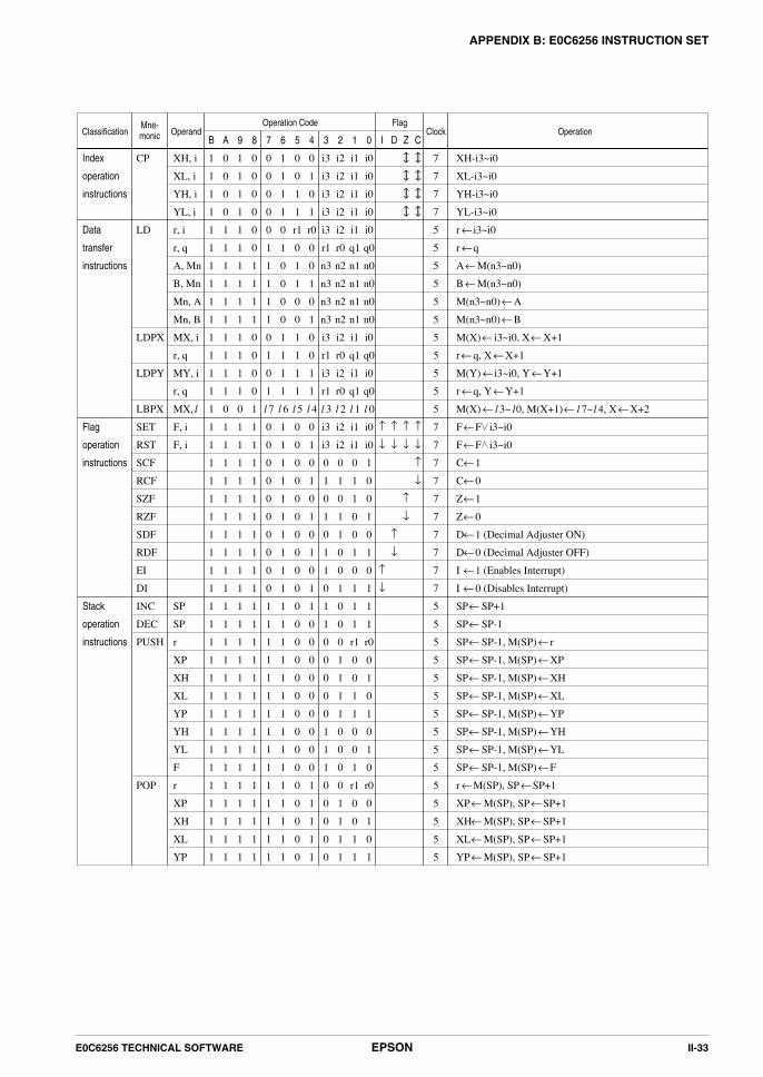
E0C6256 TECHNICAL SOFTWARE EPSON II-33
APPENDIX B: E0C6256 INSTRUCTION SET
B
1
1
1
1
1
1
1
1
1
1
1
1
1
1
1
1
1
1
1
1
1
1
1
1
1
1
1
1
1
1
1
1
1
1
1
1
1
1
1
1
A
0
0
0
0
1
1
1
1
1
1
1
1
1
1
0
1
1
1
1
1
1
1
1
1
1
1
1
1
1
1
1
1
1
1
1
1
1
1
1
1
9
1
1
1
1
1
1
1
1
1
1
1
1
1
1
0
1
1
1
1
1
1
1
1
1
1
1
1
1
1
1
1
1
1
1
1
1
1
1
1
1
8
0
0
0
0
0
0
1
1
1
1
0
0
0
0
1
1
1
1
1
1
1
1
1
1
1
1
1
1
1
1
1
1
1
1
1
1
1
1
1
1
7
0
0
0
0
0
1
1
1
1
1
0
1
0
1
7
0
0
0
0
0
0
0
0
0
0
1
1
1
1
1
1
1
1
1
1
1
1
1
1
1
6
1
1
1
1
0
1
0
0
0
0
1
1
1
1
6
1
1
1
1
1
1
1
1
1
1
1
1
1
1
1
1
1
1
1
1
1
1
1
1
1
5
0
0
1
1
r1
0
1
1
0
0
1
1
1
1
5
0
0
0
0
0
0
0
0
0
0
0
0
0
0
0
0
0
0
0
0
0
0
0
0
0
4
0
1
0
1
r0
0
0
1
0
1
0
0
1
1
4
0
1
0
1
0
1
0
1
0
1
1
0
0
0
0
0
0
0
0
0
1
1
1
1
1
3
i3
i3
i3
i3
i3
r1
n3
n3
n3
n3
i3
r1
i3
r1
3
i3
i3
0
1
0
1
0
1
1
0
1
1
0
0
0
0
0
1
1
1
0
0
0
0
0
2
i2
i2
i2
i2
i2
r0
n2
n2
n2
n2
i2
r0
i2
r0
2
i2
i2
0
1
0
1
1
0
0
1
0
0
0
1
1
1
1
0
0
0
0
1
1
1
1
1
i1
i1
i1
i1
i1
q1
n1
n1
n1
n1
i1
q1
i1
q1
1
i1
i1
0
1
1
0
0
1
0
1
1
1
r1
0
0
1
1
0
0
1
r1
0
0
1
1
0
i0
i0
i0
i0
i0
q0
n0
n0
n0
n0
i0
q0
i0
q0
0
i0
i0
1
0
0
1
0
1
0
1
1
1
r0
0
1
0
1
0
1
0
r0
0
1
0
1
XH, i
XL, i
YH, i
YL, i
r, i
r, q
A, Mn
B, Mn
Mn, A
Mn, B
MX, i
r, q
MY, i
r, q
MX,
F, i
F, i
SP
SP
r
XP
XH
XL
YP
YH
YL
F
r
XP
XH
XL
YP
CP
LD
LDPX
LDPY
LBPX
SET
RST
SCF
RCF
SZF
RZF
SDF
RDF
EI
DI
INC
DEC
PUSH
POP
Index
operation
instructions
Data
transfer
instructions
Flag
operation
instructions
Stack
operation
instructions
Classification OperandI D Z C
↑
↓
↑
↓
↑
↑
↑
↑
↑
↓
↑
↓
↑
↑
↑
↑
↑
↓
↑
↓
7
7
7
7
5
5
5
5
5
5
5
5
5
5
5
7
7
7
7
7
7
7
7
7
7
5
5
5
5
5
5
5
5
5
5
5
5
5
5
5
ClockOperation Code Flag
XH-i3~i0
XL-i3~i0
YH-i3~i0
YL-i3~i0
r i3~i0
r q
A
B
M(n3~n0) A
M(n3~n0) B
M(X) i3~i0, X X+1
r q, X X+1
M(Y) i3~i0, Y Y+1
r q, Y Y+1
M(X) 3~ 0, M(X+1) 7~ 4, X X+2
←
←
F
F
C
C
Z
Z
D
D
I
I
← ←
←
←
← ←
←←
Mne-monic Operation
↓
↓
↓
↓
↑
↓
↑
↓
↓
↓
↓
↓
SP SP+1
SP SP-1
SP SP-1, M(SP) r
SP SP-1, M(SP) XP
SP SP-1, M(SP) XH
SP SP-1, M(SP) XL
SP SP-1, M(SP) YP
SP SP-1, M(SP) YH
SP SP-1, M(SP) YL
SP SP-1, M(SP) F
r M(SP), SP SP+1
XP
XH
XL
YP
←
←
M(n3~n0)
M(n3~n0)
←
←
←
←
←
←
←
←
←
←
←
←
←
←
←
F i3~i0
F i3~i0
1
0
1
0
1 (Decimal Adjuster ON)
0 (Decimal Adjuster OFF)
1 (Enables Interrupt)
0 (Disables Interrupt)
←
←
←
←
←
←
←
←
←
←
←
←
←
←
←
←
←
←
← ←
←
←
←
←
M(SP), SP SP+1
M(SP), SP SP+1
M(SP), SP SP+1
M(SP), SP SP+1
←
←
←
←
l l l l l l l l l l l l l

II-34 EPSON E0C6256 TECHNICAL SOFTWARE
APPENDIX B: E0C6256 INSTRUCTION SET
d3 d2, d2 d1, d1 d0, d0 C, C d3
d3 C, d2 d3, d1 d2, d0 d1, C d0
M(n3~n0) M(n3~n0)+1
M(n3~n0) M(n3~n0)-1
↓
↓
↓
↓
↓
↓
↓
↓
↓
↓
↓
↓
↓
↓
↓
↓
↓
↓
↓
↓
↓
↓
↓
↓
↓
↓
↓
B
1
1
1
1
1
1
1
1
1
1
1
1
1
1
1
1
1
1
1
1
1
1
1
1
1
1
1
1
1
1
1
1
1
A
1
1
1
1
1
1
1
1
0
1
0
0
1
0
1
0
1
0
1
0
1
1
1
1
0
1
1
1
1
1
1
1
1
9
1
1
1
1
1
1
1
0
1
0
1
1
0
1
0
1
0
1
0
1
0
1
0
1
1
1
1
1
1
1
1
1
0
8
1
1
1
1
1
1
1
0
0
0
0
0
1
0
0
0
0
0
1
0
1
1
1
1
0
0
1
1
1
1
1
1
1
7
1
1
1
1
1
1
1
0
1
0
1
1
0
1
1
1
1
1
0
1
1
0
1
0
1
1
0
0
0
0
0
0
0
6
1
1
1
1
1
1
1
0
0
1
0
0
1
0
0
1
1
1
0
1
1
0
0
0
1
0
1
1
0
0
0
0
0
5
0
0
0
1
1
1
1
r1
0
r1
0
1
r1
1
r1
0
r1
0
r1
1
r1
0
r1
0
1
0
1
1
1
1
1
1
r1
4
1
1
1
0
1
0
1
r0
0
r0
1
0
r0
1
r0
0
r0
1
r0
0
r0
0
r0
1
1
0
0
1
0
0
1
1
r0
3
1
1
1
0
0
0
0
i3
r1
i3
r1
r1
i3
r1
i3
r1
i3
r1
i3
r1
i3
r1
i3
r1
r1
1
n3
n3
1
1
1
1
1
2
0
0
0
0
0
1
1
i2
r0
i2
r0
r0
i2
r0
i2
r0
i2
r0
i2
r0
i2
r0
i2
r0
r0
1
n2
n2
0
1
0
1
1
1
0
0
1
r1
r1
r1
r1
i1
q1
i1
q1
q1
i1
q1
i1
q1
i1
q1
i1
q1
i1
q1
i1
q1
r1
r1
n1
n1
r1
r1
r1
r1
1
0
0
1
0
r0
r0
r0
r0
i0
q0
i0
q0
q0
i0
q0
i0
q0
i0
q0
i0
q0
i0
q0
i0
q0
r0
r0
n0
n0
r0
r0
r0
r0
1
YH
YL
F
SPH, r
SPL, r
r, SPH
r, SPL
r, i
r, q
r, i
r, q
r, q
r, i
r, q
r, i
r, q
r, i
r, q
r, i
r, q
r, i
r, q
r, i
r, q
r
r
Mn
Mn
MX, r
MY, r
MX, r
MY, r
r
POP
LD
ADD
ADC
SUB
SBC
AND
OR
XOR
CP
FAN
RLC
RRC
INC
DEC
ACPX
ACPY
SCPX
SCPY
NOT
Stack
operation
instructions
Arithmetic
instructions
Classification OperandI D Z C
↑ ↑
↑
↑
↑
↑
↑
↑
↑
↑
↑
↑
↑
↑
↑
↑
↑
↑
↑
↑
↑
↑
↑
↑
↑
↑
↑
↑
↑
↑
↑
↑
↑
↑
↑
↑
↑
↑
↑
↑
↑
↑
↑
↑
↑
↑
5
5
5
5
5
5
5
7
7
7
7
7
7
7
7
7
7
7
7
7
7
7
7
7
7
5
7
7
7
7
7
7
7
ClockOperation Code Flag
YH
YL
F M(SP), SP SP+1
SPH
SPL
r SPH
r SPL
←
←
←
Mne-monic Operation
↓
↓
↓
↓
↓
↓
↓
↓
↓
↓
↓
↓
↓
↓
↓
↓
↓
↓
↑
←
←
←
←
←
←
←
←
←
←
←
←
←
←
←
↓↓
r r+i3~i0
r r+q
r r+i3~i0+C
r r+q+C
r r-q
r r-i3~i0-C
r r-q-C
r r i3~i0
r r q
r r i3~i0
r r q
r r i3~i0
r r q
r-i3~i0
r-q
r i3~i0
r q
M(X) M(X)+r+C, X X+1
M(Y) M(Y)+r+C, Y Y+1
M(X) M(X)-r-C, X X+1
M(Y) M(Y)-r-C, Y Y+1
r r
M(SP), SP SP+1
M(SP), SP SP+1
←
←
← ←
←
←
r
r
← ← ← ←
← ← ← ← ←
←
←
←
←
←
←
←
←
←
←
←

E0C6256 TECHNICAL SOFTWARE EPSON II-35
APPENDIX B: E0C6256 INSTRUCTION SET
Abbreviations used in the explanations have the following meanings.
Symbols associated with registers and memoryA A registerB B registerX XHL register
(low order eight bits of index register IX)Y YHL register
(low order eight bits of index register IY)XH XH register
(high order four bits of XHL register)XL XL register
(low order four bits of XHL register)YH YH register
(high order four bits of YHL register)YL YL register
(low order four bits of YHL register)XP XP register
(high order four bits of index register IX)YP YP register
(high order four bits of index register IY)SP Stack pointer SPSPH High-order four bits of stack pointer SPSPL Low-order four bits of stack pointer SPMX, M(X) Data memory whose address is specified
with index register IXMY, M(Y) Data memory whose address is specified
with index register IYMn, M(n) Data memory address 000H–00FH
(address specified with immediate data n of00H–0FH)
M(SP) Data memory whose address is specifiedwith stack pointer SP
r, q Two-bit register coder, q is two-bit immediate data; according tothe contents of these bits, they indicateregisters A, B, and MX and MY (datamemory whose addresses are specified withindex registers IX and IY)
r q Registerr1 r0 q1 q0 specified0 0 0 0 A0 1 0 1 B1 0 1 0 MX1 1 1 1 MY
Symbols associated with program counterNBP New bank pointerNPP New page pointerPCB Program counter bankPCP Program counter pagePCS Program counter stepPCSH Four high order bits of PCSPCSL Four low order bits of PCS
Symbols associated with flagsF Flag register (I, D, Z, C)C Carry flagZ Zero flagD Decimal flagI Interrupt flag↓ Flag reset↑ Flag set Flag set or reset
Associated with immediate datap Five-bit immediate data or label 00H–1FHs Eight-bit immediate data or label 00H–0FFHl Eight-bit immediate data 00H–0FFHi Four-bit immediate data 00H–0FH
Associated with arithmetic and other operations+ Add- Subtract∧ Logical AND∨ Logical OR∀ Exclusive-OR Add-subtract instruction for decimal
operation when the D flag is set

II-36 EPSON E0C6256 TECHNICAL SOFTWARE
APPENDIX C: PSEUDO-INSTRUCTION TABLE OF THE CROSS ASSEMBLER
APPENDIX C. PSEUDO-INSTRUCTION TABLE
OF THE CROSS ASSEMBLERItem No. Pseudo-instruction Meaning Example of use
1
2
3
4
5
6
7
8
9
10
11
EQU
(Equation)
ORG
(Origin)
SET
(Set)
DW
(Define Word)
BANK
(Bank)
PAGE
(Page)
SECTION
(Section)
END
(End)
MACRO
(Macro)
LOCAL
(Local)
ENDM
(End Macro)
To allocate data to label
To define location counter
To allocate data to label
(data can be changed)
To define ROM data
To define boundary of bank
To define boundary of page
To define boundary of section
To terminate assembly
To define macro
To make local specification of label
during macro definition
To end macro definition
ABC EQU 9
CHECK MACRO DATA
LOCAL LOOP
LOOP CP MX,DATA
JP NZ,LOOP
ENDM
CHECK 1
BCD EQU ABC+1
ORG 100H
ORG 256
ABC SET 0001H
ABC SET 0002H
ABC DW 'AB'
BCD DW 0FFBH
PAGE 1H
PAGE 4
SECTION
END
BANK 0
BANK 1H

E0C6256 TECHNICAL SOFTWARE EPSON II-37
APPENDIX D: COMMAND TABLE OF ICE6200
APPENDIX D. COMMAND TABLE OF ICE6200
123
4
5
6
7
8
9
10
AssembleDisassembleDump
Fill
SetRun Mode
Trace
Break
Move
Data Set
Change CPUInternalRegisters
#A,a#L,a1,a2#DP,a1,a2#DD,a1,a2#FP,a1,a2,d#FD,a1,a2,d#G,a#TIM#OTF#T,a,n
#U,a,n#BA,a#BAR,a#BD#BDR#BR#BRR#BM
#BMR
#BRES#BC#BE#BSYN#BT#BRKSEL,REM#MP,a1,a2,a3
#MD,a1,a2,a3
#SP,a#SD,a#DR#SR#I#DXY#SXY
Assemble command mnemonic code and store at address "a"Contents of addresses a1 to a2 are disassembled and displayedContents of program area a1 to a2 are displayedContent of data area a1 to a2 are displayedData d is set in addresses a1 to a2 (program area)Data d is set in addresses a1 to a2 (data area)Program is executed from the "a" addressExecution time and step counter selectionOn-the-fly display selectionExecutes program while displaying results of step instructionfrom "a" addressDisplays only the final step of #T,a,nSets Break at program address "a"Breakpoint is canceledBreak condition is set for data RAMBreakpoint is canceledBreak condition is set for EVA6256 CPU internal registersBreakpoint is canceledCombined break conditions set for program data RAM addressand registersCancel combined break conditions for program data ROMaddress and registersAll break conditions canceledBreak condition displayedEnter break enable modeEnter break disable modeSet break stop/trace modesSet BA condition clear/remain modes Contents of program area addresses a1 to a2 are moved toaddresses a3 and afterContents of data area addresses a1 to a2 are moved to addressesa3 and afterData from program area address "a" are written to memoryData from data area address "a" are written to memory
Item No. Function Command Format Outline of Operation
Display EVA6256 CPU internal registersSet EVA6256 CPU internal registersReset EVA6256 CPUDisplay X, Y, MX and MYSet data for X and Y display and MX, MY

II-38 EPSON E0C6256 TECHNICAL SOFTWARE
APPENDIX D: COMMAND TABLE OF ICE6200
11
12
13
14
15
16
17
History
File
Coverage
ROM Access
TerminateICECommandDisplaySelfDiagnosis
#H,p1,p2#HB#HG#HP#HPS,a#HC,S/C/E
#HA,a1,a2
#HAR,a1,a2
#HAD#HS,a
#HSW,a#HSR,a#RF,file#RFD,file#VF,file#VFD,file#WF,file#WFD,file#CL,file#CS,file#OPTLD,1,file#OPTLD,2,file#CVD#CVR#RP#VP#ROM#Q
#HELP
#CHK
Display history data for pointer 1 and pointer 2Display upstream history dataDisplay 21 line history dataDisplay history pointerSet history pointerSets up the history information acquisition before (S),before/after (C) and after (E)Sets up the history information acquisition from program areaa1 to a2Sets up the prohibition of the history information acquisitionfrom program area a1 to a2Indicates history acquisition program areaRetrieves and indicates the history information which executeda program address "a"Retrieves and indicates the history information which wrote orread the data area address "a"
Save contents of memory to program fileSave contents of memory to data fileLoad ICE6200 set condition from fileSave ICE6200 set condition to fileLoad function option data from fileLoad segment option data from file
Terminate ICE and return to operating system control
Display ICE6200 instruction
Report results of ICE6200 self diagnostic test
Move program file to memoryMove data file to memoryCompare program file and contents of memoryCompare data file and contents of memory
Indicates coverage informationClears coverage informationMove contents of ROM to program memoryCompare contents of ROM with contents of program memorySet ROM type
Item No. Function Command Format Outline of Operation
means press the RETURN key.

AMERICA
EPSON ELECTRONICS AMERICA, INC.
- HEADQUARTERS -1960 E. Grand AvenueEI Segundo, CA 90245, U.S.A.Phone: +1-310-955-5300 Fax: +1-310-955-5400
- SALES OFFICES -
West150 River Oaks ParkwaySan Jose, CA 95134, U.S.A.Phone: +1-408-922-0200 Fax: +1-408-922-0238
Central101 Virginia Street, Suite 290Crystal Lake, IL 60014, U.S.A.Phone: +1-815-455-7630 Fax: +1-815-455-7633
Northeast301 Edgewater Place, Suite 120Wakefield, MA 01880, U.S.A.Phone: +1-781-246-3600 Fax: +1-781-246-5443
Southeast3010 Royal Blvd. South, Suite 170Alpharetta, GA 30005, U.S.A.Phone: +1-877-EEA-0020 Fax: +1-770-777-2637
EUROPE
EPSON EUROPE ELECTRONICS GmbH
- HEADQUARTERS -Riesstrasse 1580992 Munich, GERMANYPhone: +49-(0)89-14005-0 Fax: +49-(0)89-14005-110
- GERMANY -SALES OFFICEAltstadtstrasse 17651379 Leverkusen, GERMANYPhone: +49-(0)2171-5045-0 Fax: +49-(0)2171-5045-10
- UNITED KINGDOM -UK BRANCH OFFICEUnit 2.4, Doncastle House, Doncastle RoadBracknell, Berkshire RG12 8PE, ENGLANDPhone: +44-(0)1344-381700 Fax: +44-(0)1344-381701
- FRANCE -FRENCH BRANCH OFFICE1 Avenue de l' Atlantique, LP 915 Les ConquerantsZ.A. de Courtaboeuf 2, F-91976 Les Ulis Cedex, FRANCEPhone: +33-(0)1-64862350 Fax: +33-(0)1-64862355
ASIA
- CHINA -EPSON (CHINA) CO., LTD.28F, Beijing Silver Tower 2# North RD DongSanHuanChaoYang District, Beijing, CHINAPhone: 64106655 Fax: 64107319
SHANGHAI BRANCH4F, Bldg., 27, No. 69, Gui Jing RoadCaohejing, Shanghai, CHINAPhone: 21-6485-5552 Fax: 21-6485-0775
- HONG KONG, CHINA -EPSON HONG KONG LTD.20/F., Harbour Centre, 25 Harbour RoadWanchai, HONG KONGPhone: +852-2585-4600 Fax: +852-2827-4346Telex: 65542 EPSCO HX
- TAIWAN -EPSON TAIWAN TECHNOLOGY & TRADING LTD.10F, No. 287, Nanking East Road, Sec. 3Taipei, TAIWANPhone: 02-2717-7360 Fax: 02-2712-9164Telex: 24444 EPSONTB
HSINCHU OFFICE13F-3, No. 295, Kuang-Fu Road, Sec. 2HsinChu 300, TAIWANPhone: 03-573-9900 Fax: 03-573-9169
- SINGAPORE -EPSON SINGAPORE PTE., LTD.No. 1 Temasek Avenue, #36-00Millenia Tower, SINGAPORE 039192Phone: +65-337-7911 Fax: +65-334-2716
- KOREA -SEIKO EPSON CORPORATION KOREA OFFICE50F, KLI 63 Bldg., 60 Yoido-dongYoungdeungpo-Ku, Seoul, 150-763, KOREAPhone: 02-784-6027 Fax: 02-767-3677
- JAPAN -SEIKO EPSON CORPORATIONELECTRONIC DEVICES MARKETING DIVISION
Electronic Device Marketing DepartmentIC Marketing & Engineering Group421-8, Hino, Hino-shi, Tokyo 191-8501, JAPANPhone: +81-(0)42-587-5816 Fax: +81-(0)42-587-5624
ED International Marketing Department Europe & U.S.A.421-8, Hino, Hino-shi, Tokyo 191-8501, JAPANPhone: +81-(0)42-587-5812 Fax: +81-(0)42-587-5564
ED International Marketing Department Asia421-8, Hino, Hino-shi, Tokyo 191-8501, JAPANPhone: +81-(0)42-587-5814 Fax: +81-(0)42-587-5110
International Sales Operations

In pursuit of “Saving” Technology, Epson electronic devices.Our lineup of semiconductors, liquid crystal displays and quartz devices
assists in creating the products of our customers’ dreams.Epson IS energy savings.

ELECTRONIC DEVICES MARKETING DIVISION
EPSON Electronic Devices Website
http://www.epson.co.jp/device/First issue MARCH 1994, Printed MAY 2000 in Japan M A


