Embed Size (px)
Citation preview
IEEE TRANSACTIONS ON NEURAL NETWORKS, VOL. 18, NO. 1, JANUARY 2007 253
Dynamically Reconfigurable Silicon Array of SpikingNeurons With Conductance-Based Synapses
R. Jacob Vogelstein, Student Member, IEEE, Udayan Mallik, Joshua T. Vogelstein, andGert Cauwenberghs, Senior Member, IEEE
Abstract—A mixed-signal very large scale integration (VLSI)chip for large scale emulation of spiking neural networks ispresented. The chip contains 2400 silicon neurons with fullyprogrammable and reconfigurable synaptic connectivity. Eachneuron implements a discrete-time model of a single-compartmentcell. The model allows for analog membrane dynamics and anarbitrary number of synaptic connections, each with tunableconductance and reversal potential. The array of silicon neuronsfunctions as an address–event (AE) transceiver, with incoming andoutgoing spikes communicated over an asynchronous event-drivendigital bus. Address encoding and conflict resolution of spikingevents are implemented via a randomized arbitration scheme thatensures balanced servicing of event requests across the array.Routing of events is implemented externally using dynamicallyprogrammable random-access memory that stores a postsynapticaddress, the conductance, and the reversal potential of eachsynaptic connection. Here, we describe the silicon neuron circuits,present experimental data characterizing the 3 mm � 3 mm chipfabricated in 0.5-�m complementary metal–oxide–semiconductor(CMOS) technology, and demonstrate its utility by configuring thehardware to emulate a model of attractor dynamics and waves ofneural activity during sleep in rat hippocampus.
Index Terms—Address–event representation (AER), dy-namically reconfigurable network, membrane conductance,mixed-signal very large scale integration (VLSI), neural emulator,neurotransmitter quantal release, switched capacitor.
I. INTRODUCTION
NEUROMORPHIC systems engineering [1], [2] emulatesboth structure and function of biological neural systems in
silicon, and correspondingly achieves high levels of efficiencyin the implementation of artificial sensory systems. To date,facsimiles of the initial stages of visual and auditory informa-tion processing have been implemented on single microchips(e.g., [3]–[7]). However, the complexity of neural computationbeyond sensory perception requires a multichip approach and
Manuscript received July 21, 2005; revised July 24, 2006. This work wassupported in part by the National Science Foundation, the National Institute onAging, and the Office of Naval Research. The work of R. J. Vogelstein wassupported by the National Science Foundation Graduate Research Fellowship.
R. J. Vogelstein is with the Department of Biomedical Engineering, The JohnsHopkins University, Baltimore, MD 21205 USA (e-mail: [email protected]).
U. Mallik was with the Department of Electrical and Computer Engineering,The Johns Hopkins University, Baltimore, MD 21218 USA. He is now withGoddard Space Flight Center, NASA, Greenbelt, MD 20771 USA (e-mail:[email protected]).
J. T. Vogelstein is with the Department of Neuroscience, The Johns HopkinsUniversity, Baltimore, MD 21205 USA (e-mail: [email protected]).
G. Cauwenberghs is with the Division of Biological Sciences, University ofCalifornia at San Diego, La Jolla, CA, 92093 USA (e-mail: [email protected]).
Digital Object Identifier 10.1109/TNN.2006.883007
a proper communication protocol between chips to implementhigher levels of processing and cognition (see, e.g., [8]).
The common language of neuromorphic chips is the ad-dress–event representation (AER) communication protocol[9]–[11], which uses time-multiplexing to emulate extensiveconnectivity between neurons. In its original formulation,AER effects a one-to-one connection topology; to create morecomplex neural circuits, convergent and divergent connectivityare required. Several authors have discussed and implementedmethods of enhancing the connectivity of AER systems towardthis end [5], [12]–[18]. These methods generally employ AER“transceivers” [12], [15], [16] and call for a memory-basedprojective field mapping that enables routing an address–event(AE) to multiple receiver locations. Accordingly, the chipdescribed in this paper contains 2400 neurons but no hardwiredconnections between cells, rather depending on an externalinfrastructure to route events to their appropriate targets.
Neural transceivers are useful alternatives to dedicated (hard-wired) architectures for implementing large scale spiking neuralnetworks and models of spike-timing dependent synaptic plas-ticity [20]–[23] because they are reconfigurable. In a typicalhardwired implementation, the size of the network is limited bythe number of cells integrated on-chip, where each cell imple-ments a dedicated synapse in a fully connected network. Thisapproach is appropriate to study the dynamics of small, denselyinterconnected networks, but does not scale to more complexmodels involving large, sparsely connected networks, such asthose responsible for attention, object recognition, and languageprocessing in various areas of cortex. Generally, implementa-tions of cortical models have so far been limited to softwaresimulations—because none of the cortical areas being studiedhave been fully characterized, the models are always in flux andit is often counterproductive to develop a chip hardwired to aparticular network architecture.
There are a few examples of reconfigurable neural arraytransceivers in the literature [15], [16], [24]–[30]. The one de-scribed here differs in some important aspects. First, the siliconneuron implements a more biologically realistic discrete-timemodel of membrane dynamics that includes conductance-basedsynapses. Conductance-based synapses allow for differentneural dynamics than what can be emulated with standardintegrate-and-fire (I&F) models (including those that containleakage, an activity-independent conductance to the rest po-tential, in the neural dynamics). Second, the design permits avirtually unlimited number of connections between neurons,with independent control of synaptic strength (conductance)and reversal potential on a per-connection basis. The synaptic
1045-9227/$20.00 © 2006 IEEE
254 IEEE TRANSACTIONS ON NEURAL NETWORKS, VOL. 18, NO. 1, JANUARY 2007
“wiring” and parameters can be changed on the fly by re-programming digital random-access memory. This abilityto rapidly alter synaptic connectivity and synaptic parame-ters also supports the implementation of synaptic dynamics(Section III-B) and spike-timing dependent synaptic plasticity[31]. From a circuits and systems perspective, our approachcombines advantages of analog and digital processing bydividing the network architecture into two main components:neural membrane dynamics implemented in an analog VLSIarray, and synaptic connectivity implemented in dynamicallyreconfigurable digital memory. Also, the silicon neuron uses aswitched-capacitor architecture to efficiently and reliably im-plement the membrane dynamics in discrete time, obviating theneed for precisely matched linear transconductance elements ina continuous-time implementation.
II. VIRTUAL SYNAPSES
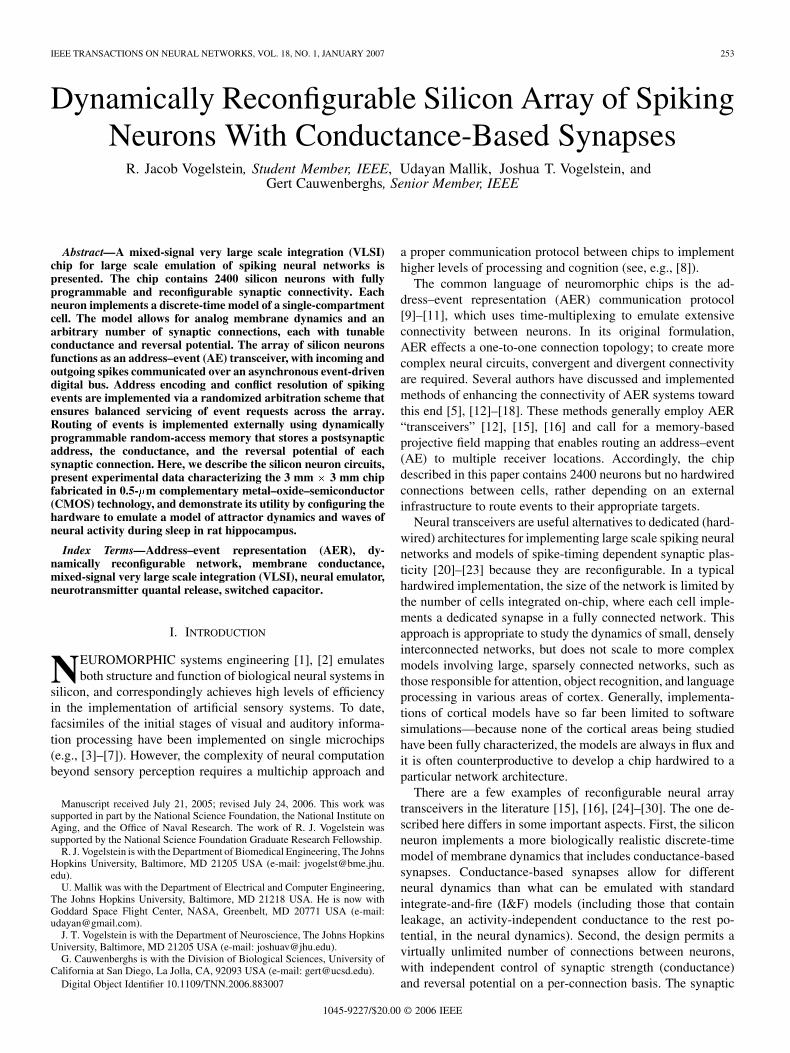
Rather than hardwiring synapses to form a physically con-nected network of neurons, we implement synapses as soft (vir-tual) connections. In this system, each neuron is given a uniqueaddress, and an off-chip lookup table (LUT) represents synapsesas a mapping between presynaptic and postsynaptic neuron ad-dresses (Fig. 1) [16], [19]. When a neuron fires an action po-tential, its address is transmitted over a shared bus to a decoderthat has access to the LUT—this is called an AE. Dependingon the data stored in the lookup table and the mechanism usedto determine postsynaptic targets, this technique can be used toemulate one-to-one [9] or one-to-many [12] connections. Addi-tionally, it allows for arbitrary and reconfigurable connectivity,as any neuron can connect to any other, and synapses can bererouted dynamically by changing entries in the table. As longas the bus speed is significantly faster than the event genera-tion rate or the spike processing dynamics, a single connectioncan be multiplexed in time to emulate extensive connectivity be-tween neurons [12].
A schematic representation of the lookup table used to storethe network connectivity is shown in Fig. 1. Each entry repre-sents a single “virtual synapse” and specifies both the presy-naptic and postsynaptic neurons’ addresses, as well as the fol-lowing four synaptic parameters:
number of release sites;probability of release;quantal postsynaptic response;reversal equilibrium potential.
The overall strength of the synaptic connection can be expressedas a conductance, , which is the product of the first threeparameters [32]
(1)
That is, the conductance is proportional to the product of thenumber of synaptic release sites on the presynaptic neuron, theprobability of synaptic release, and the postsynaptic responseto a quantal amount of neurotransmitter. The polarity of thesynaptic connection (excitatory or inhibitory) is determined bythe synaptic reversal (equilibrium) potential , which functionsas an electrochemical “battery” across the cell membrane and
Fig. 1. (a) Virtual synapses: address-domain connectivity between presynapticand postsynaptic neurons. Numbers in parentheses correspond to the synapticparameters (q, n, p, and E) defined in Section II. (b) Lookup table storing ad-dresses and parameters of the synaptic connections in random-access memory.The address of a presynaptic action potential “event” is used as an index into thetable to identify postsynaptic target addresses and their corresponding synapticparameters [1].
varies according to the ionic species (K , Na , Cl , etc.) con-ducted by the synapse. A model of how all of these parametersinteract at the postsynaptic site, adapted for analog VLSI imple-mentation, is presented in Section III.
III. NEURAL MODEL
A number of silicon neurons have been presented in the lit-erature with varying degrees of biological accuracy [33]–[40].The most detailed and accurate silicon models feature manyparameters and are very flexible, but occupy a large on-chiparea and, therefore, limit the number of cells that can be fab-ricated on a single chip. The simplest models contain only afew transistors and are well suited for implementation in a largescale network, but deviate significantly from the biology andhave few adjustable parameters. Many applications would ben-efit from a balance between these two extremes: A more bio-logically accurate neural model allows for more sophisticatedemulation of cognitive functions, but only in the context of asophisticated network architecture (see [15] and [25] for someexamples along these lines). We have, therefore, designed asmall-footprint, highly configurable, “general-purpose” siliconneuron that implements a standard extensible model of biolog-ical neural membranes.
The question of whether to use a linear I&F model or aconductance-based model has become a popular subject amongneural modelers recently, with no clear resolution [41]–[43].However, it is known that ion channels in real neurons act asnonlinear conductances [44], and this may play an importantrole in certain network computations (c.f. Section VI). Forexample, conductance-based models exhibit a concave-downcharging characteristic, which has been shown to be usefulfor synchronizing populations of neurons [45]–[47]. Con-ductance-based models also exhibit a strong dependence onthe order of input events, which may be important for neural
VOGELSTEIN et al.: DYNAMICALLY RECONFIGURABLE SILICON ARRAY OF SPIKING NEURONS 255
Fig. 2. Silicon single-compartment neuron and “general-purpose” synapse (inside dashed box, [19]), with event generation circuitry (shown right, [16]). Whenthe address of an incoming event is decoded, row- and column-select circuitry activate the cell’s neuron select (NS) line, the global signals W –W and E areestablished, and the spike is registered by a pulse on � followed by a pulse on � .
calculations based on spike timing (e.g., [48]–[52], and thereferences therein). For these reasons, we have decided toimplement a conductance-based model in our silicon neuron.
A. Membrane Dynamics
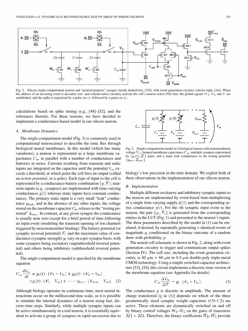
The single-compartment model (Fig. 3) is commonly used incomputational neuroscience to describe the ionic flux throughbiological neural membranes. In this model (which has manyvariations), a neuron is represented as a large membrane ca-pacitance in parallel with a number of conductances andbatteries in series. Currents resulting from transient and staticinputs are integrated on the capacitor until the potential ex-ceeds a threshold, at which point the cell fires an output (calledan action potential, or a spike). Each type of input to the cell isrepresented by a conductance-battery combination ; tran-sient inputs (e.g., synapses) are implemented with time-varyingconductances whereas static inputs have constant conduc-tances. The primary static input is a very small “leak” conduc-tance , and in the absence of any other inputs, the voltagestored on the membrane capacitor relaxes to the “resting po-tential” . In contrast, at any given synapse the conductanceis usually near zero except for a brief period of time followingan input event (modeling the transient opening of ion channelstriggered by neurotransmitter binding). The battery potential (orsynaptic reversal potential) and the maximum value of con-ductance (synaptic strength) vary on a per-synapse basis, withsome synapses being excitatory (suprathreshold reversal poten-tial) and others being inhibitory (subthreshold reversal poten-tial).
The single-compartment model is specified by the membraneequation
(2)
Although biology operates in continuous time, most neural in-teractions occur on the millisecond time scale, so it is possibleto simulate the internal dynamics of a neuron using fast, dis-crete-time steps. Similarly, while multiple synaptic inputs canbe active simultaneously in a real neuron, it is essentially equiv-alent to activate a group of synapses in rapid succession due to
Fig. 3. Single-compartment model of a biological neuron with transmembranevoltage V , lumped membrane capacitanceC , multiple synapses representedby fg (t); E g pairs, and a static leak conductance to the resting potentialfg ; E g.
biology’s low precision in the time domain. We exploit both ofthese observations in the implementation of our silicon neuron.
B. Implementation
Multiple different excitatory and inhibitory synaptic inputs tothe neuron are implemented by event-based time-multiplexingof a single time-varying supply and the corresponding se-ries conductance . For the th synaptic input event to theneuron, the pair is generated from the correspondingentries in the LUT (Fig. 1) and presented to the neuron’s inputs.The three parameters described by the model in (1) can be em-ulated, if desired, by repeatedly generating identical events ofmagnitude , conditioned on the binary outcome of a randomdraw with probability .
The neural cell schematic is shown in Fig. 2, along with eventgeneration circuitry to trigger and communicate output spikes(Section IV). The cell size, including the event generation cir-cuitry, is 40 m 60 m in 0.5- m double-poly triple-metalCMOS technology. Using a simple switched-capacitor architec-ture [53], [54], this circuit implements a discrete-time version ofthe membrane equation (see Appendix for details)
(3)
The conductance is discrete in amplitude. The amount ofcharge transferred [ in (1)] depends on which of the threegeometrically sized synaptic weight capacitors ( – ) areactive. These elements are dynamically switched on and offby binary control voltages – on the gates of transistors
. Therefore, the binary coefficients – provide
256 IEEE TRANSACTIONS ON NEURAL NETWORKS, VOL. 18, NO. 1, JANUARY 2007
eight-level control of conductance values. A larger dynamicrange in effective conductance can be accommodated by mod-ulating the multiplicity and probability of synaptic eventsaccording to (1). Although the synaptic updates in (3) areinstantaneous, synaptic dynamics mimicking the time course ofpostsynaptic potentials in biological neurons can be emulated(at the cost of bandwidth) by repeatedly stimulating the samesynapse with gradual changes in , , and .
Incoming spikes are represented by a packet of data con-taining the target neuron’s address, the synaptic weight, and thesynaptic reversal potential [Fig. 1(b)]. The address is processedby row- and column-decoders, which activate the neuron select(NS) lines to identify the postsynaptic target(s). The -compo-nent of the weight (1) corresponds to the values of – ,which are shared by all on-chip neurons. The synaptic reversalpotential is converted to an analog voltage off-chip and alsoshared by all of the neurons. After these signals are established,the spike is registered when an off-chip clock generates a pulseon followed by a pulse on , which allows a packet of chargeproportional to the difference between the synaptic reversal po-tential and the membrane potential to be accumu-lated onto the membrane capacitor . These discrete-timeupdates (3) model the transient opening of membrane channelsin the limit of a very short time window of postsynaptic re-sponse.
To conserve bandwidth, reserved address words allow therow- and column-decoders to select the entire chip or any indi-vidual row or column of neurons. Because the signals –and are global, many neurons can process events with thesame synaptic parameters simultaneously. This allows for an ef-ficient implementation of the continuous leak conductancein the membrane model (2): Leak is approximated by chip-wideperiodic (or otherwise repeated) events with low weight and asynaptic equilibrium potential equal to the rest potential .
IV. EVENT GENERATION AND ARBITRATION
Information encoded by neurons in the array is representedby the timing of spike events. Therefore, event generation, arbi-tration, and communication are essential elements of the design.
A. Event Generation
The event generation circuitry of [16] is embedded in everycell (Fig. 2, right). An event—signaled by a low voltage on
—is generated each time the total accumulated charge oncauses the neuron’s membrane potential to exceed
the spike threshold voltage . Because can risevery slowly, the threshold comparator is implemented as acurrent-starved inverter ( – ), with biased in weakinversion for reduced power dissipation. is applied tothe source of ; this value is shared by all cells in the arrayand is externally controlled. The corresponding input-referredthreshold is approximately equal to , whereis the threshold voltage of . When exceeds this value, apositive feedback loop implemented by transistors – isactivated, triggering a spike event by driving to the positiverail.
A high voltage on activates , the output node of arow-wise wired-NAND, and indicates to the row arbitration cir-cuitry that a cell in that row has generated an event and needsto be serviced. Until this occurs, the row and column acknowl-edge signals and remain low, maintaining the posi-tive feedback loop and preventing any further inputs from af-fecting the cell. The row arbitration circuitry indicates it hasselected a row by driving one pair of and signalshigh. All cells in that row with pending events then pull their
signals low, indicating to the column arbitration circuitrythat they have generated events and need to be serviced. Fi-nally, the column arbitration circuitry indicates which columnit has selected by driving one column’s signal high. Atthat point, both and are asserted (for one cell only)so the positive feedback loop is inactivated and the reset circuitimplemented by nMOS transistors and causes tobecome (like , is shared by all cells in thearray and is externally controlled). As drops below the com-parator’s threshold voltage, is pulled high by andthe column and row requests ( and ) are removed. Thiscompletes the handshaking sequence between a cell and the ar-bitration circuitry.
B. Address Encoding and Event Arbitration
The arbitration circuitry on the periphery of the neural arrayserves two purposes. First, it identifies the location of a spikingcell and converts this location into a row and column address.Second, whenever there are two or more neurons with pendingevents, it “decides” which one to service. The design is com-pletely asynchronous and consists of a number of arbitrationstages, each consisting of a chain of multiple “request propa-gation” (RP) subcircuits and one “selection unit” (SU) circuit.
The arbitration process begins when one or more neurons ac-tivate their row request line(s), (Fig. 2). Within each stageof arbitration, the RP subcircuits selectively transmit or preventthe request from proceeding to the next stage, based on the de-cisions made by the SU. The row that is eventually serviced isthe one whose request is propagated through all the stages ofarbitration. This row is then activated for column arbitration,which proceeds in an identical fashion. At the conclusion of thisprocess, a single neuron is selected and its address is placed onthe external AER bus. When an external receiving device haslatched the address, it asserts the chip acknowledge line, whichresets the arbiter. Details on the circuit implementation of the ar-bitration, and how it differs from other AER arbiters (e.g., [55]),will be presented elsewhere [56].
V. EXPERIMENTAL CHARACTERIZATION
We constructed an array of 60 40 conductance-based I&Fneurons, with associated event coding and arbitration circuits,on a 3 mm 3 mm chip in 0.5- m CMOS technology. A micro-graph of the I&F array chip is shown in Fig. 4. With 5-V supplyvoltage, the chip consumes 645 W of power at 10 synapticevents per second.
A. Hardware Architecture
Because there are no hardwired connections between neu-rons on-chip, the silicon I&F neuron array must be embedded
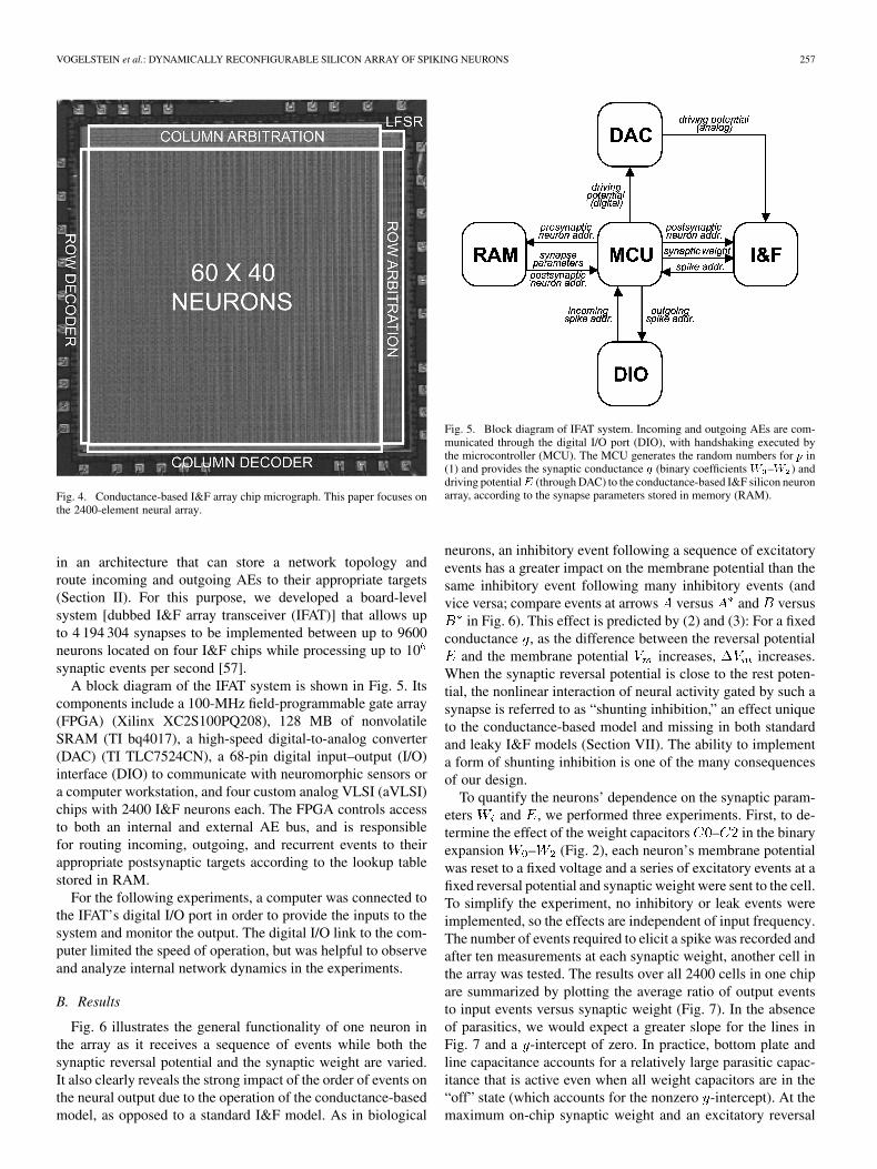
VOGELSTEIN et al.: DYNAMICALLY RECONFIGURABLE SILICON ARRAY OF SPIKING NEURONS 257
Fig. 4. Conductance-based I&F array chip micrograph. This paper focuses onthe 2400-element neural array.
in an architecture that can store a network topology androute incoming and outgoing AEs to their appropriate targets(Section II). For this purpose, we developed a board-levelsystem [dubbed I&F array transceiver (IFAT)] that allows upto 4 194 304 synapses to be implemented between up to 9600neurons located on four I&F chips while processing up to 10synaptic events per second [57].
A block diagram of the IFAT system is shown in Fig. 5. Itscomponents include a 100-MHz field-programmable gate array(FPGA) (Xilinx XC2S100PQ208), 128 MB of nonvolatileSRAM (TI bq4017), a high-speed digital-to-analog converter(DAC) (TI TLC7524CN), a 68-pin digital input–output (I/O)interface (DIO) to communicate with neuromorphic sensors ora computer workstation, and four custom analog VLSI (aVLSI)chips with 2400 I&F neurons each. The FPGA controls accessto both an internal and external AE bus, and is responsiblefor routing incoming, outgoing, and recurrent events to theirappropriate postsynaptic targets according to the lookup tablestored in RAM.
For the following experiments, a computer was connected tothe IFAT’s digital I/O port in order to provide the inputs to thesystem and monitor the output. The digital I/O link to the com-puter limited the speed of operation, but was helpful to observeand analyze internal network dynamics in the experiments.
B. Results
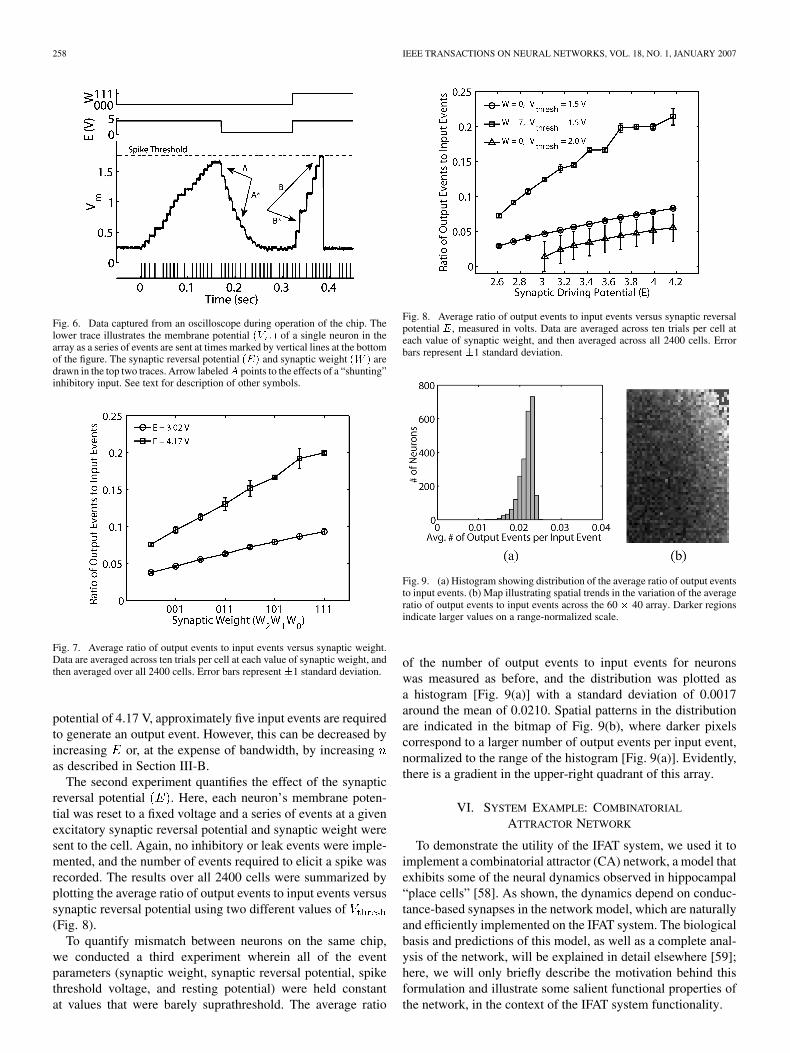
Fig. 6 illustrates the general functionality of one neuron inthe array as it receives a sequence of events while both thesynaptic reversal potential and the synaptic weight are varied.It also clearly reveals the strong impact of the order of events onthe neural output due to the operation of the conductance-basedmodel, as opposed to a standard I&F model. As in biological
Fig. 5. Block diagram of IFAT system. Incoming and outgoing AEs are com-municated through the digital I/O port (DIO), with handshaking executed bythe microcontroller (MCU). The MCU generates the random numbers for p in(1) and provides the synaptic conductance g (binary coefficients W –W ) anddriving potentialE (through DAC) to the conductance-based I&F silicon neuronarray, according to the synapse parameters stored in memory (RAM).
neurons, an inhibitory event following a sequence of excitatoryevents has a greater impact on the membrane potential than thesame inhibitory event following many inhibitory events (andvice versa; compare events at arrows versus and versus
in Fig. 6). This effect is predicted by (2) and (3): For a fixedconductance , as the difference between the reversal potential
and the membrane potential increases, increases.When the synaptic reversal potential is close to the rest poten-tial, the nonlinear interaction of neural activity gated by such asynapse is referred to as “shunting inhibition,” an effect uniqueto the conductance-based model and missing in both standardand leaky I&F models (Section VII). The ability to implementa form of shunting inhibition is one of the many consequencesof our design.
To quantify the neurons’ dependence on the synaptic param-eters and , we performed three experiments. First, to de-termine the effect of the weight capacitors – in the binaryexpansion – (Fig. 2), each neuron’s membrane potentialwas reset to a fixed voltage and a series of excitatory events at afixed reversal potential and synaptic weight were sent to the cell.To simplify the experiment, no inhibitory or leak events wereimplemented, so the effects are independent of input frequency.The number of events required to elicit a spike was recorded andafter ten measurements at each synaptic weight, another cell inthe array was tested. The results over all 2400 cells in one chipare summarized by plotting the average ratio of output eventsto input events versus synaptic weight (Fig. 7). In the absenceof parasitics, we would expect a greater slope for the lines inFig. 7 and a -intercept of zero. In practice, bottom plate andline capacitance accounts for a relatively large parasitic capac-itance that is active even when all weight capacitors are in the“off” state (which accounts for the nonzero -intercept). At themaximum on-chip synaptic weight and an excitatory reversal
258 IEEE TRANSACTIONS ON NEURAL NETWORKS, VOL. 18, NO. 1, JANUARY 2007
Fig. 6. Data captured from an oscilloscope during operation of the chip. Thelower trace illustrates the membrane potential (V ) of a single neuron in thearray as a series of events are sent at times marked by vertical lines at the bottomof the figure. The synaptic reversal potential (E) and synaptic weight (W ) aredrawn in the top two traces. Arrow labeledA points to the effects of a “shunting”inhibitory input. See text for description of other symbols.
Fig. 7. Average ratio of output events to input events versus synaptic weight.Data are averaged across ten trials per cell at each value of synaptic weight, andthen averaged over all 2400 cells. Error bars represent�1 standard deviation.
potential of 4.17 V, approximately five input events are requiredto generate an output event. However, this can be decreased byincreasing or, at the expense of bandwidth, by increasingas described in Section III-B.
The second experiment quantifies the effect of the synapticreversal potential . Here, each neuron’s membrane poten-tial was reset to a fixed voltage and a series of events at a givenexcitatory synaptic reversal potential and synaptic weight weresent to the cell. Again, no inhibitory or leak events were imple-mented, and the number of events required to elicit a spike wasrecorded. The results over all 2400 cells were summarized byplotting the average ratio of output events to input events versussynaptic reversal potential using two different values of(Fig. 8).
To quantify mismatch between neurons on the same chip,we conducted a third experiment wherein all of the eventparameters (synaptic weight, synaptic reversal potential, spikethreshold voltage, and resting potential) were held constantat values that were barely suprathreshold. The average ratio
Fig. 8. Average ratio of output events to input events versus synaptic reversalpotential E, measured in volts. Data are averaged across ten trials per cell ateach value of synaptic weight, and then averaged across all 2400 cells. Errorbars represent �1 standard deviation.
Fig. 9. (a) Histogram showing distribution of the average ratio of output eventsto input events. (b) Map illustrating spatial trends in the variation of the averageratio of output events to input events across the 60 � 40 array. Darker regionsindicate larger values on a range-normalized scale.
of the number of output events to input events for neuronswas measured as before, and the distribution was plotted asa histogram [Fig. 9(a)] with a standard deviation of 0.0017around the mean of 0.0210. Spatial patterns in the distributionare indicated in the bitmap of Fig. 9(b), where darker pixelscorrespond to a larger number of output events per input event,normalized to the range of the histogram [Fig. 9(a)]. Evidently,there is a gradient in the upper-right quadrant of this array.
VI. SYSTEM EXAMPLE: COMBINATORIAL
ATTRACTOR NETWORK
To demonstrate the utility of the IFAT system, we used it toimplement a combinatorial attractor (CA) network, a model thatexhibits some of the neural dynamics observed in hippocampal“place cells” [58]. As shown, the dynamics depend on conduc-tance-based synapses in the network model, which are naturallyand efficiently implemented on the IFAT system. The biologicalbasis and predictions of this model, as well as a complete anal-ysis of the network, will be explained in detail elsewhere [59];here, we will only briefly describe the motivation behind thisformulation and illustrate some salient functional properties ofthe network, in the context of the IFAT system functionality.
VOGELSTEIN et al.: DYNAMICALLY RECONFIGURABLE SILICON ARRAY OF SPIKING NEURONS 259
A. Biological Motivation
Hippocampal place cells are pyramidal neurons found inlayers CA1 and CA3 of the rat hippocampus. They are notablefor being active only when the rat is in a few particular locationsin space [60], [61]. In experimental settings, it has been shownthat as a rat traverses a closed room, its instantaneous positioncan be uniquely identified by decoding the activity vector froman ensemble of place cells [62]. Moreover, this activity vectorpersists even after all sensory and motor clues are extinguished,as long as the rat remains in a fixed location [63], [64]. This hasled to the notion that the rat hippocampus stores a virtual mapof space as an attractor network, wherein the present locationis represented as a stable “bump” of neural activity [65], [66].
Rat hippocampal activity within a closed room is similar tothat predicted by a two-dimensional (2-D) “plane attractor,”where a stable activity bump can move smoothly between lo-cations on the plane [67]. Exposing the rat to multiple differentrooms leads to the formation of different planar maps. The CAnetwork model allows for continuity between all states (similarto multidimensional attractors), and allows each neuron toparticipate in multiple nonadjacent attractors (similar to themultichart model [67]). It also provides for smooth transitionsbetween stable states in different maps, as well as for “partialremapping.”
The primary biological constraints on the CA network arethat it functions with spiking excitation and inhibition, and thatneurons must fire at realistic rates, i.e., neurons within a stablebump should not be maximally activated. In Section VI-B, theconstruction and operation of a CA network are described quan-titatively, and its operation is illustrated by examples of a CAnetwork implemented on the IFAT hardware in Section VI-C.
B. Network Architecture
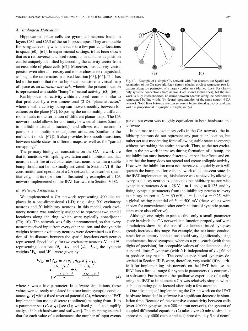
We implemented a CA network representing 400 distinctplaces in a one-dimensional (1-D) ring using 200 excitatoryneurons and 20 inhibitory neurons. In this model, each exci-tatory neuron was randomly assigned to represent two spatiallocations along the ring, which were typically nonadjacent(Fig. 10). The network was fully interconnected, so that everyneuron received input from every other neuron, and the synapticweights between excitatory neurons were determined as a func-tion of the distance between the spatial locations each neuronrepresented. Specifically, for two excitatory neurons andrepresenting locations and , the synapticweights and were given by
(4)
where was a free parameter. In software simulations, thesevalues were directly translated into maximum synaptic conduc-tances with a fixed reversal potential (2), whereas the IFATimplementation used a discrete (nonlinear) mapping from toa parameter set [see (1); we fixed 1 to simplifyanalysis in both hardware and software]. This mapping ensuredthat for each value of conductance, the number of input events
Fig. 10. Example of a simple CA network with four neurons. (a) Spatial rep-resentation of the CA network. Each neuron (shaded circles) represents two lo-cations along the perimeter of a large circular area (dashed line). For clarity,only synaptic connections from neuron 4 are shown (solid lines), but the net-work is fully interconnected. Distance between neurons along the perimeter isrepresented by line width. (b) Neural representation of the same neuron 4 CAnetwork. Solid lines between neurons represent bidirectional synapses, and linewidth is proportional to synaptic strength; see (4).
per output event was roughly equivalent in both hardware andsoftware.
In contrast to the excitatory cells in the CA network, the in-hibitory neurons do not represent any particular location, butrather act as a moderating force allowing stable states to emergewithout overtaking the entire network. Thus, as the net excita-tion in the network increases during formation of a bump, thenet inhibition must increase faster to dampen the effects and en-sure that the bump does not spread and create epileptic activity.However, the inhibition must not increase too quickly or it willquench the bump and force the network to a quiescent state. Inthe IFAT implementation, this balance was achieved by allowingevery excitatory neuron to connect to the inhibitory neuron withsynaptic parameters 4.28 V, 1, and 0.125, and byfixing synaptic parameters from the inhibitory neuron to everyexcitatory neuron at 60 mV, 1, and 0.25, witha global resting potential of 500 mV (these values werechosen for convenience; other combinations of synaptic param-eters were also effective).
Although one might expect to find only a small parameterspace in which the CA network can function properly, softwaresimulations show that the use of conductance-based synapsesgreatly increases this range. For example, the maximum conduc-tance for excitatory connections could vary significantly usingconductance-based synapses, whereas a grid search (with threedigits of precision) for acceptable values of conductance usingstandard “linear” synapses (with independent of ) failedto produce any results. The conductance-based synapses de-scribed in Section III-B were, therefore, very useful (if not crit-ical) for implementing this network on the IFAT, because theIFAT has a limited range for synaptic parameters (as comparedto software). Furthermore, the qualitative experience of config-uring the IFAT to implement a CA was relatively simple, with astable operating point located after only a few attempts.
One advantage of implementing the CA network on the IFAThardware instead of in software is a significant decrease in simu-lation time. Because of the extensive connectivity between cells(over 40 000 synapses in a 200-neuron network), the system ofcoupled differential equations (2) takes over 40 min to simulateapproximately 4000 output spikes (approximately 5 s of neural
260 IEEE TRANSACTIONS ON NEURAL NETWORKS, VOL. 18, NO. 1, JANUARY 2007
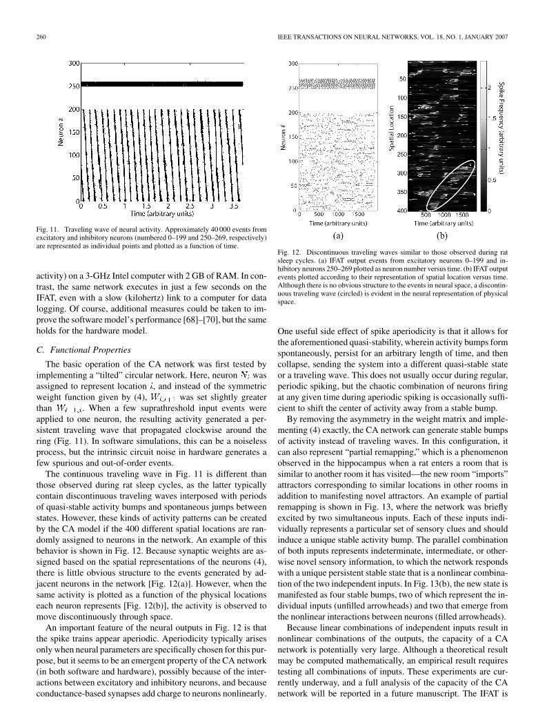
Fig. 11. Traveling wave of neural activity. Approximately 40 000 events fromexcitatory and inhibitory neurons (numbered 0–199 and 250–269, respectively)are represented as individual points and plotted as a function of time.
activity) on a 3-GHz Intel computer with 2 GB of RAM. In con-trast, the same network executes in just a few seconds on theIFAT, even with a slow (kilohertz) link to a computer for datalogging. Of course, additional measures could be taken to im-prove the software model’s performance [68]–[70], but the sameholds for the hardware model.
C. Functional Properties
The basic operation of the CA network was first tested byimplementing a “tilted” circular network. Here, neuron wasassigned to represent location , and instead of the symmetricweight function given by (4), was set slightly greaterthan . When a few suprathreshold input events wereapplied to one neuron, the resulting activity generated a per-sistent traveling wave that propagated clockwise around thering (Fig. 11). In software simulations, this can be a noiselessprocess, but the intrinsic circuit noise in hardware generates afew spurious and out-of-order events.
The continuous traveling wave in Fig. 11 is different thanthose observed during rat sleep cycles, as the latter typicallycontain discontinuous traveling waves interposed with periodsof quasi-stable activity bumps and spontaneous jumps betweenstates. However, these kinds of activity patterns can be createdby the CA model if the 400 different spatial locations are ran-domly assigned to neurons in the network. An example of thisbehavior is shown in Fig. 12. Because synaptic weights are as-signed based on the spatial representations of the neurons (4),there is little obvious structure to the events generated by ad-jacent neurons in the network [Fig. 12(a)]. However, when thesame activity is plotted as a function of the physical locationseach neuron represents [Fig. 12(b)], the activity is observed tomove discontinuously through space.
An important feature of the neural outputs in Fig. 12 is thatthe spike trains appear aperiodic. Aperiodicity typically arisesonly when neural parameters are specifically chosen for this pur-pose, but it seems to be an emergent property of the CA network(in both software and hardware), possibly because of the inter-actions between excitatory and inhibitory neurons, and becauseconductance-based synapses add charge to neurons nonlinearly.
Fig. 12. Discontinuous traveling waves similar to those observed during ratsleep cycles. (a) IFAT output events from excitatory neurons 0–199 and in-hibitory neurons 250–269 plotted as neuron number versus time. (b) IFAT outputevents plotted according to their representation of spatial location versus time.Although there is no obvious structure to the events in neural space, a discontin-uous traveling wave (circled) is evident in the neural representation of physicalspace.
One useful side effect of spike aperiodicity is that it allows forthe aforementioned quasi-stability, wherein activity bumps formspontaneously, persist for an arbitrary length of time, and thencollapse, sending the system into a different quasi-stable stateor a traveling wave. This does not usually occur during regular,periodic spiking, but the chaotic combination of neurons firingat any given time during aperiodic spiking is occasionally suffi-cient to shift the center of activity away from a stable bump.
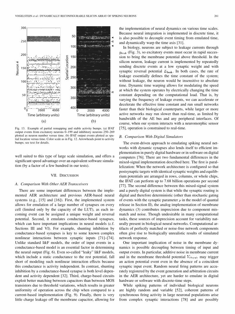
By removing the asymmetry in the weight matrix and imple-menting (4) exactly, the CA network can generate stable bumpsof activity instead of traveling waves. In this configuration, itcan also represent “partial remapping,” which is a phenomenonobserved in the hippocampus when a rat enters a room that issimilar to another room it has visited—the new room “imports”attractors corresponding to similar locations in other rooms inaddition to manifesting novel attractors. An example of partialremapping is shown in Fig. 13, where the network was brieflyexcited by two simultaneous inputs. Each of these inputs indi-vidually represents a particular set of sensory clues and shouldinduce a unique stable activity bump. The parallel combinationof both inputs represents indeterminate, intermediate, or other-wise novel sensory information, to which the network respondswith a unique persistent stable state that is a nonlinear combina-tion of the two independent inputs. In Fig. 13(b), the new state ismanifested as four stable bumps, two of which represent the in-dividual inputs (unfilled arrowheads) and two that emerge fromthe nonlinear interactions between neurons (filled arrowheads).
Because linear combinations of independent inputs result innonlinear combinations of the outputs, the capacity of a CAnetwork is potentially very large. Although a theoretical resultmay be computed mathematically, an empirical result requirestesting all combinations of inputs. These experiments are cur-rently underway, and a full analysis of the capacity of the CAnetwork will be reported in a future manuscript. The IFAT is
VOGELSTEIN et al.: DYNAMICALLY RECONFIGURABLE SILICON ARRAY OF SPIKING NEURONS 261
Fig. 13. Example of partial remapping and stable activity bumps. (a) IFAToutput events from excitatory neurons 0–199 and inhibitory neurons 250–269plotted as neuron number versus time. (b) IFAT output events plotted as spa-tial location versus time. Color scale as in Fig. 12. Arrowheads point to activitybumps; see text for details.
well suited to this type of large scale simulation, and offers asignificant speed advantage over an equivalent software simula-tion (by a factor of a few hundred in our tests).
VII. DISCUSSION
A. Comparison With Other AER Transceivers
There are some important differences between the imple-mented AER architecture and previous AER-based neuralsystems (e.g., [15] and [16]). First, the implemented systemallows for emulation of a large number of synapses on everycell (limited only by the capacity of the LUT), as each in-coming event can be assigned a unique weight and reversalpotential. Second, it emulates conductance-based synapses,which can have important implications in neural models (c.f.Sections III and VI). For example, shunting inhibition byconductance-based synapses is key to some known complexnonlinear interactions between synaptic inputs [71]–[74].Unlike standard I&F models, the order of input events in aconductance-based model is an essential factor in determiningthe neural output (Fig. 6). Even so-called “leaky” I&F models,which include a static conductance to the rest potential, fallshort of modeling such nonlinear interaction effects becausethis conductance is activity independent. In contrast, shuntinginhibition by a conductance-based synapse is both level depen-dent and activity dependent [32]. Third, charge-based circuitsexploit better matching between capacitors than between MOStransistors due to threshold variations, which results in greateruniformity of operation across the chip when compared to acurrent-based implementation (Fig. 9). Finally, there is verylittle charge leakage off the membrane capacitor, allowing for
the implementation of neural dynamics on various time scales.Because neural integration is implemented in discrete time, itis also possible to decouple event timing from emulated time,and dynamically warp the time axis [31].
In biology, neurons are subject to leakage currents through(Fig. 3), so excitatory events must occur in rapid succes-
sion to bring the membrane potential above threshold. In thesilicon neuron, leakage current is implemented by repeatedlysending discrete events at a low synaptic weight and withsynaptic reversal potential . In both cases, the rate ofleakage essentially defines the time constant of the system;without leakage, the neuron would be insensitive to absolutetime. Dynamic time warping allows for modulating the speedat which the system operates by electrically changing the timeconstant depending on the computational load. That is, byvarying the frequency of leakage events, we can accelerate ordecelerate the effective time constant and run small networksfaster than their biological counterparts, while larger or moreactive networks may run slower than real-time, as limited bybandwidth of the AE bus and any peripheral interfaces. Ofcourse, when our system interacts with a neuromorphic sensor[75], operation is constrained to real-time.
B. Comparison With Digital Simulators
The event-driven approach to emulating spiking neural net-works with dynamic synapses also lends itself to efficient im-plementation in purely digital hardware or in software on digitalcomputers [76]. There are two fundamental differences in themixed-signal implementation described here. The first is paral-lelization: When the network architecture is configured so thatpostsynaptic targets with identical synaptic weights and equilib-rium potentials are arranged in rows, columns, or whole chips,the IFAT can perform up to 7.68 billion operations per second[77]. The second difference between this mixed-signal systemand a purely digital system is that while the synaptic routing isdigital and therefore deterministic (other than stochastic gatingof events with the synaptic parameter in the model of quantalrelease in Section II), the analog implementation of membranedynamics (3) contributes imprecision due to component mis-match and noise. Though undesirable in many computationaltasks, these sources of imprecision account for variability nat-urally present in biological neural networks. Computational ar-tifacts of perfectly matched or noise-free network componentsoften give rise to biologically unrealistic results of simulatednetwork response.
One important implication of noise in the membrane dy-namics is possible decoupling between timing of input andoutput events. In particular, additive noise in membrane currentand in the membrane threshold potential may triggeran action potential event even in the absence of a coincidentsynaptic input event. Random neural firing patterns are accu-rately registered by the event generation and arbitration circuitsin the AER architecture, yet are harder to emulate in digitalhardware or software with discrete-time steps.
While spiking patterns of individual biological neuronsare highly random and variable [52], coherent patterns ofsynchronous firing activity in large neuronal populations arisefrom complex synaptic interactions [78] and are possibly
262 IEEE TRANSACTIONS ON NEURAL NETWORKS, VOL. 18, NO. 1, JANUARY 2007
modulated by attention-driven mechanisms [79]. Externallysupplied additive noise on the terminal could emulatesome important functionality in modulating activity-dependentsynchronicity otherwise lost in a deterministic implementationof the conductance-based I&F model.
Even though the event-driven approach to neural emulationis inherently sequential, it can be extended to a parallel archi-tecture in which multiple neurons and/or multiple synapses areserviced at any given time. Partitioning of the neural network ar-chitecture over multiple processors in a computer network hasbeen shown to deliver a linear increase in throughput, up to2 10 synaptic events per second per processor node in amodern PC cluster [70]. Similar improvements in throughputcan be attained, in principle, in the mixed-signal architecture bypartitioning the neural network over multiple AER processingnodes, each with local IFAT transceivers and LUT memory, andwith asynchronously pipelined message parsing between pro-cessing nodes [55]. Extending pipelining at all levels of the ar-chitecture could allow throughputs on the order of 10 eventsper second per AER node, limited by current read access ratesof DRAM memory.
C. Address-Domain Learning
The IFAT architecture is well suited for implementingsynaptic plasticity in the “address-domain” because the MCUmonitors both the incoming and outgoing synaptic events andhas read/write access to the synaptic parameters stored in RAM.In this context, plasticity only requires modifying the LUTin response to particular sequences of events. An additionalcomponent of learning in biological systems is the creationor elimination of synapses—on the IFAT, this is achieved byinserting or deleting entries in RAM. Like address-domainconnectivity, the advantage of address-domain plasticity isthat the constituents of the implemented learning rule are notconstrained to be local in space or time. Various forms oflearning algorithms can be mapped onto the same architectureby reconfiguring the MCU interfacing the IFAT and the LUT.
The IFAT can implement basic forms of Hebbian learning,including spike-timing dependent plasticity (STDP) [80], withvery little processing overhead [31]. STDP-based learning rulesspecify changes in synaptic strength depending on the time in-terval between each pair of presynaptic and postsynaptic events.An STDP synaptic modification rule can be implemented in theaddress-domain by augmenting the AER architecture with twoevent queues, one each for presynaptic and postsynaptic events,and with a counter that is incremented every time a global decayevent occurs (this sets the time constant of the system). Forevery presynaptic event, the sender’s address is entered into aqueue with an associated timestamp. A postsynaptic event thentriggers a sequence of synaptic updates by iterating backwardthrough the queue to find the causal spikes, locating the appro-priate synaptic weights in the LUT, and increasing those valuesby an amount based on the timestamps. Anticausal events re-quire an equivalent set of operations, matching each incomingpresynaptic spike with a second queue of postsynaptic events.Depending on the size of the network and the rate of learning,the weight updates can occupy a large fraction of the MCU’sresources, but because these operations are independent of the
silicon neurons and AER bus, they can be executed more quicklywith faster components.
VIII. CONCLUSION
The conductance-based I&F array chip provides a solutionfor creating large scale networks of silicon neurons with arbi-trary connectivity and reprogrammability. When combined withthe other hardware in the IFAT system, it is a powerful tool forsimulating cortical circuits. In general, the IFAT has been de-signed for reconfigurability and ease of use (e.g., implementinga new network only requires downloading a table of synapticvalues to the RAM) rather than speed or throughput. To date, thesystem has been used to detect salience in a visual image [57],spatially modulate a visual image [81], detect spatially orientedchanges in visual contrast in real time [75], compute a nonlinearpooling function similar to winner-take-all [77], and implementa model of attractor dynamics and waves of neural activity in rathippocampus (Section VI). Future work will focus on increasingthe breadth of applications to include sensory modalities otherthan vision and more complex cortical models.
APPENDIX
DERIVATION OF DISCRETE-TIME MEMBRANE EQUATION
Equation (3) is derived using simple switched-capacitor anal-ysis techniques. At the end of a previous update , switches
and (Fig. 2) are open and charge is stored on themembrane capacitor in proportion to the membrane poten-tial
(5)
When the next input event arrives, switch is closed first,and charge is stored across the active weight capacitors
– in proportion to the synaptic reversal potential
(6)
Switch is then opened, and switch is closed, sharingcharge between the weight and membrane capacitors. The totalcharge is simply the sum of the two stored charges, andthe resulting voltage is proportional to the total charge and thetotal capacitance
(7)
(8)
Rearranging terms, and using (5)–(7) in (8), we obtain
(9)
which yields (3) with the following definition of terms:
VOGELSTEIN et al.: DYNAMICALLY RECONFIGURABLE SILICON ARRAY OF SPIKING NEURONS 263
The membrane potential thus updated, switch is opened, andthe synapse is ready to process another event.
ACKNOWLEDGMENT
The authors would like to thank K. Zhang for supervisingJ. T. Vogelstein’s work on the CA model.
REFERENCES
[1] C. Mead, Analog VLSI and Neural Systems. Reading, MA: Addison-Wesley, 1989.
[2] T. Lande, Ed., Neuromorphic Systems Engineering—Neural Networksin Silicon. Norwell, MA: Kluwer, 1998.
[3] C. Koch and H. Li, Eds., Vision Chips: Implementing Vision Algorithmswith Analog VLSI Circuits. Los Alamitos, CA: IEEE Computer Press,1995.
[4] A. van Schaik, E. Fragniere, and E. Vittoz, “Improved siliconcochlea using compatible lateral bipolar transistors,” in Advances inNeural Information Processing Systems, D. Touretzky, M. Mozer,and M. Hasselmo, Eds. Cambridge, MA: MIT Press, 1996, vol.8, pp. 671–677.
[5] N. Kumar, W. Himmelbauer, G. Cauwenberghs, and A. Andreou, “Ananalog VLSI chip with asynchronous interface for auditory feature ex-traction,” IEEE Trans. Circuits Syst. II, vol. 45, no. 5, pp. 600–606,May 1998.
[6] K. A. Zaghloul and K. Boahen, “Optic nerve signals in a neuromorphicchip II: Testing and results,” IEEE Trans. Biomed. Eng., vol. 51, no. 4,pp. 667–675, Apr. 2004.
[7] S. Kameda and T. Yagi, “An analog silicon retina with multichip con-figuration,” IEEE Trans. Neural Netw., vol. 17, no. 1, pp. 197–210, Jan.2006.
[8] T. Y. W. Choi, B. E. Shi, and K. A. Boahen, “An ON-OFF orientationselective address event representation image transceiver chip,” IEEETrans. Circuits Syst. I: Reg. Papers, vol. 51, no. 2, pp. 342–353, Feb.2004.
[9] M. Mahowald, An Analog VLSI System for Stereoscopic Vi-sion. Boston, MA: Kluwer, 1994.
[10] M. Sivilotti, “Wiring considerations in analog VLSI systems with ap-plication to field-programmable networks,” Ph.D. dissertation, Cali-fornia Inst. Technol., Pasadena, CA, 1991.
[11] J. Lazzaro, J. Wawrzynek, M. Mahowald, M. Sivilotti, and D. Gillespie,“Silicon auditory processors as computer peripherals,” IEEE Trans.Neural Netw., vol. 4, no. 3, pp. 523–528, May 1993.
[12] K. A. Boahen, “Point-to-point connectivity between neuromorphicchips using address events,” IEEE Trans. Circuits Syst.s II, vol. 47, no.5, pp. 416–434, May 2000.
[13] C. M. Higgins and C. Koch, “Multi-chip neuromorphic motion pro-cessing,” in Proc. 20th Anniversary Conf. Adv. Res. VLSI, D. S. Willsand S. P. DeWeerth, Eds., Los Alamitos, CA, 1999, pp. 309–323.
[14] S.-C. Liu, J. Kramer, G. Indiveri, T. Delbrück, and R. Douglas, “Orien-tation-selective aVLSI spiking neurons,” in Advances in Neural Infor-mation Processing Systems, T. G. Dietterich, S. Becker, and Z. Ghahra-mani, Eds. Cambridge, MA: MIT Press, 2002, vol. 14.
[15] G. Indiveri, E. Chicca, and R. J. Douglas, “A VLSI reconfigurablenetwork of integrate-and-fire neurons with spike-based learningsynapses,” in Proc. Euro. Symp. Artif. Neural Netw., 2004, pp.405–410.
[16] D. H. Goldberg, G. Cauwenberghs, and A. G. Andreou, “Proba-bilistic synaptic weighting in a reconfigurable network of VLSIintegrate-and-fire neurons,” Neural Netw., vol. 14, no. 6–7, pp.781–793, 2001.
[17] S. R. Deiss, R. J. Douglas, and A. M. Whatley, “A pulse-coded commu-nications infrastructure for neuromorphic systems,” in Pulsed NeuralNetworks, W. Maass and C. M. Bishop, Eds. Cambridge, MA: MITPress, 1999, ch. 6, pp. 157–178.
[18] P. Häfliger, “Asynchronous event redirecting in bio-inspired communi-cation,” in Proc. IEEE Int. Conf. Electr., Circuits Syst., Sep. 2001, pp.87–90.
[19] R. J. Vogelstein, U. Mallik, and G. Cauwenberghs, “Silicon spike-basedsynaptic array and address-event transceiver,” in Proc. IEEE Int.Symp. Circuits Syst., Vancouver, BC, Canada, 2004, vol. 5, pp.385–388.
[20] W. Maass and C. M. Bishop, Eds., Pulsed Neural Networks. Cam-bridge, MA: MIT Press, 1999.
[21] A. Bofill-i-Petit and A. F. Murray, “Synchrony detection by analogueVLSI neurons with bimodal STDP synapses,” in Advances in NeuralInformation Processing Systems, S. Thrun, L. Saul, and B. Schölkopf,Eds. Cambridge, MA: MIT Press, 2004, vol. 16.
[22] J. Arthur and K. Boahen, “Learning in silicon: timing is everything,”in Advances in Neural Information Processing Systems, Y. Weiss, B.Schölkopf, and J. Platt, Eds. Cambridge, MA: MIT Press, 2006, vol.18, pp. 75–82.
[23] G. Indiveri, “Neuromorphic bistable VLSI synapses with spike-timing-dependent plasticity,” in Advances in Neural Information ProcessingSystems, S. Becker, S. Thrun, and K. Obermayer, Eds. Cambridge,MA: MIT Press, 2003, vol. 15, pp. 1115–1122.
[24] B. Taba and K. A. Boahen, “Topographic map formation by silicongrowth cones,” in Advances in Neural Information Processing Systems,S. T. S. Becker and K. Obermayer, Eds. Cambridge, MA: MIT Press,2003, vol. 15, pp. 1139–1146.
[25] J. V. Arthur and K. A. Boahen, “Recurrently connected silicon neuronswith active dendrites for one-shot learning,” in Proc. IEEE Int. JointConf. Neural Netw., 2004, vol. 3, pp. 1699–1704.
[26] T. Horiuchi and K. Hynna, “Spike-based VLSI modeling of the ILDsystem in the echolocating bat,” Neural Netw., vol. 14, pp. 755–762,2001.
[27] R. Paz, F. Gomez-Rodriguez, M. Rodriguez, A. Linares-Barranco,G. Jimenez, and A. Civit, “Test infrastructure for address-event-rep-resentation communications,” in Lecture Notes in Computer Sci-ence. Berlin, Germany: Springer-Verlag, 2005, vol. 3512, pp.518–526.
[28] H. K. Riis and P. Häfliger, “An asynchronous 4-to-4 AER mapper,”Lecture Notes Comput. Sci., vol. 3512, pp. 494–501, 2005.
[29] Q. Zou, Y. Bornat, J. Tomas, S. Renaud, and A. Destexhe, “Real-timesimulations of networks of Hodgkin-Huxley neurons using analog cir-cuits,” Neurocomput., vol. 69, pp. 1137–1140, 2006.
[30] E. Ros, E. M. Ortigosa, R. Agis, R. Carrillo, and M. Arnold, “Real-time computing platform for spiking neurons (RT-spike),” IEEE Trans.Neural Netw., vol. 17, no. 4, pp. 1050–1063, Jul. 2006.
[31] R. J. Vogelstein, F. Tenore, R. Philipp, M. S. Adlerstein, D. H. Gold-berg, and G. Cauwenberghs, “Spike timing-dependent plasticity in theaddress domain,” in Advances in Neural Information Processing Sys-tems, S. Becker, S. Thrun, and K. Obermayer, Eds. Cambridge, MA:MIT Press, 2003, vol. 5.
[32] C. Koch, Biophysics of Computation: Information Processing in SingleNeurons. New York: Oxford Univ. Press, 1999.
[33] M. Mahowald and R. Douglas, “A silicon neuron,” Nature, vol. 354,pp. 515–518, 1991.
[34] S. Saighi, J. Tomas, Y. Bornat, and S. Renaud, “A conductance-basedsilicon neuron with dynamically tunable model parameters,” inProc. 2nd Int. IEEE/EMBS Conf. Neural Eng., 2005, pp. 285–288.
[35] A. Bofill-i-Petit and A. F. Murray, “Learning temporal correlations inbiologically-inspired aVLSI,” in Proc. IEEE Int. Symp. Circuits Syst.,2003, vol. 5, pp. 817–820.
[36] A. van Schaik, E. Fragniere, and E. Vittoz, “A silicon model of am-plitude modulation detection in the auditory brainstem,” in Advancesin Neural Information Processing Systems, M. C. Mozer, M. I. Jordan,and T. Petsche, Eds. Cambridge, MA: MIT Press, 1997, vol. 9, pp.741–750.
[37] M. F. Simoni, G. S. Cymbalyuk, M. E. Sorensen, R. L. Calabrese,and S. P. DeWeerth, “A multiconductance silicon neuron with biolog-ically matched dynamics,” IEEE Trans. Biomed. Eng., vol. 51, no. 2,pp. 342–354, Feb. 2004.
[38] P. Häfliger and C. Rasche, “Floating gate analog memory for parameterand variable storage in a learning silicon neuron,” in Proc. IEEE Int.Symp. Circuits Syst., 1999, vol. 2, pp. 416–419.
[39] J. V. Arthur and K. Boahen, “Silicon neurons that inhibit tosynchronize,” in Proc. IEEE Int. Symp. Circuits Syst., 2006, pp.4807–4810.
[40] G. Indiveri, E. Chicca, and R. Douglas, “A VLSI array of low-powerspiking neurons and bistable synapses with spike-timing dependentplasticity,” IEEE Trans. Neural Netw., vol. 17, no. 1, pp. 211–221, Jan.2006.
[41] P. H. E. Tiesinga, J. V. Jose, and T. J. Sejnowski, “Comparison ofcurrent-driven and conductance-driven neocortical model neurons withHodgkin-Huxley voltage-gated channels,” Phys. Rev. E, vol. 62, no. 6,pp. 8413–8419, 2000.
[42] G. L. Camera, W. Senn, and S. Fusi, “Comparison between networksof conductance- and current-driven neurons: Stationary spike rates andsubthreshold depolarization,” Neurocomput., vol. 58–60, pp. 253–258,2004.
264 IEEE TRANSACTIONS ON NEURAL NETWORKS, VOL. 18, NO. 1, JANUARY 2007
[43] R. Jolivet, A. Rauch, H.-R. Lüscher, and W. Gerstner, “Predicting spiketiming of neocortical pyramidal neurons by simple threshold models,”J. Comput. Neurosci., vol. 21, no. 1, pp. 35–39, 2006.
[44] A. L. Hodgkin and A. F. Huxley, “A quantitative description of mem-brane current and its application to conduction and excitation in nerve,”J. Physiol., vol. 117, pp. 500–544, 1952.
[45] R. Mirollo and S. Strogatz, “Synchronization of pulse-coupled biolog-ical oscillators,” SIAM J. Appl. Math., vol. 50, no. 6, pp. 1645–1662,2000.
[46] F. Tenore, R. Etienne-Cummings, and M. A. Lewis, “Entrainmentof silicon central pattern generators for legged locomotory control,”in Advances in Neural Information Processing Systems, S. Thrun,L. Saul, and B. Schölkopf, Eds. Cambridge, MA: MIT Press,2004, vol. 16.
[47] A. Kumar, S. Rotter, and A. Aertsen, “Propagation of synfire activityin locally connected networks with conductance-based synapses,” pre-sented at the Conf. Comput. Syst. Neurosci. (COSYNE), Salt LakeCity, UT, Mar. 5–8, 2006.
[48] Z. F. Mainen and T. J. Sejnowski, “Reliability of spike timing in neo-cortical neurons,” Science, vol. 268, no. 5216, pp. 1503–1506, 1995.
[49] W. M. Usrey, “The role of spike timing for thalamocortical processing,”Current Opinion Neurobiol., vol. 12, no. 4, pp. 411–417, 2002.
[50] D. Fricker and R. Miles, “Interneurons, spike timing, and perception,”Neuron, vol. 32, no. 5, pp. 771–774, 2001.
[51] M. Abeles, Corticonics: Neural Circuits of the Cerebral Cortex.London, U.K.: Cambridge Univ. Press, 1991.
[52] F. Rieke, D. Warland, R. de Ruyter van Stevenick, and W. Bialek,Spikes: Exploring the Neural Code, 1st ed. Cambridge, MA: MITPress, 1999.
[53] J. G. Elias, “Artificial dendritic trees,” Neural Comput., vol. 5, pp.648–663, 1993.
[54] R. Gregorian and G. C. Temes, Analog MOS Integrated Circuits forSignal Processing. New York: Wiley, 1986.
[55] K. A. Boahen, “A burst-mode word-serial address-event channel—I:transmitter design,” IEEE Trans. Circuits Syst. I, Reg. Papers, vol. 51,no. 7, pp. 1281–1291, Jul. 2004.
[56] R. J. Vogelstein, U. Mallik, and G. Cauwenberghs, manuscript in prepa-ration.
[57] R. J. Vogelstein, U. Mallik, G. Cauwenberghs, E. Culurciello, and R.Etienne-Cummings, “Saliency-driven image acuity modulation on a re-configurable silicon array of spiking neurons,” in Advances in NeuralInformation Processing Systems, L. K. Saul, Y. Weiss, and L. Bottou,Eds. Cambridge, MA: MIT Press, 2005, vol. 17, pp. 1457–1464.
[58] J. T. Vogelstein and K. Zhang, “A novel theory for simultaneous rep-resentation of multiple dynamic states in hippocampus,” in 2004 Ab-stract Viewer/Itinerary Planner. Washington, DC: Society for Neu-roscience, 2004, Program No. 710.1.
[59] J. T. Vogelstein and K. Zhang, manuscript in preparation.[60] J. O’Keefe and J. Dostrovsky, “The hippocampus as a spatial map. Pre-
liminary evidence from unit activity in the freely-moving rat,” BrainRes., vol. 34, no. 1, pp. 171–175, 1971.
[61] J. O’Keefe and L. Nadel, The Hippocampus as a Cognitive Map. NewYork: Oxford Univ. Press, 1978.
[62] K. Zhang, I. Ginzburg, B. L. McNaughton, and T. J. Sejnowski, “Inter-preting neuronal population activity by reconstruction: Unified frame-work with application to hippocampal place cells,” J. Neurophysiol.,vol. 79, pp. 1017–1044, 1998.
[63] E. J. Markus, C. A. Barnes, B. L. McNaughton, V. L. Gladden, and W.E. Skaggs, “Spatial information content and reliability of hippocampalCA1 neurons: Effects of visual input,” Hippocampus, vol. 4, no. 4, pp.410–421, 1994.
[64] E. Save, L. Nerad, and B. Poucet, “Contribution of multiple sensoryinformation to place field stability in hippocampal place cells,” Hip-pocampus, vol. 10, no. 1, pp. 64–76, 2000.
[65] M. Tsodyks and T. Sejnowski, “Associative memory and hippocampalplace cells,” Int. J. Neural Syst., vol. 6, pp. 81–86, 1995.
[66] M. Tsodyks, “Attractor neural network models of spatial maps in hip-pocampus,” Hippocampus, vol. 9, no. 4, pp. 481–489, 1999.
[67] A. Samsonovich and B. L. McNaughton, “Path integration and cogni-tive mapping in a continuous attractor neural network model,” J. Neu-rosci., vol. 17, no. 15, pp. 5900–5920, 1997.
[68] M. Mattia and P. Del Giudice, “Efficient event-driven simulation oflarge networks of spiking neurons and dynamical synapses,” NeuralComput., vol. 12, no. 10, pp. 2305–2329, 2000.
[69] M. Rudolph and A. Destexhe, “Analytical integrate-and-fire neuronmodels with conductance-based dynamics for event-driven simulationstrategies,” Neural Comput., vol. 18, no. 9, pp. 2146–2210, 2006.
[70] A. Morrison, C. Mehring, T. Geisel, A. D. Aertsen, and M. Diesmann,“Advancing the boundaries of high-connectivity network simulationwith distributed computing,” Neural Comput., vol. 17, no. 8, pp.1776–1801, 2005.
[71] V. Torre and T. Poggio, “A synaptic mechanism possibly underlyingdirectional selectivity to motion,” Proc. Roy. Soc. London. Ser. B, vol.202, pp. 409–416, 1978.
[72] C. Koch, T. Poggio, and V. Torre, “Retinal ganglion cells: A functionalinterpretation of dendritic morphology,” Proc. Roy. Soc. London. Ser.B, vol. 298, pp. 227–264, 1982.
[73] M. Carandini and D. J. Heeger, “Summation and division by neuronsin primate visual cortex,” Science, vol. 264, pp. 1333–1336, 1994.
[74] M. E. Nelson, “A mechanism for neuronal gain control by descendingpathways,” Neural Comput., vol. 6, pp. 242–254, 1994.
[75] U. Mallik, R. J. Vogelstein, E. Culurciello, R. Etienne-Cummings, andG. Cauwenberghs, “A real-time spike-domain sensory information pro-cessing system,” in Proc. IEEE Int. Symp. Circuits Syst., Kobe, Japan,2005, pp. 1919–1922.
[76] M. Mattia and P. D. Giudice, “Efficient event-driven simulation oflarge networks of spiking neurons and dynamical synapses,” NeuralComput., vol. 12, no. 10, pp. 2305–2329, 2000.
[77] R. J. Vogelstein, U. Mallik, E. Culurciello, G. Cauwenberghs, andR. Etienne-Cummings, “A multi-chip neuromorphic system forspike-based visual information processing ,” , 2006, submitted forpublication.
[78] E. Salinas and T. J. Sejnowski, “Integrate-and-fire neurons drivenby correlated stochastic input,” Neural Comput., vol. 14, no. 9, pp.2111–2155, 2002.
[79] A. K. Engel, P. Fries, and W. Singer, “Dynamic predictions: oscilla-tions and synchrony in top-down processing,” Nature Rev. Neurosci.,vol. 2, pp. 704–716, 2001.
[80] S. Song, K. D. Miller, and L. F. Abbott, “Competitive Hebbian learningthrough spike-timing-dependent synaptic plasticity,” Nature Neurosci.,vol. 3, no. 9, pp. 919–926, 2000.
[81] R. J. Vogelstein, U. Mallik, and G. Cauwenberghs, “Spatial acuity mod-ulation of an address-event imager,” in Proc. IEEE Int. Conf. Electron.,Circuits Syst., Tel Aviv, Israel, 2004, pp. 207–210.
R. Jacob Vogelstein (S’99) received the Sc.B. degreein bioelectrical engineering from Brown University,Providence, RI, in 2000 and he is currently workingtowards the Ph.D. degree in biomedical engineeringat The Johns Hopkins University, Baltimore, MD.
His research focuses on neuromorphic and neuro-prosthetic devices, and his papers have been finalistsin the student paper competitions at the 2004 IEEEInternational Conference of the Engineering inMedicine and Biology Society and the 2004 IEEEInternational Conference on Electronics, Circuits
and Systems.Mr. Vogelstein was inducted into the Tau Beta Pi and Sigma Xi honor soci-
eties in 1999, won the Brown University Engineering Department’s OutstandingStudent Award in 2000, and received a National Science Foundation GraduateResearch Fellowship in 2002.
Udayan Mallik received the B.S. degree in electricalengineering from The Johns Hopkins University, Bal-timore, MD, in 2003.
He is presently with Goddard Space Flight Center,NASA, Greenbelt, MD.

VOGELSTEIN et al.: DYNAMICALLY RECONFIGURABLE SILICON ARRAY OF SPIKING NEURONS 265
Joshua T. Vogelstein was born in Baltimore, MD,on February 16, 1980. He received the B.S. degreein biomedical engineering from Washington Univer-sity, St. Louis, MO, in 2002 and is currently workingtowards the Ph.D. degree at the Department of Neu-roscience, The Johns Hopkins University, Baltimore,MD.
He is the author of several peer-reviewed scientificpublications, and has presented his work at severalconferences. His current research interests includetwo-photon microscopy, models of memory, neural
systems identificaton, sensory coding, and neural plasticity.
Gert Cauwenberghs (S’89–M’94–SM’04) receivedthe Ph.D. degree in electrical engineering from Cali-fornia Institute of Technology, Pasadena, in 1994.
He was a Professor of Electrical and ComputerEngineering at The Johns Hopkins University, Balti-more, MD. He joined the University of California atSan Diego, La Jolla, as a Professor of Neurobiology,in 2005. His research interests are in advancingsilicon adaptive microsystems to the understandingof biological neural systems, and development ofsensory and neural prostheses and brain–machine
interfaces.Dr. Cauwenberghs received the National Science Foundation (NSF) Career
Award in 1997, the Office of Naval Research (ONR) Young Investigator Awardin 1999, and Presidential Early Career Award for Scientists and Engineers in2000. He is an Associate Editor of IEEE TRANSACTIONS ON CIRCUITS AND
SYSTEMS I, IEEE TRANSACTIONS ON NEURAL SYSTEMS AND REHABILITATION
ENGINEERING, and IEEE SENSORS JOURNAL.


