Embed Size (px)
Citation preview

HAL Id: hal-03260311https://hal.archives-ouvertes.fr/hal-03260311
Submitted on 22 Oct 2021
HAL is a multi-disciplinary open accessarchive for the deposit and dissemination of sci-entific research documents, whether they are pub-lished or not. The documents may come fromteaching and research institutions in France orabroad, or from public or private research centers.
L’archive ouverte pluridisciplinaire HAL, estdestinée au dépôt et à la diffusion de documentsscientifiques de niveau recherche, publiés ou non,émanant des établissements d’enseignement et derecherche français ou étrangers, des laboratoirespublics ou privés.
Distributed under a Creative Commons Attribution| 4.0 International License
Device Optimization of a Lead-Free Perovskite/SiliconTandem Solar Cell with 24.4% Power Conversion
EfficiencyKhaoula Amri, Rabeb Belghouthi, Michel Aillerie, Rached Gharbi
To cite this version:Khaoula Amri, Rabeb Belghouthi, Michel Aillerie, Rached Gharbi. Device Optimization of a Lead-Free Perovskite/Silicon Tandem Solar Cell with 24.4% Power Conversion Efficiency. Energies, MDPI,2021, 14 (12), pp.3383. �10.3390/en14123383�. �hal-03260311�

energies
Article
Device Optimization of a Lead-Free Perovskite/Silicon TandemSolar Cell with 24.4% Power Conversion Efficiency
Khaoula Amri 1,2,*, Rabeb Belghouthi 1,3, Michel Aillerie 1 and Rached Gharbi 2
�����������������
Citation: Amri, K.; Belghouthi, R.;
Aillerie, M.; Gharbi, R. Device
Optimization of a Lead-Free
Perovskite/Silicon Tandem Solar Cell
with 24.4% Power Conversion
Efficiency. Energies 2021, 14, 3383.
https://doi.org/10.3390/en14123383
Academic Editor:
Emmanuel Kymakis
Received: 26 April 2021
Accepted: 2 June 2021
Published: 8 June 2021
Publisher’s Note: MDPI stays neutral
with regard to jurisdictional claims in
published maps and institutional affil-
iations.
Copyright: © 2021 by the authors.
Licensee MDPI, Basel, Switzerland.
This article is an open access article
distributed under the terms and
conditions of the Creative Commons
Attribution (CC BY) license (https://
creativecommons.org/licenses/by/
4.0/).
1 LMOPS, Université de Lorraine, CentraleSupélec, F-57000 Metz, France; [email protected] (R.B.);[email protected] (M.A.)
2 LISIER, Université de Tunis, Tunis 1008, Tunisia; [email protected] LOMC, UMR CNRS 6294, Université du Havre, F-76600 Le Havre, France* Correspondence: [email protected]
Abstract: In this work, simulations were performed to optimize the parameters of a lead-freeperovskite/silicon tandem solar cell for the improved efficiency and stability of commercial devices.The top sub-cell is based on a lead-free perovskite with a large bandgap of 1.8 eV, an electron transportlayer of SnO2/PCBM, which is known for its anti-hysteresis effect, and a hole transport layer of NiOto improve stability, whereas the bottom sub-cell is based on n-type silicon to increase the efficiencyof the whole cell. First, the two sub-cells were simulated under standalone conditions for calibrationpurposes. Then, the current matching condition was obtained by optimizing the thicknesses of theabsorber layers of both sub-cells and the doping concentration of the back surface field (BSF) layerof the silicon sub-cell. As a result of this optimization phase, thicknesses of 380 nm and 20 µm forthe top and bottom sub-cells, respectively, and a doping concentration of 1022 cm–3 were used inthe configuration of the tandem cell, yielding a large open-circuit voltage of 1.76 V and a powerconversion efficiency of 24.4% for the whole cell. Finally, the effect of the working temperature wasevaluated, and the results reveal that the high performance of lead-free perovskite sub-cells is lessaffected by an increase in temperature compared to lead-based solar cells, such as those based onCH3NH3PbI3 perovskite.
Keywords: tandem solar cell; lead-free perovskite; SCAPS simulation; high efficiency
1. Introduction
The development of solar PV technology has advanced rapidly in the last severaldecades due to the improvement of technologies, the exploration of new, low-cost materials,and the increase in commercial production [1]. To commercialize this technology, it isnecessary to improve the efficiency of solar cells as much as possible. One of the limitingfactors of single-junction photovoltaic (PV) devices is the energy loss attributed to the gapbetween the photon energy and the bandgap energy (Eg) of the material. It is well-knownthat photon energy can only be efficiently extracted as electric power when it is equal to thebandgap energy. When the photon energy is smaller than the bandgap energy, it is simplynot absorbed, and when it is larger than the bandgap energy, the additional energy is lostthrough carrier thermalization and thus does not contribute to the conduction process [2].
The stacking of specific and carefully selected photovoltaic materials with differentenergy bandgaps, which constitute individual solar cells in the stack, is one of the tech-niques developed to efficiently absorb photons of various energies covering the wholesolar spectra. In the resulting stack, each solar sub-cell is optimized for a specific part ofthe spectrum. The stacked sub-cells are ordered by increasing wavelength ranges fromthe input top surface to the back. These types of solar cells are called multi-junction cellsor, if the multi-junction is based on a stack of two cells, tandem cells. This solution takesadvantage of the tunability of bandgap energies, which can be adjusted by doping and/orchanging the composition of the materials constituting the semi-conductor junction. Since
Energies 2021, 14, 3383. https://doi.org/10.3390/en14123383 https://www.mdpi.com/journal/energies

Energies 2021, 14, 3383 2 of 20
tandem cells comprise two stacked sub-cells, there are two possible approaches to buildingthem, namely, four terminal mechanical tandem cells (4T) and two terminal tandem mono-lithic cells (2T). For 4T cells, the top and bottom sub-cells are made individually and thenmechanically stacked on top of each other. This topology helps to individually optimizethe manufacturing and efficiency of both sub-cells. This approach has the drawback ofhigh costs due to the difficulty in achieving good interconnection and integration of themodules [3]. By contrast, the manufacture of 2T cells consists of directly depositing thedifferent layers one on top of each other. The realization of this cell structure is moredelicate, but it minimizes parasitic absorption due to the need for thinner conductive layers.In addition, beyond the intrinsic efficiency linked to the difference in topology, 2T cellsrequire only a single external circuit and a substrate, so they are ultimately more profitablethan 4T cells.
Both 2T and 4T tandem cells can be developed with III–V semiconductor compoundsor the new perovskite material families. The solution of 2T solar cells made from high-quality III–V semiconductors is limited by difficulties in obtaining epitaxial layers withweak lattice mismatch and by the need for high temperatures and slow growth rates, whichmakes them expensive [4]. In the last decade, 2T and 4T perovskite solar cells (PSCs) haveattracted considerable attention because of their simple manufacturing technology, thelarge variety of materials that can be used, and their low fabrication costs at relativelylow temperatures, enabling their use on various supports, including flexible ones [5,6].Perovskite materials were also found to be very promising due to their high optical ab-sorption [7], long diffusion length [8], charge carrier mobility [9], wide adjustable bandgap(ranging from 1.48 to 2.23 eV) [10,11], and their extraordinary ability to tolerate structuraldefects [12].
Although the conversion efficiency of multi-junction solar cells based on III–V semi-conductors is higher than that of the PSC family, the latter has been increased from 3.8% to25.2% (in a laboratory environment) in the last few years [13], highlighting the promisingpotential of developing this technology into commercial devices at a large scale in thenear future. The rapid development of perovskite solar cells, which can currently achievesingle-junction efficiencies of over 22% (commercial) [13], is the result of the improvedunderstanding and optimization of the different material properties mentioned above.Therefore, PSCs are considered the most suitable solution for the large-scale distributionand marketing of tandem solar cells.
Among perovskite-based solar cells, all-perovskite tandem solar cells are unique intheir many advantages, including low-temperature processes, compatibility with flexiblesupports, lightweight applications, and low fabrication costs [14,15]. Recently, Eperonet al. reported a 2T all-perovskite tandem cell with a power conversion efficiency (PCE)of 17% [16]. Bolink et al. built 2T tandem cells that combined solution-processed wide-bandgap perovskite top cells with vacuum-deposited medium-bandgap (~1.5–1.6 eV)perovskite bottom cells, achieving a PCE of 18.1% [17]. Finally, Jen et al. obtained a PCE of18.5% for a 2T all-perovskite tandem cell using a 1.82 eV wide-Eg top cell and a 1.22 eVlow-Eg bottom cell [18]. Despite the good efficiency obtained for perovskite cells, the mainlimiting factor for their commercialization is the presence of lead ions in their composition,as shown in all of the aforementioned works that used Pb-based perovskite solar cells forboth top and bottom sub-cells. Toxicity is one of the main concerns, as Pb is a mutagenicmaterial, so its degradation poses various health risks to humans and other organisms. Pbpollution has a significant environmental impact (land, water resources, and greenhousegas emissions) [19]. In addition, lead halide perovskite solar cells suffer from poor stabilityand degradation when exposed to moisture, heat, and UV radiation. Therefore, when leadhalides are integrated into inorganic and organic perovskites, PSCs or other devices basedon this technology and material family are greatly limited in their development. In thelast decade, works on the development of new Pb-free perovskites and their integration indevices have been carried out with the objective of developing devices with a performanceand stability that are comparable to or better than those based on Pb. Halide double

Energies 2021, 14, 3383 3 of 20
perovskites with A2B’B”X6 (A = Cs, MA; B’ = Bi, Sb; B” = Cu, Ag, and X = Cl, Br, I) havebeen evaluated as substitutes for lead halide perovskites [17]. Indeed, it has been shownthat this new family is highly stable when exposed to different meteorological factors, andtherefore could be an effective solution to overcome the stability problems of perovskitesolar cells. McClure et al. [20] examined the stability of Cs2AgBiCl6 and Cs2AgBiBr6 inthe ambient atmosphere, and they found that these two perovskites were stable duringexposure to air, although Cs2AgBiBr6 degraded over several weeks when exposed to bothambient air and light. To date, no Pb-free solar cells have been produced with an efficiencyclose to that obtained using perovskites containing Pb [21].
Recently, a new method to increase the efficiency of perovskite solar cells, particularlythose in a tandem configuration, was developed. Among the possible solutions that mayincrease the efficiency of Pb-free perovskite solar cells is the use of a silicon sub-cell as abottom cell in a tandem perovskite/silicon arrangement. Highly efficient 2T tandem cellsbased on perovskite as the top cell over narrow band absorbers, such as silicon, copperindium gallium selenide, or perovskite with low bandgaps (e.g., Sn-containing perovskites),have been reported [18]. With this device structure, an efficiency close to 30% is theoreticallyachievable, although, in practice, the electrical and optical losses substantially decreasethis efficiency [22]. The first monolithic perovskite/silicon tandem solar cell was madewith a p–n junction in diffused silicon and included an n+ hydrogenated amorphoussilicon layer acting as a tunnel junction, an electron transport layer made with titania, alead methylammonium iodide absorber, and a hole transport layer of Spiro-OMeTAD.This configuration limits the power conversion efficiency (PCE) to 13.7% because of thesignificant parasitic light absorption in the hole transport layer, which restricts the adaptedcurrent density to 11.5 mA·cm–2 [23]. Werner et al. switched to a heterojunction siliconbottom cell, and tuning the layer thicknesses to reduce optical loss increased the currentdensity to 15.9 mA·cm–2 and raised the PCE to an experimental record of 21.2% [24].
The efficiency of a monolithic tandem solar cell can be optimized by adjusting thethicknesses and the bandgaps of both cells to achieve current matching throughout thewhole structure. Therefore, the total open-circuit voltage, which is the sum of the voltagesof both cells, is significant, and no additional electrical losses will occur because of ashort-circuit current mismatch.
In the current work, we simulated a perovskite/silicon tandem cell. The top sub-cellis based on a Pb-free perovskite (Cs2AgBi0.75 Sb0.25 Br6) material with a bandgap of 1.8 eV,which was chosen for its advantages over halogenated perovskites [20,21]. It is associatedwith an electron transport layer composed of SnO2 and PCBM, reducing the hysteresiseffect, which is a well-known disadvantageous phenomenon of perovskite solar cells, anda hole transport layer of NiO that improves the stability of the whole structure [25]. Thebottom sub-cell is an n-type silicon solar cell known for its long minority carrier lifetime.Firstly, based on experimental work reported in the literature [16,26], the two sub-cells werecalibrated. We first simulated the effect of varying the absorber thickness of the two sub-cells on the photovoltaic parameters as well as on the external quantum efficiency (EQE) instandalone conditions. According to the results, the thicknesses of the absorber layers ofboth sub-cells providing the best efficiency were established. Then, the bottom sub-cell wassimulated with the filtered spectrum obtained after passing through the perovskite sub-cell.The thicknesses of the two sub-cells were finally optimized to attain current matchingacross the whole structure. The optimized functional parameters of the tandem cell weretherefore obtained. Finally, the effect of the doping concentration of the BSF layer and theinfluence of the working temperature on the tandem solar cell efficiency and parameterswere studied.
2. Solar Cell Structure and Parameters
The material parameters of Cs2AgBi0.75Sb0.25Br6 perovskite and silicon (Si) wereobtained from Reference [20] and [27], respectively. The perovskite-based top sub-cell iscomposed of phenyl-C61-butyric acid methyl ester (PCBM)/tin oxide (SnO2) as the electron

Energies 2021, 14, 3383 4 of 20
transport layer (ETL) and nickel oxide (NiO) as the hole transport layer (HTL). The bottomsub-cell is based on n-type silicon with a bandgap of 1.2 eV. The as-built structure is shownin Figure 1.
Energies 2021, 14, x FOR PEER REVIEW 4 of 20
2. Solar Cell Structure and Parameters The material parameters of Cs2AgBi0.75Sb0.25Br6 perovskite and silicon (Si) were ob-
tained from References [20] and [27], respectively. The perovskite-based top sub-cell is composed of phenyl-C61-butyric acid methyl ester (PCBM)/tin oxide (SnO2) as the elec-tron transport layer (ETL) and nickel oxide (NiO) as the hole transport layer (HTL). The bottom sub-cell is based on n-type silicon with a bandgap of 1.2 eV. The as-built structure is shown in Figure 1.
Figure 1. Tandem solar cell structure based on a bottom sub-cell of n-type silicon and a top cell of lead-free perovskite (hole transport layer: NiO; absorber: Cs2AgBi0.75Sb0.25Br6; electron transport lay-ers: PCBM and SnO2).
As explained below, this structure has been well studied by various authors, as it appears promising for the production of a highly efficient solar cell with improved stabil-ity. In the following, we review some interesting properties of this structure that explain the interest that it has received in the literature. We start with the SnO2 layer and its func-tion as the ETM layer. When SnO2 is used as the ETM layer, it reduces the hysteresis effect due to its higher conductivity and good electron mobility. These electronic characteristics facilitate the transfer of charges from the perovskite absorber layer to the ETM layer, re-sulting in a decrease in the charge accumulation at the interface of these two layers and therefore limiting the hysteresis effect. In addition, the advantageous properties of SnO2 that enhance the stability of the hole device are retained in oxygen and moisture condi-tions [28]. Additionally, Fang et al. [29] determined that when using a hierarchical SnO2 nanosheet as the ETM, the device preserved 90% of its initial efficiency, even after 3000 h of storage without encapsulation. Then, by adding the PCBM layer, the perovskite solar cell performance can be further enhanced. In fact, the SnO2/PCBM bilayer has been the best cooperative combination that has been extensively developed, as shown by Wang et al. [30]. It is reported that fullerene can redissolve during the deposition of perovskite, allowing a fraction of ultra-thin fullerene elements to remain at the interface and another fraction to penetrate perovskite grain boundaries. As a result, the SnO2 layer efficiently traps holes, while the fullerenes allow the electron transfer while passivating the interface of SnO2/perovskite and the perovskite grain boundaries [31]. Finally, in the proposed structure, a surface layer of NiO caps the PSC. When NiO was used as the hole transport material (HTM), simulations and experiments showed that the stability of the solar cell
Figure 1. Tandem solar cell structure based on a bottom sub-cell of n-type silicon and a top cell oflead-free perovskite (hole transport layer: NiO; absorber: Cs2AgBi0.75Sb0.25Br6; electron transportlayers: PCBM and SnO2).
As explained below, this structure has been well studied by various authors, as itappears promising for the production of a highly efficient solar cell with improved stability.In the following, we review some interesting properties of this structure that explain theinterest that it has received in the literature. We start with the SnO2 layer and its functionas the ETM layer. When SnO2 is used as the ETM layer, it reduces the hysteresis effectdue to its higher conductivity and good electron mobility. These electronic characteristicsfacilitate the transfer of charges from the perovskite absorber layer to the ETM layer,resulting in a decrease in the charge accumulation at the interface of these two layersand therefore limiting the hysteresis effect. In addition, the advantageous properties ofSnO2 that enhance the stability of the hole device are retained in oxygen and moistureconditions [28]. Additionally, Fang et al. [29] determined that when using a hierarchicalSnO2 nanosheet as the ETM, the device preserved 90% of its initial efficiency, even after3000 h of storage without encapsulation. Then, by adding the PCBM layer, the perovskitesolar cell performance can be further enhanced. In fact, the SnO2/PCBM bilayer hasbeen the best cooperative combination that has been extensively developed, as shownby Wang et al. [30]. It is reported that fullerene can redissolve during the deposition ofperovskite, allowing a fraction of ultra-thin fullerene elements to remain at the interfaceand another fraction to penetrate perovskite grain boundaries. As a result, the SnO2 layerefficiently traps holes, while the fullerenes allow the electron transfer while passivatingthe interface of SnO2/perovskite and the perovskite grain boundaries [31]. Finally, in theproposed structure, a surface layer of NiO caps the PSC. When NiO was used as the holetransport material (HTM), simulations and experiments showed that the stability of thesolar cell was substantially increased owing to its p-type characteristics, such as a widebandgap (Eg) exceeding 3.50 eV, good conductivity, significant optical transmittance, andsuitable energy-level alignment with different absorbers [29]. It has been reported thatPSCs with NiO as the HTM layer have a high stability, i.e., over 90% for almost 60 daysof storage in air [32]. The bottom sub-cell based on n-type silicon is considered the most

Energies 2021, 14, 3383 5 of 20
efficient candidate due to its well-known advantageous properties provided by the n-typecrystalline silicon substrate itself. In addition to all of the effective properties describedabove, we can also cite the absence of defects related to boron-oxygen. n-type crystallinesilicon substrates are also highly tolerant to metal impurities [33].
The electrical parameters of all materials used in this simulation are summarized inTable 1 and reported in [16,34–39].
Table 1. Basic electrical properties of the materials used in the proposed structure [16,34–39].
Parameters SnO2 PCBM Perovskite NiO P++ Si n-Si n++ Si
Thickness (µm) 0.006 0.04 0.4 0.04 0.02 80 0.1Bandgap (eV) 3.6 2 1.8 3.8 1.12 1.12 1.12
Electron affinity (eV) 4 3.9 3.58 1.8 4.05 4.05 4.05Dielectric permittivity 9 4 6.5 11.7 11.9 11.9 11.9CB effective density of
states (cm–3) 2.2 × 10¹⁸ 1 × 10²¹ 2.2 × 10¹⁸ 2.5 × 10²⁰ 2.8 × 10¹⁹ 2.8 × 10¹⁹ 2.8 × 10¹⁹
VB effective density ofStates (cm–3) 1.8 × 10¹⁹ 2 × 10²⁰ 1.8 × 10¹⁹ 2.5 × 10²⁰ 2.6 × 10¹⁹ 2.6 × 10¹⁹ 2.6 × 10¹⁹
Electron mobility(cm2/Vs) 100 0.01 2 1 × 10⁻³ 1.04 × 10³ 1.04 × 10³ 1.04 × 10³
Hole mobility (cm2/Vs) 25 0.01 2 1 × 10⁻³ 4.2 × 10² 4.2 × 10² 4.2 × 10²
Donor density (cm–3) 5 × 10¹⁴ 5 × 10¹⁴ 1 × 10¹³ 0 0 1 × 10¹⁴ 1 × 10²²
Acceptor density (cm–3) 0 0 1 × 10¹⁷ 5 × 10¹⁷ 5 × 10¹⁹ 0 0
The simulation was performed with the SCAPS-1D simulator to study and optimizethe optical and electrical parameters of the solar cells investigated in the current workfor the considered tandem cell. The SCAPS software was developed by the University ofGhent, Belgium [40]. It enables the calculation of the functional parameters of photovoltaiccells, i.e., the short-circuit current, the open-circuit voltage, the fill factor, and the PCEas a function of the intrinsic parameters of the cells, i.e., the band structure, the electricfield distribution, the capacitance, the generation and recombination profiles, and thelight bias, and as function of external physical parameters such as the temperature andillumination spectrum. The simulation results obtained in this work using the SCAPS-1Dsimulator on the perovskite/silicon tandem solar cell were validated by comparing themwith experimental values reported in the literature [16,26].
On the basis of these fundamental material parameters, the studied tandem cell wascalibrated. We started the calibration under the standalone condition for both the topand bottom sub-cells, and then the whole tandem cell was simulated under the standardAM 1.5 G spectrum. In 2T tandem devices, the tunnel recombination junction resultsin the same short-circuit current, JSC, in both top and bottom sub-cells. Owing to thelimitations of the SCAPS-1D simulator, an ideal tunnel junction is assumed between thetop and bottom sub-cells without opto-electrical losses due to reflections at the interfacesbetween layers. The transmitted spectrum from the top to the bottom sub-cell is describedby Equation (1) [41]:
S(λ) = S0(λ)× exp
(4
∑i=1
−(αmaterial i(λ
)× dmaterial i)
)(1)
where S0(λ) represents the incident AM 1.5 spectrum, λ is the wavelength, α is the absorp-tion coefficient, and d is the thickness of the different materials forming the perovskite topsub-cell. materiali refers to NiO, perovskite, PCBM, or SnO2.
To study the performance of the whole tandem cell, after the independent simulationof individual sub-cells, we considered the top cell to be illuminated under the standard AM1.5 spectrum, as shown in Figure 2a. The filtered spectrum that reaches the bottom sub-cellis shown in Figure 2b, which was obtained using Equation (1) with different absorptioncoefficients and thicknesses of the top sub-cell layers as presented in Figure 3.

Energies 2021, 14, 3383 6 of 20
The notable changes in the incident spectrum (Figure 2a) due to absorption by the topsub-cell, as observed in the spectrum in Figure 2b, mainly involve the UV and near-UVranges of the spectrum, which explains why the combination of this type of PSC with asilicon cell is not active in this wavelength range.
Energies 2021, 14, x FOR PEER REVIEW 10 of 24
(a) (b)
Figure 2. (a) AM 1.5 spectrum absorbed by the perovskite top sub-cell and (b) filtered AM 1.5 absorbed by the silicon
bottom sub-cell obtained with Equation (1).
.
Figure 3. Absorption coefficients of Cs2AgBi0.75 Sb0.25 Br6, NiO, PCBM and SnO2 used in simulation
and for the calculation of filtered spectrum.
Figure 2. (a) AM 1.5 spectrum absorbed by the perovskite top sub-cell and (b) filtered AM 1.5 absorbed by the siliconbottom sub-cell obtained with Equation (1).
Energies 2021, 14, x FOR PEER REVIEW 6 of 20
To study the performance of the whole tandem cell, after the independent simulation of individual sub-cells, we considered the top cell to be illuminated under the standard AM 1.5 spectrum, as shown in Figure 2a. The filtered spectrum that reaches the bottom sub-cell is shown in Figure 2b, which was obtained using Equation (1) with different ab-sorption coefficients and thicknesses of the top sub-cell layers as presented in Figure 3.
The notable changes in the incident spectrum (Figure 2a) due to absorption by the top sub-cell, as observed in the spectrum in Figure 2b, mainly involve the UV and near-UV ranges of the spectrum, which explains why the combination of this type of PSC with a silicon cell is not active in this wavelength range.
(a) (b)
Figure 2. (a) AM 1.5 spectrum absorbed by the perovskite top sub-cell and (b) filtered AM 1.5 absorbed by the silicon bottom sub-cell obtained with Equation (1).
.
Figure 3. Absorption coefficients of Cs2AgBi0.75 Sb0.25 Br6, NiO, PCBM and SnO2 used in simulation and for the calculation of filtered spectrum.
With the current matching technique, the filtered spectrum in Figure 2b was used to simulate the bottom sub-cell and then the whole tandem cell [26,42].
The top and bottom sub-cells were calibrated on the basis of information related to the cells manufactured and reported in [16] (for the top sub-cell) and [26] (for the bottom sub-cell) with the parameters introduced in Table 1. In this regard, the current density–
Figure 3. Absorption coefficients of Cs2AgBi0.75 Sb0.25 Br6, NiO, PCBM and SnO2 used in simulationand for the calculation of filtered spectrum.
With the current matching technique, the filtered spectrum in Figure 2b was used tosimulate the bottom sub-cell and then the whole tandem cell [26,42].
The top and bottom sub-cells were calibrated on the basis of information related tothe cells manufactured and reported in [16] (for the top sub-cell) and [26] (for the bottomsub-cell) with the parameters introduced in Table 1. In this regard, the current density–voltage (J–V) curve and external quantum efficiency (EQE) of the standalone top andbottom sub-cells were obtained and are reported in Figure 4a,b, respectively.

Energies 2021, 14, 3383 7 of 20Energies 2021, 14, x FOR PEER REVIEW 11 of 24
(a) (b)
Figure 4. (a) J–V curve of silicon bottom sub-cell and perovskite top sub-cell (b); external quantum efficiency (EQE) of the
two sub-cells in standalone conditions.
As shown in Figure 4a, with the parameters of Table 1 and thus with different initial
thicknesses of the layers, the top and bottom sub-cells have a JSC of 15.37 mA.cm–2 and 37.8
mA.cm–2 and a VOC of 1.14 V and 0.66 V, respectively. Further, the top sub-cell achieves
more than 80% EQE at a wavelength of 400 nm, which then falls below 60% for wave-
lengths above 650 nm. This is attributed to the high bandgap (1.8 eV) of the perovskite
layer. The simulated value of EQE measured at 1.8 eV for the top sub-cell is in good agree-
ment with the EQE determined experimentally by Eperon et al. [13]. The cut-off wave-
length for EQE is 50% higher in the bottom sub-cell, which results in a higher JSC, as shown
in Figure 4a. The photovoltaic parameters of both sub-cells obtained in standalone condi-
tions in the present work and the results obtained experimentally and reported in the lit-
erature are summarized in Table 2.
Table 2. Numerical (current work) and experimental photovoltaic parameters for the top and the
bottom sub-cells considered in standalone conditions with the parameters and thicknesses reported
in the literature and listed in Table 1.
Parameters Jsc (mA.cm–2) Voc(V) FF (%) PCE (%)
Bottom Silicon Sub-Cell 1.2 eV
Our Work 37.81 0.660 80.0 19.4
Experimental [26] 37.7 0.620 78.0 18.9
Top Perovskite Sub-Cell 1.8 eV
Our Work 15.5 1.14 59 10.24
Experimental [16] 15.1 1.12 58 9.80
We observe that all of the photovoltaic parameters obtained in the simulations are
very close to those obtained experimentally, but the simulated values are always superior.
For example, the Jsc simulated in the present work is slightly greater than the experimen-
tally measured value. This discrepancy in the current density is attributed to the lower
power density received by the absorber layer in real cells due to the presence of metal
contacts [40]. Therefore, these differences in voltages and currents explain the differences
observed in the FF and in the PCE between the two approaches. Taking into account pos-
sible experimental errors in the measurements reported in the literature, we conclude that
the calibration of the top and bottom sub-cells in our work closely reflects the real values.
3. Optimization of Sub-Cell Parameters in Standalone Conditions
3.1. Effects of the Silicon Absorber Layer Thickness and the BSF Dopant Concentration on the
Bottom Sub-Cell
Figure 4. (a) J–V curve of silicon bottom sub-cell and perovskite top sub-cell (b); external quantum efficiency (EQE) of thetwo sub-cells in standalone conditions.
As shown in Figure 4a, with the parameters of Table 1 and thus with different initialthicknesses of the layers, the top and bottom sub-cells have a JSC of 15.37 mA.cm–2 and37.8 mA.cm–2 and a VOC of 1.14 V and 0.66 V, respectively. Further, the top sub-cell achievesmore than 80% EQE at a wavelength of 400 nm, which then falls below 60% for wavelengthsabove 650 nm. This is attributed to the high bandgap (1.8 eV) of the perovskite layer. Thesimulated value of EQE measured at 1.8 eV for the top sub-cell is in good agreement withthe EQE determined experimentally by Eperon et al. [13]. The cut-off wavelength for EQEis 50% higher in the bottom sub-cell, which results in a higher JSC, as shown in Figure 4a.The photovoltaic parameters of both sub-cells obtained in standalone conditions in thepresent work and the results obtained experimentally and reported in the literature aresummarized in Table 2.
Table 2. Numerical (current work) and experimental photovoltaic parameters for the top and thebottom sub-cells considered in standalone conditions with the parameters and thicknesses reportedin the literature and listed in Table 1.
Parameters Jsc (mA.cm–2) Voc(V) FF (%) PCE (%)
Bottom Silicon Sub-Cell 1.2 eV
Our Work 37.81 0.660 80.0 19.4Experimental [26] 37.7 0.620 78.0 18.9
Top Perovskite Sub-Cell 1.8 eV
Our Work 15.5 1.14 59 10.24Experimental [16] 15.1 1.12 58 9.80
We observe that all of the photovoltaic parameters obtained in the simulations are veryclose to those obtained experimentally, but the simulated values are always superior. Forexample, the Jsc simulated in the present work is slightly greater than the experimentallymeasured value. This discrepancy in the current density is attributed to the lower powerdensity received by the absorber layer in real cells due to the presence of metal contacts [40].Therefore, these differences in voltages and currents explain the differences observed in theFF and in the PCE between the two approaches. Taking into account possible experimentalerrors in the measurements reported in the literature, we conclude that the calibration ofthe top and bottom sub-cells in our work closely reflects the real values.

Energies 2021, 14, 3383 8 of 20
3. Optimization of Sub-Cell Parameters in Standalone Conditions3.1. Effects of the Silicon Absorber Layer Thickness and the BSF Dopant Concentration on theBottom Sub-Cell
To improve the current balance between the two sub-cells, we varied the thickness ofthe bottom cell as the first adjustable parameter.
In this study, the thickness of the silicon absorber layer varied from 10 to 80 µm. TheJ–V curve and EQE(λ) of the bottom cell for different thicknesses are reported in Figure 5a,brespectively. Figure 6 shows the dependence of the functional parameters Jsc, Voc, FF, andPCE on the thickness of this silicon absorber layer.
The external quantum efficiency of a photovoltaic cell is defined as the ratio of theshort-circuit current JSC(λ) to the incident photon flux Φ(λ) at a given energy multiplied bythe electronic charge q [43]:
EQE(λ) =Jsc(λ)
qΦ0(λ)(2)
Energies 2021, 14, x FOR PEER REVIEW 12 of 24
To improve the current balance between the two sub-cells, we varied the thickness
of the bottom cell as the first adjustable parameter.
In this study, the thickness of the silicon absorber layer varied from 10 to 80 μm. The
J–V curve and EQE(λ) of the bottom cell for different thicknesses are reported in Figure
5a, b respectively. Figure 6 shows the dependence of the functional parameters Jsc, Voc, FF,
and PCE on the thickness of this silicon absorber layer.
The external quantum efficiency of a photovoltaic cell is defined as the ratio of the
short-circuit current JSC(λ) to the incident photon flux Φ(λ) at a given energy multiplied
by the electronic charge q [43]:
EQE(λ) =Jsc(λ)
qΦ0(λ) (2)
(a) (b)
Figure 5. Effect of the n-type silicon layer thickness in standalone conditions on (a) the J–V curve (b) the external quantum
efficiency (EQE). Figure 5. Effect of the n-type silicon layer thickness in standalone conditions on (a) the J–V curve (b) the external quantumefficiency (EQE).

Energies 2021, 14, 3383 9 of 20Energies 2021, 14, x FOR PEER REVIEW 9 of 20
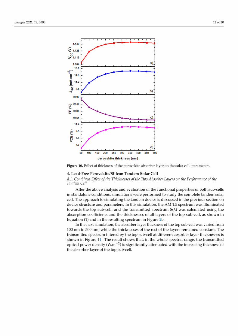
Figure 6. Effect of absorber layer thickness on the solar cell parameters.
According to Figure 6, we observe that Jsc increases to a greater extent than Voc, which only increases slightly with the thickness of the absorber layer. As a result, that the thick-ness of the absorber layer of the bottom cell determines the number of photons absorbed, especially for small dimensions up to a saturation value of the thickness, the EQE of the cell is also directly dependent. In addition, an absorber layer with a large thickness can maximize the capture of photons. As a direct consequence, as the thickness increases, the PCE increases, while the fill factor decreases. Therefore, the incident photon flux Φ0(λ) increases with the increase in the thickness of the absorber layer. It is also apparent that all functional parameters tend to saturation values, so instead of continuously increasing the thickness, it is necessary to find an optimum compromise in the physical and electrical parameters of the resulting tandem cell, as we describe below.
The back surface field (BSF) can enhance the efficiency of the solar cell. The minority carrier surface recombination at the rear surface is one of the different factors that leads to a decrease in the solar cell efficiency [44]. To minimize the surface recombination losses at the rear surface, another thin layer made of heavily doped n-type silicon was intro-duced to the back surface. In this way, the heavily doped layer creates a junction with the lightly doped absorption layer, i.e., n/n++, which is known as the back surface field (BSF). This junction pushes the minority carriers back to the absorbing layer and reduces the back surface recombination velocity (BSRV) to a greater degree, thus improving Jsc, Voc, FF, and ƞ. BSRV can be calculated following Equation (3).
BSRV = exp ∆ ( ) ( ) (3)
where N and N are the dopant concentrations, ∆V is bandgap narrowing due to a high dopant concentration, T is the temperature, K represents Boltzmann’s constant, q is
Figure 6. Effect of absorber layer thickness on the solar cell parameters.
According to Figure 6, we observe that Jsc increases to a greater extent than Voc,which only increases slightly with the thickness of the absorber layer. As a result, thatthe thickness of the absorber layer of the bottom cell determines the number of photonsabsorbed, especially for small dimensions up to a saturation value of the thickness, the EQEof the cell is also directly dependent. In addition, an absorber layer with a large thicknesscan maximize the capture of photons. As a direct consequence, as the thickness increases,the PCE increases, while the fill factor decreases. Therefore, the incident photon flux Φ0(λ)increases with the increase in the thickness of the absorber layer. It is also apparent thatall functional parameters tend to saturation values, so instead of continuously increasingthe thickness, it is necessary to find an optimum compromise in the physical and electricalparameters of the resulting tandem cell, as we describe below.
The back surface field (BSF) can enhance the efficiency of the solar cell. The minoritycarrier surface recombination at the rear surface is one of the different factors that leads toa decrease in the solar cell efficiency [44]. To minimize the surface recombination losses atthe rear surface, another thin layer made of heavily doped n-type silicon was introduced tothe back surface. In this way, the heavily doped layer creates a junction with the lightlydoped absorption layer, i.e., n/n++, which is known as the back surface field (BSF). Thisjunction pushes the minority carriers back to the absorbing layer and reduces the backsurface recombination velocity (BSRV) to a greater degree, thus improving Jsc, Voc, FF, andη. BSRV can be calculated following Equation (3).
BSRV =ND
N+D
exp
(∆V+
GKTq
) S0 +D+
eL+
etan h(W+
L+e)
1 + S0D+e
L+e
tan h(W+
L+e)
(3)
where ND and N+D are the dopant concentrations, ∆V+
G is bandgap narrowing due to ahigh dopant concentration, T is the temperature, K represents Boltzmann’s constant, q is

Energies 2021, 14, 3383 10 of 20
the electron charge, D+e
L+e
is the electron minority carrier diffusion length, W+ is the BSFthickness, and S0 is surface recombination velocity. The effect of the dopant concentrationof BSF on the energy band diagram is shown in Figure 7, which compares two values ofthe BSF layer, ND = 1015 cm–3 and ND = 1022 cm–3.
Energies 2021, 14, x FOR PEER REVIEW 14 of 24
the electron charge, De
+
Le+ is the electron minority carrier diffusion length, W+ is the BSF
thickness, and S0 is surface recombination velocity. The effect of the dopant concentra-
tion of BSF on the energy band diagram is shown in Figure 7, which compares two values
of the BSF layer, ND = 1015 cm–3 and ND = 1022 cm–3.
Figure 7. Effect of the doping concentration on the energy band diagram of the bottom sub-cell.
We can observe that adding the BSF layer creates a field that reduces the transfer of
the minority carriers to the back surface, and by increasing the dopant concentration of
the BSF, we increase the field and enhance the solar cell performance. Figure 8 shows the
effect of varying the dopant concentration of the BSF layer from ND = 1015 cm–3 to ND = 1022
cm–3, which are generally the values used in the experimental fabrication of the cell [45],
on the J–V curve of the bottom solar sub-cell.
Figure 8. Effect of the doping concentration on the J–V curve of the bottom sub-cell.
Figure 7. Effect of the doping concentration on the energy band diagram of the bottom sub-cell.
We can observe that adding the BSF layer creates a field that reduces the transfer of theminority carriers to the back surface, and by increasing the dopant concentration of the BSF,we increase the field and enhance the solar cell performance. Figure 8 shows the effect ofvarying the dopant concentration of the BSF layer from ND = 1015 cm–3 to ND = 1022 cm–3,which are generally the values used in the experimental fabrication of the cell [45], on theJ–V curve of the bottom solar sub-cell.
Energies 2021, 14, x FOR PEER REVIEW 14 of 24
the electron charge, De
+
Le+ is the electron minority carrier diffusion length, W+ is the BSF
thickness, and S0 is surface recombination velocity. The effect of the dopant concentra-
tion of BSF on the energy band diagram is shown in Figure 7, which compares two values
of the BSF layer, ND = 1015 cm–3 and ND = 1022 cm–3.
Figure 7. Effect of the doping concentration on the energy band diagram of the bottom sub-cell.
We can observe that adding the BSF layer creates a field that reduces the transfer of
the minority carriers to the back surface, and by increasing the dopant concentration of
the BSF, we increase the field and enhance the solar cell performance. Figure 8 shows the
effect of varying the dopant concentration of the BSF layer from ND = 1015 cm–3 to ND = 1022
cm–3, which are generally the values used in the experimental fabrication of the cell [45],
on the J–V curve of the bottom solar sub-cell.
Figure 8. Effect of the doping concentration on the J–V curve of the bottom sub-cell. Figure 8. Effect of the doping concentration on the J–V curve of the bottom sub-cell.

Energies 2021, 14, 3383 11 of 20
As the doping concentration increases, Jsc remains constant, while Voc increases dueto the direct relationship shown in Equation (4).
VOC =KTq
ln
[(ND + ∆n)∆n
n2i
](4)
where KTq is the thermal voltage, ∆n is the excess carrier concentration, ND is the doping
concentration, and ni is the intrinsic carrier concentration.Since Jsc remains constant and Voc increases, the PCE increases as well. According to
these results, we fixed the dopant concentration of the BSF layer to 1022 cm–3. In Section 4, weanalyze the effect of the dopant concentration of the BSF layer on the whole tandem device.
3.2. Effects of the Perovskite Absorber Layer Thickness of the Top Cell
The same simulation performed in standalone conditions for the bottom cell wasreproduced for the top cell as a function of its perovskite absorber layer thickness. TheJ–V curve and EQE(λ) of the top cell are reported in Figure 9a,b, respectively, and thedependence of the functional parameters Jsc, Voc, FF, and PCE on the thickness of thisperovskite absorber layer is illustrated in Figure 10.
Energies 2021, 14, x FOR PEER REVIEW 15 of 24
As the doping concentration increases, Jsc remains constant, while Voc increases due
to the direct relationship shown in Equation (4).
VOC =KT
qln [
(ND + ∆n)∆n
ni2 ] (4)
where KT
q is the thermal voltage, Δn is the excess carrier concentration, ND is the doping
concentration, and ni is the intrinsic carrier concentration.
Since Jsc remains constant and Voc increases, the PCE increases as well. According to
these results, we fixed the dopant concentration of the BSF layer to 1022 cm–3. In Section 4,
we analyze the effect of the dopant concentration of the BSF layer on the whole tandem
device.
3.2. Effects of the Perovskite Absorber Layer Thickness of the Top Cell
The same simulation performed in standalone conditions for the bottom cell was re-
produced for the top cell as a function of its perovskite absorber layer thickness. The J–V
curve and EQE(λ) of the top cell are reported in Figure 9a, b, respectively, and the de-
pendence of the functional parameters Jsc, Voc, FF, and PCE on the thickness of this perov-
skite absorber layer is illustrated in Figure 10.
(a) (b)
Figure 9. Effect of the standalone perovskite absorber layer thickness on (a) the J–V curve and (b) external quantum effi-
ciency.
It is noted that increasing the active layer thickness leads to an increase in the current
density due to the high absorption in the active region. Therefore, a large number of elec-
tron–hole pairs are generated. The subsequent separation of the generated electron–hole
pairs increase the JSC of the device. The improvement in Jsc and EQE is significant at lower
thicknesses and begins to saturate as thickness increases. This improvement of EQE is
mainly noticeable for longer wavelengths since low wavelength photons are absorbed
near the surface, whereas a thicker absorbent layer is necessary to absorb photons with
higher wavelengths. Figure 10 shows that Voc does not significantly increase as the thick-
ness of the absorbent layer increases: Voc increases by 2% when the thickness increases
from 100 nm to 500 nm. Due to the increase in the resistance with the absorber thickness,
the fill factor decreases from 60.2% to 59% when the thickness changes from 100 nm to 500
nm. Although there is a small reduction in FF, all of the other parameters increase, and
thus, the overall performance of the cell improves. In the same range for the absorber
Figure 9. Effect of the standalone perovskite absorber layer thickness on (a) the J–V curve and (b) external quantum efficiency.
It is noted that increasing the active layer thickness leads to an increase in the currentdensity due to the high absorption in the active region. Therefore, a large number ofelectron–hole pairs are generated. The subsequent separation of the generated electron–hole pairs increase the JSC of the device. The improvement in Jsc and EQE is significantat lower thicknesses and begins to saturate as thickness increases. This improvementof EQE is mainly noticeable for longer wavelengths since low wavelength photons areabsorbed near the surface, whereas a thicker absorbent layer is necessary to absorb photonswith higher wavelengths. Figure 10 shows that Voc does not significantly increase as thethickness of the absorbent layer increases: Voc increases by 2% when the thickness increasesfrom 100 nm to 500 nm. Due to the increase in the resistance with the absorber thickness,the fill factor decreases from 60.2% to 59% when the thickness changes from 100 nm to500 nm. Although there is a small reduction in FF, all of the other parameters increase,and thus, the overall performance of the cell improves. In the same range for the absorberthickness, the PCE increases from 7% to 10%. Our results are confirmed by other reporteddata, such as the recent work of Madan et al. [21].
Energies 2021, 14, 3383 12 of 20
Energies 2021, 14, x FOR PEER REVIEW 16 of 24
thickness, the PCE increases from 7% to 10%. Our results are confirmed by other reported
data, such as the recent work of Madan et al. [21].
Figure 10. Effect of thickness of the perovskite absorber layer on the solar cell. parameters.
4. Lead-Free Perovskite/Silicon Tandem Solar Cell
4.1. Combined Effect of the Thicknesses of the Two Absorber Layers on the Performance of the
Tandem Cell
After the above analysis and evaluation of the functional properties of both sub-cells
in standalone conditions, simulations were performed to study the complete tandem solar
cell. The approach to simulating the tandem device is discussed in the previous section on
device structure and parameters. In this simulation, the AM 1.5 spectrum was illuminated
towards the top sub-cell, and the transmitted spectrum S(λ) was calculated using the ab-
sorption coefficients and the thicknesses of all layers of the top sub-cell, as shown in Equa-
tion (1) and in the resulting spectrum in Figure 2b.
In the next simulation, the absorber layer thickness of the top sub-cell was varied
from 100 nm to 500 nm, while the thicknesses of the rest of the layers remained constant.
The transmitted spectrum filtered by the top sub-cell at different absorber layer thick-
nesses is shown in Figure 11. The result shows that, in the whole spectral range, the trans-
mitted optical power density (W.m−2) is significantly attenuated with the increasing thick-
ness of the absorber layer of the top sub-cell.
Figure 10. Effect of thickness of the perovskite absorber layer on the solar cell. parameters.
4. Lead-Free Perovskite/Silicon Tandem Solar Cell4.1. Combined Effect of the Thicknesses of the Two Absorber Layers on the Performance of theTandem Cell
After the above analysis and evaluation of the functional properties of both sub-cellsin standalone conditions, simulations were performed to study the complete tandem solarcell. The approach to simulating the tandem device is discussed in the previous section ondevice structure and parameters. In this simulation, the AM 1.5 spectrum was illuminatedtowards the top sub-cell, and the transmitted spectrum S(λ) was calculated using theabsorption coefficients and the thicknesses of all layers of the top sub-cell, as shown inEquation (1) and in the resulting spectrum in Figure 2b.
In the next simulation, the absorber layer thickness of the top sub-cell was varied from100 nm to 500 nm, while the thicknesses of the rest of the layers remained constant. Thetransmitted spectrum filtered by the top sub-cell at different absorber layer thicknesses isshown in Figure 11. The result shows that, in the whole spectral range, the transmittedoptical power density (W.m−2) is significantly attenuated with the increasing thickness ofthe absorber layer of the top sub-cell.
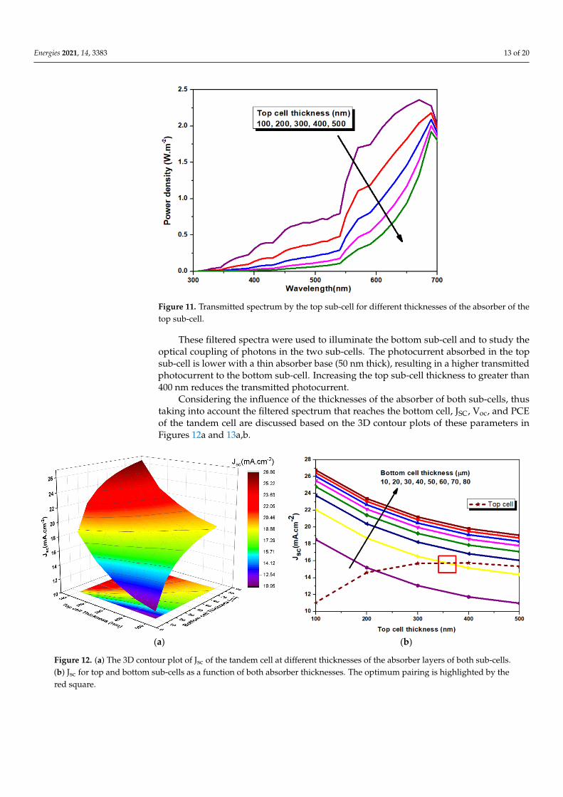
Energies 2021, 14, 3383 13 of 20Energies 2021, 14, x FOR PEER REVIEW 13 of 20
Figure 11. Transmitted spectrum by the top sub-cell for different thicknesses of the absorber of the top sub-cell.
These filtered spectra were used to illuminate the bottom sub-cell and to study the optical coupling of photons in the two sub-cells. The photocurrent absorbed in the top sub-cell is lower with a thin absorber base (50 nm thick), resulting in a higher transmitted photocurrent to the bottom sub-cell. Increasing the top sub-cell thickness to greater than 400 nm reduces the transmitted photocurrent.
Considering the influence of the thicknesses of the absorber of both sub-cells, thus taking into account the filtered spectrum that reaches the bottom cell, JSC, Voc, and PCE of the tandem cell are discussed based on the 3D contour plots of these parameters in Figures 12a and 13a,b.
(a) (b)
Figure 12. (a) The 3D contour plot of Jsc of the tandem cell at different thicknesses of the absorber layers of both sub-cells. (b) Jsc for top and bottom sub-cells as a function of both absorber thicknesses. The optimum pairing is highlighted by the red square.
Figure 11. Transmitted spectrum by the top sub-cell for different thicknesses of the absorber of thetop sub-cell.
These filtered spectra were used to illuminate the bottom sub-cell and to study theoptical coupling of photons in the two sub-cells. The photocurrent absorbed in the topsub-cell is lower with a thin absorber base (50 nm thick), resulting in a higher transmittedphotocurrent to the bottom sub-cell. Increasing the top sub-cell thickness to greater than400 nm reduces the transmitted photocurrent.
Considering the influence of the thicknesses of the absorber of both sub-cells, thustaking into account the filtered spectrum that reaches the bottom cell, JSC, Voc, and PCEof the tandem cell are discussed based on the 3D contour plots of these parameters inFigures 12a and 13a,b.
Energies 2021, 14, x FOR PEER REVIEW 13 of 20
Figure 11. Transmitted spectrum by the top sub-cell for different thicknesses of the absorber of the top sub-cell.
These filtered spectra were used to illuminate the bottom sub-cell and to study the optical coupling of photons in the two sub-cells. The photocurrent absorbed in the top sub-cell is lower with a thin absorber base (50 nm thick), resulting in a higher transmitted photocurrent to the bottom sub-cell. Increasing the top sub-cell thickness to greater than 400 nm reduces the transmitted photocurrent.
Considering the influence of the thicknesses of the absorber of both sub-cells, thus taking into account the filtered spectrum that reaches the bottom cell, JSC, Voc, and PCE of the tandem cell are discussed based on the 3D contour plots of these parameters in Figures 12a and 13a,b.
(a) (b)
Figure 12. (a) The 3D contour plot of Jsc of the tandem cell at different thicknesses of the absorber layers of both sub-cells. (b) Jsc for top and bottom sub-cells as a function of both absorber thicknesses. The optimum pairing is highlighted by the red square.
Figure 12. (a) The 3D contour plot of Jsc of the tandem cell at different thicknesses of the absorber layers of both sub-cells.(b) Jsc for top and bottom sub-cells as a function of both absorber thicknesses. The optimum pairing is highlighted by thered square.

Energies 2021, 14, 3383 14 of 20Energies 2021, 14, x FOR PEER REVIEW 14 of 20
(a) (b)
Figure 13. The 3D contour plot of PV parameters for the bottom cell: (a) Voc and (b) PCE at different thicknesses of the absorber layer in the top and bottom cells.
First, we discuss the influence of the thickness of the absorbers of the two sub-cells on the short-circuit current of the tandem cell. As observed in the results reported in Fig-ure 12a, for an absorber of the top sub-cell with low thickness, a high JSC value is transmit-ted to the bottom sub-cell. This current begins to decrease as the thickness of this layer in the top sub-cell increases. Conversely, for a given thickness of the absorber of the top sub-cell, increasing the thickness of the absorber of the bottom sub-cell increases JSC. Therefore, a compromise in the thicknesses of the two absorbers must be found to optimize the per-formance of the final tandem cell. This optimization has to account for the fact that the 2T tandem solar cell acts as two diodes connected in series. As mentioned in the introduction, this 2T structure makes it possible to ensure that the same current flows through the two sub-cells; in other words, the total value of Voc is the sum of the individual Voc of each sub-cell, but the sub-cell with the lowest value of JSC limits the overall JSC of the tandem device [46]. Therefore, in tandem devices, the thicknesses of the different layers must be opti-mized to have the same JSC value passing through the two sub-cells and to facilitate the tunnel recombination junctions used [47,48].
As the thickness of the layers in the top sub-cell decrease below a threshold value, the absorption is reduced, resulting in a reduction in the overall JSC of the tandem cell. Similarly, if the thickness of the layer in the top sub-cell increases beyond a threshold value, the absorption will decrease the optical coupling in the bottom sub-cell, which also results in a decrease in the overall JSC of the tandem cell. These observations allow us to establish the current matching conditions to obtain the same JSC value in the two sub-cells.
Next, we used the spectra filtered by the absorber layer of the top sub-cell for differ-ent thicknesses (Figure 11) as input data to evaluate the PV parameters of the bottom sub-cell. The thickness of the bottom sub-cell was varied from 10 to 80 µm. The bottom sub-cell JSC values, obtained from the spectrum filtered by the top sub-cell, were used to deter-mine the optimum pairing condition for the tandem device, as shown in Figure 12b. The best current matching condition that provides a higher equivalent value for both sub-cells is highlighted by the red square in Figure 12b and is obtained with a top sub-cell thickness of 380 nm and a bottom cell thickness of 20 µm, yielding JSC values equal to 16.01 mA.cm–
2 and 16.09 mA.cm–2, respectively. Further, apart from the current pairing condition discussed above, Figure 13a shows
that the top sub-cell has a marginal influence on the total Voc of the tandem cell, unlike the bottom sub-cell, in which Voc strongly decreases with the increase in its thickness. The
Figure 13. The 3D contour plot of PV parameters for the bottom cell: (a) Voc and (b) PCE at different thicknesses of theabsorber layer in the top and bottom cells.
First, we discuss the influence of the thickness of the absorbers of the two sub-cellson the short-circuit current of the tandem cell. As observed in the results reported inFigure 12a, for an absorber of the top sub-cell with low thickness, a high JSC value istransmitted to the bottom sub-cell. This current begins to decrease as the thickness of thislayer in the top sub-cell increases. Conversely, for a given thickness of the absorber ofthe top sub-cell, increasing the thickness of the absorber of the bottom sub-cell increasesJSC. Therefore, a compromise in the thicknesses of the two absorbers must be found tooptimize the performance of the final tandem cell. This optimization has to account for thefact that the 2T tandem solar cell acts as two diodes connected in series. As mentioned inthe introduction, this 2T structure makes it possible to ensure that the same current flowsthrough the two sub-cells; in other words, the total value of Voc is the sum of the individualVoc of each sub-cell, but the sub-cell with the lowest value of JSC limits the overall JSC ofthe tandem device [46]. Therefore, in tandem devices, the thicknesses of the different layersmust be optimized to have the same JSC value passing through the two sub-cells and tofacilitate the tunnel recombination junctions used [47,48].
As the thickness of the layers in the top sub-cell decrease below a threshold value,the absorption is reduced, resulting in a reduction in the overall JSC of the tandem cell.Similarly, if the thickness of the layer in the top sub-cell increases beyond a threshold value,the absorption will decrease the optical coupling in the bottom sub-cell, which also resultsin a decrease in the overall JSC of the tandem cell. These observations allow us to establishthe current matching conditions to obtain the same JSC value in the two sub-cells.
Next, we used the spectra filtered by the absorber layer of the top sub-cell for differentthicknesses (Figure 11) as input data to evaluate the PV parameters of the bottom sub-cell.The thickness of the bottom sub-cell was varied from 10 to 80 µm. The bottom sub-cell JSCvalues, obtained from the spectrum filtered by the top sub-cell, were used to determinethe optimum pairing condition for the tandem device, as shown in Figure 12b. The bestcurrent matching condition that provides a higher equivalent value for both sub-cells ishighlighted by the red square in Figure 12b and is obtained with a top sub-cell thickness of380 nm and a bottom cell thickness of 20 µm, yielding JSC values equal to 16.01 mA.cm–2
and 16.09 mA.cm–2, respectively.Further, apart from the current pairing condition discussed above, Figure 13a shows
that the top sub-cell has a marginal influence on the total Voc of the tandem cell, unlike thebottom sub-cell, in which Voc strongly decreases with the increase in its thickness. The PCEof the tandem cell is shown in Figure 13b. The influence of the thickness of the absorbers

Energies 2021, 14, 3383 15 of 20
of the two sub-cells is clearly demonstrated by the doubling of the PCE for the evaluatedthicknesses. A PCE value of 15.56% is obtained with the current matching condition, i.e.,for thicknesses that produce an optimum JSC throughout the tandem cell structure. Withthe absorber thicknesses optimized for the current pairing condition, as discussed above, aperovskite/silicon tandem solar cell was simulated.
The effect of the BSF layer dopant concentration, as discussed above, was also mea-sured for the global tandem solar cell. The J–V curves of the tandem solar cell are presentedin Figure 14 for two extremum values of possible dopant concentrations in the BSF layer.
Energies 2021, 14, x FOR PEER REVIEW 19 of 24
PCE of the tandem cell is shown in Figure 13b. The influence of the thickness of the ab-
sorbers of the two sub-cells is clearly demonstrated by the doubling of the PCE for the
evaluated thicknesses. A PCE value of 15.56% is obtained with the current matching con-
dition, i.e., for thicknesses that produce an optimum JSC throughout the tandem cell struc-
ture. With the absorber thicknesses optimized for the current pairing condition, as dis-
cussed above, a perovskite/silicon tandem solar cell was simulated.
The effect of the BSF layer dopant concentration, as discussed above, was also meas-
ured for the global tandem solar cell. The J–V curves of the tandem solar cell are presented
in Figure 14 for two extremum values of possible dopant concentrations in the BSF layer.
Figure 14. The I–V characteristic of the optimized tandem solar cell.
As observed from the results, for the optimal dopant concentration of the BSF layer,
ND = 1022 cm–3, the open-circuit voltage of the tandem device increases.
The J–V characteristics of the top sub-cell, the bottom sub cell, and the tandem cell
are presented in Figure 15, and the photovoltaic parameters are reported in Table 3.
Figure 15. The J–V characteristic of the optimized tandem solar cell.
Figure 14. The I–V characteristic of the optimized tandem solar cell.
As observed from the results, for the optimal dopant concentration of the BSF layer,ND = 1022 cm–3, the open-circuit voltage of the tandem device increases.
The J–V characteristics of the top sub-cell, the bottom sub cell, and the tandem cell arepresented in Figure 15, and the photovoltaic parameters are reported in Table 3.
Energies 2021, 14, x FOR PEER REVIEW 19 of 24
PCE of the tandem cell is shown in Figure 13b. The influence of the thickness of the ab-
sorbers of the two sub-cells is clearly demonstrated by the doubling of the PCE for the
evaluated thicknesses. A PCE value of 15.56% is obtained with the current matching con-
dition, i.e., for thicknesses that produce an optimum JSC throughout the tandem cell struc-
ture. With the absorber thicknesses optimized for the current pairing condition, as dis-
cussed above, a perovskite/silicon tandem solar cell was simulated.
The effect of the BSF layer dopant concentration, as discussed above, was also meas-
ured for the global tandem solar cell. The J–V curves of the tandem solar cell are presented
in Figure 14 for two extremum values of possible dopant concentrations in the BSF layer.
Figure 14. The I–V characteristic of the optimized tandem solar cell.
As observed from the results, for the optimal dopant concentration of the BSF layer,
ND = 1022 cm–3, the open-circuit voltage of the tandem device increases.
The J–V characteristics of the top sub-cell, the bottom sub cell, and the tandem cell
are presented in Figure 15, and the photovoltaic parameters are reported in Table 3.
Figure 15. The J–V characteristic of the optimized tandem solar cell.
Figure 15. The J–V characteristic of the optimized tandem solar cell.

Energies 2021, 14, 3383 16 of 20
Table 3. Photovoltaic parameters of the top, bottom, and tandem cells.
Parameters Top Cell Bottom Cell Tandem Cell
Voc (V) 1.09 0.66 1.76
Jsc (mA.cm–2) 16.01 16.09 16.01
FF (%) 82 81.3 86.7%
PCE (%) 14.37 15.56 24.4%
After the full optimization of the two sub-cells in current matching conditions, partic-ularly the absorber layer thicknesses and the dopant concentration of the BSF layer, thetandem solar cell achieves a short current circuit equal to 16.01 mA.cm–2 and an open-circuit voltage of 1.76 V, yielding a PCE of 24.4% at room temperature (T = 300 K) and forAM 1.5G.
This performance makes this solar cell structure an interesting alternative that provideshigh efficiency, better stability, and a lower cost of fabrication compared to traditional siliconsolar cells and III–V semiconductors.
To further understand our study of this tandem solar cell configuration, the effect ofthe working temperature on the solar cell efficiency is simulated in the next section.
4.2. Effect of the Working Temperature on the Parameters of the Optimized Tandem Solar Cell
In most cases, solar cells are used in outdoor environments and are exposed to sunlight,which can increase the temperature by as much as 273.15 K above ambient temperature [49].For this reason, various experiments have shown that the most difficult challenge for PSCsis long-term stability [50,51]. Since the analysis of temperature effects is very important, wesimulated the effect of working temperature on the lead-free perovskite top sub-cell in thestandalone condition and its effect on the tandem solar cell. It is reported in the literaturethat Cs2AgBiBr6 shows a better mechanical and thermal performance as compared toother MAPbBr3-type perovskites. The strong Ag–Br and Bi–Br bonds increase the rigidityof Cs2AgBiBr6, while the Pb–X bonds (X = Cl, Br, or I) in metal halide perovskites arerelatively weak. This perovskite is mainly characterized by its low thermal expansionbehavior, which reduces thermal stresses that arise during the processing or operationof the cell, improving the device life [52,53]. The effect of the working temperature onthe perovskite top sub-cell was simulated, and the associated J–V curve is presented inFigure 16.

Energies 2021, 14, 3383 17 of 20
Energies 2021, 14, x FOR PEER REVIEW 20 of 24
Table 3. Photovoltaic parameters of the top, bottom, and tandem cells.
Parameters Top Cell Bottom Cell Tandem Cell
Voc (V) 1.09 0.66 1.76
Jsc (mA.cm–2) 16.01 16.09 16.01
FF (%) 82 81.3 86.7%
PCE (%) 14.37 15.56 24.4%
After the full optimization of the two sub-cells in current matching conditions, par-
ticularly the absorber layer thicknesses and the dopant concentration of the BSF layer, the
tandem solar cell achieves a short current circuit equal to 16.01 mA.cm–2 and an open-
circuit voltage of 1.76 V, yielding a PCE of 24.4% at room temperature (T = 300 K) and for
AM 1.5G.
This performance makes this solar cell structure an interesting alternative that pro-
vides high efficiency, better stability, and a lower cost of fabrication compared to tradi-
tional silicon solar cells and III–V semiconductors.
To further understand our study of this tandem solar cell configuration, the effect of
the working temperature on the solar cell efficiency is simulated in the next section.
4.2. Effect of the Working Temperature on the Parameters of the Optimized Tandem Solar Cell
In most cases, solar cells are used in outdoor environments and are exposed to sun-
light, which can increase the temperature by as much as 273.15 K above ambient temper-
ature [49]. For this reason, various experiments have shown that the most difficult chal-
lenge for PSCs is long-term stability [50,51]. Since the analysis of temperature effects is
very important, we simulated the effect of working temperature on the lead-free perov-
skite top sub-cell in the standalone condition and its effect on the tandem solar cell. It is
reported in the literature that Cs2AgBiBr6 shows a better mechanical and thermal perfor-
mance as compared to other MAPbBr3-type perovskites. The strong Ag–Br and Bi–Br
bonds increase the rigidity of Cs2AgBiBr6, while the Pb–X bonds (X = Cl, Br, or I) in metal
halide perovskites are relatively weak. This perovskite is mainly characterized by its low
thermal expansion behavior, which reduces thermal stresses that arise during the pro-
cessing or operation of the cell, improving the device life [52,53]. The effect of the working
temperature on the perovskite top sub-cell was simulated, and the associated J–V curve is
presented in Figure 16.
Figure 16. Effect of the working temperature on the J–V curve of the perovskite top sub-cell. Figure 16. Effect of the working temperature on the J–V curve of the perovskite top sub-cell.
We observe that increasing the temperature results in a decrease in the solar cellefficiency. Comparing this decrease with that obtained when simulating lead halideperovskite solar cells, it is observed that lead-free perovskite cells are less affected by theincrease in temperature. In fact, by increasing the temperature from 300 K to 350 K, adecrease of 0.45% in solar cell efficiency is observed, which is much less than the 5% drop inefficiency obtained by Abdulsalam et al. [54] when simulating the effect of the temperatureon MAPBI3 perovskite solar cells.
Figure 17 shows the J–V curve of the tandem solar cell when varying the temperaturefrom 300 K to 500 K.
Energies 2021, 14, x FOR PEER REVIEW 17 of 20
Figure 16. Effect of the working temperature on the J–V curve of the perovskite top sub-cell.
We observe that increasing the temperature results in a decrease in the solar cell effi-ciency. Comparing this decrease with that obtained when simulating lead halide perov-skite solar cells, it is observed that lead-free perovskite cells are less affected by the in-crease in temperature. In fact, by increasing the temperature from 300 K to 350 K, a de-crease of 0.45% in solar cell efficiency is observed, which is much less than the 5% drop in efficiency obtained by Abdulsalam et al. [54] when simulating the effect of the tempera-ture on MAPBI3 perovskite solar cells.
Figure 17 shows the J–V curve of the tandem solar cell when varying the temperature from 300 K to 500 K.
Figure 17. Effect of the working temperature on the J–V curve of the tandem solar cell.
The performance of the solar cell is affected by the increasing temperature, which is linked to open-circuit voltage decay. Voc is reduced because of its direct link to reverse saturation current density (Jo), which is further related to intrinsic carrier concentration
‘ni’. ni depends on the energy bandgap, i.e., n = k e , where k1 is a constant and Eg is inversely proportional to the temperature, as given by Equation (5): E (T) = E (0) − αTT + β (5)
where Eg(T) is the bandgap of the material at temperature T, and α and β are constants. The results show that PCE and FF also decrease. The high temperature leads to more
excited electrons, but the bandgap can be unstable, resulting in the strong recombination of carriers and thus reducing the efficiency.
5. Conclusions Simulations were performed to optimize the photovoltaic parameters of a tandem
lead-free perovskite/silicon solar cell with the aim of improving the efficiency and stability of commercial devices. The top lead-free perovskite Cs2AgBi0.75Sb0.25Br6 sub-cell and the bottom n-type silicon sub-cell were first simulated under standalone conditions. Then, we aimed to optimize the thicknesses of the two absorbers to obtain current matching by sim-ulating the J–V curve of the lower silicon sub-cell using the spectrum filtered by the top sub-cell. The optimal thicknesses of top/bottom sub-cells are 380 nm/20 µm, respectively,
Figure 17. Effect of the working temperature on the J–V curve of the tandem solar cell.
The performance of the solar cell is affected by the increasing temperature, which islinked to open-circuit voltage decay. Voc is reduced because of its direct link to reversesaturation current density (Jo), which is further related to intrinsic carrier concentration

Energies 2021, 14, 3383 18 of 20
‘ni’. ni depends on the energy bandgap, i.e., ni2 = k1 e
EgKT , where k1 is a constant and Eg is
inversely proportional to the temperature, as given by Equation (5):
Eg(T) = Eg(0)−αT2
T + β(5)
where Eg(T) is the bandgap of the material at temperature T, and α and β are constants.The results show that PCE and FF also decrease. The high temperature leads to more
excited electrons, but the bandgap can be unstable, resulting in the strong recombination ofcarriers and thus reducing the efficiency.
5. Conclusions
Simulations were performed to optimize the photovoltaic parameters of a tandemlead-free perovskite/silicon solar cell with the aim of improving the efficiency and stabilityof commercial devices. The top lead-free perovskite Cs2AgBi0.75Sb0.25Br6 sub-cell and thebottom n-type silicon sub-cell were first simulated under standalone conditions. Then,we aimed to optimize the thicknesses of the two absorbers to obtain current matching bysimulating the J–V curve of the lower silicon sub-cell using the spectrum filtered by the topsub-cell. The optimal thicknesses of top/bottom sub-cells are 380 nm/20 µm, respectively,and the optimal dopant concentration of the BSF layer of the silicon sub-cell is equal to1022 cm–3. The optimized tandem solar cell achieves a large open-circuit voltage of 1.76 V,a short-circuit current of 16.01 mA.cm–2, and a PCE of 24.4%. In addition, the effect of theworking temperature was simulated, and the results show the advantages of the lead-freeperovskite tandem solar cell, which combines satisfactory thermal expansion behaviorand electrical parameter values and efficiency that are very competitive with standardsilicon cells. The nontoxicity and impressive moisture stability of this type of lead-freeperovskite/silicon tandem solar cell make it a strong candidate for potential applicationsin optoelectronics and photovoltaics.
Author Contributions: Conceptualization, K.A. and M.A.; data curation, K.A., R.B. and M.A.; formalanalysis, K.A., R.B. and M.A.; funding acquisition, R.G. and M.A.; investigation, K.A., R.B. and M.A.;methodology, K.A. and R.B.; resources, K.A. and M.A.; writing—original draft preparation, K.A.;writing—review, R.B. and M.A.; editing, M.A. All authors have read and agreed to the publishedversion of the manuscript.
Funding: This research received no external funding.
Acknowledgments: The team of authors acknowledges Marc Burgelman and his staff at the Univer-sity of Gent, Belgium, for providing the open-source SCAPS-1D simulator.
Conflicts of Interest: The authors declare no conflict of interest.
References1. Reyes-Belmonte, M.A. Quo Vadis Solar Energy Research. Appl Sci. Multidiscip. Digit. Publ. Inst. 2021, 11, 3015.2. Miller, O.D.; Yablonovitch, E. Photon extraction: The key physics for approaching solar cell efficiency limits. Act Photonic Mater
V [Internet]. International Society for Optics and Photonics. Available online: https://www.spiedigitallibrary.org/conference-proceedings-of-spie/8808/880807/Photon-extraction--the-key-physics-for-approaching-solar-cell/10.1117/12.2024592.short(accessed on 1 June 2021).
3. Todorov, T.; Gunawan, O.; Guha, S. A road towards 25% efficiency and beyond: Perovskite tandem solar cells. Mol. Syst Des. Eng.R. Soc. Chem. 2016, 1, 370–376. [CrossRef]
4. Rideout, V.L. A review of the theory and technology for ohmic contacts to group III–V compound semiconductors. Solid-StateElectron. 1975, 18, 541–550. [CrossRef]
5. Eperon, G.E.; Hörantner, M.T.; Snaith, H.J. Metal halide perovskite tandem and multiple-junction photovoltaics. Nat. Rev. Chem.Nat. Publ. Group 2017, 1, 1–18. [CrossRef]
6. Leijtens, T.; Bush, K.A.; Prasanna, R.; McGehee, M.D. Opportunities and challenges for tandem solar cells using metal halideperovskite semiconductors. Nat. Energy Nat. Publ. Group 2018, 3, 828–838. [CrossRef]
7. Wali, Q.; Elumalai, N.K.; Iqbal, Y.; Uddin, A.; Jose, R. Tandem perovskite solar cells. Renew. Sustain. Energy Rev. 2018, 84, 89–110.[CrossRef]

Energies 2021, 14, 3383 19 of 20
8. Stranks, S.D.; Eperon, G.E.; Grancini, G. Electron-Hole Diffusion Lengths Exceeding 1 Micrometer in an Organometal TrihalidePerovskite Absorber. Science 2013. [CrossRef]
9. Ponseca, C.S.; Savenijie, T.J.; Abdellah, M. Organometal Halide Perovskite Solar Cell Materials Rationalized: Ultrafast ChargeGeneration, High and Microsecond-Long Balanced Mobilities, and Slow Recombination. J. Am. Chem. Soc. 2014. [CrossRef]
10. Zhu, S.; Yao, X.; Ren, Q.; Zheng, C.; Li, S.; Tong, Y.; Shi, B.; Guo, S.; Fan, L.; Ren, H.; et al. Transparent electrode for monolithicperovskite/silicon-heterojunction two-terminal tandem solar cells. Nano Energy 2018, 45, 280–286. [CrossRef]
11. Eperon, G.E.; Stranks, S.D.; Menelaou, C.; Johnston, M.B.; Herz, L.M.; Snaith, H.J. Formamidinium lead trihalide: A broadlytunable perovskite for efficient planar heterojunction solar cells. Energy Environ. Sci. R. Soc. Chem. 2014, 7, 982–988. [CrossRef]
12. Zhou, H.; Li, C.; Luo, S. Interface engineering of highly efficient perovskite solar cells. Science 2014. [CrossRef] [PubMed]13. Best Research-Cell Efficiency Chart. Available online: https://www.nrel.gov/pv/cell-efficiency.html (accessed on 28 March 2021).14. Li, Z.; Klein, T.R.; Kim, D.H.; Yang, M.; Berry, J.J.; Van Hest, M.F.A.M.; Zhu, K. Scalable fabrication of perovskite solar cells. Nat.
Rev. Mater. Nat. Publ. Group 2018, 3, 1–20. [CrossRef]15. Reese, M.O.; Glynn, S.; Kempe, M.D.; McGott, D.L.; Dabney, M.S.; Barnes, T.M.; Booth, S.; Feldman, D.; Haegel, N.M. Increasing
markets and decreasing package weight for high-specific-power photovoltaics. Nat. Energy. Nat. Publ. Group 2018, 3, 1002–1012.[CrossRef]
16. Eperon, G.E.; Leijtens, T.; Bush, K.A. Perovskite-perovskite tandem photovoltaics with optimized band gaps. Science 2016.[CrossRef] [PubMed]
17. Forgács, D.; Gil-Escrig, L.; Pérez-Del-Rey, D.; Momblona, C.; Werner, J.; Niesen, B.; Ballif, C.; Sessolo, M.; Bolink, H.J. EfficientMonolithic Perovskite/Perovskite Tandem Solar Cells. Adv. Energy Mater. 2017, 7, 1602121. [CrossRef]
18. Rajagopal, A.; Yang, Z.; Jo, S.B. Highly Efficient Perovskite–Perovskite Tandem Solar Cells Reaching 80% of the Theoretical Limitin Photovoltage—Rajagopal—2017. Adv. Mater. Wiley Online Libr. 2017. [CrossRef]
19. Ali, R.; Hou, G.-J.; Zhu, Z.-G.; Yan, Q.-B.; Zheng, Q.-R.; Su, G. Stable mixed group II (Ca, Sr) and XIV (Ge, Sn) lead-free perovskitesolar cells. J. Mater. Chem A. R. Soc. Chem. 2018, 6, 9220–9227. [CrossRef]
20. McClure, E.T.; Ball, M.R.; Windl, W. Woodward PM. Cs2AgBiX6 (X = Br, Cl): New Visible Light Absorbing, Lead-Free HalidePerovskite Semiconductors. Chem. Mater. Am. Chem. Soc. 2016, 28, 1348–1354.
21. Madan, J.; Shivani Pandey, R.; Sharma, R. Device simulation of 17.3% efficient lead-free all-perovskite tandem solar cell. Sol.Energy 2020, 197, 212–221. [CrossRef]
22. Almansouri, I.; Ho-Baillie, A.W.Y.; Green, M.A. Ultimate Efficiency Limit of Single-Junction Perovskite and Dual-JunctionPerovskite/Silicon Two-Terminal Devices—IOPscience. Available online: https://iopscience.iop.org/article/10.7567/JJAP.54.08KD04/meta (accessed on 28 March 2021).
23. Mailoa, J.; Bailie, C.; Johlin, E.; Hoke, E.; Akey, A.; Nguyen, W.; Mc Gehee, M.D.; Buanassisi, T. A 2-Terminal Perovskite/SiliconMultijunction Solar Cell Enabled by a Silicon Tunnel Junction. Appl. Phys. Lett. 2015, 106, 121105. [CrossRef]
24. Werner, J.; Weng, C.-H.; Walter, A. Efficient Monolithic Perovskite/Silicon Tandem Solar Cell with Cell Area >1 cm2. J. Phys.Chem. Lett. 2016. [CrossRef] [PubMed]
25. Zhong, Y.; Hufnagel, M.; Thelakkat, M.; Li, C.; Huettner, S. Role of PCBM in the Suppression of Hysteresis in Perovskite SolarCells. Adv Funct Mater. 2020, 30, 1908920. [CrossRef]
26. Schmiga, C.; Nagel, H.; Schmidt, J. 19% efficient n-type Czochralski silicon solar cells with screen-printed aluminium-alloyed rearemitter—Schmiga—2006—Progress in Photovoltaics. Res. Appl. Wiley Online Libr. 2006. [CrossRef]
27. Zheng, J.; Lau, C.F.J.; Mehrvarz, H.; Ma, F.-J.; Jiang, Y.; Deng, X.; Soeriyadi, A.; Kim, J.; Zhang, M.; Hu, L.; et al. Large area efficientinterface layer free monolithic perovskite/homo-junction-silicon tandem solar cell with over 20% efficiency. Energy Environ. Sci.R. Soc. Chem. 2018, 11, 2432–2443. [CrossRef]
28. Tiwana, P.; Docampo, P.; Johnston, M.B.; Snaith, H.J.; Herz, L.M. Electron mobility and injection dynamics in mesoporous ZnO,SnO2, and TiO2 films used in dye-sensitized solar cells. ACS Nano 2011, 5, 5158–5166. [CrossRef]
29. Wang, S.; Zhu, Y.; Liu, B.; Wang, C.; Ma, R. Introduction of carbon nanodots into SnO2 electron transport layer for efficient andUV stable planar perovskite solar cells. J. Mater. Chem. A. 2019, 7. [CrossRef]
30. Wang, J.; Datta, K.; Weijtens, C.H.L.; Wienk, M.M.; Janssen, R.A.J. Insights into Fullerene Passivation of SnO2 Electron TransportLayers in Perovskite Solar Cells. Adv. Funct. Mater. 2019, 29, 1905883. [CrossRef]
31. Ke, W.; Zhao, D.; Xiao, C.; Wang, C.; Cimaroli, A.J.; Grice, C.R.; Yang, M.; Li, Z.; Jiang, C.-S.; Al-Jassim, M.; et al. Cooperative tinoxide fullerene electron selective layers for high-performance planar perovskite solar cells. J. Mater. Chem. A. R. Soc. Chem. 2016,4, 14276–14283. [CrossRef]
32. You, J.; Meng, L.; Song, T.B.; Guo, T.F.; Yang, Y.M.; Chang, W.H.; Hong, Z.; Chen, H.; Zhou, H.; Chen, Q.; et al. Improved airstability of perovskite solar cells via solution-processed metal oxide transport layers. Nat. Nanotechnol. 2016, 11, 75–81. [CrossRef]
33. Attequr, R.; Soo Hong, L. Advancements in n-Type Base Crystalline Silicon Solar Cells and Their Emergence in the PhotovoltaicIndustry. Sci. World J. 2013. [CrossRef]
34. Dong, H.; Pang, S.; Zhang, Y.; Chen, D.; Zhu, W.; Xi, H.; Chang, J.; Zhang, J.; Zhang, C.; Hao, J. Improving Electron ExtractionAbility and Device Stability of Perovskite Solar Cells Using a Compatible PCBM/AZO Electron Transporting Bilayer. Nanomater.Multidiscip. Digit. Publ. Inst. 2018, 8, 720. [CrossRef] [PubMed]
35. Gao, H.; Qin, C.; Zhang, H.; Wu, S. Theoretical Characterization of a Typical Hole/Exciton-Blocking Material Bathocuproine andIts Analogues. J. Phys. Chem. A 2008. [CrossRef] [PubMed]
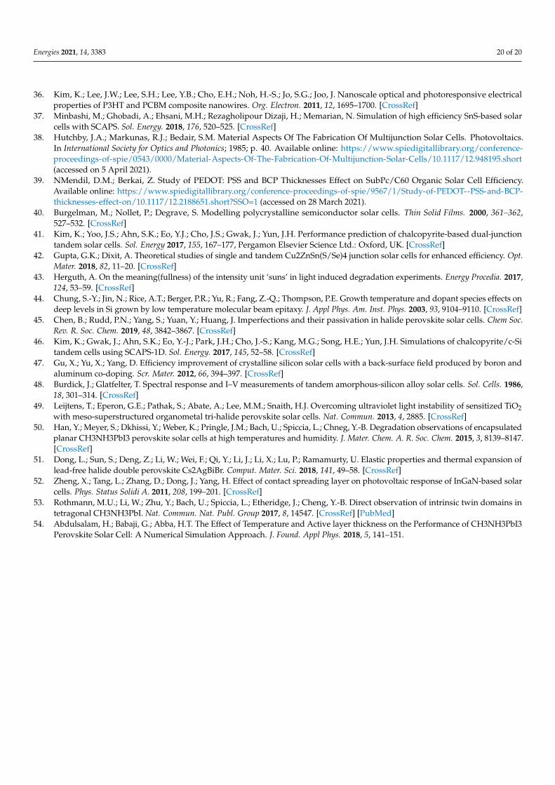
Energies 2021, 14, 3383 20 of 20
36. Kim, K.; Lee, J.W.; Lee, S.H.; Lee, Y.B.; Cho, E.H.; Noh, H.-S.; Jo, S.G.; Joo, J. Nanoscale optical and photoresponsive electricalproperties of P3HT and PCBM composite nanowires. Org. Electron. 2011, 12, 1695–1700. [CrossRef]
37. Minbashi, M.; Ghobadi, A.; Ehsani, M.H.; Rezagholipour Dizaji, H.; Memarian, N. Simulation of high efficiency SnS-based solarcells with SCAPS. Sol. Energy. 2018, 176, 520–525. [CrossRef]
38. Hutchby, J.A.; Markunas, R.J.; Bedair, S.M. Material Aspects Of The Fabrication Of Multijunction Solar Cells. Photovoltaics.In International Society for Optics and Photonics; 1985; p. 40. Available online: https://www.spiedigitallibrary.org/conference-proceedings-of-spie/0543/0000/Material-Aspects-Of-The-Fabrication-Of-Multijunction-Solar-Cells/10.1117/12.948195.short(accessed on 5 April 2021).
39. NMendil, D.M.; Berkai, Z. Study of PEDOT: PSS and BCP Thicknesses Effect on SubPc/C60 Organic Solar Cell Efficiency.Available online: https://www.spiedigitallibrary.org/conference-proceedings-of-spie/9567/1/Study-of-PEDOT--PSS-and-BCP-thicknesses-effect-on/10.1117/12.2188651.short?SSO=1 (accessed on 28 March 2021).
40. Burgelman, M.; Nollet, P.; Degrave, S. Modelling polycrystalline semiconductor solar cells. Thin Solid Films. 2000, 361–362,527–532. [CrossRef]
41. Kim, K.; Yoo, J.S.; Ahn, S.K.; Eo, Y.J.; Cho, J.S.; Gwak, J.; Yun, J.H. Performance prediction of chalcopyrite-based dual-junctiontandem solar cells. Sol. Energy 2017, 155, 167–177, Pergamon Elsevier Science Ltd.: Oxford, UK. [CrossRef]
42. Gupta, G.K.; Dixit, A. Theoretical studies of single and tandem Cu2ZnSn(S/Se)4 junction solar cells for enhanced efficiency. Opt.Mater. 2018, 82, 11–20. [CrossRef]
43. Herguth, A. On the meaning(fullness) of the intensity unit ‘suns’ in light induced degradation experiments. Energy Procedia. 2017,124, 53–59. [CrossRef]
44. Chung, S.-Y.; Jin, N.; Rice, A.T.; Berger, P.R.; Yu, R.; Fang, Z.-Q.; Thompson, P.E. Growth temperature and dopant species effects ondeep levels in Si grown by low temperature molecular beam epitaxy. J. Appl Phys. Am. Inst. Phys. 2003, 93, 9104–9110. [CrossRef]
45. Chen, B.; Rudd, P.N.; Yang, S.; Yuan, Y.; Huang, J. Imperfections and their passivation in halide perovskite solar cells. Chem Soc.Rev. R. Soc. Chem. 2019, 48, 3842–3867. [CrossRef]
46. Kim, K.; Gwak, J.; Ahn, S.K.; Eo, Y.-J.; Park, J.H.; Cho, J.-S.; Kang, M.G.; Song, H.E.; Yun, J.H. Simulations of chalcopyrite/c-Sitandem cells using SCAPS-1D. Sol. Energy. 2017, 145, 52–58. [CrossRef]
47. Gu, X.; Yu, X.; Yang, D. Efficiency improvement of crystalline silicon solar cells with a back-surface field produced by boron andaluminum co-doping. Scr. Mater. 2012, 66, 394–397. [CrossRef]
48. Burdick, J.; Glatfelter, T. Spectral response and I–V measurements of tandem amorphous-silicon alloy solar cells. Sol. Cells. 1986,18, 301–314. [CrossRef]
49. Leijtens, T.; Eperon, G.E.; Pathak, S.; Abate, A.; Lee, M.M.; Snaith, H.J. Overcoming ultraviolet light instability of sensitized TiO2with meso-superstructured organometal tri-halide perovskite solar cells. Nat. Commun. 2013, 4, 2885. [CrossRef]
50. Han, Y.; Meyer, S.; Dkhissi, Y.; Weber, K.; Pringle, J.M.; Bach, U.; Spiccia, L.; Chneg, Y.-B. Degradation observations of encapsulatedplanar CH3NH3PbI3 perovskite solar cells at high temperatures and humidity. J. Mater. Chem. A. R. Soc. Chem. 2015, 3, 8139–8147.[CrossRef]
51. Dong, L.; Sun, S.; Deng, Z.; Li, W.; Wei, F.; Qi, Y.; Li, J.; Li, X.; Lu, P.; Ramamurty, U. Elastic properties and thermal expansion oflead-free halide double perovskite Cs2AgBiBr. Comput. Mater. Sci. 2018, 141, 49–58. [CrossRef]
52. Zheng, X.; Tang, L.; Zhang, D.; Dong, J.; Yang, H. Effect of contact spreading layer on photovoltaic response of InGaN-based solarcells. Phys. Status Solidi A. 2011, 208, 199–201. [CrossRef]
53. Rothmann, M.U.; Li, W.; Zhu, Y.; Bach, U.; Spiccia, L.; Etheridge, J.; Cheng, Y.-B. Direct observation of intrinsic twin domains intetragonal CH3NH3PbI. Nat. Commun. Nat. Publ. Group 2017, 8, 14547. [CrossRef] [PubMed]
54. Abdulsalam, H.; Babaji, G.; Abba, H.T. The Effect of Temperature and Active layer thickness on the Performance of CH3NH3PbI3Perovskite Solar Cell: A Numerical Simulation Approach. J. Found. Appl Phys. 2018, 5, 141–151.


