Embed Size (px)
Citation preview


Development of cantilevers for biomolecular measurements
Memòria per a optar al grau de Doctor en Enginyeria Electrònica
Autor: Luis Guillermo Villanueva Torrijo
Director i tutor: Joan Bausells Roigé
En doctor Joan Bausells Roigé-IMB) i Professor Associat
la Universitat Autònoma de Barcelona (UAB)
CERTIFICA:
Que la present memòria Development of cantilevers for biomolecular measurements r en Luis Guillermo Villanueva Torrijo, llicenciat en Ciències Físiques per la Universidad de Zaragoza.
Bellaterra, novembre 2006
Joan Bausells Roigé

Ph.D. Thesis
i Index
INDEX
1 INTRODUCTION
1.1 GENERAL CONCEPTS ............................................................................................. 3
1.1.1 SENSORS .................................................................................................................. 3
1.1.2 CANTILEVERS ............................................................................................................. 4
1.1.3 CANTILEVER-BASED SENSORS ....................................................................................... 5
1.1.4 MEMS & CANTILEVERS .............................................................................................. 6
1.1.5 BIOSENSORS .............................................................................................................. 7
1.1.6 READOUT METHODS .................................................................................................. 8
1.2 AFM ..................................................................................................................... 9
1.2.1 INTRODUCTION .......................................................................................................... 9
1.2.2 MODES OF OPERATION ............................................................................................. 10
1.2.3 PROBES CHARACTERISTICS ......................................................................................... 12
1.3 OVERVIEW ......................................................................................................... 15
1.4 REFERENCES ....................................................................................................... 17

Ph.D. Thesis
ii Index
2 PIEZORESISTIVE CANTILEVERS
2.1 INTRODUCTION ..................................................................................................23
2.1.1 STRETCHING OF BIOMOLECULES .................................................................................. 23
2.1.2 MICRO ELECTRO MECHANICAL SENSORS ...................................................................... 26
2.1.3 BIOFINGER PROJECT ................................................................................................. 27
2.1.4 OVERVIEW OF THIS CHAPTER ...................................................................................... 28
2.2 THEORY AND OPTIMISATION ..............................................................................29
2.2.1 SIMPLE CANTILEVER .................................................................................................. 29
2.2.2 DESIGN CHOICE ........................................................................................................ 33
2.2.3 NOISE ..................................................................................................................... 36
2.2.4 PARAMETERS OPTIMISATION ...................................................................................... 41
2.2.5 CMOS CANTILEVERS ................................................................................................. 48
2.2.6 THEORETICAL STUDY OF CMOS CANTILEVERS ................................................................ 51
2.3 FEM SIMULATION ...............................................................................................55
2.3.1 SIMPLE CANTILEVER .................................................................................................. 55
2.3.2 U-SHAPED CANTILEVER ............................................................................................. 58
2.3.3 THREE-LAYER STRUCTURES ......................................................................................... 61
2.4 FABRICATION .....................................................................................................67
2.4.1 SET OF MASKS CNM196 ........................................................................................... 67
2.4.2 SET OF MASKS CNM215 ........................................................................................... 76
2.4.3 CMOS CHIPS ........................................................................................................... 92
2.5 CHARACTERIZATION ...........................................................................................99
2.5.1 RESIDUAL STRESSES ................................................................................................... 99
2.5.2 RESISTANCE VALUES .................................................................................................. 99
2.5.3 CMOS CIRCUITRY TEST ............................................................................................ 101
2.5.4 PIEZORESISTANCE ................................................................................................... 108
2.5.5 FISHING TECHNIQUE TYPE MEASUREMENTS ................................................................. 122
2.6 SUMMARY ........................................................................................................ 129
2.7 FUTURE WORK ................................................................................................. 131
2.8 REFERENCES ..................................................................................................... 133

Ph.D. Thesis
iii Index
3 SECM-AFM CANTILEVERS
3.1 INTRODUCTION ................................................................................................ 141
3.1.1 SECM .................................................................................................................. 141 3.1.2 ELECTRONIC CONDUCTANCE OF MOLECULES .............................................................. 143 3.1.3 SPOT-NOSED PROJECT ............................................................................................ 144 3.1.4 OVERVIEW OF THIS CHAPTER ................................................................................... 145
3.2 FABRICATION ................................................................................................... 147
3.2.1 TECHNOLOGY ........................................................................................................ 147 3.2.2 MASK DESIGNS ...................................................................................................... 152 3.2.3 TIPS FABRICATION .................................................................................................. 154 3.2.4 STRESS COMPENSATION .......................................................................................... 159 3.2.5 COMPLETE RUNS .................................................................................................. 168 3.2.6 CONCLUSIONS ....................................................................................................... 175
3.3 SUMMARY ....................................................................................................... 177
3.4 REFERENCES ..................................................................................................... 179
4 AFM CANTILEVERS
4.1 INTRODUCTION ................................................................................................ 189
4.1.1 MOTIVATION ........................................................................................................ 189 4.1.2 AFM PROBES FABRICATION ..................................................................................... 189 4.1.3 MINAHE PROJECT ................................................................................................. 191 4.1.4 OVERVIEW OF THIS CHAPTER ................................................................................... 191
4.2 TIP FABRICATION .............................................................................................. 193
4.2.1 INTRODUCTION ...................................................................................................... 193 4.2.2 MASK DESIGNS ...................................................................................................... 193 4.2.3 OXIDE TIPS ........................................................................................................... 195 4.2.4 CRYSTALLINE SILICON .............................................................................................. 198 4.2.5 ALTERNATIVE METHODS ......................................................................................... 215 4.2.6 CONCLUSIONS ....................................................................................................... 217
4.3 PROBES FABRICATION ...................................................................................... 219
4.3.1 FABRICATION PROCESS............................................................................................ 219 4.3.2 MASKS DESIGNS .................................................................................................... 224 4.3.3 RUNS FOR STANDARD AFM PROBES ......................................................................... 226 4.3.4 SPECIAL PROBES .................................................................................................... 238
4.4 SUMMARY ....................................................................................................... 249
4.5 REFERENCES ..................................................................................................... 251

Ph.D. Thesis
iv Index
5 CONCLUSIONS
CONCLUSIONS ........................................................................................................ 261
APPENDIXES
A - RESUMEN EN CASTELLANO ................................................................................ 265
B - RESUM EN CATALÀ ............................................................................................ 267
C - PUBLICATIONS ................................................................................................... 269

Acknowledgements v
Ph.D. Thesis
ACKNOWLEDGEMENTS Many people have contributed to and have been involved in the 4 years work of this
thesis. First, I would like to acknowledge my main supervisor, Prof. Joan Bausells Roigé, his help, advices, interest and engagement with this work. I would also like to thank Dr. Jose Antonio Plaza Plaza for his invaluable collaboration in all the work but mainly in the fabrication of AFM probes.
A special thanks goes to Dr. Josep Montserrat Martí for countless technological corrections and suggestions to improve the yield of the RUNs performed at CNM clean room. I would also like to specially acknowledge to Dr. Francesc Pérez Murano all his comments on my work and his help with characterization experiments by AFM.
I kindly acknowledge the collaboration with the group of Prof. Henry Baltes from the PEL at ETH in Zürich (in special to Martin Zimmermann and Dr. Tormod Volden) for the design of the CMOS circuitry in the BioFinger project and also to take care of the first stage of the post-processing of the CMOS wafers.
I also want to thank the people of PCB that have contributed to this work with his comments, helps and also for the FIB etchings and images: Dr. Abdelhamid Errachid and Dr. Elena Martínez.
In addition, I would like to acknowledge Gemma Rius and Dr. Xavier Borrisé for the uncountable SEM sessions at CNM. Special thanks go to Cristina Martin for the acquisition and processing of AFM images and also to Dr. Andreu Llobera for his help in the fabrication of polymer and elastomeric tips.
This work would have not been possible without the help of all the clean room staff. It is necessary to remark the invaluable work performed by Ana Sánchez Amores during the optimization of dry etching conditions for the definition of AFM tips and the work of Marta Duch and Marta Gerbolés in KOH etchings and other post processing of the wafers. I want also to acknowledge the help of Josep Lorente in the design and fabrication of PCBs, the contribution of the people in the packaging laboratory (Alberto and María) and the help of Dr. Enric Cabruja for the SMT PCB assembly. Thanks also to Dr. Núria Barniol for the differential amplifier used to perform CMOS measurements.
I would like to acknowledge Dr. Francesc Serra Mestres for allowing me to perform all this work at CNM. I would want to thank all the administrative staff at CNM for being always so willing to help me with any problem I have had. In addition, a special thanks goes to the CNM library staff.
Finally, and even that they have not scientifically contributed to this work, I would like to deeply acknowledge my parents for all their support during my whole life but mostly during these last 4 years.

Introduction
Ph.D. Thesis
1
1 INTRODUCTION 1.1 GENERAL CONCEPTS .................................................................................. 3
1.1.1 SENSORS .................................................................................................. 3
1.1.2 CANTILEVERS ............................................................................................. 4
1.1.3 CANTILEVER-BASED SENSORS ....................................................................... 5
1.1.4 MEMS & CANTILEVERS .............................................................................. 6
1.1.5 BIOSENSORS .............................................................................................. 7
1.1.6 READOUT METHODS ................................................................................... 8
1.2 AFM .......................................................................................................... 9
1.2.1 INTRODUCTION .......................................................................................... 9
1.2.2 MODES OF OPERATION ............................................................................. 10
1.2.2.1 Contact Mode .........................................................................................10
1.2.2.2 Dynamic Modes ......................................................................................11
1.2.3 PROBES CHARACTERISTICS.......................................................................... 12
1.3 OVERVIEW ............................................................................................... 15
1.4 REFERENCES ............................................................................................. 17

Introduction
Ph.D. Thesis
3
1.1 GENERAL CONCEPTS
1.1.1 SENSORS
Many different definitions for sensor can be given. From [1] we can extract the output in response to a specified
measurand output measurand is
Although some authors prefer the word transducer to sensor, we will use this word (transducer) for a part inside the whole sensor. In Fig. 1.1, an schematic of a typical sensor configuration can be seen. There, we can see that inside what we consider a sensor, there is a transducer, a signal processing and eventually there could be an actuator.
Fig. 1.1
Schematic of a typical sensor configuration. A measurand affects the
transducer, which converts the signal into an electronic one. This is then processed and either used by an actuator or obtained as an output.
A transducer converts the input variable into a signal suitable [1], but more generally it is an element which transforms energy from one kind to another. Following the definition that we have given for sensor, a usable output is to be provided and this is, in general terms, an electronic signal (although it could be also pneumatic or optical). Therefore, in general, the measurand is inherently different from the output signal, and it is there where the transducer is important. In fact, in some sensors, several transducers are needed to finally achieve the usable output.
and they can be grouped [2] according to the form of energy in which the signals are received and generated. In [2] six classes of signals are distinguished, namely: mechanical,

4
Introduction
Ph.D. Thesis
4
thermal, electrical, magnetic, radiant and chemical; and there are transduction principles which relate almost every pair of those signals.
If the signal after the whole transducers chain is electronic, it is possible to process this signal by filtering and amplifying it. This part is where the development of integrated circuits has played a very important role. Using smart circuitry, it is possible to reduce noise and hence enhance the whole sensor features.
Finally, an actuator is an element which is in charge of actuating over the transducers in order to increase stability or as a necessary part of the measurand technique. This cannot be included in all kinds of sensors and it needs of a feedback control to work properly.
1.1.2 CANTILEVERS
Beams are mechanical structures deeply studied in Mechanical Engineering [3, 4]. One of the reasons for that is that under certain approximations, e.g. small deformations, differential equations that determine their deformation are one-dimensional, what usually makes that their behaviour can be very simply explained and often obtaining high accuracy in analytical results. In addition, when performing Finite Element Modelling (FEM) [5] very complex structures can be simplified as consisting of many assembled beams, what increments the importance of these structures.
There exist several kind of beams. Depending on the boundary conditions of both edges, we can find single-clamped or double-clamped beams. In addition, depending on the shape of the beam and/or the cross section, an infinitude of types can be found.
Fig. 1.2
a)
b)
[6]).

Introduction
Ph.D. Thesis
5
A particular type of beam is the cantilever beam. A cantilever is a beam anchored at one end and projecting into space (see Fig. 1.2.a). It is a well known mechanical structure that has been widely used in constructions during the last two centuries [7], mainly for bridges and balconies (see Fig. 1.2.b). In addition, they have also been used as mechanical transducers in some sensors, e.g. with strain gauges for force or thermal gradient measurements, as fundamental part of some devices like phonograph, etc.
1.1.3 CANTILEVER-BASED SENSORS
Hence, cantilevers can be used as mechanical transducers. They are very commonly used because of their versatility given that loads of different signals can affect their configuration, that is, can be sensed by means of a cantilever beam.
Cantilevers can be used in two different modes of operation, i.e. static and dynamic. In the static mode of operation (Fig. 1.3), cantilever deflection is monitored continuously in order to detect deformations produced by external measurands. On the other hand, in dynamic mode (Fig. 1.4) changes in the value of the resonant frequency are measured.
Fig. 1.3
a)
b)
Schematic of a typical static-mode operation. Two cantilevers, one of them with
a gold and functionalized layer on top and the other working as a reference cantilever (a), are exposed to the flux of some biomolecules, which will bind with
the functionalization of measuring cantilever causing it to deflect (b).
Deformations in cantilever profile (static mode) can be produced by acceleration, mechanical surface stress and punctual forces, while changes in resonant frequency can be produced by mass addition and punctual forces. All these physical magnitudes are what directly affect the cantilever, but they can be originated by several different

6
Introduction
Ph.D. Thesis
6
phenomena, that will be commented below. In addition, as transducers, sensitivity is bigger when decreasing their dimensions. Hence, the smaller the cantilever, the more sensitive it is (to any of the possible applied loads commented before).
Fig. 1.4
a)
b)
Schematic of a typical dynamic-mode operation. A functionalized cantilever is
oscillating at its resonant frequency (a). When biomolecules bind to the surface, mass of the cantilever increases, causing the resonant frequency to
decrease (b).
1.1.4 MEMS & CANTILEVERS
On the other hand, the development of microelectronics fabrication techniques has been allowing the definition of smaller devices. In addition to transistors, diodes and other circuit elements, since the beginning of the 80s, numerous groups have been working in the use of such fabrication techniques [8] to accomplish what is named Micro Electro Mechanical Systems (MEMS) [9], what implies the fabrication of micrometric mechanical structures. Examples of MEMS devices are accelerometers [10, 11] (used for example in airbag control systems), pressure sensors [12-14], biochemical sensors [15-17] (used for medical applications, environment analysis, etc.) , etc.
The mechanical part of these MEMS devices can be made of any of the materials that are used in microelectronics fabrication, e.g. aluminium, silicon dioxide, silicon nitride, polycrystalline silicon and crystalline silicon. The latter is the most used because it is a crystalline material, hence its mechanical properties are well determined, and also because of its outstanding mechanical properties [18]. This fact is one of the main advantages of silicon-based MEMS. In addition, as it has been advanced, when decreasing dimensions, sensitivity increases (this happens not only in cantilevers but in almost every mechanical device). Hence, if dimensions are reduced until the micrometer range, a much

Introduction
Ph.D. Thesis
7
bigger sensitivity is achieved compared to that of macro devices. For example, when detecting forces by means of a deflection measurement, given that elastic constant scales
with L, smaller forces could be detected when a deflection is measured. In addition, deformation due to surface stress also scales with L. On the other hand, resonant frequency scales as L-1, what means that higher values (and hence higher sensitivity) will be accomplished when decreasing dimensions.
However, the interest of MEMS is not only based on an increase of the sensitivity; they are also interesting because there appear new behaviours that could not be observed before, as for example thermal actuation principle, that when dimensions are much bigger cannot be used because time response is very large (this has to do with the fact that response time scales as L).
Cantilevers are one of the most used mechanical structures in MEMS. One of the main reasons is that their shape is very easily defined and that they can be fabricated on a wide variety of materials and using different fabrication processes. In addition, in micron and sub-micron cantilevers, phenomena originating beam deflection or changes in resonant frequencies can be for example:
Surface stress: temperature changes, DNA hybridisation, Prostate Specific Antigen (PSA) concentration, etc. [15, 19-24]
Mass change: particles flux, PSA detection, etc. [25-30] Force at the apex: properties of biomolecules, DNA strands separation, Van
der Waals forces, etc. [31-34]
The detection of this plethora of magnitudes is often allowed because of the use of smart and specialized fabrication and post-processing of the cantilevers. For example, to measure temperature differences, a composite cantilever (fabricated using at least two materials) has to be used. Cantilever coating with different polymers has been proved satisfactory in order to detect different odorants [19, 22], or in order to detect pH changes [16, 17]. On the other hand, a careful choice of the beam dimensions has to be made in order to fabricate devices with the required resolution and sensitivity for each individual application.
1.1.5 BIOSENSORS
However, it is as biosensing tools that micro and sub-micro cantilevers have been undergoing the furthest development in recent years and where they have been proved to be one of the best alternatives. As pointed out in [35], a biosensor should allow: specific and quantitative detection of analytes, label-free detection of the biological interaction, massive parallelization by the scalability of the sensors and high-enough sensitivity for in vivo applications. Three types of instruments are being developed to meet those requirements (Surface Plasmon Resonance, Quartz Crystal Microbalances and

8
Introduction
Ph.D. Thesis
8
cantilever-based sensors) and the latter is thought to be the one which fits better all of them.
First, size of mechanical part allows high sensitivity, short response times (high resonant frequencies), access to small volume samples and parallel integration. In addition, by means of functionalization of cantilevers surface(s) label-free and specific detection is achieved [20]. This is based on the fact that some biomolecules can only bind to one or a few different molecules (see for example antigen-antibody binding). This can be understood as an ability to recognize those molecules and can be used in order to detect one of them, i.e. if a surface is functionalized with an antigen, only its own specific antibody will bind, and hence specific detection of that compound will be performed.
Using these specific bindings, detection of molecules is allowed by means of forces at the apex [31], mass change or surface stress-induced bending [20], although the most extended technique is the latter: the intermolecular forces arising from adsorption of small molecules to a surface is known to induce surface stress [36-39] and this transduction is used to cause cantilever bending what, using any deflection measurement, finally transduces biomolecular detection into an electronic signal.
Hence, cantilever-based sensors offer a wide range of applications that are only limited by surface functionalization techniques. Many different compounds have been sensed up-to-date, as for example: Prostate Specific Antigen (PSA) [15], biotin-avidin [39], Acute Myocardial Infarction (AMI) markers [35], DNA (with single-base mismatch resolution) [20, 39, 40], etc.
1.1.6 READOUT METHODS
As it has been commented, there are two main operation methods in cantilever-based sensors: static and dynamic mode. In both cases, detection of cantilever motion has to be accomplished. The most used readout methods include: optical [20], piezoresistive [41], capacitive [25] and piezoelectric detection [42].
Each of those detection methods have advantages and disadvantages. The most sensitive one is optical method, that is based on the detection of a laser beam reflected by the free end of the cantilever. Some drawbacks are that devices would not be very robust (because lasers have to be aligned continuously) and that, given the impossibility of a whole integrated sensor, their size will not be as small as it could be.
On the other hand, the rest of detection methods can be completely integrated into a chip, with the consequent size reduction. In addition, measurement is more stable with sensors using these methods and more robust devices can be obtained. Moreover, as an electronic signal is obtained, integrated circuitry can be added and hence sensitivity enhanced. Unfortunately, noise in all three detection methods is higher than in optical, what implies that, in general, resolution will be lower.

Introduction
Ph.D. Thesis
9
1.2 AFM
In the previous section, a definition of cantilever beam has been given as well as a definition of sensor and examples of cantilever-based sensors. One of the main applications of microfabricated cantilevers is their use as the mechanical part of probes for Atomic Force Microscopy (AFM). In this case, cantilevers can be considered as transducers detecting forces at their free end. Because of the great importance of this application for cantilevers (even more inside this thesis) it has been considered necessary to describe with more detail this kind of microscope.
1.2.1 INTRODUCTION
AFM [43] is one type of Scanning Probe Microscope (SPM). SPMs are a wide family of microscopes in which a sharp tip is placed at a nanometre scale distance from the sample or in mechanical contact with it. One of the most important points is to maintain tip-sample interaction almost constant and, for that reason a physical magnitude with a strong dependence of tip-sample distance is needed. In Scanning Tunnelling Microscope (STM) [44] this magnitude is the tunnelling current that flows between tip and sample; while in AFM, distance is controlled by means of the interaction force between them.
SPMs resolution is limited (among other factors) by tip sharpness. The sharper the tip, the smaller sample area which tip interacts with, what implies a higher resolution. This resolution has been proved to reach atomic level when conditions are optimal [45, 46]. Other factors as mechanical stability of the whole microscope and the quality of the feedback to control tip movement are also important parameters determining resolution.
One of the main advantages of using AFM is that different materials (conductive, can be imaged and also different magnitudes can be measured.
Surface topography, magnetic properties, conductivity, capacitance, temperature, specific heat, etc. are some examples of those measurable magnitudes. In addition, AFM can be operated in different environments, as Normal Conditions (Room Temperature, Atmospheric Pressure), Ultra High Vacuum (UHV), liquid environment, low temperature, etc. This versatility is the reason why it has become a very useful tool in nanotechnology.
In a typical AFM, the tip is usually mounted onto a cantilever. Although initially cantilevers were made manually cutting thin metal foils or were formed from fine wires, nowadays microfabricated cantilevers are used. Their smaller dimensions allow higher resolution and better performance. The sharp tip is located near the free end of the cantilever and hence forces between tip and sample are transduced into beam deflections. This deflection, as it has been advanced, can be measured by means of different readout methods. Capacitive [47], piezoresistive [48] and optical detection [49] have been proved as possible readout methods to detect cantilever bending. Given that,

10
Introduction
Ph.D. Thesis
10
as it has been commented above, optical method is the one that presents a higher resolution, and given that this kind of microscopes is in general not thought to be portable, optical readout is the best choice for bending detection.
1.2.2 MODES OF OPERATION
Given that sub-nanometre precision motion has to be accomplished, some piezoelectric actuators are present in the stage to control tip position. Nevertheless, a coarse approach system is needed to drive the tip within the piezoelectric scanning range. Then, when distance is smaller than a few microns, piezoelectric actuator(s) are able to place the tip within the required range to measure the interaction [50]. Piezoelectric actuators control is performed by means of an electronic feedback, that is a very important part in any SPM. Basically it works by comparing a reference parameter (set point) with the value of the interaction. Ideally, the feedback system applies a voltage to the Z piezoelectric actuator to approach or withdraw the tip in such a way that the difference between the set point and the interaction value is zero.
Once the tip-sample distance is fixed through the feedback, the microscope is ready to acquire an image. This is accomplished by scanning the tip in a parallel plane to the sample surface (X-Y directions). Initially the tip is moved along the X direction following the topography of the surface provided that the feedback is enabled. If the signal sent to Z piezoelectric actuator is represented as a function of the horizontal displacement, the result will be proportional to the topography of the sample. The tip is then moved along the Y direction and another line scan is obtained. By repeating this process, an image of the topography of the surface is obtained. As it has been commented before, simultaneously to the acquisition of the topographic image (Z piezoelectric actuator voltage) another magnitudes can be obtained, giving additional information about surface properties.
Until now, we have roughly described how an AFM scans. This scanning can be performed operating the microscope in one of two different modes: Contact and Dynamic.
1.2.2.1 CONTACT MODE
In contact mode the tip is brought into mechanical contact with the sample. The deflection of the cantilever is directly used as the feedback signal. A certain deflection (and hence a certain normal force, given that forces and deflection are directly related by the elastic constant of the cantilever) is chosen as set point and the feedback loop tries to maintain that loading force constant as the tip is raster-scanned over the surface. In this mode, AFM operates in a similar way to phonograph.

Introduction
Ph.D. Thesis
11
As tip and sample are contacting, both of them can result damaged what implies that great care has to be taken in order to avoid damage. Therefore, forces as small as possible are desired, what can be achieved by changing the set point of the feedback and also by using cantilevers with as low elastic constants as possible. However, even when the force that the tip exerts over the surface is very small, as the contact area is also minute, pressure values can be really high, what can imply tip and sample ruining. Nevertheless, atomic resolution has been achieved using this contact mode of operation [45].
On the other hand, when two solid bodies are in mechanical contact with each other and in relative movement, friction forces appear in the contact region. These friction forces also appear between tip and sample, causing torsional beam deformation or lateral bending, what can be imaged simultaneously than normal bending of the cantilever, caused by normal forces. Frictional forces depend on the materials of the two bodies which slide, that is, on the chemical properties of the interface. In our case, this implies that the lateral force may vary if the tip moves over regions with different chemical composition. This fact confers a way to distinguish changes of materials in our sample.
1.2.2.2 DYNAMIC MODES
In order to avoid tip and sample damage due to the pressures that appear in the contact region, another type of operation was developed in which tip and sample contact is reduced. The basic operation principle is to have the cantilever oscillating at or near its resonant frequency, and monitoring changes in oscillation parameters in order to control the feedback. A brief description of this method is presented in [50] and extensive reviews on this topic can also be found in the literature [51, 52].
Thus, the amplitude, the resonant frequency and the phase shift of the oscillation depend on the tip-sample interaction and hence could be used as a feedback parameter to control tip motion. Two major dynamic modes can be found presently: Amplitude Modulation AFM (AM-AFM) and Frequency Modulation AFM (FM-AFM).
In AM-AFM [53] the cantilever is vibrating at or near its resonant frequency (at a fixed frequency). The oscillation amplitude depends on the forces acting between tip and sample and, hence, also depends on the distance between them. Therefore, oscillation amplitude is used as a feedback parameter to measure the topography of the sample surface. Additionally, material properties can be mapped by recording the phase shift between the driving force and the tip oscillation. This mode is the most used when operating in air or in liquids.
On the other hand, in FM-AFM [54] the cantilever is maintained oscillating with a fixed amplitude at its resonant frequency. As the value of that frequency depends on the

12
Introduction
Ph.D. Thesis
12
forces between tip and sample, it can be used as the feedback parameter. This mode, as it needs from a high quality factor (Q) in order to have a proper feedback loop, is used mostly in UHV environments.
When the tip is vibrating and external boundary conditions change, all three parameters: phase, amplitude and resonant frequency change. This change presents first
two transient terms that decay with time constants and 2 , where is given by:
(1.2.1)
Therefore, the higher the quality factor of the oscillation, the slower the system is when trying to follow changes in amplitude. In liquids this characteristic time is typically less than one millisecond; in air is around five milliseconds and in UHV, given the great increase in Q that appears when decreasing pressure, is of the order of a second. Hence, in air and in liquids, amplitude is a good feedback parameter while using it in vacuum would imply extremely slow feedback responses. For that reason, FM-AFM is the most common mode in UHV, provided that changes in resonant frequency are followed with a time scale that is given by:
(1.2.2)
In any of both modes of operation, it can be easily understood that resolution will be limited (among other factors) by Q. Resonant peak will be narrower for higher values of Q, what eases detection of changes in both resonant frequency or amplitude of oscillation. Thence, operating in vacuum should allow a higher resolution, provided an increase in Q factor. Therefore, the maximum resolution achieved by AFM imaging was achieved operating in UHV with a FM-AFM [55-57].
1.2.3 PROBES CHARACTERISTICS
We have briefly introduced AFM in order to explain one of the major application of cantilever-based sensors. As it has been commented, in most of the cases, AFM tip is mounted on a micro fabricated cantilever and, as optical detection is the most used, one of the basic requirements is that proper reflection is accomplished. In addition, tip should be sharp in order to obtain the best resolution possible.
On the other hand, concerning cantilever properties, they must be chosen depending on the operation mode. For example, in contact mode, cantilever with low elastic constants (k) are preferred in order to make less damage both to the surface and the tip (k = 0.1 - 1 N/m). On the other hand, when using dynamic modes, a higher stiffness (k = 5 - 50 N/m) is desired in order to ease the cantilever oscillation (lower values of the elastic constant could yield collapse of the cantilever to the surface when scanning the surface). In addition, given (1.2.1) and (1.2.2), it is clear that the higher the resonance

Introduction
Ph.D. Thesis
13
frequency, the faster the measurement can be performed, what implies that always a high value of fres is wanted. However, this latter point is only considered in dynamic modes, given that in contact modes the previously exposed requirement is the main one and, roughly speaking, k and fres are proportional.
Summing up, cantilevers for dynamic modes will have higher values for resonant frequency and also for mechanical stiffness. On the other hand, contact mode cantilevers will be as soft as possible.

Introduction
Ph.D. Thesis
15
1.3 OVERVIEW
This thesis deals basically with the development (i.e. design, fabrication and characterization) of cantilevers for biomolecular measurements and it represents a summary of all the research work performed at CNM-IMB (CSIC) from 2002 to 2006 by the author.
The thesis is divided into five different chapters: first, a general introduction chapter is presented (this one) in which main concepts required to the general understanding of the work are commented. Then, three big chapters describing the whole work, each one of them for a different type of cantilever. Finally, conclusions are presented in the last chapter.
Chapter 2 deals with the design, fabrication and characterization of piezoresistive cantilevers to be used in the detection of biomolecules that are present with a very low concentration. Piezoresistive detection is chosen because that way a robust, handheld and portable device can be fabricated. The principle of operation is based on the so-called fishing technique and is thought to provide Boolean type measurements (yes/no). A detailed analysis of the mechanics of the beams is presented (with both analytic and FEM results) together with an estimation of the noise, determining the optimized parameters to the fabrication of the beam in order to achieve the highest resolution possible. Characterization of the sensors is finally presented, directly measuring sensitivity and indirectly determining resolution.
Design and fabrication of conductive tips for AFM is presented in Chapter 3. With the final objective of the in liquid environment, conductive but isolated probes were fabricated. A novel fabrication approach is presented, together with the optimization of parameters determining final features of the probes. A great issue is the obtention of flat cantilevers, thereby a study of built-in stresses is performed. Final results are presented with some steps to be followed on future improvements of these probes.
Chapter 4 deals with the development of a technology to fabricate AFM probes. Several ways to define tips are presented, followed by a novel technological fabrication option. Characterization of standard probes is shown, both in contact and dynamic modes of operation and also some non-standard probes (so to customized probespresented as examples of the wide variety of possibilities that this technology opens at CNM.
This thesis ends with a summary of all the results obtained with the fabrication of every kind of cantilever and with a summary in Spanish of the whole work.

Introduction
Ph.D. Thesis
17
1.4 REFERENCES
1. Grandke, T. and Ko, W.H. Fundamentals and general aspects. Vol. 1 in Sensors : a comprehensive survey. Weinheim (Germany): VCH, 1989. p. 641. 2. Lion, K.S. "Transducers - Problems and Prospects". IEEE Transactions on Industrial Electronics and Control Instrumentation, 1969, 16, (1), 2-5. 3. Timoshenko, S. Theory of elasticity. New York,: McGraw-Hill, 1934. p. 416. 4. Gere, J.M. and Timoshenko, S. Mechanics of materials. Boston: PWS-KENT Pub. Co., 1990. p. 807. 5. Washizu, K. Variational methods in elasticity and plasticity. New York: Pergamon Press, 1968. p. 349. 6. Government, U.S. American Memory from The Library of Congress. 2006 [cited 2006 1st September]. Available from: http://memory.loc.gov/ammem/index.html 7. Roth, L.M. Understanding architecture : its elements, history, and meaning. New York, NY: Icon Editions, 1993. p. 542. 8. Madou, M.J. Fundamentals of microfabrication. Boca Raton, Fla.: CRC Press, 1997. p. 589. 9. Gad-el-Hak, M. The MEMS handbook. Boca Raton (Florida): CRC Press, 2002. p. (various pagings). 10. Burrer, C.; Esteve, J.; Plaza, J.A.; Bao, M.; Ruiz, O. and Samitier, J. "Fabrication and Characterization Of a Twin-Mass Accelerometer". Sensors and Actuators A-Physical, 1994, 43, (1-3), 115-119. 11. Plaza, J.A.; Chen, H.; Esteve, J. and Lora-Tamayo, E. "New bulk accelerometer for triaxial detection". Sensors and Actuators A-Physical, 1998, 66, (1-3), 105-108. 12. French, P.J.; Muro, H.; Shinohara, T.; Nojiri, H. and Kaneko, H. "SOI Pressure Sensor". Sensors and Actuators A-Physical, 1992, 35, (1), 17-22. 13. Pakula, L.S.; Yang, H.; Pham, H.T.M.; French, P.J. and Sarro, P.M. "Fabrication of a CMOS compatible pressure sensor for harsh environments". Journal of Micromechanics and Microengineering, 2004, 14, (11), 1478-1483. 14. Mortet, V.; Petersen, R.; Haenen, K. and D'Olieslaeger, M. "Wide range pressure sensor based on a piezoelectric bimorph microcantilever". Applied Physics Letters, 2006, 88, (13), 133511. 15. Wu, G.H.; Datar, R.H.; Hansen, K.M.; Thundat, T.; Cote, R.J. and Majumdar, A. "Bioassay of prostate-specific antigen (PSA) using microcantilevers". Nature Biotechnology, 2001, 19, (9), 856-860.

18
Introduction
Ph.D. Thesis
18
16. Bashir, R.; Hilt, J.Z.; Elibol, O.; Gupta, A. and Peppas, N.A. "Micromechanical cantilever as an ultrasensitive pH microsensor". Applied Physics Letters, 2002, 81, (16), 3091-3093. 17. Hilt, J.Z.; Gupta, A.K.; Bashir, R. and Peppas, N.A. "Ultrasensitive biomems sensors based on microcantilevers patterned with environmentally responsive
hydrogels". Biomedical Microdevices, 2003, 5, (3), 177-184. 18. Petersen, K.E. "Silicon as a Mechanical Material". Proceedings of the IEEE, 1982, 70, (5), 420-457. 19. Lang, H.P.; Baller, M.K.; Berger, R.; Gerber, C.; Gimzewski, J.K.; Battiston, F.M.; Fornaro, P.; Ramseyer, J.P.;
Meyer, E. and Guntherodt, H.J. "An artificial nose based on a micromechanical cantilever array". Analytica Chimica Acta, 1999, 393, (1-3), 59-65. 20. Fritz, J.; Baller, M.K.; Lang, H.P.; Rothuizen, H.; Vettiger, P.; Meyer, E.; Guntherodt, H.J.; Gerber, C. and
Gimzewski, J.K. "Translating biomolecular recognition into nanomechanics". Science, 2000, 288, (5464), 316-318. 21. Fritz, J.; Baller, M.K.; Lang, H.P.; Strunz, T.; Meyer, E.; Guntherodt, H.J.; Delamarche, E.; Gerber, C. and
Gimzewski, J.K. "Stress at the solid-liquid interface of self-assembled monolayers on gold investigated with a nanomechanical
sensor". Langmuir, 2000, 16, (25), 9694-9696. 22. Baller, M.K.; Lang, H.P.; Fritz, J.; Gerber, C.; Gimzewski, J.K.; Drechsler, U.; Rothuizen, H.; Despont, M.; Vettiger,
P.; Battiston, F.M.; Ramseyer, J.P.; Fornaro, P.; Meyer, E. and Guntherodt, H.J. "A cantilever array-based artificial nose". Ultramicroscopy, 2000, 82, (1-4), 1-9. 23. Thundat, T.; Finot, E.; Hu, Z.; Ritchie, R.H.; Wu, G. and Majumdar, A. "Chemical sensing in Fourier space". Applied Physics Letters, 2000, 77, (24), 4061-4063. 24. Hansen, K.M.; Ji, H.F.; Wu, G.H.; Datar, R.; Cote, R.; Majumdar, A. and Thundat, T. "Cantilever-based optical deflection assay for discrimination of DNA single-nucleotide mismatches". Analytical Chemistry, 2001, 73, (7), 1567-1571. 25. Davis, Z.J.; Abadal, G.; Kuhn, O.; Hansen, O.; Grey, F. and Boisen, A. "Fabrication and characterization of nanoresonating devices for mass detection". Journal of Vacuum Science & Technology B, 2000, 18, (2), 612-616. 26. Battiston, F.M.; Ramseyer, J.P.; Lang, H.P.; Baller, M.K.; Gerber, C.; Gimzewski, J.K.; Meyer, E. and Guntherodt,
H.J. "A chemical sensor based on a microfabricated cantilever array with simultaneous resonance-frequency and
bending readout". Sensors and Actuators B-Chemical, 2001, 77, (1-2), 122-131. 27. Hagleitner, C.; Lange, D.; Hierlemann, A.; Brand, O. and Baltes, H. "CMOS single-chip gas detection system comprising capacitive, calorimetric and mass-sensitive microsensors". IEEE Journal of Solid-State Circuits, 2002, 37, (12), 1867-1878. 28. Lange, D.; Hagleitner, C.; Hierlemann, A.; Brand, O. and Baltes, H. "Complementary metal oxide semiconductor cantilever arrays on a single chip: Mass-sensitive detection of
volatile organic compounds". Analytical Chemistry, 2002, 74, (13), 3084-3095.

Introduction
Ph.D. Thesis
19
29. Davis, Z.J.; Abadal, G.; Helbo, B.; Hansen, O.; Campabadal, F.; Perez-Murano, F.; Esteve, J.; Figueras, E.; Verd, J.; Barniol, N. and Boisen, A.
"Monolithic integration of mass sensing nano-cantilevers with CMOS circuitry". Sensors and Actuators A-Physical, 2003, 105, (3), 311-319. 30. Arcamone, J.; Rius, G.; Abadal, G.; Teva, J.; Barniol, N. and Perez-Murano, F. "Micro/nanomechanical resonators for distributed mass sensing with capacitive detection". Microelectronic Engineering, 2006, 83, (4-9), 1216-1220. 31. Strick, T.R.; Dessinges, M.N.; Charvin, G.; Dekker, N.H.; Allemand, J.F.; Bensimon, D. and Croquette, V. "Stretching of macromolecules and proteins". Reports on Progress in Physics, 2003, 66, (1), 1-45. 32. Garcia, R. and San Paulo, A. "Attractive and repulsive tip-sample interaction regimes in tapping-mode atomic force microscopy". Physical Review B, 1999, 60, (7), 4961-4967. 33. San Paulo, A. and Garcia, R. "High-resolution imaging of antibodies by tapping-mode atomic force microscopy: Attractive and repulsive
tip-sample interaction regimes". Biophysical Journal, 2000, 78, (3), 1599-1605. 34. Garcia, R. and San Paulo, A. "Amplitude curves and operating regimes in dynamic atomic force microscopy". Ultramicroscopy, 2000, 82, (1-4), 79-83. 35. Arntz, Y.; Seelig, J.D.; Lang, H.P.; Zhang, J.; Hunziker, P.; Ramseyer, J.P.; Meyer, E.; Hegner, M. and Gerber, C. "Label-free protein assay based on a nanomechanical cantilever array". Nanotechnology, 2003, 14, (1), 86-90. 36. Ibach, H. "Adsorbate-Induced Surface Stress". Journal of Vacuum Science & Technology A, 1994, 12, (4), 2240-2243. 37. Chen, G.Y.; Thundat, T.; Wachter, E.A. and Warmack, R.J. "Adsorption-Induced Surface Stress and Its Effects on Resonance Frequency of Microcantilevers". Journal of Applied Physics, 1995, 77, (8), 3618-3622. 38. Berger, R.; Delamarche, E.; Lang, H.P.; Gerber, C.; Gimzewski, J.K.; Meyer, E. and Guntherodt, H.J. "Surface stress in the self-assembly of alkanethiols on gold". Science, 1997, 276, (5321), 2021-2024. 39. Wu, G.H.; Ji, H.F.; Hansen, K.; Thundat, T.; Datar, R.; Cote, R.; Hagan, M.F.; Chakraborty, A.K. and Majumdar, A. "Origin of nanomechanical cantilever motion generated from biomolecular interactions". Proceedings of the National Academy of Sciences of the United States of America, 2001, 98, (4), 1560-1564. 40. McKendry, R.; Zhang, J.Y.; Arntz, Y.; Strunz, T.; Hegner, M.; Lang, H.P.; Baller, M.K.; Certa, U.; Meyer, E.;
Guntherodt, H.J. and Gerber, C. "Multiple label-free biodetection and quantitative DNA-binding assays on a nanomechanical cantilever array". Proceedings of the National Academy of Sciences of the United States of America, 2002, 99, (15), 9783-9788. 41. Villanueva, G.; Montserrat, J.; Pérez-Murano, F.; Rius, G. and Bausells, J. "Submicron piezoresistive cantilevers in a CMOS-compatible technology for intermolecular force detection". Microelectronic Engineering, 2004, 73 74, 480 486. 42. Kobayashi, T.; Tsaur, J.; Ichiki, M. and Maeda, R. "Fabrication and performance of a flat piezoelectric cantilever obtained using a sol-gel derived PZT thick film
deposited on a SOI wafer". Smart Materials & Structures, 2006, 15, (1), S137-S140. 43. Binnig, G.; Quate, C.F. and Gerber, C. "Atomic Force Microscope". Physical Review Letters, 1986, 56, (9), 930-933.

20
Introduction
Ph.D. Thesis
20
44. Binnig, G.; Rohrer, H.; Gerber, C. and Weibel, E. "Tunneling through a Controllable Vacuum Gap". Applied Physics Letters, 1982, 40, (2), 178-180. 45. Binnig, G.; Gerber, C.; Stoll, E.; Albrecht, T.R. and Quate, C.F. "Atomic Resolution with Atomic Force Microscope". Europhysics Letters, 1987, 3, (12), 1281-1286. 46. Albrecht, T.R. and Quate, C.F. "Atomic Resolution with the Atomic Force Microscope on Conductors and Nonconductors". Journal of Vacuum Science & Technology A-Vacuum Surfaces and Films, 1988, 6, (2), 271-274. 47. Goddenhenrich, T.; Lemke, H.; Hartmann, U. and Heiden, C. "Force Microscope with Capacitive Displacement Detection". Journal of Vacuum Science & Technology A-Vacuum Surfaces and Films, 1990, 8, (1), 383-387. 48. Tortonese, M.; Barrett, R.C. and Quate, C.F. "Atomic Resolution with an Atomic Force Microscope Using Piezoresistive Detection". Applied Physics Letters, 1993, 62, (8), 834-836. 49. Meyer, G. and Amer, N.M. "Novel Optical Approach to Atomic Force Microscopy". Applied Physics Letters, 1988, 53, (12), 1045-1047. 50. Phantoms Scanning Probe Microscopy: Basic Concepts and Applications. Madrid (Spain): http://www.phantomsnet.com, 2003. p. 167. 51. Garcia, R. and Perez, R. "Dynamic atomic force microscopy methods". Surface Science Reports, 2002, 47, (6-8), 197-301. 52. Giessibl, F.J. "Advances in atomic force microscopy". Reviews of Modern Physics, 2003, 75, (3), 949-983. 53. Martin, Y.; Williams, C.C. and Wickramasinghe, H.K. "Atomic Force Microscope Force Mapping and Profiling on a Sub 100-a Scale". Journal of Applied Physics, 1987, 61, (10), 4723-4729. 54. Albrecht, T.R.; Grutter, P.; Horne, D. and Rugar, D. "Frequency-Modulation Detection Using High-Q Cantilevers for Enhanced Force Microscope Sensitivity". Journal of Applied Physics, 1991, 69, (2), 668-673. 55. Giessibl, F.J. "Atomic-Resolution of the Silicon (111)-(7x7) Surface by Atomic-Force Microscopy". Science, 1995, 267, (5194), 68-71. 56. Sugawara, Y.; Ohta, M.; Ueyama, H. and Morita, S. "Defect Motion on an Inp(110) Surface Observed with Noncontact Atomic-Force Microscopy". Science, 1995, 270, (5242), 1646-1648. 57. Giessibl, F.J.; Hembacher, S.; Bielefeldt, H. and Mannhart, J. "Subatomic features on the silicon (111)-(7x7) surface observed by atomic force microscopy". Science, 2000, 289, (5478), 422-425.

Piezoresistive Cantilevers
Ph.D. Thesis
21
2 PIEZORESISTIVE CANTILEVERS 2.1 INTRODUCTION .................................................................................................. 23
2.1.1 STRETCHING OF BIOMOLECULES .............................................................................23 2.1.1.1 Ligand - receptor interaction .............................................................................. 24 2.1.1.2 Detection with cantilevers .................................................................................. 25
2.1.2 MICRO ELECTRO MECHANICAL SENSORS ..................................................................26 2.1.2.1 MEMS .................................................................................................................. 26 2.1.2.2 CMOS MEMS ....................................................................................................... 27 2.1.2.3 Sensitivity and Resolution ................................................................................... 27
2.1.3 BIOFINGER PROJECT ............................................................................................27 2.1.4 OVERVIEW OF THIS CHAPTER .................................................................................28
2.2 THEORY AND OPTIMISATION .............................................................................. 29 2.2.1 SIMPLE CANTILEVER .............................................................................................29
2.2.1.1 Stationary solution .............................................................................................. 29 2.2.1.2 Transient response. Resonant frequency ........................................................... 30 2.2.1.3 Piezoresistive effect ............................................................................................ 31
2.2.2 DESIGN CHOICE ..................................................................................................33 2.2.2.1 Mechanical study of the new structure .............................................................. 33 2.2.2.2 Basic circuit scheme ............................................................................................ 35
2.2.3 NOISE ...............................................................................................................36 2.2.3.1 Johnson-Nyquist noise ........................................................................................ 37 2.2.3.2 Hooge or 1/f noise .............................................................................................. 37 2.2.3.3 Thermomechanical noise .................................................................................... 38 2.2.3.4 Total noise ........................................................................................................... 40
2.2.4 PARAMETERS OPTIMISATION .................................................................................41 2.2.4.1 Piezoresistive coefficient .................................................................................... 41 2.2.4.2 Resistance layer .................................................................................................. 43 2.2.4.3 Geometrical dimensions ..................................................................................... 47 2.2.4.4 Miscellanea ......................................................................................................... 47
2.2.5 CMOS CANTILEVERS ...........................................................................................48 2.2.6 THEORETICAL STUDY OF CMOS CANTILEVERS ..........................................................51
2.2.6.1 Mechanics of the beams ..................................................................................... 51 2.2.6.2 Noise ................................................................................................................... 52

Piezoresistive Cantilevers
Ph.D. Thesis
22
2.3 FEM SIMULATION ...............................................................................................55 2.3.1 SIMPLE CANTILEVER ............................................................................................ 55
2.3.1.1 Static response .................................................................................................... 55 2.3.1.2 Vibrational Modes............................................................................................... 57
2.3.2 U-SHAPED CANTILEVER ........................................................................................ 58 2.3.2.1 1 .................................................................................................................... 58 2.3.2.2 = 1/2 ................................................................................................................. 60
2.3.3 THREE-LAYER STRUCTURES ................................................................................... 61 2.3.3.1 CNM beams (rectangular cross section) ............................................................. 61 2.3.3.2 AMS beams (non-rectangular cross section) ...................................................... 63 2.3.3.3 Piezoresistivity .................................................................................................... 66
2.4 FABRICATION .....................................................................................................67 2.4.1 SET OF MASKS CNM196 ..................................................................................... 67
2.4.1.1 Objectives ........................................................................................................... 67 2.4.1.2 First technological option ................................................................................... 68 2.4.1.3 Second technological option ............................................................................... 70 2.4.1.4 Results and conclusions ...................................................................................... 72
2.4.2 SET OF MASKS CNM215 ..................................................................................... 76 2.4.2.1 Objectives ........................................................................................................... 76 2.4.2.2 Differences with the previous set of masks ........................................................ 76 2.4.2.3 Problems ............................................................................................................. 79
Convex corner compensation ........................................................................... 79 Backside mask endurance ................................................................................ 83 Cantilever yield ................................................................................................. 83
2.4.2.4 Proposed Solutions ............................................................................................. 86 2.4.2.5 Summary ............................................................................................................. 92
2.4.3 CMOS CHIPS ..................................................................................................... 92 2.4.3.1 First RUN ............................................................................................................. 93 2.4.3.2 Second RUN ........................................................................................................ 96 2.4.3.3 Summary ............................................................................................................. 98
2.5 CHARACTERIZATION ...........................................................................................99 2.5.1 RESIDUAL STRESSES ............................................................................................ 99 2.5.2 RESISTANCE VALUES ............................................................................................ 99
2.5.2.1 CNM cantilevers .................................................................................................. 99 2.5.2.2 CMOS cantilevers .............................................................................................. 101
2.5.3 CMOS CIRCUITRY TEST ...................................................................................... 101 2.5.3.1 ETH test results ................................................................................................. 102 2.5.3.2 CNM characterization ....................................................................................... 104 2.5.3.3 Measurements in liquid .................................................................................... 107
2.5.4 PIEZORESISTANCE ............................................................................................. 108 2.5.4.1 Experimental setup ........................................................................................... 108 2.5.4.2 Theoretical analysis ........................................................................................... 109
Symmetric case ............................................................................................... 111 Non-symmetric case ....................................................................................... 112
2.5.4.3 CNM cantilevers results .................................................................................... 116 2.5.4.4 CMOS cantilevers results .................................................................................. 119
2.5.5 FISHING TECHNIQUE TYPE MEASUREMENTS.......................................................... 122 2.5.5.1 Experimental Setup ........................................................................................... 123 2.5.5.2 Results ............................................................................................................... 126
2.6 SUMMARY ........................................................................................................ 129
2.7 FUTURE WORK ................................................................................................. 131
2.8 REFERENCES ..................................................................................................... 133

Piezoresistive Cantilevers
Ph.D. Thesis
23
2.1 INTRODUCTION
2.1.1 STRETCHING OF BIOMOLECULES
In the past few years [1], biophysicists have been using single-molecule manipulation techniques to study the mechanical behaviour, and hence the structure, of individual biomoleculthe molecules have been extracted from these experiments, but it is expected that they will provide quantitative constraints to more complex problems such as protein folding [2-7]. The biological importance of these studies is reflected in the fact that the mechanical behaviour of both nucleic acids and proteins is a fundamental aspect of their biological function.
Many techniques have emerged over the last years for the physical study of single molecules, e.g.: optical tweezers [8], magnetic tweezers [9], Atomic Force Microscopy (AFM) [10, 11], etc. All these techniques have in common that the molecule being studied is first anchored to a (fixed) surface at one end and to a force sensor at the other. This force sensor is what establishes the differences between the different techniques, and not only because of the nature of the measurement but mainly due to the resolution and the dynamic range of that sensor. Since the range of forces of interest at the molecular level spans several orders of magnitude, several techniques have to be used to be able to cover the full range.
This way, the minimum detectable force that we will be able to measure will be given by the Langevin force due to the Brownian fluctuations of the mechanical part of the force sensor attached at the end of the molecule. This force can be estimated by:
(2.1.1)
where kBT is the thermal energy, is the viscosity of the fluid, d is some
characteristic dimension of the mechanical part and f is the bandwidth of the experiment. This value sets a lower limit on force measurements and is typically, with a
bandwidth of 1 Hz, 10 fN.
The next type of forces we can find are the so-called entropic forces. They are the result of the thermodynamic analysis of the many bonds present in the spatial conformation of biomolecules. Their origin can be seen as lying in the fact that the number of possible configurations of the molecule is being reduced while the force is being applied. Some examples of this kind of forces are the ones exerted by molecular motors [12, 13] or the ones made when unzipping a double DNA strand [14-17]. The typical value of these forces is three orders of magnitude over the previous one (piconewtons regime).

Piezoresistive Cantilevers
Ph.D. Thesis
24
Next, we can find non-covalent bonding forces. They usually involve several Van der Waals or hydrogen bonds, what gives a total force about 100 pN. These are the forces involved in the receptor/ligand bonds [10, 11]. Finally, there are also covalent bonds, whose individual force is of the order of some nanonewtons what means that they are the strongest bonds we can find at the molecular level.
2.1.1.1 LIGAND - RECEPTOR INTERACTION
Some of the biomolecules that can be studied can be classified as ligand and receptor. These are molecules which bind between them in a very selective way. The bonds generally involve several Van der Waals or hydrogen bonds that happen because of the tri-dimensional configuration of both molecules. This way, when the spatial configuration is different, the number of singular bonds diminishes and therefore the total force of the collective bond also decreases. Therefore, strong binding will only happen between those molecules which allow a larger number of individual bonds, what implies binding selectivity. The place where a pair ligand/receptor bonds is called binding site and there may be more than one in each molecule.
Thus, the experiments described in the previous section could be used, not only to extract information about the mechanical behaviour of the molecules, but also as a sensor for some molecules. In this sense, in 1994 some groups [11, 18] performed an experiment to detect and measure the force of the bond between biotin and avidin (one of the most common ligand/receptor pair) using an AFM. As avidin has several binding sites for biotin, it is possible to cross-link a flat surface and the tip of the cantilever. The experiment was in principle oriented to the measurement of the bond force between the biomolecules but the target could be easily changed to the detection of avidin. If both the tip and the surface have biotin molecules anchored, the presence of avidin in the solution will allow the cross-linking between both surfaces and a linking force will appear. This way, if the force is detected, that will mean the presence of the molecule in the solution (see Fig. 2.1).
The force of the bond between the chosen molecules was found to be in principle about 180 pN. Other groups have analyzed these experiments [19, 20] showing that the bond force strongly depends on the experimental loading rate, giving values in the range from few pN to 200 pN.
All of these experiments were done using biotin and avidin (or streptavidin) but could be made for the detection of any biomolThe only difference would be the molecules involved in the process and the bond strength, which should also be different depending on the loading rate.

Piezoresistive Cantilevers
Ph.D. Thesis
25
Fig. 2.1
a)
b)
c)
d)
Schemat
the target molecules, which bind to the functionalization molecules. b) Functionalized AFM tip is c) approached to the surface. If target molecules are
present, bind will occur, which makes the cantilever to deflect (d) when withdrawing from the surface.
2.1.1.2 DETECTION WITH CANTILEVERS
As it has been commented before, some groups performed the experiments described in the previous paragraph with an AFM [10, 11, 18]. Though it is not the only valid technique for this kind of experiment as it is shown by the work of other groups [19, 20], it is the one that we are most interested in, given the topic of this thesis.
When using an AFM, it is known that the detection method used is optical, what optimizes the sensitivity and resolution but, as it has been commented, forces the experimental setup to be complicated, given the necessity of the alignment between the laser, the cantilever and the photodetector. The simplest solution to perform the experiment with cantilevers but overcoming the problem of the complex experimental
Au
Functionalizingmolecules
Target molecules
Deflection

Piezoresistive Cantilevers
Ph.D. Thesis
26
setup is making the measurement electrically, using piezoelectric, capacitive or piezoresistive response [21].
2.1.2 MICRO ELECTRO MECHANICAL SENSORS
2.1.2.1 MEMS
Silicon is the most used material for the fabrication of microelectronic circuits. The development of microelectronics fabrication techniques has been allowing the definition of smaller devices. Since the beginning of the 80s, numerous groups have been working in the use of such fabrication techniques [22] to define tri-dimensional structures and hence what is named Micro Electro Mechanical Systems (MEMS) [23]. The main characteristic of these systems is the presence of a mechanical part that is essential in the working principle of the system. The mechanical properties of the named part are of biggest importance inside the characteristics of the whole system.
The materials used to compound the part are, for example: crystalline Silicon [24], polycrystalline Silicon [25], Silicon nitride, Silicon dioxide [26], aluminium [27], etc. But the preferred one is crystalline Silicon, due to its outstanding mechanical properties [28]. (electronic characteristics of Si are good, but worse than those of other semiconductors, as GaAs).
In most of the cases, MEMS are used as sensors where the mechanical part corresponds to the transducer element of the sensor. The fabrication of the transducer element by means of silicon processing technologies [28] allowed a reduction in size of the whole sensor and, with the reduction in size of the mechanical transducer, the sensitivity also improved. Even more, if the transduction principle was electro-mechanical, the variations in the mechanical properties of the transducer (changes in deflection, stresses, etc.) would provide an electronic signal which could be electronically processed by some circuitry located nearby the transducer. And this was the origin of Micro Electro Mechanical Systems (MEMS).
When talking about a MEMS, we are referring to devices whose mechanical parts
have dimensions ranging from 1 mm to 1 m, that may combine both electric and mechanic components and that are fabricated using integrated circuits processing technologies [29].
Inside the MEMS there are several types of sensors and they can be arranged in many different ways: depending on the mechanical structure of the transducer (cantilever, membrane, etc.), on the transduction principle that is being used (piezoelectric,
ry to process the signal (CMOS, Bipolar,

Piezoresistive Cantilevers
Ph.D. Thesis
27
2.1.2.2 CMOS MEMS
Another classification of MEMS sensors is the way in which both the circuitry and the transducer part are integrated. Here, we can distinguish three kind of systems [30]: Beside-IC (where the circuitry and the transducer are not on the same substrate), In-IC (where the transducer and the circuitry are built on the same substrate) and Above-IC (where the chip containing the circuitry serves as a substrate for the fabrication of the transducer, which will be located onto the passivation layer).
Each of these three options has its pros and cons. In principle, what should provide us with a better sensor would be the use of optimized processes for the fabrication of each part, e.g. fabricating the transducer with a technology and the integrated circuitry with another. However, the In-IC option, although is more complicated, presents some advantages specially if mass production is being considered.
In particular, the use of CMOS technologies to develop MEMS has some clear benefits as an established fabrication processes, co-integration of powerful analog and digital circuitry and the possibility of large sensor arrays [31]. In addition, the fabrication, presents a huge cost reduction when mass production is begun.
2.1.2.3 SENSITIVITY AND RESOLUTION
When studying and characterizing a sensor, there are three parameters that have to be considered: sensitivity, resolution and dynamic range. The latter is maybe the less important for the application we are dealing with, and stands for the range of input values in which linear behavior of the sensor is present. Then, when we are in that range of input values, it is possible to define sensitivity, that is the quotient between the output and the input values. In addition, resolution can be measured as the minimum value of the input magnitude that is possible for us to measure. This is also defined as a quotient between sensitivity and noise:
(2.1.2)
2.1.3 BIOFINGER PROJECT
All the work presented in this chapter is framed in the BioFinger project [32]. This project intends to take advantage of the mechanical properties of micro- and nano-mechanical structures (cantilevers) to detect biomolecules by means of specific molecular (ligand-receptor) interactions. Such measurements would have applications in fields such

Piezoresistive Cantilevers
Ph.D. Thesis
28
as health and clinical diagnosis, environmental monitoring, detection of illicit materials and food safety. Within those application areas, the project concentrates on the clinical diagnosis field, with two specific applications: the detection of tumour-associated protein and the high-sensitivity detection of proteins.
the latter application. In order to achieve such kind of detection, piezoresistive cantilever-based sensors with on-chip integrated circuitry to amplify and filter the signal are required. Developed sensors have
iments are allowed, because this is the measurement technique chosen for the high-sensitivity detection of proteins.
2.1.4 OVERVIEW OF THIS CHAPTER
In this chapter, a detailed description of every step taken to achieve such objectives is presented. First, an analytic study of the response of a cantilever beam to a force at its free end is performed, together with an analysis of the expected noise as a function of the geometrical dimensions and electromechanical parameters of the material used. Thus, some design rules can be imposed in order to achieve the best possible resolution. Also some FEM simulations are presented in order to check the validity of analytic estimations. Fabrication of devices is presented afterwards, divided into two different parts: fabrication at CNM (with CNM technology) and fabrication at AMS-
technologies (with a 0.8 m CMOS, two polysilicon layers and two metal layers). Devices were designed following the previously obtained design rules and, in the case of CMOS fabrication, it was also necessary to consider design rules of the technology process. Finally the characterization of the devices is presented.
Piezoresistive Cantilevers
Ph.D. Thesis
29
2.2 THEORY AND OPTIMISATION
2.2.1 SIMPLE CANTILEVER
2.2.1.1 STATIONARY SOLUTION
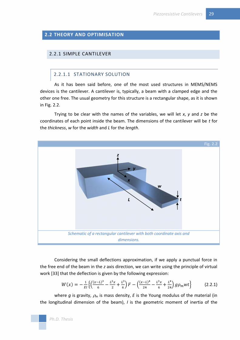
As it has been said before, one of the most used structures in MEMS/NEMS devices is the cantilever. A cantilever is, typically, a beam with a clamped edge and the other one free. The usual geometry for this structure is a rectangular shape, as it is shown in Fig. 2.2.
Trying to be clear with the names of the variables, we will let x, y and z be the coordinates of each point inside the beam. The dimensions of the cantilever will be t for the thickness, w for the width and L for the length.
Fig. 2.2
Schematic of a rectangular cantilever with both coordinate axis and
dimensions.
Considering the small deflections approximation, if we apply a punctual force in the free end of the beam in the z axis direction, we can write using the principle of virtual work [33] that the deflection is given by the following expression:
(2.2.1)
where g is gravity, m is mass density, E is the Young modulus of the material (in the longitudinal dimension of the beam), I is the geometric moment of inertia of the
L t
x
y
z
w

Piezoresistive Cantilevers
Ph.D. Thesis
30
transversal section of the structure (determined by ) and F is the applied force. It is important to pay attention on the difference between w (width) and W (vertical deflection).
(2.2.2)
Usually, the deflection of a cantilever is modelled as the deformation of a spring with a elastic constant k that is given by (2.2.3) considering a rectangular cantilever.
(2.2.3)
It can be seen from (2.2.3) that the term containing gravity effects has no influence on the elastic constant of the cantilever. In this kind of devices, deformation due to gravity is of less importance than external forces contribution, in addition, gravity effects can be considered as an initial deformation of the spring.
Though for many applications it is only necessary to know the value of the spring constant of the structure, in our case, it is also necessary to know the value of the deformation and the stresses at every point of the beam, and these are given by (2.2.4)
and (2.2.5), where x is the deformation of the structure in the x axis direction and x is the mechanical stress, both of them related
(2.2.4)
(2.2.5)
2.2.1.2 TRANSIENT RESPONSE. RESONANT FREQUENCY
In the previous section we have seen the static response of a cantilever to a force applied in the free end. If we would want to know how the deflection of the beam changes with time [34-36], we should solve the equation (2.2.6), that corresponds
cantilever:
(2.2.6)
Where A is the area of the cross section (in a rectangular cantilever: ). Solving this equation we are not taking into account the effect of
large deformations on the transversal section of the beam, but this approximation is perfectly suitable for the cases under study. Note also that nomenclature can be confusing at this point given that time and thickness can be represented by the same letter t.
The solution of (2.2.6) can be written as (2.2.7), that is a linear combination of each normal mode of vibration:
(2.2.7)

Piezoresistive Cantilevers
Ph.D. Thesis
31
where i is the resonant frequency for the ith mode and i is the shape of the ith mode. Taking into account a solution of this type, equation (2.2.6) can be reduced to:
(2.2.8)
The solution to (2.2.8) can be written as:
(2.2.9)
being i:
(2.2.10)
In the case of a rectangular cantilever with a clamped end and the other one completely free, the boundary conditions the solution must satisfy are:
(2.2.11)
Applying them we obtain that the final solution is given by (2.2.12) and that there
is a restriction in the values of i, what determines the value of the different resonant frequencies for each mode of vibration (2.2.13).
(2.2.12)
(2.2.13)
2.2.1.3 PIEZORESISTIVE EFFECT
Piezoresistive effect in Germanium (Ge) and Silicon (Si) was discovered by C.S. Smith in 1954 [37]. It was found that the resistivity of these materials changed with mechanical stresses. Small metal structures had been used to measure deformations by means of the change of the resistance, using the so-some differences between both behaviours, as the fact that the piezoresistive effect is like a hundred times greater than the gauge effect, generally anisotropic and, the most important one, the changes occurred in resistivity (not in geometrical factors that affect the value of the resistor).
Piezoresistive effect is determined by means of the piezoresistive coefficients that form the piezoresistive tensor. This tensor has, for a cubic material like silicon, three independent components [38] which will depend on temperature and impurity concentration. Hence, we could write (2.2.14), that is the basic equation of this effect:

Piezoresistive Cantilevers
Ph.D. Thesis
32
(2.2.14)
where is the piezoresistive tensor, is the stresses vector and is the electric
resistivity vector (note the difference between , electric density, and m, mass density). For a more detailed description of piezoresistive effect, some books like [39] can be consulted. The equation (2.2.14) can be expanded as following, taking as axis (100) directions of a cubic material, like silicon:
(2.2.15)
Two typical piezoresistance effects are considered when an uniaxial stress is applied in the material. One, when the current is in the direction of the stress, called
longitudinal ( l); and the other, when the current is perpendicular to the stress, called
transversal ( t). It is possible to calculate both coefficients ( l and t) for each direction. In Fig. 2.3 the anisotropy of the piezoresistive effect is shown, for standard (100) wafers in P-type and N-type silicon.
Fig. 2.3
a)
b)
Room temperature longitudinal and transversal piezoresistive coefficients for
P-type and N-type Si. Extracted from [38].
Given this anisotropy, an adequate choice of resistances will be needed to maximize the change in resistivity. For example, it is well known [29, 38] and it can be also seen in Fig. 2.3 that for P-type silicon the maximum effect happens for (110)

Piezoresistive Cantilevers
Ph.D. Thesis
33
directions, whereas it happens for (100) directions for N-type silicon. In addition, there is also a temperature and concentration dependence (Fig. 2.6) of these parameters. At low concentrations and normal temperature, the values of longitudinal and transversal coefficients for each type of silicon and for the directions where maximum is observed are:
(2.2.16)
2.2.2 DESIGN CHOICE
Piezoresistive sensors based on cantilevers have been widely used over the past two decades [29]. If the elastic constant of the structures is to be diminished or if the sensitivity is to be augmented, the dimensions of the beams should be decreased. Tortonese et al. [40-42] demonstrated that the fabrication of piezoresistive cantilevers for AFM was possible and, in order to achieve a noise level as low as necessary to make proper imaging, the dimensions of the beams had to be reduced significantly in comparison with the previously fabricated cantilevers.
In particular, width was desired as small as possible. Hence, photolithographic processes on the cantilever surface for the definition of resistors are to be avoided. In order to do that, the best design for this kind of structures [21, 42, 43] is the so-called U-shaped cantilever. In Fig. 2.4 a schematic of this type of beams is shown. It is important to note that in the clamping zone there are two separate arms (at least in the resistor layer). In this way, we can contact separately both arms, defining a resistor.
Once the shape of the beam has been chosen, it is necessary to fix the geometrical dimensions of each part of the cantilever as well as the materials to fabricate the structure with. To take these decisions the compatibility with the CMOS technology that we are using for the CMOS version of the sensor (in this case CMOS 0.8 from AMS technologies) has to be taken into account.
2.2.2.1 MECHANICAL STUDY OF THE NEW STRUCTURE
Although the most general case of cantilever beam would be the one showed in Fig. 2.4, firstly we will consider a beam with a rectangular cross section and monolithic, that is, made of only one material. This way, applying again the principle of virtual work and assuming the small deflections approximation, we can calculate that the deflection of such an U-shaped beam after applying a vertical force in the free end would be given by:

Piezoresistive Cantilevers
Ph.D. Thesis
34
(2.2.17)
What yields the following elastic constant:
(2.2.18)
Thus, the stress distribution all along the cantilever would be:
(2.2.19)
Fig. 2.4
Schematic of a U-shaped cantilever with dimensions for the mechanical
structure and the resistance layer. In this case, cantilever thickness is considered constant and also is the thickness of the resistance layer.
This way, considering a resistor layer with an infinitesimal thickness ( z), the total change of the resistor value would be given by the change in both arms (this would be longitudinal effect) plus the change in the transversal region. Thus, we could write (2.2.20) as the change in the resistor, being wR the width of the resistor layer.
(2.2.20)
As there are many parameters to be optimised, we can make some approximations to facilitate this task. For example, if the length of the resistor (LR) is much bigger than the width w2, the effect of the transversal part of the resistor will be negligible in comparison with the contribution of the longitudinal part. Moreover, as the main objective of the sensor is the detection of biomolecules, the elastic constant should
t L
LR
L1
w1/2
w2
wR

Piezoresistive Cantilevers
Ph.D. Thesis
35
be as small as possible [21], what means that the best option would be to have the quantities LR and L1 with very similar values. Taking into account these two considerations (2.2.20) could be rewritten:
(2.2.21)
where is a non-dimensional parameter defined as:
(2.2.22)
and the relative change in the value of the piezo-resistor would be given by:
(2.2.23)
Thus, in principle, we could assure that the piezoresistive effect will be bigger when increasing the length and decreasing the width of the arms and the thickness of the cantilever. The problem is that, until now, we have considered a resistor layer with an infinitesimal thickness. In many microelectronic applications this approximation is valid, due to the fact that the cantilever is much thicker than the diffused conductive layer. In our case, the thickness of the beam will be decreased as much as possible to improve the sensitivity, what means that the resistor will have a thickness comparable to the one of the whole structure.
For this reason, following the calculations made elsewhere [21, 44], we can deduce that, given a constant dopant distribution through the conductive layer, the relative change in resistor will be:
(2.2.24)
Where tR is the thickness of the resistor. If the dopant concentration (c) depends of z, we should include a correction factor, so (2.2.24) becomes (2.2.26) through (2.2.25).
(2.2.25)
(2.2.26)
2.2.2.2 BASIC CIRCUIT SCHEME
Usually, piezoresistive sensors are presented in a Wheatstone bridge or in a semi-bridge configuration. This kind of configurations allow us to easily convert a change in the values of the resistors in a voltage change, which can be then amplified or/and filtered.

Piezoresistive Cantilevers
Ph.D. Thesis
36
Fig. 2.5
Schematic of the circuit, with a Wheatstone bridge and a differential
filter/amplifier.
The typical scheme that would be used is the one presented in Fig. 2.5. In this kind of circuit, we can have variations in one of the resistors or in two opposite resistors, which yields a final sensitivity for the sensor given by (2.2.27) and (2.2.28) respectively.
(2.2.27)
(2.2.28)
If we used a semi-bridge configuration, the sensitivity in voltage would be given also by (2.2.28).
2.2.3 NOISE
We have been able to calculate the sensitivity of our sensor (before the amplification/filtering phase). As it was explained in the introduction of this chapter, sensitivity is a very important parameter for a sensor, but for the application we are focussed in, the main important parameter is resolution because it will yield the minimum detectable force. As it has been discussed, the resolution is given by both the sensitivity (known) and the noise.
To evaluate the noise of the whole circuit, it is necessary first to take into account only the noise due to the Wheatstone bridge. Once this is known, the electronics to amplify and filter the signal could be designed, implemented and the final noise calculated. Thus, given that the only electronic components in the bridge are resistors,

Piezoresistive Cantilevers
Ph.D. Thesis
37
-
bridge would be located in a cantilever, there will appear the so-called thermomechanical noise.
When studying a noise, the magnitude used here will be the so-[]2/Hz, that specifies the shape of the
noise in function of the frequency and that allows us to compute the noise in the system by integrating. For example, given a signal X(t):
(2.2.29)
If we have another signal Y(t) related with X(t) through a transfer function H(t):
(2.2.30)
Thus, this magnitude is very useful because it can help in the design of the electronic circuitry to amplify and filter the output signal of the sensor.
2.2.3.1 JOHNSON-NYQUIST NOISE
First of all, let us consider the thermoelectric noise, the one that appears in a circuit because there are resistors. This noise is a fundamental limit, set by the thermal energy of the carriers in a resistor [45, 46]. This effect is called to be white, which means that it is not frequency dependent, and it is given by:
(2.2.31)
Where kB is Boltzmann constant, T is temperature in Kelvin and R value in Ohms. It is possible to change the parameters in (2.2.31) and leave the expression depending on the geometrical parameters that can be controlled:
(2.2.32)
Where wR, tR and LR are the dimensions of the resistor and the approximation made in (2.2.22) and the one of considering a constant carrier distribution have been made here again.
2.2.3.2 HOOGE OR 1/F NOISE
Hooge noise is not constant through the frequency span, but it is inversely proportional to the frequency. Thus, when operating at low frequencies, its importance grows and it can even become the most important contribution to noise. As in the case we are considering, the measurement will be quasi-static, this noise should be the most important.

Piezoresistive Cantilevers
Ph.D. Thesis
38
The origin of this kind of noise is not very clear and there are several theories trying to explain it, but none of them is able to completely fit experimental results. Because of this, Hooge proposed [47] a semi-empirical law with just one fitting parameter that would depend on the material. So, the power noise spectrum would be given by:
(2.2.33)
Where is the fitting parameter, N is the number of carriers in the region where the noise is generated, Vcc is the supply voltage and f is the frequency.
We can now write down (2.2.33) in function of the geometrical parameters that we can externally control during the fabrication. Here, the approximations made for (2.2.32) are used again to yield:
(2.2.34)
Where c is the carrier concentration in the resistor and the rest of values are the geometrical dimensions of the resistor, as introduced in (2.2.32).
2.2.3.3 THERMOMECHANICAL NOISE
The last noise type considered here will be thermomechanical noise. As its name says, it is a merely mechanical noise, so it will only affect the cantilevers, that are the only part in the circuit where it is possible to actuate mechanically. The origin of this noise is the Brownian movement of the particles surrounding the cantilever, which will cause the beam to deflect and this will consequently change the stresses and also the resistor value.
If the measurement is made optically this is the only source of noise and this will limit the resolution of the sensor. Because of that, several studies have been made to exactly determine not only the value but also the frequency dependence of this noise [35, 36]. In our case, as the measurement will be piezoresistive, some authors consider that the other two sources of noise will contribute more than this one [21, 48-51]. We will try here to make a proper estimation of the noise and we will decide afterwards if it is negligible or not.
Following Salapaka [36], a more detailed deduction has been presented elsewhere [44]. In principle, it is derived only for a simple cantilever with rectangular and constant cross-section but it is possible to make the same treatment with a U-shaped cantilever. The differential equation to be solved is (2.2.35) instead of the previously mentioned (2.2.6)
(2.2.35)
where is the damping coefficient and pth is the thermal forcing due to the movement of the particles. This loading is in principle unknown and is calculated

Piezoresistive Cantilevers
Ph.D. Thesis
39
afterwards, in order to get the complete solution. To solve this equation, given the member with the first time derivative, the deflection will not be given by (2.2.7) but by (2.2.36), where qi is a function that carries the information of the temporal evolution of
each mode shape, i:
(2.2.36)
If the Fourier Transform is made, (2.2.36) becomes (2.2.37) through the parameters defined in (2.2.38)
(2.2.37)
(2.2.38)
Then, applying the Equipartition Theorem (each normal mode of vibration share the same amount of energy, equal to kBT) and the fact that pth, the force exerted for the particles in a Brownian movement over the cantilever has a white noise power spectra, it is possible to write that, if the condition (2.2.39) is true, then the noise power spectra for the deflection of the cantilever will be given by (2.2.40). The validity of the condition (2.2.39) will be discussed later.
(2.2.39)
(2.2.40)
Where M is the number of the normal mode for which the series is truncated. The modes with a number bigger than M are considered to not contribute to the noise.
So, the movement of the particles causes a deflection in the beam which also generates stresses in the inner part of the cantilever which finally changes the resistivity and hence the voltage output of the bridge. From (2.2.19)-(2.2.28) it can be seen that:
(2.2.41)
Considering that only one of the resistors in the bridge is mounted on a cantilever, we can write (2.2.42) what leads us to (2.2.43) through (2.2.30),
(2.2.42)
(2.2.43)

Piezoresistive Cantilevers
Ph.D. Thesis
40
And hence, using (2.2.44) we can obtain (2.2.45), that is the value of the voltage power noise spectra for the thermo-mechanical noise:
(2.2.44)
(2.2.45)
If the cut off frequency of the circuit satisfies the condition (2.2.46), a
simplification occurs in (2.2.45), where the variable can be neglected. In addition, It is possible to show that choosing M=1 introduces an error of 2%, what allows us to write (2.2.47).
(2.2.46)
(2.2.47)
Depending on the value of , this noise can change by a factor of 3 and, to make an estimation, it will be considered the value that yields a maximum noise, what results in:
(2.2.48)
where Q is the quality factor of the beam, calculated from:
(2.2.49)
With this last equation we can also show the validity of the condition (2.2.39) that will be satisfied if and only if the quality factor Q is bigger than 0.5, which in principle holds for all the beams that could be fabricated.
2.2.3.4 TOTAL NOISE
The total power noise spectrum can be estimated by adding all three of noise spectra calculated until now:
(2.2.50)
The noise is found by integrating this quantity between the cut-off frequencies:
(2.2.51)
(2.2.52)

Piezoresistive Cantilevers
Ph.D. Thesis
41
Knowing the minimum detectable voltage (2.2.52) and the sensitivity for a device with just one resistor on a cantilever (2.2.27), it is possible to obtain the resolution of the sensor, that is defined by (2.1.2)
(2.2.53)
In principle, given the target of our sensor, the magnitude that should be minimized is (2.2.53), and therefore it would be possible to make measurements of smallest forces.
2.2.4 PARAMETERS OPTIMISATION
The main objective is then to make the minimum detectable force as low as possible just changing the different parameters that appear in (2.2.53).
2.2.4.1 PIEZORESISTIVE COEFFICIENT
The simplest parameter to take into account is the piezoresistive coefficient, , of
the resistor material. The higher the value of , the lower the detectable force will be.
As it has been commented before, the materials with higher are the semiconductors. Given that the silicon is the most used material in microelectronics, we focus in it. It is possible to have the material either in the crystalline form or in the polycrystalline one.
Considering the crystalline version of the material, it is known [38] the dependence of the different coefficients with the impurity concentration, the temperature and the direction of the resistor. Depending on the latest, it is possible to observe several maxima and minima so the direction has to be carefully chosen. Generally, when using (100) silicon wafers, the lines used to define the resistors in a N-type silicon are (100) directions (45º with flat direction); whereas in P-type silicon are (110) directions (parallel and perpendicular to flat direction). In our case, given the geometry chosen for the cantilever sensor, that would mean a value of the coefficient as shown in (2.2.16), that is:
These values are for room temperature and for an impurity concentration under 1024 m-3. Varying both parameters, the piezoresistive coefficients also change, as it is shown in Fig. 2.6.a for P-type silicon or in Fig. 2.6.b for N-type silicon (extracted from [38]).

Piezoresistive Cantilevers
Ph.D. Thesis
42
Fig. 2.6
a)
b)
Piezoresistive coefficient factor in P-type (a) and N-type (b) silicon as a function
of temperature (T) and impurity concentration. Data extracted from [38].
If the material of the resistor is polysilicon it must be taken into account that, as it is explained in [39, 52], a polysilicon layer consists of a large amount of single crystalline silicon grains and some non-crystalline regions (boundary regions) between the grains. The size of the grains can vary from few tens of a nanometre up to a few microns, depending on the deposition conditions. The orientation of the grains can have a preferential orientation in the Z-axis but in the XY-planes the orientations are always random.
The boundary regions between the grains contain a large amount of trap centres which cause a potential barrier between adjacent grains and also depletion layers in the surface region of those grains. Given this configuration, the resistance consists of two parts: one from the conductive region of the grains (without the depletion layer) and another from the boundary regions and the depletion layers. These two components will change when applying mechanical stresses, what means that the total change in the resistance will have two components. For most cases, the effect of piezoresistance (change of the resistance of the crystalline grains) is the dominant effect [39] but there is a fundamental difference between this case and the crystalline Silicon one and is that in polysilicon, the random orientation in X-Y planes means that the piezoresistive coefficients result averaging those in crystalline Silicon.
Many studies deal with the experimental determination of piezoresistive coefficients in polysilicon [52-55] gauge factor (2.2.54), where the approximations are valid if and only if G>>2.
(2.2.54)

Piezoresistive Cantilevers
Ph.D. Thesis
43
It is possible to calculate the gauge factor for every non insulating material. In most metals, G is around 2, what means that there is not piezoresistive effect but only extensiometric. On the other hand, in crystalline silicon, from (2.2.16) we can derive that the biggest values of G are:
(2.2.55)
Fig. 2.7
Longitudinal and transversal gauge factors, GL and GT, in polysilicon as a
function of impurities concentration. Figure extracted from [52].
In polysilicon, several factors affect the value of the gauge factor. Doping concentration, temperature of deposition and thermal annealing for impurities activation are the most important ones. In Fig. 2.7 some literature results [52] are presented, in this case in function of doping concentration. It can be seen that the values of G are in the range 10-40, that is, somewhere in between the extensiometric effect for metals and the piezoresistive effect in crystalline silicon.
So, in principle, the piezoresistive factor, , or the gauge factor, G, are preferable to be as high as possible, but, as it depends also on factors (as seen in Fig. 2.7 for
example) that appear also in (2.2.53) it could be preferable not to have and G in their maximum values.
2.2.4.2 RESISTANCE LAYER
When defining the resistance layer in the mechanical structure, there are two major decisions to be taken, the dimensions (LR, wR and tR) and the dopant concentration. The first one can be divided in two, given that the control of the thickness is given by the

Piezoresistive Cantilevers
Ph.D. Thesis
44
doping conditions and the other two dimensions can be controlled by photolithographic steps.
The importance of carrier concentration profile is given by (2.2.26). The chosen method to dope the silicon is ion implantation. Thus, the profile can be calculated depending on the doping and the posterior thermal annealing conditions. Generally, the approximation which best fits with the experimental data is a Gaussian profile. In our case, as it will be shown later, the most used material is polysilicon, where the resistance layer is limited by a silicon oxide layer, therefore the approximation of a rectangular profile is enough.
Considering a constant profile, carrier concentration has to be chosen taking into account its influence on the piezoresistive coefficients (see Fig. 2.6 and Fig. 2.7) and on Vnoise (2.2.52). The concentration will affect the 1/f noise and the Johnson-Nyquist noise, being both of them inversely proportional to the square root of the concentration:
(2.2.56)
This way, we should choose the highest value for the concentration but trying to
maximize the piezoresistive coefficient, given that the noise depends inversely with . Indeed, the magnitude that should be maximized is:
(2.2.57)
Besides, the other parameter controlled by the doping conditions is the thickness of the resistance layer, tR. To optimize its value, it can be defined a non-dimensional
parameter, , as follows:
(2.2.58)
Using (2.2.58) and considering that in most cases the thermomechanical noise will be several orders of magnitude lower than the other two types of noise, the expression
for the minimum detectable force, (2.2.53), will have the following -dependence:
(2.2.59)
And, from (2.2.59), it is easily obtained that the minimum detectable force will be
achieved when 1/3 [21]. As it can be seen in Fig. 2.8, though the minimum is found for
the announced value of , Fmin will vary very slowly in comparison to the change in the
thickness of the resistor and, given reasonable values for , Fmin could just become the double of the minimum.

Piezoresistive Cantilevers
Ph.D. Thesis
45
Fig. 2.8
Fmin, resolution, dependence with the relative thickness of the resistance layer
( ). OY-axis values are normalized in order to have the minimum as 1.
Finally, the other two dimensions of the resistor have to be taken into account. These can be changed by means of photolithographic steps and that is the reason to consider them separated from the thickness of the resistor.
The width of the resistor can be analyzed by means of a new non-dimensional
parameter, that is and is defined by:
(2.2.60)
Now, the relation (2.2.53) will have the following dependence:
(2.2.61)
What means that the optimum case will be achieved when =1 . It is interesting to highlight the fact that the width of the resistance does not affect the sensitivity. It only (wR = w) appears in noise formulae.
The length of the resistance is determined by the total length, L, of the structure
and (2.2.22). It has yet been discussed the approximation made in (2.2.22), where L1 and LR are forced to have similar values in order to minimize the cantilever elastic constant and hence improve force resolution. Then, from (2.2.53) and (2.2.52) we can obtain the following dependence:
(2.2.62)
1
1,2
1,4
1,6
1,8
2
2,2
0 0,2 0,4 0,6 0,8 1
F min
norm
aliz
ed

Piezoresistive Cantilevers
Ph.D. Thesis
46
where A, B and C are parameters included just to simplify the formula and that each one is related with a kind of noise. For example, as C is determined by the level of thermomechanical noise, it could be neglected because in most cases this noise is much lower than the others. A (1/f noise) and B (Johnson Nyquist noise) depend on many
parameters (geometric, material properties, bandwidth, etc.). To know which value of optimizes the resolution, we should take into account the relation between these two parameters, that is, we should compute the relation between both noise sources. In the
case that both noises are comparable, the optimum value is found to be =1/2 (Fig. 2.9.a). If Johnson noise is predominant, it means that the smaller the resistance, the
better and then the optimum value of will be closer to zero (Fig. 2.9.b). On the contrary, if 1/f noise is the relevant source of noise, the signal will improve if the resistance is made
longer, but until = 2/3, where the best resolution is achieved (Fig. 2.9.c). As the measurements are to be made at low frequency, it is expected that the latter is the more
important source of noise and so, the best choice is to have between 1/2 and 2/3. In
our designs we chose to have 1 mainly for two reasons: all the calculations turn to be much simpler and the quality factor is expected to rise.
Fig. 2.9
a)
b)
c)
Fmin dependence with for different noise configurations, a) 1/f and Johnson
noises are comparable, b) Johnson noise is predominant and c) 1/f noise is predominant.
0,9
1,1
1,3
1,5
0 0,2 0,4 0,6 0,8 1
F min
norm
aliz
ed
0,9
1,4
1,9
2,4
2,9
0 0,2 0,4 0,6 0,8 1
F min
norm
aliz
ed
0,9
1
1,1
1,2
1,3
1,4
0 0,2 0,4 0,6 0,8 1
F min
norm
aliz
ed

Piezoresistive Cantilevers
Ph.D. Thesis
47
2.2.4.3 GEOMETRICAL DIMENSIONS
The geometrical dimensions of the beam (L, t and w) affect also the resolution of the sensor hence they also have to be taken into account.
Following the ideas used in the previous paragraph, if the thermomechanical noise is neglected, the resolution will be given by:
(2.2.63)
From (2.2.63) we can deduce that the minimum detectable force will be made smaller if the thickness (t) or the arms width (w1) are decreased or if the length (L) is increased.
If the thermomechanical noise was not negligible and it is necessary to take it into account, it should be necessary to analyze the quality factor of the different fabricated structures. The quality factor that appears in (2.2.52) is a good parameter for the understanding of the formulae, but it depends on the geometric dimensions, so it is not a good parameter to optimize the resolution of the sensor.
As additional requirements to the choice of the dimensions, we could consider that the elastic constant should be as low as possible (in order to avoid damage to target biologic samples) and that the resonant frequency should be as high as possible (in order to allow faster measurements and to diminish the effect of low frequency mechanical noise).
2.2.4.4 MISCELLANEA
The rest of parameters that appear in (2.2.53) and (2.2.52) are commented briefly here:
Bandwidth: Bandwidth is the range of frequencies that are used in the measurement. The upper limit can be set with electronic filtering, by the sampling rate of the measurement or the resonant frequency of the cantilever among other possibilities. The lower limit can be set with electronic filtering or by the length of the measurement in time.
Depending on the characteristics of the measurement, the sensor will have to operate in a frequency range or another. In our case the optimal frequency of operation may depend on the studied molecule [1]. However, what we propose here is a sensor to perform quasi static measurements, what means that 1/f noise will be dominant and that high frequencies can be cut off.
Supply Voltage: It is clear that is better to have Vcc as high as possible, given that Johnson noise will be diminished. However, it has been found [21] that some thin

Piezoresistive Cantilevers
Ph.D. Thesis
48
cantilevers are not able to operate under a big power consumption. This should be taken into account when choosing the supply voltage because dissipated power is proportional to Vcc
2.
parameter: As this parameter only enters in the 1/f estimation, it is clear that it is better to have it as low as possible. It can be somewhat controlled by changing the
annealing temperature and time. Making so, it is possible to achieve values of down to 10-6 for crystalline silicon and down to 10-3 for polysilicon [21, 48, 49, 56].
2.2.5 CMOS CANTILEVERS
It has been explained before that the main objective of the BioFinger project was the fabrication of a sensor with piezoresistive cantilevers using a CMOS technology allowing the integration with filtering/amplifying circuitry and a cheap mass production.
The chosen CMOS technology was the commercial 0.8 m CMOS CYE process from Austriamicrosystems (AMS). This CMOS technology has two polysilicon layers and two metal layers.
One of the first objectives was then to minimize (2.2.53) taking into account all the points enumerated in the previous section and also the restrictions imposed for the compatibility with the CMOS process. In order to keep the fabrication as cheap as possible, the standard commercial process was used, without any additional step but an adequate post-processing for the backside etching.
This backside etching of the substrate silicon was chosen to be made by means of an anisotropic wet etching with KOH (or TMAH) [28, 57-60]. These alkaline solutions have the property of etching some crystalline planes of the silicon faster than others. For example, (100) planes are etched 3-4 orders of magnitude faster than (111) planes. There are three main options to stop this anisotropic etching: by means of a heavily boron doped layer, of a dielectric layer or by the so called electrochemical etch stop, but the first is discarded because no step in the fabrication process would dope the silicon as much as it would be necessary.
The electrochemical etch stop [61, 62] has different configurations (2, 3 and 4 electrodes) and is based on the electrochemical characteristics of silicon and in the fact that they are different for N-type and P-type silicon. First, when the voltage between silicon and the solution trespass a certain value (called passivation voltage), the silicon becomes passivated and is not etched anymore. This passivation voltage is different depending on the impurities of the silicon (N or P). This allows us to define some regions by means of a doping technique (e.g. N type) and connect them to a voltage, avoiding their etching. If we force that the rest of the silicon of the substrate (e.g. P type) can be etched, the solution will machine the whole wafer until the wells defined before which will become passivated. This technique has been widely used to machine silicon

Piezoresistive Cantilevers
Ph.D. Thesis
49
cantilevers with some microns in thickness [63-66] but submicron structures are not achievable in a proper and repeatable way. This is due to the impossibility of maintaining the same voltage in all the volume of the diffused layer (because of leakage currents).
The last technique to stop the anisotropic etching of the silicon is based on the fact that the silicon oxide etching ratio is some orders of magnitude lower than that of a silicon (100) plane. In fact, this selectivity allows us to use this layer (silicon oxide) or another isolating layer (like silicon nitride) as a mask for this etching. In Table 2.1, etching ratios for different materials are shown. The silicon dioxide layer can be grown or deposited inside the technologic process or can be buried in the same wafer, using the so called SOI wafer (Silicon On Insulator). The main difference is that in the latter the material for the sensor would be crystalline silicon while in the first one the material would have to be polysilicon or any other deposited material.
Table 2.1
Conditions Si (100) SiO2 Si3N4
KOH 75º//40% 56 m/h 2200 /h 40 /h
TMAH 80º//25% 26 m/h 25 /h 7 /h Etching ratios of the most used materials for KOH and TMA, characterized in
CNM clean room.
Each technique has advantages and disadvantages. The electrochemical etch stop is much more difficult to implement, given that it is necessary the definition of doped wells and the interconnections between chips. Besides, leakage currents will not allow the fabrication of thin structures. On the other hand, the material of the mechanical structure can be crystalline silicon whereas if the etch stop is performed by means of a dielectric layer, the only possibility is to use a SOI wafer, what is not possible in this CMOS technology. Mechanical properties of crystalline silicon are much better than that of polysilicon (no internal stresses, perfecaddition, if the sensor is to be piezoresistive, the gauge factor is from 5 to 10 times higher in crystalline silicon.
Considering the chosen CMOS technology, we can analyze the different options
we can use to define the cantilever. First, it would be possible to use the n- well (3.5 m
deep) to define the mechanical structure and the p+ diffusion (0.4 m deep) to define the
piezoresistors. Second, we could use the n+ diffusion (0.4 m deep) for the cantilever and then, as there would be no thinner doped layer, the resistance should be made of
polysilicon, using the poly2 (0.27 m thick). Finally, the last option would be based on
using the two polysilicon layers, poly1 (0.42 m thick) and poly2 to define the whole cantilever.

Piezoresistive Cantilevers
Ph.D. Thesis
50
Among all three, the second is discarded immediately because it has the drawbacks of both etch stop methods: the gauge factor would be the one of the polysilicon and the final cantilever would not be very well defined because of the leakage currents. In addition, design rules do not allow the deposition of polysilicon on the n+ zones.
Between the other two options, though the first would result in a much thicker cantilever, given that the gauge factor would be that of crystalline silicon, the minimum detectable forces would be similar. Thus, using the fact that it is better to have the elastic constant as small as possible, the option of both polysilicon layers is chosen.
In this case, the thickness of the complete structure as well as the thickness of the
resistance layer would be fixed by the specifications of the process. Poly1 layer is 0.42 m
thick, poly2 is 0.27 interpoly
thickness of approximately 0.7 m for the whole cantilever and a relative thickness of the resistor of 0.38, that is similar to the optimum value of 1/3, as it has been seen before.
As the width of the cantilever has also to be minimized, the structure is designed in principle following the minimum widths imposed by the design rules of this technology.
This is 1.6 m for poly2 and for poly1, as it has to be under the other polysilicon layer, the
minimum width is 4.4 m (see Fig. 2.10).
Fig. 2.10
a)
b)
Schematics of a typical CMOS cantilever: a) complete view and b) transversal
view.

Piezoresistive Cantilevers
Ph.D. Thesis
51
2.2.6 THEORETICAL STUDY OF CMOS CANTILEVERS
Once the option of using both polysilicon layers to constitute the cantilever has been chosen and knowing that the transversal section of the beam will not be rectangular, the calculi made until now have to be reviewed and corrected.
2.2.6.1 MECHANICS OF THE BEAMS
First of all, let us fix the value of , defined in (2.2.22) as the length of the arms, as
1. It is easy to show that, even having a variable thickness through the length of the
cantilever, the conditions for the choice of are invariable, what means that the optimum choice would depend on the relative importance of Hooge and Johnson noises.
As the most important noise in this case will be 1/f (this will be shown later),
choosing = 1 instead of 2/3, though not optimum for the resolution makes the calculi much easier. This way, it is possible to consider the whole beam as two independent separate cantilevers, loaded with F/2 each. To simplify even more the mechanical model, the oxide layer between both polysilicon layers will not be considered (the oxide layer represents just a 3% of the total thickness of the beam).
So, the fact that the beam has not a rectangular transversal section affects mainly two things. First, the moment of inertia will be different and will depend on several parameters. Secondly, the position of the neutral axis will not be the middle of the beam anymore, but a calculated one by means of:
(2.2.64)
(2.2.65)
where b1 and t1 are the dimensions of the bottom part of the beam and for the top part of the beam we have b2 and t2. The integrals are extended over the area A of the whole cross section. It is very important to take into account that the choice of the origin determines the value of z0. In this case, the origin has been chosen to be in the separation between both polysilicon layers. Knowing the position of the neutral axis, the geometrical moment of inertia can be calculated:
(2.2.66)
This way, looking at (2.2.19), we can write here that mechanical stresses distribution inside the beam will be given by:
(2.2.67)

Piezoresistive Cantilevers
Ph.D. Thesis
52
Recalling now (2.2.24) it is possible to write down that the relative change in resistance is now:
(2.2.68)
That, in the case of having the resistors connected in a Wheatstone bridge and just one of the resistors mounted on a cantilever results in a relative change of voltage of:
(2.2.69)
It can be easily shown that the best choice for the widths of both layers is to have them with the minimum size allowed by the design rules. With these dimensions, the parameters that will determine the mechanical properties of the beam will be:
(2.2.70)
2.2.6.2 NOISE
In the same way than we have done for rectangular cantilevers, we have estimated the sensitivity of our sensor and we have chosen the dimensions in a manner that this parameter is optimized. As it has been commented also, it is not the sensitivity but the resolution what should be minimized. To do that, it is necessary to compute the noise of the system. In this case, there will also be three kinds of noise that are: thermoelectric (Johnson-Nyquist) and 1/f (Hooge) as completely electrical noises and thermomechanical noise, that appears because of the movement of the beams due to the Brownian motion of the particles surrounding them.
Thermoelectric noise is given by (2.2.31), which in this case can be written as:
(2.2.71)
From the specifications of the technology we know the value of the square resistance of the poly2 layer. In function of that, we can calculate the resistivity if a constant impurities profile is considered:
(2.2.72)
This value of the resistivity can be used to make an estimation of the doping concentration, using Fig. 2.11, that has been extracted from [52]. With such approximation to the value of the level of impurities, we can also estimate Hooge noise, that is given by (2.2.33) that here develops to:
(2.2.73)
where c is the carrier concentration, that is supposed to be constant.

Piezoresistive Cantilevers
Ph.D. Thesis
53
Fig. 2.11
Resistivity, , as a function of doping concentration and for different deposition
temperatures (for polysilicon). Figure extracted from [52].
Finally, the last kind of noise is thermomechanical. As it has been commented, it will be negligible in comparison with the other two, so we will just consider the sum of the other two noises.
This way, the total noise voltage is given by:
(2.2.74)
What results in a resolution for these cantilevers of:
(2.2.75)
It can be seen that (2.2.75) is optimized also taking the minimum widths allowed by the design rules. Thus, not only sensitivity but also resolution are improved by the choice made for transversal dimensions, as it happened also for a rectangular cross section cantilever.

Piezoresistive Cantilevers
Ph.D. Thesis
55
2.3 FEM SIMULATION
Mechanical calculi performed in last section are in most of the cases very simple but many approximations are taken into account for each of the estimations, especially when the cantilever is U shaped and does not have a rectangular cross section (as the ones from the CMOS process). A more refined way to obtain mechanical stresses, and thus piezoresistive effect, is by making some Finite Elements Modelling (FEM) simulations of the structures.
FEM is a well established mathematical method to solve complex differential equations [33]. It is based in splitting the whole structure to be analyzed into discrete and separate parts. This way, the structure is treated as a conjunction of nodes configuring a mesh. Each one of those nodes has several degrees of freedom (DOF), depending on the type of FEM that will be performed. For example, the first FEM analysis reported consisted in a mere mechanical analysis (mechanical DOFs), but nowadays it is possible to perform thermal, electric, magnetic, etc. analysis and, what is better, it is possible to directly solve coupled systems. The actual advantage of this method is that it can be easily implemented in a software program, which allows us to estimate the deformations and mechanical stresses that appear in any structure, no matter the complexity. The program used to make the simulations is Ansys (v. 10).
What is intended in this section is to study the behaviour in both dynamic and static modes of the structures that we have been proposing in previous section. Also the validity of the approximations made when performing the estimations will be considered. To do that, a simple cantilever will be considered firstly, mainly to check which kind of anchoring is the best (taking into account accuracy of results and also time consumption). Then, some U-shaped cantilevers will be simulated, beginning for a monolithic one, then a tri-layered and finally one with a non-rectangular cross section.
2.3.1 SIMPLE CANTILEVER
2.3.1.1 STATIC RESPONSE
First, a simple cantilever with rectangular cross section will be taken into account. A force will be applied on the free edge of the beam. The material used for this simulation will be polycrystalline silicon, and the material properties that will be used are in Table 2.2. The results will be compared to those obtained from (2.2.1). One of the approximations performed to extract (2.2.1) was that only uniaxial deformations were present. Using this approximation, Poisson coefficient has no effect in deformations. However, simulations are made with a non zero value of Poisson coefficient in order to obtain a more accurate result.

Piezoresistive Cantilevers
Ph.D. Thesis
56
Table 2.2
E = 160 GPa (Young modulus) t = 0.65 m (Thickness of the beam)
= 0.27 (Poisson coefficient) w = 4 m (Width of the beam)
= 2330 Kg/m3 L = 200 m (Length of the beam)
F = 100 pN
Data for FEM simulations.
Three geometrical configurations can be considered. A simple clamping (considering just the cantilever), a cantilever with the silicon substrate and a cantilever with a little extension, corresponding to the region that is on the substrate in the previous configuration. In Fig. 2.12 and Fig. 2.13, the results of the simulations for the most accurate geometries are shown. In Table 2.3 the results for all three simulations are presented. The difference between simulations and calculi are in all cases below 1%, and
-in which the Poisson coefficient is not taken into account.
Table 2.3
Result
G.C.1 - =0.27 -18.174 nm 0.36 %
G.C.2 - =0.27 -18.212 nm 0.03 %
G.C.3 - =0.27 -18.232 nm 0.14 %
Results for all three different Geometrical Conditions (G.C.), of the deflection of a simple cantilever and comparison with analytical result.
Given that the results for all three geometries are very similar, we choose to make the rest of simulations with the last type, because it lays somewhere in between of the
as the first one and it represents the real behaviour of the beam almost as well as the complete configuration.

Piezoresistive Cantilevers
Ph.D. Thesis
57
Fig. 2.12
Geometric configuration in which Si substrate is considered in the simulation. It is the most accurate (similar to reality) but it is also the hardest to construct.
Fig. 2.13
Geometric configuration to avoid the use of the substrate. The structure has a
little fraction of the whole length that has its bottom part fixed, as if it was on a substrate. Results are very similar to the case considering the whole substrate.
2.3.1.2 VIBRATIONAL MODES
With the same data included in Table 2.2 we can perform a modal analysis and obtain the resonant frequencies for the three first vibrational modes of such a rectangular cantilever. In Table 2.4 we can see that the difference between analytical and simulated results is also very small, below 1% in all cases.

Piezoresistive Cantilevers
Ph.D. Thesis
58
Table 2.4
Mode Analytical Simulation
Transversal fundamental 21.75 kHz 21.71 kHz 0.18 %
Lateral fundamental 133.846 kHz 133.26 kHz 0.44 %
First transversal harmonic 136.314 kHz 136.19 kHz 0.09 %
First resonant frequencies for a rectangular cantilever with dimensions and mechanical data included in Table 2.2.
2.3.2 U-SHAPED CANTILEVER
If we consider a monolithic U-shaped cantilever, that is a cantilever fabricated with just one material and with two arms in the anchoring zone, we can compare also the analytical results obtained using the approximations that we proposed with the results of the FEM simulations. Using the anchoring configuration that has been proved to be the most suitable, we can simulate the response to a force in the free edge and also the resonant frequencies of the first vibrational modes.
Using the parameters included in Table 2.2, the only parameter that remains
unknown is , that is, the relation between the length of each arm and the total length of
the beam. We will consider first the case 1 (this is the value of chosen to fabricate
our devices and the one which simplifies most the analytical treatment) and then = ½ because it is the value that optimizes the piezoresistive response and as an example of the difficulty of the theoretical estimations.
2.3.2.1 1
In Table 2.5 the results of the simulations and their comparison to the analytical results is shown. The calculi were made in this case considering that the structure behaves as two separate cantilevers with the same dimensions. In the case of the
resonant frequencies of transversal modes, the results should be the same that for a simple cantilever, given that the resonances of both beams in that directions are the same.

Piezoresistive Cantilevers
Ph.D. Thesis
59
Table 2.5
Analytical Simulation
Deflection - 9.1033 nm - 9.10 nm
Transversal fundamental 21.75 kHz 21.347 kHz 1.85 %
First harmonic (trans) 136.314 kHz 134.05 kHz 1.66 %
FEM results for a U-shaped cantilever with the dimensions and mechanical
data included in Table 2.2. Case for 1.
Fig. 2.14
a)
b)
c)
d)
Different FEM results for a U-shaped monolithic cantilever. a) static deflection as a response to a force applied at the free end, b)-d) shapes of the three first
transversal vibrational modes. In Table 2.5 results for a), b) and c) are included.
In Fig. 2.14 we can graphically see some FEM results. For example, in Fig. 2.14.b the first vibrational mode is shown, where both arms are vibrating with the same amplitude and shape, hence the first mode for the U-shaped structure is very similar to the first transversal mode in a standard rectangular cantilever. A similar situation happens for the second vibrational mode, the first harmonic. In Fig. 2.14.c, it can be seen how both

Piezoresistive Cantilevers
Ph.D. Thesis
60
arms are moving identically, making the same movement that a rectangular cantilever does. A different situation is found with the third vibrational mode, the second harmonic. In Fig. 2.14.d the shape of this mode is shown. What happens is that both arms are performing the same vibration but with a difference of half a period in the phase. This is the first vibrational mode that appears because the beam is U-shaped and the reason for it to appear is the fact that both arms are connected to each other at the free end. This connection couples both arms, and converts the free ends of both arms in somehow bounded, thus, vibrational modes of a bridge appear. This could be observed also for the fifth mode, that is similar to the second mode of a double clamped beam.
2.3.2.2 = 1/2
When the cantilever we are considering has not the same transversal section all along the length of the beam, the differential equations that have to be solved to obtain the deflection and the resonant frequencies have to be split into two separate regions, as it was done to obtain (2.2.17) for deflection. In the case of the resonant frequencies, the calculations are a little bit more complicated given that the values of the frequencies are extracted from a non-trivial equation that, in this case, would be:
(2.3.1)
Where is defined as w2/w1. From (2.3.1) we can extract the values for i which, combined with (2.2.10) give us the resonant frequencies.
Table 2.6
Analytical Simulation
Deflection - 8.72 nm - 8.73 nm
Transversal fundamental 18.07 kHz 18.071 kHz <0.05 %
First harmonic (trans) 131.78 kHz 131.66 kHz 0.09 %
FEM results for a U-shaped cantilever with the dimensions and mechanical
data included in Table 2.2. Case for 1/2.

Piezoresistive Cantilevers
Ph.D. Thesis
61
Once we have seen how successful are the estimations of the resonant frequencies performed by the method presented here (see relative errors in Table 2.6),
we could go back to the case in which 1 and take into account the final section of the beam, where the cantilever is wider. Doing this, the relative differences in the resonant frequencies go below 0.10%, in the same way than in Table 2.6. However, the deviation shown in Table 2.5 was also very small and those values are obtained using a much
simpler formula, which makes us remain with the approximation 1. Therefore, we find
here one of the reasons to choose 1 in the designs, and this is the simplicity of the analytical treatment to achieve a good estimation of the resonant frequencies.
2.3.3 THREE-LAYER STRUCTURES
2.3.3.1 CNM BEAMS (RECTANGULAR CROSS SECTION)
The next step is taking into account in the simulations the fact that there is an intermediate oxide layer in between both polysilicon layers and compare these results
with the calculations. To do that, the same kind of anchoring is used and just the 1 cantilevers considered.
As in this case there is an additional material, silicon dioxide, we rewrite Table 2.2 as Table 2.7, and we use these data to perform the simulations. The thickness parameters are chosen to be the same than the ones of the cantilevers fabricated in CNM.
Table 2.7
Ypoli = 160 GPa (Polysilicon Young modulus) t1 = 0.4 m (Poly1 thickness)
poli = 0.27 (Polysilicon Poisson coefficient) tox = 50 nm (SiO2 thickness)
poli = 2330 Kg/m3 (Polysilicon density) t2 = 0.2 m (Poly2 thickness)
Yoxi = 80 GPa (SiO2 Young modulus) w = 4 m (arm width)
oxi = 0.17 (SiO2 Poisson coefficient) L = 200 m (beam length)
oxi = 2220 Kg/m3 (SiO2 density) F = 100 pN (applied force)
Data (cantilever dimensions and mechanical properties of materials) for FEM simulations of three-layer structures.
In this case, the approximations can be improved taking into account the effect of the thin layer of silicon oxide. Until now, a constant polysilicon layer has been considered. To do that, the position of the neutral plane and the new equivalent moment of inertia

Piezoresistive Cantilevers
Ph.D. Thesis
62
must be computed, similarly as it was done in (2.2.64) and (2.2.66). The difference is that in that case the only parameter depending on was the width and now is the Young modulus. Given that, now (2.2.64) and (2.2.66) evolve into:
(2.3.2)
(2.3.3)
Knowing the result for (2.3.3), the values of the elastic constant and resonant frequencies can be calculated using these modifications of (2.2.3) and (2.2.10):
(2.3.4)
(2.3.5)
Where S is defined by (2.2.65) and the factor 2 in (2.3.4) is included to take into account both arms of the beam.
Fig. 2.15
a)
b)
c)
d)
Different FEM results for a U-shaped cantilever with three layers of materials.
a) static deflection as a response to a force applied at the free end, b)-d) shapes of the three first transversal vibrational modes.

Piezoresistive Cantilevers
Ph.D. Thesis
63
In Fig. 2.15 the results of the simulations can be seen. It is also possible to compare these results with the ones presented in Fig. 2.14 or to compare the results in Table 2.5 with the ones in Table 2.8.
Table 2.8
Analytical Simulation
Deflection - 9.21 nm - 9.22 nm
Transversal fundamental 21.624 kHz 21.235 kHz 1.79 %
First harmonic (trans) 136.314 kHz 133.314 kHz 2.2 %
FEM results for a three-layered U-shaped cantilever with the dimensions and
mechanical data included in Table 2.7. Case for 1.
As it can be seen, the values in both tables are very similar. In the case we are dealing now, both the elastic constant and the resonant frequencies are a little bit smaller because, so to speak, we have changed a thin layer of polysilicon for a thin layer of silicon oxide, which has a Young modulus of more or less half the value of that of polysilicon.
estimation as well as deflection. This could be solved, like proposed in the previous
section, but, for the sake of simplicity, we will continue with the approximation 1.
To perform this calculi, the value of (2.3.2) and (2.3.3) is obtained, which is:
(2.3.6)
2.3.3.2 AMS BEAMS (NON-RECTANGULAR CROSS SECTION)
As it was introduced in the previous chapter, due to design rules in the CMOS process, those cantilevers are not allowed to have a rectangular cross section, but must be as shown in Fig. 2.10clear how the final configuration will be. We know for sure the dimensions, both in thickness and width, for the two polysilicon layers and we also are sure about the thickness of the interpoly oxide. The first problem we find is that we do not know exactly the width of the latter (see next section for details in the fabrication process). We will consider that this width will be the same as the one of the upper polysilicon layer.
The oxide layer must be considered when modelling the structure in order to have FEM results as close to reality as possible. However, as the oxide layer is very thin, two different analytical models will be considered: one neglecting Silicon dioxide contribution

Piezoresistive Cantilevers
Ph.D. Thesis
64
and the other one with the complete three-layer structure. In Table 2.9 the geometrical data used for the cantilever studied in this section are presented.
Table 2.9
L = 200 m (beam length) t1 = 0.42 m (Poly1 thickness)
b1 = 4.4 m (Poly1 width) tox = 20 nm (SiO2 thickness)
b2 = 1.6 m (Poly2 width) t2 = 0.27 m (Poly2 thickness)
Geometrical data for FEM simulations of CMOS three-layer cantilevers.
Considering in first place a cantilever with a cross section similar to the actual one but without oxide to perform the calculations, it is possible to directly refer to equations (2.2.64)-(2.2.66). With the value of the new moment of inertia, both the elastic constant and the resonant frequencies can be estimated from (2.3.4) and (2.3.5). This way, in Table 2.10 the results with this first approximation are presented.
Table 2.10
Analytical Simulation
Deflection - 11.67 nm - 10.8 nm
Transversal fundamental 20.505 kHz 20.539 kHz 0.16 %
First harmonic (trans) 128.566 kHz 128.968 kHz 0.3 %
FEM results for a cantilever shaped like those fabricated with AMS technology. Cantilever dimensions are included in Table 2.9 and material properties can be
found in Table 2.7. Analytical calculi neglecting oxide layer.
Table 2.11
Analytical Simulation
Deflection - 10.8506 nm - 10.8 nm
Transversal fundamental 21.129 kHz 20.539 kHz 3.46 %
First harmonic (trans) 132.414 kHz 128.968 kHz 3.3 %
FEM results for a cantilever shaped like those fabricated with AMS technology. Cantilever dimensions are included in Table 2.9 and material properties can be
found in Table 2.7. Analytical calculi considering oxide layer.

Piezoresistive Cantilevers
Ph.D. Thesis
65
The relative error in the deflection (elastic constant) is very high when neglecting the oxide layer. This happens mainly because the thickness of the whole structure is smaller. If we consider a more complete model, in which the silicon dioxide is taken into account, Table 2.10 changes into Table 2.11.
Thus, the oxide layer must be considered, at least to have a good estimation of the deflection (elastic constant). All the simulations performed to obtain the results shown in last tables can be seen in Fig. 2.15.
This way we have concluded that, though the oxide layer is a very thin one, we have to consider it in order to obtain results in concordance with experiments. In particular, values contained in (2.2.70) are modified if we consider the oxide layer and finally are:
(2.3.7)
Fig. 2.16
a)
b)
c)
d)
Different FEM results for an AMS cantilever with three layers of materials. a)
static deflection as a response to a force applied at the free end, b)-d) shapes of the three first transversal vibrational modes.

Piezoresistive Cantilevers
Ph.D. Thesis
66
2.3.3.3 PIEZORESISTIVITY
Finally, we can compare for both structures (tri-layer cantilevers from the CNM clean room and AMS cantilevers) the expected piezoresistive effect and the one computed with FEM. Both estimations are made considering the data provided in Table 2.12. The values used are in principle merely representative to have a qualitative result, though we will show later that the longitudinal gauge factor is very similar to the value used in the simulation.
Table 2.12
= 1 m / m (electrical resistivity) Glon = -15 (longitudinal gauge factor)
Gtr = 7.5 (transversal gauge factor)
Electric and piezoresistive data for FEM simulations.
Recalling from (2.2.67), the relative change in resistance is given by:
(2.3.8)
Where EI is defined by (2.3.3) and z0 by (2.3.2). The value of EI is independent of the origin chosen at the beginning, but not the value of z0. In principle, the choice of the origin is made looking for the simplest analytical formula, as was done for example in (2.2.64) which was calculated with the origin in the separation between the two polysilicon layers. As (2.3.2) establishes, the origin is located in the limit between the top polysilicon layer and the oxide. Knowing this, (2.3.8) develops to (2.2.68):
Table 2.13
Analytical ( ) Simulation ( )
CNM - 0.01187 N-1 - 0.01169 N-1 1.5 %
AMS - 0.01799 N-1 - 0.0174 N-1 3.4 %
Comparison between analytical and simulated sensitivity for a CNM and a CMOS cantilever. Dimensions and conditions are in Table 2.7 and Table 2.9.
In Table 2.13 we can see analytical and simulated results and the comparison between them. We can conclude that the analytical models we are using are able to predict satisfactorily also the change in the resistance.

Piezoresistive Cantilevers
Ph.D. Thesis
67
2.4 FABRICATION
Maybe the most important part of the work presented in this chapter is the fabrication of structures with the required characteristics, both in the CNM clean room and by means of a commercial CMOS process. In this section we will describe the actions performed and the obtained results in the fabrication of those structures. As an overview, two different sets of masks were designed and two technologies implemented in the CNM clean room, one of them discarded. In addition, two sets of CMOS chips were designed and fabricated, one without circuitry and the other one with a fully integrated amplifier.
2.4.1 SET OF MASKS CNM196
2.4.1.1 OBJECTIVES
The first objective of this set of masks was simply to prove the feasibility of the fabrication of piezoresistive beams with such small dimensions as the required by the application and by the previously shown calculi, always taking into account all the design rules of the CNM clean room.
The second objective was the study of the different electronic configurations of the bridges of piezoresistors, comparing them and finally deciding which one fits better the requirements of the sensor. The different electronic configurations were:
Wheatstone bridge with all 4 resistances mounted on cantilevers (each resistor in a different beam, but with equal dimensions).
Wheatstone bridge with 2 resistances mounted on cantilevers and the other 2 on the substrate.
Semi-Wheatstone bridge with both resistances on cantilevers.
Semi-Wheatstone bridge with one resistance on a cantilever and the other on the substrate.
Each one of these options has some pros and cons. For example, while full bridges provide a differential output, the output voltage of half bridges should be compensated externally. With the direct differential output, the sensor is more simple, given that there is no need of external connections. On the other hand, the external voltage compensation allows us to compensate better the offset voltage.
The main difference between having all the resistors on cantilevers or just some of them consists of the fact that there is a noise reduction depending on the configuration of each individual resistor in the whole bridge [67]. If every resistor had the same shape and was made in the same manner, the thermal drifts should be the same for all of them and

Piezoresistive Cantilevers
Ph.D. Thesis
68
also the effect of the environment. The main drawback of having all the resistances on cantilevers is that the number of cantilevers for chip is increased and then the yield decreases. One solution is to leave two resistances on the substrate and the other two mounted on cantilevers as explained in [67]. This way, though the thermal drift of all the
Concerning the dimensions of the mechanical structures, the widths of each of the
cantilever arms range from 2 m until 10 m in steps of 1 m. No narrower design was made because of the resolution limit of the photolithographic processes in the CNM. The fact of having so many widths of beams, despite not being optimal for the sensitivity nor the resolution, was motivated in order to study the dependence of the yield with the
width of the structures. For the same reason, beam lengths range between 60 m and
200 m in steps of 20 m, though the most sensitive ones are the latest.
As a last and secondary objective of this set of masks CNM196 some chips with the size and shape of AFM-cantilever chips were introduced in the designs in order to measure the resonant frequencies of our U-shaped beams.
2.4.1.2 FIRST TECHNOLOGICAL OPTION
As it has been commented before, the set of masks CNM196 was thought and designed to be used with two different fabrication technologies: one to fabricate polysilicon beams and the other to fabricate crystalline silicon beams.
In Fig. 2.17, an scheme of the fabrication steps that are performed in the first one
is shown. The starting point is 300 m double sided polished silicon wafers (P-type silicon
and 100 mm in diameter) (Fig. 2.17.a). The use of 300 m thick wafers was due to the fact that, by the time in which the technological process was thought, those were the only double sided polished wafers available in the CNM clean room.
Firstly, a wet thermal oxidation of about 400 nm is performed (1100ºC), followed by a polysilicon deposit of about 400 nm under some previously optimized conditions in order to diminish mechanical built-in stresses (580ºC, 350 mTorr). Then, a short dry oxidation of 30 nm (inter-poly oxide, 1000ºC) and finally a polysilicon deposition of 200 nm (Fig. 2.17.b) (580ºC, 350 mTorr) are performed.
Just after this second polysilicon deposition, ionic impurities are implanted (phosphorus, E = 80 keV, Dose = 1015 cm2), followed by an annealing in order to activate
2).
Next, to define the cantilevers, the etching of the tri-layer (poly-oxide-poly) is performed in the devices side of the wafer (Fig. 2.17.c) by means of a Reactive Ion Etching (RIE). It is worth to highlight that with the same photolithographic level we etch three different layers of materials. As it is commented in [44], the RIE equipment with which this process is performed may be critical for the final definition of the structures.

Piezoresistive Cantilevers
Ph.D. Thesis
69
Fig. 2.17
a)
b)
c)
d)
e)
f)
g)
h)
i)
j)
Crystalline silicon Thermal oxide (400 nm)
Polysilicon (400 nm) Thermal oxide (30 nm)
Polysilicon (200 nm) PECVD oxide (200 nm)
LPCVD silicon nitride (180 nm) Aluminium (1 m) Fabrication steps in the first technological option.

Piezoresistive Cantilevers
Ph.D. Thesis
70
Although it may seem counterintuitive, the equipment with worst selectivity between Silicon and Silicon dioxide is the one that best defines these three-layer cantilevers (the reason for this is that with better selectivity, some polysilicon rests remain at the end). After this etching on the front side of the wafer, all three layers and also the first thermal oxide are etched and removed from the backside (Fig. 2.17.d).
Then, a Plasma Enhanced Chemical Vapour Deposited (PECVD) oxide layer of about 200 nm in thickness is deposited on the front side (380ºC, 1000 mtorr, O2-N2O-SiH4). This oxide will isolate the piezoresistive structures and the metal paths (Fig. 2.17.e). After that deposition, another short dry oxidation (a thin oxide layer will growth on the backside) is performed (1000ºC), followed by the deposition of a LPCVD silicon nitride (Low Pressure Chemical Vapour Deposition) of about 180 nm in thickness (800ºC, 150 mtorr, NH3-SiH2Cl2)(Fig. 2.17.f). This nitride is the mask material for the anisotropic backside etching with KOH, due to its high selectivity with crystalline silicon (Table 2.1). The previous oxidation has to be done because the adherence of nitride to silicon is very low due to intrinsic stresses and, with a thin oxide, this effect is diminished.
As this last nitride deposit is made on both sides of the wafer, it has to be removed from the front side. After that, the opening of the contacts is performed using a RIE process, to allow the electrical connection between the resistances and the metal layer
(Fig. 2.17.g). The metal layer (1 m thick 99.5% Al/ 0.5% Cu layer) is deposited and etched afterwards. Following, the windows for the backside etching are defined in the silicon nitride and in the oxide (Fig. 2.17.h).
Finally, the anisotropic etching with KOH (Fig. 2.17.i) is performed (75ºC, 40% concentration), followed by the final release of the levers by means of a wet etching of the wrapping oxide using a buffered HF solution (SiOetch® commercially available: 6% HF + 16% NH4F)(Fig. 2.17.j). These two steps in the fabrication process are considered as a post process of the RUN.
2.4.1.3 SECOND TECHNOLOGICAL OPTION
The second technology for which the set of masks CNM196 was very similar to the previous one, but this time the cantilevers were made of crystalline silicon.
In Fig. 2.18, an scheme of the fabrication steps that are performed in this
technology is shown. The starting point are 525 m double sided polished SOI (Silicon On Insulator) wafers (P-type silicon and 100 mm in diameter) (Fig. 2.18.a), with a crystalline
top silicon layer of around 1.2 m in thickness. The buried oxide layer thickness is
approximately 1 m. On the backside of the wafer there is a thermal oxide layer of 1 m in thickness approximately.

Piezoresistive Cantilevers
Ph.D. Thesis
71
Fig. 2.18
a)
b)
c)
d)
e)
f)
g)
h)
i)
j)
Crystalline silicon
Crystalline silicon Thermal oxide (1300 nm)
N-type doped silicon Thermal oxide (30 nm)
LPCVD silicon nitride PECVD oxide (200 nm)
Aluminium (1 m) Fabrication steps in the second technological option.

Piezoresistive Cantilevers
Ph.D. Thesis
72
Firstly, a pre-processing of the wafer is needed. After the etching of the silicon dioxide layer on the backside, the whole wafer is wetly oxidized (1300 nm of oxide) in order to achieve thinner mechanical structures. This way, after oxide removal, the final top silicon layer has approximately 600 nm (Fig. 2.18.b) what means that the mechanical performances of the cantilevers fabricated with this option and with the other one, should be very similar.
Once the wafer is ready to use, the mask for the backside etching is prepared, that is, a thin oxide is grown (dry oxidation of 30 nm at 1000ºC) and a LPCVD layer of silicon nitride is deposited (180 nm at 800ºC, 150 mtorr, NH3-SiH2Cl2)(Fig. 2.18.c). Of course, in the same manner than in the previous technology, these two material layers have to be removed from the front side, but in principle only the nitride is etched.
Then, to define the piezoresistive layer on the top crystalline silicon, an ion implantation with Arsenic (N-type dopant) is performed (E = 100 keV, Dose = 1015 cm-2). Arsenic ions are chosen in order to define an implanted region as thin as possible. This is made to create a P-N junction polarized in reverse, and therefore diminish conduction in the transversal direction. The thin oxide layer that there is on the front side avoids the exodiffusion of the impurities and decreases surface damage (Fig. 2.18.d).
After removing this thin oxide layer, and in order to define the cantilevers, the etching of the top silicon layer is performed (anisotropic RIE of silicon)(Fig. 2.18.e).
Then, a PECVD oxide layer of about 200 nm in thickness is deposited on the front side in order to isolate the resistors and the metals paths (380ºC, 1000 mtorr, O2-N2O-SiH4)(Fig. 2.18.f). Afterwards, the contacts are opened by means of a RIE process (Fig. 2.18.g).
Once the contacts have been opened, a metal layer 1 m thick 99.5% Al/ 0.5% Cu, is sputtered and then etched to define the paths on the front side and, after that, the windows for the anisotropic etching with KOH are opened on the backside (Fig. 2.18.h).
Finally, the anisotropic etching with KOH (Fig. 2.18.i) is performed (75ºC, 40% concentration), followed by the final release of the levers by means of a wet etching of the wrapping oxide using a buffered HF solution (SiOetch® commercially available: 6% HF + 16% NH4F)(Fig. 2.18.j). These two steps in the fabrication process are considered as a post process of the RUN.
2.4.1.4 RESULTS AND CONCLUSIONS
A complete description of the work performed with this set of masks can be found in [44], so here just a summary will be presented.
Although there are many differences between the two fabrication processes described before, they are similar enough to need the same amount of mask levels, that

Piezoresistive Cantilevers
Ph.D. Thesis
73
are four: one for the definition of the mechanical structures, one for the opening of the contacts, one for the definition of the metal layer and the last one for the backside etching (in Fig. 2.19, some details of the set of masks are shown). The only difference for both technologies came from the fact that the thickness of the wafers was much bigger in the second option than in the first. This means, given that the bulk micromachining is to be performed in KOH, that if the size of the windows for the cantilevers is fixed the size of the windows in the backside should be different for both technologies. To solve this little issue with a simple mask we split the level for the backside into two halves: one for 300
m wafers and the other for 525 m wafers (see Fig. 2.19.b).
Fig. 2.19
a)
b)
c)
d)
Set of masks CNM196. a) Whole wafer, b) zoom into 4 chips where both sides
of backside windows can be seen, c) and d) details of cantilever designs.
With this set of masks, we ordered two different RUNs, one for each technology. The difference in the yield was huge, as it can be seen in Fig. 2.20 and Fig. 2.21. After the final release, while nearly a 90% of the cantilevers survived in the wafers from the first

Piezoresistive Cantilevers
Ph.D. Thesis
74
technological process, none (0%) of the cantilevers survived in the wafers from the second technological process. This, together with the fact that SOI wafers are much more expensive than normal ones and also with the fact that in the CMOS version of the chips, the cantilevers would be made of polysilicon, made us discard the fabrication of cantilevers of crystalline silicon based in SOI wafers.
Fig. 2.20
a)
b)
c)
d)
SEM images of some typical cantilever chips using the first technological
option, involving polysilicon cantilevers.
However, it is clear that the best option for the fabrication of piezoresistive cantilevers of the type we want is to use crystalline silicon as the structural material. This way, noise would be reduced, piezoresistive effect would be increased, mechanical properties of the beams will be improved, etc. But what is also clear is that with this technology and the type of wafers used in the RUN (BESOI wafers) the process yield would be difficult to improve. And that is because we thought that the cause of the low yield is the high level of intrinsic stresses in the buried oxide layer. If the oxide layer had had a lower level of stresses, the membranes would not have broken, at least not all of

Piezoresistive Cantilevers
Ph.D. Thesis
75
them. This could be solved using SOI wafers from SOITEC, made with the Smartcut technique, which reduces the stresses. In addition, wet etching can also affect negatively to the yield, but this point should affect both processes equally and not only the one with SOI wafers, therefore its effect can be neglected in comparison with the effect of the intrinsic stresses of the buried oxide layer.
Fig. 2.21
a)
b)
SEM images of some typical cantilever chips using the second technological
option, involving crystalline Silicon cantilevers.
Related to the intrinsic stresses of the dielectric layer under the cantilevers we also concluded that an improvement to the exposed technology would be the use of PECVD oxide instead of thermal one. As the temperature of deposition is much lower than temperature needed for the oxidation, the stresses would be also lower. This would lead us to an improvement of the yield.
In the same sense (trying to improve the yield) we concluded also that the sawing of the wafer should be eliminated given that it was during this step when almost every broken-chip became broken. Instead of a sawing, a method similar to the one exposed in [68] was proposed, where all the chips could be separated from the wafer by just applying a small pressure on them.
Besides, this set of masks was made also to decide which cantilever dimensions were the most convenient. Concerning the length, although counter intuitive, it was found that longer cantilevers present a higher yield than shorter ones. Concerning the width of the levers, it is possible to assure that all the cantilevers with arms wider than 4
m each behave in the same manner, there is no difference in the yield. On the other
hand, some levers with 2 m width were not completely etched. For this reasons, we decided to fabricate longer cantilevers and with a bigger separation between arms.

Piezoresistive Cantilevers
Ph.D. Thesis
76
Finally, the comparison between the different electronic configurations of the bridge could not be possible, mainly because the measurements of piezoresistivity were made just in chips with the semi-bridge configuration. This was due to the fact that almost no chip with fully bridges survived after the sawing step. Although in principle we could have discarded chips with full bridge configurations, this design was maintained for the next set of masks because, as the sawing step is suppressed, it was expected that those chips would survive.
2.4.2 SET OF MASKS CNM215
2.4.2.1 OBJECTIVES
Once we demonstrated that the fabrication of piezoresistive polysilicon cantilevers with the required dimensions was possible, the following step was the design of a new set of masks with the main objective of the fabrication of the cantilevers of the same type as the obtained previously but in AFM-type chips. This way, the chips could be mounted in any commercial AFM and could be used to make some measurements with them provided the appropriate connections are available and also proper electronics to acquire data.
To avoid misunderstandings it is necessary to say that the objective of this set of masks was not the fabrication of piezoresistive AFM probes, but the fabrication of piezoresistive cantilevers for the detection of molecules. The main difference is the fact that the cantilevers presented here do not need a sharp tip at the free end, while piezoresistive AFM probes would need it in order to achieve a higher resolution when scanning surfaces. In our application, a sharp tip is not needed because the detection we are interested in is a Boolean measurement (a yes/no measurement) and not in a measurement of the concentration of molecules nor in the determination of the exact position of the molecules on the functionalized surface.
2.4.2.2 DIFFERENCES WITH THE PREVIOUS SET OF MASKS
The technological process used with this new set of masks was almost identical to the first process presented before. The only changes performed were the following: first, the oxide layer under the cantilevers was changed to a PECVD oxide layer instead of a thermal one (lower built-in stresses); second, the wafers had to be changed from the
used before with a thickness of 300 m to others with a thickness of 500 m (this was a
forced change, given that 300 m wafers were not used anymore in the CNM clean room by the time this set of masks was designed); and third, the bottom polysilicon layer (that

Piezoresistive Cantilevers
Ph.D. Thesis
77
in principle were not doped) was doped in order to diminish the curvature of the whole structure by means of a change in the intrinsic stresses of the bottom layer.
Given that the fabrication technology is almost the same than the one exposed previously, the same number of mask levels are needed. The main difference in this case came from the fact that we want to have, in the final stage, chips with the shape and size of those used for AFM. This establishes the dimensions of each chip (approximately 1500
m per 3400 m). In addition, as we did not want the wafer to be diced with the saw, each chip had to have some support structures that allow us to separate them from the wafer manually and in a simple way.
These two conditions were the most important constraints to the design of the mask level for the backside. As AFM chips are rectangular, the mask in the backside has to be also rectangular but, as the machining of the wafer was to be done with KOH, a special care has to be taken to define the convex corners. It is widely known that anisotropic wet etching with KOH etches with different rates every different crystallographic plane. {111} planes present the slowest etch rate and, hence, those are the planes that usually define devices. A clear problem arises when designs with convex corners are made. In that corners, crystallographic planes are not well-defined and therefore, KOH etches following the directions where it is fastest [57]. On the other hand, if just concave corners are defined, the only direction that KOH can follow is (100), and it does, until some {111} plane is reached.
As a consequence if structures with convex corners are desired, it is necessary to add some compensations in the backside mask [29, 57]. These compensations can have different shapes, and we chose to compensate the convex corners with strips in the (110) directions. In Fig. 2.22 some details of the designs for the backside etching are shown.
Fig. 2.22
a)
b)
Details of the design of the mask level for the backside in the set of masks
CNM215.

Piezoresistive Cantilevers
Ph.D. Thesis
78
In Fig. 2.22.a, we can also observe the nitride strips that are thought to maintain the chips bounded to the wafer and to perform the manual release.
In addition to the mask level for the backside, it is also interesting to comment the different designs that this set of masks, CNM225, contains in the devices side:
Wheatstone bridge with all 4 resistances mounted on cantilevers (each resistor in a different beam, but with equal dimensions) (Fig. 2.23.d, bottom row).
Wheatstone bridge with 2 resistances mounted on cantilevers and the other 2 on the substrate (Fig. 2.23.c, bottom row).
Semi-Wheatstone bridge with both resistances on cantilevers (Fig. 2.23.c, top row).
Both Wheatstone bridge configurations are designed also with two additional conductive cantilevers, both at each side of the chip, in order to be able to detect the contact to the surface [69] (see Fig. 2.23.b and Fig. 2.23.d, top row).
Fig. 2.23
a)
b)
c)
d)
Set of masks CNM225. a) Whole wafer, b) detail of cantilever design with a
conductive one at the side, c) and d) some chip details.

Piezoresistive Cantilevers
Ph.D. Thesis
79
2.4.2.3 PROBLEMS
With this new set of masks, several RUNs were ordered. They can be divided into backside cond type was
thought in principle to be a single RUN to test the backside mask and the convex corner compensations, but as we encountered many problems when realizing the complete process, we were forced to test many times and with many mask materials just the backside etching. The most important problems we found were: convex corner compensation, backside mask endurance and cantilevers yield.
CONVEX CORNER COMPENSATION
Fig. 2.24
a)
b)
c)
d)
Different images of individual chips after the backside etching with KOH and using CNM225 set of masks. Corners remained a little bit overcompensated.

Piezoresistive Cantilevers
Ph.D. Thesis
80
As it has been commented before, some RUNs were made just to test the convex corner compensations we had included in the mask. As it can be seen in Fig. 2.24, the results were satisfactory. At the bottom part of the wafer (Fig. 2.24.a and Fig. 2.24.b), the corners were quite exactly compensated while in the front side remained a little bit overcompensated (Fig. 2.24.c and Fig. 2.24.d). This overcompensation does not represent a problem itself for two reasons: first, it can be easily solved by over-etching some minutes and second, all the devices will be located on the substrate.
KOH etchings at CNM are always performed using the same conditions: 75ºC and a KOH solution of 40% concentration. Etch rate (for (100) direction) is monitored every few etching hours just in order to know when KOH concentration is not 40% (that is considered as optimum because of some past tests). In addition, two wafers can be etched simultaneously. Sometimes both of them are processing wafers, but it is also
can be steel, Silicon nitride, etc.). Finally, wafers position can also be changed inside the solution. They are usually located in vertical position in order to have similar conditions for both wafers.
Fig. 2.25
a)
b)
c)
d)
Different images of individual chips after the backside etching. The corners
remained a under compensated.

Piezoresistive Cantilevers
Ph.D. Thesis
81
performing the bulk micromachining two things happened. First, the mask layer material disappeared in many places of the wafer; and second, corners resulted under-compensated (Fig. 2.25). Comparing Fig. 2.25 and Fig. 2.24, it is easier to understand why the overcompensation does not represent a problem but the under compensation does: the cantilevers on the sides can even finish without substrate under them.
As the conditions of both KOH etchings were, in principle, the same (same temperature, same solution, same dummy wafer, same position); in order to check the reason of the difference between both etchings, another RUN to test the backside mask designs was ordered, obtaining similar results as the ones commented before and presented in Fig. 2.24. In order to quantify how similar were the etchings performed, we will focus into four parameters: undercutting, (100) direction etching rate, (110) direction etching rate and their relation. In fact, in order to design properly the convex compensation motifs, the mentioned relation was taken into account, leaving a total length in (110) direction that is equal to (100) length (wafer thickness) multiplied by 2.8, that is the ratio between both etching rates (data range from 2.7 to 2.9) [44, 57].
Six test wafers were machined varying conditions: solution (from the same vendor, but with different delivery date) and dummy wafer (steel, Silicon nitride, silicon). The position of the wafer was kept constant. In Table 2.14, results from the test can be observed. Excepting wafer 5, that was the one etched with an stainless steel dummy wafer, the rest of the wafers presented similar values for the ratio than expected. The other remarkable fact was that wafer 6, although etched with a brand new solution, had a low etching ratio. This was due to the fact that the dummy wafer was Silicon.
Table 2.14
Wf 1 Wf 2 Wf 3 Wf 4 Wf 5 Wf 6
V(100) ( m/h) 57.2 53.3 52.5 52.7 55.6 52.2
V(110) ( m/h) 167.4 158.4 152.7 155.3 174.6 153.4
Ratio 2.93 2.97 2.91 2.95 3.14 2.94
Undercutting ( m) 0 10 0 10 15 15
Results of a RUN to test KOH etching. Each wafer was etched in different conditions but the only one which established a difference in the results was
After discarding stainless steel, no relevant change was observed during the etchings. Therefore, we concluded that the difference was due to the fact that the other wafers suffered a complete fabrication process.

Piezoresistive Cantilevers
Ph.D. Thesis
82
RUN and that they are double side polished (both points establish the differences between both types of RUN), we thought that the problem could be there. It is known that thermal annealing at high temperature makes the lattice defects group near the surface. This effect could create a region near the backside of the wafer where the crystallographic planes would not be well defined, what would imply an unexpected behaviour of the anisotropic etching with KOH. In addition, several wafers presented scratches on the backside, due to handling and processing, which also could affect to the mask integrity.
Therefore, to avoid the problem we had with the convex corner compensation
what we proposed was the removal of a layer (from 5 to 10 m) of silicon from the backside. This way, we thought that all the lattice defects should be removed and then the behaviour of the anisotropic etching would be again as expected. This etching of the
first 5 to 10 m of silicon from the backside was performed in two different RUNs. In the first one, it was made with TMAH (KOH was discarded because it is not CMOS compatible and the wafers had to enter again to the clean room in order to finish the process). The results were discouraging. Due to the roughness of the backside, that appeared because of the TMAH etching, the mask materials deposited afterwards did not have a proper adherence, what resulted in a low quality mask layer which ended peeling off during the final bulk micromachining.
In the next RUN, the etching of the first microns of silicon from the backside was made with a Reactive Ion Etching (RIE). This time the mask layer was of a much better quality and could endure the machining of the whole wafer and presenting an expected lateral etching, what means well compensated convex corners.
Table 2.15
Wf A Wf B Wf C Wf D Wf E
V(100) ( m/h) 50.4 51.5 51.3 52.7 51.0
V(110) ( m/h) 170.2 171.8 168.4 144.1 145.7
Ratio 3.38 3.34 3.28 2.74 2.85
Undercutting ( m) 25 25 25 0 0
Results of KOH etching in wafers that have suffered whole fabrication processes. Wafers D and E were etched after removing the first 5 micron of the
bottom part of the wafer.
In Table 2.15 we can see etching results for wafers that have suffered a complete fabrication process. Comparing values of ratio of wafers A, B and C with those of Table

Piezoresistive Cantilevers
Ph.D. Thesis
83
2.14, we can see how in this case are much bigger (causing under-compensation). If we then have a look on wafers D and E (fully processed wafers without the first 5 microns of the bottom part of the wafers), we can see how the value for the ratio is even smaller than those in Table 2.14 and, what is more interesting, undercutting is null in both cases. Hence, we can conclude that problems with corner compensation (both undercutting and
ratio between etch rates are solved by etching 5 m at the bottom of each wafer).
BACKSIDE MASK ENDURANCE
As it has been commented before, together with the convex corner compensation problem, we found that in some cases the mask layer could not endure the etching of the whole wafer. For this reason, though many studies had been done in the CNM concerning mask materials for KOH etching, we also ordered a RUN to study the behaviour of some materials as mask layers.
It is clear (see above) that the main problem is not the quality of the mask material. Otherwise, the RUNs to test the convex corner compensation would have presented also problems with mask endurance and these were only present in the complete RUNs. However, we found interesting to make the study proposed because in some cases the deposition of LPCVD silicon nitride is not possible. If the thermal annealing processes are to be avoided, PECVD silicon nitride must be used.
With this objective, we ordered one last test RUN in which the mask material was PECVD silicon nitride. The results were satisfactory for the nitrides deposited in each of the ovens where this material can be deposited in the CNM clean room.
CANTILEVER YIELD
Together with the two problems commented before, we found also a very low yield in the processes performed. As the mask endurance was poor and the convex corner compensation did not work properly, those two points were taken as some of the causes for the low yield and it seemed evident that, after solving those issues, the yield would increase. In Fig. 2.26, some SEM images of chips after the KOH etching are shown. It can be seen how the use of any of those chips for measuring anything was not very appropriate.
But what was identified as the main cause for such a low yield was the technological process itself. In particular, the way of performing the bulk micromachining and the final release of the cantilevers. In principle, those steps were thought to be made with KOH (the backside etching of the wafer) and with buffered HF (in our case SiOetch solution, commercially available).
KOH etching is a very good option for the bulk micromachining because of several reasons, e.g. the high selectivity between silicon and other materials like silicon dioxide or

Piezoresistive Cantilevers
Ph.D. Thesis
84
silicon nitride; the anisotropy of the etching; and, over all, the big knowledge with which several years of handling this kind of etching have provided us. But it is a wet etching indeed and, as every wet etching, the uniformity across the wafer is not very good and therefore the control of the final of the etching can become a serious issue.
Fig. 2.26
a)
b)
c)
d)
e)
f)
SEM images of the first RUNs, showing low yield, poor quality of cantilevers,
spacers [44] and corner under-compensation.

Piezoresistive Cantilevers
Ph.D. Thesis
85
From our experience, when the area of the final dielectric windows increases and also when the internal stresses of that layer increase, the probabilities of breaking of the membranes also increase. Although the dielectric layer to stop the backside etching was the one with the lowest internal stress, the area of the windows was very big, what is translated into a high probability of being broken during the etching (in the first set of masks, dielectric membrane had approximately 0.25 mm2 and in this second set, it is approximately 6.5 mm2). This breakage represents a very serious issue because the KOH would have access to the front side of the wafer, being able to etch the Aluminium and also the Silicon.
In addition to KOH etching, the final release of the cantilevers, the etching of the silicon dioxide layer that was wrapping the beams was performed in buffered HF, what means another wet etching for the wafer. After this last process, some cantilevers finished stuck to the wall of the wafer as can be seen in Fig. 2.26.d and Fig. 2.26.e.
Fig. 2.27
a)
b)
c)
d)
Different images of individual chips after the backside etching using the
modified technological process. Corners were properly compensated.

Piezoresistive Cantilevers
Ph.D. Thesis
86
Using the previous experience of other groups [68], we intended to end the bulk micromachining using a dry etching. To do that, we proposed to perform the KOH process until we arrive at 5-10 microns from the front side; then spin a photoresist onto the front side of the wafer, with an special post exposure bake to make it harder. Afterwards, a dry etching from the backside of the remaining silicon is performed followed by the release of the cantilevers etching the silicon dioxide (it is possible to perform this step using a wet etching); and finally remove the photoresist by means of an oxygen plasma.
Using all the modifications commented above to the initial fabrication process, the yield was increased, with a good mask endurance and also the convex corner were satisfactorily compensated (see Fig. 2.27).
2.4.2.4 PROPOSED SOLUTIONS
We have commented the three main problems we found when processing the wafers and some solutions we found to those issues. The problem is that, although a big improvement was achieved thanks to the changes in the technological processes presented above, the yield was under 50 %. In addition, the area in the wafer needed to define each chip following the technological process presented before is very big, and that means a big economic cost in a CMOS RUN (and this is the way how finally the cantilevers should be made, see later). For both reasons, two new approaches were considered: first, a change of the backside mask designs and second, a change of the backside mask designs and also of the bulk micromachining method.
The first option consists in maintaining the KOH etching but, instead of defining AFM-type chips, define some windows and then saw the wafer. The tricky thing on this option is that it will not be necessary to saw for the middle of the window. The dices should be defined in silicon with a little square/rectangular window in the middle. This way, the biggest danger originated by sawing is avoided.
After the KOH etching and the final release of the cantilevers, these would be in a rectangular window (Fig. 2.28.c). This configuration does not allow proper contact of cantilever free-end with the substrate. For that reason, in order to properly allow such contact, some V-shaped grooves (Fig. 2.28.d) are designed which weaken chips structures permitting manual cutting of the chip.
In Fig. 2.28.a, some details of the mask design are shown. In Fig. 2.28.b, the results of a simulation made by SIMODE® software can be seen. SIMODE® is a software that simulates how anisotropic etching by KOH or TMAH behaves. It considers different etch rates for every crystallographic direction and etching conditions (temperature and etchant concentration in the etching solution). Finally, Fig. 2.28.c is a top view and Fig. 2.28.d a side view of a chip after finishing backside etching.

Piezoresistive Cantilevers
Ph.D. Thesis
87
Fig. 2.28
a)
b)
c)
d)
Mask designs (a) and results of a simulation of the KOH etching with SIMODE software (b) where predicted wall shapes are shown. c) top view and d) side
view of a chip after KOH etching where V-grooves can be seen.
This first approach increased the yield notoriously. Provided that the windows were much smaller than previously, the dielectric membranes did not break so often (from 6.5 mm2 of initial membranes to 0.75 mm2). In addition, we used the dry releasing method explained before and we obtained finally a yield of about 70-75 %. One of the most critical steps in this procedure was the sawing of the wafer. From our experience with the set of masks CNM196, we concluded that the sawing decreased the yield significantly, that is, several cantilevers broke during that step. In the case of this second set of masks, CNM215, we also expected a decrease of the yield and, for that reason, we analyzed sawing process in order to avoid the biggest damage possible to the cantilevers. The main source of damage during sawing process is the column of water used to refrigerate the saw. This column of water impacts the wafer exerting a big pressure on it. Although the flux of water is reduced to the minimum value, the exerted force is big enough to break the small mechanical devices we are fabricating. Some improvement was observed when sawing the wafer with a thick photoresist layer spun onto it, but this was

Piezoresistive Cantilevers
Ph.D. Thesis
88
not the biggest advance we obtained. It is clear that the force/pressure exerted by the column of water has a determined direction. Hence, we oriented the wafer (for the sawing process) in a way that water impacted cantilevers in a direction parallel to their longitudinal axis. Using this approach, obtained yield was around 75%.
The second option to improve the yield involved a fabrication process without sawing. We made the following proposal to finish the processing of the wafers: the use of DRIE instead of KOH as the bulk micromachining technique. After that, the etching of the dielectric layer could be done by buffered HF solution (SiOetch® commercially available in our case) or by HF vapours (this is a more aggressive solution but it is a dry etching); and finally the photoresist (spun on the front side of the wafer in order to protect devices) could be eliminated with oxygen plasma. To do that, a new design for the backside mask was needed. The use of this technology has been reported [24, 68] and has proved to be a very good option to achieve high yield when fabricating very fragile structures, as in our case. In addition, processing the wafer from the backside using DRIE is much less area consuming comparing with the use of KOH, so it would also solve the other issue we have exposed before (in a CMOS process, a decrease of the consumed area means also a decrease in chip cost). In Fig. 2.29 some details of this new mask are shown.
Fig. 2.29
a)
b)
Mask designs for the backside etching with DRIE of the whole wafer (a) and (b) a zoom over some of the individual chips mask.
Etching conditions were the standard conditions used to machine silicon wafers. A process named DEEP (in Chapter 4, exact conditions for this process will be presented).The results using this procedure were much better than in any of the previous

Piezoresistive Cantilevers
Ph.D. Thesis
89
trials. The yield was in this case between 90 95 %, depending on the wafer. In Fig. 2.30, some SEM images of a typical chip fabricated with this technology can be seen.
Fig. 2.30
a)
b)
c)
d)
e)
f)
SEM images of a typical chip obtained using DRIE bulk micromachining.
In addition to all these introduced changes in the backside processing of the wafers, we also considered the addition of an isolation silicon nitride layer in order to

Piezoresistive Cantilevers
Ph.D. Thesis
90
avoid leakage currents when measuring in a liquid environment. Hence, the nitride was deposited on the metal layer, covering all metallic paths excepting the openings on the pads. Besides, little nitride plateaux were disposed on the final part of some cantilevers. With these plateaux it was expected that the cantilevers could be selectively functionalized, basic requirement to perform selective biological detection (Fig. 2.30.e).
The addition of this silicon nitride layer and, in particular, of the commented plateaux led us to discard one of the possibilities to perform the final release of the cantilevers. It has been said that the two options considered were the etching of the silicon dioxide by means of a buffered HF solution or using HF vapours. This last option is less controllable than the first one, is faster etching the oxide and the selectivity between oxide and nitride is much lower than for the other solution. Using the etching with HF vapours, the result was the disappearance of the plateaux (see Fig. 2.30.f). Therefore, only buffered HF solution etching is used (Fig. 2.30.e).
This way, we can gather now all the steps of the final and optimized technological
process (see Fig. 2.31). The starting point are 500 m double sided polished wafers (P-type silicon and 100 mm in diameter)(Fig. 2.31.a).
Firstly, a thermal oxidation of about 50 nm is performed (dry oxidation, 1000o C), followed by the deposition on the front side of the wafer of a PECVD layer of silicon dioxide of about 400 nm (700ºC, O2-N2O-SiH4 ambient). Next a polysilicon layer of 400 nm is deposited (on both sides of the wafer) (580ºC, 350 mTorr). This polysilicon layer is doped (phosphorus, E = 80 keV, Dose = 1015 cm2), trying to diminish the internal stresses. Then, a short oxidation of 30 nm (inter-poly oxide, dry oxidation, 1000ºC) is performed and finally a polysilicon layer of 200 nm is deposited (Fig. 2.31.b) (580ºC, 350 mTorr).
Just after this second polysilicon deposition, ionic impurities are implanted (phosphorus, E = 80 keV, Dose = 1015 cm2), followed by an annealing in order to activate
2).
Next, to define the cantilevers, the etching of the tri-layer (poly-oxide-poly) is performed in the devices side of the wafer (Fig. 2.31.c). After this etching on the front side of the wafer, those three layers and also the first thermal oxide are etched and removed from the backside (Fig. 2.31.d).
Then, a PECVD oxide layer of about 200 nm in thickness is deposited on the front side (380ºC, 1000 mtorr, O2-N2O-SiH4 ambient)(Fig. 2.31.e), the contacts are opened and
the metal layer (1 m thick 99.5% Al/ 0.5% Cu layer) is deposited and etched (Fig. 2.31.f).
The next step is the deposition and etching (RIE) of a PECVD silicon nitride layer (200 nm)(380oC, 1500 mtorr in a NH3-SiH4 ambient) on the front side, to isolate the metal paths from the environment (Fig. 2.31.g). After finishing the front side processing, we
defined the Aluminium layer (1 m thick 99.5% Al/ 0.5% Cu layer) for the DRIE from the backside (Fig. 2.31.h). Once the mask is defined, the DRIE is performed (DEEP conditions,

Piezoresistive Cantilevers
Ph.D. Thesis
91
see Chapter 4) and the bulk is machined (Fig. 2.31.i). Finally, cantilevers are released by means of a buffered HF solution etching (Fig. 2.31.j).
Fig. 2.31
a)
b)
c)
d)
e)
f)
g)
h)
i)
j)
Crystalline silicon Thermal oxide (400 nm)
Polysilicon (400 nm) Thermal oxide (30 nm)
Polysilicon (200 nm) PECVD oxide (200 nm)
LPCVD silicon nitride (180 nm) Aluminium (1 m) Fabrication steps in the final and optimized technological option.

Piezoresistive Cantilevers
Ph.D. Thesis
92
2.4.2.5 SUMMARY
Although at the beginning the use of this set of masks, CNM215, gave us many problems, we have learned many things from there.
First of all, due to the irregular convex corner compensation that the wafers presented, we were able to determine that there is a zone of some microns near the backside surface of the wafer where lattice defects accumulate due to thermal processing at high temperatures (900ºC and above). This defect accumulation may be not very important in other cases as the fabrication of accelerometers or others but, in our case, given the small dimensions of the final chip comparing with the thickness of the wafer, this effect is more important. In addition we have proved that any silicon nitride deposited in the CNM clean room can be used as a mask layer for a KOH etching of 500
m thick wafers.
Second, the fact of finishing the bulk micromachining with a wet etching is not valid for our purposes. The facts of having such fragile structures as our cantilevers are and such a big area of dielectric membranes, are the two main reasons of the low yield. However, finishing the etching using a dry etching equipment increases the yield, being maximum when all the bulk micromachining process is performed by a DRIE equipment.
Last but not least, the final release of the cantilevers must be done always by means of a dry process. In our case, the one to remove a photoresist covering all the front side of the wafer. This way, it does not matter very much if the silicon dioxide etching is made using a dry or a wet etching, because the final step is made with an oxygen plasma, that is a dry etching. However, it has also been shown that the best option to etch the dielectric wrap of the cantilevers is the use of buffered HF solution.
2.4.3 CMOS CHIPS
The final objective of the BioFinger project was the implementation of piezoresistive cantilevers in a CMOS commercial technology. To do that, we first had to demonstrate that the fabrication of such small cantilevers were possible (set of masks CNM196). Once the fabrication of such cantilevers was proved possible, we proceeded to the obtention of cantilevers fabricated using a commercial CMOS technology. The chosen
technology, as it has been commented previously, is the commercial 0.8 m CMOS CYE process from Austriamicrosystems (AMS). This CMOS technology has two polysilicon layers and two metal layers.

Piezoresistive Cantilevers
Ph.D. Thesis
93
2.4.3.1 FIRST RUN
As it has been commented before, the layers for the fabrication of the cantilevers in the chosen CMOS technology are somewhat forced in order to achieve the best sensitivity and resolution possible. For that reason, and given the design rules, we had fixed the thickness and the width of our CMOS mechanical structures. The only thing that we were able to change was the length of the cantilevers. This way, we first designed a
group of four semi-Wheatstone bridges with lengths of 100, 150, 200 and 250 m (see Fig. 2.32).
Fig. 2.32
a)
b)
Semi-Wheatstone bridges designs for the CMOS process.
In the first RUN in which we included the designs shown in Fig. 2.32 we did not integrate them with any CMOS circuitry. We just wanted to prove the feasibility of the obtention of the structures inside the CMOS process. In principle, during the whole CMOS process, no problem was expected at all, because almost everything in the designs had been made under the restrictions of the design rules.
The only thing that was done out of the design rules was the opening of the protection nitride layer over the mechanical structures, although this layer can only be opened where the second metal layer is present. One of the reasons of this design rule is the fact that the dry etching to machine this protection nitride has to stop in a very selective layer (as the aluminium is) because it (the nitride) is always over-etched in order to achieve well opened pads. This fact could result (if the etching time is much longer than needed) in the disappearance of our polysilicon structures (selectivity between silicon and silicon nitride using RIE is not quite good). Fortunately, between the nitride

Piezoresistive Cantilevers
Ph.D. Thesis
94
layer and the cantilevers, there are some thick dielectric layers which were the ones damaged during the commented final etching.
In Fig. 2.33.a, a transversal cut of a CMOS wafer before the etching of the protection nitride layer is presented. In Fig. 2.33.b, we can see how the nitride is etched and this process stops on the metal layer or in the middle of the dielectric layers that wrap the cantilevers. After that, a KOH etching is made to machine the whole wafer. As it has been commented before, this process is made at ETH (Zürich) where electrochemical etch stop is the chosen technique to stop the bulk micromachining. A little over etching is needed to define correctly our structures, which are not damaged because the field oxide protects them from the KOH. After the definition of the dielectric membranes, the wafers are diced. As the windows are not very big in size, a very high yield is obtained. Afterwards, the final release of the cantilevers is done at single chip level at CNM.
Fig. 2.33
a)
b)
c)
d)
Different steps in the final stage of the CMOS fabrication process. a) CMOS
wafer before passivation opening, b) passivation opening on the metal pads and on mechanical structures. c) First post-processing step: KOH bulk micromachining (at ETH). d) Final release of the cantilevers (at CNM).
This final step performed at CNM required some optimization until we found the most proper way to release the cantilevers. After several etching solutions and several configurations, the final procedure was fixed as following: first, all photoresist layers added by the people of ETH were removed, giving us a bare CMOS chip. Then, a layer of photoresist is deposited over the front side (devices side) of the chip. This step is somewhat critical because, due to the small size of the chip, no spinning was possible, so

Piezoresistive Cantilevers
Ph.D. Thesis
95
it has to be done manually and it is of capital importance to avoid bubbles as much as possible. Then, a bake of the whole chip with photoresist is performed. Although it is better to make this bake using a hot plate, we made it using an oven at 80oC for 3 hours. Then, chips are submerged in a buffered HF solution (SiOetch®, commercially available) to etch the silicon dioxide layers and finally the photoresist is removed with acetone and isopropanol (IPA).
One of the most difficult points in the optimization of this procedure was the determination of the proper etching time. If the time is less than needed, the membranes are not removed entirely and the whole process (covering with photoresist, bake and etching) has to be repeated, with the increase in the risk of breakage. On the other hand, if the etching time is much more than needed, cantilevers usually result broken and, in addition, circuitry may result damaged. Once we found the proper time, the yield in this step was between 90 and 100 %. This optimization of the etching time was done as following: first, an estimation of the required time was done considering the approximate thickness of silicon dioxide layers (5 min). That time was proved to be shorter than needed. This was due to the fact that etching solution had to enter into the silicon cavity, what slows down the etching process. We increased etching time in steps of 5 minutes. When total etching time was 20 minutes, dielectric layers had disappeared. Using additional chips, we refined the estimation etching 15 minutes and then increasing etching time in steps of 1 minute. Finally, the proper etching time was found to be 20 minutes. In Fig. 2.34 two SEM images of these CMOS chips can be seen (one before and the other one after the final release of the cantilevers).
Fig. 2.34
a)
b)
SEM images of CMOS chips from the first RUN. (a) before the final release and
(b) after the final release of the cantilevers.

Piezoresistive Cantilevers
Ph.D. Thesis
96
2.4.3.2 SECOND RUN
After having proved the possibility of the fabrication of these CMOS cantilevers and even with a high yield, we moved further and, in a second CMOS RUN we included the same mechanical devices but this time with some integrated circuitry to amplify and filter the signal.
In Fig. 2.35.a, the global layout of the chip is shown. In the right part, the same designs included previously can be seen and in the left part all the circuitry is located. Circuitry will be described deeply in the next section of the chapter.
Fig. 2.35
a)
b)
c)
d)
a) Complete layout of the second RUN cantilevers design. b) Optical image of a complete chip after the final release of cantilevers. c) and d) Details of the chip.

Piezoresistive Cantilevers
Ph.D. Thesis
97
To release the cantilevers of these chips from the second RUN, the procedure was the same as the optimized previously and described above. The only difference was that the proper etching time was different and we had to tune it again. The explanation for this has yet been exposed. Given that the etching of the protection nitride layer usually stops on a metal layer and that there is always some kind of over etching, the dielectric layers on the cantilevers are always damaged. The thickness that this etching removes will depend even on the wafer, but undoubtedly on the RUN. Because of that, as these new chips came from a different RUN, the etching time for the dielectric layers had to be again optimized, resulting in a final time of 13 minutes. In Fig. 2.35.b, c and d, some optical images of a completely finished chip are shown. In Fig. 2.36 we can see some SEM details of a typical CMOS chip and its cantilevers.
Fig. 2.36
a)
b)
c)
d)
SEM images of CMOS cantilevers with circuitry. In (d) both polysilicon layers
and their separation can be seen.

Piezoresistive Cantilevers
Ph.D. Thesis
98
2.4.3.3 SUMMARY
The fabrication of the smallest piezoresistive cantilevers integrated with CMOS has been accomplished. The post-process at CNM has been optimized to achieve a high yield (90-100 %). The process performed to these CMOS chips is the same than some wafers post-processing. The yield obtained when processing full wafers was under 50%. Thus, we can conclude that the fact that the release the cantilevers by means of a wet etching reduces the yield notoriously is just true when processing full wafers. If the processing is performed with individual chips, the difference in the yield between wet and dry etching is not so important.

Piezoresistive Cantilevers
Ph.D. Thesis
99
2.5 CHARACTERIZATION
The characterization of a sensor is a fundamental part of its study. In our case, as we have fabricated some electro-mechanical sensors, we should characterize the mechanical part, the electronic part and the coupled effects.
Dealing with the mechanical part, it is possible for us to characterize the intrinsic stresses of the different layers in the cantilevers, in order to achieve more planar structures. The electronic part has some important parameters to be measured; e.g.: the value of the resistances, the behaviour of the CMOS circuitry and the output noise.
Finally, the base of the sensors we have fabricated is the piezoresistive effect, which corresponds to a coupled electromechanical effect. This is the main point to be characterized and it also leads us to the characterization of the sensitivity of the sensors. This value, together with the electronic noise, determine the resolution that is, as it has been widely commented, the most important parameter for our application.
2.5.1 RESIDUAL STRESSES
A detailed description of the experiments carried out to extract some information about the residual stresses of the layers that conform our cantilevers can be found in [44]. There, some measurements are presented and, with them, the residual stresses are calculated and then it was possible also to predict the radius of curvature of the cantilevers.
Although all this work was thought in principle to accomplish completely flat cantilevers, the first and main conclusion extracted from there was that the values of residual stresses and its gradient were not reproducible from one process to another. In the next chapter (SCEM-AFM cantilevers) a more complete explanation about these kind of calculi will be presented.
2.5.2 RESISTANCE VALUES
2.5.2.1 CNM CANTILEVERS
After the first RUNs performed at CNM clean room, the value of the resistances were measured and characterized [44]. The conclusions were that the dispersion that resistances in the same chip presented were in the same order than the dispersion all through the wafer. Great differences were found between different wafers of the first RUN even having the same level of impurities and annealing conditions, what was due to the difference in the etching conditions.

Piezoresistive Cantilevers
Ph.D. Thesis
100
During the characterization of the first RUNs, we only took the value of the resistance by means of a commercial ohmmeter. On the other hand, when characterizing the last RUNs we also performed the measurement of I-V curves. This was made because a non-stable measurement was obtained for almost every resistor from these RUNs.
What we found was a non-linear behaviour of these components of the circuit. As it can be seen in Fig. 2.37, the value of the resistances (that is the inverse of the slope of the represented functions) is very big when voltage is near zero and it decreases significantly when voltage is bigger in absolute value. All characterized resistors were measured many times obtaining repeatedly the same curves.
This behaviour of the resistances was thought to be due to a bad contact between the polysilicon conductive layer and the aluminium layer. This is a very well known problem in microelectronic circuits fabrication and it is usually solved by annealing the wafers after metal layer is patterned. When the contact between both layers is not proper, a Schottky diode is created, what means that instead of a simple resistance, we have a resistance in series with two diodes. A SPICE modelling of a configuration as described predicts exactly the same behaviour that our resistances showed.
Fig. 2.37
a)
b)
I-V curves of some resistances of the last RUNs from the CNM clean room.
After finding this drawback, we confirmed that in the last RUNs, the metal annealing step was not present anymore. In addition, we had not included any test structures in the mask design to test the contact resistance, so we could not completely prove if the problem was due to a bad contact or to another thing.
Therefore, we concluded that some test structures in order to test the quality of the contacts (e.g. Kelvin structures) and in order to characterize other resistance parameters (e.g. CBR resistances) should be included in future designs.

Piezoresistive Cantilevers
Ph.D. Thesis
101
2.5.2.2 CMOS CANTILEVERS
One of the advantages of fabricating some electronic devices using a CMOS technology is that the specifications of such technology are fixed and very well characterized by the foundry itself. This way, we know for sure that the value for the square resistance of the polysilicon layer used to define the piezoresistances is:
(2.5.1)
With (2.5.1) it is very easy to compute the values of the resistances and compare it with the experimental value. Given that dimensions of resistors is very well determined, the only source of error when predicting their value is the uncertainty in resistivity (or square resistance). This means that an error margin of a 22% is allowed according to the specifications, but we have found that all the values of the resistors (for the same dimensions) are within a 5% of variation around the mean value. Depending on cantilever
length, averages for every resistor were 8.1, 10.5, 13 and 15.5 k .
Besides, the resistivity of this polysilicon layer is really low compared to the one we obtained from the CNM RUNs. This is due to the fact that, when processing the wafers at CNM clean room, we were looking for the higher gauge factor possible, while the CMOS foundry is worried about improving the conductivity. This should give us a lower G factor, but it will also diminish the electronic noise. As G dependence with resistivity is not clear for polysilicon (it depends on deposition conditions and we do not know such deep details), it is not possible to predict in which case resolution would be better, so it should be characterized after finishing.
2.5.3 CMOS CIRCUITRY TEST
As it has been commented, the CMOS cantilevers from the second CMOS RUN came integrated with some circuitry to filter and amplify the signal [70]. This circuitry was designed at ETH-PEL (Zürich). As the measurement was thought to be performed in a quasi-static way, the more suitable amplifier for this application is based in the chopper technique [71, 72]. This technique is based in the modulation of the input signal by a square wave, what results in the translation of the low frequency signal to the chopper frequency, which is outside the range where 1/f is dominant. Then, after the amplification stage, a second modulator returns the signal to the initial frequency (see Fig. 2.38.a). Given that the modulation/demodulation is made using square waves, the presence of the different harmonics of this kind of signal makes necessary the use of a low pass filter as a final stage.

Piezoresistive Cantilevers
Ph.D. Thesis
102
Fig. 2.38
a)
b)
a) Chopper amplification principle. Figure extracted from [72]. b) Schematic of
the circuitry of our CMOS chips. External capacitors are needed in order to complete the Low Pass filter.
In Fig. 2.38.b, a schematic of the circuitry present in the CMOS chips is shown. From left to right, we can see the semi-Wheatstone bridge formed by the cantilevers, followed by an externally controlled multiplexer to decide which one of the four semi bridges is the chosen to measure. Then, the chopper amplifier stage (with an externally compensable input), that corresponds basically to the draw of Fig. 2.38.a. Finally, we can see an additional amplifier together with a low pass filter (whose cut-off frequency can be externally changed by means of the choice of the value of two external capacitors). In addition, the gain of both amplifiers can be externally controlled and changed: 20 or 40 for the chopper and 4 or 8 for the final amplifier.
This kind of amplifier is used to improve the measurement of low frequency signals [73-75]frequency and amplify there, avoids 1/f noise that is the most important source of noise when working in DC mode. The characterization of the circuitry was performed twice, first at ETH-PEL and second at CNM.
2.5.3.1 ETH TEST RESULTS
Two things were measured: gain and noise. The first magnitude was measured in two different chips. In Table 2.16, the results for the different possibilities of gain are shown for both chips.
Noise measurements were made for the maximum and minimum gain. In addition, for the maximum gain, the output noise was measured with and without chopping. In Table 2.17, Table 2.18 and Table 2.19, those measurements are presented.

Piezoresistive Cantilevers
Ph.D. Thesis
103
Table 2.16
Gain Chopper Gain Amplifier Total Theoretical Gain Chip#1 Chip#2
20 4 38 dB 37.85 dB 37.9 dB
20 4 44 dB 43.85 dB 43.85 dB
40 8 44 dB 43.85 dB 43.85 dB
40 8 50 dB 49.9 dB 49.85 dB
DC-gain for all combinations.
Table 2.17
Gain Frequency range Output noise (mV) Input referred noise ( V)
20*4
10 mHz 1 Hz 0.019 0.24
10 mHz 10 Hz 0.024 0.31
10 mHz 1 kHz 0.162 2.1
10 mHz 5 kHz 0.250 3.2
Total integrated noise with chopping, fchop = 10 kHz. Minimum gain.
Table 2.18
Gain Frequency range Output noise (mV) Input referred noise ( V)
40*8
10 mHz 1 Hz 0.056 0.18
10 mHz 10 Hz 0.063 0.2
10 mHz 1 kHz 0.258 0.83
10 mHz 5 kHz 0.366 1.17
Total integrated noise with chopping, fchop = 10 kHz. Maximum gain.
Table 2.19
Gain Frequency range Output noise (mV) Input referred noise ( V)
40*8
10 mHz 1 Hz 0.27 0.87
10 mHz 10 Hz 0.483 1.55
10 mHz 1 kHz 1.424 4.56
10 mHz 5 kHz 1.448 4.64
Total integrated noise without chopping. Maximum gain.

Piezoresistive Cantilevers
Ph.D. Thesis
104
2.5.3.2 CNM CHARACTERIZATION
After finishing the post-processing at CNM, we began the task of the characterization. The circuit needs of some external inputs to work properly (in Fig. 2.39 pads distribution and names for all inputs and outputs is shown). For example, it needs a square signal (chopping signal, 0-5 V, f = 10 kHz, duty cycle = 50%), a couple of capacitors (needed to complete the low pass filter, 100 nF), an external voltage to compensate the offset at chopper amplifier input (approximately half of the supply voltage value), a
supply voltage (5 V) and also a bias current (10 A).
Fig. 2.39
Pads distribution on Metal1 layer of the CMOS design.
Given all these points, we decided to fabricate a couple of Printed Circuit Boards (PCBs) to perform the characterization. One of them to house a CMOS chip and the other to contain all the external components needed for the proper working of the first. This way, for each chip to be characterized, we only had to fabricate a PCB without any additional component, just the chip and a connector. In addition, this kind of experimental setup is suitable with the characterization method to compute the piezoresistive effect (gauge factor, sensitivity, etc.). In Fig. 2.40, photographs of both designed PCBs are shown. In the first image (Fig. 2.40.a) the simplicity of the PCB can be appreciated. On the other hand, Fig. 2.40.b shows a much more complex board. This one only had to be fabricated once. In Fig. 2.40.c is shown a schematic of the circuit of such PCB. In order to control amplifier gains and to select active semi-Wheatstone bridge (the one connected to amplifier input), a mechanical switch, manually controllable, is included.

Piezoresistive Cantilevers
Ph.D. Thesis
105
In addition, in order to avoid the use of a functions generator each time a measure is performed, it has also been included an IC-555D to create the required square signal needing just a 5 volts supply voltage.
Fig. 2.40
a)
b)
c)
a) PCB for a lonely CMOS chip, b) PCB with all the external components needed
by the chip to work properly, c) schematic of the PCB design of (b).
It is clear that a good post processing should make no damage to the CMOS circuitry, and then the results obtained at CNM should be very similar to the results obtained at ETH-PEL. But the fact is that, although the circuitry itself has not been damaged, the cantilevers are not protected by a dielectric layer anymore, hence a

Piezoresistive Cantilevers
Ph.D. Thesis
106
different noise value can be found. In addition, thermomechanical noise will be present after the releasing of the cantilevers, although this contribution will be hidden by the other two contributions to the total noise.
The first part of the characterization at CNM was the same than at ETH-PEL: test the DC-gain for all combinations. This test is performed in every chip we want to measure. Whenever the chip is working properly, DC-gains are as predicted theoretically. If one of the combinations of gains does not give the expected output, the chip must be considered as if it is not fine, and hence discarded.
In addition, we also performed some measurements of the noise in the circuit. These were done using a spectrum analyzer (SR785 from Oxford Instruments). It is specifically designed to acquire low frequency signals, and it can only work until 102.4 kHz. As our chopping frequency is 10 kHz, this device fits perfectly our requirements.
This way, we obtained the noise power spectra of the output signal for several chips and for all the combinations of gains. In Fig. 2.41 a typical graph of the measured magnitude with the maximum gain is shown. Using these data, we can integrate and then calculate the output voltage noise that is, the minimum voltage that we are able to measure electronically.
Fig. 2.41
Noise power spectra of the output voltage signal with a total gain of 320
(maximum gain).

Piezoresistive Cantilevers
Ph.D. Thesis
107
All the measurements performed at CNM gave higher noise values compared to the measurements made at ETH-PEL, what is normal taking into account the fact that the resistances are now in contact to the air. As an example, the lowest noise value we have been able to measure for a gain of 320 is:
(2.5.2)
This was measured for cantilevers of 260 m in length, that had a resistance value
of 13 k and with a supply voltage of 5 V. The obtained value is a 20 % higher than that measured when the dielectric layers were protecting the resistors.
2.5.3.3 MEASUREMENTS IN LIQUID
As the final objective was the use of this device in a liquid environment, some tests were performed in order to evaluate noise in water. In order to do that, we prepared some CMOS chips with all connexions passivated by means of an epoxy resist. As some measurements would be done in water, we could not use CMOS chip with integrated circuitry. This is due to the fact that there are a big number of connexions, what makes impossible the use of that kind of chips. We used then CMOS chips with cantilevers but without circuitry. First, we measured noise level in air (just to locate a baseline), then we made it in water and then again in air, in order to compare if results were similar to the beginning or if, on the contrary, water had affected resistors behaviour. In Table 2.20 (without passivation), measured values can be seen. It can be observed that in water there was a big increase of the noise value and that, afterwards, during a period of time noise in air is also increased.
Table 2.20
Air1 (mV) Water (mV) Air2 (mV) Air3 (mV)
Without passivation 0.216 4.90 1.53 0.0959
With passivation 0.111 0.567 0.247 0.0814
Noise measurements of CMOS chips without circuitry in order to test cantilevers performance in a liquid environment.
These first measurements were performed without any passivation layer on the cantilevers, as they were after post processing. In order to isolate fabricated resistors from the environment, we made use of anodic oxidation of silicon (in this case polysilicon). To do that, we immersed some chips in a KOH solution with a counter-electrode and a reference electrode in order to leave polysilicon resistors (working electrode) under the proper conditions to allow anodic oxidation (positive potential with respect to the solution) [76, 77]. KOH solution was at ambient temperature, that means that silicon

Piezoresistive Cantilevers
Ph.D. Thesis
108
suffered no etching from the solution. In addition, as aluminium layers were passivated and wire-bonding wires were wrapped by an epoxy resist, no part of the chip was damaged. Noise measurements were repeated with this passivated polysilicon, obtaining the rest of the data included in Table 2.20. Fig. 2.42 sums up all these results.
Fig. 2.42
Graphic representation of data in Table 2.20. It is shown that passivation
implies an improvement of cantilevers behaviour under liquid environment.
2.5.4 PIEZORESISTANCE
As it has been commented, the measurement of the Piezoresistive effect is the most important point in the characterization of our sensor. Determining this effect we will be also specifying the sensitivity of our sensor and, in addition, using (2.5.2), the resolution.
These measurements were performed both on CNM cantilevers and also on CMOS cantilevers with integrated circuitry.
2.5.4.1 EXPERIMENTAL SETUP
The gauge factor of piezoresistors in cantilevers is determined by measuring the resistance change when forcing, in a controlled way, the cantilever to deflect. This is usually performed using a thin needle, controlled by a micro-manipulator and placed at the free end of the cantilever. The micro-manipulator can then move the needle in the z-

Piezoresistive Cantilevers
Ph.D. Thesis
109
direction, thereby deflecting the cantilever downwards [49]. This deflection originates a change in the resistance which, as the cantilevers are connected in a resistor bridge (or semi bridge), is translated in a change of the output voltage.
In our case, things are a little bit more complicated given that the widths of our beams are one order of magnitude below the typical values for microcantilevers. With this issue, the actuation using a needle and a micro manipulator would have been much more difficult. In addition, currently at CNM we do not dispose of any micro manipulator with the stabilization required for a measure like the one explained. Moreover, as in the final application deflections of few nanometres should be measured, a new way of performing the experiment should be used. And this new way consisted in the use of the AFM.
The idea is simple: to substitute the needle with the micro manipulator for an AFM cantilever, controlled by the microscope motor and piezoelectric. We chose to use AFM probes with a very high elastic constant, those that are used for Dynamic Mode operation, which have resonant frequencies of about 300 kHz and elastic constant around 40 N/m (commercially available). The main differences that can be found between this method and the one explained previously are two: first, that the minimum step that can be performed with the micro manipulator is usually in the order of few microns, while with the AFM the maximum displacement will have approximately that value. Second, that if the force between both cantilevers (the AFM probe and the one being characterized) is very high, not only the piezoresistive one will deflect, but also the actuating one. This, in the case of the micro manipulator, will hardly happened because its elastic constant is much higher. In fact, this is one of the reasons to use dynamic mode probes, in order to have the deflection of that cantilever unaffected by the force exerted by the contact.
This way, although the use of the AFM has several advantages comparing to the micro manipulator, it is also true that the low deflection that can be made (from 1 to 5
m) does represent a drawback in the reality, given that we were not able to measure anything when actuating at the free end (because of the noise). For that reason, we
decided to actuate at a distance L from the clamped edge, in order to achieve a higher piezoresistive effect.
2.5.4.2 THEORETICAL ANALYSIS
In previous sections we have made a theoretical study of the behaviour of a cantilever beam under the action of an external force applied at the free end. As we have
just commented, in our experiments, the force is applied at a distance L from the clamped edge, hence a new analysis is needed to determine the piezoresistive effect in this case.

Piezoresistive Cantilevers
Ph.D. Thesis
110
In addition to the x position of the AFM probe when applying the force, it is also important in our case the y position. This dimension had not worried us since this moment, but now it acquires a new and unsuspected importance. As the AFM probe is very sharp, it is possible for it to actuate on one arm or in the middle, between both arms (see Fig. 2.43). In the latter, the calculation of the deflection can be easily performed supposing that both arms behave in the same manner. On the other hand, the first case is a little bit more complicated to analyze theoretically given that the configuration is not symmetric anymore.
Fig. 2.43
a)
b)
c)
Different modes of actuation of an AFM cantilever on a U-shaped cantilever.

Piezoresistive Cantilevers
Ph.D. Thesis
111
SYMMETRIC CASE
If we are in the case explained by Fig. 2.43.c (actuating between both arms), we can apply the principle of virtual work, as it was done to obtain (2.2.1), but this time the action of gravity is neglected and the final result is:
(2.5.3)
Where EI is the effective stiffness of both arms together. To obtain the piezoresistive effect, what we should calculate firstly is the stresses along the x axis, what is made using the definition:
(2.5.4)
Where z0 is the neutral axis and E(z) the value of z coordinate). Beware that the effective stiffness is in general obtained adding contributions from several layers of different materials, what means that the magnitude EI to have a look in the result (2.5.4) to understand that, when applying a force in a certain point in the middle of the cantilever (in length), only the part from the clamping edge to the force applying point presents stresses, what means that only that part would contribute to the piezoresistive effect.
Once we know the stresses for every point in the cantilever, we can obtain the change in resistance that would be given by:
(2.5.5)
Then, as the change in resistance is performed in both arms at the same time and in the same manner, the relative change in resistance will be the same if the calculi are performed considering one or two arms. In addition, we have to take into account that the origin must be fixed before performing the calculus. As previously has been commented, the best option is to locate it at the bottom part of the piezoresistive layer. Therefore, we can write:
(2.5.6)
Where tR is again the thickness of the resistor layer and of course Glon is the longitudinal gauge factor of the material. This result (2.5.6) can be applied to every cantilever we work with. The only difference is the values of each of the parameters. We could also develop (2.5.6) by substituting the derivative of (2.5.3):
(2.5.7)

Piezoresistive Cantilevers
Ph.D. Thesis
112
As it can be seen, (2.5.7) gives us the change in the relative resistance due to an applied force, and also depending on the point where this force is applied. The problem is that, as we have been commented above, when operating with the AFM, we will use a very hard AFM probe, what means that it will deflect just a little bit and that the force will be hardly detectable. This means that deflection is the parameter to be measured, instead of applied force.
From (2.5.3) it is evident that:
(2.5.8)
This way, we can change (2.5.7), which finally develops in:
(2.5.9)
NON-SYMMETRIC CASE
If we now consider the case shown in Fig. 2.43.b, we can easily see that both arms will not deflect in the same manner, given that the force is acting directly on one of them. It is not the same case as having a simple cantilever deflecting given that, at the free end of the structure, both arms are linked. This binding causes the second arm (the arm where the AFM probe is not acting) to deflect. As this deflection can only be induced by this binding, what we suppose is that an unknown force is acting there.
Then, the procedure to calculate the deflection in this case is the following: consider both arms as independent. The first one has a known force F acting at a distance
L of the clamped edge. The second cantilever has an unknown force acting at the free edge. In addition, and as a reaction to the apparition of this force , another force appears acting over the first cantilever at the free edge. This way, the problem now has been reduced to solve the deflection of two beams: one with a force at the apex and the other one with a force at the apex and another one in the middle. Applying the principle of virtual work, we arrive as always to some differential equations which need some boundary conditions to be solved. As every other condition is expected because we have applied them before, we will just comment that, at the free end, it is forced that both arms have the same deflection but nothing is said about the slopes of the two different part of the structures.
Solving the equations, the deflection will be given by:
(2.5.10)
(2.5.11)

Piezoresistive Cantilevers
Ph.D. Thesis
113
Where it is necessary to remember that, in this case, EI is the effective stiffness of a simple cantilever with the dimensions of an arm, unlike the previous case in which EI was the effective stiffness of the both arms together. Finally, after applying that both arms have to deflect the same amount at the free end, we obtain the following:
(2.5.12)
(2.5.13)
This result was compared to FEM simulations. In Fig. 2.44, FEM results are shown for both symmetric and asymmetric case, showing the difference between both of them. In addition, in Table 2.21 can be seen numerical results and comparison between them. It can be seen how the estimation is better when the force is applied closer to the free end.
Fig. 2.44
a)
b)
Results from a FEM simulation for a) the symmetric actuation and b) the
asymmetric one. Data for the cantilever are the same as in Table 2.2.
Table 2.21
Analytical Simulation
= 1/4 - 0.782 nm - 0.826 nm 5.3 %
= 1/2 - 2.84 nm - 2.91 nm 2.5 %
= 3/4 - 5.76 nm - 5.83 nm 1.2 %
Comparison between analytical and simulated results at the free end of cantilevers using data included in Table 2.2.

Piezoresistive Cantilevers
Ph.D. Thesis
114
Once we have shown that the results obtained analytically through the approximations we have made, offer a good estimation, we can continue with the calculi. Hence, using (2.5.12) and (2.5.13), we can calculate the stresses in both beams:
(2.5.14)
(2.5.15)
And hence the piezoresistive effect. This time, we should consider the change in resistance for both arms separately, but (2.5.6) is still valid:
(2.5.16)
(2.5.17)
The total relative change in the resistance value will be given by:
(2.5.18)
Which, applying the values of the derivatives, develops to:
(2.5.19)
This result (2.5.19) can be compared to (2.5.7). Although it could seem that both results differ in a factor 2, they are really equal given that, as it has been commented before, in (2.5.7) the effective stiffness is defined in a different way than in (2.5.19). If this difference in the magnitude EI was taken into account, the relative change in resistance would be the same.
As it was done for the symmetric case, we now will leave (2.5.19) as a function of the deflection of the cantilever in the point where the force is applied. To do that, we have to find the dependence of the deflection with the applied force:
(2.5.20)
Using (2.5.20), it is possible to write how (2.5.19) evolves:
(2.5.21)
Now we can compare the results for both cases (symmetric and non-symmetric) by just plotting the quotient between (2.5.21) and (2.5.9). In Fig. 2.45, this comparison is shown, and it can be seen how the relative change in the resistance in the case where just
one arm is pressed is smaller than in the other one. It is smaller but, when = 1, both results are the same, what is evident because in that case the actuation would be made at the free end of the structure, what means that both arms are suffering the force.

Piezoresistive Cantilevers
Ph.D. Thesis
115
Although both treatments have been done, a practical problem arises and this is the fact that being sure of the position of the AFM probe is very difficult. Of course it is
difficult to know the value of L, but the relative error that can be made here is quite low (our cantilevers are very long in comparison with the uncertainty of the position). The main problem is the position in the transversal axis. As our cantilevers are few microns in width, this is of the same order of magnitude than the commented uncertainty. Hence, in principle we could not be sure if we are applying the force over both arms or just in one of them. The only possibility that exists is to obtain an AFM image of the piezoresistive cantilever. This way we could point out where we are acting exactly. Unfortunately this is not always possible due to instabilities in the measurement that come from the fact that the sample to be scanned is a very soft cantilever.
Fig. 2.45
Comparison between the relative change in resistance when acting in both
arms at the same time or just in one of them.
What is clear from both (2.5.9) and (2.5.21) (this is valid for both actuation principles) is that the cantilevers should be chosen as short as possible to obtain this way
a maximum effect, . The rest of parameters of both equations are fixed by the
fabrication process (t, tR, z0 g the experiment ( ), but L is a parameter that changes from a cantilever to another and that, the shorter the beam is, the bigger the change in resistance will be (for the same deflection in the same point, of course).
0,4
0,6
0,8
1
1,2
0 0,2 0,4 0,6 0,8 1
Ratio
bet
wee
n re
lativ
e ch
ange
s in
res
ista
nce

Piezoresistive Cantilevers
Ph.D. Thesis
116
2.5.4.3 CNM CANTILEVERS RESULTS
Once the fabrication process was finished and the wafers had been diced, we proceeded to the measurement of the piezoresistive effect. As we hoped that every chip in the same wafer will have a polysilicon with the same piezoresistive properties, we chose the best chips for the characterization, that is: those with the shortest cantilevers and with metal paths in good condition. Those chips were bonded to a PCB, whose paths were contacted to an external connections box, where coaxial cables can be addressed. In Fig. 2.46 the experimental setup is shown.
It is clear that the access with an AFM probe to the chips is much more difficult than with a needle and a micro-manipulator. The main problem is due to the piezoelectric that is over the probe. For that reason, we designed the chips and the PCB in such a way that the fact of performing the measurement by means of an AFM would not represent a problem, that is, that the piezoelectric column would not touch any part nor of the circuit neither of the PCB.
Fig. 2.46
a)
b)
Experimental setup to perform the measurements at CNM.
First we performed all the measurements with the AFM in contact mode but with an AFM cantilever that is usually used for the operation in dynamic mode. In this case, changes in the deflection were successively occasioned. Each of those steps is of half a
micron and the total deflection oscillated between 3-5 m. In Fig. 2.47, a typical result is shown.
When operating as described above, a big noise was detected. This noise was of very low frequency (far below Hz) and could be due to thermal drifts or other sources of noise not computed. However, some measurements could be acquired and then a first estimation of the gauge factor for this polysilicon was done:
(2.5.22)

Piezoresistive Cantilevers
Ph.D. Thesis
117
Fig. 2.47
Output voltage as a function of the deflection of the cantilever in the point
where the force is applied. This measurement was performed with a cantilever
of L = 200 m, acting at = L/3; with a supply voltage of 5 V.
This value for the gauge factor is of the order of magnitude of those reported in literature [52, 53, 55], but one order of magnitude below the one in crystalline silicon [38]. To make this estimation of the gauge factor we considered that we were applying the force on both arms simultaneously. This assumption was based in the fact that the position was chosen after having scanned the piezoresistive cantilever with the AFM.
Once we have this preliminary value of G and in order to obtain measures with lower noise, we changed the procedure. First, the output signal was acquired directly by the AFM. Second, though the probe was of the same type (high elastic constant) this time we changed to dynamic operation mode and we decided to actuate while performing force curves. This way, for each force curve, we acquired at the same time the output voltage, the deflection of the cantilever and the oscillation amplitude. With this last parameter, the moment of the contact between both cantilevers is very easy to find. This is very important for the whole measurement given that now the acquisition is continuous and faster than before.
In addition to the changes in the measurement technique, as we had an initial estimation of the gauge factor, we could calculate where the force should be applied to have the desired change in voltage having the change in deflection fixed (i.e.: to have a change of 2 mV in the output voltage, deflecting the cantilever 3 μm, in a semi-

Piezoresistive Cantilevers
Ph.D. Thesis
118
Wheatstone bridge and acting on both arms at the same time, we should act at 60 m from the clamped edge).
Fig. 2.48
a)
b)
Change in the output voltage due to a change in the deflection. (a) without any filtering and (b) after some MatLab signal processing. This measurement was
performed with a cantilever of L = 200 m, acting at = L/3; with a supply voltage of 10 V. Force curves were done at 1 Hz, what means that the complete
process (approach and withdraw) lasted 1 second.

Piezoresistive Cantilevers
Ph.D. Thesis
119
Hence, we acquired several force curves. A typical result (L = 200 m, = L/3, supply voltage of 10 V and force curves done at 1 Hz) can be seen in Fig. 2.48.a. The black function in the graph represents the oscillation amplitude of the AFM probe. In the moment where this cantilever contacts the piezoresistive one, the amplitude drops to zero. This way, we have a very accurate method to determine the beginning of the actuation. The blue curve is the output voltage and it comes with a lot of noise, as it can be seen in Fig. 2.48.a. To remove part of the noise present, what we did was applying some mathematical low-pass filters using MatLab software (with a cut-off frequency of 10 Hz). The result after applying such filters can be seen in Fig. 2.48.b. It is possible to fit the data in that figure to a linear function and therefore obtain the slope, that is the change in voltage relative to the deflection.
Using the value of the slope and considering again that the force was applied on both arms simultaneously, we could determine more precisely the value of the gauge factor, what finally was fixed as:
(2.5.23)
Once this parameter has been determined, we can compute the sensitivity of our sensor to a force applied at the free edge. To do that, we just have to recall (2.2.27) what gives us the sensitivity for a full Wheatstone bridge sensor.
(2.5.24)
Where w1 is the double of the width of a single arm. This latter equation means
that, if the supply voltage is 5 Volts, the length of the cantilever is L = 200 m and the
width w1 = 4 m, the sensitivity of the sensor would be:
(2.5.25)
And, using the value for the noise estimated in (2.5.2), we can assure that the minimum detectable force would be:
(2.5.26)
2.5.4.4 CMOS CANTILEVERS RESULTS
It has been commented before that, to perform the characterization of the circuitry of the CMOS chips, two PCBs were designed (see Fig. 2.40). These designs were made not only thinking of the noise measurements presented previously, but also thinking of the characterization by AFM of the piezoresistive coefficient. This way, the board where the CMOS chip is bonded allows the actuation by means of the AFM probe.

Piezoresistive Cantilevers
Ph.D. Thesis
120
When making the measurements, we took profit of all the experience we had gained from the previously explained work (with CNM cantilevers). In this case, given that the circuitry was present in the CMOS chip, we had to control more parameters than before. In addition, given that the output of the circuitry was differential and that the AFM only accepts individual signals, an external differential amplifier (provided by Dr. N. Barniol, from the ETSE-UAB) was introduced. Thus, the differential output of the chip was the input for this new amplifier, which has a single output.
The gain of the CMOS circuitry can be chosen between 80, 160 and 320. The gain of the differential amplifier can oscillate from 1 to 1000 but, given that the function of this external element was just to convert a differential signal into a single one and not the amplification itself, the gain was fixed to be 2.
The experimental procedure was the same as before: with a high elastic constant probe and operating in dynamic mode, we performed several force curves at different distances from the clamped edge of the cantilever. Operating this way, we could measure changes in voltage (Fig. 2.49).
It is worth to comment that in this case we have not made any signal processing after the acquisition. The plots of Fig. 2.49 are the raw data from the AFM. Both graphs
were obtained applying the force at a distance of L = 50 m and, also in both cases, the force was applied over one of the two arms. Although we tried to locate on the middle point in order to exert the force over the two arms simultaneously, we were not able to do that due to instabilities in the scanning.
If the slopes in Fig. 2.49.a and Fig. 2.49.b have different sign is because the cantilever deflected was different in each case. In the latter, it was the one closer to ground and in the first case, the one closer to the voltage supply.
Using the values of the slopes in Fig. 2.49 ( ), it is easy to calculate how
much the gauge factor will be. The only thing that should be taken into account is that the relative change in voltage will be given in this case by:
(2.5.27)
Where AT is the total gain of the setup. This way, we could determine that:
(2.5.28)
Although this gauge factor is a little bit lower than that found for CNM cantilevers (2.5.23), this is explained because the annealing and doping processes are thought to optimize the electronic characteristics, not the piezoresistance. Once we have determined this value, the sensitivity of the sensor is also defined as:
(2.5.29)

Piezoresistive Cantilevers
Ph.D. Thesis
121
Fig. 2.49
a)
b)
Change in the output voltage due to a change in the deflection in a CMOS chip.
Both images are taken at the same distance of the clamped edge, but in different cantilevers of the same semi-Wheatstone bridge. This measurement
was performed with a cantilever of L = 190 m, acting at L = 50 m; with a supply voltage of 5 V. Force curves were done at 1 Hz.
Where we have considered that the supply voltage is 5 volts. If we evaluate (2.5.29) for a cantilever with the same dimensions as that used to obtain data presented

Piezoresistive Cantilevers
Ph.D. Thesis
122
in Fig. 2.49 and for the maximum gain of the circuitry in the chip, 320, we would have the following sensitivity:
(2.5.30)
And, using the value for the noise estimated in (2.5.2), we can assure that the minimum detectable force would be:
(2.5.31)
In addition, if we consider beam dimensions that optimize sensitivity, we have:
(2.5.32)
On the other hand, it is interesting to comment the fact that, before the contact between the AFM probe and the piezoresistive cantilever is made, the output voltage is also changing. This effect has not a clear origin. Many possible explanations arise, many of them related with temperature (i.e. thermal drift due to the proximity or approximation of the AFM tip).
2.5.5 FISHING TECHNIQUE TYPE MEASUREMENTS
As it has been commented, the main objective of our sensor was the specific detection of biomolecules using the so called fishing technique as it is shown in Fig. 2.50.
Fig. 2.50
a)
b)
c)
d)
Schemat

Piezoresistive Cantilevers
Ph.D. Thesis
123
The main differences between our approach and the one proposed in Fig. 2.1 are that in our case cantilever tip is functionalized and with both selective molecule and target molecule. In addition, a flat tip is used instead of a sharp one. As our measurements are of Boolean type (yes/no), the use of a flat tip does not represent a drawback. On the contrary, it can even improve our measurements, given that a bigger area with functionalized molecules will be offering a possible binding.
The problem with this measurement is that all the functionalization processes are very complicated on their own, so a previous characterization of the bare cantilevers without functionalizing but operating in a similar way to fishing technique was intended. This way, a piezoresistive cantilever (Fig. 2.51.a) is approached to a surface and, when entering in contact with it, cantilever deflects (Fig. 2.51.b). This deflection (due to an applied force at the free end of the beam) is transduced into a variation of the resistance. This is converted into a provided that the cantilever is in a Wheatstone or a semi-Wheatstone bridge.
Fig. 2.51
a)
b)
Schematics of the measurements to test piezoresistive effect in our cantilevers
with an actuation method similar to that of the final application.
2.5.5.1 EXPERIMENTAL SETUP
As we needed a good control of the cantilever movement in the vertical direction, we decided to use our piezoresistive cantilevers in a commercial AFM in order to take profit from the AFM piezoelectric controller. To do that, we worked together with the company Nanotec E [78], that was also a partner in the BioFinger project. Nanotec is a company devoted to the design, construction and development of Scanning Probe Microscopes and related devices.
We fabricated some specific chips with cantilevers (Fig. 2.52). Tunnelling Microscope head. The board dimensions are 19 x 20 mm. There are three

Piezoresistive Cantilevers
Ph.D. Thesis
124
holes in order to use three screws to increase mechanical stability.
Fig. 2.52
a)
b)
Pictures of a typical specific PCB. a) top view and b) side view.
The chips used in this experiment were fabricated at CNM, hence no integrated circuitry was present. In order to minimize noise effects, we used an external amplifier based on the use of an AC signal as the supply voltage for the Wheatstone bridge. The idea is basically extracted from the application note AN-683 of Analog Devices [79]. An schematic is shown in Fig. 2.53.
Fig. 2.53
Schematic of AN-683 from Analog Devices [79].

Piezoresistive Cantilevers
Ph.D. Thesis
125
Following this approach, Wheatstone bridge must be excited using an AC voltage signal. Differential output is then used as inputs for a precision instrumentation amplifier (AD8221) with a gain that can be tuned by just changing the load resistor and that can be 1000 as the maximum value. Amplifier output is an AC signal that is passed through a rectifier with an additional gain of 2 (AD630R). Afterwards, a strong Low Pass filter with a cut-off frequency of approximately 16 Hz is present. After this filter, a continuous signal is obtained that varies when resistors in the initial bridge change. Finally, an output buffer amplifier is used to provide a low-impedance output without altering the signal (OP1177).
The main advantage of this configuration lies in the use of an AC excitation of the bridge. This way, 1/f noise (that is one of the biggest noise sources) is eliminated. A specific PCB was designed (by Dr. Joan Bausells) (Fig. 2.54.a) containing the circuit of Fig. 2.54.b together with a semi-Wheatstone bridge (formed by one resistor and one potentiometer) that can be used to manually compensate the initial offset voltage. SMT assembly of the PCB components was performed by Dr. Enric Cabruja. Board dimensions are 42x26 mm and were designed to fit into the head of a Nanotec STM. This way, measuring chip and amplifying circuitry would be as close as possible.
Fig. 2.54
a)
b)
Picture of a specific PCB (a) where circuit in (b) is integrated together with a semi-Wheatstone bridge to manually compensate initial offset voltage.
First of all, amplifying circuitry and chips bonded to specific PCBs were tested at CNM installations. Amplifying circuitry was in principle designed with a total gain of 1000 and worked according to its specifications when tested with discrete resistors. However, resistors of the cantilevers behaved like has been shown in Fig. 2.37, that is in a nonlinear way. Due to this nonlinearity (I/V is not constant for every value of V), offset voltage of Wheatstone bridges was always very high (over 10 mV for an AC signal of 1 V in amplitude) and that saturated the circuitry with the chosen gain. In order to avoid this problem, the load resistor of the precision instrumentation amplifier (AD8221) was changed to obtain a total gain of the circuit of approximately 100. With this final gain, the circuit did not become saturated and some measurements were performed.

Piezoresistive Cantilevers
Ph.D. Thesis
126
2.5.5.2 RESULTS
using a real Nanotec AFM (although using an STM head, we used an AFM). In Fig. 2.55.a, a picture of the modified STM head can be seen, with the amplifying circuitry inside and one of our chips at the bottom part. In Fig. 2.55.b, the chip can be better seen, together with the sample we used to characterize the sensors.
Fig. 2.55
a)
b)
a) Modified STM head to perform the measurements. PCB with amplifying
circuitry is located inside the head. b) PCB with the measuring chip located under the STM head and almost
in contact with sample.
Although we found many problems during the measurements (there was very much noise, interferences, nonlinearity of the resistors, etc.), we finally managed to obtain a change in the output voltage due to deflection at the free end.
We acquired several voltage versus distance curves and computed the average. In Fig. 2.56, an averaged output of 100 measurements is shown. Some nonlinearity can be observed. Considering the almost linear part in the middle of each one of the graphics, it is possible to calculate the sensitivity, that is:
(2.5.33)
The obtained value for the sensitivity was lower than expected. Using the value of G factor measured previously for this polysilicon, and the dimensions of the cantilever
used to perform the measurements in Fig. 2.56 (L = 240 m, w = 6 m, t = 0.65 m), the expected sensitivity is:
(2.5.34)

Piezoresistive Cantilevers
Ph.D. Thesis
127
Fig. 2.56
Averaged outputs of 100 measurements with the piezoresistive cantilever in
contact with the substrate. Cantilever dimensions are: L = 240 m, w = 6 m
and t = 0.65 m
On the other hand, if we use the sensitivity value of (2.5.33), we obtain a G factor:
(2.5.35)
Such a big decrease in the sensitivity of the sensor makes us doubt if that change is due to piezoresistive effect or to a different one.

Piezoresistive Cantilevers
Ph.D. Thesis
129
2.6 SUMMARY
The main objective of this part of the work consisted in the design and fabrication of piezoresistive cantilevers by means of a CMOS technology (the chosen technology was
from AustriaMicroSystems, a 0.8 m CMOS with two polysilicon layers and two metal layers), with some integrated circuitry to achieve the resolution needed to be able to detect intermolecular forces (in the range from 10 to 100 pN).
First, some theoretical calculations together with some FEM simulations were done to establish which structures would be more sensitive and/or would achieve a higher resolution. Thus, we concluded that the longer, thinner and narrower the cantilever, the better resolution is achieved. On the other hand, piezoresistive coefficient (or gauge factor, G) must be as high as possible. The problem with this was that the compatibility with the CMOS fabrication process forced us to make polysilicon cantilevers, with a lower G than crystalline silicon cantilevers.
Polysilicon cantilevers were fabricated both using the CNM clean room fabrication processes and the chosen CMOS technology. Technological problems, as obtaining a high yield were solved by the use of DRIE bulk micromachining (in the CNM processes) and a carefully driven post-processing technique (in the CMOS chips).
Both kind of structures were characterized. The main effort was done determining the piezoresistive coefficient (which also gave us the sensitivity of the sensors) and also the noise of our systems. Knowing both factors, we were allowed to calculate the resolution of the sensor, obtaining a typical value of approximately 30 nN for CNM cantilevers and 30 pN for CMOS cantilevers, which is in the range of forces we wanted to be able to detect.

Piezoresistive Cantilevers
Ph.D. Thesis
131
2.7 FUTURE WORK
The main reasons to fabricate the sensors in a commercial CMOS process were: the low cost of the chips, given the possibility of mass production, and the use of an integrated circuitry, which allows us to have the signal amplified and filtered.
If we consider the low cost of the chip fabrication as a second order parameter and the quality of the sensor as the most important point, the CMOS monolithic integration (In-IC) of the whole sensor loses interest and another solutions come to mind.
The simplest of the solutions would be to fabricate the transducer part of the sensor, that is, the piezoresistive cantilevers, using a technology which optimizes them. In parallel, the circuitry to filter and amplify the signal could be implemented using a technology which optimizes its features, and finally both parts could be bonded (Beside-IC).
This way both parts would be optimized separately. The main drawback of this kind of option is the fact that some noise could enter into the circuit because of the connections, while if both parts are monolithically integrated, this issue disappears.
Considering this kind of solution, we thought that the following step to be made at CNM is the fabrication of some piezoresistive cantilevers without the boundary of making the fabrication process CMOS compatible. Thus, a new technology has been proposed, which makes use of SOI wafers to define the mechanical structures. Although this new technological option has some similarities with the one explained for the set of masks CNM192, there are several differences between them that have been included in order to rise the yield and to improve the performance of the sensor. Together with this new technological process, a new set of masks has been designed, CNM295, in order to fabricate the new sensors.
The main advantage of these new sensors is that the material of the transducer (cantilever) is crystalline silicon. This fact is very important because the mechanical properties of silicon are outstanding and also because the piezoresistive coefficient is much higher for crystalline silicon than for polysilicon. But it also happens that crystalline silicon is much less noisy than polysilicon, as it is shown [21, 49, 56]
The main objective is then the fabrication of this new generation of sensors, bonding them to a circuitry to amplify and filter the signal (it could be the same used in this chapter) and try to enhance the sensitivity and the resolution of our sensor.

Piezoresistive Cantilevers
Ph.D. Thesis
133
2.8 REFERENCES
1. Strick, T.R.; Dessinges, M.N.; Charvin, G.; Dekker, N.H.; Allemand, J.F.; Bensimon, D. and Croquette, V. "Stretching of macromolecules and proteins". Reports on Progress in Physics, 2003, 66, (1), 1-45. 2. Baker, D. "A surprising simplicity to protein folding". Nature, 2000, 405, (6782), 39-42. 3. Brooks, C.L. "Protein folding - With a little help..." Nature, 2002, 420, (6911), 33-34. 4. Schuler, B.; Lipman, E.A. and Eaton, W.A. "Probing the free-energy surface for protein folding with single-molecule fluorescence spectroscopy". Nature, 2002, 419, (6908), 743-747. 5. Snow, C.D.; Nguyen, N.; Pande, V.S. and Gruebele, M. "Absolute comparison of simulated and experimental protein-folding dynamics". Nature, 2002, 420, (6911), 102-106. 6. Dobson, C.M. "Protein folding and misfolding". Nature, 2003, 426, (6968), 884-890. 7. Bowie, J.U. "Solving the membrane protein folding problem". Nature, 2005, 438, (7068), 581-589. 8. Simmons, R.M.; Finer, J.T.; Chu, S. and Spudich, J.A. "Quantitative measurements of force and displacement using an optical trap". Biophysical Journal, 1996, 70, (4), 1813-1822. 9. Amblard, F.; Yurke, B.; Pargellis, A. and Leibler, S. "A magnetic manipulator for studying local rheology and micromechanical properties of biological systems". Review of Scientific Instruments, 1996, 67, (3), 818-827. 10. Moy, V.T.; Florin, E.L. and Gaub, H.E. "Intermolecular Forces and Energies between Ligands and Receptors". Science, 1994, 266, (5183), 257-259. 11. Florin, E.L.; Moy, V.T. and Gaub, H.E. "Adhesion Forces between Individual Ligand-Receptor Pairs". Science, 1994, 264, (5157), 415-417. 12. Finer, J.T.; Simmons, R.M. and Spudich, J.A. "Single Myosin Molecule Mechanics - Piconewton Forces and Nanometer Steps". Nature, 1994, 368, (6467), 113-119. 13. Finer, J.T.; Simmons, R.M. and Spudich, J.A. "Single Myosin Steps and Forces Measured with Optical Traps". Biophysical Journal, 1994, 66, (2), A353-A353. 14. Bockelmann, U.; EssevazRoulet, B. and Heslot, F. "Molecular stick-slip motion revealed by opening DNA with piconewton forces". Physical Review Letters, 1997, 79, (22), 4489-4492. 15. Bockelmann, U.; Thomen, P.; Essevaz-Roulet, B.; Viasnoff, V. and Heslot, F. "Unzipping DNA with optical tweezers: high sequence sensitivity and force flips". Biophysical Journal, 2002, 82, (3), 1537-1553.

Piezoresistive Cantilevers
Ph.D. Thesis
134
16. EssevazRoulet, B.; Bockelmann, U. and Heslot, F. "Mechanical separation of the complementary strands of DNA". Proceedings of the National Academy of Sciences of the United States of America, 1997, 94, (22), 11935-11940. 17. Bockelmann, U.; Essevaz-Roulet, B. and Heslot, F. "DNA strand separation studied by single molecule force measurements". Physical Review E, 1998, 58, (2), 2386-2394. 18. Lee, G.U.; Chrisey, L.A. and Colton, R.J. "Direct Measurement of the Forces between Complementary Strands of DNA". Science, 1994, 266, (5186), 771-773. 19. Merkel, R.; Nassoy, P.; Leung, A.; Ritchie, K. and Evans, E. "Energy landscapes of receptor-ligand bonds explored with dynamic force spectroscopy". Nature, 1999, 397, (6714), 50-53. 20. Evans, E. and Ritchie, K. "Dynamic strength of molecular adhesion bonds". Biophysical Journal, 1997, 72, (4), 1541-1555. 21. Harley, J.A. "Advances in piezoresistive probes for atomic force microcopy". Ph.D. Thesis in Mechanical Engineering Department, 2000, Stanford University, Stanford. 22. Madou, M.J. Fundamentals of microfabrication. Boca Raton, Fla.: CRC Press, 1997. p. 589 p., [22] p. of plates. 23. Gad-el-Hak, M. The MEMS handbook. Boca Raton (Florida): CRC Press, 2002. p. (various pagings). 24. Plaza, J.A.; Zinoviev, K.; Villanueva, G.; Alvarez, M.; Tamayo, J.; Dominguez, C. and Lechuga, L.M. "T-shaped microcantilever sensor with reduced deflection offset". Applied Physics Letters, 2006, 89, (9), -. 25. Villanueva, G.; Montserrat, J.; Pérez-Murano, F.; Rius, G. and Bausells, J. "Submicron piezoresistive cantilevers in a CMOS-compatible technology for intermolecular force detection". Microelectronic Engineering, 2004, 73 74, 480 486. 26. Petersen, C.L.; Hansen, T.M.; Boggild, P.; Boisen, A.; Hansen, O.; Hassenkam, T. and Grey, F. "Scanning microscopic four-point conductivity probes". Sensors and Actuators a-Physical, 2002, 96, (1), 53-58. 27. Davis, Z.J. and Boisen, A. "Aluminum nanocantilevers for high sensitivity mass sensors". Applied Physics Letters, 2005, 87, (1), -. 28. Petersen, K.E. "Silicon as a Mechanical Material". Proceedings of the IEEE, 1982, 70, (5), 420-457. 29. Gad-el-Hak, M. The MEMS handbook. Boca Raton, FL: CRC Press, 2002. p. 1 v. (various pagings). 30. Meixner, H. and Jones, R. Micro- and Nano- sensor Technology/ Trends in Sensor Markets. Vol. 8 in Sensors : a comprehensive survey. Weinheim (Germany): VCH, 1989. p. 565.

Piezoresistive Cantilevers
Ph.D. Thesis
135
31. Brand, O. and Fedder, G.K. CMOS-MEMS. Weinheim ; [Great Britain]: Wiley-VCH, 2005. p. xiv, 594 p. 32. Kolb, C. BioFinger project. 2002 [cited 2006 September 1st]. Available from: http://www.biofinger.org 33. Washizu, K. Variational methods in elasticity and plasticity. Oxford, New York,: Pergamon Press, 1968. p. x, 349. 34. Weaver, W.; Timoshenko, S.P. and Young, D.H. Vibration Problems in Engineering. Wiley, 1990. p. 624. 35. Butt, H.J. and Jaschke, M. "Calculation of Thermal Noise in Atomic-Force Microscopy". Nanotechnology, 1995, 6, (1), 1-7. 36. Salapaka, M.V.; Bergh, H.S.; Lai, J.; Majumdar, A. and McFarland, E. "Multi-mode noise analysis of cantilevers for scanning probe microscopy". Journal of Applied Physics, 1997, 81, (6), 2480-2487. 37. Smith, C.S. "Piezoresistance Effect in Germanium and Silicon". Physical Review, 1954, 94, (1), 42-49. 38. Kanda, Y. "A Graphical Representation of the Piezoresistance Coefficients in Silicon". IEEE Transactions on Electron Devices, 1982, 29, (1), 64-70. 39. Bao, M.-H. Micro mechanical transducers : pressure sensors, accelerometers, and gyroscopes. Amsterdam New York: Elsevier, 2000. p. xiv, 378. 40. Yuan, C.W.; Batalla, E.; Zacher, M.; Delozanne, A.L.; Kirk, M.D. and Tortonese, M. "Low-Temperature Magnetic Force Microscope Utilizing a Piezoresistive Cantilever". Applied Physics Letters, 1994, 65, (10), 1308-1310. 41. Stahl, U.; Yuan, C.W.; Delozanne, A.L. and Tortonese, M. "Atomic-Force Microscope Using Piezoresistive Cantilevers and Combined with a Scanning Electron-
Microscope". Applied Physics Letters, 1994, 65, (22), 2878-2880. 42. Tortonese, M.; Barrett, R.C. and Quate, C.F. "Atomic Resolution with an Atomic Force Microscope Using Piezoresistive Detection". Applied Physics Letters, 1993, 62, (8), 834-836. 43. Harley, J.A. and Kenny, T.W. "High-sensitivity piezoresistive cantilevers under 1000 angstrom thick". Applied Physics Letters, 1999, 75, (2), 289-291. 44. Villanueva, G. "Desarrollo de voladizos piezorresistivos submicrónicos compatibles CMOS para la detección de fuerzas
intermoleculares". Master Degree Thesis in Electronic Engineering Department, 2004, Universitat Autònoma de Barcelona,
Barcelona. 45. Johnson, J.B. "Thermal Agitation of Electricity in Conductors". Physical Review, 1928, 32, (1), 97.

Piezoresistive Cantilevers
Ph.D. Thesis
136
46. Nyquist, H. "Thermal Agitation of Electric Charge in Conductors". Physical Review, 1928, 32, (1), 110. 47. Hooge, F.N.; Kleinpenning, T.G.M. and Vandamme, L.K.J. "Experimental Studies on 1/f Noise". Reports on Progress in Physics, 1981, 44, (5), 479-532. 48. Thaysen, J.; Boisen, A.; Hansen, O. and Bouwstra, S. "Atomic force microscopy probe with piezoresistive read-out and a highly symmetrical Wheatstone bridge
arrangement". Sensors and Actuators A-Physical, 2000, 83, (1-3), 47-53. 49. Thaysen, J. "Cantilever for bio-chemical sensing integrated in a microliquid handling system". Ph. D. Thesis in Mikroelektronik Centret, 2001, Technical University of Denmark, Lyngby. 50. Yu, X.M.; Thaysen, J.; Hansen, O. and Boisen, A. "Optimization of sensitivity and noise in piezoresistive cantilevers". Journal of Applied Physics, 2002, 92, (10), 6296-6301. 51. Yu, X.M.; Jiang, X.L.; Thaysen, J.; Hansen, O. and Boisen, A. "Noise and sensitivity in polysilicon piezoresistive cantilevers". Chinese Physics, 2001, 10, (10), 918-923. 52. French, P.J. "Polysilicon: a versatile material for microsystems". Sensors and Actuators A-Physical, 2002, 99, (1-2), 3-12. 53. French, P.J. and Evans, A.G.R. "Piezoresistance in Polysilicon and Its Applications to Strain-Gauges". Solid-State Electronics, 1989, 32, (1), 1-10. 54. French, P.J. and Evans, A.G.R. "Polysilicon Strain Sensors Using Shear Piezoresistance". Sensors and Actuators, 1988, 15, (3), 257-272. 55. French, P.J. and Evans, A.G.R. "Piezoresistance in Polysilicon". Electronics Letters, 1984, 20, (24), 999-1000. 56. Vandamme, L.K.J. and Oosterhoff, S. "Annealing of Ion-Implanted Resistors Reduces the 1/F Noise". Journal of Applied Physics, 1986, 59, (9), 3169-3174. 57. Bao, M.; Burrer, C.; Esteve, J.; Bausells, J. and Marco, S. "Etching Front Control of (110) Strips for Corner Compensation". Sensors and Actuators A-Physical, 1993, 37-38, 727-732. 58. Merlos, A.; Acero, M.; Bao, M.H.; Bausells, J. and Esteve, J. "Tmah/Ipa Anisotropic Etching Characteristics". Sensors and Actuators a-Physical, 1993, 37-8, 737-743. 59. Mehregany, M. and Senturia, S.D. "Anisotropic Etching of Silicon in Hydrazine". Sensors and Actuators, 1988, 13, (4), 375-390. 60. Bean, K.E. "Anisotropic Etching of Silicon". Ieee Transactions on Electron Devices, 1978, 25, (10), 1185-1193.

Piezoresistive Cantilevers
Ph.D. Thesis
137
61. Kloeck, B. "Design, fabrication and characterization of piezoresistive pressure sensors, including the study of
electrochemical etch-stop". in 1989, University of Neuchâtel, Neuchâtel. 62. Gotz, A.; Esteve, J.; Bausells, J.; Marco, S.; Samitier, J. and Morante, J.R. "Passivation Analysis of Micromechanical Silicon Structures Obtained by Electrochemical Etch-Stop". Sensors and Actuators A-Physical, 1993, 37-8, 744-750. 63. Lange, D.; Zimmermann, M.; Hagleitner, C.; Brand, O. and Baltes, H. "CMOS 10-Cantilever array for constant-force parallel scanning AFM". In Transducers '01. 2001. Munich. 64. Volden, T.; Zimmermann, M.; Lange, D.; Brand, O. and Baltes, H. "Dynamics of CMOS-based thermally actuated cantilever arrays for force microscopy". Sensors and Actuators A-Physical, 2004, 115, (2-3), 516-522. 65. Lange, D.; Hagleitner, C.; Herzog, C.; Brand, O. and Baltes, H. "Electromagnetic actuation and MOS-transistor sensing for CMOS-integrated micromechanical resonators". Sensors and Actuators a-Physical, 2003, 103, (1-2), 150-155. 66. Hagleitner, C.; Lange, D.; Hierlemann, A.; Brand, O. and Baltes, H. "CMOS single-chip gas detection system comprising capacitive, calorimetric and mass-sensitive
microsensors". Ieee Journal of Solid-State Circuits, 2002, 37, (12), 1867-1878. 67. Rasmussen, P.A.; Thaysen, J.; Hansen, O.; Eriksen, S.C. and Boisen, A. "Optimised cantilever biosensor with piezoresistive read-out". Ultramicroscopy, 2003, 97, (1-4), 371-376. 68. Zinoviev, K.; Plaza, J.A.; Dominguez, C. and Lechuga, L. "Multi-cantilever array fabrication technology". In Eurosensors XVIII. 2004. Rome. 69. Zou, J.; Bullen, D.; Wang, X.F.; Liu, C. and Mirkin, C.A. "Conductivity-based contact sensing for probe arrays in dip-pen nanolithography". Applied Physics Letters, 2003, 83, (3), 581-583. 70. Villanueva, G.; Perez-Murano, F.; Zimmermann, M.; Lichtenberg, J. and Bausells, J. "Piezoresistive cantilevers in a commercial CMOS technology for intermolecular force detection". Microelectronic Engineering, 2006, 83, (4-9), 1302-1305. 71. Hsieh, K.C.; Gray, P.R.; Senderowicz, D. and Messerschmitt, D.G. "A Low-Noise Chopper-Stabilized Differential Switched-Capacitor Filtering Technique". Ieee Journal of Solid-State Circuits, 1981, 16, (6), 708-715. 72. Enz, C.C.; Vittoz, E.A. and Krummenacher, F. "A Cmos Chopper Amplifier". Ieee Journal of Solid-State Circuits, 1987, 22, (3), 335-342. 73. Menolfi, C. and Huang, Q.T. "A low-noise CMOS instrumentation amplifier for thermoelectric infrared detectors". Ieee Journal of Solid-State Circuits, 1997, 32, (7), 968-976. 74. Menolfi, C. and Huang, Q.T. "A fully integrated, untrimmed CMOS instrumentation amplifier with submicrovolt offset". IEEE Journal of Solid-State Circuits, 1999, 34, (3), 415-420. 75. Uranga, A.; Navarro, X. and Barniol, N. "Integrated C-MOS amplifier for ENG signal recording". Ieee Transactions on Biomedical Engineering, 2004, 51, (12), 2188-2194.

Piezoresistive Cantilevers
Ph.D. Thesis
138
76. Palik, E.D.; Faust, J.W.; Gray, H.F. and Greene, R.F. "Study of the Etch-Stop Mechanism in Silicon". Journal of the Electrochemical Society, 1982, 129, (9), 2051-2059. 77. Faust, J.W. and Palik, E.D. "Study of the Orientation Dependent Etching and Initial Anodization of Si in Aqueous Koh". Journal of the Electrochemical Society, 1983, 130, (6), 1413-1420. 78. Nanotec Electrónica. 2002 [cited 2006 5th October]. Available from: http://www.nanotec.es/ 79. Analog Devices, inc. 1995 [cited 2006 5th October]. Available from: http://www.analog.com/

SECM-AFM Cantilevers 139
Ph.D. Thesis
3 SECM-AFM CANTILEVERS
3.1 INTRODUCTION ................................................................................................ 141 3.1.1 SECM ............................................................................................................ 141
3.1.1.1 SECM-AFM Probes ............................................................................................ 142 3.1.2 ELECTRONIC CONDUCTANCE OF MOLECULES ......................................................... 143 3.1.3 SPOT-NOSED PROJECT ....................................................................................... 144 3.1.4 OVERVIEW OF THIS CHAPTER ............................................................................. 145
3.2 FABRICATION ................................................................................................... 147 3.2.1 TECHNOLOGY ................................................................................................... 147 3.2.2 MASK DESIGNS ................................................................................................ 152 3.2.3 TIPS FABRICATION ............................................................................................. 154
3.2.3.1 Results ............................................................................................................... 155 3.2.3.2 Discussion.......................................................................................................... 159
3.2.4 STRESS COMPENSATION ..................................................................................... 159 3.2.4.1 Theory ............................................................................................................... 159 3.2.4.2 Experiments ...................................................................................................... 161 3.2.4.3 Discussion.......................................................................................................... 167
3.2.5 COMPLETE RUNS ............................................................................................. 168 3.2.6 CONCLUSIONS .................................................................................................. 175
3.3 SUMMARY ....................................................................................................... 177
3.4 REFERENCES ..................................................................................................... 179

SECM-AFM Cantilevers 141
Ph.D. Thesis
3.1 INTRODUCTION
3.1.1 SECM
Scanning Tunnelling Microscope (STM) [1] is a type of Scanning Probe Microscope (SPM) in which the distance between tip and sample is controlled by the measurement of the tunnelling current flowing between both of them. Although in principle STM was thought to be used in vacuum and air, it soon was also used to scan samples immersed in aqueous solutions, measuring tunnelling currents [2, 3]. The main difference between operating in vacuum or air and operating in liquid media is the fact that water solutions always are electrolytes, what implies that tip-sample current will have two different contributions: tunnelling effect and faradaic electrochemical currents. Thence, if the tunnelling current must be used as the feedback parameter, it should be bigger than faradaic contribution. Thereby, tip material is chosen in order to achieve the smallest values of faradaic current as possible. On the other hand, those electrochemical currents can be used to obtain information about tip-sample distance. In this case, a new microscopy technique rises: Scanning Electrochemical Microscopy (SECM) [4].
While both techniques (STM and SECM) resemble each other (conductive tip scanning a surface in a liquid media), they differ in the basis: the feedback parameter used, that in STM is tunnelling current and in SECM is the electrochemical (or faradaic) current [2, 5]. This current is carried by oxidation-reduction (redox) processes at both tip and substrate and is controlled by two different phenomena: electron transfer kinetics at the interfaces (electrolyte-electrodes) and mass transfer processes in solution [5]. Therefore, current depends on the distance between the tip and sample but also on all three materials of the: tip, substrate and solution.
In fact, characterization of the intensity versus distance curve is needed for every choice of materials (tip, sample and electrolyte) because, in general, different behaviour will be present. For example, when approaching the tip to a conductive sample, faradaic current increases (this is called positive feedback); while it is reduced when approaching an insulated sample (this is called negative feedback) [6, 7].
In standard electrochemical experiments, potentials and currents are controlled by a 3-electrode configuration, with one Working Electrode (WE), one Reference Electrode (RE) and one Counter Electrode (CE); and by the use of a potentiostat. A potentiostat is a device that keeps constant the potential between the WE and the RE measuring the current passing from the WE to the CE. In these SECM measurements, tip and substrate potential must often be simultaneously controlled and the electrochemical current flow monitored during imaging. This is aided by the use of a bipotentiostat, an instrument that maintains simultaneously constant potential of two WE (tip and substrate) versus a RE, measuring the current passing through both WEs. Hence, a CE and

142 SECM-AFM Cantilevers
Ph.D. Thesis
a RE are necessary to perform proper SECM or STM measurements (see [8] for more details on this kind of devices
Besides, given that the measurements are performed in a liquid environment, there may appear some currents that do not depend on the local properties of the sample, these can be considered as a kind of leakage current. In order to prevent that, conductive tips to be used in liquid must be isolated as much as possible. Several methods and materials (glass, epoxy, photo- [9-14].
SECM has gained increasing importance in the study of biological samples. It enables the detection of electro-active species generated at the sample surface and/or the characterization of the electro-active properties of the scanned surface. SECM has been widely used in the study of enzymes [15-20] and other biological species [21-23] and also biocompatible polymers [24]. In addition, it has been used for surface modification (as redox reactions may happen at the substrate, material can be either oxidized or reduced, changing surface materials) even in sub-micron range [4, 5, 25].
Although it has been proved as a very functional and useful technique, there is a big disadvantage of SECM (and/or STM operating in liquid) in comparison to other Scanning Probe Microscopy (SPM) techniques, as the Atomic Force Microscopy (AFM), and this is the lack of sufficient lateral resolution. This is mainly due to the size of the electrochemical electrode of the tip and to the fact that the positioning of the tip depends on the electronic signal (current between tip and sample). Additionally, scanning at constant height results in a convolution of the electrochemical response and the topographical information. Therefore, two different steps may be taken to make this technique progress: the miniaturization of the tip electrode (sub-micron diameter is desired) and the decoupling between the current and the positioning of the tip, what implies a method to determine tip-sample distance without using current as an information parameter (see below).
The first option has been studied and considered widely [2, 6, 11, 12, 14] over the past decade. On the other hand, the second option has recently started and is opening a new field, not only in probes fabrication, but also in the allowed measurements [20, 26, 27].
3.1.1.1 SECM-AFM PROBES
Several strategies for fabrication of probes that allow the uncoupling of current and topographical measurements have been reported. Some approaches consist on the attachment of a piezoelectric element [28] or a tuning fork [29] to a conventional SECM tip. The measurement is then acquired by the use of a technique similar to that used in Scanning Near field Optical Microscopy (SNOM) [30-32].

SECM-AFM Cantilevers 143
Ph.D. Thesis
A different approach is based on the integration in the same probe of an AFM tip and sub-micro- and/or nano-electrodes. It has been chosen by several groups to improve the performance of SECM measurements [27, 33-35]. This way, electrochemical and topographical information with high lateral resolution can be obtained in a single time measurement and correlating both magnitudes.
This approach holds both complete tip fabrication [36, 37] and modification of commercial AFM tips [38-40]. In all cases, an AFM tip is integrated together with an electrode that may be close to the tip or may be the tip itself. In general, the conductive layer is insulated by means of a dielectric layer that is wrapping it but it is also possible to deposit an additional metal layer in order to shield electrostatically the cantilever [39].
3.1.2 ELECTRONIC CONDUCTANCE OF MOLECULES
The suggestion of Aviram and Ratner in 1974 [41] that molecules can form a functional electronic component has become a cornerstone in the recent effort to exploit advanced functionality at the nanometre length scale [42-44]. However, although very interesting from the fundamental science point of view and also from the possible future applications, new techniques must be developed to properly study these systems and seriously consider future applications.
Basically there are two experimental approaches to perform measurements of electronic conductance in molecules or biomolecules. In the first option, two electrodes
the molecules must be inserted between both electrodes , which sometimes can be very difficult and time consuming depending on the chosen geometry for the gap [45-50].
The other method is based in the creation of a variable and controllable gap between the electrodes. This way, it is possible to fix one electrode (for example a planar substrate) and deposit the molecules on it, for example creating a Self Assembled Monolayer (SAM) [51]. Having a SAM, the problem of the electronic contact of the molecule to one electrode is solved. In addition, by just contacting the monolayer the properties of some individual molecules in parallel is measured. The real problem is how to make this contact to the free end of the SAM. In principle, for fundamental studies a precise positioning is required, similar to the one used in SPM techniques. Thus, the contact could be make by a conductive tip. The main drawbacks of using an SPM technique are two: first, it is very difficult to obtain information about the spatial variation of the voltage across the molecule, and this is an important magnitude to achieve [52]; and second, that the contact between the tip and the molecule is very hard to characterize.
Using SPM techniques, different approaches have been reported. The use of STM was one of the first options and has been widely applied [52-56]. Basically, the STM tip

144 SECM-AFM Cantilevers
Ph.D. Thesis
approaches to the surface until the tip-molecule separation is on the order of 0.2 nm and then electrical measures are performed. The same operation principle can be made using a conducting AFM probe [57-60]. The use of these AFM probes has some drawbacks, as the fact that it is not possible to achieve such a good resolution as to image the SAM at the molecular length scale. On the other hand, the applied force can be measured simultaneously to the acquisition of the current what enhances the functionality of this technique [61-64].
However, many of the experiments to measure the electronic properties of biomolecules must be made in liquid environment because otherwise the molecules can lose their properties or even become denaturalized. For this reason, the use of probes similar to the ones announced previously in 3.1.1.1 (i.e. with an insulating material covering the metal of the whole probe excepting the final part of the apex) may be interesting, given that leakage currents can ruin the detection.
3.1.3 SPOT-NOSED PROJECT
All the work presented in this chapter is framed in the Spot-Nosed project [65] of the 5th Framework program of the European Union. The overall objective of the project is to explore the possibility to develop a nano-biosensor array based on the electrical properties of single Olfactory Receptors (ORs). ORs are the molecules present in the ciliae of olfactory sensory neurons. They bind with odorants, what originates a conformational change of the OR itself [66]. This change is the first step of odour detection, because those neurons send the message to the brain where it is recognized in the olfactory bulb [67, 68].
In the recent years important advances in biotechnology and nano-technology have been taking place, opening a way to the development of single bio molecule-based nano-biosensors. These nano-biosensors will represent the ultimate limit in miniaturisation, specificity and sensitivity, and would constitute the closest bio-electronic mimic of the animal sensing systems. In the Spot-Nosed project, the possibility to develop the first olfactory nano-biosensor array based on the electrical properties of single ORs is explored. The nano-biosensor array is fabricated using two different approaches. First, the integration of a set of nano-transducers, each consisting of two functionalised metal nano-electrodes with an OR monolayer anchored in between (following the first of the approaches explained in 3.1.2). Second, the miniaturization of the configuration of standard electrochemical cells is considered. It is based just on diminishing the size of electrodes, finally fabricating WEs of a typical size of around 50 nm in diameter, trying to hold as less ORs as possible in each WE.
The main task of the CNM in this project consists in the design and fabrication of these nano-electrodes arrays.

SECM-AFM Cantilevers 145
Ph.D. Thesis
However, in order to have other tools to characterize the properties of the ORs used for the detection of odorants, some SECM-AFM had to be designed and fabricated. When measuring electronic properties of biomolecules in a physiological medium (otherwise molecules would result denaturalized), it is necessary to minimize effects of the medium in order to achieve a higher signal to noise ratio.
As the ORs are known to be functional and sensitive to odorants only when they are in the cell membrane, it is necessary to maintain them within the membrane and perform the measurements in aqueous solution. Otherwise, the membrane can result damaged and/or the olfactory receptor can be non-sensitive to odorants. Thus, as the measurements must be made in liquid, we are in the case announced before and conductive AFM probes with an insulating layer are needed to perform a proper measurement. Commercially there exist conductive AFM probes but, as they do not have any insulating layer covering neither the cantilever nor the tip, some impedances will be added in parallel to the molecule impedance, what could ruin the measurement. On the other hand, it is also possible to acquire probes for SECM with UME, which will be isolated everywhere but in the apex. The problem is that these probes do not provide us a good spatial resolution. Hence, the design and fabrication of conductive probes with an isolating layer everywhere excepting at the apex of the tip is necessary inside the project.
3.1.4 OVERVIEW OF THIS CHAPTER
In this chapter, the technology developed at CNM for the fabrication of SECM-AFM probes (conductive probes with an insulating layer covering the whole cantilever and also the whole tip excepting the final part of the apex) is presented.
First, the technological option is described and compared to other fabrication technologies that can be found in the literature. Previous steps to the complete probe fabrication, as the tip fabrication optimization and the internal stress characterization, are presented. Finally, complete probes fabrication is described and obtained results discussed.

SECM-AFM Cantilevers 147
Ph.D. Thesis
3.2 FABRICATION
3.2.1 TECHNOLOGY
In order to select the fabrication technology to obtain SECM-AFM probes at CNM clean room, the two different technological options reported in the literature were analyzed [36, 37, 69, 70]. One of the technologies presents a direct fabrication of silicon tips on SOI wafers, with an ulterior metallization and passivation of the probe. On the other hand, the other option defines tips indirectly, making a mould in a silicon wafer by means of a wet etching. Tips are then made with a metal layer wrapped in silicon nitride .
In both technologies tips are defined in first place patterning crystalline silicon. In one case the tip is pyramidal [36], made by KOH, and is defined indirectly; while in the other tips are directly machined with a rocket shape [37]. We proposed the fabrication of a three layered cantilever (nitride-gold-nitride) with a polysilicon tip at the free end. Therefore, mould-and-transfer technology is not necessary (direct fabrication) but metal will be more isolated and cantilever thickness would be more controllable. On the other hand, having three layers of different materials composing the beam means that there will be problems with built-in stresses. In addition, polysilicon is not as good as silicon to define tips and not many works have been reported on that [71, 72]. These two points (stress compensation and tip definition) will be the main issues to be solved when fabricating our tips.
Hence, the proposed technology starts with the standard initial substrate for bulk micromachining processes at CNM clean room: double sided polished 100 mm in diameter P-type silicon wafers (Fig. 3.1.a). A wet thermal oxidation (1100oC) is then performed, growing a 400 nm thick layer of silicon dioxide on both sides of the wafer (Fig. 3.1.b). This oxide layer will be used as an etch stop for the bulk micromachining process. Afterwards, a LPCVD silicon nitride of variable thickness depending on the value of the residual stresses is deposited (800oC, 150 mtorr, DCS-NH3 ambient)(a typical value would be around 300 nm). This layer is deposited on both front and backside of the wafer (Fig. 3.1.c). The deposited silicon nitride layer is used for two things: to define part of the insulation of the cantilever and as a mask for the whole bulk micromachining (Fig. 3.1.d), to be performed from the backside.
Next, tip definition process is started. This is one of the most critical points of the process. As it has been commented, reported works [36, 37] use crystalline silicon to define the tip. In the technology proposed here we use polycrystalline silicon, which has also been demonstrated as a proper material that allows the definition of very sharp apexes [71].

148 SECM-AFM Cantilevers
Ph.D. Thesis
Fig. 3.1
a)
b)
c)
d)
e)
f)
First steps in the fabrication process. (a) bare silicon wafer, 100 mm in
diameter, double side polished, P-type. (b) 400 nm of silicon dioxide are grown on both sides of the wafer. (c) around 300 nm of LPCVD silicon nitride are deposited. (d) silicon nitride layer is etched on the backside to define the
patterns for KOH machining. (e) polysilicon deposition and (f) PECVD silicon oxide deposition.
Si
SiO2
Si3N4
Polycrystalline silicon
SiO2

SECM-AFM Cantilevers 149
Ph.D. Thesis
Thus, a polysilicon layer with a thickness rounding 4 m was deposited on both sides of the wafer (deposition conditions will be commented later). The front side layer is to be used for the tip fabrication and the backside layer will remain during the whole process in order to avoid backside etching patterns damage (Fig. 3.1.e). Then, a PECVD oxide layer (800 nm approximately, 380oC, 1500 mtorr, SiH4-NH3 ambient) is deposited over the polysilicon on the front side (Fig. 3.1.f).
This silicon oxide layer is used to define circular patterns by RIE (Fig. 3.2.a) which will be used later to machine the polysilicon and leave tips completely built (conditions of this etching will be commented in section 3.2.3) (Fig. 3.2.b). After the machining of the tips, and in order to achieve sharper tips, oxidation of polysilicon can be performed, removing oxide just after. With this process [73], tip radii of less than 20 nm can be achieved.
Once polysilicon tips are located on the silicon nitride, the metallization is to be made. The metal covering the tip must be chosen in accordance to the application. For example, if the main interest is the performance of simple electrical measurements (over inorganic materials), doped-diamond is the best option as the conductive material, because it is very difficult to wear (hence tips last more) and it can be highly conductive. However, the final application of our tips is the study of the electronic behaviour of biomolecules. In this case, gold offers us a great advantage that is the broad knowledge of its chemistry. Therefore, it is known that it easily forms covalent bonds with thiol radicals [51], what offers a good and easy way to functionalize the tip and also means a potential way to contact the tip to the SAM on the substrate. Therefore, although it wears considerably, gold is the chosen metal, what implies that a thin metal layer of gold is deposited on the front side of the wafer (Fig. 3.2.c) (conditions and thicknesses will be commented layer) and it is immediately patterned by means of a wet etching (Fig. 3.2.d). Afterwards, and in order to complete the isolation of the metal layer, a deposition of PECVD silicon nitride is done (Fig. 3.2.e) (380oC, 1000 mtorr, SiH4-N2O-O2 ambient). This layer must be deposited in a different oven than the first LPCVD nitride layer. The reason for that is that from the same moment wafers have gold on them, they are considered contaminated, what means that they cannot be processed in equipments considered as
he CMOS compatibility that must be taken into account at CNM clean room.
The following step is the opening of the contact in the tip and in the bottom part of the chip by means of a dry etching (RIE) of the top silicon nitride layer. Tip aperture is made to allow contact with sample and the other one is just to assure the possibility of an external electrical connection (Fig. 3.2.f).

150 SECM-AFM Cantilevers
Ph.D. Thesis
Fig. 3.2
a)
b)
c)
d)
e)
f)
(a) RIE patterning of the PECVD silicon dioxide layer to define a mask for (b)
polysilicon tips definition. (c) deposition and (d) patterning of gold layer (plus adhesion layers deposited under the gold). (e) deposition of silicon nitride layer
to isolate the cantilever and tip. (f) opening of the apex of the tip and also of some contacts in the bottom part of the chips (detail not shown in figure).
Gold
Si3N4 Tip aperture

SECM-AFM Cantilevers 151
Ph.D. Thesis
Again by means of a RIE, silicon nitride layers are patterned to define the cantilever shape (Fig. 3.3.a). In fact, the order of these two last steps is quite commutative. Here we present the option where the contacts are first opened (Fig. 3.2.f) and then the cantilevers are defined (Fig. 3.3.a).
With those steps, front side processing is finished and just the release of cantilevers remains to be done. To do that, first it is necessary to remove the protection polysilicon layer from the backside (with KOH, 75oC, 40%) as well as the thermal oxide layer that were there from the beginning (wet etching with a buffered HF solution, SiOetch® commercially available)(Fig. 3.3.b). An anisotropic silicon etching with KOH (75oC, 40%) is then performed (Fig. 3.3.c) until the thermal oxide that had been grown to stop this etching. Finally, this oxide layer is removed (either using HF vapours or a buffered HF solution), releasing completely the cantilevers (Fig. 3.3.d).
Fig. 3.3
a)
b)
c)
d)
(a) RIE of the two deposited silicon nitride layers in order to define cantilever shape. (b) polysilicon protection layer etching and posterior oxide patterning.
(c) Backside etching with KOH. (d) Final release of the microcantilevers.
KOH Backside etching

152 SECM-AFM Cantilevers
Ph.D. Thesis
3.2.2 MASK DESIGNS
Once the fabrication technology was defined, a set of masks was designed. Forced by the technology chosen, 4 mask levels were prepared: one for the tip definition, another for the opening of the contacts, one more to perform the cantilever shaping (both in the metal and insulating layer) and the last one to define the backside mask.
Beginning for the latest, the strategy followed in the fabrication of this chip is very similar to the one explained in the previous chapter, i.e. the objective is that the chips after the KOH etching are like AFM probes chips in size and shape. For this reason, we took profit of the backside mask level designed and fabricated for the BioFinger project (see previous chapter). In Fig. 3.4.a and Fig. 3.4.b, a complete view of this backside level and a detail can be seen respectively.
Mask levels for the front side were more appealing. First, the mask to define the tips was quite hard to do because we did not know which etching conditions would be used to perform the machining of polysilicon. For that reason, we chose to leave a wide range in the values of the radii of the disks (Fig. 3.2.a) all through the wafer: from 2 to 6
m. This way, we could also do some etching tests with this mask level, just in order to characterize the different etching processes.
In Fig. 3.4.c, a detail of the layer in charge of the definition of the cantilevers is shown. In order to make just 4 levels, the designs were thought in such a way that the same mask level was used to pattern the metal layer and to define the shape of the cantilever in the silicon nitride layer.
As our cantilevers would be used to make measurements of biological substrates, designs were made to achieve beams with similar mechanical characteristics than commercially available AFM probes to perform measurements of similar substrates (for example BioLever® from Olympus [74]), but of course with the difference that our tips would be conductive and with an insulating layer covering the whole cantilever. Therefore, two kinds of beams were drawn: rectangular and V-shaped. V-shaped cantilevers have been widely used for contact-mode imaging because it was thought that the response to lateral forces was minimized using this geometry. Although recent studies [75, 76] have demonstrated that this is not true, many groups continue using them. The
length and width of the cantilevers were 150 or 300 m and 30 or 60 m respectively. These values for the dimensions were designed to have elastic constants from 1 mN/m to 0.1 N/m for the nominal thicknesses considered.
Finally, the mask to open the contacts in the silicon nitride layer (Fig. 3.4.d) was designed in a way that the opening of the dielectric layer on the tip was assured. Thus, some squares of 20 by 20 microns were opened in the tip region.
All the levels explained here formed part of the set of masks CNM206 and were fabricated knowing that optimization of the designs would be necessary.

SECM-AFM Cantilevers 153
Ph.D. Thesis
Fig. 3.4
a)
b)
c)
d)
CNM206: Different mask levels designs. (a) complete view and (b) detail of
backside level. (c) different chip designs, rectangular and V-shaped cantilevers can be seen. (d) detail of the front side design of a chip with a rectangular cantilever. The rectangle at the bottom part of the chip corresponds to the
opening in the silicon nitride layer that allows external electrical connection.

154 SECM-AFM Cantilevers
Ph.D. Thesis
3.2.3 TIPS FABRICATION
Inside the whole fabrication process, the formation of the tips was the most challenging point. Although demonstration that polysilicon as a valid material for tip definition had been reported [71], our task was the choice of the proper etching to define the tips.
First, as the tips should be metalized, we thought that the deposition of metal on the vertical walls could not be proper, what could finally ruin the conductance. Therefore, we discarded anisotropic definition [37] of the tips and we considered directly just isotropic etchings.
Inside isotropic etchings, both wet and dry options could be chosen, but we immediately discarded wet etching methods due to the low uniformity they have: KOH and TMAH etchings would have performed an isotropic etching over the polysilicon (being polycrystalline it has not well defined lattice planes), but these etchings are difficult to control, hence they were discarded.
On the other hand, although dry processes were in principle designed to allow anisotropic etchings (defining vertical walls), the conditions in the etching chamber can be changed in a way that the profile finally results isotropic. Thus, the parameters to be optimized while changing chamber conditions were both vertical and lateral etch rates (they must be small to be able to control the etching and with reproducibility); uniformity all through the wafer; profile shape; and selectivity with silicon nitride (is the layer that would be underneath polysilicon).
Tests were performed using two different mask levels. One of them, called CNM205, was a level especially designed to characterize tip fabrication processes. It consists in many arrays of different shapes and sizes all through the wafer (see Fig. 3.5) and it will be explained with more detail in the next chapter. On the other hand, there was other mask level used (in some wafers). This one was designed inside the set of masks CNM206. Its main function (when optimizing tip definition processes) was to check if results obtained with CNM205 mask level were valid also when using CNM206 set of masks. Due to the fact that dry etching characteristics depend a lot on the area of material exposed to the etching, it is necessary to check if the etching works properly for the definitive mask.
In all cases, a layer of LPCVD silicon nitride was deposited under the polysilicon one (this was made to allow measurements of the selectivity between both materials),
which was chosen to be 4 m in thickness. As the deposition time for the polysilicon was very high, in a couple of wafers the whole deposition was split in two equal parts. In all cases was performed at a high temperature (630oC, SiH4 ambient) to increase the deposition rate and, after the whole deposition, annealing at high temperature (4 h, 1100o C, in N2 ambient) was done in order to make the polysilicon grains bigger in size.

SECM-AFM Cantilevers 155
Ph.D. Thesis
This way, the whole tip would have many possibility to be in the same crystalline grain, what reduces the problem of polysilicon definition of the tip to the crystalline silicon definition of the tip.
Fig. 3.5
a)
b)
CNM205: Different patterns in size and shape.
After polysilicon thermal treatment, a PECVD oxide layer is deposited on the polysilicon layer and is patterned by means of a dry etching in order to define the mask for the ulterior isotropic etching of polysilicon. This mask material is deposited instead of grown to avoid the partial consumption of polysilicon that would happen in the growth.
There are four Reactive Ion Etching (RIE) equipments in the CNM clean room. Only two of them where used to perform these test, given that the other two must be used in the CMOS-CNM25 process and they are a little more sensitive to operate in non-standard conditions. Thus, two Alcatel equipments were used, one standard RIE equipment (GIR-160) and the other an Inductive Coupled Plasma Deep Reactive Ion Etching (ICP-DRIE) equipment (ICP-A601).
3.2.3.1 RESULTS
Several etching conditions (recipes) were tested in both of them. The first parameter that was considered was the selectivity with silicon nitride, which was much higher in the DRIE equipment (10:1 and higher) than in the other one (2:1). Hence, the standard RIE was discarded.
Then, after considering the rest of parameters (etch rates, uniformity, etc.), two different etching processes (named NANO2 and NANO5) remained being valid. In Table 3.1 the etching parameters for each process are included.

156 SECM-AFM Cantilevers
Ph.D. Thesis
Table 3.1
Process SF6 flux c-C4F8 flux Source Power Plate Power
NANO2 150 sccm (1 s) 100 sccm (0.333 s) 1500 W 15 W
NANO5 150 sccm --- 1200 W 15 W NANO2 and NANO5 etching parameters.
Both processes had almost identical profile shapes. NANO2 had etch rates (both vertical and horizontal) a 25 % lower than those for NANO5. NANO2 had also a better uniformity (relative dispersion is half of that for NANO5). Finally, NANO5 had a better selectivity between silicon and silicon nitride. In Table 3.2, results for both processes are presented.
Table 3.2
Process V etch rate ( m/min) H etch rate ( m/min) Dispersion Selectivity
NANO2 3.2 1.7 2.5 % 30:1
NANO5 4.4 2.4 5 % 15:1 NANO2 and NANO5 results.
The results obtained for both masks levels (CNM205 and CNM206) were quite similar in every parameter. Only a little increase (of around the 5%) in etch rates was observed when changing from the test level to the definitive one.
One of the first things that were observed was that, in the two test wafers in which the deposition of polysilicon was split in two equal parts, an anomaly in the etching occurred (see Fig. 3.6). The problem was observed all through the wafer and not only in the tips (Fig. 3.6.a) but also in other motifs, like the alignment marks (Fig. 3.6.b). This is thought to be due to the growth of a thin layer of oxide in the middle of both polysilicon layers. In the beginning of the second deposition, there is some time in which the wafer is in contact with oxygen at a relatively high temperature, what means that a thin layer of oxide is grown in that moment. Therefore, a split deposition was discarded for following processes.

SECM-AFM Cantilevers 157
Ph.D. Thesis
Fig. 3.6
a)
b)
Polysilicon etching anomaly due to deposition in two different steps.
Fig. 3.7
a)
b)
c)
d)
Tips obtained in a test RUN using ICP-A601 with (a and b) NANO5 and (c and d)
NANO2 etching conditions. The overhanging structures are masking oxide.

158 SECM-AFM Cantilevers
Ph.D. Thesis
In Fig. 3.7, some pictures of different tips are presented. In order, Fig. 3.7.a and Fig. 3.7.b were defined by a NANO5 etching while NANO2 was used to fabricate the tips in Fig. 3.7.c and Fig. 3.7.d. As announced, the profile shape is almost the same for both cases. The main difference could be the roughness of the tip surface, but this fact is easily overcome by the oxidation sharpening. The commented roughness appears because the c-C4F8 is present in the etching chamber in NANO2 process, while in NANO5 just SF6 is used.
Another additional point that can be observed in Fig. 3.7 is that the difference in shape of the silicon tip between Fig. 3.7.a and Fig. 3.7.c versus Fig. 3.7.b and Fig. 3.7.d is almost negligible. The two left-side pictures are tips with a circular mask pattern, while right-side picture correspond to square shaped mask patterns. This is due to the fact that
polysilicon top surface presents a very high roughness (RMS 70 nm, measured by AFM). This roughness affects to the behaviour of reflected light when performing the photolithography, that suffers a lot of scattering (diffuse reflection) what makes that square shaped and circular shaped patterns do not differ very much at the final stage. The first option to avoid the effect of the high roughness of polysilicon surface is the use of an especial photoresist (HIPR-6517-GH) used when performing photolithographies over Aluminium. Light reflected by the surface does not affect this especial resist.
Finally, in Fig. 3.8, two pictures of tips accomplished using the definitive mask level are presented. They can be compared to images in Fig. 3.7 to check that the shape of the tips is not different.
Fig. 3.8
a)
b)
Tip defined using the definitive mask level from CNM206 and NANO5 etching
conditions with anti-reflective photoresist.

SECM-AFM Cantilevers 159
Ph.D. Thesis
3.2.3.2 DISCUSSION
First, independently of the etching recipe used to define the tip two things should be taken into account. One is the fact that polysilicon deposition must be done in a continuous way, without interruptions to avoid results as shown in Fig. 3.6. The other one is that the use of anti-reflective photoresist to define the oxide mask for the tip fabrication is needed. Although in the definitive mask level every pattern is circular (and hence the shape will be maintained), the dimensions will adjust better to the ones designed (with a standard resist, HIPR-6512, final masking circles would be bigger).
The following remark that must be done is that, although similar results have been obtained for both mask levels (CNM205 and CNM206), this is just a result for the etching recipes tested here, and in no way this should be settled as a general result for every etching conditions.
Finally, the choice between NANO2 and NANO5 is not very clear, given that each one had advantages and drawbacks comparing to the other. The recipe is chosen depending on what is considered as most important (selectivity with silicon nitride or uniformity and low etch rate).
However, and unfortunately, dry etching processes are very sensitive to changes in the equipment and to the In principle, the memory problem can be avoided by making a pre-treatment of the etching chamber before the process is performed and changes in the equipment are not supposed to happen very often, but it is necessary to take these two things into account when using dry etching equipments, even more if the processes are not standard.
3.2.4 STRESS COMPENSATION
3.2.4.1 THEORY
The detection of the force at the tip (cantilever deflection) in a standard AFM is made optically. A laser beam is pointed to the free end of the beam, where it is reflected and redirected to a photodetector. Thus, to be able to perform a proper optical detection, the cantilever must be as planar as possible. If a large deflection is present when the cantilever is at rest, the laser beam could not be collected by the photodetector and the measurement would not be possible.
Initial deflection of cantilevers is mainly due to the so-When a multi layer cantilever is fabricated, or when non-crystalline materials are used to made it or when both things are happening simultaneously (what is the case we are dealing with), the residual stresses must be carefully considered during the design phase because, otherwise, bent cantilevers will be obtained.

160 SECM-AFM Cantilevers
Ph.D. Thesis
Several reasons can make these residual stresses to appear and often the final result will be due to several different contributions. Such kind of contributions can be divided into extrinsic (or external) and intrinsic (built-in stresses) [77] and include non-equilibrium reactions in the deposition/growth of materials, mismatch in the thermal expansion coefficient, non uniform plastic deformation, lattice mismatch, etc. The only one that may allow a quantitative analysis of the stresses generated is the mismatch in thermal expansion coefficient. Whichever the causes of the stresses are, the effect is that the deposited/grown layer presents some stress distribution inside that, when the layer is released, is translated into a deformation. This could be called internal stress contribution. In addition, deformation in released structures may be due also to clamping or external effects. When the layer where the structure is clamped also presents built-in stresses, they affect to the deformation at the clamping region of the structure [78].
Usually, this clamping effect is not taken into account and the deformation of a cantilever structure is given by an axial deformation and a curvature, what yields a deflection with a quadratic dependence with the longitudinal position. If the deformation due to clamping effects is taken into account, a linear term is added to the description of the deflection [78]. However, it is very difficult to give a theoretical treatment to this clamping deformation. One of the main reasons is the fact that it is not possible to assure that the clamping regions are equal for different structures. Little differences in the clamping region can create big differences in the deformation.
The effect of the internal stresses is usually described using a linear approximation, that is, typically two parameters should be needed to determine their value:
(3.2.1)
where 0 is the mean value of the stress and is the stress gradient. Although with this linear approximation many estimations can be done, it is necessary to point out that it is just an approximation and that the real z-dependence of the stresses is very difficult to determine.
Thus, if we do not take into account for the moment clamping effects, when considering a multi layered cantilever beam in which each layer has, in principle, a distribution of stresses as given by (3.2.1), two parameters can be determined: the axial deformation and the curvature of the cantilever. Following [79], those parameters could be calculated by the following system of equations:
(3.2.2)
where 0 is the final axial deformation of the axis where the origin is located (of
course, if the origin is on the neutral axis, by definition 0 will be zero); and is the beam curvature. The rest of parameters are given by following equations, where the origin is considered to be in the middle point of the beam, w(z) is the width of the cantilever

SECM-AFM Cantilevers 161
Ph.D. Thesis
depending on z value and where E(z) material at the height z:
(3.2.3)
(3.2.4)
(3.2.5)
(3.2.6)
(3.2.7)
Where (z) stands for the built-in stress distribution all across the beam. From (3.2.2), we have:
(3.2.8)
In [79], an iterative method is proposed to achieved flatter and flatter structures. By changing the thicknesses and also the deposition conditions of the layers composing the beam, different curvatures can be achieved.
It is clear that, for our cantilevers, the axial deformation is not important, given that it would result in a little longitudinal expansion or contraction, hence only (3.2.8) is to be considered.
3.2.4.2 EXPERIMENTS
The measurement, study and mitigation of built-in stresses has been widely reported in the scientific/engineering community [78-85]. To summarize, as a first step to achieve planar structures, it is necessary to know the value of the parameters of (3.2.1)
( 0 and ) for each of the layers composing the structure.
To determine stress gradient, mono-layered cantilevers can be used. On the other hand, the determination of the average stress is usually done by means of double clamped beams, ring crossbar structures, etc. [80-82], but it can also be calculated by depositing thin layers of material over cantilever beams with a known stress distribution [84]. Due to the previous experience in our centre, the first of both options was chosen.
The cantilevers we want to fabricate are composed by two layers of silicon nitride (each one rounding 300 nm in thickness to assure the isolation of the metal layer) and a metal layer in between (thinner than the dielectric ones, rounding 30 nm in thickness). Thus, the stresses of three different layers must be considered. Some RUNs were made to allow us to describe built-in stresses in all three layers completely.

162 SECM-AFM Cantilevers
Ph.D. Thesis
First of all, a RUN was made in order to determine which of three kinds of silicon nitride had the lowest stress gradient. Then, with the cantilever mask level of the set of masks CNM196 (see previous chapter) beams were fabricated using KOH as bulk micromachining technique. Beams of LPCVD nitride (800oC, 150 mtorr, DCS-NH3), PECVD nitride (380oC, 1000 mtorr, SiH4-N2O-O2) and LPCVD nitride doped with boron ions (4.5·1015 cm-2, 100 keV) were obtained. The measurements were performed using a co-focal microscope. Silicon nitride is almost transparent to the light used by this microscope. Hence, if a reflective surface is just underneath the silicon nitride layer we want to measure, acquired information will not be given by nitride but by the reflective surface instead. As, in this case, cantilevers were fabricated by bulk micromachining, no reflective layer was located under them, hence the measurements were feasible. On the other hand, when silicon nitride structures are defined by surface micromachining, co-focal microscope cannot be used to obtain good data.
With the co-focal microscope, images of the complete profile of the cantilever were obtained and then analyzed, fitting those data to second degree polynomials. With
these fitting data, it is possible to obtain the values of for each of the materials used for the fabrication. The problem was that big dispersion was found in each wafer. Such dispersion was shown to be related to the width of the cantilevers, although in principle, as a first approximation, width should not influence on the curvature of the different mechanical structures.
However, despite the dispersion in data, it was observed that a big uniformity was present all through the wafer, i.e. in each wafer, every cantilever with the same width had the same value for the curvature and, hence, the same value for stress gradient. Few valuable conclusions were extracted from this RUN and the experimental results obtained afterwards. Between them, it should be remarked that the use of doped silicon nitride
was discarded. The lowest uniformity (biggest dispersion) in the value of was obtained for wafers with that material. In addition, the difference between the stress gradient of LPCVD and PECVD silicon nitride was minimum. In Fig. 3.9, the comparison between both materials can be seen (Fig. 3.9.a represents the data for LPCVD silicon nitride and Fig. 3.9.b for PECVD silicon nitride).
The main problem was that the determination of was impossible to do but in a very wide range:
(3.2.9)
Where the negative sign is the reason for the cantilevers to bend downwards. With this initial approximation to the determination of the stresses, the first complete RUN was begun (see next section).

SECM-AFM Cantilevers 163
Ph.D. Thesis
Fig. 3.9
a)
b)
Experimental results measured with a co-focal microscope of cantilever profiles
for a) LPCVD silicon nitride and b) PECVD silicon nitride.
As it has been commented, the dispersion in cantilevers curvature seemed to be due to the difference in width, that is, a second order effect, neglected in the approximation of small deformations. Some studies have been made about the effect of width in the deformation of pre-stressed cantilevers [86, 87], and the authors propose a non-dimensional parameter (length to width ratio) which defines different regions for the behaviour of the cantilever deflection. The fact is that our results lay in a different region than every result analyzed in the up-to-date literature, which means that a research line remains open here.
After this initial calculated value (3.2.9), another RUN was prepared. This time, we chose to make use of a couple of existing mask designs to measure both gradient and average stress in 4 different layers: LPCVD and PECVD silicon nitride (in order to check the data obtained before and estimate the average stress) (deposited under the same conditions explained before), a metal bilayer Cr/Au (e-beam evaporated, room temperature) and a metal trilayer Ti/Ni/Au (sputtered, no temperature control).
The technological process followed in this RUN was first thought to be similar to the one used in [80], but some differences had to be included. Basically it consists in a surface micromachining of some test structures for the stress, hence the main thing is the choice of a proper sacrificial layer. The original technology was developed to measure internal stresses in polysilicon. Therefore, a silicon dioxide sacrificial layer works perfectly. In our case, other sacrificial layers had to be considered.
First of all, although silicon dioxide etchants (typically HF and buffered HF solutions) are very selective between oxide and nitride, as the oxide etching time is very high and the nitride layer is very thin, the selectivity is not enough. In fact, with a typical thickness of around 300 nm of silicon nitride and given that the sacrificial layer must be

164 SECM-AFM Cantilevers
Ph.D. Thesis
laterally etched 20 m, a selectivity of at least 1000:1 should be necessary to consider that the structural layer has not been thinned by the etching. Thus, as the highest selectivity that silicon dioxide etchants offer is of the order of 50:1, we cannot used oxide as the sacrificial layer for the nitride. On the other hand, KOH or TMAH etchings offer a huge selectivity between (100) planes of silicon and silicon nitride (14000:1 for KOH and 35000:1 for TMAH). Thus, a highly doped polysilicon was used as the sacrificial layer. The fact of using polysilicon instead of crystalline silicon is because isotropic etchings are preferred, in order to avoid problems with the orientation of the structures in the wafer.
An additional problem came when finalising the release of these beams. To avoid sticking with the surface, a Critical Point Drier (CPD) equipment was intended to be used but surprisingly, although it worked perfectly after silicon dioxide etchings, it did not after KOH or TMAH etchings. Thus, finally the CPD equipment was not used and several structures presented sticking, but at least we were able to measure some of them. In Fig. 3.10 three SEM pictures of the final result are shown for different wafers.
The main problem we found when characterizing these samples was that the use of the co-focal microscope was not possible. As it has been commented, silicon nitride is quite transparent to the light used by this microscope, therefore the measurements are difficult to perform. In the results presented previously, the measurement was possible because the mechanical structures had been defined using bulk micromachining. This time, surface micromachining was used, what implies that the silicon surface underneath the structures disturbs the measurements. However, although measurements of the complete profile were not possible, the maximum deflection of some structures remained measurable and, hence, an approximate value could finally be calculated. The problem is that, as it can be seen in Fig. 3.10.c, cantilevers present a negative curvature and they are contacting with the surface at the free end. This means that the stress gradient could not be calculated from these structures. However, an estimation of the average stress (if it is compressive) value could be achieved, making use of the method explained in [88], that consists in the analysis of the silicon nitride overhang, that has a sinusoidal variation. Knowing the amplitude and wavelength of that variation, it is possible to estimate:
(3.2.10)
In addition to the wafers with silicon nitride, there were some wafers with metal structures in the same RUN. Two different metal combinations were considered. The trilayer Ti/Ni/Au is interesting because the deposition can be performed inside CNM clean room, while the other (Cr/Au) needs to be done outside (Thin Films Laboratory, UAB). On the other hand, titanium is easily etched by many solutions, what represents a serious drawback comparing to Chromium.
Nevertheless, both combinations were considered and both combinations needed
that none of the metals are etched by HF or buffered HF solution. On the other hand, the

SECM-AFM Cantilevers 165
Ph.D. Thesis
only way to release structures containing Ti without damaging it was the use of a dry etching equipment. Thus, bare crystalline silicon was chosen as the sacrificial layer and then an isotropic etching of silicon was performed until the release of the metal structures. Unfortunately, both options consisted of very thin metal layers, therefore their mechanical stiffness was so low that all of them collapsed with the surface underneath and no result could be extracted from here.
Fig. 3.10
a)
b)
c)
SEM pictures of released silicon nitride structures.

166 SECM-AFM Cantilevers
Ph.D. Thesis
As a result, we reconsidered the way of measuring the stresses in the metal layers. First, we finally discarded the option of Ti/Ni/Au trilayer due to the chemical weakness of Ti (almost every etchant solution damages it seriously). Hence, only Cr/Au bilayer should be studied. In addition, relative thickness of the layers composing the whole cantilever was taken into account, i.e. as the dielectric layers were thought to be one order of magnitude thicker than the metal one, we considered that the contribution of the metal built-in stresses to the whole cantilever deformation could be approximated by just the
average stress 0. Finally, an alternative way [84] to determine this value was chosen. This method consists in the deposition of a thin metal layer onto a thicker crystalline silicon cantilever and then analyze its deformation, extracting the value of the average stress from the value of the cantilever curvature.
A Cr/Au layer was deposited on some crystalline silicon cantilevers (1.5 m in
thickness, 20 m wide, 150-500 m long) and then their deformation was measured by means of the co-focal microscope. From the obtained profiles (see Fig. 3.11), curvature values were extracted and then, developing (3.2.8), the average stress for the bimetal layer could be determined:
(3.2.11)
Fig. 3.11
Experimental results measured with a co-focal microscope of the profiles of two
crystalline silicon cantilevers with a deposited Cr/Au layer (5 nm/20 nm).

SECM-AFM Cantilevers 167
Ph.D. Thesis
This way, we had achieved (in principle) some approximate values for the necessary parameters to determine the internal stress distribution in the fabricated cantilevers. The problem came when the results were cross-checked with other CNM research groups. The values for the metal layers were very similar in all cases but the
results for silicon nitride were not. A strong thickness dependence of both parameters (
and 0) was evidenced, e.g. while our silicon nitride cantilevers (300 nm in thickness) bent downwards, 200 nm thick cantilevers bent upwards. For this reason, results for silicon nitride were considered doubtful from that moment.
3.2.4.3 DISCUSSION
Although, as it has been commented, the values extracted for the silicon nitride layers were not trustful, several important and interesting conclusions can be extracted from the experiments just described. Of course, the value of the stress for a Cr/Au bilayer was calculated to be (3.2.11), and this value is considered trustful after cross-checking of the results.
First, when a multi-layer structure is to be fabricated, a first estimation of the thicknesses (it may be a range of values) of each of the layers must be presented. Then, built-in stress determination must be accomplished for several thicknesses in the proposed range. This way, thickness dependence of the internal stresses is also studied. Furthermore, if the layers must be deposited in several equipments, all of them should be tested if a proper study is wished. This way, equipment dependence would also be taken into account.
Second, when studying the internal stress distribution of very thin layers (as in our case), the ideal method is not the use of surface micromachining and test structures (as we first tried). The best option (though much more expensive) is split the study into two parts. When the stress gradient must be determined, an study of the curvature of cantilevers of that material must be done in first place. Furthermore, when the average stress value must be calculated, the curvature of bilayer cantilevers (composed of a crystalline silicon layer of known thickness and a thin layer of the material under study) would yield the necessary information.
The main problem of this method is the price. Two different RUNs would be necessary for each material but, in addition, as the crystalline silicon layer must have a well-known thickness, this can only be achieved by the use of Silicon On Insulator (SOI) wafers and, among them, it would be better to use SmartCut® wafers, which are very expensive wafers.
Finally, it must be commented that the announced deformation due to external stresses, i.e. to the clamping region, has not been considered for two reasons: first, because it usually has a much smaller effect than the internal stresses contribution, and

168 SECM-AFM Cantilevers
Ph.D. Thesis
second, and more important, because with a quite simple change in the design of the structure, this effect is completely avoided [74].
Given that stresses in clamping regions force cantilevers to bend, a possible solution is to build a double clamped beam, which will have a symmetric deformation and, in the middle, a maximum value will be achieved. If a cantilever is anchored at that middle point, it will not suffer any deflection due to anchoring region. Hence, the design of a T-shaped structure is proposed. This way, the effect of the clamping regions forces the transversal beam to bend, but leaves the cantilever completely flat (see Fig. 3.12).
Fig. 3.12
a)
b)
T-Shaped structure to avoid clamping effects.
3.2.5 COMPLETE RUNS
Complete cantilevers were fabricated by means of two RUNs at CNM clean room: 2619-SPN and 3099-SPN.
The first one, 2619-SPN, was programmed as explained previously when describing the fabrication technology. We could list here all the steps that are included in the RUN, even with the internal CNM-code but instead of that, we will just try to comment the whole process, deepening in some interesting points.
As explained previously, the RUN began with 100 mm wafers, P-type, double side polished. A thermal oxide of 400 nm was grown, followed by the deposition (on both sides) of a LPCVD silicon nitride layer of 300 nm (800oC, 150 mtorr, DCS-NH3) (300 nm was the thickness we had characterized when studying the stresses, this RUN was made when
just the parameter had been measured). This latter layer was machined on the backside of the wafer defining the mask for the final bulk micromachining. Then, the polysilicon

SECM-AFM Cantilevers 169
Ph.D. Thesis
layer to define the tips was deposited (630oC, SiH4 ambient) and annealed (4 h, 1100oC,
N2). A 4 m thick layer was deposited in a single step process, following the conclusions of the tip fabrication optimization. A PECVD oxide layer was deposited on the front side (800 nm, 380oC, 1500 mtorr, SiH4-NH3) and patterned immediately by a RIE process to define the circular masks to allow tips definition.
The isotropic polysilicon etching was performed using the described NANO5 recipe, because of the higher selectivity with silicon nitride. Afterwards, a little oxidation sharpening was performed (wet process, 1100oC), what finally provided us with some tips as the one shown in Fig. 3.13. It must be recalled that the first version of the mask for the
tip definition contained circles of a wide range of radii (from 2 to 6 m), what means that just some tips (approximately, 20% of all the tips) in the whole wafer were like the one shown here.
Fig. 3.13
a)
b)
Polysilicon tip example in 2619-SPN RUN.
After tip formation, the metal layers were deposited on the front side. As it was the first RUN, we preferred to use the trilayer Ti/Ni/Au from CNM clean room (sputtered, no temperature control). It was patterned and, then, a PECVD silicon nitride layer of 200 nm in thickness was deposited (380oC, 1000 mtorr, SiH4-N2O-O2). To perform proper photolithographies after the definition of the tips, the use of special photoresist was
needed ( ap-1275). Standard resist thickness is 1.2 m, while the thickness of the resist
used here was 7.5 m. In order to obtain controllable results, a very homogenous photoresist layer is needed, what implies that resist thickness must be bigger than tip height. The main implication of this fact is a change in pattern dimensions because of the change in resist thickness.

170 SECM-AFM Cantilevers
Ph.D. Thesis
Fig. 3.14
a)
b)
c)
d)
e)
f)
Different flat cantilevers after release in 2619-SPN RUN.

SECM-AFM Cantilevers 171
Ph.D. Thesis
After the second layer of silicon nitride was deposited, two consecutive nitride etchings were performed by RIE, one to define the cantilever shape and the other to open the contacts. After that, backside etching began. By this time, we had also some results from BioFinger wafers (see previous chapter), that is, we knew that the yield could be very low.
Fortunately, two things were different between this process and the one described to fabricate piezoresistive cantilevers: there is only one cantilever per chip and they are made of silicon nitride, what means that are protected against KOH etching. Thus, the bulk micromachining was performed (75oC, 40% concentration), given a low yield, with a high portion of the silicon dioxide membranes broken but with a 40-60% yield in the chips with cantilevers after the final release.
This release was performed in both HF vapours and in a buffered HF solution (SiOetch® commercially available). The first option was chemically more aggressive and, in some cases, ended etching the whole titanium layer. The second option, although less chemically aggressive, as it was a wet etching, it damaged more mechanical structures, and hence yield decreased a little.
Fig. 3.15
a)
b)
Bent cantilevers after final release in 2619-SPN RUN.
Final results for this RUN can be observed in some SEM pictures in Fig. 3.14 and in Fig. 3.15. In Fig. 3.14, some flat cantilevers can be seen while in Fig. 3.15 a couple of bent cantilevers are included. Those bent beams were extracted from the same wafer, what implies that built-in stresses are difficult to calculate and predict (two cantilevers of the

172 SECM-AFM Cantilevers
Ph.D. Thesis
same wafer have the same layer thicknesses and also the same thermal treatments and, in spite of everything, the curvatures are opposite in sign).
Before the beginning of the first complete RUN we were aware of the difficulty of the proposed fabrication technology. Although yield was not very high, it was higher than the yield of other RUNs using KOH bulk micromachining. In addition, some flat cantilevers were achieved, which meant that residual stresses had been almost compensated. Because of those reasons, we decided to continue with the same technology, just introducing little changes to improve yield and behaviour of the cantilevers.
First, as we had well-characterized tip fabrication process, we decided to change the mask level to define the tips. Knowing the vertical and horizontal etch rates, we designed a new mask to obtain sharp tips all through the wafer, what would improve the yield of valid probes.
At this point a problem arose. It has been commented previously that dry etching equipments are very sensitive to many factors, as the chamber conditioning or changes in the equipment itself. Chamber conditioning can be controlled during the same RUN, before performing the etching, and the changes in the equipment are not likely to occur. But the fact is that after all the testing performed, some pieces were changed in the ICP-DRIE equipment that changed also the behaviour of the optimized etching recipes. Neither NANO2 nor NANO5 behaved properly since the modifications in the equipment. After that, the only recipe that was found to work well was a modification of NANO2, named NANO2bis (Table 3.3). The profile provided by this new etching recipe is isotropic and smooth, the uniformity is similar to the values of NANO5 and so are both etch rates vertical and horizontal. The problem is that the selectivity with nitride was more similar to that of NANO2 (Table 3.4).
Table 3.3
Process SF6 flux c-C4F8 flux Source Power Plate Power
NANO2bis 150 sccm --- 1200 W 15 W NANO2bis etching parameters.
Table 3.4
Process V etch rate ( m/min) H etch rate ( m/min) Dispersion Selectivity
NANO2bis 4.1 2.2 5 % 15:1 NANO2bis results.
Moreover, trying to improve the yield and using the experience acquired from BioFinger RUNs (previous chapter), the dielectric layer used to stop the backside etching

SECM-AFM Cantilevers 173
Ph.D. Thesis
was changed to be PECVD oxide instead of thermal oxide, which is much more stressed.
An additional point was considered: the deposition of a thick layer (1.5 m) of PECVD silicon dioxide on the front-side of the wafer once the whole process had finished and before performing the bulk micromachining. Proceeding in that way, a much thicker membrane would remain at the end, which would be more difficult to become broken.
In addition, to avoid problems with titanium when performing the final release of the structures (when etching with HF), we discarded the trilayer metal option and we focussed on the bilayer Cr/Au option. With this point, all changes to improve the yield have been commented. Besides, it was necessary to improve the features of the structures themselves.
Three different improvements were considered: to achieve sharp tips, flat cantilevers and smaller opening at tips passivation. The first point has also been commented, and was solved with the new mask design for the tip definition.
Flat cantilevers were wished and, in order to achieve that, all the described study of the stresses was done. However, as the final remarks of such study were not conclusive at all, what we did was trying different silicon nitride thicknesses and also with different metal layer thicknesses. Thus, bottom LPCVD silicon nitride layer was chosen to be 300 nm thick, while top silicon nitride layer had 150 nm, 200 nm, 300 nm and 400 nm (380oC, 1000 mtorr, SiH4-N2O-O2). On the other hand, Cr/Au layer was chosen to be 5/20 nm in thickness or 5/40 nm. This was also chosen in order to increase probes lifetime, given that, as gold is a metal that wears very much: the thicker the metal layer, the longer probes lifetime would be.
Finally, the size of the openings in the tip region had to be minimized. In Fig. 3.14, squares of 20x20 microns can be seen in tip regions. Those were made so big in order to assure the opening. Given that the photoresist needed to be thicker than usual, the minimum dimensions achievable were also bigger, what led us to design such a big openings for the tip. In order to minimize this size, a non-photolithographic option was tried. The idea is presented in Fig. 3.16 and consisted in the deposition of a photoresist layer with a thickness smaller than tip height, leaving tip apex without recovering. This way, when etching the silicon nitride, a little contact should be opened, much smaller than the previous.
Furthermore, the insulating layer must be opened in order to allow electrical connection. This opening must be made at the bottom part of the chip as it was designed in the first version of the set of masks CNM206 (see 3.2.2). Instead of designing a new mask layer, we decided to perform a photolithographic step with the same level
previously fabricated. This was made by displacing the mask level approximately 100 m upwards. This way, opening for external connection laid on the chip region while tip openings laid away from the tips. The result was that contacts could be opened simultaneously and leaving an electrode in the tip with a much smaller area than before.

174 SECM-AFM Cantilevers
Ph.D. Thesis
With all these modifications, the second RUN was ordered. The first problem came when, after polysilicon tip definition, it was impossible to measure the thickness of the remaining silicon nitride with the usual methods. This was probably due to the fact that NANO2bis etching conditions for polysilicon were used. After that, no problem was detected during the whole RUN until the backside etching stage.
Fig. 3.16
a)
b)
c)
d)
Tip opening proposal for the second complete RUN. (a) cantilever without tip
opening. (b) photoresist deposition leaving the top of the tip uncovered. (c) dry etching by RIE of the silicon nitride layer, opening the microelectrode at the tip.
(d) photoresist removal.
Good news were that broken membranes percentage was much lower than in the previous RUN (from a 40% to a 5-10% of broken membranes approximately). Then, the final release was performed in buffered HF solution to avoid silicon nitride damage due to HF vapours, but then, no cantilever seemed to survive at optical microscope view. Thinking of it as a yield problem, the second wafer was etched with HF vapours, but the
Photoresist

SECM-AFM Cantilevers 175
Ph.D. Thesis
result was the same. Then, a SEM inspection of the wafers was performed, obtaining results as shown in Fig. 3.17. As it can be seen, the curvature of the cantilevers is huge. As the reason for the curvature being so big is, in principle, built-in stresses distribution, we released the cantilevers in a couple more of wafers with different layer thicknesses in order to obtain different results, but no change was detected nor measured, therefore no usual stress effect is the responsible of this curvature, at least no effect that we could predict or measure. Furthermore, the value of curvature obtained in these cantilevers is really anomalous, compared to typical values. In this case, it can be measured that radius
is approximately 50 m, which means a curvature of 0.02 m-1. Usual values for curvature
are rounding 5·10-5 m-1, what means an increment of almost three orders of magnitude higher.
Fig. 3.17
a)
b)
Views from the bottom of the wafer of some extremely bent structures after
final release in 3099-SPN RUN.
3.2.6 CONCLUSIONS
When a second RUN is performed, some improvements in the final results are expected. On the contrary, actual results have been quite worse than in the first RUN, what means that some steps have been taken in an incorrect direction. Thus, bigger changes must be taken into account.
First, in order to protect the bottom layer of silicon nitride from polysilicon isotropic etching, a thin PECVD silicon dioxide layer should be deposited before polysilicon deposition is performed.

176 SECM-AFM Cantilevers
Ph.D. Thesis
Tip definition process should not be changed, because tip radius under 20 nm have been typically achieved.
Talking about metal layer, Cr/Au bilayer should be preferred to standard Ti/Ni/Au trilayer because of the titanium. But what is really important here is to design a new mask level to define metal paths that are not as wide as the whole cantilevers. This way, two simultaneous improvements should be achieved, that are, parasitic capacitance due to cantilever metal layer would be diminished and metal built-in stress influence would be much lower.
Top silicon nitride layer thickness should be optimized in order to achieve a flat cantilever. In principle, by just making variations on this parameter (thickness) the curvature should be adjusted until a null value is obtained.
Opening of the insulating layer around the tip could be made in the way described in Fig. 3.16 or, as an alternative, by means of FIB milling. The problem of the latter is that merely physical etching would be performed and, as weariness of gold is very likely, metal layer could end being damaged. Because of that, an etching of the silicon nitride layer using chemical reactions should be preferred.
Finally, the backside etching must be performed using KOH (or TMAH) because there is no other way to do that at CNM clean room (DRIE equipment must maintain CMOS compatibility and therefore it cannot be used with wafers that have gold). Although wet etching techniques show a lower yield, in this case has been proved that the yield has been optimized, arriving to a 90% of the structures without being broken.

SECM-AFM Cantilevers 177
Ph.D. Thesis
3.3 SUMMARY
The main objective of this chapter was the fabrication of conductive tips for the measurement of electronic properties of biomolecules. As this biomolecules were to be measured in liquid media, leakage currents and/or parasitic impedances may appear. To solve this issue, a completely isolated probe is needed, but with an aperture at the tip apex in order to perform the electronic contact.
First we have presented the fabrication technology in order to achieve the required probes, what would yield three-layered cantilevers (nitride-gold-nitride).
Before the complete fabrication was began, the optimization of tip fabrication process was performed. Several etching methods were tested and the optimum was chosen. At the same time, in order to diminish cantilever deformations produced because of residual stresses, some test structures were fabricated, then experimental measurements were performed and hence some values for stresses were achieved.
Complete fabrication process was carried out twice. Results from the first RUN showed that relatively flat cantilevers had been fabricated but a very low yield had been obtained. In a second RUN, yield was risen notoriously but cantilevers curvature, that we had tried to diminish, increased several orders of magnitude in a completely unexpected behavior.
Finally, general points to achieve better cantilevers have been presented.

SECM-AFM Cantilevers 179
Ph.D. Thesis
3.4 REFERENCES
1. Binnig, G.; Rohrer, H.; Gerber, C. and Weibel, E. "Tunneling through a Controllable Vacuum Gap". Applied Physics Letters, 1982, 40, (2), 178-180. 2. Liu, H.Y.; Fan, F.R.F.; Lin, C.W. and Bard, A.J. "Scanning Electrochemical and Tunneling Ultramicroelectrode Microscope for High-Resolution Examination of
Electrode Surfaces in Solution". Journal of the American Chemical Society, 1986, 108, (13), 3838-3839. 3. Sonnenfeld, R. and Hansma, P.K. "Atomic-Resolution Microscopy in Water". Science, 1986, 232, (4747), 211-213. 4. Bard, A.J. and Mirkin, M.V. Scanning electrochemical microscopy. Vol. X in Monographs in electroanalytical chemistry and electrochemistry. New York: Marcel Dekker, 2001. p. 650. 5. Bard, A.J.; Fan, F.R.F.; Kwak, J. and Lev, O. "Scanning Electrochemical Microscopy - Introduction and Principles". Analytical Chemistry, 1989, 61, (2), 132-138. 6. Zoski, C.G. "Ultramicroelectrodes: Design, fabrication, and characterization". Electroanalysis, 2002, 14, (15-16), 1041-1051. 7. Zoski, C.G.; Liu, B. and Bard, A.J. "Scanning electrochemical microscopy: Theory and characterization of electrodes of finite conical geometry". Analytical Chemistry, 2004, 76, (13), 3646-3654. 8. Abadal, G. "Nano-oxidació de Superfícies de Si(100) mitjançant Microscòpia d'Efecte túnel en Medi Electroquímic". Ph.D. Thesis in Electronic Engineering, 1997, Universidad Autónoma de Barcelona, Barcelona. 9. Nagahara, L.A.; Thundat, T. and Lindsay, S.M. "Preparation and Characterization of STM Tips for Electrochemical Studies". Review of Scientific Instruments, 1989, 60, (10), 3128-3130. 10. Heben, M.J.; Penner, R.M.; Lewis, N.S.; Dovek, M.M. and Quate, C.F. "Atomic Resolution Imaging of Electrode Surfaces in Solutions Containing Reversible Redox Species". Applied Physics Letters, 1989, 54, (15), 1421-1423. 11. Fotino, M. "Tip Sharpening by Normal and Reverse Electrochemical Etching". Review of Scientific Instruments, 1993, 64, (1), 159-167. 12. Penner, R.M.; Heben, M.J.; Longin, T.L. and Lewis, N.S. "Fabrication and Use of Nanometer-Sized Electrodes in Electrochemistry". Science, 1990, 250, (4984), 1118-1121. 13. Bach, C.E.; Nichols, R.J.; Beckmann, W.; Meyer, H.; Schulte, A.; Besenhard, J.O. and Jannakoudakis, P.D. "Effective Insulation of Scanning-Tunneling-Microscopy Tips for Electrochemical Studies Using an
Electropainting Method". Journal of the Electrochemical Society, 1993, 140, (5), 1281-1284. 14. Schulte, A. and Chow, R.H. "A simple method for insulating carbon fiber microelectrodes using anodic electrophoretic deposition of
paint". Analytical Chemistry, 1996, 68, (17), 3054-3058.

180 SECM-AFM Cantilevers
Ph.D. Thesis
15. Horrocks, B.R.; Schmidtke, D.; Heller, A. and Bard, A.J. "Scanning Electrochemical Microscopy .24. Enzyme Ultramicroelectrodes for the Measurement of Hydrogen-
Peroxide at Surfaces". Analytical Chemistry, 1993, 65, (24), 3605-3614. 16. Shiku, H.; Hara, Y.; Matsue, T.; Uchida, I. and Yamauchi, T. "Dual immunoassay of human chorionic gonadotropin and human placental lactogen at a miocrofabricated
substrate by scanning electrochemical microscopy". Journal of Electroanalytical Chemistry, 1997, 438, (1-2), 187-190. 17. Shiku, H.; Takeda, T.; Yamada, H.; Matsue, T. and Uchida, I. "Microfabrication and Characterization of Diaphorase-Patterned Surfaces by Scanning Electrochemical
Microscopy". Analytical Chemistry, 1995, 67, (2), 312-317. 18. Wittstock, G.; Yu, K.J.; Halsall, H.B.; Ridgway, T.H. and Heineman, W.R. "Imaging of Immobilized Antibody Layers with Scanning Electrochemical Microscopy". Analytical Chemistry, 1995, 67, (19), 3578-3582. 19. Zhou, H.F.; Kasai, S.; Noda, H.; Ohya-Nishiguchi, H.; Shiku, H. and Matsue, T. "Characterization of the peroxidase activity of single algae protoplasts by scanning electrochemical
microscopy". Bulletin of the Chemical Society of Japan, 2003, 76, (9), 1757-1762. 20. Kranz, C.; Kueng, A.; Lugstein, A.; Bertagnolli, E. and Mizaikoff, B. "Mapping of enzyme activity by detection of enzymatic products during AFM imaging with integrated SECM-
AFM probes". Ultramicroscopy, 2004, 100, (3-4), 127-134. 21. Shiku, H.; Shiraishi, T.; Aoyagi, S.; Utsumi, Y.; Matsudaira, M.; Abe, H.; Hoshi, H.; Kasai, S.; Ohya, H. and Matsue,
T. "Respiration activity of single bovine embryos entrapped in a cone-shaped microwell monitored by scanning
electrochemical microscopy". Analytica Chimica Acta, 2004, 522, (1), 51-58. 22. Torisawa, Y.S.; Takagi, A.; Shiku, H.; Yasukawa, T. and Matsue, T. "A multicellular spheroid-based drug sensitivity test by scanning electrochemical microscopy". Oncology Reports, 2005, 13, (6), 1107-1112. 23. Kasai, S.; Shiku, H.; Torisawa, Y.S.; Nagamine, K.; Yasukawa, T.; Watanabe, T. and Matsue, T. "Cytokine assay on a cellular chip by combining collagen gel embedded culture with scanning electrochemical
microscopy". Analytica Chimica Acta, 2006, 566, (1), 55-59. 24. Shiku, H.; Saito, T.; Wu, C.C.; Yasukawa, T.; Yokoo, M.; Abe, H.; Matsue, T. and Yamada, H. "Oxygen permeability of surface-modified poly(dimethylsiloxane) characterized by scanning electrochemical
microscopy". Chemistry Letters, 2006, 35, (2), 234-235. 25. Abadal, G.; Perez-Murano, F.; Barniol, N. and Aymerich, X. "Electrochemical modifications at the nanometer scale on Si(100) surfaces with scanning tunnelling
microscopy". Thin Solid Films, 1998, 317, (1-2), 493-496. 26. Kranz, C.; Kueng, A.; Lugstein, A.; Bertagnolli, E. and Mizaikoff, B. "Simultaneous electrochemical and AFM imaging in tapping mode of soft samples with bifunctional scanning
probe tips." Abstracts of Papers of the American Chemical Society, 2003, 226, U131-U131. 27. Kueng, A.; Kranz, C.; Mizaikoff, B.; Lugstein, A. and Bertagnolli, E. "Combined scanning electrochemical atomic force microscopy for tapping mode imaging". Applied Physics Letters, 2003, 82, (10), 1592-1594.

SECM-AFM Cantilevers 181
Ph.D. Thesis
28. Ludwig, M.; Kranz, C.; Schuhmann, W. and Gaub, H.E. "Topography Feedback Mechanism for the Scanning Electrochemical Microscope Based on Hydrodynamic-
Forces between Tip and Sample". Review of Scientific Instruments, 1995, 66, (4), 2857-2860. 29. Macpherson, J.V. and Unwin, P.R. "Combined scanning electrochemical-atomic force microscopy". Analytical Chemistry, 2000, 72, (2), 276-285. 30. Buchler, M.; Kelley, S.C. and Smyrl, W.H. "Scanning electrochemical microscopy with shear force feedback - Investigation of the lateral resolution of
different experimental configurations". Electrochemical and Solid State Letters, 2000, 3, (1), 35-38. 31. James, P.I.; Garfias-Mesias, L.F.; Moyer, P.J. and Smyrl, W.H. "Scanning electrochemical microscopy with simultaneous independent topography". Journal of the Electrochemical Society, 1998, 145, (4), L64-L66. 32. Borrise, X.; Jimenez, D.; Barniol, N.; Perez-Murano, F. and Aymerich, X. "Scanning near-field optical microscope for the characterization of optical integrated waveguides". Journal of Lightwave Technology, 2000, 18, (3), 370-374. 33. Kueng, A.; Kranz, C.; Lugstein, A.; Bertagnolli, E. and Mizaikoff, B. "Integrated AFM-SECM in tapping mode: Simultaneous topographical and electrochemical imaging of enzyme
activity". Angewandte Chemie-International Edition, 2003, 42, (28), 3238-3240. 34. Kueng, A.; Kranz, C.; Lugstein, A.; Bertagnolli, E. and Mizaikoff, B. "AFM-tip-integrated amperometric microbiosensors: High-resolution imaging of membrane transport". Angewandte Chemie-International Edition, 2005, 44, (22), 3419-3422. 35. Frederix, P.L.T.M.; Gullo, M.R.; Akiyama, T.; Tonin, A.; de Rooij, N.F.; Staufer, U. and Engel, A. "Assessment of insulated conductive cantilevers for biology and electrochemistry". Nanotechnology, 2005, 16, (8), 997-1005. 36. Akiyama, T.; Gullo, M.R.; de Rooij, N.F.; Tonin, A.; Hidber, H.R.; Frederix, P.L.T.M.; Engel, A. and Staufer, U. "Development of insulated conductive probes with platinum silicide tips for atomic force microscopy in cell
biology". Japanese Journal of Applied Physics Part 1-Regular Papers Short Notes & Review Papers, 2004, 43, (6B), 3865-
3867. 37. Fasching, R.J.; Tao, Y. and Prinz, F.B. "Cantilever tip probe arrays for simultaneous SECM and AFM analysis". Sensors and Actuators B-Chemical, 2005, 108, (1-2), 964-972. 38. Lugstein, A.; Bertagnolli, E.; Kranz, C. and Mizaikoff, B. "Fabrication of a ring nanoelectrode in an AFM tip: novel approach towards simultaneous electrochemical
and topographical imaging". Surface and Interface Analysis, 2002, 33, (2), 146-150. 39. Pingue, P.; Piazza, V.; Baschieri, P.; Ascoli, C.; Menozzi, C.; Alessandrini, A. and Facci, P. "Demonstration of an electrostatic-shielded cantilever". Applied Physics Letters, 2006, 88, (4), 043510. 40. Lugstein, A.; Bertagnolli, E.; Kranz, C.; Kueng, A. and Mizaikoff, B. "Integrating micro- and nanoelectrodes into atomic force microscopy cantilevers using focused ion beam
techniques". Applied Physics Letters, 2002, 81, (2), 349-351. 41. Aviram, A. and Ratner, M.A. "Molecular Rectifiers". Chemical Physics Letters, 1974, 29, (2), 277-283.

182 SECM-AFM Cantilevers
Ph.D. Thesis
42. Metzger, R.M.; Chen, B.; Hopfner, U.; Lakshmikantham, M.V.; Vuillaume, D.; Kawai, T.; Wu, X.L.; Tachibana, H.; Hughes, T.V.; Sakurai, H.; Baldwin, J.W.; Hosch, C.; Cava, M.P.; Brehmer, L. and Ashwell, G.J.
"Unimolecular electrical rectification in hexadecylquinolinium tricyanoquinodimethanide". Journal of the American Chemical Society, 1997, 119, (43), 10455-10466. 43. Metzger, R.M.; Tachibana, H.; Wu, X.L.; Hopfner, U.; Chen, B.; Lakshmikantham, M.V. and Cava, M.P. "Is Ashwell's zwitterion a molecular diode?" Synthetic Metals, 1997, 85, (1-3), 1359-1360. 44. Chen, J.; Reed, M.A.; Rawlett, A.M. and Tour, J.M. "Large on-off ratios and negative differential resistance in a molecular electronic device". Science, 1999, 286, (5444), 1550-1552. 45. Park, H.; Lim, A.K.L.; Alivisatos, A.P.; Park, J. and McEuen, P.L. "Fabrication of metallic electrodes with nanometer separation by electromigration". Applied Physics Letters, 1999, 75, (2), 301-303. 46. Zhou, C.; Deshpande, M.R.; Reed, M.A.; Jones, L. and Tour, J.M. "Nanoscale metal self-assembled monolayer metal heterostructures". Applied Physics Letters, 1997, 71, (5), 611-613. 47. Maruccio, G.; Visconti, P.; Arima, V.; D'Amico, S.; Blasco, A.; D'Amone, E.; Cingolani, R.; Rinaldi, R.; Masiero, S.;
Giorgi, T. and Gottarelli, G. "Field effect transistor based on a modified DNA base". Nano Letters, 2003, 3, (4), 479-483. 48. Rinaldi, R.; Biasco, A.; Maruccio, G.; Arima, V.; Visconti, P.; Cingolani, R.; Facci, P.; De Rienzo, F.; Di Felice, R.;
Molinari, E.; Verbeet, M.P. and Canters, G.W. "Electronic rectification in protein devices". Applied Physics Letters, 2003, 82, (3), 472-474. 49. Visconti, P.; Della Torre, A.; Maruccio, G.; D'Amone, E.; Bramanti, A.; Cingolani, R. and Rinaldi, R. "The fabrication of sub-10 nm planar electrodes and their use for a molecule-based transistor". Nanotechnology, 2004, 15, (7), 807-811. 50. Maruccio, G.; Biasco, A.; Visconti, P.; Bramanti, A.; Pompa, P.P.; Calabi, F.; Cingolani, R.; Rinaldi, R.; Corni, S.; Di
Felice, R.; Molinari, E.; Verbeet, M.R. and Canters, G.W. "Towards protein field-effect transistors: Report and model of prototype". Advanced Materials, 2005, 17, (7), 816-. 51. Nuzzo, R.G. and Allara, D.L. "Adsorption of Bifunctional Organic Disulfides on Gold Surfaces". Journal of the American Chemical Society, 1983, 105, (13), 4481-4483. 52. Datta, S.; Tian, W.D.; Hong, S.H.; Reifenberger, R.; Henderson, J.I. and Kubiak, C.P. "Current-voltage characteristics of self-assembled monolayers by scanning tunneling microscopy". Physical Review Letters, 1997, 79, (13), 2530-2533. 53. Bumm, L.A.; Arnold, J.J.; Cygan, M.T.; Dunbar, T.D.; Burgin, T.P.; Jones, L.; Allara, D.L.; Tour, J.M. and Weiss, P.S. "Are single molecular wires conducting?" Science, 1996, 271, (5256), 1705-1707. 54. Cygan, M.T.; Dunbar, T.D.; Arnold, J.J.; Bumm, L.A.; Shedlock, N.F.; Burgin, T.P.; Jones, L.; Allara, D.L.; Tour, J.M.
and Weiss, P.S. "Insertion, conductivity, and structures of conjugated organic oligomers in self-assembled alkanethiol
monolayers on Au{111}". Journal of the American Chemical Society, 1998, 120, (12), 2721-2732. 55. Bumm, L.A.; Arnold, J.J.; Dunbar, T.D.; Allara, D.L. and Weiss, P.S. "Electron transfer through organic molecules". Journal of Physical Chemistry B, 1999, 103, (38), 8122-8127.

SECM-AFM Cantilevers 183
Ph.D. Thesis
56. Bumm, L.A.; Arnold, J.J.; Charles, L.F.; Dunbar, T.D.; Allara, D.L. and Weiss, P.S. "Directed self-assembly to create molecular terraces with molecularly sharp boundaries in organic
monolayers". Journal of the American Chemical Society, 1999, 121, (35), 8017-8021. 57. Klein, D.L. and Mceuen, P.L. "Conducting Atomic-Force Microscopy of Alkane Layers on Graphite". Applied Physics Letters, 1995, 66, (19), 2478-2480. 58. Wold, D.J. and Frisbie, C.D. "Formation of metal-molecule-metal tunnel junctions: Microcontacts to alkanethiol monolayers with a
conducting AFM tip". Journal of the American Chemical Society, 2000, 122, (12), 2970-2971. 59. Wold, D.J. and Frisbie, C.D. "Fabrication and characterization of metal-molecule-metal junctions by conducting probe atomic force
microscopy". Journal of the American Chemical Society, 2001, 123, (23), 5549-5556. 60. Wold, D.J.; Haag, R.; Rampi, M.A. and Frisbie, C.D. "Distance dependence of electron tunneling through self-assembled monolayers measured by conducting
probe atomic force microscopy: Unsaturated versus saturated molecular junctions". Journal of Physical Chemistry B, 2002, 106, (11), 2813-2816. 61. Cui, X.D.; Primak, A.; Zarate, X.; Tomfohr, J.; Sankey, O.F.; Moore, A.L.; Moore, T.A.; Gust, D.; Harris, G. and
Lindsay, S.M. "Reproducible measurement of single-molecule conductivity". Science, 2001, 294, (5542), 571-574. 62. Cui, X.D.; Primak, A.; Zarate, X.; Tomfohr, J.; Sankey, O.F.; Moore, A.L.; Moore, T.A.; Gust, D.; Nagahara, L.A. and
Lindsay, S.M. "Changes in the electronic properties of a molecule when it is wired into a circuit". Journal of Physical Chemistry B, 2002, 106, (34), 8609-8614. 63. Cui, X.D.; Zarate, X.; Tomfohr, J.; Primak, A.; Moore, A.L.; Moore, T.A.; Gust, D.; Harris, G.; Sankey, O.F. and
Lindsay, S.M. "Bias-induced forces in conducting atomic force microscopy and contact charging of organic monolayers". Ultramicroscopy, 2002, 92, (2), 67-76. 64. Cui, X.D.; Zarate, X.; Tomfohr, J.; Sankey, O.F.; Primak, A.; Moore, A.L.; Moore, T.A.; Gust, D.; Harris, G. and
Lindsay, S.M. "Making electrical contacts to molecular monolayers". Nanotechnology, 2002, 13, (1), 5-14. 65. Ruiz, O. Spot Nosed Project. 2003 [cited 1st September 2006]. Available from: http://www.nanobiolab.pcb.ub.es/projectes/spotnosed/ 66. Gomila, G.; Casuso, I.; Errachid, A.; Ruiz, O.; Pajot, E.; Minic, J.; Gorojankina, T.; Persuy, M.A.; Aioun, J.; Salesse,
R.; Bausells, J.; Villanueva, G.; Rius, G.; Hou, Y.; Jaffrezic, N.; Pennetta, C.; Alfinito, E.; Akimov, V.; Reggiani, L.; Ferrari, G.; Fumagalli, L.; Sampietro, M. and Samitier, J.
"Advances in the production, immobilization, and electrical characterization of olfactory receptors for olfactory nanobiosensor development".
Sensors and Actuators B-Chemical, 2006, 116, (1-2), 66-71. 67. Johnson, B.A.; Woo, C.C. and Leon, M. "Spatial coding of odorant features in the glomerular layer of the rat olfactory bulb". Journal of Comparative Neurology, 1998, 393, (4), 457-471. 68. Leon, M. and Johnson, B.A. "Olfactory coding in the mammalian olfactory bulb". Brain Research Reviews, 2003, 42, (1), 23-32.

184 SECM-AFM Cantilevers
Ph.D. Thesis
69. Fasching, R.J.; Tao, Y.; Hammerick, K. and Prinz, F.B. "A pencil probe system for electrochemical analysis and modification in nanometer dimensions". In Smart Sensors, Actuators, and MEMS. 2003. Maspalomas (Spain): SPIE. 70. Akiyama, T.; Gullo, M.R.; de Rooij, N.F.; Staufer, U.; Tonin, A.; Engel, A. and Frederix, P.L.T.M. "Insulated Conductive Probes for in situ Experiments in Structural Biology". In 12th International Conference STM'03. 2003. Eindhoven (Netherlands): AIP. 71. Kong, L.C.; Orr, B.G. and Wise, K.D. "Integrated Electrostatically Resonant Scan Tip for an Atomic-Force Microscope". Journal of Vacuum Science & Technology B, 1993, 11, (3), 634-641. 72. Rasmussen, P.A.; Thaysen, J.; Bouwstra, S. and Boisen, A. "Modular design of AFM probe with sputtered silicon tip". Sensors and Actuators A-Physical, 2001, 92, (1-3), 96-101. 73. Marcus, R.B.; Ravi, T.S.; Gmitter, T.; Chin, K.; Liu, D.; Orvis, W.J.; Ciarlo, D.R.; Hunt, C.E. and Trujillo, J. "Formation of silicon tips with less-than-1 nm radius". Applied Physics Letters, 1990, 56, (3), 236-238. 74. Plaza, J.A.; Zinoviev, K.; Villanueva, G.; Alvarez, M.; Tamayo, J.; Dominguez, C. and Lechuga, L.M. "T-shaped microcantilever sensor with reduced deflection offset". Applied Physics Letters, 2006, 89, (9), 094109. 75. Sader, J.E. "Susceptibility of atomic force microscope cantilevers to lateral forces". Review of Scientific Instruments, 2003, 74, (4), 2438-2443. 76. Sader, J.E. and Sader, R.C. "Susceptibility of atomic force microscope cantilevers to lateral forces: Experimental verification". Applied Physics Letters, 2003, 83, (15), 3195-3197. 77. Gad-el-Hak, M. The MEMS handbook. Boca Raton (USA): CRC Press, 2002. p. 643. 78. Fang, W. and Wickert, J.A. "Determining mean and gradient residual stresses in thin films using micromachined cantilevers". Journal of Micromechanics and Microengineering, 1996, 6, (3), 301-309. 79. Pulskamp, J.S.; Wickenden, A.; Polcawich, R.; Piekarski, B.; Dubey, M. and Smith, G. "Mitigation of residual film stress deformation in multilayer microelectromechanical systems cantilever
devices". Journal of Vacuum Science & Technology B, 2003, 21, (6), 2482-2486. 80. Benitez, A.; Bausells, J.; Cabruja, E.; Esteve, J. and Samitier, J. "Stress in Low-Pressure Chemical-Vapor-Deposition Polycrystalline Silicon Thin-Films Deposited Below 0.1
Torr". Sensors and Actuators A-Physical, 1993, 37-8, 723-726. 81. Benrakkad, M.S.; Benitez, M.A.; Esteve, J.; Lopezvillegas, J.M.; Samitier, J. and Morante, J.R. "Stress Measurement by Microraman Spectroscopy of Polycrystalline Silicon Structures". Journal of Micromechanics and Microengineering, 1995, 5, (2), 132-135. 82. Benitez, M.A.; Fonseca, L.; Esteve, J.; Benrakkad, M.S.; Morante, J.R.; Samitier, J. and Schweitz, J.A. "Stress-profile characterization and test-structure analysis of single and double ion-implanted LPCVD
polycrystalline silicon". Sensors and Actuators A-Physical, 1996, 54, (1-3), 718-723. 83. Fang, W. and Wickert, J.A. "Comments on measuring thin-film stresses using bi-layer micromachined beams". Journal of Micromechanics and Microengineering, 1995, 5, (4), 276-281.

SECM-AFM Cantilevers 185
Ph.D. Thesis
84. Min, Y.H. and Kim, Y.K. "In situ measurement of residual stress in micromachined thin films using a specimen with composite-layered
cantilevers". Journal of Micromechanics and Microengineering, 2000, 10, (3), 314-321. 85. Lee, C.S.; Lee, J.H.; Choi, C.A.; No, K.S. and Wee, D.M. "Effects of phosphorus on stress of multi-stacked polysilicon film and single crystalline silicon". Journal of Micromechanics and Microengineering, 1999, 9, (3), 252-263. 86. Hou, M.T.K. and Chen, R.S. "Effect of width on the stress-induced bending of micromachined bilayer cantilevers". Journal of Micromechanics and Microengineering, 2003, 13, (1), 141-148. 87. Hou, M.T.K. and Chen, R.S. "A new residual stress measurement method using ultra-wide micromachined bilayer cantilevers". Journal of Micromechanics and Microengineering, 2004, 14, (4), 490-496. 88. Howe, R.T. and Muller, R.S. "Stress in Polycrystalline and Amorphous-Silicon Thin-Films". Journal of Applied Physics, 1983, 54, (8), 4674-4675.

187 AFM Cantilevers
Ph.D. Thesis
4 AFM CANTILEVERS
4.1 INTRODUCTION ................................................................................................ 189 4.1.1 MOTIVATION ................................................................................................... 189 4.1.2 AFM PROBES FABRICATION ............................................................................... 189 4.1.3 MINAHE PROJECT ............................................................................................ 191 4.1.4 OVERVIEW OF THIS CHAPTER .............................................................................. 191
4.2 TIP FABRICATION .............................................................................................. 193 4.2.1 INTRODUCTION ................................................................................................. 193 4.2.2 MASK DESIGNS ................................................................................................ 193 4.2.3 OXIDE TIPS ...................................................................................................... 195 4.2.4 CRYSTALLINE SILICON ........................................................................................ 198
4.2.4.1 Wet Anisotropic Etching ................................................................................... 198 4.2.4.2 Standard RIE ...................................................................................................... 200 4.2.4.3 Deep Reactive Ion Etching (DRIE) ...................................................................... 203
First Tests .......................................................................................................... 205 Optimized Etching Conditions ........................................................................... 208 Rocket Tips Fabrication ..................................................................................... 210
4.2.4.4 FIB Post-Processing ........................................................................................... 213 4.2.5 ALTERNATIVE METHODS .................................................................................... 215 4.2.6 SUMMARY ....................................................................................................... 217

188 AFM Cantilevers
Ph.D. Thesis
4.3 PROBES FABRICATION ....................................................................................... 219 4.3.1 FABRICATION PROCESS ...................................................................................... 219 4.3.2 MASK DESIGNS ................................................................................................ 224 4.3.3 RUNS FOR STANDARD AFM PROBES .................................................................... 226
4.3.3.1 2749-AFM: Soft Cantilevers (First RUN) ............................................................ 226 Results .............................................................................................................. 231
4.3.3.2 3370-AFM: Stiff Cantilevers (Second RUN) ....................................................... 234 Results .............................................................................................................. 237
4.3.4 SPECIAL PROBES ............................................................................................... 238 4.3.4.1 Fib Sharpening .................................................................................................. 238 4.3.4.2 3444-AFM: Cilindrical Tips ................................................................................ 239 4.3.4.3 Special Designs For KPFM ................................................................................. 241
Analytic and FEM Results.................................................................................. 243 Designs and Final Results ................................................................................. 245
4.4 SUMMARY ........................................................................................................ 249
4.5 REFERENCES ..................................................................................................... 251

189 AFM Cantilevers
Ph.D. Thesis
4.1 INTRODUCTION
4.1.1 MOTIVATION
The invention of the Atomic Force Microscope (AFM) [1] allowed high resolution surface probing (images with atomic resolution are possible [2, 3]). Though this technique is mainly used for the topographic imaging of samples, additional information can be extracted from the raster scanning of the tip over the surface. Thermal [4, 5], magnetic [6, 7], current [8] and surface potential [9-12] imaging are some examples of the versatility of this technique to characterize surfaces.
In addition, AFM has also been used to modify samples using different methods: indentation [13, 14], scratching [15], oxidation [16-19], local heating [20], object manipulation [21], material deposition [22-24], etc. A review of nanometre scale surface modification techniques can be found in [25]. Furthermore, practical applications as the fabrication of high-density data storage systems are based in AFM operation technique, opening the possibility to arrive till Terabit storage devices [26-34].
Great number of applications can be found also in the biomedicine field. Manipulations of molecules [35] (as it was commented in Chapter 2), measurements of the electronic properties of biomolecules (Chapter 3), living cell studies [36-38], etc.
Given that each application usually needs some special characteristics from the probe (cantilever and tip), and given also the wide variety of applications that can be found, several kind of probes might be needed, hence the possibility of fabricating our own customized AFM probes gains interest.
4.1.2 AFM PROBES FABRICATION
The most critical part of an Atomic Force Microscope is the sensor, i.e. the stylus that raster scans the surface. Usually a cantilever with a sharp tip at its free end is used. Initially, cantilevers were made manually cutting thin metal foils or were formed from fine wires [39, 40]; then, tips made in other substrate were attached to the end of the levers by hand or sharpening the wires. At the beginning of the 90s, several groups reported fabrication of cantilevers with tips using typical batch fabrication techniques from microelectronics [41-47]. This batch processes allowed the consecution of several probes with similar characteristics simultaneously and the decreasing in the price of each probe chip. These fabrication processes have two different sections to be optimized, that are, the consecution of a cantilever with the required mechanical characteristics and of a tip with required shapes and features.

190 AFM Cantilevers
Ph.D. Thesis
Tips must be sharp in order to achieve the best resolution possible (the sharper the better) and with a narrow end in order to diminish convolution when imaging steps. Tip fabrication is analyzed more deeply in next section: 4.2.
While tip features must be the same for almost every application, cantilever characteristics depend highly on that and also on the measurement technique used to detect cantilever deflection. Different measurement techniques have been reported: vacuum tunnelling [1, 2], optical interferometry [6, 39], capacitive [47, 48], piezoresistive [27, 49-54] and optical beam deflection [55] are some examples of that. In order to maximize the sensitivity of the sensor, probe geometry and dimensions must be changed for each case.
Optical deflection measurement technique is nowadays the most used of all announced measurements and the reason for this is that it is a very simple and versatile technique (it allows measurement of both transversal and torsional deflections) and also it provides a very high sensitivity and resolution (resolution is limited by cantilever thermomechanical noise, and not by the detector itself). When using this type of measurement technique the first and main condition that all cantilevers must accomplish is that the reflection of the beam would be good enough to allow detection in the photodiode. If the laser beam is not properly reflected, light intensity arriving to the photodetector will be low and therefore light noise could be misinterpreted as deflection variations.
On the other hand, generally speaking, AFM can be operated in two different modes: contact and non-contact. With the former mode, elastic constants between 0.1 N/m and 1 N/m are used. This corresponds to quite soft cantilevers in order not to damage the sample nor the tip, but stiff enough to reduce thermomechanical noise to an acceptable level. This last point can be qualitatively explained by saying that vibrational noise is inversely proportional to resonant frequency and this is somehow directly proportional to elastic constant.
However, non-contacting modes usually make use of cantilevers with elastic constants ranging from 5 N/m and 50 N/m, what yields quite high resonant frequencies. In this case, the lower limit for the elastic constant is imposed in order to avoid the lever snapping into contact with the sample. Moreover, in this case a high mechanical quality factor (Q) would be necessary to obtain a better measurement.
Thus, depending on the application, the dimensions or mechanical characteristics of the levers must be different, what could be an additional reason to be able to fabricate AFM probes. In the practice, this is not a valid reason given that there are companies that fabricate probes for every standard application.
One of the things that could be considered as most interesting is the fact of knowing the elastic constant and the resonant frequency values of the cantilevers fabricated. In order to do that, geometry and dimensions must be very well known and

191 AFM Cantilevers
Ph.D. Thesis
For all these reasons, crystalline materials are a good choice to compose AFM cantilevers and silicon, due to its outstanding elastic properties [56], is the best option.
Thereby some researchers at CNM have been developing [57] during recent years a fabrication method to accomplish crystalline silicon cantilevers for biological measurements with very low elastic constant and with a very high yield (percentage of survival devices). Taking profit of all the experience gained, we optimized tip fabrication processes in order to combine them with the whole probes fabrication.
4.1.3 MINAHE PROJECT
All the work presented in this chapter has been framed in a collaborative research project named MiNaHe: Micro Nano Herramientas para Microscopios de Fuerza Atómica (literally Micro Nano Tools for Atomic Force Microscopes) funded by the Spanish Government (TIC-2002-04280-C03-02). The main objective of this work was the development of microfabricated tools to use them in nano science.
Much work has been done in the field of micro and nano tools during the last two decades [58] but the fact is that the main technique not only for characterization but also for manipulation is, as it has been said before, Atomic Force Microscopy and all its variations. Therefore, MiNaHe project was directly targeted to obtain tools for AFM, and hence most of the work performed inside it has been dedicated to the fabrication of AFM probes.
4.1.4 OVERVIEW OF THIS CHAPTER
In this Chapter, the development of a technology to fabricate AFM probes is presented.
First, several ways to define tips are presented. Wet and dry processes are used, as well as different materials. Optimization of some dry etching conditions is described in order to obtain tips with the required characteristics.
Then, a novel technological fabrication option is presented. In order to validate this technology, standard probes for contact and non-contact AFM operation mode are fabricated and then tested. Characterization of standard probes is shown, both in contact and dynamic modes of operation. Finally, the fabrication of some non-standard probes are presented as examples of the wide variety of possibilities that this technology opens at CNM.

193 AFM Cantilevers
Ph.D. Thesis
4.2 TIP FABRICATION
4.2.1 INTRODUCTION
As it has been commented, the fabrication of AFM probes has two main different points: the consecution of a cantilever with the required mechanical properties and the machining of a sharp tip in its free end. Previously to the fabrication of the whole probe, we proceeded to the optimization of the tip fabrication process, given that the cantilever fabrication process had been optimized before [57]. Thus, a wide variety of tip definition processes were tested in order to choose which one was the most convenient to be used afterwards in the complete process.
All different processes were analyzed considering different parameters. Given that batch fabrication process of the probes was the final objective, cross wafer uniformity was a very important point. In addition, in order to have a better control over tip definition, low etch rates were desired. In addition, for maximum resolution, sensing tip should interact with the sample by means of an apex of few nanometres in radius (the smaller radius the better). Furthermore, not only tip sharpness is important but also tip profile, yielding as valid tips whose vertex angles are below 20o. As tip artifacts can seriously distort the AFM image, the shape and dimensions of the tip are of great importance. Thereby, smoothness of the tip surface was also taken into account.
Basically there are two main different ways to define the tips. The so-called direct methods (in which tips are machined directly on the cantilever) [59] and the indirect ones (in which tips are fabricated from a mould) [60]. Many works have been presented in both direct [43-47, 61-63] and indirect [41, 64, 65] fabrication processes. In our case, we initially decided to discard the latter option because the fabrication of those kind of tips is not easy to integrate in the same process as the previously optimized for cantilever definition. In addition, those methods are thought to fabricate non-silicon cantilevers. As one of the main objectives was that the cantilevers material was crystalline silicon, indirect tips definition was not very interesting for AFM probes fabrication [56].
Hence, we will describe now all the steps taken in order to optimize processes for etching conditions. Several materials and also several types of etching to perform tip machining were probed and will be now described, finishing by the determination of the best choice to define AFM tips.
4.2.2 MASK DESIGNS
In order to test the characteristics and behaviour of the different etching processes a single reticle was designed. The mask level CNM205 was presented briefly in

194 AFM Cantilevers
Ph.D. Thesis
the previous chapter and is a reticle to be used in a stepper machine. We chose this option instead of an standard proximity mask because higher resolution can be achieved,
and we can easily define patterns of 1 m.
Several different features were designed, as it can be seen in Fig. 4.1, where Fig. 4.1.a shows a complete image of the whole reticle, Fig. 4.1.b and Fig. 4.1.c show details and finally Fig. 4.1.d is a SEM micrograph of the result after etching.
Fig. 4.1
a)
b)
c)
d)
CNM205 mask designs. a) Complete mask; b) and c) details of the design; and
d) transferred features to silicon wafer.
The most important features included in the reticle are some squares and circles
with sizes ranging from 1 m until 100 m. These patterns are present in both a 3x3
matrix configuration and alone (they can be spotted in Fig. 4.1.d). From 1 m to 5 m, the

195 AFM Cantilevers
Ph.D. Thesis
variation between two consecutive designs is 0.2 m (of diameter if we are talking about
circles and of side if we are talking about squares). From 5 m to 10 m, the increment is
1 m. From 10 m to 40 m, of 5 m; and, finally, from 40 m to 100 m, the increment
is 10 m.
There are also some squares with sizes ranging from 1 m to 10 m and that have the directions of their sides pointing to different directions, in order to see the effect of this change on the anisotropic etching with KOH or TMAH.
4.2.3 OXIDE TIPS
One of the materials considered to fabricate the tips was silicon oxide. This material has some advantages and some disadvantages in comparison to silicon tips. For example it would be possible, using Silicon On Insulator (SOI) wafers, to deposit an oxide layer on to the top silicon layer and hence obtain cantilevers with a thickness very well known and characterized, with oxide tips on them. This way, mechanical characteristics of the beams would be known.
On the other hand, the fact that oxidation sharpening [66] is not possible for this material forces us to define a perfectly sharp tip directly by means of the etching process. This etching process can be chosen to be an isotropic wet etching with hydrofluoric acid (HF) or some kind of buffered HF (BHF) solution; or a Reactive Ion Etching (RIE) process.
As the first option is completely isotropic, it is not very interesting in matters of tip definition, given that the etching would not stop when the tip had been sharpened and, as a result, rounded apexes would be obtained. In addition, as every wet etching process, cross-wafer uniformity is not high, what makes that, even in the very improbable case of being able to stop the etching when the tip has been sharpened, it would be completely impossible to have many tips sharpened all across the wafer.
Table 4.1
Process Ar flux (sccm)
CHF3 flux (sccm)
c-C4F8 flux (sccm)
CF4 flux (sccm)
C2F6 flux (sccm)
Pressure (mtorr)
Power (W)
Magnetic Field (Gauss)
A 150 45 0 15 0 200 200 30
B 135 8 30 0 22 80 80 20
C 0 90 0 30 0 250 750 30
D 0 90 0 30 0 250 500 30 Etching parameters used in oxide etching tests with AMI Precision-5000.

196 AFM Cantilevers
Ph.D. Thesis
Therefore, dry etching processes were considered. There are many ways to perform dry machining of silicon oxide. In our centre, combinations of five gases are used: CHF3, CF4, C2F6, c-C4F8 and Ar. In Table 4.1, tested etching conditions are shown. It can be seen that all five gases are used. In addition, a high power is needed for almost every process. Results are almost completely vertical walls when using standard processes. This fact, that is desirable for microelectronic circuitry fabrication, represents a little drawback for us.
What we were looking for was a sharp tip with a vertex angle below 20 degrees, what implied that the slope of each of the walls should have been at most 80o or that the profile of the walls were not linear, but curved. In order to achieve that, some test wafers were processed.
The material chosen to constitute the tip was PECVD silicon dioxide (380oC, 1000
mtorr, SiH4-O2-N2O). Therefore, a 3 m thick layer was deposited on a 100 mm silicon wafer. The value of the thickness was chosen reaching a compromise between the height of the tip and deposition time and cost. When depositing such a dielectric layer on a single side of a silicon wafer, built-in stresses must be taken into account in order to obtain a flat enough wafer to perform optical lithography properly, hence the lowest
stressed silicon dioxide available at CNM clean room was chosen. Moreover, as 3 m is not a standard value for the thickness of an oxide layer, surface roughness measurements were performed using an AFM, giving a RMS roughness of 6 nm and a maximum peak-valley height of 45 nm.
Once the dielectric layer had been prepared, a photoresist was spun, exposed using CNM205 mask level and developed. In order to avoid extreme resist damage during the etching, a Post Exposure Bake (PEB) at high temperature (200oC) was performed for half an hour. This is necessary because the processes are very chemically aggressive high power at which oxide etching is done.
Four different conditions (Table 4.1) were tested, varying gases fluxes, pressure, power and magnetic field value. Wafers were processed in an AMI Precision-5000. Some SEM micrographs of typical results are shown in Fig. 4.2. As the material was dielectric, a poor resolution was obtained, but it was good enough to distinguish that very vertical walls had been defined. In fact, in Fig. 4.2.a and Fig. 4.2tips can be seen. In addition, cross-wafer uniformity in horizontal direction was around 3%, what means that these processes could be considered (the low dispersion in etch rates is due to the magnetic field present while etching). The problem is that with such a vertical profile of the tip walls, very small patterns in the mask design are needed to define this kind of tips and that would have complicated much more the whole final
technological process. Moreover, just 3 m high tips could be fabricated, given that an oxide layer thicker than that would be difficult to accomplish and to handle afterwards. For those reasons, oxide tips were discarded.

197 AFM Cantilevers
Ph.D. Thesis
Fig. 4.2
a)
b)
c) d)
SEM micrographs of oxide tips, a) and b) come from 1.2 m mask features,
while c) and d) come from 3 m mask features. Each one of the micrographs corresponds to the processes included in Table 4.1.

198 AFM Cantilevers
Ph.D. Thesis
4.2.4 CRYSTALLINE SILICON
One of the preferred materials for the direct fabrication of tips is silicon, as it is widely shown in the literature [43-46, 59, 62, 63, 67]. This is mainly due to the fact that on silicon tips, an additional process named sharpening oxidation can be performed [66]. This is based in the exploitation of a well known anomaly of silicon oxidation which occurs at regions of high curvature [68] and relaxes the conditions for the characteristics of the silicon etching used to define the tip, i.e. cross-wafer uniformity can be lower and also tip sharpness after etching (in comparison to the definition of silicon dioxide tips).
For these reasons we tested silicon as a tip material. We tested both crystalline and polycrystalline silicon [50, 69]. More details about the processing of the latter can be found in the previous chapter. Now, in this case we will focus in crystalline silicon tips definition.
Several types of etchings have been, and are, used to obtain tips of this material, e.g.: anisotropic wet etching with potassium hydroxide (KOH) or with tetra methyl ammonium hydroxide (TMAH) [43, 67, 70]; isotropic dry etching [44-46, 62] and different combination of isotropic and anisotropic dry etching [59, 71]. In our case, as we did not know at the beginning which kind of etching would be better for our purposes, we covered all the range of possible etching types that our clean room offered to us.
4.2.4.1 WET ANISOTROPIC ETCHING
KOH or TMAH etching are widely used in the MEMS field [72] to perform the backside directions are etched with different etch rates [73]. This differences between etch rates makes the slower planes remain when the etching is being performed, what usually yields planes {111} (when using (100) wafers and performing bulk micromachining with concave corners). However, the behaviour of the etching when defining tips is a little bit different. The main reason is that, when defining tips directly, convex corners have to be used. This fact implies that, in addition to {111} planes, there will appear others families of planes, like {201}, {331} or {411}, shaping the tips. These planes can provide great tip characteristics depending on the etching and masking conditions [67, 70] (see below).
To perform the tests, first we chose to use TMAH (and hence discard KOH) because etch rate was lower in this case and etching control would be better. Then, we prepared a 100 mm silicon wafer with a silicon dioxide mask patterned following CNM205 mask level. With this silicon dioxide mask, wafers were etched different times, in order to obtain different tip-heights.
Some results are shown in SEM pictures in Fig. 4.3. In Fig. 4.3.a and Fig. 4.3.b,
some tips fabricated from a circular mask feature are shown. With approximately 20 m

199 AFM Cantilevers
Ph.D. Thesis
in height, those tips are defined by what are thought to be {201} planes. This yields a vertex angle of around 80o and, given that walls are flat and defined by identical crystallographic planes, no difference could be obtained from sharpening oxidation. On the other hand, in Fig. 4.3.c and Fig. 4.3.d, smaller tips are shown. These tips are almost
1.5 m high and came from square shaped oxide features. As it can be seen, two families of crystallographic planes (probably {101} and {411} or {331}) are composing the walls this time. Hence a higher aspect ratio and a lower vertex angle is obtained (around 20o). In addition, sharpening oxidation would improve tips aspect ratio together with apex radius.
Therefore, performing short time etchings with TMAH, proper tips could be obtained. The drawback in comparison with other techniques that will be described below, is cross-wafer uniformity and etch rate control (dispersion in short time etchings arrived to be a 40 %).
Fig. 4.3
a)
b)
c)
d)
SEM micrographs of silicon tips defined by TMAH etching.

200 AFM Cantilevers
Ph.D. Thesis
4.2.4.2 STANDARD RIE
Fig. 4.4
a)
b)
c)
d)
e)
f)
Silicon tips obtained using GIR 160 and GSEC-SIC etching conditions. a) and b),
c) and d), and e) and f) correspond to different etching times.

201 AFM Cantilevers
Ph.D. Thesis
Dry etching techniques are well established in microelectronics fabrication and present some advantages in comparison to wet etching ones, as a better uniformity, repeatability and control of dimensions, with a lower cost for large-scale production, even though the higher equipment cost. One of the most used dry etching techniques is RIE, where ionic bombardment is accompanied by chemical etching, allowing a better process control. Many groups have been using RIE processes to define tips. Some of them use isotropic methods [43-46, 62, 63], while others combine isotropic and anisotropic processes [59].
In our clean room, just one RIE equipment was available to perform tips machining, i.e. Alcatel® GIR 160. With this equipment, dry etching of silicon can be performed combining both SF6 and O2 gases. The profile is settled by the flux of each gas, pressure of the chamber, power and, in some cases, also by etching time. Firstly, we tested the
standard conditions used to machine silicon (GSEC-SIC: 75 W, 95 bar, 25 sccm SF6, 12 sccm O2). In Fig. 4.4 some SEM micrographs of tips obtained with these conditions are shown. The difference between each of the rows is just etching time.
Given that the profile obtained with this conditions did not accomplish our requirements, we made some variations in order to achieve better results.
If we analyze the function of both gases involved in the process, SF6 is the etching gas while the presence of O2 creates a polymer that enhances the anisotropy. Thus when changing etching conditions, we decided to maintain constant pressure chamber, while decreasing power and varying gas fluxes. Power was decreased to 30 W in order to decrease etch rate.
Fig. 4.5
a)
b)
Silicon tips obtained using GIR 160 and completely isotropic conditions. a)
corresponds to a 25 sccm flux of SF6 and b) to a 38 sccm flux of SF6. P = 95 bar, Power = 30 W.

202 AFM Cantilevers
Ph.D. Thesis
To obtain completely isotropic structures, oxygen was retired. Results can be seen in Fig. 4.5. Two different processes were tested. Fig. 4.5.a corresponds to 25 standard cubic centimetres per minute (sccm) flux of SF6, while Fig. 4.5.b corresponds to a 38 sccm flux of SF6. There were almost no differences between both processes. Etch rates, tip profile, selectivity between silicon and silicon dioxide and cross-wafer uniformity were found to differ just a 3% between them. In addition, all etching characteristics were satisfactory excepting uniformity, which was around 80 % (a 20 % of dispersion considering the whole wafer). This low uniformity was due to the fact that another functionality of oxygen gas in the etching process is to improve etching homogeneity. This way, we included again O2.
Fig. 4.6
a)
b)
c)
d)
Silicon tips obtained using GIR 160 and PUN1 conditions.
Therefore, oxygen was considered again to take part in the etching process. What we wanted was an intermediate status between both presented etchings. Thus, starting from GSEC-SIC conditions, changes in the value for the SF6 flux were considered ranging from 25 sccm to 45 sccm. The power value was also decreased to 30 W, in order to reduce etch rate. The best results obtained are shown in Fig. 4.6, and correspond to the

203 AFM Cantilevers
Ph.D. Thesis
etching parameters included in Table 4.2. In Fig. 4.6.a and Fig. 4.6.b, two standard tips can be seen still with the silicon dioxide mask. In Fig. 4.6.c and Fig. 4.6.d, the oxide mask is not present anymore and a zoom of the apex is shown.
Table 4.2
Process SF6 flux O2 flux Pressure Power
PUN1 38 sccm 12 sccm 95 bar 30 W
PUN1 etching parameters.
Etch rate (180 nm/min), aspect ratio (4:1), profile shape, cross-wafer uniformity (dispersion of 5 %) and selectivity with the mask material (50:1) are more than appropriate considering our requirements. As drawbacks we can just highlight the roughness of silicon remaining surface and, what is more important, that vertex angle is, in the shortest range, around 160o. In addition, apex sharpness seems to be poor from Fig. 4.6.d, though it cannot be well characterized.
4.2.4.3 DEEP REACTIVE ION ETCHING (DRIE)
RIE equipments cannot achieve high etch rates maintaining anisotropic profiles. In order to improve that, DRIE equipments were designed, which can easily achieve etching
rates higher than 10 m/min with high anisotropy (>40:1). In addition, these techniques have a high mask selectivity (up to 75:1 for positive photoresist and twice as much for
thermal silicon oxide) and a good etching uniformity across the wafer (within 5 %) [74]. High Density Low Pressure (HDLP) plasma tools operating at low pressures improve the ion directionality, reduce the ion scattering and so enhance the control of the anisotropy. In conventional plasma tools, it was not possible to achieve high plasma densities at low pressure [75]. HDLP plasmas can be generated by excitation techniques as Electron Cyclotron Resonance (ECR), Helical Resonator, Inductive Coupled Plasma (ICP), etc. However, ICP offers the widest operating window and therefore it is dominating the market for advanced anisotropic etching for MEMS. In our clean room, there is only one DRIE equipment (Alcatel® ICP A601-E), an ICP with which all the processes described below were performed.
In 1992, Lärmer and Schilp from Bosch GmbH patented [76] a method which couples the ion bombardment with the deposition of a chemical etch resistant polymer to achieve high vertical profiles [77]. In this process, instead of simultaneous passivation and etching, alternation between both mechanisms is used. During passivation period, an etching resistant polymer is deposited on the wafer horizontal surface and also on the vertical sidewalls. During etching period, deposited polymer is removed from the

204 AFM Cantilevers
Ph.D. Thesis
horizontal surface due to physical etching and the silicon etching continues, while it remains on the vertical sidewalls, avoiding horizontal etching and providing high aspect ratios (see Fig. 4.7). In a typical configuration, SF6 is used as etching gas and c-C4F8 is used during the passivation period. Several parameters determine etching conditions (flux gases, etching and passivation cycles times, pressure, substrate and source power, substrate temperature, etc.), quite more than in standard RIE processes, what makes the optimization more complex in this case.
Fig. 4.7
a)
b)
c)
d)
e)
f)
a) Standard silicon wafer with silicon oxide masking feature (circle). b) After first SF6 cycle, isotropic etching of silicon is obtained. c) Polymer deposition in c-C4F8 cycle. d) SF6 cycle again. At the beginning, polymer is removed from horizontal
surfaces but not from walls. e) Second part of SF6 cycle, isotropic etching of silicon is performed again. f) Definition of the most used parameters when characterizing Bosch
processes.
Length of scallops
Scallopping
Undercutting

205 AFM Cantilevers
Ph.D. Thesis
Furthermore, definition of vertical profiles using Bosch-type processes yields walls as shown in Fig. 4.7.f, what results in new parameters to take into account when analyzing each type of etching. In Fig. 4.7.f, definitions for several parameters are shown. Some, like undercutting and sidewall angle were also taken into account previously and others, like scalloping and length of scallops, just appear in Bosch-type etchings. There exists also what is named footing that is not shown in Fig. 4.7.f and that only happens when etching silicon a selective layer is reached.
FIRST TESTS
When this work began, A601 was just used to perform bulk micromachining of silicon wafers. The conditions, named DEEP, used to realize such etching were the ones we used in the first tests. As vertical profiles are obtained, and we were also interested in achieving isotropic ones, not only standard DEEP was tested, but also a modification of it in which c-C4F8 was not present anymore. In Table 4.3, a summary of the conditions used in these first tests is presented.
Table 4.3
Process SF6 flux c-C4F8 flux Pressure Source Power
DEEP 300 sccm / 7 s 200 sccm / 3 s 18% aperture 1800 W
DEEP-WOP 300 sccm / 7 s 0 sccm / 3 s 18% aperture 1800 W Etching parameters used in the first tests with A601 equipment.
In Fig. 4.8, typical results after a DEEP etching are shown. As expected, this is a
process with a high etch rate, 5.5 m/min, and a cross-wafer uniformity of about 95%, what is a typical value for standard etchings using this kind of equipment. Sidewall angle was approximately 88o. These values are acceptable for a vertical etching, the problem began when considering the rest of parameters. Scalloping was measured to be
approximately 220 nm, and length of scallops value rounded 1 m. In addition, undercutting was about 170 nm. All three values had to be minimized. Scalloping yields rippled vertical walls. With a value that high, features smaller than half a micron could not be achieved. In addition, bigger patterns could be fabricated but with a big uncertainty in the mechanical properties. On the other hand, length of scallops is representative of the advance of the vertical etching in each SF6 cycle. Because of A601 way of operation, etching cannot be stopped in the middle of a cycle, therefore minimizing the length of scallops increases the depth control, though not necessarily will decrease etch rate. Finally, undercutting is another parameter that was necessary to take into account. Although it is possible to design mask features in order to obtain a final pattern as wished, the lower the undercutting is the better resolution will be achieved. For example, the

206 AFM Cantilevers
Ph.D. Thesis
measured value of undercutting was 170 30 nm. This means that, if patterns of 100 nm are needed, the mask should be 440 nm wide and the final result could be between 40 nm and 160 nm. Then, if dispersion in the values of undercutting were diminished, what in principle should be accomplished when decreasing undercutting value, definition of small patterns would be improved.
Fig. 4.8
a)
b)
c)
d)
e)
f)
Silicon columns obtained using A601 and DEEP conditions.

207 AFM Cantilevers
Ph.D. Thesis
Fig. 4.9
a)
b)
c)
d)
e)
f)
Silicon tips obtained using A601 and DEEP-WOP conditions.

208 AFM Cantilevers
Ph.D. Thesis
On the other hand, in Fig. 4.9 are included some micrograph pictures of typical results after a DEEP-WOP (without passivation) etching. A higher vertical etch rate than
with DEEP process is obtained, approximately 7 m/min, showing a dispersion of a 9%. Given that isotropic profiles were obtained, horizontal etch rate was also measured and
was around 4 m/min. Cross-wafer variation of etch rate values was different between vertical and horizontal cases, what yields a little difference in profiles depending on the wafer region. Comparing these isotropic conditions with the ones described previously obtained with GIR 160 equipment, we can observe that in that case the uniformity was much worse, with a dispersion of a 20%. This is a clear example of the differences obtained when changing from an standard RIE equipment to a DRIE. However, DEEP-WOP results had to be improved by increasing cross-wafer uniformity and decreasing etch rates, what would allow a better etching control.
OPTIMIZED ETCHING CONDITIONS
First, in order to obtain vertical walls with smaller scalloping, length of scallops and undercutting, some etching parameters were changed. Thus, comparing the final optimized conditions (named NANO1) to the previously described, source power was reduced to 1500 W and flow rates of c-C4F8 and SF6 were halved to 100 sccm and 150 sccm respectively. Hence, plasma ion density and ion flux reaching silicon surface were reduced and, therefore, etch rate was reduced. Still, substrate power was maintained to 15 W to preserve verticality. Substrate power cannot be drastically reduced to obtain low etch rates because it provides ion flux directionality, what controls anisotropy. Valve aperture, parameter which affects chamber pressure, was changed to 25%, just in order to obtain larger cross-wafer uniformity due to the effective reduction of chamber
pressure. Finally, the etch rate decreased to 2.3 m/min preserving uniformity values obtained with DEEP process, that is, a dispersion of a 5% of the average. This way, a better control of etched depth is gained. To decrease scalloping, cycle times were also reduced to 1 s (passivation gas) and 2.5 s (etching gas). It should be noticed that the ratio between both times is similar to that of DEEP etching conditions. In Fig. 4.10.a and Fig. 4.10.b, typical results are shown. Values of scalloping smaller than 15 nm and length of scallops of 200 nm were measured. Comparing these results with those obtained using DEEP process, scalloping practically has disappeared but a good vertical profile is maintained. Sidewall angle was kept to 90o by maintaining substrate power and the ratio between both cycle times. Finally, though initially undercutting was not reduced significantly, it was observed that conditioning etching chamber properly and also performing the total etch in several steps, an undercutting of 40 nm is obtained.

209 AFM Cantilevers
Ph.D. Thesis
Table 4.4
Process SF6 flux c-C4F8 flux Pressure Source Power
NANO1 150 sccm / 2.5 s 100 sccm / 1 s 25% aperture 1500 W
NANO2 150 sccm / 1 s 100 sccm / 0.33 s 25% aperture 1500 W
NANO2bis 150 sccm --- 15 bar 1500 W
Optimized etching parameters with A601 equipment. Nano2bis is a process with just one gas, hence no c-C4F8 is used. One of the consequences is that
pressure in the chamber can be better controlled than in process with alternating gases, where the only possibility is to adjust the aperture of the
valve controlling the output of gases from the chamber.
Fig. 4.10
a)
b)
c)
d)
Results obtained using optimized etching parameters with A601 equipment.
On the other hand, isotropic etching conditions had also to be improved,
decreasing etch rate and increasing uniformity. One of the first trials was the retrieval of

210 AFM Cantilevers
Ph.D. Thesis
c-C4F8 from NANO1 process. This resulted in an isotropic profile with an etch rate of 4.1
m/min (almost half of the value obtained using DEEP-WOP) and a dispersion in that value of a 7%. This was named NANO2bis and, as these improvements were not enough, we chose to include again c-C4F8 in the process, changing cycle times in comparison to NANO1. The final result, named NANO2, was a set of etching conditions which yielded an
etch rate of 2.8 m/min and a cross-wafer uniformity rounding 95% (dispersion of 5%). This was achieved using NANO1 etching conditions and just changing cycle times, that were fixed to 1 s (etching cycle) and 0.33 s. In Table 4.4, a summary of the etching conditions used in the optimized processes is shown. Though the best options were NANO1 and NANO2, we have also included NANO2bis because it was necessary afterwards. In Fig. 4.10.c a SEM micrograph of a NANO2 feature is shown. A NANO2bis feature can be seen in Fig. 4.10.d.
As it was commented in the previous chapter, DRIE results depend on the conditioning of the chamber. Even more if the processes are not standard and are quite critical, as happens for NANO1 and NANO2 etching conditions. This implies that an extreme care must be taken in order to obtain always the same results for the same processes. Fortunately, it is quite easy to condition properly the etching chamber.
ROCKET TIPS FABRICATION
We have presented until now the optimization of some etching conditions to achieve vertical profiles with low lateral walls ripple and others to obtain isotropic profiles. Both kind of processes have been used to fabricate different types of devices [78-80]. We used a combination of both processes to defined the so-called Rocket Tips [59]. This kind of tips were first introduced by Boisen et al. [59] and are distinguished because the etching of the shaft and the apex of the tip is separated, and hence robust tips with high aspect ratio are obtained.
They have been achieved making use of RIE equipments for both apex and shaft definition [59] and by means of RIE for the isotropic etching and then DRIE for the anisotropic one [71]. What we proposed was the complete fabrication using a single DRIE equipment, obtaining this way a higher cross-wafer uniformity (as it has yet been compared). Hence, the proposed technological process is shown in Fig. 4.11. From a 100 mm silicon wafer (Fig. 4.11.a), a thermal oxidation is performed (Fig. 4.11.b) and the oxide layer patterned in order to obtain mask features (Fig. 4.11.c). Then, an isotropic etching of silicon (Fig. 4.11.d), followed by an anisotropic one (Fig. 4.11.e) are performed in order to obtain the final Rocket Tips. At this stage, oxidation sharpening can be made to improve tip features (Fig. 4.11.f).

211 AFM Cantilevers
Ph.D. Thesis
Fig. 4.11
a)
b)
c)
d)
e)
f)
Technological steps to obtain Rocket Tips. (a) bare silicon wafer, (b) oxide layer
deposition, (c) oxide layer patterning for definition of masking circles, (d) isotropic etching to define apexes, (e) vertical etching to define shaft, (f) oxide etching.

212 AFM Cantilevers
Ph.D. Thesis
Fig. 4.12
a)
b)
c)
d)
e) f)
Rocket Tips. a) and b) without oxidation sharpening; c) and d) with a first sharpening; e) and f) with a second sharpening to completely smooth the
surface.

213 AFM Cantilevers
Ph.D. Thesis
In Fig. 4.12, some examples of Rocket Tips obtained by means of etchings with A601 equipment are shown. Fig. 4.12.a and Fig. 4.12.b include pictures of tips just after the etching, with no additional processing (just oxide mask removal). In Fig. 4.12.c and Fig. 4.12.d examples, a little sharpening oxidation had been realized, and the effects can be seen. Finally, in Fig. 4.12.e and Fig. 4.12.f, tips after an additional oxidation process are shown. Comparing all three rows between them, it can be seen that not only sharpening of tips is achieved, but also surface roughness diminishes. Both effects are important, given that smooth surfaces would avoid some kind of tip artifacts. On the other hand, excessive oxidation can result in blunter tips or bigger vertex angles. However, obtained Rocket Tips had typical apex radii rounding 5 nm, always under 10 nm. Vertex angles
between 10 and 25o were achieved. Tip height was 9.5 m, obtaining aspect ratio of 3:1, but this value could have been easily increased just by prolonging anisotropic etching under NANO1 conditions. Just in order to locate this work in the state of the art of DRIE machining, similar tips in shape [81] have been fabricated for intracellular sensing, but
with bigger shaft diameter (20 m) and apex radius (100 nm).
These tests, as it has been commented before, were made using CNM205 mask. This implied that sharp tips were defined all across the wafer, having different diameters in each part due to the dispersion in the horizontal etch rate. This represented an important fact when defining whole AFM probes.
4.2.4.4 FIB POST-PROCESSING
Focus Ion Beam (FIB) technique can be used for micromachining applications with a very precise dimensional control [82]. As early as in 1991 [83, 84], it was used to modify and sharpen tungsten electrochemically etched STM tips. Those tips were initially blunt
(apex radius about 1 m) and were modified to obtain conical microtips about 5 m long
and 0.5 m wide, with a 50 nm apex radius. The technique has later been used to modify AFM tips for specific purposes, such as obtaining probes for SECM [71, 85, 86], and indeed FIB pyramidal AFM tips are available commercially for the measurement of steep-sloped structures. In this section we study the combination of the previously described fabrication of Rocket Tips and the etching capabilities of FIB to modify tips characteristics [87]. Provided the difference in shape between an standard pyramidal one and our tips, final results can improve those available up to date.
A FEI Company model Strata 235® at Parc Científic de Barcelona University of Barcelona (PCB-UB) was used to locally etch the silicon. This etching was made by means of a 30 keV beam of Ga+ ions, which allows milling of the silicon in controlled positions and times. The main beam parameter to be controlled (apart from the region to be etched) is beam intensity, which was chosen to be in the range of 30 to 300 pA. Beam width decreases together with beam intensity, what implies that the smaller intensity, the

214 AFM Cantilevers
Ph.D. Thesis
higher resolution. The problem is that etch rate also decreases with intensity, what desired patterns.
Fig. 4.13
a)
b)
c)
d)
e)
f)
Fabrication steps in FIB post-processing of DRIE defined tips.

215 AFM Cantilevers
Ph.D. Thesis
In Fig. 4.13 a first approximation to the process is shown step by step. It starts from a planar rocket tip (Fig. 4.13.a). First, a circular pattern is etched to define a nanotips (Fig. 4.13.b). Process is repeated increasing radius of the circular pattern and beam intensity to eliminate the silicon rim surrounding the nanotips (Fig. 4.13.c) and to finally obtain a hyperboloid-shaped tip with a nanotip on top (Fig. 4.13.d). If blunt apex is observed, sharpening can be performed by FIB (Fig. 4.13.e and Fig. 4.13.f). Typical nanotip
dimensions achieved were a radius of 300 nm at its basis and a length of 2 m, which gives an aspect ratio of 6.6:1, and an apex radius slightly lower than 50 nm.
If we start from a rocket structure with a sharp apex, instead of the used above, much smaller apex radius can be obtained. Fig. 4.14.a shows a rocket tip after sharpening oxidation. Taking a sharp rocket tip like that in Fig. 4.14.a, we performed the same process described in the previous paragraph, but using a smaller beam intensity when operating near the apex, in order to avoid apex damage. Fig. 4.14.b shows the final result, where it can be clearly seen that the tip is much sharper in this case than in Fig. 4.13.f.
Nanotip dimensions achieved are a radius of 200 nm in its basis and a height of 2.5 m, which gives an aspect ratio of 12.5:1 and an apex radius of 5 nm, what improves one order of magnitude the result obtained before.
Fig. 4.14
a)
b)
Initial and final stages in FIB post-processing of DRIE defined sharp tips.
4.2.5 ALTERNATIVE METHODS
We have been describing our work in the development and/or characterization of different direct methods for the fabrication of tips. As it has been commented, not only

216 AFM Cantilevers
Ph.D. Thesis
direct fabrication [59] is possible but also indirect one [60]. Several options for tip definition following these indirect methods can be found not only commercially but also in the literature [41, 60, 64, 65, 85] using several types of materials as silicon nitride, silicon dioxide, tungsten [41, 85, 88]; nickel [60]; SU-8 [65] or Poly-DiMethyl Siloxane (PDMS) [64].
Despite direct methods were preferred, we found very interesting the possibility of defining in two separate substrates both cantilever and tip and finally bond them to constitute a whole AFM probe. This way, mechanical properties of the beam would be completely determined, what is beneficial when acquiring some kind of images. In this sense, we tried to define inverted silicon tips in an standard 100 mm silicon wafer. Though the final objective was Si-Si direct bonding between cantilevers and tips, we just made some tests using the only bonding method available in our clean room: anodic bonding [89]. We were able to transfer small features, smaller than any achieved up to date, but the final result were some blunt tips (Fig. 4.16.a), hence additional work must be done in order to optimize this process.
In addition, we also fabricated some polymeric (SU-8) and elastomeric (PDMS) tips in order to use them as micro-lenses for focalizing light in some micro optical sensors. An example can be seen in Fig. 4.16.b, where a 3x3 matrix of square tips made of SU-8 is shown.
Fig. 4.15
a)
b)
Tips fabricated using mould and transfer techniques. (a) silicon tip transferred by anodic bonding to a glass wafer (substrate). This tip represents the smallest
bonded feature up to date. (b) matrix of SU-8 square tips.

217 AFM Cantilevers
Ph.D. Thesis
4.2.6 SUMMARY
Two different kinds of methods are used to define tips: indirect [60] and direct [59] ones. Almost all the work has been focused in the latter option. The first option has not been explored deeply and poor results have been obtained in matter of tip features like apex sharpness.
Among direct fabrications methods, different materials were tested: silicon dioxide, polysilicon and crystalline silicon. The first was discarded mainly because of the lack of possibility to perform oxidation sharpening. Crystalline silicon was preferred in comparison to polycrystalline silicon, explored in the previous chapter, and the main reason was that typical maximum height for polysilicon tips would have been of the order
of 4 m.
Hence, crystalline silicon was clearly the best material to constitute the tip. Then, different etchings were tested in order to find the one that most fitted our requirements.
Wet etching with TMAH was first tested and abandoned due to the low cross-wafer uniformity that this type of etching presented.
Several etching conditions using an standard RIE equipment (Alcatel® GIR160) were also tested. Conditions yielding isotropic profiles were abandoned again because of a low cross-wafer uniformity. An optimized process, PUN1, offered good aspect ratio as well as tip profile, but apex sharpness and vertex angle in apex closest region were not satisfactory enough.
Great effort was invested afterwards in the development of some etching conditions in a DRIE equipment (Alcatel® A601-E) to define vertical walls with low ripple and isotropic profiles with optimized etching control. Finally, three different sets of etching conditions were obtained and, using a combination of them, Rocket Tips were defined, obtaining a process proper to batch processing (cross-wafer dispersion was around 5%) and yielding apex sharpness always below 10 nm and vertex angle between 10o and 25o.
FIB post processing was used in order to achieve tips for the measurement of steep-sloped structures, yielding super-sharp tips with a top part
dimensions of: 200 nm radius in its basis, a height of 2.5 m (aspect ratio of 12.5:1) and an apex radius of 5 nm

219 AFM Cantilevers
Ph.D. Thesis
4.3 PROBES FABRICATION
4.3.1 FABRICATION PROCESS
In order to obtain AFM probes with the best possible features we chose a fabrication process combining crystalline silicon Rocket Tips definition with crystalline silicon cantilevers. The use of crystalline silicon as the material for the mechanical structure is widely justified due to its outstanding mechanical properties [56, 90]. AFM probes completely defined in silicon have been widely explored [43-46, 52, 61-63, 67, 91] by several research groups. If standard optical deflection measurement is used, cantilevers cannot be fabricated by surface micromachining, given that a cavity through the wafer is needed to allow laser to contact the cantilever. Hence, probe fabrication must be made using a technology that allows bulk micromachining of cantilevers. As it was commented in Chapter 2, there exist several techniques to perform backside etching of silicon wafers. Basically, anisotropic wet etching or DRIE machining can be chosen. If the first one is chosen, the etch can be stopped either by a dielectric layer, an electrochemical etch stop or by a highly boron-doped layer. Electrochemical etch stop is usually neglected because the complexity of the process increases substantially (more masks have to be used, additional layers deposited, etc.) [51, 92]. On the other hand, when boron doping is used [45], internal stresses due to the high level of impurities (which results in lattice deformation due to atomic misfit) provoke an undesired bending in cantilevers with a few microns in thickness or less. Hence, the best option is the use of a dielectric layer. To perform that, Silicon On Insulator (SOI) wafers are used [67]. This kind of wafers have two crystalline silicon parts separated by a silicon dioxide layer and are widely used in the fabrication of silicon mechanical sensors [93].
Using a SOI wafer, crystalline silicon cantilevers without internal stress can be built. Nevertheless, as it was explained in the previous chapter, some deformation of the beam may occur due to the difference of materials in the clamping region [94]. We will neglect this effect given that usually cantilevers will not be soft enough as for the bending to be relevant. However, a very elegant solution to the bending because of stress due to clamping is shown in [95] and in Chapter 3. Another advantage of SOI wafers is that not only anisotropic wet etching is possible, but also dry etching with RIE or DRIE equipments. Hence, given that a fabrication process had been previously developed at CNM to obtain cantilevers using DRIE and that a yield close to 100% was obtained with such process, we chose DRIE as the bulk micromachining technique. In addition to the high yield (very difficult to obtain using wet etching) there is another advantage, that is, convex corner compensation would not be a problem anymore, given that anisotropy is caused because of ion directionality and not by different etch rates of crystallographic planes. Moreover, DRIE not only yielded the best results when performing bulk micromachining, but also (as

220 AFM Cantilevers
Ph.D. Thesis
it has been shown: 4.2) for tip definition. Hence, the following technological process was chosen initially.
Fig. 4.16
a)
b)
c)
d)
e)
f)
First stage in the fabrication process: cantilever shaping. a) SOI wafer, b)
thermal oxidation and c) tip mask features definition. d) photolithographic step to allow e) cantilever shape machining and f) resist removal.

221 AFM Cantilevers
Ph.D. Thesis
Fig. 4.17
a)
b)
c)
d)
e)
f)
Second stage in the fabrication process, the most important stage: tip
definition. a) Isotropic and b) anisotropic machining of the tip, c) sharpening oxidation and d) oxide removal. e) final oxidation and f) Al layer deposition on the backside of the wafer and protective photoresist deposition on the front
side of the wafer.

222 AFM Cantilevers
Ph.D. Thesis
A 100 mm SOI wafer is the starting point (Fig. 4.16.a). Depending on the desired size (height) of the tip and thickness of the cantilever, the top silicon layer thickness should have a determined value. Firstly, a thermal oxidation is performed in order to grow the silicon dioxide necessary to be the mask for tip definition (Fig. 4.16.b). Depending on tip height, this value should be higher or lower, taking into account also the selectivity of the etching processes used to machine the tips. This silicon dioxide layer is patterned in front-side and just some circular features remain after etching (Fig. 4.16.c). On the other side of the wafer, the whole oxide layer is etched.
After the definition of tip mask, a photolithographic step is made in which cantilever mask level is used (Fig. 4.16.d). With resist as mask material, a silicon etching is performed, generating this way a step with cantilever shape and that has a height bigger than the desired thickness of the final cantilever (Fig. 4.16.e) (the reason will be clarified below).
Once cantilever shape is defined (Fig. 4.16.f), tips definition is started. Making use of the oxide features etched before, an isotropic silicon etching is performed (Fig. 4.17.a) in order to define the apex. This etch has to be done taking care of the fact that oxide circles stay on top of the tip, because the next step is an anisotropic etching to define tip shaft (Fig. 4.17.b), what needs the same mask used before. Therefore, at this moment of the fabrication process, tips are shaped but they are necessarily not sharp (if they were sharp, oxide features would have fallen before anisotropic etching). Hence, oxidation sharpening is needed (Fig. 4.17.c), followed by an oxide etching (Fig. 4.17.d). After all oxidation steps necessary to sharpen the tips, a little final oxidation is performed (Fig. 4.17.e). This is made in order to leave apexes more protected, given that thickness would increase in that zone and hence apex brittleness would decrease (in addition SiO2 is less fragile than crystalline silicon, that is, is more difficult to break). Then, an Al/Cu layer (99.5%/0.5%) is deposited on the backside of the wafer. In order to protect even more the tips, as every wafer had to be processed downwards (DRIE bulk micromachining), after the metallization, the deposition of a thick photoresist layer is made (Fig. 4.17.f). Metal deposition is made without the protective photoresist for two reasons: first, sputtering chamber operates in high vacuum conditions, and resists usually make more
be contacted in an external zone where tips were not present: no damage could be done.
After that, aluminium layer is patterned, defining the mask for the backside etching. Afterwards, a thin layer of silicon dioxide must be etched. This layer comes from the very last oxidation (the protective one) and is necessary to accomplish proper adhesion of the aluminium layer. Following, bulk micromachining is performed with the DRIE equipment. This etching stops in the buried oxide layer of the SOI wafer (Fig. 4.18.a) as it has been commented previously. The thick photoresist layer not only allows a better protection for the tips, but also help the process to increase yield. After that, the buried oxide is removed by means of HF vapours (Fig. 4.18.b) and then the photoresist is etched

223 AFM Cantilevers
Ph.D. Thesis
by means of an oxygen plasma (Fig. 4.18.c). Finally, the previously grown protective oxide layer must be etched before using the probes to acquire images (Fig. 4.18.d).
Fig. 4.18
a)
b)
c)
d)
Final stage in the fabrication process: final release. a) silicon bulk
micromachining, b) buried silicon etching, c) resist removal and d) protective oxide etching.
As it has been commented before, when the cantilever shape is defined, the etched depth must be greater than the thickness wanted for the final cantilever. This is due to the fact that, when defining the tip, the whole surface of silicon is exposed to the etching excepting the tips themselves. Hence, silicon surface advances until reaching the buried dielectric layer. In that precise moment, silicon has disappeared just from the parts of the wafer that had been etched before, when defining cantilever shape and therefore silicon can be found only where cantilevers are located. As some dispersion in the etched depth will be present, an over-etching will be needed, what implies that cantilever final thickness will be smaller than the height defined at the beginning.

224 AFM Cantilevers
Ph.D. Thesis
4.3.2 MASK DESIGNS
The proposed technological process for the fabrication of AFM probes is, in number of mask levels, a not very complicated one. Just 3 mask levels are needed to complete the whole fabrication process: one for the cantilever shaping, another one for the tip definition and the last one to allow bulk micromachining. The whole set of masks was named CNM225.
Hence, three different levels were designed. In Fig. 4.19.a, the whole wafer is shown. Although it is difficult to see anything, the whole wafer is basically composed of 380 chips similar to the one shown in Fig. 4.19.b. As it can be seen, this corresponds to an individual chip design which holds 3 cantilevers, each of a different length and with a tip at the final part.
In Fig. 4.19.b, all three different levels can be distinguished. First, light blue corresponds to the zones where DRIE will machine the silicon. These marks yield chips with the same dimensions as typical commercially available chips. Rounded corners were designed in order to improve chip shape control. Previous experience had shown us that angular corners were very difficult to accomplish using DRIE machining and, when designing that way of holes, rounded shapes were achieved at the end, hence we decided to design directly rounded cornered chips in order to obtain the most similar devices to what we had designed as possible.
Then, dark blue designs correspond to cantilever layer (see Fig. 4.19.c). Several chip designs are included in the wafer. Each one of those different chip designs has three cantilevers with different lengths and even shapes (the latter point will be commented deeply later) in order to obtain different elastic constants and resonant frequencies values. Every cantilever has a free end not rectangular, but in angle and ending in a semi circle that allows us to know exactly where our tip is located in the cantilever. It can also be seen in Fig. 4.19.c that there are some rectangular little features beside cantilever designs. These are included in order to be able to detect the undercutting of the backside DRIE. When performing bulk micromachining with DRIE the window of silicon designed to be opened grows, which implies that cantilevers will be longer than what was designed in the mask level. In order to have a fast way to determine this additional length, this features are included.
Finally, perhaps the most critical mask level of all is drawn in fuchsia and is in charge of the tip definition. In order to be able to fabricate tips with different diameter depending on the wafer but using the same mask level, we introduced three circular
features for each cantilever (see Fig. 4.19.c). All three circles were different in side: 2 m,
3 m or 4 m of diameter, but were equal for all cantilevers across the wafer. This way, especial alignment marks were needed in order to be able to align cantilevers with tips
with diameters of 2, 3 or 4 m.

225 AFM Cantilevers
Ph.D. Thesis
Fig. 4.19
a)
b)
c)
d)
CNM225 set of masks. a) full design, b) single chip, c) cantilever detail and d)
tip definition control
In addition, and this was a very important point in the mask design, a set of
circular features ranging from 1 m in diameter to 4 m in diameter in steps of 0.2 m was included in the top-right corner of each chip (see Fig. 4.19.b and Fig. 4.19.d). This test

226 AFM Cantilevers
Ph.D. Thesis
motifs were needed in order to control horizontal advance when performing isotropic silicon etching to define tips apexes. This way, by means of simple optical inspections using optical microscope, we would be able to determine horizontal etching and then increase tip definition control.
On the other hand, it must be noted that we knew that isotropic silicon etching had a dispersion on the etch rates of about 5%. This implies that when at the centre of the wafer tips are sharp, at the external part of the wafer tips will have flat top. We could have used the knowledge about cross-wafer uniformity in order to change the diameters of the tips in the mask designs and hence obtain sharp tips simultaneously all across the wafer. The problem is that all data about uniformity had been obtained using CNM205 mask and not CNM225. Therefore, we chose to have all tips with the same shaft diameter.
4.3.3 RUNS FOR STANDARD AFM PROBES
4.3.3.1 2749-AFM: SOFT CANTILEVERS (FIRST RUN)
The first RUN to fabricate complete AFM probes was 2749-AFM. We wanted to obtain probes with soft cantilevers to perform measurements in contact-mode and also to be used with biological compounds, where the softer the cantilever the better in order to avoid substrate damage. With this premise, it was clear that cantilevers had to be as thin as possible.
We used eight 100 mm silicon wafers: 4 p-type (1 standard test wafer and 3 SOI
wafers with a top silicon 5 m thick layer) and 4 n-type (1 standard test wafer and 3 SOI
wafers with a top silicon 15 m thick layer). This way, we decided to define 2 m wide tips on the silicon p-type wafers together with cantilevers with a thickness of around 1
m. On the other hand, 2 m thick cantilevers were desired on n-type wafers: 2 of them
with 4 m wide tips and the last one with 2 m wide tips.
The process followed in the RUN was essentially the same as explained before. First, a thermal oxide was grown (wet oxidation, 1100oC). The oxide layer was 400 nm thick for p-type wafers and 800 nm thick for n-type wafers in order to allow mask endurance during the whole tip definition process. Photolithography was performed. This step was at first thought to be made using hard-contact lithography, but we obtained donut-shaped features instead of circles (see Fig. 4.20.a and Fig. 4.20.b). This was caused by wafer curvature, originated by the buried silicon dioxide layer. Therefore, a harder lithography, named vacuum-contact lithography, was used in order to shrink curvature. In this photolithographic mode, vacuum is created between wafer and quartz mask, thereby flattening the wafer and decreasing wafer curvature. Using vacuum-contact, designed circular patterns were obtained (see Fig. 4.20.c and Fig. 4.20.d). Then, silicon dioxide was etched in all 8 wafers using GIR160. As oxide etching is a process that needs of a high

227 AFM Cantilevers
Ph.D. Thesis
power value, an especial PEB has to be performed. This PEB consists in a 30 minutes annealing at 200oC, as it has been commented previously. Once the oxide is machined, cantilevers are defined by means of a photoresist mask layer and an isotropic silicon etching.
This silicon etching was chosen to be isotropic in order to avoid problems with footing, that is an horizontal over-etching of the silicon sidewall when arriving to a dielectric layer. After the whole process, we could prove that this footing effect had not occurred, hence this etching could have been performed using the anisotropic etching
conditions. However, as wished cantilever thicknesses were 1 m for p-type wafers and 2
m for n-type wafers, in this step 1.5 m and 2.5 m of silicon were etched respectively for each kind of wafer (more than final desired cantilever thickness for each wafer).
Fig. 4.20
a)
b)
c)
d)
CNM225-Tip mask level details on wafers of RUN 2749-AFM. a) and b)
correspond to a photolithogra while c) and d) were taken after a process to flatten the
wafer - .

228 AFM Cantilevers
Ph.D. Thesis
After cantilever shaping, tip definition steps were performed. First, isotropic etching should be done. As it has been commented, the best option to make this step was to use NANO2 etching conditions The problem at this stage was that, because of external factors, a modification in the etching chamber of A601-E equipment had been done in the time between the optimization of the etching conditions and this step of the RUN. This modification, as it was briefly introduced in previous chapter, changed drastically the behaviour of NANO2 etching conditions, i.e. horizontal etch rate was much lower than before and, what was worse, uniformity in horizontal etching had decreased until 50%, that is, a huge dispersion was found. This issue was detected when etching a test wafer and thence a new RUN to test etching processes was made. Obtained results showed that NANO2bis behaviour had not changed at all, while NANO2 was totally different (at least considering horizontal etching). Consequently, we decided to use NANO2bis thereafter. The behaviour of these latter etching conditions did not change because they were not as critical as those for NANO2.
Fig. 4.21
CNM225-Tip: Apexes-definition-etching control features.
Tips apexes definition was done in several etching steps, each one of very short time, and, between them, optical inspections were performed in order to control horizontal etching and also height measurements were made in order to control vertical etching. What we wanted was that all along the wafer there were machined tips on cantilevers. Hence, isotropic silicon etching was stopped before oxide mask features fell at the part of the wafer where horizontal etching was fastest. This fact meant that, given

229 AFM Cantilevers
Ph.D. Thesis
the uniformity that these etching conditions present and the tip diameter required in
each case, in wafers where 2 m tips were desired, there would be a difference of 0.15
m in apexes widths inside a single wafer. On the other hand, in wafers where 4 m tips
were desired, a difference of 0.3 m in apexes widths would be present. This implies that not every chip along the wafer will have sharp tips, but some of them will have flat tops (see Fig. 4.22 where every tip was chosen to have flat tops). After apexes definition, anisotropic etching was performed in order to shape tip shafts. In Fig. 4.21, a SEM micrograph of the test structures once shafts had been machined is shown.
Hence, given etch rates (both vertical and horizontal) of both etching conditions (isotropic and anisotropic), SOI wafers were etched as following:
3 p-type wafers (thickness of 5 m of top silicon layer): 30 seconds with
NANO2 to etch 1.6 m vertically and 0.95 m horizontally followed by 50 seconds with NANO1.
2 n-type wafers (thickness of 15 m, shaft diameter of 4 m): 60 seconds with NANO2 followed by 250 seconds with NANO1.
1 n-type wafer (thickness of 15 m, shaft diameter of 2 m): 30 seconds with NANO2 followed by 300 seconds with NANO1.
What was observed was that cantilevers, defined previously, had their width reduced mainly due to the anisotropic etching and was thought to be caused by a merely physical etching. This was deduced because this width reduction only appeared in the wafers where NANO1 etching was longer.
Once shafts machining had ended, silicon dioxide layer was visible in many parts of the wafer. In fact, due to the clear difference between silicon and oxide, it was easy to know when silicon etching could be considered finished. Afterwards, sharpening oxidations were performed. In all 5 wafers (one was a test wafer) with shafts with a
diameter of 2 m, a 100 nm-thick oxide layer was grown, while the three wafers (one was
a test wafer) with 4 m-diameter shafts, grown oxide was 200 nm in thickness. In addition, after oxide removal, another oxidation was performed, this time of 50 nm and in every wafer (protective oxide). By means of these oxidations, tips were sharpened and almost an 80% of the chips in the wafer contained sharp tips.
Then, 1 m of Al/Cu (99.5%/0.5%) was sputtered on the backside. Thick photoresist was spun on the front side of all the wafers afterwards. Depending on tips
height (5 m or 15 m) the resist was 8 m ( aP-1275) or 20 m thick (AZ-4562) respectively. During the PEB, some bubbles appeared in the thickest one. Although it could have ruined our structures, no bubble was on the position of any tip, hence we continued considering that those bubbles would not affect the whole probe. These steps and the following ones were only performed in SOI wafers.
Backside processing was performed as usual, etching aluminium, then oxide, followed by silicon bulk micromachining and a final oxide etching by means of HF vapours.

230 AFM Cantilevers
Ph.D. Thesis
This etching is quite aggressive and it cannot be very well controlled, thereby the effective length of cantilevers has some uncertainty.
Finally, photoresist removal had to be performed. When trying to do that, we
found that 8 m-thick photoresist was very difficult to remove. First, oxygen plasma, then
acetone vapours, acetone, hot acetone, etc. were not able to etch completely aP-1275 (photoresist used in the protection step). Finally, piranha solution (1 H2SO4 : 2 H2O2) was tested and it was able to remove the resist. However, some rests could be seen when imaging with SEM (see Fig. 4.22). On the other hand, when using photoresist AZ-4562 oxygen plasma was able to eliminate almost all the resist, leaving just a little bit in some places. However, after the removal of the thin silicon dioxide protective layer, as resist was adhered to it, a clean and smooth surface was accomplished for all wafers.
Fig. 4.22
a)
b)
c)
d)
SEM micrographs of probes with flat-top tips. a) and b) presented problems
with resist removal ( aP-1275), thereby rests continue being visible. c) and d) did not have as many problems (AZ-4562).

231 AFM Cantilevers
Ph.D. Thesis
RESULTS
All the chips used to obtain the SEM micrographs included in Fig. 4.22 had flat-top tips and, as they are not sharp at all, no proper surface imaging could have been performed with them. In contrast with them, we include now images of a typical probe chip with sharp tips (Fig. 4.23). Those probes have shafts with a measured diameter of 3.8
m and a designed diameter of 4 m (this difference is due to the whole process: photolithographic step with special PEB, oxide etching and silicon etching). Measured apex radius was approximately 10 nm and vertex angle was under 15o.
Nevertheless, although topographic resolution will be very poor with tips of the kind shown in Fig. 4.22, other kind of measurements like capacitive ones would be improved. As a bigger area will be near the surface, capacitance value will increase.
Fig. 4.23
a)
b)
c)
d)
SEM micrographs of a typical AFM probe-chip. Shaft diameter 3.8 m, apex
radius 10 nm, vertex angle 10o.

232 AFM Cantilevers
Ph.D. Thesis
Thus, after finishing the whole fabrication process, the results obtained were the following: 99 % yield in cantilevers fabrication (all of them survived), and rounding 95 % yield in tips. Remained tips that can be considered sharp correspond to a 75%-80% of the total number of tips.
Mechanical properties of cantilevers vary very much due to the different lengths designed, but also due to thickness dispersion all across each wafer. Although 5% of dispersion in etch rates is a very low value and quite difficult to enhance, in wafers with a
5 m thick top silicon layer 4 m had to be etched. A dispersion of 5% means that in some
places 4 m are etched whilst 4.2 or 3.8 m are etched in other places. When considering
the thickness of the cantilever, we obtain that this value could oscillate between 0.8 m
and 1.2 m, what means a dispersion of 20%. This would imply a 70 percent of dispersion in elastic constant and a 20 percent of dispersion in resonant frequency. But this is only if length (for the same design) is constant all across the wafer, which is known not to be true. Some features included in the cantilever mask level allowed us to easily measure the undercutting that happens during backside DRIE. This was found to be between 20 and 40
m and finally yielded a variation of almost one order of magnitude in the elastic
constant (0.1-1 N/m in cantilevers with a designed length of 100 m) and a variation of 50% in the values of the resonant frequency in a single wafer. Considering all cantilever designs, elastic constant values ranged from 4.5·10-4 N/m to 5.5 N/m and resonant frequency values ranged from 1.25 kHz to 300 kHz.
Fig. 4.24
a)
b)
a) DRIE defined chip. Bulk silicon shadows on cantilevers, avoiding proper
beam reflection on very short cantilevers. b) TMAH-KOH defined chip. Bulk silicon does not shadow on cantilever, hence
no minimum length is defined.
Minimum Cantilever Length
Laser beam Laser beam

233 AFM Cantilevers
Ph.D. Thesis
These probes were tested in different AFM commercial equipments (Nanotec®, Molecular Imaging®, Veeco®, Asylum®, etc.). First tests revealed that a poor reflection
was achieved. This was thought to be due to cantilever thicknesses, that was below 1 m in almost all the cases. In order to improve tip reflection we decided to deposit 8 nm of Al/Cu on the backside of the cantilevers, that is, where there is no tip. Aluminium was chosen because it is a soft metal that is deposited with a very low level of internal stresses. Thickness value was chosen to be as small as possible but enough to improve laser beam reflection. Results were very satisfactory because with such a cheap and simple treatment, cantilever reflectivity was enhanced and the signal acquired by the photodetector was increased a factor of 10.
Fig. 4.25
Contact mode AFM image of a 8 nm aluminium layer using a 0.1 N/m probe. Scan rate is 2 Hz and the number of samples is 512 x 512. (Equipment used:
Dimension 3100 Veeco)

234 AFM Cantilevers
Ph.D. Thesis
An additional issue was found when testing probe chips in commercial equipments. Typically, probe chips are positioned with an inclination of 10-15o with respect to an horizontal surface. This, combined with the fact that laser beam usually comes in vertical direction, and with the fact that chip walls are almost vertical, gives a minimum length to be able to point the laser beam at the free end of the cantilever, that is approximately
100 m for a 450 m thick silicon wafer. This issue is not a problem in commercially available probe chips because in those cases bulk micromachining is usually performed by anisotropic wet etching with KOH or TMAH. Hence, chip walls are not vertical but inclined at 35.3o, what allows laser beam to be focused at cantilever free end whichever length it has. If DRIE is used to machine the wafer, as in our case, a possible solution would be the
use of T-shaped beam structures [95] or the use of thinner SOI wafers (a 300 m thick
wafer would permit laser focus on a 60 m long cantilever) (see Fig. 4.24).
In order to characterize if tips were sharp enough or if they, on the contrary, were blunt, we raster scanned a sample consisting on an 8 nm aluminium layer deposited by RF-sputtering on an oxidized silicon wafer. This was made at CNM using the commercial AFM Dimension® 3100 and the result can be observed in Fig. 4.25. This image was acquired in contact mode using an AFM probe with an elastic constant of 0.1 N/m. In the image can be seen that features smaller than 20 nm can be resolved, what means that a sharp tip is being used, and that no significant damage is made to the tip during raster scan, given that metal grains are well defined all the time, what means that a soft cantilever is used.
4.3.3.2 3370-AFM: STIFF CANTILEVERS (SECOND RUN)
During last 15 years or so, dynamic AFM methods have been emerging as powerful and versatile techniques for characterization and manipulation at the nano-scale [96]. Amplitude Modulation AFM (AM-AFM) makes use of a stiff cantilever which is excited at or near its resonance frequency, that should be as high as possible. Then, as our first RUN was oriented to accomplish cantilevers for contact mode AFM in order to make measurements on biomolecules (very low elastic constants), our second RUN was oriented to fabricate probe chips to be used in AM-AFM (see Chapter 1), what is also called tapping mode.
It is clear that, maintaining mask levels, the only possibility to obtain higher resonant frequencies is by fabricating thicker cantilevers. Hence, target thickness was
between 3 m and 5 m. This way, probes with similar characteristics (thickness, resonant frequency, quality factor, etc.) to those commercially available would be achieved and then we could compare the behaviour of the probes fabricated in our clean room using our technological process with the results obtained with commercial probes.
In this second RUN, not only modifications in order to achieve thicker cantilevers were considered. In addition, we decided to change backside mask layer from aluminium

235 AFM Cantilevers
Ph.D. Thesis
to silicon dioxide. Given wafer thickness (450 m) and selectivity between silicon dioxide
and silicon (with a DEEP process), that was 1:150, using more than 3 m of SiO2 bulk micromachining could be performed. Hence, in order to be sure that mask would endure
the whole etching, a 3.8 m thick layer of silicon dioxide was chosen as the mask layer for backside etching. This way, as silicon dioxide etching would be performed using a wet etching, just one DRIE equipment would be necessary to complete the whole process.
Another change in the fabrication process was that protective photoresist was not deposited. As it had been quite difficult to remove the resist in the previous RUN, we decided to accomplish last steps of probe fabrication without that protection.
On the front side of the wafer, shaft diameter was chosen to be 3 m. In addition,
lifetime, cantilever shaping was decided to be performed using NANO1 instead of using
NANO2 (as in the previous RUN). This way, wider cantilevers were expected. If a 4-6 m
silicon etching is performed with isotropic etching conditions, that means a 4-6 m narrower cantilever. If, instead of isotropic conditions, anisotropic ones are considered, in principle wider cantilevers should be obtained.
Thus, in first place, in comparison to the first RUN, it is clear that only wafers with
a 15 m thick top silicon layer can be used. Hence, 3 n-type wafers were taken (2 SOI and 1 standard). The process was performed in the same way than the previous RUN excepting in the points explained before. For example, after front side oxide patterning in
order to define tip mask features, backside oxide was not removed, but 3 m of PECVD SiO2 were deposited. This way, oxide layer for backside etching was prepared. Thereafter, when performing any oxide etching, it was done using a protection for the backside.
Defining tips, isotropic etching was stopped when 3 m features were about to fall
and then an anisotropic etching of approximately 7-8 m was needed. After this etching, a huge roughness was observed in the vertical walls shaping the cantilever, i.e. not only cantilevers were narrower but also not properly defined. This only happened in the test wafer because the RUN was stopped and we made some additional tests to know what was the exact problem.
Although in principle the difference in behaviour could be associated with the fact that cantilever shape is now defined by vertical walls (instead of isotropic ones like in the previous RUN), tests revealed just a low difference between both cases, hence that was not the main problem. On the other hand, tests told us a known fact: chamber conditioning and previous processes are fundamental for the behaviour of the etching conditions. The problem was that previously some etchings using O2 had been performed. After a process containing oxygen gas, a high conditioning time with SF6 is necessary in order to have NANO1 working properly. This conditioning, when using less critical processes is not so necessary but, in this case, it is. Nevertheless, when walls were not defined completely with a set of etching conditions yielding anisotropic profiles, damage

236 AFM Cantilevers
Ph.D. Thesis
was smaller. There was not a great difference, but a little improvement would have been achieved if cantilevers had been shaped with isotropic walls. As cantilever defining step had been performed before, this data could only be used for following RUNs. Thus, after conditioning etching chamber, cantilever shapes were improved significantly and, after oxidation sharpening, roughness was reduced even more (Fig. 4.26).
Bulk micromachining was performed then using silicon dioxide as mask material and buried SiO2 as etch stop layer. Buried silicon dioxide etching was performed with a BHF solution instead of using HF vapours. This was caused by the fact that HF vapour etching is very difficult to control and hence a big indetermination of length value was obtained. Although some tests were performed in order to characterize this kind of etching, no reproducible result could be extracted from them. Thus, BHF etching removed buried silicon dioxide. At the same time, as in this RUN there was no protective photoresist on the front side of the wafer, the thin silicon dioxide layer covering silicon cantilever and tip was also etched.
Fig. 4.26
a)
b)
SEM micrographs of a typical AFM probe-chip to be used in non-contact AFM.
backside, some rests were observed (Fig. 4.27.a). As those rests were identified to be silicon dioxide, an over-etching with BHF was performed, but it was not enough. After several etchings with BHF, we abandoned that option. Two possibilities were considered: rests were not silicon dioxide or BHF solution was not arriving properly to back surface. We tried then a little exposure to HF vapours and the result is shown in Fig. 4.27.b, what means that BHF cannot arrive properly to cantilevers back surface.

237 AFM Cantilevers
Ph.D. Thesis
Fig. 4.27
a)
b)
Optical images of cantilevers backside. a) with some oxide rests and b) after a
little etching with HF vapours when oxide has been completely removed.
RESULTS
In this case, as the final release processing technique was changed, yield decreased till 90% in cantilevers with tips. The percentage of sharp tips was similar to that obtained in the previous RUN. Obtained cantilevers had elastic constant values ranging from 30·10-3 N/m to 150 N/m and resonant frequency values ranging from 5 kHz to 1 MHz. Such a big range is obtained due to the different lengths included in mask designs and also to cross-wafer dispersion of etch rate values.
These new tips were tested in CNM using a commercial AFM Dimension® 3100 and, even without having deposited aluminium layer, reflectivity was found to be high enough to perform measurements. Thence, poor reflectivity observed in previously fabricated cantilevers was clearly due to the small thickness. In addition, an improvement in Q factor was observed when comparing frequency response of cantilevers from both RUNs from Q
10 (soft cantilevers) to Q 1000 (stiff cantilevers).
Again, in order to characterize if tips were sharp enough, we raster scanned a sample consisting on an 8 nm aluminium layer deposited by RF-sputtering on an oxidized silicon wafer (the same sample used for the characterization of cantilevers obtained from the previous RUN). The image (Fig. 4.28) was acquired in non contact mode using an AFM probe with an elastic constant of 7 N/m. In the image can be seen that features smaller than 20 nm can be resolved, what means that a sharp tip is being used.

238 AFM Cantilevers
Ph.D. Thesis
Fig. 4.28
Non-contact AFM image of a 8 nm aluminium layer using a 7 N/m probe. Scan
rate is 3 Hz and the number of samples is 512 x 512. (Equipment used: Dimension 3100 Veeco)
4.3.4 SPECIAL PROBES
As it was commented in the introduction, being able to fabricate your own AFM probes is interesting because special features can be obtained. Some of those special features can be commercially available but we can also produce tips that are not.
4.3.4.1 FIB SHARPENING
One of the special feature that is commercially available and that we are able to reproduce is the fabrication of Super Sharp Tips, that is, special tips to measure steep-sloped structures. All the process optimization for tip sharpening has been described previously in 4.2.4.4 and in [87]. Therefore, it is just necessary to use that processes to

239 AFM Cantilevers
Ph.D. Thesis
machine a DRIE tip that is mounted on a cantilever. In principle, the only difference a relatively soft
cantilever. In Fig. 4.29 a couple of SEM micrographs are shown.
Fig. 4.29
a)
b)
AFM probe after sharpening by FIB etching.
4.3.4.2 3444-AFM: CILINDRICAL TIPS
Apex sharpness importance has been commented several times through this and previous chapter. In fact, tip fabrication processes optimization was driven by, among other factors, the accomplishment of sharp apexes. However, for some applications the fabrication of cylindrical tips with a flat top can be interesting, as for example
gels, etc.) [97-100].
The use of the AFM to measure elastic properties of material samples, the use of AFM as a nano-indenter, was introduced as early as in 1989 [101] and, in particular, its use in biological tissues was first reported a little bit later [102, 103]. The operation procedure to perform such measurements consists in the collection of force-displacement curves and the ulterior analysis of raw data using some mathematical
modulus and other material properties, like Poisson ratio and so on [37, 103-107]. But [100].
Some of them are related with a necessary change in the mathematical model used to describe contact mechanics on thin layers but we will not comment anything about this

240 AFM Cantilevers
Ph.D. Thesis
point here. On the other hand, it has been shown that, when soft samples are probed by commercial cantilevers with sharp tips, behaviour differs from linear elastic one [108]. It also happens that contact point is difficult to establish with these kind of samples and hence data interpretation can be uncertain.
Fig. 4.30
a)
b)
c)
d)
SEM micrographs of chips attained in RUN 3444-AFM with flat top tips.
One possible solution to the last two problems is described in [109] and consists of the attachment of microspheres to commercially available tips in order to increase contact area. Another solution would be the use of AFM probes with blunt tips [110] or even flat top tips.
In order to fabricate such flat top tips, we ordered another RUN, 3444-AFM, which was very similar to 3370-AFM explained before. Only two differences were included. Evidently, isotropic silicon etching for apex definition was withdrawn. Instead, simple cylinders were defined by means of anisotropic etching using NANO1 conditions.

241 AFM Cantilevers
Ph.D. Thesis
Moreover, when shaping cantilevers, and taking advantage of the tests performed during 3370-AFM, we performed a combination of isotropic etching followed by anisotropic etching in order to improve cantilever borders. In Fig. 4.30 some SEM micrographs of chips attained with this fabrication process are shown. In Fig. 4.30.c and Fig. 4.30.d it is possible to see how cantilever laterals were defined partially by an isotropic etching and partially by a vertical one.
When performing the final release of the cantilevers, we also profited from our previous experience and buried silicon dioxide etching was performed by means of a BHF solution followed by a short etching in HF vapours. With this procedure we accomplished both a determined length value and no oxide rests on the backside of the cantilevers.
Yield in this case was again near 95% but the difference was that all the cantilevers with tip were valid, that is, all of them had flat-top tips. Elastic constant values ranged between 0.05 N/m and 300 N/m; while resonant frequency values ranged between 5 kHz
and 1.3 MHz. Thickness of cantilevers was about 5 m. We chose such a high value because, given the wide range of length values included in the designs, we knew that a wide enough range of elastic constants and resonant frequencies would be attained.
4.3.4.3 SPECIAL DESIGNS FOR KPFM
Dynamic detection is very sensitive for some applications, as for example mass sensors [111], where a mass change implies a change in the resonant frequency of the lever.
In recent years, the possible advantages of using higher harmonics of cantilevers oscillation have received some attention. Stark [112] describes the appearance of higher harmonic oscillations due to increased tip-sample forces in tapping mode AFM; other authors [113, 114] show that the sensitivity of mass detection can be increased by using higher oscillation modes; etc. The second mode of oscillation of an AFM cantilever was employed for the detection of the surface potential, simultaneously with the regular topography measurement in a Kelvin Probe Force Microscopy (KFPM) [115]. In this method an AC bias at the frequency of the second oscillation mode is applied to the sample (or the tip), which induces cantilever oscillation at this frequency. If an additional DC bias is adjusted correctly to compensate for the electrostatic force between the tip and the sample, the oscillation at this frequency will vanish and the DC bias will correspond to the Contact Potential (CP) between the tip and the sample. This KPFM technique has been used to record CP images simultaneously with topography [11, 116-118], with the advantage (in comparison with initial KPFM operation mode [9, 10]) that the higher sensitivity of a resonant detection allows us to use small amplitudes for the AC bias. However, a limiting factor regarding the cantilevers to be used in such applications is the bandwidth of the AFM photodetector. In many experimental setups, this is limited to
500 kHz.

242 AFM Cantilevers
Ph.D. Thesis
When a rectangular cantilever is used, resonant frequencies for every oscillation mode are given by the following formula:
(4.3.1)
Where i is given by:
(4.3.2)
Theoretical explanation for these formulas can be found in Chapter 2. One of the implications is that the ratio between frequencies does not depend on cantilever dimensions, but just on the considered oscillation modes, i.e.:
(4.3.3)
Hence, if both first and second modes resonant frequencies must be measured with the photodetector, that implies that:
(4.3.4)
If the ratio f2/f1 could be diminished, that would mean a higher limit for first resonant frequency, what would enhance system stability and sensitivity.
In order to change the commented ratio [119, 120], cantilevers with a modified geometry were studied. This modification consists of cantilevers divided into two rectangular parts, where the part anchored to the tip has a length l1 and a width w1 and the free part of the cantilever has length l2 and width w2. The whole cantilever was considered to have the same thickness t in order to make these designs compatible with the fabrication technology described in this chapter. In Fig. 4.31 an schematic of the geometry is shown.
Fig. 4.31
Schematic of modified geometry proposed.

243 AFM Cantilevers
Ph.D. Thesis
Cantilevers using the described geometry (Fig. 4.31) were studied using FEM simulations with Ansys® software and also using an analytic approach. Frequencies of the first and second oscillation modes were calculated by both methods considering variations of the parameters l1, l2, w1 and w2.
ANALYTIC AND FEM RESULTS
If we want to calculate resonant frequencies for each transversal mode of vibration of a cantilever shaped like shown in the Fig. 4.31, what we should do is solve the well-known equation:
(4.3.5)
Where m is the mass density and E the Young modulus of the material, w and are the width and thickness of the beam respectively and I is the moment of inertia. The function W stands for the deflection of the beam in each point and it will depend on x and t. To do that, it is necessary to split the whole cantilever into two regions (wider and narrower). The final solution will be a linear combination of each mode of vibration, as expressed by:
(4.3.6)
where i are the resonant angular frequencies for each mode and Wi is the shape function for each mode, that will be given by:
(4.3.7)
If (4.3.6) and (4.3.7) are both applied to (4.3.5), we obtain the following equation for the resonant frequencies:
(4.3.8)
Recovering with (4.3.8) the previous result (4.3.1), that had been obtained for a
simple rectangular cantilever, the only problem now is the calculation of i. It is important
to note that constants ki and i are equal for both regions, given that in each one of them the differential equation (4.3.5) does not depend on the width. Then, it could be thought that, given that differential equations do not depend on width, resonant frequencies should have the same values as in a rectangular cantilever. The only difference lies in the boundary conditions, that in this case are different:
(4.3.9)
(4.3.10)

244 AFM Cantilevers
Ph.D. Thesis
Where L = l1 + l2. (4.3.9) are the usual boundary conditions for a rectangular cantilever and (4.3.10) are the conditions that cause the change in the resonant frequencies. After applying all conditions, a non-trivial equation (cannot be solved
analytically) is found. Using two non dimensional parameters and defined as given by (4.3.11), the equation can be written as (4.3.12):
(4.3.11)
(4.3.12)
Thus, the modification in the geometry gives rise to a change in the equation for
the determination of i: from (4.3.2) for a simple rectangular cantilever to (4.3.12). Unfortunately, equation (4.3.12) cannot be solved but numerically. Thence, what we had
to do was calculate frequency values for each mode varying parameters and .
On the other hand, we performed FEM simulations considering the same values
for and than those used with the analytic formula. Here we include the results for two
cases: leaving = 1/3 constant and varying from 0 to 1 (Fig. 4.32) and, on the other
hand, fixing = ½ and varying (Fig. 4.33). In the plotted results are included analytic data (red) and FEM simulations results (cyan).
From analytic results, it can be seen that, for a given value of , all three
parameters f1, f2 and ratio are symmetric with respect to = ½. Also, a minimum is found
for that middle point for any given value of . In the case presented in Fig. 4.32, this minimum value for the ratio is 3.95, what represents a decrease of a 37% with respect to the original case. It is clear, then, that the best case to obtain both first and second frequencies as close as possible, is to design the beam with the two regions being equal in length.
When considering width ratio, , it can be seen in Fig. 4.33 that making narrower
the part which is not clamped diminishes the ratio f2/f1. When is very far from 1, some transversal oscillation modes disappear and 2D effects (like in vibration of plates and shells) appear. For that reason, although analytic results can be calculated for any value of
, the approximations on which the model is based are not valid when >> 1 or << 1.
Then, if we want to minimize f2/f1, the clear option is making < 1 but not very small, for
example in the range: 0.2 < < 0.5. In Fig. 4.33 analytic and FEM results for the region
where 1 are shown.

245 AFM Cantilevers
Ph.D. Thesis
Fig. 4.32
FEM and analytic results of f2/f1 for = 1/3.
Fig. 4.33
FEM and analytic results of f2/f1 for = ½ and 1.
DESIGNS AND FINAL RESULTS
When designing the set of masks CNM225, we included some cantilevers with this
geometry. Designs were made with l1 = l2 = 100 m or l1 = l2 = 75 m which in both cases corresponds to a total length similar to that of typical commercial cantilevers and to the

246 AFM Cantilevers
Ph.D. Thesis
value of that minimizes the ratio f2/f1. In this point (and this can be a simple enhancement of the design) was not taken into account the undercutting that happens when machining with DRIE and that yields longer cantilevers than expected (it was not taken into account because we did not have such undercutting characterized). As a result,
final devices did not have = ½, but a higher value of .
On the other hand, parameter was chosen to be 1/4 (w1 = 80 m, w2 = 20 m)
for some designs and 1/3 (w1 = 60 m, w2 = 20 m) for others. What we did not take into account neither was the fact that, while making anisotropic etching in order to define tip shafts, cantilevers became narrower. This effect was more important when defining high
tips (15 m ones) than when defining small tips (5 m). In the former wafers, cantilever
width was reduced 2.5 m for each side, what means that final devices had different
values of than expected: w1 = 75 m, w2 = 15 m, = 0.2; w1 = 55 m, w2 = 15 m, = 0.27. Despite this lateral etching was not something expected and is considered as an
issue to be solved, the fact is that the change in makes smaller the ratio f2/f1.
Table 4.5
f1 (kHz) f2 (kHz) Ratio Error
Experimental 40.7 136.6 3.35 --
Analytic 40.05 131.21 3.28 2.3 %
FEM 39.3 126.51 3.2 4.7 % Comparison between experimental results and analytic and FEM predictions.
Once the final probes had been fabricated (Fig. 4.34) they were mounted into a commercial AFM (Nanotec®) and a frequency scan was performed to obtain the frequencies of the first and second oscillation modes. A typical frequency ratio was measured to be f2/f1 = 3.4, with f1 = 40.7 kHz and f2 = 136.6 kHz. These experimental value can be compared with the results obtained both analytically and by FEM simulation. First,
we measured the thickness of the beam t = 0.75 m; lengths: l1 = 120 m and l2 = 100 m;
and widths: w1 = 50 m and w2 = 10 m. With these dimensions, results obtained are included in Table 4.5. The fact that analytic results present a lower error compared to FEM results does not mean that our calculi behave better than FEM simulations. On the other hand, that means that actual lever dimensions are not exactly the same than those considered when performing the simulations. Fabricated cantilevers were used to obtain images of surface potential (KPFM) of some fullerene molecules over a gold substrate [119, 120].

247 AFM Cantilevers
Ph.D. Thesis
Fig. 4.34
a)
b)
a) Schematic of a complete probe with the new designed geometry and b)
SEM micrograph of a typical device.
Up to date, these special geometry cantilevers have only been tested from RUN 2749-AFM, what implies low values of both elastic constant and resonant frequency. This is the reason why, in all the measured beams, there was not a significant difference between standard cantilevers and these with special geometry. On the other hand, we have also obtained this kind of devices in RUN 3344-AFM, and in this case, expected
values for both frequencies are: f1 120-160 kHz and f2 400 530 kHz, what would indeed represent an important change compared to standard beams.

249 AFM Cantilevers
Ph.D. Thesis
4.4 SUMMARY
In this chapter, we have presented the work performed in order to fabricate AFM probes with the fabrication technologies of CNM clean room. The main interest of this work is to allow the fabrication of customized probes, not available commercially, for special applications, not as a commercial foundry but as supplier for researchers.
In order to optimized such a fabrication process, two steps were taken. First, many options for tip definition were tested, and the one that best fit our requirements was deeply investigated and optimized, that was DRIE machining of Silicon Rocket Tips.
Once the tip fabrication process was totally optimized, complete probe-chips for AFM were designed and fabricated:
Cantilevers for AFM in contact mode were first fabricated and characterized, yielding an image quality similar to that obtained with commercially available probes. Elastic constants ranged from 4.5 · 10-4 N/m to 5.5 N/m and resonant frequency values ranged from 1.25 kHz to 300 kHz.
Cantilevers for AFM in dynamic mode were fabricated and characterized, yielding again an image quality similar to that obtained with commercially available probes. Elastic constants ranged from 30·10-3 N/m to 150 N/m and resonant frequency values ranged from 5 kHz to 1 MHz.
Finally, the fabrication of two customized types of probes was performed (one with the objective of polymer indentation and the other with the objective of enhancing KPFM measurements), demonstrating this way that

251 AFM Cantilevers
Ph.D. Thesis
4.5 REFERENCES
1. Binnig, G.; Quate, C.F. and Gerber, C. "Atomic Force Microscope". Physical Review Letters, 1986, 56, (9), 930-933.
2. Binnig, G.; Gerber, C.; Stoll, E.; Albrecht, T.R. and Quate, C.F. "Atomic Resolution with Atomic Force Microscope". Europhysics Letters, 1987, 3, (12), 1281-1286.
3. Smith, D.P.E.; Binnig, G. and Quate, C.F. "Atomic Point-Contact Imaging". Applied Physics Letters, 1986, 49, (18), 1166-1168.
4. Majumdar, A.; Carrejo, J.P. and Lai, J. "Thermal Imaging Using the Atomic Force Microscope". Applied Physics Letters, 1993, 62, (20), 2501-2503.
5. Fonseca, L.; Perez-Murano, F.; Calaza, C.; Rubio, R.; Santander, J.; Figueras, E.; Gracia, I.; Cane, C.; Moreno, M. and Marco, S.
"AFM thermal imaging as an optimization tool for a bulk micromachined thermopile". Sensors and Actuators A-Physical, 2004, 115, (2-3), 440-446.
6. Martin, Y. and Wickramasinghe, H.K. "Magnetic Imaging by Force Microscopy with 1000-a Resolution". Applied Physics Letters, 1987, 50, (20), 1455-1457.
7. Saenz, J.J.; Garcia, N.; Grutter, P.; Meyer, E.; Heinzelmann, H.; Wiesendanger, R.; Rosenthaler, L.; Hidber, H.R. and Gunterodt, H.J.
"Observation of Magnetic Forces by the Atomic Force Microscope". Journal of Applied Physics, 1987, 62, (10), 4293-4295.
8. De Wolf, P.; Stephenson, R.; Trenkler, T.; Clarysse, T.; Hantschel, T. and Vandervorst, W. "Status and review of two-dimensional carrier and dopant profiling using scanning probe microscopy". Journal of Vacuum Science & Technology B: Microelectronics and Nanometer Structures, 2000, 18, 361-368.
9. Nonnenmacher, M.; Oboyle, M.P. and Wickramasinghe, H.K. "Kelvin Probe Force Microscopy". Applied Physics Letters, 1991, 58, (25), 2921-2923.
10. Nonnenmacher, M.; Oboyle, M. and Wickramasinghe, H.K. "Surface Investigations with a Kelvin Probe Force Microscope". Ultramicroscopy, 1992, 42, 268-273.
11. Sadewasser, S.; Glatzel, T.; Schuler, S.; Nishiwaki, S.; Kaigawa, R. and Lux-Steiner, M.C. "Kelvin probe force microscopy for the nano scale characterization of chalcopyrite solar cell materials and
devices". Thin Solid Films, 2003, 431, 257-261.
12. Sadewasser, S.; Glatzel, T.; Shikler, R.; Rosenwaks, Y. and Lux-Steiner, M.C. "Resolution of Kelvin probe force microscopy in ultrahigh vacuum: comparison of experiment and simulation". Applied Surface Science, 2003, 210, (1-2), 32-36.
13. Vanlandingham, M.R.; McKnight, S.H.; Palmese, G.R.; Elings, J.R.; Huang, X.; Bogetti, T.A.; Eduljee, R.F. and Gillespie, J.W.
"Nanoscale indentation of polymer systems using the atomic force microscope". Journal of Adhesion, 1997, 64, (1-4), 31-59.
14. VanLandingham, M.R.; Villarrubia, J.S.; Guthrie, W.F. and Meyers, G.F. "Nanoindentation of polymers: An overview".
Macromolecular Symposia, 2001, 167, 15-43.
15. Oesterschulze, E.; Malave, A.; Keyser, U.F.; Paesler, M. and Haug, R.J. "Diamond cantilever with integrated tip for nanomachining". Diamond and Related Materials, 2002, 11, (3-6), 667-671.

252 AFM Cantilevers
Ph.D. Thesis
16. Dagata, J.A.; Schneir, J.; Harary, H.H.; Evans, C.J.; Postek, M.T. and Bennett, J. "Modification of Hydrogen-Passivated Silicon by a Scanning Tunneling Microscope Operating in Air". Applied Physics Letters, 1990, 56, (20), 2001-2003. 17. Garcia, R.; Calleja, M. and Perez-Murano, F. "Local oxidation of silicon surfaces by dynamic force microscopy: Nanofabrication and water bridge
formation". Applied Physics Letters, 1998, 72, (18), 2295-2297. 18. Perez-Murano, F.; Martin, C.; Barniol, N.; Kuramochi, H.; Yokoyama, H. and Dagata, J.A. "Measuring electrical current during scanning probe oxidation". Applied Physics Letters, 2003, 82, (18), 3086-3088. 19. Fernandez-Cuesta, I.; Borrise, X. and Perez-Murano, F. "Atomic force microscopy local oxidation of silicon nitride thin films for mask fabrication". Nanotechnology, 2005, 16, (11), 2731-2737. 20. Mamin, H.J. and Rugar, D. "Thermomechanical Writing with an Atomic Force Microscope Tip". Applied Physics Letters, 1992, 61, (8), 1003-1005. 21. Junno, T.; Deppert, K.; Montelius, L. and Samuelson, L. "Controlled Manipulation of Nanoparticles with an Atomic-Force Microscope". Applied Physics Letters, 1995, 66, (26), 3627-3629. 22. Piner, R.D.; Zhu, J.; Xu, F.; Hong, S.H. and Mirkin, C.A. ""Dip-pen" nanolithography". Science, 1999, 283, (5402), 661-663. 23. Lee, K.B.; Park, S.J.; Mirkin, C.A.; Smith, J.C. and Mrksich, M. "Protein nanoarrays generated by dip-pen nanolithography". Science, 2002, 295, (5560), 1702-1705. 24. Demers, L.M.; Ginger, D.S.; Park, S.J.; Li, Z.; Chung, S.W. and Mirkin, C.A. "Direct patterning of modified oligonucleotides on metals and insulators by dip-pen nanolithography". Science, 2002, 296, (5574), 1836-1838. 25. Nyffenegger, R.M. and Penner, R.M. "Nanometer-scale surface modification using the scanning probe microscope: Progress since 1991". Chemical Reviews, 1997, 97, (4), 1195-1230. 26. Mamin, H.J.; Fan, L.S.; Hoen, S. and Rugar, D. "Tip-Based Data-Storage Using Micromechanical Cantilevers". Sensors and Actuators A-Physical, 1995, 48, (3), 215-219. 27. Chui, B.W.; Stowe, T.D.; Kenny, T.W.; Mamin, H.J.; Terris, B.D. and Rugar, D. "Low-stiffness silicon cantilevers for thermal writing and piezoresistive readback with the atomic force
microscope". Applied Physics Letters, 1996, 69, (18), 2767-2769. 28. Mamin, H.J.; Terris, B.D. and Rugar, D. "Data storage based on proximal probe techniques". Journal of Applied Physics, 1996, 79, (8), 5644-5644. 29. Terris, B.D.; Rishton, S.A.; Mamin, H.J.; Best, M.E.; Logan, J.A. and Rugar, D. "Atomic force microscope-based data storage using replicated media". Journal of Vacuum Science & Technology B, 1997, 15, (4), 1584-1587. 30. Terris, B.D.; Rishton, S.A.; Mamin, H.J.; Ried, R.P. and Rugar, D. "Atomic force microscope-based data storage: track servo and wear study". Applied Physics A-Materials Science & Processing, 1998, 66, S809-S813.

253 AFM Cantilevers
Ph.D. Thesis
31. Chui, B.W.; Stowe, T.D.; Ju, Y.S.; Goodson, K.E.; Kenny, T.W.; Mamin, H.J.; Terris, B.D.; Ried, R.P. and Rugar, D. "Low-stiffness silicon cantilevers with integrated heaters and piezoresistive sensors for high-density AFM
thermomechanical data storage". Journal of Microelectromechanical Systems, 1998, 7, (1), 69-78. 32. Lutwyche, M.; Andreoli, C.; Binnig, G.; Brugger, J.; Drechsler, U.; Haberle, W.; Rohrer, H.; Rothuizen, H.; Vettiger,
P.; Yaralioglu, G. and Quate, C. "5X5 2D AFM cantilever arrays a first step towards a Terabit storage device". Sensors and Actuators A-Physical, 1999, 73, (1-2), 89-94. 33. Vettiger, P.; Brugger, J.; Despont, M.; Drechsler, U.; Durig, U.; Haberle, W.; Lutwyche, M.; Rothuizen, H.; Stutz,
R.; Widmer, R. and Binnig, G. "Ultrahigh density, high-data-rate NEMS-based AFM data storage system". Microelectronic Engineering, 1999, 46, (1-4), 11-17. 34. Despont, M.; Brugger, J.; Drechsler, U.; Durig, U.; Haberle, W.; Lutwyche, M.; Rothuizen, H.; Stutz, R.; Widmer,
R.; Binnig, G.; Rohrer, H. and Vettiger, P. "VLSI-NEMS chip for parallel AFM data storage". Sensors and Actuators A-Physical, 2000, 80, (2), 100-107.
35. Strick, T.R.; Dessinges, M.N.; Charvin, G.; Dekker, N.H.; Allemand, J.F.; Bensimon, D. and Croquette, V. "Stretching of macromolecules and proteins". Reports on Progress in Physics, 2003, 66, (1), 1-45.
36. Haberle, W.; Horber, J.K.H. and Binnig, G. "Force Microscopy on Living Cells". Journal of Vacuum Science & Technology B, 1991, 9, (2), 1210-1213.
37. Ohnesorge, F.M.; Horber, J.K.H.; Haberle, W.; Czerny, C.P.; Smith, D.P.E. and Binnig, G. "AFM review study on pox viruses and living cells". Biophysical Journal, 1997, 73, (4), 2183-2194.
38. Fasching, R.J.; Bai, S.J.; Fabian, T. and Prinz, F.B. "Nanoscale electrochemical probes for single cell analysis". Microelectronic Engineering, 2006, 83, (4-9), 1638-1641.
39. Martin, Y.; Williams, C.C. and Wickramasinghe, H.K. "Atomic Force Microscope Force Mapping and Profiling on a Sub 100-a Scale". Journal of Applied Physics, 1987, 61, (10), 4723-4729. 40. Marti, O.; Drake, B. and Hansma, P.K. "Atomic Force Microscopy of Liquid-Covered Surfaces - Atomic Resolution Images". Applied Physics Letters, 1987, 51, (7), 484-486. 41. Albrecht, T.R.; Akamine, S.; Carver, T.E. and Quate, C.F. "Microfabrication of Cantilever Styli for the Atomic Force Microscope". Journal of Vacuum Science & Technology A-Vacuum Surfaces and Films, 1990, 8, (4), 3386-3396. 42. Grutter, P.; Rugar, D.; Mamin, H.J.; Castillo, G.; Lambert, S.E.; Lin, C.J.; Valletta, R.M.; Wolter, O.; Bayer, T. and
Greschner, J. "Batch Fabricated Sensors for Magnetic Force Microscopy". Applied Physics Letters, 1990, 57, (17), 1820-1822. 43. Wolter, O.; Bayer, T. and Greschner, J. "Micromachined Silicon Sensors for Scanning Force Microscopy". Journal of Vacuum Science & Technology B, 1991, 9, (2), 1353-1357. 44. Buser, R.; Brugger, J. and De Rooij, F. "Micromachined silicon cantilevers and tips for bidirectional force microscopy". Ultramicroscopy, 1992, 42, 1476-1480. 45. Farooqui, M.M.; Evans, A.G.R.; Stedman, M. and Haycocks, J. "Micromachined silicon sensors for atomic force microscopy". Nanotechnology, 1992, 3, (2), 91-101.

254 AFM Cantilevers
Ph.D. Thesis
46. Brugger, J.; Buser, R. and De Rooij, N. "Silicon cantilevers and tips for scanning force microscopy". Sensors and Actuators A-Physical, 1992, 34, (3), 193-200. 47. Brugger, J.; Buser, R.A. and Rooij, N.F.d. "Micromachined atomic force microprobe with integrated capacitive read-out". Journal of Micromechanics and Microengineering, 1992, 2, (3), 218-220.
48. Goddenhenrich, T.; Lemke, H.; Hartmann, U. and Heiden, C. "Force Microscope with Capacitive Displacement Detection". Journal of Vacuum Science & Technology A-Vacuum Surfaces and Films, 1990, 8, (1), 383-387.
49. Tortonese, M.; Barrett, R.C. and Quate, C.F. "Atomic Resolution with an Atomic Force Microscope Using Piezoresistive Detection". Applied Physics Letters, 1993, 62, (8), 834-836. 50. Rasmussen, P.A.; Thaysen, J.; Bouwstra, S. and Boisen, A. "Modular design of AFM probe with sputtered silicon tip". Sensors and Actuators A-Physical, 2001, 92, (1-3), 96-101.
51. Volden, T.; Zimmermann, M.; Lange, D.; Brand, O. and Baltes, H. "Dynamics of CMOS-based thermally actuated cantilever arrays for force microscopy". Sensors and Actuators A-Physical, 2004, 115, (2-3), 516-522. 52. Aeschimann, L.; Meister, A.; Akiyama, T.; Chui, B.W.; Niedermann, P.; Heinzelmann, H.; De Rooij, N.F.; Staufer, U.
and Vettiger, P. "Scanning probe arrays for life sciences and nanobiology applications". Microelectronic Engineering, 2006, 83, (4-9), 1698-1701.
53. Harley, J.A. "Advances in piezoresistive probes for atomic force microcopy". Ph.D. Thesis in Mechanical Engineering Department, 2000, Stanford University, Stanford. 54. Villanueva, G.; Montserrat, J.; Pérez-Murano, F.; Rius, G. and Bausells, J. "Submicron piezoresistive cantilevers in a CMOS-compatible technology for intermolecular force detection". Microelectronic Engineering, 2004, 73 74, 480 486. 55. Meyer, G. and Amer, N.M. "Novel Optical Approach to Atomic Force Microscopy". Applied Physics Letters, 1988, 53, (12), 1045-1047.
56. Petersen, K.E. "Silicon as a Mechanical Material". Proceedings of the IEEE, 1982, 70, (5), 420-457. 57. Zinoviev, K.; Plaza, J.A.; Dominguez, C. and Lechuga, L. "Multi-cantilever array fabrication technology". In Eurosensors XVIII. 2004. Rome. 58. Brugger, J.; Jaecklin, V.P.; Linder, C.; Blanc, N.; Indermuhle, P.F. and Rooij, N.F.d. "Microfabricated tools for nanoscience". Journal of Micromechanics and Microengineering, 1993, 3, (4), 161-167. 59. Boisen, A.; Hansen, O. and Bouwstra, S. "AFM probes with directly fabricated tips". Journal of Micromechanics and Microengineering, 1996, 6, (1), 58-62. 60. Boisen, A.; Rasmussen, J.P.; Hansen, O. and Bouwstra, S. "Indirect tip fabrication for scanning probe microscopy". Microelectronic Engineering, 1996, 30, (1-4), 579-582. 61. Nonnenmacher, M.; Greschner, J.; Wolter, O. and Kassing, R. "Scanning Force Microscopy with Micromachined Silicon Sensors". Journal of Vacuum Science & Technology B, 1991, 9, (2), 1358-1362.

255 AFM Cantilevers
Ph.D. Thesis
62. Buser, R.; Brugger, J. and De Rooij, F. "Micromachined silicon cantilevers and tips for scanning probe microscopy". Microelectronic Engineering, 1991, 15, (1-4), 407-410. 63. Farooqui, M.M. and Evans, A.G.R. "Silicon sensors with integral tips for atomic force microscopy: a novel single-mask fabrication process". Journal of Micromechanics and Microengineering, 1993, 3, (1), 8-12. 64. Zou, J.; Wang, X.F.; Bullen, D.; Ryu, K.; Liu, C. and Mirkin, C.A. "A mould-and-transfer technology for fabricating scanning probe microscopy probes". Journal of Micromechanics and Microengineering, 2004, 14, (2), 204-211. 65. Genolet, G.; Brugger, J.; Despont, M.; Drechsler, U.; Vettiger, P.; de Rooij, N.F. and Anselmetti, D. "Soft, entirely photoplastic probes for scanning force microscopy". Review of Scientific Instruments, 1999, 70, (5), 2398-2401. 66. Marcus, R.B.; Ravi, T.S.; Gmitter, T.; Chin, K.; Liu, D.; Orvis, W.J.; Ciarlo, D.R.; Hunt, C.E. and Trujillo, J. "Formation of silicon tips with less-than-1 nm radius". Applied Physics Letters, 1990, 56, (3), 236-238. 67. Itoh, J.; Tohma, Y.; Kanemaru, S. and Shimizu, K. "Fabrication of an ultrasharp and high-aspect-ratio microprobe with a silicon-on-insulator wafer for scanning
force microscopy". Journal of Vacuum Science & Technology B, 1995, 13, (2), 331-334. 68. Marcus, R.B. and Sheng, T.T. "The Oxidation of Shaped Silicon Surfaces". Journal of the Electrochemical Society, 1982, 129, (3), C103-C103. 69. Kong, L.C.; Orr, B.G. and Wise, K.D. "Integrated Electrostatically Resonant Scan Tip for an Atomic-Force Microscope". Journal of Vacuum Science & Technology B, 1993, 11, (3), 634-641. 70. Resnik, D.; Vrtacnik, D.; Aljancic, U.; Mozek, M. and Amon, S. "Different aspect ratio pyramidal tips obtained by wet etching of (100) and (111) silicon". Microelectronics Journal, 2003, 34, (5-8), 591-593. 71. Fasching, R.J.; Tao, Y. and Prinz, F.B. "Cantilever tip probe arrays for simultaneous SECM and AFM analysis". Sensors and Actuators B-Chemical, 2005, 108, (1-2), 964-972. 72. Gad-el-Hak, M. The MEMS handbook. Boca Raton, FL: CRC Press, 2002. p. (various pagings). 73. Kendall, D.L. "Vertical Etching of Silicon at Very High Aspect Ratios". Annual Review of Materials Science, 1979, 9, 373-403. 74. Ayon, A.; Bayt, R. and Breuer, K. "Deep reactive ion etching: a promising technology for micro- and nanosatellites". Smart Materials & Structures, 2001, 10, (6), 1135-1144. 75. McAuley, S.A.; Ashraf, H.; Atabo, L.; Chambers, A.; Hall, S.; Hopkins, J. and Nicholls, G. "Silicon micromachining using a high-density plasma source". Journal of Physics D-Applied Physics, 2001, 34, (18), 2769-2774. 76. Laermer, F. and Schilp, A., 1992 Anisotropic etching of silicon substrates - using a polymerisation process in between etching stages to protect
lateral edges of the etched shape Patent: WO9414187-A, DE4241045-C

256 AFM Cantilevers
Ph.D. Thesis
77. Laermer, F.; Schilp, A.; Funk, K. and Offenberg, M. "Bosch deep silicon etching: improving uniformity and etch rate for advanced MEMS applications". In Twelfth IEEE International Conference MEMS '99. 1999. 78. Sadewasser, S.; Abadal, G.; Fonseca, L.; Rius, G.; Barniol, N. and Esteve, J. "Development of an On-Chip Tunneling Device". In MNE'04. 2004. Rotterdam. 79. Mills, C.A.; Martinez, E.; Bessueille, F.; Villanueva, G.; Bausells, J.; Samitier, J. and Errachid, A. "Production of structures for microfluidics using polymer imprint techniques". Microelectronic Engineering, 2005, 78-79, 695-700. 80. Arcamone, J.; Rius, G.; Abadal, G.; Teva, J.; Barniol, N. and Perez-Murano, F. "Micro/nanomechanical resonators for distributed mass sensing with capacitive detection". Microelectronic Engineering, 2006, 83, (4-9), 1216-1220. 81. Hanein, Y.; Schabmueller, C.; Holman, G.; Lucke, P.; Denton, D. and Bohringer, K. "High-aspect ratio submicrometer needles for intracellular applications". Journal of Micromechanics and Microengineering, 2003, 13, (4), S91-S95. 82. Vasile, M.; Niu, Z.; Nassar, R.; Zhang, W. and Liu, S. "Focused ion beam milling: Depth control for three-dimensional microfabrication". Journal of Vacuum Science & Technology B, 1997, 15, (6), 2350-2354. 83. Vasile, M.; Grigg, D.; Griffith, J.; Fitzgerald, E. and Russel, P. "Scanning probe tips formed by focused ion-beams". Review of Scientific Instruments, 1991, 62, (9), 2167-2171. 84. Vasile, M.J.; Grigg, D.; Griffith, J.E.; Fitzgerald, E. and Russell, P.E. "Scanning Probe Tip Geometry Optimized for Metrology by Focused Ion-Beam Ion Milling". Journal of Vacuum Science & Technology B, 1991, 9, (6), 3569-3572. 85. Akiyama, T.; Gullo, M.R.; de Rooij, N.F.; Tonin, A.; Hidber, H.R.; Frederix, P.L.T.M.; Engel, A. and Staufer, U. "Development of insulated conductive probes with platinum silicide tips for atomic force microscopy in cell
biology". Japanese Journal of Applied Physics Part 1-Regular Papers Short Notes & Review Papers, 2004, 43, (6B), 3865-
3867. 86. Kranz, C.; Friedbacher, G. and Mizaikoff, B. "Integrating an ultramicroelectrode in an AFM cantilever: Combined technology for enhanced information". Analythical Chemistry, 2001, 73, (11), 2491-2500. 87. Villanueva, G.; Plaza, J.A.; Sanchez-Amores, A.; Bausells, J.; Martinez, E.; Samitier, J. and Errachid, A. "Deep reactive ion etching and focused ion beam combination for nanotip fabrication". Materials Science & Engineering C-Biomimetic and Supramolecular Systems, 2006, 26, (2-3), 164-168. 88. Steen, J.A.J.; Hayakawa, J.; Harada, T.; Lee, K.; Calame, F.; Boero, G.; Kulik, A.J. and Brugger, J. "Electrically conducting probes with full tungsten cantilever and tip for scanning probe applications". Nanotechnology, 2006, 17, (5), 1464-1469. 89. Villanueva, G.; Plaza, J.A.; Gonzalez, E. and Bausells, J. "Transfer of small structures by bonding". Microsystem Technologies-Micro-and Nanosystems-Information Storage and Processing Systems, 2006, 12, (5),
455-461. 90. Buser, R.A. and Derooij, N.F. "Very High Q-Factor Resonators in Monocrystalline Silicon". Sensors and Actuators A-Physical, 1990, 21, (1-3), 323-327. 91. Yang, J.L.; Despont, M.; Drechsler, U.; Hoogenboom, B.W.; Frederix, P.L.T.M.; Martin, S.; Engel, A.; Vettiger, P.
and Hug, H.J. "Miniaturized single-crystal silicon cantilevers for scanning force microscopy". Applied Physics Letters, 2005, 86, (13), 134101.

257 AFM Cantilevers
Ph.D. Thesis
92. Lange, D.; Zimmermann, M.; Hagleitner, C.; Brand, O. and Baltes, H. "CMOS 10-Cantilever array for constant-force parallel scanning AFM". In Transducers '01. 2001. Munich. 93. Diem, B.; Rey, P.; Renard, S.; Bosson, S.V.; Bono, H.; Michel, F.; Delaye, M.T. and Delapierre, G. "Soi Simox - from Bulk to Surface Micromachining, a New-Age for Silicon Sensors and Actuators". Sensors and Actuators A-Physical, 1995, 46, (1-3), 8-16. 94. Fang, W. and Wickert, J.A. "Determining mean and gradient residual stresses in thin films using micromachined cantilevers". Journal of Micromechanics and Microengineering, 1996, 6, (3), 301-309. 95. Plaza, J.A.; Zinoviev, K.; Villanueva, G.; Alvarez, M.; Tamayo, J.; Dominguez, C. and Lechuga, L.M. "T-shaped microcantilever sensor with reduced deflection offset". Applied Physics Letters, 2006, 89, (9), 094109. 96. Garcia, R. and Perez, R. "Dynamic atomic force microscopy methods". Surface Science Reports, 2002, 47, (6-8), 197-301. 97. Withers, J.R. and Aston, D.E. "Nanomechanical measurements with AFM in the elastic limit". Advances in Colloid and Interface Science, 2006, 120, (1-3), 57-67. 98. Stolz, M.; Raiteri, R.; Daniels, A.U.; VanLandingham, M.R.; Baschong, W. and Aebi, U. "Dynamic elastic modulus of porcine articular cartilage determined at two different levels of tissue
organization by indentation-type atomic force microscopy". Biophysical Journal, 2004, 86, (5), 3269-3283. 99. Dimitriadis, E.K.; Horkay, F.; Maresca, J. and Chadwick, R.S. "Determination of elastic moduli of soft, thin samples using the atomic force microscope". Biophysical Journal, 2001, 80, (1), 303a-304a. 100. Dimitriadis, E.K.; Horkay, F.; Maresca, J.; Kachar, B. and Chadwick, R.S. "Determination of elastic moduli of thin layers of soft material using the atomic force microscope". Biophysical Journal, 2002, 82, (5), 2798-2810. 101. Burnham, N.A. and Colton, R.J. "Measuring the Nanomechanical Properties and Surface Forces of Materials Using an Atomic Force
Microscope". Journal of Vacuum Science & Technology A-Vacuum Surfaces and Films, 1989, 7, (4), 2906-2913. 102. Tao, N.J.; Lindsay, S.M. and Lees, S. "Measuring the Microelastic Properties of Biological-Material". Biophysical Journal, 1992, 63, (4), 1165-1169. 103. Radmacher, M.; Tillmann, R.W.; Fritz, M. and Gaub, H.E. "From Molecules to Cells - Imaging Soft Samples with the Atomic Force Microscope". Science, 1992, 257, (5078), 1900-1905. 104. Radmacher, M.; Fritz, M.; Cleveland, J.P.; Walters, D.A. and Hansma, P.K. "Imaging Adhesion Forces and Elasticity of Lysozyme Adsorbed on Mica with the Atomic-Force Microscope". Langmuir, 1994, 10, (10), 3809-3814. 105. Radmacher, M.; Fritz, M. and Hansma, P.K. "Imaging Soft Samples with the Atomic-Force Microscope - Gelatin in Water and Propanol". Biophysical Journal, 1995, 69, (1), 264-270. 106. Radmacher, M.; Rotsch, C.; Fritz, M.; Kacher, C.M.; Hofmann, U.; Gaub, H.E. and Hansma, P.K. "Measuring the elastic properties of bio-polymers and living cells with the atomic force microscope." Abstracts of Papers of the American Chemical Society, 1996, 212, 324-POLY.

258 AFM Cantilevers
Ph.D. Thesis
107. Radmacher, M.; Fritz, M.; Kacher, C.M.; Cleveland, J.P. and Hansma, P.K. "Measuring the viscoelastic properties of human platelets with the atomic force microscope". Biophysical Journal, 1996, 70, (1), 556-567. 108. Costa, K.D. and Yin, F.C.P. "Analysis of indentation: Implications for measuring mechanical properties with atomic force microscopy". Journal of Biomechanical Engineering-Transactions of the Asme, 1999, 121, (5), 462-471. 109. Mahaffy, R.E.; Shih, C.K.; MacKintosh, F.C. and Kas, J. "Scanning probe-based frequency-dependent microrheology of polymer gels and biological cells". Physical Review Letters, 2000, 85, (4), 880-883. 110. Rico, F.; Roca-Cusachs, P.; Gavara, N.; Farre, R.; Rotger, M. and Navajas, D. "Probing mechanical properties of living cells by atomic force microscopy with blunted pyramidal cantilever
tips". Physical Review E, 2005, 72, (2), 021914. 111. Davis, Z.J.; Abadal, G.; Kuhn, O.; Hansen, O.; Grey, F. and Boisen, A. "Fabrication and characterization of nanoresonating devices for mass detection". Journal of Vacuum Science & Technology B, 2000, 18, (2), 612-616. 112. Stark, R.W. "Spectroscopy of higher harmonics in dynamic atomic force microscopy". Nanotechnology, 2004, 15, (3), 347-351. 113. Sharos, L.B.; Raman, A.; Crittenden, S. and Reifenberger, R. "Enhanced mass sensing using torsional and lateral resonances in microcantilevers". Applied Physics Letters, 2004, 84, (23), 4638-4640. 114. Dohn, S.; Sandberg, R.; Svendsen, W. and Boisen, A. "Enhanced functionality of cantilever based mass sensors using higher modes". Applied Physics Letters, 2005, 86, (23), 233501. 115. Kikukawa, A.; Hosaka, S. and Imura, R. "Silicon Pn Junction Imaging and Characterizations Using Sensitivity Enhanced Kelvin Probe Force Microscopy". Applied Physics Letters, 1995, 66, (25), 3510-3512. 116. Sommerhalter, C.; Sadewasser, S.; Glatzel, T.; Matthes, T.W.; Jager-Waldau, A. and Lux-Steiner, M.C. "Kelvin probe force microscopy for the characterization of semiconductor surfaces in chalcopyrite solar cells". Surface Science, 2001, 482, 1362-1367. 117. Glatzel, T.; Marron, D.F.; Schedel-Niedrig, T.; Sadewasser, S. and Lux-Steiner, M.C. "CuGaSe2 solar cell cross section studied by Kelvin probe force microscopy in ultrahigh vacuum". Applied Physics Letters, 2002, 81, (11), 2017-2019. 118. Sadewasser, S.; Glatzel, T.; Rusu, M.; Jager-Waldau, A. and Lux-Steiner, M.C. "High-resolution work function imaging of single grains of semiconductor surfaces". Applied Physics Letters, 2002, 80, (16), 2979-2981. 119. Sadewasser, S.; Villanueva, G. and Plaza, J.A. "Special cantilever geometry for the access of higher oscillation modes in atomic force microscopy". Applied Physics Letters, 2006, 89, (3), 033106. 120. Sadewasser, S.; Villanueva, G. and Plaza, J.A. "Modified atomic force microscopy cantilever design to facilitate access of higher modes of oscillation". Review of Scientific Instruments, 2006, 77, (7), 073703.

Conclusions 259
Ph.D. Thesis
5 CONCLUSIONS

Conclusions 261
Ph.D. Thesis
The main objective of this thesis has been the research in the design and fabrication of micro-cantilevers that are one of the most used mechanical transducers because of their versatility.
The use of polysilicon piezoresistive cantilevers has been explored in order to detect binding forces between biomolecules. Force resolution under 100 pN was required. A detailed analytical study has been performed in order to calculate sensitivity and resolution when applying a force at their free end. The results obtained with this analysis have been confirmed by the use of FEM simulations and hence used to determine the optimum design of the piezoresistive sensor.
U-shaped polysilicon cantilevers have been fabricated at CNM clean room facilities using a novel and dedicated technology. Designs were made following the criteria imposed by the previously obtained analytical results. The high force resolution required implied the fabrication of some cantilevers among the softest piezoresistive cantilevers reported up to date (elastic constants down to 0.5 mN/m). With the final optimized fabrication process, a yield of 95% has been achieved.
Using a commercial CMOS technology (0.8 m from AustriaMicroSystems), polysilicon piezoresistive cantilevers have been designed and fabricated following again the criteria imposed by the theoretical analysis and, in this case, also design rules from the CMOS technology. Cantilevers were integrated with a filtering and amplifying circuitry to reduce noise. The softest piezoresistive CMOS integrated cantilevers have been obtained with a high yield and with an undamaged circuitry.
In order to determine the actual sensitivity of such soft sensors and their gauge factor, a characterization method (consisting in AFM actuation) has been developed. Gauge factor for polysilicon deposited at CNM and at AustriaMicroSystems was -12 and -9 respectively. The maximum force sensitivity and force resolution obtained for CNM
fabricated sensors have been 11 V/nN and 28 nN respectively. The maximum force sensitivity and force resolution obtained for CMOS fabricated sensors have been 11
V/pN and 27 pN respectively. In both cases, resolution is limited by the noise in the circuit, whose main contributions are Hooge noise (or 1/f) and Johnson noise (or thermoelectric).
Conductive, but isolated, nitride cantilevers (with a wrapped gold layer) with a sharp tip (that has an opened contact) have been designed and fabricated to be used in conductive measurements in liquid environments. Polysilicon tips definition has been optimized to improve the whole probes fabrication process, achieving apex radii smaller than 20 nm using a dry etching by means of a DRIE equipment followed by sharpening oxidation.
A complete and novel technological process has been developed for the fabrication of AFM cantilevers. Different tip materials and machining processes have been analyzed, obtaining the best results for crystalline silicon tips defined using a DRIE

262 Conclusions
Ph.D. Thesis
equipment to machine rocket tips. Isotropic processes with low cross-wafer dispersion and anisotropic processes with low cross-wafer dispersion and low scalloping have been achieved. After a sharpening oxidation, apex radii smaller than 5 nm have been achieved.
Complete AFM probes have been fabricated. In order to test the developed technology, probes with similar characteristics to commercial ones were fabricated and used to raster scan some samples (in contact and non-contact mode) yielding results similar to those obtained with commercial probes.
In addition, some special probes have been fabricated for nanoindentation over polymers and also to improve Kelvin Probe Force Microscopy (KPFM) performance. Thus, the availability of a technology that allows the fabrication of customized cantilevers is very useful for the development of new SPM applications.

Appendixes 263
Ph.D. Thesis
APPENDIXES
A - RESUMEN EN CASTELLANO ................................................................................ 265
B - RESUM EN CATALÀ ............................................................................................ 267
C - LIST OF PUBLICATIONS....................................................................................... 269

Appendixes 265
Ph.D. Thesis
A - RESUMEN EN CASTELLANO
Esta tesis ha sido realizada en el Centro Nacional de Microelectrónica, Instituto de Microelectrónica de Barcelona (CNM-IMB) que es un instituto de investigación que forma parte del Consejo Superior de Investigaciones Científicas (CSIC). La memoria recoge el trabajo realizado por Luis Guillermo Villanueva Torrijo bajo la dirección del Profesor de Investigación Joan Bausells Roigé durante el periodo: septiembre 2002 octubre 2006. El trabajo queda dividido en tres apartados, todos ellos relacionados con el diseño y fabricación de vigas en voladizo de tamaño micrométrico (micro-cantilevers en inglés) para diferentes aplicaciones.
En el segundo capítulo se describe el trabajo realizado con vigas piezorresistivas. El objetivo fundamental de esa parte del trabajo consistía en la consecución de un elemento sensor capaz de detectar fuerzas en el rango de 10 a 100 pN. Para ello, en primer lugar, se realizó un detallado análisis teórico del comportamiento de estas estructuras mecánicas cuando se les aplica una fuerza en su extremo libre. Se estudió asimismo el ruido (tanto eléctrico como mecánico) presente en ellas. De esta manera se establecieron unos criterios para la maximización de la sensibilidad y la resolución del sensor. Los resultados analíticos se compararon con los resultados de simulaciones por elementos finitos, obteniendo divergencias muy bajas, lo cual fue interpretado como una validación de los primeros.
Se diseñaron y fabricaron unas vigas piezorresistivas de polisilicio con forma de U. Las dimensiones y demás parámetros se fijaron mediante los criterios obtenidos para la optimización del comportamiento de las vigas. Las vigas se fabricaron tanto en la Sala
Blanca del CNM como usando una tecnología CMOS comercial (0.8 m de AustriaMicroSystems). Los procesos de fabricación dentro de la Sala Blanca del CNM se optimizaron para aumentar el rendimiento de las obleas. De esta forma, finalmente, se alcanzó un rendimiento cercano al 95% (aproximadamente 95 de cada 100 dispositivos se obtuvieron correctamente). Se optimizó asimismo el post proceso de los chips CMOS en el CNM para obtener un alto rendimiento. En este caso, se consideró la supervivencia de las estructuras mecánicas así como de la circuitería CMOS integrada junto con las vigas. Esta circuitería, diseñada en el ETH de Zürich, consistía en un filtro y un amplificador para mejorar la resolución del sensor.
Una vez fabricados, los dispositivos se caracterizaron. La parte central de esta caracterización englobó dos aspectos: la medida del ruido de la señal de salida del circuito y la determinación de la sensibilidad de los dispositivos. Teniendo en cuenta ambos resultados se calculó la resolución de nuestros sensores. Los mejores resultados obtenidos fueron de unos 30 nN para las vigas fabricadas en el CNM y de unos 30 pN para las provenientes de la tecnología CMOS. Esta diferencia de tres órdenes de magnitud en la resolución es debida a la circuitería adjunta a los dispositivos transductores (vigas) y nos permitiría medir fuerzas del orden de magnitud requerido.

266 Appendixes
Ph.D. Thesis
Por otro lado, con el objetivo de realizar medidas de conducción en medio líquido, se fabricaron unas vigas conductoras pero aisladas. La capa conductora en dichas vigas (capa de oro) ha de estar aislada del exterior por medio de una capa dieléctrica (nitruro de silicio) para así disminuir las capacidades parásitas. En el extremo libre, se ha de situar una punta de polisilicio afilada para poder escanear superficies. Dicha punta ha de estar cubierta por oro y, sobre el oro, tener nitruro en todas partes salvo en el vértice.
Para obtener estos dispositivos, se optimizó el grabado de puntas de polisilicio, obteniendo finalmente puntas con un diámetro de vértice menor que 20 nm (usando un ataque en un equipo DRIE seguido por unas oxidaciones para afilar). Además, se realizó un estudio de los esfuerzos internos para intentar obtener vigas lo más planas posible.
En la última parte del trabajo, se llevó a cabo la fabricación de sondas para AFM (vigas con una punta afilada en su extremo libre). Estos dispositivos son ampliamente usados en la actualidad para caracterizar muestras y para realizar experimentos en los que se requiere una alta precisión y/o resolución. El objetivo fundamental de este trabajo era el posibilitar la fabricación de sondas para AFM en nuestro centro de manera que los diseños pudieran ser elegidos a voluntad y acordes con las necesidades de cada investigador.
Para ello se consideraron diferentes materiales y procesos de fabricación de puntas. La mejor opción fue la definición por medio de un equipo DRIE
Los procesos de grabado se optimizaron para así obtener una alta uniformidad a lo largo y ancho de la oblea así como unos perfiles de puntas apropiados para poder ser usadas después en un AFM.
A continuación, se fabricaron sondas completas. Para comprobar cómo de buena era la tecnología de fabricación que habíamos diseñado, se fabricaron puntas de dos tipos diferentes: para ser usadas en modo contacto (constante elástica baja) y para ser usadas en modo dinámico (constante elástica alta). Dichos dispositivos se usaron para escanear algunas muestras y se compararon con algunos disponibles comercialmente, obteniendo resultados similares tanto para modo contacto como para dinámico.
Finalmente, se fabricaron sondas para aplicaciones específicas: sondas con puntas con la parte superior plana para el estudio de la elasticidad de polímeros y materiales biológicos (con bajo módulo de Young) y sondas con vigas de una geometría especial para que las frecuencias de resonancia del modo fundamental y del primer harmónico transversal estuvieran más juntas, para así mejorar la detección del potencial de superficie en la técnica KPFM. Con la fabricación de estas puntas, se demostró que el disponer de una tecnología que permita la consecución de puntas puede ser muy útil para el desarrollo de nuevas aplicaciones del AFM.

Appendixes 267
Ph.D. Thesis
B - RESUM EN CATALÀ
Aquesta tesi ha estat realitzada al Centre Nacional de Microelectrònica, Institut de Microelectrònica de Barcelona (CNM- gació que forma
Investigacions Científiques (CSIC). La memòria és un recull de la feina realitzada per en Luis Guillermo Villanueva Torrijo sota la direcció del Professor
comprès entre setembre de 2002 i octubre de 2006. El treball queda dividit en tres apartats, tots tres relacionats amb el disseny i la fabricació de bigues de mida micromètrica (micro-cantilevers en anglès) per a diferents aplicacions.
bjectiu
de detectar forces dins del rang de 10 a 100 pN. Per això, en primer lloc, es va realitzar ques quan se les hi
aplica una força al seu extrem lliure. També es va estudiar el soroll (tant electrònic com
maximització de la sensibilitat i la resolució del sensor. Els resultats analítics es van comparar amb els resultats de simulacions per elements finits, obtenint divergències molt baixes. Això va ser interpretat com una validació dels resultats analítics.
Es van dissenyar i fabricar unes bigues piezoresistives de polisilici amb forma de la resta de paràmetres es van determinar mitjançant els criteris
t de les bigues. Aquestes es van fabricar a la
Sala Blanca del CNM i també fent servir una tecnologia CMOS comercial (0.8 m de AustriaMicroSystems). Els processos de fabricació dins de la Sala Blanca del CNM es van optimitzar per augmentar el rendiment de les oblies. Així, finalment, es va arribar a un rendiment que estava a prop del 95% (aproximadament 95 de cada 100 dispositius es van obtenir correctament). Es va optimitzar el post procés dels xips CMOS al CNM per obtenir un alt rendiment. En aquest cas no només es va considerar la supervivència de les estructures, sinó també la dels circuits CMOS integrats al costat de les bigues. Aquests circuits, dissenyats al ETH de Zürich, consisteixen en un filtre i un amplificador per a millorar la resolució del sensor.
Una vegada fabricats, els dispositius es van caracteritzar. La part principal ació recollia dos aspectes: la mesura del soroll del senyal de sortida
del circuit i la determinació de la sensibilitat dels dispositius. Considerant tots dos resultats es va calcular la resolució dels sensors. Els millors resultats obtinguts van ser aproximadament 30 nN per a les bigues fabricades al CNM i 30 pN per les bigues fetes amb tecnologia CMOS. Aquesta diferència de tres ordres de magnitud a la resolució és deguda als circuits amplificadors i ens permetria mesurar forces al rang requerit.

268 Appendixes
Ph.D. Thesis
Per altrlíquid, es van fabricar unes bigues conductores però aïllades. La capa conductora en
(nitrur de ure, ícies. La punta ha
Per obtenir aquests dispositius, es va optimitzar el gravat de puntes de polisilici obtenint finalment puntes amb un diàmetre de vèrtex més petit que 20 nm (fent servir un
esmolar). A més, es va realitzar un estudi dels esforços interns per intentar obtenir bigues planes.
(bigues amb una punta esmolada al seu extrem lliure). Aquests dispositius es fan servir moltíssim actualment per caracteritzar superfícies i realitzar experiments que requereixen
fabricació de sondes per AFM al nostre centre de manera que els dissenys poguessin ser tria
Per això, es van considerar diferents materials i processos de fabricació de puntes. La millor opció va ser el gravat sec amb un equip DRIE us una part superio
de puntes apropiats per poder fer-les servir en un AFM.
A continuació, es van fabricar sondes completes. Per comprovar com de bona era la tecnologia de fabricació que havíem dissenyat, es van fabricar dispositius de dos tipus diferents: per fer-les servir en mode contacte (constant elàstica baixa) i per fer-les servir en mode dinàmic (constant elàstica alta). Aquests dispositius es van utilitzar per escanejar
comercials, obtenint resultats similars en ambdós casos.
Finalment, es van fabricar sondes per a aplicacions específiques: sondes amb
que les freqüències de ressonància del mode fonamental i del primer harmònic transversal estiguessin més juntes, per així millorar la detecció del potencial de superfície
de sondes pot ser molt útil per al

Appendixes 269
Ph.D. Thesis
C - LIST OF PUBLICATIONS
During the 4 years of work of this Thesis, the following publications in international journals have been published:
1. Villanueva, G.; Montserrat, J.; Pérez-Murano, F.; Rius, G. and Bausells, J. "Submicron piezoresistive cantilevers in a CMOS-compatible technology for
intermolecular force detection". Microelectronic Engineering, 2004, 73 74, 480 486. 2. Mills, C.A.; Martinez, E.; Bessueille, F.; Villanueva, G.; Bausells, J.; Samitier, J. and
Errachid, A. "Production of structures for microfluidics using polymer imprint techniques". Microelectronic Engineering, 2005, 78-79, 695-700. 3. Gomila, G.; Casuso, I.; Errachid, A.; Ruiz, O.; Pajot, E.; Minic, J.; Gorojankina, T.;
Persuy, M.A.; Aioun, J.; Salesse, R.; Bausells, J.; Villanueva, G.; Rius, G.; Hou, Y.; Jaffrezic, N.; Pennetta, C.; Alfinito, E.; Akimov, V.; Reggiani, L.; Ferrari, G.; Fumagalli, L.; Sampietro, M. and Samitier, J.
"Advances in the production, immobilization, and electrical characterization of olfactory receptors for olfactory nanobiosensor development".
Sensors and Actuators B-Chemical, 2006, 116, (1-2), 66-71. 4. Villanueva, G.; Perez-Murano, F.; Zimmermann, M.; Lichtenberg, J. and Bausells, J. "Piezoresistive cantilevers in a commercial CMOS technology for intermolecular
force detection". Microelectronic Engineering, 2006, 83, (4-9), 1302-1305. 5. Villanueva, G.; Plaza, J.A.; Sanchez-Amores, A.; Bausells, J.; Martinez, E.; Samitier, J.
and Errachid, A. "Deep reactive ion etching and focused ion beam combination for nanotip
fabrication". Materials Science & Engineering C-Biomimetic and Supramolecular Systems, 2006,
26, (2-3), 164-168. 6. Villanueva, G.; Plaza, J.A.; Gonzalez, E. and Bausells, J. "Transfer of small structures by bonding". Microsystem Technologies-Micro-and Nanosystems-Information Storage and
Processing Systems, 2006, 12, (5), 455-461. 7. Sadewasser, S.; Villanueva, G. and Plaza, J.A. "Special cantilever geometry for the access of higher oscillation modes in atomic
force microscopy". Applied Physics Letters, 2006, 89, (3), 033106.

270 Appendixes
Ph.D. Thesis
8. Sadewasser, S.; Villanueva, G. and Plaza, J.A. "Modified atomic force microscopy cantilever design to facilitate access of higher
modes of oscillation". Review of Scientific Instruments, 2006, 77, (7), 073703. 9. Plaza, J.A.; Zinoviev, K.; Villanueva, G.; Alvarez, M.; Tamayo, J.; Dominguez, C. and
Lechuga, L.M. "T-shaped microcantilever sensor with reduced deflection offset". Applied Physics Letters, 2006, 89, (9), 094109.

A Timoshenko y sus libros; a Joan y su portaminas; a José Antonio y su hipocondría; a
Labordeta y su mochila; a Efrén y Néstor, a Néstor y Efrén; a Newton y su manzana;
a Rafa y sus líos; a Bao y sus apuntes; a Yol y estos diez años; a David y casi toda
una vida; a Machado y sus campos de Castilla; a Olga i la seva Catalunya; a Neruda y
sus 20 poemas de amor; al Tagaste y mi infancia; a Susana y mi madurez; a Ramón y
Cajal; a Andreu y sus polímeros; a Goya y su locura; a Errachid y su Audi; a Miguel de
la Quadra y sus viajes; al Sputnik y su príncipe; a los Moxos y su Cabituqui; a Álvaro
y mi vídeo; a Julien y sus ideas; a Chaplin y sus discursos; a los friquis y el Magic; a
Astérix y Obélix; a Picón y sus boquerías; a Buñuel y su sordera; a Íñigo y el dedo que
perdió; a Sabina, Úbeda y el alcohol; a Gemma y su SEM; a Francesc y sus bolsillos; a
Josep y su eficiencia; a los que ya no están y su olvido; a los que ya no están y su
recuerdo; a Jesús, Pablo, Zueco y los demás; a Allende y su sacrificio; a Gandhi y su
forma de luchar; a Benedetti y su trato; au petit prince et son renard; a Silvio y su
ojalá; a Ismael y su vértigo, nuestro vértigo; a Microsoft y al emule; al CNM y sus
rumores; a los Silmarils, su búsqueda y su encuentro; a mis tíos y su pequeño tesoro; a
desde siempre y que espero siempre estén.


