Embed Size (px)
Citation preview

User's GuideSLWU006F–December 2004–Revised August 2010
DAC5686 EVM
Contents1 Overview ..................................................................................................................... 22 DAC5686 EVM Operational Procedure .................................................................................. 33 Physical Description ........................................................................................................ 94 Circuit Description ......................................................................................................... 155 Schematic .................................................................................................................. 18
List of Figures
1 Serial Interface GUI......................................................................................................... 4
2 DAC5686 Setup for X4 Interpolation, Single Sideband Mode and Tone at Fdac/4 ................................ 5
3 Spectrum with CLK2 = 500 MHz, X4 Interpolation, Single Sideband Mode, NCO Off ............................ 6
4 Spectrum with CLK2 = 320 MHz, X4 Interpolation, Single Sideband Mode and NCO Frequency =536870912 ................................................................................................................... 7
5 Top Layer 1 ................................................................................................................ 10
6 Layer 2, Ground Plane.................................................................................................... 11
7 Layer 3, Power Plane ..................................................................................................... 12
8 Bottom Layer ............................................................................................................... 13
9 Schematic - Page 1 ....................................................................................................... 19
10 Schematic - Page 2 ....................................................................................................... 20
11 Schematic - Page 3 ....................................................................................................... 21
12 Schematic - Page 4 ....................................................................................................... 22
13 Schematic - Page 5 ....................................................................................................... 23
List of Tables
1 DAC5686 EVM Parts List ................................................................................................ 14
2 Input Connector J13 (Data A Bus) ...................................................................................... 15
3 Input Connector J14 (Data B Bus) ...................................................................................... 16
4 Transformer Output Configuration....................................................................................... 16
1SLWU006F–December 2004–Revised August 2010 DAC5686 EVM
Copyright © 2004–2010, Texas Instruments Incorporated

Overview www.ti.com
1 Overview
This user's guide document gives a general overview of the DAC5686 evaluation module (EVM) andprovides a general description of the features and functions to be considered while using this module.
1.1 Purpose
The DAC5686 EVM provides a platform for evaluating the DAC5686 digital-to-analog converter (DAC)under various signal, reference, and supply conditions. This document should be used in combination withthe EVM schematic diagram supplied.
1.2 EVM Basic Functions
Digital inputs to the DAC can be provided with CMOS level signals up to 160 MSPS through two 34-pinheaders. This enables the user to provide high-speed digital data to the DAC5686 device.
The analog outputs from the DAC are available via SMA connectors. Because of its flexible design theanalog output of the DAC5686 device can be configured to drive a doubly terminated 50-Ω cable using a4:1 or 1:1 impedance ratio transformer, or single-ended referred to AVDD.
The EVM allows for different clock configurations. The user can input a single-ended, differentialECL/PECL or TTL/CMOS level signal, to be used to generate a single-ended or differential clock source.See Section 4.1 for proper configuration and operation.
Power connections to the EVM are via banana jack sockets.
In addition to the internal bandgap reference provided by the DAC5686 device, options on the EVM allowan external reference to be provided to the DAC.
The DAC5686 EVM allows the user to program the DAC5686 internal registers with the supplied computerparallel port cable and serial interface software. The interface allows read and write access to all registersthat define the operation mode of the DAC5686 device.
1.3 Power Requirements
The demonstration board requires a minimum of two power supplies. For non-PLL and 3.3-V I/Ooperation, connect 3.3 Vdc to banana jack J7 with the return connected to J9. Connect 1.8 Vdc to bananajack J8 and the return to J10. Jumper W2 selects the digital I/O voltage level and jumper W3 enables thePLL.
1.3.1 Voltage Limits
Exceeding the maximum input voltages can damage EVM components. Undervoltage may causeimproper operation of some or all of the EVM components.
1.4 Software Installation
All necessary software to operate the serial interface is provided on the enclosed CD-ROM.
1. Insert the CD-ROM into the computer to be used to operate the serial interface.2. Unzip the contents of the DAC5686SPI_Installv1p1.zip into the C:\temp directory on the PC.3. Run the file called setup.exe in the C:\temp\Installer directory.4. The software will install the appropriate files to the C:\Program Files\TI.fdr directory.5. Once the installation is complete, the computer should be rebooted. The software is launched by
runningC:\ProgramFiles\TI.fdr\DAC5686_SPI\DAC5686_SPI.exe.
A shortcut for that program can be created and placed on the desktop or any other relevant location. SeeSection 2, DAC5686 EVM Operational Procedure, for instructions on operating the serial interfacesoftware.
2 DAC5686 EVM SLWU006F–December 2004–Revised August 2010
Copyright © 2004–2010, Texas Instruments Incorporated

www.ti.com DAC5686 EVM Operational Procedure
1.5 Hardware Configuration
The DAC5686 EVM can be set up in a variety of configurations to accommodate a specific mode ofoperation. Before starting evaluation, the user should decide on the configuration and make theappropriate connections or changes. The demonstration board comes with the following factory-setconfiguration:
• Differential clock mode using transformers T3 and T4. Input single-ended clocks are required at J3 andJ4.
• Transformer-coupled outputs using transformers T1 and T2.• The converter is set to operate with internal reference. Jumper W1 is installed between pins 2 and 3.• Full-scale output current set to 20 mA through RBIAS resistor R1.• The DAC5686 output is enabled (sleep mode disabled).• TXENABLE is set high to enable the DAC5686 device to process data.• Internal PLL disabled. Jumper W3 is installed between pins 2 and 3.• Input data level is set to +3.3VDC. Jumper W2 is installed between pins 1 and 2.
To prepare the DAC5686 EVM for evaluation, connect the following:
1. 3.3 V to J7 and the return to J9.2. 1.8 V to J8 and the return to J10.3. Provide a single-ended, 300-mVPP , 0-V offset sine-wave signal to SMA connector J3 (CLK1) if the
internal PLL is to be used. Connect this signal to SMA connector J4 (CLK2) if the PLL is disabled. Asecond sine-wave source is required only for dual clock mode. In this mode, the signal on CLK1 isused to clock data into the DAC5686 and the signal on CLK2 is used to clock the internal DAC. CLK1and CLK2 must be phase-aligned for this option to work properly. In order to preserve the specifiedperformance of the DAC5686 converter, the clock sources must feature very low jitter. Using a clockwith a 50% duty cycle gives optimum dynamic performance.
4. Use a digital test pattern generator with 50-Ω outputs to provide 3.3-V CMOS logic level inputs toconnectors J13 and J14. Adjust the digital inputs to provide the proper setup and hold times at theDAC5686 inputs. See the DAC5686 data sheet (SLWS147) for timing information.
5. Connect one end of the supplied serial interface cable to the parallel port of a PC. Connect the otherend of the cable to J1 on the EVM.
6. The DAC5686 outputs can be monitored using SMA connector J5 for IOUTA and SMA connector J19for IOUTB.
2 DAC5686 EVM Operational Procedure
This chapter describes the serial interface GUI.
To prepare the DAC5686 EVM for operation, connect one end of the supplied serial interface cable to theparallel port of a PC and the other end of the cable to J1 on the EVM.
2.1 Starting the Serial Interface Program
Power up the EVM. After power up, depress switch S1 to reset the DAC5686. Start the software byrunning DAC5686_SPI.exe. If the EVM is powered on with the parallel port connected properly, then theGUI shown in Figure 1 is displayed with the default settings read from the device. If there is a problemwith the communication, such as the EVM is not powered on or the parallel port cable is not connected, anerror message will be displayed instructing the user to correct the problem. Once corrected, hit the ReadAll button to read the default settings of the device.
For normal operation, the user needs only to select values and switches as desired. The values areautomatically sent to the device and read back to verify their configuration.
3SLWU006F–December 2004–Revised August 2010 DAC5686 EVM
Copyright © 2004–2010, Texas Instruments Incorporated

DAC5686 EVM Operational Procedure www.ti.com
Figure 1. Serial Interface GUI
4 DAC5686 EVM SLWU006F–December 2004–Revised August 2010
Copyright © 2004–2010, Texas Instruments Incorporated

www.ti.com DAC5686 EVM Operational Procedure
2.2 DAC5686 EVM Initial Setup Tests
There are several initial tests with the DAC5686 that can be done without any input data. The followingsetup steps are suggested to familiarize the user with the DAC5686 and EVM software and verify that theDAC5686 is functioning properly.
1. Provide a CLK2 input and disable the internal PLL (W3 between pins 2 and 3). Do not provide parallelinput data.
2. Power up the EVM with 1.8 V DVDD and 3.3 V AVDD3. Start the DAC5686_SPI software.4. Turn "Full Bypass" off, change Interpolation to "x4", set Mode to "Single Sideband" and the Coarse
Gain for both DACs to 15. The GUI should now look as shown in Figure 2.
Figure 2. DAC5686 Setup for X4 Interpolation, Single Sideband Mode and Tone at Fdac/4
5SLWU006F–December 2004–Revised August 2010 DAC5686 EVM
Copyright © 2004–2010, Texas Instruments Incorporated

Ref 10 dBm Att 35 dB
*
*
1 AP
CLRWR
A
RBW 3 kH z
VBW 10 k Hz
SWT 28 s
Cent er 125 MHz Span 25 0 MH z25 M
*
Hz/
−90
−80
−70
−60
−50
−40
−30
−20
−10
0
10 1
Marke r 1 [T1 ]
4. 56 d Bm
12 5.00 00000 00 M Hz
DAC5686 EVM Operational Procedure www.ti.com
A tone at a frequency of CLK2/4 should now be present at connectors J5 (IOUTA) and J19 (IOUTB). Inthe case of CLK2 = 500 MHz, the output spectrum should be similar to Figure 3, with a tone at125MHz.This tone is being generated by the DAC5686 Fdac/4 Coarse Mixer as with no input data provided toconnectors J13 and J14, the Channel A and B data bus inputs will all be zeros, or a full scale negativevalue in the default offset binary format.
Figure 3. Spectrum with CLK2 = 500 MHz, X4 Interpolation, Single Sideband Mode, NCO Off
6 DAC5686 EVM SLWU006F–December 2004–Revised August 2010
Copyright © 2004–2010, Texas Instruments Incorporated

Ref 10 dBm Att 35 dB
*
*
1 AP
CLRWR
A
RBW 3 kH z
VBW 10 k Hz
SWT 18 s
Cent er 80 MHz Span 16 0 MH z16 M
*
Hz/
−90
−80
−70
−60
−50
−40
−30
−20
−10
0
101
Marke r 1 [T1 ]
2. 71 d Bm
4 0.00 00000 00 M Hz
www.ti.com DAC5686 EVM Operational Procedure
5. Reduce the CLK2 frequency to less than 320MHz. Enable the NCO and change the NCO DDS to536870912. Doing this will generate a tone at Fdac/8. For CLK2 = 320 MHz, the tone corresponds to40 MHz. The output spectrum should be similar to the one in Figure 4.
Figure 4. Spectrum with CLK2 = 320 MHz, X4 Interpolation, Single Sideband Mode and NCO Frequency =536870912
6. Changing the NCO DDS to 268435456 will now result at an output tone at 20 MHz.
2.3 DAC5686 GUI Register Descriptions
The following section provides a brief description of each control:
2.3.1 Register Controls• Load Regs: Loads register values from a saved file to the DAC5686 and updates the GUI.• Save Regs: Saves current GUI registers settings to a text file for future use.• Read All: Reads the current registers of the DAC5686. This is used to verify settings on the front
panel.• Send All: Sends the current front panel registers to the device. This is generally only used when the
EVM power has recycled or the device has been reset and the user wants to load the displayedsettings to the device.
7SLWU006F–December 2004–Revised August 2010 DAC5686 EVM
Copyright © 2004–2010, Texas Instruments Incorporated

DAC5686 EVM Operational Procedure www.ti.com
2.3.2 Configuration Controls• Full Bypass: When set, all interpolation and NCO functions are bypassed. User can only use
CLK2/CLK2C inputs in this mode.• Counter: Uses an input counter ramp as the input data to the DAC. See the DAC5686 data sheet for
more information.• 2's Comp: When set, input data is interpreted as 2's complement. When cleared, input data is
interpreted as offset binary.• Sync_Phstr: Enables the PHSTR input as a sync input to the clock dividers in external single clock
mode. For example, in external single clock mode (PLLVDD = 0), with 16x interpolation, theCLK2/CLK2C signal is divided by 16 and output on the PLLLOCK pin. If this bit is set, a rising edge onthe PHSTR pin will be sampled by the CLK2/CLK2C clock, and used to restart the divide by 16 circuit.
• Dither: Enables dithering in the PLL.• Rev B Bus: When cleared, DB input data MSB to LSB order is DB(15)= MSB and DB(0)=LSB. When
set, DB input data MSB to LSB order is reversed, DB(15) = LSB and DB(0) = MSB.• qflag: Sets qflag bit. When set, the QFLAG input pin operates as a B sample indicator when
interleaved data is enabled. When cleared, the TXENABLE rising determines the A/B timingrelationship.
• Rev. Spect: When asserted the sin term is negated before being used in mixing. This gives thereverse spectrum in single sideband mode.
• Interleave: When set, interleaved input data mode is enabled; both A and B data streams are input atthe DA(15:0) input pins. The TXENABLE or QFLAG pin is used to identify the I/Q sequence dependingon the value the "Qflag Interleave" bit (see the following)
• Inverse Sinc: Enables inverse sinc correction filter.• Dual Clk: Only used when the PLL is disabled. When set, two differential clocks are used to input the
data to the chip; CLK1/CLK1C is used to latch the input data into the chip, and CLK2/CLK2C is usedas the DAC sample clock.
• NCO: When set, enables NCO in Single Sideband or Quad Mod modes. The NCO is operational up to350 MHz DAC update clock. When cleared, Single Sideband and Quad Mod modes use a fixed fs/4mix frequency.
• Sif: Sets sif_4pin bit. The 4 pin serial interface mode is enabled when on, 3 pin mode when off. TheDAC5686 EVM is configured for a 3 pin serial interface, so setting to a 4 bit serial interface makesreading registers impossible with the GUI.
• Single Sideband: When set, the data to DACB is inverted to generate upper side band output.• Mode: Used to select the DAC mixer mode.
– Dual DAC - runs the device in dual DAC mode; no mixing between the A and B datapaths.– Quad Mod - runs the device as a quadrature modulator. The DACA circuit is shut off and the output
is on the DACB outputs.– Single Sideband - The device generates a hilbert transform pair on the DACA and DACB outputs
suitable for connection to an analog quadrature modulator.• PLL Divider: Sets PLL VCO divider to div by 1, 2, 4, or 8. Only valid when the PLL is enabled by
providing +3.3 V to PLLVDD (W3 between pins 1 and 2). The VCO works best (low phase noise) whenbiased in the 250 to 500 MHz range. If the device is to be run with a DAC update rate below 250 MHz,set the PLL divider to 2. This allows the user to run the VCO at the 250 to 500 MHz range since theoutput is divided by 2.
• Interpolation: Sets FIR Interpolation factor: ×2, ×4, ×8, ×16.• Gain Dig/Analog: Sets the gain of the DDS to ensure that the overall gain is less than or equal to 1
(i.e. no clipping). See the DAC5686 data sheet for more information.• PLLVCO Boost: Increases the Vtol current of the PLL VCO from nominal to 45% in 15% increments.
8 DAC5686 EVM SLWU006F–December 2004–Revised August 2010
Copyright © 2004–2010, Texas Instruments Incorporated

www.ti.com Physical Description
2.3.3 DAC A(B) Gain• DAC Coarse Gain: Sets coarse gain of DAC A(B) full scale current. Range is 0 to 15. See the
DAC5686 data sheet for full scale gain equation.• DAC Fine Gain: Sets fine gain of DAC A(B) full scale current. Range is -128 to 127. See the DAC5686
data sheet for full scale gain equation.• DAC DCOffset: Sets DAC A(B) DC offset register. Range is -1024 to 1023.• Sleep: DAC A(B) sleeps when set, operational when cleared.
2.3.4 NCO• NCO DDS: Sets NCO DDS registers. See the DAC5686 data sheet for the formula.• NCO Phase: Sets initial NCO phase registers. See the DAC5686 data sheet for more information.
2.3.5 Additional Control/Monitor Registers• Pll Port Config: Selection of this button will bring up a separate window that shows the parallel port
configuration of the software. The EVM Menu should be loaded with "DAC EVM".• Quit: Quits the operation of the DAC5686 software.• Version: Displays the version of the silicon. If a version of 0 is read then the communication is not
functioning and an error message will be displayed.
3 Physical Description
This chapter describes the physical characteristics and PCB layout of the EVM and lists the componentsused on the module.
3.1 PCB Layout
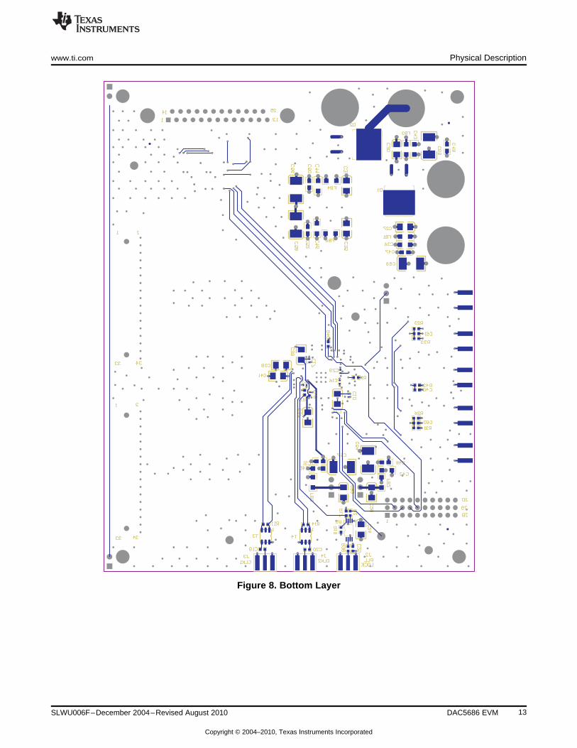
The EVM is constructed on a 4-layer, 6.5-inch x 4.7-inch, 0.055-inch thick PCB using FR-4 material.Figure 5 through Figure 8 show the PCB layout for the EVM.
3.1.1 PCB Layout Recommendations
The DAC5686 clock is sensitive to fast transitions of input data on pins 34, 35, and 36 (DA15, DA14, andDA13) due to coupling to DVDD pin 32. The noise-like spectral energy of the data line couples into theDAC clock circuit power pin, resulting in increased jitter. To minimize the jitter, a 10-Ω series resistor alongwith a 10-pF capacitor to ground has been added to DVDD pin 32 on the EVM. Pin 32 only draws around2 mA of current and the 0.02-V voltage drop across the resistor is acceptable for DVDD voltages withinthe MINIMUM and MAXIMUM specifications. It is also recommended that the transition rate of the datainput lines be slowed by inserting series resistors near the data source. The optimized value of the seriesresistor depends on the capacitance of the trace between the series resistor and the DAC5686 input pin.For a 2-3 inch trace, a 22-Ω to 47-Ω resistor are recommended.
9SLWU006F–December 2004–Revised August 2010 DAC5686 EVM
Copyright © 2004–2010, Texas Instruments Incorporated

Physical Description www.ti.com
Figure 5. Top Layer 1
10 DAC5686 EVM SLWU006F–December 2004–Revised August 2010
Copyright © 2004–2010, Texas Instruments Incorporated

www.ti.com Physical Description
Figure 6. Layer 2, Ground Plane
11SLWU006F–December 2004–Revised August 2010 DAC5686 EVM
Copyright © 2004–2010, Texas Instruments Incorporated

Physical Description www.ti.com
Figure 7. Layer 3, Power Plane
12 DAC5686 EVM SLWU006F–December 2004–Revised August 2010
Copyright © 2004–2010, Texas Instruments Incorporated
www.ti.com Physical Description
Figure 8. Bottom Layer
13SLWU006F–December 2004–Revised August 2010 DAC5686 EVM
Copyright © 2004–2010, Texas Instruments Incorporated

Physical Description www.ti.com
3.2 Parts List
Table 1 lists the parts used in constructing the EVM.
Table 1. DAC5686 EVM Parts List
Bill Of Material For DAC5686
Value QTY Part Number Vendor Ref Des Not Installed
CAPACITORS
47 mF, tantalum, 20%, 10 V 6 ECS-T1AD476R Panasonic C53–C58
10 mF, 10 V, 20% capacitor 12 ECS-T1AX106R Panasonic C24, C26–C28, C30–C32,C35, C37–C39, C41
1 mF, 16 V, 10% capacitor 6 ECJ-3YB1C105K Panasonic C36, C42–C46
0.1 mF, 16 V, 10% capacitor 1 ECJ-2VB1C104K Panasonic C21
0.01 mF, 50 V, 10% capacitor 6 ECJ-2VB1H103K Panasonic C47-C52
120 pf, 50 V, 5% Capacitor 1 ECJ-1VC1H121J Panasonic C33
0.01 mF, 16 V, 10% capacitor 2 ECJ-1VB1C103K Panasonic C19, C20
0.1 mF, 16 V, 10% capacitor 3 ECJ-1VB1C104K Panasonic C25, C60, C61
0.1 mF, 16 V, +80%, -20% capacitor 21 ECJ-0EF1C104Z Panasonic C1, C2, C4–C13, C15–C18,C29, C59, C84–C86
10 pF, 50 V, ±0.5 pF Capacitor 1 ECU-E1H100DCQ Panasonic C3
15000 pF, 16 V, 10% capacitor 1 ECJ-0EB1C153K Panasonic C34
0.01 mF, 25 V, 10% capacitor 1 ECJ-0EF1E103Z Panasonic C14
120 pF, 50 V, 5% capacitor 1 ECU-V1H121JCV Panasonic C33
RESISTORS
10-kΩ resistor 1/16 W, 1% 4 ERJ-6ENF1002V Panasonic R34–R37
10-Ω resistor 1/16 W, 1% 1 ERJ-6ENF10R0V Panasonic R3 R15
0-Ω resistor, 1/16 W, 1% 2 ERJ-3GEY0R00V Panasonic R23, R26 R24, R27–R33
49.9-Ω resistor, 1/16 W, 1% 3 ERJ-3EKF49R9V Panasonic R12, R13, R39 R40
127-Ω resistor, 1/16 W, 1% 1 ERJ-3EKF1270V Panasonic R25
200-Ω resistor, 1/16 W, 1% 2 ERJ-3EKF2000V Panasonic R11, R14
1-kΩ resistor, 1/16 W, 1% 2 ERJ-3EKF1001V Panasonic R1, R4
110-Ω resistor, 1/10 W, 1% 0 ERA-3EKF110V Panasonic R18
221-Ω resistor, 1/10 W, 1% 0 ERA-3EKF221V Panasonic R17
22.1-Ω resistor, 1/10 W, 1% 2 ERJ-3EKF22R1V Panasonic R16, R38
10-Ω resistor, 1/16 W, 1% 1 ERJ-2RFK10R0X Panasonic R43
100-Ω resistor, 1/10 W, 1% 4 ERA-3EKF100V Panasonic R5, R10, R19, R20 R21, R22
Surface Mount Socket strips 1 310-93-164-41- Mill-Max See Note 8105000
51-Ω resistor pack 4 CTS See Note 7 RP5, RP6, RP9,RP10
22-Ω resistor pack 4 4816P-001-220 BOURNS RP1–RP4
FERRITE BEADS, CONNECTORS, JUMPERS, JACKS, ICs, etc.
MBRB2515L 2 MBRB2515LT4 On- D1, D2Semiconductor
Ferrite bead 6 EXC-ML32A680U FB1–FB6
SMA connectors 8 16F3627 Newark J2–J6, J11, J18, J19
Black test point 4 5001K Keystone TP2–TP5
3POS_header 3 HTSW-150-07-L-S Samtec W1–W3
30-pin header 1 HTSW-110-07-L-T Samtec J15
34-pin header 2 TSW-117-01-S-DV- Samtec J13, J14LC
Red banana jacks 2 ST-351A Allied J7, J8
14 DAC5686 EVM SLWU006F–December 2004–Revised August 2010
Copyright © 2004–2010, Texas Instruments Incorporated

www.ti.com Circuit Description
Table 1. DAC5686 EVM Parts List (continued)
Bill Of Material For DAC5686
Value QTY Part Number Vendor Ref Des Not Installed
Black banana jacks 2 ST-351B Allied J9, J10
DAC5686PZP 1 DAC5686IPZP TI U1
SN74LVC1G125DBVR 1 SN74LVC1G125D TI U5BVR
SN74HC241PW 1 SN74HC241PW TI U4
Transformer 2 T4-1-KK8 Mini-circuit T1, T2
Transformer 2 TCM4-1W Mini-circuit T3, T4
DB25F-RA 1 745536-2 AMP J1
Mounting screws 2 J1
Nuts 2 J1
Switch 1 EVQ-PJX04M Panasonic S1
4 Circuit Description
This chapter describes the circuit functions of the DAC5686 EVM.
4.1 Input Clocks
The initial configuration of this EVM provides transformer-coupled differential clocks from single-endedinput sources. A 300-mVP-P , 0-V offset, 50% duty cycle external square wave is applied to SMA connectorJ3 to be used as the data clock input. The signal is converted to a differential clock by transformer T3 andprovides the CLK1 and CLK1C inputs to the DAC5686 device. This input represents a 50-Ω load to thesource. In order to preserve the specified performance of the DAC5686 converter, the clock source shouldfeature very low jitter. Using a clock with a 50% duty cycle gives optimum dynamic performance.
A 300 mVPP , 0-V offset, 50% duty cycle external square wave is applied to SMA connector J4 to be usedas the DAC sample clock. The signal is converted to a differential clock by transformer T4 and providesthe CLK2 and CLK2C inputs to the DAC5686 device. This input represents a 50-Ω load to the source. Inorder to preserve the specified performance of the DAC5686 converter, the clock source should featurelow jitter. Using a clock with a 50% duty cycle gives optimum dynamic performance.
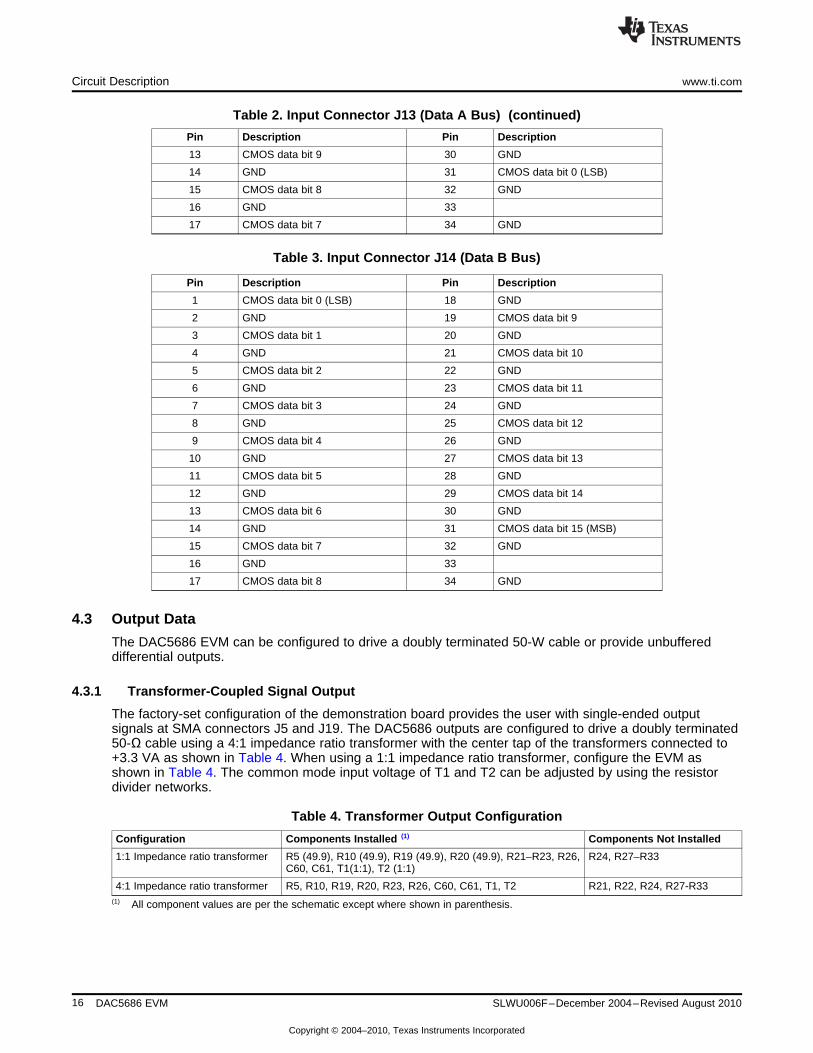
4.2 Input Data
The DAC5686 EVM can accept 1.8-V or 3.3-V CMOS logic level data inputs through the 34-pin headersJ13 and J14 per Table 2 and Table 3. The board provides 50-Ω termination option to ground and seriesdampening resistors to minimize digital ringing and switching noise.
Table 2. Input Connector J13 (Data A Bus)
Pin Description Pin Description
1 CMOS data bit 15 (MSB) 18 GND
2 GND 19 CMOS data bit 6
3 CMOS data bit 14 20 GND
4 GND 21 CMOS data bit 5
5 CMOS data bit 13 22 GND
6 GND 23 CMOS data bit 4
7 CMOS data bit 12 24 GND
8 GND 25 CMOS data bit 3
9 CMOS data bit 11 26 GND
10 GND 27 CMOS data bit 2
11 CMOS data bit 10 28 GND
12 GND 29 CMOS data bit 1
15SLWU006F–December 2004–Revised August 2010 DAC5686 EVM
Copyright © 2004–2010, Texas Instruments Incorporated
Circuit Description www.ti.com
Table 2. Input Connector J13 (Data A Bus) (continued)
Pin Description Pin Description
13 CMOS data bit 9 30 GND
14 GND 31 CMOS data bit 0 (LSB)
15 CMOS data bit 8 32 GND
16 GND 33
17 CMOS data bit 7 34 GND
Table 3. Input Connector J14 (Data B Bus)
Pin Description Pin Description
1 CMOS data bit 0 (LSB) 18 GND
2 GND 19 CMOS data bit 9
3 CMOS data bit 1 20 GND
4 GND 21 CMOS data bit 10
5 CMOS data bit 2 22 GND
6 GND 23 CMOS data bit 11
7 CMOS data bit 3 24 GND
8 GND 25 CMOS data bit 12
9 CMOS data bit 4 26 GND
10 GND 27 CMOS data bit 13
11 CMOS data bit 5 28 GND
12 GND 29 CMOS data bit 14
13 CMOS data bit 6 30 GND
14 GND 31 CMOS data bit 15 (MSB)
15 CMOS data bit 7 32 GND
16 GND 33
17 CMOS data bit 8 34 GND
4.3 Output Data
The DAC5686 EVM can be configured to drive a doubly terminated 50-W cable or provide unbuffereddifferential outputs.
4.3.1 Transformer-Coupled Signal Output
The factory-set configuration of the demonstration board provides the user with single-ended outputsignals at SMA connectors J5 and J19. The DAC5686 outputs are configured to drive a doubly terminated50-Ω cable using a 4:1 impedance ratio transformer with the center tap of the transformers connected to+3.3 VA as shown in Table 4. When using a 1:1 impedance ratio transformer, configure the EVM asshown in Table 4. The common mode input voltage of T1 and T2 can be adjusted by using the resistordivider networks.
Table 4. Transformer Output Configuration
Configuration Components Installed (1) Components Not Installed
1:1 Impedance ratio transformer R5 (49.9), R10 (49.9), R19 (49.9), R20 (49.9), R21–R23, R26, R24, R27–R33C60, C61, T1(1:1), T2 (1:1)
4:1 Impedance ratio transformer R5, R10, R19, R20, R23, R26, C60, C61, T1, T2 R21, R22, R24, R27-R33(1) All component values are per the schematic except where shown in parenthesis.
16 DAC5686 EVM SLWU006F–December 2004–Revised August 2010
Copyright © 2004–2010, Texas Instruments Incorporated
IOUTFS 16 VEXTIOR1
www.ti.com Circuit Description
4.3.2 Unbuffered Differential Output
To provide unbuffered differential outputs, the EVM must be configured as follows: remove R21, R22, T1,and T2; install R5 (24.9), R10 (24.9), R19 (24.9), R20 (24.9), R24, R27-R30, and R32. With a 20 mAfull-scale output current, this configuration provides a 0.5 VPP output.
4.3.3 PLL Lock
With the internal PLL enabled (W3 installed between pins 1 and 2), when the PLL is locked to the CLK1input, PLLOCK is driven high. With the internal PLL disabled, the PLLLOCK is an output clock that can beused by external devices to clock the input data to the DAC5686. This signal is the CLK2 signal divideddown by the interpolation rate and phase-aligned to allow the user to clock data into the DAC5686 with therequired setup and hold times.
4.4 Control Inputs
The DAC5686 device has six discrete inputs to control the operation of the device.
4.4.1 Sleep Mode
The DAC5686 EVM provides a means of placing the DAC5686 device into a power-down mode. Thismode is activated by placing a jumper between pins 5 and 6 on header J15.
4.4.2 Reset
The DAC5686 EVM provides a means of resetting the DAC5686 device. Pressing switch S1 or sendingJ15 pin 29 low provides an active low reset signal to the DAC5686 device.
4.4.3 Phase Synchronization
The DAC5686 EVM provides a means to phase synchronize the DAC5686 device. Placing an active highsignal on J15 pin 8 (PHSTR) resets the internal NCO accumulator register.
4.4.4 TxENABLE
TxENABLE must be high to enable the DAC5686 process data. When low, the DAC5686 device is forcedto a constant dc output at IOUTA and IOTB. When in the interleaved mode and MEM_QFLAG bit is set to0, TxENABLE syncronizes the data of channels A and B. When TxENABLE goes high, data present at thenext clock rising edge is treated as I data. The next valid data is then treated as Q data and so on.TxENABLE is controlled by J15 pin 11.
4.4.5 QFLAG
QFLAG is an input used to indicate Q sample data during the interleaved mode when the QFLAGinterleave bit (3) is set in register #9, MEM_QFLAG. When QFLAG is high, input data is treated as Q data,and when low, data is treated as I data. QFLAG is controlled by J15 pin 14.
4.4.6 PLL_ON_OFF
PLL_ON_OFF allows the user to disable the PLLLOCK output buffer. When PLL_ON_OFF is high, thebuffer is disabled. When low, the PLLLOCK output signal is present at SMA connector J2.
4.5 Internal Reference Operation
The full-scale output current is set by applying an external resistor (R1) between the BIASJ pin of theDAC5686 device and ground. The full-scale output current can be adjusted from 20 mA down to 2 mA byvarying R1 or changing the externally applied reference voltage. The full-scale output current, IOUTFS, isdefined as follows:
17SLWU006F–December 2004–Revised August 2010 DAC5686 EVM
Copyright © 2004–2010, Texas Instruments Incorporated

Schematic www.ti.com
where VEXTIO is the voltage at pin EXTIO. This voltage is 1.2 V typical when using the internally providedbandgap reference voltage source.
4.6 External Reference Operation
The internal reference can be disabled and overridden by an external reference by connecting a voltagesource to terminal TP1 (EXTI/O) and connecting EXTLO to +3.3VA with jumper W1 installed between pins1 and 2. The specified range for external reference voltages must be observed (see the DAC5686 datasheet (SLWS147) for details).
5 Schematic
This chapter contains the DAC5686 EVM schematic diagrams.
18 DAC5686 EVM SLWU006F–December 2004–Revised August 2010
Copyright © 2004–2010, Texas Instruments Incorporated

C7
.1u
F
C6
.1u
F
DA
0D
A1
DA
2D
A3
DA
4
DA
5D
A6
DA
7
DA
8D
A9
DA
10
DA
11
DA
12
DA
13
DA
14
DA
15
DB
0D
B1
DB
2D
B3
DB
4DB
5D
B6
DB
7
DB
8D
B9
DB
10
DB
11
DB
12
DB
13
DB
14
DB
15
CLK
2C
CLK
2
CLK
1C
CLK
1
+1
.8V
D
DB
(0..
15
)D
A(0
..1
5)
C5
.1u
F
C4
.1u
F
C3
10
pF
C2
.1u
F
C1
.1u
F
C8
.1u
F
SC
LK
SD
IOS
CL
KS
DIO
C9
.1u
FC
10
.1u
FC
11
.1u
F
C1
4
.01
uF
C1
2.1
uF
C1
3
.1u
F
TX
EN
AB
LE
TX
EN
AB
LE
SD
EN
BS
DE
NB
IOV
DD
R2
5
93
.1
C3
4 .03
3u
F
C3
3 33
0p
F
R1
3
49
.9
PH
ST
R
R4
1K
IOV
DD
S1
SW
-PB
C1
6
.1u
F
R1
1K
IOV
DD
1 3
2W
1+3
.3V
A
C1
8
.1u
F
C1
7
.1u
F
+3
.3V
A+
3.3
VA
+1
.8V
D
+1
.8V
D
+3
.3V
PL
L
+3
.3V
CL
K
SLE
EP
QF
LA
G
R3
94
9.9
R1
24
9.9
SL
EE
P
QF
LA
G
C8
6
.1u
F
C8
5
.1u
F
C8
4
.1u
F
C2
9
.1u
F
C1
5
.1u
F
+3
.3V
A
R4
04
9.9
(SH
4)
(SH
4)
(SH
4)
(SH
2)
(SH
2)
(SH
2)
+C2
4
10
uF
+C3
8
10
uF
+C3
7
10
uF
+C3
9
10
uF
+C
41
10
uF
RE
SE
TR
ES
ET
(Sh
2)
(SH
2)
(SH
2)
R1
0
10
0
R3
3 0
C6
1
.1u
F
R2
1
10
0
R5
10
0
1
2345
J1
8
SM
A1
2345
J5
SM
A
+3
.3V
A
R2
9
0
R2
8 0
(No
te1
)
IOU
TA
R2
3 0
(No
te1
)
R2
40
R1
9
10
0
R2
0
10
0
1
2345
J1
9S
MA
R2
2
10
0
C6
0
.1u
F
R3
10+
3.3
VA
1
2345
J6
SM
A
R3
0
0 R3
2 0
(No
te1
)
R2
6
0
(No
te1
)
R2
7
0(No
te1
)
(No
te 1
)
(No
te 1
)
(No
te 1
)
IOU
TB
+3
.3V
A
+3
.3V
A
NO
TE
1.
DO
NO
TIN
ST
ALL
1
2345
J2
SM
A
C2
5
.1uF
+C
26
10uF
+3
.3V
A
CL
K1
C
CL
K1
CL
K2
CL
K2
C(S
H3)
(SH
3)
(SH
3)
(SH
3)
PH
ST
R(S
H2)
SD
OS
DO
(SH
4)
4 6
3 2 1
T2
T4-1
-KK
81
46
321T
1
T4-1
-KK
81
R16
22.1
R17
221
R18
110
+3
.3V
A
(No
te1
)
TP
6
R2
22.1
CL
KIN
1
OE
2
1Y
03
GN
D4
1Y
15
VD
D/3
.3V
6
1Y
27
1Y
38
U5
CD
CV
304
R38
0
(No
te1
) (No
te1
)
(2-3
)
(No
te1
)
R7
0
R9
0 R6
0
R8
0
(No
te1
)
(No
te1
)
(No
te1
)
(No
te1
)
1
2345
J11
SM
A
C4
0
.1u
F
+3
.3V
A
R4
2
0
4 6
3 2 1
T5
T1-6
T-K
K81
R4
1
10
0
(No
te1
)
(No
te1
)
C5
9
.1u
F
R43
10
DV
DD
26
DG
ND
27
SD
EN
B2
8
SC
LK
29
SD
IO3
0
SD
O3
1
DV
DD
32
TX
EN
AB
LE
33
DA
15
34
DA
14
35
DA
13
36
DV
DD
37
DG
ND
38
DA
12
39
DA
11
40
DA
10
41
DA
94
2
DA
84
3
DV
DD
44
DG
ND
45
IOV
DD
46
IOG
ND
47
DA
74
8
DA
64
9
DA
55
0
DA451
DA352
DA253
DA154
DA055
DVDD56
DGND57
CLKGND58
CLK159
CLK1C60
CLKVDD61
CLK262
CLK2C63
CLKGND64
PLLGND65
LPF66
PLLVDD67
DVDD68
DGND69
PLLLOCK70
DB071
DB172
DB273
DB374
DB475
DB
57
6D
B6
77
DB
77
8IO
GN
D7
9IO
VD
D8
0D
GN
D8
1D
VD
D8
2D
B8
83
DB
98
4D
B1
08
5D
B11
86
DB
12
87
DG
ND
88
DV
DD
89
DB
13
90
DB
14
91
DB
15
92
DG
ND
93
PH
ST
R9
4/R
ES
ET
B9
5S
LE
EP
96
TE
ST
MO
DE
97
QF
LA
G9
8D
GN
D9
9D
VD
D1
00
AGND1
AVDD2
AVDD3
AGND4
IOUTB15
IOUTB26
AGND7
AVDD8
AGND9
AVDD10
EXTIO11
AGND12
BIASJ13
AVDD14
EXTLO15
AVDD16
AGND17
AVDD18
AGND19
IOUTA220
IOUTA121
AGND22
AVDD23
AVDD24
AGND25
U1
DA
C5687
www.ti.com Schematic
Figure 9. Schematic - Page 1
19SLWU006F–December 2004–Revised August 2010 DAC5686 EVM
Copyright © 2004–2010, Texas Instruments Incorporated

DA
TA
PO
RT
1
DA
TA
PO
RT
2
11
62
15
31
44
13
5
912
6 81
011
7
RP
12
2
11
62
15
31
44
13
5
912
6 81
011
7
RP
2
22
11
62
15
31
44
13
5
912
6 81
011
7
RP
42
2
11
62
15
31
44
13
5
912
6 81
011
7
RP
32
2
DB
(0..
15
)
DA
(0..
15
)
DA
0D
A1
DA
2D
A3
DA
4D
A5
DA
6D
A7
DA
8D
A9
DA
10
DA
11
DA
12
DA
13
DA
14
DA
15
DB
0D
B1
DB
2D
B3
DB
4D
B5
DB
6D
B7
DB
8D
B9
DB
10
DB
11
DB
12
DB
13
DB
14
DB
15
A0
A1
A2
A3
A4
A5
A6
A7
A8
A9
A10
A11
A12
A13
A14
A15
B0
B1
B2
B3
B4
B5
B6
B7
B8
B9
B10
B11
B12
B13
B14
B15
12
34
56
78
91
011
12
13
14
15
16
17
18
19
20
21
22
23
24
25
26
27
28
29
30
31
32
33
34
J1
3
34
PIN
_ID
C
12
34
56
78
91
011
12
13
14
15
16
17
18
19
20
21
22
23
24
25
26
27
28
29
30
31
32
33
34
J1
4
34
PIN
_ID
C
1
2
3
4
5
6
7
8
9
10 1
1
12
13 1
4
15
16 1
7
18
19 2
0
21
22 2
3
24
25 2
6
27
28 2
9
30
J1
5
IOV
DD
SLE
EP
TX
EN
AB
LE
QF
LA
G
SL
EE
P
TX
EN
AB
LE
QF
LA
G
3R
OW
30
PIN
CO
NN
EC
TO
R
(SH
1)
(SH
1)
(SH
1)
(SH
1)
(SH
1)
RE
SE
TR
ES
ET
(SH
1,5)
NO
TE
1.
DO
NO
TIN
ST
ALL
PH
ST
RP
HS
TR
(SH
1)
12345678910
RP
5
51
12345678910
RP
6
51
12345678910
RP
951
12345678910
RP
10
51
(No
te1
)
(No
te1
)
(No
te1
)
(No
te1
)
Schematic www.ti.com
Figure 10. Schematic - Page 2
20 DAC5686 EVM SLWU006F–December 2004–Revised August 2010
Copyright © 2004–2010, Texas Instruments Incorporated

R11
200
1
2345
J3
SM
AC
19
.01uF
CL
K1
CLK
1
CLK
1C
CL
K1
CL
K1
C
R14
200
12345
J4
SM
AC
20
.01uF
CL
K2
CLK
2
CLK
2C
CL
K2
CL
K2
C
1.
PA
RT
NO
TIN
ST
AL
LE
D
NO
TE
S:
31
46
2
T4
TC
M4-1
W
(SH
1)
(SH
1)
(SH
1)
(SH
1)
3 1
4 6
2
T3
TC
M4-1
W
www.ti.com Schematic
Figure 11. Schematic - Page 3
21SLWU006F–December 2004–Revised August 2010 DAC5686 EVM
Copyright © 2004–2010, Texas Instruments Incorporated

1 2 3 4 5 6 7 8 91
011
14
13
15
16
17
18
19
20
21
22
23
24
25
12
J1
DB
25
F-R
A
R3
41
0K
R3
51
0K
R3
61
0K
R3
71
0K
1A
11
Y2
2A
32
Y4
3A
53
Y6
GN
D7
4Y
84
A9
5Y
10
5A
11
6Y
12
6A
13
VC
C1
4
U2
SN
74
HC
T1
4
1A
11
Y2
2A
32
Y4
3A
53
Y6
GN
D7
4Y
84
A9
5Y
10
5A
11
6Y
12
6A
13
VC
C1
4
U3
SN
74
HC
T1
4
R3
10
SD
EN
B
SC
LK
SD
IOC2
1
.1u
F
+3
.3V
_S
ER
+3.3
V_S
ER
C2
3
.1u
F
C2
2
.1u
F
+3
.3V
_S
ER
SD
IO
SC
LK
SD
EN
B
(Sh
1)
(Sh
1)
(Sh
1)
OE
1_
1
1A
12
1A
24
1A
36
1A
48
2A
111
2A
21
3
2A
31
5
2A
41
7
GN
D1
02Y
43
2Y
35
2Y
27
2Y
19
1Y
41
2
1Y
314
1Y
216
1Y
118
OE
21
9
VC
C2
0
U4
SN
74
HC
24
1
SD
EN
SC
LK
SD
IOO
E_
NO
TE
1.
DO
NO
TIN
ST
ALL
SD
OS
DO
(Sh
1)
R1
51
0
(Note
1)
Schematic www.ti.com
Figure 12. Schematic - Page 4
22 DAC5686 EVM SLWU006F–December 2004–Revised August 2010
Copyright © 2004–2010, Texas Instruments Incorporated

+3
.3V
A
FB
1
+C
27
10
uF
C3
6
1u
F
C4
7
0.0
1u
F
VA
J1
0
BL
AC
KJ7
RE
D
J9
BL
AC
K
VA
TP
2B
LA
CK
TP
3B
LA
CK
TP
4B
LA
CK
+C
53
47
uF
IOV
DD
FB
2
+C
28
10
uF
C4
2
1u
F
C4
8
0.0
1u
F
+C
54
47
uF
+C
30
10
uF
C4
3
1u
F
C4
9
0.0
1u
F
FB
3
+1
.8V
D
VD
J8
RE
D
VD
+C
55
47
uF
+3
.3V
PL
L
FB
5
+C
32
10
uF
C4
5
1u
F
C5
1
0.0
1u
F
+C
57
47
uF
+3
.3V
CL
K
FB
6
+C
35
10
uF
C4
6
1u
F
C5
2
0.0
1u
F
+C
58
47
uF
+3
.3V
_S
ER
FB
4
+C
31
10
uF
C4
4
1u
F
C5
0
0.0
1u
F
+C
56
47
uF
1.
PA
RT
NO
TIN
ST
AL
LE
D
NO
TE
S:
TP
5B
LA
CK
1 3
2W
2
+3
.3V
A
+1
.8V
D
VA
+3
.3V
A
VA
1 3
2W
3
(1-2
)
(2-3
)
14
3D1
MB
RB
2515L
14
3D2
MB
RB
2515L
www.ti.com Schematic
Figure 13. Schematic - Page 5
23SLWU006F–December 2004–Revised August 2010 DAC5686 EVM
Copyright © 2004–2010, Texas Instruments Incorporated

EVALUATION BOARD/KIT IMPORTANT NOTICE
Texas Instruments (TI) provides the enclosed product(s) under the following conditions:
This evaluation board/kit is intended for use for ENGINEERING DEVELOPMENT, DEMONSTRATION, OR EVALUATION PURPOSESONLY and is not considered by TI to be a finished end-product fit for general consumer use. Persons handling the product(s) must haveelectronics training and observe good engineering practice standards. As such, the goods being provided are not intended to be completein terms of required design-, marketing-, and/or manufacturing-related protective considerations, including product safety and environmentalmeasures typically found in end products that incorporate such semiconductor components or circuit boards. This evaluation board/kit doesnot fall within the scope of the European Union directives regarding electromagnetic compatibility, restricted substances (RoHS), recycling(WEEE), FCC, CE or UL, and therefore may not meet the technical requirements of these directives or other related directives.
Should this evaluation board/kit not meet the specifications indicated in the User’s Guide, the board/kit may be returned within 30 days fromthe date of delivery for a full refund. THE FOREGOING WARRANTY IS THE EXCLUSIVE WARRANTY MADE BY SELLER TO BUYERAND IS IN LIEU OF ALL OTHER WARRANTIES, EXPRESSED, IMPLIED, OR STATUTORY, INCLUDING ANY WARRANTY OFMERCHANTABILITY OR FITNESS FOR ANY PARTICULAR PURPOSE.
The user assumes all responsibility and liability for proper and safe handling of the goods. Further, the user indemnifies TI from all claimsarising from the handling or use of the goods. Due to the open construction of the product, it is the user’s responsibility to take any and allappropriate precautions with regard to electrostatic discharge.
EXCEPT TO THE EXTENT OF THE INDEMNITY SET FORTH ABOVE, NEITHER PARTY SHALL BE LIABLE TO THE OTHER FOR ANYINDIRECT, SPECIAL, INCIDENTAL, OR CONSEQUENTIAL DAMAGES.
TI currently deals with a variety of customers for products, and therefore our arrangement with the user is not exclusive.
TI assumes no liability for applications assistance, customer product design, software performance, or infringement of patents orservices described herein.
Please read the User’s Guide and, specifically, the Warnings and Restrictions notice in the User’s Guide prior to handling the product. Thisnotice contains important safety information about temperatures and voltages. For additional information on TI’s environmental and/orsafety programs, please contact the TI application engineer or visit www.ti.com/esh.
No license is granted under any patent right or other intellectual property right of TI covering or relating to any machine, process, orcombination in which such TI products or services might be or are used.
FCC Warning
This evaluation board/kit is intended for use for ENGINEERING DEVELOPMENT, DEMONSTRATION, OR EVALUATION PURPOSESONLY and is not considered by TI to be a finished end-product fit for general consumer use. It generates, uses, and can radiate radiofrequency energy and has not been tested for compliance with the limits of computing devices pursuant to part 15 of FCC rules, which aredesigned to provide reasonable protection against radio frequency interference. Operation of this equipment in other environments maycause interference with radio communications, in which case the user at his own expense will be required to take whatever measures maybe required to correct this interference.
Mailing Address: Texas Instruments, Post Office Box 655303, Dallas, Texas 75265Copyright © 2009, Texas Instruments Incorporated
EVM WARNINGS AND RESTRICTIONS
It is important to operate this EVM within the input voltage range of 1.8 V to 3.3 V and the output voltage range of 3.3 V max.
Exceeding the specified input range may cause unexpected operation and/or irreversible damage to the EVM. If there are questionsconcerning the input range, please contact a TI field representative prior to connecting the input power.
Applying loads outside of the specified output range may result in unintended operation and/or possible permanent damage to the EVM.Please consult the EVM User's Guide prior to connecting any load to the EVM output. If there is uncertainty as to the load specification,please contact a TI field representative.
During normal operation, some circuit components may have case temperatures greater than 60°C. The EVM is designed to operateproperly with certain components above 60°C as long as the input and output ranges are maintained. These components include but arenot limited to linear regulators, switching transistors, pass transistors, and current sense resistors. These types of devices can be identifiedusing the EVM schematic located in the EVM User's Guide. When placing measurement probes near these devices during operation,please be aware that these devices may be very warm to the touch.
Mailing Address: Texas Instruments, Post Office Box 655303, Dallas, Texas 75265Copyright © 2009, Texas Instruments Incorporated

IMPORTANT NOTICE
Texas Instruments Incorporated and its subsidiaries (TI) reserve the right to make corrections, modifications, enhancements, improvements,and other changes to its products and services at any time and to discontinue any product or service without notice. Customers shouldobtain the latest relevant information before placing orders and should verify that such information is current and complete. All products aresold subject to TI’s terms and conditions of sale supplied at the time of order acknowledgment.
TI warrants performance of its hardware products to the specifications applicable at the time of sale in accordance with TI’s standardwarranty. Testing and other quality control techniques are used to the extent TI deems necessary to support this warranty. Except wheremandated by government requirements, testing of all parameters of each product is not necessarily performed.
TI assumes no liability for applications assistance or customer product design. Customers are responsible for their products andapplications using TI components. To minimize the risks associated with customer products and applications, customers should provideadequate design and operating safeguards.
TI does not warrant or represent that any license, either express or implied, is granted under any TI patent right, copyright, mask work right,or other TI intellectual property right relating to any combination, machine, or process in which TI products or services are used. Informationpublished by TI regarding third-party products or services does not constitute a license from TI to use such products or services or awarranty or endorsement thereof. Use of such information may require a license from a third party under the patents or other intellectualproperty of the third party, or a license from TI under the patents or other intellectual property of TI.
Reproduction of TI information in TI data books or data sheets is permissible only if reproduction is without alteration and is accompaniedby all associated warranties, conditions, limitations, and notices. Reproduction of this information with alteration is an unfair and deceptivebusiness practice. TI is not responsible or liable for such altered documentation. Information of third parties may be subject to additionalrestrictions.
Resale of TI products or services with statements different from or beyond the parameters stated by TI for that product or service voids allexpress and any implied warranties for the associated TI product or service and is an unfair and deceptive business practice. TI is notresponsible or liable for any such statements.
TI products are not authorized for use in safety-critical applications (such as life support) where a failure of the TI product would reasonablybe expected to cause severe personal injury or death, unless officers of the parties have executed an agreement specifically governingsuch use. Buyers represent that they have all necessary expertise in the safety and regulatory ramifications of their applications, andacknowledge and agree that they are solely responsible for all legal, regulatory and safety-related requirements concerning their productsand any use of TI products in such safety-critical applications, notwithstanding any applications-related information or support that may beprovided by TI. Further, Buyers must fully indemnify TI and its representatives against any damages arising out of the use of TI products insuch safety-critical applications.
TI products are neither designed nor intended for use in military/aerospace applications or environments unless the TI products arespecifically designated by TI as military-grade or "enhanced plastic." Only products designated by TI as military-grade meet militaryspecifications. Buyers acknowledge and agree that any such use of TI products which TI has not designated as military-grade is solely atthe Buyer's risk, and that they are solely responsible for compliance with all legal and regulatory requirements in connection with such use.
TI products are neither designed nor intended for use in automotive applications or environments unless the specific TI products aredesignated by TI as compliant with ISO/TS 16949 requirements. Buyers acknowledge and agree that, if they use any non-designatedproducts in automotive applications, TI will not be responsible for any failure to meet such requirements.
Following are URLs where you can obtain information on other Texas Instruments products and application solutions:
Products Applications
Amplifiers amplifier.ti.com Audio www.ti.com/audio
Data Converters dataconverter.ti.com Automotive www.ti.com/automotive
DLP® Products www.dlp.com Communications and www.ti.com/communicationsTelecom
DSP dsp.ti.com Computers and www.ti.com/computersPeripherals
Clocks and Timers www.ti.com/clocks Consumer Electronics www.ti.com/consumer-apps
Interface interface.ti.com Energy www.ti.com/energy
Logic logic.ti.com Industrial www.ti.com/industrial
Power Mgmt power.ti.com Medical www.ti.com/medical
Microcontrollers microcontroller.ti.com Security www.ti.com/security
RFID www.ti-rfid.com Space, Avionics & www.ti.com/space-avionics-defenseDefense
RF/IF and ZigBee® Solutions www.ti.com/lprf Video and Imaging www.ti.com/video
Wireless www.ti.com/wireless-apps
Mailing Address: Texas Instruments, Post Office Box 655303, Dallas, Texas 75265Copyright © 2010, Texas Instruments Incorporated


