Embed Size (px)
Citation preview
IEEE JOURNAL OF SELECTED TOPICS IN QUANTUM ELECTRONICS, VOL. 20, NO. 4, JULY/AUGUST 2014 8202110
CMOS Compatible Reconfigurable Silicon PhotonicLattice Filters Using Cascaded Unit Cells for
RF-Photonic ProcessingBinbin Guan, Stevan S. Djordjevic, Student Member, IEEE, Nicolas K. Fontaine, Member, IEEE, Linjie Zhou,
Salah Ibrahim, Ryan P. Scott, Member, IEEE, David J. Geisler, Member, IEEE, Zhi Ding, Fellow, IEEE,and S. J. Ben Yoo, Fellow, IEEE
(Invited Paper)
Abstract—This paper presents an overview of a comple-mentary metal–oxide–semiconductor-compatible, programmable,analog optical lattice filter based on silicon unit cells arrayed inlarge-scale photonic integrated circuits. The unit cell employs acombination of a ring resonator and a Mach–Zehnder interferome-ter with tunable phase elements in both of the paths. Each proposedunit cell contributes a separately controllable pole and zero pair.Under various configurations, we experimentally achieved >60-dBtwo-tone spurious-free dynamic range. For more sophisticated sig-nal processing, we experimentally demonstrated an optical latticefilter with four cascaded unit cells capable of dynamically reconfig-uring between a bandpass filter and a notch filter. The reconfigu-ration of the unit-cell and four-cell silicon lattice filter is based on arecursive algorithm, which brings new possibilities to RF photonicprocessing and a wide range of applications with design scalabilityto a large number of poles and zeros. The experimental results andthe recursive algorithms show potentials for scaling to higher orderfilter designs.
Index Terms—Complementary metal–oxide–semiconductor(CMOS) process, filtering algorithms, microwave photonics, op-tical filters, optical modulation, silicon photonics.
I. INTRODUCTION
R F-PHOTONIC processing of microwave signals is of con-siderable interest for replacing electrical signal processing
Manuscript received October 15, 2013; revised December 16, 2013; acceptedDecember 17, 2013. Date of publication December 23, 2013; date of currentversion February 11, 2014. This work was supported in part by DARPA MTOSi-PhASER project Grant no. HR0011-09-1-0013.
B. Guan, S. S. Djordjevic, R. P. Scott, Z. Ding, and S. J. Ben Yoo arewith the Department of Electrical and Computer Engineering, University ofCalifornia, Davis, CA 95616 USA (e-mail: [email protected]; [email protected]; [email protected]; [email protected]; [email protected]).
N. K. Fontaine was with the University of California, Davis, CA 95616 USA.He is now with Alcatel-Lucent Bell Laboratories, Holmdel, NJ 07733 USA(e-mail: [email protected]).
L. Zhou was with the University of California, Davis, CA 95616 USA. Heis now with the Department of Electronic Engineering, Shanghai Jiao TongUniversity, Minhang District, Shanghai, China (e-mail: [email protected]).
S. Ibrahim was with the University of California, Davis, CA 95616 USA. Heis now with NTT Photonics Laboratories, Atsugi-shi, Kanagawa Pref. 243-0198,Japan (e-mail: [email protected]).
D. J. Geisler was with the University of California, Davis, CA 95616 USA.He is now with the Massachusetts Institute of Technology Lincoln Laboratory,Lexington, MA 02420 USA (e-mail: [email protected]).
Color versions of one or more of the figures in this paper are available onlineat http://ieeexplore.ieee.org.
Digital Object Identifier 10.1109/JSTQE.2013.2296233
in many cases, due to possible advantages for higher band-width, lower power consumption and low latency [1], [2].There is an increasing demand of all-optical signal process-ing approach in a broad range of applications [1], [3]–[6]. Tomatch the requirement of diverse signal processing in electri-cal systems, all-optical processing components must be eas-ily reconfigurable with full control over a large number ofpoles and zeros in the transfer function. Among the manyRF-photonic processing components that exist, optical latticefilters are a good all-purpose solution due to their ability togenerate complicated transfer functions by cascading identi-cal unit cells. State-of-art research into optical reconfigurablefilter includes both silicon and InP platforms [7]–[10]. In par-ticular, [7] demonstrates the use of InP based reconfigurablelattice filter with monolithically integrated coupled ring struc-tures, while [8] shows a silicon reconfigurable filter with thermaltuning. In this paper, we discuss a complementary metal–oxide–semiconductor (CMOS) compatible silicon optical lattice filter.We also leverage the high-yield, low-cost and repeatable per-formance of silicon device fabrication technology. In addition,our optical lattice filter is dynamically reconfigurable using arecursive algorithm to achieve the (nontrivial) desired transferfunctions [11]. As a result, the optical lattice filter can ben-efit a wide range of applications, such as narrow bandwidthfilter, correlation, multiplexing distortion compensation [12],etc.
The content of the paper is organized as follows. Section IIincludes a description of the architecture of the unit-cell andfour-cell optical lattice filters with a mathematical descriptionof the transfer function. In Section III, we provide an expla-nation of the recursive algorithm used for arbitrary transferfunction synthesis in unit-cells and a derivation of the four-cell transfer function and recursive algorithm. In Section IV,we discuss the details of silicon lattice filter fabrication. InSection V, we show experimental characterization results ofunit-cell and four-cell optical lattice filters. In Section VI, wedemonstrate experimental results for unit-cell filter and four-cell transfer function reconfiguration, for both bandpass fil-ters and notch filters. In Section VII, we also discuss po-tential applications towards RF signal processing using anoptical lattice filter. Finally, Section VIII summarizes thiswork.
1077-260X © 2013 IEEE. Personal use is permitted, but republication/redistribution requires IEEE permission.See http://www.ieee.org/publications standards/publications/rights/index.html for more information.

8202110 IEEE JOURNAL OF SELECTED TOPICS IN QUANTUM ELECTRONICS, VOL. 20, NO. 4, JULY/AUGUST 2014
Fig. 1. Schematic design of (a) single unit-cell filter and (b) four-unit-cellfilter. [13].
II. UNIT-CELL AND FOUR-CELL CASCADED
RECONFIGURABLE LATTICE FILTER
Fig. 1(a) [13] shows the structure of a unit-cell and four-cell silicon optical lattice filter. The structure consists of a2 × 2 Mach–Zehnder interferometer (MZI) with a ring res-onator on the upper path and a straight waveguide with phaseshifter on the lower path. Connecting the two outputs to the twoinputs of the following unit cell constructs the lattice filter. Ina unit-cell structure, the ring resonator defines the lattice con-stant [e.g., the temporal spacing of impulses, or the inverse ofthe free spectrum range (FSR)]. In this case, the lattice constantis 100 ps, corresponding to a 10-GHz FSR. The phase shifterin the resonator and the ring resonator waveguide round triploss determine the phase and the magnitude of the pole. Tuningthe ring coupler phase shifters [labeled as 2 and 3 in Fig. 1(a)]vary the coupling strength between the ring resonator and thestraight waveguide in the upper path of the 2× 2 MZI. Therefore,the unit-cell structure can produce both finite-impulse response(FIR) and infinite-impulse response (IIR) features. When thecoupling strength is weak, the unit-cell filter is primarily IIRwith narrow resonance features in the spectrum. Alternatively,when the coupling strength is 100%, the unit-cell becomes atwo-tap FIR filter, with a 100-ps delay between the two taps.The zeros of the lattice filter transfer function are dependent onall of the phase shifters of the unit-cell structure.
Phase shifters which are based on free-carrier plasma dis-persion effect [14] in silicon photonics, are the basic tuningelements for each unit-cell. We defined lateral p-i-n carrier in-jection trenches by ion implantation. Required phase shift isinduced by injecting current into the resulting p-i-n diode.
Fig. 1(b) shows the four-cell lattice filter which is simplycreated by cascading four identical unit-cells together. As wediscussed above, the lattice filter has the advantage of facilitatingthe synthesis of high-order transfer functions by tuning eachunit-cell.
To analyze the operation of the unit-cell and four-cell filters,we will define Φn as the 2 × 2 transfer matrix for the nthunit-cell structure where Fig. 2(a) and (b) specify the variables
Fig. 2. Definitions for the (a) unit-cell structure and the (b) four-cell structure.
associated with the structures that constitute the filter. Here,κnt is the coupling coefficient of the output coupler, κnr isthe coupling coefficient of the ring coupler, θnt is the angledescription of the coupling coefficient for output coupler, ϕnr isthe phase of the ring resonator, ϕnt is the phase of the lower armwaveguide, and Cnr is defined as the coupling coefficient of theof the ring coupler. The 2 × 2 transfer matrix is then defined as
Φn =
[cnt −jsnt
−jsnt cnt
][−e−j ϕ n r AR
n (z )An (z ) 0
0 e−jϕn t
]
Φ0 =
[c0t −js0t
−js0t c0t
]for the input coupler (1)
where
cnt =√
1 − κnt = cos(θnt)
snt =√
κnt = sin(θnt) (2)
and
An (z) = 1 − cnr e−jϕn r z−1
ARn (z) = −cnr e
jϕn r + z−1 (3)
when z−1 is defined as exp(jωΔτ) and Δτ is the optical delayper round trip in the ring resonator.
In addition, the input coupler is a 2 × 2 MZI. The transfermatrix of the input coupler is in (1) as Φ0 . Since the input coupleronly affects the zero tuning. Therefore, in our experiment, weusually set the input coupler’s coupling coefficient to 50% andused other phase shifters [e.g., phase shifter 1, 4 and 5 labeledin Fig. 1(a)] in the unit-cell structure to adjust the zero.
Filter poles are independently controlled by each unit cell.However, the zeros are coupled together. As a result, it requiresa recursive algorithm to fully control the zeros. We will explainthe recursive algorithm for filter synthesis in Section III.
III. RECONFIGURABLE LATTICE FILTER SYNTHESIS
There is only one pole and one zero in the unit-cell transferfunction. Therefore, the tuning algorithm is straight forward andmainly consists of characterizing the performance of each phase

GUAN et al.: CMOS COMPATIBLE RECONFIGURABLE SILICON PHOTONIC LATTICE FILTERS USING CASCADED UNIT CELLS 8202110
Fig. 3. Unit-cell optical filter reconfiguration flow chart.
shifter and mapping the pole or zero movement as a function ofinjected current. We will discuss phase shifter characterizationin Section V. From (3), for a unit-cell structure, phase of thepole is fully controlled by the phase shifter on the ring resonator[labeled as 6 in Fig. 1(a)], whereas the magnitude of the pole isset by controlling the coupling coefficient to the ring. All of thephase shifters will affect the value of the filter’s zero.
Fig. 3 shows the flow chart of the filter synthesis for a unit-cellstructure. To start with, we characterize the complex transferfunction of the filter with an optical vector network analyzer(OVNA) which is described in detail in Section V. The calibra-tion process is defined as using characterization results to buildup the mapping between optical parameters (e.g., κnr ) and thephase shifter’s injected current. After calibration, we need tocalculate the desired pole and zeros from the transfer function.Then we use phase shifters 2, 3, and 6 to control magnitude andphase of the pole, and use phase shifters on the output coupler[labeled as 4 and 5 in Fig. 1(a)] to control the zero. In the laststep of the flow chart, phase shifter 1 in the bottom path of the2 × 2 is used for fine tuning all of the parameters.
The reconfiguration algorithm for four-cell filter is more com-plex and challenging, compared to unit-cell filter tuning. Jingujiet al. [11] has previously demonstrated a recursive algorithm fora standard cascaded lattice filter.
The recursion starts with fitting the two port measurement re-sult with an N -pole and N -zero transfer function model. We usenormalized energy error (NEE) as the filter fidelity metric [15],which is the ratio between the energy of the error spectrum [i.e.,|Tm (z) − Tf (f)|2] and the energy of the fitted spectrum [i.e.,|Tf (z)|2)] where Tm (z) and Tf (z) are defined as the measuredspectrum and fitted spectrum, respectively. In this case, we havetwo transfer functions T1(z) and T2(z) from the measurementoutput fitting results. These transfer functions are given by [16]
T1 (z) =HN (z)GN (z)
, T2(z) = jFN (z)GN (z)
(4)
where
HN (z) = hN0
+ hN1
z−1 + hN2
z−2 + · · · + hNN
z−N
FN (z) = fN0
+ fN1
z−1 + fN2
z−2 + · · · + fNN
z−N
GN (z) = gN0
+ gN1
z−1 + gN2
z−2 + · · · + gNN
z−N . (5)
The general transfer function of a four-cell cascaded opticallattice filter, ΦN (z), is the 2 × 2 transfer matrix of the N th orderlattice filter and is given by
ΦN 0 =N
Πn=0
Φn =1
GN (z)
[HN (z) jFR
N (z)jFN (z) HR
N (z)
](6)
where HRN and FR
N are reverse polynomials, and can be easilyderived from the inverse of the zeros of HN and FN . The onlydifference is limited in a real constant factor and it can be derivedbased on consistent power from the first column of the matrixand the second column of the matrix (6). We can rewrite thematrix in (6) with one-step recursion as
1GN (z)
[HN (z) jF R
N (z)
jF (z) HRN (z)
]=
ΦN (z)GN −1 (z)
×[
HN −1 (z) jFRN −1 (z)
jFN −1 (z) HRN −1 (z)
].
(7)
An inverse matrix calculation of (7) generates HN −1 , FN −1 ,θN t , θN t , ϕN t and ϕN r in (8)–(11) below where ρN is the rootof AN (z) [16]:
θN t = arctan(− FN (ρN )
HN (ρN )
)(8)
θN t = arctan(−FN (ρN ) α
HN (ρN )
)for more complete form (9)
arg(
HN −1 (ρN )FN −1 (ρN )
)= 0 = ϕN r − ϕN t
+ arg(
AN (ρN −1) (−cN tHN (ρN −1) + sN tFN (ρN −1))AR
N (ρN −1) (sN tHN (ρN −1) + cN tFN (ρN −1))
)
(10)
ϕN t = ϕN r + arg
×(
AN (ρN −1) (−cN tHN (ρN −1) + sN tFN (ρN −1))AR
N (ρN −1) (sN tHN (ρN −1) + cN tFN (ρN −1))
).
(11)
The one-step recursion reduces the polynomial order by one.We add a constant complex α, to make the content of the expres-sion in (9) a real number. Physically, α arises from magnitudeand phase differences between the two outputs of the device thatoccur when coupling from the waveguide to a fiber, or the fiberlength differences of the two outputs. In the end, we need tomake sure the ratio of [HN −1(ρN −1)]/[FN −1(ρN −1)] is a realnumber.
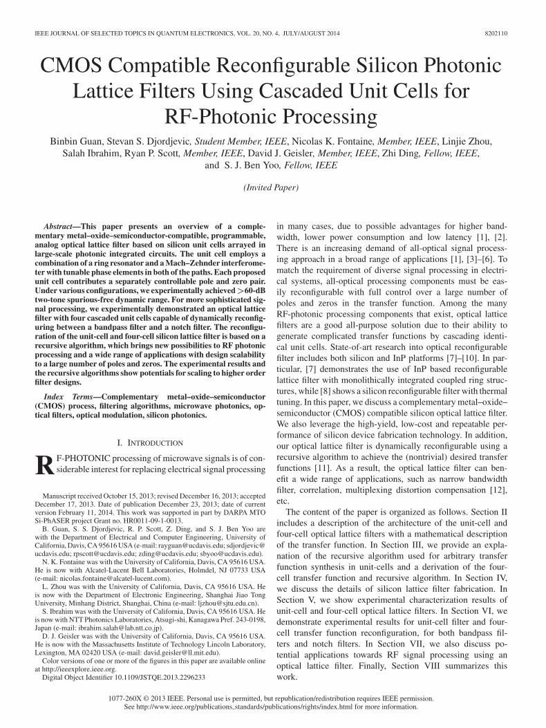
A recursive algorithm is helpful for retrieving the opticalparameters, such as coupling coefficients, and phase shifts ofeach unit-cell. However, we have to build a mapping betweenzero tuning (e.g., phase shifter tuning) and optical parameter(e.g., phase, coupling coefficients) tuning. We use a modified2 × 2 MZI to present this relation. Fig. 4(a) shows the stan-dard structure of a directional coupler and Fig. 4(b) shows the
8202110 IEEE JOURNAL OF SELECTED TOPICS IN QUANTUM ELECTRONICS, VOL. 20, NO. 4, JULY/AUGUST 2014
Fig. 4. (a) A standard coupler. (b) A MZI coupler with two phase shifters onboth arms. (c) Modified MZI coupler. (d) Modified unit-cell structure.
structure of an MZI coupler. The 2 × 2 matrix of a directionalcoupler is given by[
An
Bn
]=
[cos θ −j sin θ
−j sin θ cos θ
] [An−1
Bn−1
]. (12)
We can modify the MZI coupler as a directional coupler, withextra phase shift on both inputs and outputs [Fig. 4(c)]. Thistransformation is[
An
Bn
]= exp (jϕ+)
[j sin ϕ− −j cos ϕ−
−j cos ϕ− −j sin ϕ−
] [An−1
Bn−1
]
=[
j 00 1
] [cos
(π2 − ϕ−
)−j sin
(π2 − ϕ−
)−j sin
(π2 − ϕ−
)cos
(π2 − ϕ−
) ]
×[
exp (jϕ+) 00 −j exp (jϕ+)
] [An−1
Bn−1
]
(13)
where
ϕ+ =ϕu + ϕl
2, ϕ− =
ϕu − ϕl
2. (14)
As a result, Fig. 4(d) shows the modified unit-cell structure(nth unit-cell) with the following adjustments
ϕ′nr = ϕ6 +
π
2+ ϕ (2, 3)+ (15)
ϕ′nt = ϕ1 −
π
2+ ϕ (2, 3)+ (16)
κ′nr =
π
2− ϕ (2, 3)− (17)
κ′nt =
π
2− ϕ (4, 5)− (18)
where ϕ′nr is the modified phase shift on the ring resonator, ϕ′
nt
is the modified phase shift on the lower waveguide, κ′nr is the
modified coupling coefficient of the ring coupler, and κ′nt is the
modified coupling coefficient of the output coupler.With the help of the modified unit-cell structure, we can still
use the standard recursive algorithm [11] to find the opticalparameters for each unit-cell. After that, we can recalculate thetuning value for each phase shifter. As a result, we can tunezeros for each unit cell with the recursive algorithm.
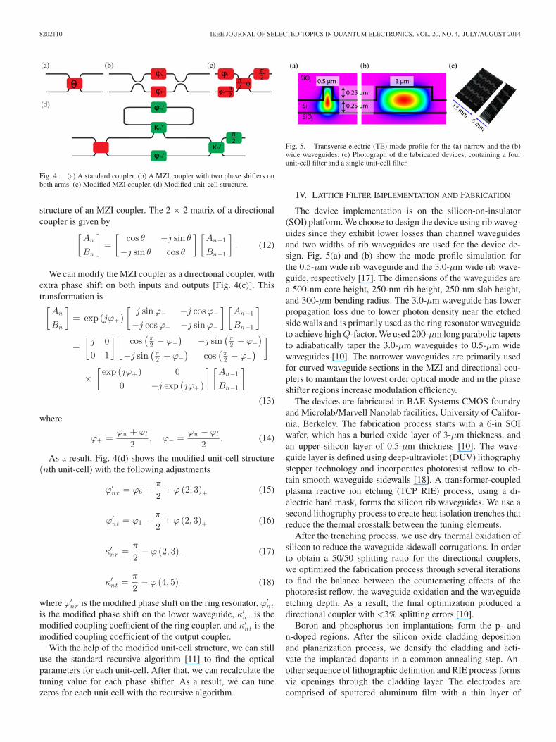
Fig. 5. Transverse electric (TE) mode profile for the (a) narrow and the (b)wide waveguides. (c) Photograph of the fabricated devices, containing a fourunit-cell filter and a single unit-cell filter.
IV. LATTICE FILTER IMPLEMENTATION AND FABRICATION
The device implementation is on the silicon-on-insulator(SOI) platform. We choose to design the device using rib waveg-uides since they exhibit lower losses than channel waveguidesand two widths of rib waveguides are used for the device de-sign. Fig. 5(a) and (b) show the mode profile simulation forthe 0.5-μm wide rib waveguide and the 3.0-μm wide rib wave-guide, respectively [17]. The dimensions of the waveguides area 500-nm core height, 250-nm rib height, 250-nm slab height,and 300-μm bending radius. The 3.0-μm waveguide has lowerpropagation loss due to lower photon density near the etchedside walls and is primarily used as the ring resonator waveguideto achieve high Q-factor. We used 200-μm long parabolic tapersto adiabatically taper the 3.0-μm waveguides to 0.5-μm widewaveguides [10]. The narrower waveguides are primarily usedfor curved waveguide sections in the MZI and directional cou-plers to maintain the lowest order optical mode and in the phaseshifter regions increase modulation efficiency.
The devices are fabricated in BAE Systems CMOS foundryand Microlab/Marvell Nanolab facilities, University of Califor-nia, Berkeley. The fabrication process starts with a 6-in SOIwafer, which has a buried oxide layer of 3-μm thickness, andan upper silicon layer of 0.5-μm thickness [10]. The wave-guide layer is defined using deep-ultraviolet (DUV) lithographystepper technology and incorporates photoresist reflow to ob-tain smooth waveguide sidewalls [18]. A transformer-coupledplasma reactive ion etching (TCP RIE) process, using a di-electric hard mask, forms the silicon rib waveguides. We use asecond lithography process to create heat isolation trenches thatreduce the thermal crosstalk between the tuning elements.
After the trenching process, we use dry thermal oxidation ofsilicon to reduce the waveguide sidewall corrugations. In orderto obtain a 50/50 splitting ratio for the directional couplers,we optimized the fabrication process through several iterationsto find the balance between the counteracting effects of thephotoresist reflow, the waveguide oxidation and the waveguideetching depth. As a result, the final optimization produced adirectional coupler with <3% splitting errors [10].
Boron and phosphorus ion implantations form the p- andn-doped regions. After the silicon oxide cladding depositionand planarization process, we densify the cladding and acti-vate the implanted dopants in a common annealing step. An-other sequence of lithographic definition and RIE process formsvia openings through the cladding layer. The electrodes arecomprised of sputtered aluminum film with a thin layer of
GUAN et al.: CMOS COMPATIBLE RECONFIGURABLE SILICON PHOTONIC LATTICE FILTERS USING CASCADED UNIT CELLS 8202110
Fig. 6. Diagram of the fabrication process flow.
titanium/titanium nitride on top which is used as a protectivebarrier. Electrodes are patterned by lithographic definition andetched in Cl2 /BCl3 plasma, followed by forming gas anneal-ing to alloy the contacts and fill the domain wall traps in thesputtered metal. After the device singulation by diamond sawdicing, facet polishing allows the coupling of light to the fabri-cated devices. In addition, we add an anti-reflection coating toreduce coupling loss and the Fabry–Perot effect. Fig. 6 showsthe summary of the fabrication process flow.
V. LATTICE FILTER CHARACTERIZATION
As we discussed in Section III, both unit-cell and four-cell op-tical lattice filter reconfiguration requires filter synthesis. How-ever, the actual tuning relies on the mapping the relationship be-tween the induced optical phase shift and the injected electricalcurrent. In this section, we describe the lattice filter characteri-zation.
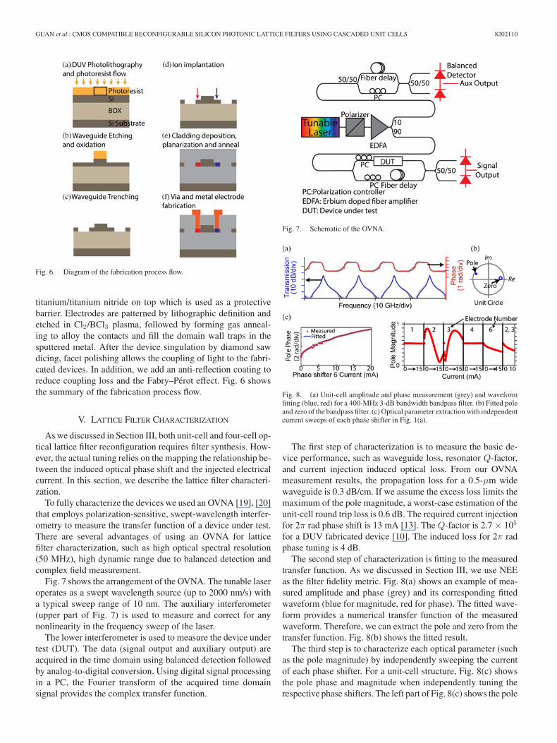
To fully characterize the devices we used an OVNA [19], [20]that employs polarization-sensitive, swept-wavelength interfer-ometry to measure the transfer function of a device under test.There are several advantages of using an OVNA for latticefilter characterization, such as high optical spectral resolution(50 MHz), high dynamic range due to balanced detection andcomplex field measurement.
Fig. 7 shows the arrangement of the OVNA. The tunable laseroperates as a swept wavelength source (up to 2000 nm/s) witha typical sweep range of 10 nm. The auxiliary interferometer(upper part of Fig. 7) is used to measure and correct for anynonlinearity in the frequency sweep of the laser.
The lower interferometer is used to measure the device undertest (DUT). The data (signal output and auxiliary output) areacquired in the time domain using balanced detection followedby analog-to-digital conversion. Using digital signal processingin a PC, the Fourier transform of the acquired time domainsignal provides the complex transfer function.
Fig. 7. Schematic of the OVNA.
Fig. 8. (a) Unit-cell amplitude and phase measurement (grey) and waveformfitting (blue, red) for a 400-MHz 3-dB bandwidth bandpass filter. (b) Fitted poleand zero of the bandpass filter. (c) Optical parameter extraction with independentcurrent sweeps of each phase shifter in Fig. 1(a).
The first step of characterization is to measure the basic de-vice performance, such as waveguide loss, resonator Q-factor,and current injection induced optical loss. From our OVNAmeasurement results, the propagation loss for a 0.5-μm widewaveguide is 0.3 dB/cm. If we assume the excess loss limits themaximum of the pole magnitude, a worst-case estimation of theunit-cell round trip loss is 0.6 dB. The required current injectionfor 2π rad phase shift is 13 mA [13]. The Q-factor is 2.7 × 10⁵
for a DUV fabricated device [10]. The induced loss for 2π radphase tuning is 4 dB.
The second step of characterization is fitting to the measuredtransfer function. As we discussed in Section III, we use NEEas the filter fidelity metric. Fig. 8(a) shows an example of mea-sured amplitude and phase (grey) and its corresponding fittedwaveform (blue for magnitude, red for phase). The fitted wave-form provides a numerical transfer function of the measuredwaveform. Therefore, we can extract the pole and zero from thetransfer function. Fig. 8(b) shows the fitted result.
The third step is to characterize each optical parameter (suchas the pole magnitude) by independently sweeping the currentof each phase shifter. For a unit-cell structure, Fig. 8(c) showsthe pole phase and magnitude when independently tuning therespective phase shifters. The left part of Fig. 8(c) shows the pole
8202110 IEEE JOURNAL OF SELECTED TOPICS IN QUANTUM ELECTRONICS, VOL. 20, NO. 4, JULY/AUGUST 2014
Fig. 9. Characterization result for (a) unit-cell lower waveguide phase witheach phase shifter current sweeping, and (b) four-cell pole magnitude with eachphase shifter current sweeping in the corresponding unit-cell.
phase tuning with ring phase shifter tuning [labeled as phaseshifter 6 in Fig. 1(a)]. As expected, the pole is only affected byphase shifters 2, 3 and 6 as labeled in Fig. 1(a). In addition, thecharacterization result shows that the p-i-n diode phase changesproportionally to the square root of the injected current. Thisis expected from free carrier effect [14]. The tested thresholdvoltage of the p-i-n diode is 0.85 V.
For a four-cell structure, poles are independently controlledby each unit-cell, and zeros are coupled through the whole trans-fer function. Based on previous discussion in Section III, therecursive algorithm focuses on optical parameter tuning insteadof zero tuning. Optical parameters are independently controlledby the unit-cells. Therefore, we can establish a mapping tablebetween each of the optical parameters and corresponding injec-tion currents [e.g., modified phase shift of the lower waveguideϕnt
′ in Fig. 4(d) links with phase shifter 1, 2 and 3 in Fig. 1(a)].Fig. 9(a) shows that for a unit-cell structure, the lower wave-
guide phase is affected by phase shifters 1, 2, 3, 4, 5 and 6 inFig. 1(a). Phase shifters 4, 5 and 6 can affect the lower waveguidephase mainly because of the heating effect. Fig. 9(b) shows thatin a four-cell lattice filter, each pole can be affected by phaseshifters 2, 3 and 6 in the unit-cell structure in Fig. 1(a). HereRi (i = 1,2, . . . ,6) is defined as phase shifter of the unit-cellstructure. The pole magnitude can be derived from the cou-pling coefficient of the ring coupler and waveguide loss. As ex-pected, each pole is independently controlled by its own unit-cellstructure.
Characterization results can help us build the look up table foreach optical parameter and the different phase shifter injection
Fig. 10. Unit-cell optical filter with (a) weak resonance and (b) strong res-onance. [13]. (a) Bandpass with small pole (FIR) pole magnitude = 0.11.(b) Bandpass with large pole (IIR) pole magnitude = 0.87.
Fig. 11. Four-cell lattice filter tuning examples for (a) H21 (ω) with a −1-dBbandwidth of 600-MHz, −3-dB bandwidth of 1-GHz and −20-dB bandwidthof 2.8-GHz. (b) H11 (ω) with −1-dB bandwidth of 1.8-GHz, −3-dB bandwidthof 2.5-GHz and −20-dB bandwidth of 7.6 GHz. (a) Bandpass filter H21 (ω).(b) Notch filter H21 (ω).
currents. Therefore, it is necessary to perform the characteriza-tion for successful lattice filter reconfiguration.
VI. EXPERIMENTAL RESULTS OF A RECONFIGURABLE
LATTICE FILTER
In this section, we present both unit-cell and four-cell latticefilter reconfiguration examples. In addition, we also measuredspurious free dynamic range (SFDR) of the unit-cell lattice filter,as well as the reconfiguration time between a bandpass filter anda notch filter for the unit-cell lattice filter.
Fig. 10(a), (b) shows the transfer function of H11(ω) andH21(ω) for a weak resonance (e.g., near FIR filter, pole magni-tude is 0.11) case, and a strong resonance (e.g., IIR filter, polemagnitude is 0.87) case. As we discussed in Section III, the tun-ing procedure is: first, set pole magnitude and phase through thering resonator phase shifter and the ring coupler phase shifters.Second, adjust the zero position with the lower waveguide phaseshifter and the output coupler phase shifters [13].
Fig. 11 shows the transmission of the four-cell optical latticefilter tuning example. This filter requires adjustment of 26 phaseshifters. Fig. 11(a) shows a narrow bandpass filter for H21(ω)transmission [13]. The filter has more than 30-dB extinction ratioand its −1-dB bandwidth is 600-MHz. Fig. 11(b) shows a widerbandpass filter for H11(ω) transmission, with −1-dB bandwidthof 1.8-GHz. In addition, Fig. 12 shows a four-cell optical lattice

GUAN et al.: CMOS COMPATIBLE RECONFIGURABLE SILICON PHOTONIC LATTICE FILTERS USING CASCADED UNIT CELLS 8202110
Fig. 12. Measured fourth-order Butterworth filter with 0.95 normalized cut-offfrequency.
Fig. 13. (a) Experimental arrangement of the two-RF-tone SFDR measure-ment. Measured RF tones (b) before DUT (unit-cell) and (c) after DUT (unit-cell).
filter example of generating a fourth-order Butterworth filterwith 0.95 normalized cut-off frequency. The filter reconfigura-tion follows the recursive algorithm discussed in Section III. Asa result, we can conclude that the four-cell lattice filter (higher-order filter) can reconfigure for more complex and versatile filtershapes when compared to the unit-cell optical filter.
Next, we also performed a two-RF-tone SFDR measurementon a unit-cell reconfigurable filter. The two-RF-tones are usedto modulate CW lasers and we measure the filtered output fromthe unit cell. Fig. 13(a) shows the experimental arrangementof the two-RF-tone measurement. We use two CW lasers asoptical carriers at 1549.495 nm and 1549.658 nm, respectively.We separately modulate two MZIs, one at 800 MHz and other900 MHz. The EDFAs and attenuators are used for equalizingthe amplitudes of two RF tones before sending them to theunit-cell filter. We put an additional EDFA before the unit-cellto compensate for the 22-dB insertion loss of the device. Theinsertion loss was dominated by the coupling loss between thelensed fibers and 3.0-μm wide silicon waveguides at the polishedoptical facets. We estimate this coupling loss was 5–7 dB perfacet. We monitor the wavelength with OSA on one output of the2× 2 directional coupler. On the other output, we use an Agilent71400 C lightwave spectrum analyzer to detect the optical signalafter the unit-cell filter and convert it to an electrical signal. The
Fig. 14. (a) Experimental arrangement for measuring the dynamic reconfigu-ration of a unit-cell filter. (b)Measured waveform after the unit-cell filter witha 2.5-MHz switching speed. (c) 2D plot (spectrogram) showing the temporalevolution of the filter shape [21].
setup noise floor is −149 dBm/Hz. The measured SFDR is61.6 dB. The total received optical power is −3.4 dBm. Theresolution bandwidth of the RF spectrum analyzer is 30 kHz,the video bandwidth is 300 Hz. The sweep time is 116 s.
Finally, we also record the reconfiguration time of a unit-cellfilter while switching from a bandpass filter to a notch filter.Fig. 14(a) shows the experimental arrangement for measuringthe dynamic reconfiguration of a unit-cell optical filter [21].We pass a train of linearly-chirped optical pulses through theunit cell filter. As a result, we can characterize the amplitude andphase of the pulses before and after the unit-cell filter. Fig. 14(b)shows the measured waveform intensities at the output of theunit-cell filter, when we applied a 2.5-MHz square waveformto lower waveguide phase shifter [labeled 1 in Fig. 1(a)]. A isthe measured output waveform after going through a bandpassfilter. Fig. 14(c) uses a spectrogram to present the dynamicreconfiguration between a notch filter and a bandpass filter.In conclusion, the major transition between two filter shapes is<16.67-ns. However, it might take 30–50 ns to fully stabilize thewaveform after each transition, because of the device’s thermalfluctuation with changing heat load (15–30 mW) [21].
VII. APPLICATIONS
RF-photonic processing components have a broad rangeof applications due to their higher bandwidth, low latencyperformance, and potentially lower cost compared to all-electronic processing. This section focuses on using RF-photonic lattice filters to replace electrical signal processingin THz waveform synthesis.
One of the challenges in THz waveform synthesis is cor-recting the non-ideal frequency response of optical modulatorsand multiplexers. For example, Fig. 15(a) shows the generalmethodology for a dynamic optical arbitrary waveform gener-ation (OAWG) transmitter, which is capable of generating ar-bitrary optical waveforms [e.g., Fig. 15(b)] within its operation

8202110 IEEE JOURNAL OF SELECTED TOPICS IN QUANTUM ELECTRONICS, VOL. 20, NO. 4, JULY/AUGUST 2014
Fig. 15. (a) Dynamic OAWG transmitter diagram. (b) An example of outputmodulated data spectrum. (c) Multiplexer transfer function. (d) Signal process-ing for derive modulation signals. [12]
bandwidth. OAWG functions by first spectrally demultiplexingan optical frequency comb (OFC) to isolate each comb line ona separate output. In parallel, each comb line is then individ-ually modulated using separate in-phase and quadrature-phasemodulators. These modulated comb lines are then spectrallycombined using a multiplexer with overlapping spectral pass-bands [Fig. 15(c)] to yield an arbitrary waveform that has a totalbandwidth of B×N , where B is the OFC line spacing and N isthe number of OFC lines. In practice, a B of 10 GHz is a goodcompromise for both the electrical and optical components nec-essary for OAWG [22]. Of course, it is also possible to use a pas-sive combiner instead of a spectral multiplexer to combine themodulated OFC lines, but this method is not practically scalableto large numbers of OFC lines due to increased optical losses.
The modulations necessary to broaden each OFC line can bederived according to Fig. 15(d). The first step is to determinea desired target waveform with bandwidth B×N . Next, apply-ing spectral slice filters to the Fourier transform of the targetwaveform yields spectral slices that are of manageable band-width for both electronic and optics (e.g., 10 GHz). Note thatthe spectral slice filters are a mathematical construct that serveonly to divide the target waveform spectrum into spectral slicesand do not result in any loss of information. Taking the inverseFourier transform of each spectral slice yields the in-phase andquadrature-phase modulations necessary to drive each I/Q mod-ulator for the generation of the target waveform at the output ofthe spectral multiplexer.
Experimental demonstrations of OAWG have relied on elec-tronic precompensation to compensate for the non-ideal fre-quency response of the I/Q modulators and the transmission
Fig. 16. Measured transmission of a unit-cell filter as an optical equalizerof H11 (f ) (H12 (f ) is the complementary output). Fitted pole and zeros arepresented in the part of the plot [12].
function of the spectral multiplexer [22]. Relying solely on elec-tronic compensation, however, reduces the effective dynamicrange available for OFC line modulation while increasing com-plexity and power consumption of the electronics.
Reconfigurable RF-photonic lattice filters [10] are a viableoptical solution for overcoming both the non-ideal I/Q modula-tor response and the spectral multiplexer transmission in THzwaveform synthesis. In this case, a 10-GHz FSR unit-cell filtercan function as an optical equalization component for an OAWGwaveform created using 10 GHz spectral slices. Specifically, theunit-cell based filter can be placed immediately after the outputof the OAWG transmitter. Fig. 16 shows the measured trans-mission of a unit-cell filter [H11(f) as output] when configuredas an optical equalizer for OAWG. The inset in Fig. 16 showsthe corresponding pole and zeros position for the unit-cell filter[zeros are from H11(f) and H12(f)]. The unit-cell optical fil-ter provides nearly identical equalization to that which can beachieved using a digital filter. Moreover, using optical process-ing, instead of digital processing, reduces the complexity of therequired electrical components, and reduces power consump-tion.
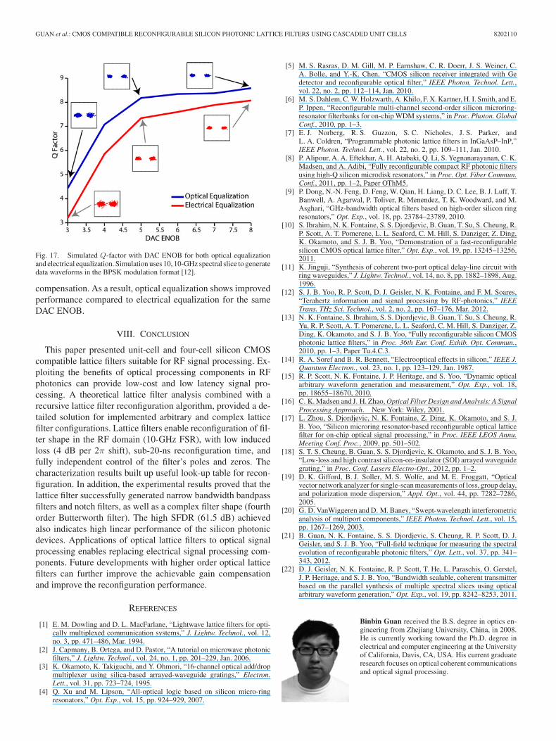
Further investigations evaluated OAWG waveform Q-factoras a function of digital-to-analog converter (DAC) effectivenumber of bits (ENOB) using electrical equalization or op-tical equalization via simulations [12]. The target waveformconsisted of a 5-ns, 100-Gb/s BPSK signal (500 bits) with asignal to noise ratio of 15 dB. The resulting 100-GHz signalwaveform was divided into ten 10-GHz spectral slices follow-ing the methodology in Fig. 15(d). The electrical equaliza-tion scenario involved the application of pre-emphasis on themodulator driven signal to correct for the non-ideal frequencyresponse of the I/Q modulators and the spectral multiplexer. Theoptical equalization scenario consisted of using a reconfigurableunit-cell lattice filter to provide the necessary compensation. Af-ter applying equalization, calculation of the waveform Q-factorfrom the simulated constellation enabled evaluating the efficacyof both methods of compensation. Fig. 17 shows the simulatedQ-factor as a function of DAC ENOB for both optical equal-ization and electrical equalization. Optical equalization showshigher Q-factor at all DAC ENOB values, which indicates im-proved waveform fidelity. Electrical equalization had reducedperformance due to a reduction in DAC ENOB available forI/Q modulator modulations after accounting for the necessary
GUAN et al.: CMOS COMPATIBLE RECONFIGURABLE SILICON PHOTONIC LATTICE FILTERS USING CASCADED UNIT CELLS 8202110
Fig. 17. Simulated Q-factor with DAC ENOB for both optical equalizationand electrical equalization. Simulation uses 10, 10-GHz spectral slice to generatedata waveforms in the BPSK modulation format [12].
compensation. As a result, optical equalization shows improvedperformance compared to electrical equalization for the sameDAC ENOB.
VIII. CONCLUSION
This paper presented unit-cell and four-cell silicon CMOScompatible lattice filters suitable for RF signal processing. Ex-ploiting the benefits of optical processing components in RFphotonics can provide low-cost and low latency signal pro-cessing. A theoretical lattice filter analysis combined with arecursive lattice filter reconfiguration algorithm, provided a de-tailed solution for implemented arbitrary and complex latticefilter configurations. Lattice filters enable reconfiguration of fil-ter shape in the RF domain (10-GHz FSR), with low inducedloss (4 dB per 2π shift), sub-20-ns reconfiguration time, andfully independent control of the filter’s poles and zeros. Thecharacterization results built up useful look-up table for recon-figuration. In addition, the experimental results proved that thelattice filter successfully generated narrow bandwidth bandpassfilters and notch filters, as well as a complex filter shape (fourthorder Butterworth filter). The high SFDR (61.5 dB) achievedalso indicates high linear performance of the silicon photonicdevices. Applications of optical lattice filters to optical signalprocessing enables replacing electrical signal processing com-ponents. Future developments with higher order optical latticefilters can further improve the achievable gain compensationand improve the reconfiguration performance.
REFERENCES
[1] E. M. Dowling and D. L. MacFarlane, “Lightwave lattice filters for opti-cally multiplexed communication systems,” J. Lightw. Technol., vol. 12,no. 3, pp. 471–486, Mar. 1994.
[2] J. Capmany, B. Ortega, and D. Pastor, “A tutorial on microwave photonicfilters,” J. Lightw. Technol., vol. 24, no. 1, pp. 201–229, Jan. 2006.
[3] K. Okamoto, K. Takiguchi, and Y. Ohmori, “16-channel optical add/dropmultiplexer using silica-based arrayed-waveguide gratings,” Electron.Lett., vol. 31, pp. 723–724, 1995.
[4] Q. Xu and M. Lipson, “All-optical logic based on silicon micro-ringresonators,” Opt. Exp., vol. 15, pp. 924–929, 2007.
[5] M. S. Rasras, D. M. Gill, M. P. Earnshaw, C. R. Doerr, J. S. Weiner, C.A. Bolle, and Y.-K. Chen, “CMOS silicon receiver integrated with Gedetector and reconfigurable optical filter,” IEEE Photon. Technol. Lett.,vol. 22, no. 2, pp. 112–114, Jan. 2010.
[6] M. S. Dahlem, C. W. Holzwarth, A. Khilo, F. X. Kartner, H. I. Smith, and E.P. Ippen, “Reconfigurable multi-channel second-order silicon microring-resonator filterbanks for on-chip WDM systems,” in Proc. Photon. GlobalConf., 2010, pp. 1–3.
[7] E. J. Norberg, R. S. Guzzon, S. C. Nicholes, J. S. Parker, andL. A. Coldren, “Programmable photonic lattice filters in InGaAsP–InP,”IEEE Photon. Technol. Lett., vol. 22, no. 2, pp. 109–111, Jan. 2010.
[8] P. Alipour, A. A. Eftekhar, A. H. Atabaki, Q. Li, S. Yegnanarayanan, C. K.Madsen, and A. Adibi, “Fully reconfigurable compact RF photonic filtersusing high-Q silicon microdisk resonators,” in Proc. Opt. Fiber Commun.Conf., 2011, pp. 1–2, Paper OThM5.
[9] P. Dong, N.-N. Feng, D. Feng, W. Qian, H. Liang, D. C. Lee, B. J. Luff, T.Banwell, A. Agarwal, P. Toliver, R. Menendez, T. K. Woodward, and M.Asghari, “GHz-bandwidth optical filters based on high-order silicon ringresonators,” Opt. Exp., vol. 18, pp. 23784–23789, 2010.
[10] S. Ibrahim, N. K. Fontaine, S. S. Djordjevic, B. Guan, T. Su, S. Cheung, R.P. Scott, A. T. Pomerene, L. L. Seaford, C. M. Hill, S. Danziger, Z. Ding,K. Okamoto, and S. J. B. Yoo, “Demonstration of a fast-reconfigurablesilicon CMOS optical lattice filter,” Opt. Exp., vol. 19, pp. 13245–13256,2011.
[11] K. Jinguji, “Synthesis of coherent two-port optical delay-line circuit withring waveguides,” J. Lightw. Technol., vol. 14, no. 8, pp. 1882–1898, Aug.1996.
[12] S. J. B. Yoo, R. P. Scott, D. J. Geisler, N. K. Fontaine, and F. M. Soares,“Terahertz information and signal processing by RF-photonics,” IEEETrans. THz Sci. Technol., vol. 2, no. 2, pp. 167–176, Mar. 2012.
[13] N. K. Fontaine, S. Ibrahim, S. S. Djordjevic, B. Guan, T. Su, S. Cheung, R.Yu, R. P. Scott, A. T. Pomerene, L. L. Seaford, C. M. Hill, S. Danziger, Z.Ding, K. Okamoto, and S. J. B. Yoo, “Fully reconfigurable silicon CMOSphotonic lattice filters,” in Proc. 36th Eur. Conf. Exhib. Opt. Commun.,2010, pp. 1–3, Paper Tu.4.C.3.
[14] R. A. Soref and B. R. Bennett, “Electrooptical effects in silicon,” IEEE J.Quantum Electron., vol. 23, no. 1, pp. 123–129, Jan. 1987.
[15] R. P. Scott, N. K. Fontaine, J. P. Heritage, and S. Yoo, “Dynamic opticalarbitrary waveform generation and measurement,” Opt. Exp., vol. 18,pp. 18655–18670, 2010.
[16] C. K. Madsen and J. H. Zhao, Optical Filter Design and Analysis: A SignalProcessing Approach. New York: Wiley, 2001.
[17] L. Zhou, S. Djordjevic, N. K. Fontaine, Z. Ding, K. Okamoto, and S. J.B. Yoo, “Silicon microring resonator-based reconfigurable optical latticefilter for on-chip optical signal processing,” in Proc. IEEE LEOS Annu.Meeting Conf. Proc., 2009, pp. 501–502.
[18] S. T. S. Cheung, B. Guan, S. S. Djordjevic, K. Okamoto, and S. J. B. Yoo,“Low-loss and high contrast silicon-on-insulator (SOI) arrayed waveguidegrating,” in Proc. Conf. Lasers Electro-Opt., 2012, pp. 1–2.
[19] D. K. Gifford, B. J. Soller, M. S. Wolfe, and M. E. Froggatt, “Opticalvector network analyzer for single-scan measurements of loss, group delay,and polarization mode dispersion,” Appl. Opt., vol. 44, pp. 7282–7286,2005.
[20] G. D. VanWiggeren and D. M. Baney, “Swept-wavelength interferometricanalysis of multiport components,” IEEE Photon. Technol. Lett., vol. 15,pp. 1267–1269, 2003.
[21] B. Guan, N. K. Fontaine, S. S. Djordjevic, S. Cheung, R. P. Scott, D. J.Geisler, and S. J. B. Yoo, “Full-field technique for measuring the spectralevolution of reconfigurable photonic filters,” Opt. Lett., vol. 37, pp. 341–343, 2012.
[22] D. J. Geisler, N. K. Fontaine, R. P. Scott, T. He, L. Paraschis, O. Gerstel,J. P. Heritage, and S. J. B. Yoo, “Bandwidth scalable, coherent transmitterbased on the parallel synthesis of multiple spectral slices using opticalarbitrary waveform generation,” Opt. Exp., vol. 19, pp. 8242–8253, 2011.
Binbin Guan received the B.S. degree in optics en-gineering from Zhejiang University, China, in 2008.He is currently working toward the Ph.D. degree inelectrical and computer engineering at the Universityof California, Davis, CA, USA. His current graduateresearch focuses on optical coherent communicationsand optical signal processing.

8202110 IEEE JOURNAL OF SELECTED TOPICS IN QUANTUM ELECTRONICS, VOL. 20, NO. 4, JULY/AUGUST 2014
Stevan S. Djordjevic received the Dipl.-Ing. degreefrom the School of Electrical Engineering, Universityof Belgrade, Serbia. He is currently working towardthe Ph.D. degree in electrical and computer engineer-ing at the University of California, Davis, CA, USA.During his graduate research, he has designed, fab-ricated, and characterized CMOS-compatible ather-mal silicon ring modulators, reconfigurable siliconphotonic lattice filters, and other integrated opticaldevices. He is currently with the Photonics, Intercon-nects, and Packaging Group, Oracle Labs, San Diego,
CA, working on the DARPA Ultra-performance Nanophotonic Intrachip Com-munication (UNIC) project.
Nicolas K. Fontaine (S’02–M’10) received B.S. de-grees in both electrical engineering and optical engi-neering , the M.S. degree in electrical and computerengineering,and the Ph.D. degree in electrical andcomputer engineering from from the University ofCalifornia (UC), Davis, CA, USA, in 2004, 2007,and 2010, respectively. He is currently a Member ofTechnical Staff at Bell Laboratories, Alcatel-Lucent,Holmdel, NJ, USA.
Linjie Zhou, photograph and biography not available at the time of publication.
Salah Ibrahim received the B.Sc. and M.Sc. degrees in electronics and com-munication engineering from Cairo University, Egypt, and the Ph.D. degree inelectronics engineering from the University of Tokyo, Japan, in 2009. From2009 to 2010, he was a Postdoctoral Research Scientist in the Departmentof Electrical and Computer Engineering, University of California, Davis, CA,USA. Since 2011, he is with NTT Photonics Laboratories, Atsugi, Japan. Hiscurrent research interests include OPS technologies, ultrafast optoelectronic andoptical device in InP, silicon and hybrid material systems.
Ryan P. Scott (S’93–M’03) received the B.S. degreein laser electrooptics technology from the Oregon In-stitute of Technology, Klamath Falls, in 1991, theM.S. degree in electrical engineering from the Uni-versity of California, Los Angeles, in 1995, and thePh.D. degree in electrical and computer engineeringfrom the University of California, Davis (UC Davis),CA, USA, in 2009. He is currently a Project Scientistin the Department of Electrical and Computer En-gineering, UC Davis. His current research interestsinclude photonic integration of complex optical sys-
tems to improve stability and expand applications, full-field optical waveformgeneration and measurement techniques, and spatial division multiplexing tech-nologies.
David J. Geisler (S’02–M’12) was born in NewYork, NY, USA, in 1982. He received the B.S. de-gree in electrical engineering from Tufts University,Medford, MA, USA, in 2004, the M.S. degree in elec-trical engineering from the University of California,Davis, CA, USA, in 2009, and the Ph.D. degree inelectrical and computer engineering from the Univer-sity of California, Davis, in 2012.
He is currently with the Advanced Lasercom andSystems Group, Massachusetts Institute of Technol-ogy Lincoln Laboratory, Lexington, MA, USA. His
research interests include optical arbitrary waveform generation and measure-ment, advanced modulation formats, and free-space optical communications.
Zhi Ding (S’88–M’90–SM’95–F’03) received thePh.D. degree in electrical engineering from CornellUniversity in 1990. He is the Child Family EndowedProfessor of Engineering and Entrepreneurship at theUniversity of California, Davis, CA, USA. He alsoholds a joint appointment as a thousand talent pro-fessorship at Southeast University in Nanjing, ChinaFrom 1990 to 2000, he was a Faculty Member ofAuburn University and later, University of Iowa. Hehas held visiting positions in Australian National Uni-versity, Hong Kong University of Science and Tech-
nology, NASA Lewis Research Center and USAF Wright Laboratory. He hasactive collaboration with researchers from several countries including Australia,China, Japan, Canada, Taiwan, Korea, Singapore, and Hong Kong. He has beenan active member of IEEE, serving on technical programs of several workshopsand conferences. He was an Associate Editor for IEEE TRANSACTIONS ON SIG-NAL PROCESSING from 1994 to 1997, 2001 to 2004, and an Associate Editor ofIEEE SIGNAL PROCESSING LETTERS 2002–2005. He was a member of technicalcommittee on Statistical Signal and Array Processing and member of technicalcommittee on Signal Processing for Communications (1994–2003). He was theTechnical Program Chair of the 2006 IEEE Globecom. He is also an IEEEDistinguished Lecturer (Circuits and Systems Society, 2004–06, Communica-tions Society, 2008–09). He served as an IEEE TRANSACTIONS ON WIRELESS
COMMUNICATIONS Steering Committee Member (2007–2009) and its Chair(2009–2010). He is a coauthor of the book Modern Digital and Analog Com-munication Systems, (4th edition, Oxford University Press, 2009).
S. J. Ben Yoo (S’82–M’84– SM’97–F’07) receivedthe B.S. degree in electrical engineering (with distinc-tion), the M.S. degree in electrical engineering, andthe Ph.D. degree in electrical engineering with minorin physics, all from Stanford University, Stanford,CA, USA, in 1984, 1986, and 1991, respectively. Hecurrently serves as Professor of electrical engineeringat the University of California at Davis (UC Davis).His research at UC Davis includes RF-photonic de-vices, systems, and networking technologies for thefuture generation Internet and computing systems. In
particular, he is conducting research on architectures, systems integration, andnetwork experiments related to all-optical label switching routers, terahertz op-tical arbitrary waveform generation, flexible bandwidth networking, and opticalinterconnect technologies. Prior to joining UC Davis in 1999, he was a SeniorResearch Scientist at Bell Communications Research (Bellcore), leading techni-cal efforts in optical networking research and systems integration. His researchinterests at Bellcore included optical-label switching for the next-generationInternet, power transients in reconfigurable optical networks, wavelength in-terchanging cross connects, wavelength converters, vertical-cavity lasers, andhigh-speed modulators. He also participated in the advanced technology demon-stration network/multiwavelength optical networking (ATD/MONET) systemsintegration, the OC-192 synchronous optical network (SONET) ring studies,and a number of standardization activities which led to documentations ofGeneric Requirements, GR-2918-CORE (1999), GR-2918-ILR (1999), GR-1377-CORE (1995), and GR-1377-ILR (1995) on dense WDM and OC-192systems. Prior to joining Bellcore in 1991, he conducted research at StanfordUniversity on nonlinear optical processes in quantum wells, a four-wave-mixingstudy of relaxation mechanisms, and ultrafast diffusion-driven photodetectors.During this period, he also conducted research on lifetime measurements ofintersubband transitions and on nonlinear optical storage mechanisms at BellLaboratories and IBM Research Laboratories, respectively. Dr. Yoo is a Fel-low of IEEE Photonics Society, a Fellow of the Optical Society of America(OSA), a Fellow of NASA NIAC, and a Member of Tau Beta Pi. He receivedthe DARPA Award for Sustained Excellence in 1997, the Bellcore CEO Awardin 1998, the Outstanding Mid-Career Research Faculty Award (UC Davis) in2004, and the Outstanding Senior Research Faculty Award (UC Davis) in 2011.He also served as an Associate Editor for IEEE PHOTONICS TECHNOLOGY LET-TERS, Guest Editor for IEEE/OSA JOURNAL OF LIGHTWAVE TECHNOLOGY andIEEE JOURNAL OF SELECTED TOPICS IN QUANTUM ELECTRONICS, and GeneralCochair for Photonics in Switching conference 2007, 2010, and 2012.


