Embed Size (px)
Citation preview

EEE JOURNAL ON SELECTED AREAS IN COMMUNICATIONS, VOL. 14, NO. 2, FEBRUARY 1996 331
Broadband Time-Division Circuit Switching Andrzej Jajszczyk, Senior Member, IEEE, and Jerzy Tyszer, Member, IEEE
Abstract- The paper describes various techniques to increase the speed of time-division switches to support rates of 600 Mb/s and beyond. The issue of multirate switching, essential to BISDN applications, is also addressed. Architectures of RAM- and shift- register-based time switches are discussed and compared. Some representative structures of time-division switch fabrics applica- ble to BISDN are presented.
I. INTRODUCTION MONG various approaches to circuit switched broad- A band ISDN, time-division switching seems to be very
attractive and promising. The main reason for the interest in time-division switching is the fact that a majority of modern transmission systems, based, for example. on SONET or SDH technology, use time-division multiplexing. Electronic technology that makes it possible to implement such time- division switching is sufficiently mature to support rates of 600 Mb/s and beyond; furthermore, in contrast to current photonic technologies, it is cost-efficient. Application of time- division circuit switching can complement ATM in such areas as cross-connects [l] or video distribution [2].
Although the concept of time-division switching dates back to 1945 [3], it should be re-examined to be applicable to BISDN. This paper contains a critical survey of techniques that can be used to increase speed and flexibility of time- division switches and switch fabrics. We can note that memory bandwidth determines capacity of several classes of architec- tures, for example shared-memory based ATM switches [4]. Alternatively, ATM switches can be used to serve as circuit or multirate circuit switches by proper cell scheduling. Section I1 analyzes speed limitations of a conventional RAM-based time switch and presents techniques to increase its speed, as well as describes fast switches that use shift registers for their data memories. Some examples of switch fabrics employing such broadband switches are discussed in Section 111. Section IV is devoted to multirate switching that is essential for integrated network applications.
11. BROADBAND TIME-DIVISION SWITCHES
A. RAM-Type Time Switches
To discuss constraints imposed upon broadband switches we start with the examination of the basic time switch shown in
Manuscript received November 17, 1994; revised June 9, 1995. A. Jajszczyk is with EFP-The Franco-Polish School of New Information
and Communication Technologies, P. Mansfelda 4, Poznaii 6, Poland (e-mail: [email protected]).
J. Tyszer is with the Department of Electrical Engineering, McGill Univer- sity, Montreal, Quebec, Canada (e-mail: [email protected]).
Publisher Item Identifier S 0733-87 16(96)00833-5.
output Input highway w z m h i g h w a y IN ADDR OUT
Control information (a)
A I )( B1 x c1 )( D1 x Input data ( Writing to DM (Al) (B1) a (ol> Readingfrom DM @ @ @ 0
X x BO )( A I >c output ( data
Fig. 1. Conventional time-division switch: (a) structure, DM denotes data memory, AM denotes address memory, C denotes counter, R denotes register; (b) time chart.
Fig. l(a). For simplicity, in this figure we have omitted the input multiplexer, the output demultiplexer and the registers converting serial data words into a parallel form and vice versa. Such a reduced switch is often referred to as time- slot interchange (TSI). The basic elements of the switch are two RAM’S: the data memory (DM) in which incoming data words are stored and the address memory (AM) which controls reading of the data memory words to be placed in the outgoing time slots.
The operation of the discussed switch will be illustrated by a simplified time chart shown in Fig. l(b). The simplifications are due to the omission of writing and reading times to and from registers at inputs and outputs of the data memory, respectively, as well as signal propagation delays between var- ious elements of the switch. During the frame representing the incoming stream, contents of the consecutive incoming time slots are sequentially written into the consecutive locations of the data memory DM, i.e., data from time slot A will always reside in cell 1, time slot B in cell 2, etc.
During a single time slot period, along with the writing, the reading of a data memory word must take place. The address of this read word is given by the AM. The location of each address memory word corresponds to the number of the outgoing time slot and its contents-to the address of the data memory word. The working cycle of AM is similar to that
0733-8716/96$05.00 0 1996 IEEE
338 IEEE JOURNAL ON SELECTED AREAS W COMMUNICATIONS, VOL. 14, NO. 2, FEBRUARY 1996
Written
e
7'
rd
7'
lines
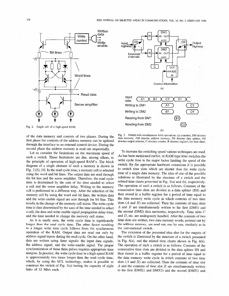
Fig. 2. Single cell of a high-speed RAM.
of the data memory and consists of two phases. During the first phase the contents of the address memory can be updated through the interface to an external control device. During the second phase the address memory is read out sequentially.
Let us consider the limitations on the maximum speed of such a switch. These limitations are due, among others, to the principle of operation of high-speed RAM'S. The block diagram of a single element of such a memory is shown in Fig. 2 [5] , [6]. In the read cycle time, a memory cell is selected using the word and bit lines. The output data are read through the bit line and the sense amplifier. Therefore, the read cycle time is determined by the sum of the time needed to select a cell and the sense amplifier delay. Writing to the memory cell is performed in a different way. After the selection of the memory cell by using the word and bit lines, the written data and the write-enable signal are sent through the bit line. This results in the change of the memory cell status. The write cycle time is thus determined by the sum of the time needed to select a cell, the data and write-enable signal propagation delay time, and the time needed to change the memory cell status.
As it is easily seen, the write cycle time is significantly longer than the read cycle time. The other factor resulting in a longer write time cycle follows from the synchronous operation of the RAM. Output data are read out only by address signal inputs during the read cycle. On the other hand, data are written using three signals: the input data signals, the address signal, and the write-enable signal. The proper synchronization of these three pulses requires appropriate time margins. In practice, the write cycle time in a high-speed RAM is approximately two times longer than the read cycle time, which, by using the ECL technology, makes it possible to construct the switch of Fig. l(a) having the capacity of eight links of 32 Mb/s each.
Control information
A I )( BI x c 1 x D1 x Input data ( Writing to DMI CA1 Writing to DM2 rn m Reading from DM2 @ Reading from DMI
(b)
Fig. 3. Switch with simultaneous write operations: (a) structure, DM denotes data memory, AM denotes address memory, DS denotes data splitter, OS denotes output selector, C denotes counter, R denotes regist& (b) time chart.
To increase the switching speed various techniques are used. As has been mentioned earlier, in RAM-type time switches the write cycle time is the major factor limiting the speed of the switch. By the appropriate hardware extensions it is possible to switch time slots which are shorter than the write cycle time of a single data memory. The idea of one of the possible solutions is illustrated by the structure of a switch and the related time charts presented in Fig. 3(a) and (b), respectively. The operation of such a switch is as follows. Contents of the consecutive time slots are divided in a data splitter (DS) and then stored in a buffer register for a period of time equal to the data memory write cycle in which contents of two time slots (A and B ) are collected. Then the contents of time slots A and B are simultaneously written to the first (DM1) and the second (DM2) data memories, respectively. Time slots C and D, etc. are analogously handled. After the contents of two time slots are written, two data memory words, pointed out by the address memory, are read out, one by one, similarly as in the conventional switch.
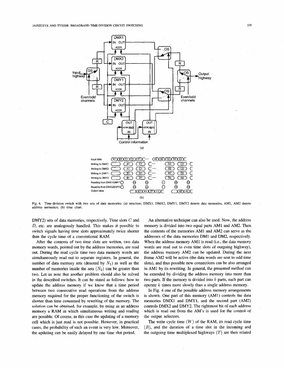
The extension of the presented idea also for the outputs of the switch is illustrated by the structure of a switch presented in Fig. 4(a), and the related time charts shown in Fig. 4(b). The operation of such a switch is as follows. Contents of the consecutive time slots are divided in the data splitter DS and then stored in a buffer register for a period of time equal to the data memory write cycle in which contents of two time slots ( A and B ) are collected. Then the contents of time slot A and the contents of time slot B are simultaneously written to the first (DMX1 and DMX2) and the second (DMYl and
JAJSZCZYK AND TYSZER BROADBAND TIME-DIVISION CIRCUIT SWITCHING 339
utput ghwa!f
Control information
(a)
Input data
WritingtoDMXl (-) (7) (7) c... (AI X s i Xci x 01 XEIX... ( A2 x 82 x C2 x D2 x E2 x (7) (7) c
Reading from DMX2/DMY2O 0 @ 0 6 3 8 Output data ( X B I X A ~ X D I X C ~ X ( x 62 x A 2 X
(b)
Fig. 4. Time-division switch with two sets of data memories: (a) structure; DMX1, DMX2, DMY1, DMY2 denote data memories, AMI, AM2 denote address memories; @) time chart.
DMY2) sets of data memories, respectively. Time slots C and D, etc. are analogously handled. This makes it possible to switch signals having time slots approximately twice shorter than the cycle time of a conventional RAM.
After the contents of two time slots are written, two data memory words, pointed out by the address memories, are read out. During the read cycle time two data memory words are simultaneously read out to separate registers. In general, the number of data memory sets (denoted by N I ) as well as the number of memories inside the sets ( N z ) can be greater than two. Let us note that another problem should also be solved in the described switches. It can be stated as follows: how to update the address memory if we know that a time period between two consecutive read operations from the address memory required for the proper functioning of the switch is shorter than time consumed by rewriting of the memory. The solution can be obtained, for example, by using as an address memory a RAM in which simultaneous writing and reading are possible. Of course, in this case the updating of a memory cell which is just read is not possible. However, in practical cases, the probability of such an event is very low. Moreover, the updating can be easily delayed by one time slot period.
An alternative technique can also be used. Now, the address memory is divided into two equal parts AM1 and AM2. Then the contents of the memories AM1 and AM2 can serve as the addresses of the data memories DM1 and DM2, respectively. When the address memory AM1 is read (i.e., the data memory words are read out to even time slots of outgoing highway), the address memory AM2 can be updated. During the next frame AM2 will be active (the data words are sent to odd time slots), and thus possible new connections can be also arranged in AM1 by its rewriting. In general, the presented method can be extended by dividing the address memory into more than two parts. If the memory is divided into k parts, each part can operate k times more slowly than a single address memory.
In Fig. 4 one of the possible address memory arrangements is shown. One part of this memory (AM1) controls the data memories DMXl and DMY1, and the second part (AM2) controls DMX2 and DMY2. The rightmost bit of each address which is read out from the AM’s is used for the control of the output selectors.
The write cycle time ( W ) of the RAM, its read cycle time (R) , and the duration of a time slot in the incoming and the outgoing time multiplexed highways ( T ) are then related

340 IEEE JOURNAL ON SELECTED AREAS IN COMMUNICATIONS, VOL. 14, NO. 2, FEBRUARY 1996
among themselves as follows
WIN1 + R/N2 5 T. (1)
It should be noted, however, that the increase of NI and N2 causes considerable problems connected with signal synchro- nization inside the switch. It is easily seen that the necessary total capacity of RAM in the described solution is proportional to Nz, since the switch contains N I sets of data memories DM, each containing N2 memories, and each memory DM is composed of f / N l words, where f is the multiplicity of the incoming and outgoing highways (f time slots are distributed among N I memory sets).
An alternative technique, based also on doubling of the data memory, is possible. The switch employing such a technique is shown in Fig. 5(a). The related, simplified time chart is presented in Fig. 5(b). The switch operates as follows. During W*ng Dl ... even frame periods, contents of the incoming time slots are written into the data memory DM1. At the same time the data memory DM2 is read, according to the addresses coming from Read,ng from D M Z ~ 8 a a 0
Control information
(a)
lnputdata A I 61 C1 D1 E l ...( A2 x 62 x C2 x ...
( A2 x El2 x ... a @ @
W*ngtoDM2 ( Read,ng from DM1
the address memory AM. In the case of odd frame periods the situation is reversed, i.e., DM2 is written and DM1 is read.
omut data ( BO x A0 x DO x CO x (, 61 x AI x Ih\
Therefore the maximum operating frequency of the switch is independent of the sum of the write and read cycle times, but instead, it depends only on the write cycle time.
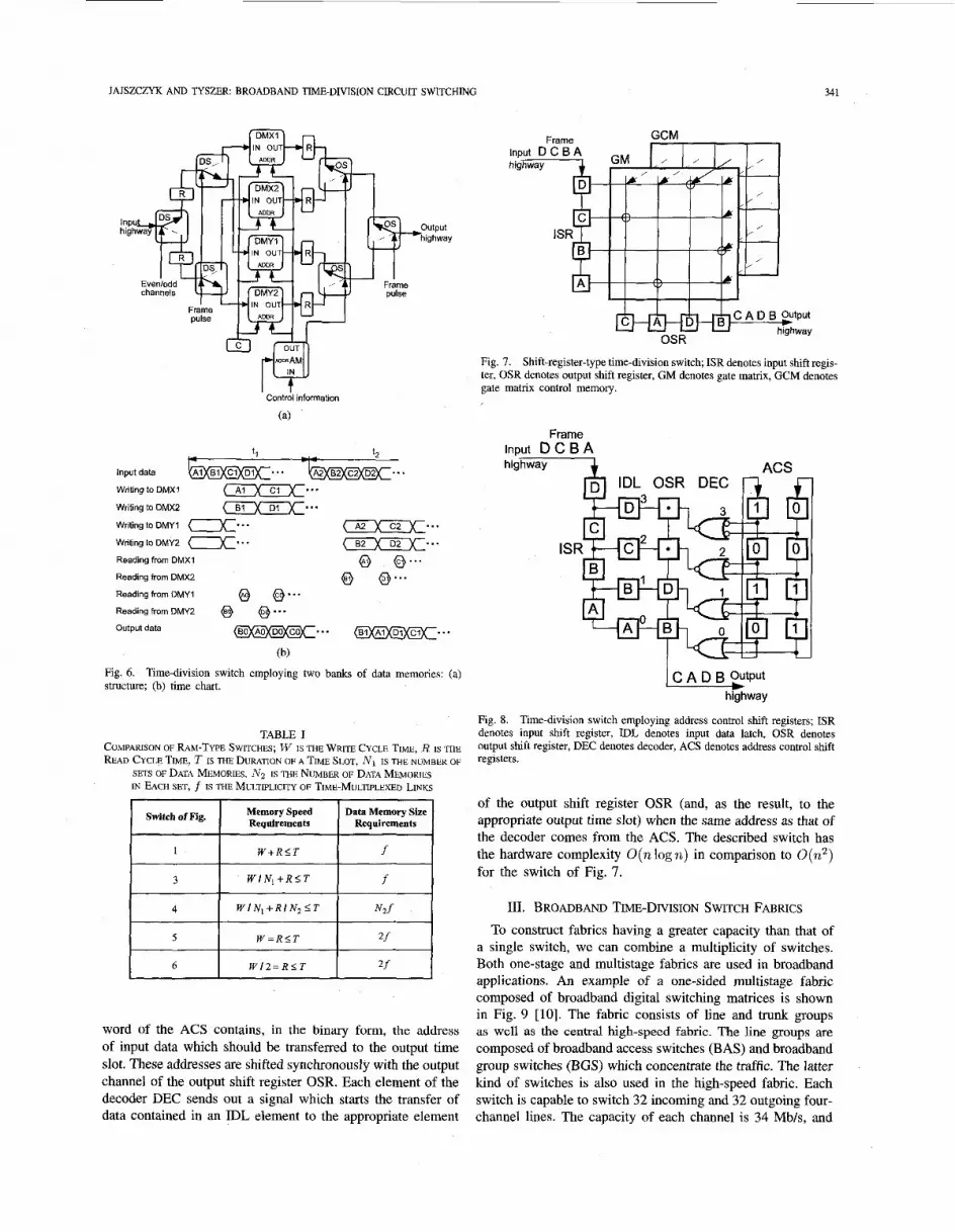
A further speed increase can be achieved by combining the techniques illustrated in Figs. 3 and 5 [7]. The structure of a switch based on such a concept is shown in Fig. 6(a) and an example of the simplified time charts is presented in Fig. 6(b). In order to simplify the description, we consider the switch containing a single address memory, although the solution introduced previously can also be used. During the tl input frame period data contained in incoming time slots are written to the memory DMXliDMX2 and, simultaneously, words of the memory DMYlDMY2 are read out, similarly as in the switch of Fig. 5, where the read-write separation technique was used. In the following frame period, t 2 , the operation of DMXliDMX2 and DMYlDMY2 is exchanged, i.e., DMXlDMX2 is read and DMYlDMY2 is written.
The division of each of the memories DMXlDMX2 and DMYl/DMY2 into two banks enables both banks to be written in parallel. This makes it possible to write data contained in a time slot during the period corresponding to two time slots in the incoming highway, as was the case in the switch of Fig. 3 . In this example, there are no savings in the duration of the read time cycle, which must be shorter than the duration of a single time slot in the outgoing link. However, this is of a secondary importance because the speed of the switch is determined mainly by the duration of the write cycle time, as it has been explained in the first part of this section.
We should note an additional, significant difference in the operation of the switches presented in Figs. 4 and 6. In the first of them data contained in a given time slot has to be simultaneously written to two memory sets (in the case N2 = 2). In the switch of Fig. 6 this is not necessary.
Some modified versions of the switch of Fig. 6 are also possib€e. For example the switch can be composed of three data memories DM. During a single frame period, two of these memories are written, and one memory is read out. Then, the
\"I
Fig. 5. Time-division switch with simultaneous write and read operations: (a) structure, DM denotes data memory, AM denotes address memory, DS denotes data splitter, OS denotes output selector; @) time chart.
roles of the memories are cyclically changed. In Table I the described kinds of RAM-type switches are compared.
B. Shifi-Register-Type Time Switches
As was mentioned previously, the write cycle time is the main factor limiting the speed of RAM-type switches. Therefore, in some solutions the data memory implemented by appropriate RAM'S can be replaced by shift registers. An example of such a switch is shown in Fig. 7 [XI, [9]. The input shift register ISR stores one frame data on a bit-by-bit basis. A frame pulse starts the transfer of the data contained in the ISR to the output shift register OSR through the space- division gate-matrix GM. The time switching is accomplished by the appropriate control of crosspoints in the GM, where each gate (a crosspoint) is controlled by a separate bit of the gate-matrix control memory GCM. The speed of the described switch is close to the speed of a shift register, which is about ten times faster than that for RAM access time. However, the main limitation of the discussed structure is that the sizes of GM and GCM increase with the order of n2, where n is the number of channels in a frame.
The time switch hardware can be reduced by using another switch structure which is shown in Fig. 8. In this switch, the gate-matrix control memory GCM and the gate-matrix GM have been replaced by the address control shift registers ACS and the decoder DEC, respectively [SI. Such a structure is referred to as a High-speed Ship-Register Time Switch and denoted by HST. The operation of this switch is as follows. Data contained in a frame of the incoming highway are serially written to the input shift register ISR. Following a frame pulse, input data latches (IDL) simultaneously take in the frame data and store them until the next frame pulse comes. Each
JAJSZCZYK AND TYSZER BROADBAND TIME-DIVISION CIRCUIT SWITCHING
4
5
341
W l N , +RI N , 5 T N2f
W = R < T 2f
' contrdi information
(a)
b;.t highway
Frame pulse
input data
Writing to DMXI ( A I x C1 X --. Writing to DMXZ ( B1 x D1 x ..- Writing to DMYI ( X - . . . Writing to DMY2 ( x - ' . . . Reading from DMXI Q @... Reading from DMXZ @ @... Reading from DMY 1 @ a... Reading from DMY2 @ @ - - -
Fig. 6. Time-division switch employing two banks of data memories: (a) structure; (b) time chart.
TABLE I COMPARISON OF RAM-TYPE SWITCHES; W IS THE WRITE CYCLE TIME, R IS THE READ CYCLE TIME, T IS THE DURATION OF A TIME SLOT, N I IS THE NUMBER OF
SETS OF DATA MEMORIES, N2 IS THE NUMBER OF DATA MEMORIES IN EACH SET, f IS THE MULTIPLICITY OF TIME-MULTIPLEXED LINKS
Requirements Requirements Switch of Fig.
W + R < T
W I NI + R S T
word of the ACS contains, in the binary form, the address of input data which should be transferred to the output time slot. These addresses are shifted synchronously with the output channel of the output shift register OSR. Each element of the decoder DEC sends out a signal which starts the transfer of data contained in an IDL element to the appropriate element
Fig. 7. Shift-register-type time-division switch; ISR denotes input shift regis- ter, OSR denotes output shift register, GM denotes gate matrix, GCM denotes gate matrix control memory.
Frame Input D C B A
ACS
IS
I C A D B O,utPut highway
Fig. 8. Time-division switch employing address control shift registers; ISR denotes input shift register, IDL denotes input data latch, OSR denotes output shift register, DEC denotes decoder, ACS denotes address control shift registers.
of the output shift register OSR (and, as the result, to the appropriate output time slot) when the same address as that of the decoder comes from the ACS. The described switch has the hardware complexity O(n1ogn) in comparison to O(n2) for the switch of Fig. 7.
111. BROADBAND TIME-DIVISION SWITCH FABRICS To construct fabrics having a greater capacity than that of
a single switch, we can combine a multiplicity of switches. Both one-stage and multistage fabrics are used in broadband applications. An example of a one-sided multistage fabric composed of broadband digital switching matrices is shown in Fig. 9 [lo]. The fabric consists of line and trunk groups as well as the central high-speed fabric. The line groups are composed of broadband access switches (BAS) and broadband group switches (BGS) which concentrate the traffic. The latter kind of switches is also used in the high-speed fabric. Each switch is capable to switch 32 incoming and 32 outgoing four- channel lines. The capacity of each channel is 34 Mb/s, and
342 IEEE JOURNAL ON SELECTED AREAS IN COMMUNICATIONS, VOL. 14, NO 2, FEBRUARY 1996
Fig. 9. switch, BGS denotes broadband group switch.
One-sided multistage switch fabric; BAS denotes broadband access
1 32
I
128
Fig. 10. Duplex switches obtained from two-sided switches.
1 64
higher capacities can be achieved by multislot connections (see next section). In all switches, input and output channels having the same number are combined to form 128 duplex channels. The way in which the triangular and mixed switches used in the fabric of Fig. 9 are obtained, is illustrated by Fig. 10, where all lines stand for single channels.
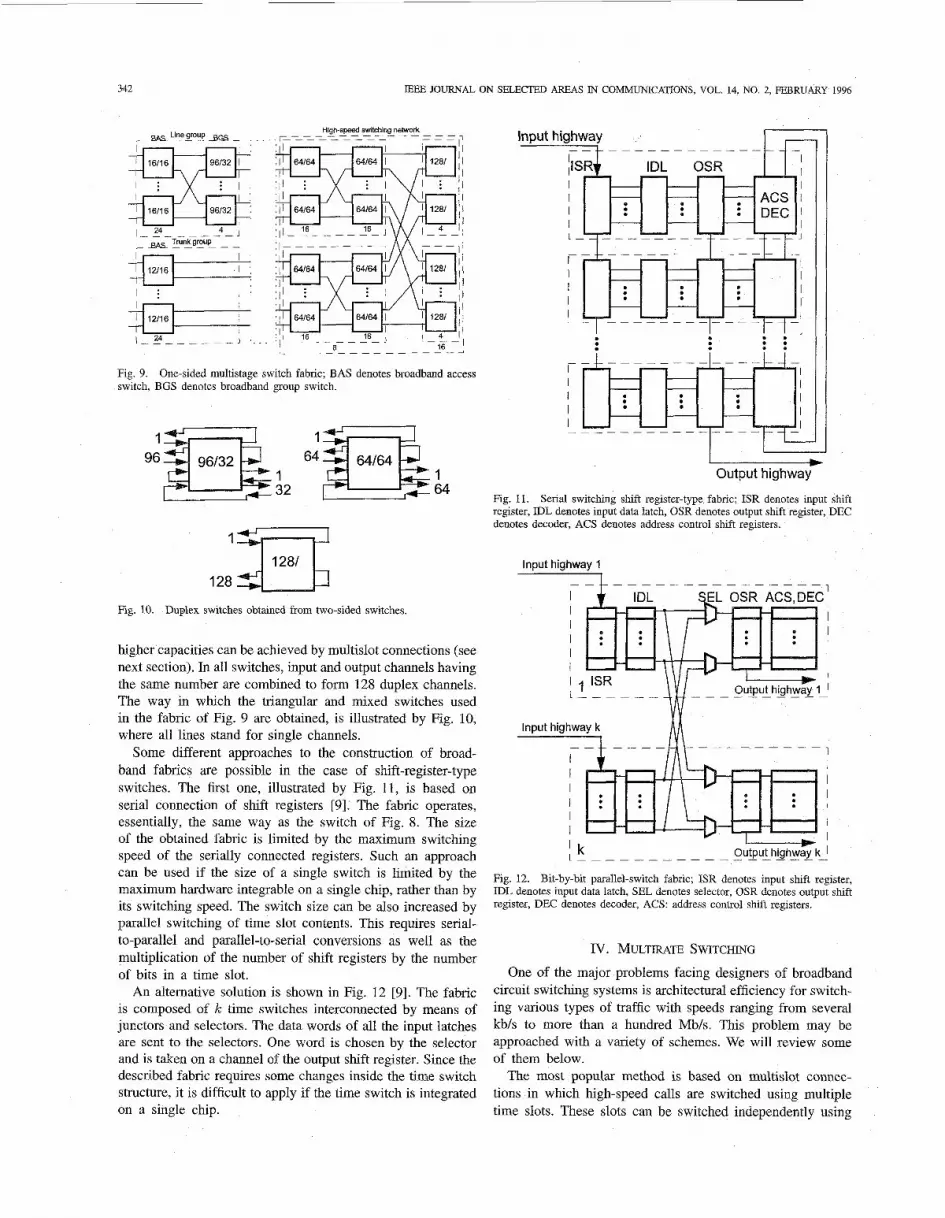
Some different approaches to the construction of broad- band fabrics are possible in the case of shift-register-type switches. The first one, illustrated by Fig. 11, is based on serial connection of shift registers [9]. The fabric operates, essentially, the same way as the switch of Fig. 8. The size of the obtained fabric is limited by the maximum switching speed of the serially connected registers. Such an approach can be used if the size of a single switch is limited by the maximum hardware integrable on a single chip, rather than by its switching speed. The switch size can be also increased by parallel switching of time slot contents. This requires serial- to-parallel and parallel-to-serial conversions as well as the multiplication of the number of shift registers by the number of bits in a time slot.
An alternative solution is shown in Fig. 12 [9]. The fabric is composed of k time switches interconnected by means of junctors and selectors. The data words of all the input latches are sent to the selectors. One word is chosen by the selector and is taken on a channel of the output shift register. !Since the described fabric requires some changes inside the time switch structure, it is difficult to apply if the time switch is integrated on a single chip.
r I I 1 I _
Output highway
Fig. 11. Senal switchng shift register-type fabnc; ISR denotes input shift reaster, LDL denotes input data latch, OSR denotes output shift register, DEC denotes decoder, ACS denotes address control shft registers.
Input highway 1
I I I I I I
' I i -
M Input highway k
Fig. 12. Bit-by-bit parallel-switch fabric; ISR denotes input shift register, IDL denotes input data latch, SEL denotes selector, OSR denotes output shift register, DEC denotes decoder, ACS: address control shift registers.
IV. MULTIRATE SWITCHING One of the major problems facing designers of broadband
circuit switching systems is architectural efficiency for switch- ing various types of traffic with speeds ranging from several kb/s to more than a hundred Mb/s. This problem may be approached with a variety of schemes. We will review some of them below.
The most popular method is based on multislot connec- tions in which high-speed calls are switched using multiple time slots. These slots can be switched independently using
JAJSZCZYK AND TYSZER BROADBAND TIME-DIVISION CIRCUIT SWITCHING 343
1 2 24 31 32 1 12 31 32 Frame 1 Frame 2
b-4 I - Output Time Slots _ ~ _ _ ~ _ _ ~ _ _ _ ~ _ _ _ _ _ _ _ _ _ _ - - -
(a) -
(b) Fig. 13. parallel switching.
Two kmds of multislot connections: (a) independent switching; (b)
1 32 I 12 24 32
(C)
Fig. 14. Examples of time slot assignments for multislot connections: (a) random; (b) periodic; (c) bursty.
different time-multiplexed links or they can be switched in parallel occupying the same link, as illustrated by Fig. 13. The independent switching method leads to significant problems with the time dot sequence integrity (TSSI), because of various propagation times in different links and different switching delays as well as the selective impact of failures of switch fabric elements. The TSSI is also affected by the way in which idle time slots inside a common link are assigned to a new call. The following three kinds of assignment can be used (see Fig. 14) [Ill:
random assignment, periodic assignment, and bursty assignment.
The random assignment does not impose any restrictions on the allocation of time slots. The periodic assignment per- mits only equal-interval allocation, and the bursty assignment allows only adjacent time slots to be occupied. Two latter assignment methods, although better as far as the TSSI is concerned, result in a higher probability of blocking at inter- exchange trunks and within switch fabrics. Therefore, we will describe schemes for maintaining the TSSI in the case of the random assignment.
Pram I L A Frame 2
Output Time Slots F F b
Fig. 15. Time switch transfer functions: (a) single data memory switch; (b) double data memory switch.
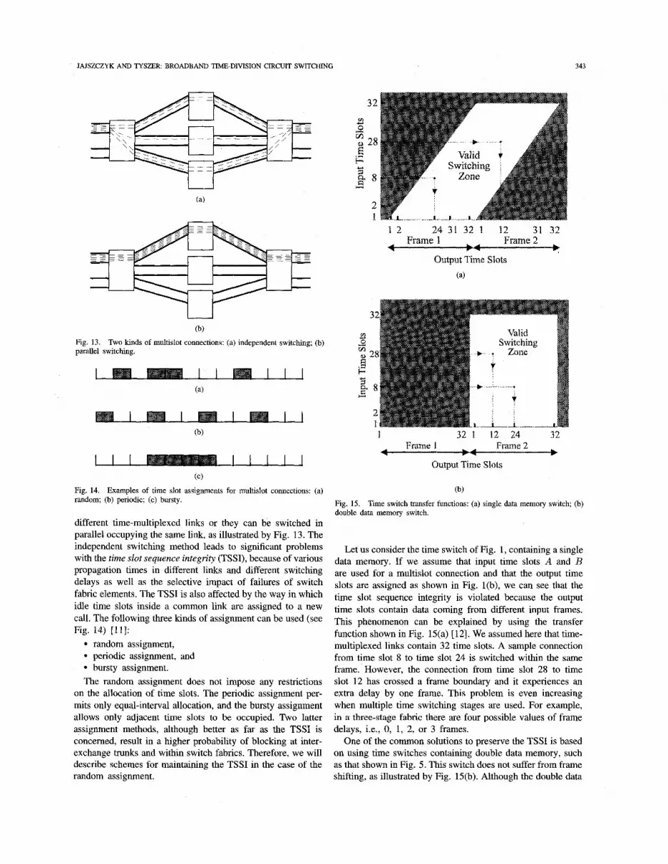
Let us consider the time switch of Fig. 1, containing a single data memory. If we assume that input time slots A and B are used for a multislot connection and that the output time slots are assigned as shown in Fig. l(b), we can see that the time slot sequence integrity is violated because the output time slots contain data coming from different input frames. This phenomenon can be explained by using the transfer function shown in Fig. 15(a) [12]. We assumed here that time- multiplexed links contain 32 time slots. A sample connection from time slot 8 to time slot 24 is switched within the same frame. However, the connection from time slot 28 to time slot 12 has crossed a frame boundary and it experiences an extra delay by one frame. This problem is even increasing when multiple time switching stages are used. For example, in a three-stage fabric there are four possible values of frame delays, i.e., 0, 1, 2, or 3 frames.
One of the common solutions to preserve the TSSI is based on using time switches containing double data memory, such as that shown in Fig. 5. This switch does not suffer from frame shifting, as illustrated by Fig. 15(b). Although the double data

344 lEEE JOURNAL ON SELECTED AREAS IN COMMUNICATIONS, VOL. 14, NO. 2, FEBRUARY 1996
memory switch contains more hardware than the conventional switch it does not require any additional equipment or software support to maintain the TSSI.
The TSSI can be also achieved in a conventional time switch by application of an appropriate control algorithm, for example that proposed by Takahashi [ l l] . Another approach, used in System X exchanges, involves demultiplexing mixing and remultiplexing devices (DMR’ s) inserted between the outer and the central stages of the switch fabric [12].
The conditions under which multislot switch fabrics are nonblocking are the same as for single-slot systems, provided that independent switching is used. In the case of parallel switching (i.e., all time slots belonging to one multislot call use the same time-multiplexed link) the relevant conditions, have been given by Kabacidski [13].
Since the bit rate range required by various broadband services is very wide the number of time slots in some multislot connections may be large, which, in turn, may cause significant problems in maintaining the time slot sequence integrity. One of the solutions is to use separated switch fabrics for signals of significantly different bit rates. Another approach used in a T-S-T switch fabric is based on time switches having the structure of Fig. 16(a) [14]. The switch is composed of two data memories DM1, DM2 and two address memories AM1, AM2. DM1 is a fast memory for, e.g., 32 M b l s channels and DM2 is a slow memory for lower bit-rate channels, e.g., 2048 kbls, 1920 kb/s, 64 kbls, or 16 kbls. DM1 and DM2 contain 36 and 1024 words, respectively. Internal framing is shown in Fig. 16(b). A time frame is divided into 36 time slots, each of length of 461.25 ns. The multiframe of 125 ps contains 271 frames. 32 time slots per frame are used for high-bit rate channels and 4 x 271 = 1084 time slots per multiframe are left for low-bit rate channels.
The operation of the discussed switch is as follows: 32 words of the fast memory DM1 are filled by high bit-rate channels, and the remaining four words are filled with infor- mation coming from the slow memory DM2. DM2 containing 1024 words must fill these four words of DM1 once per the frame time, i.e., 461.25 ns, and therefore, all 1024 words are switched during the multiframe, i.e., 125 ps. DM1 is written and read out during the frame time. We can note that low-bit- rate channels can not get a slot in each frame, but only one or more in a multiframe. DM1 and DM2 are controlled by the address memories AM1 and AM2, respectively. The described switch is used in the incoming stage of a T-S-T fabric. The switches used in the outgoing stage have a symmetrical structure. The space switch, i.e., the highway interchanger also contains fast and slow address memories for high and low bit rate channels, respectively.
An alternative approach to multi-rate calls is called a single slot switching technique with multiple fabrics of different periods [15]. In this technique each type of call is switched in a switch fabric whose time division switching period corresponds to its speed. An example of a T-S-T switch fabric employing the single slot technique is presented in Fig. 17. Several switch fabrics operate in parallel, each switching only one kind of call. Multiplexed time slots from the integrated highway are written to both the low-speed T-switch (TL) and
. Control information . (a)
Multiframe 1-125 ps.1
1- 461.25 ns -1
11 High bit-rate channels LI
(b)
Fig. 16. Multirate time switch (a) structure, DM denotes data memory, AM denotes address memory, C denotes counter, S denotes selector; (b) internal framing.
x x integrated .highway
Fig. 17. T-S-T network with single slot switching technique with multiple fabrics; MUX denotes multiplexer, TL denotes low-speed time switch, TH denotes high-speed time switch, SL denotes low-speed space switch, SH denotes high-speed space switch, DMUX denotes demultiplexer.
the high-speed T-switch (TH). However, during the frame of the low-speed call only the contents of low-speed time slots are read out from TL, and during the frame of the high-speed call only the contents of high-speed time slots are read out from TH. In general, the required number of switching modules corresponds to the number of different channel bit rates (two in the example of Fig. 17).

JAJSZCZYK AND TYSZER: BROADBAND TIME-DIVISION CIRCUIT SWITCHING 34s
V. CONCLUSION Designing an efficient broadband switching system is one of
the most important challenges in today’s telecommunications technology. In this paper, we have concentrated on time- division circuit switching that is one of the possible solutions. Although ATM switching techniques will play a dominant role in BISDN, time-division circuit switching techniques are expected to be used in some broadband applications because of their maturity as well as the compatibility with the existing transmission systems.
We can summarize techniques used to achieve broadband time-division switching, discussed in this paper, as follows:
The speed of a time switch can be increased by using multiple data and address memory blocks. The speed of shift-register-based switches is significantly higher than that of RAM-type switches. Multirate switching can be achieved by using multislot connections. The selection of time slots for a multislot call has a significant influence upon a fabric’s performance. TSSI can be maintained by application of double data memory switches, or appropriate software procedures, or additional specialized hardware. Separation of the data memory in a time switch into a fast memory and a slow memory can be used in multirate switch fabrics.
REFERENCES
[l] K. Kawaguchi, K. Hirose, I. Horiguchi, S. Karasawa, and K. Saito, “SDH cross-connect system architecture,” in IEEE GLOBECOM ’92 Conf Rec., Orlando, FL, Dec. 1992, pp. 847-852.
[2] Y.-W. Leung and T.-S. Yum, “A modular multirate video switch-Design and dimensioning,” in IEEE Int. Conf Commun. ICC ’93 Conf Rec., Geneva, Switzerland, May 1993, pp. 715-721.
[3] R. J. Chapuis and A. E. Joel Jr., Electronics, Computers and Telephone Switching. Amsterdam, The Netherlands: North-Holland, 1990.
[4] A. Jajszczyk, M. Roszkiewicz, and J. Garcia-Haro, “Comparison of ATM shared memory switches,” in Proc. XV Int. Switching Symp. ISS ’95, Berlin, Gemany, Apr. 1995, vol. 1, pp. 409413.
[5] H. Miyanaga, S. Konaka, Y. Kobayashi, Y. Yamamoto, and T. Sakai, “A 0.85-11s 1-kbit ECL RAM,” IEEE J. Solid-state Circuits, vol. SC-21,
[6] N. Yamanaka, H. Miyanaga, and Y. Yamamoto, “High-speed time division switch for 32-MbiVs bearer rate signals,” IEEE J. Select. Areas Commun., vol. SAC-5, pp. 1249-1255, Oct. 1987.
[7] ___, “Newly structured 512 MbiVs high-speed time-division switch,” Electron. Lett., vol. 22, pp. 10941095, Oct. 1986.
[8] T. Arita, S. Suzuki, and F. Ishino, “A high-speed digital satellite switching network without random access memory,” in Proc. Znt. Switching Symp. ISS ’84, Session 41 C, Florence, Italy, May 1984, pp.
[9] Y. Shimazu and T. Takada, “High-speed time switch using GaAs LSI technology,” IEEE J. Select. Areas Commun., vol. SAC-4, pp. 32-38, Jan. 1986.
[IO] P. Herger, G. Niestegge, and E. Wallmeier, “A multirate switching network for broadband channels,” IEEE J. Select. Areas Commun., vol.
pp. 501-504, 1986.
1-7.
SAC-5, pp. 1309-1314, Oct. 1987.
[ l l ] T. Takahashi, “Time-slot sequence integrity for (N x 64) kb/s con- nection,” Electr. and Commun. Jpn., Part 1 , vol. 71, no. 3, pp. 69-79, 1988.
[12] T. S. Maddern, “Analysis of multi-slot connections,” in Proc. Second IEE Natl. Con$ on Telecommunications, York, UK, Apr. 1989, pp.
[13] W. Kabacidski, “On nonblocking switching networks for multichannel connections,” IEEE Trans. Cornmun., vol. 43, Mar. 1995.
[ 141 J. van Baardewijk, “Experimental all-in-one broadband switch,” in Proc. Int. Zurich Sem. on Digital Commun., Zurich, Switzerland, Mar. 1986,
[15] K. Murakami, M. Katoh, and Y. Kato, “High-speed time division technique for broadband ISDN,” IEEE J. Select. Areas Commun., vol. SAC-5, pp. 1256-1263, Oct. 1987.
321-326.
pp. 109-112.
Andrzej Jajszczyk (M’91SM95) received the M.S. degree in electncal engineenng, in 1974, and the Ph.D. and Dr.Hab. degrees in communications from the Technical University of Poznan, Poland, in 1979 and 1986, respectively.
From 1974 to 1992, he was with the Technical University of Poznan. In 1993, he joined EFP-The Franco-Polish School of New Information and Communication Technologies in PoznaA, where he is presently a Professor and the Head of the Telecommunications Switching and Networks
Group. In 1989-1990, he spent 12 months as a visiting scientist at the Teletraffic Research Center, the University of Adelaide in Australia. In 1991 and 1992, he was a visiting scientist at the Department of Electrical Engineering, Queen’s University, Kingston, Ontario, Canada. He has been engaged in research and teaching in the areas of telecommunication switching and computer communications. He has led several projects for industry concerning the design and performance evaluation of digital switching systems. His current research interest include broadband networks and switching, both electronic and photonic. He has served as a Consultant to telecommunications industry and operators as well as government agencies in Poland, Australia, and Canada. He is the author of five books and over 100 papers, as holds 19 patents.
Dr. Jajszczyk is the Editor of the IEEE GLOBAL COMMUNICATIONS NEWSLETTER and the Editor for Switching Theory and Fabncs for the IEEE TRANSACTIONS ON COMMUNICATIONS He was organizer and chair of the 1st IEEE International Workshop on Broadband Switching Systems BSS ’95 held in PoznaA, Poland in April 1995. He is a member of the Association of Polish Electrical Engineers.
Jerzy Tyszer (M’91) received the M.S. (Hons.) degree in electrical engineering and the Ph.D. de- gree in electrical engineenng from the Technical University of Poznari, Poland, in 1981 and 1987, respechvely, and the Dr.Hab. degree in communi- cations from the Technical University of GdaAsk, Poland, in 1994.
From 1982 to 1990, he was a member of the faculty of the Technical University of Poznari. Since January 1990, he has been with the Department of Electncal Engineering, McGill University, Mon-
treal, Canada, currently as a Research Associate. His main research interests include design automatlon and testing of VLSI systems, design for testability (DFT), bmlt-in self test (BIST), and digital switching. He has published four books, more than 40 research papers, and holds six patents in these areas. He has done a contract work and has been a consultant in the area of testing to a number of telecommunication companies.


