Embed Size (px)
Citation preview
BOOK OFABSTRACTS
4th Smart Nanomaterials: Advances, Innovations and Applications
Online-Onsite Conference7-10 December 2021
This book includes only the abstracts presentedat the online-onsite SNAIA 2021 Conference

PLENARY
7-10 December 2021Chimie ParisTech, Paris
The rise of Mie-tronics and metaphotonics
Yuri Kivshar1,2
1Nonlinear Physics Center, Australian National University, Canberra ACT 2601, Australia2ITMO University, St. Petersburg, Russia
Email – [email protected]
Recent progress is nanoscale photonics is driven by the physics of Mie-resonances ofhigh-index dielectric nanoparticles that provides a novel platform for localization of light insubwavelength photonic structures and opens new horizons for metamaterial-enabled photonics,or metaphotonics. In this talk, I will review the recent advances in Mie-resonant metaphotonics(also called "Mie-tronics") for isolated high-index dielectric nanoparticles and nanoparticlestructures such as dielectric metasurfaces, and its applications to nonlinear, active, andtopological photonics [1,2].
Also, I will introduce a novel physical mechanism for achieving giant quality-factors (Qfactors) in finite-length periodic arrays of subwavelength optical resonators. The underlyingphysics is based on resonant coupling between the band-edge mode and another standing modein the array and the formation of localized states with dramatically suppressed radiative losses.
Also, I will discuss the physics of photonic bound states in the continuum (BICs) and theirapplications to metadevices, including enhancement of nonlinear response, light-matterinteraction, and development of active nanophotonic devices. I will discuss howBIC-empowered dielectric metastructures can be used to generate efficiently high-order opticalharmonics from bulk and to boost the intrinsic nonlinearity of transition metal dichalcogenideflakes. Finally, I will demonstrate how tunability of BICs in the momentum space can beemployed to realize a novel type of efficient nanolasers based on a finite-size cavity with a smallfootprint.References[1] K. Koshelev and Y. Kivshar, Dielectric resonant metaphotonics, ACS Photonics 8, 102(2021)
[2] C.W. Qiu, T. Zhang, G. Hu, and Y. Kivshar, Quo vadis, metasurfaces? Nano Lett. 21, 5461(2021).
Photonic Crystals as Non-Local Meta-surfaces and Topological Crystals
Wenzhe Liu1, Lei Shi2, Jian Zi2, Che Ting Chan1
1 Department of Physics, The Hong Kong University of Science and Technology, Hong Kong,China
2 State Key Laboratory of Surface Physics and Department of Physics, Fudan University,Shanghai, China
Email – [email protected]
Classical optical devices and conventional meta-surfaces modulate and route electromagneticbeams by modulating field amplitudes and phases locally at different positions in real space, andthe beams are consequently refracted. Here we propose that beam modulations can be done inthe momentum space in a non-local way. Instead of refracting the beams, normally incidentbeams can be shifted by applying the geometric phase gradient induced by momentum-spacepolarization field of a photonic crystal slab. We will also briefly review how simple dielectricphotonic crystals can be used to manifest topological physics.
Liquid Light Computing: from logic to analogue simulation
Pavlos LagoudakisSkolkovo Institute of Science and Technology, Russian Federation
University of Southampton, UK
Modern digital computers have changed our lives in a variety of ways, but the technology onwhich they are built is rapidly reaching a hard limit due to inherent quantum effects. Two of themain pillars of our modern digital computers are the electronic transistor and the von-Neumanncomputer architecture. While the von-Neumann architecture established the physical separation ofcomputing tasks like storage and processing, transistors are the fundamental building blocks indigital computers. The drive for faster and more powerful computers can be realised by increasingthe number of transistors in a processor and the clock frequency. However, Moore’s law will sooncome to an end, whilst the breakdown of Dennard’s scaling law means that clock frequencies haveremain unchanged since 2006. This leads to the pressing quest to develop new kinds of transistorsand alternative computing architectures that could one day lead to more efficient computers.
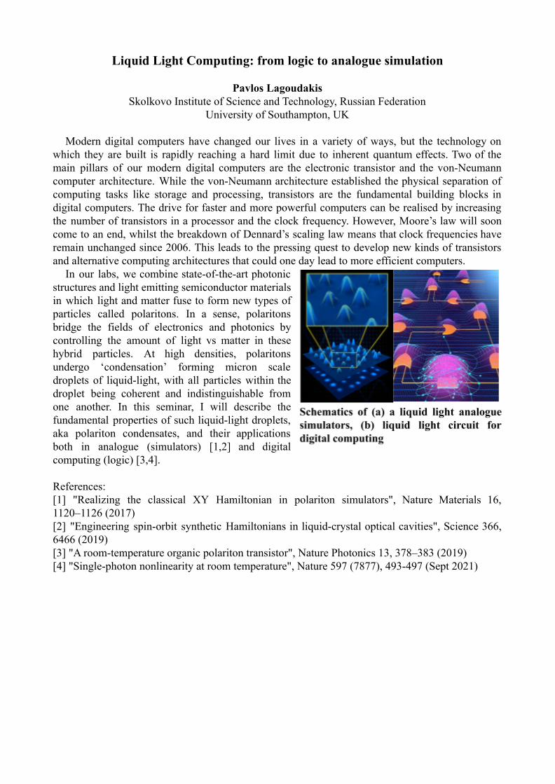
In our labs, we combine state-of-the-art photonicstructures and light emitting semiconductor materialsin which light and matter fuse to form new types ofparticles called polaritons. In a sense, polaritonsbridge the fields of electronics and photonics bycontrolling the amount of light vs matter in thesehybrid particles. At high densities, polaritonsundergo ‘condensation’ forming micron scaledroplets of liquid-light, with all particles within thedroplet being coherent and indistinguishable fromone another. In this seminar, I will describe thefundamental properties of such liquid-light droplets,aka polariton condensates, and their applicationsboth in analogue (simulators) [1,2] and digitalcomputing (logic) [3,4].
References:[1] "Realizing the classical XY Hamiltonian in polariton simulators", Nature Materials 16,1120–1126 (2017)[2] "Engineering spin-orbit synthetic Hamiltonians in liquid-crystal optical cavities", Science 366,6466 (2019)[3] "A room-temperature organic polariton transistor", Nature Photonics 13, 378–383 (2019)[4] "Single-photon nonlinearity at room temperature", Nature 597 (7877), 493-497 (Sept 2021)
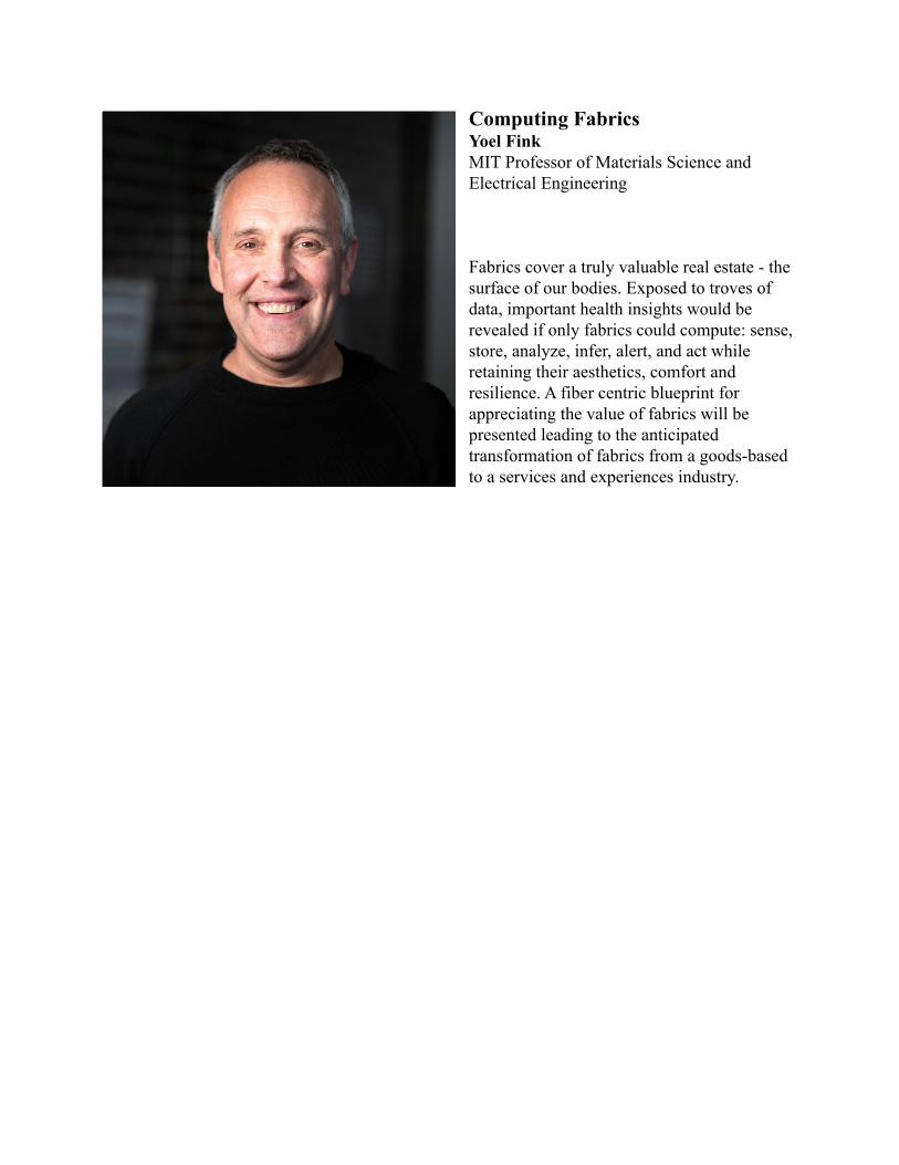
Computing FabricsYoel FinkMIT Professor of Materials Science andElectrical Engineering
Fabrics cover a truly valuable real estate - thesurface of our bodies. Exposed to troves ofdata, important health insights would berevealed if only fabrics could compute: sense,store, analyze, infer, alert, and act whileretaining their aesthetics, comfort andresilience. A fiber centric blueprint forappreciating the value of fabrics will bepresented leading to the anticipatedtransformation of fabrics from a goods-basedto a services and experiences industry.
“Carbon Nano Onion - a nanoscale material with bio at heart”
Prof. Silvia Giordani
School of Chemical Sciences, Dublin City University, Dublin, Ireland
E-mail: [email protected]
There are many issues associated with free drug delivery including: adverse side-effects, mul=-drug resistance, premature drug degrada=on, lack of =ssue penetra=on, and non-specific toxicity. Targeted delivery, which u=lises nanocarriers as payload delivery vesicles, has the poten=al to address and alleviate these prominent issues. Specifically, it involves nanomaterials func=onalised with targe=ng agents, allowing for the selec=ve uptake of these nanocarriers by cells overexpressing specific receptors. This approach explicitly increases the drug concentra=on in the target cell of interest whilst minimising the exposure of healthy cells to the therapeu=c agent.
In this presenta=on, carbon nano-onions (CNOs) will be discussed as a poten=al vesicle for nanocarrier-type drug delivery systems.[1] CNOs, or mul=-layer fullerenes, consist of mul=ple concentric layers of sp2 hybridised carbon and are emerging as plaNorms for biomedical applica=ons because of their ability to be internalized by cells and low toxicity. [2]
In my research group we have developed a synthe=c methodology for the synthesis of pure, monodispersed CNOs and various chemical func=onaliza=on strategies for the introduc=on of different func=onali=es (receptor targe=ng unit and imaging unit) onto the surface of the CNOs. The modified CNOs display high brightness and photostability in aqueous solu=ons and are selec=vely taken up by different cancer cell lines without significant cytotoxicity. [3]
We have also developed supramolecular func=onaliza=on with biocompa=ble polymers as an effec=ve strategy to develop engineered drug carriers for targeted delivery applica=ons. We reported the use of a hyaluronic acid-phospholipid (HA-DMPE) conjugate to target CD44 overexpressing cancer cells, while enhancing solubility of the nanoconstruct. Non-covalently func=onalized CNOs with HA-DMPE show excellent in vitro cell viability in human breast carcinoma cells overexpressing CD44 and are uptaken to a greater extent compared to human ovarian carcinoma cells with an undetectable amount of CD44. In addi=on, they possess high in vivo biocompa=bility in zebrafish during the different stages of development sugges=ng a high degree of biosafety of this class of nanomaterials. [4]
To probe the possible applica=ons of CNOs as a plaNorm for therapeu=c and diagnos=c interven=ons on CNS diseases, we injected fluorescent CNOs in vivo in mice hippocampus. We analyzed ex vivo their diffusion within brain =ssues and their cellular localiza=on by confocal and electron microscopy. The subsequent fluorescent staining of hippocampal cells popula=ons indicates they efficiently internalize the nanopar=cles. Furthermore, the inflammatory poten=al of the CNOs injec=on was found comparable to sterile vehicle
infusion, and it did not result in manifest neurophysiological and behavioral altera=ons of hippocampal-mediated func=ons [5].
We recently synthesised Boron/nitrogen co-doped carbon nano-onions (BN-CNOs) and examined their interac=ons with biological systems. Our study on the toxicological profiles of BN-CNOs and oxidized BN-CNOs in vitro in both healthy and cancer cell lines, as well as in vivo on the embryonic stages of zebrafish (Danio rerio) demonstrate that these new class of carbon nanopar=cles have high cyto-biocompa=bility and a high biosafety [6].
Our results encourage further development as targeted diagnos=cs or therapeu=cs nanocarriers.
References: [1] M. Bartkowski and S. Giordani, Dalton Transac=ons, 2021, 50 (7), 23. [2] S. Giordani et al., Current Medicinal Chemistry 2019, 26 (38), 6915. [3] M. Frasconi et al., Chem Eur J 2015, 21 (52), 19071. [4] M d’Amora et al., Colloids and Surfaces B: Biointerfaces, 2020, 110779. [5] M. Trusel et al., ACS Appl. Mat. & Inter. 2018, 10 (20), 16952. [6] M d’Amora et al., Nanomaterials, 2021, 11 (11), 3017.
KEYNOTE TALK ON MICROSCOPY
7-10 December 2021Chimie ParisTech, Paris
Nucleosome complexes with proteins and drugs through the prism of spFRETmicroscopy
Alexey V. Feofanov,1,2, Natalya V. Maluchenko,1 Nadezhda S. Gerasimova,1 Alexandra A.Lys,1 Darya O. Koshkina,1 Maria E. Valieva,1 Vasily М. Studitsky,1,3 Mikhail P.
Kirpichnikov1,2
1Biological Faculty, Lomonosov Moscow State University, Moscow, Russia2Shemyakin-Ovchinnikov Institute of Bioorganic Chemistry, Russian Academy of Sciences,
Moscow, Russia3Cancer Epigenetics Program, Fox Chase Cancer Center, Philadelphia, USA
[email protected], [email protected]
DNA is tightly packed in the nucleus, and special proteins check genome integrity, repairdamages and provide controlled access to genomic information intelligently unpacking andpacking back DNA. Many of these processes occur at a nucleosome level. Some of the proteinsof genome machinery, in particular, histone chaperone FACT (FAcilitates ChromatinTranscription) and poly(ADP-ribose)polymerase 1 (PARP1) are recognized pharmacologicaltargets for anticancer agents, which affect their functioning in the complexes with nucleosomes.Here we discuss how nanophotonics approach based on single particle Förster resonance energytransfer (spFRET) microscopy is used to study nucleosome interactions with proteins and drugs.We designed a set of fluorescently labeled nucleosome nanoparticles of different structure,assembling them from core histones and DNA of variable length containing a strongnucleosome-positioning sequence. A donor-acceptor pair of fluorophores introduced intoneighboring gyres of nucleosomal DNA or into linker DNA enables probing of a nucleosomestructure. Analysis of FRET at the level of single nucleosomes offers a unique opportunity toreveal various types of complexes with proteins and/or drugs, which are simultaneously formedin solution. We report on structural changes in a nucleosome structure induced by PARP1 andFACT [1, 2]. We also present the results of our studies of (i) curaxin, which disturbs nucleosomestructure and promotes FACT-induced nucleosome unwrapping, as well as (ii) PARP1 inhibitors,which trap PARP1-nucleosome complexes [3-6].
The studies were supported by Russian Science Foundation (grant 19-74-30003).
References
[1] M.E. Valieva, G.A. Armeev, K.S. Kudryashova et al. Nat. Struct. Mol. Biol. 23 (2016) 1111[2][3][4]
[5][6]
D. Sultanov, N. Gerasimova, K. Kudryashova et al. AIMS Genetics 4 (2017) 21H.-W. Chang, M.E.Valieva, A.Safina et al. Sci. Advances 4 (2018) eaav2131N.V. Malyuchenko, D.O. Koshkina, A.N. Korovina et al. Moscow Univ. Biol. Sci. Bull. (2020)142D. Nilov, N. Maluchenko, T. Kurgina et al. Int. J. Mol. Sci. 21 (2020) 2159O.L. Kantidze, A.V. Luzhin, E.V. Nizovtseva et al. Nat Commun. 10 (2019) 1441
ALL-DIELECTRIC NANOPHOTONICS
7-10 December 2021Chimie ParisTech, Paris
Nonclonal metasurfaces
Andrea AluCity University of New York
In this talk, we discuss our recent theoretical and experimental progress in the area of metasurfaces, inparticular on the role of engineered nonlocality to enable a new degree of control over spectral andcoherent features, in addition to wavefront manipulation.
We demonstrate frequency-selective and wavefront-selective responses based on these principles, ofinterest for augmented reality and secure communication applications.
We also discuss the impact of these concepts to manipulate thermal emission and photoluminescenceand to realize efficient, compact and highly flexible optical sources.
Dielectric Metasurfaces for Enhanced Sensing of Chiral Molecules
Martin Wegener1 1Institute of Applied Physics and Institute of Nanotechnology,
Karlsruhe Institute of Technology (KIT), 76128 Karlsruhe, Germany
Determining the handedness of chiral molecules plays an important role in chemistry and
pharmacy. Optical circular dichroism (CD) spectroscopy is a well-established means for
determining the molecule’s handedness. Unfortunately, acquiring optical CD spectra can be quite
time consuming. This fact asks for means to enhance the CD signal and thereby reduce the
measurement times.
Here, we review our recent theoretical work towards using silicon-disk arrays [1] or cavities
containing one or two [2,3] such arrays for resonantly enhancing the CD signal in the infrared
fingerprint spectral region. Resonant CD enhancement factors exceeding 100 have been obtained.
Using the same arrangements, similar enhancements can be obtained for detecting the linear
optical polarization rotation [4] instead of the CD signal. Experiments are in progress.
References
[1] “Achiral, Helicity Preserving, and Resonant Structures for Enhanced Sensing of Chiral
Molecules”, F. Graf, J. Feis, X. Garcia-Santiago, M. Wegener, C. Rockstuhl, I. Fernandez-
Corbaton, ACS Photonics 6 (2019) 482
[2] “A helicity preserving optical cavity for enhanced sensing of chiral molecules”, J. Feis,
D. Beutel, J. Köpfler, X. Garcia-Santiago, C. Rockstuhl, M. Wegener, I. Fernandez-Corbaton,
Phys. Rev. Lett. 124 (2020) 033201
[3] “Towards enhanced experimental sensing of chiral molecules in optical cavities, P. Scott,
C. Rockstuhl, M. Wegener, I. Fernandez-Corbaton, Appl. Phys. Rev. 7 (2020) 041413
[4] “Enhancing the Optical Rotation of Chiral Molecules Using Helicity Preserving All-
dielectric Metasurfaces, D. Beutel, P. Scott, M. Wegener, C. Rockstuhl, I. Fernandez-Corbaton,
Appl. Phys. Lett. 118 (2021) 221108
Light driven microvehicles powered and steered by optical momentumtransfer induced by embedded dielectric metasurfaces
Daniel Andrén1, Denis G. Baranov1,2, Giovanni Volpe3, Ruggero Verre1, Mikael Käll1
1Department of Physics, Chalmers University of Technology, Gothenburg, Sweden2Moscow Institute of Physics and Technology, Dolgoprudny, Russia3Physics Department, Gothenburg University, Gothenburg, Sweden
Nanostructured dielectric metasurfaces offer unprecedented opportunities to manipulate lightby imprinting an arbitrary phase gradient on an impinging wavefront. This has resulted in therealization of a range of flat analogues to classical optical components, such as lenses,waveplates and axicons. However, the change in linear and angular optical momentumassociated with phase manipulation also results in previously unexploited forces and torques thatact on the metasurface itself. Here we show that these optomechanical effects can be utilized toconstruct optical metavehicles—microscopic particles that can travel long distances underlow-intensity plane-wave illumination while being steered by the polarization of the incidentlight [1]. We demonstrate movement in complex patterns, self-correcting motion and anapplication as transport vehicles for microscopic cargoes, which include unicellular organisms.The abundance of possible optical metasurfaces attests to the prospect of developing a widevariety of metavehicles with specialized functional behaviors.
[1] Daniel Andrén, Denis. G. Baranov, Steven Jones, Giovanni Volpe, Ruggero Verre, MikaelKäll, Nature Nanotechnology (2021), https://doi.org/10.1038/s41565-021-00941-0
Sound Trapping in an Open Resonator
Lujun Huang1, Yan Kei Chiang1, Sibo Huang2, Chen Shen3, Fu Deng1, Yi Cheng2, Bin Jia2,
Yong Li2, David A Powell1, Andrey E Miroshnichenko1
1School of Engineering and Information Technology, University of New South Wales, Canberra,
Northcott Drive, ACT, 2600, Australia 2Institute of Acoustics, Tongji University, Shanghai, 200092, People's Republic of China 3Department of Mechanical Engineering, Rowan University, Glassboro, NJ, 08028, USA
The ability of extreme sound energy confinement with high-quality factor (Q-factor) resonance
is of vital importance for acoustic devices requiring high intensity and hypersensitivity in
biological ultrasonics, enhanced collimated sound emission (i.e. sound laser) and high-resolution
sensing [1]. However, structures reported so far demonstrated a limited quality factor (Q-factor)
of acoustic resonances, up to several tens in an open resonator. The emergence of bound states in
the continuum (BIC) makes it possible to realize high-Q factor acoustic modes. Here, we report
the theoretical design and experimental demonstration of acoustic BICs supported by a single open
resonator [2]. We predicted that such an open acoustic resonator could simultaneously support
three types of BICs, including symmetry protected BIC, Friedrich-Wintgen BIC induced by mode
interference, as well as a new kind of BIC: mirror-symmetry induced BIC. We also experimentally
demonstrated the existence of all three types of BIC with Q-factor up to one order of magnitude
greater than the highest Q-factor reported in an open resonator.
References
[1] Ma, G. & Sheng, P. Acoustic metamaterials: from local resonances to broad horizons. Sci.
Adv.2, e1501595 (2016).
[2] Huang, L., Chiang, Y.K., Huang, S. et al. Sound trapping in an open resonator. Nat
Commun 12, 4819 (2021).
All-dielectric metasurface with correlated disorder as an anti-reflection coating for Silicon heterojunction solar cells
P. M. Piechulla1, E. Slivina2, D. Bätzner3, I. Fernandez-Corbaton4, R. B. Wehrspohn1, A. N.Sprafke1, and C. Rockstuhl1,4
1 Institute of Physics, Martin Luther University Halle-Wittenberg, 06120 Halle, Germany2 Institute of Theoretical Solid State Physics, Karlsruhe Institute of Technology,76131 Karlsruhe,
Germany 3 Meyer Burger Research AG, Hauterive 2068, Switzerland
4 Institute of Nanotechnology, Karlsruhe Institute of Technology,76344 Eggenstein-Leopoldshafen, Germany [email protected]
While witnessing ever-decreasing wafer thicknesses of heterojunction Silicon-based solar cells nowadays, it became necessary to perceive alternative schemes to achieve an anti-reflection structure [1]. Traditional approaches such as individual layers offer a relatively poor performance but texturing the wafer with micro-pyramids becomes increasingly challenging. Here, we summarize our theoretical, numerical, and experimental efforts to solve this issue using all-dielectric metasurfaces designed while guided by helicity preservation principles [2]. Such a principle requires the metasurface to consist of strongly scattering discs with a balanced electric and magnetic response. Large-scale fabrication on centimeter-scaled wafers is demonstrated with a self-assembly approach [3,4]. The fabrication process leads to metasurfaces with well-controlled correlated disorder. That helps to effectively restore a sufficiently high rotational symmetry that is key to achieving suppressed back-reflection when combined with the helicity preserving property [5]. The disorder also renders the effect spectrally rather broad. That is essential to our experimental improvement of short-circuit currents in industrial standard solar cells by up to 5.1 % with optimized metasurfaces compared to reference cells with a flat anti-reflective layer [6].
References
[1] Z. Liu, S. E. Sofia, H. S. Laine, M. Woodhouse, S. Wieghold, I. M. Peters, and T.Buonassisi, Energy Environ. Sci. 13 (2020) 12
[2] E. Slivina, A. Abass, D. Bätzner, B. Strahm, C. Rockstuhl, and I. Fernandez-Corbaton, Phys. Rev. Appl. 12 (2019) 054003
[3] P. M. Piechulla, A. Sprafke, L. Mühlenbein, S. Nanz, A. Abass, C. Rockstuhl, and R. B.Wehrspohn, Adv. Opt. Mat. 6 (2018) 1701272
[4] P. M. Piechulla, B. Fuhrmann, E. Slivina, C. Rockstuhl, R. B. Wehrspohn, and A. N.Sprafke, Adv. Opt. Mat. (2021) 2100186
[5] I. Fernandez-Corbaton, Opt. Express (2013) 29885[6] P. M. Piechulla, E. Slivina, D. Bätzner, I. Fernandez-Corbaton, R. B. Wehrspohn, A. N.
Sprafke, and C. Rockstuhl, submitted
Quantum state generation in dielectric metasurfaces
Thomas Pertsch,1,2
1 Institute of Applied Physics, Abbe Center of Photonics, Friedrich Schiller University Jena,Albert Einstein Strasse 15, 07745 Jena, Germany
2 Fraunhofer Institute for Applied Optics and Precision Engineering, Albert Einstein Strasse 7,07745 Jena, Germany
We report on experimental and theoretical investigations of nonlinear metasurfaces fromsilicon, gallium arsenide, lithium niobate, and metasurfaces hybridized with transition metaldichalcogenide monolayers. We show that the second-order nonlinear interactions inmetasurfaces enable tailorable harmonic frequency generation as well as entangled photon pairsources by spontaneous parametric down-conversion.
In our work, we have experimentally investigated isolated nanoresonators and nonlinearmetasurfaces from different dielectric/semiconducting materials featuring electric dipole andmagnetic dipole Mie-type resonances at wavelengths in the near infrared. As an intermediatestep towards quantum experiments, we characterized second-harmonic generation from themetasurfaces, when exciting with the long wavelength fundamental wave. With these results, weshow that resonant interactions in nanoresonators are a suitable platform for second-harmonicgeneration. As a next step we demonstrate experimentally the generation of photon pairs byspontaneous parametric down-conversion, when exciting with the short wavelength pump wave.
Based on the principle of quantum-classical correspondence, both processes, second-harmonicgeneration and spontaneous parametric down-conversion, are tied together by the governingsystem parameters. We have also exploited this correspondence to develop predictive theoreticalmodels for the design of nonlinear metasurfaces for quantum applications.
References[1] A. Fedotova, M. Younesi, J. Sautter, A. Vaskin, F. J. F. Lochner, M. Steinert, R. Geiss, T.
Pertsch, I. Staude, and F. Setzpfandt, "Second-harmonic generation in resonant nonlinearmetasurfaces based on lithium niobate," Nano Lett. 20, 8608 (2020).
[2] F. Löchner, A. George, K. Koshelev, T. Bucher, E. Najafidehaghani, A. Fedotova, D.-Y.Choi, T. Pertsch, I. Staude, Y. Kivshar, A. Turchanin, and F. Setzpfandt, "Hybrid dielectricmetasurfaces for enhancing second-harmonic generation in chemical vapor deposition grownMoS2 monolayers," ACS Photonics 8, 218 (2021).
[3] T. Santiago-Cruz, A. Fedotova, V. Sultanov, M. Weissflog, D. Arslan, M. Younesi, T.Pertsch, I. Staude, F. Setzpfandt, and Maria V. Chekhova "Photon pairs from resonantmetasurfaces," Nano Lett. 21, 4423 (2021).
Topological structures in and for light
L. (Kobus) KuipersKavli Institute of Nanoscience in Delft, Dept. Quantum Nanoscience, Delft, The Netherlands
Email – [email protected]
This lecture revolves around topological photonics. With experiments we investigatetopological features in light fields, such as phase- and polarization singularities. We do this bothin unstructured two-dimensional arena’s and in nanophotonic structures that are intrinsicallytopologically non-trivial. In experiments on edge states between topologically non-trivialphotonic crystals we investigate the relation between propagation direction and the pseudo-spinof the optical eigenstates and determine their bandstructure. With near-field microscopy weobtain subwavelength information about the wavefunctions of the states, find that the opticalspin has a highly heterogeneous distribution in space, and quantify how robust robust is.
References[1] L. De Angelis, T. Bauer, F. Alpeggiani and L. Kuipers, Optica 6 (2019), 1237[2] Nikhil Parappurath, Filippo Alpeggiani, L. Kuipers and Ewold Verhagen, Science Advances
6 (2020), eaaw4137; arXiv: 1811.10739 &S. Arora, T. Bauer, R. Barczyk, E. Verhagen and L. Kuipers, , njp Light: Science &Applications 10(1) (2021), 1-7
Size Dependence of Rabi Splitting Using Gold Nano-Bipyramids on Monolayer MoS2
Julia Lawless1, Calin Hrelescu1, Carolyn Elliott1,3, Lisanne Peters2, Niall McEvoy2, A. Louise Bradley1,3
1School of Physics and AMBER, Trinity College Dublin, College Green, Dublin 2, Ireland. 2School of Chemistry and AMBER, Trinity College Dublin, College Green, Dublin 2, Ireland
3IPIC, Tyndall National Institute, Cork, Ireland. Email – [email protected]
Rabi splitting in plasmonic systems occurs when the light-matter interaction is sufficiently strong such that the rate of exchange of energy between an exciton and optical resonator is faster than their intrinsic dissipation rates. Under the condition of strong coupling the resonance splits into two new eigenstates, above and below the original optical mode and exciton energy. These new states are known as polariton states. Working in the strong coupling regime can be used for many applications, including but not limited to, low threshold lasers, optical switching and sensing. Until recent times, accessing the strong coupling regime required working at cryogenic temperatures. Developments in nanoscience allow for the observation of room temperature strong coupling in open cavity plasmonic systems, using a single plasmonic nanoresonator.1
In this work strong coupling is demonstrated using a single gold nano-bipyramid on monolayer MoS2. Bipyramid lengths of 60 to115 nm were investigated. The polaritons were detected by dark field scattering and correlated with scanning electron microscopy images which showed the size of the bipyramids. Rabi splitting of ~80 meV was observed with 100 nm long bipyramids. It is also reported that the coupling strength between the plasmon and A exciton is stronger for larger bipyramids. This arises due to two factors. Firstly, the larger bipyramids produce a larger field due to the increased number of electrons creating a stronger plasmon. Secondly, to maintain the plasmon resonance energy coincident with the exciton energy, the aspect ratio (length to width) of the larger bipyramids must be reduced. This results in an increased angle between the plasmon direction and the MoS2 layer, and consequently, produces greater overlap of the electric field and MoS2 dipole moment, without an increase in the mode volume.2 The nano-bipyramid system allows for the Rabi splitting to be increased with increasing nanoantenna size without increasing the number of excitons in the system.
References
[1] M. Stührenberg, B. Munkhbat, D. G. Baranov, J. Cuadra, A. B. Yankovich, T. J.Antosiewicz, E. Olsson, and T. Shegai, Nano Lett., 18 (2018) 5938-5945
[2] J. Lawless, C. Hrelescu, C. Elliott, L. Peters, N. McEvoy, A. L. Bradley, ACS Appl. Mater.Interfaces, 41 (2020) 46406–46415
Deep Inverse Design of All-Dielectric NanoPhotonics
Willie J. Padilla,1 Simiao Ren,1 and Jordan Malof1 1Department of Electrical and Computer Engineering, Duke University, Durham, NC 27705,
Inverse problems appear in many branches of science and engineering, and methods used for their solution remain an active area of study. Inverse problems may be classified as either well-posed or ill-posed, and many problems in photonic design fall under the later characterization. Ill-posed inverse problems (IIP) were defined by Hadamard through their failure to meet any one of three criteria: (H1) existence, (H2) uniqueness, and (H3) stability. [1,2] Although the condition of being ill-posed means it is meaningless to look for exact solutions, it is none-the-less possible to explore the set of approximate solutions to find one, or several, that are good enough to be significant. Recently, deep learning has been applied to solve inverse problems and has demonstrated excellent results.
We present an inverse method termed neural adjoint (NA) based on deep learning. [3] The NA method is thus a data driven inverse approach, where the first step is to train a neural network to approximate a forward model connecting the photonic geometry (g) and its corresponding spectra (s). The pairs that are used for training form a dataset D={g,s}, which are obtained from numerical simulation. Once an accurate forward function f has been obtained, i.e. s=f(g), we freeze the weights and biases of the neural network and specify a particular scattering that we are interested in finding the geometry for – the inverse problem. A number of randomly selected geometries are chosen, and we use df/dg to descend towards locally optimal geometries g. It is important to detail that our accurate forward model f, provides a closed-form differentiable expression, from which it is trivial to obtain df/dg. Notably, modern deep learning packages allow us to efficiently estimate gradients given a defined loss function.
In order to quantify and compare the performance of the NA inverse method against other approaches, we propose and investigate three benchmark photonics problems: an all-dielectric metasurface, a plasmonic multilayer particle, and a color rgb filter. A total of eight inverse methods are used to solve for approximate solutions, and may be classified as either stochastic iterative, deterministic, or probabilistic. We find that stochastic iterative inverse methods, such as the neural adjoint, find the best solutions, as determined by the lowest error metric (MSE).
References
[1] J. Hadamard, Princeton Univ. Bull. 13 (1902) 49
[2] J. Mueller, Linear and Nonlinear Inverse Problems with Practical Applications, Society forIndustrial and Applied Mathematics, Philadelphia 201
[3] S. Ren, W. J. Padilla, J. M. Malof, In Advances in Neural Information Processing Systems33: Annual Conference on Neural Information Processing Systems 2020, NeurIPS 2020,December 6-12, 2020, virtual.
Minimalistic efficient quantum devices build of dipole coupled nano arraysof quantum emitters
Helmut RitschTheoretical Physics, University of Innsbruck
An array of closely spaced, dipole coupled quantum emitters exhibits collective energyshifts as well as super- and sub-radiance with characteristic tailorable spatial radiationpatterns. In particular optical absorption and emission properties of ring shapedsub-wavelength nanoscopic quantum emitter structures are unique. As striking example weidentify a sub-wavelength sized ring of exactly 9 identical dipoles with an extra identicalemitter with a extra loss channel at the center as the most efficient configuration to depositincoming photon energy to center without reemission.
The enhancement is most pronounced a given resonance frequency but still stays visible forbroadband light absorption. For very tiny structures below a tenth of a wavelength a fullquantum description exhibits an even larger enhancement than predicted from a classicaldipole approximation.
The origin of the effect can be tied to a specific geometric property of nonagons allowingfor the appearance of a special collective dark state with dominant center occupation. Byspecial design of the center absorber one can harness the same efficiency enhancement also atdifferent wavelengths and for other geometric structures.
On the one hand this could be the basis of a new generation of highly efficient and selectivenano antennas for single photon detectors for microwaves, infrared and optical frequencies asused e.g. in quantum information processing or single molecule spectroscopy, while on theother hand it could be an important piece towards understanding the surprising efficiency ofnatural light harvesting molecules.
Adding gain to such systems allows to design minimalistic classical as well as non-classicallight sources.
References:Holzinger, Raphael, Mariona Moreno-Cardoner, and Helmut Ritsch. "Nanoscale continuousquantum light sources based on driven dipole emitter arrays”, Appl. Phys. Lett. 2021Holzinger, Raphael, et al. "Nanoscale coherent light source." Physical Review Letters 124.25(2020): 253603Moreno-Cardoner, Maria, Raphael Holzinger, and Helmut Ritsch. "Efficientfrequency-selective single-photon antennas based on a bio-inspired nano-scale atomic ringdesign with 9-fold symmetry." arXiv preprint arXiv:2010.09771 (2020).
Quantum photon-pair generation and measurement with metasurfaces
Andrey A. Sukhorukov1 1 ARC Centre of Excellence for Transformative Meta-Optical Systems (TMOS),
Department of Electronic Materials Engineering, Research School of Physics,
The Australian National University, Canberra, ACT 2601, Australia
Quantum nanophotonics is an active research field with emerging applications that range from
quantum computing to imaging and telecommunications. This has motivated the development of
sources of entangled photons that can be integrated into nano-scale photonic circuits, which
provide the ultimate in miniaturization. Dielectric nanoresonators [1] and nanostructured
metasurfaces [2] offer a promising route to enhance and tailor the generation of photons pairs
through spontaneous parametric down-conversion (SPDC). To date, however, metasurfaces have
used relatively low quality factor Mie resonances with an accordingly broad emission spectrum.
We present an original theory [3] and experimental demonstration [4] of strongly enhanced
photon-pair generation in metasurfaces supporting extended bound states in the continuum
resonances. The extended resonances can facilitate the preparation of strongly entangled quantum
states with a much higher spectral brightness compared to localized resonances. We performed
fabrication of resonant structures on top of x-cut lithium niobate films with sub-wavelength
thickness. We measure two-photon coincidence-to-accidental ratios larger than the classical
bound, confirming the generation of non-classical photon pairs. These results pave the way
towards the generation of spatially and polarization entangled photon states in nonlinear
metasurfaces with the properties tailored to various applications.
We also show that a dielectric metasurface can perform a complimentary task of single-shot
characterization of the distinguishability between two photons in all degrees of freedom including
time, spectrum, and polarization [5]. By utilizing a topology optimization algorithm, we designed
free-form silicon metasurfaces that can achieve high transmission efficiency and facilitate low
sensitivity of the scheme to measurement noise across a target spectral region in the
telecommunication band. The metasurface can be tailored for multi-photon states and spatial
modalities, providing versatile and ultra-compact quantum optical elements.
References:
[1] G. Marino, A. S. Solntsev, L. Xu, V. F. Gili, L. Carletti, A. N. Poddubny, M. Rahmani, D. A.
Smirnova, H. Chen, A. Lemaitre, G. Zhang, A. V. Zayats, C. De Angelis, G. Leo,
A. A. Sukhorukov, D. N. Neshev, “Spontaneous photon-pair generation from a dielectric
nanoantenna,” Optica 6, 1416-1422 (2019).
[2] T. Santiago-Cruz, A. Fedotova, V. Sultanov, M. A. Weissflog, D. Arslan, M. Younesi, T.
Pertsch, I. Staude, F. Setzpfandt, M. Chekhova, “Photon Pairs from Resonant Metasurfaces,”
Nano Lett. 21, 4423 (2021).
[3] M. Parry, A. Mazzanti, A. N. Poddubny, G. Della Valle, D. N. Neshev, A. A. Sukhorukov,
“Enhanced generation of nondegenerate photon pairs in nonlinear metasurfaces,” Adv.
Photonics 3, 055001 (2021).
[4] J. Ma, J. Zhang, M. Parry, M. Cai, R. Camacho Morales, L. Xu, D. N. Neshev,
A. A. Sukhorukov, “Photon-pair generation enhanced by extended resonances in
metasurfaces”, ANZCOP conference, Australia (2021).
[5] J. Zhang, J. Ma, N. Li, A. A. Sukhorukov, “Single-shot characterization of two-photon
distinguishability with dielectric metasurfaces,” ANZCOP conference, Australia (2021).
Determining poles, anapoles and optimal materials with approximateMie coefficients
Claire-Hélène Guidet, Redha Abdeddaim, Brian Stout, Nicolas Bonod1Aix-Marseille Univ, CNRS, Centrale Marseille, 13013 Marseille, France
Subwavelength sized Mie-scatterers exhibit anomalous scattering due to the excitation of a setof eigen-frequencies [1]. The spectral response of Mie resonances features anomalies such asresonances and anapoles.
We propose to derive approximate expressions of first order Mie scattering coefficients fromwhich can be derived the complex eigen-frequencies of the spherical scatterer and minimal andmaximal scattering bounds [2]. By solving the equations satisfying the physical bounds with theapproximate Mie coefficents, the conditions leading to anapoles and scattering maxima can beanalytically solved. Besides zeros for anapoles, unitary limit for the maximum ofelectromagnetic scattering [3], one can also consider ideal absorption in lossy materials [2,4]. Inall cases, the conditions can be solved via the parameter size or the composition of the material.In the latter case, we provide simple but accurate expressions of the dielectric permittivity of thescatterer that satisfy the scattering and absorption bounds.
References[1] N. Bonod, Y. Kivshar, “All-dielectric Mie-resonant metaphotonics,” C. R. Acad. Sci. 21,425-442 (2020)[2] C. Guidet, B. Stout, R. Abdeddaim, N. Bonod, “Poles, Physical Bounds and OptimalMaterials Predicted with Approximated Mie Coefficients,” J. Opt. Soc. Am. B 38, 979-989(2021)[3] R. Colom, A. Devilez, N. Bonod, B. Stout, “Optimal interactions of light with magnetic andelectric resonant particles,” Phys. Rev. B 93, 045427 (2016)[4] V. Grigoriev, N. Bonod, J. Wenger, B. Stout, “Optimizing Nanoparticle Designs to ReachIdeal Light Absorption,” ACS Photonics 2, 263–270 (2015).
Hybridizing Photonic Metasurfaces with Two-Dimensional Materials
Isabelle Staude1,2 1Institute of Solid State Physics, Friedrich Schiller University Jena, 07743 Jena, Germany
2Institute of Applied Physics, Abbe Center of Photonics, Friedrich Schiller University Jena, 07745 Jena, Germany
Photonic metasurfaces, namely two-dimensional arrangements of designed nanoresonators, offer unique opportunities for controlling light fields and for tailoring the interaction of light with nanoscale matter. Due to their flat nature, their integration with two-dimensional materials consisting of only a single molecular layer is particularly promising [1].
This talk reviews our recent and ongoing activities in hybridizing optical metasurfaces composed of resonant metallic or dielectric building blocks with different types of two-dimensional materials, including monolayer transition metal dichalcogenides (2D-TMDs) and carbon nanomembranes (CNMs). On the one hand, we will show that CNMs can serve as mechanically stable substrates for free-standing metasurface architectures of nanoscale thickness [2]. On the other hand, we will demonstrate that the ability of the nanoresonators to concentrate light into nanoscale volumes can be utilized to carefully control the properties, such as pattern and polarization, of light emitted by 2D-TMDs via photoluminescence or nonlinear processes [3,4].
References
1. R. Mupparapu et al., “Integration of two-dimensional transition metal dichalcogenides withMie-resonant dielectric nanostructures”, Advances in Physics: X 5, 1734083 (2020).
2. Y. D. Sırmacı et al., “Plasmonic Metasurfaces Situated on Ultrathin CarbonNanomembranes”, ACS Photonics 7, 1060 (2020).
3. T. Bucher et al., “Tailoring photoluminescence from MoS2 monolayers by Mie-resonantmetasurfaces”, ACS Photonics 6, 1002 (2019).
4. F. J.F. Löchner et al., „Hybridization of dielectric metasurfaces with chemical vapordeposition grown MoS2 monolayers for enhanced second-harmonic generation“, ACSPhotonics 8, 218 (2021).
Low-index platforms for non-conventional phase matching in third-harmonic
generation
Andrei V Lavrinenko1, Larissa Vertchenko1 1 DTU Fotonik, Technical University of Denmark, Kgs. Lyngby, 2800, Denmark
All-dielectric platforms have recently gained attention in nanophotonics due to the possibility of
extreme light confinement without compromising the level of losses. In this work, we report on
our advances in investigating the third harmonic generation conversion efficiency by a material
with effective near-zero mode index. Our activity is closely related to the remarkable properties
of epsilon-near-zero media, which are typically associated with metals, transparent conducting
oxides and polaritonic materials, the latter exemplified by SiC [1]. For instance, such materials
exhibit high transmission through distorted waveguides, low crosstalk in extremely dense
waveguides crossings and high effective nonlinearities [1-3]. However, conductive materials
inevitably possess intrinsic losses in the optical domain weakening or even completely annihilating
the effect of near-zero permittivity.
We study third-order optical nonlinear processes both in the epsilon-near-zero material regime
of conductive oxides, such as ITO and in the special modal regime of photonic crystals associated
with near-zero-index propagation modes [4, 5]. In both cases, a tight field confinement and
facilitated phase-matching conditions contribute for pronounced enhancement of nonlinear
interactions. We perform FDTD simulations using the commercial software Lumerical with two
real materials having rather close third-order susceptibilities, ITO and AlGaAs. We show that the
epsilon-near-zero regime of ITO around 1680 nm increases the conversion efficiency of the third
harmonic generation when compared to the conventional semiconductor. Moreover, we clearly
demonstrate that phase-matching conditions are automatically satisfied leading to the high
harmonic wave generation in all possible directions.
To make sure that near-zero index nonlinear phenomena can be extended to a dielectric platform,
we analyze nonlinear processes in a photonic crystal, designed to exhibit constant-phase modes in
order to allow phase matching in non-conventional directions. A square patch of such crystal made
of Si pillars emits the triple-frequency photons in all possible directions of the lattice. Thus, near-
zero-index materials or structures with effective low indices enable higher conversion efficiencies,
compactness and flexibility in the design of nonlinear devices on-chip.
References
[1] I. Liberal, N. Engheta, Nat. Photonics 11, (2017) 149.
[2]
[3]
[4]
[5]
L. Vertchenko, N. Akopian, and A. Lavrinenko. Scientific reports, 9, (2019) 6053.
M. Z. Alam, I. De Leon., and R. Boyd. Science, 352, (2016) 795.
D. I. Vulis, O. Reshef, P. Camayd-Muñoz, E. Mazur, Reports on Prog. Phys. 82, (2018)
012001.
O. Reshef, I. De Leon, M. Z. Alam, R. W. Boyd, Nat. Rev. Mater. 4, (2019) 535.
Anapole response of a trimer-based dielectric metasurface
Andrey B. Evlyukhin1 and Vladimir R. Tuz2
1Institute of Quantum Optics, Leibniz University Hannover, Germany2International Center of Future Science, Jilin University, China
Email – [email protected]
The phenomenon of anapole has attracted considerable attention in the field of metamaterialsas a possible realization of radiationless objects. We comprehensively study this phenomenon inthe cluster-based systems of dielectric particles by considering conditions of anapolemanifestation in both single trimers of disk-shaped particles and metamaterial composed on suchtrimers. Our analytical approach is based on the multipole decomposition method and thesecondary multipole decomposition technique. They allow us to associate the anapole with themultipole moments of the trimer and the separate multipole moments of its constitutive particles.The manifestation of anapole in a two-dimensional metamaterial (metasurface) is confirmed bychecking the resonant states in the reflected field as well as from the electromagnetic near-fieldpatterns obtained from the full-wave numerical simulation. It is demonstrated that the anapoleexcitation in trimers results in the polarization-independent suppression of reflection with theresonant enhancement of local electromagnetic fields in the metasurface. Finally, experimentalverification of the theoretical results is presented [1].
References
[1] V.R. Tuz, A.B. Evlyukhin, Nanophotonics (2021) https://doi.org/10.1515/nanoph-2021-0315
Low-threshold topological nanolasers
Hong-Gyu ParkDepartment of Physics, Korea University, Seoul 02841, Republic of Korea
Email – [email protected]
Topological photonics has been attracting attention as a fundamental framework for robustmanipulation of light. In this talk, I will present two novel topological nanolasers – topologicalcorner-state laser and bound states in the continuum (BIC) laser.
First, I will talk about lasing action of topological corner states in a rationally designedphotonic cavity [1]. We measured four corner-state lasing modes, which originate from thecoupling between the corner states in a square-lattice topological cavity characterized by distinctquantized Zak phases in the nontrivial and trivial domains. Second, I will present the super-BIClaser. Super-BIC mode appears by combination of the symmetry-protected and accidental BICsin a finite periodic photonic structure [2]. We measured the far-field laser image with strongangular confinement, the reduced threshold to ~1.47 kW/cm2, and the increased Q factor up to~7300 in the super-BIC regime. We believe that our approach based on topological resonantmodes will be particularly useful for the development of an ultralow-threshold light source foradvanced photonic integrated circuits.
References[1] Ha-Reem Kim et al., Nature Communications 11, 5758 (2020).[2] Min-Soo Hwang et al., Nature Communications 12, 4135 (2021).
Tunable dielectric nanoantennas and metasurfaces
Arseniy KuznetsovInstitute of Materials Research and Engineering, A*STAR (Agency for Science, Technology and
Research), [email protected]
Recent explosive developments in the field of nanoantennas and metasurfaces pave the way tonovel flat optical technologies, which can substitute conventional optics in a wide range ofapplications, from optoelectronic devices to imaging and microscopy. In particular, nanoantennasmade of high refractive index nanostructures supporting Mie resonances [1] provide possibilitiesto achieve low-loss high-performance optical components with various functions in the visibleand near-IR spectral range. Of particular application interest are those components, which canpresent a tunable functionality and which can be dynamically controlled by external stimuli. Inthis presentation, I will review our recent progress in the field of tunable dielectric nanoantennasand metasurfaces [2] and demonstrate novel spatial light modulations based on dielectricnanoantenna concept having individually controlled pixels with size down to 1 micron.
References[1] A. I. Kuznetsov et al., Science 354 (2016), aag2472[2] S.-Q. Li et al., Science 364 (2019), 1087.
Artificial intelligence enabled high-performance ultra-flat optics for vectoriallight management: from components to integrated systems
A. B. Lopez1, F. Getman1, M. Makarenko1, Q. Wang1, A. Fratalocchi1
1PRIMALIGHT, Faculty of Electrical and Computer Engineering; Applied Mathematics andComputational Science, King Abdullah University of Science and Technology, Thuwal
23955-6900, Saudi [email protected]
In this invited talk, I will review our recent theoretical, and experimental results in the field ofartificial intelligence (AI) assisted inverse design of a new class of flexible ultra-flat optics(thickness < 100nm) for high efficiency (close to unitary) vectorial control of light. Thesedevices are supported by a layer of “physical” neural network units in suitably engineered opticalnanoresonators. These systems act as universal approximators of arbitrary defined input-outputresponses, processing information at the speed of light. I will discuss basic optical componentsand new integrated systems for processing high-dimensional visual information in real-time.
References[1] Getman, F., Makarenko, M., Burguete-Lopez, A. et al. Broadband vectorial ultrathin optics
with experimental efficiency up to 99% in the visible region via universalapproximators. Light Sci Appl 10, 47 (2021). https://doi.org/10.1038/s41377-021-00489-7
[2] Makarenko, M., Wang, Q., Burguete-Lopez, A., Getman, F. and Fratalocchi, A. (2021),Robust and Scalable Flat-Optics on Flexible Substrates via Evolutionary Neural Networks.Adv. Intell. Syst. 2100105. https://doi.org/10.1002/aisy.202100105
[3] Andrea Fratalocchi, Arturo Burguete Lopez, Maxsim Makarenko, Fedor Getman, Flat opticspolarizing beam splitter, U.S. Patent Application No. 62/799,32
[4] F. Getman and A. B. Lopez and M. Makarenko and A. Fratalocchi, Light processing devicebased on multi-layer nano-elements, US. Pat. Appl. No. 62/844,416
Broadband and Achromatic Metasurfaces at Microwave Frequencies
David A. Powell,1 Ashif A. Fathnan,2
1University of New South Wales, Canberra, Australia2Research Center for Electronics and Telecommunication,
Indonesian Institute of Sciences (LIPI), Bandung, IndonesiaEmail – [email protected]
Metasurfaces are receiving increasing attention as low-profile alternatives to conventionalbulky lenses, at frequencies ranging from microwave to visible. However, this compact sizecomes at the expense of operating bandwidth, since the phase profile on the metasurface is oftencontrolled only at the center frequency. Achromatic metasurfaces have emerged to resolve thisproblem, where both the phase and its first derivative (group delay) are controlled separately foreach element. In the visible and near-infrared frequency ranges, this approach has beensuccessfully implemented with all-dielectric structures, often with thickness comparable to theoperating wavelength.
At microwave and millimeter-wave frequencies, achromatic metasurfaces are also required, forbroadband applications such as 5G communications, security imaging and short-range radar.However, in these frequency ranges, all-dielectric designs are inconveniently large, andincompatible with well-established fabrication techniques. Instead, the preferred architectures arebased on printed circuit technology, most commonly containing 3 patterned metallic layers, or asingle patterned layer above a ground plane. We show how synthesis procedures for suchstructures can be adapted to create achromatic structures. Furthermore, we analyze thebandwidth limits of the resulting structures, showing that achievable bandwidth scales inverselywith aperture size, but increases with substrate thickness [1-3].
Our analysis shows that for practically achievable metasurface dimensions, the operatingbandwidth of achromatic metasurfaces may be too narrow for many applications. Therefore wealso consider broadband dispersive structures – those which maintain high efficiency scatteringinto a chosen diffraction order over their bandwidth. This leads to a shift in the focal length withfrequency, but overcomes the limitations on aperture size, allowing practically sized structures tobe experimentally demonstrated. We also consider the angular response of broadband lensstructures, where experimental results show stronger off-axis aberrations than predicted byray-optical models [4]. By analyzing the angular response individual meta-atoms, we show thatthese aberrations are due to the excitation of higher order modes, which must be controlled foroptimal angular response.
References[1] A. A. Fathnan and D. A. Powell, Bandwidth and Size Limits of Achromatic Printed-CircuitMetasurfaces, Opt. Express, OE 26, 29440 (2018).[2] A. A. Fathnan, M. Liu, and D. A. Powell, Achromatic Huygens’ Metalenses with DeeplySubwavelength Thickness, Advanced Optical Materials 8, 2000754 (2020).[3] A. A. Fathnan, A. E. Olk, and D. A. Powell, Bandwidth Limit and Synthesis Approach forSingle Resonance Ultrathin Metasurfaces, J. Phys. D: Appl. Phys. 53, 495304 (2020).[4] A. A. Fathnan, T. M. Hossain, D. Mahmudin, Y. N. Wijayanto, and D. A. Powell,Characterization of Broadband Focusing Microwave Metasurfaces at Oblique Incidence,arXiv:2012.07511 (2020).
The total helicity of electromagnetic fields and matter
Ivan Fernandez-Corbaton1Institute of Nanotechnology, Karlsruhe Institute of Technology, Germany
The electromagnetic helicity of the free electromagnetic field and the static magnetic helicityare shown in [1] to be two different embodiments of the same physical quantity, the totalhelicity. The total helicity is the sum of two terms: The optical (electromagnetic) helicity, whichmeasures the difference between the number of left-handed and right-handed photons of the freefield, and another term that measures the screwiness of the static magnetization density in matter,proportional to the static magnetic helicity. Each term is the manifestation of the total helicity indifferent frequency regimes: ω > 0 and ω = 0, respectively. This new link between optics andmagnetism establishes the theoretical basis for studying the conversion between the twoembodiments of total helicity upon light-matter interaction. In my talk, I will explain this resultin detail and focus on a particular area of potential application: Interaction of light with solid-state magnetic systems.
References
[1] I. Fernandez-Corbaton, Phys. Rev. B 103 (2021) 054406
Designing photonic topological states via staggered bianisotropy
Daria A. SmirnovaResearch School of Physics, Australian National University, Canberra ACT 2601 Australia
Photonic topological structures supporting spin- momentum locked topological states underpina plethora of prospects and applications for disorder-robust routing and resilient localization oflight. One of the cornerstone ideas to realize such states is to exploit uniform bianisotropicresponse in periodic structures with appropriate lattice symmetries, which together enable thetopological bandgap. Here, it is demonstrated that staggered bianisotropic response gives rise tothe topological states even in a simple lattice geometry whose counterpart with uniformbianisotropy is topologically trivial. The reason behind this intriguing behavior is in thedifference in the effective coupling between the resonant elements with the same and with theopposite signs of bianisotropy. Based on this insight, we design one- [1] and two- [2]dimensional topological structures composed of resonant bianisotropic scatterers with alternatingsigns of bianisotropic response. Our results pave a way toward flexible engineering oftopologically robust light localization and propagation by encoding spatially varyingbianisotropy patterns in photonic structures.
References[1] D.A. Bobylev, D.A. Smirnova, M.A. Gorlach, Laser Photonics Rev. 15 (2021) 1900392[2] D. A. Bobylev, D. V. Zhirihin, D. I. Tihonenko, A. Vakulenko, D. A. Smirnova, A. B.
Khanikaev, M. A. Gorlach, arXiv: 2107.1433 (2021)
Reconfigurable devices with phase change materials: GaS, Ga2S3 and MoOx
F. Moreno1, Y. Gutiérrez2, G. Santos1, P. García-Fernández3, J. Junquera3, M. Mordeanu4,J.M. Saiz1, D. Ortiz1, F. González1 and M. Losurdo2
1Department of Applied Physics, University of Cantabria, 39005 Santander, Spain 2Institute of Nanotechnology, CNR-NANOTEC, 70126 Bari, Italy
3Departamento de Ciencias de la Tierra y Física de la Materia Condensada, Universidad de Cantabria, 39005 Santander, Spain
4Micro-Nanoelectronics Centre, Tyndall National Institute, T12R5CP Cork, Ireland Email – [email protected]
Nanophotonics has rapidly grown from plasmonics with conventional metals, like gold and silver, to the most recent advances with phase-change materials (PCM). These attractive materials show different optical properties when an external stimulus (thermal, electrical or optical) is applied.
In this contribution, we will present our recent research with PCM like Ga2S3, GaS and MoOx (2<x<3). These show as promising candidates for plasmonic applications for building reconfigurable devices with fast and low-loss response, for instance, pixels for reflective display applications and new broadband devices for switching and photodetection purposes [1, 2].
References
[1] Gutiérrez, Y., Brown, A. S., Moreno, F. & Losurdo, M. Plasmonics beyond noble metals:Exploiting phase and compositional changes for manipulating plasmonic performance. J.Appl. Phys. 128, 080901-1,080901-10 (2020).
[2] Santos, G. et al. Dynamic Reflective Color Pixels Based on Molybdenum Oxide. Opt.Express 29, 19417–19426 (2021).
Acknowledgements
This project has received funding from the European Union’s Horizon 2020 Research and Innovation Program under Grant Agreement No. 899598—PHEMTRONICS
Novel Hybrid anapole state and non-Huygens transparent metasurfaces
Alexander S. Shalin1,2,3, Alexey V. Kuznetsov1, Vjaceslavs Bobrovs2, Adrià Canós Valero1
1ITMO University, Russia2Riga Technical University
3Kotel'nikov Institute of Radio Engineering and Electronics of Russian Academy of Sciences(Ulyanovsk branch)
Dielectric photonics has been developing rapidly in the recent years, in particular, due to thefact that it finds applications in many fields of science and technology [1–4]. By controlling theelectrical and magnetic components of light on a subwavelength scale with negligible losses, itbecame possible to produce thin optical devices that are already used in flat optics. Dielectricmetasurfaces have allowed the manufacturing of flat lenses [5,6], hologram displays [7,8],light-managing devices [9–12], and dispersion control applications [13]. Most moderndevelopments on dielectric metasurfaces are based on Huygens metasurfaces, which allowchanging the phase of radiation passing through them with almost completetransparency [14,15]. However, their efficiency is fundamentally limited by the near fieldcoupling between the constituents of the metalattice [16], which has motivated the search foralternative means to achieve the desired 2π phase variation [17].
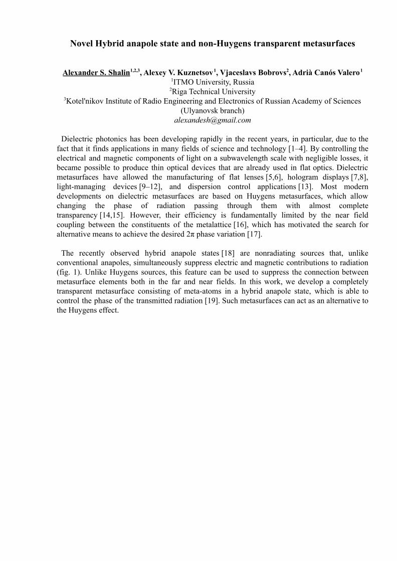
The recently observed hybrid anapole states [18] are nonradiating sources that, unlikeconventional anapoles, simultaneously suppress electric and magnetic contributions to radiation(fig. 1). Unlike Huygens sources, this feature can be used to suppress the connection betweenmetasurface elements both in the far and near fields. In this work, we develop a completelytransparent metasurface consisting of meta-atoms in a hybrid anapole state, which is able tocontrol the phase of the transmitted radiation [19]. Such metasurfaces can act as an alternative tothe Huygens effect.
Figure 1. Artistic representation of the considered silicon metasurface composed of nanocylinders,illustrating its new functionalities: full transmission, almost complete independence of properties from the
position of meta-atoms and the ability to control the phase (a), dependence of the transmission ofradiation with fixed distance between cylinders s = 300 nm (inset: absolute values of the dominant
multipolar contributions) (b), total transmitted phase obtained numerically, and phase variation
experienced by the electric quadrupole (c).
Figure 1 shows the dependence of the transmission (b) and phase shift of the tranmittedradiation (c) of the metasurface depending on the wavelenght with fixed distance between thesurfaces of the meta-atoms. It is seen from the figure that even highly compact metasurfacesdisplay almost unit transmission. In addition, contrarily to other recently proposed effectsinducing zero transmission, the hybrid anapole is preserved when deposited over substrateshaving almost zero refractive index contrast. This reduces the requirements for the technicalproduction process, allowing more design flexibility in terms of the material of the underlyingsubstrate.
Thus, in this work, a metasurface model was developed, which, in terms of its opticalproperties, can become a worthy alternative to Huygens’ metasurfaces. The developednon-Huygens’ metsurface model based on nanocylinders in a hybrid anapole state has a numberof indisputable advantages, such as full transmission of incident radiation, zero phase shift whenradiation passes through it, and the possibility of deposition on various types of substrateswithout significant changes in the optical properties of the metasurface. All of the aboveproperties make it possible to largely unlock the potential for creating various devices based onmetasurfaces, for example, various lenses, sensors, holographic devices, and so on.
The authors gratefully acknowledge the support of the RFBR Grant 20-52-00031 for themultipolar decompositions. The transient calculations for the disordered metasurfaces have beenpartially supported by the RSF Grant 21-12-00151. This research is partially funded by theLatvian Council of Science, project “DNSSN”, project No. lzp-2021/1-0048.
References
[1] Y. Kivshar, Natl. Sci. Rev. 5, 144 (2018).[2] V. Kozlov et al., Appl. Phys. Lett. 109, (2016).[3] A. Canós Valero et al., Adv. Sci. 7, 1903049 (2020).[4] D. V. Novitsky et al., Phys. Rev. B 98, 1 (2018).[5] K. Chen et al., Adv. Mater. 29, 1 (2017).[6] A. A. Fathnan, M. Liu, and D. A. Powell, Adv. Opt. Mater. 8, 1 (2020).[7] K. E. Chong et al., ACS Photonics 3, 514 (2016).[8] L. Wang et al., Optica 3, 1504 (2016).[9] S. Kruk and Y. Kivshar, ACS Photonics 4, 2638 (2017).[10] P. D. Terekhov et al., Sci. Rep. 9, 1 (2019).[11] H. Barhom et al., Nano Lett. 19, 7062 (2019).[12] P. D. Terekhov et al., Laser Photon. Rev. 1900331, 1900331 (2020).[13] X. Zhang et al., Light Sci. Appl. 9, 34 (2020).[14] M. Decker et al., Adv. Opt. Mater. 3, 813 (2015).[15] H. K. Shamkhi et al., Phys. Rev. Mater. 3, 1 (2019).[16] A. E. Olk and D. A. Powell, Phys. Rev. Appl. 11, 1 (2019).[17] A. Rahimzadegan et al., Nanophotonics 9, 75 (2020).[18] A. Canós Valero et al., Laser Photonics Rev. 2100114, 1 (2021).[19] A. V Kuznetsov et al., arXiv Phys. (2021).
Propagation and interaction of intense optical pulses in planar systems withstrong light-matter coupling
Alexey V. Yulin1
1Physics Department, ITMO University, St. Petersburg, RussiaEmail - [email protected]
In this talk I consider propagation of the pulses in dielectric planar waveguides with build-inquantum wells. The regime of strong interaction between the excitons and the photons can beachieved in the systems provided that the waveguide can support electromagnetic waves with thefrequency close to the frequency of the exciton resonance. In this case hybrid half-lighthalf-matter excitations having rich dispersive and nonlinear properties appear in the system. Thedispersion of these hybrid excitations originates mostly from the strong coupling and is muchhigher compared to the dispersion of pure guided photons. Another virtue of the hybrid waves istheir large nonlinearity appearing because of the exciton component. These two factors allow toobserve nonlinear modification of the optical pulses at the propagation distances of order of tensmicrons which makes the systems promising from the point of view of nonlinear optics.The problem of propagation of intense pulses is considered for different parameters of thewaveguide. In particular it is shown that the formation of solitons is possible in the system. Theeffect of the nonlinear losses on the pulse dynamics is addressed too. The second part of the talkis devoted to the resonant interaction between the solitons and the dispersive waves propagatingin the system. Different regimes of the collision of the solitons and the linear pulses arediscussed in detail.
Resonance Width Control in Nanoparticle Lattice with High Index and HighLosses
Viktoriia E. Babicheva1
1University of New Mexico, United [email protected]
The research of suitable material platforms for photonic nanostructures and their functionalitiesis one of the rapidly growing directions in the fields of nano-optics, nanophotonics, and materialresearch in general [1,2]. Metaphotonics is an emerging multidisciplinary research direction thatdeals with controlling electromagnetic fields in nanoengineered strucutre, materials, and surfacesusing both electric and magnetic components of the field, their interactions, and coupling. Takingadvantage of high refractive index, high losses, and strong anisotropic response insemiconductors and layered van der Waals materials, we develop photonic nanostructures withtunable resonance width. We study periodic arrays of nanoantennas made of a high-index andlossy materials placed on a low-index oxide substrate or in a uniform environment. We show thatthe nanostructure resonances and coupling between nanoscatteres and environment can becontrolled by the variation in the array size, dimensions, and surrounding index.
References[1] V. Babicheva, J. Moloney, Laser Photon. Rev. 12 (2019) 1800267[2] V. Babicheva, J. Moloney, Appl. Sciences 9 (2019) 2005
Radial bound states in the continuum forpolarization-invariant nanophotonics
Lucca Kühner1, Luca Sortino1, Rodrigo Berté1,5, Juan Wang1, Haoran Ren1,4,Stefan A. Maier1,2, Yuri S. Kivshar3, and Andreas Tittl1
1Chair in Hybrid Nanosystems, Nanoinstitute Munich, and Center for NanoScience,Ludwig-Maximilians-University Munich, Königinstrasse 10, 80539 München, Germany
2The Blackett Laboratory, Department of Physics, Imperial College London,London, SW7 2AZ, United Kingdom
3Nonlinear Physics Centre, Research School of Physics,Australian National University, Canberra ACT 2601, Australia
4MQ Photonics Research Centre, Department of Physics and Astronomy,Macquarie University, Macquarie Park NSW 2109, Australia
5Instituto de Física, Universidade Federal de Goiás, 74001-970 Goiânia-GO, [email protected]
All-dielectric nanophotonics driven by the physics of bound states in the continuum [1] (BICs)have enabled breakthrough applications in nanoscale light manipulation, frequency conversionand optical sensing [2-4]. Leading BIC implementations range from isolated nanoantennas withlocalized electromagnetic fields [5] to metasurfaces with broken in-plane inversion symmetryand controllable resonance quality (Q) factors [6]. However, such approaches often require eitherstructured light illumination with complex beam-shaping optics or large, fabrication-intensearrays of polarization-sensitive unit cells, limiting their effective use for tailored nanophotonicapplications and on-chip integration. In this presentation, we will introduce radial quasi boundstates in the continuum (rBICs) as a new class of radially distributed electromagnetic modescontrolled by the structural asymmetry in a ring of dielectric rod pair resonators. Our rBICplatform provides polarization-invariant and tunable high-Q resonances with strongly enhancednear-fields in an ultracompact footprint as low as 2 µm2, which makes them ideal for boostinglight-matter interactions. We will present experimental rBIC realizations in the visiblewavelength range for sensitive biomolecular detection and enhanced second-harmonicgeneration from monolayers of transition metal dichalcogenides. Our results demonstrate thatrBICs can open new perspectives towards compact, spectrally selective, andpolarization-invariant metadevices for multi-functional light-matter coupling, multiplexedsensing, and high-density on-chip photonics.
References[1] C.W. Hsu et al., Nat. Rev. Mater. 1 (2016) 16048[2] K. Koshelev et al., Science 367 (2020) 288-292[3] Z. Liu et al., Nano Lett. 21 (2021) 7405-7410[4] A. Tittl et al., Science 360 (2018) 1105-1109[5] M. V. Rybin et al., Phys. Rev. Lett. 119 (2017) 243901[6] K. Koshelev et al., Phys. Rev. Lett. 121 (2018) 193903
Reversible optical switching of GeSbTe spherical nanoparticles
Mikhail V. RybinSchool of Physics and Engineering, ITMO University, St. Petersburg 197101, Russia
During the last decade, phase-changing materials based on Ge-Sb-Te compounds have garneredmuch attention for their convincing evidence in the vast literature as promising material ofadvanced metaphotonics [1,2]. Ge-Sb-Te have two beneficent properties that are the highrefractive index and the non-reversible phase transition between crystalline and metastableamorphous phases. The transition is accompanied by almost two times modulation of therefractive index of the material. While both crystallization and amorphization of GeSbTe occurwith thermal heating the former is much simpler in practical realization than the latter. Theamorphization process requires thermally assisted disordering of the atoms with rapid quenchingfreezing the chaotic displacement of the elements. The literature reports on several approaches toswitching of the phase and the electric or optical pulses are the most application-orientedtreatments.
Here I present the results of reversible optical switching of GeSbTe spherical nanoparticlesfabricated by ablation technique [3]. At the first step a donor GST film was prepared by thermalevaporation in vacuum with deposition of the material onto a substrate. The nanoparticles werefabricated by placing the donor film in close contact with a receiver glass substrate. Applicationof intensive infrared optical pulses from a femtosecond laser results in an ablation process withmultiple nanoparticles produced at each pulse. The nanoparticles were examined by means ofdark-field microscopy, Raman spectroscopy and second-harmonic generation experimentaltechniques. All techniques reveal strong modification of the measured data during the phasetransition. With dark-field experiments we achieved the reversible switching by application of atrain of low-intensity pulses for the amorphous-to-crystalline transition of GST and a singlefemtosecond pulse regime delivering energy of high intensity causing the reverse transition tothe initial amorphous phase.
I acknowledge the support from the Russian Scientific Foundation (Grant No. 21-19-00677).
References[1] M. Wuttig, H. Bhaskaran, T. Taubner, Nat. Photon. 11 (2017) 465[2] S.V. Makarov et al., Laser Photon. Rev. 11 (2017) 1700108[3] M.V. Rybin et al., Laser Photon. Rev. (in press)
Correlative electron-photon spectroscopy
Nahid TalebiInstitute for Experimental and Applied Physics, 24107 Kiel, Kiel University, Germany
Email – [email protected]
Electron energy-loss spectroscopy and cathodoluminescence (CL) spectroscopy are commontechniques for characterizing the optical responses of nanostructures with unprecedented spatialresolution and spectral bandwidth [1]. Recent activities to resolve the dynamics of materialsexcitations by merging laser pumps and electron probes have opened a new era, namely,photon-induced near-field electron microscopy (PINEM) [2]. Electron-light interactions provideplethora of possibilities for fundamental investigations of quantum phenomena as well, such asquantum-path interferometry [3] and strong-coupling effects [4, 5].
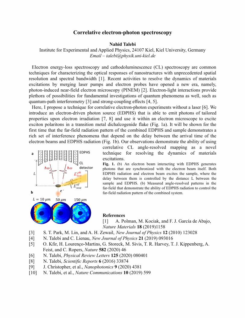
Here, I propose a technique for correlative electron-photon experiments without a laser [6]. Weintroduce an electron-driven photon source (EDPHS) that is able to emit photons of tailoredproperties upon electron irradiation [7, 8] and use it within an electron microscope to exciteexciton polaritons in a transition metal dichalcogenide flake (Fig. 1a). It will be shown for thefirst time that the far-field radiation pattern of the combined EDPHS and sample demonstrates arich set of interference phenomena that depend on the delay between the arrival time of theelectron beams and EDPHS radiation (Fig. 1b). Our observations demonstrate the ability of using
correlative CL angle-resolved mapping as a noveltechnique for resolving the dynamics of materialsexcitations.Fig. 1. (b) An electron beam interacting with EDPHS generatesphotons that are synchronized with the electron beam itself. BothEDPHS radiation and electron beam excites the sample, where thedelay between them is controlled by the distance L between thesample and EDPHS. (b) Measured angle-resolved patterns in thefar-field that demonstrate the ability of EDPHS radiation to control thefar-field radiation pattern of the combined system.
References[1] A. Polman, M. Kociak, and F. J. García de Abajo,Nature Materials 18 (2019)1158
[3] S. T. Park, M. Lin, and A. H. Zewail, New Journal of Physics 12 (2010) 123028[4] N. Talebi and C. Lienau, New Journal of Physics 21 (2019) 093016[5] O. Kfir, H. Lourenço-Martins, G. Storeck, M. Sivis, T. R. Harvey, T. J. Kippenberg, A.
Feist, and C. Ropers, Nature 582 (2020) 46[6] N. Talebi, Physical Review Letters 125 (2020) 080401[8] N. Talebi, Scientific Reports 6 (2016) 33874[9] J. Christopher, et al., Nanophotonics 9 (2020) 4381[10] N. Talebi, et al., Nature Communications 10 (2019) 599
Parametric frequency conversion in lithium niobate metasurfaces
Frank SetzpfandtInstitute of Applied Physics, Abbe Center of Photonics, Albert-Einstein-Str. 15, 07745 Jena,
Lithium niobate (LN) is an attractive material for nonlinear photonics due to its widetransparency range and high second-order nonlinearity. However, most applications of LN todate were using bulk LN crystals or waveguides. Mie-type nanoresonators in LN as well asmetasurfaces have only been studied recently, showing promise also for applications of thismaterial system in nanophotonics.
In my talk, I will show experimental results from nonlinear metasurfaces consisting of LNnanocubes realized in a LN thin film on a SiO2 substrate. For classical second-harmonicgeneration, we could demonstrate that the electric-dipole (ED) and magnetic-dipole (MD)resonances in these metasurfaces enhance the conversion efficiency for second-harmonicgeneration, that the generated second harmonic is predominantly emitted in the forwarddirection, and that the specific structure of the nonlinear tensor of LN leads to significantlydifferent dependences of the generated light on the polarization of the excitation for the ED andMD resonances [1].
The majority of my talk will be devoted to the generation of photon pairs in thesemetasurfaces. To this end, we used spontaneous parametric down conversion (SPDC). Ourexperiments successfully demonstrated the generation of photon pairs in the LN metasurfacewith high signal-to-noise ratio [2]. We could also show, that photon pair generation is controlledpredominantly by the ED resonance and that the spectrum of the emitted photon pairs can betuned by changing the wavelength of the pump laser with respect to the ED resonance.
With these results, we show that resonant metasurfaces based on lithium niobate are a suitableplatform for parametric three-wave mixing to generate classical and non-classical light. Ourresults are an important step towards the use of metasurfaces for the tailored generation ofphoton pairs.
References[1] A. Fedotova, M. Younesi, J. Sautter, A. Vaskin, F. J. F. Löchner, M. Steinert, R. Geiss, T.
Pertsch, I. Staude, and F. Setzpfandt, „Second-Harmonic Generation in Resonant NonlinearMetasurfaces Based on Lithium Niobate,” Nano Letters 20, 8608 (2020).
[2] T. Santiago-Cruz, A. Fedotova, V. Sultanov, M. A. Weissflog, D. Arslan, M. Younesi, T.Pertsch, I. Staude, F. Setzpfandt, and M. V. Chekhova, “Photon Pairs from ResonantMetasurfaces,” Nano Letters 21, 4423 (2021).
Chalcogenide and tellurite photonic resonators with whispering gallery modes
Elena A. Anashkina and Alexey V. AndrianovInstitute of Applied Physics of the Russian Academy of Sciences, Russia
Resonators with whispering gallery modes (WGMs) based on dielectric materials provideunique capabilities for controlling fundamental properties of coherent light. Such resonators havehuge Q-factors and large nonlinearity, which make it possible to attaine nonlinear and lasereffects at low pump powers [1]. Microresonators are used for various applications dealing withclassical and non-classical states of light. Sensing and biosensing, optical filtering, linewidthnarrowing, coherent communication, dual-comb spectroscopy, generation of non-classical statesof light, e.g. correlated photon pairs and squeezed light are just a few of them [1]. The use ofnew materials with outstanding optical properties allows expanding the capabilities of photonicresonators.
Chalcogenide glasses (consisting of one or more chalcogens (Se, S or/and Τe) in conjunctionwith Αs, Ga, Ge, Ρ, Sb, and some other electropositive elements) are very promising materialsfor use in various photonic devices including WGM microresonators. One of the reasons is giantvalues of optical χ(3) Kerr and Raman nonlinearities of chalcogenide glasses, 2-3 orders ofmagnitude higher compared to silica glass [2]. Chalcogenide glassy materials are transparent inthe near-IR and mid-IR and demanded for these spectral ranges [2]. Spherical microresonatorswith Q-factors of order 106-108 can be made of commercially available As2S3 and As2Se3 fibers,which makes their production a fairly accessible technology [3]. Tellurite glasses (based ontellurium dioxide ΤeO2) are another promising materials. Their nonlinear refractive index is20-30 times higher compared to silica glass and they are transparent up to ~5-6 μm [2]. They canbe easily doped with rare-earth ions for obtaining laser generation in the 1-3 μm range.
Here we present our recent experimental and theoretical results concerning nonlinear and lasereffects in chalcogenide and tellurite WGM microresonators including Raman lasing, opticalfrequency comb generation, and laser generation [3,4]. In particular, cascade Raman lasing up to4th order is experimentally attained in the near-IR (initially the 1st-order Raman radiation isgenerated which serves as the pump for the 2nd-order Raman radiation, and so on). Thepossibilities of Raman lasing as well as generation of dissipative Kerr solitons in the mid-IR arestudied numerically. Laser generation in Er-doped and Tm-doped tellurite resonators in differentregimes is predicted theoretically and confirmed experimentally. The opportunities of furtherprogress in such photonic devices are discussed.
This work is supported in part by the RSF, Grant No. 20-72-10188 (study of telluriteresonators) and in part by the Mega-grant of the Ministry of Science and Higher Education of theRussian Federation, Contract No.14. 075-15-2021-633 (study of chalcogenide resonators).
References[1] A. Pasquazi et al., Phys. Rep. 729 (2018) 1.[2] G. Tao et al., Adv. Opt. Photonics 7 (2015) 379[3] A.V. Andrianov, E.A. Anashkina, Opt. Express 29 (2021) 5580[4] E.A. Anashkina, A.V. Andrianov, J. Light. Technol. 39 (2021) 3568
Fast syntheses of phase-only metasurfaces for full-state and high-efficiencycontrol of electromagnetic fields
Jun Wei Wu,Southeast University, China
Metasurface holography is a powerful tool of imaging and advanced field control. To enrichthe functionality of metasurface holography for broader applications, independent andsimultaneous controls of the field amplitudes and phases in the region of interest (ROI) arehighly desired. Traditionally, it has been believed that such functionality can be achieved only bymetasurface holograms with both phase and amplitude modulations in the local transmissive orreflective coefficients, and recent efforts have devoted to such phase-and-amplitude (PA)metasurface holograms. However, it should be stressed that the power efficiencies of the PAmetasurface holograms are usually less than 10%, which is unfavorable for many applications.
In this presentation, we synthesize the field amplitudes and phases in ROI simultaneously andindependently with high efficiencies by using the phase-only (PO) metasurface. All points inROI may have independent values of field amplitudes and phases, and the requirements for Xand Y components may be different in achieving spatially varied polarization states. To this end,we present an efficient design method based on equivalent electromagnetic model andgradient-based nonlinear optimization. Full-wave simulations and experimental resultsdemonstrate the feasibility of the design method in synthesizing almost arbitrary amplitude andphase values at every points in ROI and their polarization states using the PO metasurface, whichhas 10 times higher power efficiency than the PA metasurface. This work opens a way to realizemore complicated and high-efficiency metasurface holography, and extends the applicationscope of electromagnetic engineering with metasurfaces. In general, this work creates aparadigm of engineering complicated fields with high efficiencies. This topic is of interest andrelevance to scientists across a broad range of directions, including optical trapping, structuredillumination microscopy, cloaking and illusion, data storage and encryption, 3D display andinterference lithography.
References[1] J. W. Wu, Z. X. Wang, Z. Q. Fang et al., Adv. Funct. Mater., (2020) 30, 39, 2004144.[2] A. C. Overvig, S. Shrestha, S. C. Malek et al., Light Sci. Appl. (2019) 8, 1.
Efficient characterization of resonant dielectric particles
Denis Tihon and Christophe CraeyeICTEAM Institute, UCLouvain, Louvain-la-Neuve, Belgium
Email – [email protected], [email protected]
In order to efficiently control the electromagnetic fields on small scales, materials with a strongcontrast of refractive index are generally desired. At optical frequencies, metals generally exhibitsuch contrast, at the expense of moderate to high losses. As a low-loss alternative to metal,resonant dielectric particles are often used. Near the resonant frequency, the response of suchparticles to incident light is strong, paving the way for compact and efficient designs tomanipulate light. However, since the response of such particles is associated with a resonance,their behavior is intrinsically dispersive.
A popular way to describe such particles is to model them as polarizable electric or magneticdipoles or multipoles with associated complex resonant frequencies. These models can beimproved using full-wave electromagnetic solvers. Using the latter, the exact distribution of thefields associated to each resonant mode can be obtained.
Several fast methods have been proposed in the literature to rapidly and accurately determinethe resonant modes and associated resonant frequencies, each of them with their associatedadvantages and drawbacks [1]. Most of the existing techniques are based on volumetric solvers.Indeed, using contrast sources, the determination of the resonant frequencies of a scatterer can beformulated as a linear problem for non-dispersive materials.
Recently, a fast method based on Surface Integral Equation (SIE) has been proposed, which isbased on the Geometrical Method of Moments (gMoM) [2]. Using SIE, only the surface of thestructure needs to be discretized, resulting in a reduced number of unknowns w.r.t. theirvolumetric counterparts. However, using SIE, the eigenmode search cannot be formulated as alinear problem. Because of this, the determination of the resonant frequencies of a structurerequires computing the impedance matrix of the structure for several frequencies, slowing downthe procedure. The computation of the impedance matrices is the time limiting step of themethod and thus limit its applicability. Using the gMoM, the frequency dependence of theimpedance matrix is reformulated as a rapidly converging series of purely geometrical terms, i.e.not depending on frequency nor material properties [3]. Thus, the impedance matrix can berapidly evaluated for many frequencies.
During the presentation, we will present the method and apply it to several dielectric materialconfigurations proposed in the literature.
References[1] Lalanne, Philippe, et al. "Quasinormal mode solvers for resonators with dispersive
materials." JOSA A 36.4 (2019): 686-704.[2] Tihon, D., & Craeye, C. (2019, September). Geometrical MoM formulation for eigenmode
analysis. In 2019 International Conference on Electromagnetics in Advanced Applications(ICEAA) (pp. 1141-1144). IEEE.
[3] Hislop, G., Ozdemir, N. A., Craeye, C., & Ovejero, D. G. (2012). MoM matrix generationbased on frequency and material independent reactions (FMIR-MoM). IEEE transactions onantennas and propagation, 60(12), 5777-5786.
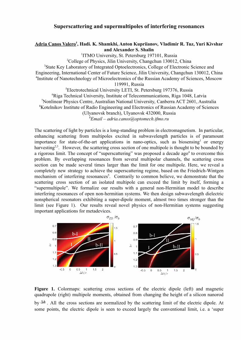
Superscattering and supermultipoles of interfering resonances
Adria Canos Valeroϯ, Hadi. K. Shamkhi, Anton Kupriianov, Vladimir R. Tuz, Yuri Kivsharand Alexander S. Shalin
1ITMO University, St. Petersburg 197101, Russia2College of Physics, Jilin University, Changchun 130012, China
3State Key Laboratory of Integrated Optoelectronics, College of Electronic Science andEngineering, International Center of Future Science, Jilin University, Changchun 130012, China4Institute of Nanotechnology of Microelectronics of the Russian Academy of Sciences, Moscow
119991, Russia5Electrotechnical University LETI, St. Petersburg 197376, Russia
6Riga Technical University, Institute of Telecommunications, Riga 1048, Latvia7Nonlinear Physics Centre, Australian National University, Canberra ACT 2601, Australia
8Kotelnikov Institute of Radio Engineering and Electronics of Russian Academy of Sciences(Ulyanovsk branch), Ulyanovsk 432000, Russia
ϯEmail – [email protected]
The scattering of light by particles is a long-standing problem in electromagnetism. In particular,enhancing scattering from multipoles excited in subwavelength particles is of paramountimportance for state-of-the-art applications in nano-optics, such as biosensing1 or energyharvesting2,3. However, the scattering cross section of one multipole is thought to be bounded bya rigorous limit. The concept of “superscattering” was proposed a decade ago4 to overcome thisproblem. By overlapping resonances from several multipolar channels, the scattering crosssection can be made several times larger than the limit for one multipole. Here, we reveal acompletely new strategy to achieve the superscattering regime, based on the Friedrich-Wintgenmechanism of interfering resonances5. Contrarily to common believe, we demonstrate that thescattering cross section of an isolated multipole can exceed the limit by itself, forming a“supermultipole”. We formalize our results with a general non-Hermitian model to describeinterfering resonances of open non-hermitian systems. We then design subwavelength dielectricnonspherical resonators exhibiting a super-dipole moment, almost two times stronger than thelimit (see Figure 1). Our results reveal novel physics of non-Hermitian systems suggestingimportant applications for metadevices.
Figure 1. Colormaps: scattering cross sections of the electric dipole (left) and magneticquadrupole (right) multipole moments, obtained from changing the height of a silicon nanorod
by . All the cross sections are normalized by the scattering limit of the electric dipole. Atsome points, the electric dipole is seen to exceed largely the conventional limit, i.e. a ‘super

dipole’ moment appears. The original nanorod has radius and height . Thedotted white lines indicate the evolution of the resonant frequencies. An avoided crossing ofmodes I-II, characteristic from the Friedrich-Wintgen mechanism, can be clearly observed.References1. Yavas, O., Svedendahl, M., Dobosz, P., Sanz, V. & Quidant, R. On-a-chip Biosensing
Based on All-Dielectric Nanoresonators. Nano Lett. 17, 4421–4426 (2017).2. Simovski, C. R., Shalin, A. S., Voroshilov, P. M. & Belov, P. A. Photovoltaic absorption
enhancement in thin-film solar cells by non-resonant beam collimation by submicrondielectric particles. J. Appl. Phys. 114, (2013).
3. Voroshilov, P. M., Simovski, C. R., Belov, P. A. & Shalin, A. S. Light-trapping andantireflective coatings for amorphous Si-based thin film solar cells. J. Appl. Phys. 117,(2015).
4. Ruan, Z. & Fan, S. Superscattering of light from subwavelength nanostructures. Phys.Rev. Lett. 105, 1–4 (2010).
5. Bogdanov, A. A. et al. Bound states in the continuum and Fano resonances in the strongmode coupling regime. Adv. Photonics 1, 1 (2019).
Superscattering channels mediated by the Friedrich-Wintgen mechanism
Hadi K. Shamkhi, Adria Canos-Valero, and Alexander S. ShalinITMO University, St. Petersburg, Kronverksky 49, 197101, Russia
In our work [1], it is revealed for some specific examples that strong coupling of Mie-resonantmultipolar modes provides an alternative pathway to the enhancement of light scattering inaddition to the overlapping of uncoupled modes. Where the latter is the currently acceptedmethod to enhance scattering to several folds higher than the uncoupled dipolar channelsmaxima, also known as supescatteing. The increment of power, in a two-level modal system forinstance, results in diving the low order multipolar channels to exceed uncoupled channellimitation [2]- a phenomenon of superscattering within the channel itself that is forbidden in Mieresonators retaining spherical symmetry. The avoided resonance crossing, as described in theFriedrich-Wintgen mechanism of interfering modes, leads to energy exchange between theradiation channels allowing to control both Qfactors and multipolar contents of resonances whilemaintaining a high scattering cross-section. Scattering maxima also is shown to occurs at thecrossing points of two uncoupled modes originating from two separate coupling mechanisms.Thus, superscattering in nonspherical resonators is shown to be realized in a practical setup at abroadband spectrum with significant enhancement at multifrequency points by only varying aone geometrical parameter. The proposed method employing the recently developed quasinormal modes QNMs of an open resonator effectively reveals the physical mechanisms behindsuperscattering phenomena and reduces the complications of real frequency calculations. It wasthen suggested and demonstrated a simple and intuitive strategy to further enhance the scatteringamplitude and/or resonance quality by assembling cylinders in symmetric clusters whilecontrolling the inter-particle distances.
References[1] A. Canós Valero, H. K Shamkhi, et al, arXiv:2105.13119, (2021)[2] Z. Ruan and S. Fan, Phys. Rev. Lett. 105, 013901, (2010)
SMART NANOMATERIALS
7-10 December 2021Chimie ParisTech, Paris
Momentum alignment of photoexcited carriers in low-dimensional Dirac materials
R.R. Hartmann1, V.A. Saroka2 and M.E. Portnoi3,4 1Physics Department, De La Salle University, Manila, Philippines
2Norwegian University of Science and Technology, Trondheim, Norway 3Physics and Astronomy, University of Exeter, Exeter, United Kingdom
4ITMO University, St. Petersburg, Russia Email – [email protected]
Devices made from conventional semiconducting materials manipulate electron flow based on their charge or spin (spintronics), the later offers the promise to revolutionize the way we do computing. In graphene and graphene-like materials, there is an alternative electron property which can be harnessed for device applications: the so-called valley degree of freedom, which could be utilized in an analogous manner to spin in spintronics and has been suggested as a basis for carrying information in graphene-based devices. The ability to control the valley degree of freedom practically is still an outstanding problem. We propose a new method of control, using linearly polarized light, to open the door to optovalleytronics.
One of graphene’s most widely known optical properties is its universal absorption, defined through the fine-structure constant, which holds true across a broad range of frequencies from the sub-infrared into the visible. A lesser-known feature is that linearly polarized light creates a strongly anisotropic distribution of photoexcited carriers with their momenta predominantly aligned normally to the polarization plane [1]. We show how this momentum alignment effect together with graphene’s spectrum anisotropy (trigonal warping) at high energies can be utilized for the spatial separation of carriers belonging to different valleys in graphene and gapped graphene-like materials [2]. The optical control of valley polarization in gapped 2D Dirac materials such as phosphorene and single-layer transition metal dichalcogenides can also be achieved via a well-known effect of using circularly polarized light. In gapped materials, the optical selection rules associated with linearly polarized light of near-band-gap energies are valley-independent, in stark contrast to the valley-dependent optical selection rules associated with circularly polarized light. This valley dependence of the circularly-polarized transitions can be utilized to measure the degree of valley polarization induced by linearly polarized light of high (well above the band gap) energies, by analyzing the degree of circularly polarization of the band-edge luminescence at different sides of the light spot.
The momentum alignment phenomenon also explains the hitherto overlooked effect of the giant enhancement of the band gap edge interband optical transition rate in narrow gap carbon nanotubes and graphene nanoribbons [3] which occurs in the terahertz range, thus opening a route for creating novel terahertz radiation emitters.
This work was supported by the EU H2020 RISE project TERASSE (Grant No. 823878).
References
[1] R.R. Hartmann, M.E. Portnoi, Optoelectronic Properties of Carbon-based Nanostructures:Steering electrons in graphene by electromagnetic fields (LAP Lambert AcademicPublishing, Saarbrucken, 2011)
[2] V.A. Saroka, R.R. Hartmann, M.E. Portnoi, arXiv:1811.00987[3] R.R. Hartmann, V.A. Saroka, and M.E. Portnoi, J. Appl. Phys 125 (2019) 124303
Nano-antennas Based on Transition Metal Dichalcogenides forPhotonics Applications
Panaiot Zotev2, Donato Contenduca1, Luca Sortino2, Toby Millard2, AlexanderTartakovskii2, Thomas Krauss1, Yue Wang1
1 Department of Physics, University of York, Heslington, York, UK2 Department of Physics and Astronomy, University of Sheffield, Sheffield, UK
Email: [email protected]
Transition metal dichalcogenides (TMDs) have shown great potential as nextgeneration photonics materials [1]. Their monolayers have direct bandgaps in a largeportion of the visible spectrum with near-unity photoluminescence (PL) efficiencies.Their bulk materials (10s to 100s nm thick) have large refractive index whilemaintaining low absorption, therefore, bulk TMDs can be explored as an excellentcandidate material for nano-photonic resonators. Here, we fabricate WS2
nano-antennas with different shapes, enabled by balancing isotropic and anisotropicetching in the fabrication process. Using dark field spectroscopy, we reveal multipleMie resonances, to which we couple PL from a monolayer WSe2. In suchmonolayer-on-bulk TMD system, we demonstrate a PL enhancement of more than240 folds. We also reveal that these WS2 nano-antennas with ultra-small gaps can beemployed for optical trapping with exceptional performance [2].
References:[1] 2D material microcavity light emitters: to lase or not to lase?, Advanced OpticalMaterials 6 (19), 1800272, 2018[2] Transition metal dichalcogenide dimer nano-antennas with ultra-small gaps, arXivpreprint arXiv:2105.09201, 2021
Edge-state tunneling in topological insulators
Igor Rozhansky1,2, Maria Legenkaia2,3, Henri Jaffres4, Henri-Jean Drouhin2 1Ioffe Institute, Russia
2Ecole Polytechnique, CEA/DRF/IRAMIS, CNRS,Institut Polytechnique de Paris 3Ecole Normale Superieure, France
4Unite Mixte de Physique, CNRS, Thales, Univ. Paris-Sud, Univ. Paris-Saclay
Tunneling between two 2D layers separated by a weakly transparent potential barrier is a prime
example of resonant tunneling phenomena in semiconductor nanostructures. In such a structure
the energy and in-plane momentum conservation put tight restrictions on the tunneling so that the
conductance exhibits sharp maximum at zero bias, while at any finite voltage applied across the
barrier the transitions between the layers are forbidden. Such a behaviour has been experimentally
observed both for the semiconductor heterostructures containing two spatially separated quantum
wells. The spin-orbit coupling in the layers leads to a complex interference picture in the I-V
characteristuc carrying information about SOC parameters of the material [1]. In this work we
consider theoretically quantum tunneling between edge states of two pieces of topological
insulator (TI) separated by a normal isolator (NI) forming a topologically trivial tunnel barrier.
Tunnel energy splitting and the eigenfunctions have been obtained analytically for the TI-NI-TI
heterostructure described by Bernevig-Hughes-Zhang Hamiltonian with proper matching
conditions at the interfaces. Using the obtained stationary solution we have calculated the non-
stationary tunneling current between the two TI edge states. As shown by the calculations the
differential tunnel conductance exhibits resonant pattern with most pronounced peaks at zero bias
as well as at the bias corresponding to the Fermi energy. We come up with a suggestion of
experimental proof of the predicted phenomenon.
References
[1] I. V. Rozhansky, N. S. Averkiev, E. Lahderanta, Phys. Rev. B 93, 195405 (2016).
Novel 2D Glassy-Graphene Devices for Broadband Photodetection andVolatile Organic Compound Sensing
Hao Xu,1,2*, Xiao Li3, Guifu Zou,4 Kwang-Leong Choy,5 Ivan P. Parkin,6 Zhengxiao Guo,6,7,8
Jiang Wu2,9
1School of Physics, University of Electronic Science and Technology of China2State Key Laboratory of Electronic Thin Films and Integrated Devices, University of Electronic
Science and Technology of China3Department of Electronic and Electrical Engineering, University College London
4School of Energy, Soochow Institute for Energy and Materials Innovations, and Key Laboratoryof Advanced Carbon Materials and Wearable Energy Technologies of Jiangsu Province,
Soochow University5Institute for Materials Discovery, University College London
6Department of Chemistry, University College London,7Departments of Chemistry and Mechanical Engineering, The University of Hong Kong, Hong
Kong SAR, P. R. China8Zhejiang Institute of Research and Innovation, The University of Hong Kong,
9Institute of Fundamental and Frontier Sciences, University of Electronic Science andTechnology of China
Email: [email protected]
Multifunctional devices are of great interest for integration and miniaturization on the sameplatform, but simple addition of functionalities would lead to excessively large devices. Here, thephotodetection and chemical sensing device is developed based on novel 2D glassy-graphene1,2
that meets similar property requirements for the two functionalities. An appropriate bandgaparising from the distorted lattice structure enables glassy-graphene to exhibit similar or evenimproved photodetection and chemical sensing capability, compared to pristine graphene. Due tostrong interactions between glassy-graphene and the ambient atmosphere, the devices are lesssensitive to photoinduced desorption than graphene. Consequently, the few-layerglassy-graphene device delivers positive photoresponse, with a responsivity of 0.22 A/W andspecific detectivity reaching 1010 Jones under 405 nm illumination. Moreover, the intrinsicdefects and strain in glassy-graphene can enhance the adsorption of analytes, leading to goodchemical sensing performance. Specifically, the extracted signal-to-noise-ratio (SNR) of theglassy-graphene device for detecting acetone is 48, representing more than 50% improvementover the graphene counterpart. Additionally, bias voltage and thickness dependent VOC sensingfeatures are identified, indicating the few-layer glassy-graphene is more sensitive. This studysuccessfully demonstrates the potential of glassy-graphene for integrated photodetection andchemical sensing, providing a promising solution for multifunctional applications furtherbeyond.
References[1] Xu, H. et al. Adv. Mater. 2018, 30: 1706561.[2] Dai, X. et al. Sci. Adv. 2016, 2: e1601574.
Optically Induced Coherent Phonons in Bismuth Oxyiodide (BiOI)Nanoplatelets
Sebastian Rieger, Tim Fürmann, Jacek K. Stolarczyk, and Jochen FeldmannChair for Photonics and Optoelectronics, Nano-Institute Munich, Department of Physics,Ludwig-Maximilians-Universität (LMU), Königinstraße 10, 80539 Munich, Germany
We have studied bismuth oxyiodide (BiOI) nanoplatelets, a material which combinesintriguing optical and structural properties for photocatalysis. In particular, its crystal structurecomprised of alternatingly charged 2D layers may give rise to a built-in dipolar electric fieldalong the stacking direction affecting charge carrier dynamics in BiOI.
In a pump-probe experiment, we show that excitation by a femtosecond laser pulse createscoherent phonons which leads to an oscillating modulation of the differential optical density. Wefound that the two underlying frequencies originate from lattice vibrations along the [001]crystallographic axis, the stacking direction of the oppositely charged layers. This is consistentwith a sub-picosecond charge separation in the built-in dipolar field, which screens the electricfield partially and thus creates coherent phonons. Further, we determine the two major dephasingmechanisms that lead to the loss of vibronic coherence: (i) the anharmonic decay of an opticalphonon into two acoustic phonons and (ii) phonon-carrier scattering. We apply that knowledge tooptimize the hydrogen evolution rate in photocatalytic experiments by controlling the BiOInanoplatelet thickness via surface ligands.
Our results provide the first direct demonstration of the presence of an electric field in BiOIalong the [001] axis and show its role in efficient charge separation. [1] This separation is crucialfor photocatalytic applications of BiOI which we confirm in photocatalytic experiments.
References[1] S. Rieger, T. Fürmann, J. K. Stolarczyk, J. Feldmann, Nano Letters 21 (2021) 7887

SMART NANOMATERIALS
7-10 December 2021Chimie ParisTech, Paris
4D Printing Green Nanomedicine: 20 Years of Learning from Nature to FightCOVID-19, Reverse Infection, and Grow Tissues
Thomas J. Webster, Ph.D.Interstellar Therapeutics, USA; Hebei University of Technology, China; Vellore Institute of
Technology, [email protected]
3D printing has already revolutionized medicine through the development of more inexpensiveand effective implants that can be printed at the site of surgery. However, recent developmentshave made 3D printing even better: the use of green or natural nano materials and 4D printing(where the 4th dimension is time and the geometry of 3D printed materials can be controlledremotely and on-demand) [1]. This presentation will introduce and highlight recent advances in4D printing of green nanomaterials for various applications including technologies to stop thespreading of COVID-19, developing surfaces to inhibit bacteria and virus attachment, as well asfabricating improved medical devices that enhance tissue growth (such as for orthopedic, neural,cartilage, and other applications). In such applications, green or natural materials have not onlyimproved material efficacy at reducing bacteria and virus functions, but have also decreasedtoxicity. Nanomaterials, through their unique small features, have further promoted materialefficacy. Lastly, 4D printing has enabled for the on-demand release of green materials to promotematerial function. This presentation will provide in vitro as well as in vivo data showing thepromise of 4D printing green nanomedicine for numerous applications. This presentation willalso cover what has been learned in over two decades of research in 4D printing greennanomedicine for the field to continue to mature.
References
[1] Cui et al, NanoResearch, available on-line February 14,2019 https://doi.org/10.1007/s12274-019-2340-9
The composition of metal particle catalyzed ternary III-V nanowires
Jonas Johansson and Egor Leshchenko Solid State Physics and NanoLund, Lund University, Sweden
The ability to grow ternary III-V semiconductor materials is of highest importance for design and fabrication of modern nanoscale devices. One promising approach relies on heterostructured nanowires with precisely tuned bandgap along the nanowire. This requires composition control and several research groups have focused their efforts on composition control in ternary nanowires, see ref. [1] for a recent review.
In this presentation I will explain how to use two-component classical nucleation theory to estimate the composition of ternary nanowires growing by the vapor-liquid-solid mechanism. The materials systems of interest are gold- and self-catalyzed ternary III-V nanowires, such as InGaAs and related materials. In our model we use realistic chemical potential differences between the quaternary liquid alloy catalyst particle and the nanowire material. The chemical potentials are calculated from assessed thermodynamic parameters for Au, In, Ga, As, Sb, InAs, GaAs, GaSb, and InSb in all relevant phases. Using this approach, we are able to link the composition of the catalyst particle to the composition of the nanowire under different conditions [2].
Below certain temperatures, some of these ternary materials have a miscibility gap. For example, below 543⁰C, InxGa1-xAs has a miscibility gap, meaning that a range of compositions, x, are thermodynamically forbidden. Still, in most experiments where InGaAs nanowires are grown at temperatures below 543⁰C, the miscibility gap is conspicuous with its absence. We propose two different explanations to this phenomenon. The first one relies on kinetic, instead of nucleation-controlled composition [3]. The second explanation relies on including the surface energy of the nucleus in the calculation [4].
Finally, I will show a verification of our models in a recent in situ experiment, where gold catalyzed InGaAs has been grown in a high-resolution transmission electron microscope where the compositions of the catalyst particle and of the nanowire were monitored during growth [5].
References [1] Ghasemi, M., Leshchenko, E. D. & Johansson, J., Nanotechnology 32 (2021) 072001[2] Leshchenko, E. D., Ghasemi, M., Dubrovskii, V. G. & Johansson, J., CrystEngComm 20
(2018) 1649[3] Leshchenko, E. D. & Johansson, J., Nanomaterials-Basel 10 (2020) 2553[4] Leshchenko, E. D. & Johansson, J., CrystEngComm 23 (2021) 5284[5] Sjökvist, R. et al., J. Phys. Chem. Lett. 12 (2021) 7590
Graphene-based materials for wastewater treatment
George Z. KyzasDepartment of Chemistry, International Hellenic University, Kavala, Greece
One of the most important decontamination techniques is considered to be adsorption. It is fast,simple, low-cost with many opportunities to modify the initial materials after appropriatesynthesis routes etc. Numerous adsorbent materials are prepared the last years having as ultimatescope to remove some pollutants especially from contaminated waters (effluents originated fromindustries). But the composition of each type of effluents is varying. Dyes, heavy metals,pharmaceutical compounds are some major components of industrial wastewaters. In the lastyears, graphene attracted many researchers employing with adsorption technique, because of itsexcellent properties and 2-D structure. Researchers proceeded with that and achieved even moreeffective graphene adsorbents making some additions to initial graphene structure, preparingmany graphene composites. This work summarizes the important contribution of graphenecomposites to adsorption technique from the research team of Prof. George Z. Kyzas. Manypreparation routes of graphene composites are given along with the respective characterizationtechniques, properties of the materials, and of course detailed adsorption evaluation of graphenecomposites. The latter is based on some adsorption parameters as maximum adsorption capacity,kinetic behavior, thermodynamics, and possible reuse ability. To highlight the superiority ofgraphene composites, comparison with other adsorbents is mandatory.
Acknowledgment: The financial support received for this study from the Greek Ministry ofDevelopment and Investments (General Secretariat for Research and Technology) through theresearch project “Intergovernmental International Scientific and TechnologicalInnovation-Cooperation. Joint declaration of Science and Technology Cooperation betweenChina and Greece” with the topic “Development of monitoring and removal strategies ofemerging micro-pollutants in wastewaters” (Grant no: T7DKI-00220) and it is gratefullyacknowledged.
Surfactant effect on graphene oxide/polymer nanocomposites films
Vipul Agarwal, Yasemin Fadil, Bich Ngoc Tran, Rabiatul 'Adawiah Mat Noor, NamrataMaslekar, Per B. Zetterlund
Cluster for Advanced Macromolecular Design (CAMD), School of Chemical Engineering,University of New South Wales, Sydney, NSW 2052, Australia
E-mail: [email protected]
Graphene oxide/polymer nanocomposites continue to draw considerable research interest due totheir versatility in terms of physicochemical, mechanical and electronic properties for a variety ofapplications. Despite extensive research, control over the intrinsic properties of the grapheneoxide/polymer nanocomposites to achieve desirable properties remains a challenge. Surfactants arefrequently employed in the fabrication of polymer/graphene-based nanocomposites via emulsiontechniques. However, the impact of surfactants on electrical and mechanical properties of suchnanocomposite films was not understood. We conducted systematic studies using commercial(water soluble) and in situ generated surfactants to understand their influence on the fundamentalproperties of the nanocomposites. In this talk, the importance of surfactant chemistry on the finalproperties of the nanocomposite will be discussed. We will provide strategies that can be adopted tomanipulate the properties of nanocomposites by judicious selection of the concentration and/or typeof surfactant.
1. Tran B.N., Thickett S.C., Agarwal V., Zetterlund P.B., Influence of Polymer Matrix onPolymer/Graphene Oxide Nanocomposite Intrinsic Properties, ACS Applied Polymer Materials2021 (DOI: 10.1021/acsapm.1c00897).
2. Agarwal, V., Fadil Y., Wan A., Maslekar N., Tran B.N., Noor R.A.M., Bhattacharyya S., BiazikJ., Lim S., Zetterlund P.B., Influence of Anionic Surfactants on Fundamental Properties ofPolymer/Reduced Graphene Oxide Nanocomposite Films, ACS Applied Materials andInterfaces 2021, 13 (15), 18338–18347.
3. Y. Fadil, L. N.M. Dinh, M. O. Y. Yap, R. P. Kuchel, Y. Yao, T. Omura, U. A. Aregueta-Robles,N. Song, S. Huang, F. Jasinski, S. C. Thickett, H. Minami, V. Agarwal, P. B. Zetterlund, ACSApplied Materials & Interfaces 2019, 11, 48450-48458.
Porous silicon microparticles as a multimodal drug delivery system
A. Sambugaro,1 E. Chisté, 1 M. Donini,2 C. Nardon,3 M. Scarpa,4 S. Dusi, 2 N. Daldosso1
1Fluorescence Laboratory, University of Verona, Verona, Italy2Division of General Pathology, University of Verona, Verona, Italy3 Department of Biotechnology, University of Verona, Verona, Italy4Laboratory of Nanoscience, University of Trento, Povo (TN), Italy
Visible photoluminescence, natural porosity and large surface-to-volume ratio, together withbiodegradability, biocompatibility and absence of immunogenicity and toxicity are the properties thatmake porous silicon (pSi) particles an ideal traceable carrier for both therapy and diagnosis purposes.Fabrication and surface hydrosilylation methods of pSi are well known1,2. We successfully overcamethe issue of pSi optical and structural degradation in aqueous media by both organic3 and inorganiccoating4. Moreover, results achieved with the loading and release of (Cobinamide) Cbi3 together withan established method to decorate pSi microparticles with SPIONs5, led the system to become amultimodal platform that can find application in theranostics.
Moving from these recent findings, we investigated pSi microparticles ability to load and deliverPam3CSK4, a synthetic Toll-like receptor (TLR) 1 and 2 agonist, able to enhance immune responsesmediated by dendritic cells (DCs). DCs are antigen-presenting cells that can recognize TLR agonists,thus inducing the production of cytokines and promoting T-cell activation and inflammatory responses.This suggested that DC-mediated immune response might be enhanced by loading a TLR agonistinside pSi microparticles to avoid its degradation. Pam3CSK4 was chosen because of its dimensionsand multiple binding sites that make it suitable to be loaded within carboxyl-functionalized pSimicroparticles. After performing preliminary in vitro tests, DCs were isolated from human donors andstimulated with different concentrations of Pam3CSK4 successfully loaded within pSi-COOHmicroparticles (as demonstrated by confocal microscopy). DCs activation was proved by opticalmicroscopy and confirmed by the elongation of the dendrites. Encapsulation efficiency wasinvestigated by fluorescence spectroscopy and estimated to be around 34%. Immune response,evaluated based on the release of some cytokines by ELISA-assay, showed a promising enhancementeffect resulting from the association of Pam3CSK4 with pSi microparticles.
Moreover, since we wanted to achieve a higher immune response, we started to work with a pHresponsive polymer, acetalated dextran, known to promote MHC I and II presentation, to eventuallyencapsulate pSi microparticles. We successfully synthetized it and we did some preliminary tests toencapsulate pSi microparticles by nanoprecipitation, further investigations will follow. These firstresults seem promising and might lead our delivery platform to interesting applications not only in thefield of theranostics but also in cancer vaccination and immunotherapy.
References[1] L. Canham, Handbook of Porous Silicon, Springer (2014)[2] A. Ghafarinazari, et al., J. Nanosci. Nanotechnol. 17 (2017) 1240[3] A. Ghafarinazari, et al., RSC Adv. 7 (2017) 6724[4] E. Chistè, et al., J. Mater. Chem. B 6 (2018) 1815[5] E. Chistè, et al., Nanomaterials 10 (2020) 463
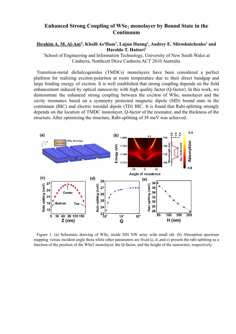
Enhanced Strong Coupling of WSe2 monolayer by Bound State in theContinuum
Ibrahim A. M. Al-Ani 1, Khalil As'Ham1, Lujun Huang1, Andrey E. Miroshnichenko1 andHaroldo T. Hattori1
1School of Engineering and Information Technology, University of New South Wales atCanberra, Northcott Drive Canberra ACT 2610 Australia
Transition-metal dichalcogenides (TMDCs) monolayers have been considered a perfectplatform for realizing exciton-polariton at room temperature due to their direct bandgap andlarge binding energy of exciton. It is well established that strong coupling depends on the fieldenhancement induced by optical nanocavity with high quality factor (Q-factor). In this work, wedemonstrate the enhanced strong coupling between the exciton of WSe2 monolayer and thecavity resonance based on a symmetry protected magnetic dipole (MD) bound state in thecontinuum (BIC) and electric toroidal dipole (TD) BIC. It is found that Rabi-splitting stronglydepends on the location of TMDC monolayer, Q-factor of the resonator, and the thickness of thestructure. After optimizing the structure, Rabi-splitting of 38 meV was achieved.
Figure 1. (a) Schematic drawing of WSe2 inside SIN NW array with small slit. (b) Absorption spectrummapping versus incident angle theta while other parameters are fixed (c, d ,and e) present the rabi-splitting as afunction of the position of the WSe2 monolayer, the Q-factor, and the height of the nanowires, respectively.
Green Chemistry – Manufacturing Novel Nanomaterials in Water
Yon Ju-Nam,1 Alejandro Fabrega,2 Wanisa Mohammed,3 and Stefana Popescu,1Jesus Ojeda Ledo,1 Mohamed Merroun2
1Swansea University, Faculty of Science and Engineering, United Kingdom2Universidad de Granada, Department of Microbiology, Spain
3Sebha University, Department of Chemistry, [email protected]
Significant effort has been made to generate reliable synthetic methods to produce metalnanoparticles, and the development of greener syntheses is particularly desirable in order toenable the use of these type of nanomaterials in a wider range of applications. This talk willcover different aspects of this research area, and more specifically be based on a green one-potsynthesis of novel functionalised metal nanoparticles in water for their potential use inbiomedical applications, and its comparison with the corresponding traditional method andprocess mass intensity (PMI) calculations. In our system, organophosphorus ligands play keyroles as coating and reducing agent at the same time [1]. The green synthesis of functionalisedmetal nanoparticles was carried out in water and at different temperatures, ranging from 60 and100°C. UV-Visible, XPS spectroscopic and TEM studies have shown that the organophosphorusligands bind to the surface of metal nanoparticles, which are typically around 5 nm in diameter[2]. These highly stable nanomaterials can offer a great opportunity in the design of novelbiorecognition and drug delivery systems.
References[1] Y. Ju-Nam, Y.-S. Chen, J.J. Ojeda, D.W. Allen, N.A. Cross, P.H. Gardiner, and N.
Bricklebank, RSC Advances 2 (2012) 10345-10351.[2] Y. Ju-Nam, W. Abdusalam-Mohammed, J.J. Ojeda. Faraday Discussions 186 (2016) 77-93.
Synergistic antibacterial effect of silver nanoparticles combined withantibiotics: Mechanism study using fluorescence microscopy
Lucie Válková1,2, Lucie Hochvaldová1, Martin Mistrík3, Renata Večeřová4, Milan Kolář4, LiborKvítek1 and Aleš Panáček1
1 Department of Physical Chemistry, Faculty of Science, Palacký University, 17. listopadu 12,77146 Olomouc, Czech Republic
2 Department of Medical Biophysics, Faculty of Medicine and Dentistry, Palacký University,Hněvotinská 3, 77515 Olomouc, Czech Republic
3 Institute of Molecular and Translational Medicine, Faculty of Medicine and Dentistry, PalackýUniversity and University Hospital in Olomouc, Hněvotínská 5, 77515 Olomouc, Czech
Republic4 Department of Microbiology, Faculty of Medicine and Dentistry, Palacký University,
Hněvotínská 3, 77515 Olomouc, Czech RepublicEmail: [email protected]
Silver nanoparticles (NPs) strongly enhance antibacterial activity against broad spectrum ofbacterial strains when combined with antibiotics [1]. However, the mechanism of theirsynergistic effect is not yet fully understood and may vary for different bacterial strains andantibiotics [2]. In this work we present a mechanism of the combined antibacterial effect of silverNPs and vancomycin against E. faecium strain sensitive and resistant to vancomycin. For thefirst time the synergistic mechanism was described based on the localization of fluorescentlabeled silver NPs and vancomycin-BODIPY FL fluorescent conjugate using high resolutionfluorescence microscopy. It can be concluded that the synergistic effects of silver NPs andvancomycin mainly consists in the mutual disruption of the permeability and strength of the cellwall, which becomes unstable and loses its strength and it is subsequently disrupted anddetached. In addition, silver NPs significantly deform bacterial DNA, which also significantlycontributes to the inhibition of bacterial growth. This work can help to better understand themechanisms of synergistic effects of silver NPs with antibiotics against resistant bacteria whichrepresent an important finding for potential approach to an effective fight against the unresolvedproblem of an increasing resistance of pathogenic bacteria against traditional antibiotics.
The authors gratefully acknowledge the support provided by the project No. 19-22720S of theCzech Science Foundation.
References[1] A. Panáček. et al, Colloids Surfaces B Biointerfaces 142 (2016) 392[2] S. Kumar, M. M. Mukherjee, M. F. Varela, Int. J. Bacteriol. 2013, (2013) ID 204141
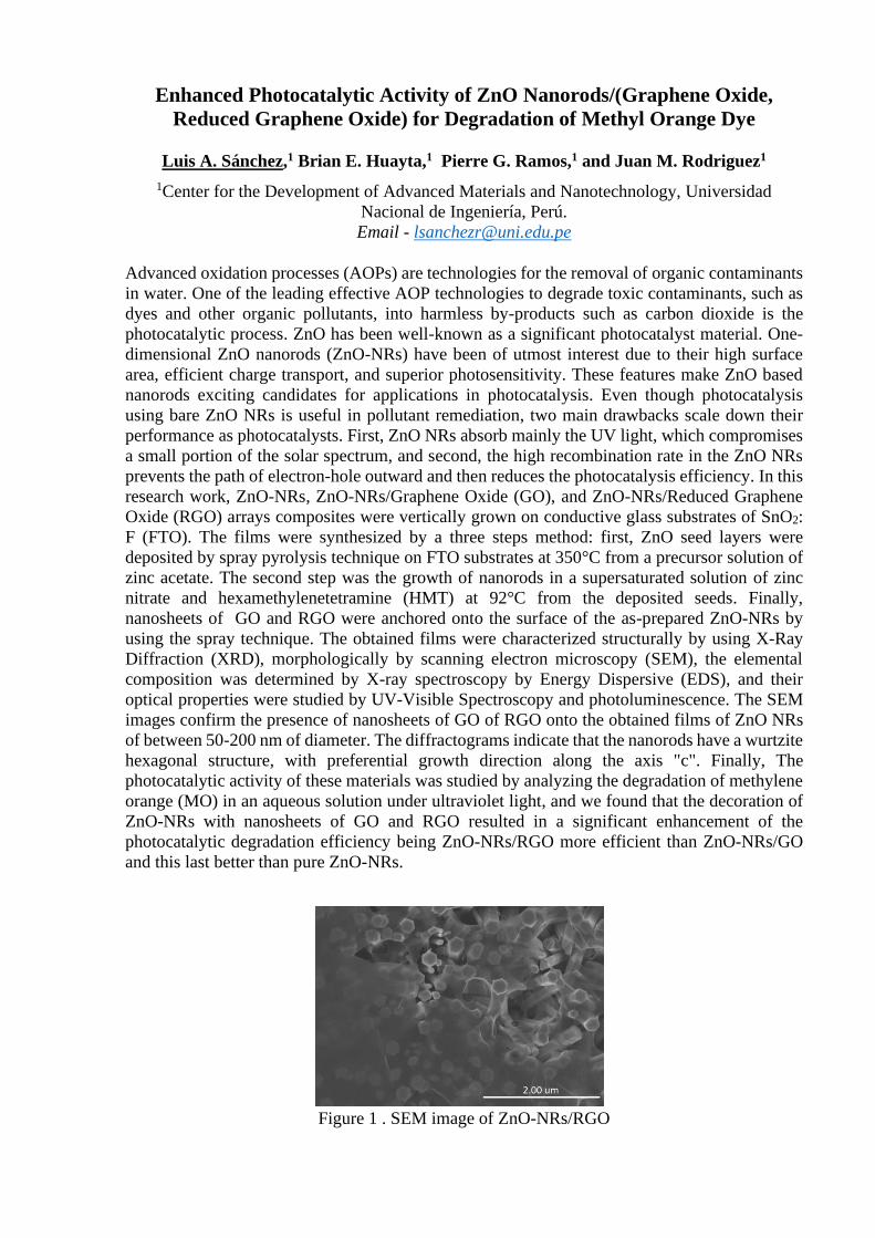
Enhanced Photocatalytic Activity of ZnO Nanorods/(Graphene Oxide,
Reduced Graphene Oxide) for Degradation of Methyl Orange Dye
Luis A. Sánchez,1 Brian E. Huayta,1 Pierre G. Ramos,1 and Juan M. Rodriguez1
1Center for the Development of Advanced Materials and Nanotechnology, Universidad
Nacional de Ingeniería, Perú.
Email - [email protected]
Advanced oxidation processes (AOPs) are technologies for the removal of organic contaminants
in water. One of the leading effective AOP technologies to degrade toxic contaminants, such as
dyes and other organic pollutants, into harmless by-products such as carbon dioxide is the
photocatalytic process. ZnO has been well-known as a significant photocatalyst material. One-
dimensional ZnO nanorods (ZnO-NRs) have been of utmost interest due to their high surface
area, efficient charge transport, and superior photosensitivity. These features make ZnO based
nanorods exciting candidates for applications in photocatalysis. Even though photocatalysis
using bare ZnO NRs is useful in pollutant remediation, two main drawbacks scale down their
performance as photocatalysts. First, ZnO NRs absorb mainly the UV light, which compromises
a small portion of the solar spectrum, and second, the high recombination rate in the ZnO NRs
prevents the path of electron-hole outward and then reduces the photocatalysis efficiency. In this
research work, ZnO-NRs, ZnO-NRs/Graphene Oxide (GO), and ZnO-NRs/Reduced Graphene
Oxide (RGO) arrays composites were vertically grown on conductive glass substrates of SnO2:
F (FTO). The films were synthesized by a three steps method: first, ZnO seed layers were
deposited by spray pyrolysis technique on FTO substrates at 350°C from a precursor solution of
zinc acetate. The second step was the growth of nanorods in a supersaturated solution of zinc
nitrate and hexamethylenetetramine (HMT) at 92°C from the deposited seeds. Finally,
nanosheets of GO and RGO were anchored onto the surface of the as-prepared ZnO-NRs by
using the spray technique. The obtained films were characterized structurally by using X-Ray
Diffraction (XRD), morphologically by scanning electron microscopy (SEM), the elemental
composition was determined by X-ray spectroscopy by Energy Dispersive (EDS), and their
optical properties were studied by UV-Visible Spectroscopy and photoluminescence. The SEM
images confirm the presence of nanosheets of GO of RGO onto the obtained films of ZnO NRs
of between 50-200 nm of diameter. The diffractograms indicate that the nanorods have a wurtzite
hexagonal structure, with preferential growth direction along the axis "c". Finally, The
photocatalytic activity of these materials was studied by analyzing the degradation of methylene
orange (MO) in an aqueous solution under ultraviolet light, and we found that the decoration of
ZnO-NRs with nanosheets of GO and RGO resulted in a significant enhancement of the
photocatalytic degradation efficiency being ZnO-NRs/RGO more efficient than ZnO-NRs/GO
and this last better than pure ZnO-NRs.
Figure 1 . SEM image of ZnO-NRs/RGO
References
[1] S. N. Ahmed and W. Haider, “Enhanced Photocatalytic Activity of ZnO-Graphene
Oxide Nanocomposite by Electron Scavenging,” Catalysts 2021, Vol. 11, Page 187,
vol. 11, no. 2, p. 187, Jan. 2021.
[2] J. Qin et al., “A facile synthesis of nanorods of ZnO/graphene oxide composites with
enhanced photocatalytic activity,” Applied Surface Science, vol. 321, pp. 226–232,
Dec. 2014.
[3] X. Liu et al., “UV-assisted photocatalytic synthesis of ZnO–reduced graphene oxide
composites with enhanced photocatalytic activity in reduction of Cr(VI),” Chemical
Engineering Journal, vol. 183, pp. 238–243, Feb. 2012.
[4] Y. Peng, J. Ji, and D. Chen, “Ultrasound assisted synthesis of ZnO/reduced graphene
oxide composites with enhanced photocatalytic activity and anti-photocorrosion,”
Applied Surface Science, vol. 356, pp. 762–768, Nov. 2015.
[5] P. Huo et al., “Incorporation of N–ZnO/CdS/Graphene oxide composite photocatalyst
for enhanced photocatalytic activity under visible light,” Journal of Alloys and
Compounds, vol. 670, pp. 198–209, Jun. 2016.
[6] S. Prabhu et al., “Synthesis, structural and optical properties of ZnO spindle/reduced
graphene oxide composites with enhanced photocatalytic activity under visible light
irradiation,” Optical Materials, vol. 79, pp. 186–195, May 2018.
[7] S. Prabhu et al., “Enhanced photocatalytic activities of ZnO dumbbell/reduced
graphene oxide nanocomposites for degradation of organic pollutants via efficient
charge separation pathway,” Applied Surface Science, vol. 487, pp. 1279–1288, Sep.
2019.
Hybrid materials based on diatomite modified by gold nanoparticles:
fabrication and photoacoustic characterization
Julijana Cvjetinovic,1 Daniil V. Nozdriukhin,1 Maria A. Kirsanova,2 Pavel A. Somov,2
Alexey I. Salimon,2 Alexander M. Korsunsky,2,3 and Dmitry A. Gorin,1 1Center for Photonics and Quantum Materials, Skolkovo Institute of Science and Technology, 3
Nobel Str., Moscow, 121205, Russia 2Center for Energy Science and Technology, Skolkovo Institute of Science and Technology, 3
Nobel Str., Moscow, 121205, Russia 3Department of Engineering Science, University of Oxford, Oxford, OX1 3PJ, United Kingdom
The production of modern functional and structural hybrid materials using natural objects such
as unicellular diatoms microalgae as templates has become one of the fastest-growing research
areas. Here, we employed for the first time the combination of two approaches—layer-by-layer
assembly and freezing-induced loading—to fabricate hybrid materials based on diatomite,
composed of the remains of fossilized diatoms, and gold nanoparticles with an average size of 19
nm. To characterize the fabricated gold-coated diatomite structures, we applied the dynamic light
scattering method, absorbance spectroscopy, scanning (SEM), scanning transmission (STEM),
and transmission electron microscopy (TEM), Energy Dispersive X-Ray Analysis (EDX), and
raster scanning optoacoustic mesoscopy (RSOM) technique. The fabrication methods allowed us
to obtain different coverage of diatomite by gold nanoparticles, depending on the number of
applied layers. The photoacoustic signal excited at a wavelength of 532 nm increased with
increasing loading cycles up to three polyelectrolyte-gold nanoparticle bilayers, after which a
decrease in the signal intensity was observed. The hybrid materials based on diatomite modified
by gold nanoparticles can be used as surface-enhanced Raman scattering (SERS) substrates.

FUNCTIONAL MATERIALS BASED ON 1D AND QUASI-
1D STRUCTURES
7-10 December 2021Chimie ParisTech, Paris
InGaN nanostructures grown by MBE
George CirlinAlferov University, Saint-Petersburg 194021, Russia
Saint-Petersburg State University, Saint-Petersburg 198504, RussiaEmail: [email protected]
Keywords: III-N nanostructures, MBE, Si based substrateIII-N nanostructures are among the most promising candidates for ultraviolet and visible solid-state
lighting and renewable energy sources. GaN nanowires (NWs) are well known, most of the growthparameters are well studied. An issue of the unintentional doping due to high growth temperature is stillunder the examination. In the first part of the talk we will focus on the substrate influence (Si or SiC/Si)on the Si ascending doping of the NWs. Another part of the talk will be dedicated on less studied system,namely InGaN nanowires and nanoflowers grown on Si and SiC/Si substrates. We will show that theelastic strain relaxation on the nanowire sidewalls can help to overcome the InGaN miscibility gap andachieve better band-gap tunability than in a bulk alloy. It appears that InGaN/Si NWs system is quitedelicate and a change in the growth temperature of just ~20 degrees Celsius leads to a significant changein structural properties of nanowires and shifts the photoluminescence emission from orange to blue. Wewill also demonstrate that InGaN NWs under appropriate growth conditions would form a core/shellstructure where In content in the core is an order of magnitude higher than that in the core one. A novelapproach to the growth of InGaN NWs at a small temperature gradient of over the substrate surface hasdemonstrated the potential for the implementation of multi-colour light emitters monolithically grown ona Si substrate. In addition, we will show that InGaN nanowires on SiC/Si have a lower indium content(about 10%) compared to the nanowires grown on Si under similar growth conditions except of thesubstrate itself.
GaP nanowires: versatile platform for nanophotonics
Alexey D. BolshakovMIPT, Dolgoprudny, Russia
Alferov University, St Petersburg, RussiaE-mail: [email protected]
Low-dimensional nanostructures have proven themselves as very efficient light emitters due toboth photonic and electronic spatial restriction. An iamportant example of the nanostructuresused in fabrication of the nanophotonic elements are semiconductor nanowires (NWs). Animportant property of the NWs is the ability to vary their crystallinity and chemical compositionboth in vertical (axial heterostructures) and lateral (core-shell heterostructures) directionsproviding growth protocols unavailable with the other structure geometries. One of the mostintriguing possibilities for nanophotonics and optoelectronics relates to synthesis of verticallystacked nanosized insertions in NW. This allows control over the coupling of the emission andincrease of the quantum efficiency due to resonant properties of the NW acting as an opticalcavity.
Gallium phosphide (GaP) is a peculiar semiconductor material. In terms of the opticalproperties GaP is lossless pretty much over the entire visible and IR ranges and optically densemaking it priceless for fabrication of waveguides and cavities. Despite being indirect bandgapmaterial, GaP can be diluted with other isovalent elements such as As, N, Al, In etc. making itdirect bandgap. This chemical variation provides opportunities for fabrication of active photonicelements based on GaP NWs.
Here we report on the study of the micro- photoluminescence response generated in multiplenano-sized GaPAs insertions in GaP NW and discuss its anisotropic nature and spectralpeculiarities occurring due to the structure geometry.
Author thanks Russian Science Foundation (grant 20–72–10192).
Characterization of optical and nonlinear properties of individual GaPnanowires using optical tweezers
Alexey D. Bolshakov1,2*, Ivan Shishkin2, Andrey Machnev3, Mikhail I. Petrov2, DemidKirilenko4, Vladimir V. Fedorov1,5, Ivan S. Mukhin1,6,7 and Pavel Ginzburg3,8
1Nanotechnology Research and Education Centre, Alferov University2School of Physics, ITMO University
3Department of Physical Electronics, Electrical Engineering, Ramat Aviv4Ioffe Institute,
5Institute of Physics, Nanotechnology and Telecommunications, Peter the Great Saint PetersburgPolytechnic University,
6Faculty of Physics, St. Petersburg State University,7Faculty of Chemistry, St. Petersburg State University,
8Center for Photonics and 2D Materials, Moscow Institute of Physics and TechnologyEmail: [email protected]
Continuous demand for miniaturization of photonic devices attracts research interests towardsindividual nanostructures as elements of photonic circuits. Semiconductor nanowires beingself-assembled structures following bottom-up approach, offer certain advantages compared tomore conventional top-down techniques (like lithographic processing), such as high throughputof growth of multiple individual wires in a single process. So far nanowires were demonstratedas a platform for single-photon emitters1, detectors and converters2, nonlinear gates3 and manyothers.
III-V nanowires, such as GaP are commonly grown using epitaxial techniques and offerdistinctive advantages, such as flexible band-gap engineering4 and tailor-made electricalproperties5. Optical properties of individual nanowires can be obtained by cleaving anddepositing them in an optically transparent substrate, allowing to probe micro-PL, Raman, and,to an extent, darkfield scattering. However such planar arrangement complicates excitation alongthe wire axis, which allows it to probe linear and nonlinear processes, such as waveguidingmodes or second harmonic generation in a single nanowire. On the contrary, optical trappingallows to immobilize individual nanowires and to study their linear and nonlinear properties.6
Here we report on spectroscopic studies of individual GaP nanowires immobilized in opticaltraps. We explore correlations between nanowire’s geometry and its second harmonic responseboth experimentally and theoretically. An impact of the nanowire geometry on phase-matchingand efficiency of second harmonic response will be discussed.[1] Leandro, L.; Hastrup, J.; Reznik, R.; Cirlin, G.; Akopian, N. Resonant Excitation of Nanowire
Quantum Dots. npj Quantum Inf. 6 (1), 2020, 93[2] Krogstrup, P.; Jørgensen, H. I.; Heiss, M.; Demichel, O.; Holm, J. V.; Aagesen, M.; Nygard,
J.; Fontcuberta I Morral, Nat. Photonics 7 (4) 2013, 306-310[3] Falk, A. L.; Koppens, F. H. L.; Yu, C. L.; Kang, K.; De Leon Snapp, N.; Akimov, A. V.; Jo,
M. H.; Lukin, M. D.; Park, H. Nat. Phys., 5 (7), 2009, 475–479.[4] Kuykendall, T.; Ulrich, P.; Aloni, S.; Yang, P. Nature Materials.6 2007, 951-956.[5] Shugurov, K. Y.; Mozharov, A. M.; Bolshakov, A. D.; Fedorov, V. V.; Sapunov, G. A.;
Shtrom, I. V.; Uvarov, A. V.; Kudryashov, D. A.; Baranov, A. I.; Yu Mikhailovskii, V.;Neplokh, V. V.; Tchernycheva, M.; Cirlin, G. E.; Mukhin, I. S. Nanotechnology 31 (24) 2020.
[6] Wang, F.; Reece, P. J.; Paiman, S.; Gao, Q.; Tan, H. H.; Jagadish, C. Nano Lett. 11 (10) 2011,4149-4153
Dopants impact on planar GaAs nanowires growth
Nickolay V. Sibirev1,2
1 The Faculty of Physics, Saint-Petersburg State University, 199034, St. Petersburg, Russia
Email - [email protected]
Semiconductor nanowires (NWs) are widely considered as promising building blocks for novel
opto- and nanoelectronic devices. Formation of p-n junction in nanowires and assembling the NWs
array are key steps for the device fabrication. Usually, these processes are considered separately.
Here we would like to discuss about the influence of dopants on growth of planar NWs via
Vapor-Liquid-Solid mechanism (VLS). In the present study we investigate the dopants impact on
the shape and growth direction of planar NWs. We focused on the following aspects of planar
nanowire growth: in-plane rotation of NW marked R in Figure 1 and NW detachment marked D
in Figure 1.
Fig. 1. Change of nanowire growth direction caused by the change of doping level: in-plane
rotation is marked with R and nanowire detachment is marked with D.
We propose a theoretical model based on the nucleation limited mode of NW growth. Our main
results can be formulated in the following way: NW rotation and detachment are caused by the
change of the catalyst droplet surface energy and volume. An unwanted change of NW dopant
level growth direction should be compensated by variation of NW growth rate and V/III ratio.
Optical sensing of organic solvents vapor with lead halide perovskite
nanowire lasers on one-dimensional polymer nanograting
Daria I. Markina,1 Anatoly P. Pushkarev,1 and Sergey V. Makarov1
1 School of Physics and Engineering, ITMO University, Russia
Email – [email protected]
The rapid development of the chemical industry in recent decades has induced an increase of the
chemical safety standards. Substances that are harmful in low concentrations or have a cumulative
effect on human health, such as volatile organic solvents - acetone, toluene, chloroform, and others
- require special attention. The need for their usage in the wide range of chemical processes
necessitates the creation of cost-effective and ultra-high sensitive gas sensors. Ideal candidates in
this sense are lead-halide perovskite nanostructures known for their unique optical properties,
including high-Q lasing at low thresholds [1]. Perovskite nanolasers demonstrate a sensitive
optical response to small changes in the effective refractive index (neff) of the surrounding medium
when integrated with nanostructured substrates. A further improvement in sensitivity is associated
with the ability of the nanostructured substrate to change its geometric parameters and,
consequently, neff by absorbing analyte molecules [2].
In this work, we report on a theoretical study of the mechanism for sensing of organic solvents
vapor in the air with CsPbBr3 nanowire (NW) lasers on a polystyrene nanograiting (PS NG). In
our model, the absorption of analyte molecules causes an increase in the width of the PS NG ridges
and, consequently, an increase in the effective refractive index under the NW laser. A small change
of neff affects the spectral position and Q-factor of the laser mode (Fig.1). It has been shown that
for a NW laser on a nanograting with a period of 280 nm, a ridge width of 180 nm, and a depth of
110 nm, even a small enlargement of the ridge width by 5 nm leads to a shift of the high-order
laser mode (TE22) by 0.3 nm to the long-wavelength region of the spectrum. These results can be
useful for further progress in the field of optical gas sensing based on perovskite nanostructures.
Figure.1. Schematic illustration of vaporized solvent detection with CsPbBr3 NW laser placed on PS NG.
References
[1] D.I. Markina, et.al. Nanophotonics 9 (2020) 3977-3984
[2] E. J. Kappert, et.al. Journal of membrane science 569 (2019) 177-199
Acknowledgement
This work was supported by RFBR (project no. 20-33-90212).
Gallium phosphide nanowires for biological ammonia concentrationsdetection
Valeriy M. Kondratev,1 Alexey Kuznetsov,1 Sergey V. Fedina,1 Rodion R. Reznik,1, 2
Svetlana S. Nalimova,3 Vyacheslav A. Moshnikov,3 George E. Cirlin1, 3, 4, 5 and Alexey D.Bolshakov 1, 4, 6
1Alferov University, St. Petersburg, 194021, Russia2Saint Petersburg State University, St. Petersburg, 199034, Russia
3Saint Petersburg Electrotechnical University “LETI”, St. Petersburg, 197376, Russia4ITMO University, St. Petersburg, 197101, Russia
5Institute for Analytical Instrumentation RAS, St. Petersburg, 190103, Russia6Moscow Institute of Physics and Technology, Moscow, 117303, Russia
Email: [email protected]
Ammonia is found both in nature and in the human body, and its detection is very important inbiology and medicine as well as in environmental monitoring systems. Concentration of theorder of 1 ppm of ammonia produced with human breath is the biological marker of pathologicalchanges in the body, while ammonia in concentrations of the order of 100 ppm is toxic andhazardous. Among modern methods for liquid probes analysis, voltammetry methods are mostlyoften used. Classical sensor devices based on metal oxides, which have proven themselves in gassensing, are widely presented [1–4]. To improve the sensitivity features of the semiconductorbased adsorption sensors, structures with developed area should be used. Despite the high ratioof the surface area to volume of epitaxial nanostructures and the pronounced conductivityfeatures of quasi–1D structures compared to bulk materials, the adsorption properties of III–VNWs and their correlation with electrical characteristics are still poorly studied [5–6].
This work is aimed at fabrication and study of precise, technological and relatively cheapammonia sensors compatible with a liquid medium. We use GaP epitaxial nanowires (NWs) asadsorption elements for ammonia sensors fabricated via a simple protocol. The device propertieswith addition of ammonia to the reference medium (water) are studied in terms of change insensor impedance spectrum. The potential of electrical impedance spectroscopy forcharacterization of interaction between low–dimensional nanostructures and environment isshown. Ammonia sensors based on III–V NWs have been developed, and a physicalinterpretation of their impedance spectra in the presence of water and ammonia is given.GaP–based devices exhibit sufficient response to the ammonia presence with the detection limitlower than 2,5ppm.
References[1] Nalimova S S, Kondratev V M, Ryabko A A, Maksimov A I and Moshnikov V A 2020
Journal of Physics: Conference Serial 012033 1658.[2] Nalimova S S, Kondrat'ev V M 2020 IEEE Conference of Russian Young Researchers in
Electrical and Electronic Engineering (EIConRus) 987.[3] Levkevich E A, Maksimov A I, Kirillova S A, Nalimova S S, Kondrat'ev V M and Semenova
A A 2020 IEEE Conference of Russian Young Researchers in Electrical and ElectronicEngineering (EIConRus) 984.
[4] Kondratev V M, Bolshakov A D and Nalimova S S 2021 IEEE Conference of Russian YoungResearchers in Electrical and Electronic Engineering (ElConRus) 1163.
[5] Kang D, Ko J H, Bae E, Hyun J, Park W, Kim B K, Kim J J and Lee C 2004 J. Appl. Phys.96 7574.
[6] Arora P, Sindhu A, Dilbaghi N, Chaudhury A 2013 Appl Nanosci 3 363.
Influence of plasmon effects on the electromagnetic waves localization in GaPnanowires
Alexey Kuznetsov,1 Sergei S. Fedina1, Konstantin P. Kotlyar3, Alexey I. Lihachev2,Rodion R. Reznik1,3 and Alexey D. Bolshakov1,4,5
1SPbAU RAS, Russia2Ioffe Institute RAS, Russia
3Institute of the Analytical Instrumentation RAS, Russia4ITMO University, Russia
5Moscow Institute of Physics and Technology, RussiaE-mail: [email protected]
The main object of this study is gallium phosphide (GaP) NWs grown by molecular beamepitaxy (MBE) on Si (111). The choice of this material is justified by the low value of theabsorption coefficient in almost the entire visible range [1]. Thus, it becomes possible to designpassive optical elements with great freedom in the choice of size and geometry. The developmentof a waveguide nanostructure of small size requires high localization of the electromagneticwave. One of the promising methods for controlling light at nanoscale is the plasmon effects.
Numerical simulation showed [2] that the localization of the incident wave field in GaP NWs isenhanced in the presence of a gallium droplet. To confirm the simulation results experimentally,the method of Raman scattering spectroscopy with local excitation was used. To carry outmeasurements, GaP NWs with a length and diameter of about 4 μm and 120 nm respectivelypossessing a gallium growth catalyst droplet were transferred from the growth substrate andplanarized on a glass substrate. To determine the location of each NW, gold marks with anindium-tin oxide sublayer, visible through an optical microscope, were preliminarily depositedon the glass. Further, SEM images were obtained to determine the geometry of the studied NWs.
After the SEM procedure, the substrate with the NWs was placed in a Raman spectroscopysetup, where the scattering response was mapped over the entire surface of severalnanostructures, including those with different polarization orientations of the laser beam.Scanning was performed through a hundredfold objective (N.A. = 0.9) with a step of 40 nm. Thelaser spot size (532 nm) was about 1 μm. According to the mapping results, an increase in theintegral signal from 450 to 3000 counts was registered as we approach the gallium dropletinterface. Maps obtained with different polarizations showed that with polarization parallel to theNW axis, the signal intensity is much higher. In addition to the enhancement of Raman scatteringdue to plasmon effects, the influence of polarization on the photoluminescence intensity of singleGaP NWs with direct-gap GaPAs inserts was investigated. In this case, the spectra weremeasured under excitation of one of the end faces with a subsequent change in the direction ofpolarization. The experiment also showed a significant increase in intensity with parallelpolarization.
Authors thanks the Ministry of Science and Higher Education of the Russian Federation (grant№ FSRM–2020–00011) for support of nanostructures optical characterization and RussianScience Foundation (grant 20–72–10192) for support of theoretical models design.
References[1] D. E. Aspnes, A. A. Studna, Phys. Rev. B Condens. Matter. 27 (1983) 985[2] P. Roy, A. D. Bolshakov, J. Phys. D Appl. Phys. B 53 (2020) 295101
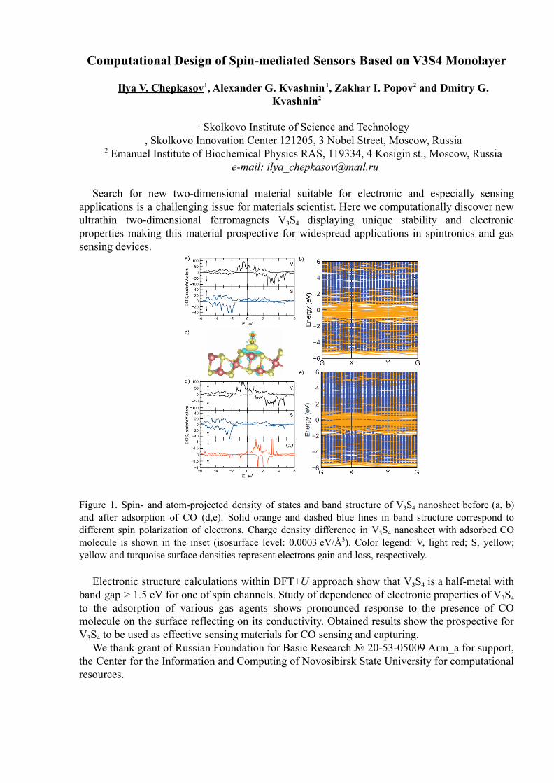
Computational Design of Spin-mediated Sensors Based on V3S4 Monolayer
Ilya V. Chepkasov1, Alexander G. Kvashnin1, Zakhar I. Popov2 and Dmitry G.Kvashnin2
1 Skolkovo Institute of Science and Technology, Skolkovo Innovation Center 121205, 3 Nobel Street, Moscow, Russia
2 Emanuel Institute of Biochemical Physics RAS, 119334, 4 Kosigin st., Moscow, Russiae-mail: [email protected]
Search for new two-dimensional material suitable for electronic and especially sensingapplications is a challenging issue for materials scientist. Here we computationally discover newultrathin two-dimensional ferromagnets V3S4 displaying unique stability and electronicproperties making this material prospective for widespread applications in spintronics and gassensing devices.
Figure 1. Spin- and atom-projected density of states and band structure of V3S4 nanosheet before (a, b)and after adsorption of CO (d,e). Solid orange and dashed blue lines in band structure correspond todifferent spin polarization of electrons. Charge density difference in V3S4 nanosheet with adsorbed COmolecule is shown in the inset (isosurface level: 0.0003 eV/Å3). Color legend: V, light red; S, yellow;yellow and turquoise surface densities represent electrons gain and loss, respectively.
Electronic structure calculations within DFT+U approach show that V3S4 is a half-metal withband gap > 1.5 eV for one of spin channels. Study of dependence of electronic properties of V3S4
to the adsorption of various gas agents shows pronounced response to the presence of COmolecule on the surface reflecting on its conductivity. Obtained results show the prospective forV3S4 to be used as effective sensing materials for CO sensing and capturing.
We thank grant of Russian Foundation for Basic Research № 20-53-05009 Arm_а for support,the Center for the Information and Computing of Novosibirsk State University for computationalresources.
THZ OPTOELECTRONICS AND PHOTONICS
7-10 December 2021Chimie ParisTech, Paris
Semiconductor Surface States: Nanoscale Wavelength Converters
Mona Jarrahi 1University of California Los Angeles
Surface states generally degrade semiconductor device performance by raising the charge injection
barrier height, introducing localized trap states, inducing surface leakage current, and altering the
electric potential. Therefore, there has been an endless effort to use various surface passivation
treatments to suppress the undesirable impacts of the surface states. We recently demonstrated that
the giant built-in electric field created by the surface states can be harnessed to enable passive
wavelength conversion with unprecedented efficiencies without utilizing any nonlinear optical
phenomena. Photo-excited surface plasmons are coupled to the surface states to generate an
electron gas, which is routed to a nanoantenna array through the giant electric field created by the
surface states. The induced current on the nanoantennas, which contains mixing product of
different optical frequency components, generates radiation at the beat frequencies of the incident
photons. We utilized the unprecedented functionalities of plasmon-coupled surface states to
demonstrate passive wavelength conversion of nanojoule optical pulses at a 1550 nm center
wavelength to terahertz regime with record-high efficiencies that exceed nonlinear optical methods
by 4-orders of magnitude. The presented scheme can be used for optical wavelength conversion
to different parts of the electromagnetic spectrum ranging from microwave to far-infrared regimes
by using appropriate optical beat frequencies.
References
[1] D. Turan, P. K. Lu, N. T. Yardimci, Z. Liu, L. Luo, J.-M. Park, U. Nandi, J. Wang, S. Preu,
M. Jarrahi, Nature Communications 12 (2021) 4641
Billiard-like resonances in metallic nanostructures and their use for efficientultrafast nonlinear optics
Ihar Babushkin,1,2,3 1Institute of Quantum Optics, Leibniz University, Welfengarten 1, 30167 Hannover, Germany
2Max Born Institute, Max Born Str. 2a, 12489 Berlin, Germany3Cluster of Excellence PhoenixD (Photonics, Optics, and Engineering – Innovation Across
Disciplines), Hannover, GermanyEmail – [email protected]
As it is known, optical properties of metallic nanostructures may demonstrate resonantbehavior because of light-induced movement of the electronic cloud close to the surface. Severaltypes of such resonances exist, such as Mie resonances, anapole modes [1], bound states incontinuum [2] and others. These resonances are related rather to light than to the boundedmotion of electrons in metals and lead to optical nonlinearities, leading to, for instance, harmonicgeneration. Another source of nonlinearities in optics are the resonances, appearing due toquantum confinement of electrons in the finite volume of a nanoparticle. In this case, electron istrapped in a cavity formed by the nanostructure walls – the picture typical also for “quantumbilliard” framework [3]. When many of such electronic levels are involved, the statistics of levelspacings reveals a peak close to zero frequency. That is, many closely spaced resonances may, incertain sense, work as a single composite resonance. Although such resonances were observed insemiconductor quantum dots, they were neither considered nor observed in metallic particles.This sounds logical, since in metals the width of every particular possible transition is huge andmany of such broad resonances, closely spaced, should compose rather a continuous band than asingle resonance.
Here we show that, quite in contrary to the above mentioned intuition, many broad resonances,arising due to quantum confinement of electrons inside metallic nanostructures and nanoclustersform a single “super-resonance”. Such super-resonance typically lies in the low, mid-infrared(MIR) or terahertz (THz) frequency range and, as we show, plays a critical role in the opticalresponse at those frequencies. Here we show that these resonances can be very useful in ultrafastnonlinear optics. We demonstrate, that the difference frequency mixing (DFG) process with thesignal in MIR and THz, can lead to a efficient broad-band conversion at the nanometer-scalepropagation distances. .
References
[1] A. E Miroshnichenko, et al, Nature Communications 6, 1 (2015).[2] Chia Wei Hsu, Bo Zhen, A Douglas Stone, John D Joannopoulos, and Marin
Soljačić, Nature Reviews Materials 1, 1 (2016).[3] Hans-Jürgen Stöckmann, Quantum Chaos: An Introduction (Cambridge
University Press, New York, USA, 1999).
Large HgTe nanocrystals for THz technology
J. Mangeney1, T. Apretna1, S. Massabeau1, C. Gréboval2, N. Goubet2, J. Tignon1, S.Dhillon1, F. Carosella1, R. Ferreira1 and E. Lhuillier2
1 Laboratoire de Physique de l’Ecole Normale Supérieure, ENS, Université PSL, CNRS, Sorbonne Université, Université Paris-Diderot, Sorbonne Paris Cité, Paris, France Paris.
2 Sorbonne Université, CNRS, Institut des NanoSciences de Paris, 4 place Jussieu, 75005 Paris, France.
Email:[email protected]
Semiconductor nanocrystals (NCs) raise more and more interest as they combine size-tuneable electronic energy levels with easy processing and transferability. They appear very promising materials for many optoelectronic applications in the visible and infrared range such as bio-labelling, single photon sources and light sources for display and low-cost infrared sensors. However, very little work has to date been focused on their potential for THz technology [1]. Among the various NCs, mercury telluride (HgTe) is an ideal material to expand the optical features towards the THz spectral range because it is a semimetal in the bulk with zero band gap. Here, we present the optical properties of self-doped large HgTe NCs in the THz spectral range. By combining microscopic modelling and measurements based on THz time-domain spectroscopy and Fourier Transform Infrared spectroscopy, we demonstrate a broad THz absorption resonance centred at ≈4.5 THz, which relies on intraband excitations of individual carriers. Our analysis reveals the absence of collective excitations in their THz optical response. Furthermore, using optical pump-THz probe experiments, we report on carrier dynamics at low energy as long as 6 ps in these self-doped large HgTe NCs [2]. We highlight evidence that Auger recombination is irrelevant in this system and attribute the main carrier recombination process to direct energy transfer from the electronic transition to the ligand vibrational modes and to nonradiative recombination assisted by surface traps. Our study opens interesting perspectives to exploit large HgTe NCs for quantum engineering at THz frequencies and for the development of THz photodetectors and emitters.
References
[1] N. Goubet, A. Jagtap, C. Livache, B. Martinez, H. Portalès, X. Zhen Xu, R. P. S. M. Lobo,B. Dubertret and E. Lhuillier, J. Am. Chem. Soc., 140, 15, 5033 (2018)
[2] T. Apretna, S. Massabeau, C. Gréboval, N. Goubet, J. Tignon, S. Dhillon, F. Carosella, R.Ferreira, E. Lhuillier and J. Mangeney. Nanophotonics, 10, 2753 (2021).
How to use terahertz emission spectroscopy and imaging
in real onsite semiconductor R&D scenes
Masayoshi Tonouchi
Osaka University, Japan
Terahertz emission spectroscopy (TES) and imaging (LTEM) are fundamentally different from
THz-TDS. THz-TDS is used to estimate the complex refractive index of materials at THz
frequencies, whereas TES discusses the emission mechanism and discloses the ultrafast optical
responses of materials. Although one can observe the THz emission from a variety of materials
and discuss their ultrafast carrier dynamics [1,2], killer applications for the large market are still
missing. In this presentation, we provide hints on how to use TES and LTEM in real onsite
semiconductor R&D scenes. To attract many scientists and engineers in the field, we have to
provide them simple pictures of what we measure and characterize from the signals. Recently we
have reported such simplified descriptions for the THz emission from semiconductor surfaces and
MOS/MIS structures[3,4], which explain the observed properties well and make it clear how we
can use the THz emission properties to characterize semiconductor parameters [5,6]. Thanks to
them, we can have much higher expectations of TES and LTEM for various applications, such as
wafer-scale characterization of passivation on semiconductors, wide bandgap semiconductor
properties, and 3D LSI development [7-11].
References
[1] D. S. Rana and M. Tonouchi, Adv. Opt. Mater. 8 (2020.)1900892
[2] F. R. G. Bagsican, et al., Nano Lett. 20 (2020)3098
[3] M. Tonouchi, J. Appl. Phys. 127(2020)245703
[4] D. Yang and M. Tonouchi, J. Appl. Phys. 130 (2021)055701
[5] T Mochizuki, et al., Appl. Phys. Lett. 110 (2017)163502,
[6] T Mochizuki, et al., J. Appl. Phys. 125 (2019)151615,.
[7] K. Yamahara et al., Sci. Rep. 10 (2020) 14633
[8] H. Jiang et al., Photonics, 7 (2020)73
[9] A Mannan, et al., Adv. Opt. Mater. 9 (2021) 2100258
[10] H. Nakanishi, et al., J. Appl. Phys. 130 (2021)115305
[11] K.J.P. Jacobs, et al., Nat. Electron. 4 (2021) 202
Perfectly Absorbing Optical Metasurfaces for Terahertz Applications
O. Mitrofanov,1,2 L.L. Hale,1 H. Jung,2,3 S.D. Gennaro,2,3
C. T. Harris,2,3 T.S. Luk,2,3 S.J. Addamane,2,3 J.L. Reno,2,3 and I. Brener2,3
1 University College London, UK2 Center for Integrated Nanotechnologies, Sandia National Laboratories, USA
3 Sandia National Laboratories, [email protected]
Integration of plasmonic nanostructures and optical metasurfaces into photoconductive THzsources and detectors over the past several years has demonstrated the potential of photonicsengineering for improving the efficiency and sensitivity of key THz technologies [1-7]. Thephotoconductive antenna (PCA) THz detectors is one of these technologies and it is widely usedin THz spectroscopy and imaging research. Recent research in the area of PCAs have focusedprimarily on design and integration of plasmonic nanostructures, including interdigitated metalliccontacts, nanorods and nanoantennas [8]. More recently, all-dielectric optical metasurfaces havebeen introduced as an alternative to plasmonic elements [3-6]. The metasurfaces can improve theefficiency of PCA detectors by exploiting the effect of perfect optical absorption, which enableshighly efficient ultrafast switching of the PCA. At the same time, the metasurface geometryallows engineering the electronic properties of PCA detectors and improve the detectorsensitivity [3]. In this presentation, we will discuss the impact of integrating all-dielectricmetasurfaces into the photoconductive channel on the electronic properties of THz detectors. Wewill show the THz PCA detectors with metasurfaces require only a μWatt-level optical gatepower for optimal operation [3]. The reduction of the power requirement opens possibilities forwider application of photoconductive THz detectors. We will also discuss how the perfectlyabsorbing metasurfaces can be exploited for generation of THz pulses.
AcknowledgmentThis work was supported by the U.S. Department of Energy, Office of Basic Energy Sciences,
Division of Materials Sciences and Engineering. Fabrication, optical, and in part THzexperiments were performed at the Center for Integrated Nanotechnologies, an Office of ScienceUser Facility operated for the U.S. Department of Energy (DOE) Office of Science. SandiaNational Laboratories is a multimission laboratory managed and operated by NationalTechnology and Engineering Solutions of Sandia, LLC., a wholly owned subsidiary ofHoneywell International, Inc., for the U.S. Department of Energy’s National Nuclear SecurityAdministration under contract DE-NA-0003525. O.M. and L.H. also acknowledge the support ofthe EPSRC.
References[1][2][3][4][5][6][7][8]
D. Turan et., Nat. Communications 12 (2001) 1.N.T. Yardimci and M. Jarrahi, Small 14 (2018) 1802437.L.L. Hale et al., Optics Lett. 46 (2021) 3159.O. Mitrofanov et al., APL Photonics 5 (2020) 101304.T. Siday et al., Nano Lett. 19, (2019) 2888.O. Mitrofanov et al., APL Photonics 3 (2018) 051703.S. Lepeshov et al., Sci. Rep. 8 (2018) 6624.O. Mitrofanov and I. Brener, Photoniques 101 (2020) 47.
Vacuum-field-induced THz transport gap in a carbon nanotube quantum dot
Takis KontosCNRS/ENS, [email protected]
The control of light-matter interaction at the most elementary level has become an importantresource for quantum technologies. Implementing such interfaces in the THz range remains anoutstanding problem. I will present how we couple a single electron trapped in a carbonnanotube quantum dot to a THz resonator. The resulting light-matter interaction reaches the deepstrong coupling regime that induces a THz energy gap in the carbon nanotube solely by thevacuum fluctuations of the THz resonator. This is directly confirmed by transport measurements.
This should be a particularly useful resource and perspective for THz quantum optics.
The absolute power meter of microwave radiation.
Vladimir AntonovRoyal Holloway University of London
A two-level quantum system, the qubit, can absorb or emit not more than one photon at atime. Using this fundamental property, we experimentally demonstrate how a qubit stronglycoupled to a microwave transmission line can be used as a sensor of the photon flux. Fourmethods can be used for the absolute calibration of power by measuring spectra of scatteredradiation from the two-level system. This type of sensor can be tuned to operate in a widefrequency range, and does not disturb the propagating waves when not in use. A range ofapplications are envisaged, in particular the sensor can be used to calibrate the attenuation of thetransmission lines inside dilution refrigerators when designing the quantum processor.
THz self-modulated graphene perfect absorber
Anastasios D. Koulouklidis1, Eudokia Kyriakou1,2, Christina Daskalaki1, Anna C.Tasolamprou1, M. Said Ergoktas3,4, Maria Kafesaki1,2, Coskun Kocabas3,4,5 and Stelios
Tzortzakis1,2,6
1Institute of Electronic Structure and Laser, FORTH, Greece2Department of Materials Science and Technology, University of Crete, Greece
3Department of Materials, University of Manchester, UK4National Graphene Institute, University of Manchester, Manchester, UK
5Henry Royce Institute for Advanced Materials, University of Manchester, UK6Science Program, Texas A&M University at Qatar, Qatar
Email: [email protected]
The era of terahertz (THz) wireless communication opens up ahead revealing the highimportance of the development of fast modulation devices operating at the THz part of theelectromagnetic spectrum. Towards this direction many devices based on graphene have beenproposed to modulate radiation at THz frequencies [1,2]. Here, we demonstrate a graphene basedTHz perfect absorber based on a cavity of monolayer graphene over a grounded dielectric thatcan be self-modulated using intense THz fields.
FIg. 1: (a) Schematic representation of the device. (b) Reflection spectra for various incident THz field strengths.The cavity (Fig. 1a) is formed by a 25 µm thick porous membrane sandwiched between a
monolayer graphene and a gold electrode. The porous membrane was soaked withroom-temperature ionic liquid electrolyte that allowed us to fine tune the Fermi energy ofgraphene with an external gating. For the excitation of the device a high power THz source basedon two-color filamentation was used, providing THz pulses with peak electric field strengthsreaching 700 kV/cm. At low THz field strengths the device achieves an absorption of -56 dB at2.3 THz that drops to -4 dB for high field strengths (Fig. 1b). This non-linear behaviour can beexplained by an interaction of the intense THz field with the free electrons in the graphene layer,resulting in strong modulation of its conductivity via carrier heating [3]. Our results demonstratethe implementation of ultrafast nonlinear THz modulators that can find applications in futuretelecommunications and flat optics modulation.
References[1] Nurbek Kakenov, Osman Balci, Taylan Takan, Vedat Ali Ozkan, Hakan Altan, and Coskun Kocabas.,
ACS Photonics, 3, (2016) 1531–1535.[2] Anna C Tasolamprou, Anastasios D Koulouklidis, Christina Daskalaki, Charalampos P Mavidis,
GeorgeKenanakis, George Deligeorgis, Zacharias Viskadourakis, Polina Kuzhir, Stelios Tzortzakis,Maria Kafesaki, Eleftherios N. Economou, and Costas M. Soukoulis., ACS Photonics, 6, (2019)720–727.
[3] Hassan A Hafez, Sergey Kovalev, Klaas Jan Tielrooij, Mischa Bonn, Michael Gensch, and DmitryTurchinovich., Advanced Optical Materials, 8, (2020) 1900771.
Terahertz scanning tunneling microscopy of atomically precise nanostructures
S. E. Ammerman1, V. Jelic1, Y. Wei1, V. N. Breslin1, M. Hassan1,N. Everett1, S. Lee1, Q. Sun2, C. A. Pignedoli2, P. Ruffieux2, R. Fasel2,3 and T. L. Cocker1
1Department of Physics and Astronomy, Michigan State University2Empa Swiss Federal Laboratories for Materials Science and Technology
3Department of Chemistry, Biochemistry and Pharmaceutical Sciences, University of [email protected]
Novel atomic-scale electronics operating at optical frequencies require new tools that cancharacterize them and inform device fabrication. Lightwave-driven scanning tunnelingmicroscopy is a promising new technique towards this purpose. By couplingfree-space-propagating single-cycle terahertz transients to an atomically sharp metal tip, itachieves simultaneous sub-nanometer and sub-picosecond spatio-temporal resolution [1–7].Here, we utilize terahertz scanning tunneling microscopy (THz-STM) and spectroscopy(THz-STS) to investigate seven-atom-wide graphene nanoribbons on an Au(111) surface andunveil highly localized wavefunctions that are inaccessible with conventional scanning tunnelingmicroscopy [7]. Three-dimensional tomographic THz-STM imaging of the electron densityreveals a faster vertical decay of the valence band compared to the conduction band, paving theway for ultrafast measurements of wavefunction dynamics in atomically precise nanostructures.Department of Chemistry, Biochemistry and Pharmaceutical Sciences, University of Bern, 3012Bern, Switzerland
References[1] T. L. Cocker et al. Nat. Photon. 7, 620–625 (2013).[2] T. L. Cocker et al. Nature 539, 263–267 (2016).[3] V. Jelic et al. Nat. Phys. 13, 591–598 (2017).[4] D. Peller et al. Nature 585, 58-62 (2020).[5] D. Peller et al. Nat. Photon. 15, 143–147 (2021).[6] T. L. Cocker et al. Nat. Photon. 15, 558–569 (2021).[7] S. Ammerman et al. Nat. Commun. (in Press).
Advances in Optics of Subcycle and Unipolar Pulses
Rostislav Arkhipov1,2, Mikhail Arkhipov1, Ihar Babushkin3, Anton Pakhomov1,Nikolay Rosanov1,2
1 St. Petersburg State University, 199034 St. Petersburg, Russia2Ioffe Institute, 194021, St. Petersburg, Russia
3Institute of Quantum Optics, Leibniz University Hannover, Cluster of ExcellencePhoenixD (Photonics, Optics, and Engineering – Innovation Across Disciplines),
Hannover, GermanyEmail – [email protected]
The important part of modern physics is the generation of extremely short pulses in variousspectral region [1, 2]. For example, they are actively used for control of wave packet dynamics inmatter [3]. Any conventional electromagnetic pulses are bipolar – electric field strength changes itsdirection several times during the pulse duration [1]. Electric area of such pulses defined as r𝑆
𝐸(
[4] ( electric field strength, - time) is always zero. The limiting case of pulse) = ∫ 𝐸 𝑟, 𝑡( )𝑑𝑡 𝐸 𝑡( ) − 𝑡
shortening is generation of unipolar half-cycle pulses, containing a monopolar half-wave of theelectric field and having non vanishing electric area, see review [5]. Unipolar pulses are capable ofexerting a unidirectional effect on quantum systems. Acting as a short “kick” they can effectively andvery fast change the state of quantum object and thus can be used for effective ultrafast control ofwave packet dynamics in matter, charges acceleration etc [5-8].
The existence of such pulses in optics has long been questioned [5]. Experimentally unipolar-likepulses in THz and optical ranges can be generated so far [2,3] . The important quantity of unipolarpulses is their electric area [4-8]. This area is of fundamental importance because it possess the𝑆
𝐸property of conservation in 1D dissipative systems [4]. The latter is a new conservation law inphysics. Next, the action of unipolar subcycle pulse on microobject is determined by the electricpulse area when pulse duration is less than characteristic wave packet oscillation time in medium[5-8].
In this talk, we revise recent approaches on unipolar subcycle pulse production in optical and THzranges. We consider their interaction with quantum objects, discuss electric pulse area conservationlaw etc. This research is supported by Russian Science Foundation, project 21-72-10028.
References[1] F. Krausz, M. Ivanov, Rev. Mod. Phys. 81 (2009) 163[2] J. A. Fülöp, S. Tzortzakis, T. Kampfrath, Advanced Optical Materials 8 (2020) 1900681[3] M. T. Hassan et al., Nature, 530 (2016) 66[4] N. N. Rosanov, R. M. Arkhipov, M. V. Arkhipov, Physics-Uspekhi 61 (2018) 1227[5] R.M. Arkhipov, M.V. Arkhipov, N.N. Rosanov, Quantum Electronics 50 (2020) 801[6] R.M. Arkhipov et al., Optics Letters 44 (2019) 1202[7] R. Arkhipov et al., Optics Express 28 (2020) 17020[8] R.M. Arkhipov et al., JETP Letters 114 (2021) 250
Optics of Two-Dimensional Materials with Tilted Dirac Cones
A. Wild1, E. Mariani1 and M. E. Portnoi1,2
1Physics and Astronomy, University of Exeter, Exeter, United Kingdom2ITMO University, St. Petersburg, Russia
Email – [email protected]
We analyse the interband optical absorption of linearly polarised light by 2D Diracsemimetals hosting tilted Dirac cones in the band structure. Super-critically tilted (type-II) Diraccones are characterised by an absorption that is highly dependent on incident photon polarisationand tuneable by changing the Fermi level with a back-gate voltage. Unlike their sub-criticallytilted (type-I) counterparts, type-II Dirac cones have open Fermi surfaces meaning that thereexists large regions of the Brillouin zone where both bands sit either above or below the Fermilevel causing many states that would otherwise contribute to absorption to be Pauli blocked. Weanalyse Dirac cones featuring tilt as well as anisotropy in the Fermi velocity, yielding a widerange of qualitatively unique absorption spectra. Guided by our in-depth discussion we developan optical recipe to fully characterise the tilt and Fermi velocity anisotropy of any 2D tilted Diraccone solely from its absorption spectra. We also show that tilted Dirac cones allow spatialseparation of carriers belonging to two different valleys under illumination by linearly polarisedlight, leading to novel optovalleytronic applications. Our results are used to analysepolarisation-dependent light absorption of 8-Pmmn Borophene[1,2].
This work was supported by the EU H2020 RISE project TERASSE (Grant No. 823878)
References[1] Xiang-Feng Zhou, Xiao Dong, Artem R. Oganov, Qiang Zhu, Yongjun Tian, and Hui-Tian
Wang, Phys. Rev. Lett. 112, 085502 (2014)[2] A. D. Zabolotskiy and Yu. E. Lozovik. Phys. Rev. B 94, 165403 (2016)

POLARITONICS & PLASMONICS
7-10 December 2021Chimie ParisTech, Paris
Ultrastrong light-matter coupling:engineering electronic wavefunctions with single photons
Simone De LiberatoSchool of Physics and Astronomy, University of Southampton, Southampton, SO17 1BJ, United
Kingdom
When the coupling between a confined electromagnetic mode and the electronic degrees offreedom of a solid-state system becomes large enough, the interaction can modify electronicwavefunctions and the related material properties. The hybrid polaritonic quasiparticle generatedwhen the system absorbs a photon gets then dressed by an excitonic wavefunction which doesn’tcorrespond to any of the unperturbed electronic states. As a first demonstration of this conceptwe experimentally observed a change of roughly 30% in either direction for the Bohr radius ofWannier excitons in GaAs microcavity embedded quantum wells [1], an effect originallypredicted by Khurgin [2].
Investigating this technique to modify electronic wavefunctions at the single photon level wediscovered the effect becomes much more dramatic in systems with continuum electronicdegrees of freedom. In these systems the gapless spectra enhance the electronic compressibility,to the point that novel photon-bound excitons can be created around the photo-excited quantumwell [3]. Using doped GaAs quantum wells we were then able to spectroscopically observe theexistence of these predicted photon-bound excitons stabilised by the presence of the photoniccavity [4].
More recently related effects were also observed in a 2D electron gas, in which the excitationof high-momenta hybrid modes by nano-features of the resonator could launch propagativeplasmons acting as a powerful damping channel [5]. This interaction with the propagative natureof the plasmons, similarly to other nonlocal effects in metals [6] or dielectrics [7], reduces theavailable field concentration and thus the maximal coupling achievable between light and matter,but it also allows to tune the electromagnetic field at the nanoscale.
Solid-state cavity quantum electrodynamics, after having shown its relevance inoptoelectronic and more recently in chemistry, is increasingly becoming a tool for quantummaterial engineering, allowing us to drastically enrich the catalogue of materials available forscientific and technological applications.
References
[1] S. Brodbeck et al., Physical Review Letters 119 (2017) 027401[2] J. B. Khurgin, Solid State Commun. 117 (2001) 307[3] E. Cortese et al., Optica 6 (2019) 354[4] E. Cortese et al., Nature Physics 17 (2021) 31[5] S. Rajabali et al., Nature Photonics 15 (2021) 690[6] C. Ciraci et al., Science 337, 1072 (2012)[7] C. R. Gubbin and S. De Liberato, Physical Review X 10, 021027 (2020)
Topological photonics and topological lasers with coupled vertical resonators
A. Dikopoltsev, 1 T. H Harder, 2 E. Lustig, 1 O. A. Egorov, 3 J. Beierlein, 2 A. Wolf, 2 Y.Lumer, 1 M. Emmerling, 2 C. Schneider, 4 S. Höfling, 2 M. Segev, 1 and S. Klembt 2
1Physics Department, Technion, 32000 Haifa, Israel. 2Chair for Applied Physics, Wilhelm-Conrad-Röntgen-Research Center for Complex Material
Systems, and Würzburg-Dresden Cluster of Excellence ct.qmat, Universität Würzburg, Am Hubland, D-97074 Würzburg, Germany.
3ITFO, Abbe Center of Photonics, Friedrich-Schiller-Universität Jena, D-07743 Jena, Germany. 4Institute of Physics, University of Oldenburg, D-26129 Oldenburg, Germany.
Topological Photonics is an emerging and novel field of research, adapting concepts from condensed matter physics to photonic systems adding new degrees of freedom. After the first demonstrations of topological photonic insulators [1,2], the field has moved on to study and exploit the inherent non-hermiticity of photonic systems and the interplay with their topological nature. With the envisaging [3] and realization [4-6] of topological insulator lasers it became possible to exploit topological effects to facilitate injection locking of arrays of semiconductor lasers. Topological insulator lasers have now been realized using a variety of platforms and designs as a means to efficiently couple and phase-lock extended arrays of lasers to behave like one single coherent laser. The major drawback so far is that the emission appears in the plane of the topologically protected light propagation, thus hindering light extraction. By designing a topological system which employs out-of-plane emitters such as evanescently coupled Vertical Cavity Surface Emitting Lasers (VCSELs), we can successfully separate the emission direction of the individual lasers from the propagation direction of the topologically protected mode in-plane ensuring the topological protection. In this work, we present the first experimental demonstration of a topological insulator VCSEL array [7]. Using the crystalline topological insulator model [8], we facilitate a topological gap and ensure topological mode protection at the interface of a compressed and stretched hexagonal lattice. In contrast to a range of topological photonic systems, here the topological protection is virtually independent of the wavelength or direction of lasing. The individual emitters form a lattice array measuring a few tens of microns, with each site emitting vertically, allowing for an efficient light collection and resulting in a powerful coherent laser beam. Using spatial interference measurements of the topological mode lasing within the bandgap, we highlight that the full array of 30 emitters displays an extended coherent mode emitting at a single wavelength, demonstrating that topologically protected in-plane transport can force the predominantly vertically oscillating emitters to act as one single coherent laser.
References
[1] M. Rechtsmann et al., Nature 496, 196 (2013).[2] M. Hafezi et al., Nat. Photon. 7, 1001 (2013).[3] G. Harari et al., CLEO (2016); G. Harari et al., Science 359, 1230 (2018).[4] M. Bandres et al., Science 359, 1231 (2018).[5] Y. Zeng et al., Nature 578, 246 (2020).[6] Topological lasers were also demonstrated using magneto-optics materials, e.g. Bahari et al.,
Science 358, 636 (2017). But such lasers fundamentally display a very small topologicalbandgap and cannot provide topological protection.
[7] A. Dikopoltsev*, T.H. Harder* et al., Science 373, 1514–1517 (2021).[8] L. H. Wu & X. Hu, Phys. Rev. Lett. 114, 223901 (2015).
Polariton lasing in organic semiconductor microcavities
David LidzeyDepartment of Physics and Astronomy, University of Sheffield, Hicks Building, Hounsfield
Road, Sheffield S3 7RH, United KingdomEmail – [email protected]
Microcavities are structures composed of two mirrors placed either side of a semiconductorfilm. Within the strong-coupling regime, a hybridization occurs between confined photon modesand the semiconductor excitons, creating new types of quasi-particles called cavity polaritons[1]. As cavity polaritons are bosons, they can undergo a condensation process at high occupationdensity, creating a non-equilibrium polariton condensate that is trapped at the bottom of the‘lower polariton branch’. The emission of light from such condensates carries the same highdegree of spatial and temporal coherence as the condensate itself, and represents a class oflight-source called a polariton laser.
Here, I present our work on the fabrication of strongly-coupled microcavities based onfluorescent organic dyes. Organic semiconductors are of interest for polariton laser applicationsas their fundamental excitations (Frenkel excitons) are strongly bound and exist at roomtemperature. The fluorescence emission wavelength of such materials can be varied across thevisible spectrum by molecular design, with their high radiative rates and high optical gainmaking such materials good candidates for lasing applications.
Here I present evidence for polariton condensation in BODIPY-Br based microcavities [2],and demonstrate that polariton-condensates combine a high degree of spatial coherence (up to 30μm), long lifetimes (up to 1.2 ns) [3], with condensate emission energy being tunable through125 meV by controlling cavity length [4]. I then show that polariton condensation and lasing canbe observed in cavities based on relatively simple ‘hybrid’ cavity mirrors that comprise a thinsilver film and a low number of dielectric layers [5]. Finally I show that polariton lasing can beobserved in microcavities containing a styrylbenzene-derivative dye (DPAVB) having a highdegree of photostability. Such properties make DPAVB of interest for a range of practicaloptoelectronic applications.
References[1] D.G. Lidzey et al, Nature 395 (1998) 53-55[2][3][4][5]
T. Cookson et al, Adv. Opt. Mater. 5 (2017) 1700203A. Putintsev et al, Appl. Phys. Lett. 117 (2020) 123302D. Sannikov et al, Adv. Opt. Mater. 7 (2019) 1900163K.E. McGhee et al, Sci. Rep. (in press 2021)
A Quantum Annealing Approach to Optical Analogue Computing
Stella L. Harrison,1 Helgi Sigurðsson,2,1 Pavlos G. Lagoudakis,3,1
1School of Physics & Astronomy, University of Southampton,Southampton, SO17 1BJ, United Kingdom
2Science Institute, University of Iceland, Dunhagi 3, IS-107, Reykjavik, Iceland3Skolkovo Institute of Science and Technology Novaya St., 100,
Skolkovo 143025, Russian FederationEmail – [email protected]
We theoretically implement a strategy from quantum computing to simulate all-to-all connecteddissipative coupled oscillator networks. Such networks correlate to the minimum in energy of theXY Hamiltonian encoded by network coupling strengths [1,2], which in turn offers perspectiveson analogue computing through heuristically solving complex graph problems, such as theNP-hard max-3-cut problem [3], and the phase retrieval problem [4].
Optical computing platforms, including polariton condensates [1,2], photon condensates [5],non-degenerate optical parametric oscillators [6] and coupled microarray lasers [7], takeadvantage of the systems’ photonic parallelism, ultrafast timescales, and low powerconsumption. However, alongside these many benefits there are a handful of technical hurdles toovercome. Most graph problems that would benefit from an optical-based heuristic solvertypically have high graph connectivity, which is hard to map to an optical oscillator network asfinite and fully controllable coupling strengths are required between every pair of oscillators.
In this work [8], we tackle this problem by expanding adense all-to-all connected graph to a sparse triad graphstructure using the minor embedding technique practiced inthe field of quantum annealing [9]. By comparing the resultsto a classical solver, we show that the triad graph oscillatordynamics correlate to the encoded dense graph problem. Thisresult demonstrates the potential of future on-chip opticalcomputing through mapping dense graph problems to astandardised hardware-friendly sparse structure. Our strategyis applicable to any system of densely coupled oscillatorswith a particular application in the design of hardware orsoftware architectures to explore fundamental physics ofdensely connected elements, and the optimisation ofcomputationally complex graph problems.
References:[1] Berloff et al., Nat. Mater. 16 (2017) 1120-1126[2] Harrison et al., Phys. Rev. B 101 (2020) 155402[3] Harrison et al., arXiv:2007:06135 (2020)[4] Waldspurger et al., Math. Prog. 149 (2015) 47-81[5] Vretenar et al., Phys. Rev. Research 3 (2021) 023167[6] Tamte et al., Quantum Sci. Technol. 3 (2017) 014004[7] Gershenzon et al., Nanophotonics 9 (2020) 4117-4126[8] Harrison et al., arXiv: 2109.10142 (2021)[9] Choi, Quant. Inf. Process. 10 (2011) 343-353
Exciton polaritons interacting with plasmons in WSe2-Au lattices investigatedusing Cathodoluminescence Spectroscopy
Masoud Taleb1, Fatemeh Davoodi1, Florian K. Diekmann1, Kai Rossnagel1,2, Nahid Talebi1
1 Institute of Experimental and Applied Physics, Kiel University, Germany2Ruprecht Haensel Laboratory, Deutsches Elektronen-Synchrotron DESY, Germany
Email - [email protected]
Semiconducting transition metal dichalcogenides (TMDC) combined with photonic cavities,exhibit strong light-matter coupling, leading to the emergence of new quasi particles [1], namelyexciton-polaritons (EP). EPs have been extensively studied using near-field techniques such asSNOM and EELS for their fascinating fundamental properties [2]. These methods conveysubwavelength features where EP propagations were directly imaged at monochromatic photonenergies. On the other hand, plasmonic crystals such as gold lattice have been previouslyinvestigated for their optical responces and surface plasmon polaritons showing promisingfeatures for photonic systems [2].
Here, we first apply cathodoluminescence (CL) spectroscopy to probe EPs and stemmingspatial correlations in atomically-flat TMDCs such as WSe2 [4] (Fig. 1). In a second step, bydepositing thin layers of WSe2 on a gold lattice, we investigate the exciton-plasmon interactionsbetween the TMDC and a two-dimensional periodic hole structure incorporated in a goldsubstrate. Cathodoluminescence spectroscopy and hyperspectral imaging are used for imagingthe spatio-spectral near-field distribution of the optical modes in the visible to the near-infraredspectral ranges. Being based on spontaneous interactions, the resolved spatial interference mapsare the direct proof of the spontaneous coherence associated with propagating exciton polaritons.To achieve this goal, we use electron beams (Fig. 1a) to excite optical modes of WSe2 flakes andto investigate their spontaneous coherences by means of CL [4]. Our experimental datademonstrate a wavelength splitting on the order of 100 nm, comparable to the predicted spectraland spatial maps. In WSe2-Au hybrid structures, experimental results fallowed by numericalsimulations demonstrated additional interactions between the WSe2 excitons and plasmonpolaritons originating from the Au structures, which provide deep inside into theexciton-plasmon interaction mechanisms. This study proposes CL spectroscopy as a powerfultechnique for investigating photonic modes of freestanding thin WSe2 flakes andplasmon-exciton hybrid structures.
Fig.1 (a)Schematic of a thin film supporting quasipropagating optical excitations (b) Edge EP propagation along the edges.References
[1] L. Lackner, et al., Nature communications 12 (2021) 1.[2] F. Hu, et al., Nature Photonics 11(2017) 356.[3] P. Bittorf et al., Optics Express (2021) Accepted.[4] M. Taleb, et al., Advanced Photonics Research, (2021) Accepted.
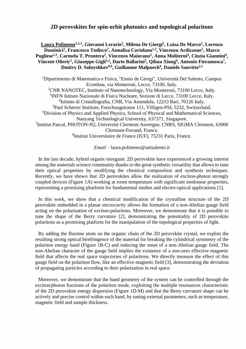
2D perovskites for spin-orbit photonics and topological polaritons
Laura Polimeno1,2,3, Giovanni Lerario2, Milena De Giorgi2, Luisa De Marco2, Lorenzo
Dominici2, Francesco Todisco2, Annalisa Coriolano1,2, Vincenzo Ardizzone2, Marco
Pugliese1,2, Carmela T. Prontera2, Vincenzo Maiorano2, Anna Moliterni4, Cinzia Giannini4,
Vincent Olieric5, Giuseppe Gigli1,2, Dario Ballarini2, Qihua Xiong6, Antonio Fieramosca7,
Dmitry D. Solnyshkov8,9, Guillaume Malpuech8, Daniele Sanvitto2,3
1Dipartimento di Matematica e Fisica, "Ennio de Giorgi", Università Del Salento, Campus
Ecotekne, via Monteroni, Lecce, 73100, Italy. 2CNR NANOTEC, Institute of Nanotechnology, Via Monteroni, 73100 Lecce, Italy. 3INFN Istituto Nazionale di Fisica Nucleare, Sezione di Lecce, 73100 Lecce, Italy.
4Istituto di Cristallografia, CNR, Via Amendola, 122/O Bari, 70126 Italy. 5Paul Scherrer Institute, Forschungstrasse 111, Villigen-PSI, 5232, Switzerland.
6Division of Physics and Applied Physics, School of Physical and Mathematical Sciences,
Nanyang Technological University, 637371, Singapore. 7Institut Pascal, PHOTON-N2, Université Clermont Auvergne, CNRS, SIGMA Clermont, 63000
Clermont-Ferrand, France. 8Institut Universitaire de France (IUF), 75231 Paris, France.
Email – [email protected]
In the last decade, hybrid organic-inorganic 2D perovskite have experienced a growing interest
among the materials science community thanks to the great synthetic versatility that allows to tune
their optical properties by modifying the chemical composition and synthesis techniques.
Recently, we have shown that 2D perovskites allow the realization of exciton-photon strongly
coupled devices (Figure 1A) working at room temperature with significant nonlonear properties,
representing a promising pltatform for fundamental studies and electro-optical applications [1].
In this work, we show that a chemical modification of the crystalline structure of the 2D
perovskite embedded in a planar microcavity allows the formation of a non-Abelian gauge field
acting on the polarization of exciton-polaritons. Moreover, we demonstrate that it is possible to
tune the shape of the Berry curvature [2], demonstrating the potentiality of 2D perovskite
polaritons as a promising platform for the manipulation of the topological properties of light.
By adding the fluorine atom on the organic chain of the 2D perovskite crystal, we exploit the
resulting strong optical birefringence of the material for breaking the cylindrical symmetry of the
polariton energy band (Figure 1B-C) and inducing the onset of a non-Abelian gauge field. The
non-Abelian character of the gauge field implies the existence of a non-zero effective magnetic
field that affects the real space trajectories of polaritons. We directly measure the effect of this
gauge field on the polariton flow, like an effective magnetic field [3], demonstrating the deviation
of propagating particles according to their polarization in real space.
Moreover, we demonstrate that the band geometry of the system can be controlled through the
exciton/photon fractions of the polariton mode, exploiting the multiple resonances characteristic
of the 2D perovskite energy dispersion (Figure 1D-M) and that the Berry curvature shape can be
actively and precise control within each band, by tuning external parameters, such as temperature,
magnetic field and sample thickness.
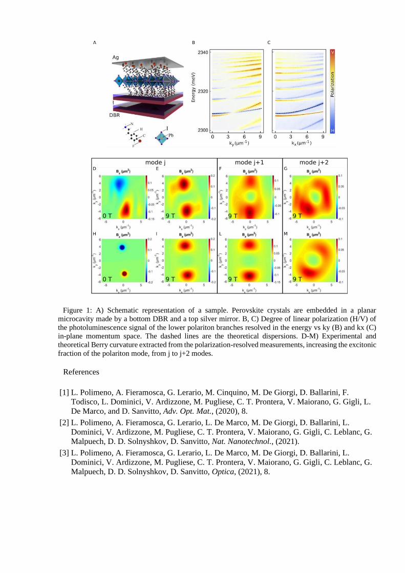
Figure 1: A) Schematic representation of a sample. Perovskite crystals are embedded in a planar
microcavity made by a bottom DBR and a top silver mirror. B, C) Degree of linear polarization (H/V) of
the photoluminescence signal of the lower polariton branches resolved in the energy vs ky (B) and kx (C)
in-plane momentum space. The dashed lines are the theoretical dispersions. D-M) Experimental and
theoretical Berry curvature extracted from the polarization-resolved measurements, increasing the excitonic
fraction of the polariton mode, from j to j+2 modes.
References
[1] L. Polimeno, A. Fieramosca, G. Lerario, M. Cinquino, M. De Giorgi, D. Ballarini, F.
Todisco, L. Dominici, V. Ardizzone, M. Pugliese, C. T. Prontera, V. Maiorano, G. Gigli, L.
De Marco, and D. Sanvitto, Adv. Opt. Mat., (2020), 8.
[2] L. Polimeno, A. Fieramosca, G. Lerario, L. De Marco, M. De Giorgi, D. Ballarini, L.
Dominici, V. Ardizzone, M. Pugliese, C. T. Prontera, V. Maiorano, G. Gigli, C. Leblanc, G.
Malpuech, D. D. Solnyshkov, D. Sanvitto, Nat. Nanotechnol., (2021).
[3] L. Polimeno, A. Fieramosca, G. Lerario, L. De Marco, M. De Giorgi, D. Ballarini, L.
Dominici, V. Ardizzone, M. Pugliese, C. T. Prontera, V. Maiorano, G. Gigli, C. Leblanc, G.
Malpuech, D. D. Solnyshkov, D. Sanvitto, Optica, (2021), 8.
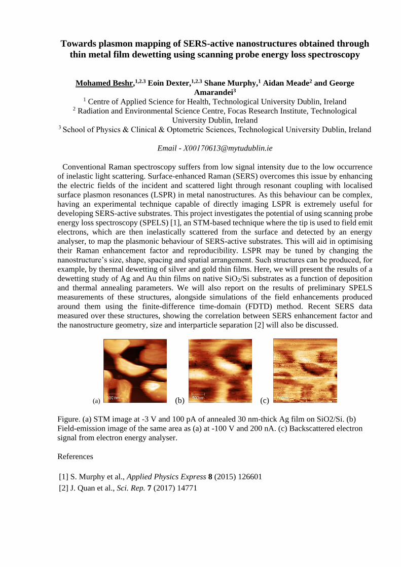
Towards plasmon mapping of SERS-active nanostructures obtained through
thin metal film dewetting using scanning probe energy loss spectroscopy
Mohamed Beshr,1,2.3 Eoin Dexter,1,2.3 Shane Murphy,1 Aidan Meade2 and George
Amarandei3 1 Centre of Applied Science for Health, Technological University Dublin, Ireland
2 Radiation and Environmental Science Centre, Focas Research Institute, Technological
University Dublin, Ireland 3 School of Physics & Clinical & Optometric Sciences, Technological University Dublin, Ireland
Email - [email protected]
Conventional Raman spectroscopy suffers from low signal intensity due to the low occurrence
of inelastic light scattering. Surface-enhanced Raman (SERS) overcomes this issue by enhancing
the electric fields of the incident and scattered light through resonant coupling with localised
surface plasmon resonances (LSPR) in metal nanostructures. As this behaviour can be complex,
having an experimental technique capable of directly imaging LSPR is extremely useful for
developing SERS-active substrates. This project investigates the potential of using scanning probe
energy loss spectroscopy (SPELS) [1], an STM-based technique where the tip is used to field emit
electrons, which are then inelastically scattered from the surface and detected by an energy
analyser, to map the plasmonic behaviour of SERS-active substrates. This will aid in optimising
their Raman enhancement factor and reproducibility. LSPR may be tuned by changing the
nanostructure’s size, shape, spacing and spatial arrangement. Such structures can be produced, for
example, by thermal dewetting of silver and gold thin films. Here, we will present the results of a
dewetting study of Ag and Au thin films on native SiO2/Si substrates as a function of deposition
and thermal annealing parameters. We will also report on the results of preliminary SPELS
measurements of these structures, alongside simulations of the field enhancements produced
around them using the finite-difference time-domain (FDTD) method. Recent SERS data
measured over these structures, showing the correlation between SERS enhancement factor and
the nanostructure geometry, size and interparticle separation [2] will also be discussed.
(a) (b) (c)
Figure. (a) STM image at -3 V and 100 pA of annealed 30 nm-thick Ag film on SiO2/Si. (b)
Field-emission image of the same area as (a) at -100 V and 200 nA. (c) Backscattered electron
signal from electron energy analyser.
References
[1] S. Murphy et al., Applied Physics Express 8 (2015) 126601
[2] J. Quan et al., Sci. Rep. 7 (2017) 14771
SMART, FUNCTIONAL FIBERS AND TEXTILES
7-10 December 2021Chimie ParisTech, Paris
Advanced Functional Semiconductor Fibers and Fabrics: NewFrontier of Flexible Electronics
Lei WeiNanyang Technological University, Singapore
Fiber-based systems have been made and used by humans as they are soft,deformable, breathable, durable and washable. The demonstration of flexiblefunctional fabrics enables the realization of wearable full-body sensing system tomonitor various physiological signals. This requires the integration of functionalmaterials such as semiconductors, conductors, and insulators into a single fiber withcomplex architectures and diverse functionalities. I will present our recent progress onfiber-shaped devices to enable the precise control on both functionality and devicedensity. The hierarchical nature (fiber - yarn - fabric) makes them particularly suitablefor the fabrication of wearable electronics.
Laser processing of semiconductor core fibers – device prospects
Seunghan Song1, Fredrik Laurell2, Bailey Meehan3, Thomas Hawkins3, John Ballato3, andUrsula Gibson1,2,3
1Norwegian University of Science and Technology, Physics Dept, Trondheim 7049 Norway2KTH Applied Physics 10691 Stockholm Sweden
3Department of Materials Science and Engineering, Clemson Univ, Clemson, SC 29634, [email protected]
Semiconductor core fibers, drawn using conventional fiber towers, have proven powerfulplatforms for optical applications, and optoelectronic and thermoelectric applications are on thehorizon. Internal structuring of conventional semiconductor cores within a silica cladding hasproven challenging due to the high temperatures involved, but the use of laser-driven thermalgradients has permitted segregation of the core constituents in both microspheres[1,2] and axiallyin continuous cores[3–6], permitting formation of structures that allow localized interaction withlight. In order to provide both electrical and optical functionality, the introduction of metalelements into the core, either as dopants or electrodes is of interest. We describe propaedeuticwork on the formation of axial and lateral electrodes, diodes and other structures in compositefibers.
References[1] A. Gumennik, E. C. Levy, B. Grena, C. Hou, M. Rein, A. F. Abouraddy, J. D. Joannopoulos,Y. Fink, PNAS 2017, 114, 7240.[2] L. Wei, C. Hou, E. Levy, G. Lestoquoy, A. Gumennik, A. F. Abouraddy, J. D. Joannopoulos,Y. Fink, Advanced Materials 2017, 29, 1603033.[3] D. A. Coucheron, M. Fokine, N. Patil, D. W. Breiby, O. T. Buset, N. Healy, A. C. Peacock, T.Hawkins, M. Jones, J. Ballato, U. J. Gibson, Nature Communications 2016, 7, 13265.[4] S. Song, K. Lønsethagen, F. Laurell, T. W. Hawkins, J. Ballato, M. Fokine, U. J. Gibson,Nature Communications 2019, 10, 1790.[5] W. Wu, M. H. Balci, K. Mühlberger, M. Fokine, F. Laurell, T. Hawkins, J. Ballato, U. J.Gibson, U. J. Gibson, Opt. Mater. Express, OME 2019, 9, 4301.[6] W. Wu, Laser-induced spatial composition gradients in SiGe core fiber. PhD thesis, NTNU,2020.
Molten-phase processing of multimaterial monofilaments: a route to functionalfiber-embedded systems
Alexander Gumennik,1,2 Louis van der Elst,1,2 Camila Faccini de Lima,1,2 Merve GokceKurtoglu,1,2 Troy Leffel,1,2 Mengxin Zheng.1,2
1Indiana University Bloomington - Luddy School of Informatics, Computing and Engineering. USAFibers & Additive Manufacturing Enabled Systems Laboratory (FAMES Lab), Bloomington, USA.
Email – [email protected]
Fibers & Additive Manufacturing Enabled Systems Laboratory at IU Bloomington (FAMES Lab)holds a proprietary technology [1, 2], pending patent [3], for fabrication of 3D photonic andoptoelectronic structures internal to fibers. In this molten-phase assembly technology, dubbed VeryLarge-Scale Integration for Fibers (VLSI-Fi), the fiber-photonics fabrication starts with defining thefiber cross-section through a thermal draw of the 3D printed preform [1], followed by the axialpatterning of the fiber cores with a spatially coherent material selective capillary breakup, andfinished by segregation-assisted dopant redistribution upon cooling and solidification of moltenphase assembled structures.
In my lecture, I will describe the recent progress in substantiating VLSI-Fi as a technology thatcan deliver groundbreakingly impactful products.
For instance, VLSI-Fi is anticipated to deliver a new class of fibers embeddable in biomedicaldevices and impart them with distributed sensing and transduction [2, 4] for physiologicalmonitoring and stimulation applicable to clinical and rehabilitation patient care. Additionally,VLSI-Fi is expected to deliver fiber-photonics that intimately and efficiently interface with emerginghigh-performance computing platforms. In application, for instance, to quantum computation, it willprovide fiber-photonics serving as Quantum Interconnect (QuIC) [5], hybridizing the existingplethora of conventional quantum material platforms into a single information medium – "theQuantum Internet of Things" (QIoT).
References
[1] Elst L van der, Faccini de Lima C, Gokce Kurtoglu M, Koraganji VN, Zheng M, GumennikA, Advanced Fiber Materials, 3 (2021) 59-75
[2] Faccini de Lima C, Elst LA van der, Koraganji VN, Zheng M, Gokce Kurtoglu M,Gumennik A, Nanoscale Research Letters, 14 (2019) 209 1–16
[3] Gumennik A, Faccini de Lima C, Koraganji VN, Zheng M, Appl. No.: US 20210333131 A1(2021)
[4] Gumennik A, Gokce Kurtoglu M, Elst L van der, Appl. No.: US 20210330864 A1 (2021)[5] Awschalom D, Berggren KK, Bernien H, Bhave S, Carr LD, Davids P, Economou SE,
Englund D, Faraon A, Fejer M, Guha S, Gustafsson M V, Hu E, Jiang L, Kim J, Korzh B,Kumar P, Kwiat PG, Lončar M, Lukin MD, Weiner AM, Zhang Z, PRX Quantum 2 (2021)017002
Glass additive manufacturing for specialty fiber fabrication
Michael Fokine, Chunxin Liu, Pawel Maniewski, Korbinian Mühlberger, Taras Oriekhov,and Clarissa M. Harvey
Department of Applied Physics, KTH Royal Institute of Technology, [email protected]
In this work we present recent activities towards developing methods for additivemanufacturing of glass within the Department of Applied Physics, at KTH. The main focus hasbeen on Laser Cladding (LC) using sub-micron powders, and Direct Glass Laser Deposition(DGLD) using glass filament feedstock. Both techniques use a CO2-laser operating at 10.6 µmwavelength. Using submicron powders having a particle diameter much smaller than the laserwavelength, shadowing effects due to particle-light interactions can largely be avoided [1]. ThisLC approach provides convenient means for manufacturing glass rods with tailoredcompositions, towards the fabrication of specialty optical fibers. Figure 1(a) shows the LCprocess during fabrication of a 40 mm long silica glass rod, 1.2 mm in diameter, at a glassdeposition rate of up to 3.8 mm3s-1. The laser head is based on discrete coaxial powder feeding(using three powder nozzles) surrounding the central laser beam. For the DGLD technique a4-beam system is employed to heat a centrally fed glass filament to temperatures in excess of2000 °C. The system is very similar to a standard Cartesian FDM 3D printer for plastics,including g-code generation using commercial slicing software. The symmetric nature of bothtechniques has been employed to remove the quill effect during glass deposition, withsubsequent improved print qualities as well as simplified programming. Figure 1(b1) shows athin wall consisting of 4 layers. Figure 1(b2) shows silicon-core glass-clad fibers [2] printed ontothe surface of a quartz glass plate, while Fig. 1(b3) shows a 5x5x5 mm3 cube printed with 100%infill settings. As a proof of concept, Fig. 1(c) shows a microscope image of a 3D printed 125µm diameter optical fiber. Here, a hexagonal rod was 3D printed, consisting of 68 strands ofsingle-mode fiber. The rod was then inserted into a glass tube, which was collapsed into apreform and subsequently drawn into fiber using our in-house CO-laser based draw tower [3,4].Both printing techniques have been shown to be applicable for optical fiber preformmanufacturing, direct waveguide printing as well as construction of more complex 3D glassstructures.
Fig. 1. Formation of (a) core rods for optical fiber fabrication using laser cladding, (b1-b3) 3D printed structuresusing glass filament, and (c) optical fiber with a core region composed of 68 cores. Here a 3D printed core rod was
inserted into a glass tube and drawn into a 125 µm diameter fiber.
[1] P. Maniewski, F. Laurell, and M. Fokine, Opt. Mat. Expr. 11(9) (2021) 3056[2] A.C. Peacock, U.J. Gibson, J. and Ballato, Advances in Physics: X, 1(1) (2016) 114-127[3] T. Oriekhov, C. Harvey, K. Mühlberger, and Michael Fokine, JOSA B, 38(12) (2021)
DOI:10.1364/JOSAB.438027[4] C. Harvey, K. Mühlberger, T. Oriekhov, P. Maniewski, and M. Fokine, JOSA B, 38(12) (2021)
DOI:10.1364/JOSAB.437667
Additive Manufacture of Single and Multi-Core Optical Fibres
J. Canning1,2, Y. Chu1,2, Y. Luo2, G.D. Peng2, J. Zhang2
1interdisciplinary Photonic Laboratories, University of Technology Sydney, NSW 2007 Australia2National Fibre Facility, University of New South Wales, Sydney, NSW 2052, Australia
Email – [email protected] manufacture of application specific optical preforms and fibres [1-3] will disrupt
traditional fabrication using chemical vapour deposition (CVD) fabrication whether on theinside, typically modified (MCVD) or on the outside (OCVD). The most obvious reason is thatCVD processes are on the whole constrained by a central spinning lathe that spins a tube intowhich material is sprayed and consolidated in various forms. This means only single and centredcore preforms are fabricated from which standard optical fibres are drawn. This constraint doeshave some advantages in that there is a highly uniform radial symmetry to temperature andpressure properties during manufacture which offer a great deal of structural symmetry criticalfor low loss scattering and generating degenerate polarisation states within an optical fibre. Thatbenefits some application specific fibres more than others – for structured optical fibres, forexample, this permits simple analytical relationships describing pressure within holes anduniformity that can be integrated into a fabrication process to control their size and wallthicknesses [4]. To fabricate multicore preforms, however, multiple single core preforms arefabricated, the cores etched and then assembled (usually manually) into the desired layout. Thisis a highly time consuming and laborious process. Given the increasing desire for multi-corefibres playing a role in extending optical bandwidth in communications and data transfer [5], thisclearly will not be tolerated longer-term. Consequently, the removal of this centre constraint inpreform manufacture is a necessary requirement even though this will be accompanied by otherchallenges. This is where additive manufacture comes into its own by removing this constraintaltogether.
I review our results on fabricating single and multicore silicate preforms and show the addedcomplexity that arises when drawing multiple cores. In particularly, the glass softening point isreduced with increasing number of cores – this explains why more uncontrolled liquid diffusionof the core into the cladding material, varying with uneven strain and flow within and leading toirregular shapes, is observed. There are unique challenges fabricating and drawing multiple coressimultaneously including addressing the variation in uniformity of strain and heat distributionthroughout the cores.
ReferencesY. Chu, X. Fu, Y. Luo, J. Canning, Y. Tian, K. Cook, J. Zhang, G-D. Peng, “Silica optical fibredrawn from 3D printed preforms”, Opt. Lett. 44 21, (2019) 5358 – 5361[1] Y. Luo, J. Canning, J. Zhang, G-D. Peng, “Towards optical fibre fabrication using 3D
printing technology”, Opt. Fibre Tech. 58 (2020) 102299[2] J. Canning, “3D Printing and Photonics”, Keynote, 4th Int. Conf. Emerging Adv. Nanomat.
(ICEAN), Newcastle University, Australia, (2020)[3] G. Tafti, J. Canning, S. Wang, Y. Luo, K. Cook, G-D. Peng, “Pressure Effects on Structured
Optical Fibre Drawing by Modified Single-Capillary Modelling”, Opt. Fibre Tech., 63(2021) 102528
[4] G. Rademacher, R. S. Luís, B. J. Puttnam, R. Ryf, S. van der Heide, T. A. Eriksson, N. K.Fontaine, H. Chen, R. Essiambre, Y. Awaji, H. Furukawa, N. Wada, "172 Tb/s C+L BandTransmission over 2040 km Strongly Coupled 3-Core Fiber," in Optical FiberCommunication Conference Postdeadline Papers 2020, (Optical Society of America, 2020),paper Th4C.5.
Towards Scalable Manufacturing of Color-Changing E-Textiles
Joshua J. Kaufman,1 Felix A. Tan,1 Morgan C. Monroe,1 and Ayman F. Abouraddy 1
1CREOL, The College of Optics and Photonics, University of Central Florida, [email protected]
Textiles and clothing have been a staple of human existence for millennia, yet the basicstructure and functionality of textile fibers and yarns has remained unchanged. While color andappearance are essential characteristics of a textile, an advancement in the fabrication of yarnsthat allows for user-controlled dynamic changes to the color or appearance of a garment has beenlacking. Touch-activated and photosensitive pigments have been used in textiles, but thesetechnologies are passive and cannot be controlled by the user. The technology to be presented inthis talk allows the owner to control both when and in what pattern the fabric color-change takesplace. In addition, the manufacturing process is compatible with mass-producing both theuser-controlled, color-changing yarns, the woven e-textiles, and the constructed end-useproducts.
The yarn fabrication utilizes a fiber extrusion system and a thread-coating attachment toencapsulate a metal wire inside a polymer sheath impregnated with thermochromic pigment. Thecolor change is distinct from garments containing LEDs that emit light in various colors. Thepigment itself changes its optical absorption to appear a different color. The thermochromiccolor-change is induced by a temperature change in the inner metal wire of each filament whencurrent is applied. The temperature required to induce color change is near body temperature andnot noticeable by touch. The prototypes already developed either use a simple push button toactivate the battery pack or are wirelessly activated via a smart-phone app over Wi-Fi. The appallows the user to choose from different activation patterns of stripes that appear in the fabriccontinuously. The power requirements are mitigated by a large hysteresis in the activationtemperature of the pigment and the temperature at which there is full color return.
The fiber fabrication process is readily scalable, and the fibers can be woven on industriallooms at commercial speeds. Furthermore, we have developed a method for quickly making thehundreds, if not thousands, of electrical connections that are necessary to produce a workingproduct that can change between different colors and multiple patterns. This method utilizesultrasonic welding and a multi-layer, multi-material bus that also accomplishes insulation of theelectrical connections and ruggedization of the connected edge all in a single step. Rapidconnectorization of the electrical components in an E-Textile has been a long-standing problemin the field, and this method aims to solve the last major hurdle in bringing this E-Textiletechnology to the market.
The developments to be discussed in this presentation represent a never-before seen capability:user-controlled, dynamic color and pattern change in large-area woven and sewn textiles andfabrics with wide-ranging applications from clothing and accessories to furniture andfixed-installation housing and business décor. The ability to activate through Wi-Fi opens uppossibilities for the textiles to be part of the ‘Internet of Things.’ Furthermore, this technology isscalable to mass-production levels for wide-scale market adoption.
Stack-and-draw Revisited For The Engineering Of Multi-material RibbonFibers
Sylvain Danto 1, Clément Strutynski 2, Georges El-Dib 1,4, Lionel Teulé-Gay 1, RedaMohammed Zaki 1, Ricardo Alvarado Meza 3, Angéline Poulon 1, Luc Vellutini 3, Sebastien
Chenu 4, Marc Dussauze 3, Thierry Cardinal 1
1Institute of Chemistry of the Condensed Matter of Bordeaux (ICMCB), University of Bordeaux,33608 Pessac, France
2Laboratoire Interdisciplinaire Carnot de Bourgogne, UMR 6303 CNR, University of BourgogneFranche-Comté, 21078 Dijon, France
3Institute of Molecular Science, University of Bordeaux, 33405 Talence – France4IRCER, University of Limoges, Limoges
E-mail: [email protected]
Here we present recent progresses in the fabrication of multimaterial fibers using glasses withintermediate Tg, including boro-phosphate glasses (Tg ~350-400°C) and soda-lime glasses (Tg
~580-620°C). More specifically, we demonstrate that the stack-and-draw technique can beexpanded to unusual materials (glasses, metals) association and profile geometries to generatefiber assemblies with unprecedented functionalities. This approach relies on the stacking of flatoxide glass slides into a preform, which is then thermally elongated into tens-of-meters-longribbon fibers with preserved cross-section ratio. Main properties and fabrication feature of themethod are introduced. We believe the insertion of intermediate-Tg oxide glasses within flatmultimaterial fibers will give access to a whole new range of functionalities, in electro-optics orsensing. In order to illustrate the versatility of the method, a panel of fibers with diverseapplications is exposed, including click chemistry for bio-chemical sensing and experimentaldevelopment of compact, all-solid fiber optical detector applied to gas analysis by means offiber-tip plasma spectroscopy.
References
[1] C. Strutynski, R. A. Meza, L. Teulé-Gay, G. El-Dib, A. Poulon-Quintin, J-P. Salvetat, L.Vellutini, M. Dussauze, T. Cardinal, S. Danto, Adv. Funct. Mat. 11 (2021) 1420
Soft Electronic Fibers for Sensing and Energy Harvesting
Fabien Sorin*, Andreas Leber, Chaoqun Dong, Inès Richard, Stella Laperoussa, William Esposito, Hritwick Banerjee, Bastien Schyrr.
1Institute of Materials, Ecole Polytechnique Fédérale de Lausanne (EPFL), 1015 Lausanne, Switzerland
Fibers and fabrics are becoming an important platform to seamlessly integrate functionalities highly relevant in the context of health care, robotics, energy harvesting and sensing and monitoring. It remains however challenging to integrate onto such particular substrates the materials and required micro to nano-scale architectures to achieve advanced functionalities with robust and state-of-the-art device performance. This is particularly difficult to do so for elastomer-based fibers, in configuration when mechanical softness and stretchability are required. In this talk, we will present recent breakthroughs in the thermal drawing process in terms of fiber device design, materials, and processing to realize state-of-the-art flexible electronic systems onto soft fibers and fabrics. After a description of the materials and process requirements, we will introduce a first example of a design that allows for the detection and localization of pressure along the fiber axis1,2. We will then move to new designs based on the thermal drawing of thermoplastic elastomers, that enables to realize soft and deformable fibers3. We will show in particular electronic fibers that integrate conducting composites, and an innovative design where several liquid metal electrodes are co-drawn within an elastomeric cladding, forming distributed sensors based on transmission line principles4. We will also demonstrate similar architectures adapted for self-powered sensors and energy harvesters relying on the triboelectric effects5. Finally, we will describe how one can also integrate metallic glasses in the thermal drawing process, paving the way for novel applications in bioengineering and electrochemical sensing6,7.
References
[1] A. Page et. al., J. Phys. D: Appl. Phys. 50, 144001 (2017)[2] A. Leber et. al., Advanced Functional Materials 30, 1904274 (2019)[3] Y. Qu et al., Advanced Materials 30, 1707251 (2018)[4] A. Leber et. al., Nature Electronics 3, 316 (2020)[5] C. Dong et. al., Nature Communication 11, 3537 (2020)[6] W. Yan et. al., Nature Nanotechnology 15, 875 (2020)[7] I. Richard et. al., ACS Applied Materials and Interfaces 13, 43356 (2021)
Multifunctional Fibers for Wearable and Implantable Applications
Xiaoting JiaVirginia Polytechnic Institute and State University, USA
Email: [email protected]
Smart textiles, wearable electronics, and biomedical implants can gain significant breakthroughthrough the invention of novel flexible devices that are capable of sensing, communicating, andinteracting with humans and the environment. Among different types of flexible devices,multimaterial fibers offer unique advantages for interfacing with humans, because of theirminimal footprint, scalability, high flexibility, multifunctionality, and biocompatibility. Despitethe significant progress made in the fabrication of multimaterial fibers in recent years, significantchallenges remain to enable wide applications in wearable and biomedical fields.
Here we present our research on developing multimaterial fibers for wearable and implantableapplications. Firstly, we developed three dimensional (3D) and multifunctional deep braininterfaces based on multimaterial fibers. Human brain is a complex organ consisting of tens ofbillions of interconnected neurons. It is critical to understand the brain circuitry across multipleregions in the brain in order to effectively treat neurological diseases. However, mapping thebrain circuitry over a large volume in the deep brain has been a major challenge. To address thischallenge, we have developed a first 3D fiber-based neural probes using multifunctional fiberarrays guided through a helical multi-channel scaffold. These fiber probes enable simultaneouselectrical recording, optical stimulation, and chemical delivery over a large volume in the deepbrain using a small surgical burr hole for the first time.
Next, we present various wearable sensors based on multimaterial fibers. Examples includefully distributed pressure and temperature sensing fiber and fabric which can sense multi-pointpressure distribution along the fiber, pressure variation, as well as continuous pressure shiftingalong the fabric with simple one-end connection, strain sensing fibers for multimodal extremedeformation sensing, and nano-integrated multifunctional fibers for bio-/chemical sensing. Wehave also developed fiber-based triboelectric nanogenerators for energy harvesting, motion andtouch sensing. These fiber sensors can be woven into fabrics, and undergo multiple washing anddrying cycles without degrading their performances.
In conclusion, multimaterial fibers provide a powerful platform for wearable and implantableapplications. Some of the future directions include more complex and integrated functions,reduced feature sizes, increased flexibility, and facile integration with silicon electronics forsignal acquisition and processing.
Smart photonic crystal fibre design for quantum technology applications
Peter J. Mosley Centre for Photonics and Photonic Materials, Department of Physics,
University of Bath, Bath, BA2 7AY, UK [email protected]
Photonic crystal fibre (PCF), formed of a matrix of air holes running along the length of a strand of silica glass, has for the last 20 years enabled unprecedented control over the propagation of light. In PCF with a solid core, the size and distribution of micro- or nano-scale holes in the cladding controls the fibre dispersion, allowing precision engineering of nonlinear processes across brightness scales from photon-pair generation to supercontinuum sources. On the other hand, silica glass walls only tens of nanometres thick but hundreds of metres long can confine light to a hollow core in which dispersion and nonlinearity are minimized to yield high-fidelity transport of both intense ultrashort laser pulses and quantum states of light.
In this talk, I will present developments in the application of PCF to quantum technologies, where its unique capabilities have potential in all-photonic as well as photonic-enabled architectures for computation, communication, and sensing. Recent work involving the University of Bath has spanned photon-pair sources, frequency conversion for quantum interfaces, topological effects in PCF, and engineering hollow-core fibre for noise reduction in pulsed laser systems, for quantum memories in atomic vapour, and for enhancing light-matter interaction with nanoparticles. Specifically in this talk, I will focus on how four-wave mixing in PCF provides a resource-efficient frequency conversion link between nodes in a distributed quantum network [1]. I will also present preliminary experimental data showing how PCF can be engineered for ultra-tunable frequency conversion capable of unifying a wide range of wavelengths in a single device to create a truly universal quantum frequency interface [2].
References
[1] T. A. Wright et al, Optics Letters 45 (2020) 4587[2] C. Parry et al, J. Opt. 23 (2021) 075202
Chemi-thermal and morphologic investigation of ti(IV) isopropoxide/pvp precursornanofibers for facile TiO2 nanofiber preparation
Yakup Aykut1,2,3, Nefise Yavuz3, Hamza Yilmaz4, Umit Koc1, Sena Ardicli5
1Bursa Uludag University, Engineering Faculty, Textile Engineering Department, 16059, Turkey2Bursa Uludag University, Institute of Health Sciences, Translational Medicine, Turkey
3Bursa Uludag University, Graduate School of Natural and Applied Sciences, TextileEngineering, Turkey
4Bursa Uludag University, Graduate School of Natural and Applied Sciences, Biomaterials,Turkey
5Bursa Uludag University, Faculty of Veterinary Medicine, Department of Genetics, TurkeyEmail: [email protected]
Sol-gel electrospinning is a promising technology that allows producing short and continuousceramic nanofibers. There are two main steps in this method. First one is the preparation of anappropriate ceramic precursor solution and flowingly production of precursor nanofibers fromthis solution. In the second step, heat treatment process is performed to convert ceramicprecursors in the nanofibers into ceramic phases and remove the products from the fibers that areproduced with the degradation of the polymer and other organic parts in the nanofibers.Microstructures of the ceramic nanofibers mostly form during the heat treatment processso-called calcination process. So, the investigation of the thermal stability of precursornanofibers is important to perform an appropriate calcination process. In this regard, sol-gelelectrospinning of Ti (IV) isopropoxide/PVP nanofibers were produced and a following heattreatment process at 280oC in air was applied to the as-spun nanofiber. Morphological analysis ofboth as-spun and heat treated nanofibers were conducted and it was shown that fibers wereswollen after heat treatment but their uniformity were not lost. Chemical and thermal analysis ofthe as-spun nanofibers were performed with FTIR and TGA techniques. Chemical structureswere totally changed after heat treatment process. XRD measurement revealed that the appliedheat treatment temperature was not fairly enough to obtain crystalline pahses in the nanofibersand even polymeric part were not compleatelt removed from the system. But, the fibers werestabilized at the applied temperature and can be used to convert them into TiO2 ceramicnanofibers with enhanced properties.
Keywords: Electrospinning, sol-gel, nanofibers, ceramic, Ti (IV) isopropoxide
Functional Fibers and Textiles for Biomedical Engineering
Louis A. van der Elst,1 Merve Gokce, 1 Jeffery Coulter, 1 and Alexander Gumennik1
1Indiana University, United States of [email protected]
Although nascent, regenerative medicine is gaining momentum with constant innovations ofcellular-level solutions for human healthcare. Functional fibers and textiles (FFT) have a uniquecontribution to play in understanding the world of cells and resolving the challenges associatedwith their manipulation, such as 3D bioprinting, genetic modification, tissue maturation, andmore. Multimaterial fiber devices can help address challenges in tissue biofabrication such as:
▪ the trade-off between resolution and volume▪ the morphological and mechanical properties▪ the selection and delivery of cell density, types, and population ratios▪ the proliferation, interaction, differentiation, and cell movement▪ the inhibition of bacterial contamination in cell cultures▪ the introduction of different signaling pathways and/or cell growth factors▪ the self-assembly and homeostasis▪ the management of dangerous and infectious by-products
At the Fibers and Additive Manufacturing Enabled Systems Laboratory (FAMES Lab), thebioengineering subgroup focuses on tackling these challenges by designing a variety of fiberdevices[1], such as FFT embedding microfluidics and porous compartments for delivery andcontrolled release of biostimulants or a combination of electroactive cores for sensing andtransduction. Specifically, recent work at the FAMES Lab includes the development of fiber thatdisturbs quorum sensing in bacteria to mitigate the infection of tissue, having applications insurgery for deep chronic wound healing, as well as in bacteria-free bioprinting and tissuematuration. These fibers are fabricated using biocompatible materials in 3D printedpolycarbonate preforms[2] and use the principles of electroceutical technology[3] to function.
References[1] L.A. van der Elst, C. Faccini de Lima, M. Gokce Kurtoglu, V. Narayana Koraganji,
M.Zheng, A. Gumennik, Adv. Fiber Mater. 32 (2021) 3[2] C. Faccini de Lima, L.A. van der Elst, V. Narayana Koraganji, M. Zheng, M. Gokce
Kurtoglu, A. Gumennik, Nanoscale. Res. Lett. 141 (2019) 14[3] J. Banerjee, P. Das Ghatak, S. Roy, S. Khanna, C. Hemann, B. Deng, A. Das, J.L. Zweier, D.
Wozniak, C.K. Sen, PLoS One 10 (2015) e0119531
Building blocks for fiber-embedded quantum circuitry
Camila Faccini de Lima1 , Troy Leffell1 and Alexander Gumennik1 1Indiana University - Luddy School of Informatics, Computing and Engineering. USA
Email – [email protected]
Photonic circuitry, in essence, a combination of resonant structures for the photons to interact with, or, mediated by, interact with each other, and waveguides, guiding the photons towards these structures, coupled appropriately for the right combinations of photons to interact.
In our previous work1, we described a methodology for universal in-fiber manufacturing of logic circuits and sensory systems ("VLSI for Fibers" or "VLSI-Fi,") which combines 3D printing of preforms, thermal draw of fibers, post-draw assembly of fiber-embedded integrated devices utilizing material-selective spatially coherent capillary breakup of the fiber cores, and segregation-driven crystallization. Liquid-phase processing of fibers, while governed by nonlinear, often chaotic2–4 fluid dynamics, is nonetheless expected to deliver a predictable, ordered solid-state fiber architecture. This type of capillary breakup is already extensively investigated for the assembly of photonic devices and systems, such as p-n diodes5,6, heterojunctions7, arrayed photodetectors8, photonic gratings5, and optical resonators9.
We envision that, combined with the ability to integrate multiple material platforms10–16, VLSI-Fi will form a complete, non-CMOS approach to fabrication of photonic circuits, addressing a number of standing challenges in Quantum Interconnects (QuIC)17. For QuIC it is important to note that the material-agnostic approach of VLSI-Fi is critical for quantum photonics implementation, since the performance of elements of such circuitry is material-platform dependent. Besides, it is known that in on-chip implementations of some of the quantum material platforms adversely affects decoherence times18–20. Fibers, on the other hand, are cylindrically symmetric and thus natural for integration with those platforms.
Through material-selective Axial Viscosity Gradient (AVG) capillary breakup, initially continuous cores in a multimaterial fiber can be selectively patterned into, for example, qubit sources, quantum memories, and quantum all-optical switches for the creation of fiber-embedded quantum devices. Moreover, AVG capillary breakup allows for the axial patterning of fiber cores both in the micron and submicron regimens. While the former is useful for the fabrication of electrically tunable whispering gallery mode spherical resonators, such as those in, the latter can be applied, for example, to create 1D photonic gratings, yet with very strict periodicity, serving as mirrors for a very-well insulated resonant cavity useful for quantum applications, as well as allowing for the tunning of interactions between photons and atoms, by coupling to them light at frequencies close to the photonic band edge.
We have developed an Axial Viscosity Gradient Instability Model (AVG-IM) which maps the the Capillary Number (Ca) and its spatial derivative into breakup position and period as one-to-one correspondence, allowing for great control over the periodicity of breakup structures through careful engineering of temperature profiles. As proof of concept, we demontrate an example of material-seclective AVG breakup where an array of spherical silicon resonators is created, with a vanadium electrode flanking along those resonators for electrical tuning of their resonant frequencies.
References
1. Faccini de Lima, C. et al. Towards Digital Manufacturing of Smart Multimaterial Fibers.Nanoscale Res. Lett. 14, 209 (2019).
2. Dreyer, K. & Hickey, F. R. The route to chaos in a dripping water faucet. Am. J. Phys. 59,
619–627 (1991). 3. Xu, B. et al. Filament formation via the instability of a stretching viscous sheet: Physical
mechanism, linear theory, and fiber applications. Phys. Rev. Fluids 4, 073902 (2019).4. Xu, B. & Deng, D. Linear analysis of dewetting instability in multilayer planar sheets for
composite nanostructures. Phys. Rev. Fluids 5, 083904 (2020).5. Gumennik, A. et al. Silicon-in-silica spheres via axial thermal gradient in-fibre capillary
instabilities. Nat. Commun. 4, 2216 (2013).6. Zhang, J., Wang, Z., Wang, Z., Zhang, T. & Wei, L. In-fibre particle manipulation and
device assembly via laser induced thermocapillary convection. Nat. Commun. 10, 5206(2019).
7. Gumennik, A. et al. Confined in-fiber solidification and structural control of silicon andsilicon-germanium microparticles. Proc. Natl. Acad. Sci. U. S. A. 114, 7240–7245 (2017).
8. Wei, L. et al. Optoelectronic Fibers via Selective Amplification of In-Fiber CapillaryInstabilities. Adv. Mater. 29, 1603033 (2017).
9. Fokine, M. et al. Laser structuring, stress modification and Bragg grating inscription insilicon-core glass fibers. Opt. Mater. Express 7, 1589–1597 (2017).
10. Homa, D., Kaur, G., Pickrell, G., Scott, B. & Hill, C. Electronic and magnetic fibers.Mater. Lett. 133, 135–138 (2014).
11. Grodkiewicz, W. H. Fused silica fibers with metal cores. Mater. Res. Bull. 10, 1085–1090(1975).
12. Ballato, J. et al. Binary III-V semiconductor core optical fiber. Opt. Express 18, 4972(2010).
13. Homa, D., Liang, Y. & Pickrell, G. Superconducting fiber. Appl. Phys. Lett. 103, 82601(2013).
14. Zhang, T. et al. Ultraflexible Glassy Semiconductor Fibers for Thermal Sensing andPositioning. ACS Appl. Mater. Interfaces 11, 2441–2447 (2019).
15. Scott, B. L. & Pickrell, G. R. Fabrication of GaSb Optical Fibers. in Processing andProperties of Advanced Ceramics and Composites V vol. 240 65–70 (wiley, 2013).
16. Snitzer ; Cunnell, E., Saker, E. & Edmond, J. Fabrication of Fibers with High Rare-EarthConcentrations for Faraday Isolator Applications. Opt. Quantum Electron vol. 39 (2007).
17. Awschalom, D. et al. Development of Quantum Interconnects (QuICs) for Next-Generation Information Technologies. Phys. Rev. Appl. 10, 36 (2021).
18. Hood, J. D. et al. Atom-atom interactions around the band edge of a photonic crystalwaveguide. Proc. Natl. Acad. Sci. U. S. A. 113, 10507–10512 (2016).
19. Corzo, N. V. et al. Waveguide-coupled single collective excitation of atomic arrays.Nature 566, 359–362 (2019).
20. Burgers, A. P. et al. Clocked atom delivery to a photonic crystal waveguide. Proc. Natl.Acad. Sci. U. S. A. 116, 456–465 (2019).
THE SPECTROSCOPY TECHNIQUES IN ART
7-10 December 2021Chimie ParisTech, Paris
Organisers:Olga Smolyanskaya (ITMO University)Michael Menu (ITMO’s Heritage Science Lab)
Recipes and review of brass gilding practice in France : 16th - 19th centuries.
M. VoisotConservator-restorer. Atelier Chronos. Dinan, France
The study and review of bibliographic sources from the 16th to the 19th centuries show anevolution in the practice of gilding. The reproduction of gilding processes gives information in thefield of « use-wear » also named « traceological analysis ».
Also it allows to inform the quantitative and semi-quantitative analysis, the metallography, andthe microscopy in all its diversity. Each gilding method prints a fringe, a coloring, a patina that isunique to it and in the visible domain.
Scientific analysis can reveal additional elements such as the composition of patinas, theconstitution of the gold layer. In the time allotted, we will make a point of stage of the recensionwork of gilding recieps, a short presentation of the principal « tracological » clues.
We will conclude with the scientific analysis requirements for this work.
The Digital Twin as a semantic-aware data-integration framework in HeritageScience
Sorin Hermon, Nikolas Bakirtzis, Svetlana Gasanova
Following on-growing requests in Europe and the world for an Open Science society, thescientific communities are more and more required to share their research data in an open andtransparent way. However, whereas some research communities, such as Life Sciences havealready a well-stablished tradition to operate with established protocols, common workflows andshare their primary data, Heritage Science is still in its infancy in regards to data sharing, use ofagreed upon protocols or canonical workflows. Moreover, its nature as an inter-disciplinarydomain, combining expertise from the humanities, natural sciences and exact sciences furtherchallenge the achievement of an open science, with inter-operable data. The presentation willpresent first steps towards a digital transformation of the field of Heritage Science, detailing howa digital twin may be defined. The concept will be introduced through a case-study, thepluri-disciplinary analysis of a medieval painting, namely the Crucifixion of Christ, by GiovanniBaronzio.
Authors:Sorin Hermon is Associate Professor at The Cyprus Institute. His research interests are
integration of Heritage Science and Digital Heritage research, FAIR-ification of scientific dataand development of scientific visualization methods in Heritage research. He coordinates theMSc program on Digital Cultural Heritage at The Cyprus Institute.
Nikolas Bakirtzis is Associate Professor and Director of the Andreas Pittas ArtCharacterization Labs at The Cyprus Institute in Nicosia, Cyprus. His research and publicationsexplore issues of heritage and cultural identity in Mediterranean cities, the development ofByzantine monasticism and the use of science and technology in art history.
Svetlana Gasanova is a chemistry graduate from Saint-Petersburg State University (RussianFederation) and PhD from the University of Duisburg-Essen in Germany. Since 2014 Svetlana isresearcher at the APAC Labs, The Cyprus Institute (Cyprus) where she leads research inHeritage Science, analyzing a wide variety of archaeological and art materials includingpolychromed statues, medieval icons and manuscripts, oil paintings, wall paintings, terracottaobjects and finds from archaeological excavations and developing the analytical lab of APAC.Her field of expertise is non-invasive analysis of pigments by spectroscopic methods (XRF,FTIR, FORS), advanced imaging techniques (IRR, XRR, multispectral imaging) and digitalmicroscopy.
Beauty & Secrets of Lustred Majolica at Renaissance
G. Padeletti1, P. Fermo2, M. Aucouturier3 and A. Bouquillon3
1- CNR-ISMN, Area della ricerca Roma1, via Salaria Km 29,3, 00015 Monterotondo, Roma, Italy2- Dep. of Chemistry, University of Milan, Via Venezian 21, Milano, Italy
3- C2RMF-UMR CNRS 171, quai François Mitterand, 75001 Paris, France
Lustre was one of the most sophisticated techniques for the decoration of majolica duringRenaissance period. It consists of a thin metallic film containing silver, copper, and other substanceslike iron oxide and cinnabar applied in a reducing atmosphere on a previously glazed ceramic. Inthis way, beautiful iridescent reflections of different colours (gold and ruby-red, in particular) areobtained. Studies have been carried out on ancient, lustred shards using different analyticaltechniques (e.g. XRD, SEM–EDX, TEM–EDX–SAED, ETAAS, ICP–OES, UV–vis reflectancespectroscopy, others) to assess the lustred film properties, relating them with their chemical andphysical characteristics.
Moreover, the most relevant findings from the study of excellent pieces belonging to theproduction of the great master Giorgio Andreoli da Gubbio, will be presented. This study waspossible thanks to the collaboration of several French Museums and the use of AGLAE acceleratorat C2RMF, in Paris.
Non-Destructive analysis to investigate the stone alterations at a UNESCOworld heritage site: the Lalibela’s churches, Ethiopia
D. Giovannacci 1, J.-D. Mertz 1, B. Taye Gemeda2, A. Garric 3, R. Mensan4
1Laboratoire de recherche des Monuments Historiques,USR 3224 CRC-LRMH, France
2Oxford Resilient Building and Landscapes Lab (OXRBL) School of Geography in theUniversity of Oxford, United Kingdom
3Centre français des études éthiopiennes, Addis Abeba, Ambassade de France en ÉthiopieService de la valise diplomatique, IFRE 23 / USR 3137 CNRS, France
4Laboratoire TRACES, UMR 5608, [email protected]
This study concerns the eleven monolithic churches in Lalibela in northeastern Ethiopia, aUNESCO World Heritage Site and currently the main pilgrimage site in Ethiopia. In 2019, on theinitiative of Prime Minister Abyi Ahmed, the French authorities proposed their support in themanagement on the site of the churches. To do so the French Development Agency (AFD), incollaboration with the Ministry of Europe and Foreign Affairs and with the support of theMinistry of Culture granted a feasibility study to examine ways of restoring, conserving anddeveloping the rock-hewn churches. The objective of the feasibility study conducted was toproduce the preliminary technical diagnostics required for the preparation of the comprehensiveproject to restore, conserve and develop the site.
In order to propose protection and conservation solution, diagnostics and analysis of thepathology of the rocks were made during two campaigns in November 2019 and November2020. The rock pathology teams implemented non-destructive and minimally invasive analysis.The complementary methods acquire data from the rock surface and the different forms ofdifferential alteration of the scoriaceous basalt. The objective is to characterize, throughcomparative analyses the impact of a protective shelter on the alteration kinetics of the rock.
Figure 1: Location of the tested-zones. Vew to the East
The microclimatic monitoring implemented concerned several churches. The sensors werepositioned in particular areas to jointly characterize the climate outside and inside the churches.
These microclimate variations will serve as input data (temperature T and humidity HR) whencalculating the expansion of the basalt samples collected, after experimentally measuringdeformations in the laboratory.
A 3D mapping was carried out with a resolution between 0.6 mm and 1 mm. The informationcollected is a 3D topographic image, capable of revealing texture, color, macro-roughness andany surface disorder whether anthropogenic or natural ([1]). This tool was exploited on the twozones of the eastern wall (counterscarp, see Figure 1) in Bete Maryam, the southwest angle ofBete Maryam presenting humidity indices, the investigated zone of the wall in Bete Libanos andBete Golgotha. Finally, very conclusive tests were also carried out on the 4 bas-reliefs sculptedin Golgotha.
The transitory air permeability allows characterizing the capacity of a material to allow a fluidpassage through its porosity ([2-3]). The assumption made is that is that a superficially degradedrock, by dissolution or any other mechanism, is likely to present an increase in its permeability.
The analysis coupled with on-site observations suggest that deterioration linked to liquid waterand the persistence of a state of high water content is more damaging than the deterioration risklinked to the salt crystallization, a process mainly occurring areas in dry areas. This risk cannotbe totally ruled out but it can be reduced by integration of current practices in stone conservation,like desalination.
As water is the key-factor in the very harmful alteration for the conservation of scoriaceousbasalt as a heritage material in humid natural environments, it seems useful to fully cover thechurches.
References
[1] T. Thomas “Rough surfaces, second edition”, Imperial College Press, London, (1999), 279p[2] V.C. Tidwell,. In Transport in Porous Media, HoC and Webb (Eds), Springer, (2006),273-286[3] J-D. Mertz, E. Colas E., A. Ben Yahmed A. and R. Lenormand R.,. XIIIth Inter. Congress onthe Deterioration and Conservation of Stone, University of the West of Scotland, Paisley,Hughes & Howind (Eds), v.1, (2016), 415-422
From remote sensing and machine learning to the history of the Silk Road
Haida Liang, Su Boming,Sotiria Kogou, ISAAC Lab, Nottingham Trent University
Dunhuang Research Academy
Automatic remote reflectance spectral imaging of large painted areas in high resolution, fromdistances of tens of meters, has made the imaging of entire architectural interior feasible. However, it has significantly increased the volume of data. Here we present a machine learningbased method to automatically detect ‘hidden’ writings and map material variations. Clusteringof reflectance spectra allowed materials at inaccessible heights to be properly identified byperforming non-invasive analysis on regions in the same cluster at accessible heights using arange of complementary imaging and spectroscopy techniques. The world heritage site of theMogao caves, along the ancient Silk Road, consists of 492 richly painted Buddhist cave templesdating from the fourth to fourteenth century. Cave 465 at the northern end of the site is unique inits Indo-Tibetan tantric Buddhist style, and like many other caves, the date of its construction isstill under debate. This study demonstrates the powers of an interdisciplinary approach thatcombines material identification, palaeographic analysis of the revealed Sanskrit writings andarchaeological evidence for the dating of the cave temple paintings, narrowing it down to the latetwelfth century to thirteenth century.
Haida Liang is Distinguished Professor of Physics at Nottingham Trent University working inthe field of Heritage Science. She leads the Imaging and Sensing for Archaeology, Art historyand Conservation (ISAAC) Research Lab, which specialises in the development and applicationof advanced optical imaging, spectroscopy, long range remote sensing and data science methodsto art conservation, art history and archaeology. She has a keen interest on historical globalconnections through interdisciplinary research.

Processing and Visualization of High Resolution Quantitative Multi-ModalSpectral Data
Ruven PillayC2RMF
Imaging spectroscopy techniques such as hyperspectral imaging, X-ray fluorescence, THzimaging and others can produce very large complex high resolution data sets that are difficult tomanage, process and exploit. In this presentation, we will look at techniques for managing,processing and visualizing such data and show how diverse data sets can be combined and madeavailable for online multi-modal visualization.
Jessica Auber- -Le Saux 1,2, Xueshi Bai1,3, Michalis Andrianakis 4, Nicolas Wilkie-Chancellier 2, and Vivi Tornari 4, Vincent Detalle 1,5,*
1 C2RMF, Centre de recherche et de Restauration des Musées de France, 14 Quai François
Mitterrand, 75001 Paris, France
2 SATIE, Systèmes et Applications des Technologies de l’Information et de l’Energie, CY
Cergy-Paris Université, ENS Paris-Saclay, CNRS UMR 8029, 5 mail Gay Lussac, 95031
Neuville sur Oise, France
3.Fondation des sciences du patrimoine/EUR-17-EURE-0021, 33 boulevard du Port, MIR de
Neuville, 95011 Cergy-Pontoise cedex, France
4 FORTH, Institute of Electronic Structure and Laser, Foundation for Research and Technology
Hellas (IESL-FORTH), N. Plastira 100, Heraklion 71110, GREECE
5.PSL Research University, Institut de Recherche Chimie Paris, Chimie ParisTech, CNRS
UMR 8247, 75005 Paris, France
*Correspondence: [email protected]
Abstract
Museum curators developed preventive strategies to control their artworks environment
(temperature, relative humidity, light, etc) to preserve the artworks. The environment control is for
now not assisted with direct material monitoring to follow mechanical modifications or chemical
reactions happening with environmental fluctuations. To complete what is lacking, we use a
technique based on speckle interferometry, Digital Holographic Speckle Pattern Interferometry
(DHSPI) which is a non-destructive, contactless and full-field technique. This technique allows taking
images of the surface to detect possible deformation below the micrometre level. The reference arm
is changed to obtain different images for the same time to increase the signal-to-noise ratio. Then,
we processed the images automatically to obtain deformation maps and improve the accuracy of the
maps.
Keywords: heritage science, speckle pattern interferometry, deformation map, preventive
conservation.
Display Holography: a novel technological multi-tool for modern Museums
Alkiviadis Lembessis1, Andreas Sarakinos1, Sergey Stafeev2, Mikhail Shevtsov3
1Hellenic Institute of Holography, Greece2ITMO University, Russia
3State Optical Institute, RussiaEmail – [email protected]
Ultra-realistic full-color holograms (OptoClonesTM) offer the opportunity to researchers tostudy artworks from close without the need to account for transport or security of original items.Also they allow the comparative documentation of artworks before/after restoration, before/aftertemporary loan etc. as well as the verification of authenticity of original artifacts. A temporarytravelling exhibition of such a holograms of invaluable and unmovable artworks allows thedissemination of cultural heritage within the same country or across the globe in a very safe,
secure, impressive and technologically advanced way. Creation of collective thematicexhibitions using Ultra realistic holograms of artworks with a common theme or origin beingdispersed among various Museum or private collections. Holographic in-situ documentation atexcavation sites with the purpose of exact optical documentation and study prior or post any
conservation works. Virtual optical 3D addition of missing parts with OptoClonesTM of eitheroriginal parts located in different museums or of replica parts manufactured for the purpose ofcompleting an artifact to its original form. Completion of collections of peripheral museums withOptoClonesTM of artworks which have been removed to major central museums on account oftheir historical value. Creation of holographic 3d moulds of archaeological findings which can beused as optical reference for texture, material, details etc. when manufacturing or repairingclassical replica moulds. Production of commemorative holograms of artifacts of highest valueand uniqueness for VIP giftware or collection series of limited edition. OptoClonesTM offer aunique impression to general public and can be used for special communication campaigns as anintroduction to main temporary exhibitions, special events and presentations by combiningadvanced technology with historical artifacts.
ReferencesA.Sarakinos, A.Lembessis Color Holography for the Documentation and Dissemination ofCultural Heritage: OptoClonesTM from Four Museums in Two Countries, J.Imaging 2019, 5(6),59.
Monumental worship cross of Uspenskaya Chapel, Kem Cathedral.Renovation of author coloristic solution based on the natural science research.
Sirro Sergey, Anastasia ZhuravlevaThe State Russian [email protected]
The large carved polychromic warship cross, located in the chapel of Uspensky Cathedral inthe city of Kem, is the monument of the second half of the XVII century. The cross was found in2021 by the expedition of specialists of the State Russian Museum. The aim of this work was toperform the first integrated research of the monument whereby the results allowed us to indentifyprecisely both the materials and the techniques applied to create the carved base and thepolychromy. Upon the initial UV examination in line with the detailed UV-photos made solely inthe Chapel, further X-Ray fluorescence spectroscopy revealed several types of metal coatings,as well as certain chemical pigments in paint layers. This work was continued in the RussianMuseum laboratory using the methods of micro chemical tests, Fourier-transformIR-spectroscopy and polarizing microscopy. The results obtained did not contradict with theXVII-century attribution of the monument by art experts. Thus, the research result is theintroduction to the open sources of another monument of the Belomorie area with the exact dateattribution, while the integrated material analysis permitted to make the probable reconstructionof the author's color approach while creating this monument.The research was carried out with the support of a grant under the Decree of the Government ofthe Russian Federation No. 220 of 09 April 2010 (Agreement No. 075-15-2021-593 of 01 June2021).
Surface displacement measurements of artworks: new data processing forspeckle pattern interferometry
Jessica Auber- -Le Saux 1,2, Xueshi Bai1,3, Michalis Andrianakis 4, NicolasWilkie-Chancellier 2, and Vivi Tornari 4, Vincent Detalle 1,5,*
1 C2RMF, Centre de recherche et de Restauration des Musées de France, 14 Quai FrançoisMitterrand, 75001 Paris, France
2 SATIE, Systèmes et Applications des Technologies de l’Information et de l’Energie, CYCergy-Paris Université, ENS Paris-Saclay, CNRS UMR 8029, 5 mail Gay Lussac, 95031
Neuville sur Oise, France3.Fondation des sciences du patrimoine/EUR-17-EURE-0021, 33 boulevard du Port, MIR de
Neuville, 95011 Cergy-Pontoise cedex, France4 FORTH, Institute of Electronic Structure and Laser, Foundation for Research andTechnology Hellas (IESL-FORTH), N. Plastira 100, Heraklion 71110, GREECE
5.PSL Research University, Institut de Recherche Chimie Paris, Chimie ParisTech, CNRSUMR 8247, 75005 Paris, [email protected]
Museum curators developed preventive strategies to control their artworks environment(temperature, relative humidity, light, etc) to preserve the artworks. The environment controlis for now not assisted with direct material monitoring to follow mechanical modifications orchemical reactions happening with environmental fluctuations. To complete what is lacking,we use a technique based on speckle interferometry, Digital Holographic Speckle PatternInterferometry (DHSPI) which is a non-destructive, contactless and full-field technique. Thistechnique allows taking images of the surface to detect possible deformation below themicrometre level. The reference arm is changed to obtain different images for the same timeto increase the signal-to-noise ratio. Then, we processed the images automatically to obtaindeformation maps and improve the accuracy of the maps.
Keywords: heritage science, speckle pattern interferometry, deformation map, preventiveconservation.
A reproduction of fabrication process of Kievan Rus' ceramic tiles
Vladimir A. Aseev 1, Leonid Yu. Mironov1, Denis S. Prokuratov2, Maria A. Isaeva1,Nadezhda A. Bulygina1, Denis D. Jolshin 2, Nikolay V. Nikonorov1
1Heritage Science lab, ITMO University, Russia2The State Hermitage Museum, Russia
In Kievan Rus' of the 10-13th century, glazed ceramic tiles were widely used as floorcoverings. The use of ceramic tiles has been archeologically identified in more than 80architectural monuments of Kievan Rus'. The geography of mosaic floors covers all thearchitectural and political centers of Russia of that period. Tiles from different places havedifferent shapes and colors, some of them have a polychrome ornament. No written evidences ofthe tiles production technology have yet been found. Reproduction of the technology of glazedtiles can provide useful information about the time and place of production, therefore, thepurpose of this work was to create replicas of tile samples from various cities of Kievan Rus'.The tasks of this work included the study of historical tiles and the development of technologyfor the production of yellow glazed tiles. Studies by X-ray diffraction and EDS analysis haveshown that all historical tiles have lead-tin yellow type 2 as a pigment, distributed in lead silicateglass. The thickness of the glaze layer reaches 3 mm.
To reproduce the technology, the following modifications were applied to a ceramic base:1. Raw components of the pigment and glass2. Raw pigment components and pre-synthesized glass powder3. Pre-synthesized pigment and raw glass components4. Pre-synthesized pigment and glass powder.
The samples were subjected to heat treatment at temperatures of 750-1000°C for 1-5 hours.
The obtained replica of glazed ceramics were analyzed using X-ray diffraction analysis, Ramanspectroscopy; the thickness of the glass layer was determined. The obtained tiles were comparedwith the historical ones.
«The research was carried out with the support of a grant under the Decree of the Governmentof the Russian Federation No. 220 of 09 April 2010 (Agreement No. 075-15-2021-593 of 01June 2021)»
Raman Spectroscopy Can Assess the Age of Animal Bones and Ivories
Alexander Khmaladze1
1SUNY University at Albany, [email protected]
Assessing the age of ivory is important for the proper identification of ivory objects and is alsocrucial for controlling illegal trafficking of elephant bones. Radiocarbon dating is the standardmethod of determining the age of ivories; however, it requires the destruction of a fragment ofthe sample. Raman spectroscopy is a non-destructive technique, and therefore can be used onartwork. Moreover, Raman measurements can be done using a portable system, and the dataanalysis can be performed on the spot once the groundwork is done. Ivories contain two primarycomponents: collagen and bioapatite. Raman spectrum of ivory material is mainly a sum of thevibrational bands of these components. As collagen deteriorates with time, its Raman signaldecreases, therefore the ratio of collagen-to-bioapatite peaks is smaller in the older samplescompared to the younger ones, providing a basis for sample dating. We have compared theresults of Raman and radiocarbon measurements applied to a set of elephant ivory fragments,and have successfully calibrated the Raman dataset using radiocarbon measurements. We foundthat the Raman collagen-to-bioapatite peak ratios of the samples can be used as a metric todetermine their age, providing a non-destructive technique to assess the age of ivory samples. Wehave also used singular value decomposition (SVD) to analyse the whole Raman spectra. Weobserved clear separation between samples of different ages in the SVD component space, whichindicates that the changes in multiple collagen and bioapatite peaks likely contribute to thedifferences in Raman spectra of ivory samples of different age.
Application of image processing techniques to the THz visualization ofpainting’s inner layer
Olesya A. Malaya,1 Maxim A. Volynsky,1 Olga V. Kravtceniuk,1 and Olga A.Smolyanskaya1
1Heritage Science lab, ITMO University, 199034, Birzhevaya liniya, 16-113, Russia. [email protected]
THz imaging is a promising technology for the Heritage Science. It can providethree-dimensional information about the inner structure of the investigated object, essential forseparate layers reconstruction and calculation of their width. However, THz images have ratherlow resolution and often contain noise. Therefore, image processing might be a useful techniquein achieving better quality of visualization. For this reason, in this paper the results of THz imageenhancement using basic processing methods were presented. Two methods were based on theconvolution of the original image with spatial domain filters: Laplacian operator, Sobel operator,median filter, average filter, and their combination. Two others relied on low pass and high passFourier filtering. The obtained images and their statistical analysis proved the ability to improveTHz image by means of these methods. Hence, this work has profound implications for futurestudies. The research was carried out with the support of a grant under the Decree of theGovernment of the Russian Federation No. 220 of 09 April 2010 (Agreement No.075-15-2021-593 of 01 June 2021).
References[1] K. Ahi, Meas. J. Int. Meas. Confed. vol. 138, no. October, (2019)[2] I. Catapano, F. Soldovieri, Elsevier Inc. Inn. in N.-Surf. Geoph., ch. 11, (2019)
Double Optics: the Role of Technological Research in Art History.German Painting
Alexandra SmolyanskayaHeritage Science lab, ITMO University, 199034, Birzhevaya liniya, 16-113
Throughout history, the achievements of physics have been applied in various fields ofscience, including heritage studies. Not only can such a transdisciplinary research be useful forthe restoration and conservation processes, it also enriches stylistic and theoreticalcomprehension of art. Technological analysis allows us to realize the exciting process of thecreation of painting. Using the physical examination as a tool, we are able to trace the evolutionof an artist's manner - compositional, coloristic and poetic. Such an efficiency can bedemonstrated by several examples of painting, German in particular.
The research was carried out with the support of a grant under the Decree of the Governmentof the Russian Federation No. 220 of 09 April 2010 (Agreement No. 075-15-2021-593 of 01June 2021).
Non-destructive techniques for the inlay’s detection
Denis Prokuratov1,2, Nikolai Kurganov3,4, Konstantin Gorlov4, Artem Gryaznov5, AlekseyBakhvalov6, Aleksandra Mikhailova7
1Heritage Science lab, ITMO University, Russia2The State Hermitage Museum, Russia
3Conservation Department, Faculty of Arts, Saint Petersburg State University, Russia4Institute of the History of Material Culture of the Russian Academy of Sciences, Russia
5Saint Petersburg Electrotechnical University "LETI", Russia6«Ekros-Analytics» Ltd., Russia
7Center for optical and laser materials research, Saint-Petersburg State University, Russia
When working with archaeological material, preliminary diagnostics is necessary - the restorermust, in one way or another, get an idea of the object being uncovered. Traditionally, X-rayradiation is used. However, in case of an object with incrustations/inlays, the task of obtaining acontrast X-ray image of such objects is quite laborious. Especially in the case of using a film forregistration of an image and its subsequent wet development. There is a need to search foralternative methods that can provide information about the structure of the archaeological objectbefore restoration. In this work, a comparative study of possible methods for detectingincrustations is carried out.
The research was carried out with the support of a grant under the Decree of the Government ofthe Russian Federation No. 220 of 09 April 2010 (Agreement No. 075-15-2021-593 of 01 June2021).

Development of Cultural Heritage Science Database
Olga A. Smolyanskaya, Mikhail D. Basmanov, Olga V. KravtsenyukITMO University, Russia
The object database for usage in Cultural Heritage Science is being developed as acollaborative media for interdisciplinary science. In this report, the concept for such database,requirements for compatibility and interoperability, as well as the existing solutions andchallenges, are discussed. In addition, working database prototype and the technologies used indevelopment are shown.

The main activities of Oil Painting Conservation Department of the StateRussian Museum
Tatiana PavlovaThe State Russian Museum
The State Russian Museum is one of the major research and restoration centers for the itemsof cultural value. The departments include the Climatological Department, Chemistry andBiology Research Laboratory, and fifteen restoration workshops, which in 2022 will celebratetheir 100th anniversary. Oil painting conservation and restoration is the main area of the museumactivity. For a hundred years, we have been accumulating vast experience, and we are ready toshare it with our colleagues. We look forward to this international collaboration that will allow usto create new conditions for the preservation of cultural values.
Leading specialist of the Oil Painting Conservation Department, oil painting restorer, artrestoration and conservation historian.
Since 1992 has worked in the State Russian Museum, since 2000 – in the Oil PaintingConservation Department.
In 2008, graduated from Ilya Repin St. Petersburg State Academic Institute for Painting,Sculpture and Architecture with a master’s degree in theory and history of fine arts.
The area of scientific interests includes the history of Russian and international art restorationand conservation, restoration and conservation research, new technologies and their applications.Has authored a series of lectures “Oil Painting Conservation. Art, craft or science?” and is acoordinator for the international scientific-practical conference “NERADOVSKY READINGS:Storing and Restoring Exhibitions in a Museum of Art. History, current state and prospects fordevelopment”. Lives and works in Saint Petersburg.
Laser painting as a new direction of modern art
Vadim Veiko-1, Yaroslava Andreeva-1, Daria Lutoshina-1,Anastasiya Morozova-1, Galina Odintsova-1, and Sergey Gorny-2
1 ITMO University, Saint Petersburg 197101, RussiaLaser Center, LLC Saint Petersburg 195176, Russia
Light is the main source of art around us. It allows us to see colors, and moreover, light itselfcan be a tool for creating unique pieces of art and designs. Here we demonstrate that a laser actsas a multifunctional and effective tool for creation of masterpieces in a way similar to that ofclassical paints and brushes. To make analogies between the processes of an artist creating acanvas and laser painting an artwork, we investigate the interaction between focused laserirradiation and metallic surfaces and analyze deeply the interferntial optical effects in thin oxidefilms. For this, we describe the nature of three main artistic operations, which are color making,multiple color change, and erasing managed by a nanosecond laser. These processes are possibledue to the material heating above the evaporation point and are proved to be dependent on thecooling rate according to the obtained experimental and theoretical results. Therefore, our paperis the first attempt to present the concept of interference-based laser painting, which sets newperspectives for modern art and design.
References[1] V. P. Veiko, Y. Andreeva, L. Van Cuong, D. Lutoshina, D. Polyakov, D. Sinev, V.
Mikhailovskii, Y. R. Kolobov, G. Odintsova, “Laser paintbrush as a new tool of modern art,”Optica, X, XX, XXXX (2021).DOI: 10.1364/OPTICA.386574.

Digital technologies for Cultural Heritage
Kravtsenyuk O., Mikhail Basmanov, Alina Korchilava, Vincent Detalle, OlgaSmolyanskaya
Heritage Science lab, ITMO University, 199034, Birzhevaya liniya, 16-113.
The concept of development of digital services for Heritage science based on moderntechnologies is discussed. Preliminar results achived in database design, image improving andmachine vision are pointed out. The strategy to use open source products and open codessolutions is declared.The research was carried out with the support of a grant under the Decree of the Government ofthe Russian Federation No. 220 of 09 April 2010 (Agreement No. 075-15-2021-593 of 01 June2021)
The application of optical and spectroscopy methods for the study of paintingsby Russian avant-garde artists of the 1910s
Ivan Andreev, Sergey Sirro, Olga SmolyanskayaHeritage Science lab, ITMO University, 199034, Birzhevaya liniya, 16-113, Russian Federation
The article shows the possibilities of using optical and spectroscopy methods to study thepaintings of the Russian avant-garde of the 1910s in the museum collection. The issues ofexamination and restoration in the framework of technological research were also considered.Routine research consists of a complex study approach, including optical microscopy, UVluminescence, IR reflectography, X-ray radiography, XRF analysis, FTIR analysis in the mid-IRregion.
The research was carried out with the support of a grant under the Decree of the Government ofthe Russian Federation No. 220 of 09 April 2010 (Agreement No. 075-15-2021-593 of 01 June2021).
Photogrammetric digitizing of a three-dimensional image of the object surfacereconstructed from a display hologram
Ekaterina V. Rabosh1, *, Nikolay S. Balbekin1, Nikolay V. Petrov1
1 ITMO University, St. Petersburg, 197101, Russia*[email protected]
We propose a novel approach to digitize the information stored in analog display holograms.It implies the conversion of a 3D image reconstructed from a hologram to electronic form byphotogrammetry. The original object and the object wavefront of the analog display hologramwere digitized by the photogrammetry method. The similarity of the three-dimensional modelshad been evaluated. Proposed approach can be used to solve problems for the long-term storageof information about cultural heritage facilities.
NANOPHOTONICS
7-10 December 2021Chimie ParisTech, Paris
Spatio-Temporal Near-Field and Quantum Dynamics of Large-Area Semiconductor Lasers and Nano-Confined Quantum Emitters
Ortwin Hess1,2 1School of Physics and CRANN Institute, Trinity College Dublin, Dublin 2, Ireland
2The Blackett Laboratory, Imperial College London, London SW7 2AZ, UK Email – [email protected]
A long-standing challenge for high-power semiconductor lasers is to tame the inherent notoriously complex and frequently chaotic spatio-temporal instabilities in edge-emitting [1] and vertical-cavity surface emitting [2] semiconductor lasers [3]. General wisdom and most strategies proposed and technologically applied to date all seek to reduce the level of complexity by reducing the number of lasing modes, for example by optical injection, delayed [4] or delayed structured and filtered optical feedback [5] or, more recently, through super-symmetry in semiconductor laser arrays [6]. Based on a radically different strategy involving fighting laser chaos with quantum-chaotic or nano-disordered cavities we have recently shown that near-field and quantum chaos on the nanoscale leads to disorder which disrupts the formation of self-organized structures such as filaments that would normally lead to instabilities [7]. The talk will give an overview of the foundations and development of theoretical approaches to simulate and understand the spatio-temporal near-field and quantum dynamics of large-area semiconductor lasers and nano-confined quantum emitters. We will discuss how microscopic and dynamic materials-based simulations are the basis for an interpretation of the quantum chaotic dynamics [7], and how an innovative cavity design can be used to advance ultrafast parallel quantum noise ‘harvesting’ by spatio-temporal many-mode and quantum chaotic lasing dynamics in semiconductor lasers forms the basis for a new paradigm for greatly accelerated quantum random bit generation [8]. We will also show how through nanoplasmonic nano-cavity design lasing and near-field control quantum dynamics can be supported down to the extreme nano-scale [9]. We will highlight recently demonstrated room-temperature strong coupling of single molecules in a plasmonic nano-cavity [10] and near-field generated strong coupling of single quantum dots [11] as well as near-field enhanced single-photon emission and dynamic quantum entanglement [12].
References [1] I. Fischer, O. Hess, W. Elsäßer, and E. Göbel, EPL 35, 579 (1996).[2] O. Hess, Opt. Express OE 2 (1998), 424.[3] E. Gehrig and O. Hess, Spatio-Temporal Dynamics and Quantum Fluctuations in
Semiconductor Lasers (Springer Science & Business Media, 2003).[4] C. Simmendinger, D. Preißer, and O. Hess, Opt. Express OE 5(1999), 48.[5] N. Gaciu, E. Gehrig, and O. Hess, in Handbook of Chaos Control (John Wiley & Sons, Ltd,
2008), pp. 427–453.[6] M. P. Hokmabadi, N. S. Nye, R. El-Ganainy, D. N. Christodoulides, and M. Khajavikhan,
Science 363 (2019), 623.[7] S. Bittner, S. Guazzotti, Y. Zeng, X. Hu, H. Yılmaz, K. Kim, S. S. Oh, Q. J. Wang, O. Hess,
and H. Cao, Science 361 (2018), 1225.[8] K. Kim, S. Bittner, Y. Zeng, S. Guazzotti, O. Hess, Q. J. Wang, and H. Cao, Science 371
(2021), 948.[9] T. Pickering, J. M. Hamm, A. F. Page, S. Wuestner, and O. Hess, Nature Commun. 5 (2014),
4972.[10] R. Chikkaraddy, B. de Nijs, F. Benz, S. J. Barrow, O. A. Scherman, E. Rosta, A.
Demetriadou, P. Fox, O. Hess, and J. J. Baumberg, Nature 535 (2016), 127.[11] H. Groß, J. M. Hamm, T. Tufarelli, O. Hess, and B. Hecht, Science Adv 4 (2018), eaar4906.[12] F. Bello, N. Kongsuwan, J. F. Donegan, and O. Hess, Nano Lett. 20 (2020), 5830.
Harmonic Scattering Optical Activity: a new nonlinear optical probe forchiral materials
Ventsislav K. ValevCentre for Photonics and Photonic Materials, University of Bath, Bath, BA2 7AY, UKCentre for Nanoscience and Nanotechnology, University of Bath, Bath, BA2 7AY, UK
Centre for Therapeutic Innovation, University of Bath, Bath, BA2 7AY, UKEmail – [email protected]
Current drug discovery is facing numerous challenges; from antimicrobial resistance – one ofthe top ten global public health threats, to the increased risk of future pandemics fromglobalization, to the spiralling costs involved in bring a new drug to market. High-throughput(HT) synthesis with robotised operations driven by AI algorithms is recognized as a significantopportunity that could help accelerate drug discovery and development, but it requiresminiaturized sample volumes and HT analysis. Therefore, new experimental tools are needed foranalysing reaction products in tiny volumes, especially when it comes to chiral drugs.
In 2019, our group “made history” by first demonstrating a chiroptical effect that had eludedscientists for 40 years.[1,2] This effect can be referred to as “harmonic scattering opticalactivity”. The effect states that in chiral light scatterers (those that lack mirror symmetry) theintensity of light, scattered at the harmonic frequencies, is proportional to the chirality. Theeffect is general. So far, it has been observed in chiral plasmonic nanoparticles,[1,3,4] in chiralorganic molecules[5] and in chiral semiconductor nanoparticles.[6] Moreover, it wasdemonstrated both for second harmonic[1,3,5] and for third harmonic scattering.[4,6]Additionally, it was reported both for nonlinear Rayleigh [1,3-5] and nonlinear Mie scattering.[6]
The new effect requires minuscule volumes of illumination and has allowed the first chiropticalcharacterization of a single nanoparticle, floating freely in an isotropic liquid.[3] Unlike othernonlinear chiroptical effects, the harmonic scattering optical activity is technologicallystraightforward. It offers access to intricate optical properties (hyperpolarizabilities) that areessential for our understanding of light-matter interactions across inorganic and organicmaterials. This new effect paves the way towards a miniaturized but straightforward analysis toolthat could, in the future, be used to automate workflows in future (chiral) therapeutics.
References[1] J.T. Collins, K.R. Rusimova, D.C. Hooper, H.-H. Jeong, L. Ohnoutek, F. Pradaux-Caggiano,
T. Verbiest, D. R. Carbery, P. Fischer, V. K. Valev, Phys Rev. X 9 (2019) 011024[2] D. L. Andrews and T. Thirunamachandran, J. Chem. Phys. 70 (1979) 1027[3] L. Ohnoutek, N. H. Cho, A. W. A. Murphy, H. Kim, D. M. Răsădean, G. D. Pantoş, K. T.
Nam, V. K. Valev, Nano Lett. 20 (2020) 5792–5798[4] L. Ohnoutek, H.-H. Jeong, R. R. Jones, J. Sachs, B. J. Olohan, D. M. Răsădean, G. D.
Pantoș, D. L. Andrews, P. Fischer, V. K. Valev Laser. Photonics. Rev. 2100235 (2021)[5] D. Verreault, K. Moreno, É. Merlet, F. Adamietz, B. Kauffmann, Y. Ferrand, C. Olivier and
V. Rodriguez, J. Am. Chem. Soc. 142 (2020), 257–263[6] L. Ohnoutek, J.-Y. Kim, J. Lu, B. J. Olohan, D. M. Răsădean, G. Dan Pantoș, N. A. Kotov, V.
K. Valev, Nature Photon. (2022) in press.
Active metasurfaces based on phase change materials and hydrogels
Dmitry N. Chigrin1,2
1I. Physikalisches Institut (1A), RWTH Aachen University, Aachen, Germany2 DWI Leibniz Institute for Interactive Materials, Aachen, Germany
By changing a phase of the phase change material or the state of hydrogel near a functionalbuilding block of a metamaterial, it is possible to realize (re)configurable, time dependent and(re)programmable materials. Phase change materials are materials in which phase transitions canbe induced quickly and reversibly, resulting in pronounced changes in their physical properties.Hydrogels are macromolecular cross-linked networks swollen by the solvent in which they aredissolved. The unique property of hydrogels is their ability to dramatically change volume inresponse to external stimuli. Here we report on our recent developments of a multiphysicsdescription of complex composite metasurfaces incorporating phase change materials andhydrogels as their building blocks. Such a multiphysics description requires self-consistenttreatment of the electromagnetic, heat transfer, mechanical deformation and phase transitionmodels. Possible applications in the field of mid-infrared and microwave metasurfaces arediscussed.
Chiral Superstructure Printing by Circularly Polarized Light
Ji-Young Kim,1,2 Connor McGlothin,1,2 Minjeong Cha, 2,3 Zechariah J.Pfaffenberger,4 Wonjin Choi,1,2 Emine Sumeyra Turali Emre,2,5 Julie Biteen,4 Nicholas A. Kotov 1,2,3,5
1Department of Chemical Engineering, University of Michigan, USA 2 Biointerfaces Institute, University of Michigan, USA
3 Department of Materials Science and Engineering, University of Michigan, USA 4 Department of Chemistry and of Biophysics, University of Michigan, USA
5 Department of Biomedical Engineering, University of Michigan, USA [email protected]
Recent progress in additive manufacturing using light to cure the polymer resins enables to generate various 3D metamaterials with structural complexity. However, for stronger optical responses from the metamaterials, implementing inorganic materials and breaking optical symmetry is inevitable, which can be represented by chiral inorganic metamaterials. Most of manufacturing chiral inorganic superstructure on substrates rely now on the high-cost and time-consuming fabrication methods, which require either multistep lithography or depositions by instrumentation with high temperatures and/or low pressures. Using solution-processed chiral nanoparticles (NPs) can be a good alternative approach that is simpler and faster. Furthermore, the NP self-assembly processes can substantially expand the spectrum of the materials by including almost any type of inorganic material- metallic, semiconductor and ceramic as well as the combinations thereof. However, although many complex structures in colloids have been accomplished, solution-processed chiral structures on the surface/interface hitherto remains virtually unexplored.
Illumination of nanoparticles (NPs) with circularly polarized light (CPL) can strongly change the interaction forces between them due to light-induced polarization. i It will be attractive to utilize the ability of light to guide the self-organization processes of NPs to ‘sculpt’ chiral structures at interfaces. Here, we show that the strong optical activity of plasmonic materials under CPL afford photon to matter chirality transfer, fabricating silver nanohelices (AgNH) over the centimeter scale area in minutes. The rotational axis of the AgNH is oriented perpendicularly to the surface of the substrate, ensuring their chiroptical efficiency, the high g-factor. The handedness of the AgNH is altered from left to right when circular polarization of the incident photons changed from right to left, showing opposite polarity in their circular dichroism (CD) spectra. The wavelength of light source determined the size of the final superstructure as well as their surface plasmonic resonance (SPR) and CD band wavelength. Electron microscopy images for its intermediate growth stages showed vivid handedness of the rotational assemblies of NPs. The experimental evolution of CD peaks in different growth stages correlated well with those calculated for assembled nanostructure models with complex geometry, as established by prediction of deposition/assembly pattern by electromagnetic simulations. The chiral patterns were also fabricated on a polydimethylsiloxane (PMMA) stamp to demonstrate the simplicity and universality of these photosynthetic routes to direct construction of metallic 3D chiral metamaterials on arbitrary substrates with controlled chirality. More importantly, we successfully built a preliminary demo for a fast chiral surface printing system by implementing programmable motorized stage. The writing pattern showed a good CD signal (hundreds mdeg) of which handiness is distinguishable through Mueller matrix polarimetry. These simple and versatile architected metamaterials can be used for extensive applications, including but not limited to photonic, optoelectronic, and electromechanical devices as well as enantioselective catalytic and sensing systems.

References
[1] J. -Y. Kim†, J. Yeom†, H. Calcaterra, G. Zhao, J. Munn, P. Zhang, N. A. Kotov*, J. Am.Chem. Soc. 141 (2019), 11739−11744
[2] J. Yeom, B. Yeom, H. Chan, K. W. Smith, S. Dominguez-Medina, J. H. Bahng, G. Zhao,W.-S. Chang, S.-J. Chang, A. Chuvilin, D. Melnikau, A. L Rogach, P. Zhang, S. Link, P.Král, N. A Kotov*, 14 Nature Materials (2014), 66–72.

QUANTUM OPTICS AND QUANTUM METROLOGY
7-10 December 2021Chimie ParisTech, Paris
Nonlinear quantum optics with trion-polariton in 2D materials
O. Kyriienko1
1Department of Physics and Astronomy, University of Exeter, Stocker Road, Exeter EX4 4QL,United Kingdom
Email – [email protected]
Monolayers of transition metal dichalcogenides (TMDC) coupled to optical cavities offer apowerful platform for nonlinear optics. Being the direct bandgap type semiconductors withrelatively large effective masses of carriers, TMDCs host strongly bound excitonic states withbinding energies that allow for robust exciton formation. In fact, excitons dominate an opticalresponse of TMDCs even at room temperature, thus paving a route to future optoelectronicdevices. Importantly, in the presence of an access of free electrons (doping), the charged excitons– trions – can be formed. These quasiparticles can couple strongly to cavity photons and resultinto hybrid exciton- and trion-polariton modes that are both coherent and nonlinear.
In my presentation, I will discuss recent theoretical and experimental results that reveal strongnonlinear response of trion-polaritons and describe their microscopic nature. First, using amonolayer of MoSe2 as an example, I will show that phase space filling effects lead to largerenormalization of trion-polariton Rabi frequency and an effective blueshift for the lowerpolariton mode [1]. The observed nonlinearity represents the state-of-the-art value for planarmicrocavity nonlinear response with 2D materials. Next, I will describe a theory and numericalsimulations that account on equal footing for exciton-polaron and trion effects, revealingqualitative spectral changes at increasing doping levels [2]. This extends the results from theelectron-dressed excitonic states that have significant nonlinearity [3]. Finally, I will also showthat the large nonlinearity and long coherence can facilitate quantum effects withtrion-polaritons, and ultimately offer single-photon emission sources in a controllable system thatis easy to fabricate.
References[1] R. P. A. Emmanuele, M. Sich, O. Kyriienko, V. Shahnazaryan, F. Withers, A. Catanzaro, P.
M. Walker, F. A. Benimetskiy, M. S. Skolnick, A. I. Tartakovskii, I. A. Shelykh, D. N.Krizhanovskii, Nature Communications 11 (2020) 3589
[2] V. Shahnazaryan, V. K. Kozin, I. A. Shelykh, I. V. Iorsh, O. Kyriienko, Phys. Rev. B 102(2020) 115310 (2020)
[3] Y. V. Zhumagulov, S. Chiavazzo, D. R. Gulevich, V. Perebeinos, I. A. Shelykh, O.Kyriienko, arXiv:2107.06927 (2021)
[4] O. Kyriienko, D. N. Krizhanovskii, I. A. Shelykh, Phys. Rev. Lett. 125 (2020) 197402
Quantum Sensors for Electromagnetic Induction Imaging: from AtomicVapours to Bose-Einstein Condensates
Ferruccio RenzoniDepartment of Physics & Astronomy, University College London, London (UK)
Electromagnetic induction imaging (EMI) allows mapping of the conductivity of targetobjects and, when combined with appropriate algorithms, the generation of full 3Dtomographic images. Despite its tremendous potential, and the wealth of possibleapplications, for a long time the use of EMI was hampered by the lack of suitable sensors,with high sensitivity at low frequency. The use of atomic magnetometers (AMs) was shownto overcome such a limitation and, in conjunction with machine learning techniques, openedthe path to new applications of EMI. Most of the EMI-AMs demonstrations reported thus farrely on atomic vapours as sensing media. This talk discusses recent results obtained withultra-cold atoms and Bose-Einstein condensates, highlighting the potential extreme resolutionobtainable.
References:[1] C. Deans, L. Marmugi, S. Hussain, F. Renzoni, Electromagnetic Induction Imaging with aRadio-Frequency Atomic Magnetometer, Appl. Phys. Lett. 108, 103503 (2016).[2] C. Deans, L.D. Griffin, L. Marmugi, and F. Renzoni, Machine learning based localizationand classification with atomic magnetometers, Phys. Rev. Lett. 120, 033204 (2018).[3] L. Marmugi, C. Deans, and F. Renzoni, Electromagnetic induction imaging with atomicmagnetometers: unlocking the low-conductivity regime, Appl. Phys. Lett. 115, 083503(2019).[4] C. Deans, L. Marmugi, and F. Renzoni, Sub-Sm-1 electromagnetic induction imaging withan unshielded atomic magnetometer, Appl. Phys. Lett. 116, 133501 (2020).
A Nanoscale Continuous Quantum Light Source
Raphael Holzinger,1 Maria Moreno-Cardoner,1,2 Helmut Ritsch,11University of Innsbruck, Austria2Universitat de Barcelona, Spain
Regular arrays of two-level emitters at distances smaller than the transition wavelengthcollectively scatter, absorb and emit photons. The strong inter-particle dipole coupling createslarge energy shifts of the collective delocalized excitations, which generates a highly nonlinearresponse at the single and few photon level. This should allow to implement nanoscalenon-classical light sources via weak coherent illumination. At the generic tailored examples ofregular chains or polygons we show that the fields emitted perpendicular to the illuminationdirection exhibit a strong directional confinement with genuine quantum properties asantibunching. For short interparticle distances superradiant directional emission can enhance theradiated intensity by an order of magnitude compared to a single atom focussed to a stronglyconfined solid angle but still keeping the anti-bunching parameter at the level of g (2)(0) ≈ 10−2.
Quantifying the breakdown of the Rotating-Wave Approximation inSuperradiance
Mads A. Jørgensen,1 Martijn Wubs, 1,2,3
1Department of Photonics Engineering, Technical University of Denmark, DK-2800 Kgs.Lyngby, Denmark
2NanoPhoton - Center for Nanophotonics, Technical University of Denmark, Ørsteds Plads345A, DK-2800 Kgs. Lyngby, Denmark
3Centre for Nanostructured Graphene, Technical University of Denmark, DK-2800 Kgs. Lyngby,Denmark
We study quantitatively the breakdown of the rotating-wave approximation in the light-matterinteraction for the description of inter-emitter interactions. As our main case study, we calculatecollective light emission of quantum emitters. We employ a known multiple-scattering formalismwhere the full light-matter interaction leads to induced inter-emitter interactions described by theclassical Green function. Within the RWA, however, these induced interactions differ in the nearfield, and for free space we find a reduction by up to a factor of two. By contrast, for acorresponding scalar model the corresponding relative RWA error for the inter-emitterinteraction even diverges in the near field. For two identical emitters, the errors due to the RWAin collective light emission will show up in the emission spectrum, but not in the sub- andsuperradiant decay rates. In case of two non-identical emitters, also the collective emission rateswill differ by making the RWA. For three or more identical emitters however, RWA errors in theinteratomic interaction in general affect both the collective emission spectra and decay rates. Ourresults show more generally how the RWA becomes inaccurate already outside of theultrastrong-coupling regime, that is long before the inter-emitter interactions would become ofthe order of the emission frequencies.
References[1] M. Wubs, L. G. Suttorp, A. Lagendijk, Phys. Rev. A 70 (2004) 053823
Raman cooling in submicron attenuators, doped with optically active impurities
Vladimir. G. Krishtop2,1,*, Vladimir G. Popov1, Dmitry A. Dvoretsky3, Kirill E. Bugay3
1Center of scientific research and perspective development, JSC Infotecs, Russia2Institute of Microelectronics Technology of RAS, Russia
3JSC SFB Laboratory, Russia*[email protected]
The development of integrated waveguide optics and its miniaturization set new challengesfor physics, microelectronics, and materials science. Microelectronic technology implementationinto optics systems leads to a size decrease of optical elements on a chip and an increase in thedensity of elements. The task is to increase the efficiency of heat distribution in optical chips, andthis task is very urgent in integrated optics.
Heat dissipation problem is a critical in quantum key distribution (QKD) systems. Attenuatorswith a large attenuation of tens of decibels are used in QKD systems to provide aquasi-single-photon mode [1, 2]. The attenuators are strongly heated under the powerful laserradiation. Due to heating, the attenuation coefficient changes and leads to a violation of thesingle-photon regime.
It is shown in [3], using the example of spliced fiber attenuators, that external laser action canlead to a violation of the single-photon regime in QKD systems. The pulses become multiphoton,which makes the QKD protocol vulnerable to a photon splitting attack.
With the progress of optical systems on a chip, miniaturization of elements is accompanied bya heat dissipation deterioration and worsening heat problems. The classical thermal conductivity ofmaterials becomes insufficient for effective heat dissipation. The challenge is to develop smartmaterials that can dissipate heat through more efficient physical processes.
Heating is caused by the dissipated optical power, which can transfer energy to vibrations ofatoms, for example, through Raman scattering. There are optically active vibrations, for example,molecular vibrations of Si-O, which absorb the power of optical radiation and transfer it to acousticphonons, with which they interact well. As a result, the Raman spectrum for such vibrationsbroadens.
A feature of phosphorus-doped SiO2 is strong Raman scattering of light. In the presence ofphosphorus impurity in SiO2, optically active P-O vibrations weakly interact with the SiO2 lattice,which demonstrates a sharp peak in the Raman spectrum (see Fig. 1). Optically active P-Ovibrations can effectively redistribute energy in a material, reducing its conversion to heat.
Although the intensity of spontaneous Raman scattering is rather low, it should be taken intoaccount that high intensity of optical radiation leads to stimulated scattering. The intensity ofstimulated Raman scattering increases by several orders of magnitude and can become comparableto the pump intensity.
Moreover, Raman scattering can occur both in the Stokes regime and in the anti-Stokesregime. Anti-Stokes scattering is associated with an increase in the photon energy due to theabsorption of energy from the phonon subsystem. Anti-Stokes scattering can effectively cool theattenuator. Thus, scattering by dopants can significantly change the energy redistribution in opticalelements, ensure efficient energy transfer, and reduce local heating.
For the case of planar waveguides made with an epitaxial crystal lattice, this effect isdescribed in terms of selective pumping of the optical phonon subsystem. The dissipated opticalpower causes local heating due to the energy transfer to acoustic phonons through Raman scattering(RS) of light. Selective pumping of a phonon system by optical phonons leads to efficient energyextraction from the region with a high optical density.
We study attenuators based on phosphorus-doped SiO2, in which the role of Raman scatteringby molecular P-O vibrations is essential. Preliminary measurements of spliced fiber attenuatorsdemonstrated that strong attenuators based on standard fiber are susceptible to damage at a radiationpower of 2.5 W. Тhe attenuation coefficient is reduced by 20-25dB. This effect was confirmed in[3].
Next, we used a phosphorus-doped fiber, and the power threshold has increased to 3.6 W. Thisis evidence of efficient energy transfer by impurity vibrations.
Fig. 1. The Raman scattering spectrum in a doped fiber with phosphorus and germanium impurities.The maximum at 400 cm-1 corresponds to scattering by Si-O vibrations.
The maximum at 1320 cm-1 corresponds to P-O vibrations.
References[1] E. Diamanti, H.-K. Lo, B. Qi and Z. Yuan, "Practical challenges in quantum key distribution,"npj Quantum Information, vol. 2, p. 1–12, 2016.[2] E. Diamanti and A. Leverrier, "Distributing secret keys with quantum continuous variables:principle, security and implementations," Entropy, vol. 17, p. 6072–6092, 2015.[3] A. Huang, R. Li, V. Egorov, S. Tchouragoulov, K. Kumar, V. Makarov, «Laser-Damage AttackAgainst Optical Attenuators in Quantum Key Distribution» Phys. Rev. 034017, 5 March 2020https://doi.org/10.1103/PhysRevApplied.13.034017
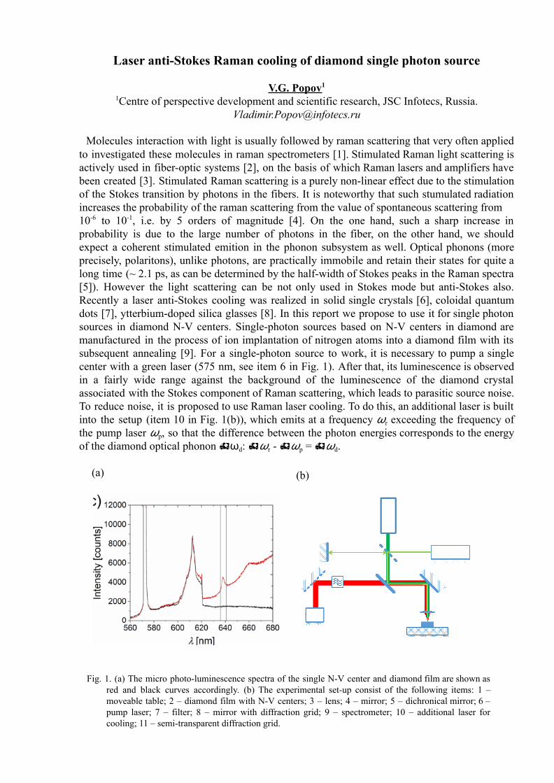
Laser anti-Stokes Raman cooling of diamond single photon source
V.G. Popov1
1Centre of perspective development and scientific research, JSC Infotecs, [email protected]
Molecules interaction with light is usually followed by raman scattering that very often appliedto investigated these molecules in raman spectrometers [1]. Stimulated Raman light scattering isactively used in fiber-optic systems [2], on the basis of which Raman lasers and amplifiers havebeen created [3]. Stimulated Raman scattering is a purely non-linear effect due to the stimulationof the Stokes transition by photons in the fibers. It is noteworthy that such stumulated radiationincreases the probability of the raman scattering from the value of spontaneous scattering from10-6 to 10-1, i.e. by 5 orders of magnitude [4]. On the one hand, such a sharp increase inprobability is due to the large number of photons in the fiber, on the other hand, we shouldexpect a coherent stimulated emition in the phonon subsystem as well. Optical phonons (moreprecisely, polaritons), unlike photons, are practically immobile and retain their states for quite along time (~ 2.1 ps, as can be determined by the half-width of Stokes peaks in the Raman spectra[5]). However the light scattering can be not only used in Stokes mode but anti-Stokes also.Recently a laser anti-Stokes cooling was realized in solid single crystals [6], coloidal quantumdots [7], ytterbium-doped silica glasses [8]. In this report we propose to use it for single photonsources in diamond N-V centers. Single-photon sources based on N-V centers in diamond aremanufactured in the process of ion implantation of nitrogen atoms into a diamond film with itssubsequent annealing [9]. For a single-photon source to work, it is necessary to pump a singlecenter with a green laser (575 nm, see item 6 in Fig. 1). After that, its luminescence is observedin a fairly wide range against the background of the luminescence of the diamond crystalassociated with the Stokes component of Raman scattering, which leads to parasitic source noise.To reduce noise, it is proposed to use Raman laser cooling. To do this, an additional laser is builtinto the setup (item 10 in Fig. 1(b)), which emits at a frequency ωr exceeding the frequency ofthe pump laser ωp, so that the difference between the photon energies corresponds to the energyof the diamond optical phononωd:ωr -ωp =ωd.
(a) (b)
Fig. 1. (a) The micro photo-luminescence spectra of the single N-V center and diamond film are shown asred and black curves accordingly. (b) The experimental set-up consist of the following items: 1 –moveable table; 2 – diamond film with N-V centers; 3 – lens; 4 – mirror; 5 – dichronical mirror; 6 –pump laser; 7 – filter; 8 – mirror with diffraction grid; 9 – spectrometer; 10 – additional laser forcooling; 11 – semi-transparent diffraction grid.
The light of an additional laser will stimulate anti-Stokes scattering in the region of a single N-Vcenter, which will lead to its local cooling and a decrease in the noise of a single-photon source.To adjust the optical scheme so as to create a general confocality of radiation, it is necessary touse a diffraction semi-transparent grid (item 11 in Fig.~1(b)). The grid period is selected foreffective refraction and reflection of the additional laser radiation in the direction of propagationof the pump laser radiation.
References
[1] E. Smith, G. Dent. “Modern Raman spectroscopy — A practical approach”. — John Wiley& Sons, LTD (2005)
[2] E.J. Woodbury, W.K. Ng, Proc. I.R.E. 50 (1962) 2367[3] A.J. Stentz, “Applications of Raman lasers and amplifiers in fiber communication systems”,
Proc. SPIE 91 (1998) 3263[4] R.W. Boyd, “Nonlinear Optics”, 3rd ed. (Academic Press, Boston, 2008), Chap. 10.[5] F.L. Galeener, J.C. Mikkelsen, R.H. Geils, W.J. Mosby, Appl. Phys. Lett. 32 (1978) 34[6] S. Rostami, A.R. Albrecht, A. Volpi, M. Shaek-Bahae, Photonics Research 7 (2019)
445[7] Y.P. Rakovich, J.F. Donegan, M.I. Vasilevskiy, A.L. Rogach, Phys.Status.Solid. A 206 (2009)
2497[8] M. Peysokhan, S. Rostami, E. Mobini, A.R. Albrecht, S. Kuhn, S. Hein, C. Hupel, J. Nold,
N. Haarlammert, T. Schreiber, R. Eberhardt, A. Flores, A. Tünnermann, M. Sheik-Bahae, A.Mafi, ACS Omega 6 (2021) 8376
[9] S.D. Trofimov, S.A. Tarelkin, S.V. Bolshedvorskii, V.S. Bormashov, S.Yu. Troshchiev, A.V.Golovanov, N.V. Luparev, D.D. Prikhodko, K.N. Boldyrev, S.A. Terentiev,A.V. Akimov, N.I. Kargin, N.S. Kukin, A.S. Gusev, A.A. Shemukhin, Y.V. Balakshin,S.G. Buga, V.D. Blank, Opt. Mater. Express. 10 (2020) 198
Non-Gaussian interactions in electromechanical systems: limitations andapplications
Salvatore Chiavazzo,1 Anders S. Sorensen,2 Oleksandr Kyriienko,1 and Luca Dellantonio3
1Department of Physics and Astronomy, University of Exeter, Exeter, Devon EX4 4QL, UK2Center for Hybrid Quantum Networks (Hy-Q), Niels Bohr Institute,University of Copenhagen,
Blegdamsvej 17, DK-2100 Copenhagen Ø, Denmark3Institute for Quantum Computing, University of Waterloo, Waterloo, Ontario, Canada, N2L 3G1
In this talk, I will consider a nonlinearly coupled electromechanical system [1], and develop aquantitative theory for two-phonon cooling. In the presence of two-phonon cooling, themechanical Hilbert space is effectively reduced to its ground and first excited states, allowing forquantum operations at the level of individual phonons and preparing nonclassical mechanicalstates with negative Wigner functions. I will describe a scheme for performing arbitrary Blochsphere rotations, and derive the fidelity in the specific case of a \pi-pulse. I characterisedetrimental processes that reduce the coherence in the system, and demonstrate that our schemecan be implemented in state-of-the-art electromechanical devices. The talk is based on the resultspresented in Ref. [2]
References[1] L. Dellantonio, O. Kyriienko, F. Marquardt, and A. S. Sorensen, Nat Comm. 9 (2018) 3621[2] S. Chiavazzo, A. S. Sorensen, O. Kyriienko, and L. Dellantonio, arXiv
preprint 2101.01750 (2021)

ENERGY HARVESTING AND PHOTOVOLTAICS
7-10 December 2021Chimie ParisTech, Paris
Strategies for Efficiency Enhancement of Thin-Film Solar Cells
Faiz Ahmad,1,2 Benjamin J. Civiletti,3 Peter B. Monk,3 and Akhlesh Lakhtakia2
1COMSATS University Islamabad, Pakistan 2The Pennsylvania State University, USA
3University of Delaware, USA Email – [email protected]
Small-scale photovoltaic generation of energy must become ubiquitous to satisfy the global demand for eco-responsible sources of cheap energy for the betterment of an ever-increasing fraction of the human population. Thin-film solar cells are a viable option in addition to crystalline-silicon solar cells due to low cost and ease of manufacturing. But their efficiencies have to be higher for commercial viability. A coupled optoelectronic model was formulated and implemented along with the differential evolution algorithm to assess the efficacy of grading the bandgap of the absorber layer in three thin-film solar cells [1]. Optimal nonlinear grading is predicted to deliver 27.7% efficiency with a 2200-nm-thick CIGS absorber layer in the CIGS solar cell, 21.7% with a 870-nm-thick CZTSSe layer in the CZTSSe solar cell, and 34.5% with a 2000-nm-thick AlGaAslayer in the AlGaAs solar cell. For a solar cell with two bandgap-graded absorber layers, 34.45%efficiency is predicted with a 300-nm-thick CIGS layer and a 870-nm-thick CZTSSe layer. Theuse of these solar cells in concentration phototovoltaic systems can enhance the efficiency further.For colored solar cells to be used in building-integrated photovoltaic systems, efficiency loss ispredicted to range between 10% and 20%, depending upon the percentage and spectral range ofincoming solar photons rejected.
References
[1] F. Ahmad, A. Lakhtakia, P.B. Monk, Theory of Graded-Bandgap Thin-Film SolarCells, Morgan & Claypool, San Rafael, CA, USA (2021)
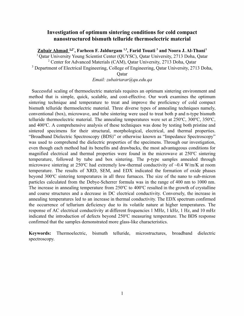
Investigation of optimum sintering conditions for cold compactnanostructured bismuth telluride thermoelectric material
Zubair Ahmad 1,2*, Farheen F. Jaldurgam 1,3, Farid Touati 3 and Noora J. Al-Thani1
1 Qatar University Young Scientist Center (QUYSC), Qatar University, 2713 Doha, Qatar2 Center for Advanced Materials (CAM), Qatar University, 2713 Doha, Qatar
3 Department of Electrical Engineering, College of Engineering, Qatar University, 2713 Doha,Qatar
Email: [email protected]
Successful scaling of thermoelectric materials requires an optimum sintering environment andmethod that is simple, quick, scalable, and cost-effective. Our work examines the optimumsintering technique and temperature to treat and improve the proficiency of cold compactbismuth telluride thermoelectric material. Three diverse types of annealing techniques namely,conventional (box), microwave, and tube sintering were used to treat both p and n-type bismuthtelluride thermoelectric material. The annealing temperatures were set at 250oC, 300oC, 350oC,and 400oC. A comprehensive analysis of these techniques was done by testing both pristine andsintered specimens for their structural, morphological, electrical, and thermal properties.“Broadband Dielectric Spectroscopy (BDS)” or otherwise known as “Impedance Spectroscopy”was used to comprehend the dielectric properties of the specimens. Through our investigation,even though each method had its benefits and drawbacks, the most advantageous conditions formagnified electrical and thermal properties were found in the microwave at 250oC sinteringtemperature, followed by tube and box sintering. The p-type samples annealed throughmicrowave sintering at 250oC had extremely low-thermal conductivity of ~0.4 W/m/K at roomtemperature. The results of XRD, SEM, and EDX indicated the formation of oxide phasesbeyond 300oC sintering temperatures in all three furnaces. The size of the nano to sub-micronparticles calculated from the Debye-Scherrer formula was in the range of 400 nm to 1000 nm.The increase in annealing temperature from 250oC to 400oC resulted in the growth of crystallineand coarse structures and a decrease in DC electrical conductivity. Conversely, the increase inannealing temperatures led to an increase in thermal conductivity. The EDX spectrum confirmedthe occurrence of tellurium deficiency due to its volatile nature at higher temperatures. Theresponse of AC electrical conductivity at different frequencies 1 MHz, 1 kHz, 1 Hz, and 10 mHzindicated the introduction of defects beyond 250oC measuring temperature. The BDS responseconfirmed that the samples demonstrated more glass-like characteristics.
Keywords: Thermoelectric, bismuth telluride, microstructures, broadband dielectricspectroscopy.
1
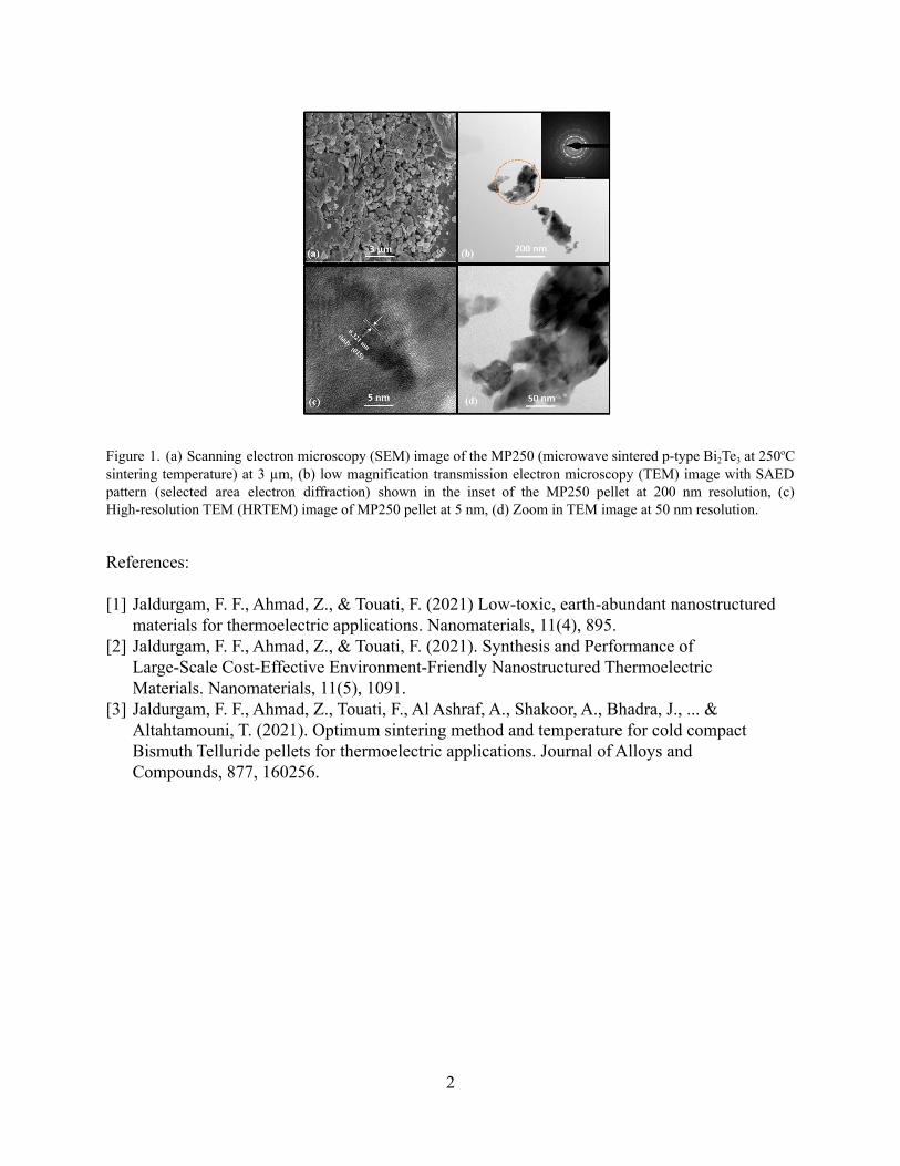
Figure 1. (a) Scanning electron microscopy (SEM) image of the MP250 (microwave sintered p-type Bi2Te3 at 250oCsintering temperature) at 3 µm, (b) low magnification transmission electron microscopy (TEM) image with SAEDpattern (selected area electron diffraction) shown in the inset of the MP250 pellet at 200 nm resolution, (c)High-resolution TEM (HRTEM) image of MP250 pellet at 5 nm, (d) Zoom in TEM image at 50 nm resolution.
References:
[1] Jaldurgam, F. F., Ahmad, Z., & Touati, F. (2021) Low-toxic, earth-abundant nanostructuredmaterials for thermoelectric applications. Nanomaterials, 11(4), 895.
[2] Jaldurgam, F. F., Ahmad, Z., & Touati, F. (2021). Synthesis and Performance ofLarge-Scale Cost-Effective Environment-Friendly Nanostructured ThermoelectricMaterials. Nanomaterials, 11(5), 1091.
[3] Jaldurgam, F. F., Ahmad, Z., Touati, F., Al Ashraf, A., Shakoor, A., Bhadra, J., ... &Altahtamouni, T. (2021). Optimum sintering method and temperature for cold compactBismuth Telluride pellets for thermoelectric applications. Journal of Alloys andCompounds, 877, 160256.
2
Aerosol Treatment for Efficient and Stable Perovskite Solar Cells
Joe Briscoe,1 Tian Du,1,2 Sinclair Ryley Ratnasingham,1,2 Thomas J. Macdonald,2 Felix
Kosasih,3 Ruo Xi Yang,4 Meng Li,5 Zhongyao Jiang,2 Lokeshwari Mohan,1,2 Adriana
Augurio,1 Huda Ahli,2 Shengda Xu,2 Weidong Xu,2 Zhenhuang Su,6 Xingyu Gao,6 Richard
Whiteley,1 Chieh-Ting Lin,2 Ganghong Min,2 Saif A. Haque,2 Kristin A. Persson,7 Caterina
Ducati,3 James Durrant,2 and Martyn McLachlan2 1 Queen Mary University of London, UK; 2 Imperial College, UK; 3 University of Cambridge,
UK; 4 Lawrence Berkeley National Lab, USA; 5 Henan University, China; 6 Shanghai
Synchrotron Radiation Facility, China; 7 Lawrence Berkeley National Lab, USA
Solvent annealing has been shown to be an effective and simple post-deposition treatment for
perovskite solar cells (PSCs) that does not rely on complex chemical modification on the precursor
solution or on the as-deposited films.1 The ability to improve the efficiency of a PV device through
such a simple process is therefore in principle an attractive approach. However, due to a lack of
uniformity and reproducibility, this process is not widely used for the production of high-
efficiency devices, nor seems likely to be highly relevant for commercial applications.
We have demonstrated a new approach to solvent-based post-treatment of perovskite films that
addresses these major issues with reproducibility and uniformity, and have shown the applicability
of this approach to large-scale processing of PSCs.2 This is achieved by controllably passing a
solvent aerosol across the film surface within a bespoke reactor. By controlling the aerodynamic
processes, a boundary layer forms though which the solvent diffuses towards the film surface,
leading to a highly-uniform and controllable exposure to the solvent.
Gaining such high level of control of the process has allowed us to not only achieve a power
conversion efficiency (PCE) enhancement of p-i-n structured photovoltaic devices to over 20%
using conventional methylammonium lead iodide (MAPbI3) as the active layer, but also, more
significantly, we have achieved large improvements in uniformity of film morphology after
treatment over the whole reactor area (~30 cm2), which also translates to reduced PCE variability
of devices produced from treated films. This improved large-area uniformity leads to a much less
marked efficiency drop when scaling up device area to 1 cm2 compared to untreated films as well
as increased stability under continuous maximum-power-point tracking in both N2 atmosphere and
ambient air. Furthermore, we also demonstrate that the technique can be applied to a wide range
of perovskite compositions and cell architectures, including Cs-FA, triple cation, Br-containing,
‘conventional’ (n-i-p), and HTL-free architectures, with efficiency enhancements in all cases.
Expanding beyond solvent post-treatment, we have also applied this technique to pure
formamidinium lead iodide (FAPbI3). Using aerosol-assisted crystallization (AAC) of the FAPbI3
films we are able to crystalise pure black-phase α-FAPbI3 in only 2.5 minutes at 100°C, compared
to 20 minutes at 150°C for conventional thermal annealing. Not only does this open up wider
processing options for the material, but we demonstrate improvement in PCE and, importantly,
phase stability of pure α-FAPbI3 compared to thermally annealed control samples. Using X-ray
diffraction, X-ray scattering and density functional theory simulation, we identify that relaxation
of residual tensile strains due to the lower annealing temperature and post-crystallization crystal
growth during AAC are key factors that facilitate the formation of phase-stable α-FAPbI3.
References
[1] Z. Xiao, Q. Dong, C. Bi, Y. Shao, Y. Yuan and J. Huang, Adv. Mater. 26, (2014) 6503.
[2] T. Du, S.R. Ratnasingham, F.U. Kosasih, T.J. Macdonald, L. Mohan, A. Augurio, H. Ahli,
C.‐T. Lin, S. Xu, W. Xu, R. Binions, C. Ducati, J.R. Durrant, J. Briscoe,* M.A.
McLachlan,*Adv. Energy Mater. 2101420 (2021).
Comparative studies of optoelectrical properties of prominent PV materials:
Halide perovskite, CdTe, and GaAs
Yong Zhang
The University of North Carolina at Charlotte, USA
Email – [email protected]
Impressive performance in PV application of halide perovskite MAPbI3 and related materials is
often attributed to their similarity in electronic properties with well-known PV materials like GaAs
and CdTe that have had a much longer development history. However, objective comparison is
rarely available. We compare three representative high performance PV materials: halide
perovskite MAPbI3, CdTe, and GaAs, in terms of photoluminescence (PL) efficiency, PL
lineshape, carrier diffusion, and surface recombination and passivation, over multiple orders of
photo-excitation density or carrier density appropriate for different applications [1]. The results
indicate that on the one hand the MAPbI3, even without surface passivation, can be superior than
the best CdTe and GaAs double heterostructures with passivated surfaces in PL efficiency at low
excitation density near and below 1 sun equivalent, indicating that the halide perovskite is more
immune to both surface and bulk Shockley–Read–Hall (SRH) recombination loss; on the other
hand, the polycrystalline MAPbI3 samples, which are similar to those typically used for the high
performance PV devices, have much shorter carrier diffusion lengths than the CdTe and GaAs
samples use for the comparison. Additionally, as an organic-inorganic hybrid material, MAPbI3 is
structurally disordered and much less unstable, in contrast to the inorganic counterparts as well as
another group of II-VI based organic-inorganic hybrid materials that have been found to be nearly
perfectly ordered in structure and exhibit over 15 years shelf stability [2]. An analytic model that
takes into account the radiative and SRH recombination is used to describe the excitation density
dependence of PL intensity and extract the internal PL efficiency, occupation fraction of the SRH
centers, and multiple pertinent recombination parameters, allowing for making quantitative
comparison between different materials. This comparative photovoltaics study provides more
insights into the fundamental material science and the search for optimal device designs by
learning from different technologies.
References
[1] F. Zhang, J.F. Castaneda, S. Chen, W. Wu, M.J. DiNezza, M. Lassise, W. Nie, A. Mohite, Y.
Liu, S. Liu, D. Friedman, H. Liu, Q. Chen, Y.-H. Zhang, J. Huang, Y. Zhang, Comparative
studies of optoelectrical properties of prominent PV materials: Halide perovskite, CdTe, and
GaAs, Materials Today, 36 (2020) 18-29.
[2] T. Ye, M. Kocherga, Y.-Y. Sun, A. Nesmelov, F. Zhang, W. Oh, X.-Y. Huang, J. Li, D.
Beasock, D.S. Jones, T.A. Schmedake, Y. Zhang, II–VI Organic–Inorganic Hybrid
Nanostructures with Greatly Enhanced Optoelectronic Properties, Perfectly Ordered Structures,
and Shelf Stability of Over 15 Years, ACS Nano, 15 (2021) 10565.
Stability of Nonfullerene Organic Solar Cells: from Built-in Potential andInterfacial Passivation Perspectives
Yiwen Wang,12 Zhe Li,1 Furong Zhu2
1 Queen Mary University of London, London, United Kingdom2 Hong Kong Baptist University, Hong Kong, China
Email: [email protected]
Remarkable progress has been made in the development of high efficiency solution-processablenonfullerene organic solar cells (OSCs). However, the stability of the nonfullerene (NFA) OSCsis not fully understood yet. In this talk, we report our effort to understand the stability of NFAOSCs, made with the binary blendpoly[(2,6-(4,8-bis(5-(2-ethylhexyl)thiophen-2-yl)-benzo[1,2-b:4,5-b’]dithiophene))-alt-(5,5-(1’,3’-di-2-thienyl-5’,7’-bis(2-ethylhexyl)benzo[1’,2’-c:4’,5’-c’]dithiophene-4,8-dione)] (PBDB-T) :3,9- bis(2-methylene-(3-(1,1-dicyanomethylene)-indanone))-5,5,11,11-tetrakis(4-hexylphenyl)-dithieno[2,3-d:2’,3’-d’]-s-indaceno[1,2-b:5,6-b’] dithiophene (ITIC) system andpoly[(2,6-(4,8-bis(5-(2-ethylhexyl-3-fluoro)thiophen-2-yl)-benzo[1,2-b:4,5-b’]dithiophene))-alt-(5,5-(1’,3’-di-2-thienyl-5’,7’-bis(2-ethylhexyl)benzo[1’,2’-c:4’,5’-c’] dithiophene-4,8-dione)](PM6) :3,9-bis(2-methylene-((3-(1,1-dicyanomethylene)-6,7-difluoro)-indanone))-5,5,11,11-tetrakis(4-hexylphenyl)-dithieno[2,3-d:2’,3’-d’]-s-indaceno [1,2-b:5,6-b’]dithiophene (IT-4F) system. Itshows that a continuous vertical phase separation process occurred, forming a donor-rich topsurface and an acceptor-rich bottom surface in BHJ during the aging period. It is found that agradual decrease in the built-in potential (V0) in the regular configuration NFA OSCs, due to theinterfacial reaction between the poly(3,4-ethylenedioxythiophene)- poly(styrenesulfonate)(PEDOT:PSS) hole transporting layer (HTL) and NFA acceptor, is one of the reasons responsiblefor the performance deterioration.[1] The impact of interfacial modification, molybdenum oxide(MoO3) induced oxidation doping of the PEDOT:PSS HTL, on the operational stability ofPM6:IT-4F nonfullerene OSCs has been studied. [2] The MoO3-induced oxidation doping inPEDOT:PSS can effectively suppress the interfacial chemical reactions between NFA acceptorand PEDOT:PSS. Our findings highlight that retaining a stable and high V0 across the BHJ viainterfacial modification and device engineering is a prerequisite for efficient and stable operationof the nonfullerene OSCs.
References
[1] Wang, Yiwen; Lan, Weixia; Li, Ning; Lan, Zhaojue; Li, Zhen; Jia, Jingnan; Zhu, Furong.Stability of Nonfullerene Organic Solar Cells: From Built-in Potential and InterfacialPassivation Perspectives. Adv. Energy Mater. 2019, 9 (19), 1900157.https://doi.org/10.1002/aenm.201900157.
[2] Wang, Yiwen; Han, Jiayin; Cai, Linfeng; Li, Ning; Li, Zhe; Zhu, Furong. Efficient andStable Operation of Nonfullerene Organic Solar Cells: Retaining a High Built-in Potential. J.Mater. Chem. A 2020, 8, 21255–21264. https://doi.org/10.1039/d0ta08018g.
Transfer of Direct to Indirect Bound Excitons by Electron Intervalley
Scattering in Cs2AgBiBr6 Double Perovskite Nanocrystals
Amrita Dey, Alexander. F. Richter, Tushar Debnath, He Huang, Lakshminarayan Polavarapu, and Jochen Feldmann
Chair for Photonics and Optoelectronics, Nano-Institute, Ludwig Maximilians Universität (LMU), 80539 Munich, Germany
Lead halide perovskites have gained a lot of popularity in the field of optoelectronics in recent times. Where the toxicity of lead remains a major issue, an emerging non-toxic alternative proposed is lead-free double perovskites with the generic stoichiometric formula A2MIMIIIX6. In double perovskite the divalent lead is replaced with one monovalent (MI) and one trivalent (MII) metal cation. Cs2AgBiBr6 is one the stable double perovskite with an indirect bandgap where the optical properties and the charge carrier relaxation processes are not fully understood. We applied time-resolved photoluminescence and differential transmission spectroscopy to explore the photo-excited charge carrier dynamics within the indirect band structure of Cs2AgBiBr6 nanocrystals. We observed a high energetic emission at the direct bandgap, alongside the emission from the indirect bandgap transition. We assigned this emission to the radiative recombination of the direct bound excitons originating due to trapping of holes. Due to the electron intervalley scattering process, the emission maximum from this direct bound excitons redshifts over 1 eV within 10 ps, leading to its transfer from direct to indirect bound exciton. We conclude that this direct bound exciton has giant oscillator strength which causes the higher energetic emission to occur at the direct bandgap despite the prevailing intervalley scattering process. These results expand the current understanding of the optical properties and the charge carrier relaxation process in double perovskites family, thus, facilitating the further development of optoelectronic devices harnessing lead-free perovskites.
References
[1] A. Dey, A. F. Richter, T. Debnath, H. Huang, L. Polavarapu, and J. Feldmann, ACS Nano 14 (2020)
5855–5861
Solution-based synthesis of Barium Titanate-Hematite Nanocomposite
Thin Films for Enhancement of Photocatalytic Activity
Adriana Augurio,1 Qian Guo,1 Alberto Alvarez-Fernandez,2 Vishal Panchal,3 Stefan
Guldin,2 Ana Belen Jorge Sobrido,1 and Joe Briscoe1
1Queen Mary University of London, London, UK 2University College London, London, UK
3Bruker, Coventry, UK
The study of novel photocatalyst and photo-electrocatalysts (PEC) for solar energy has gained
great attention, aiming to use solar energy to directly split water into hydrogen and oxygen to
produce solar fuels. In order to achieve unassisted water splitting, new low-cost, stable and
high- efficiency PEC systems are being explored. Recent research has focused on a wide range
of materials such as Fe2O3, BiVO4, CuWO4, with bandgaps in the range of 2-2.5 eV, which
allow visible light absorption, unlike the traditional photocatalyst, TiO2. However, these
materials generally present high level of surface or bulk recombination and low carrier
mobility1. The electric field associated with ferroelectric polarization has emerged as novel
strategy in photocatalysis to induce opposite band bending at material surfaces facilitating
charge migration towards different sites and promoting selective redox reactions in the
respective locations2. In the present work, we develop and investigate a nanostructured,
composite thin film, obtained combining ferroelectric BaTiO3 with the photocatalyst Fe2O3 in
parallel at the nanoscale to improve the photocatalytic performance. The ferroelectric
polarization can aid effective charge separation while narrow bandgaps and good charge
transport properties of the photocatalyst are needed for light absorption and carrier extraction.
Porous BaTiO3 (pBTO) thin films are synthesized by a surfactant-assisted sol-gel method.
Using different concentrations of organic template, the porosity of pBTO thin films has been
controlled in order to obtain suitable thin films for photocatalyst integration. SEM analysis and
ellipsometry allow the determination of overall porosity of pBTO thin films. The tetragonal
(ferroelectric) phase of pBTO thin films is confirmed by XRD analysis and Raman
spectroscopy.The switching of spontaneous polarization of BaTiO3 thin films by an electric
field is verified by PFM. In addition, the alignment of polar dipoles to the
ferroelectric surface (P⃗⃗ upor P⃗⃗ down) is evaluated by testing PEC performance of pBTO thin film
after electrochemical (EC) poling at 8V. XPS analysis does not reveal a considerable
alteration of pBTO thin film due to EC poling. Lastly, the pBTO/Fe2O3 composite
photocatalyst thin film shows an enhancement of the photocurrent density compared to either
the bare Fe2O3 (by ∼2 times) and pBTO thin films (by ∼20 times), which could be correlated
to the upward band bending induced by the ferroelectric polarization of pBTO leading to
improved charge separation and injection in pBTO/Fe2O3 thin films. The possibility to regulate
the PEC response in pBTO/Fe2O3 by changing the polarization direction in pBTO is verified
using EC poling, which does not significantly affect the Fe2O3 layer, as confirmed by XPS
analysis. This research work shows a facile and low-cost approach for the development of
novel ferroelectric/photocatalyst photoanodes with switchable control of their PEC
performance, which possess a great potential for photoelectrochemical applications.
References
[1] S. Kment, Chem. Soc. Rev., (2017), 46, 3716
[2] F.Chen, Angew. Chem. Int. Ed., (2019), 58, 10061-10073
P-N junction-based ZnO textile nanogenerator for wearable energy-
harvesting
Qinrong. He, Joe. Briscoe *
School of Engineering and Material Science and Materials Research Institute, Queen Mary
University of London, London, E1 4NS
Email - [email protected]
To solve the issue of clean energy availability and environmental pollution issue, for example
through battery disposal, mechanical energy is considered as one of the most promising resources
because it is abundant and accessible in various environments such as body movements, vibration,
flowing air and muscle stretching. Zinc oxide (ZnO) nanostructures have been extensively
investigated for harvesting mechanical power owing to the large piezoelectric coefficient and easy
synthesis. In addition, with increasing development of portable/wearable electronic devices such
as smart watches, health or activities monitors, it is particular desire to research a flexible energy
harvester that can capture multiple forms of mechanical energy with enhanced energy conversion
efficiency, which holds great promise in personal smart devices.
Herein, p-n junction-based ZnO textile nanogenerator has been designed to combine the
advantage of ZnO piezoelectricity and textile flexibility. ZnO nanorods were synthesized on
copper-nickel plated textile. A P-N junction was established between PEDOT:PSS and ZnO
nanorods to reduce the rate of screening to achieve higher performance output, which can generate
increasing output voltage from 0.2 V to 1.81 V as the shaking frequency increases from 19 Hz to
26 Hz. The device also show high stability and durability under 26000 cycles test by shaking at 26
Hz. The output voltage from the device can activate an LCD screen display by shaking at its
resonant frequency. The device is able to harvest energy from mechanical forces different
impacting force, flicking from different direction and gentle finger tapping and bending. Our
results can be utilized for future flexible self-powering nanogenerator design to harvest a larger
amount of electricity from the environment.
Scheme 1. Fabrication process of PEDOT:PSS/CuSCN/ZnO textile nanogenerator. (a) Cu/Ni
coated textile, (b) enlarged section of textile with grown ZnO nanorods, (c) schematic of
nanogenerator.
References
[1] J. Briscoe, M. Stewart, M. Vopson, M. Cain, P.M. Weaver, &, S. Dunn (2012). Advanced
Energy Materials, 2(10), 1261.
[2] Q. He, X. Li, J. Zhang, H. Zhang, J. Briscoe, Nano Energy. 85 (2021) 105938.

EARLY CAREER
7-10 December 2021Chimie ParisTech, Paris
Non-Abelian Topological Charges of Nodal Links in Dielectric PhotonicCrystals
Haedong Park,1 Stephan Wong,1 Xiao Zhang,2 Sang Soon Oh1*1School of Physics and Astronomy, Cardiff University, Cardiff CF24 3AA, United Kingdom
2School of Physics, Sun Yat-sen University, Guangzhou 510275, [email protected]
For the last two decades, point degeneracies, such as Dirac or Weyl points, have been widelystudied in topological physics. It is also well-known that Weyl points are formed when one ofspace-time inversion (P and T) symmetries is broken. In contrast, a perturbation preserving P andT symmetries can generate a line degneracy, called a nodal line, rather than the Weyl points [1].This means that nodal lines are very closely linked with Weyl points but exhibits differenttopological properties. Therefore, extensive efforts on the nodal lines have been recently made incondensed matter physics, for example on topological semimetals [2] and metals [3].
In photonics, diverse nodal shapes such as nodal chains and links were realized in metallicphotonic crystals [4,5]. However, there has not been a dielectric photonic crystal exhibiting nodalchain or link, in spite of the advantage of dielectric structures such as the frequency scalability.
In this work, we propose a dielectric double-diamond photonic crystal as a design fornon-Abelian charges of nodal lines [6]. Based on numerical simulations, we show that theproposed design has nodal links, composed of two nodal rings, in the momentum space. Then weshow the topological charges of the nodal lines are non-Abelian that can be described byquaternion numbers. This is done by considering a loop which encloses the section of the link(s)and observing the correlation vectors of the eigenstates.
References
[1] L. Lu, L. Fu, J. D. Joannopoulos, and M. Soljačić, Nat. Photonics, 7 (2013), 294[2] Z. Yang, C.-K. Chiu, C. Fang, and J. Hu, Phys. Rev. Lett., 124 (2020), 186402[3] Q. Wu, A. A. Soluyanov, and T. Bzdušek, Science, 365 (2019), 1273[4] Q. Yan et al., Nat. Phys., 14 (2018), 461[5] E. Yang et al., Phys. Rev. Lett., 125 (2020), 033901[6] H. Park, S. Wong, X. Zhang, and S. S. Oh, ACS Photonics, 8 (2021), 2746
Low-cost, asymmetric metasurfaces for chirality at the nanoscale
Emilija Petronijevic,1 Alessandro Belardini,1 Grigore Leahu,1 Roberto Li Voti,1 TizianaCesca,2 Carlo Scian,2 Giovanni Mattei,2 and Concita Sibilia1
1Department S.B.A.I., La Sapienza University of Rome, Italy2Department of Physics and Astronomy, University of Padova, Italy
Plasmonic asymmetric nanostructures can tailor chiro-optical phenomena at the nanoscale [1],leading to applications spanning from chiral sensing [2] to circularly polarized light emission [3].Here we combine the cost- and time-effective nanosphere lithography [4] with a tilted metaldeposition to fabricate various asymmetric plasmonic nanostructures organized in metasurfaces.We characterize them with different optical and photo-thermal techniques, and we gain insightinto the electromagnetic behavior at the nanoscale by modelling.
We previously used photo-acoustic technique to characterize metasurfaces made of polystyrenenanospheres (PSN) covered by asymmetric plasmonic layer [5]; we showed the extrinsic chiralbehavior at 633 nm. Next, we noticed that the tilted metal deposition leaves an ellipticalnanohole array (ENHA) on the substrate, which can give the chiral behavior itself, even atnormal incidence [6]. Indeed, we measure intrinsic chirality in similar metasurfaces withoutPSN, which consist of ENHA in 50 nm of Ag [7]. As the numerical modelling provides good fitwith experimental data, we use the same approach to design ENHA coupled with achiralquantum emitters, for tunable, chiral light emission in the visible and near-infrared [8].Furthermore, we perform broadband extrinsic chirality characterization in the near-infrared rangein PSN-based metasurfaces; we demonstrate rich, resonance-governed, spin-dependentextinction [9]. Most recently, we characterize similar metasurfaces in the blue range by means ofphoto-deflection technique, and demonstrate strong chirality in diffracted beams [10].
References
[1] G. Leahu, E. Petronijevic, A. Belardini, M. Centini, C. Sibilia, T. Hakkarainen, E.Koivusalo, M. Rizzo Piton, S. Suomalainen, M. Guina, Adv. Opt. Mater. 5(16) (2017)1601063
[2] E. Petronijevic, M. Centini, A. Belardini, G. Leahu, T. Hakkarainen, C. Sibilia, Opt.Express 25(13) (2017) 14148
[3] T. Hakkarainen, E. Petronijevic, M. Rizzo Piton, C. Sibilia, Sci. Rep. 9 (2019) 5040[4] N. Michieli, B. Kalinic, C. Scian, T. Cesca, G. Mattei, ACS Photonics 5 (2018) 2189–2199[5] E. Petronijevic, G. Leahu, R. Li Voti, A. Belardini, C. Scian, N. Michieli, T.Cesca,
G.Mattei, C. Sibilia, Appl. Phys. Lett. 114 (2019) 053101[6] E. Petronijevic, H. Ali, N. Zaric, A. Belardini, G. Leahu, T. Cesca, G. Mattei, L. C.
Andreani, C. Sibilia, Opt. Quantum Electron. 52 (2020) 176[7] E. Petronijevic, A. Belardini, G. Leahu, T. Cesca, C. Scian, G. Mattei, C. Sibilia, Appl. Sci.
10 (2020) 1316[8] E. Petronijevic, R. Ghahri, C. Sibilia, Appl. Sci. 11(13) (2021) 6012[9] E. Petronijevic, A. Belardini, T. Cesca, C. Scian, G. Mattei, C. Sibilia, Phys. Rev. Appl.
16(1) (2021) 014003[10] G. Leahu, E. Petronijevic, R. Li Voti, A. Belardini, T. Cesca, G. Mattei, C. Sibilia, Adv. Opt.
Mater. (2021) 2100670
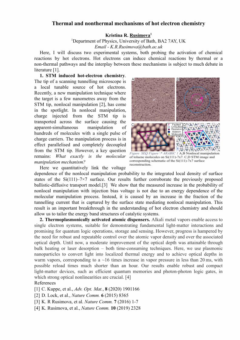
Thermal and nonthermal mechanisms of hot electron chemistry
Kristina R. Rusimova1
1Department of Physics, University of Bath, BA2 7AY, UKEmail - [email protected]
Here, I will discuss two experimental systems, both probing the activation of chemicalreactions by hot electrons. Hot electrons can induce chemical reactions by thermal or anon-thermal pathways and the interplay between these mechanisms is subject to much debate inliterature [1].
1. STM induced hot-electron chemistry.The tip of a scanning tunnelling microscope isa local tunable source of hot electrons.Recently, a new manipulation technique wherethe target is a few nanometres away from theSTM tip, nonlocal manipulation [2], has comein the spotlight. In nonlocal manipulation,charge injected from the STM tip istransported across the surface causing theapparent-simultaneous manipulation ofhundreds of molecules with a single pulse ofcharge carriers. The manipulation process is ineffect parallelised and completely decoupledfrom the STM tip. However, a key questionremains: What exactly is the molecularmanipulation mechanism?
Here we quantitatively link the voltagedependence of the nonlocal manipulation probability to the integrated local density of surfacestates of the Si(111)–7×7 surface. Our results further corroborate the previously proposedballistic-diffusive transport model.[3] We show that the measured increase in the probability ofnonlocal manipulation with injection bias voltage is not due to an energy dependence of themolecular manipulation process. Instead, it is caused by an increase in the fraction of thetunnelling current that is captured by the surface state mediating nonlocal manipulation. Thisresult is an important breakthrough in the understanding of hot electron chemistry and shouldallow us to tailor the energy band structures of catalytic systems.
2. Thermoplasmonically activated atomic dispensers. Alkali metal vapors enable access tosingle electron systems, suitable for demonstrating fundamental light-matter interactions andpromising for quantum logic operations, storage and sensing. However, progress is hampered bythe need for robust and repeatable control over the atomic vapor density and over the associatedoptical depth. Until now, a moderate improvement of the optical depth was attainable throughbulk heating or laser desorption – both time-consuming techniques. Here, we use plasmonicnanoparticles to convert light into localized thermal energy and to achieve optical depths inwarm vapors, corresponding to a ~16 times increase in vapor pressure in less than 20 ms, withpossible reload times much shorter than an hour. Our results enable robust and compactlight-matter devices, such as efficient quantum memories and photon-photon logic gates, inwhich strong optical nonlinearities are crucial. [4]References[1] C. Kuppe, et al., Adv. Opt. Mat., 8 (2020) 1901166[2] D. Lock, et al., Nature Comm. 6 (2015) 8365[3] K. R Rusimova, et al. Nature Comm. 7 (2016) 1-7[4] K. Rusimova, et al., Nature Comm. 10 (2019) 2328
Analytical models for quality of transmission applied for ultrawidebandsystem analysis and design
Anastasiia Vasylchenkova,1 Henrique Buglia,1 Eric Sillekens,1 Robert I. Killey, 1 LidiaGaldino, 1 and Polina Bayvel1
1Optical Networks Group, University College London, [email protected]
The throughput of the currently employed fibre-optics infrastructure is reaching its limits, andnew ideas are needed to meet ever-growing data demand. One of the promising andcost-effective directions is maximizing the usage of currently employed fibre infrastructure byutilizing the entire transparency window of silica fibre. This approach, known as ultrawidebandtransmission, can bring 50 THz overall bandwidth, compared to 5 THz one for the conventionalC band. This methodology requires the development of amplifiers and transceivers for additionalwavelengths. Additionally, ultrawideband transmission suffers from the severe impact ofinterchannel stimulated Raman scattering (ISRS), which leads to power transfer betweenchannels and non-uniform signal-to-noise (SNR) distribution across the transmissionwindow [1].
To study the performance of optical communication systems, traditionally simulation tools ofsignal propagation in the optical fibre are used. However, the design of ultrawidebandtransmission systems involves the adjustment of a multitude of system parameters, includingmodulation format, channels spacing and sampling, amplification gain profile. Furthermore,fibre parameters, e.g., chromatic dispersion or attenuation, depend on channel wavelength.Because of this, extensive simulation of all possible input waveforms and parameters is notpractical. Instead, one can use analytical or semi-analytical models for the estimation of thequality of transmission metrics. The Gaussian noise model [2] applies the perturbation approachand the statistical properties of input signals and impairments impact, to provide SNR estimationfor a given transmission system. Its generalization, which accounts for ISRS [3], allows studyingultrawideband scenarios in an accurate and computationally cost-effective way.
We demonstrate the advantage of the analytical models for optimising communicationsystems. We show it being applied for three different scenarios; for throughput maximisation bymeans of power tilting [4]; for the validation of different bands performance; and for the analysisof experimental transmission systems aimed at maximizing transmission throughputs [5].
References
[1] A. Ferrari et al., 21st International Conference on Transparent Optical Networks (2019)[2] P. Poggiolini, G. Bosco, A. Carena, V. Curri, Y. Jiang, F. Forghieri, J. Lightw. Technol. 32(2013) 694[3] D. Semrau, R. I. Killey, P. Bayvel, J. Lightw. Technol. 36 (2018) 3046[4] A. Vasylchenkova, E. Sillekens, R. I. Killey, P. Bayvel, accepted in Optical FiberCommunication Conference (2022)[5] H. Buglia, E. Sillekens, A. Vasylchenkova, W. Yi, R. Killey, P. Bayvel, L. Galdino,International Conference on Optical Network Design and Modeling (2021)

POSTER SESSION
7-10 December 2021Chimie ParisTech, Paris
Hydrogen isotopes discrimination with SAW sensors
Ionut Nicolae, Razvan Mihalcea, Mihai Serbanescu, Cristian Viespe and Aurelian Marcu
National Institute for Laser Plasma and Radiation Physics, Atomistilor 409, Ilfov 077125,Romania
Email – [email protected]
Among the green energy sources, hydrogen technologies are a very promising option.However, while using, handling and storing hydrogen, safety precaution have to be carrefullytaking care and sensors are presently a key issue in the present technological development.However, gas discrimination is a major problem of the existing sensors, beside ambient factorsinfluences and other ambiental conditions.
Surface Acoustic Wave (SAW) sensing is among the technques with best performances interms of detection limit. It is using acoustic waves propagating over a piezoelectric surface andare basing their functionality on the ‘active layer’ material mechanical properties change. Forsensor fabrication we use ZnO nanowires layers, as a versatile wide bang-gap semiconductorwith a high surface-to-volume ratio, and a good absorption of hydrogen and its isotopes. Wegrow ZnO single crystal [0001] nanowires on sensor surface as an active leyer using PulsedLaser Deposition (PLD) - Vapour-Liquid-Solid (VLS) techniques. On one hand, discriminationprocess used by our sensors relays on different mass and similar sorbtion mechanisms of thehydrogen isotopes into the active layer. On the other hand a multi-frequency scan is a way todiscriminate the active layer different behaviour for each analyt. Experimental results arepresented together with a theoretical modelling of the sensor response results.
Development of a sustainable biosensor to detect respiratory infectious diseases
A. Nascimento1, C. Abreu1, M. Silva2, B. Leite2, S. Rouly4, R. Ferraz1,5, M. Costa2,3, C.Prudêncio1,7, E. Parente2 and M. Vieira1,6,8
1School of Health, Polutechnic Institute of Porto, Rua António Bernardino de Almeida 400, 4200-072 Porto, Portugal
2CLOTHIUS – Tecelagem, LDA, RDD Textiles, Rua do Arranjinho 381 Fração Q Pavilhão 17, 4750-803 Barcelos, Portugal
3Departament of Textile Engineering, University of Minho, Campus de Azurém, 4800-058 Guimarães, Portugal
4Pharmaceutical and biological laboratory technology at Odisee, Gebroeders de Smetstraat 1, 9000, Ghent
5LAQV-REQUIMTE, Department of Chemistry and Biochemistry, Faculty of Sciences, University of Porto, Rua do Campo Alegre 687, P-4169-007 Porto, Portugal.
6Chemical and Biomolecular Sciences, Rua António Bernardino de Almeida 400, 4200-072 Porto, Portugal
7i3S- Institute for Health Research and Innovation, University of Porto, Rua Alfredo Allen 208, P-4200-135 Porto, Portugal
8CISA- Center for Health and Environmental Research, Rua António Bernardino de Almeida 400, 4200-072 Porto, Portugal
The Covid-19 pandemic brought the need to use social masks to prevent the spread of the virus. However, no reliable and fast method were yet established to detect viral particles and to improve the protective ability of social masks. The new Sars-Cov-2 has a second pathway of entry into the cells of the human body – the sialic acid (SA) receptor. Gold nanoparticles (AuNP) are known to have excellent optical properties and huge research potential. Through color changes, colorimetric biosensors can be used as a rapid and easily approach to detect virus. Here, we develop a colorimetric biosensor based on the functionalization of AuNP by SA (SA-AuNP), as a new and effective textile coating layer, to provide a direct indication of the protective capacity of social masks. This biosensor will provide information about the state of contamination by Sars-Cov-2 and other viruses that cause breathing problems. To do that, AuNPs (10 nm) were functionalized with SA (SA-AuNP), in three different concentrations (50-50, 30-70 and 20-80, respectively) to select the optimal concentration for respiratory virus detection. Fourier-transform infrared spectroscopy (FTIR) and Scanning Electron Microscope with a Transmission Detector (STEM) analyses confirmed SA-AuNPs binding. FTIR results showed a well-established bond, through matches of peaks of SA-AuNPs. Bindings between the compounds were more evident in 50-50 concentration of SA-AuNP. In the 30-70 SA-AuNP the STEM images show some superposition of the nanoparticles and not so evident binding, as in the 20-80 concentration. Still, between these last two concentrations, the 30-70 is the one that shows the best results since it is visible some circular points larger than the others. In order to achieve the goal, the concentrations 30-70 and 50-50 of SA-AuNP were impregnated (Textile Foulard) in two substrates of differentcompositions, a cellulosic and a synthetic one. However, in this technique there are manyparameters, such as drying time and temperature, which were varied in order to understand whichwas the best procedure to obtain the biosensor. The development of these smart mask demonstratedas a sensitive, rapid, and simple way to ensure a greater individual protection against viruses thatattack the respiratory tract, and further reduce their contagion and preventing their spread.

References
[1] Lee C, Gaston MA, Weiss AA, Zhang P. Colorimetric viral detection based on sialic acidstabilized gold nanoparticles. Biosens Bioelectron. 2013;42:236-241.
[2] Alfassam HA, Nassar MS, Almusaynid MM, et al. Development of a Colorimetric Tool forSARS-CoV-2 and Other Respiratory Viruses Detection Using Sialic Acid Fabricated GoldNanoparticles. Pharmaceutics. 2021;13(4):502.
Highly efficient organic photovoltaics using non-toxic solvents for large scaleapplications
Eva MazzoliniQueen Mary University of London, England
Organic photovoltaics using non-fullerene acceptors have now reached 18% efficiencies1.These devices offer advantages over their inorganic counterparts such as lower cost, shorterenergy payback time, solution processability and tuneability of energy levels. However, thesematerials are usually processed using chlorinated, toxic solvents that cannot be used in industrialsettings. The solvent used during fabrication has a significant impact on the active layermorphology, meaning that a fundamental first step towards industrialization is to finddonor/acceptor material blends that are soluble in greener alternatives such as tetrahydrofuranand o-xylene. The purpose of this work is to fabricate lab-scale (spin-coated) devices with thepoly[(2,6-(4,8-bis(5-(2-ethylhexyl-3-fluoro)thiophen-2-yl)-benzo[1,2-b:4,5-b’]dithiophene))-alt-(5,5-(1’,3’-di-2-thienyl-5’,7’-bis(2-ethylhexyl)benzo[1’,2’-c:4’,5’-c’] dithiophene-4,8-dione)](PM6):2,2'-((2Z,2'Z)-((12,13-bis(2-butyloctyl)-3,9-diundecyl-12,13-dihydro-[1,2,5]thiadiazolo[3,4-e]thieno[2",3’':4’,5']thieno[2',3':4,5]pyrrolo[3,2-g]thieno[2',3':4,5]thieno[3,2-b]indole-2,10-diyl)bis(methanylylidene))bis(5,6-difluoro-3-oxo-2,3-dihydro-1H-indene-2,1-diylidene))dimalononitrile (BTP-4F-12) blend with green solvents, and to compare their performance to devices madewith the traditionally used chlorinated solvents. This will provide insight on how highefficiencies can be reproduced with low-toxicity and large-scale compatible solvents.
References[1] Qishi Liu, Yufan Jiang, Ke Jin, Jianqiang Qin, Science Bulletin (2020)
Cyanographene@Ag Nanocomposite: Synthesis and Antibacterial Activity
Aleš Panáček1, Lucie Hochvaldová1, David Panáček1,2, Aris Bakandritsos2, Renata Večeřová3,Lucie Válková1,4, Tomáš Malina1,2, Jan Belza1,2, and Libor Kvítek1
1 Department of Physical Chemistry, Faculty of Science, Palacký University, 17. listopadu 12,77146 Olomouc, Czech Republic
2 Regional Centre of Advanced Technologies and Materials, Czech Advanced Technology andResearch Institute, Palacký University, Křížkovského 8, 779 00 Olomouc, Czech Republic
3 Department of Microbiology, Faculty of Medicine and Dentistry, Palacký University,Hněvotínská 3, 77515 Olomouc, Czech Republic
4 Department of Medical Biophysics, Faculty of Medicine and Dentistry, Palacký University,Hněvotinská 3, 77515 Olomouc, Czech Republic
Email: [email protected]
The ability of bacteria to develop resistance to conventional antibiotics as well as to silver andsilver nanoparticles is threatening one of the pillars of modern medicine. To mitigate the risk ofreturning to the pre-antibiotic era, effective agents against pathogens are needed to be developed.Silver nanoparticles strongly bound to cyanographene (GCN/Ag) show high antibacterial activityat very low concentrations (0.2-2 ppm of Ag). Such strong antibacterial activity is higher eventhan that of ionic silver. Furthermore, GCN/Ag overcomes resistance mechanisms ofmulti-drug-resistant, and silver-nanoparticle-resistant bacteria, which has been so far an unmetchallenge. Due to the strong dative bond between the nitrile groups of GCN and silver there isminimum leaching and thus record cytocompatibility to human cells. This work offers theopportunity to exploit suitably functionalized graphene as a covalent trap for silver, surpassingthe antibacterial activity of Ag ions, keeping good biocompatibility and preventing Ag ionleaching and bacterial resistance.
The authors gratefully acknowledge the support provided by the project No. 19-22720S of theCzech Science Foundation.
Development of Epirubicin-Loaded Biocompatible Polymer PLA–PEG–PLANanoparticles: Synthesis, Characterization, Stability, and In Vitro
Anticancerous Assessment
Salam Massadeh 1,2*, Iman Almohammad1, Mona Al Sawaji1, Eman Barhoush1, MostafaOmar3,4, Abdulaziz Almalik 2,5 , and Manal Alaamery 1,2,*
1 Developmental Medicine Department, King Abdullah International Medical Research Center,King Saud Bin Abdulaziz University for Health Sciences, King Abdulaziz Medical City,
Ministry of National Guard- Health Affairs (MNG-HA), Saudi Arabia.2KACST-BWH Centre of Excellence for Biomedicine, Joint Centers of Excellence Program,
King Abdulaziz City for Science and Technology (KACST), Saudi Arabia3 College of Pharmacy, King Saud bin Abdulaziz University for Health Sciences, Saudi Arabia
4 King Abdullah International Medical Research Center, Saudi Arabia5 Life sciences and Environment Research Institute, King Abdulaziz City for Science and
Technology (KACST), Saudi ArabiaEmail: [email protected]; [email protected]
Epirubicin (EPI) is an anti-cancerous chemotherapeutic drug that is an effective epimer ofdoxorubicin with less cardiotoxicity. Although EPI has fewer side effects than its analog,doxorubicin, this study aims to develop EPI nanoparticles as an improved formula of theconventional treatment of EPI in its free form. Methods: In this study, EPI-loaded polymericnanoparticles (EPI-NPs) were prepared by the double emulsion method using a biocompatiblepoly (lactide) poly (ethylene glycol) poly(lactide) (PLA–PEG–PLA) polymer. Thephysicochemical properties of the EPI-NPs were determined by dynamic light scattering (DLS),transmission electron microscopy (TEM), differential scanning calorimetry (DSC), entrapmentefficiency and stability studies. The effect of EPI-NPs on cancer cells was determined by highthroughput imaging and flow cytometry. Results: The synthesis process resulted in monodisperseEPI-NPs with a size of 166.93 ± 1.40 nm and an elevated encapsulation efficiency (EE) of88.3%. In addition, TEM images revealed the spherical uniformness of EPI-NPs with noaggregation, while the cellular studies presented the effect of EPI-NPs on MCF-7 cells’ viability;after 96 h of treatment, the MCF-7 cells presented considerable apoptotic activity. The stabilitystudy showed that the EPI-NPs remained stable at room temperature at physiological pH for over30 days. Conclusion: EPI-NPs were successfully encapsulated within a highly stablebiocompatible polymer with minimal loss of the drug. The used polymer has low cytotoxicityand EPI-NPs induced apoptosis in estrogen-positive cell line, making them a promising, safetreatment for cancer with less adverse side effects.
References
[1] Massadeh, S.; Omer, M.E.; Alterawi, A.; Ali, R.; Alanazi, F.H.; Almutairi, F.; Almotairi, W.;Alobaidi, F.F.; Alhelal, K.; Almutairi, M.S.; et al. Optimized Polyethylene GlycolylatedPolymer–Lipid Hybrid Nanoparticles as a Potential Breast CancerTreatment. Pharmaceutics 2020, 12, 666.
[2] Gewirtz, D. A Critical Evaluation of the Mechanisms of Action Proposed for the AntitumorEffects of the Anthracycline Antibiotics Adriamycin and Daunorubicin. Biochem.Pharmacol. 1999, 57, 727–741.
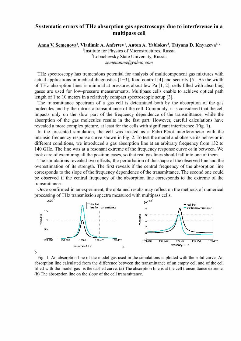
Systematic errors of THz absorption gas spectroscopy due to interference in amultipass cell
Anna V. Semenova1, Vladimir A. Anfertev1, Anton A. Yablokov1, Tatyana D. Knyazeva1, 2
1Institute for Physics of Microstructures, Russia2Lobachevsky State University, Russia
THz spectroscopy has tremendous potential for analysis of multicomponent gas mixtures withactual applications in medical diagnostics [1−3], food control [4] and security [5]. As the widthof THz absorption lines is minimal at pressures about few Pa [1, 2], cells filled with absorbinggases are used for low-pressure measurements. Multipass cells enable to achieve optical pathlength of 1 to 10 meters in a relatively compact spectroscopic setup [3].
The transmittance spectrum of a gas cell is determined both by the absorption of the gasmolecules and by the intrinsic transmittance of the cell. Commonly, it is considered that the cellimpacts only on the slow part of the frequency dependence of the transmittance, while theabsorption of the gas molecules results in the fast part. However, careful calculations haverevealed a more complex picture, at least for the cells with significant interference (Fig. 1).
In the presented simulation, the cell was treated as a Fabri-Pérot interferometer with theintrinsic frequency response curve shown in Fig. 2. To test the model and observe its behavior indifferent conditions, we introduced a gas absorption line at an arbitrary frequency from 132 to140 GHz. The line was at a resonant extreme of the frequency response curve or in between. Wetook care of examining all the position cases, so that real gas lines should fall into one of them.
The simulations revealed two effects, the perturbation of the shape of the observed line and theoverestimation of its strength. The first reveals if the central frequency of the absorption linecorresponds to the slope of the frequency dependence of the transmittance. The second one couldbe observed if the central frequency of the absorption line corresponds to the extreme of thetransmittance.
Once confirmed in an experiment, the obtained results may reflect on the methods of numericalprocessing of THz transmission spectra measured with multipass cells.
ab
Fig. 1. An absorption line of the model gas used in the simulations is plotted with the solid curve. Anabsorption line calculated from the difference between the transmittance of an empty cell and of the cellfilled with the model gas is the dashed curve. (a) The absorption line is at the cell transmittance extreme.(b) The absorption line on the slope of the cell transmittance.
Fig. 2. The frequency dependence of the intrinsic transmittance of the cell (TM-polarization).AcknowledgementsThis research was funded by the Russian Science Foundation, grant No. 21-19-00357,
https://rscf.ru/en/project/21-19-00357/References[1] V.L. Vaks, A.A. Aizenshtadt, V.A. Anfertevet. al., Appl Sci. 11(16)(2021) 7562[2] V.L. Vaks, E.G. Domracheva, S.I. Pripolzin, M.B. Chernyaeva, Proc. ofSPIE9934 (2016)
99340E-1[3] N. Rothbart, K. Schmalz, H. Hübers, IEEE Transactions on Terahertz Science and
Technology, 10(1) (2020) 9-14[4] V.L. Vaks, E.G. Domracheva, S.I. Pripolzin, et al., J Appl Spectrosc 86 (2019) 861–866[5] V.L. Vaks, J Infrared Milli Terahz Waves 33 (2012), 43–53
Hydrogen sorbtion in ZnO nanostructures
C. Samoil1, V.Chihaia1, Razvan Mihalcea3, Ionut Nicolae3, M.Serbanescu3, E. Slushanschi3,Cristian Viespe3 and Aurelian Marcu3
1University ‘Politehnica’ of Bucharest, Bucharest 060042, Romania2Institute of Physical Chemistry “Ilie Murgulescu”, Bucharest 060021, Romania
3National Institute for Laser Plasma and Radiation Physics, Magurele 077125, RomaniaEmail – [email protected]
While sensors are a key issue in the present technological development, decreasing thedetection limit in gas sensing is just one of the main directions of the development for a widerange of application worldwide including green anergy. Hydrogen is one of the serious greenenergy candidates for reducing carbon dioxide polution but with serious safety issues, needing arigurous monitoring of its presence into the atmosphere. ZnO is a versatile wide bang-gapsemiconductor with a good sorbtion of various gases including hydrogen isotopes, and presentlyused in a wide range of sensor applications. For a ZnO sensor case with application in hydrogendetection, decreasing of the sensor detection limit relays mostly on the increasing of the sensoractive area surface and the main way of doing that is using ZnO nanostructures as alternative tobulk material for sensing applications. Controlled morphology nanowires are used as ‘buildingblocks’ for such an active layer. On the other hand ZnO nanostructures presents a series ofenhanced properties related with the bulk materials, due to the high surface-to-volume ration,and, it is relatively easy to grow on many materials. In the present work, using LAMPopen-source software, theoretical simulation on ZnO nanowire gas absorption were performed.Theoretical simulations for hydrogen gas and its isotopesand are presented together with someexperimental gas detection results using SAW sensors. Results are aimed for device applicationsin gas detection and possible discrimination as well as pressure measurements.
Different sizes of gold nanoparticles in a self-assembling plasmonic filmas a SERS substrates
Kseniya Maleeva1, Antonina Dadadzhanova1, Mikhail Baranov1 and Kirill Bogdanov1
1ITMO University, RussiaEmail – [email protected]
Surface-enhanced Raman scattering (SERS) is a powerful analytical method for studying thecomposition of various analytes. It can be used in chemistry, medicine, biology, material sciencesand other areas of life [1]. SERS has two main types of enhancing media. They are colloidalsuspensions of plasmonic nanoparticles and solid substrates with immobilized plasmonicnanoparticles on their solid surfaces. Each has associated advantages and disadvantages. Themain problem of colloidal suspensions is time-dependences of enhancing factors. Most solidsubstrates have irreproducible surface distributions of enhancing factors. Regularly patternedsurfaces obtained via lithographic techniques or thermal evaporation can solve problems ofirreproducible surface distribution, but they are expensive to synthesize. Self-assembledplasmonic films (SPF) have been studied as potential SERS active substrates. This method of theenhancing substrate synthesis combines the simplicity of synthesis, the regularity of the resultingstructure, the absence of the dependence of the enhancing factor on time. SPF are metal films atthe interface between an aqueous gold colloid and a solution of a modifier in an organic solvent.The main types of modifiers are transition metal complexes, thiols, quaternary ammonium andarsonium salts crown ethers, etc [2].
Colloids with different sizes of gold nanoparticles (Au-NP) were synthesized by the citratemethod with varying the content of sodium citrate in the reaction mixture [3]. SEM and DSLstudies were carried out to determine the particle size of the obtained colloids. Colloid № 1 (C1)contained spherical particles 40 nm in size. Colloid № 2 (C2) consisted of lamellar particles withan approximate size of 60x30x15 nm. Colloid № 3 (C3) contained spherical particles of 15 - 20nm in size. The zeta potential of the obtained colloid Au-NPs is equal to - 20.7 mV, - 37.6 mVand -8 mV for C1, C2 and C3, respectively. C1 and C3 were unstable. The film was obtainedfrom freshly prepared colloids. SEM and DLS results were obtained at the same time withobtaining film, and the absorption spectrum was recorded later only for stable C2. However, SPFalso formed from aggregated colloids. Three obtained colloids were used to obtain SPF. Threesamples were prepared on a glass substrate for the comparison of enhancement substrates study.Pseudoisocyanine iodide (1,1'-diethyl-2,2'-cyanine iodide) was selected as the analyte. Theintensity distribution map (IDM) of samples with an area of 2025 μm2 was obtained on aRenishaw micro-Raman spectrometer. Average intensity of IDM and IDM gates were calculatedfor C1, C2 and C3. These quantities for C1 are 5393 counts and 3523 counts (5393±3523 countsfurther), for C2 are 9398±1838 counts and for C3 are 2414±1274 counts. This corresponds toanalytical enhancing factors [1] 5·104, 9·104, and 2·104 for samples C1, C2, and C3, respectively.The best enhancement will be determined in future works. Optimization of the ratio of thereaction mixture components in the SPF preparation will be carried out in these works.
This work was supported by the Russian Science Foundation (Agreement 20-72-00114).
References[1] J. Langer, et al., ACS Nano 14 (2020) 28[2] M. P. Konrad, A. P. Doherty, and S. E. J. Bell, Anal. Chem. 85 (2013) 6783[3] P. C. Lee, D. Meisel The Journal of Physical Chemistry 86 (1982) 17
Electronic Nose based on Organic Field Effect Transistors
Askold A. Trul,1,2 Daniil S. Anisimov,1,2 Victoria P. Chekusova,1,2 Anton A. Abramov1, Oleg V. Borshchev,1 Elena V. Agina1 and Sergey A. Ponomarenko1
1Enikolopov Institute of Synthetic Polymeric Materials of Russian Academy of Sciences, Russian Federation
2Printeltech LLC, Russian Federation Email: [email protected]
Real-time quantitative analysis of various gaseous mixtures such as indoor and outdoor air atmosphere, exhaled breath, food aromas, etc., are becoming more and more important from both safety and personal medicine points of view. Modern solid-state gas sensors are approaching limit of detection of a few ppbs while their cost is much less then ones utilizing benchmark optical and mass-spectroscopy methods. Thin-film organic field effect transistors (OFETs) are notably promising for gas sensing due to their high sensitivity at room temperature, low power consumption and architectural versatility. Such high sensitivity achieved due to direct contact between the thin current-carrying layer and the analyte in the OFETs leasing to the strong dependence of the OFETs electrical properties on the environment. [1] However, due to non-covalent sensing mechanism, single OFET sensors responses to a different of analytes including water vapors, are rather similar what leading to their main drawbacks – poor selectivity and environmental instability.[2] To overcome such problems usually the “electronic nose” approach based on a combination of cross-selective sensors array with pattern recognition algorithms is used, however up to now it was rarely reported for OFETs.
Figure 1. (a) Response of sensors with different receptors. LDA diagrams for target gases in (b) dry and (c) humid air.
We present the first fully integrated, compact and portable electronic nose based on array of OFETs gas sensors with varied cross-sensitivity. We developed a simple, affordable and versatile approach for fabrication of such array on a single substrate. This approach is based on partial modification of the substrate with a set of receptor molecules by easy-processable and rather fast Langmuir technique. Fabricated sensors were found to be very stable and have a limit of detection down to 30 ppb of NO2 in a wide range of air humidity from 0 to 95%. Electronic nose also demonstrated great ability of distinguishing low molecular gases such as NH3, NO2, H2S and Et-SH at the same humidity range (Fig.1). The device have a great potential in a wide range of practical applications such as environmental monitoring and food spoilage detection.[3] References [1] Andringa, A.-M., et al., Org Electron (2010), 11(5): p. 895-898.[2] Song, R., et al., Chempluschem(2019), 84(9): p. 1222-1234.[3] Anisimov, D.S., et al.,. Sci Rep(202), 11(1): p. 10683.
a) b) c)


