Embed Size (px)
Citation preview

SCADAMETRICS
Bell 202 Modem
DIGITAL COMMUNICATIONS
FOR RADIO TELEMETRY
Standards-Based, Non-Proprietary Modem
For Radio Telemetry…
The SCADAmetrics Model B202 Modem is designed to provide non-proprietary, Bell-202 data modulation and
demodulation for many popular analog telemetry
radios.
The unit offers the following notable features:
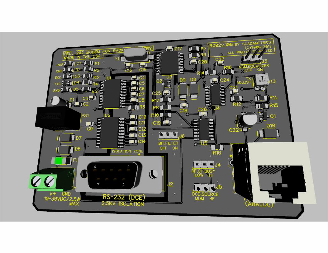
Wide-Input Power Range 10-30VDC.
2.5KV Isolated Serial Port for RS-232 Interface to PLC/RTU/Computer.
Serial Port Pins 4-6, 7-8 Jumpered for Rockwell/Allen Bradley Compatibility.
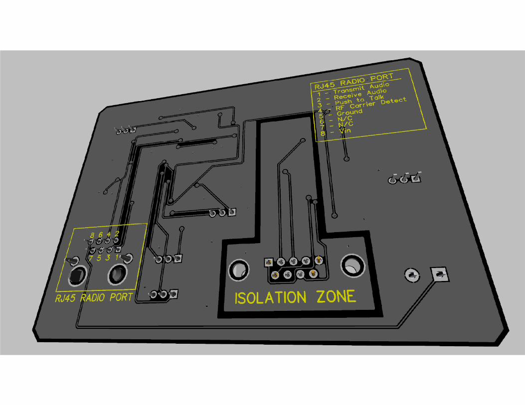
Radio Interface: RJ45F.
Industrial Din-Rail Mount.
LED’s: Power, Transmit, Receive, TxD, RxD.
Adjustable Transmit Audio Level: 0-2V Peak-to-Peak Signal. Able to Drive 600-∞ Ω Loads.
Selectable RF or Modem Carrier Detect.
Carrier-Detect Byte Filtering Option.
Receive Signal Equalizer Option.
‘Dumb’ Mode Operation.
2 YEAR WARRANTY
The B202 modem permits users to mix various makes
and models of compatible radios within a telemetry system, thereby alleviating the problem of vendor lock-
in.
This new design is based upon the MX614 modem IC (CML Micro), and it is also fully compatible with legacy
Bell-202 modems that are based upon the TCM3105 modem IC (Texas Instruments), such as the Calamp
DM-3282, Maxon SD-FSK, and MARC 366-101.
Compatibility is anticipated with a wide range of popular analog telemetry radios, including models from
the following manufacturers:
Ritron
Tecnet / Maxon
GE / Microwave Data Systems
Calamp
RF Neulink
In accordance with FCC CFR 47 Part 15.103(a,b,c) – the B202 is only intended to be used as a control
system component at public utility facilities, industrial plants, and within commercial transportation vehicles.
It is also intended to be used within industrial, commercial, & medical test equipment. Not intended
for consumer applications.
SCADAmetrics
scadametrics.com
St. Louis, Missouri USA
(636)405-7101
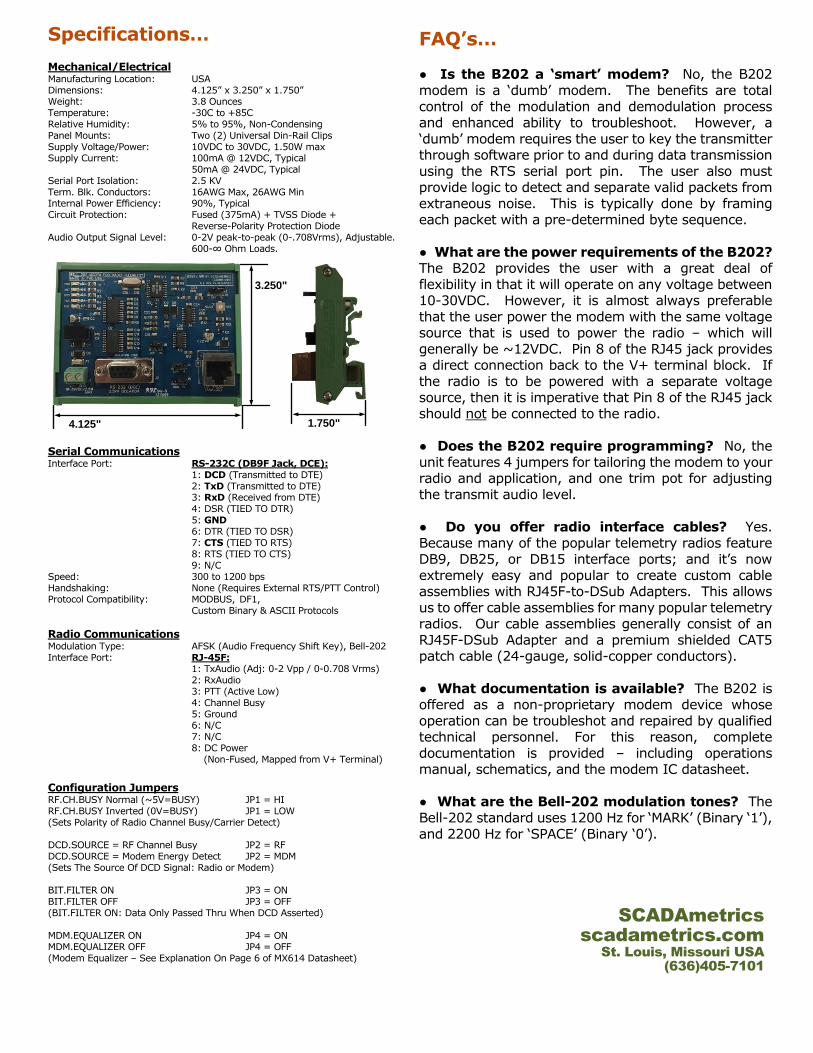
Specifications…
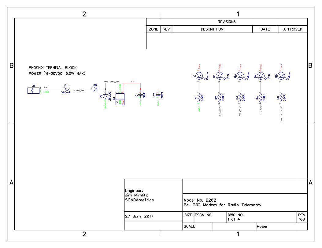
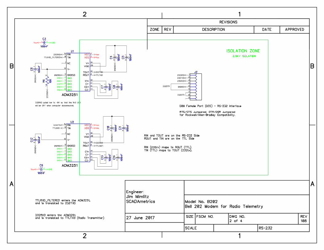
Mechanical/Electrical Manufacturing Location: USA Dimensions: 4.125” x 3.250” x 1.750” Weight: 3.8 Ounces Temperature: -30C to +85C Relative Humidity: 5% to 95%, Non-Condensing Panel Mounts: Two (2) Universal Din-Rail Clips Supply Voltage/Power: 10VDC to 30VDC, 1.50W max Supply Current: 100mA @ 12VDC, Typical 50mA @ 24VDC, Typical Serial Port Isolation: 2.5 KV
Term. Blk. Conductors: 16AWG Max, 26AWG Min Internal Power Efficiency: 90%, Typical Circuit Protection: Fused (375mA) + TVSS Diode + Reverse-Polarity Protection Diode Audio Output Signal Level: 0-2V peak-to-peak (0-.708Vrms), Adjustable. 600-∞ Ohm Loads.
4.125"
3.250"
1.750"
Serial Communications Interface Port: RS-232C (DB9F Jack, DCE): 1: DCD (Transmitted to DTE) 2: TxD (Transmitted to DTE) 3: RxD (Received from DTE) 4: DSR (TIED TO DTR) 5: GND 6: DTR (TIED TO DSR) 7: CTS (TIED TO RTS) 8: RTS (TIED TO CTS) 9: N/C Speed: 300 to 1200 bps Handshaking: None (Requires External RTS/PTT Control) Protocol Compatibility: MODBUS, DF1, Custom Binary & ASCII Protocols
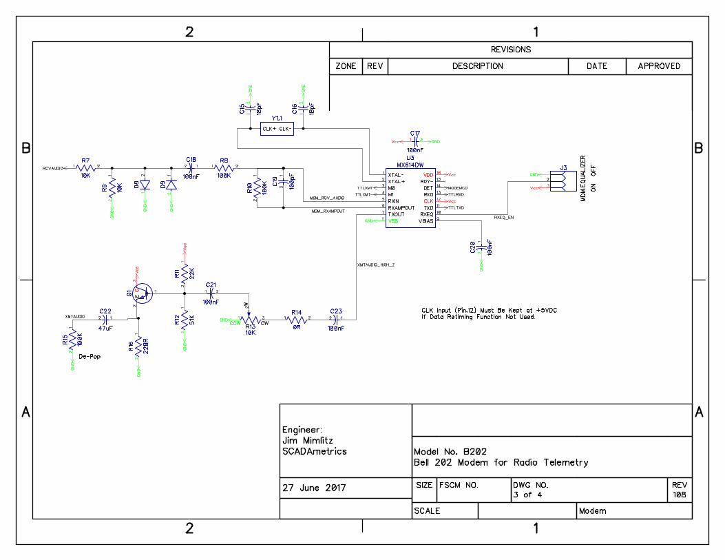
Radio Communications Modulation Type: AFSK (Audio Frequency Shift Key), Bell-202 Interface Port: RJ-45F: 1: TxAudio (Adj: 0-2 Vpp / 0-0.708 Vrms) 2: RxAudio 3: PTT (Active Low) 4: Channel Busy 5: Ground 6: N/C 7: N/C 8: DC Power (Non-Fused, Mapped from V+ Terminal)
Configuration Jumpers RF.CH.BUSY Normal (~5V=BUSY) JP1 = HI RF.CH.BUSY Inverted (0V=BUSY) JP1 = LOW (Sets Polarity of Radio Channel Busy/Carrier Detect) DCD.SOURCE = RF Channel Busy JP2 = RF DCD.SOURCE = Modem Energy Detect JP2 = MDM (Sets The Source Of DCD Signal: Radio or Modem) BIT.FILTER ON JP3 = ON BIT.FILTER OFF JP3 = OFF (BIT.FILTER ON: Data Only Passed Thru When DCD Asserted)
MDM.EQUALIZER ON JP4 = ON MDM.EQUALIZER OFF JP4 = OFF (Modem Equalizer – See Explanation On Page 6 of MX614 Datasheet)
FAQ’s… Is the B202 a ‘smart’ modem? No, the B202
modem is a ‘dumb’ modem. The benefits are total
control of the modulation and demodulation process and enhanced ability to troubleshoot. However, a
‘dumb’ modem requires the user to key the transmitter through software prior to and during data transmission
using the RTS serial port pin. The user also must provide logic to detect and separate valid packets from
extraneous noise. This is typically done by framing each packet with a pre-determined byte sequence.
What are the power requirements of the B202? The B202 provides the user with a great deal of
flexibility in that it will operate on any voltage between 10-30VDC. However, it is almost always preferable
that the user power the modem with the same voltage source that is used to power the radio – which will
generally be ~12VDC. Pin 8 of the RJ45 jack provides a direct connection back to the V+ terminal block. If
the radio is to be powered with a separate voltage
source, then it is imperative that Pin 8 of the RJ45 jack should not be connected to the radio.
Does the B202 require programming? No, the
unit features 4 jumpers for tailoring the modem to your radio and application, and one trim pot for adjusting
the transmit audio level.
Do you offer radio interface cables? Yes.
Because many of the popular telemetry radios feature DB9, DB25, or DB15 interface ports; and it’s now
extremely easy and popular to create custom cable assemblies with RJ45F-to-DSub Adapters. This allows
us to offer cable assemblies for many popular telemetry radios. Our cable assemblies generally consist of an
RJ45F-DSub Adapter and a premium shielded CAT5 patch cable (24-gauge, solid-copper conductors).
What documentation is available? The B202 is offered as a non-proprietary modem device whose
operation can be troubleshot and repaired by qualified technical personnel. For this reason, complete
documentation is provided – including operations manual, schematics, and the modem IC datasheet.
What are the Bell-202 modulation tones? The
Bell-202 standard uses 1200 Hz for ‘MARK’ (Binary ‘1’),
and 2200 Hz for ‘SPACE’ (Binary ‘0’).
SCADAmetrics
scadametrics.com
St. Louis, Missouri USA
(636)405-7101

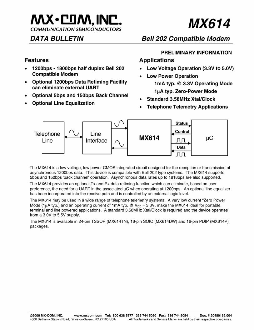
COMMUNICATION SEMICONDUCTORSMX614
DATA BULLETIN Bell 202 Compatible Modem
2000 MX-COM, INC. www.mxcom.com Tel: 800 638 5577 336 744 5050 Fax: 336 744 5054 Doc. # 20480162.0044800 Bethania Station Road, Winston-Salem, NC 27105 USA All Trademarks and Service Marks are held by their respective companies.
PRELIMINARY INFORMATION
Features Applications• 1200bps - 1800bps half duplex Bell 202
Compatible Modem
• Optional 1200bps Data Retiming Facilitycan eliminate external UART
• Optional 5bps and 150bps Back Channel
• Optional Line Equalization
• Low Voltage Operation (3.3V to 5.0V)
• Low Power Operation1mA typ. @ 3.3V Operating Mode
1µµµµA typ. Zero-Power Mode
• Standard 3.58MHz Xtal/Clock
• Telephone Telemetry Applications
µC
Data
Control
Status
MX614Line
InterfaceTelephone
Line
The MX614 is a low voltage, low power CMOS integrated circuit designed for the reception or transmission ofasynchronous 1200bps data. This device is compatible with Bell 202 type systems. The MX614 supports5bps and 150bps 'back channel' operation. Asynchronous data rates up to 1818bps are also supported.
The MX614 provides an optional Tx and Rx data retiming function which can eliminate, based on userpreference, the need for a UART in the associated µC when operating at 1200bps. An optional line equalizerhas been incorporated into the receive path and is controlled by an external logic level.
The MX614 may be used in a wide range of telephone telemetry systems. A very low current “Zero PowerMode (1µA typ.) and an operating current of 1mA typ. @ VDD = 3.3V, make the MX614 ideal for portable,terminal and line powered applications. A standard 3.58MHz Xtal/Clock is required and the device operatesfrom a 3.0V to 5.5V supply.
The MX614 is available in 24-pin TSSOP (MX614TN), 16-pin SOIC (MX614DW) and 16-pin PDIP (MX614P)packages.
Bell 202 Compatible Modem 2 MX614 PRELIMINARY INFORMATION
2000 MX-COM, INC. www.mxcom.com Tel: 800 638 5577 336 744 5050 Fax: 336 744 5054 Doc. # 20480162.0044800 Bethania Station Road, Winston-Salem, NC 27105 USA All Trademarks and Service Marks are held by their respective companies.
CONTENTSSection Page
1. Block Diagram................................................................................................................. 3
2. Signal List........................................................................................................................ 4
3. External Components ..................................................................................................... 5
4. General Description ........................................................................................................ 64.1 Xtal Osc and Clock Dividers....................................................................................................6
4.2 Mode Control Logic .................................................................................................................6
4.3 Rx Input Amplifier....................................................................................................................6
4.4 Receive Filter and Equalizer ...................................................................................................6
4.5 Energy Detector ......................................................................................................................7
4.6 FSK Demodulator....................................................................................................................7
4.7 FSK Modulator and Transmit Filter .........................................................................................8
4.8 Rx Data Retiming....................................................................................................................9
4.9 Tx Data Retiming ..................................................................................................................10
5. Application Notes.......................................................................................................... 125.1 Line Interface ........................................................................................................................12
6. Performance Specification........................................................................................... 136.1 Electrical Performance ..........................................................................................................13
6.2 Packaging .............................................................................................................................16
MX•COM, Inc. reserves the right to change specifications at any time and without notice.
Bell 202 Compatible Modem 3 MX614 PRELIMINARY INFORMATION
2000 MX-COM, INC. www.mxcom.com Tel: 800 638 5577 336 744 5050 Fax: 336 744 5054 Doc. # 20480162.0044800 Bethania Station Road, Winston-Salem, NC 27105 USA All Trademarks and Service Marks are held by their respective companies.
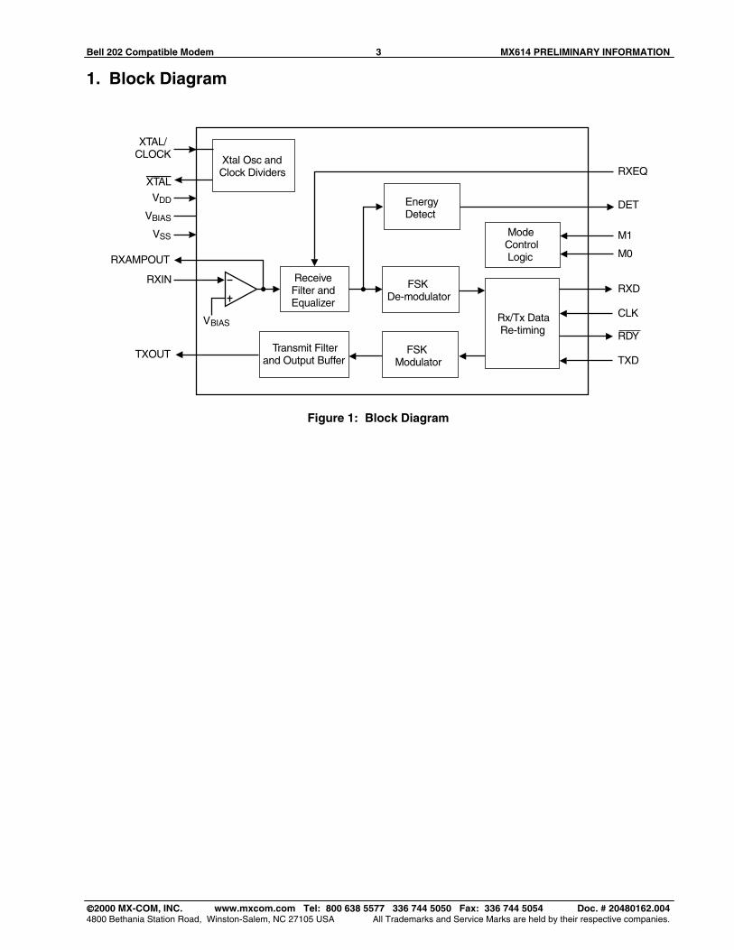
1. Block Diagram
TXD
M0
RXEQ
CLK
RXD
RDY
M1
DETEnergyDetect
FSKDe-modulator
ReceiveFilter andEqualizer
ModeControlLogic
Rx/Tx DataRe-timing
Transmit Filterand Output Buffer
FSKModulator
RXIN
RXAMPOUT
TXOUT
Xtal Osc andClock Dividers
XTAL/CLOCK
XTAL
VDD
VBIAS
VBIAS
VSS
Figure 1: Block Diagram
Bell 202 Compatible Modem 4 MX614 PRELIMINARY INFORMATION
2000 MX-COM, INC. www.mxcom.com Tel: 800 638 5577 336 744 5050 Fax: 336 744 5054 Doc. # 20480162.0044800 Bethania Station Road, Winston-Salem, NC 27105 USA All Trademarks and Service Marks are held by their respective companies.
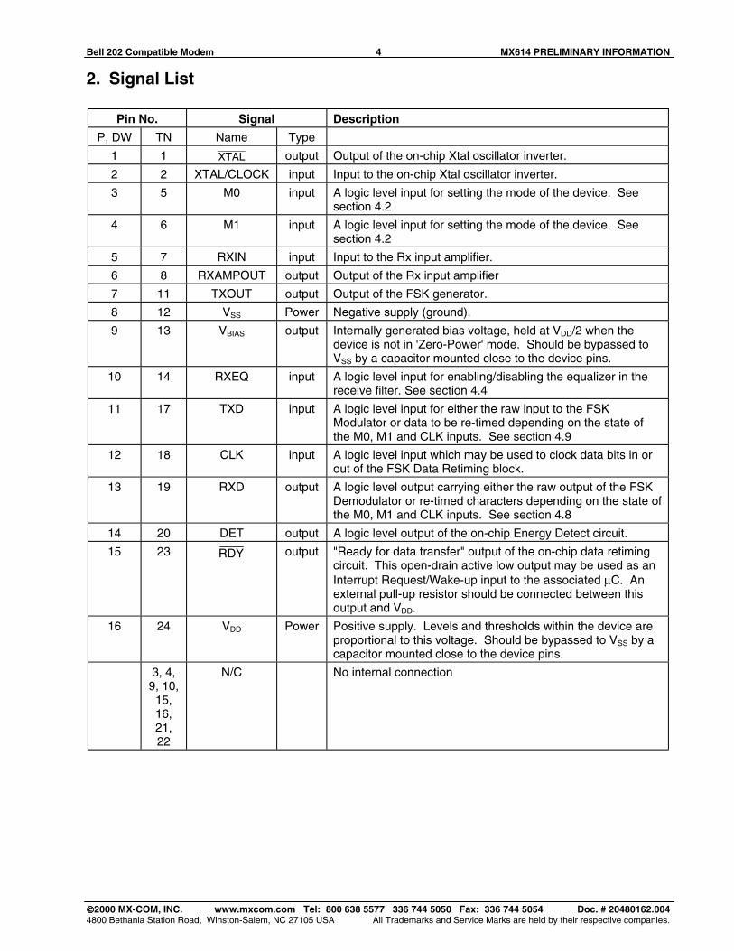
2. Signal List
Pin No. Signal Description
P, DW TN Name Type
1 1 XTAL output Output of the on-chip Xtal oscillator inverter.
2 2 XTAL/CLOCK input Input to the on-chip Xtal oscillator inverter.
3 5 M0 input A logic level input for setting the mode of the device. Seesection 4.2
4 6 M1 input A logic level input for setting the mode of the device. Seesection 4.2
5 7 RXIN input Input to the Rx input amplifier.
6 8 RXAMPOUT output Output of the Rx input amplifier
7 11 TXOUT output Output of the FSK generator.
8 12 VSS Power Negative supply (ground).
9 13 VBIAS output Internally generated bias voltage, held at VDD/2 when thedevice is not in 'Zero-Power' mode. Should be bypassed toVSS by a capacitor mounted close to the device pins.
10 14 RXEQ input A logic level input for enabling/disabling the equalizer in thereceive filter. See section 4.4
11 17 TXD input A logic level input for either the raw input to the FSKModulator or data to be re-timed depending on the state ofthe M0, M1 and CLK inputs. See section 4.9
12 18 CLK input A logic level input which may be used to clock data bits in orout of the FSK Data Retiming block.
13 19 RXD output A logic level output carrying either the raw output of the FSKDemodulator or re-timed characters depending on the state ofthe M0, M1 and CLK inputs. See section 4.8
14 20 DET output A logic level output of the on-chip Energy Detect circuit.
15 23 RDY output "Ready for data transfer" output of the on-chip data retimingcircuit. This open-drain active low output may be used as anInterrupt Request/Wake-up input to the associated µC. Anexternal pull-up resistor should be connected between thisoutput and VDD.
16 24 VDD Power Positive supply. Levels and thresholds within the device areproportional to this voltage. Should be bypassed to VSS by acapacitor mounted close to the device pins.
3, 4,9, 10,15,16,21,22
N/C No internal connection
Bell 202 Compatible Modem 5 MX614 PRELIMINARY INFORMATION
2000 MX-COM, INC. www.mxcom.com Tel: 800 638 5577 336 744 5050 Fax: 336 744 5054 Doc. # 20480162.0044800 Bethania Station Road, Winston-Salem, NC 27105 USA All Trademarks and Service Marks are held by their respective companies.
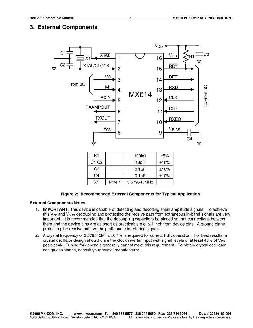
3. External Components
VDD
VBIASVSS
MX614
16
15
14
13
12
11
10
98
7
6
5
4
3
2
1
DET
RDY
CLK
RXEQ
RXD
TXD
M1
TXOUT
RXAMPOUT
RXIN
M0
To/F
rom
µC
From µC
C1
C2
C3
C4
X1 R1
XTAL/CLOCK
XTAL VDD
R1 100kΩ ±5%
C1 C2 18pF ±10%
C3 0.1µF ±10%
C4 0.1µF ±10%
X1 Note 1 3.579545MHz
Figure 2: Recommended External Components for Typical Application
External Components Notes
1. IMPORTANT: This device is capable of detecting and decoding small amplitude signals. To achievethis VDD and VBIAS decoupling and protecting the receive path from extraneous in-band signals are veryimportant. It is recommended that the decoupling capacitors be placed so that connections betweenthem and the device pins are as short as practicable e.g. ≤ 1 inch from device pins. A ground planeprotecting the receive path will help attenuate interfering signals
2. A crystal frequency of 3.579545MHz ±0.1% is required for correct FSK operation. For best results, acrystal oscillator design should drive the clock inverter input with signal levels of at least 40% of VDD
peak-peak. Tuning fork crystals generally cannot meet this requirement. To obtain crystal oscillatordesign assistance, consult your crystal manufacturer.
Bell 202 Compatible Modem 6 MX614 PRELIMINARY INFORMATION
2000 MX-COM, INC. www.mxcom.com Tel: 800 638 5577 336 744 5050 Fax: 336 744 5054 Doc. # 20480162.0044800 Bethania Station Road, Winston-Salem, NC 27105 USA All Trademarks and Service Marks are held by their respective companies.
4. General Description
4.1 Xtal Osc and Clock DividersFrequency and timing accuracy of the MX614 is determined by a 3.579545MHz clock signal present at theXTAL/CLOCK pin. This may be generated by the on-chip oscillator inverter using the external componentsC1, C2 and X1 of Figure 2, or may be supplied from an external source to the XTAL/CLOCK input. If suppliedfrom an external source, C1, C2 and X1 should not be fitted.
The on-chip oscillator is turned off in the 'Zero-Power' mode.
If the clock is provided by an external source which is not always running, then the 'Zero-Power' mode mustbe set when the clock is not available. Failure to observe this rule may cause a significant rise in the supplycurrent drawn by MX614 as well as generating undefined states of the RXD, DET and RDY outputs.
4.2 Mode Control LogicThe MX614's operating mode is determined by the logic levels applied to the M0 and M1 input pins:
M1 M0 Rx Mode Tx Mode Data Retime[1]
0 0 1200bps 150bps Rx
0 1 Off 1200bps Tx
1 0 1200bps Off / 5bps Rx
1 1 'Zero-Power' -
[1] If enabled
Note: On applying power to the device, the mode must be set to 'ZP', i.e. M0 = '1', M1 = '1', until VDD
has stabilized.
In the 'Zero-Power' (ZP) mode, power is removed from all internal circuitry. When leaving the 'ZP' mode theremust be a delay of 20ms before any Tx data is passed to, or Rx data read from the device to allow the biaslevel, filters, and oscillator to stabilize.
4.3 Rx Input AmplifierThis amplifier is used to adjust the received signal to the correct amplitude for the FSK receiver and EnergyDetect circuits (see section 5.1).
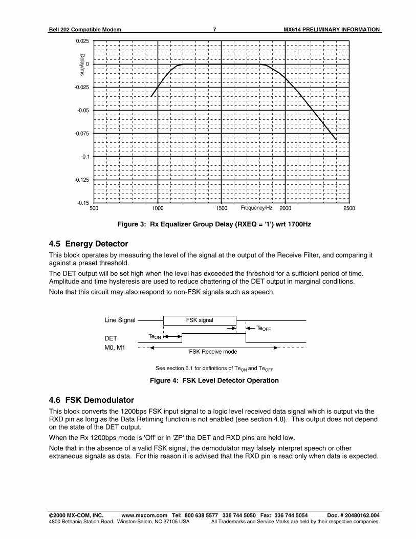
4.4 Receive Filter and EqualizerThe Receive Filter and Equalizer section is used to attenuate out of band noise and interfering signals,especially the locally generated transmit tones which might otherwise reach the 1200bps FSK Demodulatorand Energy Detector circuits. This block also includes a switchable equalizer section. When the RXEQ pin islow, the overall group delay of the receive filter is flat over the 1200bps frequency range. If the RXEQ pin ishigh the receive filter's typical overall group delay will be as shown in Figure 3.
Bell 202 Compatible Modem 7 MX614 PRELIMINARY INFORMATION
2000 MX-COM, INC. www.mxcom.com Tel: 800 638 5577 336 744 5050 Fax: 336 744 5054 Doc. # 20480162.0044800 Bethania Station Road, Winston-Salem, NC 27105 USA All Trademarks and Service Marks are held by their respective companies.
-0.15
-0.125
-0.1
-0.075
-0.05
-0.025
0
0.025
500 1000 1500 2000 2500
Delay/m
s
Frequency/Hz
Figure 3: Rx Equalizer Group Delay (RXEQ = '1') wrt 1700Hz
4.5 Energy DetectorThis block operates by measuring the level of the signal at the output of the Receive Filter, and comparing itagainst a preset threshold.
The DET output will be set high when the level has exceeded the threshold for a sufficient period of time.Amplitude and time hysteresis are used to reduce chattering of the DET output in marginal conditions.
Note that this circuit may also respond to non-FSK signals such as speech.
DET
Line Signal
M0, M1FSK Receive mode
FSK signal
TeON
TeOFF
See section 6.1 for definitions of TeON and TeOFF
Figure 4: FSK Level Detector Operation
4.6 FSK DemodulatorThis block converts the 1200bps FSK input signal to a logic level received data signal which is output via theRXD pin as long as the Data Retiming function is not enabled (see section 4.8). This output does not dependon the state of the DET output.
When the Rx 1200bps mode is 'Off' or in 'ZP' the DET and RXD pins are held low.
Note that in the absence of a valid FSK signal, the demodulator may falsely interpret speech or otherextraneous signals as data. For this reason it is advised that the RXD pin is read only when data is expected.
Bell 202 Compatible Modem 8 MX614 PRELIMINARY INFORMATION
2000 MX-COM, INC. www.mxcom.com Tel: 800 638 5577 336 744 5050 Fax: 336 744 5054 Doc. # 20480162.0044800 Bethania Station Road, Winston-Salem, NC 27105 USA All Trademarks and Service Marks are held by their respective companies.
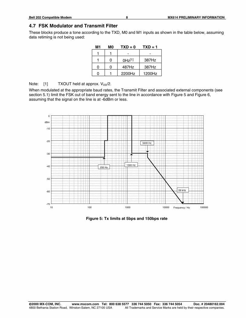
4.7 FSK Modulator and Transmit FilterThese blocks produce a tone according to the TXD, M0 and M1 inputs as shown in the table below, assumingdata retiming is not being used:
M1 M0 TXD = 0 TXD = 1
1 1 - -
1 0 0Hz[1] 387Hz
0 0 487Hz 387Hz
0 1 2200Hz 1200Hz
Note: [1] TXOUT held at approx. VDD/2.
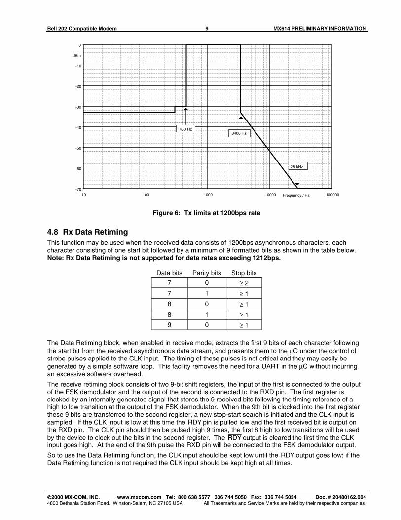
When modulated at the appropriate baud rates, the Transmit Filter and associated external components (seesection 5.1) limit the FSK out of band energy sent to the line in accordance with Figure 5 and Figure 6,assuming that the signal on the line is at -6dBm or less.
-70
-60
-50
-40
-30
-20
-10
0
10 100 1000 10000 100000Frequency / Hz
dBm
1300 Hz
3400 Hz
28 kHz
250 Hz
Figure 5: Tx limits at 5bps and 150bps rate
Bell 202 Compatible Modem 9 MX614 PRELIMINARY INFORMATION
2000 MX-COM, INC. www.mxcom.com Tel: 800 638 5577 336 744 5050 Fax: 336 744 5054 Doc. # 20480162.0044800 Bethania Station Road, Winston-Salem, NC 27105 USA All Trademarks and Service Marks are held by their respective companies.
-70
-60
-50
-40
-30
-20
-10
0
10 100 1000 10000 100000Frequency / Hz
dBm
3400 Hz
28 kHz
450 Hz
Figure 6: Tx limits at 1200bps rate
4.8 Rx Data RetimingThis function may be used when the received data consists of 1200bps asynchronous characters, eachcharacter consisting of one start bit followed by a minimum of 9 formatted bits as shown in the table below.Note: Rx Data Retiming is not supported for data rates exceeding 1212bps.
Data bits Parity bits Stop bits
7 0 ≥ 2
7 1 ≥ 1
8 0 ≥ 1
8 1 ≥ 1
9 0 ≥ 1
The Data Retiming block, when enabled in receive mode, extracts the first 9 bits of each character followingthe start bit from the received asynchronous data stream, and presents them to the µC under the control ofstrobe pulses applied to the CLK input. The timing of these pulses is not critical and they may easily begenerated by a simple software loop. This facility removes the need for a UART in the µC without incurringan excessive software overhead.
The receive retiming block consists of two 9-bit shift registers, the input of the first is connected to the outputof the FSK demodulator and the output of the second is connected to the RXD pin. The first register isclocked by an internally generated signal that stores the 9 received bits following the timing reference of ahigh to low transition at the output of the FSK demodulator. When the 9th bit is clocked into the first registerthese 9 bits are transferred to the second register, a new stop-start search is initiated and the CLK input issampled. If the CLK input is low at this time the RDY pin is pulled low and the first received bit is output onthe RXD pin. The CLK pin should then be pulsed high 9 times, the first 8 high to low transitions will be usedby the device to clock out the bits in the second register. The RDY output is cleared the first time the CLKinput goes high. At the end of the 9th pulse the RXD pin will be connected to the FSK demodulator output.
So to use the Data Retiming function, the CLK input should be kept low until the RDY output goes low; if theData Retiming function is not required the CLK input should be kept high at all times.
Bell 202 Compatible Modem 10 MX614 PRELIMINARY INFORMATION
2000 MX-COM, INC. www.mxcom.com Tel: 800 638 5577 336 744 5050 Fax: 336 744 5054 Doc. # 20480162.0044800 Bethania Station Road, Winston-Salem, NC 27105 USA All Trademarks and Service Marks are held by their respective companies.
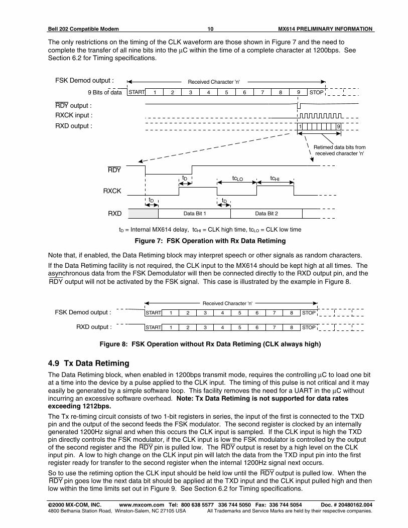
The only restrictions on the timing of the CLK waveform are those shown in Figure 7 and the need tocomplete the transfer of all nine bits into the µC within the time of a complete character at 1200bps. SeeSection 6.2 for Timing specifications.
START STOP1
1
2 3 4 5 6 7 8 9
9
FSK Demod output :
RDY output :
RXCK input :
RXD output :
Received Character 'n'
Retimed data bits fromreceived character 'n'
Data Bit 1 Data Bit 2
tD tcHItcLO
RXCK
RXD
9 Bits of data
tDtD
RDY
tD = Internal MX614 delay, tcHI = CLK high time, tcLO = CLK low time
Figure 7: FSK Operation with Rx Data Retiming
Note that, if enabled, the Data Retiming block may interpret speech or other signals as random characters.
If the Data Retiming facility is not required, the CLK input to the MX614 should be kept high at all times. Theasynchronous data from the FSK Demodulator will then be connected directly to the RXD output pin, and theRDY output will not be activated by the FSK signal. This case is illustrated by the example in Figure 8.
START
START
STOP
STOP
1
1
2
2
3
3
4
4
5
5
6
6
7
7
8
8
FSK Demod output :
RXD output :
Received Character 'n'
Figure 8: FSK Operation without Rx Data Retiming (CLK always high)
4.9 Tx Data RetimingThe Data Retiming block, when enabled in 1200bps transmit mode, requires the controlling µC to load one bitat a time into the device by a pulse applied to the CLK input. The timing of this pulse is not critical and it mayeasily be generated by a simple software loop. This facility removes the need for a UART in the µC withoutincurring an excessive software overhead. Note: Tx Data Retiming is not supported for data ratesexceeding 1212bps.
The Tx re-timing circuit consists of two 1-bit registers in series, the input of the first is connected to the TXDpin and the output of the second feeds the FSK modulator. The second register is clocked by an internallygenerated 1200Hz signal and when this occurs the CLK input is sampled. If the CLK input is high the TXDpin directly controls the FSK modulator, if the CLK input is low the FSK modulator is controlled by the outputof the second register and the RDY pin is pulled low. The RDY output is reset by a high level on the CLKinput pin. A low to high change on the CLK input pin will latch the data from the TXD input pin into the firstregister ready for transfer to the second register when the internal 1200Hz signal next occurs.
So to use the retiming option the CLK input should be held low until the RDY output is pulled low. When theRDY pin goes low the next data bit should be applied at the TXD input and the CLK input pulled high and thenlow within the time limits set out in Figure 9. See Section 6.2 for Timing specifications.
Bell 202 Compatible Modem 11 MX614 PRELIMINARY INFORMATION
2000 MX-COM, INC. www.mxcom.com Tel: 800 638 5577 336 744 5050 Fax: 336 744 5054 Doc. # 20480162.0044800 Bethania Station Road, Winston-Salem, NC 27105 USA All Trademarks and Service Marks are held by their respective companies.
1
1
1
2 3 4
32FSK Modulator input :
CLK input :
TXD input :
tS tH
tD
tR
tcHI
RDY
CLK
TXD
RDY output :
tD = Internal MX614 delay, tR = RDY low to CLK going low, tS = data set up time
tcHI= CLK high time, tH = data hold time
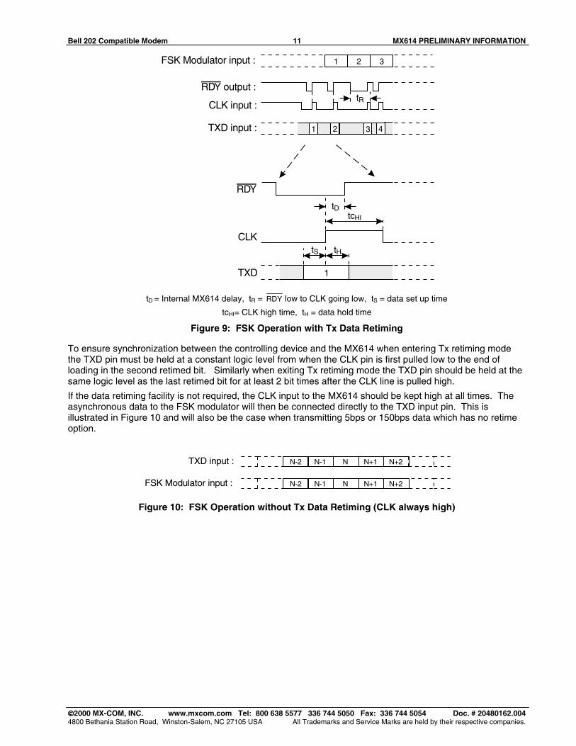
Figure 9: FSK Operation with Tx Data Retiming
To ensure synchronization between the controlling device and the MX614 when entering Tx retiming modethe TXD pin must be held at a constant logic level from when the CLK pin is first pulled low to the end ofloading in the second retimed bit. Similarly when exiting Tx retiming mode the TXD pin should be held at thesame logic level as the last retimed bit for at least 2 bit times after the CLK line is pulled high.
If the data retiming facility is not required, the CLK input to the MX614 should be kept high at all times. Theasynchronous data to the FSK modulator will then be connected directly to the TXD input pin. This isillustrated in Figure 10 and will also be the case when transmitting 5bps or 150bps data which has no retimeoption.
N-2
N-2
N-1
N-1
N
N
N+1
N+1
N+2
N+2FSK Modulator input :
TXD input :
Figure 10: FSK Operation without Tx Data Retiming (CLK always high)
Bell 202 Compatible Modem 12 MX614 PRELIMINARY INFORMATION
2000 MX-COM, INC. www.mxcom.com Tel: 800 638 5577 336 744 5050 Fax: 336 744 5054 Doc. # 20480162.0044800 Bethania Station Road, Winston-Salem, NC 27105 USA All Trademarks and Service Marks are held by their respective companies.
5. Application
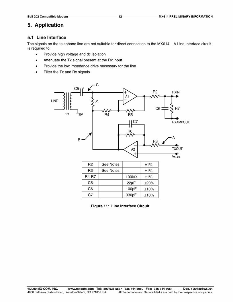
5.1 Line InterfaceThe signals on the telephone line are not suitable for direct connection to the MX614. A Line Interface circuitis required to:
• Provide high voltage and dc isolation
• Attenuate the Tx signal present at the Rx input
• Provide the low impedance drive necessary for the line
• Filter the Tx and Rx signals
LINE
1:1
R3
R6
R5R4
Z
R7
RXIN
RXAMPOUT
TXOUT
VBIAS
AB
C
A2
A1
0V
C5
C6
C7
R2
+
R2 See Notes ±1%,
R3 See Notes ±1%,
R4-R7 100kΩ ±1%,
C5 22µF ±20%
C6 100pF ±10%
C7 330pF ±10%
Figure 11: Line Interface Circuit
Bell 202 Compatible Modem 13 MX614 PRELIMINARY INFORMATION
2000 MX-COM, INC. www.mxcom.com Tel: 800 638 5577 336 744 5050 Fax: 336 744 5054 Doc. # 20480162.0044800 Bethania Station Road, Winston-Salem, NC 27105 USA All Trademarks and Service Marks are held by their respective companies.
Line Interface Notes:
1. The components 'Z' between points B and C should match the line impedance.
2. Device A2 must be able to drive 'Z' and the line.
3. R2: For optimum results R2 should be set so that the gain is VDD/5.0, i.e. R2 = 100kΩ at VDD = 5.0V, risingto 150kΩ at VDD = 3.3V.
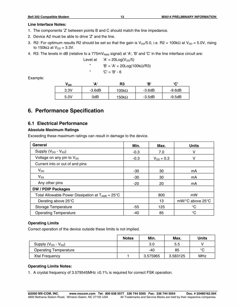
4. R3: The levels in dB (relative to a 775mVRMS signal) at 'A', 'B' and 'C' in the line interface circuit are:
Level at 'A' = 20Log(VDD/5)
" 'B' = 'A' + 20Log(100kΩ/R3)
" 'C' = 'B' - 6
Example:
VDD 'A' R3 'B' 'C'
3.3V -3.6dB 100kΩ -3.6dB -9.6dB
5.0V 0dB 150kΩ -3.5dB -9.5dB
6. Performance Specification
6.1 Electrical PerformanceAbsolute Maximum Ratings
Exceeding these maximum ratings can result in damage to the device.
General Min. Max. UnitsSupply (VDD - VSS) -0.3 7.0 VVoltage on any pin to VSS -0.3 VDD + 0.3 VCurrent into or out of and pins
VDD -30 30 mAVSS -30 30 mAAny other pins -20 20 mA
DW / PDIP Packages
Total Allowable Power Dissipation at TAMB = 25°C 800 mW
Derating above 25°C 13 mW/°C above 25°C
Storage Temperature -55 125 °C
Operating Temperature -40 85 °C
Operating Limits
Correct operation of the device outside these limits is not implied.
Notes Min. Max. Units
Supply (VDD - VSS) 3.0 5.5 V
Operating Temperature -40 85 °C
Xtal Frequency 1 3.575965 3.583125 MHz
Operating Limits Notes:
1. A crystal frequency of 3.579545MHz ±0.1% is required for correct FSK operation.
Bell 202 Compatible Modem 14 MX614 PRELIMINARY INFORMATION
2000 MX-COM, INC. www.mxcom.com Tel: 800 638 5577 336 744 5050 Fax: 336 744 5054 Doc. # 20480162.0044800 Bethania Station Road, Winston-Salem, NC 27105 USA All Trademarks and Service Marks are held by their respective companies.
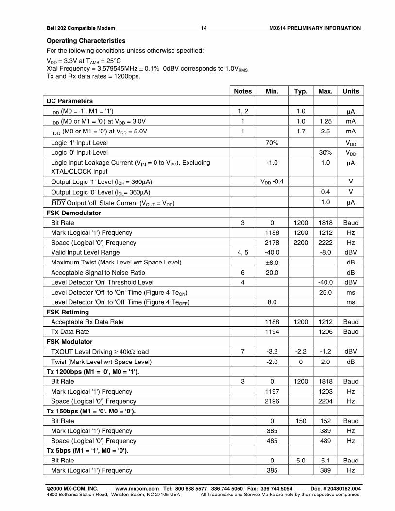
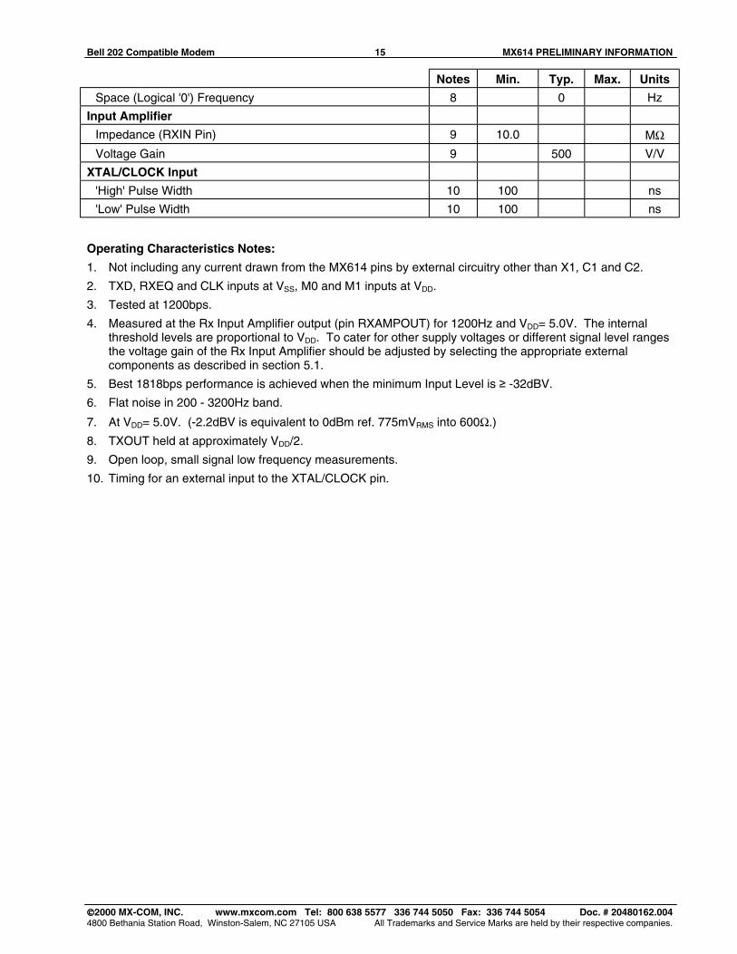
Operating Characteristics
For the following conditions unless otherwise specified:
VDD = 3.3V at TAMB = 25°CXtal Frequency = 3.579545MHz ± 0.1% 0dBV corresponds to 1.0VRMS
Tx and Rx data rates = 1200bps.
Notes Min. Typ. Max. Units
DC Parameters
IDD (M0 = '1', M1 = '1') 1, 2 1.0 µA
IDD (M0 or M1 = '0') at VDD = 3.0V 1 1.0 1.25 mA
IDD (M0 or M1 = '0') at VDD = 5.0V 1 1.7 2.5 mA
Logic '1' Input Level 70% VDD
Logic '0' Input Level 30% VDD
Logic Input Leakage Current (VIN = 0 to VDD), ExcludingXTAL/CLOCK Input
-1.0 1.0 µA
Output Logic '1' Level (lOH = 360µA) VDD -0.4 V
Output Logic '0' Level (lOL= 360µA) 0.4 V
RDY Output 'off' State Current (VOUT = VDD) 1.0 µA
FSK Demodulator
Bit Rate 3 0 1200 1818 Baud
Mark (Logical '1') Frequency 1188 1200 1212 Hz
Space (Logical '0') Frequency 2178 2200 2222 Hz
Valid Input Level Range 4, 5 -40.0 -8.0 dBV
Maximum Twist (Mark Level wrt Space Level) ±6.0 dB
Acceptable Signal to Noise Ratio 6 20.0 dB
Level Detector 'On' Threshold Level 4 -40.0 dBV
Level Detector 'Off' to 'On' Time (Figure 4 TeON) 25.0 ms
Level Detector 'On' to 'Off' Time (Figure 4 TeOFF) 8.0 ms
FSK Retiming
Acceptable Rx Data Rate 1188 1200 1212 Baud
Tx Data Rate 1194 1206 Baud
FSK Modulator
TXOUT Level Driving ≥ 40kΩ load 7 -3.2 -2.2 -1.2 dBV
Twist (Mark Level wrt Space Level) -2.0 0 2.0 dB
Tx 1200bps (M1 = '0', M0 = '1').
Bit Rate 3 0 1200 1818 Baud
Mark (Logical '1') Frequency 1197 1203 Hz
Space (Logical '0') Frequency 2196 2204 Hz
Tx 150bps (M1 = '0', M0 = '0').
Bit Rate 0 150 152 Baud
Mark (Logical '1') Frequency 385 389 Hz
Space (Logical '0') Frequency 485 489 Hz
Tx 5bps (M1 = '1', M0 = '0').
Bit Rate 0 5.0 5.1 Baud
Mark (Logical '1') Frequency 385 389 Hz
Bell 202 Compatible Modem 15 MX614 PRELIMINARY INFORMATION
2000 MX-COM, INC. www.mxcom.com Tel: 800 638 5577 336 744 5050 Fax: 336 744 5054 Doc. # 20480162.0044800 Bethania Station Road, Winston-Salem, NC 27105 USA All Trademarks and Service Marks are held by their respective companies.
Notes Min. Typ. Max. Units
Space (Logical '0') Frequency 8 0 Hz
Input Amplifier
Impedance (RXIN Pin) 9 10.0 MΩVoltage Gain 9 500 V/V
XTAL/CLOCK Input
'High' Pulse Width 10 100 ns
'Low' Pulse Width 10 100 ns
Operating Characteristics Notes:
1. Not including any current drawn from the MX614 pins by external circuitry other than X1, C1 and C2.
2. TXD, RXEQ and CLK inputs at VSS, M0 and M1 inputs at VDD.
3. Tested at 1200bps.
4. Measured at the Rx Input Amplifier output (pin RXAMPOUT) for 1200Hz and VDD= 5.0V. The internalthreshold levels are proportional to VDD. To cater for other supply voltages or different signal level rangesthe voltage gain of the Rx Input Amplifier should be adjusted by selecting the appropriate externalcomponents as described in section 5.1.
5. Best 1818bps performance is achieved when the minimum Input Level is -32dBV.
6. Flat noise in 200 - 3200Hz band.
7. At VDD= 5.0V. (-2.2dBV is equivalent to 0dBm ref. 775mVRMS into 600Ω.)
8. TXOUT held at approximately VDD/2.
9. Open loop, small signal low frequency measurements.
10. Timing for an external input to the XTAL/CLOCK pin.
Bell 202 Compatible Modem 16 MX614 PRELIMINARY INFORMATION
2000 MX-COM, INC. www.mxcom.com Tel: 800 638 5577 336 744 5050 Fax: 336 744 5054 Doc. # 20480162.0044800 Bethania Station Road, Winston-Salem, NC 27105 USA All Trademarks and Service Marks are held by their respective companies.
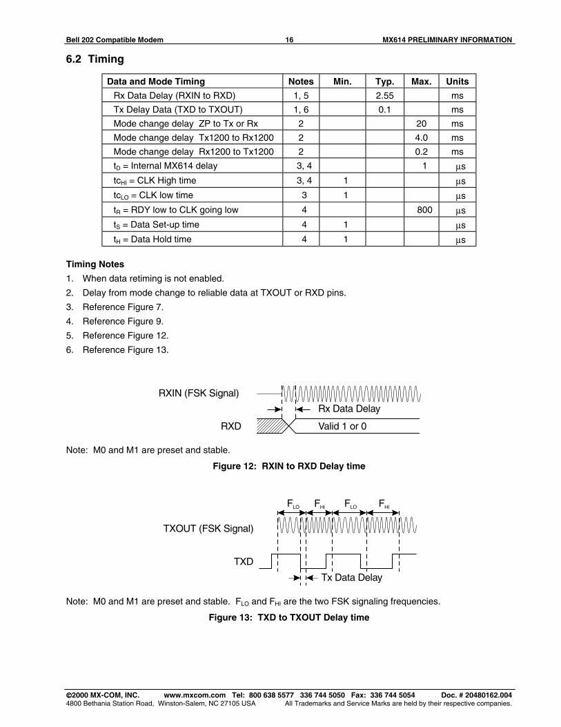
6.2 Timing
Data and Mode Timing Notes Min. Typ. Max. Units
Rx Data Delay (RXIN to RXD) 1, 5 2.55 ms
Tx Delay Data (TXD to TXOUT) 1, 6 0.1 ms
Mode change delay ZP to Tx or Rx 2 20 ms
Mode change delay Tx1200 to Rx1200 2 4.0 ms
Mode change delay Rx1200 to Tx1200 2 0.2 ms
tD = Internal MX614 delay 3, 4 1 µs
tcHI = CLK High time 3, 4 1 µs
tcLO = CLK low time 3 1 µs
tR = RDY low to CLK going low 4 800 µs
tS = Data Set-up time 4 1 µs
tH = Data Hold time 4 1 µs
Timing Notes
1. When data retiming is not enabled.
2. Delay from mode change to reliable data at TXOUT or RXD pins.
3. Reference Figure 7.
4. Reference Figure 9.
5. Reference Figure 12.
6. Reference Figure 13.
Valid 1 or 0RXD
RXIN (FSK Signal)
Rx Data Delay
Note: M0 and M1 are preset and stable.
Figure 12: RXIN to RXD Delay time
TXD
TXOUT (FSK Signal)
Tx Data Delay
FHIFLOFLO FHI
Note: M0 and M1 are preset and stable. FLO and FHI are the two FSK signaling frequencies.
Figure 13: TXD to TXOUT Delay time
Bell 202 Compatible Modem 17 MX614 PRELIMINARY INFORMATION
2000 MX-COM, INC. www.mxcom.com Tel: 800 638 5577 336 744 5050 Fax: 336 744 5054 Doc. # 20480162.0044800 Bethania Station Road, Winston-Salem, NC 27105 USA All Trademarks and Service Marks are held by their respective companies.
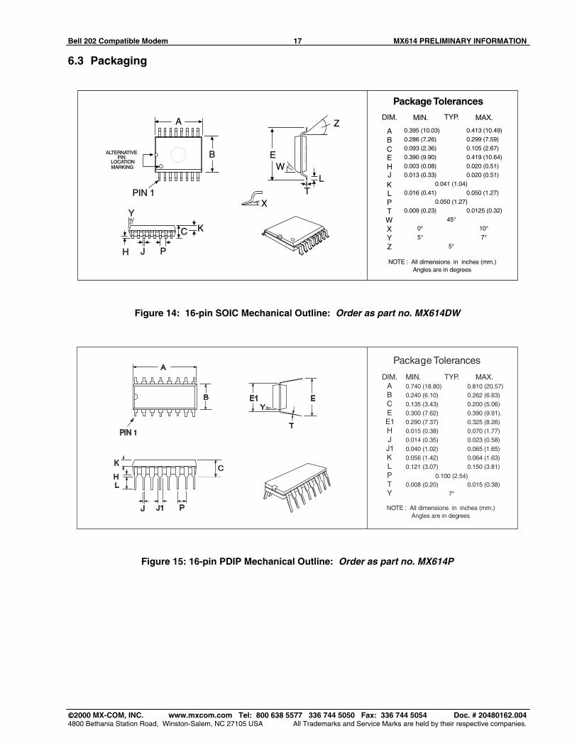
6.3 Packaging
PIN 1
A
BALTERNATIVEPIN
LOCATIONMARKING
X
PJ
Y
C K
H
E
LT
W
Z
NOTE : All dimensions in inches (mm.)Angles are in degrees
Package Tolerances
ABCEH
TYP. MAX.MIN.DIM.
J
P
XWT
Y
KL
0.105 (2.67)0.093 (2.36)0.419 (10.64)
45°
7°0° 10°
0.050 (1.27)0.041 (1.04)
0.413 (10.49)0.299 (7.59)
0.050 (1.27)0.016 (0.41)
0.390 (9.90)0.020 (0.51)0.003 (0.08)
0.009 (0.23) 0.0125 (0.32)
0.013 (0.33) 0.020 (0.51)
0.395 (10.03)0.286 (7.26)
Z 5°5°
Figure 14: 16-pin SOIC Mechanical Outline: Order as part no. MX614DW
Package Tolerances
NOTE : All dimensions in inches (mm.)Angles are in degrees
TYP. MAX.MIN.ABCEE1H
DIM.
JJ1
P
YT
KL
0.200 (5.06)0.262 (6.63)
0.390 (9.91).
7°
0.150 (3.81)
0.810 (20.57)
0.135 (3.43)
0.100 (2.54)
0.121 (3.07)
0.300 (7.62)0.290 (7.37) 0.325 (8.26)0.015 (0.38) 0.070 (1.77)
0.008 (0.20) 0.015 (0.38)
0.014 (0.35) 0.023 (0.58)0.040 (1.02) 0.065 (1.65)0.056 (1.42) 0.064 (1.63)
0.740 (18.80)0.240 (6.10)B
A
PIN 1
EY
E1
T
K
H
J1J
C
P
L
Figure 15: 16-pin PDIP Mechanical Outline: Order as part no. MX614P
Bell 202 Compatible Modem 18 MX614 PRELIMINARY INFORMATION
2000 MX-COM, INC. www.mxcom.com Tel: 800 638 5577 336 744 5050 Fax: 336 744 5054 Doc. # 20480162.0044800 Bethania Station Road, Winston-Salem, NC 27105 USA All Trademarks and Service Marks are held by their respective companies.
PIN 1
A
BALTERNATIVEPIN
LOCATIONMARKING
E
LT
PJ
Y
C
H
0.303 (7.70)
Package Tolerances
TYP. MAX.MIN.
ABCEH
DIM.
J
P
YT
L
0.047 (1.20)----------0.256 (6.50)
0° 8°
0.030 (0.75)
0.311 (7.90)0.177 (4.50)
0.0256 (0.65)0.020 (0.50)
0.248 (6.30)0.006 (0.15)0.002 (0.05)
0.003 (0.08) 0.008 (0.20)
0.007 (0.17) 0.012 (0.30)
0.169 (4.30)
NOTE : All dimensions in inches (mm.)Angles are in degrees
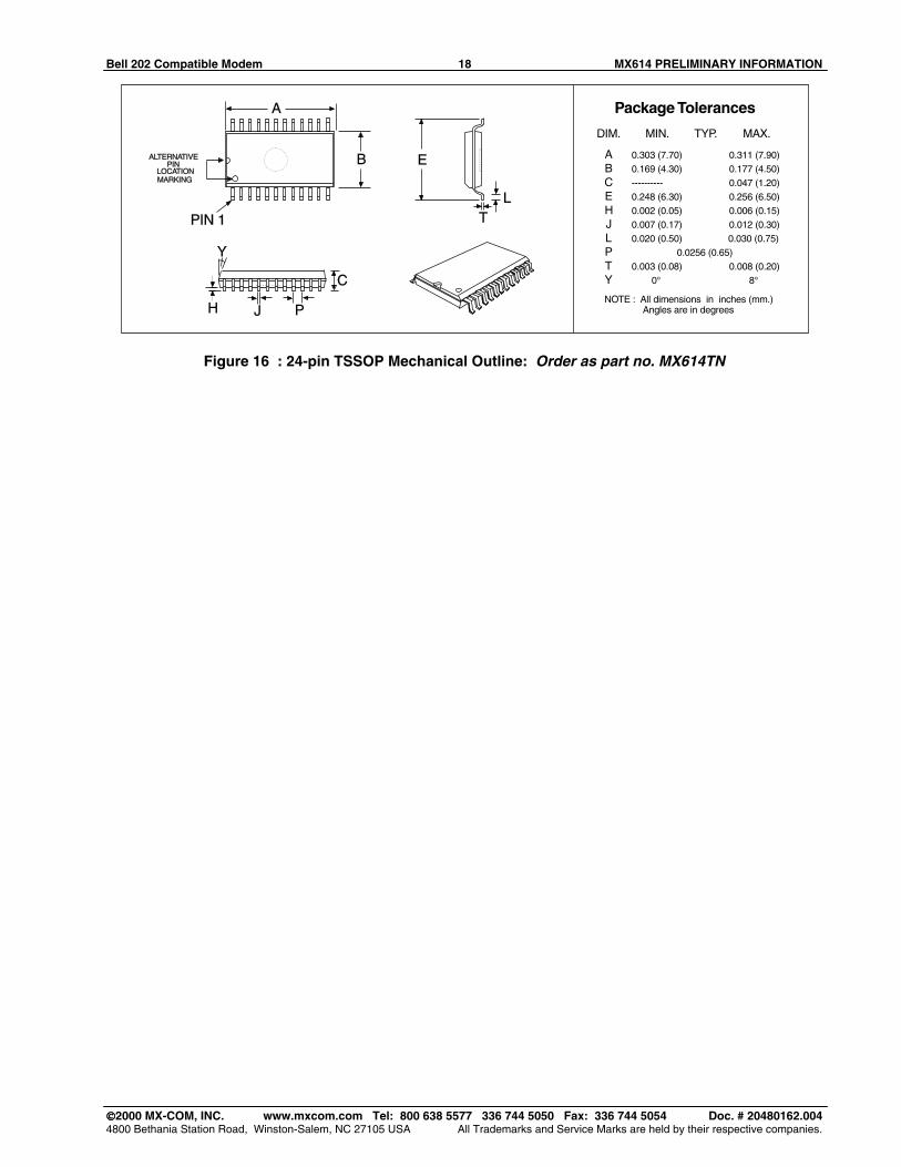
Figure 16 : 24-pin TSSOP Mechanical Outline: Order as part no. MX614TN

CML Product Data
In the process of creating a more global image, the three standard product semiconductorcompanies of CML Microsystems Plc (Consumer Microcircuits Limited (UK), MX-COM, Inc(USA) and CML Microcircuits (Singapore) Pte Ltd) have undergone name changes and, whilstmaintaining their separate new names (CML Microcircuits (UK) Ltd, CML Microcircuits (USA)Inc and CML Microcircuits (Singapore) Pte Ltd), now operate under the single title CMLMicrocircuits.These companies are all 100% owned operating companies of the CML Microsystems PlcGroup and these changes are purely changes of name and do not change any underlying legalentities and hence will have no effect on any agreements or contacts currently in force.
CML Microcircuits Product Prefix CodesUntil the latter part of 1996, the differentiator between products manufactured and sold fromMXCOM, Inc. and Consumer Microcircuits Limited were denoted by the prefixes MX and FXrespectively. These products use the same silicon etc. and today still carry the same prefixes.In the latter part of 1996, both companies adopted the common prefix: CMX.
This notification is relevant product information to which it is attached.
CML Microcircuits (USA) [formerly MX-COM, Inc.] Product Textual MarkingOn CML Microcircuits (USA) products, the ‘MX-COM’ textual logo is being replaced by a ‘CML’textual logo.
Company contact information is as below:
CML Microcircuits
(UK)Ltd
COMMUNICATION SEMICONDUCTORS
CML Microcircuits
COMMUNICATION SEMICONDUCTORS
CML Microcircuits
(Singapore)PteLtd
COMMUNICATION SEMICONDUCTORS
CML Microcircuits
(USA) Inc.
COMMUNICATION SEMICONDUCTORS
Oval Park, Langford, Maldon,Essex, CM9 6WG, EnglandTel: +44 (0)1621 875500Fax: +44 (0)1621 [email protected]
4800 Bethania Station Road,Winston-Salem, NC 27105, USATel: +1 336 744 5050,
0800 638 5577Fax: +1 336 744 [email protected]
No 2 Kallang Pudding Road, 09-05/06 Mactech Industrial Building,Singapore 349307Tel: +65 7450426Fax: +65 [email protected]
D/CML (D)/2 May 2002
Isolated, Single-Channel RS-232 Line Driver/Receiver
Data Sheet ADM3251E FEATURES 2.5 kV fully isolated (power and data) RS-232 transceiver isoPower integrated, isolated dc-to-dc converter 460 kbps data rate 1 Tx and 1 Rx Meets EIA/TIA-232E specifications ESD protection on RIN and TOUT pins
±8 kV: contact discharge ±15 kV: air gap discharge
0.1 μF charge pump capacitors High common-mode transient immunity: >25 kV/μs Safety and regulatory approvals
UL recognition 2500 V rms for 1 minute per UL 1577
VDE Certificate of Conformity DIN EN 60747-5-2 (VDE 0884 Teil 2): 2003-01
CSA Component Acceptance Notice #5A Operating temperature range: −40°C to +85°C Wide body, 20-lead SOIC package
APPLICATIONS High noise data communications Industrial communications General-purpose RS232 data links Industrial/telecommunications diagnostic ports Medical equipment
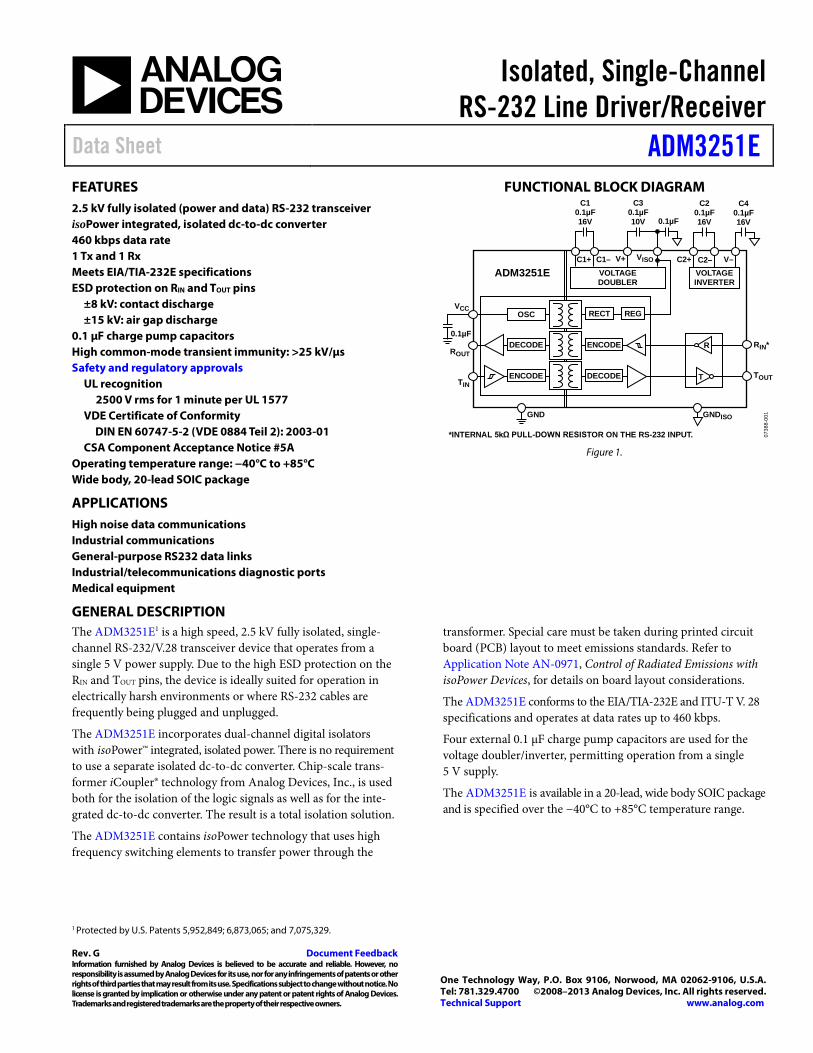
FUNCTIONAL BLOCK DIAGRAM
0738
8-00
1
DECODE
RECT REG
V–
C40.1µF16V
VOLTAGEDOUBLER
C1+ C1– V+ VISO C2+ C2–
R
T
VOLTAGEINVERTER
VCC
ROUT
TIN
GND GNDISO
RIN*
TOUT
ADM3251E
OSC
ENCODE
ENCODE
DECODE
*INTERNAL 5kΩ PULL-DOWN RESISTOR ON THE RS-232 INPUT.
0.1µF
C30.1µF10V
C20.1µF16V0.1µF
C10.1µF16V
Figure 1.
GENERAL DESCRIPTION The ADM3251E1 is a high speed, 2.5 kV fully isolated, single-channel RS-232/V.28 transceiver device that operates from a single 5 V power supply. Due to the high ESD protection on the RIN and TOUT pins, the device is ideally suited for operation in electrically harsh environments or where RS-232 cables are frequently being plugged and unplugged.
The ADM3251E incorporates dual-channel digital isolators with isoPower™ integrated, isolated power. There is no requirement to use a separate isolated dc-to-dc converter. Chip-scale trans-former iCoupler® technology from Analog Devices, Inc., is used both for the isolation of the logic signals as well as for the inte-grated dc-to-dc converter. The result is a total isolation solution.
The ADM3251E contains isoPower technology that uses high frequency switching elements to transfer power through the
transformer. Special care must be taken during printed circuit board (PCB) layout to meet emissions standards. Refer to Application Note AN-0971, Control of Radiated Emissions with isoPower Devices, for details on board layout considerations.
The ADM3251E conforms to the EIA/TIA-232E and ITU-T V. 28 specifications and operates at data rates up to 460 kbps.
Four external 0.1 μF charge pump capacitors are used for the voltage doubler/inverter, permitting operation from a single 5 V supply.
The ADM3251E is available in a 20-lead, wide body SOIC package and is specified over the −40°C to +85°C temperature range.
1 Protected by U.S. Patents 5,952,849; 6,873,065; and 7,075,329.
Rev. G Document Feedback Information furnished by Analog Devices is believed to be accurate and reliable. However, no responsibility is assumed by Analog Devices for its use, nor for any infringements of patents or other rights of third parties that may result from its use. Specifications subject to change without notice. No license is granted by implication or otherwise under any patent or patent rights of Analog Devices. Trademarks and registered trademarks are the property of their respective owners.
One Technology Way, P.O. Box 9106, Norwood, MA 02062-9106, U.S.A. Tel: 781.329.4700 ©2008–2013 Analog Devices, Inc. All rights reserved. Technical Support www.analog.com
ADM3251E* PRODUCT PAGE QUICK LINKSLast Content Update: 02/23/2017
COMPARABLE PARTSView a parametric search of comparable parts.
EVALUATION KITS• ADM3251E Evaluation board
DOCUMENTATIONApplication Notes
• AN-740: iCoupler Isolation in RS-232 Applications
Data Sheet
• ADM3251E: Isolated, Single-Channel RS-232 Line Driver/Receiver Data Sheet
User Guides
• UG-120: Standard Evaluation Kit User Guide for the ADM3251E
• UG-124: EMI optimized evaluation kit user guide for the ADM3251E
• UG-181: PLC Demo System, Industrial Process Control Demo System
REFERENCE MATERIALSPress
• Analog Devices Achieves Major Milestone by Shipping 1 Billionth Channel of iCoupler Digital Isolation
Product Selection Guide
• Digital Isolator Product Selection and Resource Guide
Solutions Bulletins & Brochures
• RS-232 Transceivers Applications Bulletin (Summer 2008)
Technical Articles
• Inside iCoupler® Technology:ADuM347x PWM Controller and Transformer Driver with Quad-Channel Isolators Design Summary
• NAppkin Note: Lowering the Power of the ADuM524x
• Part 1: Simplifying Design of Industrial Process-Control Systems with PLC Evaluation Boards
• Part 2: Simplifying Design of Industrial Process-Control Systems with PLC Evaluation Boards
DESIGN RESOURCES• ADM3251E Material Declaration
• PCN-PDN Information
• Quality And Reliability
• Symbols and Footprints
DISCUSSIONSView all ADM3251E EngineerZone Discussions.
SAMPLE AND BUYVisit the product page to see pricing options.
TECHNICAL SUPPORTSubmit a technical question or find your regional support number.
DOCUMENT FEEDBACKSubmit feedback for this data sheet.
This page is dynamically generated by Analog Devices, Inc., and inserted into this data sheet. A dynamic change to the content on this page will not trigger a change to either the revision number or the content of the product data sheet. This dynamic page may be frequently modified.
ADM3251E Data Sheet
TABLE OF CONTENTS Features .............................................................................................. 1 Applications ....................................................................................... 1 Functional Block Diagram .............................................................. 1 General Description ......................................................................... 1 Revision History ............................................................................... 2 Specifications ..................................................................................... 3
Package Characteristics ............................................................... 5 Regulatory Information ............................................................... 5 Insulation and Safety-Related Specifications ............................ 5 DIN EN 60747-5-2 (VDE 0884 TEIL 2): 2003-01 Insulation Characteristics .............................................................................. 6
Absolute Maximum Ratings ............................................................ 7 ESD Caution .................................................................................. 7
Pin Configuration and Function Descriptions ............................. 8 Typical Performance Characteristics ............................................. 9
Theory of Operation ...................................................................... 11 Isolation of Power and Data ...................................................... 11 Charge Pump Voltage Converter ............................................. 12 5.0 V Logic to EIA/TIA-232E Transmitter .............................. 12 EIA/TIA-232E to 5 V Logic Receiver ...................................... 12 High Baud Rate ........................................................................... 12 Thermal Analysis ....................................................................... 12 Insulation Lifetime ..................................................................... 12
Applications Information .............................................................. 13 PCB Layout ................................................................................. 13 Example PCB for Reduced EMI ............................................... 13 DC Correctness and Magnetic Field Immunity ..................... 13 Isolated Power Supply Circuit .................................................. 14
Outline Dimensions ....................................................................... 15 Ordering Guide .......................................................................... 15
REVISION HISTORY 10/13—Rev. F to Rev. G Added Patents Information, Note 1 ............................................... 1 Changed Minimum External Tracking (Creepage) Value to 7.6 mm, Table 5 ................................................................................. 5 Changes to Pin 9 Description and Pin 11 Descriptions, Table 8 ...... 8 Changes to Isolation of Power and Data Section ....................... 11 6/12—Rev. E to Rev. F Changes to Endnote 1 in Table 4 .................................................... 5 Added DC Correctness and Magnetic Field Immunity Section .............................................................................................. 13 Added Figure 22 and Figure 23; Renumbered Sequentially ..... 14 Updated Outline Dimensions and Changes to Ordering Guide ............................................................................... 15 5/10—Rev. D to Rev. E Changes to Features Section............................................................ 1 Changes to Table 4 ............................................................................ 5 3/10—Rev. C to Rev. D Changes to Features and General Description Sections .............. 1 Changes to Table 4 and Table 5 ....................................................... 5 Changed DIN V VDE V 0884-10 (VDE V 0884-10):2006-12 Insulation Characteristics (Pending) Heading to DIN EN 60747-5-2 (VDE 0884 Teil 2): 2003-01 Insulation Characteristics ................................................................................... 6
Changes to Pollution Degree and Input–to-Output Test Voltage Parameters, Table 6............................................................................ 6 Added Applications Information Section and Example PCB for Reduced EMI Section; Added Table 9 and Table 10; Renumbered Sequentially ............................................................. 13 Changes to PCB Layout Section ................................................... 13 Added Isolated Power Supply Circuit Section, and Figure 22; Renumbered Sequentially ............................................................. 14 1/10—Rev. B to Rev. C Changes to Table 4 ............................................................................. 5 11/09—Rev. A to Rev. B Changes to Figure 1 ........................................................................... 1 Changed to Primary Side Supply Input Current, ICC(DISABLE) Maximum Limit to 2.5 mA .............................................................. 4 Changes to Table 4 ............................................................................. 5 Changes to Figure 13 ...................................................................... 11 9/08—Rev. 0 to Rev. A Changes to Timing Parameters in Table 1 .................................... 3 Changes to Timing Parameters in Table 2 .................................... 4 Changes to Ordering Guide .......................................................... 14 7/08—Revision 0: Initial Version
Rev. G | Page 2 of 16
Data Sheet ADM3251E
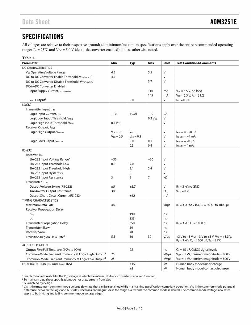
SPECIFICATIONS All voltages are relative to their respective ground; all minimum/maximum specifications apply over the entire recommended operating range; TA = 25°C and VCC = 5.0 V (dc-to-dc converter enabled), unless otherwise noted.
Table 1. Parameter Min Typ Max Unit Test Conditions/Comments
DC CHARACTERISTICS VCC Operating Voltage Range 4.5 5.5 V DC-to-DC Converter Enable Threshold, VCC(ENABLE)
1 4.5 V
DC-to-DC Converter Disable Threshold, VCC(DISABLE)1 3.7 V
DC-to-DC Converter Enabled Input Supply Current, ICC(ENABLE) 110 mA VCC = 5.5 V, no load 145 mA VCC = 5.5 V, RL = 3 kΩ VISO Output2 5.0 V IISO = 0 µA
LOGIC Transmitter Input, TIN
Logic Input Current, ITIN −10 +0.01 +10 μA Logic Low Input Threshold, VTINL 0.3 VCC V Logic High Input Threshold, VTINH 0.7 VCC V
Receiver Output, ROUT Logic High Output, VROUTH VCC − 0.1 VCC V IROUTH = −20 μA VCC − 0.5 VCC − 0.3 V IROUTH = −4 mA Logic Low Output, VROUTL 0.0 0.1 V IROUTH = 20 μA
0.3 0.4 V IROUTH = 4 mA
RS-232 Receiver, RIN
EIA-232 Input Voltage Range3 −30 +30 V EIA-232 Input Threshold Low 0.6 2.0 V EIA-232 Input Threshold High 2.1 2.4 V EIA-232 Input Hysteresis 0.1 V EIA-232 Input Resistance 3 5 7 kΩ
Transmitter, TOUT Output Voltage Swing (RS-232) ±5 ±5.7 V RL = 3 kΩ to GND Transmitter Output Resistance 300 Ω VISO = 0 V Output Short-Circuit Current (RS-232) ±12 mA
TIMING CHARACTERISTICS Maximum Data Rate 460 kbps RL = 3 kΩ to 7 kΩ, CL = 50 pF to 1000 pF Receiver Propagation Delay
tPHL 190 ns tPLH 135 ns
Transmitter Propagation Delay 650 ns RL = 3 kΩ, CL = 1000 pF Transmitter Skew 80 ns Receiver Skew 70 ns
Transition Region Slew Rate3 5.5 10 30 V/μs +3 V to −3 V or −3 V to +3 V, VCC = +3.3 V, RL = 3 kΩ, CL = 1000 pF, TA = 25°C
AC SPECIFICATIONS Output Rise/Fall Time, tR/tF (10% to 90%) 2.3 ns CL = 15 pF, CMOS signal levels Common-Mode Transient Immunity at Logic High Output4 25 kV/μs VCM = 1 kV, transient magnitude = 800 V
Common-Mode Transient Immunity at Logic Low Output4 25 kV/μs VCM = 1 kV, transient magnitude = 800 V
ESD PROTECTION (RIN And TOUT PINS) ±15 kV Human body model air discharge ±8 kV Human body model contact discharge
1 Enable/disable threshold is the VCC voltage at which the internal dc-to-dc converter is enabled/disabled. 2 To maintain data sheet specifications, do not draw current from VISO. 3 Guaranteed by design. 4 VCM is the maximum common-mode voltage slew rate that can be sustained while maintaining specification-compliant operation. VCM is the common-mode potential
difference between the logic and bus sides. The transient magnitude is the range over which the common mode is slewed. The common-mode voltage slew rates apply to both rising and falling common-mode voltage edges.
Rev. G | Page 3 of 16
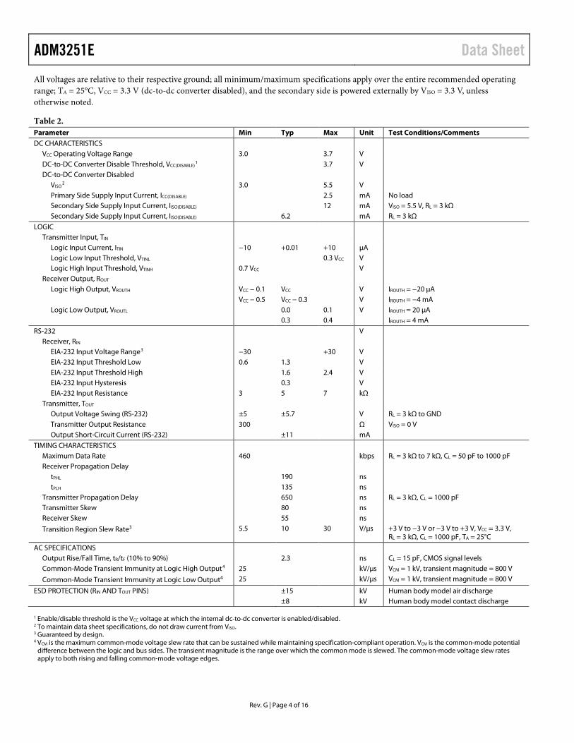
ADM3251E Data Sheet All voltages are relative to their respective ground; all minimum/maximum specifications apply over the entire recommended operating range; TA = 25°C, VCC = 3.3 V (dc-to-dc converter disabled), and the secondary side is powered externally by VISO = 3.3 V, unless otherwise noted.
Table 2. Parameter Min Typ Max Unit Test Conditions/Comments DC CHARACTERISTICS
VCC Operating Voltage Range 3.0 3.7 V DC-to-DC Converter Disable Threshold, VCC(DISABLE)
1 3.7 V DC-to-DC Converter Disabled
VISO2 3.0 5.5 V
Primary Side Supply Input Current, ICC(DISABLE) 2.5 mA No load Secondary Side Supply Input Current, IISO(DISABLE) 12 mA VISO = 5.5 V, RL = 3 kΩ Secondary Side Supply Input Current, IISO(DISABLE) 6.2 mA RL = 3 kΩ
LOGIC Transmitter Input, TIN
Logic Input Current, ITIN −10 +0.01 +10 μA Logic Low Input Threshold, VTINL 0.3 VCC V Logic High Input Threshold, VTINH 0.7 VCC V
Receiver Output, ROUT Logic High Output, VROUTH VCC − 0.1 VCC V IROUTH = −20 μA VCC − 0.5 VCC − 0.3 V IROUTH = −4 mA Logic Low Output, VROUTL 0.0 0.1 V IROUTH = 20 μA
0.3 0.4 IROUTH = 4 mA
RS-232 V Receiver, RIN
EIA-232 Input Voltage Range3 −30 +30 V EIA-232 Input Threshold Low 0.6 1.3 V EIA-232 Input Threshold High 1.6 2.4 V EIA-232 Input Hysteresis 0.3 V EIA-232 Input Resistance 3 5 7 kΩ
Transmitter, TOUT Output Voltage Swing (RS-232) ±5 ±5.7 V RL = 3 kΩ to GND Transmitter Output Resistance 300 Ω VISO = 0 V Output Short-Circuit Current (RS-232) ±11 mA
TIMING CHARACTERISTICS Maximum Data Rate 460 kbps RL = 3 kΩ to 7 kΩ, CL = 50 pF to 1000 pF Receiver Propagation Delay
tPHL 190 ns tPLH 135 ns
Transmitter Propagation Delay 650 ns RL = 3 kΩ, CL = 1000 pF Transmitter Skew 80 ns Receiver Skew 55 ns
Transition Region Slew Rate3 5.5 10 30 V/μs +3 V to −3 V or −3 V to +3 V, VCC = 3.3 V, RL = 3 kΩ, CL = 1000 pF, TA = 25°C
AC SPECIFICATIONS Output Rise/Fall Time, tR/tF (10% to 90%) 2.3 ns CL = 15 pF, CMOS signal levels Common-Mode Transient Immunity at Logic High Output4 25 kV/μs VCM = 1 kV, transient magnitude = 800 V
Common-Mode Transient Immunity at Logic Low Output4 25 kV/μs VCM = 1 kV, transient magnitude = 800 V
ESD PROTECTION (RIN AND TOUT PINS) ±15 kV Human body model air discharge ±8 kV Human body model contact discharge
1 Enable/disable threshold is the VCC voltage at which the internal dc-to-dc converter is enabled/disabled. 2 To maintain data sheet specifications, do not draw current from VISO. 3 Guaranteed by design. 4 VCM is the maximum common-mode voltage slew rate that can be sustained while maintaining specification-compliant operation. VCM is the common-mode potential
difference between the logic and bus sides. The transient magnitude is the range over which the common mode is slewed. The common-mode voltage slew rates apply to both rising and falling common-mode voltage edges.
Rev. G | Page 4 of 16
Data Sheet ADM3251E
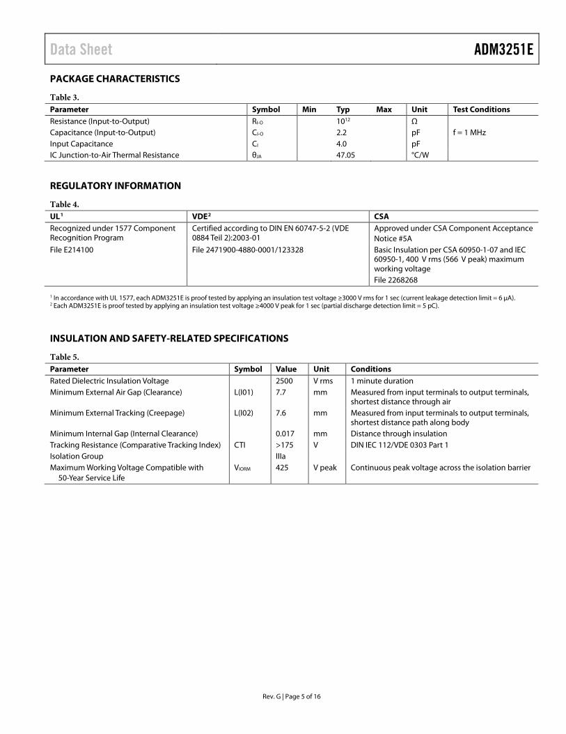
PACKAGE CHARACTERISTICS
Table 3. Parameter Symbol Min Typ Max Unit Test Conditions Resistance (Input-to-Output) RI-O 1012 Ω Capacitance (Input-to-Output) CI-O 2.2 pF f = 1 MHz Input Capacitance CI 4.0 pF IC Junction-to-Air Thermal Resistance θJA 47.05 °C/W
REGULATORY INFORMATION
Table 4. UL1 VDE2 CSA Recognized under 1577 Component Recognition Program
Certified according to DIN EN 60747-5-2 (VDE 0884 Teil 2):2003-01
Approved under CSA Component Acceptance Notice #5A
File E214100 File 2471900-4880-0001/123328 Basic Insulation per CSA 60950-1-07 and IEC 60950-1, 400 V rms (566 V peak) maximum working voltage
File 2268268
1 In accordance with UL 1577, each ADM3251E is proof tested by applying an insulation test voltage ≥3000 V rms for 1 sec (current leakage detection limit = 6 μA). 2 Each ADM3251E is proof tested by applying an insulation test voltage ≥4000 V peak for 1 sec (partial discharge detection limit = 5 pC).
INSULATION AND SAFETY-RELATED SPECIFICATIONS
Table 5. Parameter Symbol Value Unit Conditions Rated Dielectric Insulation Voltage 2500 V rms 1 minute duration Minimum External Air Gap (Clearance) L(I01) 7.7 mm Measured from input terminals to output terminals,
shortest distance through air Minimum External Tracking (Creepage) L(I02) 7.6 mm Measured from input terminals to output terminals,
shortest distance path along body Minimum Internal Gap (Internal Clearance) 0.017 mm Distance through insulation Tracking Resistance (Comparative Tracking Index) CTI >175 V DIN IEC 112/VDE 0303 Part 1 Isolation Group IIIa Maximum Working Voltage Compatible with
50-Year Service Life VIORM 425 V peak Continuous peak voltage across the isolation barrier
Rev. G | Page 5 of 16
ADM3251E Data Sheet
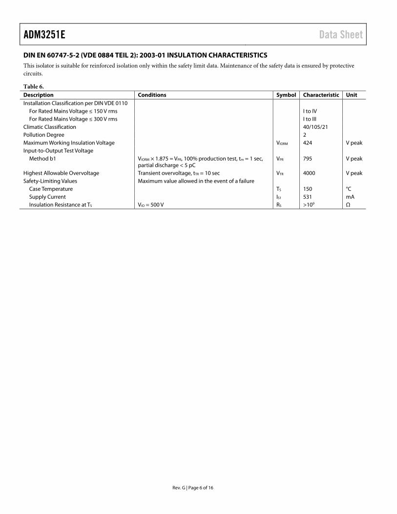
DIN EN 60747-5-2 (VDE 0884 TEIL 2): 2003-01 INSULATION CHARACTERISTICS This isolator is suitable for reinforced isolation only within the safety limit data. Maintenance of the safety data is ensured by protective circuits.
Table 6. Description Conditions Symbol Characteristic Unit Installation Classification per DIN VDE 0110
For Rated Mains Voltage ≤ 150 V rms I to IV For Rated Mains Voltage ≤ 300 V rms I to III
Climatic Classification 40/105/21 Pollution Degree 2 Maximum Working Insulation Voltage VIORM 424 V peak Input-to-Output Test Voltage
Method b1 VIORM × 1.875 = VPR, 100% production test, tm = 1 sec, partial discharge < 5 pC
VPR 795 V peak
Highest Allowable Overvoltage Transient overvoltage, tTR = 10 sec VTR 4000 V peak Safety-Limiting Values Maximum value allowed in the event of a failure
Case Temperature TS 150 °C Supply Current IS1 531 mA Insulation Resistance at TS VIO = 500 V RS >109 Ω
Rev. G | Page 6 of 16
Data Sheet ADM3251E
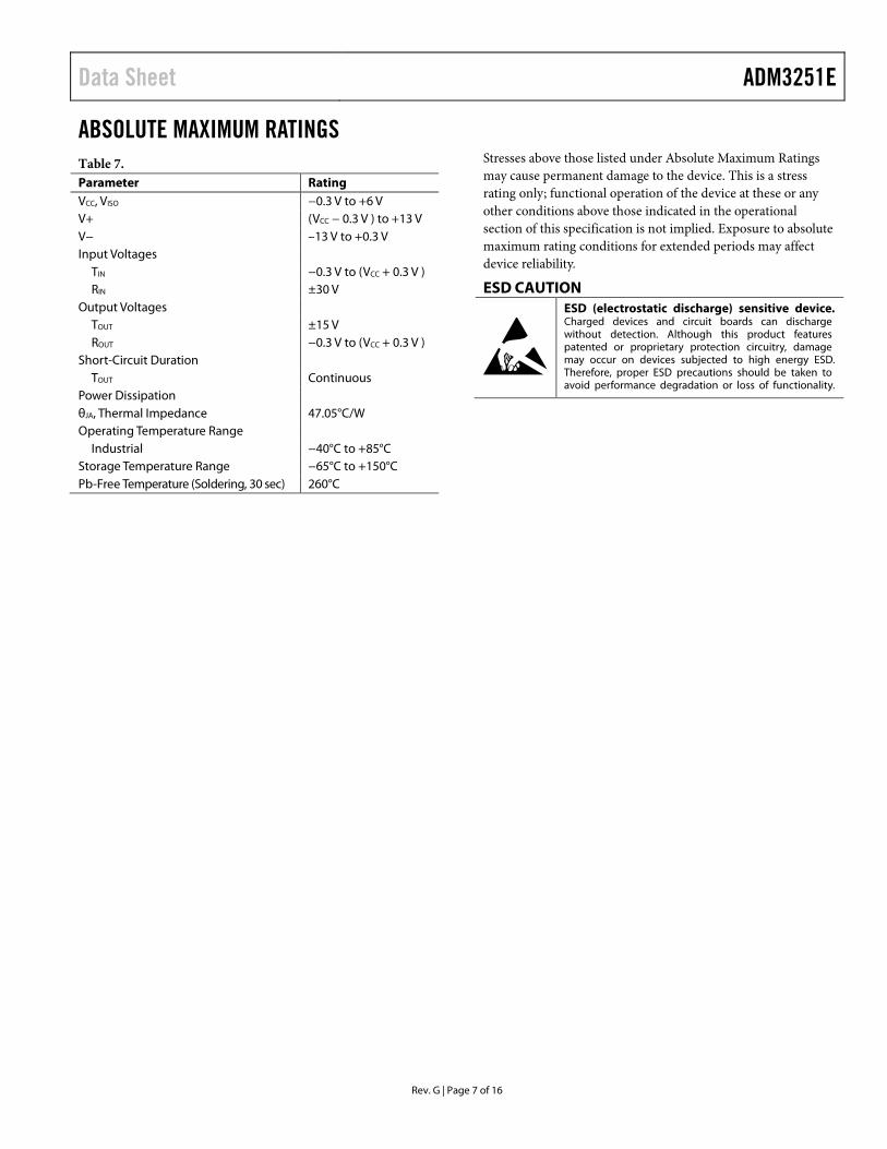
ABSOLUTE MAXIMUM RATINGS Table 7. Parameter Rating VCC, VISO −0.3 V to +6 V V+ (VCC − 0.3 V ) to +13 V V− –13 V to +0.3 V Input Voltages
TIN −0.3 V to (VCC + 0.3 V ) RIN ±30 V
Output Voltages TOUT ±15 V ROUT −0.3 V to (VCC + 0.3 V )
Short-Circuit Duration TOUT Continuous
Power Dissipation θJA, Thermal Impedance 47.05°C/W Operating Temperature Range
Industrial −40°C to +85°C Storage Temperature Range −65°C to +150°C Pb-Free Temperature (Soldering, 30 sec) 260°C
Stresses above those listed under Absolute Maximum Ratings may cause permanent damage to the device. This is a stress rating only; functional operation of the device at these or any other conditions above those indicated in the operational section of this specification is not implied. Exposure to absolute maximum rating conditions for extended periods may affect device reliability.
ESD CAUTION
Rev. G | Page 7 of 16
ADM3251E Data Sheet
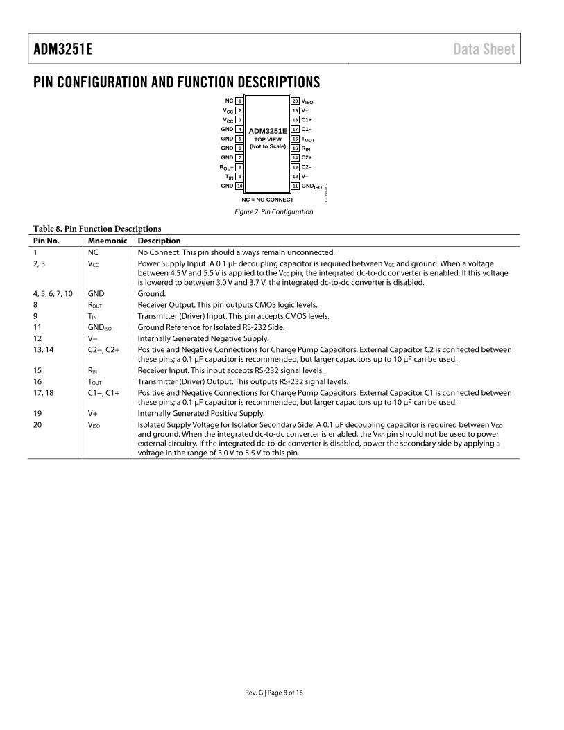
PIN CONFIGURATION AND FUNCTION DESCRIPTIONS NC 1
VCC 2
VCC 3
GND 4
VISO20
V+19
C1+18
C1–17
GND 5 TOUT16
GND 6 RIN15
GND 7 C2+14
ROUT 8 C2–13
TIN 9 V–12
GND 10 GNDISO11
NC = NO CONNECT
ADM3251ETOP VIEW
(Not to Scale)
0738
8-00
2
Figure 2. Pin Configuration
Table 8. Pin Function Descriptions Pin No. Mnemonic Description 1 NC No Connect. This pin should always remain unconnected. 2, 3 VCC Power Supply Input. A 0.1 µF decoupling capacitor is required between VCC and ground. When a voltage
between 4.5 V and 5.5 V is applied to the VCC pin, the integrated dc-to-dc converter is enabled. If this voltage is lowered to between 3.0 V and 3.7 V, the integrated dc-to-dc converter is disabled.
4, 5, 6, 7, 10 GND Ground. 8 ROUT Receiver Output. This pin outputs CMOS logic levels. 9 TIN Transmitter (Driver) Input. This pin accepts CMOS levels. 11 GNDISO Ground Reference for Isolated RS-232 Side. 12 V− Internally Generated Negative Supply. 13, 14 C2−, C2+ Positive and Negative Connections for Charge Pump Capacitors. External Capacitor C2 is connected between
these pins; a 0.1 µF capacitor is recommended, but larger capacitors up to 10 µF can be used. 15 RIN Receiver Input. This input accepts RS-232 signal levels. 16 TOUT Transmitter (Driver) Output. This outputs RS-232 signal levels. 17, 18 C1−, C1+ Positive and Negative Connections for Charge Pump Capacitors. External Capacitor C1 is connected between
these pins; a 0.1 µF capacitor is recommended, but larger capacitors up to 10 µF can be used. 19 V+ Internally Generated Positive Supply. 20 VISO Isolated Supply Voltage for Isolator Secondary Side. A 0.1 µF decoupling capacitor is required between VISO
and ground. When the integrated dc-to-dc converter is enabled, the VISO pin should not be used to power external circuitry. If the integrated dc-to-dc converter is disabled, power the secondary side by applying a voltage in the range of 3.0 V to 5.5 V to this pin.
Rev. G | Page 8 of 16
Data Sheet ADM3251E
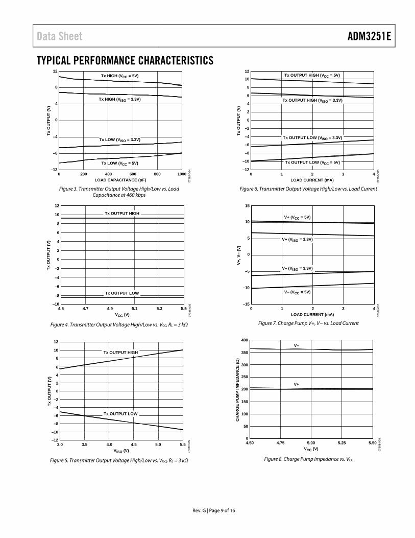
TYPICAL PERFORMANCE CHARACTERISTICS 12
8
4
0
–4
–8
–120 200 400 600 800 1000
LOAD CAPACITANCE (pF)
Tx O
UTP
UT
(V)
0738
8-00
4
Tx LOW (VCC = 5V)
Tx LOW (VISO = 3.3V)
Tx HIGH (VCC = 5V)
Tx HIGH (VISO = 3.3V)
Figure 3. Transmitter Output Voltage High/Low vs. Load
Capacitance at 460 kbps
12
10
8
6
4
2
0
–2
–4
–6
–8
–104.5 4.7 4.9 5.1 5.3 5.5
VCC (V)
Tx O
UTP
UT
(V)
0738
8-00
5
Tx OUTPUT HIGH
Tx OUTPUT LOW
Figure 4. Transmitter Output Voltage High/Low vs. VCC, RL = 3 kΩ
12
8
4
0
–4
–8
–12
10
6
2
–2
–6
–10
3.0 3.5 4.0 4.5 5.0 5.5VISO (V)
Tx O
UTP
UT
(V)
0738
8-00
9
Tx OUTPUT HIGH
Tx OUTPUT LOW
Figure 5. Transmitter Output Voltage High/Low vs. VISO, RL = 3 kΩ
12
10
8
6
4
2
0
–2
–4
–6
–8
–10
–120 1 2 3 4
LOAD CURRENT (mA)
Tx O
UTP
UT
(V)
0738
8-00
6
Tx OUTPUT LOW (VCC = 5V)
Tx OUTPUT LOW (VISO = 3.3V)
Tx OUTPUT HIGH (VCC = 5V)
Tx OUTPUT HIGH (VISO = 3.3V)
Figure 6. Transmitter Output Voltage High/Low vs. Load Current
15
10
5
0
–5
–10
–150 1 2 3 4
LOAD CURRENT (mA)
V+, V
– (V
)
0738
8-00
7
V+ (VCC = 5V)
V– (VCC = 5V)
V+ (VISO = 3.3V)
V– (VISO = 3.3V)
Figure 7. Charge Pump V+, V− vs. Load Current
400
V+
V–350
300
250
200
150
100
50
04.50 4.75 5.00 5.25 5.50
VCC (V)
CH
AR
GE
PUM
P IM
PED
AN
CE
(Ω)
0738
8-00
8
Figure 8. Charge Pump Impedance vs. VCC
Rev. G | Page 9 of 16
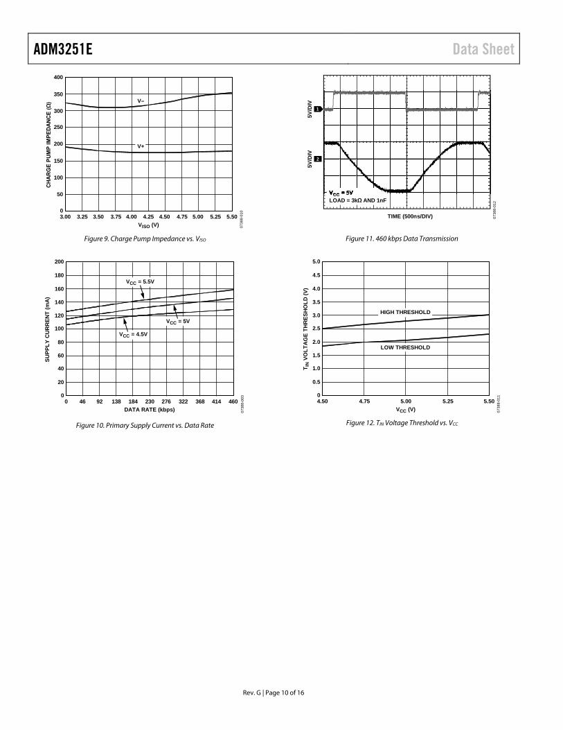
ADM3251E Data Sheet
400
V–350
300
250
200
150
100
50
03.00 3.25 3.50 3.75 4.00 4.25 4.50 4.75 5.00 5.25 5.50
VISO (V)
CH
AR
GE
PUM
P IM
PED
AN
CE
(Ω)
0738
8-01
0
V+
Figure 9. Charge Pump Impedance vs. VISO
200
180
160
140
120
100
80
60
40
20
00 46 92 138 184 230 276 322 368 414 460
DATA RATE (kbps)
SUPP
LY C
UR
REN
T (m
A)
0738
8-00
3
VCC = 4.5V
VCC = 5.5V
VCC = 5V
Figure 10. Primary Supply Current vs. Data Rate
0738
8-01
2
5V/D
I V5V
/DI V
TIME (500ns/DIV)
2
1
VCC = 5VLOAD = 3kΩ AND 1nF
Figure 11. 460 kbps Data Transmission
5.0
4.5
4.0
3.5
3.0
2.5
2.0
1.5
1.0
0.5
04.50 4.75 5.00 5.25 5.50
VCC (V)
T IN
VO
LTA
GE
THR
ESH
OLD
(V)
0738
8-01
1
HIGH THRESHOLD
LOW THRESHOLD
Figure 12. TIN Voltage Threshold vs. VCC
Rev. G | Page 10 of 16
Data Sheet ADM3251E
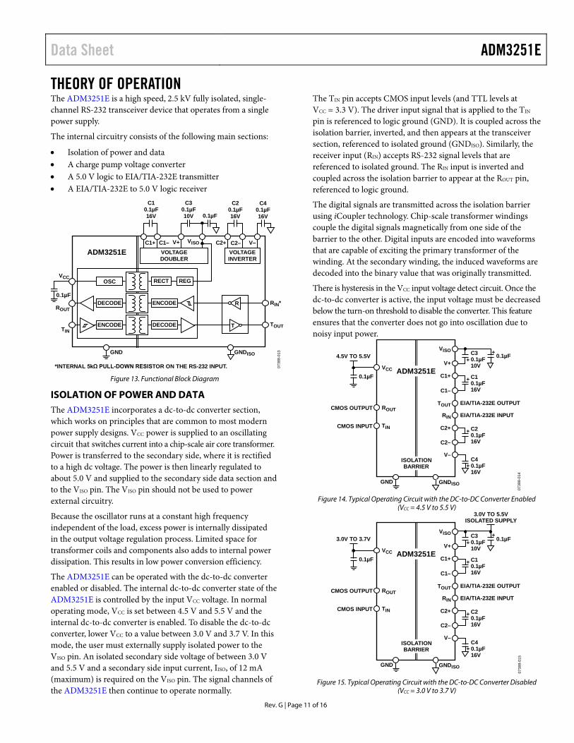
THEORY OF OPERATION The ADM3251E is a high speed, 2.5 kV fully isolated, single-channel RS-232 transceiver device that operates from a single power supply.
The internal circuitry consists of the following main sections:
• Isolation of power and data • A charge pump voltage converter • A 5.0 V logic to EIA/TIA-232E transmitter • A EIA/TIA-232E to 5.0 V logic receiver
0738
8-01
3
DECODE
RECT REG
V–
C40.1µF16V
VOLTAGEDOUBLER
C1+ C1– V+ VISO C2+ C2–
R
T
VOLTAGEINVERTER
VCC
ROUT
TIN
GND GNDISO
RIN*
TOUT
ADM3251E
OSC
ENCODE
ENCODE
DECODE
*INTERNAL 5kΩ PULL-DOWN RESISTOR ON THE RS-232 INPUT.
0.1µF
C30.1µF10V
C20.1µF16V0.1µF
C10.1µF16V
Figure 13. Functional Block Diagram
ISOLATION OF POWER AND DATA The ADM3251E incorporates a dc-to-dc converter section, which works on principles that are common to most modern power supply designs. VCC power is supplied to an oscillating circuit that switches current into a chip-scale air core transformer. Power is transferred to the secondary side, where it is rectified to a high dc voltage. The power is then linearly regulated to about 5.0 V and supplied to the secondary side data section and to the VISO pin. The VISO pin should not be used to power external circuitry.
Because the oscillator runs at a constant high frequency independent of the load, excess power is internally dissipated in the output voltage regulation process. Limited space for transformer coils and components also adds to internal power dissipation. This results in low power conversion efficiency.
The ADM3251E can be operated with the dc-to-dc converter enabled or disabled. The internal dc-to-dc converter state of the ADM3251E is controlled by the input VCC voltage. In normal operating mode, VCC is set between 4.5 V and 5.5 V and the internal dc-to-dc converter is enabled. To disable the dc-to-dc converter, lower VCC to a value between 3.0 V and 3.7 V. In this mode, the user must externally supply isolated power to the VISO pin. An isolated secondary side voltage of between 3.0 V and 5.5 V and a secondary side input current, IISO, of 12 mA (maximum) is required on the VISO pin. The signal channels of the ADM3251E then continue to operate normally.
The TIN pin accepts CMOS input levels (and TTL levels at VCC = 3.3 V). The driver input signal that is applied to the TIN pin is referenced to logic ground (GND). It is coupled across the isolation barrier, inverted, and then appears at the transceiver section, referenced to isolated ground (GNDISO). Similarly, the receiver input (RIN) accepts RS-232 signal levels that are referenced to isolated ground. The RIN input is inverted and coupled across the isolation barrier to appear at the ROUT pin, referenced to logic ground.
The digital signals are transmitted across the isolation barrier using iCoupler technology. Chip-scale transformer windings couple the digital signals magnetically from one side of the barrier to the other. Digital inputs are encoded into waveforms that are capable of exciting the primary transformer of the winding. At the secondary winding, the induced waveforms are decoded into the binary value that was originally transmitted.
There is hysteresis in the VCC input voltage detect circuit. Once the dc-to-dc converter is active, the input voltage must be decreased below the turn-on threshold to disable the converter. This feature ensures that the converter does not go into oscillation due to noisy input power.
++
C30.1µF10V
+ C10.1µF16V
+ C20.1µF16V
0.1µF
+C40.1µF16V
EIA/TIA-232E OUTPUT
EIA/TIA-232E INPUT
VISO
V+
C1+
C1–
TOUT
RIN
C2+
C2–
V–
GNDISO
0738
8-01
4
ISOLATIONBARRIER
CMOS OUTPUT
CMOS INPUT
4.5V TO 5.5V
VCC
ROUT
TIN
GND
0.1µFADM3251E
Figure 14. Typical Operating Circuit with the DC-to-DC Converter Enabled
(VCC = 4.5 V to 5.5 V)
++
C30.1µF10V
+ C10.1µF16V
+ C20.1µF16V
0.1µF
+C40.1µF16V
EIA/TIA-232E OUTPUT
EIA/TIA-232E INPUT
VISO
V+
C1+
C1–
TOUT
RIN
C2+
C2–
V–
GNDISO
0738
8-01
5
ISOLATIONBARRIER
CMOS OUTPUT
CMOS INPUT
3.0V TO 3.7V
3.0V TO 5.5VISOLATED SUPPLY
VCC
ROUT
TIN
GND
0.1µFADM3251E
Figure 15. Typical Operating Circuit with the DC-to-DC Converter Disabled
(VCC = 3.0 V to 3.7 V)
Rev. G | Page 11 of 16
ADM3251E Data Sheet
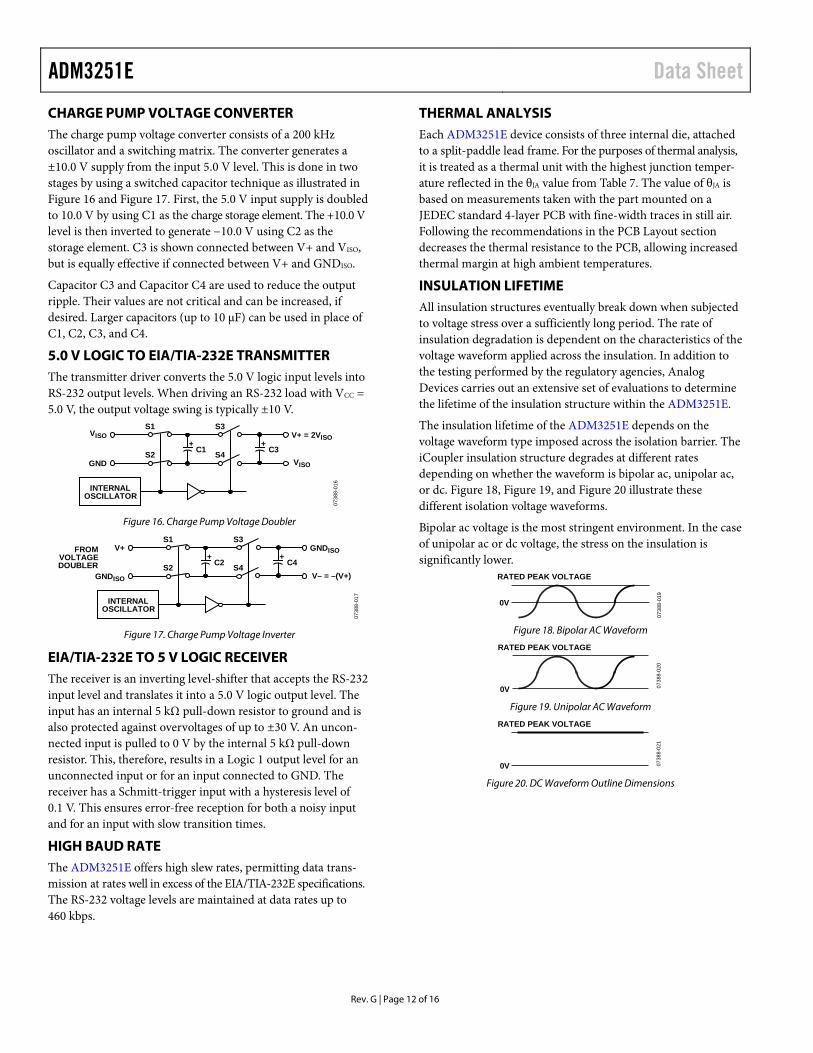
CHARGE PUMP VOLTAGE CONVERTER The charge pump voltage converter consists of a 200 kHz oscillator and a switching matrix. The converter generates a ±10.0 V supply from the input 5.0 V level. This is done in two stages by using a switched capacitor technique as illustrated in Figure 16 and Figure 17. First, the 5.0 V input supply is doubled to 10.0 V by using C1 as the charge storage element. The +10.0 V level is then inverted to generate −10.0 V using C2 as the storage element. C3 is shown connected between V+ and VISO, but is equally effective if connected between V+ and GNDISO.
Capacitor C3 and Capacitor C4 are used to reduce the output ripple. Their values are not critical and can be increased, if desired. Larger capacitors (up to 10 μF) can be used in place of C1, C2, C3, and C4.
5.0 V LOGIC TO EIA/TIA-232E TRANSMITTER The transmitter driver converts the 5.0 V logic input levels into RS-232 output levels. When driving an RS-232 load with VCC = 5.0 V, the output voltage swing is typically ±10 V.
GNDC3C1
S1
S2
S3
S4
V+ = 2VISO+ +
INTERNALOSCILLATOR
VISO
VISO
0738
8-01
6
Figure 16. Charge Pump Voltage Doubler
GNDISO
C4C2
S1
S2
S3
S4
GNDISO+ +
INTERNALOSCILLATOR
V+
V– = –(V+)
FROMVOLTAGEDOUBLER
0738
8-01
7
Figure 17. Charge Pump Voltage Inverter
EIA/TIA-232E TO 5 V LOGIC RECEIVER The receiver is an inverting level-shifter that accepts the RS-232 input level and translates it into a 5.0 V logic output level. The input has an internal 5 kΩ pull-down resistor to ground and is also protected against overvoltages of up to ±30 V. An uncon-nected input is pulled to 0 V by the internal 5 kΩ pull-down resistor. This, therefore, results in a Logic 1 output level for an unconnected input or for an input connected to GND. The receiver has a Schmitt-trigger input with a hysteresis level of 0.1 V. This ensures error-free reception for both a noisy input and for an input with slow transition times.
HIGH BAUD RATE The ADM3251E offers high slew rates, permitting data trans-mission at rates well in excess of the EIA/TIA-232E specifications. The RS-232 voltage levels are maintained at data rates up to 460 kbps.
THERMAL ANALYSIS Each ADM3251E device consists of three internal die, attached to a split-paddle lead frame. For the purposes of thermal analysis, it is treated as a thermal unit with the highest junction temper-ature reflected in the θJA value from Table 7. The value of θJA is based on measurements taken with the part mounted on a JEDEC standard 4-layer PCB with fine-width traces in still air. Following the recommendations in the PCB Layout section decreases the thermal resistance to the PCB, allowing increased thermal margin at high ambient temperatures.
INSULATION LIFETIME All insulation structures eventually break down when subjected to voltage stress over a sufficiently long period. The rate of insulation degradation is dependent on the characteristics of the voltage waveform applied across the insulation. In addition to the testing performed by the regulatory agencies, Analog Devices carries out an extensive set of evaluations to determine the lifetime of the insulation structure within the ADM3251E.
The insulation lifetime of the ADM3251E depends on the voltage waveform type imposed across the isolation barrier. The iCoupler insulation structure degrades at different rates depending on whether the waveform is bipolar ac, unipolar ac, or dc. Figure 18, Figure 19, and Figure 20 illustrate these different isolation voltage waveforms.
Bipolar ac voltage is the most stringent environment. In the case of unipolar ac or dc voltage, the stress on the insulation is significantly lower.
0V
RATED PEAK VOLTAGE
0738
8-01
9
Figure 18. Bipolar AC Waveform
0V
RATED PEAK VOLTAGE07
388-
020
Figure 19. Unipolar AC Waveform
0V
RATED PEAK VOLTAGE
0738
8-02
1
Figure 20. DC Waveform Outline Dimensions
Rev. G | Page 12 of 16
Data Sheet ADM3251E
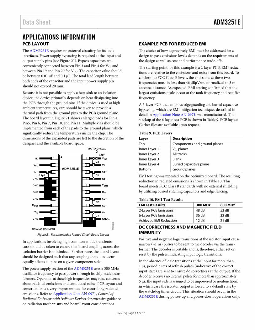
APPLICATIONS INFORMATION PCB LAYOUT The ADM3251E requires no external circuitry for its logic interfaces. Power supply bypassing is required at the input and output supply pins (see Figure 21). Bypass capacitors are conveniently connected between Pin 3 and Pin 4 for VCC and between Pin 19 and Pin 20 for VISO. The capacitor value should be between 0.01 μF and 0.1 μF. The total lead length between both ends of the capacitor and the input power supply pin should not exceed 20 mm.
Because it is not possible to apply a heat sink to an isolation device, the device primarily depends on heat dissipating into the PCB through the ground pins. If the device is used at high ambient temperatures, care should be taken to provide a thermal path from the ground pins to the PCB ground plane. The board layout in Figure 21 shows enlarged pads for Pin 4, Pin5, Pin 6, Pin 7, Pin 10, and Pin 11. Multiple vias should be implemented from each of the pads to the ground plane, which significantly reduce the temperatures inside the chip. The dimensions of the expanded pads are left to the discretion of the designer and the available board space.
NC
VCC
VCC
GND
VISO
V+
C1+
C1–
GND TOUT
GND RIN
GND C2+
ROUT C2–
TIN V–
GND GNDISO
0738
8-01
8
ADM3251E
VIA TO GNDISO
0.1µF
C3
C1
C2
0.1µF
NC = NO CONNECT
C4
Figure 21. Recommended Printed Circuit Board Layout
In applications involving high common-mode transients, care should be taken to ensure that board coupling across the isolation barrier is minimized. Furthermore, the board layout should be designed such that any coupling that does occur equally affects all pins on a given component side.
The power supply section of the ADM3251E uses a 300 MHz oscillator frequency to pass power through its chip-scale trans-formers. Operation at these high frequencies may raise concerns about radiated emissions and conducted noise. PCB layout and construction is a very important tool for controlling radiated emissions. Refer to Application Note AN-0971, Control of Radiated Emissions with isoPower Devices, for extensive guidance on radiation mechanisms and board layout considerations.
EXAMPLE PCB FOR REDUCED EMI The choice of how aggressively EMI must be addressed for a design to pass emissions levels depends on the requirements of the design as well as cost and performance trade-offs.
The starting point for this example is a 2-layer PCB. EMI reduc-tions are relative to the emissions and noise from this board. To conform to FCC Class B levels, the emissions at these two frequencies must be less than 46 dBμV/m, normalized to 3 m antenna distance. As expected, EMI testing confirmed that the largest emissions peaks occur at the tank frequency and rectifier frequency.
A 6-layer PCB that employs edge guarding and buried capacitive bypassing, which are EMI mitigation techniques described in detail in Application Note AN-0971, was manufactured. The stackup of the 6-layer test PCB is shown in Table 9. PCB layout Gerber files are available upon request.
Table 9. PCB Layers Layer Description Top Components and ground planes Inner Layer 1 VCC planes Inner Layer 2 All tracks Inner Layer 3 Blank Inner Layer 4 Buried capacitive plane Bottom Ground planes
EMI testing was repeated on the optimized board. The resulting reduction in radiated emissions is shown in Table 10. This board meets FCC Class B standards with no external shielding by utilizing buried stitching capacitors and edge fencing.
Table 10. EMI Test Results EMI Test Results 300 MHz 600 MHz 2-Layer PCB Emissions 48 dB 53 dB 6-Layer PCB Emissions 36 dB 32 dB Achieved EMI Reduction 12 dB 21 dB
DC CORRECTNESS AND MAGNETIC FIELD IMMUNITY Positive and negative logic transitions at the isolator input cause narrow (~1 ns) pulses to be sent to the decoder via the trans-former. The decoder is bistable and is, therefore, either set or reset by the pulses, indicating input logic transitions.
In the absence of logic transitions at the input for more than 1 μs, periodic sets of refresh pulses (indicative of the correct input state) are sent to ensure dc correctness at the output. If the decoder receives no internal pulses for more than approximately 5 μs, the input side is assumed to be unpowered or nonfunctional, in which case the isolator output is forced to a default state by the watchdog timer circuit. This situation should occur in the ADM3251E during power-up and power-down operations only.
Rev. G | Page 13 of 16
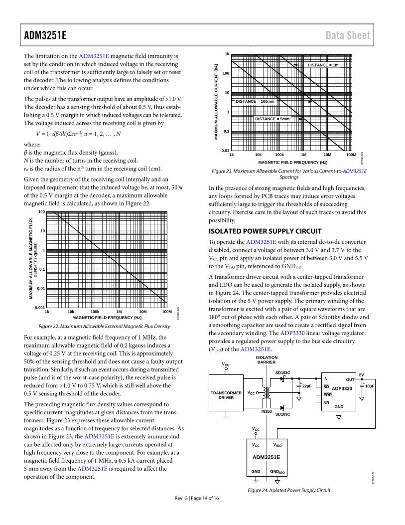
ADM3251E Data Sheet The limitation on the ADM3251E magnetic field immunity is set by the condition in which induced voltage in the receiving coil of the transformer is sufficiently large to falsely set or reset the decoder. The following analysis defines the conditions under which this can occur.
The pulses at the transformer output have an amplitude of >1.0 V. The decoder has a sensing threshold of about 0.5 V, thus estab-lishing a 0.5 V margin in which induced voltages can be tolerated. The voltage induced across the receiving coil is given by
V = (−dβ/dt)Σπrn2; n = 1, 2, … , N
where: β is the magnetic flux density (gauss). N is the number of turns in the receiving coil. rn is the radius of the nth turn in the receiving coil (cm).
Given the geometry of the receiving coil internally and an imposed requirement that the induced voltage be, at most, 50% of the 0.5 V margin at the decoder, a maximum allowable magnetic field is calculated, as shown in Figure 22.
MAGNETIC FIELD FREQUENCY (Hz)
100
MA
XIM
UM
ALL
OW
AB
LE M
AG
NET
IC F
LUX
DEN
SITY
(kga
uss)
0.0011M
10
0.01
1k 10k 10M
0.1
1
100M100k
0738
8-20
0
Figure 22. Maximum Allowable External Magnetic Flux Density
For example, at a magnetic field frequency of 1 MHz, the maximum allowable magnetic field of 0.2 kgauss induces a voltage of 0.25 V at the receiving coil. This is approximately 50% of the sensing threshold and does not cause a faulty output transition. Similarly, if such an event occurs during a transmitted pulse (and is of the worst-case polarity), the received pulse is reduced from >1.0 V to 0.75 V, which is still well above the 0.5 V sensing threshold of the decoder.
The preceding magnetic flux density values correspond to specific current magnitudes at given distances from the trans-formers. Figure 23 expresses these allowable current magnitudes as a function of frequency for selected distances. As shown in Figure 23, the ADM3251E is extremely immune and can be affected only by extremely large currents operated at high frequency very close to the component. For example, at a magnetic field frequency of 1 MHz, a 0.5 kA current placed 5 mm away from the ADM3251E is required to affect the operation of the component.
MAGNETIC FIELD FREQUENCY (Hz)
MA
XIM
UM
ALL
OW
AB
LE C
UR
REN
T (k
A)
1k
100
10
1
0.1
0.011k 10k 100M100k 1M 10M
DISTANCE = 5mm
DISTANCE = 1m
DISTANCE = 100mm
0738
8-20
1
Figure 23. Maximum Allowable Current for Various Current-to-ADM3251E
Spacings
In the presence of strong magnetic fields and high frequencies, any loops formed by PCB traces may induce error voltages sufficiently large to trigger the thresholds of succeeding circuitry. Exercise care in the layout of such traces to avoid this possibility.
ISOLATED POWER SUPPLY CIRCUIT To operate the ADM3251E with its internal dc-to-dc converter disabled, connect a voltage of between 3.0 V and 3.7 V to the VCC pin and apply an isolated power of between 3.0 V and 5.5 V to the VISO pin, referenced to GNDISO.
A transformer driver circuit with a center-tapped transformer and LDO can be used to generate the isolated supply, as shown in Figure 24. The center-tapped transformer provides electrical isolation of the 5 V power supply. The primary winding of the transformer is excited with a pair of square waveforms that are 180° out of phase with each other. A pair of Schottky diodes and a smoothing capacitor are used to create a rectified signal from the secondary winding. The ADP3330 linear voltage regulator provides a regulated power supply to the bus side circuitry (VISO) of the ADM3251E.
ADP3330
IN
NR
+ +
SD103C
22µF 10µF
5VOUT
SD103C
78253
VCC
VCC
VCC
GND
ISOLATIONBARRIER
SD
ERRTRANSFORMERDRIVER
VCC
GND
VISO
GNDISO
ADM3251E
0738
8-02
2
Figure 24. Isolated Power Supply Circuit
Rev. G | Page 14 of 16
Data Sheet ADM3251E
OUTLINE DIMENSIONS
CONTROLLING DIMENSIONS ARE IN MILLIMETERS; INCH DIMENSIONS(IN PARENTHESES) ARE ROUNDED-OFF MILLIMETER EQUIVALENTS FORREFERENCE ONLY AND ARE NOT APPROPRIATE FOR USE IN DESIGN.
COMPLIANT TO JEDEC STANDARDS MS-013-AC
13.00 (0.5118)12.60 (0.4961)
0.30 (0.0118)0.10 (0.0039)
2.65 (0.1043)2.35 (0.0925)
10.65 (0.4193)10.00 (0.3937)
7.60 (0.2992)7.40 (0.2913)
0.75 (0.0295)0.25 (0.0098) 45°
1.27 (0.0500)0.40 (0.0157)
COPLANARITY0.10 0.33 (0.0130)
0.20 (0.0079)0.51 (0.0201)0.31 (0.0122)
SEATINGPLANE
8°0°
20 11
101
1.27(0.0500)
BSC
06-0
7-20
06-A
Figure 25. 20-Lead Standard Small Outline Package [SOIC_W]
Wide Body (RW-20) Dimensions shown in millimeters and (inches)
ORDERING GUIDE Model1 Temperature Range Package Description Package Option ADM3251EARWZ −40°C to +85°C 20-Lead Standard Small Outline Package [SOIC_W] RW-20 ADM3251EARWZ-REEL −40°C to +85°C 20-Lead Standard Small Outline Package [SOIC_W] RW-20 EVAL-ADM3251EEB1Z Evaluation Board
1 Z = RoHS Compliant Part.
Rev. G | Page 15 of 16

ADM3251E Data Sheet
NOTES
©2008–2013 Analog Devices, Inc. All rights reserved. Trademarks and registered trademarks are the property of their respective owners. D07388-0-10/13(G)
Rev. G | Page 16 of 16


