Embed Size (px)
Citation preview
E-LEARNING MATERIAL
on
BASIC ELECTRONICS ENGINEERING
OF 1ST
& 2ND
SEMESTER
For
DIPLOMA IN ALL ENGINEERING COURSE
STATE COUNCIL FOR TECHNICAL EDUCATION & VOCATIONAL TRAINING, ODISHA,
Bhubaneswar-751012
E-LEARNING MATERIAL
on
Basic Electronics engineering (Th.4 (b))
of 1st
& 2nd
semester
for
Diploma in all engineering course of SCTE&VT,
Odisha
Contents written by:
Mr. Manas Ranjan Pati , Lect.ETC, Govt. Polytechnic, Bhubaneswar
Ms. P. Bhawani , Lect.ETC, Govt. Polytechnic, Bhubaneswar
Reviewed and Validated by:
Mr. Sangram Kumar Mohanty, Sr.Lect. AEIE, B.O.S.E, Cuttack
All rights are reserved by SCTE&VT, Odisha. The material is meant to be used by students of
Diploma Course of SCTE&VT, Odisha, as downloadable from SCTE&VT websites free of cost.
This material is not be treated as Text book, but be treated as reference material.
Published by
SCTE&VT, Odisha ,Bhubaneswar-12
https://sctevtodisha.nic.in/en/
[email protected], [email protected]
Contents
1. ELECTRONIC DEVICE ...................................................................................................................... 5
1.1 Basic Concept of Electronics and its application. ............................................................................... 5
1.2 Basic Concept of Electron Emission & its types. ............................................................................... 7
1.3 Classification of material according to electrical conductivity (Conductor, ....................................... 9
Semiconductor & Insulator) with respect to energy band diagram only................................................... 9
1.4 Difference between Intrinsic & Extrinsic Semiconductor. ............................................................... 11
1.5 Difference between vacuum tube & semiconductor. ........................................................................ 14
1.6 Principle of working and use of PN junction diode, Zener diode and Light Emitting Diode (LED) 15
1.7 Integrated circuits (I.C) & its advantages. ........................................................................................ 21
2. ELECTRONIC CIRCUITS................................................................................................................. 23
2.1 Rectifier & its uses. ........................................................................................................................... 23
2.2 Principles of working of different types of Rectifiers with their merits and demerits ...................... 23
2.3 Functions of filters and classification of simple Filter circuit (Capacitor, Choke inputand π) ......... 26
2.4 Working of D.C power supply system (unregulated) with help of block diagrams only.................. 28
2.5 Transistor, Different types of Transistor Configuration and state output and inputcurrent gain
relationship in CE,CB and CC configuration( No mathematical derivation) ......................................... 29
2.6 Need of biasing and explain different types of biasing with circuit diagram. (only CEconfiguration)
................................................................................................................................................................ 34
2.7 Amplifiers(concept) , working principles of single phase CE amplifier........................................... 37
2.8 Electronic Oscillator and its classification ........................................................................................ 39
3.COMMUNICATION SYSTEM .............................................................................................................. 42
3.1 Basic communication system (concept & explanation with help of Block diagram) ....................... 42
3.2 Concept of Modulation and Demodulation, Difference between them ............................................ 44
3.3 Different types of Modulation (AM, FM & PM) based on signal, carrier wave and modulated wave
(only concept, No mathematical Derivation) .......................................................................................... 46
4. TRANSDUCERS AND MEASURING INSTRUMENTS .................................................................... 49
4.1 Concept of Transducer and sensor with their differences ................................................................. 49
4.2 Different type of Transducers & concept of active and passive transducer. ..................................... 50
4.3 Working principle of photo emissive, photoconductive, photovoltaic transducer and its application
................................................................................................................................................................ 53
Applications of Photoelectric Transducer ........................................................................................... 56
4.4 Multimeter and its applications ......................................................................................................... 56
4.5 Analog and Digital Multimeter and their differences ....................................................................... 57
4.6 Working principle of Multimeter with Basic Block diagram ........................................................... 58
4.7 CRO, working principle of CRO with simple Block diagram .............................................................. 59
CHAPTER-1
1. ELECTRONIC DEVICE
1.1 Basic Concept of Electronics and its application.
Defination:
The branch of engineering which deals with current conduction through a vacuum or gas
or semiconductor is known as electronics.An electronic device is that in which current flows
through a vacuum or gas or semiconductor.
(Or)
Electronics is the branch of science that deals with the study of the flow of electrons and
their effects in a vacuum, gases, and semiconductor materials.
Applications:
Electronics has gained much importance due to its numerous applications in our daily life
starting from home to any industry. For simplification we categorise them in some area such as
Consumer Electronics.
Electronics devices which make our life easy and better such as air conditioner, cooking
appliances, dryer, personal computer, mobile phones, etc.
Commercial applications.
Electronic devices and gadgets are widely used for the commercial purpose such as
Telephone, Airconditioning, heating, Digital Advertising, power supplies, Personal
computer, MP3s, office equipment, light dimmer, uninterruptible power supplies (UPS), etc.
Medical applications.
With the advancement of the electronics field, and particularly that of computer
technology has made possible many of the application which made possible for nurses and
doctors to examine his patient. Many machines like NMR, ECE, x-ray, etc use electronics.
There is noticeable advancement of electronics in the field of medical sciences. There are a
few mindblowing innovations which prove how important is electronics – Robotic Arm,
Robotic Check-Ups, Bionic Eye, Needle-Free Diabetes Care, etc.
Agriculture application.
Electronics has proved to be the biggest problem solver in the agriculture field. Today
number of electronics devices and sensors are used to monitor a crop or enhance the
production of Agriculture. Like e-Agri Sensors and other electronic gadgets which are used
for measuring the salinity of soil, moisture level, and nutrition level in the soil.
Industrial automation.
Electronics applications are widely utilized in Arc and Industrial furnaces such as
blowers, fans, pumps and compressors, industrial lasers, transformer tap changers, rolling
mills, textile mills, excavators, cement mills, welding. Nowadays most of the firms use
robotics technology Such as in the manufacturing of cars.
Communication.
In order to communicate for far distance, Electronic devices and systems are used such
as Am Radio, FM Radio, Television, processing, Memory storage, display, analysis,
protection, etc.
Military &defence applications.
Electronics devices and machinery are also widely used in the military such as UAV and
drones which are used in the military for aerial attack as well as for monitoring. Magnetic
anomaly detector, People sniffer, Night vision device, infrared detector, RADAR, PNS
Hameed, and night vision camera etc. are some gadgets used by the military.
Automobiles.
Electronics are used in road vehicles, such as Lighting system of the car, telematics, in-
car sound systems, etc. Initially, electronics were used to in cars to control engines.
Nowadays almost every things are controlled using electronics whether it‟s a chair in car or
speed limitation in car, or Gas management in the car. Now electronic with its advancement.
Aerospace.
Today with advancement in electronics engineering application in the field of aerospace
has open many impossible ways to humans. Most of the parts used in the Space shuttle,
Satellite power supplies, aircraft power management, and other communication instruments
are electronics devices. Even in commercial airlines, there are numerous electronic devices
which are used to measure different physical parameters like humidity, temperature, pressure,
elevation, etc.
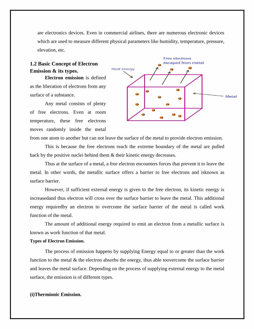
1.2 Basic Concept of Electron
Emission & its types.
Electron emission is defined
as the liberation of electrons from any
surface of a substance.
Any metal consists of plenty
of free electrons. Even at room
temperature, these free electrons
moves randomly inside the metal
from one atom to another but can not leave the surface of the metal to provide electron emission.
This is because the free electrons reach the extreme boundary of the metal are pulled
back by the positive nuclei behind them & their kinetic energy decreases.
Thus at the surface of a metal, a free electron encounters forces that prevent it to leave the
metal. In other words, the metallic surface offers a barrier to free electrons and isknown as
surface barrier.
However, if sufficient external energy is given to the free electron, its kinetic energy is
increasedand thus electron will cross over the surface barrier to leave the metal. This additional
energy requiredby an electron to overcome the surface barrier of the metal is called work
function of the metal.
The amount of additional energy required to emit an electron from a metallic surface is
known as work function of that metal.
Types of Electron Emission.
The process of emission happens by supplying Energy equal to or greater than the work
function to the metal & the electron absorbs the energy, thus able toovercome the surface barrier
and leaves the metal surface. Depending on the process of supplying external energy to the metal
surface, the emission is of different types.
(i)Thermionic Emission.
The process of electron emission from a metal surface by supplying thermal energy to it
is known asthermionic emission.
In this method, the metal is heated to sufficient temperature (about2500ºC) to enable the
free electrons to leave the metal surface. The number of electrons emitteddepends upon the
temperature. The higher the temperature, the greater is the emission of electrons.This type of
emission is employed in vacuum tubes.
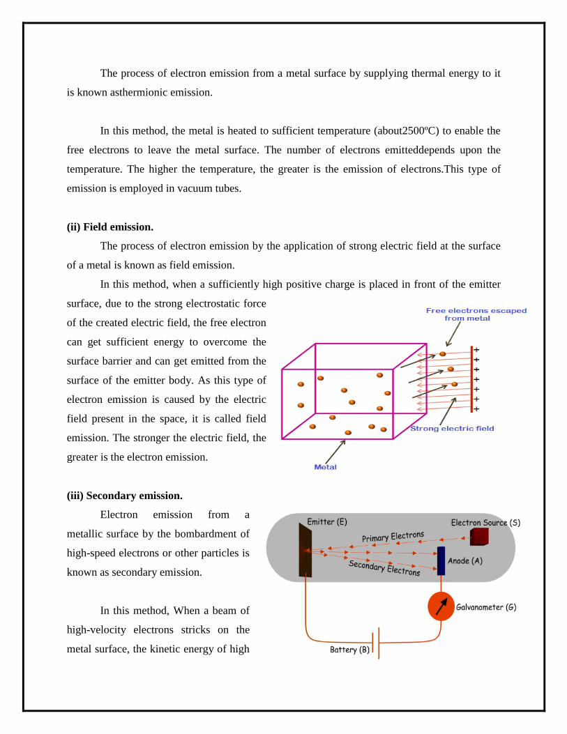
(ii) Field emission.
The process of electron emission by the application of strong electric field at the surface
of a metal is known as field emission.
In this method, when a sufficiently high positive charge is placed in front of the emitter
surface, due to the strong electrostatic force
of the created electric field, the free electron
can get sufficient energy to overcome the
surface barrier and can get emitted from the
surface of the emitter body. As this type of
electron emission is caused by the electric
field present in the space, it is called field
emission. The stronger the electric field, the
greater is the electron emission.
(iii) Secondary emission.
Electron emission from a
metallic surface by the bombardment of
high-speed electrons or other particles is
known as secondary emission.
In this method, When a beam of
high-velocity electrons stricks on the
metal surface, the kinetic energy of high
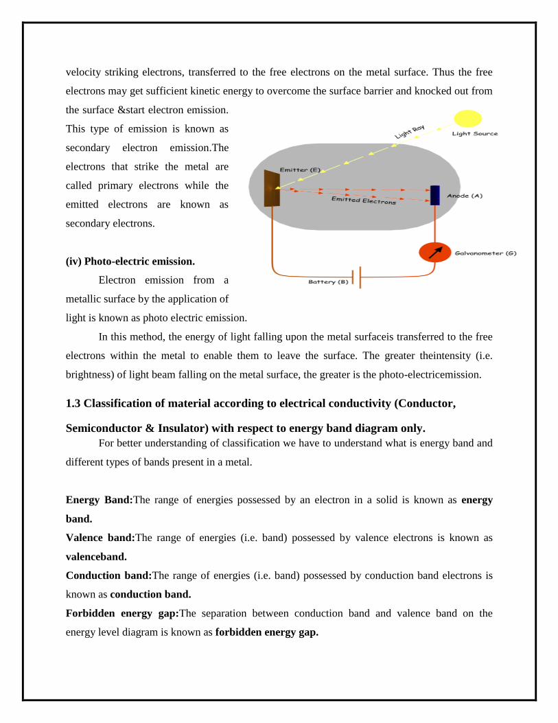
velocity striking electrons, transferred to the free electrons on the metal surface. Thus the free
electrons may get sufficient kinetic energy to overcome the surface barrier and knocked out from
the surface &start electron emission.
This type of emission is known as
secondary electron emission.The
electrons that strike the metal are
called primary electrons while the
emitted electrons are known as
secondary electrons.
(iv) Photo-electric emission.
Electron emission from a
metallic surface by the application of
light is known as photo electric emission.
In this method, the energy of light falling upon the metal surfaceis transferred to the free
electrons within the metal to enable them to leave the surface. The greater theintensity (i.e.
brightness) of light beam falling on the metal surface, the greater is the photo-electricemission.
1.3 Classification of material according to electrical conductivity (Conductor,
Semiconductor & Insulator) with respect to energy band diagram only.
For better understanding of classification we have to understand what is energy band and
different types of bands present in a metal.
Energy Band:The range of energies possessed by an electron in a solid is known as energy
band.
Valence band:The range of energies (i.e. band) possessed by valence electrons is known as
valenceband.
Conduction band:The range of energies (i.e. band) possessed by conduction band electrons is
known as conduction band.
Forbidden energy gap:The separation between conduction band and valence band on the
energy level diagram is known as forbidden energy gap.
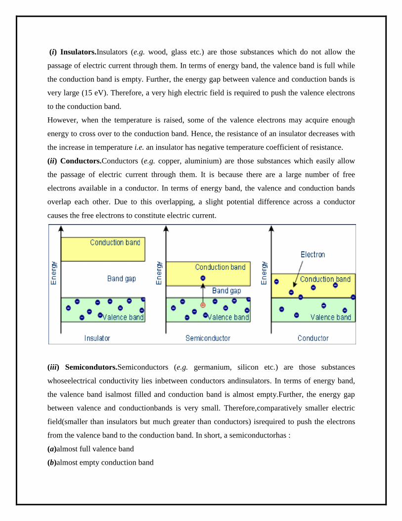
(i) Insulators.Insulators (e.g. wood, glass etc.) are those substances which do not allow the
passage of electric current through them. In terms of energy band, the valence band is full while
the conduction band is empty. Further, the energy gap between valence and conduction bands is
very large (15 eV). Therefore, a very high electric field is required to push the valence electrons
to the conduction band.
However, when the temperature is raised, some of the valence electrons may acquire enough
energy to cross over to the conduction band. Hence, the resistance of an insulator decreases with
the increase in temperature i.e. an insulator has negative temperature coefficient of resistance.
(ii) Conductors.Conductors (e.g. copper, aluminium) are those substances which easily allow
the passage of electric current through them. It is because there are a large number of free
electrons available in a conductor. In terms of energy band, the valence and conduction bands
overlap each other. Due to this overlapping, a slight potential difference across a conductor
causes the free electrons to constitute electric current.
(iii) Semicondutors.Semiconductors (e.g. germanium, silicon etc.) are those substances
whoseelectrical conductivity lies inbetween conductors andinsulators. In terms of energy band,
the valence band isalmost filled and conduction band is almost empty.Further, the energy gap
between valence and conductionbands is very small. Therefore,comparatively smaller electric
field(smaller than insulators but much greater than conductors) isrequired to push the electrons
from the valence band to the conduction band. In short, a semiconductorhas :
(a)almost full valence band
(b)almost empty conduction band
(c)small energy gap (1 eV) between valence and conduction bands.
At low temperature, the valence band is completely full and conduction band is
completely empty. Therefore, a semiconductor virtually behaves as an insulator at low
temperatures. However, even at room temperature, some electrons (about one electron for 1010
atoms) cross over to the conduction band, imparting little conductivity to the semiconductor.
1.4 Difference between Intrinsic & Extrinsic Semiconductor.
Intrinsic Semiconductor:
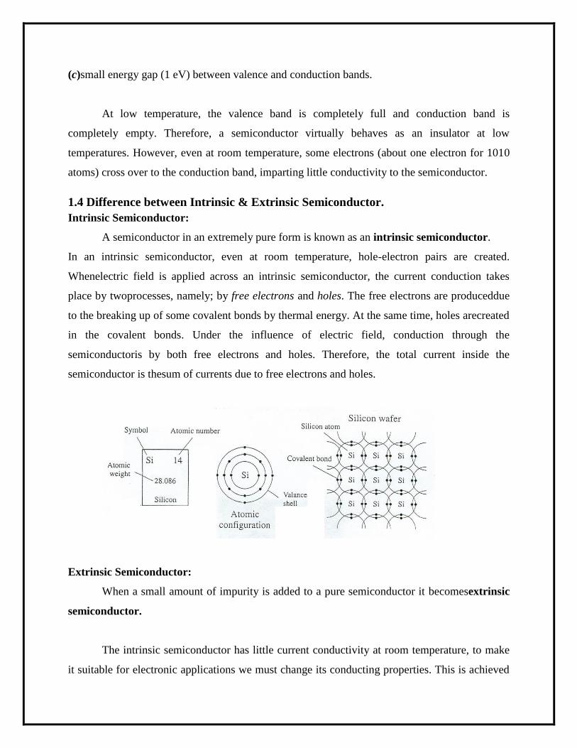
A semiconductor in an extremely pure form is known as an intrinsic semiconductor.
In an intrinsic semiconductor, even at room temperature, hole-electron pairs are created.
Whenelectric field is applied across an intrinsic semiconductor, the current conduction takes
place by twoprocesses, namely; by free electrons and holes. The free electrons are produceddue
to the breaking up of some covalent bonds by thermal energy. At the same time, holes arecreated
in the covalent bonds. Under the influence of electric field, conduction through the
semiconductoris by both free electrons and holes. Therefore, the total current inside the
semiconductor is thesum of currents due to free electrons and holes.
Extrinsic Semiconductor:
When a small amount of impurity is added to a pure semiconductor it becomesextrinsic
semiconductor.
The intrinsic semiconductor has little current conductivity at room temperature, to make
it suitable for electronic applications we must change its conducting properties. This is achieved
by adding a small amount of suitable impurity to a semiconductor. It is then called impurity or
extrinsic semiconductor. The process of adding impurities to a semiconductor is known as
doping.
The purpose of adding impurity is to increase either the number of free electrons or holes
in the semiconductor crystal. If a pentavalent impurity (having 5 valence electrons) is added to
the semiconductor, a large number of free electrons are produced in the semiconductor. If a
trivalent impurity (having 3 valence electrons) is added to the semiconductor, large number of
holes are produced in the semiconductor crystal. Depending upon the type of impurity added,
extrinsic semiconductors are classified into:
(i) n-type semiconductor (ii) p-type semiconductor
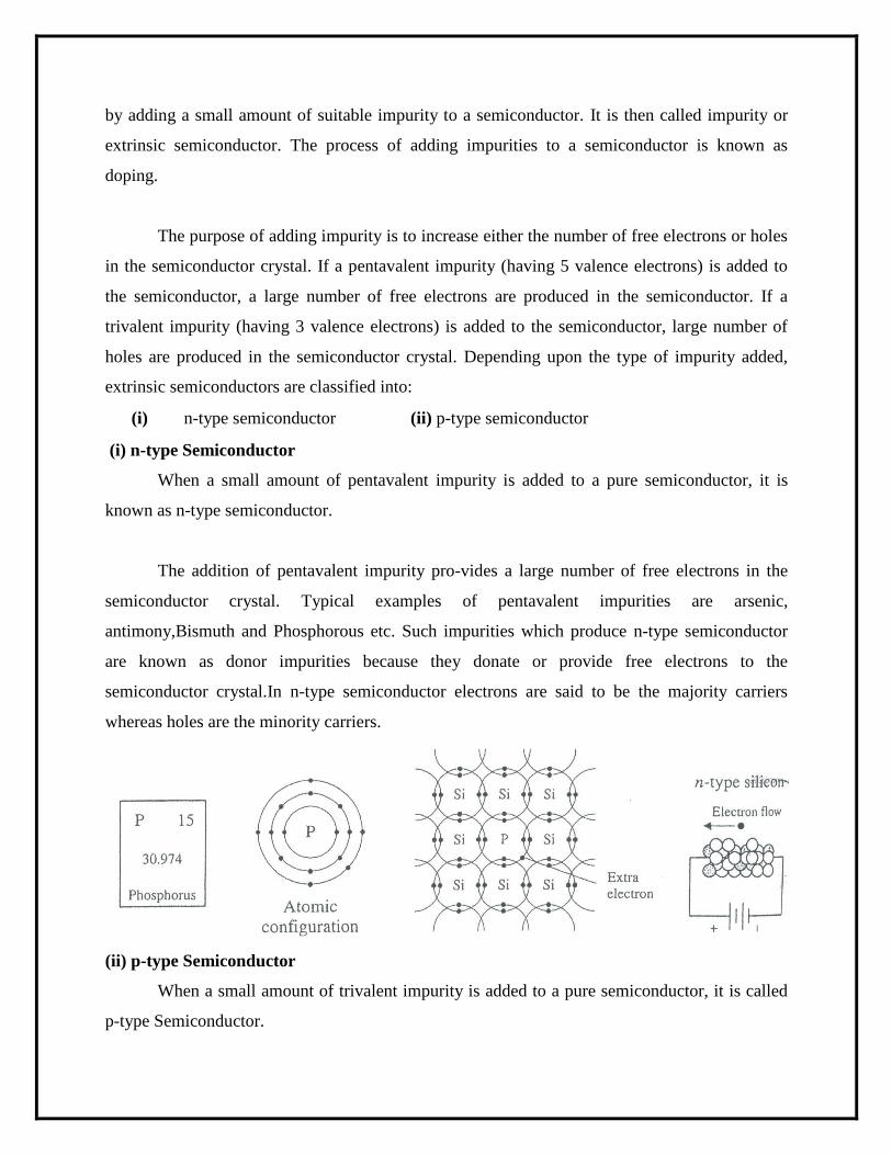
(i) n-type Semiconductor
When a small amount of pentavalent impurity is added to a pure semiconductor, it is
known as n-type semiconductor.
The addition of pentavalent impurity pro-vides a large number of free electrons in the
semiconductor crystal. Typical examples of pentavalent impurities are arsenic,
antimony,Bismuth and Phosphorous etc. Such impurities which produce n-type semiconductor
are known as donor impurities because they donate or provide free electrons to the
semiconductor crystal.In n-type semiconductor electrons are said to be the majority carriers
whereas holes are the minority carriers.
(ii) p-type Semiconductor
When a small amount of trivalent impurity is added to a pure semiconductor, it is called
p-type Semiconductor.
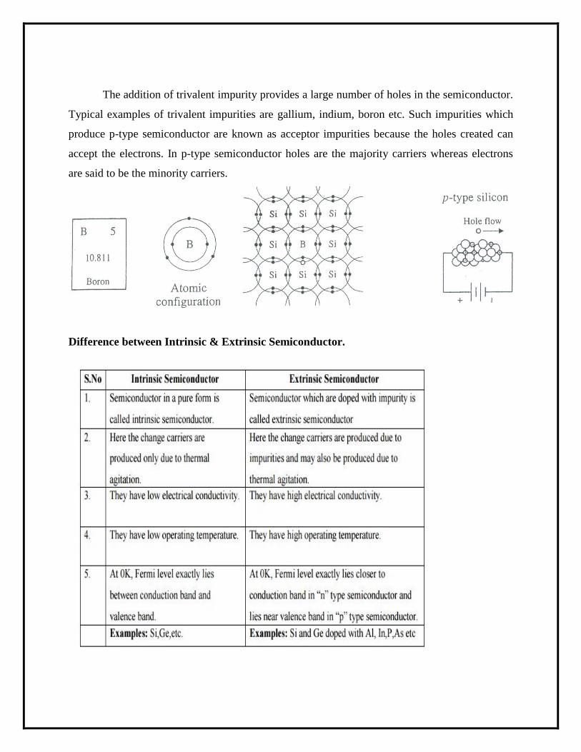
The addition of trivalent impurity provides a large number of holes in the semiconductor.
Typical examples of trivalent impurities are gallium, indium, boron etc. Such impurities which
produce p-type semiconductor are known as acceptor impurities because the holes created can
accept the electrons. In p-type semiconductor holes are the majority carriers whereas electrons
are said to be the minority carriers.
Difference between Intrinsic & Extrinsic Semiconductor.
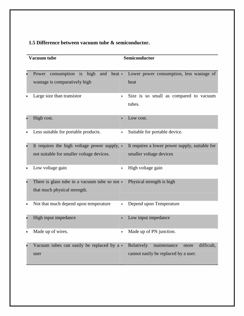
1.5 Difference between vacuum tube & semiconductor.
Vacuum tube Semiconductor
Power consumption is high and heat
wastage is comparatively high
Lower power consumption, less wastage of
heat
Large size than transistor Size is so small as compared to vacuum
tubes.
High cost. Low cost.
Less suitable for portable products. Suitable for portable device.
It requires the high voltage power supply,
not suitable for smaller voltage devices.
It requires a lower power supply, suitable for
smaller voltage devices
Low voltage gain High voltage gain
There is glass tube in a vacuum tube so not
that much physical strength.
Physical strength is high
Not that much depend upon temperature Depend upon Temperature
High input impedance Low input impedance
Made up of wires. Made up of PN junction.
Vacuum tubes can easily be replaced by a
user
Relatively maintenance more difficult,
cannot easily be replaced by a user.
1.6 Principle of working and use of PN junction diode, Zener diode and Light
Emitting Diode (LED)
PN Junction:
When a p-type & n-type
semiconductor properly join together it
forms pn junction. It is the basic building
block for many semiconductor devices. After
the formation of junction a large difference
in carrier density exists which results holes
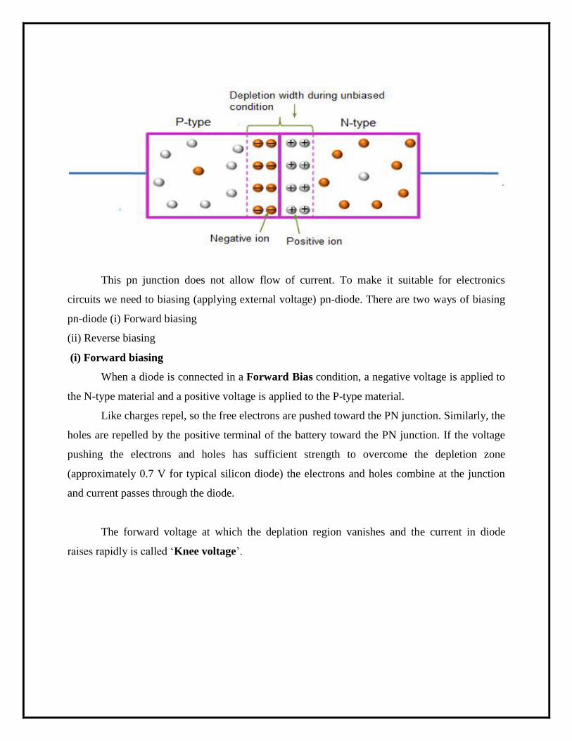
in the p-side tends to diffuse into n-side leaving behind trivalent ion and electrons in the n-side
are tends to diffuse into p-side leaving behind pentavalent ion. Due to this charg separation a
layer of negative charges (trivalent ions) in p-type & positive charges (pentavalent ions) in n-
type near the junction created.These two layers of positive and negative charges form the
depletion region(or depletion layer).
Once pnjunction is formed and depletion layer created, the diffusion of free electrons
stops. Inother words, the depletion region acts as a barrier to the further movement of free
electrons across thejunction. Since the holes in p-side encounters a positive charge in n-side near
the junction similarly electrons in n-side encounters a negative charge in p-side near the junction.
The positive and negative charges set up an electric field. The electric field is a barrier to the free
electrons in the n-region. There exists a potential difference across the depletion layer and is
called barrier potential (V0).
Pn- junction Diode:
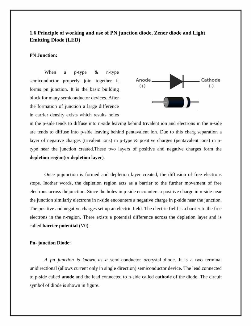
A pn junction is known as a semi-conductor orcrystal diode. It is a two terminal
unidirectional (allows current only in single direction) semiconductor device. The lead connected
to p-side called anode and the lead connected to n-side called cathode of the diode. The circuit
symbol of diode is shown in figure.
This pn junction does not allow flow of current. To make it suitable for electronics
circuits we need to biasing (applying external voltage) pn-diode. There are two ways of biasing
pn-diode (i) Forward biasing
(ii) Reverse biasing
(i) Forward biasing
When a diode is connected in a Forward Bias condition, a negative voltage is applied to
the N-type material and a positive voltage is applied to the P-type material.
Like charges repel, so the free electrons are pushed toward the PN junction. Similarly, the
holes are repelled by the positive terminal of the battery toward the PN junction. If the voltage
pushing the electrons and holes has sufficient strength to overcome the depletion zone
(approximately 0.7 V for typical silicon diode) the electrons and holes combine at the junction
and current passes through the diode.
The forward voltage at which the deplation region vanishes and the current in diode
raises rapidly is called „Knee voltage‟.
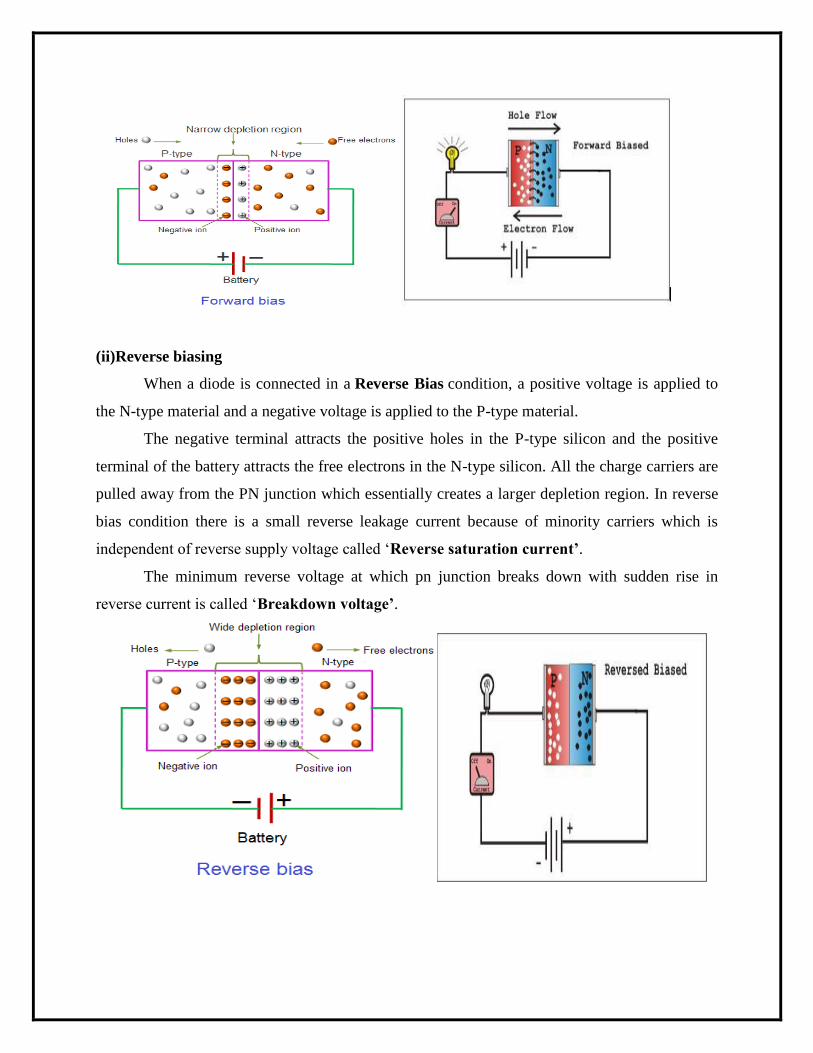
(ii)Reverse biasing
When a diode is connected in a Reverse Bias condition, a positive voltage is applied to
the N-type material and a negative voltage is applied to the P-type material.
The negative terminal attracts the positive holes in the P-type silicon and the positive
terminal of the battery attracts the free electrons in the N-type silicon. All the charge carriers are
pulled away from the PN junction which essentially creates a larger depletion region. In reverse
bias condition there is a small reverse leakage current because of minority carriers which is
independent of reverse supply voltage called „Reverse saturation current’.
The minimum reverse voltage at which pn junction breaks down with sudden rise in
reverse current is called „Breakdown voltage’.
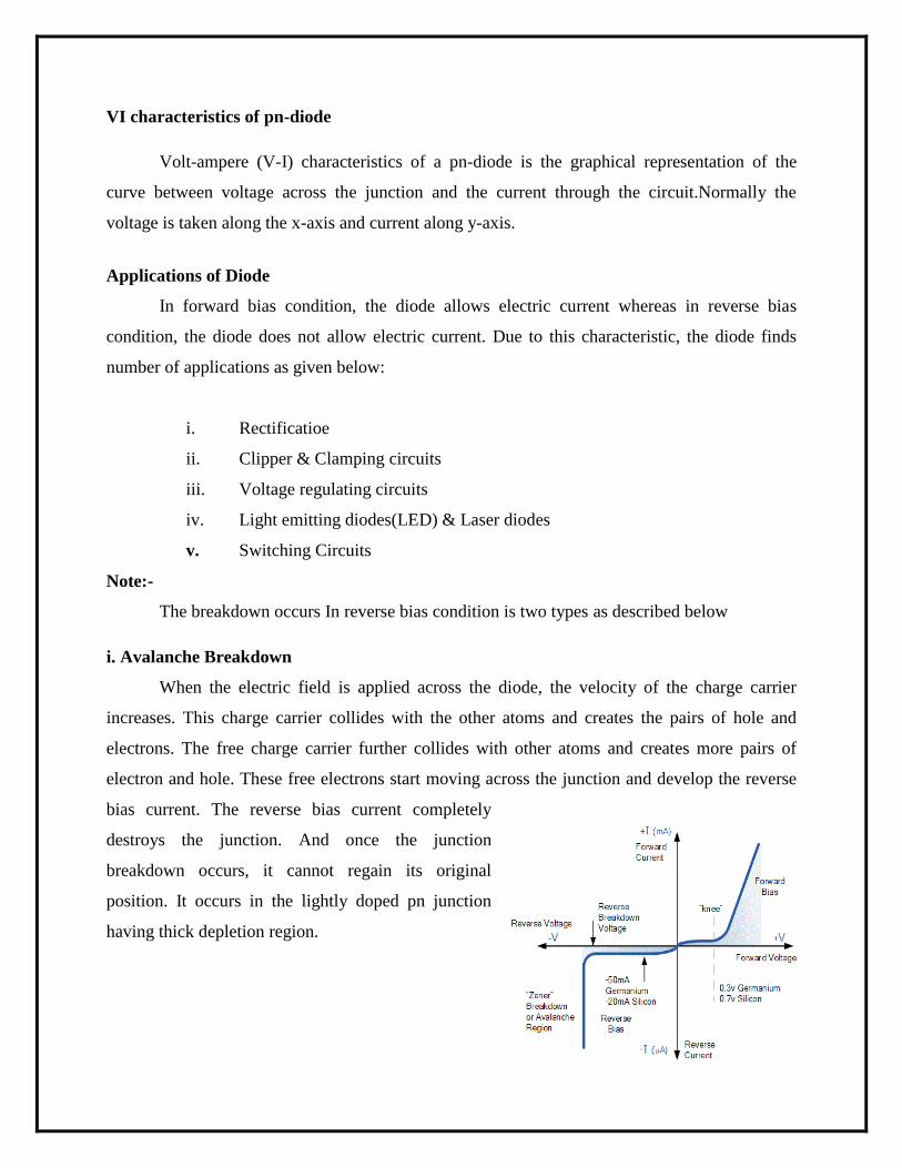
VI characteristics of pn-diode
Volt-ampere (V-I) characteristics of a pn-diode is the graphical representation of the
curve between voltage across the junction and the current through the circuit.Normally the
voltage is taken along the x-axis and current along y-axis.
Applications of Diode
In forward bias condition, the diode allows electric current whereas in reverse bias
condition, the diode does not allow electric current. Due to this characteristic, the diode finds
number of applications as given below:
i. Rectificatioe
ii. Clipper & Clamping circuits
iii. Voltage regulating circuits
iv. Light emitting diodes(LED) & Laser diodes
v. Switching Circuits
Note:-
The breakdown occurs In reverse bias condition is two types as described below
i. Avalanche Breakdown
When the electric field is applied across the diode, the velocity of the charge carrier
increases. This charge carrier collides with the other atoms and creates the pairs of hole and
electrons. The free charge carrier further collides with other atoms and creates more pairs of
electron and hole. These free electrons start moving across the junction and develop the reverse
bias current. The reverse bias current completely
destroys the junction. And once the junction
breakdown occurs, it cannot regain its original
position. It occurs in the lightly doped pn junction
having thick depletion region.
ii. Zener Breakdown.
When the high electric field is applied across the junction, the charge carrier starts
jumping across the junction. These electrons constitute the heavy current in the reversed
direction. In Zener breakdown, the temporary breakdown of junction occurs. The junction
regains its original position when the reverse voltage removes. It occurs in the heavily doped pn
junction having thin deplation region.
Difference between avalanche breakdown and zener breakdown
Avalanche Breakdown Zener Breakdown
The process of applying high voltage and
increasing the free electrons or electric current in
semiconductors and insulating materials is called
an avalanche breakdown.
The process in which the electrons move
across the barrier from the valence band of
p-type material to the conduction band of n-
type material is known as Zener breakdown.
It occurs in diodes that are lightly doped. It occurs in diodes that are highly doped.
The valence electrons are pushed to conduction
due to the energy imparted by accelerated
electrons, which gain their velocity due to their
collision with other atoms.
The valence electrons are pulled into
conduction due to the high electric field in
the narrow depletion region.
The increase in temperature increases the
breakdown voltage.
The increase in temperature decreases the
breakdown voltage.
The VI characteristic curve of the avalanche
breakdown is not as sharp as the Zener
breakdown.
The VI characteristics of a Zener
breakdown has a sharp curve.
This is observed in Zener diode having a Zener
breakdown voltage Vz greater than 8 volts.
This is observed in Zener diodes having a
Zener breakdown voltage
Vz of 5 to 8 volts.
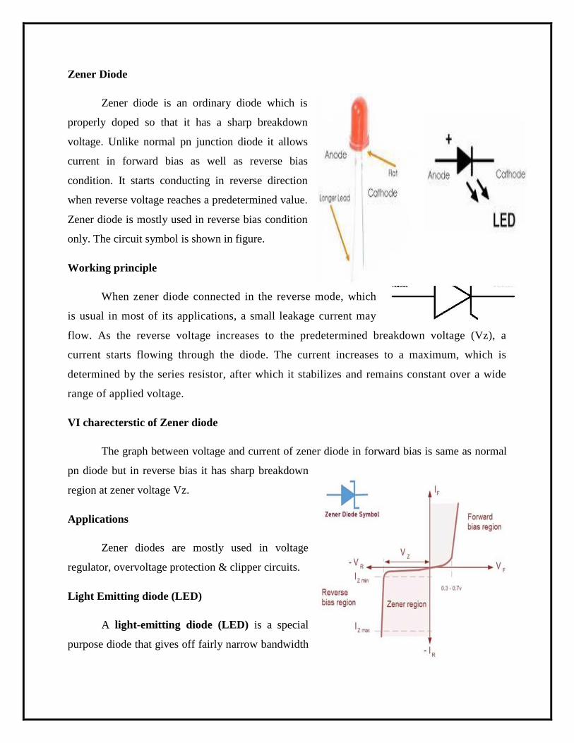
Zener Diode
Zener diode is an ordinary diode which is
properly doped so that it has a sharp breakdown
voltage. Unlike normal pn junction diode it allows
current in forward bias as well as reverse bias
condition. It starts conducting in reverse direction
when reverse voltage reaches a predetermined value.
Zener diode is mostly used in reverse bias condition
only. The circuit symbol is shown in figure.
Working principle
When zener diode connected in the reverse mode, which
is usual in most of its applications, a small leakage current may
flow. As the reverse voltage increases to the predetermined breakdown voltage (Vz), a
current starts flowing through the diode. The current increases to a maximum, which is
determined by the series resistor, after which it stabilizes and remains constant over a wide
range of applied voltage.
VI charecterstic of Zener diode
The graph between voltage and current of zener diode in forward bias is same as normal
pn diode but in reverse bias it has sharp breakdown
region at zener voltage Vz.
Applications
Zener diodes are mostly used in voltage
regulator, overvoltage protection & clipper circuits.
Light Emitting diode (LED)
A light-emitting diode (LED) is a special
purpose diode that gives off fairly narrow bandwidth
of visible or invisible light when forward biased.The circuit symbol is shown in figure.
These are made by using elements like gallium, phosphorus and arsenic instead of normal
Silicon and Germanium materials.
When light-emitting diode (LED) is forward biasedthe electrons from the n-type material
cross the pnjunction and recombine with holes in the p-type material. These free electrons are in
the conduction band and at a higher energy level than the holes in the valence band. When
recombination takes place, the recombining electrons release some part of energy in the form of
heat and light. In Si &Ge diodes these energy dissipate in the form of heat but in Galium-
Arsenide-phosphorous (GaAsP) and Galium-phosphorous (GaP) semiconductors, the electrons
dissipate energy in the form of photons.
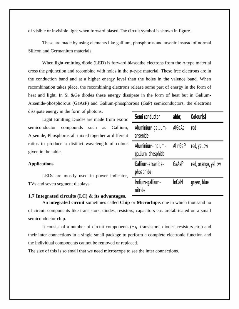
Light Emitting Diodes are made from exotic
semiconductor compounds such as Gallium,
Arsenide, Phosphorus all mixed together at different
ratios to produce a distinct wavelength of colour
given in the table.
Applications
LEDs are mostly used in power indicator,
TVs and seven segment displays.
1.7 Integrated circuits (I.C) & its advantages.
An integrated circuit sometimes called Chip or Microchipis one in which thousand no
of circuit components like transistors, diodes, resistors, capacitors etc. arefabricated on a small
semiconductor chip.
It consist of a number of circuit components (e.g. transistors, diodes, resistors etc.) and
their inter connections in a single small package to perform a complete electronic function and
the individual components cannot be removed or replaced.
The size of this is so small that we need microscope to see the inter connections.
Advantages of IC
Integrated Circuits has many advantages over discrete circuits such as:
(i) Extremely small in size,
(ii) Low power consumption,
(iii) Reliability,
(iv) Reduced cost,
(v) Very small weight
(vi) Easy replacement.
Chapter Review Questions:
1. Define Electronics & its application.
2. Define work function.
3. Define Electronic Emission & different types of Emission.
4. Explain Conductor, Semiconductor & Insulator with respect to energy band diagram only.
5. Define doping.
6. Define energy gap & valence electrons.
7. Discuss Intrinsic Semiconductor.
8. Discuss Extrinsic Semiconductor.
9. Define accepter & donor atom.
10. List different types of Impurity.
11. Explain the difference between vacuum tube & semiconductor.
12. State basic concept of integrated circuits (I.C) & its use.
13. Explain P-type and N-type semiconductor junction.
14. Define PN junction Barrier voltage, depletion region, Junction Capacitance.
15. Draw Forward biased & reversed biased junction Diode.
16. Draw symbol, circuit diagram for characteristics (Forward & reversed) Characteristics PN
junction diode.
17. Explain Construction (reference to doping level),Symbol ,circuit diagram for characteristics
(forwarded & reversed) of Zener Diode.
18. Explain Avalanche &Zener breakdown and its comparison.
19. Explain Construction ,Symbol ,circuit diagram for characteristics of LED.
CHAPTER-2
2. ELECTRONIC CIRCUITS
2.1 Rectifier & its uses.
Rectifier
A rectifier is an electrical device that converts an Alternating Current (AC) into a Direct
Current (DC) by using one or more P-N junction diodes.
When AC voltage or AC current is applied across the P-N junction diode, during the
positive half cycle the diode is forward biased and allows electric current through it.
However, when the AC current reverses its direction to negative half cycle, the diode is
reverse biased and does not allow electric current through it. Thus, electric current flows
through the diode only during the positive half cycle of the AC current.
This current which flows across the diode is nothing but a DC current. Thus, the P-N
junction diode acts like a rectifier by converting the AC current into DC current.
Rectifiers are mostly used to provide continuous voltage (DC Voltage) required to run
almost all electronic devices & circuits.
2.2 Principles of working of different types of Rectifiers with their merits and
demerits
Types of Rectifier: The rectifiers are mainly classified into two types:
(i) Half wave rectifier
(ii) Full wave rectifier
Half Wave Rectifier
As the name suggests, the half wave rectifier is a type of rectifier which converts half of
the AC input signal (positive half cycle) into pulsating DC output signal and the remaining half
signal (negative half cycle) is blocked or lost.A half-wave rectifier is the simplest of them all as
it is composed of only a single diode.
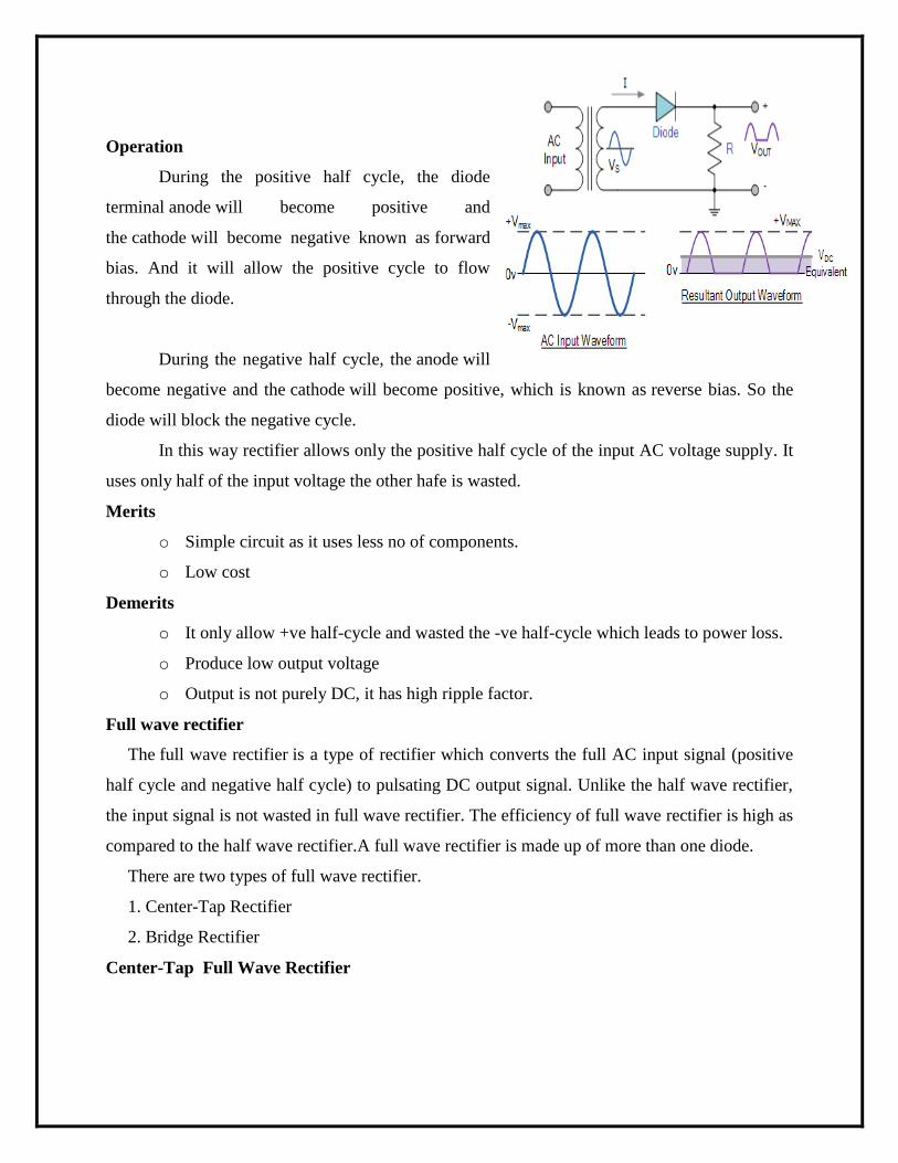
Operation
During the positive half cycle, the diode
terminal anode will become positive and
the cathode will become negative known as forward
bias. And it will allow the positive cycle to flow
through the diode.
During the negative half cycle, the anode will
become negative and the cathode will become positive, which is known as reverse bias. So the
diode will block the negative cycle.
In this way rectifier allows only the positive half cycle of the input AC voltage supply. It
uses only half of the input voltage the other hafe is wasted.
Merits
o Simple circuit as it uses less no of components.
o Low cost
Demerits
o It only allow +ve half-cycle and wasted the -ve half-cycle which leads to power loss.
o Produce low output voltage
o Output is not purely DC, it has high ripple factor.
Full wave rectifier
The full wave rectifier is a type of rectifier which converts the full AC input signal (positive
half cycle and negative half cycle) to pulsating DC output signal. Unlike the half wave rectifier,
the input signal is not wasted in full wave rectifier. The efficiency of full wave rectifier is high as
compared to the half wave rectifier.A full wave rectifier is made up of more than one diode.
There are two types of full wave rectifier.
1. Center-Tap Rectifier
2. Bridge Rectifier
Center-Tap Full Wave Rectifier
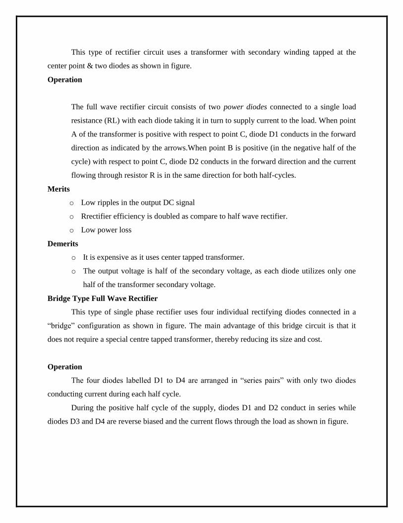
This type of rectifier circuit uses a transformer with secondary winding tapped at the
center point & two diodes as shown in figure.
Operation
The full wave rectifier circuit consists of two power diodes connected to a single load
resistance (RL) with each diode taking it in turn to supply current to the load. When point
A of the transformer is positive with respect to point C, diode D1 conducts in the forward
direction as indicated by the arrows.When point B is positive (in the negative half of the
cycle) with respect to point C, diode D2 conducts in the forward direction and the current
flowing through resistor R is in the same direction for both half-cycles.
Merits
o Low ripples in the output DC signal
o Rrectifier efficiency is doubled as compare to half wave rectifier.
o Low power loss
Demerits
o It is expensive as it uses center tapped transformer.
o The output voltage is half of the secondary voltage, as each diode utilizes only one
half of the transformer secondary voltage.
Bridge Type Full Wave Rectifier
This type of single phase rectifier uses four individual rectifying diodes connected in a
“bridge” configuration as shown in figure. The main advantage of this bridge circuit is that it
does not require a special centre tapped transformer, thereby reducing its size and cost.
Operation
The four diodes labelled D1 to D4 are arranged in “series pairs” with only two diodes
conducting current during each half cycle.
During the positive half cycle of the supply, diodes D1 and D2 conduct in series while
diodes D3 and D4 are reverse biased and the current flows through the load as shown in figure.
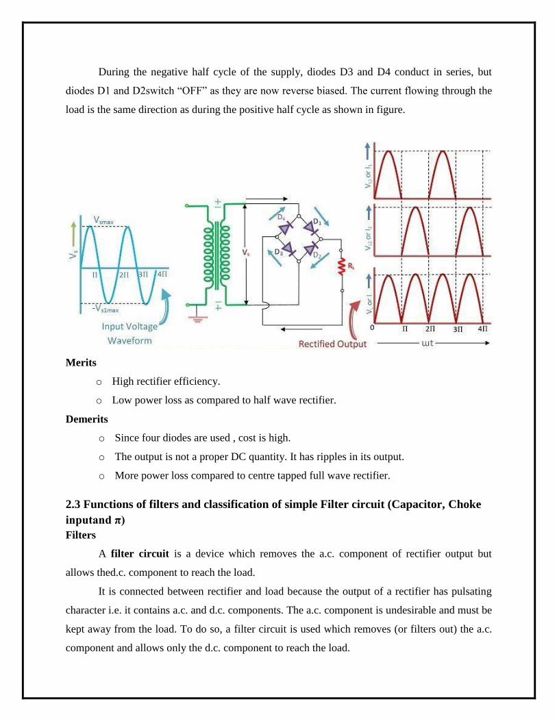
During the negative half cycle of the supply, diodes D3 and D4 conduct in series, but
diodes D1 and D2switch “OFF” as they are now reverse biased. The current flowing through the
load is the same direction as during the positive half cycle as shown in figure.
Merits
o High rectifier efficiency.
o Low power loss as compared to half wave rectifier.
Demerits
o Since four diodes are used , cost is high.
o The output is not a proper DC quantity. It has ripples in its output.
o More power loss compared to centre tapped full wave rectifier.
2.3 Functions of filters and classification of simple Filter circuit (Capacitor, Choke
inputand π)
Filters
A filter circuit is a device which removes the a.c. component of rectifier output but
allows thed.c. component to reach the load.
It is connected between rectifier and load because the output of a rectifier has pulsating
character i.e. it contains a.c. and d.c. components. The a.c. component is undesirable and must be
kept away from the load. To do so, a filter circuit is used which removes (or filters out) the a.c.
component and allows only the d.c. component to reach the load.
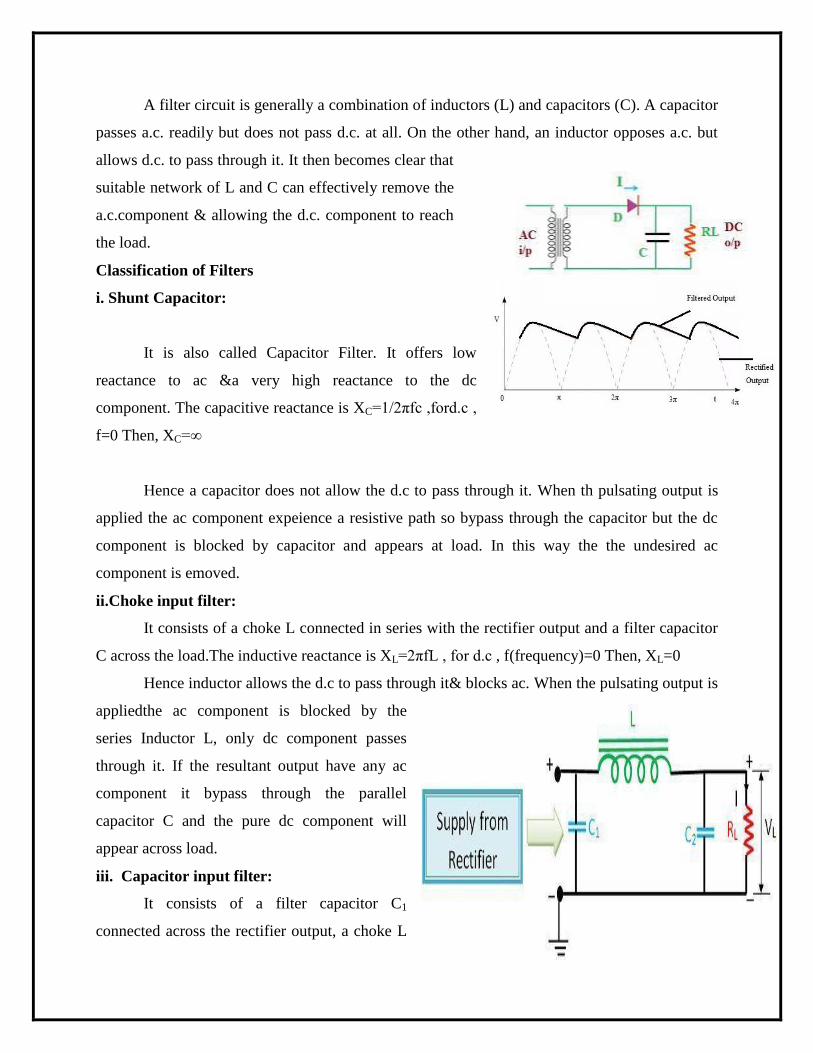
A filter circuit is generally a combination of inductors (L) and capacitors (C). A capacitor
passes a.c. readily but does not pass d.c. at all. On the other hand, an inductor opposes a.c. but
allows d.c. to pass through it. It then becomes clear that
suitable network of L and C can effectively remove the
a.c.component & allowing the d.c. component to reach
the load.
Classification of Filters
i. Shunt Capacitor:
It is also called Capacitor Filter. It offers low
reactance to ac &a very high reactance to the dc
component. The capacitive reactance is XC=1/2πfc ,ford.c ,
f=0 Then, XC=∞
Hence a capacitor does not allow the d.c to pass through it. When th pulsating output is
applied the ac component expeience a resistive path so bypass through the capacitor but the dc
component is blocked by capacitor and appears at load. In this way the the undesired ac
component is emoved.
ii.Choke input filter:
It consists of a choke L connected in series with the rectifier output and a filter capacitor
C across the load.The inductive reactance is XL=2πfL , for d.c , f(frequency)=0 Then, XL=0
Hence inductor allows the d.c to pass through it& blocks ac. When the pulsating output is
appliedthe ac component is blocked by the
series Inductor L, only dc component passes
through it. If the resultant output have any ac
component it bypass through the parallel
capacitor C and the pure dc component will
appear across load.
iii. Capacitor input filter:
It consists of a filter capacitor C1
connected across the rectifier output, a choke L
in series and another filter capacitor C2 connected across the load.The shape of the circuit
diagram of this filter circuit appears like Greek letter π (pi) and hence the name π-filter.
Here pulsating output from rectifier is applied across 1st capacitor C1which offers zero
reactance to a.c& infinite reactance to d.c. Hence d.c component continues to reach across
(Choke Filter)L . The filter choke then allows the d.c component easily by blocking a.c
component if any. Finally the 2nd capacitor C2across load bypasses the a.c component if any
which the choke(L) failed to block by making d.c component to reach across load.
2.4 Working of D.C power supply system (unregulated) with help of block diagrams
only
Almost all household electronic circuits need an unregulated AC to be converted to
constant DC in order to operate. All devices will have certain power supply
Limit and the inside circuit must be able to supply dc voltage within this limit. This DC supply is
regulated & limited interms of voltage and current but the mains supply may be fluctuating may
cause damage to the electronic circuit. This job is done by a unregulated power supply.
The DC power supply is practically converted to each & every stage in the system. All
low power system can be run with a battery but batteries are expensive & frequently replaced. So
the best method is a unregulated power supply.
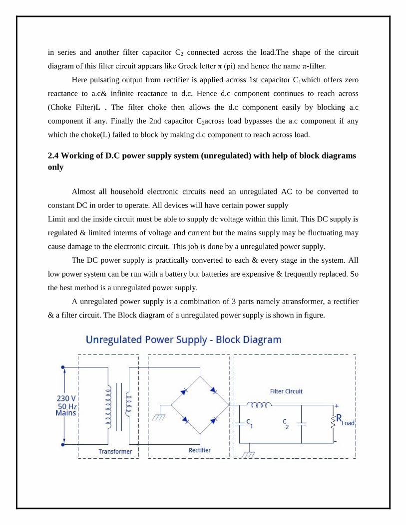
A unregulated power supply is a combination of 3 parts namely atransformer, a rectifier
& a filter circuit. The Block diagram of a unregulated power supply is shown in figure.
A small step down transformer is used o reduce the voltage level as the device needed.
The output of the transformer is a pulsating AC voltage which is feed into rectifier circuit. The
rectifier convert it and it‟s output is pulsating DC. Again this output is feed to filter circuit as
input. This filter circuit then removes the ac components present if any and gives a DC voltage as
required by the electronic circuit.
2.5 Transistor, Different types of Transistor Configuration and state output and
inputcurrent gain relationship in CE,CB and CC configuration( No mathematical
derivation)
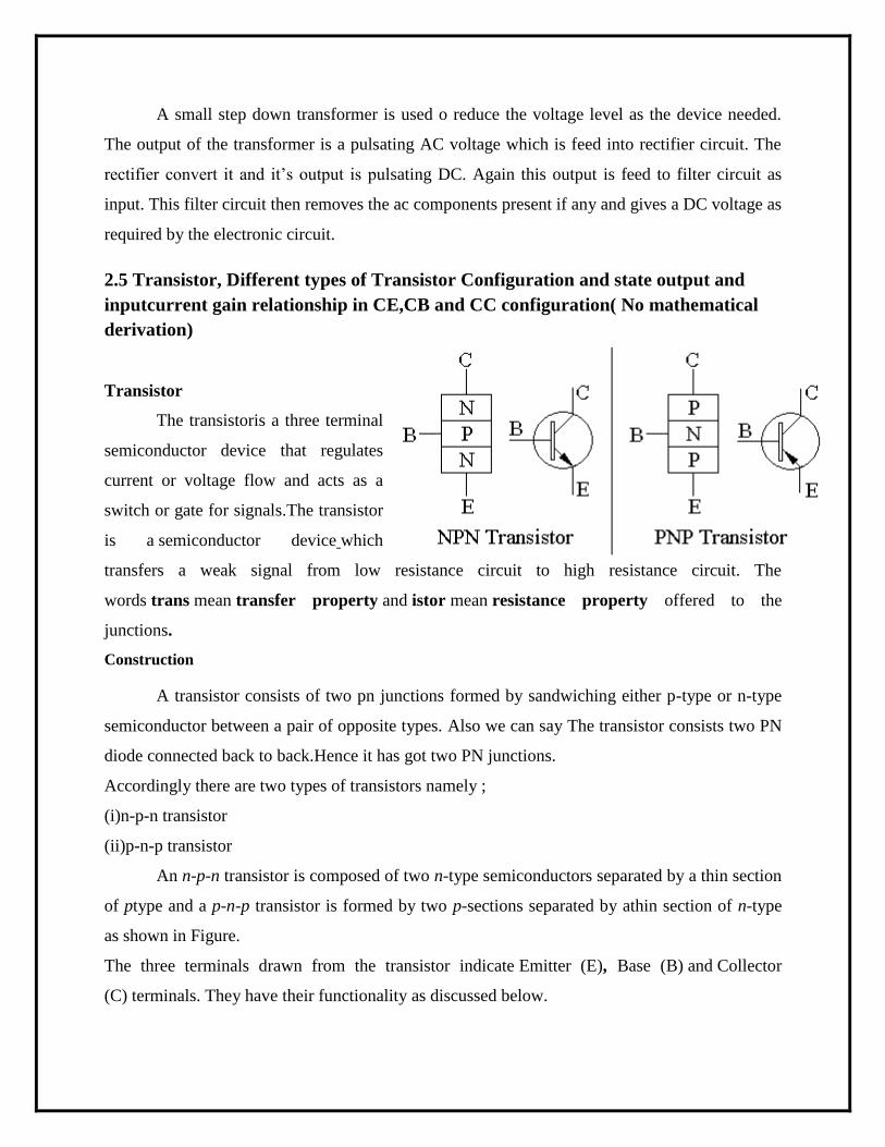
Transistor
The transistoris a three terminal
semiconductor device that regulates
current or voltage flow and acts as a
switch or gate for signals.The transistor
is a semiconductor device which
transfers a weak signal from low resistance circuit to high resistance circuit. The
words trans mean transfer property and istor mean resistance property offered to the
junctions.
Construction
A transistor consists of two pn junctions formed by sandwiching either p-type or n-type
semiconductor between a pair of opposite types. Also we can say The transistor consists two PN
diode connected back to back.Hence it has got two PN junctions.
Accordingly there are two types of transistors namely ;
(i)n-p-n transistor
(ii)p-n-p transistor
An n-p-n transistor is composed of two n-type semiconductors separated by a thin section
of ptype and a p-n-p transistor is formed by two p-sections separated by athin section of n-type
as shown in Figure.
The three terminals drawn from the transistor indicate Emitter (E), Base (B) and Collector
(C) terminals. They have their functionality as discussed below.
Emitter
The left-hand side of the above shown structure can be understood as Emitter.
This has a moderate size and is heavilydoped as its main function is to supply a number
of majority carriers, i.e. either electrons or holes.
As this emits electrons, it is called as an Emitter.
This is simply indicated with the letter E.
Base
The middle material in the above figure is the Base.
This is thin and lightlydoped.
Its main function is to pass the majority carriers from the emitter to the collector.
This is indicated by the letter B.
Collector
The right side material in the above figure can be understood as a Collector.
Its name implies its function of collecting the carriers.
This is a bit larger in size than emitter and base. It is moderately doped.
This is indicated by the letter C.
The emitter-basa junction is always forward bias whereas the collector-base junction is always
reverse bias.The arrow in the symbol indicates the direction of flow of conventional current in
the emitter with forward biasing applied to the emitter-base junction. The only difference
between the NPN and PNP transistor is in the direction of the current.
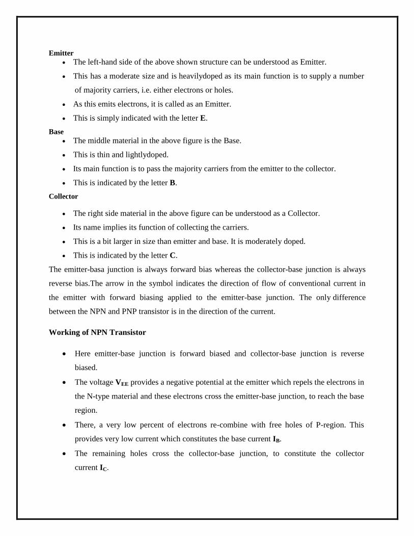
Working of NPN Transistor
Here emitter-base junction is forward biased and collector-base junction is reverse
biased.
The voltage VEE provides a negative potential at the emitter which repels the electrons in
the N-type material and these electrons cross the emitter-base junction, to reach the base
region.
There, a very low percent of electrons re-combine with free holes of P-region. This
provides very low current which constitutes the base current IB.
The remaining holes cross the collector-base junction, to constitute the collector
current IC.
As an electron reaches out of the collector terminal, and enters the positive terminal of
the battery, an electron from the negative terminal of the battery VEE enters the emitter
increases and the electron current flows through the transistor.
Using Kirchhoff‟s Current Law we getIE = IB + IC
Working of PNP Transistor
Here emitter-base junction is forward biased and collector-base junction is reverse
biased.
The voltage VEE provides a positive potential at the emitter which repels the holes in the
P-type material and these holes cross the emitter-base junction, to reach the base region.
There a very low percent of holes re-combine with free electrons of N-region. This
provides very low current which constitutes the base current IB.
The remaining holes cross the collector-base junction, to constitute collector current IC,
which is the hole current.
As a hole reaches the collector terminal, an electron from the battery negative terminal
fills the space in the collector. This flow slowly increases and the electron minority
current flows through the emitter, where each electron entering the positive terminal
of VEE, is replaced by a hole by moving towards the emitter junction. This constitutes
emitter current IE.
Here also if we applyingKirchhoff‟s Current Law we getIE = IB + IC
Different Transistor Configurations
There are three leads in a transistor named as Emitter, Base and Collector terminals.
However, when atransistor is to be connected in a circuit, we require four terminals, two for the
input and two for theoutput. This difficulty is overcome by making one terminal of the transistor
common to both inputand output. The input is fed between this common terminal and one of the
other twoterminals. The output is obtained between the common terminal and the remaining
terminal.
Accordingly, There are three different configurations of Transistors.
Common Base (CB) Configuration: no current gain but voltage gain
Common Emitter (CE) Configuration: current gain and voltage gain
Common Collector (CC) Configuration: current gain but no voltage gain
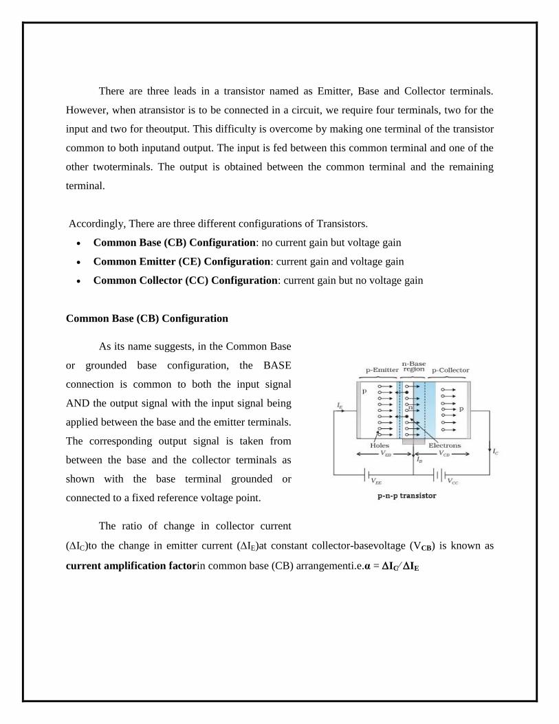
Common Base (CB) Configuration
As its name suggests, in the Common Base
or grounded base configuration, the BASE
connection is common to both the input signal
AND the output signal with the input signal being
applied between the base and the emitter terminals.
The corresponding output signal is taken from
between the base and the collector terminals as
shown with the base terminal grounded or
connected to a fixed reference voltage point.
The ratio of change in collector current
(IC)to the change in emitter current (IE)at constant collector-basevoltage (VCB) is known as
current amplification factorin common base (CB) arrangementi.e.α = IC⁄ IE
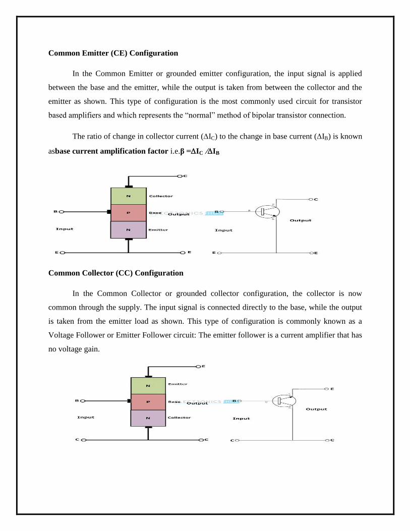
Common Emitter (CE) Configuration
In the Common Emitter or grounded emitter configuration, the input signal is applied
between the base and the emitter, while the output is taken from between the collector and the
emitter as shown. This type of configuration is the most commonly used circuit for transistor
based amplifiers and which represents the “normal” method of bipolar transistor connection.
The ratio of change in collector current (IC) to the change in base current (IB) is known
asbase current amplification factor i.e.β =IC ⁄IB
Common Collector (CC) Configuration
In the Common Collector or grounded collector configuration, the collector is now
common through the supply. The input signal is connected directly to the base, while the output
is taken from the emitter load as shown. This type of configuration is commonly known as a
Voltage Follower or Emitter Follower circuit: The emitter follower is a current amplifier that has
no voltage gain.
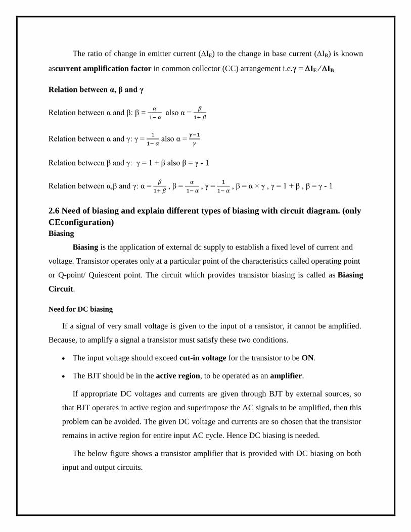
The ratio of change in emitter current (IE) to the change in base current (IB) is known
ascurrent amplification factor in common collector (CC) arrangement i.e.γ = IE ⁄ IB
Relation between α, β and γ
Relation between α and β: β =
also α =
Relation between α and γ: γ =
also α =
Relation between β and γ: γ = 1 + β also β = γ - 1
Relation between α,β and γ: α =
, β =
, γ =
, β = α × γ , γ = 1 + β , β = γ - 1
2.6 Need of biasing and explain different types of biasing with circuit diagram. (only
CEconfiguration)
Biasing
Biasing is the application of external dc supply to establish a fixed level of current and
voltage. Transistor operates only at a particular point of the characteristics called operating point
or Q-point/ Quiescent point. The circuit which provides transistor biasing is called as Biasing
Circuit.
Need for DC biasing
If a signal of very small voltage is given to the input of a ransistor, it cannot be amplified.
Because, to amplify a signal a transistor must satisfy these two conditions.
The input voltage should exceed cut-in voltage for the transistor to be ON.
The BJT should be in the active region, to be operated as an amplifier.
If appropriate DC voltages and currents are given through BJT by external sources, so
that BJT operates in active region and superimpose the AC signals to be amplified, then this
problem can be avoided. The given DC voltage and currents are so chosen that the transistor
remains in active region for entire input AC cycle. Hence DC biasing is needed.
The below figure shows a transistor amplifier that is provided with DC biasing on both
input and output circuits.
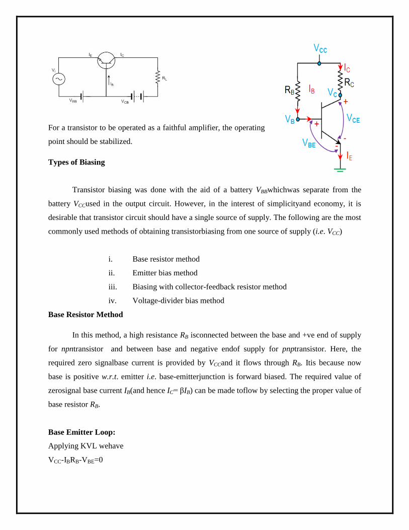
For a transistor to be operated as a faithful amplifier, the operating
point should be stabilized.
Types of Biasing
Transistor biasing was done with the aid of a battery VBBwhichwas separate from the
battery VCCused in the output circuit. However, in the interest of simplicityand economy, it is
desirable that transistor circuit should have a single source of supply. The following are the most
commonly used methods of obtaining transistorbiasing from one source of supply (i.e. VCC)
i. Base resistor method
ii. Emitter bias method
iii. Biasing with collector-feedback resistor method
iv. Voltage-divider bias method
Base Resistor Method
In this method, a high resistance RB isconnected between the base and +ve end of supply
for npntransistor and between base and negative endof supply for pnptransistor. Here, the
required zero signalbase current is provided by VCCand it flows through RB. Itis because now
base is positive w.r.t. emitter i.e. base-emitterjunction is forward biased. The required value of
zerosignal base current IB(and hence IC= βIB) can be made toflow by selecting the proper value of
base resistor RB.
Base Emitter Loop:
Applying KVL wehave
VCC-IBRB-VBE=0
IB=
Since VBE and VCC are constant, the selection of a base resistor RB sets the level of base current
for the operating point.
Collector Emitter Loop:
IC=β IB
VCC-ICRC-VCE=0
VCE= VCC-ICRC
So RB controls IB and IC, and the level of RC determines the magnitude of VCE.
VCE= VC- VE, VBE= VB- VE
Emitter Bias Method
This circuit differs from base-bias circuit in two important respects. First, it uses two separate
d.c. voltage sources; one positive (+ VCC) and the other negative (– VEE). Normally, the two
supply voltages will be equal. For example, if VCC= + 20V (d.c.), then VEE= – 20V (d.c.).
Secondly, there is a resistor REin the emitter circuit.
Base Emitter Loop:
Applying KVL we have
VCC-IBRB-VBE- IERE =0
Collector Emitter Loop:
IC=β IB
VCC-ICRC-VCE- IERE =0
VCE= VCC-IC (RC+RE)
Collector feedback Resistor Method
In this method, one end of RBis connected to the base and the other end to the collector as shown
in Figure. Here, the required zero signal base current is determined not byVCCbut by the
collectorbase voltage VCB. It is clear that VCBforward biases the base-emitter junction and hence
base current IBflows through RB. This causes the zero signal collector current to flow in the
circuit.
Base Emitter Loop:
Applying KVL and solving we have
IB=
Collector Emitter Loop:
Applying KVL and solving we have
VCE=VCC-IC (RC+RE)
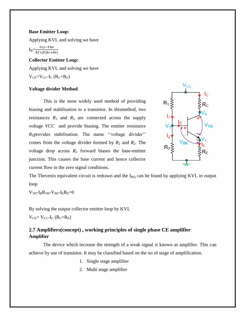
Voltage divider Method
This is the most widely used method of providing
biasing and stabilisation to a transistor. In thismethod, two
resistances R1 and R2 are connected across the supply
voltage VCC and provide biasing. The emitter resistance
REprovides stabilisation. The name „„voltage divider‟‟
comes from the voltage divider formed by R2 and R2. The
voltage drop across R2 forward biases the base-emitter
junction. This causes the base current and hence collector
current flow in the zero signal conditions.
The Thevenin equivalent circuit is redrawn and the IBQ can be found by applying KVL in output
loop
VTH-IBRTH-VBE-IERE=0
By solving the output collector emitter loop by KVL
VCE= VCC-IC (RC+RE)
2.7 Amplifiers(concept) , working principles of single phase CE amplifier
Amplifier
The device which increase the strength of a weak signal is known as amplifier. This can
achieve by use of transistor. It may be classified based on the no of stage of amplification.
1. Single stage amplifier
2. Multi stage amplifier
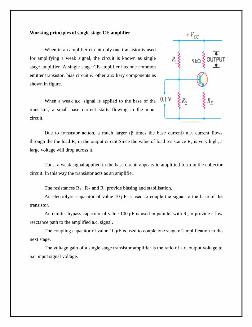
Working principles of single stage CE amplifier
When in an amplifier circuit only one transistor is used
for amplifying a weak signal, the circuit is known as single
stage amplifier. A single stage CE amplifier has one common
emitter transistor, bias circuit & other auxiliary components as
shown in figure.
When a weak a.c. signal is applied to the base of the
transistor, a small base current starts flowing in the input
circuit.
Due to transistor action, a much larger (β times the base current) a.c. current flows
through the the load Rc in the output circuit.Since the value of load resistance Rc is very high, a
large voltage will drop across it.
Thus, a weak signal applied in the base circuit appears in amplified form in the collector
circuit. In this way the transistor acts as an amplifier.
The resistances R1 , R2 and RE provide biasing and stabilisation.
An electrolytic capacitor of value 10 μF is used to couple the signal to the base of the
transistor.
An emitter bypass capacitor of value 100 μF is used in parallel with RE to provide a low
reactance path to the amplified a.c. signal.
The coupling capacitor of value 10 μF is used to couple one stage of amplification to the
next stage.
The voltage gain of a single stage transistor amplifier is the ratio of a.c. output voltage to
a.c. input signal voltage.
2.8 Electronic Oscillator and its classification
Defination
An oscillator is a circuit which produces a continuous, repeated, alternating waveform
without any input. Oscillators basically convert unidirectional current flow from a DC source
into an alternating waveform which is of the desired frequency, as decided by its circuit
components.
The basic principle behind the working of oscillators can be understood by analyzing the
behavior of an LC tank circuit shown in Figure, which employs an inductor L and a completely
pre-charged capacitor C as its components.
Classification of Oscillator
The oscillators are classified based on the nature of the output waveforms, the parameters
used, the range of frequency etc. The various ways in which oscillators are classified as :
Based on the Output Waveform
Under this, the oscillators are classified as sinusoidal and non sinusoidal oscillators. The
sinusoidal oscillator generate purely sinusoidal waveform at the output. While non sinusoidal
oscillators generate an output waveform as triangular, square, saw tooth etc.
Based on the circuit components
The oscillator using the components resistance and capacitor are called RC oscillators.
While the oscillators using the components inductance and capacitor are called LC oscillators. In
some oscillators, crystal is used, are called crystal oscillators.
Based on the range of Operating Frequency
If the oscillators are used to generate the oscillations at audio frequency range which is
20 Hz to 100 – 200 KHz, then the oscillators are classified as low frequency or audio frequency
oscillators. While the oscillators used at the frequency range more than 200 – 300 KHz upto GHz
are classified as high frequency or radio frequency oscillators. The RC oscillators are used at low
frequency while the LC oscillators are used at high frequency range.
Based on type of Feedback used
The oscillators in which the feedback is used, which satisfies the required conditions, are
classified as feedback type of oscillators. The oscillators in which the feedback is not used to
generate the oscillations, are classified as non feedback oscillators.
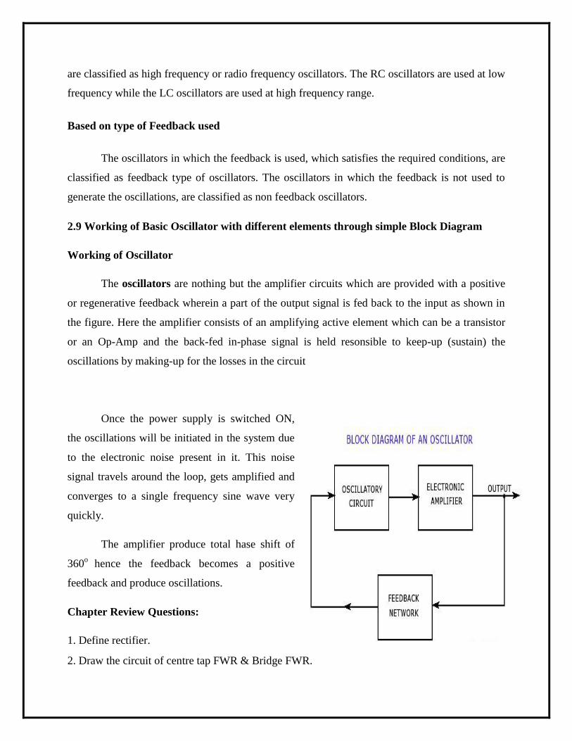
2.9 Working of Basic Oscillator with different elements through simple Block Diagram
Working of Oscillator
The oscillators are nothing but the amplifier circuits which are provided with a positive
or regenerative feedback wherein a part of the output signal is fed back to the input as shown in
the figure. Here the amplifier consists of an amplifying active element which can be a transistor
or an Op-Amp and the back-fed in-phase signal is held resonsible to keep-up (sustain) the
oscillations by making-up for the losses in the circuit
Once the power supply is switched ON,
the oscillations will be initiated in the system due
to the electronic noise present in it. This noise
signal travels around the loop, gets amplified and
converges to a single frequency sine wave very
quickly.
The amplifier produce total hase shift of
360o
hence the feedback becomes a positive
feedback and produce oscillations.
Chapter Review Questions:
1. Define rectifier.
2. Draw the circuit of centre tap FWR & Bridge FWR.
3. State different types of filters .
4. Define ripple & ripple factor.
5. Define rectifier efficiency.
6. What is a transistor ?
7. State different types of transistor configurations.
8. State relation between α & β and β & γ.
9. State the need of biasing & name different types of biasing.
10. What is DCregulator ?Explain need of regulators.
11. Define Concept of amplification
12. Explain Single stage CE amplifier with voltage divider biases its explanation.
13. Define oscillator.
14. Explain working of basic Oscillator with simple block diagram.
CHAPTER-3
3.COMMUNICATION SYSTEM
3.1 Basic communication system (concept & explanation with help of Block
diagram)
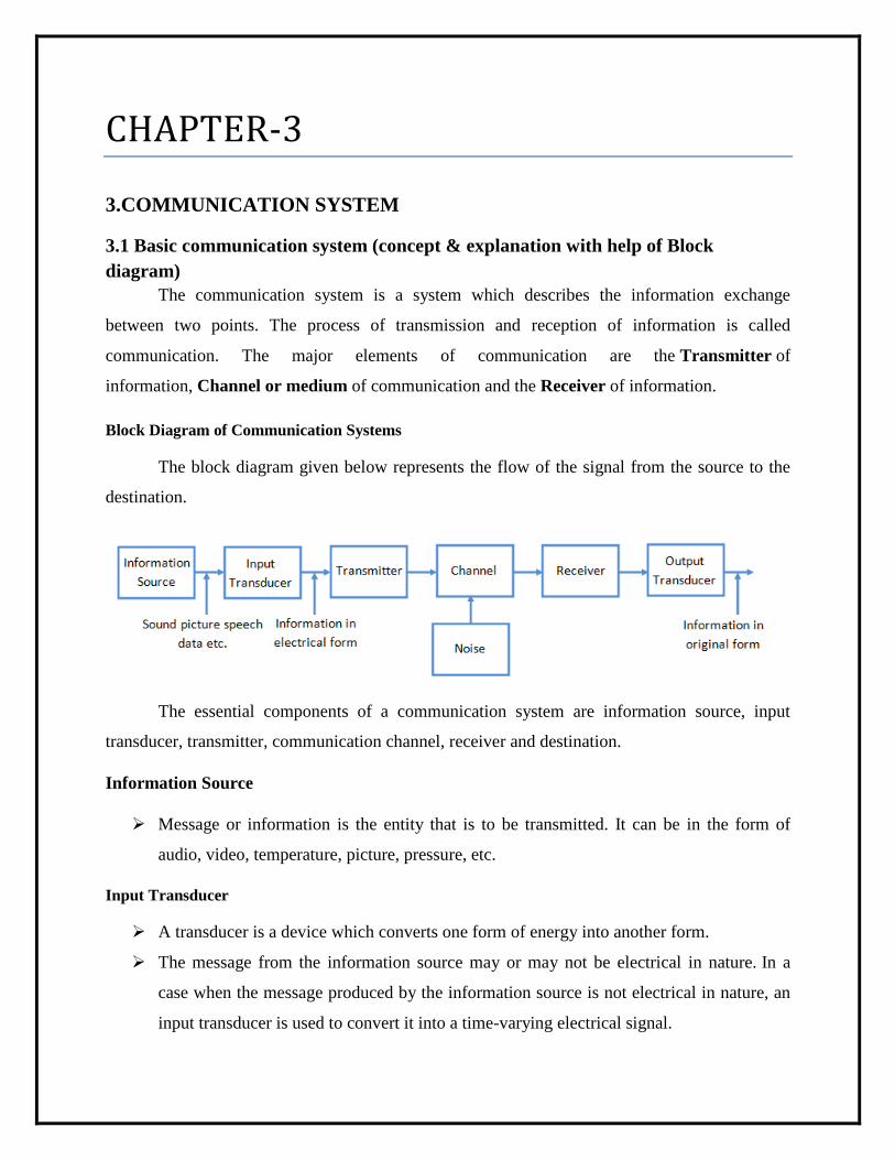
The communication system is a system which describes the information exchange
between two points. The process of transmission and reception of information is called
communication. The major elements of communication are the Transmitter of
information, Channel or medium of communication and the Receiver of information.
Block Diagram of Communication Systems
The block diagram given below represents the flow of the signal from the source to the
destination.
The essential components of a communication system are information source, input
transducer, transmitter, communication channel, receiver and destination.
Information Source
Message or information is the entity that is to be transmitted. It can be in the form of
audio, video, temperature, picture, pressure, etc.
Input Transducer
A transducer is a device which converts one form of energy into another form.
The message from the information source may or may not be electrical in nature. In a
case when the message produced by the information source is not electrical in nature, an
input transducer is used to convert it into a time-varying electrical signal.
Example: microphone converts the information or massage which is in the form of sound
waves into corresponding electrical signal.
Transmitter
It is the arrangement that processes the message signal into a suitable form for
transmission and subsequently reception.
Modulation is the main function of the transmitter. In modulation, the message signal is
superimposed upon the high-frequency carrier signal.
Channel
A channel refers to a physical medium such as wire, cables, space through which the
signal is passed from transmitter to the receiver.
There are many channel impairments that affect the channel performance to a pronounced
level. Noise, Attenuation and distortion to mention the major impairments.
Noise
Noise is an unwanted signal which tend to interfere with the required signal. Noise signal
is always random in character. Noise may interfere with signal at any point in a
communication system.
Receiver
An arrangement that extracts the message or information from the transmitted signal at
the output end of the channel and reproduces it in a suitable form as the original message
signal is a receiver.
The main function of the receiver is to reproduce the message signal in electrical form
from the distorted received signal. This reproduction of the original signal is
accomplished by a process known as the demodulation or detection. Demodulation is the
reverse process of modulation carried out in transmitter.
Output transducer
Output transducer convert an electrical message signal into its original form.
Example- loudspeaker which works as a transducer i.e. converts the electrical signal in
the form of original sound signal.
3.2 Concept of Modulation and Demodulation, Difference between them
Modulation is the process by which some characteristics or parameters of the carrier
wave is changed according to the signal containing information. These characteristics can
be amplitude, frequency or phase. Basically, it is assumed that the information signal is a
low-frequency one and thus needs conversion from low to high in order to have a better
transmission.
Demodulation is defined as extracting the original information-carrying signal from a
modulated carrier wave. A demodulator is an electronic circuit that is mainly used to
recover the information content from the modulated carrier wave.
Need for modulation:
The baseband signals can be transmitted directly, but the baseband transmission has
many limitations which can be overcome using modulation.
In the process of modulation, the baseband signal is translated i.e. shifted from low
frequency to high frequency.
This frequency shift is proportional to the frequency of carrier.
The modulation process has the following advantages:
Advantages of modulation:
- Reduction in the height of antenna:
When the transmission occurs over free pace, the antennae radiate the signal out and
receiver receives it. In order to operate efficiently, antennae need to be in order of the
magnitude of wavelength of the transmitted signal.
For the transmission of radio signals, the antenna height must be a multiple of (λ/4). Here
λ is the wavelength. Λ =c/f where c is velocity of light and f is the frequency of the signal
to be transmitted.
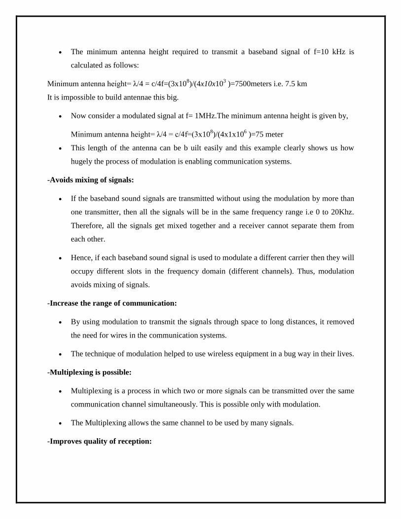
The minimum antenna height required to transmit a baseband signal of f=10 kHz is
calculated as follows:
Minimum antenna height= λ/4 = c/4f=(3x108)/(4x10x10
3 )=7500meters i.e. 7.5 km
It is impossible to build antennae this big.
Now consider a modulated signal at f= 1MHz.The minimum antenna height is given by,
Minimum antenna height= λ/4 = c/4f=(3x108)/(4x1x10
6 )=75 meter
This length of the antenna can be b uilt easily and this example clearly shows us how
hugely the process of modulation is enabling communication systems.
-Avoids mixing of signals:
If the baseband sound signals are transmitted without using the modulation by more than
one transmitter, then all the signals will be in the same frequency range i.e 0 to 20Khz.
Therefore, all the signals get mixed together and a receiver cannot separate them from
each other.
Hence, if each baseband sound signal is used to modulate a different carrier then they will
occupy different slots in the frequency domain (different channels). Thus, modulation
avoids mixing of signals.
-Increase the range of communication:
By using modulation to transmit the signals through space to long distances, it removed
the need for wires in the communication systems.
The technique of modulation helped to use wireless equipment in a bug way in their lives.
-Multiplexing is possible:
Multiplexing is a process in which two or more signals can be transmitted over the same
communication channel simultaneously. This is possible only with modulation.
The Multiplexing allows the same channel to be used by many signals.
-Improves quality of reception:
With frequency modulation (FM), and the digital communication techniques like PCM,
the effect of noise is reduced to a great extent. This improves quality of reception.
Differences between Modulation and Demodulation
1. The key difference between modulation and demodulation is that modulation is done at the
transmitter side while demodulation is done at the receiver side of a communication
system.
2. Both modulation and demodulation occur during data transmission but the two
processes are exactly reverse of each other. In modulation original message signal is mixed
with the carrier wave whose parameters are required to be changed. As against, in
demodulation the combination of carrier and message signal are separated from each other,
to have original information signal.
3. Modulation requires a modulator section for mixing of the two signals whereas
demodulation requires demodulator to recover the original signal. However, combined
equipment is used for the two known as Modem.
4. Modulation is done to convert the low-frequency signal into a high-frequency signal.
While at the time of demodulation, the low-frequency signal is achieved form high-
frequency signal.
5. Modulation is basically done to transmit data to longer distance whereas demodulation is
done to regain the original message signal.
6. Demodulation is somewhat a complex process when compared with modulation.
3.3 Different types of Modulation (AM, FM & PM) based on signal, carrier wave
and modulated wave (only concept, No mathematical Derivation)
There are three types of modulation, namely:
1.Amplitude modulation (AM)
In amplitude modulation, the amplitude of the carrier wave is varied in proportion to the
message signal, and the other factors like frequency and phase remain constant.
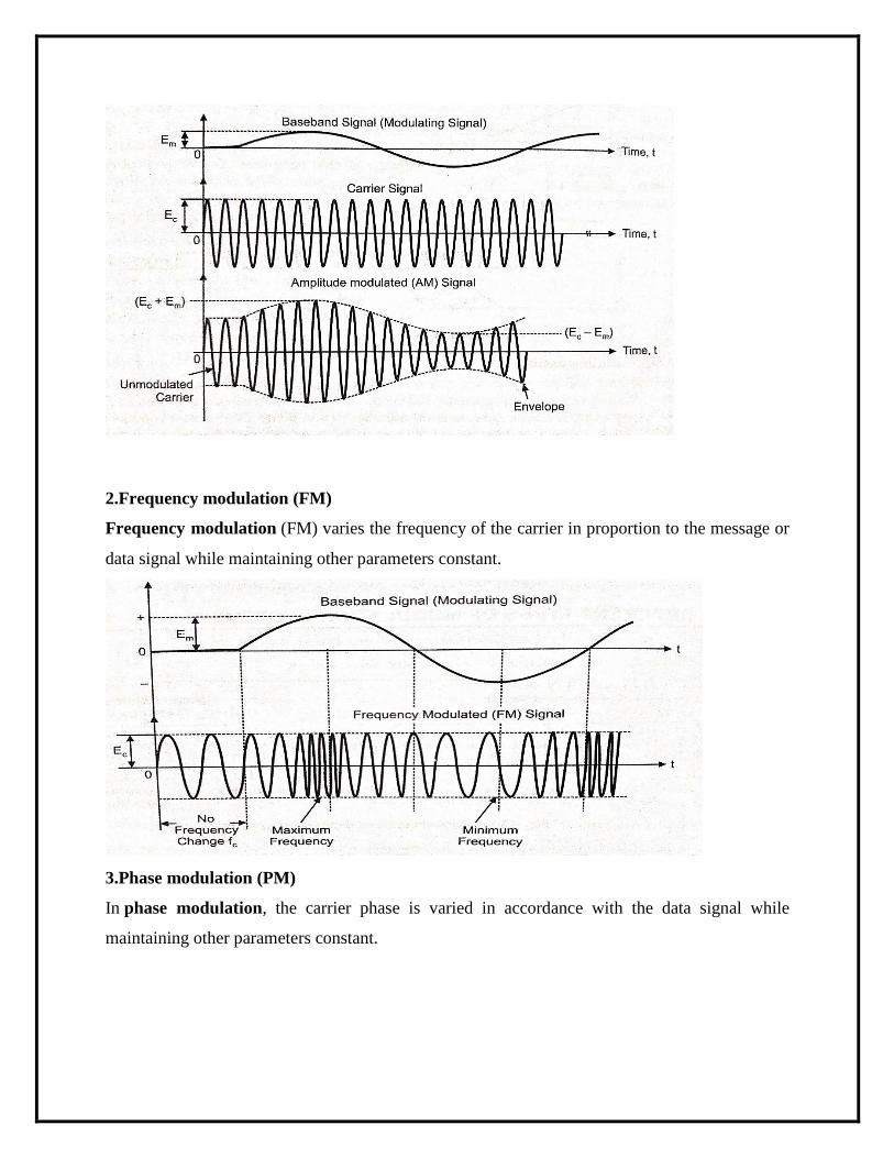
2.Frequency modulation (FM)
Frequency modulation (FM) varies the frequency of the carrier in proportion to the message or
data signal while maintaining other parameters constant.
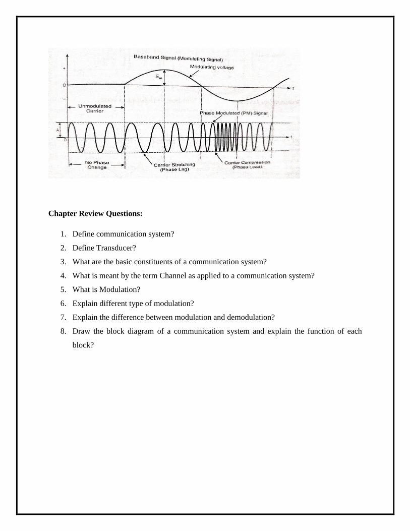
3.Phase modulation (PM)
In phase modulation, the carrier phase is varied in accordance with the data signal while
maintaining other parameters constant.
Chapter Review Questions:
1. Define communication system?
2. Define Transducer?
3. What are the basic constituents of a communication system?
4. What is meant by the term Channel as applied to a communication system?
5. What is Modulation?
6. Explain different type of modulation?
7. Explain the difference between modulation and demodulation?
8. Draw the block diagram of a communication system and explain the function of each
block?
CHAPTER-4
4. TRANSDUCERS AND MEASURING INSTRUMENTS
4.1 Concept of Transducer and sensor with their differences
Transducer
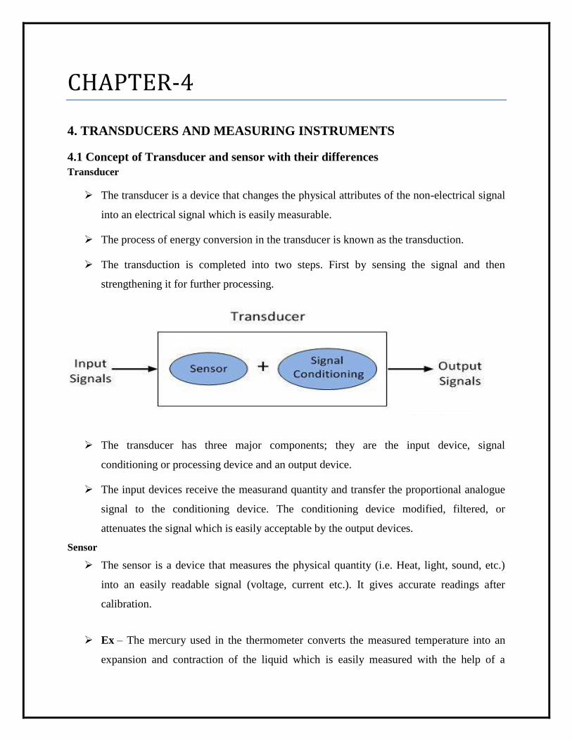
The transducer is a device that changes the physical attributes of the non-electrical signal
into an electrical signal which is easily measurable.
The process of energy conversion in the transducer is known as the transduction.
The transduction is completed into two steps. First by sensing the signal and then
strengthening it for further processing.
The transducer has three major components; they are the input device, signal
conditioning or processing device and an output device.
The input devices receive the measurand quantity and transfer the proportional analogue
signal to the conditioning device. The conditioning device modified, filtered, or
attenuates the signal which is easily acceptable by the output devices.
Sensor
The sensor is a device that measures the physical quantity (i.e. Heat, light, sound, etc.)
into an easily readable signal (voltage, current etc.). It gives accurate readings after
calibration.
Ex – The mercury used in the thermometer converts the measured temperature into an
expansion and contraction of the liquid which is easily measured with the help of a
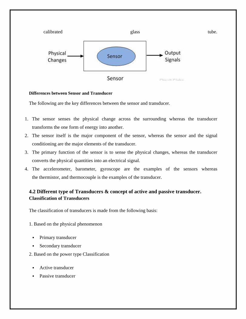
calibrated glass tube.
Differences between Sensor and Transducer
The following are the key differences between the sensor and transducer.
1. The sensor senses the physical change across the surrounding whereas the transducer
transforms the one form of energy into another.
2. The sensor itself is the major component of the sensor, whereas the sensor and the signal
conditioning are the major elements of the transducer.
3. The primary function of the sensor is to sense the physical changes, whereas the transducer
converts the physical quantities into an electrical signal.
4. The accelerometer, barometer, gyroscope are the examples of the sensors whereas
the thermistor, and thermocouple is the examples of the transducer.
4.2 Different type of Transducers & concept of active and passive transducer.
Classification of Transducers
The classification of transducers is made from the following basis:
1. Based on the physical phenomenon
Primary transducer
Secondary transducer
2. Based on the power type Classification
Active transducer
Passive transducer
3. Based on the type of output the classification of transducers are made
Analog transducer
Digital transducer
4. Based on the electrical phenomenon is a best Classification of Trasnducer
Resistive transducer
Capacitive transducer
Inductive transducer
Photoelectric transducer
Photovoltaic transducer
5. Based on the non-electrical phenomenon Classification of transducer
Linear displacement
Rotary displacement
6. Based on the transduction phenomenon
Transducer
Inverse transducer.
concept of active and passive transducer.
Active Transducer
The transducer which does not require the external power source is known as the active
transducer.
Such type of transducer develops theirs owns voltage or current, hence known as a self-
generating transducer.
The energy requires for generating the output signals are obtained from the physical
quantity which is to be measured.
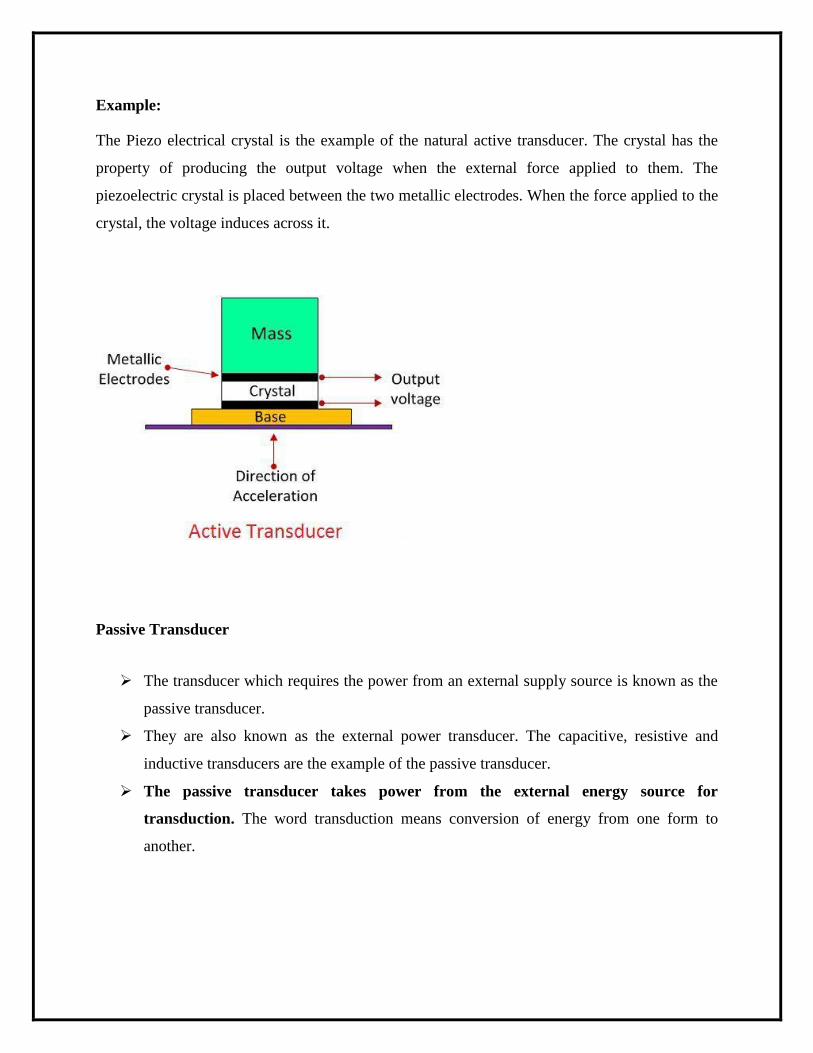
Example:
The Piezo electrical crystal is the example of the natural active transducer. The crystal has the
property of producing the output voltage when the external force applied to them. The
piezoelectric crystal is placed between the two metallic electrodes. When the force applied to the
crystal, the voltage induces across it.
Passive Transducer
The transducer which requires the power from an external supply source is known as the
passive transducer.
They are also known as the external power transducer. The capacitive, resistive and
inductive transducers are the example of the passive transducer.
The passive transducer takes power from the external energy source for
transduction. The word transduction means conversion of energy from one form to
another.
Example:
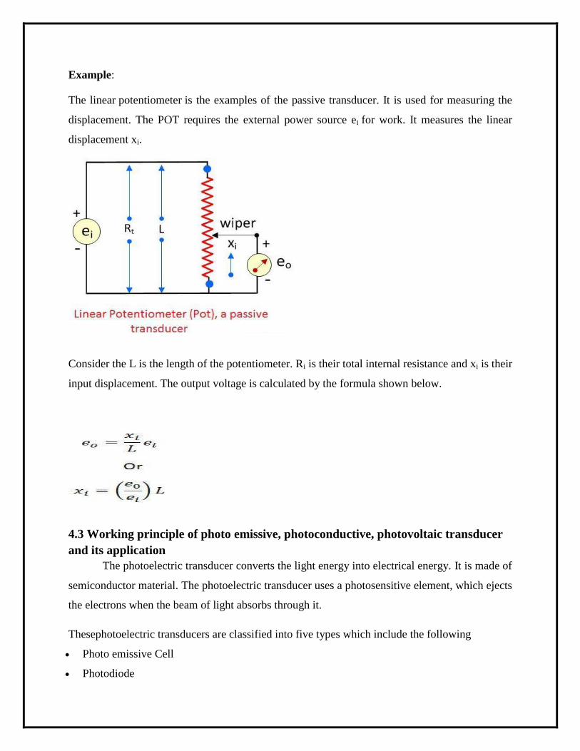
The linear potentiometer is the examples of the passive transducer. It is used for measuring the
displacement. The POT requires the external power source ei for work. It measures the linear
displacement xi.
Consider the L is the length of the potentiometer. Ri is their total internal resistance and xi is their
input displacement. The output voltage is calculated by the formula shown below.
4.3 Working principle of photo emissive, photoconductive, photovoltaic transducer
and its application
The photoelectric transducer converts the light energy into electrical energy. It is made of
semiconductor material. The photoelectric transducer uses a photosensitive element, which ejects
the electrons when the beam of light absorbs through it.
Thesephotoelectric transducers are classified into five types which include the following
Photo emissive Cell
Photodiode
Phototransistor
Photo-voltaic cell
Photoconductive Cell
Photo-emissive Cell
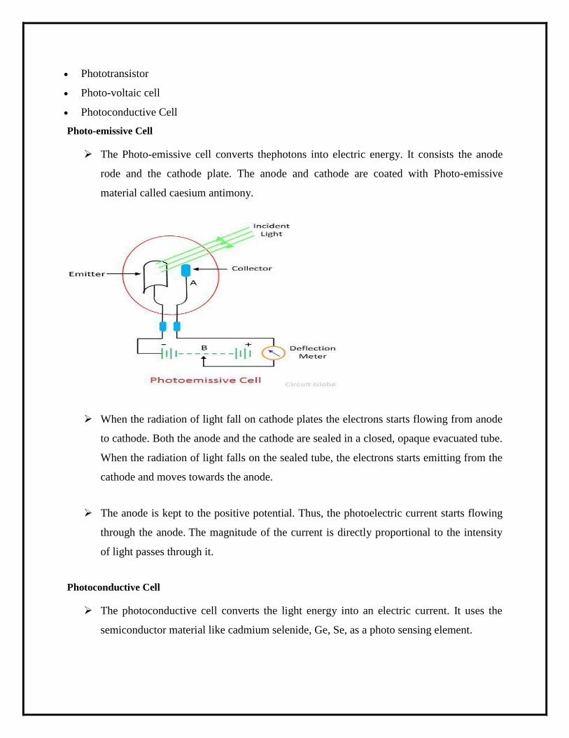
The Photo-emissive cell converts thephotons into electric energy. It consists the anode
rode and the cathode plate. The anode and cathode are coated with Photo-emissive
material called caesium antimony.
When the radiation of light fall on cathode plates the electrons starts flowing from anode
to cathode. Both the anode and the cathode are sealed in a closed, opaque evacuated tube.
When the radiation of light falls on the sealed tube, the electrons starts emitting from the
cathode and moves towards the anode.
The anode is kept to the positive potential. Thus, the photoelectric current starts flowing
through the anode. The magnitude of the current is directly proportional to the intensity
of light passes through it.
Photoconductive Cell
The photoconductive cell converts the light energy into an electric current. It uses the
semiconductor material like cadmium selenide, Ge, Se, as a photo sensing element.
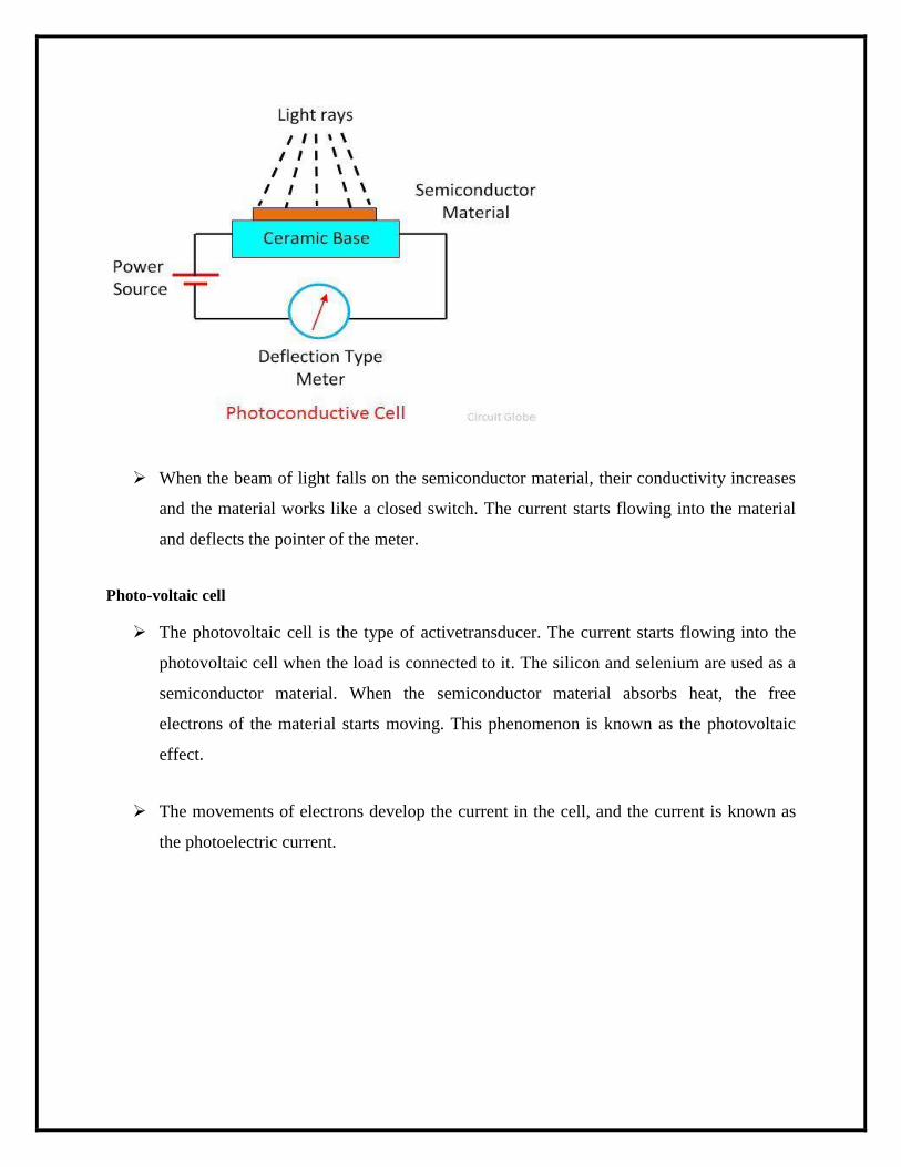
When the beam of light falls on the semiconductor material, their conductivity increases
and the material works like a closed switch. The current starts flowing into the material
and deflects the pointer of the meter.
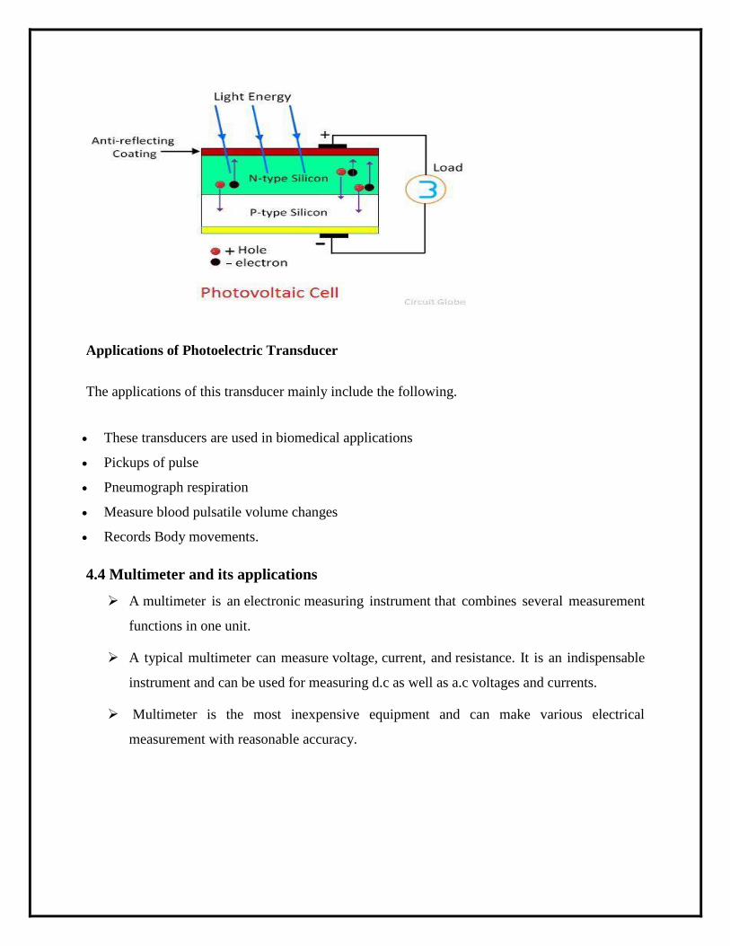
Photo-voltaic cell
The photovoltaic cell is the type of activetransducer. The current starts flowing into the
photovoltaic cell when the load is connected to it. The silicon and selenium are used as a
semiconductor material. When the semiconductor material absorbs heat, the free
electrons of the material starts moving. This phenomenon is known as the photovoltaic
effect.
The movements of electrons develop the current in the cell, and the current is known as
the photoelectric current.
Applications of Photoelectric Transducer
The applications of this transducer mainly include the following.
These transducers are used in biomedical applications
Pickups of pulse
Pneumograph respiration
Measure blood pulsatile volume changes
Records Body movements.
4.4 Multimeter and its applications
A multimeter is an electronic measuring instrument that combines several measurement
functions in one unit.
A typical multimeter can measure voltage, current, and resistance. It is an indispensable
instrument and can be used for measuring d.c as well as a.c voltages and currents.
Multimeter is the most inexpensive equipment and can make various electrical
measurement with reasonable accuracy.
Applications
For checking the circuit continuity.
For measuring d.c current flowing through the cathode, plate,screen and other vacuum
tube circuits.
For measuring d.c voltages across various resistors in electric circuits.
For measuring a.c voltages across power supply transformers.
For ascertaining whether or not open or short circuit exits in the circuit under study.
4.5 Analog and Digital Multimeter and their differences
Analog Multimeter
Analog Multimeter is basically a moving coil instrument. A rectifier unit is also provided
with the instrument. It is a multirange instrument and various ranges are obtained by
different resistance elements in series or in parallel with the movement of the instrument.
With the help of a rotary selector switch the various ranges are used.
Digital Multimeter
The digital multimeter is an instrument capable of measuring dc voltage, ac voltage, dc
current, ac current, resistance, conductance and decibles. Thus DMM offers increased
versatility. Some DMMs can measure the temperature, frequency etc.
A DMM has a digital display and a function selector switch. The range selection takes
place automatically. There are four input terminals, out of which two terminals are used for
measurement of all the general purpose quantities such as ac/dc voltage, resistance,
capacitance and diode, transistor testing.
Difference between Analog and Digital Multimeter
Analog Multimeter Digital Multimeter
Power supply is not required Power supply is required
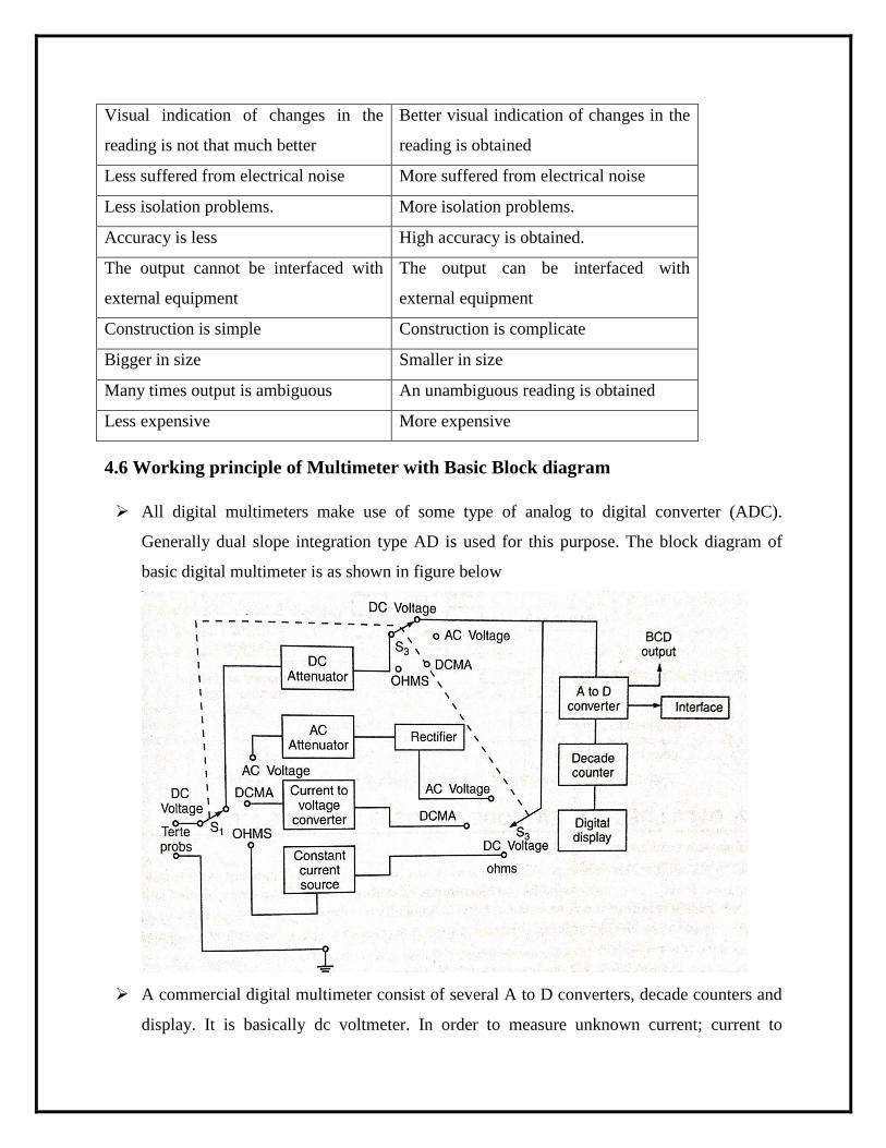
Visual indication of changes in the
reading is not that much better
Better visual indication of changes in the
reading is obtained
Less suffered from electrical noise More suffered from electrical noise
Less isolation problems. More isolation problems.
Accuracy is less High accuracy is obtained.
The output cannot be interfaced with
external equipment
The output can be interfaced with
external equipment
Construction is simple Construction is complicate
Bigger in size Smaller in size
Many times output is ambiguous An unambiguous reading is obtained
Less expensive More expensive
4.6 Working principle of Multimeter with Basic Block diagram
All digital multimeters make use of some type of analog to digital converter (ADC).
Generally dual slope integration type AD is used for this purpose. The block diagram of
basic digital multimeter is as shown in figure below
A commercial digital multimeter consist of several A to D converters, decade counters and
display. It is basically dc voltmeter. In order to measure unknown current; current to
voltage converter is used. An unknown current to be measured is applied to one of the input
terminals of op-amp. Since input impedance of op-amp is very high; very small current can
pass through it. This current passing into the op-amp can be neglected.
Thus Iin= Ifb, Here Ifb = feedback current
This feedback current is allowed to pass through one of the known resistances. This current
will cause a voltage drop across the resistance. This voltage is applied to analog to digital
converter and finally digital display is obtained. Thus, output displayed on the digital
display is directly proportional to unknown current.
In order to measure an unknown resistance; a constant current source is used. The current
from this constant current source is allowed to pass through unknown resistance. Thus the
proportional voltage is obtained. The output disply is directly proportional to unknown
resistance.
To measure the ac voltage; a rectifier and filter is used. This rectifier converts ac signal into
dc signal. Now, this dc signal is applied to A to D converter to the digital display. The BCD
output can be obtained from A to D converter. Similarly, the output from digital multimeter
can be used to interface with other equipments.
4.7 CRO, working principle of CRO with simple Block diagram
Oscilloscope is electronic equipment, which displays a voltage waveform. Among the
oscilloscopes, Cathode Ray Oscilloscope (CRO) is the basic one and it displays a time
varying signal or waveform.
Block Diagram of CRO
Cathode Ray Oscilloscope (CRO) consists a set of blocks. Those are vertical amplifier,
delay line, trigger circuit, time base generator, horizontal amplifier, Cathode Ray Tube
(CRT) & power supply. The block diagram of CRO is shown in below figure.
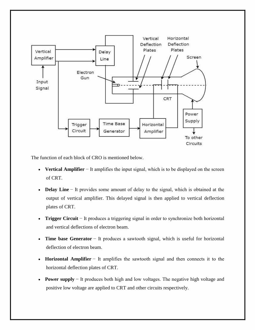
The function of each block of CRO is mentioned below.
Vertical Amplifier − It amplifies the input signal, which is to be displayed on the screen
of CRT.
Delay Line − It provides some amount of delay to the signal, which is obtained at the
output of vertical amplifier. This delayed signal is then applied to vertical deflection
plates of CRT.
Trigger Circuit − It produces a triggering signal in order to synchronize both horizontal
and vertical deflections of electron beam.
Time base Generator − It produces a sawtooth signal, which is useful for horizontal
deflection of electron beam.
Horizontal Amplifier − It amplifies the sawtooth signal and then connects it to the
horizontal deflection plates of CRT.
Power supply − It produces both high and low voltages. The negative high voltage and
positive low voltage are applied to CRT and other circuits respectively.
Cathode Ray Tube (CRT) − It is the major important block of CRO and mainly
consists of four parts. Those are electron gun, vertical deflection plates, horizontal
deflection plates and fluorescent screen.The electron beam, which is produced by an
electron gun gets deflected in both vertical and horizontal directions by a pair of vertical
deflection plates and a pair of horizontal deflection plates respectively. Finally, the
deflected beam will appear as a spot on the fluorescent screen.
In this way, CRO will display the applied input signal on the screen of CRT. So, we can
analyse the signals in time domain by using CRO.
Chapter Review Questions:
1. Define Transducer?
2. What are the type of Transducer?
3. Write difference between Transducer and Sensor?
4. Write difference between Active and Passive Transducer?
5. What is Multimeter?
6. Write two application of Multimeter?
7. Write short notes on Photo-Emission transducer?
8. Write difference between Analog and Digital Multimeter?
9. Explain working principle of photo emissive, photoconductive, photovoltaic transducer?
10. Explain working principle of Multimeter with Basic Block diagram?
11. What is CRO? Explain working principle of CRO with simple Block diagram?


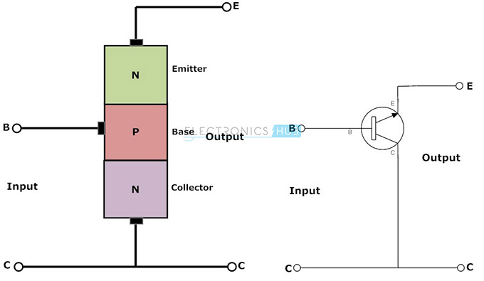
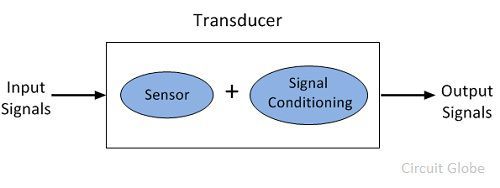
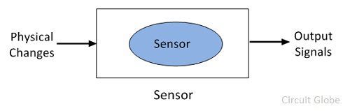
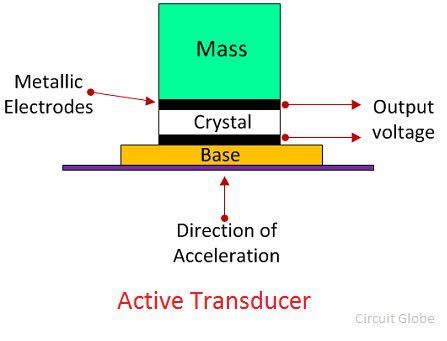
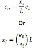
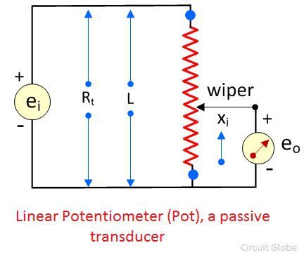
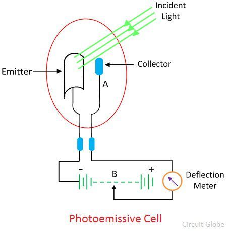
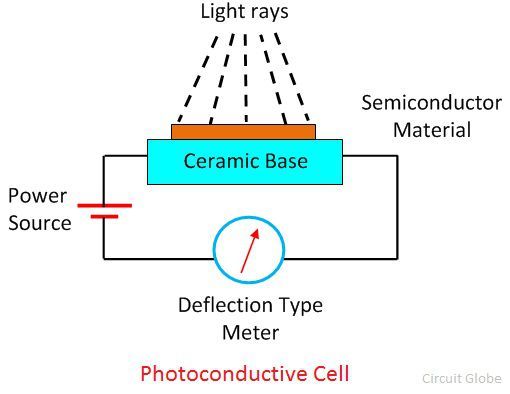
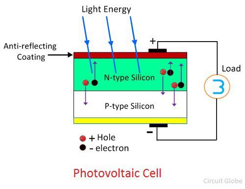