Embed Size (px)
Citation preview

Analog MIMO spatial filtering
Citation for published version (APA):Heuvel, van den, J. H. C. (2012). Analog MIMO spatial filtering. Technische Universiteit Eindhoven.https://doi.org/10.6100/IR724476
DOI:10.6100/IR724476
Document status and date:Published: 01/01/2012
Document Version:Publisher’s PDF, also known as Version of Record (includes final page, issue and volume numbers)
Please check the document version of this publication:
• A submitted manuscript is the version of the article upon submission and before peer-review. There can beimportant differences between the submitted version and the official published version of record. Peopleinterested in the research are advised to contact the author for the final version of the publication, or visit theDOI to the publisher's website.• The final author version and the galley proof are versions of the publication after peer review.• The final published version features the final layout of the paper including the volume, issue and pagenumbers.Link to publication
General rightsCopyright and moral rights for the publications made accessible in the public portal are retained by the authors and/or other copyright ownersand it is a condition of accessing publications that users recognise and abide by the legal requirements associated with these rights.
• Users may download and print one copy of any publication from the public portal for the purpose of private study or research. • You may not further distribute the material or use it for any profit-making activity or commercial gain • You may freely distribute the URL identifying the publication in the public portal.
If the publication is distributed under the terms of Article 25fa of the Dutch Copyright Act, indicated by the “Taverne” license above, pleasefollow below link for the End User Agreement:www.tue.nl/taverne
Take down policyIf you believe that this document breaches copyright please contact us at:[email protected] details and we will investigate your claim.
Download date: 17. May. 2022

Analog MIMO Spatial Filtering
Johannes Henricus Cornelus van den Heuvel
Samenstelling promotiecommissie:
voorzitter
prof.dr.ir A.C.P.M. Backx
promotoren
prof.dr.ir. P.G.M. Baltus
prof.dr.ir. J.P.M.G. Linnartz
leden
prof. D. Cabric
prof.dr.ir. L. van der Perre
prof.dr.ir. B. Nauta
prof.dr.ir. C.H. Slump
prof.dr.ir. A.H.M. van Roermund
Technische Universiteit Eindhoven
Technische Universiteit Eindhoven
Technische Universiteit Eindhoven
Philips Research Eindhoven
University of California, Los Angeles
Katholieke Universiteit Leuven
Imec
Universiteit Twente
Universiteit Twente
Technische Universiteit Eindhoven
A catalogue record is available from the Eindhoven University of Technology Library.
CIP-DATA LIBRARY TECHNISCHE UNIVERSITEIT EINDHOVEN
Analog MIMO Spatial Filtering / by Johannes Henricus Cornelus van den Heuvel.
- Eindhoven: Technische Universiteit Eindhoven, 2012.
Proefschrift. - ISBN 978-94-6191-123-0
NUR 959
Subject headings: Spatial filters / Array signal processing / Interference suppression /
Radiofrequency integrated circuits / MIMO systems / Cognitive Radio / Power demand
/ Wireless communication / Analog-digital conversion / OFDM modulation.
This research is supported by IOP Generic Communication - Senter Novem program.
Copyright c© 2011 by Johannes Henricus Cornelus van den Heuvel. All rights reserved.
Reproduction in whole or in parts is prohibited without the written consent of the copy-
right owner.

Analog MIMO Spatial Filtering
PROEFSCHRIFT
ter verkrijging van de graad van doctor aan de
Technische Universiteit Eindhoven, op gezag van de
rector magnificus, prof.dr.ir. C.J. van Duijn, voor een
commissie aangewezen door het College voor
Promoties in het openbaar te verdedigen
op woensdag 11 januari 2012 om 16.00 uur
door
Johannes Henricus Cornelus van den Heuvel
geboren te Oss

Dit proefschrift is goedgekeurd door de promotoren:
prof.dr.ir. P.G.M Baltus
en
prof.dr.ir. J.P.M.G. Linnartz

Aan Petra, mijn zus, ouders, grootouders en familie


Contents
Abbreviations vii
List of Symbols ix
1 Introduction 1
1.1 Wireless Communication . . . . . . . . . . . . . . . . . . . . . . . . 2
1.2 Capacity of Wireless Systems . . . . . . . . . . . . . . . . . . . . . 5
1.2.1 MIMO . . . . . . . . . . . . . . . . . . . . . . . . . . . . . . 6
1.3 Trends in Wireless Transceivers . . . . . . . . . . . . . . . . . . . . 6
1.3.1 Migration of RF Frequencies Bandwidths and Distances . . . 7
1.3.2 Multiple Antennas . . . . . . . . . . . . . . . . . . . . . . . 9
1.3.3 Multiple Standards and Devices . . . . . . . . . . . . . . . . 10
1.3.4 Multiple Users . . . . . . . . . . . . . . . . . . . . . . . . . . 11
1.3.5 Energy Trends . . . . . . . . . . . . . . . . . . . . . . . . . 13
i

ii Contents
1.4 MIMO in a Mass Market . . . . . . . . . . . . . . . . . . . . . . . . 15
1.5 The Research . . . . . . . . . . . . . . . . . . . . . . . . . . . . . . 17
1.5.1 Scientific Contributions . . . . . . . . . . . . . . . . . . . . . 17
1.6 Structure of the Thesis . . . . . . . . . . . . . . . . . . . . . . . . . 20
2 State of the Art MIMO OFDM Systems 21
2.1 Introduction . . . . . . . . . . . . . . . . . . . . . . . . . . . . . . . 21
2.2 Receiver . . . . . . . . . . . . . . . . . . . . . . . . . . . . . . . . . 23
2.2.1 RF Front End . . . . . . . . . . . . . . . . . . . . . . . . . . 23
2.2.2 ADC . . . . . . . . . . . . . . . . . . . . . . . . . . . . . . . 26
2.2.3 BB Processing . . . . . . . . . . . . . . . . . . . . . . . . . . 27
2.3 Batteries . . . . . . . . . . . . . . . . . . . . . . . . . . . . . . . . . 28
2.4 Screen Size . . . . . . . . . . . . . . . . . . . . . . . . . . . . . . . 31
2.5 Flash Memory Speed . . . . . . . . . . . . . . . . . . . . . . . . . . 31
2.6 Extrapolations . . . . . . . . . . . . . . . . . . . . . . . . . . . . . 34
2.7 Summary and Conclusions . . . . . . . . . . . . . . . . . . . . . . . 36
3 System Design Considerations 39
3.1 Introduction . . . . . . . . . . . . . . . . . . . . . . . . . . . . . . . 39
Contents iii
3.2 Received Signal Model . . . . . . . . . . . . . . . . . . . . . . . . . 40
3.2.1 Legal Transmit Power . . . . . . . . . . . . . . . . . . . . . 40
3.2.2 Data Format . . . . . . . . . . . . . . . . . . . . . . . . . . 40
3.2.3 OFDM . . . . . . . . . . . . . . . . . . . . . . . . . . . . . . 41
3.2.4 Noise . . . . . . . . . . . . . . . . . . . . . . . . . . . . . . . 42
3.2.5 Channel Model . . . . . . . . . . . . . . . . . . . . . . . . . 43
3.3 MIMO Channel Capacity . . . . . . . . . . . . . . . . . . . . . . . . 43
3.4 Zero-IF . . . . . . . . . . . . . . . . . . . . . . . . . . . . . . . . . . 46
3.5 Receiver Cascade . . . . . . . . . . . . . . . . . . . . . . . . . . . . 47
3.5.1 Gain . . . . . . . . . . . . . . . . . . . . . . . . . . . . . . . 48
3.5.2 Linearity . . . . . . . . . . . . . . . . . . . . . . . . . . . . . 51
3.5.3 Noise Contribution . . . . . . . . . . . . . . . . . . . . . . . 54
3.6 Analog-to-Digital Converter . . . . . . . . . . . . . . . . . . . . . . 55
3.7 Design Considerations . . . . . . . . . . . . . . . . . . . . . . . . . 56
3.8 Conclusions . . . . . . . . . . . . . . . . . . . . . . . . . . . . . . . 57
4 Optimum Data Transfer Energy Efficiency 59
4.1 Introduction . . . . . . . . . . . . . . . . . . . . . . . . . . . . . . . 59

iv Contents
4.2 Modeling System Data Transfer Energy Efficiency . . . . . . . . . . 62
4.2.1 Distortion and Noise . . . . . . . . . . . . . . . . . . . . . . 63
4.2.2 Optimum Throughput . . . . . . . . . . . . . . . . . . . . . 66
4.2.3 Minimum-Power Cascade Optimization Method . . . . . . . 67
4.2.4 Maximum-Throughput Cascade Optimization Method . . . 68
4.2.5 Variable Third Order Intercept Point . . . . . . . . . . . . . 69
4.2.6 Maximum Data Transfer Energy Efficiency . . . . . . . . . . 71
4.2.7 Duty Cycling . . . . . . . . . . . . . . . . . . . . . . . . . . 73
4.3 Numerical Results . . . . . . . . . . . . . . . . . . . . . . . . . . . . 73
4.4 Conclusions . . . . . . . . . . . . . . . . . . . . . . . . . . . . . . . 78
5 ACMM MIMO IC for Analog Spatial Filtering 81
5.1 Introduction . . . . . . . . . . . . . . . . . . . . . . . . . . . . . . . 81
5.2 Proposed MIMO Receiver Architecture . . . . . . . . . . . . . . . . 85
5.3 ACMM Circuit Description . . . . . . . . . . . . . . . . . . . . . . 89
5.4 Aluminum and Gold Bond Wires . . . . . . . . . . . . . . . . . . . 96
5.5 Measurement Results . . . . . . . . . . . . . . . . . . . . . . . . . . 98
5.6 Measurements Analysis and Redesign . . . . . . . . . . . . . . . . . 103
Contents v
5.7 Benchmarks . . . . . . . . . . . . . . . . . . . . . . . . . . . . . . . 115
5.8 Conclusions . . . . . . . . . . . . . . . . . . . . . . . . . . . . . . . 118
6 Analog Spatial Filtering in Wideband Cognitive Radio 119
6.1 Introduction . . . . . . . . . . . . . . . . . . . . . . . . . . . . . . . 119
6.2 System Model . . . . . . . . . . . . . . . . . . . . . . . . . . . . . . 121
6.2.1 Front End Architectures . . . . . . . . . . . . . . . . . . . . 122
6.2.2 Analog-to-Digital Converter . . . . . . . . . . . . . . . . . . 124
6.2.3 Signal Model . . . . . . . . . . . . . . . . . . . . . . . . . . 125
6.2.4 Wide Band Multiple Antenna Channel Models . . . . . . . . 126
6.3 Spatial Filtering Approach . . . . . . . . . . . . . . . . . . . . . . . 131
6.3.1 Problem statement . . . . . . . . . . . . . . . . . . . . . . . 131
6.3.2 Proposed Beamforming Algorithms . . . . . . . . . . . . . . 135
6.3.3 Proposed Full MIMO Spatial Filter Algorithms . . . . . . . 138
6.4 Numerical Results . . . . . . . . . . . . . . . . . . . . . . . . . . . . 140
6.4.1 Beamforming Flat Fading . . . . . . . . . . . . . . . . . . . 141
6.4.2 Beamforming OFDM Signals . . . . . . . . . . . . . . . . . . 143
6.4.3 Full MIMO Spatial Filtering Wideband Channel . . . . . . . 154

vi Contents
6.5 Conclusions . . . . . . . . . . . . . . . . . . . . . . . . . . . . . . . 159
7 Conclusions and Recommendations 161
7.1 Conclusions . . . . . . . . . . . . . . . . . . . . . . . . . . . . . . . 161
7.2 Recommendations . . . . . . . . . . . . . . . . . . . . . . . . . . . . 164
References 167
List of Publications 179
Summary 181
Samenvatting 185
Acknowledgements 189
Biography 195
Abbreviations
ACMM analog complex matrix multiplier
ADC analog-to-digital converter
AGC automatic gain control
AOA angle of arrival
AWGN additive white Gaussian noise
BB baseband
BPSK binary phase shift keying
CMOS complementary metaloxide semiconductor
CR cognitive radio
DAC digital-to-analog converter
dB decibel
DR dynamic range
DSP digital signal processing
DSP digital signal processor
ENOB effective number of bits
EFOM effective figure of merit
FFT fast Fourier transform
FOM figure of merit
I in-phase component
IC integrated circuit
IEEE Institute of Electrical and Electronic Engineers
IF intermediate frequency
IFFT inverse fast Fourier transform
LAN local area network
LNA low noise amplifier
vii
viii Abbreviations
LO local oscilator
LOS line-of-sight
LTE long term evolution
MIMO multiple-input and multiple-output
MPCO minimum power cascade optimization
MRC maximum ratio combining
MTCO maximum throughput cascade optimization
NLOS non-line-of-sight
OFDM orthogonal frequency division multiplexing
PCB printed circuit board
PLL phased locked loop
Q quadrature component
RF radio frequency
RX receiver
SD secure digital
SDHC secure digital high capacity
SDXC secure digital extended capacity
SISO single-input and single-output
SIT structure independent transform
SPI serial peripheral interface
SVD singular value decomposition
TX transmitter
VGA variable gain amplifier
VGA video graphics array
WB wide band
WiMAX worldwide interoperability for microwave access
WLAN wireless local area network
WRAN wireless regional area network

List of Symbols
Symbol Description Unit
a complex constant
A complex valued matrix
bADC number of ADC bits
b complex valued vector
B bandwidth containing both negative and positive frequencies Hz
c the speed of light in vacuum 3× 10⁸ m/s
C capacity b/s/Hz
C capacitor F
CIR carrier-to-interference ratio dB
d distance m
e base of natural logarithm e= 2.7183
f frequency Hz
fc carrier frequency Hz
fs sample frequency Hz
F noise factor
F power optimal F
G gain dB
H complex channel-gain matrix
i the imaginary number√−1
I identity matrix
ICR interference-to-carrier ratio dB
Idd supply current A
IIP3 input referred third order intercept point dBm
ix

x List of Symbols
IP3 input referred third order intercept point dBm
IP3 power optimal IP3 dBm
k Boltzmann’s constant 1.38× 10⁻²³ J/K
k an integer
K an integer
m an integer
M an integer
M complex valued matrix
n an integer
n complex AWGN vector
N an integer
N noise power W
NF noise figure dB
Nr number of receive antennas
Nt number of transmit antennas
OIP3 output referred third order intercept point dBm
P power Watt
Pr receiver circuit power W
R resistor Ω
r(t) output signal in the time domain
r output signal in the frequency domain
r complex constant
ρ signal-to-noise ratio dB
S received signal power Watt
S scattering matrix
s(t) signal in the time domain
s signal in the frequency domain
SNR signal-to-noise ratio dB
SNDR signal-to-noise-and-distortion ratio dB
t time s
t1...t10 short training symbols
T a time interval s
T absolute temperature K
T throughput b/s/Hz
T maximized T b/s/Hz

List of Symbols xi
T1, T2 long training symbols
TSymbol symbol time s
U complex valued matrix
V complex valued matrix
V dd supply voltage V
x(t) italic: signal in the time domain
x bold: signal in the frequency domain
X bold capital: complex valued matrix
α a constant
κt technology constant
κm power linearity factor
λ a constant
λ wavelength m
λc carrier wavelength m
ω frequency rad/s
π 3.14159
σ a constant
τ a delay time s
θ angle rad
φ phase o

xii Contents
Chapter 1
Introduction
Modern mobile telecommunication systems have allowed for almost complete free-
dom of communication. One can communicate almost anything (speech, text,
videos, photos, books, etcetera) to virtually anyone, from virtually everywhere to
anywhere. This freedom of communication has spurred a revolution in the way
people communicate and has contributed to the enormous growth in the amount of
information communicated worldwide via telecommunication systems. The need
for an ever increasing data rate has resulted in an increase in the number of trans-
mit and receive antennas per mobile user. Where until recently there was one
transmit and one receive antenna per individual user, recent communication sys-
tems, such as for WLAN IEEE 802.11n and for mobile phones LTE-Advanced,
consist of multiple transmit and multiple receive antennas per individual user.
Next to an increase in the number of antennas, also the total number of users
has increased over time. Due to the increase in the number of users, users are
increasingly interfering with one another. The challenges associated with multiple
antenna systems and interference mitigation are the main topics of the research
presented in this thesis. The mathematical foundation of the theory of communi-
cation systems was laid by Claude E. Shannon in 1948 [1]. This work has remained
the fundamental theory of communication until this day. In 1998-1999 the the-
ory of wireless communication systems was expanded to include multiple-input
multiple-output (MIMO) systems by Telatar [2], and Foschini and Gans [3]. The
1
2 Chapter 1. Introduction
theory of wireless communication systems tells us the upper bound of what is
achievable. However, the theory does not tell us the required effort to attain a
communication system that operates near that upper bound.
The research presented in this thesis contains theoretical system modeling consid-
ering arguments based on Shannon capacity, and a partial system implementation
used for verification of the theory. The system implementation consists of algo-
rithm design, PCB design, and circuit design and implementation in 65 nm CMOS.
To obtain a joint optimization of both the radio frequency (RF) front end and the
baseband (BB) digital signal processing (DSP), and to fully exploit the benefit of
joint optimization, a more in depth investigation into the joint bottlenecks and
challenges is conducted. The result of this investigation is used as a starting point
for the theoretical system modeling. From the model, novel and key system compo-
nents are identified, and subsequently designed and implemented. Measurements
of a proof-of-concept system implementation confirm the models and the benefit
of the approach. The research presented in this thesis was conducted within the
framework of the MIMO in a Mass Market project.
To provide the proper context of the research, we will first start this chapter by
providing background information on wireless systems. Secondly, the capacity
formula as derived by Claude E. Shannon is given to show the limitations of single
antenna systems and indicate the benefit of multiple antenna systems. Thirdly,
mayor trends in wireless transceivers are introduced which influence our design
choices. Fourthly, after introducing the proper context, the MIMO in a Mass
Market project in which the research was conducted is explained. Fifthly, the
Research described in this thesis and the contributions are listed. The final section
of this chapter explains the structure of the thesis.
1.1 Wireless Communication
Wireless transceivers communicate via electro-magnetic waves ranging in the fre-
quency domain from several kHz up to 1 THz. These electro-magnetic waves can
1.1. Wireless Communication 3
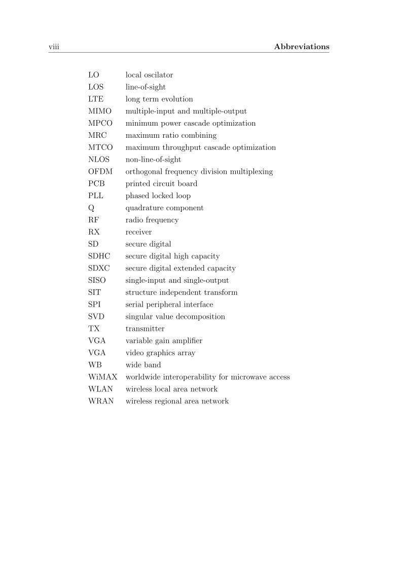
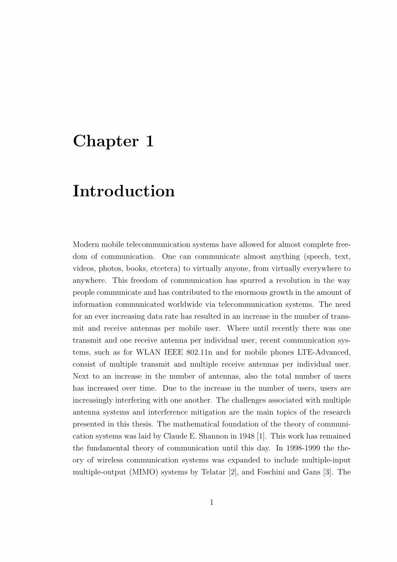
Figure 1.1: Example of an outdoor radio link.
Figure 1.2: Example of an indoor radio link.
4 Chapter 1. Introduction
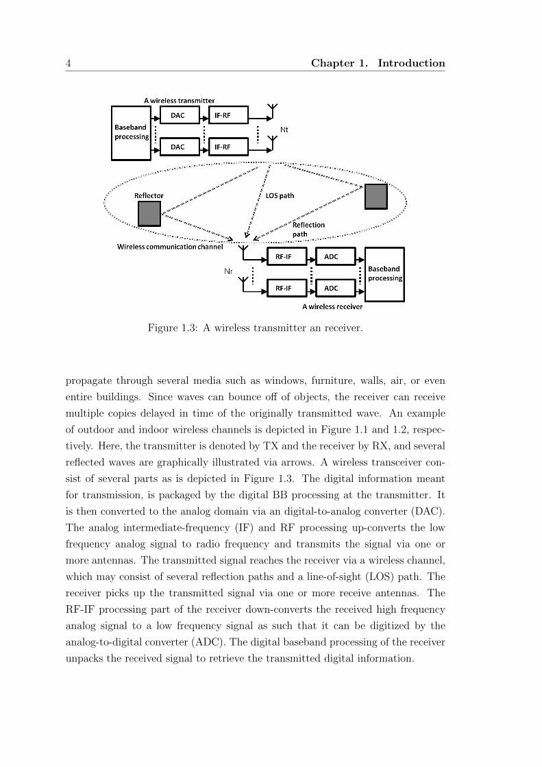
Figure 1.3: A wireless transmitter an receiver.
propagate through several media such as windows, furniture, walls, air, or even
entire buildings. Since waves can bounce off of objects, the receiver can receive
multiple copies delayed in time of the originally transmitted wave. An example
of outdoor and indoor wireless channels is depicted in Figure 1.1 and 1.2, respec-
tively. Here, the transmitter is denoted by TX and the receiver by RX, and several
reflected waves are graphically illustrated via arrows. A wireless transceiver con-
sist of several parts as is depicted in Figure 1.3. The digital information meant
for transmission, is packaged by the digital BB processing at the transmitter. It
is then converted to the analog domain via an digital-to-analog converter (DAC).
The analog intermediate-frequency (IF) and RF processing up-converts the low
frequency analog signal to radio frequency and transmits the signal via one or
more antennas. The transmitted signal reaches the receiver via a wireless channel,
which may consist of several reflection paths and a line-of-sight (LOS) path. The
receiver picks up the transmitted signal via one or more receive antennas. The
RF-IF processing part of the receiver down-converts the received high frequency
analog signal to a low frequency signal as such that it can be digitized by the
analog-to-digital converter (ADC). The digital baseband processing of the receiver
unpacks the received signal to retrieve the transmitted digital information.
1.2. Capacity of Wireless Systems 5
1.2 Capacity of Wireless Systems
The amount of information that can be transmitted via telecommunication sys-
tems is governed by the Capacity equation [1]. For a single-input and single-output
(SISO) system with an additive white Gaussian noise (AWGN) channel, the achiev-
able capacity has been shown to be
C = B log2
(1 +
S
N
). (1.1)
Here B is the bandwidth, S the power of the received signal, and N is the variance
of the AWGN. Further N = kTB with Boltzmann’s constant k = 1.38 ·10−23 JK−1
and T the temperature in Kelvin.
Traditionally, telecommunication systems increase the capacity by either increasing
the available bandwidth B or by increasing the received signal power S. The Friis
transmission equation gives the power received by the receiver under idealized
conditions, for free space the Friis transmission equation is
S = PTGTGR
(λ
4πD
)2
(1.2)
here S is the received signal power, PT is the transmit signal power, GT is the
transmit antenna gain, GR is the receiver antenna gain, λ is the wavelength of the
transmit frequency and D is the distance between transmitter and receiver. As
can be seen in Friis equation, the received signal power S can be increased at the
transmitter by either devoting more power towards transmitting or by increasing
the antenna gain. The antenna gain at both the transmitter and receiver can be
increased by the use of directional antennas. Along with the current trend for larger
bandwidth there is a shift to an ever higher carrier frequency as lower frequency
bands become increasingly congested. Unfortunately, since f = 1/λ, the received
power for a fixed distance is decreasing with the square of the frequency. The result
is that as the carrier frequency is increasing, the distance that can be covered is
decreasing, at similar transmit power and at similar antenna gains. To counteract
the decrease in transmit distance one can increase the antenna gain proportional
6 Chapter 1. Introduction
to the carrier frequency increase. For single antenna systems this can be achieved
by using highly directional antennas. Another option is to use multiple antennas
and constructively combine their transmitted and received signals. Increasing the
amount of antennas increases the effective antenna area, allowing for more energy
to be received and transmitted at different locations in space. In Section 3.3 it
is shown that modern multiple-input and multiple-output (MIMO) systems can
exploit the spatial domain as an additional degree of freedom to create parallel
communication paths to vastly increase the channel capacity when compared to
traditional SISO systems.
1.2.1 MIMO
An increased effective antenna gain via multiple antennas opens up a new degree of
freedom in the Capacity equation, since most wireless communication channels are
selective in the spatial domain. The spatial selectivity stems either from the spatial
distribution of the antennas, and/or the existence of reflective surfaces. MIMO
systems seek to exploit this additional degree of freedom in order to increase the
achievable capacity [2] [3] [4]. The same frequency band is reused to transmit
independent information along separate spatial streams.
1.3 Trends in Wireless Transceivers
In wireless communication systems we can identify several long term trends
• Increase in communication bandwidth
• Migration to higher frequency bands
• Communication over shorter distances
• Decrease in transmit power
1.3. Trends in Wireless Transceivers 7
• Increase in number of antennas
• Increase in number of standards
• Increase in the number of wireless devices in a mobile device
• Creation of generic platforms for several standards
• Increase in number of users
• Increase in functionalities of a mobile device requiring more battery power
• Improvements of battery technology, used for mobile size reduction
1.3.1 Migration of RF Frequencies Bandwidths and Dis-
tances
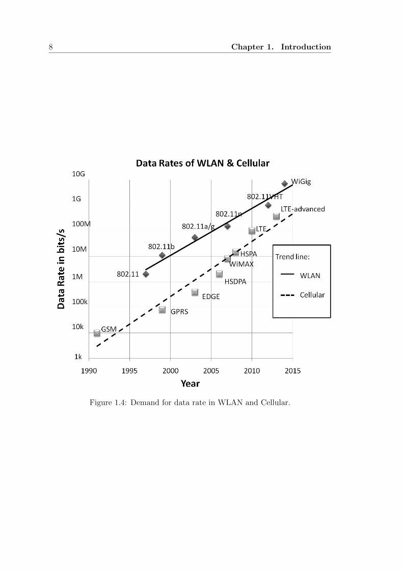
The desire for increased data-rates in wireless local area networks (WLAN) and
cellular phones (Figure 1.4), has resulted in a subsequent need for additional band-
width. As lower frequency bands become congested, additional spectral space is
used at higher RF frequencies. Currently, this trend still continues with the in-
troduction of e.g. 60 GHz transceivers with up to 7 GHz of available spectral
space for the WiGig standard [5]. As was explained in Section 1.2 via (1.2), an
increase in carrier frequency results in a smaller transmit distance, when trans-
mit power and antenna gain remains equal. Therefore, next to the migration to
higher frequencies, wireless transceivers tend to transmit over shorter and shorter
distances. However, there is a benefit to a smaller transmit range. A decrease in
the transmit distance allows for smaller cells and thus higher spatial reuse of the
same frequency, effectively increasing the data rate per surface area. The current
electric infrastructure that enables mobile communication consists of both wired
and wireless links. Since the communication distances are becoming shorter, the
final stage of the communication to the end user is increasingly becoming wireless.
For example, this can be a base station for mobile phones replacing the landlines, a
Bluetooth device wirelessly connected to a computer replacing the cable, a wireless
DECT telephone system connected to a fixed landline replacing the phone cord,
or a wireless internet router connected to the landline of the internet connection
8 Chapter 1. Introduction
Figure 1.4: Demand for data rate in WLAN and Cellular.
1.3. Trends in Wireless Transceivers 9
replacing the WLAN cable to the computer. To illustrate the migration to smaller
communication distances we listed several well known wireless communication sys-
tems and their introduction date:
• 1904 Marconi across the Atlantic
• AM radio (200 km, 2,000,000 watt)
• FM radio (50 km, 50,000 watt)
• 1980 cellular radio (3 km, 10 watt)
• 2000 WLAN (10 meters, 0.1 watt)
• 2010 Body area Networks (1 meter, 0.01 watt)
1.3.2 Multiple Antennas
Similar Band
There are two main drivers behind the use of multiple antennas at the same fre-
quency band. The first reason originates from (1.2), where multiple antennas help
to compensate part of the loss of received power at smaller wavelengths by increas-
ing the effective antenna gain. The other reason to use multiple antennas is to
exploit the spatial selectivity of the channel to increase the data rate in a limited
spectral space, i.e. reuse spectral components across different reflective surfaces in
the channel.
A physical explanation of the received power loss due to smaller wavelengths in
(1.2) is that it is due to the receive antenna aperture, since at smaller wavelengths
antennas are smaller in order to effectively pick up power from an incoming elec-
tromagnetic wave. Because the antenna is smaller, the energy they are able to
pick up at equal transmit power and distance is decreased as well. This effect can
be restrictive at very high carrier frequencies such as for example the 60 GHz ISM
10 Chapter 1. Introduction
band. In order to achieve enough antenna gain to receive enough of the trans-
mitted power over a given distance, multiple antennas can be used [5]. These
antennas are combined at RF in the analog domain and use a single receiver chain
to process the common analog signal. Due to the limited spectral space of the ISM
bands, or limited spectral space owned by mobile operators, it is attractive to use
multiple antennas to increase the throughput. This allows for an additional degree
of freedom, due to the spatial selectivity of the channel. Examples of standards
exploiting spatial selectivity are the IEEE 802.11n standard and LTE advance.
In these standards each antenna has its own receiver chain and the antennas are
used to send independent information via different reflective surfaces at similar
frequencies.
Multiple Bands
Although modern antennas in handheld devices are capable of receiving a multi-
tude of frequency bands there still are several antennas in a handheld connected to
different transceivers. The existence of multiple antennas for multiple standards
may be due to the desire to use several functionalities simultaneously. A mobile
user might be listening to an FM radio station while he is transmitting a photo to
another user via a Bluetooth connection.
1.3.3 Multiple Standards and Devices
Next to the trend towards more antennas for a transceiver we observe that new
generations of mobile phones and laptops accommodate more and more standards
which often have an antenna of their own. This means that there is an increased
number of antennas which need to be fitted in a mobile device. One option to
reduce the number of antennas is to use an antenna for more than one standard.
The standards available in modern handhelds may be, but are not limited to, multi
band GSM, GPS, FM-radio, Bluetooth, WLAN, and NFC. With the introduction
of new standards such as LTE advanced and WiMAX, the number of supported
standards is expected to increase for the foreseeable future.
1.3. Trends in Wireless Transceivers 11
For size and cost reduction it is desirable to create generic platforms to accom-
modate several wireless standards in a single transceiver. Standards are often
combined when they occupy a similar frequency range. A single transceiver in a
mobile device can than service several standards in the same frequency range. Sev-
eral of these transceivers are placed in a mobile phone or a laptop to allow mobile
communication across a plurality of standards. For further cost and size reduction
it can be desirable to combine standards operating at different frequency ranges.
A downside of generic platforms is that they often require additional dynamic
range, frequency range, linearity, and isolation requirements (when compared to
single purpose solutions) in order to comply with all the standard requirements,
and as such commonly require more battery power. The combined requirements
of separate standards can even prove to be prohibitive in creating generic devices.
Despite the benefits of antenna sharing, size and cost reduction, the use of generic
platforms commonly increases overal power consumption reducing battery lifetime.
1.3.4 Multiple Users
Interference
With the success of mobile communication the number of users has grown rapidly
over time. The increase in the amount of users has resulted in an increasing
amount of interference and the congestion of limited spectral space. Even when
users occupy different frequency bands, part of their transmit power can end up in
the band of adjacent users interfering with their transmission. Since more users are
present, the chance of a powerful interferer appearing at the antenna is increased.
The presence of powerful interference increases the chances of desensitization of a
receiver and thus blocking of the desired transmission. To decrease the possibility
of blocking due to interference, the interference power levels at which a receiver
should still operate is increased in new generations of receivers.
In most receivers a broad band signal is processed at RF by the analog front end,
where the desired signal only occupies a small portion of the front end bandwidth.
To present the desired signal to the BB ADC, the analog front end amplifies,

12 Chapter 1. Introduction
down-converts, and filters the received RF broadband signal. Therefore, the first
stages of the receiver usually contains strong adjacent channel interferers, with a
priori not fully known statistical properties [6]. These signals need to be handled
with adequate linearity to avoid excessive distortion spill-over into the band of
the desired signal [7]. Generally, a higher linearity requirement leads to a higher
power consumption of the analog circuit. In conventional RF designs the linearity
is fixed and specified for the highest power of the interference at which the receiver
should still operate, thus resulting in an overly linear design at all lower values of
the interference power, reducing battery lifetime unnecessarily. Most RF designs
are based on a set of system specifications, these specifications are determined by
standardization [7], and may include packet error rates, sensitivity and modulation.
An RF designer then strives to design a receiver at the lowest power possible, for
this target [8, 9].
Cognitive Radio
Cognitive radio (CR) promises to vastly improve the efficiency of spectral use. In
the concept of CR the radio continuously senses and uses unoccupied channels in a
wide band spectrum, alleviating congestion and improving the overall throughput.
In order to adequately receive and reconstruct the transmitted data from the
desired signal, both coordinated and random interfering signals need to be filtered.
The filtering of interference can occur in combinations of domains, such as time
domain filtering, code domain filtering, frequency domain filtering, and spatial
domain filtering.
We observe that in most systems the RF front end and ADC handle the interfering
users via extra dynamic range (DR) and linearity, which make them power hungry
[10]. The DR and oversample frequency of the ADC are a combination of the
interference power level with which the receiver needs to cope, both in and out of
band, and a trade off with the analog filter drop off [11].
However, modern MIMO systems make it feasible to include spatial filtering tech-

1.3. Trends in Wireless Transceivers 13
niques in the analog front end. Since the channel is selective in the angular domain,
such techniques have the potential to vastly reduce the interference power and thus
the DR and linearity requirements of both the RF front end and ADC. Therefore, a
spatial filtering technique can be the basis for ultra low-power high data-rate wire-
less receivers, and has the potential to mitigate the DR requirements of cognitive
radios.
1.3.5 Energy Trends
Additional Functionalities
In the first GSM phones the majority of the available battery power was allocated
for the wireless GSM transmission. With the recent succes of smart phones, the
trend of introducing more and more features next to the core application has con-
tinued. Today mobile phones share the scarce battery resource over a plurality of
applications. Not the least one is the screen, which requires an ever larger portion
of the battery power as its size increases. Further, more wireless application re-
quire a portion of the battery power even when they are not used, as they are often
set to a standby mode. This trend has resulted in an ever dwindling percentage of
battery power availability for the core GSM function and a competition between
application for a limited resource, driving the need for ever more power reduction
of the individual application.
Available Energy and Phone Size Reduction
At the same time as we have witnessed an increase in the amount of applications in
a mobile phone, the energy density of batteries has finally took off. Where battery
technology was stagnant for almost 150 years (Section 2.4), the invention of the
mobile phone has spurred research in this field resulting in batteries with vastly
superior energy densities, of almost an order of magnitude larger than only two
decades ago. Compared to the historic trend of battery power technology, this is
14 Chapter 1. Introduction
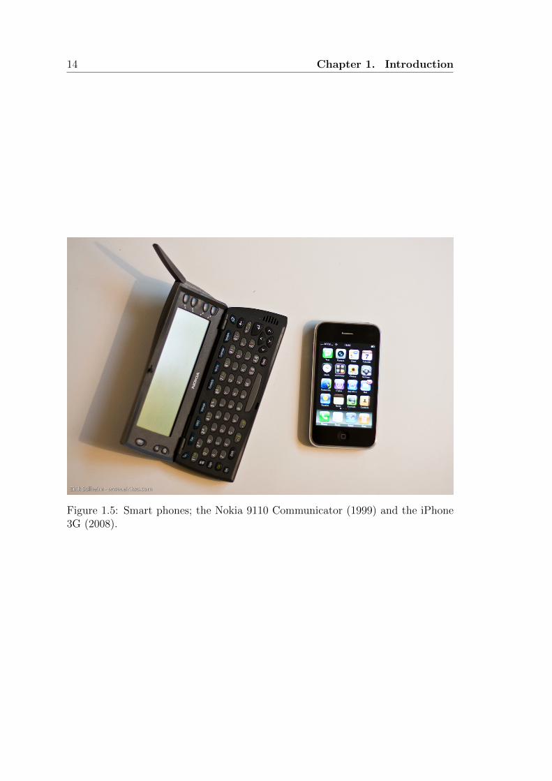
Figure 1.5: Smart phones; the Nokia 9110 Communicator (1999) and the iPhone3G (2008).
1.4. MIMO in a Mass Market 15
a huge acceleration in the field.
Although energy density has gone up considerably, the available energy in a mo-
bile phone has remained near constant over the last two decades (Section 2.3).
This is due to the appeal of a small and thin phone to the consumer. So rather
than relaxing power requirements and increase battery lifetime, consumers and
producers alike have opted for ever smaller, lighter, and thinner phones. Every
new battery technology has led to a size reduction, rather than the availability of
more energy. Where the first commercially available cellular phone, the Motorola
DynaTAC 8000X from 1983 weighed 783 grams, the Nokia 3110 classic from 2007
weighs 87 grams. With the recent succes of smart phones (which are replacing
regular mobiles phones) and the subsequent increase in screen and phone size, this
weight reduction trend might be slightly reversed or halted for the time being. For
example the Apple iPhone 4 from 2010 weighs 137 grams, were the iPhone 3G
from 2008 weighs 133 grams. This is because there are two counter acting trends
for smart phones, the ongoing miniaturization of applications and the ongoing
increase in the number of applications in a mobile phone. Despite these counter
acting trends, a similar trend of making phones thinner and lighter over time is
observed among smart phones as well, as for example the Nokia 9110 Communi-
cator from 1999 weighs 253 grams (Figure 1.5). In the case of the Nokia 3110 the
miniaturization of applications was the dominant driver in weight reduction com-
pared to the Motorola DynaTAC 8000X. In the case of the smart phones weight
is reduced slower, as the miniaturization trend is currently offset by the increase
in number of applications.
1.4 MIMO in a Mass Market
The aim of the MIMO in a Mass Market project is power reduction of MIMO
systems and interference mitigation, without loss in performance. In most wireless
communication systems the interface to the landline, such as a wireless router or a
basestation, is power plugged thus power consumption is less constricted. On the
other hand, the mobile user is limited by the available battery power.
16 Chapter 1. Introduction
MIMO transceivers take advantage of the existence of multiple reflected waves in
wireless channels (Section 3.3). MIMO systems consist of multiple transmit and
multiple receive antennas. MIMO systems exploit reflected waves by transmit-
ting different information on the same frequency over separate reflections. Thus
exploiting the spatial selectivity of the channel. This allows the transmission of
more information than SISO systems.
Current MIMO systems consist of dedicated transmitters and receivers per trans-
mit and receive antenna. Since the average data-rate of MIMO systems scales less
than linearly in the number of antennas, the power efficiency of MIMO system is
reduced when the number of antennas is increased.
Due to the succes of wireless devices, and their subsequent increase in numbers,
they interfere more and more with one another. Traditionally, an increase in
interference levels has been handled by increasing linearity and dynamic range of
the receiver. Unfortunately, increasing linearity and dynamic range comes at a
cost of higher power consumption [7].
The main focus of the MIMO in a Mass Market project is on the receiver cir-
cuit power consumption. The motivation to focus on a receiver with a limited
availability of battery power is two-fold. In many applications, the mobile user
spends significantly more time receiving data than transmitting. Often, the en-
ergy consumed in receiving mode is several orders of magnitudes larger than the
energy consumed in transmit mode [12] [13], even if the transmitter circuit power
consumption is larger than the receiver circuit power consumption when switched
on. Secondly, in a short range link, the transmit power can be relatively small.
So the transmit power amplifier is no longer the main power consumer. Yet, the
receiver front end often needs to recover a weak signal in the presence of strong
adjacent channel interference, which requires highly linear, thus power hungry RF
designs. In the absence of disruptive new approaches, we expect that this trend
will continue for the foreseeable future.
Traditionally the BB and RF of transceivers are optimized separately. The MIMO
in a Mass Market project aims at achieving its goals via system optimization over
both the RF and BB domain. This joint optimization requires novel architectures
1.5. The Research 17
and baseband algorithms.
The MIMO in a Mass Market project is sponsored by Senter-Novem under the
IOP-Gencom program (IGC05002) and is a collaboration in the framework of 3TU
(consisting of the Delft, Eindhoven and Twente universities of technology ) and
industrial partner Philips Research.
1.5 The Research
As mentioned in the introduction of this chapter, the research presented in this
thesis contains theoretical system modeling considering arguments based on Shan-
non capacity, and a partial system implementation used for verification of the
theory. The system implementation consists of algorithm design, PCB design, and
circuit design and implementation in 65 nm CMOS. To fully exploit the benefit
of a joint optimization of both RF and BB, an in dept investigation into the joint
bottlenecks and challenges is conducted. From this investigation, key system com-
ponents are identified, and novel components are designed and implemented. A
proof-of-concept system measurement confirms the models and the benefit of the
joint RF-BB optimization approach. The results of the research are listed below.
1.5.1 Scientific Contributions
We showed that mitigating interference as early as possible in the receiver chain is
a favorable approach in achieving the objectives of the MIMO in a Mass Market
project, as it simultaneously increases interference robustness and decreases power
consumption.
We succeeded in setting up a generic framework that leads to system level con-
clusions. The closed-form solution is used to calculate the optimal transmission
rate for a given receiver circuit power and to calculate the maximum achievable
receiver efficiency in terms of bits per Joule of receiver energy. Further, the frame-
18 Chapter 1. Introduction
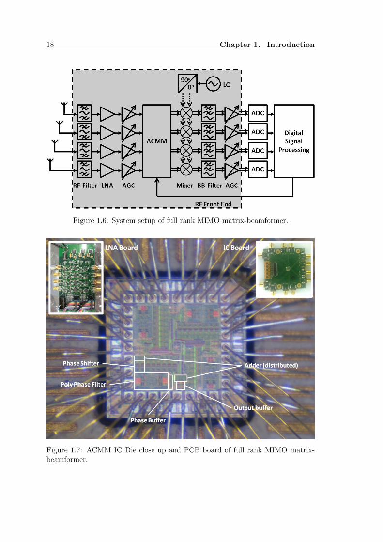
Figure 1.6: System setup of full rank MIMO matrix-beamformer.
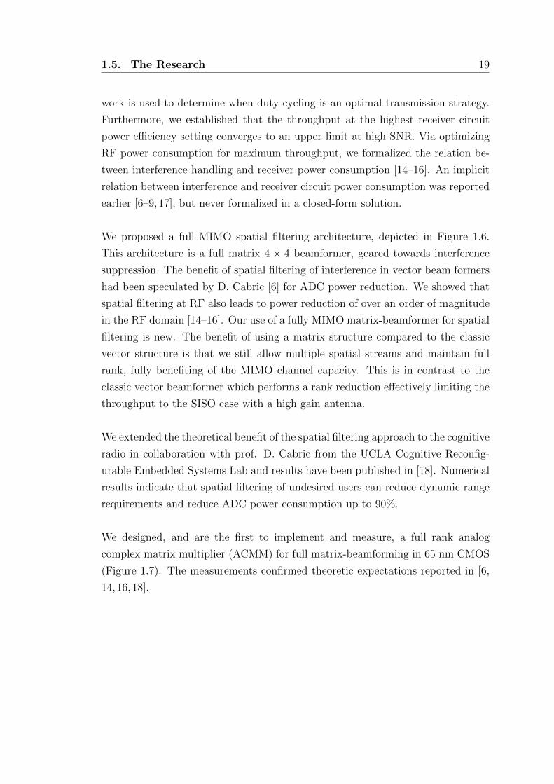
Figure 1.7: ACMM IC Die close up and PCB board of full rank MIMO matrix-beamformer.
1.5. The Research 19
work is used to determine when duty cycling is an optimal transmission strategy.
Furthermore, we established that the throughput at the highest receiver circuit
power efficiency setting converges to an upper limit at high SNR. Via optimizing
RF power consumption for maximum throughput, we formalized the relation be-
tween interference handling and receiver power consumption [14–16]. An implicit
relation between interference and receiver circuit power consumption was reported
earlier [6–9,17], but never formalized in a closed-form solution.
We proposed a full MIMO spatial filtering architecture, depicted in Figure 1.6.
This architecture is a full matrix 4 × 4 beamformer, geared towards interference
suppression. The benefit of spatial filtering of interference in vector beam formers
had been speculated by D. Cabric [6] for ADC power reduction. We showed that
spatial filtering at RF also leads to power reduction of over an order of magnitude
in the RF domain [14–16]. Our use of a fully MIMO matrix-beamformer for spatial
filtering is new. The benefit of using a matrix structure compared to the classic
vector structure is that we still allow multiple spatial streams and maintain full
rank, fully benefiting of the MIMO channel capacity. This is in contrast to the
classic vector beamformer which performs a rank reduction effectively limiting the
throughput to the SISO case with a high gain antenna.
We extended the theoretical benefit of the spatial filtering approach to the cognitive
radio in collaboration with prof. D. Cabric from the UCLA Cognitive Reconfig-
urable Embedded Systems Lab and results have been published in [18]. Numerical
results indicate that spatial filtering of undesired users can reduce dynamic range
requirements and reduce ADC power consumption up to 90%.
We designed, and are the first to implement and measure, a full rank analog
complex matrix multiplier (ACMM) for full matrix-beamforming in 65 nm CMOS
(Figure 1.7). The measurements confirmed theoretic expectations reported in [6,
14,16,18].
20 Chapter 1. Introduction
1.6 Structure of the Thesis
Chapter 2 reviews the current state of the art and expected technology trends,
which help to identify long-term bottlenecks.
Chapter 3 of the thesis expands the models of Chapter 2, and shows that by
exploiting the spatial selectivity of the wireless channel in the RF domain of the
MIMO receiver for interference mitigation, there exists potential to vastly reduce
receiver circuit power consumption and improve overall interference robustness.
Chapter 4 of the thesis focusses on the relationship between receiver circuit power
consumption in RF front ends and interference power levels. Next to the relation
between receiver circuit power and interference levels, the optimal throughput for
a low power wireless receiver is calculated.
Chapter 5 of the thesis shows the IC design of the analog spatial filter, the ACMM
IC in 65 nm CMOS. Further, Chapter 5 shows the implementation of the IC in the
receiver via a custom designed PCB, with off-the-shelf components and the custom
designed ACMM-IC. Finally Chapter 5 shows the proof of concept measurements.
Chapter 6 focusses on the digital baseband algorithms that are required to ob-
tain an optimal beamforming setting of both a beamformer and the ACMM. Via
practical algorithms it is shown that analog beamforming can result in significant
ADC power consumption reduction.
Chapter 7 provides the conclusions and recommendations.
Chapter 2
State of the Art MIMO OFDM
Systems
2.1 Introduction
As mentioned in the introductory chapter, there are several trends that can be
distinguished in wireless communication. Some are obvious to regular users, such
as an increase in standards in their mobile phones, and some are less visible such
as power consumption trends of individual components that make up the mobile
device. In this chapter we will show that in the absence of disruptive new tech-
nologies, the RF front end and ADC power consumption are the future bottlenecks
of MIMO transceivers in terms of extending battery lifetime. Since interference
poses strong dynamic range requirements on the front-end and ADC, mitigating
the interference has the potential to vastly reduce the power consumption of the
ADC and RF front end. We will focus on the power trends of wireless transceivers
and the available energy in battery powered devices. Because battery energy is a
scarce commodity in a mobile device, such as a smart phone, reducing the power
consumption of wireless transceivers to increase battery lifetime is of prime im-
portance. The power trends of individual components that make up the wireless
link are extrapolated to obtain expected development curves. The expected de-
21
22 Chapter 2. State of the Art MIMO OFDM Systems
velopment curves are used to identify the mayor future bottlenecks. Identifying
and solving the future bottlenecks is important when designing systems that are
supposed to be used in the future.
An obvious shift in mobile communication of the last couple of years, as the smart
phone is becoming more popular, is the emphasis that is put on increasing data
transfer. Most mobile phones are now connected to the internet, and generate
more data traffic than ever before. When planning for communication networks,
operators need to account for the number of consumers per unit area in cities and
towns. In cities, operators tend to prefer small cell sizes, allowing them to reuse
their frequencies more often over the city area and thereby achieve a high data rate
per square meter where there are many customers per unit area, as such that each
costumer has a high data rate available (examples of such a standard are WiMax
and LTE Advanced). In rural areas, relatively long range connections are preferred,
even though these generate a low data rate per square meter covered. But, since the
number of costumers is relatively small, such systems still achieve a high data rate
per costumer. An example is the wireless regional area network (WRAN) function
of IEEE802.22. Since more and more people migrate to cities and more people
inside cities use smart phones, expectations are that communication distances will
decrease, to allow for even denser reuse of precious spectral resources.
Modern MIMO systems exploit spatial diversity of urban propagation environ-
ments. MIMO systems reuse the same RF frequencies or spectral resources to
transmit different data simultaneously to a single user. This is achieved by ex-
ploiting reflective surfaces to open parallel data streams. Since MIMO systems are
inherently directional they can also be used in a single base station of, for example,
the LTE Advanced standard to beamform on the same frequency to different users
without mutual interference, as would have been the case with omnidirectional
SISO transmissions.
Current MIMO systems consist of dedicated transceivers per transmit and receive
antenna. Thus the power consumption of the ADCs and RF front ends increases
linearly in the number of transmit Nt and receive Nr antennas. Unfortunately the
increase in average capacity scales less than linearly in the number of antennas.
In this chapter we will first introduce the power breakdown and power trends of
2.2. Receiver 23
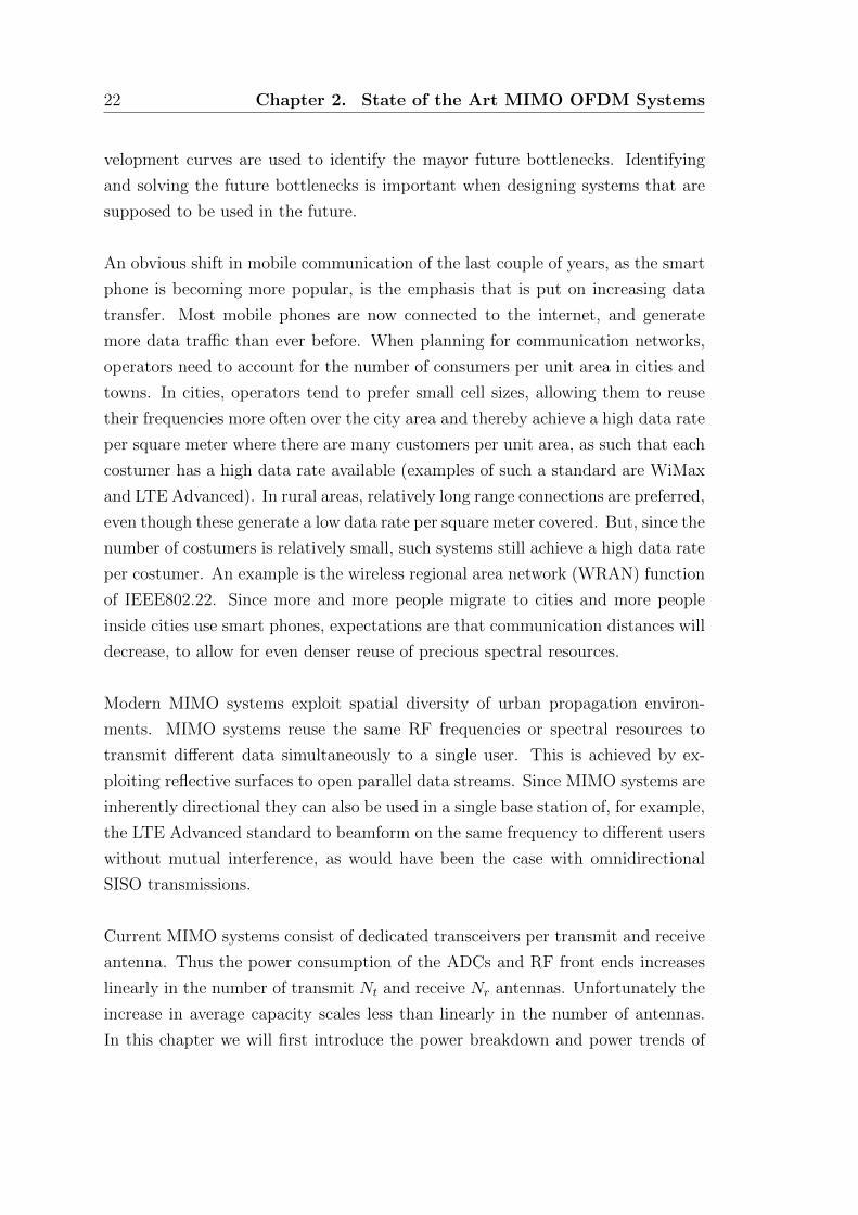
Figure 2.1: A wireless transceiver.
MIMO systems. Then we will discuss several key components that impact the
available energy for the MIMO system in mobile devices. Finally we will give
an extrapolation of the long term trends of MIMO transceivers. We identify the
receiver RF and ADC as the future bottleneck in energy consumption reduction.
2.2 Receiver
A typical transceiver consists of several blocks as is depicted in (Figure 2.1). In
common user scenarios, most users spend significantly more time receiving than
transmitting [12] [13]. As a result the total energy consumed in the receiver can be
orders of magnitude larger than the energy consumed in the transmitter. Moreover,
the increase in the number of users poses additional dynamic range requirements
on the front end. Unfortunately, the power consumption of the front end scales
exponentially in the DR, making the front end more power hungry [9]. To find a
reliable power trend for the transceiver we will first start with the power trends of
the RF, then the power trend of the analog-to-digital converters is presented and
finally the baseband processing trend is given.
2.2.1 RF Front End
Establishing a reliable power trend in RF is difficult due to the multitude of stan-
dards and requirements. Despite these difficulties, a commonly used rule of thumb
is an order of magnitude power reduction for the same function per decade. Since
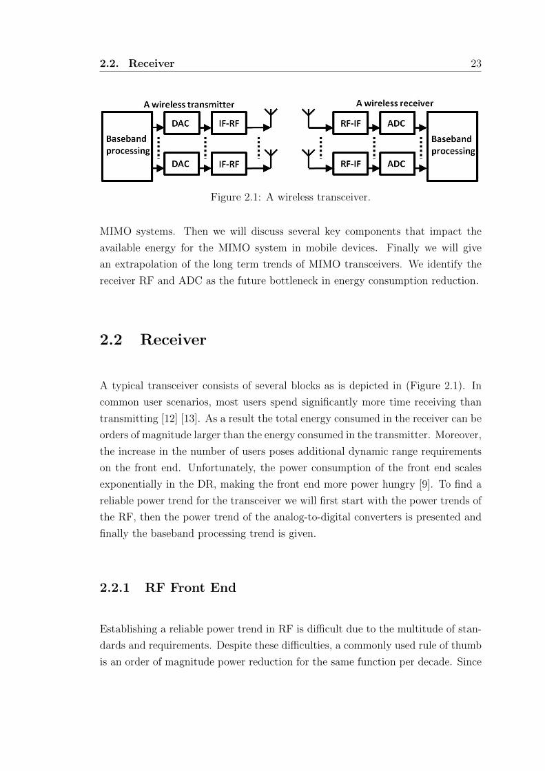
24 Chapter 2. State of the Art MIMO OFDM Systems
Figure 2.2: Power consumption of IEEE802.11 receivers over time.
we are interested in MIMO systems, we will focus on equipment that can operate
at 2.4 GHz according to the IEEE 802.11n standard. An additional benefit of lim-
iting ourselves to a single standard is that the receivers need to operate according
to a similar specification set, making them easier to compare.
The eighteen data point of the receivers in Figure 2.2 are given by Table 2.1. In
Figure 2.2 a straight solid trend line is plotted using all the data points. The
angle of the actual power trend line may differ quite a bit from the solid line found
here, as every point is slightly biased due to different system requirements. In
our data set, later receivers mostly are dual mode receivers operating at different
frequencies and as such have to comply to more stringent specifications making
them more power hungry than would have been required for a dedicated receiver.
This affects te trend line and leads to a lower slope than an order of magnitude
per decade. A further limitation of the solid line is the fact that we relate the
power consumption back to one receiver chain. MIMO receivers share resources
such as the clock and PLL, making the power consumption per chain slightly more
favorable and more difficult to compare to a SISO receiver.
2.2. Receiver 25
Table 2.1: Data points of Figure 2.2.
Journal/Conference Year Power [mW] ReferenceRFICS 2003 345 [19]ISSCC 2003 350 [20]ISSCC 2003 215 [21]JSSC 2004 260 [22]JSSC 2004 176 [23]ISSCC 2004 216 [24]ISSCC 2004 342 [25]JSSC 2004 370 [26]ISSCC 2005 136 [27]JSSC 2005 117 [28]JSSC 2006 186 [29]ISSCC 2007 66 [30]ISSCC 2008 270 [31]ISSCC 2008 93 [32]RFICS 2008 64 [33]ISSCC 2009 165 [34]ESSCIRC 2009 174 [35]RFICS 2010 115 [36]
There are two trends influencing the solid line in Figure 2.2. On the one hand
miniaturization helps to decrease power consumption. On the other hand, as men-
tioned in Section 1.3.3, for size and cost reduction it is desirable to create generic
platforms to accommodate several wireless standards in a single transceiver. How-
ever, the combining of functionality in one receiver results in more stringent re-
quirements and thus more power consumption than would have been required by
a dedicated receiver. Another method is to use only the best data per year for
dedicated receivers and plot a line through them, as is indicated by the dotted
line. In this line all points are dedicated receivers at 2.4 GHz, further we have
omitted data from 2009 and 2010 as those receivers are all dual band. As can
be seen in Figure 2.2, the dotted line comes close to one order of magnitude per
decade. The dotted line in Figure 2.2 isolates the trend due to miniaturization
better than the solid line and confirms the rule of thumb for the power trend in
RF of an order of magnitude power reduction for the same function per decade.
However, the increase in the number of users, and the subsequent required DR to
handle the additional interference, is expected to increase the power consumption
of the front end.
26 Chapter 2. State of the Art MIMO OFDM Systems
2.2.2 ADC
A commonly used rule of thumb for ADC power consumption is given by Walden,
and predicts an order of magnitude every decade [37], [38], [39]. Note that this
rule of thumb is similar to rule of thumb of the analog RF front end explained in
the previous section. Another rule of thumb given by Murmann predicts a factor
of two every two years [40], [41], [42]. A problem in accurately predicting trends
in ADC power consumption is the choice of FOM and the arbitrary nature of such
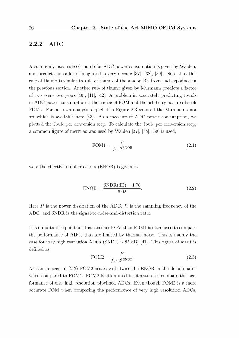
FOMs. For our own analysis depicted in Figure 2.3 we used the Murmann data
set which is available here [43]. As a measure of ADC power consumption, we
plotted the Joule per conversion step. To calculate the Joule per conversion step,
a common figure of merit as was used by Walden [37], [38], [39] is used,
FOM1 =P
fs · 2ENOB(2.1)
were the effective number of bits (ENOB) is given by
ENOB =SNDR(dB)− 1.76
6.02. (2.2)
Here P is the power dissipation of the ADC, fs is the sampling frequency of the
ADC, and SNDR is the signal-to-noise-and-distortion ratio.
It is important to point out that another FOM than FOM1 is often used to compare
the performance of ADCs that are limited by thermal noise. This is mainly the
case for very high resolution ADCs (SNDR > 85 dB) [41]. This figure of merit is
defined as,
FOM2 =P
fs · 22ENOB. (2.3)
As can be seen in (2.3) FOM2 scales with twice the ENOB in the denominator
when compared to FOM1. FOM2 is often used in literature to compare the per-
formance of e.g. high resolution pipelined ADCs. Even though FOM2 is a more
accurate FOM when comparing the performance of very high resolution ADCs,

2.2. Receiver 27
the assumption that the ADC is limited by thermal noise is often pessimistic for
real designs. Therefore, the appropriate use of FOM2 depends on both the design
and implementation of the considered ADCs. In this section we restrict ourselves
to the more universally used FOM1, as was used by Walden [37], [38], [39], but it
is important to keep in mind that the accuracy of FOM1 is limited when assessing
the performance of thermal noise limited ADCs.
As can be seen in Figure 2.3 the trend line of the power consumption reduction
(solid) over the years comes close to the factor of 2 per two years as was predicted
by Murmann [40], [41], [42]. It should be noted thought that this is a data set
which contains all 302 ADCs from ISSCC and VLSI from 1997 to 2010, each with
their own specifications and application areas. Therefore, the resulting power trend
does not necessarily hold for all types of ADCs. To find a more accurate power
trend for our receiver we have plotted a second trend line (dashed) in Figure
2.3. Since most MIMO receivers use high resolution ADCS, we have only used
the 93 data points of ADCs containing 12 or more ENOBs. The trend line of
these high resolution ADCs comes very close to Walden’s prediction of one order
of magnitude per decade. Since we are using high resolution ADCs in MIMO
receivers, we will use this trend line in the final section of this chapter. The trend
line shows that miniaturization helps to decrease power consumption over time for
the same functionality. On the other hand, the increase in the number of users
and the subsequent increase in interference, increases the DR requirements of the
ADCs in the front end and as such the required number of ENOBs. As can be
seen in (2.1) and (2.3) the power consumption of the ADC scales exponential in
the number of ENOBs for a given FOM. The increase of the required DR due to
interference is counteracting the benefits of miniaturization.
2.2.3 BB Processing
The reduction of power consumption of the baseband processing engine has been
governed by Moore’s law for the past half century. Moore’s law was first reported
in 1965 [44], and states that the amount of transistors doubles approximately
every two years. Due to reduced power supply voltage and increased transistor
28 Chapter 2. State of the Art MIMO OFDM Systems
Figure 2.3: ADC power consumption trend expressed in energy per conversion step.
switching speed due to size reduction, the power consumption required to perform
a certain computational task approximately halves every two years as well. It
has been speculated that Moore’s law will end in the foreseeable future. A first
reason for the end of Moore’s law is due to economics [45], as the cost of new
manufacturing plants is growing beyond what private companies can afford. This
effect is predicted to influence Moore’s law from 2015 onwards [45]. Another reason
for the predicted end to Moore’s law is due to fundamental limits on the physical
size of a transistor [46]. The size reduction of transistors will hit the size limit
of an individual electron around 2036 [46], bringing an end to the possible size
reduction of transistors. For now however, Moore’s law is expected to continue in
the foreseeable future.
2.3 Batteries
A very important aspect of mobile devices is the energy stored in the battery. The
total energy capacity is determined by the battery technology used and the battery
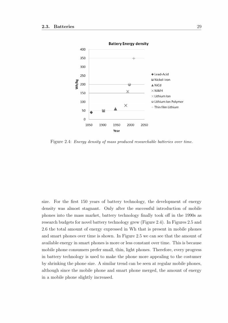
2.3. Batteries 29
Figure 2.4: Energy density of mass produced researchable batteries over time.
size. For the first 150 years of battery technology, the development of energy
density was almost stagnant. Only after the successful introduction of mobile
phones into the mass market, battery technology finally took off in the 1990s as
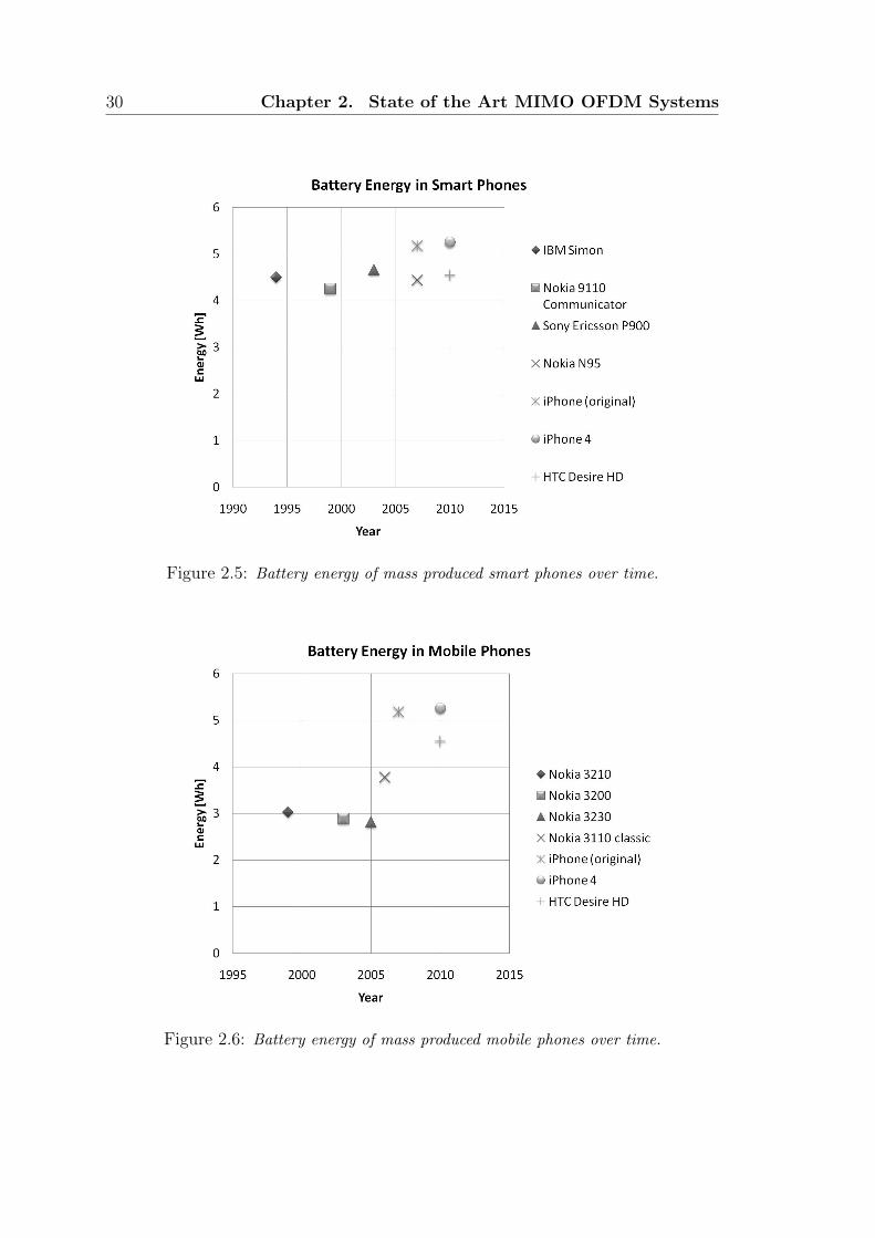
research budgets for novel battery technology grew (Figure 2.4). In Figures 2.5 and
2.6 the total amount of energy expressed in Wh that is present in mobile phones
and smart phones over time is shown. In Figure 2.5 we can see that the amount of
available energy in smart phones is more or less constant over time. This is because
mobile phone consumers prefer small, thin, light phones. Therefore, every progress
in battery technology is used to make the phone more appealing to the costumer
by shrinking the phone size. A similar trend can be seen at regular mobile phones,
although since the mobile phone and smart phone merged, the amount of energy
in a mobile phone slightly increased.
30 Chapter 2. State of the Art MIMO OFDM Systems
Figure 2.5: Battery energy of mass produced smart phones over time.
Figure 2.6: Battery energy of mass produced mobile phones over time.
2.4. Screen Size 31
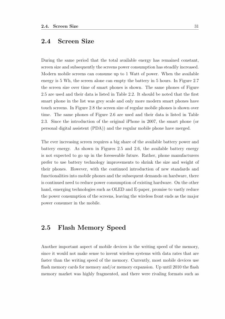
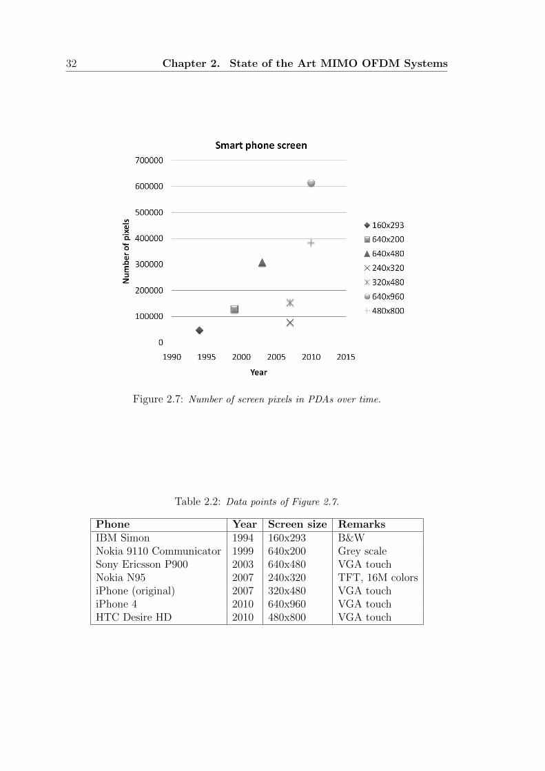
2.4 Screen Size
During the same period that the total available energy has remained constant,
screen size and subsequently the screens power consumption has steadily increased.
Modern mobile screens can consume up to 1 Watt of power. When the available
energy is 5 Wh, the screen alone can empty the battery in 5 hours. In Figure 2.7
the screen size over time of smart phones is shown. The same phones of Figure
2.5 are used and their data is listed in Table 2.2. It should be noted that the first
smart phone in the list was grey scale and only more modern smart phones have
touch screens. In Figure 2.8 the screen size of regular mobile phones is shown over
time. The same phones of Figure 2.6 are used and their data is listed in Table
2.3. Since the introduction of the original iPhone in 2007, the smart phone (or
personal digital assistent (PDA)) and the regular mobile phone have merged.
The ever increasing screen requires a big share of the available battery power and
battery energy. As shown in Figures 2.5 and 2.6, the available battery energy
is not expected to go up in the foreseeable future. Rather, phone manufacturers
prefer to use battery technology improvements to shrink the size and weight of
their phones. However, with the continued introduction of new standards and
functionalities into mobile phones and the subsequent demands on hardware, there
is continued need to reduce power consumption of existing hardware. On the other
hand, emerging technologies such as OLED and E-paper, promise to vastly reduce
the power consumption of the screens, leaving the wireless front ends as the major
power consumer in the mobile.
2.5 Flash Memory Speed
Another important aspect of mobile devices is the writing speed of the memory,
since it would not make sense to invent wireless systems with data rates that are
faster than the writing speed of the memory. Currently, most mobile devices use
flash memory cards for memory and/or memory expansion. Up until 2010 the flash
memory market was highly fragmented, and there were rivaling formats such as
32 Chapter 2. State of the Art MIMO OFDM Systems
Figure 2.7: Number of screen pixels in PDAs over time.
Table 2.2: Data points of Figure 2.7.
Phone Year Screen size RemarksIBM Simon 1994 160x293 B&WNokia 9110 Communicator 1999 640x200 Grey scaleSony Ericsson P900 2003 640x480 VGA touchNokia N95 2007 240x320 TFT, 16M colorsiPhone (original) 2007 320x480 VGA touchiPhone 4 2010 640x960 VGA touchHTC Desire HD 2010 480x800 VGA touch
2.5. Flash Memory Speed 33
Figure 2.8: Number of screen pixels in mobiles over time.
Table 2.3: Data points of Figure 2.8.
Phone Year Screen size RemarksNokia 3210 1999 84x84 B&WNokia 3200 2003 128x128 Grey scaleNokia 3230 2005 176x208 TFT, 65K colorsNokia 3110 classic 2006 128x160 TFT, 256K colorsiPhone (original) 2007 320x480 VGA touchiPhone 4 2010 640x960 VGA touchHTC Desire HD 2010 480x800 VGA touch
34 Chapter 2. State of the Art MIMO OFDM Systems
for example the Sony memory stick and the Olympus xD-Card. Since 2010 micro-
SD (Secure Digital) has come to dominate the new high-end phones and tablet
computers. The follow up of micro-SD is Secure Digital High Capacity (SDHC)
which is meant for memory sizes of up to 32 GB. The follow up of SDHC, the
Secure Digital Extended Capacity (SDXC) format was unveiled at CES 2009 and
will support up to 2TB.
The maximum transfer rate of micro-SD using an Serial Peripheral Interface (SPI)
bus is 10 MB/s. For our system, we conclude that higher transfer rates are needed,
as the maximum raw data rate of IEEE 802.11n is 600 Mbit/s. The maximum
transfer rate of SDXCs, which is planned to follow up the SD 3.0 specification, was
announced as 832 Mbit/s, with plans that the SD 4.0 specification shall increase
this to 2.4 Gbit/s. At those writing speeds, the writing speed of the memory will
not be the bottleneck of our wireless system. Only for a system at the targeted
7 Gbit/s data rate of the 60 GHz band, the memory writing speed of SDXC can
potentially become a bottleneck.
2.6 Extrapolations
Based on the power trends of the RF, ADC, and BB processing engine, we can
extrapolate the power consumption reduction of the components of a 4x4 MIMO
system into the near future. An important aspect to consider when extrapolating,
is the fact that although the power consumption of dedicated RF receivers reduces
with an order of magnitude per decade, the power consumption of multipurpose
front ends does not necessarily follow the same trend line. As can be seen in
Figure 2.2 the multipurpose receivers introduced after 2008 consume significantly
more power than a dedicated single purpose receiver. Building a MIMO system
from multipurpose transceivers may therefore be more power hungry than the
values projected here. In the absence of disruptive new technologies, we expect
the trends of RF, ADC, and BB to continue in the foreseeable future. Figure 2.9
depicts the expected power trend of MIMO OFDM systems. As can be seen in
Figure 2.9 the power consumption of the digital baseband engine is expected to
2.6. Extrapolations 35
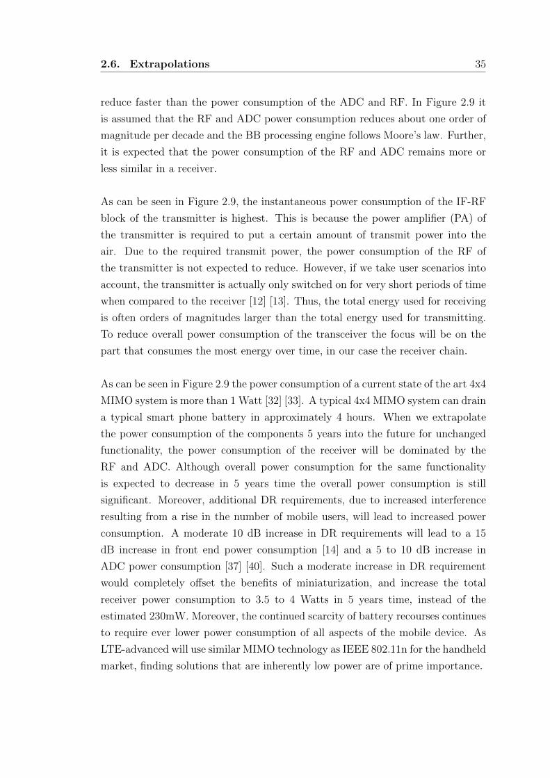
reduce faster than the power consumption of the ADC and RF. In Figure 2.9 it
is assumed that the RF and ADC power consumption reduces about one order of
magnitude per decade and the BB processing engine follows Moore’s law. Further,
it is expected that the power consumption of the RF and ADC remains more or
less similar in a receiver.
As can be seen in Figure 2.9, the instantaneous power consumption of the IF-RF
block of the transmitter is highest. This is because the power amplifier (PA) of
the transmitter is required to put a certain amount of transmit power into the
air. Due to the required transmit power, the power consumption of the RF of
the transmitter is not expected to reduce. However, if we take user scenarios into
account, the transmitter is actually only switched on for very short periods of time
when compared to the receiver [12] [13]. Thus, the total energy used for receiving
is often orders of magnitudes larger than the total energy used for transmitting.
To reduce overall power consumption of the transceiver the focus will be on the
part that consumes the most energy over time, in our case the receiver chain.
As can be seen in Figure 2.9 the power consumption of a current state of the art 4x4
MIMO system is more than 1 Watt [32] [33]. A typical 4x4 MIMO system can drain
a typical smart phone battery in approximately 4 hours. When we extrapolate
the power consumption of the components 5 years into the future for unchanged
functionality, the power consumption of the receiver will be dominated by the
RF and ADC. Although overall power consumption for the same functionality
is expected to decrease in 5 years time the overall power consumption is still
significant. Moreover, additional DR requirements, due to increased interference
resulting from a rise in the number of mobile users, will lead to increased power
consumption. A moderate 10 dB increase in DR requirements will lead to a 15
dB increase in front end power consumption [14] and a 5 to 10 dB increase in
ADC power consumption [37] [40]. Such a moderate increase in DR requirement
would completely offset the benefits of miniaturization, and increase the total
receiver power consumption to 3.5 to 4 Watts in 5 years time, instead of the
estimated 230mW. Moreover, the continued scarcity of battery recourses continues
to require ever lower power consumption of all aspects of the mobile device. As
LTE-advanced will use similar MIMO technology as IEEE 802.11n for the handheld
market, finding solutions that are inherently low power are of prime importance.
36 Chapter 2. State of the Art MIMO OFDM Systems
Figure 2.9: Current MIMO wireless transceiver (transmitter left, and receiverright).
2.7 Summary and Conclusions
Available battery energy in smart phones has remained constant over time. Each
battery power density improvement has resulted in a shrinking phone to appeal
to consumers. In the meanwhile the screen size has steadily gone up and new
standards and functionalities have been added to the phone, reducing the power
budget of existing wireless transceivers. Emerging technologies such as OLED
and E-paper are expected to vastly reduce screen power consumption, leaving the
analog frond end as the main power consumer in the mobile. The new LTE ad-
vance standard will use similar MIMO techniques as IEEE 802.11n to increase
the data rate of smart phones. Despite the ongoing miniaturization of existing
functionality and its corresponding power reduction in handheld devices, the vast
increase in number of applications in new generations of smart phones and its
subsequent demands on hardware has offset and for now halted the overall trend
of weight and size reduction of mobile phones. Moreover, additional DR require-
ments, due to increased interference resulting from a rise in the number of mobile
users, will lead to vastly increased power consumption of the front end. Current
state-of-the-art MIMO receivers use about 1 Watt of power in receiving mode. A

2.7. Summary and Conclusions 37
typical state-of-the-art 4x4 MIMO system can drain a typical smart phone bat-
tery in approximately 4 hours. A moderate 10 dB increase of DR requirements
to handle increased interference levels, will reduce this to 20 minutes. Reducing
MIMO power consumption in handheld devices is therefore of prime importance
to increase battery lifetime.

38 Chapter 2. State of the Art MIMO OFDM Systems

Chapter 3
System Design Considerations for
MIMO OFDM Systems
3.1 Introduction
In the previous chapter we have discussed the power trends that dominate mobile
devices and MIMO systems. In this chapter we will focus more on the technical
background of MIMO systems and try to identify the technical bottlenecks and
challenges of designing a MIMO OFDM system.
To create a framework for evaluating the MIMO system, we will start by first
addressing the commonly encountered received signal. This signal depends on the
transmitted signal and the MIMO communication channel. For now we will use
the commonly used Rayleigh fading channel model. In Chapter 6 we will introduce
a ray tracer channel model, but for basic understanding of MIMO channels and
MIMO capacity, the ray tracer model is not necessary in this chapter. From
the received signal we will introduce the MIMO channel capacity model as it was
derived by Telatar [2], and Foschini and Gans [3]. After we introduced the received
signal, we introduce the state-of-the-art zero-IF receiver which is commonly used in
MIMO OFDM systems. From the zero-IF architecture we will introduce common
39
40 Chapter 3. System Design Considerations
RF specifications and how they influence one another over a receiver chain. Finally,
we will use the capacity equation to help to identify areas of unresolved challenges
and opportunities in MIMO OFDM systems.
3.2 Received Signal Model
3.2.1 Legal Transmit Power
From the IEEE 802.11n standard it is known that the legal transmit power limit
varies per area and carrier frequency. For example at a 40 MHz bandwidth at 2.4
GHz, the legal transmit power is 23 dBm in Japan, 30 dBm in the USA, and 20
dBm in Europe.
3.2.2 Data Format
In the IEEE 802.11n protocol, the data symbols are preceded by a preamble.
During the preamble the receiver is trained and the channel is estimated. In this
chapter we assume the channel is time invariant, during the transmission of the
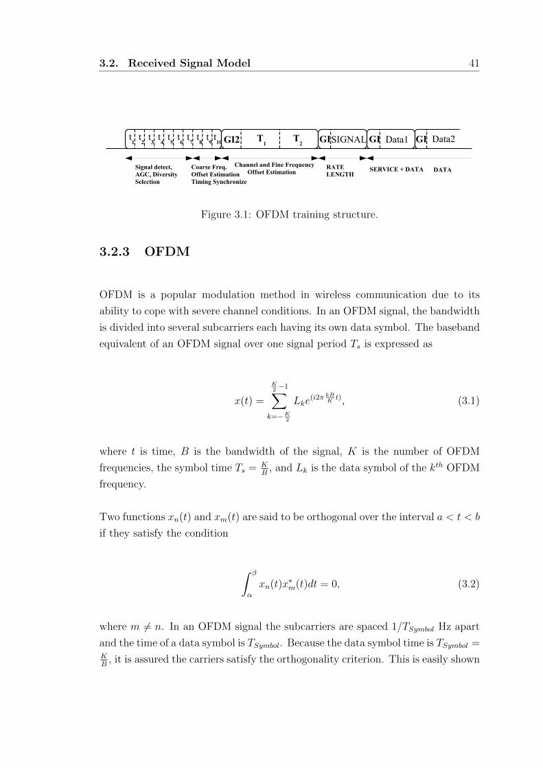
data symbols. Such a system is called “packet based”. Figure 3.1 shows the OFDM
training structure as is used in the IEEE 802.11 standard. In this figure, t1 to t10
denote short training symbols and T1 and T2 denote long training symbols. The
preamble is followed by the SIGNAL field and DATA. The SIGNAL field contains
information about the modulation and the packet length. The DATA contains
the data symbols that the transmitter sends to the receiver. The guard intervals
GI and GI2 are chosen such that all relevant reflections arrive within a symbol
time and there is no inter-symbol interference. In most systems the short training
symbols are used to set the analog variable gain amplifiers (VGAs) in the RF of
the receiver and the long training symbols are used to do a channel estimate in
the digital domain of the receiver.
3.2. Received Signal Model 41
t7
t6
t8t9t10
t4
t3
t2
t1 GI2 T
1T
2 GISIGNAL GI GIData1 Data2
Signal detect,AGC, Diversity Selection
Coarse Freq.Offset EstimationTiming Synchronize
Channel and Fine Frequency Offset Estimation
t5
RATE LENGTH
SERVICE + DATA DATA
Figure 3.1: OFDM training structure.
3.2.3 OFDM
OFDM is a popular modulation method in wireless communication due to its
ability to cope with severe channel conditions. In an OFDM signal, the bandwidth
is divided into several subcarriers each having its own data symbol. The baseband
equivalent of an OFDM signal over one signal period Ts is expressed as
x(t) =
K2−1∑
k=−K2
Lke(i2π kB
Kt), (3.1)
where t is time, B is the bandwidth of the signal, K is the number of OFDM
frequencies, the symbol time Ts = KB
, and Lk is the data symbol of the kth OFDM
frequency.
Two functions xn(t) and xm(t) are said to be orthogonal over the interval a < t < b
if they satisfy the condition
∫ β
α
xn(t)x∗m(t)dt = 0, (3.2)
where m 6= n. In an OFDM signal the subcarriers are spaced 1/TSymbol Hz apart
and the time of a data symbol is TSymbol. Because the data symbol time is TSymbol =KB
, it is assured the carriers satisfy the orthogonality criterion. This is easily shown
42 Chapter 3. System Design Considerations
with the following equations
∫ α+TSymbol
α
xn(t)x∗m(t)dt =
∫ α+TSymbol
α
e(i2πfc)Lne(i2π nB
Kt)e(−i2πfc)L∗me
(−i2πmBKt)dt
= LnL∗m
∫ α+TSymbol
α
e(i2π(n−m) BKt)dt = LnL
∗m
e(i2π(n−m) BKα)(e(i2π(n−m) B
KTSymbol) − 1)
i2π(n−m)BK
= 0,
(3.3)
because m 6= n and e(i2π(n−m) BKTSymbol) = 1. The benefit, of ensuring that the
subcarriers are orthogonal, is that these will not interfere with each other. This
quality is independent and unaffected by the channel which may exist between
the transmitter and receiver; as long as the channel is constant during the symbol
time and the guard interval is chosen sufficiently large to prevent inter-symbol
interference.
A downside of using an OFDM modulation scheme is that during one symbol
time, many, or even all, the sub carriers can ad up constructively, leading to a
large peak to average power ratio (PAPR). The large PAPR of OFDM requires
a large power back-off in the receiver chain [47]. The power back-off reduces the
RF front end efficiency, as the signal is seldom amplified at its full range, thus
the amplifier operates at a much lower efficiency. Another downside of the large
PAPR is that many ADC levels are seldom used, and as such quantizing the input
signal via an ADC often involves more quantization levels and thus more ADC
power consumption than strictly necessary.
3.2.4 Noise
The system is affected by white noise. The noise power at a receive antenna is
equal to
3.3. MIMO Channel Capacity 43
N = 10 log(kTB), (3.4)
where k is Boltzmann’s constant (k = 1.38 · 10−23J/K), T is the equivalent noise
temperature of the receiver (T = 290 K), B is the noise bandwidth. Assuming a
noise bandwidth of 40MHz, the receiver noise power amounts to N = −128 dBm.
3.2.5 Channel Model
Since the user uses an OFDM scheme the receiver channelizes the spectrum through
the use of an FFT. As a result, the wideband spectrum can be considered as a set
of narrowband signals. The channel for a single OFDM subcarrier can be modeled
as narrowband Rayleigh fading. Consider a transmission system that consists of
Nt transmit antennas and Nr receive antennas. If a narrowband complex trans-
mitted signal vector s is transmitted, the received signal vector r can be expressed
per subcarrier as
r = Hs + n, (3.5)
where H is a Nr × Nt complex channel-gain matrix and n is a complex Nr-
dimensional additive white Gaussian noise (AWGN) vector. For uncorrelated
Rayleigh fading, the entries in H are independent and identically distributed
(i.i.d.), complex, zero-mean Gaussian.
3.3 MIMO Channel Capacity
The conventional way to calculate MIMO channel capacity is expressed by Fos-
chini, Gans [3] and Telatar [2] as:
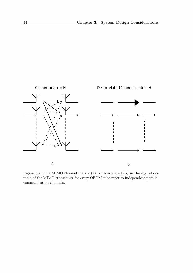
44 Chapter 3. System Design Considerations
Figure 3.2: The MIMO channel matrix (a) is decorrelated (b) in the digital do-main of the MIMO transceiver for every OFDM subcarrier to independent parallelcommunication channels.
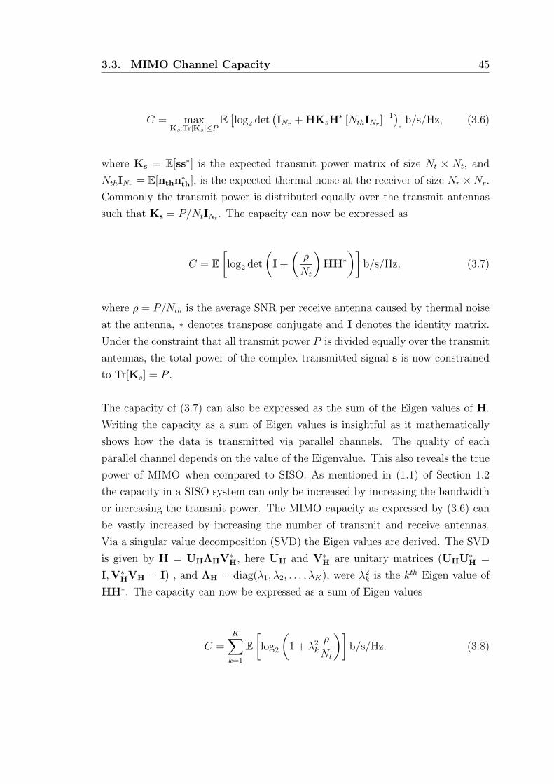
3.3. MIMO Channel Capacity 45
C = maxKs:Tr[Ks]≤P
E[log2 det
(INr + HKsH
∗ [NthINr ]−1)] b/s/Hz, (3.6)
where Ks = E[ss∗] is the expected transmit power matrix of size Nt × Nt, and
NthINr = E[nthn∗th], is the expected thermal noise at the receiver of size Nr ×Nr.
Commonly the transmit power is distributed equally over the transmit antennas
such that Ks = P/NtINt . The capacity can now be expressed as
C = E[log2 det
(I +
(ρ
Nt
)HH∗
)]b/s/Hz, (3.7)
where ρ = P/Nth is the average SNR per receive antenna caused by thermal noise
at the antenna, ∗ denotes transpose conjugate and I denotes the identity matrix.
Under the constraint that all transmit power P is divided equally over the transmit
antennas, the total power of the complex transmitted signal s is now constrained
to Tr[Ks] = P .
The capacity of (3.7) can also be expressed as the sum of the Eigen values of H.
Writing the capacity as a sum of Eigen values is insightful as it mathematically
shows how the data is transmitted via parallel channels. The quality of each
parallel channel depends on the value of the Eigenvalue. This also reveals the true
power of MIMO when compared to SISO. As mentioned in (1.1) of Section 1.2
the capacity in a SISO system can only be increased by increasing the bandwidth
or increasing the transmit power. The MIMO capacity as expressed by (3.6) can
be vastly increased by increasing the number of transmit and receive antennas.
Via a singular value decomposition (SVD) the Eigen values are derived. The SVD
is given by H = UHΛHV∗H, here UH and V∗H are unitary matrices (UHU∗H =
I,V∗HVH = I) , and ΛH = diag(λ1, λ2, . . . , λK), were λ2k is the kth Eigen value of
HH∗. The capacity can now be expressed as a sum of Eigen values
C =K∑k=1
E[log2
(1 + λ2
k
ρ
Nt
)]b/s/Hz. (3.8)
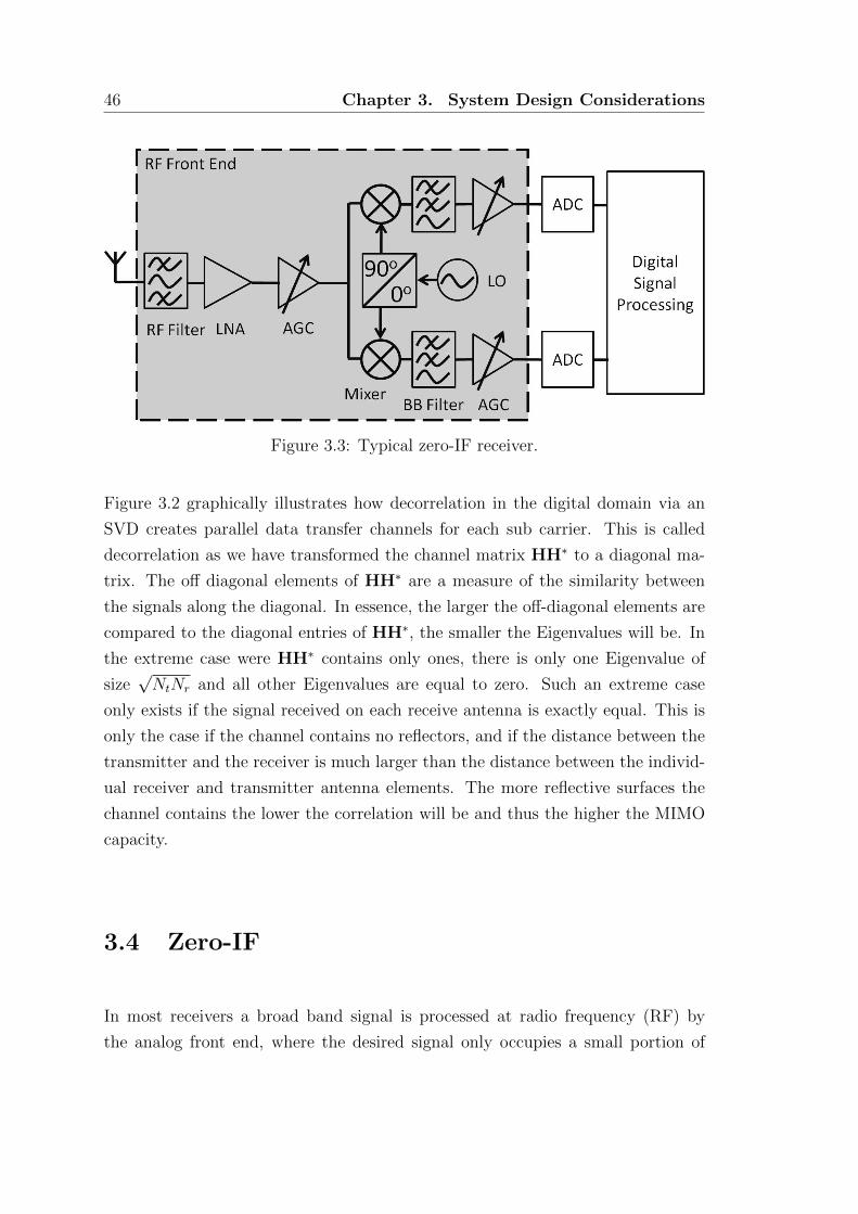
46 Chapter 3. System Design Considerations
Figure 3.3: Typical zero-IF receiver.
Figure 3.2 graphically illustrates how decorrelation in the digital domain via an
SVD creates parallel data transfer channels for each sub carrier. This is called
decorrelation as we have transformed the channel matrix HH∗ to a diagonal ma-
trix. The off diagonal elements of HH∗ are a measure of the similarity between
the signals along the diagonal. In essence, the larger the off-diagonal elements are
compared to the diagonal entries of HH∗, the smaller the Eigenvalues will be. In
the extreme case were HH∗ contains only ones, there is only one Eigenvalue of
size√NtNr and all other Eigenvalues are equal to zero. Such an extreme case
only exists if the signal received on each receive antenna is exactly equal. This is
only the case if the channel contains no reflectors, and if the distance between the
transmitter and the receiver is much larger than the distance between the individ-
ual receiver and transmitter antenna elements. The more reflective surfaces the
channel contains the lower the correlation will be and thus the higher the MIMO
capacity.
3.4 Zero-IF
In most receivers a broad band signal is processed at radio frequency (RF) by
the analog front end, where the desired signal only occupies a small portion of
3.5. Receiver Cascade 47
the front end bandwidth. To present the desired signal to the baseband (BB)
ADC, the analog front end amplifies, down-converts, and filters the received RF
broadband signal. Therefore, the first stages of a receiver usually contain strong
adjacent channel interferers.
Current state-of-the art MIMO receivers use a zero-IF receiver, also known as
a direct conversion receiver, or homodyne receiver. Figure 3.3 depicts a typical
zero IF receiver. The RF front end of a zero-IF receiver consists of a low-noise
amplifier (LNA), a mixer, and a BB output buffer. The automatic gain control
(AGC) behind the LNA prevents saturation of the mixer and BB filter, and the
second AGC prevents clipping of the ADC. In a zero-IF receiver the RF signal
is down converted directly to BB via a mixer [7]. The simplicity of the zero-IF
receiver makes it attractive for compact implementation. One of the benefits of the
zero-IF receiver is that the number of RF components is reduced when compared
to a heterodyne receiver which uses an IF before final down conversion. Another
important benefit is that the BB filter can be a low pass filter with a low Q-factor
which allows for easy integration, without the need for external components. A
benefit over heterodyne receivers is that there is no need for an image rejection
filter. An important downside of direct conversion receivers are the high IP2
requirements, as the IP2 products appear in the IF band. Another downside
of direct conversion receivers is that they are susceptible to I and Q imbalance.
However, the I and Q imbalance can be corrected in the digital domain [48]. An
additional downside of zero-IF receivers is that they are sensitive to DC offset,
and require DC offset compensation. To simplify the receiver design the IEEE
802.11 standard has a zero in the BB equivalent spectrum at DC. Despite the
difficulties of zero-IF receivers, their simplicity and economic benefits have made
them popular and contributed to their widespread use in state-of-the-art receivers.
3.5 Receiver Cascade
As depicted in Figure 3.3 a typical receiver consists of several building blocks.
For a zero-IF receiver the main building blocks are an LNA, a mixer, and an
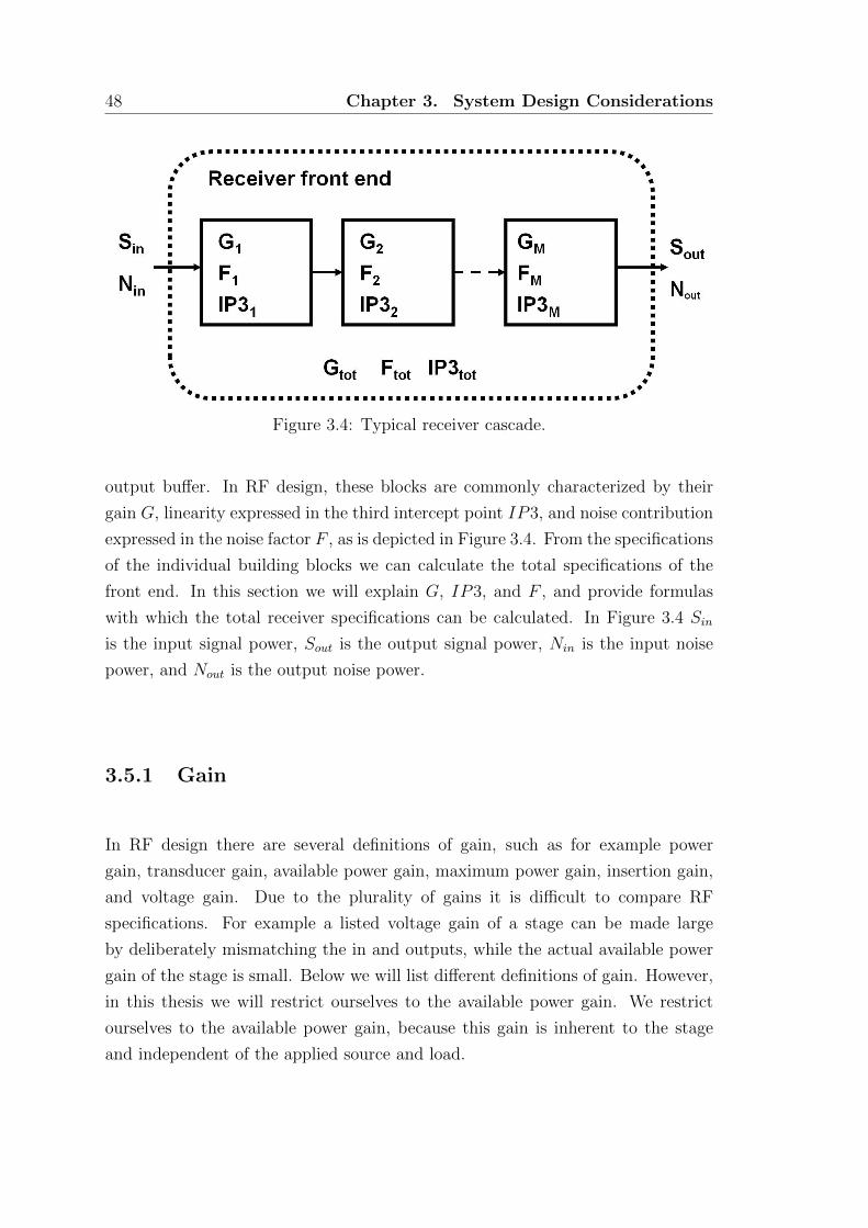
48 Chapter 3. System Design Considerations
Figure 3.4: Typical receiver cascade.
output buffer. In RF design, these blocks are commonly characterized by their
gain G, linearity expressed in the third intercept point IP3, and noise contribution
expressed in the noise factor F , as is depicted in Figure 3.4. From the specifications
of the individual building blocks we can calculate the total specifications of the
front end. In this section we will explain G, IP3, and F , and provide formulas
with which the total receiver specifications can be calculated. In Figure 3.4 Sin
is the input signal power, Sout is the output signal power, Nin is the input noise
power, and Nout is the output noise power.
3.5.1 Gain
In RF design there are several definitions of gain, such as for example power
gain, transducer gain, available power gain, maximum power gain, insertion gain,
and voltage gain. Due to the plurality of gains it is difficult to compare RF
specifications. For example a listed voltage gain of a stage can be made large
by deliberately mismatching the in and outputs, while the actual available power
gain of the stage is small. Below we will list different definitions of gain. However,
in this thesis we will restrict ourselves to the available power gain. We restrict
ourselves to the available power gain, because this gain is inherent to the stage
and independent of the applied source and load.

3.5. Receiver Cascade 49
Available Power Gain
Available power gain, is defined as the maximum power that can be delivered to
the load when the load is matched to the stage, divided by the maximum power
that can be delivered to the stage when the source and stage are matched.
Available Power Gain (G): G =Pload,maxPinput,max
(3.9)
Maximum Power Gain
Maximum power gain is defined as the maximum power that can be delivered to
the load when the load is matched to the stage, divided by the actual power that
is delivered to the stage. By changing the impedance of the source, the maximum
power gain can be changed.
Maximum Power Gain (GM): G =Pload,maxPinput
(3.10)
Transducer Gain
Transducer gain is defined as the actual power that is delivered to the load, divided
by the maximum power that can be delivered to the stage when the source and
stage are matched. By changing the impedance of the load, the transducer gain
can be changed.
Transducer Gain (GT ): GT =Pload
Pinput,max(3.11)

50 Chapter 3. System Design Considerations
Power Gain
Power gain is defined as the actual power that is delivered to the load, divided by
the actual power that is delivered to the stage. By changing the impedance of the
in and output of the stage the power gain can be changed.
Power Gain (GP ): GP =PloadPinput
(3.12)
It is interesting to note that when the input and output of the stage are matched
to the source and load, the available power gain, the maximum power gain, the
transducer gain, and the power gain are equal in value G = GM = GT = GP .
Voltage Gain
Voltage gain is defined as the amplitude of the signal expressed in Volt on the
load, divided by the amplitude of the input signal expressed in Volt. By changing
the in and output impedance the voltage gain is changed as well.
Voltage Gain (GV ): GV =V 2load
V 2input
(3.13)
When the in and output are matched, voltage gain is not necessarily equal to the
available power gain. Voltage gain is only equal to the available power gain when
the in and output are matched, and the in and output impedance is equal.
Insertion Gain
Insertion gain is defined as the actual power that is delivered to the load by the
stage, divided by the actual power that is delivered to the load when the load is

3.5. Receiver Cascade 51
directly connected to the source without the stage in between the load and source.
The insertion gain can be changed by changing the matching of the load compared
to the stage and source.
Insertion Gain (GI): GI =Pload,stagePload,source
(3.14)
Total Gain
The available power gain, only dependents on the stage itself. Because the avail-
able power gain is inherent to the stage itself, it is a suitable measure for stage
comparison. The total available power gain of the analog receiver Gtot (provided
all stages are in and output matched) is given by
Gtot =M∏m=1
Gm, (3.15)
where Gm is the available power gain of the mth stage in the cascade (Figure 3.4).
3.5.2 Linearity
Third-Order Intercept Point
Analog devices are inherently nonlinear. The nonlinearity of a stage is commonly
modeled via the third intercept point IP3 [7]. The third-order intercept point is
based on the theory that a nonlinear system can be modeled as a Taylor series.
The third-order intercept point relates nonlinear products caused by the third order
nonlinear term of the Taylor series to the linearly amplified signal. The third-order
intercept point is defined as the extrapolated point at which the output power of
the third order nonlinearity is equal to the output power of the linearly amplified
signal (Figure 3.5). Normally, an amplifier never reaches the intercept point, as it
commonly lies beyond the output power an amplifier can deliver. Mathematically
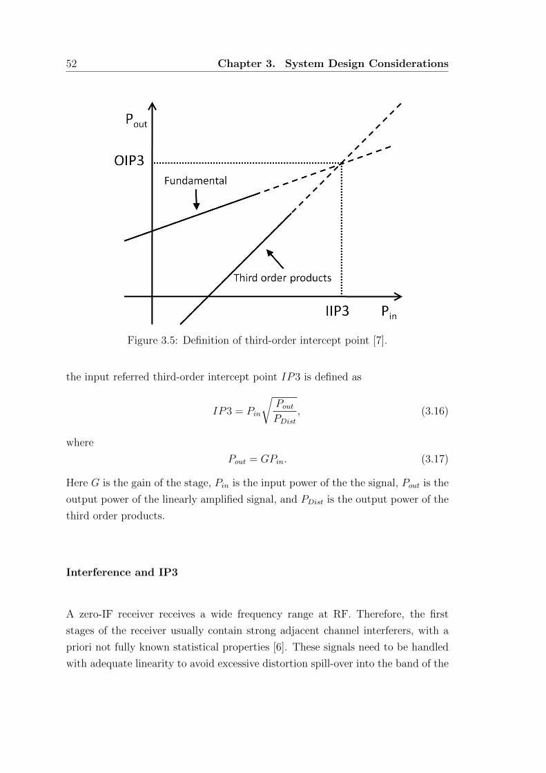
52 Chapter 3. System Design Considerations
Figure 3.5: Definition of third-order intercept point [7].
the input referred third-order intercept point IP3 is defined as
IP3 = Pin
√PoutPDist
, (3.16)
where
Pout = GPin. (3.17)
Here G is the gain of the stage, Pin is the input power of the the signal, Pout is the
output power of the linearly amplified signal, and PDist is the output power of the
third order products.
Interference and IP3
A zero-IF receiver receives a wide frequency range at RF. Therefore, the first
stages of the receiver usually contain strong adjacent channel interferers, with a
priori not fully known statistical properties [6]. These signals need to be handled
with adequate linearity to avoid excessive distortion spill-over into the band of the
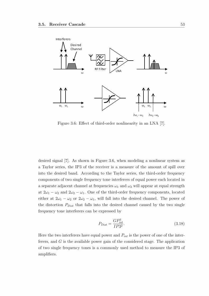
3.5. Receiver Cascade 53
Figure 3.6: Effect of third-order nonlinearity in an LNA [7].
desired signal [7]. As shown in Figure 3.6, when modeling a nonlinear system as
a Taylor series, the IP3 of the receiver is a measure of the amount of spill over
into the desired band. According to the Taylor series, the third-order frequency
components of two single frequency tone interferers of equal power each located in
a separate adjacent channel at frequencies ω1 and ω2 will appear at equal strength
at 2ω1 − ω2 and 2ω2 − ω1. One of the third-order frequency components, located
either at 2ω1 − ω2 or 2ω2 − ω1, will fall into the desired channel. The power of
the distortion PDist that falls into the desired channel caused by the two single
frequency tone interferers can be expressed by
PDist =GP 3
int
IP32. (3.18)
Here the two interferers have equal power and Pint is the power of one of the inter-
ferers, and G is the available power gain of the considered stage. The application
of two single frequency tones is a commonly used method to measure the IP3 of
amplifiers.
54 Chapter 3. System Design Considerations
Total IP3
The total worst case IP3 of M stages can be calculated via [17]
IP3tot =
(M∑m=1
∏m−1j=1 Gj
IP3m
)−1
, (3.19)
under the worst case assumption that all distortion components are in-phase.
To reconstruct the information content of the desired channel, the receiver does
not necessarily need to be linear. As long as all the nonlinearities can be accounted
for in the BB DSP, the information of the desired channel can be recovered. Be-
cause receivers generally need to be low power, the interferers are generally not
sampled, but are filtered by non ideal analog components. Therefore, the statis-
tical properties of interferers are generally not known in the BB-DSP and cannot
be compensated. To prevent excessive spill-over of the interferers into the desired
band, the receiver needs to be linear. However, it is generally known that linearity
comes at a power penalty. Therefore, handling an interferer via additional linear-
ity has a cost in terms of additional receiver circuit power. In Chapter 4 we will
quantify the relation between interference power levels with which the receiver can
cope and receiver circuit power consumption.
3.5.3 Noise Contribution
Next to the distortion signals, the analog front end adds noise to the desired signal.
The noise added by the front end originates from the electronics, and is generally
much larger than the noise of the channel introduced in Section 3.2.4. The addition
of noise by the front end is modeled via the noise figure (NF), and is defined as
NF= 10 log10(Fm). Here, the noise factor Fm is defined for thermal input noise as:
Fm =SNRm
SNRm+1
, (3.20)
3.6. Analog-to-Digital Converter 55
where SNRm is the SNR at the input, and SNRm+1 is the SNR at the output of
the mth stage in a cascade. The total noise-factor of M stages in a cascade, Ftot,
can be calculated via Friis formula
Ftot = 1 +M∑m=1
Fm − 1∏m−1j=1 Gj
, (3.21)
where Fm the noise-factor of the mth stage and Gj the available power gain of the
jth stage. The total noise figure also complies to
Ftot =
(Sin
Nin
)(Sout
Nout
) , (3.22)
where Sin is the input signal power of the receiver, Sout is the output signal power
of the receiver, Nin is the input noise power of the receiver, and Nout is the output
noise power of the receiver.
3.6 Analog-to-Digital Converter
The analog signal is finally presented to the ADC for digitization. To prevent
aliasing, the ADC is required to sample the analog input signal at least at the
Nyquist rate. Because the selectivity of the BB filter of the output buffer is
non-ideal there are unwanted left over frequency components of adjacent channels
which are also sampled by the ADC. To prevent corruption of the desired channel
via aliasing of these unwanted adjacent channel products into the desired channel,
the ADC needs to sample at a higher frequency than the Nyquist rate. Moreover,
the adjacent channel components generally contain more power than the desired
signal. To maintain adequate resolution for the desired channel, additional bits are
required in the ADC. These additional bits are called headroom bits. It should be
noted that in OFDM systems the term headroom is also commonly used to refer
to power back-off due to PAPR. The exact sampling frequency and resolution of
the ADC is therefore a function of the required resolution for the desired channel,
the BB filter selectivity, and the interference power with which the receiver needs
56 Chapter 3. System Design Considerations
to cope [11]. Unfortunately, the power consumption of an ADC is linear in the
sampling rate and exponential in the number of bits. A commonly accepted ADC
power model is,
PADC ∼ κtFs2bADC , (3.23)
where Fs is the sample frequency of the ADC, κt a technology constant and bADC
the number of ADC bits [37] [49]. This ADC power model is related to the ADC
FOM presented in Section 2.2.2. As mentioned in Section 2.2.2, for ADCs which
are limited by thermal noise, the power consumption even scales with twice the
number of effective number of bits. Additional headroom bits and a higher sam-
pling frequency, to deal with high interference power levels, are therefore a costly
solution in terms of ADC power consumption.
3.7 Design Considerations
Both the receiver front end and the ADC require additional dynamic range (DR) to
adequately cope with adjacent channel interference. In most standards the receiver
needs to recover the desired signal at high adjacent channel interferer levels. The
interference-to-carrier ratio (ICR) as specified by IEEE802.11 is around ICR = 40
dB. However, in reality the ICR values are often even higher [50]. The required
additional linearity of the front end comes at increased receiver circuit power. In
Chapter 4 we will quantify the relation between ICR and receiver circuit power, and
show that the ICR requirement dominates the receiver circuit power consumption.
In regard to the ADC, let us assume that at an ICR of 40 dB, the adjacent channel
products that are present at the ADC are 40 dB larger than the desired channel.
To guarantee sufficient resolution for the desired user in the presence of such large
adjacent channel users, additional bits for the ADC are required. In case adjacent
channel users of 40 dB larger than the desired user need to be sampled together
with the desired user, an additional DR in the ADC of 40 dB is required. This
translates to an additional number of bits per ADC of 1/2 log2(104) = 6.64 bits,
resulting via (3.23) to an overal PADC increase of 9900%.
From this simple analysis it is clear that handling interferers is a dominant factor
3.8. Conclusions 57
in receiver circuit and ADC power consumption. As established in Chapter 2 the
receiver circuit and ADC power consumption are expected to be the bottleneck
of future wireless transceiver when extending battery lifetime. As such it makes
sense to focus on interference reduction to reduce receiver circuit and ADC power
consumption.
In Chapter 4 the relation between ICR and receiver circuit power will be presented.
In Chapter 5 we will introduce a practical solution that reduces interference power
in the RF front end to alleviate the ADC and RF requirements in order to reduce
power consumption. Further, in Chapter 5 an IC implementation in 65nm CMOS
is given along with proof of concept measurements. In Chapter 6 algorithms are
given that control the circuit implementation presented in Chapter 5, and the
power savings achieved by the algorithms in terms of ADC bits are quantified.
3.8 Conclusions
OFDM is a popular modulation scheme due to its ability to cope with extreme
channel conditions. However, the PAPR of OFDM requires a power back-off in the
receiver chain, reducing overall system efficiency. Next to the PAPR of OFDM,
interferers pose strong dynamic range requirements on the RF front end and ADC,
making them power hungry. In Chapter 2 we have shown that in the absence of
disruptive new technologies, the RF front end and ADC power consumption are the
future bottlenecks in terms of extending battery lifetime. Mitigating the interferers
and thus the dynamic range requirements of the RF front end and ADC has the
potential to vastly reduce the power consumption of the ADC and RF front end.

58 Chapter 3. System Design Considerations
Chapter 4
Optimum Data Transfer Energy
Efficiency
4.1 Introduction
The motivation to optimize data transfer energy efficiency (bits/Joule) for a re-
ceiver with a limited availability of battery energy is two-fold. As mentioned in
Chapters 2 and 3, in many applications the mobile user spends significantly more
time receiving data than transmitting. Often, the energy consumed in receiving
mode is several orders of magnitudes larger than the energy consumed in transmit
mode [12] [13], even if the transmitter circuit power consumption is larger than the
receiver circuit power consumption when switched on. Secondly, in a short range
link, the transmit power can be relatively small. So the transmit power amplifier
is no longer the main power consumer. Yet, the receiver front end often needs to
recover a weak signal in the presence of strong adjacent channel interference, which
requires highly linear, thus power hungry RF designs. In the absence of disruptive
new approaches, we expect that this trend will continue for the foreseeable future.
This chapter is based on work published in [14–16], and aims to quantify the
relation between carrier-to-interference ratio (CIR) and the receiver circuit power
59

60 Chapter 4. Optimum Data Transfer Energy Efficiency
dissipation. In order to quantify this relation we strive to find an appropriate
operation point for each of the analog stages of a power-constrained receiver, such
that its user data transfer energy efficiency is maximized per Joule of receiver
circuit energy spent. To find the optimum user data transfer energy efficiency we
perform the following steps:
1. We find the lowest receiver circuit power consumption for a given set of
receiver specifications and for a given IC process according to [17].
2. For a given receiver circuit power budget and for a given IC process we
find the maximum throughput expressed in spectral efficiency (bits/s/Hz)
by reformulating the results of step 1.
3. For a given bandwidth we calculate the data transfer energy efficiency (bits/Joule)
of the maximum possible throughput found in step 2 for various receiver cir-
cuit power budgets and CIRs.
4. We use the results of step 3 to find the optimum data transfer energy effi-
ciency and use that result to calculate the relation between receiver circuit
power consumption and CIR.
5. We calculate that at large SNR the most power-efficient receiver (in terms
of Joule/bit) resulting from step 4 operates at a spectral efficiency near 2.3
bits/s/Hz.
The optimum of step 4 appears to depend mainly on the strength of adjacent chan-
nel interference. Therefore, the optimum serves to quantify the relation between
CIR and receiver circuit power dissipation. Too low receiver circuit power would
lead to a highly non-linear receiver, hence strong distortion and low throughput.
Too high values of receiver circuit power would create an unnecessarily linear re-
ceiver, which cannot be exploited because of the finite signal-to-channel-noise ratio
of the received signal. Yet even with very large signal-to-noise ratios, it appears to
be more energy efficient to use a receiver with modest linearity. There appears to
be an optimum choice of the distribution of gain, noise figure and linearity along
the cascade, which yields the highest user data transfer energy efficiency. For very
low available receiver circuit power, our results imply that a duty cycle strategy is
4.1. Introduction 61
more efficient than continuous operation. In these cases the receiver is proposed
to operate in bursts.
A commonly used direct-conversion receiver architecture as presented in Section
3.4 is used in our analysis. As mentioned in Section 3.4, in most receivers a broad
band signal is processed at radio frequency (RF) by the analog front end, where
the desired signal only occupies a small portion of the front end bandwidth. The
analog front end amplifies, down-converts, and filters the received RF broadband
signal in order to present the desired signal to the baseband (BB) ADC. Because
final channel selection usually occurs at a later stage, the first stages of our receiver
usually contains strong adjacent channel interferers, with a priori not fully known
statistical properties [6]. To avoid excessive distortion spill-over into the band of
the desired signal these signals need to be handled with adequate linearity [7].
Generally, a higher linearity requirement leads to a higher power consumption of
the analog circuit. Conventionally, the linearity is fixed in RF designs and specified
for the highest power of the interference at which the receiver should still operate.
This results in an overly linear design at all lower values of the interference power,
reducing battery lifetime unnecessarily. Most RF designs are based on a set of
system specifications, determined by standardization [7], such specifications may
include packet error rates, sensitivity and modulation. An RF designer than strives
to design a receiver at the lowest power possible, for this target [8, 9].
Conversely, we want to determine the maximum data transfer energy efficiency
(bits/Joule) possible in terms of bits/s per unit of available receiver circuit power
budget (Joule/s). To formulate this optimum we do not a priori fix the system
specifications, such as the modulation constellation. Rather, we assume that the
key RF receiver specifications, IP3, gain, and noise figure, are adaptive. The max-
imum data transfer energy efficiency might seem to depend on a large number of
independent variables, but for a given IC process, several design performance indi-
cators have known achievable values [17]. This reduces the number of independent
variables which determine the optimum of the throughput in terms of spectral
efficiency [14]. We conclude that at large SNR, the most power-efficient receiver
(in terms of Joule/bit) will operate near 2.3 bits/s/Hz. We give an expression for
its power consumption in (4.35).

62 Chapter 4. Optimum Data Transfer Energy Efficiency
4.2 Modeling System Data Transfer Energy Ef-
ficiency
To operate a wireless network at the highest data transfer energy efficiency possi-
ble, in terms of bits per second per unit of receiver circuit power, we strive to find
the receiver circuit power Pr at which the throughput T (bits/s/Hz) is maximized
for a given bandwidth B using
Pr = arg maxPr
(max
P1...PM :∑Pm=Pr
(BT
Pr
))[Joule/s]. (4.1)
That is, we search the most efficient receiver circuit power budget. The inner
optimization for a given receiver circuit budget with∑Pm = Pr is given by
T = maxT |∑Pm=Pr [bits/s/Hz], (4.2)
here Pm is the power allocated to the mth stage of a receiver circuit. The maxi-
mum is taken over all possible settings of the RF stages, provided that the total
consumed power does not exceed Pr. We use the capacity expression
T = log2
(1 +
S
Ntot
)[bits/s/Hz], (4.3)
as a measure of achievable throughput T . Here S is the input signal power. Yet,
T should not be interpreted as the Shannon capacity of the system in information
theoretic sense: if the sampling and ADC circuits are allowed to capture the en-
tire band, including the interference signal, the distortion can be predicted by the
BB DSP and its effect can be eliminated, at least from an information theoretical
perspective. Hence one could design a receiver that has higher throughput than
the value found in (4.3). An example of such an architecture is a receiver were the
ADC samples the antenna RF signals directly. However, such a receiver architec-
ture would be at odds with our ambition to minimize the receiver circuit power
consumption. Conventional receiver architectures reduce power consumption by
using analog frequency selectivity to relax the dynamic range requirements of the
front end and the ADC. Lacking a better model, we define the throughput T as
4.2. Modeling System Data Transfer Energy Efficiency 63
in (4.3). The total noise plus distortion, relative to power levels at the input, is
Ntot = Nth +Nr
Gtot
+Nd
Gtot
, (4.4)
where Nth is the noise in the channel, Nr the electronics noise added by the analog
circuits of the receiver, and Nd is the distortion caused by an interferer. Other
RF impairments such as LO leakage, DC leakage and images are not considered,
since they are related to the architecture, topology and layout, which are beyond
the scope of this chapter. The AWGN noise in the channel is defined as in Section
3.2.4 and is given by Nth = kTB. where k = 1.38×10⁻²³ is Boltzmann’s constant,
T is the temperature and B is the bandwidth of the desired signal. Further, Gtot
is the total available power gain of the analog receiver as defined in Section 3.5
and is given by
Gtot =M∏m=1
Gm, (4.5)
where Gm is the gain of the mth stage in the cascade (Figure 4.1). We now need
a more detailed model of Nd and Nr.
4.2.1 Distortion and Noise
Here we recapitulate part of Section 3.5, but contrary to Section 3.5 the interference
is not modeled as two single frequency tones. As mentioned in the introduction of
this chapter, the first stages of our receiver usually contain strong adjacent channel
interferers, with a priori not fully known statistical properties [6]. These signals
need to be handled with adequate linearity to avoid excessive distortion spill-over
into the band of the desired signal [7]. Because the statistical properties of the
interferers are a priori not fully known, the distortion spill-over in the band of
interest is experienced by the receiver as noise. Here, we obtain the distortion
power Nd in (4.4) via the third order input referred intercept point IP3. The IP3
is a measure of the linearity of the analog circuits in the receiver [7]. Total IP3,
IP3tot, is defined as in Section 3.5 and is given by
IP3tot = Pint
√PoutNd
, (4.6)
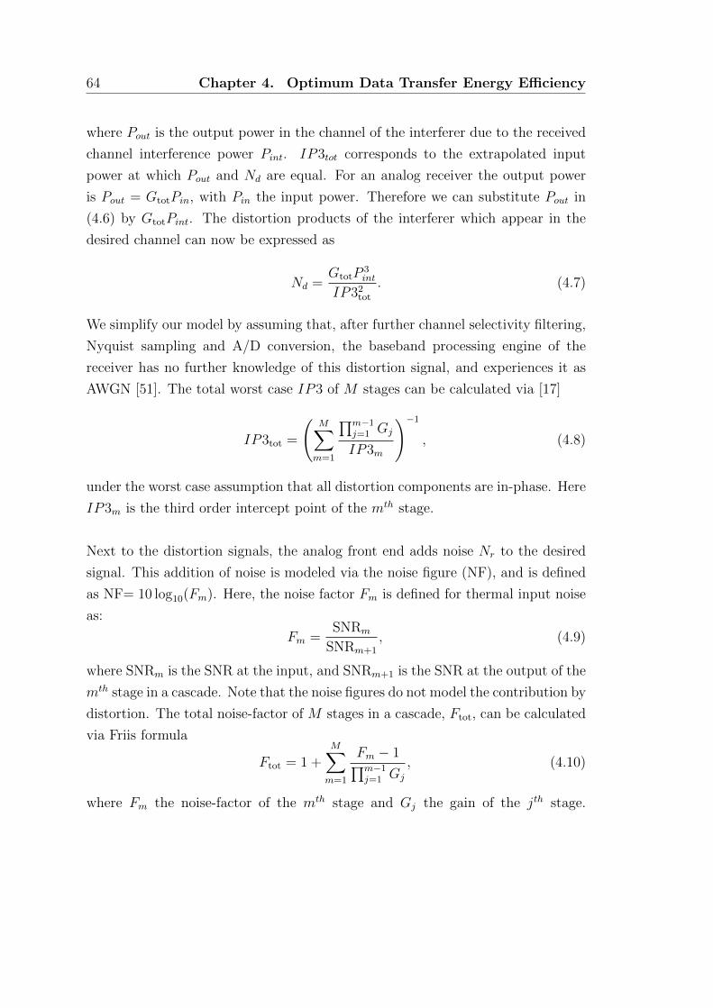
64 Chapter 4. Optimum Data Transfer Energy Efficiency
where Pout is the output power in the channel of the interferer due to the received
channel interference power Pint. IP3tot corresponds to the extrapolated input
power at which Pout and Nd are equal. For an analog receiver the output power
is Pout = GtotPin, with Pin the input power. Therefore we can substitute Pout in
(4.6) by GtotPint. The distortion products of the interferer which appear in the
desired channel can now be expressed as
Nd =GtotP
3int
IP32tot
. (4.7)
We simplify our model by assuming that, after further channel selectivity filtering,
Nyquist sampling and A/D conversion, the baseband processing engine of the
receiver has no further knowledge of this distortion signal, and experiences it as
AWGN [51]. The total worst case IP3 of M stages can be calculated via [17]
IP3tot =
(M∑m=1
∏m−1j=1 Gj
IP3m
)−1
, (4.8)
under the worst case assumption that all distortion components are in-phase. Here
IP3m is the third order intercept point of the mth stage.
Next to the distortion signals, the analog front end adds noise Nr to the desired
signal. This addition of noise is modeled via the noise figure (NF), and is defined
as NF= 10 log10(Fm). Here, the noise factor Fm is defined for thermal input noise
as:
Fm =SNRm
SNRm+1
, (4.9)
where SNRm is the SNR at the input, and SNRm+1 is the SNR at the output of the
mth stage in a cascade. Note that the noise figures do not model the contribution by
distortion. The total noise-factor of M stages in a cascade, Ftot, can be calculated
via Friis formula
Ftot = 1 +M∑m=1
Fm − 1∏m−1j=1 Gj
, (4.10)
where Fm the noise-factor of the mth stage and Gj the gain of the jth stage.
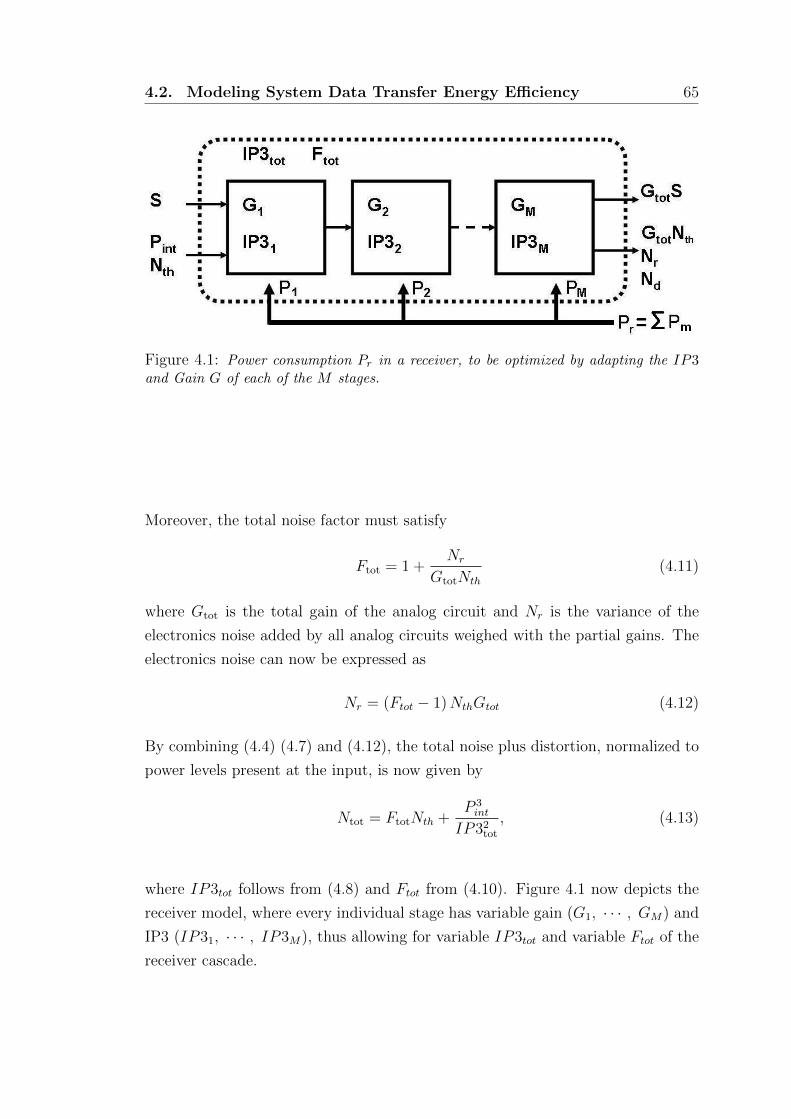
4.2. Modeling System Data Transfer Energy Efficiency 65
Figure 4.1: Power consumption Pr in a receiver, to be optimized by adapting the IP3and Gain G of each of the M stages.
Moreover, the total noise factor must satisfy
Ftot = 1 +Nr
GtotNth
(4.11)
where Gtot is the total gain of the analog circuit and Nr is the variance of the
electronics noise added by all analog circuits weighed with the partial gains. The
electronics noise can now be expressed as
Nr = (Ftot − 1)NthGtot (4.12)
By combining (4.4) (4.7) and (4.12), the total noise plus distortion, normalized to
power levels present at the input, is now given by
Ntot = FtotNth +P 3int
IP32tot
, (4.13)
where IP3tot follows from (4.8) and Ftot from (4.10). Figure 4.1 now depicts the
receiver model, where every individual stage has variable gain (G1, · · · , GM) and
IP3 (IP31, · · · , IP3M), thus allowing for variable IP3tot and variable Ftot of the
receiver cascade.
66 Chapter 4. Optimum Data Transfer Energy Efficiency
4.2.2 Optimum Throughput
To find the optimum data transfer energy efficiency, we first optimize the through-
put for a given receiver circuit power budget. In [14] our aim is to optimize the
power budget Pr over the various stages such that throughput T is optimum un-
der the constraint of a given technology, a given received power S, total gain Gtot
needed to drive the ADC and channel parameters Nth and Pint. In [14] we first
addressed how for a chosen Ftot and IP3tot one can optimize the power budget Pr
by optimally distributing the gains (G1, · · · , GM) and IP3’s (IP31, · · · , IP3M)
over the cascade. In fact, this is a mathematical formalization of a commonly
encountered design problem in RF design, of optimizing each circuit block to meet
a given spec for the receiver. In [17] a double Lagrangian tool is proposed for this
exercise, to solve the distribution of the gains and IP3 for the cascade. Paper [9]
summarizes [17] for M = 2. This Minimum-Power Cascade Optimization (MPCO)
solves:
Pmin = min
(M∑m=1
Pm
), (4.14)
where Pm is the power dissipation of circuit block m, as will be covered by (4.17).
In [14] we extend the MPCO by further optimizing Ftot and IP3tot to satisfy our
end goal of maximizing the throughput, thus searching for
T = maxFtot, IP3tot
(T ) , (4.15)
where the available receiver circuit power Pr, satisfies Pr = Pmin as in (4.14). This
is achieved by expressing the power optimal IP3tot, called IP3tot, as a closed form
function (4.22) of the figure of merits related to the used IC design process, the
available receiver circuit power Pr, the power optimal total noise factor Ftot and
total gain Gtot. Therefore, we can write Ntot as a function of Ftot and the available
receiver circuit power Pr. Our claim is that in the end the maximization in (4.15),
for a given power budget Pr, is equal to minimizing the total noise according to
Ntot = minFtot
(Ntot
(IP3tot(Ftot)
)). (4.16)
We call this a Maximum-Throughput Cascade Optimization Method (MTCO).
4.2. Modeling System Data Transfer Energy Efficiency 67
4.2.3 Minimum-Power Cascade Optimization Method
Linearity Factor Model
A commonly used equivalent figure of merit (EFOM) [17] is
Pm =fmGm IP3m
κm, (4.17)
where fm is the power limiting bandwidth and κm is the power linearity factor of
the mth stage. The most appropriate parameter to choose for fm highly depends
on the circuit functionality. For LNAs with a dominant pole, the bandwidth is an
appropriate choice. By using an EFOM, Pm theoretically does not depend on the
noise figure Fm. By using structure independent transforms (SIT), it is possible
to trade IP3, gain and power dissipation, to transform a chosen topology for each
circuit block to a circuit with the optimal specification [52]. Creating a topology
that can also change IP3 adaptively and stil meet (4.17) is a topic of current IC
design research.
Dual Lagrange Optimization Method
So,
Pmin = minG1, · · · , GM
IP31, · · · , IP3M
(M∑m=1
fmκm
Gm IP3m
), (4.18)
while achieving the Gtot using (4.5), IP3tot using (4.8), and Ftot using (4.10). In
this optimization process, the fm, κm and Fm of a cascade are taken as constant.
The individual Fm is kept constant because the Fm is limited by the topology
and used IC process technology. A closed form expression [17] for the minimal
analog signal conditioning (ASC) power dissipation as a function of the overall

68 Chapter 4. Optimum Data Transfer Energy Efficiency
noise factor Ftot is,
Pmin = IP3tot
(√Fe +
√Fw
(Ftot − F1)
)2
, (4.19)
where the ”weighed excess noise factor” Fw is defined as
Fw =
(M−1∑m=1
3
√fmκm
(Fm+1 − 1)
)3
. (4.20)
Here the excess noise factor of the final stage is
Fe =fMκM
Gtot, (4.21)
which is a fixed value.
4.2.4 Maximum-Throughput Cascade Optimization Method
While (4.19) gives the minimum power Pmin needed to satisfy a required IP3tot,
we can conversely claim that the best IP3tot that one can achieve for a given
available Pr equals
IP3tot = Pr
(√Fe +
√Fw
(Ftot − F1)
)−2
. (4.22)
Now, we can rewrite the total noise (4.4) as a function depending on Ftot, Pint and
Pr
Ntot = FtotNth +P 3int
P 2r
(√Fe +
√Fw
(Ftot−F1)
)4
, (4.23)
By combining (4.2), (4.3), (4.4), and (4.23), we can maximize T by minimizing
Ntot. We require thatdNtot(Ftot)
dFtot
∣∣∣∣Ftot=Ftot
= 0, (4.24)
4.2. Modeling System Data Transfer Energy Efficiency 69
and obtain Ftot as Ftot =
F1 +4Fw(
−√Fe +
√Fe + 25/3
(FwNth
P 2r
P 3int
)1/3)2 . (4.25)
Applying this value of Ftot means that (4.12) turns into Nr/Gtot =
(F1 − 1)Nth + 4FwNth−√Fe+
√Fe+25/3
(FwNth
P2r
P3int
)1/32 ,
(4.26)
and (4.7) turns into Nd/Gtot =
P 3int
P 2r
116
(√Fe +
√Fe + 25/3
(FwNth
P 2r
P 3int
)1/3)4
, (4.27)
which we insert in (4.3) and (4.4). We now have found an analytically closed-form
solution which maximizes the throughput for a given circuit power budget Pr.
We also found closed-form solutions for Ftot and IP3tot that achieve the optimum
throughput, respectively (4.25) and (4.22) with (4.25) inserted. The individual
gain (G1, · · · , GM) and IP3 (IP31, · · · , IP3M) per stage follow from [17]. In
Section 4.3 we give an example of MPCO to motivate our search for the MTCO,
calculating the efficiency in terms of bits/Joule for a target NFtot = 2 dB, with
firstly IP3tot = −40 dBm, and secondly IP3tot = −20 dBm. Surprisingly, in our
scenario, the data transfer energy efficiency at IP3tot = −40 dBm is more than
an order of magnitude larger than at IP3tot = −20 dBm, namely 4.4 Gbit/Joule
and 0.3 Gbit/Joule, respectively. The difference in Pr is 8 dBm (5.9 mW) versus
28 dBm (590 mW), respectively.
4.2.5 Variable Third Order Intercept Point
With increasing interference power Pint both the second and third noise term
in (4.4) will increase. The second term increases, because to mitigate a more
powerful interferer, more linearity is required so noise figure often is sacrificed.
70 Chapter 4. Optimum Data Transfer Energy Efficiency
The third noise contribution increases as a function of Pint, as a more powerful
interferer means more distortion. The only option to meet target specifications is
to make more receiver circuit power available. Conversely, a weaker interferer can
be handled with less power in the analog circuits.
In conventional RF design, the total IP3 is determined by a worst case channel
to interference ratio (CIR) as defined by the standard, where
CIR =S
Pint. (4.28)
An example of a common value for the CIR in the IEEE 802.11b standard at which
the receiver should still operate is -40 dB. However, as mentioned in Section 3.7,
in reality the CIR requirements are often even more stringent [50]. This implies
that a conventional design wastes power to achieve a certain linearity, when the
actual value of the CIR is lower than the worst case.
A variable IP3 setting in the receiver adds an additional degree of freedom and
allows the power consumption of the receiver to lower. The receiver can now adapt
itself to the instantaneous value of the CIR, instead of to the worst case required by
the standard. In the MTCO the optimal throughput of the system as a function
of the available receiver and interference power is calculated. Figure 4.2 shows
the simulation results for the system specifications of Table 4.4, S/Nth = 30 dB,
k = 1.38 × 10⁻²³, T = 295 K, Gtot = 65 dB, and B = 22 MHz. The circuits of
Table 4.4 originate from a circuit library which is given in Tables 4.1, 4.2, and
4.3. In Figure 4.2 it can be seen that a reduction of the CIR of 20 dB allows for a
reduction of the power consumption of 30 dB for a given target rate. The factor32
relation between CIR and Pr follows from (4.7).
This implies that a receiver with adaptive IP3 could opportunistically scale back
the IP3, in the absence of large interferers, to operate in a substantially lower
power mode, potentially orders of magnitudes. We recognize that this can be a
challenge in IC design as changing the IP3 typically also changes in and output
impedances of receiver stages which in turn can lead to a power mismatch, which
can reduce the aforementioned benefits. An implicit relation between interference
and receiver circuit power consumption was reported earlier [6–9,17], but now we

4.2. Modeling System Data Transfer Energy Efficiency 71
have quantified this relation. We have reported this result in literature in [14–16].
4.2.6 Maximum Data Transfer Energy Efficiency
The data transfer energy efficiency observes an optimum, as depicted in Figure
4.3. The location of the optimum is technology-dependent and directly relates to
the linearity factors κ. The optima as in Figure 4.3 are depicted in Figure 4.4 for
different values of CIR. These form a straight line on a logarithmic scale, with an
angle of the line being α = −3dBm2dB
, due to (4.7). Therefore, we only need to find
one optimum to calculate all other optima for different CIR. This relation can be
expressed as
Popt = Popt, 0dB − αCIR, (4.29)
where Popt, 0dB is the optimum at CIR = 0dB and Popt is expressed in dBm and
CIR in dBs.
We now derive the throughput related to the maximum data transfer energy effi-
ciency in Figure 4.3, the throughput T corresponding to
TMT = maxPr
BT
Pr(4.30)
The corresponding value of T is now called the maximum data transfer energy
efficiency throughput TMT . Results are plotted in Figure 4.5. As can be observed
in Figure 4.5, TMT converges to an upper limit for high values of the SNR. For
large values of SNR we can simplify Equation (4.3) with (4.26) and (4.27) inserted
via (4.4) to
limSNR→∞
T = log2
(1 +
SP 2r
P 3int(
fnκnGtot)2
). (4.31)
We are interested in finding TMT . Thus solving
δ
δPr
(log2(1 + αP 2
r )
Pr
)= 0, (4.32)
72 Chapter 4. Optimum Data Transfer Energy Efficiency
where
α =S
P 3int(
fnκnGtot)2
, (4.33)
yields,
2σ − (1 + σ) ln(1 + σ) = 0, (4.34)
where σ = αP 2r . A numerical approximation for σ yields σ = 3.9, and the limit
of TPr at large SNR is TPr = 2.3 bits/s/Hz. The Pr corresponding to TPr at large
SNR, Pr, is given by
Pr =√σ
√P 3int
S
(fnκnGtot
)(4.35)
A conclusion is that we showed the most power efficient receiver in terms of
Joule/bit at large SNR will operate near 2.3 bits/s/Hz and its power consumption
has been calculated in (4.35). Interestingly this limit is independent of the used
IC technology. However, the optimum power efficiency for lower SNR values does
depend on IC technology. At high SNR the receiver is limited by the distortion
noise caused by the interferer. When the power budget of the receiver circuit is
increased the data transfer energy efficiency is initially increased via the MTCO, as
the noise figure is improved which is required to lift the signal above the noise floor.
Increasing the power budget further decreases the data transfer energy efficiency
obtained via MTCO. This is because the data rate can now only be increased
by increasing the linearity. Unfortunately, there is a non-linear relation between
linearity and power consumption which causes the data transfer energy efficiency
to decrease.
We believe this result is significant. A system designer can fix the modulation
and coding method to 2.3 bits/s/Hz irrespective of the channel and interference
conditions. Moreover the transmitter does not need to know the IC technology
used for the receiver, because the optimum is independent of IC technology. The
receiver then adapts G, IP3, but there is no need to adapt transmitter settings.
By fixing the throughput to 2.3 bits/s/Hz we are generally well below the available
channel capacity for high SNR (log2(1+S/Nth)). Therefore, we effectively exchange
excess transmit power of for example a mains powered base station for maximal
receiver circuit data transfer energy efficiency in a handheld device. An additional
argument is that for most wireless network applications, mobile users spend only
4.3. Numerical Results 73
a short amount of time transmitting. Thus the energy consumed for receiving is
orders of magnitudes larger than for transmitting [12] [13]. From this perspective
it makes sense to focus on reducing the receiver circuit energy consumption.
4.2.7 Duty Cycling
A strategy to operate at the optimal data transfer energy efficiency and to achieve
lower average power consumption is duty cycling. The receiver operates at the
optimal data transfer energy efficiency and switches on and off according to the
available circuit power. Via (4.3), (4.4), (4.26), and (4.27) the throughput which
corresponds to the maxima of the data transfer energy efficiency curves in Figure
4.3 is calculated, results are shown in Figure 4.5. Interestingly, the throughput
corresponding to the optimum data transfer energy efficiency is independent of
the CIR. However, the receiver circuit power required to achieve this throughput
is not (Figure 4.4). At large SNR this relation is given by (4.35).
However, in systems with very short duty cycles, the overhead for short packages
can be prohibitive. In such cases there exists a tradeoff between the delay for
merging packets versus the optimal power consumption. Furthermore, at the right
hand side of the optimum, the throughput T expressed in bit/s/Hz can increase by
making more circuit power available. However, the data transfer energy efficiency
BT/Pr expressed in bits/Joule cannot increase if a more power consuming circuit
is used. Designing for better linearity than, the linearity needed to accommodate
a crude modulation of 2.3 bit/s/Hz, does not pay off.
4.3 Numerical Results
We first start with an example of the traditional Minimum Power Cascade Op-
timization (MPCO), and show how this can lead to a non-optimum system in
terms of data transfer energy efficiency. As an example the target specifications
for the MPCO are NFtot = 2 dB, with first IP3tot = −40 dBm, and secondly
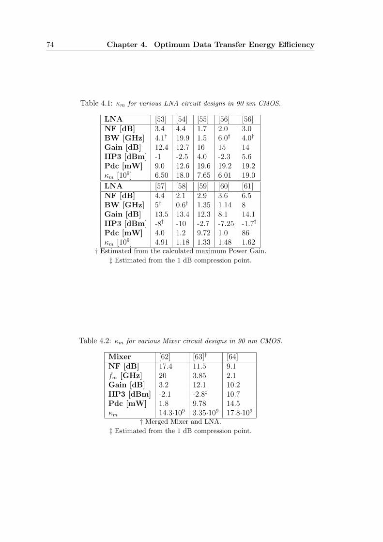
74 Chapter 4. Optimum Data Transfer Energy Efficiency
Table 4.1: κm for various LNA circuit designs in 90 nm CMOS.
LNA [53] [54] [55] [56] [56]NF [dB] 3.4 4.4 1.7 2.0 3.0BW [GHz] 4.1† 19.9 1.5 6.0† 4.0†
Gain [dB] 12.4 12.7 16 15 14IIP3 [dBm] -1 -2.5 4.0 -2.3 5.6Pdc [mW] 9.0 12.6 19.6 19.2 19.2κm [109] 6.50 18.0 7.65 6.01 19.0
LNA [57] [58] [59] [60] [61]NF [dB] 4.4 2.1 2.9 3.6 6.5BW [GHz] 5† 0.6† 1.35 1.14 8Gain [dB] 13.5 13.4 12.3 8.1 14.1IIP3 [dBm] -8‡ -10 -2.7 -7.25 -1.7‡
Pdc [mW] 4.0 1.2 9.72 1.0 86κm [109] 4.91 1.18 1.33 1.48 1.62
† Estimated from the calculated maximum Power Gain.
‡ Estimated from the 1 dB compression point.
Table 4.2: κm for various Mixer circuit designs in 90 nm CMOS.
Mixer [62] [63]† [64]NF [dB] 17.4 11.5 9.1fm [GHz] 20 3.85 2.1Gain [dB] 3.2 12.1 10.2IIP3 [dBm] -2.1 -2.8‡ 10.7Pdc [mW] 1.8 9.78 14.5κm 14.3·109 3.35·109 17.8·109
† Merged Mixer and LNA.
‡ Estimated from the 1 dB compression point.
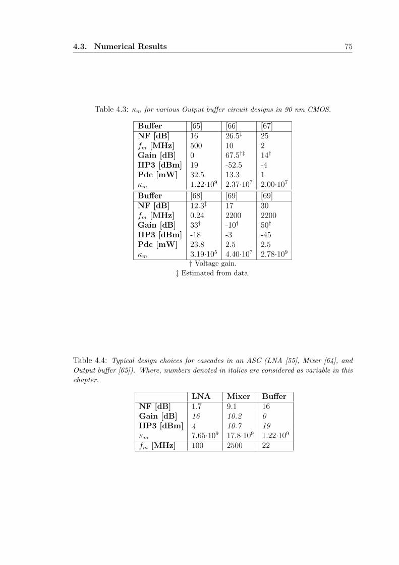
4.3. Numerical Results 75
Table 4.3: κm for various Output buffer circuit designs in 90 nm CMOS.
Buffer [65] [66] [67]NF [dB] 16 26.5‡ 25fm [MHz] 500 10 2Gain [dB] 0 67.5†‡ 14†
IIP3 [dBm] 19 -52.5 -4Pdc [mW] 32.5 13.3 1κm 1.22·109 2.37·107 2.00·107
Buffer [68] [69] [69]NF [dB] 12.3‡ 17 30fm [MHz] 0.24 2200 2200Gain [dB] 33† -10† 50†
IIP3 [dBm] -18 -3 -45Pdc [mW] 23.8 2.5 2.5κm 3.19·105 4.40·107 2.78·109
† Voltage gain.
‡ Estimated from data.
Table 4.4: Typical design choices for cascades in an ASC (LNA [55], Mixer [64], and
Output buffer [65]). Where, numbers denoted in italics are considered as variable in this
chapter.
LNA Mixer BufferNF [dB] 1.7 9.1 16Gain [dB] 16 10.2 0IIP3 [dBm] 4 10.7 19κm 7.65·109 17.8·109 1.22·109
fm [MHz] 100 2500 22
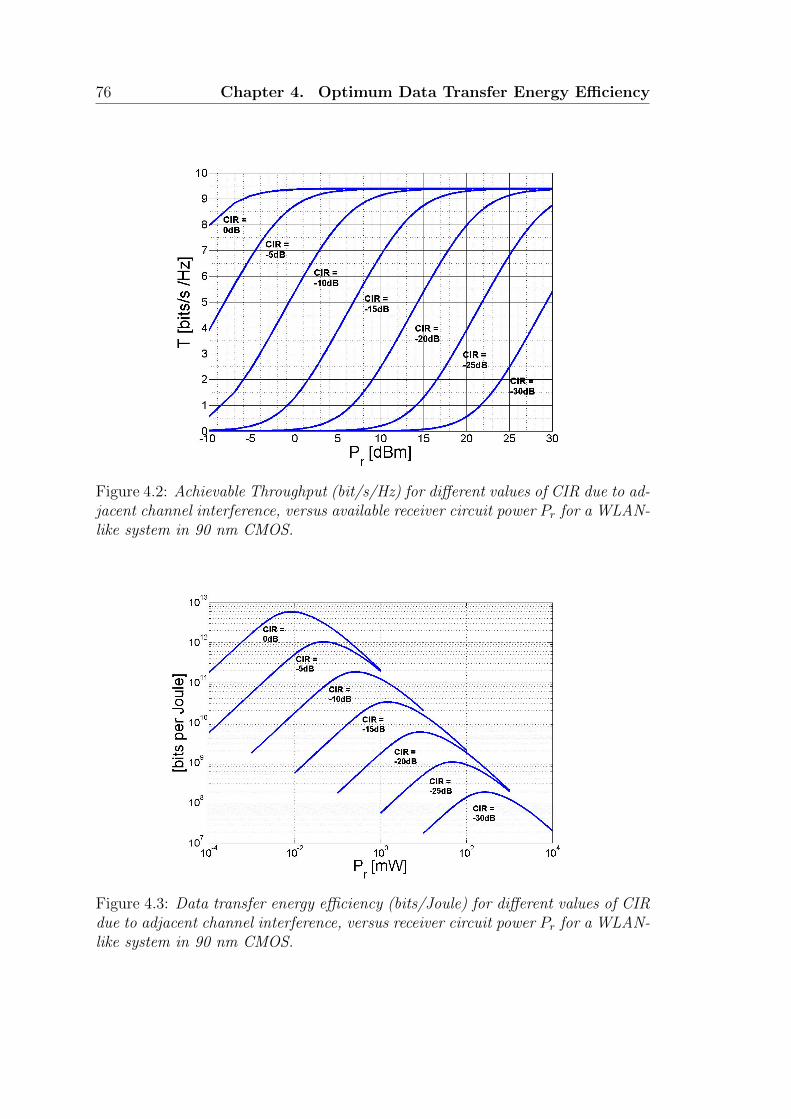
76 Chapter 4. Optimum Data Transfer Energy Efficiency
Figure 4.2: Achievable Throughput (bit/s/Hz) for different values of CIR due to ad-jacent channel interference, versus available receiver circuit power Pr for a WLAN-like system in 90 nm CMOS.
Figure 4.3: Data transfer energy efficiency (bits/Joule) for different values of CIRdue to adjacent channel interference, versus receiver circuit power Pr for a WLAN-like system in 90 nm CMOS.
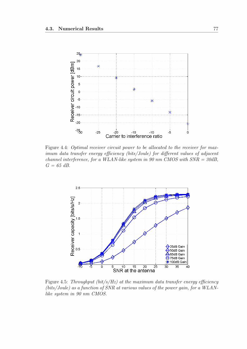
4.3. Numerical Results 77
Figure 4.4: Optimal receiver circuit power to be allocated to the receiver for max-imum data transfer energy efficiency (bits/Joule) for different values of adjacentchannel interference, for a WLAN-like system in 90 nm CMOS with SNR = 30dB,G = 65 dB.
Figure 4.5: Throughput (bit/s/Hz) at the maximum data transfer energy efficiency(bits/Joule) as a function of SNR at various values of the power gain, for a WLAN-like system in 90 nm CMOS.
78 Chapter 4. Optimum Data Transfer Energy Efficiency
IP3tot = −20 dBm. We consider a transmitter that can provide ample S/Nth,
namely of 30 dB. Adjacent channel interference is at + 20 dB, i.e., CIR = −20 dB.
We use the EFOM of Table 4.4 for 90 nm CMOS. Further, T = 295 K, Gtot = 65
dB. The characteristic frequencies fm are chosen to satisfy the frequency require-
ments of an IEEE802.11b system in the 2.4 GHz band, with B = 22 MHz, fm is for
the LNA f1 = 100 MHz, the mixer f2 = 2500 MHz, and the output buffer f3 = 22
MHz. The MPCO gives the power needed to operate this receiver. The result
is very illustrative: The data transfer energy efficiency for a system operating at
IP3tot = −40 dBm is 4.4 Gbit/Joule (T = 1.1 bits/s/Hz, Pr = 8 dBm), and at
IP3tot = −20 dBm it is 0.3 Gbit/Joule (T = 9.2 bits/s/Hz, Pr = 28 dBm). This
motivated our search for a MTCO which results in the optimal setting for NFtot
and IP3tot in terms of maximizing the data transfer energy efficiency.
The closed-form solution for optimum spectral efficiency of the throughput as a
function of available receiver circuit power and for various values of CIR is depicted
in figure 4.2, using (4.3), (4.4), (4.26) and (4.27). For large available receiver power
the throughput approaches the throughput for a signal 30 dB above thermal noise,
and for an LNA with noise figure F1 = 1.7 dB. At small available receiver power,
Nr and Nd become dominant. The figure shows that when the CIR is decreased,
more power is needed to achieve a certain throughput. The closed-form solution
for maximizing throughput can be extended to express the data transfer energy
efficiency in bits per Joule as a function of available receiver power BT/Pr, using
(4.2), (4.3), (4.4), (4.26) and (4.27). The result is depicted in Figure 4.3. When the
CIR is decreased, the efficiency in bits per Joule for a given available receiver power
is decreased as well. The receiver circuit power and throughput corresponding to
the optimum of the data transfer energy efficiency curves in Figure 4.3 are plotted
in Figure 4.4 and 4.5 respectively.
4.4 Conclusions
A closed form analytical solution has been presented which maximizes the data
transfer energy efficiency. From the maximized data transfer energy efficiency all
4.4. Conclusions 79
other receiver system specifications such as IP3 and F can be derived via the
MTCO. Making the IP3 adaptive can substantially improve the power efficiency,
since a 20 dB reduction in CIR requirements results in a 30 dB reduction in re-
ceiver circuit power consumption. Furthermore, the closed form solution allows us
to formalize the relation between interference power and achievable throughput for
a given available receiver circuit power budget. The relation between interference
and receiver circuit power has been known, but we have formalized this relation.
For large SNR the throughput corresponding to the optimal data transfer energy
efficiency is 2.3 bits/s/Hz, irrespective of interference power level. Interestingly
this limit is independent of the used IC technology. However, the optimum power
efficiency for lower SNR values does depend on IC technology. This result has
interesting consequences for new standards and can aid in the design of new stan-
dards and wireless networks to extend battery lifetime, since in typical applications
most energy in mobile devices is consumed by the receiver chain. Therefore, a duty
cycling strategy at low power consumption levels results in a higher system data
transfer energy efficiency. Interestingly, our analysis can be used as a method
to determine whether duty cycling is a good design strategy for low power fixed
receivers in a given technology.

80 Chapter 4. Optimum Data Transfer Energy Efficiency
Chapter 5
ACMM MIMO IC for Analog
Spatial Filtering
5.1 Introduction
The main contribution of this chapter is to report our successful design and im-
plementation of a novel 65nm CMOS 4x4 RF Analog Complex Matrix Multiplier
(ACMM) IC working at 2.4 GHz. This includes the design method, design choices,
the IC implementation challenges, and the attainable circuit performance and its
limitations. The IC is designed for MIMO systems operating in the IEEE 802.11n
standard. However, the principles are applicable to other frequencies and chan-
nel bands. In Chapter 6 we apply the principles to cognitive radio. The theory
supporting this chapter has been published in the signal processing and commu-
nication theory community in [16] [18] and will be introduced and extended in
Chapter 6. This chapter focuses on the novel receiver architecture and its CMOS
implementation. As this dissertation may be read by researchers with a different
background we give an intuitive explanation of the underlying signal processing
principles, to make this chapter self contained, and to explain design choices. The
architecture is described in Section 5.3. Our measurements reported in Section
5.5 are used in Section 5.7 to quantify that the average receiver circuit power can
81
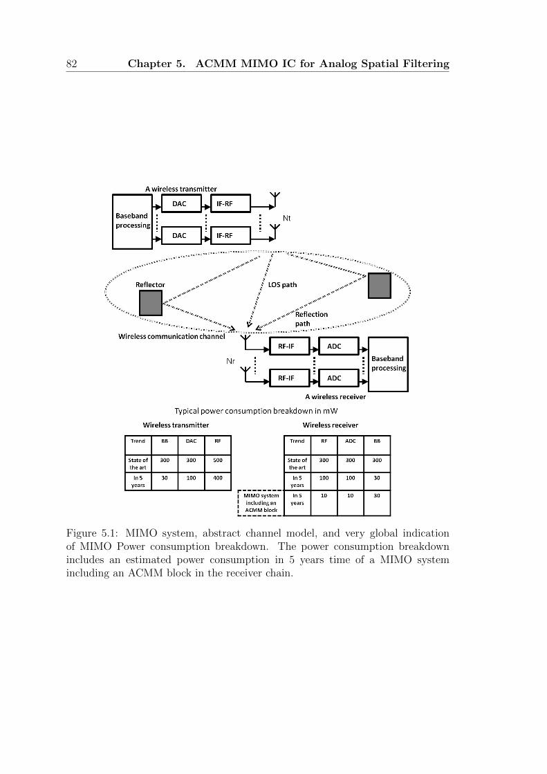
82 Chapter 5. ACMM MIMO IC for Analog Spatial Filtering
Figure 5.1: MIMO system, abstract channel model, and very global indicationof MIMO Power consumption breakdown. The power consumption breakdownincludes an estimated power consumption in 5 years time of a MIMO systemincluding an ACMM block in the receiver chain.
5.1. Introduction 83
be reduced by 90%. Our realization confirms theoretical expectations reported
in [16] [18] [70]. Section 5.8 concludes this chapter.
As mentioned in Chapters 1, 2, and 3, due to an increasing use of wireless com-
munication systems, the cellular and license free spectrum becomes increasingly
congested. Therefore, interference suppression has become of key importance. It is
clear that interference can effectively be filtered in time domain, in code domain, in
frequency domain, in spatial domain, or by combinations thereof. Unfortunately,
the effectiveness of filter selectivity in the analog domain is limited, and increases
power consumption. Many receivers such as in laptops and in mobile phones are
portable and limited in battery power. Thus average energy consumption reduc-
tion to increase battery lifetime is of key importance. Currently, in most systems
the radio frequency (RF) front end and analog-to-digital converter (ADC) need
to handle the interfering users via extra dynamic range (DR) and bandwidth, be-
fore final digital filtering can be performed. The additional DR and bandwidth
requirements of the front end, and the additional DR as well as the additional
sample rate requirements of the ADC, cause increased power consumption. The
DR and sample rate of the ADC depend on the interference power level, both in
and out of band. Determining this DR and sample rate requires a trade off with
the analog filter selectivity [10] [11].
As mentioned in Section 3.3, multiple-input and multiple-output (MIMO) systems
can best exploit their transmit and receive antennas, when they operate in propa-
gation conditions with multiple reflective paths and/or at short distances (Figure
1.1, 1.2 and 5.1). This makes the channel selective both in the frequency and in the
angular domain. Modern MIMO systems exploit the angular selectivity by spa-
tially multiplexing multiple streams from a single user. An intuitive interpretation
is that of transmitting independent data streams, each via a separate mutually
overlapping set of reflective surfaces. Mostly, MIMO systems emit a different
data stream on each available transmit antenna, which creates partly overlapping
radiation patterns. The scattering properties of the channel typically create ran-
dom, partly overlapping, but nonetheless separable directionality patterns for the
different streams. As Figure 3.2 depicts, a form of spatial multiplexing occurs,
which significantly increases the channel capacity. The more orthogonal the vari-
ous streams are upon arrival at the receiver, the more effective decorrelation can
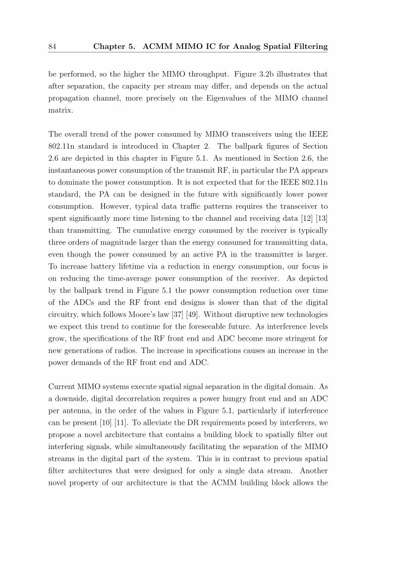
84 Chapter 5. ACMM MIMO IC for Analog Spatial Filtering
be performed, so the higher the MIMO throughput. Figure 3.2b illustrates that
after separation, the capacity per stream may differ, and depends on the actual
propagation channel, more precisely on the Eigenvalues of the MIMO channel
matrix.
The overall trend of the power consumed by MIMO transceivers using the IEEE
802.11n standard is introduced in Chapter 2. The ballpark figures of Section
2.6 are depicted in this chapter in Figure 5.1. As mentioned in Section 2.6, the
instantaneous power consumption of the transmit RF, in particular the PA appears
to dominate the power consumption. It is not expected that for the IEEE 802.11n
standard, the PA can be designed in the future with significantly lower power
consumption. However, typical data traffic patterns requires the transceiver to
spent significantly more time listening to the channel and receiving data [12] [13]
than transmitting. The cumulative energy consumed by the receiver is typically
three orders of magnitude larger than the energy consumed for transmitting data,
even though the power consumed by an active PA in the transmitter is larger.
To increase battery lifetime via a reduction in energy consumption, our focus is
on reducing the time-average power consumption of the receiver. As depicted
by the ballpark trend in Figure 5.1 the power consumption reduction over time
of the ADCs and the RF front end designs is slower than that of the digital
circuitry, which follows Moore’s law [37] [49]. Without disruptive new technologies
we expect this trend to continue for the foreseeable future. As interference levels
grow, the specifications of the RF front end and ADC become more stringent for
new generations of radios. The increase in specifications causes an increase in the
power demands of the RF front end and ADC.
Current MIMO systems execute spatial signal separation in the digital domain. As
a downside, digital decorrelation requires a power hungry front end and an ADC
per antenna, in the order of the values in Figure 5.1, particularly if interference
can be present [10] [11]. To alleviate the DR requirements posed by interferers, we
propose a novel architecture that contains a building block to spatially filter out
interfering signals, while simultaneously facilitating the separation of the MIMO
streams in the digital part of the system. This is in contrast to previous spatial
filter architectures that were designed for only a single data stream. Another
novel property of our architecture is that the ACMM building block allows the
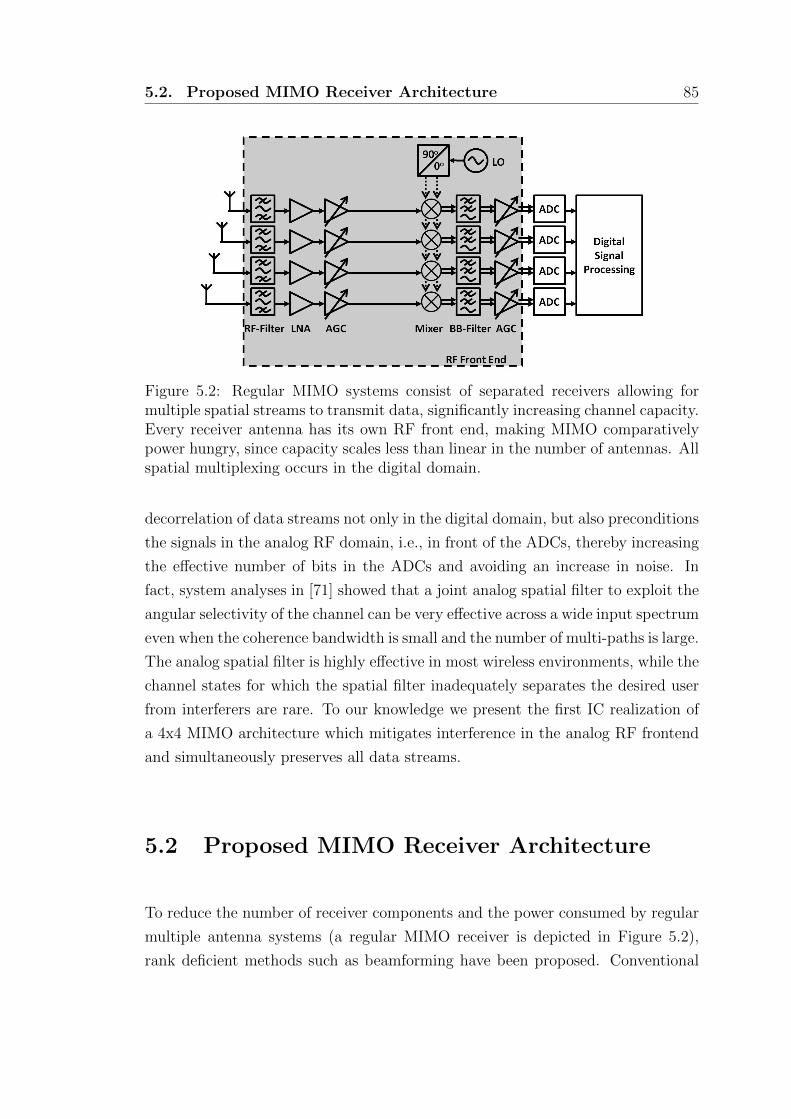
5.2. Proposed MIMO Receiver Architecture 85
Figure 5.2: Regular MIMO systems consist of separated receivers allowing formultiple spatial streams to transmit data, significantly increasing channel capacity.Every receiver antenna has its own RF front end, making MIMO comparativelypower hungry, since capacity scales less than linear in the number of antennas. Allspatial multiplexing occurs in the digital domain.
decorrelation of data streams not only in the digital domain, but also preconditions
the signals in the analog RF domain, i.e., in front of the ADCs, thereby increasing
the effective number of bits in the ADCs and avoiding an increase in noise. In
fact, system analyses in [71] showed that a joint analog spatial filter to exploit the
angular selectivity of the channel can be very effective across a wide input spectrum
even when the coherence bandwidth is small and the number of multi-paths is large.
The analog spatial filter is highly effective in most wireless environments, while the
channel states for which the spatial filter inadequately separates the desired user
from interferers are rare. To our knowledge we present the first IC realization of
a 4x4 MIMO architecture which mitigates interference in the analog RF frontend
and simultaneously preserves all data streams.
5.2 Proposed MIMO Receiver Architecture
To reduce the number of receiver components and the power consumed by regular
multiple antenna systems (a regular MIMO receiver is depicted in Figure 5.2),
rank deficient methods such as beamforming have been proposed. Conventional
86 Chapter 5. ACMM MIMO IC for Analog Spatial Filtering
Figure 5.3: A beamformer reduces the number of mixers and ADCs required andallows for spatial filtering to alleviate the dynamic range requirements in an ADC.Since a beamformer is essentially a rank reduction only a single data stream ispossible resulting in significant channel capacity loss.
Figure 5.4: Block diagram of ACMM in a MIMO receiver. The ACMM is a fullrank matrix operation which allows for multiple independent beamforms simulta-neously. Multiple data streams and spatial filtering of interferers are supportedsimultaneously.
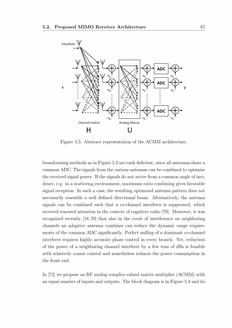
5.2. Proposed MIMO Receiver Architecture 87
Figure 5.5: Abstract representation of the ACMM architecture.
beamforming methods as in Figure 5.3 are rank deficient, since all antennas share a
common ADC. The signals from the various antennas can be combined to optimize
the received signal power. If the signals do not arrive from a common angle of inci-
dence, e.g. in a scattering environment, maximum ratio combining gives favorable
signal reception. In such a case, the resulting optimized antenna pattern does not
necessarily resemble a well defined directional beam. Alternatively, the antenna
signals can be combined such that a co-channel interferer is suppressed, which
received renewed attention in the context of cognitive radio [70]. Moreover, it was
recognized recently [18, 70] that also in the event of interference on neighboring
channels an adaptive antenna combiner can reduce the dynamic range require-
ments of the common ADC significantly. Perfect nulling of a dominant co-channel
interferer requires highly accurate phase control in every branch. Yet, reduction
of the power of a neighboring channel interferer by a few tens of dBs is feasible
with relatively coarse control and nonetheless reduces the power consumption in
the front end.
In [72] we propose an RF analog complex-valued matrix multiplier (ACMM) with
an equal number of inputs and outputs. The block diagram is in Figure 5.4 and its
88 Chapter 5. ACMM MIMO IC for Analog Spatial Filtering
signal processing model is in Figure 5.5. Instead of reducing the vector signal to
a single component, as in regular beamforming, our ACMM has multiple outputs,
each of which is offered to the baseband MIMO processor. The RF stages adapt to
the current state of the propagation and interference, under adaptive control via
a baseband (BB) feedback loop. Since the ACMM reduces the interference power,
the analog stages and the ADCs behind the ACMM can be operated at a low
power consumption setting, while maintaining a throughput that is comparable to
a regular digital MIMO system, i.e., as in Figure 5.2. In this way, our proposed
architecture not only alleviates the power-hungry dynamic range requirements of
the ADC, but also preconditions the analog wanted signal components to optimally
excite the ADCs. This results in significant receiver power reduction, as predicted
in [18] [70]. Hence, our architecture performs a non-critical part of the signal
separation processing in the analog domain, so that it reduces the total power
consumption.
When exploiting the angular selectivity of the channel, every ACMM output can
be interpreted as a differently beamformed combination of the inputs. Typically,
the digital BB estimation algorithm performs a blind estimation. Similarly, the
algorithm used in our measurements is an adaptation of the one used in [18] and
performs its channel estimation based on the matrix outputs seen at the ADCs.
Since the ACMM restricts itself to phase shifting and amplification, which may
have occurred naturally in some scattering propagation environment, the sepa-
ration algorithms in the digital domain itself only require minor modifications,
compared to traditional MIMO without ACMM. However, an additional control
loop is needed to adapt the ACMM parameters, and their estimation. The con-
version of the digital control into settings of the analog circuits has been part of
our design. Due to the oversampling rate of the ADCs and the non ideal selectiv-
ity of the analog filter, frequency products containing angular information of the
interference are available in the digital domain, and can be used in the digital BB
estimation.
For an intuitive understanding of a MIMO receiver in combination with the novel
ACMM building block, we can interpret each of the four resulting beam patterns
as an appropriate compromise between focusing on a unique Eigenvalue (or unique
data stream) in the MIMO channel and suppressing interferers. Effectively, the
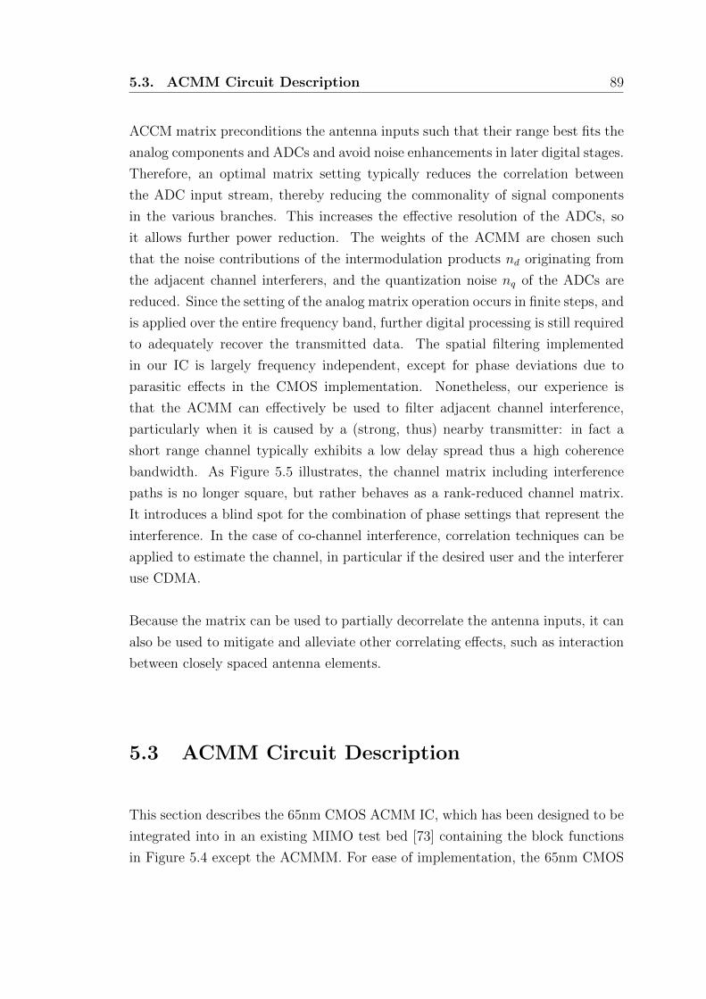
5.3. ACMM Circuit Description 89
ACCM matrix preconditions the antenna inputs such that their range best fits the
analog components and ADCs and avoid noise enhancements in later digital stages.
Therefore, an optimal matrix setting typically reduces the correlation between
the ADC input stream, thereby reducing the commonality of signal components
in the various branches. This increases the effective resolution of the ADCs, so
it allows further power reduction. The weights of the ACMM are chosen such
that the noise contributions of the intermodulation products nd originating from
the adjacent channel interferers, and the quantization noise nq of the ADCs are
reduced. Since the setting of the analog matrix operation occurs in finite steps, and
is applied over the entire frequency band, further digital processing is still required
to adequately recover the transmitted data. The spatial filtering implemented
in our IC is largely frequency independent, except for phase deviations due to
parasitic effects in the CMOS implementation. Nonetheless, our experience is
that the ACMM can effectively be used to filter adjacent channel interference,
particularly when it is caused by a (strong, thus) nearby transmitter: in fact a
short range channel typically exhibits a low delay spread thus a high coherence
bandwidth. As Figure 5.5 illustrates, the channel matrix including interference
paths is no longer square, but rather behaves as a rank-reduced channel matrix.
It introduces a blind spot for the combination of phase settings that represent the
interference. In the case of co-channel interference, correlation techniques can be
applied to estimate the channel, in particular if the desired user and the interferer
use CDMA.
Because the matrix can be used to partially decorrelate the antenna inputs, it can
also be used to mitigate and alleviate other correlating effects, such as interaction
between closely spaced antenna elements.
5.3 ACMM Circuit Description
This section describes the 65nm CMOS ACMM IC, which has been designed to be
integrated into in an existing MIMO test bed [73] containing the block functions
in Figure 5.4 except the ACMMM. For ease of implementation, the 65nm CMOS
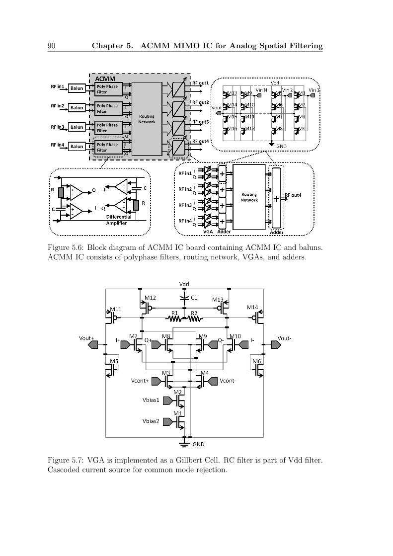
90 Chapter 5. ACMM MIMO IC for Analog Spatial Filtering
Figure 5.6: Block diagram of ACMM IC board containing ACMM IC and baluns.ACMM IC consists of polyphase filters, routing network, VGAs, and adders.
Figure 5.7: VGA is implemented as a Gillbert Cell. RC filter is part of Vdd filter.Cascoded current source for common mode rejection.
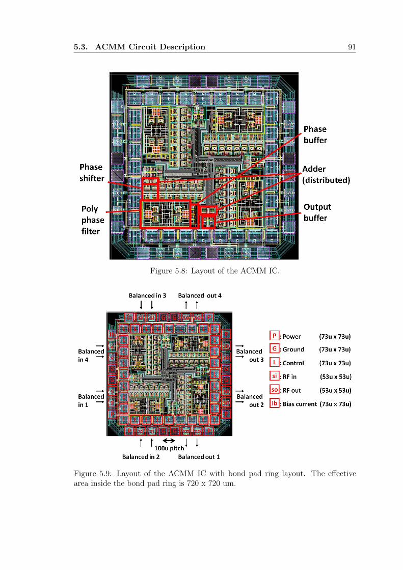
5.3. ACMM Circuit Description 91
Figure 5.8: Layout of the ACMM IC.
Figure 5.9: Layout of the ACMM IC with bond pad ring layout. The effectivearea inside the bond pad ring is 720 x 720 um.
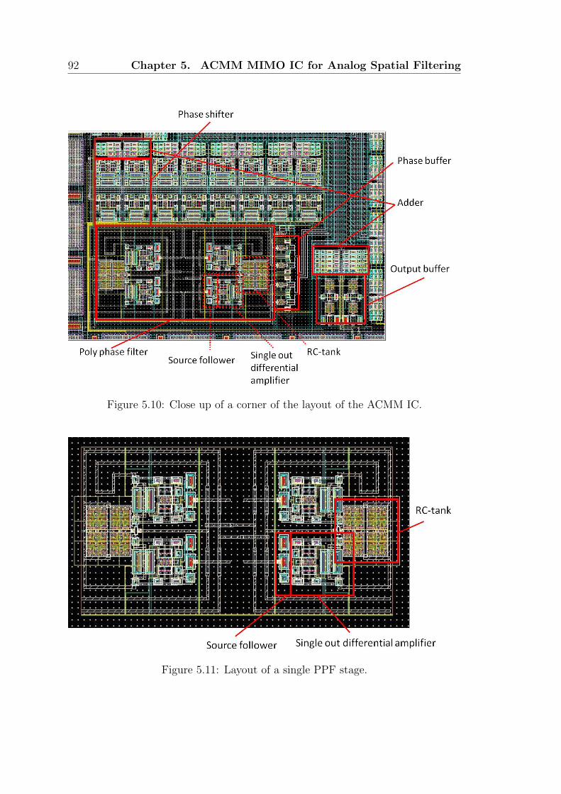
92 Chapter 5. ACMM MIMO IC for Analog Spatial Filtering
Figure 5.10: Close up of a corner of the layout of the ACMM IC.
Figure 5.11: Layout of a single PPF stage.
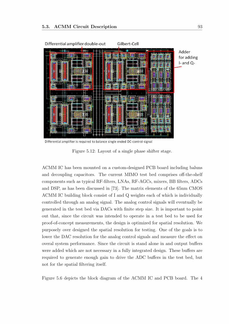
5.3. ACMM Circuit Description 93
Figure 5.12: Layout of a single phase shifter stage.
ACMM IC has been mounted on a custom-designed PCB board including baluns
and decoupling capacitors. The current MIMO test bed comprises off-the-shelf
components such as typical RF-filters, LNAs, RF-AGCs, mixers, BB filters, ADCs
and DSP, as has been discussed in [73]. The matrix elements of the 65nm CMOS
ACMM IC building block consist of I and Q weights each of which is individually
controlled through an analog signal. The analog control signals will eventually be
generated in the test bed via DACs with finite step size. It is important to point
out that, since the circuit was intended to operate in a test bed to be used for
proof-of-concept measurements, the design is optimized for spatial resolution. We
purposely over designed the spatial resolution for testing. One of the goals is to
lower the DAC resolution for the analog control signals and measure the effect on
overal system performance. Since the circuit is stand alone in and output buffers
were added which are not necessary in a fully integrated design. These buffers are
required to generate enough gain to drive the ADC buffers in the test bed, but
not for the spatial filtering itself.
Figure 5.6 depicts the block diagram of the ACMM IC and PCB board. The 4
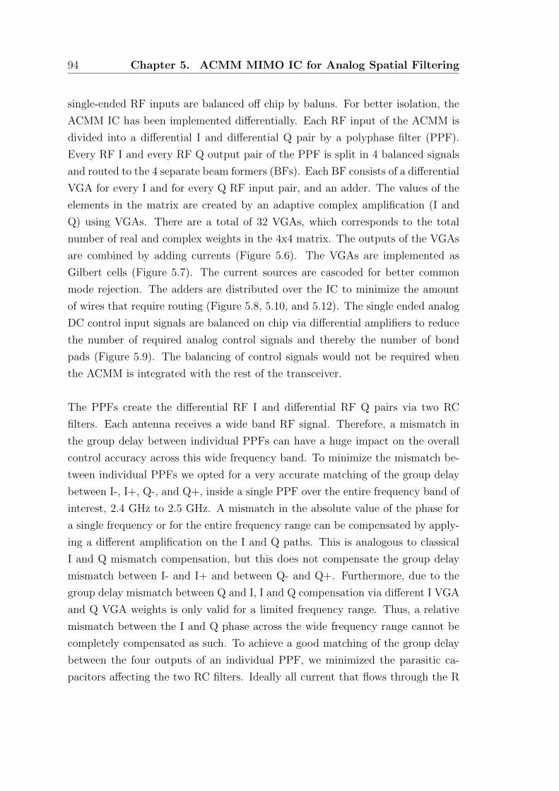
94 Chapter 5. ACMM MIMO IC for Analog Spatial Filtering
single-ended RF inputs are balanced off chip by baluns. For better isolation, the
ACMM IC has been implemented differentially. Each RF input of the ACMM is
divided into a differential I and differential Q pair by a polyphase filter (PPF).
Every RF I and every RF Q output pair of the PPF is split in 4 balanced signals
and routed to the 4 separate beam formers (BFs). Each BF consists of a differential
VGA for every I and for every Q RF input pair, and an adder. The values of the
elements in the matrix are created by an adaptive complex amplification (I and
Q) using VGAs. There are a total of 32 VGAs, which corresponds to the total
number of real and complex weights in the 4x4 matrix. The outputs of the VGAs
are combined by adding currents (Figure 5.6). The VGAs are implemented as
Gilbert cells (Figure 5.7). The current sources are cascoded for better common
mode rejection. The adders are distributed over the IC to minimize the amount
of wires that require routing (Figure 5.8, 5.10, and 5.12). The single ended analog
DC control input signals are balanced on chip via differential amplifiers to reduce
the number of required analog control signals and thereby the number of bond
pads (Figure 5.9). The balancing of control signals would not be required when
the ACMM is integrated with the rest of the transceiver.
The PPFs create the differential RF I and differential RF Q pairs via two RC
filters. Each antenna receives a wide band RF signal. Therefore, a mismatch in
the group delay between individual PPFs can have a huge impact on the overall
control accuracy across this wide frequency band. To minimize the mismatch be-
tween individual PPFs we opted for a very accurate matching of the group delay
between I-, I+, Q-, and Q+, inside a single PPF over the entire frequency band of
interest, 2.4 GHz to 2.5 GHz. A mismatch in the absolute value of the phase for
a single frequency or for the entire frequency range can be compensated by apply-
ing a different amplification on the I and Q paths. This is analogous to classical
I and Q mismatch compensation, but this does not compensate the group delay
mismatch between I- and I+ and between Q- and Q+. Furthermore, due to the
group delay mismatch between Q and I, I and Q compensation via different I VGA
and Q VGA weights is only valid for a limited frequency range. Thus, a relative
mismatch between the I and Q phase across the wide frequency range cannot be
completely compensated as such. To achieve a good matching of the group delay
between the four outputs of an individual PPF, we minimized the parasitic ca-
pacitors affecting the two RC filters. Ideally all current that flows through the R
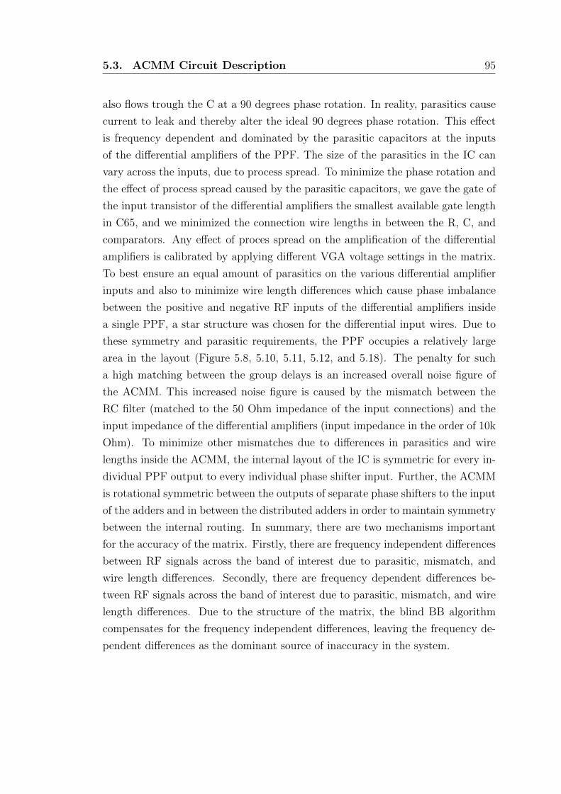
5.3. ACMM Circuit Description 95
also flows trough the C at a 90 degrees phase rotation. In reality, parasitics cause
current to leak and thereby alter the ideal 90 degrees phase rotation. This effect
is frequency dependent and dominated by the parasitic capacitors at the inputs
of the differential amplifiers of the PPF. The size of the parasitics in the IC can
vary across the inputs, due to process spread. To minimize the phase rotation and
the effect of process spread caused by the parasitic capacitors, we gave the gate of
the input transistor of the differential amplifiers the smallest available gate length
in C65, and we minimized the connection wire lengths in between the R, C, and
comparators. Any effect of proces spread on the amplification of the differential
amplifiers is calibrated by applying different VGA voltage settings in the matrix.
To best ensure an equal amount of parasitics on the various differential amplifier
inputs and also to minimize wire length differences which cause phase imbalance
between the positive and negative RF inputs of the differential amplifiers inside
a single PPF, a star structure was chosen for the differential input wires. Due to
these symmetry and parasitic requirements, the PPF occupies a relatively large
area in the layout (Figure 5.8, 5.10, 5.11, 5.12, and 5.18). The penalty for such
a high matching between the group delays is an increased overall noise figure of
the ACMM. This increased noise figure is caused by the mismatch between the
RC filter (matched to the 50 Ohm impedance of the input connections) and the
input impedance of the differential amplifiers (input impedance in the order of 10k
Ohm). To minimize other mismatches due to differences in parasitics and wire
lengths inside the ACMM, the internal layout of the IC is symmetric for every in-
dividual PPF output to every individual phase shifter input. Further, the ACMM
is rotational symmetric between the outputs of separate phase shifters to the input
of the adders and in between the distributed adders in order to maintain symmetry
between the internal routing. In summary, there are two mechanisms important
for the accuracy of the matrix. Firstly, there are frequency independent differences
between RF signals across the band of interest due to parasitic, mismatch, and
wire length differences. Secondly, there are frequency dependent differences be-
tween RF signals across the band of interest due to parasitic, mismatch, and wire
length differences. Due to the structure of the matrix, the blind BB algorithm
compensates for the frequency independent differences, leaving the frequency de-
pendent differences as the dominant source of inaccuracy in the system.
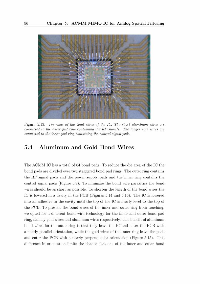
96 Chapter 5. ACMM MIMO IC for Analog Spatial Filtering
Figure 5.13: Top view of the bond wires of the IC. The short aluminum wires areconnected to the outer pad ring containing the RF signals. The longer gold wires areconnected to the inner pad ring containing the control signal pads.
5.4 Aluminum and Gold Bond Wires
The ACMM IC has a total of 64 bond pads. To reduce the die area of the IC the
bond pads are divided over two staggered bond pad rings. The outer ring contains
the RF signal pads and the power supply pads and the inner ring contains the
control signal pads (Figure 5.9). To minimize the bond wire parasitics the bond
wires should be as short as possible. To shorten the length of the bond wires the
IC is lowered in a cavity in the PCB (Figures 5.14 and 5.15). The IC is lowered
into an adhesive in the cavity until the top of the IC is nearly level to the top of
the PCB. To prevent the bond wires of the inner and outer ring from touching,
we opted for a different bond wire technology for the inner and outer bond pad
ring, namely gold wires and aluminum wires respectively. The benefit of aluminum
bond wires for the outer ring is that they leave the IC and enter the PCB with
a nearly parallel orientation, while the gold wires of the inner ring leave the pads
and enter the PCB with a nearly perpendicular orientation (Figure 5.15). This
difference in orientation limits the chance that one of the inner and outer bond
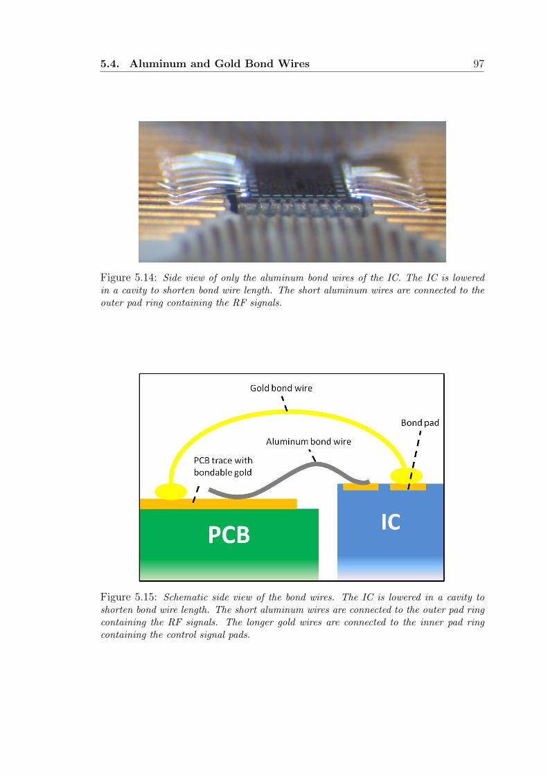
5.4. Aluminum and Gold Bond Wires 97
Figure 5.14: Side view of only the aluminum bond wires of the IC. The IC is loweredin a cavity to shorten bond wire length. The short aluminum wires are connected to theouter pad ring containing the RF signals.
Figure 5.15: Schematic side view of the bond wires. The IC is lowered in a cavity toshorten bond wire length. The short aluminum wires are connected to the outer pad ringcontaining the RF signals. The longer gold wires are connected to the inner pad ringcontaining the control signal pads.

98 Chapter 5. ACMM MIMO IC for Analog Spatial Filtering
wires touch each other. Due to the small pitch of the bond pads and the limits of
the aluminum bond wire machine, the aluminum bond wires are attached inversely
to the standard procedure. The benefit of wiring the aluminum bonds inversely
is that the excess tab of the aluminum wires is at the side of the PCB (Figure
5.14). Since the bond wires are fanning out, having the tab of the aluminum wires
at the IC side could have caused the tabs of separate wires to touch each other.
By lowering the IC into the cavity and by using aluminum bonds which leave and
enter parallel to the IC and PCB, the RF bond wire lengths are reduced from 3
mm to 0.8 mm.
5.5 Measurement Results
The spatial resolution and nulling precision is limited by the accuracy with which
the phase shifts and amplitudes of the matrix elements can be controlled. In our
system, the accuracy of the phase and amplitude setting is further determined
by deviations from a true-time delay for different matrix elements, so these are
susceptible to slope deviations in the group delay. The parasitics, mismatch, and
wire length differences inside the PPF cause a slight imbalance in the group delay
of I- and I+, and Q- and Q+. This causes an error in the differences of the phase
shift over the band of different matrix elements which are added at every output.
The left hand side of Figure 5.16 depicts a screenshot of a typical S-parameter
measurement of a single setting for a single matrix element. As can be seen the
input matching, indicated by S11, of the IC and PCB board is -23 dB in the band
of interest. In the measurement the scale of the y-axes is 20 dB per unit. The S11
measurement shows that, as was expected, the input matching of the RC filter is
poor at low frequencies, where the C acts as an open, while at higher frequencies
we can see the effect of the R. Further, the measured S22 output matching is -16
dB in the band of interest, the S12 is -80 dB, and the S21 is used to measure the
phase over the band of interest.
The measured maximum difference in the expected value of the phase, originating
from deviations in the group delays, in a PPF determines the resolution with which
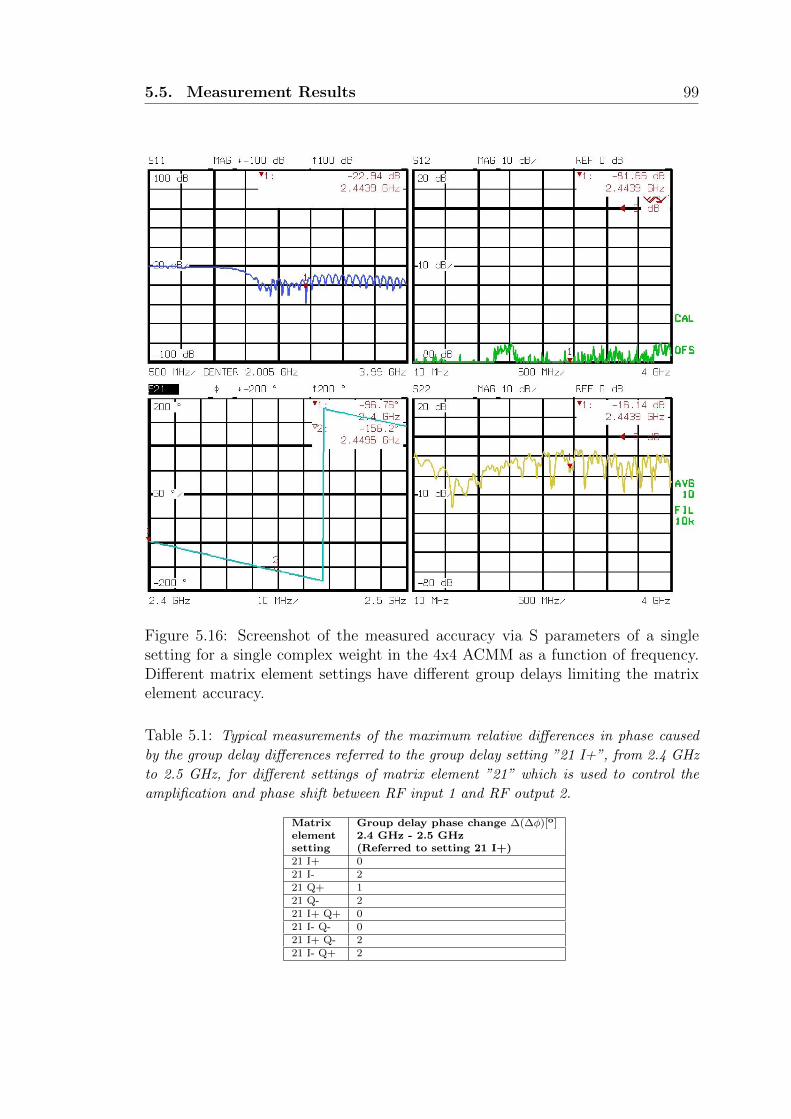
5.5. Measurement Results 99
Figure 5.16: Screenshot of the measured accuracy via S parameters of a singlesetting for a single complex weight in the 4x4 ACMM as a function of frequency.Different matrix element settings have different group delays limiting the matrixelement accuracy.
Table 5.1: Typical measurements of the maximum relative differences in phase caused
by the group delay differences referred to the group delay setting ”21 I+”, from 2.4 GHz
to 2.5 GHz, for different settings of matrix element ”21” which is used to control the
amplification and phase shift between RF input 1 and RF output 2.
Matrix Group delay phase change ∆(∆φ)[o]element 2.4 GHz - 2.5 GHzsetting (Referred to setting 21 I+)21 I+ 021 I- 221 Q+ 121 Q- 221 I+ Q+ 021 I- Q- 021 I+ Q- 221 I- Q+ 2
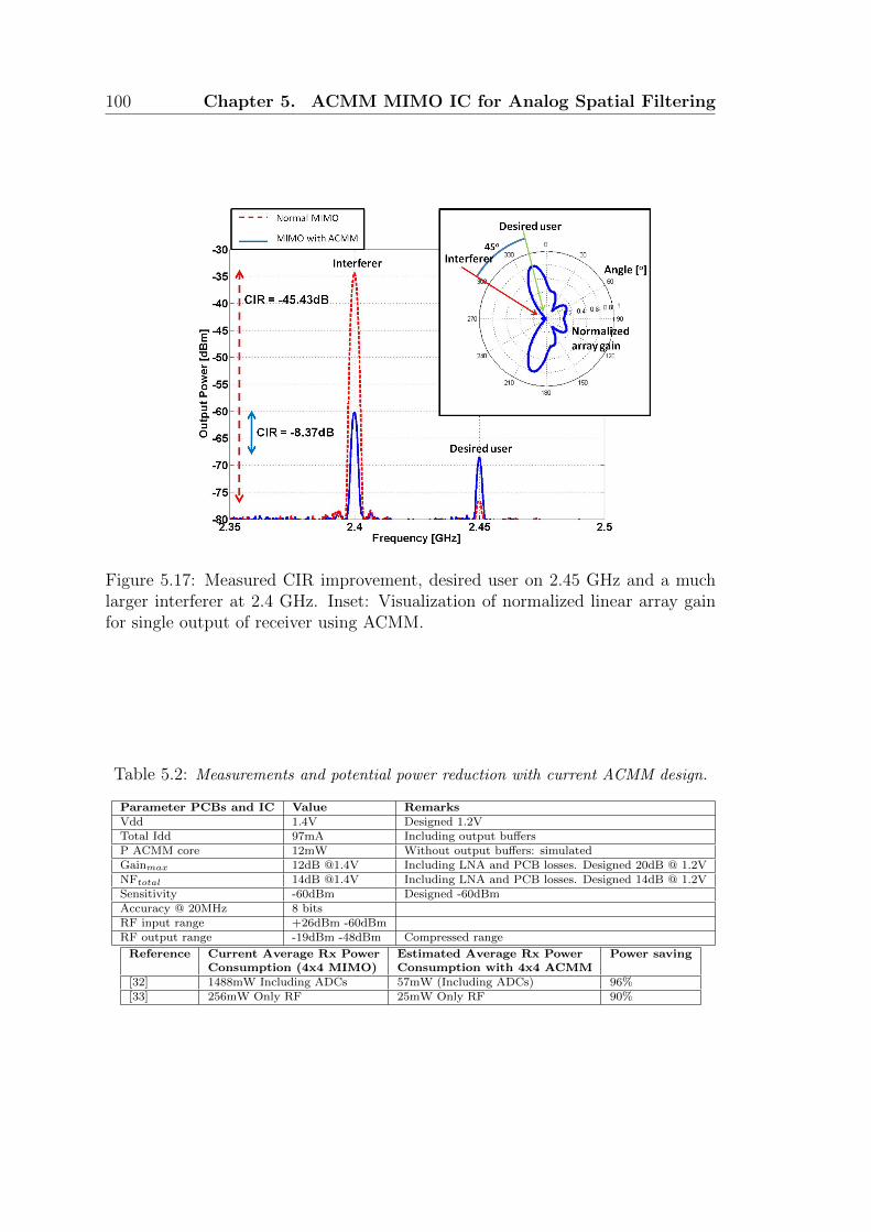
100 Chapter 5. ACMM MIMO IC for Analog Spatial Filtering
Figure 5.17: Measured CIR improvement, desired user on 2.45 GHz and a muchlarger interferer at 2.4 GHz. Inset: Visualization of normalized linear array gainfor single output of receiver using ACMM.
Table 5.2: Measurements and potential power reduction with current ACMM design.
Parameter PCBs and IC Value RemarksVdd 1.4V Designed 1.2VTotal Idd 97mA Including output buffersP ACMM core 12mW Without output buffers: simulatedGainmax 12dB @1.4V Including LNA and PCB losses. Designed 20dB @ 1.2VNFtotal 14dB @1.4V Including LNA and PCB losses. Designed 14dB @ 1.2VSensitivity -60dBm Designed -60dBmAccuracy @ 20MHz 8 bitsRF input range +26dBm -60dBmRF output range -19dBm -48dBm Compressed range
Reference Current Average Rx Power Estimated Average Rx Power Power savingConsumption (4x4 MIMO) Consumption with 4x4 ACMM
[32] 1488mW Including ADCs 57mW (Including ADCs) 96%[33] 256mW Only RF 25mW Only RF 90%
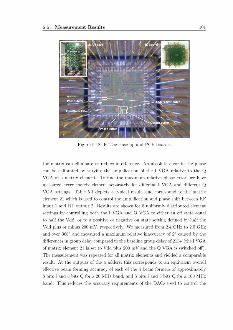
5.5. Measurement Results 101
Figure 5.18: IC Die close up and PCB boards.
the matrix can eliminate or reduce interference. An absolute error in the phase
can be calibrated by varying the amplification of the I VGA relative to the Q
VGA of a matrix element. To find the maximum relative phase error, we have
measured every matrix element separately for different I VGA and different Q
VGA settings. Table 5.1 depicts a typical result, and correspond to the matrix
element 21 which is used to control the amplification and phase shift between RF
input 1 and RF output 2. Results are shown for 8 uniformly distributed element
settings by controlling both the I VGA and Q VGA to either an off state equal
to half the Vdd, or to a positive or negative on state setting defined by half the
Vdd plus or minus 200 mV, respectively. We measured from 2.4 GHz to 2.5 GHz
and over 360o and measured a maximum relative inaccuracy of 2o caused by the
differences in group delay compared to the baseline group delay of 21I+ (the I VGA
of matrix element 21 is set to Vdd plus 200 mV and the Q VGA is switched off).
The measurement was repeated for all matrix elements and yielded a comparable
result. At the outputs of the 4 adders, this corresponds to an equivalent overall
effective beam forming accuracy of each of the 4 beam formers of approximately
8 bits I and 8 bits Q for a 20 MHz band, and 5 bits I and 5 bits Q for a 100 MHz
band. This reduces the accuracy requirements of the DACs used to control the
102 Chapter 5. ACMM MIMO IC for Analog Spatial Filtering
VGAs. In fact, controlling the VGAs at higher resolution would not significantly
improve the accuracy of the resulting beam formed outputs.
Figure 5.17 depicts a system level IC measurement. The desired user is at 2.45
GHz, while a 45 dB stronger interferer is at 2.4 GHz. The dotted line represents
the signal present in a normal MIMO receiver branch. The solid line depicts the
signal in the same receiver branch after signal preconditioning via our spatial filter.
In this measurement, the delays for the desired and interfering antenna signals are
created via fixed delay lines from a single source for each of the signals. The
element values of the ACMM are calculated according to [18]. The corresponding
angle-of-arrival (AOA) difference between the two sources is 45o. For this AOA
difference the channel-to-interference ratio (CIR) improvement is 37 dB. This 37
dB improvement is in agreement with the 5 bits accuracy over the 100 MHz band
measured in Table 5.1. Due to the different cable lengths the corresponding phase
differences of the measurements do not correspond to the phase shifts that would
occur in a linear array with antennas at half a wavelength of the carrier frequency
when receiving these signals in a multi-path-free environment. In the radiation
pattern of the inset of Figure 5.17 we have corrected for this nonuniform phase
distribution by assuming that the antennas are off grid as compared to a linear
array, and calculated the corresponding beam pattern from the measured outputs.
This calibration was performed to provide an intuitive and graphical interpretation
of the measured ACMM output. The CIR improvement is achieved without using
any frequency selective filtering. Spatial filtering can even be applied with an
interferer at the same frequency as the desired user.
The measured performance of the LNA and ACMM are specified in Table 5.2.
Vdd is 1.4 V and Idd is 97 mA including output buffers. Our realization of the
IC fell short of the target gain, but this could be compensated through the LNA
board such that we could reassure performance to determine the system power
reduction. In principle the gain is required to drive the input buffer of the ADC
in the test bed. The gain is not necessary to show the functionality of the spatial
filter operation. In a fully integrated design the input buffers of the ADC and the
output buffers of the ACMM are not necessary.
5.6. Measurements Analysis and Redesign 103
5.6 Measurements Analysis and Redesign
Due to errors in the post layout parasitic extraction deck in the TSMC library,
proper post layout simulations could not be performed to verify the ACMM layout
design. Therefore a manual parasitic extraction was conducted and the expected
gain was 10 dB. After tapeout the measured gain of the ACMM was between -
20 to -30 dB. By increasing the bias current and power supply voltage, the gain
was increased to 2 dB. The origin of the loss of gain at the original biassing and
voltage supply was found by Zhe Chen under my supervision via measurements
and additional circuit and post layout simulations. After an initial RC parasitic
extraction the gain was estimated between -10 to -22 dB, which was still 10 dB
higher than the measured value. After inclusion of additional causes for gain
loss, such as the double MIM-Capacitor extraction error of the TSMC library, the
simulated gain loss after parasitic extraction approached the measured results up
to an error of 1 to 4 dB. A main cause of the gain loss was ground lifting due to a
connection error in the IC wide ground mesh. Therefore, increasing the Vdd and
bias current could restore most of the gain loss.1
Isolate PCB and Connection Wires
The IC is measured with a vector network analyzer (VNA) (Rohde & Schwarz,
ZVRE) with two single ended cables. The Vdd and several control signals are
generated by five power supplies (Agilent E3631A), the other control signals and
the bias currents are set with a precision measurement mainframe (Agilent E5270).
In measurements the differential outputs of the IC are first DC decoupled with
external decoupling capacitors and then connected via SMA cables to an external
off-PCB balun. The single ended port 1 of the VNA is connected to one of the single
ended inputs of the IC-PCB, and the single ended port 2 of the VNA is connected
to the output of the external balun. The effects of the cables connected to the
VNA are removed from the measurements via a calibration with a calibration
set. To accurately measure the IC performance in combination with the bond
1In principle we do not need gain for the spatial filter, we needed gain to drive the inputbuffer of the ADC in the test bed
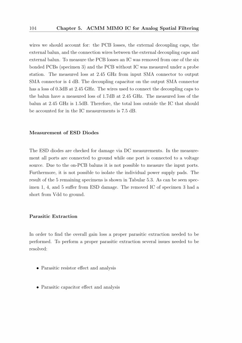
104 Chapter 5. ACMM MIMO IC for Analog Spatial Filtering
wires we should account for: the PCB losses, the external decoupling caps, the
external balun, and the connection wires between the external decoupling caps and
external balun. To measure the PCB losses an IC was removed from one of the six
bonded PCBs (specimen 3) and the PCB without IC was measured under a probe
station. The measured loss at 2.45 GHz from input SMA connector to output
SMA connector is 4 dB. The decoupling capacitor on the output SMA connector
has a loss of 0.3dB at 2.45 GHz. The wires used to connect the decoupling caps to
the balun have a measured loss of 1.7dB at 2.45 GHz. The measured loss of the
balun at 2.45 GHz is 1.5dB. Therefore, the total loss outside the IC that should
be accounted for in the IC measurements is 7.5 dB.
Measurement of ESD Diodes
The ESD diodes are checked for damage via DC measurements. In the measure-
ment all ports are connected to ground while one port is connected to a voltage
source. Due to the on-PCB baluns it is not possible to measure the input ports.
Furthermore, it is not possible to isolate the individual power supply pads. The
result of the 5 remaining specimens is shown in Tabular 5.3. As can be seen spec-
imen 1, 4, and 5 suffer from ESD damage. The removed IC of specimen 3 had a
short from Vdd to ground.
Parasitic Extraction
In order to find the overall gain loss a proper parasitic extraction needed to be
performed. To perform a proper parasitic extraction several issues needed to be
resolved:
• Parasitic resistor effect and analysis
• Parasitic capacitor effect and analysis
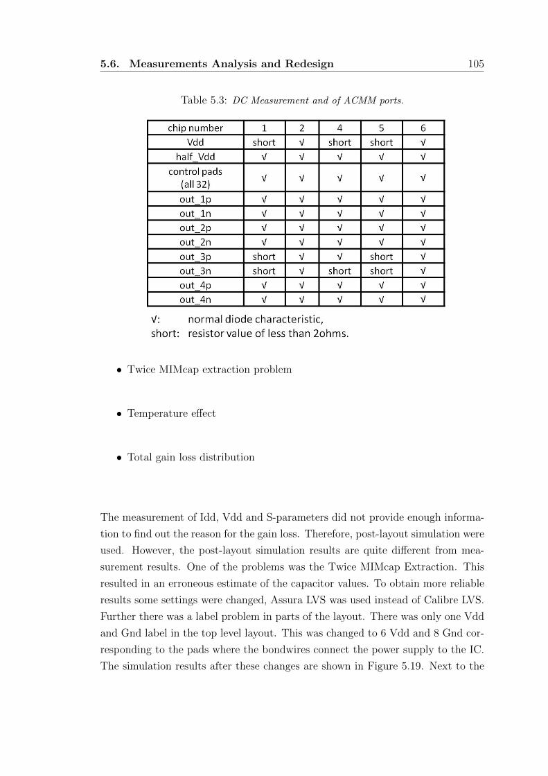
5.6. Measurements Analysis and Redesign 105
Table 5.3: DC Measurement and of ACMM ports.
• Twice MIMcap extraction problem
• Temperature effect
• Total gain loss distribution
The measurement of Idd, Vdd and S-parameters did not provide enough informa-
tion to find out the reason for the gain loss. Therefore, post-layout simulation were
used. However, the post-layout simulation results are quite different from mea-
surement results. One of the problems was the Twice MIMcap Extraction. This
resulted in an erroneous estimate of the capacitor values. To obtain more reliable
results some settings were changed, Assura LVS was used instead of Calibre LVS.
Further there was a label problem in parts of the layout. There was only one Vdd
and Gnd label in the top level layout. This was changed to 6 Vdd and 8 Gnd cor-
responding to the pads where the bondwires connect the power supply to the IC.
The simulation results after these changes are shown in Figure 5.19. Next to the
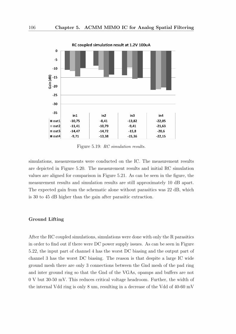
106 Chapter 5. ACMM MIMO IC for Analog Spatial Filtering
Figure 5.19: RC simulation results.
simulations, measurements were conducted on the IC. The measurement results
are depicted in Figure 5.20. The measurement results and initial RC simulation
values are aligned for comparison in Figure 5.21. As can be seen in the figure, the
measurement results and simulation results are still approximately 10 dB apart.
The expected gain from the schematic alone without parasitics was 22 dB, which
is 30 to 45 dB higher than the gain after parasitic extraction.
Ground Lifting
After the RC coupled simulations, simulations were done with only the R parasitics
in order to find out if there were DC power supply issues. As can be seen in Figure
5.22, the input part of channel 4 has the worst DC biasing and the output part of
channel 3 has the worst DC biasing. The reason is that despite a large IC wide
ground mesh there are only 3 connections between the Gnd mesh of the pad ring
and inter ground ring so that the Gnd of the VGAs, opamps and buffers are not
0 V but 30-50 mV. This reduces critical voltage headroom. Further, the width of
the internal Vdd ring is only 8 um, resulting in a decrease of the Vdd of 40-60 mV
5.6. Measurements Analysis and Redesign 107
Figure 5.20: Measurement results.
Figure 5.21: Comparison between measurement results (top) and initial RC simulationresults (bottom).
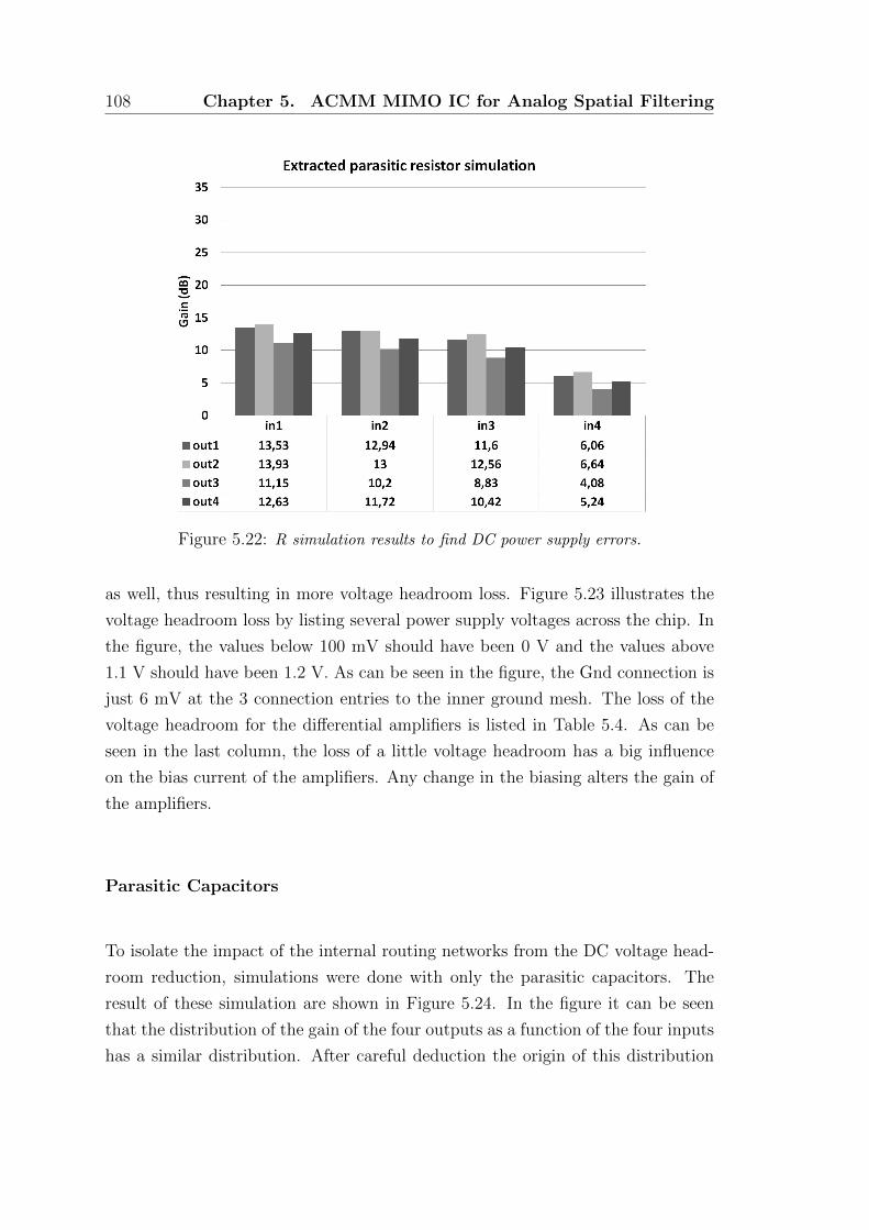
108 Chapter 5. ACMM MIMO IC for Analog Spatial Filtering
Figure 5.22: R simulation results to find DC power supply errors.
as well, thus resulting in more voltage headroom loss. Figure 5.23 illustrates the
voltage headroom loss by listing several power supply voltages across the chip. In
the figure, the values below 100 mV should have been 0 V and the values above
1.1 V should have been 1.2 V. As can be seen in the figure, the Gnd connection is
just 6 mV at the 3 connection entries to the inner ground mesh. The loss of the
voltage headroom for the differential amplifiers is listed in Table 5.4. As can be
seen in the last column, the loss of a little voltage headroom has a big influence
on the bias current of the amplifiers. Any change in the biasing alters the gain of
the amplifiers.
Parasitic Capacitors
To isolate the impact of the internal routing networks from the DC voltage head-
room reduction, simulations were done with only the parasitic capacitors. The
result of these simulation are shown in Figure 5.24. In the figure it can be seen
that the distribution of the gain of the four outputs as a function of the four inputs
has a similar distribution. After careful deduction the origin of this distribution
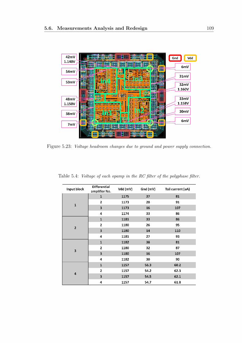
5.6. Measurements Analysis and Redesign 109
Figure 5.23: Voltage headroom changes due to ground and power supply connection.
Table 5.4: Voltage of each opamp in the RC filter of the polyphase filter.
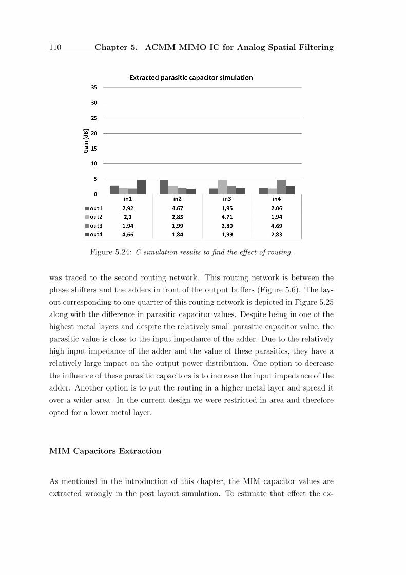
110 Chapter 5. ACMM MIMO IC for Analog Spatial Filtering
Figure 5.24: C simulation results to find the effect of routing.
was traced to the second routing network. This routing network is between the
phase shifters and the adders in front of the output buffers (Figure 5.6). The lay-
out corresponding to one quarter of this routing network is depicted in Figure 5.25
along with the difference in parasitic capacitor values. Despite being in one of the
highest metal layers and despite the relatively small parasitic capacitor value, the
parasitic value is close to the input impedance of the adder. Due to the relatively
high input impedance of the adder and the value of these parasitics, they have a
relatively large impact on the output power distribution. One option to decrease
the influence of these parasitic capacitors is to increase the input impedance of the
adder. Another option is to put the routing in a higher metal layer and spread it
over a wider area. In the current design we were restricted in area and therefore
opted for a lower metal layer.
MIM Capacitors Extraction
As mentioned in the introduction of this chapter, the MIM capacitor values are
extracted wrongly in the post layout simulation. To estimate that effect the ex-
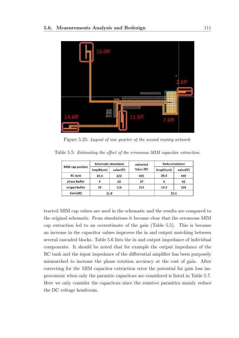
5.6. Measurements Analysis and Redesign 111
Figure 5.25: Layout of one quarter of the second routing network.
Table 5.5: Estimating the effect of the erroneous MIM capacitor extraction.
tracted MIM cap values are used in the schematic and the results are compared to
the original schematic. From simulations it became clear that the erroneous MIM
cap extraction led to an overestimate of the gain (Table 5.5). This is because
an increase in the capacitor values improves the in and output matching between
several cascaded blocks. Table 5.6 lists the in and output impedance of individual
components. It should be noted that for example the output impedance of the
RC tank and the input impedance of the differential amplifier has been purposely
mismatched to increase the phase rotation accuracy at the cost of gain. After
correcting for the MIM capacitor extraction error the potential for gain loss im-
provement when only the parasitic capacitors are considered is listed in Table 5.7.
Here we only consider the capacitors since the resistive parasitics mainly reduce
the DC voltage headroom.
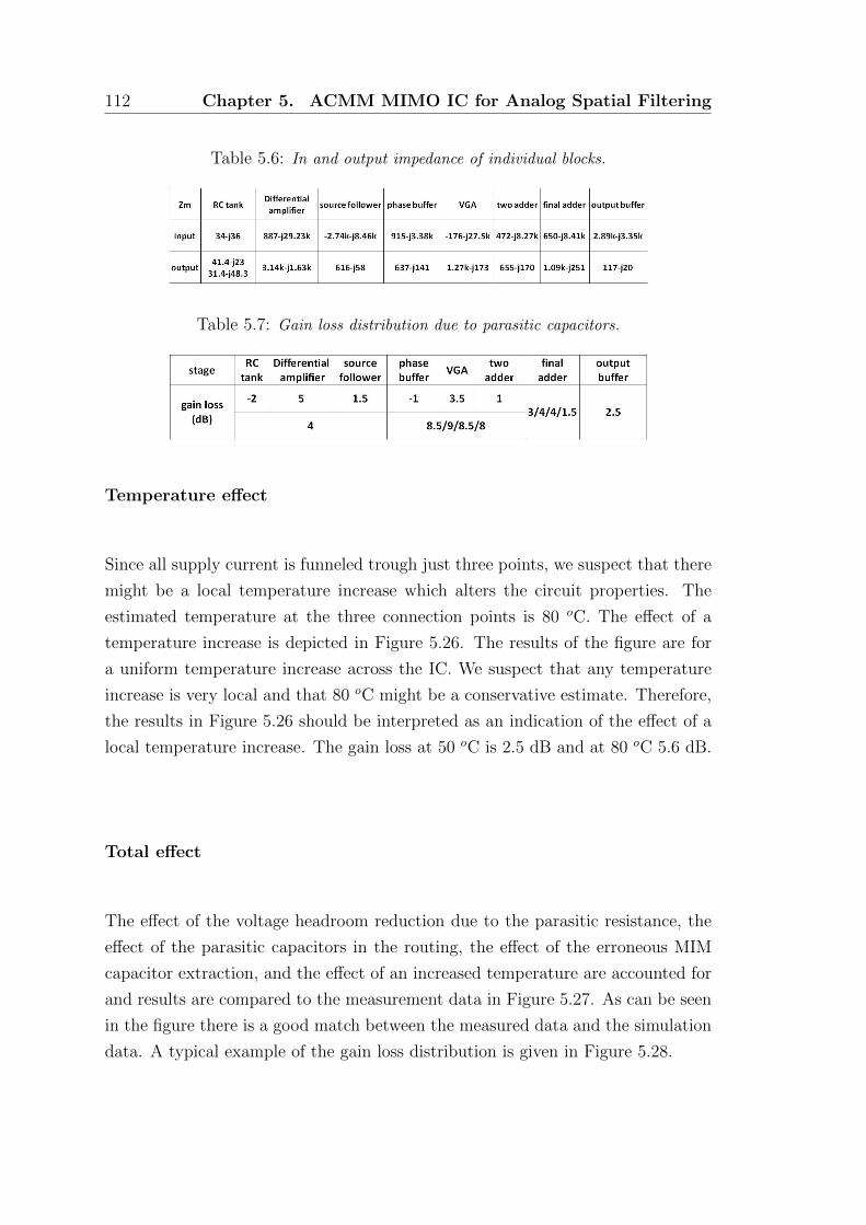
112 Chapter 5. ACMM MIMO IC for Analog Spatial Filtering
Table 5.6: In and output impedance of individual blocks.
Table 5.7: Gain loss distribution due to parasitic capacitors.
Temperature effect
Since all supply current is funneled trough just three points, we suspect that there
might be a local temperature increase which alters the circuit properties. The
estimated temperature at the three connection points is 80 oC. The effect of a
temperature increase is depicted in Figure 5.26. The results of the figure are for
a uniform temperature increase across the IC. We suspect that any temperature
increase is very local and that 80 oC might be a conservative estimate. Therefore,
the results in Figure 5.26 should be interpreted as an indication of the effect of a
local temperature increase. The gain loss at 50 oC is 2.5 dB and at 80 oC 5.6 dB.
Total effect
The effect of the voltage headroom reduction due to the parasitic resistance, the
effect of the parasitic capacitors in the routing, the effect of the erroneous MIM
capacitor extraction, and the effect of an increased temperature are accounted for
and results are compared to the measurement data in Figure 5.27. As can be seen
in the figure there is a good match between the measured data and the simulation
data. A typical example of the gain loss distribution is given in Figure 5.28.
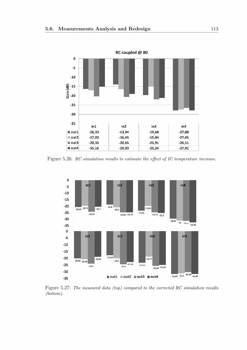
5.6. Measurements Analysis and Redesign 113
Figure 5.26: RC simulation results to estimate the effect of IC temperature increase.
Figure 5.27: The measured data (top) compared to the corrected RC simulation results(bottom).
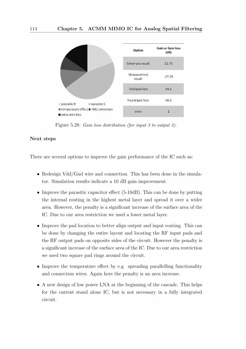
114 Chapter 5. ACMM MIMO IC for Analog Spatial Filtering
Figure 5.28: Gain loss distribution (for input 3 to output 2).
Next steps
There are several options to improve the gain performance of the IC such as:
• Redesign Vdd/Gnd wire and connection. This has been done in the simula-
tor. Simulation results indicate a 10 dB gain improvement.
• Improve the parasitic capacitor effect (5-10dB). This can be done by putting
the internal routing in the highest metal layer and spread it over a wider
area. However, the penalty is a significant increase of the surface area of the
IC. Due to our area restriction we used a lower metal layer.
• Improve the pad location to better align output and input routing. This can
be done by changing the entire layout and locating the RF input pads and
the RF output pads on opposite sides of the circuit. However the penalty is
a significant increase of the surface area of the IC. Due to our area restriction
we used two square pad rings around the circuit.
• Improve the temperature effect by e.g. spreading parallelling functionality
and connection wires. Again here the penalty is an area increase.
• A new design of low power LNA at the beginning of the cascade. This helps
for the current stand alone IC, but is not necessary in a fully integrated
circuit.
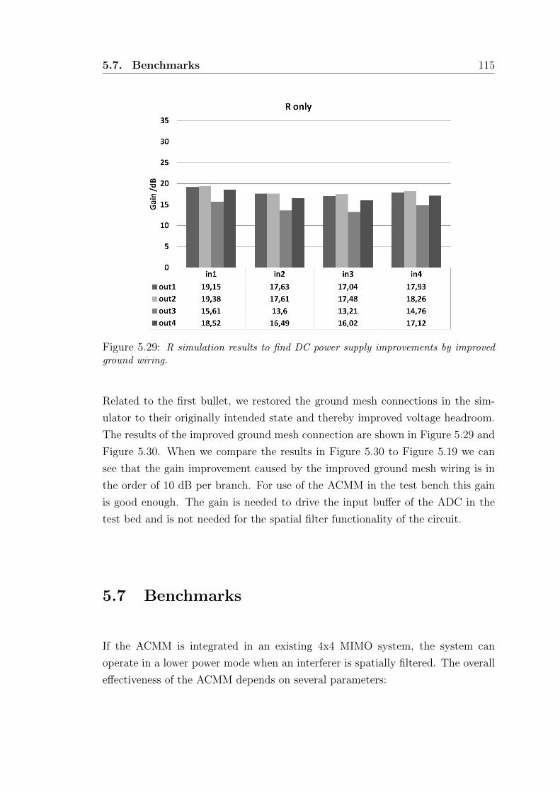
5.7. Benchmarks 115
Figure 5.29: R simulation results to find DC power supply improvements by improvedground wiring.
Related to the first bullet, we restored the ground mesh connections in the sim-
ulator to their originally intended state and thereby improved voltage headroom.
The results of the improved ground mesh connection are shown in Figure 5.29 and
Figure 5.30. When we compare the results in Figure 5.30 to Figure 5.19 we can
see that the gain improvement caused by the improved ground mesh wiring is in
the order of 10 dB per branch. For use of the ACMM in the test bench this gain
is good enough. The gain is needed to drive the input buffer of the ADC in the
test bed and is not needed for the spatial filter functionality of the circuit.
5.7 Benchmarks
If the ACMM is integrated in an existing 4x4 MIMO system, the system can
operate in a lower power mode when an interferer is spatially filtered. The overall
effectiveness of the ACMM depends on several parameters:
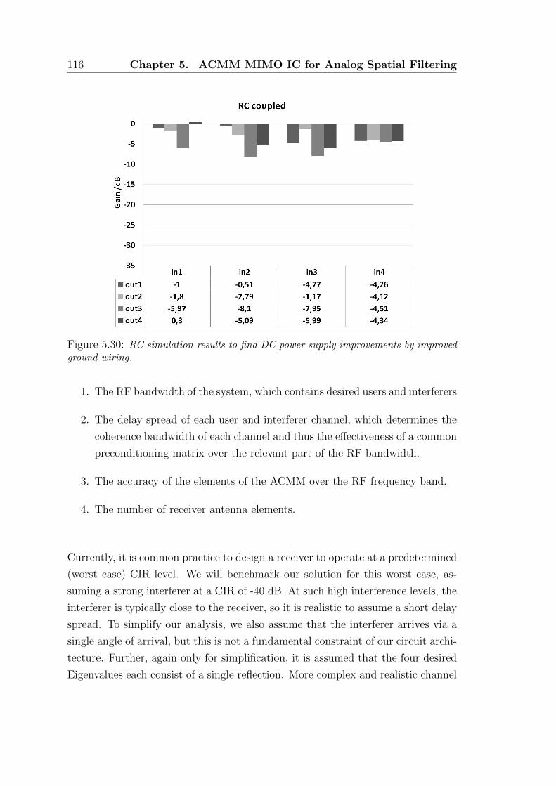
116 Chapter 5. ACMM MIMO IC for Analog Spatial Filtering
Figure 5.30: RC simulation results to find DC power supply improvements by improvedground wiring.
1. The RF bandwidth of the system, which contains desired users and interferers
2. The delay spread of each user and interferer channel, which determines the
coherence bandwidth of each channel and thus the effectiveness of a common
preconditioning matrix over the relevant part of the RF bandwidth.
3. The accuracy of the elements of the ACMM over the RF frequency band.
4. The number of receiver antenna elements.
Currently, it is common practice to design a receiver to operate at a predetermined
(worst case) CIR level. We will benchmark our solution for this worst case, as-
suming a strong interferer at a CIR of -40 dB. At such high interference levels, the
interferer is typically close to the receiver, so it is realistic to assume a short delay
spread. To simplify our analysis, we also assume that the interferer arrives via a
single angle of arrival, but this is not a fundamental constraint of our circuit archi-
tecture. Further, again only for simplification, it is assumed that the four desired
Eigenvalues each consist of a single reflection. More complex and realistic channel
5.7. Benchmarks 117
model simulations are reported in Chapter 6. The reported results are in agree-
ment with the simplified channel model of this section. Due to the finite accuracy
of the ACMM, the interferer cannot be canceled fully if the difference in AOA of
one of the four reflections of the desired user and the reflection of the interferer is
smaller than the angular resolution with which the ACMM can set a minimum.
The angular resolution of the ACMM depends on the achievable control accuracy
of the elements of the ACMM over the considered bandwidth, and the number
of antenna elements. For a uniform angle of arrival, under the constraint of our
current channel assumption, the probability that the interferer and desired signals
effectively overlap for four receive antennas and cannot be separated is less than
1% in our ACMM realization of 5 bit I and Q accuracy over a bandwidth of a 100
MHz. At all other angles of incidence, the power consumption of the RF front end
and of the ADC, can be reduced substantially by exploiting the CIR improvement
method demonstrated here [72] and predicted theoretically already in [18] [16].
Given the current channel assumptions, the probability that all four desired reflec-
tions overlap with the AOA of the interferer (and thus the MIMO receiver needs
to operate at full power including the ACMM power consumption) is in the order
of 10−8. At all other instances the receiver can scale back power consumption of
at least one receiver chain, if its linearity and ADC settings are adaptive. If the
linearity setting of the receiver is not adaptive, the receiver could still operate in a
lower power mode. The increased linearity of the front end will impact negatively
on the average bit-error-rate, but on the other hand this is outweighed by the
enabled CIR improvement which acts positively on the average bit-error-rate. The
exact trade-off is beyond the scope of this chapter. The simulated power consump-
tion of the ACMM core, excluding the output buffers, is 12 mW. The measured
power consumption of the entire IC including output buffers and PCB board is
136 mW. Since our ACMM building block enables a CIR improvement, power
consumption can be opportunistically reduced for a typical MIMO receiver for all
blocks after the ACMM block depending on the current channel conditions. In
our calculation, the power consumption of the LNAs is estimated at around 4% of
the original total RF circuit power consumption. Under our channel assumptions,
our solution showed an average improvement of 90 to 96% of the time-average
power consumption, given the presence of a strong interferer (Table 5.2). If spatial
filtering can be applied to unamplified antenna signals at a sufficiently low NF,
the LNA power can be reduced as well. The average power reduction for 5 bits
118 Chapter 5. ACMM MIMO IC for Analog Spatial Filtering
accuracy over a 100 MHz band can then be estimated to reach almost two orders
of magnitude. However, the power spend in the matrix is still an overhead.
Figure 5.18 shows the IC, the IC board, and the LNA board. The chip is mounted
in a cavity. The 65 nm CMOS chip occupies 1.2 mm2 including bond pads. This
IC has been successfully used in a proof-of-concept measurement. This validates
our claim that with our approach, MIMO receivers using over 90% less power than
state of the art solutions can be realized, when MIMO receivers include the novel
ACMM building block.
5.8 Conclusions
A novel MIMO receiver architecture has been introduced containing a novel ACMM
building block which exploits the spatial selectivity of the MIMO channel in the
analog domain. The ACMM IC has been implemented in 65 nm CMOS and op-
erates in the 2.4 GHz band. To the best of our knowledge the ACMM is the first
realization of an analog spatial filtering of interference at RF to alleviate the DR
requirements of the receiver and ADC in a MIMO system. Earlier this concept
has been simulated by us (Chapter 6), and the substantial performance gain has
been confirmed by our test. In contrast to regular beamforming the ACMM allows
for all MIMO data streams. The control accuracy of the ACMM is 5 bits I and 5
bits Q per matrix element over a 100 MHz band. Measured CIR improvement is
37 dB at an AOA difference of 45o. The measurements confirm that the expected
average power consumption reduction over time of a MIMO system including an
ACMM building block is over 90%.
Chapter 6
Analog Spatial Filtering in
Wideband Cognitive Radio
6.1 Introduction
In the previous chapter we showed spatial filtering in an IEEE 802.11n context.
To support the practical feasibility of our approach in Chapter 5, an IC imple-
mentation of an analog 4×4 ACMM full MIMO spatial filter at an RF of 2.45
GHz has been realized in 65nm CMOS, and it is confirmed via measurements that
analog interference suppression is effective. The implementation and measurement
results are documented in Chapter 5 and submitted in the RF community in [72].
However, the principles of spatial filtering are also applicable to other frequencies
and channel bands. Therefore, in this chapter we apply the same spatial filtering
principles as shown in Chapter 5, but now applied to cognitive radio. More specif-
ically, we determine the potential benefits of spatial filtering in terms of increased
throughput (bit/s/Hz), and we quantify the potential power savings in terms of
ADC quantization bits. Our approach in this chapter is as follows:
i) extending [18], from a vector beamformer to the novel receiver architecture
including a full rank analog complex matrix multiplier (ACMM) (which was in-
troduced in Chapter 5), which allows for full MIMO spatial filtering. In contrast
119

120 Chapter 6. Analog Spatial Filtering in Wideband Cognitive Radio
to the wideband vector beamformer from [18], and the narrowband rank reduced
matrix from [74], our full rank wideband MIMO spatial filter separates all spatial
streams simultaneously, hereby significantly increasing system capacity.
ii) The channel model is expanded to the full MIMO case and novel DSP algo-
rithms for computation of MIMO spatial filter coefficients are proposed.
iii) Analysis of DR reduction in different wireless propagation environments mod-
eled via ray tracers.
iv) Analysis of the effect of quantization in the filter implementation.
The Chapter is structured as follows: Section 6.2 introduces the model for respec-
tively the radio front-end, the ADC, the signal, and the wideband multiple antenna
channel models. Section 6.3 includes the throughput calculation, the beamform-
ing algorithms, and the MIMO spatial filtering algorithm. Section 6.4 gives the
numerical results of the beamforming and spatial filtering algorithms for various
channel conditions. Finally Section 6.5 concludes this chapter.
With the continued increase in the number of users in the crowded pre-allocated
parts of the radio spectrum, a more efficient use of the available spectrum is re-
quired. To increase spectrum utilization, a cognitive radio (CR) continuously
senses and uses unoccupied channels in a wideband spectrum, alleviating conges-
tion and improving the overall throughput.
In a typical CR scenario there are multiple primary and secondary user transmis-
sions over a wide bandwidth and the desired user only occupies a small portion of
the band [6, 75, 76]. Contrary to the front end of Chapter 5, now the entire RF
band is filtered, down converted, and finally sampled by an ADC. Final channel
selection occurs in the digital domain. As mentioned in Section 3.7, before final
digital filtering can be performed, in most systems the radio frequency (RF) front
end and analog-to-digital converter (ADC) need to handle the interfering users
via extra dynamic range (DR). Unfortunately, additional DR requirements make
the RF and ADC power hungry [10, 77, 78]. The DR and sample rate require-
ments of the ADC depend on the combination of the interference power level with
which the receiver needs to cope, both inside and outside the band, and these are
a trade off with the analog filter selectivity [11]. As mentioned in Section 2.2.2,
the power consumption of ADCs currently reduces approximately with an order
of magnitude every decade [37,49]. In the absence of disruptive new technologies,
6.2. System Model 121
we expect this power trend to continue for the foreseeable future. In a CR several
users with various received power levels are sampled simultaneously. At a typical
power level difference of 40 dB for an undesired user, the ADC requires 6.64 more
effective bits to maintain similar effective resolution for the desired user compared
to an interference free case. This additional ADC bit requirement leads to an ap-
proximate 100 times increase in the required ADC power consumption, compared
to what is necessary for the interference-free case. The power requirements of,
for example, high sampling speeds (e.g. 1 GHz), and high resolution (10/12 bits)
ADCs required for the IEEE 802.22 standard have thus far been prohibitive for
the wide spread use of CR.
Since the received signals come from distinct spatial angles, multiple antennas can
be used at the receiver to resolve them (Section 3.3). Systems that include multiple
receive antennas can be realized as vector beamformers (multiple antennas with
combining in the analog domain and a single ADC) and full MIMO (multiple
antennas with an ADC per antenna). The concept of spatial filtering via vector
beamforming to reduce interfering users was first introduced in [70]. In [74], a
narrowband channel in combination with a rank reduced analog matrix is studied.
In [18], the benefit of a vector beamformer as a spatial filter to reduce interference
power levels is analyzed for a wideband channel, and it is shown that spatial
filtering has the potential to reduce ADC power consumption with over 90%.
6.2 System Model
In this section firstly two receiver architectures from Chapter 5 for spatial filtering
are reintroduced, namely a vector beamformer spatial filter and a MIMO spatial
filter. Specifically, the impact of the difference between the IEEE 802.11n sce-
nario and the CR scenario on the architectures is explained. Secondly, the ADC
power consumption model is introduced, to allow quantitative analysis of power
savings obtained by our proposed architectures. Thirdly, our signal model is based
on OFDM signaling. Finally, wideband channel models for realistic propagation
environments are introduced, namely i.i.d. Rayleigh fading per subcarrier, and a
122 Chapter 6. Analog Spatial Filtering in Wideband Cognitive Radio
wideband MIMO ray tracing model.
6.2.1 Front End Architectures
Contrary to the RF front end of Chapter 5, the sampled broadband BB signal
contains the interfering users as well as the desired signal. The CR RF front end
chain and the ADC have to deal with a broadband RF signal. To prevent clipping
of the ADC, an automatic gain control (AGC) amplifies the entire wideband spec-
trum to an appropriate level. To prevent excessive spill over of interfering signals
into the desired signal band, the analog front end needs to have adequate linear-
ity. After analog channel selection within the wide bandwidth via mixing and non
ideal analog filtering, the signal presented to the analog-to-digital converter (ADC)
consist of the desired user, interfering users, and leftover adjacent channel inter-
ference products. To prevent aliasing of the adjacent channel interferer into the
desired channel it is necessary to over-sample, and headroom bits are required to
guarantee adequate resolution for the desired signal. The filtered signal is further
processed in the baseband (BB) domain by the digital signal processing (DSP)
for the purpose of spectrum sensing and/or narrowband reception. A co-channel
interferer can be filtered digitally using a combination of coding, timing, and fre-
quency hopping schemes. In full MIMO antenna systems, the BB DSP can also
use matrix beamforming techniques to spatially filter co-channel interferers, but
this digital filtering requires a powerhungry ADC per receive antenna with large
DR.
Vector Beamforming
In contrast to Section 5.2, the I and Q baseband signals contain all users. The
I and Q signals are low pass filtered, set to an adequate gain for the ADC by
an AGC, and then quantized by an ADC. Figure 5.3 depicts a CR receiver with
a vector beamforming architecture acting as an analog vector spatial filter. The
considered beamforming system architecture consists of a commonly used zero
IF architecture combined with several receive antennas, each with their own RF-
6.2. System Model 123
filter, LNA, and phase shifter. The outputs of the phase shifters are combined
and presented to an in-phase I and quadrature Q mixer which downconverts the
combined RF frequency band to baseband with the signal provided by the local
oscillator (LO).
Full MIMO Spatial Filter
Contrary to the architecture of Section 5.2, the ADCs now sample a broadband BB
signal containing all users. The architecture depicted in Figure 5.4 and processes
parallel RF signal streams in the form of a MIMO receiver with an independent
ADC per antenna. The architecture includes a similar RF analog complex matrix
multiplier (ACMM) as in Section 5.2, which is implemented as a matrix of com-
plex multipliers and adders (Figure 5.6). In contrast to the vector beamformer,
the considered full MIMO spatial filter addresses all spatial streams simultane-
ously, hereby significantly increasing system capacity. The considered MIMO ar-
chitecture consists of a commonly used zero IF architecture combined with several
receiver antennas, each with their own RF-filter and LNA. The outputs of the
LNAs are inputs to a matrix operation at RF. The outputs of the matrix are each
presented to an in-phase I and a quadrature Q mixer which down converts the RF
signal to baseband with the signal provided by the shared local oscillator (LO).
The composite I and Q baseband signals containing all users are low pass filtered,
set to an adequate gain for their ADC by an AGC, and then quantized by the
ADCs.
Mismatch
There are two kinds of mismatches that impact overall system performance. The
first form is impedance mismatch between two stages of a receiver chain. The sec-
ond form is a difference in physical attributes between paths in the receiver, caused
for instance by process spread, and parasitic differences attributable to e.g. rout-
ing in the layout. Many of the latter form of mismatches, particularly differences
in signal branches, can not be distinguished from random channel realizations, so
124 Chapter 6. Analog Spatial Filtering in Wideband Cognitive Radio
these can be partly or entirely corrected by our proposed solution. In particular the
feedback loop (see Figure 5.4) compensates mismatch artifacts that appear in the
base band, by setting the ACMM appropriately. However, these mismatches have
not been part of the simulation in this chapter. On the other hand, impedance
mismatches lead to a penalty in the noise performance. In our IC realization
(Chapter 5), we achieved a proper gain and phase control by buffering the signals,
feeding it into an RC hybrid, and applying a high-impedance, voltage controlled
I and Q amplification. This avoids mutual coupling of the settings of the various
matrix elements, but potentially does not achieve the highest noise performance.
This noise penalty can be acceptable because it is applied to input signals that are
already preamplified. Yet, this of course puts more stringent requirements on the
noise performance, gain and dynamic range of the first LNA amplifiers. On the
other hand, dynamic range reduction achieved by spatial filtering impacts power
consumption of stages behind the ACMM favorably, where power spent in the
spatial filter is an overhead. A full analysis of the power consumption trade-off of
the entire chain, including LNA, AGC, mixer and ADC is beyond the scope of this
chapter, but in [14–16] and Chapter 4, we published a framework that potentially
can model this. In our model we purposely omit mismatch in the analog front end,
since mismatch heavily depends on the technology and the specific design in that
technology [79], which are beyond the scope of this chapter.
6.2.2 Analog-to-Digital Converter
To guarantee adequate resolution, dynamic range for the desired user, and re-
ceiver sensitivity for spectrum sensing, additional headroom bits are required in
the presence of strong interference levels. Unfortunately, the power consumption
of an ADC grows exponentially with the number of bits. As mentioned in Section
3.6, a commonly accepted ADC power model is,
PADC ∼ κtFs2bADC , (6.1)
where Fs is the sample frequency of the ADC, κt a technology constant and bADC
the number of ADC bits [37] [49]. With respect to the required resolution, it is
6.2. System Model 125
expected that typically a wideband signal containing several users with various
power levels is presented to the baseband ADC. According to commonly used
standards, a receiver needs to adequately receive the desired user even if power
levels of the adjacent channel users are substantially larger than the desired user. A
typical value, e.g. specified by the IEEE 802.11 standard, is 40 dB. To guarantee
sufficient resolution for the desired user in the presence of such large adjacent
channel users, additional bits for the ADC are required. In case adjacent channel
users of 40 dB larger than the desired user need to be sampled together with the
desired user, an additional DR of 40 dB is required. This results via (6.1) to an
overal PADC increase of 100 times and translates to an additional number of bits
per ADC of 1/2 log2(104) = 6.64 bits. Not only does the ADC in a CR have to
deal with interfering users inside the desired wide frequency range, but also with
left over interference products outside of the desired frequency range. This poses
further demands on the ADC. The number of additional headroom bits therefore
depends on both the standard and the practical implementation. In this chapter
the goal is to reduce the number of bits for the ADC in order to save power, while
maintaining the CR system throughput.
6.2.3 Signal Model
As mentioned in Section 3.2, Orthogonal Frequency-Division Multiplexing (OFDM)
is a popular modulation method in wireless communication due to its ability to
cope with severe channel conditions. Opportunistic use of spectrum in CR (as
proposed in the IEEE 802.22 standard) can be achieved via OFDMA. Thus we as-
sume the CR signals are wideband OFDM. The baseband equivalent of an OFDM
signal over one signal period Ts is expressed as
s(t) =
K2−1∑
k=−K2
Lkei2π kB
Kt, (6.2)
here t is time, B is the bandwidth of the signal, K is the number of OFDM
frequencies, the symbol time Ts = KB
, and Lk is the data symbol of the kth OFDM
frequency.
126 Chapter 6. Analog Spatial Filtering in Wideband Cognitive Radio
6.2.4 Wide Band Multiple Antenna Channel Models
Since all users use an OFDM scheme, the receiver channelizes the spectrum through
the use of an FFT. As a result, the wideband spectrum can be considered as a set of
narrowband signals, but with correlated fading between subcarriers (characterized
by the delay spread) and between different antennas (characterized by the angular
spread) [80]. One extreme model would be to assume that all antennas and all
subcarriers see fully uncorrelated fading. This results in extremely rich multipath,
thus high theoretical capacity gains. However, this scenario can not be handled
effectively by a frequency non-selective ACMM, except in the special case of K = 1
subcarrier or only very few. However, it is reasonable to claim that this scenario is
too rich to be useful in a cognitive wideband setting. Another extreme occurs if all
paths of one source arrive from the same direction, such that the beamformer can
perform an angular separation even if the channel is frequency selective. A third
extreme case occurs if the angular spread is large (independent and identically
distributed (i.i.d.) fading per antenna), but the RMS delay spread is small (flat
fading). In this case, a frequency non-selective ACMM, can be effective. Moreover,
we claim that an ACMM can also be effective if the wanted signal sees frequency
selective fading, as long as the RMS delay spread of the interference is small (flat
fading). As mentioned in the introduction, the receiver needs to cope with large
interferers which are typically 40 dB larger than the desired user. We consider
it reasonable to assume that such a large interferer is in close proximity to the
receiver, resulting in a small RMS delay spread. The RMS delay spread is defined
as
τRMS =
√∫∞0
(τ − τ)2A(τ)dτ∫∞0A(τ)dτ
, (6.3)
where A(τ) is the power delay profile and the mean delay of the channel is
τ =
∫∞0τA(τ)dτ∫∞
0A(τ)dτ
. (6.4)
In order to investigate the effects of some moderate degree of spatial and frequency
correlation of indoor and urban wireless channels on system performance, we used
6.2. System Model 127
a ray tracer to model various channel realizations. The ray tracer calculates the
channel for each subcarrier corresponding to the various multi paths between each
transmit and receive antenna. The uncorrelated Rayleigh Fading channel model is
used as a benchmark to test the beamforming algorithms. Next we will introduce
a ray tracer model based on a wideband channel model that accounts for the
angular spatial correlation in the wideband channel. We analyze the special flat
fading case of K = 1 subcarrier in combination with the uncorrelated Rayleigh
Fading channel model for the beamformer first. Secondly, we analyze the effect on
the beamformer of shifting from flat fading to frequency selective fading via the
ray tracer channel model, by increasing the RMS delay spread of both the signal
and the interferer. Finally, we analyze the ACMM with the ray tracer channel
model in case of frequency selective fading of the wanted signal and flat fading of
the interferer.
Independent Rayleigh Fading per Subcarrier
Consider a transmission system that consists of Nt transmit antennas and Nr
receive antennas. Each transmit antenna corresponds to a primary or secondary
transmitter in the CR network. If a narrowband complex signal s is transmitted,
the received signal r on a specific subcarrier can be expressed as
r = Hs + n, (6.5)
where H is a Nr × Nt complex channel-gain matrix and n is a complex Nr-
dimensional additive white Gaussian noise (AWGN) vector. For spatially-uncorrelated
Rayleigh fading, the entries in H are independent and identically distributed
(i.i.d.), complex, zero-mean Gaussian with unit magnitude variance. The results
simulated for this case are valid for K = 1 subcarriers per primary or secondary
transmitter (flat fading), but also if all subcarriers see the same channel H (flat
fading, small delay spread).
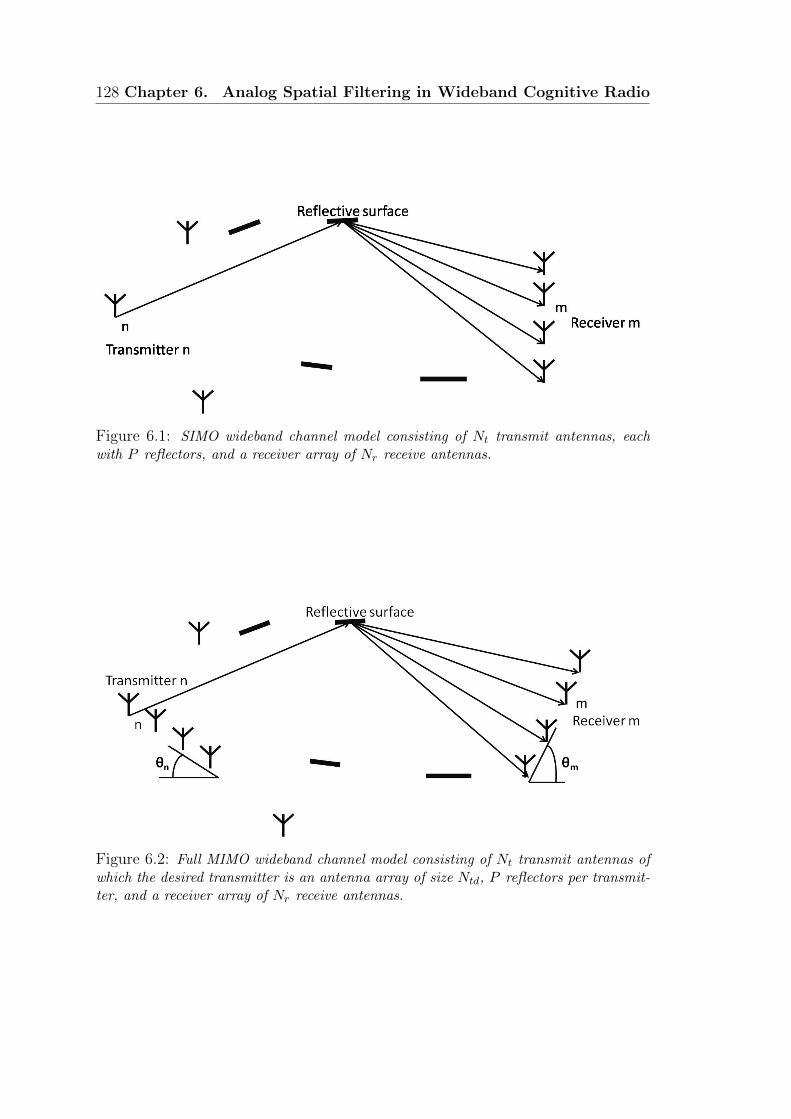
128 Chapter 6. Analog Spatial Filtering in Wideband Cognitive Radio
Figure 6.1: SIMO wideband channel model consisting of Nt transmit antennas, eachwith P reflectors, and a receiver array of Nr receive antennas.
Figure 6.2: Full MIMO wideband channel model consisting of Nt transmit antennas ofwhich the desired transmitter is an antenna array of size Ntd, P reflectors per transmit-ter, and a receiver array of Nr receive antennas.
6.2. System Model 129
Ray Tracer
To study cases with moderate degrees of correlation, we used a wideband channel
model [81], based on ray tracing [82]. The proposed model is depicted for the
SIMO beamforming architecture of Figure 5.3 in Figure 6.1 and for the full MIMO
architecture of Figure 5.4 in Figure 6.2. The beamforming model consists of Nt
transmit antennas, each with P multipath components and a receiver array con-
sisting of Nr receive antennas. Each Nt transmit antenna corresponds to a primary
or secondary transmitter in the CR network. The full MIMO wideband channel
model consists of Nt transmit antennas of which the desired user is a transmitter
with an antenna array of size Ntd, the undesired users are transmitters with one
antenna, each of the Nt−Ntd+1 transmitting users has P multipath components,
and the receiver array consists of Nr receive antennas. In the ray tracer model
each channel for each OFDM subcarrier for each transmit and receive antenna is
calculated. The baseband equivalent of the received signal without noise
y = Hs (6.6)
at the mth antenna of the wideband channel models is given in time domain by
ym(t) =P∑p=1
an,m,pe−i2πf(t−τn,m,p)sn(t) (6.7)
where sn(t) is the transmitted signal of the nth transmit antenna, P is the number
of multipath components, and an,m,p and τn,m,p are the random complex am-
plitude and random arrival time coefficient sequences of the multipath components
between transmit antenna n and receive antenna m.
In the proposed SIMO ray tracer channel model, each transmit source has a unique
set of reflectors. The transmit antennas and corresponding reflectors are randomly
placed in a two dimensional space according to a Gaussian distribution with a vari-
ance of σ2n and σ2
n,p in each dimension of a Cartesian coordinate system, respec-
tively. The center of the receiver array is randomly placed in the two dimensional
space according to a Gaussian distribution in each dimension of the Cartesian co-
ordinate system with a variance of σ2m; the antennas are spaced in a uniform lineair
130 Chapter 6. Analog Spatial Filtering in Wideband Cognitive Radio
array according to an inter element distance of half the wavelength of the carrier
frequency λcar; the carrier frequency is the center frequency of the considered RF
band; and the angle of the receiver array θm in respect to the origin is randomly
set according to a uniform distribution over all angles θm ∈ [0, 2π]. In the full
MIMO case the transmitter consists of more transmit antennas. The center of the
transmitter array is randomly placed in the two dimensional space according to
a Gaussian distribution in each dimension of a Cartesian coordinate system with
a variance of σ2n; the antennas are spaced in a linear array according to an inter
element distance of half the wavelength of the carrier frequency λcar; the carrier
frequency is the center frequency of the considered RF band; and the angle of the
transmitter array θn in respect to the origin is randomly set according to a uniform
distribution over all angles θn ∈ [0, 2π].
The path signal strength coefficients are defined as
an,m,p = rn,p
(c
f4πdn,m,p
)(6.8)
and the delays as
τn,m,p =dn,m,pc
(6.9)
were rn,p is complex, zero-mean Gaussian with unit magnitude variance, c is the
speed of light, f is frequency, dn,m,p is the distance between transmitter n and re-
flective surface p plus the distance between reflective surface p and receive antenna
m. In case the pth multipath is a line of sight (LOS) signal, dn,m,p is the distance
between transmitter n and receive antenna m and rn,p = 1.
The baseband equivalent of the received OFDM signal without noise is now ex-
pressed as
ym(t) =
K2−1∑
k=−K2
P∑p=1
Lkan,m,pe−i2π kB
K(t−τn,m,p) (6.10)
were an,m,p is a function of subcarrier index k and the carrier frequency.
6.3. Spatial Filtering Approach 131
6.3 Spatial Filtering Approach
6.3.1 Problem statement
Our goal is to quantify the potential power savings of spatial filtering in terms of
number of ADC bits. To this aim we maximize the throughput that is achievable
for a given ADC resolution in combination with a spatial filter. This throughput
calculation has to account for the quantization effect of the ADC, because we
are assuming that the ADC is the bottleneck. In the presence of strong in-band
interference, we would like to utilize the ADC resolution as effectively as possible
for the desired user. Firstly we will model the quantization noise, secondly we
insert the quantization model in the throughput calculation. The model will be
a generalized model to enable analysis of both the vector SIMO beamformer and
the full MIMO spatial filter architectures. Then, we proceed with the development
of the spatial algorithms, and evaluate their performance throughput. We assume
perfect channel state information (CSI) at the receiver Rx. On the other hand, the
transmitter Tx does not know CSI and therefore cannot optimize the transmission
based on the interference. Note that CSI at Tx requires feedback, which is complex
to implement in practice. In addition, we assume perfect channel knowledge at
Rx, as opposed to estimated, in order to study performance of the spatial filter
independently from the channel estimation algorithm.
Quantization Noise
The input signal is quantized in the time domain, while the OFDM symbols are
extracted after an FFT of the input signal. The received signal after the analog
spatial filter U (which is a complex valued matrix of size (Nr ×Nr) in the MIMO
case, and a complex valued vector of size (1 × Nr) in the beamforming case), is
now modeled in the frequency domain for all K frequency components as
rk = Uk(Hksk + nth,k) (6.11)
132 Chapter 6. Analog Spatial Filtering in Wideband Cognitive Radio
were
sk = xk + nint,k (6.12)
Here rk is the complex valued received signal vector of size (Nt×1) in the full MIMO
case and a complex valued scalar in the beamforming case, xk is a complex valued
transmit vector of size (Nt×1) containing the complex components corresponding
to the transmitted desired user, nint,k is a complex valued transmit vector of
size (Nt × 1) containing the non zero complex components corresponding to the
interfering users, Hk is the complex current channel state matrix of size Nr ×Nt,
Uk is a complex valued matrix of size (Nr×Nr) in the MIMO case, and a complex
valued vector of size (1×Nr) in the beamforming case of the analog spatial filter,
and nth,k is a complex valued thermal noise vector of size Nr × 1 at the kth
frequency. According to the central limit theorem we can model the quantization
noise in the frequency domain as AWGN [83] [84]. To simplify the mathematics,
the AGC sets the variance of the combined input signals equal to the variance of
the input signal for an idealized ADC, which only generates quantization noise.
With a unit magnitude scaling the boundary condition for the AGC is
K∑k=1
E [rkrk∗] = ρADC
K∑k=1
E [nq,knq,k∗] , (6.13)
where K is the total number of unique OFDM frequencies of x and nint, nq,k is the
quantization noise at the kth subcarrier, and ρADC = 22bADC − 1 is the SNR of an
idealized complex input ADC. Due to considerations such as large peak to average
power ratios and clipping prevention, the input signal could have a different scaling
than the unitary scaling that is now applied in (6.13) [83].
Throughput model
By modeling the quantization noise as AWGN we can use the capacity equation to
calculate the throughput [83] [84]. Since this is an approximation, this throughput
should not be interpreted as the Shannon capacity given by [3] [2]. Lacking a
better model we use the capacity equation as a proportional measure of achievable
throughput. The throughput is derived via similar steps as in [3] [2] [85], and the
6.3. Spatial Filtering Approach 133
result is given by
T =
maxKx:Tr[Kx]≤P
EH
[log det
(INr +
kK∑k=k1
(UkHkKx,kH∗kU∗k)
[kK∑k=k1
(Nth,kUkU∗kINr
+ Nq,k)
]−1
(6.14)
where k1 . . . kK are the frequency components of the OFDM symbols of the desired
user x; Kx,k = E[xkx∗k] = P/(NtdK)IK is the expected transmit power matrix of
size Nt×Nt; Nth,kINr = E[nth,kn∗th,k] is the expected thermal noise at the receiver
of size Nr×Nr; and Nq,k = E [nq,knq,k∗] is the expected quantization noise matrix
of size Nr ×Nr in the full MIMO case and a scalar in the beamforming case. Due
to the AGC constraint of (6.13) the expected quantization noise can be written as
Nq,k = diag
(1
ρADC
1
K
K∑k=1
(UkHkKx,kH∗kU∗k
+ UkHkKint,kH∗kU∗k +Nth,kUkU
∗kINr
)
),
(6.15)
where Kint,k = E[nint,kn∗int,k] is the expected interference power matrix of size
Nt×Nt of the kth subcarrier. The throughput is defined for complex input signals.
An ADC can only sample a real input signal. In a zero intermediate frequency
(IF) architecture this is solved by using a quadrature ADC (Figure 5.3). Another
commonly used method is to use an adequately large IF receiver and use an ADC
which samples at, at least, twice the wide bandwidth of the input signals.
134 Chapter 6. Analog Spatial Filtering in Wideband Cognitive Radio
Independent Rayleigh Fading per Subcarrier
In the commonly used narrowband Rayleigh fading model, the SNR per receive
antenna (when all transmit antennas transmit an equal amount of power), is de-
fined as the sum of the received power of the desired user by all receive antennas,
divided by the number of desired user transmit antennas and the power of the
corresponding channel noise
SNR =
∑kKk=k1
Tr[Kx,k]
Ntd
∑kKk=k1
Nth,k
, (6.16)
where k1, . . . , kK are the frequency components of the OFDM symbols of the de-
sired user x, where the channel noise components are defined as Nth,k = 1kK−k1
Nth,
with Nth = kbTB, here T is the temperature, B is the bandwidth of the user, and
Boltzmann’s constant kb equals 1.38 · 10−23. Further, the interference to carrier
ratio (ICR) of the ith individual interferer is defined as
ICR =
∑ki,Kk=ki,1
Tr[Kint,k,i]
Ntd
∑KK
k=k1Tr[Kx,k]
, (6.17)
where ki,1, . . . , ki,K are the frequency components of the OFDM symbols of nint,k,i,
were Kint,k,i = E[nint,k,in∗int,k,i], and nint,k =
∑Nt−1i=1 nint,k,i.
Ray Tracer
The elements of the channel matrix H of the wideband channel model do not have
a unit magnitude variance. To compare the wideband model with narrowband
Rayleigh fading the SNR at each receive antenna is now defined as,
SNR =Nr
∑kKk=k1
Tr[HkKx,kH∗k]∑kK
k=k1Nth,k
, (6.18)
here k1, . . . , kK are the frequency components of the OFDM symbols of x, were
the channel noise components are defined as Nth,k = 1kK−k1
Nth, with Nth = kbTB.
In the wideband channel model, the interference to carrier ratio (ICR) of the ith
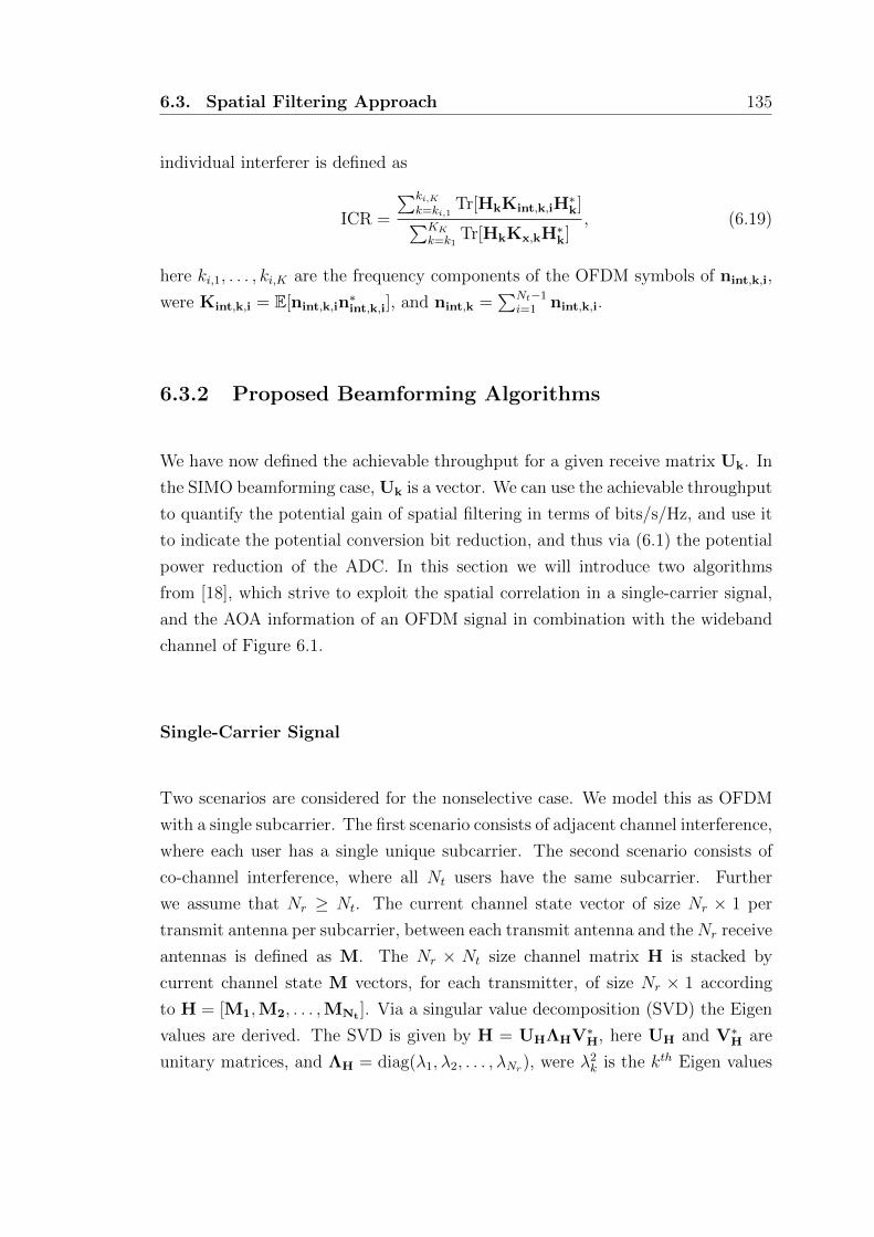
6.3. Spatial Filtering Approach 135
individual interferer is defined as
ICR =
∑ki,Kk=ki,1
Tr[HkKint,k,iH∗k]∑KK
k=k1Tr[HkKx,kH∗k]
, (6.19)
here ki,1, . . . , ki,K are the frequency components of the OFDM symbols of nint,k,i,
were Kint,k,i = E[nint,k,in∗int,k,i], and nint,k =
∑Nt−1i=1 nint,k,i.
6.3.2 Proposed Beamforming Algorithms
We have now defined the achievable throughput for a given receive matrix Uk. In
the SIMO beamforming case, Uk is a vector. We can use the achievable throughput
to quantify the potential gain of spatial filtering in terms of bits/s/Hz, and use it
to indicate the potential conversion bit reduction, and thus via (6.1) the potential
power reduction of the ADC. In this section we will introduce two algorithms
from [18], which strive to exploit the spatial correlation in a single-carrier signal,
and the AOA information of an OFDM signal in combination with the wideband
channel of Figure 6.1.
Single-Carrier Signal
Two scenarios are considered for the nonselective case. We model this as OFDM
with a single subcarrier. The first scenario consists of adjacent channel interference,
where each user has a single unique subcarrier. The second scenario consists of
co-channel interference, where all Nt users have the same subcarrier. Further
we assume that Nr ≥ Nt. The current channel state vector of size Nr × 1 per
transmit antenna per subcarrier, between each transmit antenna and theNr receive
antennas is defined as M. The Nr × Nt size channel matrix H is stacked by
current channel state M vectors, for each transmitter, of size Nr × 1 according
to H = [M1,M2, . . . ,MNt ]. Via a singular value decomposition (SVD) the Eigen
values are derived. The SVD is given by H = UHΛHV∗H, here UH and V∗H are
unitary matrices, and ΛH = diag(λ1, λ2, . . . , λNr), were λ2k is the kth Eigen values
136 Chapter 6. Analog Spatial Filtering in Wideband Cognitive Radio
of HH∗. The matrix U∗H contains Nr conjugated Eigenvectors of size 1×Nr, from
these Nr vectors the vector that maximizes (6.14) is chosen for Uk. The receiver
array is now beamforming into the direction of the desired user, while nulling the
other sources.
OFDM Signal
For the wideband channel of Figure 6.1 all OFDM subcarriers of x and nint each
have a unique frequency. The Nr × Nt size channel matrix H is stacked by cur-
rent channel state M vectors, for each transmitter, of size Nr × 1 according to
H = [M1,M2, . . . ,MNt ]. The aim is to find an appropriate setting for a common
vector Uk across all frequency components such that the throughput T is maxi-
mized. Ideally, the spatial filter should preserve all the desired user information
while simultaneously nulling the interferers. In reality however, there is a trade-off
between these two requirements, and perfect nulling across the entire frequency
range cannot be achieved by a common matrix setting. In order to find an ap-
propriate setting for Uk we propose two different estimation algorithms. The first
algorithm is comparable to maximum ratio combining, and primarily strives to
maximize the SNR of the desired user. The second algorithm primarily strives
to minimize the noise contribution of Nq =∑K
k=1 Nq,k, which is a scalar in the
beamforming case, by suppressing the interferers.
The first algorithm (WB Method 1) is a least squares algorithm which tries to
maximize the power of the desired user and mitigate the power of the interfering
users. The algorithm iteratively solves the equality
‖AU− b‖22 = 0 (6.20)
here A is a K ×Nr size matrix containing the channel components of 1×Nr size
transposed non zero channel vector Mk of each kth frequency, b is a K × 1 vector
containing zeros on the frequency components of nint and ones on the frequency
components of x, U is a complex Nr × 1 size vector and its transpose is used as a
common Uk in (6.14).
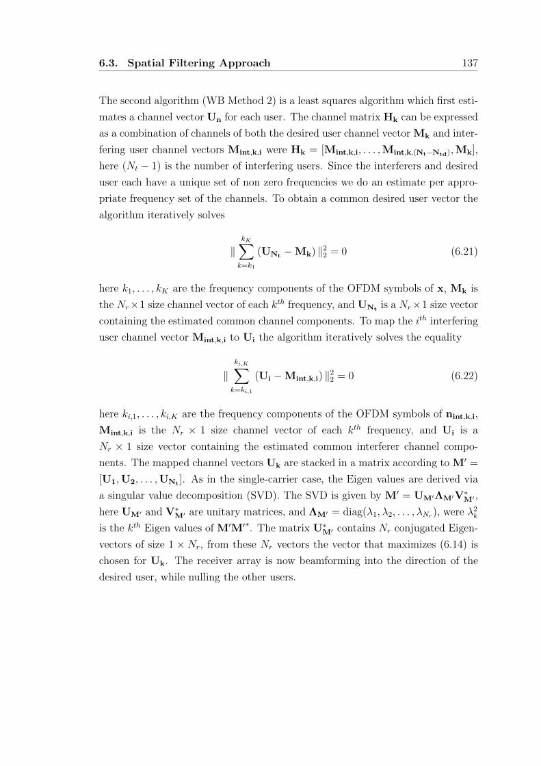
6.3. Spatial Filtering Approach 137
The second algorithm (WB Method 2) is a least squares algorithm which first esti-
mates a channel vector Un for each user. The channel matrix Hk can be expressed
as a combination of channels of both the desired user channel vector Mk and inter-
fering user channel vectors Mint,k,i were Hk = [Mint,k,i, . . . ,Mint,k,(Nt−Ntd),Mk],
here (Nt − 1) is the number of interfering users. Since the interferers and desired
user each have a unique set of non zero frequencies we do an estimate per appro-
priate frequency set of the channels. To obtain a common desired user vector the
algorithm iteratively solves
‖kK∑k=k1
(UNt −Mk) ‖22 = 0 (6.21)
here k1, . . . , kK are the frequency components of the OFDM symbols of x, Mk is
the Nr×1 size channel vector of each kth frequency, and UNt is a Nr×1 size vector
containing the estimated common channel components. To map the ith interfering
user channel vector Mint,k,i to Ui the algorithm iteratively solves the equality
‖ki,K∑k=ki,1
(Ui −Mint,k,i) ‖22 = 0 (6.22)
here ki,1, . . . , ki,K are the frequency components of the OFDM symbols of nint,k,i,
Mint,k,i is the Nr × 1 size channel vector of each kth frequency, and Ui is a
Nr × 1 size vector containing the estimated common interferer channel compo-
nents. The mapped channel vectors Uk are stacked in a matrix according to M′ =
[U1,U2, . . . ,UNt ]. As in the single-carrier case, the Eigen values are derived via
a singular value decomposition (SVD). The SVD is given by M′ = UM′ΛM′V∗M′ ,
here UM′ and V∗M′ are unitary matrices, and ΛM′ = diag(λ1, λ2, . . . , λNr), were λ2k
is the kth Eigen values of M′M′∗. The matrix U∗M′ contains Nr conjugated Eigen-
vectors of size 1 × Nr, from these Nr vectors the vector that maximizes (6.14) is
chosen for Uk. The receiver array is now beamforming into the direction of the
desired user, while nulling the other users.
138 Chapter 6. Analog Spatial Filtering in Wideband Cognitive Radio
6.3.3 Proposed Full MIMO Spatial Filter Algorithms
In the Full MIMO Spatial filter, the wideband input signal is processed in front
of the ADCs via a single common analog matrix as depicted in Figure 5.4, and
x and nint are on separate frequencies. In the channel model of Figure 6.2, we
assume a full rank MIMO system, Ntd = Nr. Therefore, there is a larger number
of transmit antennas than receive antennas (i.e., Nt > Nr) in the channel model.
Since the channel matrix is rank deficient, it acts as a rank reduction matrix on
the system. In the system depicted in Figure 5.4 the Nr × Nt channel matrix is
processed in front of the ADCs via a smaller Nr ×Nr matrix.
The aim is to find an appropriate setting for the common Nr×Nr matrix Uk across
all frequency components such that the throughput T of (6.14) is maximized. In an
appropriate setting for the common channel spatial filter matrix, each row of Uk
should beamform in an independent direction such that UkU∗k = cI (here c is a non
zero scalar), this in order to prevent correlation in (6.14). Correlation in (6.14)
negatively impacts the throughput by decreasing the value of the determinant.
Simultaneously, the AOAs of the interferers should be suppressed as such that the
value of the components of Nq =∑K
k=1 Nq,k, which is a diagonal matrix in the
full MIMO case, in (6.14) is minimized.
Since the wideband channel matrix H is rank deficient and the received signal
includes strong interference, standard estimation methods based on SVD are not
applicable. An SVD on a rank deficient channel matrix yields fewer Eigenvalues
than transmit antennas and the largest Eigenvalues will correspond to the inter-
ferers. Therefore, we propose a new approach to find a setting for the common
matrix Uk. In the first step we map the channel matrices of the separate OFDM
symbols on a common channel matrix for all frequencies. In the second step we will
use the mapped common channel matrix to estimate a common matrix setting of
Uk across all frequency components. The algorithm primarily strives to minimize
the noise contribution of the components of diagonal matrix Nq by suppressing
the interferers.
For the mapping we estimate a common channel matrix H′ from all Hk channels.
6.3. Spatial Filtering Approach 139
The channel matrix Hk can be expressed as a combination of channels of both
the desired user channel matrix Mk and interfering user channel vectors Mint,k,i
were Hk = [Mint,k,i, . . . ,Mint,k,(Nt−Ntd),Mk], here (Nt − Ntd) is the number of
interfering users. Since the interferers and desired user each have a disjoint set of
non zero frequencies the mapping to a common channel across all frequencies per
user is only performed per appropriate non zero frequency set of the channels. To
map the desired user channel matrix Mk to M′ the algorithm iteratively solves
the equality
‖kK∑k=k1
(M′ −Mk) ‖22 = 0 (6.23)
here k1, . . . , kK are the frequency components of the OFDM symbols of x, Mk is
the Nr ×Ntd size channel matrix of each kth frequency, and M′ is a Nr ×Ntd size
matrix containing the estimated common channel components. To map the ith
interfering user channel vector Mint,k,i to M′int,i the algorithm iteratively solves
the equality
‖ki,K∑k=ki,1
(M′
int,i −Mint,k,i
)‖2
2 = 0 (6.24)
here ki,1, . . . , ki,K are the frequency components of the OFDM symbols of nint,k,i,
Mint,k,i is the Nr×1 size channel vector of each kth frequency, and M′int,i is a Nr×1
size matrix containing the estimated common interferer channel components.
The spatial filter should minimize the components of diagonal matrix Nq in (6.14),
while preserving the desired user information. To find an appropriate setting for
Uk, first each Eigenvalue vector of M′ is combined with the AOAs of the interferers
to form separate matrices. On each resulting matrix an SVD is performed to find
a 1×Nr sized row vector for each row of Nr ×Nr sized spatial filter matrix Uk as
such that each row vector of matrix Uk beamforms towards a separate Eigenvalue
vector of the common desired user channel state matrix M′ while nulling the AOAs
of common channel state vectors M′int,i of each interferer.
To find the common AOAs of M that contain most of the desired user power
(which we want to preserve in the setting of the common spatial filter matrix Uk)
we search for the common Eigenvalue vectors corresponding to M′. The Eigenvalue
vectors of M′ are obtained via an SVD. The SVD is given by M′ = UM′ΛM′V∗M′ ,

140 Chapter 6. Analog Spatial Filtering in Wideband Cognitive Radio
here UM′ and V∗M′ are unitary matrices, and ΛM′ = diag(λ1, λ2, . . . , λNr), were
λ2k is the kth Eigenvalues of M′M′∗. From UM′ , every column is taken and set in
a separate vector UM′,m, as such that UM′ = [UM′,1, . . . ,UM′,Nr ]. The vectors
UM′,m now correspond to the dominant AOAs at the receiver of the Eigenvalues
of M′.
Now that the Eigenvalue vectors of M′ are found, these are combined with the
AOAs of M′int,i of each interferer to find a setting for Uk that maximizes (6.14).
In this maximum, the receiver beamforms towards the Eigenvalue vectors of M′
while nulling the AOAs of M′int,i of each interferer. Under the constraint that
(Nt −Ntd) < Nr, each vector UM′,m is stacked in a matrix Qm with the common
interferer channel vectors such that Qm = [M′int,i, . . . ,M
′int,(Nt−Ntd),UM′,m]. We
now take an SVD of Qm. The SVD is given by Qm = UQ,mΛQ,mV∗Q,m, here UQ,m
and V∗Q,m are unitary matrices, and ΛQ,m = diag(λ1, λ2, . . . , λNr), were λ2k is the
kth Eigenvalues of Q′mQ′∗m. There are Nr matrices UQ,m of size Nr×Nr containing
Nr Eigenvectors UQ,d,m of size Nr×1. The total number of N2r vectors UQ,d,m are
stacked in NNrr unique matrices Ut of the form Ut = [UQ,d,1, . . . ,UQ,d,Nr ]. From
the NNrr unique matrices Ut the matrix U∗t that maximizes (6.14) is chosen for
Uk. The resulting matrix setting now nulls the interferers, while beaming into the
Eigenvalues of the desired user. Nulling the interference is a good strategy when
the number of ADC steps is small. When more steps are available in the ADC
a compromise between interference suppression and maximum ratio combining is
needed.
6.4 Numerical Results
In this Section we start by simulating the vector beamforming architecture of
Figure 5.3 in combination with single-carrier signals and a Rayleigh fading channel
example. Secondly we use OFDM signals and the wideband channel model of
Figure 6.1 to show the potential benefit of spatial filtering in a wideband regime
and to quantify the potential gain in terms of ADC power reduction and ADC
bits. Then, we extend the simulation to show the effect of the RMS delay spread
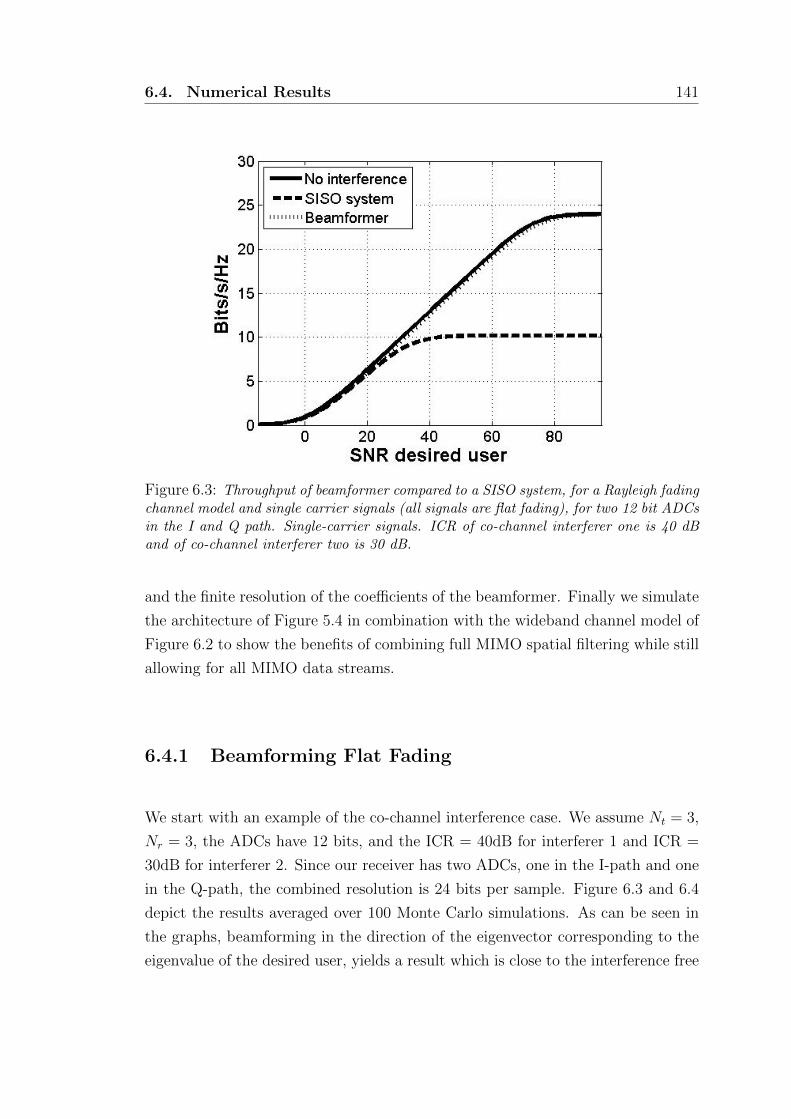
6.4. Numerical Results 141
Figure 6.3: Throughput of beamformer compared to a SISO system, for a Rayleigh fadingchannel model and single carrier signals (all signals are flat fading), for two 12 bit ADCsin the I and Q path. Single-carrier signals. ICR of co-channel interferer one is 40 dBand of co-channel interferer two is 30 dB.
and the finite resolution of the coefficients of the beamformer. Finally we simulate
the architecture of Figure 5.4 in combination with the wideband channel model of
Figure 6.2 to show the benefits of combining full MIMO spatial filtering while still
allowing for all MIMO data streams.
6.4.1 Beamforming Flat Fading
We start with an example of the co-channel interference case. We assume Nt = 3,
Nr = 3, the ADCs have 12 bits, and the ICR = 40dB for interferer 1 and ICR =
30dB for interferer 2. Since our receiver has two ADCs, one in the I-path and one
in the Q-path, the combined resolution is 24 bits per sample. Figure 6.3 and 6.4
depict the results averaged over 100 Monte Carlo simulations. As can be seen in
the graphs, beamforming in the direction of the eigenvector corresponding to the
eigenvalue of the desired user, yields a result which is close to the interference free
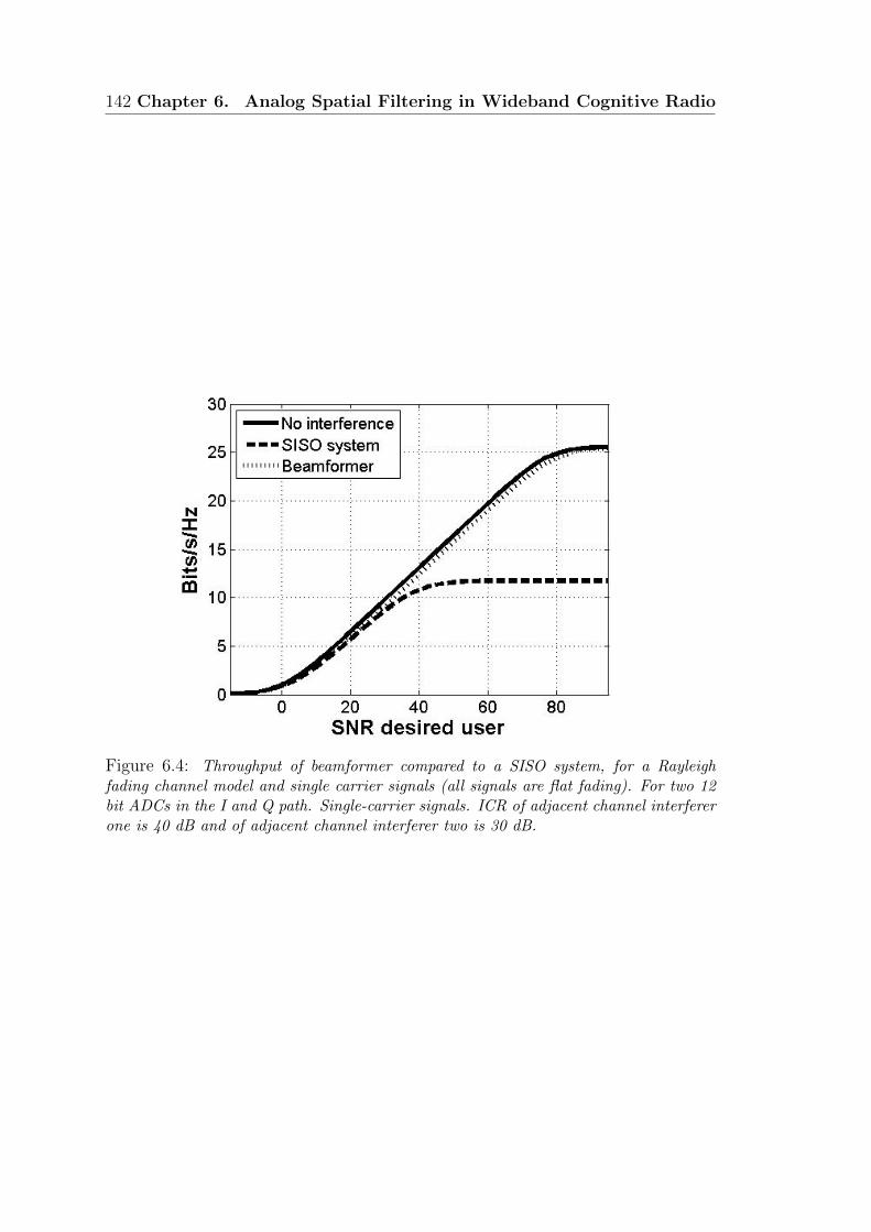
142 Chapter 6. Analog Spatial Filtering in Wideband Cognitive Radio
Figure 6.4: Throughput of beamformer compared to a SISO system, for a Rayleighfading channel model and single carrier signals (all signals are flat fading). For two 12bit ADCs in the I and Q path. Single-carrier signals. ICR of adjacent channel interfererone is 40 dB and of adjacent channel interferer two is 30 dB.
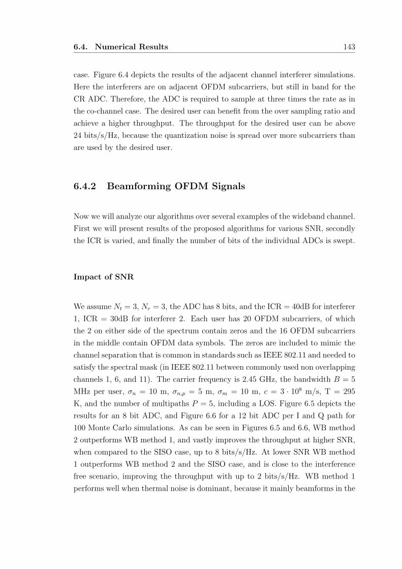
6.4. Numerical Results 143
case. Figure 6.4 depicts the results of the adjacent channel interferer simulations.
Here the interferers are on adjacent OFDM subcarriers, but still in band for the
CR ADC. Therefore, the ADC is required to sample at three times the rate as in
the co-channel case. The desired user can benefit from the over sampling ratio and
achieve a higher throughput. The throughput for the desired user can be above
24 bits/s/Hz, because the quantization noise is spread over more subcarriers than
are used by the desired user.
6.4.2 Beamforming OFDM Signals
Now we will analyze our algorithms over several examples of the wideband channel.
First we will present results of the proposed algorithms for various SNR, secondly
the ICR is varied, and finally the number of bits of the individual ADCs is swept.
Impact of SNR
We assume Nt = 3, Nr = 3, the ADC has 8 bits, and the ICR = 40dB for interferer
1, ICR = 30dB for interferer 2. Each user has 20 OFDM subcarriers, of which
the 2 on either side of the spectrum contain zeros and the 16 OFDM subcarriers
in the middle contain OFDM data symbols. The zeros are included to mimic the
channel separation that is common in standards such as IEEE 802.11 and needed to
satisfy the spectral mask (in IEEE 802.11 between commonly used non overlapping
channels 1, 6, and 11). The carrier frequency is 2.45 GHz, the bandwidth B = 5
MHz per user, σn = 10 m, σn,p = 5 m, σm = 10 m, c = 3 · 108 m/s, T = 295
K, and the number of multipaths P = 5, including a LOS. Figure 6.5 depicts the
results for an 8 bit ADC, and Figure 6.6 for a 12 bit ADC per I and Q path for
100 Monte Carlo simulations. As can be seen in Figures 6.5 and 6.6, WB method
2 outperforms WB method 1, and vastly improves the throughput at higher SNR,
when compared to the SISO case, up to 8 bits/s/Hz. At lower SNR WB method
1 outperforms WB method 2 and the SISO case, and is close to the interference
free scenario, improving the throughput with up to 2 bits/s/Hz. WB method 1
performs well when thermal noise is dominant, because it mainly beamforms in the
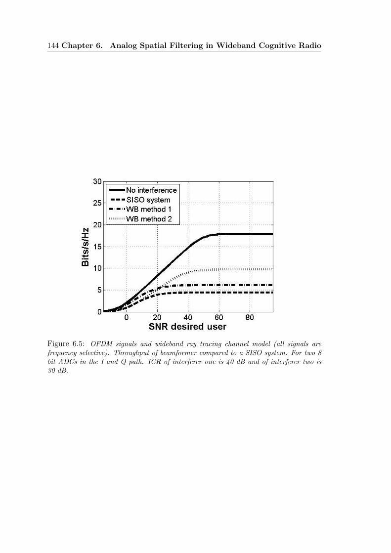
144 Chapter 6. Analog Spatial Filtering in Wideband Cognitive Radio
Figure 6.5: OFDM signals and wideband ray tracing channel model (all signals arefrequency selective). Throughput of beamformer compared to a SISO system. For two 8bit ADCs in the I and Q path. ICR of interferer one is 40 dB and of interferer two is30 dB.
6.4. Numerical Results 145
Figure 6.6: OFDM signals and wideband ray tracing channel model (all signals arefrequency selective). Throughput of beamformer compared to a SISO system. For two 12bit ADCs in the I and Q path. ICR of interferer one is 40 dB and of interferer two is30 dB.
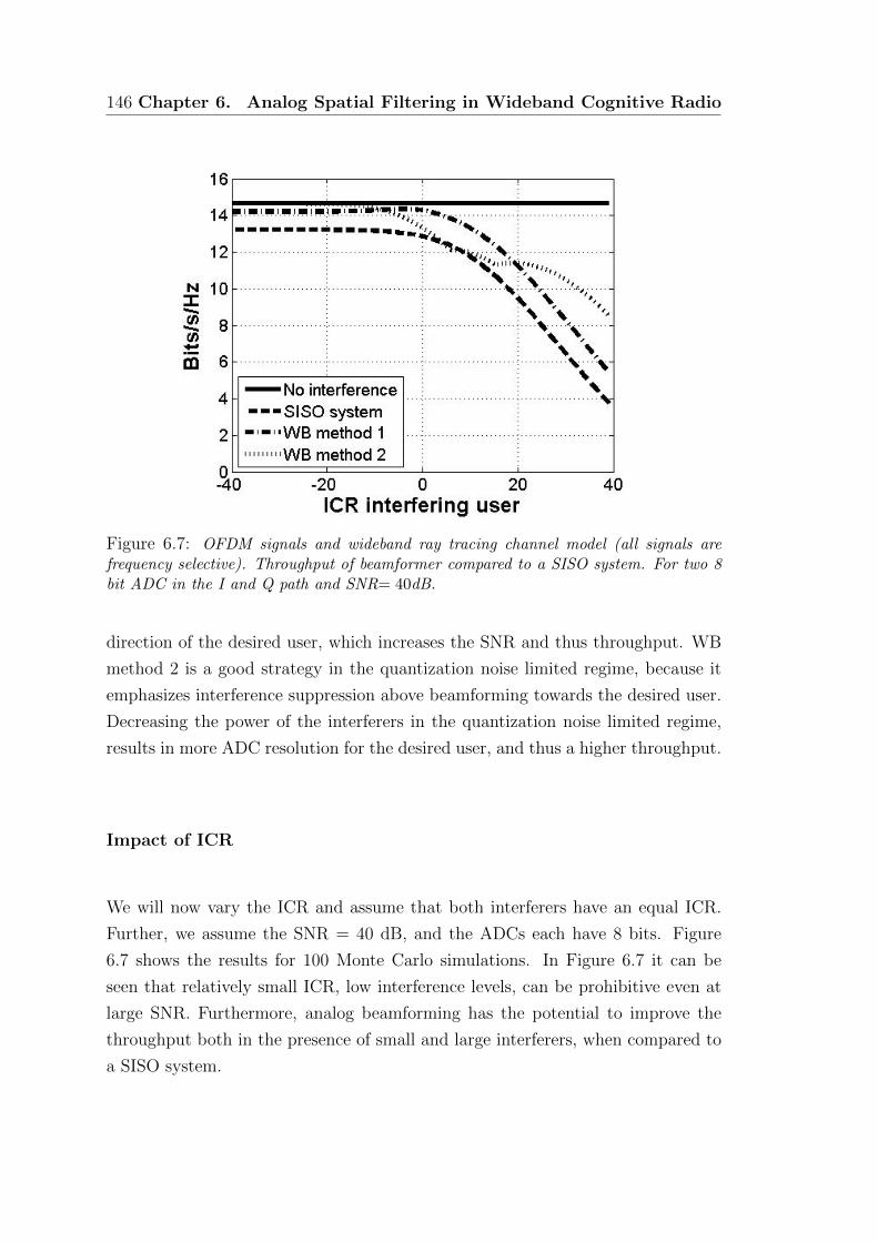
146 Chapter 6. Analog Spatial Filtering in Wideband Cognitive Radio
Figure 6.7: OFDM signals and wideband ray tracing channel model (all signals arefrequency selective). Throughput of beamformer compared to a SISO system. For two 8bit ADC in the I and Q path and SNR= 40dB.
direction of the desired user, which increases the SNR and thus throughput. WB
method 2 is a good strategy in the quantization noise limited regime, because it
emphasizes interference suppression above beamforming towards the desired user.
Decreasing the power of the interferers in the quantization noise limited regime,
results in more ADC resolution for the desired user, and thus a higher throughput.
Impact of ICR
We will now vary the ICR and assume that both interferers have an equal ICR.
Further, we assume the SNR = 40 dB, and the ADCs each have 8 bits. Figure
6.7 shows the results for 100 Monte Carlo simulations. In Figure 6.7 it can be
seen that relatively small ICR, low interference levels, can be prohibitive even at
large SNR. Furthermore, analog beamforming has the potential to improve the
throughput both in the presence of small and large interferers, when compared to
a SISO system.
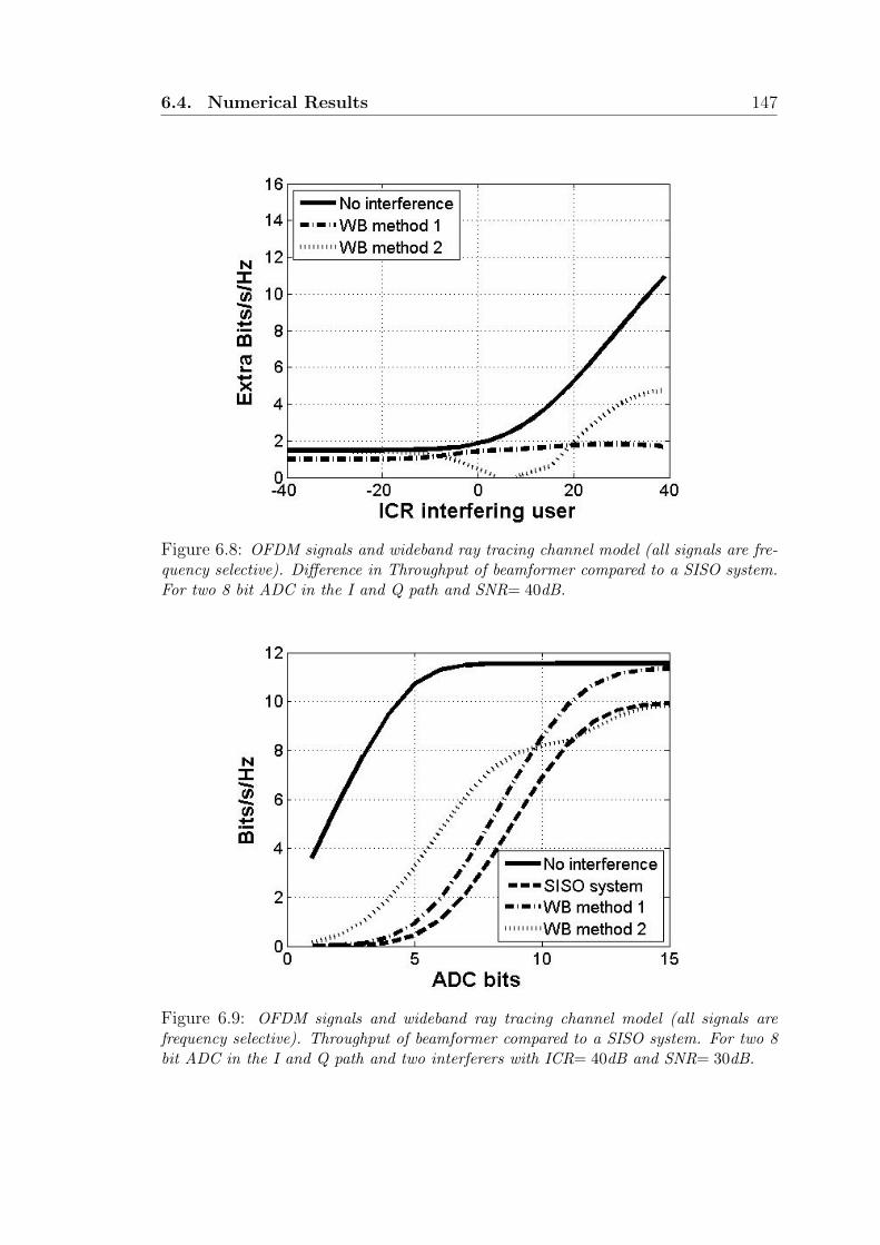
6.4. Numerical Results 147
Figure 6.8: OFDM signals and wideband ray tracing channel model (all signals are fre-quency selective). Difference in Throughput of beamformer compared to a SISO system.For two 8 bit ADC in the I and Q path and SNR= 40dB.
Figure 6.9: OFDM signals and wideband ray tracing channel model (all signals arefrequency selective). Throughput of beamformer compared to a SISO system. For two 8bit ADC in the I and Q path and two interferers with ICR= 40dB and SNR= 30dB.
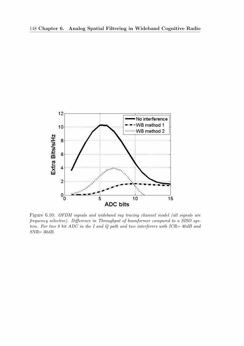
148 Chapter 6. Analog Spatial Filtering in Wideband Cognitive Radio
Figure 6.10: OFDM signals and wideband ray tracing channel model (all signals arefrequency selective). Difference in Throughput of beamformer compared to a SISO sys-tem. For two 8 bit ADC in the I and Q path and two interferers with ICR= 40dB andSNR= 30dB.

6.4. Numerical Results 149
Table 6.1: SNR versus number of bits required to achieve a given throughput in the
beamformer case T = 2 bits/s/Hz. OFDM signals and wideband ray tracing channel
model (wanted signal is frequency selective and interferers are flat fading).
SNR Analog Array SISO Difference[dB] [bits] [bits] [bits]10 5.0 7.5 2.520 3.1 7.1 4.030 2.4 6.8 4.440 2.4 6.7 4.3
Impact of Number of ADC Bits
Compared to the previous section we will now vary the number of ADC bits and
assume both the I and Q ADC have an equal number of bits. Further, we assume
the ICR = 40 dB for interferer 1 and 2. Figure 6.8 shows that the throughput gain
compared to a SISO system is largest in a quantization noise limited scenario.
From Figure 6.9 we can derive that at a throughput of 2 bits/s/Hz, an analog
spatial filtering system can equal a SISO system with 3 bits per ADC less. Since
we assume a large ICR of 40 dB we consider it reasonable to assume the interference
is in close proximity to the receiver. Therefore the delay spread of the interferer
will be much smaller than that of the desired user. To take this into account, the
significant multipaths for the interferers are set to two and for the desired user
to five in (6.10). Results are shown in Table 6.1. This result is significant since
this indicates that the power savings for the ADC can potentially be an order of
magnitude. Since the power of ADC converters reduces with approximately 90%
every decade, analog spatial filtering has the potential to accelerate the reduction
of overall system power reduction.
Impact of Finite Resolution Phase Shifters
Up until now we have considered the phase shifters to have floating point precision.
In practical systems the analog phase shifters have discrete steps. A common
implementation of a phase shifter is a VGA in the I and a VGA in the Q path.
We realized an IC implementation in [72], where an RF polyphase filter after the
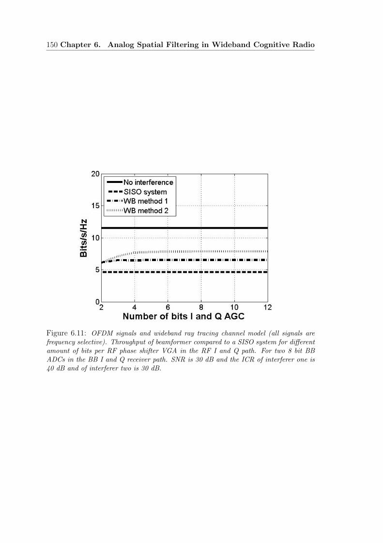
150 Chapter 6. Analog Spatial Filtering in Wideband Cognitive Radio
Figure 6.11: OFDM signals and wideband ray tracing channel model (all signals arefrequency selective). Throughput of beamformer compared to a SISO system for differentamount of bits per RF phase shifter VGA in the RF I and Q path. For two 8 bit BBADCs in the BB I and Q receiver path. SNR is 30 dB and the ICR of interferer one is40 dB and of interferer two is 30 dB.
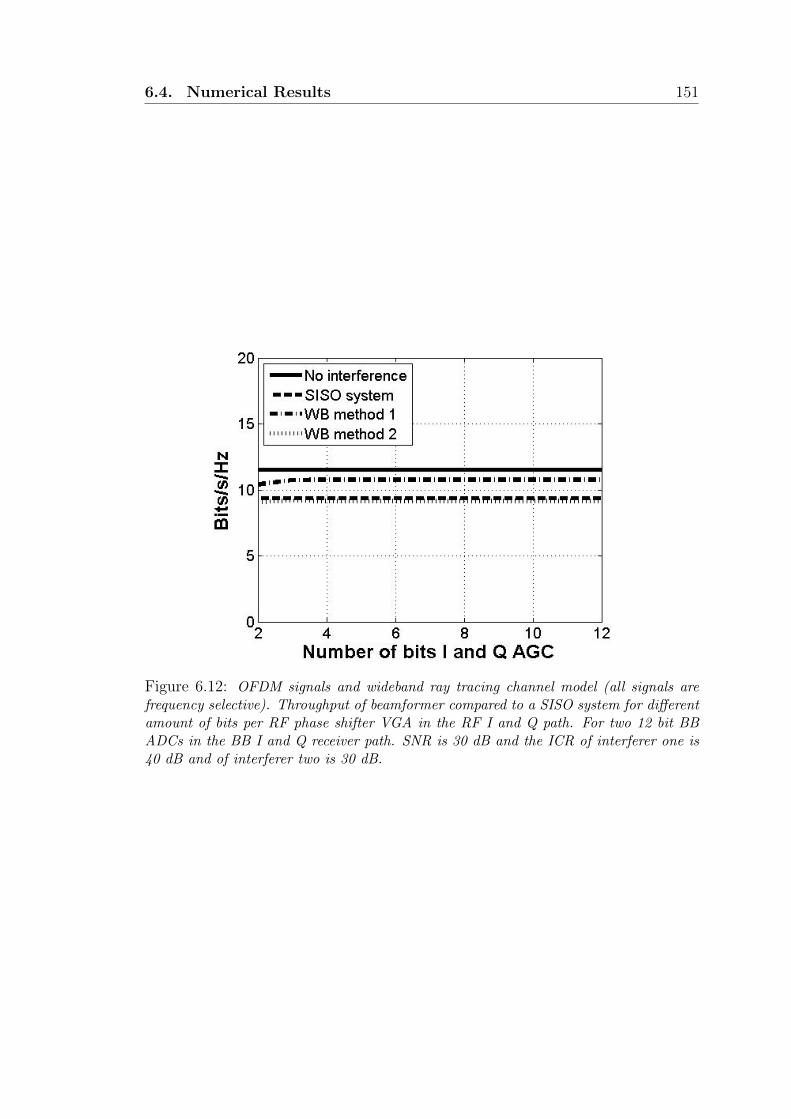
6.4. Numerical Results 151
Figure 6.12: OFDM signals and wideband ray tracing channel model (all signals arefrequency selective). Throughput of beamformer compared to a SISO system for differentamount of bits per RF phase shifter VGA in the RF I and Q path. For two 12 bit BBADCs in the BB I and Q receiver path. SNR is 30 dB and the ICR of interferer one is40 dB and of interferer two is 30 dB.
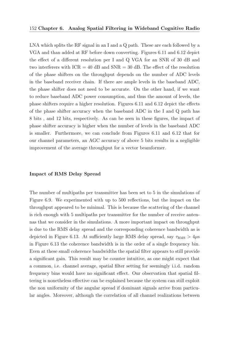
152 Chapter 6. Analog Spatial Filtering in Wideband Cognitive Radio
LNA which splits the RF signal in an I and a Q path. These are each followed by a
VGA and than added at RF before down converting. Figures 6.11 and 6.12 depict
the effect of a different resolution per I and Q VGA for an SNR of 30 dB and
two interferers with ICR = 40 dB and SNR = 30 dB. The effect of the resolution
of the phase shifters on the throughput depends on the number of ADC levels
in the baseband receiver chain. If there are ample levels in the baseband ADC,
the phase shifter does not need to be accurate. On the other hand, if we want
to reduce baseband ADC power consumption, and thus the amount of levels, the
phase shifters require a higher resolution. Figures 6.11 and 6.12 depict the effects
of the phase shifter accuracy when the baseband ADC in the I and Q path has
8 bits , and 12 bits, respectively. As can be seen in these figures, the impact of
phase shifter accuracy is higher when the number of levels in the baseband ADC
is smaller. Furthermore, we can conclude from Figures 6.11 and 6.12 that for
our channel parameters, an AGC accuracy of above 5 bits results in a negligible
improvement of the average throughput for a vector beamformer.
Impact of RMS Delay Spread
The number of multipaths per transmitter has been set to 5 in the simulations of
Figure 6.9. We experimented with up to 500 reflections, but the impact on the
throughput appeared to be minimal. This is because the scattering of the channel
is rich enough with 5 multipaths per transmitter for the number of receive anten-
nas that we consider in the simulations. A more important impact on throughput
is due to the RMS delay spread and the corresponding coherence bandwidth as is
depicted in Figure 6.13. At sufficiently large RMS delay spread, say τRMS > 4µs
in Figure 6.13 the coherence bandwidth is in the order of a single frequency bin.
Even at these small coherence bandwidths the spatial filter appears to still provide
a significant gain. This result may be counter intuitive, as one might expect that
a common, i.e. channel average, spatial filter setting for seemingly i.i.d. random
frequency bins would have no significant effect. Our observation that spatial fil-
tering is nonetheless effective can be explained because the system can still exploit
the non uniformity of the angular spread if dominant signals arrive from particu-
lar angles. Moreover, although the correlation of all channel realizations between
6.4. Numerical Results 153
Figure 6.13: OFDM signals and wideband ray tracing channel model (all signals arefrequency selective). Effect of changing delay spread on throughput for 400 reflectivesurfaces, SNR is 30 dB. For two 8 bit ADCs in the I and Q path. ICR of interferer oneis 40 dB and of interferer two is 30 dB.

154 Chapter 6. Analog Spatial Filtering in Wideband Cognitive Radio
frequency bins will approach zero at large RMS delay spread, the instantaneous
signal correlation for a specific channel realization is not necessarily zero, in which
case it can be exploited by the spatial filter.
Although our focus here is primarily on indoor environments, spatial filtering can
also be effective in other propagation environments. In the IEEE 802.22 standard,
which is primarily designed for low populated rural areas [86], most primary users,
such as TV broadcasters and FM radio stations, which interfere with the secondary
CR tend to have a small RMS delay spread and a small AOA spread [87].
6.4.3 Full MIMO Spatial Filtering Wideband Channel
Now we will give several examples of the full MIMO case. In the full MIMO
case, the ACMM performs spatial filtering while allowing for all data streams. For
simulations we will use the channel model depicted in Figure 6.2.
Impact of Number of ADC Bits
We will now vary the number of ADC bits and assume both the I and Q ADC
have an equal number of bits. Since we assume a large ICR of 40 dB we consider it
reasonable to assume the interference is in close proximity to the receiver. There-
fore the delay spread of the interferer will be much smaller than that of the desired
user. To account for this effect, we assume that in the MIMO wideband channel
model there are 2 reflections per interferer and 40 reflection for the desired user.
Figures 6.14 and 6.15 show that the throughput gain compared to a regular MIMO
system is largest in a quantization noise limited scenario. In Table 6.2 it can be
seen that the difference between the ACMM and regular MIMO is smaller at lower
SNR values. This is because our algorithm is trying to null the interferers, at lower
SNR values it may be more effective to focus more on maximum ratio combining
than nulling. From Figures 6.14 and 6.15 we can derive that at a throughput of
5 bits/s/Hz, an analog spatial filtering system can equal a 4 × 4 MIMO system
with 3 bits per ADC less (Table 6.2). We believe this result is significant since
6.4. Numerical Results 155
Figure 6.14: OFDM signals and wideband ray tracing channel model (wanted signalis frequency selective and interferers are flat fading). Throughput of ACMM-MIMOcompared to a regular and interference free MIMO system at SNR is 20dB, for a 4×4MIMO system. Two interferers at ICR = 40 dB.
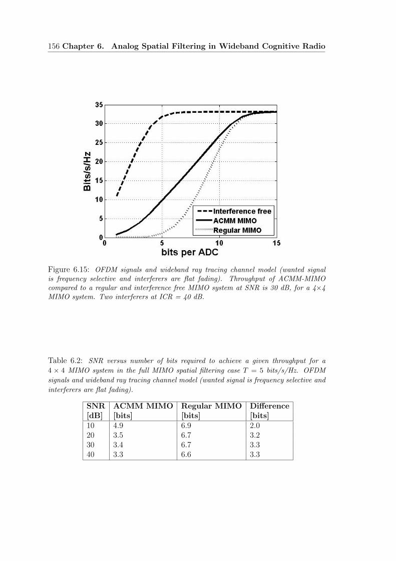
156 Chapter 6. Analog Spatial Filtering in Wideband Cognitive Radio
Figure 6.15: OFDM signals and wideband ray tracing channel model (wanted signalis frequency selective and interferers are flat fading). Throughput of ACMM-MIMOcompared to a regular and interference free MIMO system at SNR is 30 dB, for a 4×4MIMO system. Two interferers at ICR = 40 dB.
Table 6.2: SNR versus number of bits required to achieve a given throughput for a
4 × 4 MIMO system in the full MIMO spatial filtering case T = 5 bits/s/Hz. OFDM
signals and wideband ray tracing channel model (wanted signal is frequency selective and
interferers are flat fading).
SNR ACMM MIMO Regular MIMO Difference[dB] [bits] [bits] [bits]10 4.9 6.9 2.020 3.5 6.7 3.230 3.4 6.7 3.340 3.3 6.6 3.3
6.4. Numerical Results 157
this indicates that the power consumption of the MIMO ADCs can potentially
be reduced with over 85%. Therefore, full MIMO analog spatial filtering has the
potential to accelerate the overall system power consumption reduction.
Comparing Full MIMO Spatial Filtering to Beamforming
In Figure 6.16 a 4× 4 full MIMO spatial filter is compared to a 4× 1 beamformer.
We assume that in the MIMO wideband channel model there are 2 reflections
per interferer and 40 reflection for the desired user. The figure shows that at low
ADC bits, when the quantization noise is dominant, the beamformer and ACMM
have a comparable performance. However, at higher ADC bits the MIMO receiver
clearly outperforms the beamformer. The performance is comparable at low ADC
bits because the quantization noise is so dominant that only the strongest Eigen
value contributes to the throughput. Since the beamfomer focuses mainly on
the strongest Eigen value its performance is similar to the ACMM, but with 3
ADCs less. From this example it can be seen that at channel realizations were
there is a large variation in the dynamic range of the Eigen values, it is beneficial
to switch off branches in the ACMM opportunistically to safe power, since they
do not contribute to the overall system throughput. The empirical distribution
function of the eigenvalues of Wishart matrices has an asymptotic distribution.
This implies a large condition number and thus often leads to a large difference in
the dynamic range of the eigenvalues for a given channel state. After evaluating
the eigenvalue distribution of the channel, the signal to thermal and quantization
noise ratio at the receiver can be used by the receiver as a measure to decide to
switch on and off branches. Another option is to dynamically allocate the total
amount of quantization levels in the receiver across the ADCs to further minimize
the quantization noise contribution. This may allow for a reduction in the total
amount of levels used and thus in the total ADC requirements.
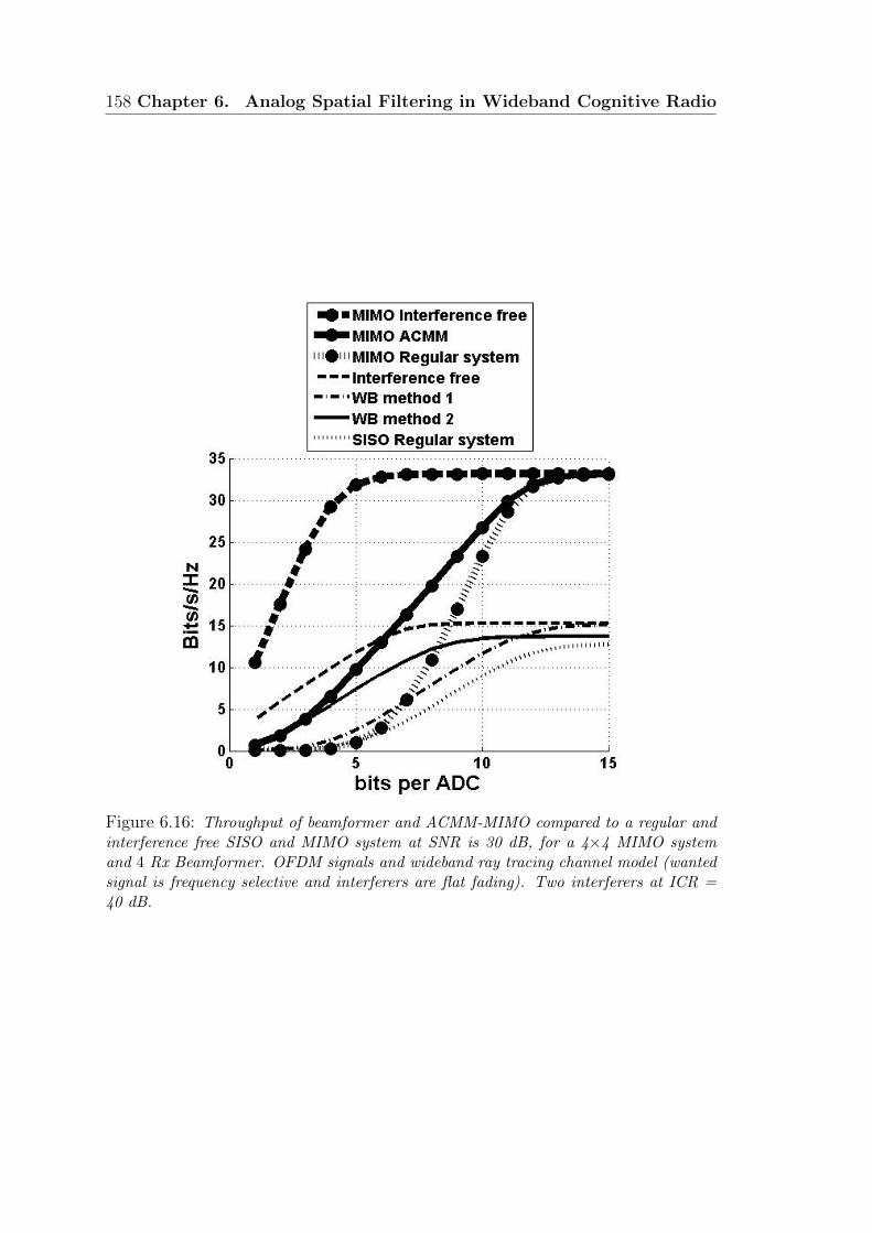
158 Chapter 6. Analog Spatial Filtering in Wideband Cognitive Radio
Figure 6.16: Throughput of beamformer and ACMM-MIMO compared to a regular andinterference free SISO and MIMO system at SNR is 30 dB, for a 4×4 MIMO systemand 4 Rx Beamformer. OFDM signals and wideband ray tracing channel model (wantedsignal is frequency selective and interferers are flat fading). Two interferers at ICR =40 dB.
6.5. Conclusions 159
6.5 Conclusions
In wideband cognitive radio (CR), analog spatial filtering can achieve similar sys-
tem throughput as systems without spatial filtering with significantly less quantiza-
tion bits in the baseband ADC. Simulations show that for realistic indoor scenarios
with an SNR of 20 dB and two interferers with an ICR of 40 dB, a receiver using
analog vector beamforming spatial filtering can achieve similar throughput com-
pared to SISO with 4 ADC bits less, corresponding to a power reduction of over
90%. Further, simulations indicate that a MIMO system with an analog complex
matrix multiplier that allows for full MIMO spatial filtering can achieve a simi-
lar throughput as a regular MIMO system with 3 ADC bit less, corresponding to
a power reduction of over 85%. Opportunistic on and off switching of branches
in the ACMM given a large variety in the dynamic range of the Eigen values of
the current channel state and under low SNR can contribute to further power
reduction. Another option is to dynamically allocate quantization levels among
branches to further minimize the quantization noise contributed by the ADCs and
thus their requirements. Since ADC power consumption reduces at a rate of an
order of magnitude per decade, we believe that the algorithms and architectures
for spatial filtering we proposed in this chapter, and submitted to [88], can largely
contribute to overall system power reduction, and accelerate the introduction of
CR in the handheld market.

160 Chapter 6. Analog Spatial Filtering in Wideband Cognitive Radio
Chapter 7
Conclusions and
Recommendations
7.1 Conclusions
Most wireless devices such as laptops and mobile phones are battery powered. To
extend battery lifetime the power consumption of the wireless transceivers needs
to be reduced. Currently, we observe two opposing trends in new generations of
mobile phones. Despite the ongoing miniaturization of existing functionality and
its corresponding power reduction in handheld devices, the vast increase in number
of applications and the subsequent demands on hardware in new generations of
smart phones has offset and for now halted the overall trend of weight and size
reduction of mobile phones. Furthermore, the available battery energy in smart
phones has remained constant over time. Each battery power density improvement
has resulted in a shrinking phone to appeal to consumers. With the addition of new
functionalities, the power budget of existing wireless transceivers is still reducing.
The current rate of power reduction of the RF front end and ADC is one order of
magnitude per decade.
To increase the data rate of new wireless devices more new standard are using
161
162 Chapter 7. Conclusions and Recommendations
MIMO techniques, such as LTE advance for mobile phones and IEEE 802.11n for
WLAN. Because MIMO systems require multiple transceiver front ends and ADCs
they consume more power and alone can drain a smart phone battery in under 4
hours. Therefore, reducing MIMO power consumption in handheld devices is of
prime importance to increase battery lifetime.
Due to an increase in the number of users, the amount of interference is increasing.
To cope with the rise in interference, new generations of mobile devices have to
comply with more stringent requirements. The more stringent requirements come
at a cost of increased power consumption. In Chapter 2 it is shown that the RF
front end and ADC power consumption are the future bottlenecks in terms of
extending battery lifetime. Mitigating the interferers and thus the dynamic range
requirements of the RF front end and ADC has the potential to vastly reduce the
power consumption of the ADC and RF front end.
The closed form solution we presented in Chapter 4 allows us to formalize the
relation between interference power and achievable throughput for a given avail-
able receiver circuit power budget. Importantly, with the closed form solution we
can show that a 20 dB reduction in CIR requirements results in a 30 dB reduc-
tion in receiver circuit power consumption. This means that a little interference
suppression can already substantially reduce the required power budget. Another
interesting result of the closed form solution in Chapter 4 is that for large SNR
the optimal throughput per unit of receiver circuit power is 2.3 bits/s/Hz, irre-
spective of interference power level. Interestingly this limit is also independent of
the used IC technology. However, the optimum power efficiency for lower SNR
values does depend on IC technology. Furthermore, it can be shown that a duty
cycling strategy at low power consumption level can result in a higher average sys-
tem throughput than a continuously operating receiver consuming a similar time
averaged power.
In Chapter 5 a novel ACMM building block that can suppress interference in the
MIMO analog front ends, to alleviate the DR requirements of the RF front ends
and ADCs, is proposed and introduced. A key feature of the ACMM is that it
allows for all MIMO data streams, this in contrast to regular beamforming. The
ACMM IC has been implemented in 65 nm CMOS and operates in the 2.4 GHz
7.1. Conclusions 163
band. The control accuracy of the ACMM is 5 bits I and 5 bits Q per matrix
element over a 100 MHz band. Measured CIR improvement is 37 dB at an AOA
difference of 45o. The ACMM concept has been simulated in Chapter 6, and the
substantial performance gain has been confirmed by our test. The measurements
confirm that the expected time average power consumption reduction of a MIMO
system including an ACMM building block can potentially be over 90%.
Next to MIMO techniques, CR is a method to increase the average data rate. CR
achieves this by optimizing the spectral use. The theory in Chapter 6 sows that
in wideband CR, analog spatial filtering can achieve similar system throughput
as systems without spatial filtering with significantly less quantization bits in the
baseband ADC. Simulations show that for realistic indoor scenarios, a CR receiver
using analog vector beamforming spatial filtering can achieve similar throughput
compared to CR SISO with 4 ADC bits less. Furthermore, simulation indicate that
a CR MIMO system with an analog complex matrix multiplier that allows for full
MIMO spatial filtering can achieve a similar throughput as a regular CR MIMO
system with 3 ADC bit less, corresponding to a power reduction of over 85%. Since
ADC power consumption reduces at a rate of an order of magnitude per decade,
we think that the algorithms and architectures for spatial filtering can largely
contribute to overall system power reduction, and accelerate the introduction of
CR in the handheld market.
The ACMM building block proposed in this thesis, exploits the presence of multiple
receive antennas and the spatial selectivity of the channel. The overall effectiveness
of the ACMM depends on several parameters, such as e.g.:
• The RF bandwidth of the system, which contains desired users and interfer-
ers.
• The delay spread of each user and interferer channel, which determines the
coherence bandwidth of each channel and thus the effectiveness of a common
preconditioning matrix over the relevant part of the RF bandwidth
• The accuracy of the elements of the ACMM over the RF frequency band.
• The number of receiver antenna elements.

164 Chapter 7. Conclusions and Recommendations
We found that, for a 4x4 MIMO system operating in an indoor environment con-
taining the designed 65nm CMOS ACMM IC, overall front end and ADC power
consumption can potentially be reduced with an order of magnitude.
7.2 Recommendations
In this thesis we presented an analog MIMO spatial filter. The analog spatial
filter increases interference robustness and allows for significant power consump-
tion reduction of wireless receivers. Reducing the power consumption of wireless
receivers is of prime importance, since it will be the major bottleneck in the bat-
tery lifetime of future mobile devices. In this section we would like to give several
recommendations and propose several potential next steps based on this research.
• The decorrelation of the input signals of the MIMO ADCs by the ACMM IC
allows for further bit reduction still. In this thesis we have reduced the bits of
all the ADCs simultaneously. However, it is also possible to reduce the bits
per individual ADC and reduce overall power consumption further. Initial
tests on a 4 x 4 MIMO system indicate this can reduce the total number of
ADC levels by another 50% while achieving a similar data rate.
• Making the IP3 adaptable to the current channel state can help to vastly
reduce the receiver circuit power consumption of MIMO and SISO receivers.
The IP3 requirement is a dominant factor in receiver circuit power consump-
tion. A reduction of the IP3 requirement of 20 dB has the potential to reduce
receiver circuit power consumption by 30 dB. Currently, IP3 is defined for
the worst case in which the receiver should still operate. As such, the IP3
of the receiver is often over dimensioned for what is actually required given
the actual channel state.
• The effectiveness of the ACMM can be increased at a cost of more receiver
antennas. An increase in receive antennas increases the receiver spatial res-
olution and thus the accuracy with which interference can be suppressed.
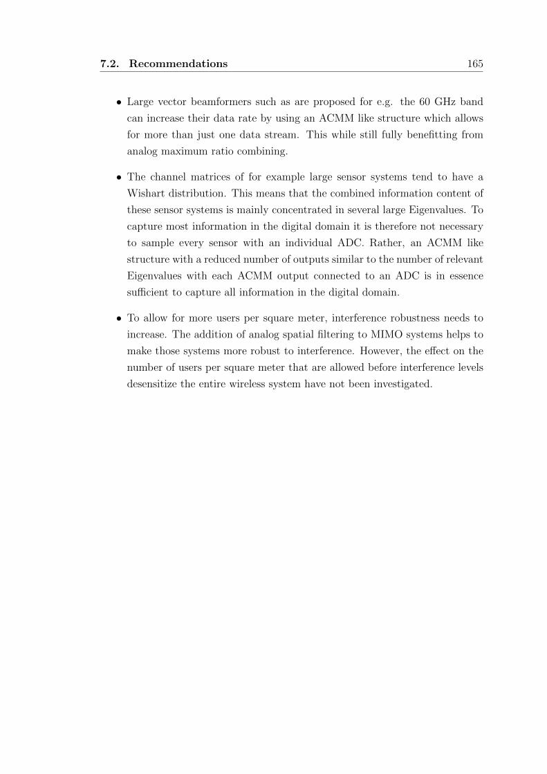
7.2. Recommendations 165
• Large vector beamformers such as are proposed for e.g. the 60 GHz band
can increase their data rate by using an ACMM like structure which allows
for more than just one data stream. This while still fully benefitting from
analog maximum ratio combining.
• The channel matrices of for example large sensor systems tend to have a
Wishart distribution. This means that the combined information content of
these sensor systems is mainly concentrated in several large Eigenvalues. To
capture most information in the digital domain it is therefore not necessary
to sample every sensor with an individual ADC. Rather, an ACMM like
structure with a reduced number of outputs similar to the number of relevant
Eigenvalues with each ACMM output connected to an ADC is in essence
sufficient to capture all information in the digital domain.
• To allow for more users per square meter, interference robustness needs to
increase. The addition of analog spatial filtering to MIMO systems helps to
make those systems more robust to interference. However, the effect on the
number of users per square meter that are allowed before interference levels
desensitize the entire wireless system have not been investigated.

166 Chapter 7. Conclusions and Recommendations
References
[1] C. E. Shannon, “A Mathematical Theory of Communication,” The Bell Sys-
tem Technical Journal, vol. 27, pp. 379–423, 623–656, October 1948.
[2] I. Telatar, “Capacity of Multi-Antenna Gaussian Channels,” European Trans-
actions on Telecommunications, vol. 10, pp. 585–595, Nov-Dec 1999.
[3] G. Foschini and M. Gans, “On Limits of Wireless Communications in a Fading
Environment When Using Multiple Antennas,” Wireless Personal Communi-
cations, vol. 6, pp. 233–235, March 1998.
[4] D. Tse and P. Viswanath, Fundamentals of Wireless Communication. Cam-
bridge University Press, 2005.
[5] P. Smulders, “Exploiting the 60 GHz Band for Local Wireless Multimedia
Acces: Prospects and Future Directions,” IEEE Communications Magazine,
pp. 140–147, January 2002.
[6] D. Cabric, M. S. Chen, D. A. Sobel, S. Wang, J. Yang, , and R. W. Broder-
sen, “Novel Radio Architectures for UWB, 60 GHz, and Cognitive Wireless
Systems,” EURASIP Journal on Wireless Communications and Networking,
Special Issue on CMOS RF Circuits for Wireless Applications, vol. 2006, Apr
2006.
[7] B. Razavi, “Challenges in Portable RF Transceiver Design,” Circuits and
Devices Magazine, IEEE, vol. 12, pp. 12–25, Sep 1996.
167
168 References
[8] A. Stelzer and R. Weigel, “Communication ICs- Market Leaders in Microelec-
tronics,” e & i Elektrotechnik und Informationstechnik, vol. 118, pp. 481–486,
Oct 2001.
[9] P. Baltus and R. Dekker, “Optimizing RF Front Ends for Low Power,” Pro-
ceedings of the IEEE, vol. 88, pp. 1546–1559, Oct 2000.
[10] B. Razavi, “Challenges in the Design of Cognitive Radios,” IEEE 2009 Cus-
tom Intergrated Circuits Conference (CICC), pp. 391–398, Sept 2009.
[11] B. Razavi, “CMOS RF Receiver Design for Wireless LAN Applications,” Ra-
dio and Wireless Conference, 1999. RAWCON 99. 1999 IEEE, pp. 275 – 280,
Aug 1999.
[12] J. Liu and L. Zhong, “Micro Power Management of Active 802.11 Interfaces,”
MobiSys08, June 2008.
[13] R. Krashinsky and H. Balakrishnan, “Minimizing Energy for Wireless Web
Access with Bounded Slowdown,” MOBICOM02, Sep 2002.
[14] J. van den Heuvel, J.-P. Linnartz, and P. Baltus, “Optimizing Throughput for
Limited Receiver Circuit Power,” IEEE International Symposium on Circuits
and Systems 2010, ISCAS 2010, May 2010.
[15] J. van den Heuvel, J.-P. Linnartz, and P. Baltus, “Theoretical Model For
Maximum Throughput of a Radio Receiver with Limited Battery Power,”
31st WIC Symposium on Information Theory in the Benelux,IEEE Benelux
Information Theory Chapter and WIC SITB 2010, May 2010.
[16] J. van den Heuvel, J.-P. Linnartz, and P. Baltus, “Optimal Transmission Rate
for Ultra Low-Power Receivers,” 21st Annual IEEE International Symposium
on Personal, Indoor and Mobile Radio Communications, PIMRC 2010, Sep
2010.
[17] P. Baltus, Minimum Power Design of RF Front Ends. PhD thesis, Eind-
hoven University of Technology, September 2004. http://library.tue.nl/
catalog/LinkToVubis.csp?DataBib=6:580521.
References 169
[18] J. van den Heuvel and D. Cabric, “Spatial Filtering Approach for Dynamic
Range Reduction in Cognitive Radios,” 21st Annual IEEE International Sym-
posium on Personal, Indoor and Mobile Radio Communications, PIMRC
2010, Sep 2010.
[19] B.-U. Klepser, M. Punzenberger, T. Ruhlicke, and M. Zannoth, “5-GHz and
2.4-GHz dual-band RF-transceiver for WLAN 802.11a/b/g applications,” in
Radio Frequency Integrated Circuits (RFIC) Symposium, 2003 IEEE, pp. 37
– 40, Jun 2003.
[20] G. Chien, W. Feng, Y. Hsu, and L. Tse, “A 2.4GHz CMOS transceiver and
baseband processor chipset for 802.11b wireless LAN application,” in Solid-
State Circuits Conference, 2003. Digest of Technical Papers. ISSCC. 2003
IEEE International, pp. 358 – 499 vol.1, 2003.
[21] W. Kluge, L. Dathe, R. Jaehne, S. Ehrenreich, and D. Eggert, “A 2.4GHz
CMOS transceiver for 802.11b wireless LANs,” in Solid-State Circuits Con-
ference, 2003. Digest of Technical Papers. ISSCC. 2003 IEEE International,
pp. 360 – 361 vol.1, 2003.
[22] K. Vavelidis, I. Vassiliou, T. Georgantas, A. Yamanaka, S. Kavadias,
G. Kamoulakos, C. Kapnistis, Y. Kokolakis, A. Kyranas, P. Merakos,
I. Bouras, S. Bouras, S. Plevridis, and N. Haralabidis, “A dual-band 5.15-
5.35-GHz, 2.4-2.5-GHz 0.18- µm CMOS transceiver for 802.11a/b/g wireless
LAN,” Solid-State Circuits, IEEE Journal of, vol. 39, pp. 1180 – 1184, Jul
2004.
[23] Y.-J. Jung, H. Jeong, E. Song, J. Lee, S.-W. Lee, D. Seo, I. Song, S. Jung,
J. Park, D.-K. Jeong, S.-I. Chae, and W. Kim, “A 2.4-GHz 0.25- µm CMOS
dual-mode direct-conversion transceiver for bluetooth and 802.11b,” Solid-
State Circuits, IEEE Journal of, vol. 39, pp. 1185 – 1190, Jul 2004.
[24] R. Ahola, A. Aktas, J. Wilson, K. Rao, F. Jonsson, I. Hyyrylainen, A. Brolin,
T. Hakala, A. Friman, T. Makiniemi, J. Hanze, M. Sanden, D. Wallner,
Y. Guo, T. Lagerstam, L. Noguer, T. Knuuttila, P. Olofsson, and M. Ismail,
“A single chip CMOS transceiver for 802.11 a/b/g WLANs,” in Solid-State
Circuits Conference, 2004. Digest of Technical Papers. ISSCC. 2004 IEEE
International, pp. 92 – 515, Feb 2004.
170 References
[25] L. Perraud, C. Pinatel, M. Recouly, J.-L. Bonnot, N. Sornin, F. Benoist,
M. Massei, and O. Gibrat, “A dual-band 802.11a/b/g radio in 0.18 µm
CMOS,” in Solid-State Circuits Conference, 2004. Digest of Technical Pa-
pers. ISSCC. 2004 IEEE International, vol. 1, pp. 94 – 515, Feb 2004.
[26] M. Zargari, M. Terrovitis, S.-M. Jen, B. Kaczynski, M. Lee, M. Mack,
S. Mehta, S. Mendis, K. Onodera, H. Samavati, W. Si, K. Singh,
A. Tabatabaei, D. Weber, D. Su, and B. Wooley, “A single-chip dual-band
tri-mode CMOS transceiver for IEEE 802.11a/b/g wireless LAN,” Solid-State
Circuits, IEEE Journal of, vol. 39, pp. 2239 – 2249, Dec 2004.
[27] Z. Xu, S. Jiang, Y. Wu, H. yu Jian, G. Chu, K. Ku, P. Wang, N. Tran,
Q. Gu, M. zhi Lai, C. Chien, M. Chang, and R. Chow, “A compact dual-band
direct-conversion CMOS transceiver for 802.11a/b/g WLAN,” in Solid-State
Circuits Conference, 2005. Digest of Technical Papers. ISSCC. 2005 IEEE
International, vol. 1, pp. 98 – 586, Feb 2005.
[28] S. Mehta, D. Weber, M. Terrovitis, K. Onodera, M. Mack, B. Kaczynski,
H. Samavati, S.-M. Jen, W. Si, M. Lee, K. Singh, S. Mendis, P. Husted,
N. Zhang, B. McFarland, D. Su, T. Meng, and B. Wooley, “An 802.11g WLAN
SoC,” Solid-State Circuits, IEEE Journal of, vol. 40, pp. 2483 – 2491, Dec
2005.
[29] O. Charlon, M. Locher, H. Visser, D. Duperray, J. Chen, M. Judson,
A. Landesman, C. Hritz, U. Kohlschuetter, Y. Zhang, C. Ramesh, A. Daa-
nen, M. Gao, S. Haas, V. Maheshwari, A. Bury, G. Nitsche, A. Wrzyszcz,
W. Redman-White, H. Bonakdar, R. E. Waffaoui, and M. Bracey, “A low-
power high-performance SiGe BiCMOS 802.11a/b/g transceiver IC for cellular
and bluetooth Co-existence applications,” Solid-State Circuits, IEEE Journal
of, vol. 41, pp. 1503–1512, Jul 2006.
[30] M. Simon, P. Laaser, V. Filimon, H. Geltinger, D. Friedrich, Y. Raman,
and R. Weigel, “An 802.11a/b/g RF Transceiver in an SoC,” in Solid-State
Circuits Conference, 2007. ISSCC 2007. Digest of Technical Papers. IEEE
International, pp. 562–622, Feb 2007.
[31] O. Degani, M. Ruberto, E. Cohen, Y. Eilat, B. Jann, F. Cossoy, N. Telzhensky,
T. Maimon, G. Normatov, R. Banin, O. Ashkenazi, A. Ben Bassat, S. Zaguri,
References 171
G. Hara, M. Zajac, E. Shaviv, S. Wail, A. Fridman, R. Lin, and S. Gross,
“A 1x2 MIMO Multi-Band CMOS Transceiver with an Integrated Front-
End in 90nm CMOS for 802.11a/g/n WLAN Applications,” in Solid-State
Circuits Conference, 2008. ISSCC 2008. Digest of Technical Papers. IEEE
International, pp. 356 –619, Feb 2008.
[32] L. Nathawad, M. Zargari, H. Samavati, S. Mehta, A. Kheirkhahi, P. Chen,
K. Gong, B. Vakili-Amini, J. Hwang, M. Chen, M. Terrovitis, B. Kaczynski,
S. Limotyrakis, M. Mack, H. Gan, M. Lee, S. Abdollahi-Alibeik, B. Baytekin,
K. Onodera, S. Mendis, A. Chang, S. Jen, D. Su, and B. Wooley, “A Dual-
Band CMOS MIMO Radio SoC for IEEE 802.11n Wireless LAN,” Solid-State
Circuits Conference, 2008. ISSCC 2008. Digest of Technical Papers. IEEE
International, pp. 358 –619, Feb 2008.
[33] Y.-M. Chiu, T.-M. Chen, P.-Y. Chen, R. Kuan, Y.-C. Shih, Y.-J. Lin, C.-L.
Li, Y.-S. Jean, K.-Y. Huang, S.-M. Lin, C.-K. Chien, P.-C. Lin, W.-S. Wang,
H.-T. Hsu, M.-C. Huang, C.-H. Lu, H.-J. Shih, K.-U. Chan, and Y.-H. Lin,
“A 65nm Low-power CMOS Transceiver for 802.11n Portable Application,”
Radio Frequency Integrated Circuits Symposium, 2008. RFIC 2008. IEEE,
pp. 97 –100, Jun 2008.
[34] L. Lin, N. Wongkomet, D. Yu, C.-H. Lin, M. He, B. Nissim, S. Lyuee, P. Yu,
T. Sepke, S. Shekarchian, L. Tee, P. Muller, J. Tam, and T. Cho, “A fully inte-
grated 2x2 MIMO dual-band dual- mode direct-conversion CMOS transceiver
for WiMAX/WLAN applications,” in Solid-State Circuits Conference - Di-
gest of Technical Papers, 2009. ISSCC 2009. IEEE International, pp. 416
–417,417a, Feb 2009.
[35] M. Terrovitis, M. Mack, J. Hwang, B. Kaczynski, G. Tseng, B. Wang,
S. Mehta, and D. Su, “A 1x1 802.11n WLAN SoC with fully integrated RF
front-end utilizing PA linearization,” in ESSCIRC, 2009. ESSCIRC ’09. Pro-
ceedings of, pp. 224 –227, Sep 2009.
[36] S. Gross, T. Maimon, F. Cossoy, M. Ruberto, G. Normatov, A. Rivkind,
N. Telzhensky, R. Banin, O. Ashckenazi, A. Ben-Bassat, S. Zaguri, G. Hara,
M. Zajac, N. Shahar, S. Shahaf, H. Yousef, E. Mor, Y. Eilat, A. Nazimov,
Z. Beer, A. Fridman, and O. Degani, “Dual-band CMOS transceiver with
172 References
highly integrated front-end for 450Mb/s 802.11n systems,” in Radio Frequency
Integrated Circuits Symposium (RFIC), 2010 IEEE, pp. 431 –434, May 2010.
[37] R. Walden, “Analog-to-Digital Converter Survey and Analysis,” Selected Ar-
eas in Communications, IEEE Journal on, vol. 17, pp. 539–550, Apr 1999.
[38] R. Walden, “Performance trends for analog to digital converters,” Communi-
cations Magazine, IEEE, vol. 37, pp. 96 –101, Feb 1999.
[39] R. Walden, “Analog-to-digital converters and associated ic technologies,” in
Compound Semiconductor Integrated Circuits Symposium, 2008. CSIC ’08.
IEEE, pp. 1 –2, Oct 2008.
[40] B. Murmann, “LIMITS ON ADC POWER DISSIPATION,” in Analog Circuit
Design (M. Steyaert, J. H. Huijsing, and A. H. van Roermund, eds.), pp. 351–
367, Springer Netherlands, 2006.
[41] B. Murmann, “A/D converter trends: Power dissipation, scaling and digi-
tally assisted architectures,” in Custom Integrated Circuits Conference, 2008.
CICC 2008. IEEE, pp. 105 –112, Sep 2008.
[42] B. Murmann, “Trends in Low-Power, Digitally Assisted A/D Conversion,”
IEICE Transactions on Electronics, vol. 93, pp. 718–729, 2010.
[43] B. Murmann, “ADC Performance Survey 1997-2010,” [Online]. Available:
http: // www. stanford. edu/ ~ murmann/ adcsurvey. html .
[44] G. E. Moore, “Cramming more components onto integrated circuits,
Reprinted from Electronics, volume 38, number 8, April 19, 1965, pp.114
ff.,” Solid-State Circuits Newsletter, IEEE, vol. 20, pp. 33 –35, Sep 2006.
[45] K. Rupp and S. Selberherr, “The Economic Limit to Moore’s Law [Point of
View],” Proceedings of the IEEE, vol. 98, pp. 351 –353, Mar 2010.
[46] J. Powell, “The Quantum Limit to Moore’s Law,” Proceedings of the IEEE,
vol. 96, pp. 1247 –1248, aug 2008.
[47] R. Rietman and J.-P. Linnartz, “Peak restoration in ofdm receiver with clip-
ping a/d converter,” Wireless Communications, IEEE Transactions on, vol. 7,
pp. 5177 –5181, Dec 2008.
References 173
[48] T. Schenk, P. Smulders, and E. Fledderus, “Estimation and Compensation
of Frequency Selective TX/RX IQ Imbalance in MIMO OFDM systems,” in
Communications, 2006. ICC ’06. IEEE International Conference on, vol. 1,
pp. 251 –256, Jun 2006.
[49] B. Le, T. Rondeau, J. Reed, and C. Bostian, “Analog-to-Digital Converters,”
Signal Processing Magazine, IEEE, vol. 22, pp. 69–77, Nov 2005.
[50] “The Effects of Adjacent Channel Rejection and Adjacent Channel Interfer-
ence on 802.11 WLAN Performance,” tech. rep., Texas Instruments White Pa-
per, Nov 2003. [Online]. Available: http://focus.ti.com/pdfs/bcg/80211_
acr_wp.pdf.
[51] S. Verdu, “Spectral Efficiency in the Wideband Regime,” IEEE Transactions
on Information Theory, vol. 48, pp. 1319–1343, June 2002.
[52] P. Baltus, “Put your power into SOA LNAs!,” Workshop on Advances in
Analogue Circuit Design, 1998.
[53] D. Linten, S. Thijs, W. Jeamsaksiri, J. Ramos, A. Mercha, M. Natarajan,
P. Wambacq, A. Scholten, and s. Decoutere, “An Integrated 5 GHz Low-Noise
Amplifier with 5.5 kV HBM ESD Protection in 90 nm RF CMOS,” VLSI
Circuits, 2005. Digest of Technical Papers. 2005 Symposium on, pp. 86–89,
June 2005.
[54] M. Chen and J. Lin, “A 0.1-20 GHz Low-Power Self-Biased Resistive-
Feedback LNA in 90 nm Digital CMOS,” Microwave and Wireless Compo-
nents Letters, IEEE, vol. 16, pp. 323–325, May 2009.
[55] L. Aspemyr, H. Sjoland, H. Jacobsson, M. Bao, and G. Carchon, “A 5.8
GHz 1.7 dB NF Fully Integrated Differential Low Noise Amplifier in CMOS,”
Microwave Conference, 2006. APMC 2006. Asia-Pacific, pp. 309–312, Dec
2006.
[56] L. Aspemyr, H. Jacobsson, M. Bao, H. Sjoland, M. Ferndahl, and G. Carchon,
“A 15 GHz and a 20 GHz Low Noise Amplifier in 90 nm RF-CMOS,” Silicon
Monolithic Integrated Circuits in RF Systems, 2006. Digest of Papers. 2006
Topical Meeting on, Jan 2006.
174 References
[57] E. Cohen, S. Ravid, and D. Ritter, “An Ultra Low Power LNA with 15dB
Gain and 4.4dB NF in 90nm CMOS Process for 60 GHz Phase Array Radio,”
Radio Frequency Integrated Circuits Symposium, 2008. RFIC 2008. IEEE,
pp. 61–64, Apr 2008.
[58] D. Linten, X. Sun, S. Thijs, M. Natarajan, A. Mercha, G. Carchon,
P. Wambacq, T. Nakaie, and S. Decoutere, “Low-Power Low-Noise Highly
ESD Robust LNA, and VCO Design Using Above-IC Inductors,” Custom
Integrated Circuits Conference, 2005. Proceedings of the IEEE 2005, pp. 497–
500, Sep 2005.
[59] D. Linten, S. Thijs, M. Natarajan, P. Wambacq, W. Jeamsaksiri, J. Ramos,
A. Mercha, S. Jenei, S. Donnay, and S. Decoutere, “A 5 GHz Fully Inte-
grated ESD-Protected Low-Noise Amplifier in 90 nm RF CMOS,” Solid-State
Circuits Conference, 2004. ESSCIRC 2004. Proceeding of the 30th European,
pp. 291–294, Sep 2004.
[60] D. Linten, L. Aspemyr, W. Jeamsaksiri, J. Ramos, A. Mercha, S. Jenei,
S. Thijs, R. Garcia, H. Jacobsson, P. Wambacq, S. Donnay, and S. Decoutere,
“Low-Power 5 GHz LNA and VCO in 90 nm RF CMOS,” VLSI Circuits, 2004.
Digest of Technical Papers. 2004 Symposium on, pp. 372–375, Jun 2004.
[61] S. Pellerano, Y. Palaskas, and K. Soumyanath, “A 64 GHz LNA With 15.5
dB Gain and 6.5 dB NF in 90 nm CMOS,” Solid-State Circuits, IEEE Journal
of, vol. 43, pp. 1542–1552, Jul 2008.
[62] C. Kienmayer, M. Tiebout, W. Simburger, and A. Scholtz, “A Low-Power
Low-Voltage NMOS Bulk-Mixer with 20 GHz Bandwidth in 90 nm CMOS,”
Circuits and Systems, 2004. ISCAS ’04. Proceedings of the 2004 International
Symposium on, vol. 4, pp. 385–388, May 2004.
[63] A. Amer, E. Hegazi, and H. F. Ragaie, “A 90-nm Wideband Merged CMOS
LNA and Mixer Exploiting Noise Cancellation,” Solid-State Circuits, IEEE
Journal of, vol. 42, pp. 323–328, Feb 2007.
[64] S. Peng, C.-C. Chen, and A. Bellaouar, “A Wide-Band Mixer for
WCDMA/CDMA2000 in 90nm Digital CMOS Process,” Radio Frequency in-
tegrated Circuits (RFIC) Symposium, 2005. Digest of Papers. 2005 IEEE,
pp. 179–182, Jun 2005.
References 175
[65] T. Hui Teo, M. W. G. Y. Annamalai Arasu, and M. Itoh, “A 90nm CMOS
Variable-Gain Amplifier and RSSI Design for Wide-Band Wireless Network
Application,” Solid-State Circuits Conference, 2006. ESSCIRC 2006. Pro-
ceedings of the 32nd European, pp. 86–89, Sep 2006.
[66] M. Elmala, B. Carlton, R. Bishop, and K. Soumyanath, “A 1.4V, 13.5mW,
10/100MHz 6th Order Elliptic Filter/VGA with DC-Offset Correction in
90nm CMOS [WLAN Applications],” Radio Frequency integrated Circuits
(RFIC) Symposium, 2005. Digest of Papers. 2005 IEEE, pp. 189–192, Jun
2005.
[67] N. Stanic, A. Balankutty, P. Kinget, and Y. Tsividis, “A 2.4-GHz ISM-Band
Sliding-IF Receiver With a 0.5-V Supply,” Solid-State Circuits, IEEE Journal
of, vol. 43, pp. 1138–1145, May 2008.
[68] N. Stanic, A. Balankutty, P. Kinget, and Y. Tsividis, “Low-IF 90nm CMOS
Receiver for 2.5G Application,” Electrotechnical Conference, 2004. MELE-
CON 2004. Proceedings of the 12th IEEE Mediterranean, vol. 1, pp. 151–154,
May 2004.
[69] Y. Wang, B. Afshar, T.-Y. Cheng, V. Gaudet, and A. Niknejad, “A 2.5mW
Inductorless Wideband VGA with Dual Feedback DC-Offset Correction in
90nm CMOS Technology,” Radio Frequency Integrated Circuits Symposium,
2008. RFIC 2008. IEEE, pp. 91–94, Apr 2008.
[70] D. Cabric, I. O’Donnell, M. S.-W. Chen, and R. W. Brodersen, “Spectrum
Sharing Radios,” Circuits and Systems Magazine, IEEE, vol. 6, p. 30, Jul
2006.
[71] J. van den Heuvel, J.-P. Linnartz, and P. Baltus, “The Effect of RMS Delay
Spread on Spatial Filtering,” 32nd WIC Symposium on Information Theory
in the Benelux,IEEE Benelux Information Theory Chapter and WIC SITB
2011, May 2011.
[72] J. van den Heuvel, J.-P. Linnartz, and P. Baltus, “4x4 RF Analog Complex
Matrix Multiplier Enables 90% Power Reduction in a MIMO Receiver,” Solid-
State Circuits, IEEE Journal of, In preporation for resubmission 2011.
176 References
[73] J. Warnas, X. Shao, R. Schiphorst, and C. Slump, “MIMO System Setup
and Parameter Estimation,” 19th Annual Workshop on Circuits, Systems and
Signal Processing, Prorisc 2008, Nov 2008.
[74] V. Venkateswaran and A.-J. van der Veen, “Analog Beamforming in MIMO
Communications With Phase Shift Networks and Online Channel Estima-
tion,” Signal Processing, IEEE Transactions on, vol. 58, pp. 4131 –4143, Aug
2010.
[75] W.-B. Chien, C.-K. Yang, and Y.-H. Huang, “Energy-Saving Cooperative
Spectrum Sensing Processor for Cognitive Radio System,” Circuits and Sys-
tems I: Regular Papers, IEEE Transactions on, vol. 58, pp. 711 –723, april
2011.
[76] R. Mahesh and A. Vinod, “A Low-Complexity Flexible Spectrum-Sensing
Scheme for Mobile Cognitive Radio Terminals,” Circuits and Systems II: Ex-
press Briefs, IEEE Transactions on, vol. 58, pp. 371 –375, june 2011.
[77] J. Yang, R. Brodersen, and D. Tse, “Addressing the Dynamic Range Problem
in Cognitive Radios,” in Communications, 2007. ICC ’07. IEEE International
Conference on, pp. 5183 –5188, june 2007.
[78] C. Lelandais-Perrault, T. Petrescu, D. Poulton, P. Duhamel, and J. Oksman,
“Wideband, bandpass, and versatile hybrid filter bank a/d conversion for
software radio,” Circuits and Systems I: Regular Papers, IEEE Transactions
on, vol. 56, pp. 1772 –1782, aug. 2009.
[79] B. Razavi, “Design of Millimeter-Wave CMOS Radios: A Tutorial,” Circuits
and Systems I: Regular Papers, IEEE Transactions on, vol. 56, pp. 4 –16, jan.
2009.
[80] D. Gesbert, H. Bolcskei, D. Gore, and A. Paulraj, “Outdoor MIMO wire-
less channels: models and performance prediction,” Communications, IEEE
Transactions on, vol. 50, pp. 1926 – 1934, dec 2002.
[81] H. Hashemi, “The Indoor Radio Propagation Channel,” Proceedings of the
IEEE, vol. 81, pp. 943–968, July 1993.
References 177
[82] G. E. Athanasiadou, A. R. Nix, and J. P. McGeehan, “A Microcellular Ray-
Tracing Propagation Model and Evaluation of its Narrow-Band and Wide-
Band Predictions,” IEEE Journal on Selected Areas in Communications,
vol. 18, pp. 322–335, March 2000.
[83] X. Shao and C. H. Slump, “Quantization Effects in OFDM Systems,” WIC
Symposium on Information Theory in the Benelux (IEEE Benelux Informa-
tion Theory Chapter and WIC SITB 2008), May 2008.
[84] X. Shao, R. Schiphorst, and C. H. Slump, “Energy Efficient Error Correction
in Mobile TV,” IEEE International Conference on Communications, ICC
2009, June 2009.
[85] A. Goldsmith, S. Jafar, N. Jindal, and S. Vishwanath, “Capacity limits
of MIMO channels,” Selected Areas in Communications, IEEE Journal on,
vol. 21, pp. 684 – 702, june 2003.
[86] Y.-C. Liang, A. T. Hoang, and H.-H. Chen, “Cognitive Radio on TV Bands:
A New Approach to Provide Wireless Connectivity for Rural Areas,” Wireless
Communications, IEEE, vol. 15, pp. 16 –22, Jun 2008.
[87] A. Molisch, L. Greenstein, and M. Shafi, “Propagation issues for cognitive
radio,” Proceedings of the IEEE, vol. 97, pp. 787 –804, May 2009.
[88] J. van den Heuvel, J.-P. Linnartz, P. Baltus, and D. Cabric, “Full MIMO
Spatial Filtering Approach for Dynamic Range Reduction in Wideband Cog-
nitive Radios,” IEEE Transactions on Circuits and Systems I, Accepted with
minor revisions 2011.

178 References
List of Publications
Journals
J. van den Heuvel, J.-P. Linnartz, and P. Baltus, “4x4 RF Analog Complex Ma-
trix Multiplier Enables 90% Power Reduction in a MIMO Receiver,” Solid-State
Circuits, IEEE Journal of, In preporation for resubmission 2011.
J. van den Heuvel, J.-P. Linnartz, P. Baltus, and D. Cabric, “Full MIMO Spatial
Filtering Approach for Dynamic Range Reduction in Wideband Cognitive Radios,”
IEEE Transactions on Circuits and Systems I, Accepted with minor revisions 2011.
J. van den Heuvel, Y. Wu, P. Baltus, and J.-P. Linnartz, “Power Dissipation Min-
imization and Optimal Transmission Rate for Low-Power RF Receivers,” IEEE
Transactions on Circuits and Systems I, Planned for submission 2011.
Conference Proceedings
J. van den Heuvel, J.-P. Linnartz, and P. Baltus, “The Effect of RMS Delay
Spread on Spatial Filtering,” 32nd WIC Symposium on Information Theory in the
Benelux,IEEE Benelux Information Theory Chapter and WIC SITB 2011, May
2011.
179
180 List of Publications
J. van den Heuvel and D. Cabric, “Spatial Filtering Approach for Dynamic Range
Reduction in Cognitive Radios,” 21st Annual IEEE International Symposium on
Personal, Indoor and Mobile Radio Communications, PIMRC 2010, Sep 2010.
J. van den Heuvel, J.-P. Linnartz, and P. Baltus, “Optimal Transmission Rate
for Ultra Low-Power Receivers,” 21st Annual IEEE International Symposium on
Personal, Indoor and Mobile Radio Communications, PIMRC 2010, Sep 2010.
P. Baltus, Y. Wu, J. van den Heuvel, and J.-P. Linnartz, “Power Dissipation
Minimization in RF Front Ends,” 21st Annual IEEE International Symposium on
Personal, Indoor and Mobile Radio Communications, PIMRC 2010, Sep 2010.
J. van den Heuvel, J.-P. Linnartz, and P. Baltus, “Optimizing Throughput for
Limited Receiver Circuit Power,” IEEE International Symposium on Circuits and
Systems 2010, ISCAS 2010, May 2010.
J. van den Heuvel, J.-P. Linnartz, and P. Baltus, “Theoretical Model For Maximum
Throughput of a Radio Receiver with Limited Battery Power,” 31st WIC Sym-
posium on Information Theory in the Benelux,IEEE Benelux Information Theory
Chapter and WIC SITB 2010, May 2010.
J. van den Heuvel, J.-P. Linnartz, P. Baltus, and F. Willems, “A first
analysis of MIMO communication as a basis for low power wireless,” 3rd
IEEE BENELUX/DSP Valley Signal Processing Symposium SPS-DARTS 2007,
Antwerp, Mar 2007.
Summary
Analog MIMO Spatial Filtering
In this thesis we study the potential of MIMO systems as a basis for low power high
data rate wireless systems. One of the major benefits of multiple input antennas,
is the potential to mitigate interference in the analog domain via analog spatial
filtering. Regular MIMO systems handle the interference via additional linearity
in the front end, and additional quantization bits in the ADC. By suppressing
the interference early in the front end, the required linearity of the front end and
the number of ADC bits can be opportunistically reduced. This leads to reduced
power consumption of the front end and ADC.
In Chapter 2 it is shown that in the absence of disruptive new technologies, the
RF front end and ADC power consumption are the future bottlenecks of MIMO
transceivers in terms of extending battery lifetime. Since interference poses strong
dynamic range requirements on the front-end and ADC, mitigating the interference
has the potential to vastly reduce the power consumption of the ADC and RF front
end.
The design considerations of OFDM MIMO systems are studied in Chapter 3.
OFDM is a popular modulation scheme due to its ability to cope with extreme
channel conditions. A downside of the OFDM modulation scheme is the PAPR.
The PAPR of OFDM requires a power back-off in the receiver chain, which reduces
the overall system efficiency. Next to the PAPR of OFDM, interferers impose
181
182 Summary
strong dynamic range requirements on the RF front end and ADC. This, in turn
makes the front end and ADC power hungry.
In Chapter 4 the relation between interference and receiver circuit power con-
sumption is formalized. Formalizing this relation is helpful in quantifying the
amount of receiver circuit power that can be reduced via interference mitigation.
To establish the relation between interference power and receiver circuit power, a
closed form analytical solution has been presented which maximizes the through-
put efficiency per unit of available receiver circuit power. Via the MTCO all other
receiver system specifications such as IP3 and F can be derived from the maxi-
mized throughput efficiency. Moreover, it is shown that a 20 dB reduction in CIR
requirements results in a 30 dB reduction in receiver circuit power consumption.
Making the IP3 adaptive can therefore substantially improve the power efficiency.
Via the limit of the MTCO it is shown that for large SNR the optimal through-
put per unit of receiver circuit power approaches 2.3 bits/s/Hz, irrespective of
the interference power level. Since in typical applications most energy in mobile
devices is consumed by the receiver chain, this result can aid in the design of new
standards and wireless networks to extend battery lifetime. Effectively, transmit
power is exchanged for receiver circuit power reduction. Furthermore, the results
indicate that a duty cycling strategy results in a higher system throughput at low
power consumption levels. Interestingly, our analysis can be used as a method
to determine whether duty cycling is a good design strategy for low power fixed
receivers in a given technology.
In Chapter 5, a MIMO receiver architecture has been introduced which contains
a novel ACMM building block. The ACMM building block exploits the spatial
selectivity of the MIMO channel in the analog domain to allow for interference
mitigation at RF. The ACMM IC has been implemented in 65 nm CMOS and
operates in the 2.4 GHz band. To the best of our knowledge the ACMM is the
first realization of an analog spatial filtering of interference at RF to alleviate
the DR requirements of the receiver and ADC in a MIMO system. The concept
of interference suppression at RF has been simulated earlier, and the substantial
performance gain have now been confirmed by our test. In contrast to regular
beamforming the ACMM allows for all MIMO data streams. The control accuracy
of the ACMM is 5 bits I and 5 bits Q per matrix element over a 100 MHz band.
Summary 183
Measured CIR improvement is 37 dB at an AOA difference of 45o. The measure-
ments confirm that the expected average power consumption reduction over time
of a MIMO system including an ACMM building block is over 90%.
In a typical CR scenario there are multiple primary and secondary user transmis-
sions over a wide bandwidth, and the desired user only occupies a small portion of
the band. The presence of multiple users poses strong dynamic range requirements
on the receiver of the CR, making the RF front end and in particular the ADC
power hungry. Therefore, undesired user suppression via spatial filtering can relax
the CR system requirements. In Chapter 6 DSP algorithms for computation of
both vector SIMO beamformer and MIMO spatial filter coefficients are proposed.
The focus is on the ADC power consumption and the ADC power reduction is
quantified in terms of ADC bit reduction. In Chapter 6 it is shown that in a wide-
band CR, analog spatial filtering can achieve similar system throughput as systems
without spatial filtering with significantly less quantization bits in the baseband
ADC.
Simulations show that a receiver using analog vector beamforming spatial filtering
can achieve similar throughput compared to SISO with 4 ADC bits less, for realistic
indoor scenarios with an SNR of 20 dB and two interferers with an ICR of 40 dB.
The 4 bits ADC reduction corresponds to a power reduction of over 90%. Further,
simulation indicate that a MIMO system with an analog complex matrix multiplier
that allows for full MIMO spatial filtering can achieve a similar throughput as a
regular MIMO system with 3 ADC bit less. This corresponds to a power reduction
of the MIMO ADCs of over 85%. Since ADC power consumption reduces at a rate
of an order of magnitude per decade, we think that the algorithms and architectures
for spatial filtering we proposed, can largely contribute to overall system power
reduction, and accelerate the introduction of CR in the handheld market.
The ACMM building block proposed in this thesis allows for interference mitiga-
tion at RF. The ACMM block exploits the presence of multiple receive antennas
and the spatial selectivity of the channel. The overall effectiveness of the ACMM
depends on several parameters. One of the parameters is the RF bandwidth of
the system, which contains desired users and interferers. Another one is the delay
spread of each user and interferer channel, which determines the coherence band-

184 Summary
width of each channel and thus the effectiveness of a common preconditioning
matrix over the relevant part of the RF bandwidth. One more parameter is the
accuracy of the elements of the ACMM over the RF frequency band. And finally
the number of receiver antenna elements. For a 4x4 MIMO system operating in
an indoor environment containing the designed 65nm CMOS ACMM IC, we found
that overall front end and ADC power consumption can potentially be reduced
with an order of magnitude.
Samenvatting
Analoge MIMO Spatiele Filtering
In dit proefschrift bestuderen we de mogelijkheden van MIMO-systemen als ba-
sis voor lage vermogens en hoge data snelheid draadloze systemen. Een van de
belangrijkste voordelen van meerdere ontvangst antennes is het potentieel om in-
terferentie te onderdrukken in het analoge domein via analoge spatiele filtering.
Normale MIMO systemen gaan met interferentie om door middel van extra lin-
eariteit in de front end en extra quantisatie bits in de ADC. Door het onderdrukken
van de interferentie vroeg in het front end, kan de vereiste lineariteit van het front
end en het aantal ADC bits opportunistisch worden verminderd, wat weer leidt
tot een verminderd stroomverbruik van de front ends en de ADCs.
In hoofdstuk 2 wordt aangetoond dat, bij het uitblijven van ontwrichtende nieuwe
technologische ontwikkelingen, het vermogensverbruik van de RF front end en de
ADC de toekomstige knelpunten zijn van een verbetering in de batterij levensduur
van MIMO transceivers. Omdat interferentie hoge eisen stelt aan het dynamisch
bereik van de front end en de ADC, kan het onderdrukken van de interferentie het
energieverbruik van de ADC en de RF front end potentieel sterk verminderen.
De ontwerp overwegingen van OFDM MIMO systemen zijn bestudeerd in hoofd-
stuk 3. OFDM is een populaire modulatie techniek, vanwege zijn vermogen om
te kunnen gaan met extreme kanaal omstandigheden. Een nadeel van de OFDM
modulatie techniek is de PAPR. Door de PAPR van OFDM is er een power back-
185
186 Samenvatting
off in de ontvanger keten nodig waardoor de totale systeem efficientie verminderd.
Naast de PAPR van OFDM, stellen interferers hoge dynamisch bereik eisen aan
de RF front end en ADC. Dit verhoogt het vermogensverbruik in de front end en
ADC.
In hoofdstuk 4 wordt de relatie tussen interferentie en het vermogensverbruik van
het ontvanger circuit geformaliseerd. Het formaliseren van deze relatie is belan-
grijk voor het kwantificeren van de hoeveelheid ontvanger circuit vermogen dat
kan worden verminderd via interferentie onderdrukking. Om de relatie tussen
het interferentie vermogen en het vermogensverbruik van het ontvanger circuit
vast te stellen, wordt een analytische gesloten vorm oplossing gepresenteerd die de
efficientie van de throughput maximaliseert per eenheid van het beschikbare ont-
vanger circuit vermogen. Van de gemaximaliseerde throughput efficientie kunnen
via de MTCO alle andere ontvanger systeem specificaties zoals IP3 en F worden
afgeleid. In hoofdstuk 4 wordt aangetoond dat 20 dB vermindering van de CIR
eisen resulteert in een 30 dB vermindering van het vermogensverbruik van het ont-
vanger circuit. Het adaptief maken van de IP3 kan dus leiden tot een aanzienlijke
verbetering van de vermogensverbruik efficientie. Via de limiet van de MTCO kan
worden aangetoond dat ongeacht het interferentie vermogen voor grote SNR de
optimale throughput per eenheid van het ontvanger circuit vermogensverbruik 2,3
bits/s/Hz benadert. Omdat in typische toepassingen de meeste energie in mobiele
apparaten wordt verbruikt door de ontvanger-keten, kan dit helpen bij het ontwer-
pen van nieuwe standaarden en draadloze netwerken teneinde de levensduur van
de batterij te verlengen. Effectief wordt dan zendvermogen uitgewisseld voor ont-
vanger circuit vermogensverbruik reductie. Verder geven de resultaten aan dat een
duty-cycling strategie kan resulteren in een hogere throughput voor lagere vermo-
gensverbruik niveaus. Ook is het interessant dat onze analyse kan worden gebruikt
als een methode om te bepalen of duty-cycling van ontvangers, geımplementeerd
in een bepaalde technologie, met een laag vermogensverbruik een goede ontwerp
strategie is.
In hoofdstuk 5 wordt een MIMO ontvanger architectuur geıntroduceerd met een
nieuwe ACMM bouwsteen. De ACMM bouwsteen onderdrukt interferentie op
RF door in het analoge domein gebruik te maken van de spatiele selectiviteit
van het MIMO kanaal. Het ACMM IC is geımplementeerd in 65 nm CMOS en
Samenvatting 187
werkt in de 2,4 GHz-band. Voor zover bij ons bekend is het ACMM IC de eerste
realisatie van een analoog spatiele filter van interferentie op RF met als doel om
de vereiste DR van de ontvanger en ADC in een MIMO-systeem te verminderen.
Het concept van interferentie onderdrukking van RF is eerder gesimuleerd en de
aanzienlijke prestatie verbetering is bevestigd door onze metingen. In tegenstelling
tot reguliere beamforming ondersteunt de ACMM alle MIMO data streams. De
aansturing nauwkeurigheid van de ACMM is omgerekend 5 bits I en 5 bits Q
per matrix element over een 100 MHz band. De gemeten CIR verbetering is
37 dB bij een AOA verschil van 45o. De metingen bevestigen dat de verwachte
gemiddelde vermogensgebruik vermindering van een MIMO systeem inclusief een
ACMM bouwsteen over de tijd meer dan 90% is.
In een typisch CR scenario zenden meerdere primaire en secundaire gebruikers over
een grote bandbreedte, maar de gewenste gebruiker neemt slechts een klein deel
van de band in. De aanwezigheid van meerdere gebruikers stelt sterke DR eisen
aan de ontvanger van de CR, waardoor het benodigde vermogensverbruik van de
RF front end en in het bijzonder de ADC sterk toeneemt. Daardoor kan het on-
derdrukken van ongewenste gebruikers door middel van spatiele filtering helpen bij
het versoepelen van de CR systeem eisen. In hoofdstuk 6 worden DSP-algoritmes
voorgesteld voor de berekening van de coefficienten van zowel de vector SIMO
beamformer als de MIMO spatiele filter. De focus ligt op het ADC vermogensver-
bruik. De reductie van het ADC vermogensverbruik wordt gekwantificeerd door
middel van de reductie in het aantal ADC bits. In hoofdstuk 6 wordt aangetoond
dat in een breedband CR met analoge spatiele filtering een vergelijkbare systeem
throughput kan worden bereikt met significant minder bits in de baseband ADC
dan in een systeem zonder spatiele filtering.
Simulaties laten zien dat een ontvanger met een analoge vector beamformer als
spatieel filter een equivalente throughput kan bereiken in vergelijking tot een SISO
met 4 bits minder in de ADC, voor realistische indoor scenario’s met een SNR van
20 dB en twee interferers met een ICR van 40 dB. De 4 bits ADC reductie komt
overeen met een vermogensreductie van meer dan 90%. Verder geven de simulatie
resultaten aan dat een MIMO systeem met een analoge complexe matrix ver-
menigvuldiger, wat volledige MIMO spatiele filtering mogelijk maakt, een equiva-
lente throughput in vergelijking tot een regulier MIMO systeem kan bereiken met
188 Samenvatting
3 ADC bits minder. Dit komt overeen met een vermogensreductie van de MIMO
ADC’s van meer dan 85%. Omdat het ADC vermogensverbruik vermindert met
een orde van grootte per decennium, denken wij dat de voorgestelde algoritmen
en architecturen voor spatiele filtering in belangrijke mate kunnen bijdragen aan
de algehele systeem vermogensreductie en dat dit de introductie van CR in de de
handheld markt kan versnellen.
De in dit proefschrift voorgestelde ACMM bouwsteen zorgt voor interferentie on-
derdrukking op RF. Het ACMM blok maakt daarbij gebruik van de aanwezigheid
van meerdere ontvangst antennes en de spatiele selectiviteit van het draadloze
kanaal. De effectiviteit van de ACMM hangt echter af van verschillende parame-
ters. Een van deze parameters is de RF-bandbreedte van het systeem dat zowel
de gewenste gebruikers als de interferers bevat. Een andere parameter is de delay
spread van elk gebruiker en elk interferer kanaal. De delay spread bepaalt de corre-
latie bandbreedte van elk kanaal en daarmee de effectiviteit van een gemeenschap-
pelijke preconditionering matrix over het relevante deel van de RF bandbreedte.
Nog een parameter is de nauwkeurigheid van de elementen van de ACMM over de
gehele RF frequentieband. De laatste parameter is het aantal antenne elementen
van de ontvanger. Voor een 4x4 MIMO systeem met het ontworpen 65nm CMOS
ACMM IC werkend in een indoor omgeving, hebben we vastgesteld dat het totale
front end en ADC vermogensverbruik potentieel kan worden verminderd met een
orde van grootte.

Acknowledgements
Contrary to popular believe most science is not done in isolation. Often scien-
tists are portrayed in popular culture as reclusive and performing their magic in
isolation, only for the world to see their final eureka achievement. However, my
personal experience while working on this thesis has been very different. I am sure
this thesis would not have reached its current form without the support of many
people during the past years. Here I would like to thank all those who gave me this
opportunity to learn, and who were kind enough to support and provide feedback
while I was working on this Ph.D. project. Without them and without the work
of other scientists, on whose work I have build, I would never have been able to
write this thesis.
Firstly, I would like to thank my two promotors prof.dr.ir. Peter Baltus and
prof.dr.ir Jean-Paul Linnartz for giving me the opportunity to do my Ph.D. re-
search. When I first met Peter I was a blank slate when it comes to RF design.
The stories Peter told me in our first meetings captured my imagination and I
knew then I wanted to learn more about RF design. Back then we were sitting in
opposite offices in a hallway at Philips Research were I was conducting my M.Sc
thesis. To my personal delight Peter gave me the opportunity to do my Ph.D.
under his supervision and it has been a partnership I have enjoyed very much ever
since. Peter, you are an excellent supervisor and I really enjoyed working with
you very much. You have been very supportive and your door was always open
for me when I needed help or guidance. I am also truly grateful to my second
promotor prof.dr.ir Jean-Paul Linnartz. I was conducting my M.Sc thesis in his
group at Philips Research. Jean-Paul, you have always been very constructive,
very helpful, friendly and an outstanding supervisor. Your technical knowledge
189

190 Acknowledgements
and feedback have always been excellent and inspiring. You have been very sup-
portive throughout my Ph.D. and have helped me on many occasions far beyond
what can normally be expected from a supervisor. Therefore, I am very grateful
and happy that both you and Peter were my supervisors. Personally, I do not
think I could have wished for two better supervisors.
Furthermore, I wish to thank prof.dr.ir Arthur van Roermund for the opportunity
to conduct my Ph.D. within the MsM group and for giving me the trust to learn
RF design. Thank you for your constructive and positive feedback over the past
years and thank you for your efforts in creating a cosy atmosphere in the MsM
group. Very often your office light was the first one burning and one of the last
to go out. During the past years I have often wondered how you combined all
your different tasks while you were running in the hallway and answering emails
at crazy hours. I will never forget our dinner in France during a conference were
I convinced the French waiter to bring me the vegetarian menu.
I would like to thank prof.dr.ir. Liesbet van der Perre and prof.dr.ir Bram Nauta
for being a committee member. Thank you very much for your time and effort.
Furthermore, I would like to thank the dean prof.dr.ir. Ton Backx for the permis-
sion of my Ph.D. promotion.
I wish to thank all the members of the MIMO in a Mass Market project team
and the people involved in organizing the project such as Fred Snijders and Job
Oostveen. I also wish to thank prof.dr.ir. Kees Slump, Xiaoying Shao and Harm
Cronie from the SAS group of the University of Twente. Kees, you have been very
supportive enthusiastic and stimulating during the project. You were especially
helpful when we needed to order the PCB and when we needed to arrange progress
meetings. I would also like to thank the people from the SPS group of the Eind-
hoven University of Technology and in particular prof.dr.ir. Jan Bergmans, Frans
Willems, Wu Yan, and Peng Zang. Especially the discussions with Frans Willems
have been very instrumental in formulating my ideas about information theory.
I also wish to thank prof.dr.ir. Alle-Jan van der Veen and Vijay Venkateswaran
from the Circuits and Systems group of the Delft University of Technology for
their insights into MIMO signal processing and their very helpful and useful con-
versations. The discussions I had with Vijay have always been very stimulating

Acknowledgements 191
and fruitful.
I want to thank all members and students of the MsM group, for the discussions
and the friendly atmosphere. The positive and friendly atmosphere in the group
have been very helpful during my Ph.D. I want to thank Margot van den Heuvel
and Piet Klessen. Not only do Margot and I share the same family name, we also
share the same birthday. This little fact has caused quite some confusion among
senders of mail during the past few years. Luckily, now there is a student who
shares my name for people to send mail to. Dear Margot, I have often wondered
how you managed to administer the agendas of both Arthur and Peter. The word
magic comes to mind. Dear Piet, I am very grateful for your positive attitude
and your hands on help in the lab and your great help with Cadence problems. I
do not think I could have managed without you. I wish to thank Charl Linssen
and Zhe Chen for their excellent work under my supervision. Charl, your work
on the LNA board was excellent and I was pleasantly surprised with your help
on the ACMM board. You did much more than what Peter and I thought was
to be expected from a student. The work you put in easily shaved months of my
Ph.D. and I thank you for that. Dear Zhe Chen, you worked hard and focused and
showed excellent research skills and broad electrical engineering knowledge. You
managed to do a difficult task in a short time frame while getting familiar with the
circuits and systems. Without your input I would not have been able to solve those
issues during my Ph.D. Furthermore, I would like to thank my office mates Xia
Li, Hao Gao and Yi Wang for the friendly atmosphere in our office and the many
discussions. I really enjoyed our office diners. Especially Xia, your artwork has
been a source of wonder and entertainment for me and I enjoyed your creations very
much. I also want to thank Hans Hegt and Eugenio Cantatore for your supportive
attitude and helpful feedback during the past years. Furthermore, I would like to
thank all the members of the MsM group and the CWTe, Dusan Milosevic, Reza
Mahmoudi, Jan Haagh, Pieter Harpe, Georgi Radulov, Pooyan Sakian Dezfuli,
Wei Deng, Yikun Yu, Hammad M. Cheema, Erwin Janssen, Maarten Lont, Yu
Lin, Mehdi Sarkeshi, Jaap Essing, Foad Arfei Malakzadeh, Chuang Lu, Elbert
Bechthum and so on. Dear Piet, Margot, Reza, Jan, Hans, etc. I really enjoyed
our daily coffee breaks and the many discussions away from science. Thank you
for making me feel at home in the University.
192 Acknowledgements
I would like to thank all my former colleagues from the Philips Research CoSiNe
Group who have been instrumental in shaping my views about signal process-
ing. I especially wish to thank Ronald Rietman without whom I probably would
not have started a Ph.D. Ronald was my supervisor during my M.Sc and gave
me the courage and the encouragement to pursue a Ph.D. Furthermore, Ronald
also acted as a daily supervisor during the first months of my Ph.D. I can sin-
cerely say I learned more about research and electrical engineering in those years
from you and the colleagues in the CoSiNe group than I did in the four years
before. Therefore I wish to thank all the members in the CoSiNe group who cre-
ated that friendly, supportive and learning atmosphere, Maurice Draaijer, Tim
Schenk, Yvonne Lansink-Stroeve, Ludo Tolhuizen, Maurice Stassen, Joop Talstra,
Hongming Yang, Xiangyu Wang, Stan Baggen, Semih Serbetli, Peter Rutten, Eric
Penning de Vries, Lorenzo Feri, Alessio Felippi, Yonggang Du, Dee Denteneer, Sri
Andari Husen, Luc Tan an so on. Thank you for making me feel at home and for
the discussions during lunch time. Tim, the book you gave me at the start of my
Ph.D. proved to be very helpful the past years. Special thanks go to Peter Rutten
for supervising Char Linssen while he was within MiPlaza. Peter your input was
very constructive and helpful.
I also wish to thank all the members of the ESSI group of Philips Research for
support during tapeout and PCB design and for making me feel welcome in your
group. I want to thank Lennart Yseboodt for his help during the PCB design.
Furthermore, I wish to thank Henry van der Zanden for his help in layouting and
debugging of the circuits. I also wish to thank Bob Theunissen for his support
during tapeouts and his advice during design reviews. I also want to thank Marleen
Duizer-Heijmans for arranging meetings and for her support. Furthermore, I wish
to thank Hugo Veenstra for his constructive feedback and raising valid questions.
I enjoyed my stay in the ESSI group and the discussions during lunch and coffee
breaks. Moreover, I would like to thank Nienke Bruinsma of Philips Research for
her creative help in bonding the IC to the PCB.
I would like to thank prof. Danijela Cabric for allowing me to spend several months
in her Cores group at the University of California, Los Angeles. Danijela, I always
looked forward to our weekly discussions. You were very positive and supportive
even long after I left your group. I really enjoyed working together with you.

Acknowledgements 193
Moreover, I wish to thank all the members of the Cores group for their positive
attitude and for making me feel welcome and at home for this period, Paulo Isagani
Urriza, Jung-Mao Lin, Jun Wang, Przemyslaw Pawelczak, Jihoon Park, Tsung-
Han Yu, Jared Dulmage, Oussama Sekkat, Kun Zeng, Wesam Gabran, Alican Gok,
Lucas Araki, Pal Grønsund, and so on. The lunches with you and Shaunak Joshi
were always a delight.
I am grateful to the WATS team at IMEC for offering me a job on the basis of this
work. I would like to thank the current team members who make me feel at home
and have a positive attitude, Hans Pflug, Jac Romme, Xiaoyan Wang, Georgios
Selimis, Yao-Hong Liu, Yan Zhang, Nauman Kiyani, Alex Young, Victor van Acht,
Benjamin Busze, Cui Zhou, Kathleen Philips, Maja Vidojkovic, Li Huang, Coby
Huang, Ming Ding, Ao Ba, Mario Konijnenburg, Christian Bachmann, Guido Dol-
mans, Martijn Hijdra, Jef van de Molengraft, Lindsay Brown, Siebren Schaafsma,
Harmke de Groot, Huib Visser, and so on.
I would also like to thank all my friends who have distracted me from work an
helped me relax, Christian Brands, Vincent Almering, Arnout van den Bosch,
Pieter van den Akker, Sven Stringer, Jorg van Orsouw, Michel van Eerd, and so
on. Michel thank you for your help with the interface PCB for my measurements.
I also wish to thank all my friends at the rowing club for their support and friend-
ship, Tom van Rijsewijk, Basjan Schouwenaars, Bert Knegtering, Tom Corstjens,
Boudewijn Deurloo, Teun Lijnkamp, Floor Luub, and so on. I also want to thank
my former house mates for their support over the years, Daan Alberga, Frank van
de Sande, Annet Aarts, and so on.
Many thanks go to my entire family. Special thanks go to my parents, sister and
grandmother who have supported me throughout my studies. Also I wish to thank
my uncle Theo who had the patience to listen to ”my new inventions” when I was
a kid.
Finally, I would like to thank Petra for sharing our lives, for supporting me through-
out, and for working together on this thesis.

194 Acknowledgements

Biography
Johannes H.C. van den Heuvel was born on Febuary 5th 1981 in Oss, the Nether-
lands. He received his Ir. and M.Sc. degree in Electrical Engineering, from the
Eindhoven University of Technology, the Netherlands, in 2006. In 2007 he started
working towards the Ph.D. degree at the Eindhoven University of Technology,
where he was a member of the Mixed-signal Microelectronics group. Since april
2011 he moved to IMEC-NL. There he is working as a wireless research scien-
tist. His current research interests include low-power and high-speed mixed signal
circuits and architectures, multiple antennas system implementations, and digital
baseband algorithms.
195


