Embed Size (px)
Citation preview

Altera Product CatalogVersion 12.0

Contents
Glossary. .......................................................... 2
Stratix® FPGA Series ....................................... 3
HardCopy® ASIC Series .................................. 16
Arria® FPGA Series ........................................ 20
Cyclone® FPGA Series ................................... 28
MAX® CPLD Series ........................................ 42
Quartus® II Software ..................................... 46
Embedded Processing ................................... 49
Intellectual Property ...................................... 54
Development Kits .......................................... 58
Training ......................................................... 70
Protocols, Devices, and Data Rates ............... 75
Configuration Devices ................................... 79
Ordering Codes ............................................. 80
1 Altera Product Catalog • 2012 • www.altera.com Altera Product Catalog • 2012 • www.altera.com 1
DevicesInnovation You Can Count On
Altera delivers the broadest portfolio of custom logic devices—FPGAs, SoC FPGAs, ASICs, and CPLDs. This portfolio uniquely positions us to bring your great ideas to life faster, better, and more cost effectively. You can count on it.
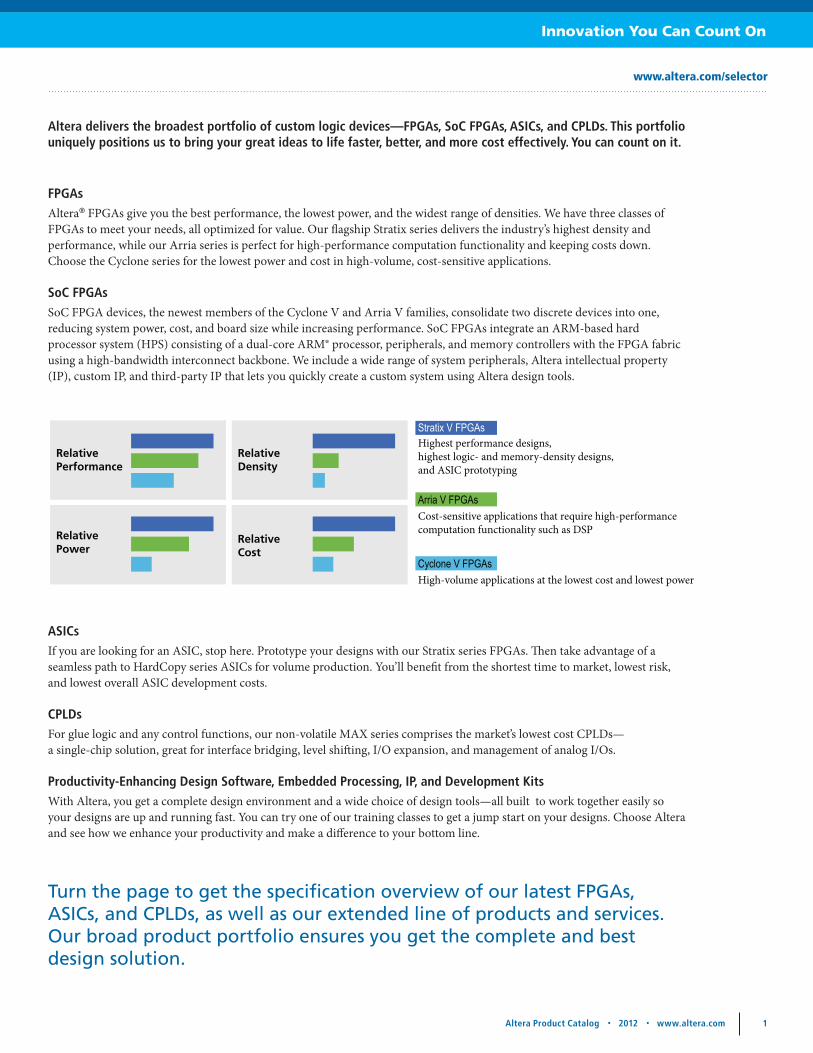
FPGAsAltera® FPGAs give you the best performance, the lowest power, and the widest range of densities. We have three classes of FPGAs to meet your needs, all optimized for value. Our flagship Stratix series delivers the industry’s highest density and performance, while our Arria series is perfect for high-performance computation functionality and keeping costs down. Choose the Cyclone series for the lowest power and cost in high-volume, cost-sensitive applications.
SoC FPGAsSoC FPGA devices, the newest members of the Cyclone V and Arria V families, consolidate two discrete devices into one, reducing system power, cost, and board size while increasing performance. SoC FPGAs integrate an ARM-based hard processor system (HPS) consisting of a dual-core ARM® processor, peripherals, and memory controllers with the FPGA fabric using a high-bandwidth interconnect backbone. We include a wide range of system peripherals, Altera intellectual property (IP), custom IP, and third-party IP that lets you quickly create a custom system using Altera design tools.
ASICsIf you are looking for an ASIC, stop here. Prototype your designs with our Stratix series FPGAs. Then take advantage of a seamless path to HardCopy series ASICs for volume production. You’ll benefit from the shortest time to market, lowest risk, and lowest overall ASIC development costs. CPLDsFor glue logic and any control functions, our non-volatile MAX series comprises the market’s lowest cost CPLDs— a single-chip solution, great for interface bridging, level shifting, I/O expansion, and management of analog I/Os.
Productivity-Enhancing Design Software, Embedded Processing, IP, and Development KitsWith Altera, you get a complete design environment and a wide choice of design tools—all built to work together easily so your designs are up and running fast. You can try one of our training classes to get a jump start on your designs. Choose Altera and see how we enhance your productivity and make a difference to your bottom line.
Turn the page to get the specification overview of our latest FPGAs, ASICs, and CPLDs, as well as our extended line of products and services. Our broad product portfolio ensures you get the complete and best design solution.
RelativePerformance
RelativeDensity
Stratix IV
Cyclone III
Arria II
Relativecost
Relativeperformance
Relativepower
Density
Highest performance designsHighgest logic and memory density designsASIC prototyping
Cost sensitive applications that require high performance computation functionality like DSP
Requires the lowest cost for high volume applications
Stratix V FPGAs
Cyclone V FPGAs
Arria V FPGAs
RelativeCost
RelativePower
Highest performance designs,highest logic- and memory-density designs, and ASIC prototyping
Cost-sensitive applications that require high-performance computation functionality such as DSP
High-volume applications at the lowest cost and lowest power
www.altera.com/selector
2 Altera Product Catalog • 2012 • www.altera.com Altera Product Catalog • 2012 • www.altera.com 32 Altera Product Catalog • 2012 • www.altera.com Altera Product Catalog • 2012 • www.altera.com 3
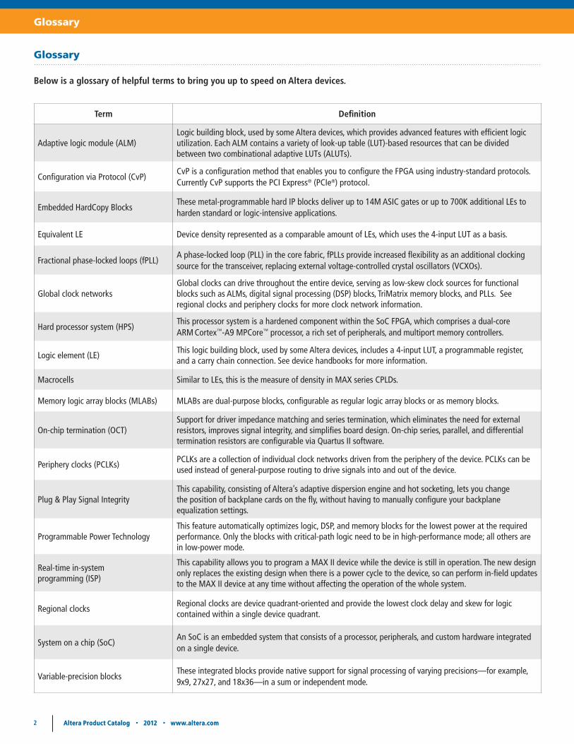
Glossary
Term Definition
Adaptive logic module (ALM)Logic building block, used by some Altera devices, which provides advanced features with efficient logic utilization. Each ALM contains a variety of look-up table (LUT)-based resources that can be divided between two combinational adaptive LUTs (ALUTs).
Configuration via Protocol (CvP)CvP is a configuration method that enables you to configure the FPGA using industry-standard protocols. Currently CvP supports the PCI Express® (PCIe®) protocol.
Embedded HardCopy BlocksThese metal-programmable hard IP blocks deliver up to 14M ASIC gates or up to 700K additional LEs to harden standard or logic-intensive applications.
Equivalent LE Device density represented as a comparable amount of LEs, which uses the 4-input LUT as a basis.
Fractional phase-locked loops (fPLL)A phase-locked loop (PLL) in the core fabric, fPLLs provide increased flexibility as an additional clocking source for the transceiver, replacing external voltage-controlled crystal oscillators (VCXOs).
Global clock networksGlobal clocks can drive throughout the entire device, serving as low-skew clock sources for functional blocks such as ALMs, digital signal processing (DSP) blocks, TriMatrix memory blocks, and PLLs. See regional clocks and periphery clocks for more clock network information.
Hard processor system (HPS)This processor system is a hardened component within the SoC FPGA, which comprises a dual-core ARM Cortex™-A9 MPCore™ processor, a rich set of peripherals, and multiport memory controllers.
Logic element (LE)This logic building block, used by some Altera devices, includes a 4-input LUT, a programmable register, and a carry chain connection. See device handbooks for more information.
Macrocells Similar to LEs, this is the measure of density in MAX series CPLDs.
Memory logic array blocks (MLABs) MLABs are dual-purpose blocks, configurable as regular logic array blocks or as memory blocks.
On-chip termination (OCT)Support for driver impedance matching and series termination, which eliminates the need for external resistors, improves signal integrity, and simplifies board design. On-chip series, parallel, and differential termination resistors are configurable via Quartus II software.
Periphery clocks (PCLKs)PCLKs are a collection of individual clock networks driven from the periphery of the device. PCLKs can be used instead of general-purpose routing to drive signals into and out of the device.
Plug & Play Signal IntegrityThis capability, consisting of Altera’s adaptive dispersion engine and hot socketing, lets you change the position of backplane cards on the fly, without having to manually configure your backplane equalization settings.
Programmable Power TechnologyThis feature automatically optimizes logic, DSP, and memory blocks for the lowest power at the required performance. Only the blocks with critical-path logic need to be in high-performance mode; all others are in low-power mode.
Real-time in-system programming (ISP)
This capability allows you to program a MAX II device while the device is still in operation. The new design only replaces the existing design when there is a power cycle to the device, so can perform in-field updates to the MAX II device at any time without affecting the operation of the whole system.
Regional clocksRegional clocks are device quadrant-oriented and provide the lowest clock delay and skew for logic contained within a single device quadrant.
System on a chip (SoC)An SoC is an embedded system that consists of a processor, peripherals, and custom hardware integrated on a single device.
Variable-precision blocksThese integrated blocks provide native support for signal processing of varying precisions—for example, 9x9, 27x27, and 18x36—in a sum or independent mode.
Below is a glossary of helpful terms to bring you up to speed on Altera devices.
Glossary
2

2 Altera Product Catalog • 2012 • www.altera.com Altera Product Catalog • 2012 • www.altera.com 3
Devices
2 Altera Product Catalog • 2012 • www.altera.com Altera Product Catalog • 2012 • www.altera.com 3
Stratix V GT FPGA Featureswww.altera.com/selector
Maximum Resource Count for Stratix V GT FPGAs (0.85 V)1
5SGTC5 5SGTC7
Den
sity
and
Spe
ed
ALMs 160,400 234,720
LEs (K) 425 622
Registers 641,600 938,880
M20K memory blocks 2,304 2,560
M20K memory (Mb) 45 50
MLAB memory (Mb) 4.9 7.16
Variable-precision DSP blocks 256 256
18 x 18 multipliers 512 512
Arc
hite
ctur
al
Feat
ures
Global clock networks 16
Regional clock networks 92
Design security 3
HardCopy series device support Contact Altera
I/O F
eatu
res
I/O voltage levels supported (V) 1.2, 1.5, 1.8, 2.5, 3.32
I/O standards supported
LVTTL, LVCMOS, PCI™, PCI-X™, LVDS, mini-LVDS, RSDS, LVPECL, Differential SSTL-15, Differential SSTL-18, Differential SSTL-2, Differential HSTL-12, Differential HSTL-5,
Differential HSTL-18, SSTL-15 (I and II), SSTL-18 (I and II), SSTL-2 (I and II), 1.2-V HSTL (I and II), 1.5-V HSTL (I and II), 1.8-V HSTL (I and II)
LVDS channels, 1.4 Gbps (receive/transmit) 150 150
Embedded DPA circuitry 3
OCT Series, parallel, and differential
Transceiver count
(28.05 Gbps/14.1 Gbps)4/32 4/32
PCIe hard IP blocks (Gen3) 1 1
Memory devices supported DDR3, DDR2, QDR II, QDR II+, RLDRAM II, RLDRAM III
1 All data is preliminary.2 3.3-V compliant, requires a 3-V power supply.
The following features, packages, and I/O matrices give you an overview of our devices. To get the full story, check out our online selector guide.

4 Altera Product Catalog • 2012 • www.altera.com Altera Product Catalog • 2012 • www.altera.com 5
Devices
Stratix V GX FPGA Features
Maximum Resource Count for Stratix V GX FPGAs (0.85 V)1
5SGXA3 5SGXA4 5SGXA5 5SGXA7 5SGXA9 5SGXAB 5SGXB5 5SGXB6 5SGXB9 5SGXBB
Den
sity
and
Spe
ed
ALMs 128,300 158,500 185,000 234,720 317,000 359,200 185,000 225,400 317,000 359,200
LEs (K) 340 420 490 622 840 952 490 597 840 952
Registers 513,200 634,000 740,000 938,880 1,268,000 1,436,800 740,000 901,600 1,268,000 1,436,800
M20K memory blocks 957 1,900 2,304 2,560 2,640 2,640 2,100 2,660 2,640 2,640
M20K memory (Mb) 19 37 45 50 52 52 41 52 52 52
MLAB memory (Mb) 3.92 4.84 5.65 7.16 9.67 10.96 5.65 6.88 9.67 10.96
Variable-precision DSP blocks
256 256 256 256 352 352 399 399 352 352
18 x 18 multipliers 512 512 512 512 704 704 798 798 704 704
Arc
hite
ctur
al F
eatu
res Global clock
networks16
Regional clock networks
92
Design security 3
HardCopy series device support 3
I/O F
eatu
res
I/O voltage levels supported (V)
1.2, 1.5, 1.8, 2.5, 3.32
I/O standards supported
LVTTL, LVCMOS, PCI, PCI-X, LVDS, mini-LVDS, RSDS, LVPECL, Differential SSTL-15, Differential SSTL-18, Differential SSTL-2, Differential HSTL-12, Differential HSTL-5, Differential HSTL-18, SSTL-15 (I and II),
SSTL-18 (I and II), SSTL-2 (I and II), 1.2-V HSTL (I and II), 1.5-V HSTL (I and II), 1.8-V HSTL (I and II)
LVDS channels, 1.4 Gbps (receive/transmit)
174 174 210 210 210 210 150 150 150 150
Embedded DPA circuitry 3
OCT Series, parallel, and differential
Transceiver count
(14.1 Gbps)36 36 48 48 48 48 66 66 66 66
PCIe hard IP blocks (Gen3)
2 2 4 4 4 4 4 4 4 4
Memory devices supported
DDR3, DDR2, QDR II, QDR II+, RLDRAM II, RLDRAM III
1 All data is preliminary.2 3.3-V compliant, requires a 3-V power supply.

4 Altera Product Catalog • 2012 • www.altera.com Altera Product Catalog • 2012 • www.altera.com 5
Devices
Stratix V GS FPGA Features
Maximum Resource Count for Stratix V GS FPGAs (0.85 V)1
5SGSD3 5SGSD4 5SGSD5 5SGSD6 5SGSD8
Den
sity
and
Spe
ed
ALMs 89,000 135,840 172,600 220,000 262,400
LEs (K) 236 360 457 583 695
Registers 356,000 543,360 690,400 880,000 1,049,600
M20K memory blocks 688 957 2,014 2,320 2,567
M20K memory (Mb) 13 19 39 45 50
MLAB memory (Mb) 2.72 4.15 5.27 6.71 8.01
Variable-precision DSP blocks
600 1,044 1,590 1,775 1,963
18 x 18 multipliers 1,200 2,088 3,180 3,550 3,926
Arc
hite
ctur
al
Feat
ures
Global clock networks 16
Regional clock networks 92
Design security 3
HardCopy series device support 3
I/O F
eatu
res
I/O voltage levels supported (V)
1.2, 1.5, 1.8, 2.5, 3.32
I/O standards supportedLVTTL, LVCMOS, PCI, PCI-X, LVDS, mini-LVDS, RSDS, LVPECL, Differential SSTL-15, Differential SSTL-18, Differential SSTL-2, Differential HSTL-12, Differential HSTL-5, Differential HSTL-18, SSTL-15 (I and II), SSTL-18 (I and II), SSTL-2 (I and II), 1.2-V HSTL (I and II), 1.5-V HSTL (I and II), 1.8-V HSTL (I and II)
LVDS channels, 1.4 Gbps (receive/transmit)
108 174 174 210 210
Embedded DPA circuitry 3
OCT Series, parallel, and differential
Transceiver count
(14.1 Gbps)24 36 36 48 48
PCIe hard IP blocks (Gen3) 1 1 1 2 2
Memory devices supported DDR3, DDR2, DDR, QDR II, QDR II+, RLDRAM II, RLDRAM III
1 All data is preliminary.2 3.3-V compliant, requires a 3-V power supply.
6 Altera Product Catalog • 2012 • www.altera.com Altera Product Catalog • 2012 • www.altera.com 7
Devices
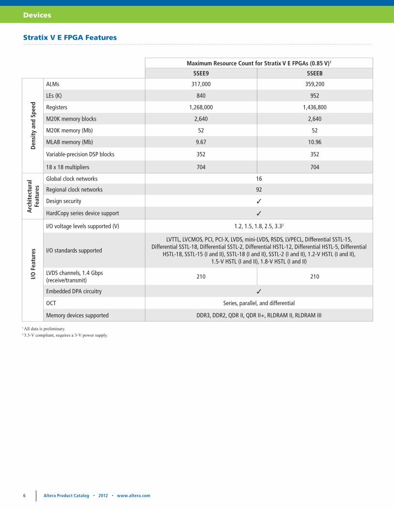
Stratix V E FPGA Features
Maximum Resource Count for Stratix V E FPGAs (0.85 V)1
5SEE9 5SEEB
Den
sity
and
Spe
ed
ALMs 317,000 359,200
LEs (K) 840 952
Registers 1,268,000 1,436,800
M20K memory blocks 2,640 2,640
M20K memory (Mb) 52 52
MLAB memory (Mb) 9.67 10.96
Variable-precision DSP blocks 352 352
18 x 18 multipliers 704 704
Arc
hite
ctur
al
Feat
ures
Global clock networks 16
Regional clock networks 92
Design security 3
HardCopy series device support 3
I/O F
eatu
res
I/O voltage levels supported (V) 1.2, 1.5, 1.8, 2.5, 3.32
I/O standards supported
LVTTL, LVCMOS, PCI, PCI-X, LVDS, mini-LVDS, RSDS, LVPECL, Differential SSTL-15, Differential SSTL-18, Differential SSTL-2, Differential HSTL-12, Differential HSTL-5, Differential
HSTL-18, SSTL-15 (I and II), SSTL-18 (I and II), SSTL-2 (I and II), 1.2-V HSTL (I and II), 1.5-V HSTL (I and II), 1.8-V HSTL (I and II)
LVDS channels, 1.4 Gbps (receive/transmit)
210 210
Embedded DPA circuitry 3
OCT Series, parallel, and differential
Memory devices supported DDR3, DDR2, QDR II, QDR II+, RLDRAM II, RLDRAM III
1 All data is preliminary.2 3.3-V compliant, requires a 3-V power supply.

6 Altera Product Catalog • 2012 • www.altera.com Altera Product Catalog • 2012 • www.altera.com 7
Devices
Maximum Resource Count for Stratix IV GT FPGAs (0.95 V)1
EP4S40G2 EP4S40G5 EP4S100G2 EP4S100G3 EP4S100G4 EP4S100G5
Den
sity
and
Spe
ed
ALMs 91,200 212,480 91,200 116,480 141,440 212,480
LEs (K) 228 531 228 291 354 531
Registers2 182,400 424,960 182,400 232,960 282,880 424,960
M9K memory blocks 1,235 1,280 1,235 936 1,248 1,280
M144K memory blocks 22 64 22 36 48 64
MLAB memory (Kb) 2,850 6,640 2,850 3,640 4,420 6,640
Embedded memory (Kb) 14,283 20,736 14,283 13,608 18,144 20,736
18 x 18 multipliers 1,288 1,024 1,288 832 1,024 1,024
Arc
hite
ctur
al F
eatu
res
Global clock networks 16
Regional clock networks 64 88 64 88 88 88
Periphery clock networks 88 112 88 112 112 112
PLLs 8 8 8 12 12 12
Design security 3
HardCopy series device support –
Configuration file size (Mb) 95 172 95 172 172 172
Others Plug & Play Signal Integrity, Programmable Power Technology
I/O F
eatu
res
I/O voltage levels supported (V) 1.2, 1.5, 1.8, 2.5, 3.33
I/O standards supportedLVTTL, LVCMOS, PCI, PCI-X, LVDS, mini-LVDS, RSDS, LVPECL, Differential SSTL-15, Differential SSTL-18, Differential SSTL-2, Differential HSTL-12, Differential HSTL-15, Differential HSTL-18, SSTL-15 (I and II),
SSTL-18 (I and II), SSTL-2 (I and II), 1.2-V HSTL (I and II), 1.5-V HSTL (I and II), 1.8-V HSTL (I and II)
Emulated LVDS channels, 1,100 Mbps
192 256 192 256 256 256
LVDS channels, 1,600 Mbps (receive/transmit)
46/46
Embedded DPA circuitry 3
OCT Series, parallel, and differential
Transceiver count4 (11.3 Gbps/8.5 Gbps/6.5 Gbps)
12/12/12 12/12/12 24/0/12 24/8/16 24/8/16 32/0/16
PCIe hard IP blocks 2 2 2 4 4 4
Memory devices supported DDR3, DDR2, DDR, QDR II, QDR II+, RLDRAM II, SDR
1 Available in industrial temperatures only (0oC to 100oC).2 This is the base core logic register count. The ALM can support three registers when used in LUTREG mode, which increases total register count by an additional 50 percent.3 3.3-V compliant, requires a 3-V power supply.4 The total transceiver count is the sum of 11.3-Gbps plus 8.5-Gbps plus 6.5-Gbps transceivers.
Stratix IV GT FPGA Features

8 Altera Product Catalog • 2012 • www.altera.com Altera Product Catalog • 2012 • www.altera.com 9
Devices
Maximum Resource Count for Stratix IV GX FPGAs (0.9 V)1
EP4SGX70 EP4SGX110 EP4SGX180 EP4SGX230 EP4SGX290 EP4SGX360 EP4SGX530
Den
sity
and
Spe
ed
ALMs 29,040 42,240 70,300 91,200 116,480 141,440 212,480
LEs (K) 73 106 176 228 291 354 531
Registers2 58,080 84,480 140,600 182,400 232,960 282,880 424,960
M9K memory blocks 462 660 950 1,235 936 1,248 1,280
M144K memory blocks 16 16 20 22 36 48 64
MLAB memory (Kb) 908 1,320 2,197 2,850 3,640 4,420 6,640
Embedded memory (Kb) 6,462 8,244 11,430 14,283 13,608 18,144 20,736
18 x 18 multipliers 384 512 920 1,288 832 1,0403 1,024
Arc
hite
ctur
al F
eatu
res
Global clock networks 16
Regional clock networks 64 64 64 64 88 88 88
Periphery clock networks 56 56 88 88 88 88 112
PLLs 4 4 8 12 12 12
Design security 3
HardCopy series device support 34 34 3 3 3 3 3
Configuration file size (Mb) 53 53 95 95 141 141 172
Others Plug & Play Signal Integrity, Programmable Power Technology
I/O voltage levels supported (V) 1.2, 1.5, 1.8, 2.5, 3.35
I/O F
eatu
res
I/O standards supportedLVTTL, LVCMOS, PCI, PCI-X, LVDS, mini-LVDS, RSDS, LVPECL, Differential SSTL-15, Differential SSTL-18, Differential SSTL-2, Differential HSTL-12, Differential HSTL-15, Differential HSTL-18, SSTL-15 (I and II),
SSTL-18 (I and II), SSTL-2 (I and II), 1.2-V HSTL (I and II), 1.5-V HSTL (I and II), 1.8-V HSTL (I and II)
Emulated LVDS channels, 1,100 Mbps
128 128 192 192 256 256 256
LVDS channels, 1,600 Mbps (receive/transmit)
56/56 56/56 88/88 88/88 98/98 98/98 98/98
Embedded DPA circuitry
OCT Series, parallel, and differential
Transceiver count (8.5 Gbps/6.5 Gbps)6 16/8 16/8 24/12 24/12 32/16 32/16 32/16
PCIe hard IP blocks 2 2 2 2 4 4 4
Memory devices supported DDR3, DDR2, DDR, QDR II, QDR II+, RLDRAM II, SDR
Stratix IV GX FPGA Features
1 Various packages and device options offer a variety of options to meet your design needs.2 This is the base core logic register count. The ALM can support three registers when used in LUTREG mode, which increases the total register count by an additional 50 percent.3 EP4SGX360N has 1,024 18x18 multipliers.4 For EP4SGX70D and EP4SGX110D/F devices.5 3.3-V compliant, requires a 3-V power supply.6 The total transceiver count is the sum of 8.5-Gbps transceivers plus 6.5-Gbps transceivers.
8 Altera Product Catalog • 2012 • www.altera.com Altera Product Catalog • 2012 • www.altera.com 9
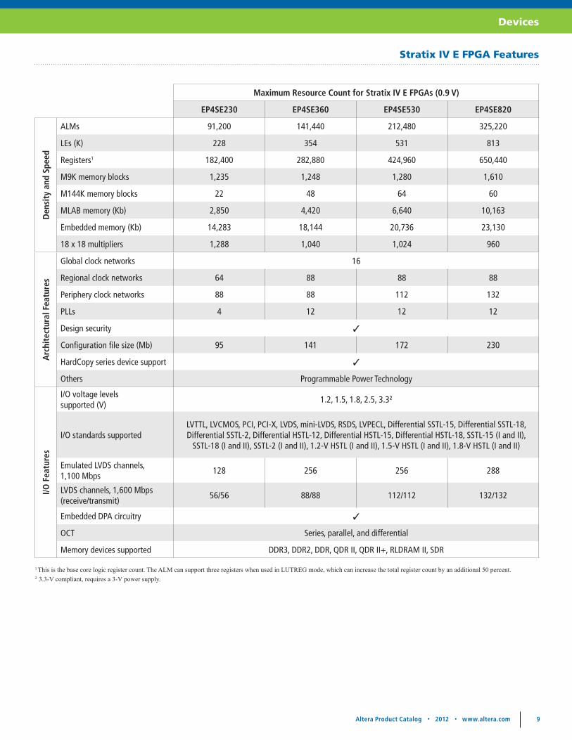
Devices
Maximum Resource Count for Stratix IV E FPGAs (0.9 V)
EP4SE230 EP4SE360 EP4SE530 EP4SE820
Den
sity
and
Spe
ed
ALMs 91,200 141,440 212,480 325,220
LEs (K) 228 354 531 813
Registers1 182,400 282,880 424,960 650,440
M9K memory blocks 1,235 1,248 1,280 1,610
M144K memory blocks 22 48 64 60
MLAB memory (Kb) 2,850 4,420 6,640 10,163
Embedded memory (Kb) 14,283 18,144 20,736 23,130
18 x 18 multipliers 1,288 1,040 1,024 960
Arc
hite
ctur
al F
eatu
res
Global clock networks 16
Regional clock networks 64 88 88 88
Periphery clock networks 88 88 112 132
PLLs 4 12 12 12
Design security 3
Configuration file size (Mb) 95 141 172 230
HardCopy series device support 3
Others Programmable Power Technology
I/O F
eatu
res
I/O voltage levels supported (V)
1.2, 1.5, 1.8, 2.5, 3.32
I/O standards supportedLVTTL, LVCMOS, PCI, PCI-X, LVDS, mini-LVDS, RSDS, LVPECL, Differential SSTL-15, Differential SSTL-18, Differential SSTL-2, Differential HSTL-12, Differential HSTL-15, Differential HSTL-18, SSTL-15 (I and II),
SSTL-18 (I and II), SSTL-2 (I and II), 1.2-V HSTL (I and II), 1.5-V HSTL (I and II), 1.8-V HSTL (I and II)
Emulated LVDS channels, 1,100 Mbps
128 256 256 288
LVDS channels, 1,600 Mbps (receive/transmit)
56/56 88/88 112/112 132/132
Embedded DPA circuitry 3
OCT Series, parallel, and differential
Memory devices supported DDR3, DDR2, DDR, QDR II, QDR II+, RLDRAM II, SDR
1 This is the base core logic register count. The ALM can support three registers when used in LUTREG mode, which can increase the total register count by an additional 50 percent.2 3.3-V compliant, requires a 3-V power supply.
Stratix IV E FPGA Features

10 Altera Product Catalog • 2012 • www.altera.com Altera Product Catalog • 2012 • www.altera.com 11
Devices
Maximum Resource Count for Stratix III L FPGAs (1.1 V, 0.9 V)
EP3SL50 EP3SL70 EP3SL110 EP3SL150 EP3SL200 EP3SL340
Den
sity
and
Spe
ed
ALMs 19,000 27,000 42,600 56,800 79,560 135,200
LEs (K) 47.5 67.5 107.5 143 199 338
Registers1 38,000 54,000 85,200 113,600 159,120 270,400
M9K memory blocks 108 150 275 355 468 1,040
M144K memory blocks 6 6 12 16 36 48
MLAB memory (Kb)2 297 422 672 891 1,250 2,110
Embedded memory (Kb) 1,836 2,214 4,203 5,499 9,396 16,272
18 x 18 multipliers 216 288 288 384 576 576
Arc
hite
ctur
al F
eatu
res
Global clock networks 16
Regional clock networks 48 48 48 48 88 88
Periphery clock networks 104 104 208 208 208 208
PLLs 4 4 8 8 12 12
Design security 3
Configuration file size (Mb) 22 22 47 47 66 120
HardCopy series device support 3
Others Programmable Power Technology
I/O F
eatu
res
I/O voltage levels supported (V)
1.2, 1.5, 1.8, 2.5, 3.3
I/O standards supportedLVDS, LVPECL, Differential SSTL-18, Differential SSTL-2, Differential HSTL,
SSTL-18 (I and II), SSTL-15 (I and II), SSTL-2 (I and II), 1.5-V HSTL (I and II), 1.8-V HSTL (I and II), PCI, PCI-X 1.0, LVTTL, LVCMOS
Emulated LVDS channels, 1,100 Mbps
56 56 88 88 112 137
LVDS channels, 1,600 Mbps (receive/transmit)
56/56 56/56 88/88 88/88 112/112 132/132
Embedded DPA circuitry 3
OCT Series, parallel, and differential
Memory devices supported DDR3, DDR2, DDR, QDR II, RLDRAM II, SDR
1 This is the base core logic register count. The ALM can support three registers when used in LUTREG mode, which increases the total register count by an additional 50 percent.2 The size of the MLAB ROM is twice the size of the MLAB RAM.
Stratix III L FPGA Features

10 Altera Product Catalog • 2012 • www.altera.com Altera Product Catalog • 2012 • www.altera.com 11
Devices
Maximum Resource Count for Stratix III E FPGAs (1.1 V)
EP3SE50 EP3SE80 EP3SE110 EP3SE260
Den
sity
and
Spe
ed
ALMs 19,000 32,000 42,600 101,760
LEs (K) 47.5 80 107.5 254
Registers1 38,000 64,000 85,200 203,520
M9K memory blocks 400 495 639 864
M144K memory blocks 12 12 16 48
MLAB memory (Kb)2 297 500 672 1,594
Embedded memory (Kb) 5,328 6,183 8,055 14,688
18 x 18 multipliers 384 672 896 768
Arc
hite
ctur
al F
eatu
res
Global clock networks 16
Regional clock networks 48 48 48 88
Periphery clock networks 104 208 208 208
PLLs 4 8 8 12
Design security 3
Configuration file size (Mb) 26 48 48 93
HardCopy series device support 3
Others Programmable Power Technology
I/O F
eatu
res
I/O voltage levels supported (V)
1.2, 1.5, 1.8, 2.5, 3.3
I/O standards supportedLVDS, LVPECL, Differential SSTL-18, Differential SSTL-2, Differential HSTL,
SSTL-18 (I and II), SSTL-15 (I and II), SSTL-2 (I and II), 1.5-V HSTL (I and II), 1.8-V HSTL (I and II), PCI, PCI-X 1.0, LVTTL, LVCMOS
Emulated LVDS channels, 1,100 Mbps
56 88 88 112
LVDS channels, 1,600 Mbps (receive/transmit)
56/56 88/88 88/88 112/112
Embedded DPA circuitry 3
OCT Series, parallel, and differential
Memory devices supported DDR3, DDR2, DDR, QDR II, RLDRAM II, SDR
1 This is the base core logic register count. The ALM can support three registers when used in LUTREG mode, which increases the total register count by an additional 50 percent.2 The size of the MLAB ROM is twice the size of the MLAB RAM.
Stratix III E FPGA Features
12 Altera Product Catalog • 2012 • www.altera.com Altera Product Catalog • 2012 • www.altera.com 13
Devices
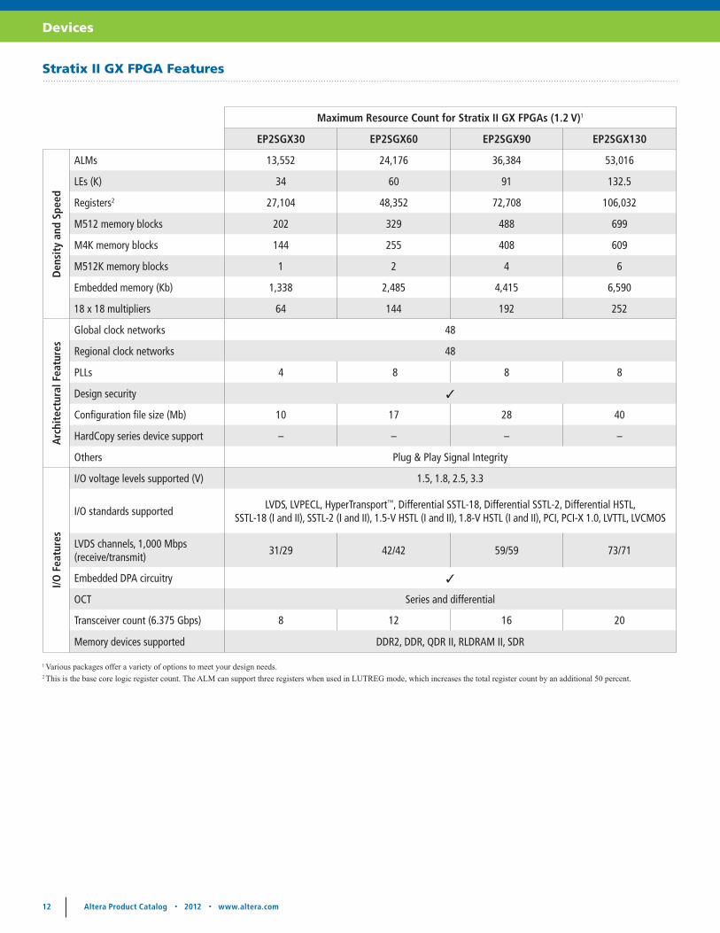
Stratix II GX FPGA Features
Maximum Resource Count for Stratix II GX FPGAs (1.2 V)1
EP2SGX30 EP2SGX60 EP2SGX90 EP2SGX130
Den
sity
and
Spe
ed
ALMs 13,552 24,176 36,384 53,016
LEs (K) 34 60 91 132.5
Registers2 27,104 48,352 72,708 106,032
M512 memory blocks 202 329 488 699
M4K memory blocks 144 255 408 609
M512K memory blocks 1 2 4 6
Embedded memory (Kb) 1,338 2,485 4,415 6,590
18 x 18 multipliers 64 144 192 252
Arc
hite
ctur
al F
eatu
res
Global clock networks 48
Regional clock networks 48
PLLs 4 8 8 8
Design security 3
Configuration file size (Mb) 10 17 28 40
HardCopy series device support – – – –
Others Plug & Play Signal Integrity
I/O F
eatu
res
I/O voltage levels supported (V) 1.5, 1.8, 2.5, 3.3
I/O standards supportedLVDS, LVPECL, HyperTransport™, Differential SSTL-18, Differential SSTL-2, Differential HSTL,
SSTL-18 (I and II), SSTL-2 (I and II), 1.5-V HSTL (I and II), 1.8-V HSTL (I and II), PCI, PCI-X 1.0, LVTTL, LVCMOS
LVDS channels, 1,000 Mbps (receive/transmit)
31/29 42/42 59/59 73/71
Embedded DPA circuitry 3
OCT Series and differential
Transceiver count (6.375 Gbps) 8 12 16 20
Memory devices supported DDR2, DDR, QDR II, RLDRAM II, SDR
1 Various packages offer a variety of options to meet your design needs.2 This is the base core logic register count. The ALM can support three registers when used in LUTREG mode, which increases the total register count by an additional 50 percent.

12 Altera Product Catalog • 2012 • www.altera.com Altera Product Catalog • 2012 • www.altera.com 13
Devices
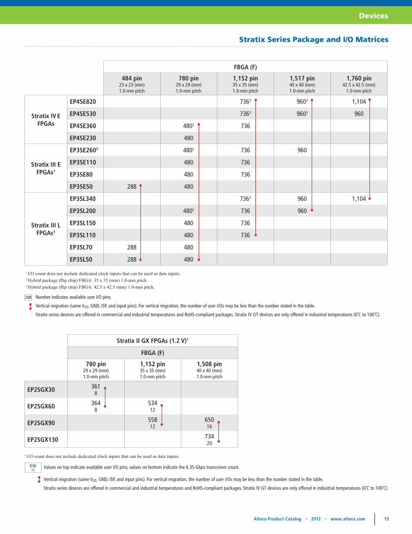
Stratix FPGA Series Package and I/O Matrices
1 Hybrid package (flip chip) FBGA: 33 x 33 (mm) 1.0-mm pitch.2 Hybrid package (flip chip) FBGA: 45 x 45 (mm) 1.0-mm pitch.3 GX–GT migration. Unused transceiver channels connected to power/ground.
Stratix V GS, GX, GT, and E FPGAs (0.85 V)
FBGA (F)
780 pin29 x 29 (mm)1.0-mm pitch
1,152 pin35 x 35 (mm)1.0-mm pitch
1,152 pin35 x 35 (mm)1.0-mm pitch
1,517 pin40 x 40 (mm)
1.0-mm pitch
1,517 pin40 x 40 (mm) 1.0-mm pitch
1,760 pin42.5 x 42.5 (mm)
1.0-mm pitch
1,932 pin45 x 45 (mm)1.0-mm pitch
5SGSD3 360, 90, 121 432, 108, 24
5SGSD4 360, 90, 121 432, 108, 24 696, 174, 36
5SGSD5 552, 138, 24 696, 174, 36
5SGSD6 696, 174, 36 840, 210, 48
5SGSD8 696, 174, 36 840, 210, 48
5SGXA3 360, 90, 121 432, 108, 24 432, 108, 36 696, 174, 36
5SGXA4 552, 138, 24 432, 108, 36 696, 174, 36
5SGXA5 552, 138, 24 432, 108, 36 696, 174, 36 600, 150, 48 840, 210, 48
5SGXA7 552, 138, 24 432, 108, 36 696, 174, 36 600, 150, 48 840, 210, 48
5SGXA9 696, 174, 362 840, 210, 48
5SGXAB 696, 174, 362 840, 210, 48
5SGXB5 432, 108, 66 600, 150, 66
5SGXB6 432, 108, 66 600, 150, 66
5SGXB9 600, 150, 662
5SGXBB 600, 150, 662
5SGTC5 600, 150, 363
5SGTC7 600, 150, 363
5SEE9 696, 174, 02 840, 210, 0
5SEEB 696, 174, 02 840, 210, 0
264, 66, 24 Numbers indicate GPIO count, LVDS count, and transceiver count.
Vertical migration (same Vcc, GND, ISP, and input pins). User I/Os may be less than labelled for vertical migration.
Stratix series devices are offered in commercial and industrial temperatures and RoHS-compliant packages. Stratix IV GT devices are only offered in industrial temperatures (0˚C to 100˚C).

14 Altera Product Catalog • 2012 • www.altera.com Altera Product Catalog • 2012 • www.altera.com 15
Devices
1 I/O count does not include dedicated clock inputs that can be used as data inputs.2 Hybrid package (flip chip) FBGA: 35 x 35 (mm) 1.0-mm pitch.3 Hybrid package (flip chip) FBGA: 42.5 x 42.5 (mm) 1.0-mm pitch.
Stratix IV GX FPGAs (0.9 V)1
FBGA (F)
780 pin29 x 29 (mm) 1.0-mm pitch
1,152 pin35 x 35 (mm) 1.0-mm pitch
1,152 pin35 x 35 (mm) 1.0-mm pitch
1,517 pin40 x 40 (mm) 1.0-mm pitch
1,760 pin42.5 x 42.5 (mm)
1.0-mm pitch
1,932 pin 45 x 45 (mm) 1.0-mm pitch
EP4SGX70 3688+0
48016+8
EP4SGX110 3688+0
36816+0
48016+8
EP4SGX180 3688+0
56016+0
56016+8
73624+12
EP4SGX230 3688+0
56016+0
56016+8
73624+12
EP4SGX290 2882
16+056016+0
56016+8
73624+12
86424+12
90432+16
EP4SGX360 2882
16+056016+0
56016+8
73624+12
86424+12
90432+16
EP4SGX530 5603
16+87363
24+12864
24+12904
32+16
Values on top indicate available user I/O pins; values at the bottom indicate the 8.5-Gbps plus 6.5-Gbps transceiver count.
Vertical migration (same Vcc, GND, ISP, and input pins). For vertical migration, the number of user I/Os may be less than the number stated in the table.
Stratix series devices are offered in commercial and industrial temperatures and RoHS-compliant packages. Stratix IV GT devices are only offered in industrial temperatures (0˚C to 100˚C).
6368+0
Stratix Series Package and I/O Matrices
Stratix IV GT FPGAs (0.95 V)
FBGA (F)1
1,517 pin40 x 40 (mm) 1.0-mm pitch
1,932 pin 45 x 45 (mm) 1.0-mm pitch
EP4S40G2 64612+12+12
EP4S40G5 6462
12+12+12
EP4S100G2 64624+0+12
EP4S100G3 76924+8+16
EP4S100G4 76924+8+16
EP4S100G5 6462
24+0+12769
32+0+16
Values on top indicate available user I/O pins; values on bottom indicate the 11.3-Gbps plus 8.5-Gbps plus 6.5-Gbps transceiver count.
Vertical migration (same Vcc, GND, ISP, and input pins). For vertical migration, the number of user I/Os may be less than the number stated in the table.
Stratix series devices are offered in commercial and industrial temperatures and RoHS-compliant packages. Stratix IV GT devices are only offered in industrial temperatures (0˚C to 100˚C).
63612+12+12
1FineLine ball grid array.2 Hybrid package (flip chip) FBGA: 42.5 x 42.5 (mm) 1.0-mm pitch.
14 Altera Product Catalog • 2012 • www.altera.com Altera Product Catalog • 2012 • www.altera.com 15
Devices
FBGA (F)
484 pin23 x 23 (mm) 1.0-mm pitch
780 pin29 x 29 (mm)1.0-mm pitch
1,152 pin35 x 35 (mm)1.0-mm pitch
1,517 pin40 x 40 (mm)1.0-mm pitch
1,760 pin42.5 x 42.5 (mm)
1.0-mm pitch
Stratix IV EFPGAs
EP4SE820 7363 9603 1,104
EP4SE530 7363 9603 960
EP4SE360 4802 736
EP4SE230 480
Stratix III EFPGAs1
EP3SE2603 4802 736 960
EP3SE110 480 736
EP3SE80 480 736
EP3SE50 288 480
Stratix III L FPGAs1
EP3SL340 7363 960 1,104
EP3SL200 4802 736 960
EP3SL150 480 736
EP3SL110 480 736
EP3SL70 288 480
EP3SL50 288 480
Stratix Series Package and I/O Matrices
1 I/O count does not include dedicated clock inputs that can be used as data inputs.
1 I/O count does not include dedicated clock inputs that can be used as data inputs.2 Hybrid package (flip chip) FBGA: 35 x 35 (mm) 1.0-mm pitch.3 Hybrid package (flip chip) FBGA: 42.5 x 42.5 (mm) 1.0-mm pitch.
288 Number indicates available user I/O pins.
Vertical migration (same Vcc, GND, ISP, and input pins). For vertical migration, the number of user I/Os may be less than the number stated in the table.
Stratix series devices are offered in commercial and industrial temperatures and RoHS-compliant packages. Stratix IV GT devices are only offered in industrial temperatures (0˚C to 100˚C).
Stratix II GX FPGAs (1.2 V)1
FBGA (F)
780 pin29 x 29 (mm)1.0-mm pitch
1,152 pin35 x 35 (mm)1.0-mm pitch
1,508 pin40 x 40 (mm)1.0-mm pitch
EP2SGX30 3618
EP2SGX60 3648
53412
EP2SGX90 55812
65016
EP2SGX130 73420
Values on top indicate available user I/O pins; values on bottom indicate the 6.35-Gbps transceiver count.
Vertical migration (same Vcc, GND, ISP, and input pins). For vertical migration, the number of user I/Os may be less than the number stated in the table.
Stratix series devices are offered in commercial and industrial temperatures and RoHS-compliant packages. Stratix IV GT devices are only offered in industrial temperatures (0˚C to 100˚C).
63612

16 Altera Product Catalog • 2012 • www.altera.com Altera Product Catalog • 2012 • www.altera.com 17
Devices
Maximum Resource Count for HardCopy IV ASICs (0.9 V)
HC4GX15 HC4GX25 HC4GX35 HC4E25 HC4E35
Den
sity
and
Spe
ed
Usable ASIC gates 9.4M 11.5M 11.5M 9.4M 14.6M
LEs (K) 354 532 532 354 813
M9K memory blocks 660 936 1,280 864 1,320
M144K memory blocks 24 36 64 32 48
MLAB memory Implemented in HCells
Embedded memory (Kb) 9,396 13,608 20,736 12,384 18,792
18 x 18 multipliers1 1,288 1,288 1,288 1,288 1,040
Arc
hite
ctur
alFe
atur
es
PLLs 3 6 8 4 12
Design security2 3
Stratix series prototyping support
EP4SGX70EP4SGX110EP4SGX180EP4SGX230EP4SGX290EP4SGX360
EP4SGX110EP4SGX180EP4SGX230EP4SGX290EP4SGX360EP4SGX530
EP4SGX180EP4SGX230EP4SGX290EP4SGX360EP4SGX530
EP4SE230EP4SE360
EP4SE360EP4SE530EP4SE820
I/O F
eatu
res
I/O voltage levels supported (V) 1.2, 1.5, 1.8, 2.5, 3.33
I/O standards supported
LVTTL, LVCMOS, PCI, PCI-X, LVDS, mini-LVDS, RSDS, LVPECL, Differential SSTL-15,Differential SSTL-18, Differential SSTL-2,Differential HSTL-12, Differential HSTL-15,
Differential HSTL-18, SSTL-15 (I and II), SSTL-18 (I and II), SSTL-2 (I and II),1.2-V HSTL (I and II), 1.5-V HSTL (I and II), 1.8-V HSTL (I and II)
Emulated LVDS channels, 1,100 Mbps
184 236 280 120 216
LVDS channels, 1,250 Mbps (receive/transmit)
28/28 44/44 88/88 56/56 88/88
Embedded DPA circuitry 3
OCT Series and differential
Transceiver count (6.5 Gbps/6.5 Gbps, PMA only)
8/0 16/8 24/12 — —
PCIe hard IP blocks 1 2 2 — —
Exte
rnal
M
emor
y In
terf
aces
Memory devices supported DDR3, DDR2, DDR, QDR II, RLDRAM II, SDR
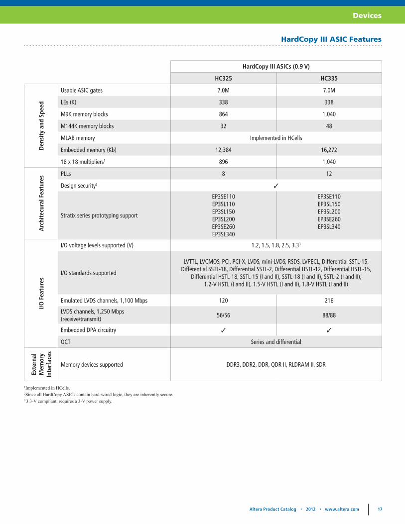
HardCopy IV ASIC Features
1Implemented in HCells.2Since all HardCopy ASICs contain hard-wired logic, they are inherently secure.3 3.3-V compliant, requires a 3-V power supply.
16 Altera Product Catalog • 2012 • www.altera.com Altera Product Catalog • 2012 • www.altera.com 17
Devices
HardCopy III ASICs (0.9 V)
HC325 HC335
Den
sity
and
Spe
ed
Usable ASIC gates 7.0M 7.0M
LEs (K) 338 338
M9K memory blocks 864 1,040
M144K memory blocks 32 48
MLAB memory Implemented in HCells
Embedded memory (Kb) 12,384 16,272
18 x 18 multipliers1 896 1,040
Arc
hite
cura
l Fea
ture
s PLLs 8 12
Design security2 3
Stratix series prototyping support
EP3SE110EP3SL110EP3SL150EP3SL200EP3SE260EP3SL340
EP3SE110EP3SL150EP3SL200EP3SE260EP3SL340
I/O F
eatu
res
I/O voltage levels supported (V) 1.2, 1.5, 1.8, 2.5, 3.33
I/O standards supported
LVTTL, LVCMOS, PCI, PCI-X, LVDS, mini-LVDS, RSDS, LVPECL, Differential SSTL-15, Differential SSTL-18, Differential SSTL-2, Differential HSTL-12, Differential HSTL-15,
Differential HSTL-18, SSTL-15 (I and II), SSTL-18 (I and II), SSTL-2 (I and II), 1.2-V HSTL (I and II), 1.5-V HSTL (I and II), 1.8-V HSTL (I and II)
Emulated LVDS channels, 1,100 Mbps 120 216
LVDS channels, 1,250 Mbps (receive/transmit)
56/56 88/88
Embedded DPA circuitry 3 3
OCT Series and differential
Exte
rnal
M
emor
y In
terf
aces
Memory devices supported DDR3, DDR2, DDR, QDR II, RLDRAM II, SDR
HardCopy III ASIC Features
1Implemented in HCells.2Since all HardCopy ASICs contain hard-wired logic, they are inherently secure.3 3.3-V compliant, requires a 3-V power supply.

18 Altera Product Catalog • 2012 • www.altera.com Altera Product Catalog • 2012 • www.altera.com 19
Devices
HardCopy II ASICs
HC210W HC210 HC220 HC230 HC240
Den
sity
and
Spe
ed
Usable ASIC gates 1.0M 1.0M 1.9M 2.9M 3.6M
LEs (K) 91 91 133 179 179
M512 memory blocks Not available in HardCopy II ASICs
M4K memory blocks 190 190 408 614 768
M512K memory blocks 0 0 2 6 9
Embedded memory (Kb) 855 855 2,988 6,219 8,640
18 x 18 multipliers1 192 192 252 384 384
Arc
hite
ctur
alFe
atur
es
PLLs 4 4 4 8 12
Design security2 3
Stratix series prototyping support
EP2S30EP2S60EP2S90
EP2S30EP2S60EP2S90
EP2S60EP2S90
EP2S130
EP2S90EP2S130EP2S180
EP2S180
I/O F
eatu
res
I/O voltage levels supported (V) 1.5, 1.8, 2.5, 3.3
I/O standards supported
LVTTL, LVCMOS, PCI, PCI-X 1.0, LVDS, LVPECL, Differential SSTL-18, Differential SSTL-2,
Differential HSTL SSTL-18 (I and II), SSTL-2 (I and II),1.5-V HSTL (I and II), 1.8-V HSTL (I and II), HyperTransport
LVDS channels, 1,040 Mbps (receive/transmit)
17/13 21/19 30/29 46/44 116/116
Embedded DPA circuitry 3
OCT Series and differential
Exte
rnal
M
emor
y In
terf
aces
Memory devices supported DDR2, DDR, QDR II, RLDRAM II, SDR
HardCopy II ASIC Features
1Implemented in HCells.2Since all HardCopy ASICs contain hard-wired logic, they are inherently secure.
18 Altera Product Catalog • 2012 • www.altera.com Altera Product Catalog • 2012 • www.altera.com 19
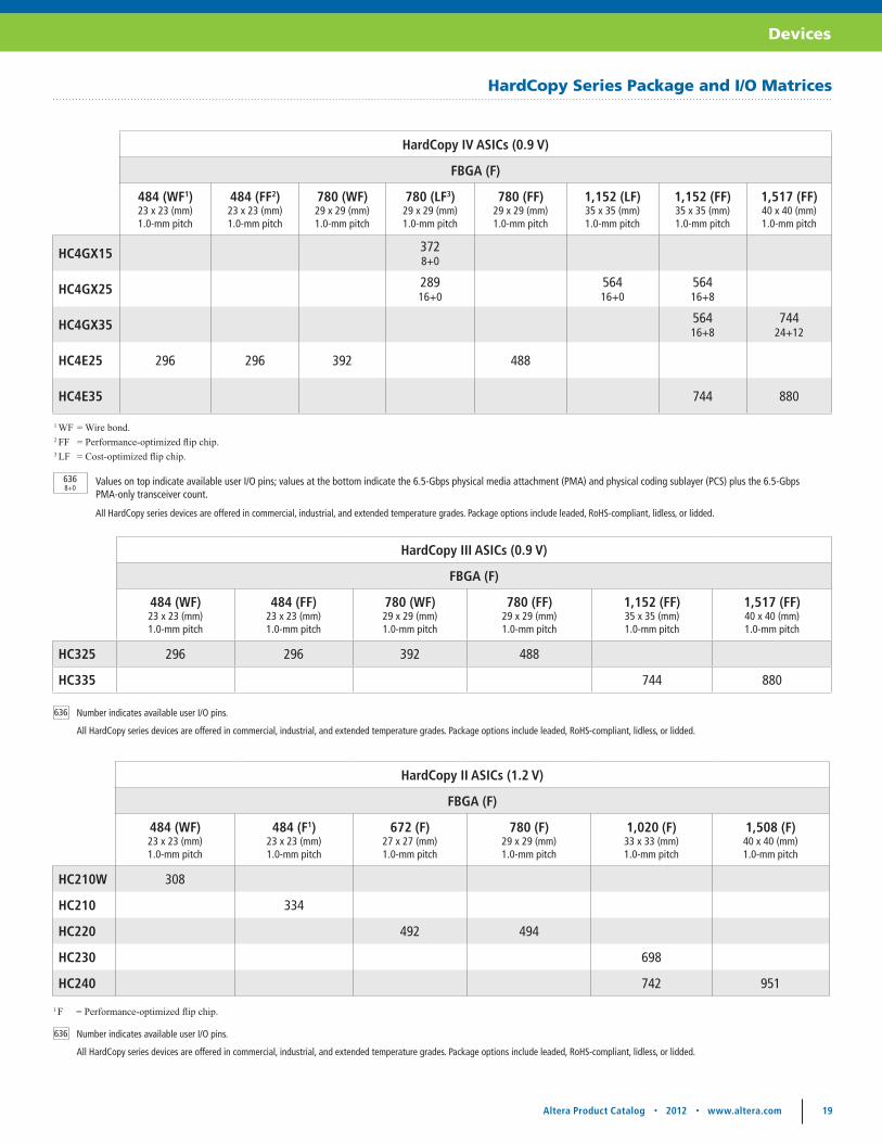
Devices
HardCopy IV ASICs (0.9 V)
FBGA (F)
484 (WF1)23 x 23 (mm) 1.0-mm pitch
484 (FF2)23 x 23 (mm) 1.0-mm pitch
780 (WF)29 x 29 (mm)1.0-mm pitch
780 (LF3)29 x 29 (mm)1.0-mm pitch
780 (FF)29 x 29 (mm) 1.0-mm pitch
1,152 (LF)35 x 35 (mm) 1.0-mm pitch
1,152 (FF)35 x 35 (mm) 1.0-mm pitch
1,517 (FF)40 x 40 (mm) 1.0-mm pitch
HC4GX15 3728+0
HC4GX25 28916+0
56416+0
56416+8
HC4GX35 56416+8
74424+12
HC4E25 296 296 392 488
HC4E35 744 880
HardCopy III ASICs (0.9 V)
FBGA (F)
484 (WF)23 x 23 (mm) 1.0-mm pitch
484 (FF)23 x 23 (mm)1.0-mm pitch
780 (WF)29 x 29 (mm)1.0-mm pitch
780 (FF)29 x 29 (mm)1.0-mm pitch
1,152 (FF)35 x 35 (mm)1.0-mm pitch
1,517 (FF)40 x 40 (mm)1.0-mm pitch
HC325 296 296 392 488
HC335 744 880
1 F = Performance-optimized flip chip.
636 Number indicates available user I/O pins.
All HardCopy series devices are offered in commercial, industrial, and extended temperature grades. Package options include leaded, RoHS-compliant, lidless, or lidded.
636 Number indicates available user I/O pins.
All HardCopy series devices are offered in commercial, industrial, and extended temperature grades. Package options include leaded, RoHS-compliant, lidless, or lidded.
HardCopy Series Package and I/O Matrices
HardCopy II ASICs (1.2 V)
FBGA (F)
484 (WF)23 x 23 (mm) 1.0-mm pitch
484 (F1)23 x 23 (mm) 1.0-mm pitch
672 (F)27 x 27 (mm)1.0-mm pitch
780 (F)29 x 29 (mm)1.0-mm pitch
1,020 (F)33 x 33 (mm)1.0-mm pitch
1,508 (F)40 x 40 (mm)1.0-mm pitch
HC210W 308
HC210 334
HC220 492 494
HC230 698
HC240 742 951
Values on top indicate available user I/O pins; values at the bottom indicate the 6.5-Gbps physical media attachment (PMA) and physical coding sublayer (PCS) plus the 6.5-Gbps PMA-only transceiver count.
All HardCopy series devices are offered in commercial, industrial, and extended temperature grades. Package options include leaded, RoHS-compliant, lidless, or lidded.
6368+0
1 WF = Wire bond.2 FF = Performance-optimized flip chip.3 LF = Cost-optimized flip chip.
20 Altera Product Catalog • 2012 • www.altera.com Altera Product Catalog • 2012 • www.altera.com 21
Devices
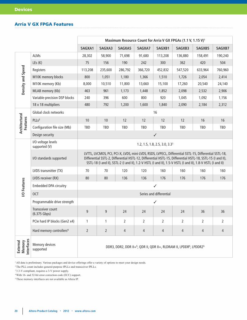
Arria V GX FPGA Features
Maximum Resource Count for Arria V GX FPGAs (1.1 V, 1.15 V)1
5AGXA1 5AGXA3 5AGXA5 5AGXA7 5AGXB1 5AGXB3 5AGXB5 5AGXB7
Den
sity
and
Spe
ed
ALMs 28,302 58,900 71,698 91,680 113,208 136,880 158,491 190,240
LEs (K) 75 156 190 242 300 362 420 504
Registers 113,208 235,600 286,792 366,720 452,832 547,520 633,964 760,960
M10K memory blocks 800 1,051 1,180 1,366 1,510 1,726 2,054 2,414
M10K memory (Kb) 8,000 10,510 11,800 13,660 15,100 17,260 20,540 24,140
MLAB memory (Kb) 463 961 1,173 1,448 1,852 2,098 2,532 2,906
Variable-precision DSP blocks 240 396 600 800 920 1,045 1,092 1,156
18 x 18 multipliers 480 792 1,200 1,600 1,840 2,090 2,184 2,312
Arc
hite
ctur
al
Feat
ures
Global clock networks 16
PLLs2 10 10 12 12 12 12 16 16
Configuration file size (Mb) TBD TBD TBD TBD TBD TBD TBD TBD
Design security 3
I/O F
eatu
res
I/O voltage levels supported (V)
1.2, 1.5, 1.8, 2.5, 3.0, 3.33
I/O standards supportedLVTTL, LVCMOS, PCI, PCI-X, LVDS, mini-LVDS, RSDS, LVPECL, Differential SSTL-15, Differential SSTL-18, Differential SSTL-2, Differential HSTL-12, Differential HSTL-15, Differential HSTL-18, SSTL-15 (I and II),
SSTL-18 (I and II), SSTL-2 (I and II), 1.2-V HSTL (I and II), 1.5-V HSTL (I and II), 1.8-V HSTL (I and II)
LVDS transmitter (TX) 70 70 120 120 160 160 160 160
LVDS receiver (RX) 80 80 136 136 176 176 176 176
Embedded DPA circuitry 3
OCT Series and differential
Programmable drive strength 3
Transceiver count (6.375 Gbps)
9 9 24 24 24 24 36 36
PCIe hard IP blocks (Gen2 x4) 1 1 2 2 2 2 2 2
Hard memory controllers4 2 2 4 4 4 4 4 4
Exte
rnal
M
emor
y In
terf
aces
Memory devices supported
DDR3, DDR2, DDR II+5, QDR II, QDR II+, RLDRAM II, LPDDR5, LPDDR25
1 All data is preliminary. Various packages and device offerings offer a variety of options to meet your design needs.2 The PLL count includes general-purpose fPLLs and transceiver fPLLs.3 3.3-V compliant, requires a 3-V power supply.4 With 16- and 32-bit error correction code (ECC) support.5 These memory interfaces are not available as Altera IP.
20 Altera Product Catalog • 2012 • www.altera.com Altera Product Catalog • 2012 • www.altera.com 21
Devices
Maximum Resource Count for Arria V GX FPGAs (1.1 V, 1.15 V)1
5AGXA1 5AGXA3 5AGXA5 5AGXA7 5AGXB1 5AGXB3 5AGXB5 5AGXB7
Den
sity
and
Spe
ed
ALMs 28,302 58,900 71,698 91,680 113,208 136,880 158,491 190,240
LEs (K) 75 156 190 242 300 362 420 504
Registers 113,208 235,600 286,792 366,720 452,832 547,520 633,964 760,960
M10K memory blocks 800 1,051 1,180 1,366 1,510 1,726 2,054 2,414
M10K memory (Kb) 8,000 10,510 11,800 13,660 15,100 17,260 20,540 24,140
MLAB memory (Kb) 463 961 1,173 1,448 1,852 2,098 2,532 2,906
Variable-precision DSP blocks 240 396 600 800 920 1,045 1,092 1,156
18 x 18 multipliers 480 792 1,200 1,600 1,840 2,090 2,184 2,312
Arc
hite
ctur
al
Feat
ures
Global clock networks 16
PLLs2 10 10 12 12 12 12 16 16
Configuration file size (Mb) TBD TBD TBD TBD TBD TBD TBD TBD
Design security 3
I/O F
eatu
res
I/O voltage levels supported (V)
1.2, 1.5, 1.8, 2.5, 3.0, 3.33
I/O standards supportedLVTTL, LVCMOS, PCI, PCI-X, LVDS, mini-LVDS, RSDS, LVPECL, Differential SSTL-15, Differential SSTL-18, Differential SSTL-2, Differential HSTL-12, Differential HSTL-15, Differential HSTL-18, SSTL-15 (I and II),
SSTL-18 (I and II), SSTL-2 (I and II), 1.2-V HSTL (I and II), 1.5-V HSTL (I and II), 1.8-V HSTL (I and II)
LVDS transmitter (TX) 70 70 120 120 160 160 160 160
LVDS receiver (RX) 80 80 136 136 176 176 176 176
Embedded DPA circuitry 3
OCT Series and differential
Programmable drive strength 3
Transceiver count (6.375 Gbps)
9 9 24 24 24 24 36 36
PCIe hard IP blocks (Gen2 x4) 1 1 2 2 2 2 2 2
Hard memory controllers4 2 2 4 4 4 4 4 4
Exte
rnal
M
emor
y In
terf
aces
Memory devices supported
DDR3, DDR2, DDR II+5, QDR II, QDR II+, RLDRAM II, LPDDR5, LPDDR25
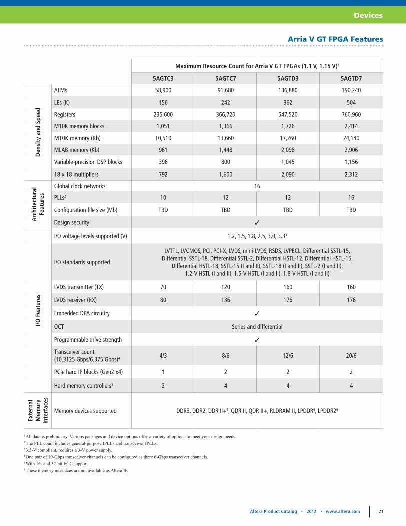
Arria V GT FPGA Features
Maximum Resource Count for Arria V GT FPGAs (1.1 V, 1.15 V)1
5AGTC3 5AGTC7 5AGTD3 5AGTD7
Den
sity
and
Spe
ed
ALMs 58,900 91,680 136,880 190,240
LEs (K) 156 242 362 504
Registers 235,600 366,720 547,520 760,960
M10K memory blocks 1,051 1,366 1,726 2,414
M10K memory (Kb) 10,510 13,660 17,260 24,140
MLAB memory (Kb) 961 1,448 2,098 2,906
Variable-precision DSP blocks 396 800 1,045 1,156
18 x 18 multipliers 792 1,600 2,090 2,312
Arc
hite
ctur
al
Feat
ures
Global clock networks 16
PLLs2 10 12 12 16
Configuration file size (Mb) TBD TBD TBD TBD
Design security 3
I/O F
eatu
res
I/O voltage levels supported (V) 1.2, 1.5, 1.8, 2.5, 3.0, 3.33
I/O standards supported
LVTTL, LVCMOS, PCI, PCI-X, LVDS, mini-LVDS, RSDS, LVPECL, Differential SSTL-15, Differential SSTL-18, Differential SSTL-2, Differential HSTL-12, Differential HSTL-15,
Differential HSTL-18, SSTL-15 (I and II), SSTL-18 (I and II), SSTL-2 (I and II), 1.2-V HSTL (I and II), 1.5-V HSTL (I and II), 1.8-V HSTL (I and II)
LVDS transmitter (TX) 70 120 160 160
LVDS receiver (RX) 80 136 176 176
Embedded DPA circuitry 3
OCT Series and differential
Programmable drive strength 3
Transceiver count (10.3125 Gbps/6.375 Gbps)4 4/3 8/6 12/6 20/6
PCIe hard IP blocks (Gen2 x4) 1 2 2 2
Hard memory controllers5 2 4 4 4
Exte
rnal
M
emor
y In
terf
aces
Memory devices supported DDR3, DDR2, DDR II+6, QDR II, QDR II+, RLDRAM II, LPDDR6, LPDDR26
1 All data is preliminary. Various packages and device options offer a variety of options to meet your design needs.2 The PLL count includes general-purpose fPLLs and transceiver fPLLs.3 3.3-V compliant, requires a 3-V power supply.4 One pair of 10-Gbps transceiver channels can be configured as three 6-Gbps transceiver channels.5 With 16- and 32-bit ECC support.6 These memory interfaces are not available as Altera IP.

22 Altera Product Catalog • 2012 • www.altera.com Altera Product Catalog • 2012 • www.altera.com 23
Devices
Arria V SX SoC FPGA Features
Maximum Resource Count for Arria V SX SoC FPGAs (1.1 V)1
5ASXB3 5ASXB5
Den
sity
and
Spe
ed
ALMs 132,075 174,340
LEs (K) 350 462
Registers 528,300 697,360
M10K memory blocks 1,729 2,282
M10K memory (Kb) 17,288 22,820
MLAB memory (Kb) 2,014 2,658
Variable-precision DSP blocks 809 1,068
18 x 18 multipliers 1,618 2,186
Arc
hite
ctur
al
Feat
ures
Processor cores (ARM Cortex-A9) Dual Dual
Global clock networks 16
PLLs2 (FPGA) 10 14
PLLs2 (HPS) 3 3
Configuration file size (Mb) TBD TBD
Design security 3
I/O F
eatu
res
I/O voltage levels supported (V) 1.2, 1.5, 1.8, 2.5, 3.0, 3.33
I/O standards supported
LVTTL, LVCMOS, PCI, PCI-X, LVDS, mini-LVDS, RSDS, LVPECL, Differential SSTL-15, Differential SSTL-18, Differential SSTL-2, Differential HSTL-12, Differential HSTL-15,
Differential HSTL-18, SSTL-15 (I and II), SSTL-18 (I and II), SSTL-2 (I and II), 1.2-V HSTL (I and II), 1.5-V HSTL (I and II), 1.8-V HSTL (I and II)
LVDS transmitter (TX) 120 120
LVDS receiver (RX) 120 120
Embedded DPA circuitry 3
OCT Series and differential
Programmable drive strength 3
Transceiver count (6.375 Gbps) 30 30
PCIe hard IP blocks (Gen2 x4) 2 2
GPIOs (FPGA) 528 528
GPIOs (HPS) 216 216
Hard memory controllers3 (FPGA) 3 3
Hard memory controllers3 (HPS) 1 1
Exte
rnal
M
emor
y In
terf
aces
Memory devices supported DDR3, DDR2, DDR, QDR II, QDR II+, RLDRAM II, LPDDR2, SDR
1 All data is preliminary.2 The PLL count includes general-purpose fPLLs and transceiver fPLLs.3 3.3-V compliant, requires a 3-V power supply.4 With 16- and 32-bit ECC support.5 These memory interfaces are not available as Altera IP.
22 Altera Product Catalog • 2012 • www.altera.com Altera Product Catalog • 2012 • www.altera.com 23
Devices
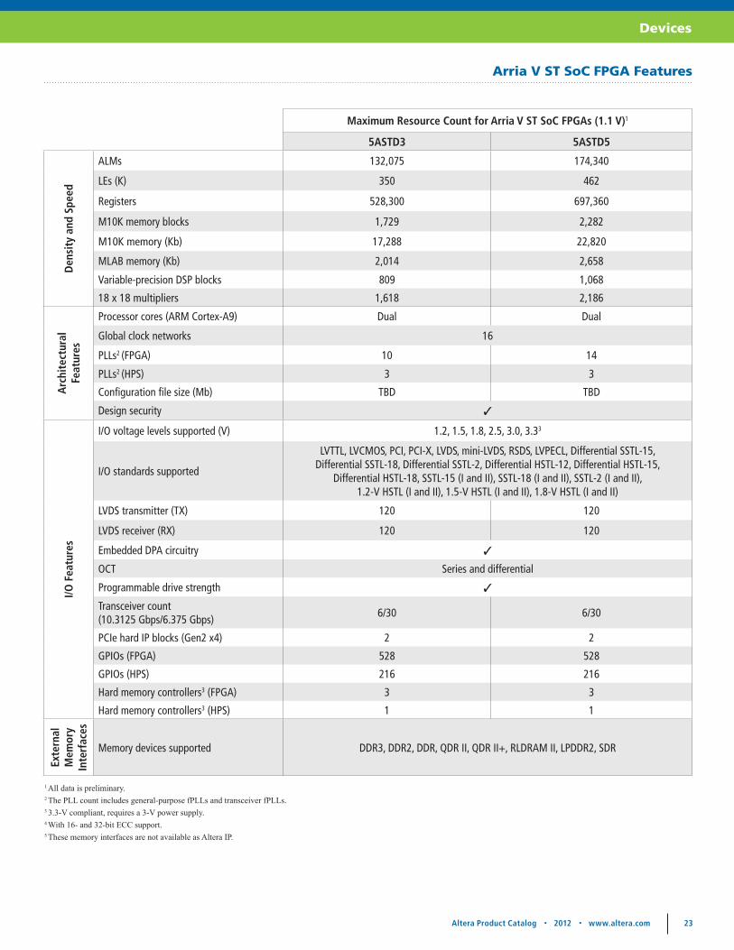
Arria V ST SoC FPGA Features
Maximum Resource Count for Arria V ST SoC FPGAs (1.1 V)1
5ASTD3 5ASTD5
Den
sity
and
Spe
ed
ALMs 132,075 174,340
LEs (K) 350 462
Registers 528,300 697,360
M10K memory blocks 1,729 2,282
M10K memory (Kb) 17,288 22,820
MLAB memory (Kb) 2,014 2,658
Variable-precision DSP blocks 809 1,068
18 x 18 multipliers 1,618 2,186
Arc
hite
ctur
al
Feat
ures
Processor cores (ARM Cortex-A9) Dual Dual
Global clock networks 16
PLLs2 (FPGA) 10 14
PLLs2 (HPS) 3 3
Configuration file size (Mb) TBD TBD
Design security 3
I/O F
eatu
res
I/O voltage levels supported (V) 1.2, 1.5, 1.8, 2.5, 3.0, 3.33
I/O standards supported
LVTTL, LVCMOS, PCI, PCI-X, LVDS, mini-LVDS, RSDS, LVPECL, Differential SSTL-15, Differential SSTL-18, Differential SSTL-2, Differential HSTL-12, Differential HSTL-15,
Differential HSTL-18, SSTL-15 (I and II), SSTL-18 (I and II), SSTL-2 (I and II), 1.2-V HSTL (I and II), 1.5-V HSTL (I and II), 1.8-V HSTL (I and II)
LVDS transmitter (TX) 120 120
LVDS receiver (RX) 120 120
Embedded DPA circuitry 3
OCT Series and differential
Programmable drive strength 3
Transceiver count (10.3125 Gbps/6.375 Gbps)
6/30 6/30
PCIe hard IP blocks (Gen2 x4) 2 2
GPIOs (FPGA) 528 528
GPIOs (HPS) 216 216
Hard memory controllers3 (FPGA) 3 3
Hard memory controllers3 (HPS) 1 1
Exte
rnal
M
emor
y In
terf
aces
Memory devices supported DDR3, DDR2, DDR, QDR II, QDR II+, RLDRAM II, LPDDR2, SDR
1 All data is preliminary.2 The PLL count includes general-purpose fPLLs and transceiver fPLLs.3 3.3-V compliant, requires a 3-V power supply.4 With 16- and 32-bit ECC support.5 These memory interfaces are not available as Altera IP.

24 Altera Product Catalog • 2012 • www.altera.com Altera Product Catalog • 2012 • www.altera.com 25
Devices
Maximum Resource Count for Arria II GX FPGAs (0.9 V)
EP2AGX45 EP2AGX65 EP2AGX95 EP2AGX125 EP2AGX190 EP2AGX260
Den
sity
and
Spe
ed
ALMs 18,050 25,300 37,470 49,640 76,120 102,600
LEs (K) 43 60 89 118 118 244
Registers1 36,100 50,600 74,940 99,280 152,240 205,200
M9K memory blocks 319 495 612 730 840 950
MLAB memory (Kb) 564 791 1,171 1,551 2,379 3,206
Embedded memory (Kb) 2,871 4,455 5,508 6,570 7,560 8,550
18 x 18 multipliers 232 312 448 576 656 736
Arc
hite
ctur
al F
eatu
res
Global clock networks 16
Regional clock networks 48
Periphery clock networks 50 50 59 59 84 84
PLLs 4 4 6 6 6 6
Configuration file size (Mb) 18 18 34 34 64 64
Design security 3
Others Plug & Play Signal Integrity
I/O F
eatu
res
I/O voltage levels supported (V)
1.2, 1.5, 1.8, 2.5, 3.0, 3.3
I/O standards supported
LVTTL, LVCMOS, PCI, PCI-X, LVDS, mini-LVDS, RSDS, LVPECL, BLVDS, Differential SSTL-18, Differential SSTL-15, Differential SSTL-2, Differential HSTL-18, Differential HSTL-12,
Differential HSTL-15, SSTL-18 (I and II), SSTL-15 (I), SSTL-2 (I and II), 1.8-V HSTL (I and II), 1.5-V HSTL (I and II), 1.2-V HSTL (I and II)
Emulated LVDS channels, 945 Mbps 56 56 64 64 96 96
LVDS channels, 1,250 Mbps (receive/transmit)
85/84 85/84 105/104 105/104 145/144 145/144
Embedded DPA circuitry 3
OCT Series and differential
Transceiver count (6.375 Gbps) 8 8 12 12 16 16
PCIe hard IP block (Gen1) 1
Exte
rnal
M
emor
y In
terf
aces
Memory devices supported DDR3, DDR2, DDR, QDR II
1 This is the base core logic register count. The ALM can support three registers when used in LUTREG mode, which increases total register count by an additional 50 percent.
Arria II GX FPGA Features

24 Altera Product Catalog • 2012 • www.altera.com Altera Product Catalog • 2012 • www.altera.com 25
Devices
Maximum Resource Count for Arria II GZ FPGAs (0.9 V)
EP2AGZ225 EP2AGZ300 EP2AGZ350
Den
sity
and
Spe
ed
ALMs 89,600 119,200 139,400
LEs (K) 224 298 349
Registers 179,200 238,400 278,800
M9K memory blocks 1,235 1,248 1,248
M144K memory blocks 0 24 36
MLAB memory (Kb) 2,850 4,420 4,420
Embedded memory (Kb) 11,115 14,688 16,416
18 x 18 multipliers 800 920 1,040
Arc
hite
ctur
al F
eatu
res Global clock networks 16
Regional clock networks 64 88 88
Periphery clock networks 88
PLLs 8 8 8
Configuration file size (Mb) 95 141 141
Design security 3
I/O F
eatu
res
I/O voltage levels supported (V)
1.2, 1.5, 1.8, 2.5, 3.0
I/O standards supported
LVTTL, LVCMOS, PCI, PCI-X, LVDS, mini-LVDS, RSDS, LVPECL, Differential SSTL-15, Differential SSTL-18, Differential SSTL-2, Differential HSTL-12, Differential HSTL-15 (I and II),
Differential HSTL-18, SSTL-15 (I and II), SSTL-18 (I and II), 1.2-V HSTL (I and II), SSTL-2 (I and II), 1.5-V HSTL (I and II), 1.8-V HSTL (I and II)
Emulated LVDS channels, 1,152 Mbps 184 184 184
LVDS channels, 1,250 Mbps (receive/transmit)
Up to 86
Embedded DPA circuitry 3
OCT Series and differential
Transceiver count (6.375 Gbps) Up to 24
PCIe hard IP blocks (value as 1.1, 2.0, etc) 1
Exte
rnal
M
emor
y In
terf
aces
Memory devices supported DDR3, DDR2, DDR, QDR II, RLDRAM II, SDR
Arria II GZ FPGA Features
26 Altera Product Catalog • 2012 • www.altera.com Altera Product Catalog • 2012 • www.altera.com 27
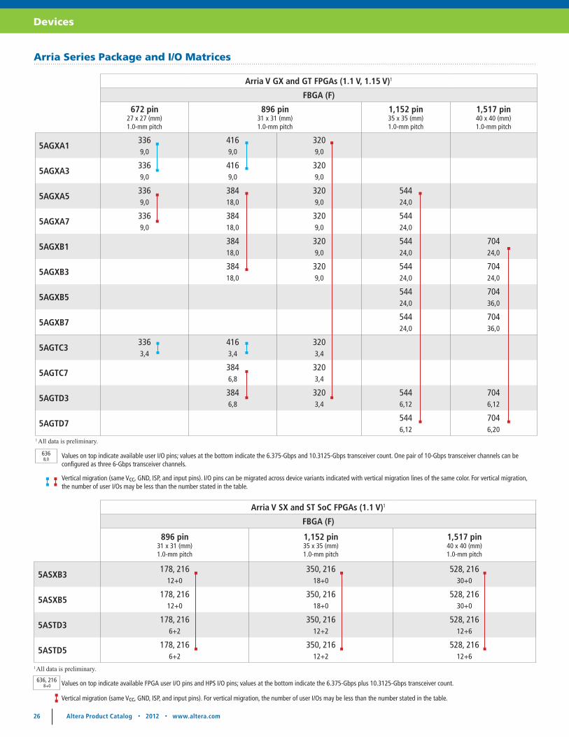
Devices
Arria V GX and GT FPGAs (1.1 V, 1.15 V)1
FBGA (F)
672 pin27 x 27 (mm)1.0-mm pitch
896 pin31 x 31 (mm)1.0-mm pitch
1,152 pin35 x 35 (mm)1.0-mm pitch
1,517 pin40 x 40 (mm)1.0-mm pitch
5AGXA13369,0
4169,0
3209,0
5AGXA33369,0
4169,0
3209,0
5AGXA53369,0
38418,0
3209,0
54424,0
5AGXA73369,0
38418,0
3209,0
54424,0
5AGXB138418,0
3209,0
54424,0
70424,0
5AGXB338418,0
3209,0
54424,0
70424,0
5AGXB554424,0
70436,0
5AGXB754424,0
70436,0
5AGTC33363,4
4163,4
3203,4
5AGTC73846,8
3203,4
5AGTD33846,8
3203,4
5446,12
7046,12
5AGTD75446,12
7046,20
Arria V SX and ST SoC FPGAs (1.1 V)1
FBGA (F)
896 pin31 x 31 (mm)1.0-mm pitch
1,152 pin35 x 35 (mm)1.0-mm pitch
1,517 pin40 x 40 (mm)1.0-mm pitch
5ASXB3178, 216
12+0
350, 21618+0
528, 21630+0
5ASXB5178, 216
12+0
350, 21618+0
528, 21630+0
5ASTD3178, 216
6+2
350, 21612+2
528, 21612+6
5ASTD5178, 216
6+2
350, 21612+2
528, 21612+6
Arria Series Package and I/O Matrices
Values on top indicate available user I/O pins; values at the bottom indicate the 6.375-Gbps and 10.3125-Gbps transceiver count. One pair of 10-Gbps transceiver channels can be configured as three 6-Gbps transceiver channels.
Vertical migration (same Vcc, GND, ISP, and input pins). I/O pins can be migrated across device variants indicated with vertical migration lines of the same color. For vertical migration, the number of user I/Os may be less than the number stated in the table.
Values on top indicate available FPGA user I/O pins and HPS I/O pins; values at the bottom indicate the 6.375-Gbps plus 10.3125-Gbps transceiver count.
Vertical migration (same Vcc, GND, ISP, and input pins). For vertical migration, the number of user I/Os may be less than the number stated in the table.
636
636, 216
8,0
8+0
1 All data is preliminary.
1 All data is preliminary.

26 Altera Product Catalog • 2012 • www.altera.com Altera Product Catalog • 2012 • www.altera.com 27
Devices
Arria Series Package and I/O Matrices
Arria II GX FPGAs (0.9 V)
UBGA (U)1 FBGA (F)
358 pin17 x 17 (mm)0.8-mm pitch
572 pin25 x 25 (mm)1.0-mm pitch
780 pin29 x 29 (mm)1.0-mm pitch
1,152 pin35 x 35 (mm)1.0-mm pitch
EP2AGX45156
4
2528
3648
EP2AGX65156
4
2528
3648
EP2AGX95260
8
37212
45212
EP2AGX125260
8
37212
45212
EP2AGX19037212
61216
EP2AGX26037212
61216
Arria II GZ FPGAs (0.9 V)
Hybrid FBGA (H) FBGA (F)
780 pin33 x 33 (mm)1.0-mm pitch
1,152 pin35 x 35 (mm)1.0-mm pitch
1,517 pin40 x 40 (mm)1.0-mm pitch
EP2AGZ22555416
73424
EP2AGZ30028116
55416
73424
EP2AGZ35028116
55416
73424
1Ultra FineLine ball grid array.
Values on top indicate available user I/O pins; values at the bottom indicate the 6.375-Gbps transceiver count.
Vertical migration (same Vcc, GND, ISP, and input pins). For vertical migration, the number of user I/Os may be less than the number stated in the table.
Values on top indicate available user I/O pins; values at the bottom indicate the 6.375-Gbps transceiver count.
Vertical migration (same Vcc, GND, ISP, and input pins). For vertical migration, the number of user I/Os may be less than the number stated in the table.
72624
63612
28 Altera Product Catalog • 2012 • www.altera.com Altera Product Catalog • 2012 • www.altera.com 29
Devices
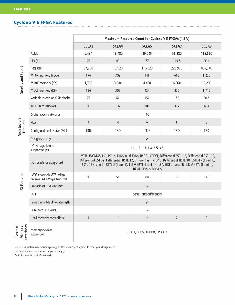
Cyclone V E FPGA Features
Maximum Resource Count for Cyclone V E FPGAs (1.1 V)1
5CEA2 5CEA4 5CEA5 5CEA7 5CEA9
Den
sity
and
Spe
ed
ALMs 9,434 18,480 29,080 56,480 113,560
LEs (K) 25 49 77 149.5 301
Registers 37,736 73,920 116,320 225,920 454,240
M10K memory blocks 176 308 446 686 1,220
M10K memory (Kb) 1,760 3,080 4,460 6,860 12,200
MLAB memory (Kb) 196 303 424 836 1,717
Variable-precision DSP blocks 25 66 150 156 342
18 x 18 multipliers 50 132 300 312 684
Arc
hite
ctur
al
Feat
ures
Global clock networks 16
PLLs 4 4 6 6 6
Configuration file size (Mb) TBD TBD TBD TBD TBD
Design security 3
I/O F
eatu
res
I/O voltage levels supported (V)
1.1, 1.2, 1.5, 1.8, 2.5, 3.32
I/O standards supported
LVTTL, LVCMOS, PCI, PCI-X, LVDS, mini-LVDS, RSDS, LVPECL, Differential SSTL-15, Differential SSTL-18, Differential SSTL-2, Differential HSTL-12, Differential HSTL-15, Differential HSTL-18, SSTL-15 (I and II),
SSTL-18 (I and II), SSTL-2 (I and II), 1.2-V HSTL (I and II), 1.5-V HSTL (I and II), 1.8-V HSTL (I and II), HiSpi, SLVS, Sub-LVDS
LVDS channels, 875-Mbps receive, 840-Mbps transmit
56 56 84 120 140
Embedded DPA circuitry –
OCT Series and differential
Programmable drive strength 3
PCIe hard IP blocks –
Hard memory controllers3 1 1 2 2 2
Exte
rnal
M
emor
y In
terf
aces
Memory devices supported
DDR3, DDR2, LPDDR, LPDDR2
1 All data is preliminary. Various packages offer a variety of options to meet your design needs.2 3.3-V compliant, requires a 3-V power supply.3 With 16- and 32-bit ECC support.
28 Altera Product Catalog • 2012 • www.altera.com Altera Product Catalog • 2012 • www.altera.com 29
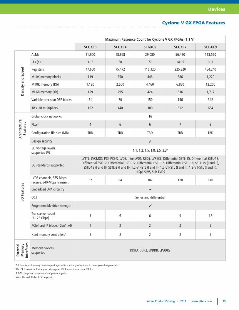
Devices
Cyclone V GX FPGA Features
Maximum Resource Count for Cyclone V GX FPGAs (1.1 V)1
5CGXC3 5CGXC4 5CGXC5 5CGXC7 5CGXC9
Den
sity
and
Spe
ed
ALMs 11,900 18,868 29,080 56,480 113,560
LEs (K) 31.5 50 77 149.5 301
Registers 47,600 75,472 116,320 225,920 454,240
M10K memory blocks 119 250 446 686 1,220
M10K memory (Kb) 1,190 2,500 4,460 6,860 12,200
MLAB memory (Kb) 159 295 424 836 1,717
Variable-precision DSP blocks 51 70 150 156 342
18 x 18 multipliers 102 140 300 312 684
Arc
hite
ctur
al
Feat
ures
Global clock networks 16
PLLs2 4 6 6 7 8
Configuration file size (Mb) TBD TBD TBD TBD TBD
Design security 3
I/O F
eatu
res
I/O voltage levels supported (V)
1.1, 1.2, 1.5, 1.8, 2.5, 3.33
I/O standards supported
LVTTL, LVCMOS, PCI, PCI-X, LVDS, mini-LVDS, RSDS, LVPECL, Differential SSTL-15, Differential SSTL-18, Differential SSTL-2, Differential HSTL-12, Differential HSTL-15, Differential HSTL-18, SSTL-15 (I and II),
SSTL-18 (I and II), SSTL-2 (I and II), 1.2-V HSTL (I and II), 1.5-V HSTL (I and II), 1.8-V HSTL (I and II), HiSpi, SLVS, Sub-LVDS
LVDS channels, 875-Mbps receive, 840-Mbps transmit
52 84 84 120 140
Embedded DPA circuitry –
OCT Series and differential
Programmable drive strength 3
Transceiver count (3.125 Gbps)
3 6 6 9 12
PCIe hard IP blocks (Gen1 x4) 1 2 2 2 2
Hard memory controllers4 1 2 2 2 2
Exte
rnal
M
emor
y In
terf
aces
Memory devices supported
DDR3, DDR2, LPDDR, LPDDR2
1 All data is preliminary. Various packages offer a variety of options to meet your design needs.2 The PLL count includes general-purpose fPLLs and transceiver fPLLs.3 3.3-V compliant, requires a 3-V power supply.4 With 16- and 32-bit ECC support.

30 Altera Product Catalog • 2012 • www.altera.com Altera Product Catalog • 2012 • www.altera.com 31
Devices
Cyclone V GT FPGA Features
Maximum Resource Count for Cyclone V GT FPGAs (1.1 V)1
5CGTD5 5CGTD7 5CGTD9
Den
sity
and
Spe
ed
ALMs 29,080 56,480 113,560
LEs (K) 77 149.5 301
Registers 116,320 225,920 454,240
M10K memory blocks 446 686 1,220
M10K memory (Kb) 4,460 6,860 12,200
MLAB memory (Kb) 424 836 1,717
Variable-precision DSP blocks 150 156 342
18 x 18 multipliers 300 312 684
Arc
hite
ctur
al
Feat
ures
Global clock networks 16
PLLs2 6 7 8
Configuration file size (Mb) TBD TBD TBD
Design security 3
I/O F
eatu
res
I/O voltage levels supported (V)
1.1, 1.2, 1.5, 1.8, 2.5, 3.33
I/O standards supported
LLVTTL, LVCMOS, PCI, PCI-X, LVDS, mini-LVDS, RSDS, LVPECL, Differential SSTL-15, Differential SSTL-18, Differential SSTL-2, Differential HSTL-12, Differential HSTL-15, Differential HSTL-18, SSTL-15 (I and II),
SSTL-18 (I and II), SSTL-2 (I and II), 1.2-V HSTL (I and II), 1.5-V HSTL (I and II), 1.8-V HSTL (I and II), HiSpi, SLVS, Sub-LVDS
LVDS channels, 875-Mbps receive, 840-Mbps transmit
84 120 140
Embedded DPA circuitry –
OCT Series and differential
Programmable drive strength 3
Transceiver count (5 Gbps) 6 9 12
PCIe hard IP blocks (Gen2 x2, Gen1 x4)
2 2 2
Hard memory controllers4 2 2 2
Exte
rnal
M
emor
y In
terf
aces
Memory devices supported
DDR3, DDR2, LPDDR, LPDDR2
1 All data is preliminary. Various packages offer a variety of options to meet your design needs.2 The PLL count includes general-purpose fPLLs and transceiver fPLLs.3 3.3-V compliant, requires a 3-V power supply.4 With 16- and 32-bit ECC support.

30 Altera Product Catalog • 2012 • www.altera.com Altera Product Catalog • 2012 • www.altera.com 31
Devices
1 All data is preliminary.2 The PLL count includes general-purpose fPLLs and transceiver fPLLs.3 3.3-V compliant, requires a 3-V power supply.4 With 16- and 32-bit ECC support.
Cyclone V SE SoC FPGA Features
Maximum Resource Count for Cyclone V SE SoC FPGAs (1.1 V)1
5CSEA2 5CSEA4 5CSEA5 5CSEA6
Den
sity
and
Spe
ed
ALMs 9,434 15,094 32,075 41,509
LEs (K) 25 40 85 110
Registers 37,736 60,376 128,300 166,036
M10K memory blocks 140 224 397 514
M10K memory (Kb) 1,400 2,240 3,972 5,140
MLAB memory (Kb) 138 220 480 621
Variable-precision DSP blocks 36 58 87 112
18 x 18 multipliers 72 116 174 224
Arc
hite
ctur
al F
eatu
res Processor cores (ARM Cortex-A9) Single or dual Single or dual Single or dual Single or dual
Global clock networks 16
PLLs2 (FPGA) 4 5 6 6
PLLs2 (HPS) 3 3 3 3
Configuration file size (Mb) TBD TBD TBD TBD
Design security 3
I/O F
eatu
res
I/O voltage levels supported (V) 1.1, 1.2, 1.5, 1.8, 2.5, 3.33
I/O standards supported
LVTTL, LVCMOS, PCI, PCI-X, LVDS, mini-LVDS, RSDS, LVPECL, Differential SSTL-15, Differential SSTL-18, Differential SSTL-2, Differential HSTL-12, Differential HSTL-15, Differential HSTL-18, SSTL-15 (I and II),
SSTL-18 (I and II), SSTL-2 (I and II), 1.2-V HSTL (I and II), 1.5-V HSTL (I and II), 1.8-V HSTL (I and II), HiSpi, SLVS, Sub-LVDS
LVDS channels, 875-Mbps receive, 840-Mbps transmit
31 31 72 72
Embedded DPA circuitry –
OCT Series and differential
Programmable drive strength 3
PCIe hard IP blocks –
GPIOs (FPGA) 145 145 288 288
GPIOs (HPS) 188 188 188 188
Hard memory controllers4 (FPGA) 1 1 1 1
Hard memory controllers4 (HPS) 1 1 1 1
Exte
rnal
M
emor
y In
terf
aces
Memory devices supported DDR3, DDR2, LPDDR, LPDDR2
32 Altera Product Catalog • 2012 • www.altera.com Altera Product Catalog • 2012 • www.altera.com 33
Devices
1 All data is preliminary.2 The PLL count includes general-purpose fPLLs and transceiver fPLLs.3 3.3-V compliant, requires a 3-V power supply.4 With 16- and 32-bit ECC support.
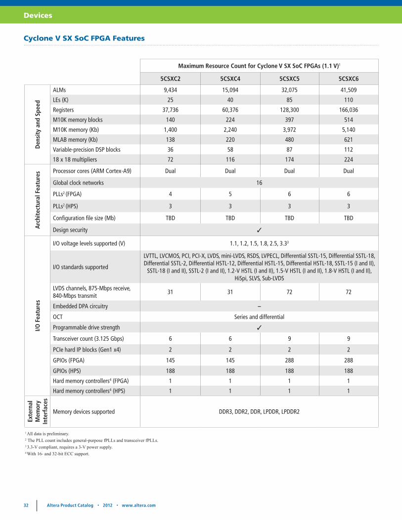
Cyclone V SX SoC FPGA Features
Maximum Resource Count for Cyclone V SX SoC FPGAs (1.1 V)1
5CSXC2 5CSXC4 5CSXC5 5CSXC6
Den
sity
and
Spe
ed
ALMs 9,434 15,094 32,075 41,509
LEs (K) 25 40 85 110
Registers 37,736 60,376 128,300 166,036
M10K memory blocks 140 224 397 514
M10K memory (Kb) 1,400 2,240 3,972 5,140
MLAB memory (Kb) 138 220 480 621
Variable-precision DSP blocks 36 58 87 112
18 x 18 multipliers 72 116 174 224
Arc
hite
ctur
al F
eatu
res Processor cores (ARM Cortex-A9) Dual Dual Dual Dual
Global clock networks 16
PLLs2 (FPGA) 4 5 6 6
PLLs2 (HPS) 3 3 3 3
Configuration file size (Mb) TBD TBD TBD TBD
Design security 3
I/O F
eatu
res
I/O voltage levels supported (V) 1.1, 1.2, 1.5, 1.8, 2.5, 3.33
I/O standards supported
LVTTL, LVCMOS, PCI, PCI-X, LVDS, mini-LVDS, RSDS, LVPECL, Differential SSTL-15, Differential SSTL-18, Differential SSTL-2, Differential HSTL-12, Differential HSTL-15, Differential HSTL-18, SSTL-15 (I and II),
SSTL-18 (I and II), SSTL-2 (I and II), 1.2-V HSTL (I and II), 1.5-V HSTL (I and II), 1.8-V HSTL (I and II), HiSpi, SLVS, Sub-LVDS
LVDS channels, 875-Mbps receive, 840-Mbps transmit
31 31 72 72
Embedded DPA circuitry –
OCT Series and differential
Programmable drive strength 3
Transceiver count (3.125 Gbps) 6 6 9 9
PCIe hard IP blocks (Gen1 x4) 2 2 2 2
GPIOs (FPGA) 145 145 288 288
GPIOs (HPS) 188 188 188 188
Hard memory controllers4 (FPGA) 1 1 1 1
Hard memory controllers4 (HPS) 1 1 1 1
Exte
rnal
M
emor
y In
terf
aces
Memory devices supported DDR3, DDR2, DDR, LPDDR, LPDDR2
32 Altera Product Catalog • 2012 • www.altera.com Altera Product Catalog • 2012 • www.altera.com 33
Devices
1 All data is preliminary.2 The PLL count includes general-purpose fPLLs and transceiver fPLLs.3 3.3-V compliant, requires a 3-V power supply.4 With 16- and 32-bit ECC support.
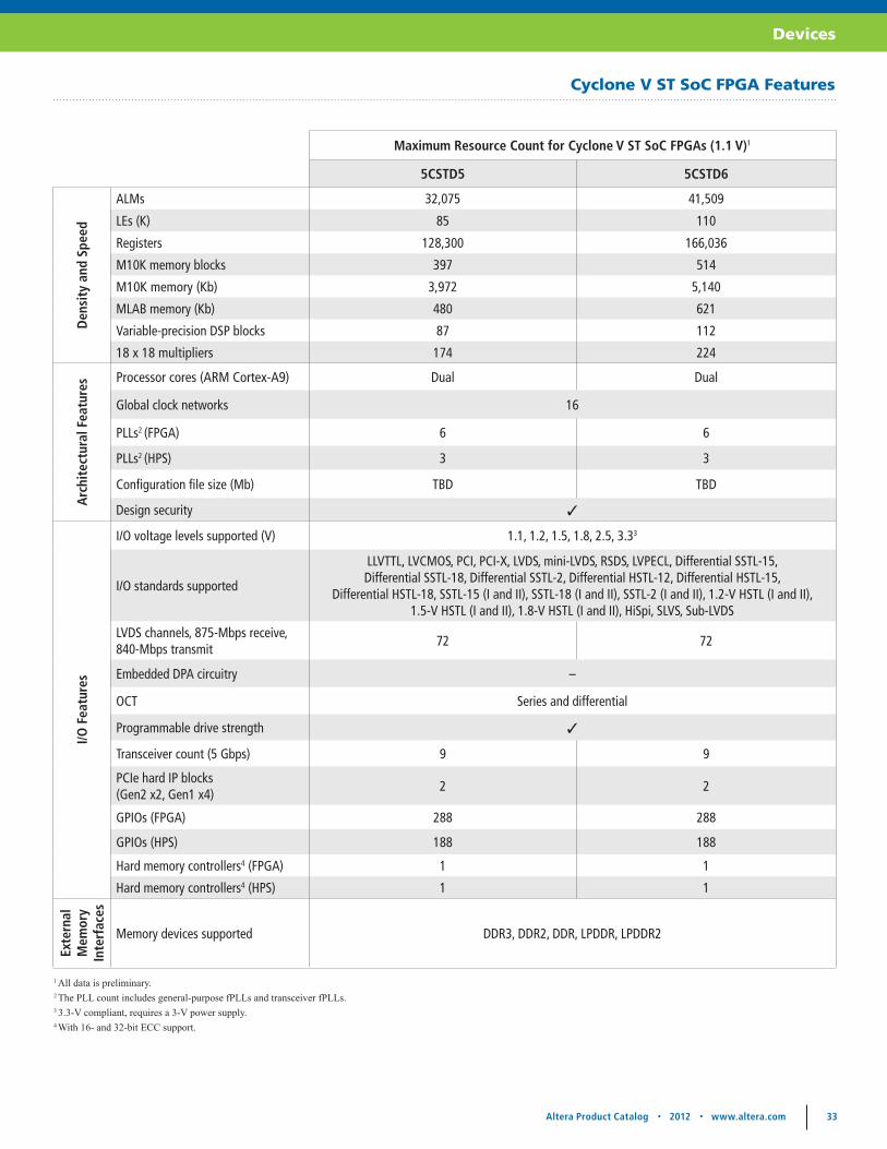
Cyclone V ST SoC FPGA Features
Maximum Resource Count for Cyclone V ST SoC FPGAs (1.1 V)1
5CSTD5 5CSTD6
Den
sity
and
Spe
ed
ALMs 32,075 41,509
LEs (K) 85 110
Registers 128,300 166,036
M10K memory blocks 397 514
M10K memory (Kb) 3,972 5,140
MLAB memory (Kb) 480 621
Variable-precision DSP blocks 87 112
18 x 18 multipliers 174 224
Arc
hite
ctur
al F
eatu
res Processor cores (ARM Cortex-A9) Dual Dual
Global clock networks 16
PLLs2 (FPGA) 6 6
PLLs2 (HPS) 3 3
Configuration file size (Mb) TBD TBD
Design security 3
I/O F
eatu
res
I/O voltage levels supported (V) 1.1, 1.2, 1.5, 1.8, 2.5, 3.33
I/O standards supported
LLVTTL, LVCMOS, PCI, PCI-X, LVDS, mini-LVDS, RSDS, LVPECL, Differential SSTL-15, Differential SSTL-18, Differential SSTL-2, Differential HSTL-12, Differential HSTL-15,
Differential HSTL-18, SSTL-15 (I and II), SSTL-18 (I and II), SSTL-2 (I and II), 1.2-V HSTL (I and II), 1.5-V HSTL (I and II), 1.8-V HSTL (I and II), HiSpi, SLVS, Sub-LVDS
LVDS channels, 875-Mbps receive, 840-Mbps transmit
72 72
Embedded DPA circuitry –
OCT Series and differential
Programmable drive strength 3
Transceiver count (5 Gbps) 9 9
PCIe hard IP blocks (Gen2 x2, Gen1 x4)
2 2
GPIOs (FPGA) 288 288
GPIOs (HPS) 188 188
Hard memory controllers4 (FPGA) 1 1
Hard memory controllers4 (HPS) 1 1
Exte
rnal
M
emor
y In
terf
aces
Memory devices supported DDR3, DDR2, DDR, LPDDR, LPDDR2

34 Altera Product Catalog • 2012 • www.altera.com Altera Product Catalog • 2012 • www.altera.com 35
Devices
Cyclone IV GX FPGA Features
Maximum Resource Count for Cyclone IV GX FPGAs (1.2 V)1
EP4CGX15 EP4CGX22 EP4CGX30 EP4CGX50 EP4CGX75 EP4CGX110 EP4CGX150
Den
sity
and
Sp
eed
LEs (K) 14 21 29 50 74 109 150
M9K memory blocks 60 84 120 278 462 666 720
Embedded memory (Kb) 540 756 1,080 2,502 4,158 5,490 6,480
18 x 18 multipliers 0 40 80 140 198 280 360
Arc
hite
ctur
al
Feat
ures
Global clock networks 20 20 20 30 30 30 30
PLLs 3 4 4 8 8 8 8
Configuration file size (Mb) 3.8 7.6 7.6 24.5 24.5 47.6 47.6
I/O F
eatu
res
I/O voltage levels supported (V)
1.2, 1.5, 1.8, 2.5, 3.3
I/O standards supportedLVTTL, LVCMOS, PCI, PCI-X, LVDS, mini-LVDS, RSDS, LVPECL, Differential SSTL-15, Differential SSTL-18, Differential SSTL-2, Differential HSTL-12, Differential HSTL-15, Differential HSTL-18, SSTL-15 (I and II),
SSTL-18 (I and II), SSTL-2 (I and II), 1.2-V HSTL (I and II), 1.5-V HSTL (I and II), 1.8-V HSTL (I and II)
Emulated LVDS channels 9 40 40 73 73 139 139
LVDS channels, 840 Mbps (receive/transmit)
7/7 14/14 14/14 49/49 49/49 59/59 59/59
Transceiver count2 (2.5 Gbps/3.125 Gbps)
2/0 2, 0 / 4, 0 4, 0 / 0, 43 0, 8 0, 8 0, 8 0, 8
PCIe hard IP blocks (Gen1) 1
Exte
rnal
Mem
ory
Inte
rfac
es
Memory devices supported DDR2, DDR, QDR II, RLDRAM II, SDR
1 Various packages offer a variety options to meet your design needs.2Transceiver performance varies by product line and package offering.3EP4CGX30 supports 3.125 Gbps only in F484 package option.
34 Altera Product Catalog • 2012 • www.altera.com Altera Product Catalog • 2012 • www.altera.com 35
Devices
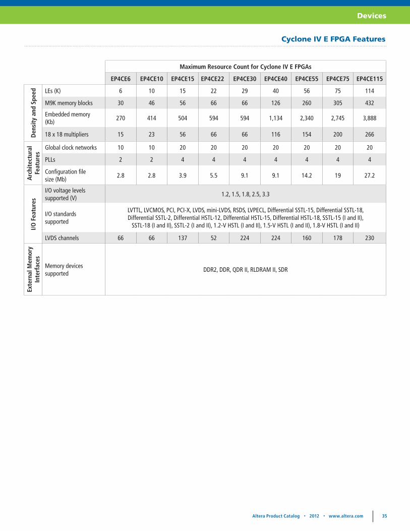
Maximum Resource Count for Cyclone IV E FPGAs
EP4CE6 EP4CE10 EP4CE15 EP4CE22 EP4CE30 EP4CE40 EP4CE55 EP4CE75 EP4CE115
Den
sity
and
Spe
ed LEs (K) 6 10 15 22 29 40 56 75 114
M9K memory blocks 30 46 56 66 66 126 260 305 432
Embedded memory (Kb)
270 414 504 594 594 1,134 2,340 2,745 3,888
18 x 18 multipliers 15 23 56 66 66 116 154 200 266
Arc
hite
ctur
al
Feat
ures
Global clock networks 10 10 20 20 20 20 20 20 20
PLLs 2 2 4 4 4 4 4 4 4
Configuration file size (Mb)
2.8 2.8 3.9 5.5 9.1 9.1 14.2 19 27.2
I/O F
eatu
res
I/O voltage levels supported (V)
1.2, 1.5, 1.8, 2.5, 3.3
I/O standards supported
LVTTL, LVCMOS, PCI, PCI-X, LVDS, mini-LVDS, RSDS, LVPECL, Differential SSTL-15, Differential SSTL-18, Differential SSTL-2, Differential HSTL-12, Differential HSTL-15, Differential HSTL-18, SSTL-15 (I and II),
SSTL-18 (I and II), SSTL-2 (I and II), 1.2-V HSTL (I and II), 1.5-V HSTL (I and II), 1.8-V HSTL (I and II)
LVDS channels 66 66 137 52 224 224 160 178 230
Exte
rnal
Mem
ory
Inte
rfac
es
Memory devices supported
DDR2, DDR, QDR II, RLDRAM II, SDR
Cyclone IV E FPGA Features
36 Altera Product Catalog • 2012 • www.altera.com Altera Product Catalog • 2012 • www.altera.com 37
Devices
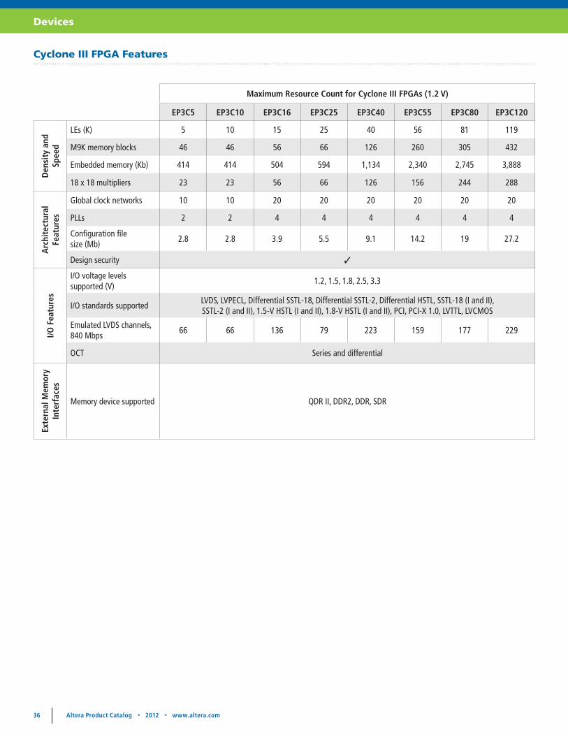
Maximum Resource Count for Cyclone III FPGAs (1.2 V)
EP3C5 EP3C10 EP3C16 EP3C25 EP3C40 EP3C55 EP3C80 EP3C120
Den
sity
and
Sp
eed
LEs (K) 5 10 15 25 40 56 81 119
M9K memory blocks 46 46 56 66 126 260 305 432
Embedded memory (Kb) 414 414 504 594 1,134 2,340 2,745 3,888
18 x 18 multipliers 23 23 56 66 126 156 244 288
Arc
hite
ctur
al
Feat
ures
Global clock networks 10 10 20 20 20 20 20 20
PLLs 2 2 4 4 4 4 4 4
Configuration file size (Mb)
2.8 2.8 3.9 5.5 9.1 14.2 19 27.2
Design security 3
I/O F
eatu
res
I/O voltage levels supported (V)
1.2, 1.5, 1.8, 2.5, 3.3
I/O standards supportedLVDS, LVPECL, Differential SSTL-18, Differential SSTL-2, Differential HSTL, SSTL-18 (I and II), SSTL-2 (I and II), 1.5-V HSTL (I and II), 1.8-V HSTL (I and II), PCI, PCI-X 1.0, LVTTL, LVCMOS
Emulated LVDS channels, 840 Mbps
66 66 136 79 223 159 177 229
OCT Series and differential
Exte
rnal
Mem
ory
Inte
rfac
es
Memory device supported QDR II, DDR2, DDR, SDR
Cyclone III FPGA Features
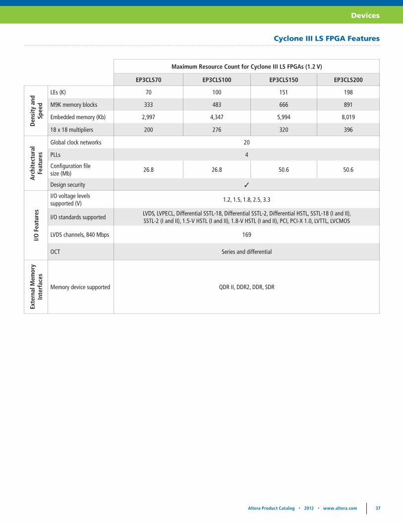
36 Altera Product Catalog • 2012 • www.altera.com Altera Product Catalog • 2012 • www.altera.com 37
Devices
Maximum Resource Count for Cyclone III LS FPGAs (1.2 V)
EP3CLS70 EP3CLS100 EP3CLS150 EP3CLS200
Den
sity
and
Sp
eed
LEs (K) 70 100 151 198
M9K memory blocks 333 483 666 891
Embedded memory (Kb) 2,997 4,347 5,994 8,019
18 x 18 multipliers 200 276 320 396
Arc
hite
ctur
al
Feat
ures
Global clock networks 20
PLLs 4
Configuration file size (Mb)
26.8 26.8 50.6 50.6
Design security 3
I/O F
eatu
res
I/O voltage levels supported (V)
1.2, 1.5, 1.8, 2.5, 3.3
I/O standards supportedLVDS, LVPECL, Differential SSTL-18, Differential SSTL-2, Differential HSTL, SSTL-18 (I and II), SSTL-2 (I and II), 1.5-V HSTL (I and II), 1.8-V HSTL (I and II), PCI, PCI-X 1.0, LVTTL, LVCMOS
LVDS channels, 840 Mbps 169
OCT Series and differential
Exte
rnal
Mem
ory
Inte
rfac
es
Memory device supported QDR II, DDR2, DDR, SDR
Cyclone III LS FPGA Features
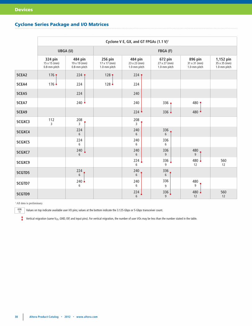
38 Altera Product Catalog • 2012 • www.altera.com Altera Product Catalog • 2012 • www.altera.com 39
Devices
Cyclone Series Package and I/O Matrices
Cyclone V E, GX, and GT FPGAs (1.1 V)1
UBGA (U) FBGA (F)
324 pin15 x 15 (mm) 0.8-mm pitch
484 pin19 x 19 (mm)0.8-mm pitch
256 pin17 x 17 (mm)1.0-mm pitch
484 pin23 x 23 (mm) 1.0-mm pitch
672 pin27 x 27 (mm) 1.0-mm pitch
896 pin31 x 31 (mm) 1.0-mm pitch
1,152 pin35 x 35 (mm) 1.0-mm pitch
5CEA2 176 224 128 224
5CEA4 176 224 128 224
5CEA5 224 240
5CEA7 240 240 336 480
5CEA9 224 336 480
5CGXC3 1123
2083
2083
5CGXC4 2246
2406
3366
5CGXC5 2246
2406
3366
5CGXC7 2406
2406
3369
4809
5CGXC9 2246
3369
48012
56012
5CGTD5 2246
2406
3366
5CGTD7 2406
2406
3369
4809
5CGTD9 2246
3369
48012
56012
Vertical migration (same Vcc, GND, ISP, and input pins). For vertical migration, the number of user I/Os may be less than the number stated in the table.
Values on top indicate available user I/O pins; values at the bottom indicate the 3.125-Gbps or 5-Gbps transceiver count.63612
1 All data is preliminary.

38 Altera Product Catalog • 2012 • www.altera.com Altera Product Catalog • 2012 • www.altera.com 39
Devices
Cyclone Series Package and I/O Matrices
Cyclone V SE, SX, and ST SoC FPGAs (1.1 V)1
UBGA (U) FBGA (F)
484 pin19 x 19 (mm)0.8-mm pitch
672 pin23 x 23 (mm)0.8-mm pitch
896 pin31 x 31 (mm)1.0-mm pitch
5CSEA2 66, 1610
145, 1880
5CSEA4 66, 1610
145, 1880
5CSEA5 66, 1610
145, 1880
288, 1880
5CSEA6 66, 1610
145, 1880
288, 1880
5CSXC2 145, 1886
5CSXC4 145, 1886
5CSXC5 145, 1889
288, 1889
5CSXC6 145, 1889
288, 1889
5CSTD5 288, 1889
5CSTD6 288, 1889
Vertical migration (same Vcc, GND, ISP, and input pins). For vertical migration, the number of user I/Os may be less than the number stated in the table.
Values on top indicate available FPGA user I/O pins and HPS I/O pins; values at the bottom indicate the 3.125-Gbps or 5-Gbps transceiver count.636, 16112
1 All data is preliminary.
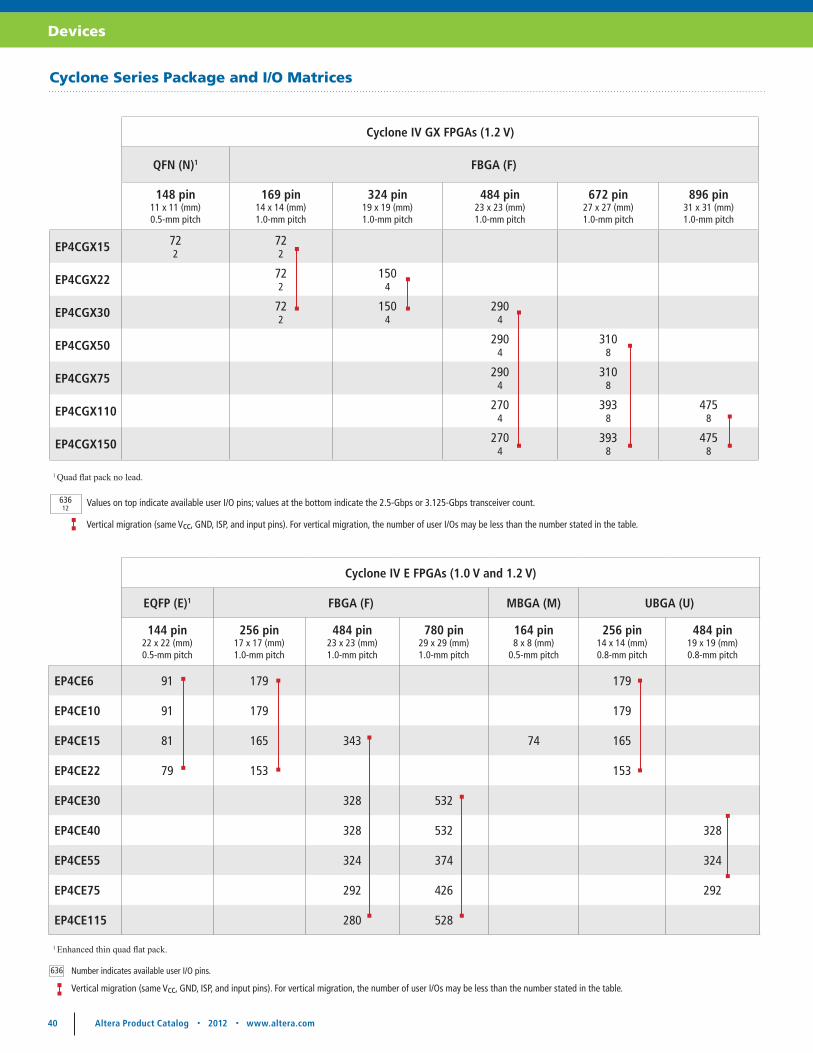
40 Altera Product Catalog • 2012 • www.altera.com Altera Product Catalog • 2012 • www.altera.com 41
Devices
Cyclone Series Package and I/O Matrices
Cyclone IV GX FPGAs (1.2 V)
QFN (N)1 FBGA (F)
148 pin11 x 11 (mm)0.5-mm pitch
169 pin14 x 14 (mm) 1.0-mm pitch
324 pin19 x 19 (mm)1.0-mm pitch
484 pin23 x 23 (mm)1.0-mm pitch
672 pin27 x 27 (mm)1.0-mm pitch
896 pin31 x 31 (mm) 1.0-mm pitch
EP4CGX15 722
722
EP4CGX22 722
1504
EP4CGX30 722
1504
2904
EP4CGX50 2904
3108
EP4CGX75 2904
3108
EP4CGX110 2704
3938
4758
EP4CGX150 2704
3938
4758
Cyclone IV E FPGAs (1.0 V and 1.2 V)
EQFP (E)1 FBGA (F) MBGA (M) UBGA (U)
144 pin22 x 22 (mm)0.5-mm pitch
256 pin17 x 17 (mm) 1.0-mm pitch
484 pin23 x 23 (mm)1.0-mm pitch
780 pin29 x 29 (mm) 1.0-mm pitch
164 pin8 x 8 (mm)
0.5-mm pitch
256 pin14 x 14 (mm) 0.8-mm pitch
484 pin19 x 19 (mm) 0.8-mm pitch
EP4CE6 91 179 179
EP4CE10 91 179 179
EP4CE15 81 165 343 74 165
EP4CE22 79 153 153
EP4CE30 328 532
EP4CE40 328 532 328
EP4CE55 324 374 324
EP4CE75 292 426 292
EP4CE115 280 528
Vertical migration (same Vcc, GND, ISP, and input pins). For vertical migration, the number of user I/Os may be less than the number stated in the table.
Vertical migration (same Vcc, GND, ISP, and input pins). For vertical migration, the number of user I/Os may be less than the number stated in the table.
636 Number indicates available user I/O pins.
Values on top indicate available user I/O pins; values at the bottom indicate the 2.5-Gbps or 3.125-Gbps transceiver count.63612
1 Enhanced thin quad flat pack.
1 Quad flat pack no lead.

40 Altera Product Catalog • 2012 • www.altera.com Altera Product Catalog • 2012 • www.altera.com 41
Devices
Cyclone III FPGAs (1.2 V)
EQFP (E) MBGA (M)1 PQFP (Q)2 FBGA (F) UBGA (U)
144 pin22 x 22 (mm) 0.5-mm pitch
164 pin8 x 8 (mm)
0.5-mm pitch
240 pin34.6 x 34.6 (mm)
0.5-mm pitch
256 pin17 x 17 (mm)1.0-mm pitch
324 pin19 x 19 (mm)1.0-mm pitch
484 pin23 x 23 (mm)1.0-mm pitch
780 pin29 x 29 (mm)1.0-mm pitch
256 pin14 x 14 (mm) 0.8-mm pitch
484 pin19 x 19 (mm)0.8-mm pitch
EP3C5 94 106 182 182
EP3C10 94 106 182 182
EP3C16 84 92 160 168 346 168 346
EP3C25 82 148 156 215 156
EP3C40 128 195 331 535 331
EP3C55 327 377 327
EP3C80 295 429 295
EP3C120 283 531
EP3CLS70 294 429 294
EP3CLS100 294 429 294
EP3CLS150 226 429
EP3CLS200 226 429
Cyclone Series Package and I/O Matrices
Vertical migration (same Vcc, GND, ISP, and input pins). For vertical migration, the number of user I/Os may be less than the number stated in the table.
636 Number indicates available user I/O pins.
1 Micro FineLine BGA.2Plastic quad flat pack.

42 Altera Product Catalog • 2012 • www.altera.com Altera Product Catalog • 2012 • www.altera.com 43
Devices
MAX V CPLD Features
MAX V CPLDs (1.8 V)
5M40Z 5M80Z 5M160Z 5M240Z 5M570Z 5M1270Z 5M2210Z
Den
sity
and
Spe
ed
LEs 40 80 160 240 570 1270 2210
Equivalent macrocells1 32 64 128 192 440 980 1700
Pin-to-pin delay (ns) 7.5 7.5 7.5 7.5 9.0 6.2 7.0
User flash memory (Kb) 8
Total on-chip memory (bits)2 Yes Yes Yes Yes Yes Yes Yes
Arc
hite
ctur
al F
eatu
res
Internal oscillator 3
Digital PLL3 3
Fast power on reset 3
Boundary scan JTAG 3
JTAG ISP 3
Fast input registers 3
Programmable register power up 3
JTAG translator 3
Real-time ISP 3
I/O F
eatu
res
MultiVolt I/Os (V) 1.2, 1.5, 1.8, 2.5, 3.3 1.2, 1.5, 1.8, 2.5, 3.3, 5.04
I/O power banks 2 2 2 2 2 4 4
Maximum output enables 54 54 79 114 159 271 271
LVTTL/LVCMOS 3
LVDS outputs Yes Yes Yes Yes Yes Yes Yes
32-bit, 66-MHz PCI compliant - - - - - 34 34
Schmitt triggers 3
Programmable slew rate 3
Programmable pull-up resistors 3
Programmable ground pins 3
Open-drain outputs 3
Bus hold 3
1 Typical equivalent macrocells.2 Unused LEs can be converted to memory. The total number of available LE RAM bits depends on the memory mode, depth, and width configurations of the instantiated memory.3 Optional IP core. Contact your Altera sales representative for availability.4 An external resistor must be used for 5-V tolerance.
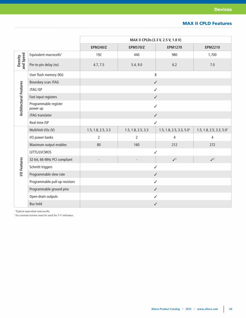
42 Altera Product Catalog • 2012 • www.altera.com Altera Product Catalog • 2012 • www.altera.com 43
Devices
MAX II CPLD Features
MAX II CPLDs (3.3 V, 2.5 V, 1.8 V)
EPM240/Z EPM570/Z EPM1270 EPM2210
Den
sity
an
d Sp
eed Equivalent macrocells1 192 440 980 1,700
Pin-to-pin delay (ns) 4.7, 7.5 5.4, 9.0 6.2 7.0
Arc
hite
ctur
al F
eatu
res
User flash memory (Kb) 8
Boundary scan JTAG 3
JTAG ISP 3
Fast input registers 3
Programmable register power up 3
JTAG translator 3
Real-time ISP 3
I/O F
eatu
res
MultiVolt I/Os (V) 1.5, 1.8, 2.5, 3.3 1.5, 1.8, 2.5, 3.3 1.5, 1.8, 2.5, 3.3, 5.02 1.5, 1.8, 2.5, 3.3, 5.02
I/O power banks 2 2 4 4
Maximum output enables 80 160 212 272
LVTTL/LVCMOS 3
32-bit, 66-MHz PCI compliant - - 32 32
Schmitt triggers 3
Programmable slew rate 3
Programmable pull-up resistors 3
Programmable ground pins 3
Open-drain outputs 3
Bus hold 3
1 Typical equivalent macrocells.2An external resistor must be used for 5-V tolerance.
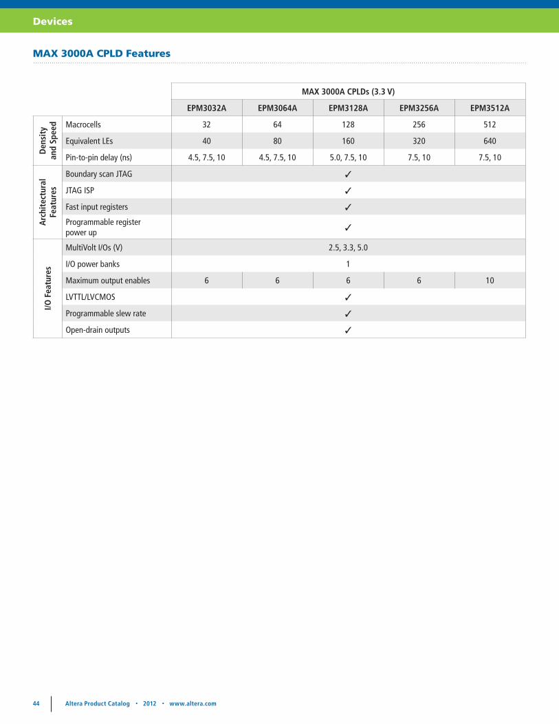
44 Altera Product Catalog • 2012 • www.altera.com Altera Product Catalog • 2012 • www.altera.com 45
Devices
MAX 3000A CPLDs (3.3 V)
EPM3032A EPM3064A EPM3128A EPM3256A EPM3512A
Den
sity
an
d Sp
eed Macrocells 32 64 128 256 512
Equivalent LEs 40 80 160 320 640
Pin-to-pin delay (ns) 4.5, 7.5, 10 4.5, 7.5, 10 5.0, 7.5, 10 7.5, 10 7.5, 10
Arc
hite
ctur
al
Feat
ures
Boundary scan JTAG 3
JTAG ISP 3
Fast input registers 3
Programmable register power up 3
I/O F
eatu
res
MultiVolt I/Os (V) 2.5, 3.3, 5.0
I/O power banks 1
Maximum output enables 6 6 6 6 10
LVTTL/LVCMOS 3
Programmable slew rate 3
Open-drain outputs 3
MAX 3000A CPLD Features
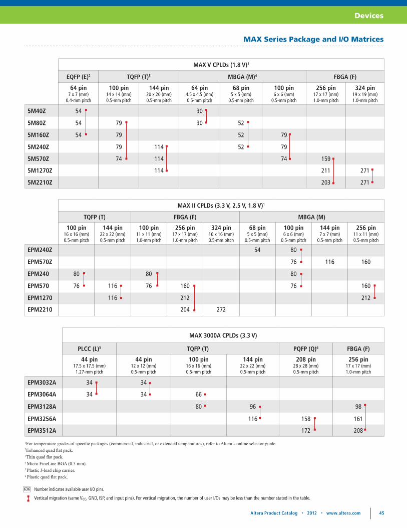
44 Altera Product Catalog • 2012 • www.altera.com Altera Product Catalog • 2012 • www.altera.com 45
Devices
1For temperature grades of specific packages (commercial, industrial, or extended temperatures), refer to Altera’s online selector guide.2Enhanced quad flat pack.3Thin quad flat pack.4 Micro FineLine BGA (0.5 mm).5 Plastic J-lead chip carrier.6 Plastic quad flat pack.
MAX II CPLDs (3.3 V, 2.5 V, 1.8 V)1
TQFP (T) FBGA (F) MBGA (M)
100 pin16 x 16 (mm) 0.5-mm pitch
144 pin22 x 22 (mm) 0.5-mm pitch
100 pin11 x 11 (mm) 1.0-mm pitch
256 pin17 x 17 (mm) 1.0-mm pitch
324 pin16 x 16 (mm) 0.5-mm pitch
68 pin5 x 5 (mm)
0.5-mm pitch
100 pin6 x 6 (mm)
0.5-mm pitch
144 pin7 x 7 (mm)
0.5-mm pitch
256 pin11 x 11 (mm) 0.5-mm pitch
EPM240Z 54 80
EPM570Z 76 116 160
EPM240 80 80 80
EPM570 76 116 76 160 76 160
EPM1270 116 212 212
EPM2210 204 272
MAX V CPLDs (1.8 V)1
EQFP (E)2 TQFP (T)3 MBGA (M)4 FBGA (F)
64 pin7 x 7 (mm)
0.4-mm pitch
100 pin14 x 14 (mm) 0.5-mm pitch
144 pin20 x 20 (mm) 0.5-mm pitch
64 pin4.5 x 4.5 (mm) 0.5-mm pitch
68 pin5 x 5 (mm)
0.5-mm pitch
100 pin6 x 6 (mm)
0.5-mm pitch
256 pin17 x 17 (mm) 1.0-mm pitch
324 pin19 x 19 (mm) 1.0-mm pitch
5M40Z 54 30
5M80Z 54 79 30 52
5M160Z 54 79 52 79
5M240Z 79 114 52 79
5M570Z 74 114 74 159
5M1270Z 114 211 271
5M2210Z 203 271
MAX Series Package and I/O Matrices
MAX 3000A CPLDs (3.3 V)
PLCC (L)5 TQFP (T) PQFP (Q)6 FBGA (F)
44 pin17.5 x 17.5 (mm)
1.27-mm pitch
44 pin12 x 12 (mm) 0.5-mm pitch
100 pin16 x 16 (mm) 0.5-mm pitch
144 pin22 x 22 (mm) 0.5-mm pitch
208 pin28 x 28 (mm) 0.5-mm pitch
256 pin17 x 17 (mm) 1.0-mm pitch
EPM3032A 34 34
EPM3064A 34 34 66
EPM3128A 80 96 98
EPM3256A 116 158 161
EPM3512A 172 208
Vertical migration (same Vcc, GND, ISP, and input pins). For vertical migration, the number of user I/Os may be less than the number stated in the table.
636 Number indicates available user I/O pins.

46 Altera Product Catalog • 2012 • www.altera.com Altera Product Catalog • 2012 • www.altera.com 47
Design Software
Quartus II Design Software
1 Requires additional license.2 Available with TalkBack feature enabled in Web Edition.
Quartus II software is number one in performance and productivity for CPLD, FPGA, SoC FPGA, and HardCopy ASIC designs, providing the fastest path to convert your concept into reality. Quartus II software also supports many third-party tools in synthesis, static timing analysis, board-level simulation, signal integrity analysis, and formal verification.
www.altera.com/products/software
Quartus II Software Design Flow
Quartus II Software Key FeaturesAvailability
Subscription Edition
Web Edition (Free)
Design Entry
Cyclone FPGA and MAX CPLD device support 3 3
Arria and Stratix FPGA device support 3
HardCopy ASIC device support 3
Multiprocessor support (faster compile time support) 3
IP Base Suite (includes licenses for 15 popular IP cores) 3
Qsys (next-generation system–integration tool) 3 3
SOPC Builder (legacy system development tool) 3 3
Rapid Recompile (faster compile for small design changes) 3
Incremental compile (performance preservation and team-based design) 3
Functional SimulationModelSim®-Altera Starter Edition software 3 3
ModelSim-Altera Edition software 31 31
Synthesis Quartus Integrated Synthesis (synthesis tool) 3 3
Placement and Routing Fitter (placement and routing tool) 3 3
Timing and Power Verification
TimeQuest tool (static timing analysis) 3 3
PowerPlay tool and optimization (power analysis) 3 3
In-System DebugSignalTapTM II logic analyzer (embedded logic analyzer)2 3
Transceiver Toolkit (transceiver interface and verification tool) 3
Operating System SupportAvailability
Subscription Edition
Web Edition (Free)
Windows/Linux 32-bit support 3 3
Windows/Linux 64-bit support 3

46 Altera Product Catalog • 2012 • www.altera.com Altera Product Catalog • 2012 • www.altera.com 47
Design Software
Quartus II Design Software Features Summary
Des
ign
Flow
Met
hodo
logy
Incremental compilation1 Improves design timing closure and reduces design compilation times up to 70 percent. Supports team-based design.
Pin planner Eases the process of assigning and managing pin assignments for high-density and high pin-count designs.
Qsys (replaces SOPC Builder)Automates system development by integrating IP functions and subsystems (collection of IP functions) using a hierarchical approach and a high-performance interconnect (based on a network-on-a-chip architecture).
Off-the-shelf IP cores Lets you construct your system-level design using IP cores from Altera and from Altera’s third-party IP partners.
Parallel development in ASICs1
Allows for FPGA prototypes and HardCopy ASICs to be designed in parallel using the same design software and IP.
Scripting support Supports command-line operation and Tcl scripting, as well as GUI design.
Rapid Recompile1 Maximizes your productivity by reducing your compilation time by 50 percent on average (for a small design change after a full compile). Improves design timing preservation.
Perf
orm
ance
and
Tim
ing
Cl
osur
e M
etho
dolo
gy
Physical synthesis Uses post placement and routing delay knowledge of a design to improve performance.
Design space explorer (DSE)Increases performance by automatically iterating through combinations of Quartus II software settings to find optimal results.
Extensive cross-probing Provides support for cross-probing between verification tools and design source files.
Optimization advisors Provides design-specific advice to improve performance, resource usage, and power consumption.
Chip plannerReduces verification time (while maintaining timing closure) by enabling small, post placement and routing design changes to be implemented in minutes.
Veri
ficat
ion
TimeQuest timing analyzerProvides native Synopsys Design Constraint (SDC) support and allows you to create, manage, and analyze complex timing constraints and quickly perform advanced timing verification.
SignalTap II embedded logic analyzer2
Supports the most channels, fastest clock speeds, largest sample depths, and most advanced triggering capabilities available in an embedded logic analyzer.
System ConsoleEnables you to easily debug your FPGA in real time using read and write transactions. It also enables you to quickly create a GUI to help monitor and send data into your FPGA.
PowerPlay technology Enables you to accurately analyze and optimize both dynamic and static power consumption.
Thir
d-Pa
rty
Supp
ort
EDA partnersOffers EDA software support for synthesis, functional and timing simulation, static timing analysis, board-level simulation, signal integrity analysis, and formal verification. To see a complete list of partners, visit www.altera.com/products/software/partners/eda_partners/eda-index.html.
1 Included in Subscription Edition only.2 Available with talkback feature enabled in Web Edition.
Quartus II Design Software
Getting Started Steps
Step 1: Download free Web Edition www.altera.com/download
Step 2: Get oriented with Quartus II Software interactive tutorial After installation, open the interactive tutorial on the welcome screen.
Step 3: Sign up for training www.altera.com/training

48 Altera Product Catalog • 2012 • www.altera.com Altera Product Catalog • 2012 • www.altera.com 4948 Altera Product Catalog • 2012 • www.altera.com Altera Product Catalog • 2012 • www.altera.com 49
Design Software
Quartus II Design Software
Purchase Quartus II software and increase your productivity today.
Pricing Description
$2,995 (SW-QUARTUS-SE-FIX)Renewal $2,495 (SWR-QUARTUS-SE-FIX)
Fixed-node license: subscription for one year—Windows only.
$3,995 (SW-QUARTUS-SE-FLT)Renewal $2,495 (SWR-QUARTUS-SE-FLT)Add seat $3,995 (SW-QUARTUS-SE-ADD)
Floating-node license: subscription for one year—Windows/Linux.
ModelSim-Altera Edition Software
$945 (SW-MODELSIM-AE)Renewal $945 (SWR-MODELSIM-AE)
ModelSim-Altera Edition software is available as a $945 option for both Quartus II software Subscription Edition and Web Edition. It’s 33 percent faster than Starter Edition with no line limitation.
ModelSim-Altera Starter Edition Software
FreeFree for both Quartus II software Subscription Edition and Web Edition softwares with a 10,000 executable line limitation, ModelSim-Altera Starter Edition software is recommended for simulating small FPGA designs.
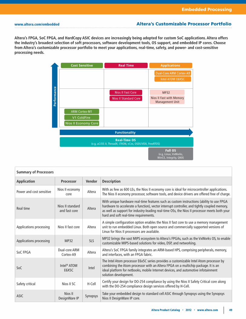
48 Altera Product Catalog • 2012 • www.altera.com Altera Product Catalog • 2012 • www.altera.com 49
Embedded Processing
48 Altera Product Catalog • 2012 • www.altera.com Altera Product Catalog • 2012 • www.altera.com 49
www.altera.com/embedded
Altera’s FPGA, SoC FPGA, and HardCopy ASIC devices are increasingly being adopted for custom SoC applications. Altera offers the industry’s broadest selection of soft processors, software development tools, OS support, and embedded IP cores. Choose from Altera’s customizable processor portfolio to meet your applications, real-time, safety, and power- and cost-sensitive processing needs.
Summary of Processors
Application Processor Vendor Description
Power and cost sensitiveNios II economy
coreAltera
With as few as 600 LEs, the Nios II economy core is ideal for microcontroller applications. The Nios II economy processor, software tools, and device drivers are offered free of charge.
Real timeNios II standard
and fast coreAltera
With unique hardware real-time features such as custom instructions (ability to use FPGA hardware to accelerate a function), vector interrupt controller, and tightly coupled memory, as well as support for industry-leading real-time OSs, the Nios II processor meets both your hard and soft real-time requirements.
Applications processing Nios II fast core AlteraA simple configuration option enables the Nios II fast core to use a memory management unit to run embedded Linux. Both open source and commercially supported versions of Linux for Nios II processors are available.
Applications processing MP32 SLSMP32 brings the vast MIPS ecosystem to Altera’s FPGAs, such as the VxWorks OS, to enable customizable MIPS-based solutions for video, DSP, and networking.
SoC FPGADual-core ARM
Cortex-A9Altera
Altera’s SoC FPGA family integrates an ARM-based HPS, comprising peripherals, memory, and interfaces, with an FPGA fabric.
SoCIntel® ATOM
E6X5CIntel
The Intel Atom processor E6x5C series provides a customizable Intel Atom processor by combining the Atom processor with an Altera FPGA on a multichip package. It is an ideal platform for netbooks, mobile Internet devices, and automotive infotainment solution development.
Safety critical Nios II SC H-CellCertify your design for DO-254 compliance by using the Nios II Safety Critical core along with the DO-254 compliance design services offered by H-Cell.
ASICNios II
DesignWare IPSynopsys
Take your embedded design to standard cell ASIC through Synopsys using the Synopsys Nios II DesignWare IP core.
Altera’s Customizable Processor Portfolio
Perf
orm
ance
Functionality
Cost Sensitive Real Time Applications
Dual-Core ARM Cortex-A9
Intel ATOM E6X5C
MP32
Nios II Fast with MemoryManagement Unit
Nios II Fast Core
Nios II Standard Core
Real-Time OS(e.g, uC/OS II, ThreadX, iTRON, eCos, OSEK/VDX, FreeRTOS)
Full OS(e.g, Linux, VxWorks,
WinCE, Integrity, QNX)
ARM Cortex-M1
V1 ColdFire
Nios II Economy Core

50 Altera Product Catalog • 2012 • www.altera.com Altera Product Catalog • 2012 • www.altera.com 51
Embedded Processing
Comparative Summary of Altera’s Soft Processors by Performance and Feature Set
Category Cost-and Power-Sensitive Processors Real-Time Processor Applications Processors
Features ARM Cortex-M1 V1 ColdFireNios II
EconomyNios II
StandardNios II Fast MP32 ARM Cortex-A9
Maximum frequency (MHz) 200 145 330 270 290 290 800
Maximum performance (MIPS2 at MHz) Stratix Series
160 at 200 135 at 145 50 at 330 170 at 270 340 at 290 300 at 290 –
Maximum performance (MIPS2 at MHz) Arria Series
– 84 at 90 45 at 300 115 at 180 270 at 240 300 at 290 2,000 at 8001
Maximum performance (MIPS2 at MHz) Cyclone Series
80 at 100 84 at 90 30 at 175 90 at 145 195 at 175 140 at 145 2,000 at 8001
Maximum performance efficiency (MIPS2 per MHz)
0.8 0.93 0.15 0.64 1.13 1.15 2.5
16-/32-bit instruction set support
16 and 32 16, 32, and 48 32 32 32 32 32
Level 1 instruction cache – – – Configurable Configurable Configurable 32 KB
Level 1 data cache – – – – Configurable 64 KB 32 KB
Level 2 cache – – – – – – 512 KB
Memory management unit – – – – 3 3 3
Floating-point unit – – – FPCI3 FPCI3 –Dual
precision
Vector interrupt controller 3 – – 3 3 – –
Tightly coupled memory Up to 64K – – Configurable Configurable – –
Custom instruction interface
– – Up to 256 Up to 256 Up to 256 – –
Equivalent LEs 2,500 6,800 600 1,200 1,800 – 3,200 5,500 HPS
1 Per processor2 Dhrystone 2.1 benchmark3 Floating-point custom instructions
Altera’s Customizable Processor Portfolio
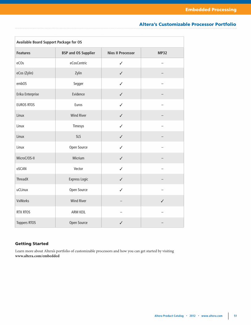
50 Altera Product Catalog • 2012 • www.altera.com Altera Product Catalog • 2012 • www.altera.com 51
Embedded Processing
Learn more about Altera’s portfolio of customizable processors and how you can get started by visiting www.altera.com/embedded
Getting Started
Available Board Support Package for OS
Features BSP and OS Supplier Nios II Processor MP32
eCOs eCosCentric 3 –
eCos (Zylin) Zylin 3 –
embOS Segger 3 –
Erika Enterprise Evidence 3 –
EUROS RTOS Euros 3 –
Linux Wind River 3 –
Linux Timesys 3 –
Linux SLS 3 –
Linux Open Source 3 –
MicroC/OS-II Micrium 3 –
oSCAN Vector 3 –
ThreadX Express Logic 3 –
uCLinux Open Source 3 –
VxWorks Wind River – 3
RTX RTOS ARM KEIL – –
Toppers RTOS Open Source 3 –
Altera’s Customizable Processor Portfolio

52 Altera Product Catalog • 2012 • www.altera.com Altera Product Catalog • 2012 • www.altera.com 53
Embedded Processing
Nios II Processor
Altera’s Nios II processor, the world’s most versatile processor according to Gartner Research, is the most widely used soft processor in the FPGA industry. This soft processor delivers unprecedented flexibility for your cost- sensitive, real-time, safety-critical (DO-254), ASIC-optimized, and applications processing needs. The Nios II processor supports all Altera FPGA and HardCopy device families and is also available for standard cell ASICs through Synopsys.The Nios II processor in any one of Altera’s FPGA and HardCopy devices offers a custom SoC solution that has the flexibility of software and the performance of hardware. Through its innovative design, the Nios II processor leverages the logic resources of the device to provide unprecedented hard and soft real-time capabilities.
You can:• Lower overall system cost, complexity, and power consumption by integrating the processor with the FPGA.
• Scale performance with multiple processors, custom instructions (hardware acceleration of an instruction) or coprocessing (hardware accelerator next to the soft processor).
• Target any Stratix, Arria, or Cyclone series FPGA or HardCopy series ASIC.
• Eliminate the risk of processor and ASSP obsolescence.
• Take advantage of the free Nios II economy core, the free Nios II Embedded Design Suite (EDS), and the NicheStack TCP/IP Network Stack, Nios II Edition software to get started today.
Qsys
Targets
Quartus IISoftware
Nios II EDS
Hardware Software
AutomaticBSP
Generation
System LibraryHeader FileApplication Template
Define System
ProcessorsPeripherals
MemoryInterfaces
RTL Simulation
Instruction Set Simulator
Target Hardware
RTL SystemDescription
System Testbench
JTAG DebuggerFPGA
Configuration
Software Development
EditCompileDebug
Generate FPGA Configuration
SynthesizePlace and Route
CompileDownload
Nios II Processor Development Flow
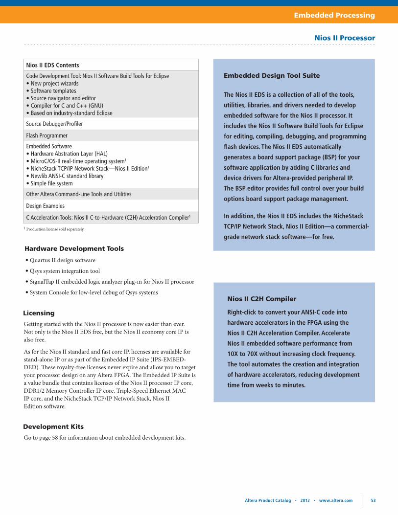
52 Altera Product Catalog • 2012 • www.altera.com Altera Product Catalog • 2012 • www.altera.com 53
Embedded Processing
Nios II Processor
Nios II EDS Contents
Code Development Tool: Nios II Software Build Tools for Eclipse•New project wizards•Software templates•Source navigator and editor•Compiler for C and C++ (GNU)•Based on industry-standard Eclipse
Source Debugger/Profiler
Flash Programmer
Embedded Software•Hardware Abstration Layer (HAL)•MicroC/OS-II real-time operating system1
•NicheStack TCP/IP Network Stack—Nios II Edition1
•Newlib ANSI-C standard library•Simple file system
Other Altera Command-Line Tools and Utilities
Design Examples
C Acceleration Tools: Nios II C-to-Hardware (C2H) Acceleration Compiler1
1 Production license sold separately.
The Nios II EDS is a collection of all of the tools,
utilities, libraries, and drivers needed to develop
embedded software for the Nios II processor. It
includes the Nios II Software Build Tools for Eclipse
for editing, compiling, debugging, and programming
flash devices. The Nios II EDS automatically
generates a board support package (BSP) for your
software application by adding C libraries and
device drivers for Altera-provided peripheral IP.
The BSP editor provides full control over your build
options board support package management.
In addition, the Nios II EDS includes the NicheStack
TCP/IP Network Stack, Nios II Edition—a commercial-
grade network stack software—for free.
Embedded Design Tool Suite
Nios II C2H Compiler
Right-click to convert your ANSI-C code into
hardware accelerators in the FPGA using the
Nios II C2H Acceleration Compiler. Accelerate
Nios II embedded software performance from
10X to 70X without increasing clock frequency.
The tool automates the creation and integration
of hardware accelerators, reducing development
time from weeks to minutes.
•Quartus II design software
•Qsys system integration tool
•SignalTap II embedded logic analyzer plug-in for Nios II processor
•System Console for low-level debug of Qsys systems
Getting started with the Nios II processor is now easier than ever. Not only is the Nios II EDS free, but the Nios II economy core IP is also free.
As for the Nios II standard and fast core IP, licenses are available for stand-alone IP or as part of the Embedded IP Suite (IPS-EMBED-DED). These royalty-free licenses never expire and allow you to target your processor design on any Altera FPGA. The Embedded IP Suite is a value bundle that contains licenses of the Nios II processor IP core, DDR1/2 Memory Controller IP core, Triple-Speed Ethernet MAC IP core, and the NicheStack TCP/IP Network Stack, Nios II Edition software.
Go to page 58 for information about embedded development kits.
Hardware Development Tools
Licensing
Development Kits

54 Altera Product Catalog • 2012 • www.altera.com Altera Product Catalog • 2012 • www.altera.com 55
Intellectual Property
Product Name Vendor Name
DSP
Error Detection/Correction
Reed-Solomon Compiler Decoder Altera
Reed-Solomon Compiler Encoder Altera
Reed-Solomon Encoder/Decoder II1 Altera
Viterbi Compiler, High-Speed Parallel Decoder
Altera
Viterbi Compiler, Low-Speed/ Hybrid Serial Decoder
Altera
DVB-RCS CTC Turbo Decoder TurboConcept
WiMAX CTC Decoder TurboConcept
3GPP/LTE CTC Decoder TurboConcept
Turbo Product Code Decoder TurboConcept
Filters and Transforms
Fast Fourier Transform (FFT)/ Inverse FFT (IFFT)
Altera
Cascaded Integrator Comb (CIC) Compiler
Altera
Finite Impulse Response (FIR) Compiler
Altera
FIR Compiler II Altera
2D Forward/Inverse Discrete Cosine Transform
CAST, Inc.
2D Inverse Discrete Cosine Transform (IDCT)
CAST, Inc.
Forward Discrete Cosine Transform (DCT)
CAST, Inc.
Modulation/Demodulation
Numerically Controlled Oscillator Compiler
Altera
DVB-C/J.83 (QAM) Modulator Commsonic
DVB/H T/H Modulator Commsonic
DVB-S2 Modulator Commsonic
Video and Image Processing
Video and Image Processing Suite1 Altera
JPEG Decoder & Encoder Barco Silex
JPEG 2000 Sub-Frame Latency Encoder & Decoder
Barco Silex
Multi-channel JPEG 2000 Encoder & Decoder cores
Barco Silex
Display Port Receiver Bitec
Product Name Vendor Name
DSP
(Con
tinu
ed)
V-by-One HS Bitec
JPEG CODEC CAST, Inc.
JPEG Encoders and Decoders CAST, Inc.
Lossless JPEG Encoder and Decoder
CAST, Inc.
H.264 AVC High-Definition (HD) and Extended Definition (ED) Video Encoder
CAST, Inc.
H.264 Main/ Baseline Profile Encoder
EyeLytics
H.264 Encoders Jointwave
Video LVDS SERDES Transmitter/Receiver
Microtronix, Inc.
Arithmetic
Floating-Point Addition/ Subtraction
Altera
Floating-Point Multiplication Altera
Floating-Point Division Altera
Floating-Point Square Root Altera
Floating-Point Compare Altera
Floating Point Arithmetic Unit Digital Core Design
Floating Point Mathematics Unit Digital Core Design
Floating Point PipelinedDivider Unit
Digital Core Design
Floating Point to IntegerPipelined Converter
Digital Core Design
Integer to Floating Point Pipelined Converter
Digital Core Design
Additional Functions
AES Engine Barco Silex
DES / 3DES Barco Silex
Hashing Barco Silex
Public Key Barco Silex
SHA-1 CAST, Inc.
SHA-256 CAST, Inc.
AES CODEC CAST, Inc.
D/AVE 2D Graphics Hardware Accelerator
TES Electronic Solutions1Qsys-compliant licensed core.
Altera and Partner Functions
The following is a partial list of IP functions from Altera and its partners. To get the full story, check out our online selector guide.
www.altera.com/selector

54 Altera Product Catalog • 2012 • www.altera.com Altera Product Catalog • 2012 • www.altera.com 55
Intellectual Property
Product Name Vendor Name
Embe
dded
Pro
cess
ors
32-/16-bit
Nios II Embedded Processor1 Altera
ARM Cortex-A9 MPCore Processor Altera
ARM Cortex-M11 ARM
C68000 AHB Microprocessor CAST, Inc.
C68000 Microprocessor CAST, Inc.
C80186EC Microprocessor CAST, Inc.
C80186XL Microprocessor CAST, Inc.
V1 ColdFire1 Freescale
8-bit
CZ80CPU Processor CAST, Inc.
T8051 CAST, Inc.
8051XC2 Microcontroller CAST, Inc.
DP8051 8-Bit Microcontroller Digital Core Design
DP8051XP Pipelined, High Performance 8-Bit Microcontroller
Digital Core Design
DF6811E 8-Bit FastMicrocontroller
Digital Core Design
DFPIC1655X 8-Bit RISC Microcontroller
Digital Core Design
Inte
rfac
e an
d Pr
otoc
ols
Communication
8B/10B Encoder/Decoder Altera
POS-PHY Level 4 Altera
CRC Compiler Altera
OTN Framer/Deframer Altera
SFI-5.1 Altera
SONET/SDH Deframer Aliathon
SONET/SDH Demapper Aliathon
SONET/SDH Framer Aliathon
SONET/SDH Mapper Aliathon
SDLC Controller CAST, Inc.
Ethernet
10-Gbps Ethernet MAC1 Altera
10/100/1000 Mbps (Tri-Speed) Ethernet MAC and PHY1 Altera
Product Name Vendor Name
Inte
rfac
e an
d Pr
otoc
ols
(Con
tinu
ed)
10G Base-R PHY Altera
10G Base-X (XAUI) PHY Altera
40G/100G Ethernet Altera
MAC-1G/1G PCS GbE MAC and PCS
CAST, Inc.
Ethernet MAC Controller with PCI Host Interface (MAC-PCI)
CAST, Inc.
GbE MAC1 IFI
Advanced GbE MAC1 IFI
EtherCAT (Software Stack) IXXAT
Ethernet Powerlink IXXAT
EtherNET/IP IXXAT
Fast XAUI Macnica Americas
10G MAC Lite Macnica Americas
40G/100G Ethernet MorethanIP
10GbE MAC and PCS MorethanIP
RXAUI PCS MorethanIP
SPAUI MAC MorethanIP
DXAUI PCS MorethanIP
QSGMII PCS MorethanIP
2.5-Gbps Ethernet MAC MorethanIP
10/100Mbps Ethernet MAC1 SLS Corp
EtherNET/IP Softing AG
EtherCAT (Software Stack) Softing AG
High Speed
Serial RapidIO®1 Altera
CPRI Altera
Interlaken Altera
SerialLite II Altera
HyperTransport 16-Bit GDA Technologies
SATA 1.0/SATA 2.0 Intelliprop, Inc.
QPI Intel Corporation
HyperTransport 3.0 University of Heidelberg
Altera and Partner Functions
1Qsys-compliant licensed core.
56 Altera Product Catalog • 2012 • www.altera.com Altera Product Catalog • 2012 • www.altera.com 57
Intellectual Property
Product Name Vendor Name
Inte
rfac
e an
d Pr
otoc
ols
(Con
tinu
ed)
PCI
PCIe Gen1 x11, x41, x8 Controller (Soft IP)
Altera
PCIe Gen1 and Gen2x1, x4, and x8 Lane (Hard IP)
Altera
PCI Compiler, 32-Bit Master/Target Altera
PCI Compiler, 32-Bit Target Altera
PCI Compiler, 64-Bit Master/Target Altera
PCI Compiler, 64-Bit Target Altera
PCIe Controller CAST, Inc.
PCIe x8 Controller CAST, Inc.
PCI 32-/64-Bit PCI Master/ Target 33-/66-MHz Controllers
CAST, Inc.
PCI Multifunction Target Interface
CAST, Inc.
32-Bit PCI Bus Master/ Target Interface
Eureka Technology, Inc.
64-Bit PCI Bus Master/ Target Interface
Eureka Technology, Inc.
PCIe Gen1 x1, x4, x8 Controller Northwest Logic, Inc.
PCIe Complete Core x1, x4, x8
Northwest Logic, Inc.
PCI-X Controller Northwest Logic, Inc.
Integrated PCI Core Northwest Logic, Inc.
PCI Interface Northwest Logic, Inc.
PCIe, Gen1 and Gen2 PLDA
PCI-X Master/Target Core 32-/64-bit
PLDA
Serial
SPI2 Altera
SPI/Avalon® Master Bridge2 Altera
UART2 Altera
JTAG UART2 Altera
Product Name Vendor Name
Inte
rfac
e an
d Pr
otoc
ols
(Con
tinu
ed)
JTAG/Avalon Master Bridge2 Altera
C_CAN1 Bosch
I2C Bus Controller1 CAST, Inc.
I2C Bus Controller Slave CAST, Inc.
CAN1 CAST, Inc.
CUSB USB Function Controller CAST, Inc.
CUSB2 USB High-Speed Function Controller
CAST, Inc.
USB High-Speed OTG Multi-point CAST, Inc.
Local Interconnect Network (LIN) Controller
CAST, Inc.
SPI Master/Slave CAST, Inc.
H16450S UART CAST, Inc.
H16550S UART CAST, Inc.
H16750S UART CAST, Inc.
MD5 CAST, Inc.
Smart Card Reader CAST, Inc.
DI2CM I2C Bus Interface-Master Digital Core Design
DI2CSB I2C Bus Interface-Slave Digital Core Design
D16550 UART with 16-Byte FIFO
Digital Core Design
DSPI Serial Peripheral Interface Master/Slave
Digital Core Design
SD/MMC SPI El Camino GmbH
SDIO/SD Memory/ Slave Controller
Eureka Technology, Inc.
UART Eureka Technology, Inc.
SDIO/SD Memory/MMC Host Controller
Eureka Technology, Inc.
Nios_CAN1 IFI
Nios II Advanced CAN1 IFI
MediaLB Device Interface1 IFI
I2C Master/Slave/PIO Controller Microtronix, Inc.
USB 1.1 Host/Device Microtronix, Inc.
ATA-4 Host Controller Nuvation
Altera and Partner Functions
1Qsys-compliant licensed core.2Qsys component (no license required).

56 Altera Product Catalog • 2012 • www.altera.com Altera Product Catalog • 2012 • www.altera.com 57
Intellectual Property
Product Name Vendor Name
Inte
rfac
e an
d Pr
otoc
ols
(Con
tinu
ed)
ATA-5 Host Controller Nuvation
USB 3.0 SuperSpeed1 Device Controller
PLDA
I2C Master and Slave SLS
PS2 Interface SLS
USB High-Speed Function Controller1 SLS
USB Full/Low-Speed Function Controller1 SLS
SD Host Controller1 SLS
USB 3.0 SuperSpeed Device Controller
SLS
Audio and Video
Character LCD2 Altera
Pixel Converter (BGR0 -> BGR)2 Altera
Video Sync Generator2 Altera
ASI Altera
SD/HD/3G-HD SDI Altera
I2S Audio CODEC1 SLS
Mem
orie
s an
d M
emor
y Co
ntro
llers
DMA
Scatter Gather DMA Controller2 Altera
DMA Controller2 Altera
DMA for Hard PCIe (EZDMA2) PLDA
Flash
CompactFlash (True IDE)2 Altera
EPCS Serial Flash Controller2 Altera
Flash Memory2 Altera
NFlashCtrl NAND Flash Memory Controller
CAST, Inc.
NAND Flash Controller Eureka Technology, Inc.
ISA/PC Card/PCMCIA/ CompactFlash Host Adapter
Eureka Technology, Inc.
ONFI Controller Octera
CompactFlash Interface1 SLS
1Qsys-compliant licensed core.2Qsys component (no license required).
Altera and Partner Functions
Product Name Vendor Name
Mem
orie
s an
d M
emor
y Co
ntro
llers
(Con
tinu
ed)
SDRAM
DDR and DDR2 SDRAM Controllers1 Altera
DDR and DDR2 SDRAM Controllers supporting ALTMEMPHY1 Altera
DDR2 and DDR3 SDRAM Controllers supporting UniPHY and ALTMEMPHY1
Altera
DDR3 SDRAM Controller supporting ALTMEMPHY1 Altera
SDR SDRAM2 Altera
RLDRAM II Controller supporting UniPHY
Altera
DDR SDRAM Controller CAST, Inc.
SDR SDRAM Controller CAST, Inc.
Streaming Multi-Port SDRAM Memory Controller
Microtronix, Inc.
HyperDrive Multi-Port DDR2 Memory Controller
Microtronix, Inc.
Avalon Multi-Port SDRAM Memory Controller1 Microtronix, Inc.
DDR SDRAM Controller Northwest Logic, Inc.
DDR2 SDRAM Controller Northwest Logic, Inc.
Mobile DDR SDRAM Controller Northwest Logic, Inc.
Mobile SDR SDRAM Controller Northwest Logic, Inc.
SDR SDRAM Controller Northwest Logic, Inc.
RLDRAM II Controller Northwest Logic, Inc.
SRAM
SSRAM (Cypress CY7C1380C)2 Altera
QDR II / II+ Controllersupporting UniPHY
Altera
QDR II SRAM Controller supporting ALTMEMPHY
Altera

58 Altera Product Catalog • 2012 • www.altera.com
Development Kits
www.altera.com/selector
Product and Vendor Name Device Description
DSP
DSP Development Kit, Cyclone III Edition1 Altera
Cyclone III EP3C120N
This kit is for general DSP or wireless design engineers, regardless of whether you need pre-processing, DSP plus FPGA coprocessing, or post-processsing. This kit includes complete 16-bit high-speed analog-to-digital (A/D) and digital-to-analog (D/A) converters (operating at up to 200 MSPS), as well as interfaces to TI DSP processors (DM642 and DaVinci). Altera’s DSP Builder GUI simplifies the information flow between the FPGA toolset and MATLAB/Simulink (30-day evaluation copy included).
Cyclone III Video and Image Processing Development Kit1 Bitec
Cyclone III EP3C120N
This kit is designed to help you start developing complex video applications. It supports various video I/O interfaces, allowing you to get your video data in and out of the Cyclone III FPGA. Different video interfaces are supported using the different daughtercards included in this kit: cards supporting ASI/SDI, composite, component, and digital video interfaces (DVIs).
Software Programmable Reconfiguration (SPR) Development System BittWare
Cyclone III FPGA
This development system provides a system platform to explore software reconfiguration of waveform functionality for high-end signal processing applications such as software-defined radio. The platform provides a flexible, portable, low-cost environment for software-defined radio development in an Advanced Mezzanine Card (AdvancedMC) and Micro Telecommunications Computing Architecture (MicroTCA) environment, enabling you to quickly and cost-effectively bring your waveform designs to life.
Audio Video Development Kit, Stratix IV GX EditionAltera
Stratix IV GX EP4SGX230
This kit provides a complete video and image processing development environment for design engineers. It features the Stratix IV GX FPGA development board along with an SDI high-speed mezzanine card (HSMC) and associated reference designs.
DSP Development Kit, Stratix III Edition Altera
Stratix III EP3SL150
This kit comprises a Stratix III development board with a HSMC equipped with 16-bit A/D and D/A converters (operating at up to 200 MSPS). The HSMC also has interfaces to TI DSP processors, allowing the designs that use Stratix III FPGAs to be created both as stand-alone devices and as companion devices. The kit also contains Altera’s Quartus II development software, DSP Builder software, and a 30-day trial of MATLAB/Simulink.
GT-3U-cPCI CompactPCI Board BittWare
Stratix II GX EP2SGX90
This ruggedized hybrid signal processing board features a Stratix II FPGA, a TigerSHARC DSP cluster, DDR2 SRAM/QDR SDRAM, flash memory, and an external I/O throughput of 2 Gbps achieved via BittWare’s ATLANTiS FrameWork.
GX-AMC BittWare
Stratix II GX FPGA
This mid-size, single-width AdvancedMC can be attached to Advanced Telecommunications Computing Architecture (AdvancedTCA) carriers or other cards equipped with AdvancedMC bays, and used in MicroTCA systems. The GXAM features a high-density Altera Stratix II GX FPGA, BittWare’s ATLANTiS FrameWork (implemented in the FPGA), a front panel I/O interface, a control plane interface via BittWare’s FINe interface bridge, an IPMI system management interface, and a configurable x8 SERDES interface supporting a variety of protocols. It also provides 10/100 Ethernet, Gigabit Ethernet (GbE), two banks of DDR2 SDRAM, one bank of QDR II SRAM, and flash memory for booting the FPGA and FINe.
1 RoHS compliant.
Altera and Partner Development Kits
The following is a list of Altera and partner development kits. To get the full story, check out our online selector guide.
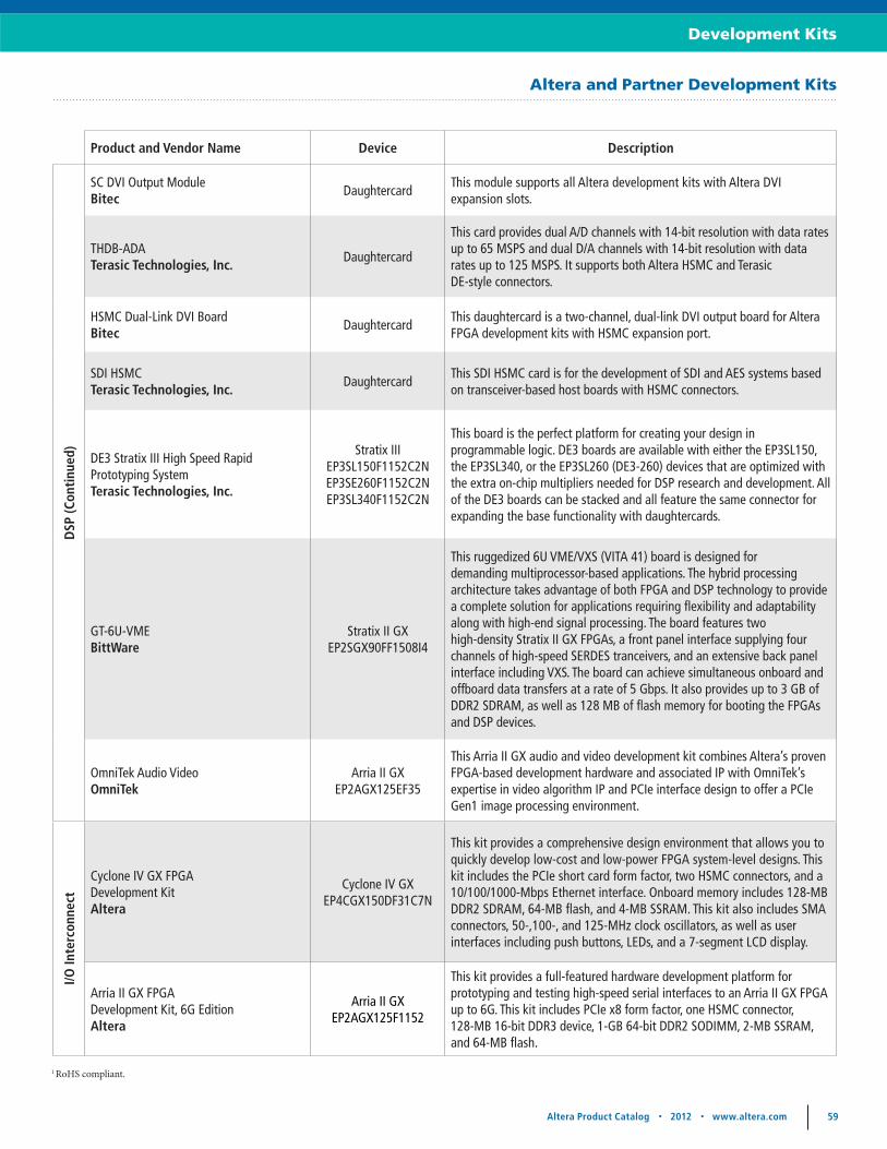
Altera Product Catalog • 2012 • www.altera.com 59
Development Kits
Product and Vendor Name Device Description
DSP
(Con
tinu
ed)
SC DVI Output Module Bitec
DaughtercardThis module supports all Altera development kits with Altera DVI expansion slots.
THDB-ADATerasic Technologies, Inc.
Daughtercard
This card provides dual A/D channels with 14-bit resolution with data rates up to 65 MSPS and dual D/A channels with 14-bit resolution with data rates up to 125 MSPS. It supports both Altera HSMC and Terasic DE-style connectors.
HSMC Dual-Link DVI BoardBitec
DaughtercardThis daughtercard is a two-channel, dual-link DVI output board for Altera FPGA development kits with HSMC expansion port.
SDI HSMCTerasic Technologies, Inc.
DaughtercardThis SDI HSMC card is for the development of SDI and AES systems based on transceiver-based host boards with HSMC connectors.
DE3 Stratix III High Speed Rapid Prototyping SystemTerasic Technologies, Inc.
Stratix IIIEP3SL150F1152C2N EP3SE260F1152C2N EP3SL340F1152C2N
This board is the perfect platform for creating your design in programmable logic. DE3 boards are available with either the EP3SL150, the EP3SL340, or the EP3SL260 (DE3-260) devices that are optimized with the extra on-chip multipliers needed for DSP research and development. All of the DE3 boards can be stacked and all feature the same connector for expanding the base functionality with daughtercards.
GT-6U-VME BittWare
Stratix II GX EP2SGX90FF1508I4
This ruggedized 6U VME/VXS (VITA 41) board is designed for demanding multiprocessor-based applications. The hybrid processing architecture takes advantage of both FPGA and DSP technology to provide a complete solution for applications requiring flexibility and adaptability along with high-end signal processing. The board features two high-density Stratix II GX FPGAs, a front panel interface supplying four channels of high-speed SERDES tranceivers, and an extensive back panel interface including VXS. The board can achieve simultaneous onboard and offboard data transfers at a rate of 5 Gbps. It also provides up to 3 GB of DDR2 SDRAM, as well as 128 MB of flash memory for booting the FPGAs and DSP devices.
OmniTek Audio VideoOmniTek
Arria II GX EP2AGX125EF35
This Arria II GX audio and video development kit combines Altera’s proven FPGA-based development hardware and associated IP with OmniTek’s expertise in video algorithm IP and PCIe interface design to offer a PCIe Gen1 image processing environment.
I/O In
terc
onne
ct
Cyclone IV GX FPGA Development Kit Altera
Cyclone IV GX EP4CGX150DF31C7N
This kit provides a comprehensive design environment that allows you to quickly develop low-cost and low-power FPGA system-level designs. This kit includes the PCIe short card form factor, two HSMC connectors, and a 10/100/1000-Mbps Ethernet interface. Onboard memory includes 128-MB DDR2 SDRAM, 64-MB flash, and 4-MB SSRAM. This kit also includes SMA connectors, 50-,100-, and 125-MHz clock oscillators, as well as user interfaces including push buttons, LEDs, and a 7-segment LCD display.
Arria II GX FPGA Development Kit, 6G EditionAltera
Arria II GX EP2AGX125F1152
This kit provides a full-featured hardware development platform for prototyping and testing high-speed serial interfaces to an Arria II GX FPGA up to 6G. This kit includes PCIe x8 form factor, one HSMC connector, 128-MB 16-bit DDR3 device, 1-GB 64-bit DDR2 SODIMM, 2-MB SSRAM, and 64-MB flash.
1 RoHS compliant.
Altera and Partner Development Kits
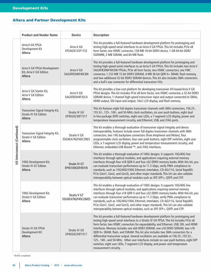
60 Altera Product Catalog • 2012 • www.altera.com
Development Kits
Product and Vendor Name Device Description
I/O In
terc
onne
ct (C
onti
nued
)
Arria II GX FPGA Development KitAltera
Arria II GX EP2AGX125F1152
This kit provides a full-featured hardware development platform for prototyping and testing high-speed serial interfaces to an Arria II GX FPGA. This kit includes PCIe x8 form factor, one HSMC connector, 128-MB 16-bit DDR3 device, 1-GB 64-bit DDR2 SODIMM, 2-MB SSRAM, and 64-MB flash.
Arria V GX FPGA Development Kit, Arria V GX EditionAltera
Arria V GX 5AGXFB3H6F40C6N
This kit provides a full-featured hardware development platform for prototyping and testing high-speed serial interfaces to an Arria V GX FPGA. This kit includes two Arria V 5AGXFB3H6F40C6N FPGAs, PCIe x8 form factor, two HSMC connectors, one FMC connector, 1,152-MB 72-bit DDR3 SDRAM, 4-MB 36-bit QDR II+ SRAM, flash memory, and two additional 32-bit DDR3 SDRAM devices. This kit also includes SMA connectors and a bull’s-eye connector for differential transceiver I/Os.
Arria V GX Starter Kit, Arria V GX EditionAltera
Arria V GX 5AGXFB3H4F35C4
This kit provides a low-cost platform for developing transceiver I/O-based Arria V GX FPGA designs. This kit includes PCIe x8 form factor, one HSMC connector, a 32-bit DDR3 SDRAM device, 1-channel high-speed transceiver input and output connected to SMAs, HDMI output, SDI input and output, 16x2 LCD display, and flash memory.
Transceiver Signal Integrity Kit, Stratix IV GX EditionAltera
Stratix IV GX EP4SGX230F1517
This kit features eight full-duplex transceiver channels with SMA connectors, 156.25-, 155.52-, 125-, 100-, and 50-MHz clock oscillators, six user push buttons, eight dual in-line package (DIP) switches, eight user LEDs, a 7-segment LCD display, power and temperature measurement circuitry, and Ethernet, USB, and JTAG ports.
Transceiver Signal Integrity Kit, Stratix V GX Edition Altera
Stratix V GX5SGXEA7N2F40C2NES
This kit enables a thorough evaluation of transceiver signal integrity and device interoperability. Features include seven full-duplex transceiver channels with SMA connectors, two 14G backplane connectors (from Amphenol and Molex), four programmable clock oscillators, four user push buttons, eight DIP switches, eight user LEDs, a 7-segment LCD display, power and temperature measurement circuitry, and Ethernet, embedded USB Blaster™, and JTAG interfaces.
100G Development Kit, Stratix IV GT Edition Altera
Stratix IV GTEP4S100G5F45I1N
This kit enables a thorough evaluation of 100G designs. It supports 10G/40G line interfaces through optical modules, and applications requiring external memory interfaces through four x18 QDR II and four x32 DDR3 memory banks. With this kit, you can evaluate transceiver performance up to 11.3 Gbps, verify PMA compliance to standards, such as 10G/40G/100G Ethernet, Interlaken, CEI-6G/11G, Serial RapidIO, PCIe (Gen1, Gen2, and Gen3), and other major standards. This kit can also validate interoperability between optical modules such as SFP, SFP+, QSFP, and CFP.
100G Development Kit, Stratix V GX Edition Altera
Stratix V GT5SGXEA7N2F45C2N/ES
This kit enables a thorough evaluation of 100G designs. It supports 10G/40G line interfaces through optical modules, and applications requiring external memoryinterfaces through four x18 QDR II and four x32 DDR3 memory banks. With this kit, you can evaluate transceiver performance up to 11.3 Gbps, verify PMA compliance to standards, such as 10G/40G/100G Ethernet, Interlaken, CEI-6G/11G, Serial RapidIO, PCIe (Gen1, Gen2, and Gen3), and other major standards. This kit can also validate interoperability between optical modules, such as SFP, SFP+, QSFP, and CFP.
Stratix IV GX FPGA Development KitAltera
Stratix IV GX EP4SGX230F1517
This kit provides a full-featured hardware development platform for prototyping and testing high-speed serial interfaces to a Stratix IV GX FPGA. This kit includes PCIe x8 form factor, two HSMC connectors for expandability, and Ethernet, USB, SDI, and HDMI interfaces. Memory includes one x64 DDR3 SDRAM, one x16 DDR3 SDRAM, two x18 QDR II+ SRAM, flash, and SSRAM. This kit also includes two SMA connectors for a differential transceiver output. Several oscillators are available at 156.25-,155.52-, 125-, 100-, and 50-MHz. Other user interfaces include six user push buttons, eight DIP switches, eight user LEDs, 7-segment LCD display, and power and temperature measurement circuitry.
1 RoHS compliant.
Altera and Partner Development Kits
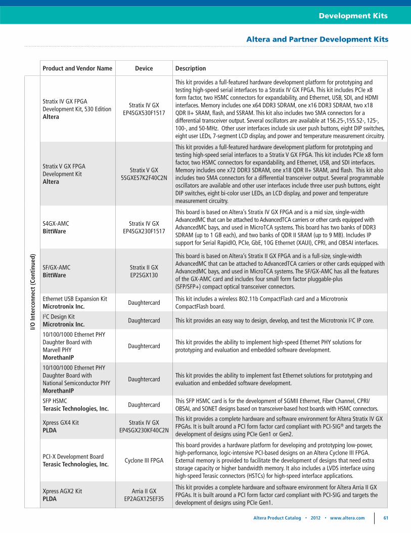
Altera Product Catalog • 2012 • www.altera.com 61
Development Kits
Product and Vendor Name Device Description
I/O In
terc
onne
ct (C
onti
nued
)
Stratix IV GX FPGA Development Kit, 530 Edition Altera
Stratix IV GXEP4SGX530F1517
This kit provides a full-featured hardware development platform for prototyping and testing high-speed serial interfaces to a Stratix IV GX FPGA. This kit includes PCIe x8 form factor, two HSMC connectors for expandability, and Ethernet, USB, SDI, and HDMI interfaces. Memory includes one x64 DDR3 SDRAM, one x16 DDR3 SDRAM, two x18 QDR II+ SRAM, flash, and SSRAM. This kit also includes two SMA connectors for a differential transceiver output. Several oscillators are available at 156.25-,155.52-, 125-, 100-, and 50-MHz. Other user interfaces include six user push buttons, eight DIP switches, eight user LEDs, 7-segment LCD display, and power and temperature measurement circuitry.
Stratix V GX FPGA Development KitAltera
Stratix V GX5SGXES7K2F40C2N
This kit provides a full-featured hardware development platform for prototyping and testing high-speed serial interfaces to a Stratix V GX FPGA. This kit includes PCIe x8 form factor, two HSMC connectors for expandability, and Ethernet, USB, and SDI interfaces. Memory includes one x72 DDR3 SDRAM, one x18 QDR II+ SRAM, and flash. This kit also includes two SMA connectors for a differential transceiver output. Several programmable oscillators are available and other user interfaces include three user push buttons, eight DIP switches, eight bi-color user LEDs, an LCD display, and power and temperature measurement circuitry.
S4GX-AMCBittWare
Stratix IV GX EP4SGX230F1517
This board is based on Altera’s Stratix IV GX FPGA and is a mid size, single-width AdvancedMC that can be attached to AdvancedTCA carriers or other cards equipped with AdvancedMC bays, and used in MicroTCA systems. This board has two banks of DDR3 SDRAM (up to 1 GB each), and two banks of QDR II SRAM (up to 9 MB). Includes IP support for Serial RapidIO, PCIe, GbE, 10G Ethernet (XAUI), CPRI, and OBSAI interfaces.
SF/GX-AMCBittWare
Stratix II GX EP2SGX130
This board is based on Altera’s Stratix II GX FPGA and is a full-size, single-width AdvancedMC that can be attached to AdvancedTCA carriers or other cards equipped with AdvancedMC bays, and used in MicroTCA systems. The SF/GX-AMC has all the features of the GX-AMC card and includes four small form factor pluggable-plus (SFP/SFP+) compact optical transceiver connectors.
Ethernet USB Expansion Kit Microtronix Inc.
DaughtercardThis kit includes a wireless 802.11b CompactFlash card and a Microtronix CompactFlash board.
I2C Design Kit Microtronix Inc.
Daughtercard This kit provides an easy way to design, develop, and test the Microtronix I2C IP core.
10/100/1000 Ethernet PHY Daughter Board with Marvell PHY MorethanIP
DaughtercardThis kit provides the ability to implement high-speed Ethernet PHY solutions for prototyping and evaluation and embedded software development.
10/100/1000 Ethernet PHY Daughter Board with National Semiconductor PHY MorethanIP
DaughtercardThis kit provides the ability to implement fast Ethernet solutions for prototyping and evaluation and embedded software development.
SFP HSMCTerasic Technologies, Inc.
DaughtercardThis SFP HSMC card is for the development of SGMII Ethernet, Fiber Channel, CPRI/ OBSAI, and SONET designs based on transceiver-based host boards with HSMC connectors.
Xpress GX4 KitPLDA
Stratix IV GX EP4SGX230KF40C2N
This kit provides a complete hardware and software environment for Altera Stratix IV GX FPGAs. It is built around a PCI form factor card compliant with PCI-SIG® and targets the development of designs using PCIe Gen1 or Gen2.
PCI-X Development BoardTerasic Technologies, Inc.
Cyclone III FPGA
This board provides a hardware platform for developing and prototyping low-power, high-performance, logic-intensive PCI-based designs on an Altera Cyclone III FPGA. External memory is provided to facilitate the development of designs that need extra storage capacity or higher bandwidth memory. It also includes a LVDS interface using high-speed Terasic connectors (HSTCs) for high-speed interface applications.
Xpress AGX2 KitPLDA
Arria II GX EP2AGX125EF35
This kit provides a complete hardware and software environment for Altera Arria II GX FPGAs. It is built around a PCI form factor card compliant with PCI-SIG and targets the development of designs using PCIe Gen1.
Altera and Partner Development Kits

62 Altera Product Catalog • 2012 • www.altera.com
Development Kits
Product and Vendor Name Device Description
I/O In
terc
onne
ct (C
onti
nued
)
Xpress AGX KitPLDA
Arria GX EP1AGX60DF780C6
This kit provides a complete hardware and software environment for Altera Arria GX FPGAs. It is built around a PCI form factor card compliant with PCI-SIG and targets the development of designs using PCIe Gen1.
Cyclone IV GX Transceiver Starter KitAltera
Cyclone IV GX EP4CGX15
This kit provides a low-cost platform for developing transceiver I/O-based FPGA designs. It includes the complete hardware and software you need to develop your FPGA design for cost-sensitive applications. You can measure the FPGA’s power consumption, test the signal quality of the FPGA transceiver I/Os (up to 2.5 Gbps), and develop and test PCIe Gen1 designs.
Transceiver Signal Integrity Development Kit, Stratix IV GT EditionAltera
Stratix IV EP4S100G2F40I1N
This kit enables a thorough evaluation of transceiver interoperability and SERDES signal integrity by allowing you to evaluate transceiver performance up to 11.3 Gbps. You can generate and check pseudo-random binary sequence (PRBS) patterns via a simple-to-use GUI, change differential output voltage (VOD), pre-emphasis, and equalization settings to optimize transceiver performance for your channel, perform jitter analysis, verify PMA compliance to 40G/100G Ethernet, Interlaken, CEI-6G/11G, PCIe (Gen1, Gen2, and Gen3), Serial RapidIO, and other major standards, and validate interoperability between optical modules.
B2-AMCBittWare
Stratix II EP2S90F1020C3
This board supports universal baseband processing for wireless communication infrastructures such as 2G, 2.5G, 3G, WiMAX, and software-defined radio. It attaches to AdvancedTCA carriers or other cards equipped with AdvancedMC bays, and is completely hot-swappable. It uses an Altera Stratix II FPGA, and provides a 10/100/1000 Ethernet interface for command, control, and reprogramming, as well as flash memory for booting the DSP devices and FPGAs.
Gt-3U-VPXBittWare
Stratix II GX EP2SGX90FF1508I4
This ruggedized 3U CompactPCI board is designed for demanding multiprocessor applications requiring complete flexibility and adaptability. It features an Altera Stratix II GX FPGA, a front panel interface supplying four channels of high-speed SERDES tranceivers, and a back panel interface providing RS-232/RS-422 and 10/100 Ethernet. Simultaneous onboard and offboard data transfers can be achieved at a rate of 2 Gbps. It also provides 1 GB of DDR2 SDRAM and 64 MB of flash memory for booting the FPGA and DSP devices.
TREX S2 Prototyping SystemTerasic Technologies, Inc.
Stratix II FPGAThis Stratix II FPGA prototyping system provides almost 700 user I/Os and high-speed I/O connections. This board is flexible and configurable, and it provides default motherboards for free—with schematic and design libraries for you to develop your own motherboards.
QuickUSB Starter KitBitwise Systems
Cyclone II EP2C20F256C7
This kit includes one QuickUSB module and one QuickUSB Cyclone II Evaluation Board. The evaluation board has a QuickUSB module site on headers that provide access to the signals. The EP2C20F256C7 FPGA connects to nearly every pin of the QuickUSB module, and extra I/O pins go to the headers so you can wire in your circuitry. The kit gets its power from the USB bus, but if you need more power, there is a power connector and a 5V/2A power supply included in the kit.
C3 Digital Radio KitCEPD
Cyclone III EP3C16
This kit aids the development and testing of algorithms and signal processing applications including digital radio, modulator/demodulator development, software- defined radio, high-speed data acquisition and signal processing, and audio data acquisition and signal processing. The acquired signals are sampled and then digitally processed by a Cyclone III FPGA. The FPGA card comes with a JTAG programming connector and a configuration PROM to retain the FPGA settings. The PCI card provides interfaces for the FPGA card to a computer PCI bus, RS232 interface, and user push buttons and includes a digital radio reference design example and full documentation.
Cyclone III FPGA/ PCI Development BoardCEPD
Cyclone III EP3C16F484C8N
This board provides a platform for fast and easy prototyping and design verification with the Cyclone III EP3C16F484C8N FPGA. It can be accessed either through the PCI bus or powered as a stand-alone system and accessed through an RS232 port. It comes with an onboard configuration PROM to retain the FPGA settings, an RS232 level shifter, voltage monitor, oscillator, buttons, and LEDs. There is a prototyping area on the board for user circuits and all FPGA pins are accessible through connectors and clearly labeled test points. The connectors are designed to mate with other CEPD daughterboards.
Altera and Partner Development Kits
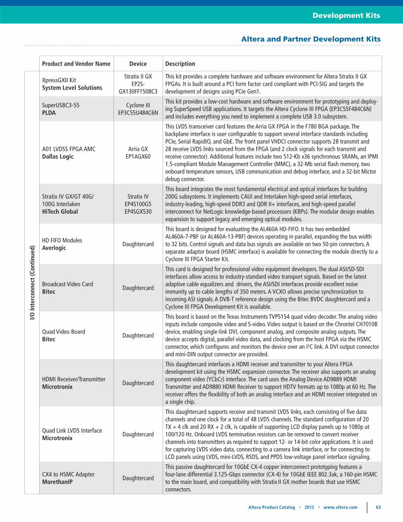
Altera Product Catalog • 2012 • www.altera.com 63
Development Kits
Product and Vendor Name Device Description
I/O In
terc
onne
ct (C
onti
nued
)
XpressGXII KitSystem Level Solutions
Stratix II GX EP2S-
GX130FF1508C3
This kit provides a complete hardware and software environment for Altera Stratix II GX FPGAs. It is built around a PCI form factor card compliant with PCI-SIG and targets the development of designs using PCIe Gen1.
SuperUSBC3-55PLDA
Cyclone III EP3C55U484C6N
This kit provides a low-cost hardware and software environment for prototyping and deploy-ing SuperSpeed USB applications. It targets the Altera Cyclone III FPGA (EP3C55F484C6N) and includes everything you need to implement a complete USB 3.0 subsystem.
A01 LVDSS FPGA AMCDallas Logic
Arria GX EP1AGX60
This LVDS transceiver card features the Arria GX FPGA in the F780 BGA package. The backplane interface is user configurable to support several interface standards including PCIe, Serial RapidIO, and GbE. The front panel VHDCI connector supports 28 transmit and 28 receive LVDS links sourced from the FPGA (and 2 clock signals for each transmit and receive connector). Additional features include two 512-Kb x36 synchronous SRAMs, an IPMI 1.5-compliant Module Management Controller (MMC), a 32-Mb serial flash memory, two onboard temperature sensors, USB communication and debug interface, and a 32-bit Mictor debug connector.
Stratix IV GX/GT 40G/ 100G InterlakenHiTech Global
Stratix IV EP4S100G5EP4SGX530
This board integrates the most fundamental electrical and optical interfaces for building 200G subsystems. It implements CAUI and Interlaken high-speed serial interfaces, industry-leading, high-speed DDR3 and QDR II+ interfaces, and high-speed parallel interconnect for NetLogic knowledge-based processors (KBPs). The modular design enables expansion to support legacy and emerging optical modules.
HD FIFO ModulesAverlogic
Daughtercard
This board is designed for evaluating the AL460A HD-FIFO. It has two embedded AL460A-7-PBF (or AL460A-13-PBF) devices operating in parallel, expanding the bus width to 32 bits. Control signals and data bus signals are available on two 50-pin connectors. A separate adaptor board (HSMC interface) is available for connecting the module directly to a Cyclone III FPGA Starter Kit.
Broadcast Video CardBitec
Daughtercard
This card is designed for professional video equipment developers. The dual ASI/SD-SDI interfaces allow access to industry-standard video transport signals. Based on the latest adaptive cable equalizers and drivers, the ASI/SDI interfaces provide excellent noise immunity up to cable lengths of 350 meters. A VCXO allows precise synchronization to incoming ASI signals. A DVB-T reference design using the Bitec BVDC daughtercard and a Cyclone III FPGA Development Kit is available.
Quad Video BoardBitec
Daughtercard
This board is based on the Texas Instruments TVP5154 quad video decoder. The analog video inputs include composite video and S-video. Video output is based on the Chrontel CH7010B device, enabling single-link DVI, component analog, and composite analog outputs. The device accepts digital, parallel video data, and clocking from the host FPGA via the HSMC connector, which configures and monitors the device over an I2C link. A DVI output connector and mini-DIN output connector are provided.
HDMI Receiver/TransmitterMicrotronix
Daughtercard
This daughtercard interfaces a HDMI receiver and transmitter to your Altera FPGA development kit using the HSMC expansion connector. The receiver also supports an analog component video (YCbCr) interface. The card uses the Analog Device AD9889 HDMI Transmitter and AD9880 HDMI Receiver to support HDTV formats up to 1080p at 60 Hz. The receiver offers the flexibility of both an analog interface and an HDMI receiver integrated on a single chip.
Quad Link LVDS InterfaceMicrotronix
Daughtercard
This daughtercard supports receive and transmit LVDS links, each consisting of five data channels and one clock for a total of 48 LVDS channels. The standard configuration of 20 TX + 4 clk and 20 RX + 2 clk, is capable of supporting LCD display panels up to 1080p at 100/120 Hz. Onboard LVDS termination resistors can be removed to convert receiver channels into transmitters as required to support 12- or 14-bit color applications. It is used for capturing LVDS video data, connecting to a camera link interface, or for connecting to LCD panels using LVDS, mini-LVDS, RSDS, and PPDS low-voltage panel interface signaling.
CX4 to HSMC AdapterMorethanIP
Daughtercard
This passive daughtercard for 10GbE CX-4 copper interconnect prototyping features a four-lane differential 3.125-Gbps connector (CX-4) for 10GbE IEEE 802.3ak, a 160-pin HSMC to the main board, and compatibility with Stratix II GX mother boards that use HSMC connectors.
Altera and Partner Development Kits
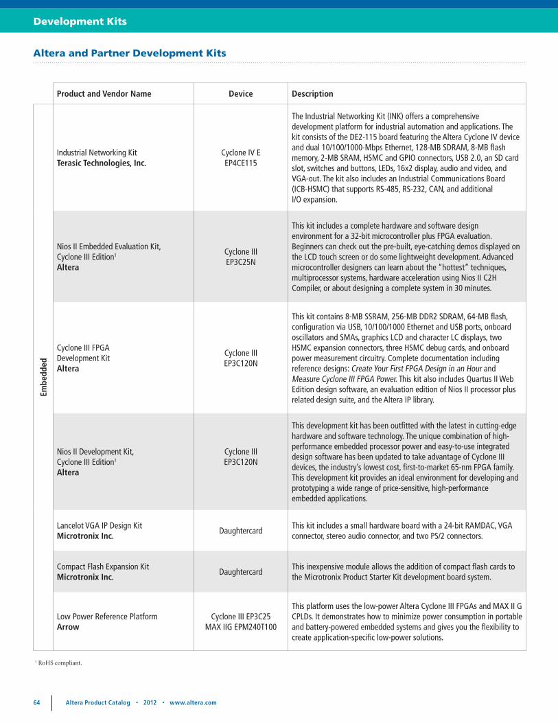
64 Altera Product Catalog • 2012 • www.altera.com
Development Kits
1 RoHS compliant.
Altera and Partner Development Kits
Product and Vendor Name Device Description
Embe
dded
Industrial Networking KitTerasic Technologies, Inc.
Cyclone IV E EP4CE115
The Industrial Networking Kit (INK) offers a comprehensive development platform for industrial automation and applications. The kit consists of the DE2-115 board featuring the Altera Cyclone IV device and dual 10/100/1000-Mbps Ethernet, 128-MB SDRAM, 8-MB flash memory, 2-MB SRAM, HSMC and GPIO connectors, USB 2.0, an SD card slot, switches and buttons, LEDs, 16x2 display, audio and video, and VGA-out. The kit also includes an Industrial Communications Board (ICB-HSMC) that supports RS-485, RS-232, CAN, and additional I/O expansion.
Nios II Embedded Evaluation Kit, Cyclone III Edition1 Altera
Cyclone III EP3C25N
This kit includes a complete hardware and software design environment for a 32-bit microcontroller plus FPGA evaluation. Beginners can check out the pre-built, eye-catching demos displayed on the LCD touch screen or do some lightweight development. Advanced microcontroller designers can learn about the “hottest” techniques, multiprocessor systems, hardware acceleration using Nios II C2H Compiler, or about designing a complete system in 30 minutes.
Cyclone III FPGA Development Kit Altera
Cyclone III EP3C120N
This kit contains 8-MB SSRAM, 256-MB DDR2 SDRAM, 64-MB flash, configuration via USB, 10/100/1000 Ethernet and USB ports, onboard oscillators and SMAs, graphics LCD and character LC displays, two HSMC expansion connectors, three HSMC debug cards, and onboard power measurement circuitry. Complete documentation including reference designs: Create Your First FPGA Design in an Hour and Measure Cyclone III FPGA Power. This kit also includes Quartus II Web Edition design software, an evaluation edition of Nios II processor plus related design suite, and the Altera IP library.
Nios II Development Kit, Cyclone III Edition1 Altera
Cyclone III EP3C120N
This development kit has been outfitted with the latest in cutting-edge hardware and software technology. The unique combination of high-performance embedded processor power and easy-to-use integrated design software has been updated to take advantage of Cyclone III devices, the industry’s lowest cost, first-to-market 65-nm FPGA family. This development kit provides an ideal environment for developing and prototyping a wide range of price-sensitive, high-performance embedded applications.
Lancelot VGA IP Design Kit Microtronix Inc.
DaughtercardThis kit includes a small hardware board with a 24-bit RAMDAC, VGA connector, stereo audio connector, and two PS/2 connectors.
Compact Flash Expansion Kit Microtronix Inc.
DaughtercardThis inexpensive module allows the addition of compact flash cards to the Microtronix Product Starter Kit development board system.
Low Power Reference PlatformArrow
Cyclone III EP3C25 MAX IIG EPM240T100
This platform uses the low-power Altera Cyclone III FPGAs and MAX II G CPLDs. It demonstrates how to minimize power consumption in portable and battery-powered embedded systems and gives you the flexibility to create application-specific low-power solutions.
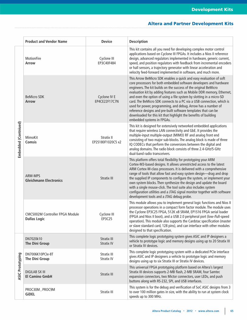
Altera Product Catalog • 2012 • www.altera.com 65
Development Kits
Product and Vendor Name Device Description
Embe
dded
(Con
tniu
ed)
MotionFireArrow
Cyclone III EP3C40F484
This kit contains all you need for developing complex motor control applications based on Cyclone III FPGAs. It includes a Nios II reference design, advanced regulators implemented in hardware, generic current, speed, and position regulators with feedback from incremental encoders or hall sensors, a trajectory generator with linear acceleration and velocity feed-forward implemented in software, and much more.
BeMicro SDKArrow
Cyclone IV E EP4CE22F17C7N
This Arrow BeMicro SDK enables a quick and easy evaluation of soft core processors for both embedded software developers and hardware engineers. The kit builds on the success of the original BeMicro evaluation kit by adding features such as Mobile DDR memory, Ethernet, and even the option of using a file system by slotting in a micro-SD card. The BeMicro SDK connects to a PC via a USB connection, which is used for power, programming, and debug. Arrow has a number of reference designs and pre-built software templates that can be downloaded for this kit that highlight the benefits of building embedded systems in FPGAs.
MimoKitComsis
Stratix II EP2S180F1020C5 x2
This kit is designed for extensively networked embedded applications that require wireless LAN connectivity and GbE. It provides the multiple-input multiple-output (MIMO) RF and analog front end consisting of two major sub-blocks. The analog block is made of three IQ CODECs that perform the conversions between the digital and analog domains. The radio block consists of three 2.4-GHz/5-GHz dual-band radio transceivers.
ARM-MPSGleichmann Electronics
Stratix III
This platform offers total flexibility for prototyping your ARM Cortex-M3-based designs. It allows unrestricted access to the latest ARM Cortex-M-class processors. It is delivered with a comprehensive range of tools that allow fast and easy system design—drag and drop the supplied IP components to configure the system, or implement your own system blocks. Then synthesize the design and update the board with a single mouse-click. The tool suite also includes system configuration utilities and a JTAG signal monitor together with software development tools and a JTAG debug probe.
CMCS002M Controller FPGA ModuleDallas Logic
Cyclone IIIEP3C25
This module allows you to implement general logic functions and Nios II processor operations in a compact form factor module. The module uses the Cyclone EP3C25 FPGA, 512K x8 SRAM, EP1S16 FPGA serial loader (FPGA and Nios II boot), and a USB 2.0 peripheral port (low-/full-speed operation). This module also supports the Cardstac specification (master or slave standard card, 128 pins), and can interface with other modules designed to that specification.
ASI
C Pr
otot
ypin
g
DN7020k10The Dini Group
Stratix III Stratix IV
This complete logic prototyping system gives ASIC and IP designers a vehicle to prototype logic and memory designs using up to 20 Stratix III or Stratix IV devices.
DN7006K10PCIe-8TThe Dini Group
Stratix III Stratix IV
This complete logic prototyping system with a dedicated PCIe interface gives ASIC and IP designers a vehicle to prototype logic and memory designs using up to six Stratix III or Stratix IV devices.
DIGILAB SX IIIEl Camino GmbH
Stratix III
This universal FPGA prototyping platform based on Altera’s largest Stratix III devices supports 2-MB flash, 2-MB SRAM, four Samtec expansion connectors, two Mictor connectors, user LEDs, and push buttons along with RS-232, SPI, and USB interfaces.
PROC30M , PROC9M GiDEL
Stratix IIIThis system is for the debug and verification of SoC ASIC designs from 3 to over 100 million gates in size, with the ability to run at system clock speeds up to 300 MHz.
Altera and Partner Development Kits
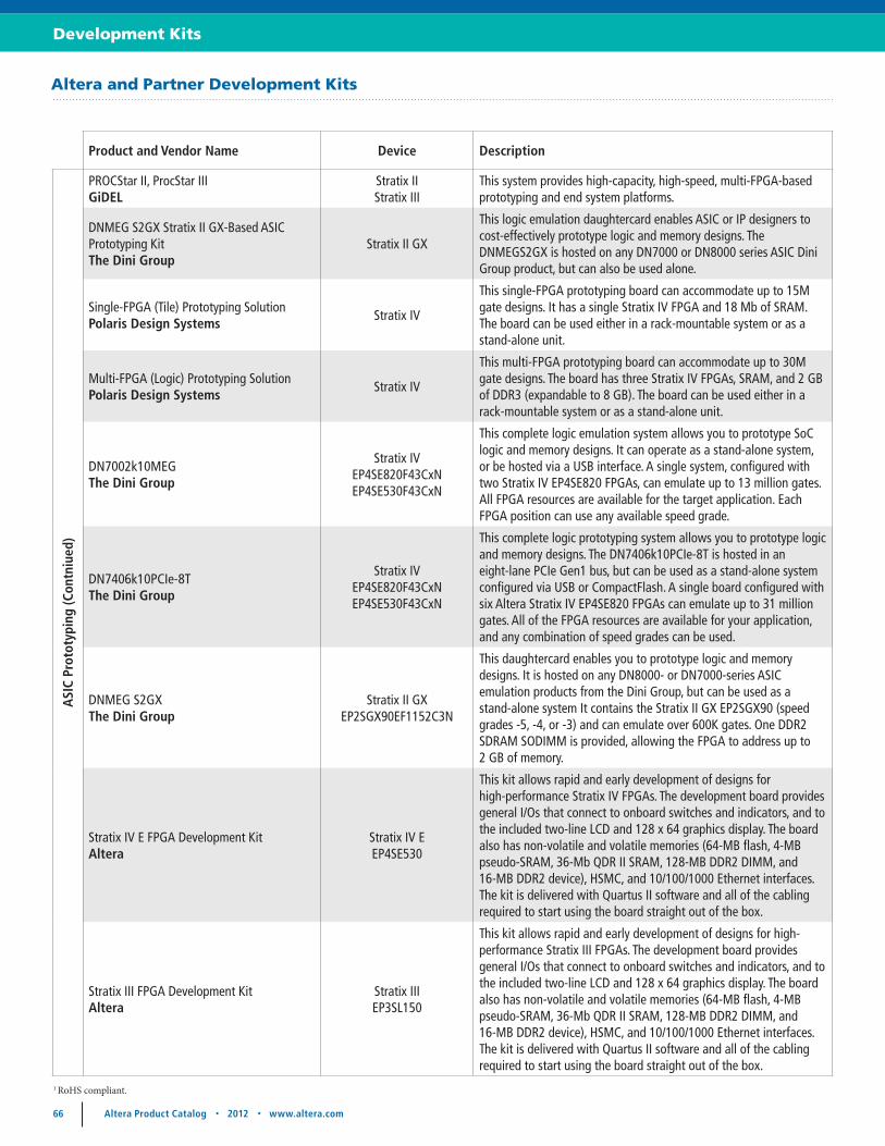
66 Altera Product Catalog • 2012 • www.altera.com
Development Kits
Product and Vendor Name Device Description
ASI
C Pr
otot
ypin
g (C
ontn
iued
)
PROCStar II, ProcStar III GiDEL
Stratix IIStratix III
This system provides high-capacity, high-speed, multi-FPGA-based prototyping and end system platforms.
DNMEG S2GX Stratix II GX-Based ASIC Prototyping Kit The Dini Group
Stratix II GX
This logic emulation daughtercard enables ASIC or IP designers to cost-effectively prototype logic and memory designs. The DNMEGS2GX is hosted on any DN7000 or DN8000 series ASIC Dini Group product, but can also be used alone.
Single-FPGA (Tile) Prototyping SolutionPolaris Design Systems
Stratix IV
This single-FPGA prototyping board can accommodate up to 15M gate designs. It has a single Stratix IV FPGA and 18 Mb of SRAM. The board can be used either in a rack-mountable system or as a stand-alone unit.
Multi-FPGA (Logic) Prototyping SolutionPolaris Design Systems
Stratix IV
This multi-FPGA prototyping board can accommodate up to 30M gate designs. The board has three Stratix IV FPGAs, SRAM, and 2 GB of DDR3 (expandable to 8 GB). The board can be used either in a rack-mountable system or as a stand-alone unit.
DN7002k10MEGThe Dini Group
Stratix IV EP4SE820F43CxNEP4SE530F43CxN
This complete logic emulation system allows you to prototype SoC logic and memory designs. It can operate as a stand-alone system, or be hosted via a USB interface. A single system, configured with two Stratix IV EP4SE820 FPGAs, can emulate up to 13 million gates. All FPGA resources are available for the target application. Each FPGA position can use any available speed grade.
DN7406k10PCIe-8TThe Dini Group
Stratix IV EP4SE820F43CxNEP4SE530F43CxN
This complete logic prototyping system allows you to prototype logic and memory designs. The DN7406k10PCIe-8T is hosted in an eight-lane PCIe Gen1 bus, but can be used as a stand-alone system configured via USB or CompactFlash. A single board configured with six Altera Stratix IV EP4SE820 FPGAs can emulate up to 31 million gates. All of the FPGA resources are available for your application, and any combination of speed grades can be used.
DNMEG S2GXThe Dini Group
Stratix II GX EP2SGX90EF1152C3N
This daughtercard enables you to prototype logic and memory designs. It is hosted on any DN8000- or DN7000-series ASIC emulation products from the Dini Group, but can be used as a stand-alone system It contains the Stratix II GX EP2SGX90 (speed grades -5, -4, or -3) and can emulate over 600K gates. One DDR2 SDRAM SODIMM is provided, allowing the FPGA to address up to 2 GB of memory.
Stratix IV E FPGA Development KitAltera
Stratix IV E EP4SE530
This kit allows rapid and early development of designs for high-performance Stratix IV FPGAs. The development board provides general I/Os that connect to onboard switches and indicators, and to the included two-line LCD and 128 x 64 graphics display. The board also has non-volatile and volatile memories (64-MB flash, 4-MB pseudo-SRAM, 36-Mb QDR II SRAM, 128-MB DDR2 DIMM, and 16-MB DDR2 device), HSMC, and 10/100/1000 Ethernet interfaces. The kit is delivered with Quartus II software and all of the cabling required to start using the board straight out of the box.
Stratix III FPGA Development Kit Altera
Stratix IIIEP3SL150
This kit allows rapid and early development of designs for high- performance Stratix III FPGAs. The development board provides general I/Os that connect to onboard switches and indicators, and to the included two-line LCD and 128 x 64 graphics display. The board also has non-volatile and volatile memories (64-MB flash, 4-MB pseudo-SRAM, 36-Mb QDR II SRAM, 128-MB DDR2 DIMM, and 16-MB DDR2 device), HSMC, and 10/100/1000 Ethernet interfaces. The kit is delivered with Quartus II software and all of the cabling required to start using the board straight out of the box.
1 RoHS compliant.
Altera and Partner Development Kits
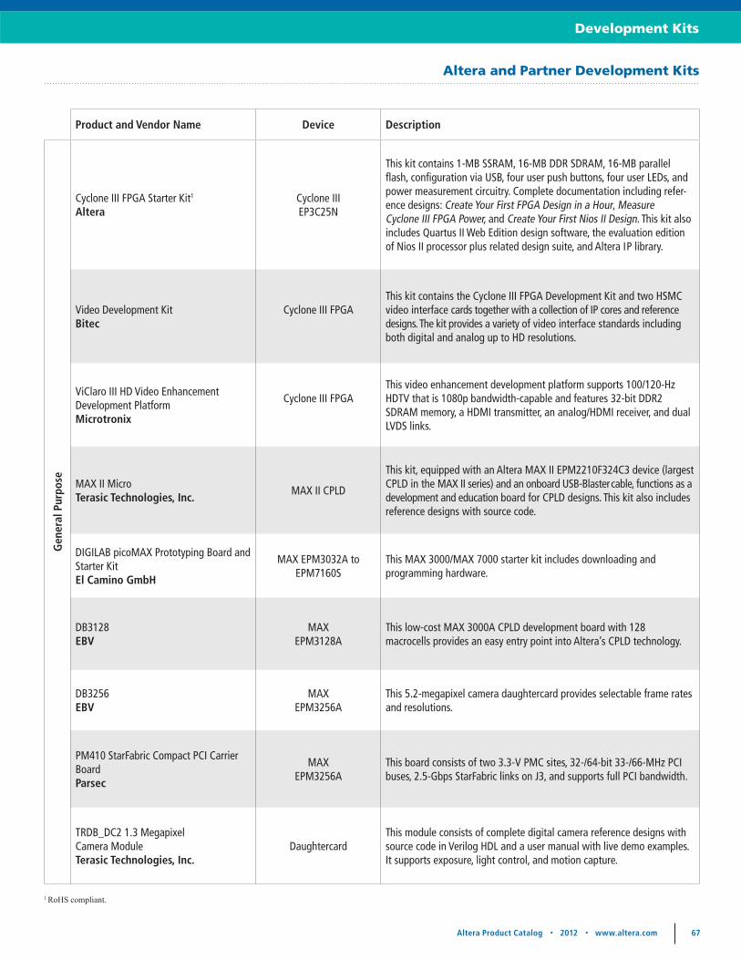
Altera Product Catalog • 2012 • www.altera.com 67
Development Kits
Product and Vendor Name Device Description
ASI
C Pr
otot
ypin
g (C
ontn
iued
)
PROCStar II, ProcStar III GiDEL
Stratix IIStratix III
This system provides high-capacity, high-speed, multi-FPGA-based prototyping and end system platforms.
DNMEG S2GX Stratix II GX-Based ASIC Prototyping Kit The Dini Group
Stratix II GX
This logic emulation daughtercard enables ASIC or IP designers to cost-effectively prototype logic and memory designs. The DNMEGS2GX is hosted on any DN7000 or DN8000 series ASIC Dini Group product, but can also be used alone.
Single-FPGA (Tile) Prototyping SolutionPolaris Design Systems
Stratix IV
This single-FPGA prototyping board can accommodate up to 15M gate designs. It has a single Stratix IV FPGA and 18 Mb of SRAM. The board can be used either in a rack-mountable system or as a stand-alone unit.
Multi-FPGA (Logic) Prototyping SolutionPolaris Design Systems
Stratix IV
This multi-FPGA prototyping board can accommodate up to 30M gate designs. The board has three Stratix IV FPGAs, SRAM, and 2 GB of DDR3 (expandable to 8 GB). The board can be used either in a rack-mountable system or as a stand-alone unit.
DN7002k10MEGThe Dini Group
Stratix IV EP4SE820F43CxNEP4SE530F43CxN
This complete logic emulation system allows you to prototype SoC logic and memory designs. It can operate as a stand-alone system, or be hosted via a USB interface. A single system, configured with two Stratix IV EP4SE820 FPGAs, can emulate up to 13 million gates. All FPGA resources are available for the target application. Each FPGA position can use any available speed grade.
DN7406k10PCIe-8TThe Dini Group
Stratix IV EP4SE820F43CxNEP4SE530F43CxN
This complete logic prototyping system allows you to prototype logic and memory designs. The DN7406k10PCIe-8T is hosted in an eight-lane PCIe Gen1 bus, but can be used as a stand-alone system configured via USB or CompactFlash. A single board configured with six Altera Stratix IV EP4SE820 FPGAs can emulate up to 31 million gates. All of the FPGA resources are available for your application, and any combination of speed grades can be used.
DNMEG S2GXThe Dini Group
Stratix II GX EP2SGX90EF1152C3N
This daughtercard enables you to prototype logic and memory designs. It is hosted on any DN8000- or DN7000-series ASIC emulation products from the Dini Group, but can be used as a stand-alone system It contains the Stratix II GX EP2SGX90 (speed grades -5, -4, or -3) and can emulate over 600K gates. One DDR2 SDRAM SODIMM is provided, allowing the FPGA to address up to 2 GB of memory.
Stratix IV E FPGA Development KitAltera
Stratix IV E EP4SE530
This kit allows rapid and early development of designs for high-performance Stratix IV FPGAs. The development board provides general I/Os that connect to onboard switches and indicators, and to the included two-line LCD and 128 x 64 graphics display. The board also has non-volatile and volatile memories (64-MB flash, 4-MB pseudo-SRAM, 36-Mb QDR II SRAM, 128-MB DDR2 DIMM, and 16-MB DDR2 device), HSMC, and 10/100/1000 Ethernet interfaces. The kit is delivered with Quartus II software and all of the cabling required to start using the board straight out of the box.
Stratix III FPGA Development Kit Altera
Stratix IIIEP3SL150
This kit allows rapid and early development of designs for high- performance Stratix III FPGAs. The development board provides general I/Os that connect to onboard switches and indicators, and to the included two-line LCD and 128 x 64 graphics display. The board also has non-volatile and volatile memories (64-MB flash, 4-MB pseudo-SRAM, 36-Mb QDR II SRAM, 128-MB DDR2 DIMM, and 16-MB DDR2 device), HSMC, and 10/100/1000 Ethernet interfaces. The kit is delivered with Quartus II software and all of the cabling required to start using the board straight out of the box.
Product and Vendor Name Device Description
Gen
eral
Pur
pose
Cyclone III FPGA Starter Kit1 Altera
Cyclone IIIEP3C25N
This kit contains 1-MB SSRAM, 16-MB DDR SDRAM, 16-MB parallel flash, configuration via USB, four user push buttons, four user LEDs, and power measurement circuitry. Complete documentation including refer-ence designs: Create Your First FPGA Design in a Hour, Measure Cyclone III FPGA Power, and Create Your First Nios II Design. This kit also includes Quartus II Web Edition design software, the evaluation edition of Nios II processor plus related design suite, and Altera IP library.
Video Development Kit Bitec
Cyclone III FPGAThis kit contains the Cyclone III FPGA Development Kit and two HSMC video interface cards together with a collection of IP cores and reference designs. The kit provides a variety of video interface standards including both digital and analog up to HD resolutions.
ViClaro III HD Video Enhancement Development Platform Microtronix
Cyclone III FPGAThis video enhancement development platform supports 100/120-Hz HDTV that is 1080p bandwidth-capable and features 32-bit DDR2 SDRAM memory, a HDMI transmitter, an analog/HDMI receiver, and dual LVDS links.
MAX II Micro Terasic Technologies, Inc.
MAX II CPLD
This kit, equipped with an Altera MAX II EPM2210F324C3 device (largest CPLD in the MAX II series) and an onboard USB-Blaster cable, functions as a development and education board for CPLD designs. This kit also includes reference designs with source code.
DIGILAB picoMAX Prototyping Board and Starter Kit El Camino GmbH
MAX EPM3032A to EPM7160S
This MAX 3000/MAX 7000 starter kit includes downloading and programming hardware.
DB3128 EBV
MAX EPM3128A
This low-cost MAX 3000A CPLD development board with 128 macrocells provides an easy entry point into Altera’s CPLD technology.
DB3256 EBV
MAX EPM3256A
This 5.2-megapixel camera daughtercard provides selectable frame rates and resolutions.
PM410 StarFabric Compact PCI Carrier Board Parsec
MAXEPM3256A
This board consists of two 3.3-V PMC sites, 32-/64-bit 33-/66-MHz PCI buses, 2.5-Gbps StarFabric links on J3, and supports full PCI bandwidth.
TRDB_DC2 1.3 Megapixel Camera Module Terasic Technologies, Inc.
Daughtercard This module consists of complete digital camera reference designs with source code in Verilog HDL and a user manual with live demo examples. It supports exposure, light control, and motion capture.
1 RoHS compliant.
Altera and Partner Development Kits
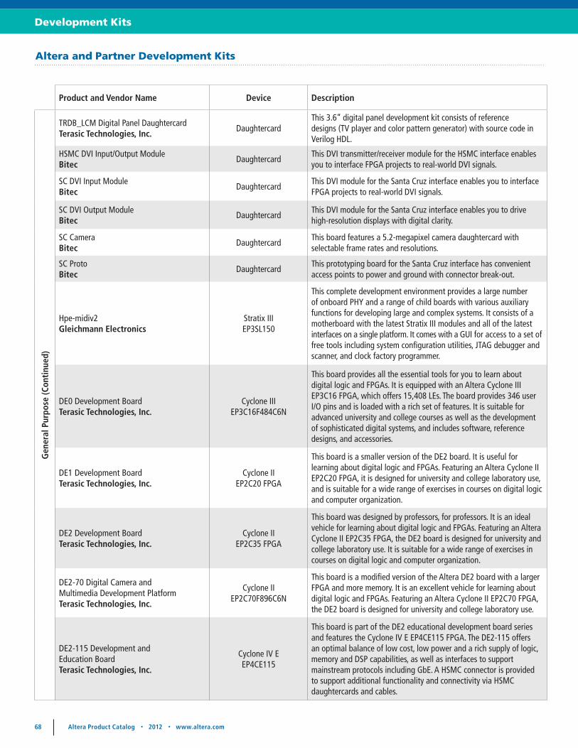
68 Altera Product Catalog • 2012 • www.altera.com
Development Kits
Product and Vendor Name Device Description
Gen
eral
Pur
pose
(Con
tinu
ed)
TRDB_LCM Digital Panel Daughtercard Terasic Technologies, Inc.
DaughtercardThis 3.6” digital panel development kit consists of reference designs (TV player and color pattern generator) with source code in Verilog HDL.
HSMC DVI Input/Output Module Bitec
DaughtercardThis DVI transmitter/receiver module for the HSMC interface enables you to interface FPGA projects to real-world DVI signals.
SC DVI Input Module Bitec
DaughtercardThis DVI module for the Santa Cruz interface enables you to interface FPGA projects to real-world DVI signals.
SC DVI Output Module Bitec
DaughtercardThis DVI module for the Santa Cruz interface enables you to drive high-resolution displays with digital clarity.
SC Camera Bitec
DaughtercardThis board features a 5.2-megapixel camera daughtercard with selectable frame rates and resolutions.
SC Proto Bitec
DaughtercardThis prototyping board for the Santa Cruz interface has convenient access points to power and ground with connector break-out.
Hpe-midiv2Gleichmann Electronics
Stratix III EP3SL150
This complete development environment provides a large number of onboard PHY and a range of child boards with various auxiliary functions for developing large and complex systems. It consists of a motherboard with the latest Stratix III modules and all of the latest interfaces on a single platform. It comes with a GUI for access to a set of free tools including system configuration utilities, JTAG debugger and scanner, and clock factory programmer.
DE0 Development BoardTerasic Technologies, Inc.
Cyclone III EP3C16F484C6N
This board provides all the essential tools for you to learn about digital logic and FPGAs. It is equipped with an Altera Cyclone III EP3C16 FPGA, which offers 15,408 LEs. The board provides 346 user I/O pins and is loaded with a rich set of features. It is suitable for advanced university and college courses as well as the development of sophisticated digital systems, and includes software, reference designs, and accessories.
DE1 Development BoardTerasic Technologies, Inc.
Cyclone II EP2C20 FPGA
This board is a smaller version of the DE2 board. It is useful for learning about digital logic and FPGAs. Featuring an Altera Cyclone II EP2C20 FPGA, it is designed for university and college laboratory use, and is suitable for a wide range of exercises in courses on digital logic and computer organization.
DE2 Development BoardTerasic Technologies, Inc.
Cyclone II EP2C35 FPGA
This board was designed by professors, for professors. It is an ideal vehicle for learning about digital logic and FPGAs. Featuring an Altera Cyclone II EP2C35 FPGA, the DE2 board is designed for university and college laboratory use. It is suitable for a wide range of exercises in courses on digital logic and computer organization.
DE2-70 Digital Camera and Multimedia Development PlatformTerasic Technologies, Inc.
Cyclone II EP2C70F896C6N
This board is a modified version of the Altera DE2 board with a larger FPGA and more memory. It is an excellent vehicle for learning about digital logic and FPGAs. Featuring an Altera Cyclone II EP2C70 FPGA, the DE2 board is designed for university and college laboratory use.
DE2-115 Development and Education Board Terasic Technologies, Inc.
Cyclone IV E EP4CE115
This board is part of the DE2 educational development board series and features the Cyclone IV E EP4CE115 FPGA. The DE2-115 offers an optimal balance of low cost, low power and a rich supply of logic, memory and DSP capabilities, as well as interfaces to support mainstream protocols including GbE. A HSMC connector is provided to support additional functionality and connectivity via HSMC daughtercards and cables.
Altera and Partner Development Kits
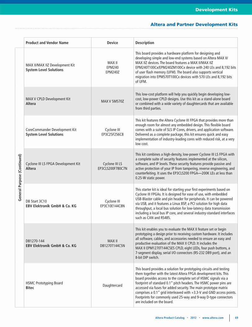
Altera Product Catalog • 2012 • www.altera.com 69
Development Kits
Product and Vendor Name Device Description
Gen
eral
Pur
pose
(Con
tinu
ed)
MAX II/MAX IIZ Development KitSystem Level Solutions
MAX IIEPM240EPM240Z
This board provides a hardware platform for designing and developing simple and low-end systems based on Altera MAX II/ MAX IIZ devices. The board features a MAX II/MAX IIZ EPM240T100Cx/EPM240ZM100Cx device with 240 LEs and 8,192 bits of user flash memory (UFM). The board also supports vertical migration into EPM570T100Cx devices with 570 LEs and 8,192 bits of UFM.
MAX V CPLD Development KitAltera
MAX V 5M570Z
This low-cost platform will help you quickly begin developing low-cost, low-power CPLD designs. Use this kit as a stand-alone board or combined with a wide variety of daughtercards that are available from third parties.
CoreCommander Development KitSystem Level Solutions
Cyclone IIIEP3C25F256C8
This kit features the Altera Cyclone III FPGA that provides more than enough room for almost any embedded design. This flexible board comes with a suite of SLS IP Cores, drivers, and application software. Delivered as a complete package, this kit ensures quick and easy implementation of industry-leading cores with reduced risk, at a very low cost.
Cyclone III LS FPGA Development KitAltera
Cyclone III LSEP3CLS200F780C7N
This kit combines a high-density, low-power Cyclone III LS FPGA with a complete suite of security features implemented at the silicon, software, and IP levels. These security features provide passive and active protection of your IP from tampering, reverse engineering, and counterfeiting. It uses the EP3CLS200 FPGA—200K LEs at less than 0.25-W static power.
DB Start 3C10EBV Elektronik GmbH & Co. KG
Cyclone III EP3C10E144C8N
This starter kit is ideal for starting your first experiments based on Cyclone III FPGAs. It is designed for ease of use, with embedded USB-Blaster cable and pin header for peripherals. It can be powered via USB, and it features a Linux BSP, a PCI solution for high data throughput, a local bus solution for low-latency data transmission including a local bus IP core, and several industry-standard interfaces such as CAN and RS485.
DB1270-144EBV Elektronik GmbH & Co. KG
MAX II DB1270T144C5N
This kit enables you to evaluate the MAX II feature set or begin prototyping a design prior to receiving custom hardware. It includes all software, cables, and accessories needed to ensure an easy and productive evaluation of the MAX II CPLD. It includes the MAX II EPM1270T144C5ES CPLD, eight LEDs, four push buttons, a 7-segment display, serial I/O connectors (RS-232 DB9 port), and an 8-bit DIP switch.
HSMC Prototyping BoardBitec
Daughtercard
This board provides a solution for prototyping circuits and testing them together with the latest Altera FPGA development kits. This board provides access to the complete set of HSMC signals via a footprint of standard 0.1” pitch headers. The HSMC power pins are accessed via fuses for added security. The main prototype matrix comprises a 0.1” grid interleaved with +3.3-V and GND access points. Footprints for commonly used 25-way and 9-way D-type connectors are included on the board.
Altera and Partner Development Kits
70 Altera Product Catalog • 2012 • www.altera.com Altera Product Catalog • 2012 • www.altera.com 71
Training
We offer an extensive curriculum of classes to deepen your expertise. Our classes are beneficial whether you’re new to FPGA and CPLD design, or are an advanced user wanting an update on the latest tools, tips, and tricks. Choose a training path delivered in three different ways:
•Instructor-led training, typically lasting one to two days, involves in-person instruction with hands-on exercises from an Altera or Altera partner subject matter expert. Fees vary.
•Virtual classrooms, involving live instructor-taught training over the Web, allow you to benefit from the interactivity with an instructor from the comfort of your home or office. Classes are taught in 4.5-hour sessions across consecutive days.
•Online training, typically one to two hours long, features pre-recorded presentations and demonstrations. Online classes are free and can be taken at any time.
To help you decide which courses might be most useful to you, we’ve grouped classes into specific curricula. Curricula paths include CPLD Designer, FPGA Designer, SoC Designer, Embedded Hardware Designer, and many more.
Instructor-Led, Virtual, and Online Classes
Learn more about our training
program or sign up for classes
at www.altera.com/training.
Start sharpening your competitive
edge today!
www.altera.com/training

70 Altera Product Catalog • 2012 • www.altera.com Altera Product Catalog • 2012 • www.altera.com 71
Training
www.altera.com/training
Altera Instructor-Led and Virtual Classroom Courses Virtual Classroom Courses Denoted with a *
(All Courses Are One Day in Length Unless Otherwise Noted)
Course Category General Description Course Titles
ProductivityLearn the recommended design methodology to maximize productivity and minimize design cycle time
•Best Practices for Maximizing FPGA Design Productivity* (course length: two days)
Design languagesAttain the skills needed to design with Verilog HDL and VHDL for programmable logic
•Introduction to VHDL*
•Advanced VHDL Design Techniques*
•Introduction to Verilog HDL*
•Advanced Verilog HDL Design Techniques*
SoftwareAcquire design entry, compilation, programming, verification, and optimization skills by learning how to use both basic and advanced features of Quartus II software
•The Quartus II Software Design Series: Foundation*
•The Quartus II Software Debug and Analysis Tools
•The Quartus II Software Design Series: Timing Analysis*
•Timing Closure with the Quartus II Software*
•Advanced Timing Analysis with TimeQuest*
•Design Optimization Using Quartus II Incremental Compilation*
System integration
Build hierarchical systems by integrating IP and custom logic•Introduction to the Qsys System Integration Tool
•Advanced Qsys System Integration Tool Methodologies
Embedded DesignLearn to design a Nios II soft-core microprocessor system in an Altera FPGA
•Designing with the Nios II Processor
•Developing Software for the Nios II Processor (2-day course)
Memory interfaces Implement interfaces to external memory•Implementing, Simulating, and Debugging External
Memory Interfaces
System DesignSolve DSP and video system design challenges using Altera technology
•Designing with DSP Builder Standard Blockset
•Designing with DSP Builder Advanced Blockset*
•Video Design Framework Workshop
Design securityCreate secure, reliable designs using the Quartus II software design separation flow
•Cyclone III LS Design Separation Flow*
Instructor-Led and Virtual Classroom Courses
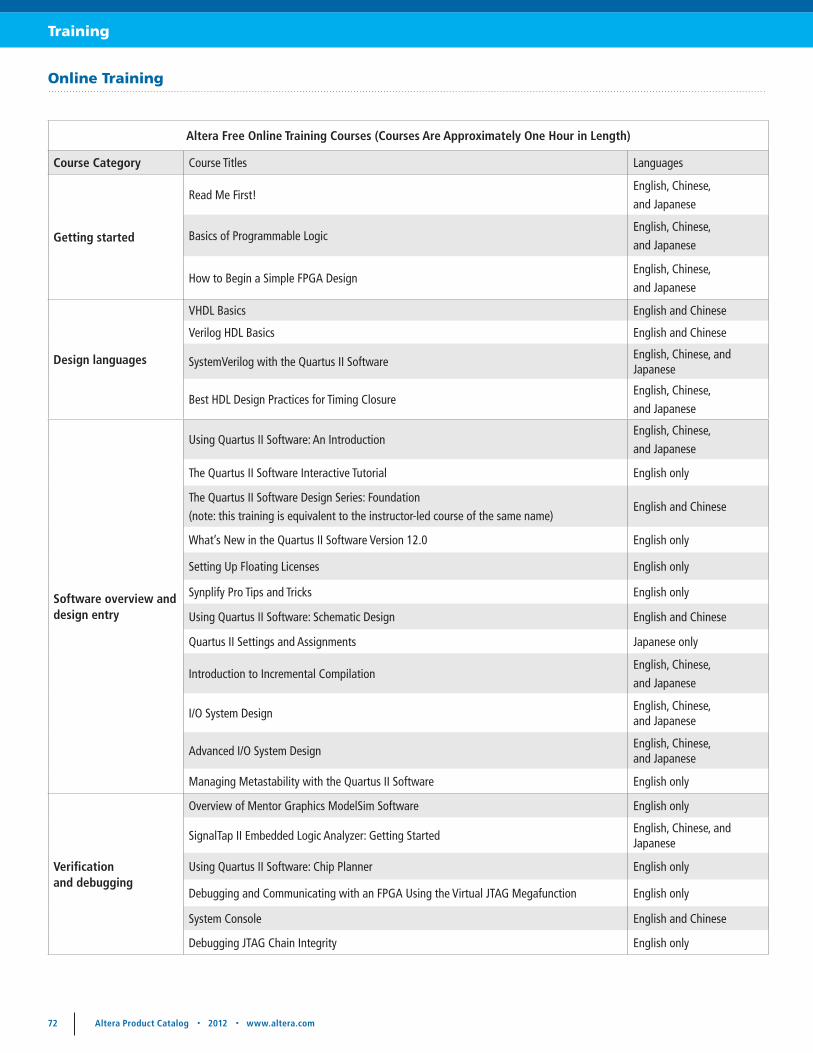
72 Altera Product Catalog • 2012 • www.altera.com Altera Product Catalog • 2012 • www.altera.com 73
Training
Altera Free Online Training Courses (Courses Are Approximately One Hour in Length)
Course Category Course Titles Languages
Getting started
Read Me First! English, Chinese,and Japanese
Basics of Programmable LogicEnglish, Chinese,and Japanese
How to Begin a Simple FPGA DesignEnglish, Chinese,and Japanese
Design languages
VHDL Basics English and Chinese
Verilog HDL Basics English and Chinese
SystemVerilog with the Quartus II SoftwareEnglish, Chinese, and Japanese
Best HDL Design Practices for Timing ClosureEnglish, Chinese,and Japanese
Software overview and design entry
Using Quartus II Software: An IntroductionEnglish, Chinese,and Japanese
The Quartus II Software Interactive Tutorial English only
The Quartus II Software Design Series: Foundation(note: this training is equivalent to the instructor-led course of the same name)
English and Chinese
What’s New in the Quartus II Software Version 12.0 English only
Setting Up Floating Licenses English only
Synplify Pro Tips and Tricks English only
Using Quartus II Software: Schematic Design English and Chinese
Quartus II Settings and Assignments Japanese only
Introduction to Incremental CompilationEnglish, Chinese,and Japanese
I/O System DesignEnglish, Chinese, and Japanese
Advanced I/O System DesignEnglish, Chinese, and Japanese
Managing Metastability with the Quartus II Software English only
Verification and debugging
Overview of Mentor Graphics ModelSim Software English only
SignalTap II Embedded Logic Analyzer: Getting StartedEnglish, Chinese, and Japanese
Using Quartus II Software: Chip Planner English only
Debugging and Communicating with an FPGA Using the Virtual JTAG Megafunction English only
System Console English and Chinese
Debugging JTAG Chain Integrity English only
Online Training
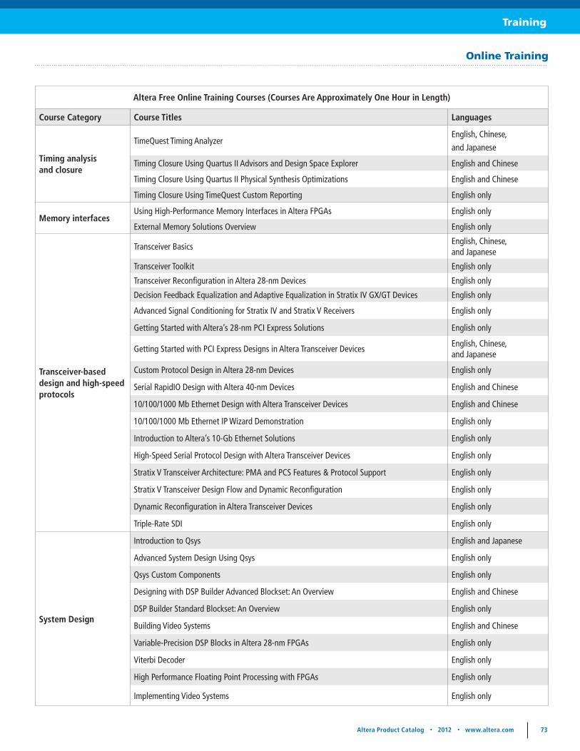
72 Altera Product Catalog • 2012 • www.altera.com Altera Product Catalog • 2012 • www.altera.com 73
Training
Altera Free Online Training Courses (Courses Are Approximately One Hour in Length)
Course Category Course Titles Languages
Getting started
Read Me First! English, Chinese,and Japanese
Basics of Programmable LogicEnglish, Chinese,and Japanese
How to Begin a Simple FPGA DesignEnglish, Chinese,and Japanese
Design languages
VHDL Basics English and Chinese
Verilog HDL Basics English and Chinese
SystemVerilog with the Quartus II SoftwareEnglish, Chinese, and Japanese
Best HDL Design Practices for Timing ClosureEnglish, Chinese,and Japanese
Software overview and design entry
Using Quartus II Software: An IntroductionEnglish, Chinese,and Japanese
The Quartus II Software Interactive Tutorial English only
The Quartus II Software Design Series: Foundation(note: this training is equivalent to the instructor-led course of the same name)
English and Chinese
What’s New in the Quartus II Software Version 12.0 English only
Setting Up Floating Licenses English only
Synplify Pro Tips and Tricks English only
Using Quartus II Software: Schematic Design English and Chinese
Quartus II Settings and Assignments Japanese only
Introduction to Incremental CompilationEnglish, Chinese,and Japanese
I/O System DesignEnglish, Chinese, and Japanese
Advanced I/O System DesignEnglish, Chinese, and Japanese
Managing Metastability with the Quartus II Software English only
Verification and debugging
Overview of Mentor Graphics ModelSim Software English only
SignalTap II Embedded Logic Analyzer: Getting StartedEnglish, Chinese, and Japanese
Using Quartus II Software: Chip Planner English only
Debugging and Communicating with an FPGA Using the Virtual JTAG Megafunction English only
System Console English and Chinese
Debugging JTAG Chain Integrity English only
Altera Free Online Training Courses (Courses Are Approximately One Hour in Length)
Course Category Course Titles Languages
Timing analysis and closure
TimeQuest Timing AnalyzerEnglish, Chinese,and Japanese
Timing Closure Using Quartus II Advisors and Design Space Explorer English and Chinese
Timing Closure Using Quartus II Physical Synthesis Optimizations English and Chinese
Timing Closure Using TimeQuest Custom Reporting English only
Memory interfacesUsing High-Performance Memory Interfaces in Altera FPGAs English only
External Memory Solutions Overview English only
Transceiver-based design and high-speed protocols
Transceiver BasicsEnglish, Chinese, and Japanese
Transceiver Toolkit English only
Transceiver Reconfiguration in Altera 28-nm Devices English only
Decision Feedback Equalization and Adaptive Equalization in Stratix IV GX/GT Devices English only
Advanced Signal Conditioning for Stratix IV and Stratix V Receivers English only
Getting Started with Altera’s 28-nm PCI Express Solutions English only
Getting Started with PCI Express Designs in Altera Transceiver DevicesEnglish, Chinese, and Japanese
Custom Protocol Design in Altera 28-nm Devices English only
Serial RapidIO Design with Altera 40-nm Devices English and Chinese
10/100/1000 Mb Ethernet Design with Altera Transceiver Devices English and Chinese
10/100/1000 Mb Ethernet IP Wizard Demonstration English only
Introduction to Altera’s 10-Gb Ethernet Solutions English only
High-Speed Serial Protocol Design with Altera Transceiver Devices English only
Stratix V Transceiver Architecture: PMA and PCS Features & Protocol Support English only
Stratix V Transceiver Design Flow and Dynamic Reconfiguration English only
Dynamic Reconfiguration in Altera Transceiver Devices English only
Triple-Rate SDI English only
System Design
Introduction to Qsys English and Japanese
Advanced System Design Using Qsys English only
Qsys Custom Components English only
Designing with DSP Builder Advanced Blockset: An Overview English and Chinese
DSP Builder Standard Blockset: An Overview English only
Building Video Systems English and Chinese
Variable-Precision DSP Blocks in Altera 28-nm FPGAs English only
Viterbi Decoder English only
High Performance Floating Point Processing with FPGAs English only
Implementing Video Systems English only
Online Training

74 Altera Product Catalog • 2012 • www.altera.com Altera Product Catalog • 2012 • www.altera.com 75
Training
Altera Free Online Training Courses (Courses Are Approximately One Hour in Length)
Course Category Course Titles Languages
System Design (Continued)
IP & Design Reuse English only
Using Cascaded-Integrator-Comb Filter in Multirate Digital Systems English only
FIR Compiler II English only
Avalon Verification Suite English only
Industrial Ethernet Solutions English and Chinese
Embedded systems
Designing with the Nios II Processor and Qsys - Day 1 (Online Training) English and Japanese
Developing Software for the Nios II Processor: Tools OverviewEnglish, Chinese, and Japanese
Developing Software for the Nios II Processor: Design Flow English and Chinese
SoC Hardware Overview - (Part 1) English only
SoC Hardware Overview - (Part 2) English only
Using the Nios II Processor English, Chinese, and Japanese
Nios II Processor and SOPC Builder Japanese only
Developing Software for the Nios II Processor: Nios II Software Build Tools for Eclipse English and Japanese
Nios II Software Build Tools for Eclipse and BSP Editor (Quartus II Software 10.0 Update) English only
Developing Software for the Nios II Processor: Debug Primer English and Chinese
Developing Software for the Nios II Processor: HAL PrimerEnglish, Chinese, and Japanese
Developing Software for the Nios II Processor: Software Build Flow - (Part 1) English only
Developing Software for the Nios II Processor: Software Build Flow - (Part 2) English only
Developing Software for the Nios II Processor: C2H Fundamentals English and Japanese
Nios II Floating-Point Custom Instructions English and Chinese
Developing Software for the Nios II Processor: MMU and MPU English and Chinese
Lauterbach Debug Tools English only
Introduction to Graphics English only
Introduction to D/AVE GPU English only
Device-specific training
Power Distribution Network Design for Stratix III and Stratix IV FPGAs English and Chinese
Power Distribution Network Design Using Altera PDN Design Tools English only
Configuring Altera FPGAs English and Chinese
The Quartus II Software Design Flow for HardCopy ASICs English only
Scripting
Command-Line Scripting English only
Introduction to Tcl English only
Quartus II Software Tcl Scripting English and Japanese
Online Training
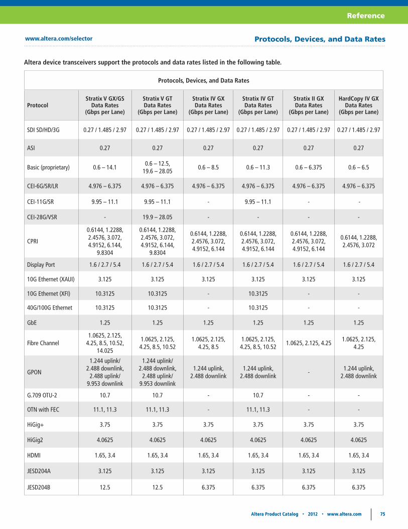
Altera Product Catalog • 2012 • www.altera.com 75
Reference
74 Altera Product Catalog • 2012 • www.altera.com Altera Product Catalog • 2012 • www.altera.com 75
www.altera.com/selector
Protocols, Devices, and Data Rates
ProtocolStratix V GX/GS
Data Rates(Gbps per Lane)
Stratix V GTData Rates
(Gbps per Lane)
Stratix IV GX Data Rates
(Gbps per Lane)
Stratix IV GT Data Rates
(Gbps per Lane)
Stratix II GX Data Rates
(Gbps per Lane)
HardCopy IV GX Data Rates
(Gbps per Lane)
SDI SD/HD/3G 0.27 / 1.485 / 2.97 0.27 / 1.485 / 2.97 0.27 / 1.485 / 2.97 0.27 / 1.485 / 2.97 0.27 / 1.485 / 2.97 0.27 / 1.485 / 2.97
ASI 0.27 0.27 0.27 0.27 0.27 0.27
Basic (proprietary) 0.6 – 14.10.6 – 12.5,
19.6 – 28.05 0.6 – 8.5 0.6 – 11.3 0.6 – 6.375 0.6 – 6.5
CEI-6G/SR/LR 4.976 – 6.375 4.976 – 6.375 4.976 – 6.375 4.976 – 6.375 4.976 – 6.375 4.976 – 6.375
CEI-11G/SR 9.95 – 11.1 9.95 – 11.1 - 9.95 – 11.1 - -
CEI-28G/VSR - 19.9 – 28.05 - - - -
CPRI
0.6144, 1.2288,2.4576, 3.072, 4.9152, 6.144,
9.8304
0.6144, 1.2288,2.4576, 3.072, 4.9152, 6.144,
9.8304
0.6144, 1.2288, 2.4576, 3.072, 4.9152, 6.144
0.6144, 1.2288,2.4576, 3.072, 4.9152, 6.144
0.6144, 1.2288, 2.4576, 3.072, 4.9152, 6.144
0.6144, 1.2288, 2.4576, 3.072
Display Port 1.6 / 2.7 / 5.4 1.6 / 2.7 / 5.4 1.6 / 2.7 / 5.4 1.6 / 2.7 / 5.4 1.6 / 2.7 / 5.4 1.6 / 2.7 / 5.4
10G Ethernet (XAUI) 3.125 3.125 3.125 3.125 3.125 3.125
10G Ethernet (XFI) 10.3125 10.3125 - 10.3125 - -
40G/100G Ethernet 10.3125 10.3125 - 10.3125 - -
GbE 1.25 1.25 1.25 1.25 1.25 1.25
Fibre Channel1.0625, 2.125,
4.25, 8.5, 10.52, 14.025
1.0625, 2.125,4.25, 8.5, 10.52
1.0625, 2.125, 4.25, 8.5
1.0625, 2.125,4.25, 8.5, 10.52
1.0625, 2.125, 4.251.0625, 2.125,
4.25
GPON
1.244 uplink/ 2.488 downlink,
2.488 uplink/ 9.953 downlink
1.244 uplink/ 2.488 downlink,
2.488 uplink/ 9.953 downlink
1.244 uplink, 2.488 downlink
1.244 uplink, 2.488 downlink
-1.244 uplink,
2.488 downlink
G.709 OTU-2 10.7 10.7 - 10.7 - -
OTN with FEC 11.1, 11.3 11.1, 11.3 - 11.1, 11.3 - -
HiGig+ 3.75 3.75 3.75 3.75 3.75 3.75
HiGig2 4.0625 4.0625 4.0625 4.0625 4.0625 4.0625
HDMI 1.65, 3.4 1.65, 3.4 1.65, 3.4 1.65, 3.4 1.65, 3.4 1.65, 3.4
JESD204A 3.125 3.125 3.125 3.125 3.125 3.125
JESD204B 12.5 12.5 6.375 6.375 6.375 6.375
Protocols, Devices, and Data Rates
Altera device transceivers support the protocols and data rates listed in the following table.

76 Altera Product Catalog • 2012 • www.altera.com
Reference
Protocols, Devices, and Data Rates
ProtocolArria V GX Data Rates
(Gbps per Lane)
Arria V GT Data Rates
(Gbps per Lane)
Arria II GX/GZ Data Rates
(Gbps per Lane)
Cyclone V GX Data Rates
(Gbps per Lane)
Cyclone V GT Data Rates
(Gbps per Lane)
Cyclone IV GX Data Rates
(Gbps per Lane)
SDI SD/HD/3G 0.27 / 1.485 / 2.97 0.27 / 1.485 / 2.97 0.27 / 1.485 / 2.97 0.27 / 1.485 / 2.97 0.27 / 1.485 / 2.97 0.27 / 1.485 / 2.97
ASI 0.27 0.27 0.27 - - -
Basic (proprietary) 0.6 – 6.5 0.6 – 10.3125 0.6 – 6.375 0.6 – 3.125 0.6 – 5.0 0.6 – 3.125
CEI-6G/SR/LR 4.976 – 6.375 4.976 – 6.375 - - - -
CPRI0.6144, 1.2288, 2.4576, 3.072, 4.9152, 6.144,
0.6144, 1.2288, 2.4576, 3.072, 4.9152, 6.144,
9.8304
0.6144, 1.2288, 2.4576, 3.072, 4.9152, 6.144
0.6144, 1.2288, 2.4576, 3.072
0.6144, 1.2288, 2.4576, 3.072,
4.915
0.6144, 1.2288, 2.4576, 3.072
Display Port 1.62, 2.7, 5.4 1.62, 2.7, 5.4 - 1.62, 2.7 1.62, 2.7 1.62, 2.7
10G Ethernet (XAUI) 3.125 3.125 3.125 3.125 3.125 3.125
10G Ethernet (XFI) - 10.3125 - - - -
GbE 1.25 1.25 1.25 1.25 1.25 1.25
Fibre Channel 1.0625, 2.125, 4.25 1.0625, 2.125, 4.25 1.0625, 2.125, 4.25 1.0625, 2.125 1.0625, 2.125, 4.25 -
GPON1.244 uplink,
2.488 downlink1.244 uplink,
2.488 downlink1.244 uplink,
2.488 downlink- - -
HiGig+ 3.75 3.75 3.75 - - -
HiGig2 4.0625 4.0625 - - - -
HDMI 1.65, 3.4 1.65, 3.4 1.65, 3.4 1.65 1.65, 3.4 1.65
JESD204A 3.125 3.125 3.125 3.125 3.125 3.125
JESD204B 6.375 6.375 6.375 - - -
Protocols, Devices, and Data Rates
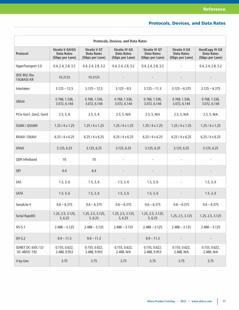
Altera Product Catalog • 2012 • www.altera.com 77
Reference
Protocols, Devices, and Data Rates
ProtocolStratix V GX/GS
Data Rates(Gbps per Lane)
Stratix V GTData Rates
(Gbps per Lane)
Stratix IV GX Data Rates
(Gbps per Lane)
Stratix IV GT Data Rates
(Gbps per Lane)
Stratix II GX Data Rates
(Gbps per Lane)
HardCopy IV GX Data Rates
(Gbps per Lane)
HyperTransport 3.0 0.4, 2.4, 2.8, 3.2 0.4, 2.4, 2.8, 3.2 0.4, 2.4, 2.8, 3.2 0.4, 2.4, 2.8, 3.2 - 0.4, 2.4, 2.8, 3.2
IEEE 802.3ba 10GBASE-KR
10.3125 10.3125 - - - -
Interlaken 3.125 – 12.5 3.125 – 12.5 3.125 – 8.5 3.125 – 11.3 3.125 – 6.375 3.125 – 6.375
OBSAI0.768, 1.536, 3.072, 6.144
0.768, 1.536, 3.072, 6.144
0.768, 1.536, 3.072, 6.144
0.768, 1.536, 3.072, 6.144
0.768, 1.536, 3.072, 6.144
0.768, 1.536, 3.072, 6.144
PCIe Gen1, Gen2, Gen3 2.5, 5, 8 2.5, 5, 8 2.5, 5, N/A 2.5, 5, N/A 2.5, 5, N/A 2.5, 5, N/A
SGMII / QSGMII 1.25 / 4 x 1.25 1.25 / 4 x 1.25 1.25 / 4 x 1.25 1.25 / 4 x 1.25 1.25 / 4 x 1.25 1.25 / 4 x 1.25
RXAUI / DXAUI 6.25 / 4 x 6.25 6.25 / 4 x 6.25 6.25 / 4 x 6.25 6.25 / 4 x 6.25 6.25 / 4 x 6.25 6.25 / 4 x 6.25
SPAUI 3.125, 6.25 3.125, 6.25 3.125, 6.25 3.125, 6.25 3.125, 6.25 3.125, 6.25
QDR Infiniband 10 10 - - - -
QPI 6.4 6.4 - - - -
SAS 1.5, 3, 6 1.5, 3, 6 1.5, 3, 6 1.5, 3, 6 - 1.5, 3, 6
SATA 1.5, 3, 6 1.5, 3, 6 1.5, 3, 6 1.5, 3, 6 - 1.5, 3, 6
SerialLite II 0.6 – 6.375 0.6 – 6.375 0.6 – 6.375 0.6 – 6.375 0.6 – 6.375 0.6 – 6.375
Serial RapidIO1.25, 2.5, 3.125,
5, 6.251.25, 2.5, 3.125,
5, 6.251.25, 2.5, 3.125,
5, 6.251.25, 2.5, 3.125,
5, 6.251.25, 2.5, 3.125 1.25, 2.5, 3.125
SFI-5.1 2.488 – 3.125 2.488 – 3.125 2.488 – 3.125 2.488 – 3.125 2.488 – 3.125 2.488 – 3.125
SFI-5.2 9.9 – 11.3 9.9 – 11.3 - 9.9 – 11.3 - -
SONET OC-3/OC-12/ OC-48/OC-192
0.155, 0.622, 2.488, 9.953
0.155, 0.622, 2.488, 9.953
0.155, 0.622, 2.488, N/A
0.155, 0.622, 2.488, 9.953
0.155, 0.622, 2.488, N/A
0.155, 0.622, 2.488, N/A
V-by-One 3.75 3.75 3.75 3.75 3.75 3.75
Protocols, Devices, and Data Rates

78 Altera Product Catalog • 2012 • www.altera.com
Reference
Protocols, Devices, and Data Rates
ProtocolArria V GX Data Rates
(Gbps per Lane)
Arria V GT Data Rates
(Gbps per Lane)
Arria II GX/GT Data Rates
(Gbps per Lane)
Cyclone V GX Data Rates
(Gbps per Lane)
Cyclone V GT Data Rates
(Gbps per Lane)
Cyclone IV GX Data Rates
(Gbps per Lane)
HyperTransport 3.0 0.4, 2.4, 2.8, 3.2 0.4, 2.4, 2.8, 3.2 - - - -
Interlaken 3.125 – 6.375 3.125 – 6.375 - - - -
OBSAI0.768, 1.536, 3.072, 6.144
0.768, 1.536, 3.072, 6.144
0.768, 1.536, 3.072, 6.144
0.768, 1.536, 3.072
0.768, 1.536, 3.072
0.768, 1.536, 3.072
PCIe Gen1, Gen2, Gen3 2.5, 5, N/A 2.5, 5, N/A 2.5, 5, N/A 2.5, N/A, N/A 2.5, 5, N/A 2.5, N/A, N/A
SGMII / QSGMII 1.25 / 4 x 1.25 1.25 / 4 x 1.25 1.25 / 4 x 1.25 1.25 1.25 / 4 x 1.25 1.25
RXAUI / DXAUI 6.25 / 4 x 6.25 6.25 / 4 x 6.25 - - - -
SPAUI - - 3.125 - - -
SAS 1.5, 3, 6 1.5, 3, 6 1.5, 3, 6 - - -
SATA 1.5, 3, 6 1.5, 3, 6 1.5, 3, 6 1.5, 3 1.5, 3 1.5, 3
SerialLite II 0.6 – 6.375 0.6 – 6.375 0.6 – 3.75 - - -
Serial RapidIO1.25, 2.5, 3.125,
5, 6.251.25, 2.5, 3.125,
5, 6.251.25, 2.5, 3.125 1.25, 2.5, 3.125 1.25, 2.5, 3.125 1.25, 2.5, 3.125
SFI-5.1 2.488 – 3.125 2.488 – 3.125 - - - -
SONET OC-3/OC-12/ OC-48/OC-192
0.155, 0.622, 2.488, N/A
0.155, 0.622, 2.488, N/A
0.155, 0.622, 2.488, N/A
- - -
V-by-One 3.75 3.75 - 3 3.75 3
Protocols, Devices, and Data Rates
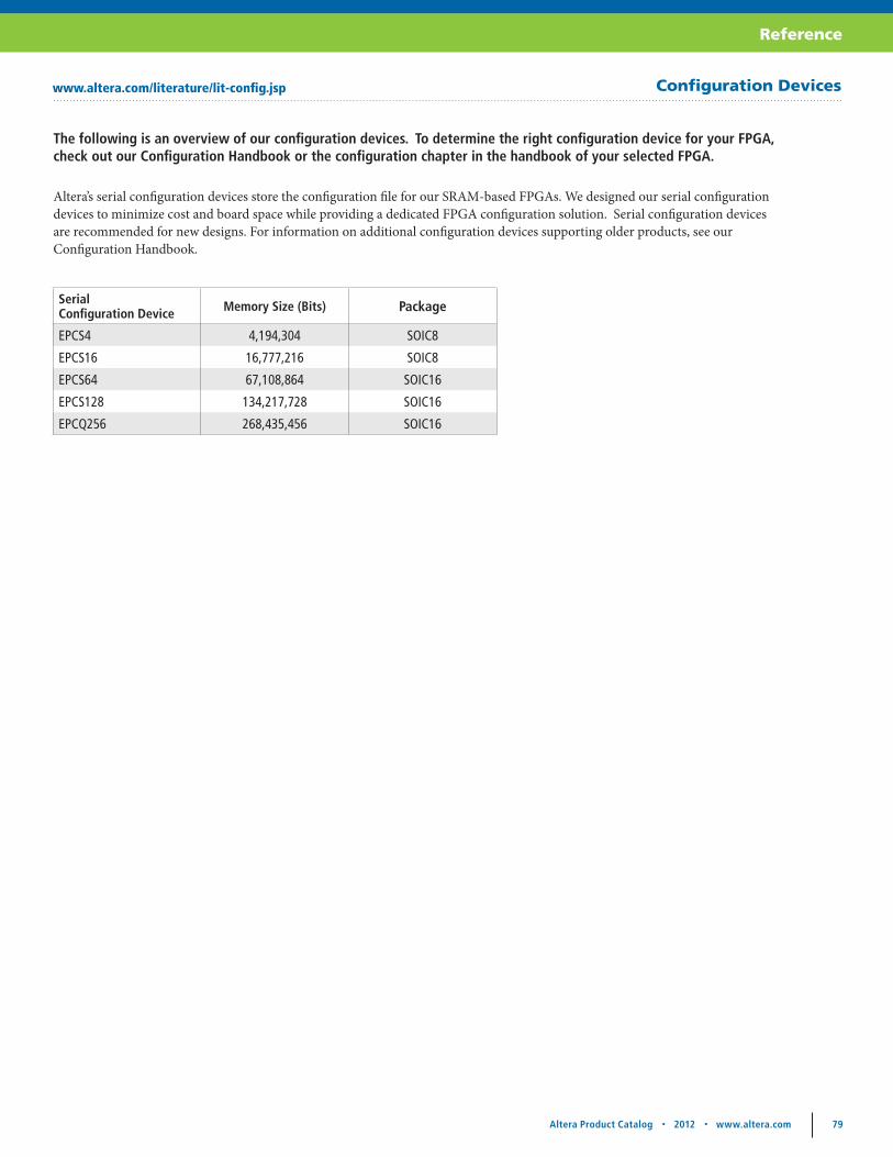
Altera Product Catalog • 2012 • www.altera.com 79
Reference
www.altera.com/literature/lit-config.jsp Configuration Devices
Altera’s serial configuration devices store the configuration file for our SRAM-based FPGAs. We designed our serial configuration devices to minimize cost and board space while providing a dedicated FPGA configuration solution. Serial configuration devices are recommended for new designs. For information on additional configuration devices supporting older products, see our Configuration Handbook.
The following is an overview of our configuration devices. To determine the right configuration device for your FPGA, check out our Configuration Handbook or the configuration chapter in the handbook of your selected FPGA.
Serial Configuration Device Memory Size (Bits) Package
EPCS4 4,194,304 SOIC8
EPCS16 16,777,216 SOIC8
EPCS64 67,108,864 SOIC16
EPCS128 134,217,728 SOIC16
EPCQ256 268,435,456 SOIC16
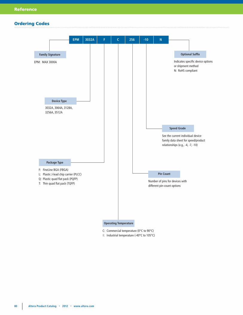
80 Altera Product Catalog • 2012 • www.altera.com
Reference
EPM 3032A F C 256 -10 N
Optional SuffixFamily Signature
EPM: MAX 3000A
Device Type
3032A, 3064A, 3128A,3256A, 3512A
Package Type
F: FineLine BGA (FBGA)L: Plastic J-lead chip carrier (PLCC)Q: Plastic quad flat pack (PQFP)T: Thin quad flat pack (TQFP)
Speed Grade
See the current individual device family data sheet for speed/product relationships (e.g., -4, -7, -10)
Pin Count
Number of pins for devices with different pin-count options
Indicates specific device options or shipment methodN: RoHS compliant
Operating Temperature
C: Commercial temperature (0°C to 90°C) I : Industrial temperature (-40°C to 105°C)
Ordering Codes
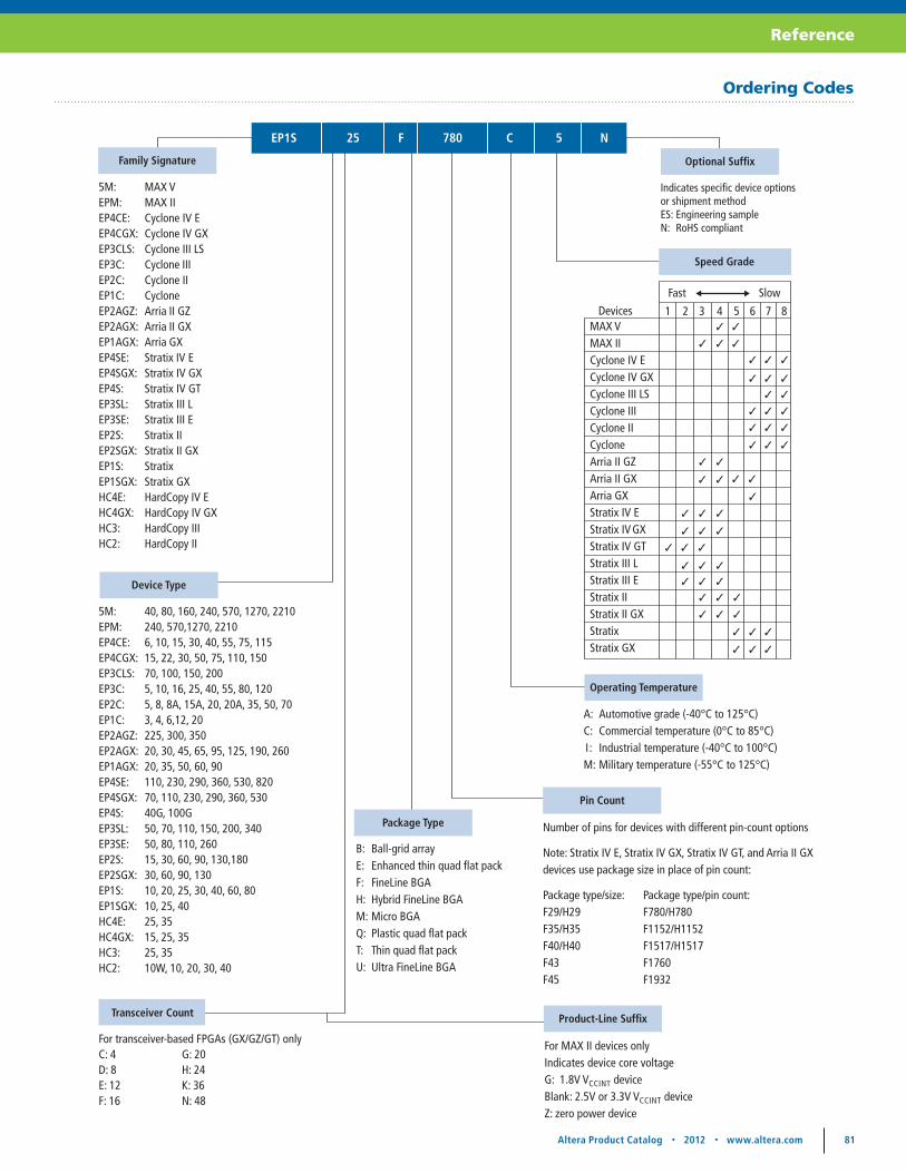
Altera Product Catalog • 2012 • www.altera.com 81
Reference
Ordering Codes
Package Type
B: Ball-grid arrayE: Enhanced thin quad flat packF: FineLine BGAH: Hybrid FineLine BGAM: Micro BGAQ: Plastic quad flat packT: Thin quad flat packU: Ultra FineLine BGA
Family Signature
5M: MAX VEPM: MAX IIEP4CE: Cyclone IV EEP4CGX: Cyclone IV GXEP3CLS: Cyclone III LSEP3C: Cyclone IIIEP2C: Cyclone IIEP1C: CycloneEP2AGZ: Arria II GZEP2AGX: Arria II GXEP1AGX: Arria GXEP4SE: Stratix IV EEP4SGX: Stratix IV GXEP4S: Stratix IV GTEP3SL: Stratix III LEP3SE: Stratix III EEP2S: Stratix IIEP2SGX: Stratix II GXEP1S: StratixEP1SGX: Stratix GXHC4E: HardCopy IV EHC4GX: HardCopy IV GXHC3: HardCopy IIIHC2: HardCopy II
5M: 40, 80, 160, 240, 570, 1270, 2210EPM: 240, 570,1270, 2210EP4CE: 6, 10, 15, 30, 40, 55, 75, 115EP4CGX: 15, 22, 30, 50, 75, 110, 150EP3CLS: 70, 100, 150, 200EP3C: 5, 10, 16, 25, 40, 55, 80, 120EP2C: 5, 8, 8A, 15A, 20, 20A, 35, 50, 70EP1C: 3, 4, 6,12, 20EP2AGZ: 225, 300, 350EP2AGX: 20, 30, 45, 65, 95, 125, 190, 260EP1AGX: 20, 35, 50, 60, 90EP4SE: 110, 230, 290, 360, 530, 820EP4SGX: 70, 110, 230, 290, 360, 530EP4S: 40G, 100GEP3SL: 50, 70, 110, 150, 200, 340EP3SE: 50, 80, 110, 260EP2S: 15, 30, 60, 90, 130,180EP2SGX: 30, 60, 90, 130EP1S: 10, 20, 25, 30, 40, 60, 80EP1SGX: 10, 25, 40HC4E: 25, 35HC4GX: 15, 25, 35HC3: 25, 35HC2: 10W, 10, 20, 30, 40
Indicates specific device options or shipment methodES: Engineering sampleN: RoHS compliant
A: Automotive grade (-40°C to 125°C) C: Commercial temperature (0°C to 85°C) I : Industrial temperature (-40°C to 100°C)M: Military temperature (-55°C to 125°C)
EP1S 25 F 780 C 5 N
Transceiver Count
For transceiver-based FPGAs (GX/GZ/GT) onlyC: 4 D: 8 E: 12 F: 16
G: 20H: 24K: 36N: 48
MAX VMAX IICyclone IV ECyclone IV GXCyclone III LSCyclone IIICyclone IICycloneArria II GZArria II GXArria GXStratix IV EStratix IV GXStratix IV GT Stratix III LStratix III EStratix IIStratix II GXStratixStratix GX
321 4 5 6 7 8
Fast Slow
Product-Line Suffix
Device Type
Optional Suffix
Pin Count
Number of pins for devices with different pin-count options
Note: Stratix IV E, Stratix IV GX, Stratix IV GT, and Arria II GX devices use package size in place of pin count:
Package type/size: Package type/pin count:F29/H29 F780/H780F35/H35 F1152/H1152F40/H40 F1517/H1517F43 F1760F45 F1932
For MAX II devices onlyIndicates device core voltageG: 1.8V VCCINT deviceBlank: 2.5V or 3.3V VCCINT deviceZ: zero power device
Speed Grade
Operating Temperature
Devices
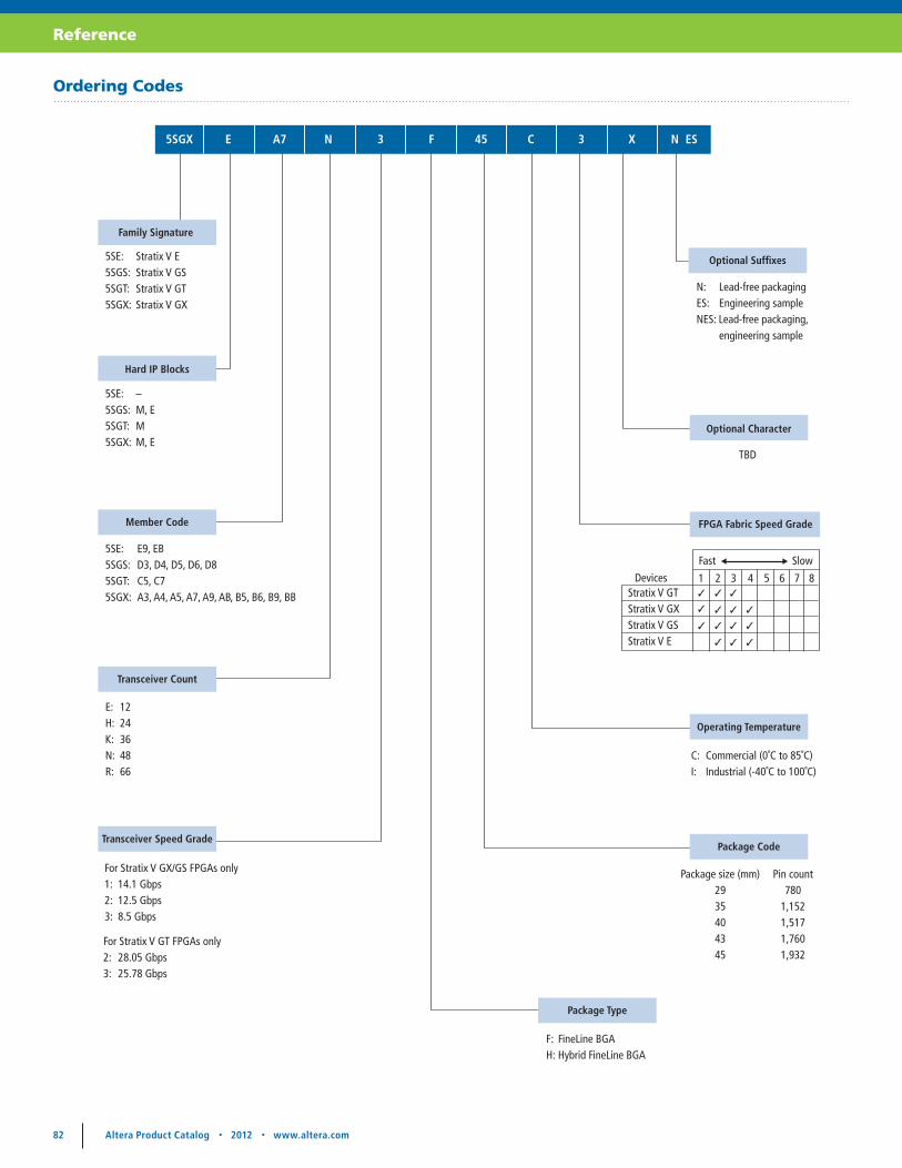
82 Altera Product Catalog • 2012 • www.altera.com
Reference
Optional Suffixes
N: Lead-free packagingES: Engineering sampleNES: Lead-free packaging, engineering sample
5SGX E A7 N 3 F 45 C 3 X N ES
Family Signature
Member Code
5SE: Stratix V E5SGS: Stratix V GS5SGT: Stratix V GT5SGX: Stratix V GX
Hard IP Blocks
5SE: –5SGS: M, E5SGT: M5SGX: M, E
5SE: E9, EB5SGS: D3, D4, D5, D6, D85SGT: C5, C75SGX: A3, A4, A5, A7, A9, AB, B5, B6, B9, BB
Transceiver Count
E: 12H: 24K: 36N: 48R: 66
Package Type
F: FineLine BGAH: Hybrid FineLine BGA
Package CodeTransceiver Speed Grade
For Stratix V GX/GS FPGAs only1: 14.1 Gbps2: 12.5 Gbps3: 8.5 Gbps
Optional Character
FPGA Fabric Speed Grade
TBD
Operating Temperature
C: Commercial (0˚C to 85˚C)I: Industrial (-40˚C to 100˚C)
Package size (mm)2935404345
Pin count780
1,1521,5171,7601,932
Stratix V GTStratix V GXStratix V GSStratix V E
321 4 5 6 7 8
Fast Slow
Devices
For Stratix V GT FPGAs only2: 28.05 Gbps3: 25.78 Gbps
Ordering Codes

Altera Product Catalog • 2012 • www.altera.com 83
Reference
5AGX B A7 D 4 F 27 C 4 X N
Family Signature
Member Code
5AGX: Arria V GX5AGT: Arria V GT
Hard IP Blocks
5AGX: B, M, F5AGT: B, M, F
5AGX: A1, A3, A5, A7, B1, B3, B5, B75AGT: C3, C7, D3, D7
Transceiver Count
D: 9 E: 12G: 18H: 24K: 36
Package Type
F: FineLine BGA
Package Code
Transceiver Speed Grade
Optional Character
FPGA Fabric Speed Grade
TBD
Operating Temperature
C: Commercial (0˚C to 85˚C)I: Industrial (-40˚C to 100˚C for I5) (0˚C to 100˚C for I3)
Package size (mm)27313540
Pin count672896
1,1521,517
Arria V GXArria V GT
321 4 5 6 7 8
Fast Slow
Devices
For Arria V GT FPGAs only3: 10.3125 Gbps
For Arria V GX FPGAs only4: 6.375 Gbps6: 3.125 Gbps
Optional Suffixes
N: Lead-free packagingES: Engineering sampleNES: Lead-free packaging, engineering sample
Ordering Codes

84 Altera Product Catalog • 2012 • www.altera.com
Reference
5AST F D5 K 4 F 40 I 5 N
Family Signature
Member Code
5ASX: Arria V SX5AST: Arria V ST
Hard IP Blocks
5ASX: B, M, F5AST: F
5ASX: B3, B55AST: D3, D5
Transceiver Count
D: 9 E: 12G: 18H: 24K: 30
Package Type
F: FineLine BGA
Package Code
Transceiver Speed Grade
Optional Suffixes
N: Lead-free packagingES: Engineering sampleNES: Lead-free packaging, engineering sample
FPGA Fabric Speed Grade
Operating Temperature
C: Commercial (0˚C to 85˚C)I: Industrial (-40˚C to 100˚C)
Package size (mm)313540
Pin count896
1,1521,517
Arria V SXArria V ST
321 4 5 6 7 8
Fast Slow
Devices
For Arria V ST FPGAs only3: 10.3125 Gbps
For Arria V SX FPGAs only4: 6.375 Gbps6: 3.125 Gbps
Ordering Codes

Altera Product Catalog • 2012 • www.altera.com 85
Reference
5CGX B C3 B 6 F 23 C 7 X N
Family Signature
Member Code
5CE: Cyclone V E5CGX: Cyclone V GX5CGT: Cyclone V GT
Hard IP Blocks
5CE: B, F5CGX: B, F5CGT: F
5CE: A2, A4, A5, A7, A95CGX: C3, C4, C5,C7, C95CGT: D5, D7, D9
Transceiver Count
B: 3 C: 6D: 9 E: 12
Package Type
F: FineLine BGAU: Ultra FineLine BGA
Package Code
Transceiver Speed Grade
Optional Character
FPGA Fabric Speed Grade
TBD
Operating Temperature
A: Automotive (-40°C to 125°C)C: Commercial (0˚C to 85˚C)I: Industrial (-40˚C to 100˚C)
Package size (mm)15171923273135
Pin count325256484484672896
1,152
Cyclone V GTCyclone V GXCyclone V E
321 4 5 6 7 8
Fast Slow
Devices
For Cyclone V GX FPGAs only6: 3.125 Gbps7: 2.5 Gbps
For Cyclone V GT FPGAs only5: 5 Gbps
Optional Suffixes
N: Lead-free packagingES: Engineering sampleNES: Lead-free packaging, engineering sample
Ordering Codes
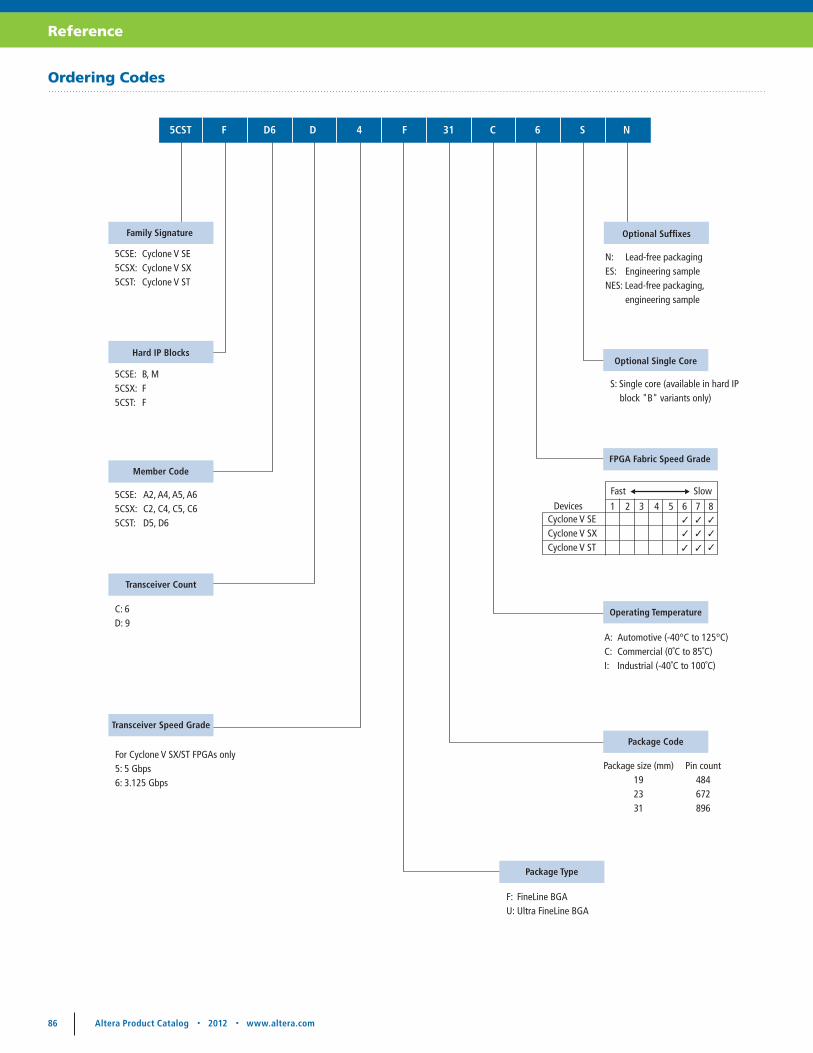
86 Altera Product Catalog • 2012 • www.altera.com
Reference
5CST F D6 D 4 F 31 C 6 S N
Family Signature
Member Code
5CSE: Cyclone V SE5CSX: Cyclone V SX5CST: Cyclone V ST
Hard IP Blocks
5CSE: B, M5CSX: F5CST: F
5CSE: A2, A4, A5, A65CSX: C2, C4, C5, C65CST: D5, D6
Transceiver Count
C: 6D: 9
Package Type
F: FineLine BGAU: Ultra FineLine BGA
Package Code
Transceiver Speed Grade
Optional Single Core
FPGA Fabric Speed Grade
S: Single core (available in hard IP block "B" variants only)
Operating Temperature
A: Automotive (-40°C to 125°C)C: Commercial (0˚C to 85˚C)I: Industrial (-40˚C to 100˚C)
Package size (mm)192331
Pin count484672896
Cyclone V SECyclone V SXCyclone V ST
321 4 5 6 7 8
Fast Slow
Devices
For Cyclone V SX/ST FPGAs only5: 5 Gbps6: 3.125 Gbps
N: Lead-free packagingES: Engineering sampleNES: Lead-free packaging, engineering sample
Optional Suffixes
Ordering Codes

Notes

Notes
System Design
Explore system design challenges with Altera’s editor-in-chief, Ron Wilson.
You’ll get technical articles on system design to help you learn more about
system performance tradeoffs, lowering system power consumption and
cost, and improving design-team productivity.
Dive further into the details today with technical resources from Altera.
www.altera.com/technology/system-design
at 28 nm

Altera Corporation101 Innovation DriveSan Jose, CA 95134USAwww.altera.com
Altera European HeadquartersHolmers Farm WayHigh WycombeBuckinghamshireHP12 4XFUnited KingdomTelephone: (44) 1 494 602 000
Altera Japan Ltd.Shinjuku I Tower 32F6-5-1, Nishi ShinjukuShinjuku-ku, Tokyo 163-1332JapanTelephone: (81) 3 3340 9480www.altera.co.jp
Altera International Ltd.Unit 11- 18, 9/FMillennium City 1, Tower 1388 Kwun Tong RoadKwun TongKowloon, Hong Kong Telephone: (852) 2 945 7000www.altera.com.cn
FSC logo
www.altera.com/twitter www.altera.com/facebook www.alteraforum.com
©2012 Altera Corporation. All rights reserved. ALTERA, ARRIA, CYCLONE, HARDCOPY, MAX, MEGACORE, NIOS, QUARTUS and STRATIX words and logos are trademarks of Altera Corporation and registered in the U.S. Patent and Trademark Office and in other countries. All other words and logos identified as trademarks or service marks are the property of their respective holders as described at www.altera.com/legal. May 2012 SG-PRDCT-12.0


