Embed Size (px)
Citation preview
AGGREGATIVE GROWTH OF COLLOIDAL SEMICONDUCTING NANOCRYSTALS FOR NANOSHELL QUANTUM DOTS AND QUANTUM DOT MOLECULES
James Cassidy
A Dissertation
Submitted to the Graduate College of Bowling Green State University in partial fulfillment of
the requirements for the degree of
DOCTOR OF PHILOSOPHY
April 2022
Committee:
Mikhail Zamkov, Advisor
Michael Todd Arrigo, Graduate Faculty Representative
Pavel Anzenbacher
Alexander N. Tarnovsky

© 2022
James Cassidy
All Rights Reserved
iii
ABSTRACT
Mikhail Zamkov, Advisor
One property of colloidal semiconducting nanocrystals that has remained elusive to the
rational design is the ensemble photoluminescence (PL) line width. Given the growing demand
for NC-based light-emitting materials, substantial research effort has been dedicated to this issue.
A postsynthetic strategy has been developed that allows reducing emission line widths of CdSe
and CdS NCs to near single-particle levels while enhancing the PL quantum yield. The key idea
behind the synthetic approach lies in employing a nonclassical coalescence growth mechanism,
which leads to size focusing irrespective of the initial sample morphology. Numerical
simulations accurately predict the observed particle size evolution, confirming the ability of
coalescence growth to promote size focusing of semiconductor colloids.
Furthermore, the optoelectronic properties of colloidal semiconductor nanocrystals can
be manipulated by changing their geometric shape. Precise synthetic control over particle
morphologies, however, has remained elusive. Conventional growth techniques rely on the
kinetic assembly of atomic units, where supersaturation and precipitation processes can lead to a
broad distribution of particle shapes. A growth strategy has been developed to allow for the
shape-selective syntheses of CdSe and CdS NC cubes, spheres, rods, as well as unprecedented
“donut” and ring-like structures. Different particle morphologies were obtained through a
thermodynamically driven growth, using a distinct combination of coordinating compounds that
minimize the surface free energy.
Auger decay of multiple excitons represents a significant obstacle to photonic
applications of semiconductor quantum dots. This nonradiative process is particularly
detrimental to the performance of QD-based electroluminescent and lasing devices.
iv
Semiconductor quantum shells with an “inverted” QD geometry have been shown to inhibit
Auger recombination, allowing for substantial improvements to multiexciton characteristics. By
promoting a spatial separation between multiple excitons, the quantum shell geometry leads to
ultralong biexciton lifetimes (>10 ns) and a large biexciton quantum yield. Furthermore, the
architecture of quantum shells induces an exciton–exciton repulsion, which splits exciton and
biexciton optical transitions, giving rise to an Auger-inactive single-exciton gain mode. In this
regime, quantum shells exhibit the longest optical gain lifetime reported for colloidal QDs to
date (>6 ns), which is significant for optically and electrically pumped gain media.
v
To all those while helped make this a reality
Especially my family and Robyn
For your love and support
vi
ACKNOWLEDGMENTS
I would like to first and foremost thank my advisor, Dr. Mikhail Zamkov, for his
guidance and extraordinary support throughout the past five years. His invaluable research
tutelage has helped shape and mold me into a formidable scientist. I am incredibly grateful for all
the opportunities he has afforded to me and his countless hours of teaching and guidance.
I would also like to thank my committee members, Professor Michael Arrigo, Dr. Pavel
Anzenbacher, and Dr. Alex Tarnovsky for time and commitment to my education. I am also
thankful for the many collaborators I have had the pleasure of publishing with over the years;
including, Dr. Malcolm D. E. Forbes, Dr. Benjamin Diroll, Dr. Dmitriy Khon, Dr. Andrew
Proppe, Dr. Moungi G. Bawendi, Dr. Richard D. Shaller, Dr. Hedi Mattoussi, and Dr. Aton V.
Malko.
I would also like to acknowledge all of my friends and lab mates I have had over the fast
half decade, including Pavel Moroz, Dmitry Porotnikov, Mingrui Yang, and Dulanjan
Harankahage for all the support, friendship, and valuable discussion they provided.
Finally, If not for the support and love of Robyn, Beau, Ashley, Brendan, and Jill, I
would not have made it through this journey.

vii
TABLE OF CONTENTS Page
CHAPTER I. INTRODUCTION TO SEMICONDUCTOR NANOCRYSTALS .................. 1
1.1 Surface Chemistry ................................................................................................... 1
1.2 Quantum Dot Optical Transitions and Electronic Structure ................................... 3
1.3 Nanocrystal Heterostructures .................................................................................. 5
1.4 Multiexciton Generation and Auger Decay ............................................................ 7
1.5 Overview of Quantum Dot Applications ................................................................ 9
CHAPTER II. AGGREGATIVE GROWTH OF SEMICONDUCTOR NANOCRYSTALS 10
2.1 Introduction to Colloidal Nanocrystal Coalescence ............................................... 10
2.2 Digestive Ripening of Semiconductor Nanocrystals .............................................. 13
2.3 Size Focusing of Nanocrystals via Coalescence Growth ........................................ 18
2.4 Theoretical Analysis of Nanocrystal Aggregative Growth ..................................... 25
2.5 Conclusions Regarding Semiconductor Nanocrystal Coalescence ......................... 30
2.6 Experimental Methods for Nanocrystal Coalescence ............................................. 31
CHAPTER III. COALESCENCE INDUCED SHAPE CONTROL OF SEMICONDUCTOR
NANOCRSYATLS ............................................................................................................... 35
3.1 Introduction to Aggregative Growth for Shape Control ......................................... 35
3.2 Utilizing Aggregative Growth for Shape Control ................................................... 38
3.3 Investigation of Crystal Structure and Coordinating Solvent on Shape Control .... 43
3.4 Further Observations on the Shape Control of Aggregative Growth ..................... 48
3.5 Theoretical Investigation of Coalescence Induced Shape Control ......................... 50
3.6 Concluding Remarks on Shape Control via Coalescence ....................................... 53
3.7 Experimental Methods on Aggregative Growth Induced Shape Control ............... 54
viii
CHAPTER IV. BUILDING ARTIFICAL MOLECULES WITH QUANTUM DOTS.......... 59
4.1 Introduction to Quantum Dot Molecules ................................................................ 59
4.2 Formation of a Molten Surface Layer on Nanocrystals .......................................... 61
4.3 Fusion of Nanocrystal Surfaces and Impact on Nanocrystal Dimensionality ........ 64
4.4 Coupling of Homogeneous and Heterogenous Fused Nanocrystal Assemblies ..... 68
4.5 Theoretical Model Describing Molten Surface Melting ......................................... 72
4.6 Conclusions on Nanocrystal Molecular Assemblies............................................... 73
3.7 Experimental Methods for Quantum Dot Molecules .............................................. 74
CHAPTER V. COALESCENCE INDUCED SHAPE CONTROL OF SEMICONDUCTOR
NANOCRSYATLS ............................................................................................................... 78
5.1 Introduction to Multiexcitons in Quantum Dots ..................................................... 78
5.2 Engineering Materials for Extended Biexcitons and Their Spectroscopic Properties
............................................................................................................... 82
5.3 Carrier Confinement in Quantum Dot Quantum Well Nanoshells ......................... 88
5.4 Biexciton Decay Pathways ..................................................................................... 93
5.5 Conclusions Regarding Sustained Biexciton Populations ...................................... 96
5.6 Experimental Methods on the Engineering of Quantum Dots for Extended Biexciton
Lifetimes ............................................................................................................... 97
CHAPTER VI. QUANTUM SHELL NANOCRYSTALS: AVENUE FOR LONG OPTICAL
GAIN AND LOW-THRESHOLD AMPLIFIED SPNOTANEOUS EMISSION.................... 101
6.1 Introduction to Optical Gain and Amplified Spontaneous Emission in Quantum Shell
Nanocrystals ............................................................................................................... 101
6.2 Quantum Shell Fabrication and Biexciton Dynamics ............................................. 105

ix
6.3 Ultrafast Spectroscopy and Optical Gain ................................................................ 108
6.4 Amplified Spontaneous Emission from Quantum Shells: Utilization for Light
Emitting Applications ................................................................................................... 111
6.5 Exciton-Exciton Repulsion Dynamics .................................................................... 114
6.6 Conclusions on Quantum Shells ............................................................................. 118
6.7 Experimental Procedures and Methods for the Synthesis of Quantum Shells........ 118
CHAPTER VII. REFERENCES .............................................................................................. 123
x
LIST OF FIGURES Figure Page
1 Illustration showing cadmium (black dots) and selenium (red dots) in a
CdSe nanocrystal .......................................................................................................... 2
2 Absorption and photoluminescence spectrum of CdS QDs .......................................... 4
3 Overview of core/shell nanocrystal bandgap configurations ........................................ 6
4 Depiction of Auger recombination pathways ............................................................... 8
5 Nanocrystal growth rate for classical growth vs coalescence growth .......................... 12
6 The results of several characteristic growth reactions .................................................. 16
7 Overview of CdSe coalescence growth conditions ....................................................... 20
8 Evolution of NC PL dynamics during size-focusing coalescence ................................ 23
9 Size focusing of CdS NCs in a mixture of OLAM and Cd(OA)2 free ligands ............. 24
10 Theoretical model of nanocrystal coalescence ............................................................. 26
11 Shape selective synthesis of CdS NCs using the aggregative growth strategy............. 37
12 Spectroscopic investigations of aggregative growth compared to known models ....... 39
13 A diagram showing a greater affinity of bound-ion pairs ............................................. 41
14 Evolution of ZB CdS NCs during aggregative growth ................................................. 44
15 Crystal structure impact on shape controlled aggregative growth ................................ 46
16 Tuning of the exciton fine structure during aggregative growth .................................. 48
17 A thermodynamic model explaining the formation of molten phases
in spherical nanocrystals ............................................................................................... 52
18 Illustration of the viscoelastic assembly approach........................................................ 60
19 Model on the interfacial and elastic energies for nanoparticle fusion .......................... 63
20 Photophysics of fused nanocrystals .............................................................................. 65
xi
21 Coupling dynamics of fused nanocrystals .................................................................... 69
22 Understanding molten layer formation and thickness .................................................. 71
23 Configuration of CdSbulk/CdSe/CdSshell quantum-well nanoshells ............................... 80
24 Characterization of three quantum-confined CdSe morphologies ................................ 84
25 Summary of structural and optical parameters corresponding
to eight investigated samples ........................................................................................ 85
26 High-angle annular dark field (HAADF)-STEM images ............................................. 87
27 Measurements of biexciton lifetimes in zero-dimensional CdSe nanocrystal
and CdS/CdSe nanoshells ............................................................................................. 90
28 Measurements of biexciton lifetimes in CdSbulk/CdSe/CdSshell
quantum-well nanoshells .............................................................................................. 95
29 Geometry and Biexciton repulsion in CdSe quantum shells ........................................ 104
30 Characterizations of CdSe quantum well nanocrystals ................................................. 107
31 Optical gain, bandwidth, and multiexcitons in CdSe quantum wells ........................... 109
32 ASE measurements of CdSe quantum well films ......................................................... 112
33 Radial probability distributions for electron and hole wave functions ......................... 116

1
1 INTRODUCTION TO SEMICONDUCTING COLLODIAL NANOCRYSTAL
The first successful synthesis of colloidal monodispersed semiconducting nanocrystals
was first reported in 1993 on the synthesis of cadmium selenide (CdSe) nanocrystals (NCs).1
This synthetic strategy relied on the use of dimethyl cadmium, a highly toxic, flammable
organometallic compound that reacts and fumes under ambient conditions. It was almost eight
years later, in 2001, that the synthesis of cadmium chalcogenide (chalcogenides are sulfur,
selenium, or tellurium) NCs was modified to use much less toxic, and air stable, cadmium oxide
(CdO).2 This revolutionized synthesis opened a wave of innovative nanocrystal syntheses using
metal salts and fatty metals, based on the CdO model. The field of materials rapidly expanded
from CdX (X represents a chalcogenide) to include indium phosphide (InP)3, zinc chalcogenide
(ZnX)4, and lead chalcogenide (PbX)5 nanocrystals.
1.1 Surface Chemistry
A surface shell of functionalized capping molecules is needed in order to both synthesize
and stabilize nanocrystals in organic solutions. The metal ions that comprise a NC do not exist
on their own outside a vacuum space. The metal and chalcogenide ions typically found on the
surface of NCs are in fact coordinated to these ligands to stabilize any charges (i.e., the
nanocrystal is a neutral entity). Due to the inherit high surface to volume ratio of NCs, the
surface chemistry (dictated by the specific ligands on the nanocrystal surface) have strong
influence over the physical properties of the NC.6-7 For example, in order to have coupling
between nanocrystal, it is required that the capping ligands be as short as possible. If the ligands
become to long (i.e., more than 4-6 atoms long) they can induce an insulating effect, hindering
the performance of optoelectronic devices such as solar cells and transistors.8-10
In typical synthesis, the full report of which can be found in the methods section of this
dissertation, long chain ligands with a single head group (i.e., carboxylic acid, amine, thiol,
2 phosphine, or phosphonic acid) are used as stabilizing ligands. The ligand-nanocrystal surface
chemistry is, in the prevailing theory, believed to be dictated by the covalent bond classification
method.11-12 Covalent bond classification leads to three main classification for ligand binding
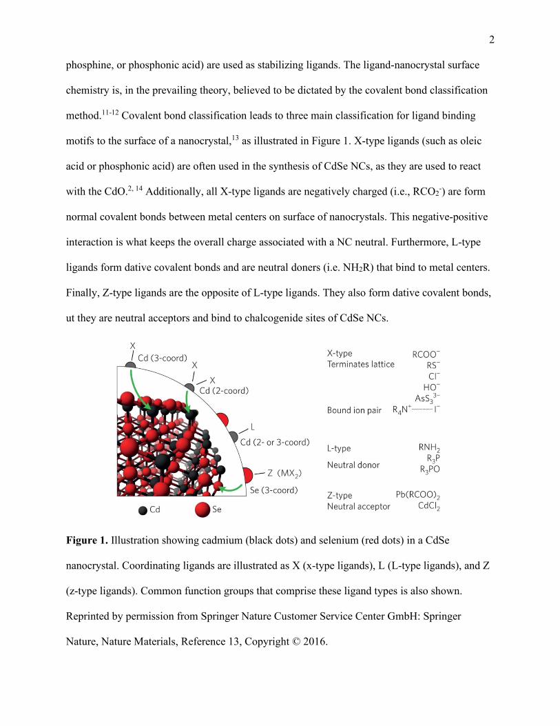
motifs to the surface of a nanocrystal,13 as illustrated in Figure 1. X-type ligands (such as oleic
acid or phosphonic acid) are often used in the synthesis of CdSe NCs, as they are used to react
with the CdO.2, 14 Additionally, all X-type ligands are negatively charged (i.e., RCO2-) are form
normal covalent bonds between metal centers on surface of nanocrystals. This negative-positive
interaction is what keeps the overall charge associated with a NC neutral. Furthermore, L-type
ligands form dative covalent bonds and are neutral doners (i.e. NH2R) that bind to metal centers.
Finally, Z-type ligands are the opposite of L-type ligands. They also form dative covalent bonds,
ut they are neutral acceptors and bind to chalcogenide sites of CdSe NCs.
Figure 1. Illustration showing cadmium (black dots) and selenium (red dots) in a CdSe
nanocrystal. Coordinating ligands are illustrated as X (x-type ligands), L (L-type ligands), and Z
(z-type ligands). Common function groups that comprise these ligand types is also shown.
Reprinted by permission from Springer Nature Customer Service Center GmbH: Springer
Nature, Nature Materials, Reference 13, Copyright © 2016.
3
Due to most synthesis relying on X-type ligands, which often limit the quantum yield of
the nanocrystal, it becomes important to understand how ligands might be exchanged for
different ones. In order to ensure that ligand exchange will happen to completeness, it typically
will involve exposing NCs to a large excess of the new ligand.15 In addition, some ligand
exchanges are favored over others. In classical inorganic chemistry, in which only one metal
center is studied, X-to-L ligand exchanges are highly favored, as is the exchange of Z-to-L-type
ligands exchange. However, in a classical environment the exchange of L-to-X-type ligands is
forbidden, as this would induce a charge imbalance (i.e., the molecule would no longer be
neutral). However, as nanocrystals contain many metal centers it has been found that the
forbidden exchange of L-to-X-type ligands can occur under an ion mediated regime, in which the
ligands leave with metal ions from the nanocrystal surface.16 Additionally, a ling of the same
type may be exchanged for another ligand of that type, with the general trend being that shorter
ligands are favored over longer ligands. 17
1.2 Quantum Dot Optical Transitions and Electronic Structure
The most unique property of semiconductor nanocrystals and the primary driving force in
their interest is the tunability of their bandgap, which results in the ability to change the emission
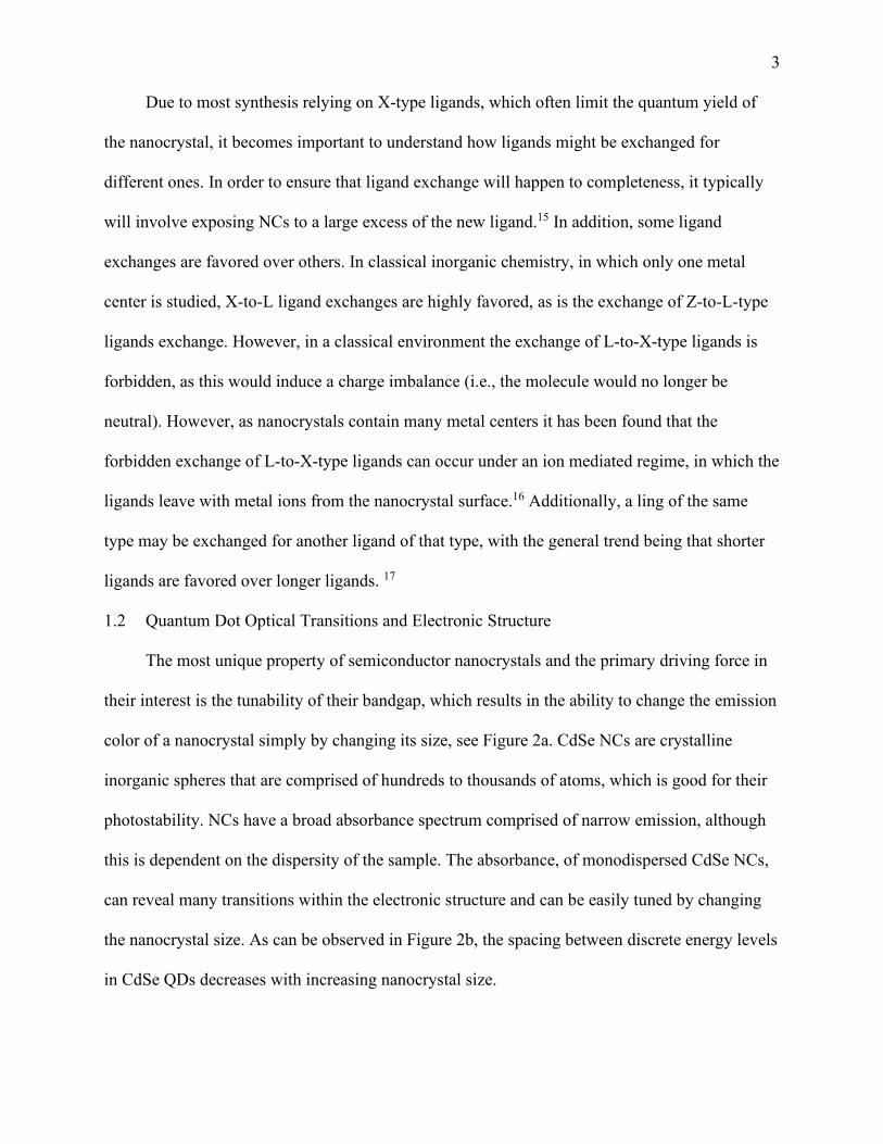
color of a nanocrystal simply by changing its size, see Figure 2a. CdSe NCs are crystalline
inorganic spheres that are comprised of hundreds to thousands of atoms, which is good for their
photostability. NCs have a broad absorbance spectrum comprised of narrow emission, although
this is dependent on the dispersity of the sample. The absorbance, of monodispersed CdSe NCs,
can reveal many transitions within the electronic structure and can be easily tuned by changing
the nanocrystal size. As can be observed in Figure 2b, the spacing between discrete energy levels
in CdSe QDs decreases with increasing nanocrystal size.
4
Figure 2. Absorption and photoluminescence spectrum of CdS QDs. (a) An absorption and
photoluminescence spectrum of CdS QDs. The trap emission is denoted as a red arrow. (b)
Schematics on the effect of surface states on the recombination process. Reprinted from
Reference 24, Copyright © 2012 Optica Publishing Group.
The typical, and simplest, model used to describe NCs is “particle in a box”, which has
been shown to agree with experimental results. In this case, photoexcited excitons are confined,
meaning that their wavefunction is such that it is limited to a specific space. This is a well-known
quantum mechanical effect that occurs on the nanoscale. In quantum dots, all three dimensions
are confined, therefore, the NC is said to be 0D, that is it has zero dimensions of bulk properties.
Conversely, 3D crystals are those that have no confinement, and therefore no quantum
properties. Additionally, 1D and 2D NCs have been synthesized as well (see Methods). An
example of a 1D material would be a rod or wire, were as a platelet or sheet would be 2D.
Recently, 2D materials have been gaining considerable interest because of their narrow emission
and virtual uniformity, which is controlled only by the thickness of the crystal.18
In addition to the transitions intrinsic to quantum dots (QDs), low energy trap sates,
induced by ligands and surface defects can also contribute to the observed emission of CdSe and
5 other NCs, as illustrated in Figure 2c. Trap emission has been primarily associated with metal
site deficiencies that leave exposed chalcogenides on the surface of NCs.19 This could help to
explain why the use of Z-type ligands has been shown to passivate trap states and cure defects in
CdSe NCs, resulting in increases in the quantum yield (QY) up to 90%.20 Furthermore, it has
been known for some time that amine capping ligands result in increased QY and decreased trap
emission of NCs.21 Trap states have been attributed to the cause of “blinking” in single quantum
dots. Blinking is a single dot phenomenon that, when under continues excitation, a dot does from
a bright state (i.e., emitting light) to a dark state, also called on and off states, respectively.
1.3 Nanocrystal Heterostructures
Continuing the discussion from above, another way to passivate the surface of a NC is to
grow another, wider bandgap material over the surface, curing crystallinity defects. This
morphology, known as a core/shell, has been widely used to suppress blinking dynamics in
QDs.22-23 The growth of a second, or even third, material creates the opportunity to engineer
band gaps and electronic structures of heterostructure NCs to get desired properties. There are
three main categories of NC heterostructures 1) type-I 2) type-II and 3) quasi type-II, as depicted
in Figure 3. In type-I core/shell NCs, the electron and hole generated by photoexcitation are both
confined to the core material, if they are both confined to the shell, it is typically called a reverse
type-I. For type-II, the photogenerated hole and electron are each confined in a different
material, one to the core, the other to the shell. Quasi type-II is when one charge is confined to a
specific material (usually the core) and the other is able to dissociate between both materials. An
example of this is CdSe/CdS in which the positively generated hole is confined to the CdSe core,
and the electron is confined to the entire NC (i.e.; both the core and shell).

6
Figure 3. Overview of core/shell nanocrystal bandgap configurations. (a) a type-I bandgap
configuration and (b) type-II bandgap configurations of core/shell QDs. The type-I bandgap
configuration confines electron and hole wavefunctions in a same space, improving the
recombination probability and it produces the band-edge emission. While the type-II bandgap
configuration divides electron wavefunctions spatially, as a result, the probability on the
radiative recombination is reduced and photon energy is the difference between the conduction
(valence) band of core and valence (conduction) band of shell. (c) Electronic energy levels of
several group II-VI, III-V, IV-VI, VI semiconductor materials using the valence-band
offsets. Reprinted from Reference 24, Copyright © 2012 Optica Publishing Group.
Another type of heterostructure can be used that allows for quantum dots to change their
dimensionality from 0D to 2D materials. These materials were first introduced as colloidal
spherical quantum wells (CSQWs), sometimes also called quantum dot quantum wells
(QDQWs).25-27 This architecture has a core/shell/shell motif, in which the middle layer is the
emissive layer, typically layered between two wide bandgap materials (i.e., CdS, ZnS). In the
case of CdS/CdSe/CdS CSQWs there is a quasi 2D confinement, as the photogenerated hole is
confined to the 2D CdSe emitting shell layer, but the electron is free to dissociate throughout the

7 entire NC. These architypes will become important when discussing light emitting applications
for quantum dots.
1.4 Multiexciton Generation and Auger Decay
Typically, when a QD absorbs light, it generates an exciton, a coupled electron-hole pair. If
the electron and hole recombine the QD emits light, making QDs very attractive for applications
in light emitting devices. However, when the QD absorbs a photon of sufficiently high energy,
more than one exciton can be generated from the single incoming photon. This is known as
multi-exciton generation (MEG).28-30 Multiexciton generation creates a population inversion, as
dictated by the Boltzmann distribution, meaning that the conduction band has a higher
population than the valence band. Population inversion is critical for lasers, in which
spontaneous emission is needed.
One could imagine that a single photon could be used to generate many electrons,
creating solar cells with efficiencies many times more than 100%. This in fact was the hope
when MEG was noticed in NCs; however, MEG has an inherent flaw. The more excitons that are
generated within a NC, the shorter time they live. This is the result of what is known as Auger
decay, depicted in Figure 4. The Coulomb interactions of proximal excitons causes Auger
recombination in NCs.31 The advancement of light emitting applications faces an important
challenge of overcoming the fast nonradiative Auger decay of multiple excitations in
semiconductor nanocrystals.32 This process is known to cause a reduced trion emission in
nanocrystals and is often invoked to explain photoluminescence blinking in single quantum
dots.33 Even in the case of longer-lived biexciton populations, the Auger decay time constant
could be as short as just a few picoseconds (e.g., CdSe or PbSe NCs),34-35 representing the
predominant mechanism of carrier loss in laser and photovoltaic applications.36-37
8
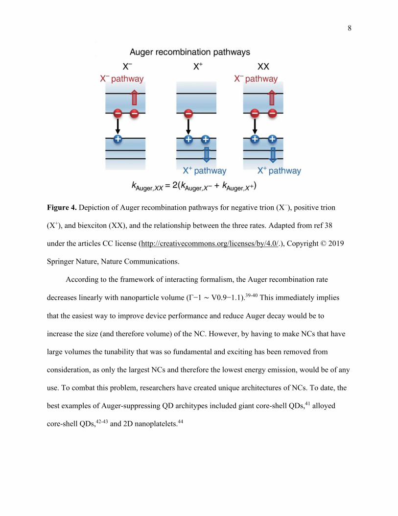
Figure 4. Depiction of Auger recombination pathways for negative trion (X−), positive trion
(X+), and biexciton (XX), and the relationship between the three rates. Adapted from ref 38
under the articles CC license (http://creativecommons.org/licenses/by/4.0/.), Copyright © 2019
Springer Nature, Nature Communications.
According to the framework of interacting formalism, the Auger recombination rate
decreases linearly with nanoparticle volume (Γ−1 ∼ V0.9−1.1).39-40 This immediately implies
that the easiest way to improve device performance and reduce Auger decay would be to
increase the size (and therefore volume) of the NC. However, by having to make NCs that have
large volumes the tunability that was so fundamental and exciting has been removed from
consideration, as only the largest NCs and therefore the lowest energy emission, would be of any
use. To combat this problem, researchers have created unique architectures of NCs. To date, the
best examples of Auger-suppressing QD architypes included giant core-shell QDs,41 alloyed
core-shell QDs,42-43 and 2D nanoplatelets.44
9 1.5 Overview of Quantum Dot Applications
As previously mentioned above, a major application of QDs is their ability to be used for
light-emitting diodes (LEDs) and lasers.45 Colloidal QDs are attractive for these and other
devices because they offer a unique advantage, solution processability. There are many light
emitting applications that would benefit from solution processing; such as, wearable devices,46-47
integrated photonic circuits,48-49 and bioimaging50 just to name a few. For applications based on
LED or laser technology, it will require the need for improved NC performance. For QDs to
reach high performance level in lasing materials they will need high biexciton (BX) lifetimes and
a robust BX quantum yield. This is because when charges are electrically introduced, as they
would be in a device, MXs are sure to be generated. The suppression of Auger recombination
rates, and subsequent long-lived MXs, is imperative for the future of light emitting devices based
on QDs.
10
2 AGGREGATIVE GRWOTH OF SEMICONDUCTOR NANOCRYSTALS
The following chapter and all of its content was Reprinted with permission from [Cassidy, J.;
Ellison, C.; Bettinger, J.; Yang, M.; Moroz, P.; Zamkov, M., Enabling Narrow Emission Line
Widths in Colloidal Nanocrystals through Coalescence Growth. Chem. Mater. 2020, 32, 7524].
Copyright © 2020 American Chemical Society. All supplementary information can be found,
free of charge, at https://doi.org/10.1021/acs.chemmater.0c02874
2.1 Introduction to Colloidal Nanocrystal Coalescence
Colloidal semiconductor nanocrystals (NCs) have become an attractive material platform
for solution processing of optoelectronic devices.51 The ability to tune NC emission and
absorption characteristics via the particle size has enabled new paradigms in solid-state
lighting,52-61 sensing,62-66 and energy harvesting.67-72 At present, one of the challenges facing the
development of NC technologies concerns the reduction of the particle size dispersion towards
improving ensemble spectral characteristics.73 This issue has been intensely investigated over the
years,73-86 and continues to represent one of the main synthetic challenges of the colloidal NC
research.78, 85-93
Most traditional strategies for size focusing of colloidal NCs rely on controlling the
precursor conversion rates during growth. The basic idea behind these methods follows the
Sugimoto principle86, 94 stating that nanocrystals smaller than a certain critical size (r*) dissolve,
while larger ones grow (Figure 5a, blue curve). Under these conditions, size focusing can be
achieved through secondary precursor injections (or a delayed precursor decomposition), which
lower the critical size, r*, to just below the average size of particles present in solution. This
causes most nanoparticles to exhibit a positive growth rate, dr/dt > 0, with a corresponding size
dependence that eventually results in narrowing of the particle size distribution.
11
In addition to the classical, precursor-controlled synthesis, some reports95-105 have
demonstrated the existence of a fundamentally different growth mechanism, which involves the
coalescence of already pre-formed nanoparticles in the reaction mixture. This process is
recognized as an important mechanism contributing to the formation of metal nanoparticles105-109
and is believed to play a significant role in the size evolution of semiconductor NCs. In the low
temperature regime, the coalescence (aggregative) growth of semiconductor NCs is known to
cause oriented attachment (OA)110-111 of nanoparticles along matching crystallographic
directions. The OA strategy has been widely explored for fabricating 2D nanoplatelets112-113 and
nanoribbons114-116 via cluster aggregation. The less explored, high-temperature coalescence
regime, on the other hand, allows nanoparticles to aggregate along random crystallographic
orientations, producing larger, spherically-shaped colloids. An example of this process is
illustrated in Figure 5b, where the coalescence of 5-nm CdS NCs in ligand-saturated solutions
([oleylamine] > 60%) leads to a 3.5-fold increase in the average particle size despite the absence
of precursors in the mixture. Notably, the final product appears to be monodisperse. The driving
force behind the coalescence-induced size focusing is the ~1/R dependence of the nanocrystals
growth rate (dr/dt) on the particle size (see Figure 5a, red curve). Under these conditions, smaller
particles grow faster than larger ones for any r, leading to eventual focusing of particle sizes.
This contrasts the traditional, precursor conversion strategy, which requires r > r* for size
focusing. It is, therefore, reasonable to expect that coalescence growth conditions could represent
a more effective strategy for reducing the size dispersion of semiconductor NCs as compared to
the classical precursor-controlled synthesis.16, 101
12
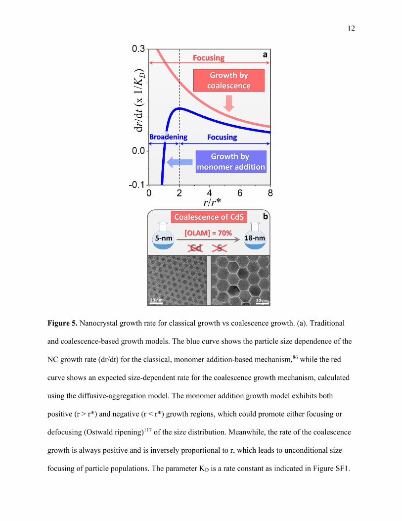
Figure 5. Nanocrystal growth rate for classical growth vs coalescence growth. (a). Traditional
and coalescence-based growth models. The blue curve shows the particle size dependence of the
NC growth rate (dr/dt) for the classical, monomer addition-based mechanism,86 while the red
curve shows an expected size-dependent rate for the coalescence growth mechanism, calculated
using the diffusive-aggregation model. The monomer addition growth model exhibits both
positive (r > r*) and negative (r < r*) growth regions, which could promote either focusing or
defocusing (Ostwald ripening)117 of the size distribution. Meanwhile, the rate of the coalescence
growth is always positive and is inversely proportional to r, which leads to unconditional size
focusing of particle populations. The parameter KD is a rate constant as indicated in Figure SF1.

13 (b). Illustration of the coalescence growth of CdS NCs. The diameter of CdS nanoparticles
increased more than 3-fold upon heating to 240 ˚C in the reaction mixture containing free ligands
(OLAM - 70% by volume). No precursors are introduced during the reaction. A portion of the
Figure 5b was adapted with permission from Ref. 98. Copyright 2018 American Chemical
Society.
Here, we report on the synthesis of colloidal CdSe NCs exhibiting spectrally narrow emission
with corresponding linewidths approaching single-particle values. The synthetic innovation lies
in the employment of coalescence-only growth conditions enabled by high concentrations of L-
and Z-type ligands in the reaction mixture. The presence of more than 60% L-type ligand
promotes the coalescence of NCs, while the presence of approximately 2% by volume of Z-
ligand inhibits the traditional oriented attachment mechanism, thus allowing for the formation of
spherical NCs. When applied as a post-synthetic treatment, this strategy results in a reproducible
reduction of the particle size dispersion, enabling CdSe NC photoluminescence with FHWM of
as low as 72 meV and quantum yield above 20% without shelling. Model calculations based on
the diffusive aggregation approach118 accurately predict the particle size evolution observed for
CdSe NCs, indicating that coalescence growth can lead to unconditional focusing of particle
sizes irrespective of the initial sample morphology. This premise was confirmed through the
application of the coalescence growth strategy to a number of polydisperse CdSe NC samples as
well as samples of CdS semiconductor NCs, where an apparent reduction of the emission
linewidth was observed as well. Overall, present experimental findings backed by theoretical
calculations, indicate that ligand-controlled coalescence growth could represent an attractive
post-synthetic strategy for size-focusing of many types of semiconductor NCs.
14 2.2 Digestive Ripening of Semiconductor Nanocrystal
The traditional approach to the colloidal synthesis of semiconductor nanocrystals relies on a
controlled addition of monomers released during the thermal precursor decomposition. This
process is characterized by the Gibbs-Thomson equation,94 which balances the reduction of free
energy due to monomer-to-nanoparticle bonding with the increase of the surface energy resulting
from such an addition.119-125 The interplay of the positive and negative energy terms in the
Gibbs-Thomson equation gives rise to the well-known Sugimoto principle86 formulating that
nanocrystals greater than a certain critical size exhibit a positive growth rate (Figure 5a, blue
curve and Figure SF1) while those that are smaller dissolve. Consequently, if nanoparticle sizes
are distributed on both sides of the critical radius (r*), the particle size dispersion would
naturally increase with the reaction time (Oswald ripening117). With additional precursor
injections at the growth temperature, however, one can shift the critical nanocrystal size to a
smaller value causing the majority of nanocrystals in solution to exhibit a positive growth rate.
Under these conditions, smaller nanocrystals in the distribution will grow faster than the larger
ones, leading to size focusing.
When large proportions of free ligands are present in the reaction mixture, the contribution of
coalescence processes into the particle growth becomes significant.98 At low reaction
temperatures, such aggregative processes primarily lead to the oriented attachment of
nanocrystals,126 which represents a well-known strategy for the synthesis of nanoplatelets and
nanoribbons,113, 116 nanorods,110 and other, more complex morphologies.127-128 For instance, CdSe
nanoplatelets are known to form through the oriented attachment of magic size clusters (e.g.
CdSe13, CdSe34)129-130 in the presence of cadmium carboxylate (Z-type ligand), while PbS
nanosheets112 are synthesized by the oriented attachment of < 3-nm nanocrystals in the presence
of chloride compounds. The decrease of the surface energy through the decrease of the number
15 of unsatisfied surface bonds has been identified as the driving force for the attachment of these
NCs to form a new particle morphology.111
When free ligands are introduced at temperatures exceeding a certain thermal threshold (e.g.
220-240 ˚C for cadmium chalcogenides), attachment of the two nanoparticles can occur along
random crystallographic directions.131 This is usually followed by the self-reorganization of
coalesced structures into spherically shaped, larger nanoparticles (see Figure 5b).73, 132-133
Previous studies98, 133-135 have shown that the growth rate associated with the coalescence
mechanism is positive and approximately proportional to 1/r (Figure 1a, red curve), which leads
to size-focusing regardless of the nanoparticle size.77, 95, 97-99, 111, 119 This trend contrasts the
classical monomer-addition growth, where size focusing is observed only for r > r* (Figure 1b,
blue curve). The experimental evidence in favor of a positive coalescence growth rate, dr/dt, has
been provided by a recent report98 investigating an aggregative growth of a mixed nanoparticle
samples containing small- and large-diameter CdS NCs (Figures SF6 a-f). Upon heating of this
mixture in ligand-saturated solutions to above the coalescence threshold, absorption features of
both small and large nanoparticles were observed to red-shift,98 indicating that dr/dt was positive
for all particle diameters. Notably, smaller-size intermediates have not been detected during the
reaction.
To understand the interplay between the classical precursor-conversion and coalescence-
driven growth mechanisms, we first looked into the evolution of CdSe NCs in the presence of
free ligands only (no precursors). To this end, small-diameter CdSe NCs (d = 2.5-4 nm)136-137
were loaded into a flask containing a 70:30 oleylamine (OLAM):octadecene (ODE) mixture by
volume and subsequently heated to 230-240 ˚C. Please see Table ST1 for the summary of all the
performed synthetic experiments. After 60-90 min of exposure, the average particle diameter
increased by 150 - 250% (see a representative PL spectrum of CdSe NCs before and after the
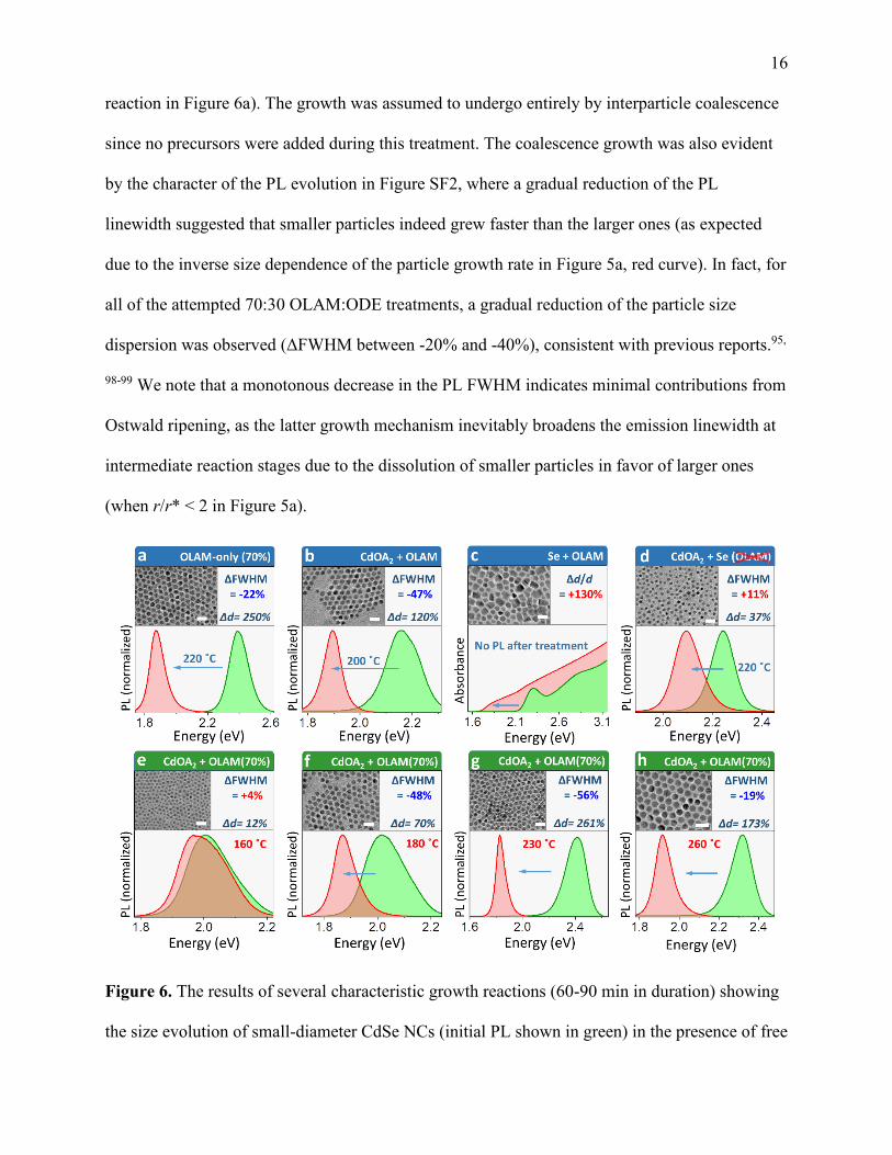
16 reaction in Figure 6a). The growth was assumed to undergo entirely by interparticle coalescence
since no precursors were added during this treatment. The coalescence growth was also evident
by the character of the PL evolution in Figure SF2, where a gradual reduction of the PL
linewidth suggested that smaller particles indeed grew faster than the larger ones (as expected
due to the inverse size dependence of the particle growth rate in Figure 5a, red curve). In fact, for
all of the attempted 70:30 OLAM:ODE treatments, a gradual reduction of the particle size
dispersion was observed (ΔFWHM between -20% and -40%), consistent with previous reports.95,
98-99 We note that a monotonous decrease in the PL FWHM indicates minimal contributions from
Ostwald ripening, as the latter growth mechanism inevitably broadens the emission linewidth at
intermediate reaction stages due to the dissolution of smaller particles in favor of larger ones
(when r/r* < 2 in Figure 5a).
Figure 6. The results of several characteristic growth reactions (60-90 min in duration) showing
the size evolution of small-diameter CdSe NCs (initial PL shown in green) in the presence of free
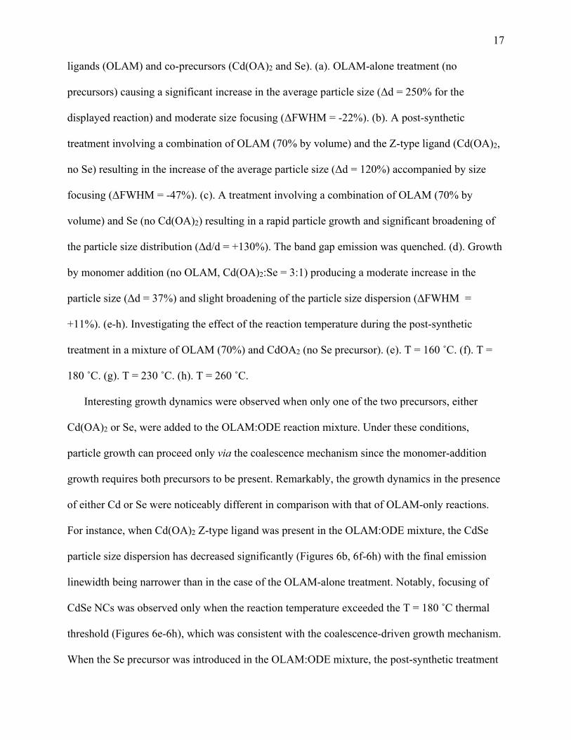
17 ligands (OLAM) and co-precursors (Cd(OA)2 and Se). (a). OLAM-alone treatment (no
precursors) causing a significant increase in the average particle size (Δd = 250% for the
displayed reaction) and moderate size focusing (ΔFWHM = -22%). (b). A post-synthetic
treatment involving a combination of OLAM (70% by volume) and the Z-type ligand (Cd(OA)2,
no Se) resulting in the increase of the average particle size (Δd = 120%) accompanied by size
focusing (ΔFWHM = -47%). (c). A treatment involving a combination of OLAM (70% by
volume) and Se (no Cd(OA)2) resulting in a rapid particle growth and significant broadening of
the particle size distribution (Δd/d = +130%). The band gap emission was quenched. (d). Growth
by monomer addition (no OLAM, Cd(OA)2:Se = 3:1) producing a moderate increase in the
particle size (Δd = 37%) and slight broadening of the particle size dispersion (ΔFWHM =
+11%). (e-h). Investigating the effect of the reaction temperature during the post-synthetic
treatment in a mixture of OLAM (70%) and CdOA2 (no Se precursor). (e). T = 160 ˚C. (f). T =
180 ˚C. (g). T = 230 ˚C. (h). T = 260 ˚C.
Interesting growth dynamics were observed when only one of the two precursors, either
Cd(OA)2 or Se, were added to the OLAM:ODE reaction mixture. Under these conditions,
particle growth can proceed only via the coalescence mechanism since the monomer-addition
growth requires both precursors to be present. Remarkably, the growth dynamics in the presence
of either Cd or Se were noticeably different in comparison with that of OLAM-only reactions.
For instance, when Cd(OA)2 Z-type ligand was present in the OLAM:ODE mixture, the CdSe
particle size dispersion has decreased significantly (Figures 6b, 6f-6h) with the final emission
linewidth being narrower than in the case of the OLAM-alone treatment. Notably, focusing of
CdSe NCs was observed only when the reaction temperature exceeded the T = 180 ˚C thermal
threshold (Figures 6e-6h), which was consistent with the coalescence-driven growth mechanism.
When the Se precursor was introduced in the OLAM:ODE mixture, the post-synthetic treatment

18 resulted in a significant increase of the particle size dispersion marked by a large variety of
shapes and sizes in the final product (TEM image in Figures 6c). The rate of particle coalescence
under the (Se + OLAM) growth conditions, appeared to be even faster than in the case of
(Cd(OA)2+ OLAM) mixture, as could be attested by the Δd = +310% increase in the average
particle size accompanying the +130% growth in the particle size dispersion (Δd/d).
2.3 Size Focusing of Nanocrystals via Coalescence Growth
For the next step, the size-focusing treatment was performed using a combination of free
ligands (OLAM:ODE = 70:30) and precursors (Cd(OA)2 and Se). This environment permits both
coalescence and monomer addition-based growth mechanisms to contribute to the evolution of
CdSe NC sizes. According to several existing models that consider aggregative growth of
nanoparticles in the presence of precursors,106, 135, 138-139 a combination of the coalescence and
monomer-addition processes could represent an efficient size-focusing strategy. In present
experiments, we observed that the Cd to Se precursor ratio played an important role in the
particle size evolution (Figure 7a). For instance, when Cd:Se > 2, the particle size dispersion was
noticeably reduced with an overall reduction in the FWHM value exceeding that of OLAM
alone. In particular, co-injecting Cd and Se precursors at a ratio of 3:1 in the presence of OLAM
has resulted in CdSe NCs with the emission linewidth of 87 meV. When the ratio of Cd to Se
precursors was below 1, the growth dynamics have changed significantly from that of Cd-rich
reactions. For instance, a OLAM:ODE = 70:30 mixture containing a Cd:Se = 1:3 precursor ratio
resulted in the fast particle growth accompanied by significant broadening of the particle size
distribution. According to Figure 7a, ΔFWHM for this case was + 60%. When only Se was
injected (Cd:Se = 0) in the presence of OLAM (70%), the particle size dispersion in the final
product broadened by +130% (Figure 6c), accompanied by full quenching of the band gap
emission. The lack of PL in Se-treated CdSe NCs could be explained by the fact that in the

19 absence of electronic doping, Se-2c orbitals will be occupied and can serve as hole traps. This is
consistent with experimental observations of the hole-trapping limit to the PL QY in CdSe NCs
following the displacement of cadmium carboxylate.140 Density Functional Theory (DFT) theory
developed for smaller NC models also predicted that 2-coordinated Se atoms could introduce a
midgap state in the bandgap of the material.141
Size focusing dynamics under OLAM-deprived reaction conditions was investigated next.
Only a minimal amount of OLAM (3-4%) needed to dissolve the Se precursor was present in the
flask (see Table ST1 for the summary of all performed post-synthetic treatments). In this
environment, the rate of the coalescence growth becomes sufficiently low to allow for the
conventional, monomer-addition mechanism become the primary process contributing to the
nanoparticle size evolution. According to Figure 6d, under these conditions, the rate of
nanoparticle growth was substantially lower than in the case of a coalescence-driven synthesis
(Δd/Δt (70% OLAM) = 150-250%/hour; Δd/Δt (4% OLAM) = 37%/hour). Furthermore, the
presence of both precursors (Cd and Se) was required for observing any changes in the particle
diameter, which was consistent with the lack of coalescence contribution to growth. Introducing
both precursors at a ratio of Cd:Se = 3:1 (Figure 6d) produced rather small changes in the
average particle size. In this case, three separate experiments have resulted in a narrow
distribution of ΔFMHW outcomes (ΔFWHM = -8% - +23%, Figure 7 and Table ST1) indicating
that monomer addition-only growth conditions during a post-synthetic treatment are not likely to
cause dramatic changes in the particle size dispersion.

20
Figure 7. Overview of CdSe coalescence growth conditions. (a). The summary of coalescence
growth reactions applied to small-diameter CdSe NCs. The concentration of a free ligand
(OLAM) is plotted along the horizontal axis, and the varying precursor ratio, Cd(OA)2:Se is
plotted along the vertical axis. Overall, size-focusing conditions (negative ΔFWHM expressed as
the diameter of a blue circle) were enhanced at higher concentrations of OLAM due to an
increased coalescence contribution to the growth. The presence of Cd(OA)2 (without Se) was
found to be necessary for further reduction of the particle size dispersion. Conversely, reactions
containing low Cd:Se precursor ratios (< 1) resulted in broadening of the particle size dispersion,
irrespective of OLAM concentrations. (b). The effect of the CdSe NC concentration (μmol/L) in
the Cd(OA)2 + OLAM (70%) growth mixture on the ultimate emission linewidth in the final
product (FWHM). The initial linewidth of the starting CdSe NC samples was in the 105 – 174

21 meV range (see Table ST1). (c). The effect of OLAM concentration (%) in the Cd(OA)2 +
OLAM growth mixture on the ultimate emission linewidth of larger CdSe NCs (FWHM).
Overall, the above experiments demonstrate that size-focusing conditions are readily
achieved when the coalescence contribution into particle growth is significant (high
concentration of free ligands in the reaction mixture). In the absence of the coalescence growth,
focusing of nanoparticle sizes was less reproducible (-8% < ΔFWHM < 23 %). The greatest
reduction of the particle size dispersion (-48% < ΔFWHM < -20%) was observed in reactions
containing Z-type ligands (CdOA2) in combination with 60-70% OLAM (see Figures. 6, 6f, 6h).
Both the concentration of nanoparticles in the reaction mixture (Figure 7b) and the percentage of
OLAM in the flask (Figure 7c) played a role in determining the ultimate emission linewidth of
treated NCs. It was observed that during the size-focusing treatment, the initial concentration of
CdSe NCs was reduced due to growth. For instance, for CdSe NCs with a first exciton peak at
520 nm and initial concentration of 12 μmol/L (70 nmol total), the final concentration after
coalescence-growth has dropped to 0.3 μmol/L (1.2 nmol total). Notably, based on the number of
moles and the average particle diameter, we estimate that the total volume for both the initial and
final CdSe NC population was approximately the same.
We speculate that the presence of Cd(OA)2 was necessary to facilitate inter- and intra-
particle ion exchange processes necessary for size-focusing and spherical nanocrystal
morphologies. The second important role of the Cd(OA)2 was its ability to suppress the oriented
attachment of large-size CdSe NCs along the wurtzite c-axis, as discussed later in the text, which
further helped reducing the particle size dispersion. Notably, a combination of Cd(OA)2 and
OLAM has helped improving the emission quantum yield of CdSe NCs, with the final product
exhibiting QY over 20%. Such an improvement in the PL QY of OLAM-treated CdSe NC
samples agrees with previous reports,88, 99, 142-145 indicating an enhancement of the emission

22 intensity (PL QY up to 50%)83 upon binding of L-type ligands to under-coordinated surface Cd
atoms. This interaction raises the energy of both the conduction and valence band edges toward
vacuum,146 which could effectively suppress hole trapping.
The demonstrated ability of coalescence processes to reduce the particle size dispersion
represents a potentially useful strategy for lowering the ensemble PL linewidth to near single-
particle levels. In general, the fundamental limit to the room-temperature emission linewidth for
single CdSe NCs is determined by the lifetime of the excitation (~ h/Δτ), with further broadening
being contributed by phonon coupling, exciton fine structure, and spectral dynamics.147-149
Recently, Bawendi group149 has reported the single-dot PL FWHM for CdSe NCs in the 60−75
meV range. Peng et al.77 has studied the emission of magic size clusters observing an ultralow
emission FWHM of 58-70 meV, with larger structures exhibiting lower FWHM values. The
ensemble PL peak width for conventional quantum dots produced by the state-of-art synthesis
usually lies in the 90 – 150 meV range.81, 147, 150 In general, ∼80-90 meV is considered as a
narrow FWHM for ensemble PL of CdSe.151
To achieve near single-particle emission linewidths, the coalescence growth was performed
in the mixture of Cd(OA)2 and OLAM free ligands (Cd(OA)2 : OLAM : ODE = 2 : 80 : 18 by
volume). During a 60-min treatment, 3.1-nm CdSe NCs with an initial FWHM of ~157 meV
have gradually increased in size (Figure 8a) while exhibiting a progressively lower PL linewidth.
The final product had an ensemble PL FWHM of 72 meV (Figure 8d) and the corresponding
particle size dispersion of Δd/d = 4.9% (based on TEM statistical analysis in Figure 8b). Several
independent tests were performed on different batches of starting CdSe NCs (FWHM = 105-174
meV) all resulting in the final PL FWHM of 72-95 meV (see Table ST1). Notably, the observed
linewidth was within 20% of a single-particle FWHM, reported in Ref. 148. In addition, the
emission lifetime of treated nanocrystals was increased by almost an order of magnitude from its
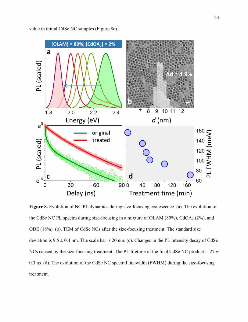
23 value in initial CdSe NC samples (Figure 8c).
Figure 8. Evolution of NC PL dynamics during size-focusing coalescence. (a). The evolution of
the CdSe NC PL spectra during size-focusing in a mixture of OLAM (80%), CdOA2 (2%), and
ODE (18%). (b). TEM of CdSe NCs after the size-focusing treatment. The standard size
deviation is 9.5 ± 0.4 nm. The scale bar is 20 nm. (c). Changes in the PL intensity decay of CdSe
NCs caused by the size-focusing treatment. The PL lifetime of the final CdSe NC product is 27 ±
0.3 ns. (d). The evolution of the CdSe NC spectral linewidth (FWHM) during the size-focusing
treatment.
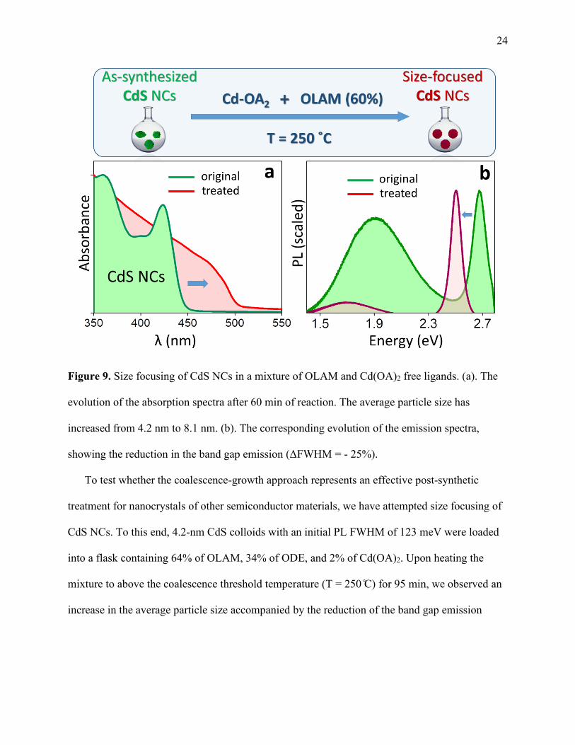
24
Figure 9. Size focusing of CdS NCs in a mixture of OLAM and Cd(OA)2 free ligands. (a). The
evolution of the absorption spectra after 60 min of reaction. The average particle size has
increased from 4.2 nm to 8.1 nm. (b). The corresponding evolution of the emission spectra,
showing the reduction in the band gap emission (ΔFWHM = - 25%).
To test whether the coalescence-growth approach represents an effective post-synthetic
treatment for nanocrystals of other semiconductor materials, we have attempted size focusing of
CdS NCs. To this end, 4.2-nm CdS colloids with an initial PL FWHM of 123 meV were loaded
into a flask containing 64% of OLAM, 34% of ODE, and 2% of Cd(OA)2. Upon heating the
mixture to above the coalescence threshold temperature (T = 250 ̊C) for 95 min, we observed an
increase in the average particle size accompanied by the reduction of the band gap emission
25 FWHM from 123 to 92 meV. The ultimate size of CdS nanoparticles in the final product was
estimated to be 8.1 nm (see Figure SF4)
2.4 Theoretical Analysis of Nanocrystal Aggregative Growth
The observed focusing of CdSe and CdS NC sizes is consistent with the existing theoretical
literature on aggregative growth of colloidal nanoparticles.101, 135, 138-139 For instance, early theoretical
works have demonstrated that coalescence alone could be responsible for the formation of
monodisperse nanoparticles of silica,139 Au,135 and silver.138 Aggregative growth was also suggested
as the possible mechanism for controlling the particle size distribution during NC synthesis.101 Most
of these studies have used the Smoluchowski rate equation152 for modelling the kinetics of diffusion-
or reaction-limited colloid aggregation.153-154 Within this approach, the two primary particles, A1, can
aggregate upon collision resulting in the formation of secondary particles A2, which in turn can
further aggregate to form larger colloids, Ai. In general, the coalescence growth of any two particles
Ai and Aj, each containing i and j numbers of primary particles, can be described as follows:
kK
ji AAA ij→+ (2.1)
where kA represents a composite colloid containing k primary particles, such that k = i + j. The time-
evolution of the Ak concentrations can be determined by solving the following rate equations:
jj
kjkjikji
ijk NKNNNK
dtdN ∑∑ −=
=+21
(2.2)
where Nk is the concentration (number per unit volume) of Ak nanoparticle aggregates, and Kij is
the rate constants for the reaction between the i and j aggregates ( )( )jijiij DDRRK ++= π4 ,
where D is the diffusion coefficient (see the SI section for details).
26
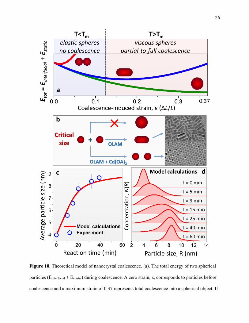
Figure 10. Theoretical model of nanocrystal coalescence. (a). The total energy of two spherical
particles (Einterfacial + Eelastic) during coalescence. A zero strain, ε, corresponds to particles before
coalescence and a maximum strain of 0.37 represents total coalescence into a spherical object. If

27 the growth solution temperature, T, is lower than Tm, particles are too elastic to undergo
coalescence (red curve). When T > Tm, either partial (blue) or full (green) coalescence is
achieved. (b). Illustration of the critical size for particle coalescence, Rc. For r > Rc, coalescence
of randomly oriented nanocrystals becomes suppressed. In this case, subsequent heating can only
resolve in the oriented attachment of large nanoparticles (r = Rc) along specific crystallographic
directions (as usually observed in OLAM:ODE mixtures), which causes the formation of
nanorods (see the TEM image in the insert). When Cd(OA)2 is introduced into the OLAM:ODE
reaction mixture, oriented attachment processes become inhibited causing the average
nanoparticle size to remain spherical (r = Rc) despite further heating. (c). Diffusive-aggregation
model calculations of the coalescence growth kinetics for CdSe NCs. The predicted temporal
evolution of the particle size r(t) (red curve) is compared with experimental data points (blue
circles). The experimental error bars represent the uncertainty in the value of the average particle
size due to an intrinsic uncertainty in the NC size-band gap scaling. (d). Model calculations of
the particle size distribution during the coalescence growth.
The diffusion-limited aggregation (diffusive-aggregation) model outlined above, assumes
that collisions between nanoparticles are followed by their coalescence, regardless of the particle
size. The experimental kinetics for cadmium chalcogenide NCs, however, shows that the
coalescence growth does not occur for particles larger than a certain critical size (dr/dt → 0 with
increasing r, Figure 9a). This behavior agrees with the general premise of the viscoelastic collision
theory of colloidal nanoparticles,155 whose main principles follow the general framework of
viscoelastic droplet coalescence. A simple model of droplet aggregation156 suggests that during the
coalescence of structured (crystallized) droplets, the interfacial energy of the two particles, Einterfacial,
is reduced upon particle fusion, while the elastic energy, Eelastic, is increased by the compression of
the internal structure. When the two processes balance each another (Etot = Einterfacial + Eelastic →
28 min), the coalescence process is arrested. In analogy to this model, we propose that as the two
nanoparticles contact, coalescence is initiated when a ligand-based neck forms between them. The
particles are then pulled together into a single spherical shape via the exchange of ions. This process
is driven by the reduction of the interfacial energy, which in the case of two coalescing spheres is
approximately exponential with the instantaneous geometric strain, ε = ΔL/(2 × init. particle
diameter):
(2.3)
where and A is the total interfacial area of two coalescing particles and A0, A1, A2 are the constants
for the exponential decay fit.156 Meanwhile, the strain energy of the two coalescing particles
increases during the coalescence process. This is due to the two crystal lattices being compressed in
a manner similar to the elastic compression of two springs. The energy term associated with the
compression strain is given as:
(2.4)
where G is the particle shear modulus that characterizes the nanocrystal rigidity and V is total
volume of the coalescing nanostructures. The total energy of the two particles is thus given as a sum
of the decreasing interfacial energy (Eq. 2.3) and increasing elastic energy (Eq. 2.4). The
coalescence process is expected to stop when the total energy is minimized, Etot(ε) → min. If the
minimum of Etot(ε) is realized at a negligibly small strain (ε < 0.02), particle aggregation will not
occur. Clearly, the final morphology of the two coalesced particles (full coalescence, particle
coalescence, or no coalescence) depends on the value of the shear modulus, G. The temperature
dependence of G follows the Mechanical Threshold Stress (MTS) model157 for inorganic crystals,
, where G0 is the shear modulus at T = 0K and D is a material constant.
When T = Tm, G diminishes, signifying the melting phase transition. According to Figure 10a, in the
( )210)( A
terfacialin eAAAE εγεγ −+×=×=
VGEelastic2
23 ε=
)1(exp(0 −−= TTDGG m

29 low temperature regime (T < Tm), the elastic energy of the particles is too large for the total energy
Etot(ε) to exhibit a minimum (red curve). Consequently, no coalescence is achieved (elastic
stabilization). However, when T > Tm, the value of G drops abruptly with T, so that the total energy
exhibits a decline with the increasing strain (green and blue curves). In this case, either a full or
partial coalescence is achieved depending on the actual slope of the G(T) curve. Notably, because
the strain energy is directly proportional to the total volume, V, larger particles are less driven
towards a full coalescence.
In the present work, the transition from viscose (aggregative) to viscoelastic (partly-aggregative)
collisions may occur even in the high temperature regime, T > Tm (220 ̊C), if the radii of fusing
particles exceed a critical value r = Rc. This process is clearly manifested during the coalescence
growth of CdS NCs in OLAM-only solutions (no Cd(OA)2). According to Figures 10b and SF3a,
once the critical size of CdS is reached, subsequent heating does not result in further coalescence.
Instead, nanoparticles undergo oriented attachment along specific crystallographic directions, which
causes the formation of nanorods (Figure 10b and SF3b). However, if Cd(OA)2 is introduced along
with OLAM, oriented attachment processes become suppressed and the average nanoparticle size
does not increase above the critical size with further heating (Figure 10b). Along these lines, in order
to model the effect of the critical size in this work, we assume that the coalescence rate (but not the
collision rate, Kij ) approaches zero, if the size of Ak exceeds the critical size parameter, RC.
Figures 10c and 10d illustrate the predictions of the diffusive-aggregation model for the
evolution of the CdSe particle size. The initial rise of the theoretical r(t) (red curve) indicates a fast
coalescence growth at early times, which is followed by an asymptotic decrease of the growth rate
when the average particle radius approaches the critical size, RC. Similar r(t) trends have been
predicted for the aggregative growth of ZnS158 and PbS133 NCs within the Smoluchowski approach.
In present calculations, the product of the initial particle concentration, N1, and the primary particle
30 diffusion coefficient, D1, was designated as a fitting parameter to ensure a better match of theoretical
parameters for solvent viscosity and particle number concentrations with that of an experiment.
According to Figure 10c, the calculated r(t) accurately captures experimentally observed CdSe
NC growth kinetics, evidenced by a gradual reduction of the growth rate with increasing particle
size. Model calculations have also revealed an increase in the particle size dispersion at early stages
of the reaction prior to size focusing (Figure 10d). To some degree, similar broadening in the
experimental emission linewidth at early states of the post-synthetic treatment has been observed in
several (but not all) tests (Figure SF5). This behavior could indicate that size-focusing becomes
more efficient when the average particle size approaches RC. Indeed, when the starting particle
diameter is several times lower than RC, most of Ai + Aj coalescence paths are still allowed, which
causes statistical broadening of the particle size distribution.
2.5 Conclusions Regarding Semiconductor Nanocrystal Coalescence
In summary, we demonstrate that non-classical coalescence growth of cadmium chalcogenide
NCs provides a robust strategy for controlling nanocrystal size distributions and corresponding
spectral linewidths. The demonstrated approach employs ligand-saturated solutions to stimulate the
viscoelastic behavior of colloidal nanocrystals, during which, elastic collisions between
nanoparticles are followed by the viscous reorganization of surface ions, causing coalescence
(aggregative) growth. Because the rate of the coalescence growth is inversely proportional to the
particle size, size focusing is achieved irrespective of the initial sample morphology. In case of CdSe
NCs, the coalescence growth resulted in monodisperse samples (Δd < 5%) exhibiting ensemble PL
linewidths near single-particle levels (FWHM = 72 meV). The final CdSe NC product exhibited
enhanced PL lifetimes with the corresponding PL quantum yield above 20% (depending on the
ultimate particle size). Numerical simulations based on the diffusive-aggregation model accurately
predict the observed particle size evolution, confirming the ability of the coalescence growth to drive

31
nanoparticle size-focusing. Overall, we show that the coalescence growth strategy can produce high
quality chalcogenide nanocrystals needed for a wide range of applications. With future work, we
expect this method to become potentially applicable to other semiconductor materials providing a
general pathway for achieving the narrow spectral linewidths.
2.6 Experimental Methods for Nanocrystal Coalescence
The following materials were used: cadmium oxide (CdO, 99% STREM), 1-octadecene
(ODE, 90% Aldrich), n-octadecylphosphonic acid (ODPA, PCI), octadecylamine (ODA, 90%,
Acros), oleic acid (OA, 90% Aldrich), sulfur (S, 99.99% Acros), Chloroform (anhydrous, 99%
Aldrich), oleylamine (OLAM, tech., 70% Aldrich), hexane (anhydrous, 95% Aldrich), ethanol
(anhydrous, 95% Aldrich), tri-n-octylphosphine (TOP, 97% STREM), tri-n-octylphosphine oxide
(TOPO, 99.0% Aldrich), selenium powder (Se, 200 mesh, Acros), acetone (anhydrous, Amresco,
ACS grade), stearic acid (97% Aldrich), and tributylphosphine (TBP, 97% Aldrich). All
reactions were performed under argon atmosphere using the standard Schlenk technique. The
VWR Clinical 100 centrifuge used for precipitation operated at 6500 rpm.
CdS NCs were fabricated according to the previously reported procedure.159 A mixture of
0.0768 g (0.6 mmol) of CdO, 3.6 mL of OA, and 24 mL of ODE in a 50 mL three-neck flask was
heated to 240 °C until the solution turned optically clear and colorless. Then, the mixture was
allowed to stir at this temperature at which point all of the sulfur precursor solution made by
dissolving 0.02 g (0.625 mmol) of sulfur powder at 200 °C in ODE (10 mL) was quickly
injected. The reaction was stopped by removing the flask from the heating mantle after 4−5 min.
CdS NCs were separated from the solution by precipitating with methanol and redissolving the
product in chloroform
CdSe NCs were fabricated by adapting a previously reported procedure.136 Briefly,
TOPO (3.0 g), ODPA (0.025 g), OA (2.0 mL), and CdO (0.060 g) were mixed in a 50 mL flask,
32
heated to 120°C and exposed to vacuum for 1 hour. Then, under argon, the solution was heated
to 300°C to dissolve CdO until the mixture turned optically clear and colorless. At this point, 1.5
g of TOP (that had been degassed at 120°C for 30 minutes) was injected into the flask and the
temperature was adjusted to 270ºC. The reaction flask with Cd precursor was raised up from the
heating mantle right before the injection of Se precursor to get small-diameter nanoparticles. A
selenium precursor prepared by dissolving 0.060 g of Se in 1 mL of TOP through heating to
150ºC under argon and cooling to room temperature was injected all at once into the raised flask
(at 270ºC). The reaction temperature dropped to approximately 250°C and was left stirring for 30
seconds before being quenched in a water bath, this yielded CdSe nanocrystals with a first
exciton peak around 520 nm. After the synthesis, nanocrystals were precipitated with ethanol,
and washed by repeated redissolution in chloroform and precipitation with the addition of
ethanol. Finally, the product was stored in chloroform (3 ml).
An 0.2M Cd(OA)2 stock solution was prepared by combining 15mL OA (47 mmol),
1.845 g CdO (14 mmol), and 60 mL of ODE in a 100 mL three neck round bottom flask. Under
argon, the flask was heated to 240°C until the solution turned clear. The final mixture was stored
under argon and heated to 50°C before being used.
In a typical treatment, CdSe NCs, ODE, OLAM, and Cd(OA)2 were degassed in a 25 mL
round bottom flask at 80°C for approximately 20 minutes. The flask was then switched over to
argon using a Schlenk line and the sample was heated to the desired temperature, typically 180-
260°C, for the remainder of the treatment. The concentration of NCs ranged 6-350 μmol/L;
which was found to have a significant effect on the critical size and overall emission linewidth.
To obtain monodisperse samples with approximately 72-80 meV PL linewidth; a 5 mL solution
of 12 μmol/L CdSe NCs (520nm first absorption peak), with 70% by volume OLAM (4.2 mL),
33
0.6 mL of Cd(OA)2 stock solution, and 1.2 mL of ODE was degassed at 80°C for 20 minutes, the
mixture was then heated to 230°C for 45-60 minutes before being quenched in a water bath.
Alternatively, narrow-linewidth CdSe NCs could also be produced via coalescence of
larger nanocrystals with a first absorbance peak at 577 nm and a concentration of 9 μmol/L (all
other parameters were kept the same). When using solutions that were too concentrated it was
observed that the emission line width could not be reduced to below 90 meV.
To determine the concentration of our nanocrystal solutions, we used the work of Yu et.
al.160 Briefly, for the less concentrated samples, the optical density of a small aliquot was placed
into a cuvette and measured. Based on the first absorbance peak (size of the nanocrystal) the
concentration could be calculated using the Beer–Lambert law. Alternatively, for the more
concentrated samples, a small aliquot of the reaction mixture was diluted in chloroform and the
optical density was then measured. The concertation was then calculated as above, but then the
original concentration of the reaction mixture was determined via the dilution equation.
After the reaction mixture had cooled to room temperature, equal amounts of solution
(approximately 3 mL) were placed in two 15 mL centrifuge tubes. To precipitate the product, 2
mL of chloroform and 6 mL of ethanol were added to each tube, which were then inverted
several times and centrifuged for 5 min at 6500 rpm. The clear supernate was discarded and the
remaining precipitate was dissolved in 2 mL of chloroform, 6 mL of ethanol was added, the
centrifuge tubes were inverted several times and then centrifuged 5 min at 6500 rpm. Finally, the
precipitate was dissolved in hexane (5 mL) and centrifuged 30 sec at 6500 rpm to remove any
insoluble products. The final hexane solution was stored under ambient conditions and was
stable for months.
UV-vis absorption spectra were recorded using a CARY 60 scan spectrophotometer. High
resolution transmission electron microscopy (TEM) measurements were carried out using JEOL
34
311UHR operated at 300 kV and all other TEM images were acquired using a JEOL 2010F
Analytical Electron Microscope operating at 200 kV. Specimens were prepared by depositing a
drop of NP solution in organic solvent onto a carbon-coated copper grid and allowing it to dry in
air. Powder X-Ray diffraction measurements were carried out with a Bruker D8 Advance PXRD.
Energy dispersive X-ray (EDX) analysis was performed using Hitachi 2700 operated at 20 kV.
Emission spectra where acquired using a 405-nm PicoQuant PDL 800-D pulsed laser and
measured with an Andor newtonEM SR-303i-A spectrograph. Time-resolved emission lifetime
spectra where acquired using the same 405-nm pulsed laser and photons where collected using
ID Quantique’s id100-50 single photon detector and processed using a SPC-130 TCSPC module
from Beckler & Hickl. Relative quantum yield measurements where acquired using a GS32
Intelite 532-nm CW DPSS laser (Cyanine3 NHS ester dye obtained from Lumiprobe was used as
the reference).
35
3 COALESCENCE INDUCED SHAPE CONTROL OF SEMICONDUCTOR
NANOCRYSTALS
The following chapter and all of its content was reprinted with permission from [Cassidy, J.;
Harankahage, D.; Ojile, J.; Porotnikov, D.; Walker, L.; Montemurri, M.; Narvaez, B. S. L.;
Khon, D.; Forbes, M. D. E.; Zamkov, M., Shape Control of Colloidal Semiconductor
Nanocrystals through Thermodynamically Driven Aggregative Growth. Chem. Mat. 2022.
doi/10.1021/acs.chemmater.2c00265]. Copright © 2022 American Chemical Society. All
supplementary information can be found, free of charge, at
https://doi.org/10.1021/acs.chemmater.2c00265
3.1 Introduction to Aggregative Growth for Shape Control
Colloidal semiconductor nanocrystals (NCs) represent a promising class of inorganic
nanomaterials for solution processing of optoelectronic devices.51, 54-55, 65, 70, 161-166 The strong
correlation between NC geometry and ensuing optoelectronic properties has been a prominent
driving force behind the strong interest in these nanomaterials.51, 167 To that end, significant
effort has been devoted to achieving a narrow particle size distribution,75, 88, 91, 93, 168-173 while
shape control of semiconductor NCs has received less attention84, 174-176 and, at present, is of
great interest in the field.177 The expected benefits of shape-selective NC syntheses include the
ability to expose targeted NC facets for catalytic processes, to create nanostructures with a large
fraction of surface atoms, and to design shapes suitable for close-packed, electrically-coupled
NC assemblies.
Classically, the shape evolution of semiconducting nanocrystals has been precursor-
driven. This dynamic environment of colloidal growth is strongly influenced by monomer
kinetics (atomic building blocks with a neutral charge).86, 178 A continuous supply of monomers
during synthesis causes monomer supersaturation.179 As a result, non-equilibrium phases in the
36 form of isolated clusters or surface growth are created. The presence of reactive monomers in the
growth solution also leads to delayed nucleation, which further broadens the particle shape
dispersion, making precise shape control more challenging.
In contrast to the conventional, precursor-driven NC synthesis, recent literature in the
field96, 98, 100, 102-103, 105-106, 111, 180-184 reports the existence of a fundamentally different growth
mechanism, known as aggregative growth, which involves the coalescence of nanoparticles
within the reaction mixture. This process has been known to contribute to the formation of metal
nanoparticles,106, 109, 185-186 and was recently identified as an important mechanism contributing to
the size evolution of semiconductor NCs.174, 187 Aggregative growth excludes monomer
interactions, allowing the shape evolution to proceed in a thermodynamic regime.177 The shape
evolution of colloidal nanocrystals is driven by the minimization of surface energy. This leads to
the formation of low-energy facets, which indexes are determined by the Wulff method.188-190
Consequently, in thermodynamic equilibrium, the shape of a nanocrystal can be predicted
as a function of its volume.176, 191 During aggregative growth, nanoparticles coalesce to form
composite nanostructures with reduced surface free energy, whose shapes are determined solely
by the surface tension.192 We have previously reported that the rate of aggregative growth is
significantly increased in coordinating solvents.170 This has been attributed to the role of bonds
between coordinating solvent molecules and surface ions. The binding energy of ligands (Z-type,
X-type, or L-type) can reduce the surface energy of a nanocrystal,176 resulting in melting point
depression of the corresponding NC facet (see Supplementary Information, equation 3), which
makes it more susceptible to interparticle coalescence-growth. Additionally, it has previously
been demonstrated that NCs have suppressed melting points compared to bulk material.193

37
Figure 11. Shape selective synthesis of CdS NCs using the aggregative growth strategy. The
four listed morphologies were fabricated via coalescence of ~3-nm zinc blende CdS seeds in the
presence of a unique coordinating surfactant: a) spherical CdS NCs grown at T = 260°C in a
OLAM/CdCl2 mixture, b) cubic CdS NCs grown in OA/C17H35COCl2 at T = 300°C, c) rod-
shaped CdS NCs fabricated in OLAM/CdCl2 at T = 200°C (the reaction is fully completed after
24 hours), d) donut-like CdS NCs synthesized in NaOA at T = 245°C. Scale bars are 20 nm.
Here, we demonstrate that aggregative growth of colloidal semiconductor NCs enables a
predictive control over nanoparticle shapes. In the present approach, the growth of colloidal NCs
is achieved through aggregation of small-size nanoparticles in coordinating solvents. Under these

38 conditions, the shape of growing nanocrystals is determined primarily by the surface energy and,
therefore, is tunable solely via the type of coordinating solvents/compounds used in the reaction
mixture. This concept is illustrated in Figure 11, where different coordinating compounds result
in different shapes of CdS NCs, including spheres (Figure 11a), cubes (Figure 11b), nanorods
(Figure 11c), as well as unusual geometries, such as donut– and ring–shaped NCs (Figure 11d).
The assembly-driven growth as demonstrated can be explained using existing theoretical models
for interacting viscoelastic colloids.
3.2 Utilizing Aggregative Growth for Shape Control
The aggregative growth of CdSe and CdS NCs was explored in reaction mixtures
containing different combinations of coordinating solvents and coordinating compounds, as
shown in Figure 11. Reactions were carried out via a hot injection method, in which small-size
colloidal NCs (less than 4 nm diameter, prepared separately) were injected into coordinating
reaction mixtures, inducing coalescence growth. The reaction temperature was varied such that it
was at or above the thermal threshold (Figure 12a) for a given reaction mixture. The onset of
coalescence was explored by heating the reaction mixture, including original “seed”
nanocrystals, from room temperature until growth was observed (evident from red-shifting of the
lowest exciton peak in absorbance). The CdSe NC size evolution in a typical growth reaction is
illustrated in Figure 12b. The photoluminescence (PL) peak gradually red shifts during the
reaction, indicating NC growth. The corresponding nanoparticle sizes, calculated according to
Ref.160, are indicated by red dots in Figure 12c.
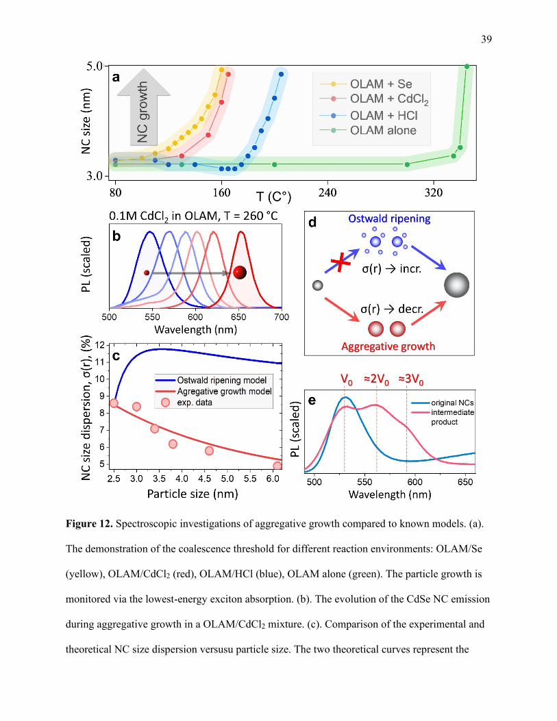
39
Figure 12. Spectroscopic investigations of aggregative growth compared to known models. (a).
The demonstration of the coalescence threshold for different reaction environments: OLAM/Se
(yellow), OLAM/CdCl2 (red), OLAM/HCl (blue), OLAM alone (green). The particle growth is
monitored via the lowest-energy exciton absorption. (b). The evolution of the CdSe NC emission
during aggregative growth in a OLAM/CdCl2 mixture. (c). Comparison of the experimental and
theoretical NC size dispersion versusu particle size. The two theoretical curves represent the
40 predictions of the Ostwald ripening and aggregative growth models, calculating according to
Ref. 96. (d). Graphic illustration of the Ostwald ripening and aggregative growth mechanisms.
(e). The PL spectra of CdSe NCs prior to (blue) and during (red) aggregative growth with
intermediate PL spectra showing the presence of CdSe NCs with twice and three times the
volume of the original seeds. To obtain the PL spectrum for early-time product of aggregation,
the rate of coalescence was reduced by introducing a significant volume fraction of a non-
coordinating solvent (octadecene).
Notably, during the growth reaction, the emission linewidth decreases, which suggests
size focusing of the NC population (Figure 12b). By assuming a constant single-particle
linewidth, we estimate the NC size dispersion from the full width half maximum (FWHM) of the
PL spectra (Figure 12c, red dots). The reduction in the CdSe NC size dispersion is consistent
with the predictions of the aggregative growth model96 (Figure 12c, red curve), which assumes
nanoparticle growth by coalescence. In contrast to aggregative growth, Ostwald ripening
model117 stipulates that NC growth is due to the dissolution of smaller NCs in favor of larger
ones (Figure 12d), which causes initial broadening of the nanoparticle size dispersion (Figure
12c, blue curve). According to Figure 12c, our experimental size dispersion, σ(r), closely follows
the aggregative growth model. Furthermore, the PL spectra in Figure 12e demonstrates clear
evidence that nanocrystal volume doubles and/or triples due to coalescence at early stages of the
growth reaction, which is consistent with the aggregative growth model. Similarly, volume
increase at very early stages of the aggregative growth reaction were observed in the case of
ultrasmall CdSe NCs (Figure SF1), showing evidence of 2-5 times volume increases within 5
second of growth.

41
Figure 13. A diagram showing a greater affinity of bound-ion pairs (x-type ligands) over L-type
amine ligands (i.e., oleylamine). The surface energy of CdX (X = S, Se) NCs are lower than with
L-type ligands.
The role of coordinating solvents in the aggregative growth of semiconductor colloids has
been investigated by previous reports.98, 184, 187 It is generally accepted that amines and
carboxylates increase the rate of nanoparticle coalescence compared to non-coordinating solvents
(e.g. 1-octadecence) due to increased driving force towards colloidal aggregation.187 The head
groups of coordinating solvent molecules render the solution more polar compared to alkyl-
terminated colloidal nanoparticles causing NC aggregation. Binding of amines and carboxylates
to NC surfaces also increases the aggregative growth rate. Binding of these ligands reduces the
surface energy of a NC facet (hkl), by the amount, which is equal to the difference between
binding and relaxed energies of a particular ligand, Ebound ligand (hkl) – Efree ligand.176 The ligand-
induced decrease in the surface energy of a NC facet lowers its melting point (Supplementary
Information, Equation 3), which makes it more susceptible to interparticle coalescence and is
responsible for the different observable coalescence onset temperatures shown in Figure 12a.
The use of bound ion pairs, such as n-alkylammonium chloride, are created by the addition of
Lewis acids (i.e., HCl, CdCl2, or stearoyl chloride) to coordinating solution and have previously
been explored as strong ligands with high binding affinity onto CdSe NC surfaces (Figure 13).194
42 The increased binding energy of bound ion pairs over classical L-type ligands (i.e., oleylamine)
is what leads to the reduced surface energy and coalescence onset observed for CdX (X = S, Se)
NCs.
The effect of n-alkylammonium chloride on the aggregative growth of NCs was further
explored by heating NCs in OLAM to 260 °C without the addition of lewis acid (i.e., no bound
ion pair was present; Figure SF2). Upon maintaining the temperature for several minutes, no
change in the NC size is observed, however, upon addition of stearoyl chloride, immediate
nanocrystal growth is observed, demonstrating the crucial role bound ion pair ligands have in
reducing the onset temperature of coalescence. Furthermore, when the concentration of NCs
versus n-alkylammonium chloride was investigated, it was found to have little effect (Figure
SF3). The effect of n-alkylammonium chloride was investigated by hot injecting of 50-940
nmols of CdSe nanocrystals into 5 mL OLAM and 20 mg CdCl2 at 260 °C and reacting for 40
minutes. There was a negligible effect on the FWHM of the emission linewidths, with a < 6%
deviation between all experiments and no clear trend. The position of the emission peak was
found to vary slightly, with 50 nmols of NCs emitting at ~694 nm and 940 nmols emitting at
~685 nm, representing an approximately 1.5 nm diameter difference (~11.5 nm diameter using
940 nmols vs ~13 nm diameter using 50 nmols of CdSe NCs), or about 12% deviation. Overall,
these experiments demonstrated that the amount of n-alkylammonium chloride present during
the reaction is independent of the amount of NCs used, suggesting that the n-alkylammonium
chloride is a type of initiator to aggregative growth and not required to sustain growth. Finally,
the temperature at which growth is performed was found to have a significant impact on the size
of the final NCs (Figure SF4). When using n-alkylammonium chloride in the coordinating
solution (OLAM/CdCl2 mixture), the size of CdS NCs ranged from 8.2 nm at 260 °C to 16.8 nm
at 325 °C.
43 3.3 Investigation of Crystal Structure and Coordinating Solvent on Shape Control
The NC size evolution during an aggregative growth in an OLAM/CdCl2 mixture is
characterized in Figure 14a-d. The original, zinc blende (ZB) CdS NCs gradually increase in size
from 3.1 nm to 7.5 nm (in 30 min) when heated at T = 260°C. The shape of NCs appears to be
spherical throughout the growth reaction and maintains a relatively low size dispersion at
different growth stages (< 8%, Figure 12b, c). A high-resolution TEM image of a characteristic
NC in the final product reveals a wurtzite (WZ) lattice structure (Figure 14d) and the
transformation of the ZB lattice to a WZ lattice was confirmed by powder X-ray diffraction
(XRD) measurements (Figure SF5). The spherical shape of NCs is replaced by a hexagonal
geometry when a particle size reaches 15-17 nm (Figure SF6). Growth of these larger structures
requires higher reaction temperatures (T = 300-320°C). An apparent mono-crystalline
morphology of these nanoparticles suggests that the incorporated NC seeds anneal to form a
uniform lattice during the synthesis. The shape evolution of CdSe NCs in OLAM/CdCl2
coordinating solvent mixtures was similar to that of CdS. A 30 min aggregation growth reaction
at T = 260°C produces a 3.5 nm to 9 nm increase in the average particle size (Figure SF7a),
caused by the coalescence of original ZB NC seeds. The final product exhibits a low particle size
dispersion of < 7%, which was consistent with a reduced PL linewidth (ΔE = 86 meV) of
coalesced CdSe NCs, compared to ΔE = 125 meV for the original 3.5 nm CdSe seeds (Figure
SF7b).
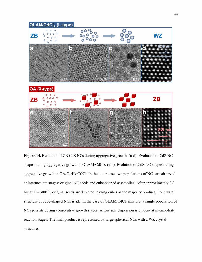
44
Figure 14. Evolution of ZB CdS NCs during aggregative growth. (a-d). Evolution of CdS NC
shapes during aggregative growth in OLAM/CdCl2. (e-h). Evolution of CdS NC shapes during
aggregative growth in OA/C17H35COCl. In the latter case, two populations of NCs are observed
at intermediate stages: original NC seeds and cube-shaped assemblies. After approximately 2-3
hrs at T = 300°C, original seeds are depleted leaving cubes as the majority product. The crystal
structure of cube-shaped NCs is ZB. In the case of OLAM/CdCl2 mixture, a single population of
NCs persists during consecutive growth stages. A low size dispersion is evident at intermediate
reaction stages. The final product is represented by large spherical NCs with a WZ crystal
structure.
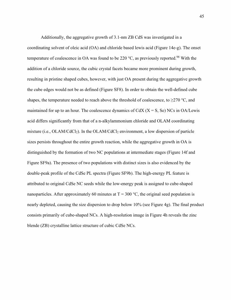
45
Additionally, the aggregative growth of 3.1-nm ZB CdS was investigated in a
coordinating solvent of oleic acid (OA) and chloride based lewis acid (Figure 14e-g). The onset
temperature of coalescence in OA was found to be 220 °C, as previously reported.98 With the
addition of a chloride source, the cubic crystal facets became more prominent during growth,
resulting in pristine shaped cubes, however, with just OA present during the aggregative growth
the cube edges would not be as defined (Figure SF8). In order to obtain the well-defined cube
shapes, the temperature needed to reach above the threshold of coalescence, to ≥270 °C, and
maintained for up to an hour. The coalescence dynamics of CdX (X = S, Se) NCs in OA/Lewis
acid differs significantly from that of a n-alkylammonium chloride and OLAM coordinating
mixture (i.e., OLAM/CdCl2). In the OLAM/CdCl2 environment, a low dispersion of particle
sizes persists throughout the entire growth reaction, while the aggregative growth in OA is
distinguished by the formation of two NC populations at intermediate stages (Figure 14f and
Figure SF9a). The presence of two populations with distinct sizes is also evidenced by the
double-peak profile of the CdSe PL spectra (Figure SF9b). The high-energy PL feature is
attributed to original CdSe NC seeds while the low-energy peak is assigned to cube-shaped
nanoparticles. After approximately 60 minutes at T = 300 °C, the original seed population is
nearly depleted, causing the size dispersion to drop below 10% (see Figure 4g). The final product
consists primarily of cube-shaped NCs. A high-resolution image in Figure 4h reveals the zinc
blende (ZB) crystalline lattice structure of cubic CdSe NCs.
46
Figure 15. Crystal structure impact on shape controlled aggregative growth. (a). Spherically
shaped CdS nanoparticles forming through the aggregative growth of 2.6-nm ZB NCs in 5 mL
OLAM and 20 mg CdCl2. (b) Spherically shaped CdS nanoparticles forming through the
aggregative growth of 2.5-nm WZ NCs in 5 mL OLAM and 20 mg CdCl2. (c) Cubic-shaped CdS
nanoparticles forming through the aggregative growth of 2.6-nm ZB NCs in 5 mL OA, 1 mL
ODE with 0.2 mL stearoyl chloride stock solution. (d). Rod-shaped CdS nanoparticles forming
through the aggregative growth of 2.6-nm WZ NCs in 5 mL OA, 1 mL ODE with 0.2 mL
stearoyl chloride stock solution.
47
The role of crystal structure in the original seed NCs is investigated by looking at the
coalescence of wurtzite (WZ) nanocrystals in OLAM/CdCl2 and OA coordinating solutions,
which can be compared to the results from the ZB crystals. We find that the crystal structure of
original NC seeds appears to play a unique role in determining the trajectory of the coalescence
growth and overall final shape, as shown in Figure 15a-d. According to Figure 15a and 15b, both
ZB and WZ NC seeds give rise to spherical WZ nanocrystals in n-alkylammonium chloride
coordinating mixtures. However, in the case of the OA reaction solvent, original NC seeds with
different lattice structures produced different NC geometries upon coalescence. For instance,
aggregative growth seeded by ZB CdS NCs leads to the formation of ZB cubes (Figure 15c).
Meanwhile WZ CdS seeds in a OA mixture react to form WZ nanorods (Figure 15d). The rod
thickness is broader than single NCs, which indicates that nanorods were not formed thru
oriented attachment of original seeds but rather through thermodynamically-driven shape
formation. Additionally, using mixtures of OLAM and OA, it is possible to produced very thick
(> 4 nm diameter) rods, as shown in Figure 11e, 11f, and Figure SF10.
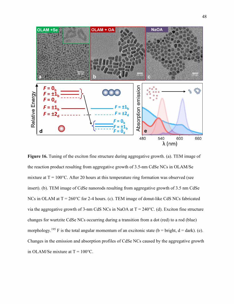
48
Figure 16. Tuning of the exciton fine structure during aggregative growth. (a). TEM image of
the reaction product resulting from aggregative growth of 3.5-nm CdSe NCs in OLAM/Se
mixture at T = 100°C. After 20 hours at this temperature ring formation was observed (see
insert). (b). TEM image of CdSe nanorods resulting from aggregative growth of 3.5 nm CdSe
NCs in OLAM at T = 260°C for 2-4 hours. (c). TEM image of donut-like CdS NCs fabricated
via the aggregative growth of 3-nm CdS NCs in NaOA at T = 240°C. (d). Exciton fine structure
changes for wurtzite CdSe NCs occurring during a transition from a dot (red) to a rod (blue)
morphology.195 F is the total angular momentum of an excitonic state (b = bright, d = dark). (e).
Changes in the emission and absorption profiles of CdSe NCs caused by the aggregative growth
in OLAM/Se mixture at T = 100°C.

49 3.4 Further Observations on the Shape Control of Aggregative Growth
Aggregative growth in a mixture of elemental chalcogenides and OLAM (i.e., a bound
ion pair using Se2- in place of Cl-) exhibited the lowest thermal threshold for NC coalescence
(Figure 12a). The fusion of CdSe NCs is achieved at temperatures as low as T = 90 °C when the
concentration of Se in OLAM is 100 mM. In such a low-temperature regime, aggregative growth
appears to resemble fusion of NCs at molten surfaces187 resulting in characteristic, one-
dimensional assemblies, as shown in Figure 16a. The elongated structures appear to grow in a
curved pattern, which in some cases leads to the formation of CdSe rings, particularly at longer
reaction times (Figure 16a, insert). While it is difficult to achieve specific shape homogeneity for
such 1D assemblies, the emission linewidth remains relatively narrow (ΔE = 85 meV, Figure
15e). However, upon injection of CdSe NCs into n-alkylammonium ion solution with Se/OLAM
at 260 °C, the formation of large spherical NCs is observed, similar to that obtained for
OLAM/chloride coordinating mixtures at ≥180 °C and OLAM only at 330 °C (Figure SF11).
The rate of NC coalescence in a OLAM/CdCl2 mixture slows significantly when the
particle size reaches a particular threshold value. We attribute this suppression of aggregative
growth to the increasing elasticity of the core components of the larger nanoparticles. It has been
established that the solvent/solid tension in small-diameter NCs converts the entire nanoparticle
into a molten phase,180, 196 which permits their coalescence into a single composite nano-object.
In larger colloids, only the surface layer is affected by the solvent/solid tension,197 causing the
formation of a molten layer over the elastic core. In this case, nanoparticles can undergo a partial
rather than the full coalescence. An example of such a partial coalescence is provided in Figure
16b, which show a nanorod-like assembly of large-size CdSe NCs along the 0001 wurtize (WZ)
axis. In this case, the attachment process is much slower than the coalescence of small-size
50
seeds, requiring several hours at a minimum to produce nanorods with an aspect ratio of 2-3
(Figure SF10).
One-dimensional assemblies of CdSe NCs achieved in OLAM/Se reaction mixture
(Figure 16a) represent an interesting type of semiconductor quantum dots (QDs), where the fine
structure of lowest-energy excitons differs from that of zero-dimensional QDs. As illustrated in
Figure 16d, eight lowest-energy transitions in CdSe NCs shift lower in energy and reorder when
several dots are fused into a 1D assembly of the same diameter. In spherical CdSe NCs, the
upper F = ±1bright states (F = S + J is the total angular momentum) carry most of the dipole
strength for optical absorption, while the lower F = ±1bright states are responsible for the room-
temperature emission. When CdSe is elongated along the wurtzite c-axis, the upper F = ±1bright
states drop in energy (up to 80 meV, depending on the particle diameter), which is consistent
with a red-shifted emission in coalesced CdSe NCs (Figure 16e).
The most unusual nanoparticle growth is observed in the NaOA reaction mixture at T =
240-260°C. In this case, the aggregative growth of ~3 nm CdS seed NCs results in the formation
of donut-shaped NCs, measuring ~7 nm in diameter. The “donut hole” is present in 95% of all
structures, as shown in Figure 16c. Our analysis of high-resolution TEM images in
Supplementary Figure SF12 reveals a possible mechanism of the “hole” formation. The presence
of partly closed rings suggests that NC seeds do not undergo a full coalescence but rather stick at
hetero-interfaces in a ring-like pattern. Fully formed donuts, on the other hand, exhibit the same
lattice fringe pattern throughout the entire structure, possibly as a result of thermal annealing
across interfaces.
3.5 Theoretical Investigation of Coalescence Induced Shape Control
Our experiments demonstrate that aggregative growth of NCs leads to potential control of
particle shapes. The final products of these reactions exhibit a remarkable homogeneity of
51 particle shapes, which implies that the rate of coalescence falls abruptly when a maximum
particle size for given experimental conditions is reached. This behavior, however, deviates from
the predictions of classical aggregative growth models based on the classical Smoluchowski rate
equation (see Supporting Information).153-154, 187, 198 Namely, the coalescence growth of any two
particles Ai and Aj, each containing i and j numbers of primary particles (A1), can be described
as: kK
ji AAA ij→+ , where the collision rate, Kij, depends on particle sizes, Ri, Rj, and
their respective diffusion coefficients, Di,j, according to:
( )( )jijiij DDRRK ++= π4 (3.1)
Based on this model, the ultimate size of a NC in the reaction mixture is diffusion
limited. Since larger particles exhibit a lower diffusion coefficient, given by the Stokes-Einstein
law, their growth rates subside with the particle size. Our simulations based on Eq.1 (see
Supporting Information) demonstrate that such a diffusion-limited aggregation cannot explain
the distribution of particle shapes in the final product. Indeed, the predicted particle size
dispersion σ(r) continues to increase with r (Figure SF13), which disagrees with the experimental
data showing uniform particle distributions at long reaction times.
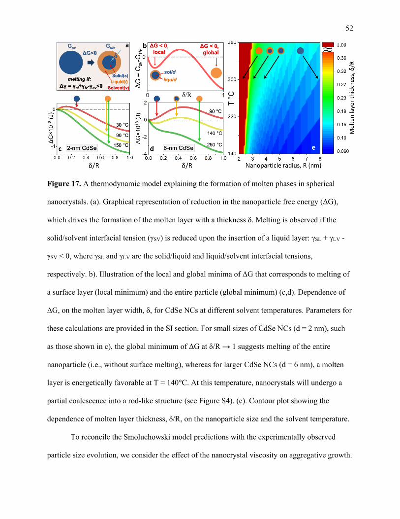
52
Figure 17. A thermodynamic model explaining the formation of molten phases in spherical
nanocrystals. (a). Graphical representation of reduction in the nanoparticle free energy (ΔG),
which drives the formation of the molten layer with a thickness δ. Melting is observed if the
solid/solvent interfacial tension (γSV) is reduced upon the insertion of a liquid layer: γSL + γLV -
γSV < 0, where γSL and γLV are the solid/liquid and liquid/solvent interfacial tensions,
respectively. b). Illustration of the local and global minima of ΔG that corresponds to melting of
a surface layer (local minimum) and the entire particle (global minimum) (c,d). Dependence of
ΔG, on the molten layer width, δ, for CdSe NCs at different solvent temperatures. Parameters for
these calculations are provided in the SI section. For small sizes of CdSe NCs (d = 2 nm), such
as those shown in c), the global minimum of ΔG at δ/R → 1 suggests melting of the entire
nanoparticle (i.e., without surface melting), whereas for larger CdSe NCs (d = 6 nm), a molten
layer is energetically favorable at T = 140°C. At this temperature, nanocrystals will undergo a
partial coalescence into a rod-like structure (see Figure S4). (e). Contour plot showing the
dependence of molten layer thickness, δ/R, on the nanoparticle size and the solvent temperature.
To reconcile the Smoluchowski model predictions with the experimentally observed
particle size evolution, we consider the effect of the nanocrystal viscosity on aggregative growth.

53 A recent study180 has suggested that particle coalescence results from a liquid-drop behavior of
heated colloids, caused by the formation of a molten inorganic phase. From a theoretical
prospective, the melting of inorganic nanoparticles is driven by the reduction of the interfacial
energy between the solid (nanoparticle) and matrix (solvent) phases. This concept is illustrated in
Figure 17a, indicating that the reduction of free energy, ΔG < 0, is caused by the reduction in the
nanoparticle interfacial tension (γSV) upon melting of the surface layer, δ, such that γSL + γLV -
γSV < 0, where γSL and γLV are the solid-liquid and liquid-solvent tension terms. To estimate the
corresponding change in the particle free energy as a function of the liquid layer thickness, δ,
ΔG(δ) = Gslv-Gsv, we use the Kofman approximation197 adapted for spherical nanoparticles in
solution (see Supporting Information). A typical evolution of ΔG with δ is illustrated in Figure
17b. The local minimum of ΔG(δ, T) provides the expected thickness of the molten layer, δ(T).
If δ = R, the entire nanoparticle is considered to be in a liquid phase.
In the case of smaller-diameter CdSe nanoparticles, the onset of surface melting is
strongly affected by the curvature of the particle.199 (see Supporting Information). According to
Figure 17c, small-size CdSe NCs (d = 2 nm) exhibit no local minimum of ΔG with increasing
liquid layer thickness, δ, indicating that the entire particle becomes molten at a threshold
temperature (a global minimum at δ/R → 1). Consequently, smaller-diameter NCs undergo full
coalescence when the threshold temperature is reached. For larger NCs (e.g. d = 6 nm CdSe NCs
in Figure 16d), ΔG (δ) exhibits both global and local minima, suggesting that melting of the
surface layer is thermodynamically favorable in a certain solvent temperature range. Another
effect of a large particle size is that the melting of the entire particle (δ/R → 1) requires greater
temperatures than that of smaller-size CdSe NCs. The increase in the full-particle melting
threshold with the size of a nanocrystal in Figure 17d suggests that the maximum particle size
that can be achieved via the coalescence growth is determined by the reaction temperature.

54 Particles larger than this size are not fully molten and thus cannot undergo full coalescence.
Partial coalescence, however, is possible. In case of d = 6 nm CdSe, ΔG exhibits a local
minimum at δ/R = 0.1 (0.3 nm) at T= 140 °C, which implies that surface melting is energetically
favorable at this particle size, shown in Figure 17e. With molten surfaces, nanoparticles can form
one-dimensional structures, such as rod-like or chain-like assemblies, which agrees with
experimentally observed morphologies in Figure 16b and Figure SF14.
3.6 Concluding Remarks on Shape Control via Coalescence
We have demonstrated that aggregative growth of colloidal semiconductor NCs provides a
powerful strategy for tuning nanoparticle shapes. Unlike conventional growth techniques that
rely on the reaction of atomic precursors, the present approach employs the coalescence of small-
size nanoparticles into larger colloids. The absence of atomic species during aggregative growth
prevents shape evolution by monomer precipitation, allowing nanoparticles to transform into a
"lowest energy" morphology. With this approach, controlling the shape of nanocrystals is
achieved through the use of different reaction environments, which uniquely affect the final
particle shape. This concept is conclusively demonstrated by performing a shape-selective
growth of CdX (X = S, Se) cubes, spheres, nanorods, nanorings, and donut-like structures. The
aggregative growth mechanism is explained using a thermodynamic model of interacting viscous
colloids. We expect that the present growth strategy will provide a viable platform for the shape-
selective synthesis of many other types of inorganic colloids, stimulating the discovery of novel
optoelectronic properties.
3.7 Experimental Methods on Aggregative Growth Induced Shape Control
The following materials were used: cadmium oxide (CdO, 99% STREM), 1-octadecene
(ODE, 90% Aldrich), n-octadecylphosphonic acid (ODPA, >99% PCI), octadecylamine (ODA,
90% Acros), oleic acid (OA, 90% Aldrich), sulfur (S, 99.99% Acros), Chloroform (anhydrous,
55 99% Aldrich), oleylamine (OLAM, 70% Aldrich), hexane (anhydrous, 95% Aldrich), ethanol
(anhydrous, 95% Aldrich), isopropyl alcohol (IPA, HPLC grade, OmniSolv), tri-n-
octylphosphine (TOP, 97% STREM), tri-n-octylphosphine oxide (TOPO, 99% Aldrich),
selenium powder (Se, 200 mesh, Acros), acetone (anhydrous, Amresco, ACS grade), stearic acid
(97% Aldrich), stearoyl chloride (SC, >97% TCI), and tributylphosphine (TBP, 97% Aldrich).
All reactions were performed under argon atmosphere using the standard Schlenk technique. The
centrifuge used for precipitation operated at 6500 rpm.
CdS NCs were fabricated according to the previously reported procedure.199 A mixture of
0.0768 g of CdO, 3.6 mL of OA, and 24 mL of ODE in a 50 mL three-neck flask was heated to
240°C until the solution turned optically clear. Then, all of the sulfur precursor solution made by
dissolving 0.02 g of sulfur powder in 10 ml of ODE at 200°C was quickly injected. The reaction
was finally stopped by removing the flask from the heating mantle after 4−5 min. CdS NCs were
separated from the solution by precipitating with ethanol and redissolving the product in hexane.
NCs were synthesized using the following procedure. A mixture of 0.06 g of CdO, 0.28 g
of ODPA, and 3g of TOPO (1.5 g of TOPO for CdS NC synthesis) was heated to 320°C until the
solution turned optically clear. Then, the mixture was heated up to 370°C and kept at this
temperature. In another flask, 0.73 mmoles of chalcogenide powder (58 mg Se powder or 23.6
mg S powder) were dissolved in 1.5 ml of TOP at 120°C. Finally, chalcogenide precursor was
swiftly injected into the Cd flask and allowed to react for up to 3 min. The reaction was
quenched by placing a flask into water bath when the solution temperature was below 290°C.
CdS or CdSe NCs were cleaned via two successive precipitations with anhydrous ethanol and
toluene. Finally being suspended in hexane. The final NC product was centrifuged for 30
seconds to remove anything insoluble.
56
ZB CdSe NCs were synthesized by adapting a previous reported procedure from the
literature.200 Briefly, 80 mg of CdO, 2 mL OA, and 18 mL ODE were heated in a 50 mL flask to
250 °C until the solution turned clear. Next, 25 mg Se powder was sonicated in 1 mL ODE for at
least 5 minutes to create a suspension. Once the Cd flask had reached 250 C, the Se suspension
was swiftly injected and allowed to react for the desired amount of time. The flask was then
removed from the heat and quenched in a water bath. The NCs were cleaned by precipitation
with toluene / ethanol procedure, followed by centrifugation at 6500 rpm for up to 10 minutes.
This cleaning procedure was performed twice before the final NCs were suspended in hexane.
In a typical growth for spheres, 5 mL of OLAM and 20 mg of CdCl2 (or equicalent molar
amount of HCl or stearoyl chloride) were degassed at 120 °C for approximately 15 minutes. The
flask was switched to argon environment (using Schlenk line) and heated to the desired
temperature (180 °C – 320 °C). Next, 70 nmols of CdX (X = S, Se) NCs in 1 mL ODE were
swiftly injected into the flask and allowed to grow for 30 – 60 minutes. The growth was stopped
by quenching the reaction in a water bath. The product was cleaned by several precipitations
with ethanol and resuspension in toluene. The final NC product was suspended in hexane and
centrifuged for 30 seconds to remove anything insoluble
In a typical procedure for nanorods, 2.5 mL OA, 2.5 mL OLAM, and 20 mg CdCl2 were
heated to the desired temperature (200 °C – 320 °C), followed by hot injection of 200-250 nmols
of CdX (X = S, Se) NCs in 1 mL ODE. Once the desired size (diameter of the rod) was reached,
the reaction mixture was cooled to 160 °C – 200°C for 3-20 hours to promoted elongation via
fusion of NCs. The NC product was cleaned via several successive precipitations with
ethanol/toluene before being dispersed in hexane.
Aggregative growth in OA + Stearoyl chloride was performed using the following
procedure. Here, 50 mg CdO, 5 mL OA, and 1 mL ODE were heated to 260 °C until a clear
57 solution was achieved. The temperature was lowered to 120 °C and degassed for approximately
15 minutes. Switching to argon, 0.2 mL of stearoyl chloride solution and 50 nmols of CdS NCs
were added to the flask followed by brief degassing to remove any solvent. The flask, under
argon, was subsequently heated to 305 °C – 325 °C for 30 minutes. When using Wurtzite NCs
the final product was rods and when using Zinc Blende NCs the final product was cubes. Lastly,
the NCs were precipitated using excess iso-propyl alcohol, twice, before being suspended in
hexane and centrifuged for 30 seconds to remove any insoluble.
For the formation of donut-shaped CdS NCs, 125 nmols of CdS seed NCs, 225 mg of
sodium oleate, and 4 mL of OA were combined in a 25 mL flask and degassed at 150°C for 10
min. The flask was then switched argon, placed on a Schlenk line, and heated to 245°C for 10
minutes. The reaction was removed from the heat and allowed to cool to room temperature,
finally being cleaned via three ethanol/toluene precipitations. Final samples were redispersed in
hexane.
In a standard procedure for nano-rings, 200 nmols of CdSe NCs, 6 mL OLAM, and 15 mg
of selenium powder were placed into a flask and degassed at 100 °C. Following the degassing,
the NC mixture was switched to argon and maintained at that temperature for 20 hours. The NC
product was precipitated several times using ethanol/toluene method. The final product was
suspended in hexane and centrifuged to remove any unreacted selenium powder.
Stearoyl chloride stock solution was made by the following: in a 25 mL flask, 10 mL of
ODE was degassed at 120 °C for at least 30 minutes. It is important to remove any potential
water to prevent the hydrolysis of the stearoyl chloride. Next, the flask was switch to argon,
removed from the heat, and 0.3 g of stearoyl chloride was added to the flask under positive argon
pressure, to prevent air from entering the flask. The stearoyl chloride would be fulling dissolved
within 10 minutes.
58
After the reaction mixture had cooled to room temperature, equal amounts of solution
(approximately 3 mL) were placed in two 15 mL centrifuge tubes. To precipitate the product, 2
mL of chloroform and 6 mL of ethanol were added to each tube, which were then inverted
several times and centrifuged for 5 min at 6500 rpm. The clear supernatant was discarded and the
remaining precipitate was dissolved in 2 mL of chloroform, 6 mL of ethanol was added, the
centrifuge tubes were inverted several times and then centrifuged 5 min at 6500 rpm. Finally, the
precipitate was dissolved in 5 ml of hexane and centrifuged 3 min at 6500 rpm to remove any
insoluble products. The final hexane solution was stored under ambient conditions and was
stable for months.
UV-vis absorption spectra were recorded using a CARY 60 scan spectrophotometer. High
resolution transmission electron microscopy (TEM) measurements were carried out using a
Thermo Fisher Talos F200X G2 S/TEM instrument operated at 200 kV. Specimens were
prepared by depositing a drop of NP solution in hexane onto a carbon-coated copper grid and
allowing it to dry in air. Powder X-Ray diffraction measurements were carried out with a Bruker
D8 Advance PXRD. Energy dispersive X-ray (EDX) analysis was performed using Hitachi 2700
operated at 20 kV. Emission spectra where acquired using a 405-nm PicoQuant PDL 800-D
pulsed laser and measured with an Andor newtonEM SR-303i-A spectrograph. Time-resolved
emission lifetime spectra where acquired using the same 405-nm pulsed laser and photons where
collected using ID Quantique’s id100-50 single photon detector and processed using a SPC-130
TCSPC module from Beckler & Hickl.
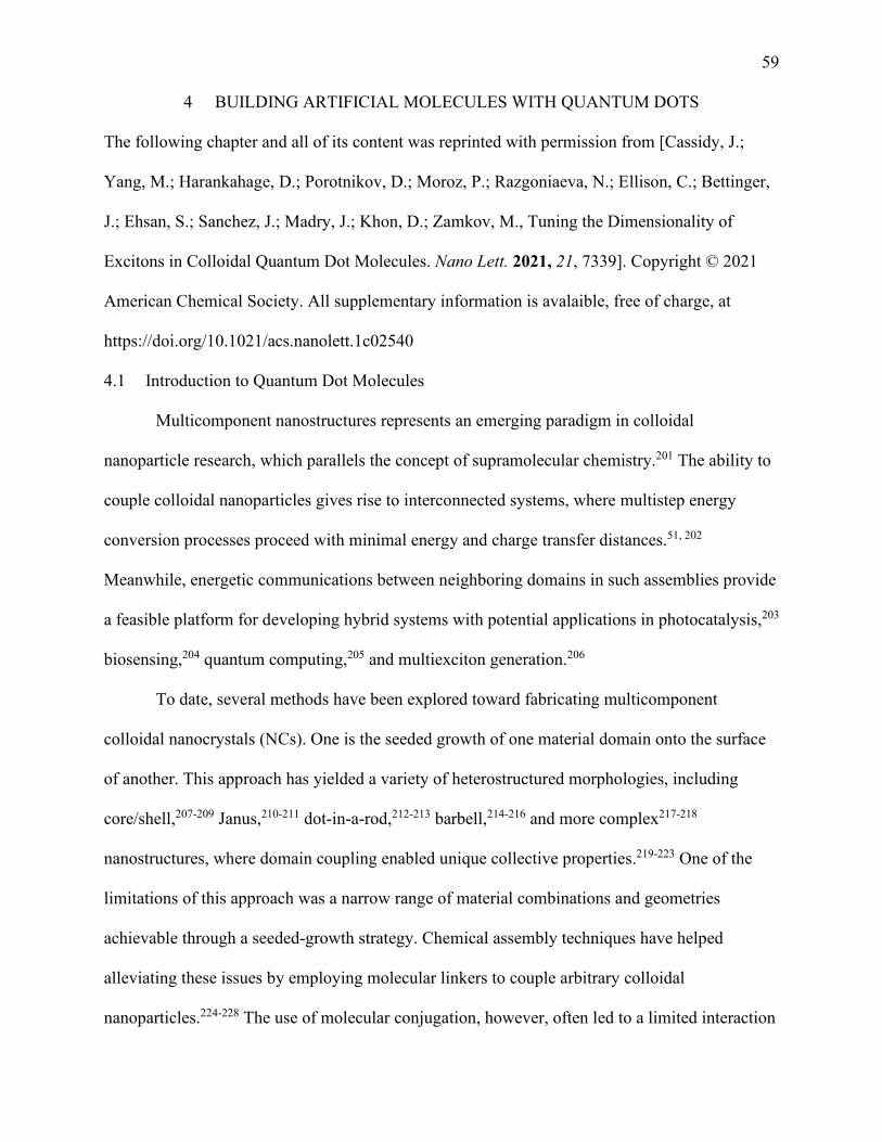
59
4 BUILDING ARTIFICIAL MOLECULES WITH QUANTUM DOTS
The following chapter and all of its content was reprinted with permission from [Cassidy, J.;
Yang, M.; Harankahage, D.; Porotnikov, D.; Moroz, P.; Razgoniaeva, N.; Ellison, C.; Bettinger,
J.; Ehsan, S.; Sanchez, J.; Madry, J.; Khon, D.; Zamkov, M., Tuning the Dimensionality of
Excitons in Colloidal Quantum Dot Molecules. Nano Lett. 2021, 21, 7339]. Copyright © 2021
American Chemical Society. All supplementary information is avalaible, free of charge, at
https://doi.org/10.1021/acs.nanolett.1c02540
4.1 Introduction to Quantum Dot Molecules
Multicomponent nanostructures represents an emerging paradigm in colloidal
nanoparticle research, which parallels the concept of supramolecular chemistry.201 The ability to
couple colloidal nanoparticles gives rise to interconnected systems, where multistep energy
conversion processes proceed with minimal energy and charge transfer distances.51, 202
Meanwhile, energetic communications between neighboring domains in such assemblies provide
a feasible platform for developing hybrid systems with potential applications in photocatalysis,203
biosensing,204 quantum computing,205 and multiexciton generation.206
To date, several methods have been explored toward fabricating multicomponent
colloidal nanocrystals (NCs). One is the seeded growth of one material domain onto the surface
of another. This approach has yielded a variety of heterostructured morphologies, including
core/shell,207-209 Janus,210-211 dot-in-a-rod,212-213 barbell,214-216 and more complex217-218
nanostructures, where domain coupling enabled unique collective properties.219-223 One of the
limitations of this approach was a narrow range of material combinations and geometries
achievable through a seeded-growth strategy. Chemical assembly techniques have helped
alleviating these issues by employing molecular linkers to couple arbitrary colloidal
nanoparticles.224-228 The use of molecular conjugation, however, often led to a limited interaction

60 between subunits, caused by steric conditions of bulky linkers. As a result, a collective behavior
between incorporated components was often suppressed.229-231 In addition to molecular
conjugation methods, other strategies have been developed for the assembly of colloidal
nanocomposites. These included multiple precipitations to induced aggregation232 and oriented
attachment.233 More recently, Banin et al.234-237 has demonstrated a conceptually novel strategy
for the assembly of colloidal nanocrystal molecules, which relied on using large colloidal beads
as sites for interparticle bonding. This approach has enabled the synthesis of CdSe/CdS
core−shell dimers exhibiting interparticle electronic interactions.
Figure 18. Illustration of the viscoelastic assembly approach. Formation of a molten layer in
heated colloidal NCs enables bonding of nanoparticles at hybrid interfaces. The driving force for
the assembly process is controlled by nanoparticle surfactants, while the degree of inter-particle
fusion is tunable via the solvent temperature.
Here, we demonstrate colloidally stable assemblies of semiconductor nanocrystals that
support electronic communications across incorporated sites. The solution-phase assembly of
colloidal nanocrystals was achieved through surfactant directed surface interactions, which
promoted the adhesion of nanoparticles at hybrid interfaces (Figure 18). This technique was
demonstrated through the synthesis of both homogeneous assemblies of the same-type colloids

61 (e.g., CdS−CdS, PbS− PbS, CdSe−CdSe), as well as heterogeneous assemblies of dissimilar
nanocrystals (e.g., PbS−CdS, CdS−CdSe). Individual components of fabricated assemblies were
found to engage in charge and energy transfer interactions across heterostructured interfaces. In
particular, we observed that dimers of CdSe/CdS core/shell NC exhibited unique optical
characteristics arising from a superposition of single-particle excitonic states. From the
fabrication standpoint, the degree of interparticle bonding at interfaces was tunable by changing
the depth of the molten surface layer in original nanoparticles, as illustrated in Figure 18. The
demonstrated assembly approach was explained within the viscoelastic interaction theory, which
was adapted to account for molten surfaces in heated colloidal nanoparticles.
4.2 Formation of a Molten Surface Layer on Nanocrystals
The intrinsic property of heated inorganic nanoparticles to form a molten surface layer
was first demonstrated by works of Samorjai,238 El-Sayed,239 and Boret240 on metal colloids.
These studies have demonstrated that heated NCs of Au, Pt, and Pd formed a few-atom-deep
liquid layer around the still solid core. The melting point of the surface was substantially lower
than that of the bulk material because of a reduced surface tension of the solid−liquid interface.
A similar melting point depression was observed for semiconductor NCs heated to 400 °C in
vacuum.193 More recently, solution-phase semiconductor nanocrystals were also shown to
undergo a similar solid-to-liquid transition at temperatures that were much lower than the
corresponding bulk melting point (see Figure S1).98, 241
In the present work, the formation of molten surfaces in colloidal NCs helped achieve a
partial fusion of nanoparticles in the form of n-mer assemblies (Figure 18). The fusion of
colloidal NCs required a proper balance between (1) aggregative forces driving the particle
attachment,98 and (2) opposing elastic forces,156 associated with the elastic repulsion of solid
“cores”. Thermodynamically, the fusion of colloidal nanoparticles is driven by the reduction of

62 the total surface area, A(ε), where ε = ΔL/L is a geometric strain coordinate (L is the size of
uncompressed nanoparticles and ΔL is the compression distance; see Figure S2). The
corresponding decrease in the interfacial energy, Einterfacial = γA(ε), is plotted in Figure 19a,
where γ is the solvent/surfactant interfacial tension. These aggregative forces are
counterbalanced by the increasing elastic energy, Eelastic (Figure 19c), which represents the elastic
repulsion of the two fusing nanoparticles due to the deformation of the lattice, 𝐸𝐸𝑒𝑒𝑒𝑒𝑒𝑒𝑒𝑒𝑒𝑒𝑒𝑒𝑒𝑒 =
32𝐺𝐺𝜀𝜀2𝑉𝑉, where G(T) is the temperature-dependent nanoparticle shear modulus that characterizes
the nanocrystal rigidity, and V is total volume of the coalescing nanostructures. The total free
energy of the two fusing particles is thus given as a sum of the decreasing interfacial energy and
increasing elastic energy terms:
𝐸𝐸𝑒𝑒𝑡𝑡𝑒𝑒 = 𝐸𝐸𝑒𝑒𝑖𝑖𝑒𝑒𝑒𝑒𝑖𝑖𝑖𝑖𝑒𝑒𝑒𝑒𝑒𝑒𝑒𝑒𝑒𝑒 + 𝐸𝐸𝑒𝑒𝑒𝑒𝑒𝑒𝑒𝑒𝑒𝑒𝑒𝑒𝑒𝑒 = 𝛾𝛾𝛾𝛾(𝜀𝜀) + 32𝐺𝐺(𝑇𝑇)𝜀𝜀2𝑉𝑉 (4.1)
Therefore, the coalescence of two particles is expected to stop at an particular stage
corresponding to the minimization of the total energy, Etot(ε) → min, for a given T (Figure 19b).
According to eq 4.1, the degree of nanocrystal fusion (expressed as a function of compression
strain ε, see Figure S2) could be controlled by tuning either Einterface (ε) or Eelastic (ε) energy terms.
For instance, increasing the difference between respective polarities of the solvent and the
particle surfactant enhances the driving force for particle aggregation, dEinterface(ε)/dε.
Meanwhile, increasing the solvent temperature causes a greater fraction of the surface layer,
δ(T), to become molten (viscose), thus reducing Eelastic within this layer, as illustrated in Figure
19c.
63
Figure 19. Model on the interfacial and elastic energies for nanoparticle fusion. (a). Driving
force towards particle aggregation caused by the reduction of the interfacial energy (Einterface) of
fusing nanoparticles, which minimizes the total particle/solvent interfacial area. ε is the
geometric strain coordinate ε = ΔL/L (L is the size of uncompressed nanoparticles and ΔL is the
compression distance – see Figure SF2). (b). Changes in the total free energy of fusing
nanoparticles (Etot), contributed by the reduction of the interfacial energy (Einterface) and the
increase in the strain energy of elastic NCs (Eelastic), for three representative solvent temperatures,
T1 < T2 < T3. (c). The elastic energy of fusing nanoparticles (Eelastic), which represents their
repulsion. An increasing thickness of a molten surface layer with higher temperatures (T1 → T2
→ T3) results in flattening of E(ε) with increasing ε. (d,e). Three-particle clusters of CdS
nanocrystals, assembled at T = 180 °C and T = 120 °C, respectively. (f). Illustration of the
64 assembly strategy, which involves the use of aggregation-inducing solvents and elemental
chalcogenides to promote fusion of molten-surface nanoparticles. (g,h). Coupled dimers of CdS
(g) and CdSe/CdS (h) nanocrystals, assembled at T = 120 °C and T = 200 °C, respectively.
4.3 Fusion of Nanocrystal Surfaces and Impact on Nanocrystal Dimensionality
The fusion of colloidal nanocrystals is impeded by the stearic hindrance of long-chain
amines or carboxylates present on particle surfaces. To overcome such a repulsion, we have
employed two strategies that decrease the density of bulky ligands. The first method
(schematically shown in Figure 19f) involved the exchange of long-chain ligands, such as oleic
acid (OA) or oleylamine (OLAM), with small, atomic chalcogenides of the same type242 (L → L,
X → X). Figure S3 demonstrates that elemental S and Se behaved as L-type ligands, triggering a
fast OLAM → (S, Se) exchange and simultaneous fusion of OLAM-deprived NCs. The decrease
in the density of OLAM ligands following the addition of elemental chalcogenides was evident
from the characteristic reduction of the interparticle spacing in NC assemblies on a TEM grid, as
illustrated in Figure S3e. For OA-capped nanoparticles (X-type ligands), an efficient ligand
exchange was achieved by using X-type anionic ligands in methanol (e.g., Na2S), which
injection promoted nanoparticle fusion (Figure S4). The second strategy to overcome the
compression strain of bulky ligands involved stripping the long-chain molecules. To this end,
nanocrystals were transferred into a formamide (FA) solution via the OA → S2− exchange (X-
type to X-type) and heated to 110−150 °C, as detailed in section SI.2. Figure 19g and Figure S5a
show examples of CdS NC molecules assembled using the FA heat-up strategy.
Figure 20d, e shows two examples of homogeneous assemblies obtained by injecting
elemental chalcogenides into an OLAM solution of colloidal NCs. The polar headgroup (HN2,
CO2H) of unattached OLAM molecules renders the solution more polar compared to alkyl-
terminated colloidal nanoparticles, providing the necessary driving force for particle
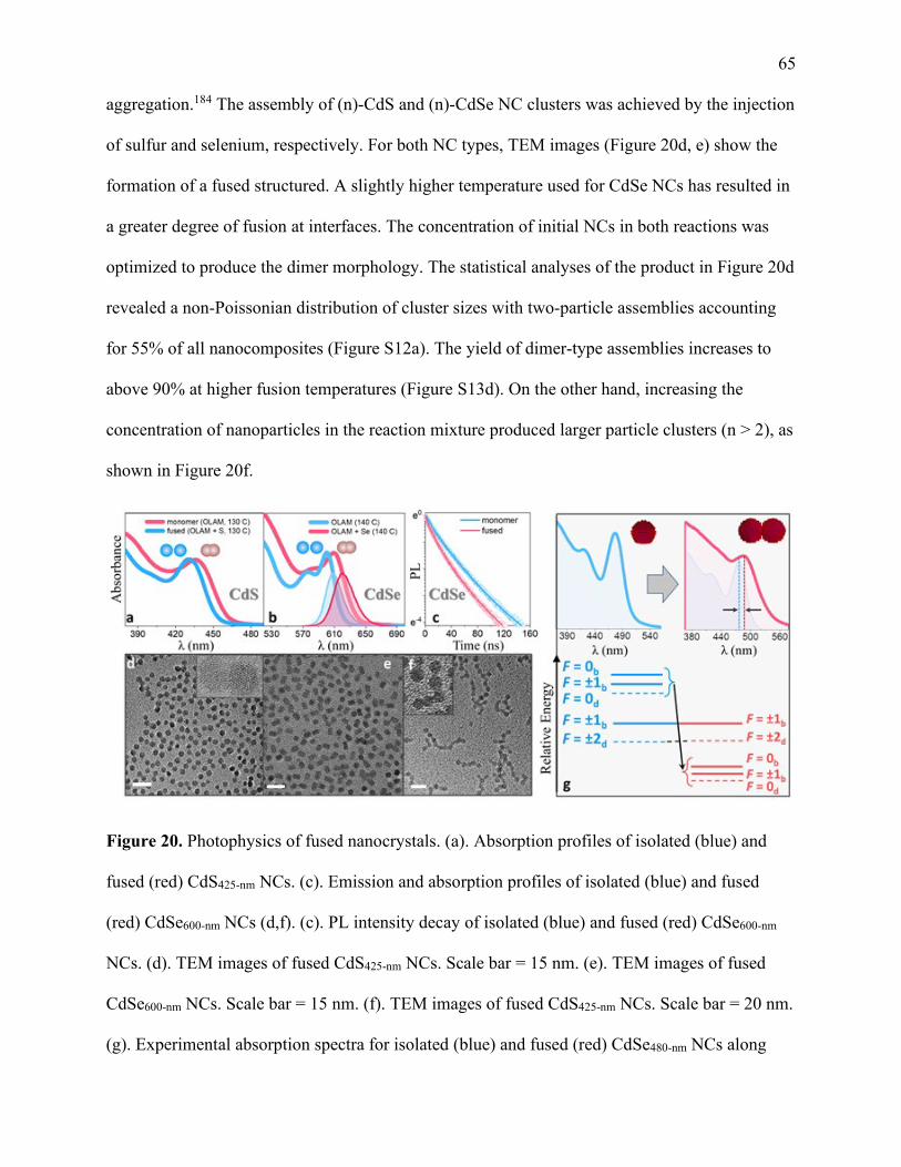
65 aggregation.184 The assembly of (n)-CdS and (n)-CdSe NC clusters was achieved by the injection
of sulfur and selenium, respectively. For both NC types, TEM images (Figure 20d, e) show the
formation of a fused structured. A slightly higher temperature used for CdSe NCs has resulted in
a greater degree of fusion at interfaces. The concentration of initial NCs in both reactions was
optimized to produce the dimer morphology. The statistical analyses of the product in Figure 20d
revealed a non-Poissonian distribution of cluster sizes with two-particle assemblies accounting
for 55% of all nanocomposites (Figure S12a). The yield of dimer-type assemblies increases to
above 90% at higher fusion temperatures (Figure S13d). On the other hand, increasing the
concentration of nanoparticles in the reaction mixture produced larger particle clusters (n > 2), as
shown in Figure 20f.
Figure 20. Photophysics of fused nanocrystals. (a). Absorption profiles of isolated (blue) and
fused (red) CdS425-nm NCs. (c). Emission and absorption profiles of isolated (blue) and fused
(red) CdSe600-nm NCs (d,f). (c). PL intensity decay of isolated (blue) and fused (red) CdSe600-nm
NCs. (d). TEM images of fused CdS425-nm NCs. Scale bar = 15 nm. (e). TEM images of fused
CdSe600-nm NCs. Scale bar = 15 nm. (f). TEM images of fused CdS425-nm NCs. Scale bar = 20 nm.
(g). Experimental absorption spectra for isolated (blue) and fused (red) CdSe480-nm NCs along
66 with predicted exciton fine structure changes for wurtzite CdSe NCs occurring during a
transition from a dot (blue) to a rod (red) morphology.243 F is the total angular momentum of an
excitonic state (b = bright, d = dark)
According to TEM images of fused CdX (X = S, Se) NCs in Figure 20d−f, the geometry
of nanoparticles changes from zero to quasi one-dimensional. This trend is evident through
characteristic changes in absorption profiles of both NC types (Figures 20a, b). Upon the
formation of dimer structures, the lowest-energy exciton feature red-shifts, meanwhile the dipole
strength of higher energy absorbing transitions increases (resulting in a shoulder-like
absorbance). Both of these changes are representative features of an exciton fine structure
transitioning from a zero- to a one-dimensional character. As illustrated in Figure 20g, eight
lowest-energy exciton states in CdSe NCs are expected to shift lower in energy and reorder when
two dots are fused into an ellipsoid of the same diameter.244-245 In spherical CdSe NCs, the upper
Fbright = ± 1 states (F = S + J is the total angular momentum) carry most of the dipole strength for
optical absorption, whereas the lower Fbright = ± 1 states are responsible for the room-temperature
emission. When CdSe is elongated along the wurtzite c-axis, the upper F = ± 1bright states drop in
energy (up to 80 meV, depending on the diameter and aspect ratio of a nanorod).246 In the case of
dimer-like structures, we expect that the decrease in the upper F = ± 1bright state energy will result
in the upper and lower F = ± 1bright states to become near-degenerate,246 causing a red-shift of
the absorbance edge, as was observed in Figure 20a, b. Furthermore, upon elongation of a CdSe
NC, F = 0bright states gain additional dipole strength compared to a spherical geometry, which is
expected to broaden the emission in CdSe dimers (since F = 0bright are now included in the
emission along with F = ± 1, and all states are thermally populated). According to Figure 20b, an
∼18% PL broadening was indeed observed upon CdSe NC dimer formation. The enhancement
67 of the F = 0bright dipole strength also shortens the radiative lifetime of an exciton,245 which could
explain the reduced PL lifetime in fused CdSe nanostructures (Figure 20c).
In contrast to homogeneous nanocrystal molecules (CdS− CdS, CdSe−CdSe), where
electronic states delocalizes over the entire structure, assemblies of CdSe/CdS core/shell NCs
could lead to an adjustable coupling of single-particle exciton states. Recent work on the direct
attachment of CdSe/CdS core/shell NCs236 has provided evidence of exciton delocalization
across the two CdSe domains separated by the barrier of the CdS shell. Therefore, coupled
CdSe/CdS NC molecules could support a superposition of low-energy excitonic states, which are
mixed by Coulomb exchange (Förster) interaction.
In assemblies of CdSe/CdS NCs, the superposition of excitonic states could be expressed
using a single-particle basis set of 4 states corresponding to exciton being present (1) or absent
(0) on each dot (Figure 21a). Previously, theoretical models of electronic states in a two-particle
dimer considered the direct Coulomb binding energy between two excitons (VXX).217, 236 In this
work, we take into account both the direct Coulomb energy VXX (a diagonal term of the H-
matrix) and the Coulomb exchange (Förster) interaction, which is off-diagonal and therefore
induces the transfer of an exciton from one QD to the other. Using this nomenclature, we can
define the four states of a NC heterodimer as |00⟩, |10⟩, |01⟩, |11⟩, with the first digit referring to
dot 1 and the second to dot 2. If Förster interaction, VF, is comparable or greater than the
difference between exciton energies in each dots (VF ≥ ΔE = E1 − E2), single-particle states
|10⟩,|01⟩ become strongly coupled and are no longer eigenfunctions of the system.247 This can be
verified by examining the system Hamiltonian248 in Figure 21a. If coupling is weak, VF/ΔE ≪ 1,
the eigenstates are | 10⟩, |01⟩. However, if the Förster interaction is strong, VF/ΔE ≥ 1,
eigenstates will become the superposition of single-particle states |00⟩, c1|10⟩ + c2|01⟩, c1|01⟩ −
c2|10⟩,|11⟩ (where c1 and c2 are given by eq S2). Consequently, the system excited at dot 1,
68 would naturally evolve into a superposition of single-particle excitonic states |10⟩, |01⟩, under the
action of the time−evolution operator, Ψ(t) = exp(−iĤ t/ℏ)|10⟩. In analogy to coupled epitaxial
quantum dots,249 such a pair of interacting colloidal CdSe/CdS NCs can therefore represent the
simplest two-level exciton system (qubit) in quantum computing applications.
4.4 Coupling of Homogeneous and Heterogenous Fused Nanocrystal Assemblies
In this work, we demonstrate both weak and strong coupling regimes of exciton states in
CdSe/CdS NC heterodimers. The term heterodimers was originally defined236 as same-type
core− shell NCs fused at heteronymous faces (heteroplane attachment of same-type particles).
Following this terminology, we refer to heterodimers as assemblies of same-type particles, which
attach predominantly at heteronymous faces (see Figure S14). Weakly coupled heterodimers
were fabricated by using the FA fusion strategy at T = 130 °C (see Assembly Method 2 in the
Supporting Information), which resulted in the interfacial fusion of CdS shell components
(Figure 21d, f). Both absorbance and PL spectral features of fused nanocrystals did not change
significantly from those of isolated NCs (Figure 21b), suggesting that excitons were well
localized in individual dots. To obtain strongly coupled heterodimers, we performed the fusion
reaction by the injection of S in the OLAM solution of CdSe/CdS NCs at T = 180 °C. The use of
elevated temperatures has allowed bringing the two CdSe core domains into a closer proximity.
According to TEM images in Figure 21e g the starting, spherical core/shell NCs (inset in Figure
21g) were combined to form oval-shaped heterodimers. These structures exhibited a strong
interaction of single-particle excitonic states, which was evidenced through emission changes.
Broadening of the emission in heterodimers (accompanied by a small reshift) is consistent with
the fact that eigenvalues of the two superposition states are both lower in energy than that of a
monomer, 𝐸𝐸_(𝑖𝑖 = 1,2) = 𝐸𝐸_𝑚𝑚𝑚𝑚𝑚𝑚𝑚𝑚𝑚𝑚𝑚𝑚𝑚𝑚 − 0.5Δ𝐸𝐸_𝑚𝑚𝑚𝑚𝑚𝑚𝑚𝑚𝑚𝑚𝑚𝑚𝑚𝑚 (1 ± √(1 + 4(𝑉𝑉_𝐹𝐹 ⁄
(Δ𝐸𝐸_𝑚𝑚𝑚𝑚𝑚𝑚𝑚𝑚𝑚𝑚𝑚𝑚𝑚𝑚 ) )^2 )). By comparing the PL of QDs before and after fusion, we extract the
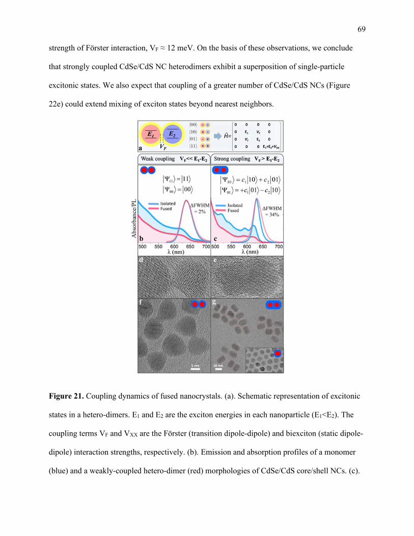
69 strength of Förster interaction, VF ≈ 12 meV. On the basis of these observations, we conclude
that strongly coupled CdSe/CdS NC heterodimers exhibit a superposition of single-particle
excitonic states. We also expect that coupling of a greater number of CdSe/CdS NCs (Figure
22e) could extend mixing of exciton states beyond nearest neighbors.
Figure 21. Coupling dynamics of fused nanocrystals. (a). Schematic representation of excitonic
states in a hetero-dimers. E1 and E2 are the exciton energies in each nanoparticle (E1<E2). The
coupling terms VF and VXX are the Förster (transition dipole-dipole) and biexciton (static dipole-
dipole) interaction strengths, respectively. (b). Emission and absorption profiles of a monomer
(blue) and a weakly-coupled hetero-dimer (red) morphologies of CdSe/CdS core/shell NCs. (c).
70 Emission and absorption profiles of a monomer (blue) and a strongly-coupled hetero-dimer (red)
morphologies of CdSe/CdS core/shell NCs. (d,f). TEM images of weakly-coupled CdSe/CdS
core/shell NCs, fabricated using the FA fusion strategy at T = 130 °C. (e, g). TEM images of
strongly-coupled CdSe/CdS core/shell NCs, fabricated using the OLAM-S fusion strategy at T =
180 °C.
The fusion-assembly approach was also used to achieve heteroepitaxial bonds between
dissimilar semiconductor materials. This was demonstrated through the assembly of rock-salt
PbS and wurtzite CdS NCs. According to the TEM image of the reaction product in Figure 22a,
b, heterogeneous assemblies of CdS and PbS NCs were formed on par with homogeneous
clusters (CdS−CdS and PbS−PbS), accounting for at least 15% of morphologies (see Figure S5b
for the statistical analysis). The interface of CdS and PbS domains appeared to have minimal
alloying despite the difference in the type of the two lattice structures. We speculate that molten
surfaces of fusing nanoparticles help alleviating the heteroepitaxial strain through the formation
of an ion-diffusion boundary.250 Similar domain interfaces were also observed at interfaces of
CdS nanorods and CdS QDs, shown in Figure 22c, d. The above examples of the heteroepitaxial
fusion suggests that a utilization of molten surfaces in colloidal inorganic NCs could be a
feasible strategy for coupling lattice-mismatched materials.

71
Figure 22. Understanding molten layer formation and thickness. (a,b). High angle annular dark
field (HAADF)-STEM imaging of CdS-PbS assemblies comprising 8.6-nm PbS (lighter shade)
and 6.1-nm CdS (darker shade) nanocrystals. (c-d). TEM images of nanocrystal assemblies
comprising CdS NCs attached to CdS nanorods. (e). Chain-like assemblies of CdSe/CdS
core/shell NCs. (f). A thermodynamic model of surface melting in spherical nanocrystals. The
reduction in the nanoparticle free energy (ΔG) drives the formation of the molten layer with the
thickness δ. Melting is observed if the solid/solvent interfacial tension (γSV) is reduced upon the
insertion of a liquid layer: γSL + γLV -γSV < 0, where γSL and γLV are the solid/liquid and
liquid/solvent interfacial tensions, respectively. (g,h). The dependence of the free energy change,
ΔG, on the molten layer width, δ, for CdSe NCs at different solvent temperatures. Parameters of
the calculation are provided in Sec. SI.4. For small size CdSe NCs (R=1 nm), shown in (g), the

72 global minimum of ΔG at δ/R → 1 suggests melting of the entire nanoparticle (no surface
melting), whereas in (h) for larger CdSe NCs (R = 3 nm), a molten layer is energetically
favorable across a temperature range (e.g. at T = 140 °C and T = 210 °C).
4.5 Theoretical Model Describing Molten Surface Melting
Controlling the process of nanoparticle fusion during assembly requires understanding of
molten layer formation in semiconductor colloids. Thermodynamically,197-198, 240 melting of the
surface layer in inorganic nanoparticles is caused by the reduction of the interfacial energy
between the solid (nanoparticle) and matrix (either solvent/ligand or vacuum) phases. This
concept is illustrated in Figure 22f, indicating that the reduction of free energy, ΔG < 0, is caused
by the reduction in the nanoparticle interfacial tension (γSV) upon melting of the surface layer,
such that γSL + γLV − γSV < 0, where γSL and γLV are the solid−liquid and liquid-solvent tension
terms. Consequently, the formation of a molten (liquid) layer represents a general property of the
inorganic phase, as was evident from early studies on bulk surfaces251 (Figure S10).
In case of small-diameter nanoparticles, the onset of surface melting due to interfacial
tension is contributed both by solid/ solvent interactions and by the curvature of a particle (see
section SI.4 and Figure S11). The corresponding change in the free energy with increasing liquid
layer thickness, δ, ΔG(δ) = Gslv − Gsv, was calculated in this work by adapting the Kofman
approximation198 to spherical nanoparticles in solution (section SI.4). The minimum of ΔG(δ, T)
at each temperature provides the expected thickness of the molten layer, δ(T), as illustrated in the
case of R = 3 nm CdSe NCs in Figure 22h. At T = 90 °C, ΔG is positive for any δ, indicating that
melting does not occur. At T = 140 °C, ΔG exhibits a minimum at δ/R = 0.1 (0.3 nm), which
implies that surface melting is energetically favorable at this temperature. The thickness of the
molten layer increases to δ/R = 0.18 (0.54 nm) at T = 210 °C, which is consistent with the TEM
image of partly fused nanocrystal assemblies in Figures 18 and 19. At T = 250 °C, the global
73
minimum of ΔG occurs at δ/R → 1, indicating that the entire particle becomes molten. Fusion of
these nanoparticles results in their full coalescence as can be verified by the TEM image of the
reaction product at these temperatures (Figure 18, rightmost frame). In case of small-size CdSe
NCs (R = 1 nm), no local minimum of ΔG is observed (Figure 22g). Instead, increasing the
temperature to above 90 °C results in a global minimum at δ/R → 1, indicating that the entire
particle becomes molten. These predictions agree with the experimental data on fusion of small-
diameter CdSe NCs (Figure S12) showing a sharp transition from isolated particles to nearly
coalesced dimers when the temperature is increased from 120 to 140 °C.
Overall, the above model predictions indicate that the onset of surface melting in
semiconductor nanocrystals occurs at a relatively low thermal threshold, which agrees with
experimental observation of nanocrystal fusion at these temperatures. Consequently, ripening
processes of nanoparticles growth that benefit from a molten layer formation, such as digestive
or Ostwald ripening, would be strongly enhanced under these conditions and should be
considered when modeling colloidal growth reactions.
4.6 Conclusions on Nanocrystal Molecular Assemblies
In summary, we have demonstrated a colloidal strategy for building coupled assemblies
of semiconductor nanocrystals. The present approach exploits a general property of inorganic
colloids to form a molten surface layer upon heating, which allows attaching nanoparticles at
hybrid interfaces. The assembly method was demonstrated through the synthesis of
homogeneous (CdS−CdS, CdSe−CdSe, PbS−PbS) and heterogeneous (CdS−PbS, CdS−CdSe,
CdSe/CdS−CdSe/ CdS) nanocrystal molecules, where the interaction between assembly
components was mediated by charge and energy transfer processes. Heterodimer assemblies of
CdSe/CdSe NCs exhibited evidence of the exciton band formation with a tunable superposition
of single-particle states. The dynamics of nanoparticle assembly was successfully explained
74 within the viscoelastic interaction theory developed for molten-surface colloids. Predictions of
this model were found in a good agreement with the experimentally observed formation of
nanocrystal molecules and alloyed interfaces. Such molten− particle interactions could be
relevant for many synthetic processes, including aggregative growth, oriented attachment, and
coalescence. Overall, we expect that the demonstrated molten-surface assembly of
semiconductor nanocrystals will provide a synthetic and theoretical foundation needed for
building artificial molecules of potentially many inorganic nanocrystals.
4.7 Experimental Methods for Quantum Dot Molecules
The following materials were used: cadmium oxide (CdO, 99% STREM), 1- octadecene
(ODE, 90% Aldrich), n-octadecylphosphonic acid (ODPA, PCI), octadecylamine (ODA, 90%,
Acros), oleic acid (OA, 90% Aldrich), sulfur (S, 99.99% Acros), methanol (anhydrous, 99.8%
Aldrich), chloroform (anhydrous, 99% Aldrich), oleylamine (OLAM, tech., 70% Aldrich),
hexane (anhydrous, 95% Aldrich), ethanol (anhydrous, 95% Aldrich), tri-noctylphosphine (TOP,
97% STREM), tri-n-octylphosphine oxide (TOPO, 99.0% Aldrich), selenium powder (Se, 200
mesh, Acros), acetone (anhydrous, Amresco, ACS grade), stearic acid (97% Aldrich),
tributylphosphine (TBP, 97% Aldrich) and diethylzinc (95% STREM). All reactions were
performed under argon atmosphere using the standard Schlenk technique. The centrifuge used
for precipitation operated at 5400 and 7200 rpm.
CdS NCs were fabricated according to the previously reported procedure.252 A mixture of
0.0768 g (0.6 mmol) of CdO, 3.6 mL of OA, and 24 mL of ODE in a 50 mL three- S5 neck flask
was heated to 240 °C until the solution turned optically clear and colorless. Then, the mixture
was allowed to stir at this temperature at which point all of the sulfur precursor solution made by
dissolving 0.02 g (0.625 mmol) of sulfur powder at 200 °C in ODE (10 mL) was quickly
injected. The reaction was stopped by removing the flask from the heating mantle after 4−5 min.
75 CdS NCs were separated from the solution by precipitating with methanol and redissolving the
product in chloroform.
CdSe NCs were fabricated by adapting a previously reported procedure.14 5 Briefly, TOPO
(3.0 g), ODPA (0.025 g), OA (2.0 mL), and CdO (0.060 g) were mixed in a 50 mL flask, heated
to 120 °C and exposed to vacuum for 1 h. Then, under argon, the solution was heated to 300 °C
to dissolve CdO until the mixture turned optically clear and colorless. At this point, 1.5 g of TOP
(that had been degassed at 120 °C for 30 min) was injected into the flask and the temperature
was adjusted to 270 °C. The reaction flask with the Cd precursor was raised up from the heating
mantle right before the injection of the Se precursor to get small-diameter nanoparticles. A
selenium precursor prepared by dissolving 0.060 g of Se in 1 mL of TOP through heating to 150
°C under argon and cooling to room temperature was injected all at once into the raised flask (at
270 °C). The reaction temperature dropped to approximately 250 °C and was left stirring for 30 s
before being quenched in a water bath, this yielded CdSe nanocrystals with a first exciton peak
around 520 nm. After the synthesis, nanocrystals were precipitated with ethanol and washed by
repeated redissolution in chloroform and precipitation with the addition of ethanol. Finally, the
product was stored in chloroform (3 mL).
Synthesis of CdSe/CdS core/shell NCs was performed using an “accelerated” procedure
evolved from a previously reported seeded-type growth approach.253 In a typical synthesis, S
(0.120 g) was dissolved in TOP (1.81 mL) at 200 °C and after cooling to room temperature was
mixed with CdSe nanocrystal solution in chloroform. Separately, a mixture of CdO (0.060 g),
TOPO (3.0 g) and OA (1.5ml) was exposed to vacuum at 150 °C for 60 min. Subsequently, the
system was switched to Ar flow and heated to 300 °C until the solution turned optically clear and
colorless. At this point, TOP (1.0 mL) was added to the flask, and the temperature was raised to
350 °C. The growth of the CdS shell was initiated with a swift injection of a nanocrystal
76 seeds/sulfur mixture at 350 °C. After the initial temperature drop, the reaction temperature was
allowed to recover to 320 °C. The overall growth time was 2 min. S6 Purification of the
CdSe/CdS NCs was carried out by precipitation with ethanol and redispersion in hexane. This
process was repeated two times, and the final product was stored in hexane.
PbS NCs were fabricated according to a procedure adapted from Hines et al.5 In a typical
synthesis, a mixture of 0.49 g (2mmol) PbO in 18 mL of ODE and 1-16 mL of OA (increasing
the amount of OA results in a larger NC diameter) was degassed in a threeneck flask at 120°C
for 2 hours, switched to Argon, and heated to 135 °C. Meanwhile, 10 mL of ODE was degassed
for two hours at 120°C and allowed to cool down to room temperature. Then, 0.21 ml of
(TMS)2S was added carefully into the flask and the resulting (TMS)2S/ODE mixture was
injected into the Pb precursor solution at 135°C, while stirring. The reaction was stopped after 0-
5 minutes (longer reaction time leads to larger NCs) by removing the flask from the heating
mantle and placing it into an ice water bath. Nanocrystals were isolated from the mixture by
precipitating with acetone, centrifuging, and re-dispersing in toluene. The cleaning procedure
was repeated 2-3 times, upon which nanocrystals were re-dispersed in a minimal amount of
hexane (4- 5 ml).
The fusion of nanocrystals (assembly method 1) in non-polar solvents was carried out
either by using a mixture of OLAM and chalcogenide (S, Se) selenium powders or a mixture of
OLAM and 10-20 mg of CdCl2 salt. In the former case, 10-20 mg of colloidal NCs were
dispersed in 3 mL of OLAM along with 5-15 mg of S or Se powder. Chalcogenide powder
(suspended in ODE) could also be injected directly after the OLAM/NC mixture reached the
desired temperature. Prior to heating, the solution was degassed at 80 °C to remove impurity
solvents. The fusion reaction temperature ranged between 95 °C and 180 °C for
OLAM/chalcogenide mixtures. In the case of the OLAM/CdCl2 reaction mixture, the fusion
77 temperature ranged between 220 °C and 280 °C. The mixture was kept at this temperature for 30
min to an hour under argon atmosphere. Subsequently, solutions were allowed to cool to room
temperature and precipitated twice with ethanol/toluene. The final solution was dispersed in
hexane and centrifuged to remove all unused chalcogenide/CdCl2 powders or insoluble species.
The fusion of S 2- -capped nanocrystals in polar solvent, called assembly method 2. The
method for transferring nanocrystals to FA with S2- ligands was adapted from Nag et al.8 In a
typical fusion reaction, 120 mg of Na2S•9H2O was dissolved in 6 mL of FA and mixed together
with 3mL of hexane solution of colloidal nanocrystals capped with X-type ligands (e.g. OA).
Upon transferring S7 to FA, the NC/FA mixture was heated to a desired temperature (usually
120 °C – 140 °C). From room temperature, the solution was heated at a rate of approximately
18°C/min and maintained at the final temperature for 5 minutes, followed by rapid quenching in
a water bath. After the temperature had fallen below 60 °C, 4 mL of OLAM and 2 mL of
chloroform were added to phase transfer the nanocrystals from FA/S2- back to CHCl3/OLAM.
The nanocrystals were precipitated with ethanol and then redispersed in 4 mL of OLAM and 1
mL ODE and heated to 120 °C for 20 minutes to anneal the fused nanocrystals and fully
passivate the nanocrystal surface. The final fused nanocrystals were cleaned by two cycles of
precipitation with ethanol/toluene and redispersion in hexane.
6.2-nm PbS NCs were combined with 8.6-nm CdS NCs in a flask containing a 50:50
OLAM:ODE degassed mixture. Elemental sulfur in the amount of 0.02 g dissolved in a minimal
amount of ODE was added to the flask at room temperature. The mixture was then quickly
heated to 180 – 200 °C, and kept at that temperature for 5-10 min to achieve interparticle fusion.
The product was isolated from the mixture by precipitating with acetone, centrifuging, and re-
dispersing in toluene.
78
5 ENGINEERING NANOCRYSTALS FOR EXTENDED BIEXCITON LIFETIMES
The following chapter and all of its content was reprinted with permission from [Kholmicheva,
N.; Budkina, D. S.; Cassidy, J.; Porotnikov, D.; Harankahage, D.; Boddy, A.; Galindo, M.;
Khon, D.; Tarnovsky, A. N.; Zamkov, M., Sustained Biexciton Populations in Nanoshell
Quantum Dots. ACS Photonics 2019, 6, 1041]. Copyright © 2019 American Chemical Society.
All supporting information is avaliable, free of charge, at
https://doi.org/10.1021/acsphotonics.9b00068
5.1 Introduction to Multiexcitons in Quantum Dots
Multiple excitons (MXs) play an important role in the photoinduced dynamics of
semiconductor nanocrystals. The utilization of multiexciton effects in photovoltaic254-256 and
photoelectrochemical67, 69 devices has long been considered for converting the energy of a single
high-energy photon into multiple carriers as a mechanism for mitigating thermal energy losses.
Likewise, MXs are essential for the operation of quantum-dot lasers,54, 60, 257-258 where multiple
excitons are required for achieving the excited-state population inversion, and were recently
considered as a strategy for carrier concentration in multielectron photocatalytic reactions (e.g.,
H2 production and water oxidation).259-262 The advancement of these applications faces an
important challenge of overcoming the fast nonradiative Auger decay of multiple excitations in
semiconductor nanocrystals.60 This process is known to cause a reduced trion emission in
nanocrystals and is often invoked to explain photoluminescence blinking in single quantum
dots.263 Even in the case of longer-lived biexciton populations (n = 2), the Auger decay time
constant could be as short as just a few picoseconds (e.g., CdSe or PbSe NCs),264-265 representing
the predominant mechanism of carrier loss in laser and photovoltaic applications of these
materials.266-267
79 Within the framework of interacting formalism,268 the Auger recombination rate
decreases linearly with nanoparticle volume (Γ−1 ∼ V0.9−1.1).269-273 As a result, the general
solution for enhancing the biexciton lifetime of semiconductors is often sought through
nanoscale geometries that offer a reduced confinement in one or two spatial dimensions. Along
these lines, zero-dimensional nanocrystals have given way to architectures featuring mixed
dimensionalities, such as alloyed core/shell nanoparticles,274-275 nanorod-shaped
heterostructures,276-280 and nanoplatelets (NPLs),281-285 where the increased confinement volume
leads to long-lived biexcitons.
Quantum-dot quantum-well (QDQW) systems286-297 represent another example of low-
dimensional colloids that could potentially result in suppressed Auger recombination of
biexcitons. The quantum confined layer in these materials (e.g., CdSe or HgS) is sandwiched
between the core and shell domains comprising a wider gap semiconductor (e.g., CdS and ZnS).
The resulting energy gradient leads to the formation of two-dimensional excitons that reside
primarily in the intermediate shell and therefore exhibit an increased confinement volume.
Recently, such quantum-well layers were successfully grown onto bulk-size core domains.298-299
An important advantage of the bulk-seeded “nanoshell” geometry was associated with the ability
to preserve the radial confinement of photoinduced charges regardless of the particle size.
Consequently, all three dimensions of nanoshells could exceed the exciton Bohr radius, enabling
a significant increase in the exciton confinement volume.299 The reported nanomaterials,
however, employed a single-barrier CdS/CdSe architecture (Figure SF1), where the carrier
delocalization at unpassivated CdSe surfaces interfered with the biexciton dynamics.

80
Figure 23. Configuration of CdSbulk/CdSe/CdSshell quantum-well nanoshells. (a) Schematic
illustration of a CdSbulk/CdSe/CdSshell quantum-well nanoshell geometry along with a
projected carrier localization pattern. The energy offset of CdSe and CdS valence bands
promotes a strong localization of photoinduced holes within the CdSe shell; meanwhile, the
energetic proximity of electronic states in CdSbulk and CdSe domains and low effective masses
of CdSbulk and CdSe electrons cause the delocalization of photoinduced electron wave functions
over the entire nanocrystal volume. (b) Estimated quantum-confinement volume corresponding
to several reported MX geometries: spherical CdSe quantum dots (diameter = 4 nm), CdSe/ CdS
dot in a rod (dot diameter = 4 nm; rod length = 30 nm), CdSe/ CdS core/shell (core radius = 2
nm; shell radius = 10 nm), CdSe/ CdS nanosheets (20 nm × 20 nm × 2 nm), and QW nanoshells,
81 reported here (CdSe shell radius = 6 nm; shell thickness = 2 nm; total radius = 10 nm), from left
to right, respectively.
Here, we report on the synthesis of semiconductor quantum-well nanoshells exhibiting
long-lived biexciton populations. The unique feature of the demonstrated nanoparticle
architecture lies in the one-dimensional confinement of excitons within the surface layer (CdSe)
of the bulk-size semiconductor nanoparticle (CdSbulk). In this geometry (Figure 23a), all three
dimensions of CdSbulk/CdSe/CdSshell core/shell/shell nanostructures are allowed to exceed the
exciton Bohr radius, lifting spatial limitations on the total particle size. We show that such an
arrangement of semiconductor domains allows us to increase the volume of the carrier
confinement more effectively than by using other zero-, one-, or two-dimensional geometries
(Figure 23b), which makes the reported architecture particularly suitable for suppressing Auger
recombination processes. By using femtosecond transient absorption spectroscopy, we
demonstrate that the biexciton lifetime of CdSbulk/CdSe/CdSshell nanostructures featuring a 10
nm diameter CdSe shell (τ2 ≈ 1.24 ns) can be increased more than 30 times compared to that of
zero dimensional CdSe nanocrystals. The observed biexciton lifetime was found to be inversely
proportional to the thickness of the quantum confined layer, which was attributed to the size-
dependeny tuning of CdSe energy levels at CdSe/CdS interfaces. Our study has also revealed a
significant contribution of surface recombination processes to single exciton decay in bulk-
seeded nanoshells [quantum yield (QY) < 17%], as compared to similar processes in smaller-
diameter QDQW (QY = 30−90%). Because surface recombination could potentially affect the
biexciton dynamics on par with Auger processes, we believe that future improvements in the
surface chemistry of these materials should result in further increases in the biexciton lifetime.
Overall, the demonstrated suppression of Auger processes in CdSbulk/CdSe/CdSshell nanoshells is
expected to encourage the utilization of these nanostructures in MX applications (MX generation
82 and stimulated emission), particularly because the reported geometry could be extended to a
plethora of QDQW semiconductor combinations (e.g., CdS/HgS/CdS, ZnSe/ InP/ZnSe, and
ZnS/CdS/ZnS). In addition to enhanced biexciton lifetimes, an important advantage of the
nanoshell architecture includes a continuous density of excited states,286, 289, 300 which permits
lasing without the complete occupation of the CB edge,301 similar to nanoplatelets113, 302 and
nanosheet colloids.303 Finally, a nearly spherical shape of nanoshells is expected to facilitate the
assembly of these nanostructures into solids and superlattices,304-305 a task that could be
challenging in the case of nonspherical one- and twodimensional colloids.
5.2 Engineering Materials for Extended Biexcitons and Their Spectroscopic Properties
Figure 23a shows a projected pattern of carrier confinement in CdSbulk/CdSe/CdSshell
quantum-well nanoshells. A relatively high energy of the CdSe valence band (VB) edge is
expected to result in a strong confinement of photoinduced holes within the CdSe domain.306 In
contrast, photoinduced electrons are likely to become delocalized over the entire nanoparticle
volume due to nearly degenerate energies of conduction band (CB) edges in the two materials.307
Under these conditions, the ensuing nature of electron−hole Coulomb interactions in QW
nanoshells is strongly dependent on the relative offset of CB energies in CdS and CdSe
semiconductors. If the global minimum of CB electrons lies in CdSe (type I confinement), the
corresponding electron−hole spatial overlap will be greater than when such a minimum is found
in the CdS material (quasi-type II confinement). Because the electron−hole overlap directly
affects Coulomb interactions between photoinduced charges, the ultimate offset of CB energies
in QW nanoshells should play an important role in determining the rate of corresponding Auger
processes. To understand the magnitude of this effect, we have explored both aforementioned
types of carrier confinement, which was accomplished by varying the thickness of the CdSe
layer in CdSbulk/CdSe/ CdSshell QW nanoshells.
83 CdSbulk/CdSe/CdSshell quantum-well nanoshells were synthesized through a successive
deposition of respective layers via hot-injection colloidal chemistry. First, bulk-size CdS
nanoparticles (d = 5.8−13.1 nm) were grown by ripening 4 nm CdS nanocrystalline seeds in the
presence of oleylamine.98-99 The final product containing monodisperse, bulk-size CdS NCs was
then used for seeding the growth of the CdSe shell.299 During the CdSe deposition stage, a
mixture of Cd and Se precursors was gradually introduced into the solution of CdSbulk
nanoparticles. Slow injection speeds, controlled by a syringe pump, helped to prevent the
formation of isolated CdSe NCs. Typically, the shell growth was continued until the excitonic
feature corresponding to the lowest-energy transition in the CdSe shell (λ = 550−630 nm) was
observed in the absorption spectra (see Figure 24e). The shoulder like appearance of the exciton
absorption profile in nanoshells was consistent with the two-dimensional character of the carrier
confinement. The onset of the CdSe exciton absorption in CdS/CdSe nanoparticles was
accompanied by an increase in the intensity of the CdSe band gap photoluminescence (PL)
signal, corresponding to the CB → VB carrier recombination in the shell domain (see Figure
24e). In addition to the band gap PL, the emission profile of CdS/CdSe nanoshells contained a
broad spectral feature spanning the range of 700−1000 nm, which was tentatively attributed to
the interaction of “core” excitons with strongly coupled surface states.308 We speculate that such
surface emission in nanoshells could be enhanced relative to that of zero-dimensional CdSe NCs
due to the surface localization of photoinduced holes (Figure SF1a). Their strong interaction with
the nanocrystal surface states could explain a relatively low, 1−3% PL QY of the band gap
emission in large diameter (>12 nm) CdS/CdSe nanoshell quantum dots. Conversely, Cd-
(oleate)2-capped small-diameter CdS/CdSe nanoshells were shown to exhibit a PL QY of
≤8%.299
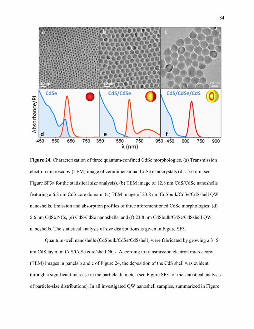
84
Figure 24. Characterization of three quantum-confined CdSe morphologies. (a) Transmission
electron microscopy (TEM) image of zerodimensional CdSe nanocrystals (d ≈ 5.6 nm; see
Figure SF3a for the statistical size analysis). (b) TEM image of 12.8 nm CdS/CdSe nanoshells
featuring a 6.2 nm CdS core domain. (c) TEM image of 23.8 nm CdSbulk/CdSe/CdSshell QW
nanoshells. Emission and absorption profiles of three aforementioned CdSe morphologies: (d)
5.6 nm CdSe NCs, (e) CdS/CdSe nanoshells, and (f) 23.8 nm CdSbulk/CdSe/CdSshell QW
nanoshells. The statistical analysis of size distributions is given in Figure SF3.
Quantum-well nanoshells (CdSbulk/CdSe/CdSshell) were fabricated by growing a 3−5
nm CdS layer on CdS/CdSe core/shell NCs. According to transmission electron microscopy
(TEM) images in panels b and c of Figure 24, the deposition of the CdS shell was evident
through a significant increase in the particle diameter (see Figure SF3 for the statistical analysis
of particle-size distributions). In all investigated QW nanoshell samples, summarized in Figure

85 25, the CdS shell growth step has resulted in an improved emission QY. Of the two strategies for
shell deposition, employing either the slow or fast309 injection of precursors, the former method
has yielded an overall better quality and a greater PL QY of QW nanoshells. Generally, the
dispersion of CdSbulk/CdSe/CdSshell particle diameters was <10% (Figure SF3c,e). On the
contrary, the fast growth strategy has resulted in colloids exhibiting a partly fragmented shell
morphology with a corresponding particle-size dispersion of 12.5% (Figure SF4).
Figure 25. Summary of structural and optical parameters corresponding to eight investigated
samples. The sample number in the leftmost column is used as a unique sample ID in the Results
and Discussion
The growth of the CdS passivating layer on CdS/CdSe nanoshells was accompanied by
the red-shift of the band gap emission (Figure 24f) reflecting the delocalization of electronic
wave functions into the CdSshell domain. The quantum yield of the band gap PL in
CdSbulk/CdSe/CdSshell nanoparticles has varied between 4% and 17% (Figure 25) depending on
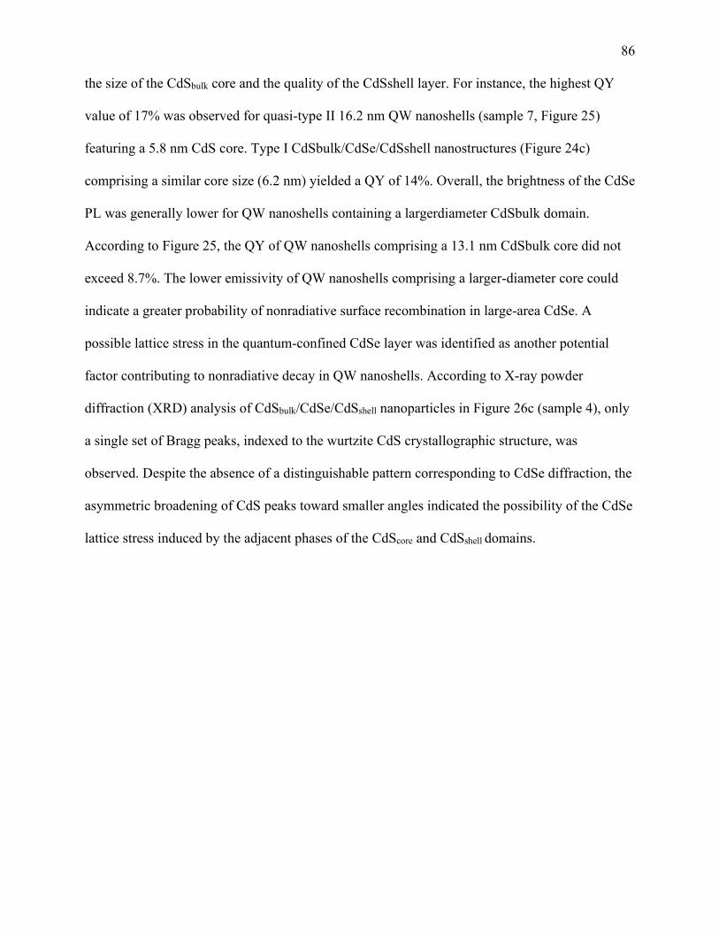
86 the size of the CdSbulk core and the quality of the CdSshell layer. For instance, the highest QY
value of 17% was observed for quasi-type II 16.2 nm QW nanoshells (sample 7, Figure 25)
featuring a 5.8 nm CdS core. Type I CdSbulk/CdSe/CdSshell nanostructures (Figure 24c)
comprising a similar core size (6.2 nm) yielded a QY of 14%. Overall, the brightness of the CdSe
PL was generally lower for QW nanoshells containing a largerdiameter CdSbulk domain.
According to Figure 25, the QY of QW nanoshells comprising a 13.1 nm CdSbulk core did not
exceed 8.7%. The lower emissivity of QW nanoshells comprising a larger-diameter core could
indicate a greater probability of nonradiative surface recombination in large-area CdSe. A
possible lattice stress in the quantum-confined CdSe layer was identified as another potential
factor contributing to nonradiative decay in QW nanoshells. According to X-ray powder
diffraction (XRD) analysis of CdSbulk/CdSe/CdSshell nanoparticles in Figure 26c (sample 4), only
a single set of Bragg peaks, indexed to the wurtzite CdS crystallographic structure, was
observed. Despite the absence of a distinguishable pattern corresponding to CdSe diffraction, the
asymmetric broadening of CdS peaks toward smaller angles indicated the possibility of the CdSe
lattice stress induced by the adjacent phases of the CdScore and CdSshell domains.
87
Figure 26. High-angle annular dark field (HAADF)-STEM image of (a) a 12.8 nm
CdSbulk/CdSe nanoshell (sample 3 in Figure 25) and (b) a CdSbulk/CdSe/CdSshell quantum-
well nanoshell (sample 6). (c) TEM image of 18.4 nm CdSbulk/CdSe nanoshells (sample 2)
comprising a 13.1 nm CdS core. (d) TEM image of 16.2 nm CdSbulk/CdSe/CdSshell quantum-
well nanoshells (sample 8). (e) Powder X-ray diffraction (XRD) analysis of crystal phases in
18.4 nm CdSbulk/CdSe nanoshells (sample 2), suggesting that core/shell nanoparticles grow in a
wurtzite crystallographic phase with a CdSe domain exhibiting a stressed lattice pattern (peak
broadening toward smaller angles). (f) EDX analysis of elemental fractions in 18.4 nm
CdSbulk/CdSe nanoshells (sample 2).
Spectroscopic data combined with TEM characterization of a nanoparticle product at
different growth stages were used as the primary strategy to determine the thickness of the CdSe
layer in CdSbulk/CdSe/CdSshell QW nanoshells. Ensuing CdSe thickness assignments were found
88 to be consistent with the energy dispersive X-ray (EDX) analysis performed on selected
specimens. For instance, relative amplitudes of SK-shell, SeL-shell, and CdL-shell X-ray signals
in the 18.4 nm CdS/CdSe nanoshells (sample 2, Figure 26f) suggest a 1:1.4 ratio of CdS to CdSe
semiconductors in these nanoparticles, which falls within 10% of the CdS:CdSe ratio estimated
from the TEM and ultraviolet−visible analysis of the same structures (Figure 26c and Figure
SF3b). The presence of the CdSe crystal phase in QW nanoshells was also confirmed by EDAX-
STEM analysis of selected areas on a TEM grid (Figure SF4). The biexciton dynamics of
nanoshell quantum dots was investigated by means of the femtosecond pump−probe transient
absorption spectroscopy, as described in Methods. The laser pump wavelength (λ = 420 nm) was
set to excite band gap transitions in both CdS and CdSe domains of nanoshells, the recovery of
which was then probed using a white-light supercontinuum (λ = 400−650 nm). The pump power
was adjusted using neutral density filters to produce an average exciton population ⟨N⟩ of
0.4−1.1 per single nanocrystal (see Figure SF6).
5.3 Carrier Confinement in Quantum Dots Quantum Well Nanoshells
To understand the effect of the radial carrier confinement in nanoshells on the ensuing
biexciton dynamics, transient absorption (TA) measurements of CdSbulk/CdSe/CdSshell QW
nanoshells were compared with those of zero-dimensional CdSe and unpassivated CdSbulk/CdSe
quantum dots. Figure 27b shows the chirp-corrected TA spectra of 5.6 nm CdSe NCs (sample 1).
The excitation pulse resulted in photobleaching of the 1S(e)−1S3/2(h) low-energy transition,
denoted as CdSe1S (λ ≈ 610 nm), as well as the higher-energy excitation, corresponding to the
combination of 1S(e)−2S1/2(h) and 1P(e)−1P3/2(h) transitions310 labeled A (λ = 500−540 nm). In
the case of 18.4 nm CdS/CdSe nanoshells, TA spectra revealed two areas of photobleaching as
indicated in Figure 27e. A stronger ΔA signal at λ ≈ 500 nm was attributed to the excitation-
induced state filling of the 1S(e)−1S3/2(h) transition in the CdS core, while the second TA bleach,
89 observed at lower energies (λ = 540−610 nm), was attributed to the lowest-energy transition in
the CdSe shell. Notably, the spectral position of the assigned CdSe bleach was correlated with
the steady-state exciton absorption of the CdSe shell (Figure 27d). In addition to the two negative
ΔA signals, the TA spectra of both nanostructures contained derivative-like distortions, labeled
as B. The two signals had lifetimes comparable to those of 1S(e)−1S3/2(h) transitions and were
ascribed to their spectral interactions with the 1P(e)−1P3/2(h) bands.311-312 A slow recovery of the
CdS bleach in CdS/CdSe nanoshells [λ ≈ 490 nm (Figure 27e and Figure SF7)] indicated the lack
of a significant driving force for the photoinduced electron transfer into the CdSe shell. Indeed,
because of the high degeneracy of hole levels in spherical CdS NCs, the TA bleach of band edge
transitions is primarily contributed by electrons. Consequently, a slow reduction in the ratio of
core to shell TA bleach amplitudes as a function of the pump− probe delay is consistent with the
delocalization of the electron wave function over the entire nanoparticle volume.
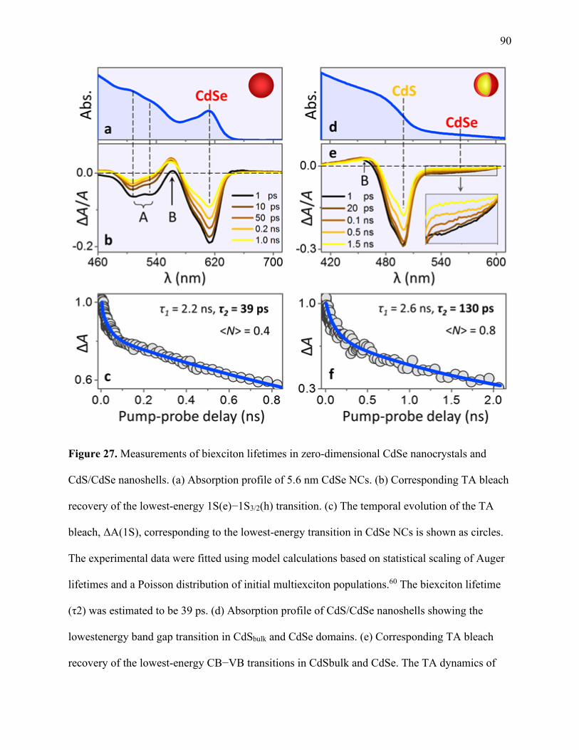
90
Figure 27. Measurements of biexciton lifetimes in zero-dimensional CdSe nanocrystals and
CdS/CdSe nanoshells. (a) Absorption profile of 5.6 nm CdSe NCs. (b) Corresponding TA bleach
recovery of the lowest-energy 1S(e)−1S3/2(h) transition. (c) The temporal evolution of the TA
bleach, ΔA(1S), corresponding to the lowest-energy transition in CdSe NCs is shown as circles.
The experimental data were fitted using model calculations based on statistical scaling of Auger
lifetimes and a Poisson distribution of initial multiexciton populations.60 The biexciton lifetime
(τ2) was estimated to be 39 ps. (d) Absorption profile of CdS/CdSe nanoshells showing the
lowestenergy band gap transition in CdSbulk and CdSe domains. (e) Corresponding TA bleach
recovery of the lowest-energy CB−VB transitions in CdSbulk and CdSe. The TA dynamics of
91 the CdSe spectral region is magnified in the inset. (f) Temporal evolution of the measured TA
bleach associated with the CdSe shell (circles). The experimental data were fitted using eq 1,
resulting in a biexciton lifetime (τ2) of 130 ps. The pump pulse fluence corresponded to ⟨N⟩ =
0.8 exciton per nanocrystal.
To extract biexciton lifetimes from the bleach recovery kinetics in panels c and f of
Figure 27, we have employed the coupled rate equation formalism,60 which assumes (i) a Poisson
distribution of initial multiexciton populations in a nanocrystal ensemble and (ii) statistical
scaling of Auger lifetimes. Within this strategy, the average number of photons absorbed by a
nanoparticle, ⟨N⟩, is first estimated from the known excitation pulse power, spectral density, and
sample absorption profile.313 The average number of absorbed photons per particle is
subsequently used to create the statistical distribution of nanoparticle fractions in the sample that
receive n = 0, 1, 2, ..., excitons, P(n). To this end, the probability of a nanocrystal absorbing n
photons, f(n), is assumed to follow the Poisson distribution f(n) = ⟨N⟩n × e−n /n!, as shown in
Table ST1. Under the assumption that multiple excitons in a given nanocrystal decay
sequentially (via Auger recombination), the temporal evolution of the n-exciton population in a
particle, P(n, t), can be determined by solving coupled rate equations:
𝑑𝑑𝑑𝑑(𝑖𝑖,𝑒𝑒)𝑑𝑑𝑒𝑒
= 𝑑𝑑(𝑖𝑖+1,𝑒𝑒)𝜏𝜏𝑛𝑛+1
− 𝑑𝑑(𝑖𝑖,𝑒𝑒)𝜏𝜏𝑛𝑛
(5.1)
where τn represents the lifetime of the n-exciton state. The resulting evolution of multiexciton
populations, P(n, t), obtained by solving eq 5.1, depends on a single unknown parameter, τ2,
corresponding to the Auger-limited biexciton lifetime. The single exciton lifetime, τ1, as well as
multiexciton lifetimes (τn; n > 2) entering eq 1 can be determined a priori. To this end, τ1 is either
extracted from the long-time TA bleach recovery at low excitation powers or obtained from the
PL intensity decay (Figure SF8). The lifetimes of multiexciton states, τn, are computed using the
92 statistical scaling law τn
-1 = n2(n – 1)τ2-1/4.314 Because of the relatively low excitation powers
used in the experiments presented here (⟨N⟩ ∼ 1), we assume that the TA bleach, ΔA, is
contributed by up to four excitons, such that the average number of excitons per nanocrystal
becomes P(t)=4 × P(4, t)+3 × P(3, t) + P(2, t) + P(1, t). The resulting parametric curve, P(τ2, t),
was used to fit the experimentally measured TA bleach, ΔA(t), to determine the best fitting
parameter, τ2 (see Table ST1). We note that despite n = 2 being the highest exciton occupation
number for zero-dimensional CdSe NCs, due to continuous electron density in CdS/CdSe
nanoshells, these colloids are likely to support a larger number of band edge excitons.
Figure 27c shows the TA bleach recovery kinetics for CdSe1S excitations in zero-
dimensional CdSe nanocrystals. The best fit of the experimental data with the multiexciton
population curve, P(t), has yielded an average biexciton lifetime [τ2(CdSe)] of 39 ps. In applying
the fitting procedure, we have used the single exciton lifetime [τ1(CdSe)] of 2.2 ns, which was
obtained from the double-exponential fit to the long-time TA data. The ⟨N⟩ value of 0.4 was
estimated from the excitation pulse fluence and further corroborated by the ΔA/A power
dependence in Figure SF6 (according to ref 272). Overall, the measured biexciton lifetime in 5.6
nm CdSe NCs appeared to be within the range of τ2 values reported by previous works.315-316
Given the small size of these nanocrystals, the corresponding Auger decay was expected to be
enhanced due to a strong interaction of photoinduced charges.
The multiexciton dynamics of CdS/CdSe nanoshells is analyzed in Figure 27f, showing
the temporal evolution of the integrated TA bleach recovery corresponding to the CB−VB
transition in the CdSe shell. The experimental data were fitted with the multiexciton decay curve
obtained by solving eq 1 (blue curve). In this case, a single exciton lifetime τ1 of 2.6 ns (see
Table ST1) was obtained from the double-exponential fit to the long-time TA bleach recovery
93 spectra. According to the best fit of the experimental data in Figure 27f, the biexciton lifetime
(τ2) was determined to be 130 ps.
5.4 Biexciton Decay Pathways
There are several processes that can potentially contribute to the decay of biexciton
populations in CdS/CdSe nanoshells. In addition to the Auger recombination mechanism,
multiple excitations could undergo a nonradiative decay through interactions with nanoshell
surfaces, as their area is increased in comparison with those of zero-dimensional structures.
Excitons can also funnel to the potential energy minimum of nanoshells associated with a locally
enhanced CdSe thickness, where the number of Coulomb interactions is increased. To estimate
whether Auger recombination represents the primary process of biexciton decay, we have
compared the volume dependence of measured biexciton lifetimes in CdS/CdSe and zero-
dimensional CdSe NCs. Considering that the quantum confinement volume of nanoshells,
Vexciton, differs from the nanoparticle physical volume, the value of Vexciton was obtained by using
a strategy developed for alloyed-interface CdSe/CdS core/shell NCs.274 The employment of the
same model in characterizing photoinduced electrons of CdSe/CdS core/shell and CdS/CdSe
nanoshell quantum dots could be reasonably expected due to the similarity of energy offsets and
effective masses in bulklike cores of nanoshells and bulklike shells of CdSe/CdS nanocrystals.
To this end, the effective volume was derived by using localization radii of the electron and hole
wave functions, Re and Rh, respectively, such that Vexciton = (8π/3) × (Re2Rh
2)/(Re + Rh). The
value of Rh for nanoshells was determined from the total volume of the shell (Vshell) as follows:
Rh = ∛((3/4𝜋𝜋)𝑉𝑉_𝑠𝑠ℎ𝑚𝑚𝑒𝑒𝑒𝑒 ). Accordingly, we estimate that for 18.4 nm nanoshells, Vexciton is 9.8
times greater than the volume of 5.6 nm CdSe NCs, which places the biexciton lifetime in the
range of 400 ps. Consequently, the measured constant τ2 of 130 ps falls short of the volume
scaling prediction. The biexciton lifetime of nanoshells also appears to be shorter than Auger
94 time constants reported for other twodimensional forms of nanoscale CdSe, such as CdS/CdSe
nanoplatelets (500 ps)281 or alloyed-interface CdSe/CdS core/ shell nanostructures (>1 ns). A
lower than expected lifetime of biexcitons in CdS/CdSe nanoshells was tentatively attributed to
the enhanced role of surfaces in a nanoshell geometry, where surface-localized photoinduced
holes can drive nonradiative recombination of excitons. The same issue could be responsible for
a relatively short lifetime of single excitons in CdS/CdSe nanoshells [τ1 ≈ 2.2 ns (see Table
ST1)].
The level of surface-induced carrier recombination in CdSbulk/CdSe nanoshells was
significantly reduced upon the deposition of the CdSshell layer. The successful neutralization of
surface traps in CdSbulk/CdSe/CdSshell QW nanoshells was evidenced through the enhancement of
the PL quantum yield (from 1% to 3% to 17%) as well as an apparent increase in the single
exciton lifetime (Figure SF8). The presence of the “holeblocking” surface layer in
CdSbulk/CdSe/CdSshell nanostructures has also given rise to characteristic temporal changes in the
TA dynamics of CdSe excitons, as summarized in Figure 28. For all three investigated
geometries of CdSbulk/CdSe/CdSshell QW nanoshells, including small-core type II (Figure 28b),
large-core type I (Figure 28e), and small-core type I (Figure 28i) specimens, the recovery of
biexciton populations was noticeably slower than in the case of “unpassivated” CdS/CdSe
nanoshells (Figure 27e). According to the model fit of the integrated CdSe TA signal, a small-
core type II CdSbulk/CdSe/ CdSshell QW nanoshell geometry resulted in the longest biexciton
lifetime of 1.24 ns (Figure 28c). A somewhat lower decay constant was observed for small-core
type I nanostructures [τ2 = 0.85 ns (Figure 28j)], exhibiting a stronger carrier overlap. The
comparison of the TA bleach recovery between type I (sample 7) and type II (sample 8) QW
nanoshells has helped in identifying the effect of the carrier localization on the value of τ2, as
both specimens featured nearly the same CdSbulk/CdSe/CdSshell and CdSbulk diameters (see Figure
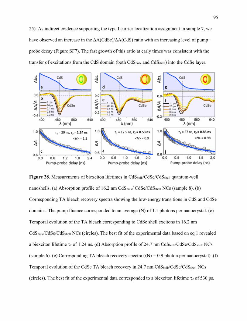
95 25). As indirect evidence supporting the type I carrier localization assignment in sample 7, we
have observed an increase in the ΔA(CdSe)/ΔA(CdS) ratio with an increasing level of pump−
probe decay (Figure SF7). The fast growth of this ratio at early times was consistent with the
transfer of excitations from the CdS domain (both CdSbulk and CdSshell) into the CdSe layer.
Figure 28. Measurements of biexciton lifetimes in CdSbulk/CdSe/CdSshell quantum-well
nanoshells. (a) Absorption profile of 16.2 nm CdSbulk/ CdSe/CdSshell NCs (sample 8). (b)
Corresponding TA bleach recovery spectra showing the low-energy transitions in CdS and CdSe
domains. The pump fluence corresponded to an average ⟨N⟩ of 1.1 photons per nanocrystal. (c)
Temporal evolution of the TA bleach corresponding to CdSe shell excitons in 16.2 nm
CdSbulk/CdSe/CdSshell NCs (circles). The best fit of the experimental data based on eq 1 revealed
a biexciton lifetime τ2 of 1.24 ns. (d) Absorption profile of 24.7 nm CdSbulk/CdSe/CdSshell NCs
(sample 6). (e) Corresponding TA bleach recovery spectra (⟨N⟩ = 0.9 photon per nanocrystal). (f)
Temporal evolution of the CdSe TA bleach recovery in 24.7 nm CdSbulk/CdSe/CdSshell NCs
(circles). The best fit of the experimental data corresponded to a biexciton lifetime τ2 of 530 ps.
96 (g) Absorption profile of 23.9 nm CdSbulk/CdSe/CdSshell NCs (sample 7). (i) Corresponding TA
bleach recovery spectra (⟨N⟩ = 0.98). (j) Temporal evolution of the CdSe TA bleach recovery in
23.8 nm CdSbulk/CdSe/ CdSshell NCs (circles). The best fit of the experimental data corresponded
to a biexciton lifetime τ2 of 850 ps.
The observation of a shorter biexciton time constant for type I QW nanoshells (sample 7)
was consistent with a relatively smaller exciton volume in these nanostructures. Furthermore, in
comparison with type I core/shell nanocrystals, the type II localization regime has been predicted
to increase the repulsive component of the Coulomb interaction causing a net repulsion of
biexcitons,317 thus diminishing their corresponding Auger recombination rates. Such an
enhancement of the biexciton lifetime in type II structures has been also observed in CdSe/ CdS
core/shell and ZnSe/CdSe core/shell nanostructures.317-318 Finally, samples featuring a large-size
CdS core yielded the lowest of three biexciton lifetimes (τ2 = 0.53 ns). While the exciton volume
for this QW geometry was larger than in the case of small-core type I nanocrystals (sample 7),
the single exciton lifetime for large-core nanoshells was comparatively short [τ1 = 12.5 ns
(Figure 28f)]. This was likely the result of enhanced surface recombination caused by a relatively
large surface area of the quantum-confined CdSe. As was stated above, the synthesis of such
large-core QW nanoshells has not been optimized to the same degree as for small-core
nanostructures. We expect, however, that with the future improvements in the surface
passivation of large-core nanoshells, the biexciton time constant could be increased beyond the
range of τ2 reported for small-core structures.
5.5 Conclusions Regarding Sustained Biexciton Populations
In conclusion, we report on the synthesis of semiconductor quantum-well nanoshells
exhibiting long-lived biexciton populations. The demonstrated nanoparticle architecture utilizes a
CdSbulk/CdSe/CdSshell core/shell/shell morphology, which effectively reduces the rate of
97 Auger recombination in the quantum-confined layer of CdSe. As a result, the nonradiative decay
of biexcitons becomes suppressed, as was demonstrated in this work by means of femtosecond
transient absorption spectroscopy. In particular, we show that the biexciton lifetime of
CdSbulk/CdSe/CdSshell nanostructures featuring an 8 nm-diameter CdSe shell (τ2 ≈ 1.24 ns)
was increased more than 30 times compared to that of zerodimensional CdSe nanocrystals. We
expect that the demonstrated QW nanoshell architecture could useful in applications win which
long-lived biexciton populations are critical to performance. Furthermore, a nearly spherical
shape of QW nanoshells is expected to facilitate the assembly of these nanostructures into solids
and superlattices, a task that could be challenging in the case of nonspherical one- and
twodimensional colloids.
5.6 Experimental Methods on the Engineering of Quantum Dots for Extended Biexciton
Lifetimes
The following materials were used: cadmium oxide (CdO, 99%, Aldrich), 1-octadecene
(ODE, 90%, Aldrich), oleic acid (OA, 90%, Aldrich), sulfur (S, 99.99%, Acros), ethanol
(anhydrous, BeanTown Chemical), chloroform (anhydrous, 99%, BeanTown Chemical),
oleylamine (OLAM, tech., 70%, Aldrich), tri-n-octylphosphine (TOP, 90%, Acros), tri-n-
octylphosphine oxide (TOPO, 99.0%, Aldrich), selenium powder (Se, 200 mesh, Acros), and
acetone (anhydrous, Amresco, ACS grade), All reactions were performed under an argon
atmosphere using the standard Schlenk technique. The centrifuge (VWR Clinical 100) used for
precipitation was operated at 6500 rpm.
Bulk-size CdS nanocrystals (d = 6−14 nm) were fabricated through digestive ripening of
small-diameter CdS nanocrystals prepared according to the method described in ref 319. The
details of the digestive ripening protocol are given in ref 98. Briefly, small-diameter CdS NC
seeds were transferred into a flask containing a 60:40 OLAM/ODE mixture (total volume of 7
98 mL) and degassed at 120 °C to remove chloroform. The reaction mixture was subsequently
heated to 260 °C under argon. When the desired nanoparticle size was reached, the reaction was
stopped by removing the flask from the heating mantle. The NC product was separated from the
solution by precipitating with acetone and redispersing in chloroform.
The deposition of the CdSe shell onto bulklike CdS nanoparticles was performed using a
previously reported strategy.299 First, cadmium oleate was prepared by dissolving 0.025 g of
CdO in the mixture of 0.4 mL of OA and 5.4 mL of ODE under an argon flow at 260 °C and
cooled to room temperature. In a separate flask, 0.015 g of Se was dissolved in 1 mL of TOP at
120 °C. The TOP/Se mixture was added to Cd-(oleate)2 at room temperature. For CdSe shell
deposition, the reaction mixture containing bulk-size CdS NCs in chloroform, 4 mL of OLAM,
and 10 mL of ODE was degassed at 120 °C, switched to argon, and heated to 260 °C. When the
temperature stabilized, the combined precursor mixture was injected into the reaction flask via a
syringe pump at a rate of 1 mL/h. Once the desired CdSe shell size was reached (typically, when
the intensity of the CdSe shell PL became prominent), the reaction was stopped by removing the
flask from the heating mantle. The product was separated from the solution by precipitation with
a 1:2 ethanol/acetone mixture and stored in chloroform.
The growth of the CdS passivating layer on CdS/CdSe nanoshells was performed
according to the methodology of either Cirillo et al.309 or Jeong et al.287 The latter method
yielded overall better-quality nanocrystals exhibiting a relatively greater QY. In this case,
cadmium oleate was prepared by degassing a mixture of 0.034 g of CdO, 0.8 mL of OA, and 5
mL of ODE at 120 °C for 30 min followed by switching the flask to an argon atmosphere and
heating to 230 °C until the solution became clear. At the same time, a mixture of 0.026 g of S
powder and 1.8 mL of TOP was degassed at 120 °C for 30 min. Both Cd and S precursors were
mixed at room temperature and stored under an argon flow. For CdS shell deposition, a mixture
99 of CdS/CdSe seeds in chloroform, 4 mL of OLAM, and 10 mL of ODE was transferred to the
reaction flask and degassed at 120 °C for 1 h. Subsequently, the flask was switched to Ar and
heated to 260 °C. As soon as the temperature stabilized, the Cd/S precursor mixture was injected
into the flask with the syringe pump at a rate of 2 mL/ h. Once the desired shell size was reached,
the reaction was stopped by removing the flask from the heating mantle. The product was
separated from the solution by precipitation with a 1:2 ethanol/acetone mixture and stored in
chloroform.
Ultraviolet−visible absorption spectra were recorded using a CARY 60 scan
spectrophotometer. High-resolution transmission electron microscopy (TEM) measurements
were carried out using a JEOL JEM-3011UHR instrument operated at 300 kV. Specimens were
prepared by depositing a drop of NP solution in organic solvent onto a carbon-coated copper grid
and allowing it to dry in air. Powder X-ray diffraction measurements were carried out with a
Bruker D8 Advance PXRD instrument. Luminescence spectra were recorded using a 400 nm
PicoQuant PDL 800-D pulsed laser and measured with an Andor newton detector. Time-resolved
emission lifetime spectra were recorded using the same 400 nm pulsed laser, and photons were
collected and processed using a SPC-130 TCSPC module from Boston Electronics. Relative
quantum yield measurements were acquired using a GS32 Intelite 532 nm CW DPSS laser (a
Cyanine3 NHS ester dye obtained from Lumiprobe was used as the reference).
The femtosecond transient absorption spectrometer used in these experiments is based on a
regeneratively amplified Ti:sapphire laser system (Hurricane, Spectra-Physics) that generates a 1
kHz train of 90 fs (fhwm), 0.9 mJ pulses centered at 800 nm. The amplified beam is a 50:50
split. The first beam is sent to a TOPAS-C optical parametric amplifier to produce the 420 nm
(or 500 nm) pulses used for sample excitation. The second beam is attenuated, sent through a
computer-controlled optical delay stage, and then focused onto a 3 mm CaF2 window to produce
100 a white-light continuum (wlc) probe spanning the range of 345−760 nm. The wlc probe beam
was focused to a 75 μmdiameter spot at the sample position and overlapped at a 6° angle with the
excitation beam focused to a 150 μm-diameter spot. A fraction of the wlc probe beam was split
off before the sample to be utilized as a reference for the correction of shotto-shot pulse intensity
fluctuations. The probe (after the sample) and reference beams were dispersed by a spectrograph
and recorded using a dual 512-pixel diode array detector synchronized to the 1 kHz repetition
rate. The difference between the decadic logarithms of a probe-to-reference pulse intensity ratio
was measured at a specific position of the optical stage for the case in which the excitation pulse
was on and off. Typically, 300 on and off pairs were averaged to produce the transient absorption
signal (ΔA) at the corresponding delay time, and then the procedure was repeated for ∼10 scans
of the optical delay stage. The solutions were kept in a 1 mm path length cell or in a spinning 2
mm path length cuvette. These two sets of conditions did not have any noticeable difference in
terms of the time and spectral evolution of transient absorption signals. The zero delay time
positions at different probe wavelengths were obtained from nonresonant electronic responses
from a neat CHCl3 solvent measured under the same experimental conditions320 and used for the
chirp correction of the measured ΔA data. The typical excitation energy was 0.5 μJ/pulse. The
linearity of ΔA signals with excitation energy confirmed that single-photon excitation is
responsible for the measured data. The polarization of the excitation beam was set at the magic
angle (54.7°) with respect to the probe beam to eliminate signals from rotational dynamics of the
solute. All experiments were performed at 21 °C.
101 6 QUANTUM SHELL NANOCRYSTALS: AVENUE FOR LONG OPTICAL GAIN AND
LOW-THRESHOLD AMPLIFIED SPONTANEOUS EMISSION
The following chapter and all its content was reprinted with permission from [Cassidy, J.; Diroll,
B. T.; Mondal, N.; Berkinsky, D. B.; Zhao, K.; Harankahage, D.; Porotnikov, D.; Gately, R.;
Khon, D.; Proppe, A.; Bawendi, M. G.; Schaller, R. D.; Malko, A. V.; Zamkov, M., Quantum
Shells Boost the Optical Gain of Lasing Media. ACS Nano 2022, 16 (2), 3017-3026]. Copyright
© 2022 American Chemical Society. All supporting information is avaliable, free of charge, at
https://doi.org/10.1021/acsnano.1c10404
6.1 Introduction to Optical Gain and Amplified Spontaneous Emission in Quantum Shell
Nanocrystals
Colloidal semiconductor quantum dots (QDs) hold strong promise for future
optoelectronic applications.321-322 These nanomaterials are inexpensive to process and offer a
broad range of attractive quantum-mechanical properties. Central to their appeal is an efficient,
narrowband emission,323 which has encouraged QD commercialization in backlit displays.324-325
Meanwhile, a combination of high color purity, quantized electronic levels, and solution-phase
device processing has stimulated the interest in QD-based optically and electrically pumped
light-emitting devices.326-327 In this case, QDs can offer low lasing thresholds and temperature-
insensitive gains,328-331 a tunable electroluminescent spectrum,332-333 and low injection current in
high-brightness LEDs.55, 334-335
The geometric confinement of electrical charges in colloidal QDs leads to extraordinary
optical performance in a single-exciton regime, but is detrimental to multi-exciton dynamics. The
Coulomb interactions of proximal excitons cause their Auger recombination,336 which leads to
substantial energy losses in photonic applications.314, 337 Accordingly, several strategies have
been devised over the years for suppressing Auger processes in colloidal semiconductor QDs.
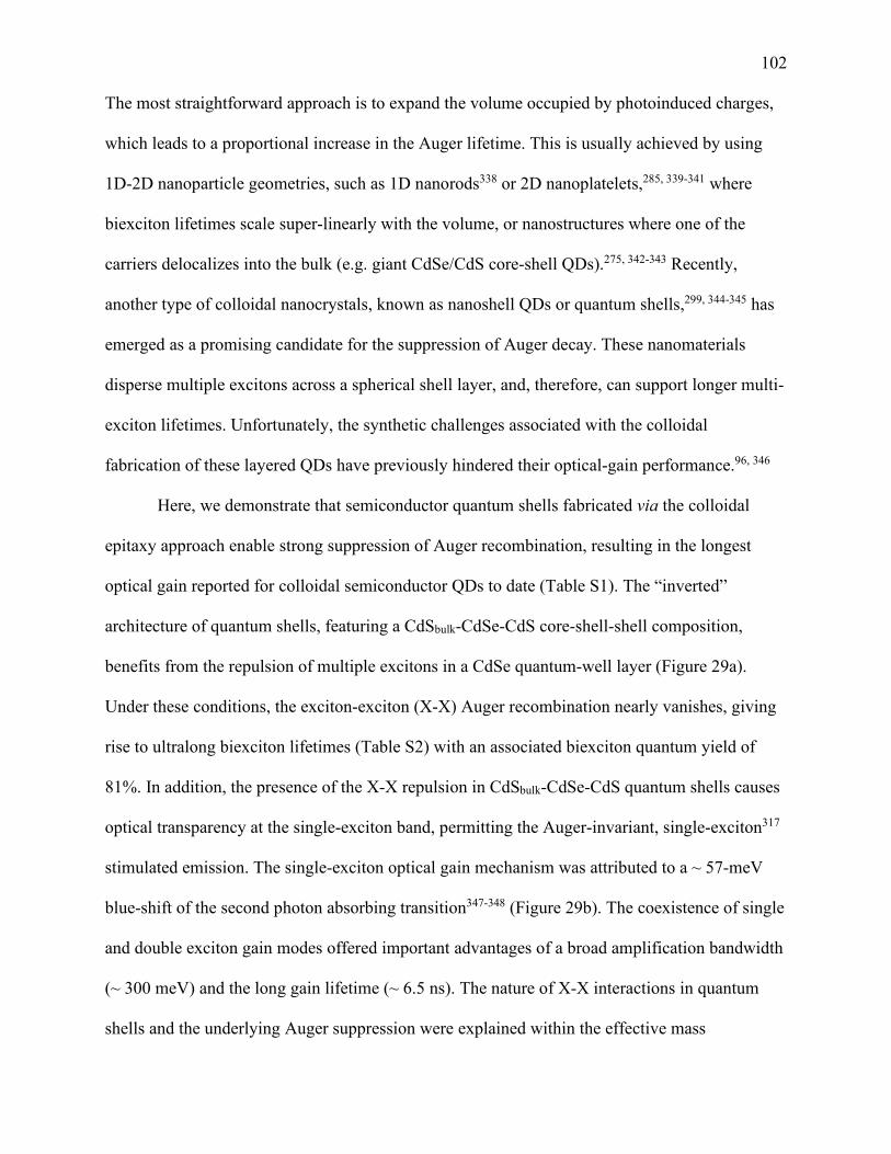
102 The most straightforward approach is to expand the volume occupied by photoinduced charges,
which leads to a proportional increase in the Auger lifetime. This is usually achieved by using
1D-2D nanoparticle geometries, such as 1D nanorods338 or 2D nanoplatelets,285, 339-341 where
biexciton lifetimes scale super-linearly with the volume, or nanostructures where one of the
carriers delocalizes into the bulk (e.g. giant CdSe/CdS core-shell QDs).275, 342-343 Recently,
another type of colloidal nanocrystals, known as nanoshell QDs or quantum shells,299, 344-345 has
emerged as a promising candidate for the suppression of Auger decay. These nanomaterials
disperse multiple excitons across a spherical shell layer, and, therefore, can support longer multi-
exciton lifetimes. Unfortunately, the synthetic challenges associated with the colloidal
fabrication of these layered QDs have previously hindered their optical-gain performance.96, 346
Here, we demonstrate that semiconductor quantum shells fabricated via the colloidal
epitaxy approach enable strong suppression of Auger recombination, resulting in the longest
optical gain reported for colloidal semiconductor QDs to date (Table S1). The “inverted”
architecture of quantum shells, featuring a CdSbulk-CdSe-CdS core-shell-shell composition,
benefits from the repulsion of multiple excitons in a CdSe quantum-well layer (Figure 29a).
Under these conditions, the exciton-exciton (X-X) Auger recombination nearly vanishes, giving
rise to ultralong biexciton lifetimes (Table S2) with an associated biexciton quantum yield of
81%. In addition, the presence of the X-X repulsion in CdSbulk-CdSe-CdS quantum shells causes
optical transparency at the single-exciton band, permitting the Auger-invariant, single-exciton317
stimulated emission. The single-exciton optical gain mechanism was attributed to a ~ 57-meV
blue-shift of the second photon absorbing transition347-348 (Figure 29b). The coexistence of single
and double exciton gain modes offered important advantages of a broad amplification bandwidth
(~ 300 meV) and the long gain lifetime (~ 6.5 ns). The nature of X-X interactions in quantum
shells and the underlying Auger suppression were explained within the effective mass

103 approximation. Our calculations show that quantum shells support an intrinsically smaller
electron-hole overlap compared to “conventional” CdSe-CdS core-shell QDs, which diminishes
their non-radiative recombination rate.
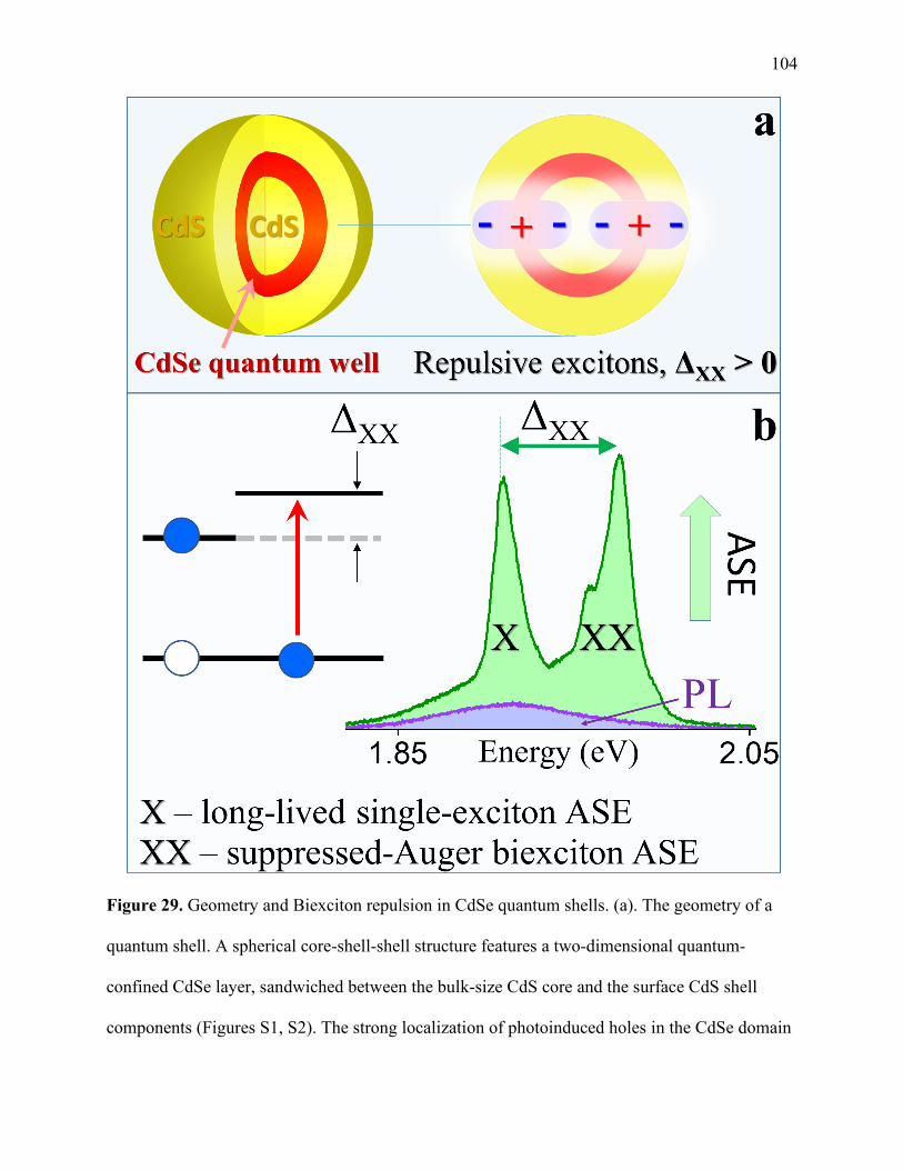
104
Figure 29. Geometry and Biexciton repulsion in CdSe quantum shells. (a). The geometry of a
quantum shell. A spherical core-shell-shell structure features a two-dimensional quantum-
confined CdSe layer, sandwiched between the bulk-size CdS core and the surface CdS shell
components (Figures S1, S2). The strong localization of photoinduced holes in the CdSe domain

105 leads to the repulsion of multiple excitons (ΔXX > 0). (b). The X-X repulsion offsets an absorbing
transition energy for the second incoming photon, allowing for a single-exciton optical gain in
quantum shells. The spectrum shows a dual-mode amplified spontaneous emission (ASE)
involving both the single-exciton and the biexciton gain mechanisms. These bands are separated
by the X-X interaction energy of 57 meV. The pump fluence was 10.5 μJ/cm2.
6.2 Quantum Shell Fabrication and Biexciton Dynamics
The geometry of a CdSbulk-CdSe-CdS quantum shell is illustrated in Figure 29a. The CdSe
quantum-well layer is sandwiched between the two CdS “barrier” components, providing a
potential energy minimum to photoinduced charges. An important aspect of the quantum shell
design is the large-diameter CdS core domain, which distinguishes the present quantum shell
geometry from previously reported Quantum-Dot Quantum-Wells (QDQW).288, 292, 295, 349-352 The
existence of a large core increases the volume occupied by multiple excitons, leading to their
reduced Coulomb interactions. This results in the reduction of the Auger recombination rate,
which is inversely proportional to the nanoparticle volume, (Γ-1 ~ V1.1).268, 271
In the present work, CdSbulk-CdSe-CdS quantum shells were fabricated by growing two
sequential shell layers onto 4.5 - 6.0 nm CdS core nanocrystals. The size of the CdS core
component surpasses the CdS exciton Bohr radius (~3.4 nm)353 and therefore is considered to be
bulk-like. An improved growth strategy, called colloidal epitaxy, was used to achieve defect-free
interfaces between a thin CdSe quantum-well layer and bulk-like CdS phases, which was crucial
to suppressing Auger recombination of multiple excitons. The deposition of the ~2-nm CdSe
shell onto the CdS core results in the band gap photoluminescence (PL) (Figures 30a and S3),
which intensity increases with the subsequent growth of the 3-5 nm CdS “surface-barrier” shell.
In the case of 4.5-nm-core quantum shells, the diameter of the entire nanoparticle averages 16
nm with a size dispersion of 8.1% (Figures 30d-30f and S6), whereas 6.0-nm-core quantum

106 shells reach an average size of 22 nm (Figure 30g). The estimated 2.0-nm thickness of the CdSe
quantum-well layer in 6.0-nm-core nanostructures was corroborated by the spectral position of
their respective PL maximum (Figure SF11). The presence of the CdSe quantum-well layer was
also evident through a color-contrast in high angle annular dark field (HAADF)-STEM images
(Figure S5).
The PL spectrum of 4.5-nm-core quantum shells in Figure 30a exhibits a single emission
peak with a corresponding quantum yield (QY) of 52% (Figure S7). A relatively small PL
linewidth (ΔE = 69 meV) in 4.5-nm-core quantum shells attests to the narrow distribution of the
CdSe layer thickness. Notably, the absorption profile of 4.5-nm-core quantum shells (Figure 30a)
resembles those of high-quality CdSe-CdS core-shell QDs featuring well-resolved 1S light-hole
and heavy-hole transitions. The comparison of PL intensity decay in 4.5-nm-core quantum shells
measured at low and high pump fluences (<N> ≈ 0.05 and <N> ≈ 1.2 excitations per dot,
respectively) reveals a long ensemble-averaged biexciton lifetime of τxx = 5.1 ns (Figure 30b, red
curve). This result was corroborated by single-particle measurements of the same sample,
showing an intensity-resolved characteristic biexciton lifetime of τxx = 6.2 ns (Figure S4b).
Quantum shells featuring a larger, 6.0-nm core size, exhibit even longer τxx, approaching 10.5 ns
(Figure S8b). To the best of our knowledge, these are among the longest biexciton lifetimes
reported for colloidal semiconductor QDs to date (Table T2).
107
Figure 30. Characterizations of CdSe quantum well nanocrystals. (a). Absorption and emission
spectra of 4.5-nm-core CdSbulk-CdSe-CdS quantum shells (RCdS = 2.25 nm, HSe = 2 nm and HS =
3.75 nm). (b). The photoluminescence intensity decay of 4.5-nm-core CdSbulk-CdSe-CdS
quantum shells measured under two excitation regimes with the average number of absorbed
photons per QD being equal to <N> ≈ 0.05 (grey curve) and <N> ≈ 1.2 (red curve). The high-
power excitation regime reveals an ensemble-averaged biexciton lifetime of τXX = 5.1 ns. The
low-power excitation measurement (black curve) shows a single-exponential decay with an
exciton lifetime of τXX = 36 ns (R-value = 0.998). (c). Lagtime-dependence of the cross-
correlation function, g2, showing the ratio of biexciton to exciton QY (BX/X QY) for 4.5-nm
core (orange curve) and 6.0-nm core (blue curve) quantum shells. (d). Transmission electron
microscopy (TEM) image of 4.5-nm-core CdSbulk-CdSe-CdS quantum shells. (e-f). High-
108 resolution TEM images of 4.5-nm-core CdSbulk-CdSe-CdS quantum shells. (g). TEM image of
6.0-nm-core CdSbulk-CdSe-CdS quantum shells.
The quantum yield (QY) of biexciton emission can be expressed using statistical
considerations as QYXX = 4τXX/τrad,X , where τXX is the experimental biexciton lifetime and τrad,X
is the radiative lifetime of single excitons.321 Taking into account the single-exciton quantum
yield QYX = 52% and PL lifetime τX = 36 ns, we can estimate the biexciton-to-exciton quantum
yield ratio, QYXX /QYX = 4τXX/(QYX × τrad,X) = 4τXX/τX ≈ 0.57. To obtain a more accurate
estimate of QYXX, we use Fluorescence Correlation Spectroscopy that determines the ensemble
averaged biexciton-to-exciton quantum yield ratio from a solution-phase photon correlation.354
To this end, we detect emission from diffusing nanoparticles in solution using a confocal
microscope and a pulsed excitation source in a Hanbury-Brown-Twiss setup. We then calculate
the second order cross-correlation function, g(2)(τ), according to the protocol on page S14 of the
SI section. Figure 30c shows that the QYXX /QYX is higher for the 6.0-nm-core QDs (81.8% ±
1.1%) compared to 4.5-nm core samples (62.0% ± 0.4%) suggesting a reduction in the non-
radiative Auger recombination pathway as a result of the greater delocalization of the electron
wave function.
6.3 Ultrafast Spectroscopy and Optical Gain
To understand the spectral and temporal characteristics of the optical gain in quantum shells,
we performed femtosecond transient absorption (TA) measurements of dilute nanoparticle
solutions. The TA study primarily focused on 4.5-nm-core quantum shells, exhibiting 80%
greater single-exciton QY than those with a 6.0-nm core. In these experiments, the absorption
change (Δα = α – α0) induced by a femtosecond pulse is monitored by using a broadband pulse of
a white-light continuum. Optical gain is realized when -Δα/α0 > 1, where α0 is a linear absorption.
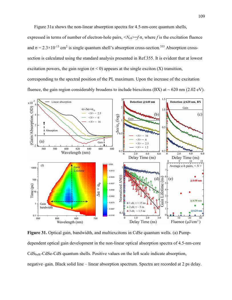
109
Figure 31a shows the non-linear absorption spectra for 4.5-nm-core quantum shells,
expressed in terms of number of electron-hole pairs, <Neh>=f σ, where f is the excitation fluence
and σ = 2.3×10⁻¹³ cm2 is single quantum shell’s absorption cross-section.355 Absorption cross-
section is calculated using the standard analysis presented in Ref.355. It is evident that at lowest
excitation powers, the gain region (σ < 0) appears at the single exciton (X) transition,
corresponding to the spectral position of the PL maximum. Upon the increase of the excitation
fluence, the gain region considerably broadens to include biexcitons (BX) at ~ 620 nm (2.02 eV).
Figure 31. Optical gain, bandwidth, and multiexcitons in CdSe quantum wells. (a) Pump-
dependent optical gain development in the non-linear optical absorption spectra of 4.5-nm-core
CdSbulk-CdSe-CdS quantum shells. Positive values on the left scale indicate absorption,
negative–gain. Black solid line – linear absorption spectrum. Spectra are recorded at 2 ps delay.
110 (b, c) Population-dependent TA dynamics at various photon energies. Black solid lines –
single/double/triple exponential fits (d) Dynamics of 1, 2 and 3 e-h pair states obtained using the
subtractive procedure as described in the text. Black lines - single exponential fits. Here, larger
core sample (6 nm) is used. (e) Gain lifetimes at different wavelengths extracted from dynamics
in panels (b) – red dots, (c) –blue triangles and additional set at 630 nm – green squares (f). A 3D
lifetime/bandwidth contour plot of the optical gain in a low-concentration, 4.5-nm-core quantum
shells. The positive gain is achieved when α + αΔ > 0. The pump fluence is 36 μJ/cm2.
Figure 31 (b,c) shows gain dynamics at X and BX transitions. Dynamics of X transition
at the lowest excitation level are close to the monoexponential with τlong > 15 ns, with more
precise determination limited by the scanning range of the delay line. Optical gain (-Δα/α0 > 1)
appears close to <Neh> ~ 2 and extends to τgain~ 6.5 ns (Figure 31e) at the highest excitation
level, making it the longest gain lifetime recorded for colloidal semiconductor QDs to date. For a
comparison, first reports of optical gain in colloidal CdSe/ZnS QDs dealt with exciton gain
lifetimes in 10-100 ps range as they were limited by strong Auger recombination.356-358 More
recently, long–lived optical gain has been achieved in CdSe-CdS nanoplatelets (830 ps)359 and
charged CdSe-CdS QDs (1.6 ns),360 where enhanced lifetimes were possible due to sub-single
exciton gain mechanisms.
Gain at the BX transition develops at the higher excitation levels, nevertheless reaching
~300 ps lifetime. We note that the power dependence of X and BX gain thresholds has a
complex character imposed by the multi-exciton interactions in the initially populated state,
which alters <Neh> from the values derived using population statistics.257, 286, 361 These multi-
exciton interactions affect both the gain threshold and gain bandwidth. The latter is illustrated in
Figure 31f showing the 3D bandwidth/lifetime contour plot of the excited state absorption at a
higher excitation level (fluence = 36 μJ/cm2). The gain bandwidth extends to ~ 300 meV, which

111 is one of the largest known for colloidal QDs. Previously, large gain bandwidths have been
observed in core/shell quantum dots that were capable of accommodating multi-exciton
populations either by having a large optical cross section275, 362 or through energy-coupling to
quantum shells.288
To characterize multiexcitonic Auger recombination decays, we recorded exciton population
dynamics at <Neh> = 0.5; 1.5; and 2.5 pairs and used a simple subtractive procedure268 to derive
the single exponential decays of each multiexciton species, shown in Figure 31d. As expected,
the resultant carrier dynamics become progressively faster due to Auger recombination. Ratio of
Auger times for 3 and 2 pair states, τ3: τ2 ~ 0.5 : 1 is approximately following the volumetric
scaling that is expected for the spherically-symmetric confinement of carriers, τ3: τ2 ~ 0.44 : 1.
6.4 Amplified Spontaneous Emission from Quantum Shells: Utilization for Light Emitting
Applications
The long optical gain lifetime of quantum shells makes these nanomaterials a promising
candidate for the development of lasing media. To explore this prospect, we have measured the
amplified spontaneous emission (ASE) from a spincoated film of 4.5-nm-core quantum shells
(see Figure 32d). According to the standard practice, the samples were excited by focusing
ultrafast pulses through a cylindrical lens and the ASE was observed perpendicular to the
excitation direction. The onset of ASE is evident as a spectrally narrowed peak with superlinear
fluence-dependence on the higher-energy side of the broader PL band (Figure 32c). The energy
difference between the steady-state PL (Figure 32a) and ASE peak (Figure 32b) suggests a
biexciton origin of the optical gain mechanism with the corresponding biexciton binding energy
of -57 meV (X-X repulsion). Previously, such a significant X-X repulsion has been observed
only in type II QDs,317 where electrons and holes occupy different components of a core-shell

112 nanoparticle. Notably, the XX ASE peak of quantum shells appears at a relatively low pump
fluence of 9.52 μJ/cm2 (Figure 32c).
Figure 32. ASE measurements of CdSe quantum well films. (a). Absorption (blue) and emission
(red) spectra of 4.5-nm-core quantum shells (RCdS = 2.5 nm, HSe = 2 nm and HS = 4.5 nm). (b).
Emission spectra observed from thin films of 4.5-nm-core quantum shells for different pump
fluences. The narrow ASE peak at 9.8 μJ/cm2 corresponds to XX optical gain. The appearance of
the lower-energy ASE feature at 11.1 μJ/cm2 that matches the spectral position of the PL peak is
attributed to a single exciton gain mechanism. <N> are the average e-h pairs. (c). Evolution of

113 the biexciton ASE peak with increasing pump fluence. (d). The pump fluence dependence of the
integrated intensity in (c), which reveals the biexciton ASE threshold of 9.52 μJ/cm2.
In addition to the XX ASE feature at E = 2.02 eV, another narrow-bandwidth ASE peak
emerges when the pump fluence is increased to 11.1 μJ/cm2 (Figure 32b). The spectral position
of this ASE peak (E = 1.96 eV) matches the steady state PL, indicating a single-exciton origin of
this emission. Evidence of the single-exciton gain mechanism in ASE measurements
corroborates TA gain spectra in Figure 31a, which also show the optical gain maximum at the PL
photon energy. The observation of the single-exciton ASE feature provides additional evidence
in support of X-X repulsion, which perturbs the absorption energy of the second photon in
quantum shells (Figure 29b).348, 363 The fact that biexciton ASE appears at lower fluences than a
single-exciton ASE feature is partly contributed by the interaction between X and XX emissive
phases. In general, the average number of excitons per nanoparticle, required for a single exciton
optical gain is <NXgain> = 2/3.348 For a biexciton-mode ASE, the threshold occupancy rises to
<NXXgain> ≥ 1. The interference of single and double exciton bands, however, increases the
single-exciton threshold: ( ))/exp(3/2 22 Γ∆−−= XXXgainN , where Γ in the inhomogenious
linewidth of the lowest-energy transition. For quantum shells (Γ = 69 meV, ΔXX = 57 meV), this
correction yields a theoretical threshold of 8.0=XgainN . Further suppression of the single-
exciton ASE threshold will be contributed by interactions with other multi-exciton bands288 that
are clearly present in quantum shells (Figure SF10). Nevertheless, the interaction between X and
other emissive phases, by itself, is not sufficient to explain the “re-ordering” of the single- and
bi-exciton ASE onsets in investigated materials. According to TA measurements of the
stimulated emission in Figure 31a, the X gain (λ ≈ 645 nm) develops at lower fluences that XX
gain (λ ≈ 620 nm).

114
The question is why the single-exciton ASE feature arrears at a slightly higher fluence in
solid films, despite being observed at lower fluences in TA measurements. This anomalous
behavior could be attributed to the re-absorption of the X spontaneous emission in ASE
measurements. In solution-phase samples (TA measurements), the reabsorption of the single-
exciton emission is insignificant due to the lack of sample absorption at this wavelength. In a
solid film (ASE measurements), the absorption at the single-exciton emission is no longer
negligible (Figure SF12a). Such reabsorption of the emitted photon causes the suppression of
optical gain, which enhances ASE threshold for a single-exciton gain mechanism. For a
biexciton gain (λ = 620 nm), the absorption difference between solution and solid samples is not
significant, so XX ASE feature is suppressed less due to re-absorbance than X ASE peak. In
support of this explanation, we provide an example of a low-quality quantum shell film
(significant amount of light scattering, Figure SF12b), where single-exciton gain is still absent at
36.0 μJ/cm2.
Further increases of the excitation fluence result in the saturation of X and XX 1S
transitions, causing ASE from higher-energy excitons, including 1S(e)-2S3/2(h) (Figure 32a, top
panel) and 1P(e)-1P3/2(h) (Figures S9, S10) interband transitions. We note that optical gain due
to 1P excitons is rarely observed in conventional, core-shell QDs because of relatively short
multiexciton lifetimes.275 Such high-energy ASE allows demonstration of optical amplifications
with a large spectral bandwidth (Figure 31f) and low excitation thresholds.
6.5 Exciton-Exciton Repulsion Dynamics
To understand the origin of the strong exciton-exciton repulsion in quantum shells, we
calculate single-carrier wave functions for the lowest-energy excitons within the effective-mass
approximation364-365 (see SI for details of calculation). The corresponding electron and hole
radial probabilities, r2R2(r), are shown in Figure 33a for the three regions of a 4.5-nm-core

115 CdScore-CdSeshell-CdS quantum shell with RCdS = 2.25 nm, HSe = 2 nm and HS = 3.75 nm. The
strong localization of photogenerated holes in the CdSe shell region leads to a vanishing
probability of hole tunneling to the origin of a quantum shell QD (r = 0). For comparison, in case
of giant, 16-nm CdSe-CdS core-shell QDs with RCdSe = 2.3 and HS = 5.7 nm, the radial
probability profile of photoinduced holes is skewed towards the origin. Such a difference in the
hole localization pattern between the two morphologies leads to a considerable difference is the
electron-hole overlap. For CdScore-CdSe-CdS quantum shells, the overlap integral (Eq. SE11) is
determined to be f = 0.185, which is 2.5 times lower than in the case of giant core-shell QDs of
the same size (f = 0.505). We note that a lower e-h overlap enhances X-X repulsion by favoring
co-localization of same-sign charges.321 Simultaneously, it decreases the Coulomb attraction of
excitons, since charges of opposite sign are separated across the hetero-interface. The net effect
is a strong X-X repulsion, manifested in this work through blue-shifted ASE.
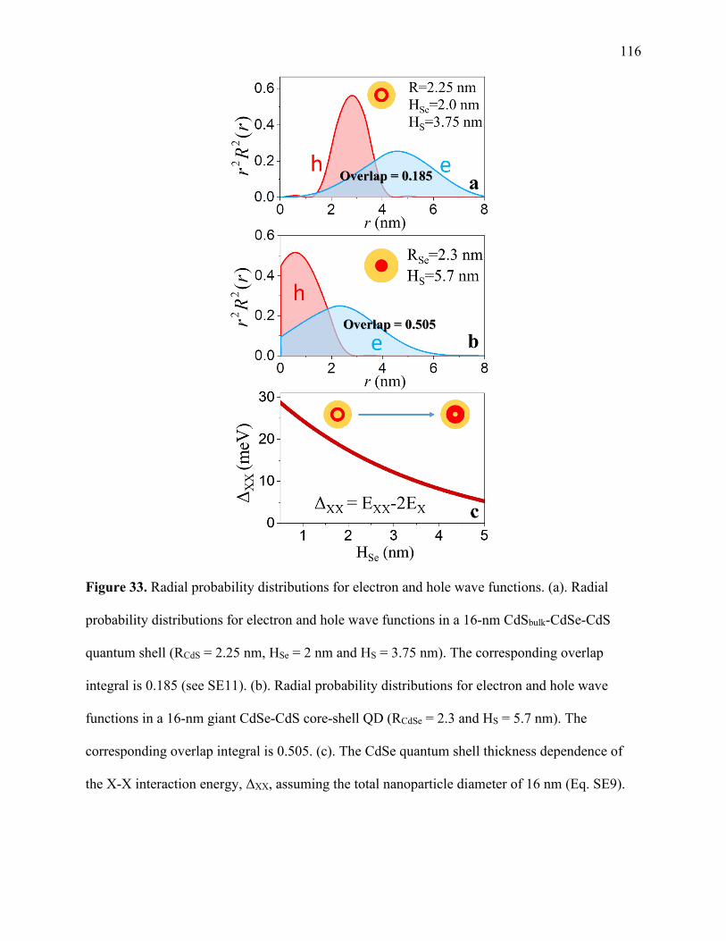
116
Figure 33. Radial probability distributions for electron and hole wave functions. (a). Radial
probability distributions for electron and hole wave functions in a 16-nm CdSbulk-CdSe-CdS
quantum shell (RCdS = 2.25 nm, HSe = 2 nm and HS = 3.75 nm). The corresponding overlap
integral is 0.185 (see SE11). (b). Radial probability distributions for electron and hole wave
functions in a 16-nm giant CdSe-CdS core-shell QD (RCdSe = 2.3 and HS = 5.7 nm). The
corresponding overlap integral is 0.505. (c). The CdSe quantum shell thickness dependence of
the X-X interaction energy, ΔXX, assuming the total nanoparticle diameter of 16 nm (Eq. SE9).

117
A relatively low electron-hole overlap in quantum shells supports the premise of
repulsive excitons.348 A more accurate determination of the X-X interaction energy, ΔXX, can be
achieved by evaluating the direct Coulomb coupling between multiple electron-hole pairs.366 To
this end, we use the first-order perturbation theory to calculate the X-X coupling between two
ground-state electrons and two ground-state holes. We note that the first-order contribution to
ΔXX vanishes in structures with a large electron-hole overlap (type I heterostructures), which
usually require higher-order perturbation terms. The situation is different for quantum shells,
where the overlap integral is sufficiently small to justify treatment within the first-order
perturbation theory. Other contributions into ΔXX include the core-shell interface polarization and
self-interaction of each charge with its own image. Both of these terms are appreciably smaller
than the direct Coulomb coupling and were not calculated here.366 Using the aforementioned
ansatz, we have evaluated the direct Coulomb coupling of excitons in a 16-nm CdScore-CdSe-
CdS quantum shell (see SI section II for details of calculation). The resulting X-X interaction
energy, ΔXX, is plotted in Figure 33c versus the CdSe layer thickness (HSe). The positive sign of
ΔXX, indicates X-X repulsion, which increases with decreasing HSe. For quantum shells
investigated in this work, we estimate ΔXX = 30 meV. This value is smaller than the
experimentally observed repulsion energy of 57 meV. The discrepancy could be attributed to the
fact that present calculations assume an isotropic angular distribution of photoinduced charges (L
= 0), which does not take into account a possible hybridization of repulsive excitons. If the two
excitons polarize away from each other, as schematically depicted in Figure 29a, charges of
opposite sign will be further separated reducing the Coulomb attraction contribution.
The above theoretical analysis demonstrates that the key feature of quantum shells
contributing to the long-lived optical gain is the shell-type geometry of the quantum-confined
layer. It could be inferred from Figure 33c that a thin, two-dimensional geometry of CdSe in

118 combination with its large surface area promote the biexciton repulsion. Similar characteristics
are observed in chalcogenide nanoplatelets359 and CsPbI3 perovskite QDs.363 The geometry of
these quasi-2D materials supports X-X repulsion, which permits the single and sub-single
exciton gain mode. Compared to these types of colloidal QDs, however, quantum shells offer an
increased lifetime of the optical gain. We attribute this beneficial feature to the delocalization of
electrons out of the 2D CdSe quantum well into the CdS “barrier” layers, which helps reduce
carrier Coulomb interactions.
6.6 Conclusions on Quantum Shells
In conclusion, we demonstrate that semiconductor quantum shells enable a near complete
suppression of Auger processes, evidenced through a ~ 80% biexciton QY and ultralong
biexciton lifetimes. An important feature of the quantum shell geometry is the energy-dispersive
quantum well layer that induces the repulsion between multiple excitons. This leads to the
suppression of Auger decay for biexciton populations and optical transparency at the single-
exciton band, for which Auger decay is inactive. The single-exciton contribution into stimulated
emission gives rise to the longest optical gain lifetime reported for colloidal QDs to date, while
the presence of higher-order exciton gain enables a broad amplification bandwidth. Based on
their multi-exciton properties, we expect quantum shells to emerge as a promising class of
colloidal semiconductor nanocrystals for lasing and light-emitting applications.
6.7 Experimental Procedures and Methods for the Synthesis of Quantum Shells
The following chemicals were used as received without further purification or modification:
anhydrous acetone (99 %, Amresco), cadmium oxide (CdO, 99.95%, MilliporeSigma),
anhydrous ethanol (99%, BeanTown Chemical), hexane (ACS grade, Thermo Scientific),
mercaptopropyltrimethoxysilane (MPTA, 95%, MilliporeSigma), 1-octadecene (ODE, technical
grade, 90%, MiliporeSigma), Octane (98%, MiliporeSigma), octanethiol (98%, TCI America),

119 oleic acid (OA, technical grade, 90%, MiliporeSigma), oleylamine (OLAM, technical grade,
70%, MiliporeSigma), rhodamine 101 inner salt (R101, 94%, pure, Thermo Scientific), selenium
powder (Se, 99.5%, 200 mesh, Thermo Scientific), sulfur powder (S, 99.999%, Thermo
Scientific), toluene (99.8%, MiliporeSigma), and tir-n-octylphosphine (TOP, 97%, Strem
Chemical).
The synthesis of 4.5 nm CdS was adapted from the literature.367 Briefly, 300 mg of CdO, 10
mL of ODE, and 10 mL of OA were loaded into a 50 mL round bottom flask. Using a Schlenk
line, the flask was placed under argon and heated to 260 °C until clear. At 260 °C, a sulfur
solution (90 mg sulfur powder dissolved in 5 mL ODE at 120 °C) was swiftly injected into the
Cd flask. After 10 seconds of cooking, the reaction was quenched by placing the flask in a water
bath. The resulting nanocrystals were precipitated 3 times using toluene/ethanol mixture and
redispersed in hexane.
CdS NCs (“bulk” size) were synthesized according to a previously published coalescence-
based growth procedure.241 In brief, 5 mL OLAM and 15-20 mg CdCl2 were loaded into a 25 mL
flask and degassed under vacuum at 120 °C. After the evolution of bubbles stopped
(approximately 20 minutes), the flask was switched to an argon atmosphere (maintained using a
Schlenk line) and heated to 230 °C. Once the temperature stabilized, 265 nmols of small CdS
seed NCs (2-4 nm diameter) were swiftly injected into the flask and left to coalesce for 60
minutes. The flask was then removed from the heating mantle and quenched in a water bath. The
NCs were cleaned via precipitation with toluene/ethanol mixture, twice. The final NCs were
suspended in hexane and stored under ambient conditions.
The formation of the CdSe emitting shell layer onto CdS core NCs was done by injection of
two precursors (0.1 M Cd-oleate and 0.1 M TOP-Se, not mixed) via a syringe pump. The Cd-
oleate precursor was prepared by adding 206 mg CdO, 4 mL OA, and 12 mL ODE into a 50 mL
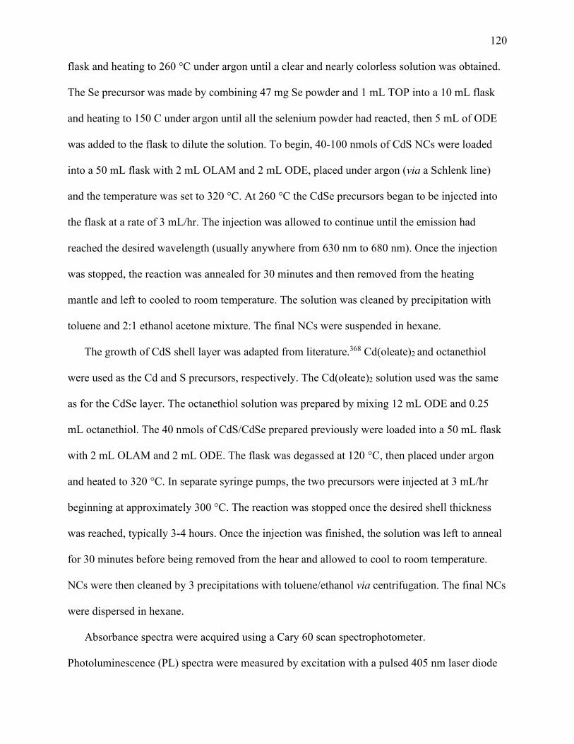
120 flask and heating to 260 °C under argon until a clear and nearly colorless solution was obtained.
The Se precursor was made by combining 47 mg Se powder and 1 mL TOP into a 10 mL flask
and heating to 150 C under argon until all the selenium powder had reacted, then 5 mL of ODE
was added to the flask to dilute the solution. To begin, 40-100 nmols of CdS NCs were loaded
into a 50 mL flask with 2 mL OLAM and 2 mL ODE, placed under argon (via a Schlenk line)
and the temperature was set to 320 °C. At 260 °C the CdSe precursors began to be injected into
the flask at a rate of 3 mL/hr. The injection was allowed to continue until the emission had
reached the desired wavelength (usually anywhere from 630 nm to 680 nm). Once the injection
was stopped, the reaction was annealed for 30 minutes and then removed from the heating
mantle and left to cooled to room temperature. The solution was cleaned by precipitation with
toluene and 2:1 ethanol acetone mixture. The final NCs were suspended in hexane.
The growth of CdS shell layer was adapted from literature.368 Cd(oleate)2 and octanethiol
were used as the Cd and S precursors, respectively. The Cd(oleate)2 solution used was the same
as for the CdSe layer. The octanethiol solution was prepared by mixing 12 mL ODE and 0.25
mL octanethiol. The 40 nmols of CdS/CdSe prepared previously were loaded into a 50 mL flask
with 2 mL OLAM and 2 mL ODE. The flask was degassed at 120 °C, then placed under argon
and heated to 320 °C. In separate syringe pumps, the two precursors were injected at 3 mL/hr
beginning at approximately 300 °C. The reaction was stopped once the desired shell thickness
was reached, typically 3-4 hours. Once the injection was finished, the solution was left to anneal
for 30 minutes before being removed from the hear and allowed to cool to room temperature.
NCs were then cleaned by 3 precipitations with toluene/ethanol via centrifugation. The final NCs
were dispersed in hexane.
Absorbance spectra were acquired using a Cary 60 scan spectrophotometer.
Photoluminescence (PL) spectra were measured by excitation with a pulsed 405 nm laser diode
121 (PDL 800-D, Picoquant) and emitted photons were collected by a fiber optic cable connected to
an Andor Shamrock 303i spectrograph and measured using an Andor Newton 970 EMCCD. PL
decay dynamics were acquired via 405 nm pulsed excitation (picoquant) and photons were
detected with an ID100-50 single photon detector (ID Quantique) and processed by a SPC-130
TCSPC module (Becker & Hickl). Transmission electron microscope (TEM) images were
acquired at 200 kV on carbon films coated with a copper grid (300 mesh, obtained from Electron
Microscope Science) using a Thermo Fisher Talos F200X G2 S/TEM. Relative quantum yield
(QY) measurements were acquired with a 532 nm CW DPSS laser (MeshTel INTELITE, INC.
USA) and R101 dye was used as a reference (99% QY in ethanol).
Nanocrystal thin-films were fabricated by first performing an additional anti-solvent
precipitation with ethanol, followed by redispersion in a 9:1 hexane/octane mixture.
Concentrated solutions were drop-cast onto microscope slides that had been treated with MPTS
over 24 hours (5% MPTS w/v in dried toluene). The samples with showed the lowest ASE
thresholds were spin coated at 2000 rpm. Samples that displayed the best ASE results were
opalescent, non-scattering; other films however, displayed perceptible haze. Samples were
photoexcited with a 35 fs Ti:sapphire laser (2 kHz, Spectraphysics), which was frequency
doubled to 400 nm. The 400 nm beam was focused using a cylindrical lens to produced a strip,
with the edges defined by razor blades. The emission was collected via a lens positioned
perpendicular to the excitation beam and fiber-coupled to a CCD through a monochromater
(Princeton), for spectral data acquisition, or to a streak camera (Hamamatsu) for time-resolved
data collection.
We detect emission from diffusing QDs in solution, under a confocal microscope and using a
pulsed excitation source in a Hanbury-Brown-Twiss setup (Fluorescence Correlation
Spectroscopy), and calculate the second order cross-correlation function, g(2)(τ). In the case of
122 solution-based measurements, this is also known as Fluorescence Correlation Spectroscopy
(FCS). At early τ, before QDs have diffused out of the confocal volume being probed, photon
pairs are more likely to emit from the same QD, thereby causing g(2)(τ) to have a higher degree
of correlation at timescales faster than the diffusion time of the QDs. For large τ, beyond the
diffusion time, photon pairs are highly unlikely to originate from the same QD, and g(2)(τ)
consists of uncorrelated photon pairs from the ensemble. At τ=0, the intensity is a mixture of
antibunching from exciton emission, bunching from biexciton emission and some signal from
photon pairs from different QDs. For a dilute sample with a high degree of correlation at short
time scales (small τ), we can subtract the uncorrelated ensemble emission (large τ) to isolate the
correlations from single QDs. We determine the ensemble averaged BX/X QY by taking the
ratio of the ensemble background subtracted correlation center peak (g⁽²⁾(0)-1) to the correlation
side peak (g⁽²⁾(τrep)-1), where τrep is the repetition rate of the laser. The correlation side peak is
determined by fitting correlations across all timescales to a 2D diffusion model (the Supporting
Information). All measurements were performed under low excitation flux (<n> << 1) in order to
avoid emission from higher order multiexcitons. Additionally, we ensured that the repetition rate
of the pulsed laser was well beyond the lifetime of the emitter.
123
7 REFERENCES
1. Murray, C. B.; Norris, D. J.; Bawendi, M. G., Synthesis and characterization of nearly
monodisperse CdE (E = sulfur, selenium, tellurium) semiconductor nanocrystallites. Journal
of the American Chemical Society 1993, 115 (19), 8706-8715.
2. Peng, Z. A.; Peng, X., Formation of High-Quality CdTe, CdSe, and CdS Nanocrystals Using
CdO as Precursor. Journal of the American Chemical Society 2001, 123 (1), 183-184.
3. Battaglia, D.; Peng, X., Formation of High Quality InP and InAs Nanocrystals in a
Noncoordinating Solvent. Nano Lett. 2002, 2 (9), 1027-1030.
4. Li, L. S.; Pradhan, N.; Wang, Y.; Peng, X., High Quality ZnSe and ZnS Nanocrystals
Formed by Activating Zinc Carboxylate Precursors. Nano Lett. 2004, 4 (11), 2261-2264.
5. Hines, M. A.; Scholes, G. D., Colloidal PbS Nanocrystals with Size-Tunable Near-Infrared
Emission: Observation of Post-Synthesis Self-Narrowing of the Particle Size Distribution.
Advanced Materials 2003, 15 (21), 1844-1849.
6. Kuno, M.; Lee, J. K.; Dabbousi, B. O.; Mikulec, F. V.; Bawendi, M. G., The band edge
luminescence of surface modified CdSe nanocrystallites: Probing the luminescing state. The
Journal of Chemical Physics 1997, 106 (23), 9869-9882.
7. Yu, D.; Wang, C.; Guyot-Sionnest, P., n-Type Conducting CdSe Nanocrystal Solids. Science
2003, 300 (5623), 1277-1280.
8. Zabet-Khosousi, A.; Dhirani, A.-A., Charge Transport in Nanoparticle Assemblies. Chemical
Reviews 2008, 108 (10), 4072-4124.
9. Talapin Dmitri, V.; Murray Christopher, B., PbSe Nanocrystal Solids for n- and p-Channel
Thin Film Field-Effect Transistors. Science 2005, 310 (5745), 86-89.
10. Gur, I.; Fromer Neil, A.; Geier Michael, L.; Alivisatos, A. P., Air-Stable All-Inorganic
Nanocrystal Solar Cells Processed from Solution. Science 2005, 310 (5747), 462-465.
124
11. Anderson, N. C.; Hendricks, M. P.; Choi, J. J.; Owen, J. S., Ligand Exchange and the
Stoichiometry of Metal Chalcogenide Nanocrystals: Spectroscopic Observation of Facile
Metal-Carboxylate Displacement and Binding. Journal of the American Chemical Society
2013, 135 (49), 18536-18548.
12. Green, M. L. H., A new approach to the formal classification of covalent compounds of the
elements. Journal of Organometallic Chemistry 1995, 500 (1), 127-148.
13. Boles, M. A.; Ling, D.; Hyeon, T.; Talapin, D. V., The surface science of nanocrystals.
Nature Materials 2016, 15 (2), 141-153.
14. Carbone, L.; Nobile, C.; De Giorgi, M.; Sala, F. D.; Morello, G.; Pompa, P.; Hytch, M.;
Snoeck, E.; Fiore, A.; Franchini, I. R.; Nadasan, M.; Silvestre, A. F.; Chiodo, L.; Kudera, S.;
Cingolani, R.; Krahne, R.; Manna, L., Synthesis and Micrometer-Scale Assembly of
Colloidal CdSe/CdS Nanorods Prepared by a Seeded Growth Approach. Nano Lett. 2007, 7
(10), 2942-2950.
15. Murray, C. B.; Kagan, C. R.; Bawendi, M. G., Synthesis and Characterization of
Monodisperse Nanocrystals and Close-Packed Nanocrystal Assemblies. Annual Review of
Materials Science 2000, 30 (1), 545-610.
16. Kholmicheva, N.; Yang, M. R.; Moroz, P.; Eckard, H.; Vore, A.; Cassidy, J.; Pushina, M.;
Boddy, A.; Porotnikov, D.; Anzenbacher, P.; Zamkov, M., Ion-Mediated Ligand Exchange
and Size Focusing of Semiconductor Nanocrystals in Ligand-Saturated Solutions. Journal of
Physical Chemistry C 2018, 122 (41), 23623-23630.
17. Jarosz, M. V.; Porter, V. J.; Fisher, B. R.; Kastner, M. A.; Bawendi, M. G.,
Photoconductivity studies of treated CdSe quantum dot films exhibiting increased exciton
ionization efficiency. Physical Review B 2004, 70 (19), 195327.
125
18. Porotnikov, D.; Zamkov, M., Progress and Prospects of Solution-Processed Two-
Dimensional Semiconductor Nanocrystals. The Journal of Physical Chemistry C 2020, 124
(40), 21895-21908.
19. Giansante, C.; Infante, I., Surface Traps in Colloidal Quantum Dots: A Combined
Experimental and Theoretical Perspective. The Journal of Physical Chemistry Letters 2017, 8
(20), 5209-5215.
20. Kirkwood, N.; Monchen, J. O. V.; Crisp, R. W.; Grimaldi, G.; Bergstein, H. A. C.; du Fossé,
I.; van der Stam, W.; Infante, I.; Houtepen, A. J., Finding and Fixing Traps in II–VI and III–
V Colloidal Quantum Dots: The Importance of Z-Type Ligand Passivation. Journal of the
American Chemical Society 2018, 140 (46), 15712-15723.
21. Ji, X.; Copenhaver, D.; Sichmeller, C.; Peng, X., Ligand Bonding and Dynamics on Colloidal
Nanocrystals at Room Temperature: The Case of Alkylamines on CdSe Nanocrystals.
Journal of the American Chemical Society 2008, 130 (17), 5726-5735.
22. Chen, O.; Zhao, J.; Chauhan, V. P.; Cui, J.; Wong, C.; Harris, D. K.; Wei, H.; Han, H.-S.;
Fukumura, D.; Jain, R. K.; Bawendi, M. G., Compact high-quality CdSe–CdS core–shell
nanocrystals with narrow emission linewidths and suppressed blinking. Nature Materials
2013, 12 (5), 445-451.
23. Ghosh, Y.; Mangum, B. D.; Casson, J. L.; Williams, D. J.; Htoon, H.; Hollingsworth, J. A.,
New Insights into the Complexities of Shell Growth and the Strong Influence of Particle
Volume in Nonblinking “Giant” Core/Shell Nanocrystal Quantum Dots. Journal of the
American Chemical Society 2012, 134 (23), 9634-9643.
24. Lim, J.; Bae, W. K.; Kwak, J.; Lee, S.; Lee, C.; Char, K., Perspective on synthesis, device
structures, and printing processes for quantum dot displays. Opt. Mater. Express 2012, 2 (5),
594-628.
126
25. Jeong, B. G.; Park, Y.-S.; Chang, J. H.; Cho, I.; Kim, J. K.; Kim, H.; Char, K.; Cho, J.;
Klimov, V. I.; Park, P.; Lee, D. C.; Bae, W. K., Colloidal Spherical Quantum Wells with
Near-Unity Photoluminescence Quantum Yield and Suppressed Blinking. ACS Nano 2016,
10 (10), 9297-9305.
26. Battaglia, D.; Li, J. J.; Wang, Y.; Peng, X., Colloidal Two-Dimensional Systems: CdSe
Quantum Shells and Wells. Angewandte Chemie International Edition 2003, 42 (41), 5035-
5039.
27. Pokatilov, E. P.; Fonoberov, V. A.; Fomin, V. M.; Devreese, J. T., Electron and hole states in
quantum dot quantum wells within a spherical eight-band model. Physical Review B 2001, 64
(24), 245329.
28. Schaller, R. D.; Klimov, V. I., High Efficiency Carrier Multiplication in PbSe Nanocrystals:
Implications for Solar Energy Conversion. Physical Review Letters 2004, 92 (18), 186601.
29. Murphy, J. E.; Beard, M. C.; Norman, A. G.; Ahrenkiel, S. P.; Johnson, J. C.; Yu, P.; Mićić,
O. I.; Ellingson, R. J.; Nozik, A. J., PbTe Colloidal Nanocrystals: Synthesis,
Characterization, and Multiple Exciton Generation. Journal of the American Chemical
Society 2006, 128 (10), 3241-3247.
30. Ellingson, R. J.; Beard, M. C.; Johnson, J. C.; Yu, P.; Micic, O. I.; Nozik, A. J.; Shabaev, A.;
Efros, A. L., Highly Efficient Multiple Exciton Generation in Colloidal PbSe and PbS
Quantum Dots. Nano Lett. 2005, 5 (5), 865-871.
31. Bae, W. K.; Park, Y.-S.; Lim, J.; Lee, D.; Padilha, L. A.; McDaniel, H.; Robel, I.; Lee, C.;
Pietryga, J. M.; Klimov, V. I., Controlling the influence of Auger recombination on the
performance of quantum-dot light-emitting diodes. Nature Communications 2013, 4 (1),
2661.
127
32. Klimov, V. I.; Mikhailovsky, A. A.; Xu, S.; Malko, A.; Hollingsworth, J. A.; Leatherdale, C.
A.; Eisler, H. J.; Bawendi, M. G., Optical Gain and Stimulated Emission in Nanocrystal
Quantum Dots. Science 2000, 290 (5490), 314-317.
33. Nirmal, M.; Dabbousi, B. O.; Bawendi, M. G.; Macklin, J. J.; Trautman, J. K.; Harris, T. D.;
Brus, L. E., Fluorescence intermittency in single cadmium selenide nanocrystals. Nature
1996, 383 (6603), 802-804.
34. Klimov, V. I.; McGuire, J. A.; Schaller, R. D.; Rupasov, V. I., Scaling of multiexciton
lifetimes in semiconductor nanocrystals. Physical Review B 2008, 77 (19), 195324.
35. Trinh, M. T.; Polak, L.; Schins, J. M.; Houtepen, A. J.; Vaxenburg, R.; Maikov, G. I.;
Grinbom, G.; Midgett, A. G.; Luther, J. M.; Beard, M. C.; Nozik, A. J.; Bonn, M.; Lifshitz,
E.; Siebbeles, L. D. A., Anomalous Independence of Multiple Exciton Generation on
Different Group IV−VI Quantum Dot Architectures. Nano Lett. 2011, 11 (4), 1623-1629.
36. Eisler, H.-J.; Sundar, V. C.; Bawendi, M. G.; Walsh, M.; Smith, H. I.; Klimov, V., Color-
selective semiconductor nanocrystal laser. Applied Physics Letters 2002, 80 (24), 4614-4616.
37. Grivas, C.; Li, C.; Andreakou, P.; Wang, P.; Ding, M.; Brambilla, G.; Manna, L.;
Lagoudakis, P., Single-mode tunable laser emission in the single-exciton regime from
colloidal nanocrystals. Nature Communications 2013, 4 (1), 2376.
38. Hou, X.; Kang, J.; Qin, H.; Chen, X.; Ma, J.; Zhou, J.; Chen, L.; Wang, L.; Wang, L.-W.;
Peng, X., Engineering Auger recombination in colloidal quantum dots via dielectric
screening. Nature Communications 2019, 10 (1), 1750.
39. Philbin, J. P.; Rabani, E., Electron–Hole Correlations Govern Auger Recombination in
Nanostructures. Nano Lett. 2018, 18 (12), 7889-7895.
128
40. Robel, I.; Gresback, R.; Kortshagen, U.; Schaller, R. D.; Klimov, V. I., Universal Size-
Dependent Trend in Auger Recombination in Direct-Gap and Indirect-Gap Semiconductor
Nanocrystals. Physical Review Letters 2009, 102 (17), 177404.
41. García-Santamaría, F.; Chen, Y.; Vela, J.; Schaller, R. D.; Hollingsworth, J. A.; Klimov, V.
I., Suppressed Auger Recombination in “Giant” Nanocrystals Boosts Optical Gain
Performance. Nano Lett. 2009, 9 (10), 3482-3488.
42. Lin, C. H.; Lafalce, E.; Jung, J.; Smith, M. J.; Malak, S. T.; Aryal, S.; Yoon, Y. J.; Zhai, Y.;
Lin, Z.; Vardeny, Z. V.; Tsukruk, V. V., Core/Alloyed-Shell Quantum Dot Robust Solid
Films with High Optical Gains. ACS Photonics 2016, 3 (4), 647-658.
43. Lim, J.; Park, Y.-S.; Klimov, V. I., Optical gain in colloidal quantum dots achieved with
direct-current electrical pumping. Nature Materials 2018, 17 (1), 42-49.
44. She, C.; Fedin, I.; Dolzhnikov, D. S.; Demortière, A.; Schaller, R. D.; Pelton, M.; Talapin, D.
V., Low-Threshold Stimulated Emission Using Colloidal Quantum Wells. Nano Lett. 2014,
14 (5), 2772-2777.
45. Park, Y.-S.; Roh, J.; Diroll, B. T.; Schaller, R. D.; Klimov, V. I., Colloidal quantum dot
lasers. Nature Reviews Materials 2021, 6 (5), 382-401.
46. Karl, M.; Glackin, J. M. E.; Schubert, M.; Kronenberg, N. M.; Turnbull, G. A.; Samuel, I. D.
W.; Gather, M. C., Flexible and ultra-lightweight polymer membrane lasers. Nature
Communications 2018, 9 (1), 1525.
47. Kang, D.; Chen, H.; Yoon, J., Stretchable, skin-conformal microscale surface-emitting lasers
with dynamically tunable spectral and directional selectivity. Applied Physics Letters 2019,
114 (4), 041103.
48. Cegielski, P. J.; Giesecke, A. L.; Neutzner, S.; Porschatis, C.; Gandini, M.; Schall, D.; Perini,
C. A. R.; Bolten, J.; Suckow, S.; Kataria, S.; Chmielak, B.; Wahlbrink, T.; Petrozza, A.;
129
Lemme, M. C., Monolithically Integrated Perovskite Semiconductor Lasers on Silicon
Photonic Chips by Scalable Top-Down Fabrication. Nano Lett. 2018, 18 (11), 6915-6923.
49. Xie, W.; Stöferle, T.; Rainò, G.; Aubert, T.; Bisschop, S.; Zhu, Y.; Mahrt, R. F.; Geiregat, P.;
Brainis, E.; Hens, Z.; Van Thourhout, D., On-Chip Integrated Quantum-Dot–Silicon-Nitride
Microdisk Lasers. Advanced Materials 2017, 29 (16), 1604866.
50. Martynenko, I. V.; Litvin, A. P.; Purcell-Milton, F.; Baranov, A. V.; Fedorov, A. V.; Gun'ko,
Y. K., Application of semiconductor quantum dots in bioimaging and biosensing. Journal of
Materials Chemistry B 2017, 5 (33), 6701-6727.
51. Kovalenko, M. V.; Manna, L.; Cabot, A.; Hens, Z.; Talapin, D. V.; Kagan, C. R.; Klimov, V.
I.; Rogach, A. L.; Reiss, P.; Milliron, D. J.; Guyot-Sionnnest, P.; Konstantatos, G.; Parak, W.
J.; Hyeon, T.; Korgel, B. A.; Murray, C. B.; Heiss, W., Prospects of Nanoscience with
Nanocrystals. ACS Nano 2015, 9, 1012.
52. Lim, J.; Park, Y.; Wu, K.; Yun, H. J.; Klimov, V. I., Droop-Free Colloidal Quantum Dot
Light-Emitting Diodes. Nano Lett. 2018, 18, 6645.
53. Cao, F.; Zhao, D.; Shen, P.; Wu, J.; Wang, H.; Wu, Q.; Wang, F.; Yang, X., High-Efficiency,
Solution-Processed White Quantum Dot Light-Emitting Diodes with Serially Stacked
Red/Green/Blue Units. Adv. Opt. Mater. 2018, 6, 1800652.
54. Yang, Z.; Pelton, M.; Fedin, I.; Talapin, D. V.; Waks, E., A Room Temperature Continuous-
Wave Nanolaser Using Colloidal Quantum Wells. Nat. Commun. 2017, 8, 143.
55. Dai, X.; Deng, Y.; Peng, X.; Jin, Y., Quantum-Dot Light-Emitting Diodes for Large-Area
Displays: Towards the Dawn of Commercialization. Adv. Mater. 2017, 29, 1607022.
56. Supran, G. J.; Shirasaki, Y.; Song, K. W.; Caruge, J.; Kazlas, P. T.; Coe-sullivan, S.;
Andrew, T. L.; Bawendi, M. G.; Bulovi, V., QLEDs for displays and solid-state lighting.
MRS Bull. 2013, 38, 703.
130
57. Shirasaki, Y.; Supran, G. J.; Bawendi, M. G.; Bulovic, V., Emergence of colloidal quantum-
dot light-emitting technologies. Nat. Photonics 2013, 7, 13.
58. Sun, L.; Choi, J. J.; Stachnik, D.; Bartnik, A. C.; Hyun, B.; Malliaras, G. G.; Hanrath, T.;
Wise, F. W., Bright infrared quantum-dot light-emitting diodes through inter-dot spacing
control. Nat. Nanotechnol. 2012, 7, 369.
59. Coe, S.; Woo, W. K.; Bawendi, M.; Bulovic, V., Electroluminescence from single
monolayers of nanocrystals in molecular organic devices. Nature 2002, 420, 800.
60. Klimov, V. I.; Mikhailovsky, A. A.; Xu, S.; Malko, A.; Hollingsworth, J. A.; Leatherdale, A.
C.; Eisler, H.; Bawendi, M. G., Optical gain and stimulated emission in nanocrystal quantum
dots. Science 2000, 290, 314.
61. Colvin, V. L.; Schlamp, M. C.; Alivisatos, A. P., Light-emitting diodes made from cadmium
selenide nanocrystals and a semiconducting polymer. Nature 1994, 370, 354.
62. Moroz, P.; Jin, Z.; Sugiyama, Y.; Lara, D.; Razgoniaeva, N.; Yang, M.; Kholmicheva, N.;
Khon, D.; Mattoussi, H.; Zamkov, M., The Competition of Charge and Energy Transfer
Processes in Donor-Acceptor Fluorescence Pairs: Calibrating the Spectroscopic Ruler. ACS
Nano 2018, 12, 5657.
63. Petryayeva, E.; Algar, W. R.; Medintz, I. L., Quantum Dots in Bioanalysis: A Review of
Applications Across Various Platforms for Fluorescence Spectroscopy and Imaging. Appl.
Spectrosc. 2013, 67, 215.
64. Yun, C. S.; Javier, A.; Jennings, T.; Fisher, M.; Hira, S.; Peterson, S.; Hopkins, B.; Reich, N.
O.; Strouse, G. F., Nanometal Surface Energy Transfer in Optical Rulers, Breaking the FRET
Barrier. J. Am. Chem. Soc. 2005, 127, 3115.

131
65. Clapp, A. R.; Medintz, I. L.; Mauro, J. M.; Fisher, B. R.; Bawendi, M. G.; Mattoussi, H.,
Fluorescence Resonance Energy Transfer Between Quantum Dot Donors and Dye-Labeled
Protein Acceptors. J. Am. Chem. Soc. 2004, 126, 301.
66. Medintz, I. L.; Clapp, A. R.; Mattoussi, H.; Goldman, E. R.; Fisher, B.; Mauro, J. M., Self-
assembled nanoscale biosensors based on quantum dot FRET donors. Nat. Mater. 2003, 2,
630.
67. Zamkov, M., Solar hydrogen generation: Exceeding 100% efficiency. Nat. Energy 2017, 2,
17072.
68. Yang, Z.; Fan, J. Z.; Proppe, A. H.; Pelayo García de Arquer, F.; Rossouw, D.; Voznyy, O.;
Lan, X.; Liu, M.; Walters, G.; Quintero-Bermudez, R.; Sun, B.; Hoogland, S.; Botton, G. A.;
Kelley, S. O.; Sargent, E. H., Mixed-Quantum-Dot Solar Cells. Nat. Commun. 2017, 8, 1325.
69. Yan, Y.; Crisp, R. W.; Gu, J.; Chernomordik, B. D.; Pach, G. F.; Marshall, A. R.; Turner, J.
A.; Beard, M. C., Multiple exciton generation for photoelectrochemical hydrogen evolution
reactions with quantum yields exceeding 100%. Nat. Energy 2017, 2, 17052.
70. Mongin, C.; Garakyaraghi, S.; Razgoniaeva, N.; Zamkov, M.; Castellano, F. N., Direct
Observation of Triplet Energy Transfer from Semiconductor Nanocrystals. Science 2016,
351, 369.
71. Ko, D. K.; Maurano, A.; Suh, S. K.; Kim, D.; Hwang, G. W.; Grossman, J. C.; Bulovic, V.;
Bawendi, M. G., Photovoltaic Performance of PbS Quantum Dots Treated with Metal Salts.
ACS Nano 2016, 10, 3382.
72. Beard, M. C.; Blackburn, J. L.; Johnson, J. C.; Rumbles, G., Status and Prognosis of Future
Generation Photoconversion to Photovoltaics and Solar Fuels. ACS Energy Lett. 2016, 1,
344.
132
73. Peng, X. G.; Wickham, J.; Alivisatos, A. P., Kinetics of II-VI and III-V Colloidal
Semiconductor Nanocrystal Growth: “Focusing” of Size Distributions. J. Am. Chem. Soc.
1998, 120, 5343.
74. Voznyy, O.; Levina, L.; Fan, J.; Askerka, M.; Jain, A.; Choi, M.; Ouellette, O.; Todorović,
P.; Sagar, L.; Sargent, E., Machine Learning Accelerates Discovery of Optimal Colloidal
Quantum Dot Synthesis. ACS Nano 2019, 13, 11122.
75. Li, J.; Wang, H.; Lin, L.; Fang, Q.; Peng, X., Quantitative Identification of Basic Growth
Channels for Formation of Monodisperse Nanocrystals. J. Am. Chem. Soc. 2018, 140, 5474.
76. Tan, R.; Yuan, Y.; Nagaoka, Y.; Eggert, D.; Wang, X.; Thota, S.; Guo, P.; Yang, H.; Zhao,
J.; Chen, O., Monodisperse Hexagonal Pyramidal and Bipyramidal Wurtzite CdSe-CdS
Core–Shell Nanocrystals. Chem. Mater. 2017, 29, 4097.
77. Zhou, J.; Pu, C.; Jiao, T.; Hou, X.; Peng, X., A Two-Step Synthetic Strategy toward
Monodisperse Colloidal CdSe and CdSe/CdS Core/ Shell Nanocrystals. J. Am. Chem. Soc.
2016, 138, 6475.
78. Razgoniaeva, N.; Carrillo, L.; Burchfield, D.; Moroz, P.; Adhikari, P.; Yadav, P.; Khon, D.;
Zamkov, M., Colloidal Synthesis of Monodisperse Semiconductor Nanocrystals through the
Saturated Ionic Layer Adsorption. Chem. Mater. 2016, 28, 2823.
79. Gómez, D. E.; Embden, J.; Mulvaney, P., Spectral Diffusion of Single Semiconductor
Nanocrystals: The Influence of the Dielectric Environment. Appl. Phys. Lett. 2006, 88,
154106.
80. Zhong, X.; Feng, Y.; Knoll, W.; Han, M., Alloyed ZnxCd1-xS Nanocrystals with Highly
Narrow Luminescence Spectral Width. J. Am. Chem. Soc. 2003, 125, 13559.
133
81. de Mello Donegá, C.; Hickey, S.; Wuister, S.; Vanmaekelbergh, D.; Meijerink, A., Single-
Step Synthesis to Control the Photoluminescence Quantum Yield and Size Dispersion of
CdSe Nanocrystals. J. Phys. Chem. B 2003, 107, 489.
82. Rogach, A.; Talapin, D.; Shevchenko, E.; Kornowski, A.; Haase, M.; Weller, H.,
Organization of Matter on Different Size Scales: Monodisperse Nanocrystals and Their
Superstructures. Adv. Funct. Mater. 2002, 12, 653.
83. Talapin, D. V.; Rogach, A. L.; Kornowski, A.; Haase, M.; Weller, H., Highly Luminescent
Monodisperse CdSe and CdSe/ZnS Nanocrystals Synthesized in a Hexadecylamine-
Trioctylphosphine Oxide-Trioctylphospine Mixture. Nano Lett. 2001, 1, 207.
84. Peng, X.; Manna, L.; Yang, W.; Wickham, J.; Scher, E.; Kadavanich, A.; Alivisatos, A. P.,
Shape Control of CdSe Nanocrystals. Nature 2000, 404, 59.
85. Flamee, S.; Cirillo, M.; Abe, S.; Nolf, K.; Gomes, R.; Aubert, T.; Hens, Z., Fast, High Yield,
and High Solid Loading Synthesis of Metal Selenide Nanocrystals. Chem. Mater. 2013, 25,
2476.
86. Sugimoto, T., Preparation of Monodispersed Colloidal Particles. Adv. Colloid Interface Sci.
1987, 28, 65.
87. Hassinen, A.; Moreels, I.; De Nolf, K.; Smet, P. F.; Martins, J. C.; Hens, Z., Short-Chain
Alcohols Strip X-Type Ligands and Quench the Luminescence of PbSe and CdSe Quantum
Dots, Acetonitrile Does Not. J. Am. Chem. Soc. 2012, 134, 20705.
88. Smith, D. K.; Luther, J. M.; Semonin, O. E.; Nozik, A. J.; Beard, M. C., Tuning the Synthesis
of Ternary Lead Chalcogenide Quantum Dots by Balancing Precursor Reactivity. ACS Nano
2011, 5, 183.
134
89. Chen, O.; Yang, Y. A.; Wang, T.; Wu, H. M.; Niu, C. G.; Yang, J. H.; Cao, Y. C., Surface-
Functionalization-Dependent Optical Properties of II-VI Semiconductor Nanocrystals. J. Am.
Chem. Soc. 2011, 133, 17504.
90. Morris-Cohen, A. J.; Frederick, M. T.; Lilly, G. D.; McArthur, E. A.; Weiss, E. A., Organic
Surfactant Controlled Composition of the Surfaces of CdSe Quantum Dots. J. Phys. Chem.
Lett. 2010, 1, 1078.
91. Dai, Q.; Wang, Y.; Li, X.; Zhang, Y.; Pellegrino, D. J.; Zhao, M.; Zou, B.; Seo, J.; Wang, Y.;
Yu, W. W., Size-Dependent Composition and Molar Extinction Coefficient of PbSe
Semiconductor Nanocrystals. ACS Nano 2009, 3, 1518.
92. Munro, A. M.; Ginger, D. S., Photoluminescence Quenching of Single CdSe Nanocrystals by
Ligand Adsorption. Nano Lett. 2008, 8, 2585.
93. Park, J.; Joo, J.; Kwon, S. G.; Jang, Y.; Hyeon, T., Synthesis of Monodisperse Spherical
Nanocrystals. Angew. Chem., Int. Ed. 2007, 46, 4630.
94. Lifshitz, I.; Slyozov, V. J., The Kinetics of Precipitation from Supersaturated Solid Solutions.
J. Phys. Chem. Solids 1961, 19, 35.
95. Kim, M.; Jeong, J.; Choi, Y.; Park, J.; Park, E.; Cheon, C.; Kim, N.; Min, B. K.; Kim, W.,
Synthesis of V-doped In2O3 Nanocrystals via Digestive-Ripening Process and Their
Electrocatalytic Properties in CO2 Reduction Reaction. ACS Appl. Mater. Interfaces 2020,
12, 11890.
96. Cassidy, J.; Zamkov, M., Nanoshell Quantum Dots: Quantum Confinement Beyond the
Exciton Bohr Radius. J. Chem. Phys. 2020, 152, 110902.
97. Yu, L.; You, H.; Zhang, Q.; Zhang, L.; Fang, J., Digestive ripening mechanism investigation
in a classical Lee–Meisel method based on in situ UV–vis spectra. CrystEngComm 2019, 21,
1529.
135
98. Razgoniaeva, N.; Yang, M.; Garrett, P.; Kholmicheva, N.; Moroz, P.; Eckard, H.; Royo
Romero, L.; Porotnikov, D.; Khon, D.; Zamkov, M., Just Add Ligands: Self-Sustained Size
Focusing of Colloidal Semiconductor Nanocrystals. Chem. Mater. 2018, 30, 1391.
99. Kholmicheva, N.; Yang, M.; Moroz, P.; Eckard, H.; Vore, A.; Cassidy, J.; Pushina, M.;
Boddy, A.; Porotnikov, D.; Anzenbacher, P.; Zamkov, M., Ion-Mediated Ligand Exchange
and Size-Focusing of Semiconductor Nanocrystals in Ligand-Saturated Solutions. J. Phys.
Chem. C 2018, 122, 23623.
100. Cheng, T.; Marin, R.; Skripka, A.; Vetrone, F., Small and Bright Lithium-Based
Upconverting Nanoparticles. J. Am. Chem. Soc. 2018, 140, 12890.
101. Wang, F. D.; Richards, V. N.; Shields, S. P.; Buhro, W. E., Kinetics and Mechanisms of
Aggregative Nanocrystal Growth. Chem. Mat. 2014, 26 (1), 5-21.
102. Yu, K.; Ouyang, J.; Leek, D. M., In-Situ Observation of Nucleation and Growth of PbSe
Magic-Sized Nanoclusters and Regular Nanocrystals. Small 2011, 7, 2250.
103. Kumar, S.; Davis, T. M.; Ramanan, H.; Penn, R. L.; Tsapatsis, M., Aggregative Growth of
Silicalite-1. J. Phys. Chem. B 2007, 111, 3398.
104. Penn, R. L., Imperfect Oriented Attachment: Dislocation Generation in Defect-Free
Nanocrystals. Science 1998, 281, 969.
105. Shimpi, J. R.; Sidhaye, D. S.; Prasad, B. L. V., Digestive Ripening: A Fine Chemical
Machining Process on the Nanoscale. Langmuir 2017, 33, 9491.
106. Wang, F.; Richards, V. N.; Shields, S. P.; Buhro, W. E., Kinetics and Mechanisms of
Aggregative Nanocrystal Growth. Chem. Mater. 2014, 26, 5.
107. Yuk, J. M.; Park, J.; Ercius, P.; Kim, K.; Hellebusch, D. J.; Crommie, M. F.; Lee, J. Y.; Zettl,
A.; Alivisatos, A. P., High-Resolution TEM of Colloidal Nanocrystal Growth Using
Graphene Liquid Cells. Science 2012, 336, 61.
136
108. Polte, J.; Ahner, T. T.; Delissen, F.; Sokolov, S.; Emmerling, F.; Thunemann, A. F.;
Kraehnert, R., Mechanism of Gold Nanoparticle Formation in the Classical Citrate Synthesis
Method Derived from Coupled In Situ XANES and SAXS Evaluation. J. Am. Chem. Soc.
2010, 132, 1296.
109. Zheng, H.; Smith, R. K.; Jun, Y. W.; Kisielowski, C.; Dahmen, U.; Alivisatos, A. P.,
Observation of Single Colloidal Platinum Nanocrystal Growth Trajectories. Science 2009,
324, 1309.
110. Tang, Z. Y.; Kotov, N. A.; Giersig, M., Spontaneous Organization of Single CdTe
Nanoparticles into Luminescent Nanowires. Science 2002, 297, 237.
111. Penn, R. L.; Banfield, J. F., Imperfect Oriented Attachment: Dislocation Generation in
Defect-Free Nanocrystals. Science 1998, 281, 969.
112. Schliehe, C.; Juarez, B. H.; Pelletier, M.; Jander, S.; Greshnykh, D.; Nagel, M.; Meyer, A.;
Foerster, S.; Kornowski, A.; Klinke, C.; Weller, H., Ultrathin PbS Sheets by Two-
Dimensional Oriented Attachment. Science 2010, 329, 550.
113. Ithurria, S.; Dubertret, B., Quasi 2D colloidal CdSe platelets with thicknesses controlled at
the atomic level. J. Am. Chem. Soc. 2008, 130, 16504.
114. Son, J. S.; Wen, X. D.; Joo, J.; Chae, J.; Baek, S.; Park, K.; Kim, J. H.; An, K.; Yu, J. H.;
Kwon, S. G.; Choi, S. H.; Wang, Z.; Kim, Y. W.; Kuk, Y.; Hoffmann, R.; Hyeon, T., Large-
Scale Soft Colloidal Template Synthesis of 1.4 nm Thick CdSe Nanosheets. Angew. Chem.,
Int. Ed. 2009, 48, 6861.
115. Tang, Z. Y.; Zhang, Z. L.; Wang, Y.; Glotzer, S. C.; Kotov, N. A., Self-assembly of CdTe
nanocrystals into free-floating sheets. Science 2006, 314, 274.
116. Joo, J.; Son, J.; Kwon, S.; Yu, S.; Hyeon, T., Low-temperature solution-phase synthesis of
quantum well structured CdSe nanoribbons. J. Am. Chem. Soc. 2006, 128, 5632.
137
117. Ostwald, W., On the Assumed Isomerism of Red and Yellow Mercury Oxide and the
Surface-Tension of Solid Bodies. Z. Phys. Chem. 1900, 34, 495.
118. Hendriks, E. M.; Ernst, W. H., Exactly Soluble Addition and Condensation Models in
Coagulation Kinetics. J. Colloid Interface Sci. 1984, 97, 176.
119. Karatutlu, A.; Barhoum, A.; Sapelkin, A., Emerging Applications of Nanoparticles and
Architecture Nanostructures. 2018; p 597.
120. Thanh, N. T.; Maclean, N.; Mahiddine, S., Mechanisms of nucleation and growth of
nanoparticles in solution. Chem. Rev. 2014, 114, 7610.
121. García-Rodríguez, R.; Hendricks, M. P.; Cossairt, B. M.; Liu, H.; Owen, J. S., Conversion
reactions of cadmium chalcogenide nanocrystal precursors. Chem. Mater. 2013, 25, 1233.
122. Abe, S.; Čapek, R. K.; De Geyter, B.; Hens, Z., Tuning the Postfocused Size of Colloidal
Nanocrystals by the Reaction Rate: From Theory to Application. ACS Nano 2012, 6, 42.
123. Zhuang, Z.; Peng, Q.; Li, Y., Controlled synthesis of semiconductor nanostructures in the
liquid phase. Chem. Soc. Rev. 2011, 40, 5492.
124. Rempel, J. Y.; Bawendi, M. G.; Jensen, K. F., Insights into the kinetics of semiconductor
nanocrystal nucleation and growth. J. Am. Chem. Soc. 2009, 131, 4479.
125. Liu, H.; Owen, J. S.; Alivisatos, A. P., Mechanistic Study of Precursor Evolution in Colloidal
Group II-VI Semiconductor Nanocrystal Synthesis. J. Am. Chem. Soc. 2007, 129, 305.
126. Zhang, Q.; Liu, S.; Yu, S., Recent Advances in Oriented Attachment Growth and Synthesis
of Functional Materials: Concept, Evidence, Mechanism, and Future. J. Mater. Chem. 2009,
19, 191.
127. Cho, K. S.; Talapin, D. V.; Gaschler, W.; Murray, C. B., Designing PbSe nanowires and
nanorings through oriented attachment of nanoparticles. J. Am. Chem. Soc. 2005, 127, 7140.

138
128. Jun, Y. W.; Casula, M. F.; Sim, J. H.; Kim, S. Y.; Cheon, J.; Alivisatos, A. P., Surfactant-
assisted elimination of a high energy facet as a means of controlling the shapes of TiO2
nanocrystals. J. Am. Chem. Soc. 2003, 125, 15981.
129. Lhuillier, E.; Pedetti, S.; Ithurria, S.; Nadal, B.; Heuclin, H.; Dubertret, B., Two-Dimensional
Colloidal Metal Chalcogenides Semiconductors: Synthesis, Spectroscopy, and Applications.
Acc. Chem. Res. 2015, 48, 22.
130. Liu, Y. H.; Wang, F. D.; Wang, Y. Y.; Gibbons, P. C.; Buhro, W. E., Lamellar Assembly of
Cadmium Selenide Nanoclusters into Quantum Belts. J. Am. Chem. Soc. 2011, 133, 17005.
131. Moldovan, D.; Yamakov, V.; Wolf, D.; Phillpot, S. R., Scaling behavior of grain-rotation-
induced grain growth. Phys. Rev. Lett. 2002, 89, 206101.
132. Zhang, J.; Huang, F.; Lin, Z., Progress of nanocrystalline growth kinetics based on oriented
attachment. Nanoscale 2010, 2, 18.
133. Zhang, J.; Wang, Y. H.; Zheng, J. S.; Huang, F.; Chen, D. G.; Lan, Y. Z.; Ren, G. Q.; Lin, Z.;
Wang, C., Oriented attachment kinetics for ligand capped nanocrystals: Coarsening of thiol-
PbS nanoparticles. J. Phys. Chem. B 2007, 111, 1449.
134. Park, J.; Privman, V.; Matijeviæ, E., Model of Formation of Monodispersed Colloids. J.
Phys. Chem. B 2001, 105, 11630.
135. Privman, V.; Goia, D. V.; Park, J.; Matijevic, E. J., Mechanism of Formation of
Monodispersed Colloids by Aggregation of Nanosize Precursors. J. Colloid Interface Sci.
1999, 213, 36.
136. Carbone, L.; Nobile, C.; De Giorgi, M.; Della Salla, F.; Morello, G.; Pompa, P.; Hytch, M.;
Snoeck, E.; Fiore, A.; Franchini, I. R.; Nadasan, M.; Silvestre, A. F.; Chiodo, L.; Kudera, S.;
Cingolani, R.; Krahne, R.; Manna, L., Synthesis and Micrometer-Scale Assembly of

139
Colloidal CdSe/CdS Nanorods Prepared by a Seeded Growth Approach. Nano Lett. 2007, 7,
2942.
137. Peng, Z. A.; Peng, X. G., Nearly Monodisperse and Shape-Controlled CdSe Nanocrystals via
Alternative Routes: Nucleation and Growth. J. Am. Chem. Soc. 2002, 124, 3343.
138. Van Hyning, D. L.; Klemperer, W. G.; Zukoski, C. F., Silver Nanoparticle Formation:
Predictions and Verification of the Aggregative Growth Model. Langmuir 2001, 17, 3128.
139. Bogush, G. H.; Zukoski, C. F., Uniform silica particle precipitation: An aggregative growth
model. J. Colloid Interface Sci. 1991, 142, 19.
140. Busby, E.; Anderson, N. C.; Owen, J. S.; Sfeir, M. Y., Effect of Surface Stoichiometry on
Blinking and Hole Trapping Dynamics in CdSe Nanocrystals. J. Phys. Chem. C 2015, 119,
27797.
141. Houtepen, A. J.; Hens, H.; Owen, J. S.; Infante, I., On the Origin of Surface Traps in
Colloidal II–VI Semiconductor Nanocrystals. Chem. Mater. 2017, 29, 752.
142. Saniepay, M.; Mi, C.; Liu, Z.; Abel, E. P.; Beaulac, R., Insights into the Structural
Complexity of Colloidal CdSe Nanocrystal Surfaces: Correlating the Efficiency of
Nonradiative Excited-State Processes to Specific Defects. J. Am. Chem. Soc. 2018, 140,
1725.
143. Anderson, N. C.; Owen, J. S., Soluble, Chloride-Terminated CdSe Nanocrystals: Ligand
Exchange Monitored by 1H and 31P NMR Spectroscopy. Chem. Mater. 2013, 25, 69.
144. Ji, X.; Copenhaver, D.; Sichmeller, C.; Peng, X., Ligand Bonding and Dynamics on Colloidal
Nanocrystals at Room Temperature: The Case of Alkylamines on CdSe Nanocrystals. J. Am.
Chem. Soc. 2008, 130, 5726.
145. Peng, X.; Wickham, J.; Alivisatos, A. P., Kinetics of II-VI and III-V colloidal semiconductor
nanocrystal growth: “focusing” of size distributions. J. Am. Chem. Soc. 1998, 120, 5343.
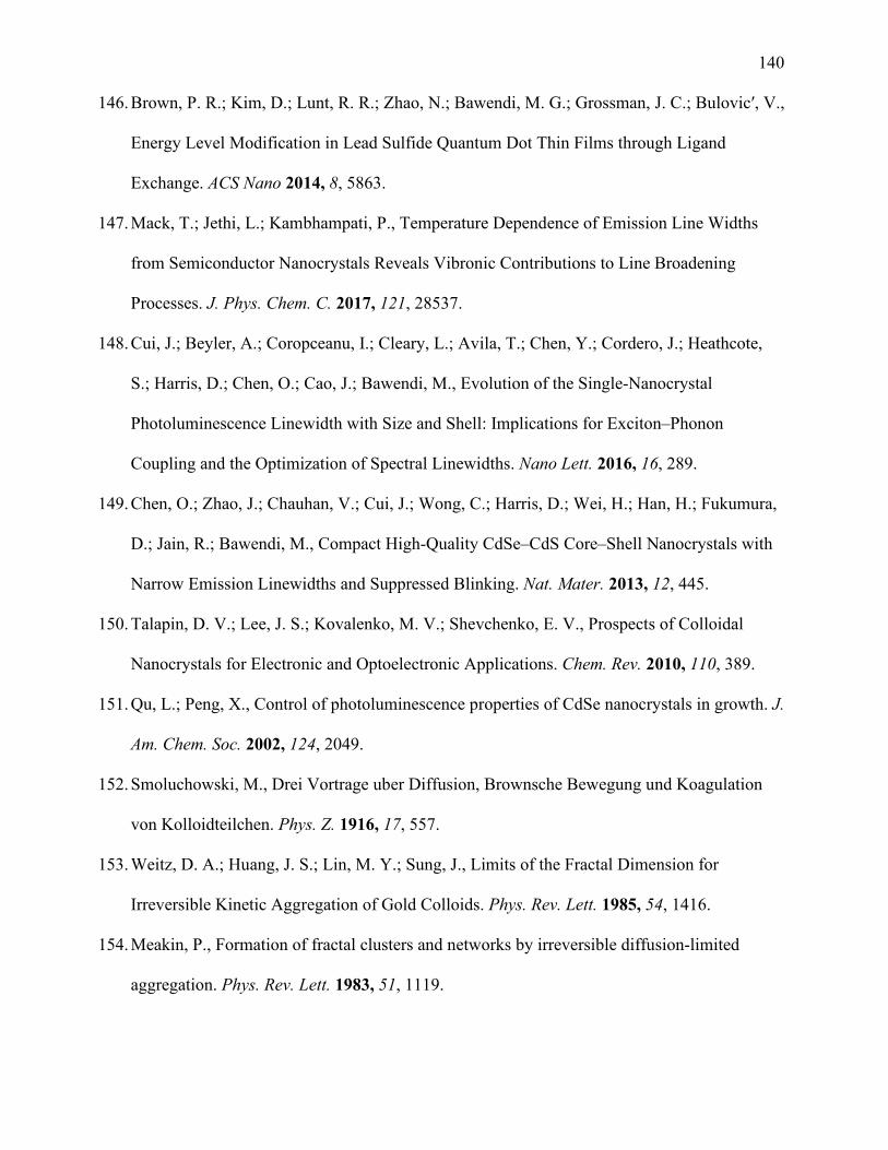
140
146. Brown, P. R.; Kim, D.; Lunt, R. R.; Zhao, N.; Bawendi, M. G.; Grossman, J. C.; Bulovic′, V.,
Energy Level Modification in Lead Sulfide Quantum Dot Thin Films through Ligand
Exchange. ACS Nano 2014, 8, 5863.
147. Mack, T.; Jethi, L.; Kambhampati, P., Temperature Dependence of Emission Line Widths
from Semiconductor Nanocrystals Reveals Vibronic Contributions to Line Broadening
Processes. J. Phys. Chem. C. 2017, 121, 28537.
148. Cui, J.; Beyler, A.; Coropceanu, I.; Cleary, L.; Avila, T.; Chen, Y.; Cordero, J.; Heathcote,
S.; Harris, D.; Chen, O.; Cao, J.; Bawendi, M., Evolution of the Single-Nanocrystal
Photoluminescence Linewidth with Size and Shell: Implications for Exciton–Phonon
Coupling and the Optimization of Spectral Linewidths. Nano Lett. 2016, 16, 289.
149. Chen, O.; Zhao, J.; Chauhan, V.; Cui, J.; Wong, C.; Harris, D.; Wei, H.; Han, H.; Fukumura,
D.; Jain, R.; Bawendi, M., Compact High-Quality CdSe–CdS Core–Shell Nanocrystals with
Narrow Emission Linewidths and Suppressed Blinking. Nat. Mater. 2013, 12, 445.
150. Talapin, D. V.; Lee, J. S.; Kovalenko, M. V.; Shevchenko, E. V., Prospects of Colloidal
Nanocrystals for Electronic and Optoelectronic Applications. Chem. Rev. 2010, 110, 389.
151. Qu, L.; Peng, X., Control of photoluminescence properties of CdSe nanocrystals in growth. J.
Am. Chem. Soc. 2002, 124, 2049.
152. Smoluchowski, M., Drei Vortrage uber Diffusion, Brownsche Bewegung und Koagulation
von Kolloidteilchen. Phys. Z. 1916, 17, 557.
153. Weitz, D. A.; Huang, J. S.; Lin, M. Y.; Sung, J., Limits of the Fractal Dimension for
Irreversible Kinetic Aggregation of Gold Colloids. Phys. Rev. Lett. 1985, 54, 1416.
154. Meakin, P., Formation of fractal clusters and networks by irreversible diffusion-limited
aggregation. Phys. Rev. Lett. 1983, 51, 1119.

141
155. Brilliantov, N. V.; Albers, N.; Spahn, F.; Poschel, T., Collision dynamics of granular
particles with adhesion. Phys. Rev. E 2007, 76, 051302.
156. Pawar, A. B.; Caggioni, M.; Hartel, R. W.; Spicer, P. T., Arrested coalescence of viscoelastic
droplets with internal microstructure. Faraday Discuss. 2012, 158, 341.
157. Varshni, Y. P., Temperature dependence of the elastic constants. Phys. Rev. B 1970, 2, 3952.
158. Zhang, J.; Lin, Z.; Lan, Y. Z.; Ren, G. Q.; Chen, D. G.; Huang, F.; Hong, M. C., A multistep
oriented attachment kinetics: Coarsening of ZnS nanoparticle in concentrated NaOH. J. Am.
Chem. Soc. 2006, 128, 12981.
159. Yu, W. W.; Peng, X., Formation of High-Quality CdS and Other II–VI Semiconductor
Nanocrystals in Noncoordinating Solvents: Tunable Reactivity of Monomers. Angew. Chem.,
Int. Ed. 2002, 41, 2368.
160. Yu, W. W.; Qu, L. H.; Guo, W. Z.; Peng, X. G., Experimental determination of the extinction
coefficient of CdTe, CdSe, and CdS nanocrystals. Chem. Mater. 2003, 15, 2854.
161. Park, Y. S.; Roh, J.; Diroll, B. T.; Schaller, R. D.; Klimov, V. I., Colloidal Quantum Dot
Lasers. Nat. Rev. Mater. 2021, 6, 382.
162. Porotnikov, D.; Zamkov, M., Progress and Prospects of Solution-Processed Two-
Dimensional Semiconductor Nanocrystals. J. Phys. Chem. C 2020, 124, 21895.
163. Yang, Z.; Fan, J. Z.; Proppe, A. H.; de Arquer, F. P. G.; Rossouw, D.; Voznyy, O.; Lan, X.;
Liu, M.; Walters, G.; Quintero-Bermudez, R.; Sun, B.; Hoogland, S.; Botton, G. A.; Kelley,
S. O.; Sargent, E. H., Mixed-Quantum-Dot Solar Cells. Nat. Commun. 2017, 8, 1325.
164. Beard, M. C.; Blackburn, J. L.; Johnson, J. C.; Rumbles, G., Status and Prognosis of Future-
Generation Photoconversion to Photovoltaics and Solar Fuels. ACS Energy Lett. 2016, 1,
344.

142
165. Shirasaki, Y.; Supran, G. J.; Bawendi, M. G.; Bulović, V., Emergence of Colloidal Quantum-
Dot Light-Emitting Technologies. Nat. Photonics 2013, 7, 13.
166. Coe, S.; Woo, W. K.; Bawendi, M.; Bulović, V., Electroluminescence from Single
Monolayers of Nanocrystals in Molecular Organic Devices. Nature 2002, 420, 800.
167. Efros, A. L.; Brus, L. E., Nanocrystal Quantum Dots: From Discovery to Modern
Development. ACS Nano 2021, 15, 6192.
168. Voznyy, O.; Levina, L.; Fan, J. Z.; Askerka, M.; Jain, A.; Choi, M. J.; Ouellette, O.;
Todorović, P.; Sagar, L. K.; Sargent, E. H., Machine Learning Accelerates Discovery of
Optimal Colloidal Quantum Dot Synthesis. ACS Nano 2019, 13, 11122.
169. Zhou, J.; Pu, C.; Jiao, T.; Hou, X.; Peng, X., A Two-Step Synthetic Strategy toward
Monodisperse Colloidal CdSe and CdSe/CdS Core/Shell Nanocrystals. J. Am. Chem. Soc.
2016, 138, 6475.
170. Razgoniaeva, N.; Carrillo, L.; Burchfield, D.; Moroz, P.; Adhikari, P.; Yadav, P.; Khon, D.;
Zamkov, M., Colloidal Synthesis of Monodisperse Semiconductor Nanocrystals through
Saturated Ionic Layer Adsorption. Chem. Mater. 2016, 28, 2823.
171. Morris-Cohen, A. J.; Frederick, M. T.; Lilly, G. D.; McArthur, E. A.; Weiss, E. A., Organic
Surfactant-Controlled Composition of the Surfaces of CdSe Quantum Dots. J. Phys. Chem.
Lett. 2010, 1, 1078.
172. Zhong, X.; Feng, Y.; Knoll, W.; Han, M., Alloyed Zn x Cd 1 - x S Nanocrystals with Highly
Narrow Luminescence Spectral Width. J. Am. Chem. Soc. 2003, 125, 13559.
173. Talapin, D. V.; Rogach, A. L.; Kornowski, A.; Haase, M.; Weller, H., Highly Luminescent
Monodisperse CdSe and CdSe/ZnS Nanocrystals Synthesized in a Hexadecylamine–
Trioctylphosphine Oxide–Trioctylphospine Mixture. Nano Lett. 2001, 1, 207.
143
174. Lv, L.; Li, J.; Wang, Y.; Shu, Y.; Peng, X., Monodisperse CdSe Quantum Dots Encased in
Six (100) Facets via Ligand-Controlled Nucleation and Growth. J. Am. Chem. Soc. 2020,
142, 19926.
175. Zhang, J.; Zhang, H.; Cao, W.; Pang, Z.; Li, J.; Shu, Y.; Zhu, C.; Kong, X.; Wang, L.; Peng,
X., Identification of Facet-Dependent Coordination Structures of Carboxylate Ligands on
CdSe Nanocrystals. J. Am. Chem. Soc. 2019, 141, 15675.
176. Bealing, C. R.; Baumgardner, W. J.; Choi, J. J.; Hanrath, T.; Hennig, R. G., Predicting
Nanocrystal Shape through Consideration of Surface-Ligand Interactions. ACS Nano 2012, 6,
2118.
177. Xia, Y.; Chen, W.; Zhang, P.; Liu, S.; Wang, K.; Yang, X.; Tang, H.; Lian, L.; He, J.; Liu,
X.; Liang, G.; Tan, M.; Gao, L.; Liu, H.; Song, H.; Zhang, D.; Gao, J.; Wang, K.; Lan, X.;
Zhang, X.; Müller-Buschbaum, n.; Tang, J.; Zhang, J., Facet Control for Trap-State
Suppression in Colloidal Quantum Dot Solids. Adv. Funct. Mater. 2020, 30, 2000594.
178. Hewavitharana, I. K.; Brock, S. L., When Ligand Exchange Leads to Ion-Exchange:
Nanocrystal Facets Dictate the Outcome. ACS Nano 2017, 11, 11217.
179. Lifshitz, I. M.; Slyozov, V. V., The Kinetics of Precipitation from Supersaturated Solid
Solutions. J. Phys. Chem. Solids 1961, 19, 35.
180. Yuan, B.; Cademartiri, L., Growth of Colloidal Nanocrystals by Liquid-Like Coalescence.
Angew. Chem., Int. Ed. 2021, 60, 6667.
181. Kim, M. G.; Jeong, J.; Choi, Y.; Park, J.; Park, E.; Cheon, C. H.; Kim, N. K.; Min, B. K.;
Kim, W., Synthesis of V-Doped In 2 O 3 Nanocrystals via Digestive-Ripening Process and
Their Electrocatalytic Properties in CO 2 Reduction Reaction. ACS Appl. Mater. Interfaces
2020, 12, 11890.

144
182. Huang, X.; Parashar, V. K.; Ao, Z.; Gijs, M. A. M., Insight into the Growth of Anisotropic
CdSe Nanocrystals: Attachment of Intrinsically Different Building Blocks. J. Phys. Chem. C
2020, 124, 27754.
183. Yu, L.; You, H.; Zhang, Q.; Zhang, L.; Fang, J., Digestive Ripening Mechanism
Investigation in a Classical Lee–Meisel Method Based on in Situ UV-Vis Spectra.
CrystEngComm 2019, 21, 1529.
184. Kholmicheva, N.; Yang, M.; Moroz, P.; Eckard, H.; Vore, A.; Cassidy, J.; Pushina, M.;
Boddy, A.; Porotnikov, D.; Anzenbacher, P.; Zamkov, M., Ion-Mediated Ligand Exchange
and Size Focusing of Semiconductor Nanocrystals in Ligand-Saturated Solutions. J. Phys.
Chem. C 2018, 122, 23623.
185. Yuk, J. M.; Park, J.; Ercius, P.; Kim, K.; Hellebusch, D. J.; Crommie, M. F.; Lee, J. Y.; Zettl,
A.; Alivisatos, A. P., High-Resolution EM of Colloidal Nanocrystal Growth Using Graphene
Liquid Cells. Science 2012, 336, 61.
186. Polte, J.; Ahner, T. T.; Delissen, F.; Sokolov, S.; Emmerling, F.; Thünemann, A. F.;
Kraehnert, R., Mechanism of Gold Nanoparticle Formation in the Classical Citrate Synthesis
Method Derived from Coupled In Situ XANES and SAXS Evaluation. J. Am. Chem. Soc.
2010, 132, 1296.
187. Cassidy, J.; Ellison, C.; Bettinger, J.; Yang, M.; Moroz, P.; Zamkov, M., Enabling Narrow
Emission Line Widths in Colloidal Nanocrystals through Coalescence Growth. Chem. Mater.
2020, 32, 7524.
188. Rempel, J. Y.; Trout, B. L.; Bawendi, M. G.; Jensen, K. F., Density Functional Theory Study
of Ligand Binding on CdSe (0001), (0001̅), and (112̅0) Single Crystal Relaxed and
Reconstructed Surfaces: Implications for Nanocrystalline Growth. J. Phys. Chem. B 2006,
110, 18007.
145
189. Burda, C.; Chen, X.; Narayanan, R.; El-Sayed, M. A., Chemistry and Properties of
Nanocrystals of Different Shapes. Chem. Rev. 2005, 105, 1025.
190. Herring, C., Some Theorems on the Free Energies of Crystal Surfaces. Phys. Rev. 1951, 82,
87.
191. Sarkar, S.; Sharp, C. G.; Finn, S. T.; Macdonald, J. E., Cracking Shells and Scrambling Eggs:
Intermediate Shell Formation and Anion Rearrangement in the Cation Exchange from p-SnS
to Cu1.8S. Chem. Mater. 2021, 33, 3011.
192. Brilliantov, N. V.; Albers, N.; Spahn, F.; Pöschel, T., Collision Dynamics of Granular
Particles with Adhesion. Phys. Rev. E 2007, 76, 051302.
193. Goldstein, A. N.; Echer, C. M.; Alivisatos, A. P., Melting in Semiconductor Nanocrystals.
Science 1992, 256, 1425.
194. Chen, P. E.; Anderson, N. C.; Norman, Z. M.; Owen, J. S., Tight binding of carboxylate,
phosphonate, and carbamate anions to stoichiometric CdSe nanocrystals. J. Am. Chem. Soc.
2017, 139, 3227.
195. Scholes, G. D., Controlling the Optical Properties of Inorganic Nanoparticles: Controlling the
Optical Properties of Inorganic Nanoparticles. Adv. Funct. Mater. 2008, 18, 1157.
196. Cassidy, J.; Yang, M.; Harankahage, D.; Porotnikov, D.; Moroz, P.; Razgoniaeva, N.;
Ellison, C.; Bettinger, J.; Ehsan, S.; Sanchez, J.; Madry, J.; Khon, D.; Zamkov, M., Tuning
the Dimensionality of Excitons in Colloidal Quantum Dot Molecules. Nano Lett. 2021, 21,
7339.
197. Mei, Q. S.; Lu, K., Melting and superheating of crystalline solids: From bulk to nanocrystals.
Prog. Mater. Sci. 2007, 52, 1175.
198. Kofman, R.; Cheyssac, P.; Aouaj, A.; Lereah, Y.; Deutscher, G.; Ben-David, T.; Penisson, J.
M.; Bourret, A., Surface Melting Enhanced by Curvature Effects. Surf. Sci. 1994, 303, 231.

146
199. Yu, W. W.; Peng, X., Formation of High-Quality CdS and Other II–VI Semiconductor
Nanocrystals in Noncoordinating Solvents: Tunable Reactivity of Monomers. Angew. Chem.,
Int. Ed. 2002, 114, 2474.
200. Pu, C.; Zhou, J.; Lai, R., Highly reactive, flexible yet green Se precursor for metal selenide
nanocrystals: Se-octadecene suspension (Se-SUS). Nano Res. 2013, 6, 652.
201. Katz, E.; Willner, I., Integrated Nanoparticle-Biomolecule Hybrid Systems: Synthesis,
Properties, and Applications. Angew. Chem., Int. Ed. 2004, 43, 6042.
202. Kagan, C. R.; Lifshitz, E.; Sargent, E. H.; Talapin, D. V., Building devices from colloidal
quantum dots. Science 2016, 353, aac5523.
203. Gilroy, K. D.; Ruditskiy, A.; Peng, H. C.; Qin, D.; Xia, Y., Bimetallic Nanocrystals:
Syntheses, Properties, and Applications. Chem. Rev. 2016, 116, 10414.
204. Wang, X.; Valiev, R. R.; Ohulchanskyy, T. Y.; Agren, H.; Yang, C.; Chen, G., Dye-
sensitized lanthanide-doped upconversion nanoparticles. Chem. Soc. Rev. 2017, 46, 4150.
205. Kagan, C. R.; Bassett, L. C.; Murray, C. B.; Thompson, S. M., Colloidal Quantum Dots as
Platforms for Quantum Information Science. Chem. Rev. 2021, 121, 3186.
206. Kroupa, D. M.; Pach, G. F.; Vörös, M.; Giberti, F.; Chernomordik, B. D.; Crisp, R. W.;
Nozik, A. J.; Johnson, J. C.; Singh, R.; Klimov, V. I.; Galli, G.; Beard, M. C., Enhanced
Multiple Exciton Generation in PbS|CdS Janus-like Heterostructured Nanocrystals. ACS
Nano 2018, 12, 10084.
207. Peng, X.; Schlamp, M. C.; Kadavanich, A. V.; Alivisatos, A. P., Epitaxial Growth of Highly
Luminescent CdSe/CdS Core/Shell Nanocrystals with Photostability and Electronic
Accessibility. J. Am. Chem. Soc. 1997, 119, 7019.
208. Hines, M. A.; Guyot-Sionnest, P., Synthesis and Characterization of Strongly Luminescing
ZnS-Capped CdSe Nanocrystals. J. Phys. Chem. 1996, 100, 468.
147
209. Danek, M.; Jensen, K. F.; Murray, C. B.; Bawendi, M. G., Synthesis of Luminescent Thin-
Film CdSe/ZnSe Quantum Dot Composites Using CdSe Quantum Dots Passivated with an
Overlayer of ZnSe. Chem. Mater. 1996, 8, 173.
210. Shao, Q.; Wang, P.; Huang, X., Opportunities and Challenges of Interface Engineering in
Bimetallic Nanostructure for Enhanced Electrocatalysis. Adv. Funct. Mater. 2019, 29,
1806419.
211. Zhang, J.; Chernomordik, B. D.; Crisp, R. W.; Kroupa, D. M.; Luther, J. M.; Miller, E. M.;
Gao, J.; Beard, M. C., Preparation of Cd/Pb Chalcogenide Heterostructured Janus Particles
via Controllable Cation Exchange. ACS Nano 2015, 9, 7151.
212. Hewa-Kasakarage, N. N.; Kirsanova, M.; Nemchinov, A.; Schmall, N.; El-Khoury, P. Z.;
Tarnovsky, A. N.; Zamkov, M., Radiative recombination of spatially extended excitons in
(ZnSe/CdS)/CdS heterostructured nanorods. J. Am. Chem. Soc. 2009, 131, 1328.
213. Carbone, L.; Nobile, C.; De Giorgi, M.; Sala, F. D.; Morello, G.; Pompa, P.; Hytch, M.;
Snoeck, E.; Fiore, A.; Franchini, I. R., Synthesis and Micrometer-Scale Assembly of
Colloidal CdSe/CdS Nanorods Prepared by a Seeded Growth Approach. Nano Lett. 2007, 7,
2942.
214. Halpert, J. E.; Porter, V. J.; Zimmer, J. P.; Bawendi, M. G., Synthesis of CdSe/CdTe
Nanobarbells. J. Am. Chem. Soc. 2006, 128, 12590.
215. Shieh, F.; Saunders, A. E.; Korgel, B. A., General Shape Control of Colloidal CdS, CdSe,
CdTe Quantum Rods and Quantum Rod Heterostructures. J. Phys. Chem. B 2005, 109, 8538.
216. Kudera, S.; Carbone, L.; Casula, M. F.; Cingolani, R.; Falqui, A.; Snoeck, E.; Parak, W. J.;
Manna, L., Selective Growth of PbSe on One or Both Tips of Colloidal Semiconductor
Nanorods. Nano Lett. 2005, 5, 445.
148
217. Pedetti, S.; Ithurria, S.; Heuclin, H.; Patriarche, G.; Dubertret, B., Type-II CdSe/CdTe
Core/Crown Semiconductor Nanoplatelets. J. Am. Chem. Soc. 2014, 136, 16430.
218. Carbone, L.; Cozzoli, P. D., Colloidal heterostructured nanocrystals: Synthesis and growth
mechanisms. Nano Today 2010, 5, 449.
219. Shen, H.; Gao, Q.; Zhang, Y.; Lin, Y.; Lin, Q.; Li, Z.; Chen, L.; Zeng, Z.; Li, X.; Jia, Y.;
Wang, S.; Du, Z.; Li, L. S.; Zhang, Z., Visible quantum dot light-emitting diodes with
simultaneous high brightness and efficiency. Nat. Photonics 2019, 13, 192.
220. Shirasaki, Y.; Supran, G. J.; Bawendi, M. G.; Bulovic, V., Emergence of Colloidal Quantum-
Dot LightEmitting Technologies. Nat. Photonics 2013, 7, 13.
221. Zhu, H.; Song, N.; Lv, H.; Hill, C. L.; Lian, T., Near unity quantum yield of light-driven
redox mediator reduction and efficient H2 generation using colloidal nanorod
heterostructures. J. Am. Chem. Soc. 2012, 134, 11701.
222. Acharya, K. P.; Khnayzer, R. S.; O’Connor, T.; Diederich, G.; Kirsanova, M.; Klinkova, A.;
Roth, D.; Kinder, E.; Imboden, M.; Zamkov, M., The role of hole localization in sacrificial
hydrogen production by semiconductor-metal heterostructured nanocrystals. Nano Lett.
2011, 11, 2919.
223. Amirav, L.; Alivisatos, P. A. J., Photocatalytic Hydrogen Production with Tunable Nanorod
Heterostructures. J. Phys. Chem. Lett. 2010, 1, 1051.
224. Yi, C.; Liu, H.; Zhang, S.; Yang, Y.; Zhang, Y.; Lu, Z.; Kumacheva, E.; Nie, Z., Self-
limiting Directional Nanoparticle Bonding Governed by Reaction Stoichiometry. Science
2020, 369, 1369.
225. Jones, M. R.; Seeman, N. C.; Mirkin, C. A., Nanomaterials. Programmable Materials and the
Nature of the DNA Bond. Science 2015, 347, 1260901.
149
226. Jones, M. R.; Osberg, K. D.; MacFarlane, R. J.; Langille, M. R.; Mirkin, C. A., Templated
Techniques for the Synthesis and Assembly of Plasmonic Nanostructures. Chem. Rev. 2011,
111, 3736.
227. Zheng, J.; Constantinou, P. E.; Micheel, C.; Alivisatos, A. P.; Kiehl, R. A.; Seeman, N. C.,
Two-Dimensional Nanoparticle Arrays Show the Organizational Power of Robust DNA
Motifs. Nano Lett. 2006, 6, 1502.
228. Seeman, N. C., DNA in a Material World. Nature 2003, 421, 427.
229. Song, L.; Deng, Z. X., Valency Control and Functional Synergy in DNA-Bonded
Nanomolecules. ChemNanoMater. 2017, 3, 698.
230. Kim, J. Y.; Kotov, N. A., Charge Transport Dilemma of Solution-Processed Nanomaterials.
Chem. Mater. 2014, 26, 134.
231. Prodan, E.; Radloff, C.; Halas, N. J.; Nordlander, P., A Hybridization Model for the Plasmon
Response of Complex Nanostructures. Science 2003, 302, 419.
232. Xu, X.; Stöttinger, S.; Battagliarin, G.; Hinze, G.; Mugnaioli, E.; Li, C.; Müllen, K.; Basché,
T., Assembly and Separation of Semiconductor Quantum Dot Dimers and Trimers. J. Am.
Chem. Soc. 2011, 133, 18062.
233. Salzmann, B. B. V.; van der Sluijs, M. M.; Soligno, G.; Vanmaekelbergh, D., Oriented
Attachment: From Natural Crystal Growth to a Materials Engineering Tool. Acc. Chem. Res.
2021, 54, 787.
234. Koley, S.; Cui, J.; Panfil, Y. E.; Banin, U., Coupled Colloidal Quantum Dot Molecules. Acc.
Chem. Res. 2021, 54, 1178.
235. Cui, J.; Koley, S.; Panfil, Y. E.; Levi, A.; Waiskopf, N.; Remennik, S.; Oded, M.; Banin, U.,
Semiconductor Bow-Tie Nanoantenna from Coupled Colloidal Quantum Dot Molecules.
Angew. Chem., Int. Ed. 2021, 60, 14467.
150
236. Cui, J.; Panfil, Y. E.; Koley, S.; Shamalia, D.; Waiskopf, N.; Remennik, S.; Popov, I.; Oded,
M.; Banin, U., Colloidal Quantum Dot Molecules Manifesting Quantum Coupling at Room
Temperature. Nat. Commun. 2019, 10, 5401.
237. Hu, Y.; Sun, Y., A Generic Approach for the Synthesis of Dimer Nanoclusters and
Asymmetric Nanoassemblies. J. Am. Chem. Soc. 2013, 135, 2213.
238. Goodman, B. M.; Somorjai, G. A., Low-Energy Electron Diffraction Studies of Surface
Melting and Freezing of Lead, Bismuth, and Tin Single-Crystal Surfaces. J. Chem. Phys.
1970, 52, 6325.
239. Wang, Z. L.; Petroski, J. M.; Green, T. C.; El-Sayed, M. A., Shape Transformation and
Surface Melting of Cubic and Tetrahedral Platinum Nanocrystals. J. Phys. Chem. B 1998,
102, 6145.
240. Buffat, P.; Borel, J. P., Size effect on the melting temperature of gold particles. Phys. Rev. A:
At., Mol., Opt. Phys. 1976, 13, 2287.
241. Cassidy, J.; Ellison, C.; Bettinger, J.; Yang, M.; Moroz, P.; Zamkov, M., Enabling Narrow
Emission Linewidths in Colloidal Nanocrystals through Coalescence Growth. Chem. Mater.
2020, 32, 7524.
242. Owen, J. S.; Park, J.; Trudeau, P. E.; Alivisatos, A. P., Reaction Chemistry and Ligand
Exchange at Cadmium–Selenide Nanocrystal Surfaces. J. Am. Chem. Soc. 2008, 130, 12279.
243. Scholes, G. D., Controlling the optical properties of inorganic nanoparticles. Adv. Funct.
Mater. 2008, 18, 1157.
244. Scholes, G. D.; Kim, J.; Wong, C. Y.; Huxter, V. M.; Nair, P. S.; Fritz, K. P.; Kumar, S.,
Nanocrystal shape and the mechanism of exciton spin relaxation. Nano Lett. 2006, 6, 1765.
245. Shabaev, A.; Efros, A. L., 1D exciton spectroscopy of semiconductor nanorods. Nano Lett.
2004, 4, 1821.

151
246. Zhao, Q.; Graf, P. A.; Jones, W. B.; Franceschetti, A.; Li, J.; Wang, L.; Kim, K., Shape
dependence of band-edge Exciton fine structure in CdSe nanocrystals. Nano Lett. 2007, 7,
3274.
247. Chen, T.; Reich, K. V.; Kramer, N. J.; Fu, H.; Kortshagen, U. R.; Shklovskii, B. I., Metal-
Insulator Transition in Films of Doped Semiconductor Nanocrystals. Nat. Mater. 2016, 15,
299.
248. Lovett, B. W.; Reina, J. H.; Nazir, A.; Briggs, G., Optical schemes for quantum computation
in quantum dot molecules. Phys. Rev. B: Condens. Matter Mater. Phys. 2003, 68, 205319.
249. Schedelbeck, G.; Wegscheider, W.; Bichler, M.; Abstreiter, G., Coupled quantum dots
fabricated by cleaved edge overgrowth: from artificial atoms to molecules. Science 1997,
278, 1792.
250. Grossmann, A.; Erley, W.; Hannon, J. B.; Ibach, H., Giant Surface Stress in Heteroepitaxial
Films: Invalidation of a Classical Rule in Epitaxy. Phys. Rev. Lett. 1996, 77, 127.
251. van der Veen, J. F., Melting and freezing at surfaces. Surf. Sci. 1999, 433–435, 1.
252. Razgoniaeva, N.; Moroz, P.; Yang, M.; Budkina, D. S.; Eckard, H.; Augspurger, M.; Khon,
D.; Tarnovsky, A. N.; Zamkov, M., One-Dimensional Carrier Confinement in “Giant”
CdS/CdSe Excitonic Nanoshells. Journal of the American Chemical Society 2017, 139 (23),
7815-7822.
253. Khon, E.; Lambright, S.; Khon, D.; Smith, B.; O'Connor, T.; Moroz, P.; Imboden, M.;
Diederich, G.; Perez-Bolivar, C.; Anzenbacher, P.; Zamkov, M., Inorganic Solids of CdSe
Nanocrystals Exhibiting High Emission Quantum Yield. Advanced Functional Materials
2012, 22 (17), 3714-3722.
152
254. Semonin, O. E.; Luther, J. M.; Choi, S.; Chen, H.; Gao, J.; Nozik, A. J.; Beard, M. C., Peak
external photocurrent quantum efficiency exceeding 100% via MEG in a quantum dot solar
cell. Science 2011, 334, 1530.
255. Nair, G.; Chang, L.; Geyer, S. M.; Bawendi, M. G., Perspective on the prospects of a carrier
multiplication nanocrystal solar cell. Nano Lett. 2011, 11, 2145.
256. Sukhovatkin, V.; Hinds, S.; Brzozowski, L.; Sargent, E. H., Colloidal quantum-dot
photodetectors exploiting multiexciton generation. Science 2009, 324, 1542.
257. Kambhampati, P., Multiexcitons in Semiconductor Nanocrystals: A Platform for
Optoelectronics at High Carrier Concentration. J. Phys. Chem. Lett. 2012, 3, 1182.
258. Klimov, V. I., Spectral and dynamical properties of multiexcitons in semiconductor
nanocrystals. Annu. Rev. Phys. Chem. 2007, 58, 635.
259. Moroz, P.; Boddy, A.; Zamkov, M., Challenges and Prospects of Photocatalytic Applications
Based On Semiconductor Nanocrystals. Front. Chem. 2018, 6, 353.
260. Kholmicheva, N.; Royo Romero, L.; Cassidy, J.; Zamkov, M., Prospects and applications of
plasmon-exciton interactions in the near-field regime. Nanophotonics 2018.
261. Blankenship, R. E.; Tiede, D. M.; Barber, J.; Brudvig, G. W.; Fleming, G.; Ghirardi, M.;
Gunner, M. R.; Junge, W.; Kramer, D. M.; Melis, A.; Moore, T. A.; Moser, C. C.; Nocera, D.
G.; Nozik, A. J.; Ort, D. R.; Parson, W. W.; Prince, R. C.; Sayre, R. T., Comparing
photosynthetic and photovoltaic efficiencies and recognizing the potential for improvement.
Science 2011, 332, 805.
262. Lewis, N. S.; Nocera, D. G., Powering the planet: Chemical challenges in solar energy
utilization. Proc. Natl. Acad. Sci. U. S. A. 2006, 103, 15729.
153
263. Nirmal, M.; Dabbousi, B. O.; Bawendi, M. G.; Macklin, J. J.; Trautman, J. K.; Harris, T. D.;
Brus, L. E., Fluorescence intermittency in single cadmium selenide nanocrystals. Nature
1996, 383, 802.
264. Trinh, M. T.; Polak, L.; Schins, J. M.; Houtepen, A. J.; Vaxenburg, R.; Maikov, G. I.;
Grinbom, G.; Midgett, A. G.; Luther, J. M.; Beard, M. C.; Nozik, A. J.; Bonn, M.; Lifshitz,
E.; Siebbeles, L. D. A., Anomalous independence of multiple exciton generation on different
group IV-VI quantum dot architectures. Nano Lett. 2011, 11, 1623.
265. Klimov, V. I.; McGuire, J. A.; Schaller, R. D.; Rupasov, V. I., Scaling of multiexciton
lifetimes in semiconductor nanocrystals. Phys. Rev. B: Condens. Matter Mater. Phys. 2008,
77, 195324.
266. Grivas, C.; Li, C.; Andreakou, P.; Wang, P.; Ding, M.; Brambilla, G.; Manna, L.;
Lagoudakis, P., Single-mode tunable laser emission in the single-exciton regime from
colloidal nanocrystals. Nat. Commun. 2013, 4, 2376.
267. Eisler, H.; Sundar, V. C.; Bawendi, M. G.; Walsh, M.; Smith, H. I.; Klimov, V., Color-
selective semiconductor nanocrystal laser. Appl. Phys. Lett. 2002, 80, 4614.
268. Philbin, J. P.; Rabani, E., Electron-Hole Correlations Govern Auger Recombination in
Nanostructures. Nano Lett. 2018, 18, 7889.
269. Klimov, V. I., Multicarrier interactions in semiconductor nanocrystals in relation to the
phenomena of Auger recombination and carrier multiplication. Annu. Rev. Condens. Matter
Phys. 2014, 5, 285.
270. Cragg, G. E.; Efros, A. L., Suppression of Auger Processes in Confined Structures. Nano
Lett. 2010, 10, 313.
154
271. Robel, I.; Gresback, R.; Kortshagen, U.; Schaller, R. D.; Klimov, V. I., Universal size-
dependent trend in auger recombination in direct-gap and indirect-gap semiconductor
nanocrystals. Phys. Rev. Lett. 2009, 102, 177404.
272. Pietryga, J. M.; Zhuravlev, K. K.; Whitehead, M.; Klimov, V. I.; Schaller, R. D., Evidence
for barrierless Auger recombination in PbSe nanocrystals: a pressure-dependent study of
transient optical absorption. Phys. Rev. Lett. 2008, 101, 217401.
273. Wang, L. W.; Califano, M.; Zunger, A.; Franceschetti, A., Pseudopotential theory of Auger
processes in CdSe quantum dots. Phys. Rev. Lett. 2003, 91, 056404.
274. Park, Y.; Lim, J.; Makarov, N. S.; Klimov, V. I., Effect of Interfacial Alloying versus
“Volume Scaling” on Auger Recombination in Compositionally Graded Semiconductor
Quantum Dots. Nano Lett. 2017, 17, 5607.
275. García-Santamaría, F.; Chen, Y.; Vela, J.; Schaller, R. D.; Hollingsworth, J. A.; Klimov, V.
I., Suppressed Auger Recombination in “Giant” Nanocrystals Boosts Optical Gain
Performance. Nano Lett. 2009, 9, 3482.
276. Ben-Shahar, Y.; Philbin, J. P.; Scotognella, F.; Ganzer, L.; Cerullo, G.; Rabani, E.; Banin, U.,
Charge Carrier Dynamics in Photocatalytic Hybrid Semiconductor-Metal Nanorods:
Crossover from Auger Recombination to Charge Transfer. Nano Lett. 2018, 18, 5211.
277. Rabouw, F. T.; Lunnemann, P.; van Dijk-Moes, R. J.; Frimmer, M.; Pietra, F.; Koenderink,
A. F.; Vanmaekelbergh, D., Reduced auger recombination in single CdSe/CdS nanorods by
one-dimensional electron delocalization. Nano Lett. 2013, 13, 4884.
278. Padilha, L. A.; Stewart, J. T.; Sandberg, R. L.; Bae, W. K.; Koh, W.; Pietryga, J. M.; Klimov,
V. I., Aspect ratio dependence of auger recombination and carrier multiplication in PbSe
nanorods. Nano Lett. 2013, 13, 1092.

155
279. Cunningham, P. D.; Boercker, J. E.; Foos, E. E.; Lumb, M. P.; Smith, A. R.; Tischler, J. G.;
Melinger, J. S., Enhanced multiple exciton generation in quasi-one-dimensional
semiconductors. Nano Lett. 2011, 11, 3476.
280. Zavelani-Rossi, M.; Lupo, M. G.; Tassone, F.; Manna, L.; Lanzani, G., Suppression of
biexciton Auger recombination in CdSe/CdS dot/rods: role of the electronic structure in the
carrier dynamics. Nano Lett. 2010, 10, 3142.
281. Pelton, M., Carrier Dynamics, Optical Gain, and Lasing with Colloidal Quantum Wells. J.
Phys. Chem. C 2018, 122, 10659.
282. Pelton, M.; Andrews, J. J.; Fedin, I.; Talapin, D. V.; Leng, H.; O’Leary, S. K.,
Nonmonotonic Dependence of Auger Recombination Rate on Shell Thickness for CdSe/CdS
Core/Shell Nanoplatelets. Nano Lett. 2017, 17, 6900.
283. Li, Q.; Lian, T., Area-and thickness-dependent biexciton Auger recombination in colloidal
CdSe nanoplatelets: Breaking the “universal volume scaling law. Nano Lett. 2017, 17, 3152.
284. Park, Y.; Bae, W. K.; Baker, T.; Lim, J.; Klimov, V. I., Effect of Auger recombination on
lasing in heterostructured quantum dots with engineered core/shell interfaces. Nano Lett.
2015, 15, 7319.
285. She, C.; Fedin, I.; Dolzhnikov, D. S.; Demortière, A.; Schaller, R. D.; Pelton, M.; Talapin, D.
V., Low-Threshold Stimulated Emission Using Colloidal Quantum Wells. Nano Lett. 2014,
14, 2772.
286. Kambhampati, P.; Mack, T.; Jethi, L., Understanding and Exploiting the Interface of
Semiconductor Nanocrystals for Light Emissive Applications. ACS Photonics 2017, 4, 412.
287. Jeong, B. G.; Park, Y.; Chang, J. H.; Cho, I.; Kim, J. K.; Kim, H.; Char, K.; Cho, J.; Klimov,
V. I.; Park, P.; Lee, D. C.; Bae, W. K., Colloidal Spherical Quantum Wells with Near-Unity
Photoluminescence Quantum Yield and Suppressed Blinking. ACS Nano 2016, 10, 9297.

156
288. Dias, E. A.; Saari, J. I.; Tyagi, P.; Kambhampati, P., Improving Optical Gain Performance in
Semiconductor Quantum Dots via Coupled Quantum Shells. J. Phys. Chem. C 2012, 116,
5407.
289. Schrier, J.; Wang, L., Electronic structure of nanocrystal quantum-dot quantum wells. Phys.
Rev. B: Condens. Matter Mater. Phys. 2006, 73, 245332.
290. Schill, A. W.; Gaddis, C. S.; Qian, W.; El-Sayed, M. A.; Cai, Y.; Milam, V. T.; Sandhage,
K., Ultrafast electronic relaxation and charge-carrier localization in CdS/CdSe/CdS quantum-
dot quantum-well heterostructures. Nano Lett. 2006, 6, 1940.
291. Xu, J.; Xiao, M.; Battaglia, D.; Peng, X., Exciton radiative recombination in spherical Cd
S/Cd Se/Cd S quantum-well nanostructures. Appl. Phys. Lett. 2005, 87, 043107.
292. Xu, J.; Xiao, M., Lasing Action in Colloidal CdS/CdSe/CdS Quantum Wells. Appl. Phys.
Lett. 2005, 87, 173117.
293. Xu, J.; Battaglia, D.; Peng, X.; Xiao, M., Photoluminescence from colloidal CdS-CdSe-CdS
quantum wells. J. Opt. Soc. Am. B 2005, 22, 1112.
294. Battaglia, D.; Li, J. J.; Wang, Y.; Peng, X., Colloidal two dimensional systems: CdSe
quantum shells and wells. Angew. Chem., Int. Ed. 2003, 42, 5035.
295. Braun, M.; Link, S.; Burda, C.; El-Sayed, M., Transfer Times of Electrons and Holes across
the Interface in CdS/HgS/CdS Quantum Dot Quantum Well Nanoparticles. Chem. Phys. Lett.
2002, 361, 446.
296. Pokatilov, E. P.; Fonoberov, V. A.; Fomin, V. M.; Devreese, J. T., Electron and hole states in
quantum dot quantum wells within a spherical eight-band model. Phys. Rev. B: Condens.
Matter Mater. Phys. 2001, 64, 245329.
297. Braun, M.; Burda, C.; El-Sayed, M. A., Variation of the thickness and number of wells in the
CdS/HgS/CdS quantum dot quantum well system. J. Phys. Chem. A 2001, 105, 5548.
157
298. Razgoniaeva, N.; Yang, M.; Colegrove, C.; Kholmicheva, N.; Moroz, P.; Eckard, H.; Vore,
A.; Zamkov, M., Double-Well Colloidal Nanocrystals Featuring Two-Color
Photoluminescence. Chem. Mater. 2017, 29, 7852.
299. Razgoniaeva, N.; Moroz, P.; Yang, M.; Budkina, D. S.; Eckard, H.; Augspurger, M.; Khon,
D.; Tarnovsky, A. N.; Zamkov, M., One-dimensional carrier confinement in “giant”
CdS/CdSe excitonic nanoshells. J. Am. Chem. Soc. 2017, 139, 7815.
300. Weng, C.; Chen, I.; Tsai, Y., Electron–acoustic-phonon interaction in core/shell nanocrystals
and in quantum-dot quantum wells. Phys. Rev. B: Condens. Matter Mater. Phys. 2007, 76,
195313.
301. Sippel, P.; Albrecht, W.; van der Bok, J. C.; Van Dijk-Moes, R. J.; Hannappel, T.;
Eichberger, R.; Vanmaekelbergh, D., Femtosecond cooling of hot electrons in CdSe
quantum-well platelets. Nano Lett. 2015, 15, 2409.
302. Ithurria, S.; Tessier, M. D.; Mahler, B.; Lobo, R. P. S. M.; Dubertret, B.; Efros, A. L.,
Colloidal nanoplatelets with two-dimensional electronic structure. Nat. Mater. 2011, 10, 936.
303. Aerts, M.; Bielewicz, T.; Klinke, C.; Grozema, F. C.; Houtepen, A. J.; Schins, J. M.;
Siebbeles, L. D. A., Highly efficient carrier multiplication in PbS nanosheets. Nat. Commun.
2014, 5, 3789.
304. Murray, C. B.; Shevchenko, E. V.; O’Brien, S.; Talapin, D. V.; Kotov, N. A., Structural
diversity in binary nanoparticle superlattices. Nature 2006, 439, 55.
305. Murray, C. B.; Kagan, C. R.; Bawendi, M. G., Synthesis and Characterization of
Monodisperse Nanocrystals and Close-Packed Nanocrystal Assemblies. Annu. Rev. Mater.
Sci. 2000, 30, 545.
158
306. She, C.; Bryant, G. W.; Demortière, A.; Shevchenko, E. V.; Pelton, M., Controlling the
spatial location of photoexcited electrons in semiconductor CdSe/CdS core/shell nanorods.
Phys. Rev. B: Condens. Matter Mater. Phys. 2013, 87, 155427.
307. Wu, K.; Lian, T., Quantum confined colloidal nanorod heterostructures for solar-to-fuel
conversion. Chem. Soc. Rev. 2016, 45, 3781.
308. Mooney, J.; Krause, M. M.; Saari, J. I.; Kambhampati, P., Challenge to the deep-trap model
of the surface in semiconductor nanocrystals. Phys. Rev. B: Condens. Matter Mater. Phys.
2013, 87, 081201.
309. Cirillo, M.; Aubert, T.; Gomes, R.; Van Deun, R.; Emplit, P.; Biermann, A.; Lange, H.;
Thomsen, C.; Brainis, E.; Hens, Z., Flash” Synthesis of CdSe/CdC Core–Shell Quantum
Dots. Chem. Mater. 2014, 26, 1154.
310. Sewall, S. L.; Cooney, R. R.; Anderson, K. E.; Dias, E. A.; Kambhampati, P., State-to-state
exciton dynamics in semiconductor quantum dots. Phys. Rev. B: Condens. Matter Mater.
Phys. 2006, 74, 235328.
311. Houtepen, A. J.; Vanmaekelbergh, D., Orbital occupation in electron-charged CdSe
quantum-dot solids. J. Phys. Chem. B 2005, 109, 19634.
312. Sacra, A.; Norris, D. J.; Murray, C. B.; Bawendi, M. G., Stark spectroscopy of CdSe
nanocrystallites: The significance of transition linewidths. J. Chem. Phys. 1995, 103, 5236.
313. Huang, J.; Huang, Z.; Yang, Y.; Zhu, H.; Lian, T., Multiple exciton dissociation in CdSe
quantum dots by ultrafast electron transfer to adsorbed methylene blue. J. Am. Chem. Soc.
2010, 132, 4858.
314. Klimov, V. I.; Mikhailovsky, A. A.; McBranch, D. W.; Leatherdale, C. A.; Bawendi, M. G.,
Quantization of multiparticle Auger rates in semiconductor quantum dots. Science 2000, 287,
1011.

159
315. Kong, D.; Jia, Y.; Ren, Y.; Xie, Z.; Wu, K.; Lian, T., Shell-Thickness-Dependent Biexciton
Lifetime in Type I and Quasi-Type II CdSe@ CdS Core/Shell Quantum Dots. J. Phys. Chem.
C 2018, 122, 14091.
316. Htoon, H.; Hollingsworth, J. A.; Dickerson, R.; Klimov, V. I., Effect of zero-to one-
dimensional transformation on multiparticle auger recombination in semiconductor quantum
rods. Phys. Rev. Lett. 2003, 91, 227401.
317. Klimov, V. I.; Ivanov, S. A.; Nanda, J.; Achermann, M.; Bezel, I.; McGuire, J. A.;
Piryatinski, A., Single-exciton optical gain in semiconductor nanocrystals. Nature 2007, 447,
441.
318. Oron, D.; Kazes, M.; Banin, U., Multiexcitons in type-II colloidal semiconductor quantum
dots. Phys. Rev. B: Condens. Matter Mater. Phys. 2007, 75, 035330.
319. Yu, W. W.; Peng, X., Formation of high-quality CdS and other II-VI semiconductor
nanocrystals in noncoordinating solvents: Tunable reactivity of monomers. Angew. Chem.,
Int. Ed. 2007, 46, 2559.
320. Kovalenko, S. A.; Dobryakov, A. L.; Ruthmann, J.; Ernsting, N. P., Femtosecond
spectroscopy of condensed phases with chirped supercontinuum probing. Phys. Rev. A: At.,
Mol., Opt. Phys. 1999, 59, 2369.
321. Park, Y. S.; Roh, J.; Diroll, B. T.; Schaller, R. D.; Klimov, V. I., Colloidal quantum Quantum
dot Dot lasersLasers. Nat. Rev. Mater. 2021, 6, 382.
322. Shirasaki, Y.; Supran, G. J.; Bawendi, M. G.; Bulović, V., Emergence of colloidal Colloidal
quantumQuantum-dot Dot lightLight-emitting Emitting technologiesTechnologies. Nature
Photonics 2013, 7, 13.
323. Hanifi, D. A.; Bronstein, N. D.; Koscher, B. A.; Nett, Z.; Swabeck, J. K.; Takano, K.;
Schwartzberg, A. M.; Maserati, L.; Vandewal, K.; van de Burgt, Y.; Salleo, A.; Alivisatos,

160
A. P., Redefining Near-Unity Luminescence in Quantum Dots with Photothermal Threshold
Quantum Yield. Science 2019, 363, 1199.
324. Yang, J.; Choi, M. K.; Yang, U. J.; Kim, S. Y.; Kim, Y. S.; Kim, J. H.; Kim, D. H.; Hyeon,
T., Toward Full-Color Electroluminescent Quantum Dot Displays. Nano Lett. 2021, 21, 26.
325. Panfil, Y. E.; Oded, M.; Banin, U., Colloidal Quantum Nanostructures: Emerging Materials
for Display Applications. Angew. Chem., Int. Ed. 2018, 57, 4274.
326. García de Arquer, F. P.; Talapin, D. V.; Klimov, V. I.; Arakawa, Y.; Bayer, M.; Sargent, E.
H., Semiconductor quantum dots: Technological Progress and Future Challenges. Science
2021, 373, eaaz8541.
327. Lim, J.; Park, Y. S.; Klimov, V. I., Optical Gain in Colloidal Quantum Dots Achieved with
Direct-Current Electrical Pumping. Nat. Mater. 2018, 17, 42.
328. Wang, Y.; Sun, H., Advances and Prospects of Lasers Developed from Colloidal
Semiconductor Nanostructures. Prog. Quantum. Electron. 2018, 60, 1.
329. Yang, Z.; Pelton, M.; Fedin, I.; Talapin, D. V.; Waks, E. A., A Room Temperature
Continuous-Wave Nanolaser Using Solloidal Quantum Wells. Nat. Commun. 2017, 8, 143.
330. Fan, F.; Voznyy, O.; Sabatini, R. P.; Bicanic, K. T.; Adachi, M. M.; McBride, J. R.; Reid, K.
R.; Park, Y. S.; Li, X.; Jain, A.; Quintero-Bermudez, R.; Saravanapavanantham, M.; Liu, M.;
Korkusinski, M.; Hawrylak, P.; Klimov, V. I.; Rosenthal, S. J.; Hoogland, S.; Sargent, E. H.,
Continuous-Wave Lasing in Colloidal Quantum Dot Solids Enabled by Facet-Selective
Epitaxy. Nature 2017, 544, 75.
331. Yakunin, S.; Protesescu, L.; Krieg, F.; Bodnarchuk, M. I.; Nedelcu, G.; Humer, M.; De Luca,
G.; Fiebig, M.; Heiss, W.; Kovalenko, M. V., Low-Threshold Amplified Spontaneous
Emission and Lasing from Colloidal Nanocrystals of Caesium Lead Halide Perovskites. Nat.
Commun. 2015, 6, 8056.

161
332. Wang, Y.; Fong, K. E.; Yang, S.; Ta, V. D.; Gao, Y.; Wang, Z.; Nalla, V.; Demir, H. V.;
Sun, H., Unraveling the Ultralow Threshold Stimulated Emission from CdZnS/ZnS Quantum
Dot and Enabling High-Q Microlasers. Laser Photonics. Rev. 2015, 9, 507.
333. Kazes, M.; Lewis, D.; Ebenstein, Y.; Mokari, T.; Banin, U., Lasing from Semiconductor
Quantum Rods in a Cylindrical Microcavity. Adv. Mater. 2002, 14, 317.
334. Roh, J.; Park, Y. S.; Lim, J.; Klimov, V. I., Optically Pumped Colloidal-Quantum-Dot Lasing
in LED-Like Devices with an Integrated Optical Cavity. Nat. Commun. 2020, 11, 1.
335. Azzelino, G.; Freyria, F. S.; Nasilowski, M.; Bawendi, M. G.; Bulovic, V., Micron-Scale
Patterning of High Quantum Yield Quantum Dot LEDs. Adv. Mater. Technol. 2019, 4,
1800727.
336. Bae, W. K.; Park, Y. S.; Lim, J.; Lee, D.; Padilha, L. A.; McDaniel, H.; Robel, I.; Lee, C.;
Pietryga, J. M.; Klimov, V. I., Controlling the Influence of Auger Recombination on the
Performance of Quantum-Dot Light-Emitting Diodes. Nat. Commun. 2013, 4, 2661.
337. Kharchenko, V. A.; Rosen, M., Auger Relaxation Processes in Semiconductor Nanocrystals
and Quantum Wells. J. Lumin. 1996, 70, 158.
338. Ben-Shahar, Y.; Philbin, J. P.; Scotognella, F.; Ganzer, L.; Cerullo, G.; Rabani, E.; Banin, U.,
Charge Carrier Dynamics in Photocatalytic Hybrid Semiconducto-Metal Nanorods:
Crossover from Auger Recombination to Charge Transfer. Nano Lett. 2018, 18, 5211.
339. Kelestemur, Y.; Shynkarenko, Y.; Anni, M.; Yakunin, S.; De Giorgi, M. L.; Kovalenko, M.
V., Colloidal CdSe Quantum Wells with Graded Shell Composition for Low-Threshold
Amplified Spontaneous Emission and Highly Efficient Electroluminescence. ACS Nano
2019, 13, 13899.
340. Guzelturk, B.; Pelton, M.; Olutas, M.; Demir, H. V., Giant Modal Gain Coefficients in
Colloidal II-VI Nanoplatelets. Nano Lett. 2019, 19, 277.
162
341. Chen, B.; Chang, S.; Li, D.; Chen, L.; Wang, Y.; Chen, T.; Zou, B.; Zhong, H.; Rogach, A.
L., Template Synthesis of CuInS2 Nanocrystals from In2S3 Nanoplates and Their
Application as Counter Electrodes in Dye-Sensitized Solar Cells. Chem. Mater. 2015, 27,
5949.
342. Hou, X.; Qin, H.; Peng, X., Enhancing Dielectric Screening for Auger Suppression in
CdSe/CdS Quantum Dots by Epitaxial Growth of ZnS Shell. Nano Lett. 2021, 21, 3871.
343. Lin, C. H.; Lafalce, E.; Jung, J.; Smith, M. J.; Malak, S. T.; Aryal, S.; Yoon, Y. J.; Zhai, Y.;
Lin, Z.; Vardeny, Z. V.; Tsukruk, V. V., Core/Alloyed-Shell Quantum Dot Robust Solid
Films with High Optical Gains. ACS Photonics 2016, 3, 647.
344. Nagamine, G.; Jeong, B. G.; Ferreira, T. A. C.; Chang, J. H.; Park, K.; Lee, D. C.; Bae, W.
K.; Padilha, L. A., Efficient Optical Gain in Spherical Quantum Wells Enabled by
Engineering Biexciton Interactions. ACS Photonics 2020, 7, 2252.
345. Kholmicheva, N.; Budkina, D. S.; Cassidy, J.; Porotnikov, D.; Harankahage, D.; Boddy, A.;
Galindo, M.; Khon, D.; Tarnovsky, A. N.; Zamkov, M., Sustained Biexciton Populations in
Nanoshell Quantum Dots. ACS Photonics 2019, 6, 1041.
346. Porotnikov, D.; Diroll, B. T.; Harankahage, D.; Obloy, L.; Yang, M.; Cassidy, J.; Ellison, C.;
Miller, E.; Rogers, S.; Tarnovsky, A. N.; Schaller, R. D.; Zamkov, M., Low-Threshold Laser
Medium Utilizing Semiconductor Nanoshell Quantum Dots. Nanoscale 2020, 12, 17426.
347. Dang, C.; Lee, J.; Breen, C.; Steckel, J. S.; Coe-Sullivan, S.; Nurmikko, A., Red, Green and
Blue Lasing Enabled by Single-Exciton Gain in Colloidal Quantum Dot Films. Nat.
Nanotechnol. 2012, 7, 335.
348. Ivanov, S. A.; Nanda, J.; Piryatinski, A.; Achermann, M.; Balet, L. P.; Bezel, I. V.;
Anikeeva, P. O.; Tretiak, S.; Klimov, V. I., Light Amplification Using Inverted Core/Shell
163
Nanocrystals: Towards Lasing in the Single-Exciton Regime. J. Phys. Chem. B 2004, 108,
10625.
349. Jeong, B. G.; Park, Y. S.; Chang, J. H.; Cho, I.; Kim, J. K.; Kim, H.; Char, K.; Cho, J.;
Klimov, V. I.; Park, P.; Lee, D. C.; Bae, W. K., Colloidal Spherical Quantum Wells with
Near-Unity Photoluminescence Quantum Yield and Suppressed Blinking. ACS Nano 2016,
10, 9297.
350. Xu, J.; Xiao, M.; Battaglia, D.; Peng, X., Exciton Radiative Recombination in Spherical
CdS/CdSe/CdS Quantum-Well Nanostructures. Appl. Phys. Lett. 2005, 87, 043107.
351. Battaglia, D.; Li, J. J.; Wang, Y.; Peng, X., Colloidal Two-Dimensional Systems: CdSe
Quantum Shells and Wells. Angew. Chem. Int. Ed. 2003, 42, 5035.
352. Pokatilov, E. P.; Fonoberov, V. A.; Fomin, V. M.; Devreese, J. T., Electron and Hole States
in Quantum Dot Quantum Wells within a Spherical Eight-Band Model. Phys. Rev. B 2001,
64, 245329.
353. Kurian, P. A.; Vijayan, C.; Sathiyamoorthy, K.; Suchand Sandeep, C. S.; Philip, R.,
Excitonic Transitions and Off-resonant Optical Limiting in CdS Quantum Dots Stabilized in
a Synthetic Glue Matrix. Nanoscale Res. Lett. 2007, 2, 561.
354. Beyler, A. P.; Bischof, T. S.; Cui, J.; Coropceanu, I.; Harris, D. K.; Bawendi, M. G., Sample-
Averaged Biexciton Quantum Yield Measured by Solution-Phase Photon Correlation. Nano
Lett. 2014, 14, 6792.
355. Park, Y. S.; Malko, A. V.; Vela, J.; Chen, Y.; Ghosh, Y.; Garcia-Santamaria, F.;
Hollingsworth, J. A.; Klimov, V. I.; Htoon, H., Near-Unity Quantum Yields of Biexciton
Emission from CdSe/CdS Nanocrystals Measured Using Single-Particle Spectroscopy. Phys.
Rev. Lett. 2011, 106, 187401.
164
356. Mikhailovsky, A. A.; Malko, A. V.; Hollingsworth, J. A.; Bawendi, M. G.; Klimov, V. I.,
Multiparticle Interactions and Stimulated Emission in Chemically Synthesized Quantum
Dots. Appl. Phys. Lett. 2002, 80, 2380.
357. Malko, A. V.; Mikhailovsky, A. A.; Petruska, M. A.; Hollingsworth, J. A.; Htoon, H.;
Bawendi, M. G.; Klimov, V. I., From Amplified Spontaneous Emission to Microring Lasing
Using Nanocrystal Quantum Dot Solids. Appl. Phys. Lett. 2002, 81, 1303.
358. Klimov, V. I.; Mikhailovsky, A. A.; Xu, S.; Malko, A. V.; Hollingsworth, J. A.; Leatherdale,
C. A.; Eisler, H.; Bawendi, M. G., Optical Gain and Stimulated Emission in Nanocrystal
Quantum Dots. Science 2000, 290, 314.
359. Taghipour, N.; Delikanli, S.; Shendre, S.; Sak, M.; Li, M.; Isik, F.; Tanriover, I.; Guzelturk,
B.; Sum, T. C.; Demir, H. V., Sub-Single Exciton Optical Gain Threshold in Colloidal
Semiconductor Quantum Wells with Gradient Alloy Shelling. Nat. Commun. 2020, 11, 3305.
360. Kozlov, O. V.; Park, Y. S.; Roh, J.; Fedin, I.; Nakotte, T.; Klimov, V. I., Sub-Single-Exciton
Lasing Using Charged Quantum Dots Coupled to a Distributed Feedback Cavity. Science
2019, 365, 672.
361. Cooney, R. R.; Sewall, S. L.; Sagar, D. M.; Kambhampati, P., Gain Control in
Semiconductor Quantum Dots via State-Resolved Optical Pumping. Phys. Rev. Lett. 2009,
102, 127404.
362. Walsh, B. R.; Saari, J. I.; Krause, M. M.; Mack, T. G.; Nick, R.; Coe-Sullivan, S.;
Kambhampati, P., Interfacial Electronic Structure in Graded Shell Nanocrystals Dictates
Their Performance for Optical Gain. J. Phys. Chem. C 2016, 120, 19409.
363. Kobiyama, E.; Tahara, H.; Sato, R.; Saruyama, M.; Teranishi, T.; Kanemitsu, Y., Reduction
of Optical Gain Threshold in CsPbI3 Nanocrystals Achieved by Generation of Asymmetric
Hot-Biexcitons. Nano Lett. 2020, 20, 3905.
165
364. Sahu, A.; Kumar, D., Theoretical Modeling of a “Giant” Colloidal Core-Shell Quantum Dot
with an Alloyed Interfacial Layer for Solar Cell Applications. J. Opt. Soc. Am. B 2021, 38,
842.
365. Haus, J. W.; Zhou, H. S.; Honma, I.; Komiyama, H., Quantum Confinement in
Semiconductor Heterostructure Nanometer-Size Particles. Phys. Rev. B 1993, 47, 1359.
366. Piryatinski, A.; Ivanov, S. A.; Tretiak, S.; Klimov, V. I., Effect of Quantum and Dielectric
Confinement on the Exciton-Exciton Interaction Energy in Type II Core/Shell
Semiconductor Nanocrystals. Nano Lett. 2007, 7, 108.
367. Yu, W. W.; Peng, X., Formation of High-Quality CdS and Other II-VI Semiconductor
Nanocrystals in Noncoordinating Solvents: Tunable Reactivity of Monomers. Angew. Chem.
2002, 114, 2474.
368. Chen, O.; Zhao, J.; Chauhan, V. P.; Cui, J.; Wong, C.; Harris, D. K.; Wei, H.; Han, H. S.;
Fukumura, D.; Jain, R. K.; Bawendi, M. G., Compact High-Quality CdSe-CdS Core-Shell
Nanocrystals with Narrow Emission Linewidths and Suppressed Blinking. Nat. Mater. 2013,
12, 445.


