Embed Size (px)
Citation preview
IL NUOVO CIMENTO VOL. 18 D, N. 10 Ottobre 1996
AC conductivity of porous silicon: a fractal and surface transport mechanism? (*)
G. DI FRANCIA(1), V. LA FERRARA(2), P. MADDALENA(2), D. NINNO(2) L. P. ODIERNA(2) and V. CATAUDELLA(2) (1) E N E A - C R I F ,,Centro Ricerche Fotovoltaiche~, - Loc. Granatello, 80055 Portici, (NA) Italy (2) I N F M and Dipartimento di Scienze Fisiche, Universit(t di Napoli ~Federico IL)
Mostra d'Oltremare, Pad. 19, 80125 Napoli, Italy
(ricevuto il 19 Aprile 1996; approvato il 21 Giugno 1996)
Summary. - - In this paper we report on the frequency dependence of the AC conductivity of porous silicon in the range 10 Hz-100 kHz. Two types of testing devices have been fabricated on three different series of samples formed electrochemically using as a starting material p-type, n -type and n +-type silicon substrates. For frequencies less than 20-40 kHz the conductivity is found to follow a sublinear frequency dependence. This behaviour is typical of a carrier transport mechanism determined by an anomalous diffusion process. At higher frequencies we find that surface states influence the transport mechanism. This suggests a double-channel transport mechanism: one related to porous-silicon ,~volume, properties and the other more connected to the ,~surface- itself.
PACS 85.60 - Optoelectronic devices. PACS 01.30.Cc - Conference proceedings.
1 . - I n t r o d u c t i o n
Porous silicon (PS) is formed by electrochemically or chemically etching single- crystal silicon in HF-based solutions [1-3]. The discovery of its strong room-tempera ture- visible photoluminescence (PL)[4, 5] has stimulated considerable interest in view of the possibility to use PS ,mctive- layers in silicon-based optoelectronics devices.
So far, most of the efforts have been devoted to the s tudy of the PL origin and various effects have been invoked to explain the light emission mechanism[4,6-11]. On the cont rary few works have investigated the PS electrical properties[12-18]. Results are, however, often ambiguous as the high resistivity of the material ,
(*) Paper presented at the I I I INSEL (Incontro Nazionale sul Silicio Emettitore di Luce), Torino, 12-13 October 1995.
1187

1188 G. D1 FRANCIA, V. LA FERRARA, P. MADDALENA, ETC.
generally estimated to be in the order of 105Qcm, makes ohmic contacting a very difficult task and affects the electrical measurements themselves.
In this paper, to further investigate the electrical properties of PS, we report on the frequency dependence of the AC conductivity in the range 10 Hz-100 kHz, for three different series of porous samples electrochemically formed using as a starting material p-type, n -type and n +-type silicon substrates. For frequencies less than 20-40 kHz, for all the samples, the conductivity follows an ~~-dependence with u
0.5. A similar law has been already found for the AC conductivity of p-type PS samples by Ben-Chorin and co-workers [15]. This behaviour is typical of a carrier transport mechanism ruled by a fractal network with a characteristic random walk dimension d,v- 4. At higher frequencies we find that surface states influence the transport mechanism changing the conductivity dependence v s . w .
2 . - E x p e r i m e n t a l
Several series of 3 cm 2 porous samples have been prepared from 350 ~m thick (100>-oriented, CZ-silicon wafers. The first series (A) has been obtained from n- - type silicon with resistivity 0.2 fl cm, the second one (B) from n+-type with resistivity 0.01fl cm, and the last one (C) from p-type with resistivity 1 fl cm. Electrochemical anodization has been performed using the usual cell arrangement[19]. To ensure a good ohmic contact at the back, series A and B have been back-coated using 0.3 ~m e-gun evaporated gold. For series C, e-gun evaporated aluminum with a thickness of 0.5 ~m was used. All contacts have been sintered in N2 flow at 400~ for 15'. The three series of samples have been fabricated using a HF:CH3OH:H20 = 3:4:3 solution at a current density of 6 mA/cm 2, then washed in deionized water and air dried. The etching time, for the three series, has been adjusted to obtain a high porous- silicon thickness: 300 min for series A and B and 120 min for series C. From series A, free-standing films have also been obtained, finishing the etching process by increasing the current density at 280 mA/cm 2 for a few seconds. For both series A and B, etching was performed illuminating the samples with a 250W Hg lamp. All the samples look macroscopically homogeneous and, respectively, yellowish, greyish and brownish in appearance.
In order to measure the layer porosity, ~, and its thickness, d, controlling series of samples have been fabricated in the same etching conditions as above. The sample porosity has been determined by the gravimetric method [3], while as far as thickness is concerned, after masking parts of the samples with photoresist, the porous film was removed in a 1N NaOH solution and thickness measurements have been performed using a mechanical profiler. In table I porosity and film thickness are reported for the different series of samples used for this work (1).
For all the samples, photoluminescence spectra have been recorded at 300 K, using as excitation source the light of 250W Hg lamp filtered by a 10 nm bandpass interference filter, centered at 400 nm. The collection spot size was in the order of 5 mm in diameter. The emission, filtered by means of a set of 10 nm bandpass
(1) Cross-section morphological analysis shows however that samples are strongly inhomogeneous in depth, i .e . both macro- meso- and nanoporous phases should exist. For this reason very little meaning can be attributed to the porosity value.
AC CONDUCTIVITY OF POROUS SILICON: ETC. 1189
TABLE I. - Porosity, ~, and film thickness, d, for the three series of samples used in this work.
Series s (%) d (~tm)
A 20 --- 1 260 +- 5 B 30 - 2 200 -+ 5 C 60 - 3 200 -+ 5
interference filters ranging f rom 550 nm to 900 nm with step of 50 nm, was measured by a silicon detector.
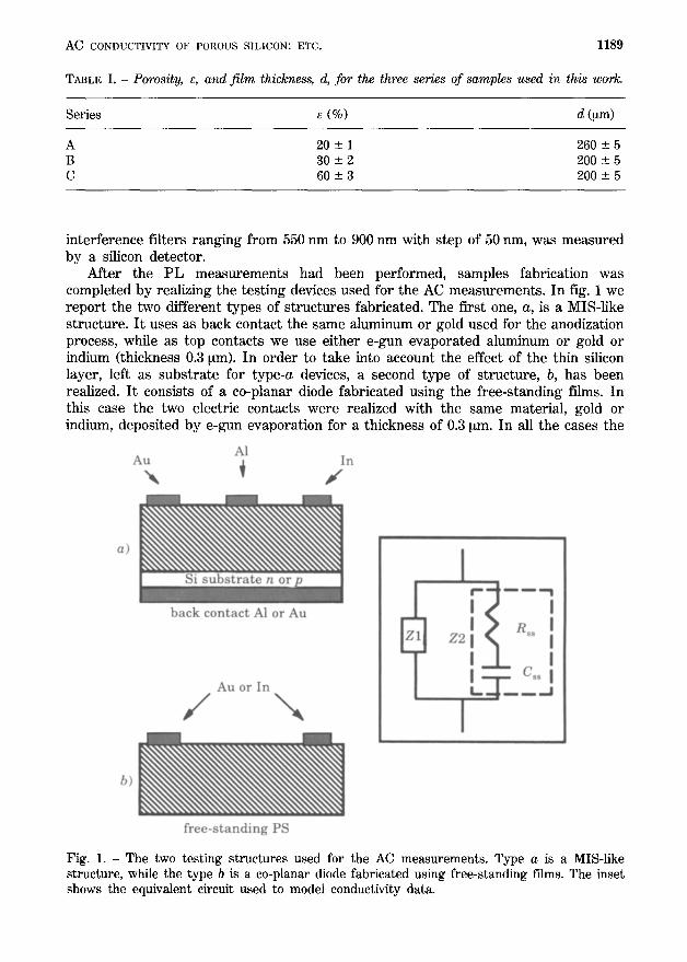
After the P L measu remen t s had been performed, samples fabrication was completed by realizing the tes t ing devices used for the AC measurements . In fig. 1 we repor t the two different types of s t ructures fabricated. The first one, a, is a MIS-like structure. I t uses as back contact the same aluminum or gold used for the anodization process, while as top contacts we use ei ther e-gun evapora ted aluminum or gold or indium (thickness 0.3 ~tm). In order to take into account the effect of the thin silicon layer, left as subs t ra te for type-a devices, a second type of structure, b, has been realized. I t consists of a co-planar diode fabricated using the free-s tanding films. In this case the two electric contacts were realized with the same material , gold or indium, deposited by e-gun evaporat ion for a thickness of 0.3 ~m. In all the cases the
Fig. 1. - The two testing structures used for the AC measurements. Type a is a MIS-like structure, while the type b is a co-planar diode fabricated using free-standing films. The inset shows the equivalent circuit used to model conductivity data.
1190 c~. DI FRANCIA, V. LA FERRARA, P. MADDALENA, ETC.
top contact area is about 5 mm '~ . The AC conductivity has been then measured by applying a 1 V square voltage and measuring currents and voltages using a lock-in technique. Measurements uncertainty is less than 1%.
3. - Results and discussion
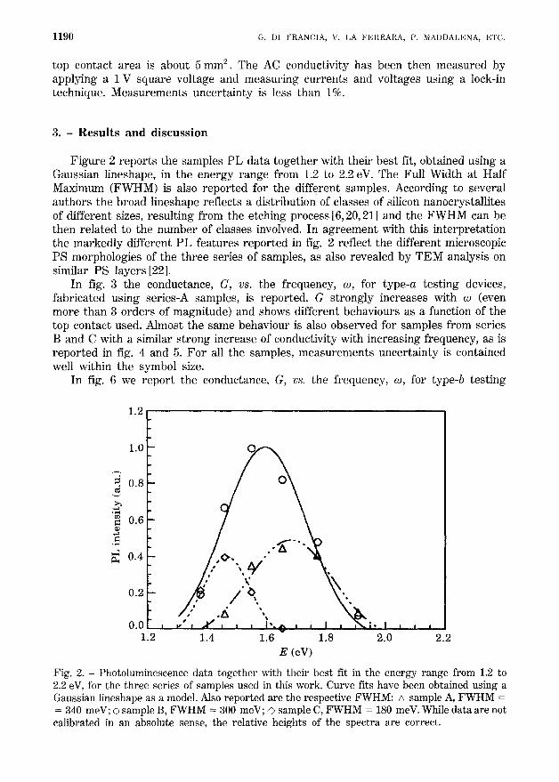
Figure 2 reports the samples PL data together with their best fit, obtained using a Gaussian lineshape, in the energy range from 1.2 to 2.2 eV. The Full Width at Half Maximum (FWHM) is also repor ted for the different samples. According to several authors the broad lineshape reflects a distribution of classes of silicon nanocrystallites of different sizes, resulting from the etching process [6, 20, 21] and the FWHM can be then related to the number of classes involved. In agreement with this interpretat ion the markedly different PL features repor ted in fig. 2 reflect the different microscopic PS morphologies of the three series of samples, as also revealed by TEM analysis on similar PS layers [22].
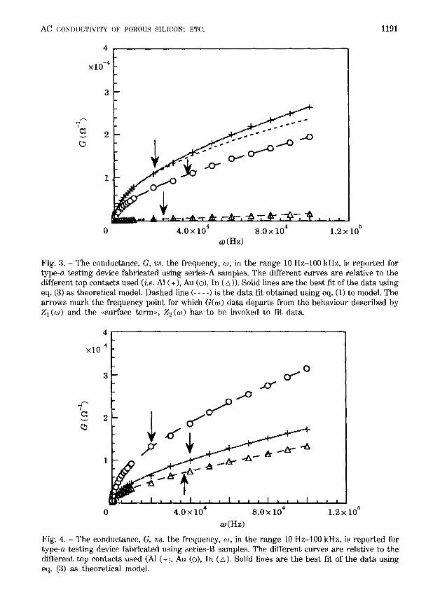
In fig. 3 the conductance, G, vs. the frequency, w, for type-a testing devices, fabricated using series-A samples, is reported. G strongly increases with (o (even more than 3 orders of magnitude) and shows different behaviours as a function of the top contact used. Almost the same behaviour is also observed for samples from series B and C with a similar s trong increase of conductivity with increasing frequency, as is repor ted in fig. 4 and 5. For all the samples, measurements uncertainty is contained well within the symbol size.
In fig. 6 we repor t the conductance, G, vs. the frequency, ~, for type-b testing
1.2
1.0 Q
=. 0.8
0.6
0.4 n~
0.2
0.0 , l'.l , , ,
1.2 1.4 1.6 1.8 2.0 2.2 E (eV)
Fig. 2. - Photoluminescence data together with their best fit in the energy range from 1.2 to 2.2 eV, for the three series of samples used in this work. Curve fits have been obtained using a Gaussian lineshape as a model. Also reported are the respective FWHM: A sample A, FWHM = = 340 meV; o sample B, FWHM = 300 meV; ~ sample C, FWHM = 180 meV. While data are not calibrated in an absolute sense, the relative heights of the spectra are correct.
AC CONDUCTIVITY OF POROUS SILICON: ETC.
4
xlO -4
1191
2 . . . . . - ^ . . . . O . . O
0 4 .0x 10 4 8 .0x 10 4 1 .2x 10 5 x ( H z )
Fig. 3. - The conductance, G, vs. the frequency, w, in the range 10 Hz-100 kHz, is reported for type-a testing device fabricated using series-A samples. The different curves are relative to the different top contacts used (i.e. A1 (+), Au (�9 In (A)). Solid lines are the best fit of the data using eq. (3) as theoretical model. Dashed line ( . . . . ) is the data fit obtained using eq. (1) to model. The arrows mark the frequency point for which G(o) data departs from the behaviour described by Z , ( ~ ) and the ,,surface term~, Z2(w) has to be invoked to fit data.
4
xlO -4
o o "
. o "
olo ~ 2
1~# ~ " h- "/~" -4
0 4 .0x 104 8 .0x 104 1 .2x 10 s
co(Hz)
Fig. 4. - The conductance, G, vs. the frequency, w, in the range 10 Hz-100 kHz, is reported for type-a testing device fabricated using series-B samples. The different curves are relative to the different top contacts used (A1 (+), Au (�9 In (A). Solid lines are the best fit of the data using eq. (3) as theoretical model.
1192 G. DI FRANCIA, V. LA FERRARA, P. MADDALENA, ETC.
4
xl0 -4
2 r
1
" r "
0 4.0x 10⁴ 8.0x 10 a 1.2x 10² co(Hz)
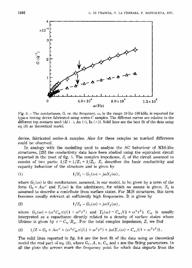
Fig. 5. - The conductance, G, vs. the frequency, w, in the range 10 Hz-100 kHz, is reported for type-a testing device fabricated using series-C samples. The different curves are relative to the different top contacts used (A1 (+), Au (�9 In (A)). Solid lines are the best fit of the data using eq. (3) as theoretical model.
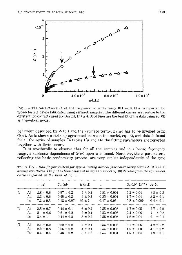
device, fabricated series-A samples. Also for these samples no marked difference could be observed.
In analogy with the modelling used to analyze the AC behaviour of MIS-like structures, [23] the conductivity data have been studied using the equivalent circuit reported in the inset of fig. 1. The complex impedance, Z, of the circuit assumed to consist of two parts: 1/Z = 1/Z1 + 1/Z2. Z1 describes the basic conductivity and capacity behaviour of the structure and is given by
(1) 1/Z1 = G1 (co) + floY, (~) ,
where Gi (co) is the conductance, assumed, in our model, to be given by a term of the form Go + A(o u and Yi(w) is the admittance, for which no ansatz is given. Z2 is assumed to describe a contribute from surface states. For MIS structures, this term becomes usually relevant at sufficiently high frequencies. It is given by
(2) 1/Z2 = G1 (w) + jwYe (w),
where G2(co) = (~92Cssv)/(1 + w2v 2) and Y2(w) = Cs~/(1 + w2v2). C~s is usually interpreted as a capacitance directly related to a density of surface states whose lifetime is given by T = Cs~'R~. For the total complex impedance, Z, we find
(3) l / Z - - Go + Aw u + (t92Cssv)/(1 + w2v 2) +flO(Yl(W) + C~/(1 + w~r2)).
The solid lines reported in fig. 3-6 are the best fit of the data using as theoretical model the real part of eq. (3), where Go, A, u, C~ and r are the fitting parameters. In all the plots the arrows mark the frequency point for which data departs from the
AC CONDUCTIVITY OF POROUS SILICON: ETC. 1193
4
x l 0 -4
'CI L~
ot.O/~ ~ 0
z
S .:! I I I I I
4.0 x 10⁴ 8.0 x 10⁴ 1.2 x 10⁵
o)(Hz)
Fig. 6. - The conductance, G, vs. the frequency, o~, in the range 10 Hz-100 kHz, is reported for type-b testing device fabricated using series-A samples. The different curves are relative to the different top contacts used (i.e. Au (�9 In (A)). Solid lines are the best fit of the data using eq. (3) as theoretical model.
behav iour descr ibed by Z1 ((o) and the , su r f ace t e r m , , Z2(~o) has to be invoked to fit G(w). As is shown a s t r ik ing a g r e e m e n t be tween the model , eq. (3), and da ta is found for all the ser ies of samples. I n tab les I I a and I Ib the f i t t ing p a r a m e t e r s are r epo r t ed toge the r with the i r e r rors .
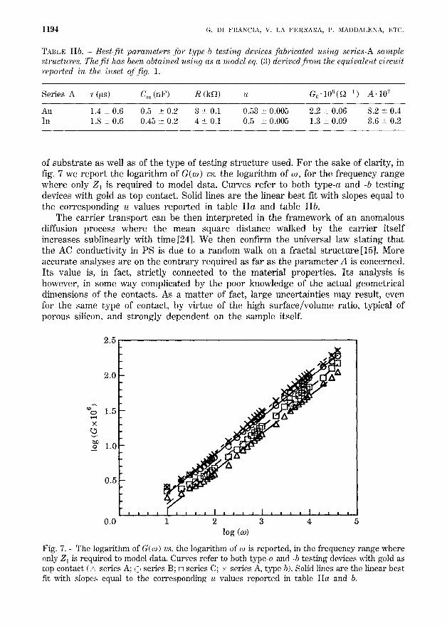
I t is wor thwhi le to observe t ha t for all the samples and in a b road f r equency range , a sub l inea r dependence of G(oJ) upon (o is found. Moreover , the u pa r a m e te r s , re f lec t ing the basic conduct iv i ty process, are ve ry s imilar i n d e p e n d e n t l y of the type
TABLE IIa. - Best-fit parameters for type-a testing devices fabricated using series A, B and C sample structures. The fit has been obtained using as a model eq. (3) derived from the equivalent circuit reported in the inset of fig. 1.
v(~ts) Cs~(nF) R(k~2) u Go.106(~2 1) A.107
A Al 2.3 _+ 0.6 0.57 +- 0.2 4 -+ 0.1 0.51 _+ 0.004 5.2 +-- 0.04 6.8 -+ 0.2 Au 2.2 +_ 0.6 0.45 -+ 0.2 5 -+ 0.2 0.55 _+ 0.004 1.7 _+ 0.04 3.2 +_ 0.1 In 7.2 _+ 0.3 0.12 -+ 0.07 60 +- 2 0.47 +_ 0.03 0.8 -+ 0.009 0.4 +_ 0.1
A1 2.5 +- 0.7 0.44 + 0.1 6 -+ 0.2 0.55 _+ 0.005 1.7 _+ 0.05 2.7 +- 0.2 Au 2 +_ 0.6 0.61 -+ 0.2 3 +- 0.1 0.53 +_ 0.006 2.4 _+ 0.06 7 - 0.3 In 3.4 _ 1 0.44 -+ 0.2 8 -+ 0.2 0.55 _+ 0.006 1.6 _+ 0.04 2 _+ 0.1
C A1 2.1 _+ 0.9 0.52 +- 0.2 4 _+ 0.1 0.55 _+ 0.005 2.1 +_ 0.06 4.2 _+ 0.2 Au 2.2 _+ 0.8 0.55 +_ 0.2 4 _+ 0.1 0.55 _+ 0.005 1.9 _+ 0.03 4.1 _+ 0.2 In 3.4 +_ 0.6 0.43 -+ 0.2 8 -+ 0.2 0.55 +_ 0.004 1.5 +_ 0.04 1.9 _+ 0.1
1194 G. DI FRANCIA, V. LA FERRARA, P. MADDALENA, ETC.
TABLE I I b . - Best:fit parameters .for type-b testing devices fabricated using series-A sample structures. The fit has been obtained using as a model eq. (3) derived from the equivalent circuit ~vported in the inset of fig. 1.
Series A rqts) C~s(nF) R(kg~) ~t G0.10s(~ 1) A.107
Au 1.4 _+ 0.6 0.5 _+ 0.2 3 -+ 0.1 0.53 _+ 0.005 2.2 -+ 0.06 8.2 -+ 0.4 In 1.8 -+ 0.6 0.45 _+ 0.2 4 _+ 0.1 0.5 _+ 0.005 1.3 _+ 0.09 3.6 -+ 0.2
of subs t ra te as well as of the type of test ing s t ructure used. Fo r the sake of clarity, in fig. 7 we repor t the logari thm of G(w) vs. the logari thm of ta, for the f requency range where only Z1 is required to model data. Curves refer to both type-a and -b test ing devices with gold as top contact. Solid lines are the linear best fit with slopes equal to the corresponding u values repor ted in table I I a and table IIb.
The carr ier t r anspor t can be then in terpre ted in the f ramework of an anomalous diffusion process where the mean square distance walked by the carr ier itself increases sublinearly with t ime [24]. We then confirm the universal law stat ing tha t the AC conductivity in PS is due to a random walk on a fractal s t ructure [15]. More accurate analyses are on the contrary required as far as the p a r a m e t e r A is concerned. I t s value is, in fact, strictly connected to the material properties. I t s analysis is however, in some way complicated by the poor knowledge of the actual geometrical dimensions of the contacts. As a ma t t e r of fact, large uncertainties may result, even for the same type of contact, by virtue of the high surface/volume ratio, typical of porous silicon, and s t rongly dependent on the sample itself.
2.5
2.0
1.5 •
i . o
0.5 ~ / X
, , , , I , ~ , , I ~ , , , I , , , , I . . . .
0.0 1 2 3 4 5 log (co)
Fig. 7. - The logarithm of G(o~) vs. the logarithm of ~ is reported, in the frequency range where only Z 1 is required to model data. Curves refer to both type-a and -b testing devices with gold as top contact (• series A; �9 series B; [] series C; • series A, type b). Solid lines are the linear best fit with slopes equal to the corresponding u values reported in table I Ia and b.

AC CONDUCTIVITY OF POROUS SILICON: ETC. 1195
A fur ther insight to the data presented in table I I a and IIb, shows that, ruling out sample A ( type-a test ing device) with the indium contact, which shows an anomalous behaviour with respect to all the others, even v and Css are very similar for all the samples, i.e. v -- 2.5.10 ~ s and C~s -- 0 .5"10-9F . The fact that, similarly to u, also v and Css do not seem to s t rongly depend on the mater ial or on the contact used, suggests that a double-channel t r anspor t mechanism for the AC conductivity in PS is possible: at low frequency thermoionic and /o r hopping or tunneling could prevail [15], while for increasing w some kind of surface s ta tes begin to respond to the applied signal improving the t r anspor t mechanism both assist ing carr ier injection in the ,vo lume- of PS itself and /o r activating a surface conduction mechanism via hopping between localized s ta tes characterized by a large distribution of energies (i.e. wide tails) (2).
4. - Conclusion
We have studied the AC conductivity of different series of PS samples fabricated using p-type, n - - t y p e and n § silicon substrates . In the range w = 0, w -- 20-40 kHz data follow the universal law G((o) ~ A(o ~ At higher frequencies the effect of surface s ta tes can be invoked to explain data. This suggests a double-channel t r anspor t mechanism, one related to PS , vo lume . proper t ies and the other more connected to the , su r face - itself.
(2) The conductivity mechanism at higher frequencies suggested by Ben-Chorin, in ref. [15], is in good agreement with our data as soon as one identifies his broad distribution of activation energies with our distribution of surface states.
R E F E R E N C E S
[1] BEALE M. I. J., BENJAMIN J. D., UREN M. J., CHEW N. G. and CULLIS A. J., J. Cryst. Growth, 73 (1985) 622.
[2] FATHAUER R. W., GEORGE W., KSENDZOV A. and VASQUEZ R. P., Appl. Phys. Lett., 60 (1992) 995.
[3] DI FRANCIA G. and CITARELLA A., J. Appl. Phys., 77 (1995) 3549. [4] CANHAM L. T., Appl. Phys. Lett., 57 (1990) 1046. [5] LEHMANN V. and GOSELE U., Appl. Phys. Lett., 58 (1991) 856. [6] DI FRANCIA G., MENNA P. and FALCONIERI M., J. Lumin., 57 (1993) 95. [7] AMATO G., D~ FRANCIA G., MENNA P. and NINNO D., Europhys. Lett., 25 (1994) 471. [8] TSAI C., LI K.-H., SARATHY J., SHIH S. and CAMPBELL J. C., Appl. Phys. Lett., 59 (1991)
2814. [9] PETROVA-KocH V., MUSCHIK T., Kux A., MEYER B. K. and KOCH F., Appl. Phys. Lett., 61
(1992) 943. [10] KOCH F., PETROVA-KOCH V., MUSCHIK T., NIKOLOV A. and GAVRILENKO V., Mater. Res.
Soc. Syrup. Proc., 283 (1993) 197. [11] BRANDT M. S., FUCHS H. D., STUTZMANN M., WEBER J. and COR;)ONA M., Solid State
Commun., 81 (1992) 307. [12] KOSHIDA N. and KOYAMA H., Mater. Res. Soc. Symp. Proc., 283 (1993) 343.
1196 G. DI FRANCIA, V. LA FERRARA, P. MADDALENA, ETC.
[13] ANDERSON R. C., MULLER R. S. and TOBIAS C. W., J. Electrochem. Soc., 138 (1991) 3406.
[14] SIMONS A. J., COX W. I., UREN M. J. and CALCOTT P. D. J., Thin Solid Films, 255 (1995) 12. [15] BEN-CHORIN M., MOLLER F., KOCH F., SCHIRMACHER W. and EBERHARD M., Phys. Rev. B,
51 (1995) 2199. [16] BEN-CHORIN M., MOLLER F. and KOCH F., Phys. Rew. B, 49 (1994) 2981. [17] KOCKA J., FEJFAR A. and PELANT I., Phys. Status Solidi B, 190 (1995) 27. [18] HLINOMAZ P., KLIMA 0., HOSPODKOVA A., HULICIUS E., OSWALD J., SIPEK E. and KOCKA J.,
Appl. Phys. Lett., 64 (1994) 3118. [19] GUPTA P., COLVIN V. L. and GEORGE S. M., Phys. Rev. B, 37 (1988) 234. [20] FISHMANN G., MIHALCESCU I. and ROMESTAIN R., Phys. Rev. B, 48 (1993) 1464. [21] DI FRANCIA G., MADDALENA P. and NINNO D., Solid State Commun., 96 (1995) 579. [22] SMITH R. L. and COLLINS S. D., J. Appl. Phys., 71 (1992) R1. [23] SZE S. M., Fisica dei dispositivi a semiconduttore (Tamburini, Firenze) 1973, cap. 9. [24] See for instance: KIRKPATRICK S., Ill-Condensed Matter, Proceedings of Les-Houches
Summer Schoo~ Section XXXI, edited by R. BALIAN, R. MAINARD and G. TOULOSE (North-Holland, Amsterdam) 1979. STAUSSER D. and AHARONY A., Introduction to Percolation Theow, 2nd edition (Taylor and Francis, London) 1985.


