Embed Size (px)
Citation preview
European Journal of Molecular & Clinical Medicine
ISSN 2515-8260 Volume 07, Issue 01, 2020
2322
A LOW POWER OPERATIONAL AMPLIFIER DESIGN
USING 18NM FIN-FET TECHNOLOGY FOR
BIOMEDICAL APPLICATIONS
Hari Kishore Kakarla, Mukil Alagirisamy
Postdoctoral Research Fellow in Electronics and Communication Engineering,
Lincoln University College, Petaling Jaya, Selangor, Malaysia
Senior Lecture, Faculty of Engineering, Lincoln University College, Petaling Jaya, Selangor,
Malaysia
ABSTRACT
Bioelectric impedances have been found to correlate with a number of biological phenomena in
some tissues, organs, and cells. This has helped to advance several of today's bioelectric
impedance applications, like Electrical Impedance Tomography (EIT), Electrical impedance
spectroscopy (EIS). For calculating bioelectric impedance it is very important to design low
power Analog Front end consisting of Op-amp and ADC. In this paper, a low
supply voltage based FinFET operational amplifier and its characteristics are studied and
designed by using Cadence 18nm FinFET technology. The standard characteristics of the op-
amp like gain, bandwidth, unity gain bandwidth product, settling time and so on
are distinguished with the existing architectures. The suggested FinFET-based amplifiers
are having a greater performance at a reduced voltage than conventional two-stage Op-amps. In
this work, supply voltage is provided as 0.8V. The circuit consumes a power of 35 μW, provides a
gain of 83 dB and unity gain repeat of 10 MHz with a phase edge of 70 degrees. The difference
between the suggested architecture and standard two stage CMOS Op-amp shows that figure of
Merit for proposed circuit is improved to 1.1pj.
Keywords: Op-Amp, FINFET, ADC, DAC
1. INTRODUCTION
In the current digital market [1], the trend towards the development of bio-medical devices with
portable batteries has recently increased. This phenomenon is because of progress and advancement
in scaling of VLSI technology leading to more analog and digital circuit (ADC) creation in deep sub-
micron size [2]. This condition has its own advantages where, at lower voltage supply, the circuit can
be operated with lower power consumption. But most analog and digital electronic circuits suffered
performance degradation due to technology scaling short-channel effects (SCEs). Bio-potential
identification of signals in the medical world is the most common and dependable way for medical
practitioners to diagnose their patient’s medical conditions. Many bio-potential signal detections
such as, electromyography, electroencephalography and electrocardiography are recognized in the
medical world.
EMG, EMG and ECG are the typical bio-potential signals provided by the human body. There
are common characteristics of these bio-potential. Signals; amplitude of low frequency range and
low voltage. Table 1 shows the range of frequencies and voltage amplitude of the specified bio-
potential signal [3]. The observation and recording of bio potential signal is of importance in medical
European Journal of Molecular & Clinical Medicine
ISSN 2515-8260 Volume 07, Issue 01, 2020
2323
diagnosis and contemporary clinical practices require routine recording of these signals. Patients are
generally linked to lengthy recording instruments in order to obtain signals from the body for
diagnosis purposes. This impacts their mobility and creates overall unease. As a consequence,
acquisition time decreases and avoids constant patient monitoring affecting the overall diagnosis of
diseases.
Bioelectric impedances have been found to correlate with a number of biological phenomena in
some tissues, organs, and cells. This has helped to advance several of today's bioelectric impedance
applications, like Electrical Impedance Tomography (EIT), Electrical impedance spectroscopy (EIS)
[4].
Scientists are currently investigating a variety of different applications, including glucose
control, breast cancer control, foot sole blood perfusion, and instant blood pressure [5][8].
Researchers also started studying implantable bio-impedance analyzers, which would require
minimally invasive data monitoring around the clock. Bio-impedance correlations and different
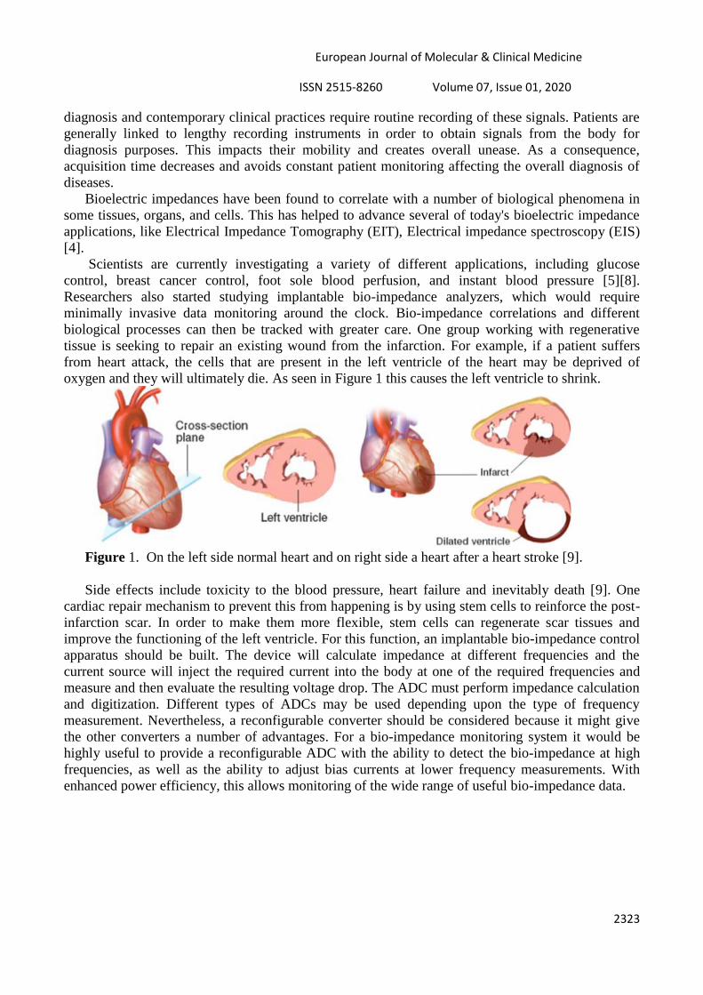
biological processes can then be tracked with greater care. One group working with regenerative
tissue is seeking to repair an existing wound from the infarction. For example, if a patient suffers
from heart attack, the cells that are present in the left ventricle of the heart may be deprived of
oxygen and they will ultimately die. As seen in Figure 1 this causes the left ventricle to shrink.
Figure 1. On the left side normal heart and on right side a heart after a heart stroke [9].
Side effects include toxicity to the blood pressure, heart failure and inevitably death [9]. One
cardiac repair mechanism to prevent this from happening is by using stem cells to reinforce the post-
infarction scar. In order to make them more flexible, stem cells can regenerate scar tissues and
improve the functioning of the left ventricle. For this function, an implantable bio-impedance control
apparatus should be built. The device will calculate impedance at different frequencies and the
current source will inject the required current into the body at one of the required frequencies and
measure and then evaluate the resulting voltage drop. The ADC must perform impedance calculation
and digitization. Different types of ADCs may be used depending upon the type of frequency
measurement. Nevertheless, a reconfigurable converter should be considered because it might give
the other converters a number of advantages. For a bio-impedance monitoring system it would be
highly useful to provide a reconfigurable ADC with the ability to detect the bio-impedance at high
frequencies, as well as the ability to adjust bias currents at lower frequency measurements. With
enhanced power efficiency, this allows monitoring of the wide range of useful bio-impedance data.
European Journal of Molecular & Clinical Medicine
ISSN 2515-8260 Volume 07, Issue 01, 2020
2324
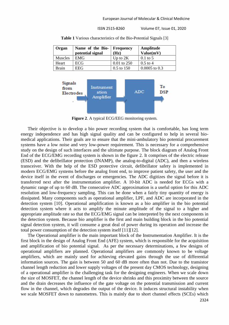
Table 1 Various characteristics of the Bio-Potential Signals [3]
Organ Name of the Bio-
potential signal
Frequency
(Hz)
Amplitude
Value(mV)
Muscles EMG Up to 2K 0.1 to 5
Heart ECG 0.01 to 250 0.5 to 4
Brain EEG 0.5 to 150 0.0005 to 0.3
Figure 2. A typical ECG/EEG monitoring system.
Their objective is to develop a bio power recording system that is comfortable, has long term
energy independence and has high signal quality and can be configured to help in several bio-
medical applications. Their goals are to ensure that the mini-ambulatory bio potential procurement
systems have a low noise and very low-power requirement. This is necessary for a comprehensive
study on the design of such interfaces and the ultimate purpose. The block diagram of Analog Front
End of the ECG/EMG recording system is shown in the figure 2. It comprises of the electric release
(ESD) and the defibrillator protection (INAMP), the analog-to-digital (ADC), and then a wireless
transceiver. With the help of the ESD protective circuit, defibrillator safety is implemented in
modern ECG/EMG systems before the analog front end, to improve patient safety, the user and the
device itself in the event of discharges or emergencies. The ADC digitizes the signal before it is
transferred next after the instrumentation amplifier. A 10-bit ADC is needed for ECGs with a
dynamic range of up to 60 dB. The consecutive ADC approximation is a useful option for this ADC
resolution and low-frequency sampling. This can be done when a fairly tiny quantity of energy is
dissipated. Many components such as operational amplifier, LPF, and ADC are incorporated in the
detection system [10]. Operational amplification is known as a bio amplifier in the bio potential
detection system where it acts to amplify the minute amplitude of the signal to a higher and
appropriate amplitude rate so that the ECG/EMG signal can be interpreted by the next components in
the detection system. Because bio amplifier is the first and main building block in the bio potential
signal detection system, it will consume a great deal of power during its operation and increase the
total power consumption of the detection system itself [11][12].
The Operational amplifier is the main important block of the Instrumentation Amplifier. It is the
first block in the design of Analog Front End (AFE) system, which is responsible for the acquisition
and amplification of bio potential signal. As per the necessary determinations, a few designs of
operational amplifiers are planned. Operational amplifiers are commonly known to be voltage
amplifiers, which are mainly used for achieving elevated gains through the use of differential
information sources. The gain is between 50 and 60 dB more often than not. Due to the transistor
channel length reduction and lower supply voltages of the present day CMOS technology, designing
of a operational amplifier is the challenging task for the designing engineers. When we scale down
the size of MOSFET, the channel length of the device shrinks and this proximity between the source
and the drain decreases the influence of the gate voltage on the potential transmission and current
flow in the channel, which degrades the output of the device. It induces structural instability when
we scale MOSFET down to nanometres. This is mainly due to short channel effects (SCEs) which
European Journal of Molecular & Clinical Medicine
ISSN 2515-8260 Volume 07, Issue 01, 2020
2325
play a key role in deciding the output of scaled devices. While output degrades with a decrease in
channel length as the device dimension shrinks, it is increasingly difficult to perform basic device
manufacturing steps such as lithography, interconnecting and processing. As the dimension of the
system becomes smaller, the circuit becomes denser and more complex.
1.1 Errors during the MOSFET Downscaling
Generally referred to as short channel effects is the class of effects that modify device behaviour
resulting from device miniaturization. It leads to an increase in the current of leakage between the
drain source and decreases the current ratio of ON-state to OFF. In particular, it is possible to
distinguish the short channel effects [14-20].
a. Drain Induced Barrier Lowering (DIBL):
The potential barrier is controlled by both Vgs and Vgs in small MOSFET geometry. When Vds
increases, the barrier of the electron or the holes in the source decreases so that they can pass from
the source and drain where the voltage of the gate remains unchanged. The potential barrier to the
channel decreases, contributing to DIBL. Reducing the potential barrier ultimately enables the
electron to pass between the source and the drain, even if it is Vgs<Vth. When the area of depletion
region surrounding the drain enters the source, so that the two layers of depletion layers overlap,
punching occurs. Gate loses current flow control via MOSFET and becomes as good as redundant.
With thinner oxide, larger substrate doping, shallower junctions and obliviously longer channel,
punching through can be minimized. When the area of depletion surrounding the drain enters the
origin, so that the two layers of depletion overlap, punching occurs. Gate loses current flow control
via MOSFET and becomes as good as redundant. With thinner oxide, larger substratum doping,
shallower junctions and obliviously longer channel, punching through can be minimized.
b. Hot Electron Effect:
If carriers gain high energy at an effective temperature higher than the temperature of the lattice,
it is said that they are hot. Such cold electrons are produced when MOSFET operates in linear or
saturation mode in the inverted channel region. These hot electrons cannot pass their energies to the
lattice atoms quickly enough. The key issues that arise as a result of hot carriers are parasitic gate
currents, weakening drain current, increasing transconductance, and rising threshold voltage over
time. The use of graded drain profile decreases the generation of hot carriers. The technique is used
in floating gate devices to raise the threshold by trapping electrons in the floating gate. The drain is
doped slightly through this process, resulting in less electrical field produced for the carrier.
c. Parasitic resistance and Capacity:
Due to the reduced parasitic resistance of the transistor dimensions and the capacity is both
unfavourably scaled and diminished. As a consequence, the effect of parasitic elements on the
current is significantly increasing. Such parasite elements should reduce the transistor scaling
efficiency.
d. Velocity saturation:
The velocity is directly proportional to the electrical field up to a certain point. But the point's
velocity is saturated and does not raise the electrical field. It lowers saturation mode
transconductivity.
European Journal of Molecular & Clinical Medicine
ISSN 2515-8260 Volume 07, Issue 01, 2020
2326
e. Heat dissipation:
MOSFETs in the resistive portion release energy in the form of heat. Hot spots are generated on
the circuit if this heat is not dissipated properly, which ultimately leads to system malfunction.
As the devices continue to shrink, there is an increasing problem with conventional MOSFETs
[1]. One problem's solution leads to another. Short channel effects like VT roll off, drain-induced
barrier lowering (DIBL), increasing the current of leakage, etc. To solve these short channel effects
issues, such as double gate, FinFET, Tri-gate, Fore-gate, all-around gate, and so on, a lot of
MOSFET has been implemented. It needs new architectural structures to design and implement
operational amplifiers, as noted above, an increase in demand for low-power applications and
accuracy. In addition, structuring a high-speed and high-gain operational amplifier is essential in
high-precision devices. In addition, with FinFET to better understand multi-gate devices, we will
present a high-gain and low-control voltage operational amplifier and the advantages of the
framework suggested to enhance basic amplifier parameters including gain and bandwidth. In the
section 2, Introduction to FINFET devices is presented, in the section 3; various characteristics of
FinFET are presented. Methodology regarding the proposed technique is studied in section 4.The
proposed Operational Amplifier and its simulation is discussed in the section 5 and 6 respectively
followed by Conclusion in section 7.
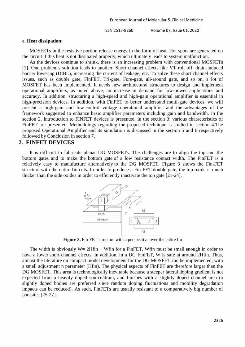
2. FINFET DEVICES
It is difficult to fabricate planar DG MOSFETs. The challenges are to align the top and the
bottom gates and to make the bottom gate of a low resistance contact width. The FinFET is a
relatively easy to manufacture alternatively to the DG MOSFET. Figure 3 shows the Fin-FET
structure with the entire fin cuts. In order to produce a Fin-FET double gate, the top oxide is much
thicker than the side oxides in order to efficiently inactivate the top gate [21-24].
Figure 3. Fin-FET structure with a perspective over the entire fin
The width is obviously W= 2Hfin + Wfin for a FinFET. Wfin must be small enough in order to
have a lower short channel effects. In addition, in a DG FinFET, W is safe at around 2Hfin. Thus,
almost the literature on compact model development for the DG MOSFET can be implemented, with
a small adjustment n parameter (Hfin). The physical aspects of FinFET are therefore larger than the
DG MOSFET. This area is technologically inevitable because a steeper lateral doping gradient is not
expected from a heavily doped source/drain, and finishes with a slightly doped channel area (a
slightly doped bodies are preferred since random doping fluctuations and mobility degradation
impacts can be reduced). As such, FinFETs are usually resistant to a comparatively big number of
parasites [25-27].

European Journal of Molecular & Clinical Medicine
ISSN 2515-8260 Volume 07, Issue 01, 2020
2327
3. CHARACTERISTICS OF FIN FET
Now we're talking about the electrostatic characteristic of FinFET (Current-voltage).
The unique characteristic of FinFET is that the gate is formed by a conductive channel enclosed
by thin "fin" silicon. The thickness of the fin is determined from the source to the drain in the
direction that defines the device's effective channel width [28][29]. The gate electrode is wrapped
around the channel so that multiple gate electrodes can be formed on each side, resulting in reduced
leakage currents and increased drive current. For FinFET, a self-aligned double gate controls the
vertical si fin.
Linear Region: It is the region where Ids is increased linearly with Vds, for a given Vg >Vth For
the first approximation, Ids is given in the linear region as
{
} (1)
Where Vth is the threshold voltage is called as carrier mobility in the inversion region, i.e. the
channel, Cox is the gate oxide capacitance per unit area, W / L is the device width to length ratio.
Saturation Region: In this region, Ids is becoming constant even though Vds is increasing. Once
again, for the first rough calculation, the Ids are in the saturation region given by
Ids=
{
} , m=1+3(tox/xd) (2)
xd is the thickness of the depletion layer and tox
is the thickness of the oxide showing that Ids does not depend on Vds.
Cut-Off Region: In this region Vg <Vth so that there is no channel between the source and the
drain resulting in Ids=0. In fact, for Vg <Vth, the sub threshold current flows is the exponential
decay current.
Low concentration of electrons results in high electrical field along the channel and, as a
consequence, sub-threshold current is primarily due to carrier diffusion. This current of this region is
approximated as
( )
(
( )
) (3)
ΔΔ is the difference between the function of the gate electrode and the almost intruded silicon skin.
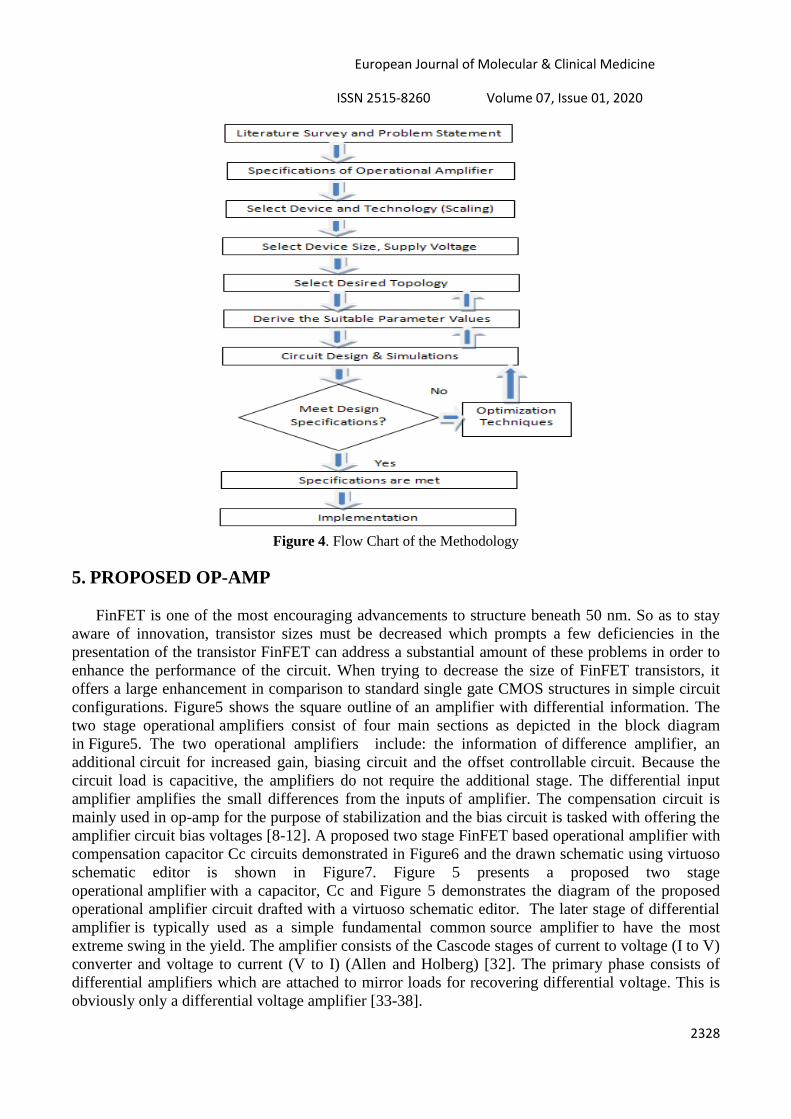
4. METHODOLOGY
The following section discusses the details of the methodology which will be used to implement
the proposed technique [16-20].
The flow chart shown in the figure 4 demonstrates the method followed for the designing of the
opamp in biomedical applications.
European Journal of Molecular & Clinical Medicine
ISSN 2515-8260 Volume 07, Issue 01, 2020
2328
Figure 4. Flow Chart of the Methodology
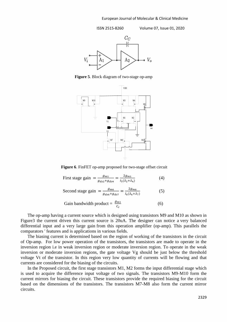
5. PROPOSED OP-AMP
FinFET is one of the most encouraging advancements to structure beneath 50 nm. So as to stay
aware of innovation, transistor sizes must be decreased which prompts a few deficiencies in the
presentation of the transistor FinFET can address a substantial amount of these problems in order to
enhance the performance of the circuit. When trying to decrease the size of FinFET transistors, it
offers a large enhancement in comparison to standard single gate CMOS structures in simple circuit
configurations. Figure5 shows the square outline of an amplifier with differential information. The
two stage operational amplifiers consist of four main sections as depicted in the block diagram
in Figure5. The two operational amplifiers include: the information of difference amplifier, an
additional circuit for increased gain, biasing circuit and the offset controllable circuit. Because the
circuit load is capacitive, the amplifiers do not require the additional stage. The differential input
amplifier amplifies the small differences from the inputs of amplifier. The compensation circuit is
mainly used in op-amp for the purpose of stabilization and the bias circuit is tasked with offering the
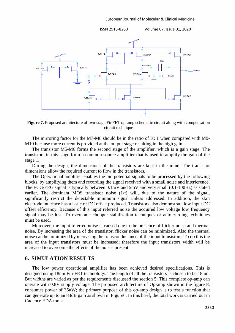
amplifier circuit bias voltages [8-12]. A proposed two stage FinFET based operational amplifier with
compensation capacitor Cc circuits demonstrated in Figure6 and the drawn schematic using virtuoso
schematic editor is shown in Figure7. Figure 5 presents a proposed two stage
operational amplifier with a capacitor, Cc and Figure 5 demonstrates the diagram of the proposed
operational amplifier circuit drafted with a virtuoso schematic editor. The later stage of differential
amplifier is typically used as a simple fundamental common source amplifier to have the most
extreme swing in the yield. The amplifier consists of the Cascode stages of current to voltage (I to V)
converter and voltage to current (V to I) (Allen and Holberg) [32]. The primary phase consists of
differential amplifiers which are attached to mirror loads for recovering differential voltage. This is
obviously only a differential voltage amplifier [33-38].
European Journal of Molecular & Clinical Medicine
ISSN 2515-8260 Volume 07, Issue 01, 2020
2329
Figure 5. Block diagram of two-stage op-amp
M1
M3 M4
M2
M8M7
VDD
out
M9 M10
M6
M5
V1
V2
Figure 6. FinFET op-amp proposed for two-stage offset circuit
First stage gain
( ) (4)
Second stage gain
( ) (5)
Gain bandwidth product =
(6)
The op-amp having a current source which is designed using transistors M9 and M10 as shown in
Figure3 the current driven this current source is 20uA. The designer can notice a very balanced
differential input and a very large gain from this operation amplifier (op-amp). This parallels the
comparators ' features and is applications in various fields.
The biasing current is determined based on the region of working of the transistors in the circuit
of Op-amp. For low power operation of the transistors, the transistors are made to operate in the
inversion region i.e in weak inversion region or moderate inversion region. To operate in the weak
inversion or moderate inversion regions, the gate voltage Vg should be just below the threshold
voltage Vt of the transistor. In this region very low quantity of currents will be flowing and that
currents are considered for the biasing of the circuits.
In the Proposed circuit, the first stage transistors M1, M2 forms the input differential stage which
is used to acquire the difference input voltage of two signals. The transistors M9-M10 form the
current mirrors for biasing the circuit. These transistors provide the required biasing for the circuit
based on the dimensions of the transistors. The transistors M7-M8 also form the current mirror
circuits.
European Journal of Molecular & Clinical Medicine
ISSN 2515-8260 Volume 07, Issue 01, 2020
2330
Figure 7. Proposed architecture of two-stage FinFET op-amp schematic circuit along with compensation
circuit technique
The mirroring factor for the M7-M8 should be in the ratio of K: 1 when compared with M9-
M10 because more current is provided at the output stage resulting in the high gain.
The transistor M5-M6 forms the second stage of the amplifier, which is a gain stage. The
transistors in this stage form a common source amplifier that is used to amplify the gain of the
stage 1.
During the design, the dimensions of the transistors are kept in the mind. The transistor
dimensions allow the required current to flow in the transistors.
The Operational amplifier enables the bio potential signals to be processed by the following
blocks, by amplifying them and recording the signal received with a small noise and interference.
The ECG/EEG signal is typically between 0.1mV and 5mV and very small (0.1-100Hz) as stated
earlier. The dominant MOS transistor noise (1/f) will, due to the nature of the signal,
significantly restrict the detectable minimum signal unless addressed. In addition, the skin
electrode interface has a issue of DC offset produced. Transistors also demonstrate low input DC
offset efficiency. Because of this input referred noise the acquired low voltage low frequency
signal may be lost. To overcome chopper stabilization techniques or auto zeroing techniques
must be used.
Moreover, the input referred noise is caused due to the presence of flicker noise and thermal
noise. By increasing the area of the transistor, flicker noise can be minimized. Also the thermal
noise can be minimized by increasing the transconductance of the input transistors. To do this the
area of the input transistors must be increased; therefore the input transistors width will be
increased to overcome the effects of the noises present.
6. SIMULATION RESULTS
The low power operational amplifier has been achieved desired specifications. This is
designed using 18nm Fin-FET technology. The length of all the transistors is chosen to be 18nm.
But widths are varied as per the requirements discussed the section 5. This complete op-amp can
operate with 0.8V supply voltage. The proposed architecture of Op-amp shown in the figure 8,
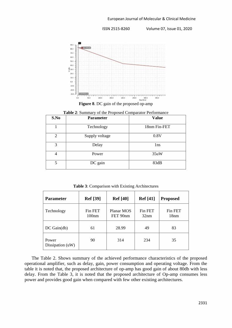
consumes power of 35uW; the primary purpose of this op-amp design is to test a function that
can generate up to an 83dB gain as shown in Figure6. In this brief, the total work is carried out in
Cadence EDA tools.
European Journal of Molecular & Clinical Medicine
ISSN 2515-8260 Volume 07, Issue 01, 2020
2331
Figure 8. DC gain of the proposed op-amp
Table 2: Summary of the Proposed Comparator Performance
S.No Parameter Value
1 Technology 18nm Fin-FET
2 Supply voltage 0.8V
3 Delay 1ns
4 Power 35uW
5 DC gain 83dB
Table 3: Comparison with Existing Architectures
Parameter Ref [39] Ref [40] Ref [41] Proposed
Technology Fin FET
100nm
Planar MOS
FET 90nm
Fin FET
32nm
Fin FET
18nm
DC Gain(db) 61 28.99 49 83
Power
Dissipation (uW)
90 314 234 35
The Table 2. Shows summary of the achieved performance characteristics of the proposed
operational amplifier, such as delay, gain, power consumption and operating voltage. From the
table it is noted that, the proposed architecture of op-amp has good gain of about 80db with less
delay. From the Table 3, it is noted that the proposed architecture of Op-amp consumes less
power and provides good gain when compared with few other existing architectures.
European Journal of Molecular & Clinical Medicine
ISSN 2515-8260 Volume 07, Issue 01, 2020
2332
7. CONCLUSION
In this paper a low voltage low power operational amplifier is proposed. This is designed
using 18nm Fin-FET technology and simulated using Cadence Virtuoso. The power and timing
analysis done and the simulation results are shows the improvement in the design of a novel
operational amplifier, performance, and also other references like power, time delay.
REFERENCES
[1] J. Magri, I. Grech, O. Casha, E. Gatt, and J. Micallef, “Design of CMOS front-end circuitry for the
acquisition of biopotential signals,” 2016 IEEE Int. Conf. Electron. Circuits Syst. ICECS 2016, pp. 161–164,
2017.
[2] R. Rakhi, A. D. Taralkar, M. H. Vasantha, and Y. B. Nithin Kumar, “A 0.5 v Low Power OTA-C Low Pass
Filter for ECG Detection,” Proc. IEEE Comput. Soc. Annu. Symp. VLSI, ISVLSI, vol. 2017–July, pp. 589–
593, 2017.
[3] W. M. Chen, W. C. Yang, T. Y. Tsai, H. Chiueh, and C. Y. Wu, “The design of CMOS general-purpose
analog front-end circuit with tunable gain and bandwidth for biopotential signal recording systems,” Proc.
Annu. Int. Conf. IEEE Eng. Med. Biol. Soc. EMBS, no. Cic, pp. 4784–4787, 2011.
[4] National Research Council. Emerging Technologies for Nutrition Research: Potential for Assessing Military
Performance Capability. Washington, DC: The National Academies Press, 1997.
[5] iao, . ang, . Duan, F. heng, A.J. inclair, C.R. Chatwin, “Bioimpedance analysis for the characterization of
breast cancer cells in suspension,” Biomedical Engineering, IEEE Transactions on , vol.59, pp. 2321-2329,
2012.
[6] K. Cheng, Y. Ko, T. ang, “The Application of Bioimpedance ethod for Foot ole Blood Perfusion
Characterization,” Genetic and Evolutionary Computing (ICGEC), 2012 Sixth International Conference on,
pp. 211-213, 2012.
[7] ansouri, . ahjoubi, R.B. alah, “Determination of instantaneous arterial blood pressure from bio-impedance
signal,” Biophysics and Structural Biology, Journal of, vol. 2, pp. 9-15, 2010.
[8] R. Lumbroso, N. Naas, L.K. Beitel, M.F. Lawrence, M.A. Trifiro, "Novel Bioimpedance Sensor for Glucose
Recognition," Signals, Systems and Electronics, 2007. ISSSE '07. International Symposium on, pp. 41-43,
2007.
[9] Mending a Broken Heart: Stem Cells and Cardiac Repair. In Stem Cell Information [Online]. Bethesda, MD:
National Institutes of Health, U.S. Department of Health and Human Services, 2010.
[10] Alioto M, Comparative evaluation of layout density in 3T, 4T, and MT FinFET standard cells. IEEE
Transactions on Very Large Scale Integration Systems, vol. 19, no. 5, pp. 751–762, 2011.
[11] Agostinelli, M., Alioto, M., Esseni and Selmi, Leakage delay tradeoffs in FinFET logic circuits: a
comparative analysis with bulk technology, IEEE Transactions on Very Large Scale Integration Systems, vol.
18, no. 2, pp. 232–245, 2010.
[12] Allen and Holberg, CMOS Analog Circuit Design, Oxford University Press, New York, 2002.
[13] Amara Amara and Rozeau Olivier, Planar Double-Gate Transistor: From Technology to Circuit, Springer
Netherlands, pp. 1-20, 2009.
[14] Black, W., Allstot and Reed R, A High Performance Low Power CMOS Channel Filter, IEEE Journal of
Solid-State Circuits, Vol. No. 15, Issue.6, pp. 929–938, 1980.
[15] VahidBaghiRahina , Amir BaghiRahin, A Low-Voltage and Low-Power Two-Stage Operational Amplifier
Using FinFET Transistors, International Academic Journal of Science and Engineering, Vol. 3, No. 4, 2016,
pp. 80-95, 2016.
[16] Gray P and Meyer R, Recent Advances in Monolithic Operational Amplifier Design, IEEE Transactions on
Circuits and Systems, Vol. NO. 21, Issue NO. 3, pp. 317–327, 1994.
[17] Huijsing, J., R. Hogervorst, and de Langen, K.-J., Low-power low-voltage VLSI operational amplifier
cells, IEEE Transactions on Circuits and Systems, Vol. 42, No. 11, pp. 841–852. 1995.
[18] Aminul Islam, M. W. Akram and Mohd. Hasan, Variability Immune FinFET-Based Full Adder Design in
Subthreshold Region, IEEE International Conference on Devices and Communications, pp. 1-5, 2011.
[19] Johns, D and Martin, K, Analog Integrated Circuit Design, John Wiley and Sons, Inc, New York, 1995.
[20] Kang, S. M., and Leblebici Y, CMOS Digital Integrated Circuits Analysis and Design, McGraw-Hill, New
York, USA, 2003.
European Journal of Molecular & Clinical Medicine
ISSN 2515-8260 Volume 07, Issue 01, 2020
2333
[21] KunihiroSuzuki,TetsuTanaka,YoshiharuTosaka,HiroshiHorie,YoshihiroArimoto,TakashiItoh, Analytical
surface potential expression for thin-film double-gate SOI MOSFETs, Solid-State Electronics, Vol. No.37,
Issue No. 2, pp.327-332, 2002.
[22] Tosaka, Y., Suzuki, K., Horie, H., &Sugii, T, Scaling-parameter-dependent model for subthreshold swing in
double-gate SOI MOSFET’s, IEEE Electron Device Letters, vol.15, no.11, pp.466–468, 1994.
[23] Vinoth, C., Bhaaskaran, V. S. K., Brindha, B. & et al. A novel low power and high speed Wallace tree
multiplier for RISC processor, Proceedings of the International Conference on Electronics Computer
Technology, pp. 330–334, 2011.
[24] Wong, beyond the conventional MOSFET, Proceeding of the European Solid-State Device Research
Conference, pp.69–72, 2001.
[25] Yu, B., Wang, H., Joshi, A., Xiang, Q., Ibok, E., and Lin, M, 15nm Gate Length Planar CMOS Transistor,
Proceedings of the International Electron Devices Meeting Technical Digest, pp. 937–939, 2001.
[26] K Hari Kishore, B. K. V. Prasad, Y. Manoj Sai Teja, D. Akhila, K. Nikhil Sai, P. Sravan Kumar “Design and
comparative analysis of inexact speculative adder and multiplier” International Journal of Engineering and
Technology(UAE), ISSN No: 2227-524X, Vol No: 7, Issue No: 2.8, Page No: 413-426, March 2018.
[27] Nadhindla Bala Dastagiri, Kakarla Hari Kishore, Vinit Kumar Gunjan and Shaik Fahimuddin, “Design of a
Low-Power Low-Kickback-Noise Latched Dynamic Comparator for Cardiac Implantable Medical Device
Applications”, Proceedings of Lecture Notes in Electrical Engineering 434, pp. 637-645, ISSN No: 1876-
1100, E-ISSN: 1876-1119, January 2018.
[28] P.Ramakrishna, M. Nagarani, K Hari Kishore “A Low Power 8-Bit Current-Steering DAC Using CMOS
Technology” International Journal of Innovative Technology and Exploring Engineering, ISSN: 2278-3075,
Volume-8, Issue No: 6, Page No: 137-140, April 2019.
[29] Mahesh Madavath, K Hari Kishore “RF Front-End Design of Inductorless CMOS LNA Circuit with Noise
Cancellation Method for IoT Applications” International Journal of Innovative Technology and Exploring
Engineering, ISSN: 2278-3075, Volume-8, Issue No: 6, Page No: 176-183, April 2019.
[30] K.Sarath Chandra, K Hari Kishore “Electrical Characteristics of Double Gate FINFET under Different Modes
of Operation” International Journal of Innovative Technology and Exploring Engineering, ISSN: 2278-3075,
Volume-8, Issue No: 6, Page No: 172-175, April 2019.
[31] Avinash Yadlapati, K Hari Kishore “Implementation of Asynchronous FIFO using Low Power DFT”
International Journal of Innovative Technology and Exploring Engineering, ISSN: 2278-3075, Volume-8,
Issue No: 6S, Page No: 152-156, April 2019.
[32] Avinash Yadlapati, Hari Kishore Kakarla “Low-power design-for-test implementation on phase-locked loop
design” Measurement and Control, ISSN: 0020-2940, Volume-52, Issue No: (7-8), Page No: 995-1001, June
2019.
[33] Nan Jiang, Abdol Ghaffar Ebadi, Kakarla Hari Kishore, Qahtan.A.Yousif, Mohammad Salmani
“Thermomechanical Reliability Assessment of Solder Joints in a Photo-voltaic Module Operated in a Hot
Climate” IEEE Transactions on Components, Packaging and Manufacturing Technology, P-ISSN: 2156-
3950, E-ISSN: 2156-3985, Vol No: 10, Issue No: 1, Page No: 160-167, January 2020.
[34] Mahesh Madavath, K Hari Kishore “Design and Analysis of Receiver Front-End of CMOS Cascode
Common Source Stage with Inductive Degeneration Low Noise Amplifier on 65 nm Technology Process”
Journal of Nanoscience and Nanotechnology, ISSN: 1546-1955, Volume-16, Issue No: (5-6), Page No: 2628-
2634, June 2019.
[35] P Ramakrishna, K Hari Kishore “Implementation of Low Power and Area Efficient 7-Bit Flash Analog to
Digital Converter” Journal of Nanoscience and Nanotechnology, ISSN: 1546-1955, Volume-16, Issue No: (5-
6), Page No: 2213-2217, June 2019.
[36] Hari Kishore Kakarla, Mukil Alagirisamy “Design of Reconfigurable Low Power Pipelined ADC for Bio-
Impedance Measurement” International Journal of Advanced Trends in Computer Science and Engineering,
ISSN: 2278-3091, Volume-9 Issue-4, Page No: 6760-6765, August 2020.
[37] Raja Kumari Chilukuri, Hari Kishore Kakarla, K Subba Rao “Estimation of Modulation Parameters of LPI
Radar using Cyclostationary Design of Reconfigurable Low Power Pipelined ADC for Bio-Impedance
Measurement” Sensing and Imaging 2020, 21 (1), Volume: 51, ISSN: 1557-2072.
[38] P. Rama Krishna, R. Naveen Kumar, K. Hari Kishore, Mukil Alagirisamy “A Low Power Design of
Asynchronous SAR ADC using DTMOS Technique” International Journal of Advanced Trends in Computer
Science and Engineering, ISSN: 2278-3091, Volume-9 Issue-5, Page No: 8695-8702, October 2020.
[39] S.O’uchi, K.End “Realization of 0.7VAnalog Circuits by Adaptive Vt Operation of FinFET”, IEEE Custom
Integrated Circuits Conference, 2010.

European Journal of Molecular & Clinical Medicine
ISSN 2515-8260 Volume 07, Issue 01, 2020
2334
[40] Himandri Sahu et al,” Low Power Shorted Gate Fin-FET based High Performance Amplifier”, IEEE 8th
Annual Computing and Communication Workshop and Conference, 2018.
[41] T. Kiran Tej,”Comparision of Miller Compensation Op-Amp designed using Planar MOS and FinFET
Transistors”, IEEE International Conference on Computational Intelligence and Computing Research, 2015.


