Embed Size (px)
Citation preview

2700 IEEE JOURNAL OF SOLID-STATE CIRCUITS, VOL. 40, NO. 12, DECEMBER 2005
A 0.94-ps-RMS-Jitter 0.016-mm2 2.5-GHzMultiphase Generator PLL with 360 Digitally
Programmable Phase Shift for 10-Gb/s Serial LinksThomas Toifl, Member, IEEE, Christian Menolfi, Member, IEEE, Peter Buchmann, Marcel Kossel, Member, IEEE,
Thomas Morf, Member, IEEE, Robert Reutemann, Member, IEEE, Michael Ruegg, Martin L. Schmatz, Member, IEEE,and Jonas Weiss, Student Member, IEEE
Abstract—A novel architecture for clock generation in dual-loopsubrate clock and data recovery (CDR) circuits is proposed basedon an adjustable phase-locked loop (PLL). The adjustable PLL(adjPLL) generates eight equidistant clock phases, whose timingwith respect to a reference clock can be simultaneously shifted insteps of 3 ps, controllable by a digital value. The programmablephase shift is achieved by adding the weighted outputs of severalXOR phase detectors. The measured tracking jitter of the PLL, fab-ricated in 90-nm SOI CMOS, is 0.94 ps rms at 2.5 GHz, and thepower consumption is 20 mW at DD = 0 9 V. The circuit occu-pies an area of only 0.016 mm2.
Index Terms—Clock and data recovery (CDR), phase detector,phase interpolator, phase-locked loop (PLL), XOR.
I. INTRODUCTION
THE aggregate data rates in future chip-to-chip communi-cation will soon reach several terabits per second in some
applications. Since serial links are analog in nature, ordinaryscaling in power and area, as seen for digital logic, does notapply. Hence, the relative area and power consumption of thechip input–outputs (I/Os) versus logic is increasing. On the re-ceiver side, most power is spent for clock generation. Conse-quently, serial link receiver architectures that minimize area andpower consumption have to be found.
In high-speed links, subrate receiver architectures are fre-quently used. This allows clocking the receiver at an integerfraction of the data rate, thereby relaxing the requirementson the sampling latches and the clock distribution circuitry.Thus, subrate receivers allow exploring the speed limits of agiven technology [1] and reducing the power consumption [2].
Typical values for range between 2 and 8. Fig. 1 displaysthe required sample clocks for a quarter rate receiver,where four data bits are sampled in one clock cycle. In orderto extract also the timing information the incoming data signalhas to be oversampled, with an oversampling factor typicallybeing either 2 or 3. Hence, the clock generator has to supply atotal number of equidistantly spaced clock phases (e.g.,
Manuscript received April 4, 2005; revised July 25, 2005.T. Toifl, C. Menolfi, P. Buchmann, M. Kossel, T. Morf, M. L. Schmatz, and
J. Weiss are with the IBM Zurich Research Laboratory, Rueschlikon CH-8803,Switzerland (e-mail: [email protected]; [email protected]).
R. Reutemann and M. Ruegg are with Miromico AG, CH-8005 Zurich,Switzerland.
Digital Object Identifier 10.1109/JSSC.2005.856581
Fig. 1. Sampling clocks for a quarter-rate CDR system with twofoldoversampling.
eight as in Fig. 1). Additionally, the means have to be provided toshift these clocks in phase by some controlled amount in order toalign the clocks to the data phase. This phase shift should not belimited to a finite phase range in order to allow plesiochronousoperation.
In dual-loop architectures [3] for clock and data recovery(CDR), the clock phases are generated from a clean local refer-ence. A second loop, functioning as a digital delay-locked loop(DLL), then locks the sampling phases to the random input data.
A previous solution for a subrate dual-loop CDR circuit [4]is shown in Fig. 2(a) for . A reference clock en-ters a phase-locked loop (PLL) or DLL, which then generates anumber of clock phases. These clock phases are then fed intoa phase rotator, which allows setting the phase by some digitalvalue. The clock coming out of the phase rotator enters a phasegenerator, which provides eight equidistantly spaced clocks tobe used in eight sampling latches. The resulting samples (fourdata bits and four edge bits) then enter a digital loop filter, whichfinally controls the phase rotator. This forms a digital DLL thattracks the phase and small frequency deviations of the inputdata.
An alternative solution for phase generation is to use anumber of at least phase rotators instead of thephase generator [5]–[7] or to combine a DLL with an injec-tion-locked slave oscillator [8].
II. ADJUSTABLE PLL ARCHITECTURE
The proposed adjustable PLL (adjPLL), shown in Fig. 2(b),combines the function of phase generation and phase rotation
0018-9200/$20.00 © 2005 IEEE

TOIFL et al.: PLL WITH 360 DIGITALLY PROGRAMMABLE PHASE SHIFT FOR 10-Gb/s SERIAL LINKS 2701
Fig. 2. CDR architectures using phase rotator plus phase generator (left) or the proposed adjPLL (right).
in one single compact unit. The clock phases are simultane-ously adjusted directly in the PLL, which is achieved by using anovel multiphase phase detector. The proposed scheme has sev-eral advantages. First, it allows connecting the sampling latchesdirectly to the oscillator. By keeping the clock path short, noiseeffects and duty cycle variations can be minimized. In addition,since no phase rotators are required, the proposed circuit resultsin small area and low power consumption. Furthermore, com-pared to a phase rotator, the phase adjustment method is inher-ently linear, which eases the design for low supply voltages.
In the proposed circuit, the phase shift is, thus, achieved bycontrolling the delay in the feedback path of the PLL. In a pre-vious solution, this was achieved by inserting a phase rotatorin the PLL feedback path [9]. The phase rotator, however, in-creases the loop delay, suffers from nonlinearity, and requirescareful control of the signal slew rates. The circuit in [2], on theother hand, achieves a simultaneous shift in the clock phases byintroducing a programmable imbalance in the charge-pump cur-rents. This has the disadvantage of limiting the adjustable delayrange to some unit intervals, which disallows plesiochronousoperation.
A typical multichannel receiver system for a data rate of 10Gb/s using the proposed adjPLL is shown in Fig. 3. A 2.5-GHzdifferential clock is distributed to receivers. The clock caneither stem from an on-chip clock multiplier unit (CMU) usinga high- LC oscillator or, in the case of a synchronous link, canbe received on a dedicated clock channel.
Using a relatively high frequency on the reference clockmakes the need for clock multiplication in the CDR unitobsolete and, thus, allows locking the adjPLL with highbandwidth, thereby minimizing the effects of thermal- andpower-supply-induced noise in the voltage-controlled oscillator(VCO).
A block diagram of the proposed adjPLL is shown in Fig. 4.The VCO produces eight clock phases, which are supposed tobe used in eight sampling latches of a CDR circuit. The VCOfrequency is regulated by the VCO control voltage stemmingfrom the loop filter. The loop filter is a second-order low-passfilter with resistance , capacitance , and ripple capacitance
.
Fig. 3. Architecture of hypothetical receiver system using adjPLL.
Fig. 4. Architecture of adjPLL with multiphase XOR phase detector.
The phase detector consists of slave phase detectors, whereis an integer divisor of the number of VCO phases.
All slave phase detectors are of the XOR type. Although the min-imum number of required slave phase detectors is four, in thisimplementation, all eight clock phases are connected to dedi-cated phase detectors. As we will show, this provided a highdegree of robustness with respect to duty cycle variations on thereference and VCO clocks.
A coarse phase adjustment can be readily achieved byswitching on only one of the eight phase detectors, thereby

2702 IEEE JOURNAL OF SOLID-STATE CIRCUITS, VOL. 40, NO. 12, DECEMBER 2005
Fig. 5. Output of the XOR phase detector can be separated in a constant ripplevoltage pd and the signal containing the phase differences�pd.
locking to one of the eight phases. Hence, the 360 circle isdivided into eight coarse phase positions.
A fine adjustment of the phase can be achieved by multi-plying the output values of the slave phase detectors by someweighting factor and by summing the resulting currents. Atany time, always two adjacent phase detectors are active. Hence,it is possible to interpolate between two coarse phase positionsby adapting the weighting factors.
The voltage after the summation is converted to a current bya voltage-to-current converter, working as a charge pump.
III. PLL MODELING AND OPTIMIZATION
A. XOR Phase Detector in Charge-Pump PLLs
The loop dynamics of the adjPLL is essentially the same asin the case of a PLL with a single XOR phase detector. The XOR
phase detector multiplies the input signals, and the resultingoutput voltage is fed into a voltage-to-current converter. Thelatter is equivalent to a charge pump that steers a currentin and out of the loop filter. In order to obtain a correct modelof the PLL, it is instructive to separate the output signal of theXOR gate in a cyclic modulation waveform and awaveform , which captures the phase deviation of the os-cillator signal osc, as shown in Fig. 5. The signal , afterbeing filtered by the loop filter, results in a constant ripple on theVCO control voltage. Although it causes a cyclic phase modula-tion, it does not have any influence on the loop dynamics, sinceit is independent of the actual phase difference.
Interestingly, for an XOR phase detector, the update rate of theerror information is twice the reference frequency. Hence,the loop dynamics of a charge-pump PLL with an XOR phasedetector is equivalent to the case of using two single-edge-trig-gered phase-frequency detectors (PFDs), one for the rising andone for the falling edge. This is due to the fact that in contrast toa PFD, the XOR phase detector measures the phase at both risingand falling edges. As a consequence, the PLL can be most accu-rately described by a discrete time model with a sampling fre-quency of twice the oscillation frequency. Additionally, as can
be seen from the curve in Fig. 5, the gain of the phase de-tector is given by
(1)
where denotes the charge-pump current. This is twice thevalue as for a PFD. Taking into account the special propertiesof an XOR-type charge-pump PLL, the second-order loop pa-rameters damping factor and natural frequency are, thus,given by
(2)
(3)
where and correspond to the components of the loop filterin Fig. 4. Note that the VCO gain is also multiplied by two inthese equations since due to the double sampling frequency, thephase progresses with double rate.
B. Effect of Ripple on VCO Control Voltage
The periodic switching activity of the XOR phase detectorcauses ripple on the VCO control voltage, resulting in a cyclicphase modulation. Phase deviations are problematic in phasegenerator application, since the generated clocks should beequidistantly spaced. Hence, it is necessary to suppress rippleby carefully placing the third pole in the loop transfer function.
The square wave current output of the phase detectoris low-pass filtered by the loop filter. With a loop filter of secondorder, ripple can be approximated by a triangular wave with anamplitude given by
(4)
where is the inverse of the reference frequency andis the value of the parallel capacitor in the loop filter. Since theparasitic higher order poles in the system suppress the higherharmonics of the triangular wave, the ripple voltage at the VCOinput can be best described by a sinusoid with amplitude
(5)
where the amplitude scales by a factor of due to the Fourierseries expansion of the triangular waveform. The resultingmodulation voltage can, thus, be approximated by a sinusoid offrequency and amplitude . The VCO phase excursioncaused by the ripple voltage is given by
(6)
resulting in a maximum phase deviation of
(7)

TOIFL et al.: PLL WITH 360 DIGITALLY PROGRAMMABLE PHASE SHIFT FOR 10-Gb/s SERIAL LINKS 2703
Fig. 6. PLL model used to optimize loop parameters. The time-discrete inputand output phase values � and� are sampled at twice the reference frequency.
which, by using the (3) and (5), calculates to
(8)
where is the reference frequency in radians per second.Hence, in order to keep large for stability, small valuesfor the normalized natural frequency are preferable.
It was previously shown [10] that in order to achieve smalljitter and a low third pole (for small ripple) simultaneously, theloop delay should be minimized. The proposed structure is op-timum in this sense, since no additional buffers of phase rotatorsadd to the loop delay.
C. PLL Model
On the one hand, PLLs are discrete-time systems by nature,since their input and output variables (input phase and outputphase ) are discrete random variables. On the other hand,the different components of the PLL (phase detector, loop filter,VCO) all operate in the continuous time domain. It was previ-ously shown [11], [12] that the commonly used continuous timeapproximation for PLLs does not accurately predict the loop dy-namics when the loop bandwidth approaches one tenth of thereference frequency.
In order to accurately model a PLL with a second-order loopfilter and a loop delay in the feedback path, we took the approachof simulating the PLL with Matlab/Simulink using the modelof Fig. 6. The input and output phases are discrete random vari-ables and with a sampling frequency of twice the refer-ence frequency. For a given set of loop parameters, the system isfully characterized by simulating its discrete impulse response
, from which the transfer function
(9)
can be derived.
D. Choice of PLL Loop Parameters
DLLs have often been preferred over PLLs since they donot suffer from the effect of noise accumulation in the oscil-lator. On the other hand, PLLs have the advantage of filteringhigh-frequency jitter on the input clock. Additionally, oscilla-tors are easier to design than delay lines since the shape of theclock signal does not change as the signal progresses along the
Fig. 7. Comparison of PLL to a delay line of length T .
delay line. Furthermore, the generated voltage ripple of an in-verter-based VCO on a regulated supply is much smaller duethe circular symmetric current consumption pattern.
In the following, we will show that by choosing a high-band-width PLL approach and choosing the loop parameterscorrectly, the noise properties of the PLL can be made similarto a DLL.
The jitter sources in a PLL can be divided into three cate-gories, namely: 1) jitter caused by random noise in the VCO; 2)phase deviation caused by variations of the supply; and 3) jitteron the input clock.
It is instructive to compare the various jitter components inthe PLL to the case of an unregulated delay line of length
, as shown in Fig. 7, which is also to first order representa-tive for a DLL with small loop bandwidth. It is assumed that thedelay line uses the same delay elements as in the VCO. Hence,the primary effects of device noise and power supply jumps onthe delay elements are the same in both cases.
For random noise sources, the standard deviation of jitter atthe output of a delay line with a delay is given by [13]
(10)
where is a figure of merit of the delay cell.A sudden jump in supply voltage leads to a jump in phase at
the output of the delay line
(11)
where is the jump in power supply voltage, and(radians per volt) denotes the delay line gain with respect to thepower supply node. Since there is no jitter accumulation in thedelay line case, the phase jump is also the maximum phasedeviation . In a PLL, however, phase deviations areaccumulated. A phase difference within one cycle is equiv-alent to a frequency jump of at thePLL input. The PLL reacts to the frequency jump and will even-tually drive the phase deviation to zero. In the course of the ad-justment, a maximum phase deviation will occur.As we will see, by choosing the proper loop parameters, this re-sulting maximum phase deviations can be made comparable tothe delay line case.
We will now define some measures to compare the two cases.

2704 IEEE JOURNAL OF SOLID-STATE CIRCUITS, VOL. 40, NO. 12, DECEMBER 2005
Fig. 8. Resulting PLL jitter parameters � , � , and � and maximum peaking for different values of ! and � , under the condition of a constant rippleamplitude.
The VCO noise induced jitter accumulation factor
(12)
relates the jitter variance at the output of the PLL to the jitterat the output of the delay line caused by white thermal noisein the delay elements. Note that 1/f noise is not considered inthe analysis, since its dominant contribution lies within the large( 200 MHz) loop bandwidth of the PLL, and is, hence, filteredout.
The input jitter reduction factor
(13)
where is the standard deviation of the jitter on the input clock,and corresponds the PLL output jitter (under the assumptionof a noiseless VCO), specified how input jitter is reduced
or amplified . White noise at the input is assumed,which to first order models the phase noise picked up in theclock distribution path before the PLL. For a delay line isequal to 1, since the input noise passes unfiltered to the output.
The power-supply step induced phase deviation factor
(14)
determines how the maximum phase deviation of the PLL inresponse to a jump in supply voltage compares to the DLL case.
Using the model of Fig. 6, the above factors were derived witha Matlab simulation, where the loop parameters andwere swept. For each parameter set, the amplitude of the ripple
voltage was kept constant by adjusting , such that the max-imum phase deviation caused by ripple is 1% of the cycle time(i.e., 4 ps at 2.5 GHz). The resulting factors , , andare displayed in Fig. 8, together with the maximum peaking inthe loop transfer function. Note that the growing peaking in thetransfer function with rising is due to the approaching stabilitylimit caused by the discrete-time nature of the PLL and wouldnot be seen using a continuous-time model.
Concerning VCO jitter, it can be seen that by choosingand , there is a broad minimum where
the VCO jitter accumulation factor . Similarly, forthe same set of values, the power-supply step induced phasedeviation factor is about 1.2. Hence, by proper choice of thePLL loop parameters, jitter accumulation within the VCO canbe made similar to the case of the DLL. On the other hand,the PLL filters high-frequency noise on the clock input, whichcannot be achieved by a DLL.
It is also interesting to compare the effect of using an XOR
phase detector, effectively working at twice the sampling rate,to a single-edge-triggered PFD. Fig. 9 displays the VCO jitteraccumulation factor and the input jitter reduction factor for thetwo cases. It can be seen that an XOR phase detector providesmuch better input noise suppression since the averaging of twophase updates filters out much of the high-frequency noise. ThePFD, on the other hand, neglects the information from everysecond phase update.
E. Multiphase Phase Detector
In the proposed architecture, two XOR phase detector outputsare always combined in order to achieve lock to a phase position

TOIFL et al.: PLL WITH 360 DIGITALLY PROGRAMMABLE PHASE SHIFT FOR 10-Gb/s SERIAL LINKS 2705
(a) (b)
Fig. 9. (a) VCO jitter accumulation factor and (b) input jitter reduction factor using an XOR phase detector (solid line) or a PFD (dashed line).
Fig. 10. Output currents of two active XOR phase detectors as a function ofphase difference ��.
between two clock phases. Referencing to Fig. 10, where thecase of a system with slave phase detectors is displayed,the output currents of the two phase detectors are given as
(15)
where is the difference between input and outputphase. Linearly combining the two currents by a weightingfactor results in the total phase detector output current
(16)
which, by forcing (16) to zero to obey the lock condition, resultsin the phase characteristic
(17)
Hence, the phase depends linearly on .
F. Effects of Duty Cycle Imperfections
Although the phase relationship is perfectly linear for idealXOR phase detectors and square-shaped clock signals, linearitydegrades with any imperfections. The impairment depends onthe number of used slave phase detectors . Fig. 11 displays theeffect of duty cycle imperfections on the phase detector currentoutputs for the case of and . Imperfect duty cycles,on both the reference and VCO clocks, cause a clipping of the
Fig. 11. Effect of duty cycle variations on the phase detector characteristic forthe case of (a) N = 4 and (b) N = 8 phase detectors.
ideal triangular phase detector characteristic. The width of theupper and lower plateaus are given by
(18)
(19)
respectively, where and are the duty cycles of the referenceand VCO clocks. Taking into account the clipping, the phasecharacteristic is given by
otherwise.(20)
If , some duty cycle imperfections can be toleratedwithout any implication on linearity. As seen in Fig. 11(b), forthe case of , the range is not affected by clip-ping. It can easily be shown that there is no linearity impairmentif
(21)
which, by (18) and (19) and for , corresponds, for ex-ample, to duty cycles and on the referenceand VCO signals, respectively. The maximum deviation fromthe ideal curve as a function of duty cycle on the VCO clockis shown in Fig. 12, where the input clock is assumed to havea duty cycle of . It can be seen that for , alarge duty cycle variation of 0.25–0.75 can be tolerated withouthaving an effect on linearity.

2706 IEEE JOURNAL OF SOLID-STATE CIRCUITS, VOL. 40, NO. 12, DECEMBER 2005
Fig. 12. Maximum integral nonlinearity as a function of the duty cycle on oneclock assuming the other clock has a perfect duty cycle of 0.5.
G. Effects of Bandwidth Limitations
The previous analysis assumed that the signals at the phasedetector are ideal rectangular waves with zero rise/fall times.Although this is still a good approximation for the frequencyof 2.5 GHz of the present design, this might not be the casewhen faster systems are considered. In the worst case, all higherharmonics of the clock signals are suppressed, leaving only thesinusoidal component at the oscillation frequency. The phasedetector output current can then be written as
(22)
which results in a phase detector characteristic given by
(23)
The maximum integral phase deviations then calculates to1.1% and 0.128% of for and , respectively.
IV. APPLICATION IN CDR CIRCUITS
A. Effect of Feedback Path
In a dual-loop CDR circuit, the phase deviation of the inputdata is measured, and the sampling clocks are adjusted accord-ingly by a digital DLL. In contrast to CDR loops with a phaserotator in the feed-forward path [3], in the proposed circuit, thephase is changed in the feedback path of the PLL. Hence, theloop response of the PLL influences the loop dynamics of thedigital DLL.
Fig. 13 displays the response to a programmed phase step of50 ps, which was simulated with the Spectre circuit simulatorfor different values of the charge-pump current. The solid linedisplays the ideal phase response, which corresponds to a CDRcircuit using a phase rotator in the feed-forward path.
B. Effect on Jitter Tolerance
To assess the effect of the nonideal loop response, the jittertolerance characteristic was simulated with a program writtenin C. It is assumed that the input signal has Gaussian timing
Fig. 13. Simulated response of the PLL to a programmed phase step of 50 psfor different values of charge-pump current.
Fig. 14. Simulated jitter tolerance. The curves correspond to different valuesof the charge-pump current, as depicted in Fig. 13.
jitter with a standard deviation of 0.05 UI. Furthermore, it is as-sumed that in the digital CDR loop, the early/late informationundergoes majority voting over eight consecutive data bits be-fore being low-pass filtered. To account for the delay in the dig-ital CDR logic, a fixed delay of 4 UI ps was added toall step responses. Fig. 14 displays the result of the simulationfor a bit error rate of , where the loop responses of Fig. 13are compared to an ideal step response. It can be seen that theeffect of the feedback loop response on jitter tolerance is verysmall, which is a consequence of the fast response of the PLL.Hence, the proposed architecture is also suited for CDR appli-cations requiring high jitter tolerance.
C. Choice of Reference Clock
Since the proposed circuit does not perform clock multiplica-tion, the reference clock is the data rate divided by the numberof received data bits per cycle . For a data rate of 10 Gb/sand , the reference frequency, thus, results to 2.5 GHz.Although this frequency can be easily distributed over a local-ized link macro in advanced CMOS technologies offering thickupper metals, lower reference frequencies are possible by in-creasing . Decreasing the reference frequency, however, re-sults in more PLL jitter and a slower loop response.

TOIFL et al.: PLL WITH 360 DIGITALLY PROGRAMMABLE PHASE SHIFT FOR 10-Gb/s SERIAL LINKS 2707
Fig. 15. Multiphase phase detector for N = 8.
V. CIRCUIT IMPLEMENTATION
A. Phase Detector
The implementation of the proposed multiphase phase de-tector is depicted in Fig. 15. The phase detector is based oncurrent-mode logic (CML)-style XOR cells. The reference clock
is fed to all four XOR blocks, whereas the VCO phasesare distributed among the different subphase detectors.
Since all eight VCO clock phases are connected to the phasedetector, the loading on the VCO is symmetric. At any giventime, two XOR blocks are active. For example, the referenceclock signal is multiplied by the input clock phases
and and by and , and the resulting cur-rents are weighted and summed. Transistors – constitutea Gilbert multiplier. Since the phase detector uses differentialCML logic, it has a high degree of power supply rejection.
The effective number of required XOR cells can be halved,as two opposite phase octants (e.g., and ) are never ac-tive at the same time and therefore can be combined. Hence,only four cells are needed for an eight-phase phase detector.Transistors and act as switches and are used to selecttwo phase octants. – and – constitute a currentdigital-to-analog converter (DAC). The DAC uses eight ther-mometer-coded bits plus one half-weight bit, thus, providing17 interpolation steps between any two phase octants chosen,resulting in a total of 136 phase steps for full 360 coverage.This corresponds to 34 phase steps per data unit interval for aquarter rate receiver, or about 3 ps per step at 10 Gb/s. It is tonote that the power consumption in the phase detector is not in-creased when compared to a simple XORphase detector, becausethe sum of the currents flowing in the two interpolating branchesis always constant.
All transistors except the current sources – in thephase detector use low threshold voltage devices in order toallow small supply voltages. The gate voltage of the currentsources is generated by a bias generator (not shown) that
Fig. 16. Block diagram of VCO and full-swing restoration stage.
regulates the common mode voltage at the output of the phasedetector to 2/3 of the supply voltage.
B. VCO
A block diagram of the VCO block is displayed in Fig. 16.The control voltage at the output of the loop filter is bufferedby a single-stage operational amplifier that regulates the gatevoltage of an NMOS current source. This creates a regulatedground node, which also serves as the control voltage node ofthe VCO. Compared with a topology, where the oscillator isoperated as a current-controlled oscillator (ICO), controlling thevoltage has the advantage that no voltage-to-current converteris required, and the supply voltage of the VCO is inherentlyregulated. It is noted that voltage-to-current converters are hardto implement with good power supply rejection at the given lowsupply voltage.
By regulating the ground instead of , the current sourcecan be implemented using a small NMOS transistor. This min-imizes the associated gate-drain capacitance that limits the ef-fect of power supply noise. It is to note that this topology ben-efits from the used silicon-on-insulator (SOI) technology, since

2708 IEEE JOURNAL OF SOLID-STATE CIRCUITS, VOL. 40, NO. 12, DECEMBER 2005
Fig. 17. Core VCO block diagram.
Fig. 18. Single VCO delay stage with feed-forward and cross-coupling.
Fig. 19. Simulated and measured VCO characteristic.
there are no substrate noise currents as would be the case in abulk n-well technology.
The dominant pole of the operational amplifier (opamp) is atthe gate node of the current source transistor. The second pole inthe opamp appears at the drain of the VCO current source. Sincethis is a low impedance node and the VCO does not contain anydecoupling capacitance, a sufficiently large phase margin can beachieved.
The core VCO, displayed in Fig. 17, consists of eight delaystages, which are based on CMOS inverters [14]. As shown inFig. 18, small cross coupling inverters were added to achievepseudodifferential clock phases and to assure stable oscillation.In addition, a feed-forward path was added to speed up theVCO. Although a total number of 16 phases with 25-ps spacingare generated, only every second output is effectively used.Hence, the same VCO can also readily be used in a 20-Gb/ssystem. Fig. 19 displays the simulated VCO characteristic forthe process corners along with the measured data.
The signal swing at the output of the VCO is dependent onprocess and temperature variations. Consequently, a full swingrestoration stage was added, which provides a large voltage
Fig. 20. Simulated response of PLL output phase to power supply jump.
swing at the output independent of the signal swing in the coreVCO.
The full swing restoration stage is implemented as a pair ofself-biased inverters, which are coupled to the core VCO witha coupling capacitance. This capacitance was implemented as aMOSFET gate capacitance, which requires only a very smallarea. In this case, we make use of one of the advantages ofan SOI technology. Since the capacitance is not connected toa substrate, as in the case of a bulk technology, its associatedparasitic capacitance is very small. Hence, with an SOI tech-nology, the implementation of floating capacitances consumevery small area and offer small coupling to power supply noise.The ground node for the full-swing restoration stage is also reg-ulated in order to suppress power supply noise. In a CDR circuit,the clock at its output would then be directly connected to thesampling latches. In the test circuit, the clock signal was fed toinverter buffers running from an unregulated supply. The sim-ulated variation in duty cycle of the output clock over process,temperature, and supply is less than 5%.
Fig. 20 displays the simulated response of the PLL to rectan-gular jumps on the power supply voltage. A 50-mV jump witha rise time of 50 ps causes a maximum phase deviation of 7 ps.Note that the DC phase offset at different supply voltages issmall, which is due to the regulated power supply in the VCO,as well as the inherent power supply rejection of the differentialphase detector.
C. Loop Filter
The loop filter was implemented as a passive second-orderRC filter referenced to . Two additional poles are created bythe regulating opamp. A thick-oxide MOSFET was used to im-plement the loop filter capacitance for minimizing gate leakage.
A tradeoff exists between the size of the capacitor and thenoise contribution of the associated loop filter resistor. Incharge-pump PLLs with a PFD, the use of a feed-forward filter[7] allows to achieve low noise together with a small filtercapacitance, since the physical resistor is eliminated and thecharge pump providing the feed-forward path is only active fora short fraction of the reference period. In the proposed circuit,however, the used XOR phase detector activates the charge
TOIFL et al.: PLL WITH 360 DIGITALLY PROGRAMMABLE PHASE SHIFT FOR 10-Gb/s SERIAL LINKS 2709
Fig. 21. Measured delay as a function of the programmed delay value anddelay step.
Fig. 22. 2.5-GHz clock signal at the output of the PLL.
pump during the whole period. Consequently, a feed-forwardloop filter would not be able to reduce the noise.
Due to the high reference frequency, however, the loop filtercapacitance in the used passive filter can be made reasonablysmall. For the chosen capacitor value of 20 pF, the loop filter re-sistor contributes about 22% to total PLL jitter (integrated phasenoise outside the loop bandwidth).
VI. MEASUREMENT RESULTS
An adjPLL test circuit was fabricated in a 90-nm partiallydepleted digital CMOS SOI technology [15]. The test circuitalso contains a shift register to provide digital control values tothe adjPLL, and two inverter-based output buffers to monitortwo opposite phase signals ( and ).
On obvious drawback of the XOR phase detector is its lim-ited lock-in range. In this test circuit, which aimed to prove theconcept of the proposed multiphase phase detector, lock-in wasachieved by sweeping the VCO control voltage. Future versionsof the circuit are supposed to include an auxiliary PFD for lockacquisition. It is to note that this PFD for lock-in can be easilydesigned from standard digital library cells since it need not beoptimized for low-jitter performance.
The measured delay characteristic is displayed in Fig. 21. Thevalue on the -axis corresponds to the programmed delay value,
Fig. 23. Jitter histogram of clock signal.
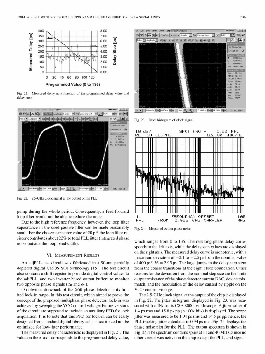
Fig. 24. Measured output phase noise.
which ranges from 0 to 135. The resulting phase delay corre-sponds to the left axis, while the delay step values are displayedon the right axis. The measured delay curve is monotonic, with amaximum deviation of 2.1 to 2.5 ps from the nominal valueof 400 ps/136 2.95 ps. The large jumps in the delay step stemfrom the coarse transitions at the eight clock boundaries. Otherreasons for the deviation from the nominal step size are the finiteoutput resistance of the phase detector current DAC, device mis-match, and the modulation of the delay caused by ripple on theVCO control voltage.
The 2.5-GHz clock signal at the output of the chip is displayedin Fig. 22. The jitter histogram, displayed in Fig. 23, was mea-sured with a Tektronix CSA 8000 oscilloscope. A jitter value of1.4 ps rms and 15.8 ps pp ( 100k hits) is displayed. The scopejitter was measured to be 1.04 ps rms and 14.5 ps pp; hence, thePLL tracking jitter calculates to 0.94 ps rms. Fig. 24 displays thephase noise plot for the PLL. The output spectrum is shown inFig. 25. The spectrum contains spurs at 11 and 40 MHz. Since noother circuit was active on the chip except the PLL, and signals

2710 IEEE JOURNAL OF SOLID-STATE CIRCUITS, VOL. 40, NO. 12, DECEMBER 2005
Fig. 25. Measured output spectrum.
TABLE ITRACKING JITTER AS A FUNCTION OF CHARGE-PUMP CURRENT
Fig. 26. Overlaid signals at eight coarse phase positions.
at the given frequencies were also seen with the device undertest (DUT) turned off, it could be verified that these spurs orig-inated from crosstalk in the measurement setup.
Table I shows the measured tracking jitter as a function ofthe charge-pump current. There is good agreement between thesimulated VCO jitter accumulation factor and the mea-sured rms jitter.
Fig. 27. Die microphotograph and PLL layout.
For the measurement shown in Fig. 26, the coarse phaseposition was iterated from 0 to 7, and the measured clockwaveforms were superposed on the scope. Using this method,the phase deviation caused by ripple from its ideal value canbe estimated. The resulting maximum phase deviation wasmeasured to be 5.5 ps. Although this is acceptable for a symboltime of 100 ps, it is to note that ripple can be suppressed to ahigher degree by more aggressively setting the third pole of theloop transfer functions.
The power consumption of the overall circuit was measuredto be 29.3 mW from a 0.9-V supply. Of this value, 19.8 mWis consumed in the PLL and 9.5 mW in the two output buffersdriving 50- loads. The measured frequency range of the VCOextends from 0.4 to 3.4 GHz. The layout and a die microphoto-graph of the PLL are shown in Fig. 27.
VII. CONCLUSION
In this paper, a phase generator based on a PLL with a multi-phase phase detector has been proposed. It has been shown thatthe proposed phase generator circuit allows the implementationof low-power small-area CDR circuits. A high PLL loop band-width provides low timing jitter and a fast response in the phasetracking loop. Since the topology allows to generate and pre-cisely adjust many clock phases at the same time, highly over-sampled (e.g., to ) CDR circuits, as used to explore thespeed limits of a given technology, can easily be implementedwith low power and area.
Measured performance of the concept demonstrator imple-mented in a 90-nm partially depleted CMOS process showeda power consumption of 20 mW from a single 0.9-V powersupply, 1 ps rms jitter, and 3-ps nominal phase steps on a diearea of 0.016 mm .
The loop dynamics of a PLL using an XOR phase detector in acharge-pump PLL was investigated, wherein it was shown thatby proper choice of loop parameters, jitter accumulation can bemade comparable to the DLL case. Additionally, the advantagesof an XOR phase detector versus a PFD with respect to noisefiltering was pointed out.
ACKNOWLEDGMENT
The authors would like to thank Dr. L. Wagner, IBMHopewell Junction, NY, for device-modeling support, and theIBM Fishkill foundry team, Hopewell Junction, NY.

TOIFL et al.: PLL WITH 360 DIGITALLY PROGRAMMABLE PHASE SHIFT FOR 10-Gb/s SERIAL LINKS 2711
REFERENCES
[1] J. Lee and B. Razavi, “A 40-Gb/s clock and data recovery circuit in0.18-�m CMOS technology,” IEEE J. Solid-State Circuits, vol. 38, no.12, pp. 2181–2190, Dec. 2003.
[2] K.-L. Wong, H. Hatamkhani, M. Mansuri, and C.-K. Ken Yang, “A27-mW 3.6 Gb/s I/O transceiver,” IEEE J. Solid-State Circuits, vol. 39,no. 4, pp. 602–612, Apr. 2004.
[3] S. Sidiropoulos and M. Horowitz, “A semi-digital dual delay-lockedloop,” IEEE J. Solid-State Circuits, vol. 32, no. 11, pp. 1683–1692, Nov.1997.
[4] J. Kim and M. Horowitz, “Adaptive supply serial links with sub-1-Voperation and per-pin clock recovery,” IEEE J. Solid-State Circuits, vol.37, no. 11, pp. 1403–1413, Nov. 2002.
[5] M.-J. E. Lee, W. Dally, J. Poulton, P. Chiang, and S. Greenwood, “An84-mW 4-Gb/s clock and data recovery circuit for serial link applica-tions,” in IEEE Symp. VLSI Circuits Dig. Tech. Papers, Kyoto, Japan,Jun. 2001, pp. 149–152.
[6] K. K. Chang, J. Wei, C. Huang, S. Li, K. Donnelly, M. Horowitz, Y. Li,and S. Sidiropoulos, “A 0.4-4-Gb/s CMOS quad transceiver cell usingon-chip regulated dual-loop PLLs,” IEEE J. Solid-State Circuits, vol. 38,no. 5, pp. 747–754, May 2003.
[7] A. Maxim, “A 160–2550 MHz CMOS active clock deskewing PLLusing analog phase interpolation,” IEEE J. Solid-State Circuits, vol. 40,no. 1, pp. 110–131, Jan. 2005.
[8] R. Farjad-Rad, A. Nguyen, J. M. Tran, T. Greer, J. Poulton, W. J. Dally,J. H. Edmondson, R. Senthinathan, R. Rathi, M.-J. E. Lee, and H.-T.Ng, “A 33-mW 8-Gb/s CMOS clock multiplier and CDR for highly inte-grated I/Os,” IEEE J. Solid-State Circuits, vol. 39, no. 9, pp. 1553–1561,Sep. 2004.
[9] P. Larsson, “A 2-1600-MHz CMOS clock recovery PLL with low-Vddcapability,” IEEE J. Solid-State Circuits, vol. 34, no. 12, pp. 1951–1960,Dec. 1999.
[10] M. Mansuri and C.-K. K. Yang, “Jitter optimization based on phase-locked loop design parameters,” IEEE J. Solid-State Circuits, vol. 37,no. 11, pp. 1375–1382, Nov. 2002.
[11] F. Gardner, “Charge-pump phase-lock loops,” IEEE Trans. Commun.,vol. COM-28, no. 11, pp. 1849–1858, Nov. 1980.
[12] J. Hein and J. Scott, “z-domain model for discrete-time PLL’s,” IEEETrans. Circuits Syst., vol. 35, no. 11, pp. 1393–1400, Nov. 1988.
[13] J. McNeill, “Jitter in ring oscillators,” IEEE J. Solid-State Circuits, vol.32, no. 6, pp. 870–879, Jun. 1997.
[14] L. Sun and T. Kwasniewski, “A 1.25-GHz 0.35 �m monolithic CMOSPLL based on a multiphase ring oscillator,” IEEE J. Solid-State Circuits,vol. 36, no. 6, pp. 910–916, Jun. 2001.
[15] M. Khare et al., “A high performance 90 nm SOI technology with 0.992�m 6T-SRAM cell,” in Int. Electron Devices Meeting (IEDM) Tech.Dig., San Francisco, CA, 2002, pp. 407–410.
Thomas Toifl (S’97–M’99) received the Dipl.Ing.(M.S.) and the Ph.D. degrees from the ViennaUniversity of Technology, Vienna, Austria, in 1995and 1999, respectively.
In 1996, he joined the Microelectronics Group ofthe European Research Center for Particle Physics(CERN), Geneva, Switzerland, where he worked onradiation-hard integrated circuits for particle physicsdetectors. There, he developed circuits for detectorsynchronization and transmission of detector data,which were integrated in the four-particle detector
systems of the new Large Hadron Collider (LHC). In 2001, he joined theIBM Zurich Research Laboratory, Rueschlikon, Switzerland, where he hasbeen working on multigigabit low-power communication circuits in advancedCMOS technologies.
Christian Menolfi (S’97–M’99) was born inSt. Gallen, Switzerland, in 1967. He receivedthe Dipl.Ing. and the Ph.D. degrees in electricalengineering from the Swiss Federal Institute ofTechnology (ETH), Zurich, Switzerland, in 1993and 2000, respectively.
From 1993 to 2000, he was with the IntegratedSystems Laboratory, ETH, working as a ResearchAssistant, where he worked on highly sensitiveCMOS VLSI data acquisition circuits for sil-icon-based microsensors. Since September 2000, he
has been with the IBM Zurich Research Laboratory, Rueschlikon, Switzerland,where he has been involved with multigigabit low-power communicationcircuits in advanced CMOS technologies.
Peter Buchmann was born in Zurich, Switzerland,in 1953. He received the diploma in experimentalphysics and the Ph.D. degree in physics from theFederal Institute of Technology, Zurich, Switzerland,in 1978 and 1987, respectively.
From 1978 to 1981, he was involved in surfacephysics studies. From 1981 to 1985, he was workingin the field of integrated optics in the group of Ap-plied Research at the Federal Institute of Technology.He was engaged in the technology, design, and char-acterization of III–V semiconductor waveguide de-
vices, electro-optic modulators, and switches. In 1985, he joined the IBM ZurichResearch Laboratory, Rueschlikon, Switzerland, where he has been engagedin MESFET technology and in the process technology of III–V semiconductorlasers. In particular, he was involved in the research on dry-etching techniquesand optoelectronic integration. Since 1994, he has been involved in the designand implementation of VLSI chips for communication applications in the fieldof ATM, SONET/SDH, and network processors. His most recent work includescircuit design for high-speed I/O and link technology.
Dr. Buchmann is a member of the Swiss Physical Society.
Marcel Kossel (S’99–M’02) received the Dipl.Ing.degree and the Ph.D. degree in electrical engineeringfrom the Swiss Federal Institute of Technology(ETH), Zurich, Switzerland, in 1997 and 2000,respectively.
He joined the IBM Zurich Research Laboratory in2001 where he was involved in analog circuit designfor high-speed serial links. His research interests in-clude circuit design and RF measurement techniques.He also did research in the field of microwave taggingsystems and RF identification systems.
Thomas Morf (S’87–M’97) was born on April 4,1961, in Zurich, Switzerland. He received the B.S.degree from Winterthur Polytechnic, Winterthur,Switzerland, in 1987, the M.S. degree in electricalengineering from the University of California atSanta Barbara (UCSB) in 1991, and the Ph.D. degreefrom the Swiss Federal Institute of Technology(ETH), Zurich, Switzerland, in 1996. His Ph.D.work was on circuit design and processing forhigh-speed optical links on GaAs using “epitaxiallift off” techniques.
From 1989 to 1991, he worked as a Research Assistant at UCSB, performingresearch in the field of active microwave inductors and digital GaAs circuits. In1991, he joined the ETH. In 1996, he joined the Electronics Laboratory, also atthe ETH, where he led a research group in the area of InP-HBT circuit designand technology. Since Fall 1999, he has been with the IBM Zurich ResearchLaboratory, Rueschlikon, Switzerland. His present research interests include allaspects of electrical and optical high-speed high-density interconnects and high-speed and microwave circuit design.

2712 IEEE JOURNAL OF SOLID-STATE CIRCUITS, VOL. 40, NO. 12, DECEMBER 2005
Robert Reutemann (S’95–M’97) received theDipl.Ing. degree in electrical engineering fromthe Swiss Federal Institute of Technology (ETH),Zurich, Switzerland, in 1997.
From 1998 to 2003, he was with the IntegratedSystems Laboratory of the Swiss Federal Instituteof Technology, working on low-power VLSI digitalsignal processing implementations for communi-cations and mixed-signal integrated circuits forsensor/control applications. In 2002, he cofoundedMiromico AG, Zurich, Switzerland, a spin-off of
ETH Zurich focusing on analog and mixed-signal IC design services.
Michael Ruegg received the Dipl.Ing. degree in elec-trical engineering from the Swiss Federal Institute ofTechnology (ETH), Zurich, Switzerland, in 1997.
From 1997 to 1999, he was with SiemensSemiconductors, working as an Analog IC DesignEngineer on analog front ends for video applicationsand GSM phones. In 1999, he joined Infineon Tech-nologies in California where he designed low-jitterphase-locked loops for DVD and hard disk read/writechannels. He is the inventor or co-inventor of severalpatents in this area. In 2002, he cofounded Miromico
AG, Zurich, Switzerland, a spin-off of ETH Zurich focusing on analog andmixed-signal IC design services.
Martin L. Schmatz (S’94–M’97) received the de-gree in electrical engineering in 1993 and the Ph.D.degree in 1998, both from the Swiss Federal Insti-tute of Technology (ETH), Zurich, Switzerland, forhis work on low-power wireless receiver designs andon noise-parameter measurement systems.
In 1999, he joined the IBM Zurich Research Lab-oratory, where he established a research group fo-cusing on high-speed and high-density CMOS serial-link systems. Since 2001, he has been managing theI/O Link Technology group at IBM Zurich Research
Laboratory. He is also the IBM manager responsible for the joint IBM–ETHCompetence Center for Advanced Silicon Electronics (CASE), which allowsresearchers from ETH to access IBM’s most advanced SiGe and CMOS tech-nologies.
Jonas Weiss (S’04) received the Dipl.Ing. degree inelectrical engineering from the Swiss Federal Insti-tute of Technology (ETH), Zurich, Switzerland, in1997.
From 1997 to 1998, he was with PhilipsSemiconductors, working on analog low-powerCMOS circuits. From 2000 to 2002, he workedon mixed-signal front-ends for medical ultrasoundapplications. He joined the IBM Zurich ResearchLaboratory in 2003 to pursue his Ph.D. studies in thefield of electro-optical interconnections. His research
interests include packaging, ESD protection schemes, and analog front endsfor high-speed serial links.


