Embed Size (px)
Citation preview
DDR4 SDRAMMT40A2G4MT40A1G8MT40A512M16
Features• VDD = VDDQ = 1.2V ±60mV• VPP = 2.5V, –125mV, +250mV• On-die, internal, adjustable VREFDQ generation• 1.2V pseudo open-drain I/O• TC maximum up to 95°C
– 64ms, 8192-cycle refresh up to 85°C– 32ms, 8192-cycle refresh at >85°C to 95°C
• 16 internal banks (x4, x8): 4 groups of 4 banks each• 8 internal banks (x16): 2 groups of 4 banks each• 8n-bit prefetch architecture• Programmable data strobe preambles• Data strobe preamble training• Command/Address latency (CAL)• Multipurpose register READ and WRITE capability• Write and read leveling• Self refresh mode• Low-power auto self refresh (LPASR)• Temperature controlled refresh (TCR)• Fine granularity refresh• Self refresh abort• Maximum power saving• Output driver calibration• Nominal, park, and dynamic on-die termination
(ODT)• Data bus inversion (DBI) for data bus• Command/Address (CA) parity• Databus write cyclic redundancy check (CRC)• Per-DRAM addressability• Connectivity test (x16)• JEDEC JESD-79-4 compliant• sPPR and hPPR capability
Options1 Marking• Configuration
– 2 Gig x 4 2G4– 1 Gig x 8 1G8– 512 Meg x 16 512M16
• 78-ball FBGA package (Pb-free) – x4,x8
– 9mm x 13.2mm – Rev. A PM– 8mm x 12mm – Rev. B, D, G WE– 7.5mm x 11mm – Rev. E, H SA
• 96-ball FBGA package (Pb-free) – x16 – 9mm x 14mm – Rev. A HA– 8mm x 14mm – Rev. B JY– 7.5mm x 13.5mm – Rev. D, E, H LY
• Timing – cycle time – 0.625ns @ CL = 22 (DDR4-3200) -062E– 0.682ns @ CL = 21 (DDR4-2933) -068– 0.750ns @ CL = 19 (DDR4-2666) -075– 0.750ns @ CL = 18 (DDR4-2666) -075E– 0.833ns @ CL = 17 (DDR4-2400) -083– 0.833ns @ CL = 16 (DDR4-2400) -083E– 0.937ns @ CL = 15 (DDR4-2133) -093E– 1.071ns @ CL = 13 (DDR4-1866) -107E
• Operating temperature – Commercial (0° TC 95°C) None– Industrial (–40° TC 95°C) IT
• Revision :A,:B, :D, :G,
:E, :H
Note: 1. Not all options listed can be combined todefine an offered product. Use the partcatalog search on http://www.micron.comfor available offerings.
Table 1: Key Timing Parameters
Speed Grade Data Rate (MT/s) Target CL-tRCD-tRP CL (ns) tRCD (ns) tRP (ns)
-062E6 3200 22-22-22 13.75 13.75 13.75
-0685 2933 21-21-21 14.32 14.32 14.32
-0754 2666 19-19-19 14.25 14.25 14.25
-075E4 2666 18-18-18 13.50 13.50 13.50
8Gb: x4, x8, x16 DDR4 SDRAMFeatures
09005aef861d1d4a8gb_ddr4_dram.pdf - Rev. L 9/17 EN 1 Micron Technology, Inc. reserves the right to change products or specifications without notice.
© 2015 Micron Technology, Inc. All rights reserved.
Products and specifications discussed herein are subject to change by Micron without notice.
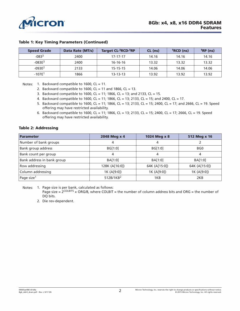
Table 1: Key Timing Parameters (Continued)
Speed Grade Data Rate (MT/s) Target CL-tRCD-tRP CL (ns) tRCD (ns) tRP (ns)
-0833 2400 17-17-17 14.16 14.16 14.16
-083E3 2400 16-16-16 13.32 13.32 13.32
-093E2 2133 15-15-15 14.06 14.06 14.06
-107E1 1866 13-13-13 13.92 13.92 13.92
Notes: 1. Backward compatible to 1600, CL = 11.2. Backward compatible to 1600, CL = 11 and 1866, CL = 13.3. Backward compatible to 1600, CL = 11; 1866, CL = 13; and 2133, CL = 15.4. Backward compatible to 1600, CL = 11; 1866, CL = 13; 2133, CL = 15; and 2400, CL = 17.5. Backward compatible to 1600, CL = 11; 1866, CL = 13; 2133, CL = 15; 2400, CL = 17; and 2666, CL = 19. Speed
offering may have restricted availability.6. Backward compatible to 1600, CL = 11; 1866, CL = 13; 2133, CL = 15; 2400, CL = 17; 2666, CL = 19. Speed
offering may have restricted availability.
Table 2: Addressing
Parameter 2048 Meg x 4 1024 Meg x 8 512 Meg x 16
Number of bank groups 4 4 2
Bank group address BG[1:0] BG[1:0] BG0
Bank count per group 4 4 4
Bank address in bank group BA[1:0] BA[1:0] BA[1:0]
Row addressing 128K (A[16:0]) 64K (A[15:0]) 64K (A[15:0])
Column addressing 1K (A[9:0]) 1K (A[9:0]) 1K (A[9:0])
Page size1 512B/1KB2 1KB 2KB
Notes: 1. Page size is per bank, calculated as follows:Page size = 2COLBITS × ORG/8, where COLBIT = the number of column address bits and ORG = the number ofDQ bits.
2. Die rev-dependent.
8Gb: x4, x8, x16 DDR4 SDRAMFeatures
09005aef861d1d4a8gb_ddr4_dram.pdf - Rev. L 9/17 EN 2 Micron Technology, Inc. reserves the right to change products or specifications without notice.
© 2015 Micron Technology, Inc. All rights reserved.
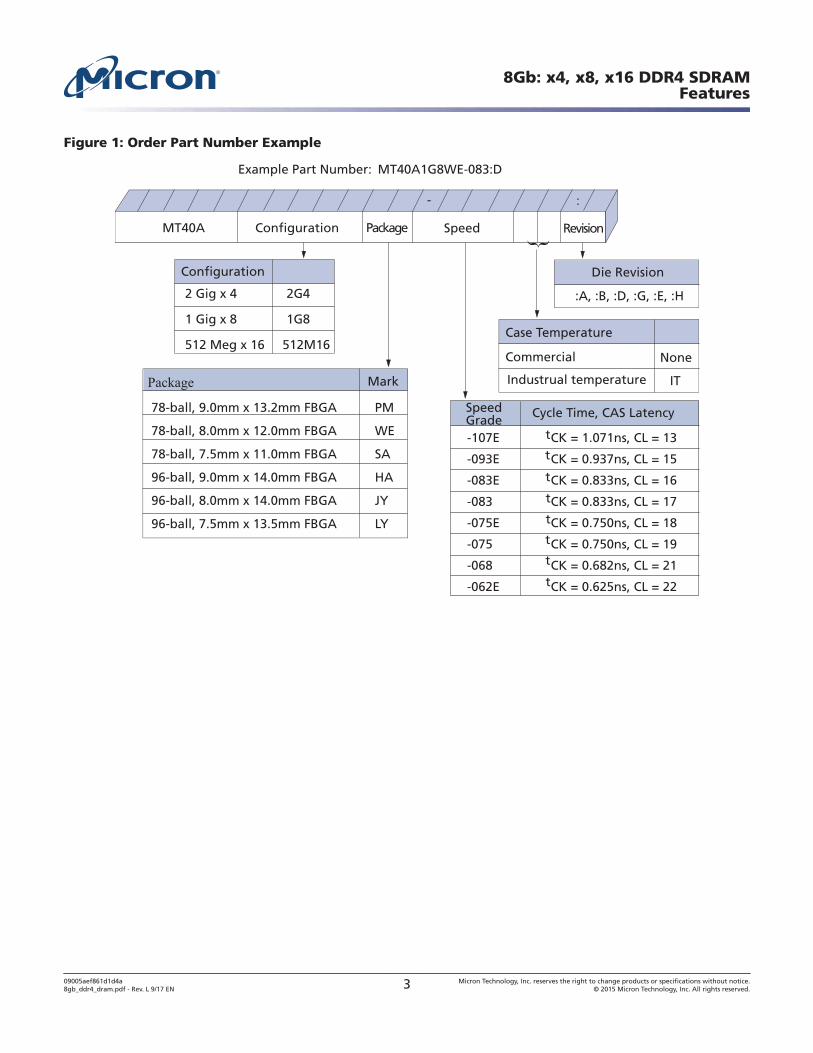
Figure 1: Order Part Number Example
Example Part Number: MT40A1G8WE-083:D
MT40A
Configuration
Package Speed
Die Revision
Revision
:A, :B, :D, :G, :E, :H
Configuration
Case Temperature
Commercial None
Industrual temperature IT
2 Gig x 4 2G4
1 Gig x 8 1G8
512 Meg x 16 512M16
Mark
SpeedGrade
78-ball, 9.0mm x 13.2mm FBGA PM
78-ball, 8.0mm x 12.0mm FBGA WE
78-ball, 7.5mm x 11.0mm FBGA SA
96-ball, 9.0mm x 14.0mm FBGA HA
96-ball, 8.0mm x 14.0mm FBGA JY
96-ball, 7.5mm x 13.5mm FBGA LY
-107E CK = 1.071ns, CL = 13
-093E CK = 0.937ns, CL = 15
-083E CK = 0.833ns, CL = 16
-083 CK = 0.833ns, CL = 17
-075E CK = 0.750ns, CL = 18
-075 CK = 0.750ns, CL = 19
-068 CK = 0.682ns, CL = 21
-062E CK = 0.625ns, CL = 22
t
t
t
t
t
t
t
t
Cycle Time, CAS Latency
8Gb: x4, x8, x16 DDR4 SDRAMFeatures
09005aef861d1d4a8gb_ddr4_dram.pdf - Rev. L 9/17 EN 3 Micron Technology, Inc. reserves the right to change products or specifications without notice.
© 2015 Micron Technology, Inc. All rights reserved.
ContentsGeneral Notes and Description ....................................................................................................................... 19
Description ................................................................................................................................................ 19Industrial Temperature ............................................................................................................................... 19General Notes ............................................................................................................................................ 19Definitions of the Device-Pin Signal Level ................................................................................................... 20Definitions of the Bus Signal Level ............................................................................................................... 20
Functional Block Diagrams ............................................................................................................................. 21Ball Assignments ............................................................................................................................................ 23Ball Descriptions ............................................................................................................................................ 25Package Dimensions ....................................................................................................................................... 28State Diagram ................................................................................................................................................ 34Functional Description ................................................................................................................................... 36RESET and Initialization Procedure ................................................................................................................. 37
Power-Up and Initialization Sequence ......................................................................................................... 37RESET Initialization with Stable Power Sequence ......................................................................................... 40Uncontrolled Power-Down Sequence .......................................................................................................... 41
Programming Mode Registers ......................................................................................................................... 42Mode Register 0 .............................................................................................................................................. 45
Burst Length, Type, and Order ..................................................................................................................... 47CAS Latency ............................................................................................................................................... 48Test Mode .................................................................................................................................................. 48Write Recovery(WR)/READ-to-PRECHARGE ............................................................................................... 48DLL RESET ................................................................................................................................................. 48
Mode Register 1 .............................................................................................................................................. 49DLL Enable/DLL Disable ............................................................................................................................ 50Output Driver Impedance Control ............................................................................................................... 51ODT RTT(NOM) Values .................................................................................................................................. 51Additive Latency ......................................................................................................................................... 51DQ RX EQ .................................................................................................................................................. 51Write Leveling ............................................................................................................................................ 52Output Disable ........................................................................................................................................... 52Termination Data Strobe ............................................................................................................................. 52
Mode Register 2 .............................................................................................................................................. 53CAS WRITE Latency .................................................................................................................................... 55Low-Power Auto Self Refresh ....................................................................................................................... 55Dynamic ODT ............................................................................................................................................ 55Write Cyclic Redundancy Check Data Bus .................................................................................................... 55
Mode Register 3 .............................................................................................................................................. 56Multipurpose Register ................................................................................................................................ 57WRITE Command Latency When CRC/DM is Enabled ................................................................................. 58Fine Granularity Refresh Mode .................................................................................................................... 58Temperature Sensor Status ......................................................................................................................... 58Per-DRAM Addressability ........................................................................................................................... 58Gear-Down Mode ....................................................................................................................................... 58
Mode Register 4 .............................................................................................................................................. 59Hard Post Package Repair Mode .................................................................................................................. 60Soft Post Package Repair Mode .................................................................................................................... 61WRITE Preamble ........................................................................................................................................ 61READ Preamble .......................................................................................................................................... 61READ Preamble Training ............................................................................................................................ 61
8Gb: x4, x8, x16 DDR4 SDRAMFeatures
09005aef861d1d4a8gb_ddr4_dram.pdf - Rev. L 9/17 EN 4 Micron Technology, Inc. reserves the right to change products or specifications without notice.
© 2015 Micron Technology, Inc. All rights reserved.
Temperature-Controlled Refresh ................................................................................................................. 61Command Address Latency ........................................................................................................................ 61Internal VREF Monitor ................................................................................................................................. 61Maximum Power Savings Mode ................................................................................................................... 62
Mode Register 5 .............................................................................................................................................. 63Data Bus Inversion ..................................................................................................................................... 64Data Mask .................................................................................................................................................. 65CA Parity Persistent Error Mode .................................................................................................................. 65ODT Input Buffer for Power-Down .............................................................................................................. 65CA Parity Error Status ................................................................................................................................. 65CRC Error Status ......................................................................................................................................... 65CA Parity Latency Mode .............................................................................................................................. 65
Mode Register 6 .............................................................................................................................................. 66tCCD_L Programming ................................................................................................................................. 67VREFDQ Calibration Enable .......................................................................................................................... 67VREFDQ Calibration Range ........................................................................................................................... 67VREFDQ Calibration Value ............................................................................................................................ 68DQ RX EQ .................................................................................................................................................. 68
Truth Tables ................................................................................................................................................... 69NOP Command .............................................................................................................................................. 72DESELECT Command .................................................................................................................................... 72DLL-Off Mode ................................................................................................................................................ 72DLL-On/Off Switching Procedures .................................................................................................................. 74
DLL Switch Sequence from DLL-On to DLL-Off ........................................................................................... 74DLL-Off to DLL-On Procedure .................................................................................................................... 75
Input Clock Frequency Change ....................................................................................................................... 76Write Leveling ................................................................................................................................................ 77
DRAM Setting for Write Leveling and DRAM TERMINATION Function in that Mode ..................................... 79Procedure Description ................................................................................................................................ 80Write Leveling Mode Exit ............................................................................................................................ 81
Command Address Latency ............................................................................................................................ 82Low-Power Auto Self Refresh Mode ................................................................................................................. 87
Manual Self Refresh Mode .......................................................................................................................... 87Multipurpose Register .................................................................................................................................... 89
MPR Reads ................................................................................................................................................. 90MPR Readout Format ................................................................................................................................. 92MPR Readout Serial Format ........................................................................................................................ 92MPR Readout Parallel Format ..................................................................................................................... 93MPR Readout Staggered Format .................................................................................................................. 94MPR READ Waveforms ............................................................................................................................... 95MPR Writes ................................................................................................................................................ 97MPR WRITE Waveforms .............................................................................................................................. 98MPR REFRESH Waveforms ......................................................................................................................... 99
Gear-Down Mode .......................................................................................................................................... 102Maximum Power-Saving Mode ....................................................................................................................... 105
Maximum Power-Saving Mode Entry .......................................................................................................... 105Maximum Power-Saving Mode Entry in PDA .............................................................................................. 106CKE Transition During Maximum Power-Saving Mode ................................................................................ 106Maximum Power-Saving Mode Exit ............................................................................................................ 106
Command/Address Parity .............................................................................................................................. 108Per-DRAM Addressability .............................................................................................................................. 116VREFDQ Calibration ........................................................................................................................................ 119
8Gb: x4, x8, x16 DDR4 SDRAMFeatures
09005aef861d1d4a8gb_ddr4_dram.pdf - Rev. L 9/17 EN 5 Micron Technology, Inc. reserves the right to change products or specifications without notice.
© 2015 Micron Technology, Inc. All rights reserved.
VREFDQ Range and Levels ........................................................................................................................... 120VREFDQ Step Size ........................................................................................................................................ 120VREFDQ Increment and Decrement Timing .................................................................................................. 121VREFDQ Target Settings ............................................................................................................................... 125
Connectivity Test Mode ................................................................................................................................. 127Pin Mapping ............................................................................................................................................. 127Minimum Terms Definition for Logic Equations ......................................................................................... 128Logic Equations for a ×4 Device .................................................................................................................. 128Logic Equations for a ×8 Device .................................................................................................................. 129Logic Equations for a ×16 Device ................................................................................................................ 129CT Input Timing Requirements .................................................................................................................. 129
Excessive Row Activation ............................................................................................................................... 131Post Package Repair ....................................................................................................................................... 132
Post Package Repair ................................................................................................................................... 132Hard Post Package Repair .............................................................................................................................. 133
hPPR Row Repair - Entry ............................................................................................................................ 133hPPR Row Repair – WRA Initiated (REF Commands Allowed) ...................................................................... 133hPPR Row Repair – WR Initiated (REF Commands NOT Allowed) ................................................................. 135
sPPR Row Repair ........................................................................................................................................... 137hPPR/sPPR Support Identifier ........................................................................................................................ 140ACTIVATE Command .................................................................................................................................... 140PRECHARGE Command ................................................................................................................................ 141REFRESH Command ..................................................................................................................................... 142Temperature-Controlled Refresh Mode .......................................................................................................... 144
TCR Mode – Normal Temperature Range .................................................................................................... 144TCR Mode – Extended Temperature Range ................................................................................................. 144
Fine Granularity Refresh Mode ....................................................................................................................... 146Mode Register and Command Truth Table .................................................................................................. 146tREFI and tRFC Parameters ........................................................................................................................ 146Changing Refresh Rate ............................................................................................................................... 149Usage with TCR Mode ................................................................................................................................ 149Self Refresh Entry and Exit ......................................................................................................................... 149
SELF REFRESH Operation .............................................................................................................................. 151Self Refresh Abort ...................................................................................................................................... 153Self Refresh Exit with NOP Command ......................................................................................................... 154
Power-Down Mode ........................................................................................................................................ 156Power-Down Clarifications – Case 1 ........................................................................................................... 161Power-Down Entry, Exit Timing with CAL ................................................................................................... 162
ODT Input Buffer Disable Mode for Power-Down ............................................................................................ 164CRC Write Data Feature ................................................................................................................................. 166
CRC Write Data ......................................................................................................................................... 166WRITE CRC DATA Operation ...................................................................................................................... 166DBI_n and CRC Both Enabled .................................................................................................................... 167DM_n and CRC Both Enabled .................................................................................................................... 167DM_n and DBI_n Conflict During Writes with CRC Enabled ........................................................................ 167CRC and Write Preamble Restrictions ......................................................................................................... 167CRC Simultaneous Operation Restrictions .................................................................................................. 167CRC Polynomial ........................................................................................................................................ 167CRC Combinatorial Logic Equations .......................................................................................................... 168Burst Ordering for BL8 ............................................................................................................................... 169CRC Data Bit Mapping ............................................................................................................................... 169CRC Enabled With BC4 .............................................................................................................................. 170
8Gb: x4, x8, x16 DDR4 SDRAMFeatures
09005aef861d1d4a8gb_ddr4_dram.pdf - Rev. L 9/17 EN 6 Micron Technology, Inc. reserves the right to change products or specifications without notice.
© 2015 Micron Technology, Inc. All rights reserved.
CRC with BC4 Data Bit Mapping ................................................................................................................ 170CRC Equations for x8 Device in BC4 Mode with A2 = 0 and A2 = 1 ................................................................ 173CRC Error Handling ................................................................................................................................... 175CRC Write Data Flow Diagram ................................................................................................................... 176
Data Bus Inversion ........................................................................................................................................ 177DBI During a WRITE Operation .................................................................................................................. 177DBI During a READ Operation ................................................................................................................... 178
Data Mask ..................................................................................................................................................... 179Programmable Preamble Modes and DQS Postambles .................................................................................... 181
WRITE Preamble Mode .............................................................................................................................. 181READ Preamble Mode ............................................................................................................................... 184READ Preamble Training ........................................................................................................................... 184WRITE Postamble ...................................................................................................................................... 185READ Postamble ....................................................................................................................................... 185
Bank Access Operation .................................................................................................................................. 187READ Operation ............................................................................................................................................ 191
Read Timing Definitions ............................................................................................................................ 191Read Timing – Clock-to-Data Strobe Relationship ....................................................................................... 192Read Timing – Data Strobe-to-Data Relationship ........................................................................................ 194tLZ(DQS), tLZ(DQ), tHZ(DQS), and tHZ(DQ) Calculations ............................................................................ 195tRPRE Calculation ..................................................................................................................................... 196tRPST Calculation ...................................................................................................................................... 197READ Burst Operation ............................................................................................................................... 198READ Operation Followed by Another READ Operation .............................................................................. 200READ Operation Followed by WRITE Operation .......................................................................................... 205READ Operation Followed by PRECHARGE Operation ................................................................................ 211READ Operation with Read Data Bus Inversion (DBI) .................................................................................. 214READ Operation with Command/Address Parity (CA Parity) ........................................................................ 215READ Followed by WRITE with CRC Enabled .............................................................................................. 217READ Operation with Command/Address Latency (CAL) Enabled ............................................................... 218
WRITE Operation .......................................................................................................................................... 220Write Timing Definitions ........................................................................................................................... 220Write Timing – Clock-to-Data Strobe Relationship ...................................................................................... 220tWPRE Calculation .................................................................................................................................... 222tWPST Calculation ..................................................................................................................................... 223Write Timing – Data Strobe-to-Data Relationship ........................................................................................ 223WRITE Burst Operation ............................................................................................................................. 227WRITE Operation Followed by Another WRITE Operation ........................................................................... 229WRITE Operation Followed by READ Operation .......................................................................................... 235WRITE Operation Followed by PRECHARGE Operation ............................................................................... 239WRITE Operation with WRITE DBI Enabled ................................................................................................ 242WRITE Operation with CA Parity Enabled ................................................................................................... 244WRITE Operation with Write CRC Enabled ................................................................................................. 245
Write Timing Violations ................................................................................................................................. 250Motivation ................................................................................................................................................ 250Data Setup and Hold Violations ................................................................................................................. 250Strobe-to-Strobe and Strobe-to-Clock Violations ........................................................................................ 250
ZQ CALIBRATION Commands ....................................................................................................................... 251On-Die Termination ...................................................................................................................................... 253ODT Mode Register and ODT State Table ........................................................................................................ 253
ODT Read Disable State Table .................................................................................................................... 254Synchronous ODT Mode ................................................................................................................................ 255
8Gb: x4, x8, x16 DDR4 SDRAMFeatures
09005aef861d1d4a8gb_ddr4_dram.pdf - Rev. L 9/17 EN 7 Micron Technology, Inc. reserves the right to change products or specifications without notice.
© 2015 Micron Technology, Inc. All rights reserved.
ODT Latency and Posted ODT .................................................................................................................... 255Timing Parameters .................................................................................................................................... 255ODT During Reads .................................................................................................................................... 257
Dynamic ODT ............................................................................................................................................... 258Functional Description .............................................................................................................................. 258
Asynchronous ODT Mode .............................................................................................................................. 261Electrical Specifications ................................................................................................................................. 262
Absolute Ratings ........................................................................................................................................ 262DRAM Component Operating Temperature Range ...................................................................................... 262
Electrical Characteristics – AC and DC Operating Conditions .......................................................................... 263Supply Operating Conditions ..................................................................................................................... 263Leakages ................................................................................................................................................... 264VREFCA Supply ............................................................................................................................................ 264VREFDQ Supply and Calibration Ranges ....................................................................................................... 265VREFDQ Ranges ........................................................................................................................................... 266
Electrical Characteristics – AC and DC Single-Ended Input Measurement Levels .............................................. 267RESET_n Input Levels ................................................................................................................................ 267Command/Address Input Levels ................................................................................................................ 267Command, Control, and Address Setup, Hold, and Derating ........................................................................ 269Data Receiver Input Requirements ............................................................................................................. 271Connectivity Test (CT) Mode Input Levels .................................................................................................. 275
Electrical Characteristics – AC and DC Differential Input Measurement Levels ................................................. 279Differential Inputs ..................................................................................................................................... 279Single-Ended Requirements for CK Differential Signals ............................................................................... 280Slew Rate Definitions for CK Differential Input Signals ................................................................................ 281CK Differential Input Cross Point Voltage .................................................................................................... 282DQS Differential Input Signal Definition and Swing Requirements .............................................................. 284DQS Differential Input Cross Point Voltage ................................................................................................. 286Slew Rate Definitions for DQS Differential Input Signals .............................................................................. 287
Electrical Characteristics – Overshoot and Undershoot Specifications ............................................................. 289Address, Command, and Control Overshoot and Undershoot Specifications ................................................ 289Clock Overshoot and Undershoot Specifications ......................................................................................... 289Data, Strobe, and Mask Overshoot and Undershoot Specifications .............................................................. 290
Electrical Characteristics – AC and DC Output Measurement Levels ................................................................ 291Single-Ended Outputs ............................................................................................................................... 291Differential Outputs .................................................................................................................................. 292Reference Load for AC Timing and Output Slew Rate ................................................................................... 294Connectivity Test Mode Output Levels ........................................................................................................ 294
Electrical Characteristics – AC and DC Output Driver Characteristics ............................................................... 296Connectivity Test Mode Output Driver Electrical Characteristics ................................................................. 296Output Driver Electrical Characteristics ..................................................................................................... 297Output Driver Temperature and Voltage Sensitivity ..................................................................................... 300Alert Driver ............................................................................................................................................... 300
Electrical Characteristics – On-Die Termination Characteristics ...................................................................... 302ODT Levels and I-V Characteristics ............................................................................................................ 302ODT Temperature and Voltage Sensitivity ................................................................................................... 303ODT Timing Definitions ............................................................................................................................ 304
DRAM Package Electrical Specifications ......................................................................................................... 307Thermal Characteristics ................................................................................................................................. 311Current Specifications – Measurement Conditions .......................................................................................... 312
IDD, IPP, and IDDQ Measurement Conditions ................................................................................................ 312IDD Definitions .......................................................................................................................................... 314
8Gb: x4, x8, x16 DDR4 SDRAMFeatures
09005aef861d1d4a8gb_ddr4_dram.pdf - Rev. L 9/17 EN 8 Micron Technology, Inc. reserves the right to change products or specifications without notice.
© 2015 Micron Technology, Inc. All rights reserved.
Current Specifications – Patterns and Test Conditions ..................................................................................... 318Current Test Definitions and Patterns ......................................................................................................... 318IDD Specifications ...................................................................................................................................... 327
Current Specifications – Limits ....................................................................................................................... 328Speed Bin Tables ........................................................................................................................................... 343Refresh Parameters By Device Density ............................................................................................................ 352Electrical Characteristics and AC Timing Parameters ...................................................................................... 353Electrical Characteristics and AC Timing Parameters: 2666 Through 3200 ........................................................ 365Timing Parameter Notes ................................................................................................................................ 377Clock Specification ........................................................................................................................................ 379
Definition for tCK(AVG) ............................................................................................................................. 379Definition for tCK(ABS) .............................................................................................................................. 379Definition for tCH(AVG) and tCL(AVG) ........................................................................................................ 379Definition for tJIT(per) and tJIT(per,lck) ...................................................................................................... 379Definition for tJIT(cc) and tJIT(cc,lck) ......................................................................................................... 379Definition for tERR(nper) ........................................................................................................................... 379
Jitter Notes .................................................................................................................................................... 380Converting Time-Based Specifications to Clock-Based Requirements .............................................................. 381Options Tables .............................................................................................................................................. 382
8Gb: x4, x8, x16 DDR4 SDRAMFeatures
09005aef861d1d4a8gb_ddr4_dram.pdf - Rev. L 9/17 EN 9 Micron Technology, Inc. reserves the right to change products or specifications without notice.
© 2015 Micron Technology, Inc. All rights reserved.
List of FiguresFigure 1: Order Part Number Example .............................................................................................................. 3Figure 2: 2 Gig x 4 Functional Block Diagram .................................................................................................. 21Figure 3: 1 Gig x 8 Functional Block Diagram .................................................................................................. 21Figure 4: 512 Meg x 16 Functional Block Diagram ........................................................................................... 22Figure 5: 78-Ball x4, x8 Ball Assignments ........................................................................................................ 23Figure 6: 96-Ball x16 Ball Assignments ............................................................................................................ 24Figure 7: 78-Ball FBGA – x4, x8 (PM) ............................................................................................................... 28Figure 8: 78-Ball FBGA – x4, x8 (WE) ............................................................................................................... 29Figure 9: 78-Ball FBGA – x4, x8 (SA) ................................................................................................................ 30Figure 10: 96-Ball FBGA – x16 (HA) ................................................................................................................. 31Figure 11: 96-Ball FBGA – x16 (JY) .................................................................................................................. 32Figure 12: 96-Ball FBGA – x16 (LY) .................................................................................................................. 33Figure 13: Simplified State Diagram ............................................................................................................... 34Figure 14: RESET and Initialization Sequence at Power-On Ramping ............................................................... 40Figure 15: RESET Procedure at Power Stable Condition ................................................................................... 41Figure 16: tMRD Timing ................................................................................................................................ 43Figure 17: tMOD Timing ................................................................................................................................ 43Figure 18: DLL-Off Mode Read Timing Operation ........................................................................................... 73Figure 19: DLL Switch Sequence from DLL-On to DLL-Off .............................................................................. 75Figure 20: DLL Switch Sequence from DLL-Off to DLL-On .............................................................................. 76Figure 21: Write Leveling Concept, Example 1 ................................................................................................ 78Figure 22: Write Leveling Concept, Example 2 ................................................................................................ 79Figure 23: Write Leveling Sequence (DQS Capturing CK LOW at T1 and CK HIGH at T2) .................................. 80Figure 24: Write Leveling Exit ......................................................................................................................... 81Figure 25: CAL Timing Definition ................................................................................................................... 82Figure 26: CAL Timing Example (Consecutive CS_n = LOW) ............................................................................ 82Figure 27: CAL Enable Timing – tMOD_CAL ................................................................................................... 83Figure 28: tMOD_CAL, MRS to Valid Command Timing with CAL Enabled ....................................................... 83Figure 29: CAL Enabling MRS to Next MRS Command, tMRD_CAL .................................................................. 84Figure 30: tMRD_CAL, Mode Register Cycle Time With CAL Enabled ............................................................... 84Figure 31: Consecutive READ BL8, CAL3, 1tCK Preamble, Different Bank Group ............................................... 85Figure 32: Consecutive READ BL8, CAL4, 1tCK Preamble, Different Bank Group ............................................... 85Figure 33: Auto Self Refresh Ranges ................................................................................................................ 88Figure 34: MPR Block Diagram ....................................................................................................................... 89Figure 35: MPR READ Timing ........................................................................................................................ 96Figure 36: MPR Back-to-Back READ Timing ................................................................................................... 96Figure 37: MPR READ-to-WRITE Timing ........................................................................................................ 97Figure 38: MPR WRITE and WRITE-to-READ Timing ...................................................................................... 98Figure 39: MPR Back-to-Back WRITE Timing .................................................................................................. 99Figure 40: REFRESH Timing ........................................................................................................................... 99Figure 41: READ-to-REFRESH Timing ........................................................................................................... 100Figure 42: WRITE-to-REFRESH Timing ......................................................................................................... 100Figure 43: Clock Mode Change from 1/2 Rate to 1/4 Rate (Initialization) ......................................................... 103Figure 44: Clock Mode Change After Exiting Self Refresh ................................................................................ 103Figure 45: Comparison Between Gear-Down Disable and Gear-Down Enable ................................................. 104Figure 46: Maximum Power-Saving Mode Entry ............................................................................................. 105Figure 47: Maximum Power-Saving Mode Entry with PDA .............................................................................. 106Figure 48: Maintaining Maximum Power-Saving Mode with CKE Transition ................................................... 106Figure 49: Maximum Power-Saving Mode Exit ............................................................................................... 107Figure 50: Command/Address Parity Operation ............................................................................................. 108
8Gb: x4, x8, x16 DDR4 SDRAMFeatures
09005aef861d1d4a8gb_ddr4_dram.pdf - Rev. L 9/17 EN 10 Micron Technology, Inc. reserves the right to change products or specifications without notice.
© 2015 Micron Technology, Inc. All rights reserved.
Figure 51: Command/Address Parity During Normal Operation ..................................................................... 110Figure 52: Persistent CA Parity Error Checking Operation ............................................................................... 111Figure 53: CA Parity Error Checking – SRE Attempt ........................................................................................ 111Figure 54: CA Parity Error Checking – SRX Attempt ........................................................................................ 112Figure 55: CA Parity Error Checking – PDE/PDX ............................................................................................ 112Figure 56: Parity Entry Timing Example – tMRD_PAR ..................................................................................... 113Figure 57: Parity Entry Timing Example – tMOD_PAR ..................................................................................... 113Figure 58: Parity Exit Timing Example – tMRD_PAR ....................................................................................... 114Figure 59: Parity Exit Timing Example – tMOD_PAR ....................................................................................... 114Figure 60: CA Parity Flow Diagram ................................................................................................................ 115Figure 61: PDA Operation Enabled, BL8 ........................................................................................................ 117Figure 62: PDA Operation Enabled, BC4 ........................................................................................................ 117Figure 63: MRS PDA Exit ............................................................................................................................... 118Figure 64: VREFDQ Voltage Range ................................................................................................................... 119Figure 65: Example of VREF Set Tolerance and Step Size .................................................................................. 121Figure 66: VREFDQ Timing Diagram for VREF,time Parameter .............................................................................. 122Figure 67: VREFDQ Training Mode Entry and Exit Timing Diagram ................................................................... 123Figure 68: VREF Step: Single Step Size Increment Case .................................................................................... 124Figure 69: VREF Step: Single Step Size Decrement Case ................................................................................... 124Figure 70: VREF Full Step: From VREF,min to VREF,maxCase .................................................................................. 125Figure 71: VREF Full Step: From VREF,max to VREF,minCase .................................................................................. 125Figure 72: VREFDQ Equivalent Circuit ............................................................................................................. 126Figure 73: Connectivity Test Mode Entry ....................................................................................................... 130Figure 74: hPPR WRA – Entry ........................................................................................................................ 135Figure 75: hPPR WRA – Repair and Exit ......................................................................................................... 135Figure 76: hPPR WR – Entry .......................................................................................................................... 136Figure 77: hPPR WR – Repair and Exit ............................................................................................................ 137Figure 78: sPPR – Entry ................................................................................................................................. 139Figure 79: sPPR – Repair, and Exit ................................................................................................................. 140Figure 80: tRRD Timing ................................................................................................................................ 141Figure 81: tFAW Timing ................................................................................................................................. 141Figure 82: REFRESH Command Timing ......................................................................................................... 143Figure 83: Postponing REFRESH Commands (Example) ................................................................................. 143Figure 84: Pulling In REFRESH Commands (Example) ................................................................................... 143Figure 85: TCR Mode Example1 ..................................................................................................................... 145Figure 86: 4Gb with Fine Granularity Refresh Mode Example ......................................................................... 148Figure 87: OTF REFRESH Command Timing ................................................................................................. 149Figure 88: Self Refresh Entry/Exit Timing ...................................................................................................... 152Figure 89: Self Refresh Entry/Exit Timing with CAL Mode ............................................................................... 153Figure 90: Self Refresh Abort ......................................................................................................................... 154Figure 91: Self Refresh Exit with NOP Command ............................................................................................ 155Figure 92: Active Power-Down Entry and Exit ................................................................................................ 157Figure 93: Power-Down Entry After Read and Read with Auto Precharge ......................................................... 158Figure 94: Power-Down Entry After Write and Write with Auto Precharge ........................................................ 158Figure 95: Power-Down Entry After Write ...................................................................................................... 159Figure 96: Precharge Power-Down Entry and Exit .......................................................................................... 159Figure 97: REFRESH Command to Power-Down Entry ................................................................................... 160Figure 98: Active Command to Power-Down Entry ......................................................................................... 160Figure 99: PRECHARGE/PRECHARGE ALL Command to Power-Down Entry .................................................. 161Figure 100: MRS Command to Power-Down Entry ......................................................................................... 161Figure 101: Power-Down Entry/Exit Clarifications – Case 1 ............................................................................ 162Figure 102: Active Power-Down Entry and Exit Timing with CAL .................................................................... 162
8Gb: x4, x8, x16 DDR4 SDRAMFeatures
09005aef861d1d4a8gb_ddr4_dram.pdf - Rev. L 9/17 EN 11 Micron Technology, Inc. reserves the right to change products or specifications without notice.
© 2015 Micron Technology, Inc. All rights reserved.
Figure 103: REFRESH Command to Power-Down Entry with CAL ................................................................... 163Figure 104: ODT Power-Down Entry with ODT Buffer Disable Mode .............................................................. 164Figure 105: ODT Power-Down Exit with ODT Buffer Disable Mode ................................................................. 165Figure 106: CRC Write Data Operation .......................................................................................................... 166Figure 107: CRC Error Reporting ................................................................................................................... 175Figure 108: CA Parity Flow Diagram .............................................................................................................. 176Figure 109: 1tCK vs. 2tCK WRITE Preamble Mode ........................................................................................... 181Figure 110: 1tCK vs. 2tCK WRITE Preamble Mode, tCCD = 4 ............................................................................ 182Figure 111: 1tCK vs. 2tCK WRITE Preamble Mode, tCCD = 5 ............................................................................ 183Figure 112: 1tCK vs. 2 tCK WRITE Preamble Mode, tCCD = 6 ........................................................................... 183Figure 113: 1tCK vs. 2tCK READ Preamble Mode ............................................................................................ 184Figure 114: READ Preamble Training ............................................................................................................. 185Figure 115: WRITE Postamble ....................................................................................................................... 185Figure 116: READ Postamble ........................................................................................................................ 186Figure 117: Bank Group x4/x8 Block Diagram ................................................................................................ 187Figure 118: READ Burst tCCD_S and tCCD_L Examples .................................................................................. 188Figure 119: Write Burst tCCD_S and tCCD_L Examples ................................................................................... 188Figure 120: tRRD Timing ............................................................................................................................... 189Figure 121: tWTR_S Timing (WRITE-to-READ, Different Bank Group, CRC and DM Disabled) ......................... 189Figure 122: tWTR_L Timing (WRITE-to-READ, Same Bank Group, CRC and DM Disabled) .............................. 190Figure 123: Read Timing Definition ............................................................................................................... 192Figure 124: Clock-to-Data Strobe Relationship .............................................................................................. 193Figure 125: Data Strobe-to-Data Relationship ................................................................................................ 194Figure 126: tLZ and tHZ Method for Calculating Transitions and Endpoints .................................................... 195Figure 127: tRPRE Method for Calculating Transitions and Endpoints ............................................................. 196Figure 128: tRPST Method for Calculating Transitions and Endpoints ............................................................. 197Figure 129: READ Burst Operation, RL = 11 (AL = 0, CL = 11, BL8) ................................................................... 198Figure 130: READ Burst Operation, RL = 21 (AL = 10, CL = 11, BL8) ................................................................. 199Figure 131: Consecutive READ (BL8) with 1tCK Preamble in Different Bank Group .......................................... 200Figure 132: Consecutive READ (BL8) with 2tCK Preamble in Different Bank Group .......................................... 200Figure 133: Nonconsecutive READ (BL8) with 1tCK Preamble in Same or Different Bank Group ....................... 201Figure 134: Nonconsecutive READ (BL8) with 2tCK Preamble in Same or Different Bank Group ....................... 201Figure 135: READ (BC4) to READ (BC4) with 1tCK Preamble in Different Bank Group ...................................... 202Figure 136: READ (BC4) to READ (BC4) with 2tCK Preamble in Different Bank Group ...................................... 202Figure 137: READ (BL8) to READ (BC4) OTF with 1tCK Preamble in Different Bank Group ............................... 203Figure 138: READ (BL8) to READ (BC4) OTF with 2tCK Preamble in Different Bank Group ............................... 203Figure 139: READ (BC4) to READ (BL8) OTF with 1tCK Preamble in Different Bank Group ............................... 204Figure 140: READ (BC4) to READ (BL8) OTF with 2tCK Preamble in Different Bank Group ............................... 204Figure 141: READ (BL8) to WRITE (BL8) with 1tCK Preamble in Same or Different Bank Group ........................ 205Figure 142: READ (BL8) to WRITE (BL8) with 2tCK Preamble in Same or Different Bank Group ........................ 205Figure 143: READ (BC4) OTF to WRITE (BC4) OTF with 1tCK Preamble in Same or Different Bank Group ......... 206Figure 144: READ (BC4) OTF to WRITE (BC4) OTF with 2tCK Preamble in Same or Different Bank Group ......... 207Figure 145: READ (BC4) Fixed to WRITE (BC4) Fixed with 1tCK Preamble in Same or Different Bank Group ..... 207Figure 146: READ (BC4) Fixed to WRITE (BC4) Fixed with 2tCK Preamble in Same or Different Bank Group ..... 208Figure 147: READ (BC4) to WRITE (BL8) OTF with 1tCK Preamble in Same or Different Bank Group ................ 209Figure 148: READ (BC4) to WRITE (BL8) OTF with 2tCK Preamble in Same or Different Bank Group ................ 209Figure 149: READ (BL8) to WRITE (BC4) OTF with 1tCK Preamble in Same or Different Bank Group ................ 210Figure 150: READ (BL8) to WRITE (BC4) OTF with 2tCK Preamble in Same or Different Bank Group ................ 210Figure 151: READ to PRECHARGE with 1tCK Preamble .................................................................................. 211Figure 152: READ to PRECHARGE with 2tCK Preamble .................................................................................. 212Figure 153: READ to PRECHARGE with Additive Latency and 1tCK Preamble .................................................. 212Figure 154: READ with Auto Precharge and 1tCK Preamble ............................................................................ 213
8Gb: x4, x8, x16 DDR4 SDRAMFeatures
09005aef861d1d4a8gb_ddr4_dram.pdf - Rev. L 9/17 EN 12 Micron Technology, Inc. reserves the right to change products or specifications without notice.
© 2015 Micron Technology, Inc. All rights reserved.
Figure 155: READ with Auto Precharge, Additive Latency, and 1tCK Preamble ................................................. 214Figure 156: Consecutive READ (BL8) with 1tCK Preamble and DBI in Different Bank Group ............................ 214Figure 157: Consecutive READ (BL8) with 1tCK Preamble and CA Parity in Different Bank Group .................... 215Figure 158: READ (BL8) to WRITE (BL8) with 1tCK Preamble and CA Parity in Same or Different Bank Group ... 216Figure 159: READ (BL8) to WRITE (BL8 or BC4: OTF) with 1tCK Preamble and Write CRC in Same or Different
Bank Group ............................................................................................................................................... 217Figure 160: READ (BC4: Fixed) to WRITE (BC4: Fixed) with 1tCK Preamble and Write CRC in Same or Different
Bank Group ............................................................................................................................................... 218Figure 161: Consecutive READ (BL8) with CAL (3tCK) and 1tCK Preamble in Different Bank Group .................. 218Figure 162: Consecutive READ (BL8) with CAL (4tCK) and 1tCK Preamble in Different Bank Group .................. 219Figure 163: Write Timing Definition .............................................................................................................. 221Figure 164: tWPRE Method for Calculating Transitions and Endpoints ............................................................ 222Figure 165: tWPST Method for Calculating Transitions and Endpoints ............................................................ 223Figure 166: Rx Compliance Mask .................................................................................................................. 224Figure 167: VCENT_DQ VREFDQ Voltage Variation .............................................................................................. 224Figure 168: Rx Mask DQ-to-DQS Timings ...................................................................................................... 225Figure 169: Rx Mask DQ-to-DQS DRAM-Based Timings ................................................................................. 226Figure 170: Example of Data Input Requirements Without Training ................................................................ 227Figure 171: WRITE Burst Operation, WL = 9 (AL = 0, CWL = 9, BL8) ................................................................. 228Figure 172: WRITE Burst Operation, WL = 19 (AL = 10, CWL = 9, BL8) ............................................................. 229Figure 173: Consecutive WRITE (BL8) with 1tCK Preamble in Different Bank Group ........................................ 229Figure 174: Consecutive WRITE (BL8) with 2tCK Preamble in Different Bank Group ........................................ 230Figure 175: Nonconsecutive WRITE (BL8) with 1tCK Preamble in Same or Different Bank Group ..................... 231Figure 176: Nonconsecutive WRITE (BL8) with 2tCK Preamble in Same or Different Bank Group ..................... 231Figure 177: WRITE (BC4) OTF to WRITE (BC4) OTF with 1 tCK Preamble in Different Bank Group .................... 232Figure 178: WRITE (BC4) OTF to WRITE (BC4) OTF with 2 tCK Preamble in Different Bank Group .................... 233Figure 179: WRITE (BC4) Fixed to WRITE (BC4) Fixed with 1 tCK Preamble in Different Bank Group ................. 233Figure 180: WRITE (BL8) to WRITE (BC4) OTF with 1 tCK Preamble in Different Bank Group ............................ 234Figure 181: WRITE (BC4) OTF to WRITE (BL8) with 1 tCK Preamble in Different Bank Group ............................ 235Figure 182: WRITE (BL8) to READ (BL8) with 1tCK Preamble in Different Bank Group ..................................... 235Figure 183: WRITE (BL8) to READ (BL8) with 1tCK Preamble in Same Bank Group .......................................... 236Figure 184: WRITE (BC4) OTF to READ (BC4) OTF with 1tCK Preamble in Different Bank Group ...................... 237Figure 185: WRITE (BC4) OTF to READ (BC4) OTF with 1tCK Preamble in Same Bank Group ........................... 237Figure 186: WRITE (BC4) Fixed to READ (BC4) Fixed with 1 tCK Preamble in Different Bank Group ................. 238Figure 187: WRITE (BC4) Fixed to READ (BC4) Fixed with 1tCK Preamble in Same Bank Group ....................... 238Figure 188: WRITE (BL8/BC4-OTF) to PRECHARGE with 1tCK Preamble ........................................................ 239Figure 189: WRITE (BC4-Fixed) to PRECHARGE with 1tCK Preamble .............................................................. 240Figure 190: WRITE (BL8/BC4-OTF) to Auto PRECHARGE with 1tCK Preamble ................................................ 240Figure 191: WRITE (BC4-Fixed) to Auto PRECHARGE with 1tCK Preamble ...................................................... 241Figure 192: WRITE (BL8/BC4-OTF) with 1tCK Preamble and DBI ................................................................... 242Figure 193: WRITE (BC4-Fixed) with 1tCK Preamble and DBI ......................................................................... 243Figure 194: Consecutive Write (BL8) with 1tCK Preamble and CA Parity in Different Bank Group ..................... 244Figure 195: Consecutive WRITE (BL8/BC4-OTF) with 1tCK Preamble and Write CRC in Same or Different Bank
Group ....................................................................................................................................................... 245Figure 196: Consecutive WRITE (BC4-Fixed) with 1tCK Preamble and Write CRC in Same or Different Bank
Group ....................................................................................................................................................... 246Figure 197: Nonconsecutive WRITE (BL8/BC4-OTF) with 1tCK Preamble and Write CRC in Same or Different
Bank Group ............................................................................................................................................... 247Figure 198: Nonconsecutive WRITE (BL8/BC4-OTF) with 2tCK Preamble and Write CRC in Same or Different
Bank Group ............................................................................................................................................... 248Figure 199: WRITE (BL8/BC4-OTF/Fixed) with 1tCK Preamble and Write CRC in Same or Different Bank Group ... 249Figure 200: ZQ Calibration Timing ................................................................................................................ 252
8Gb: x4, x8, x16 DDR4 SDRAMFeatures
09005aef861d1d4a8gb_ddr4_dram.pdf - Rev. L 9/17 EN 13 Micron Technology, Inc. reserves the right to change products or specifications without notice.
© 2015 Micron Technology, Inc. All rights reserved.
Figure 201: Functional Representation of ODT .............................................................................................. 253Figure 202: Synchronous ODT Timing with BL8 ............................................................................................. 256Figure 203: Synchronous ODT with BC4 ........................................................................................................ 256Figure 204: ODT During Reads ...................................................................................................................... 257Figure 205: Dynamic ODT (1t CK Preamble; CL = 14, CWL = 11, BL = 8, AL = 0, CRC Disabled) .......................... 259Figure 206: Dynamic ODT Overlapped with RTT(NOM) (CL = 14, CWL = 11, BL = 8, AL = 0, CRC Disabled) .......... 260Figure 207: Asynchronous ODT Timings with DLL Off ................................................................................... 261Figure 208: VREFDQ Voltage Range .................................................................................................................. 264Figure 209: RESET_n Input Slew Rate Definition ............................................................................................ 267Figure 210: Single-Ended Input Slew Rate Definition ..................................................................................... 269Figure 211: DQ Slew Rate Definitions ............................................................................................................ 272Figure 212: Rx Mask Relative to tDS/tDH ....................................................................................................... 274Figure 213: Rx Mask Without Write Training .................................................................................................. 275Figure 214: TEN Input Slew Rate Definition ................................................................................................... 276Figure 215: CT Type-A Input Slew Rate Definition .......................................................................................... 277Figure 216: CT Type-B Input Slew Rate Definition .......................................................................................... 277Figure 217: CT Type-C Input Slew Rate Definition .......................................................................................... 278Figure 218: CT Type-D Input Slew Rate Definition ......................................................................................... 279Figure 219: Differential AC Swing and “Time Exceeding AC-Level” tDVAC ....................................................... 279Figure 220: Single-Ended Requirements for CK .............................................................................................. 281Figure 221: Differential Input Slew Rate Definition for CK_t, CK_c .................................................................. 282Figure 222: VIX(CK) Definition ........................................................................................................................ 283Figure 223: Differential Input Signal Definition for DQS_t, DQS_c .................................................................. 284Figure 224: DQS_t, DQS_c Input Peak Voltage Calculation and Range of Exempt non-Monotonic Signaling ..... 285Figure 225: VIXDQS Definition ........................................................................................................................ 286Figure 226: Differential Input Slew Rate and Input Level Definition for DQS_t, DQS_c ..................................... 287Figure 227: ADDR, CMD, CNTL Overshoot and Undershoot Definition ........................................................... 289Figure 228: CK Overshoot and Undershoot Definition .................................................................................... 290Figure 229: Data, Strobe, and Mask Overshoot and Undershoot Definition ..................................................... 291Figure 230: Single-ended Output Slew Rate Definition ................................................................................... 292Figure 231: Differential Output Slew Rate Definition ...................................................................................... 293Figure 232: Reference Load For AC Timing and Output Slew Rate ................................................................... 294Figure 233: Connectivity Test Mode Reference Test Load ................................................................................ 295Figure 234: Connectivity Test Mode Output Slew Rate Definition .................................................................... 295Figure 235: Output Driver During Connectivity Test Mode ............................................................................. 296Figure 236: Output Driver: Definition of Voltages and Currents ...................................................................... 297Figure 237: Alert Driver ................................................................................................................................ 301Figure 238: ODT Definition of Voltages and Currents ..................................................................................... 302Figure 239: ODT Timing Reference Load ....................................................................................................... 304Figure 240: tADC Definition with Direct ODT Control .................................................................................... 305Figure 241: tADC Definition with Dynamic ODT Control ................................................................................ 306Figure 242: tAOFAS and tAONAS Definitions .................................................................................................. 306Figure 243: Thermal Measurement Point ....................................................................................................... 312Figure 244: Measurement Setup and Test Load for IDDx, IDDPx, and IDDQx ........................................................ 314Figure 245: Correlation: Simulated Channel I/O Power to Actual Channel I/O Power ....................................... 314
8Gb: x4, x8, x16 DDR4 SDRAMFeatures
09005aef861d1d4a8gb_ddr4_dram.pdf - Rev. L 9/17 EN 14 Micron Technology, Inc. reserves the right to change products or specifications without notice.
© 2015 Micron Technology, Inc. All rights reserved.
List of TablesTable 1: Key Timing Parameters ....................................................................................................................... 1Table 2: Addressing ......................................................................................................................................... 2Table 3: Ball Descriptions .............................................................................................................................. 25Table 4: State Diagram Command Definitions ................................................................................................ 35Table 5: Supply Power-up Slew Rate ............................................................................................................... 37Table 6: Address Pin Mapping ........................................................................................................................ 45Table 7: MR0 Register Definition .................................................................................................................... 45Table 8: Burst Type and Burst Order ............................................................................................................... 47Table 9: Address Pin Mapping ........................................................................................................................ 49Table 10: MR1 Register Definition .................................................................................................................. 49Table 11: Additive Latency (AL) Settings ......................................................................................................... 51Table 12: TDQS Function Matrix .................................................................................................................... 52Table 13: Address Pin Mapping ...................................................................................................................... 53Table 14: MR2 Register Definition .................................................................................................................. 53Table 15: Address Pin Mapping ...................................................................................................................... 56Table 16: MR3 Register Definition .................................................................................................................. 56Table 17: Address Pin Mapping ...................................................................................................................... 59Table 18: MR4 Register Definition .................................................................................................................. 59Table 19: Address Pin Mapping ...................................................................................................................... 63Table 20: MR5 Register Definition .................................................................................................................. 63Table 21: Address Pin Mapping ...................................................................................................................... 66Table 22: MR6 Register Definition .................................................................................................................. 66Table 23: Truth Table – Command .................................................................................................................. 69Table 24: Truth Table – CKE ........................................................................................................................... 71Table 25: MR Settings for Leveling Procedures ................................................................................................ 79Table 26: DRAM TERMINATION Function in Leveling Mode ........................................................................... 79Table 27: Auto Self Refresh Mode ................................................................................................................... 87Table 28: MR3 Setting for the MPR Access Mode ............................................................................................. 89Table 29: DRAM Address to MPR UI Translation ............................................................................................. 89Table 30: MPR Page and MPRx Definitions ..................................................................................................... 90Table 31: MPR Readout Serial Format ............................................................................................................. 92Table 32: MPR Readout – Parallel Format ....................................................................................................... 93Table 33: MPR Readout Staggered Format, x4 ................................................................................................. 94Table 34: MPR Readout Staggered Format, x4 – Consecutive READs ................................................................ 95Table 35: MPR Readout Staggered Format, x8 and x16 ..................................................................................... 95Table 36: Mode Register Setting for CA Parity ................................................................................................. 110Table 37: VREFDQ Range and Levels ................................................................................................................ 120Table 38: VREFDQ Settings (VDDQ = 1.2V) ......................................................................................................... 126Table 39: Connectivity Mode Pin Description and Switching Levels ................................................................ 128Table 40: MAC Encoding of MPR Page 3 MPR3 ............................................................................................... 131Table 41: PPR MR0 Guard Key Settings .......................................................................................................... 133Table 42: DDR4 hPPR Timing Parameters DDR4-1600 through DDR4-3200 ..................................................... 137Table 43: sPPR Associated Rows .................................................................................................................... 138Table 44: PPR MR0 Guard Key Settings .......................................................................................................... 138Table 45: DDR4 sPPR Timing Parameters DDR4-1600 through DDR4-3200 ..................................................... 140Table 46: DDR4 Repair Mode Support Identifier ............................................................................................ 140Table 47: Normal tREFI Refresh (TCR Disabled) ............................................................................................. 144Table 48: Normal tREFI Refresh (TCR Enabled) .............................................................................................. 145Table 49: MRS Definition .............................................................................................................................. 146Table 50: REFRESH Command Truth Table .................................................................................................... 146
8Gb: x4, x8, x16 DDR4 SDRAMFeatures
09005aef861d1d4a8gb_ddr4_dram.pdf - Rev. L 9/17 EN 15 Micron Technology, Inc. reserves the right to change products or specifications without notice.
© 2015 Micron Technology, Inc. All rights reserved.
Table 51: tREFI and tRFC Parameters ............................................................................................................. 147Table 52: Power-Down Entry Definitions ....................................................................................................... 156Table 53: CRC Error Detection Coverage ........................................................................................................ 167Table 54: CRC Data Mapping for x4 Devices, BL8 ........................................................................................... 169Table 55: CRC Data Mapping for x8 Devices, BL8 ........................................................................................... 169Table 56: CRC Data Mapping for x16 Devices, BL8 ......................................................................................... 170Table 57: CRC Data Mapping for x4 Devices, BC4 ........................................................................................... 170Table 58: CRC Data Mapping for x8 Devices, BC4 ........................................................................................... 171Table 59: CRC Data Mapping for x16 Devices, BC4 ......................................................................................... 172Table 60: DBI vs. DM vs. TDQS Function Matrix ............................................................................................. 177Table 61: DBI Write, DQ Frame Format (x8) ................................................................................................... 177Table 62: DBI Write, DQ Frame Format (x16) ................................................................................................. 177Table 63: DBI Read, DQ Frame Format (x8) .................................................................................................... 178Table 64: DBI Read, DQ Frame Format (x16) .................................................................................................. 178Table 65: DM vs. TDQS vs. DBI Function Matrix ............................................................................................. 179Table 66: Data Mask, DQ Frame Format (x8) .................................................................................................. 179Table 67: Data Mask, DQ Frame Format (x16) ................................................................................................ 179Table 68: CWL Selection ............................................................................................................................... 182Table 69: DDR4 Bank Group Timing Examples .............................................................................................. 187Table 70: Read-to-Write and Write-to-Read Command Intervals .................................................................... 192Table 71: Termination State Table ................................................................................................................. 254Table 72: Read Termination Disable Window ................................................................................................. 254Table 73: ODT Latency at DDR4-1600/-1866/-2133/-2400/-2666/-3200 .......................................................... 255Table 74: Dynamic ODT Latencies and Timing (1tCK Preamble Mode and CRC Disabled) ................................ 258Table 75: Dynamic ODT Latencies and Timing with Preamble Mode and CRC Mode Matrix ............................ 259Table 76: Absolute Maximum Ratings ............................................................................................................ 262Table 77: Temperature Range ........................................................................................................................ 262Table 78: Recommended Supply Operating Conditions .................................................................................. 263Table 79: VDD Slew Rate ................................................................................................................................ 263Table 80: Leakages ....................................................................................................................................... 264Table 81: VREFDQ Specification ...................................................................................................................... 265Table 82: VREFDQ Range and Levels ................................................................................................................ 266Table 83: RESET_n Input Levels (CMOS) ....................................................................................................... 267Table 84: Command and Address Input Levels: DDR4-1600 Through DDR4-2400 ........................................... 267Table 85: Command and Address Input Levels: DDR4-2666 ............................................................................ 268Table 86: Command and Address Input Levels: DDR4-2933 and DDR4-3200 ................................................... 268Table 87: Single-Ended Input Slew Rates ....................................................................................................... 269Table 88: Command and Address Setup and Hold Values Referenced – AC/DC-Based ..................................... 270Table 89: Derating Values for tIS/tIH – AC100DC75-Based .............................................................................. 270Table 90: Derating Values for tIS/tIH – AC90/DC65-Based .............................................................................. 271Table 91: DQ Input Receiver Specifications .................................................................................................... 272Table 92: Rx Mask and tDS/tDH without Write Training .................................................................................. 275Table 93: TEN Input Levels (CMOS) .............................................................................................................. 275Table 94: CT Type-A Input Levels .................................................................................................................. 276Table 95: CT Type-B Input Levels .................................................................................................................. 277Table 96: CT Type-C Input Levels (CMOS) ..................................................................................................... 277Table 97: CT Type-D Input Levels .................................................................................................................. 278Table 98: Differential Input Swing Requirements for CK_t, CK_c ..................................................................... 280Table 99: Minimum Time AC Time tDVAC for CK ........................................................................................... 280Table 100: Single-Ended Requirements for CK ............................................................................................... 281Table 101: CK Differential Input Slew Rate Definition ..................................................................................... 281Table 102: Cross Point Voltage For CK Differential Input Signals at DDR4-1600 through DDR4-2400 ................ 283
8Gb: x4, x8, x16 DDR4 SDRAMFeatures
09005aef861d1d4a8gb_ddr4_dram.pdf - Rev. L 9/17 EN 16 Micron Technology, Inc. reserves the right to change products or specifications without notice.
© 2015 Micron Technology, Inc. All rights reserved.
Table 103: Cross Point Voltage For CK Differential Input Signals at DDR4-2666 through DDR4-3200 ................ 283Table 104: DDR4-1600 through DDR4-2400 Differential Input Swing Requirements for DQS_t, DQS_c ............. 284Table 105: DDR4-2633 through DDR4-3200 Differential Input Swing Requirements for DQS_t, DQS_c ............. 284Table 106: Cross Point Voltage For Differential Input Signals DQS ................................................................... 286Table 107: DQS Differential Input Slew Rate Definition .................................................................................. 287Table 108: DDR4-1600 through DDR4-2400 Differential Input Slew Rate and Input Levels for DQS_t, DQS_c ... 287Table 109: DDR4-2666 through DDR4-3200 Differential Input Slew Rate and Input Levels for DQS_t, DQS_c ... 288Table 110: ADDR, CMD, CNTL Overshoot and Undershoot/Specifications ...................................................... 289Table 111: CK Overshoot and Undershoot/ Specifications .............................................................................. 289Table 112: Data, Strobe, and Mask Overshoot and Undershoot/ Specifications ................................................ 290Table 113: Single-Ended Output Levels ......................................................................................................... 291Table 114: Single-Ended Output Slew Rate Definition .................................................................................... 291Table 115: Single-Ended Output Slew Rate .................................................................................................... 292Table 116: Differential Output Levels ............................................................................................................. 292Table 117: Differential Output Slew Rate Definition ....................................................................................... 293Table 118: Differential Output Slew Rate ....................................................................................................... 294Table 119: Connectivity Test Mode Output Levels .......................................................................................... 294Table 120: Connectivity Test Mode Output Slew Rate ..................................................................................... 296Table 121: Output Driver Electrical Characteristics During Connectivity Test Mode ......................................... 297Table 122: Strong Mode (34 ) Output Driver Electrical Characteristics ........................................................... 298Table 123: Weak Mode (48 ) Output Driver Electrical Characteristics ............................................................. 299Table 124: Output Driver Sensitivity Definitions ............................................................................................ 300Table 125: Output Driver Voltage and Temperature Sensitivity ....................................................................... 300Table 126: Alert Driver Voltage ...................................................................................................................... 301Table 127: ODT DC Characteristics ............................................................................................................... 302Table 128: ODT Sensitivity Definitions .......................................................................................................... 303Table 129: ODT Voltage and Temperature Sensitivity ..................................................................................... 304Table 130: ODT Timing Definitions ............................................................................................................... 304Table 131: Reference Settings for ODT Timing Measurements ........................................................................ 305Table 132: DRAM Package Electrical Specifications for x4 and x8 Devices ....................................................... 307Table 133: DRAM Package Electrical Specifications for x16 Devices ................................................................ 308Table 134: Pad Input/Output Capacitance ..................................................................................................... 310Table 135: Thermal Characteristics ............................................................................................................... 311Table 136: Basic IDD, IPP, and IDDQ Measurement Conditions .......................................................................... 314Table 137: IDD0 and IPP0 Measurement-Loop Pattern1 .................................................................................... 318Table 138: IDD1 Measurement – Loop Pattern1 ............................................................................................... 319Table 139: IDD2N, IDD3N, and IPP3P Measurement – Loop Pattern1 .................................................................... 320Table 140: IDD2NT and IDDQ2NT Measurement – Loop Pattern1 ......................................................................... 321Table 141: IDD4R Measurement – Loop Pattern1 .............................................................................................. 322Table 142: IDD4W Measurement – Loop Pattern1 ............................................................................................. 323Table 143: IDD4Wc Measurement – Loop Pattern1 ............................................................................................ 324Table 144: IDD5R Measurement – Loop Pattern1 .............................................................................................. 325Table 145: IDD7 Measurement – Loop Pattern1 ............................................................................................... 326Table 146: Timings used for IDD, IPP, and IDDQ Measurement – Loop Patterns .................................................. 327Table 147: IDD, IPP, and IDDQ Current Limits; Die Rev. A .................................................................................. 328Table 148: IDD, IPP, and IDDQ Current Limits; Die Rev. B .................................................................................. 330Table 149: IDD, IPP, and IDDQ Current Limits, Preliminary; Die Rev. D .............................................................. 332Table 150: IDD, IPP, and IDDQ Current Limits, Preliminary; Die Rev. E ............................................................... 335Table 151: IDD, IPP, and IDDQ Current Limits, Preliminary; Die Rev. G ............................................................... 337Table 152: IDD, IPP, and IDDQ Current Limits; Die Rev. H .................................................................................. 339Table 153: DDR4-1600 Speed Bins and Operating Conditions ......................................................................... 343Table 154: DDR4-1866 Speed Bins and Operating Conditions ......................................................................... 344
8Gb: x4, x8, x16 DDR4 SDRAMFeatures
09005aef861d1d4a8gb_ddr4_dram.pdf - Rev. L 9/17 EN 17 Micron Technology, Inc. reserves the right to change products or specifications without notice.
© 2015 Micron Technology, Inc. All rights reserved.
Table 155: DDR4-2133 Speed Bins and Operating Conditions ......................................................................... 346Table 156: DDR4-2400 Speed Bins and Operating Conditions ......................................................................... 347Table 157: DDR4-2666 Speed Bins and Operating Conditions ......................................................................... 348Table 158: DDR4-2933 Speed Bins and Operating Conditions ......................................................................... 349Table 159: DDR4-3200 Speed Bins and Operating Conditions ......................................................................... 351Table 160: Refresh Parameters by Device Density ........................................................................................... 352Table 161: Electrical Characteristics and AC Timing Parameters: DDR4-1600 through DDR4-2400 ................... 353Table 162: Electrical Characteristics and AC Timing Parameters ..................................................................... 365Table 163: Options – Speed Based ................................................................................................................. 382Table 164: Options – Width Based ................................................................................................................. 383
8Gb: x4, x8, x16 DDR4 SDRAMFeatures
09005aef861d1d4a8gb_ddr4_dram.pdf - Rev. L 9/17 EN 18 Micron Technology, Inc. reserves the right to change products or specifications without notice.
© 2015 Micron Technology, Inc. All rights reserved.
General Notes and Description
Description
The DDR4 SDRAM is a high-speed dynamic random-access memory internally config-ured as an eight-bank DRAM for the x16 configuration and as a 16-bank DRAM for thex4 and x8 configurations. The DDR4 SDRAM uses an 8n-prefetch architecture to ach-ieve high-speed operation. The 8n-prefetch architecture is combined with an interfacedesigned to transfer two data words per clock cycle at the I/O pins.
A single READ or WRITE operation for the DDR4 SDRAM consists of a single 8n-bitwide, four-clock data transfer at the internal DRAM core and two corresponding n-bitwide, one-half-clock-cycle data transfers at the I/O pins.
Industrial Temperature
An industrial temperature (IT) device option requires that the case temperature not ex-ceed below –40°C or above 95°C. JEDEC specifications require the refresh rate to doublewhen TC exceeds 85°C; this also requires use of the high-temperature self refresh option.Additionally, ODT resistance and the input/output impedance must be derated whenoperating outside of the commercial temperature range, when TC is between –40°C and0°C.
General Notes
• The functionality and the timing specifications discussed in this data sheet are for theDLL enable mode of operation (normal operation), unless specifically stated other-wise.
• Throughout the data sheet, the various figures and text refer to DQs as "DQ." The DQterm is to be interpreted as any and all DQ collectively, unless specifically stated oth-erwise.
• The terms "_t" and "_c" are used to represent the true and complement of a differen-tial signal pair. These terms replace the previously used notation of "#" and/or over-bar characters. For example, differential data strobe pair DQS, DQS# is now referredto as DQS_t, DQS_c.
• The term "_n" is used to represent a signal that is active LOW and replaces the previ-ously used "#" and/or overbar characters. For example: CS# is now referred to asCS_n.
• The terms "DQS" and "CK" found throughout the data sheet are to be interpreted asDQS_t, DQS_c and CK_t, CK_c respectively, unless specifically stated otherwise.
• Complete functionality may be described throughout the entire document; any pageor diagram may have been simplified to convey a topic and may not be inclusive of allrequirements.
• Any specific requirement takes precedence over a general statement.• Any functionality not specifically stated here within is considered undefined, illegal,
and not supported, and can result in unknown operation.• Addressing is denoted as BG[n] for bank group, BA[n] for bank address, and A[n] for
row/col address.• The NOP command is not allowed, except when exiting maximum power savings
mode or when entering gear-down mode, and only a DES command should be used.
8Gb: x4, x8, x16 DDR4 SDRAMGeneral Notes and Description
09005aef861d1d4a8gb_ddr4_dram.pdf - Rev. L 9/17 EN 19 Micron Technology, Inc. reserves the right to change products or specifications without notice.
© 2015 Micron Technology, Inc. All rights reserved.
• Not all features described within this document may be available on the Rev. A (first)version.
• Not all specifications listed are finalized industry standards; best conservative esti-mates have been provided when an industry standard has not been finalized.
• Although it is implied throughout the specification, the DRAM must be used after VDDhas reached the stable power-on level, which is achieved by toggling CKE at least onceevery 8192 × tREFI. However, in the event CKE is fixed HIGH, toggling CS_n at leastonce every 8192 × tREFI is an acceptable alternative. Placing the DRAM into self re-fresh mode also alleviates the need to toggle CKE.
• Not all features designated in the data sheet may be supported by earlier die revisionsdue to late definition by JEDEC.
Definitions of the Device-Pin Signal Level
• HIGH: A device pin is driving the logic 1 state.• LOW: A device pin is driving the logic 0 state.• High-Z: A device pin is tri-state.• ODT: A device pin terminates with the ODT setting, which could be terminating or tri-
state depending on the mode register setting.
Definitions of the Bus Signal Level
• HIGH: One device on the bus is HIGH, and all other devices on the bus are either ODTor High-Z. The voltage level on the bus is nominally VDDQ.
• LOW: One device on the bus is LOW, and all other devices on the bus are either ODTor High-Z. The voltage level on the bus is nominally VOL(DC) if ODT was enabled, orVSSQ if High-Z.
• High-Z: All devices on the bus are High-Z. The voltage level on the bus is undefined asthe bus is floating.
• ODT: At least one device on the bus is ODT, and all others are High-Z. The voltage lev-el on the bus is nominally VDDQ.
• The specification requires 8,192 refresh commands within 64ms between 0 oC and 85oC. This allows for a tREFI of 7.8125μs (the use of "7.8μs" is truncated from 7.8125μs).The specification also requires 8,192 refresh commands within 32ms between 85 oCand 95 oC. This allows for a tREFI of 3.90625μs (the use of "3.9μs" is truncated from3.90625μs).
8Gb: x4, x8, x16 DDR4 SDRAMGeneral Notes and Description
09005aef861d1d4a8gb_ddr4_dram.pdf - Rev. L 9/17 EN 20 Micron Technology, Inc. reserves the right to change products or specifications without notice.
© 2015 Micron Technology, Inc. All rights reserved.
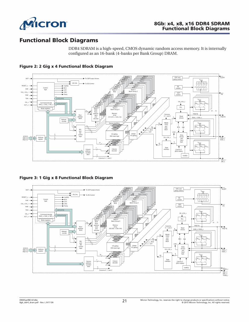
Functional Block DiagramsDDR4 SDRAM is a high-speed, CMOS dynamic random access memory. It is internallyconfigured as an 16-bank (4-banks per Bank Group) DRAM.
Figure 2: 2 Gig x 4 Functional Block Diagram
Figure 3: 1 Gig x 8 Functional Block Diagram
8Gb: x4, x8, x16 DDR4 SDRAMFunctional Block Diagrams
09005aef861d1d4a8gb_ddr4_dram.pdf - Rev. L 9/17 EN 21 Micron Technology, Inc. reserves the right to change products or specifications without notice.
© 2015 Micron Technology, Inc. All rights reserved.
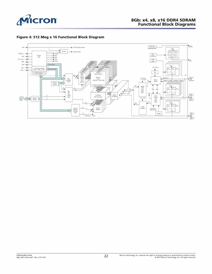
Figure 4: 512 Meg x 16 Functional Block Diagram
8Gb: x4, x8, x16 DDR4 SDRAMFunctional Block Diagrams
09005aef861d1d4a8gb_ddr4_dram.pdf - Rev. L 9/17 EN 22 Micron Technology, Inc. reserves the right to change products or specifications without notice.
© 2015 Micron Technology, Inc. All rights reserved.
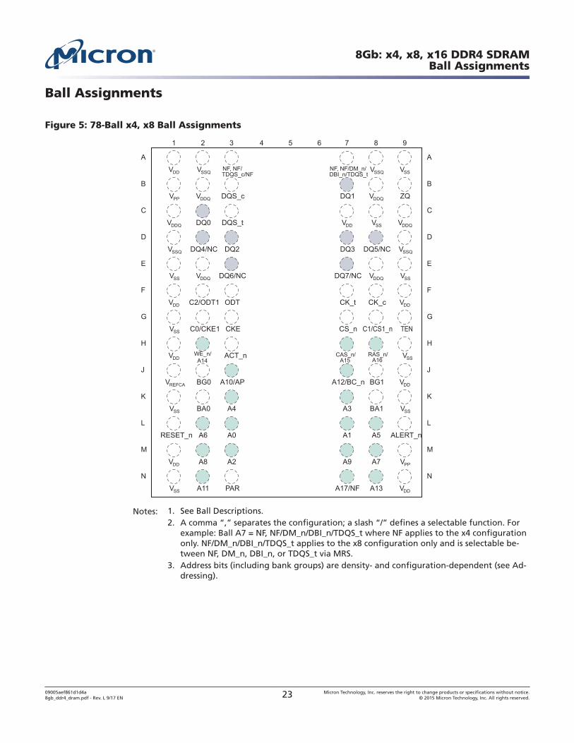
Ball Assignments
Figure 5: 78-Ball x4, x8 Ball Assignments
Notes: 1. See Ball Descriptions.2. A comma “,” separates the configuration; a slash “/” defines a selectable function. For
example: Ball A7 = NF, NF/DM_n/DBI_n/TDQS_t where NF applies to the x4 configurationonly. NF/DM_n/DBI_n/TDQS_t applies to the x8 configuration only and is selectable be-tween NF, DM_n, DBI_n, or TDQS_t via MRS.
3. Address bits (including bank groups) are density- and configuration-dependent (see Ad-dressing).
8Gb: x4, x8, x16 DDR4 SDRAMBall Assignments
09005aef861d1d4a8gb_ddr4_dram.pdf - Rev. L 9/17 EN 23 Micron Technology, Inc. reserves the right to change products or specifications without notice.
© 2015 Micron Technology, Inc. All rights reserved.
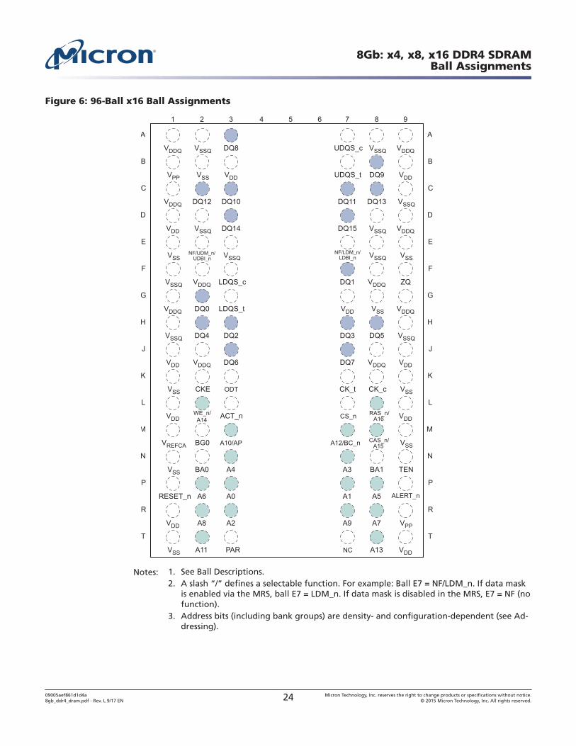
Figure 6: 96-Ball x16 Ball Assignments
Notes: 1. See Ball Descriptions.2. A slash “/” defines a selectable function. For example: Ball E7 = NF/LDM_n. If data mask
is enabled via the MRS, ball E7 = LDM_n. If data mask is disabled in the MRS, E7 = NF (nofunction).
3. Address bits (including bank groups) are density- and configuration-dependent (see Ad-dressing).
8Gb: x4, x8, x16 DDR4 SDRAMBall Assignments
09005aef861d1d4a8gb_ddr4_dram.pdf - Rev. L 9/17 EN 24 Micron Technology, Inc. reserves the right to change products or specifications without notice.
© 2015 Micron Technology, Inc. All rights reserved.
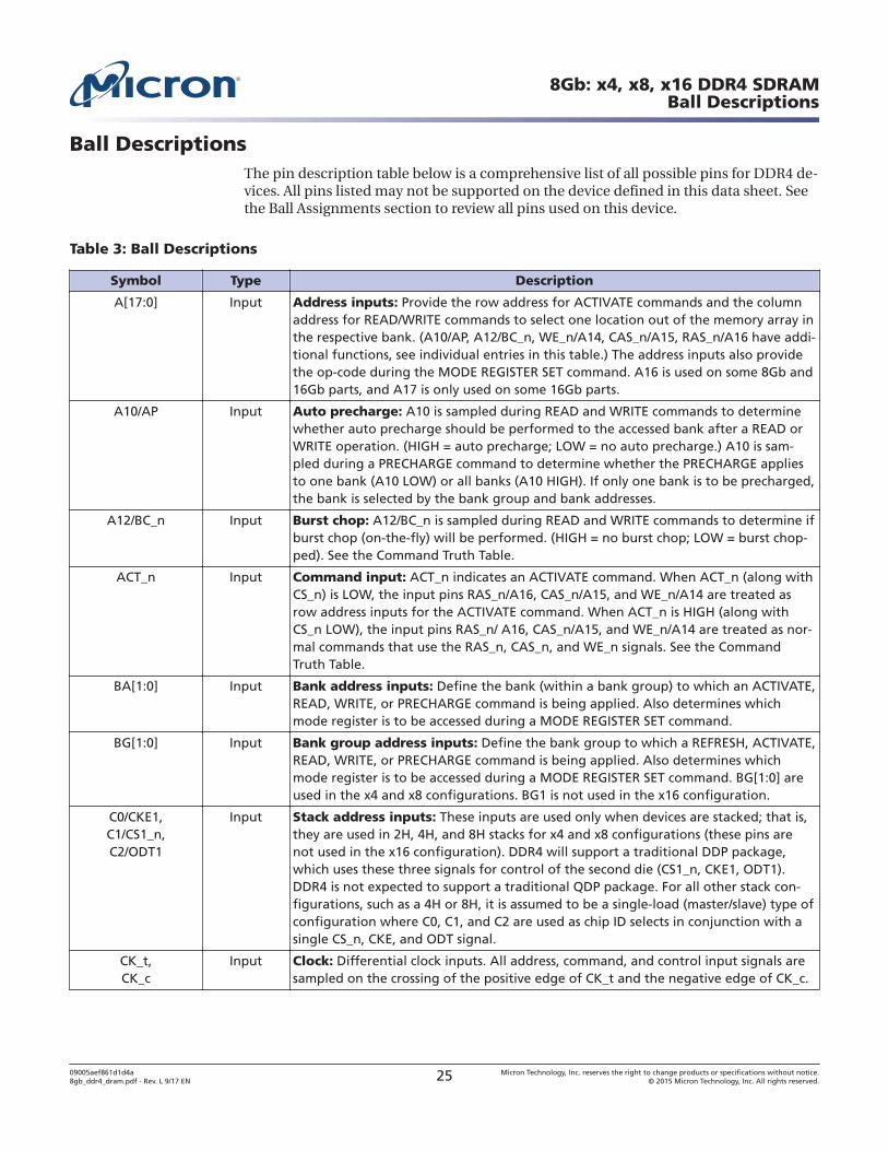
Ball DescriptionsThe pin description table below is a comprehensive list of all possible pins for DDR4 de-vices. All pins listed may not be supported on the device defined in this data sheet. Seethe Ball Assignments section to review all pins used on this device.
Table 3: Ball Descriptions
Symbol Type Description
A[17:0] Input Address inputs: Provide the row address for ACTIVATE commands and the columnaddress for READ/WRITE commands to select one location out of the memory array inthe respective bank. (A10/AP, A12/BC_n, WE_n/A14, CAS_n/A15, RAS_n/A16 have addi-tional functions, see individual entries in this table.) The address inputs also providethe op-code during the MODE REGISTER SET command. A16 is used on some 8Gb and16Gb parts, and A17 is only used on some 16Gb parts.
A10/AP Input Auto precharge: A10 is sampled during READ and WRITE commands to determinewhether auto precharge should be performed to the accessed bank after a READ orWRITE operation. (HIGH = auto precharge; LOW = no auto precharge.) A10 is sam-pled during a PRECHARGE command to determine whether the PRECHARGE appliesto one bank (A10 LOW) or all banks (A10 HIGH). If only one bank is to be precharged,the bank is selected by the bank group and bank addresses.
A12/BC_n Input Burst chop: A12/BC_n is sampled during READ and WRITE commands to determine ifburst chop (on-the-fly) will be performed. (HIGH = no burst chop; LOW = burst chop-ped). See the Command Truth Table.
ACT_n Input Command input: ACT_n indicates an ACTIVATE command. When ACT_n (along withCS_n) is LOW, the input pins RAS_n/A16, CAS_n/A15, and WE_n/A14 are treated asrow address inputs for the ACTIVATE command. When ACT_n is HIGH (along withCS_n LOW), the input pins RAS_n/ A16, CAS_n/A15, and WE_n/A14 are treated as nor-mal commands that use the RAS_n, CAS_n, and WE_n signals. See the CommandTruth Table.
BA[1:0] Input Bank address inputs: Define the bank (within a bank group) to which an ACTIVATE,READ, WRITE, or PRECHARGE command is being applied. Also determines whichmode register is to be accessed during a MODE REGISTER SET command.
BG[1:0] Input Bank group address inputs: Define the bank group to which a REFRESH, ACTIVATE,READ, WRITE, or PRECHARGE command is being applied. Also determines whichmode register is to be accessed during a MODE REGISTER SET command. BG[1:0] areused in the x4 and x8 configurations. BG1 is not used in the x16 configuration.
C0/CKE1,C1/CS1_n,C2/ODT1
Input Stack address inputs: These inputs are used only when devices are stacked; that is,they are used in 2H, 4H, and 8H stacks for x4 and x8 configurations (these pins arenot used in the x16 configuration). DDR4 will support a traditional DDP package,which uses these three signals for control of the second die (CS1_n, CKE1, ODT1).DDR4 is not expected to support a traditional QDP package. For all other stack con-figurations, such as a 4H or 8H, it is assumed to be a single-load (master/slave) type ofconfiguration where C0, C1, and C2 are used as chip ID selects in conjunction with asingle CS_n, CKE, and ODT signal.
CK_t,CK_c
Input Clock: Differential clock inputs. All address, command, and control input signals aresampled on the crossing of the positive edge of CK_t and the negative edge of CK_c.
8Gb: x4, x8, x16 DDR4 SDRAMBall Descriptions
09005aef861d1d4a8gb_ddr4_dram.pdf - Rev. L 9/17 EN 25 Micron Technology, Inc. reserves the right to change products or specifications without notice.
© 2015 Micron Technology, Inc. All rights reserved.
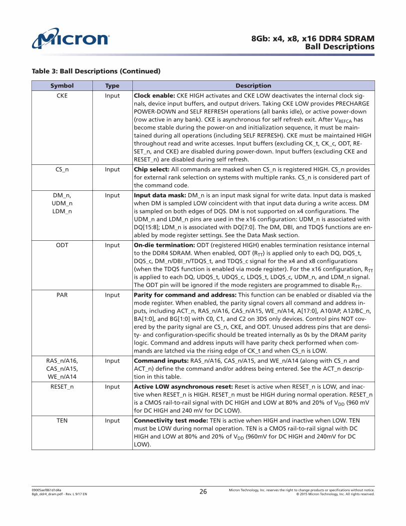
Table 3: Ball Descriptions (Continued)
Symbol Type Description
CKE Input Clock enable: CKE HIGH activates and CKE LOW deactivates the internal clock sig-nals, device input buffers, and output drivers. Taking CKE LOW provides PRECHARGEPOWER-DOWN and SELF REFRESH operations (all banks idle), or active power-down(row active in any bank). CKE is asynchronous for self refresh exit. After VREFCA hasbecome stable during the power-on and initialization sequence, it must be main-tained during all operations (including SELF REFRESH). CKE must be maintained HIGHthroughout read and write accesses. Input buffers (excluding CK_t, CK_c, ODT, RE-SET_n, and CKE) are disabled during power-down. Input buffers (excluding CKE andRESET_n) are disabled during self refresh.
CS_n Input Chip select: All commands are masked when CS_n is registered HIGH. CS_n providesfor external rank selection on systems with multiple ranks. CS_n is considered part ofthe command code.
DM_n,UDM_nLDM_n
Input Input data mask: DM_n is an input mask signal for write data. Input data is maskedwhen DM is sampled LOW coincident with that input data during a write access. DMis sampled on both edges of DQS. DM is not supported on x4 configurations. TheUDM_n and LDM_n pins are used in the x16 configuration: UDM_n is associated withDQ[15:8]; LDM_n is associated with DQ[7:0]. The DM, DBI, and TDQS functions are en-abled by mode register settings. See the Data Mask section.
ODT Input On-die termination: ODT (registered HIGH) enables termination resistance internalto the DDR4 SDRAM. When enabled, ODT (RTT) is applied only to each DQ, DQS_t,DQS_c, DM_n/DBI_n/TDQS_t, and TDQS_c signal for the x4 and x8 configurations(when the TDQS function is enabled via mode register). For the x16 configuration, RTT
is applied to each DQ, UDQS_t, UDQS_c, LDQS_t, LDQS_c, UDM_n, and LDM_n signal.The ODT pin will be ignored if the mode registers are programmed to disable RTT.
PAR Input Parity for command and address: This function can be enabled or disabled via themode register. When enabled, the parity signal covers all command and address in-puts, including ACT_n, RAS_n/A16, CAS_n/A15, WE_n/A14, A[17:0], A10/AP, A12/BC_n,BA[1:0], and BG[1:0] with C0, C1, and C2 on 3DS only devices. Control pins NOT cov-ered by the parity signal are CS_n, CKE, and ODT. Unused address pins that are densi-ty- and configuration-specific should be treated internally as 0s by the DRAM paritylogic. Command and address inputs will have parity check performed when com-mands are latched via the rising edge of CK_t and when CS_n is LOW.
RAS_n/A16,CAS_n/A15,WE_n/A14
Input Command inputs: RAS_n/A16, CAS_n/A15, and WE_n/A14 (along with CS_n andACT_n) define the command and/or address being entered. See the ACT_n descrip-tion in this table.
RESET_n Input Active LOW asynchronous reset: Reset is active when RESET_n is LOW, and inac-tive when RESET_n is HIGH. RESET_n must be HIGH during normal operation. RESET_nis a CMOS rail-to-rail signal with DC HIGH and LOW at 80% and 20% of VDD (960 mVfor DC HIGH and 240 mV for DC LOW).
TEN Input Connectivity test mode: TEN is active when HIGH and inactive when LOW. TENmust be LOW during normal operation. TEN is a CMOS rail-to-rail signal with DCHIGH and LOW at 80% and 20% of VDD (960mV for DC HIGH and 240mV for DCLOW).
8Gb: x4, x8, x16 DDR4 SDRAMBall Descriptions
09005aef861d1d4a8gb_ddr4_dram.pdf - Rev. L 9/17 EN 26 Micron Technology, Inc. reserves the right to change products or specifications without notice.
© 2015 Micron Technology, Inc. All rights reserved.
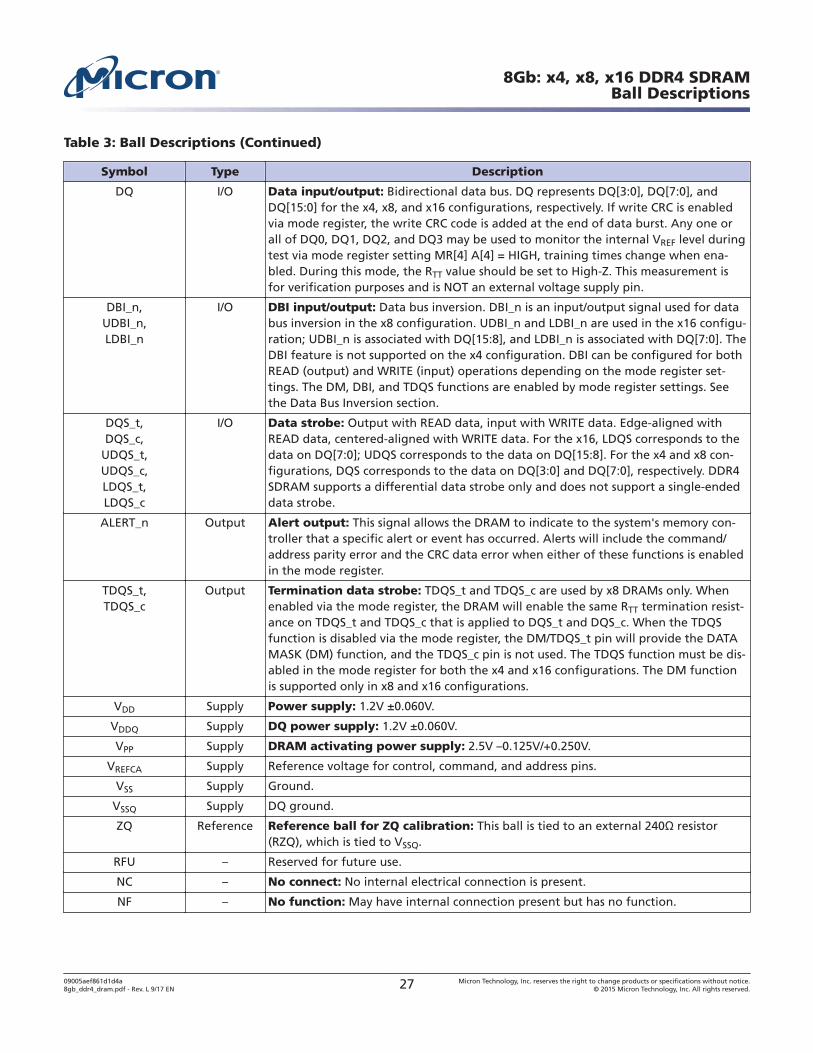
Table 3: Ball Descriptions (Continued)
Symbol Type Description
DQ I/O Data input/output: Bidirectional data bus. DQ represents DQ[3:0], DQ[7:0], andDQ[15:0] for the x4, x8, and x16 configurations, respectively. If write CRC is enabledvia mode register, the write CRC code is added at the end of data burst. Any one orall of DQ0, DQ1, DQ2, and DQ3 may be used to monitor the internal VREF level duringtest via mode register setting MR[4] A[4] = HIGH, training times change when ena-bled. During this mode, the RTT value should be set to High-Z. This measurement isfor verification purposes and is NOT an external voltage supply pin.
DBI_n,UDBI_n,LDBI_n
I/O DBI input/output: Data bus inversion. DBI_n is an input/output signal used for databus inversion in the x8 configuration. UDBI_n and LDBI_n are used in the x16 configu-ration; UDBI_n is associated with DQ[15:8], and LDBI_n is associated with DQ[7:0]. TheDBI feature is not supported on the x4 configuration. DBI can be configured for bothREAD (output) and WRITE (input) operations depending on the mode register set-tings. The DM, DBI, and TDQS functions are enabled by mode register settings. Seethe Data Bus Inversion section.
DQS_t,DQS_c,
UDQS_t,UDQS_c,LDQS_t,LDQS_c
I/O Data strobe: Output with READ data, input with WRITE data. Edge-aligned withREAD data, centered-aligned with WRITE data. For the x16, LDQS corresponds to thedata on DQ[7:0]; UDQS corresponds to the data on DQ[15:8]. For the x4 and x8 con-figurations, DQS corresponds to the data on DQ[3:0] and DQ[7:0], respectively. DDR4SDRAM supports a differential data strobe only and does not support a single-endeddata strobe.
ALERT_n Output Alert output: This signal allows the DRAM to indicate to the system's memory con-troller that a specific alert or event has occurred. Alerts will include the command/address parity error and the CRC data error when either of these functions is enabledin the mode register.
TDQS_t,TDQS_c
Output Termination data strobe: TDQS_t and TDQS_c are used by x8 DRAMs only. Whenenabled via the mode register, the DRAM will enable the same RTT termination resist-ance on TDQS_t and TDQS_c that is applied to DQS_t and DQS_c. When the TDQSfunction is disabled via the mode register, the DM/TDQS_t pin will provide the DATAMASK (DM) function, and the TDQS_c pin is not used. The TDQS function must be dis-abled in the mode register for both the x4 and x16 configurations. The DM functionis supported only in x8 and x16 configurations.
VDD Supply Power supply: 1.2V ±0.060V.
VDDQ Supply DQ power supply: 1.2V ±0.060V.
VPP Supply DRAM activating power supply: 2.5V –0.125V/+0.250V.
VREFCA Supply Reference voltage for control, command, and address pins.
VSS Supply Ground.
VSSQ Supply DQ ground.
ZQ Reference Reference ball for ZQ calibration: This ball is tied to an external 240 resistor(RZQ), which is tied to VSSQ.
RFU – Reserved for future use.
NC – No connect: No internal electrical connection is present.
NF – No function: May have internal connection present but has no function.
8Gb: x4, x8, x16 DDR4 SDRAMBall Descriptions
09005aef861d1d4a8gb_ddr4_dram.pdf - Rev. L 9/17 EN 27 Micron Technology, Inc. reserves the right to change products or specifications without notice.
© 2015 Micron Technology, Inc. All rights reserved.
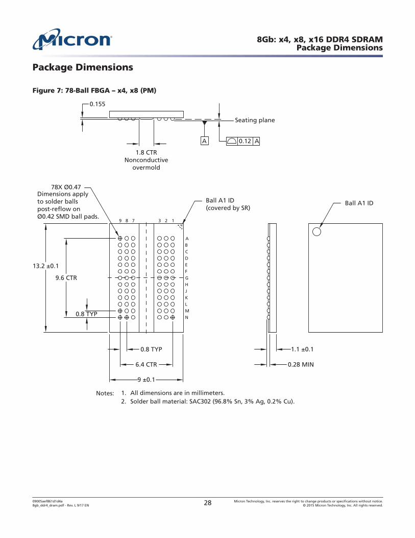
Package Dimensions
Figure 7: 78-Ball FBGA – x4, x8 (PM)
1.8 CTRNonconductive
overmold
0.155
Seating plane
0.12 A
Ball A1 ID(covered by SR)
Ball A1 ID
A
0.28 MIN
1.1 ±0.1
6.4 CTR
9 ±0.1
0.8 TYP
9.6 CTR
13.2 ±0.1
78X Ø0.47Dimensions applyto solder ballspost-reflow onØ0.42 SMD ball pads.
0.8 TYP
123789
ABCDEFGHJKLMN
Notes: 1. All dimensions are in millimeters.2. Solder ball material: SAC302 (96.8% Sn, 3% Ag, 0.2% Cu).
8Gb: x4, x8, x16 DDR4 SDRAMPackage Dimensions
09005aef861d1d4a8gb_ddr4_dram.pdf - Rev. L 9/17 EN 28 Micron Technology, Inc. reserves the right to change products or specifications without notice.
© 2015 Micron Technology, Inc. All rights reserved.
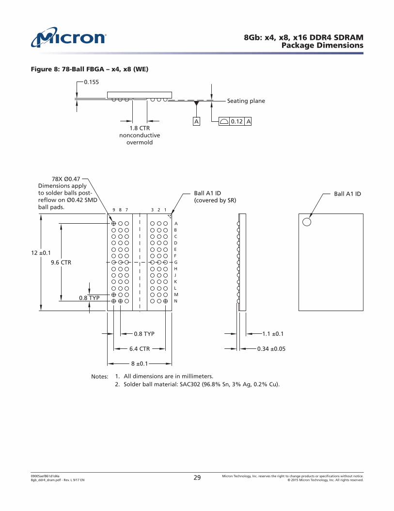
Figure 8: 78-Ball FBGA – x4, x8 (WE)
1.8 CTRnonconductive
overmold
0.155
Seating plane
0.12 A
Ball A1 ID(covered by SR)
Ball A1 ID
A
0.34 ±0.05
1.1 ±0.1
6.4 CTR
8 ±0.1
0.8 TYP
9.6 CTR
12 ±0.1
78X Ø0.47Dimensions applyto solder balls post-reflow on Ø0.42 SMDball pads.
0.8 TYP
123789
ABCDEFGHJKLMN
Notes: 1. All dimensions are in millimeters.2. Solder ball material: SAC302 (96.8% Sn, 3% Ag, 0.2% Cu).
8Gb: x4, x8, x16 DDR4 SDRAMPackage Dimensions
09005aef861d1d4a8gb_ddr4_dram.pdf - Rev. L 9/17 EN 29 Micron Technology, Inc. reserves the right to change products or specifications without notice.
© 2015 Micron Technology, Inc. All rights reserved.

Figure 9: 78-Ball FBGA – x4, x8 (SA)
1.8 CTRnonconductive
overmold
0.155
Seating plane
0.12 AA
Ball A1 ID(covered by SR)
Ball A1 ID
0.34 ±0.05
1.1 ±0.1
6.4 CTR
7.5 ±0.1
0.8 TYP
9.6 CTR
11 ±0.1
78X Ø0.47Dimensions applyto solder balls post-reflow on Ø0.42 SMDball pads.
0.8 TYP
123789
ABCDEFGHJKLMN
Notes: 1. All dimensions are in millimeters.2. Solder ball material: SAC302 (96.8% Sn, 3% Ag, 0.2% Cu).
8Gb: x4, x8, x16 DDR4 SDRAMPackage Dimensions
09005aef861d1d4a8gb_ddr4_dram.pdf - Rev. L 9/17 EN 30 Micron Technology, Inc. reserves the right to change products or specifications without notice.
© 2015 Micron Technology, Inc. All rights reserved.
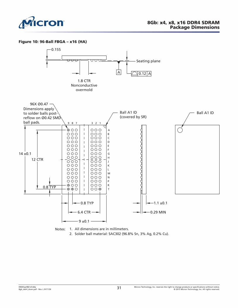
Figure 10: 96-Ball FBGA – x16 (HA)
1.8 CTRNonconductive
overmold
0.155
Seating plane
0.12 A
Ball A1 ID(covered by SR)
Ball A1 ID
A
0.29 MIN
1.1 ±0.1
6.4 CTR
9 ±0.1
0.8 TYP
12 CTR
14 ±0.1
96X Ø0.47Dimensions applyto solder balls post-reflow on Ø0.42 SMDball pads.
0.8 TYP
123789
ABCDEFGHJKLMNPRT
Notes: 1. All dimensions are in millimeters.2. Solder ball material: SAC302 (96.8% Sn, 3% Ag, 0.2% Cu).
8Gb: x4, x8, x16 DDR4 SDRAMPackage Dimensions
09005aef861d1d4a8gb_ddr4_dram.pdf - Rev. L 9/17 EN 31 Micron Technology, Inc. reserves the right to change products or specifications without notice.
© 2015 Micron Technology, Inc. All rights reserved.
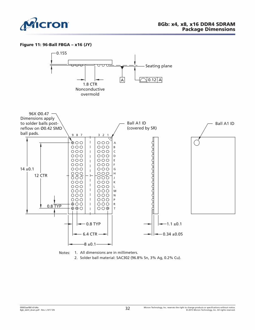
Figure 11: 96-Ball FBGA – x16 (JY)
1.8 CTRNonconductive
overmold
0.155
Seating plane
0.12 A
Ball A1 ID(covered by SR)
Ball A1 ID
0.34 ±0.05
1.1 ±0.1
6.4 CTR
8 ±0.1
0.8 TYP
12 CTR
14 ±0.1
96X Ø0.47Dimensions applyto solder balls post-reflow on Ø0.42 SMDball pads.
0.8 TYP
123789
ABCDEFGHJKLMNPRT
A
Notes: 1. All dimensions are in millimeters.2. Solder ball material: SAC302 (96.8% Sn, 3% Ag, 0.2% Cu).
8Gb: x4, x8, x16 DDR4 SDRAMPackage Dimensions
09005aef861d1d4a8gb_ddr4_dram.pdf - Rev. L 9/17 EN 32 Micron Technology, Inc. reserves the right to change products or specifications without notice.
© 2015 Micron Technology, Inc. All rights reserved.
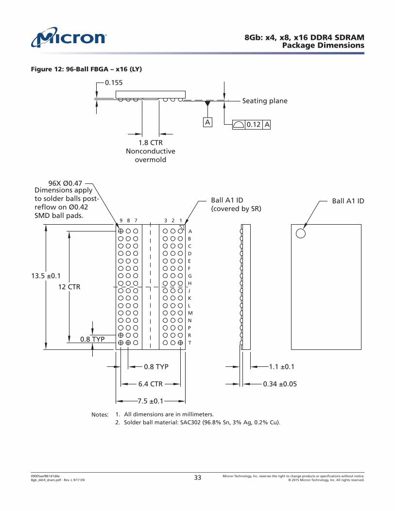
Figure 12: 96-Ball FBGA – x16 (LY)
Seating plane
0.12 A
Ball A1 ID(covered by SR)
Ball A1 ID
A
0.34 ±0.05
1.1 ±0.1
6.4 CTR
7.5 ±0.1
0.8 TYP
12 CTR
13.5 ±0.1
96X Ø0.47Dimensions applyto solder balls post-reflow on Ø0.42SMD ball pads.
0.8 TYP
1.8 CTRNonconductive
overmold
0.155
123789
ABCDEFGHJKLMNPRT
Notes: 1. All dimensions are in millimeters.2. Solder ball material: SAC302 (96.8% Sn, 3% Ag, 0.2% Cu).
8Gb: x4, x8, x16 DDR4 SDRAMPackage Dimensions
09005aef861d1d4a8gb_ddr4_dram.pdf - Rev. L 9/17 EN 33 Micron Technology, Inc. reserves the right to change products or specifications without notice.
© 2015 Micron Technology, Inc. All rights reserved.
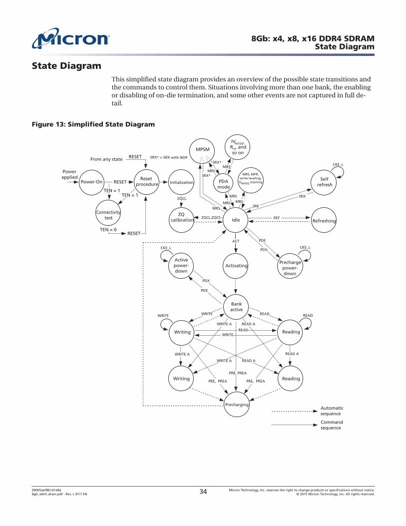
State DiagramThis simplified state diagram provides an overview of the possible state transitions andthe commands to control them. Situations involving more than one bank, the enablingor disabling of on-die termination, and some other events are not captured in full de-tail.
Figure 13: Simplified State Diagram
Bankactive
ReadingWriting
Activating
Refreshing
Selfrefresh
Idle
Activepower-down
ZQcalibration
Power
From any state
applied Reset procedurePower-On Initialization
MRS, MPR,write leveling,VREFDQ training
Prechargepower-down
Writing Reading
Automaticsequence
Commandsequence
Precharging
READ
READ READ
READ A
READ A
READ A
PRE, PREA
PRE, PREA PRE, PREA
WRITE
WRITEWRITE
WRITE A
WRITE A
WRITE A
PDE
PDE
PDX
PDX
SRX
SRE
REF
ACT
ZQCL
ZQCL,ZQCS
CKE_L
CKE_L
CKE_L
MPSM
PDAmode
IVREFDQ,RTT, andso on
Connectivitytest
RESET
RESET
RESET
TEN = 0
MRS
MRSSRX*
SRX*SRX* = SRX with NOP
MRS
MRS
MRSMRS
TEN = 1TEN = 1
8Gb: x4, x8, x16 DDR4 SDRAMState Diagram
09005aef861d1d4a8gb_ddr4_dram.pdf - Rev. L 9/17 EN 34 Micron Technology, Inc. reserves the right to change products or specifications without notice.
© 2015 Micron Technology, Inc. All rights reserved.
Table 4: State Diagram Command Definitions
Command Description
ACT Active
MPR Multipurpose register
MRS Mode register set
PDE Enter power-down
PDX Exit power-down
PRE Precharge
PREA Precharge all
READ RD, RDS4, RDS8
READ A RDA, RDAS4, RDAS8
REF Refresh, fine granularity refresh
RESET Start reset procedure
SRE Self refresh entry
SRX Self refresh exit
TEN Boundary scan mode enable
WRITE WR, WRS4, WRS8 with/without CRC
WRITE A WRA, WRAS4, WRAS8 with/without CRC
ZQCL ZQ calibration long
ZQCS ZQ calibration short
Note: 1. See the Command Truth Table for more details.
8Gb: x4, x8, x16 DDR4 SDRAMState Diagram
09005aef861d1d4a8gb_ddr4_dram.pdf - Rev. L 9/17 EN 35 Micron Technology, Inc. reserves the right to change products or specifications without notice.
© 2015 Micron Technology, Inc. All rights reserved.
Functional DescriptionThe DDR4 SDRAM is a high-speed dynamic random-access memory internally config-ured as sixteen banks (4 bank groups with 4 banks for each bank group) for x4/x8 devi-ces, and as eight banks for each bank group (2 bank groups with 4 banks each) for x16devices. The device uses double data rate (DDR) architecture to achieve high-speed op-eration. DDR4 architecture is essentially an 8n-prefetch architecture with an interfacedesigned to transfer two data words per clock cycle at the I/O pins. A single read orwrite access for a device module effectively consists of a single 8n-bit-wide, four-clock-cycle-data transfer at the internal DRAM core and eight corresponding n-bit-wide, one-half-clock-cycle data transfers at the I/O pins.
Read and write accesses to the device are burst-oriented. Accesses start at a selected lo-cation and continue for a burst length of eight or a chopped burst of four in a program-med sequence. Operation begins with the registration of an ACTIVE command, which isthen followed by a READ or WRITE command. The address bits registered coincidentwith the ACTIVE command are used to select the bank and row to be accessed (BG[1:0]select the bank group for x4/x8, and BG0 selects the bank group for x16; BA[1:0] selectthe bank, and A[17:0] select the row. See the Addressing section for more details). Theaddress bits registered coincident with the READ or WRITE command are used to selectthe starting column location for the burst operation, determine if the auto PRECHARGEcommand is to be issued (via A10), and select BC4 or BL8 mode on-the-fly (OTF) (viaA12) if enabled in the mode register.
Prior to normal operation, the device must be powered up and initialized in a prede-fined manner. The following sections provide detailed information covering device resetand initialization, register definition, command descriptions, and device operation.
NOTE: The use of the NOP command is allowed only when exiting maximum powersaving mode or when entering gear-down mode.
8Gb: x4, x8, x16 DDR4 SDRAMFunctional Description
09005aef861d1d4a8gb_ddr4_dram.pdf - Rev. L 9/17 EN 36 Micron Technology, Inc. reserves the right to change products or specifications without notice.
© 2015 Micron Technology, Inc. All rights reserved.
RESET and Initialization ProcedureTo ensure proper device function, the power-up and reset initialization default valuesfor the following mode register (MR) settings are defined as:
• Gear-down mode (MR3 A[3]): 0 = 1/2 rate• Per-DRAM addressability (MR3 A[4]): 0 = disable• Maximum power-saving mode (MR4 A[1]): 0 = disable• CS to command/address latency (MR4 A[8:6]): 000 = disable• CA parity latency mode (MR5 A[2:0]): 000 = disable• Hard post package repair mode (MR4 A[13]): 0 = disable• Soft post package repair mode (MR4 A[5]): 0 = disable
Power-Up and Initialization Sequence
The following sequence is required for power-up and initialization:
1. Apply power (RESET_n and TEN should be maintained below 0.2 × VDD while sup-plies ramp up; all other inputs may be undefined). When supplies have ramped toa valid stable level, RESET_n must be maintained below 0.2 × VDD for a minimumof tPW_RESET_L and TEN must be maintained below 0.2 × VDD for a minimum of700μs. CKE is pulled LOW anytime before RESET_n is de-asserted (minimum timeof 10ns). The power voltage ramp time between 300mV to VDD,min must be nogreater than 200ms, and during the ramp, VDD must be greater than or equal toVDDQ and (VDD - VDDQ) < 0.3V. VPP must ramp at the same time or before VDD, andVPP must be equal to or higher than VDD at all times. After VDD has ramped andreached the stable level and after RESET_n goes high, the initialization sequencemust be started within 3 seconds. For debug purposes, the 3 second delay limitmay be extended to 60 minutes provided the DRAM is operated in this debugmode for no more than 360 cumulative hours.
During power-up, the supply slew rate is governed by the limits stated in the tablebelow and either condition A or condition B listed below must be met.
Table 5: Supply Power-up Slew Rate
Symbol Min Max Unit Comment
VDD_SL, VDDQ_SL,VPP_SL
0.004 600 V/ms Measured between 300mV and 80% ofsupply minimum
VDD_ona N/A 200 ms VDD maximum ramp time from 300mV toVDD minimum
VDDQ_ona N/A 200 ms VDDQ maximum ramp time from 300mVto VDDQ minimum
Note: 1. 20 MHz band-limited measurement.
• Condition A:– Apply VPP without any slope reversal before or at the same time as VDD and
VDDQ.– VDD and VDDQ are driven from a single-power converter output and apply
VDD/VDDQ without any slope reversal before or at the same time as VTT andVREFCA.
8Gb: x4, x8, x16 DDR4 SDRAMRESET and Initialization Procedure
09005aef861d1d4a8gb_ddr4_dram.pdf - Rev. L 9/17 EN 37 Micron Technology, Inc. reserves the right to change products or specifications without notice.
© 2015 Micron Technology, Inc. All rights reserved.
– The voltage levels on all balls other than VDD, VDDQ, VSS, and VSSQ must be lessthan or equal to VDDQ and VDD on one side and must be greater than or equalto VSSQ and VSS on the other side.
– VTT is limited to 0.76V MAX when the power ramp is complete.– VREFCA tracks VDD/2.
• Condition B:– Apply VPP without any slope reversal before or at the same time as VDD.– Apply VDD without any slope reversal before or at the same time as VDDQ.– Apply VDDQ without any slope reversal before or at the same time as VTT and
VREFCA.– The voltage levels on all pins other than VPP, VDD, VDDQ, VSS, and VSSQ must be
less than or equal to VDDQ and VDD on one side and must be larger than orequal to VSSQ and VSS on the other side.
2. After RESET_n is de-asserted, wait for another 500μs but no longer then 3 secondsuntil CKE becomes active. During this time, the device will start internal state ini-tialization; this will be done independently of external clocks. A reasonable at-tempt was made in the design to power up with the following default MR settings:gear-down mode (MR3 A[3]): 0 = 1/2 rate; per-DRAM addressability (MR3 A[4]): 0= disable; maximum power-down (MR4 A[1]): 0 = disable; CS to command/address latency (MR4 A[8:6]): 000 = disable; CA parity latency mode (MR5 A[2:0]):000 = disable. However, it should be assumed that at power up the MR settings areundefined and should be programmed as shown below.
3. Clocks (CK_t, CK_c) need to be started and stabilized for at least 10ns or 5 tCK(whichever is larger) before CKE goes active. Because CKE is a synchronous signal,the corresponding setup time to clock (tIS) must be met. Also, a DESELECT com-mand must be registered (with tIS setup time to clock) at clock edge Td. After theCKE is registered HIGH after RESET, CKE needs to be continuously registeredHIGH until the initialization sequence is finished, including expiration of tDLLKand tZQinit.
4. The device keeps its ODT in High-Z state as long as RESET_n is asserted. Further,the SDRAM keeps its ODT in High-Z state after RESET_n de-assertion until CKE isregistered HIGH. The ODT input signal may be in an undefined state until tIS be-fore CKE is registered HIGH. When CKE is registered HIGH, the ODT input signalmay be statically held either LOW or HIGH. If RTT(NOM) is to be enabled in MR1,the ODT input signal must be statically held LOW. In all cases, the ODT input sig-nal remains static until the power-up initialization sequence is finished, includingthe expiration of tDLLK and tZQinit.
5. After CKE is registered HIGH, wait a minimum of RESET CKE EXIT time, tXPR, be-fore issuing the first MRS command to load mode register (tXPR = MAX (tXS, 5 ×tCK).
6. Issue MRS command to load MR3 with all application settings, wait tMRD.7. Issue MRS command to load MR6 with all application settings, wait tMRD.8. Issue MRS command to load MR5 with all application settings, wait tMRD.9. Issue MRS command to load MR4 with all application settings, wait tMRD.
10. Issue MRS command to load MR2 with all application settings, wait tMRD.11. Issue MRS command to load MR1 with all application settings, wait tMRD.12. Issue MRS command to load MR0 with all application settings, wait tMOD.13. Issue a ZQCL command to start ZQ calibration.14. Wait for tDLLK and tZQinit to complete.
8Gb: x4, x8, x16 DDR4 SDRAMRESET and Initialization Procedure
09005aef861d1d4a8gb_ddr4_dram.pdf - Rev. L 9/17 EN 38 Micron Technology, Inc. reserves the right to change products or specifications without notice.
© 2015 Micron Technology, Inc. All rights reserved.
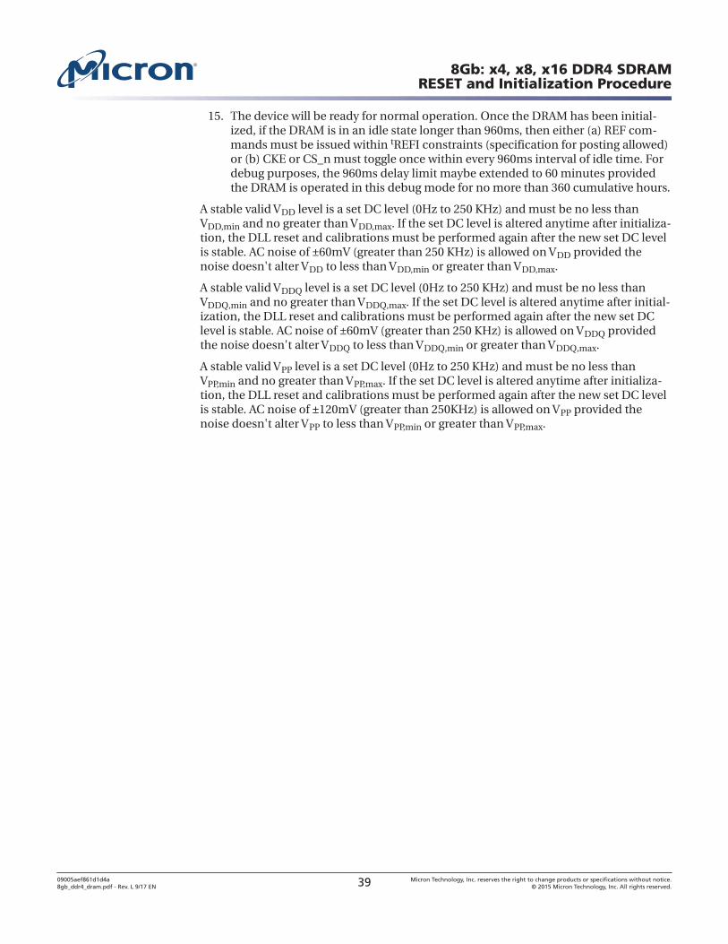
15. The device will be ready for normal operation. Once the DRAM has been initial-ized, if the DRAM is in an idle state longer than 960ms, then either (a) REF com-mands must be issued within tREFI constraints (specification for posting allowed)or (b) CKE or CS_n must toggle once within every 960ms interval of idle time. Fordebug purposes, the 960ms delay limit maybe extended to 60 minutes providedthe DRAM is operated in this debug mode for no more than 360 cumulative hours.
A stable valid VDD level is a set DC level (0Hz to 250 KHz) and must be no less thanVDD,min and no greater than VDD,max. If the set DC level is altered anytime after initializa-tion, the DLL reset and calibrations must be performed again after the new set DC levelis stable. AC noise of ±60mV (greater than 250 KHz) is allowed on VDD provided thenoise doesn't alter VDD to less than VDD,min or greater than VDD,max.
A stable valid VDDQ level is a set DC level (0Hz to 250 KHz) and must be no less thanVDDQ,min and no greater than VDDQ,max. If the set DC level is altered anytime after initial-ization, the DLL reset and calibrations must be performed again after the new set DClevel is stable. AC noise of ±60mV (greater than 250 KHz) is allowed on VDDQ providedthe noise doesn't alter VDDQ to less than VDDQ,min or greater than VDDQ,max.
A stable valid VPP level is a set DC level (0Hz to 250 KHz) and must be no less thanVPP,min and no greater than VPP,max. If the set DC level is altered anytime after initializa-tion, the DLL reset and calibrations must be performed again after the new set DC levelis stable. AC noise of ±120mV (greater than 250KHz) is allowed on VPP provided thenoise doesn't alter VPP to less than VPP,min or greater than VPP,max.
8Gb: x4, x8, x16 DDR4 SDRAMRESET and Initialization Procedure
09005aef861d1d4a8gb_ddr4_dram.pdf - Rev. L 9/17 EN 39 Micron Technology, Inc. reserves the right to change products or specifications without notice.
© 2015 Micron Technology, Inc. All rights reserved.
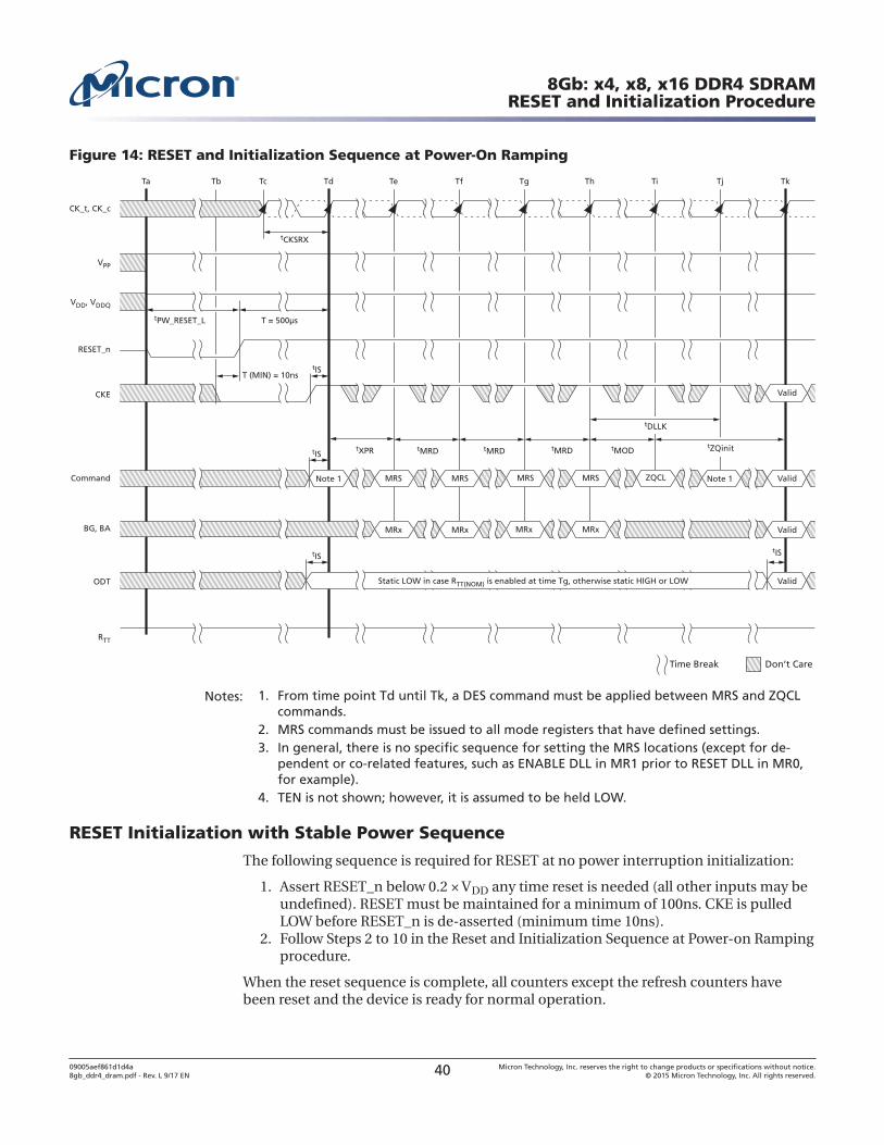
Figure 14: RESET and Initialization Sequence at Power-On Ramping
CKE
RTT
BG, BA
tPW_RESET_L
CK_t, CK_c
Command Note 1 Note 1
TdTc
Don’t CareTime Break
tIS
ODT
Th
tMRD tMOD
MRSMRS Valid
Valid
tMRD tMRD
MRS
MRxMRxMRx
MRS
MRx
Ti Tj Tk
RESET_n
T = 500μs
Valid
TeTa Tb Tf
ZQCL
tIS
Static LOW in case RTT(NOM) is enabled at time Tg, otherwise static HIGH or LOW
tIStIS
tXPR
Valid
T (MIN) = 10ns
VDD, VDDQ
VPP
tDLLK
tZQinit
tCKSRX
Tg
Notes: 1. From time point Td until Tk, a DES command must be applied between MRS and ZQCLcommands.
2. MRS commands must be issued to all mode registers that have defined settings.3. In general, there is no specific sequence for setting the MRS locations (except for de-
pendent or co-related features, such as ENABLE DLL in MR1 prior to RESET DLL in MR0,for example).
4. TEN is not shown; however, it is assumed to be held LOW.
RESET Initialization with Stable Power Sequence
The following sequence is required for RESET at no power interruption initialization:
1. Assert RESET_n below 0.2 × VDD any time reset is needed (all other inputs may beundefined). RESET must be maintained for a minimum of 100ns. CKE is pulledLOW before RESET_n is de-asserted (minimum time 10ns).
2. Follow Steps 2 to 10 in the Reset and Initialization Sequence at Power-on Rampingprocedure.
When the reset sequence is complete, all counters except the refresh counters havebeen reset and the device is ready for normal operation.
8Gb: x4, x8, x16 DDR4 SDRAMRESET and Initialization Procedure
09005aef861d1d4a8gb_ddr4_dram.pdf - Rev. L 9/17 EN 40 Micron Technology, Inc. reserves the right to change products or specifications without notice.
© 2015 Micron Technology, Inc. All rights reserved.
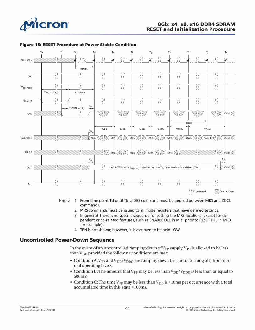
Figure 15: RESET Procedure at Power Stable Condition
CKE
RTT
BG, BA
tPW_RESET_S
CK_t, CK_c
Command Note 1 Note 1
TdTc
Don’t CareTime Break
tIS
ODT
Th
tMRD tMOD
MRSMRS Valid
Valid
tMRD tMRD
MRS
MRxMRxMRx
MRS
MRx
Ti Tj Tk
RESET_n
T = 500μs
Valid
TeTa Tb Tf
ZQCL
tIS
Static LOW in case RTT(NOM) is enabled at time Tg, otherwise static HIGH or LOW
tIStIS
tXPR
Valid
T (MIN) = 10ns
VDD, VDDQ
VPP
tDLLK
tZQinit
tCKSRX
Tg
Notes: 1. From time point Td until Tk, a DES command must be applied between MRS and ZQCLcommands.
2. MRS commands must be issued to all mode registers that have defined settings.3. In general, there is no specific sequence for setting the MRS locations (except for de-
pendent or co-related features, such as ENABLE DLL in MR1 prior to RESET DLL in MR0,for example).
4. TEN is not shown; however, it is assumed to be held LOW.
Uncontrolled Power-Down Sequence
In the event of an uncontrolled ramping down of VPP supply, VPP is allowed to be lessthan VDD provided the following conditions are met:
• Condition A: VPP and VDD/VDDQ are ramping down (as part of turning off) from nor-mal operating levels.
• Condition B: The amount that VPP may be less than VDD/VDDQ is less than or equal to500mV.
• Condition C: The time VPP may be less than VDD is 10ms per occurrence with a totalaccumulated time in this state 100ms.
8Gb: x4, x8, x16 DDR4 SDRAMRESET and Initialization Procedure
09005aef861d1d4a8gb_ddr4_dram.pdf - Rev. L 9/17 EN 41 Micron Technology, Inc. reserves the right to change products or specifications without notice.
© 2015 Micron Technology, Inc. All rights reserved.
• Condition D: The time VPP may be less than 2.0V and above VSS while turning off is15ms per occurrence with a total accumulated time in this state 150ms.
Programming Mode RegistersFor application flexibility, various functions, features, and modes are programmable inseven mode registers (MRn) provided by the device as user defined variables that mustbe programmed via a MODE REGISTER SET (MRS) command. Because the default val-ues of the mode registers are not defined, contents of mode registers must be fully ini-tialized and/or re-initialized; that is, they must be written after power-up and/or resetfor proper operation. The contents of the mode registers can be altered by re-executingthe MRS command during normal operation. When programming the mode registers,even if the user chooses to modify only a sub-set of the MRS fields, all address fieldswithin the accessed mode register must be redefined when the MRS command is is-sued. MRS and DLL RESET commands do not affect array contents, which means thesecommands can be executed any time after power-up without affecting the array con-tents.
The MRS command cycle time, tMRD, is required to complete the WRITE operation tothe mode register and is the minimum time required between the two MRS commandsshown in the tMRD Timing figure.
Some of the mode register settings affect address/command/control input functionali-ty. In these cases, the next MRS command can be allowed when the function being up-dated by the current MRS command is completed. These MRS commands don’t applytMRD timing to the next MRS command; however, the input cases have unique MR set-ting procedures, so refer to individual function descriptions:
• Gear-down mode• Per-DRAM addressability• Maximum power saving mode• CS to command/address latency• CA parity latency mode• VREFDQ training value• VREFDQ training mode• VREFDQ training range
Some mode register settings may not be supported because they are not required bycertain speed bins.
8Gb: x4, x8, x16 DDR4 SDRAMProgramming Mode Registers
09005aef861d1d4a8gb_ddr4_dram.pdf - Rev. L 9/17 EN 42 Micron Technology, Inc. reserves the right to change products or specifications without notice.
© 2015 Micron Technology, Inc. All rights reserved.
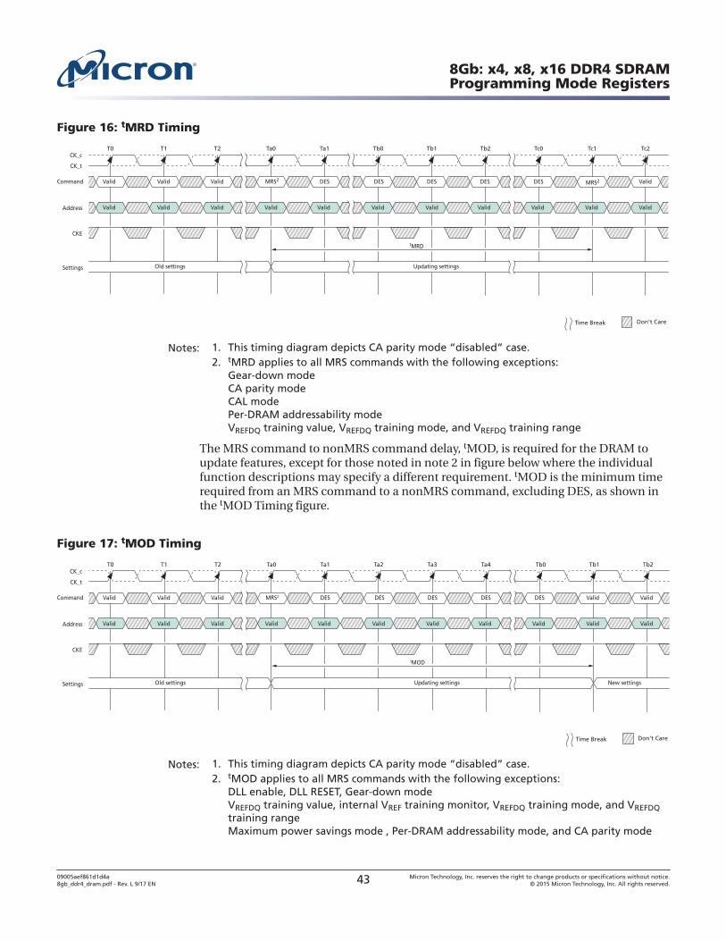
Figure 16: tMRD Timing
T0 T1 T2 Ta0 Ta1 Tb0 Tb1 Tb2 Tc0 Tc1 Tc2
Don’t Care
ValidValid Valid MRS2 MRS2DES DES DESDES DES Valid
CK_t
CK_c
Command
Settings
CKE
Updating settings
Address Valid Valid Valid Valid Valid Valid Valid Valid Valid Valid Valid
tMRD
Time Break
Old settings
Notes: 1. This timing diagram depicts CA parity mode “disabled” case.2. tMRD applies to all MRS commands with the following exceptions:
Gear-down modeCA parity modeCAL modePer-DRAM addressability modeVREFDQ training value, VREFDQ training mode, and VREFDQ training range
The MRS command to nonMRS command delay, tMOD, is required for the DRAM toupdate features, except for those noted in note 2 in figure below where the individualfunction descriptions may specify a different requirement. tMOD is the minimum timerequired from an MRS command to a nonMRS command, excluding DES, as shown inthe tMOD Timing figure.
Figure 17: tMOD Timing
T0 T1 T2 Ta0 Ta1 Ta2 Ta3 Ta4 Tb0 Tb1 Tb2
Don’t Care
ValidValid Valid MRS2 DES DES DESDES DES ValidValid
CK_t
CK_c
Command
Settings
CKE
Updating settings New settings
Address Valid Valid Valid Valid Valid Valid Valid Valid Valid Valid Valid
tMOD
Time Break
Old settings
Notes: 1. This timing diagram depicts CA parity mode “disabled” case.2. tMOD applies to all MRS commands with the following exceptions:
DLL enable, DLL RESET, Gear-down modeVREFDQ training value, internal VREF training monitor, VREFDQ training mode, and VREFDQtraining rangeMaximum power savings mode , Per-DRAM addressability mode, and CA parity mode
8Gb: x4, x8, x16 DDR4 SDRAMProgramming Mode Registers
09005aef861d1d4a8gb_ddr4_dram.pdf - Rev. L 9/17 EN 43 Micron Technology, Inc. reserves the right to change products or specifications without notice.
© 2015 Micron Technology, Inc. All rights reserved.
The mode register contents can be changed using the same command and timing re-quirements during normal operation as long as the device is in idle state; that is, allbanks are in the precharged state with tRP satisfied, all data bursts are completed, andCKE is HIGH prior to writing into the mode register. If the RTT(NOM) feature is enabled inthe mode register prior to and/or after an MRS command, the ODT signal must contin-uously be registered LOW, ensuring RTT is in an off state prior to the MRS command.The ODT signal may be registered HIGH after tMOD has expired. If the RTT(NOM) featureis disabled in the mode register prior to and after an MRS command, the ODT signalcan be registered either LOW or HIGH before, during, and after the MRS command. Themode registers are divided into various fields depending on functionality and modes.
In some mode register setting cases, function updating takes longer than tMOD. Thistype of MRS does not apply tMOD timing to the next valid command, excluding DES.These MRS command input cases have unique MR setting procedures, so refer to indi-vidual function descriptions.
8Gb: x4, x8, x16 DDR4 SDRAMProgramming Mode Registers
09005aef861d1d4a8gb_ddr4_dram.pdf - Rev. L 9/17 EN 44 Micron Technology, Inc. reserves the right to change products or specifications without notice.
© 2015 Micron Technology, Inc. All rights reserved.
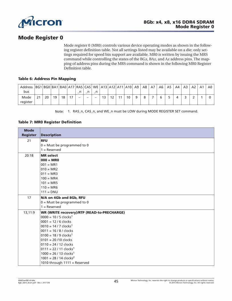
Mode Register 0Mode register 0 (MR0) controls various device operating modes as shown in the follow-ing register definition table. Not all settings listed may be available on a die; only set-tings required for speed bin support are available. MR0 is written by issuing the MRScommand while controlling the states of the BGx, BAx, and Ax address pins. The map-ping of address pins during the MRS command is shown in the following MR0 RegisterDefinition table.
Table 6: Address Pin Mapping
Addressbus
BG1 BG0 BA1 BA0 A17 RAS_n
CAS_n
WE_n
A13 A12 A11 A10 A9 A8 A7 A6 A5 A4 A3 A2 A1 A0
Moderegister
21 20 19 18 17 – – – 13 12 11 10 9 8 7 6 5 4 3 2 1 0
Note: 1. RAS_n, CAS_n, and WE_n must be LOW during MODE REGISTER SET command.
Table 7: MR0 Register Definition
ModeRegister Description
21 RFU0 = Must be programmed to 01 = Reserved
20:18 MR select000 = MR0001 = MR1010 = MR2011 = MR3100 = MR4101 = MR5110 = MR6111 = DNU
17 N/A on 4Gb and 8Gb, RFU0 = Must be programmed to 01 = Reserved
13,11:9 WR (WRITE recovery)/RTP (READ-to-PRECHARGE)0000 = 10 / 5 clocks1
0001 = 12 / 6 clocks0010 = 14 / 7 clocks1
0011 = 16 / 8 / clocks0100 = 18 / 9 clocks1
0101 = 20 /10 clocks0110 = 24 / 12 clocks0111 = 22 / 11 clocks1
1000 = 26 / 13 clocks1
1001 = 28 / 14 clocks2
1010 through 1111 = Reserved
8Gb: x4, x8, x16 DDR4 SDRAMMode Register 0
09005aef861d1d4a8gb_ddr4_dram.pdf - Rev. L 9/17 EN 45 Micron Technology, Inc. reserves the right to change products or specifications without notice.
© 2015 Micron Technology, Inc. All rights reserved.
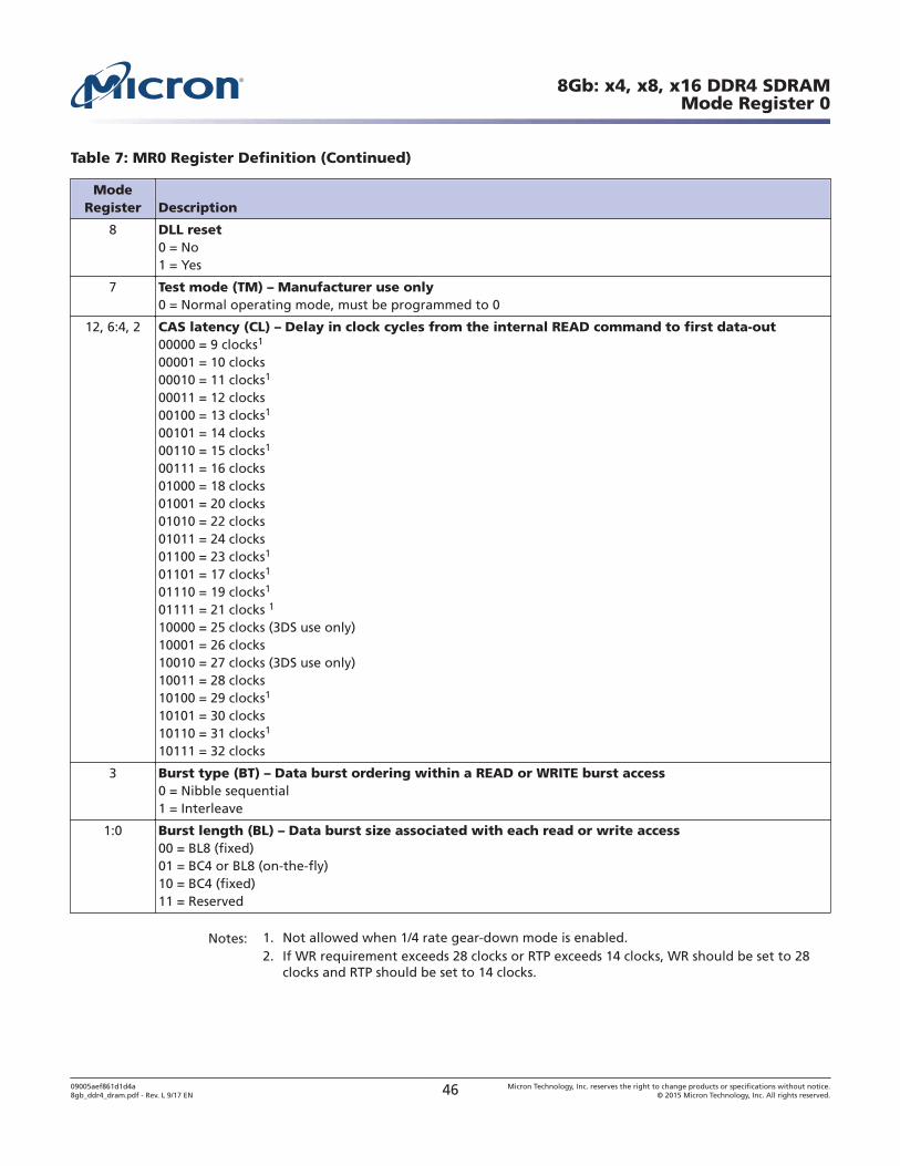
Table 7: MR0 Register Definition (Continued)
ModeRegister Description
8 DLL reset0 = No1 = Yes
7 Test mode (TM) – Manufacturer use only0 = Normal operating mode, must be programmed to 0
12, 6:4, 2 CAS latency (CL) – Delay in clock cycles from the internal READ command to first data-out00000 = 9 clocks1
00001 = 10 clocks00010 = 11 clocks1
00011 = 12 clocks00100 = 13 clocks1
00101 = 14 clocks00110 = 15 clocks1
00111 = 16 clocks01000 = 18 clocks01001 = 20 clocks01010 = 22 clocks01011 = 24 clocks01100 = 23 clocks1
01101 = 17 clocks1
01110 = 19 clocks1
01111 = 21 clocks 1
10000 = 25 clocks (3DS use only)10001 = 26 clocks10010 = 27 clocks (3DS use only)10011 = 28 clocks10100 = 29 clocks1
10101 = 30 clocks10110 = 31 clocks1
10111 = 32 clocks
3 Burst type (BT) – Data burst ordering within a READ or WRITE burst access0 = Nibble sequential1 = Interleave
1:0 Burst length (BL) – Data burst size associated with each read or write access00 = BL8 (fixed)01 = BC4 or BL8 (on-the-fly)10 = BC4 (fixed)11 = Reserved
Notes: 1. Not allowed when 1/4 rate gear-down mode is enabled.2. If WR requirement exceeds 28 clocks or RTP exceeds 14 clocks, WR should be set to 28
clocks and RTP should be set to 14 clocks.
8Gb: x4, x8, x16 DDR4 SDRAMMode Register 0
09005aef861d1d4a8gb_ddr4_dram.pdf - Rev. L 9/17 EN 46 Micron Technology, Inc. reserves the right to change products or specifications without notice.
© 2015 Micron Technology, Inc. All rights reserved.
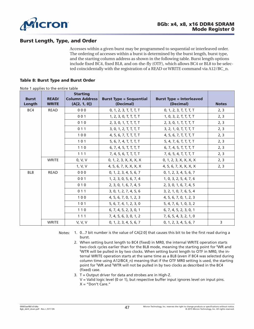
Burst Length, Type, and Order
Accesses within a given burst may be programmed to sequential or interleaved order.The ordering of accesses within a burst is determined by the burst length, burst type,and the starting column address as shown in the following table. Burst length optionsinclude fixed BC4, fixed BL8, and on-the-fly (OTF), which allows BC4 or BL8 to be selec-ted coincidentally with the registration of a READ or WRITE command via A12/BC_n.
Table 8: Burst Type and Burst Order
Note 1 applies to the entire table
BurstLength
READ/WRITE
StartingColumn Address
(A[2, 1, 0])Burst Type = Sequential
(Decimal)Burst Type = Interleaved
(Decimal) Notes
BC4 READ 0 0 0 0, 1, 2, 3, T, T, T, T 0, 1, 2, 3, T, T, T, T 2, 3
0 0 1 1, 2, 3, 0, T, T, T, T 1, 0, 3, 2, T, T, T, T 2, 3
0 1 0 2, 3, 0, 1, T, T, T, T 2, 3, 0, 1, T, T, T, T 2, 3
0 1 1 3, 0, 1, 2, T, T, T, T 3, 2, 1, 0, T, T, T, T 2, 3
1 0 0 4, 5, 6, 7, T, T, T, T 4, 5, 6, 7, T, T, T, T 2, 3
1 0 1 5, 6, 7, 4, T, T, T, T 5, 4, 7, 6, T, T, T, T 2, 3
1 1 0 6, 7, 4, 5, T, T, T, T 6, 7, 4, 5, T, T, T, T 2, 3
1 1 1 7, 4, 5, 6, T, T, T, T 7, 6, 5, 4, T, T, T, T 2, 3
WRITE 0, V, V 0, 1, 2, 3, X, X, X, X 0, 1, 2, 3, X, X, X, X 2, 3
1, V, V 4, 5, 6, 7, X, X, X, X 4, 5, 6, 7, X, X, X, X 2, 3
BL8 READ 0 0 0 0, 1, 2, 3, 4, 5, 6, 7 0, 1, 2, 3, 4, 5, 6, 7
0 0 1 1, 2, 3, 0, 5, 6, 7, 4 1, 0, 3, 2, 5, 4, 7, 6
0 1 0 2, 3, 0, 1, 6, 7, 4, 5 2, 3, 0, 1, 6, 7, 4, 5
0 1 1 3, 0, 1, 2, 7, 4, 5, 6 3, 2, 1, 0, 7, 6, 5, 4
1 0 0 4, 5, 6, 7, 0, 1, 2, 3 4, 5, 6, 7, 0, 1, 2, 3
1 0 1 5, 6, 7, 4, 1, 2, 3, 0 5, 4, 7, 6, 1, 0, 3, 2
1 1 0 6, 7, 4, 5, 2, 3, 0, 1 6, 7, 4, 5, 2, 3, 0, 1
1 1 1 7, 4, 5, 6, 3, 0, 1, 2 7, 6, 5, 4, 3, 2, 1, 0
WRITE V, V, V 0, 1, 2, 3, 4, 5, 6, 7 0, 1, 2, 3, 4, 5, 6, 7 3
Notes: 1. 0...7 bit number is the value of CA[2:0] that causes this bit to be the first read during aburst.
2. When setting burst length to BC4 (fixed) in MR0, the internal WRITE operation startstwo clock cycles earlier than for the BL8 mode, meaning the starting point for tWR andtWTR will be pulled in by two clocks. When setting burst length to OTF in MR0, the in-ternal WRITE operation starts at the same time as a BL8 (even if BC4 was selected duringcolumn time using A12/BC4_n) meaning that if the OTF MR0 setting is used, the startingpoint for tWR and tWTR will not be pulled in by two clocks as described in the BC4(fixed) case.
3. T = Output driver for data and strobes are in High-Z.V = Valid logic level (0 or 1), but respective buffer input ignores level on input pins.X = “Don’t Care.”
8Gb: x4, x8, x16 DDR4 SDRAMMode Register 0
09005aef861d1d4a8gb_ddr4_dram.pdf - Rev. L 9/17 EN 47 Micron Technology, Inc. reserves the right to change products or specifications without notice.
© 2015 Micron Technology, Inc. All rights reserved.
CAS Latency
The CAS latency (CL) setting is defined in the MR0 Register Definition table. CAS laten-cy is the delay, in clock cycles, between the internal READ command and the availabilityof the first bit of output data. The device does not support half-clock latencies. Theoverall read latency (RL) is defined as additive latency (AL) + CAS latency (CL): RL = AL +CL.
Test Mode
The normal operating mode is selected by MR0[7] and all other bits set to the desiredvalues shown in the MR0 Register Definition table. Programming MR0[7] to a value of 1places the device into a DRAM manufacturer-defined test mode to be used only by themanufacturer, not by the end user. No operations or functionality is specified if MR0[7]= 1.
Write Recovery(WR)/READ-to-PRECHARGE
The programmed write recovery (WR) value is used for the auto precharge feature alongwith tRP to determine tDAL. WR for auto precharge (MIN) in clock cycles is calculatedby dividing tWR (in ns) by tCK (in ns) and rounding up to the next integer: WR (MIN)cycles = roundup (tWR[ns]/tCK[ns]). The WR value must be programmed to be equal toor larger than tWR (MIN). When both DM and write CRC are enabled in the mode regis-ter, the device calculates CRC before sending the write data into the array; tWR valueswill change when enabled. If there is a CRC error, the device blocks the WRITE opera-tion and discards the data.
Internal READ-to-PRECHARGE (RTP) command delay for auto precharge (MIN) inclock cycles is calculated by dividing tRTP (in ns) by tCK (in ns) and rounding up to thenext integer: RTP (MIN) cycles = roundup (tRTP[ns]/tCK[ns]). The RTP value in themode register must be programmed to be equal to or larger than RTP (MIN). The pro-grammed RTP value is used with tRP to determine the ACT timing to the same bank.
DLL RESET
The DLL reset bit is self-clearing, meaning that it returns to the value of 0 after the DLLRESET function has been issued. After the DLL is enabled, a subsequent DLL RESETshould be applied. Any time the DLL RESET function is used, tDLLK must be met beforefunctions requiring the DLL can be used, such as READ commands or synchronousODT operations, for example,).
8Gb: x4, x8, x16 DDR4 SDRAMMode Register 0
09005aef861d1d4a8gb_ddr4_dram.pdf - Rev. L 9/17 EN 48 Micron Technology, Inc. reserves the right to change products or specifications without notice.
© 2015 Micron Technology, Inc. All rights reserved.
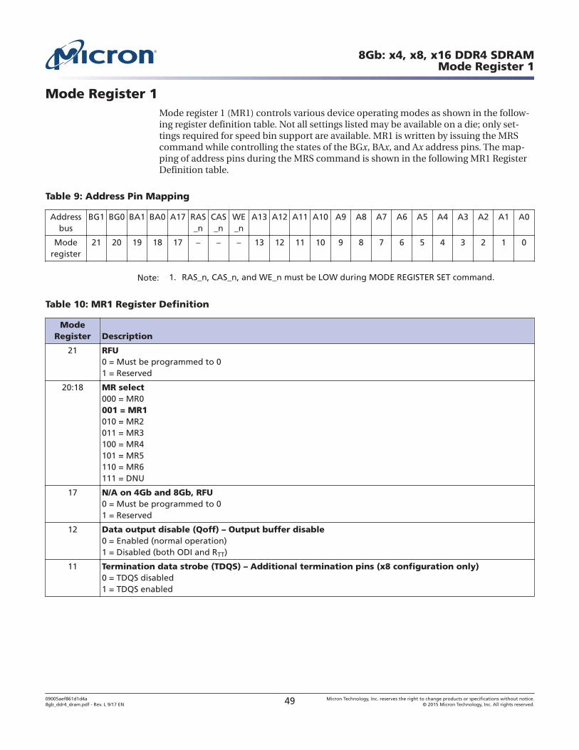
Mode Register 1Mode register 1 (MR1) controls various device operating modes as shown in the follow-ing register definition table. Not all settings listed may be available on a die; only set-tings required for speed bin support are available. MR1 is written by issuing the MRScommand while controlling the states of the BGx, BAx, and Ax address pins. The map-ping of address pins during the MRS command is shown in the following MR1 RegisterDefinition table.
Table 9: Address Pin Mapping
Addressbus
BG1 BG0 BA1 BA0 A17 RAS_n
CAS_n
WE_n
A13 A12 A11 A10 A9 A8 A7 A6 A5 A4 A3 A2 A1 A0
Moderegister
21 20 19 18 17 – – – 13 12 11 10 9 8 7 6 5 4 3 2 1 0
Note: 1. RAS_n, CAS_n, and WE_n must be LOW during MODE REGISTER SET command.
Table 10: MR1 Register Definition
ModeRegister Description
21 RFU0 = Must be programmed to 01 = Reserved
20:18 MR select000 = MR0001 = MR1010 = MR2011 = MR3100 = MR4101 = MR5110 = MR6111 = DNU
17 N/A on 4Gb and 8Gb, RFU0 = Must be programmed to 01 = Reserved
12 Data output disable (Qoff) – Output buffer disable0 = Enabled (normal operation)1 = Disabled (both ODI and RTT)
11 Termination data strobe (TDQS) – Additional termination pins (x8 configuration only)0 = TDQS disabled1 = TDQS enabled
8Gb: x4, x8, x16 DDR4 SDRAMMode Register 1
09005aef861d1d4a8gb_ddr4_dram.pdf - Rev. L 9/17 EN 49 Micron Technology, Inc. reserves the right to change products or specifications without notice.
© 2015 Micron Technology, Inc. All rights reserved.
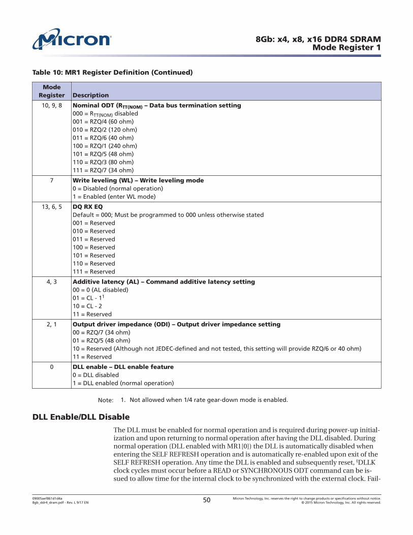
Table 10: MR1 Register Definition (Continued)
ModeRegister Description
10, 9, 8 Nominal ODT (RTT(NOM) – Data bus termination setting000 = RTT(NOM) disabled001 = RZQ/4 (60 ohm)010 = RZQ/2 (120 ohm)011 = RZQ/6 (40 ohm)100 = RZQ/1 (240 ohm)101 = RZQ/5 (48 ohm)110 = RZQ/3 (80 ohm)111 = RZQ/7 (34 ohm)
7 Write leveling (WL) – Write leveling mode0 = Disabled (normal operation)1 = Enabled (enter WL mode)
13, 6, 5 DQ RX EQDefault = 000; Must be programmed to 000 unless otherwise stated001 = Reserved010 = Reserved011 = Reserved100 = Reserved101 = Reserved110 = Reserved111 = Reserved
4, 3 Additive latency (AL) – Command additive latency setting00 = 0 (AL disabled)01 = CL - 11
10 = CL - 211 = Reserved
2, 1 Output driver impedance (ODI) – Output driver impedance setting00 = RZQ/7 (34 ohm)01 = RZQ/5 (48 ohm)10 = Reserved (Although not JEDEC-defined and not tested, this setting will provide RZQ/6 or 40 ohm)11 = Reserved
0 DLL enable – DLL enable feature0 = DLL disabled1 = DLL enabled (normal operation)
Note: 1. Not allowed when 1/4 rate gear-down mode is enabled.
DLL Enable/DLL Disable
The DLL must be enabled for normal operation and is required during power-up initial-ization and upon returning to normal operation after having the DLL disabled. Duringnormal operation (DLL enabled with MR1[0]) the DLL is automatically disabled whenentering the SELF REFRESH operation and is automatically re-enabled upon exit of theSELF REFRESH operation. Any time the DLL is enabled and subsequently reset, tDLLKclock cycles must occur before a READ or SYNCHRONOUS ODT command can be is-sued to allow time for the internal clock to be synchronized with the external clock. Fail-
8Gb: x4, x8, x16 DDR4 SDRAMMode Register 1
09005aef861d1d4a8gb_ddr4_dram.pdf - Rev. L 9/17 EN 50 Micron Technology, Inc. reserves the right to change products or specifications without notice.
© 2015 Micron Technology, Inc. All rights reserved.
ing to wait for synchronization to occur may result in a violation of the tDQSCK, tAON,or tAOF parameters.
During tDLLK, CKE must continuously be registered HIGH. The device does not requireDLL for any WRITE operation, except when RTT(WR) is enabled and the DLL is requiredfor proper ODT operation.
The direct ODT feature is not supported during DLL off mode. The ODT resistors mustbe disabled by continuously registering the ODT pin LOW and/or by programming theRTT(NOM) bits MR1[9,6,2] = 000 via an MRS command during DLL off mode.
The dynamic ODT feature is not supported in DLL off mode; to disable dynamic ODTexternally, use the MRS command to set RTT(WR), MR2[10:9] = 00.
Output Driver Impedance Control
The output driver impedance of the device is selected by MR1[2,1], as shown in the MR1Register Definition table.
ODT RTT(NOM) Values
The device is capable of providing three different termination values: RTT(Park), RTT(NOM),and RTT(WR). The nominal termination value, RTT(NOM), is programmed in MR1. A sepa-rate value, RTT(WR), may be programmed in MR2 to enable a unique RTT value whenODT is enabled during WRITE operations. The RTT(WR) value can be applied duringWRITE commands even when RTT(NOM) is disabled. A third RTT value, RTT(Park), is pro-gramed in MR5. RTT(Park) provides a termination value when the ODT signal is LOW.
Additive Latency
The ADDITIVE LATENCY (AL) operation is supported to make command and databuses efficient for sustainable bandwidths in the device. In this operation, the device al-lows a READ or WRITE command (either with or without auto precharge) to be issuedimmediately after the ACTIVATE command. The command is held for the time of AL be-fore it is issued inside the device. READ latency (RL) is controlled by the sum of the ALand CAS latency (CL) register settings. WRITE latency (WL) is controlled by the sum ofthe AL and CAS WRITE latency (CWL) register settings.
Table 11: Additive Latency (AL) Settings
A4 A3 AL
0 0 0 (AL disabled)
0 1 CL - 1
1 0 CL - 2
1 1 Reserved
Note: 1. AL has a value of CL - 1 or CL - 2 based on the CL values programmed in the MR0 regis-ter.
DQ RX EQ
These settings are reserved for DQ Equalization functionality.
8Gb: x4, x8, x16 DDR4 SDRAMMode Register 1
09005aef861d1d4a8gb_ddr4_dram.pdf - Rev. L 9/17 EN 51 Micron Technology, Inc. reserves the right to change products or specifications without notice.
© 2015 Micron Technology, Inc. All rights reserved.
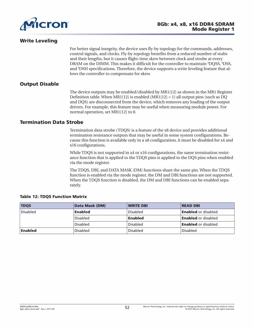
Write Leveling
For better signal integrity, the device uses fly-by topology for the commands, addresses,control signals, and clocks. Fly-by topology benefits from a reduced number of stubsand their lengths, but it causes flight-time skew between clock and strobe at everyDRAM on the DIMM. This makes it difficult for the controller to maintain tDQSS, tDSS,and tDSH specifications. Therefore, the device supports a write leveling feature that al-lows the controller to compensate for skew.
Output Disable
The device outputs may be enabled/disabled by MR1[12] as shown in the MR1 RegisterDefinition table. When MR1[12] is enabled (MR1[12] = 1) all output pins (such as DQand DQS) are disconnected from the device, which removes any loading of the outputdrivers. For example, this feature may be useful when measuring module power. Fornormal operation, set MR1[12] to 0.
Termination Data Strobe
Termination data strobe (TDQS) is a feature of the x8 device and provides additionaltermination resistance outputs that may be useful in some system configurations. Be-cause this function is available only in a x8 configuration, it must be disabled for x4 andx16 configurations.
While TDQS is not supported in x4 or x16 configurations, the same termination resist-ance function that is applied to the TDQS pins is applied to the DQS pins when enabledvia the mode register.
The TDQS, DBI, and DATA MASK (DM) functions share the same pin. When the TDQSfunction is enabled via the mode register, the DM and DBI functions are not supported.When the TDQS function is disabled, the DM and DBI functions can be enabled sepa-rately.
Table 12: TDQS Function Matrix
TDQS Data Mask (DM) WRITE DBI READ DBI
Disabled Enabled Disabled Enabled or disabled
Disabled Enabled Enabled or disabled
Disabled Disabled Enabled or disabled
Enabled Disabled Disabled Disabled
8Gb: x4, x8, x16 DDR4 SDRAMMode Register 1
09005aef861d1d4a8gb_ddr4_dram.pdf - Rev. L 9/17 EN 52 Micron Technology, Inc. reserves the right to change products or specifications without notice.
© 2015 Micron Technology, Inc. All rights reserved.
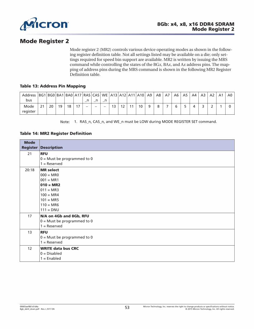
Mode Register 2Mode register 2 (MR2) controls various device operating modes as shown in the follow-ing register definition table. Not all settings listed may be available on a die; only set-tings required for speed bin support are available. MR2 is written by issuing the MRScommand while controlling the states of the BGx, BAx, and Ax address pins. The map-ping of address pins during the MRS command is shown in the following MR2 RegisterDefinition table.
Table 13: Address Pin Mapping
Addressbus
BG1 BG0 BA1 BA0 A17 RAS_n
CAS_n
WE_n
A13 A12 A11 A10 A9 A8 A7 A6 A5 A4 A3 A2 A1 A0
Moderegister
21 20 19 18 17 – – – 13 12 11 10 9 8 7 6 5 4 3 2 1 0
Note: 1. RAS_n, CAS_n, and WE_n must be LOW during MODE REGISTER SET command.
Table 14: MR2 Register Definition
ModeRegister Description
21 RFU0 = Must be programmed to 01 = Reserved
20:18 MR select000 = MR0001 = MR1010 = MR2011 = MR3100 = MR4101 = MR5110 = MR6111 = DNU
17 N/A on 4Gb and 8Gb, RFU0 = Must be programmed to 01 = Reserved
13 RFU0 = Must be programmed to 01 = Reserved
12 WRITE data bus CRC0 = Disabled1 = Enabled
8Gb: x4, x8, x16 DDR4 SDRAMMode Register 2
09005aef861d1d4a8gb_ddr4_dram.pdf - Rev. L 9/17 EN 53 Micron Technology, Inc. reserves the right to change products or specifications without notice.
© 2015 Micron Technology, Inc. All rights reserved.
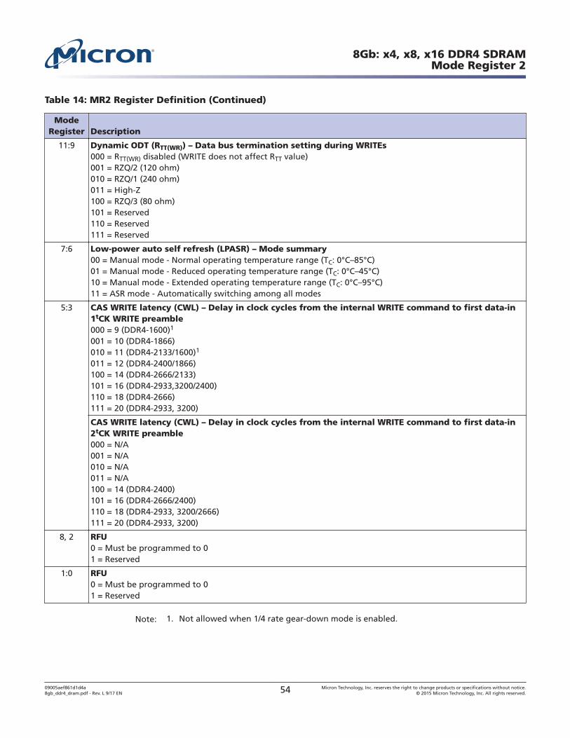
Table 14: MR2 Register Definition (Continued)
ModeRegister Description
11:9 Dynamic ODT (RTT(WR)) – Data bus termination setting during WRITEs000 = RTT(WR) disabled (WRITE does not affect RTT value)001 = RZQ/2 (120 ohm)010 = RZQ/1 (240 ohm)011 = High-Z100 = RZQ/3 (80 ohm)101 = Reserved110 = Reserved111 = Reserved
7:6 Low-power auto self refresh (LPASR) – Mode summary00 = Manual mode - Normal operating temperature range (TC: 0°C–85°C)01 = Manual mode - Reduced operating temperature range (TC: 0°C–45°C)10 = Manual mode - Extended operating temperature range (TC: 0°C–95°C)11 = ASR mode - Automatically switching among all modes
5:3 CAS WRITE latency (CWL) – Delay in clock cycles from the internal WRITE command to first data-in1tCK WRITE preamble000 = 9 (DDR4-1600)1
001 = 10 (DDR4-1866)010 = 11 (DDR4-2133/1600)1
011 = 12 (DDR4-2400/1866)100 = 14 (DDR4-2666/2133)101 = 16 (DDR4-2933,3200/2400)110 = 18 (DDR4-2666)111 = 20 (DDR4-2933, 3200)
CAS WRITE latency (CWL) – Delay in clock cycles from the internal WRITE command to first data-in2tCK WRITE preamble000 = N/A001 = N/A010 = N/A011 = N/A100 = 14 (DDR4-2400)101 = 16 (DDR4-2666/2400)110 = 18 (DDR4-2933, 3200/2666)111 = 20 (DDR4-2933, 3200)
8, 2 RFU0 = Must be programmed to 01 = Reserved
1:0 RFU0 = Must be programmed to 01 = Reserved
Note: 1. Not allowed when 1/4 rate gear-down mode is enabled.
8Gb: x4, x8, x16 DDR4 SDRAMMode Register 2
09005aef861d1d4a8gb_ddr4_dram.pdf - Rev. L 9/17 EN 54 Micron Technology, Inc. reserves the right to change products or specifications without notice.
© 2015 Micron Technology, Inc. All rights reserved.
CAS WRITE Latency
CAS WRITE latency (CWL) is defined by MR2[5:3] as shown in the MR2 Register Defini-tion table. CWL is the delay, in clock cycles, between the internal WRITE command andthe availability of the first bit of input data. The device does not support any half-clocklatencies. The overall WRITE latency (WL) is defined as additive latency (AL) + parity la-tency (PL) + CAS WRITE latency (CWL): WL = AL +PL + CWL.
Low-Power Auto Self Refresh
Low-power auto self refresh (LPASR) is supported in the device. Applications requiringSELF REFRESH operation over different temperature ranges can use this feature to opti-mize the IDD6 current for a given temperature range as specified in the MR2 RegisterDefinition table.
Dynamic ODT
In certain applications and to further enhance signal integrity on the data bus, it is de-sirable to change the termination strength of the device without issuing an MRS com-mand. This may be done by configuring the dynamic ODT (RTT(WR)) settings inMR2[11:9]. In write leveling mode, only RTT(NOM) is available.
Write Cyclic Redundancy Check Data Bus
The write cyclic redundancy check (CRC) data bus feature during writes has been addedto the device. When enabled via the mode register, the data transfer size goes from thenormal 8-bit (BL8) frame to a larger 10-bit UI frame, and the extra two UIs are used forthe CRC information.
8Gb: x4, x8, x16 DDR4 SDRAMMode Register 2
09005aef861d1d4a8gb_ddr4_dram.pdf - Rev. L 9/17 EN 55 Micron Technology, Inc. reserves the right to change products or specifications without notice.
© 2015 Micron Technology, Inc. All rights reserved.
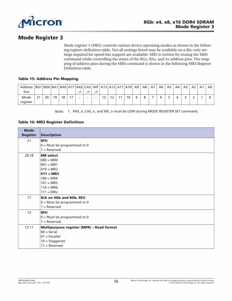
Mode Register 3Mode register 3 (MR3) controls various device operating modes as shown in the follow-ing register definition table. Not all settings listed may be available on a die; only set-tings required for speed bin support are available. MR3 is written by issuing the MRScommand while controlling the states of the BGx, BAx, and Ax address pins. The map-ping of address pins during the MRS command is shown in the following MR3 RegisterDefinition table.
Table 15: Address Pin Mapping
Addressbus
BG1 BG0 BA1 BA0 A17 RAS_n
CAS_n
WE_n
A13 A12 A11 A10 A9 A8 A7 A6 A5 A4 A3 A2 A1 A0
Moderegister
21 20 19 18 17 – – – 13 12 11 10 9 8 7 6 5 4 3 2 1 0
Note: 1. RAS_n, CAS_n, and WE_n must be LOW during MODE REGISTER SET command.
Table 16: MR3 Register Definition
ModeRegister Description
21 RFU0 = Must be programmed to 01 = Reserved
20:18 MR select000 = MR0001 = MR1010 = MR2011 = MR3100 = MR4101 = MR5110 = MR6111 = DNU
17 N/A on 4Gb and 8Gb, RFU0 = Must be programmed to 01 = Reserved
13 RFU0 = Must be programmed to 01 = Reserved
12:11 Multipurpose register (MPR) – Read format00 = Serial01 = Parallel10 = Staggered11 = Reserved
8Gb: x4, x8, x16 DDR4 SDRAMMode Register 3
09005aef861d1d4a8gb_ddr4_dram.pdf - Rev. L 9/17 EN 56 Micron Technology, Inc. reserves the right to change products or specifications without notice.
© 2015 Micron Technology, Inc. All rights reserved.
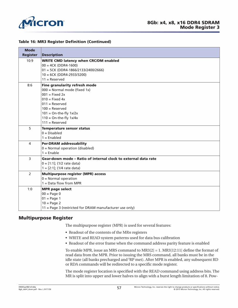
Table 16: MR3 Register Definition (Continued)
ModeRegister Description
10:9 WRITE CMD latency when CRC/DM enabled00 = 4CK (DDR4-1600)01 = 5CK (DDR4-1866/2133/2400/2666)10 = 6CK (DDR4-2933/3200)11 = Reserved
8:6 Fine granularity refresh mode000 = Normal mode (fixed 1x)001 = Fixed 2x010 = Fixed 4x011 = Reserved100 = Reserved101 = On-the-fly 1x/2x110 = On-the-fly 1x/4x111 = Reserved
5 Temperature sensor status0 = Disabled1 = Enabled
4 Per-DRAM addressability0 = Normal operation (disabled)1 = Enable
3 Gear-down mode – Ratio of internal clock to external data rate0 = [1:1]; (1/2 rate data)1 = [2:1]; (1/4 rate data)
2 Multipurpose register (MPR) access0 = Normal operation1 = Data flow from MPR
1:0 MPR page select00 = Page 001 = Page 110 = Page 211 = Page 3 (restricted for DRAM manufacturer use only)
Multipurpose Register
The multipurpose register (MPR) is used for several features:
• Readout of the contents of the MRn registers• WRITE and READ system patterns used for data bus calibration• Readout of the error frame when the command address parity feature is enabled
To enable MPR, issue an MRS command to MR3[2] = 1. MR3[12:11] define the format ofread data from the MPR. Prior to issuing the MRS command, all banks must be in theidle state (all banks precharged and tRP met). After MPR is enabled, any subsequent RDor RDA commands will be redirected to a specific mode register.
The mode register location is specified with the READ command using address bits. TheMR is split into upper and lower halves to align with a burst length limitation of 8. Pow-
8Gb: x4, x8, x16 DDR4 SDRAMMode Register 3
09005aef861d1d4a8gb_ddr4_dram.pdf - Rev. L 9/17 EN 57 Micron Technology, Inc. reserves the right to change products or specifications without notice.
© 2015 Micron Technology, Inc. All rights reserved.
er-down mode, SELF REFRESH, and any other nonRD/RDA or nonWR/WRA com-mands are not allowed during MPR mode. The RESET function is supported duringMPR mode, which requires device re-initialization.
WRITE Command Latency When CRC/DM is Enabled
The WRITE command latency (WCL) must be set when both write CRC and DM are en-abled for write CRC persistent mode. This provides the extra time required when com-pleting a WRITE burst when write CRC and DM are enabled. This means at data ratesless than or equal to 1600 MT/s then 4nCK is used, 5nCK or 6nCK are not allowed; atdata rates greater than 1600 MT/s and less than or equal to 2666 MT/s then 5nCK isused, 4nCK or 6nCK are not allowed; and at data rates greater than 2666 MT/s and lessthan or equal to 3200 MT/s then 6nCK is used; 4nCK or 5nCK are not allowed.
Fine Granularity Refresh Mode
This mode had been added to DDR4 to help combat the performance penalty due torefresh lockout at high densities. Shortening tRFC and increasing cycle time allows moreaccesses to the chip and can produce higher bandwidth.
Temperature Sensor Status
This mode directs the DRAM to update the temperature sensor status at MPR Page 2,MPR0 [4,3]. The temperature sensor setting should be updated within 32ms; when anMPR read of the temperature sensor status bits occurs, the temperature sensor statusshould be no older than 32ms.
Per-DRAM Addressability
This mode allows commands to be masked on a per device basis providing any devicein a rank (devices sharing the same command and address signals) to be programmedindividually. As an example, this feature can be used to program different ODT or VREFvalues on DRAM devices within a given rank.
Gear-Down Mode
The device defaults in 1/2 rate (1N) clock mode and uses a low frequency MRS com-mand followed by a sync pulse to align the proper clock edge for operating the controllines CS_n, CKE, and ODT when in 1/4 rate (2N) mode. For operation in 1/2 rate mode,no MRS command or sync pulse is required.
8Gb: x4, x8, x16 DDR4 SDRAMMode Register 3
09005aef861d1d4a8gb_ddr4_dram.pdf - Rev. L 9/17 EN 58 Micron Technology, Inc. reserves the right to change products or specifications without notice.
© 2015 Micron Technology, Inc. All rights reserved.
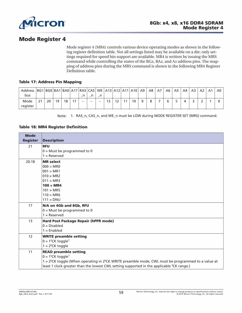
Mode Register 4Mode register 4 (MR4) controls various device operating modes as shown in the follow-ing register definition table. Not all settings listed may be available on a die; only set-tings required for speed bin support are available. MR4 is written by issuing the MRScommand while controlling the states of the BGx, BAx, and Ax address pins. The map-ping of address pins during the MRS command is shown in the following MR4 RegisterDefinition table.
Table 17: Address Pin Mapping
Addressbus
BG1 BG0 BA1 BA0 A17 RAS_n
CAS_n
WE_n
A13 A12 A11 A10 A9 A8 A7 A6 A5 A4 A3 A2 A1 A0
Moderegister
21 20 19 18 17 – – – 13 12 11 10 9 8 7 6 5 4 3 2 1 0
Note: 1. RAS_n, CAS_n, and WE_n must be LOW during MODE REGISTER SET (MRS) command.
Table 18: MR4 Register Definition
ModeRegister Description
21 RFU0 = Must be programmed to 01 = Reserved
20:18 MR select000 = MR0001 = MR1010 = MR2011 = MR3100 = MR4101 = MR5110 = MR6111 = DNU
17 N/A on 4Gb and 8Gb, RFU0 = Must be programmed to 01 = Reserved
13 Hard Post Package Repair (hPPR mode)0 = Disabled1 = Enabled
12 WRITE preamble setting0 = 1tCK toggle1
1 = 2tCK toggle
11 READ preamble setting0 = 1tCK toggle1
1 = 2tCK toggle (When operating in 2tCK WRITE preamble mode, CWL must be programmed to a value atleast 1 clock greater than the lowest CWL setting supported in the applicable tCK range.)
8Gb: x4, x8, x16 DDR4 SDRAMMode Register 4
09005aef861d1d4a8gb_ddr4_dram.pdf - Rev. L 9/17 EN 59 Micron Technology, Inc. reserves the right to change products or specifications without notice.
© 2015 Micron Technology, Inc. All rights reserved.
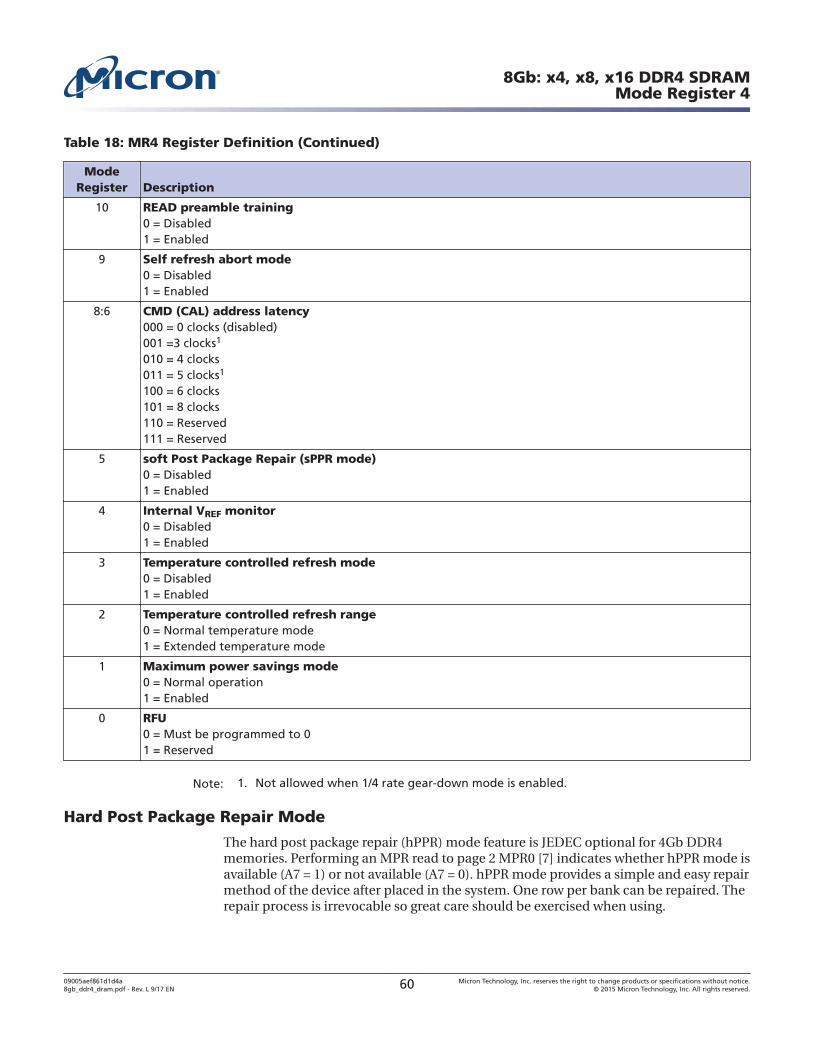
Table 18: MR4 Register Definition (Continued)
ModeRegister Description
10 READ preamble training0 = Disabled1 = Enabled
9 Self refresh abort mode0 = Disabled1 = Enabled
8:6 CMD (CAL) address latency000 = 0 clocks (disabled)001 =3 clocks1
010 = 4 clocks011 = 5 clocks1
100 = 6 clocks101 = 8 clocks110 = Reserved111 = Reserved
5 soft Post Package Repair (sPPR mode)0 = Disabled1 = Enabled
4 Internal VREF monitor0 = Disabled1 = Enabled
3 Temperature controlled refresh mode0 = Disabled1 = Enabled
2 Temperature controlled refresh range0 = Normal temperature mode1 = Extended temperature mode
1 Maximum power savings mode0 = Normal operation1 = Enabled
0 RFU0 = Must be programmed to 01 = Reserved
Note: 1. Not allowed when 1/4 rate gear-down mode is enabled.
Hard Post Package Repair Mode
The hard post package repair (hPPR) mode feature is JEDEC optional for 4Gb DDR4memories. Performing an MPR read to page 2 MPR0 [7] indicates whether hPPR mode isavailable (A7 = 1) or not available (A7 = 0). hPPR mode provides a simple and easy repairmethod of the device after placed in the system. One row per bank can be repaired. Therepair process is irrevocable so great care should be exercised when using.
8Gb: x4, x8, x16 DDR4 SDRAMMode Register 4
09005aef861d1d4a8gb_ddr4_dram.pdf - Rev. L 9/17 EN 60 Micron Technology, Inc. reserves the right to change products or specifications without notice.
© 2015 Micron Technology, Inc. All rights reserved.
Soft Post Package Repair Mode
The soft post package repair (sPPR) mode feature is JEDEC optional for 4Gb and 8GbDDR4 memories. Performing an MPR read to page 2 MPR0 [6] indicates whether sPPRmode is available (A6 = 1) or not available (A6 = 0). sPPR mode provides a simple andeasy repair method of the device after placed in the system. One row per bank can berepaired. The repair process is revocable by either doing a reset or power-down or byrewriting a new address in the same bank.
WRITE Preamble
Programmable WRITE preamble, tWPRE, can be set to 1tCK or 2tCK via the MR4 register.The 1tCK setting is similar to DDR3. However, when operating in 2tCK WRITE preamblemode, CWL must be programmed to a value at least 1 clock greater than the lowest CWLsetting supported in the applicable tCK range.
When operating in 2tCK WRITE preamble mode, CWL must be programmed to a valueat least 1 clock greater than the lowest CWL setting supported in the applicable tCKrange. Some even settings will require addition of 2 clocks. If the alternate longer CWLwas used, the additional clocks will not be required.
READ Preamble
Programmable READ preamble tRPRE can be set to 1tCK or 2tCK via the MR4 register.Both the 1tCK and 2tCK DDR4 preamble settings are different from that defined for theDDR3 SDRAM. Both DDR4 READ preamble settings may require the memory controllerto train (or read level) its data strobe receivers using the READ preamble training.
READ Preamble Training
Programmable READ preamble training can be set to 1tCK or 2tCK. This mode can beused by the memory controller to train or READ level its data strobe receivers.
Temperature-Controlled Refresh
When temperature-controlled refresh mode is enabled, the device may adjust the inter-nal refresh period to be longer than tREFI of the normal temperature range by skippingexternal REFRESH commands with the proper gear ratio. For example, the DRAM tem-perature sensor detected less than 45°C. Normal temperature mode covers the range of0°C to 85°C, while the extended temperature range covers 0°C to 95°C.
Command Address Latency
COMMAND ADDRESS LATENCY (CAL) is a power savings feature and can be enabledor disabled via the MRS setting. CAL is defined as the delay in clock cycles (tCAL) be-tween a CS_n registered LOW and its corresponding registered command and address.The value of CAL (in clocks) must be programmed into the mode register and is basedon the roundup (in clocks) of [tCK(ns)/tCAL(ns)].
Internal VREF Monitor
The device generates its own internal VREFDQ. This mode may be enabled during VREFDQtraining, and when enabled, VREF,time-short and VREF,time-long need to be increased by 10ns
8Gb: x4, x8, x16 DDR4 SDRAMMode Register 4
09005aef861d1d4a8gb_ddr4_dram.pdf - Rev. L 9/17 EN 61 Micron Technology, Inc. reserves the right to change products or specifications without notice.
© 2015 Micron Technology, Inc. All rights reserved.
if DQ0, DQ1, DQ2, or DQ3 have 0pF loading. An additional 15ns per pF of loading is alsoneeded.
Maximum Power Savings Mode
This mode provides the lowest power mode where data retention is not required. Whenthe device is in the maximum power saving mode, it does not need to guarantee dataretention or respond to any external command (except the MAXIMUM POWER SAVINGMODE EXIT command and during the assertion of RESET_n signal LOW).
8Gb: x4, x8, x16 DDR4 SDRAMMode Register 4
09005aef861d1d4a8gb_ddr4_dram.pdf - Rev. L 9/17 EN 62 Micron Technology, Inc. reserves the right to change products or specifications without notice.
© 2015 Micron Technology, Inc. All rights reserved.
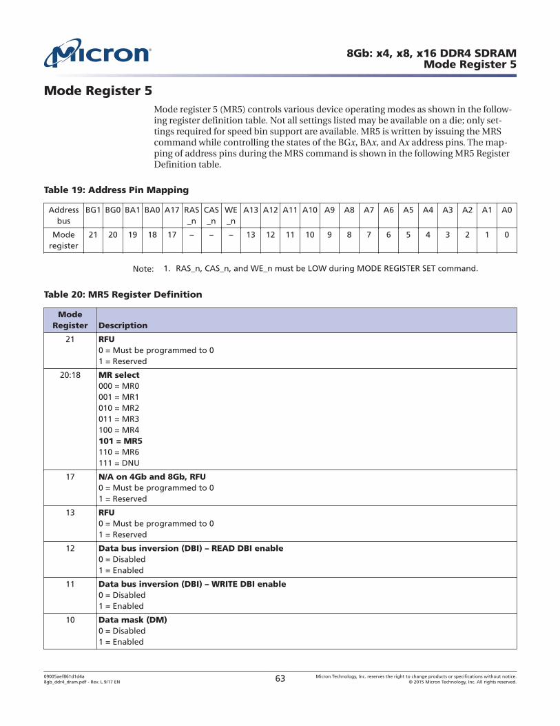
Mode Register 5Mode register 5 (MR5) controls various device operating modes as shown in the follow-ing register definition table. Not all settings listed may be available on a die; only set-tings required for speed bin support are available. MR5 is written by issuing the MRScommand while controlling the states of the BGx, BAx, and Ax address pins. The map-ping of address pins during the MRS command is shown in the following MR5 RegisterDefinition table.
Table 19: Address Pin Mapping
Addressbus
BG1 BG0 BA1 BA0 A17 RAS_n
CAS_n
WE_n
A13 A12 A11 A10 A9 A8 A7 A6 A5 A4 A3 A2 A1 A0
Moderegister
21 20 19 18 17 – – – 13 12 11 10 9 8 7 6 5 4 3 2 1 0
Note: 1. RAS_n, CAS_n, and WE_n must be LOW during MODE REGISTER SET command.
Table 20: MR5 Register Definition
ModeRegister Description
21 RFU0 = Must be programmed to 01 = Reserved
20:18 MR select000 = MR0001 = MR1010 = MR2011 = MR3100 = MR4101 = MR5110 = MR6111 = DNU
17 N/A on 4Gb and 8Gb, RFU0 = Must be programmed to 01 = Reserved
13 RFU0 = Must be programmed to 01 = Reserved
12 Data bus inversion (DBI) – READ DBI enable0 = Disabled1 = Enabled
11 Data bus inversion (DBI) – WRITE DBI enable0 = Disabled1 = Enabled
10 Data mask (DM)0 = Disabled1 = Enabled
8Gb: x4, x8, x16 DDR4 SDRAMMode Register 5
09005aef861d1d4a8gb_ddr4_dram.pdf - Rev. L 9/17 EN 63 Micron Technology, Inc. reserves the right to change products or specifications without notice.
© 2015 Micron Technology, Inc. All rights reserved.
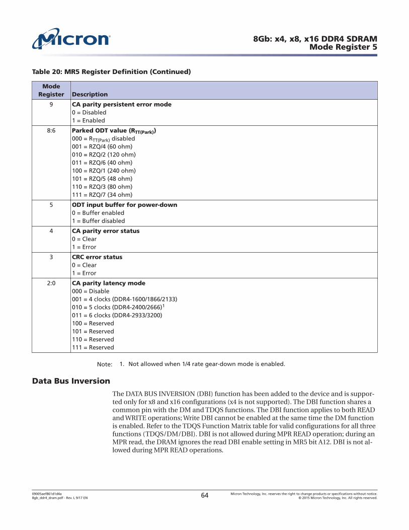
Table 20: MR5 Register Definition (Continued)
ModeRegister Description
9 CA parity persistent error mode0 = Disabled1 = Enabled
8:6 Parked ODT value (RTT(Park))000 = RTT(Park) disabled001 = RZQ/4 (60 ohm)010 = RZQ/2 (120 ohm)011 = RZQ/6 (40 ohm)100 = RZQ/1 (240 ohm)101 = RZQ/5 (48 ohm)110 = RZQ/3 (80 ohm)111 = RZQ/7 (34 ohm)
5 ODT input buffer for power-down0 = Buffer enabled1 = Buffer disabled
4 CA parity error status0 = Clear1 = Error
3 CRC error status0 = Clear1 = Error
2:0 CA parity latency mode000 = Disable001 = 4 clocks (DDR4-1600/1866/2133)010 = 5 clocks (DDR4-2400/2666)1
011 = 6 clocks (DDR4-2933/3200)100 = Reserved101 = Reserved110 = Reserved111 = Reserved
Note: 1. Not allowed when 1/4 rate gear-down mode is enabled.
Data Bus Inversion
The DATA BUS INVERSION (DBI) function has been added to the device and is suppor-ted only for x8 and x16 configurations (x4 is not supported). The DBI function shares acommon pin with the DM and TDQS functions. The DBI function applies to both READand WRITE operations; Write DBI cannot be enabled at the same time the DM functionis enabled. Refer to the TDQS Function Matrix table for valid configurations for all threefunctions (TDQS/DM/DBI). DBI is not allowed during MPR READ operation; during anMPR read, the DRAM ignores the read DBI enable setting in MR5 bit A12. DBI is not al-lowed during MPR READ operations.
8Gb: x4, x8, x16 DDR4 SDRAMMode Register 5
09005aef861d1d4a8gb_ddr4_dram.pdf - Rev. L 9/17 EN 64 Micron Technology, Inc. reserves the right to change products or specifications without notice.
© 2015 Micron Technology, Inc. All rights reserved.
Data Mask
The DATA MASK (DM) function, also described as a partial write, has been added to thedevice and is supported only for x8 and x16 configurations (x4 is not supported). TheDM function shares a common pin with the DBI and TDQS functions. The DM functionapplies only to WRITE operations and cannot be enabled at the same time the write DBIfunction is enabled. Refer to the TDQS Function Matrix table for valid configurations forall three functions (TDQS/DM/DBI).
CA Parity Persistent Error Mode
Normal CA parity mode (CA parity persistent mode disabled) no longer performs CAparity checking while the parity error status bit remains set at 1. However, with CA pari-ty persistent mode enabled, CA parity checking continues to be performed when theparity error status bit is set to a 1.
ODT Input Buffer for Power-Down
This feature determines whether the ODT input buffer is on or off during power-down.If the input buffer is configured to be on (enabled during power-down), the ODT inputsignal must be at a valid logic level. If the input buffer is configured to be off (disabledduring power-down), the ODT input signal may be floating and the device does not pro-vide RTT(NOM) termination. However, the device may provide RTT(Park) termination de-pending on the MR settings. This is primarily for additional power savings.
CA Parity Error Status
The device will set the error status bit to 1 upon detecting a parity error. The parity errorstatus bit remains set at 1 until the device controller clears it explicitly using an MRScommand.
CRC Error Status
The device will set the error status bit to 1 upon detecting a CRC error. The CRC errorstatus bit remains set at 1 until the device controller clears it explicitly using an MRScommand.
CA Parity Latency Mode
CA parity is enabled when a latency value, dependent on tCK, is programmed; this ac-counts for parity calculation delay internal to the device. The normal state of CA parityis to be disabled. If CA parity is enabled, the device must ensure there are no parity er-rors before executing the command. CA parity signal (PAR) covers ACT_n, RAS_n/A16 ,CAS_n/A15, WE_n/A14, and the address bus including bank address and bank groupbits. The control signals CKE, ODT, and CS_n are not included in the parity calculation.
8Gb: x4, x8, x16 DDR4 SDRAMMode Register 5
09005aef861d1d4a8gb_ddr4_dram.pdf - Rev. L 9/17 EN 65 Micron Technology, Inc. reserves the right to change products or specifications without notice.
© 2015 Micron Technology, Inc. All rights reserved.
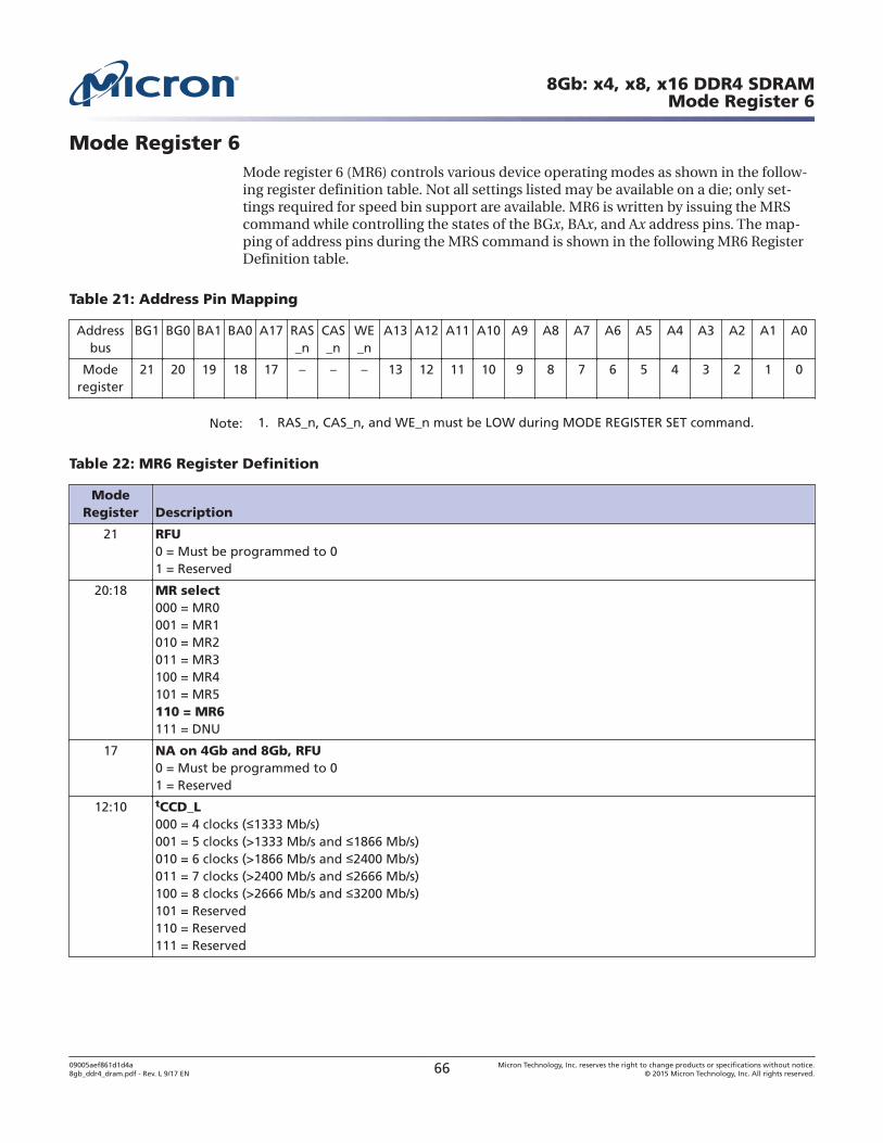
Mode Register 6Mode register 6 (MR6) controls various device operating modes as shown in the follow-ing register definition table. Not all settings listed may be available on a die; only set-tings required for speed bin support are available. MR6 is written by issuing the MRScommand while controlling the states of the BGx, BAx, and Ax address pins. The map-ping of address pins during the MRS command is shown in the following MR6 RegisterDefinition table.
Table 21: Address Pin Mapping
Addressbus
BG1 BG0 BA1 BA0 A17 RAS_n
CAS_n
WE_n
A13 A12 A11 A10 A9 A8 A7 A6 A5 A4 A3 A2 A1 A0
Moderegister
21 20 19 18 17 – – – 13 12 11 10 9 8 7 6 5 4 3 2 1 0
Note: 1. RAS_n, CAS_n, and WE_n must be LOW during MODE REGISTER SET command.
Table 22: MR6 Register Definition
ModeRegister Description
21 RFU0 = Must be programmed to 01 = Reserved
20:18 MR select000 = MR0001 = MR1010 = MR2011 = MR3100 = MR4101 = MR5110 = MR6111 = DNU
17 NA on 4Gb and 8Gb, RFU0 = Must be programmed to 01 = Reserved
12:10 tCCD_L000 = 4 clocks ( 1333 Mb/s)001 = 5 clocks (>1333 Mb/s and 1866 Mb/s)010 = 6 clocks (>1866 Mb/s and 2400 Mb/s)011 = 7 clocks (>2400 Mb/s and 2666 Mb/s)100 = 8 clocks (>2666 Mb/s and 3200 Mb/s)101 = Reserved110 = Reserved111 = Reserved
8Gb: x4, x8, x16 DDR4 SDRAMMode Register 6
09005aef861d1d4a8gb_ddr4_dram.pdf - Rev. L 9/17 EN 66 Micron Technology, Inc. reserves the right to change products or specifications without notice.
© 2015 Micron Technology, Inc. All rights reserved.
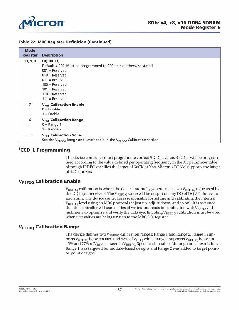
Table 22: MR6 Register Definition (Continued)
ModeRegister Description
13, 9, 8 DQ RX EQDefault = 000; Must be programmed to 000 unless otherwise stated001 = Reserved010 = Reserved011 = Reserved100 = Reserved101 = Reserved110 = Reserved111 = Reserved
7 VREF Calibration Enable0 = Disable1 = Enable
6 VREF Calibration Range0 = Range 11 = Range 2
5:0 VREF Calibration ValueSee the VREFDQ Range and Levels table in the VREFDQ Calibration section
tCCD_L Programming
The device controller must program the correct tCCD_L value. tCCD_L will be program-med according to the value defined per operating frequency in the AC parameter table.Although JEDEC specifies the larger of 5nCK or Xns, Micron's DRAM supports the largerof 4nCK or Xns.
VREFDQ Calibration Enable
VREFDQ calibration is where the device internally generates its own VREFDQ to be used bythe DQ input receivers. The VREFDQ value will be output on any DQ of DQ[3:0] for evalu-ation only. The device controller is responsible for setting and calibrating the internalVREFDQ level using an MRS protocol (adjust up, adjust down, and so on). It is assumedthat the controller will use a series of writes and reads in conduction with VREFDQ ad-justments to optimize and verify the data eye. Enabling VREFDQ calibration must be usedwhenever values are being written to the MR6[6:0] register.
VREFDQ Calibration Range
The device defines two VREFDQ calibration ranges: Range 1 and Range 2. Range 1 sup-ports VREFDQ between 60% and 92% of VDDQ while Range 2 supports VREFDQ between45% and 77% of VDDQ, as seen in VREFDQ Specification table. Although not a restriction,Range 1 was targeted for module-based designs and Range 2 was added to target point-to-point designs.
8Gb: x4, x8, x16 DDR4 SDRAMMode Register 6
09005aef861d1d4a8gb_ddr4_dram.pdf - Rev. L 9/17 EN 67 Micron Technology, Inc. reserves the right to change products or specifications without notice.
© 2015 Micron Technology, Inc. All rights reserved.
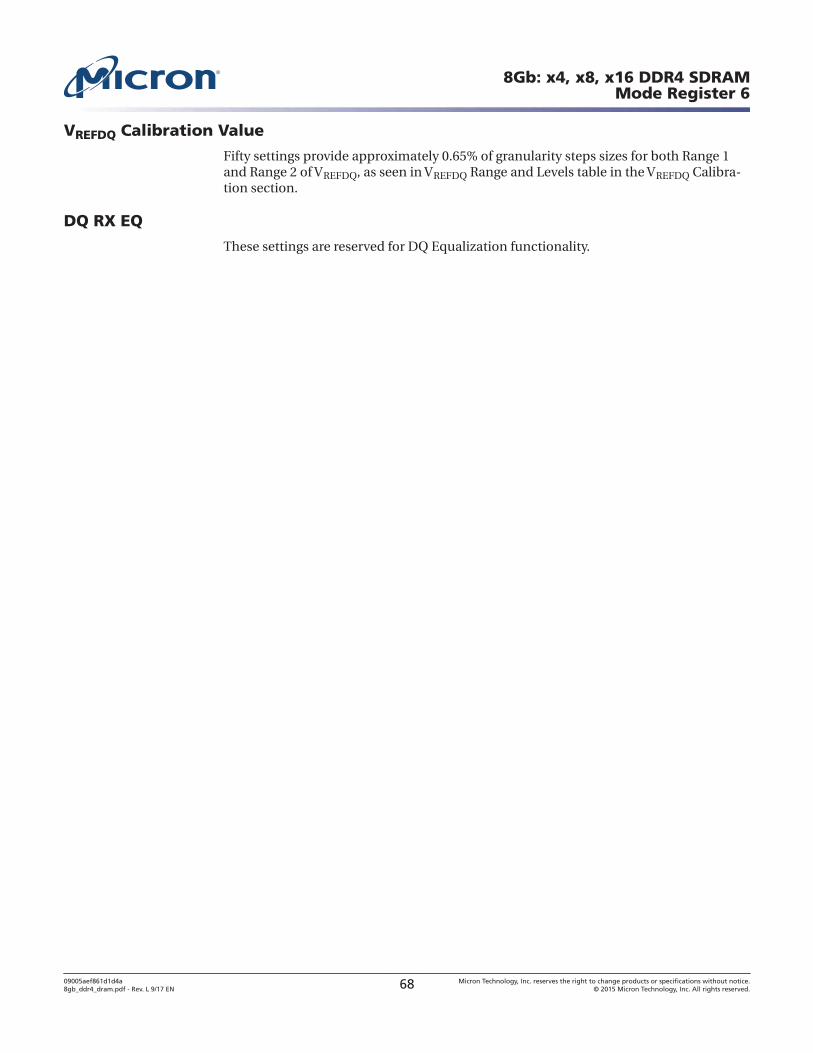
VREFDQ Calibration Value
Fifty settings provide approximately 0.65% of granularity steps sizes for both Range 1and Range 2 of VREFDQ, as seen in VREFDQ Range and Levels table in the VREFDQ Calibra-tion section.
DQ RX EQ
These settings are reserved for DQ Equalization functionality.
8Gb: x4, x8, x16 DDR4 SDRAMMode Register 6
09005aef861d1d4a8gb_ddr4_dram.pdf - Rev. L 9/17 EN 68 Micron Technology, Inc. reserves the right to change products or specifications without notice.
© 2015 Micron Technology, Inc. All rights reserved.
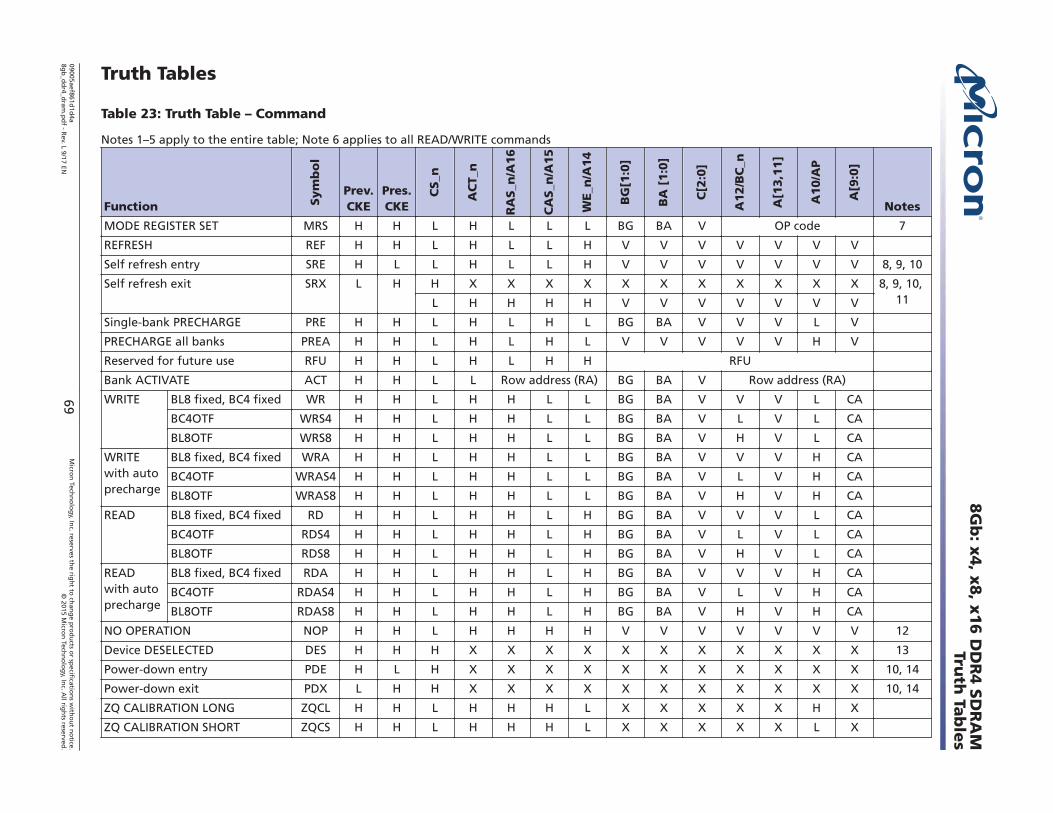
Truth Tables
Table 23: Truth Table – Command
Notes 1–5 apply to the entire table; Note 6 applies to all READ/WRITE commands
Function Sym
bo
l
Prev.CKE
Pres.CKE
CS_n
AC
T_n
RA
S_n
/A16
CA
S_n
/A15
WE_n
/A14
BG
[1:0
]
BA
[1:0
]
C[2
:0]
A12/B
C_n
A[1
3,1
1]
A10/A
P
A[9
:0]
Notes
MODE REGISTER SET MRS H H L H L L L BG BA V OP code 7
REFRESH REF H H L H L L H V V V V V V V
Self refresh entry SRE H L L H L L H V V V V V V V 8, 9, 10
Self refresh exit SRX L H H X X X X X X X X X X X 8, 9, 10, 11L H H H H V V V V V V V
Single-bank PRECHARGE PRE H H L H L H L BG BA V V V L V
PRECHARGE all banks PREA H H L H L H L V V V V V H V
Reserved for future use RFU H H L H L H H RFU
Bank ACTIVATE ACT H H L L Row address (RA) BG BA V Row address (RA)
WRITE BL8 fixed, BC4 fixed WR H H L H H L L BG BA V V V L CA
BC4OTF WRS4 H H L H H L L BG BA V L V L CA
BL8OTF WRS8 H H L H H L L BG BA V H V L CA
WRITEwith autoprecharge
BL8 fixed, BC4 fixed WRA H H L H H L L BG BA V V V H CA
BC4OTF WRAS4 H H L H H L L BG BA V L V H CA
BL8OTF WRAS8 H H L H H L L BG BA V H V H CA
READ BL8 fixed, BC4 fixed RD H H L H H L H BG BA V V V L CA
BC4OTF RDS4 H H L H H L H BG BA V L V L CA
BL8OTF RDS8 H H L H H L H BG BA V H V L CA
READwith autoprecharge
BL8 fixed, BC4 fixed RDA H H L H H L H BG BA V V V H CA
BC4OTF RDAS4 H H L H H L H BG BA V L V H CA
BL8OTF RDAS8 H H L H H L H BG BA V H V H CA
NO OPERATION NOP H H L H H H H V V V V V V V 12
Device DESELECTED DES H H H X X X X X X X X X X X 13
Power-down entry PDE H L H X X X X X X X X X X X 10, 14
Power-down exit PDX L H H X X X X X X X X X X X 10, 14
ZQ CALIBRATION LONG ZQCL H H L H H H L X X X X X H X
ZQ CALIBRATION SHORT ZQCS H H L H H H L X X X X X L X
8G
b: x
4, x
8, x
16 D
DR
4 S
DR
AM
Truth
Tab
les
09005aef861d1d
4a8g
b_d
dr4_d
ram.p
df - R
ev. L 9/17 EN69
Micro
n Tech
no
log
y, Inc. reserves th
e righ
t to ch
ang
e pro
du
cts or sp
ecification
s with
ou
t no
tice.©
2015 Micro
n Tech
no
log
y, Inc. A
ll righ
ts reserved.
Notes: 1. • BG = Bank group address• BA = Bank address• RA = Row address• CA = Column address• BC_n = Burst chop• X = “Don’t Care”• V = Valid
2. All DDR4 SDRAM commands are defined by states of CS_n, ACT_n, RAS_n/A16, CAS_n/A15, WE_n/A14, and CKE at the rising edge of the clock. The MSB of BG, BA, RA, and CAare device density- and configuration-dependent. When ACT_n = H, pins RAS_n/A16,CAS_n/A15, and WE_n/A14 are used as command pins RAS_n, CAS_n, and WE_n, respec-tively. When ACT_n = L, pins RAS_n/A16, CAS_n/A15, and WE_n/A14 are used as addresspins A16, A15, and A14, respectively.
3. RESET_n is enabled LOW and is used only for asynchronous reset and must be main-tained HIGH during any function.
4. Bank group addresses (BG) and bank addresses (BA) determine which bank within abank group is being operated upon. For MRS commands, the BG and BA selects the spe-cific mode register location.
5. V means HIGH or LOW (but a defined logic level), and X means either defined or unde-fined (such as floating) logic level.
6. READ or WRITE bursts cannot be terminated or interrupted, and fixed/on-the-fly (OTF)BL will be defined by MRS.
7. During an MRS command, A17 is RFU and is device density- and configuration-depend-ent.
8. The state of ODT does not affect the states described in this table. The ODT function isnot available during self refresh.
9. VPP and VREF (VREFCA) must be maintained during SELF REFRESH operation.10. Refer to the Truth Table – CKE table for more details about CKE transition.11. Controller guarantees self refresh exit to be synchronous. DRAM implementation has
the choice of either synchronous or asynchronous.12. The NO OPERATION (NOP) command may be used only when exiting maximum power
saving mode or when entering gear-down mode.13. The NOP command may not be used in place of the DESELECT command.14. The power-down mode does not perform any REFRESH operation.
8Gb: x4, x8, x16 DDR4 SDRAMTruth Tables
09005aef861d1d4a8gb_ddr4_dram.pdf - Rev. L 9/17 EN 70 Micron Technology, Inc. reserves the right to change products or specifications without notice.
© 2015 Micron Technology, Inc. All rights reserved.
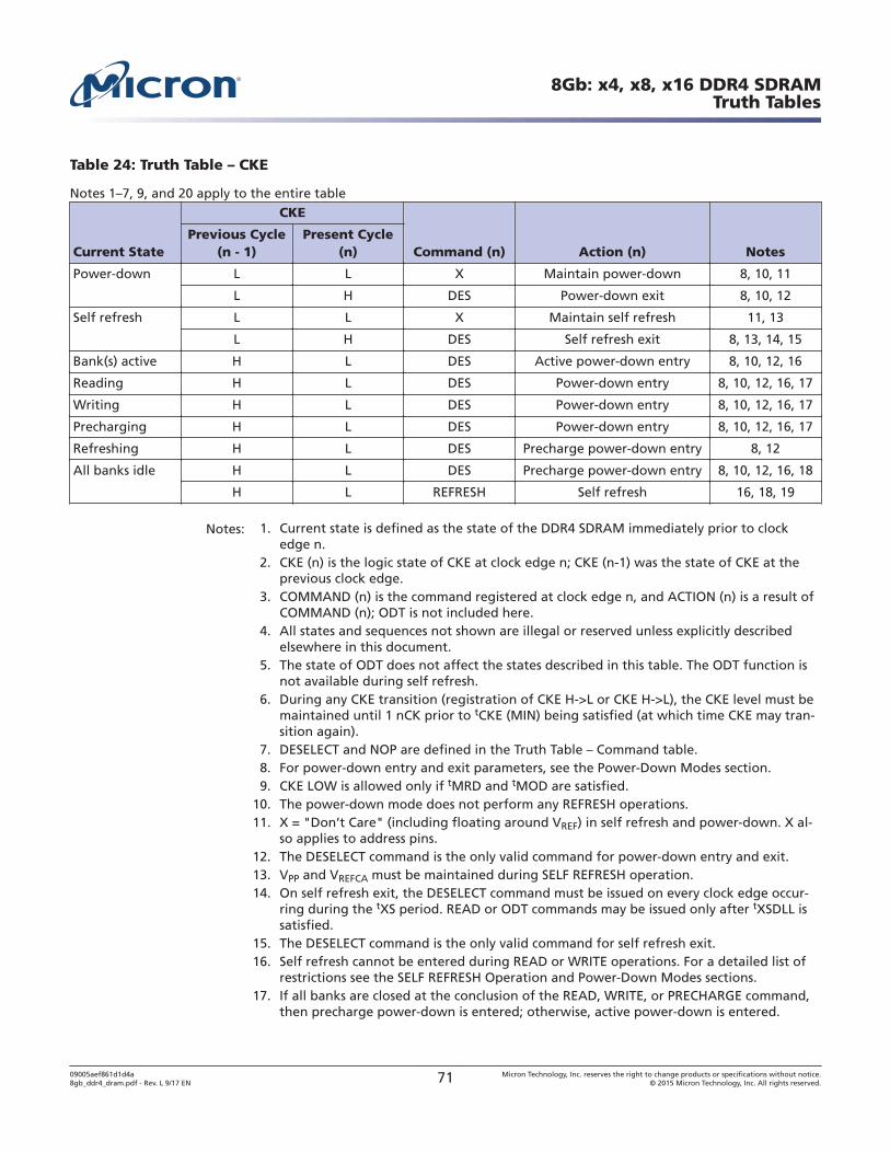
Table 24: Truth Table – CKE
Notes 1–7, 9, and 20 apply to the entire table
Current State
CKE
Command (n) Action (n) NotesPrevious Cycle
(n - 1)Present Cycle
(n)
Power-down L L X Maintain power-down 8, 10, 11
L H DES Power-down exit 8, 10, 12
Self refresh L L X Maintain self refresh 11, 13
L H DES Self refresh exit 8, 13, 14, 15
Bank(s) active H L DES Active power-down entry 8, 10, 12, 16
Reading H L DES Power-down entry 8, 10, 12, 16, 17
Writing H L DES Power-down entry 8, 10, 12, 16, 17
Precharging H L DES Power-down entry 8, 10, 12, 16, 17
Refreshing H L DES Precharge power-down entry 8, 12
All banks idle H L DES Precharge power-down entry 8, 10, 12, 16, 18
H L REFRESH Self refresh 16, 18, 19
Notes: 1. Current state is defined as the state of the DDR4 SDRAM immediately prior to clockedge n.
2. CKE (n) is the logic state of CKE at clock edge n; CKE (n-1) was the state of CKE at theprevious clock edge.
3. COMMAND (n) is the command registered at clock edge n, and ACTION (n) is a result ofCOMMAND (n); ODT is not included here.
4. All states and sequences not shown are illegal or reserved unless explicitly describedelsewhere in this document.
5. The state of ODT does not affect the states described in this table. The ODT function isnot available during self refresh.
6. During any CKE transition (registration of CKE H->L or CKE H->L), the CKE level must bemaintained until 1 nCK prior to tCKE (MIN) being satisfied (at which time CKE may tran-sition again).
7. DESELECT and NOP are defined in the Truth Table – Command table.8. For power-down entry and exit parameters, see the Power-Down Modes section.9. CKE LOW is allowed only if tMRD and tMOD are satisfied.
10. The power-down mode does not perform any REFRESH operations.11. X = "Don’t Care" (including floating around VREF) in self refresh and power-down. X al-
so applies to address pins.12. The DESELECT command is the only valid command for power-down entry and exit.13. VPP and VREFCA must be maintained during SELF REFRESH operation.14. On self refresh exit, the DESELECT command must be issued on every clock edge occur-
ring during the tXS period. READ or ODT commands may be issued only after tXSDLL issatisfied.
15. The DESELECT command is the only valid command for self refresh exit.16. Self refresh cannot be entered during READ or WRITE operations. For a detailed list of
restrictions see the SELF REFRESH Operation and Power-Down Modes sections.17. If all banks are closed at the conclusion of the READ, WRITE, or PRECHARGE command,
then precharge power-down is entered; otherwise, active power-down is entered.
8Gb: x4, x8, x16 DDR4 SDRAMTruth Tables
09005aef861d1d4a8gb_ddr4_dram.pdf - Rev. L 9/17 EN 71 Micron Technology, Inc. reserves the right to change products or specifications without notice.
© 2015 Micron Technology, Inc. All rights reserved.
18. Idle state is defined as all banks are closed (tRP, tDAL, and so on, satisfied), no databursts are in progress, CKE is HIGH, and all timings from previous operations are satis-fied (tMRD, tMOD, tRFC, tZQinit, tZQoper, tZQCS, and so on), as well as all self refresh ex-it and power-down exit parameters are satisfied (tXS, tXP, tXSDLL, and so on).
19. Self refresh mode can be entered only from the all banks idle state.20. For more details about all signals, see the Truth Table – Command table; must be a legal
command as defined in the table.
NOP CommandThe NO OPERATION (NOP) command was originally used to instruct the selectedDDR4 SDRAM to perform a NOP (CS_n = LOW and ACT_n, RAS_n/A16, CAS_n/A15, andWE_n/A14 = HIGH). This prevented unwanted commands from being registered duringidle or wait states. NOP command general support has been removed and the com-mand should not be used unless specifically allowed, which is when exiting maximumpower-saving mode or when entering gear-down mode.
DESELECT CommandThe deselect function (CS_n HIGH) prevents new commands from being executed;therefore, with this command, the device is effectively deselected. Operations already inprogress are not affected.
DLL-Off ModeDLL-off mode is entered by setting MR1 bit A0 to 0, which will disable the DLL for sub-sequent operations until the A0 bit is set back to 1. The MR1 A0 bit for DLL control canbe switched either during initialization or during self refresh mode. Refer to the InputClock Frequency Change section for more details.
The maximum clock frequency for DLL-off mode is specified by the parametertCKDLL_OFF. There is no minimum frequency limit besides the need to satisfy the re-fresh interval, tREFI.
Due to latency counter and timing restrictions, only one CL value and CWL value (inMR0 and MR2 respectively) are supported. The DLL-off mode is only required to sup-port setting both CL = 10 and CWL = 9.
DLL-off mode will affect the read data clock-to-data strobe relationship (tDQSCK), butnot the data strobe-to-data relationship (tDQSQ, tQH). Special attention is needed toline up read data to the controller time domain.
Compared with DLL-on mode, where tDQSCK starts from the rising clock edge (AL +CL) cycles after the READ command, the DLL-off mode tDQSCK starts (AL + CL - 1) cy-cles after the READ command. Another difference is that tDQSCK may not be smallcompared to tCK (it might even be larger than tCK), and the difference between tDQSCK(MIN) and tDQSCK (MAX) is significantly larger than in DLL-on mode. The tDQSCK(DLL-off) values are vendor-specific.
The timing relations on DLL-off mode READ operation are shown in the following dia-gram, where CL = 10, AL = 0, and BL = 8.
8Gb: x4, x8, x16 DDR4 SDRAMNOP Command
09005aef861d1d4a8gb_ddr4_dram.pdf - Rev. L 9/17 EN 72 Micron Technology, Inc. reserves the right to change products or specifications without notice.
© 2015 Micron Technology, Inc. All rights reserved.
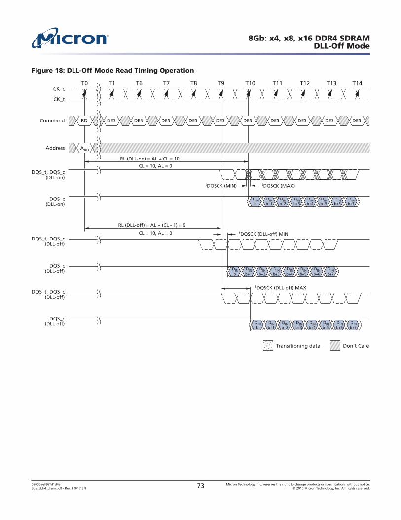
Figure 18: DLL-Off Mode Read Timing Operation
CK_c
CK_t
Command
T0 T1 T6 T7 T8 T9 T10 T11 T12 T13 T14
Address
DQS_t, DQS_c(DLL-on)
DQS_c(DLL-on)
CL = 10, AL = 0
CL = 10, AL = 0
RL (DLL-on) = AL + CL = 10
RL (DLL-off) = AL + (CL - 1) = 9
tDQSCK (DLL-off) MAX
tDQSCK (DLL-off) MIN
tDQSCK (MAX)
DQS_t, DQS_c(DLL-off)
DQS_c(DLL-off)
DQS_c(DLL-off)
DQS_t, DQS_c(DLL-off)
RD DES DES DES DES DES DES DES DES DES DES
Don’t CareTransitioning data
DINb
()()
()()
()()
()()
()()
()()
()()
()()
()()
()()
()()
()()
()()
()()
DINb+1
DINb+2
DINb+3
DINb+4
DINb+5
DINb+6
DINb+7
DINb
DINb+1
DINb+2
DINb+3
DINb+4
DINb+5
DINb+6
DINb+7
DINb
DINb+1
DINb+2
DINb+3
DINb+4
DINb+5
DINb+6
DINb+7
()()
tDQSCK (MIN)
ARD
8Gb: x4, x8, x16 DDR4 SDRAMDLL-Off Mode
09005aef861d1d4a8gb_ddr4_dram.pdf - Rev. L 9/17 EN 73 Micron Technology, Inc. reserves the right to change products or specifications without notice.
© 2015 Micron Technology, Inc. All rights reserved.
DLL-On/Off Switching ProceduresThe DLL-off mode is entered by setting MR1 bit A0 to 0; this will disable the DLL forsubsequent operations until the A0 bit is set back to 1.
DLL Switch Sequence from DLL-On to DLL-Off
To switch from DLL-on to DLL-off requires the frequency to be changed during self re-fresh, as outlined in the following procedure:
1. Starting from the idle state (all banks pre-charged, all timings fulfilled, and, to dis-able the DLL, the DRAM on-die termination resistors, RTT(NOM), must be in High-Zbefore MRS to MR1.)
2. Set MR1 bit A0 to 1 to disable the DLL.3. Wait tMOD.4. Enter self refresh mode; wait until tCKSRE/tCKSRE_PAR is satisfied.5. Change frequency, following the guidelines in the Input Clock Frequency Change
section.6. Wait until a stable clock is available for at least tCKSRX at device inputs.7. Starting with the SELF REFRESH EXIT command, CKE must continuously be reg-
istered HIGH until all tMOD timings from any MRS command are satisfied. In ad-dition, if any ODT features were enabled in the mode registers when self refreshmode was entered, the ODT signal must continuously be registered LOW until alltMOD timings from any MRS command are satisfied. If RTT(NOM) was disabled inthe mode registers when self refresh mode was entered, the ODT signal is "Don'tCare."
8. Wait tXS_FAST, tXS_ABORT, or tXS, and then set mode registers with appropriatevalues (an update of CL, CWL, and WR may be necessary; a ZQCL command canalso be issued after tXS_FAST).
• tXS_FAST: ZQCL, ZQCS, and MRS commands. For MRS commands, only CL andWR/RTP registers in MR0, the CWL register in MR2, and gear-down mode inMR3 may be accessed provided the device is not in per-DRAM addressabilitymode. Access to other device mode registers must satisfy tXS timing.
• tXS_ABORT: If MR4 [9] is enabled, then the device aborts any ongoing refreshand does not increment the refresh counter. The controller can issue a validcommand after a delay of tXS_ABORT. Upon exiting from self refresh, the devicerequires a minimum of one extra REFRESH command before it is put back intoself refresh mode. This requirement remains the same regardless of the MRS bitsetting for self refresh abort.
• tXS: ACT, PRE, PREA, REF, SRE, PDE, WR, WRS4, WRS8, WRA, WRAS4, WRAS8,RD, RDS4, RDS8, RDA, RDAS4, and RDAS8.
9. Wait tMOD to complete.
The device is ready for the next command.
8Gb: x4, x8, x16 DDR4 SDRAMDLL-On/Off Switching Procedures
09005aef861d1d4a8gb_ddr4_dram.pdf - Rev. L 9/17 EN 74 Micron Technology, Inc. reserves the right to change products or specifications without notice.
© 2015 Micron Technology, Inc. All rights reserved.
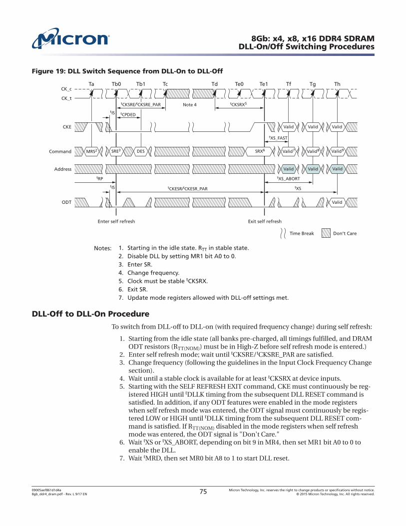
Figure 19: DLL Switch Sequence from DLL-On to DLL-Off
CK_c
CK_t
Ta Tb0 Tb1 Tc Td Te0 Te1 Tf Tg Th
Don’t CareTime Break
CKE
Command
Enter self refresh Exit self refresh
ODT
Valid
SRE3 DES SRX6
Valid Valid
Valid Valid
MRS2
tXS_FAST
tXS_ABORTtRP
tXS
Note 4
tCPDEDtIS
tCKSRE/tCKSRE_PAR tCKSRX5
Valid
Address Valid
Valid7 Valid8 Valid9
tIS tCKESR/tCKESR_PAR
Notes: 1. Starting in the idle state. RTT in stable state.2. Disable DLL by setting MR1 bit A0 to 0.3. Enter SR.4. Change frequency.5. Clock must be stable tCKSRX.6. Exit SR.7. Update mode registers allowed with DLL-off settings met.
DLL-Off to DLL-On Procedure
To switch from DLL-off to DLL-on (with required frequency change) during self refresh:
1. Starting from the idle state (all banks pre-charged, all timings fulfilled, and DRAMODT resistors (RTT(NOM)) must be in High-Z before self refresh mode is entered.)
2. Enter self refresh mode; wait until tCKSRE/tCKSRE_PAR are satisfied.3. Change frequency (following the guidelines in the Input Clock Frequency Change
section).4. Wait until a stable clock is available for at least tCKSRX at device inputs.5. Starting with the SELF REFRESH EXIT command, CKE must continuously be reg-
istered HIGH until tDLLK timing from the subsequent DLL RESET command issatisfied. In addition, if any ODT features were enabled in the mode registerswhen self refresh mode was entered, the ODT signal must continuously be regis-tered LOW or HIGH until tDLLK timing from the subsequent DLL RESET com-mand is satisfied. If RTT(NOM) disabled in the mode registers when self refreshmode was entered, the ODT signal is "Don't Care."
6. Wait tXS or tXS_ABORT, depending on bit 9 in MR4, then set MR1 bit A0 to 0 toenable the DLL.
7. Wait tMRD, then set MR0 bit A8 to 1 to start DLL reset.
8Gb: x4, x8, x16 DDR4 SDRAMDLL-On/Off Switching Procedures
09005aef861d1d4a8gb_ddr4_dram.pdf - Rev. L 9/17 EN 75 Micron Technology, Inc. reserves the right to change products or specifications without notice.
© 2015 Micron Technology, Inc. All rights reserved.
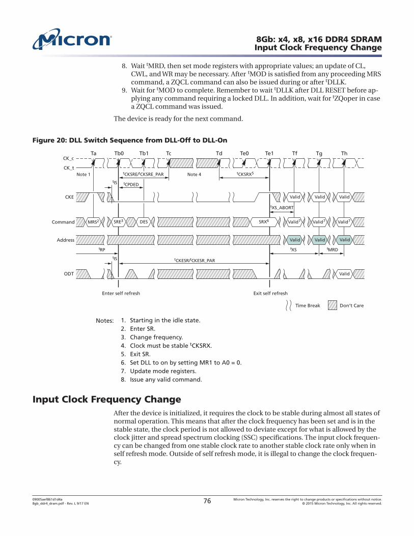
8. Wait tMRD, then set mode registers with appropriate values; an update of CL,CWL, and WR may be necessary. After tMOD is satisfied from any proceeding MRScommand, a ZQCL command can also be issued during or after tDLLK.
9. Wait for tMOD to complete. Remember to wait tDLLK after DLL RESET before ap-plying any command requiring a locked DLL. In addition, wait for tZQoper in casea ZQCL command was issued.
The device is ready for the next command.
Figure 20: DLL Switch Sequence from DLL-Off to DLL-On
CK_c
CK_t
Ta Tb0 Tb1 Tc Td Te0 Te1 Tf Tg Th
Don’t CareTime Break
CKE
Command
Enter self refresh Exit self refresh
ODT
Valid
SRE3 DES SRX6
Valid Valid
Valid Valid
MRS2
tXS_ABORT
tRP tXS tMRD
Note 4Note 1
tCPDEDtIS
tCKSRE/tCKSRE_PAR tCKSRX5
Valid
Address Valid
Valid7
tIS
Valid7 Valid7
tCKESR/tCKESR_PAR
Notes: 1. Starting in the idle state.2. Enter SR.3. Change frequency.4. Clock must be stable tCKSRX.5. Exit SR.6. Set DLL to on by setting MR1 to A0 = 0.7. Update mode registers.8. Issue any valid command.
Input Clock Frequency ChangeAfter the device is initialized, it requires the clock to be stable during almost all states ofnormal operation. This means that after the clock frequency has been set and is in thestable state, the clock period is not allowed to deviate except for what is allowed by theclock jitter and spread spectrum clocking (SSC) specifications. The input clock frequen-cy can be changed from one stable clock rate to another stable clock rate only when inself refresh mode. Outside of self refresh mode, it is illegal to change the clock frequen-cy.
8Gb: x4, x8, x16 DDR4 SDRAMInput Clock Frequency Change
09005aef861d1d4a8gb_ddr4_dram.pdf - Rev. L 9/17 EN 76 Micron Technology, Inc. reserves the right to change products or specifications without notice.
© 2015 Micron Technology, Inc. All rights reserved.
After the device has been successfully placed in self refresh mode and tCKSRE/tCKSRE_PAR have been satisfied, the state of the clock becomes a "Don’t Care." Follow-ing a "Don’t Care," changing the clock frequency is permissible, provided the new clockfrequency is stable prior to tCKSRX. When entering and exiting self refresh mode for thesole purpose of changing the clock frequency, the self refresh entry and exit specifica-tions must still be met as outlined in SELF REFRESH Operation.
For the new clock frequency, additional MRS commands to MR0, MR2, MR3, MR4, MR5,and MR6 may need to be issued to program appropriate CL, CWL, gear-down mode,READ and WRITE preamble, Command Address Latency, and tCCD_L/tDLLK values.
When the clock rate is being increased (faster), the MR settings that require additionalclocks should be updated prior to the clock rate being increased. In particular, the PLlatency must be disabled when the clock rate changes, ie. while in self refresh mode. Forexample, if changing the clock rate from DDR4-2133 to DDR4-2933 with CA paritymode enabled, MR5[2:0] must first change from PL = 4 to PL = disable prior to PL = 6.The correct procedure would be to (1) change PL = 4 to disable via MR5 [2:0], (2) enterself refresh mode, (3) change clock rate from DDR4-2133 to DDR4-2933, (4) exit self re-fresh mode, (5) Enable CA parity mode setting PL = 6 vis MR5 [2:0].
If the MR settings that require additional clocks are updated after the clock rate hasbeen increased, for example. after exiting self refresh mode, the required MR settingsmust be updated prior to removing the DRAM from the IDLE state, unless the DRAM isRESET. If the DRAM leaves the IDLE state to enter self refresh mode or ZQ Calibration,the updating of the required MR settings may be deferred to the next time the DRAMenters the IDLE state.
If MR6 is issued prior to self refresh entry for new the tDLLK value, DLL will relock auto-matically at self refresh exit. However, if MR6 is issued after self refresh entry, MR0 mustbe issued to reset the DLL.
The device input clock frequency can change only within the minimum and maximumoperating frequency specified for the particular speed grade. Any frequency change be-low the minimum operating frequency would require the use of DLL-on mode to DLL-off mode transition sequence (see DLL-On/Off Switching Procedures).
Write LevelingFor better signal integrity, DDR4 memory modules use fly-by topology for the com-mands, addresses, control signals, and clocks. Fly-by topology has benefits from the re-duced number of stubs and their length, but it also causes flight-time skew betweenclock and strobe at every DRAM on the DIMM. This makes it difficult for the controllerto maintain tDQSS, tDSS, and tDSH specifications. Therefore, the device supports awrite leveling feature to allow the controller to compensate for skew. This feature maynot be required under some system conditions, provided the host can maintain thetDQSS, tDSS, and tDSH specifications.
The memory controller can use the write leveling feature and feedback from the deviceto adjust the DQS (DQS_t, DQS_c) to CK (CK_t, CK_c) relationship. The memory con-troller involved in the leveling must have an adjustable delay setting on DQS to align therising edge of DQS with that of the clock at the DRAM pin. The DRAM asynchronouslyfeeds back CK, sampled with the rising edge of DQS, through the DQ bus. The controllerrepeatedly delays DQS until a transition from 0 to 1 is detected. The DQS delay estab-lished though this exercise would ensure the tDQSS specification. Besides tDQSS, tDSS
8Gb: x4, x8, x16 DDR4 SDRAMWrite Leveling
09005aef861d1d4a8gb_ddr4_dram.pdf - Rev. L 9/17 EN 77 Micron Technology, Inc. reserves the right to change products or specifications without notice.
© 2015 Micron Technology, Inc. All rights reserved.
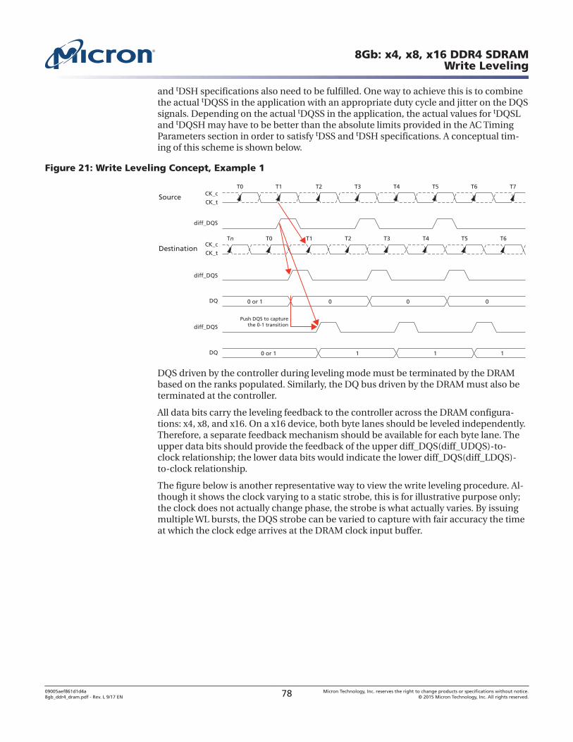
and tDSH specifications also need to be fulfilled. One way to achieve this is to combinethe actual tDQSS in the application with an appropriate duty cycle and jitter on the DQSsignals. Depending on the actual tDQSS in the application, the actual values for tDQSLand tDQSH may have to be better than the absolute limits provided in the AC TimingParameters section in order to satisfy tDSS and tDSH specifications. A conceptual tim-ing of this scheme is shown below.
Figure 21: Write Leveling Concept, Example 1
diff_DQS
diff_DQS
DQ
diff_DQS
DQ
T0 T1 T2 T3 T4 T5CK_c
CK_t
T6 T7
Tn T0 T1 T2 T3 T4CK_c
CK_t
T5 T6
0 or 1 0 0 0
0 or 1
Push DQS to capturethe 0-1 transition
1 1 1
Source
Destination
DQS driven by the controller during leveling mode must be terminated by the DRAMbased on the ranks populated. Similarly, the DQ bus driven by the DRAM must also beterminated at the controller.
All data bits carry the leveling feedback to the controller across the DRAM configura-tions: x4, x8, and x16. On a x16 device, both byte lanes should be leveled independently.Therefore, a separate feedback mechanism should be available for each byte lane. Theupper data bits should provide the feedback of the upper diff_DQS(diff_UDQS)-to-clock relationship; the lower data bits would indicate the lower diff_DQS(diff_LDQS)-to-clock relationship.
The figure below is another representative way to view the write leveling procedure. Al-though it shows the clock varying to a static strobe, this is for illustrative purpose only;the clock does not actually change phase, the strobe is what actually varies. By issuingmultiple WL bursts, the DQS strobe can be varied to capture with fair accuracy the timeat which the clock edge arrives at the DRAM clock input buffer.
8Gb: x4, x8, x16 DDR4 SDRAMWrite Leveling
09005aef861d1d4a8gb_ddr4_dram.pdf - Rev. L 9/17 EN 78 Micron Technology, Inc. reserves the right to change products or specifications without notice.
© 2015 Micron Technology, Inc. All rights reserved.
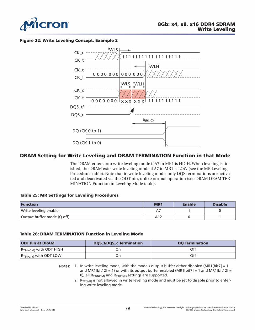
Figure 22: Write Leveling Concept, Example 2
XX X
CK_t
CK_c
CK_t
CK_c
CK_t
CK_c
DQS_t/
DQS_c
DQ (CK 0 to 1)
tWLH
tWLH
tWLO
tWLS
tWLS
0 0 00 0 00 0 000 0 0
0 0 000 0 0 XX X
11111 11111 1111 1111
11 1111 1111
DQ (CK 1 to 0)
DRAM Setting for Write Leveling and DRAM TERMINATION Function in that Mode
The DRAM enters into write leveling mode if A7 in MR1 is HIGH. When leveling is fin-ished, the DRAM exits write leveling mode if A7 in MR1 is LOW (see the MR LevelingProcedures table). Note that in write leveling mode, only DQS terminations are activa-ted and deactivated via the ODT pin, unlike normal operation (see DRAM DRAM TER-MINATION Function in Leveling Mode table).
Table 25: MR Settings for Leveling Procedures
Function MR1 Enable Disable
Write leveling enable A7 1 0
Output buffer mode (Q off) A12 0 1
Table 26: DRAM TERMINATION Function in Leveling Mode
ODT Pin at DRAM DQS_t/DQS_c Termination DQ Termination
RTT(NOM) with ODT HIGH On Off
RTT(Park) with ODT LOW On Off
Notes: 1. In write leveling mode, with the mode's output buffer either disabled (MR1[bit7] = 1and MR1[bit12] = 1) or with its output buffer enabled (MR1[bit7] = 1 and MR1[bit12] =0), all RTT(NOM) and RTT(Park) settings are supported.
2. RTT(WR) is not allowed in write leveling mode and must be set to disable prior to enter-ing write leveling mode.
8Gb: x4, x8, x16 DDR4 SDRAMWrite Leveling
09005aef861d1d4a8gb_ddr4_dram.pdf - Rev. L 9/17 EN 79 Micron Technology, Inc. reserves the right to change products or specifications without notice.
© 2015 Micron Technology, Inc. All rights reserved.
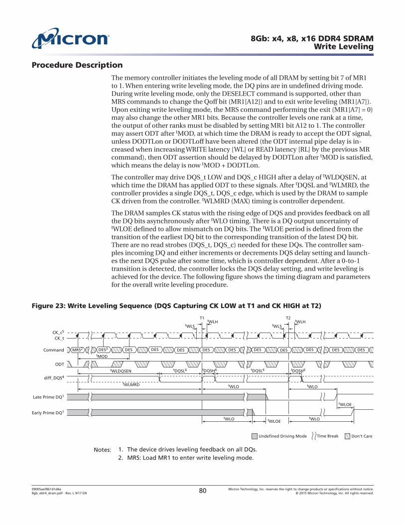
Procedure Description
The memory controller initiates the leveling mode of all DRAM by setting bit 7 of MR1to 1. When entering write leveling mode, the DQ pins are in undefined driving mode.During write leveling mode, only the DESELECT command is supported, other thanMRS commands to change the Qoff bit (MR1[A12]) and to exit write leveling (MR1[A7]).Upon exiting write leveling mode, the MRS command performing the exit (MR1[A7] = 0)may also change the other MR1 bits. Because the controller levels one rank at a time,the output of other ranks must be disabled by setting MR1 bit A12 to 1. The controllermay assert ODT after tMOD, at which time the DRAM is ready to accept the ODT signal,unless DODTLon or DODTLoff have been altered (the ODT internal pipe delay is in-creased when increasing WRITE latency [WL] or READ latency [RL] by the previous MRcommand), then ODT assertion should be delayed by DODTLon after tMOD is satisfied,which means the delay is now tMOD + DODTLon.
The controller may drive DQS_t LOW and DQS_c HIGH after a delay of tWLDQSEN, atwhich time the DRAM has applied ODT to these signals. After tDQSL and tWLMRD, thecontroller provides a single DQS_t, DQS_c edge, which is used by the DRAM to sampleCK driven from the controller. tWLMRD (MAX) timing is controller dependent.
The DRAM samples CK status with the rising edge of DQS and provides feedback on allthe DQ bits asynchronously after tWLO timing. There is a DQ output uncertainty oftWLOE defined to allow mismatch on DQ bits. The tWLOE period is defined from thetransition of the earliest DQ bit to the corresponding transition of the latest DQ bit.There are no read strobes (DQS_t, DQS_c) needed for these DQs. The controller sam-ples incoming DQ and either increments or decrements DQS delay setting and launch-es the next DQS pulse after some time, which is controller dependent. After a 0-to-1transition is detected, the controller locks the DQS delay setting, and write leveling isachieved for the device. The following figure shows the timing diagram and parametersfor the overall write leveling procedure.
Figure 23: Write Leveling Sequence (DQS Capturing CK LOW at T1 and CK HIGH at T2)
tMOD
tWLDQSEN
tWLMRD
tWLH
tDQSH6tDQSL6 tDQSH6tDQSL6
tWLStWLH
tWLS
NOP
CK_tCK_c5
Command
T1 T2
Early Prime DQ1
ODT
Late Prime DQ1
diff_DQS4
DESMRS2 DES DES DES DES DES DES DES DES DES
Don’t CareUndefined Driving Mode Time Break
tWLO
tWLO tWLO
tWLO
tWLOE
tWLOE
DES3
Notes: 1. The device drives leveling feedback on all DQs.2. MRS: Load MR1 to enter write leveling mode.
8Gb: x4, x8, x16 DDR4 SDRAMWrite Leveling
09005aef861d1d4a8gb_ddr4_dram.pdf - Rev. L 9/17 EN 80 Micron Technology, Inc. reserves the right to change products or specifications without notice.
© 2015 Micron Technology, Inc. All rights reserved.
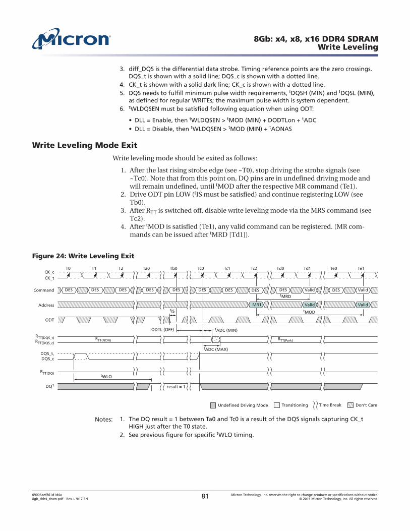
3. diff_DQS is the differential data strobe. Timing reference points are the zero crossings.DQS_t is shown with a solid line; DQS_c is shown with a dotted line.
4. CK_t is shown with a solid dark line; CK_c is shown with a dotted line.5. DQS needs to fulfill minimum pulse width requirements, tDQSH (MIN) and tDQSL (MIN),
as defined for regular WRITEs; the maximum pulse width is system dependent.6. tWLDQSEN must be satisfied following equation when using ODT:
• DLL = Enable, then tWLDQSEN > tMOD (MIN) + DODTLon + tADC• DLL = Disable, then tWLDQSEN > tMOD (MIN) + tAONAS
Write Leveling Mode Exit
Write leveling mode should be exited as follows:
1. After the last rising strobe edge (see ~T0), stop driving the strobe signals (see~Tc0). Note that from this point on, DQ pins are in undefined driving mode andwill remain undefined, until tMOD after the respective MR command (Te1).
2. Drive ODT pin LOW (tIS must be satisfied) and continue registering LOW (seeTb0).
3. After RTT is switched off, disable write leveling mode via the MRS command (seeTc2).
4. After tMOD is satisfied (Te1), any valid command can be registered. (MR com-mands can be issued after tMRD [Td1]).
Figure 24: Write Leveling Exit
tMOD
tWLO
ODTL (OFF)
tIS
tMRD
CK_t
T0 T1 T2 Ta0 Tb0 Tc0 Tc1 Tc2 Td0 Td1 Te0 Te1CK_c
Command
ODT
RTT(DQS_t)RTT(DQS_c)
RTT(DQ)
DQ1
DQS_t,DQS_c
DESDES DES DES DES DES DES DES DES
Address MR1 Valid
Valid Valid
Valid
Don’t CareTransitioning Time Break
RTT(NON)
Undefined Driving Mode
tADC (MAX)
tADC (MIN)
DES
RTT(Park)
result = 1
Notes: 1. The DQ result = 1 between Ta0 and Tc0 is a result of the DQS signals capturing CK_tHIGH just after the T0 state.
2. See previous figure for specific tWLO timing.
8Gb: x4, x8, x16 DDR4 SDRAMWrite Leveling
09005aef861d1d4a8gb_ddr4_dram.pdf - Rev. L 9/17 EN 81 Micron Technology, Inc. reserves the right to change products or specifications without notice.
© 2015 Micron Technology, Inc. All rights reserved.
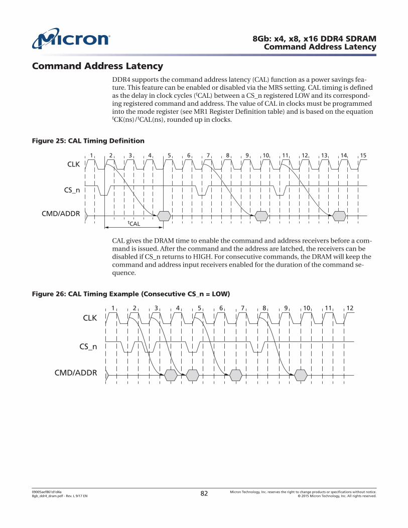
Command Address LatencyDDR4 supports the command address latency (CAL) function as a power savings fea-ture. This feature can be enabled or disabled via the MRS setting. CAL timing is definedas the delay in clock cycles (tCAL) between a CS_n registered LOW and its correspond-ing registered command and address. The value of CAL in clocks must be programmedinto the mode register (see MR1 Register Definition table) and is based on the equationtCK(ns)/tCAL(ns), rounded up in clocks.
Figure 25: CAL Timing Definition
CLK
CMD/ADDR
1 2 3 4 5 6 7 8 9 10 11 12 13 14 15
CS_n
tCAL
CAL gives the DRAM time to enable the command and address receivers before a com-mand is issued. After the command and the address are latched, the receivers can bedisabled if CS_n returns to HIGH. For consecutive commands, the DRAM will keep thecommand and address input receivers enabled for the duration of the command se-quence.
Figure 26: CAL Timing Example (Consecutive CS_n = LOW)
CLK
CMD/ADDR
1 2 3 4 5 6 7 8 9 10 11 12
CS_n
8Gb: x4, x8, x16 DDR4 SDRAMCommand Address Latency
09005aef861d1d4a8gb_ddr4_dram.pdf - Rev. L 9/17 EN 82 Micron Technology, Inc. reserves the right to change products or specifications without notice.
© 2015 Micron Technology, Inc. All rights reserved.
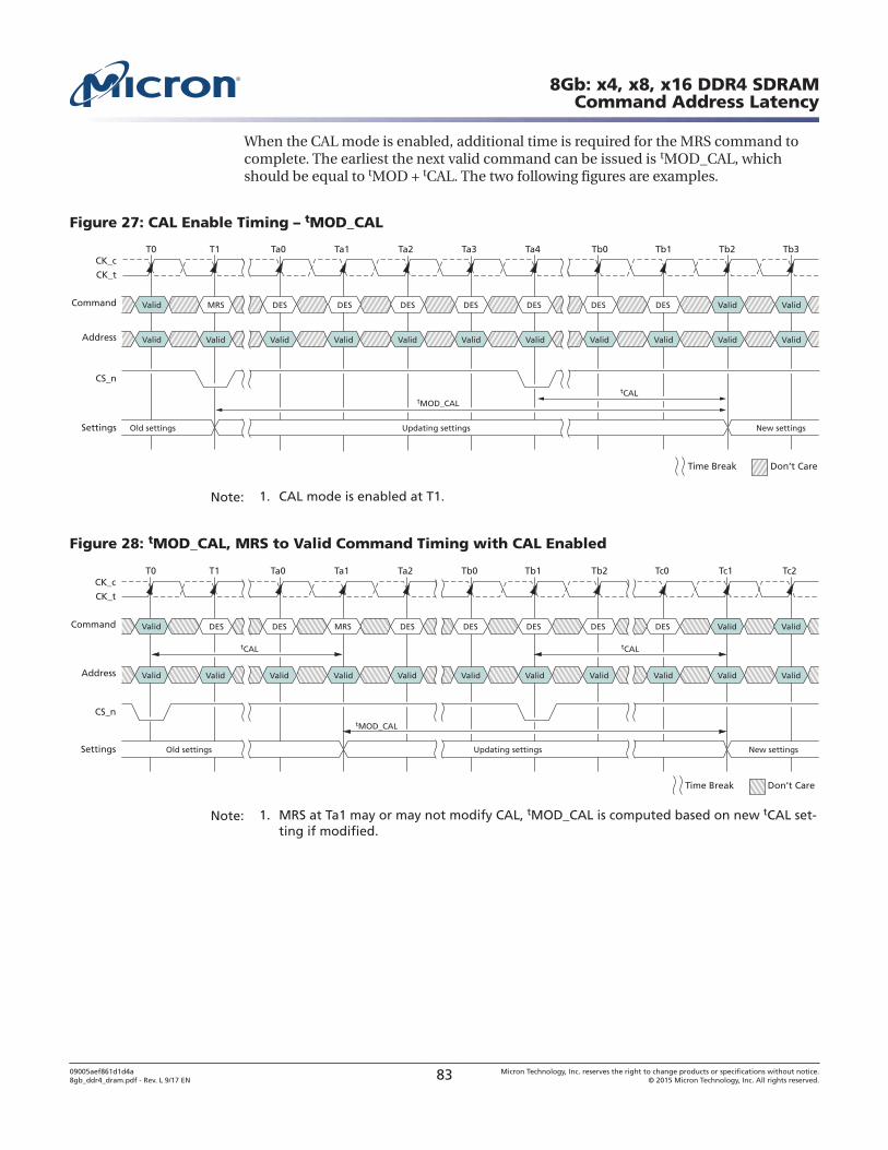
When the CAL mode is enabled, additional time is required for the MRS command tocomplete. The earliest the next valid command can be issued is tMOD_CAL, whichshould be equal to tMOD + tCAL. The two following figures are examples.
Figure 27: CAL Enable Timing – tMOD_CAL
T0 T1 Ta0 Ta1 Ta2CK_c
CK_t
Address
CS_n
Settings
Command
Ta3 Ta4
Old settings
MRSValid DESDESDES DES
Valid ValidValid Valid Valid Valid ValidValid
Don’t CareTime Break
Tb0 Tb1 Tb2 Tb3
New settings
Valid Valid
Valid Valid Valid
tMOD_CAL
tCAL
Updating settings
DES DES DES
Note: 1. CAL mode is enabled at T1.
Figure 28: tMOD_CAL, MRS to Valid Command Timing with CAL Enabled
T0 T1 Ta0 Ta1 Ta2CK_c
CK_t
Address
CS_n
Settings
Command
Tb0 Tb1
Old settings
Valid DESDESDES DES
Valid ValidValid Valid Valid Valid ValidValid
Don’t CareTime Break
Tb2 Tc0 Tc1 Tc2
New settings
Valid Valid Valid
tMOD_CAL
tCAL tCAL
Updating settings
DES DES DESMRS Valid Valid
Note: 1. MRS at Ta1 may or may not modify CAL, tMOD_CAL is computed based on new tCAL set-ting if modified.
8Gb: x4, x8, x16 DDR4 SDRAMCommand Address Latency
09005aef861d1d4a8gb_ddr4_dram.pdf - Rev. L 9/17 EN 83 Micron Technology, Inc. reserves the right to change products or specifications without notice.
© 2015 Micron Technology, Inc. All rights reserved.
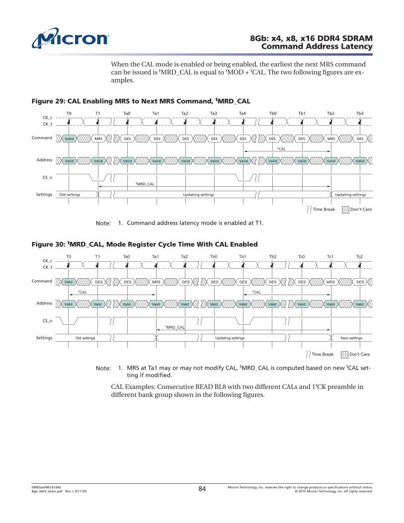
When the CAL mode is enabled or being enabled, the earliest the next MRS commandcan be issued is tMRD_CAL is equal to tMOD + tCAL. The two following figures are ex-amples.
Figure 29: CAL Enabling MRS to Next MRS Command, tMRD_CAL
T0 T1 Ta0 Ta1 Ta2CK_c
CK_t
Address
CS_n
Settings
Command
Ta3 Ta4
Old settings
MRS MRSValid DESDESDES DES DES
Valid ValidValid Valid Valid Valid ValidValid
Don’t CareTime Break
Tb0 Tb1 Tb2 Tb3
Valid Valid Valid
tMRD_CAL
tCAL
Updating settings Updating settings
DES DES DES
Note: 1. Command address latency mode is enabled at T1.
Figure 30: tMRD_CAL, Mode Register Cycle Time With CAL Enabled
CK_c
CK_t
Address
CS_n
Settings
Command
Note: 1. MRS at Ta1 may or may not modify CAL, tMRD_CAL is computed based on new tCAL set-ting if modified.
CAL Examples: Consecutive READ BL8 with two different CALs and 1tCK preamble indifferent bank group shown in the following figures.
8Gb: x4, x8, x16 DDR4 SDRAMCommand Address Latency
09005aef861d1d4a8gb_ddr4_dram.pdf - Rev. L 9/17 EN 84 Micron Technology, Inc. reserves the right to change products or specifications without notice.
© 2015 Micron Technology, Inc. All rights reserved.
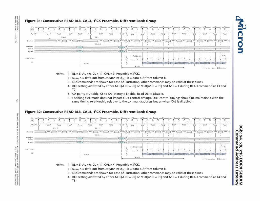
Figure 31: Consecutive READ BL8, CAL3, 1tCK Preamble, Different Bank Group
DOUT n
DOUT n + 1
DOUT n + 2
DOUT n + 3RL = 11
RL = 11
T0 T1 T2 T3 T4 T5 T6 T7 T14T13
tCAL = 3
T15 T16
Don’t CareTransitioning Data
T17 T18 T19 T20 T21 T22
Bank,Col n
tRPST
DES DES DES DES DES DES DES DES DES DES DES DES DES DESREADREAD
CK_tCK_c
Command
CS_n
DQ
DQS_t, DQS_c
Address
Bank GroupAddress
tCAL = 3
tCCD_S = 4
BG a
Bank,Col b
BG b
tRPRE (1nCK)
DOUT n + 4
DOUT n + 5
DOUT n + 6
DOUTn + 7
DOUT b
DOUT b + 7
DOUT b + 2
DOUT b + 3
DOUT b + 4
DOUT b + 5
DOUT b + 6
DOUT b + 7
Notes: 1. BL = 8, AL = 0, CL = 11, CAL = 3, Preamble = 1tCK.2. DOUT n = data-out from column n; DOUT b = data-out from column b.3. DES commands are shown for ease of illustration, other commands may be valid at these times.4. BL8 setting activated by either MR0[A1:0 = 00] or MR0[A1:0 = 01] and A12 = 1 during READ command at T3 and
T7.5. CA parity = Disable, CS to CA latency = Enable, Read DBI = Disable.6. Enabling CAL mode does not impact ODT control timings. ODT control timings should be maintained with the
same timing relationship relative to the command/address bus as when CAL is disabled.
Figure 32: Consecutive READ BL8, CAL4, 1tCK Preamble, Different Bank Group
Notes: 1. BL = 8, AL = 0, CL = 11, CAL = 4, Preamble = 1tCK.2. DOUT n = data-out from column n; DOUT b = data-out from column b.3. DES commands are shown for ease of illustration, other commands may be valid at these times.4. BL8 setting activated by either MR0[A1:0 = 00] or MR0[A1:0 = 01] and A12 = 1 during READ command at T4 and
T8.
8G
b: x
4, x
8, x
16 D
DR
4 S
DR
AM
Co
mm
an
d A
dd
ress La
ten
cy
09005aef861d1d
4a8g
b_d
dr4_d
ram.p
df - R
ev. L 9/17 EN85
Micro
n Tech
no
log
y, Inc. reserves th
e righ
t to ch
ang
e pro
du
cts or sp
ecification
s with
ou
t no
tice.©
2015 Micro
n Tech
no
log
y, Inc. A
ll righ
ts reserved.
5. CA parity = Disable, CS to CA latency = Enable, Read DBI = Disable.6. Enabling CAL mode does not impact ODT control timings. ODT control timings should be maintained with the
same timing relationship relative to the command/address bus as when CAL is disabled.
8G
b: x
4, x
8, x
16 D
DR
4 S
DR
AM
Co
mm
an
d A
dd
ress La
ten
cy
09005aef861d1d
4a8g
b_d
dr4_d
ram.p
df - R
ev. L 9/17 EN86
Micro
n Tech
no
log
y, Inc. reserves th
e righ
t to ch
ang
e pro
du
cts or sp
ecification
s with
ou
t no
tice.©
2015 Micro
n Tech
no
log
y, Inc. A
ll righ
ts reserved.
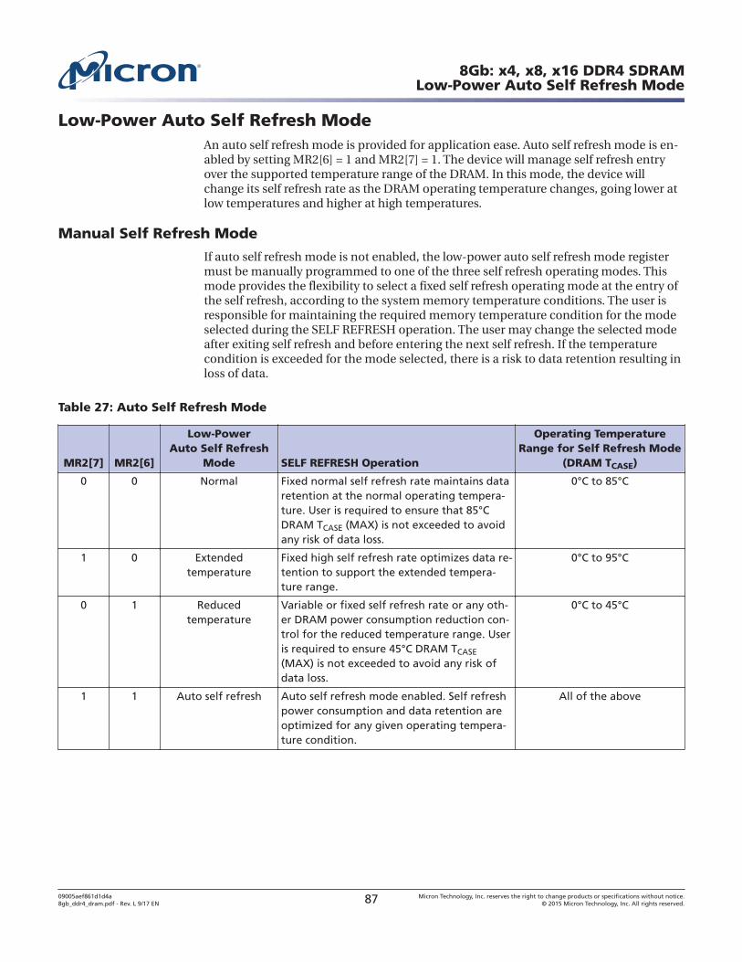
Low-Power Auto Self Refresh ModeAn auto self refresh mode is provided for application ease. Auto self refresh mode is en-abled by setting MR2[6] = 1 and MR2[7] = 1. The device will manage self refresh entryover the supported temperature range of the DRAM. In this mode, the device willchange its self refresh rate as the DRAM operating temperature changes, going lower atlow temperatures and higher at high temperatures.
Manual Self Refresh Mode
If auto self refresh mode is not enabled, the low-power auto self refresh mode registermust be manually programmed to one of the three self refresh operating modes. Thismode provides the flexibility to select a fixed self refresh operating mode at the entry ofthe self refresh, according to the system memory temperature conditions. The user isresponsible for maintaining the required memory temperature condition for the modeselected during the SELF REFRESH operation. The user may change the selected modeafter exiting self refresh and before entering the next self refresh. If the temperaturecondition is exceeded for the mode selected, there is a risk to data retention resulting inloss of data.
Table 27: Auto Self Refresh Mode
MR2[7] MR2[6]
Low-PowerAuto Self Refresh
Mode SELF REFRESH Operation
Operating TemperatureRange for Self Refresh Mode
(DRAM TCASE)
0 0 Normal Fixed normal self refresh rate maintains dataretention at the normal operating tempera-ture. User is required to ensure that 85°CDRAM TCASE (MAX) is not exceeded to avoidany risk of data loss.
0°C to 85°C
1 0 Extendedtemperature
Fixed high self refresh rate optimizes data re-tention to support the extended tempera-ture range.
0°C to 95°C
0 1 Reducedtemperature
Variable or fixed self refresh rate or any oth-er DRAM power consumption reduction con-trol for the reduced temperature range. Useris required to ensure 45°C DRAM TCASE
(MAX) is not exceeded to avoid any risk ofdata loss.
0°C to 45°C
1 1 Auto self refresh Auto self refresh mode enabled. Self refreshpower consumption and data retention areoptimized for any given operating tempera-ture condition.
All of the above
8Gb: x4, x8, x16 DDR4 SDRAMLow-Power Auto Self Refresh Mode
09005aef861d1d4a8gb_ddr4_dram.pdf - Rev. L 9/17 EN 87 Micron Technology, Inc. reserves the right to change products or specifications without notice.
© 2015 Micron Technology, Inc. All rights reserved.
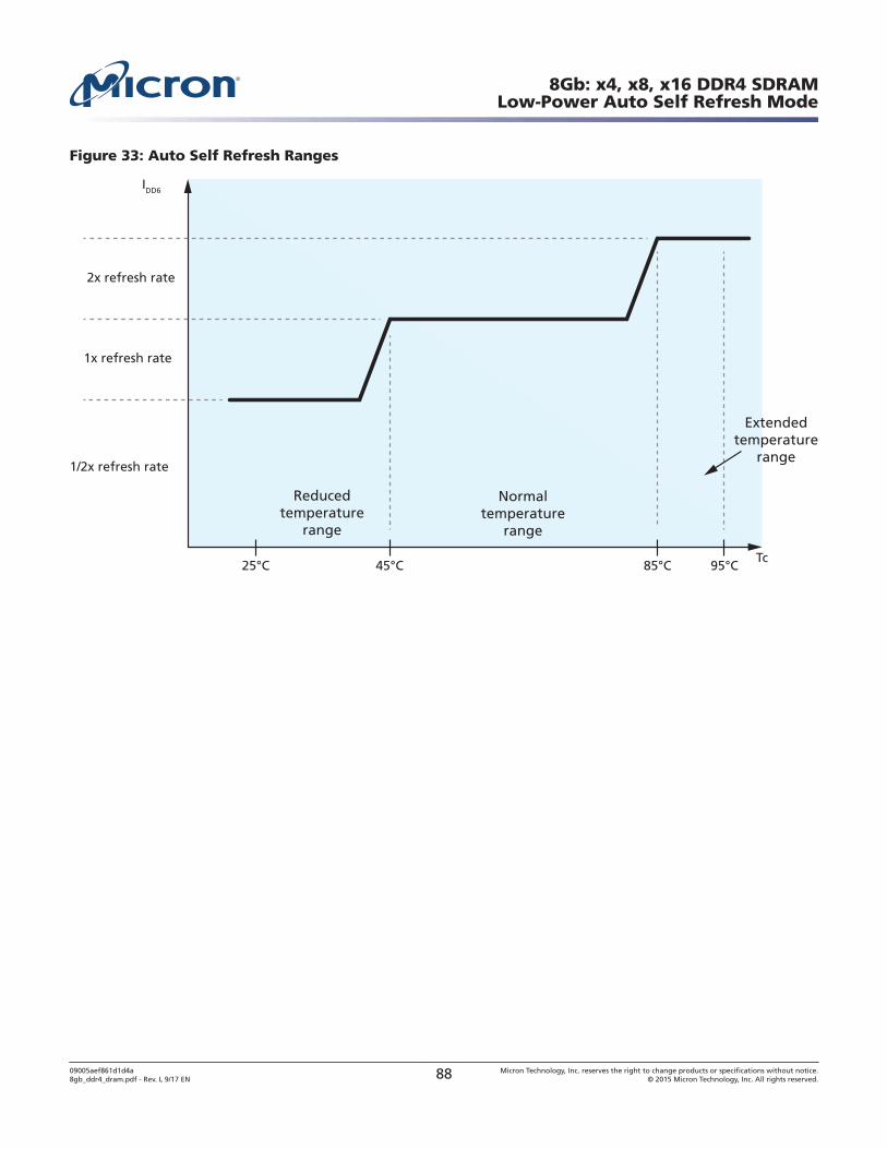
Figure 33: Auto Self Refresh Ranges
45°C25°C
IDD6
Tc85°C 95°C
Reducedtemperature
range
Normaltemperature
range
2x refresh rate
1x refresh rate
1/2x refresh rate
Extendedtemperature
range
8Gb: x4, x8, x16 DDR4 SDRAMLow-Power Auto Self Refresh Mode
09005aef861d1d4a8gb_ddr4_dram.pdf - Rev. L 9/17 EN 88 Micron Technology, Inc. reserves the right to change products or specifications without notice.
© 2015 Micron Technology, Inc. All rights reserved.
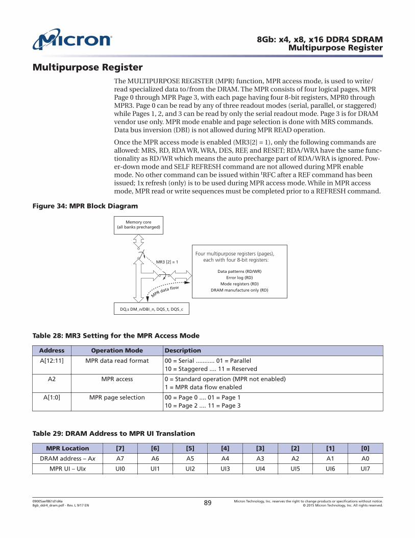
Multipurpose RegisterThe MULTIPURPOSE REGISTER (MPR) function, MPR access mode, is used to write/read specialized data to/from the DRAM. The MPR consists of four logical pages, MPRPage 0 through MPR Page 3, with each page having four 8-bit registers, MPR0 throughMPR3. Page 0 can be read by any of three readout modes (serial, parallel, or staggered)while Pages 1, 2, and 3 can be read by only the serial readout mode. Page 3 is for DRAMvendor use only. MPR mode enable and page selection is done with MRS commands.Data bus inversion (DBI) is not allowed during MPR READ operation.
Once the MPR access mode is enabled (MR3[2] = 1), only the following commands areallowed: MRS, RD, RDA WR, WRA, DES, REF, and RESET; RDA/WRA have the same func-tionality as RD/WR which means the auto precharge part of RDA/WRA is ignored. Pow-er-down mode and SELF REFRESH command are not allowed during MPR enablemode. No other command can be issued within tRFC after a REF command has beenissued; 1x refresh (only) is to be used during MPR access mode. While in MPR accessmode, MPR read or write sequences must be completed prior to a REFRESH command.
Figure 34: MPR Block Diagram
Memory core(all banks precharged)
MR3 [2] = 1
DQ,s DM_n/DBI_n, DQS_t, DQS_c
Four multipurpose registers (pages),each with four 8-bit registers:
Data patterns (RD/WR)
Error log (RD)
Mode registers (RD)
DRAM manufacture only (RD)MPR data flow
Table 28: MR3 Setting for the MPR Access Mode
Address Operation Mode Description
A[12:11] MPR data read format 00 = Serial ........... 01 = Parallel10 = Staggered .... 11 = Reserved
A2 MPR access 0 = Standard operation (MPR not enabled)1 = MPR data flow enabled
A[1:0] MPR page selection 00 = Page 0 .... 01 = Page 110 = Page 2 .... 11 = Page 3
Table 29: DRAM Address to MPR UI Translation
MPR Location [7] [6] [5] [4] [3] [2] [1] [0]
DRAM address – Ax A7 A6 A5 A4 A3 A2 A1 A0
MPR UI – UIx UI0 UI1 UI2 UI3 UI4 UI5 UI6 UI7
8Gb: x4, x8, x16 DDR4 SDRAMMultipurpose Register
09005aef861d1d4a8gb_ddr4_dram.pdf - Rev. L 9/17 EN 89 Micron Technology, Inc. reserves the right to change products or specifications without notice.
© 2015 Micron Technology, Inc. All rights reserved.
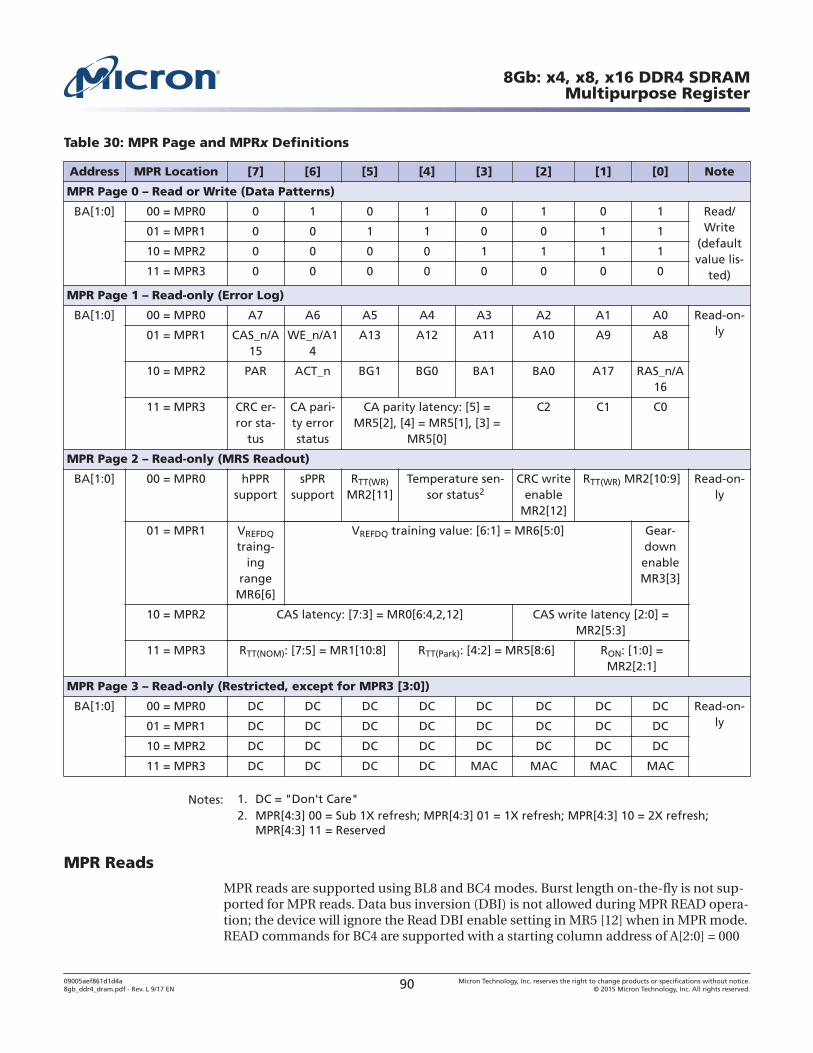
Table 30: MPR Page and MPRx Definitions
Address MPR Location [7] [6] [5] [4] [3] [2] [1] [0] Note
MPR Page 0 – Read or Write (Data Patterns)
BA[1:0] 00 = MPR0 0 1 0 1 0 1 0 1 Read/Write
(defaultvalue lis-
ted)
01 = MPR1 0 0 1 1 0 0 1 1
10 = MPR2 0 0 0 0 1 1 1 1
11 = MPR3 0 0 0 0 0 0 0 0
MPR Page 1 – Read-only (Error Log)
BA[1:0] 00 = MPR0 A7 A6 A5 A4 A3 A2 A1 A0 Read-on-ly01 = MPR1 CAS_n/A
15WE_n/A1
4A13 A12 A11 A10 A9 A8
10 = MPR2 PAR ACT_n BG1 BG0 BA1 BA0 A17 RAS_n/A16
11 = MPR3 CRC er-ror sta-
tus
CA pari-ty errorstatus
CA parity latency: [5] =MR5[2], [4] = MR5[1], [3] =
MR5[0]
C2 C1 C0
MPR Page 2 – Read-only (MRS Readout)
BA[1:0] 00 = MPR0 hPPRsupport
sPPRsupport
RTT(WR)
MR2[11]Temperature sen-
sor status2CRC write
enableMR2[12]
RTT(WR) MR2[10:9] Read-on-ly
01 = MPR1 VREFDQ
traing-ing
rangeMR6[6]
VREFDQ training value: [6:1] = MR6[5:0] Gear-downenableMR3[3]
10 = MPR2 CAS latency: [7:3] = MR0[6:4,2,12] CAS write latency [2:0] =MR2[5:3]
11 = MPR3 RTT(NOM): [7:5] = MR1[10:8] RTT(Park): [4:2] = MR5[8:6] RON: [1:0] =MR2[2:1]
MPR Page 3 – Read-only (Restricted, except for MPR3 [3:0])
BA[1:0] 00 = MPR0 DC DC DC DC DC DC DC DC Read-on-ly01 = MPR1 DC DC DC DC DC DC DC DC
10 = MPR2 DC DC DC DC DC DC DC DC
11 = MPR3 DC DC DC DC MAC MAC MAC MAC
Notes: 1. DC = "Don't Care"2. MPR[4:3] 00 = Sub 1X refresh; MPR[4:3] 01 = 1X refresh; MPR[4:3] 10 = 2X refresh;
MPR[4:3] 11 = Reserved
MPR Reads
MPR reads are supported using BL8 and BC4 modes. Burst length on-the-fly is not sup-ported for MPR reads. Data bus inversion (DBI) is not allowed during MPR READ opera-tion; the device will ignore the Read DBI enable setting in MR5 [12] when in MPR mode.READ commands for BC4 are supported with a starting column address of A[2:0] = 000
8Gb: x4, x8, x16 DDR4 SDRAMMultipurpose Register
09005aef861d1d4a8gb_ddr4_dram.pdf - Rev. L 9/17 EN 90 Micron Technology, Inc. reserves the right to change products or specifications without notice.
© 2015 Micron Technology, Inc. All rights reserved.
or 100. After power-up, the content of MPR Page 0 has the default values, which are de-fined in Table 30. MPR page 0 can be rewritten via an MPR WRITE command. The de-vice maintains the default values unless it is rewritten by the DRAM controller. If theDRAM controller does overwrite the default values (Page 0 only), the device will main-tain the new values unless re-initialized or there is power loss.
Timing in MPR mode:
• Reads (back-to-back) from Page 0 may use tCCD_S or tCCD_L timing between READcommands
• Reads (back-to-back) from Pages 1, 2, or 3 may not use tCCD_S timing between READcommands; tCCD_L must be used for timing between READ commands
The following steps are required to use the MPR to read out the contents of a mode reg-ister (MPR Page x, MPRy).
1. The DLL must be locked if enabled.2. Precharge all; wait until tRP is satisfied.3. MRS command to MR3[2] = 1 (Enable MPR data flow), MR3[12:11] = MPR read for-
mat, and MR3[1:0] MPR page.
a. MR3[12:11] MPR read format:
1. 00 = Serial read format2. 01 = Parallel read format3. 10 = staggered read format4. 11 = RFU
b. MR3[1:0] MPR page:
1. 00 = MPR Page 02. 01 = MPR Page 13. 10 = MPR Page 24. 11 = MPR Page 3
4. tMRD and tMOD must be satisfied.5. Redirect all subsequent READ commands to specific MPRx location.6. Issue RD or RDA command.
a. BA1 and BA0 indicate MPRx location:
1. 00 = MPR02. 01 = MPR13. 10 = MPR24. 11 = MPR3
b. A12/BC = 0 or 1; BL8 or BC4 fixed-only, BC4 OTF not supported.
1. If BL = 8 and MR0 A[1:0] = 01, A12/BC must be set to 1 during MPRREAD commands.
c. A2 = burst-type dependant:
1. BL8: A2 = 0 with burst order fixed at 0, 1, 2, 3, 4, 5, 6, 72. BL8: A2 = 1 not allowed3. BC4: A2 = 0 with burst order fixed at 0, 1, 2, 3, T, T, T, T4. BC4: A2 = 1 with burst order fixed at 4, 5, 6, 7, T, T, T, T
d. A[1:0] = 00, data burst is fixed nibble start at 00.e. Remaining address inputs, including A10, and BG1 and BG0 are "Don’t
Care."
8Gb: x4, x8, x16 DDR4 SDRAMMultipurpose Register
09005aef861d1d4a8gb_ddr4_dram.pdf - Rev. L 9/17 EN 91 Micron Technology, Inc. reserves the right to change products or specifications without notice.
© 2015 Micron Technology, Inc. All rights reserved.
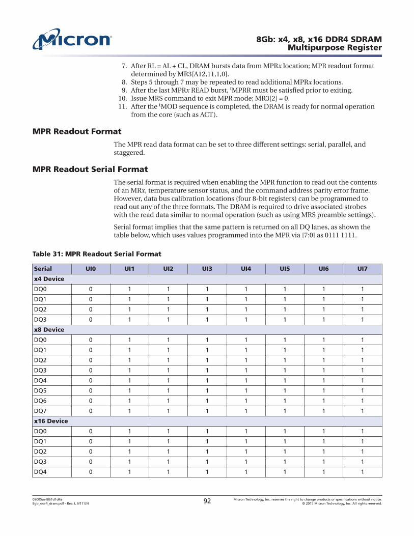
7. After RL = AL + CL, DRAM bursts data from MPRx location; MPR readout formatdetermined by MR3[A12,11,1,0].
8. Steps 5 through 7 may be repeated to read additional MPRx locations.9. After the last MPRx READ burst, tMPRR must be satisfied prior to exiting.
10. Issue MRS command to exit MPR mode; MR3[2] = 0.11. After the tMOD sequence is completed, the DRAM is ready for normal operation
from the core (such as ACT).
MPR Readout Format
The MPR read data format can be set to three different settings: serial, parallel, andstaggered.
MPR Readout Serial Format
The serial format is required when enabling the MPR function to read out the contentsof an MRx, temperature sensor status, and the command address parity error frame.However, data bus calibration locations (four 8-bit registers) can be programmed toread out any of the three formats. The DRAM is required to drive associated strobeswith the read data similar to normal operation (such as using MRS preamble settings).
Serial format implies that the same pattern is returned on all DQ lanes, as shown thetable below, which uses values programmed into the MPR via [7:0] as 0111 1111.
Table 31: MPR Readout Serial Format
Serial UI0 UI1 UI2 UI3 UI4 UI5 UI6 UI7
x4 Device
DQ0 0 1 1 1 1 1 1 1
DQ1 0 1 1 1 1 1 1 1
DQ2 0 1 1 1 1 1 1 1
DQ3 0 1 1 1 1 1 1 1
x8 Device
DQ0 0 1 1 1 1 1 1 1
DQ1 0 1 1 1 1 1 1 1
DQ2 0 1 1 1 1 1 1 1
DQ3 0 1 1 1 1 1 1 1
DQ4 0 1 1 1 1 1 1 1
DQ5 0 1 1 1 1 1 1 1
DQ6 0 1 1 1 1 1 1 1
DQ7 0 1 1 1 1 1 1 1
x16 Device
DQ0 0 1 1 1 1 1 1 1
DQ1 0 1 1 1 1 1 1 1
DQ2 0 1 1 1 1 1 1 1
DQ3 0 1 1 1 1 1 1 1
DQ4 0 1 1 1 1 1 1 1
8Gb: x4, x8, x16 DDR4 SDRAMMultipurpose Register
09005aef861d1d4a8gb_ddr4_dram.pdf - Rev. L 9/17 EN 92 Micron Technology, Inc. reserves the right to change products or specifications without notice.
© 2015 Micron Technology, Inc. All rights reserved.
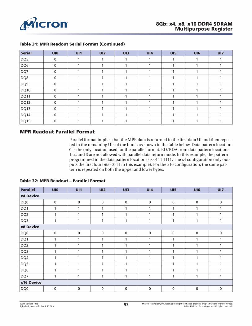
Table 31: MPR Readout Serial Format (Continued)
Serial UI0 UI1 UI2 UI3 UI4 UI5 UI6 UI7
DQ5 0 1 1 1 1 1 1 1
DQ6 0 1 1 1 1 1 1 1
DQ7 0 1 1 1 1 1 1 1
DQ8 0 1 1 1 1 1 1 1
DQ9 0 1 1 1 1 1 1 1
DQ10 0 1 1 1 1 1 1 1
DQ11 0 1 1 1 1 1 1 1
DQ12 0 1 1 1 1 1 1 1
DQ13 0 1 1 1 1 1 1 1
DQ14 0 1 1 1 1 1 1 1
DQ15 0 1 1 1 1 1 1 1
MPR Readout Parallel Format
Parallel format implies that the MPR data is returned in the first data UI and then repea-ted in the remaining UIs of the burst, as shown in the table below. Data pattern location0 is the only location used for the parallel format. RD/RDA from data pattern locations1, 2, and 3 are not allowed with parallel data return mode. In this example, the patternprogrammed in the data pattern location 0 is 0111 1111. The x4 configuration only out-puts the first four bits (0111 in this example). For the x16 configuration, the same pat-tern is repeated on both the upper and lower bytes.
Table 32: MPR Readout – Parallel Format
Parallel UI0 UI1 UI2 UI3 UI4 UI5 UI6 UI7
x4 Device
DQ0 0 0 0 0 0 0 0 0
DQ1 1 1 1 1 1 1 1 1
DQ2 1 1 1 1 1 1 1 1
DQ3 1 1 1 1 1 1 1 1
x8 Device
DQ0 0 0 0 0 0 0 0 0
DQ1 1 1 1 1 1 1 1 1
DQ2 1 1 1 1 1 1 1 1
DQ3 1 1 1 1 1 1 1 1
DQ4 1 1 1 1 1 1 1 1
DQ5 1 1 1 1 1 1 1 1
DQ6 1 1 1 1 1 1 1 1
DQ7 1 1 1 1 1 1 1 1
x16 Device
DQ0 0 0 0 0 0 0 0 0
8Gb: x4, x8, x16 DDR4 SDRAMMultipurpose Register
09005aef861d1d4a8gb_ddr4_dram.pdf - Rev. L 9/17 EN 93 Micron Technology, Inc. reserves the right to change products or specifications without notice.
© 2015 Micron Technology, Inc. All rights reserved.
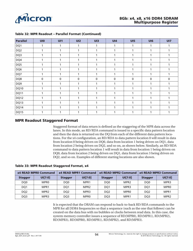
Table 32: MPR Readout – Parallel Format (Continued)
Parallel UI0 UI1 UI2 UI3 UI4 UI5 UI6 UI7
DQ1 1 1 1 1 1 1 1 1
DQ2 1 1 1 1 1 1 1 1
DQ3 1 1 1 1 1 1 1 1
DQ4 1 1 1 1 1 1 1 1
DQ5 1 1 1 1 1 1 1 1
DQ6 1 1 1 1 1 1 1 1
DQ7 1 1 1 1 1 1 1 1
DQ8 0 0 0 0 0 0 0 0
DQ9 1 1 1 1 1 1 1 1
DQ10 1 1 1 1 1 1 1 1
DQ11 1 1 1 1 1 1 1 1
DQ12 1 1 1 1 1 1 1 1
DQ13 1 1 1 1 1 1 1 1
DQ14 1 1 1 1 1 1 1 1
DQ15 1 1 1 1 1 1 1 1
MPR Readout Staggered Format
Staggered format of data return is defined as the staggering of the MPR data across thelanes. In this mode, an RD/RDA command is issued to a specific data pattern locationand then the data is returned on the DQ from each of the different data pattern loca-tions. For the x4 configuration, an RD/RDA to data pattern location 0 will result in datafrom location 0 being driven on DQ0, data from location 1 being driven on DQ1, datafrom location 2 being driven on DQ2, and so on, as shown below. Similarly, an RD/RDAcommand to data pattern location 1 will result in data from location 1 being driven onDQ0, data from location 2 being driven on DQ1, data from location 3 being driven onDQ2, and so on. Examples of different starting locations are also shown.
Table 33: MPR Readout Staggered Format, x4
x4 READ MPR0 Command x4 READ MPR1 Command x4 READ MPR2 Command x4 READ MPR3 Command
Stagger UI[7:0] Stagger UI[7:0] Stagger UI[7:0] Stagger UI[7:0]
DQ0 MPR0 DQ0 MPR1 DQ0 MPR2 DQ0 MPR3
DQ1 MPR1 DQ1 MPR2 DQ1 MPR3 DQ1 MPR0
DQ2 MPR2 DQ2 MPR3 DQ2 MPR0 DQ2 MPR1
DQ3 MPR3 DQ3 MPR0 DQ3 MPR1 DQ3 MPR2
It is expected that the DRAM can respond to back-to-back RD/RDA commands to theMPR for all DDR4 frequencies so that a sequence (such as the one that follows) can becreated on the data bus with no bubbles or clocks between read data. In this case, thesystem memory controller issues a sequence of RD(MPR0), RD(MPR1), RD(MPR2),RD(MPR3), RD(MPR0), RD(MPR1), RD(MPR2), and RD(MPR3).
8Gb: x4, x8, x16 DDR4 SDRAMMultipurpose Register
09005aef861d1d4a8gb_ddr4_dram.pdf - Rev. L 9/17 EN 94 Micron Technology, Inc. reserves the right to change products or specifications without notice.
© 2015 Micron Technology, Inc. All rights reserved.
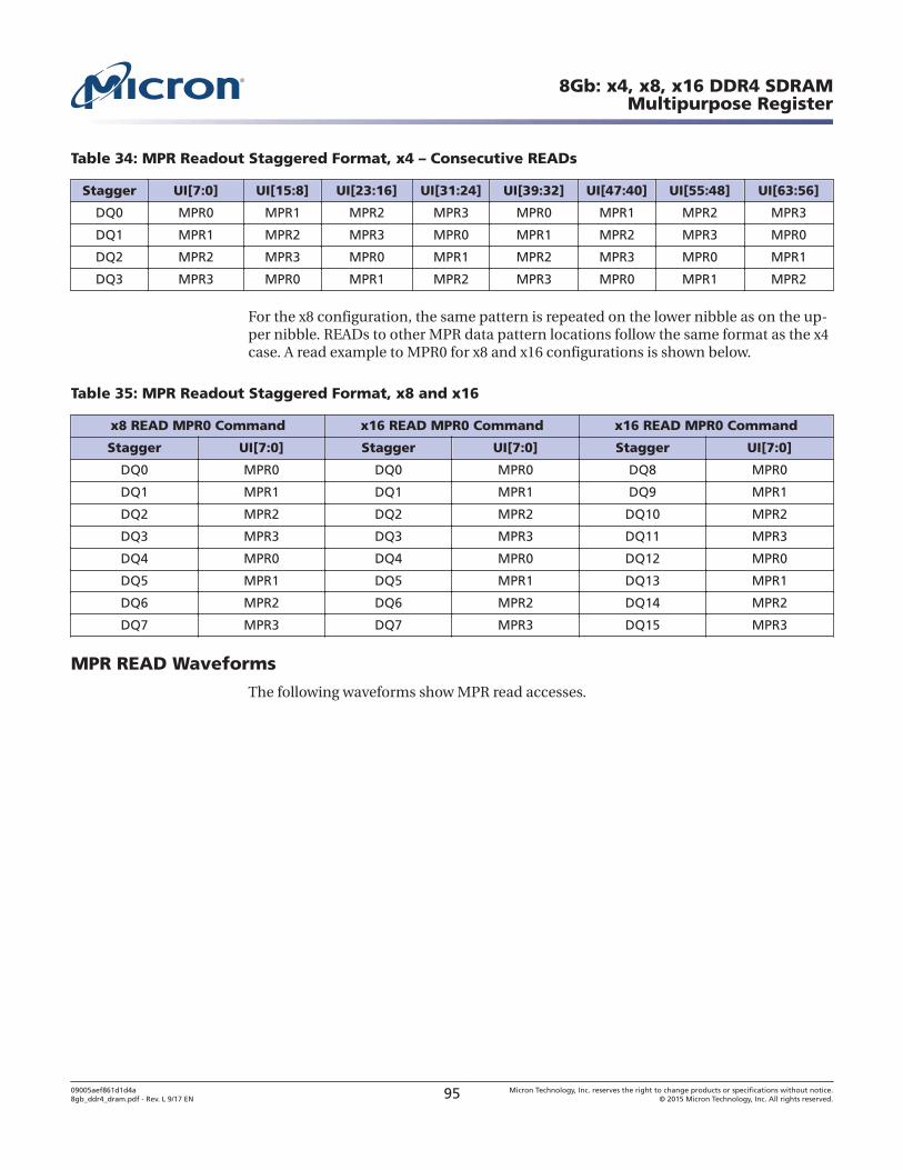
Table 34: MPR Readout Staggered Format, x4 – Consecutive READs
Stagger UI[7:0] UI[15:8] UI[23:16] UI[31:24] UI[39:32] UI[47:40] UI[55:48] UI[63:56]
DQ0 MPR0 MPR1 MPR2 MPR3 MPR0 MPR1 MPR2 MPR3
DQ1 MPR1 MPR2 MPR3 MPR0 MPR1 MPR2 MPR3 MPR0
DQ2 MPR2 MPR3 MPR0 MPR1 MPR2 MPR3 MPR0 MPR1
DQ3 MPR3 MPR0 MPR1 MPR2 MPR3 MPR0 MPR1 MPR2
For the x8 configuration, the same pattern is repeated on the lower nibble as on the up-per nibble. READs to other MPR data pattern locations follow the same format as the x4case. A read example to MPR0 for x8 and x16 configurations is shown below.
Table 35: MPR Readout Staggered Format, x8 and x16
x8 READ MPR0 Command x16 READ MPR0 Command x16 READ MPR0 Command
Stagger UI[7:0] Stagger UI[7:0] Stagger UI[7:0]
DQ0 MPR0 DQ0 MPR0 DQ8 MPR0
DQ1 MPR1 DQ1 MPR1 DQ9 MPR1
DQ2 MPR2 DQ2 MPR2 DQ10 MPR2
DQ3 MPR3 DQ3 MPR3 DQ11 MPR3
DQ4 MPR0 DQ4 MPR0 DQ12 MPR0
DQ5 MPR1 DQ5 MPR1 DQ13 MPR1
DQ6 MPR2 DQ6 MPR2 DQ14 MPR2
DQ7 MPR3 DQ7 MPR3 DQ15 MPR3
MPR READ Waveforms
The following waveforms show MPR read accesses.
8Gb: x4, x8, x16 DDR4 SDRAMMultipurpose Register
09005aef861d1d4a8gb_ddr4_dram.pdf - Rev. L 9/17 EN 95 Micron Technology, Inc. reserves the right to change products or specifications without notice.
© 2015 Micron Technology, Inc. All rights reserved.
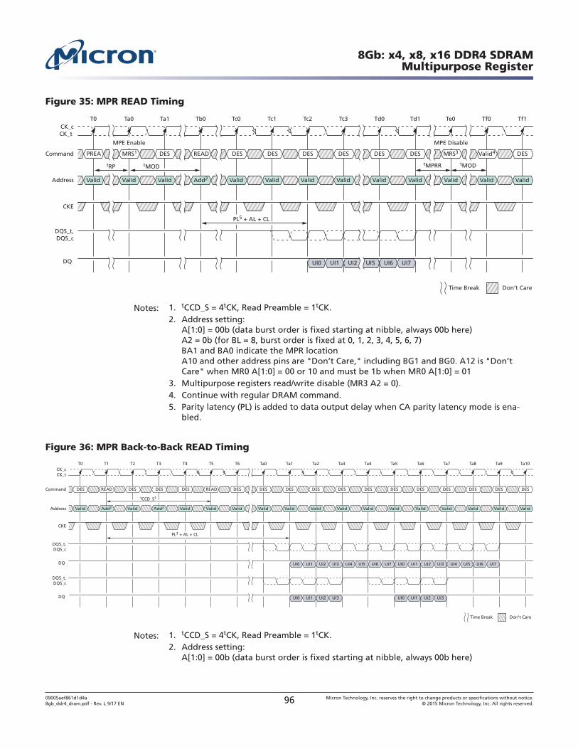
Figure 35: MPR READ Timing
T0 Ta0 Ta1
CK_tCK_c
DQ
DQS_t,DQS_c
tMODtMPRR
Tb0 Tc0 Tc1 Tc2 Tc3 Td0 Td1 Te0 Tf0 Tf1
DES DES DES DES MRS3 Valid4 DESCommand MRS1PREA DES READ DES DES
Valid Valid Valid Valid Valid Valid ValidValidValid Valid Add2 Valid ValidAddress
CKE
PL5 + AL + CL
tRP tMOD
UI0 UI1 UI2 UI5 UI6 UI7
MPE Enable MPE Disable
Don’t CareTime Break
Notes: 1. tCCD_S = 4tCK, Read Preamble = 1tCK.2. Address setting:
A[1:0] = 00b (data burst order is fixed starting at nibble, always 00b here)A2 = 0b (for BL = 8, burst order is fixed at 0, 1, 2, 3, 4, 5, 6, 7)BA1 and BA0 indicate the MPR locationA10 and other address pins are "Don’t Care," including BG1 and BG0. A12 is "Don’tCare" when MR0 A[1:0] = 00 or 10 and must be 1b when MR0 A[1:0] = 01
3. Multipurpose registers read/write disable (MR3 A2 = 0).4. Continue with regular DRAM command.5. Parity latency (PL) is added to data output delay when CA parity latency mode is ena-
bled.
Figure 36: MPR Back-to-Back READ Timing
T0 T1 T2
DQ
DQS_t,DQS_c
T3 T4 T5 T6 Ta0 Ta1 Ta2 Ta3 Ta4 Ta5 Ta6 Ta7 Ta8 Ta9 Ta10
DES DES DES DES DES DES DES DES DES DES DES DESCommand READDES DES DES DES READ
Valid Valid Valid Valid Valid Valid Valid Valid Valid Valid Valid ValidAdd2Valid Valid Add2 Valid ValidAddress
CKE
PL3 + AL + CL
tCCD_S1
DQ
DQS_t,DQS_c
UI0 UI1 UI2 UI3
UI0 UI1 UI2 UI3 UI0 UI1 UI2 UI3
UI4 UI5 UI6 UI7 UI0 UI1 UI2 UI3 UI4 UI5 UI6 UI7
CK_tCK_c
Don’t CareTime Break
Notes: 1. tCCD_S = 4tCK, Read Preamble = 1tCK.2. Address setting:
A[1:0] = 00b (data burst order is fixed starting at nibble, always 00b here)
8Gb: x4, x8, x16 DDR4 SDRAMMultipurpose Register
09005aef861d1d4a8gb_ddr4_dram.pdf - Rev. L 9/17 EN 96 Micron Technology, Inc. reserves the right to change products or specifications without notice.
© 2015 Micron Technology, Inc. All rights reserved.
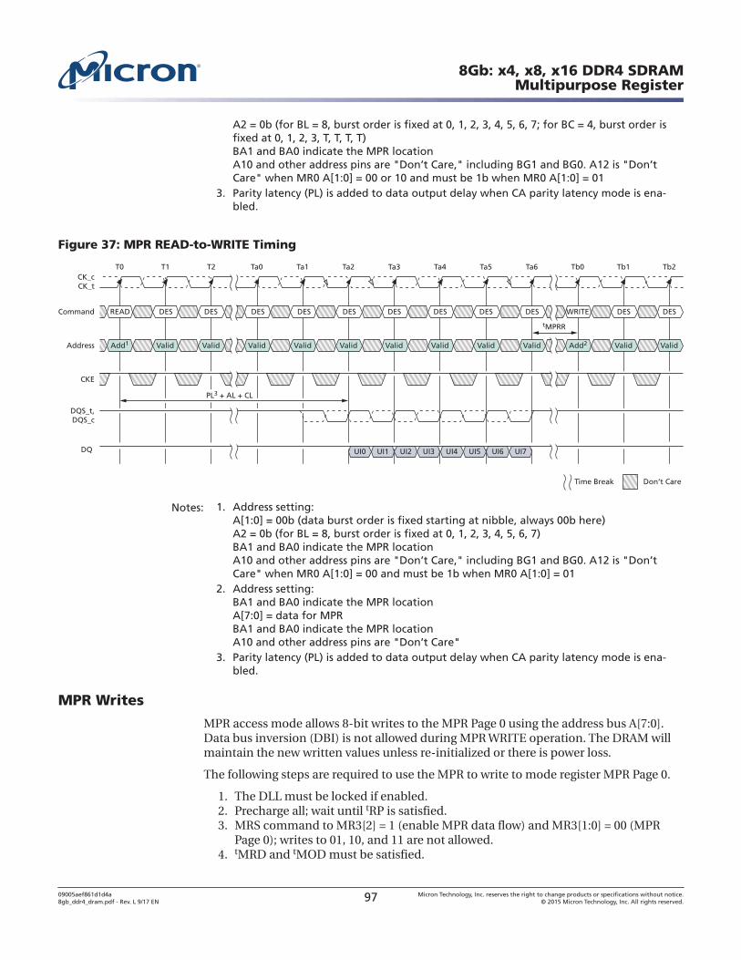
A2 = 0b (for BL = 8, burst order is fixed at 0, 1, 2, 3, 4, 5, 6, 7; for BC = 4, burst order isfixed at 0, 1, 2, 3, T, T, T, T)BA1 and BA0 indicate the MPR locationA10 and other address pins are "Don’t Care," including BG1 and BG0. A12 is "Don’tCare" when MR0 A[1:0] = 00 or 10 and must be 1b when MR0 A[1:0] = 01
3. Parity latency (PL) is added to data output delay when CA parity latency mode is ena-bled.
Figure 37: MPR READ-to-WRITE Timing
T0 T1 T2
DQ
DQS_t,DQS_c
tMPRR
Ta0 Ta1 Ta2 Ta3 Ta4 Ta5 Ta6 Tb0 Tb1 Tb2
DES DES DES DES WRITE DES DESCommand DESREAD DES DES DES DES
Valid Valid Valid Valid Add2 Valid ValidValidAdd1 Valid Valid Valid ValidAddress
CKE
PL3 + AL + CL
UI2 UI3UI0 UI1 UI4 UI5 UI6 UI7
CK_tCK_c
Don’t CareTime Break
Notes: 1. Address setting:A[1:0] = 00b (data burst order is fixed starting at nibble, always 00b here)A2 = 0b (for BL = 8, burst order is fixed at 0, 1, 2, 3, 4, 5, 6, 7)BA1 and BA0 indicate the MPR locationA10 and other address pins are "Don’t Care," including BG1 and BG0. A12 is "Don’tCare" when MR0 A[1:0] = 00 and must be 1b when MR0 A[1:0] = 01
2. Address setting:BA1 and BA0 indicate the MPR locationA[7:0] = data for MPRBA1 and BA0 indicate the MPR locationA10 and other address pins are "Don’t Care"
3. Parity latency (PL) is added to data output delay when CA parity latency mode is ena-bled.
MPR Writes
MPR access mode allows 8-bit writes to the MPR Page 0 using the address bus A[7:0].Data bus inversion (DBI) is not allowed during MPR WRITE operation. The DRAM willmaintain the new written values unless re-initialized or there is power loss.
The following steps are required to use the MPR to write to mode register MPR Page 0.
1. The DLL must be locked if enabled.2. Precharge all; wait until tRP is satisfied.3. MRS command to MR3[2] = 1 (enable MPR data flow) and MR3[1:0] = 00 (MPR
Page 0); writes to 01, 10, and 11 are not allowed.4. tMRD and tMOD must be satisfied.
8Gb: x4, x8, x16 DDR4 SDRAMMultipurpose Register
09005aef861d1d4a8gb_ddr4_dram.pdf - Rev. L 9/17 EN 97 Micron Technology, Inc. reserves the right to change products or specifications without notice.
© 2015 Micron Technology, Inc. All rights reserved.
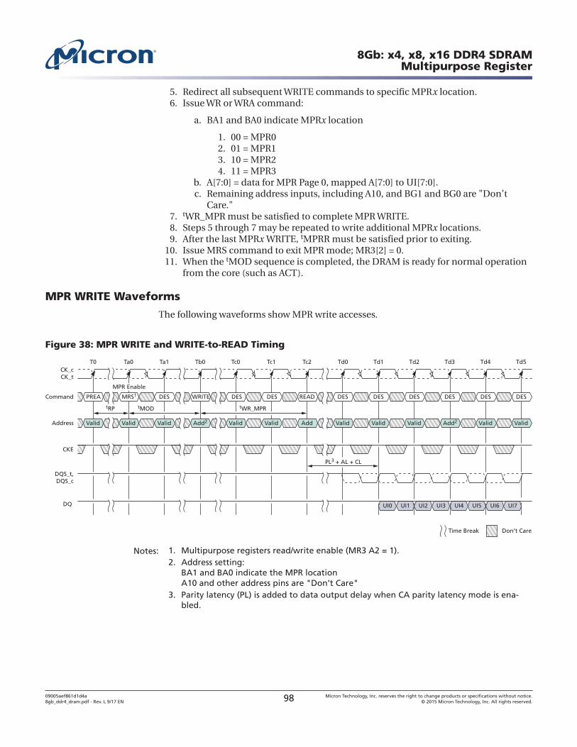
5. Redirect all subsequent WRITE commands to specific MPRx location.6. Issue WR or WRA command:
a. BA1 and BA0 indicate MPRx location
1. 00 = MPR02. 01 = MPR13. 10 = MPR24. 11 = MPR3
b. A[7:0] = data for MPR Page 0, mapped A[7:0] to UI[7:0].c. Remaining address inputs, including A10, and BG1 and BG0 are "Don’t
Care."7. tWR_MPR must be satisfied to complete MPR WRITE.8. Steps 5 through 7 may be repeated to write additional MPRx locations.9. After the last MPRx WRITE, tMPRR must be satisfied prior to exiting.
10. Issue MRS command to exit MPR mode; MR3[2] = 0.11. When the tMOD sequence is completed, the DRAM is ready for normal operation
from the core (such as ACT).
MPR WRITE Waveforms
The following waveforms show MPR write accesses.
Figure 38: MPR WRITE and WRITE-to-READ Timing
T0 Ta0 Ta1
DQ
DQS_t,DQS_c
tRP tMOD tWR_MPR
Tb0 Tc0 Tc1 Tc2 Td0 Td1 Td2 Td3 Td4 Td5
READ DES DES DES DES DES DESCommand MRS1PREA DES WRITE DES DES
Add Valid Valid Valid Add2 Valid ValidValidValid Valid Add2 Valid ValidAddress
CKE
PL3 + AL + CL
UI2 UI3UI0 UI1 UI4 UI5 UI6 UI7
CK_tCK_c
MPR Enable
Don’t CareTime Break
Notes: 1. Multipurpose registers read/write enable (MR3 A2 = 1).2. Address setting:
BA1 and BA0 indicate the MPR locationA10 and other address pins are "Don’t Care"
3. Parity latency (PL) is added to data output delay when CA parity latency mode is ena-bled.
8Gb: x4, x8, x16 DDR4 SDRAMMultipurpose Register
09005aef861d1d4a8gb_ddr4_dram.pdf - Rev. L 9/17 EN 98 Micron Technology, Inc. reserves the right to change products or specifications without notice.
© 2015 Micron Technology, Inc. All rights reserved.
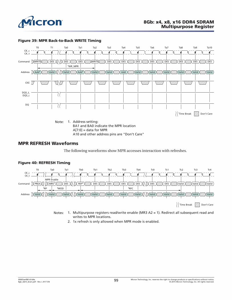
Figure 39: MPR Back-to-Back WRITE Timing
T0 T1 Ta0
DQ
DQS_t,DQS_c
tWR_MPR
Ta1 Ta2 Ta3 Ta4 Ta5 Ta6 Ta7 Ta8 Ta9 Ta10
DES DES DES DES DES DES DESCommand DESWRITE DES WRITEDES DES
Add Valid Valid Valid Valid Valid ValidValidAdd1 Valid Add1 Valid ValidAddress
CKE
CK_tCK_c
Don’t CareTime Break
Note: 1. Address setting:BA1 and BA0 indicate the MPR locationA[7:0] = data for MPRA10 and other address pins are "Don’t Care"
MPR REFRESH Waveforms
The following waveforms show MPR accesses interaction with refreshes.
Figure 40: REFRESH Timing
T0
tMODtRP
Tc4Ta0 Ta1 Tb0 Tb1 Tb2 Tb3 Tb4 Tc0 Tc1 Tc2 Tc3
DES DES DES DES Valid Valid ValidCommand MRS1PREA DES REF2 DES DES
Valid Valid Valid Valid Valid Valid ValidValidValid Valid Valid Valid ValidAddress
CK_tCK_c
tRFC
MPR Enable
Don’t CareTime Break
Notes: 1. Multipurpose registers read/write enable (MR3 A2 = 1). Redirect all subsequent read andwrites to MPR locations.
2. 1x refresh is only allowed when MPR mode is enabled.
8Gb: x4, x8, x16 DDR4 SDRAMMultipurpose Register
09005aef861d1d4a8gb_ddr4_dram.pdf - Rev. L 9/17 EN 99 Micron Technology, Inc. reserves the right to change products or specifications without notice.
© 2015 Micron Technology, Inc. All rights reserved.
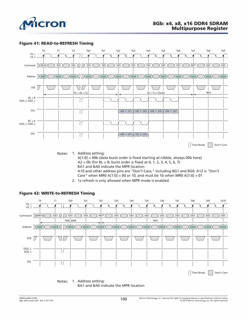
Figure 41: READ-to-REFRESH Timing
T0 T1 T2
DQ
BL = 8DQS_t, DQS_c
Ta0 Ta1 Ta2 Ta3 Ta4 Ta5 Ta6 Ta7 Ta8 Ta9
DES DES DES DES REF2 DES DESCommand DESREAD DES DES DES DES
Valid Valid Valid Valid Valid Valid ValidValidAdd1 Valid Valid Valid ValidAddress
CKE
tRFC
UI2 UI3UI0 UI1 UI4 UI5 UI6 UI7
DQ
BC = 4DQS_t, DQS_c
UI2 UI3UI0 UI1
(4 + 1) + ClocksPL + AL + CL
CK_tCK_c
Don’t CareTime Break
Notes: 1. Address setting:A[1:0] = 00b (data burst order is fixed starting at nibble, always 00b here)A2 = 0b (for BL = 8, burst order is fixed at 0, 1, 2, 3, 4, 5, 6, 7)BA1 and BA0 indicate the MPR locationA10 and other address pins are "Don’t Care," including BG1 and BG0. A12 is "Don’tCare" when MR0 A[1:0] = 00 or 10, and must be 1b when MR0 A[1:0] = 01
2. 1x refresh is only allowed when MPR mode is enabled.
Figure 42: WRITE-to-REFRESH Timing
T0 T1 Ta0
DQ
DQS_t,DQS_c
tRFC
Don’t Care
Ta1 Ta2 Ta3 Ta4 Ta5 Ta6 Ta7 Ta8 Ta9 Ta10
DES DES DES DES DES DES DESCommand DESWRITE DES DES REF2 DES
Valid Valid Valid Valid Valid Valid ValidValidAdd1 Valid Valid Valid Valid
Time Break
Address
CKE
CK_tCK_c
tWR_MPR
Notes: 1. Address setting:BA1 and BA0 indicate the MPR location
8Gb: x4, x8, x16 DDR4 SDRAMMultipurpose Register
09005aef861d1d4a8gb_ddr4_dram.pdf - Rev. L 9/17 EN 100 Micron Technology, Inc. reserves the right to change products or specifications without notice.
© 2015 Micron Technology, Inc. All rights reserved.
A[7:0] = data for MPRA10 and other address pins are "Don’t Care"
2. 1x refresh is only allowed when MPR mode is enabled.
8Gb: x4, x8, x16 DDR4 SDRAMMultipurpose Register
09005aef861d1d4a8gb_ddr4_dram.pdf - Rev. L 9/17 EN 101 Micron Technology, Inc. reserves the right to change products or specifications without notice.
© 2015 Micron Technology, Inc. All rights reserved.
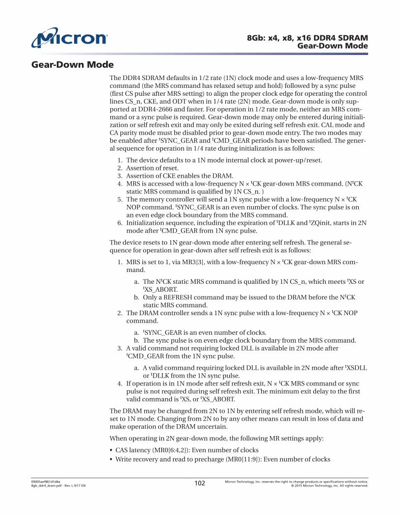
Gear-Down ModeThe DDR4 SDRAM defaults in 1/2 rate (1N) clock mode and uses a low-frequency MRScommand (the MRS command has relaxed setup and hold) followed by a sync pulse(first CS pulse after MRS setting) to align the proper clock edge for operating the controllines CS_n, CKE, and ODT when in 1/4 rate (2N) mode. Gear-down mode is only sup-ported at DDR4-2666 and faster. For operation in 1/2 rate mode, neither an MRS com-mand or a sync pulse is required. Gear-down mode may only be entered during initiali-zation or self refresh exit and may only be exited during self refresh exit. CAL mode andCA parity mode must be disabled prior to gear-down mode entry. The two modes maybe enabled after tSYNC_GEAR and tCMD_GEAR periods have been satisfied. The gener-al sequence for operation in 1/4 rate during initialization is as follows:
1. The device defaults to a 1N mode internal clock at power-up/reset.2. Assertion of reset.3. Assertion of CKE enables the DRAM.4. MRS is accessed with a low-frequency N × tCK gear-down MRS command. (NtCK
static MRS command is qualified by 1N CS_n. )5. The memory controller will send a 1N sync pulse with a low-frequency N × tCK
NOP command. tSYNC_GEAR is an even number of clocks. The sync pulse is onan even edge clock boundary from the MRS command.
6. Initialization sequence, including the expiration of tDLLK and tZQinit, starts in 2Nmode after tCMD_GEAR from 1N sync pulse.
The device resets to 1N gear-down mode after entering self refresh. The general se-quence for operation in gear-down after self refresh exit is as follows:
1. MRS is set to 1, via MR3[3], with a low-frequency N × tCK gear-down MRS com-mand.
a. The NtCK static MRS command is qualified by 1N CS_n, which meets tXS ortXS_ABORT.
b. Only a REFRESH command may be issued to the DRAM before the NtCKstatic MRS command.
2. The DRAM controller sends a 1N sync pulse with a low-frequency N × tCK NOPcommand.
a. tSYNC_GEAR is an even number of clocks.b. The sync pulse is on even edge clock boundary from the MRS command.
3. A valid command not requiring locked DLL is available in 2N mode aftertCMD_GEAR from the 1N sync pulse.
a. A valid command requiring locked DLL is available in 2N mode after tXSDLLor tDLLK from the 1N sync pulse.
4. If operation is in 1N mode after self refresh exit, N × tCK MRS command or syncpulse is not required during self refresh exit. The minimum exit delay to the firstvalid command is tXS, or tXS_ABORT.
The DRAM may be changed from 2N to 1N by entering self refresh mode, which will re-set to 1N mode. Changing from 2N to by any other means can result in loss of data andmake operation of the DRAM uncertain.
When operating in 2N gear-down mode, the following MR settings apply:
• CAS latency (MR0[6:4,2]): Even number of clocks• Write recovery and read to precharge (MR0[11:9]): Even number of clocks
8Gb: x4, x8, x16 DDR4 SDRAMGear-Down Mode
09005aef861d1d4a8gb_ddr4_dram.pdf - Rev. L 9/17 EN 102 Micron Technology, Inc. reserves the right to change products or specifications without notice.
© 2015 Micron Technology, Inc. All rights reserved.
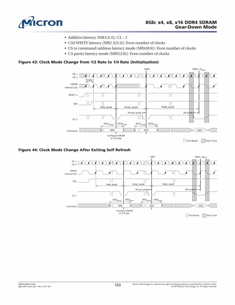
• Additive latency (MR1[4:3]): CL - 2• CAS WRITE latency (MR2 A[5:3]): Even number of clocks• CS to command/address latency mode (MR4[8:6]): Even number of clocks• CA parity latency mode (MR5[2:0]): Even number of clocks
Figure 43: Clock Mode Change from 1/2 Rate to 1/4 Rate (Initialization)
tXPR_GEAR tCMD_GEARtSYNC_GEAR
TdkN
CK_c
CK_t
Don’t CareTime Break
TdkN + Neven
Configure DRAMto 1/4 rate
tDSRX
NtCKsetup NtCKhold NtCKsetup NtCKhold
1N sync pulse 2N mode
DRAM
internal CLK
RESET_n
CKE
CS_n
Command MRS NOP Valid
Figure 44: Clock Mode Change After Exiting Self Refresh
TdkN
CK_c
CK_t
Don’t CareTime Break
TdkN + Neven
Configure DRAMto 1/4 rate
NtCKsetup NtCKhold NtCKsetup NtCKhold
1N sync pulse 2N mode
DRAM
internal CLK
CKE
CS_n
Command MRS NOP Valid
tXPR_GEAR tCMD_GEARtSYNC_GEAR
8Gb: x4, x8, x16 DDR4 SDRAMGear-Down Mode
09005aef861d1d4a8gb_ddr4_dram.pdf - Rev. L 9/17 EN 103 Micron Technology, Inc. reserves the right to change products or specifications without notice.
© 2015 Micron Technology, Inc. All rights reserved.
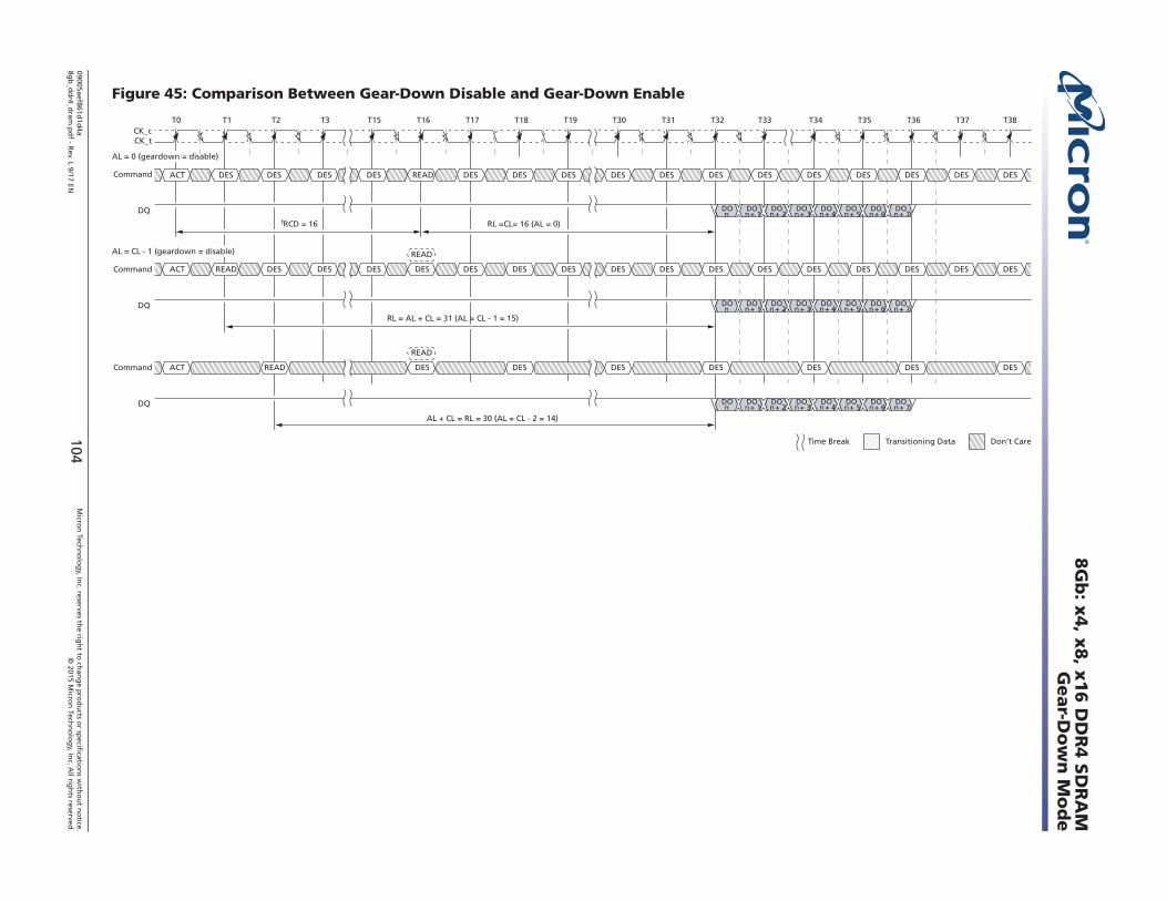
Figure 45: Comparison Between Gear-Down Disable and Gear-Down Enable
T0
tRCD = 16
T33T1 T2 T3 T15 T16 T17 T18 T19 T30 T31 T32
DES DES DES DES DES DES DESCommand DESACT DES DES DES READ
DQ
CK_tCK_c
RL =CL= 16 (AL = 0)
T38T34 T35 T36 T37
AL = 0 (geardown = disable)
Don’t CareTransitioning DataTime Break
DOn + 3
DOn + 4
DOn + 5
DOn + 6
DOn + 7
DOn + 2
DOn + 1
DOn
DES DES DES DES DES
DES DES DES DES DES DES DESCommand READACT DES DES DES DES
READ
DQ
RL = AL + CL = 31 (AL = CL - 1 = 15)
AL = CL - 1 (geardown = disable)
DOn + 3
DOn + 4
DOn + 5
DOn + 6
DOn + 7
DOn + 2
DOn + 1
DOn
DES DES DES DES DES
DES DES DESCommand ACT READ DES
READ
DQ
AL + CL = RL = 30 (AL = CL - 2 = 14)
DOn + 3
DOn + 4
DOn + 5
DOn + 6
DOn + 7
DOn + 2
DOn + 1
DOn
DES DES DES
8G
b: x
4, x
8, x
16 D
DR
4 S
DR
AM
Gear-D
ow
n M
od
e
09005aef861d1d
4a8g
b_d
dr4_d
ram.p
df - R
ev. L 9/17 EN104
Micro
n Tech
no
log
y, Inc. reserves th
e righ
t to ch
ang
e pro
du
cts or sp
ecification
s with
ou
t no
tice.©
2015 Micro
n Tech
no
log
y, Inc. A
ll righ
ts reserved.
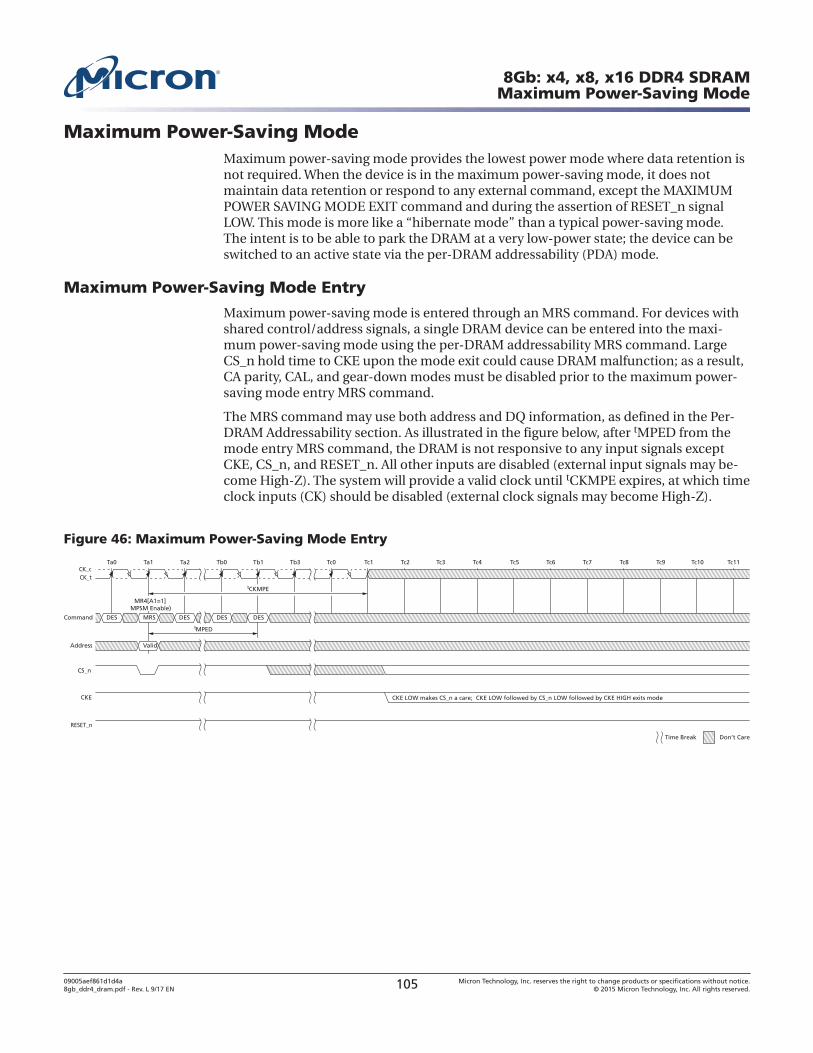
Maximum Power-Saving ModeMaximum power-saving mode provides the lowest power mode where data retention isnot required. When the device is in the maximum power-saving mode, it does notmaintain data retention or respond to any external command, except the MAXIMUMPOWER SAVING MODE EXIT command and during the assertion of RESET_n signalLOW. This mode is more like a “hibernate mode” than a typical power-saving mode.The intent is to be able to park the DRAM at a very low-power state; the device can beswitched to an active state via the per-DRAM addressability (PDA) mode.
Maximum Power-Saving Mode Entry
Maximum power-saving mode is entered through an MRS command. For devices withshared control/address signals, a single DRAM device can be entered into the maxi-mum power-saving mode using the per-DRAM addressability MRS command. LargeCS_n hold time to CKE upon the mode exit could cause DRAM malfunction; as a result,CA parity, CAL, and gear-down modes must be disabled prior to the maximum power-saving mode entry MRS command.
The MRS command may use both address and DQ information, as defined in the Per-DRAM Addressability section. As illustrated in the figure below, after tMPED from themode entry MRS command, the DRAM is not responsive to any input signals exceptCKE, CS_n, and RESET_n. All other inputs are disabled (external input signals may be-come High-Z). The system will provide a valid clock until tCKMPE expires, at which timeclock inputs (CK) should be disabled (external clock signals may become High-Z).
Figure 46: Maximum Power-Saving Mode Entry
Ta0 Ta1 Ta2 Tb0 Tb1
Command MRSDES DES DESDES
CK_tCK_c
RESET_n
Tc11Tb3 Tc0 Tc1 Tc2 Tc3 Tc4 Tc7Tc5 Tc6 Tc8 Tc9 Tc10
Don’t CareTime Break
CS_n
CKE
tMPED
CKE LOW makes CS_n a care; CKE LOW followed by CS_n LOW followed by CKE HIGH exits mode
MR4[A1=1]MPSM Enable)
Address Valid
tCKMPE
8Gb: x4, x8, x16 DDR4 SDRAMMaximum Power-Saving Mode
09005aef861d1d4a8gb_ddr4_dram.pdf - Rev. L 9/17 EN 105 Micron Technology, Inc. reserves the right to change products or specifications without notice.
© 2015 Micron Technology, Inc. All rights reserved.
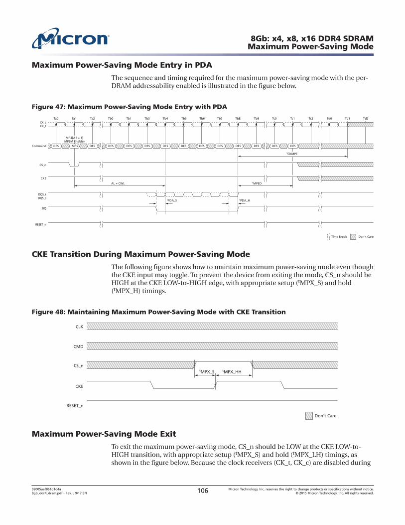
Maximum Power-Saving Mode Entry in PDA
The sequence and timing required for the maximum power-saving mode with the per-DRAM addressability enabled is illustrated in the figure below.
Figure 47: Maximum Power-Saving Mode Entry with PDA
Ta0 Ta1 Ta2 Tb0 Tb1
Command MRSDES DES DESDES DES DES DES DES DES DES DES DESDES
CK_tCK_c
DQS_tDQS_c
DQ
Tb3 Tb4 Tb5 Tb6 Tb7 Tb8 Tc1Tb9 Tc0 Tc2 Td0 Td1 Td2
Don’t CareTime Break
CS_n
CKE
RESET_n
MR4[A1 = 1]MPSM Enable)
AL + CWL tMPED
tPDA_HtPDA_S
tCKMPE
CKE Transition During Maximum Power-Saving Mode
The following figure shows how to maintain maximum power-saving mode even thoughthe CKE input may toggle. To prevent the device from exiting the mode, CS_n should beHIGH at the CKE LOW-to-HIGH edge, with appropriate setup (tMPX_S) and hold(tMPX_H) timings.
Figure 48: Maintaining Maximum Power-Saving Mode with CKE Transition
CMD
CS_n
CKE
RESET_n
Don’t Care
CLK
tMPX_HHtMPX_S
Maximum Power-Saving Mode Exit
To exit the maximum power-saving mode, CS_n should be LOW at the CKE LOW-to-HIGH transition, with appropriate setup (tMPX_S) and hold (tMPX_LH) timings, asshown in the figure below. Because the clock receivers (CK_t, CK_c) are disabled during
8Gb: x4, x8, x16 DDR4 SDRAMMaximum Power-Saving Mode
09005aef861d1d4a8gb_ddr4_dram.pdf - Rev. L 9/17 EN 106 Micron Technology, Inc. reserves the right to change products or specifications without notice.
© 2015 Micron Technology, Inc. All rights reserved.
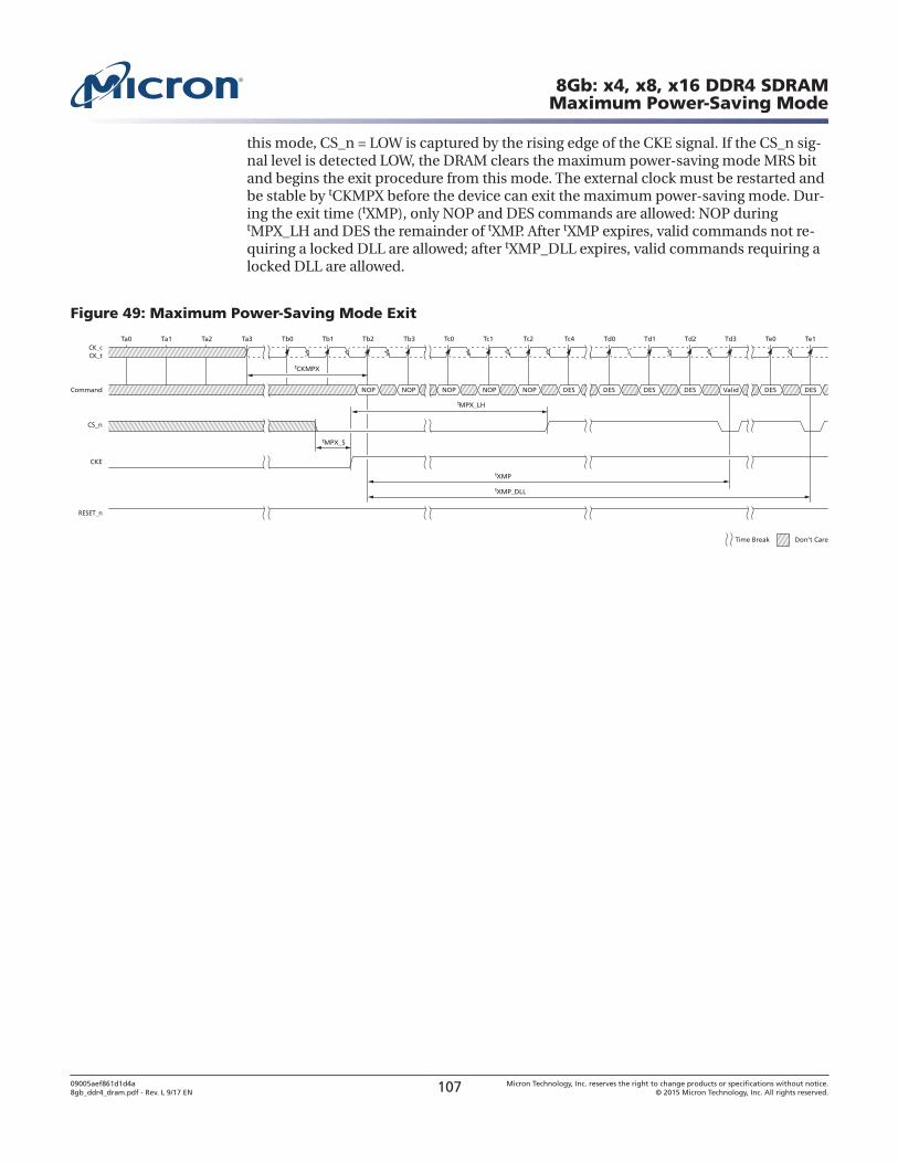
this mode, CS_n = LOW is captured by the rising edge of the CKE signal. If the CS_n sig-nal level is detected LOW, the DRAM clears the maximum power-saving mode MRS bitand begins the exit procedure from this mode. The external clock must be restarted andbe stable by tCKMPX before the device can exit the maximum power-saving mode. Dur-ing the exit time (tXMP), only NOP and DES commands are allowed: NOP duringtMPX_LH and DES the remainder of tXMP. After tXMP expires, valid commands not re-quiring a locked DLL are allowed; after tXMP_DLL expires, valid commands requiring alocked DLL are allowed.
Figure 49: Maximum Power-Saving Mode Exit
Ta0
tCKMPX
tMPX_S
tXMP
tXMP_DLL
Ta1 Ta2 Ta3 Tb0
NOP NOP NOP NOP NOP DES DESCommand
CK_tCK_c
RESET_n
Te1Tb1 Tb2 Tb3 Tc0 Tc1 Tc2 Td1Tc4 Td0 Td2 Td3 Te0
Don’t CareTime Break
DES DES Valid DES DES
CS_n
CKE
tMPX_LH
8Gb: x4, x8, x16 DDR4 SDRAMMaximum Power-Saving Mode
09005aef861d1d4a8gb_ddr4_dram.pdf - Rev. L 9/17 EN 107 Micron Technology, Inc. reserves the right to change products or specifications without notice.
© 2015 Micron Technology, Inc. All rights reserved.
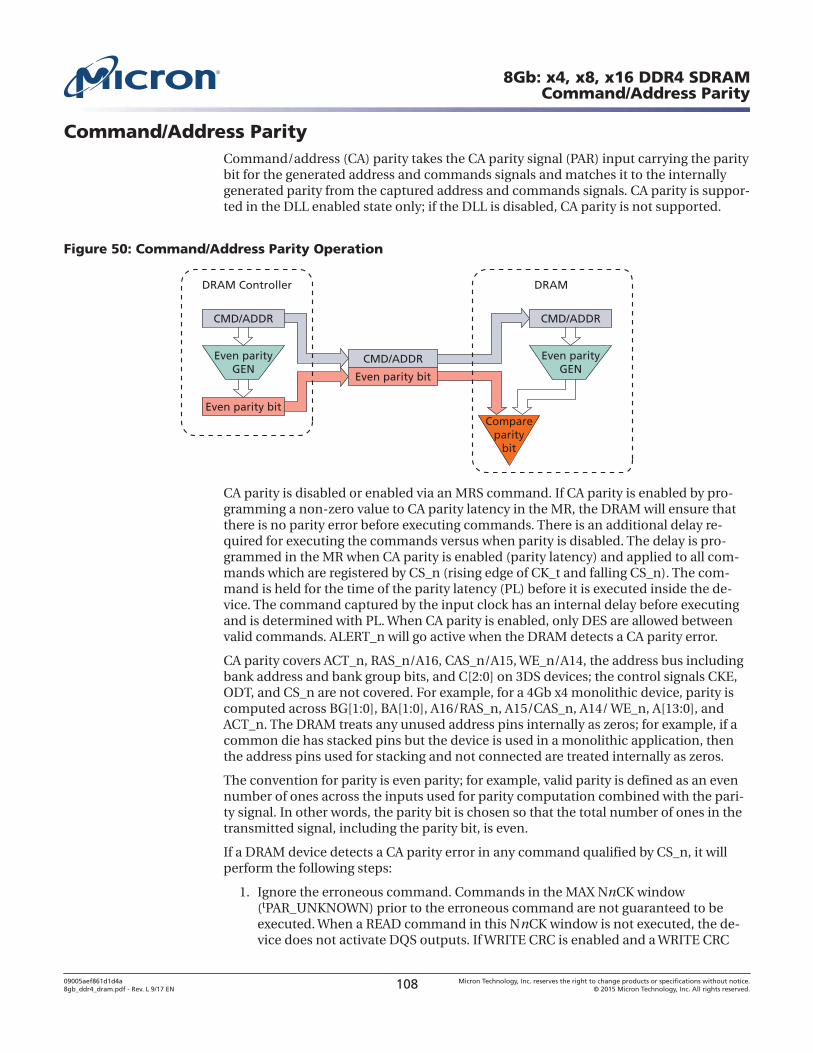
Command/Address ParityCommand/address (CA) parity takes the CA parity signal (PAR) input carrying the paritybit for the generated address and commands signals and matches it to the internallygenerated parity from the captured address and commands signals. CA parity is suppor-ted in the DLL enabled state only; if the DLL is disabled, CA parity is not supported.
Figure 50: Command/Address Parity Operation
CMD/ADDR
DRAM Controller DRAM
CMD/ADDR
Even parity bit
Even parity bit
Even parityGEN
Even parityGEN
CMD/ADDR
Compareparity
bit
CA parity is disabled or enabled via an MRS command. If CA parity is enabled by pro-gramming a non-zero value to CA parity latency in the MR, the DRAM will ensure thatthere is no parity error before executing commands. There is an additional delay re-quired for executing the commands versus when parity is disabled. The delay is pro-grammed in the MR when CA parity is enabled (parity latency) and applied to all com-mands which are registered by CS_n (rising edge of CK_t and falling CS_n). The com-mand is held for the time of the parity latency (PL) before it is executed inside the de-vice. The command captured by the input clock has an internal delay before executingand is determined with PL. When CA parity is enabled, only DES are allowed betweenvalid commands. ALERT_n will go active when the DRAM detects a CA parity error.
CA parity covers ACT_n, RAS_n/A16, CAS_n/A15, WE_n/A14, the address bus includingbank address and bank group bits, and C[2:0] on 3DS devices; the control signals CKE,ODT, and CS_n are not covered. For example, for a 4Gb x4 monolithic device, parity iscomputed across BG[1:0], BA[1:0], A16/RAS_n, A15/CAS_n, A14/ WE_n, A[13:0], andACT_n. The DRAM treats any unused address pins internally as zeros; for example, if acommon die has stacked pins but the device is used in a monolithic application, thenthe address pins used for stacking and not connected are treated internally as zeros.
The convention for parity is even parity; for example, valid parity is defined as an evennumber of ones across the inputs used for parity computation combined with the pari-ty signal. In other words, the parity bit is chosen so that the total number of ones in thetransmitted signal, including the parity bit, is even.
If a DRAM device detects a CA parity error in any command qualified by CS_n, it willperform the following steps:
1. Ignore the erroneous command. Commands in the MAX NnCK window(tPAR_UNKNOWN) prior to the erroneous command are not guaranteed to beexecuted. When a READ command in this NnCK window is not executed, the de-vice does not activate DQS outputs. If WRITE CRC is enabled and a WRITE CRC
8Gb: x4, x8, x16 DDR4 SDRAMCommand/Address Parity
09005aef861d1d4a8gb_ddr4_dram.pdf - Rev. L 9/17 EN 108 Micron Technology, Inc. reserves the right to change products or specifications without notice.
© 2015 Micron Technology, Inc. All rights reserved.
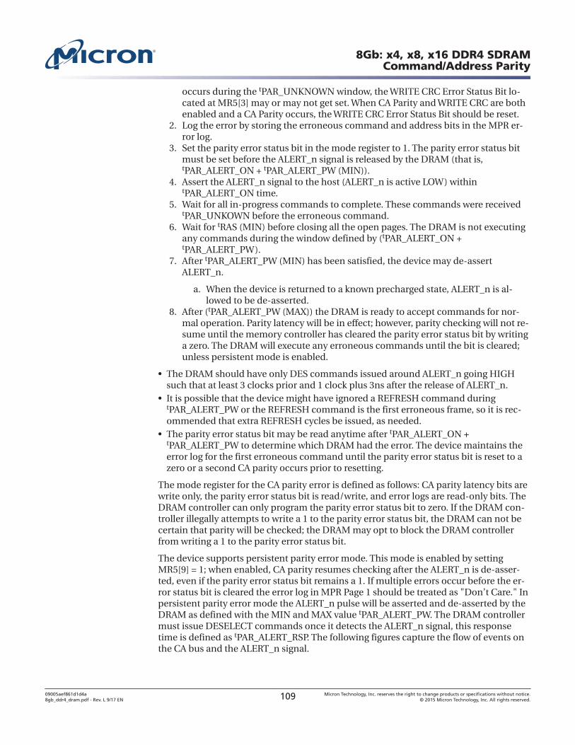
occurs during the tPAR_UNKNOWN window, the WRITE CRC Error Status Bit lo-cated at MR5[3] may or may not get set. When CA Parity and WRITE CRC are bothenabled and a CA Parity occurs, the WRITE CRC Error Status Bit should be reset.
2. Log the error by storing the erroneous command and address bits in the MPR er-ror log.
3. Set the parity error status bit in the mode register to 1. The parity error status bitmust be set before the ALERT_n signal is released by the DRAM (that is,tPAR_ALERT_ON + tPAR_ALERT_PW (MIN)).
4. Assert the ALERT_n signal to the host (ALERT_n is active LOW) withintPAR_ALERT_ON time.
5. Wait for all in-progress commands to complete. These commands were receivedtPAR_UNKOWN before the erroneous command.
6. Wait for tRAS (MIN) before closing all the open pages. The DRAM is not executingany commands during the window defined by (tPAR_ALERT_ON +tPAR_ALERT_PW).
7. After tPAR_ALERT_PW (MIN) has been satisfied, the device may de-assertALERT_n.
a. When the device is returned to a known precharged state, ALERT_n is al-lowed to be de-asserted.
8. After (tPAR_ALERT_PW (MAX)) the DRAM is ready to accept commands for nor-mal operation. Parity latency will be in effect; however, parity checking will not re-sume until the memory controller has cleared the parity error status bit by writinga zero. The DRAM will execute any erroneous commands until the bit is cleared;unless persistent mode is enabled.
• The DRAM should have only DES commands issued around ALERT_n going HIGHsuch that at least 3 clocks prior and 1 clock plus 3ns after the release of ALERT_n.
• It is possible that the device might have ignored a REFRESH command duringtPAR_ALERT_PW or the REFRESH command is the first erroneous frame, so it is rec-ommended that extra REFRESH cycles be issued, as needed.
• The parity error status bit may be read anytime after tPAR_ALERT_ON +tPAR_ALERT_PW to determine which DRAM had the error. The device maintains theerror log for the first erroneous command until the parity error status bit is reset to azero or a second CA parity occurs prior to resetting.
The mode register for the CA parity error is defined as follows: CA parity latency bits arewrite only, the parity error status bit is read/write, and error logs are read-only bits. TheDRAM controller can only program the parity error status bit to zero. If the DRAM con-troller illegally attempts to write a 1 to the parity error status bit, the DRAM can not becertain that parity will be checked; the DRAM may opt to block the DRAM controllerfrom writing a 1 to the parity error status bit.
The device supports persistent parity error mode. This mode is enabled by settingMR5[9] = 1; when enabled, CA parity resumes checking after the ALERT_n is de-asser-ted, even if the parity error status bit remains a 1. If multiple errors occur before the er-ror status bit is cleared the error log in MPR Page 1 should be treated as "Don’t Care." Inpersistent parity error mode the ALERT_n pulse will be asserted and de-asserted by theDRAM as defined with the MIN and MAX value tPAR_ALERT_PW. The DRAM controllermust issue DESELECT commands once it detects the ALERT_n signal, this responsetime is defined as tPAR_ALERT_RSP. The following figures capture the flow of events onthe CA bus and the ALERT_n signal.
8Gb: x4, x8, x16 DDR4 SDRAMCommand/Address Parity
09005aef861d1d4a8gb_ddr4_dram.pdf - Rev. L 9/17 EN 109 Micron Technology, Inc. reserves the right to change products or specifications without notice.
© 2015 Micron Technology, Inc. All rights reserved.
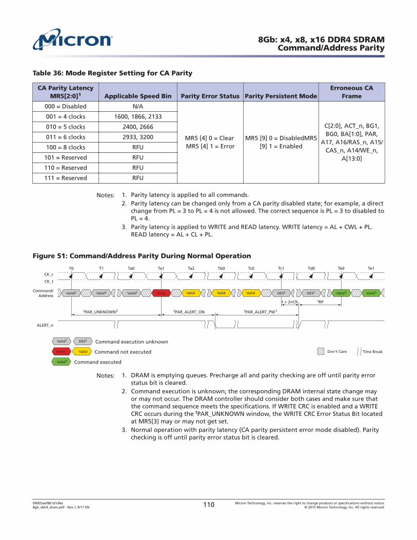
Table 36: Mode Register Setting for CA Parity
CA Parity LatencyMR5[2:0]1 Applicable Speed Bin Parity Error Status Parity Persistent Mode
Erroneous CAFrame
000 = Disabled N/A
MR5 [4] 0 = Clear MR5 [4] 1 = Error
MR5 [9] 0 = DisabledMR5[9] 1 = Enabled
C[2:0], ACT_n, BG1,BG0, BA[1:0], PAR,
A17, A16/RAS_n, A15/CAS_n, A14/WE_n,
A[13:0]
001 = 4 clocks 1600, 1866, 2133
010 = 5 clocks 2400, 2666
011 = 6 clocks 2933, 3200
100 = 8 clocks RFU
101 = Reserved RFU
110 = Reserved RFU
111 = Reserved RFU
Notes: 1. Parity latency is applied to all commands.2. Parity latency can be changed only from a CA parity disabled state; for example, a direct
change from PL = 3 to PL = 4 is not allowed. The correct sequence is PL = 3 to disabled toPL = 4.
3. Parity latency is applied to WRITE and READ latency. WRITE latency = AL + CWL + PL.READ latency = AL + CL + PL.
Figure 51: Command/Address Parity During Normal Operation
Don’t Care Time Break
Command execution unknown
Command not executed
Command executed
DES2
Valid3
ValidError
CK_t
CK_c
Command/Address
Valid2 Valid2 Valid2 Valid3 Valid3
T0 T1 Ta0 Ta1 Tb0 Tc0
ALERT_n
Tc1
tPAR_ALERT_ON
Td0
Valid Valid ValidError
tPAR_UNKNOWN2
Ta2 Te1
tPAR_ALERT_PW1
Te0
DES2 DES2
Valid2
tRPt > 2nCK
Notes: 1. DRAM is emptying queues. Precharge all and parity checking are off until parity errorstatus bit is cleared.
2. Command execution is unknown; the corresponding DRAM internal state change mayor may not occur. The DRAM controller should consider both cases and make sure thatthe command sequence meets the specifications. If WRITE CRC is enabled and a WRITECRC occurs during the tPAR_UNKNOWN window, the WRITE CRC Error Status Bit locatedat MR5[3] may or may not get set.
3. Normal operation with parity latency (CA parity persistent error mode disabled). Paritychecking is off until parity error status bit is cleared.
8Gb: x4, x8, x16 DDR4 SDRAMCommand/Address Parity
09005aef861d1d4a8gb_ddr4_dram.pdf - Rev. L 9/17 EN 110 Micron Technology, Inc. reserves the right to change products or specifications without notice.
© 2015 Micron Technology, Inc. All rights reserved.
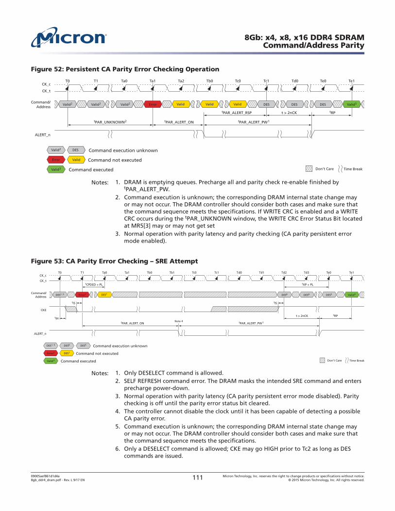
Figure 52: Persistent CA Parity Error Checking Operation
Don’t Care Time Break
Command execution unknown
Command not executed
Command executed
DES
Valid3
ValidError
CK_t
CK_c
Command/Address
Valid2 Valid2 Valid2 Valid3
T0 T1 Ta0 Ta1 Tb0 Tc0
ALERT_n
Tc1
tPAR_ALERT_ON
Td0
Valid Valid ValidError
tPAR_UNKNOWN2
Ta2 Te1
tPAR_ALERT_PW1
tPAR_ALERT_RSP
Te0
DES DES DES
Valid2
tRPt > 2nCK
Notes: 1. DRAM is emptying queues. Precharge all and parity check re-enable finished bytPAR_ALERT_PW.
2. Command execution is unknown; the corresponding DRAM internal state change mayor may not occur. The DRAM controller should consider both cases and make sure thatthe command sequence meets the specifications. If WRITE CRC is enabled and a WRITECRC occurs during the tPAR_UNKNOWN window, the WRITE CRC Error Status Bit locatedat MR5[3] may or may not get set
3. Normal operation with parity latency and parity checking (CA parity persistent errormode enabled).
Figure 53: CA Parity Error Checking – SRE Attempt
Don’t Care Time Break
Command not executed
Command executed
DES6 Command execution unknownDES5
Valid3
DES1Error2
CK_t
CK_c
Command/Address
DES1, 5 Valid3
T0 T1 Ta0 Ta1 Tb1 Tc0
ALERT_n
Tc1
tPAR_ALERT_ON
Td0
DES1
Note 4
Error2
Tb0 Td2
tPAR_ALERT_PW1
Td1
DES6 DES6 DES5
DES1, 5
t > 2nCKtIH
tIS
tXP + PLtCPDED + PL
Td3 Te0 Te1
CKE
tIS
tRP
Notes: 1. Only DESELECT command is allowed.2. SELF REFRESH command error. The DRAM masks the intended SRE command and enters
precharge power-down.3. Normal operation with parity latency (CA parity persistent error mode disabled). Parity
checking is off until the parity error status bit cleared.4. The controller cannot disable the clock until it has been capable of detecting a possible
CA parity error.5. Command execution is unknown; the corresponding DRAM internal state change may
or may not occur. The DRAM controller should consider both cases and make sure thatthe command sequence meets the specifications.
6. Only a DESELECT command is allowed; CKE may go HIGH prior to Tc2 as long as DEScommands are issued.
8Gb: x4, x8, x16 DDR4 SDRAMCommand/Address Parity
09005aef861d1d4a8gb_ddr4_dram.pdf - Rev. L 9/17 EN 111 Micron Technology, Inc. reserves the right to change products or specifications without notice.
© 2015 Micron Technology, Inc. All rights reserved.
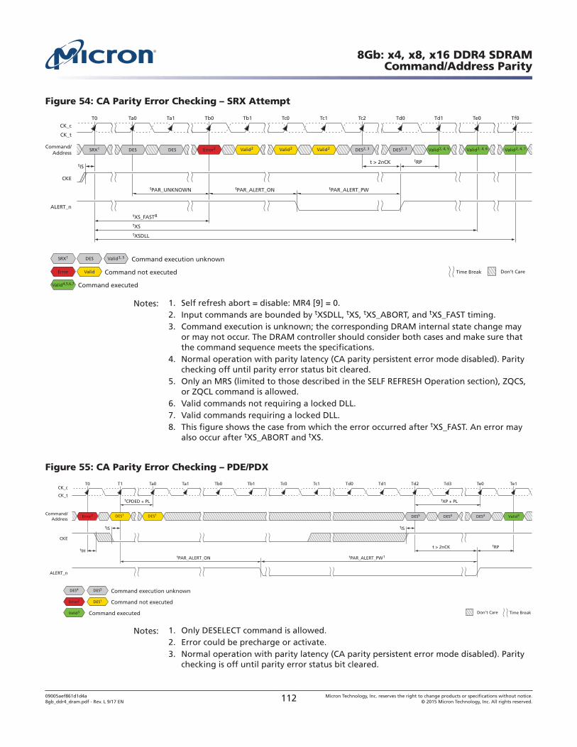
Figure 54: CA Parity Error Checking – SRX Attempt
Don’t CareTime Break
Command execution unknown
Command not executed
Command executed
DES Valid3, 5
Valid4,5,6,7
ValidError
CK_t
CK_c
Command/Address
SRX1 DES DES Valid2, 4, 5 Valid2, 4, 7Valid2, 4, 6
T0 Ta0 Tb0Ta1 Tc0 Tc1
ALERT_n
Tc2
tPAR_ALERT_ON
Td0
Valid2 Valid2 Valid2Error2
tPAR_UNKNOWN
tXS_FAST8
tXStXSDLL
Tb1 Te0
tPAR_ALERT_PW
Td1
DES2, 3 DES2, 3
SRX1
t > 2nCK
Tf0
CKE
tIStRP
Notes: 1. Self refresh abort = disable: MR4 [9] = 0.2. Input commands are bounded by tXSDLL, tXS, tXS_ABORT, and tXS_FAST timing.3. Command execution is unknown; the corresponding DRAM internal state change may
or may not occur. The DRAM controller should consider both cases and make sure thatthe command sequence meets the specifications.
4. Normal operation with parity latency (CA parity persistent error mode disabled). Paritychecking off until parity error status bit cleared.
5. Only an MRS (limited to those described in the SELF REFRESH Operation section), ZQCS,or ZQCL command is allowed.
6. Valid commands not requiring a locked DLL.7. Valid commands requiring a locked DLL.8. This figure shows the case from which the error occurred after tXS_FAST. An error may
also occur after tXS_ABORT and tXS.
Figure 55: CA Parity Error Checking – PDE/PDX
Don’t Care Time Break
Command not executed
Command executed
DES5 Command execution unknown
Valid3
DES1Error2
CK_t
CK_c
Command/Address
Valid3
T0 T1 Ta0 Ta1 Tb1 Tc0
ALERT_n
Tc1
tPAR_ALERT_ON
Td0
DES1DES1Error2
Tb0 Td2
tPAR_ALERT_PW1
Td1
DES5 DES5 DES4
DES4
t > 2nCKtIH
tIS
tXP + PLtCPDED + PL
Td3 Te0 Te1
CKE
tIS
tRP
Notes: 1. Only DESELECT command is allowed.2. Error could be precharge or activate.3. Normal operation with parity latency (CA parity persistent error mode disabled). Parity
checking is off until parity error status bit cleared.
8Gb: x4, x8, x16 DDR4 SDRAMCommand/Address Parity
09005aef861d1d4a8gb_ddr4_dram.pdf - Rev. L 9/17 EN 112 Micron Technology, Inc. reserves the right to change products or specifications without notice.
© 2015 Micron Technology, Inc. All rights reserved.
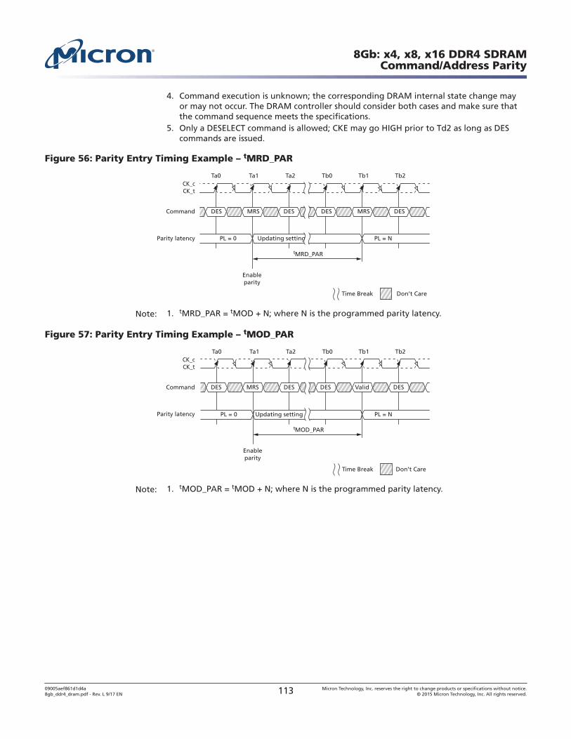
4. Command execution is unknown; the corresponding DRAM internal state change mayor may not occur. The DRAM controller should consider both cases and make sure thatthe command sequence meets the specifications.
5. Only a DESELECT command is allowed; CKE may go HIGH prior to Td2 as long as DEScommands are issued.
Figure 56: Parity Entry Timing Example – tMRD_PAR
Ta0
tMRD_PAR
Ta1 Ta2 Tb0 Tb1 Tb2
Command MRSDES DES DES MRS DES
PL = 0 Updating setting PL = NParity latency
CK_tCK_c
Enableparity
Don’t CareTime Break
Note: 1. tMRD_PAR = tMOD + N; where N is the programmed parity latency.
Figure 57: Parity Entry Timing Example – tMOD_PAR
Ta0
tMOD_PAR
Ta1 Ta2 Tb0 Tb1 Tb2
Command MRSDES DES DES Valid DES
Parity latency
CK_tCK_c
Enableparity
Don’t CareTime Break
PL = 0 Updating setting PL = N
Note: 1. tMOD_PAR = tMOD + N; where N is the programmed parity latency.
8Gb: x4, x8, x16 DDR4 SDRAMCommand/Address Parity
09005aef861d1d4a8gb_ddr4_dram.pdf - Rev. L 9/17 EN 113 Micron Technology, Inc. reserves the right to change products or specifications without notice.
© 2015 Micron Technology, Inc. All rights reserved.
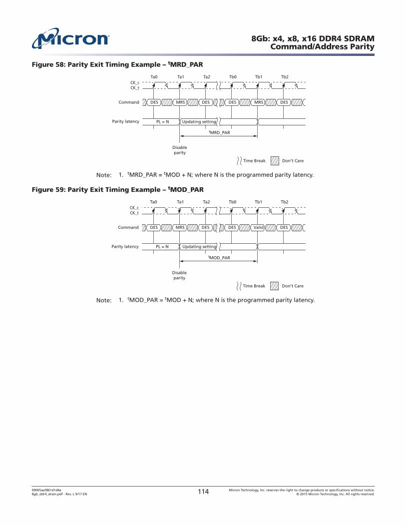
Figure 58: Parity Exit Timing Example – tMRD_PAR
Ta0
tMRD_PAR
Ta1 Ta2 Tb0 Tb1 Tb2
Command MRSDES DES DES MRS DES
Parity latency
CK_tCK_c
Disableparity
Don’t CareTime Break
PL = N Updating setting
Note: 1. tMRD_PAR = tMOD + N; where N is the programmed parity latency.
Figure 59: Parity Exit Timing Example – tMOD_PAR
Ta0
tMOD_PAR
Ta1 Ta2 Tb0 Tb1 Tb2
Command MRSDES DES DES Valid DES
Parity latency
CK_tCK_c
Disableparity
Don’t CareTime Break
PL = N Updating setting
Note: 1. tMOD_PAR = tMOD + N; where N is the programmed parity latency.
8Gb: x4, x8, x16 DDR4 SDRAMCommand/Address Parity
09005aef861d1d4a8gb_ddr4_dram.pdf - Rev. L 9/17 EN 114 Micron Technology, Inc. reserves the right to change products or specifications without notice.
© 2015 Micron Technology, Inc. All rights reserved.
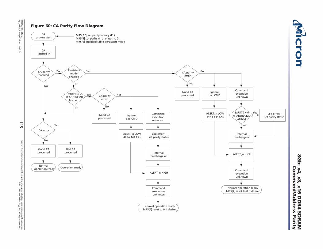
Figure 60: CA Parity Flow Diagram
CAlatched in
Yes
CAprocess start
MR5[2:0] set parity latency (PL)MR5[4] set parity error status to 0MR5[9] enable/disable persistent mode
No
Yes
No
Yes
No
Yes
No
Yes
No
CA parityenabled
CA error
Persistentmode
enabled
Good CAprocessed
Good CAprocessed
Good CAprocessed
Ignorebad CMD
Ignorebad CMD
Log error/set parity status
Internalprecharge all
ALERT_n HIGH
Commandexecutionunknown
Commandexecutionunknown
Normal operation readyMR5[4] reset to 0 if desired
Normal operation readyMR5[4] reset to 0 if desired
Yes
No
CA parityerror
ALERT_n LOW44 to 144 CKs
ALERT_n LOW44 to 144 CKs
Internalprecharge all
ALERT_n HIGH
Commandexecutionunknown
Commandexecutionunknown
No
Yes Log error/set parity status
MR5[4] = 0@ ADDR/CMD
latched
MR5[4] = 0@ ADDR/CMD
latched
CA parityerror
Normaloperation ready
Bad CAprocessed
Operation ready?
8G
b: x
4, x
8, x
16 D
DR
4 S
DR
AM
Co
mm
an
d/A
dd
ress P
arity
09005aef861d1d
4a8g
b_d
dr4_d
ram.p
df - R
ev. L 9/17 EN115
Micro
n Tech
no
log
y, Inc. reserves th
e righ
t to ch
ang
e pro
du
cts or sp
ecification
s with
ou
t no
tice.©
2015 Micro
n Tech
no
log
y, Inc. A
ll righ
ts reserved.
Per-DRAM AddressabilityDDR4 allows programmability of a single, specific DRAM on a rank. As an example, thisfeature can be used to program different ODT or VREF values on each DRAM on a givenrank. Because per-DRAM addressability (PDA) mode may be used to program optimalVREF for the DRAM, the data set up for first DQ0 transfer or the hold time for the lastDQ0 transfer cannot be guaranteed. The DRAM may sample DQ0 on either the first fall-ing or second rising DQS transfer edge. This supports a common implementation be-tween BC4 and BL8 modes on the DRAM. The DRAM controller is required to drive DQ0to a stable LOW or HIGH state during the length of the data transfer for BC4 and BL8cases.
1. Before entering PDA mode, write leveling is required.
• BL8 or BC4 may be used.2. Before entering PDA mode, the following MR settings are possible:
• RTT(Park) MR5 A[8:6] = Enable• RTT(NOM) MR1 A[10:8] = Enable
3. Enable PDA mode using MR3 [4] = 1. (The default programed value of MR3[4] = 0.)4. In PDA mode, all MRS commands are qualified with DQ0. The device captures
DQ0 by using DQS signals. If the value on DQ0 is LOW, the DRAM executes theMRS command. If the value on DQ0 is HIGH, the DRAM ignores the MRS com-mand. The controller can choose to drive all the DQ bits.
5. Program the desired DRAM and mode registers using the MRS command andDQ0.
6. In PDA mode, only MRS commands are allowed.7. The MODE REGISTER SET command cycle time in PDA mode, AL + CWL + BL/2 -
0.5tCK + tMRD_PDA + PL, is required to complete the WRITE operation to themode register and is the minimum time required between two MRS commands.
8. Remove the device from PDA mode by setting MR3[4] = 0. (This command re-quires DQ0 = 0.)
Note: Removing the device from PDA mode will require programming the entire MR3when the MRS command is issued. This may impact some PDA values programmedwithin a rank as the EXIT command is sent to the rank. To avoid such a case, the PDAenable/disable control bit is located in a mode register that does not have any PDAmode controls.
In PDA mode, the device captures DQ0 using DQS signals the same as in a normalWRITE operation; however, dynamic ODT is not supported. Extra care is required forthe ODT setting. If RTT(NOM) MR1 [10:8] = enable, device data termination needs to becontrolled by the ODT pin, and applies the same timing parameters (defined below).
Symbol Parameter
DODTLon Direct ODT turnon latency
DODTLoff Direct ODT turn off latencytADC RTT change timing skew
tAONAS Asynchronous RTT(NOM) turn-on delaytAOFAS Asynchronous RTT(NOM) turn-off delay
8Gb: x4, x8, x16 DDR4 SDRAMPer-DRAM Addressability
09005aef861d1d4a8gb_ddr4_dram.pdf - Rev. L 9/17 EN 116 Micron Technology, Inc. reserves the right to change products or specifications without notice.
© 2015 Micron Technology, Inc. All rights reserved.

Figure 61: PDA Operation Enabled, BL8
Note: 1. RTT(Park) = Enable; RTT(NOM) = Enable; WRITE preamble set = 2tCK; and DLL = On.
Figure 62: PDA Operation Enabled, BC4
CK_t
CK_c
DQ0
ODT
tPDA_S
tMOD CWL+AL+PL tMRD_PDA
DQS_t
DQS_c
MR3 A4 = 1(PDA enable) MRS MRS MRS
DODTLoff = WL-3
DODTLon = WL-3
tPDA_H
RTT(Park)RTT(Park)RTT RTT(NOM)
Note: 1. RTT(Park) = Enable; RTT(NOM) = Enable; WRITE preamble set = 2tCK; and DLL = On.
8Gb: x4, x8, x16 DDR4 SDRAMPer-DRAM Addressability
09005aef861d1d4a8gb_ddr4_dram.pdf - Rev. L 9/17 EN 117 Micron Technology, Inc. reserves the right to change products or specifications without notice.
© 2015 Micron Technology, Inc. All rights reserved.
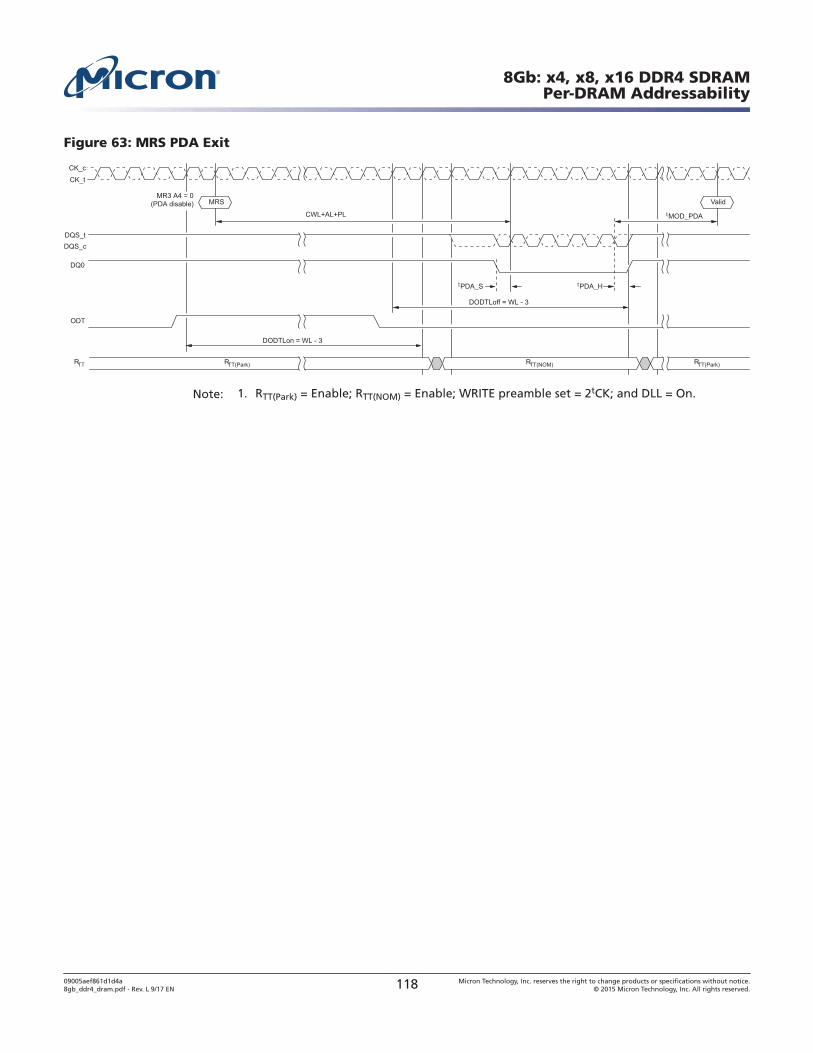
Figure 63: MRS PDA Exit
Note: 1. RTT(Park) = Enable; RTT(NOM) = Enable; WRITE preamble set = 2tCK; and DLL = On.
8Gb: x4, x8, x16 DDR4 SDRAMPer-DRAM Addressability
09005aef861d1d4a8gb_ddr4_dram.pdf - Rev. L 9/17 EN 118 Micron Technology, Inc. reserves the right to change products or specifications without notice.
© 2015 Micron Technology, Inc. All rights reserved.
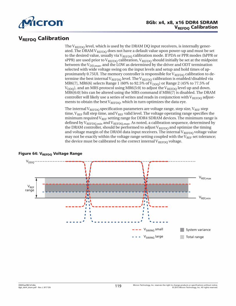
VREFDQ CalibrationThe VREFDQ level, which is used by the DRAM DQ input receivers, is internally gener-ated. The DRAM VREFDQ does not have a default value upon power-up and must be setto the desired value, usually via VREFDQ calibration mode. If PDA or PPR modes (hPPR orsPPR) are used prior to VREFDQ calibration, VREFDQ should initially be set at the midpointbetween the VDD,max, and the LOW as determined by the driver and ODT terminationselected with wide voltage swing on the input levels and setup and hold times of ap-proximately 0.75UI. The memory controller is responsible for VREFDQ calibration to de-termine the best internal VREFDQ level. The VREFDQ calibration is enabled/disabled viaMR6[7], MR6[6] selects Range 1 (60% to 92.5% of VDDQ) or Range 2 (45% to 77.5% ofVDDQ), and an MRS protocol using MR6[5:0] to adjust the VREFDQ level up and down.MR6[6:0] bits can be altered using the MRS command if MR6[7] is disabled. The DRAMcontroller will likely use a series of writes and reads in conjunction with VREFDQ adjust-ments to obtain the best VREFDQ, which in turn optimizes the data eye.
The internal VREFDQ specification parameters are voltage range, step size, VREF steptime, VREF full step time, and VREF valid level. The voltage operating range specifies theminimum required VREF setting range for DDR4 SDRAM devices. The minimum range isdefined by VREFDQ,min and VREFDQ,max. As noted, a calibration sequence, determined bythe DRAM controller, should be performed to adjust VREFDQ and optimize the timingand voltage margin of the DRAM data input receivers. The internal VREFDQ voltage valuemay not be exactly within the voltage range setting coupled with the VREF set tolerance;the device must be calibrated to the correct internal VREFDQ voltage.
Figure 64: VREFDQ Voltage Range
VDDQ
VREFrange
VSWING small
VSWING large
System variance
Total range
VREF,max
VREF,min
8Gb: x4, x8, x16 DDR4 SDRAMVREFDQ Calibration
09005aef861d1d4a8gb_ddr4_dram.pdf - Rev. L 9/17 EN 119 Micron Technology, Inc. reserves the right to change products or specifications without notice.
© 2015 Micron Technology, Inc. All rights reserved.
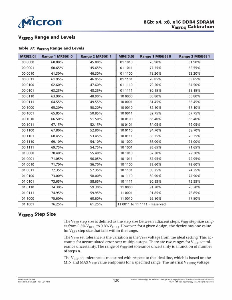
VREFDQ Range and Levels
Table 37: VREFDQ Range and Levels
MR6[5:0] Range 1 MR6[6] 0 Range 2 MR6[6] 1 MR6[5:0] Range 1 MR6[6] 0 Range 2 MR6[6] 1
00 0000 60.00% 45.00% 01 1010 76.90% 61.90%
00 0001 60.65% 45.65% 01 1011 77.55% 62.55%
00 0010 61.30% 46.30% 01 1100 78.20% 63.20%
00 0011 61.95% 46.95% 01 1101 78.85% 63.85%
00 0100 62.60% 47.60% 01 1110 79.50% 64.50%
00 0101 63.25% 48.25% 01 1111 80.15% 65.15%
00 0110 63.90% 48.90% 10 0000 80.80% 65.80%
00 0111 64.55% 49.55% 10 0001 81.45% 66.45%
00 1000 65.20% 50.20% 10 0010 82.10% 67.10%
00 1001 65.85% 50.85% 10 0011 82.75% 67.75%
00 1010 66.50% 51.50% 10 0100 83.40% 68.40%
00 1011 67.15% 52.15% 10 0101 84.05% 69.05%
00 1100 67.80% 52.80% 10 0110 84.70% 69.70%
00 1101 68.45% 53.45% 10 0111 85.35% 70.35%
00 1110 69.10% 54.10% 10 1000 86.00% 71.00%
00 1111 69.75% 54.75% 10 1001 86.65% 71.65%
01 0000 70.40% 55.40% 10 1010 87.30% 72.30%
01 0001 71.05% 56.05% 10 1011 87.95% 72.95%
01 0010 71.70% 56.70% 10 1100 88.60% 73.60%
01 0011 72.35% 57.35% 10 1101 89.25% 74.25%
01 0100 73.00% 58.00% 10 1110 89.90% 74.90%
01 0101 73.65% 58.65% 10 1111 90.55% 75.55%
01 0110 74.30% 59.30% 11 0000 91.20% 76.20%
01 0111 74.95% 59.95% 11 0001 91.85% 76.85%
01 1000 75.60% 60.60% 11 0010 92.50% 77.50%
01 1001 76.25% 61.25% 11 0011 to 11 1111 = Reserved
VREFDQ Step Size
The VREF step size is defined as the step size between adjacent steps. VREF step size rang-es from 0.5% VDDQ to 0.8% VDDQ. However, for a given design, the device has one valuefor VREF step size that falls within the range.
The VREF set tolerance is the variation in the VREF voltage from the ideal setting. This ac-counts for accumulated error over multiple steps. There are two ranges for VREF set tol-erance uncertainty. The range of VREF set tolerance uncertainty is a function of numberof steps n.
The VREF set tolerance is measured with respect to the ideal line, which is based on theMIN and MAX VREF value endpoints for a specified range. The internal VREFDQ voltage
8Gb: x4, x8, x16 DDR4 SDRAMVREFDQ Calibration
09005aef861d1d4a8gb_ddr4_dram.pdf - Rev. L 9/17 EN 120 Micron Technology, Inc. reserves the right to change products or specifications without notice.
© 2015 Micron Technology, Inc. All rights reserved.
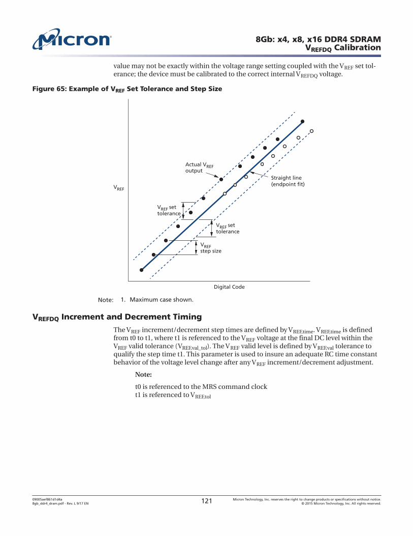
value may not be exactly within the voltage range setting coupled with the VREF set tol-erance; the device must be calibrated to the correct internal VREFDQ voltage.
Figure 65: Example of VREF Set Tolerance and Step Size
VREF
VREFstep size
VREF settolerance
VREF settolerance
Straight line(endpoint fit)
Actual VREFoutput
Digital Code
Note: 1. Maximum case shown.
VREFDQ Increment and Decrement Timing
The VREF increment/decrement step times are defined by VREF,time. VREF,time is definedfrom t0 to t1, where t1 is referenced to the VREF voltage at the final DC level within theVREF valid tolerance (VREF,val_tol). The VREF valid level is defined by VREF,val tolerance toqualify the step time t1. This parameter is used to insure an adequate RC time constantbehavior of the voltage level change after any VREF increment/decrement adjustment.
Note:
t0 is referenced to the MRS command clockt1 is referenced to VREF,tol
8Gb: x4, x8, x16 DDR4 SDRAMVREFDQ Calibration
09005aef861d1d4a8gb_ddr4_dram.pdf - Rev. L 9/17 EN 121 Micron Technology, Inc. reserves the right to change products or specifications without notice.
© 2015 Micron Technology, Inc. All rights reserved.
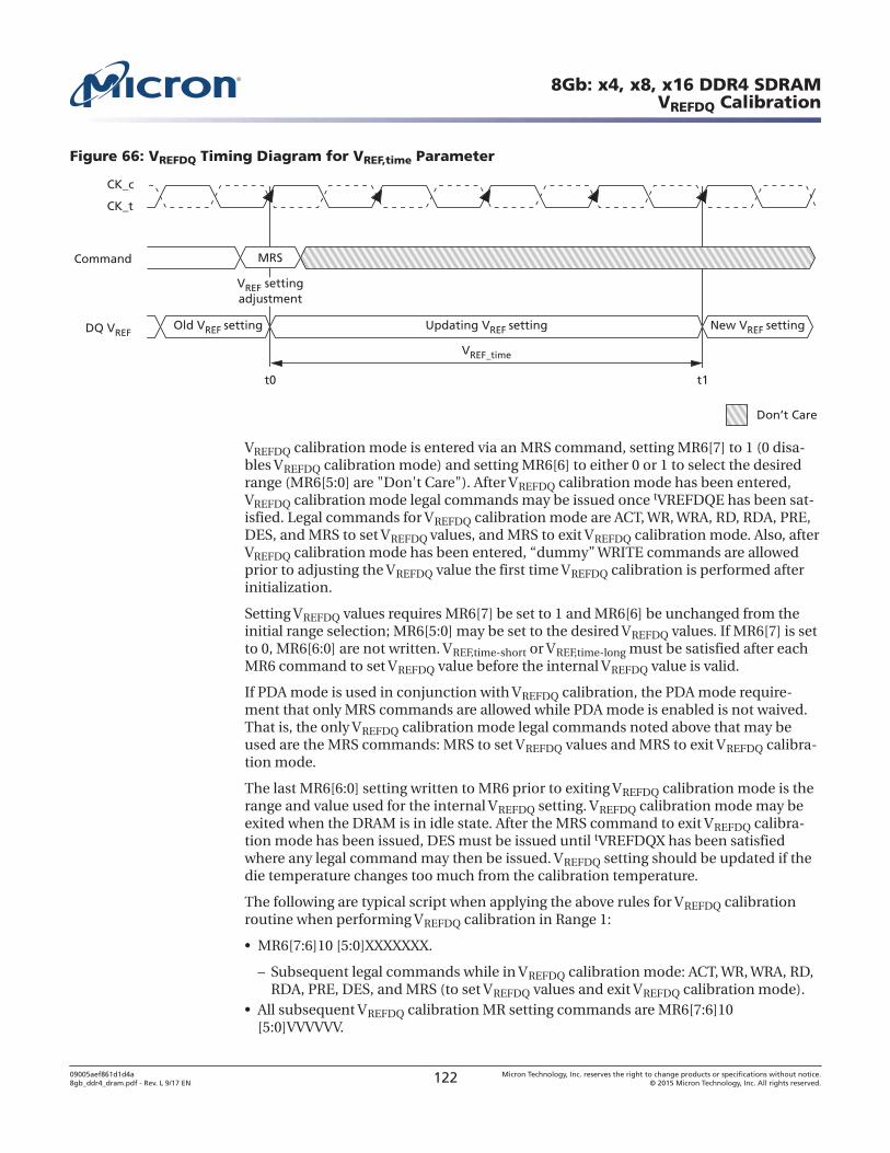
Figure 66: VREFDQ Timing Diagram for VREF,time Parameter
MRS
VREF settingadjustment
Command
DQ VREF
VREF_time
t0 t1
Old VREF setting New VREF settingUpdating VREF setting
Don’t Care
CK_t
CK_c
VREFDQ calibration mode is entered via an MRS command, setting MR6[7] to 1 (0 disa-bles VREFDQ calibration mode) and setting MR6[6] to either 0 or 1 to select the desiredrange (MR6[5:0] are "Don't Care"). After VREFDQ calibration mode has been entered,VREFDQ calibration mode legal commands may be issued once tVREFDQE has been sat-isfied. Legal commands for VREFDQ calibration mode are ACT, WR, WRA, RD, RDA, PRE,DES, and MRS to set VREFDQ values, and MRS to exit VREFDQ calibration mode. Also, afterVREFDQ calibration mode has been entered, “dummy” WRITE commands are allowedprior to adjusting the VREFDQ value the first time VREFDQ calibration is performed afterinitialization.
Setting VREFDQ values requires MR6[7] be set to 1 and MR6[6] be unchanged from theinitial range selection; MR6[5:0] may be set to the desired VREFDQ values. If MR6[7] is setto 0, MR6[6:0] are not written. VREF,time-short or VREF,time-long must be satisfied after eachMR6 command to set VREFDQ value before the internal VREFDQ value is valid.
If PDA mode is used in conjunction with VREFDQ calibration, the PDA mode require-ment that only MRS commands are allowed while PDA mode is enabled is not waived.That is, the only VREFDQ calibration mode legal commands noted above that may beused are the MRS commands: MRS to set VREFDQ values and MRS to exit VREFDQ calibra-tion mode.
The last MR6[6:0] setting written to MR6 prior to exiting VREFDQ calibration mode is therange and value used for the internal VREFDQ setting. VREFDQ calibration mode may beexited when the DRAM is in idle state. After the MRS command to exit VREFDQ calibra-tion mode has been issued, DES must be issued until tVREFDQX has been satisfiedwhere any legal command may then be issued. VREFDQ setting should be updated if thedie temperature changes too much from the calibration temperature.
The following are typical script when applying the above rules for VREFDQ calibrationroutine when performing VREFDQ calibration in Range 1:
• MR6[7:6]10 [5:0]XXXXXXX.
– Subsequent legal commands while in VREFDQ calibration mode: ACT, WR, WRA, RD,RDA, PRE, DES, and MRS (to set VREFDQ values and exit VREFDQ calibration mode).
• All subsequent VREFDQ calibration MR setting commands are MR6[7:6]10[5:0]VVVVVV.
8Gb: x4, x8, x16 DDR4 SDRAMVREFDQ Calibration
09005aef861d1d4a8gb_ddr4_dram.pdf - Rev. L 9/17 EN 122 Micron Technology, Inc. reserves the right to change products or specifications without notice.
© 2015 Micron Technology, Inc. All rights reserved.
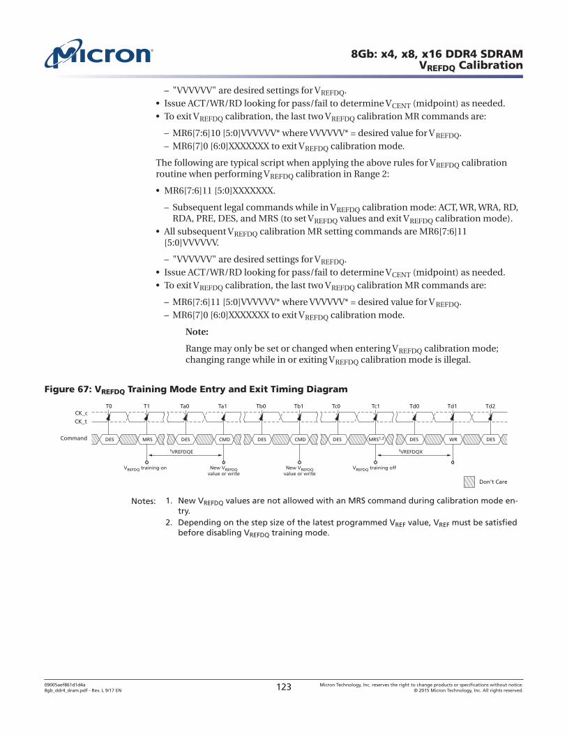
– "VVVVVV" are desired settings for VREFDQ.• Issue ACT/WR/RD looking for pass/fail to determine VCENT (midpoint) as needed.• To exit VREFDQ calibration, the last two VREFDQ calibration MR commands are:
– MR6[7:6]10 [5:0]VVVVVV* where VVVVVV* = desired value for V REFDQ.– MR6[7]0 [6:0]XXXXXXX to exit VREFDQ calibration mode.
The following are typical script when applying the above rules for VREFDQ calibrationroutine when performing VREFDQ calibration in Range 2:
• MR6[7:6]11 [5:0]XXXXXXX.
– Subsequent legal commands while in VREFDQ calibration mode: ACT, WR, WRA, RD,RDA, PRE, DES, and MRS (to set VREFDQ values and exit VREFDQ calibration mode).
• All subsequent VREFDQ calibration MR setting commands are MR6[7:6]11[5:0]VVVVVV.
– "VVVVVV" are desired settings for VREFDQ.• Issue ACT/WR/RD looking for pass/fail to determine VCENT (midpoint) as needed.• To exit VREFDQ calibration, the last two VREFDQ calibration MR commands are:
– MR6[7:6]11 [5:0]VVVVVV* where VVVVVV* = desired value for V REFDQ.– MR6[7]0 [6:0]XXXXXXX to exit VREFDQ calibration mode.
Note:
Range may only be set or changed when entering VREFDQ calibration mode;changing range while in or exiting VREFDQ calibration mode is illegal.
Figure 67: VREFDQ Training Mode Entry and Exit Timing Diagram
T0 T1 Ta0 Ta1 Tb0CK_c
CK_t
Command
Tb1 Tc0
MRS WRDESCMDDESDES CMD DES
Tc1 Td0 Td1 Td2
tVREFDQE
VREFDQ training on
tVREFDQX
DES MRS1,2 DES
New VREFDQvalue or write
New VREFDQvalue or write
VREFDQ training off
Don’t Care
Notes: 1. New VREFDQ values are not allowed with an MRS command during calibration mode en-try.
2. Depending on the step size of the latest programmed VREF value, VREF must be satisfiedbefore disabling VREFDQ training mode.
8Gb: x4, x8, x16 DDR4 SDRAMVREFDQ Calibration
09005aef861d1d4a8gb_ddr4_dram.pdf - Rev. L 9/17 EN 123 Micron Technology, Inc. reserves the right to change products or specifications without notice.
© 2015 Micron Technology, Inc. All rights reserved.
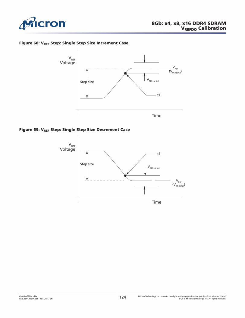
Figure 68: VREF Step: Single Step Size Increment Case
VREF
Voltage
Time
VREF,val_tol
t1
VREF
(VDDQ(DC))
Step size
Figure 69: VREF Step: Single Step Size Decrement Case
VREF
Voltage
Time
VREF,val_tol
t1
VREF
(VDDQ(DC))
Step size
8Gb: x4, x8, x16 DDR4 SDRAMVREFDQ Calibration
09005aef861d1d4a8gb_ddr4_dram.pdf - Rev. L 9/17 EN 124 Micron Technology, Inc. reserves the right to change products or specifications without notice.
© 2015 Micron Technology, Inc. All rights reserved.
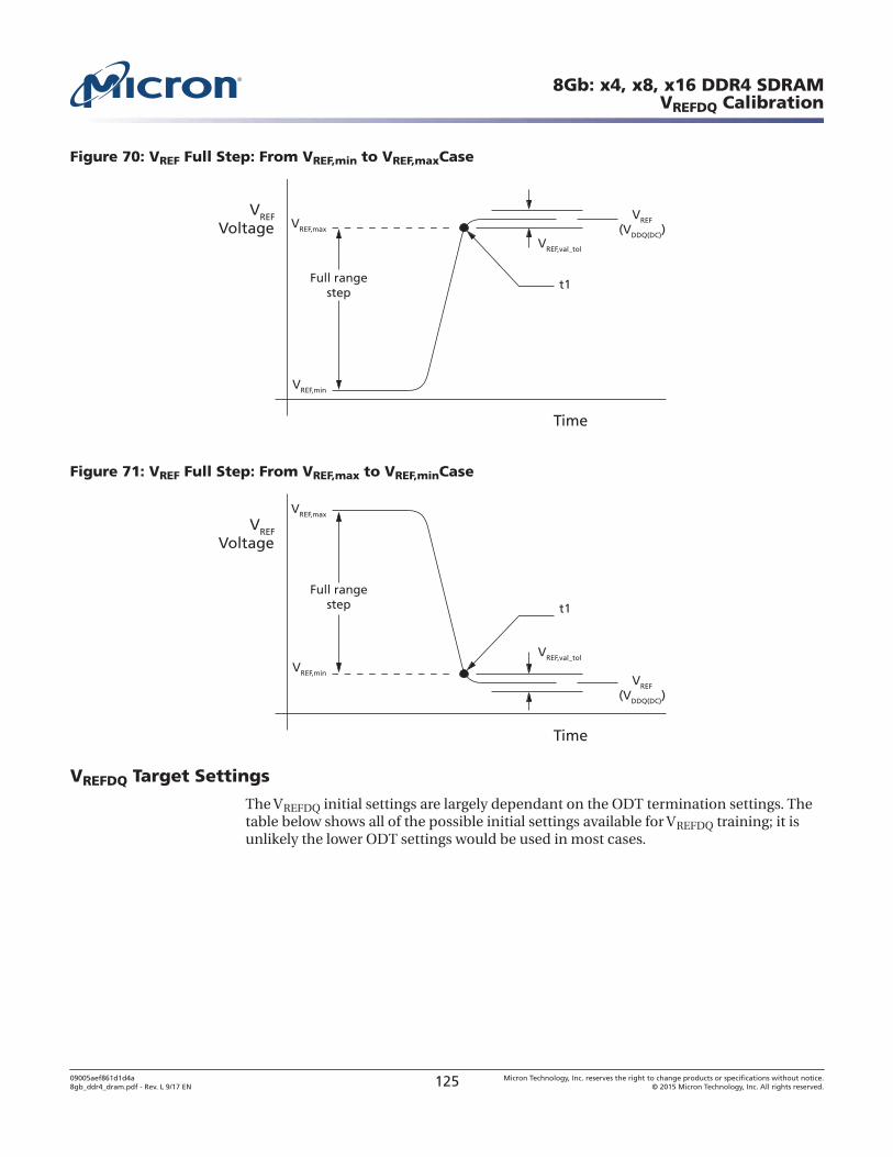
Figure 70: VREF Full Step: From VREF,min to VREF,maxCase
VREF
Voltage
Time
VREF,val_tol
VREF,max
VREF,min
t1
VREF
(VDDQ(DC))
Full rangestep
Figure 71: VREF Full Step: From VREF,max to VREF,minCase
VREF
Voltage
Time
VREF,val_tol
VREF,max
VREF,min
t1
VREF
(VDDQ(DC))
Full rangestep
VREFDQ Target Settings
The VREFDQ initial settings are largely dependant on the ODT termination settings. Thetable below shows all of the possible initial settings available for VREFDQ training; it isunlikely the lower ODT settings would be used in most cases.
8Gb: x4, x8, x16 DDR4 SDRAMVREFDQ Calibration
09005aef861d1d4a8gb_ddr4_dram.pdf - Rev. L 9/17 EN 125 Micron Technology, Inc. reserves the right to change products or specifications without notice.
© 2015 Micron Technology, Inc. All rights reserved.
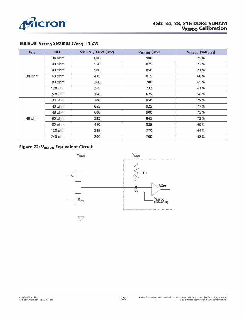
Table 38: VREFDQ Settings (VDDQ = 1.2V)
RON ODT Vx – VIN LOW (mV) VREFDQ (mv) VREFDQ (%VDDQ)
34 ohm
34 ohm 600 900 75%
40 ohm 550 875 73%
48 ohm 500 850 71%
60 ohm 435 815 68%
80 ohm 360 780 65%
120 ohm 265 732 61%
240 ohm 150 675 56%
48 ohm
34 ohm 700 950 79%
40 ohm 655 925 77%
48 ohm 600 900 75%
60 ohm 535 865 72%
80 ohm 450 825 69%
120 ohm 345 770 64%
240 ohm 200 700 58%
Figure 72: VREFDQ Equivalent Circuit
RXer
VREFDQ(internal)
RON
ODT
Vx
VDDQ VDDQ
8Gb: x4, x8, x16 DDR4 SDRAMVREFDQ Calibration
09005aef861d1d4a8gb_ddr4_dram.pdf - Rev. L 9/17 EN 126 Micron Technology, Inc. reserves the right to change products or specifications without notice.
© 2015 Micron Technology, Inc. All rights reserved.
Connectivity Test ModeConnectivity test (CT) mode is similar to boundary scan testing but is designed to sig-nificantly speed up the testing of electrical continuity of pin interconnections betweenthe device and the memory controller on the PC boards. Designed to work seamlesslywith any boundary scan device, CT mode is supported in all ×4, ×8, and ×16 devices (JE-DEC states CT mode for ×4 and ×8 is not required on 4Gb and is an optional feature on8Gb and above).
Contrary to other conventional shift-register-based test modes, where test patterns areshifted in and out of the memory devices serially during each clock, the CT mode allowstest patterns to be entered on the test input pins in parallel and the test results to beextracted from the test output pins of the device in parallel. These two functions are al-so performed at the same time, significantly increasing the speed of the connectivitycheck. When placed in CT mode, the device appears as an asynchronous device to theexternal controlling agent. After the input test pattern is applied, the connectivity testresults are available for extraction in parallel at the test output pins after a fixed propa-gation delay time.
Note: A reset of the device is required after exiting CT mode (see RESET and Initializa-tion Procedure).
Pin Mapping
Only digital pins can be tested using the CT mode. For the purposes of a connectivitycheck, all the pins used for digital logic in the device are classified as one of the follow-ing types:
• Test enable (TEN): When asserted HIGH, this pin causes the device to enter CT mode.In CT mode, the normal memory function inside the device is bypassed and the I/Opins appear as a set of test input and output pins to the external controlling agent.Additionally, the device will set the internal VREFDQ to VDDQ × 0.5 during CT mode(this is the only time the DRAM takes direct control over setting the internal VREFDQ).The TEN pin is dedicated to the connectivity check function and will not be used dur-ing normal device operation.
• Chip select (CS_n): When asserted LOW, this pin enables the test output pins in thedevice. When de-asserted, these output pins will be High-Z. The CS_n pin in the de-vice serves as the CS_n pin in CT mode.
• Test input: A group of pins used during normal device operation designated as testinput pins. These pins are used to enter the test pattern in CT mode.
• Test output: A group of pins used during normal device operation designated as testoutput pins. These pins are used for extraction of the connectivity test results in CTmode.
• RESET_n: This pin must be fixed high level during CT mode, as in normal function.
8Gb: x4, x8, x16 DDR4 SDRAMConnectivity Test Mode
09005aef861d1d4a8gb_ddr4_dram.pdf - Rev. L 9/17 EN 127 Micron Technology, Inc. reserves the right to change products or specifications without notice.
© 2015 Micron Technology, Inc. All rights reserved.
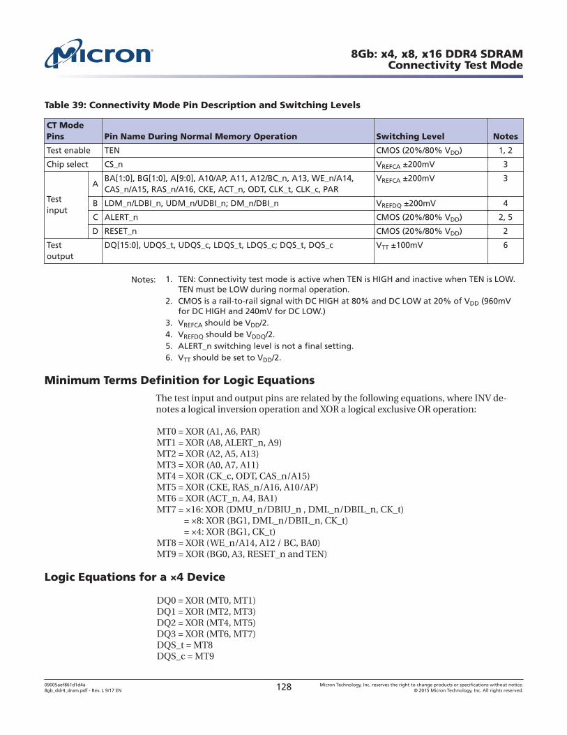
Table 39: Connectivity Mode Pin Description and Switching Levels
CT ModePins Pin Name During Normal Memory Operation Switching Level Notes
Test enable TEN CMOS (20%/80% VDD) 1, 2
Chip select CS_n VREFCA ±200mV 3
Testinput
ABA[1:0], BG[1:0], A[9:0], A10/AP, A11, A12/BC_n, A13, WE_n/A14,CAS_n/A15, RAS_n/A16, CKE, ACT_n, ODT, CLK_t, CLK_c, PAR
VREFCA ±200mV 3
B LDM_n/LDBI_n, UDM_n/UDBI_n; DM_n/DBI_n VREFDQ ±200mV 4
C ALERT_n CMOS (20%/80% VDD) 2, 5
D RESET_n CMOS (20%/80% VDD) 2
Testoutput
DQ[15:0], UDQS_t, UDQS_c, LDQS_t, LDQS_c; DQS_t, DQS_c VTT ±100mV 6
Notes: 1. TEN: Connectivity test mode is active when TEN is HIGH and inactive when TEN is LOW.TEN must be LOW during normal operation.
2. CMOS is a rail-to-rail signal with DC HIGH at 80% and DC LOW at 20% of VDD (960mVfor DC HIGH and 240mV for DC LOW.)
3. VREFCA should be VDD/2.4. VREFDQ should be VDDQ/2.5. ALERT_n switching level is not a final setting.6. VTT should be set to VDD/2.
Minimum Terms Definition for Logic Equations
The test input and output pins are related by the following equations, where INV de-notes a logical inversion operation and XOR a logical exclusive OR operation:
MT0 = XOR (A1, A6, PAR)MT1 = XOR (A8, ALERT_n, A9)MT2 = XOR (A2, A5, A13)MT3 = XOR (A0, A7, A11)MT4 = XOR (CK_c, ODT, CAS_n/A15)MT5 = XOR (CKE, RAS_n/A16, A10/AP)MT6 = XOR (ACT_n, A4, BA1)MT7 = ×16: XOR (DMU_n/DBIU_n , DML_n/DBIL_n, CK_t)
= ×8: XOR (BG1, DML_n/DBIL_n, CK_t)= ×4: XOR (BG1, CK_t)
MT8 = XOR (WE_n/A14, A12 / BC, BA0)MT9 = XOR (BG0, A3, RESET_n and TEN)
Logic Equations for a ×4 Device
DQ0 = XOR (MT0, MT1)DQ1 = XOR (MT2, MT3)DQ2 = XOR (MT4, MT5)DQ3 = XOR (MT6, MT7)DQS_t = MT8DQS_c = MT9
8Gb: x4, x8, x16 DDR4 SDRAMConnectivity Test Mode
09005aef861d1d4a8gb_ddr4_dram.pdf - Rev. L 9/17 EN 128 Micron Technology, Inc. reserves the right to change products or specifications without notice.
© 2015 Micron Technology, Inc. All rights reserved.
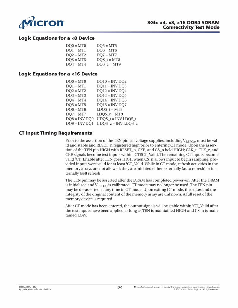
Logic Equations for a ×8 Device
DQ0 = MT0 DQ5 = MT5DQ1 = MT1 DQ6 = MT6DQ2 = MT2 DQ7 = MT7DQ3 = MT3 DQS_t = MT8DQ4 = MT4 DQS_c = MT9
Logic Equations for a ×16 Device
DQ0 = MT0 DQ10 = INV DQ2DQ1 = MT1 DQ11 = INV DQ3DQ2 = MT2 DQ12 = INV DQ4DQ3 = MT3 DQ13 = INV DQ5DQ4 = MT4 DQ14 = INV DQ6DQ5 = MT5 DQ15 = INV DQ7DQ6 = MT6 LDQS_t = MT8DQ7 = MT7 LDQS_c = MT9DQ8 = INV DQ0 UDQS_t = INV LDQS_tDQ9 = INV DQ1 UDQS_c = INV LDQS_c
CT Input Timing Requirements
Prior to the assertion of the TEN pin, all voltage supplies, including VREFCA, must be val-id and stable and RESET_n registered high prior to entering CT mode. Upon the asser-tion of the TEN pin HIGH with RESET_n, CKE, and CS_n held HIGH; CLK_t, CLK_c, andCKE signals become test inputs within tCTECT_Valid. The remaining CT inputs becomevalid tCT_Enable after TEN goes HIGH when CS_n allows input to begin sampling, pro-vided inputs were valid for at least tCT_Valid. While in CT mode, refresh activities in thememory arrays are not allowed; they are initiated either externally (auto refresh) or in-ternally (self refresh).
The TEN pin may be asserted after the DRAM has completed power-on. After the DRAMis initialized and VREFDQ is calibrated, CT mode may no longer be used. The TEN pinmay be de-asserted at any time in CT mode. Upon exiting CT mode, the states and theintegrity of the original content of the memory array are unknown. A full reset of thememory device is required.
After CT mode has been entered, the output signals will be stable within tCT_Valid afterthe test inputs have been applied as long as TEN is maintained HIGH and CS_n is main-tained LOW.
8Gb: x4, x8, x16 DDR4 SDRAMConnectivity Test Mode
09005aef861d1d4a8gb_ddr4_dram.pdf - Rev. L 9/17 EN 129 Micron Technology, Inc. reserves the right to change products or specifications without notice.
© 2015 Micron Technology, Inc. All rights reserved.
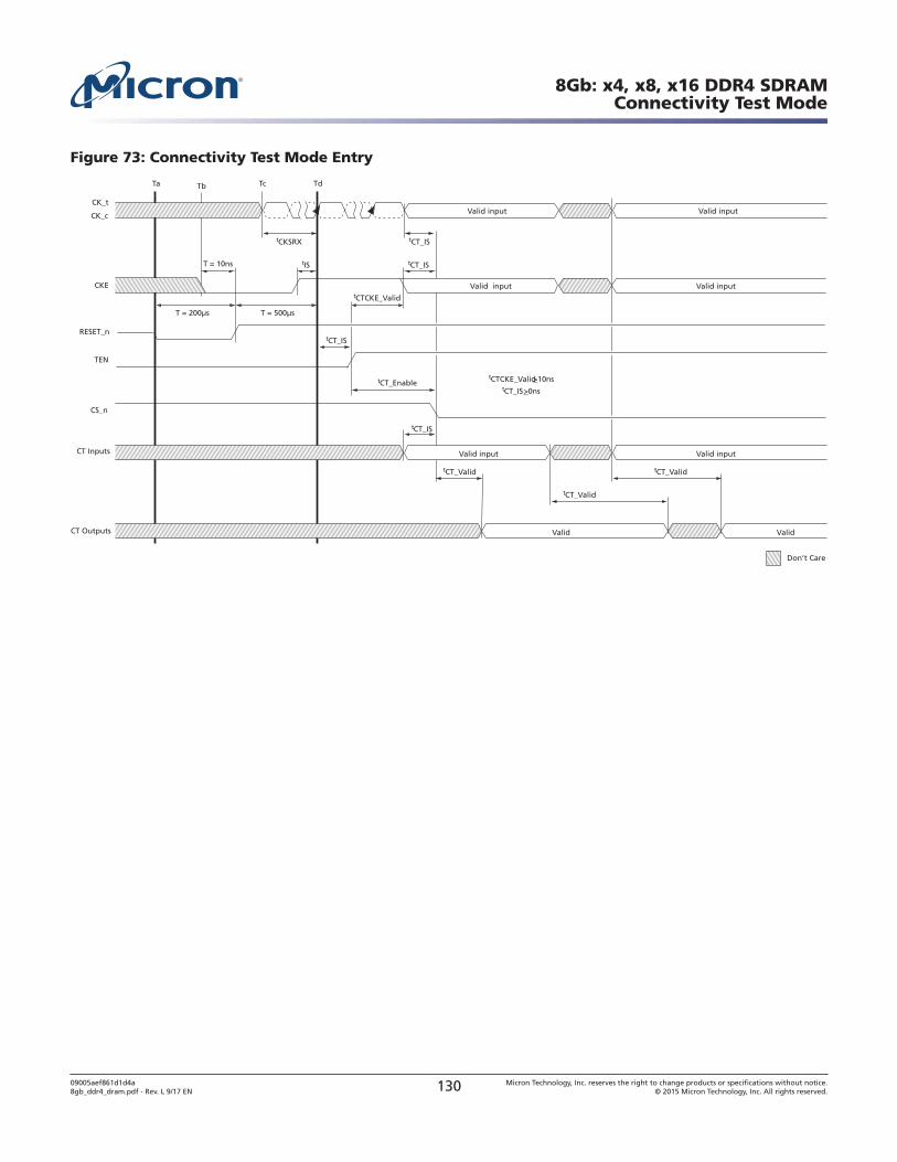
Figure 73: Connectivity Test Mode Entry
tCTCKE_Valid
T = 10ns
CS_n
CT Inputs
CT Outputs
tCT_Enable
tCKSRX
tCTCKE_Valid >10ns tCT_IS >0ns
T = 500μsT = 200μs
tIS
tCT_Valid tCT_Valid
tCT_Valid
TEN
Valid input Valid input
Valid input Valid input
Valid input Valid input
Valid Valid
RESET_n
CKE
CK_c
CK_t
Ta Tb Tc Td
tCT_IS
tCT_IS
tCT_IS
tCT_IS
Don’t Care
8Gb: x4, x8, x16 DDR4 SDRAMConnectivity Test Mode
09005aef861d1d4a8gb_ddr4_dram.pdf - Rev. L 9/17 EN 130 Micron Technology, Inc. reserves the right to change products or specifications without notice.
© 2015 Micron Technology, Inc. All rights reserved.
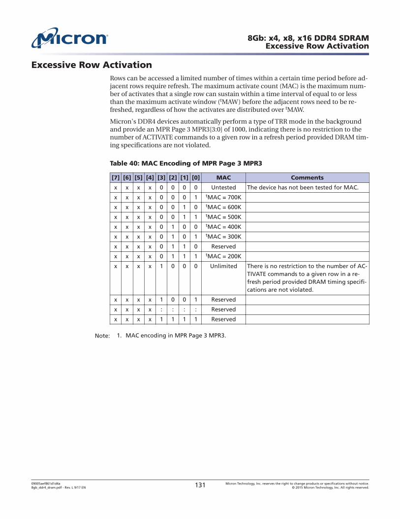
Excessive Row ActivationRows can be accessed a limited number of times within a certain time period before ad-jacent rows require refresh. The maximum activate count (MAC) is the maximum num-ber of activates that a single row can sustain within a time interval of equal to or lessthan the maximum activate window (tMAW) before the adjacent rows need to be re-freshed, regardless of how the activates are distributed over tMAW.
Micron's DDR4 devices automatically perform a type of TRR mode in the backgroundand provide an MPR Page 3 MPR3[3:0] of 1000, indicating there is no restriction to thenumber of ACTIVATE commands to a given row in a refresh period provided DRAM tim-ing specifications are not violated.
Table 40: MAC Encoding of MPR Page 3 MPR3
[7] [6] [5] [4] [3] [2] [1] [0] MAC Comments
x x x x 0 0 0 0 Untested The device has not been tested for MAC.
x x x x 0 0 0 1 tMAC = 700K
x x x x 0 0 1 0 tMAC = 600K
x x x x 0 0 1 1 tMAC = 500K
x x x x 0 1 0 0 tMAC = 400K
x x x x 0 1 0 1 tMAC = 300K
x x x x 0 1 1 0 Reserved
x x x x 0 1 1 1 tMAC = 200K
x x x x 1 0 0 0 Unlimited There is no restriction to the number of AC-TIVATE commands to a given row in a re-fresh period provided DRAM timing specifi-cations are not violated.
x x x x 1 0 0 1 Reserved
x x x x : : : : Reserved
x x x x 1 1 1 1 Reserved
Note: 1. MAC encoding in MPR Page 3 MPR3.
8Gb: x4, x8, x16 DDR4 SDRAMExcessive Row Activation
09005aef861d1d4a8gb_ddr4_dram.pdf - Rev. L 9/17 EN 131 Micron Technology, Inc. reserves the right to change products or specifications without notice.
© 2015 Micron Technology, Inc. All rights reserved.
Post Package Repair
Post Package Repair
JEDEC defines two modes of Post Package Repair (PPR): soft Post Package Repair (sPPR)and hard Post Package Repair (hPPR). sPPR is non-persistent so the repair row maybealtered; that is, sPPR is NOT a permanent repair and even though it will repair a row, therepair can be reversed, reassigned via another sPPR, or made permanent via hPPR.Hard Post Package Repair is persistent so once the repair row is assigned for a hPPR ad-dress, further PPR commands to a previous hPPR section should not be performed, thatis, hPPR is a permanent repair; once repaired, it cannot be reversed. The controller pro-vides the failing row address in the hPPR/sPPR sequence to the device to perform therow repair. hPPR Mode and sPPR Mode may not be enabled at the same time.
JEDEC states hPPR is optional for 4Gb and sPPR is optional for 4Gb and 8Gb parts how-ever Micron 4Gb and 8Gb DDR4 DRAMs should have both sPPR and hPPR support. ThehPPR support is identified via an MPR read from MPR Page 2, MPR0[7] and sPPR sup-port is identified via an MPR read from MPR Page 2, MPR0[6].
The JEDEC minimum support requirement for DDR4 PPR (hPPR or sPPR) is to provideone row of repair per bank group (BG), x4/x8 have 4 BG and x16 has 2 BG; this is a totalof 4 repair rows available on x4/x8 and 2 repair rows available on x16. Micron PPR sup-port exceeds the JEDEC minimum requirements; Micron DDR4 DRAMs have at leastone row of repair for each bank which is essentially 4 row repairs per BG for a total of 16repair rows for x4 and x8 and 8 repair rows for x16; a 4x increase in repair rows.
JEDEC requires the user to have all sPPR row repair addresses reset and cleared prior toenabling hPPR Mode. Micron DDR4 PPR does not have this restriction, the existingsPPR row repair addresses are not required to be cleared prior to entering hPPR mode.Each bank in a BG is PPR independent: sPPR or hPPR issued to a bank will not alter asPPR row repair existing in a different bank.
sPPR followed by sPPR to same bank
When PPR is issued to a bank for the first time and is a sPPR command, the repair rowwill be a sPPR. When a subsequent sPPR is issued to the same bank, the previous sPPRrepair row will be cleared and used for the subsequent sPPR address as the sPPR opera-tion is non-persistent.
sPPR followed by hPPR to same bank
When a PPR is issued to a bank for the first time and is a sPPR command, the repair rowwill be a sPPR. When a subsequent hPPR is issued to the same bank, the initial sPPRrepair row will be cleared and used for the hPPR address. If a further subsequent PPR(hPPR or sPPR) is issued to the same bank, the further subsequent PPR ( hPPR or sPPR)repair row will not clear or overwrite the previous hPPR address as the hPPR operationis persistent.
hPPR followed by hPPR or sPPR to same bank
When a PPR is issued to a bank for the first time and is a hPPR command, the repair rowwill be a hPPR. When a subsequent PPR (hPPR or sPPR) is issued to the same bank, thesubsequent PPR ( hPPR or sPPR) repair row will not clear or overwrite the initial hPPRaddress as the initial hPPR is persistent.
8Gb: x4, x8, x16 DDR4 SDRAMPost Package Repair
09005aef861d1d4a8gb_ddr4_dram.pdf - Rev. L 9/17 EN 132 Micron Technology, Inc. reserves the right to change products or specifications without notice.
© 2015 Micron Technology, Inc. All rights reserved.
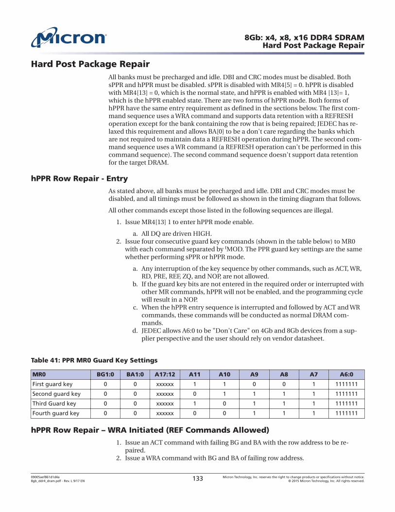
Hard Post Package RepairAll banks must be precharged and idle. DBI and CRC modes must be disabled. BothsPPR and hPPR must be disabled. sPPR is disabled with MR4[5] = 0. hPPR is disabledwith MR4[13] = 0, which is the normal state, and hPPR is enabled with MR4 [13]= 1,which is the hPPR enabled state. There are two forms of hPPR mode. Both forms ofhPPR have the same entry requirement as defined in the sections below. The first com-mand sequence uses a WRA command and supports data retention with a REFRESHoperation except for the bank containing the row that is being repaired; JEDEC has re-laxed this requirement and allows BA[0] to be a don't care regarding the banks whichare not required to maintain data a REFRESH operation during hPPR. The second com-mand sequence uses a WR command (a REFRESH operation can't be performed in thiscommand sequence). The second command sequence doesn't support data retentionfor the target DRAM.
hPPR Row Repair - Entry
As stated above, all banks must be precharged and idle. DBI and CRC modes must bedisabled, and all timings must be followed as shown in the timing diagram that follows.
All other commands except those listed in the following sequences are illegal.
1. Issue MR4[13] 1 to enter hPPR mode enable.
a. All DQ are driven HIGH.2. Issue four consecutive guard key commands (shown in the table below) to MR0
with each command separated by tMOD. The PPR guard key settings are the samewhether performing sPPR or hPPR mode.
a. Any interruption of the key sequence by other commands, such as ACT, WR,RD, PRE, REF, ZQ, and NOP, are not allowed.
b. If the guard key bits are not entered in the required order or interrupted withother MR commands, hPPR will not be enabled, and the programming cyclewill result in a NOP.
c. When the hPPR entry sequence is interrupted and followed by ACT and WRcommands, these commands will be conducted as normal DRAM com-mands.
d. JEDEC allows A6:0 to be "Don't Care" on 4Gb and 8Gb devices from a sup-plier perspective and the user should rely on vendor datasheet.
Table 41: PPR MR0 Guard Key Settings
MR0 BG1:0 BA1:0 A17:12 A11 A10 A9 A8 A7 A6:0
First guard key 0 0 xxxxxx 1 1 0 0 1 1111111
Second guard key 0 0 xxxxxx 0 1 1 1 1 1111111
Third Guard key 0 0 xxxxxx 1 0 1 1 1 1111111
Fourth guard key 0 0 xxxxxx 0 0 1 1 1 1111111
hPPR Row Repair – WRA Initiated (REF Commands Allowed)
1. Issue an ACT command with failing BG and BA with the row address to be re-paired.
2. Issue a WRA command with BG and BA of failing row address.
8Gb: x4, x8, x16 DDR4 SDRAMHard Post Package Repair
09005aef861d1d4a8gb_ddr4_dram.pdf - Rev. L 9/17 EN 133 Micron Technology, Inc. reserves the right to change products or specifications without notice.
© 2015 Micron Technology, Inc. All rights reserved.
a. The address must be at valid levels, but the address is "Don't Care."3. All DQ of the target DRAM should be driven LOW for 4nCK (bit 0 through bit 7)
after WL (WL = CWL + AL + PL) in order for hPPR to initiate repair.
a. Repair will be initiated to the target DRAM only if all DQ during bit 0through bit 7 are LOW. The bank under repair does not get the REFRESHcommand applied to it.
b. Repair will not be initiated to the target DRAM if any DQ during bit 0through bit 7 is HIGH.
1. JEDEC states: All DQs of target DRAM should be LOW for 4tCK. IfHIGH is driven to all DQs of a DRAM consecutively for equal to or lon-ger than 2tCK, then DRAM does not conduct hPPR and retains data ifREF command is properly issued; if all DQs are neither LOW for 4tCKnor HIGH for equal to or longer than 2tCK, then hPPR mode executionis unknown.
c. DQS should function normally.4. REF command may be issued anytime after the WRA command followed by WL +
4nCK + tWR + tRP.
a. Multiple REF commands are issued at a rate of tREFI or tREFI/2, howeverback-to-back REF commands must be separated by at least tREFI/4 whenthe DRAM is in hPPR mode.
b. All banks except the bank under repair will perform refresh.5. Issue PRE after tPGM time so that the device can repair the target row during
tPGM time.
a. Wait tPGM_Exit after PRE to allow the device to recognize the repaired targetrow address.
6. Issue MR4[13] 0 command to hPPR mode disable.
a. Wait tPGMPST for hPPR mode exit to complete.b. After tPGMPST has expired, any valid command may be issued.
The entire sequence from hPPR mode enable through hPPR mode disable may be re-peated if more than one repair is to be done.
After completing hPPR mode, MR0 must be re-programmed to a prehPPR mode state ifthe device is to be accessed.
After hPPR mode has been exited, the DRAM controller can confirm if the target rowwas repaired correctly by writing data into the target row and reading it back.
8Gb: x4, x8, x16 DDR4 SDRAMHard Post Package Repair
09005aef861d1d4a8gb_ddr4_dram.pdf - Rev. L 9/17 EN 134 Micron Technology, Inc. reserves the right to change products or specifications without notice.
© 2015 Micron Technology, Inc. All rights reserved.
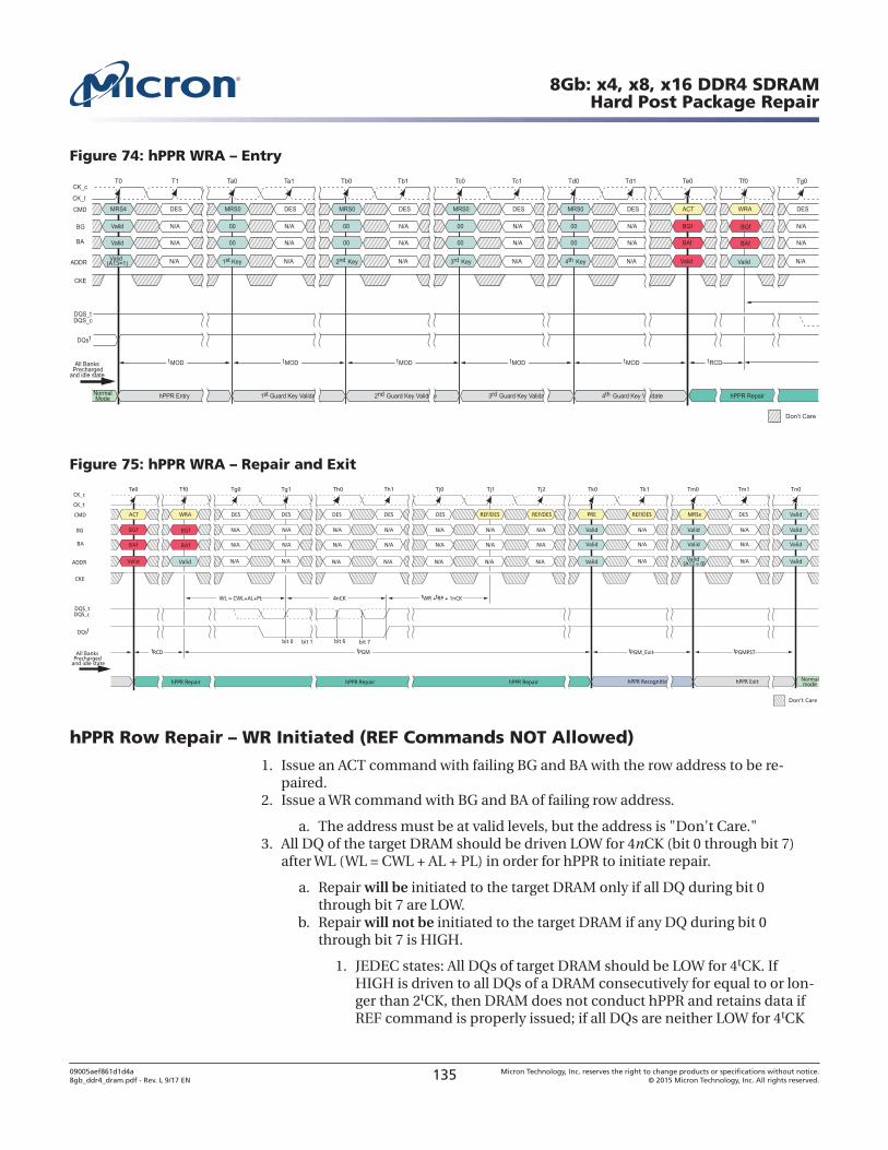
Figure 74: hPPR WRA – Entry
Figure 75: hPPR WRA – Repair and Exit
ADDR
CMD
CKE
DQS_tDQS_c
DQs1
Valid
BA BAf
BG
Valid
BGf
tRCD
WL = CWL+AL+PL tWR + tRP + 1nCK
CK_t
CK_c
N/A
N/A
N/A
N/A
N/A
N/A
N/A
N/A
N/A
N/A
N/A
N/A
N/A
N/A
N/A
N/A
N/A
N/A
N/A
N/A
N/A
All Banks Precharged
and idle state
NormalmodehPPR Recognition hPPR ExithPPR Repair hPPR RepairhPPR Repair
MRSx
tPGM
ACT WRA
Valid (A13 = 0)
Valid
Valid
Valid
Valid
Valid
Valid
Valid
ValidN/A
N/A
N/A
tPGM_Exit tPGMPST
REF/DES REF/DES REF/DESDES DES DES DES DES
N/A
N/A
N/A
DESPRE
Valid
BAf
BGf
Te0 Tf0 Tg0 Tg1 Th0 Th1 Tj0 Tj1 Tj2 Tk0 Tk1 Tm0 Tm1 Tn0
4nCK
bit 0 bit 7bit 6bit 1
Don’t Care
hPPR Row Repair – WR Initiated (REF Commands NOT Allowed)
1. Issue an ACT command with failing BG and BA with the row address to be re-paired.
2. Issue a WR command with BG and BA of failing row address.
a. The address must be at valid levels, but the address is "Don't Care."3. All DQ of the target DRAM should be driven LOW for 4nCK (bit 0 through bit 7)
after WL (WL = CWL + AL + PL) in order for hPPR to initiate repair.
a. Repair will be initiated to the target DRAM only if all DQ during bit 0through bit 7 are LOW.
b. Repair will not be initiated to the target DRAM if any DQ during bit 0through bit 7 is HIGH.
1. JEDEC states: All DQs of target DRAM should be LOW for 4tCK. IfHIGH is driven to all DQs of a DRAM consecutively for equal to or lon-ger than 2tCK, then DRAM does not conduct hPPR and retains data ifREF command is properly issued; if all DQs are neither LOW for 4tCK
8Gb: x4, x8, x16 DDR4 SDRAMHard Post Package Repair
09005aef861d1d4a8gb_ddr4_dram.pdf - Rev. L 9/17 EN 135 Micron Technology, Inc. reserves the right to change products or specifications without notice.
© 2015 Micron Technology, Inc. All rights reserved.
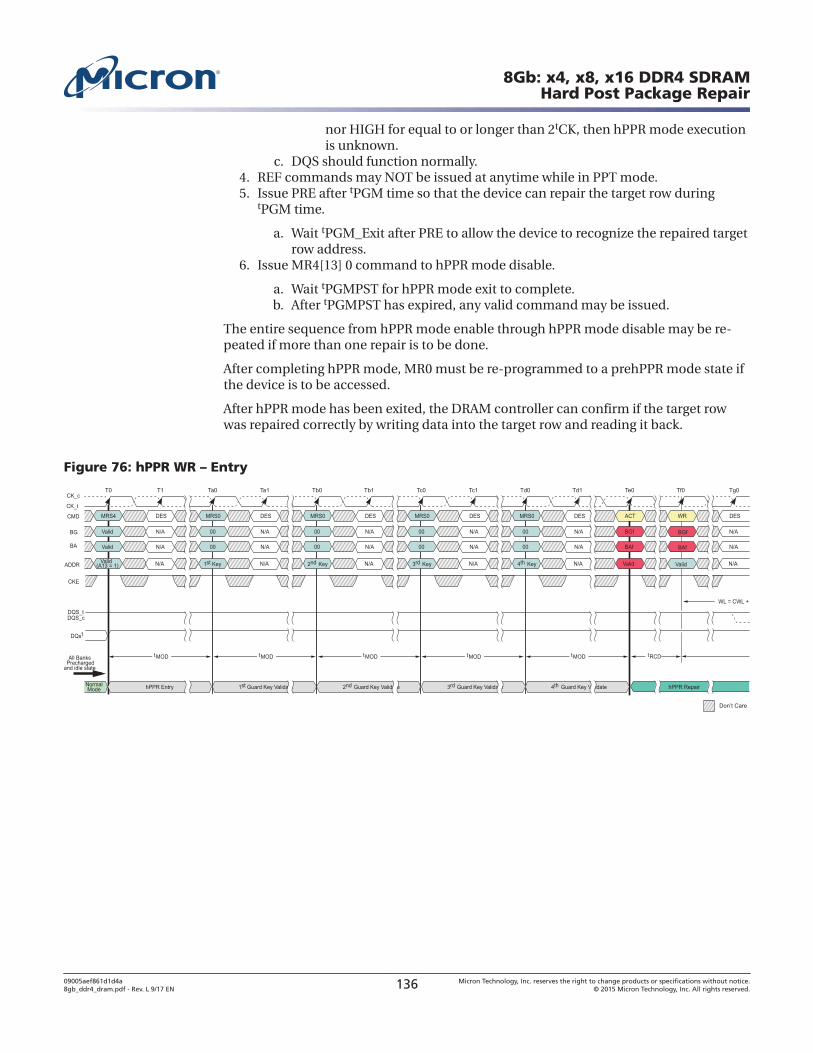
nor HIGH for equal to or longer than 2tCK, then hPPR mode executionis unknown.
c. DQS should function normally.4. REF commands may NOT be issued at anytime while in PPT mode.5. Issue PRE after tPGM time so that the device can repair the target row during
tPGM time.
a. Wait tPGM_Exit after PRE to allow the device to recognize the repaired targetrow address.
6. Issue MR4[13] 0 command to hPPR mode disable.
a. Wait tPGMPST for hPPR mode exit to complete.b. After tPGMPST has expired, any valid command may be issued.
The entire sequence from hPPR mode enable through hPPR mode disable may be re-peated if more than one repair is to be done.
After completing hPPR mode, MR0 must be re-programmed to a prehPPR mode state ifthe device is to be accessed.
After hPPR mode has been exited, the DRAM controller can confirm if the target rowwas repaired correctly by writing data into the target row and reading it back.
Figure 76: hPPR WR – Entry
8Gb: x4, x8, x16 DDR4 SDRAMHard Post Package Repair
09005aef861d1d4a8gb_ddr4_dram.pdf - Rev. L 9/17 EN 136 Micron Technology, Inc. reserves the right to change products or specifications without notice.
© 2015 Micron Technology, Inc. All rights reserved.
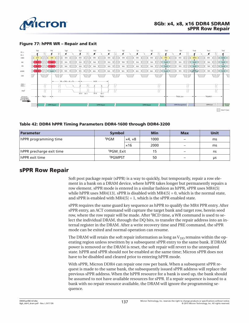
Figure 77: hPPR WR – Repair and Exit
ADDR
CMD
CKE
DQS_tDQS_c
DQs1
Valid
BA BAf
BG
Valid
BGf
tRCD
WL = CWL + AL + PL
CK_t
CK_c
N/A
N/A
N/A
N/A
N/A
N/A
N/A
N/A
N/A
N/A
N/A
N/A
N/A
N/A
N/A
N/A
N/A
N/A
N/A
N/A
N/A
All Banks Precharged
and idle state
NormalmodehPPR Recognition hPPR ExithPPR Repair hPPR RepairhPPR Repair
MRSx
tPGM
ACT WR
Valid (A13 = 0)
Valid
Valid
Valid
Valid
Valid
Valid
Valid
ValidN/A
N/A
N/A
tPGM_Exit tPGMPST
DES DES DES DES DES DES DESDES
N/A
N/A
N/A
DESPRE
Valid
BAf
BGf
Te0 Tf0 Tg0 Tg1 Th0 Th1 Tj0 Tj1 Tj2 Tk0 Tk1 Tm0 Tm1 Tn0
4nCK
bit 0 bit 7bit 6bit 1
Don’t Care
Table 42: DDR4 hPPR Timing Parameters DDR4-1600 through DDR4-3200
Parameter Symbol Min Max Unit
hPPR programming time tPGM ×4, ×8 1000 – ms
×16 2000 – ms
hPPR precharge exit time tPGM_Exit 15 – ns
hPPR exit time tPGMPST 50 – μs
sPPR Row RepairSoft post package repair (sPPR) is a way to quickly, but temporarily, repair a row ele-ment in a bank on a DRAM device, where hPPR takes longer but permanently repairs arow element. sPPR mode is entered in a similar fashion as hPPR, sPPR uses MR4[5]while hPPR uses MR4[13]. sPPR is disabled with MR4[5] = 0, which is the normal state,and sPPR is enabled with MR4[5] = 1, which is the sPPR enabled state.
sPPR requires the same guard key sequence as hPPR to qualify the MR4 PPR entry. AftersPPR entry, an ACT command will capture the target bank and target row, herein seedrow, where the row repair will be made. After tRCD time, a WR command is used to se-lect the individual DRAM, through the DQ bits, to transfer the repair address into an in-ternal register in the DRAM. After a write recovery time and PRE command, the sPPRmode can be exited and normal operation can resume.
The DRAM will retain the soft repair information as long as VDD remains within the op-erating region unless rewritten by a subsequent sPPR entry to the same bank. If DRAMpower is removed or the DRAM is reset, the soft repair will revert to the unrepairedstate. hPPR and sPPR should not be enabled at the same time; Micron sPPR does nothave to be disabled and cleared prior to entering hPPR mode.
With sPPR, Micron DDR4 can repair one row per bank. When a subsequent sPPR re-quest is made to the same bank, the subsequently issued sPPR address will replace theprevious sPPR address. When the hPPR resource for a bank is used up, the bank shouldbe assumed to not have available resources for sPPR. If a repair sequence is issued to abank with no repair resource available, the DRAM will ignore the programming se-quence.
8Gb: x4, x8, x16 DDR4 SDRAMsPPR Row Repair
09005aef861d1d4a8gb_ddr4_dram.pdf - Rev. L 9/17 EN 137 Micron Technology, Inc. reserves the right to change products or specifications without notice.
© 2015 Micron Technology, Inc. All rights reserved.
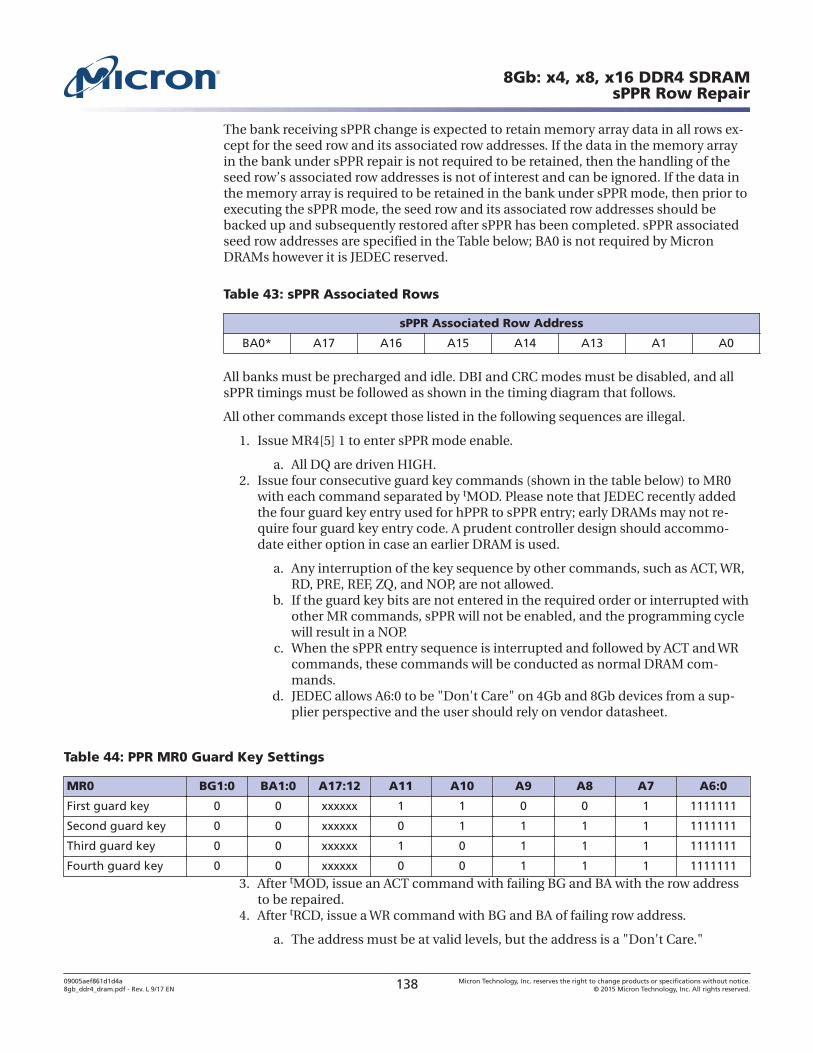
The bank receiving sPPR change is expected to retain memory array data in all rows ex-cept for the seed row and its associated row addresses. If the data in the memory arrayin the bank under sPPR repair is not required to be retained, then the handling of theseed row’s associated row addresses is not of interest and can be ignored. If the data inthe memory array is required to be retained in the bank under sPPR mode, then prior toexecuting the sPPR mode, the seed row and its associated row addresses should bebacked up and subsequently restored after sPPR has been completed. sPPR associatedseed row addresses are specified in the Table below; BA0 is not required by MicronDRAMs however it is JEDEC reserved.
Table 43: sPPR Associated Rows
sPPR Associated Row Address
BA0* A17 A16 A15 A14 A13 A1 A0
All banks must be precharged and idle. DBI and CRC modes must be disabled, and allsPPR timings must be followed as shown in the timing diagram that follows.
All other commands except those listed in the following sequences are illegal.
1. Issue MR4[5] 1 to enter sPPR mode enable.
a. All DQ are driven HIGH.2. Issue four consecutive guard key commands (shown in the table below) to MR0
with each command separated by tMOD. Please note that JEDEC recently addedthe four guard key entry used for hPPR to sPPR entry; early DRAMs may not re-quire four guard key entry code. A prudent controller design should accommo-date either option in case an earlier DRAM is used.
a. Any interruption of the key sequence by other commands, such as ACT, WR,RD, PRE, REF, ZQ, and NOP, are not allowed.
b. If the guard key bits are not entered in the required order or interrupted withother MR commands, sPPR will not be enabled, and the programming cyclewill result in a NOP.
c. When the sPPR entry sequence is interrupted and followed by ACT and WRcommands, these commands will be conducted as normal DRAM com-mands.
d. JEDEC allows A6:0 to be "Don't Care" on 4Gb and 8Gb devices from a sup-plier perspective and the user should rely on vendor datasheet.
Table 44: PPR MR0 Guard Key Settings
MR0 BG1:0 BA1:0 A17:12 A11 A10 A9 A8 A7 A6:0
First guard key 0 0 xxxxxx 1 1 0 0 1 1111111
Second guard key 0 0 xxxxxx 0 1 1 1 1 1111111
Third guard key 0 0 xxxxxx 1 0 1 1 1 1111111
Fourth guard key 0 0 xxxxxx 0 0 1 1 1 1111111
3. After tMOD, issue an ACT command with failing BG and BA with the row addressto be repaired.
4. After tRCD, issue a WR command with BG and BA of failing row address.
a. The address must be at valid levels, but the address is a "Don't Care."
8Gb: x4, x8, x16 DDR4 SDRAMsPPR Row Repair
09005aef861d1d4a8gb_ddr4_dram.pdf - Rev. L 9/17 EN 138 Micron Technology, Inc. reserves the right to change products or specifications without notice.
© 2015 Micron Technology, Inc. All rights reserved.
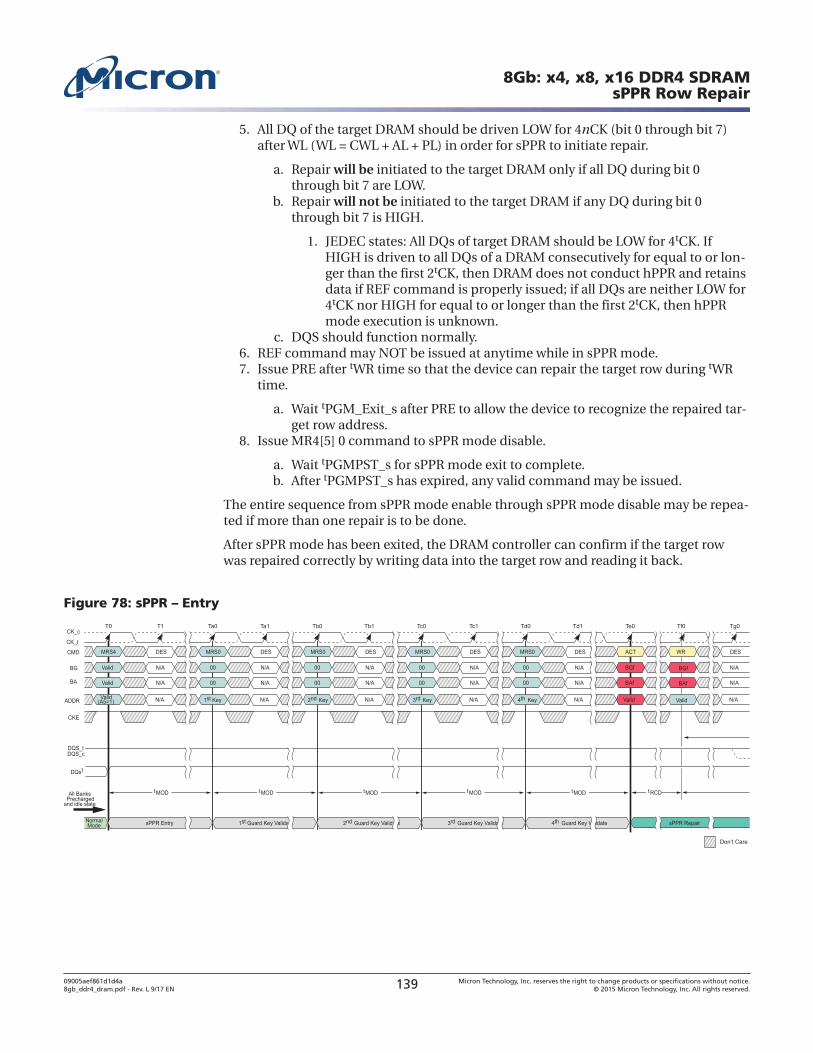
5. All DQ of the target DRAM should be driven LOW for 4nCK (bit 0 through bit 7)after WL (WL = CWL + AL + PL) in order for sPPR to initiate repair.
a. Repair will be initiated to the target DRAM only if all DQ during bit 0through bit 7 are LOW.
b. Repair will not be initiated to the target DRAM if any DQ during bit 0through bit 7 is HIGH.
1. JEDEC states: All DQs of target DRAM should be LOW for 4tCK. IfHIGH is driven to all DQs of a DRAM consecutively for equal to or lon-ger than the first 2tCK, then DRAM does not conduct hPPR and retainsdata if REF command is properly issued; if all DQs are neither LOW for4tCK nor HIGH for equal to or longer than the first 2tCK, then hPPRmode execution is unknown.
c. DQS should function normally.6. REF command may NOT be issued at anytime while in sPPR mode.7. Issue PRE after tWR time so that the device can repair the target row during tWR
time.
a. Wait tPGM_Exit_s after PRE to allow the device to recognize the repaired tar-get row address.
8. Issue MR4[5] 0 command to sPPR mode disable.
a. Wait tPGMPST_s for sPPR mode exit to complete.b. After tPGMPST_s has expired, any valid command may be issued.
The entire sequence from sPPR mode enable through sPPR mode disable may be repea-ted if more than one repair is to be done.
After sPPR mode has been exited, the DRAM controller can confirm if the target rowwas repaired correctly by writing data into the target row and reading it back.
Figure 78: sPPR – Entry
8Gb: x4, x8, x16 DDR4 SDRAMsPPR Row Repair
09005aef861d1d4a8gb_ddr4_dram.pdf - Rev. L 9/17 EN 139 Micron Technology, Inc. reserves the right to change products or specifications without notice.
© 2015 Micron Technology, Inc. All rights reserved.
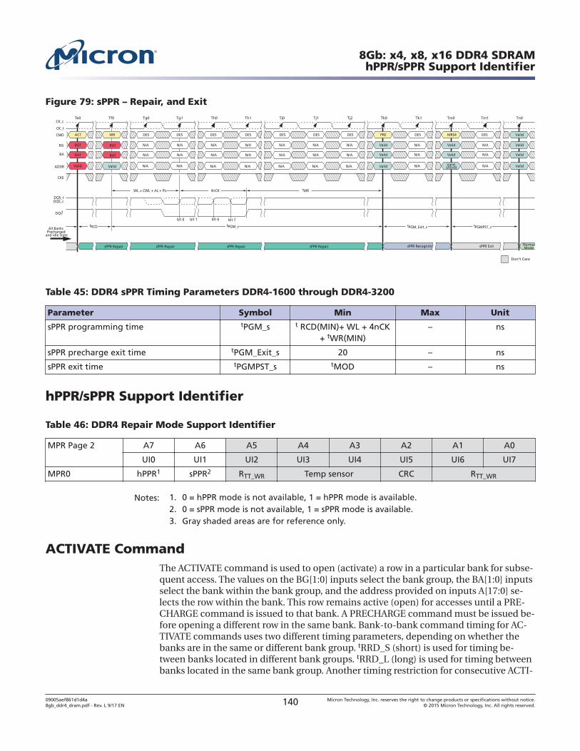
Figure 79: sPPR – Repair, and Exit
bit 1
ADDR
CMD
CKE
DQS_tDQS_c
DQs1
Valid
BA BAf
BG
Valid
BGf
tRCD
WL = CWL + AL + PL
CK_t
CK_c
N/A
N/A
N/A
N/A
N/A
N/A
N/A
N/A
N/A
N/A
N/A
N/A
N/A
N/A
N/A
N/A
N/A
N/A
N/A
N/A
N/A
All Banks Precharged
and idle state
NormalModesPPR Recognition sPPR ExitsPPR Repair sPPR RepairsPPR RepairsPPR Repair
MRS4
tPGM_s
ACT WR
Valid (A5=0)
Valid
Valid
Valid
Valid
Valid
Valid
Valid
ValidN/A
N/A
N/A
DES DES DES DES DES DES DES DES
N/A
N/A
N/A
DESPRE
Valid
BAf
BGf
Te0 Tf0 Tg0 Tg1 Th0 Th1 Tj0 Tj1 Tj2 Tk0 Tk1 Tm0 Tm1 Tn0
4nCK
bit 0 bit 7bit 6
tWR
tPGM_Exit_s tPGMPST_s
Don’t Care
Table 45: DDR4 sPPR Timing Parameters DDR4-1600 through DDR4-3200
Parameter Symbol Min Max Unit
sPPR programming time tPGM_s t RCD(MIN)+ WL + 4nCK+ tWR(MIN)
– ns
sPPR precharge exit time tPGM_Exit_s 20 – ns
sPPR exit time tPGMPST_s tMOD – ns
hPPR/sPPR Support Identifier
Table 46: DDR4 Repair Mode Support Identifier
MPR Page 2 A7 A6 A5 A4 A3 A2 A1 A0
UI0 UI1 UI2 UI3 UI4 UI5 UI6 UI7
MPR0 hPPR1 sPPR2 RTT_WR Temp sensor CRC RTT_WR
Notes: 1. 0 = hPPR mode is not available, 1 = hPPR mode is available.2. 0 = sPPR mode is not available, 1 = sPPR mode is available.3. Gray shaded areas are for reference only.
ACTIVATE CommandThe ACTIVATE command is used to open (activate) a row in a particular bank for subse-quent access. The values on the BG[1:0] inputs select the bank group, the BA[1:0] inputsselect the bank within the bank group, and the address provided on inputs A[17:0] se-lects the row within the bank. This row remains active (open) for accesses until a PRE-CHARGE command is issued to that bank. A PRECHARGE command must be issued be-fore opening a different row in the same bank. Bank-to-bank command timing for AC-TIVATE commands uses two different timing parameters, depending on whether thebanks are in the same or different bank group. tRRD_S (short) is used for timing be-tween banks located in different bank groups. tRRD_L (long) is used for timing betweenbanks located in the same bank group. Another timing restriction for consecutive ACTI-
8Gb: x4, x8, x16 DDR4 SDRAMhPPR/sPPR Support Identifier
09005aef861d1d4a8gb_ddr4_dram.pdf - Rev. L 9/17 EN 140 Micron Technology, Inc. reserves the right to change products or specifications without notice.
© 2015 Micron Technology, Inc. All rights reserved.
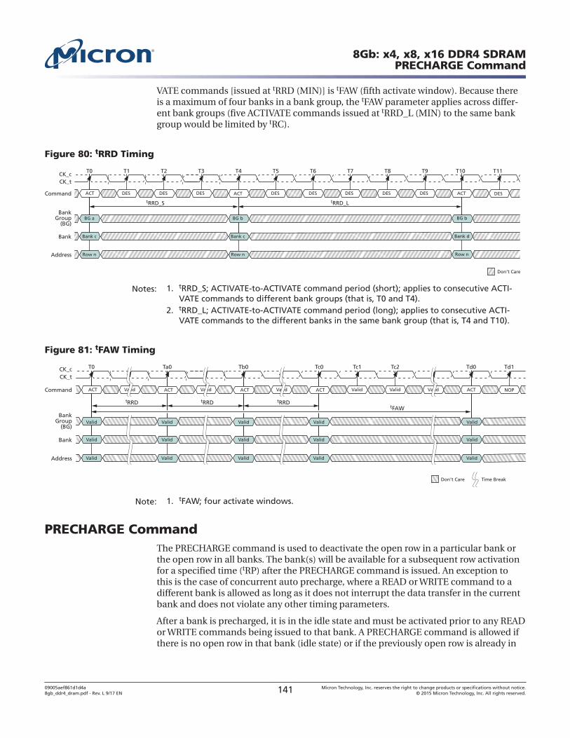
VATE commands [issued at tRRD (MIN)] is tFAW (fifth activate window). Because thereis a maximum of four banks in a bank group, the tFAW parameter applies across differ-ent bank groups (five ACTIVATE commands issued at tRRD_L (MIN) to the same bankgroup would be limited by tRC).
Figure 80: tRRD Timing
T0 T1 T2 T3 T4 T5 T6 T7 T8 T9
tRRD_S
T10 T11
Don’t Care
BG a
DESACT ACTDES DES DES DES DES DES DES DES
CK_tCK_c
Command
BankGroup
(BG)
Bank cBank
Row n
BG b
Bank c
Row n
BG b
Bank d
Row nAddress
tRRD_L
ACT
Notes: 1. tRRD_S; ACTIVATE-to-ACTIVATE command period (short); applies to consecutive ACTI-VATE commands to different bank groups (that is, T0 and T4).
2. tRRD_L; ACTIVATE-to-ACTIVATE command period (long); applies to consecutive ACTI-VATE commands to the different banks in the same bank group (that is, T4 and T10).
Figure 81: tFAW Timing
T0 Ta0 Tb0 Tc0 Tc1 Tc2
tRRD tRRD
Td0 Td1
Don’t Care Time Break
Valid
ValidACT ACTValid Valid Valid Valid Valid NOP
CK_tCK_c
Command
BankGroup
(BG)
ValidBank
Valid
ACT ACT
Address
tFAW
ACT
Valid
Valid
Valid
Valid
Valid
Valid
Valid
Valid
Valid
Valid
Valid
Valid
tRRD
Note: 1. tFAW; four activate windows.
PRECHARGE CommandThe PRECHARGE command is used to deactivate the open row in a particular bank orthe open row in all banks. The bank(s) will be available for a subsequent row activationfor a specified time (tRP) after the PRECHARGE command is issued. An exception tothis is the case of concurrent auto precharge, where a READ or WRITE command to adifferent bank is allowed as long as it does not interrupt the data transfer in the currentbank and does not violate any other timing parameters.
After a bank is precharged, it is in the idle state and must be activated prior to any READor WRITE commands being issued to that bank. A PRECHARGE command is allowed ifthere is no open row in that bank (idle state) or if the previously open row is already in
8Gb: x4, x8, x16 DDR4 SDRAMPRECHARGE Command
09005aef861d1d4a8gb_ddr4_dram.pdf - Rev. L 9/17 EN 141 Micron Technology, Inc. reserves the right to change products or specifications without notice.
© 2015 Micron Technology, Inc. All rights reserved.
the process of precharging. However, the precharge period will be determined by thelast PRECHARGE command issued to the bank.
The auto precharge feature is engaged when a READ or WRITE command is issued withA10 HIGH. The auto precharge feature uses the RAS lockout circuit to internally delaythe PRECHARGE operation until the ARRAY RESTORE operation has completed. TheRAS lockout circuit feature allows the PRECHARGE operation to be partially or com-pletely hidden during burst READ cycles when the auto precharge feature is engaged.The PRECHARGE operation will not begin until after the last data of the burst write se-quence is properly stored in the memory array.
REFRESH CommandThe REFRESH command (REF) is used during normal operation of the device. Thiscommand is nonpersistent, so it must be issued each time a refresh is required. The de-vice requires REFRESH cycles at an average periodic interval of tREFI. When CS_n,RAS_n/A16, and CAS_n/A15 are held LOW and WE_n/A14 HIGH at the rising edge ofthe clock, the device enters a REFRESH cycle. All banks of the SDRAM must be pre-charged and idle for a minimum of the precharge time, tRP (MIN), before the REFRESHcommand can be applied. The refresh addressing is generated by the internal DRAM re-fresh controller. This makes the address bits “Don’t Care” during a REFRESH command.An internal address counter supplies the addresses during the REFRESH cycle. No con-trol of the external address bus is required once this cycle has started. When the RE-FRESH cycle has completed, all banks of the SDRAM will be in the precharged (idle)state. A delay between the REFRESH command and the next valid command, exceptDES, must be greater than or equal to the minimum REFRESH cycle time tRFC (MIN),as shown in Figure 82 (page 143).
Note: The tRFC timing parameter depends on memory density.
In general, a REFRESH command needs to be issued to the device regularly every tREFIinterval. To allow for improved efficiency in scheduling and switching between tasks,some flexibility in the absolute refresh interval is provided for postponing and pulling-in the REFRESH command. A limited number REFRESH commands can be postponeddepending on refresh mode: a maximum of 8 REFRESH commands can be postponedwhen the device is in 1X refresh mode; a maximum of 16 REFRESH commands can bepostponed when the device is in 2X refresh mode; and a maximum of 32 REFRESHcommands can be postponed when the device is in 4X refresh mode.
When 8 consecutive REFRESH commands are postponed, the resulting maximum inter-val between the surrounding REFRESH commands is limited to 9 × tREFI (see Figure 83(page 143)). For both the 2X and 4X refresh modes, the maximum consecutive RE-FRESH commands allowed is limited to 17 × tREFI2 and 36 × tREFI4, respectively.
A limited number REFRESH commands can be pulled-in as well. A maximum of 8 addi-tional REFRESH commands can be issued in advance or “pulled-in” in 1X refresh mode,a maximum of 16 additional REFRESH commands can be issued when in advance in 2Xrefresh mode, and a maximum of 32 additional REFRESH commands can be issued inadvance when in 4X refresh mode. Each of these REFRESH commands reduces thenumber of regular REFRESH commands required later by one. Note that pulling inmore than the maximum allowed REFRESH commands in advance does not further re-duce the number of regular REFRESH commands required later, so that the resultingmaximum interval between two surrounding REFRESH commands is limited to 9 × tRE-
8Gb: x4, x8, x16 DDR4 SDRAMREFRESH Command
09005aef861d1d4a8gb_ddr4_dram.pdf - Rev. L 9/17 EN 142 Micron Technology, Inc. reserves the right to change products or specifications without notice.
© 2015 Micron Technology, Inc. All rights reserved.
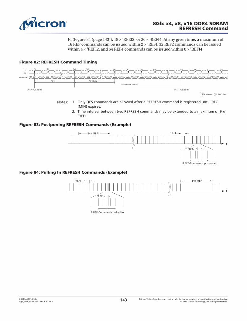
FI (Figure 84 (page 143)), 18 × tRFEI2, or 36 × tREFI4. At any given time, a maximum of16 REF commands can be issued within 2 × tREFI, 32 REF2 commands can be issuedwithin 4 × tREFI2, and 64 REF4 commands can be issued within 8 × tREFI4.
Figure 82: REFRESH Command Timing
DESREF DESREF Valid Valid Valid Valid REF ValidValidValid
CK_t
CK_c
Command
tRFC tRFC (MIN)
tREFI (MAX 9 × tREFI)
Don’t CareTime Break
T0 T1 Ta0 Ta1 Tb0 Tb1 Tb2 Tb3 Tc0 Tc1 Tc2 Tc3
ValidDESDES
DRAM must be idle DRAM must be idle
Notes: 1. Only DES commands are allowed after a REFRESH command is registered until tRFC(MIN) expires.
2. Time interval between two REFRESH commands may be extended to a maximum of 9 ×tREFI.
Figure 83: Postponing REFRESH Commands (Example)
8 REF-Commands postponed
tRFC
tREFI9 × tREFI
Figure 84: Pulling In REFRESH Commands (Example)
8 REF-Commands pulled-in
tRFC
tREFI 9 × tREFI
8Gb: x4, x8, x16 DDR4 SDRAMREFRESH Command
09005aef861d1d4a8gb_ddr4_dram.pdf - Rev. L 9/17 EN 143 Micron Technology, Inc. reserves the right to change products or specifications without notice.
© 2015 Micron Technology, Inc. All rights reserved.
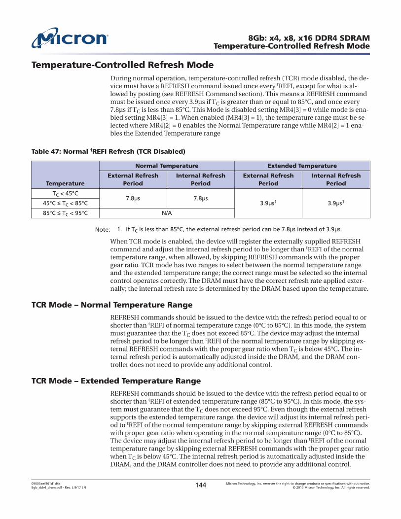
Temperature-Controlled Refresh ModeDuring normal operation, temperature-controlled refresh (TCR) mode disabled, the de-vice must have a REFRESH command issued once every tREFI, except for what is al-lowed by posting (see REFRESH Command section). This means a REFRESH commandmust be issued once every 3.9μs if TC is greater than or equal to 85°C, and once every7.8μs if TC is less than 85°C. This Mode is disabled setting MR4[3] = 0 while mode is ena-bled setting MR4[3] = 1. When enabled (MR4[3] = 1), the temperature range must be se-lected where MR4[2] = 0 enables the Normal Temperature range while MR4[2] = 1 ena-bles the Extended Temperature range
Table 47: Normal tREFI Refresh (TCR Disabled)
Temperature
Normal Temperature Extended Temperature
External RefreshPeriod
Internal RefreshPeriod
External RefreshPeriod
Internal RefreshPeriod
TC < 45°C7.8μs 7.8μs
3.9μs1 3.9μs145°C TC < 85°C
85°C TC < 95°C N/A
Note: 1. If TC is less than 85°C, the external refresh period can be 7.8 s instead of 3.9μs.
When TCR mode is enabled, the device will register the externally supplied REFRESHcommand and adjust the internal refresh period to be longer than tREFI of the normaltemperature range, when allowed, by skipping REFRESH commands with the propergear ratio. TCR mode has two ranges to select between the normal temperature rangeand the extended temperature range; the correct range must be selected so the internalcontrol operates correctly. The DRAM must have the correct refresh rate applied exter-nally; the internal refresh rate is determined by the DRAM based upon the temperature.
TCR Mode – Normal Temperature Range
REFRESH commands should be issued to the device with the refresh period equal to orshorter than tREFI of normal temperature range (0°C to 85°C). In this mode, the systemmust guarantee that the TC does not exceed 85°C. The device may adjust the internalrefresh period to be longer than tREFI of the normal temperature range by skipping ex-ternal REFRESH commands with the proper gear ratio when TC is below 45°C. The in-ternal refresh period is automatically adjusted inside the DRAM, and the DRAM con-troller does not need to provide any additional control.
TCR Mode – Extended Temperature Range
REFRESH commands should be issued to the device with the refresh period equal to orshorter than tREFI of extended temperature range (85°C to 95°C). In this mode, the sys-tem must guarantee that the TC does not exceed 95°C. Even though the external refreshsupports the extended temperature range, the device will adjust its internal refresh peri-od to tREFI of the normal temperature range by skipping external REFRESH commandswith proper gear ratio when operating in the normal temperature range (0°C to 85°C).The device may adjust the internal refresh period to be longer than tREFI of the normaltemperature range by skipping external REFRESH commands with the proper gear ratiowhen TC is below 45°C. The internal refresh period is automatically adjusted inside theDRAM, and the DRAM controller does not need to provide any additional control.
8Gb: x4, x8, x16 DDR4 SDRAMTemperature-Controlled Refresh Mode
09005aef861d1d4a8gb_ddr4_dram.pdf - Rev. L 9/17 EN 144 Micron Technology, Inc. reserves the right to change products or specifications without notice.
© 2015 Micron Technology, Inc. All rights reserved.
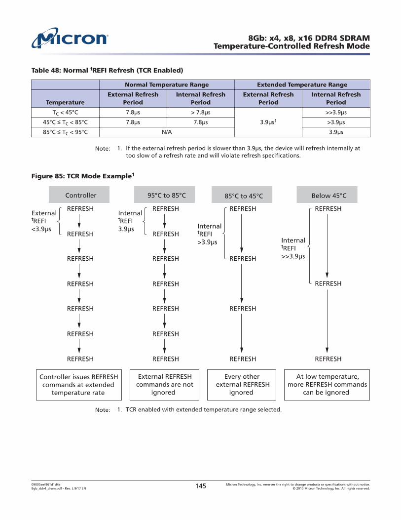
Table 48: Normal tREFI Refresh (TCR Enabled)
Normal Temperature Range Extended Temperature Range
TemperatureExternal Refresh
PeriodInternal Refresh
PeriodExternal Refresh
PeriodInternal Refresh
Period
TC < 45°C 7.8μs > 7.8μs
3.9μs1
>>3.9μs
45°C TC < 85°C 7.8μs 7.8μs >3.9μs
85°C TC < 95°C N/A 3.9μs
Note: 1. If the external refresh period is slower than 3.9μs, the device will refresh internally attoo slow of a refresh rate and will violate refresh specifications.
Figure 85: TCR Mode Example1
External REFRESHcommands are not
ignored
Every otherexternal REFRESH
ignored
At low temperature,more REFRESH commands
can be ignored
Controller 95°C to 85°C 85°C to 45°C Below 45°C
Controller issues REFRESHcommands at extended
temperature rate
REFRESHExternaltREFI<3.9μs
InternaltREFI3.9μs Internal
tREFI>3.9μs Internal
tREFI>>3.9μs
REFRESH
REFRESH
REFRESH
REFRESH
REFRESH
REFRESH
REFRESH
REFRESH
REFRESH
REFRESH
REFRESH
REFRESH
REFRESH
REFRESH
REFRESH
REFRESH
REFRESH
REFRESH
REFRESH
REFRESH
Note: 1. TCR enabled with extended temperature range selected.
8Gb: x4, x8, x16 DDR4 SDRAMTemperature-Controlled Refresh Mode
09005aef861d1d4a8gb_ddr4_dram.pdf - Rev. L 9/17 EN 145 Micron Technology, Inc. reserves the right to change products or specifications without notice.
© 2015 Micron Technology, Inc. All rights reserved.
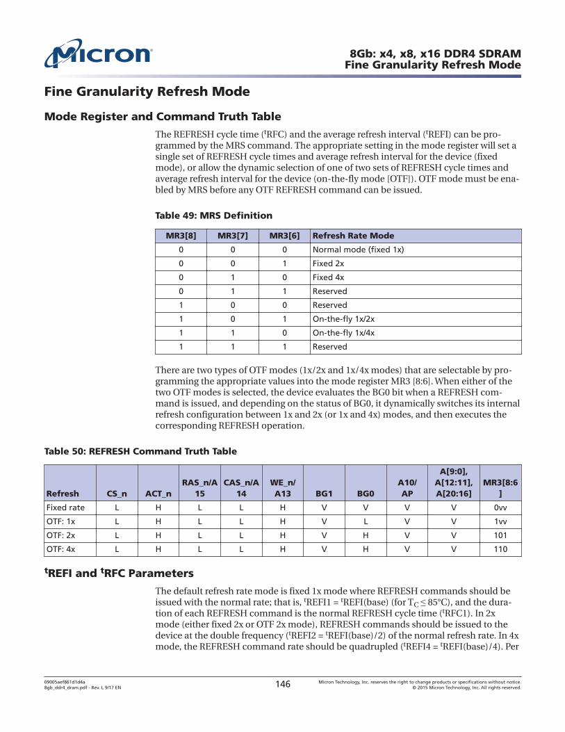
Fine Granularity Refresh Mode
Mode Register and Command Truth Table
The REFRESH cycle time (tRFC) and the average refresh interval (tREFI) can be pro-grammed by the MRS command. The appropriate setting in the mode register will set asingle set of REFRESH cycle times and average refresh interval for the device (fixedmode), or allow the dynamic selection of one of two sets of REFRESH cycle times andaverage refresh interval for the device (on-the-fly mode [OTF]). OTF mode must be ena-bled by MRS before any OTF REFRESH command can be issued.
Table 49: MRS Definition
MR3[8] MR3[7] MR3[6] Refresh Rate Mode
0 0 0 Normal mode (fixed 1x)
0 0 1 Fixed 2x
0 1 0 Fixed 4x
0 1 1 Reserved
1 0 0 Reserved
1 0 1 On-the-fly 1x/2x
1 1 0 On-the-fly 1x/4x
1 1 1 Reserved
There are two types of OTF modes (1x/2x and 1x/4x modes) that are selectable by pro-gramming the appropriate values into the mode register MR3 [8:6]. When either of thetwo OTF modes is selected, the device evaluates the BG0 bit when a REFRESH com-mand is issued, and depending on the status of BG0, it dynamically switches its internalrefresh configuration between 1x and 2x (or 1x and 4x) modes, and then executes thecorresponding REFRESH operation.
Table 50: REFRESH Command Truth Table
Refresh CS_n ACT_nRAS_n/A
15CAS_n/A
14WE_n/A13 BG1 BG0
A10/AP
A[9:0],A[12:11],A[20:16]
MR3[8:6]
Fixed rate L H L L H V V V V 0vv
OTF: 1x L H L L H V L V V 1vv
OTF: 2x L H L L H V H V V 101
OTF: 4x L H L L H V H V V 110
tREFI and tRFC Parameters
The default refresh rate mode is fixed 1x mode where REFRESH commands should beissued with the normal rate; that is, tREFI1 = tREFI(base) (for TC 85°C), and the dura-tion of each REFRESH command is the normal REFRESH cycle time (tRFC1). In 2xmode (either fixed 2x or OTF 2x mode), REFRESH commands should be issued to thedevice at the double frequency (tREFI2 = tREFI(base)/2) of the normal refresh rate. In 4xmode, the REFRESH command rate should be quadrupled (tREFI4 = tREFI(base)/4). Per
8Gb: x4, x8, x16 DDR4 SDRAMFine Granularity Refresh Mode
09005aef861d1d4a8gb_ddr4_dram.pdf - Rev. L 9/17 EN 146 Micron Technology, Inc. reserves the right to change products or specifications without notice.
© 2015 Micron Technology, Inc. All rights reserved.
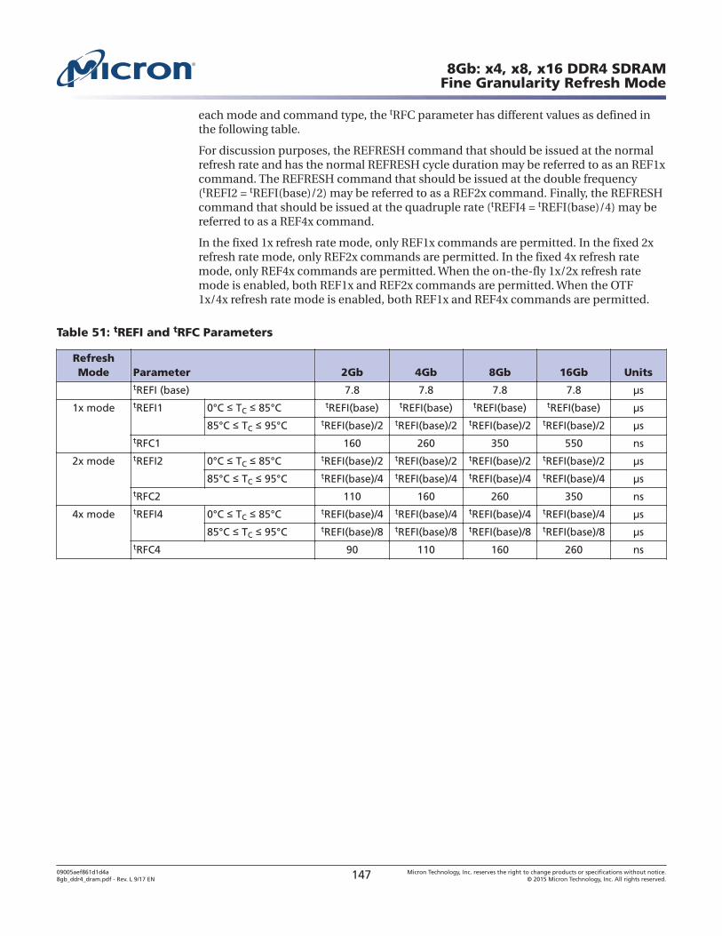
each mode and command type, the tRFC parameter has different values as defined inthe following table.
For discussion purposes, the REFRESH command that should be issued at the normalrefresh rate and has the normal REFRESH cycle duration may be referred to as an REF1xcommand. The REFRESH command that should be issued at the double frequency(tREFI2 = tREFI(base)/2) may be referred to as a REF2x command. Finally, the REFRESHcommand that should be issued at the quadruple rate (tREFI4 = tREFI(base)/4) may bereferred to as a REF4x command.
In the fixed 1x refresh rate mode, only REF1x commands are permitted. In the fixed 2xrefresh rate mode, only REF2x commands are permitted. In the fixed 4x refresh ratemode, only REF4x commands are permitted. When the on-the-fly 1x/2x refresh ratemode is enabled, both REF1x and REF2x commands are permitted. When the OTF1x/4x refresh rate mode is enabled, both REF1x and REF4x commands are permitted.
Table 51: tREFI and tRFC Parameters
RefreshMode Parameter 2Gb 4Gb 8Gb 16Gb Units
tREFI (base) 7.8 7.8 7.8 7.8 μs
1x mode tREFI1 0°C TC 85°C tREFI(base) tREFI(base) tREFI(base) tREFI(base) μs
85°C TC 95°C tREFI(base)/2 tREFI(base)/2 tREFI(base)/2 tREFI(base)/2 μstRFC1 160 260 350 550 ns
2x mode tREFI2 0°C TC 85°C tREFI(base)/2 tREFI(base)/2 tREFI(base)/2 tREFI(base)/2 μs
85°C TC 95°C tREFI(base)/4 tREFI(base)/4 tREFI(base)/4 tREFI(base)/4 μstRFC2 110 160 260 350 ns
4x mode tREFI4 0°C TC 85°C tREFI(base)/4 tREFI(base)/4 tREFI(base)/4 tREFI(base)/4 μs
85°C TC 95°C tREFI(base)/8 tREFI(base)/8 tREFI(base)/8 tREFI(base)/8 μstRFC4 90 110 160 260 ns
8Gb: x4, x8, x16 DDR4 SDRAMFine Granularity Refresh Mode
09005aef861d1d4a8gb_ddr4_dram.pdf - Rev. L 9/17 EN 147 Micron Technology, Inc. reserves the right to change products or specifications without notice.
© 2015 Micron Technology, Inc. All rights reserved.
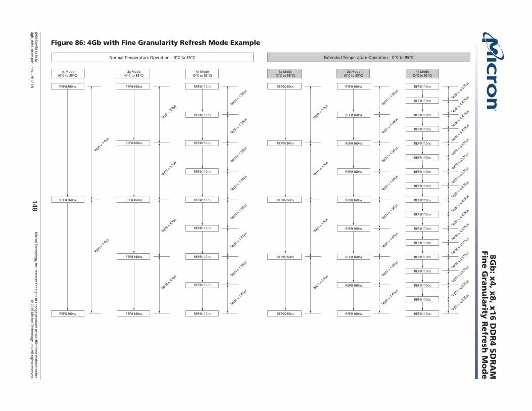
Figure 86: 4Gb with Fine Granularity Refresh Mode Example
t REFI =
0.97
5μs
t REFI =
0.97
5μs
t REFI =
0.97
5μs
t REFI =
0.97
5μs
t REFI =
0.97
5μs
t REFI =
0.97
5μs
t REFI =
0.97
5μs
t REFI =
0.97
5μs
t REFI =
0.97
5μs
t REFI =
0.97
5μs
t REFI =
0.97
5μs
t REFI =
0.97
5μs
t REFI =
0.97
5μs
t REFI =
0.97
5μst REF
I = 0.
975μ
s
t REFI =
0.97
5μs
1x Mode(0°C to 85°C)
2x Mode(0°C to 85°C)
4x Mode(0°C to 85°C)
Normal Temperature Operation – 0°C to 85°C
REF@260ns REF@160ns REF@110ns
REF@110ns
REF@160ns REF@110ns
REF@110ns
REF@260ns REF@160ns REF@110ns
REF@110ns
REF@160ns REF@110ns
REF@110nsREF@260ns REF@160ns
REF@110ns
t REFI =
7.8μ
s
t REFI =
7.8μ
s
t REFI =
3.9μ
s
t REFI =
3.9μ
s
t REFI =
3.9μ
s
t REFI =
3.9μ
s t REFI =
1.95
μs
t REFI =
1.95
μs
t REFI =
1.95
μs
t REFI =
1.95
μs
t REFI =
1.95
μs
t REFI =
1.95
μs
t REFI =
1.95
μs
t REFI =
1.95
μs
1x Mode(0°C to 95°C)
2x Mode(0°C to 95°C)
4x Mode(0°C to 95°C)
REF@260ns REF@160ns REF@110ns
REF@110ns
REF@160ns REF@110ns
REF@110ns
REF@260ns REF@160ns REF@110ns
REF@110ns
REF@160ns REF@110ns
REF@110nsREF@260ns
REF@260ns
REF@260ns
REF@160ns
REF@160ns
REF@160ns
REF@160ns
REF@160ns REF@110ns
REF@110ns
REF@110ns
REF@110ns
REF@110ns
REF@110ns
REF@110ns
REF@110ns
REF@110ns
t REFI =
3.9μ
s
t REFI =
3.9μ
s
t REFI =
3.9μ
s
t REFI =
3.9μ
s t REFI =
1.95
μs
t REFI =
1.95
μs
t REFI =
1.95
μs
t REFI =
1.95
μs
t REFI =
1.95
μs
t REFI =
1.95
μs
t REFI =
1.95
μs
t REFI =
1.95
μs
Extended Temperature Operation – 0°C to 95°C
8G
b: x
4, x
8, x
16 D
DR
4 S
DR
AM
Fine G
ran
ula
rity R
efre
sh M
od
e
09005aef861d1d
4a8g
b_d
dr4_d
ram.p
df - R
ev. L 9/17 EN148
Micro
n Tech
no
log
y, Inc. reserves th
e righ
t to ch
ang
e pro
du
cts or sp
ecification
s with
ou
t no
tice.©
2015 Micro
n Tech
no
log
y, Inc. A
ll righ
ts reserved.
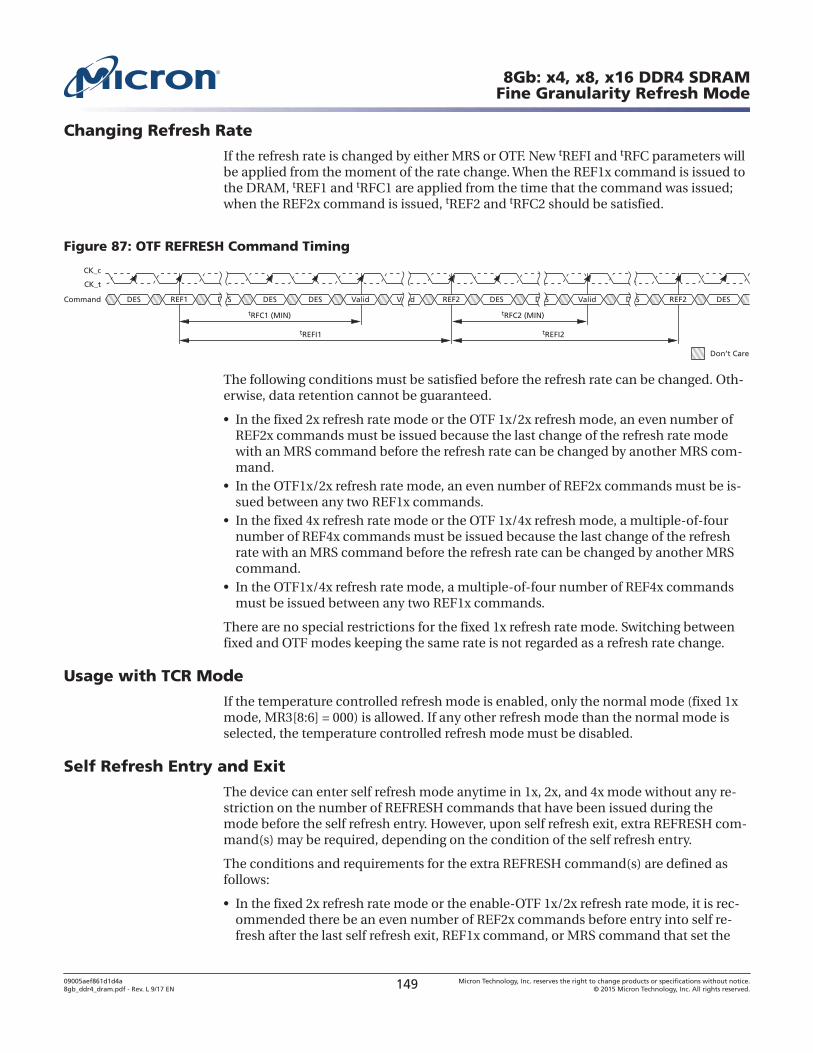
Changing Refresh Rate
If the refresh rate is changed by either MRS or OTF. New tREFI and tRFC parameters willbe applied from the moment of the rate change. When the REF1x command is issued tothe DRAM, tREF1 and tRFC1 are applied from the time that the command was issued;when the REF2x command is issued, tREF2 and tRFC2 should be satisfied.
Figure 87: OTF REFRESH Command Timing
REF1 DESDES DES ValidDES REF2 DESValid Valid DESDES DESREF2
tRFC1 (MIN) tRFC2 (MIN)
tREFI1 tREFI2
Don’t Care
Command
CK_t
CK_c
The following conditions must be satisfied before the refresh rate can be changed. Oth-erwise, data retention cannot be guaranteed.
• In the fixed 2x refresh rate mode or the OTF 1x/2x refresh mode, an even number ofREF2x commands must be issued because the last change of the refresh rate modewith an MRS command before the refresh rate can be changed by another MRS com-mand.
• In the OTF1x/2x refresh rate mode, an even number of REF2x commands must be is-sued between any two REF1x commands.
• In the fixed 4x refresh rate mode or the OTF 1x/4x refresh mode, a multiple-of-fournumber of REF4x commands must be issued because the last change of the refreshrate with an MRS command before the refresh rate can be changed by another MRScommand.
• In the OTF1x/4x refresh rate mode, a multiple-of-four number of REF4x commandsmust be issued between any two REF1x commands.
There are no special restrictions for the fixed 1x refresh rate mode. Switching betweenfixed and OTF modes keeping the same rate is not regarded as a refresh rate change.
Usage with TCR Mode
If the temperature controlled refresh mode is enabled, only the normal mode (fixed 1xmode, MR3[8:6] = 000) is allowed. If any other refresh mode than the normal mode isselected, the temperature controlled refresh mode must be disabled.
Self Refresh Entry and Exit
The device can enter self refresh mode anytime in 1x, 2x, and 4x mode without any re-striction on the number of REFRESH commands that have been issued during themode before the self refresh entry. However, upon self refresh exit, extra REFRESH com-mand(s) may be required, depending on the condition of the self refresh entry.
The conditions and requirements for the extra REFRESH command(s) are defined asfollows:
• In the fixed 2x refresh rate mode or the enable-OTF 1x/2x refresh rate mode, it is rec-ommended there be an even number of REF2x commands before entry into self re-fresh after the last self refresh exit, REF1x command, or MRS command that set the
8Gb: x4, x8, x16 DDR4 SDRAMFine Granularity Refresh Mode
09005aef861d1d4a8gb_ddr4_dram.pdf - Rev. L 9/17 EN 149 Micron Technology, Inc. reserves the right to change products or specifications without notice.
© 2015 Micron Technology, Inc. All rights reserved.
refresh mode. If this condition is met, no additional REFRESH commands are re-quired upon self refresh exit. In the case that this condition is not met, either one ex-tra REF1x command or two extra REF2x commands must be issued upon self refreshexit. These extra REFRESH commands are not counted toward the computation of theaverage refresh interval (tREFI).
• In the fixed 4x refresh rate mode or the enable-OTF 1x/4x refresh rate mode, it is rec-ommended there be a multiple-of-four number of REF4x commands before entry in-to self refresh after the last self refresh exit, REF1x command, or MRS command thatset the refresh mode. If this condition is met, no additional refresh commands are re-quired upon self refresh exit. When this condition is not met, either one extra REF1xcommand or four extra REF4x commands must be issued upon self refresh exit. Theseextra REFRESH commands are not counted toward the computation of the averagerefresh interval (tREFI).
There are no special restrictions on the fixed 1x refresh rate mode.
This section does not change the requirement regarding postponed REFRESH com-mands. The requirement for the additional REFRESH command(s) described above isindependent of the requirement for the postponed REFRESH commands.
8Gb: x4, x8, x16 DDR4 SDRAMFine Granularity Refresh Mode
09005aef861d1d4a8gb_ddr4_dram.pdf - Rev. L 9/17 EN 150 Micron Technology, Inc. reserves the right to change products or specifications without notice.
© 2015 Micron Technology, Inc. All rights reserved.
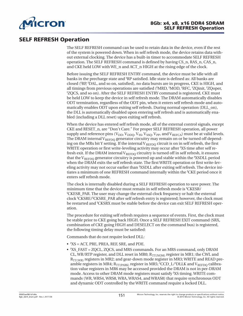
SELF REFRESH OperationThe SELF REFRESH command can be used to retain data in the device, even if the restof the system is powered down. When in self refresh mode, the device retains data with-out external clocking. The device has a built-in timer to accommodate SELF REFRESHoperation. The SELF REFRESH command is defined by having CS_n, RAS_n, CAS_n,and CKE held LOW with WE_n and ACT_n HIGH at the rising edge of the clock.
Before issuing the SELF REFRESH ENTRY command, the device must be idle with allbanks in the precharge state and tRP satisfied. Idle state is defined as: All banks areclosed (tRP, tDAL, and so on, satisfied), no data bursts are in progress, CKE is HIGH, andall timings from previous operations are satisfied (tMRD, tMOD, tRFC, tZQinit, tZQoper,tZQCS, and so on). After the SELF REFRESH ENTRY command is registered, CKE mustbe held LOW to keep the device in self refresh mode. The DRAM automatically disablesODT termination, regardless of the ODT pin, when it enters self refresh mode and auto-matically enables ODT upon exiting self refresh. During normal operation (DLL_on),the DLL is automatically disabled upon entering self refresh and is automatically ena-bled (including a DLL reset) upon exiting self refresh.
When the device has entered self refresh mode, all of the external control signals, exceptCKE and RESET_n, are “Don’t Care.” For proper SELF REFRESH operation, all powersupply and reference pins (VDD, VDDQ, VSS, VSSQ, VPP, and VREFCA) must be at valid levels.The DRAM internal VREFDQ generator circuitry may remain on or be turned off depend-ing on the MRx bit Y setting. If the internal V REFDQ circuit is on in self refresh, the firstWRITE operation or first write-leveling activity may occur after tXS time after self re-fresh exit. If the DRAM internal VREFDQ circuitry is turned off in self refresh, it ensuresthat the VREFDQ generator circuitry is powered up and stable within the tXSDLL periodwhen the DRAM exits the self refresh state. The first WRITE operation or first write-lev-eling activity may not occur earlier than tXSDLL after exiting self refresh. The device ini-tiates a minimum of one REFRESH command internally within the tCKE period once itenters self refresh mode.
The clock is internally disabled during a SELF REFRESH operation to save power. Theminimum time that the device must remain in self refresh mode is tCKESR/tCKESR_PAR. The user may change the external clock frequency or halt the externalclock tCKSRE/tCKSRE_PAR after self refresh entry is registered; however, the clock mustbe restarted and tCKSRX must be stable before the device can exit SELF REFRESH oper-ation.
The procedure for exiting self refresh requires a sequence of events. First, the clock mustbe stable prior to CKE going back HIGH. Once a SELF REFRESH EXIT command (SRX,combination of CKE going HIGH and DESELECT on the command bus) is registered,the following timing delay must be satisfied:
Commands that do not require locked DLL:
• tXS = ACT, PRE, PREA, REF, SRE, and PDE.• tXS_FAST = ZQCL, ZQCS, and MRS commands. For an MRS command, only DRAM
CL, WR/RTP register, and DLL reset in MR0; RTT(NOM) register in MR1; the CWL andRTT(WR) registers in MR2; and gear-down mode register in MR3; WRITE and READ pre-amble registers in MR4; RTT(PARK) register in MR5; tCCD_L/tDLLK and VREFDQ calibra-tion value registers in MR6 may be accessed provided the DRAM is not in per-DRAMmode. Access to other DRAM mode registers must satisfy tXS timing. WRITE com-mands (WR, WRS4, WRS8, WRA, WRAS4, and WRAS8) that require synchronous ODTand dynamic ODT controlled by the WRITE command require a locked DLL.
8Gb: x4, x8, x16 DDR4 SDRAMSELF REFRESH Operation
09005aef861d1d4a8gb_ddr4_dram.pdf - Rev. L 9/17 EN 151 Micron Technology, Inc. reserves the right to change products or specifications without notice.
© 2015 Micron Technology, Inc. All rights reserved.
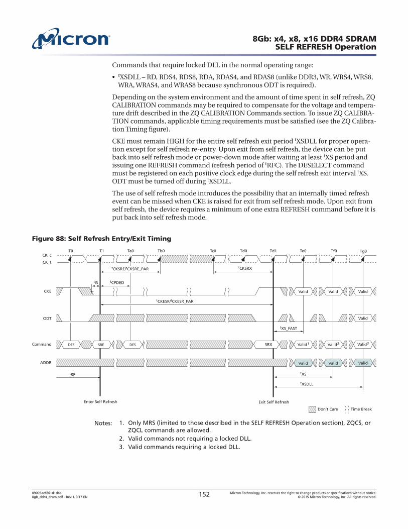
Commands that require locked DLL in the normal operating range:
• tXSDLL – RD, RDS4, RDS8, RDA, RDAS4, and RDAS8 (unlike DDR3, WR, WRS4, WRS8,WRA, WRAS4, and WRAS8 because synchronous ODT is required).
Depending on the system environment and the amount of time spent in self refresh, ZQCALIBRATION commands may be required to compensate for the voltage and tempera-ture drift described in the ZQ CALIBRATION Commands section. To issue ZQ CALIBRA-TION commands, applicable timing requirements must be satisfied (see the ZQ Calibra-tion Timing figure).
CKE must remain HIGH for the entire self refresh exit period tXSDLL for proper opera-tion except for self refresh re-entry. Upon exit from self refresh, the device can be putback into self refresh mode or power-down mode after waiting at least tXS period andissuing one REFRESH command (refresh period of tRFC). The DESELECT commandmust be registered on each positive clock edge during the self refresh exit interval tXS.ODT must be turned off during tXSDLL.
The use of self refresh mode introduces the possibility that an internally timed refreshevent can be missed when CKE is raised for exit from self refresh mode. Upon exit fromself refresh, the device requires a minimum of one extra REFRESH command before it isput back into self refresh mode.
Figure 88: Self Refresh Entry/Exit Timing
CK_t
CK_c
Command DES DESSRE
ADDR
CKE
ODT
SRX Valid1 Valid2
Valid Valid
tRP tXS
tXSDLL
tCKESR/tCKESR_PAR
tCPDEDtIS
tCKSRE/tCKSRE_PAR tCKSRX
Enter Self Refresh Exit Self Refresh
T0 T1 Ta0 Td0 Td1 Te0Tc0
Don’t Care
Tf0
Time Break
Tb0 Tg0
tXS_FAST
Valid3
Valid
Valid Valid Valid
Valid
Notes: 1. Only MRS (limited to those described in the SELF REFRESH Operation section), ZQCS, orZQCL commands are allowed.
2. Valid commands not requiring a locked DLL.3. Valid commands requiring a locked DLL.
8Gb: x4, x8, x16 DDR4 SDRAMSELF REFRESH Operation
09005aef861d1d4a8gb_ddr4_dram.pdf - Rev. L 9/17 EN 152 Micron Technology, Inc. reserves the right to change products or specifications without notice.
© 2015 Micron Technology, Inc. All rights reserved.
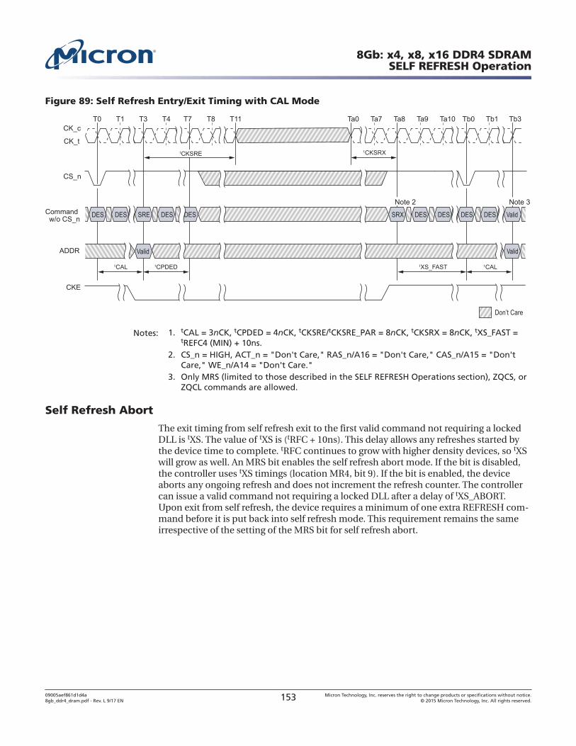
Figure 89: Self Refresh Entry/Exit Timing with CAL Mode
Notes: 1. tCAL = 3nCK, tCPDED = 4nCK, tCKSRE/tCKSRE_PAR = 8nCK, tCKSRX = 8nCK, tXS_FAST =tREFC4 (MIN) + 10ns.
2. CS_n = HIGH, ACT_n = "Don't Care," RAS_n/A16 = "Don't Care," CAS_n/A15 = "Don'tCare," WE_n/A14 = "Don't Care."
3. Only MRS (limited to those described in the SELF REFRESH Operations section), ZQCS, orZQCL commands are allowed.
Self Refresh Abort
The exit timing from self refresh exit to the first valid command not requiring a lockedDLL is tXS. The value of tXS is (tRFC + 10ns). This delay allows any refreshes started bythe device time to complete. tRFC continues to grow with higher density devices, so tXSwill grow as well. An MRS bit enables the self refresh abort mode. If the bit is disabled,the controller uses tXS timings (location MR4, bit 9). If the bit is enabled, the deviceaborts any ongoing refresh and does not increment the refresh counter. The controllercan issue a valid command not requiring a locked DLL after a delay of tXS_ABORT.Upon exit from self refresh, the device requires a minimum of one extra REFRESH com-mand before it is put back into self refresh mode. This requirement remains the sameirrespective of the setting of the MRS bit for self refresh abort.
8Gb: x4, x8, x16 DDR4 SDRAMSELF REFRESH Operation
09005aef861d1d4a8gb_ddr4_dram.pdf - Rev. L 9/17 EN 153 Micron Technology, Inc. reserves the right to change products or specifications without notice.
© 2015 Micron Technology, Inc. All rights reserved.
Figure 90: Self Refresh Abort
CK_t
CK_c
Command DES DESSRE
ADDR
CKE
ODT
SRX Valid1 Valid2
Valid Valid
tRP tXS_ABORT
tXSDLL
tCKESR/tCKESR_PAR
tCPDEDtIS
tCKSRE/tCKSRE_PAR tCKSRX
Enter Self Refresh Exit Self Refresh
T0 T1 Ta0 Td0 Td1 Te0Tc0
Don’t Care
Tf0
Time Break
Tb0 Tg0
tXS_FAST
Valid3
Valid
Valid Valid Valid
Valid
Notes: 1. Only MRS (limited to those described in the SELF REFRESH Operation section), ZQCS, orZQCL commands are allowed.
2. Valid commands not requiring a locked DLL with self refresh abort mode enabled in themode register.
3. Valid commands requiring a locked DLL.
Self Refresh Exit with NOP Command
Exiting self refresh mode using the NO OPERATION command (NOP) is allowed under aspecific system application. This special use of NOP allows for a common command/address bus between active DRAM devices and DRAM(s) in maximum power savingmode. Self refresh mode may exit with NOP commands provided:
• The device entered self refresh mode with CA parity and CAL disabled.• tMPX_S and tMPX_LH are satisfied.• NOP commands are only issued during tMPX_LH window.
No other command is allowed during the tMPX_LH window after an SELF REFRESH EX-IT (SRX) command is issued.
8Gb: x4, x8, x16 DDR4 SDRAMSELF REFRESH Operation
09005aef861d1d4a8gb_ddr4_dram.pdf - Rev. L 9/17 EN 154 Micron Technology, Inc. reserves the right to change products or specifications without notice.
© 2015 Micron Technology, Inc. All rights reserved.
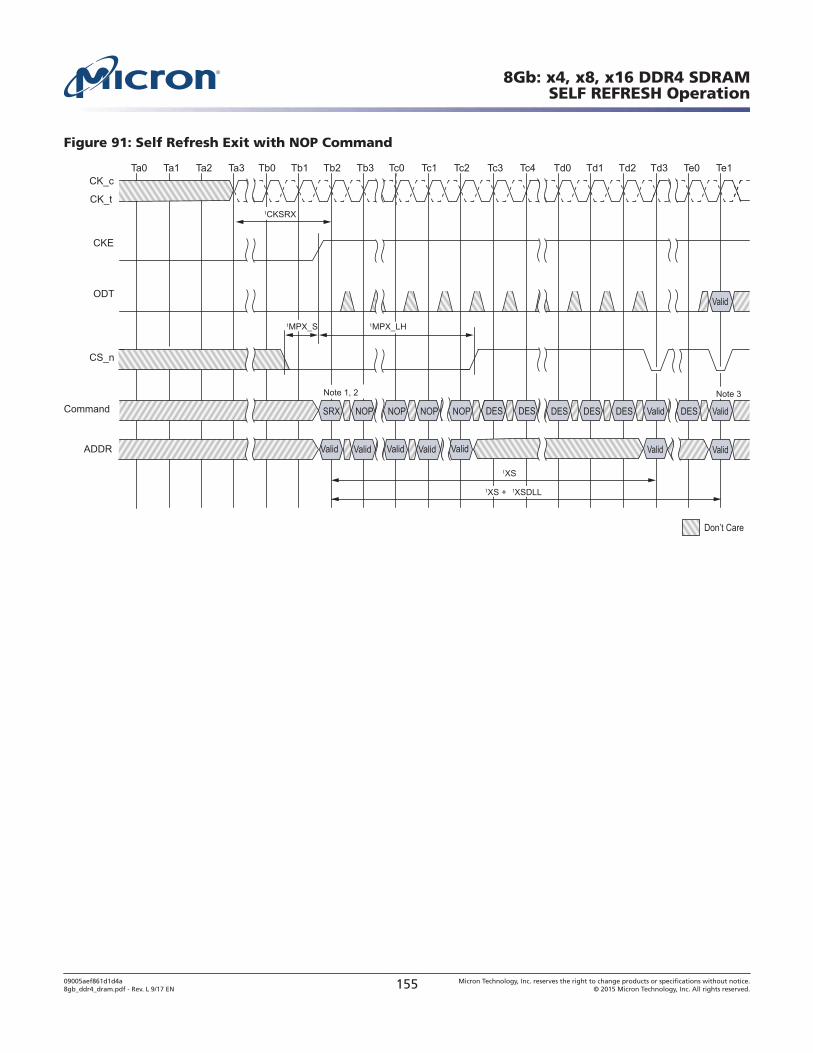
Figure 91: Self Refresh Exit with NOP Command
8Gb: x4, x8, x16 DDR4 SDRAMSELF REFRESH Operation
09005aef861d1d4a8gb_ddr4_dram.pdf - Rev. L 9/17 EN 155 Micron Technology, Inc. reserves the right to change products or specifications without notice.
© 2015 Micron Technology, Inc. All rights reserved.
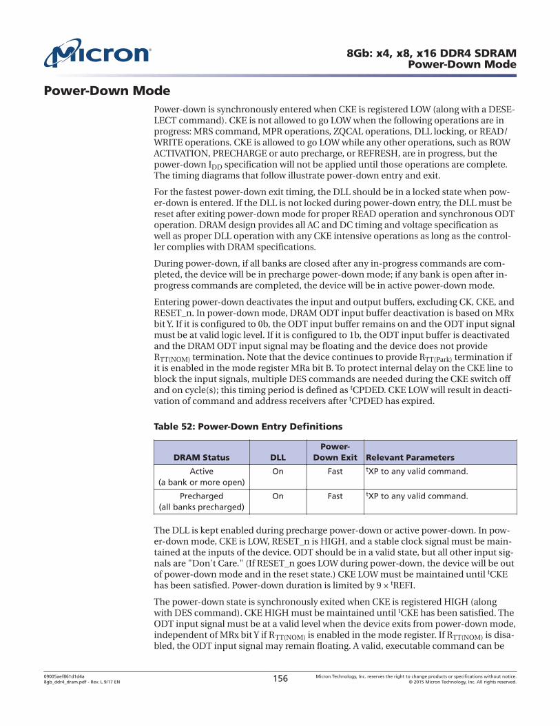
Power-Down ModePower-down is synchronously entered when CKE is registered LOW (along with a DESE-LECT command). CKE is not allowed to go LOW when the following operations are inprogress: MRS command, MPR operations, ZQCAL operations, DLL locking, or READ/WRITE operations. CKE is allowed to go LOW while any other operations, such as ROWACTIVATION, PRECHARGE or auto precharge, or REFRESH, are in progress, but thepower-down IDD specification will not be applied until those operations are complete.The timing diagrams that follow illustrate power-down entry and exit.
For the fastest power-down exit timing, the DLL should be in a locked state when pow-er-down is entered. If the DLL is not locked during power-down entry, the DLL must bereset after exiting power-down mode for proper READ operation and synchronous ODToperation. DRAM design provides all AC and DC timing and voltage specification aswell as proper DLL operation with any CKE intensive operations as long as the control-ler complies with DRAM specifications.
During power-down, if all banks are closed after any in-progress commands are com-pleted, the device will be in precharge power-down mode; if any bank is open after in-progress commands are completed, the device will be in active power-down mode.
Entering power-down deactivates the input and output buffers, excluding CK, CKE, andRESET_n. In power-down mode, DRAM ODT input buffer deactivation is based on MRxbit Y. If it is configured to 0b, the ODT input buffer remains on and the ODT input signalmust be at valid logic level. If it is configured to 1b, the ODT input buffer is deactivatedand the DRAM ODT input signal may be floating and the device does not provideRTT(NOM) termination. Note that the device continues to provide RTT(Park) termination ifit is enabled in the mode register MRa bit B. To protect internal delay on the CKE line toblock the input signals, multiple DES commands are needed during the CKE switch offand on cycle(s); this timing period is defined as tCPDED. CKE LOW will result in deacti-vation of command and address receivers after tCPDED has expired.
Table 52: Power-Down Entry Definitions
DRAM Status DLLPower-
Down Exit Relevant Parameters
Active(a bank or more open)
On Fast tXP to any valid command.
Precharged(all banks precharged)
On Fast tXP to any valid command.
The DLL is kept enabled during precharge power-down or active power-down. In pow-er-down mode, CKE is LOW, RESET_n is HIGH, and a stable clock signal must be main-tained at the inputs of the device. ODT should be in a valid state, but all other input sig-nals are "Don't Care." (If RESET_n goes LOW during power-down, the device will be outof power-down mode and in the reset state.) CKE LOW must be maintained until tCKEhas been satisfied. Power-down duration is limited by 9 × tREFI.
The power-down state is synchronously exited when CKE is registered HIGH (alongwith DES command). CKE HIGH must be maintained until tCKE has been satisfied. TheODT input signal must be at a valid level when the device exits from power-down mode,independent of MRx bit Y if RTT(NOM) is enabled in the mode register. If RTT(NOM) is disa-bled, the ODT input signal may remain floating. A valid, executable command can be
8Gb: x4, x8, x16 DDR4 SDRAMPower-Down Mode
09005aef861d1d4a8gb_ddr4_dram.pdf - Rev. L 9/17 EN 156 Micron Technology, Inc. reserves the right to change products or specifications without notice.
© 2015 Micron Technology, Inc. All rights reserved.
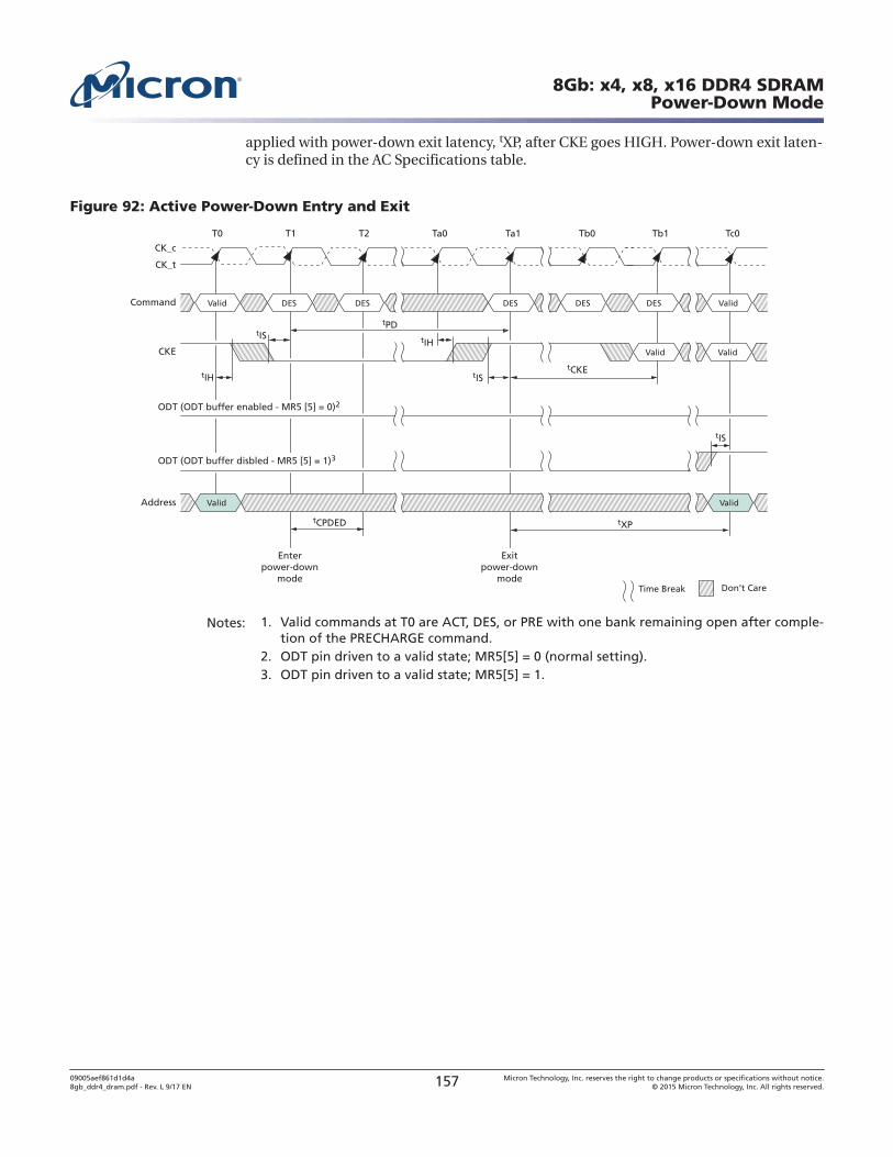
applied with power-down exit latency, tXP, after CKE goes HIGH. Power-down exit laten-cy is defined in the AC Specifications table.
Figure 92: Active Power-Down Entry and Exit
CK_t
CK_c
Command DES DES DES DES DES
Address
CKE
Enterpower-down
mode
Exitpower-down
mode
tPD
Valid
Valid
Valid
Valid
tCPDED
Valid
Valid
ODT (ODT buffer enabled - MR5 [5] = 0)2
ODT (ODT buffer disbled - MR5 [5] = 1)3
tIH
tIHtIS
tIS
tIS
T0 T1 T2 Ta0 Ta1 Tb0 Tb1 Tc0
DES
tXP
tCKE
Don’t CareTime Break
Notes: 1. Valid commands at T0 are ACT, DES, or PRE with one bank remaining open after comple-tion of the PRECHARGE command.
2. ODT pin driven to a valid state; MR5[5] = 0 (normal setting).3. ODT pin driven to a valid state; MR5[5] = 1.
8Gb: x4, x8, x16 DDR4 SDRAMPower-Down Mode
09005aef861d1d4a8gb_ddr4_dram.pdf - Rev. L 9/17 EN 157 Micron Technology, Inc. reserves the right to change products or specifications without notice.
© 2015 Micron Technology, Inc. All rights reserved.
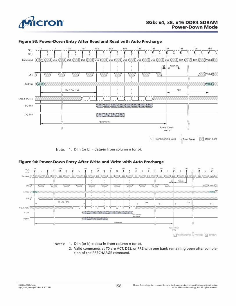
Figure 93: Power-Down Entry After Read and Read with Auto Precharge
T0 T1 Ta0 Ta1 Ta2 Ta3 Ta4 Ta5 Ta6 Ta7
RL = AL + CL
Ta8 Tb0 Tb1
DES
Valid Valid
RD orRDA DES DES DES DES DES DES DES DES DES DES Valid
Valid
CK_t
CK_c
Command
DQ BL8
DQ BC4
DQS_t, DQS_c
Address
CKE
tCPDEDtIS
tPD
tRDPDEN
Power-Downentry
Transitioning Data Don’t CareTime Break
DIb+3
DIb+2
DIb+1
DIb
DIn+3
DIn+2
DIn+1
DIn
DIb+7
DIb+6
DIb+5
DIb+4
Note: 1. DI n (or b) = data-in from column n (or b).
Figure 94: Power-Down Entry After Write and Write with Auto Precharge
T0 T1 Ta0 Ta1 Ta2 Ta3 Ta4 Ta5 Ta6 Ta7
WL = AL + CWL
Tb0 Tb1 Tb2 Tc0 Tc1
Bank,Col n
DIb + 3
DIb + 2
DIb + 1
DIb
DIb + 7
DIb + 6
DIb + 5
DIb + 4
DESWRITE DES DES DES DES DES DES DES DES DES DES DES DES
CK_t
CK_c
Command
DQ BL8
DQ BC4
DQS_t, DQS_c
Address
A10
CKE
WR
tCPDEDtIS
tPD
tWRAPDEN
Power-Down entry
Start internalprecharge
DIn + 3
DIn + 2
DIn + 1
DIn
Transitioning Data
Valid
Valid
Valid
Notes: 1. DI n (or b) = data-in from column n (or b).2. Valid commands at T0 are ACT, DES, or PRE with one bank remaining open after comple-
tion of the PRECHARGE command.
8Gb: x4, x8, x16 DDR4 SDRAMPower-Down Mode
09005aef861d1d4a8gb_ddr4_dram.pdf - Rev. L 9/17 EN 158 Micron Technology, Inc. reserves the right to change products or specifications without notice.
© 2015 Micron Technology, Inc. All rights reserved.
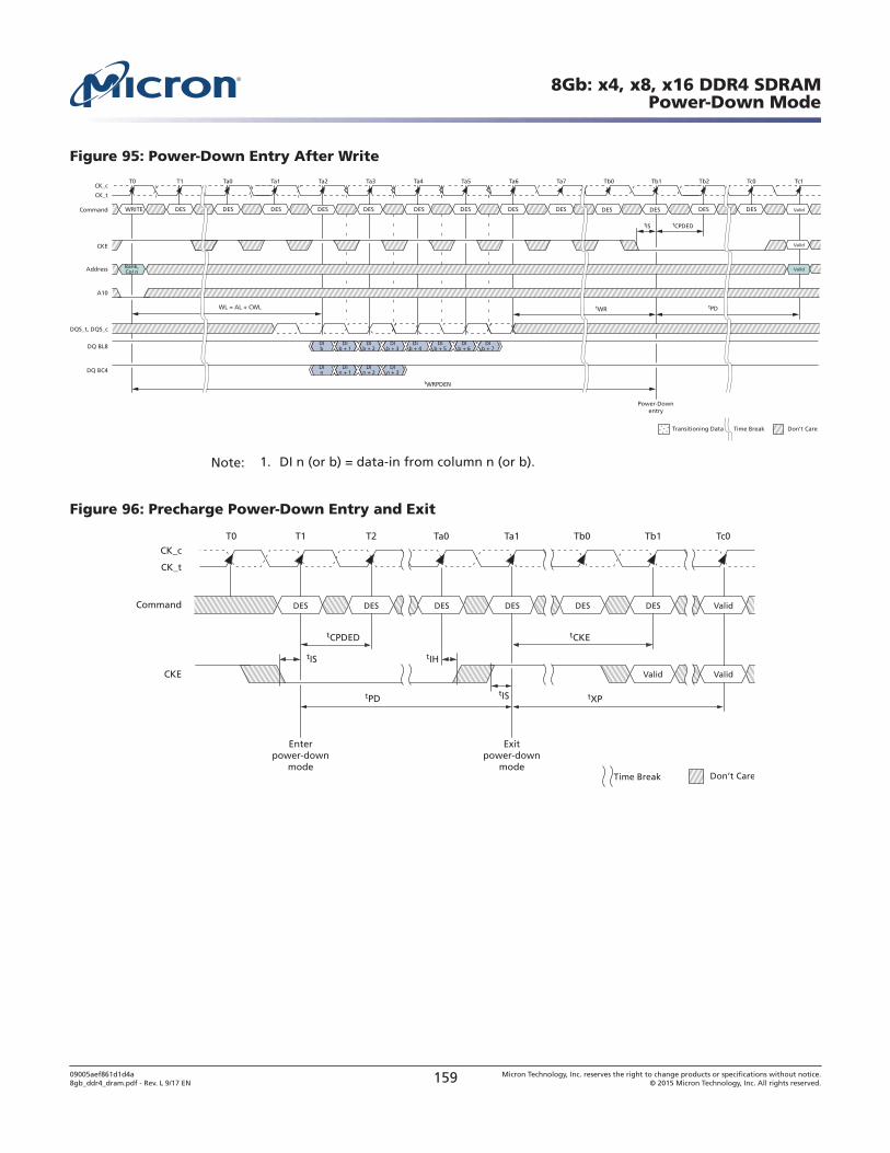
Figure 95: Power-Down Entry After Write
T0 T1 Ta0 Ta1 Ta2 Ta3 Ta4 Ta5 Ta6 Ta7
WL = AL + CWL
Tb0 Tb1 Tb2 Tc0 Tc1
Bank,Col n
DESWRITE DES DES DES DES DES DES DES DES DES DES DES DES
CK_t
CK_c
Command
DQ BL8
DQ BC4
DQS_t, DQS_c
Address
A10
CKE
tWR
tCPDEDtIS
tPD
tWRPDEN
Power-Downentry
Valid
Valid
Valid
Transitioning Data Don’t CareTime Break
DIb + 3
DIb + 2
DIb + 1
DIb
DIb + 7
DIb + 6
DIb + 5
DIb + 4
DI n + 3
DIn + 2
DIn + 1
DIn
Note: 1. DI n (or b) = data-in from column n (or b).
Figure 96: Precharge Power-Down Entry and Exit
CK_t
CK_c
Command DES DES DESDES DES DES
CKE
Enterpower-down
mode
Exitpower-down
mode
tPD tXP
tCPDED
tIS
tIHtIS
T0 T1 T2 Ta0 Ta1 Tb0 Tb1 Tc0
tCKE
Don’t CareTime Break
Valid Valid
Valid
8Gb: x4, x8, x16 DDR4 SDRAMPower-Down Mode
09005aef861d1d4a8gb_ddr4_dram.pdf - Rev. L 9/17 EN 159 Micron Technology, Inc. reserves the right to change products or specifications without notice.
© 2015 Micron Technology, Inc. All rights reserved.
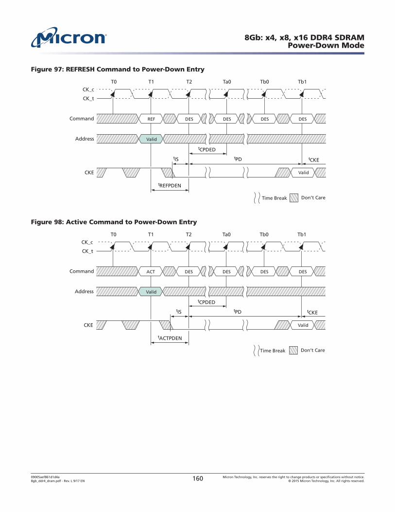
Figure 97: REFRESH Command to Power-Down Entry
CK_t
CK_c
Command REF DES DESDES
Address Valid
CKE
tREFPDEN
tCPDED
tCKE
T0 T1 T2 Ta0 Tb0 Tb1
tPD
Don’t CareTime Break
Valid
tIS
DES
Figure 98: Active Command to Power-Down Entry
CK_t
CK_c
Command ACT DES DESDES
Address Valid
CKE
tACTPDEN
tCPDED
tCKEtIS
T0 T1 T2 Ta0 Tb0 Tb1
tPD
Don’t CareTime Break
Valid
DES
8Gb: x4, x8, x16 DDR4 SDRAMPower-Down Mode
09005aef861d1d4a8gb_ddr4_dram.pdf - Rev. L 9/17 EN 160 Micron Technology, Inc. reserves the right to change products or specifications without notice.
© 2015 Micron Technology, Inc. All rights reserved.
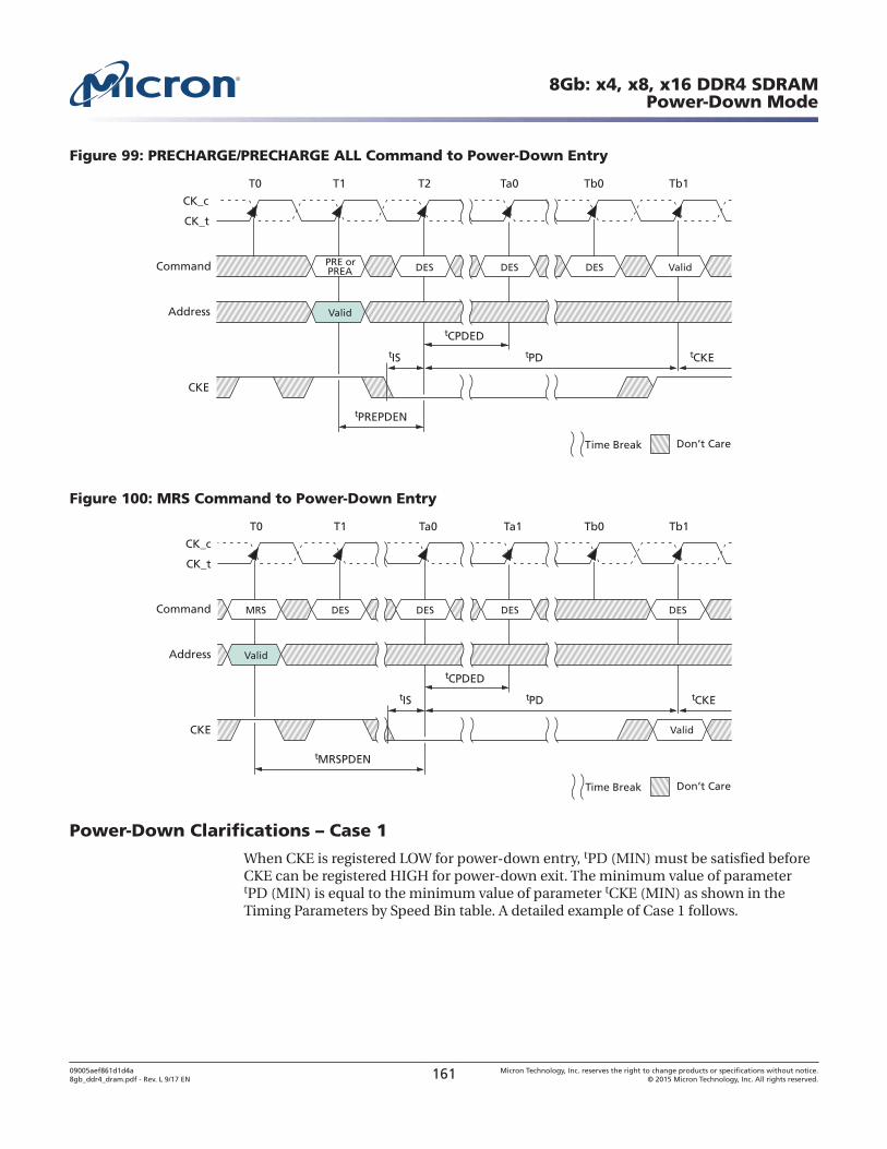
Figure 99: PRECHARGE/PRECHARGE ALL Command to Power-Down Entry
CK_t
CK_c
Command PRE orPREA DES DESDES Valid
Address Valid
CKE
tPREPDEN
tCPDED
T0 T1 T2 Ta0 Tb0 Tb1
tPD tCKE
Don’t CareTime Break
tIS
Figure 100: MRS Command to Power-Down Entry
CK_t
CK_c
Command MRS DES DESDES
Address Valid
CKE
tMRSPDEN
tCPDED
T0 T1 Tb0 Tb1Ta0 Ta1
tPD tCKE
Don’t CareTime Break
Valid
tIS
DES
Power-Down Clarifications – Case 1
When CKE is registered LOW for power-down entry, tPD (MIN) must be satisfied beforeCKE can be registered HIGH for power-down exit. The minimum value of parametertPD (MIN) is equal to the minimum value of parameter tCKE (MIN) as shown in theTiming Parameters by Speed Bin table. A detailed example of Case 1 follows.
8Gb: x4, x8, x16 DDR4 SDRAMPower-Down Mode
09005aef861d1d4a8gb_ddr4_dram.pdf - Rev. L 9/17 EN 161 Micron Technology, Inc. reserves the right to change products or specifications without notice.
© 2015 Micron Technology, Inc. All rights reserved.
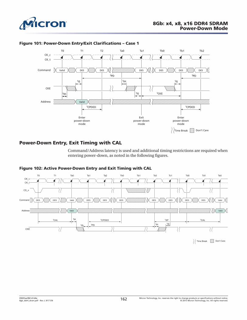
Figure 101: Power-Down Entry/Exit Clarifications – Case 1
CK_t
CK_c
Command Valid DES DESDES DES
Address Valid
CKE
tCPDED
Enterpower-down
mode
Exitpower-down
mode
Enterpower-down
mode
tCPDED
T0 T1 T2 Ta0 Ta1
tPD tPD
Don’t CareTime Break
Tb0 Tb1 Tb2
tIS tIS
tIH tIS tCKE
tIH
DES DES
Power-Down Entry, Exit Timing with CAL
Command/Address latency is used and additional timing restrictions are required whenentering power-down, as noted in the following figures.
Figure 102: Active Power-Down Entry and Exit Timing with CAL
8Gb: x4, x8, x16 DDR4 SDRAMPower-Down Mode
09005aef861d1d4a8gb_ddr4_dram.pdf - Rev. L 9/17 EN 162 Micron Technology, Inc. reserves the right to change products or specifications without notice.
© 2015 Micron Technology, Inc. All rights reserved.
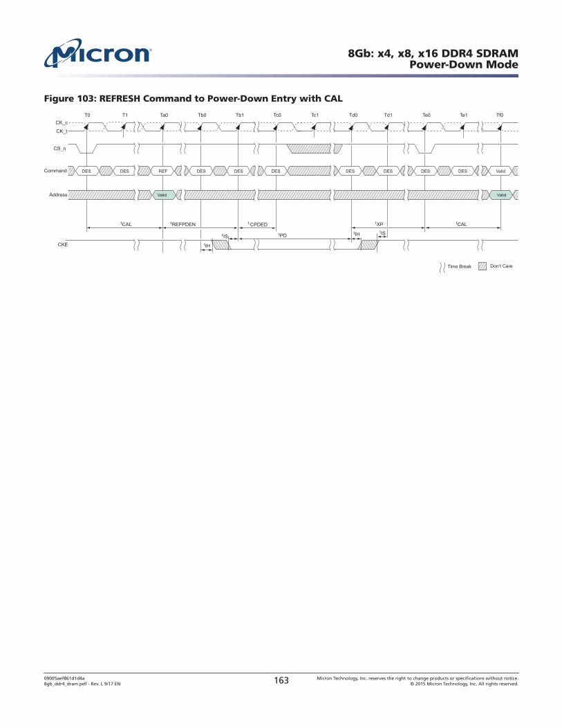
Figure 103: REFRESH Command to Power-Down Entry with CAL
8Gb: x4, x8, x16 DDR4 SDRAMPower-Down Mode
09005aef861d1d4a8gb_ddr4_dram.pdf - Rev. L 9/17 EN 163 Micron Technology, Inc. reserves the right to change products or specifications without notice.
© 2015 Micron Technology, Inc. All rights reserved.
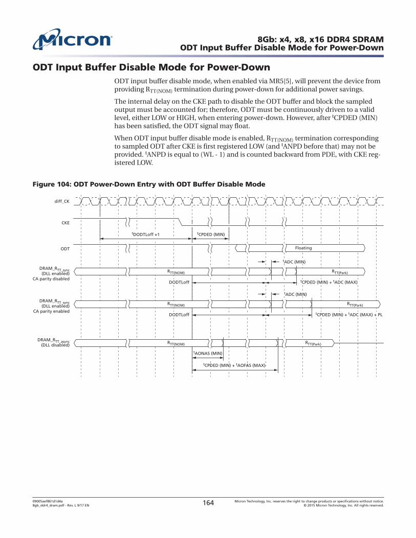
ODT Input Buffer Disable Mode for Power-DownODT input buffer disable mode, when enabled via MR5[5], will prevent the device fromproviding RTT(NOM) termination during power-down for additional power savings.
The internal delay on the CKE path to disable the ODT buffer and block the sampledoutput must be accounted for; therefore, ODT must be continuously driven to a validlevel, either LOW or HIGH, when entering power-down. However, after tCPDED (MIN)has been satisfied, the ODT signal may float.
When ODT input buffer disable mode is enabled, RTT(NOM) termination correspondingto sampled ODT after CKE is first registered LOW (and tANPD before that) may not beprovided. tANPD is equal to (WL - 1) and is counted backward from PDE, with CKE reg-istered LOW.
Figure 104: ODT Power-Down Entry with ODT Buffer Disable Mode
diff_CK
tDODTLoff +1 tCPDED (MIN)
CKE
ODT Floating
DRAM_RTT_sync(DLL enabled)
CA parity disabled
DRAM_RTT_async(DLL disabled)
RTT(Park)RTT(NOM)
tCPDED (MIN) + tADC (MAX)
tADC (MIN)
DODTLoff
RTT(Park)RTT(NOM)
tAONAS (MIN)
tCPDED (MIN) + tAOFAS (MAX)
DRAM_RTT_sync(DLL enabled)
CA parity enabled
RTT(Park)RTT(NOM)
tCPDED (MIN) + tADC (MAX) + PL
tADC (MIN)
DODTLoff
8Gb: x4, x8, x16 DDR4 SDRAMODT Input Buffer Disable Mode for Power-Down
09005aef861d1d4a8gb_ddr4_dram.pdf - Rev. L 9/17 EN 164 Micron Technology, Inc. reserves the right to change products or specifications without notice.
© 2015 Micron Technology, Inc. All rights reserved.
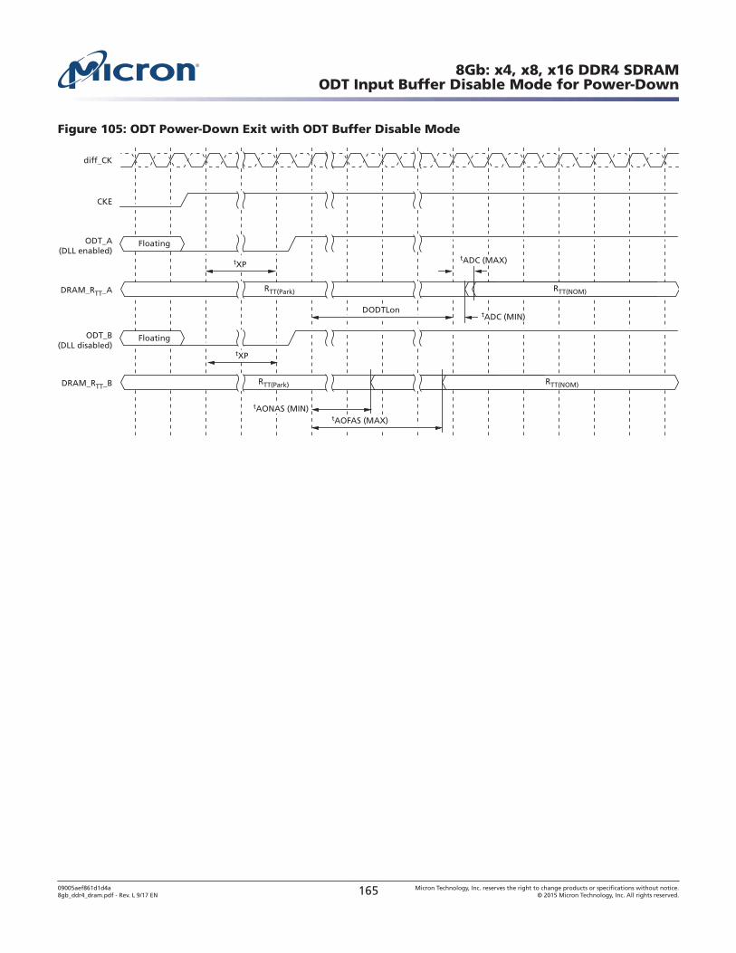
Figure 105: ODT Power-Down Exit with ODT Buffer Disable Mode
diff_CK
CKE
ODT_A(DLL enabled)
tADC (MAX)tXP
tXP
Floating
DRAM_RTT_A RTT(Park) RTT(NOM)
tADC (MIN)DODTLon
ODT_B(DLL disabled)
Floating
DRAM_RTT_B RTT(Park)
tAONAS (MIN)tAOFAS (MAX)
RTT(NOM)
8Gb: x4, x8, x16 DDR4 SDRAMODT Input Buffer Disable Mode for Power-Down
09005aef861d1d4a8gb_ddr4_dram.pdf - Rev. L 9/17 EN 165 Micron Technology, Inc. reserves the right to change products or specifications without notice.
© 2015 Micron Technology, Inc. All rights reserved.
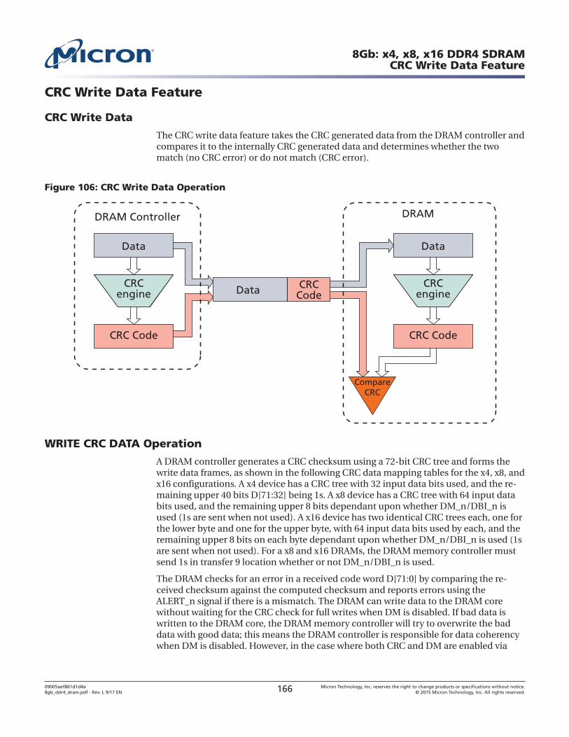
CRC Write Data Feature
CRC Write Data
The CRC write data feature takes the CRC generated data from the DRAM controller andcompares it to the internally CRC generated data and determines whether the twomatch (no CRC error) or do not match (CRC error).
Figure 106: CRC Write Data Operation
Data
DRAM Controller DRAM
Data
CRC Code
CRCCode
CRCengine
Data
CRC Code
CRCengine
CompareCRC
WRITE CRC DATA Operation
A DRAM controller generates a CRC checksum using a 72-bit CRC tree and forms thewrite data frames, as shown in the following CRC data mapping tables for the x4, x8, andx16 configurations. A x4 device has a CRC tree with 32 input data bits used, and the re-maining upper 40 bits D[71:32] being 1s. A x8 device has a CRC tree with 64 input databits used, and the remaining upper 8 bits dependant upon whether DM_n/DBI_n isused (1s are sent when not used). A x16 device has two identical CRC trees each, one forthe lower byte and one for the upper byte, with 64 input data bits used by each, and theremaining upper 8 bits on each byte dependant upon whether DM_n/DBI_n is used (1sare sent when not used). For a x8 and x16 DRAMs, the DRAM memory controller mustsend 1s in transfer 9 location whether or not DM_n/DBI_n is used.
The DRAM checks for an error in a received code word D[71:0] by comparing the re-ceived checksum against the computed checksum and reports errors using theALERT_n signal if there is a mismatch. The DRAM can write data to the DRAM corewithout waiting for the CRC check for full writes when DM is disabled. If bad data iswritten to the DRAM core, the DRAM memory controller will try to overwrite the baddata with good data; this means the DRAM controller is responsible for data coherencywhen DM is disabled. However, in the case where both CRC and DM are enabled via
8Gb: x4, x8, x16 DDR4 SDRAMCRC Write Data Feature
09005aef861d1d4a8gb_ddr4_dram.pdf - Rev. L 9/17 EN 166 Micron Technology, Inc. reserves the right to change products or specifications without notice.
© 2015 Micron Technology, Inc. All rights reserved.
MRS (that is, persistent mode), the DRAM will not write bad data to the core when aCRC error is detected.
DBI_n and CRC Both Enabled
The DRAM computes the CRC for received written data D[71:0]. Data is not invertedback based on DBI before it is used for computing CRC. The data is inverted back basedon DBI before it is written to the DRAM core.
DM_n and CRC Both Enabled
When both DM and write CRC are enabled in the DRAM mode register, the DRAM cal-culates CRC before sending the write data into the array. If there is a CRC error, theDRAM blocks the WRITE operation and discards the data. The Nonconsecutive WRITE(BL8/BC4-OTF) with 2tCK Preamble and Write CRC in Same or Different Bank Group andthe WRITE (BL8/BC4-OTF/Fixed) with 1tCK Preamble and Write CRC in Same or DifferentBankGroup figures in the WRITE Operation section show timing differences when DMis enabled.
DM_n and DBI_n Conflict During Writes with CRC Enabled
Both write DBI_n and DM_n can not be enabled at the same time; read DBI_n andDM_n can be enabled at the same time.
CRC and Write Preamble Restrictions
When write CRC is enabled:
• And 1tCK WRITE preamble mode is enabled, a tCCD_S or tCCD_L of 4 clocks is notallowed.
• And 2tCK WRITE preamble mode is enabled, a tCCD_S or tCCD_L of 6 clocks is notallowed.
CRC Simultaneous Operation Restrictions
When write CRC is enabled, neither MPR writes nor per-DRAM mode is allowed.
CRC Polynomial
The CRC polynomial used by DDR4 is the ATM-8 HEC, X8 + X2 + X1 + 1.
A combinatorial logic block implementation of this 8-bit CRC for 72 bits of data in-cludes 272 two-input XOR gates contained in eight 6-XOR-gate-deep trees.
The CRC polynomial and combinatorial logic used by DDR4 is the same as used onGDDR5.
The error coverage from the DDR4 polynomial used is shown in the following table.
Table 53: CRC Error Detection Coverage
Error Type Detection Capability
Random single-bit errors 100%
Random double-bit errors 100%
8Gb: x4, x8, x16 DDR4 SDRAMCRC Write Data Feature
09005aef861d1d4a8gb_ddr4_dram.pdf - Rev. L 9/17 EN 167 Micron Technology, Inc. reserves the right to change products or specifications without notice.
© 2015 Micron Technology, Inc. All rights reserved.
Table 53: CRC Error Detection Coverage (Continued)
Error Type Detection Capability
Random odd count errors 100%
Random multibit UI vertical column errordetection excluding DBI bits
100%
CRC Combinatorial Logic Equations
module CRC8_D72;// polynomial: (0 1 2 8)// data width: 72// convention: the first serial data bit is D[71]//initial condition all 0 implied// "^" = XORfunction [7:0]nextCRC8_D72;input [71:0] Data;input [71:0] D;reg [7:0] CRC;beginD = Data;
CRC[0] =D[69]^D[68]^D[67]^D[66]^D[64]^D[63]^D[60]^D[56]^D[54]^D[53]^D[52]^D[50]^D[49]^D[48]^D[45]^D[43]^D[40]^D[39]^D[35]^D[34]^D[31]^D[30]^D[28]^D[23]^D[21]^D[19]^D[18]^D[16]^D[14]^D[12]^D[8]^D[7]^D[6]^D[0] ;
CRC[1] =D[70]^D[66]^D[65]^D[63]^D[61]^D[60]^D[57]^D[56]^D[55]^D[52]^D[51]^D[48]^D[46]^D[45]^D[44]^D[43]^D[41]^D[39]^D[36]^D[34]^D[32]^D[30]^D[29]^D[28]^D[24]^D[23]^D[22]^D[21]^D[20]^D[18]^D[17]^D[16]^D[15]^D[14]^D[13]^D[12]^D[9]^D[6]^D[1]^D[0];
CRC[2] =D[71]^D[69]^D[68]^D[63]^D[62]^D[61]^D[60]^D[58]^D[57]^D[54]^D[50]^D[48]^D[47]^D[46]^D[44]^D[43]^D[42]^D[39]^D[37]^D[34]^D[33]^D[29]^D[28]^D[25]^D[24]^D[22]^D[17]^D[15]^D[13]^D[12]^D[10]^D[8]^D[6]^D[2]^D[1]^D[0];
CRC[3] =D[70]^D[69]^D[64]^D[63]^D[62]^D[61]^D[59]^D[58]^D[55]^D[51]^D[49]^D[48]^D[47]^D[45]^D[44]^D[43]^D[40]^D[38]^D[35]^D[34]^D[30]^D[29]^D[26]^D[25]^D[23]^D[18]^D[16]^D[14]^D[13]^D[11]^D[9]^D[7]^D[3]^D[2]^D[1];
CRC[4] =D[71]^D[70]^D[65]^D[64]^D[63]^D[62]^D[60]^D[59]^D[56]^D[52]^D[50]^D[49]^D[48]^D[46]^D[45]^D[44]^D[41]^D[39]^D[36]^D[35]^D[31]^D[30]^D[27]^D[26]^D[24]^D[19]^D[17]^D[15]^D[14]^D[12]^D[10]^D[8]^D[4]^D[3]^D[2];
CRC[5] =D[71]^D[66]^D[65]^D[64]^D[63]^D[61]^D[60]^D[57]^D[53]^D[51]^D[50]^D[49]^D[47]^D[46]^D[45]^D[42]^D[40]^D[37]^D[36]^D[32]^D[31]^D[28]^D[27]^D[25]^D[20]^D[18]^D[16]^D[15]^D[13]^D[11]^D[9]^D[5]^D[4]^D[3];
8Gb: x4, x8, x16 DDR4 SDRAMCRC Write Data Feature
09005aef861d1d4a8gb_ddr4_dram.pdf - Rev. L 9/17 EN 168 Micron Technology, Inc. reserves the right to change products or specifications without notice.
© 2015 Micron Technology, Inc. All rights reserved.
CRC[6] =D[67]^D[66]^D[65]^D[64]^D[62]^D[61]^D[58]^D[54]^D[52]^D[51]^D[50]^D[48]^D[47]^D[46]^D[43]^D[41]^D[38]^D[37]^D[33]^D[32]^D[29]^D[28]^D[26]^D[21]^D[19]^D[17]^D[16]^D[14]^D[12]^D[10]^D[6]^D[5]^D[4];
CRC[7] =D[68]^D[67]^D[66]^D[65]^D[63]^D[62]^D[59]^D[55]^D[53]^D[52]^D[51]^D[49]^D[48]^D[47]^D[44]^D[42]^D[39]^D[38]^D[34]^D[33]^D[30]^D[29]^D[27]^D[22]^D[20]^D[18]^D[17]^D[15]^D[13]^D[11]^D[7]^D[6]^D[5];
nextCRC8_D72 = CRC;
Burst Ordering for BL8
DDR4 supports fixed WRITE burst ordering [A2:A1:A0 = 0:0:0] when write CRC is ena-bled in BL8 (fixed).
CRC Data Bit Mapping
Table 54: CRC Data Mapping for x4 Devices, BL8
Func-tion
Transfer
0 1 2 3 4 5 6 7 8 9
DQ0 D0 D1 D2 D3 D4 D5 D6 D7 CRC0 CRC4
DQ1 D8 D9 D10 D11 D12 D13 D14 D15 CRC1 CRC5
DQ2 D16 D17 D18 D19 D20 D21 D22 D23 CRC2 CRC6
DQ3 D24 D25 D26 D27 D28 D29 D30 D31 CRC3 CRC7
Table 55: CRC Data Mapping for x8 Devices, BL8
Func-tion
Transfer
0 1 2 3 4 5 6 7 8 9
DQ0 D0 D1 D2 D3 D4 D5 D6 D7 CRC0 1
DQ1 D8 D9 D10 D11 D12 D13 D14 D15 CRC1 1
DQ2 D16 D17 D18 D19 D20 D21 D22 D23 CRC2 1
DQ3 D24 D25 D26 D27 D28 D29 D30 D31 CRC3 1
DQ4 D32 D33 D34 D35 D36 D37 D38 D39 CRC4 1
DQ5 D40 D41 D42 D43 D44 D45 D46 D47 CRC5 1
DQ6 D48 D49 D50 D51 D52 D53 D54 D55 CRC6 1
DQ7 D56 D57 D58 D59 D60 D61 D62 D63 CRC7 1
DM_n/DBI_n
D64 D65 D66 D67 D68 D69 D70 D71 1 1
A x16 device is treated as two x8 devices; a x16 device will have two identical CRC treesimplemented. CRC[7:0] covers data bits D[71:0], and CRC[15:8] covers data bitsD[143:72].
8Gb: x4, x8, x16 DDR4 SDRAMCRC Write Data Feature
09005aef861d1d4a8gb_ddr4_dram.pdf - Rev. L 9/17 EN 169 Micron Technology, Inc. reserves the right to change products or specifications without notice.
© 2015 Micron Technology, Inc. All rights reserved.
Table 56: CRC Data Mapping for x16 Devices, BL8
Func-tion
Transfer
0 1 2 3 4 5 6 7 8 9
DQ0 D0 D1 D2 D3 D4 D5 D6 D7 CRC0 1
DQ1 D8 D9 D10 D11 D12 D13 D14 D15 CRC1 1
DQ2 D16 D17 D18 D19 D20 D21 D22 D23 CRC2 1
DQ3 D24 D25 D26 D27 D28 D29 D30 D31 CRC3 1
DQ4 D32 D33 D34 D35 D36 D37 D38 D39 CRC4 1
DQ5 D40 D41 D42 D43 D44 D45 D46 D47 CRC5 1
DQ6 D48 D49 D50 D51 D52 D53 D54 D55 CRC6 1
DQ7 D56 D57 D58 D59 D60 D61 D62 D63 CRC7 1
LDM_n/LDBI_n
D64 D65 D66 D67 D68 D69 D70 D71 1 1
DQ8 D72 D73 D74 D75 D76 D77 D78 D79 CRC8 1
DQ9 D80 D81 D82 D83 D84 D85 D86 D87 CRC9 1
DQ10 D88 D89 D90 D91 D92 D93 D94 D95 CRC10 1
DQ11 D96 D97 D98 D99 D100 D101 D102 D103 CRC11 1
DQ12 D104 D105 D106 D107 D108 D109 D110 D111 CRC12 1
DQ13 D112 D113 D114 D115 D116 D117 D118 D119 CRC13 1
DQ14 D120 D121 D122 D123 D124 D125 D126 D127 CRC14 1
DQ15 D128 D129 D130 D131 D132 D133 D134 D135 CRC15 1
UDM_n/UDBI_n
D136 D137 D138 D139 D140 D141 D142 D143 1 1
CRC Enabled With BC4
If CRC and BC4 are both enabled, then address bit A2 is used to transfer critical datafirst for BC4 writes.
CRC with BC4 Data Bit Mapping
For a x4 device, the CRC tree inputs are 16 data bits, and the inputs for the remainingbits are 1.
When A2 = 1, data bits D[7:4] are used as inputs for D[3:0], D[15:12] are used as inputs toD[11:8], and so forth, for the CRC tree.
Table 57: CRC Data Mapping for x4 Devices, BC4
Function
Transfer
0 1 2 3 4 5 6 7 8 9
A2 = 0
DQ0 D0 D1 D2 D3 1 1 1 1 CRC0 CRC4
DQ1 D8 D9 D10 D11 1 1 1 1 CRC1 CRC5
DQ2 D16 D17 D18 D19 1 1 1 1 CRC2 CRC6
8Gb: x4, x8, x16 DDR4 SDRAMCRC Write Data Feature
09005aef861d1d4a8gb_ddr4_dram.pdf - Rev. L 9/17 EN 170 Micron Technology, Inc. reserves the right to change products or specifications without notice.
© 2015 Micron Technology, Inc. All rights reserved.
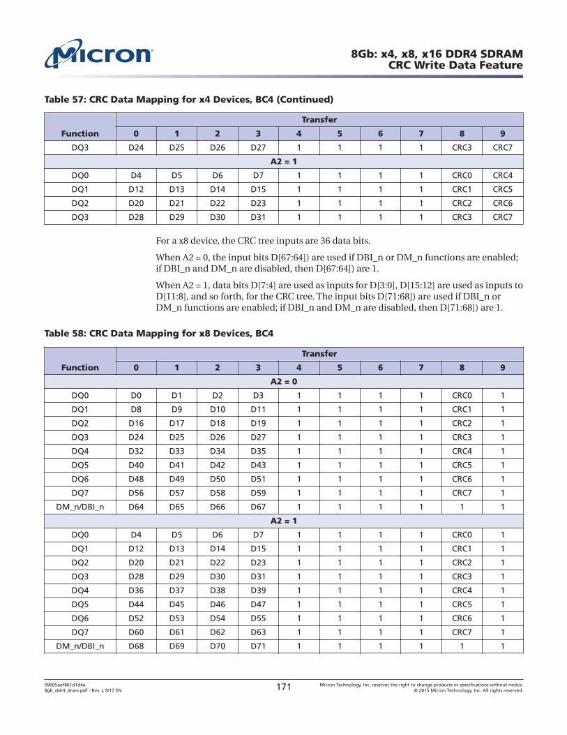
Table 57: CRC Data Mapping for x4 Devices, BC4 (Continued)
Function
Transfer
0 1 2 3 4 5 6 7 8 9
DQ3 D24 D25 D26 D27 1 1 1 1 CRC3 CRC7
A2 = 1
DQ0 D4 D5 D6 D7 1 1 1 1 CRC0 CRC4
DQ1 D12 D13 D14 D15 1 1 1 1 CRC1 CRC5
DQ2 D20 D21 D22 D23 1 1 1 1 CRC2 CRC6
DQ3 D28 D29 D30 D31 1 1 1 1 CRC3 CRC7
For a x8 device, the CRC tree inputs are 36 data bits.
When A2 = 0, the input bits D[67:64]) are used if DBI_n or DM_n functions are enabled;if DBI_n and DM_n are disabled, then D[67:64]) are 1.
When A2 = 1, data bits D[7:4] are used as inputs for D[3:0], D[15:12] are used as inputs toD[11:8], and so forth, for the CRC tree. The input bits D[71:68]) are used if DBI_n orDM_n functions are enabled; if DBI_n and DM_n are disabled, then D[71:68]) are 1.
Table 58: CRC Data Mapping for x8 Devices, BC4
Function
Transfer
0 1 2 3 4 5 6 7 8 9
A2 = 0
DQ0 D0 D1 D2 D3 1 1 1 1 CRC0 1
DQ1 D8 D9 D10 D11 1 1 1 1 CRC1 1
DQ2 D16 D17 D18 D19 1 1 1 1 CRC2 1
DQ3 D24 D25 D26 D27 1 1 1 1 CRC3 1
DQ4 D32 D33 D34 D35 1 1 1 1 CRC4 1
DQ5 D40 D41 D42 D43 1 1 1 1 CRC5 1
DQ6 D48 D49 D50 D51 1 1 1 1 CRC6 1
DQ7 D56 D57 D58 D59 1 1 1 1 CRC7 1
DM_n/DBI_n D64 D65 D66 D67 1 1 1 1 1 1
A2 = 1
DQ0 D4 D5 D6 D7 1 1 1 1 CRC0 1
DQ1 D12 D13 D14 D15 1 1 1 1 CRC1 1
DQ2 D20 D21 D22 D23 1 1 1 1 CRC2 1
DQ3 D28 D29 D30 D31 1 1 1 1 CRC3 1
DQ4 D36 D37 D38 D39 1 1 1 1 CRC4 1
DQ5 D44 D45 D46 D47 1 1 1 1 CRC5 1
DQ6 D52 D53 D54 D55 1 1 1 1 CRC6 1
DQ7 D60 D61 D62 D63 1 1 1 1 CRC7 1
DM_n/DBI_n D68 D69 D70 D71 1 1 1 1 1 1
8Gb: x4, x8, x16 DDR4 SDRAMCRC Write Data Feature
09005aef861d1d4a8gb_ddr4_dram.pdf - Rev. L 9/17 EN 171 Micron Technology, Inc. reserves the right to change products or specifications without notice.
© 2015 Micron Technology, Inc. All rights reserved.
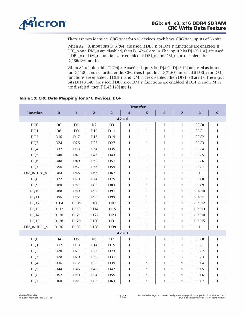
There are two identical CRC trees for x16 devices, each have CRC tree inputs of 36 bits.
When A2 = 0, input bits D[67:64] are used if DBI_n or DM_n functions are enabled; ifDBI_n and DM_n are disabled, then D[67:64] are 1s. The input bits D[139:136] are usedif DBI_n or DM_n functions are enabled; if DBI_n and DM_n are disabled, thenD[139:136] are 1s.
When A2 = 1, data bits D[7:4] are used as inputs for D[3:0], D[15:12] are used as inputsfor D[11:8], and so forth, for the CRC tree. Input bits D[71:68] are used if DBI_n or DM_nfunctions are enabled; if DBI_n and DM_n are disabled, then D[71:68] are 1s. The inputbits D[143:140] are used if DBI_n or DM_n functions are enabled; if DBI_n and DM_nare disabled, then D[143:140] are 1s.
Table 59: CRC Data Mapping for x16 Devices, BC4
Function
Transfer
0 1 2 3 4 5 6 7 8 9
A2 = 0
DQ0 D0 D1 D2 D3 1 1 1 1 CRC0 1
DQ1 D8 D9 D10 D11 1 1 1 1 CRC1 1
DQ2 D16 D17 D18 D19 1 1 1 1 CRC2 1
DQ3 D24 D25 D26 D27 1 1 1 1 CRC3 1
DQ4 D32 D33 D34 D35 1 1 1 1 CRC4 1
DQ5 D40 D41 D42 D43 1 1 1 1 CRC5 1
DQ6 D48 D49 D50 D51 1 1 1 1 CRC6 1
DQ7 D56 D57 D58 D59 1 1 1 1 CRC7 1
LDM_n/LDBI_n D64 D65 D66 D67 1 1 1 1 1 1
DQ8 D72 D73 D74 D75 1 1 1 1 CRC8 1
DQ9 D80 D81 D82 D83 1 1 1 1 CRC9 1
DQ10 D88 D89 D90 D91 1 1 1 1 CRC10 1
DQ11 D96 D97 D98 D99 1 1 1 1 CRC11 1
DQ12 D104 D105 D106 D107 1 1 1 1 CRC12 1
DQ13 D112 D113 D114 D115 1 1 1 1 CRC13 1
DQ14 D120 D121 D122 D123 1 1 1 1 CRC14 1
DQ15 D128 D129 D130 D131 1 1 1 1 CRC15 1
UDM_n/UDBI_n D136 D137 D138 D139 1 1 1 1 1 1
A2 = 1
DQ0 D4 D5 D6 D7 1 1 1 1 CRC0 1
DQ1 D12 D13 D14 D15 1 1 1 1 CRC1 1
DQ2 D20 D21 D22 D23 1 1 1 1 CRC2 1
DQ3 D28 D29 D30 D31 1 1 1 1 CRC3 1
DQ4 D36 D37 D38 D39 1 1 1 1 CRC4 1
DQ5 D44 D45 D46 D47 1 1 1 1 CRC5 1
DQ6 D52 D53 D54 D55 1 1 1 1 CRC6 1
DQ7 D60 D61 D62 D63 1 1 1 1 CRC7 1
8Gb: x4, x8, x16 DDR4 SDRAMCRC Write Data Feature
09005aef861d1d4a8gb_ddr4_dram.pdf - Rev. L 9/17 EN 172 Micron Technology, Inc. reserves the right to change products or specifications without notice.
© 2015 Micron Technology, Inc. All rights reserved.
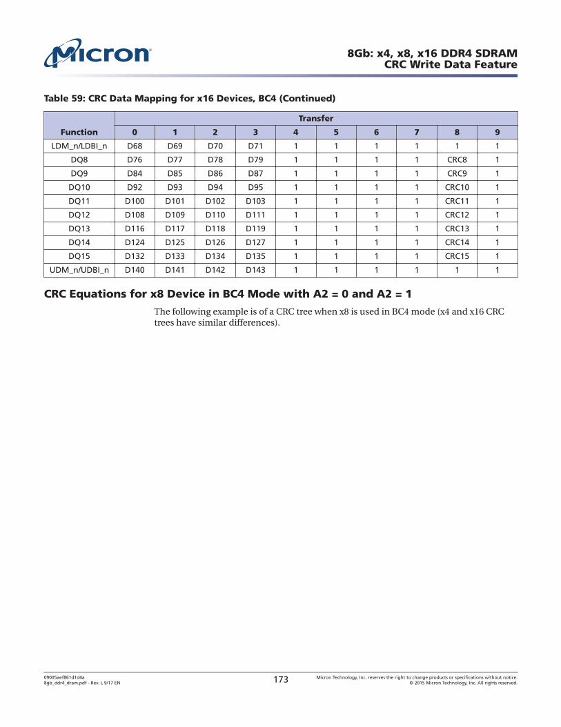
Table 59: CRC Data Mapping for x16 Devices, BC4 (Continued)
Function
Transfer
0 1 2 3 4 5 6 7 8 9
LDM_n/LDBI_n D68 D69 D70 D71 1 1 1 1 1 1
DQ8 D76 D77 D78 D79 1 1 1 1 CRC8 1
DQ9 D84 D85 D86 D87 1 1 1 1 CRC9 1
DQ10 D92 D93 D94 D95 1 1 1 1 CRC10 1
DQ11 D100 D101 D102 D103 1 1 1 1 CRC11 1
DQ12 D108 D109 D110 D111 1 1 1 1 CRC12 1
DQ13 D116 D117 D118 D119 1 1 1 1 CRC13 1
DQ14 D124 D125 D126 D127 1 1 1 1 CRC14 1
DQ15 D132 D133 D134 D135 1 1 1 1 CRC15 1
UDM_n/UDBI_n D140 D141 D142 D143 1 1 1 1 1 1
CRC Equations for x8 Device in BC4 Mode with A2 = 0 and A2 = 1
The following example is of a CRC tree when x8 is used in BC4 mode (x4 and x16 CRCtrees have similar differences).
8Gb: x4, x8, x16 DDR4 SDRAMCRC Write Data Feature
09005aef861d1d4a8gb_ddr4_dram.pdf - Rev. L 9/17 EN 173 Micron Technology, Inc. reserves the right to change products or specifications without notice.
© 2015 Micron Technology, Inc. All rights reserved.
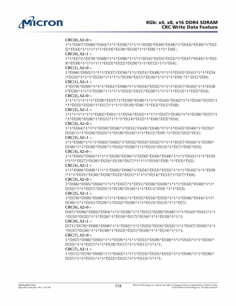
CRC[0], A2=0 =1^1^D[67]^D[66]^D[64]^1^1^D[56]^1^1^1^D[50]^D[49]^D[48]^1^D[43]^D[40]^1^D[35]^D[34]^1^1^1^1^1^D[19]^D[18]^D[16]^1^1^D[8] ^1^1^ D[0] ;CRC[0], A2=1 =1^1^D[71]^D[70]^D[68]^1^1^D[60]^1^1^1^D[54]^D[53]^D[52]^1^D[47]^D[44]^1^D[39]^D[38]^1^1^1^1^1^D[23]^D[22]^D[20]^1^1^D[12]^1^1^D[4] ;CRC[1], A2=0 =1^D[66]^D[65]^1^1^1^D[57]^D[56]^1^1^D[51]^D[48]^1^1^1^D[43]^D[41]^1^1^D[34]^D[32]^1^1^1^D[24]^1^1^1^1^D[18]^D[17]^D[16]^1^1^1^1^D[9] ^1^ D[1]^D[0];CRC[1], A2=1 =1^D[70]^D[69]^1^1^1^D[61]^D[60]^1^1^D[55]^D[52]^1^1^1^D[47]^D[45]^1^1^D[38]^D[36]^1^1^1^D[28]^1^1^1^1^D[22]^D[21]^D[20]^1^1^1^1^D[13]^1^D[5]^D[4];CRC[2], A2=0 =1^1^1^1^1^1^1^D[58]^D[57]^1^D[50]^D[48]^1^1^1^D[43]^D[42]^1^1^D[34]^D[33]^1^1^D[25]^D[24]^1^D[17]^1^1^1^D[10]^D[8] ^1^D[2]^D[1]^D[0];CRC[2], A2=1 =1^1^1^1^1^1^1^D[62]^D[61]^1^D[54]^D[52]^1^1^1^D[47]^D[46]^1^1^D[38]^D[37]^1^1^D[29]^D[28]^1^D[21]^1^1^1^D[14]^D12]^1^D[6]^D[5]^D[4];CRC[3], A2=0 =1^1^D[64]^1^1^1^D[59]^D[58]^1^D[51]^D[49]^D[48]^1^1^1^D[43]^D[40]^1^D[35]^D[34]^1^1^D[26]^D[25]^1^D[18]^D[16]^1^1^D[11]^D[9] ^1^D[3]^D[2]^D[1];CRC[3], A2=1 =1^1^D[68]^1^1^1^D[63]^D[62]^1^D[55]^D[53]^D[52]^1^1^1^D[47]^D[44]^1^D[39]^D[38]^1^1^D[30]^D[29]^1^D[22]^D[20]^1^1^D[15]^D[13]^1^D[7]^D[6]^D[5];CRC[4], A2=0 =1^1^D[65]^D[64]^1^1^1^D[59]^D[56]^1^D[50]^D[49]^D[48]^1^1^1^D[41]^1^1^D[35]^1^1^D[27]^D[26]^D[24]^D[19]^D[17]^1^1^1^D[10]^D[8] ^1^D[3]^D[2];CRC[4], A2=1 =1^1^D[69]^D[68]^1^1^1^D[63]^D[60]^1^D[54]^D[53]^D[52]^1^1^1^D[45]^1^1^D[39]^1^1^D[31]^D[30]^D[28]^D[23]^D[21]^1^1^1^D[14]^D[12]^1^D[7]^D[6];CRC[5], A2=0 =1^D[66]^D[65]^D[64]^1^1^1^D[57]^1^D[51]^D[50]^D[49]^1^1^1^D[42]^D[40]^1^1^D[32]^1^1^D[27]^D[25]^1^D[18]^D[16]^1^1^D[11]^D[9] ^1^1^D[3];CRC[5], A2=1 =1^D[70]^D[69]^D[68]^1^1^1^D[61]^1^D[55]^D[54]^D[53]^1^1^1^D[46]^D[44]^1^1^D[36]^1^1^D[31]^D[29]^1^D[22]^D[20]^1^1^D[15]^D[13]^1^1^D[7];CRC[6], A2=0 =D[67]^D[66]^D[65]^D[64]^1^1^D[58]^1^1^D[51]^D[50]^D[48]^1^1^D[43]^D[41]^1^1^D[33]^D[32]^1^1^D[26]^1^D[19]^D[17]^D[16]^1^1^D[10]^1^1^1;CRC[6], A2=1 =D[71]^D[70]^D[69]^D[68]^1^1^D[62]^1^1^D[55]^D[54]^D[52]^1^1^D[47]^D[45]^1^1^D[37]^D[36]^1^1^D[30]^1^D[23]^D[21]^D[20]^1^1^D[14]^1^1^1;CRC[7], A2=0 =1^D[67]^D[66]^D[65]^1^1^D[59]^1^1^1^D[51]^D[49]^D[48]^1^1^D[42]^1^1^D[34]^D[33]^1^1^D[27]^1^1^D[18]^D[17]^1^1^D[11]^1^1^1;CRC[7], A2=1 =1^D[71]^D[70]^D[69]^1^1^D[63]^1^1^1^D[55]^D[53]^D[52]^1^1^D[46]^1^1^D[38]^D[37]^1^1^D[31]^1^1^D[22]^D[21]^1^1^D[15]^1^1^1;
8Gb: x4, x8, x16 DDR4 SDRAMCRC Write Data Feature
09005aef861d1d4a8gb_ddr4_dram.pdf - Rev. L 9/17 EN 174 Micron Technology, Inc. reserves the right to change products or specifications without notice.
© 2015 Micron Technology, Inc. All rights reserved.
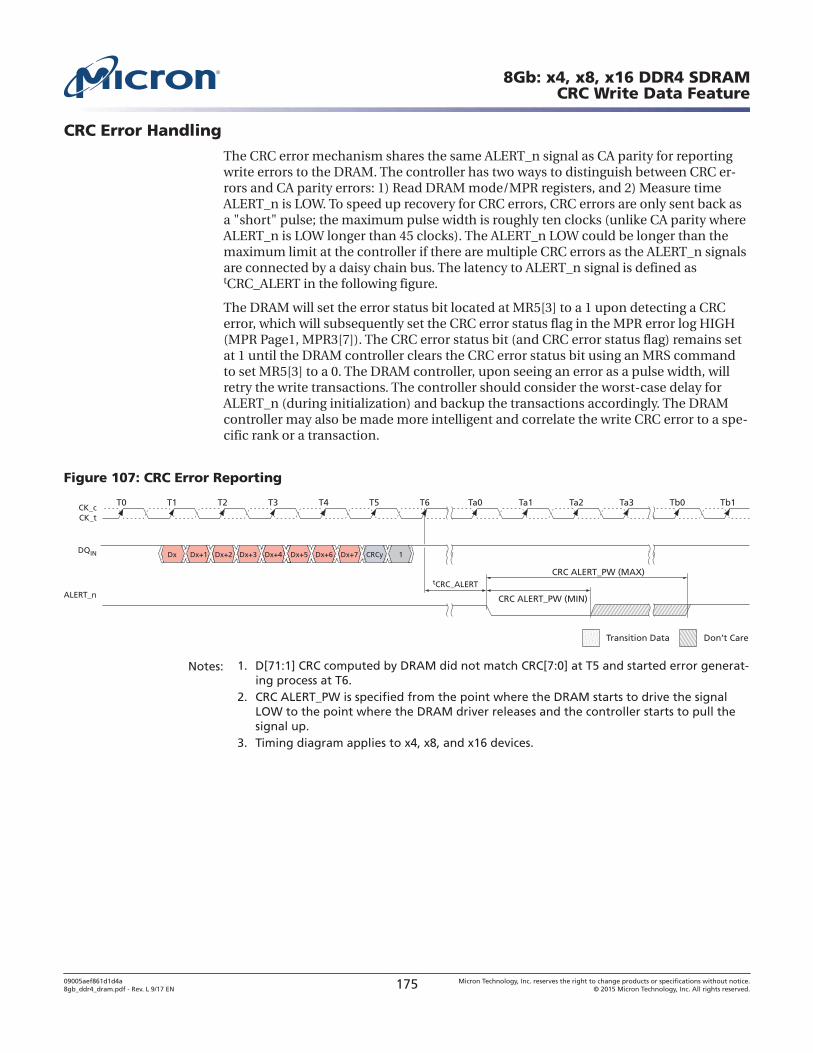
CRC Error Handling
The CRC error mechanism shares the same ALERT_n signal as CA parity for reportingwrite errors to the DRAM. The controller has two ways to distinguish between CRC er-rors and CA parity errors: 1) Read DRAM mode/MPR registers, and 2) Measure timeALERT_n is LOW. To speed up recovery for CRC errors, CRC errors are only sent back asa "short" pulse; the maximum pulse width is roughly ten clocks (unlike CA parity whereALERT_n is LOW longer than 45 clocks). The ALERT_n LOW could be longer than themaximum limit at the controller if there are multiple CRC errors as the ALERT_n signalsare connected by a daisy chain bus. The latency to ALERT_n signal is defined astCRC_ALERT in the following figure.
The DRAM will set the error status bit located at MR5[3] to a 1 upon detecting a CRCerror, which will subsequently set the CRC error status flag in the MPR error log HIGH(MPR Page1, MPR3[7]). The CRC error status bit (and CRC error status flag) remains setat 1 until the DRAM controller clears the CRC error status bit using an MRS commandto set MR5[3] to a 0. The DRAM controller, upon seeing an error as a pulse width, willretry the write transactions. The controller should consider the worst-case delay forALERT_n (during initialization) and backup the transactions accordingly. The DRAMcontroller may also be made more intelligent and correlate the write CRC error to a spe-cific rank or a transaction.
Figure 107: CRC Error Reporting
Dx
T0 T1 T2 T3 T4 T5 T6 Ta0 Ta1 Ta2 Ta3 Tb0
CK_tCK_c
DQIN Dx+1 Dx+2 Dx+3 Dx+4 Dx+5 Dx+6 Dx+7 CRCy 1
ALERT_n CRC ALERT_PW (MIN)
Tb1
tCRC_ALERTCRC ALERT_PW (MAX)
Don’t CareTransition Data
Notes: 1. D[71:1] CRC computed by DRAM did not match CRC[7:0] at T5 and started error generat-ing process at T6.
2. CRC ALERT_PW is specified from the point where the DRAM starts to drive the signalLOW to the point where the DRAM driver releases and the controller starts to pull thesignal up.
3. Timing diagram applies to x4, x8, and x16 devices.
8Gb: x4, x8, x16 DDR4 SDRAMCRC Write Data Feature
09005aef861d1d4a8gb_ddr4_dram.pdf - Rev. L 9/17 EN 175 Micron Technology, Inc. reserves the right to change products or specifications without notice.
© 2015 Micron Technology, Inc. All rights reserved.
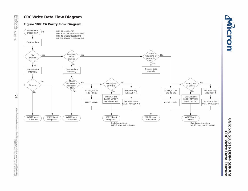
CRC Write Data Flow Diagram
Figure 108: CA Parity Flow Diagram
Capture data
Transfer DataInternally
Transfer datainternally
Yes
DRAM writeprocess start
MR2 12 enable CRCMR5 3 set CRC error clear to 0MR5 10 enable/disable DMMR3[10:9] WCL if DM enabled
No
No
Yes
Yes
No
ALERT_n LOW6 to 10 CKs
ALERT_n HIGH Set error statusPAGE1 MPR3[7] 1
Set error flagMR5[A3] 1
Transfer datainternally
Yes
No
Yes
No
CRCenabled
CA error
Persistentmode
enabled
MR5[A3] andPAGE1 MPR3[7]remain set to 1
No
Yes
DRAMCRC same as
controllerCRC
DRAMCRC same as
controllerCRC
MR5[3] = 0at WRITE
WRITE burstcompleted
WRITE burstcompleted
WRITE burstcompleted
WRITE burstcompleted
WRITE burstcompleted
Bad data writtenMR5 3 reset to 0 if desired
ALERT_n LOW6 to 10 CKs
ALERT_n HIGH Set error statusPAGE1 MPR3[7] 1
Set error flagMR5[A3] 1
Yes
No
MR5[A3] andPAGE1 MPR3[7]remain set to 1
MR5[3] = 0at WRITE
WRITE burstrejected
Bad data not writtenMR5 3 reset to 0 if desired
8G
b: x
4, x
8, x
16 D
DR
4 S
DR
AM
CR
C W
rite D
ata
Featu
re
09005aef861d1d
4a8g
b_d
dr4_d
ram.p
df - R
ev. L 9/17 EN176
Micro
n Tech
no
log
y, Inc. reserves th
e righ
t to ch
ang
e pro
du
cts or sp
ecification
s with
ou
t no
tice.©
2015 Micro
n Tech
no
log
y, Inc. A
ll righ
ts reserved.
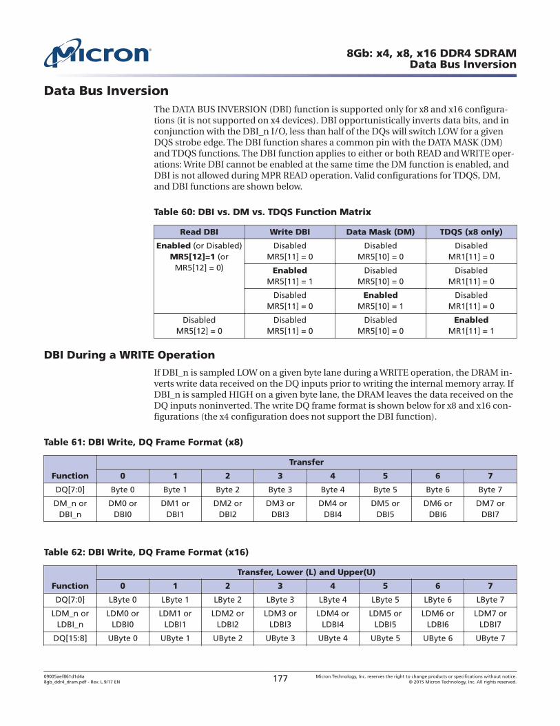
Data Bus InversionThe DATA BUS INVERSION (DBI) function is supported only for x8 and x16 configura-tions (it is not supported on x4 devices). DBI opportunistically inverts data bits, and inconjunction with the DBI_n I/O, less than half of the DQs will switch LOW for a givenDQS strobe edge. The DBI function shares a common pin with the DATA MASK (DM)and TDQS functions. The DBI function applies to either or both READ and WRITE oper-ations: Write DBI cannot be enabled at the same time the DM function is enabled, andDBI is not allowed during MPR READ operation. Valid configurations for TDQS, DM,and DBI functions are shown below.
Table 60: DBI vs. DM vs. TDQS Function Matrix
Read DBI Write DBI Data Mask (DM) TDQS (x8 only)
Enabled (or Disabled)MR5[12]=1 (or
MR5[12] = 0)
DisabledMR5[11] = 0
DisabledMR5[10] = 0
DisabledMR1[11] = 0
EnabledMR5[11] = 1
DisabledMR5[10] = 0
DisabledMR1[11] = 0
DisabledMR5[11] = 0
EnabledMR5[10] = 1
DisabledMR1[11] = 0
DisabledMR5[12] = 0
DisabledMR5[11] = 0
DisabledMR5[10] = 0
EnabledMR1[11] = 1
DBI During a WRITE Operation
If DBI_n is sampled LOW on a given byte lane during a WRITE operation, the DRAM in-verts write data received on the DQ inputs prior to writing the internal memory array. IfDBI_n is sampled HIGH on a given byte lane, the DRAM leaves the data received on theDQ inputs noninverted. The write DQ frame format is shown below for x8 and x16 con-figurations (the x4 configuration does not support the DBI function).
Table 61: DBI Write, DQ Frame Format (x8)
Function
Transfer
0 1 2 3 4 5 6 7
DQ[7:0] Byte 0 Byte 1 Byte 2 Byte 3 Byte 4 Byte 5 Byte 6 Byte 7
DM_n orDBI_n
DM0 orDBI0
DM1 orDBI1
DM2 orDBI2
DM3 orDBI3
DM4 orDBI4
DM5 orDBI5
DM6 orDBI6
DM7 orDBI7
Table 62: DBI Write, DQ Frame Format (x16)
Function
Transfer, Lower (L) and Upper(U)
0 1 2 3 4 5 6 7
DQ[7:0] LByte 0 LByte 1 LByte 2 LByte 3 LByte 4 LByte 5 LByte 6 LByte 7
LDM_n orLDBI_n
LDM0 orLDBI0
LDM1 orLDBI1
LDM2 orLDBI2
LDM3 orLDBI3
LDM4 orLDBI4
LDM5 orLDBI5
LDM6 orLDBI6
LDM7 orLDBI7
DQ[15:8] UByte 0 UByte 1 UByte 2 UByte 3 UByte 4 UByte 5 UByte 6 UByte 7
8Gb: x4, x8, x16 DDR4 SDRAMData Bus Inversion
09005aef861d1d4a8gb_ddr4_dram.pdf - Rev. L 9/17 EN 177 Micron Technology, Inc. reserves the right to change products or specifications without notice.
© 2015 Micron Technology, Inc. All rights reserved.
Table 62: DBI Write, DQ Frame Format (x16) (Continued)
Function
Transfer, Lower (L) and Upper(U)
0 1 2 3 4 5 6 7
UDM_n orUDBI_n
UDM0 orUDBI0
UDM1 orUDBI1
UDM2 orUDBI2
UDM3 orUDBI3
UDM4 orUDBI4
UDM5 orUDBI5
UDM6 orUDBI6
UDM7 orUDBI7
DBI During a READ Operation
If the number of 0 data bits within a given byte lane is greater than four during a READoperation, the DRAM inverts read data on its DQ outputs and drives the DBI_n pinLOW; otherwise, the DRAM does not invert the read data and drives the DBI_n pinHIGH. The read DQ frame format is shown below for x8 and x16 configurations (the x4configuration does not support the DBI function).
Table 63: DBI Read, DQ Frame Format (x8)
Function
Transfer Byte
0 1 2 3 4 5 6 7
DQ[7:0] Byte 0 Byte 1 Byte 2 Byte 3 Byte 4 Byte 5 Byte 6 Byte 7
DBI_n DBI0 DBI1 DBI2 DBI3 DBI4 DBI5 DBI6 DBI7
Table 64: DBI Read, DQ Frame Format (x16)
Function
Transfer Byte, Lower (L) and Upper(U)
0 1 2 3 4 5 6 7
DQ[7:0] LByte 0 LByte 1 LByte 2 LByte 3 LByte 4 LByte 5 LByte 6 LByte 7
LDBI_n LDBI0 LDBI1 LDBI2 LDBI3 LDBI4 LDBI5 LDBI6 LDBI7
DQ[15:8] UByte 0 UByte 1 UByte 2 UByte 3 UByte 4 UByte 5 UByte 6 UByte 7
UDBI_n UDBI0 UDBI1 UDBI2 UDBI3 UDBI4 UDBI5 UDBI6 UDBI7
8Gb: x4, x8, x16 DDR4 SDRAMData Bus Inversion
09005aef861d1d4a8gb_ddr4_dram.pdf - Rev. L 9/17 EN 178 Micron Technology, Inc. reserves the right to change products or specifications without notice.
© 2015 Micron Technology, Inc. All rights reserved.
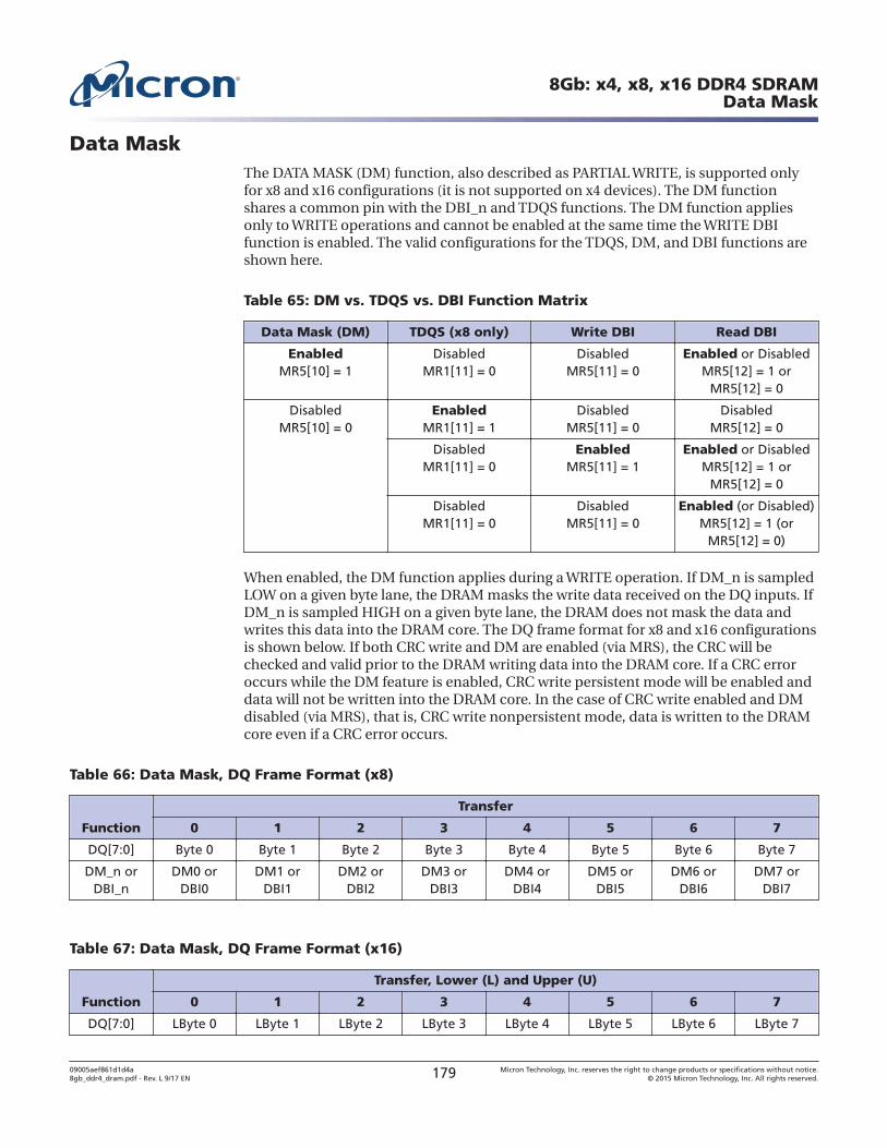
Data MaskThe DATA MASK (DM) function, also described as PARTIAL WRITE, is supported onlyfor x8 and x16 configurations (it is not supported on x4 devices). The DM functionshares a common pin with the DBI_n and TDQS functions. The DM function appliesonly to WRITE operations and cannot be enabled at the same time the WRITE DBIfunction is enabled. The valid configurations for the TDQS, DM, and DBI functions areshown here.
Table 65: DM vs. TDQS vs. DBI Function Matrix
Data Mask (DM) TDQS (x8 only) Write DBI Read DBI
EnabledMR5[10] = 1
DisabledMR1[11] = 0
DisabledMR5[11] = 0
Enabled or DisabledMR5[12] = 1 or
MR5[12] = 0
DisabledMR5[10] = 0
EnabledMR1[11] = 1
DisabledMR5[11] = 0
DisabledMR5[12] = 0
DisabledMR1[11] = 0
EnabledMR5[11] = 1
Enabled or DisabledMR5[12] = 1 or
MR5[12] = 0
DisabledMR1[11] = 0
DisabledMR5[11] = 0
Enabled (or Disabled)MR5[12] = 1 (or
MR5[12] = 0)
When enabled, the DM function applies during a WRITE operation. If DM_n is sampledLOW on a given byte lane, the DRAM masks the write data received on the DQ inputs. IfDM_n is sampled HIGH on a given byte lane, the DRAM does not mask the data andwrites this data into the DRAM core. The DQ frame format for x8 and x16 configurationsis shown below. If both CRC write and DM are enabled (via MRS), the CRC will bechecked and valid prior to the DRAM writing data into the DRAM core. If a CRC erroroccurs while the DM feature is enabled, CRC write persistent mode will be enabled anddata will not be written into the DRAM core. In the case of CRC write enabled and DMdisabled (via MRS), that is, CRC write nonpersistent mode, data is written to the DRAMcore even if a CRC error occurs.
Table 66: Data Mask, DQ Frame Format (x8)
Function
Transfer
0 1 2 3 4 5 6 7
DQ[7:0] Byte 0 Byte 1 Byte 2 Byte 3 Byte 4 Byte 5 Byte 6 Byte 7
DM_n orDBI_n
DM0 orDBI0
DM1 orDBI1
DM2 orDBI2
DM3 orDBI3
DM4 orDBI4
DM5 orDBI5
DM6 orDBI6
DM7 orDBI7
Table 67: Data Mask, DQ Frame Format (x16)
Function
Transfer, Lower (L) and Upper (U)
0 1 2 3 4 5 6 7
DQ[7:0] LByte 0 LByte 1 LByte 2 LByte 3 LByte 4 LByte 5 LByte 6 LByte 7
8Gb: x4, x8, x16 DDR4 SDRAMData Mask
09005aef861d1d4a8gb_ddr4_dram.pdf - Rev. L 9/17 EN 179 Micron Technology, Inc. reserves the right to change products or specifications without notice.
© 2015 Micron Technology, Inc. All rights reserved.
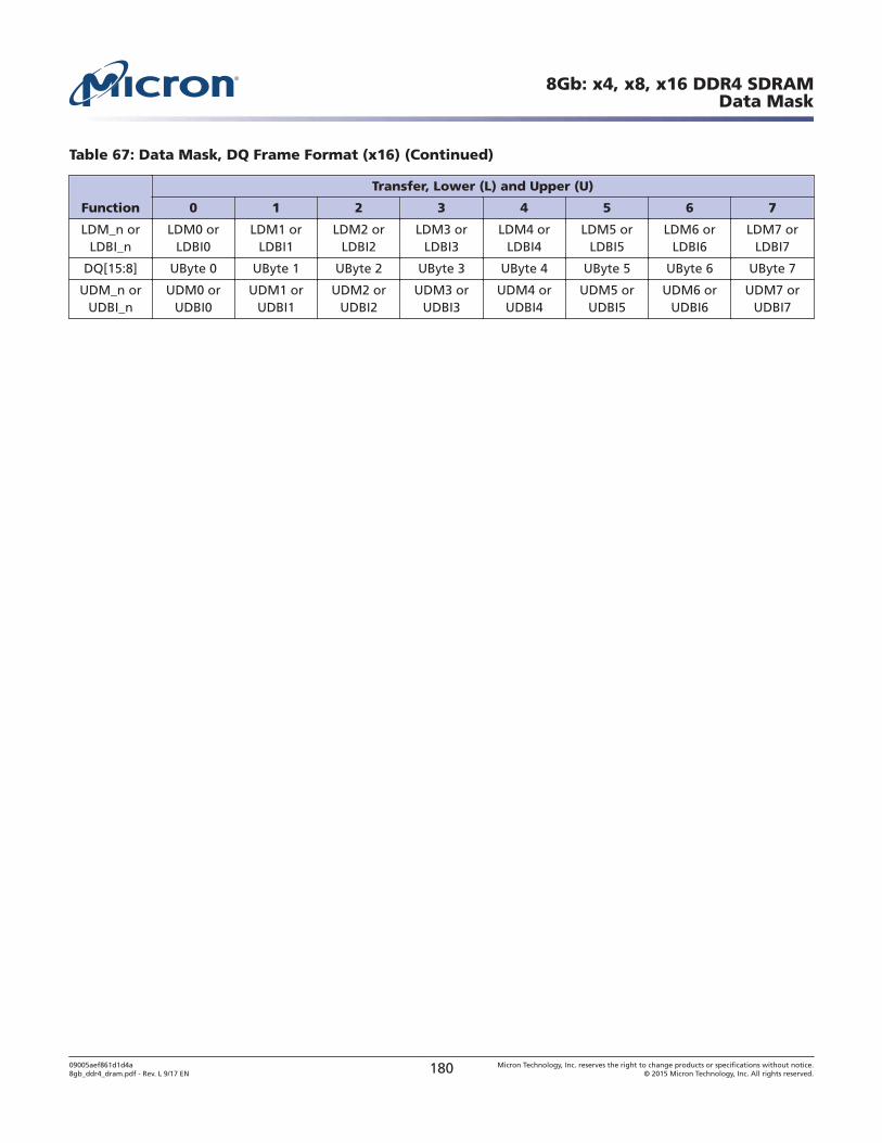
Table 67: Data Mask, DQ Frame Format (x16) (Continued)
Function
Transfer, Lower (L) and Upper (U)
0 1 2 3 4 5 6 7
LDM_n orLDBI_n
LDM0 orLDBI0
LDM1 orLDBI1
LDM2 orLDBI2
LDM3 orLDBI3
LDM4 orLDBI4
LDM5 orLDBI5
LDM6 orLDBI6
LDM7 orLDBI7
DQ[15:8] UByte 0 UByte 1 UByte 2 UByte 3 UByte 4 UByte 5 UByte 6 UByte 7
UDM_n orUDBI_n
UDM0 orUDBI0
UDM1 orUDBI1
UDM2 orUDBI2
UDM3 orUDBI3
UDM4 orUDBI4
UDM5 orUDBI5
UDM6 orUDBI6
UDM7 orUDBI7
8Gb: x4, x8, x16 DDR4 SDRAMData Mask
09005aef861d1d4a8gb_ddr4_dram.pdf - Rev. L 9/17 EN 180 Micron Technology, Inc. reserves the right to change products or specifications without notice.
© 2015 Micron Technology, Inc. All rights reserved.
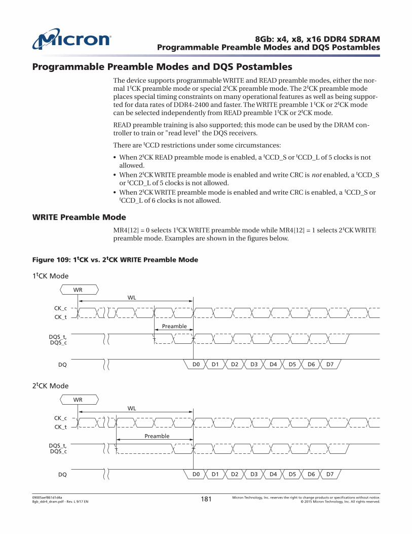
Programmable Preamble Modes and DQS PostamblesThe device supports programmable WRITE and READ preamble modes, either the nor-mal 1tCK preamble mode or special 2tCK preamble mode. The 2tCK preamble modeplaces special timing constraints on many operational features as well as being suppor-ted for data rates of DDR4-2400 and faster. The WRITE preamble 1tCK or 2tCK modecan be selected independently from READ preamble 1tCK or 2tCK mode.
READ preamble training is also supported; this mode can be used by the DRAM con-troller to train or "read level" the DQS receivers.
There are tCCD restrictions under some circumstances:
• When 2tCK READ preamble mode is enabled, a tCCD_S or tCCD_L of 5 clocks is notallowed.
• When 2tCK WRITE preamble mode is enabled and write CRC is not enabled, a tCCD_Sor tCCD_L of 5 clocks is not allowed.
• When 2tCK WRITE preamble mode is enabled and write CRC is enabled, a tCCD_S ortCCD_L of 6 clocks is not allowed.
WRITE Preamble Mode
MR4[12] = 0 selects 1tCK WRITE preamble mode while MR4[12] = 1 selects 2tCK WRITEpreamble mode. Examples are shown in the figures below.
Figure 109: 1tCK vs. 2tCK WRITE Preamble Mode
DQ
CK_c
CK_t
Preamble
2tCK Mode
D0 D1 D2 D3 D4 D5 D6 D7
WL
WR
DQ
DQS_t,DQS_c
DQS_t,DQS_c
CK_c
CK_t
Preamble
1tCK Mode
D0 D1 D2 D3 D4 D5 D6 D7
WRWL
8Gb: x4, x8, x16 DDR4 SDRAMProgrammable Preamble Modes and DQS Postambles
09005aef861d1d4a8gb_ddr4_dram.pdf - Rev. L 9/17 EN 181 Micron Technology, Inc. reserves the right to change products or specifications without notice.
© 2015 Micron Technology, Inc. All rights reserved.
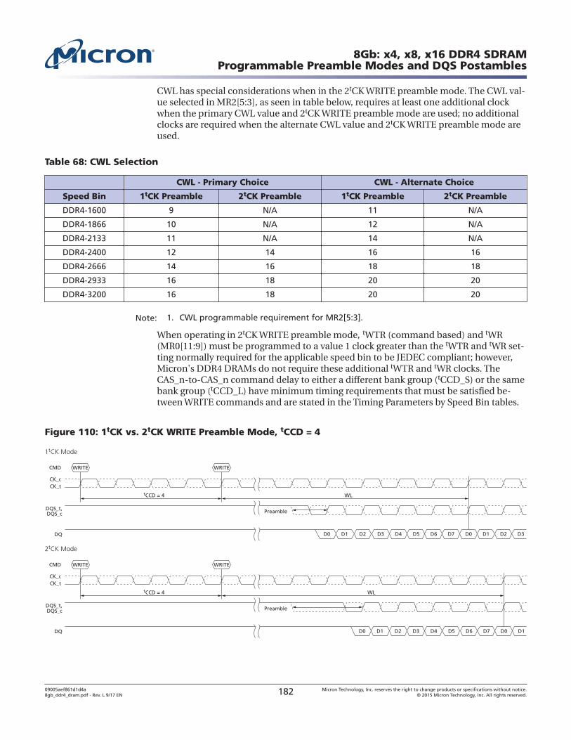
CWL has special considerations when in the 2tCK WRITE preamble mode. The CWL val-ue selected in MR2[5:3], as seen in table below, requires at least one additional clockwhen the primary CWL value and 2tCK WRITE preamble mode are used; no additionalclocks are required when the alternate CWL value and 2tCK WRITE preamble mode areused.
Table 68: CWL Selection
CWL - Primary Choice CWL - Alternate Choice
Speed Bin 1tCK Preamble 2tCK Preamble 1tCK Preamble 2tCK Preamble
DDR4-1600 9 N/A 11 N/A
DDR4-1866 10 N/A 12 N/A
DDR4-2133 11 N/A 14 N/A
DDR4-2400 12 14 16 16
DDR4-2666 14 16 18 18
DDR4-2933 16 18 20 20
DDR4-3200 16 18 20 20
Note: 1. CWL programmable requirement for MR2[5:3].
When operating in 2tCK WRITE preamble mode, tWTR (command based) and tWR(MR0[11:9]) must be programmed to a value 1 clock greater than the tWTR and tWR set-ting normally required for the applicable speed bin to be JEDEC compliant; however,Micron's DDR4 DRAMs do not require these additional tWTR and tWR clocks. TheCAS_n-to-CAS_n command delay to either a different bank group (tCCD_S) or the samebank group (tCCD_L) have minimum timing requirements that must be satisfied be-tween WRITE commands and are stated in the Timing Parameters by Speed Bin tables.
Figure 110: 1tCK vs. 2tCK WRITE Preamble Mode, tCCD = 4
DQ
DQS_t,DQS_c
tCCD = 4 WL
Preamble
1tCK Mode
D0 D1
WRITE WRITE
D2 D3 D4 D5 D6 D7 D0 D1 D2 D3
CK_tCK_c
CMD
DQ
DQS_t,DQS_c
tCCD = 4 WL
Preamble
2tCK Mode
D0 D1
WRITE WRITE
D2 D3 D4 D5 D6 D7 D0 D1
CK_tCK_c
CMD
8Gb: x4, x8, x16 DDR4 SDRAMProgrammable Preamble Modes and DQS Postambles
09005aef861d1d4a8gb_ddr4_dram.pdf - Rev. L 9/17 EN 182 Micron Technology, Inc. reserves the right to change products or specifications without notice.
© 2015 Micron Technology, Inc. All rights reserved.
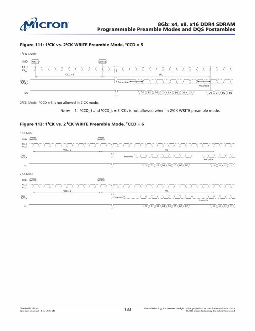
Figure 111: 1tCK vs. 2tCK WRITE Preamble Mode, tCCD = 5
DQ
DQS_t,DQS_c
tCCD = 5 WL
PreamblePreamble
1tCK Mode
D0 D1
WRITEWRITE
D2 D3 D4 D5 D6 D7 D0 D1 D2 D3
CK_tCK_c
CMD
2tCK Mode: tCCD = 5 is not allowed in 2tCK mode.
Note: 1. tCCD_S and tCCD_L = 5 tCKs is not allowed when in 2tCK WRITE preamble mode.
Figure 112: 1tCK vs. 2 tCK WRITE Preamble Mode, tCCD = 6
DQ
tCCD = 6
DQS_t,DQS_c
WL
PreamblePreamble
1tCK Mode
D0 D1
WRITEWRITE
D2 D3 D4 D5 D6 D7 D0 D1 D2 D3
CK_tCK_c
CMD
2tCK Mode
DQ
tCCD = 6
DQS_t,DQS_c
WL
PreamblePreamble
D0 D1
WRITEWRITE
D2 D3 D4 D5 D6 D7 D0 D1 D2 D3
CK_tCK_c
CMD
8Gb: x4, x8, x16 DDR4 SDRAMProgrammable Preamble Modes and DQS Postambles
09005aef861d1d4a8gb_ddr4_dram.pdf - Rev. L 9/17 EN 183 Micron Technology, Inc. reserves the right to change products or specifications without notice.
© 2015 Micron Technology, Inc. All rights reserved.
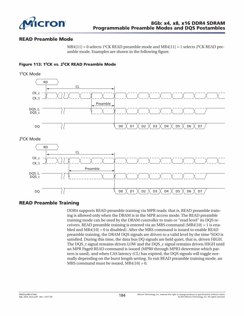
READ Preamble Mode
MR4[11] = 0 selects 1tCK READ preamble mode and MR4[11] = 1 selects 2tCK READ pre-amble mode. Examples are shown in the following figure.
Figure 113: 1tCK vs. 2tCK READ Preamble Mode
DQ
DQS_t,DQS_c
DQS_t,DQS_c
CK_c
CK_t
Preamble
2tCK Mode
D0 D1 D2 D3 D4 D5 D6 D7
CL
RD
DQ
CK_c
CK_t
Preamble
1tCK Mode
D0 D1 D2 D3 D4 D5 D6 D7
RDCL
READ Preamble Training
DDR4 supports READ preamble training via MPR reads; that is, READ preamble train-ing is allowed only when the DRAM is in the MPR access mode. The READ preambletraining mode can be used by the DRAM controller to train or "read level" its DQS re-ceivers. READ preamble training is entered via an MRS command (MR4[10] = 1 is ena-bled and MR4[10] = 0 is disabled). After the MRS command is issued to enable READpreamble training, the DRAM DQS signals are driven to a valid level by the time tSDO issatisfied. During this time, the data bus DQ signals are held quiet, that is, driven HIGH.The DQS_t signal remains driven LOW and the DQS_c signal remains driven HIGH untilan MPR Page0 READ command is issued (MPR0 through MPR3 determine which pat-tern is used), and when CAS latency (CL) has expired, the DQS signals will toggle nor-mally depending on the burst length setting. To exit READ preamble training mode, anMRS command must be issued, MR4[10] = 0.
8Gb: x4, x8, x16 DDR4 SDRAMProgrammable Preamble Modes and DQS Postambles
09005aef861d1d4a8gb_ddr4_dram.pdf - Rev. L 9/17 EN 184 Micron Technology, Inc. reserves the right to change products or specifications without notice.
© 2015 Micron Technology, Inc. All rights reserved.
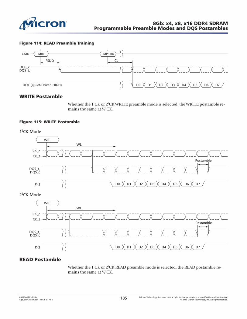
Figure 114: READ Preamble Training
CMD
DQs
CL
DQS_cDQS_t,
tSDO
MPR RD
(Quiet/Driven HIGH)
MRS
D0 D1 D2 D3 D4 D5 D6 D7
WRITE Postamble
Whether the 1tCK or 2tCK WRITE preamble mode is selected, the WRITE postamble re-mains the same at ½tCK.
Figure 115: WRITE Postamble
DQ
DQS_t,DQS_c
DQS_t,DQS_c
CK_c
CK_t
2tCK Mode
D0 D1 D2 D3 D4 D5 D6 D7
WL
WR
DQ
CK_c
CK_tPostamble
1tCK Mode
D0 D1 D2 D3 D4 D5 D6 D7
WRWL
Postamble
READ Postamble
Whether the 1tCK or 2tCK READ preamble mode is selected, the READ postamble re-mains the same at ½tCK.
8Gb: x4, x8, x16 DDR4 SDRAMProgrammable Preamble Modes and DQS Postambles
09005aef861d1d4a8gb_ddr4_dram.pdf - Rev. L 9/17 EN 185 Micron Technology, Inc. reserves the right to change products or specifications without notice.
© 2015 Micron Technology, Inc. All rights reserved.
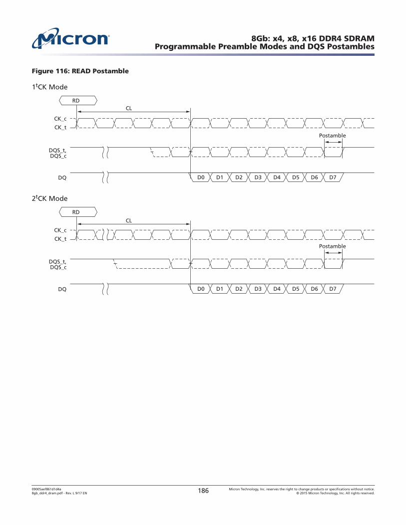
Figure 116: READ Postamble
DQ
CK_c
CK_t
2tCK Mode
D0 D1 D2 D3 D4 D5 D6 D7
CL
RD
DQ
DQS_t,DQS_c
DQS_t,DQS_c
CK_c
CK_t
1tCK Mode
D0 D1 D2 D3 D4 D5 D6 D7
RDCL
Postamble
Postamble
8Gb: x4, x8, x16 DDR4 SDRAMProgrammable Preamble Modes and DQS Postambles
09005aef861d1d4a8gb_ddr4_dram.pdf - Rev. L 9/17 EN 186 Micron Technology, Inc. reserves the right to change products or specifications without notice.
© 2015 Micron Technology, Inc. All rights reserved.
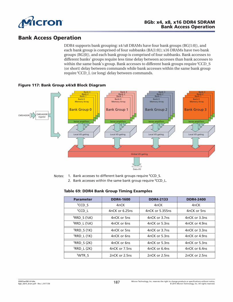
Bank Access OperationDDR4 supports bank grouping: x4/x8 DRAMs have four bank groups (BG[1:0]), andeach bank group is comprised of four subbanks (BA[1:0]); x16 DRAMs have two bankgroups (BG[0]), and each bank group is comprised of four subbanks. Bank accesses todifferent banks' groups require less time delay between accesses than bank accesses towithin the same bank's group. Bank accesses to different bank groups require tCCD_S(or short) delay between commands while bank accesses within the same bank grouprequire tCCD_L (or long) delay between commands.
Figure 117: Bank Group x4/x8 Block Diagram
Local I/O gating
Global I/O gating
Bank 0Memory Array
Sense amplifiers
Bank 1Bank 2
Bank 3
Local I/O gating
Bank 0Memory Array
Sense amplifiers
Bank 1Bank 2
Bank 3
Local I/O gating
Bank 0Memory Array
Sense amplifiers
Bank 1Bank 2
Bank 3
Local I/O gating
Bank 0Memory Array
Sense amplifiers
Bank 1Bank 2
Bank 3
CMD/ADDRregister
CMD/ADDR
Data I/O
Bank Group 0 Bank Group 1 Bank Group 2 Bank Group 3
Notes: 1. Bank accesses to different bank groups require tCCD_S.2. Bank accesses within the same bank group require tCCD_L.
Table 69: DDR4 Bank Group Timing Examples
Parameter DDR4-1600 DDR4-2133 DDR4-2400tCCD_S 4nCK 4nCK 4nCKtCCD_L 4nCK or 6.25ns 4nCK or 5.355ns 4nCK or 5ns
tRRD_S (½K) 4nCK or 5ns 4nCK or 3.7ns 4nCK or 3.3nstRRD_L (½K) 4nCK or 6ns 4nCK or 5.3ns 4nCK or 4.9ns
tRRD_S (1K) 4nCK or 5ns 4nCK or 3.7ns 4nCK or 3.3nstRRD_L (1K) 4nCK or 6ns 4nCK or 5.3ns 4nCK or 4.9ns
tRRD_S (2K) 4nCK or 6ns 4nCK or 5.3ns 4nCK or 5.3nstRRD_L (2K) 4nCK or 7.5ns 4nCK or 6.4ns 4nCK or 6.4ns
tWTR_S 2nCK or 2.5ns 2nCK or 2.5ns 2nCK or 2.5ns
8Gb: x4, x8, x16 DDR4 SDRAMBank Access Operation
09005aef861d1d4a8gb_ddr4_dram.pdf - Rev. L 9/17 EN 187 Micron Technology, Inc. reserves the right to change products or specifications without notice.
© 2015 Micron Technology, Inc. All rights reserved.
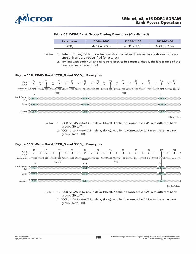
Table 69: DDR4 Bank Group Timing Examples (Continued)
Parameter DDR4-1600 DDR4-2133 DDR4-2400tWTR_L 4nCK or 7.5ns 4nCK or 7.5ns 4nCK or 7.5ns
Notes: 1. Refer to Timing Tables for actual specification values, these values are shown for refer-ence only and are not verified for accuracy.
2. Timings with both nCK and ns require both to be satisfied; that is, the larger time of thetwo cases must be satisfied.
Figure 118: READ Burst tCCD_S and tCCD_L Examples
T0 T1 T2 T3 T4 T5 T6 T7 T8 T9
tCCD_S
T10 T11
Don’t Care
BG a
DESREAD READDES DES DES DES DES DES DES DES
CK_tCK_c
Command
Bank Group(BG)
Bank cBank
Col n
BG b
Bank c
Col n
BG b
Bank c
Col nAddress
tCCD_L
READ
Notes: 1. tCCD_S; CAS_n-to-CAS_n delay (short). Applies to consecutive CAS_n to different bankgroups (T0 to T4).
2. tCCD_L; CAS_n-to-CAS_n delay (long). Applies to consecutive CAS_n to the same bankgroup (T4 to T10).
Figure 119: Write Burst tCCD_S and tCCD_L Examples
T0 T1 T2 T3 T4 T5 T6 T7 T8 T9
tCCD_S
T10 T11
Don’t Care
BG a
DESWRITE WRITEDES DES DES DES DES DES DES DES
CK_tCK_c
Command
Bank Group(BG)
Bank cBank
Col n
BG b
Bank c
Col n
BG b
Bank c
Col nAddress
tCCD_L
WRITE
Notes: 1. tCCD_S; CAS_n-to-CAS_n delay (short). Applies to consecutive CAS_n to different bankgroups (T0 to T4).
2. tCCD_L; CAS_n-to-CAS_n delay (long). Applies to consecutive CAS_n to the same bankgroup (T4 to T10).
8Gb: x4, x8, x16 DDR4 SDRAMBank Access Operation
09005aef861d1d4a8gb_ddr4_dram.pdf - Rev. L 9/17 EN 188 Micron Technology, Inc. reserves the right to change products or specifications without notice.
© 2015 Micron Technology, Inc. All rights reserved.
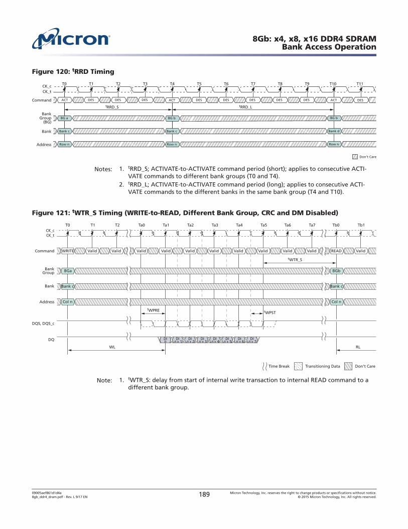
Figure 120: tRRD Timing
T0 T1 T2 T3 T4 T5 T6 T7 T8 T9
tRRD_S
T10 T11
Don’t Care
BG a
DESACT ACTDES DES DES DES DES DES DES DES
CK_tCK_c
Command
BankGroup
(BG)
Bank cBank
Row n
BG b
Bank c
Row n
BG b
Bank d
Row nAddress
tRRD_L
ACT
Notes: 1. tRRD_S; ACTIVATE-to-ACTIVATE command period (short); applies to consecutive ACTI-VATE commands to different bank groups (T0 and T4).
2. tRRD_L; ACTIVATE-to-ACTIVATE command period (long); applies to consecutive ACTI-VATE commands to the different banks in the same bank group (T4 and T10).
Figure 121: tWTR_S Timing (WRITE-to-READ, Different Bank Group, CRC and DM Disabled)
T0 Tb0T1 T2 Ta0 Ta1 Ta2 Ta3 Ta4 Ta5 Ta6 Ta7
Valid Valid Valid Valid Valid READ ValidCommand ValidWRITE Valid Valid Valid Valid
BGbBankGroup BGa
Bank cBank
Col n
Bank c
Col nAddress
CK_tCK_c
Tb1
Don’t CareTransitioning DataTime Break
DQ
WL
tWPRE tWPST
RL
tWTR_S
DIn + 3
DIn + 4
DIn + 5
DIn + 6
DIn + 7
DIn + 2
DIn + 1
DIn
DQS, DQS_c
Note: 1. tWTR_S: delay from start of internal write transaction to internal READ command to adifferent bank group.
8Gb: x4, x8, x16 DDR4 SDRAMBank Access Operation
09005aef861d1d4a8gb_ddr4_dram.pdf - Rev. L 9/17 EN 189 Micron Technology, Inc. reserves the right to change products or specifications without notice.
© 2015 Micron Technology, Inc. All rights reserved.
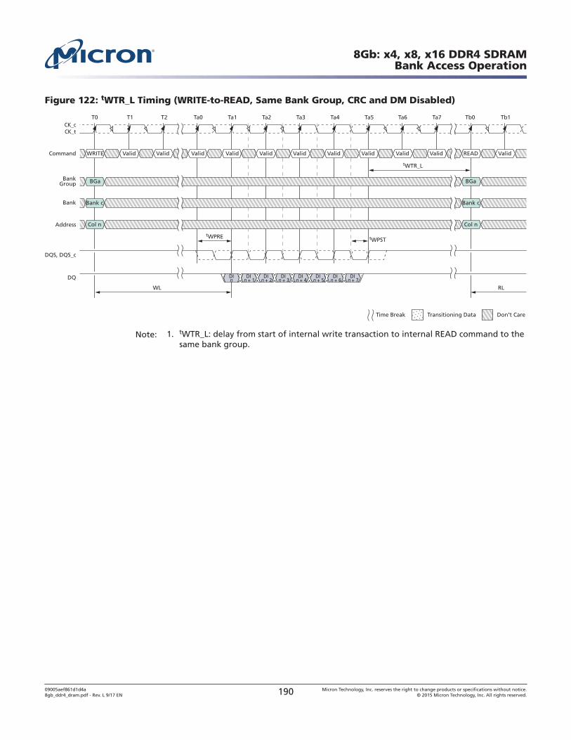
Figure 122: tWTR_L Timing (WRITE-to-READ, Same Bank Group, CRC and DM Disabled)
T0 Tb0T1 T2 Ta0 Ta1 Ta2 Ta3 Ta4 Ta5 Ta6 Ta7
Valid Valid Valid Valid Valid READ ValidCommand ValidWRITE Valid Valid Valid Valid
BGaBankGroup BGa
Bank cBank
Col n
Bank c
Col nAddress
CK_tCK_c
Tb1
Don’t CareTransitioning DataTime Break
DQ
WL
tWPRE tWPST
RL
tWTR_L
DIn + 3
DIn + 4
DIn + 5
DIn + 6
DIn + 7
DIn + 2
DIn + 1
DIn
DQS, DQS_c
Note: 1. tWTR_L: delay from start of internal write transaction to internal READ command to thesame bank group.
8Gb: x4, x8, x16 DDR4 SDRAMBank Access Operation
09005aef861d1d4a8gb_ddr4_dram.pdf - Rev. L 9/17 EN 190 Micron Technology, Inc. reserves the right to change products or specifications without notice.
© 2015 Micron Technology, Inc. All rights reserved.
READ Operation
Read Timing Definitions
The read timings shown below are applicable in normal operation mode, that is, whenthe DLL is enabled and locked.
Note: tDQSQ = both rising/falling edges of DQS; no tAC defined.
Rising data strobe edge parameters:
• tDQSCK (MIN)/(MAX) describes the allowed range for a rising data strobe edge rela-tive to CK.
• tDQSCK is the actual position of a rising strobe edge relative to CK.• tQSH describes the DQS differential output HIGH time.• tDQSQ describes the latest valid transition of the associated DQ pins.• tQH describes the earliest invalid transition of the associated DQ pins.
Falling data strobe edge parameters:
• tQSL describes the DQS differential output LOW time.• tDQSQ describes the latest valid transition of the associated DQ pins.• tQH describes the earliest invalid transition of the associated DQ pins.
8Gb: x4, x8, x16 DDR4 SDRAMREAD Operation
09005aef861d1d4a8gb_ddr4_dram.pdf - Rev. L 9/17 EN 191 Micron Technology, Inc. reserves the right to change products or specifications without notice.
© 2015 Micron Technology, Inc. All rights reserved.
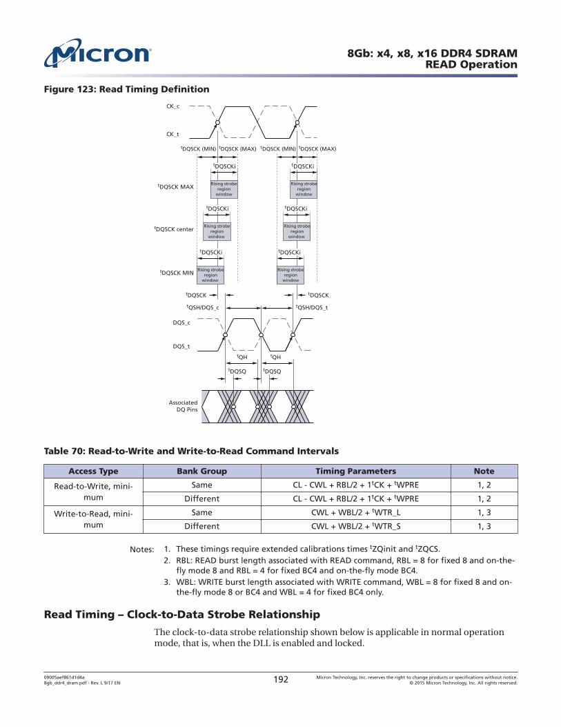
Figure 123: Read Timing Definition
CK_t
CK_c
DQS_c
DQS_t
tDQSCK tDQSCK
tDQSQtDQSQ
Rising stroberegion
window
Rising stroberegion
window
tQSH/DQS_c tQSH/DQS_t
tQH tQH
tDQSCK (MAX)tDQSCK (MIN) tDQSCK (MAX)tDQSCK (MIN)
AssociatedDQ Pins
tDQSCKi
tDQSCK MIN
tDQSCKi
Rising stroberegion
window
Rising stroberegion
window
tDQSCKi
tDQSCK center
tDQSCKi
Rising stroberegion
window
Rising stroberegion
window
tDQSCKi
tDQSCK MAX
tDQSCKi
Table 70: Read-to-Write and Write-to-Read Command Intervals
Access Type Bank Group Timing Parameters Note
Read-to-Write, mini-mum
Same CL - CWL + RBL/2 + 1tCK + tWPRE 1, 2
Different CL - CWL + RBL/2 + 1tCK + tWPRE 1, 2
Write-to-Read, mini-mum
Same CWL + WBL/2 + tWTR_L 1, 3
Different CWL + WBL/2 + tWTR_S 1, 3
Notes: 1. These timings require extended calibrations times tZQinit and tZQCS.2. RBL: READ burst length associated with READ command, RBL = 8 for fixed 8 and on-the-
fly mode 8 and RBL = 4 for fixed BC4 and on-the-fly mode BC4.3. WBL: WRITE burst length associated with WRITE command, WBL = 8 for fixed 8 and on-
the-fly mode 8 or BC4 and WBL = 4 for fixed BC4 only.
Read Timing – Clock-to-Data Strobe Relationship
The clock-to-data strobe relationship shown below is applicable in normal operationmode, that is, when the DLL is enabled and locked.
8Gb: x4, x8, x16 DDR4 SDRAMREAD Operation
09005aef861d1d4a8gb_ddr4_dram.pdf - Rev. L 9/17 EN 192 Micron Technology, Inc. reserves the right to change products or specifications without notice.
© 2015 Micron Technology, Inc. All rights reserved.
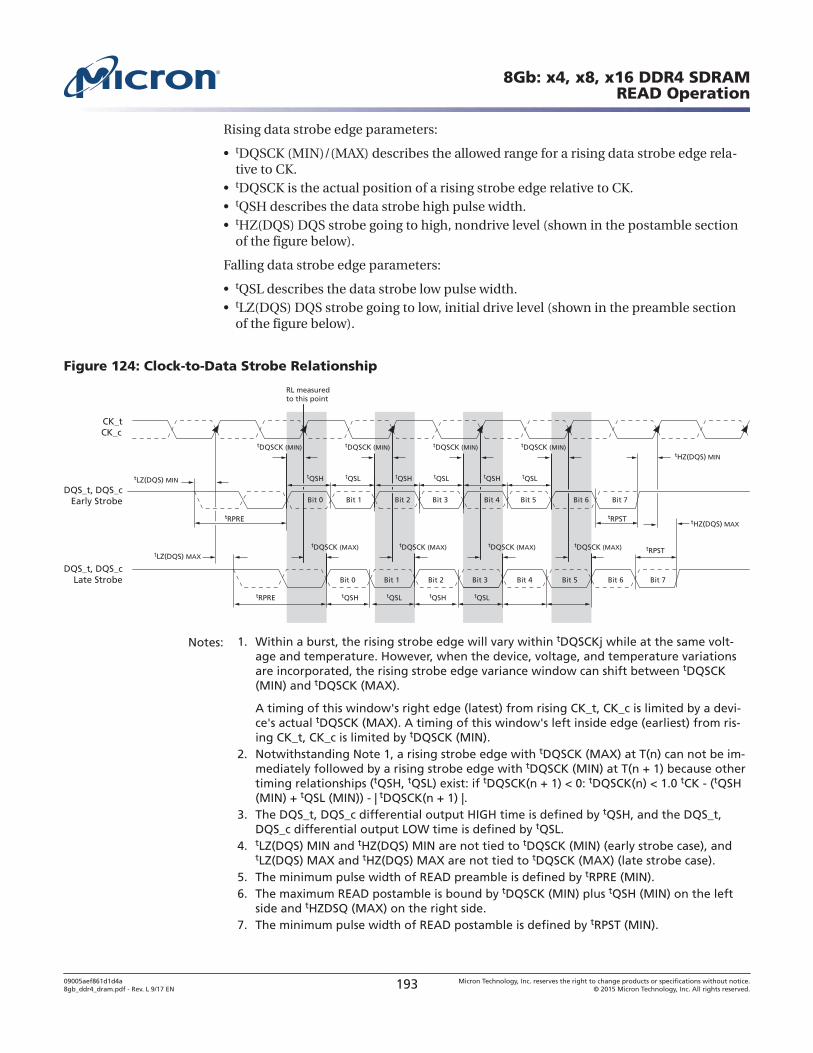
Rising data strobe edge parameters:
• tDQSCK (MIN)/(MAX) describes the allowed range for a rising data strobe edge rela-tive to CK.
• tDQSCK is the actual position of a rising strobe edge relative to CK.• tQSH describes the data strobe high pulse width.• tHZ(DQS) DQS strobe going to high, nondrive level (shown in the postamble section
of the figure below).
Falling data strobe edge parameters:
• tQSL describes the data strobe low pulse width.• tLZ(DQS) DQS strobe going to low, initial drive level (shown in the preamble section
of the figure below).
Figure 124: Clock-to-Data Strobe Relationship
RL measuredto this point
DQS_t, DQS_cEarly Strobe
CK_tCK_c
tLZ(DQS) MIN
tLZ(DQS) MAX
DQS_t, DQS_cLate Strobe
tDQSCK (MIN)
tDQSCK (MAX) tDQSCK (MAX) tDQSCK (MAX) tDQSCK (MAX)
tDQSCK (MIN) tDQSCK (MIN) tDQSCK (MIN)tHZ(DQS) MIN
tHZ(DQS) MAXtRPRE
tRPRE
tQSH tQSL
tQSH tQSL tQSH tQSL
tQSH tQSL tQSH tQSL
Bit 0 Bit 1 Bit 2 Bit 7Bit 6Bit 4Bit 3 Bit 5
Bit 0 Bit 1 Bit 2 Bit 7Bit 6Bit 4Bit 3 Bit 5
tRPST
tRPST
Notes: 1. Within a burst, the rising strobe edge will vary within tDQSCKj while at the same volt-age and temperature. However, when the device, voltage, and temperature variationsare incorporated, the rising strobe edge variance window can shift between tDQSCK(MIN) and tDQSCK (MAX).
A timing of this window's right edge (latest) from rising CK_t, CK_c is limited by a devi-ce's actual tDQSCK (MAX). A timing of this window's left inside edge (earliest) from ris-ing CK_t, CK_c is limited by tDQSCK (MIN).
2. Notwithstanding Note 1, a rising strobe edge with tDQSCK (MAX) at T(n) can not be im-mediately followed by a rising strobe edge with tDQSCK (MIN) at T(n + 1) because othertiming relationships (tQSH, tQSL) exist: if tDQSCK(n + 1) < 0: tDQSCK(n) < 1.0 tCK - (tQSH(MIN) + tQSL (MIN)) - | tDQSCK(n + 1) |.
3. The DQS_t, DQS_c differential output HIGH time is defined by tQSH, and the DQS_t,DQS_c differential output LOW time is defined by tQSL.
4. tLZ(DQS) MIN and tHZ(DQS) MIN are not tied to tDQSCK (MIN) (early strobe case), andtLZ(DQS) MAX and tHZ(DQS) MAX are not tied to tDQSCK (MAX) (late strobe case).
5. The minimum pulse width of READ preamble is defined by tRPRE (MIN).6. The maximum READ postamble is bound by tDQSCK (MIN) plus tQSH (MIN) on the left
side and tHZDSQ (MAX) on the right side.7. The minimum pulse width of READ postamble is defined by tRPST (MIN).
8Gb: x4, x8, x16 DDR4 SDRAMREAD Operation
09005aef861d1d4a8gb_ddr4_dram.pdf - Rev. L 9/17 EN 193 Micron Technology, Inc. reserves the right to change products or specifications without notice.
© 2015 Micron Technology, Inc. All rights reserved.
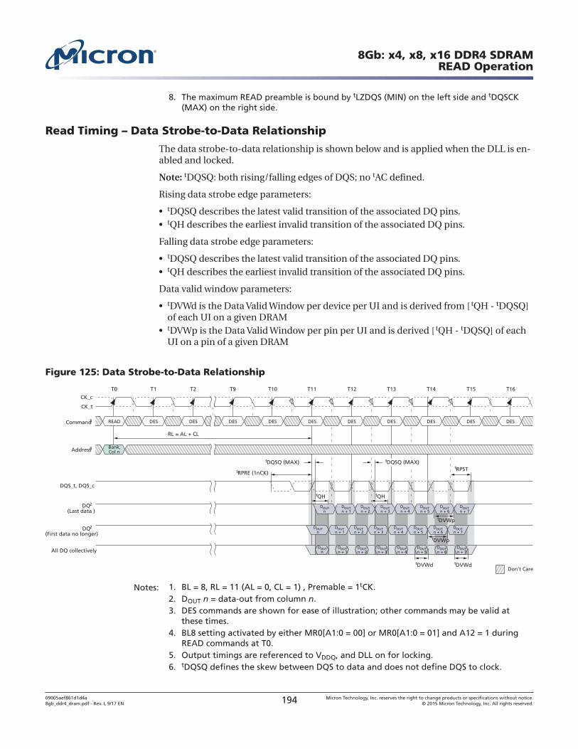
8. The maximum READ preamble is bound by tLZDQS (MIN) on the left side and tDQSCK(MAX) on the right side.
Read Timing – Data Strobe-to-Data Relationship
The data strobe-to-data relationship is shown below and is applied when the DLL is en-abled and locked.
Note: tDQSQ: both rising/falling edges of DQS; no tAC defined.
Rising data strobe edge parameters:
• tDQSQ describes the latest valid transition of the associated DQ pins.• tQH describes the earliest invalid transition of the associated DQ pins.
Falling data strobe edge parameters:
• tDQSQ describes the latest valid transition of the associated DQ pins.• tQH describes the earliest invalid transition of the associated DQ pins.
Data valid window parameters:
• tDVWd is the Data Valid Window per device per UI and is derived from [ tQH - tDQSQ]of each UI on a given DRAM
• tDVWp is the Data Valid Window per pin per UI and is derived [ tQH - tDQSQ] of eachUI on a pin of a given DRAM
Figure 125: Data Strobe-to-Data Relationship
CK_t
CK_c
Command3 READ
Bank,Col n
DES DES DES DES DES DES DES DES DES DES
Address4
DQS_t, DQS_c
DQ2
(Last data )
DQ2
(First data no longer)
All DQ collectively
RL = AL + CL
tDQSQ (MAX)
tRPRE (1nCK)tRPST
tQH tQH
tDVWp
tDVWp
tDVWd tDVWd
T0 T1 T2 T9 T10 T11 T12 T13
Don’t Care
T14 T15 T16
DOUTn + 2
DOUTn + 1
DOUTn + 4
DOUTn + 5
DOUTn + 6
DOUTn + 7
DOUTn + 2
DOUTn + 1
DOUTn + 3
DOUTn + 4
DOUTn + 5
DOUTn + 6
DOUTn + 7
tDQSQ (MAX)
DOUTn
DOUTn + 2
DOUTn + 1
DOUTn + 3
DOUTn + 4
DOUTn + 5
DOUTn + 6
DOUTn + 7
DOUTn
DOUTn + 3
DOUTn
Notes: 1. BL = 8, RL = 11 (AL = 0, CL = 1) , Premable = 1tCK.2. DOUT n = data-out from column n.3. DES commands are shown for ease of illustration; other commands may be valid at
these times.4. BL8 setting activated by either MR0[A1:0 = 00] or MR0[A1:0 = 01] and A12 = 1 during
READ commands at T0.5. Output timings are referenced to VDDQ, and DLL on for locking.6. tDQSQ defines the skew between DQS to data and does not define DQS to clock.
8Gb: x4, x8, x16 DDR4 SDRAMREAD Operation
09005aef861d1d4a8gb_ddr4_dram.pdf - Rev. L 9/17 EN 194 Micron Technology, Inc. reserves the right to change products or specifications without notice.
© 2015 Micron Technology, Inc. All rights reserved.
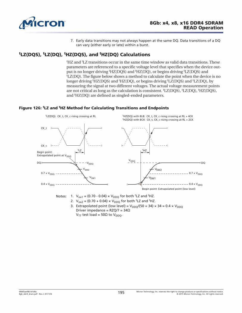
7. Early data transitions may not always happen at the same DQ. Data transitions of a DQcan vary (either early or late) within a burst.
tLZ(DQS), tLZ(DQ), tHZ(DQS), and tHZ(DQ) CalculationstHZ and tLZ transitions occur in the same time window as valid data transitions. Theseparameters are referenced to a specific voltage level that specifies when the device out-put is no longer driving tHZ(DQS) and tHZ(DQ), or begins driving tLZ(DQS) andtLZ(DQ). The figure below shows a method to calculate the point when the device is nolonger driving tHZ(DQS) and tHZ(DQ), or begins driving tLZ(DQS) and tLZ(DQ), bymeasuring the signal at two different voltages. The actual voltage measurement pointsare not critical as long as the calculation is consistent. tLZ(DQS), tLZ(DQ), tHZ(DQS),and tHZ(DQ) are defined as singled-ended parameters.
Figure 126: tLZ and tHZ Method for Calculating Transitions and Endpoints
CK_t
CK_ctLZ tHZ
DQ
0.7 × VDDQ
0.4 × VDDQ
DQ
Begin point: Extrapolated point at VDDQ
VDDQ
VSW2
Begin point: Extrapolated point (low level)
VDDQ
tLZ(DQ): CK_t, CK_c rising crossing at RL tHZ(DQ) with BL8: CK_t, CK_c rising crossing at RL + 4CKtHZ(DQ) with BC4: CK_t, CK_c rising crossing at RL + 2CK
VSW1
VSW2
VSW1
0.7 × VDDQ
0.4 × VDDQ
Notes: 1. Vsw1 = (0.70 - 0.04) × VDDQ for both tLZ and tHZ.2. Vsw2 = (0.70 + 0.04) × VDDQ for both tLZ and tHZ.3. Extrapolated point (low level) = VDDQ/(50 + 34) × 34 = 0.4 × VDDQ
Driver impedance = RZQ/7 = 34VTT test load = 50 to VDDQ.
8Gb: x4, x8, x16 DDR4 SDRAMREAD Operation
09005aef861d1d4a8gb_ddr4_dram.pdf - Rev. L 9/17 EN 195 Micron Technology, Inc. reserves the right to change products or specifications without notice.
© 2015 Micron Technology, Inc. All rights reserved.
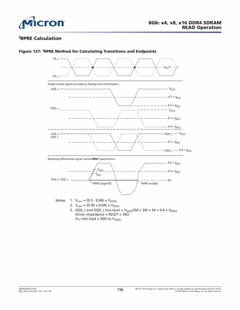
tRPRE Calculation
Figure 127: tRPRE Method for Calculating Transitions and Endpoints
DQS_t
tRPRE ends (t2)
CK_t
CK_c
Resulting differential signal relevant for tRPRE specification
Single-ended signal provided as background information
0V
DQS_c
DQS_t, DQS_c
DQS_tDQS_c
DQS_t
DQS_c
tRPRE begins (t1)
VSW1
VSW2
0.7 × VDDQ
0.7 × VDDQ
0.4 × VDDQ
0.4 × VDDQ
VDDQ
VDDQ
VDDQ
0.7 × VDDQ
0.3 × VDDQ
0.6 × VDDQ
0.4 × VDDQ
VDD /2
Notes: 1. Vsw1 = (0.3 - 0.04) × VDDQ.2. Vsw2 = (0.30 + 0.04) × VDDQ.3. DQS_t and DQS_c low level = VDDQ/(50 + 34) × 34 = 0.4 × VDDQ
Driver impedance = RZQ/7 = 34VTT test load = 50 to VDDQ.
8Gb: x4, x8, x16 DDR4 SDRAMREAD Operation
09005aef861d1d4a8gb_ddr4_dram.pdf - Rev. L 9/17 EN 196 Micron Technology, Inc. reserves the right to change products or specifications without notice.
© 2015 Micron Technology, Inc. All rights reserved.
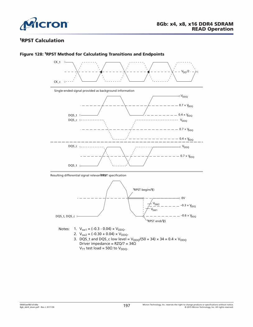
tRPST Calculation
Figure 128: tRPST Method for Calculating Transitions and Endpoints
DQS_t, DQS_c
VSW1
VSW2
DQS_t
tRPST ends (t2)
CK_t
CK_c
Resulting differential signal relevant for tRPST specification
Single-ended signal provided as background information
0V
DQS_c
DQS_t
DQS_c
tRPST begins (t1)
0.7 × VDDQ
0.7 × VDDQ
0.4 × VDDQ
0.4 × VDDQ
VDDQ
VDDQ
VDDQ
0.7 × VDDQ
–0.3 × VDDQ
–0.6 × VDDQ
VDD /2
Notes: 1. Vsw1 = (–0.3 - 0.04) × VDDQ.2. Vsw2 = (–0.30 + 0.04) × VDDQ.3. DQS_t and DQS_c low level = VDDQ/(50 + 34) × 34 = 0.4 × VDDQ
Driver impedance = RZQ/7 = 34VTT test load = 50 to VDDQ.
8Gb: x4, x8, x16 DDR4 SDRAMREAD Operation
09005aef861d1d4a8gb_ddr4_dram.pdf - Rev. L 9/17 EN 197 Micron Technology, Inc. reserves the right to change products or specifications without notice.
© 2015 Micron Technology, Inc. All rights reserved.
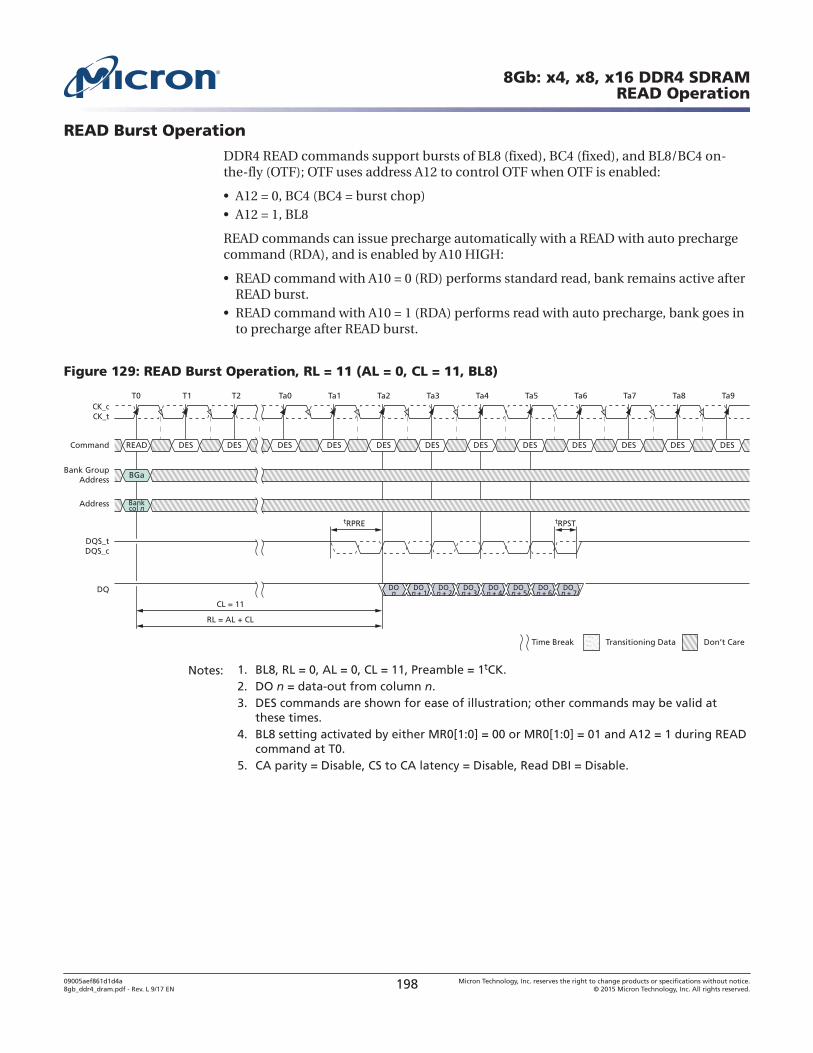
READ Burst Operation
DDR4 READ commands support bursts of BL8 (fixed), BC4 (fixed), and BL8/BC4 on-the-fly (OTF); OTF uses address A12 to control OTF when OTF is enabled:
• A12 = 0, BC4 (BC4 = burst chop)• A12 = 1, BL8
READ commands can issue precharge automatically with a READ with auto prechargecommand (RDA), and is enabled by A10 HIGH:
• READ command with A10 = 0 (RD) performs standard read, bank remains active afterREAD burst.
• READ command with A10 = 1 (RDA) performs read with auto precharge, bank goes into precharge after READ burst.
Figure 129: READ Burst Operation, RL = 11 (AL = 0, CL = 11, BL8)
T0
CL = 11
RL = AL + CL
tRPRE
T1 T2 Ta1Ta0 Ta2 Ta3 Ta4 Ta5 Ta6 Ta7 Ta8 Ta9
DES DES DES DES DES DESCommand DESREAD DES DESDES DES DES
DQ
CK_tCK_c
Don’t CareTransitioning DataTime Break
DOn + 3
DOn + 4
DOn + 5
DOn + 6
DOn + 7
DOn + 2
DOn + 1
DOn
Bank GroupAddress
DQS_tDQS_c
BGa
Address Bankcol n
tRPST
Notes: 1. BL8, RL = 0, AL = 0, CL = 11, Preamble = 1tCK.2. DO n = data-out from column n.3. DES commands are shown for ease of illustration; other commands may be valid at
these times.4. BL8 setting activated by either MR0[1:0] = 00 or MR0[1:0] = 01 and A12 = 1 during READ
command at T0.5. CA parity = Disable, CS to CA latency = Disable, Read DBI = Disable.
8Gb: x4, x8, x16 DDR4 SDRAMREAD Operation
09005aef861d1d4a8gb_ddr4_dram.pdf - Rev. L 9/17 EN 198 Micron Technology, Inc. reserves the right to change products or specifications without notice.
© 2015 Micron Technology, Inc. All rights reserved.
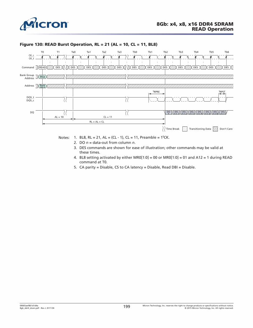
Figure 130: READ Burst Operation, RL = 21 (AL = 10, CL = 11, BL8)
T0
CL = 11AL = 10
RL = AL + CL
tRPRE
T1 Ta0 Ta1 Ta2 Ta3 Tb0 Tb1 Tb2 Tb3 Tb4 Tb5 Tb6
DES DES DES DES DESCommand DESREAD DES DES DES DES
DQ
CK_tCK_c
Don’t CareTransitioning DataTime Break
DOn + 3
DOn + 4
DOn + 5
DOn + 6
DOn + 7
DOn + 2
DOn + 1
DOn
Bank GroupAddress
DQS_tDQS_c
BGa
Address Bankcol n
tRPST
DESDES
Notes: 1. BL8, RL = 21, AL = (CL - 1), CL = 11, Preamble = 1tCK.2. DO n = data-out from column n.3. DES commands are shown for ease of illustration; other commands may be valid at
these times.4. BL8 setting activated by either MR0[1:0] = 00 or MR0[1:0] = 01 and A12 = 1 during READ
command at T0.5. CA parity = Disable, CS to CA latency = Disable, Read DBI = Disable.
8Gb: x4, x8, x16 DDR4 SDRAMREAD Operation
09005aef861d1d4a8gb_ddr4_dram.pdf - Rev. L 9/17 EN 199 Micron Technology, Inc. reserves the right to change products or specifications without notice.
© 2015 Micron Technology, Inc. All rights reserved.
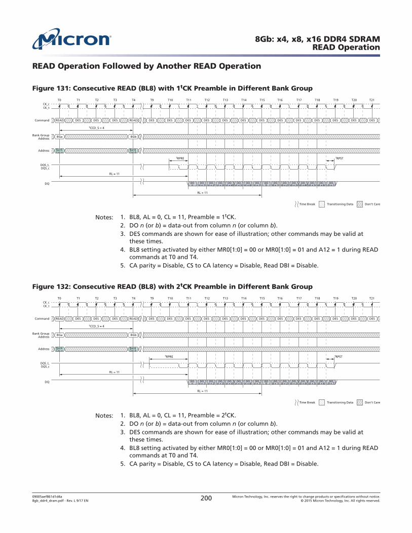
READ Operation Followed by Another READ Operation
Figure 131: Consecutive READ (BL8) with 1tCK Preamble in Different Bank Group
T0
tCCD_S = 4
tRPRE
RL = 11
tRPST
T16T1 T2 T3 T4 T9 T10 T11 T12 T13 T14 T15
DES DES DES DES DES DES DESCommand DESREAD DES DES READ DES
DQ
CK_tCK_c
DQS_t,DQS_c
RL = 11
T21T17 T18 T19 T20
Don’t CareTransitioning DataTime Break
DOn + 1
DOn + 2
DOn + 3
DOn + 4
DOn + 5
DOn + 6
DOn + 7
DOb
DOb + 1
DOb + 2
DOb + 3
DOb + 4
DOb + 5
DOb + 6
DOb + 7
DOn
DES DES DES DES DES
Bank GroupAddress
BGa BGb
Address BankCol n
BankCol b
Notes: 1. BL8, AL = 0, CL = 11, Preamble = 1tCK.2. DO n (or b) = data-out from column n (or column b).3. DES commands are shown for ease of illustration; other commands may be valid at
these times.4. BL8 setting activated by either MR0[1:0] = 00 or MR0[1:0] = 01 and A12 = 1 during READ
commands at T0 and T4.5. CA parity = Disable, CS to CA latency = Disable, Read DBI = Disable.
Figure 132: Consecutive READ (BL8) with 2tCK Preamble in Different Bank Group
T0
tCCD_S = 4
tRPRE
RL = 11
tRPST
T16T1 T2 T3 T4 T9 T10 T11 T12 T13 T14 T15
DES DES DES DES DES DES DESCommand DESREAD DES DES READ DES
DQ
CK_tCK_c
DQS_t,DQS_c
RL = 11
T21T17 T18 T19 T20
Don’t CareTransitioning DataTime Break
DOn + 1
DOn + 2
DOn + 3
DOn + 4
DOn + 5
DOn + 6
DOn + 7
DOb
DOb + 1
DOb + 2
DOb + 3
DOb + 4
DOb + 5
DOb + 6
DOb + 7
DOn
DES DES DES DES DES
Bank GroupAddress
BGa BGb
Address BankCol n
BankCol b
Notes: 1. BL8, AL = 0, CL = 11, Preamble = 2tCK.2. DO n (or b) = data-out from column n (or column b).3. DES commands are shown for ease of illustration; other commands may be valid at
these times.4. BL8 setting activated by either MR0[1:0] = 00 or MR0[1:0] = 01 and A12 = 1 during READ
commands at T0 and T4.5. CA parity = Disable, CS to CA latency = Disable, Read DBI = Disable.
8Gb: x4, x8, x16 DDR4 SDRAMREAD Operation
09005aef861d1d4a8gb_ddr4_dram.pdf - Rev. L 9/17 EN 200 Micron Technology, Inc. reserves the right to change products or specifications without notice.
© 2015 Micron Technology, Inc. All rights reserved.
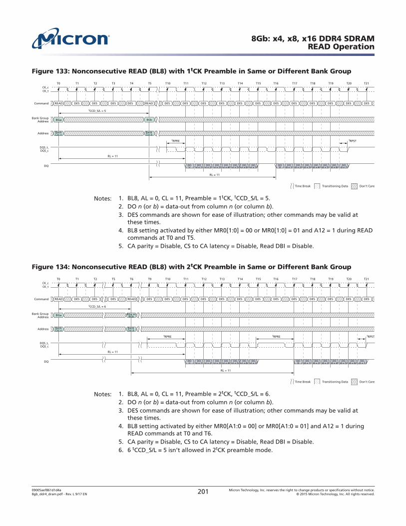
Figure 133: Nonconsecutive READ (BL8) with 1tCK Preamble in Same or Different Bank Group
T0
tCCD_S/L = 5
tRPRE
RL = 11
tRPST
T16T1 T2 T3 T4 T5 T10 T11 T12 T13 T14 T15
DES DES DES DES DES DES DESCommand DESREAD DES DES DES READ
DQ
CK_tCK_c
DQS_t,DQS_c
RL = 11
T21T17 T18 T19 T20
Don’t CareTransitioning DataTime Break
DOn + 1
DOn + 2
DOn + 3
DOn + 4
DOn + 5
DOn + 6
DOn + 7
DOb
DOb + 1
DOb + 2
DOb + 3
DOb + 4
DOb + 5
DOb + 6
DOb + 7
DOn
DES DES DES DES DES
Bank GroupAddress BGa BGb
Address BankCol n
BankCol b
Notes: 1. BL8, AL = 0, CL = 11, Preamble = 1tCK, tCCD_S/L = 5.2. DO n (or b) = data-out from column n (or column b).3. DES commands are shown for ease of illustration; other commands may be valid at
these times.4. BL8 setting activated by either MR0[1:0] = 00 or MR0[1:0] = 01 and A12 = 1 during READ
commands at T0 and T5.5. CA parity = Disable, CS to CA latency = Disable, Read DBI = Disable.
Figure 134: Nonconsecutive READ (BL8) with 2tCK Preamble in Same or Different Bank Group
T0
tCCD_S/L = 6
tRPRE
RL = 11
tRPST
T16T1 T2 T5 T6 T9 T10 T11 T12 T13 T14 T15
DES DES DES DES DES DES DESCommand DESREAD DES DES READ DES
DQ
CK_tCK_c
DQS_t,DQS_c
RL = 11
T21T17 T18 T19 T20
Don’t CareTransitioning DataTime Break
DOn + 1
DOn + 2
DOn + 3
DOn + 4
DOn + 5
DOn + 6
DOn + 7
DOb
DOb + 1
DOb + 2
DOb + 3
DOb + 4
DOb + 5
DOb + 6
DOb + 7
DOn
DES DES DES DES DES
Bank GroupAddress
BGa BGa orBGb
Address BankCol n
BankCol b
tRPRE
Notes: 1. BL8, AL = 0, CL = 11, Preamble = 2tCK, tCCD_S/L = 6.2. DO n (or b) = data-out from column n (or column b).3. DES commands are shown for ease of illustration; other commands may be valid at
these times.4. BL8 setting activated by either MR0[A1:0 = 00] or MR0[A1:0 = 01] and A12 = 1 during
READ commands at T0 and T6.5. CA parity = Disable, CS to CA latency = Disable, Read DBI = Disable.6. 6 tCCD_S/L = 5 isn’t allowed in 2tCK preamble mode.
8Gb: x4, x8, x16 DDR4 SDRAMREAD Operation
09005aef861d1d4a8gb_ddr4_dram.pdf - Rev. L 9/17 EN 201 Micron Technology, Inc. reserves the right to change products or specifications without notice.
© 2015 Micron Technology, Inc. All rights reserved.
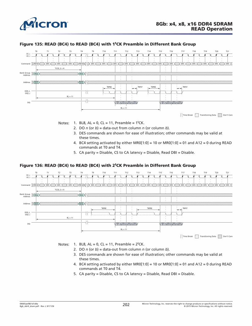
Figure 135: READ (BC4) to READ (BC4) with 1tCK Preamble in Different Bank Group
T0
tCCD_S = 4
tRPRE
RL = 11
tRPST
T16T1 T2 T3 T4 T9 T10 T11 T12 T13 T14 T15
DES DES DES DES DES DES DESCommand DESREAD DES DES READ DES
DQ
CK_tCK_c
DQS_t,DQS_c
RL = 11
T21T17 T18 T19 T20
Don’t CareTransitioning DataTime Break
DOn + 1
DOn + 2
DOn + 3
DOb
DOb + 1
DOb + 2
DOb + 3
DOn
DES DES DES DES DES
Bank GroupAddress
BGa BGb
Address BankCol n
BankCol b
tRPREtRPST
Notes: 1. BL8, AL = 0, CL = 11, Preamble = 1tCK.2. DO n (or b) = data-out from column n (or column b).3. DES commands are shown for ease of illustration; other commands may be valid at
these times.4. BC4 setting activated by either MR0[1:0] = 10 or MR0[1:0] = 01 and A12 = 0 during READ
commands at T0 and T4.5. CA parity = Disable, CS to CA latency = Disable, Read DBI = Disable.
Figure 136: READ (BC4) to READ (BC4) with 2tCK Preamble in Different Bank Group
T0
tCCD_S = 4
tRPRE
RL = 11
tRPST
T16T1 T2 T3 T4 T9 T10 T11 T12 T13 T14 T15
DES DES DES DES DES DES DESCommand DESREAD DES DES READ DES
DQ
CK_tCK_c
DQS_t,DQS_c
RL = 11
T21T17 T18 T19 T20
Don’t CareTransitioning DataTime Break
DOn + 1
DOn + 2
DOn + 3
DOb
DOb + 1
DOb + 2
DOb + 3
DOn
DES DES DES DES DES
Bank GroupAddress
BGa BGb
Address BankCol n
BankCol b
tRPRE
Notes: 1. BL8, AL = 0, CL = 11, Preamble = 2tCK.2. DO n (or b) = data-out from column n (or column b).3. DES commands are shown for ease of illustration; other commands may be valid at
these times.4. BC4 setting activated by either MR0[1:0] = 10 or MR0[1:0] = 01 and A12 = 0 during READ
commands at T0 and T4.5. CA parity = Disable, CS to CA latency = Disable, Read DBI = Disable.
8Gb: x4, x8, x16 DDR4 SDRAMREAD Operation
09005aef861d1d4a8gb_ddr4_dram.pdf - Rev. L 9/17 EN 202 Micron Technology, Inc. reserves the right to change products or specifications without notice.
© 2015 Micron Technology, Inc. All rights reserved.
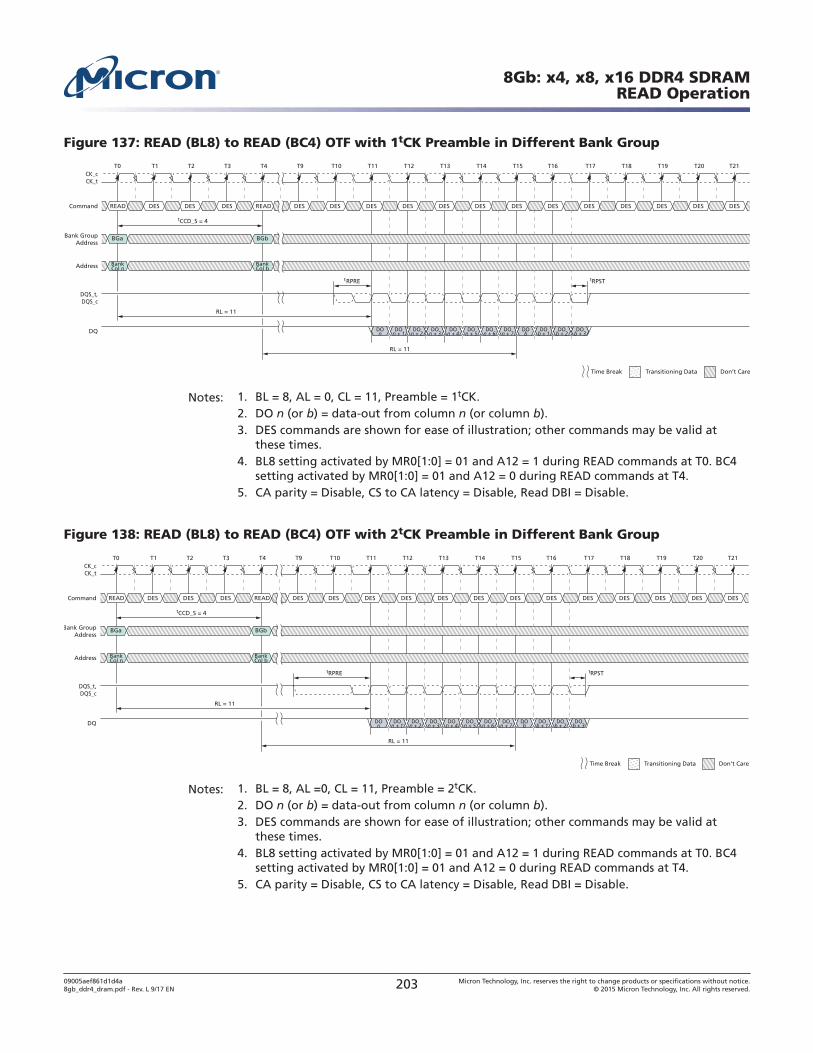
Figure 137: READ (BL8) to READ (BC4) OTF with 1tCK Preamble in Different Bank Group
T0
tCCD_S = 4
tRPRE
RL = 11
tRPST
T16T1 T2 T3 T4 T9 T10 T11 T12 T13 T14 T15
DES DES DES DES DES DES DESCommand DESREAD DES DES READ DES
DQ
CK_tCK_c
DQS_t,DQS_c
RL = 11
T21T17 T18 T19 T20
Don’t CareTransitioning DataTime Break
DOn + 1
DOn + 2
DOn + 3
DOn + 4
DOn + 5
DOn + 6
DOn + 7
DOb
DOb + 1
DOb + 2
DOb + 3
DOn
DES DES DES DES DES
Bank GroupAddress
BGa BGb
Address BankCol n
BankCol b
Notes: 1. BL = 8, AL = 0, CL = 11, Preamble = 1tCK.2. DO n (or b) = data-out from column n (or column b).3. DES commands are shown for ease of illustration; other commands may be valid at
these times.4. BL8 setting activated by MR0[1:0] = 01 and A12 = 1 during READ commands at T0. BC4
setting activated by MR0[1:0] = 01 and A12 = 0 during READ commands at T4.5. CA parity = Disable, CS to CA latency = Disable, Read DBI = Disable.
Figure 138: READ (BL8) to READ (BC4) OTF with 2tCK Preamble in Different Bank Group
T0
tCCD_S = 4
tRPRE
RL = 11
tRPST
T16T1 T2 T3 T4 T9 T10 T11 T12 T13 T14 T15
DES DES DES DES DES DES DESCommand DESREAD DES DES READ DES
DQ
CK_tCK_c
DQS_t,DQS_c
RL = 11
T21T17 T18 T19 T20
Don’t CareTransitioning DataTime Break
DOn + 1
DOn + 2
DOn + 3
DOn + 4
DOn + 5
DOn + 6
DOn + 7
DOb
DOb + 1
DOb + 2
DOb + 3
DOn
DES DES DES DES DES
Bank GroupAddress
BGa BGb
Address BankCol n
BankCol b
Notes: 1. BL = 8, AL =0, CL = 11, Preamble = 2tCK.2. DO n (or b) = data-out from column n (or column b).3. DES commands are shown for ease of illustration; other commands may be valid at
these times.4. BL8 setting activated by MR0[1:0] = 01 and A12 = 1 during READ commands at T0. BC4
setting activated by MR0[1:0] = 01 and A12 = 0 during READ commands at T4.5. CA parity = Disable, CS to CA latency = Disable, Read DBI = Disable.
8Gb: x4, x8, x16 DDR4 SDRAMREAD Operation
09005aef861d1d4a8gb_ddr4_dram.pdf - Rev. L 9/17 EN 203 Micron Technology, Inc. reserves the right to change products or specifications without notice.
© 2015 Micron Technology, Inc. All rights reserved.
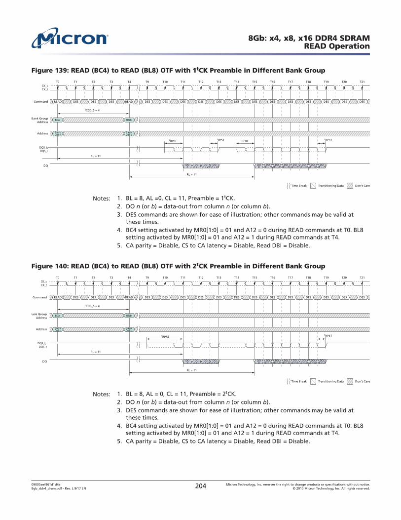
Figure 139: READ (BC4) to READ (BL8) OTF with 1tCK Preamble in Different Bank Group
T0
tCCD_S = 4
tRPRE
RL = 11
T1 T2 T3 T4
DES DES DES DES DES DES DESCommand DESREAD DES DES READ DES
DQ
CK_tCK_c
DQS_t,DQS_c
RL = 11
T20 T21T14T9 T10 T11 T12 T13 T19T15 T16 T17 T18
Don’t CareTransitioning DataTime Break
DOn + 1
DOn + 2
DOn + 3
DOb
DOb + 1
DOb + 2
DOb + 3
DOb + 4
DOb + 5
DOb + 6
DOb + 7
DOn
DES DES DES DES DES
Bank GroupAddress
Address BankCol n
BankCol b
BGb
tRPREtRPSTtRPST
BGa
Notes: 1. BL = 8, AL =0, CL = 11, Preamble = 1tCK.2. DO n (or b) = data-out from column n (or column b).3. DES commands are shown for ease of illustration; other commands may be valid at
these times.4. BC4 setting activated by MR0[1:0] = 01 and A12 = 0 during READ commands at T0. BL8
setting activated by MR0[1:0] = 01 and A12 = 1 during READ commands at T4.5. CA parity = Disable, CS to CA latency = Disable, Read DBI = Disable.
Figure 140: READ (BC4) to READ (BL8) OTF with 2tCK Preamble in Different Bank Group
T0
tCCD_S = 4
tRPRE
RL = 11
T1 T2 T3 T4
DES DES DES DES DES DES DESCommand DESREAD DES DES READ DES
DQ
CK_tCK_c
DQS_t,DQS_c
RL = 11
T20 T21T14T9 T10 T11 T12 T13 T19T15 T16 T17 T18
Don’t CareTransitioning DataTime Break
DOn + 1
DOn + 2
DOn + 3
DOb
DOb + 1
DOb + 2
DOb + 3
DOb + 4
DOb + 5
DOb + 6
DOb + 7
DOn
DES DES DES DES DES
Bank GroupAddress
Address BankCol n
BankCol b
BGb
tRPST
BGa
Notes: 1. BL = 8, AL = 0, CL = 11, Preamble = 2tCK.2. DO n (or b) = data-out from column n (or column b).3. DES commands are shown for ease of illustration; other commands may be valid at
these times.4. BC4 setting activated by MR0[1:0] = 01 and A12 = 0 during READ commands at T0. BL8
setting activated by MR0[1:0] = 01 and A12 = 1 during READ commands at T4.5. CA parity = Disable, CS to CA latency = Disable, Read DBI = Disable.
8Gb: x4, x8, x16 DDR4 SDRAMREAD Operation
09005aef861d1d4a8gb_ddr4_dram.pdf - Rev. L 9/17 EN 204 Micron Technology, Inc. reserves the right to change products or specifications without notice.
© 2015 Micron Technology, Inc. All rights reserved.
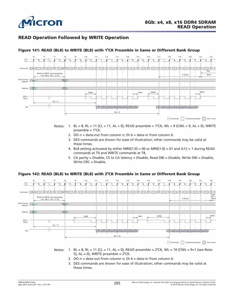
READ Operation Followed by WRITE Operation
Figure 141: READ (BL8) to WRITE (BL8) with 1tCK Preamble in Same or Different Bank Group
T0
READ to WRITE command delay= RL +BL/2 - WL + 2 tCK 4 Clocks
tRPRE
RL = 11
tRPST
T1 T7 T8 T9
DES DES DES DES DES DES DESCommand DESREAD DES WRITE DES DES
DQ
CK_tCK_c
DQS_t,DQS_c
WL = 9
T22T16T10 T11 T12 T13 T14 T15 T21T17 T18 T19 T20
Don’t CareTransitioning DataTime Break
DOn + 1
DOn + 2
DOn + 3
DOn + 4
DOn + 5
DOn + 6
DOn + 7
DIb
DIb + 1
DIb + 2
DIb + 3
DIb + 4
DIb + 5
DIb + 6
DIb + 7
DOn
DES DES DES DES DES
Bank GroupAddress
Address BankCol n
BankCol b
BGa BGa orBGb
tWPRE tWPST
tWTR
tWR
Notes: 1. BL = 8, RL = 11 (CL = 11, AL = 0), READ preamble = 1tCK, WL = 9 (CWL = 9, AL = 0), WRITEpreamble = 1tCK.
2. DO n = data-out from column n; DI b = data-in from column b.3. DES commands are shown for ease of illustration; other commands may be valid at
these times.4. BL8 setting activated by either MR0[1:0] = 00 or MR0[1:0] = 01 and A12 = 1 during READ
commands at T0 and WRITE commands at T8.5. CA parity = Disable, CS to CA latency = Disable, Read DBI = Disable, Write DBI = Disable,
Write CRC = Disable.
Figure 142: READ (BL8) to WRITE (BL8) with 2tCK Preamble in Same or Different Bank Group
T0
READ to WRITE command delay= RL +BL/2 - WL + 3 tCK 4 Clocks
tRPRE
RL = 11
tRPST
T1 T7 T8 T9
DES DES DES DES DES DES DESCommand DESREAD DES WRITE DES DES
DQ
CK_tCK_c
DQS_t,DQS_c
WL = 10
T22T16T10 T11 T12 T13 T14 T15 T21T17 T18 T19 T20
Don’t CareTransitioning DataTime Break
DOn + 1
DOn + 2
DOn + 3
DOn + 4
DOn + 5
DOn + 6
DOn + 7
DIb
DIb + 1
DIb + 2
DIb + 3
DIb + 4
DIb + 5
DIb + 6
DIb + 7
DOn
DES DES DES DES DES
Bank GroupAddress
Address BankCol n
BankCol b
BGa BGa orBGb
tWPRE tWPST
tWTR
tWR
Notes: 1. BL = 8, RL = 11 (CL = 11, AL = 0), READ preamble = 2tCK, WL = 10 (CWL = 9+1 [see Note5], AL = 0), WRITE preamble = 2tCK.
2. DO n = data-out from column n; DI b = data-in from column b.3. DES commands are shown for ease of illustration; other commands may be valid at
these times.
8Gb: x4, x8, x16 DDR4 SDRAMREAD Operation
09005aef861d1d4a8gb_ddr4_dram.pdf - Rev. L 9/17 EN 205 Micron Technology, Inc. reserves the right to change products or specifications without notice.
© 2015 Micron Technology, Inc. All rights reserved.
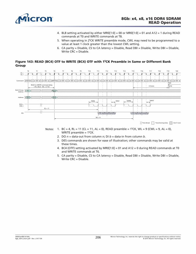
4. BL8 setting activated by either MR0[1:0] = 00 or MR0[1:0] = 01 and A12 = 1 during READcommands at T0 and WRITE commands at T8.
5. When operating in 2tCK WRITE preamble mode, CWL may need to be programmed to avalue at least 1 clock greater than the lowest CWL setting.
6. CA parity = Disable, CS to CA latency = Disable, Read DBI = Disable, Write DBI = Disable,Write CRC = Disable.
Figure 143: READ (BC4) OTF to WRITE (BC4) OTF with 1tCK Preamble in Same or Different BankGroup
T0
READ to WRITE command delay= RL +BL/2 - WL + 2 tCK 4 Clocks
tRPRE
RL = 11
tRPST
T1 T5 T6 T7
DES DES DES DES DES DES DESCommand DESREAD DES WRITE DES DES
DQ
CK_tCK_c
DQS_t,DQS_c
WL = 9
T20T14T8 T9 T10 T11 T12 T13 T19T15 T16 T17 T18
Don’t CareTransitioning DataTime Break
DOn + 1
DOn + 2
DOn + 3
DIb
DIb + 1
DIb + 2
DIb + 3
DOn
DES DES DES DES DES
Bank GroupAddress
Address BankCol n
BankCol b
BGa BGa orBGb
tWPRE tWPST
tWTR
tWR
Notes: 1. BC = 4, RL = 11 (CL = 11, AL = 0), READ preamble = 1tCK, WL = 9 (CWL = 9, AL = 0),WRITE preamble = 1tCK.
2. DO n = data-out from column n; DI b = data-in from column b.3. DES commands are shown for ease of illustration; other commands may be valid at
these times.4. BC4 (OTF) setting activated by MR0[1:0] = 01 and A12 = 0 during READ commands at T0
and WRITE commands at T6.5. CA parity = Disable, CS to CA latency = Disable, Read DBI = Disable, Write DBI = Disable,
Write CRC = Disable.
8Gb: x4, x8, x16 DDR4 SDRAMREAD Operation
09005aef861d1d4a8gb_ddr4_dram.pdf - Rev. L 9/17 EN 206 Micron Technology, Inc. reserves the right to change products or specifications without notice.
© 2015 Micron Technology, Inc. All rights reserved.
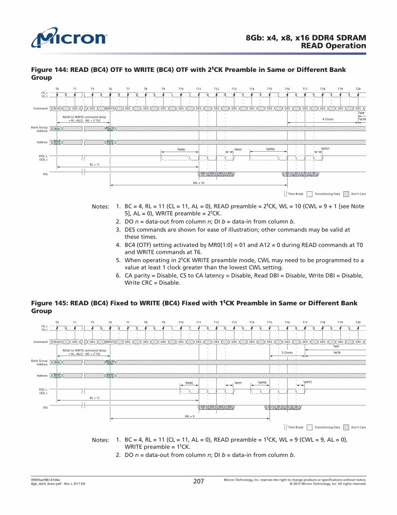
Figure 144: READ (BC4) OTF to WRITE (BC4) OTF with 2tCK Preamble in Same or Different BankGroup
T0
READ to WRITE command delay= RL +BL/2 - WL + 3 tCK 4 Clocks
tRPRE
RL = 11
tRPST
T1 T5 T6 T7
DES DES DES DES DES DES DESCommand DESREAD DES WRITE DES DES
DQ
CK_tCK_c
DQS_t,DQS_c
WL = 10
T20T14T8 T9 T10 T11 T12 T13 T19T15 T16 T17 T18
Don’t CareTransitioning DataTime Break
DOn + 1
DOn + 2
DOn + 3
DIb
DIb + 1
DIb + 2
DIb + 3
DOn
DES DES DES DES DES
Bank GroupAddress
Address BankCol n
BankCol b
BGa BGa orBGb
tWPRE tWPST
tWTR
tWR
Notes: 1. BC = 4, RL = 11 (CL = 11, AL = 0), READ preamble = 2tCK, WL = 10 (CWL = 9 + 1 [see Note5], AL = 0), WRITE preamble = 2tCK.
2. DO n = data-out from column n; DI b = data-in from column b.3. DES commands are shown for ease of illustration; other commands may be valid at
these times.4. BC4 (OTF) setting activated by MR0[1:0] = 01 and A12 = 0 during READ commands at T0
and WRITE commands at T6.5. When operating in 2tCK WRITE preamble mode, CWL may need to be programmed to a
value at least 1 clock greater than the lowest CWL setting.6. CA parity = Disable, CS to CA latency = Disable, Read DBI = Disable, Write DBI = Disable,
Write CRC = Disable.
Figure 145: READ (BC4) Fixed to WRITE (BC4) Fixed with 1tCK Preamble in Same or Different BankGroup
T0
READ to WRITE command delay= RL +BL/2 - WL + 2 tCK
tRPRE
RL = 11
tRPST
T1 T5 T6 T7
DES DES DES DES DES DES DESCommand DESREAD DES WRITE DES DES
DQ
CK_tCK_c
DQS_t,DQS_c
WL = 9
T20T14T8 T9 T10 T11 T12 T13 T19T15 T16 T17 T18
Don’t CareTransitioning DataTime Break
DOn + 1
DOn + 2
DOn + 3
DIb
DIb + 1
DIb + 2
DIb + 3
DOn
DES DES DES DES DES
Bank GroupAddress
Address BankCol n
BankCol b
BGa orBGb
tWPRE tWPST
tWTR
tWR
BGa
2 Clocks
Notes: 1. BC = 4, RL = 11 (CL = 11, AL = 0), READ preamble = 1tCK, WL = 9 (CWL = 9, AL = 0),WRITE preamble = 1tCK.
2. DO n = data-out from column n; DI b = data-in from column b.
8Gb: x4, x8, x16 DDR4 SDRAMREAD Operation
09005aef861d1d4a8gb_ddr4_dram.pdf - Rev. L 9/17 EN 207 Micron Technology, Inc. reserves the right to change products or specifications without notice.
© 2015 Micron Technology, Inc. All rights reserved.
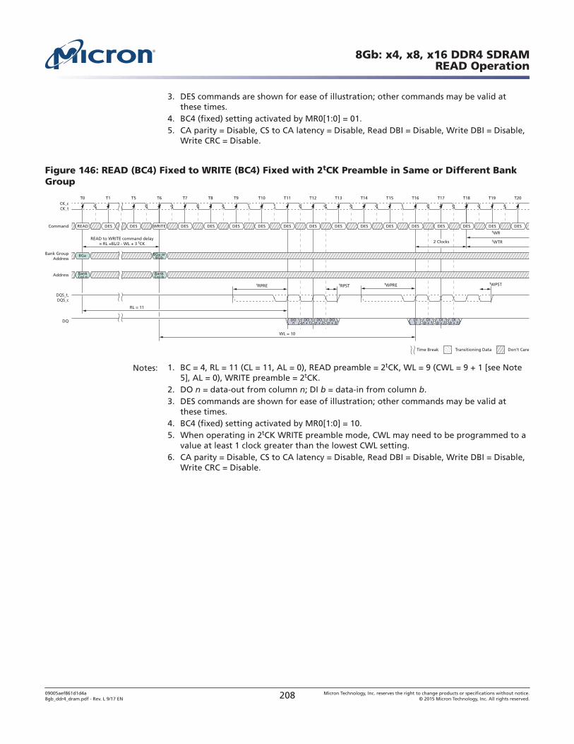
3. DES commands are shown for ease of illustration; other commands may be valid atthese times.
4. BC4 (fixed) setting activated by MR0[1:0] = 01.5. CA parity = Disable, CS to CA latency = Disable, Read DBI = Disable, Write DBI = Disable,
Write CRC = Disable.
Figure 146: READ (BC4) Fixed to WRITE (BC4) Fixed with 2tCK Preamble in Same or Different BankGroup
T0
READ to WRITE command delay= RL +BL/2 - WL + 3 tCK 2 Clocks
tRPRE
RL = 11
tRPST
T1 T5 T6 T7
DES DES DES DES DES DES DESCommand DESREAD DES WRITE DES DES
DQ
CK_tCK_c
DQS_t,DQS_c
WL = 10
T20T14T8 T9 T10 T11 T12 T13 T19T15 T16 T17 T18
Don’t CareTransitioning DataTime Break
DOn + 1
DOn + 2
DOn + 3
DIb
DIb + 1
DIb + 2
DIb + 3
DOn
DES DES DES DES DES
Bank GroupAddress
Address BankCol n
BankCol b
BGa BGa orBGb
tWPRE tWPST
tWTR
tWR
Notes: 1. BC = 4, RL = 11 (CL = 11, AL = 0), READ preamble = 2tCK, WL = 9 (CWL = 9 + 1 [see Note5], AL = 0), WRITE preamble = 2tCK.
2. DO n = data-out from column n; DI b = data-in from column b.3. DES commands are shown for ease of illustration; other commands may be valid at
these times.4. BC4 (fixed) setting activated by MR0[1:0] = 10.5. When operating in 2tCK WRITE preamble mode, CWL may need to be programmed to a
value at least 1 clock greater than the lowest CWL setting.6. CA parity = Disable, CS to CA latency = Disable, Read DBI = Disable, Write DBI = Disable,
Write CRC = Disable.
8Gb: x4, x8, x16 DDR4 SDRAMREAD Operation
09005aef861d1d4a8gb_ddr4_dram.pdf - Rev. L 9/17 EN 208 Micron Technology, Inc. reserves the right to change products or specifications without notice.
© 2015 Micron Technology, Inc. All rights reserved.
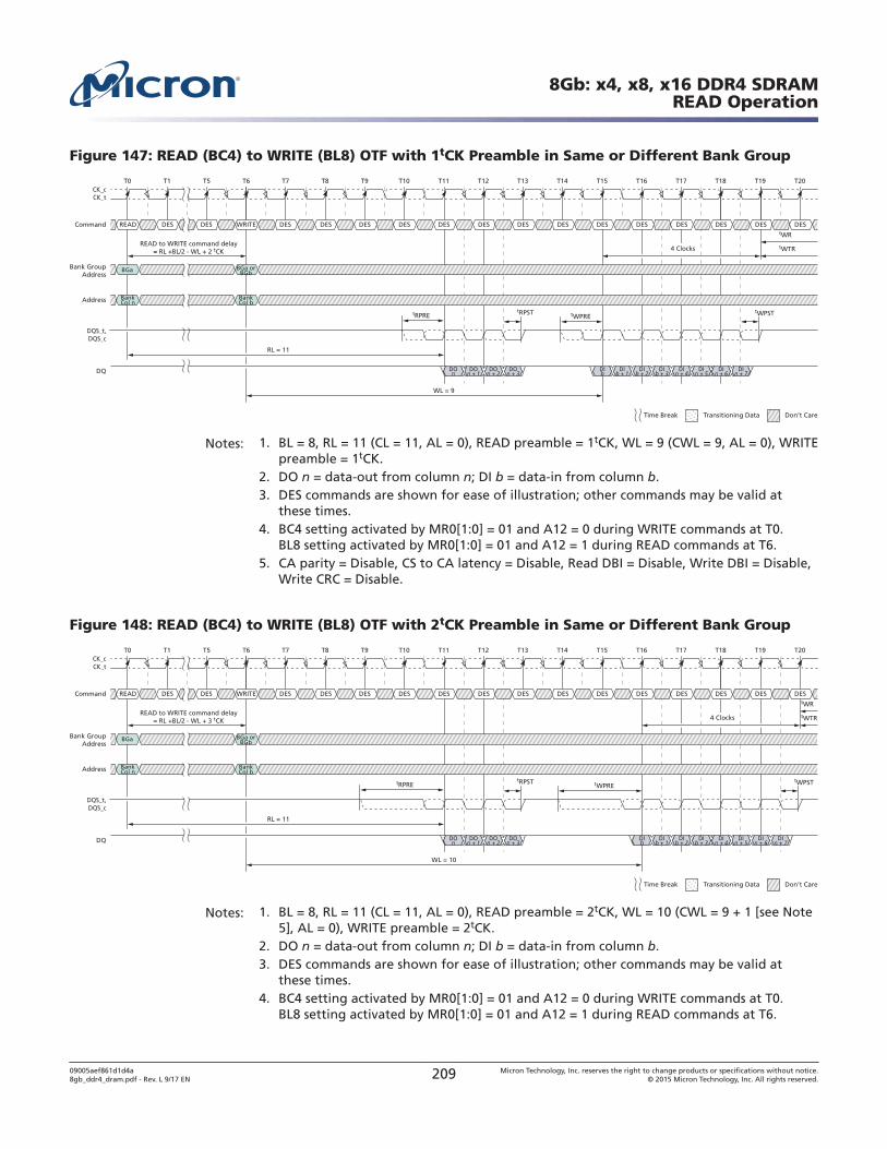
Figure 147: READ (BC4) to WRITE (BL8) OTF with 1tCK Preamble in Same or Different Bank Group
T0
READ to WRITE command delay= RL +BL/2 - WL + 2 tCK
tWPRE
RL = 11
tWPST
T1
DES DES DES DES DES DES DESCommand DESREAD DES WRITE DES DES
DQ
CK_tCK_c
DQS_t,DQS_c
WL = 9
T5 T6 T7 T20T14T8 T9 T10 T11 T12 T13 T19T15 T16 T17 T18
Don’t CareTransitioning DataTime Break
DOn + 1
DOn + 2
DOn + 3
DIn + 4
DIn + 5
DIn + 6
DIn + 7
DIb
DIb + 1
DIb + 2
DIb + 3
DOn
DES DES DES DES DES
Bank GroupAddress
Address BankCol n
BankCol b
BGa BGa orBGb
tRPREtRPST
tWTR
tWR
4 Clocks
Notes: 1. BL = 8, RL = 11 (CL = 11, AL = 0), READ preamble = 1tCK, WL = 9 (CWL = 9, AL = 0), WRITEpreamble = 1tCK.
2. DO n = data-out from column n; DI b = data-in from column b.3. DES commands are shown for ease of illustration; other commands may be valid at
these times.4. BC4 setting activated by MR0[1:0] = 01 and A12 = 0 during WRITE commands at T0.
BL8 setting activated by MR0[1:0] = 01 and A12 = 1 during READ commands at T6.5. CA parity = Disable, CS to CA latency = Disable, Read DBI = Disable, Write DBI = Disable,
Write CRC = Disable.
Figure 148: READ (BC4) to WRITE (BL8) OTF with 2tCK Preamble in Same or Different Bank Group
T0
READ to WRITE command delay= RL +BL/2 - WL + 3 tCK
tWPRE
RL = 11
tWPST
T1
DES DES DES DES DES DES DESCommand DESREAD DES WRITE DES DES
DQ
CK_tCK_c
DQS_t,DQS_c
WL = 10
T5 T6 T7 T20T14T8 T9 T10 T11 T12 T13 T19T15 T16 T17 T18
Don’t CareTransitioning DataTime Break
DOn + 1
DOn + 2
DOn + 3
DIn + 4
DIn + 5
DIn + 6
DIn + 7
DIb
DIb + 1
DIb + 2
DIb + 3
DOn
DES DES DES DES DES
Bank GroupAddress
Address BankCol n
BankCol b
BGa BGa orBGb
tRPREtRPST
tWTR
tWR
4 Clocks
Notes: 1. BL = 8, RL = 11 (CL = 11, AL = 0), READ preamble = 2tCK, WL = 10 (CWL = 9 + 1 [see Note5], AL = 0), WRITE preamble = 2tCK.
2. DO n = data-out from column n; DI b = data-in from column b.3. DES commands are shown for ease of illustration; other commands may be valid at
these times.4. BC4 setting activated by MR0[1:0] = 01 and A12 = 0 during WRITE commands at T0.
BL8 setting activated by MR0[1:0] = 01 and A12 = 1 during READ commands at T6.
8Gb: x4, x8, x16 DDR4 SDRAMREAD Operation
09005aef861d1d4a8gb_ddr4_dram.pdf - Rev. L 9/17 EN 209 Micron Technology, Inc. reserves the right to change products or specifications without notice.
© 2015 Micron Technology, Inc. All rights reserved.
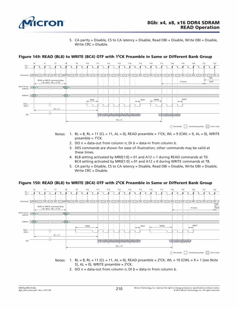
5. CA parity = Disable, CS to CA latency = Disable, Read DBI = Disable, Write DBI = Disable,Write CRC = Disable.
Figure 149: READ (BL8) to WRITE (BC4) OTF with 1tCK Preamble in Same or Different Bank Group
T0
READ to WRITE command delay= RL +BL/2 - WL + 2 tCK 4 Clocks
tRPRE
RL = 11
tRPST
T1
DES DES DES DES DES DES DESCommand DESREAD DES WRITE DES DES
DQ
CK_tCK_c
DQS_t,DQS_c
WL = 9
T22T21T7 T20T14T8 T9 T10 T11 T12 T13 T19T15 T16 T17 T18
Don’t CareTransitioning DataTime Break
DOn + 1
DOn + 2
DOn + 3
DOn + 4
DOn + 5
DOn + 6
DOn + 7
DIb
DIb + 1
DIb + 2
DIb + 3
DOn
DES DES DES DES DES
Bank GroupAddress
Address BankCol n
BankCol b
BGa BGa orBGb
tWPRE tWPST
tWTR
tWR
Notes: 1. BL = 8, RL = 11 (CL = 11, AL = 0), READ preamble = 1tCK, WL = 9 (CWL = 9, AL = 0), WRITEpreamble = 1tCK.
2. DO n = data-out from column n; DI b = data-in from column b.3. DES commands are shown for ease of illustration; other commands may be valid at
these times.4. BL8 setting activated by MR0[1:0] = 01 and A12 = 1 during READ commands at T0.
BC4 setting activated by MR0[1:0] = 01 and A12 = 0 during WRITE commands at T8.5. CA parity = Disable, CS to CA latency = Disable, Read DBI = Disable, Write DBI = Disable,
Write CRC = Disable.
Figure 150: READ (BL8) to WRITE (BC4) OTF with 2tCK Preamble in Same or Different Bank Group
T0
READ to WRITE command delay= RL +BL/2 - WL + 3 tCK 4 Clocks
tRPRE
RL = 11
tRPST
T1
DES DES DES DES DES DES DESCommand DESREAD DES WRITE DES DES
DQ
CK_tCK_c
DQS_t,DQS_c
WL = 10
T22T21T7 T20T14T8 T9 T10 T11 T12 T13 T19T15 T16 T17 T18
Don’t CareTransitioning DataTime Break
DOn + 1
DOn + 2
DOn + 3
DOn + 4
DOn + 5
DOn + 6
DOn + 7
DIb
DIb + 1
DIb + 2
DIb + 3
DOn
DES DES DES DES DES
Bank GroupAddress
Address BankCol n
BankCol b
BGa BGa orBGb
tWPRE tWPST
tWTR
tWR
Notes: 1. BL = 8, RL = 11 (CL = 11, AL = 0), READ preamble = 2tCK, WL = 10 (CWL = 9 + 1 [see Note5], AL = 0), WRITE preamble = 2tCK.
2. DO n = data-out from column n; DI b = data-in from column b.
8Gb: x4, x8, x16 DDR4 SDRAMREAD Operation
09005aef861d1d4a8gb_ddr4_dram.pdf - Rev. L 9/17 EN 210 Micron Technology, Inc. reserves the right to change products or specifications without notice.
© 2015 Micron Technology, Inc. All rights reserved.
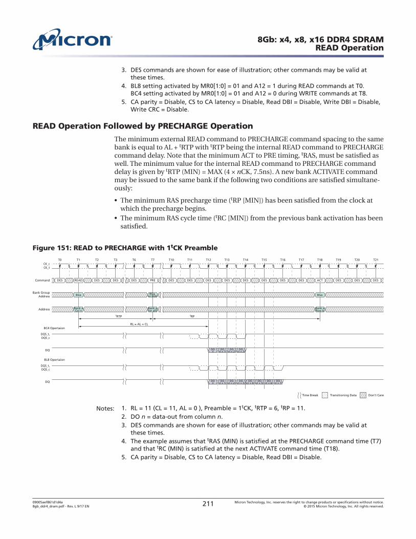
3. DES commands are shown for ease of illustration; other commands may be valid atthese times.
4. BL8 setting activated by MR0[1:0] = 01 and A12 = 1 during READ commands at T0.BC4 setting activated by MR0[1:0] = 01 and A12 = 0 during WRITE commands at T8.
5. CA parity = Disable, CS to CA latency = Disable, Read DBI = Disable, Write DBI = Disable,Write CRC = Disable.
READ Operation Followed by PRECHARGE Operation
The minimum external READ command to PRECHARGE command spacing to the samebank is equal to AL + tRTP with tRTP being the internal READ command to PRECHARGEcommand delay. Note that the minimum ACT to PRE timing, tRAS, must be satisfied aswell. The minimum value for the internal READ command to PRECHARGE commanddelay is given by tRTP (MIN) = MAX (4 × nCK, 7.5ns). A new bank ACTIVATE commandmay be issued to the same bank if the following two conditions are satisfied simultane-ously:
• The minimum RAS precharge time (tRP [MIN]) has been satisfied from the clock atwhich the precharge begins.
• The minimum RAS cycle time (tRC [MIN]) from the previous bank activation has beensatisfied.
Figure 151: READ to PRECHARGE with 1tCK Preamble
T0
RL = AL + CL
tRTP tRP
T1 T2 T3 T6
DES DES DES DES DES DES DESCommand READDES DES DES DES PRE
DQ
BC4 Opertaion
CK_tCK_c
DQS_t,DQS_c
T20 T21T14T7 T10 T11 T12 T13 T19T15 T16 T17 T18
Don’t CareTransitioning DataTime Break
DOn + 1
DOn + 2
DOn + 3
DOn
DES ACT DES DES DES
Bank GroupAddress BGa BGa
or BGb BGa
Address Bank aCol n
Bank a(or all)
Bank aRow b
DQ
BL8 Opertaion
DQS_t,DQS_c
DOn + 1
DOn + 2
DOn + 3
DOn + 4
DOn + 5
DOn + 6
DOn + 7
DOn
Notes: 1. RL = 11 (CL = 11, AL = 0 ), Preamble = 1tCK, tRTP = 6, tRP = 11.2. DO n = data-out from column n.3. DES commands are shown for ease of illustration; other commands may be valid at
these times.4. The example assumes that tRAS (MIN) is satisfied at the PRECHARGE command time (T7)
and that tRC (MIN) is satisfied at the next ACTIVATE command time (T18).5. CA parity = Disable, CS to CA latency = Disable, Read DBI = Disable.
8Gb: x4, x8, x16 DDR4 SDRAMREAD Operation
09005aef861d1d4a8gb_ddr4_dram.pdf - Rev. L 9/17 EN 211 Micron Technology, Inc. reserves the right to change products or specifications without notice.
© 2015 Micron Technology, Inc. All rights reserved.
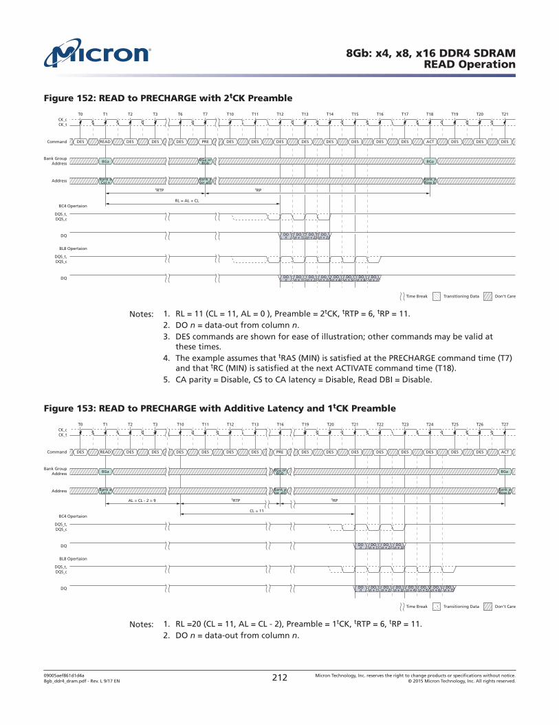
Figure 152: READ to PRECHARGE with 2tCK Preamble
RL = AL + CL
tRTP tRP
DQ
BC4 Opertaion
DQS_t,DQS_c
Don’t CareTransitioning DataTime Break
DOn + 1
DOn + 2
DOn + 3
DOn
DQ
BL8 Opertaion
DQS_t,DQS_c
DOn + 1
DOn + 2
DOn + 3
DOn + 4
DOn + 5
DOn + 6
DOn + 7
DOn
T0 T1 T2 T3 T6
DES DES DES DES DES DES DESCommand READDES DES DES DES PRE
CK_tCK_c
T20 T21T14T7 T10 T11 T12 T13 T19T15 T16 T17 T18
DES ACT DES DES DES
Bank GroupAddress BGa BGaBGa or
BGb
Address Bank aCol n
Bank a(or all)
Bank aRow b
Notes: 1. RL = 11 (CL = 11, AL = 0 ), Preamble = 2tCK, tRTP = 6, tRP = 11.2. DO n = data-out from column n.3. DES commands are shown for ease of illustration; other commands may be valid at
these times.4. The example assumes that tRAS (MIN) is satisfied at the PRECHARGE command time (T7)
and that tRC (MIN) is satisfied at the next ACTIVATE command time (T18).5. CA parity = Disable, CS to CA latency = Disable, Read DBI = Disable.
Figure 153: READ to PRECHARGE with Additive Latency and 1tCK Preamble
T0
CL = 11
AL = CL - 2 = 9 tRTP
T1 T2 T3
DES DES PRE DES DES DES DESCommand READDES DES DES DES DES
DQ
BC4 Opertaion
CK_tCK_c
DQS_t,DQS_c
T26 T27T10 T11 T12 T13 T24 T25T22 T23T21T20T19T16
Don’t CareTransitioning DataTime Break
DOn + 1
DOn + 2
DOn + 3
DOn
DES DES DES DES ACT
Bank GroupAddress BGa BGa or
BGb
tRP
DQ
BL8 Opertaion
DQS_t,DQS_c
DOn + 1
DOn + 2
DOn + 3
DOn + 4
DOn + 5
DOn + 6
DOn + 7
DOn
Address Bank aCol n
Bank a(or all)
Bank aRow b
BGa
Notes: 1. RL =20 (CL = 11, AL = CL - 2), Preamble = 1tCK, tRTP = 6, tRP = 11.2. DO n = data-out from column n.
8Gb: x4, x8, x16 DDR4 SDRAMREAD Operation
09005aef861d1d4a8gb_ddr4_dram.pdf - Rev. L 9/17 EN 212 Micron Technology, Inc. reserves the right to change products or specifications without notice.
© 2015 Micron Technology, Inc. All rights reserved.
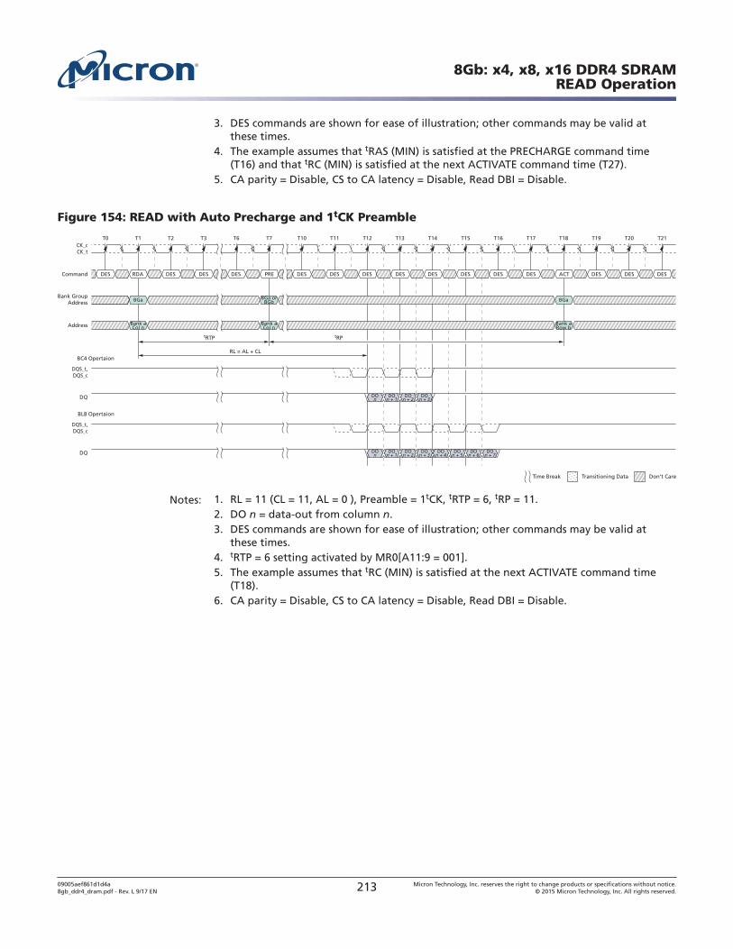
3. DES commands are shown for ease of illustration; other commands may be valid atthese times.
4. The example assumes that tRAS (MIN) is satisfied at the PRECHARGE command time(T16) and that tRC (MIN) is satisfied at the next ACTIVATE command time (T27).
5. CA parity = Disable, CS to CA latency = Disable, Read DBI = Disable.
Figure 154: READ with Auto Precharge and 1tCK Preamble
T0
RL = AL + CL
tRTP tRP
T1 T2 T3 T6
DES DES DES DES DES DES DESCommand RDADES DES DES DES PRE
DQ
BC4 Opertaion
CK_tCK_c
DQS_t,DQS_c
T20 T21T14T7 T10 T11 T12 T13 T19T15 T16 T17 T18
Don’t CareTransitioning DataTime Break
DOn + 1
DOn + 2
DOn + 3
DOn
DES ACT DES DES DES
Bank GroupAddress BGa BGa
Address Bank aCol n
Bank aCol n
BGa orBGb
Bank aRow b
DQ
BL8 Opertaion
DQS_t,DQS_c
DOn + 1
DOn + 2
DOn + 3
DOn + 4
DOn + 5
DOn + 6
DOn + 7
DOn
Notes: 1. RL = 11 (CL = 11, AL = 0 ), Preamble = 1tCK, tRTP = 6, tRP = 11.2. DO n = data-out from column n.3. DES commands are shown for ease of illustration; other commands may be valid at
these times.4. tRTP = 6 setting activated by MR0[A11:9 = 001].5. The example assumes that tRC (MIN) is satisfied at the next ACTIVATE command time
(T18).6. CA parity = Disable, CS to CA latency = Disable, Read DBI = Disable.
8Gb: x4, x8, x16 DDR4 SDRAMREAD Operation
09005aef861d1d4a8gb_ddr4_dram.pdf - Rev. L 9/17 EN 213 Micron Technology, Inc. reserves the right to change products or specifications without notice.
© 2015 Micron Technology, Inc. All rights reserved.
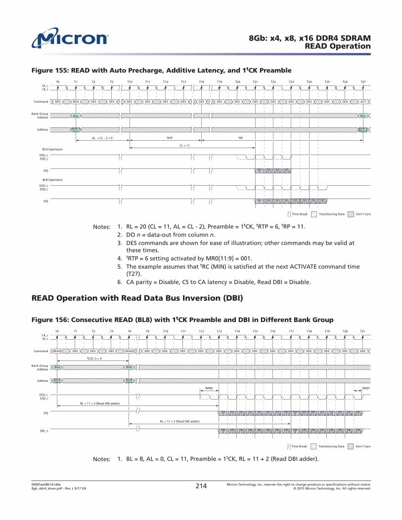
Figure 155: READ with Auto Precharge, Additive Latency, and 1tCK Preamble
T0
CL = 11
AL = CL - 2 = 9 tRTP
T1 T2 T3
DES DES DES DES DES DES DESCommand RDADES DES DES DES DES
DQ
BC4 Opertaion
CK_tCK_c
DQS_t,DQS_c
T26 T27T10 T11 T12 T13 T24 T25T22 T23T21T20T19T16
Don’t CareTransitioning DataTime Break
DOn + 1
DOn + 2
DOn + 3
DOn
DES DES DES DES ACT
Bank GroupAddress BGa BGa
tRP
DQ
BL8 Opertaion
DQS_t,DQS_c
DOn + 1
DOn + 2
DOn + 3
DOn + 4
DOn + 5
DOn + 6
DOn + 7
DOn
Address Bank aCol n
Bank aRow b
Notes: 1. RL = 20 (CL = 11, AL = CL - 2), Preamble = 1tCK, tRTP = 6, tRP = 11.2. DO n = data-out from column n.3. DES commands are shown for ease of illustration; other commands may be valid at
these times.4. tRTP = 6 setting activated by MR0[11:9] = 001.5. The example assumes that tRC (MIN) is satisfied at the next ACTIVATE command time
(T27).6. CA parity = Disable, CS to CA latency = Disable, Read DBI = Disable.
READ Operation with Read Data Bus Inversion (DBI)
Figure 156: Consecutive READ (BL8) with 1tCK Preamble and DBI in Different Bank Group
T0
tCCD_S = 4
tRPRE
RL = 11 + 2 (Read DBI adder)
T16T1 T2 T3 T4 T9 T10 T11 T12 T13 T14 T15
DES DES DES DES DES DES DESCommand DESREAD DES DES READ DES
DQ
CK_tCK_c
DQS_t,DQS_c
RL = 11 + 2 (Read DBI adder)
T21T17 T18 T19 T20
Don’t CareTransitioning DataTime Break
DOn + 1
DOn + 2
DOn + 3
DOb + 1
DOb + 2
DOb + 7
DOn
DES DES DES DES DES
Bank GroupAddress
BGa BGb
Address BankCol n
BankCol b
tRPST
DOn + 4
DOn + 5
DOn + 6
DOn + 7
DOb
DOb + 5
DOb + 6
DOb + 3
DOb +4 _
DBI_n DBIn + 1
DBIn + 2
DBIn + 3
DBIb + 1
DBIb + 2
DBIb + 7
DBIn
DBIn + 4
DBIn + 5
DBIn + 6
DBIn + 7
DBIb
DBIb + 5
DBIb + 6
DBIb + 3
DBIb + 4
Notes: 1. BL = 8, AL = 0, CL = 11, Preamble = 1tCK, RL = 11 + 2 (Read DBI adder).
8Gb: x4, x8, x16 DDR4 SDRAMREAD Operation
09005aef861d1d4a8gb_ddr4_dram.pdf - Rev. L 9/17 EN 214 Micron Technology, Inc. reserves the right to change products or specifications without notice.
© 2015 Micron Technology, Inc. All rights reserved.
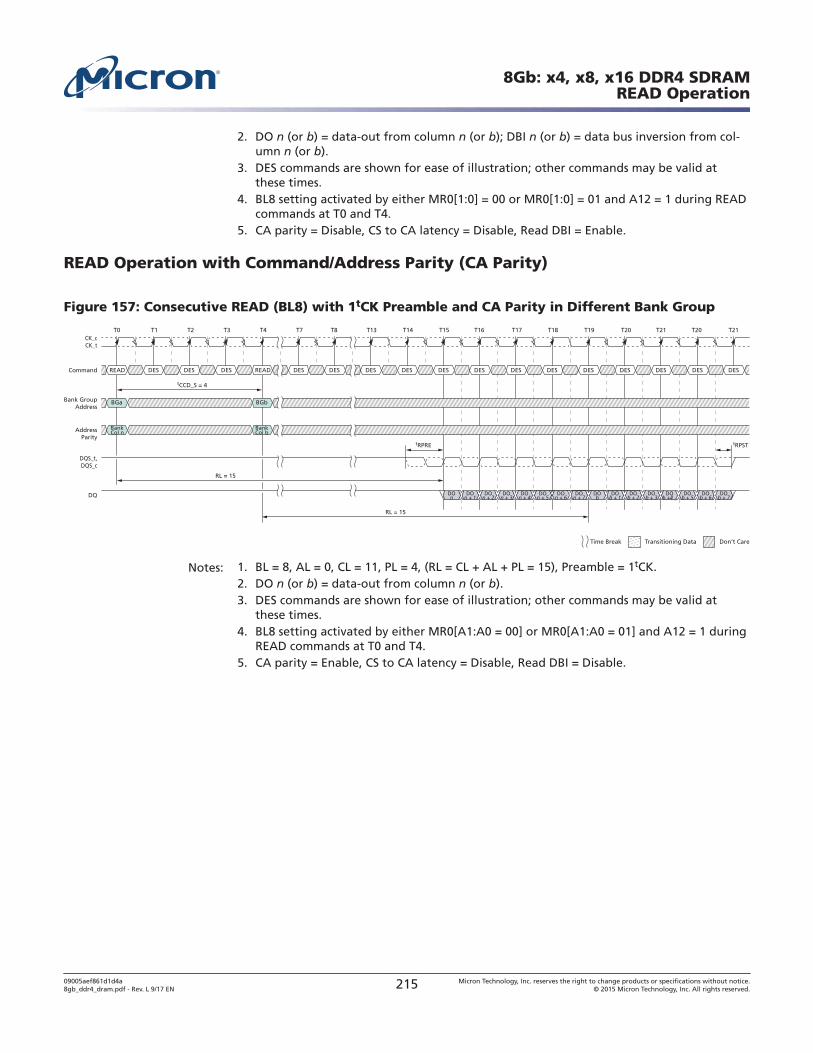
2. DO n (or b) = data-out from column n (or b); DBI n (or b) = data bus inversion from col-umn n (or b).
3. DES commands are shown for ease of illustration; other commands may be valid atthese times.
4. BL8 setting activated by either MR0[1:0] = 00 or MR0[1:0] = 01 and A12 = 1 during READcommands at T0 and T4.
5. CA parity = Disable, CS to CA latency = Disable, Read DBI = Enable.
READ Operation with Command/Address Parity (CA Parity)
Figure 157: Consecutive READ (BL8) with 1tCK Preamble and CA Parity in Different Bank Group
T0
tCCD_S = 4
tRPRE
RL = 15
T1 T2 T3 T4 T7 T8
DES DES DES DES DES DES DESCommand DESREAD DES DES READ DES
DQ
CK_tCK_c
DQS_t,DQS_c
RL = 15
T16T13 T14 T15 T21T17 T18 T19 T20 T21T20
Don’t CareTransitioning DataTime Break
DOn + 1
DOn + 2
DOn + 3
DOb + 1
DOb + 2
DOb + 7
DOn
DES DES DES DES DES
Bank GroupAddress
BGa BGb
AddressParity
BankCol n
BankCol b
tRPST
DOn + 4
DOn + 5
DOn + 6
DOn + 7
DOb
DOb + 5
DOb + 6
DOb + 3
DOb +4 _
Notes: 1. BL = 8, AL = 0, CL = 11, PL = 4, (RL = CL + AL + PL = 15), Preamble = 1tCK.2. DO n (or b) = data-out from column n (or b).3. DES commands are shown for ease of illustration; other commands may be valid at
these times.4. BL8 setting activated by either MR0[A1:A0 = 00] or MR0[A1:A0 = 01] and A12 = 1 during
READ commands at T0 and T4.5. CA parity = Enable, CS to CA latency = Disable, Read DBI = Disable.
8Gb: x4, x8, x16 DDR4 SDRAMREAD Operation
09005aef861d1d4a8gb_ddr4_dram.pdf - Rev. L 9/17 EN 215 Micron Technology, Inc. reserves the right to change products or specifications without notice.
© 2015 Micron Technology, Inc. All rights reserved.
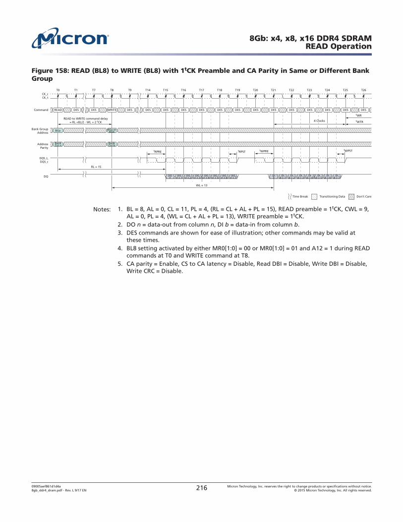
Figure 158: READ (BL8) to WRITE (BL8) with 1tCK Preamble and CA Parity in Same or Different BankGroup
T0
READ to WRITE command delay= RL +BL/2 - WL + 2 tCK 4 Clocks
tRPRE
RL = 15
tRPST
T1 T7 T8 T9
DES DES DES DES DES DES DESCommand DESREAD DES WRITE DES DES
DQ
CK_tCK_c
DQS_t,DQS_c
WL = 13
T22T16T14 T15 T21T17 T18 T19 T20 T25 T26T24T23
Don’t CareTransitioning DataTime Break
DOn + 1
DOn + 2
DOn + 3
DOn + 4
DOn + 5
DOn + 6
DOn + 7
DIb
DIb + 1
DIb + 2
DIb + 3
DIb + 4
DIb + 5
DIb + 6
DIb + 7
DOn
DES DES DES DES DES
Bank GroupAddress
AddressParity
BankCol n
BankCol b
BGa BGa orBGb
tWPRE tWPST
tWTR
tWR
Notes: 1. BL = 8, AL = 0, CL = 11, PL = 4, (RL = CL + AL + PL = 15), READ preamble = 1tCK, CWL = 9,AL = 0, PL = 4, (WL = CL + AL + PL = 13), WRITE preamble = 1tCK.
2. DO n = data-out from column n, DI b = data-in from column b.3. DES commands are shown for ease of illustration; other commands may be valid at
these times.4. BL8 setting activated by either MR0[1:0] = 00 or MR0[1:0] = 01 and A12 = 1 during READ
commands at T0 and WRITE command at T8.5. CA parity = Enable, CS to CA latency = Disable, Read DBI = Disable, Write DBI = Disable,
Write CRC = Disable.
8Gb: x4, x8, x16 DDR4 SDRAMREAD Operation
09005aef861d1d4a8gb_ddr4_dram.pdf - Rev. L 9/17 EN 216 Micron Technology, Inc. reserves the right to change products or specifications without notice.
© 2015 Micron Technology, Inc. All rights reserved.
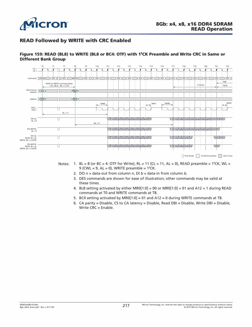
READ Followed by WRITE with CRC Enabled
Figure 159: READ (BL8) to WRITE (BL8 or BC4: OTF) with 1tCK Preamble and Write CRC in Same orDifferent Bank Group
T0
READ to WRITE command delay= RL +BL/2 - WL + 2 tCK 4 Clocks
tRPRE
RL = 11
tRPST
T1 T7 T8 T9 T10 T11 T12 T13
DES DES DES DES DES DES DESCommand DESREAD DES WRITE DES DES
DQ x4,BL = 8
CK_tCK_c
DQS_t,DQS_c
WL = 9
T22T16T14 T15 T21T17 T18 T19 T20
Don’t CareTransitioning DataTime Break
DOn + 1
DOn + 2
DOn + 3
DOn + 4
DOn + 5
DOn + 6
DOn + 7
DIb
DIb + 1
DIb + 2
DIb + 3
DIb + 4
DIb + 5
DIb + 6
DIb + 7 CRC CRCDO
n
DES DES DES DES DES
Bank GroupAddress
Address BankCol n
BankCol b
BGa BGa orBGb
DQ x8/X16,BL = 8
DOn + 1
DOn + 2
DOn + 3
DOn + 4
DOn + 5
DOn + 6
DOn + 7
DIb
DIb + 1
DIb + 2
DIb + 3
DIb + 4
DIb + 5
DIb + 6
DIb + 7 CRCDO
n
DQ x4,READ: BL = 8,
WRITE: BC = 4 (OTF)
DQ x8/X16,READ: BL = 8,
WRITE: BC = 4 (OTF)
DOn + 1
DOn + 2
DOn + 3
DOn + 4
DOn + 5
DOn + 6
DOn + 7
DIb
DIb + 1
DIb + 2 CRC CRCDO
n
tWPRE tWPST
tWTR
tWR
DOn + 1
DOn + 2
DOn + 3
DOn + 4
DOn + 5
DOn + 6
DOn + 7
DIb
DIb + 1
DIb + 2
DIb + 3 CRCDO
n
DIb + 3
Notes: 1. BL = 8 (or BC = 4: OTF for Write), RL = 11 (CL = 11, AL = 0), READ preamble = 1tCK, WL =9 (CWL = 9, AL = 0), WRITE preamble = 1tCK.
2. DO n = data-out from column n, DI b = data-in from column b.3. DES commands are shown for ease of illustration; other commands may be valid at
these times.4. BL8 setting activated by either MR0[1:0] = 00 or MR0[1:0] = 01 and A12 = 1 during READ
commands at T0 and WRITE commands at T8.5. BC4 setting activated by MR0[1:0] = 01 and A12 = 0 during WRITE commands at T8.6. CA parity = Disable, CS to CA latency = Disable, Read DBI = Disable, Write DBI = Disable,
Write CRC = Enable.
8Gb: x4, x8, x16 DDR4 SDRAMREAD Operation
09005aef861d1d4a8gb_ddr4_dram.pdf - Rev. L 9/17 EN 217 Micron Technology, Inc. reserves the right to change products or specifications without notice.
© 2015 Micron Technology, Inc. All rights reserved.
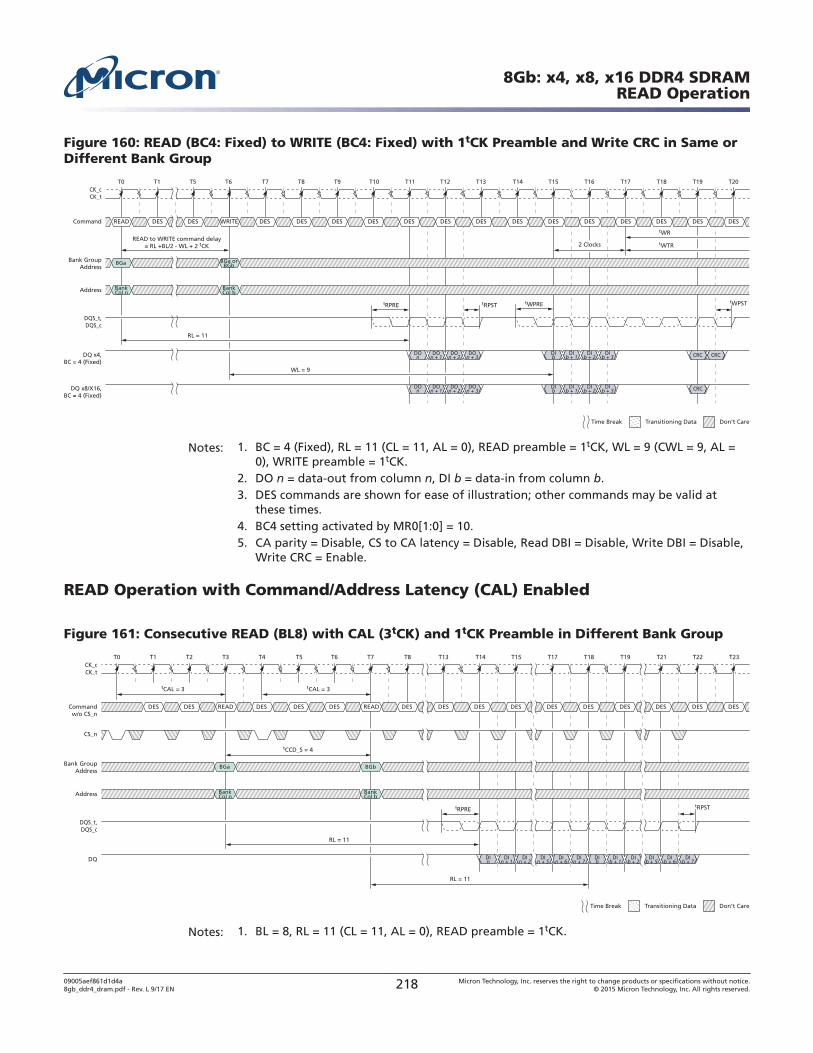
Figure 160: READ (BC4: Fixed) to WRITE (BC4: Fixed) with 1tCK Preamble and Write CRC in Same orDifferent Bank Group
T0
READ to WRITE command delay= RL +BL/2 - WL + 2 tCK 2 Clocks
tRPRE
RL = 11
tRPST
T1 T7T6T5 T8 T9 T10 T11 T12 T13
DES DES DES DES DES DES DESCommand DESREAD DES WRITE DES DES
DQ x4,BC = 4 (Fixed)
CK_tCK_c
DQS_t,DQS_c
WL = 9
T16T14 T15 T17 T18 T19 T20
Don’t CareTransitioning DataTime Break
DOn + 1
DOn + 2
DOn + 3
DIb
DIb + 1
DIb + 2
DIb + 3 CRC CRCDO
n
DES DES DES DES DES
Bank GroupAddress
Address BankCol n
BankCol b
BGa BGa orBGb
DQ x8/X16,BC = 4 (Fixed)
DOn + 1
DOn + 2
DOn + 3
DIb
DIb + 1
DIb + 2
DIb + 3 CRCDO
n
tWPRE tWPST
tWTR
tWR
Notes: 1. BC = 4 (Fixed), RL = 11 (CL = 11, AL = 0), READ preamble = 1tCK, WL = 9 (CWL = 9, AL =0), WRITE preamble = 1tCK.
2. DO n = data-out from column n, DI b = data-in from column b.3. DES commands are shown for ease of illustration; other commands may be valid at
these times.4. BC4 setting activated by MR0[1:0] = 10.5. CA parity = Disable, CS to CA latency = Disable, Read DBI = Disable, Write DBI = Disable,
Write CRC = Enable.
READ Operation with Command/Address Latency (CAL) Enabled
Figure 161: Consecutive READ (BL8) with CAL (3tCK) and 1tCK Preamble in Different Bank Group
T0
tCAL = 3 tCAL = 3
tCCD_S = 4
tRPRE
RL = 11
T1 T2 T3 T4
DES DES DES DES DES DESCommandw/o CS_n
DES DES READ READDES DES
DQ
CK_tCK_c
DQS_t,DQS_c
RL = 11
T5 T6 T7 T8 T22 T23T13 T17T14 T15 T18 T19 T21
Don’t CareTransitioning DataTime Break
DIn + 1
DIn + 2
DIn + 5
DIn + 6
DIn + 7
DIb
DIb + 1
DIb + 2
DIb + 5
DIb + 6
DIb + 7
DIn
DES DES DES DES DES
Bank GroupAddress
Address BankCol n
BankCol b
BGa BGb
tRPST
CS_n
Notes: 1. BL = 8, RL = 11 (CL = 11, AL = 0), READ preamble = 1tCK.
8Gb: x4, x8, x16 DDR4 SDRAMREAD Operation
09005aef861d1d4a8gb_ddr4_dram.pdf - Rev. L 9/17 EN 218 Micron Technology, Inc. reserves the right to change products or specifications without notice.
© 2015 Micron Technology, Inc. All rights reserved.
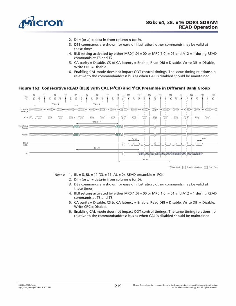
2. DI n (or b) = data-in from column n (or b).3. DES commands are shown for ease of illustration; other commands may be valid at
these times.4. BL8 setting activated by either MR0[1:0] = 00 or MR0[1:0] = 01 and A12 = 1 during READ
commands at T3 and T7.5. CA parity = Disable, CS to CA latency = Enable, Read DBI = Disable, Write DBI = Disable,
Write CRC = Disable.6. Enabling CAL mode does not impact ODT control timings. The same timing relationship
relative to the command/address bus as when CAL is disabled should be maintained.
Figure 162: Consecutive READ (BL8) with CAL (4tCK) and 1tCK Preamble in Different Bank Group
T0
tCAL = 4 tCAL = 4
tCCD_S = 4
tRPRE
RL = 11
T1 T2 T3 T4
DES DES DES DES DES DESCommandw/o CS_n
DES DES READ READDES DES
DQ
CK_tCK_c
DQS_t,DQS_c
RL = 11
T5 T6 T7 T8 T24T22 T23T16T14 T15 T18 T19 T21
Don’t CareTransitioning DataTime Break
DIn + 1
DIn + 2
DIn + 5
DIn + 6
DIn + 7
DIb
DIb + 1
DIb + 2
DIb + 5
DIb + 6
DIb + 7
DIn
DES DES DES DES DES
Bank GroupAddress
Address BankCol n
BankCol b
BGa BGb
tRPST
CS_n
Notes: 1. BL = 8, RL = 11 (CL = 11, AL = 0), READ preamble = 1tCK.2. DI n (or b) = data-in from column n (or b).3. DES commands are shown for ease of illustration; other commands may be valid at
these times.4. BL8 setting activated by either MR0[1:0] = 00 or MR0[1:0] = 01 and A12 = 1 during READ
commands at T3 and T8.5. CA parity = Disable, CS to CA latency = Enable, Read DBI = Disable, Write DBI = Disable,
Write CRC = Disable.6. Enabling CAL mode does not impact ODT control timings. The same timing relationship
relative to the command/address bus as when CAL is disabled should be maintained.
8Gb: x4, x8, x16 DDR4 SDRAMREAD Operation
09005aef861d1d4a8gb_ddr4_dram.pdf - Rev. L 9/17 EN 219 Micron Technology, Inc. reserves the right to change products or specifications without notice.
© 2015 Micron Technology, Inc. All rights reserved.
WRITE Operation
Write Timing Definitions
The write timings shown in the following figures are applicable in normal operationmode, that is, when the DLL is enabled and locked.
Write Timing – Clock-to-Data Strobe Relationship
The clock-to-data strobe relationship is shown below and is applicable in normal oper-ation mode, that is, when the DLL is enabled and locked.
Rising data strobe edge parameters:
• tDQSS (MIN) to tDQSS (MAX) describes the allowed range for a rising data strobe edgerelative to CK.
• tDQSS is the actual position of a rising strobe edge relative to CK.• tDQSH describes the data strobe high pulse width.• tWPST strobe going to HIGH, nondrive level (shown in the postamble section of the
graphic below).
Falling data strobe edge parameters:
• tDQSL describes the data strobe low pulse width.• tWPRE strobe going to LOW, initial drive level (shown in the preamble section of the
graphic below).
8Gb: x4, x8, x16 DDR4 SDRAMWRITE Operation
09005aef861d1d4a8gb_ddr4_dram.pdf - Rev. L 9/17 EN 220 Micron Technology, Inc. reserves the right to change products or specifications without notice.
© 2015 Micron Technology, Inc. All rights reserved.
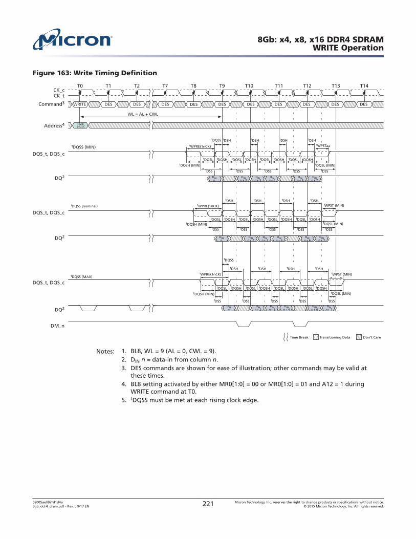
Figure 163: Write Timing Definition
WL = AL + CWL
T0 T1 T2 T7 T8 T9 T10 T11 T12 T13 T14
Don’t CareTime Break Transitioning Data
Bank,Col n
DESWRITE DESDES DES DES DES DES DES DES DES
CK_tCK_c
Command3
DQ2
DQS_t, DQS_c
DQS_t, DQS_c
DQS_t, DQS_c
Address4
tWPSTaa
DM_n
tWPST (MIN)
tDQSL
tDQSS (MIN)
DINn
DINn + 2
DINn + 3DQ2
DQ2
tDQSS (MAX)
tDQSS (nominal)
tDQSL
tWPRE(1nCK)
tDQSL
tDQSS
tDQSS
tDSS tDSS tDSS tDSS tDSS
tDSH tDSH tDSH tDSH
tDSS tDSS tDSS tDSS tDSS
tDSS tDSS tDSS tDSS tDSS
tDSH tDSH tDSH tDSH
tDSH tDSH tDSH tDSH
tDQSLtDQSH tDQSLtDQSH tDQSLtDQSH tDQSH
tDQSLtDQSH tDQSLtDQSH tDQSLtDQSH tDQSH
tDQSLtDQSH tDQSLtDQSH tDQSLtDQSH tDQSH
tWPRE(1nCK)
tWPRE(1nCK)
tDQSH (MIN)
tDQSH (MIN)
tDQSH (MIN)
tWPST (MIN)
tDQSL (MIN)
tDQSL (MIN)
tDQSL (MIN)
DINn + 4
DINn + 6
DINn + 7
DINn
DINn + 2
DINn + 3
DINn + 4
DINn + 6
DINn + 7
DINn
DINn + 2
DINn + 3
DINn + 4
DINn + 6
DINn + 7
Notes: 1. BL8, WL = 9 (AL = 0, CWL = 9).2. DIN n = data-in from column n.3. DES commands are shown for ease of illustration; other commands may be valid at
these times.4. BL8 setting activated by either MR0[1:0] = 00 or MR0[1:0] = 01 and A12 = 1 during
WRITE command at T0.5. tDQSS must be met at each rising clock edge.
8Gb: x4, x8, x16 DDR4 SDRAMWRITE Operation
09005aef861d1d4a8gb_ddr4_dram.pdf - Rev. L 9/17 EN 221 Micron Technology, Inc. reserves the right to change products or specifications without notice.
© 2015 Micron Technology, Inc. All rights reserved.
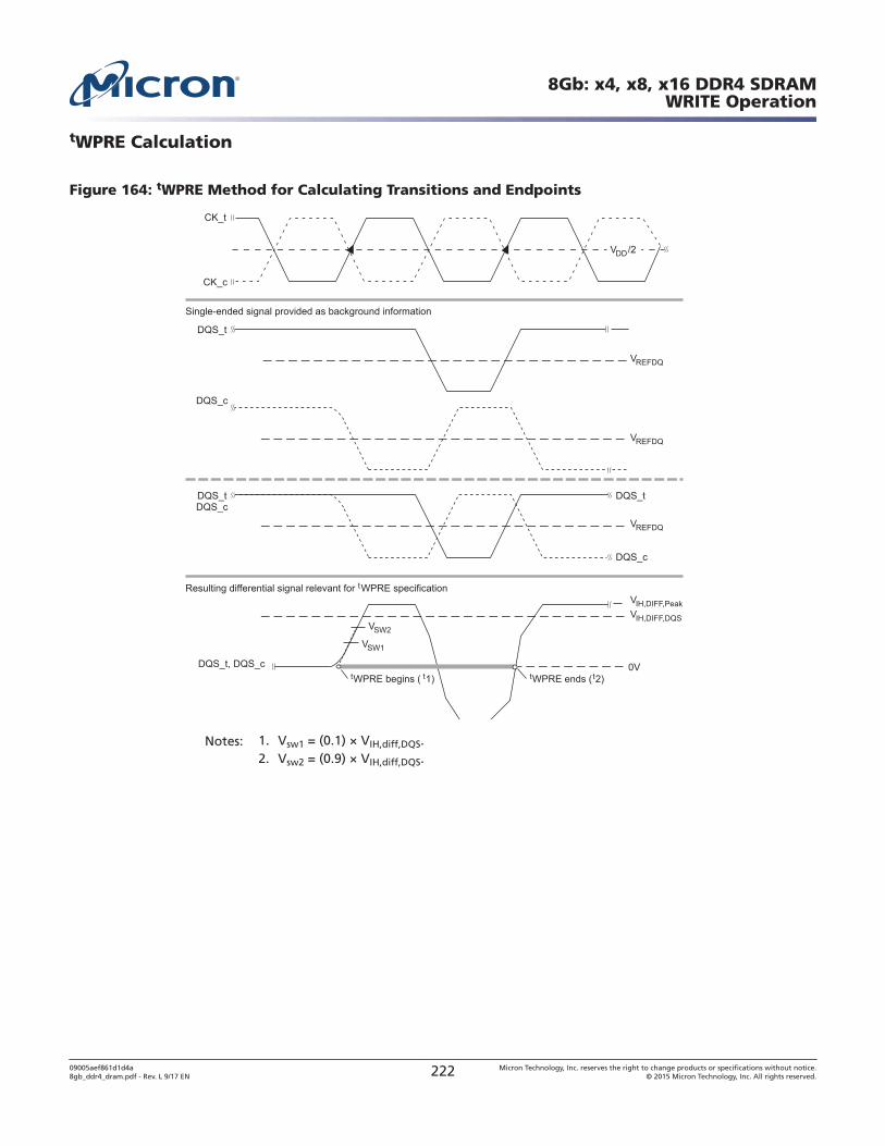
tWPRE Calculation
Figure 164: tWPRE Method for Calculating Transitions and Endpoints
Notes: 1. Vsw1 = (0.1) × VIH,diff,DQS.2. Vsw2 = (0.9) × VIH,diff,DQS.
8Gb: x4, x8, x16 DDR4 SDRAMWRITE Operation
09005aef861d1d4a8gb_ddr4_dram.pdf - Rev. L 9/17 EN 222 Micron Technology, Inc. reserves the right to change products or specifications without notice.
© 2015 Micron Technology, Inc. All rights reserved.
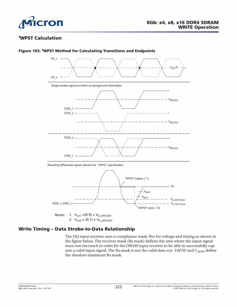
tWPST Calculation
Figure 165: tWPST Method for Calculating Transitions and Endpoints
Notes: 1. Vsw1 =(0.9) × VIL,diff,DQS.2. Vsw2 = (0.1) × VIL,diff,DQS.
Write Timing – Data Strobe-to-Data Relationship
The DQ input receiver uses a compliance mask (Rx) for voltage and timing as shown inthe figure below. The receiver mask (Rx mask) defines the area where the input signalmust not encroach in order for the DRAM input receiver to be able to successfully cap-ture a valid input signal. The Rx mask is not the valid data-eye. TdiVW and V diVW definethe absolute maximum Rx mask.
8Gb: x4, x8, x16 DDR4 SDRAMWRITE Operation
09005aef861d1d4a8gb_ddr4_dram.pdf - Rev. L 9/17 EN 223 Micron Technology, Inc. reserves the right to change products or specifications without notice.
© 2015 Micron Technology, Inc. All rights reserved.
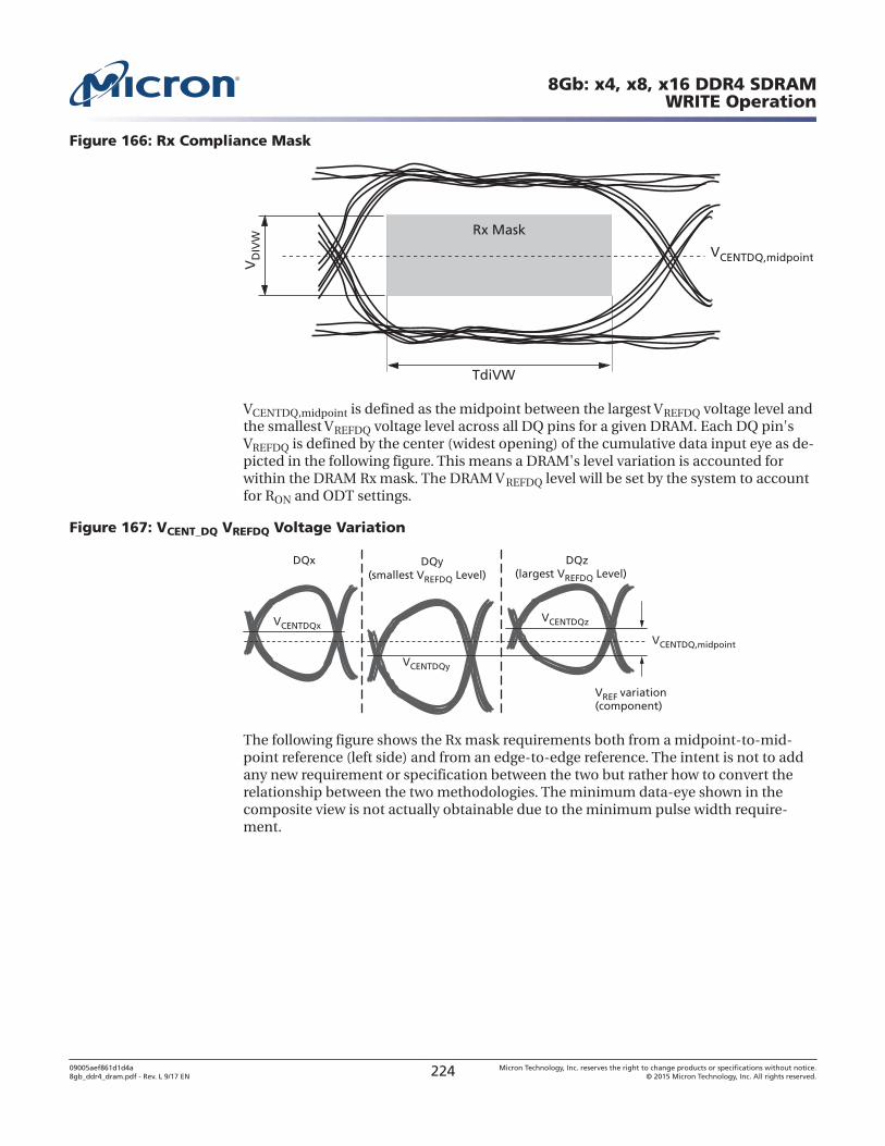
Figure 166: Rx Compliance Mask
TdiVW
VD
IVW
Rx Mask
VCENTDQ,midpoint
VCENTDQ,midpoint is defined as the midpoint between the largest VREFDQ voltage level andthe smallest VREFDQ voltage level across all DQ pins for a given DRAM. Each DQ pin'sVREFDQ is defined by the center (widest opening) of the cumulative data input eye as de-picted in the following figure. This means a DRAM's level variation is accounted forwithin the DRAM Rx mask. The DRAM VREFDQ level will be set by the system to accountfor RON and ODT settings.
Figure 167: VCENT_DQ VREFDQ Voltage Variation
VCENTDQx
VCENTDQy
VCENTDQz
VCENTDQ,midpoint
DQx DQy (smallest VREFDQ Level)
DQz (largest VREFDQ Level)
VREF variation(component)
The following figure shows the Rx mask requirements both from a midpoint-to-mid-point reference (left side) and from an edge-to-edge reference. The intent is not to addany new requirement or specification between the two but rather how to convert therelationship between the two methodologies. The minimum data-eye shown in thecomposite view is not actually obtainable due to the minimum pulse width require-ment.
8Gb: x4, x8, x16 DDR4 SDRAMWRITE Operation
09005aef861d1d4a8gb_ddr4_dram.pdf - Rev. L 9/17 EN 224 Micron Technology, Inc. reserves the right to change products or specifications without notice.
© 2015 Micron Technology, Inc. All rights reserved.
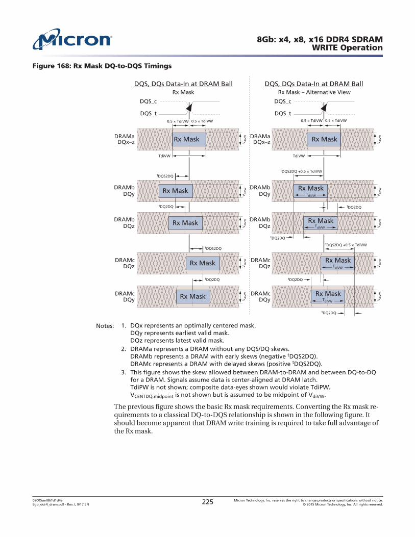
Figure 168: Rx Mask DQ-to-DQS Timings
DQS, DQs Data-In at DRAM BallDQS, DQs Data-In at DRAM BallRx Mask Rx Mask – Alternative View
Rx Mask
Rx Mask
Rx Mask
Rx Mask
DQS_t
Rx Mask
0.5 × TdiVW0.5 × TdiVW
tDQS2DQ +0.5 × TdiVW
tDQS2DQ +0.5 × TdiVW
DQyDRAMc Rx Mask
DQzDRAMc Rx Mask
DQzDRAMb Rx Mask
DQyDRAMb Rx Mask
DQS_cDQS_c
DQS_t
DQx–zDRAMa
DQyDRAMc
DQzDRAMc
DQzDRAMb
DQyDRAMb
DQx–zDRAMaRx Mask
TdiVW TdiVW
0.5 × TdiVW0.5 × TdiVW
tDQS2DQ
tDQ2DQ
tDQ2DQ
tDQ2DQ
tDQ2DQ
tDQ2DQ
tDQS2DQ
tDQ2DQ
Vd
iVW
Vd
iVW
Vd
iVW
Vd
iVW
Vd
iVW
Vd
iVW
Vd
iVW
Vd
iVW
Vd
iVW
Vd
iVW
TdiVW
TdiVW
TdiVW
TdiVW
Notes: 1. DQx represents an optimally centered mask.DQy represents earliest valid mask.DQz represents latest valid mask.
2. DRAMa represents a DRAM without any DQS/DQ skews.DRAMb represents a DRAM with early skews (negative tDQS2DQ).DRAMc represents a DRAM with delayed skews (positive tDQS2DQ).
3. This figure shows the skew allowed between DRAM-to-DRAM and between DQ-to-DQfor a DRAM. Signals assume data is center-aligned at DRAM latch.TdiPW is not shown; composite data-eyes shown would violate TdiPW.VCENTDQ,midpoint is not shown but is assumed to be midpoint of VdiVW.
The previous figure shows the basic Rx mask requirements. Converting the Rx mask re-quirements to a classical DQ-to-DQS relationship is shown in the following figure. Itshould become apparent that DRAM write training is required to take full advantage ofthe Rx mask.
8Gb: x4, x8, x16 DDR4 SDRAMWRITE Operation
09005aef861d1d4a8gb_ddr4_dram.pdf - Rev. L 9/17 EN 225 Micron Technology, Inc. reserves the right to change products or specifications without notice.
© 2015 Micron Technology, Inc. All rights reserved.
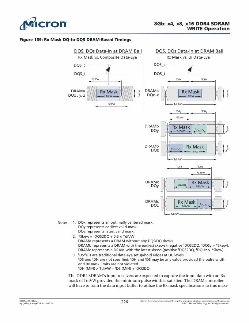
Figure 169: Rx Mask DQ-to-DQS DRAM-Based Timings
DQS_c
DQS_t
Rx Mask
DQS, DQs Data-In at DRAM Ball
Vd
iVW
Vd
iVW
Vd
iVW
Vd
iVW
Vd
iVW
Vd
iVW
DQx , y, z
DQS_c
DQS_t
Rx Mask
DQS, DQs Data-In at DRAM Ball
tDSx tDHx
DQx–zDRAMaDRAMa
DRAMb
DRAMb
DRAMc
DRAMc
TdiPW
TdiPW
Rx Mask vs. Composite Data-Eye Rx Mask vs. UI Data-Eye
TdiPW
*Skew
*Skew
tDSy tDHy
DQyRx Mask
TdiVWtDQ2DQ
DQz
TdiPW
TdiVW TdiVW
tDSz tDHz
DQy tDQ2DQ
DQz
TdiPW
Rx MaskTdiVW
tDQ2DQ
Rx MaskTdiVW
Rx MaskTdiVW
tDQ2DQ
Notes: 1. DQx represents an optimally centered mask.DQy represents earliest valid mask.DQz represents latest valid mask.
2. *Skew = tDQS2DQ + 0.5 × TdiVWDRAMa represents a DRAM without any DQS/DQ skews.DRAMb represents a DRAM with the earliest skews (negative tDQS2DQ, tDQSy > *Skew).DRAMc represents a DRAM with the latest skews (positive tDQS2DQ, tDQHz > *Skew).
3. tDS/tDH are traditional data-eye setup/hold edges at DC levels.tDS and tDH are not specified; tDH and tDS may be any value provided the pulse widthand Rx mask limits are not violated.tDH (MIN) > TdiVW + tDS (MIN) + tDQ2DQ.
The DDR4 SDRAM's input receivers are expected to capture the input data with an Rxmask of TdiVW provided the minimum pulse width is satisfied. The DRAM controllerwill have to train the data input buffer to utilize the Rx mask specifications to this maxi-
8Gb: x4, x8, x16 DDR4 SDRAMWRITE Operation
09005aef861d1d4a8gb_ddr4_dram.pdf - Rev. L 9/17 EN 226 Micron Technology, Inc. reserves the right to change products or specifications without notice.
© 2015 Micron Technology, Inc. All rights reserved.
mum benefit. If the DRAM controller does not train the data input buffers, then theworst case limits have to be used for the Rx mask (TdiVW + 2 × tDQS2DQ), which willgenerally be the classical minimum ( tDS and tDH) and is required as well.
Figure 170: Example of Data Input Requirements Without Training
tDS
Vd
iVW
0.5 × VdiVW
0.5 × VdiVW
tDH
0.5 × TdiVW + tDQS2DQ
TdiVW + 2 × tDQS2DQ
0.5 × TdiVW + tDQS2DQ
VCENTDQ,midpoint
VIL(DC)
VIH(DC)
DQS_c
DQS_t
Rx Mask
WRITE Burst Operation
The following write timing diagrams are intended to help understand each write pa-rameter's meaning and are only examples. Each parameter will be defined in detail sep-arately. In these write timing diagrams, CK and DQS are shown aligned, and DQS andDQ are shown center-aligned for the purpose of illustration.
DDR4 WRITE command supports bursts of BL8 (fixed), BC4 (fixed), and BL8/BC4 on-the-fly (OTF); OTF uses address A12 to control OTF when OTF is enabled:
• A12 = 0, BC4 (BC4 = burst chop)• A12 = 1, BL8
WRITE commands can issue precharge automatically with a WRITE with auto pre-charge (WRA) command, which is enabled by A10 HIGH.
• WRITE command with A10 = 0 (WR) performs standard write, bank remains active af-ter WRITE burst
• WRITE command with A10 = 1 (WRA) performs write with auto precharge, bank goesinto precharge after WRITE burst
The DATA MASK (DM) function is supported for the x8 and x16 configurations only (theDM function is not supported on x4 devices). The DM function shares a common pinwith the DBI_n and TDQS functions. The DM function only applies to WRITE opera-tions and cannot be enabled at the same time the DBI function is enabled.
• If DM_n is sampled LOW on a given byte lane, the DRAM masks the write data re-ceived on the DQ inputs.
8Gb: x4, x8, x16 DDR4 SDRAMWRITE Operation
09005aef861d1d4a8gb_ddr4_dram.pdf - Rev. L 9/17 EN 227 Micron Technology, Inc. reserves the right to change products or specifications without notice.
© 2015 Micron Technology, Inc. All rights reserved.
• If DM_n is sampled HIGH on a given byte lane, the DRAM does not mask the data andwrites this data into the DRAM core.
• If CRC write is enabled, then DM enabled (via MRS) will be selected between writeCRC nonpersistent mode (DM disabled) and write CRC persistent mode (DM ena-bled).
Figure 171: WRITE Burst Operation, WL = 9 (AL = 0, CWL = 9, BL8)
T0
tWPRE
T1 T7T2 T8 T9 T10 T11 T12 T13
DES DES DES DES DES DES DESCommand DESWRITE DES DES DES DES
DQ
CK_tCK_c
DQS_t,DQS_c
WL = AL + CWL = 9
T16T14 T15
Don’t CareTransitioning DataTime Break
DIn + 1
DIn + 2
DIn + 3
DIn + 4
DIn + 5
DIn + 6
DIn + 7
DIn
Bank GroupAddress
Address BankCol n
BGa
tWPST
Notes: 1. BL8, WL = 0, AL = 0, CWL = 9, Preamble = 1tCK.2. DI n = Data-in from column n.3. DES commands are shown for ease of illustration; other commands may be valid at
these times.4. BL8 setting activated by either MR0[1:0] = 00 or MR0[1:0] = 01 and A12 = 1 during
WRITE command at T0.5. CA parity = Disable, CS to CA atency = Disable, Read DBI = Disable.
8Gb: x4, x8, x16 DDR4 SDRAMWRITE Operation
09005aef861d1d4a8gb_ddr4_dram.pdf - Rev. L 9/17 EN 228 Micron Technology, Inc. reserves the right to change products or specifications without notice.
© 2015 Micron Technology, Inc. All rights reserved.
Figure 172: WRITE Burst Operation, WL = 19 (AL = 10, CWL = 9, BL8)
T0
tWPRE
AL = 10 CWL = 9
T1 T2 T9 T10 T11
DES DES DES DES DES DES DESCommand DESWRITE DES DES DES DES
DQ
CK_tCK_c
DQS_t,DQS_c
WL = AL + CWL = 19
T21T17 T18 T19 T20 T23T22
Don’t CareTransitioning DataTime Break
DIn
DIn + 1
DIn + 2
DIn + 3
DIn + 4
DIn + 5
DIn + 6
DIn + 7
Bank GroupAddress
Address BankCol n
BGa
tWPST
Notes: 1. BL8, WL = 19, AL = 10 (CL - 1), CWL = 9, Preamble = 1tCK.2. DI n = data-in from column n.3. DES commands are shown for ease of illustration; other commands may be valid at
these times.4. BL8 setting activated by either MR0[1:0] = 00 or MR0[1:0] = 01 and A12 = 1 during
WRITE command at T0.5. CA parity = Disable, CS to CA latency = Disable, Read DBI = Disable.
WRITE Operation Followed by Another WRITE Operation
Figure 173: Consecutive WRITE (BL8) with 1tCK Preamble in Different Bank Group
T0
tCCD_S = 4 4 Clocks
tWPRE
WL = AL + CWL = 9
T1 T2 T3 T4
DES DES DES DES DES DES DESCommand DESWRITE DES DES WRITE DES
DQ
CK_tCK_c
DQS_t,DQS_c
WL = AL + CWL = 9
T7 T8 T9 T10 T11 T12 T13 T16T14 T15 T17 T18 T19
Don’t CareTransitioning DataTime Break
DIn + 1
DIn + 2
DIn + 3
DIn + 4
DIn + 5
DIn + 6
DIn + 7
DIb
DIb + 1
DIb + 2
DIb + 3
DIb + 4
DIb + 5
DIb + 6
DIb + 7
DIn
DES DES DES DES DES
Bank GroupAddress
Address BankCol n
BankCol b
BGa BGb
tWPST
tWTR
tWR
Notes: 1. BL8, AL = 0, CWL = 9, Preamble = 1tCK.2. DI n (or b) = data-in from column n (or column b).
8Gb: x4, x8, x16 DDR4 SDRAMWRITE Operation
09005aef861d1d4a8gb_ddr4_dram.pdf - Rev. L 9/17 EN 229 Micron Technology, Inc. reserves the right to change products or specifications without notice.
© 2015 Micron Technology, Inc. All rights reserved.
3. DES commands are shown for ease of illustration; other commands may be valid atthese times.
4. BL8 setting activated by either MR0[1:0] = 00 or MR0[1:0] = 01 and A12 = 1 duringWRITE commands at T0 and T4.
5. CA parity = Disable, CS to CA latency = Disable, Write DBI = Disable, Write CRC = Disable.6. The write recovery time (tWR) and write timing parameter (tWTR) are referenced from
the first rising clock edge after the last write data shown at T17.
Figure 174: Consecutive WRITE (BL8) with 2tCK Preamble in Different Bank Group
T0
tCCD_S = 4 4 Clocks
tWPRE
WL = AL + CWL = 10
T1 T2 T3 T4
DES DES DES DES DES DES DESCommand DESWRITE DES DES WRITE DES
DQ
CK_tCK_c
DQS_t,DQS_c
WL = AL + CWL = 10
T7 T8 T9 T10 T11 T12 T13 T16T14 T15 T17 T18 T19
Don’t CareTransitioning DataTime Break
DIn + 1
DIn + 2
DIn + 3
DIn + 4
DIn + 5
DIn + 6
DIn + 7
DIb
DIb + 1
DIb + 2
DIb + 3
DIb + 4
DIb + 5
DIb + 6
DIb + 7
DIn
DES DES DES DES DES
Bank GroupAddress
Address BankCol n
BankCol b
BGa BGb
tWPST
tWTR
tWR
Notes: 1. BL8, AL = 0, CWL = 9 + 1 = 10 (see Note 7), Preamble = 2tCK.2. DI n (or b) = data-in from column n (or column b).3. DES commands are shown for ease of illustration; other commands may be valid at
these times.4. BL8 setting activated by either MR0[1:0] = 00 or MR0[1:0] = 01 and A12 = 1 during
WRITE commands at T0 and T4.5. CA parity = Disable, CS to CA latency = Disable, Write DBI = Disable, Write CRC = Disable.6. The write recovery time (tWR) and write timing parameter (tWTR) are referenced from
the first rising clock edge after the last write data shown at T17.7. When operating in 2tCK WRITE preamble mode, CWL may need to be programmed to a
value at least 1 clock greater than the lowest CWL setting supported in the applicabletCK range, which means CWL = 9 is not allowed when operating in 2tCK WRITE pream-ble mode.
8Gb: x4, x8, x16 DDR4 SDRAMWRITE Operation
09005aef861d1d4a8gb_ddr4_dram.pdf - Rev. L 9/17 EN 230 Micron Technology, Inc. reserves the right to change products or specifications without notice.
© 2015 Micron Technology, Inc. All rights reserved.
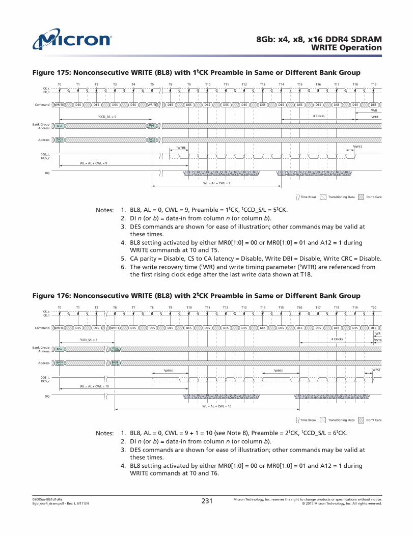
Figure 175: Nonconsecutive WRITE (BL8) with 1tCK Preamble in Same or Different Bank Group
T0
tCCD_S/L = 5 4 Clocks
tWPRE
WL = AL + CWL = 9
T1 T2 T3 T4
DES DES DES DES DES DES DESCommand DESWRITE DES DES DES WRITE
DQ
CK_tCK_c
DQS_t,DQS_c
WL = AL + CWL = 9
T5 T8 T9 T10 T11 T12 T13 T16T14 T15 T17 T18 T19
Don’t CareTransitioning DataTime Break
DIn + 1
DIn + 2
DIn + 3
DIn + 4
DIn + 5
DIn + 6
DIn + 7
DIb
DIb + 1
DIb + 2
DIb + 3
DIb + 4
DIb + 5
DIb + 6
DIb + 7
DIn
DES DES DES DES DES
Bank GroupAddress
Address BankCol n
BankCol b
BGa BGaor BGb
tWPST
tWTR
tWR
Notes: 1. BL8, AL = 0, CWL = 9, Preamble = 1tCK, tCCD_S/L = 5tCK.2. DI n (or b) = data-in from column n (or column b).3. DES commands are shown for ease of illustration; other commands may be valid at
these times.4. BL8 setting activated by either MR0[1:0] = 00 or MR0[1:0] = 01 and A12 = 1 during
WRITE commands at T0 and T5.5. CA parity = Disable, CS to CA latency = Disable, Write DBI = Disable, Write CRC = Disable.6. The write recovery time (tWR) and write timing parameter (tWTR) are referenced from
the first rising clock edge after the last write data shown at T18.
Figure 176: Nonconsecutive WRITE (BL8) with 2tCK Preamble in Same or Different Bank Group
T0
tCCD_S/L = 6 4 Clocks
tWPRE
WL = AL + CWL = 10
T1 T2 T6 T7
DES DES DES DES DES DES DESCommand DESWRITE DES WRITE DES DES
DQ
CK_tCK_c
DQS_t,DQS_c
WL = AL + CWL = 10
T8 T9 T10 T11 T12 T13 T16T14 T15 T17 T18 T20T19
Don’t CareTransitioning DataTime Break
DIn + 1
DIn + 2
DIn + 3
DIn + 4
DIn + 5
DIn + 6
DIn + 7
DIb
DIb + 1
DIb + 2
DIb + 3
DIb + 4
DIb + 5
DIb + 6
DIb + 7
DIn
DES DES DES DES DES
Bank GroupAddress
Address BankCol n
BankCol b
BGa BGaor BGb
tWPREtWPST
tWTR
tWR
Notes: 1. BL8, AL = 0, CWL = 9 + 1 = 10 (see Note 8), Preamble = 2tCK, tCCD_S/L = 6tCK.2. DI n (or b) = data-in from column n (or column b).3. DES commands are shown for ease of illustration; other commands may be valid at
these times.4. BL8 setting activated by either MR0[1:0] = 00 or MR0[1:0] = 01 and A12 = 1 during
WRITE commands at T0 and T6.
8Gb: x4, x8, x16 DDR4 SDRAMWRITE Operation
09005aef861d1d4a8gb_ddr4_dram.pdf - Rev. L 9/17 EN 231 Micron Technology, Inc. reserves the right to change products or specifications without notice.
© 2015 Micron Technology, Inc. All rights reserved.
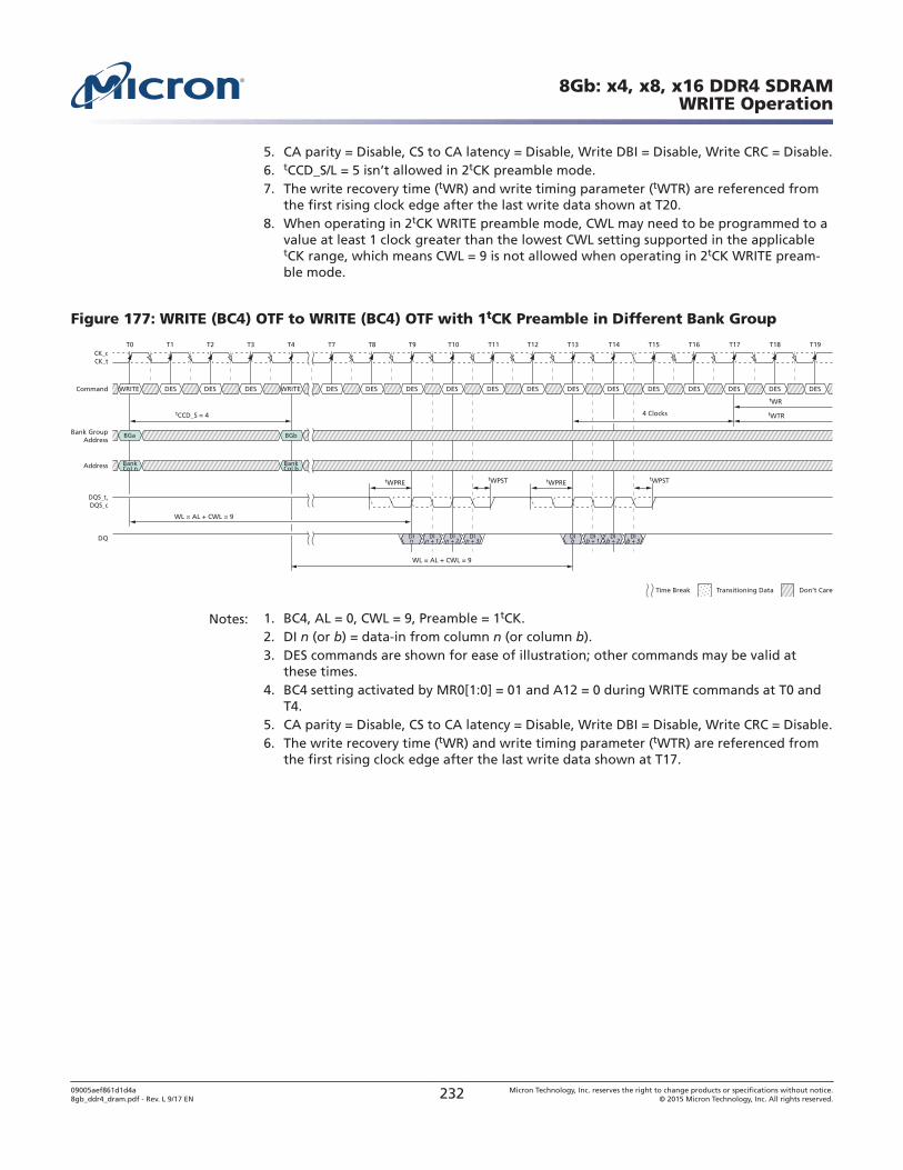
5. CA parity = Disable, CS to CA latency = Disable, Write DBI = Disable, Write CRC = Disable.6. tCCD_S/L = 5 isn’t allowed in 2tCK preamble mode.7. The write recovery time (tWR) and write timing parameter (tWTR) are referenced from
the first rising clock edge after the last write data shown at T20.8. When operating in 2tCK WRITE preamble mode, CWL may need to be programmed to a
value at least 1 clock greater than the lowest CWL setting supported in the applicabletCK range, which means CWL = 9 is not allowed when operating in 2tCK WRITE pream-ble mode.
Figure 177: WRITE (BC4) OTF to WRITE (BC4) OTF with 1tCK Preamble in Different Bank Group
T0
tCCD_S = 4 4 Clocks
tWPRE
WL = AL + CWL = 9
T1 T2 T3 T4
DES DES DES DES DES DES DESCommand DESWRITE DES DES WRITE DES
DQ
CK_tCK_c
DQS_t,DQS_c
WL = AL + CWL = 9
T7 T8 T9 T10 T11 T12 T13 T16T14 T15 T17 T18 T19
Don’t CareTransitioning DataTime Break
DIn + 1
DIn + 2
DIn + 3
DIb
DIb + 1
DIb + 2
DIb + 3
DIn
DES DES DES DES DES
Bank GroupAddress
Address BankCol n
BankCol b
BGa BGb
tWPRE
tWTR
tWR
tWPSTtWPST
Notes: 1. BC4, AL = 0, CWL = 9, Preamble = 1tCK.2. DI n (or b) = data-in from column n (or column b).3. DES commands are shown for ease of illustration; other commands may be valid at
these times.4. BC4 setting activated by MR0[1:0] = 01 and A12 = 0 during WRITE commands at T0 and
T4.5. CA parity = Disable, CS to CA latency = Disable, Write DBI = Disable, Write CRC = Disable.6. The write recovery time (tWR) and write timing parameter (tWTR) are referenced from
the first rising clock edge after the last write data shown at T17.
8Gb: x4, x8, x16 DDR4 SDRAMWRITE Operation
09005aef861d1d4a8gb_ddr4_dram.pdf - Rev. L 9/17 EN 232 Micron Technology, Inc. reserves the right to change products or specifications without notice.
© 2015 Micron Technology, Inc. All rights reserved.
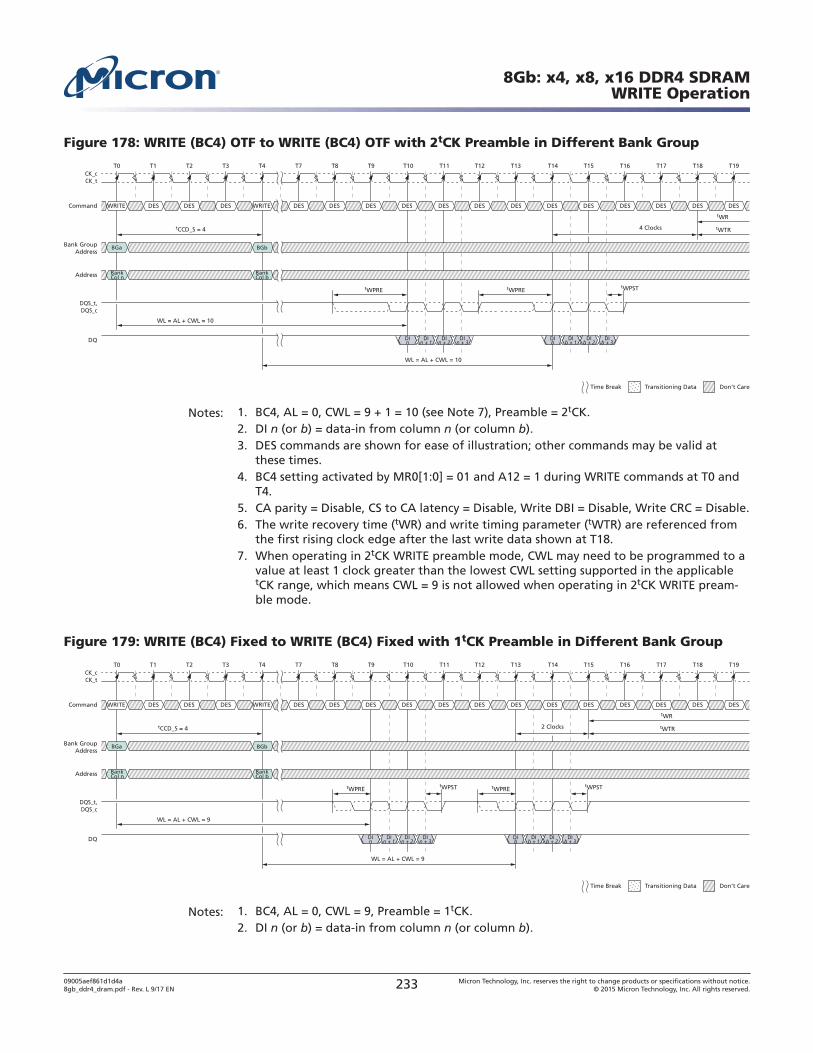
Figure 178: WRITE (BC4) OTF to WRITE (BC4) OTF with 2tCK Preamble in Different Bank Group
T0
tCCD_S = 4 4 Clocks
tWPRE
WL = AL + CWL = 10
T1 T2 T3 T4
DES DES DES DES DES DES DESCommand DESWRITE DES DES WRITE DES
DQ
CK_tCK_c
DQS_t,DQS_c
WL = AL + CWL = 10
T7 T8 T9 T10 T11 T12 T13 T16T14 T15 T17 T18 T19
Don’t CareTransitioning DataTime Break
DIn + 1
DIn + 2
DIn + 3
DIb
DIb + 1
DIb + 2
DIb + 3
DIn
DES DES DES DES DES
Bank GroupAddress
Address BankCol n
BankCol b
BGa BGb
tWPRE
tWTR
tWR
tWPST
Notes: 1. BC4, AL = 0, CWL = 9 + 1 = 10 (see Note 7), Preamble = 2tCK.2. DI n (or b) = data-in from column n (or column b).3. DES commands are shown for ease of illustration; other commands may be valid at
these times.4. BC4 setting activated by MR0[1:0] = 01 and A12 = 1 during WRITE commands at T0 and
T4.5. CA parity = Disable, CS to CA latency = Disable, Write DBI = Disable, Write CRC = Disable.6. The write recovery time (tWR) and write timing parameter (tWTR) are referenced from
the first rising clock edge after the last write data shown at T18.7. When operating in 2tCK WRITE preamble mode, CWL may need to be programmed to a
value at least 1 clock greater than the lowest CWL setting supported in the applicabletCK range, which means CWL = 9 is not allowed when operating in 2tCK WRITE pream-ble mode.
Figure 179: WRITE (BC4) Fixed to WRITE (BC4) Fixed with 1tCK Preamble in Different Bank Group
T0
tCCD_S = 4 2 Clocks
tWPRE
WL = AL + CWL = 9
T1 T2 T3 T4
DES DES DES DES DES DES DESCommand DESWRITE DES DES WRITE DES
DQ
CK_tCK_c
DQS_t,DQS_c
WL = AL + CWL = 9
T7 T8 T9 T10 T11 T12 T13 T16T14 T15 T17 T18 T19
Don’t CareTransitioning DataTime Break
DIn + 1
DIn + 2
DIn + 3
DIb
DIb + 1
DIb + 2
DIb + 3
DIn
DES DES DES DES DES
Bank GroupAddress
Address BankCol n
BankCol b
BGa BGb
tWPRE
tWTR
tWR
tWPSTtWPST
Notes: 1. BC4, AL = 0, CWL = 9, Preamble = 1tCK.2. DI n (or b) = data-in from column n (or column b).
8Gb: x4, x8, x16 DDR4 SDRAMWRITE Operation
09005aef861d1d4a8gb_ddr4_dram.pdf - Rev. L 9/17 EN 233 Micron Technology, Inc. reserves the right to change products or specifications without notice.
© 2015 Micron Technology, Inc. All rights reserved.
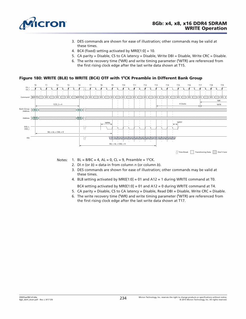
3. DES commands are shown for ease of illustration; other commands may be valid atthese times.
4. BC4 (fixed) setting activated by MR0[1:0] = 10.5. CA parity = Disable, CS to CA latency = Disable, Write DBI = Disable, Write CRC = Disable.6. The write recovery time (tWR) and write timing parameter (tWTR) are referenced from
the first rising clock edge after the last write data shown at T15.
Figure 180: WRITE (BL8) to WRITE (BC4) OTF with 1tCK Preamble in Different Bank Group
T0
tCCD_S = 4 4 Clocks
tWPRE
WL = AL + CWL = 9
T1 T2 T3 T4
DES DES DES DES DES DES DESCommand DESWRITE DES DES WRITE DES
DQ
CK_tCK_c
DQS_t,DQS_c
WL = AL + CWL = 9
T7 T8 T9 T10 T11 T12 T13 T16T14 T15 T17 T18 T19
Don’t CareTransitioning DataTime Break
DIn + 1
DIn + 2
DIn + 3
DIn + 4
DIn + 5
DIn + 6
DIn + 7
DIb
DIb + 1
DIb + 2
DIb + 3
DIn
DES DES DES DES DES
Bank GroupAddress
Address BankCol n
BankCol b
BGa BGb
tWTR
tWR
tWPST
Notes: 1. BL = 8/BC = 4, AL = 0, CL = 9, Preamble = 1tCK.2. DI n (or b) = data-in from column n (or column b).3. DES commands are shown for ease of illustration; other commands may be valid at
these times.4. BL8 setting activated by MR0[1:0] = 01 and A12 = 1 during WRITE command at T0.
BC4 setting activated by MR0[1:0] = 01 and A12 = 0 during WRITE command at T4.5. CA parity = Disable, CS to CA latency = Disable, Read DBI = Disable, Write CRC = Disable.6. The write recovery time (tWR) and write timing parameter (tWTR) are referenced from
the first rising clock edge after the last write data shown at T17.
8Gb: x4, x8, x16 DDR4 SDRAMWRITE Operation
09005aef861d1d4a8gb_ddr4_dram.pdf - Rev. L 9/17 EN 234 Micron Technology, Inc. reserves the right to change products or specifications without notice.
© 2015 Micron Technology, Inc. All rights reserved.
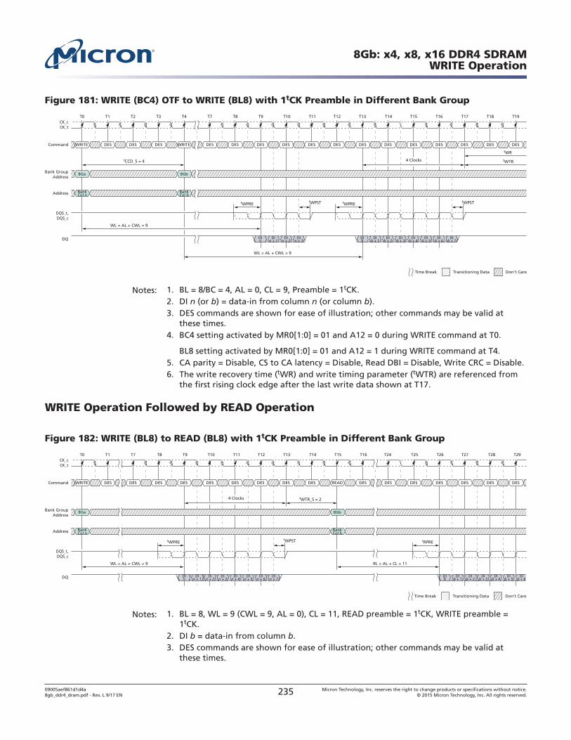
Figure 181: WRITE (BC4) OTF to WRITE (BL8) with 1tCK Preamble in Different Bank Group
T0
tCCD_S = 4
tWPRE tWPRE
WL = AL + CWL = 9
T1 T2 T3 T4
DES DES DES DES DES DES DESCommand DESWRITE DES DES WRITE DES
DQ
CK_tCK_c
DQS_t,DQS_c
WL = AL + CWL = 9
T7 T8 T9 T10 T11 T12 T13 T16T14 T15 T17 T18 T19
Don’t CareTransitioning DataTime Break
DIn + 1
DIn + 2
DIn + 3
DIb
DIb + 1
DIb + 2
DIb + 3
DIb + 4
DIb + 5
DIb + 6
DIb + 7
DIn
DES DES DES DES DES
Bank GroupAddress
Address BankCol n
BankCol b
BGa BGb
tWTR
tWR
tWPSTtWPST
4 Clocks
Notes: 1. BL = 8/BC = 4, AL = 0, CL = 9, Preamble = 1tCK.2. DI n (or b) = data-in from column n (or column b).3. DES commands are shown for ease of illustration; other commands may be valid at
these times.4. BC4 setting activated by MR0[1:0] = 01 and A12 = 0 during WRITE command at T0.
BL8 setting activated by MR0[1:0] = 01 and A12 = 1 during WRITE command at T4.5. CA parity = Disable, CS to CA latency = Disable, Read DBI = Disable, Write CRC = Disable.6. The write recovery time (tWR) and write timing parameter (tWTR) are referenced from
the first rising clock edge after the last write data shown at T17.
WRITE Operation Followed by READ Operation
Figure 182: WRITE (BL8) to READ (BL8) with 1tCK Preamble in Different Bank Group
DIb
DIb + 1
DIb + 2
DIb + 3
DIb + 4
DIb + 5
DIb + 6
T0
tWTR_S = 2
tWPRE
WL = AL + CWL = 9 RL = AL + CL = 11
T1 T7
DES DES DES DES READ DES DESCommand DESWRITE DES DES DES DES
DQ
CK_tCK_c
DQS_t,DQS_c
T8 T9 T10 T11 T12 T13 T16T14 T15 T24 T25 T26 T27 T28 T29
Don’t CareTransitioning DataTime Break
DIn + 1
DIn + 2
DIn + 3
DIn + 4
DIn + 5
DIn + 6
DIn + 7
DIn
DES DES DES DES DES
Bank GroupAddress
Address BankCol n
BankCol b
BGa BGb
tRPREtWPST
4 Clocks
Notes: 1. BL = 8, WL = 9 (CWL = 9, AL = 0), CL = 11, READ preamble = 1tCK, WRITE preamble =1tCK.
2. DI b = data-in from column b.3. DES commands are shown for ease of illustration; other commands may be valid at
these times.
8Gb: x4, x8, x16 DDR4 SDRAMWRITE Operation
09005aef861d1d4a8gb_ddr4_dram.pdf - Rev. L 9/17 EN 235 Micron Technology, Inc. reserves the right to change products or specifications without notice.
© 2015 Micron Technology, Inc. All rights reserved.
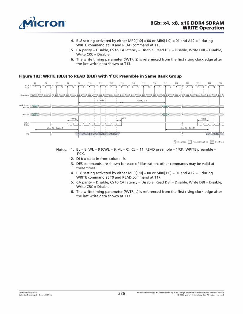
4. BL8 setting activated by either MR0[1:0] = 00 or MR0[1:0] = 01 and A12 = 1 duringWRITE command at T0 and READ command at T15.
5. CA parity = Disable, CS to CA latency = Disable, Read DBI = Disable, Write DBI = Disable,Write CRC = Disable.
6. The write timing parameter (tWTR_S) is referenced from the first rising clock edge afterthe last write data shown at T13.
Figure 183: WRITE (BL8) to READ (BL8) with 1tCK Preamble in Same Bank Group
T0
tWTR_L = 4
tWPRE
WL = AL + CWL = 9 RL = AL + CL = 11
T1 T7
DES DES DES DES DES DESDESCommand DESWRITE DES DES DES READ
DQ
CK_tCK_c
DQS_t,DQS_c
T8 T9 T10 T11 T12 T13 T16T14 T15 T17 T18 T26 T27 T28 T29
Don’t CareTransitioning DataTime Break
DIn + 1
DIn + 2
DIn + 3
DIn + 4
DIn + 5
DIn + 6
DIn + 7
DIn
DES DES DES DES DES
Bank GroupAddress
Address BankCol n
BankCol b
BGa BGa
tRPREtWPST
DIb
DIb + 1
DIb + 2
4 Clocks
Notes: 1. BL = 8, WL = 9 (CWL = 9, AL = 0), CL = 11, READ preamble = 1tCK, WRITE preamble =1tCK.
2. DI b = data-in from column b.3. DES commands are shown for ease of illustration; other commands may be valid at
these times.4. BL8 setting activated by either MR0[1:0] = 00 or MR0[1:0] = 01 and A12 = 1 during
WRITE command at T0 and READ command at T17.5. CA parity = Disable, CS to CA latency = Disable, Read DBI = Disable, Write DBI = Disable,
Write CRC = Disable.6. The write timing parameter (tWTR_L) is referenced from the first rising clock edge after
the last write data shown at T13.
8Gb: x4, x8, x16 DDR4 SDRAMWRITE Operation
09005aef861d1d4a8gb_ddr4_dram.pdf - Rev. L 9/17 EN 236 Micron Technology, Inc. reserves the right to change products or specifications without notice.
© 2015 Micron Technology, Inc. All rights reserved.
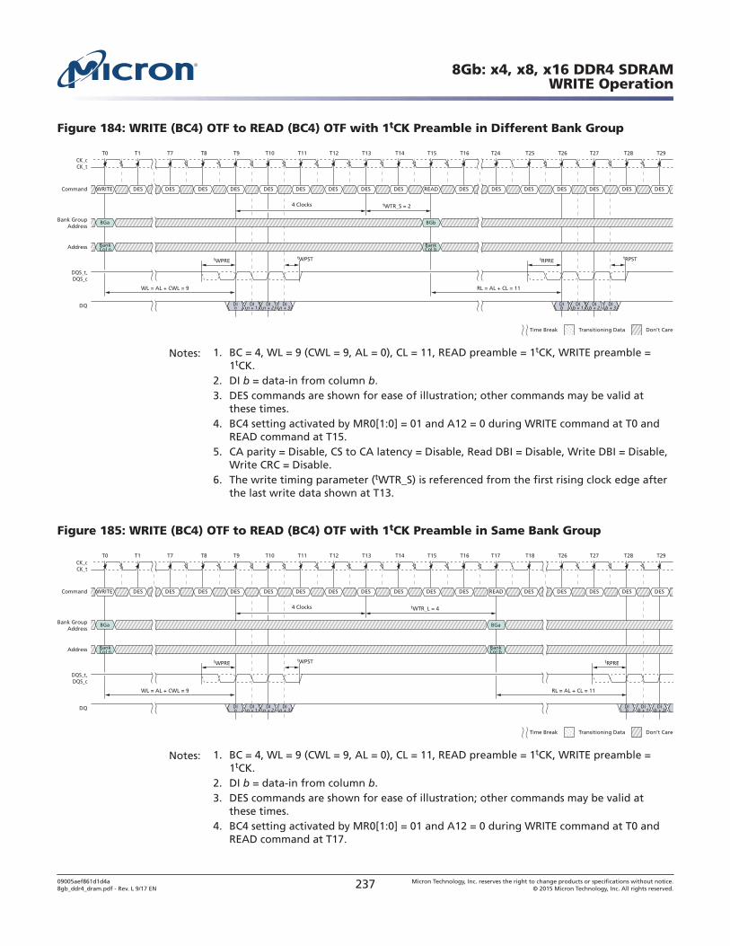
Figure 184: WRITE (BC4) OTF to READ (BC4) OTF with 1tCK Preamble in Different Bank Group
T0
tWTR_S = 2
tWPRE
WL = AL + CWL = 9 RL = AL + CL = 11
T1 T7
DES DES DES DES READ DES DESCommand DESWRITE DES DES DES DES
DQ
CK_tCK_c
DQS_t,DQS_c
T8 T9 T10 T11 T12 T13 T16T14 T15 T24 T25 T26 T27 T28 T29
Don’t CareTransitioning DataTime Break
DIn + 1
DIn + 2
DIn + 3
DIn
DES DES DES DES DES
Bank GroupAddress
Address BankCol n
BankCol b
BGa BGb
tRPREtWPST tRPST
DIb
DIb + 1
DIb + 2
DIb + 3
4 Clocks
Notes: 1. BC = 4, WL = 9 (CWL = 9, AL = 0), CL = 11, READ preamble = 1tCK, WRITE preamble =1tCK.
2. DI b = data-in from column b.3. DES commands are shown for ease of illustration; other commands may be valid at
these times.4. BC4 setting activated by MR0[1:0] = 01 and A12 = 0 during WRITE command at T0 and
READ command at T15.5. CA parity = Disable, CS to CA latency = Disable, Read DBI = Disable, Write DBI = Disable,
Write CRC = Disable.6. The write timing parameter (tWTR_S) is referenced from the first rising clock edge after
the last write data shown at T13.
Figure 185: WRITE (BC4) OTF to READ (BC4) OTF with 1tCK Preamble in Same Bank Group
T0
tWTR_L = 4
tWPRE
WL = AL + CWL = 9 RL = AL + CL = 11
T1 T7
DES DES DES DES DES DES READCommand DESWRITE DES DES DES DES
DQ
CK_tCK_c
DQS_t,DQS_c
T8 T9 T10 T11 T12 T13 T16T14 T15 T17 T18 T26 T27 T28 T29
Don’t CareTransitioning DataTime Break
DIn + 1
DIn + 2
DIn + 3
DIn
DES DES DES DES DES
Bank GroupAddress
Address BankCol n
BankCol b
BGa BGa
tRPREtWPST
DIb
DIb + 1
DIb + 2
4 Clocks
Notes: 1. BC = 4, WL = 9 (CWL = 9, AL = 0), CL = 11, READ preamble = 1tCK, WRITE preamble =1tCK.
2. DI b = data-in from column b.3. DES commands are shown for ease of illustration; other commands may be valid at
these times.4. BC4 setting activated by MR0[1:0] = 01 and A12 = 0 during WRITE command at T0 and
READ command at T17.
8Gb: x4, x8, x16 DDR4 SDRAMWRITE Operation
09005aef861d1d4a8gb_ddr4_dram.pdf - Rev. L 9/17 EN 237 Micron Technology, Inc. reserves the right to change products or specifications without notice.
© 2015 Micron Technology, Inc. All rights reserved.
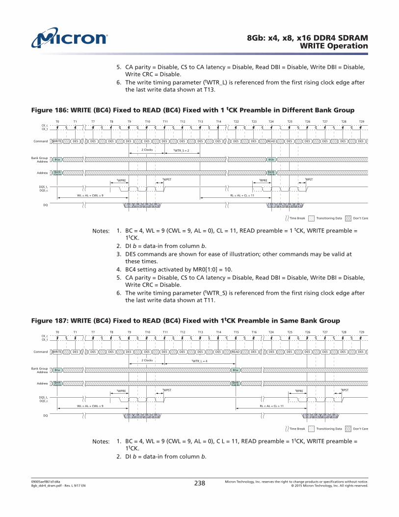
5. CA parity = Disable, CS to CA latency = Disable, Read DBI = Disable, Write DBI = Disable,Write CRC = Disable.
6. The write timing parameter (tWTR_L) is referenced from the first rising clock edge afterthe last write data shown at T13.
Figure 186: WRITE (BC4) Fixed to READ (BC4) Fixed with 1 tCK Preamble in Different Bank Group
T0
tWTR_S = 2
tWPRE
WL = AL + CWL = 9 RL = AL + CL = 11
T1 T7
DES DES DES DES DES DES READCommand DESWRITE DES DES DES DES
DQ
CK_tCK_c
DQS_t,DQS_c
T8 T9 T10 T11 T12 T13 T23T14 T22 T24 T25 T26 T27 T28 T29
Don’t CareTransitioning DataTime Break
DIn + 1
DIn + 2
DIn + 3
DIn
DES DES DES DES DES
Bank GroupAddress
Address BankCol n
BankCol b
BGa BGb
tRPREtWPST tRPST
DIb
DIb + 1
DIb + 2
DIb + 3
2 Clocks
Notes: 1. BC = 4, WL = 9 (CWL = 9, AL = 0), CL = 11, READ preamble = 1 tCK, WRITE preamble =1tCK.
2. DI b = data-in from column b.3. DES commands are shown for ease of illustration; other commands may be valid at
these times.4. BC4 setting activated by MR0[1:0] = 10.5. CA parity = Disable, CS to CA latency = Disable, Read DBI = Disable, Write DBI = Disable,
Write CRC = Disable.6. The write timing parameter (tWTR_S) is referenced from the first rising clock edge after
the last write data shown at T11.
Figure 187: WRITE (BC4) Fixed to READ (BC4) Fixed with 1tCK Preamble in Same Bank Group
T0
tWTR_L = 4
tWPRE
WL = AL + CWL = 9 RL = AL + CL = 11
T1 T7
DES DES DES DES DESDESREADCommand DESWRITE DES DES DES DES
DQ
CK_tCK_c
DQS_t,DQS_c
T8 T9 T10 T11 T12 T13 T16T14 T15 T24 T25 T26 T27 T28 T29
Don’t CareTransitioning DataTime Break
DIn + 1
DIn + 2
DIn + 3
DIn
DES DES DES DES DES
Bank GroupAddress
Address BankCol n
BankCol b
BGa BGa
tRPREtWPST tRPST
DIb
DIb + 1
DIb + 2
DIb + 3
2 Clocks
Notes: 1. BC = 4, WL = 9 (CWL = 9, AL = 0), C L = 11, READ preamble = 1tCK, WRITE preamble =1tCK.
2. DI b = data-in from column b.
8Gb: x4, x8, x16 DDR4 SDRAMWRITE Operation
09005aef861d1d4a8gb_ddr4_dram.pdf - Rev. L 9/17 EN 238 Micron Technology, Inc. reserves the right to change products or specifications without notice.
© 2015 Micron Technology, Inc. All rights reserved.
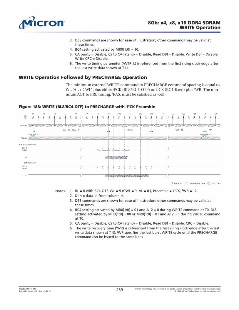
3. DES commands are shown for ease of illustration; other commands may be valid atthese times.
4. BC4 setting activated by MR0[1:0] = 10.5. CA parity = Disable, CS to CA latency = Disable, Read DBI = Disable, Write DBI = Disable,
Write CRC = Disable.6. The write timing parameter (tWTR_L) is referenced from the first rising clock edge after
the last write data shown at T11.
WRITE Operation Followed by PRECHARGE Operation
The minimum external WRITE command to PRECHARGE command spacing is equal toWL (AL + CWL) plus either 4tCK (BL8/BC4-OTF) or 2tCK (BC4-fixed) plus tWR. The min-imum ACT to PRE timing, tRAS, must be satisfied as well.
Figure 188: WRITE (BL8/BC4-OTF) to PRECHARGE with 1tCK Preamble
T0
WL = AL + CWL = 9 tWR = 12 tRP
T1 T2 T3 T4
DES DES DES DES DES DES DESCommand DESWRITE DES DES DES DES
DQ
BC4 (OTF) Opertaion
CK_tCK_c
DQS_t,DQS_c
T14T7 T8 T9 T10 T11 T12 T13 T26T22 T23 T24 T25
Don’t CareTransitioning DataTime Break
DIn + 1
DIn + 2
DIn + 3
DIn
DES DES DES PRE DES
Address
BGa, Bank bCol n
BGa, Bank b(or all)
DQ
BL8 Opertaion
DQS_t,DQS_c
DIn + 1
DIn + 2
DIn + 3
DIn + 4
DIn + 5
DIn + 6
DIn + 7
DIn
4 Clocks
Notes: 1. BL = 8 with BC4-OTF, WL = 9 (CWL = 9, AL = 0 ), Preamble = 1tCK, tWR = 12.2. DI n = data-in from column n.3. DES commands are shown for ease of illustration; other commands may be valid at
these times.4. BC4 setting activated by MR0[1:0] = 01 and A12 = 0 during WRITE command at T0. BL8
setting activated by MR0[1:0] = 00 or MR0[1:0] = 01 and A12 = 1 during WRITE commandat T0.
5. CA parity = Disable, CS to CA latency = Disable, Read DBI = Disable, CRC = Disable.6. The write recovery time (tWR) is referenced from the first rising clock edge after the last
write data shown at T13. tWR specifies the last burst WRITE cycle until the PRECHARGEcommand can be issued to the same bank.
8Gb: x4, x8, x16 DDR4 SDRAMWRITE Operation
09005aef861d1d4a8gb_ddr4_dram.pdf - Rev. L 9/17 EN 239 Micron Technology, Inc. reserves the right to change products or specifications without notice.
© 2015 Micron Technology, Inc. All rights reserved.
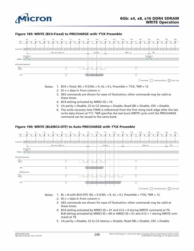
Figure 189: WRITE (BC4-Fixed) to PRECHARGE with 1tCK Preamble
T0
WL = AL + CWL = 9 tWR = 12 tRP
T1 T2 T3 T4
DES DES DES DES DES DES DESCommand DESWRITE DES DES DES DES
DQ
BC4 (Fixed) Opertaion
CK_tCK_c
DQS_t,DQS_c
T14T7 T8 T9 T10 T11 T12 T13 T26T22 T23 T24 T25
Don’t CareTransitioning DataTime Break
DIn + 1
DIn + 2
DIn + 3
DIn
DES PRE DES DES DES
Address
BGa, Bank bCol n
BGa, Bank b(or all)
2 Clocks
Notes: 1. BC4 = fixed, WL = 9 (CWL = 9, AL = 0 ), Preamble = 1tCK, tWR = 12.2. DI n = data-in from column n.3. DES commands are shown for ease of illustration; other commands may be valid at
these times.4. BC4 setting activated by MR0[1:0] = 10.5. CA parity = Disable, CS to CA latency = Disable, Read DBI = Disable, CRC = Disable.6. The write recovery time (tWR) is referenced from the first rising clock edge after the last
write data shown at T11. tWR specifies the last burst WRITE cycle until the PRECHARGEcommand can be issued to the same bank.
Figure 190: WRITE (BL8/BC4-OTF) to Auto PRECHARGE with 1tCK Preamble
T0
WL = AL + CWL = 9 tWR = 12 tRP
T1 T2 T3 T4
DES DES DES DES DES DES DESCommand DESWRITE DES DES DES DES
DQ
BC4 (OTF) Opertaion
CK_tCK_c
DQS_t,DQS_c
T14T7 T8 T9 T10 T11 T12 T13 T26T22 T23 T24 T25
Don’t CareTransitioning DataTime Break
DIn + 1
DIn + 2
DIn + 3
DIn
DES DES DES DES DES
Address
BGa, Bank bCol n
DQ
BL8 Opertaion
DQS_t,DQS_c
DIn + 1
DIn + 2
DIn + 3
DIn + 4
DIn + 5
DIn + 6
DIn + 7
DIn
4 Clocks
Notes: 1. BL = 8 with BC4-OTF, WL = 9 (CWL = 9, AL = 0 ), Preamble = 1tCK, tWR = 12.2. DI n = data-in from column n.3. DES commands are shown for ease of illustration; other commands may be valid at
these times.4. BC4 setting activated by MR0[1:0] = 01 and A12 = 0 during WRITE command at T0.
BL8 setting activated by MR0[1:0] = 00 or MR0[1:0] = 01 and A12 = 1 during WRITE com-mand at T0.
5. CA parity = Disable, CS to CA latency = Disable, Read DBI = Disable, CRC = Disable.
8Gb: x4, x8, x16 DDR4 SDRAMWRITE Operation
09005aef861d1d4a8gb_ddr4_dram.pdf - Rev. L 9/17 EN 240 Micron Technology, Inc. reserves the right to change products or specifications without notice.
© 2015 Micron Technology, Inc. All rights reserved.
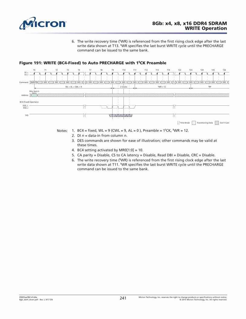
6. The write recovery time (tWR) is referenced from the first rising clock edge after the lastwrite data shown at T13. tWR specifies the last burst WRITE cycle until the PRECHARGEcommand can be issued to the same bank.
Figure 191: WRITE (BC4-Fixed) to Auto PRECHARGE with 1tCK Preamble
T0
WL = AL + CWL = 9 tWR = 12 tRP
T1 T2 T3 T4
DES DES DES DES DES DES DESCommand DESWRITE DES DES DES DES
DQ
BC4 (Fixed) Opertaion
CK_tCK_c
DQS_t,DQS_c
T14T7 T8 T9 T10 T11 T12 T13 T26T22 T23 T24 T25
Don’t CareTransitioning DataTime Break
DIn + 1
DIn + 2
DIn + 3
DIn
DES DES DES DES DES
Address
BGa, Bank bCol n
2 Clocks
Notes: 1. BC4 = fixed, WL = 9 (CWL = 9, AL = 0 ), Preamble = 1tCK, tWR = 12.2. DI n = data-in from column n.3. DES commands are shown for ease of illustration; other commands may be valid at
these times.4. BC4 setting activated by MR0[1:0] = 10.5. CA parity = Disable, CS to CA latency = Disable, Read DBI = Disable, CRC = Disable.6. The write recovery time (tWR) is referenced from the first rising clock edge after the last
write data shown at T11. tWR specifies the last burst WRITE cycle until the PRECHARGEcommand can be issued to the same bank.
8Gb: x4, x8, x16 DDR4 SDRAMWRITE Operation
09005aef861d1d4a8gb_ddr4_dram.pdf - Rev. L 9/17 EN 241 Micron Technology, Inc. reserves the right to change products or specifications without notice.
© 2015 Micron Technology, Inc. All rights reserved.
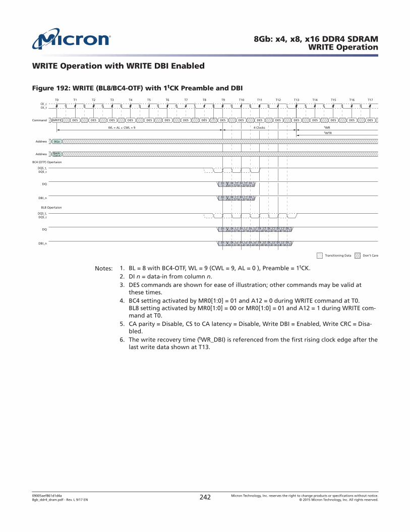
WRITE Operation with WRITE DBI Enabled
Figure 192: WRITE (BL8/BC4-OTF) with 1tCK Preamble and DBI
T0
WL = AL + CWL = 9 tWRtWTR
T1 T2 T3 T4
DES DES DES DES DES DES DESCommand DESWRITE DES DES DES DES
DQ
BC4 (OTF) Opertaion
CK_tCK_c
DQS_t,DQS_c
T5 T6 T14T7 T8 T9 T10 T11 T12 T13 T15 T16 T17
Don’t CareTransitioning Data
DIn + 1
DIn + 2
DIn + 3
DIn
DES DES DES DES DES
Address BGa
Address Bank,Col n
DQ
DBI_n
BL8 Opertaion
DQS_t,DQS_c
DIn + 1
DIn + 2
DIn + 3
DIn + 4
DIn + 5
DIn + 6
DIn + 7
DIn
DIn + 1
DIn + 2
DIn + 3
DIn + 4
DIn + 5
DIn + 6
DIn + 7
DIn
DBI_n DIn + 1
DIn + 2
DIn + 3
DIn
4 Clocks
Notes: 1. BL = 8 with BC4-OTF, WL = 9 (CWL = 9, AL = 0 ), Preamble = 1tCK.2. DI n = data-in from column n.3. DES commands are shown for ease of illustration; other commands may be valid at
these times.4. BC4 setting activated by MR0[1:0] = 01 and A12 = 0 during WRITE command at T0.
BL8 setting activated by MR0[1:0] = 00 or MR0[1:0] = 01 and A12 = 1 during WRITE com-mand at T0.
5. CA parity = Disable, CS to CA latency = Disable, Write DBI = Enabled, Write CRC = Disa-bled.
6. The write recovery time (tWR_DBI) is referenced from the first rising clock edge after thelast write data shown at T13.
8Gb: x4, x8, x16 DDR4 SDRAMWRITE Operation
09005aef861d1d4a8gb_ddr4_dram.pdf - Rev. L 9/17 EN 242 Micron Technology, Inc. reserves the right to change products or specifications without notice.
© 2015 Micron Technology, Inc. All rights reserved.
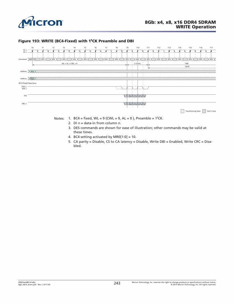
Figure 193: WRITE (BC4-Fixed) with 1tCK Preamble and DBI
T0
WL = AL + CWL = 9 tWRtWTR
T1 T2 T3 T4
DES DES DES DES DES DES DESCommand DESWRITE DES DES DES DES
DQ
BC4 (Fixed) Opertaion
CK_tCK_c
DQS_t,DQS_c
T5 T6 T14T7 T8 T9 T10 T11 T12 T13 T15 T16 T17
Don’t CareTransitioning Data
DIn + 1
DIn + 2
DIn + 3
DIn
DES DES DES DES DES
Address BGa
Address Bank,Col n
DBI_n DIn + 1
DIn + 2
DIn + 3
DIn
2 Clocks
Notes: 1. BC4 = fixed, WL = 9 (CWL = 9, AL = 0 ), Preamble = 1tCK.2. DI n = data-in from column n.3. DES commands are shown for ease of illustration; other commands may be valid at
these times.4. BC4 setting activated by MR0[1:0] = 10.5. CA parity = Disable, CS to CA latency = Disable, Write DBI = Enabled, Write CRC = Disa-
bled.
8Gb: x4, x8, x16 DDR4 SDRAMWRITE Operation
09005aef861d1d4a8gb_ddr4_dram.pdf - Rev. L 9/17 EN 243 Micron Technology, Inc. reserves the right to change products or specifications without notice.
© 2015 Micron Technology, Inc. All rights reserved.
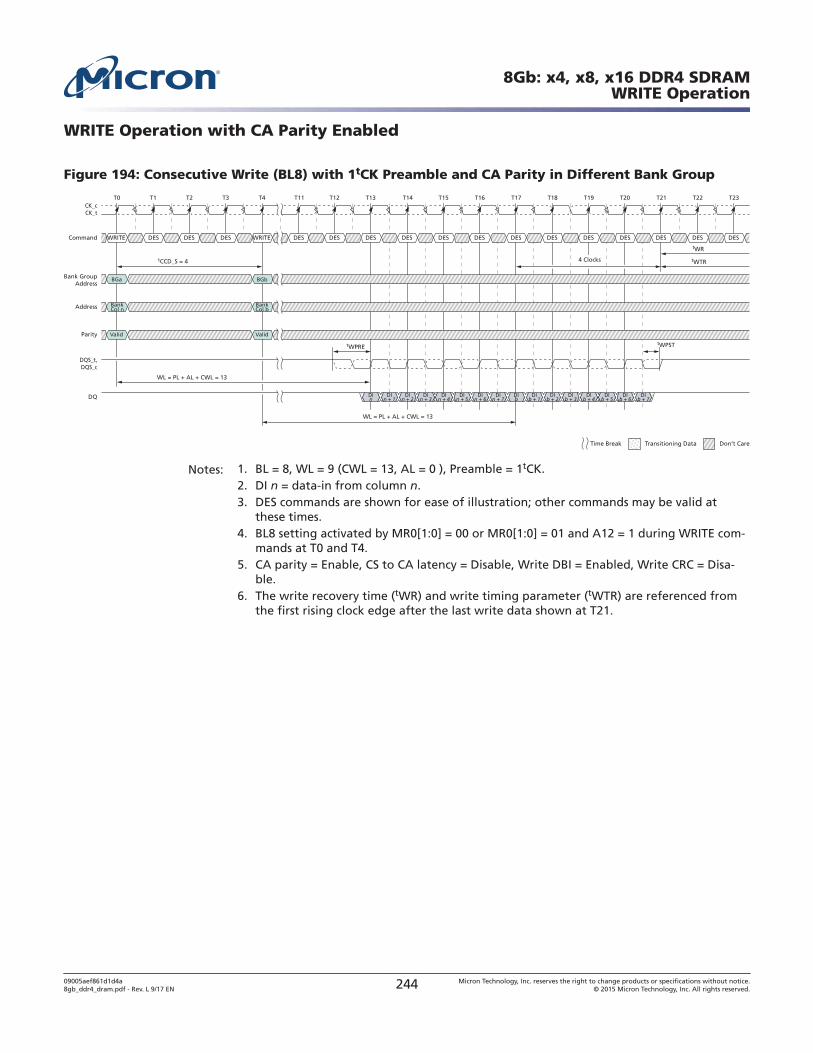
WRITE Operation with CA Parity Enabled
Figure 194: Consecutive Write (BL8) with 1tCK Preamble and CA Parity in Different Bank Group
T0
tCCD_S = 4 4 Clocks
tWPRE
WL = PL + AL + CWL = 13
T1 T2 T3 T4
DES DES DES DES DES DES DESCommand DESWRITE DES DES WRITE DES
DQ
CK_tCK_c
DQS_t,DQS_c
WL = PL + AL + CWL = 13
T20 T21 T22 T23T11 T12 T13 T16T14 T15 T17 T18 T19
Don’t CareTransitioning DataTime Break
DIn + 1
DIn + 2
DIn + 3
DIn + 4
DIn + 5
DIn + 6
DIn + 7
DIb
DIb + 1
DIb + 2
DIb + 3
DIb + 4
DIb + 5
DIb + 6
DIb + 7
DIn
DES DES DES DES DES
Bank GroupAddress
Address BankCol n
BankCol b
BGa BGb
tWPST
tWTR
tWR
Parity Valid Valid
Notes: 1. BL = 8, WL = 9 (CWL = 13, AL = 0 ), Preamble = 1tCK.2. DI n = data-in from column n.3. DES commands are shown for ease of illustration; other commands may be valid at
these times.4. BL8 setting activated by MR0[1:0] = 00 or MR0[1:0] = 01 and A12 = 1 during WRITE com-
mands at T0 and T4.5. CA parity = Enable, CS to CA latency = Disable, Write DBI = Enabled, Write CRC = Disa-
ble.6. The write recovery time (tWR) and write timing parameter (tWTR) are referenced from
the first rising clock edge after the last write data shown at T21.
8Gb: x4, x8, x16 DDR4 SDRAMWRITE Operation
09005aef861d1d4a8gb_ddr4_dram.pdf - Rev. L 9/17 EN 244 Micron Technology, Inc. reserves the right to change products or specifications without notice.
© 2015 Micron Technology, Inc. All rights reserved.
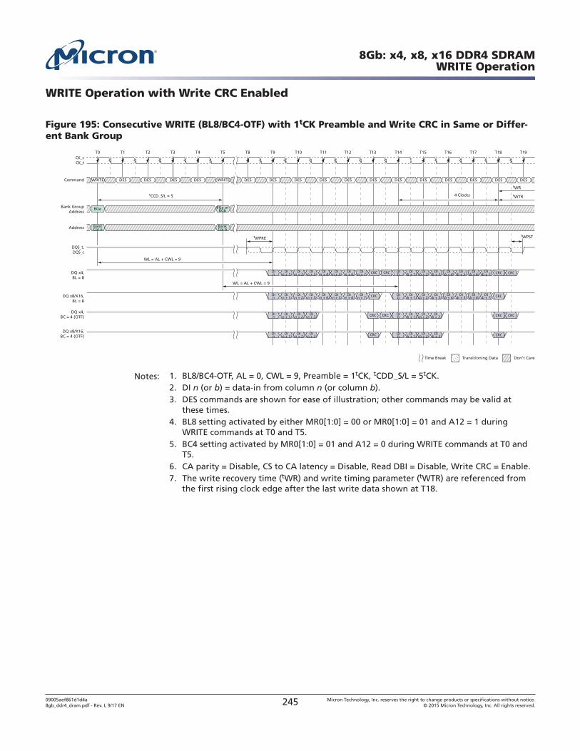
WRITE Operation with Write CRC Enabled
Figure 195: Consecutive WRITE (BL8/BC4-OTF) with 1tCK Preamble and Write CRC in Same or Differ-ent Bank Group
T0
tCCD_S/L = 5
tWPRE
WL = AL + CWL = 9
T1 T2 T3 T4
DES DES DES DES DES DES DESCommand DESWRITE DES DES DES WRITE
DQ x4,BL = 8
CK_tCK_c
DQS_t,DQS_c
WL = AL + CWL = 9
T5 T8 T9 T10 T11 T12 T13 T16T14 T15 T17 T18 T19
Don’t CareTransitioning DataTime Break
DIn + 1
DIn + 2
DIn + 3
DIn + 4
DIn + 5
DIn + 6
DIn + 7 CRC
DIn + 7
CRC
CRC
CRC
DIb
DIb + 1
DIb + 2
DIb + 3
DIb + 4
DIb + 5
DIb + 6
DIb + 7 CRC CRCDI
n
DES DES DES DES DES
Bank GroupAddress
Address BankCol n
BankCol b
BGa BGa orBGb
DQ x8/X16,BL = 8
DIn + 1
DIn + 2
DIn + 3
DIn + 4
DIn + 5
DIn + 6
DIb
DIb + 1
DIb + 2
DIb + 3
DIb + 4
DIb + 5
DIb + 6
DIb + 7 CRCDI
n
CRC
DQ x4,BC = 4 (OTF)
DQ x8/X16,BC = 4 (OTF)
DIn + 1
DIn + 2
DIn + 3
DIb
DIb + 1
DIb + 2 CRC CRCDI
n
tWPST
tWTR
tWR
DIn + 1
DIn + 2
DIn + 3
DIb
DIb + 1
DIb + 2
DIb + 3 CRCDI
n
DIb + 3
CRC
4 Clocks
Notes: 1. BL8/BC4-OTF, AL = 0, CWL = 9, Preamble = 1tCK, tCDD_S/L = 5tCK.2. DI n (or b) = data-in from column n (or column b).3. DES commands are shown for ease of illustration; other commands may be valid at
these times.4. BL8 setting activated by either MR0[1:0] = 00 or MR0[1:0] = 01 and A12 = 1 during
WRITE commands at T0 and T5.5. BC4 setting activated by MR0[1:0] = 01 and A12 = 0 during WRITE commands at T0 and
T5.6. CA parity = Disable, CS to CA latency = Disable, Read DBI = Disable, Write CRC = Enable.7. The write recovery time (tWR) and write timing parameter (tWTR) are referenced from
the first rising clock edge after the last write data shown at T18.
8Gb: x4, x8, x16 DDR4 SDRAMWRITE Operation
09005aef861d1d4a8gb_ddr4_dram.pdf - Rev. L 9/17 EN 245 Micron Technology, Inc. reserves the right to change products or specifications without notice.
© 2015 Micron Technology, Inc. All rights reserved.
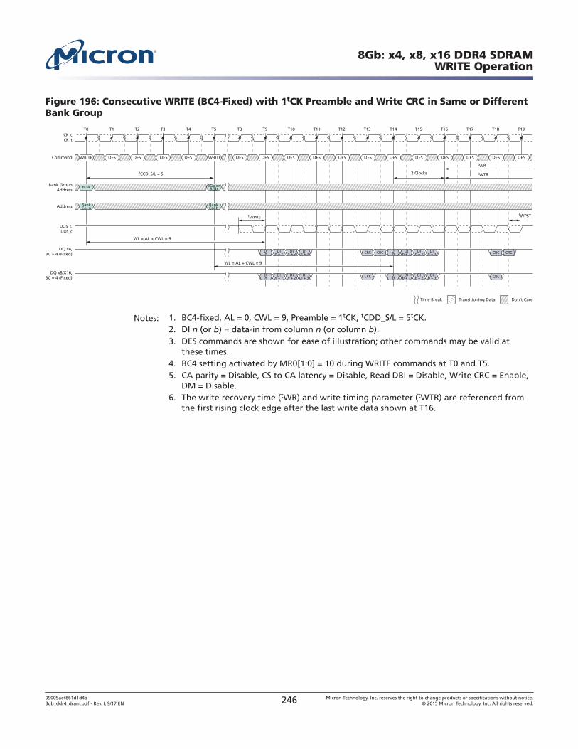
Figure 196: Consecutive WRITE (BC4-Fixed) with 1tCK Preamble and Write CRC in Same or DifferentBank Group
T0
tCCD_S/L = 5
tWPRE
WL = AL + CWL = 9
T1 T2 T3 T4
DES DES DES DES DES DES DESCommand DESWRITE DES DES DES WRITE
CK_tCK_c
DQS_t,DQS_c
WL = AL + CWL = 9
T5 T8 T9 T10 T11 T12 T13 T16T14 T15 T17 T18 T19
Don’t CareTransitioning DataTime Break
CRC
DES DES DES DES DES
Bank GroupAddress
Address BankCol n
BankCol b
BGa BGa orBGb
CRC
CRCDQ x4,
BC = 4 (Fixed)
DQ x8/X16,BC = 4 (Fixed)
DIn + 1
DIn + 2
DIn + 3
DIb
DIb + 1
DIb + 2 CRC CRCDI
n
tWPST
tWTR
tWR
DIn + 1
DIn + 2
DIn + 3
DIb
DIb + 1
DIb + 2
DIb + 3 CRCDI
n
DIb + 3
2 Clocks
Notes: 1. BC4-fixed, AL = 0, CWL = 9, Preamble = 1tCK, tCDD_S/L = 5tCK.2. DI n (or b) = data-in from column n (or column b).3. DES commands are shown for ease of illustration; other commands may be valid at
these times.4. BC4 setting activated by MR0[1:0] = 10 during WRITE commands at T0 and T5.5. CA parity = Disable, CS to CA latency = Disable, Read DBI = Disable, Write CRC = Enable,
DM = Disable.6. The write recovery time (tWR) and write timing parameter (tWTR) are referenced from
the first rising clock edge after the last write data shown at T16.
8Gb: x4, x8, x16 DDR4 SDRAMWRITE Operation
09005aef861d1d4a8gb_ddr4_dram.pdf - Rev. L 9/17 EN 246 Micron Technology, Inc. reserves the right to change products or specifications without notice.
© 2015 Micron Technology, Inc. All rights reserved.
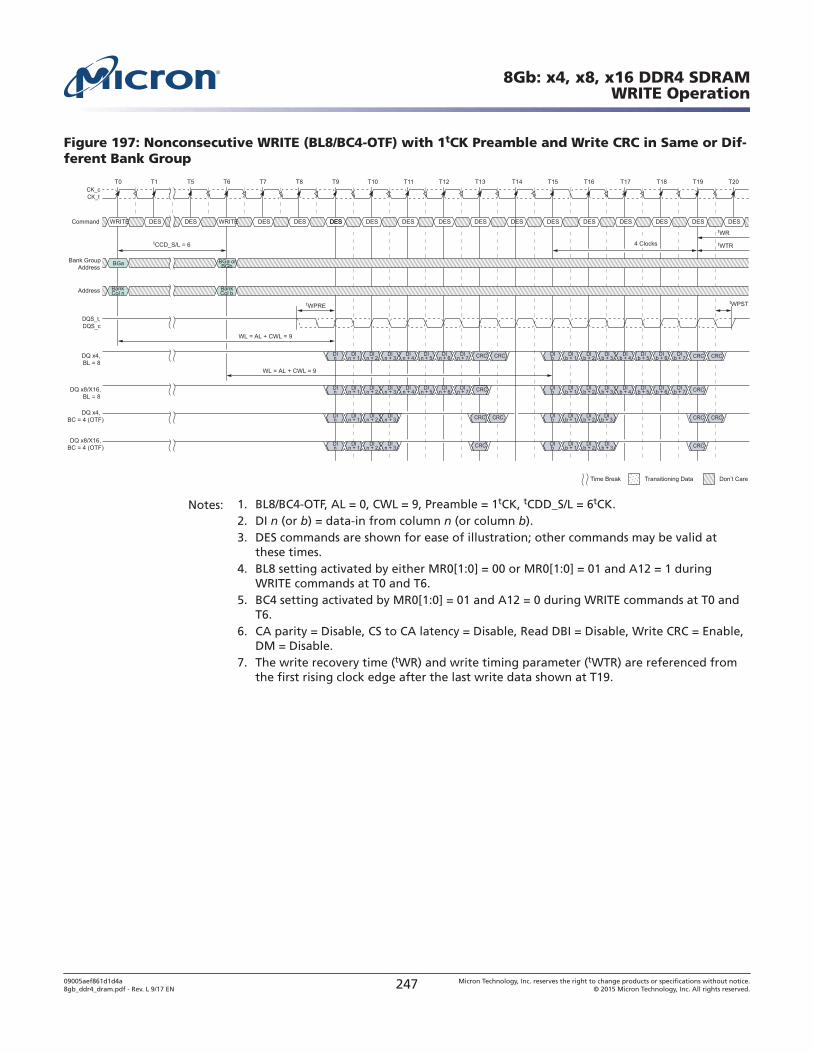
Figure 197: Nonconsecutive WRITE (BL8/BC4-OTF) with 1tCK Preamble and Write CRC in Same or Dif-ferent Bank Group
Notes: 1. BL8/BC4-OTF, AL = 0, CWL = 9, Preamble = 1tCK, tCDD_S/L = 6tCK.2. DI n (or b) = data-in from column n (or column b).3. DES commands are shown for ease of illustration; other commands may be valid at
these times.4. BL8 setting activated by either MR0[1:0] = 00 or MR0[1:0] = 01 and A12 = 1 during
WRITE commands at T0 and T6.5. BC4 setting activated by MR0[1:0] = 01 and A12 = 0 during WRITE commands at T0 and
T6.6. CA parity = Disable, CS to CA latency = Disable, Read DBI = Disable, Write CRC = Enable,
DM = Disable.7. The write recovery time (tWR) and write timing parameter (tWTR) are referenced from
the first rising clock edge after the last write data shown at T19.
8Gb: x4, x8, x16 DDR4 SDRAMWRITE Operation
09005aef861d1d4a8gb_ddr4_dram.pdf - Rev. L 9/17 EN 247 Micron Technology, Inc. reserves the right to change products or specifications without notice.
© 2015 Micron Technology, Inc. All rights reserved.
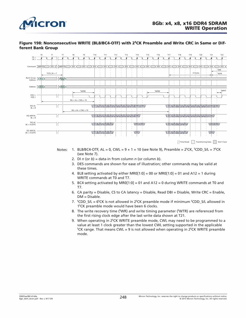
Figure 198: Nonconsecutive WRITE (BL8/BC4-OTF) with 2tCK Preamble and Write CRC in Same or Dif-ferent Bank Group
T0
tCCD_S/L = 7
tWPRE
WL = AL + CWL = 10
T1
DES DES DES DES DES DES DESCommand DESWRITE DES DESDESWRITE
DQ x4,BL = 8
CK_tCK_c
DQS_t,DQS_c
WL = AL + CWL = 10
T22T21T7 T20T8 T9 T10 T11 T12 T13 T16T14 T15 T17 T18 T19
Don’t CareTransitioning DataTime Break
DIn + 1
DIn + 2
DIn + 3
DIn + 4
DIn + 5
DIn + 6
DIn + 7 CRC
DIn + 7
CRC
CRC
CRC
DIb
DIb + 1
DIb + 2
DIb + 3
DIb + 4
DIb + 5
DIb + 6
DIb + 7 CRC CRCDI
n
DES DES DES DES DES
Bank GroupAddress
Address BankCol n
BankCol b
BGa BGa orBGb
DQ x8/X16,BL = 8
DIn + 1
DIn + 2
DIn + 3
DIn + 4
DIn + 5
DIn + 6
DIb
DIb + 1
DIb + 2
DIb + 3
DIb + 4
DIb + 5
DIb + 6
DIb + 7 CRCDI
n
CRC
DQ x4,BC = 4 (OTF)
DQ x8/X16,BC = 4 (OTF)
DIn + 1
DIn + 2
DIn + 3
DIb
DIb + 1
DIb + 2 CRC CRCDI
n
tWPREtWPST
tWTR
tWR
DIn + 1
DIn + 2
DIn + 3
DIb
DIb + 1
DIb + 2
DIb + 3 CRCDI
n
DIb + 3
CRC
4 Clocks
Notes: 1. BL8/BC4-OTF, AL = 0, CWL = 9 + 1 = 10 (see Note 9), Preamble = 2tCK, tCDD_S/L = 7tCK(see Note 7).
2. DI n (or b) = data-in from column n (or column b).3. DES commands are shown for ease of illustration; other commands may be valid at
these times.4. BL8 setting activated by either MR0[1:0] = 00 or MR0[1:0] = 01 and A12 = 1 during
WRITE commands at T0 and T7.5. BC4 setting activated by MR0[1:0] = 01 and A12 = 0 during WRITE commands at T0 and
T7.6. CA parity = Disable, CS to CA latency = Disable, Read DBI = Disable, Write CRC = Enable,
DM = Disable.7. tCDD_S/L = 6tCK is not allowed in 2tCK preamble mode if minimum tCDD_S/L allowed in
1tCK preamble mode would have been 6 clocks.8. The write recovery time (tWR) and write timing parameter (tWTR) are referenced from
the first rising clock edge after the last write data shown at T21.9. When operating in 2tCK WRITE preamble mode, CWL may need to be programmed to a
value at least 1 clock greater than the lowest CWL setting supported in the applicabletCK range. That means CWL = 9 is not allowed when operating in 2tCK WRITE preamblemode.
8Gb: x4, x8, x16 DDR4 SDRAMWRITE Operation
09005aef861d1d4a8gb_ddr4_dram.pdf - Rev. L 9/17 EN 248 Micron Technology, Inc. reserves the right to change products or specifications without notice.
© 2015 Micron Technology, Inc. All rights reserved.
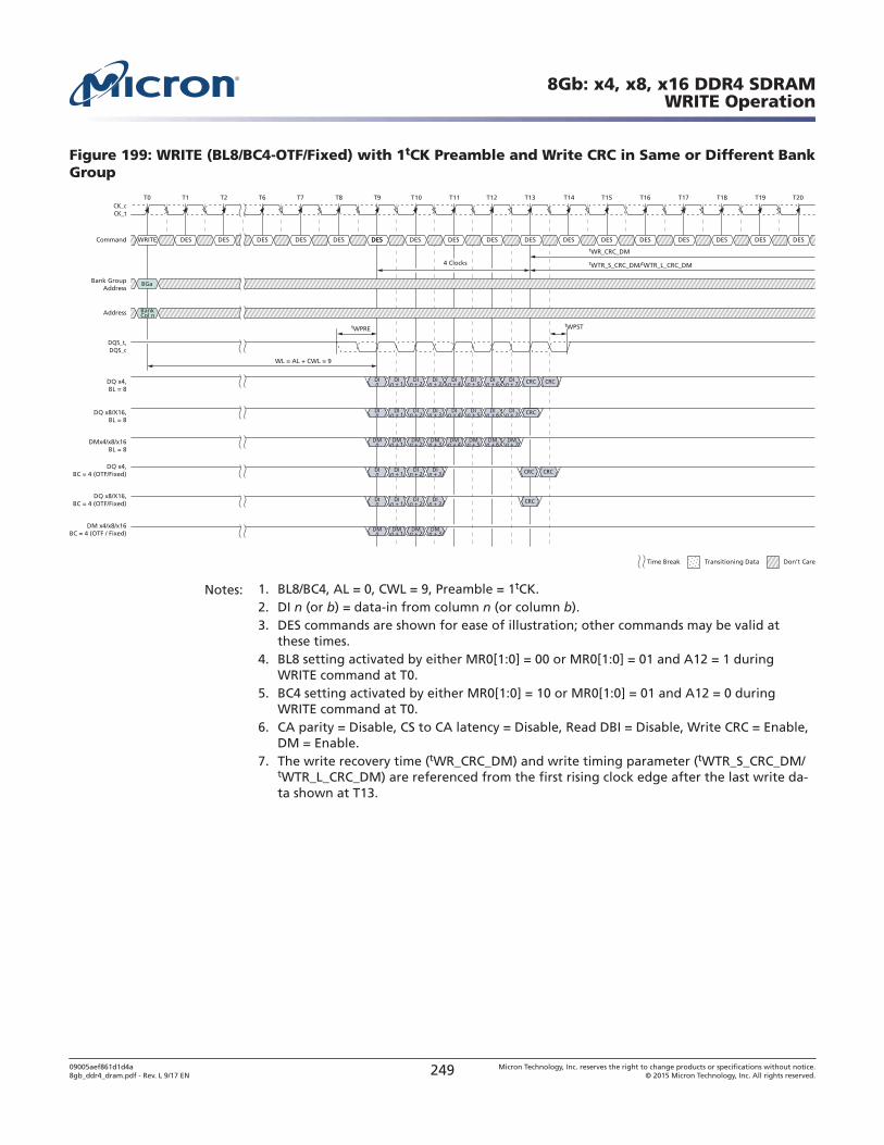
Figure 199: WRITE (BL8/BC4-OTF/Fixed) with 1tCK Preamble and Write CRC in Same or Different BankGroup
T0
tWPRE
WL = AL + CWL = 9
T1 T2 T6 T7
DES DES DES DES DES DES DESCommand DESWRITE DES DESDESDESDES
DQ x4,BL = 8
CK_tCK_c
DQS_t,DQS_c
T20T8 T9 T10 T11 T12 T13 T16T14 T15 T17 T18 T19
Don’t CareTransitioning DataTime Break
DIn + 1
DIn + 2
DIn + 3
DIn + 4
DIn + 5
DIn + 6
DIn + 7 CRC
DIn + 7
CRC
CRC
CRC
DIn
DES DES DES DES DES
Bank GroupAddress
Address BankCol n
BGa
DQ x8/X16,BL = 8
DIn + 1
DIn + 2
DIn + 3
DIn + 4
DIn + 5
DIn + 6
DIn
CRC
DQ x4,BC = 4 (OTF/Fixed)
DQ x8/X16,BC = 4 (OTF/Fixed)
DIn + 1
DIn + 2
DIn + 3
DIn
tWTR_S_CRC_DM/tWTR_L_CRC_DM
tWR_CRC_DM
tWPST
DIn + 1
DIn + 2
DIn + 3
DIn
DMn + 7DMx4/x8/x16
BL = 8
DMn + 1
DMn + 2
DMn + 3
DMn + 4
DMn + 5
DMn + 6
DMn
CRC
DM x4/x8/x16BC = 4 (OTF / Fixed)
DMn + 1
DMn + 2
DMn + 3
DMn
4 Clocks
Notes: 1. BL8/BC4, AL = 0, CWL = 9, Preamble = 1tCK.2. DI n (or b) = data-in from column n (or column b).3. DES commands are shown for ease of illustration; other commands may be valid at
these times.4. BL8 setting activated by either MR0[1:0] = 00 or MR0[1:0] = 01 and A12 = 1 during
WRITE command at T0.5. BC4 setting activated by either MR0[1:0] = 10 or MR0[1:0] = 01 and A12 = 0 during
WRITE command at T0.6. CA parity = Disable, CS to CA latency = Disable, Read DBI = Disable, Write CRC = Enable,
DM = Enable.7. The write recovery time (tWR_CRC_DM) and write timing parameter (tWTR_S_CRC_DM/
tWTR_L_CRC_DM) are referenced from the first rising clock edge after the last write da-ta shown at T13.
8Gb: x4, x8, x16 DDR4 SDRAMWRITE Operation
09005aef861d1d4a8gb_ddr4_dram.pdf - Rev. L 9/17 EN 249 Micron Technology, Inc. reserves the right to change products or specifications without notice.
© 2015 Micron Technology, Inc. All rights reserved.
Write Timing Violations
Motivation
Generally, if timing parameters are violated, a complete reset/initialization procedurehas to be initiated to make sure that the device works properly. However, for certain mi-nor violations, it is desirable that the device is guaranteed not to "hang up" and that er-rors are limited to that specific operation. A minor violation does not include a majortiming violation (for example, when a DQS strobe misses in the tDQSCK window).
For the following, it will be assumed that there are no timing violations with regard tothe WRITE command itself (including ODT, and so on) and that it does satisfy all timingrequirements not mentioned below.
Data Setup and Hold Violations
If the data-to-strobe timing requirements (tDS, tDH) are violated, for any of the strobeedges associated with a WRITE burst, then wrong data might be written to the memorylocation addressed with this WRITE command.
In the example, the relevant strobe edges for WRITE Burst A are associated with theclock edges: T5, T5.5, T6, T6.5, T7, T7.5, T8, and T8.5.
Subsequent reads from that location might result in unpredictable read data; however,the device will work properly otherwise.
Strobe-to-Strobe and Strobe-to-Clock Violations
If the strobe timing requirements (tDQSH, tDQSL, tWPRE, tWPST) or the strobe to clocktiming requirements (tDSS, tDSH, tDQSS) are violated, for any of the strobe edges asso-ciated with a WRITE burst, then wrong data might be written to the memory locationaddressed with the offending WRITE command. Subsequent reads from that locationmight result in unpredictable read data; however, the device will work properly other-wise with the following constraints:
• Both write CRC and data burst OTF are disabled; timing specifications other thantDQSH, tDQSL, tWPRE, tWPST, tDSS, tDSH, tDQSS are not violated.
• The offending write strobe (and preamble) arrive no earlier or later than six DQS tran-sition edges from the WRITE latency position.
• A READ command following an offending WRITE command from any open bank isallowed.
• One or more subsequent WR or a subsequent WRA (to same bank as offending WR)may be issued tCCD_L later, but incorrect data could be written. Subsequent WR andWRA can be either offending or non-offending writes. Reads from these writes mayprovide incorrect data.
• One or more subsequent WR or a subsequent WRA (to a different bank group) may beissued tCCD_S later, but incorrect data could be written. Subsequent WR and WRAcan be either offending or non-offending writes. Reads from these writes may provideincorrect data.
• After one or more precharge commands (PRE or PREA) are issued to the device afteran offending WRITE command and all banks are in precharged state (idle state), asubsequent, non-offending WR or WRA to any open bank will be able to write correctdata.
8Gb: x4, x8, x16 DDR4 SDRAMWrite Timing Violations
09005aef861d1d4a8gb_ddr4_dram.pdf - Rev. L 9/17 EN 250 Micron Technology, Inc. reserves the right to change products or specifications without notice.
© 2015 Micron Technology, Inc. All rights reserved.
ZQ CALIBRATION CommandsA ZQ CALIBRATION command is used to calibrate DRAM RON and ODT values. The de-vice needs a longer time to calibrate the output driver and on-die termination circuitsat initialization and a relatively smaller time to perform periodic calibrations.
The ZQCL command is used to perform the initial calibration during the power-up ini-tialization sequence. This command may be issued at any time by the controller de-pending on the system environment. The ZQCL command triggers the calibration en-gine inside the DRAM and, after calibration is achieved, the calibrated values are trans-ferred from the calibration engine to DRAM I/O, which is reflected as an updated out-put driver and ODT values.
The first ZQCL command issued after reset is allowed a timing period of tZQinit to per-form the full calibration and the transfer of values. All other ZQCL commands exceptthe first ZQCL command issued after reset are allowed a timing period of tZQoper.
The ZQCS command is used to perform periodic calibrations to account for voltage andtemperature variations. A shorter timing window is provided to perform the calibrationand transfer of values as defined by timing parameter tZQCS. One ZQCS command caneffectively correct a minimum of 0.5% (ZQ correction) of RON and RTT impedance errorwithin 64 nCK for all speed bins assuming the maximum sensitivities specified in theOutput Driver and ODT Voltage and Temperature Sensitivity tables. The appropriate in-terval between ZQCS commands can be determined from these tables and other appli-cation-specific parameters. One method for calculating the interval between ZQCScommands, given the temperature (Tdrift_rate) and voltage (Vdrift_rate) drift rates that thedevice is subjected to in the application, is illustrated. The interval could be defined bythe following formula:
ZQcorrection
(Tsense x Tdrift_rate) + (Vsense x Tdrift_rate)
Where Tsense = MAX(dRTTdT, dRONdTM) and Vsense = MAX(dRTTdV, dRONdVM) definethe temperature and voltage sensitivities.
For example, if Tsens = 1.5%/°C, Vsens = 0.15%/mV, Tdriftrate = 1 °C/sec and Vdriftrate = 15mV/sec, then the interval between ZQCS commands is calculated as:
0.5= 0.133 128ms
(1.5 × 1) + (0.15 × 15)
No other activities should be performed on the DRAM channel by the controller for theduration of tZQinit, tZQoper, or tZQCS. The quiet time on the DRAM channel allows ac-curate calibration of output driver and on-die termination values. After DRAM calibra-tion is achieved, the device should disable the ZQ current consumption path to reducepower.
All banks must be precharged and tRP met before ZQCL or ZQCS commands are issuedby the controller.
ZQ CALIBRATION commands can also be issued in parallel to DLL lock time whencoming out of self refresh. Upon self refresh exit, the device will not perform an I/O cali-bration without an explicit ZQ CALIBRATION command. The earliest possible time for a
8Gb: x4, x8, x16 DDR4 SDRAMZQ CALIBRATION Commands
09005aef861d1d4a8gb_ddr4_dram.pdf - Rev. L 9/17 EN 251 Micron Technology, Inc. reserves the right to change products or specifications without notice.
© 2015 Micron Technology, Inc. All rights reserved.
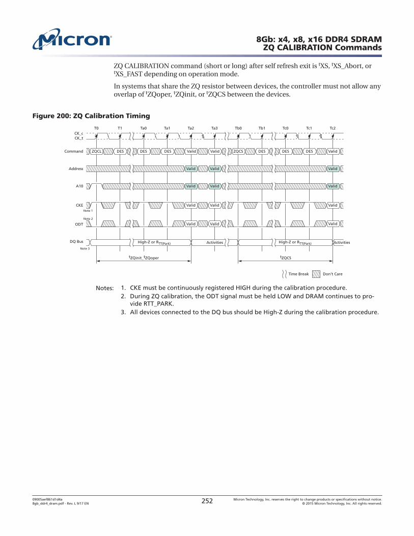
ZQ CALIBRATION command (short or long) after self refresh exit is tXS, tXS_Abort, ortXS_FAST depending on operation mode.
In systems that share the ZQ resistor between devices, the controller must not allow anyoverlap of tZQoper, tZQinit, or tZQCS between the devices.
Figure 200: ZQ Calibration Timing
T0 T1 Ta0
DQ Bus
tZQinit_tZQoper
Don’t Care
Ta1 Ta2 Ta3 Tb0 Tb1 Tc0 Tc1 Tc2
ZQCS DES DES DES Valid
Valid
Valid
Valid
Valid
Command DESZQCL DES DES Valid Valid
Valid Valid
High-Z or RTT(Park) ActivitiesNote 3
Note 2
Note 1
ActivitiesHigh-Z or RTT(Park)
Time Break
Address
Valid Valid
Valid Valid
A10
CKE
Valid ValidODT
CK_tCK_c
tZQCS
Notes: 1. CKE must be continuously registered HIGH during the calibration procedure.2. During ZQ calibration, the ODT signal must be held LOW and DRAM continues to pro-
vide RTT_PARK.3. All devices connected to the DQ bus should be High-Z during the calibration procedure.
8Gb: x4, x8, x16 DDR4 SDRAMZQ CALIBRATION Commands
09005aef861d1d4a8gb_ddr4_dram.pdf - Rev. L 9/17 EN 252 Micron Technology, Inc. reserves the right to change products or specifications without notice.
© 2015 Micron Technology, Inc. All rights reserved.
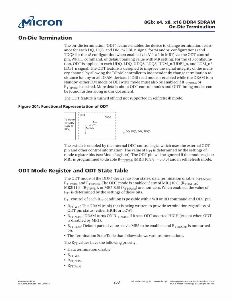
On-Die TerminationThe on-die termination (ODT) feature enables the device to change termination resist-ance for each DQ, DQS, and DM_n/DBI_n signal for x4 and x8 configurations (andTDQS for the x8 configuration when enabled via A11 = 1 in MR1) via the ODT controlpin, WRITE command, or default parking value with MR setting. For the x16 configura-tion, ODT is applied to each UDQ, LDQ, UDQS, LDQS, UDM_n/UDBI_n, and LDM_n/LDBI_n signal. The ODT feature is designed to improve the signal integrity of the mem-ory channel by allowing the DRAM controller to independently change termination re-sistance for any or all DRAM devices. If DBI read mode is enabled while the DRAM is instandby, either DM mode or DBI write mode must also be enabled if RTT(NOM) orRTT(Park) is desired. More details about ODT control modes and ODT timing modes canbe found further along in this document.
The ODT feature is turned off and not supported in self refresh mode.
Figure 201: Functional Representation of ODT
ODT VDDQ
RTT
SwitchDQ, DQS, DM, TDQS
To othercircuitrysuch asRCV, . . .
The switch is enabled by the internal ODT control logic, which uses the external ODTpin and other control information. The value of RTT is determined by the settings ofmode register bits (see Mode Register). The ODT pin will be ignored if the mode registerMR1 is programmed to disable RTT(NOM) [MR1[10,9,8] = 0,0,0] and in self refresh mode.
ODT Mode Register and ODT State TableThe ODT mode of the DDR4 device has four states: data termination disable, RTT(NOM),RTT(WR), and RTT(Park). The ODT mode is enabled if any of MR1[10:8] (RTT(NOM)),MR2[11:9] (RTT(WR)), or MR5[8:6] (RTT(Park)) are non-zero. When enabled, the value ofRTT is determined by the settings of these bits.
RTT control of each RTT condition is possible with a WR or RD command and ODT pin.
• RTT(WR): The DRAM (rank) that is being written to provide termination regardless ofODT pin status (either HIGH or LOW).
• RTT(NOM): DRAM turns ON RTT(NOM) if it sees ODT asserted HIGH (except when ODTis disabled by MR1).
• RTT(Park): Default parked value set via MR5 to be enabled and RTT(NOM) is not turnedon.
• The Termination State Table that follows shows various interactions.
The RTT values have the following priority:
• Data termination disable• RTT(WR)
• RTT(NOM)
• RTT(Park)
8Gb: x4, x8, x16 DDR4 SDRAMOn-Die Termination
09005aef861d1d4a8gb_ddr4_dram.pdf - Rev. L 9/17 EN 253 Micron Technology, Inc. reserves the right to change products or specifications without notice.
© 2015 Micron Technology, Inc. All rights reserved.
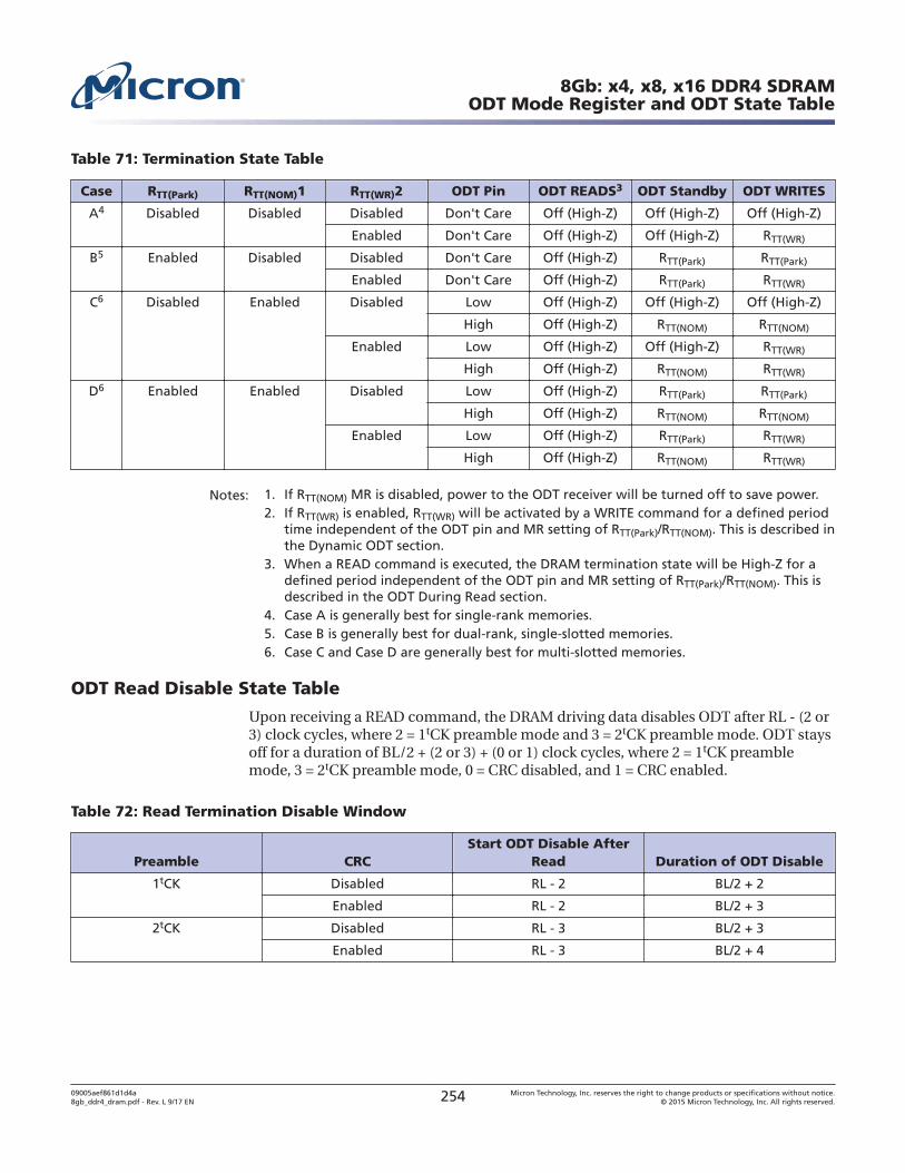
Table 71: Termination State Table
Case RTT(Park) RTT(NOM)1 RTT(WR)2 ODT Pin ODT READS3 ODT Standby ODT WRITES
A4 Disabled Disabled Disabled Don't Care Off (High-Z) Off (High-Z) Off (High-Z)
Enabled Don't Care Off (High-Z) Off (High-Z) RTT(WR)
B5 Enabled Disabled Disabled Don't Care Off (High-Z) RTT(Park) RTT(Park)
Enabled Don't Care Off (High-Z) RTT(Park) RTT(WR)
C6 Disabled Enabled Disabled Low Off (High-Z) Off (High-Z) Off (High-Z)
High Off (High-Z) RTT(NOM) RTT(NOM)
Enabled Low Off (High-Z) Off (High-Z) RTT(WR)
High Off (High-Z) RTT(NOM) RTT(WR)
D6 Enabled Enabled Disabled Low Off (High-Z) RTT(Park) RTT(Park)
High Off (High-Z) RTT(NOM) RTT(NOM)
Enabled Low Off (High-Z) RTT(Park) RTT(WR)
High Off (High-Z) RTT(NOM) RTT(WR)
Notes: 1. If RTT(NOM) MR is disabled, power to the ODT receiver will be turned off to save power.2. If RTT(WR) is enabled, RTT(WR) will be activated by a WRITE command for a defined period
time independent of the ODT pin and MR setting of RTT(Park)/RTT(NOM). This is described inthe Dynamic ODT section.
3. When a READ command is executed, the DRAM termination state will be High-Z for adefined period independent of the ODT pin and MR setting of RTT(Park)/RTT(NOM). This isdescribed in the ODT During Read section.
4. Case A is generally best for single-rank memories.5. Case B is generally best for dual-rank, single-slotted memories.6. Case C and Case D are generally best for multi-slotted memories.
ODT Read Disable State Table
Upon receiving a READ command, the DRAM driving data disables ODT after RL - (2 or3) clock cycles, where 2 = 1tCK preamble mode and 3 = 2tCK preamble mode. ODT staysoff for a duration of BL/2 + (2 or 3) + (0 or 1) clock cycles, where 2 = 1tCK preamblemode, 3 = 2tCK preamble mode, 0 = CRC disabled, and 1 = CRC enabled.
Table 72: Read Termination Disable Window
Preamble CRCStart ODT Disable After
Read Duration of ODT Disable
1tCK Disabled RL - 2 BL/2 + 2
Enabled RL - 2 BL/2 + 3
2tCK Disabled RL - 3 BL/2 + 3
Enabled RL - 3 BL/2 + 4
8Gb: x4, x8, x16 DDR4 SDRAMODT Mode Register and ODT State Table
09005aef861d1d4a8gb_ddr4_dram.pdf - Rev. L 9/17 EN 254 Micron Technology, Inc. reserves the right to change products or specifications without notice.
© 2015 Micron Technology, Inc. All rights reserved.
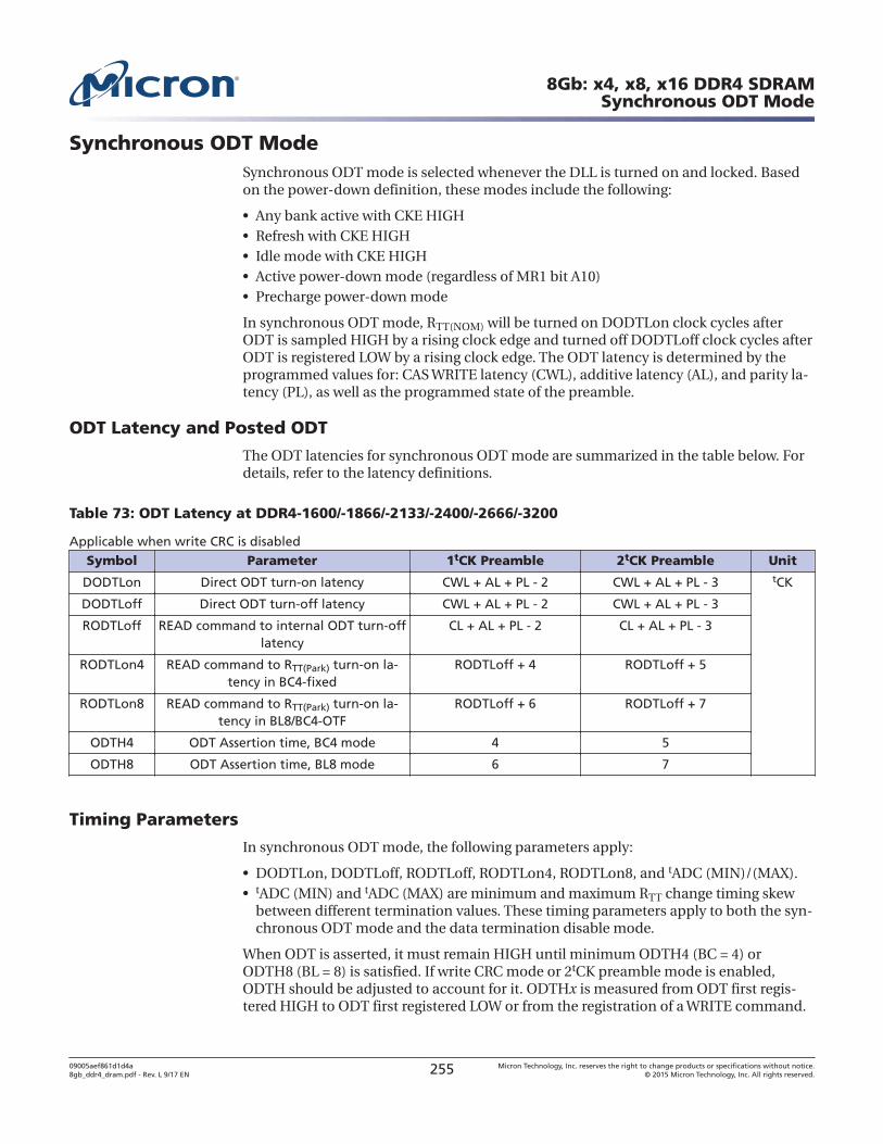
Synchronous ODT ModeSynchronous ODT mode is selected whenever the DLL is turned on and locked. Basedon the power-down definition, these modes include the following:
• Any bank active with CKE HIGH• Refresh with CKE HIGH• Idle mode with CKE HIGH• Active power-down mode (regardless of MR1 bit A10)• Precharge power-down mode
In synchronous ODT mode, RTT(NOM) will be turned on DODTLon clock cycles afterODT is sampled HIGH by a rising clock edge and turned off DODTLoff clock cycles afterODT is registered LOW by a rising clock edge. The ODT latency is determined by theprogrammed values for: CAS WRITE latency (CWL), additive latency (AL), and parity la-tency (PL), as well as the programmed state of the preamble.
ODT Latency and Posted ODT
The ODT latencies for synchronous ODT mode are summarized in the table below. Fordetails, refer to the latency definitions.
Table 73: ODT Latency at DDR4-1600/-1866/-2133/-2400/-2666/-3200
Applicable when write CRC is disabledSymbol Parameter 1tCK Preamble 2tCK Preamble Unit
DODTLon Direct ODT turn-on latency CWL + AL + PL - 2 CWL + AL + PL - 3 tCK
DODTLoff Direct ODT turn-off latency CWL + AL + PL - 2 CWL + AL + PL - 3
RODTLoff READ command to internal ODT turn-offlatency
CL + AL + PL - 2 CL + AL + PL - 3
RODTLon4 READ command to RTT(Park) turn-on la-tency in BC4-fixed
RODTLoff + 4 RODTLoff + 5
RODTLon8 READ command to RTT(Park) turn-on la-tency in BL8/BC4-OTF
RODTLoff + 6 RODTLoff + 7
ODTH4 ODT Assertion time, BC4 mode 4 5
ODTH8 ODT Assertion time, BL8 mode 6 7
Timing Parameters
In synchronous ODT mode, the following parameters apply:
• DODTLon, DODTLoff, RODTLoff, RODTLon4, RODTLon8, and tADC (MIN)/(MAX).• tADC (MIN) and tADC (MAX) are minimum and maximum RTT change timing skew
between different termination values. These timing parameters apply to both the syn-chronous ODT mode and the data termination disable mode.
When ODT is asserted, it must remain HIGH until minimum ODTH4 (BC = 4) orODTH8 (BL = 8) is satisfied. If write CRC mode or 2tCK preamble mode is enabled,ODTH should be adjusted to account for it. ODTHx is measured from ODT first regis-tered HIGH to ODT first registered LOW or from the registration of a WRITE command.
8Gb: x4, x8, x16 DDR4 SDRAMSynchronous ODT Mode
09005aef861d1d4a8gb_ddr4_dram.pdf - Rev. L 9/17 EN 255 Micron Technology, Inc. reserves the right to change products or specifications without notice.
© 2015 Micron Technology, Inc. All rights reserved.
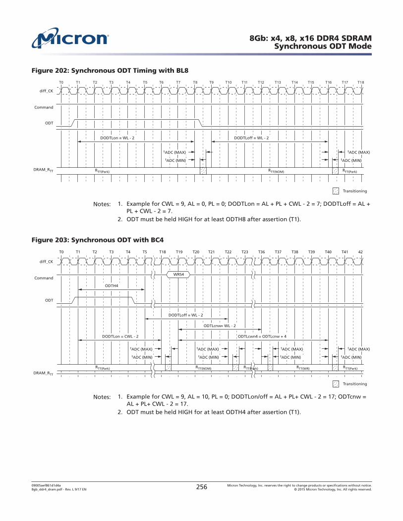
Figure 202: Synchronous ODT Timing with BL8
diff_CK
DODTLon = WL - 2 DODTLoff = WL - 2
Command
ODT
DRAM_RTT RTT(Park) RTT(NOM) RTT(Park)
tADC (MIN)
tADC (MAX)
tADC (MIN)
tADC (MAX)
Transitioning
Notes: 1. Example for CWL = 9, AL = 0, PL = 0; DODTLon = AL + PL + CWL - 2 = 7; DODTLoff = AL +PL + CWL - 2 = 7.
2. ODT must be held HIGH for at least ODTH8 after assertion (T1).
Figure 203: Synchronous ODT with BC4
diff_CK
DODTLon = CWL - 2
ODTH4
ODTLcwn4 = ODTLcnw + 4
DODTLoff = WL - 2
Command
ODT
DRAM_RTT
RTT(Park) RTT(Park)RTT(WR)
tADC (MIN)
tADC (MAX)
tADC (MIN)
tADC (MAX)
T1T0 T2 T3 T4 T5 T18 T19 T20 T21 T22 T23 T36 T37 T38 T39 T40 T41 42
tADC (MIN)
tADC (MAX)
tADC (MIN)
tADC (MAX)
WRS4
Transitioning
ODTLcnw = WL - 2
RTT(Park)RTT(NOM)
Notes: 1. Example for CWL = 9, AL = 10, PL = 0; DODTLon/off = AL + PL+ CWL - 2 = 17; ODTcnw =AL + PL+ CWL - 2 = 17.
2. ODT must be held HIGH for at least ODTH4 after assertion (T1).
8Gb: x4, x8, x16 DDR4 SDRAMSynchronous ODT Mode
09005aef861d1d4a8gb_ddr4_dram.pdf - Rev. L 9/17 EN 256 Micron Technology, Inc. reserves the right to change products or specifications without notice.
© 2015 Micron Technology, Inc. All rights reserved.
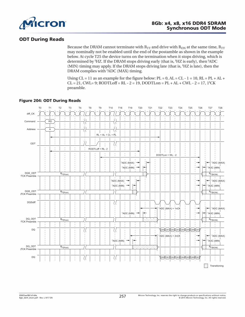
ODT During Reads
Because the DRAM cannot terminate with RTT and drive with RON at the same time, RTTmay nominally not be enabled until the end of the postamble as shown in the examplebelow. At cycle T25 the device turns on the termination when it stops driving, which isdetermined by tHZ. If the DRAM stops driving early (that is, tHZ is early), then tADC(MIN) timing may apply. If the DRAM stops driving late (that is, tHZ is late), then theDRAM complies with tADC (MAX) timing.
Using CL = 11 as an example for the figure below: PL = 0, AL = CL - 1 = 10, RL = PL + AL +CL = 21, CWL= 9; RODTLoff = RL - 2 = 19, DODTLon = PL + AL + CWL - 2 = 17, 1tCKpreamble.
Figure 204: ODT During Reads
8Gb: x4, x8, x16 DDR4 SDRAMSynchronous ODT Mode
09005aef861d1d4a8gb_ddr4_dram.pdf - Rev. L 9/17 EN 257 Micron Technology, Inc. reserves the right to change products or specifications without notice.
© 2015 Micron Technology, Inc. All rights reserved.
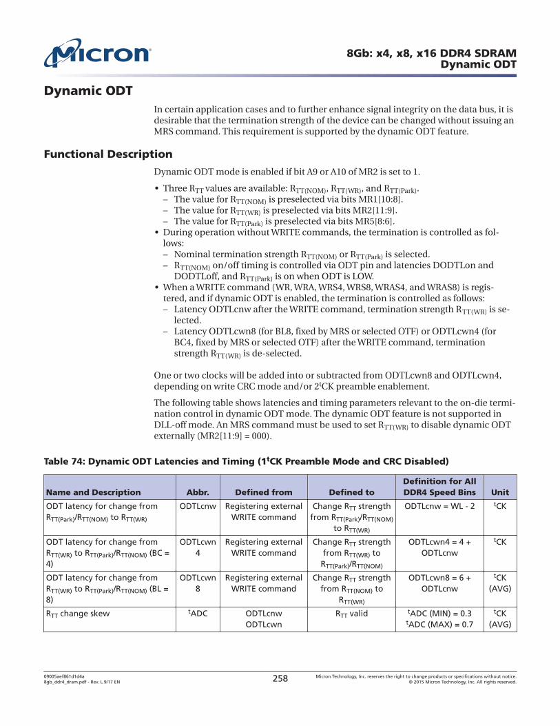
Dynamic ODTIn certain application cases and to further enhance signal integrity on the data bus, it isdesirable that the termination strength of the device can be changed without issuing anMRS command. This requirement is supported by the dynamic ODT feature.
Functional Description
Dynamic ODT mode is enabled if bit A9 or A10 of MR2 is set to 1.
• Three RTT values are available: RTT(NOM), RTT(WR), and RTT(Park).– The value for RTT(NOM) is preselected via bits MR1[10:8].– The value for RTT(WR) is preselected via bits MR2[11:9].– The value for RTT(Park) is preselected via bits MR5[8:6].
• During operation without WRITE commands, the termination is controlled as fol-lows:– Nominal termination strength RTT(NOM) or RTT(Park) is selected.– RTT(NOM) on/off timing is controlled via ODT pin and latencies DODTLon and
DODTLoff, and RTT(Park) is on when ODT is LOW.• When a WRITE command (WR, WRA, WRS4, WRS8, WRAS4, and WRAS8) is regis-
tered, and if dynamic ODT is enabled, the termination is controlled as follows:– Latency ODTLcnw after the WRITE command, termination strength RTT(WR) is se-
lected.– Latency ODTLcwn8 (for BL8, fixed by MRS or selected OTF) or ODTLcwn4 (for
BC4, fixed by MRS or selected OTF) after the WRITE command, terminationstrength RTT(WR) is de-selected.
One or two clocks will be added into or subtracted from ODTLcwn8 and ODTLcwn4,depending on write CRC mode and/or 2tCK preamble enablement.
The following table shows latencies and timing parameters relevant to the on-die termi-nation control in dynamic ODT mode. The dynamic ODT feature is not supported inDLL-off mode. An MRS command must be used to set RTT(WR) to disable dynamic ODTexternally (MR2[11:9] = 000).
Table 74: Dynamic ODT Latencies and Timing (1tCK Preamble Mode and CRC Disabled)
Name and Description Abbr. Defined from Defined toDefinition for AllDDR4 Speed Bins Unit
ODT latency for change fromRTT(Park)/RTT(NOM) to RTT(WR)
ODTLcnw Registering externalWRITE command
Change RTT strengthfrom RTT(Park)/RTT(NOM)
to RTT(WR)
ODTLcnw = WL - 2 tCK
ODT latency for change fromRTT(WR) to RTT(Park)/RTT(NOM) (BC =4)
ODTLcwn4
Registering externalWRITE command
Change RTT strengthfrom RTT(WR) to
RTT(Park)/RTT(NOM)
ODTLcwn4 = 4 +ODTLcnw
tCK
ODT latency for change fromRTT(WR) to RTT(Park)/RTT(NOM) (BL =8)
ODTLcwn8
Registering externalWRITE command
Change RTT strengthfrom RTT(NOM) to
RTT(WR)
ODTLcwn8 = 6 +ODTLcnw
tCK(AVG)
RTT change skew tADC ODTLcnwODTLcwn
RTT valid tADC (MIN) = 0.3tADC (MAX) = 0.7
tCK(AVG)
8Gb: x4, x8, x16 DDR4 SDRAMDynamic ODT
09005aef861d1d4a8gb_ddr4_dram.pdf - Rev. L 9/17 EN 258 Micron Technology, Inc. reserves the right to change products or specifications without notice.
© 2015 Micron Technology, Inc. All rights reserved.
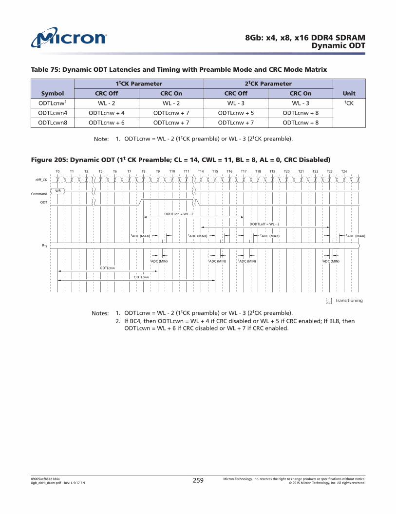
Table 75: Dynamic ODT Latencies and Timing with Preamble Mode and CRC Mode Matrix
Symbol
1tCK Parameter 2tCK Parameter
UnitCRC Off CRC On CRC Off CRC On
ODTLcnw1 WL - 2 WL - 2 WL - 3 WL - 3 tCK
ODTLcwn4 ODTLcnw + 4 ODTLcnw + 7 ODTLcnw + 5 ODTLcnw + 8
ODTLcwn8 ODTLcnw + 6 ODTLcnw + 7 ODTLcnw + 7 ODTLcnw + 8
Note: 1. ODTLcnw = WL - 2 (1tCK preamble) or WL - 3 (2tCK preamble).
Figure 205: Dynamic ODT (1t CK Preamble; CL = 14, CWL = 11, BL = 8, AL = 0, CRC Disabled)
diff_CK
ODTLcwn
ODTLcnw
DODTLon = WL - 2
DODTLoff = WL - 2
Command
ODT
RTT RTT(Park) RTT(NOM) RTT(Park)RTT(WR)
tADC (MAX) tADC (MAX)
T1T0 T2 T5 T6 T7 T14T8 T9 T10 T11 T15 T16 T17 T18 T19 T20 T21 T22 T23 T24
tADC (MIN)tADC (MIN)tADC (MIN)tADC (MIN)
tADC (MAX)
RTT(Park)
tADC (MAX)
WR
Transitioning
Notes: 1. ODTLcnw = WL - 2 (1tCK preamble) or WL - 3 (2tCK preamble).2. If BC4, then ODTLcwn = WL + 4 if CRC disabled or WL + 5 if CRC enabled; If BL8, then
ODTLcwn = WL + 6 if CRC disabled or WL + 7 if CRC enabled.
8Gb: x4, x8, x16 DDR4 SDRAMDynamic ODT
09005aef861d1d4a8gb_ddr4_dram.pdf - Rev. L 9/17 EN 259 Micron Technology, Inc. reserves the right to change products or specifications without notice.
© 2015 Micron Technology, Inc. All rights reserved.
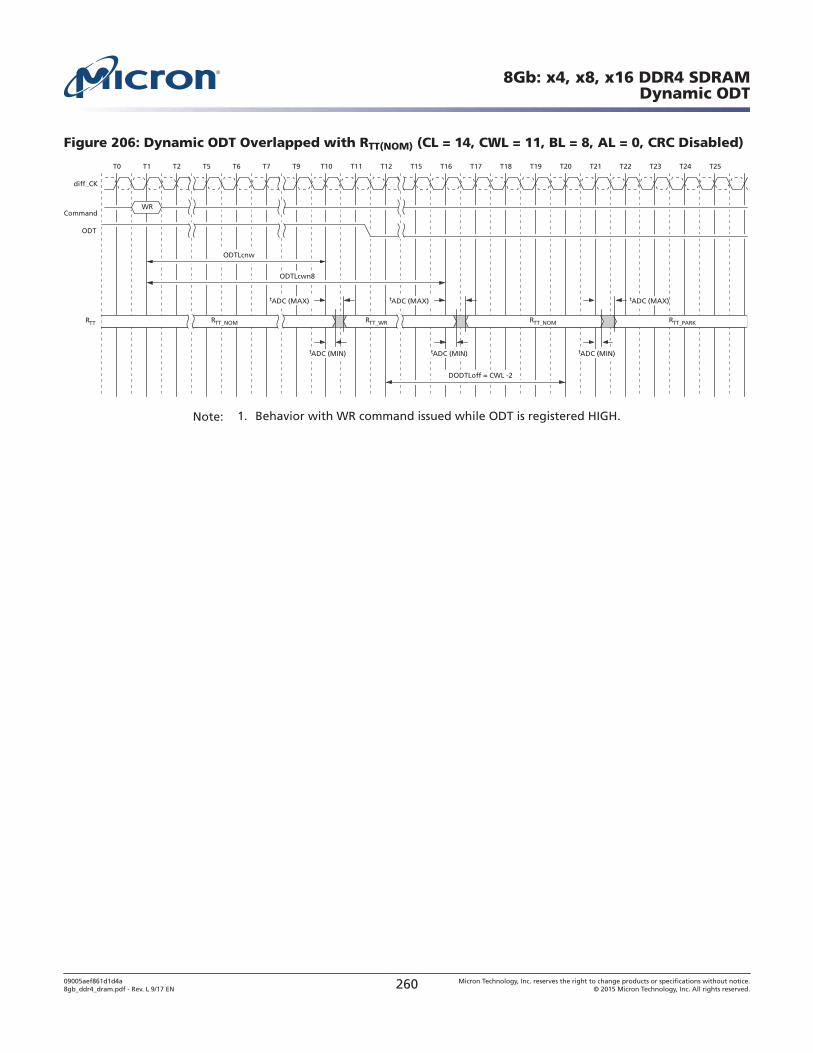
Figure 206: Dynamic ODT Overlapped with RTT(NOM) (CL = 14, CWL = 11, BL = 8, AL = 0, CRC Disabled)
diff_CK
Command
ODT
T1T0 T2 T5 T6 T7 T25T12T9 T10 T11 T15 T16 T17 T18 T19 T20 T21 T22 T23 T24
WR
ODTLcnw
DODTLoff = CWL -2
ODTLcwn8
RTT RTT_NOM RTT_NOM RTT_PARKRTT_WR
tADC (MAX) tADC (MAX)
tADC (MIN)tADC (MIN)tADC (MIN)
tADC (MAX)
Note: 1. Behavior with WR command issued while ODT is registered HIGH.
8Gb: x4, x8, x16 DDR4 SDRAMDynamic ODT
09005aef861d1d4a8gb_ddr4_dram.pdf - Rev. L 9/17 EN 260 Micron Technology, Inc. reserves the right to change products or specifications without notice.
© 2015 Micron Technology, Inc. All rights reserved.
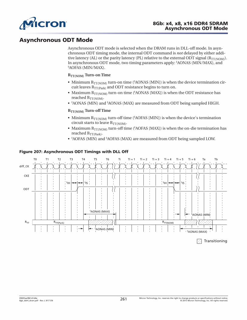
Asynchronous ODT ModeAsynchronous ODT mode is selected when the DRAM runs in DLL-off mode. In asyn-chronous ODT timing mode, the internal ODT command is not delayed by either addi-tive latency (AL) or the parity latency (PL) relative to the external ODT signal (RTT(NOM)).In asynchronous ODT mode, two timing parameters apply: tAONAS (MIN/MAX), andtAOFAS (MIN/MAX).
RTT(NOM) Turn-on Time
• Minimum RTT(NOM) turn-on time (tAONAS [MIN]) is when the device termination cir-cuit leaves RTT(Park) and ODT resistance begins to turn on.
• Maximum RTT(NOM) turn-on time (tAONAS [MAX]) is when the ODT resistance hasreached RTT(NOM).
• tAONAS (MIN) and tAONAS (MAX) are measured from ODT being sampled HIGH.
RTT(NOM) Turn-off Time
• Minimum RTT(NOM) turn-off time (tAOFAS [MIN]) is when the device's terminationcircuit starts to leave RTT(NOM).
• Maximum RTT(NOM) turn-off time (tAOFAS [MAX]) is when the on-die termination hasreached RTT(Park).
• tAOFAS (MIN) and tAOFAS (MAX) are measured from ODT being sampled LOW.
Figure 207: Asynchronous ODT Timings with DLL Off
diff_CK
tAONAS (MAX)
CKE
ODT
RTT RTT(Park) RTT(NOM)
tAONAS (MIN)tAONAS (MAX)
tAONAS (MIN)
tIH tIS tIH tIS
T1T0 T2 T3 T4 T5 T6 Ti Ti + 1 Ti + 2 Ti + 3 Ti + 4 Ti + 5 Ti + 6 Ta Tb
Transitioning
8Gb: x4, x8, x16 DDR4 SDRAMAsynchronous ODT Mode
09005aef861d1d4a8gb_ddr4_dram.pdf - Rev. L 9/17 EN 261 Micron Technology, Inc. reserves the right to change products or specifications without notice.
© 2015 Micron Technology, Inc. All rights reserved.
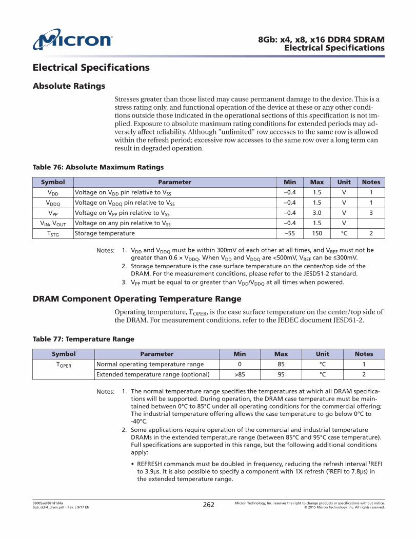
Electrical Specifications
Absolute Ratings
Stresses greater than those listed may cause permanent damage to the device. This is astress rating only, and functional operation of the device at these or any other condi-tions outside those indicated in the operational sections of this specification is not im-plied. Exposure to absolute maximum rating conditions for extended periods may ad-versely affect reliability. Although "unlimited" row accesses to the same row is allowedwithin the refresh period; excessive row accesses to the same row over a long term canresult in degraded operation.
Table 76: Absolute Maximum Ratings
Symbol Parameter Min Max Unit Notes
VDD Voltage on VDD pin relative to VSS –0.4 1.5 V 1
VDDQ Voltage on VDDQ pin relative to VSS –0.4 1.5 V 1
VPP Voltage on VPP pin relative to VSS –0.4 3.0 V 3
VIN, VOUT Voltage on any pin relative to VSS –0.4 1.5 V
TSTG Storage temperature –55 150 °C 2
Notes: 1. VDD and VDDQ must be within 300mV of each other at all times, and VREF must not begreater than 0.6 × VDDQ. When VDD and VDDQ are <500mV, VREF can be 300mV.
2. Storage temperature is the case surface temperature on the center/top side of theDRAM. For the measurement conditions, please refer to the JESD51-2 standard.
3. VPP must be equal to or greater than VDD/VDDQ at all times when powered.
DRAM Component Operating Temperature Range
Operating temperature, TOPER, is the case surface temperature on the center/top side ofthe DRAM. For measurement conditions, refer to the JEDEC document JESD51-2.
Table 77: Temperature Range
Symbol Parameter Min Max Unit Notes
TOPER Normal operating temperature range 0 85 °C 1
Extended temperature range (optional) >85 95 °C 2
Notes: 1. The normal temperature range specifies the temperatures at which all DRAM specifica-tions will be supported. During operation, the DRAM case temperature must be main-tained between 0°C to 85°C under all operating conditions for the commercial offering;The industrial temperature offering allows the case temperature to go below 0°C to-40°C.
2. Some applications require operation of the commercial and industrial temperatureDRAMs in the extended temperature range (between 85°C and 95°C case temperature).Full specifications are supported in this range, but the following additional conditionsapply:
• REFRESH commands must be doubled in frequency, reducing the refresh interval tREFIto 3.9 s. It is also possible to specify a component with 1X refresh (tREFI to 7.8 s) inthe extended temperature range.
8Gb: x4, x8, x16 DDR4 SDRAMElectrical Specifications
09005aef861d1d4a8gb_ddr4_dram.pdf - Rev. L 9/17 EN 262 Micron Technology, Inc. reserves the right to change products or specifications without notice.
© 2015 Micron Technology, Inc. All rights reserved.
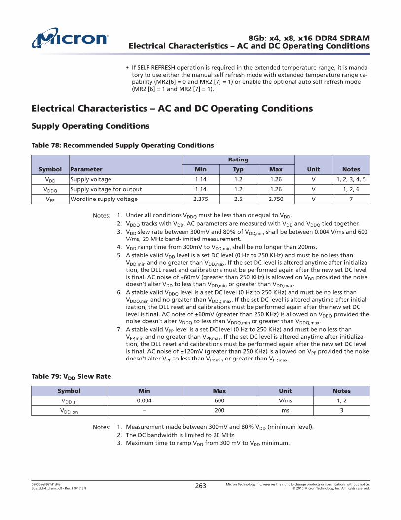
• If SELF REFRESH operation is required in the extended temperature range, it is manda-tory to use either the manual self refresh mode with extended temperature range ca-pability (MR2[6] = 0 and MR2 [7] = 1) or enable the optional auto self refresh mode(MR2 [6] = 1 and MR2 [7] = 1).
Electrical Characteristics – AC and DC Operating Conditions
Supply Operating Conditions
Table 78: Recommended Supply Operating Conditions
Symbol Parameter
Rating
Unit NotesMin Typ Max
VDD Supply voltage 1.14 1.2 1.26 V 1, 2, 3, 4, 5
VDDQ Supply voltage for output 1.14 1.2 1.26 V 1, 2, 6
VPP Wordline supply voltage 2.375 2.5 2.750 V 7
Notes: 1. Under all conditions VDDQ must be less than or equal to VDD.2. VDDQ tracks with VDD. AC parameters are measured with VDD and VDDQ tied together.3. VDD slew rate between 300mV and 80% of VDD,min shall be between 0.004 V/ms and 600
V/ms, 20 MHz band-limited measurement.4. VDD ramp time from 300mV to VDD,min shall be no longer than 200ms.5. A stable valid VDD level is a set DC level (0 Hz to 250 KHz) and must be no less than
VDD,min and no greater than VDD,max. If the set DC level is altered anytime after initializa-tion, the DLL reset and calibrations must be performed again after the new set DC levelis final. AC noise of ±60mV (greater than 250 KHz) is allowed on VDD provided the noisedoesn't alter VDD to less than VDD,min or greater than VDD,max.
6. A stable valid VDDQ level is a set DC level (0 Hz to 250 KHz) and must be no less thanVDDQ,min and no greater than VDDQ,max. If the set DC level is altered anytime after initial-ization, the DLL reset and calibrations must be performed again after the new set DClevel is final. AC noise of ±60mV (greater than 250 KHz) is allowed on VDDQ provided thenoise doesn't alter VDDQ to less than VDDQ,min or greater than VDDQ,max.
7. A stable valid VPP level is a set DC level (0 Hz to 250 KHz) and must be no less thanVPP,min and no greater than VPP,max. If the set DC level is altered anytime after initializa-tion, the DLL reset and calibrations must be performed again after the new set DC levelis final. AC noise of ±120mV (greater than 250 KHz) is allowed on VPP provided the noisedoesn't alter VPP to less than VPP,min or greater than VPP,max.
Table 79: VDD Slew Rate
Symbol Min Max Unit Notes
VDD_sl 0.004 600 V/ms 1, 2
VDD_on – 200 ms 3
Notes: 1. Measurement made between 300mV and 80% VDD (minimum level).2. The DC bandwidth is limited to 20 MHz.3. Maximum time to ramp VDD from 300 mV to VDD minimum.
8Gb: x4, x8, x16 DDR4 SDRAMElectrical Characteristics – AC and DC Operating Conditions
09005aef861d1d4a8gb_ddr4_dram.pdf - Rev. L 9/17 EN 263 Micron Technology, Inc. reserves the right to change products or specifications without notice.
© 2015 Micron Technology, Inc. All rights reserved.
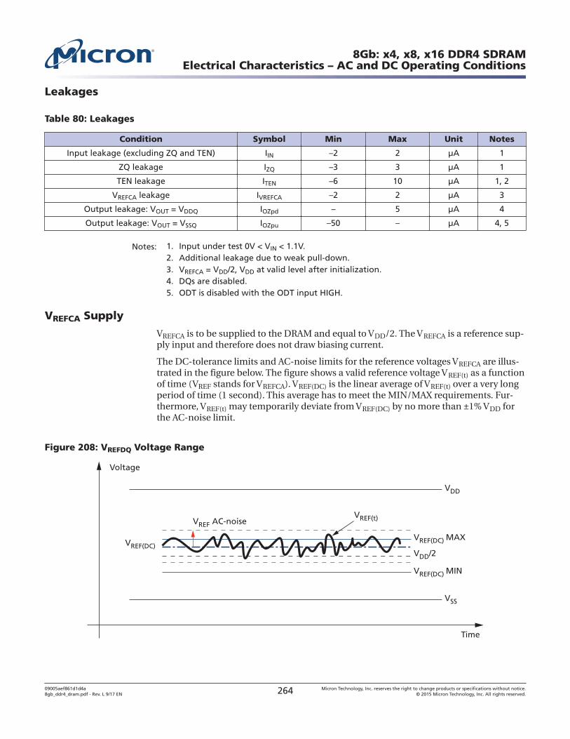
Leakages
Table 80: Leakages
Condition Symbol Min Max Unit Notes
Input leakage (excluding ZQ and TEN) IIN –2 2 μA 1
ZQ leakage IZQ –3 3 μA 1
TEN leakage ITEN –6 10 μA 1, 2
VREFCA leakage IVREFCA –2 2 μA 3
Output leakage: VOUT = VDDQ IOZpd – 5 μA 4
Output leakage: VOUT = VSSQ IOZpu –50 – μA 4, 5
Notes: 1. Input under test 0V < VIN < 1.1V.2. Additional leakage due to weak pull-down.3. VREFCA = VDD/2, VDD at valid level after initialization.4. DQs are disabled.5. ODT is disabled with the ODT input HIGH.
VREFCA Supply
VREFCA is to be supplied to the DRAM and equal to VDD/2. The VREFCA is a reference sup-ply input and therefore does not draw biasing current.
The DC-tolerance limits and AC-noise limits for the reference voltages VREFCA are illus-trated in the figure below. The figure shows a valid reference voltage VREF(t) as a functionof time (VREF stands for VREFCA). VREF(DC) is the linear average of VREF(t) over a very longperiod of time (1 second). This average has to meet the MIN/MAX requirements. Fur-thermore, VREF(t) may temporarily deviate from VREF(DC) by no more than ±1% VDD forthe AC-noise limit.
Figure 208: VREFDQ Voltage Range
VREF AC-noise
VREF(DC)VREF(DC) MAX
VREF(t)
VREF(DC) MIN
VDD/2
VSS
Time
Voltage
VDD
8Gb: x4, x8, x16 DDR4 SDRAMElectrical Characteristics – AC and DC Operating Conditions
09005aef861d1d4a8gb_ddr4_dram.pdf - Rev. L 9/17 EN 264 Micron Technology, Inc. reserves the right to change products or specifications without notice.
© 2015 Micron Technology, Inc. All rights reserved.
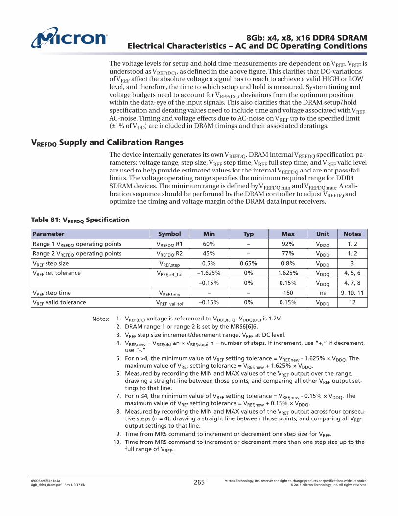
The voltage levels for setup and hold time measurements are dependent on VREF. VREF isunderstood as VREF(DC), as defined in the above figure. This clarifies that DC-variationsof VREF affect the absolute voltage a signal has to reach to achieve a valid HIGH or LOWlevel, and therefore, the time to which setup and hold is measured. System timing andvoltage budgets need to account for VREF(DC) deviations from the optimum positionwithin the data-eye of the input signals. This also clarifies that the DRAM setup/holdspecification and derating values need to include time and voltage associated with VREFAC-noise. Timing and voltage effects due to AC-noise on VREF up to the specified limit(±1% of VDD) are included in DRAM timings and their associated deratings.
VREFDQ Supply and Calibration Ranges
The device internally generates its own VREFDQ. DRAM internal VREFDQ specification pa-rameters: voltage range, step size, VREF step time, VREF full step time, and VREF valid levelare used to help provide estimated values for the internal VREFDQ and are not pass/faillimits. The voltage operating range specifies the minimum required range for DDR4SDRAM devices. The minimum range is defined by VREFDQ,min and VREFDQ,max. A cali-bration sequence should be performed by the DRAM controller to adjust VREFDQ andoptimize the timing and voltage margin of the DRAM data input receivers.
Table 81: VREFDQ Specification
Parameter Symbol Min Typ Max Unit Notes
Range 1 VREFDQ operating points VREFDQ R1 60% – 92% VDDQ 1, 2
Range 2 VREFDQ operating points VREFDQ R2 45% – 77% VDDQ 1, 2
VREF step size VREF,step 0.5% 0.65% 0.8% VDDQ 3
VREF set tolerance VREF,set_tol –1.625% 0% 1.625% VDDQ 4, 5, 6
–0.15% 0% 0.15% VDDQ 4, 7, 8
VREF step time VREF,time – – 150 ns 9, 10, 11
VREF valid tolerance VREF_val_tol –0.15% 0% 0.15% VDDQ 12
Notes: 1. VREF(DC) voltage is referenced to VDDQ(DC). VDDQ(DC) is 1.2V.2. DRAM range 1 or range 2 is set by the MRS6[6]6.3. VREF step size increment/decrement range. VREF at DC level.4. VREF,new = VREF,old ±n × VREF,step; n = number of steps. If increment, use “+,” if decrement,
use “-.”5. For n >4, the minimum value of VREF setting tolerance = VREF,new - 1.625% × VDDQ. The
maximum value of VREF setting tolerance = VREF,new + 1.625% × VDDQ.6. Measured by recording the MIN and MAX values of the VREF output over the range,
drawing a straight line between those points, and comparing all other VREF output set-tings to that line.
7. For n 4, the minimum value of VREF setting tolerance = VREF,new - 0.15% × VDDQ. Themaximum value of VREF setting tolerance = VREF,new + 0.15% × VDDQ.
8. Measured by recording the MIN and MAX values of the VREF output across four consecu-tive steps (n = 4), drawing a straight line between those points, and comparing all VREFoutput settings to that line.
9. Time from MRS command to increment or decrement one step size for VREF.10. Time from MRS command to increment or decrement more than one step size up to the
full range of VREF.
8Gb: x4, x8, x16 DDR4 SDRAMElectrical Characteristics – AC and DC Operating Conditions
09005aef861d1d4a8gb_ddr4_dram.pdf - Rev. L 9/17 EN 265 Micron Technology, Inc. reserves the right to change products or specifications without notice.
© 2015 Micron Technology, Inc. All rights reserved.
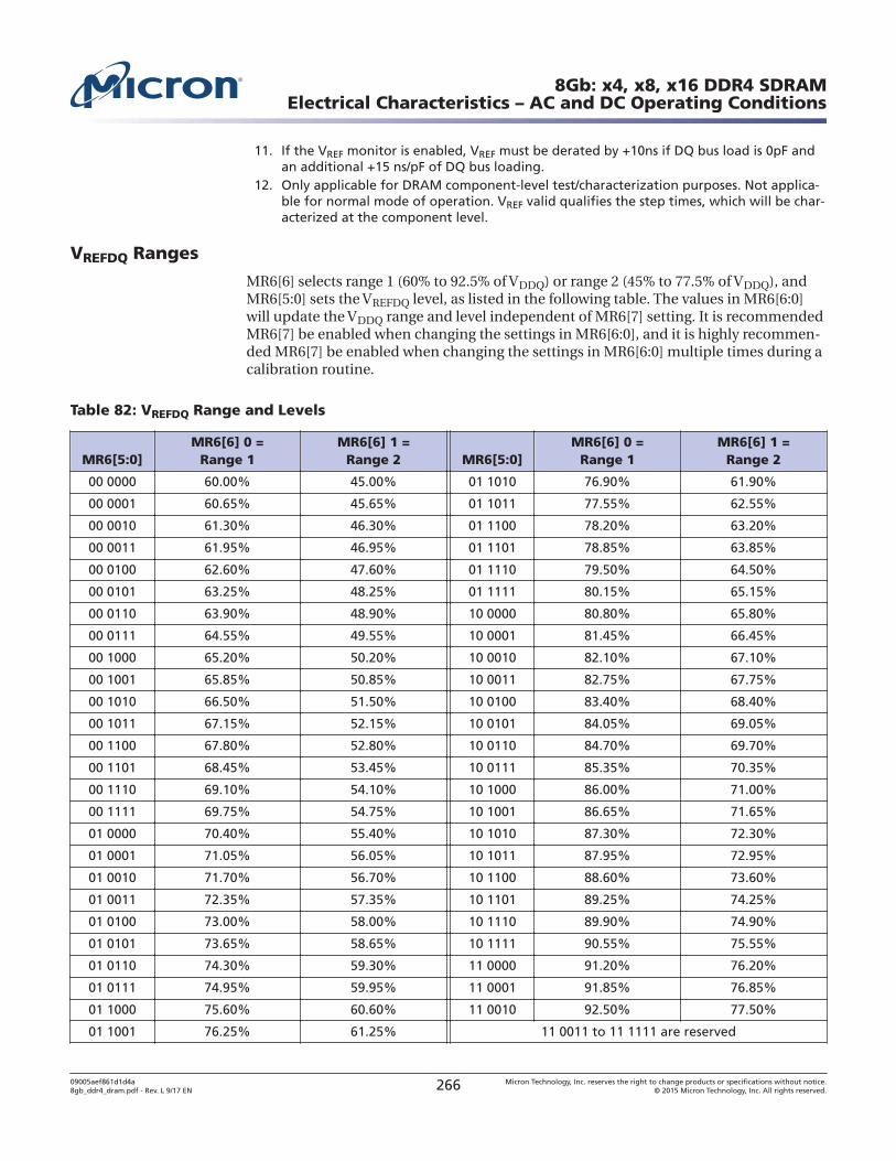
11. If the VREF monitor is enabled, VREF must be derated by +10ns if DQ bus load is 0pF andan additional +15 ns/pF of DQ bus loading.
12. Only applicable for DRAM component-level test/characterization purposes. Not applica-ble for normal mode of operation. VREF valid qualifies the step times, which will be char-acterized at the component level.
VREFDQ Ranges
MR6[6] selects range 1 (60% to 92.5% of VDDQ) or range 2 (45% to 77.5% of VDDQ), andMR6[5:0] sets the VREFDQ level, as listed in the following table. The values in MR6[6:0]will update the VDDQ range and level independent of MR6[7] setting. It is recommendedMR6[7] be enabled when changing the settings in MR6[6:0], and it is highly recommen-ded MR6[7] be enabled when changing the settings in MR6[6:0] multiple times during acalibration routine.
Table 82: VREFDQ Range and Levels
MR6[5:0]MR6[6] 0 =
Range 1MR6[6] 1 =
Range 2 MR6[5:0]MR6[6] 0 =
Range 1MR6[6] 1 =
Range 2
00 0000 60.00% 45.00% 01 1010 76.90% 61.90%
00 0001 60.65% 45.65% 01 1011 77.55% 62.55%
00 0010 61.30% 46.30% 01 1100 78.20% 63.20%
00 0011 61.95% 46.95% 01 1101 78.85% 63.85%
00 0100 62.60% 47.60% 01 1110 79.50% 64.50%
00 0101 63.25% 48.25% 01 1111 80.15% 65.15%
00 0110 63.90% 48.90% 10 0000 80.80% 65.80%
00 0111 64.55% 49.55% 10 0001 81.45% 66.45%
00 1000 65.20% 50.20% 10 0010 82.10% 67.10%
00 1001 65.85% 50.85% 10 0011 82.75% 67.75%
00 1010 66.50% 51.50% 10 0100 83.40% 68.40%
00 1011 67.15% 52.15% 10 0101 84.05% 69.05%
00 1100 67.80% 52.80% 10 0110 84.70% 69.70%
00 1101 68.45% 53.45% 10 0111 85.35% 70.35%
00 1110 69.10% 54.10% 10 1000 86.00% 71.00%
00 1111 69.75% 54.75% 10 1001 86.65% 71.65%
01 0000 70.40% 55.40% 10 1010 87.30% 72.30%
01 0001 71.05% 56.05% 10 1011 87.95% 72.95%
01 0010 71.70% 56.70% 10 1100 88.60% 73.60%
01 0011 72.35% 57.35% 10 1101 89.25% 74.25%
01 0100 73.00% 58.00% 10 1110 89.90% 74.90%
01 0101 73.65% 58.65% 10 1111 90.55% 75.55%
01 0110 74.30% 59.30% 11 0000 91.20% 76.20%
01 0111 74.95% 59.95% 11 0001 91.85% 76.85%
01 1000 75.60% 60.60% 11 0010 92.50% 77.50%
01 1001 76.25% 61.25% 11 0011 to 11 1111 are reserved
8Gb: x4, x8, x16 DDR4 SDRAMElectrical Characteristics – AC and DC Operating Conditions
09005aef861d1d4a8gb_ddr4_dram.pdf - Rev. L 9/17 EN 266 Micron Technology, Inc. reserves the right to change products or specifications without notice.
© 2015 Micron Technology, Inc. All rights reserved.
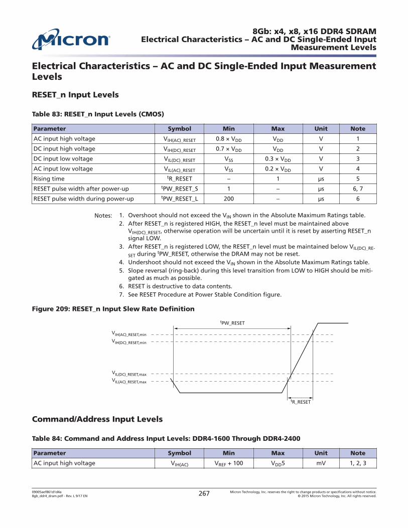
Electrical Characteristics – AC and DC Single-Ended Input MeasurementLevels
RESET_n Input Levels
Table 83: RESET_n Input Levels (CMOS)
Parameter Symbol Min Max Unit Note
AC input high voltage VIH(AC)_RESET 0.8 × VDD VDD V 1
DC input high voltage VIH(DC)_RESET 0.7 × VDD VDD V 2
DC input low voltage VIL(DC)_RESET VSS 0.3 × VDD V 3
AC input low voltage VIL(AC)_RESET VSS 0.2 × VDD V 4
Rising time tR_RESET – 1 μs 5
RESET pulse width after power-up tPW_RESET_S 1 – μs 6, 7
RESET pulse width during power-up tPW_RESET_L 200 – μs 6
Notes: 1. Overshoot should not exceed the VIN shown in the Absolute Maximum Ratings table.2. After RESET_n is registered HIGH, the RESET_n level must be maintained above
VIH(DC)_RESET, otherwise operation will be uncertain until it is reset by asserting RESET_nsignal LOW.
3. After RESET_n is registered LOW, the RESET_n level must be maintained below VIL(DC)_RE-
SET during tPW_RESET, otherwise the DRAM may not be reset.4. Undershoot should not exceed the VIN shown in the Absolute Maximum Ratings table.5. Slope reversal (ring-back) during this level transition from LOW to HIGH should be miti-
gated as much as possible.6. RESET is destructive to data contents.7. See RESET Procedure at Power Stable Condition figure.
Figure 209: RESET_n Input Slew Rate Definition
tR_RESET
tPW_RESET
VIH(AC)_RESET,min
VIL(AC)_RESET,max
VIH(DC)_RESET,min
VIL(DC)_RESET,max
Command/Address Input Levels
Table 84: Command and Address Input Levels: DDR4-1600 Through DDR4-2400
Parameter Symbol Min Max Unit Note
AC input high voltage VIH(AC) VREF + 100 VDD5 mV 1, 2, 3
8Gb: x4, x8, x16 DDR4 SDRAMElectrical Characteristics – AC and DC Single-Ended Input
Measurement Levels
09005aef861d1d4a8gb_ddr4_dram.pdf - Rev. L 9/17 EN 267 Micron Technology, Inc. reserves the right to change products or specifications without notice.
© 2015 Micron Technology, Inc. All rights reserved.
Table 84: Command and Address Input Levels: DDR4-1600 Through DDR4-2400 (Continued)
Parameter Symbol Min Max Unit Note
DC input high voltage VIH(DC) VREF + 75 VDD mV 1, 2
DC input low voltage VIL(DC) VSS VREF - 75 mV 1, 2
AC input low voltage VIL(AC) VSS5 VREF - 100 mV 1, 2, 3
Reference voltage for CMD/ADDR inputs VREFFCA(DC) 0.49 × VDD 0.51 × VDD V 4
Notes: 1. For input except RESET_n. VREF = VREFCA(DC).2. VREF = VREFCA(DC).3. Input signal must meet VIL/VIH(AC) to meet tIS timings and VIL/VIH(DC) to meet tIH timings.4. The AC peak noise on VREF may not allow VREF to deviate from VREFCA(DC) by more than
±1% VDD (for reference: approximately ±12mV).5. Refer to “Overshoot and Undershoot Specifications.”
Table 85: Command and Address Input Levels: DDR4-2666
Parameter Symbol Min Max Unit Note
AC input high voltage VIH(AC) VREF + 90 VDD5 mV 1, 2, 3
DC input high voltage VIH(DC) VREF + 65 VDD mV 1, 2
DC input low voltage VIL(DC) VSS VREF - 65 mV 1, 2
AC input low voltage VIL(AC) VSS5 VREF - 90 mV 1, 2, 3
Reference voltage for CMD/ADDR inputs VREFFCA(DC) 0.49 × VDD 0.51 × VDD V 4
Notes: 1. For input except RESET_n. VREF = VREFCA(DC).2. VREF = VREFCA(DC).3. Input signal must meet VIL/VIH(AC) to meet tIS timings and VIL/VIH(DC) to meet tIH timings.4. The AC peak noise on VREF may not allow VREF to deviate from VREFCA(DC) by more than
±1% VDD (for reference: approximately ±12mV).5. Refer to “Overshoot and Undershoot Specifications.”
Table 86: Command and Address Input Levels: DDR4-2933 and DDR4-3200
Parameter Symbol Min Max Unit Note
AC input high voltage VIH(AC) VREF + 90 VDD5 mV 1, 2, 3
DC input high voltage VIH(DC) VREF + 65 VDD mV 1, 2
DC input low voltage VIL(DC) VSS VREF - 65 mV 1, 2
AC input low voltage VIL(AC) VSS5 VREF - 90 mV 1, 2, 3
Reference voltage for CMD/ADDR inputs VREFFCA(DC) 0.49 × VDD 0.51 × VDD V 4
Notes: 1. For input except RESET_n. VREF = VREFCA(DC).2. VREF = VREFCA(DC).3. Input signal must meet VIL/VIH(AC) to meet tIS timings and VIL/VIH(DC) to meet tIH timings.4. The AC peak noise on VREF may not allow VREF to deviate from VREFCA(DC) by more than
±1% VDD (for reference: approximately ±12mV).5. Refer to “Overshoot and Undershoot Specifications.”
8Gb: x4, x8, x16 DDR4 SDRAMElectrical Characteristics – AC and DC Single-Ended Input
Measurement Levels
09005aef861d1d4a8gb_ddr4_dram.pdf - Rev. L 9/17 EN 268 Micron Technology, Inc. reserves the right to change products or specifications without notice.
© 2015 Micron Technology, Inc. All rights reserved.
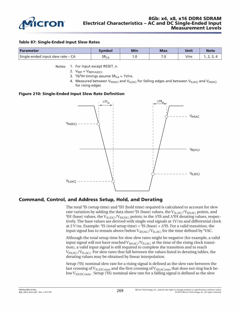
Table 87: Single-Ended Input Slew Rates
Parameter Symbol Min Max Unit Note
Single-ended input slew rate – CA SRCA 1.0 7.0 V/ns 1, 2, 3, 4
Notes: 1. For input except RESET_n.2. VREF = VREFCA(DC).3. tIS/tIH timings assume SRCA = 1V/ns.4. Measured between VIH(AC) and VIL(AC) for falling edges and between VIL(AC) and VIH(AC)
for rising edges
Figure 210: Single-Ended Input Slew Rate Definition
TRseTFse
VIH(DC)
VIH(AC)
VIL(AC)
VIL(DC)
VREFCA
Command, Control, and Address Setup, Hold, and Derating
The total tIS (setup time) and tIH (hold time) required is calculated to account for slewrate variation by adding the data sheet tIS (base) values, the VIL(AC)/VIH(AC) points, andtIH (base) values, the VIL(DC)/VIH(DC) points; to the tIS and tIH derating values, respec-tively. The base values are derived with single-end signals at 1V/ns and differential clockat 2 V/ns. Example: tIS (total setup time) = tIS (base) + tIS. For a valid transition, theinput signal has to remain above/below VIH(AC)/VIL(AC) for the time defined by tVAC.
Although the total setup time for slow slew rates might be negative (for example, a validinput signal will not have reached VIH(AC)/VIL(AC) at the time of the rising clock transi-tion), a valid input signal is still required to complete the transition and to reachVIH(AC)/VIL(AC). For slew rates that fall between the values listed in derating tables, thederating values may be obtained by linear interpolation.
Setup (tIS) nominal slew rate for a rising signal is defined as the slew rate between thelast crossing of VIL(DC)max and the first crossing of VIH(AC)min that does not ring back be-low VIH(DC)min . Setup (tIS) nominal slew rate for a falling signal is defined as the slew
8Gb: x4, x8, x16 DDR4 SDRAMElectrical Characteristics – AC and DC Single-Ended Input
Measurement Levels
09005aef861d1d4a8gb_ddr4_dram.pdf - Rev. L 9/17 EN 269 Micron Technology, Inc. reserves the right to change products or specifications without notice.
© 2015 Micron Technology, Inc. All rights reserved.
rate between the last crossing of VIH(DC)min and the first crossing of VIL(AC)max that doesnot ring back above VIL(DC)max.
Hold (tIH) nominal slew rate for a rising signal is defined as the slew rate between thelast crossing of VIL(DC)max and the first crossing of VIH(AC)min that does not ring back be-low VIH(DC)min. Hold (tIH) nominal slew rate for a falling signal is defined as the slew ratebetween the last crossing of VIH(DC)min and the first crossing of VIL(AC)minthat does notring back above VIL(DC)max.
Table 88: Command and Address Setup and Hold Values Referenced – AC/DC-Based
Symbol 1600 1866 2133 2400 2666 2933 3200 Unit ReferencetIS(base, AC100) 115 100 80 62 – – – ps VIH(AC)/VIL(AC)
tIH(base, DC75) 140 125 105 87 – – – ps VIH(DC)/VIL(DC)
tIS(base, AC90) – – – – 55 48 40 ps VIH(AC)/VIL(AC)
tIH(base, DC65) – – – – 80 73 65 ps VIH(DC)/VIL(DC)
tIS/tIH(Vref) 215 200 180 162 145 138 130 ps VIH(DC)/VIL(DC)
Table 89: Derating Values for tIS/tIH – AC100DC75-Based
tIS with AC100 Threshold, tIH with DC75 Threshold Derating (ps) – AC/DC-Based
CMD/ADDR
Slew RateV/ns
CK, CK# Differential Slew Rate
10.0 V/ns 8.0 V/ns 6.0 V/ns 4.0 V/ns 3.0 V/ns 2.0 V/ns 1.5 V/ns 1.0 V/ns
tIS tIH tIS tIH tIS tIH tIS tIH tIS tIH tIH tIH tIS tIH tIS tIH
7.0 76 54 76 55 77 56 79 58 82 60 86 64 94 73 111 89
6.0 73 53 74 53 75 54 77 56 79 58 83 63 92 71 108 88
5.0 70 50 71 51 72 52 74 54 76 56 80 60 88 68 105 85
4.0 65 46 66 47 67 48 69 50 71 52 75 56 83 65 100 81
3.0 57 40 57 41 58 42 60 44 63 46 67 50 75 58 92 75
2.0 40 28 41 28 42 29 44 31 46 33 50 38 58 46 75 63
1.5 23 15 24 16 25 17 27 19 29 21 33 25 42 33 58 50
1.0 –10 –10 –9 –9 –8 –8 –6 –6 –4 –4 0 0 8 8 25 25
0.9 –17 –14 –16 –14 –15 –13 –13 –10 –11 –8 –7 –4 1 4 18 21
0.8 –26 –19 –25 –19 –24 –18 –22 –16 –20 –14 –16 –9 –7 –1 9 16
0.7 –37 –26 –36 –25 –35 –24 –33 –22 –31 –20 –27 –16 –18 –8 –2 9
0.6 –52 –35 –51 –34 –50 –33 –48 –31 –46 –29 –42 –25 –33 –17 –17 0
0.5 –73 –48 –72 –47 –71 –46 –69 –44 –67 –42 –63 –38 –54 –29 –38 –13
0.4 –104 –66 –103 –66 –102 –65 –100 –63 –98 –60 –94 –56 –85 –48 –69 –31
8Gb: x4, x8, x16 DDR4 SDRAMElectrical Characteristics – AC and DC Single-Ended Input
Measurement Levels
09005aef861d1d4a8gb_ddr4_dram.pdf - Rev. L 9/17 EN 270 Micron Technology, Inc. reserves the right to change products or specifications without notice.
© 2015 Micron Technology, Inc. All rights reserved.
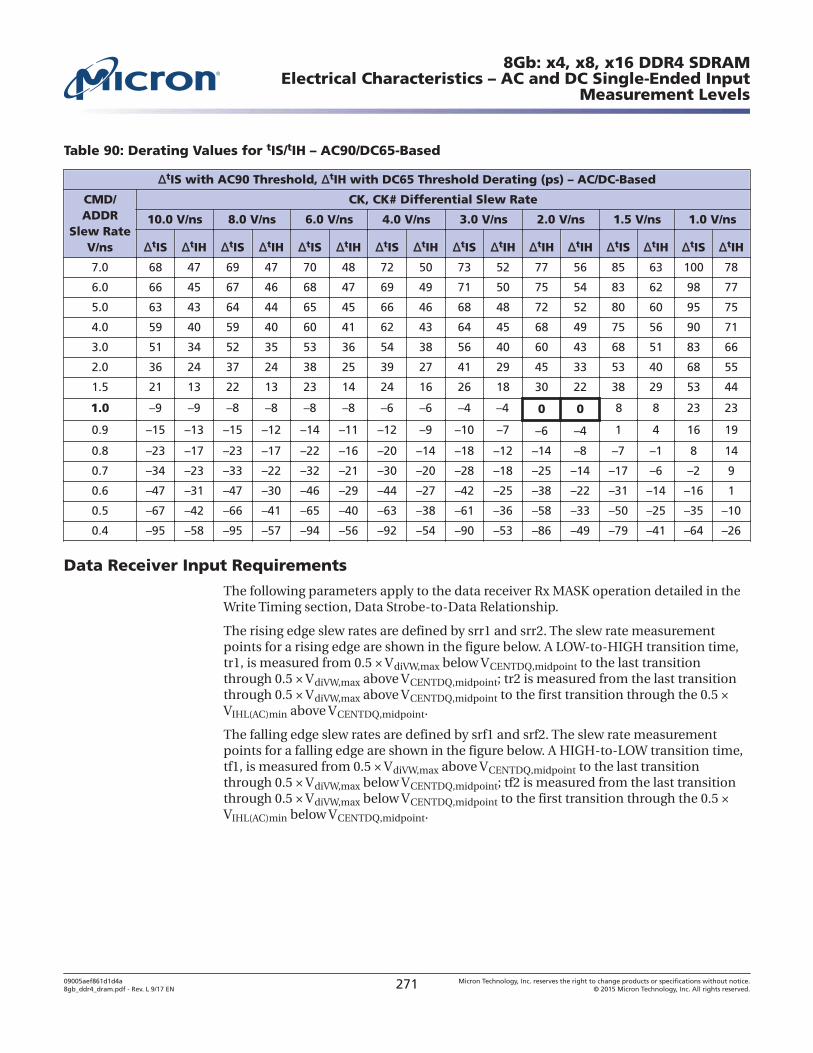
Table 90: Derating Values for tIS/tIH – AC90/DC65-Based
tIS with AC90 Threshold, tIH with DC65 Threshold Derating (ps) – AC/DC-Based
CMD/ADDR
Slew RateV/ns
CK, CK# Differential Slew Rate
10.0 V/ns 8.0 V/ns 6.0 V/ns 4.0 V/ns 3.0 V/ns 2.0 V/ns 1.5 V/ns 1.0 V/ns
tIS tIH tIS tIH tIS tIH tIS tIH tIS tIH tIH tIH tIS tIH tIS tIH
7.0 68 47 69 47 70 48 72 50 73 52 77 56 85 63 100 78
6.0 66 45 67 46 68 47 69 49 71 50 75 54 83 62 98 77
5.0 63 43 64 44 65 45 66 46 68 48 72 52 80 60 95 75
4.0 59 40 59 40 60 41 62 43 64 45 68 49 75 56 90 71
3.0 51 34 52 35 53 36 54 38 56 40 60 43 68 51 83 66
2.0 36 24 37 24 38 25 39 27 41 29 45 33 53 40 68 55
1.5 21 13 22 13 23 14 24 16 26 18 30 22 38 29 53 44
1.0 –9 –9 –8 –8 –8 –8 –6 –6 –4 –4 0 0 8 8 23 23
0.9 –15 –13 –15 –12 –14 –11 –12 –9 –10 –7 –6 –4 1 4 16 19
0.8 –23 –17 –23 –17 –22 –16 –20 –14 –18 –12 –14 –8 –7 –1 8 14
0.7 –34 –23 –33 –22 –32 –21 –30 –20 –28 –18 –25 –14 –17 –6 –2 9
0.6 –47 –31 –47 –30 –46 –29 –44 –27 –42 –25 –38 –22 –31 –14 –16 1
0.5 –67 –42 –66 –41 –65 –40 –63 –38 –61 –36 –58 –33 –50 –25 –35 –10
0.4 –95 –58 –95 –57 –94 –56 –92 –54 –90 –53 –86 –49 –79 –41 –64 –26
Data Receiver Input Requirements
The following parameters apply to the data receiver Rx MASK operation detailed in theWrite Timing section, Data Strobe-to-Data Relationship.
The rising edge slew rates are defined by srr1 and srr2. The slew rate measurementpoints for a rising edge are shown in the figure below. A LOW-to-HIGH transition time,tr1, is measured from 0.5 × VdiVW,max below VCENTDQ,midpoint to the last transitionthrough 0.5 × VdiVW,max above VCENTDQ,midpoint; tr2 is measured from the last transitionthrough 0.5 × VdiVW,max above VCENTDQ,midpoint to the first transition through the 0.5 ×VIHL(AC)min above VCENTDQ,midpoint.
The falling edge slew rates are defined by srf1 and srf2. The slew rate measurementpoints for a falling edge are shown in the figure below. A HIGH-to-LOW transition time,tf1, is measured from 0.5 × VdiVW,max above VCENTDQ,midpoint to the last transitionthrough 0.5 × VdiVW,max below VCENTDQ,midpoint; tf2 is measured from the last transitionthrough 0.5 × VdiVW,max below VCENTDQ,midpoint to the first transition through the 0.5 ×VIHL(AC)min below VCENTDQ,midpoint.
8Gb: x4, x8, x16 DDR4 SDRAMElectrical Characteristics – AC and DC Single-Ended Input
Measurement Levels
09005aef861d1d4a8gb_ddr4_dram.pdf - Rev. L 9/17 EN 271 Micron Technology, Inc. reserves the right to change products or specifications without notice.
© 2015 Micron Technology, Inc. All rights reserved.
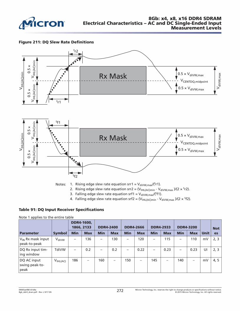
Figure 211: DQ Slew Rate Definitions
VIH
L(A
C)m
in
0.5
×V
IHL(
AC
)min
0.5
×V
IHL(
AC
)min
VIH
L(A
C)m
in
0.5
×V
IHL(
AC
)min
0.5
×V
IHL(
AC
)min
0.5 × VdiVW,max
0.5 × VdiVW,max
VCENTDQ,midpoint
Vd
iVW
,max
0.5 × VdiVW,max
0.5 × VdiVW,max Vd
iVW
,max
tr1
tr2
VCENTDQ,midpoint
tf1
tf2
Rx Mask
Rx Mask
Notes: 1. Rising edge slew rate equation srr1 = VdiVW,max/(tr1).2. Rising edge slew rate equation srr2 = (VIHL(AC)min - VdiVW,max )/(2 × tr2).3. Falling edge slew rate equation srf1 = VdiVW,max/(tf1).4. Falling edge slew rate equation srf2 = (VIHL(AC)min - VdiVW,max )/(2 × tf2).
Table 91: DQ Input Receiver Specifications
Note 1 applies to the entire table
Parameter Symbol
DDR4-1600,1866, 2133 DDR4-2400 DDR4-2666 DDR4-2933 DDR4-3200
UnitNotesMin Max Min Max Min Max Min Max Min Max
VIN Rx mask inputpeak-to-peak
VdiVW – 136 – 130 – 120 – 115 – 110 mV 2, 3
DQ Rx input tim-ing window
TdiVW – 0.2 – 0.2 – 0.22 – 0.23 – 0.23 UI 2, 3
DQ AC inputswing peak-to-peak
VIHL(AC) 186 – 160 – 150 – 145 – 140 – mV 4, 5
8Gb: x4, x8, x16 DDR4 SDRAMElectrical Characteristics – AC and DC Single-Ended Input
Measurement Levels
09005aef861d1d4a8gb_ddr4_dram.pdf - Rev. L 9/17 EN 272 Micron Technology, Inc. reserves the right to change products or specifications without notice.
© 2015 Micron Technology, Inc. All rights reserved.
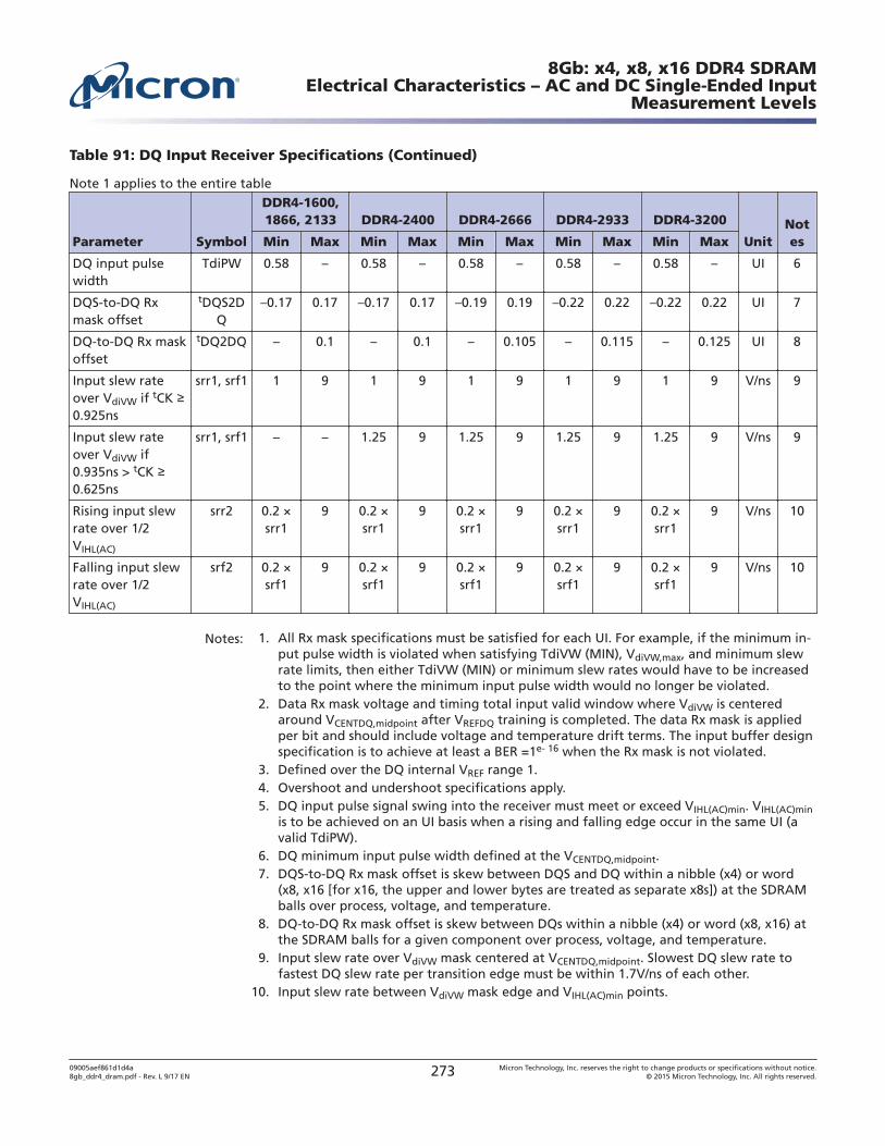
Table 91: DQ Input Receiver Specifications (Continued)
Note 1 applies to the entire table
Parameter Symbol
DDR4-1600,1866, 2133 DDR4-2400 DDR4-2666 DDR4-2933 DDR4-3200
UnitNotesMin Max Min Max Min Max Min Max Min Max
DQ input pulsewidth
TdiPW 0.58 – 0.58 – 0.58 – 0.58 – 0.58 – UI 6
DQS-to-DQ Rxmask offset
tDQS2DQ
–0.17 0.17 –0.17 0.17 –0.19 0.19 –0.22 0.22 –0.22 0.22 UI 7
DQ-to-DQ Rx maskoffset
tDQ2DQ – 0.1 – 0.1 – 0.105 – 0.115 – 0.125 UI 8
Input slew rateover VdiVW if tCK 0.925ns
srr1, srf1 1 9 1 9 1 9 1 9 1 9 V/ns 9
Input slew rateover VdiVW if0.935ns > tCK 0.625ns
srr1, srf1 – – 1.25 9 1.25 9 1.25 9 1.25 9 V/ns 9
Rising input slewrate over 1/2VIHL(AC)
srr2 0.2 ×srr1
9 0.2 ×srr1
9 0.2 ×srr1
9 0.2 ×srr1
9 0.2 ×srr1
9 V/ns 10
Falling input slewrate over 1/2VIHL(AC)
srf2 0.2 ×srf1
9 0.2 ×srf1
9 0.2 ×srf1
9 0.2 ×srf1
9 0.2 ×srf1
9 V/ns 10
Notes: 1. All Rx mask specifications must be satisfied for each UI. For example, if the minimum in-put pulse width is violated when satisfying TdiVW (MIN), VdiVW,max, and minimum slewrate limits, then either TdiVW (MIN) or minimum slew rates would have to be increasedto the point where the minimum input pulse width would no longer be violated.
2. Data Rx mask voltage and timing total input valid window where VdiVW is centeredaround VCENTDQ,midpoint after VREFDQ training is completed. The data Rx mask is appliedper bit and should include voltage and temperature drift terms. The input buffer designspecification is to achieve at least a BER =1e- 16 when the Rx mask is not violated.
3. Defined over the DQ internal VREF range 1.4. Overshoot and undershoot specifications apply.5. DQ input pulse signal swing into the receiver must meet or exceed VIHL(AC)min. VIHL(AC)min
is to be achieved on an UI basis when a rising and falling edge occur in the same UI (avalid TdiPW).
6. DQ minimum input pulse width defined at the VCENTDQ,midpoint.7. DQS-to-DQ Rx mask offset is skew between DQS and DQ within a nibble (x4) or word
(x8, x16 [for x16, the upper and lower bytes are treated as separate x8s]) at the SDRAMballs over process, voltage, and temperature.
8. DQ-to-DQ Rx mask offset is skew between DQs within a nibble (x4) or word (x8, x16) atthe SDRAM balls for a given component over process, voltage, and temperature.
9. Input slew rate over VdiVW mask centered at VCENTDQ,midpoint. Slowest DQ slew rate tofastest DQ slew rate per transition edge must be within 1.7V/ns of each other.
10. Input slew rate between VdiVW mask edge and VIHL(AC)min points.
8Gb: x4, x8, x16 DDR4 SDRAMElectrical Characteristics – AC and DC Single-Ended Input
Measurement Levels
09005aef861d1d4a8gb_ddr4_dram.pdf - Rev. L 9/17 EN 273 Micron Technology, Inc. reserves the right to change products or specifications without notice.
© 2015 Micron Technology, Inc. All rights reserved.
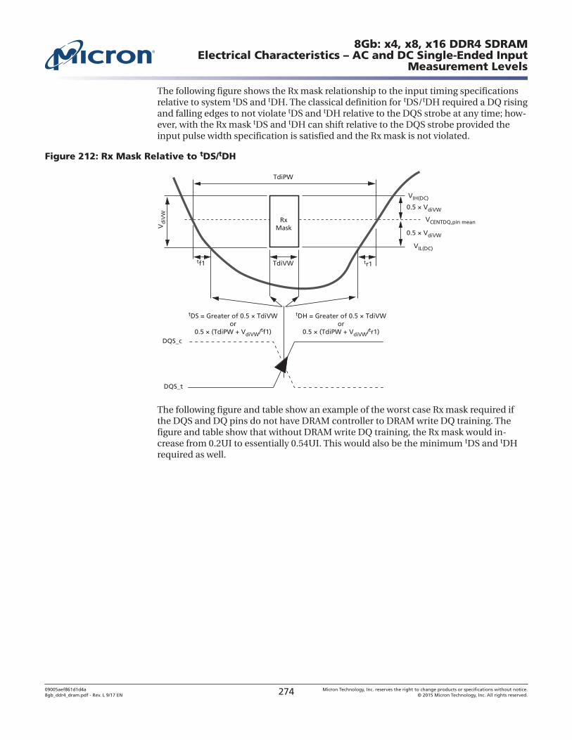
The following figure shows the Rx mask relationship to the input timing specificationsrelative to system tDS and tDH. The classical definition for tDS/tDH required a DQ risingand falling edges to not violate tDS and tDH relative to the DQS strobe at any time; how-ever, with the Rx mask tDS and tDH can shift relative to the DQS strobe provided theinput pulse width specification is satisfied and the Rx mask is not violated.
Figure 212: Rx Mask Relative to tDS/tDH
tDH = Greater of 0.5 × TdiVWor
0.5 × (TdiPW + VdiVW/tr1)
tDS = Greater of 0.5 × TdiVWor
0.5 × (TdiPW + VdiVW/tf1)
Vd
iVW
0.5 × VdiVW
tf1 tr1
0.5 × VdiVW
TdiPW
TdiVW
VCENTDQ,pin mean
VIL(DC)
VIH(DC)
DQS_c
DQS_t
RxMask
The following figure and table show an example of the worst case Rx mask required ifthe DQS and DQ pins do not have DRAM controller to DRAM write DQ training. Thefigure and table show that without DRAM write DQ training, the Rx mask would in-crease from 0.2UI to essentially 0.54UI. This would also be the minimum tDS and tDHrequired as well.
8Gb: x4, x8, x16 DDR4 SDRAMElectrical Characteristics – AC and DC Single-Ended Input
Measurement Levels
09005aef861d1d4a8gb_ddr4_dram.pdf - Rev. L 9/17 EN 274 Micron Technology, Inc. reserves the right to change products or specifications without notice.
© 2015 Micron Technology, Inc. All rights reserved.
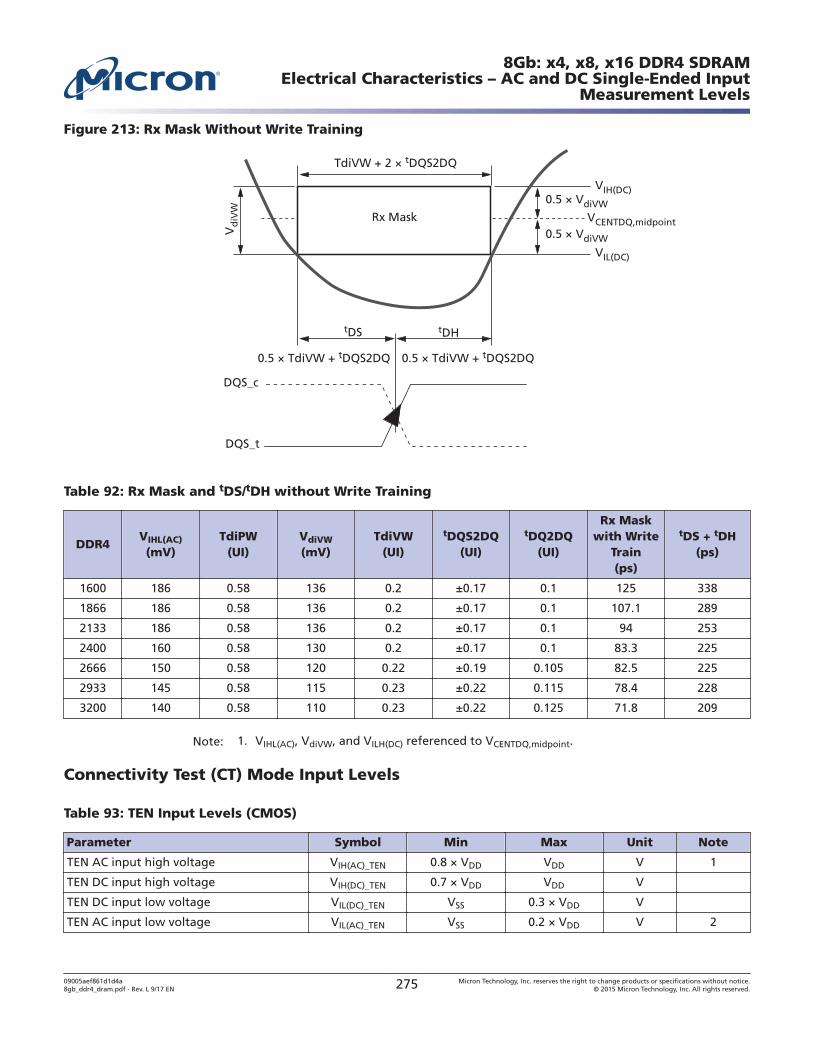
Figure 213: Rx Mask Without Write Training
tDS
Vd
iVW
0.5 × VdiVW
0.5 × VdiVW
tDH
0.5 × TdiVW + tDQS2DQ
TdiVW + 2 × tDQS2DQ
0.5 × TdiVW + tDQS2DQ
VCENTDQ,midpoint
VIL(DC)
VIH(DC)
DQS_c
DQS_t
Rx Mask
Table 92: Rx Mask and tDS/tDH without Write Training
DDR4VIHL(AC)
(mV)TdiPW
(UI)VdiVW
(mV)TdiVW
(UI)
tDQS2DQ(UI)
tDQ2DQ(UI)
Rx Maskwith Write
Train(ps)
tDS + tDH(ps)
1600 186 0.58 136 0.2 ±0.17 0.1 125 338
1866 186 0.58 136 0.2 ±0.17 0.1 107.1 289
2133 186 0.58 136 0.2 ±0.17 0.1 94 253
2400 160 0.58 130 0.2 ±0.17 0.1 83.3 225
2666 150 0.58 120 0.22 ±0.19 0.105 82.5 225
2933 145 0.58 115 0.23 ±0.22 0.115 78.4 228
3200 140 0.58 110 0.23 ±0.22 0.125 71.8 209
Note: 1. VIHL(AC), VdiVW, and VILH(DC) referenced to VCENTDQ,midpoint.
Connectivity Test (CT) Mode Input Levels
Table 93: TEN Input Levels (CMOS)
Parameter Symbol Min Max Unit Note
TEN AC input high voltage VIH(AC)_TEN 0.8 × VDD VDD V 1
TEN DC input high voltage VIH(DC)_TEN 0.7 × VDD VDD V
TEN DC input low voltage VIL(DC)_TEN VSS 0.3 × VDD V
TEN AC input low voltage VIL(AC)_TEN VSS 0.2 × VDD V 2
8Gb: x4, x8, x16 DDR4 SDRAMElectrical Characteristics – AC and DC Single-Ended Input
Measurement Levels
09005aef861d1d4a8gb_ddr4_dram.pdf - Rev. L 9/17 EN 275 Micron Technology, Inc. reserves the right to change products or specifications without notice.
© 2015 Micron Technology, Inc. All rights reserved.
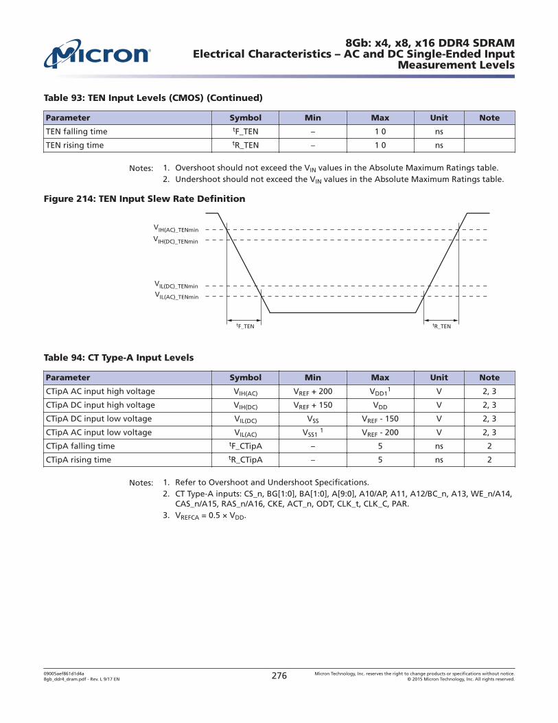
Table 93: TEN Input Levels (CMOS) (Continued)
Parameter Symbol Min Max Unit Note
TEN falling time tF_TEN – 1 0 ns
TEN rising time tR_TEN – 1 0 ns
Notes: 1. Overshoot should not exceed the VIN values in the Absolute Maximum Ratings table.2. Undershoot should not exceed the VIN values in the Absolute Maximum Ratings table.
Figure 214: TEN Input Slew Rate Definition
tR_TENtF_TEN
VIH(AC)_TENmin
VIL(AC)_TENmin
VIH(DC)_TENmin
VIL(DC)_TENmin
Table 94: CT Type-A Input Levels
Parameter Symbol Min Max Unit Note
CTipA AC input high voltage VIH(AC) VREF + 200 VDD11 V 2, 3
CTipA DC input high voltage VIH(DC) VREF + 150 VDD V 2, 3
CTipA DC input low voltage VIL(DC) VSS VREF - 150 V 2, 3
CTipA AC input low voltage VIL(AC) VSS1 1 VREF - 200 V 2, 3
CTipA falling time tF_CTipA – 5 ns 2
CTipA rising time tR_CTipA – 5 ns 2
Notes: 1. Refer to Overshoot and Undershoot Specifications.2. CT Type-A inputs: CS_n, BG[1:0], BA[1:0], A[9:0], A10/AP, A11, A12/BC_n, A13, WE_n/A14,
CAS_n/A15, RAS_n/A16, CKE, ACT_n, ODT, CLK_t, CLK_C, PAR.3. VREFCA = 0.5 × VDD.
8Gb: x4, x8, x16 DDR4 SDRAMElectrical Characteristics – AC and DC Single-Ended Input
Measurement Levels
09005aef861d1d4a8gb_ddr4_dram.pdf - Rev. L 9/17 EN 276 Micron Technology, Inc. reserves the right to change products or specifications without notice.
© 2015 Micron Technology, Inc. All rights reserved.
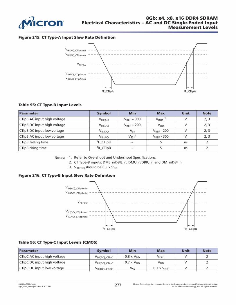
Figure 215: CT Type-A Input Slew Rate Definition
VIH(AC)_CTipAmin
VIL(AC)_CTipAmax
VIH(DC)_CTipAmin
VIL(DC)_CTipAmax
tR_CTipAtF_CTipA
VREFCA
Table 95: CT Type-B Input Levels
Parameter Symbol Min Max Unit Note
CTipB AC input high voltage VIH(AC) VREF + 300 VDD1 1 V 2, 3
CTipB DC input high voltage VIH(DC) VREF + 200 VDD V 2, 3
CTipB DC input low voltage VIL(DC) VSS VREF - 200 V 2, 3
CTipB AC input low voltage VIL(AC) VSS11 VREF - 300 V 2, 3
CTipB falling time tF_CTipB – 5 ns 2
CTipB rising time tR_CTipB – 5 ns 2
Notes: 1. Refer to Overshoot and Undershoot Specifications.2. CT Type-B inputs: DML_n/DBIL_n, DMU_n/DBIU_n and DM_n/DBI_n.3. VREFDQ should be 0.5 × VDD
Figure 216: CT Type-B Input Slew Rate Definition
VIH(AC)_CTipBmin
VIL(AC)_CTipBmax
VIH(DC)_CTipBmin
VIL(DC)_CTipBmax
tR_CTipBtF_CTipB
VREFDQ
Table 96: CT Type-C Input Levels (CMOS)
Parameter Symbol Min Max Unit Note
CTipC AC input high voltage VIH(AC)_CTipC 0.8 × VDD VDD1 V 2
CTipC DC input high voltage VIH(DC)_CTipC 0.7 × VDD VDD V 2
CTipC DC input low voltage VIL(DC)_CTipC VSS 0.3 × VDD V 2
8Gb: x4, x8, x16 DDR4 SDRAMElectrical Characteristics – AC and DC Single-Ended Input
Measurement Levels
09005aef861d1d4a8gb_ddr4_dram.pdf - Rev. L 9/17 EN 277 Micron Technology, Inc. reserves the right to change products or specifications without notice.
© 2015 Micron Technology, Inc. All rights reserved.
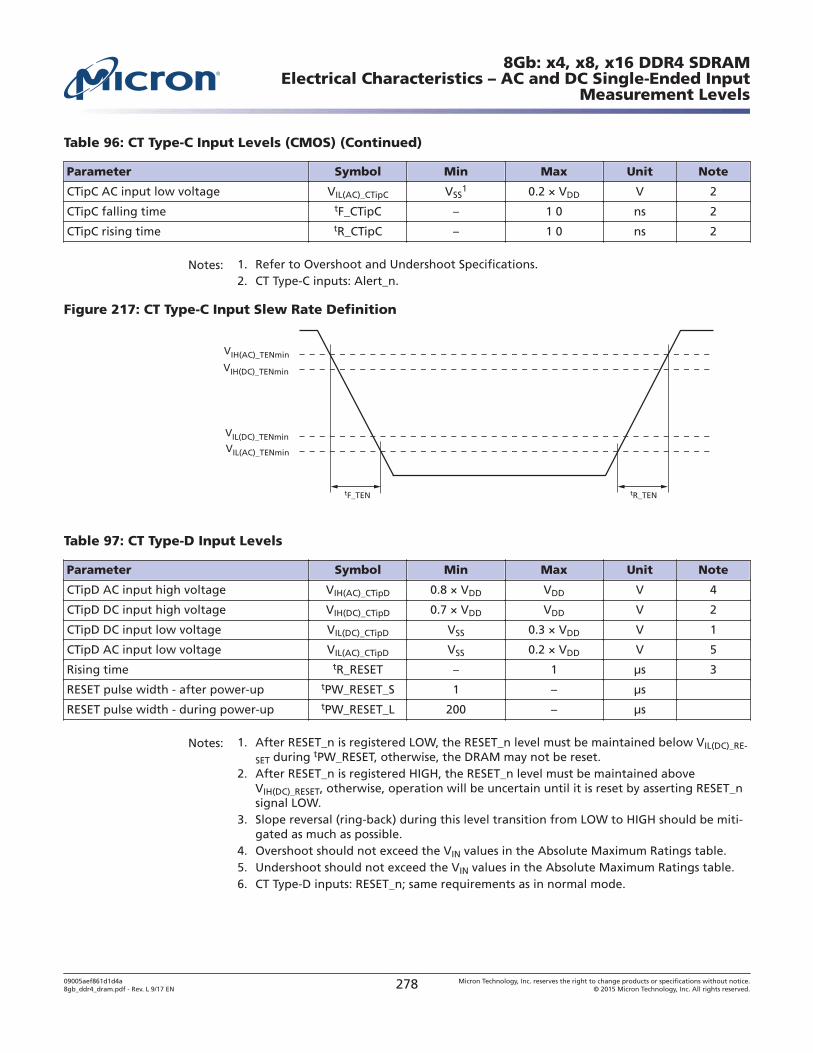
Table 96: CT Type-C Input Levels (CMOS) (Continued)
Parameter Symbol Min Max Unit Note
CTipC AC input low voltage VIL(AC)_CTipC VSS1 0.2 × VDD V 2
CTipC falling time tF_CTipC – 1 0 ns 2
CTipC rising time tR_CTipC – 1 0 ns 2
Notes: 1. Refer to Overshoot and Undershoot Specifications.2. CT Type-C inputs: Alert_n.
Figure 217: CT Type-C Input Slew Rate Definition
tR_TENtF_TEN
VIH(AC)_TENmin
VIL(AC)_TENmin
VIH(DC)_TENmin
VIL(DC)_TENmin
Table 97: CT Type-D Input Levels
Parameter Symbol Min Max Unit Note
CTipD AC input high voltage VIH(AC)_CTipD 0.8 × VDD VDD V 4
CTipD DC input high voltage VIH(DC)_CTipD 0.7 × VDD VDD V 2
CTipD DC input low voltage VIL(DC)_CTipD VSS 0.3 × VDD V 1
CTipD AC input low voltage VIL(AC)_CTipD VSS 0.2 × VDD V 5
Rising time tR_RESET – 1 μs 3
RESET pulse width - after power-up tPW_RESET_S 1 – μs
RESET pulse width - during power-up tPW_RESET_L 200 – μs
Notes: 1. After RESET_n is registered LOW, the RESET_n level must be maintained below VIL(DC)_RE-
SET during tPW_RESET, otherwise, the DRAM may not be reset.2. After RESET_n is registered HIGH, the RESET_n level must be maintained above
VIH(DC)_RESET, otherwise, operation will be uncertain until it is reset by asserting RESET_nsignal LOW.
3. Slope reversal (ring-back) during this level transition from LOW to HIGH should be miti-gated as much as possible.
4. Overshoot should not exceed the VIN values in the Absolute Maximum Ratings table.5. Undershoot should not exceed the VIN values in the Absolute Maximum Ratings table.6. CT Type-D inputs: RESET_n; same requirements as in normal mode.
8Gb: x4, x8, x16 DDR4 SDRAMElectrical Characteristics – AC and DC Single-Ended Input
Measurement Levels
09005aef861d1d4a8gb_ddr4_dram.pdf - Rev. L 9/17 EN 278 Micron Technology, Inc. reserves the right to change products or specifications without notice.
© 2015 Micron Technology, Inc. All rights reserved.
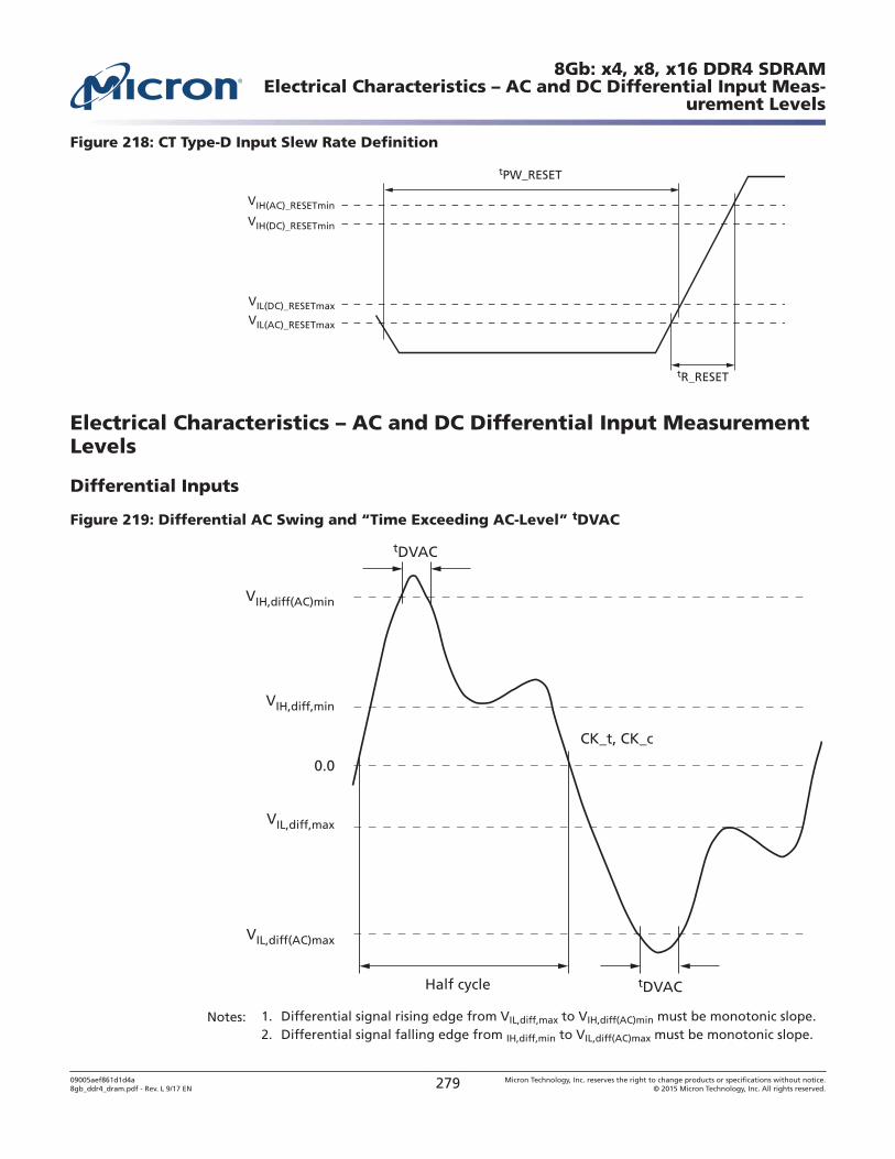
Figure 218: CT Type-D Input Slew Rate Definition
tR_RESET
tPW_RESET
VIH(AC)_RESETmin
VIL(AC)_RESETmax
VIH(DC)_RESETmin
VIL(DC)_RESETmax
Electrical Characteristics – AC and DC Differential Input MeasurementLevels
Differential Inputs
Figure 219: Differential AC Swing and “Time Exceeding AC-Level” tDVAC
VIH,diff(AC)min
0.0
VIL,diff,max
tDVAC
VIH,diff,min
VIL,diff(AC)max
Half cycle tDVAC
CK_t, CK_c
Notes: 1. Differential signal rising edge from VIL,diff,max to VIH,diff(AC)min must be monotonic slope.2. Differential signal falling edge from IH,diff,min to VIL,diff(AC)max must be monotonic slope.
8Gb: x4, x8, x16 DDR4 SDRAMElectrical Characteristics – AC and DC Differential Input Meas-
urement Levels
09005aef861d1d4a8gb_ddr4_dram.pdf - Rev. L 9/17 EN 279 Micron Technology, Inc. reserves the right to change products or specifications without notice.
© 2015 Micron Technology, Inc. All rights reserved.
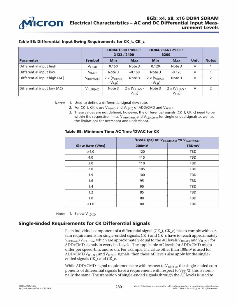
Table 98: Differential Input Swing Requirements for CK_t, CK_c
Parameter Symbol
DDR4-1600 / 1866 /2133 / 2400
DDR4-2666 / 2933 /3200
Unit NotesMin Max Min Max
Differential input high VIHdiff 0.150 Note 3 0.120 Note 3 V 1
Differential input low VILdiff Note 3 –0.150 Note 3 -0.120 V 1
Differential input high (AC) VIHdiff(AC) 2 × (VIH(AC)
- VREF)Note 3 2 × (VIH(AC)
- VREF)Note 3 V 2
Differential input low (AC) VILdiff(AC) Note 3 2 × (VIL(AC) -VREF)
Note 3 2 × (VIL(AC) -VREF)
V 2
Notes: 1. Used to define a differential signal slew-rate.2. For CK_t, CK_c use VIH(AC) and VIL(AC) of ADD/CMD and VREFCA.3. These values are not defined; however, the differential signals (CK_t, CK_c) need to be
within the respective limits, VIH(DC)max and VIL(DC)min for single-ended signals as well asthe limitations for overshoot and undershoot.
Table 99: Minimum Time AC Time tDVAC for CK
Slew Rate (V/ns)
tDVAC (ps) at |VIH,diff(AC) to VIL,diff(AC)|
200mV TBDmV
>4.0 120 TBD
4.0 115 TBD
3.0 110 TBD
2.0 105 TBD
1.9 100 TBD
1.6 95 TBD
1.4 90 TBD
1.2 85 TBD
1.0 80 TBD
<1.0 80 TBD
Note: 1. Below VIL(AC).
Single-Ended Requirements for CK Differential Signals
Each individual component of a differential signal (CK_t, CK_c) has to comply with cer-tain requirements for single-ended signals. CK_t and CK_c have to reach approximatelyVSEHmin/VSEL,max, which are approximately equal to the AC levels VIH(AC) and VIL(AC) forADD/CMD signals in every half-cycle. The applicable AC levels for ADD/CMD mightdiffer per speed-bin, and so on. For example, if a value other than 100mV is used forADD/CMD VIH(AC) and VIL(AC) signals, then these AC levels also apply for the single-ended signals CK_t and CK_c.
While ADD/CMD signal requirements are with respect to VREFCA, the single-ended com-ponents of differential signals have a requirement with respect to VDD/2; this is nomi-nally the same. The transition of single-ended signals through the AC levels is used to
8Gb: x4, x8, x16 DDR4 SDRAMElectrical Characteristics – AC and DC Differential Input Meas-
urement Levels
09005aef861d1d4a8gb_ddr4_dram.pdf - Rev. L 9/17 EN 280 Micron Technology, Inc. reserves the right to change products or specifications without notice.
© 2015 Micron Technology, Inc. All rights reserved.
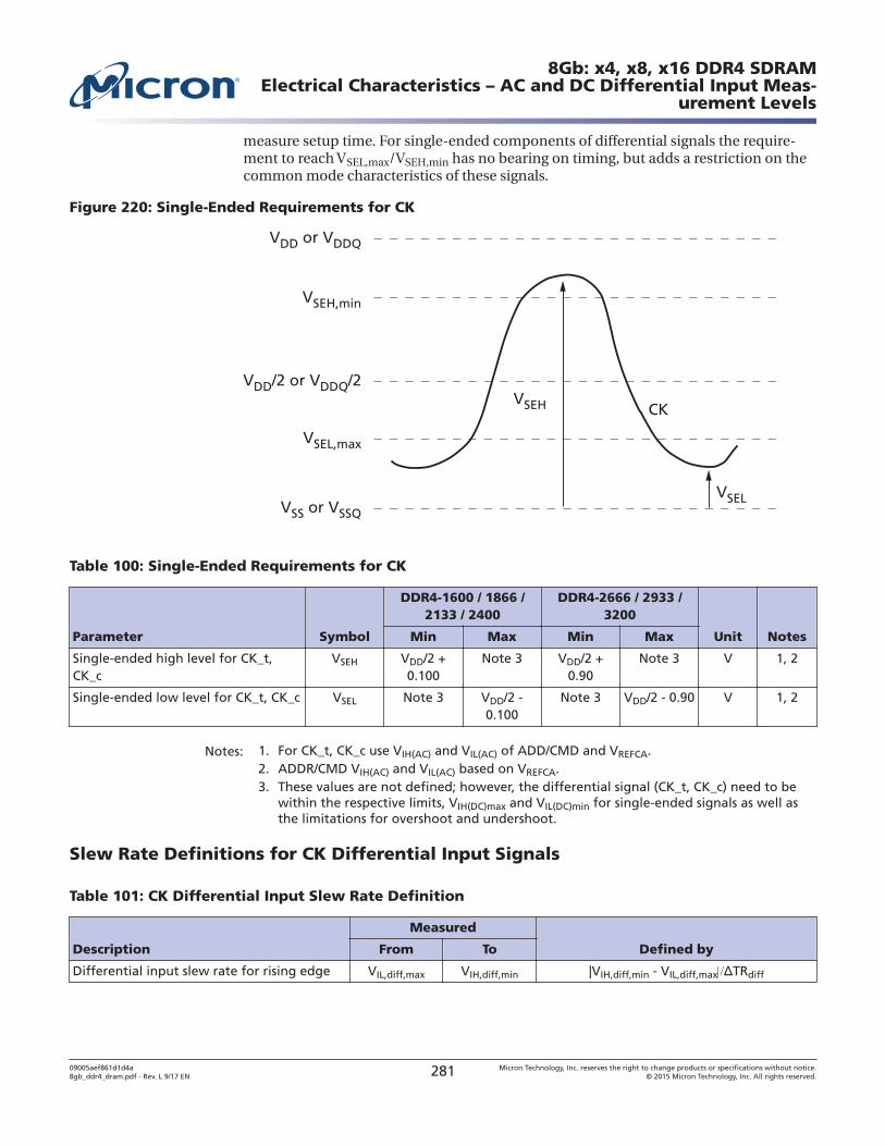
measure setup time. For single-ended components of differential signals the require-ment to reach VSEL,max/VSEH,min has no bearing on timing, but adds a restriction on thecommon mode characteristics of these signals.
Figure 220: Single-Ended Requirements for CK
VSS or VSSQ
VDD or VDDQ
VSEL,max
VSEH,min
VSEH
VSEL
CK
VDD/2 or VDDQ/2
Table 100: Single-Ended Requirements for CK
Parameter Symbol
DDR4-1600 / 1866 /2133 / 2400
DDR4-2666 / 2933 /3200
Unit NotesMin Max Min Max
Single-ended high level for CK_t,CK_c
VSEH VDD/2 +0.100
Note 3 VDD/2 +0.90
Note 3 V 1, 2
Single-ended low level for CK_t, CK_c VSEL Note 3 VDD/2 -0.100
Note 3 VDD/2 - 0.90 V 1, 2
Notes: 1. For CK_t, CK_c use VIH(AC) and VIL(AC) of ADD/CMD and VREFCA.2. ADDR/CMD VIH(AC) and VIL(AC) based on VREFCA.3. These values are not defined; however, the differential signal (CK_t, CK_c) need to be
within the respective limits, VIH(DC)max and VIL(DC)min for single-ended signals as well asthe limitations for overshoot and undershoot.
Slew Rate Definitions for CK Differential Input Signals
Table 101: CK Differential Input Slew Rate Definition
Description
Measured
Defined byFrom To
Differential input slew rate for rising edge VIL,diff,max VIH,diff,min |VIH,diff,min - VIL,diff,max TRdiff
8Gb: x4, x8, x16 DDR4 SDRAMElectrical Characteristics – AC and DC Differential Input Meas-
urement Levels
09005aef861d1d4a8gb_ddr4_dram.pdf - Rev. L 9/17 EN 281 Micron Technology, Inc. reserves the right to change products or specifications without notice.
© 2015 Micron Technology, Inc. All rights reserved.
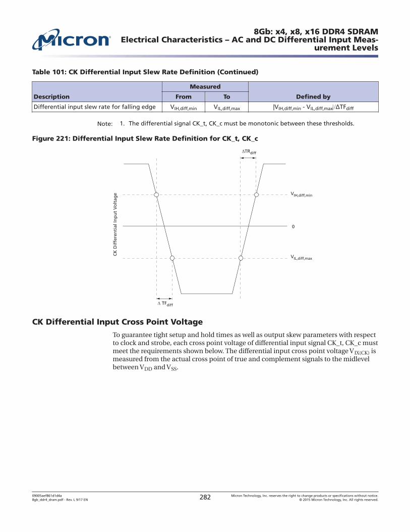
Table 101: CK Differential Input Slew Rate Definition (Continued)
Description
Measured
Defined byFrom To
Differential input slew rate for falling edge VIH,diff,min VIL,diff,max |VIH,diff,min - VIL,diff,max TFdiff
Note: 1. The differential signal CK_t, CK_c must be monotonic between these thresholds.
Figure 221: Differential Input Slew Rate Definition for CK_t, CK_c
TFdiff
VIH,diff,min
VIL,diff,max
0
CK
Dif
fere
nti
al In
pu
t V
olt
age
TRdiff
CK Differential Input Cross Point Voltage
To guarantee tight setup and hold times as well as output skew parameters with respectto clock and strobe, each cross point voltage of differential input signal CK_t, CK_c mustmeet the requirements shown below. The differential input cross point voltage VIX(CK) ismeasured from the actual cross point of true and complement signals to the midlevelbetween VDD and VSS.
8Gb: x4, x8, x16 DDR4 SDRAMElectrical Characteristics – AC and DC Differential Input Meas-
urement Levels
09005aef861d1d4a8gb_ddr4_dram.pdf - Rev. L 9/17 EN 282 Micron Technology, Inc. reserves the right to change products or specifications without notice.
© 2015 Micron Technology, Inc. All rights reserved.
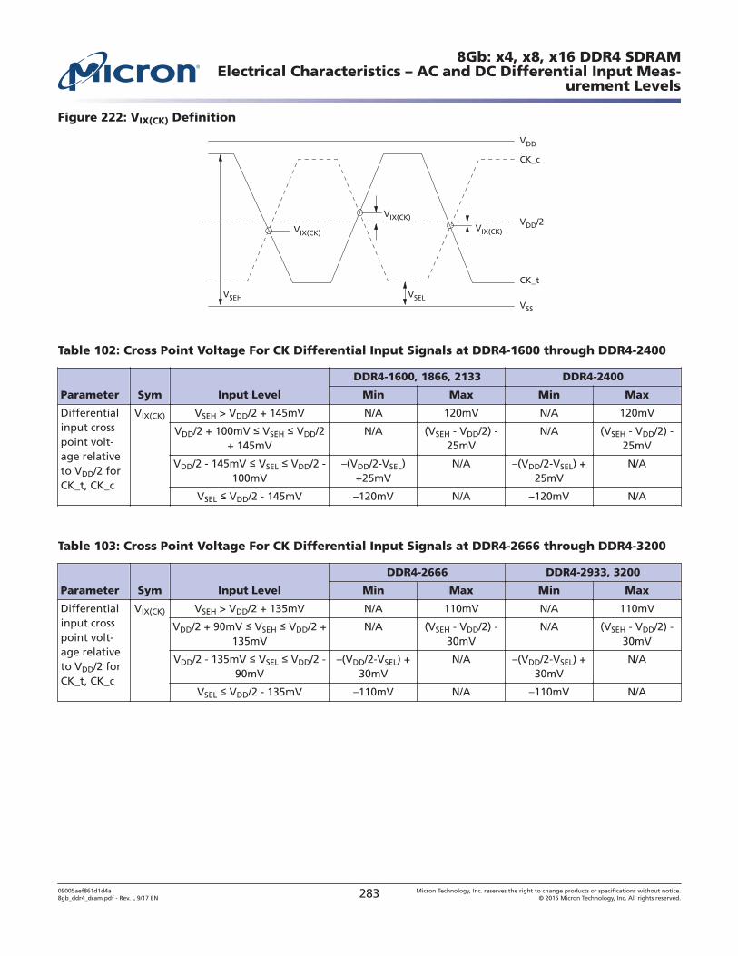
Figure 222: VIX(CK) Definition
VIX(CK)
VSEH VSEL
VIX(CK)
VIX(CK)
CK_t
VSS
VDD/2
CK_c
VDD
Table 102: Cross Point Voltage For CK Differential Input Signals at DDR4-1600 through DDR4-2400
Parameter Sym Input Level
DDR4-1600, 1866, 2133 DDR4-2400
Min Max Min Max
Differentialinput crosspoint volt-age relativeto VDD/2 forCK_t, CK_c
VIX(CK) VSEH > VDD/2 + 145mV N/A 120mV N/A 120mV
VDD/2 + 100mV VSEH VDD/2+ 145mV
N/A (VSEH - VDD/2) -25mV
N/A (VSEH - VDD/2) -25mV
VDD/2 - 145mV VSEL VDD/2 -100mV
–(VDD/2-VSEL)+25mV
N/A –(VDD/2-VSEL) +25mV
N/A
VSEL VDD/2 - 145mV –120mV N/A –120mV N/A
Table 103: Cross Point Voltage For CK Differential Input Signals at DDR4-2666 through DDR4-3200
Parameter Sym Input Level
DDR4-2666 DDR4-2933, 3200
Min Max Min Max
Differentialinput crosspoint volt-age relativeto VDD/2 forCK_t, CK_c
VIX(CK) VSEH > VDD/2 + 135mV N/A 110mV N/A 110mV
VDD/2 + 90mV VSEH VDD/2 +135mV
N/A (VSEH - VDD/2) -30mV
N/A (VSEH - VDD/2) -30mV
VDD/2 - 135mV VSEL VDD/2 -90mV
–(VDD/2-VSEL) +30mV
N/A –(VDD/2-VSEL) +30mV
N/A
VSEL VDD/2 - 135mV –110mV N/A –110mV N/A
8Gb: x4, x8, x16 DDR4 SDRAMElectrical Characteristics – AC and DC Differential Input Meas-
urement Levels
09005aef861d1d4a8gb_ddr4_dram.pdf - Rev. L 9/17 EN 283 Micron Technology, Inc. reserves the right to change products or specifications without notice.
© 2015 Micron Technology, Inc. All rights reserved.
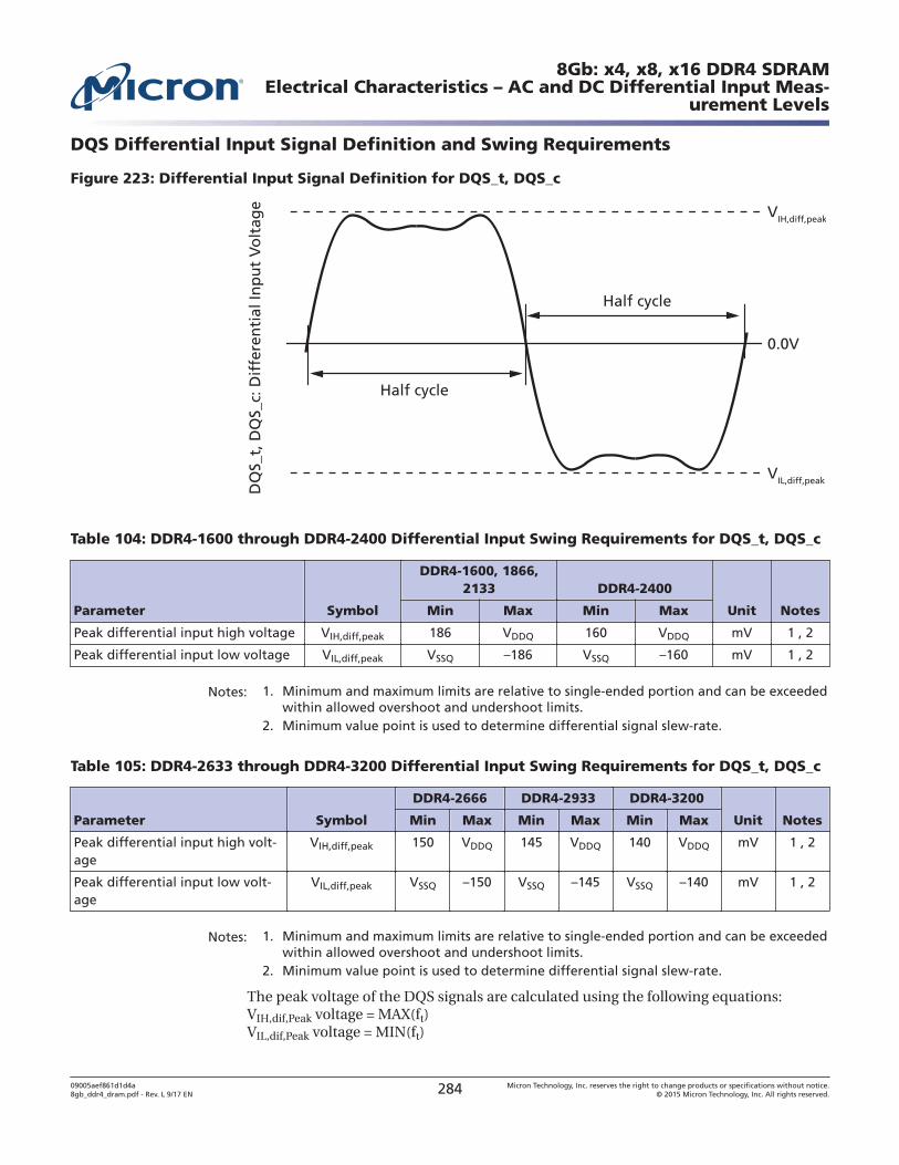
DQS Differential Input Signal Definition and Swing Requirements
Figure 223: Differential Input Signal Definition for DQS_t, DQS_c
Half cycle
VIL,diff,peak
0.0V
DQ
S_t,
DQ
S_c:
Dif
fere
nti
al In
pu
t V
olt
age VIH,diff,peak
Half cycle
Table 104: DDR4-1600 through DDR4-2400 Differential Input Swing Requirements for DQS_t, DQS_c
Parameter Symbol
DDR4-1600, 1866,2133 DDR4-2400
Unit NotesMin Max Min Max
Peak differential input high voltage VIH,diff,peak 186 VDDQ 160 VDDQ mV 1 , 2
Peak differential input low voltage VIL,diff,peak VSSQ –186 VSSQ –160 mV 1 , 2
Notes: 1. Minimum and maximum limits are relative to single-ended portion and can be exceededwithin allowed overshoot and undershoot limits.
2. Minimum value point is used to determine differential signal slew-rate.
Table 105: DDR4-2633 through DDR4-3200 Differential Input Swing Requirements for DQS_t, DQS_c
Parameter Symbol
DDR4-2666 DDR4-2933 DDR4-3200
Unit NotesMin Max Min Max Min Max
Peak differential input high volt-age
VIH,diff,peak 150 VDDQ 145 VDDQ 140 VDDQ mV 1 , 2
Peak differential input low volt-age
VIL,diff,peak VSSQ –150 VSSQ –145 VSSQ –140 mV 1 , 2
Notes: 1. Minimum and maximum limits are relative to single-ended portion and can be exceededwithin allowed overshoot and undershoot limits.
2. Minimum value point is used to determine differential signal slew-rate.
The peak voltage of the DQS signals are calculated using the following equations:VIH,dif,Peak voltage = MAX(ft)VIL,dif,Peak voltage = MIN(ft)
8Gb: x4, x8, x16 DDR4 SDRAMElectrical Characteristics – AC and DC Differential Input Meas-
urement Levels
09005aef861d1d4a8gb_ddr4_dram.pdf - Rev. L 9/17 EN 284 Micron Technology, Inc. reserves the right to change products or specifications without notice.
© 2015 Micron Technology, Inc. All rights reserved.
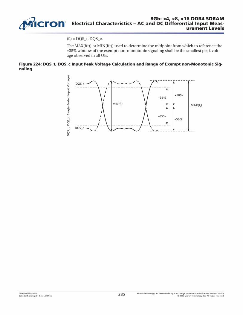
(ft) = DQS_t, DQS_c.
The MAX(f(t)) or MIN(f(t)) used to determine the midpoint from which to reference the±35% window of the exempt non-monotonic signaling shall be the smallest peak volt-age observed in all UIs.
Figure 224: DQS_t, DQS_c Input Peak Voltage Calculation and Range of Exempt non-Monotonic Sig-naling
DQS_t
MIN(ft) MAX(ft)
DQS_c
DQ
S_t,
DQ
S_c:
Sin
gle
-En
ded
Inp
ut
Vo
ltag
es
+50%
–50%
+35%
–35%
8Gb: x4, x8, x16 DDR4 SDRAMElectrical Characteristics – AC and DC Differential Input Meas-
urement Levels
09005aef861d1d4a8gb_ddr4_dram.pdf - Rev. L 9/17 EN 285 Micron Technology, Inc. reserves the right to change products or specifications without notice.
© 2015 Micron Technology, Inc. All rights reserved.
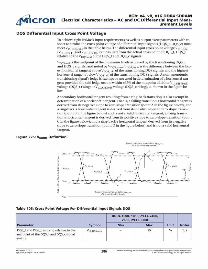
DQS Differential Input Cross Point Voltage
To achieve tight RxMask input requirements as well as output skew parameters with re-spect to strobe, the cross point voltage of differential input signals (DQS_t, DQS_c) mustmeet VIX_DQS,ratio in the table below. The differential input cross point voltage VIX_DQS(VIX_DQS_FR and VIX_DQS_RF) is measured from the actual cross point of DQS_t, DQS_crelative to the VDQS,mid of the DQS_t and DQS_c signals.
VDQS,mid is the midpoint of the minimum levels achieved by the transitioning DQS_tand DQS_c signals, and noted by VDQS_trans. VDQS_trans is the difference between the low-est horizontal tangent above VDQS,mid of the transitioning DQS signals and the highesthorizontal tangent below VDQS,mid of the transitioning DQS signals. A non-monotonictransitioning signal’s ledge is exempt or not used in determination of a horizontal tan-gent provided the said ledge occurs within ±35% of the midpoint of either VIH.DIFF.Peakvoltage (DQS_t rising) or VIL.DIFF.Peak voltage (DQS_c rising), as shown in the figure be-low.
A secondary horizontal tangent resulting from a ring-back transition is also exempt indetermination of a horizontal tangent. That is, a falling transition’s horizontal tangent isderived from its negative slope to zero slope transition (point A in the figure below), anda ring-back’s horizontal tangent is derived from its positive slope to zero slope transi-tion (point B in the figure below) and is not a valid horizontal tangent; a rising transi-tion’s horizontal tangent is derived from its positive slope to zero slope transition (pointC in the figure below), and a ring-back’s horizontal tangent derived from its negativeslope to zero slope transition (point D in the figure below) and is not a valid horizontaltangent.
Figure 225: VIXDQS Definition
DQ
S_t,
DQ
S_c:
Sin
gle
-En
ded
Inp
ut
Vo
ltag
es
DQS_t
VIX_DQS,FR
VIX_DQS,FRVIX_DQS,RF
VIX_DQS,RF
VD
QS_
tran
s
VD
QS_
tran
s/2
Lowest horizontal tanget above VDQS,midof the transitioning signals
Highest horizontal tanget below VDQS,midof the transitioning signals
VSSQ
VDQS,mid
DQS_c
A
B
C
D
Table 106: Cross Point Voltage For Differential Input Signals DQS
Parameter Symbol
DDR4-1600, 1866, 2133, 2400,2666, 2933, 3200
Unit NotesMin Max
DQS_t and DQS_c crossing relative to themidpoint of the DQS_t and DQS_c signalswings
VIX_DQS,ratio – 25 % 1, 2
8Gb: x4, x8, x16 DDR4 SDRAMElectrical Characteristics – AC and DC Differential Input Meas-
urement Levels
09005aef861d1d4a8gb_ddr4_dram.pdf - Rev. L 9/17 EN 286 Micron Technology, Inc. reserves the right to change products or specifications without notice.
© 2015 Micron Technology, Inc. All rights reserved.
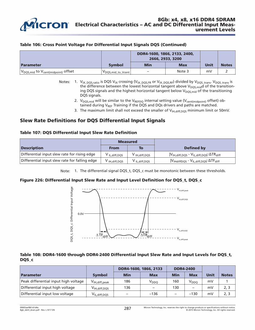
Table 106: Cross Point Voltage For Differential Input Signals DQS (Continued)
Parameter Symbol
DDR4-1600, 1866, 2133, 2400,2666, 2933, 3200
Unit NotesMin Max
VDQS,mid to Vcent(midpoint) offset VDQS,mid_to_Vcent – Note 3 mV 2
Notes: 1. VIX_DQS,ratio is DQS VIX crossing (VIX_DQS,FR or VIX_DQS,RF) divided by VDQS_trans. VDQS_trans isthe difference between the lowest horizontal tangent above VDQS,midd of the transition-ing DQS signals and the highest horizontal tangent below VDQS,mid of the transitioningDQS signals.
2. VDQS,mid will be similar to the VREFDQ internal setting value (Vcent(midpoint) offset) ob-tained during VREF Training if the DQS and DQs drivers and paths are matched.
3. The maximum limit shall not exceed the smaller of VIH,diff,DQS minimum limit or 50mV.
Slew Rate Definitions for DQS Differential Input Signals
Table 107: DQS Differential Input Slew Rate Definition
Description
Measured
Defined byFrom To
Differential input slew rate for rising edge V IL,diff,DQS V IH,diff,DQS |VIH,diff,DQS - VIL,diff,DQS TRdiff
Differential input slew rate for falling edge V IH,diff,DQS V IL,diff,DQS |VIHdiffDQS - VIL,diff,DQS TFdiff
Note: 1. The differential signal DQS_t, DQS_c must be monotonic between these thresholds.
Figure 226: Differential Input Slew Rate and Input Level Definition for DQS_t, DQS_c
TFdiff TRdiff VIL,diff,peak
0.0V
DQ
S_t,
DQ
S_c:
Dif
fere
nti
al In
pu
t V
olt
age
VIH,diff,peak
VIH,diff,DQS
VIL,diff,DQS
Table 108: DDR4-1600 through DDR4-2400 Differential Input Slew Rate and Input Levels for DQS_t,DQS_c
Parameter Symbol
DDR4-1600, 1866, 2133 DDR4-2400
Unit NotesMin Max Min Max
Peak differential input high voltage VIH,diff,peak 186 VDDQ 160 VDDQ mV 1
Differential input high voltage VIH,diff,DQS 136 – 130 – mV 2, 3
Differential input low voltage VIL,diff,DQS – –136 – –130 mV 2, 3
8Gb: x4, x8, x16 DDR4 SDRAMElectrical Characteristics – AC and DC Differential Input Meas-
urement Levels
09005aef861d1d4a8gb_ddr4_dram.pdf - Rev. L 9/17 EN 287 Micron Technology, Inc. reserves the right to change products or specifications without notice.
© 2015 Micron Technology, Inc. All rights reserved.
Table 108: DDR4-1600 through DDR4-2400 Differential Input Slew Rate and Input Levels for DQS_t,DQS_c (Continued)
Parameter Symbol
DDR4-1600, 1866, 2133 DDR4-2400
Unit NotesMin Max Min Max
Peak differential input low voltage VIL,diff,peak VSSQ –186 VSSQ –160 mV 1
DQS differential input slew rate SRIdiff 3.0 18 3.0 18 V/ns 4, 5
Notes: 1. Minimum and maximum limits are relative to single-ended portion and can be exceededwithin allowed overshoot and undershoot limits.
2. Differential signal rising edge from VIL,diff,DQS to VIH,diff,DQS must be monotonic slope.3. Differential signal falling edge from VIH,diff,DQS to VIL,diff,DQS must be monotonic slope.4. Differential input slew rate for rising edge from VIL,diff,DQS to VIH,diff,DQS is defined by |
VIL,diff,min - VIH,diff,max TRdiff.5. Differential input slew rate for falling edge from VIH,diff,DQS to VIL,diff,DQS is defined by |
VIL,diff,min - VIH,diff,max TFdiff.
Table 109: DDR4-2666 through DDR4-3200 Differential Input Slew Rate and Input Levels for DQS_t,DQS_c
Parameter Symbol
DDR4-2666 DDR4-2933 DDR4-3200
Unit NotesMin Max Min Max Min Max
Peak differential inputhigh voltage
VIH,diff,peak 150 VDDQ 145 VDDQ 140 VDDQ mV 1
Differential input highvoltage
VIH,diff,DQS 120 – 115 – 110 – mV 2, 3
Differential input lowvoltage
VIL,diff,DQS – –120 – –115 – –110 mV 2, 3
Peak differential inputlow voltage
VIL,diff,peak VSSQ –150 VSSQ –145 VSSQ –140 mV 1
DQS differential inputslew rate
SRIdiff 3.0 18 3.0 18 3.0 18 V/ns 4, 5
Notes: 1. Minimum and maximum limits are relative to single-ended portion and can be exceededwithin allowed overshoot and undershoot limits.
2. Differential signal rising edge from VIL,diff,DQS to VIH,diff,DQS must be monotonic slope.3. Differential signal falling edge from VIH,diff,DQS to VIL,diff,DQS must be monotonic slope.4. Differential input slew rate for rising edge from VIL,diff,DQS to VIH,diff,DQS is defined by |
VIL,diff,min - VIH,diff,max TRdiff.5. Differential input slew rate for falling edge from VIH,diff,DQS to VIL,diff,DQS is defined by |
VIL,diff,min - VIH,diff,max TFdiff.
8Gb: x4, x8, x16 DDR4 SDRAMElectrical Characteristics – AC and DC Differential Input Meas-
urement Levels
09005aef861d1d4a8gb_ddr4_dram.pdf - Rev. L 9/17 EN 288 Micron Technology, Inc. reserves the right to change products or specifications without notice.
© 2015 Micron Technology, Inc. All rights reserved.
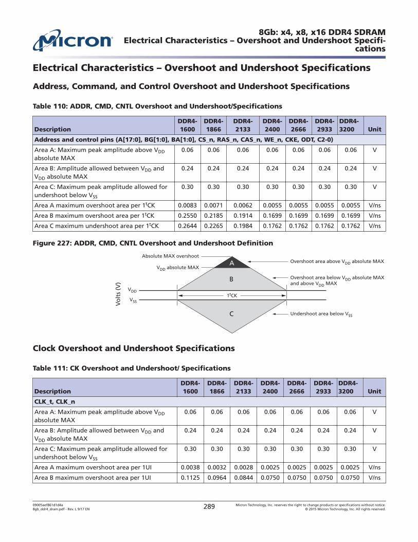
Electrical Characteristics – Overshoot and Undershoot Specifications
Address, Command, and Control Overshoot and Undershoot Specifications
Table 110: ADDR, CMD, CNTL Overshoot and Undershoot/Specifications
DescriptionDDR4-1600
DDR4-1866
DDR4-2133
DDR4-2400
DDR4-2666
DDR4-2933
DDR4-3200 Unit
Address and control pins (A[17:0], BG[1:0], BA[1:0], CS_n, RAS_n, CAS_n, WE_n, CKE, ODT, C2-0)
Area A: Maximum peak amplitude above VDD
absolute MAX0.06 0.06 0.06 0.06 0.06 0.06 0.06 V
Area B: Amplitude allowed between VDD andVDD absolute MAX
0.24 0.24 0.24 0.24 0.24 0.24 0.24 V
Area C: Maximum peak amplitude allowed forundershoot below VSS
0.30 0.30 0.30 0.30 0.30 0.30 0.30 V
Area A maximum overshoot area per 1tCK 0.0083 0.0071 0.0062 0.0055 0.0055 0.0055 0.0055 V/ns
Area B maximum overshoot area per 1tCK 0.2550 0.2185 0.1914 0.1699 0.1699 0.1699 0.1699 V/ns
Area C maximum undershoot area per 1tCK 0.2644 0.2265 0.1984 0.1762 0.1762 0.1762 0.1762 V/ns
Figure 227: ADDR, CMD, CNTL Overshoot and Undershoot Definition
VDD absolute MAX
Absolute MAX overshootOvershoot area above VDD absolute MAX
Overshoot area below VDD absolute MAXand above VDD MAX
Undershoot area below VSS
1tCK
Vo
lts
(V)
VDD
VSS
A
B
C
Clock Overshoot and Undershoot Specifications
Table 111: CK Overshoot and Undershoot/ Specifications
DescriptionDDR4-1600
DDR4-1866
DDR4-2133
DDR4-2400
DDR4-2666
DDR4-2933
DDR4-3200 Unit
CLK_t, CLK_n
Area A: Maximum peak amplitude above VDD
absolute MAX0.06 0.06 0.06 0.06 0.06 0.06 0.06 V
Area B: Amplitude allowed between VDD andVDD absolute MAX
0.24 0.24 0.24 0.24 0.24 0.24 0.24 V
Area C: Maximum peak amplitude allowed forundershoot below VSS
0.30 0.30 0.30 0.30 0.30 0.30 0.30 V
Area A maximum overshoot area per 1UI 0.0038 0.0032 0.0028 0.0025 0.0025 0.0025 0.0025 V/ns
Area B maximum overshoot area per 1UI 0.1125 0.0964 0.0844 0.0750 0.0750 0.0750 0.0750 V/ns
8Gb: x4, x8, x16 DDR4 SDRAMElectrical Characteristics – Overshoot and Undershoot Specifi-
cations
09005aef861d1d4a8gb_ddr4_dram.pdf - Rev. L 9/17 EN 289 Micron Technology, Inc. reserves the right to change products or specifications without notice.
© 2015 Micron Technology, Inc. All rights reserved.
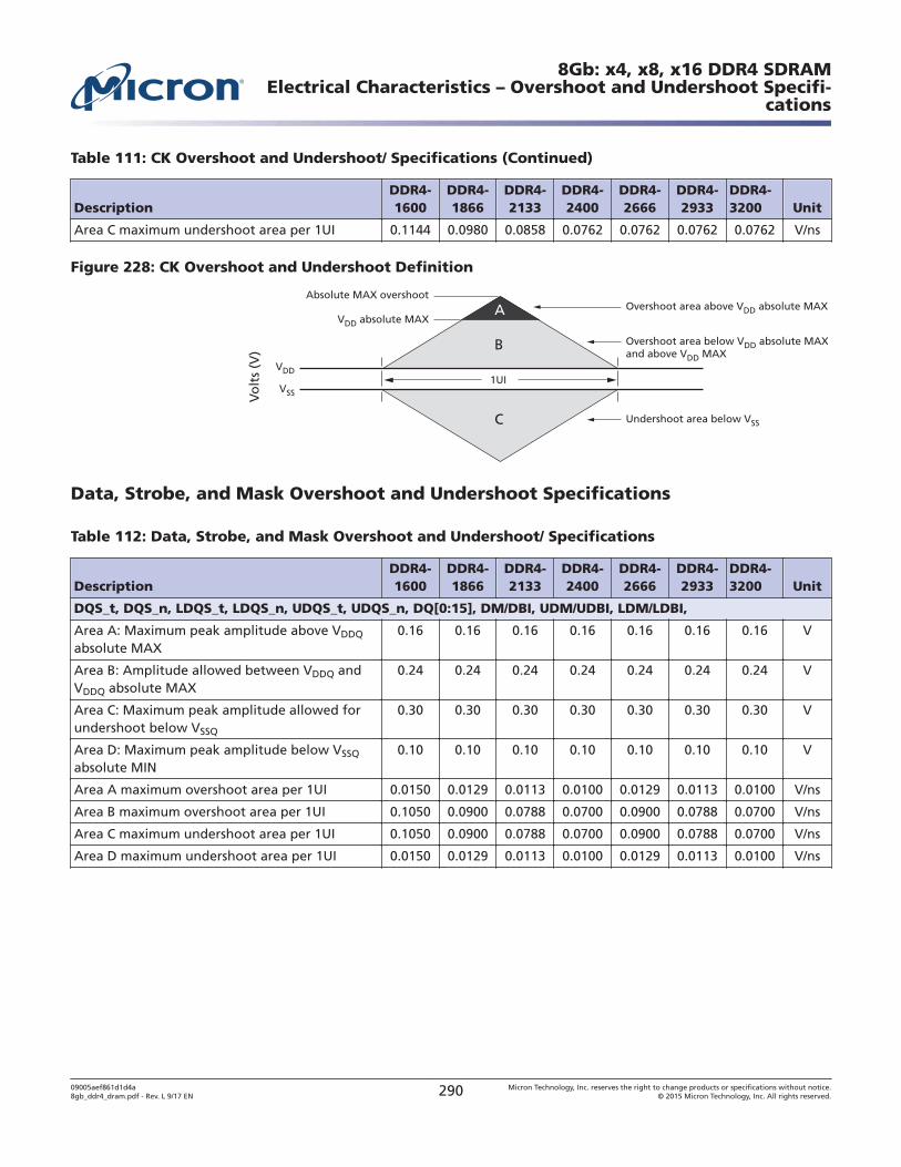
Table 111: CK Overshoot and Undershoot/ Specifications (Continued)
DescriptionDDR4-1600
DDR4-1866
DDR4-2133
DDR4-2400
DDR4-2666
DDR4-2933
DDR4-3200 Unit
Area C maximum undershoot area per 1UI 0.1144 0.0980 0.0858 0.0762 0.0762 0.0762 0.0762 V/ns
Figure 228: CK Overshoot and Undershoot Definition
VDD absolute MAX
Absolute MAX overshootOvershoot area above VDD absolute MAX
Overshoot area below VDD absolute MAXand above VDD MAX
Undershoot area below VSS
1UI
Vo
lts
(V)
VDD
VSS
A
B
C
Data, Strobe, and Mask Overshoot and Undershoot Specifications
Table 112: Data, Strobe, and Mask Overshoot and Undershoot/ Specifications
DescriptionDDR4-1600
DDR4-1866
DDR4-2133
DDR4-2400
DDR4-2666
DDR4-2933
DDR4-3200 Unit
DQS_t, DQS_n, LDQS_t, LDQS_n, UDQS_t, UDQS_n, DQ[0:15], DM/DBI, UDM/UDBI, LDM/LDBI,
Area A: Maximum peak amplitude above VDDQ
absolute MAX0.16 0.16 0.16 0.16 0.16 0.16 0.16 V
Area B: Amplitude allowed between VDDQ andVDDQ absolute MAX
0.24 0.24 0.24 0.24 0.24 0.24 0.24 V
Area C: Maximum peak amplitude allowed forundershoot below VSSQ
0.30 0.30 0.30 0.30 0.30 0.30 0.30 V
Area D: Maximum peak amplitude below VSSQ
absolute MIN0.10 0.10 0.10 0.10 0.10 0.10 0.10 V
Area A maximum overshoot area per 1UI 0.0150 0.0129 0.0113 0.0100 0.0129 0.0113 0.0100 V/ns
Area B maximum overshoot area per 1UI 0.1050 0.0900 0.0788 0.0700 0.0900 0.0788 0.0700 V/ns
Area C maximum undershoot area per 1UI 0.1050 0.0900 0.0788 0.0700 0.0900 0.0788 0.0700 V/ns
Area D maximum undershoot area per 1UI 0.0150 0.0129 0.0113 0.0100 0.0129 0.0113 0.0100 V/ns
8Gb: x4, x8, x16 DDR4 SDRAMElectrical Characteristics – Overshoot and Undershoot Specifi-
cations
09005aef861d1d4a8gb_ddr4_dram.pdf - Rev. L 9/17 EN 290 Micron Technology, Inc. reserves the right to change products or specifications without notice.
© 2015 Micron Technology, Inc. All rights reserved.
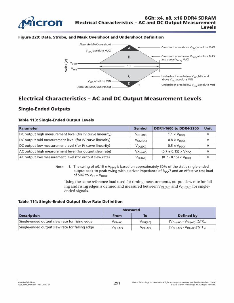
Figure 229: Data, Strobe, and Mask Overshoot and Undershoot Definition
VDDQ absolute MAX
VSSQ absolute MIN
A
B
C
Absolute MAX overshoot
Absolute MAX undershoot
Overshoot area above VDDQ absolute MAX
Undershoot area below VSSQ absolute MIN
Overshoot area below VDDQ absolute MAXand above VDDQ MAX
Undershoot area below VSSQ MIN andabove VSSQ absolute MIN
1UIV
olt
s (V
)VDDQ
VSSQ
D
Electrical Characteristics – AC and DC Output Measurement Levels
Single-Ended Outputs
Table 113: Single-Ended Output Levels
Parameter Symbol DDR4-1600 to DDR4-3200 Unit
DC output high measurement level (for IV curve linearity) VOH(DC) 1.1 × VDDQ V
DC output mid measurement level (for IV curve linearity) VOM(DC) 0.8 × VDDQ V
DC output low measurement level (for IV curve linearity) VOL(DC) 0.5 × VDDQ V
AC output high measurement level (for output slew rate) VOH(AC) (0.7 + 0.15) × VDDQ V
AC output low measurement level (for output slew rate) VOL(AC) (0.7 - 0.15) × VDDQ V
Note: 1. The swing of ±0.15 × VDDQ is based on approximately 50% of the static single-endedoutput peak-to-peak swing with a driver impedance of RZQ/7 and an effective test loadof 50 to VTT = VDDQ.
Using the same reference load used for timing measurements, output slew rate for fall-ing and rising edges is defined and measured between VOL(AC) and VOH(AC) for single-ended signals.
Table 114: Single-Ended Output Slew Rate Definition
Description
Measured
Defined byFrom To
Single-ended output slew rate for rising edge VOL(AC) VOH(AC) [VOH(AC) - VOL(AC) TRse
Single-ended output slew rate for falling edge VOH(AC) VOL(AC) [VOH(AC) - VOL(AC) TFse
8Gb: x4, x8, x16 DDR4 SDRAMElectrical Characteristics – AC and DC Output Measurement
Levels
09005aef861d1d4a8gb_ddr4_dram.pdf - Rev. L 9/17 EN 291 Micron Technology, Inc. reserves the right to change products or specifications without notice.
© 2015 Micron Technology, Inc. All rights reserved.
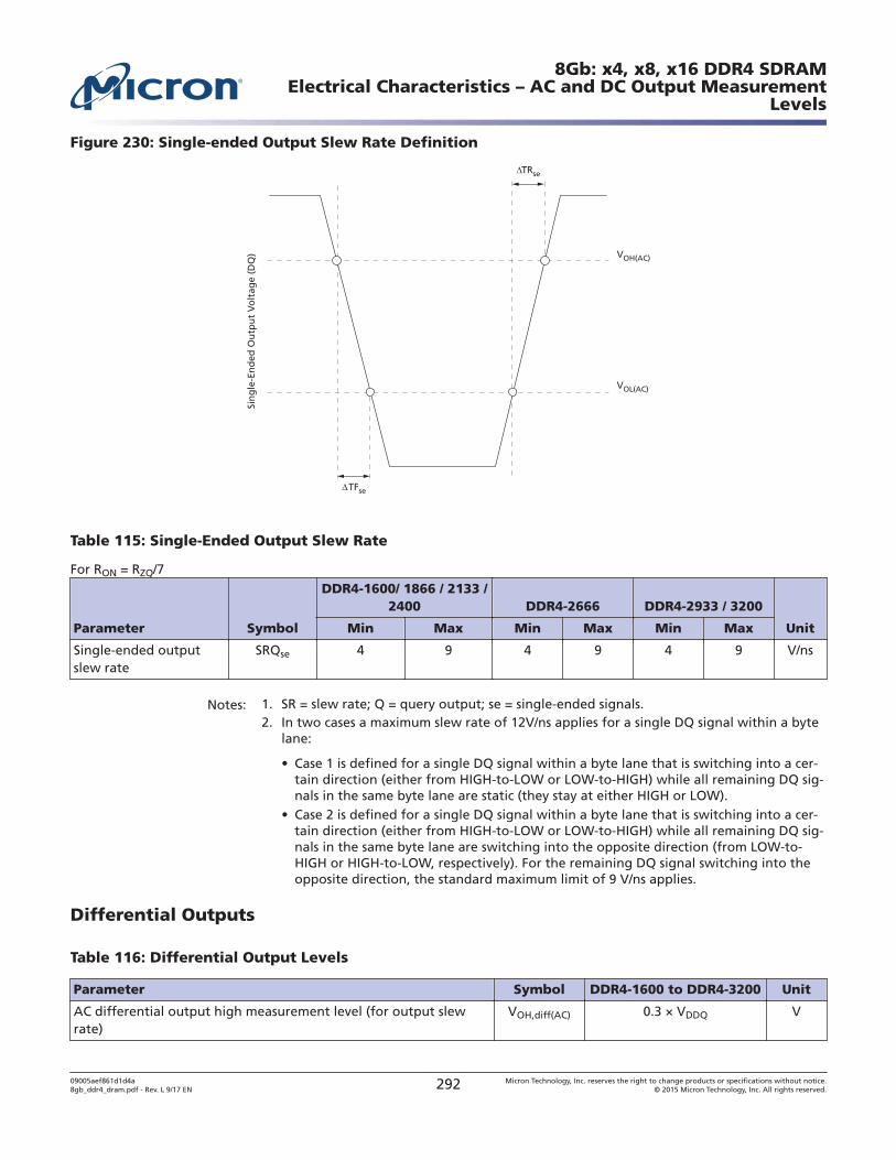
Figure 230: Single-ended Output Slew Rate Definition
TRse
TFse
VOH(AC)
VOL(AC)
Sin
gle
-En
ded
Ou
tpu
t V
olt
age
(DQ
)
Table 115: Single-Ended Output Slew Rate
For RON = RZQ/7
Parameter Symbol
DDR4-1600/ 1866 / 2133 /2400 DDR4-2666 DDR4-2933 / 3200
UnitMin Max Min Max Min Max
Single-ended outputslew rate
SRQse 4 9 4 9 4 9 V/ns
Notes: 1. SR = slew rate; Q = query output; se = single-ended signals.2. In two cases a maximum slew rate of 12V/ns applies for a single DQ signal within a byte
lane:
• Case 1 is defined for a single DQ signal within a byte lane that is switching into a cer-tain direction (either from HIGH-to-LOW or LOW-to-HIGH) while all remaining DQ sig-nals in the same byte lane are static (they stay at either HIGH or LOW).
• Case 2 is defined for a single DQ signal within a byte lane that is switching into a cer-tain direction (either from HIGH-to-LOW or LOW-to-HIGH) while all remaining DQ sig-nals in the same byte lane are switching into the opposite direction (from LOW-to-HIGH or HIGH-to-LOW, respectively). For the remaining DQ signal switching into theopposite direction, the standard maximum limit of 9 V/ns applies.
Differential Outputs
Table 116: Differential Output Levels
Parameter Symbol DDR4-1600 to DDR4-3200 Unit
AC differential output high measurement level (for output slewrate)
VOH,diff(AC) 0.3 × VDDQ V
8Gb: x4, x8, x16 DDR4 SDRAMElectrical Characteristics – AC and DC Output Measurement
Levels
09005aef861d1d4a8gb_ddr4_dram.pdf - Rev. L 9/17 EN 292 Micron Technology, Inc. reserves the right to change products or specifications without notice.
© 2015 Micron Technology, Inc. All rights reserved.
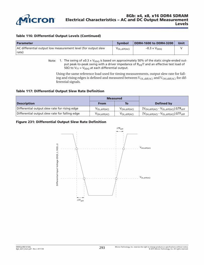
Table 116: Differential Output Levels (Continued)
Parameter Symbol DDR4-1600 to DDR4-3200 Unit
AC differential output low measurement level (for output slewrate)
VOL,diff(AC) –0.3 × VDDQ V
Note: 1. The swing of ±0.3 × VDDQ is based on approximately 50% of the static single-ended out-put peak-to-peak swing with a driver impedance of RZQ/7 and an effective test load of50 to VTT = VDDQ at each differential output.
Using the same reference load used for timing measurements, output slew rate for fall-ing and rising edges is defined and measured between VOL,diff(AC) and VOH,diff(AC) for dif-ferential signals.
Table 117: Differential Output Slew Rate Definition
Description
Measured
Defined byFrom To
Differential output slew rate for rising edge VOL,diff(AC) VOH,diff(AC) [VOH,diff(AC) - VOL,diff(AC) TRdiff
Differential output slew rate for falling edge VOH,diff(AC) VOL,diff(AC) [VOH,diff(AC) - VOL,diff(AC) TFdiff
Figure 231: Differential Output Slew Rate Definition
TRdiff
TFdiff
VOH,diff(AC)
VOL,diff(AC)
Dif
fere
nti
al In
pu
t V
olt
age
(DQ
S_t,
DQ
S_c)
8Gb: x4, x8, x16 DDR4 SDRAMElectrical Characteristics – AC and DC Output Measurement
Levels
09005aef861d1d4a8gb_ddr4_dram.pdf - Rev. L 9/17 EN 293 Micron Technology, Inc. reserves the right to change products or specifications without notice.
© 2015 Micron Technology, Inc. All rights reserved.
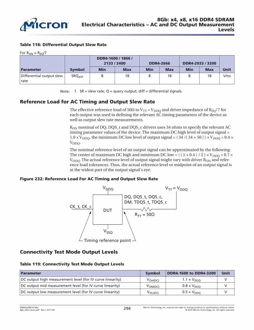
Table 118: Differential Output Slew Rate
For RON = RZQ/7
Parameter Symbol
DDR4-1600 / 1866 /2133 / 2400 DDR4-2666 DDR4-2933 / 3200
UnitMin Max Min Max Min Max
Differential output slewrate
SRQdiff 8 18 8 18 8 18 V/ns
Note: 1. SR = slew rate; Q = query output; diff = differential signals.
Reference Load for AC Timing and Output Slew Rate
The effective reference load of 50 to VTT = VDDQ and driver impedance of RZQ/7 foreach output was used in defining the relevant AC timing parameters of the device aswell as output slew rate measurements.
RON nominal of DQ, DQS_t and DQS_c drivers uses 34 ohms to specify the relevant ACtiming parameter values of the device. The maximum DC high level of output signal =1.0 × VDDQ, the minimum DC low level of output signal = { 34 /( 34 + 50 ) } × VDDQ = 0.4 ×VDDQ.
The nominal reference level of an output signal can be approximated by the following:The center of maximum DC high and minimum DC low = { ( 1 + 0.4 ) / 2 } × VDDQ = 0.7 ×VDDQ. The actual reference level of output signal might vary with driver RON and refer-ence load tolerances. Thus, the actual reference level or midpoint of an output signal isat the widest part of the output signal’s eye.
Figure 232: Reference Load For AC Timing and Output Slew Rate
Timing reference point
DQ, DQS_t, DQS_c, DM, TDQS_t, TDQS_c
CK_t, CK_cDUT
VTT = VDDQVDDQ
VSSQ
RTT = 50
Connectivity Test Mode Output Levels
Table 119: Connectivity Test Mode Output Levels
Parameter Symbol DDR4-1600 to DDR4-3200 Unit
DC output high measurement level (for IV curve linearity) VOH(DC) 1.1 × VDDQ V
DC output mid measurement level (for IV curve linearity) VOM(DC) 0.8 × VDDQ V
DC output low measurement level (for IV curve linearity) VOL(DC) 0.5 × VDDQ V
8Gb: x4, x8, x16 DDR4 SDRAMElectrical Characteristics – AC and DC Output Measurement
Levels
09005aef861d1d4a8gb_ddr4_dram.pdf - Rev. L 9/17 EN 294 Micron Technology, Inc. reserves the right to change products or specifications without notice.
© 2015 Micron Technology, Inc. All rights reserved.
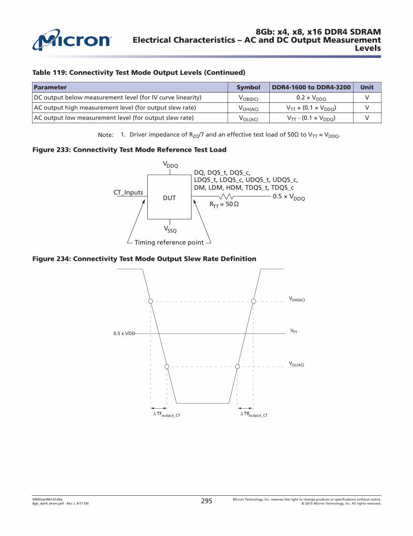
Table 119: Connectivity Test Mode Output Levels (Continued)
Parameter Symbol DDR4-1600 to DDR4-3200 Unit
DC output below measurement level (for IV curve linearity) VOB(DC) 0.2 × VDDQ V
AC output high measurement level (for output slew rate) VOH(AC) VTT + (0.1 × VDDQ) V
AC output low measurement level (for output slew rate) VOL(AC) VTT - (0.1 × VDDQ) V
Note: 1. Driver impedance of RZQ/7 and an effective test load of 50 to VTT = VDDQ.
Figure 233: Connectivity Test Mode Reference Test Load
Timing reference point
LDQS_t, LDQS_c, UDQS_t, UDQS_c, DQ, DQS_t, DQS_c,
DM, LDM, HDM, TDQS_t, TDQS_cCT_Inputs
DUT 0.5 × VDDQ
VDDQ
VSSQ
RTT = 50
Figure 234: Connectivity Test Mode Output Slew Rate Definition
TFoutput_CT
VOH(AC)
VOL(AC)
VTT0.5 x VDD
TRoutput_CT
8Gb: x4, x8, x16 DDR4 SDRAMElectrical Characteristics – AC and DC Output Measurement
Levels
09005aef861d1d4a8gb_ddr4_dram.pdf - Rev. L 9/17 EN 295 Micron Technology, Inc. reserves the right to change products or specifications without notice.
© 2015 Micron Technology, Inc. All rights reserved.
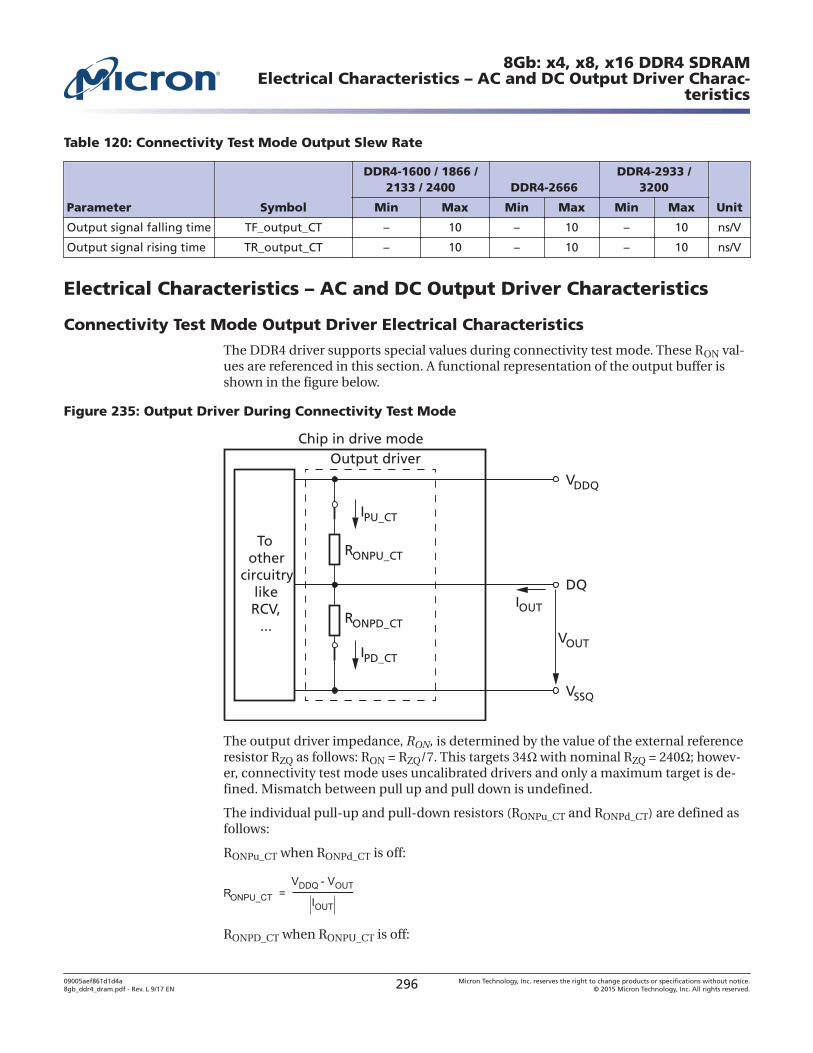
Table 120: Connectivity Test Mode Output Slew Rate
Parameter Symbol
DDR4-1600 / 1866 /2133 / 2400 DDR4-2666
DDR4-2933 /3200
UnitMin Max Min Max Min Max
Output signal falling time TF_output_CT – 10 – 10 – 10 ns/V
Output signal rising time TR_output_CT – 10 – 10 – 10 ns/V
Electrical Characteristics – AC and DC Output Driver Characteristics
Connectivity Test Mode Output Driver Electrical Characteristics
The DDR4 driver supports special values during connectivity test mode. These RON val-ues are referenced in this section. A functional representation of the output buffer isshown in the figure below.
Figure 235: Output Driver During Connectivity Test Mode
VDDQ
VSSQ
Chip in drive mode
DQ
VOUT
IOUT
RONPU_CT
RONPD_CT
Output driver
Toother
circuitrylikeRCV,
...
IPU_CT
IPD_CT
The output driver impedance, RON, is determined by the value of the external referenceresistor RZQ as follows: RON = RZQ/7. This targets 34 with nominal RZQ = 240 ; howev-er, connectivity test mode uses uncalibrated drivers and only a maximum target is de-fined. Mismatch between pull up and pull down is undefined.
The individual pull-up and pull-down resistors (RONPu_CT and RONPd_CT) are defined asfollows:
RONPu_CT when RONPd_CT is off:
RONPD_CT when RONPU_CT is off:
8Gb: x4, x8, x16 DDR4 SDRAMElectrical Characteristics – AC and DC Output Driver Charac-
teristics
09005aef861d1d4a8gb_ddr4_dram.pdf - Rev. L 9/17 EN 296 Micron Technology, Inc. reserves the right to change products or specifications without notice.
© 2015 Micron Technology, Inc. All rights reserved.
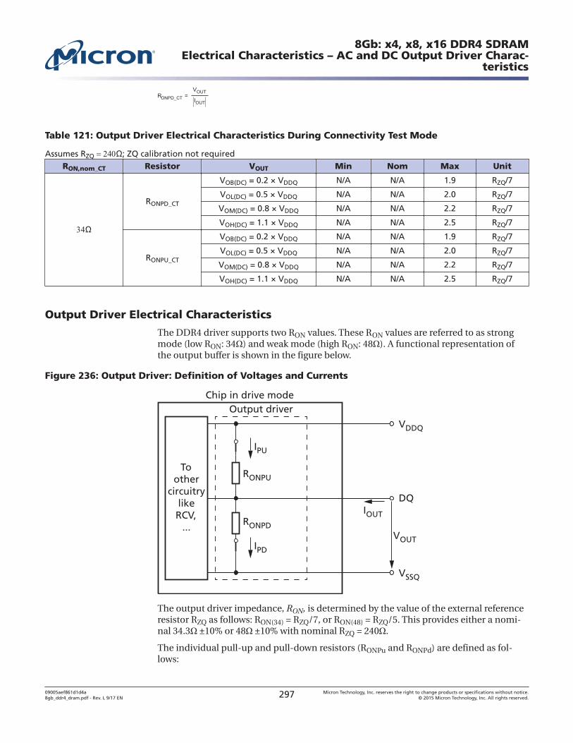
Table 121: Output Driver Electrical Characteristics During Connectivity Test Mode
Assumes RZQ ; ZQ calibration not requiredRON,nom_CT Resistor VOUT Min Nom Max Unit
RONPD_CT
VOB(DC) = 0.2 × VDDQ N/A N/A 1.9 RZQ/7
VOL(DC) = 0.5 × VDDQ N/A N/A 2.0 RZQ/7
VOM(DC) = 0.8 × VDDQ N/A N/A 2.2 RZQ/7
VOH(DC) = 1.1 × VDDQ N/A N/A 2.5 RZQ/7
RONPU_CT
VOB(DC) = 0.2 × VDDQ N/A N/A 1.9 RZQ/7
VOL(DC) = 0.5 × VDDQ N/A N/A 2.0 RZQ/7
VOM(DC) = 0.8 × VDDQ N/A N/A 2.2 RZQ/7
VOH(DC) = 1.1 × VDDQ N/A N/A 2.5 RZQ/7
Output Driver Electrical Characteristics
The DDR4 driver supports two RON values. These RON values are referred to as strongmode (low RON: 34 ) and weak mode (high RON: 48 ). A functional representation ofthe output buffer is shown in the figure below.
Figure 236: Output Driver: Definition of Voltages and Currents
VDDQ
VSSQ
Chip in drive mode
DQ
VOUT
IOUT
RONPU
RONPD
Output driver
Toother
circuitrylikeRCV,
...
IPU
IPD
The output driver impedance, RON, is determined by the value of the external referenceresistor RZQ as follows: RON(34) = RZQ/7, or RON(48) = RZQ/5. This provides either a nomi-nal 34.3 ±10% or 48 ±10% with nominal RZQ = 240 .
The individual pull-up and pull-down resistors (RONPu and RONPd) are defined as fol-lows:
8Gb: x4, x8, x16 DDR4 SDRAMElectrical Characteristics – AC and DC Output Driver Charac-
teristics
09005aef861d1d4a8gb_ddr4_dram.pdf - Rev. L 9/17 EN 297 Micron Technology, Inc. reserves the right to change products or specifications without notice.
© 2015 Micron Technology, Inc. All rights reserved.
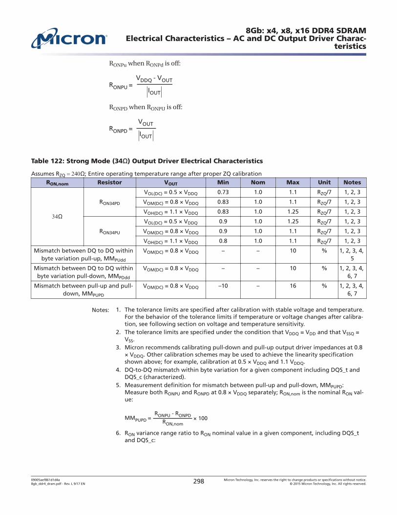
RONPu when RONPd is off:
RONPU =VDDQ - VOUT
IOUT
RONPD when RONPU is off:
RONPD =VOUT
IOUT
Table 122: Strong Mode (34 ) Output Driver Electrical Characteristics
Assumes RZQ ; Entire operating temperature range after proper ZQ calibrationRON,nom Resistor VOUT Min Nom Max Unit Notes
RON34PD
VOL(DC) = 0.5 × VDDQ 0.73 1.0 1.1 RZQ/7 1, 2, 3
VOM(DC) = 0.8 × VDDQ 0.83 1.0 1.1 RZQ/7 1, 2, 3
VOH(DC) = 1.1 × VDDQ 0.83 1.0 1.25 RZQ/7 1, 2, 3
RON34PU
VOL(DC) = 0.5 × VDDQ 0.9 1.0 1.25 RZQ/7 1, 2, 3
VOM(DC) = 0.8 × VDDQ 0.9 1.0 1.1 RZQ/7 1, 2, 3
VOH(DC) = 1.1 × VDDQ 0.8 1.0 1.1 RZQ/7 1, 2, 3
Mismatch between DQ to DQ withinbyte variation pull-up, MMPUdd
VOM(DC) = 0.8 × VDDQ – – 10 % 1, 2, 3, 4, 5
Mismatch between DQ to DQ withinbyte variation pull-down, MMPDdd
VOM(DC) = 0.8 × VDDQ – – 10 % 1, 2, 3, 4, 6, 7
Mismatch between pull-up and pull-down, MMPUPD
VOM(DC) = 0.8 × VDDQ –10 – 16 % 1, 2, 3, 4, 6, 7
Notes: 1. The tolerance limits are specified after calibration with stable voltage and temperature.For the behavior of the tolerance limits if temperature or voltage changes after calibra-tion, see following section on voltage and temperature sensitivity.
2. The tolerance limits are specified under the condition that VDDQ = VDD and that VSSQ =VSS.
3. Micron recommends calibrating pull-down and pull-up output driver impedances at 0.8× VDDQ. Other calibration schemes may be used to achieve the linearity specificationshown above; for example, calibration at 0.5 × VDDQ and 1.1 VDDQ.
4. DQ-to-DQ mismatch within byte variation for a given component including DQS_t andDQS_c (characterized).
5. Measurement definition for mismatch between pull-up and pull-down, MMPUPD:Measure both RONPU and RONPD at 0.8 × VDDQ separately; RON,nom is the nominal RON val-ue:
MMPUPD = × 100RONPU - RONPD
RON,nom
6. RON variance range ratio to RON nominal value in a given component, including DQS_tand DQS_c:
8Gb: x4, x8, x16 DDR4 SDRAMElectrical Characteristics – AC and DC Output Driver Charac-
teristics
09005aef861d1d4a8gb_ddr4_dram.pdf - Rev. L 9/17 EN 298 Micron Technology, Inc. reserves the right to change products or specifications without notice.
© 2015 Micron Technology, Inc. All rights reserved.
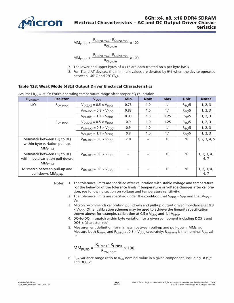
MMPUDD = × 100RONPU,max - RONPU,min
RON,nom
MMPDDD = × 100RONPD,max - RONPD,min
RON,nom
7. The lower and upper bytes of a x16 are each treated on a per byte basis.8. For IT and AT devices, the minimum values are derated by 9% when the device operates
between –40°C and 0°C (TC).
Table 123: Weak Mode (48 ) Output Driver Electrical Characteristics
Assumes RZQ ; Entire operating temperature range after proper ZQ calibrationRON,nom Resistor VOUT Min Nom Max Unit Notes
RON34PD VOL(DC) = 0.5 × VDDQ 0.73 1.0 1.1 RZQ/5 1, 2, 3
VOM(DC) = 0.8 × VDDQ 0.83 1.0 1.1 RZQ/5 1, 2, 3
VOH(DC) = 1.1 × VDDQ 0.83 1.0 1.25 RZQ/5 1, 2, 3
RON34PU VOL(DC) = 0.5 × VDDQ 0.9 1.0 1.25 RZQ/5 1, 2, 3
VOM(DC) = 0.8 × VDDQ 0.9 1.0 1.1 RZQ/5 1, 2, 3
VOH(DC) = 1.1 × VDDQ 0.8 1.0 1.1 RZQ/5 1, 2, 3
Mismatch between DQ to DQwithin byte variation pull-up,
MMPUdd
VOM(DC) = 0.8 × VDDQ -10 – 10 % 1, 2, 3, 4, 5
Mismatch between DQ to DQwithin byte variation pull-down,
MMPDdd
VOM(DC) = 0.8 × VDDQ – – 10 % 1, 2, 3, 4, 6, 7
Mismatch between pull-up andpull-down, MMPUPD
VOM(DC) = 0.8 × VDDQ – – 16 % 1, 2, 3, 4, 6, 7
Notes: 1. The tolerance limits are specified after calibration with stable voltage and temperature.For the behavior of the tolerance limits if temperature or voltage changes after calibra-tion, see following section on voltage and temperature sensitivity.
2. The tolerance limits are specified under the condition that VDDQ = VDD and that VSSQ =VSS.
3. Micron recommends calibrating pull-down and pull-up output driver impedances at 0.8× VDDQ. Other calibration schemes may be used to achieve the linearity specificationshown above; for example, calibration at 0.5 × VDDQ and 1.1 VDDQ.
4. DQ-to-DQ mismatch within byte variation for a given component including DQS_t andDQS_c (characterized).
5. Measurement definition for mismatch between pull-up and pull-down, MMPUPD:Measure both RONPU and RONPD at 0.8 × VDDQ separately; RON,nom is the nominal RON val-ue:
MMPUPD = × 100RONPU - RONPD
RON,nom
6. RON variance range ratio to RON nominal value in a given component, including DQS_tand DQS_c:
8Gb: x4, x8, x16 DDR4 SDRAMElectrical Characteristics – AC and DC Output Driver Charac-
teristics
09005aef861d1d4a8gb_ddr4_dram.pdf - Rev. L 9/17 EN 299 Micron Technology, Inc. reserves the right to change products or specifications without notice.
© 2015 Micron Technology, Inc. All rights reserved.
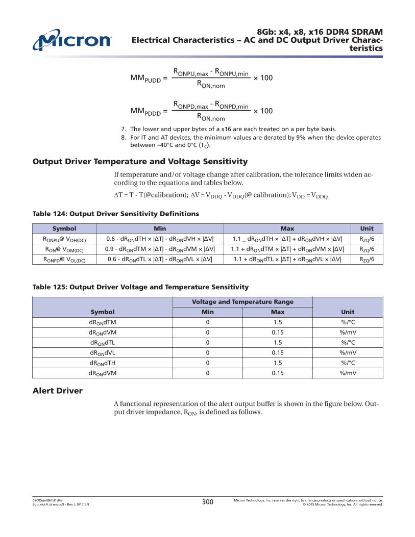
MMPUDD = × 100RONPU,max - RONPU,min
RON,nom
MMPDDD = × 100RONPD,max - RONPD,min
RON,nom
7. The lower and upper bytes of a x16 are each treated on a per byte basis.8. For IT and AT devices, the minimum values are derated by 9% when the device operates
between –40°C and 0°C (TC).
Output Driver Temperature and Voltage Sensitivity
If temperature and/or voltage change after calibration, the tolerance limits widen ac-cording to the equations and tables below.
T = T - T(@calibration); V = VDDQ - VDDQ(@ calibration); VDD = VDDQ
Table 124: Output Driver Sensitivity Definitions
Symbol Min Max Unit
RONPU@ VOH(DC) 0.6 - dRONdTH × | T| - dRONdVH × | V| 1.1 _ dRONdTH × | T| + dRONdVH × | V| RZQ/6
RON@ VOM(DC) 0.9 - dRONdTM × | T| - dRONdVM × | V| 1.1 + dRONdTM × | T| + dRONdVM × | V| RZQ/6
RONPD@ VOL(DC) 0.6 - dRONdTL × | T| - dRONdVL × | V| 1.1 + dRONdTL × | T| + dRONdVL × | V| RZQ/6
Table 125: Output Driver Voltage and Temperature Sensitivity
Symbol
Voltage and Temperature Range
UnitMin Max
dRONdTM 0 1.5 %/°C
dRONdVM 0 0.15 %/mV
dRONdTL 0 1.5 %/°C
dRONdVL 0 0.15 %/mV
dRONdTH 0 1.5 %/°C
dRONdVM 0 0.15 %/mV
Alert Driver
A functional representation of the alert output buffer is shown in the figure below. Out-put driver impedance, RON, is defined as follows.
8Gb: x4, x8, x16 DDR4 SDRAMElectrical Characteristics – AC and DC Output Driver Charac-
teristics
09005aef861d1d4a8gb_ddr4_dram.pdf - Rev. L 9/17 EN 300 Micron Technology, Inc. reserves the right to change products or specifications without notice.
© 2015 Micron Technology, Inc. All rights reserved.
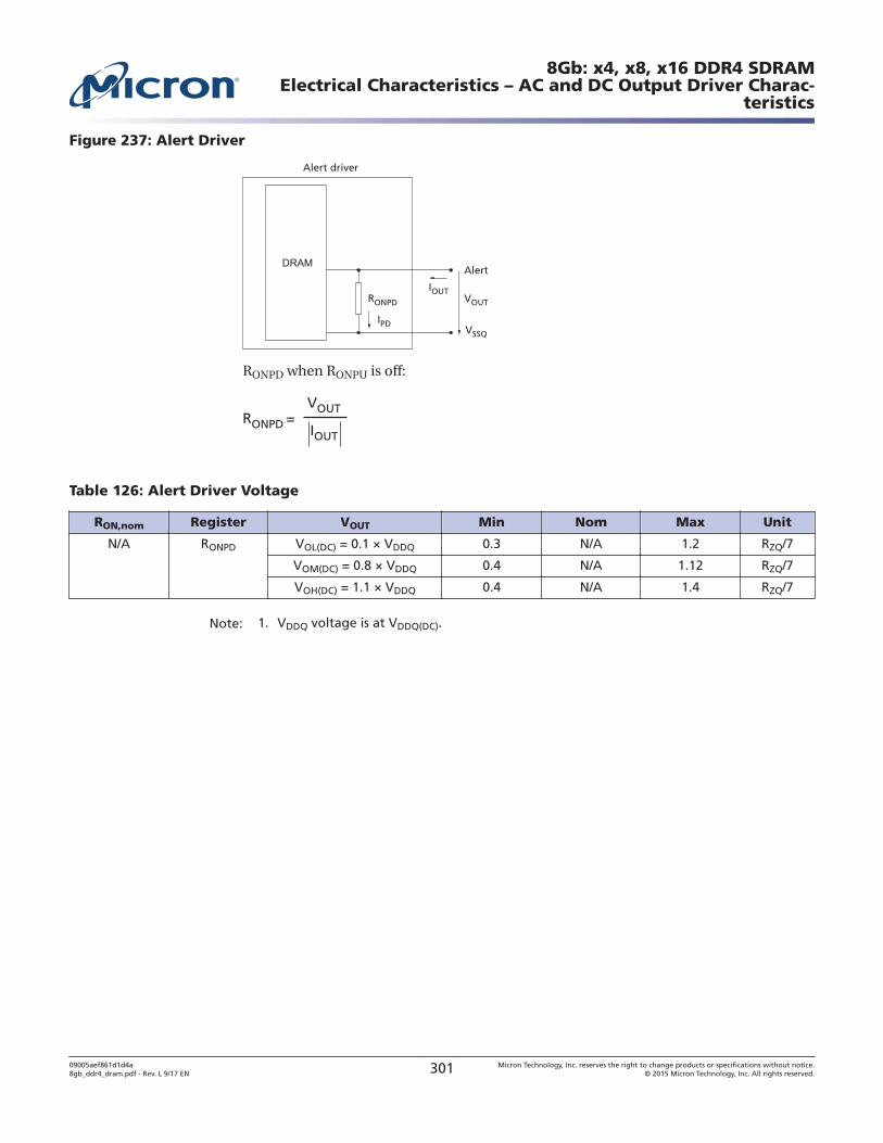
Figure 237: Alert Driver
Alert
VOUTRONPD
Alert driver
IPD
IOUT
VSSQ
RONPD when RONPU is off:
RONPD =VOUT
IOUT
Table 126: Alert Driver Voltage
RON,nom Register VOUT Min Nom Max Unit
N/A RONPD VOL(DC) = 0.1 × VDDQ 0.3 N/A 1.2 RZQ/7
VOM(DC) = 0.8 × VDDQ 0.4 N/A 1.12 RZQ/7
VOH(DC) = 1.1 × VDDQ 0.4 N/A 1.4 RZQ/7
Note: 1. VDDQ voltage is at VDDQ(DC).
8Gb: x4, x8, x16 DDR4 SDRAMElectrical Characteristics – AC and DC Output Driver Charac-
teristics
09005aef861d1d4a8gb_ddr4_dram.pdf - Rev. L 9/17 EN 301 Micron Technology, Inc. reserves the right to change products or specifications without notice.
© 2015 Micron Technology, Inc. All rights reserved.
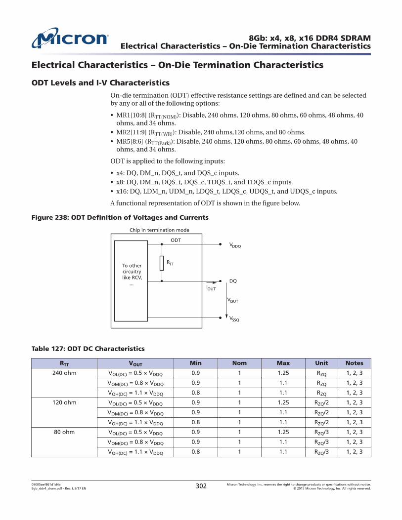
Electrical Characteristics – On-Die Termination Characteristics
ODT Levels and I-V Characteristics
On-die termination (ODT) effective resistance settings are defined and can be selectedby any or all of the following options:
• MR1[10:8] (RTT(NOM)): Disable, 240 ohms, 120 ohms, 80 ohms, 60 ohms, 48 ohms, 40ohms, and 34 ohms.
• MR2[11:9] (RTT(WR)): Disable, 240 ohms,120 ohms, and 80 ohms.• MR5[8:6] (RTT(Park)): Disable, 240 ohms, 120 ohms, 80 ohms, 60 ohms, 48 ohms, 40
ohms, and 34 ohms.
ODT is applied to the following inputs:
• x4: DQ, DM_n, DQS_t, and DQS_c inputs.• x8: DQ, DM_n, DQS_t, DQS_c, TDQS_t, and TDQS_c inputs.• x16: DQ, LDM_n, UDM_n, LDQS_t, LDQS_c, UDQS_t, and UDQS_c inputs.
A functional representation of ODT is shown in the figure below.
Figure 238: ODT Definition of Voltages and Currents
VDDQ
VSSQ
Chip in termination mode
DQ
VOUT
IOUT
RTTTo othercircuitrylike RCV,
...
ODT
Table 127: ODT DC Characteristics
RTT VOUT Min Nom Max Unit Notes
240 ohm VOL(DC) = 0.5 × VDDQ 0.9 1 1.25 RZQ 1, 2, 3
VOM(DC) = 0.8 × VDDQ 0.9 1 1.1 RZQ 1, 2, 3
VOH(DC) = 1.1 × VDDQ 0.8 1 1.1 RZQ 1, 2, 3
120 ohm VOL(DC) = 0.5 × VDDQ 0.9 1 1.25 RZQ/2 1, 2, 3
VOM(DC) = 0.8 × VDDQ 0.9 1 1.1 RZQ/2 1, 2, 3
VOH(DC) = 1.1 × VDDQ 0.8 1 1.1 RZQ/2 1, 2, 3
80 ohm VOL(DC) = 0.5 × VDDQ 0.9 1 1.25 RZQ/3 1, 2, 3
VOM(DC) = 0.8 × VDDQ 0.9 1 1.1 RZQ/3 1, 2, 3
VOH(DC) = 1.1 × VDDQ 0.8 1 1.1 RZQ/3 1, 2, 3
8Gb: x4, x8, x16 DDR4 SDRAMElectrical Characteristics – On-Die Termination Characteristics
09005aef861d1d4a8gb_ddr4_dram.pdf - Rev. L 9/17 EN 302 Micron Technology, Inc. reserves the right to change products or specifications without notice.
© 2015 Micron Technology, Inc. All rights reserved.
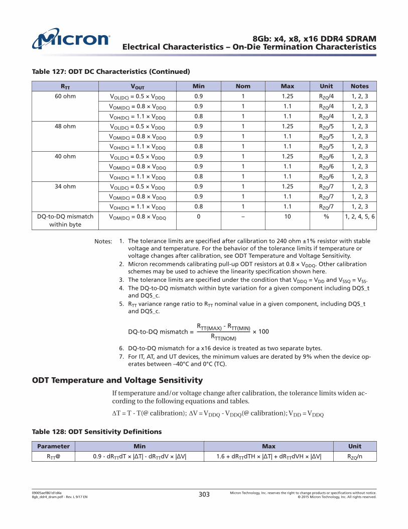
Table 127: ODT DC Characteristics (Continued)
RTT VOUT Min Nom Max Unit Notes
60 ohm VOL(DC) = 0.5 × VDDQ 0.9 1 1.25 RZQ/4 1, 2, 3
VOM(DC) = 0.8 × VDDQ 0.9 1 1.1 RZQ/4 1, 2, 3
VOH(DC) = 1.1 × VDDQ 0.8 1 1.1 RZQ/4 1, 2, 3
48 ohm VOL(DC) = 0.5 × VDDQ 0.9 1 1.25 RZQ/5 1, 2, 3
VOM(DC) = 0.8 × VDDQ 0.9 1 1.1 RZQ/5 1, 2, 3
VOH(DC) = 1.1 × VDDQ 0.8 1 1.1 RZQ/5 1, 2, 3
40 ohm VOL(DC) = 0.5 × VDDQ 0.9 1 1.25 RZQ/6 1, 2, 3
VOM(DC) = 0.8 × VDDQ 0.9 1 1.1 RZQ/6 1, 2, 3
VOH(DC) = 1.1 × VDDQ 0.8 1 1.1 RZQ/6 1, 2, 3
34 ohm VOL(DC) = 0.5 × VDDQ 0.9 1 1.25 RZQ/7 1, 2, 3
VOM(DC) = 0.8 × VDDQ 0.9 1 1.1 RZQ/7 1, 2, 3
VOH(DC) = 1.1 × VDDQ 0.8 1 1.1 RZQ/7 1, 2, 3
DQ-to-DQ mismatchwithin byte
VOM(DC) = 0.8 × VDDQ 0 – 10 % 1, 2, 4, 5, 6
Notes: 1. The tolerance limits are specified after calibration to 240 ohm ±1% resistor with stablevoltage and temperature. For the behavior of the tolerance limits if temperature orvoltage changes after calibration, see ODT Temperature and Voltage Sensitivity.
2. Micron recommends calibrating pull-up ODT resistors at 0.8 × VDDQ. Other calibrationschemes may be used to achieve the linearity specification shown here.
3. The tolerance limits are specified under the condition that VDDQ = VDD and VSSQ = VSS.4. The DQ-to-DQ mismatch within byte variation for a given component including DQS_t
and DQS_c.5. RTT variance range ratio to RTT nominal value in a given component, including DQS_t
and DQS_c.
DQ-to-DQ mismatch =RTT(MAX) - RTT(MIN)
RTT(NOM)× 100
6. DQ-to-DQ mismatch for a x16 device is treated as two separate bytes.7. For IT, AT, and UT devices, the minimum values are derated by 9% when the device op-
erates between –40°C and 0°C (TC).
ODT Temperature and Voltage Sensitivity
If temperature and/or voltage change after calibration, the tolerance limits widen ac-cording to the following equations and tables.
T = T - T(@ calibration); V = VDDQ - VDDQ(@ calibration); VDD = VDDQ
Table 128: ODT Sensitivity Definitions
Parameter Min Max Unit
RTT@ 0.9 - dRTTdT × | T| - dRTTdV × | V| 1.6 + dRTTdTH × | T| + dRTTdVH × | V| RZQ/n
8Gb: x4, x8, x16 DDR4 SDRAMElectrical Characteristics – On-Die Termination Characteristics
09005aef861d1d4a8gb_ddr4_dram.pdf - Rev. L 9/17 EN 303 Micron Technology, Inc. reserves the right to change products or specifications without notice.
© 2015 Micron Technology, Inc. All rights reserved.
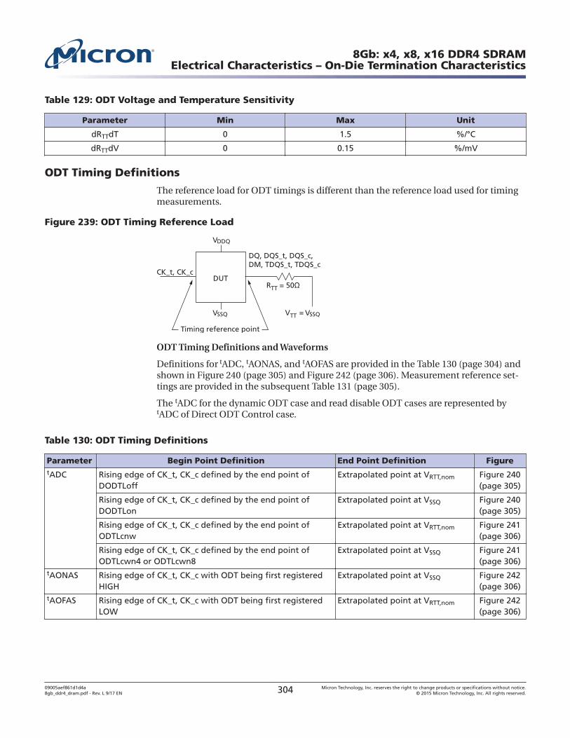
Table 129: ODT Voltage and Temperature Sensitivity
Parameter Min Max Unit
dRTTdT 0 1.5 %/°C
dRTTdV 0 0.15 %/mV
ODT Timing Definitions
The reference load for ODT timings is different than the reference load used for timingmeasurements.
Figure 239: ODT Timing Reference Load
Timing reference point
DQ, DQS_t, DQS_c, DM, TDQS_t, TDQS_c
CK_t, CK_cDUT
VTT
VDDQ
VSSQ VSSQ=
RTT = 50
ODT Timing Definitions and Waveforms
Definitions for tADC, tAONAS, and tAOFAS are provided in the Table 130 (page 304) andshown in Figure 240 (page 305) and Figure 242 (page 306). Measurement reference set-tings are provided in the subsequent Table 131 (page 305).
The tADC for the dynamic ODT case and read disable ODT cases are represented bytADC of Direct ODT Control case.
Table 130: ODT Timing Definitions
Parameter Begin Point Definition End Point Definition FiguretADC Rising edge of CK_t, CK_c defined by the end point of
DODTLoffExtrapolated point at VRTT,nom Figure 240
(page 305)
Rising edge of CK_t, CK_c defined by the end point ofDODTLon
Extrapolated point at VSSQ Figure 240(page 305)
Rising edge of CK_t, CK_c defined by the end point ofODTLcnw
Extrapolated point at VRTT,nom Figure 241(page 306)
Rising edge of CK_t, CK_c defined by the end point ofODTLcwn4 or ODTLcwn8
Extrapolated point at VSSQ Figure 241(page 306)
tAONAS Rising edge of CK_t, CK_c with ODT being first registeredHIGH
Extrapolated point at VSSQ Figure 242(page 306)
tAOFAS Rising edge of CK_t, CK_c with ODT being first registeredLOW
Extrapolated point at VRTT,nom Figure 242(page 306)
8Gb: x4, x8, x16 DDR4 SDRAMElectrical Characteristics – On-Die Termination Characteristics
09005aef861d1d4a8gb_ddr4_dram.pdf - Rev. L 9/17 EN 304 Micron Technology, Inc. reserves the right to change products or specifications without notice.
© 2015 Micron Technology, Inc. All rights reserved.
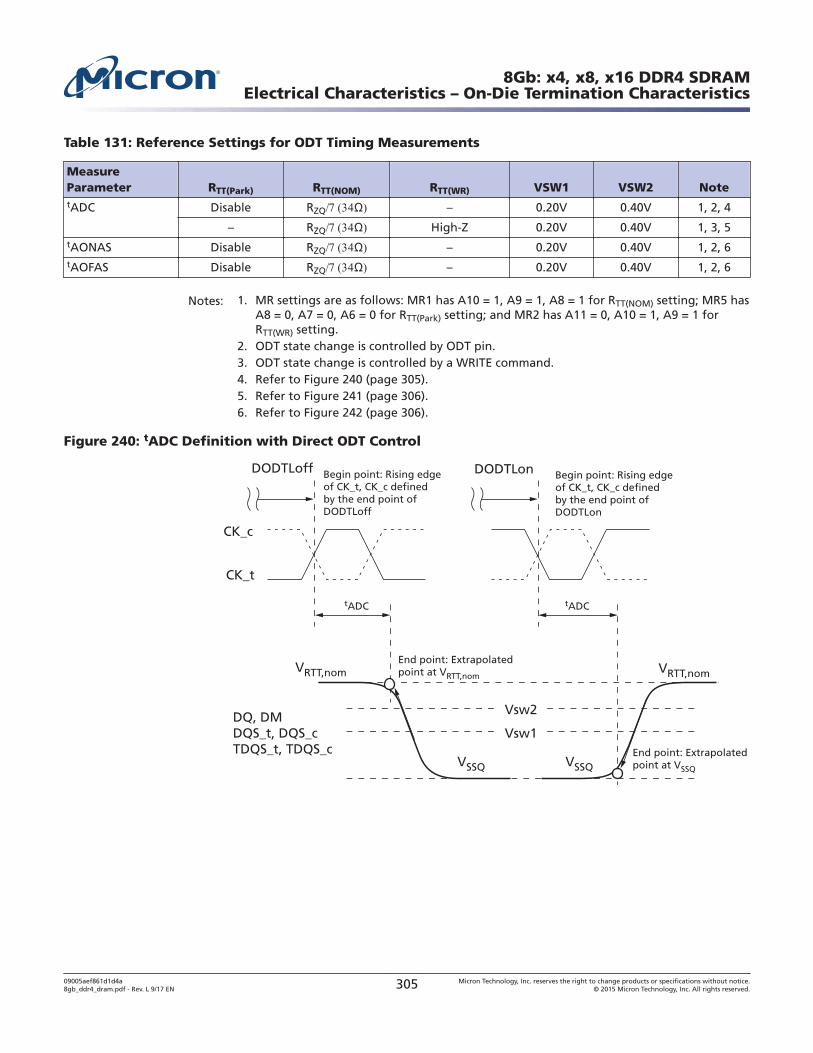
Table 131: Reference Settings for ODT Timing Measurements
MeasureParameter RTT(Park) RTT(NOM) RTT(WR) VSW1 VSW2 NotetADC Disable RZQ – 0.20V 0.40V 1, 2, 4
– RZQ High-Z 0.20V 0.40V 1, 3, 5tAONAS Disable RZQ – 0.20V 0.40V 1, 2, 6tAOFAS Disable RZQ – 0.20V 0.40V 1, 2, 6
Notes: 1. MR settings are as follows: MR1 has A10 = 1, A9 = 1, A8 = 1 for RTT(NOM) setting; MR5 hasA8 = 0, A7 = 0, A6 = 0 for RTT(Park) setting; and MR2 has A11 = 0, A10 = 1, A9 = 1 forRTT(WR) setting.
2. ODT state change is controlled by ODT pin.3. ODT state change is controlled by a WRITE command.4. Refer to Figure 240 (page 305).5. Refer to Figure 241 (page 306).6. Refer to Figure 242 (page 306).
Figure 240: tADC Definition with Direct ODT Control
tADC tADC
Begin point: Rising edgeof CK_t, CK_c definedby the end point ofDODTLoff
DODTLoff Begin point: Rising edgeof CK_t, CK_c definedby the end point ofDODTLon
DODTLon
End point: Extrapolatedpoint at VRTT,nom
End point: Extrapolatedpoint at VSSQ
VRTT,nomVRTT,nom
VSSQ VSSQ
DQ, DMDQS_t, DQS_cTDQS_t, TDQS_c
CK_c
CK_t
Vsw2
Vsw1
8Gb: x4, x8, x16 DDR4 SDRAMElectrical Characteristics – On-Die Termination Characteristics
09005aef861d1d4a8gb_ddr4_dram.pdf - Rev. L 9/17 EN 305 Micron Technology, Inc. reserves the right to change products or specifications without notice.
© 2015 Micron Technology, Inc. All rights reserved.
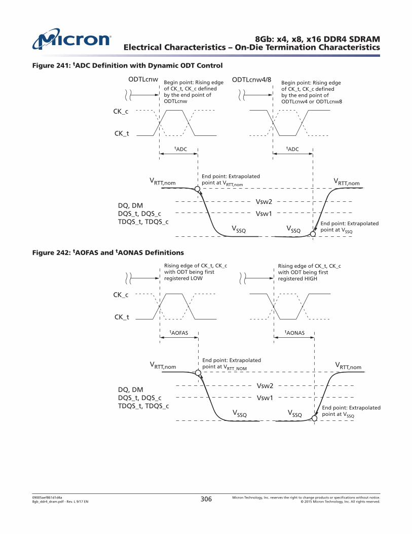
Figure 241: tADC Definition with Dynamic ODT Control
tADC tADC
Begin point: Rising edgeof CK_t, CK_c definedby the end point ofODTLcnw
ODTLcnw Begin point: Rising edgeof CK_t, CK_c definedby the end point ofODTLcnw4 or ODTLcnw8
ODTLcnw4/8
End point: Extrapolatedpoint at VRTT,nom
End point: Extrapolatedpoint at VSSQ
VRTT,nomVRTT,nom
VSSQ VSSQ
DQ, DMDQS_t, DQS_cTDQS_t, TDQS_c
CK_c
CK_t
Vsw2
Vsw1
Figure 242: tAOFAS and tAONAS Definitions
tAOFAS tAONAS
Rising edge of CK_t, CK_cwith ODT being firstregistered LOW
Rising edge of CK_t, CK_cwith ODT being firstregistered HIGH
End point: Extrapolatedpoint at VRTT_NOM
End point: Extrapolatedpoint at VSSQ
VRTT,nomVRTT,nom
VSSQ VSSQ
DQ, DMDQS_t, DQS_cTDQS_t, TDQS_c
CK_c
CK_t
Vsw2
Vsw1
8Gb: x4, x8, x16 DDR4 SDRAMElectrical Characteristics – On-Die Termination Characteristics
09005aef861d1d4a8gb_ddr4_dram.pdf - Rev. L 9/17 EN 306 Micron Technology, Inc. reserves the right to change products or specifications without notice.
© 2015 Micron Technology, Inc. All rights reserved.
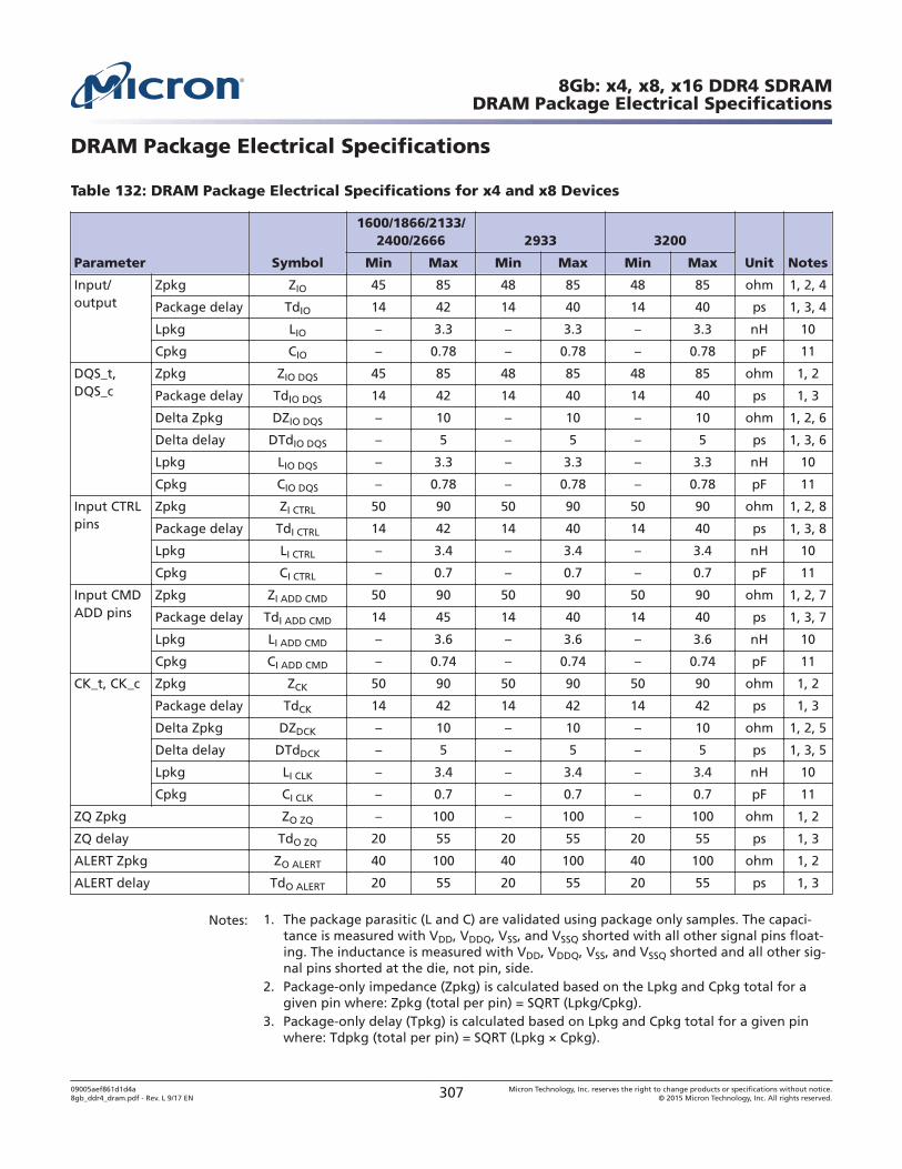
DRAM Package Electrical Specifications
Table 132: DRAM Package Electrical Specifications for x4 and x8 Devices
Parameter Symbol
1600/1866/2133/2400/2666 2933 3200
Unit NotesMin Max Min Max Min Max
Input/output
Zpkg ZIO 45 85 48 85 48 85 ohm 1, 2, 4
Package delay TdIO 14 42 14 40 14 40 ps 1, 3, 4
Lpkg LIO – 3.3 – 3.3 – 3.3 nH 10
Cpkg CIO – 0.78 – 0.78 – 0.78 pF 11
DQS_t,DQS_c
Zpkg ZIO DQS 45 85 48 85 48 85 ohm 1, 2
Package delay TdIO DQS 14 42 14 40 14 40 ps 1, 3
Delta Zpkg DZIO DQS – 10 – 10 – 10 ohm 1, 2, 6
Delta delay DTdIO DQS – 5 – 5 – 5 ps 1, 3, 6
Lpkg LIO DQS – 3.3 – 3.3 – 3.3 nH 10
Cpkg CIO DQS – 0.78 – 0.78 – 0.78 pF 11
Input CTRLpins
Zpkg ZI CTRL 50 90 50 90 50 90 ohm 1, 2, 8
Package delay TdI CTRL 14 42 14 40 14 40 ps 1, 3, 8
Lpkg LI CTRL – 3.4 – 3.4 – 3.4 nH 10
Cpkg CI CTRL – 0.7 – 0.7 – 0.7 pF 11
Input CMDADD pins
Zpkg ZI ADD CMD 50 90 50 90 50 90 ohm 1, 2, 7
Package delay TdI ADD CMD 14 45 14 40 14 40 ps 1, 3, 7
Lpkg LI ADD CMD – 3.6 – 3.6 – 3.6 nH 10
Cpkg CI ADD CMD – 0.74 – 0.74 – 0.74 pF 11
CK_t, CK_c Zpkg ZCK 50 90 50 90 50 90 ohm 1, 2
Package delay TdCK 14 42 14 42 14 42 ps 1, 3
Delta Zpkg DZDCK – 10 – 10 – 10 ohm 1, 2, 5
Delta delay DTdDCK – 5 – 5 – 5 ps 1, 3, 5
Lpkg LI CLK – 3.4 – 3.4 – 3.4 nH 10
Cpkg CI CLK – 0.7 – 0.7 – 0.7 pF 11
ZQ Zpkg ZO ZQ – 100 – 100 – 100 ohm 1, 2
ZQ delay TdO ZQ 20 55 20 55 20 55 ps 1, 3
ALERT Zpkg ZO ALERT 40 100 40 100 40 100 ohm 1, 2
ALERT delay TdO ALERT 20 55 20 55 20 55 ps 1, 3
Notes: 1. The package parasitic (L and C) are validated using package only samples. The capaci-tance is measured with VDD, VDDQ, VSS, and VSSQ shorted with all other signal pins float-ing. The inductance is measured with VDD, VDDQ, VSS, and VSSQ shorted and all other sig-nal pins shorted at the die, not pin, side.
2. Package-only impedance (Zpkg) is calculated based on the Lpkg and Cpkg total for agiven pin where: Zpkg (total per pin) = SQRT (Lpkg/Cpkg).
3. Package-only delay (Tpkg) is calculated based on Lpkg and Cpkg total for a given pinwhere: Tdpkg (total per pin) = SQRT (Lpkg × Cpkg).
8Gb: x4, x8, x16 DDR4 SDRAMDRAM Package Electrical Specifications
09005aef861d1d4a8gb_ddr4_dram.pdf - Rev. L 9/17 EN 307 Micron Technology, Inc. reserves the right to change products or specifications without notice.
© 2015 Micron Technology, Inc. All rights reserved.
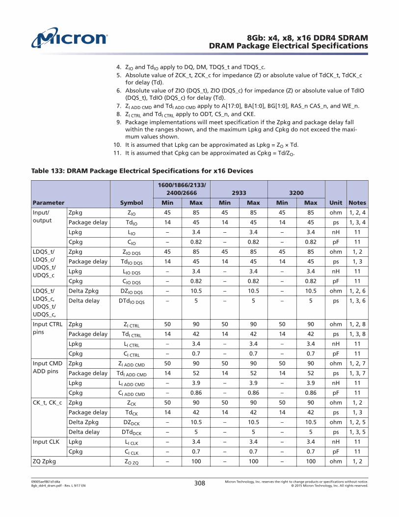
4. ZIO and TdIO apply to DQ, DM, TDQS_t and TDQS_c.5. Absolute value of ZCK_t, ZCK_c for impedance (Z) or absolute value of TdCK_t, TdCK_c
for delay (Td).6. Absolute value of ZIO (DQS_t), ZIO (DQS_c) for impedance (Z) or absolute value of TdIO
(DQS_t), TdIO (DQS_c) for delay (Td).7. ZI ADD CMD and TdI ADD CMD apply to A[17:0], BA[1:0], BG[1:0], RAS_n CAS_n, and WE_n.8. ZI CTRL and TdI CTRL apply to ODT, CS_n, and CKE.9. Package implementations will meet specification if the Zpkg and package delay fall
within the ranges shown, and the maximum Lpkg and Cpkg do not exceed the maxi-mum values shown.
10. It is assumed that Lpkg can be approximated as Lpkg = ZO × Td.11. It is assumed that Cpkg can be approximated as Cpkg = Td/ZO.
Table 133: DRAM Package Electrical Specifications for x16 Devices
Parameter Symbol
1600/1866/2133/2400/2666 2933 3200
Unit NotesMin Max Min Max Min Max
Input/output
Zpkg ZIO 45 85 45 85 45 85 ohm 1, 2, 4
Package delay TdIO 14 45 14 45 14 45 ps 1, 3, 4
Lpkg LIO – 3.4 – 3.4 – 3.4 nH 11
Cpkg CIO – 0.82 – 0.82 – 0.82 pF 11
LDQS_t/LDQS_c/UDQS_t/UDQS_c
Zpkg ZIO DQS 45 85 45 85 45 85 ohm 1, 2
Package delay TdIO DQS 14 45 14 45 14 45 ps 1, 3
Lpkg LIO DQS – 3.4 – 3.4 – 3.4 nH 11
Cpkg CIO DQS – 0.82 – 0.82 – 0.82 pF 11
LDQS_t/LDQS_c,UDQS_t/UDQS_c,
Delta Zpkg DZIO DQS – 10.5 – 10.5 – 10.5 ohm 1, 2, 6
Delta delay DTdIO DQS – 5 – 5 – 5 ps 1, 3, 6
Input CTRLpins
Zpkg ZI CTRL 50 90 50 90 50 90 ohm 1, 2, 8
Package delay TdI CTRL 14 42 14 42 14 42 ps 1, 3, 8
Lpkg LI CTRL – 3.4 – 3.4 – 3.4 nH 11
Cpkg CI CTRL – 0.7 – 0.7 – 0.7 pF 11
Input CMDADD pins
Zpkg ZI ADD CMD 50 90 50 90 50 90 ohm 1, 2, 7
Package delay TdI ADD CMD 14 52 14 52 14 52 ps 1, 3, 7
Lpkg LI ADD CMD – 3.9 – 3.9 – 3.9 nH 11
Cpkg CI ADD CMD – 0.86 – 0.86 – 0.86 pF 11
CK_t, CK_c Zpkg ZCK 50 90 50 90 50 90 ohm 1, 2
Package delay TdCK 14 42 14 42 14 42 ps 1, 3
Delta Zpkg DZDCK – 10.5 – 10.5 – 10.5 ohm 1, 2, 5
Delta delay DTdDCK – 5 – 5 – 5 ps 1, 3, 5
Input CLK Lpkg LI CLK – 3.4 – 3.4 – 3.4 nH 11
Cpkg CI CLK – 0.7 – 0.7 – 0.7 pF 11
ZQ Zpkg ZO ZQ – 100 – 100 – 100 ohm 1, 2
8Gb: x4, x8, x16 DDR4 SDRAMDRAM Package Electrical Specifications
09005aef861d1d4a8gb_ddr4_dram.pdf - Rev. L 9/17 EN 308 Micron Technology, Inc. reserves the right to change products or specifications without notice.
© 2015 Micron Technology, Inc. All rights reserved.
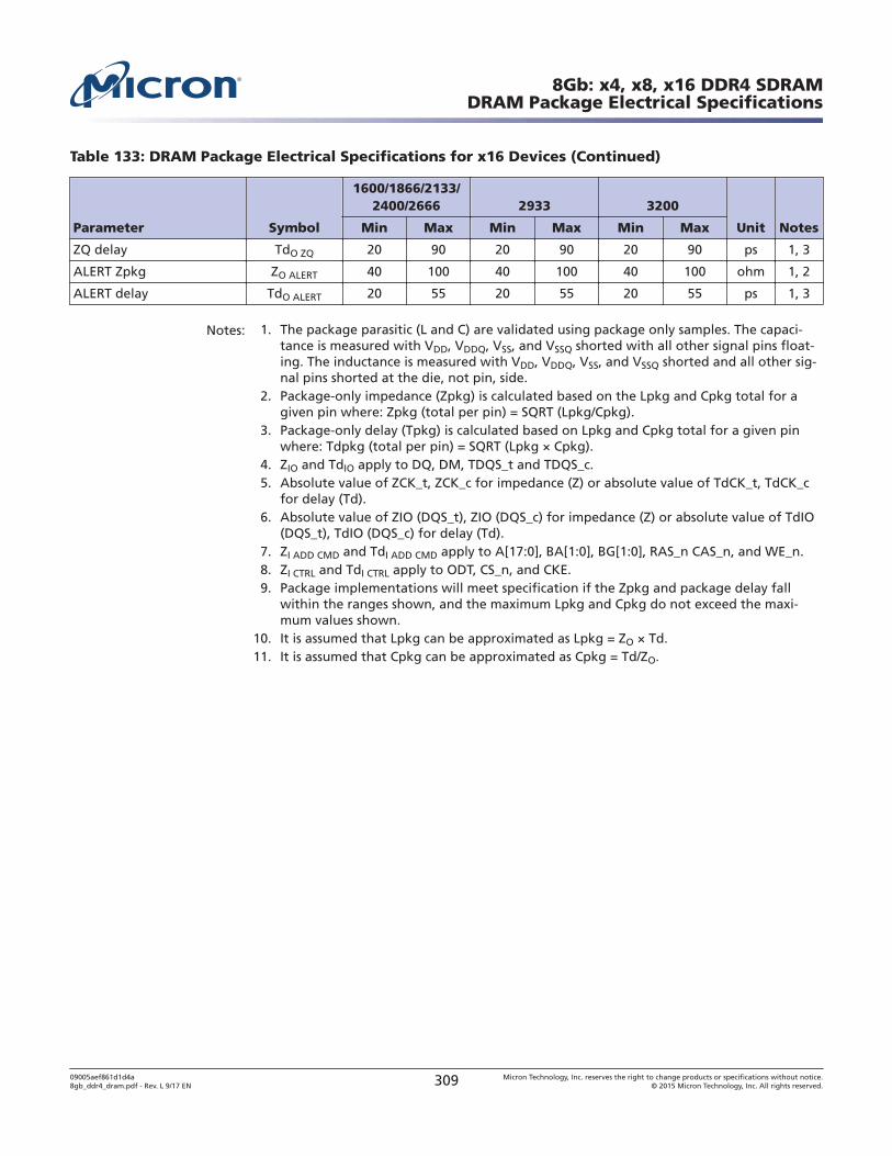
Table 133: DRAM Package Electrical Specifications for x16 Devices (Continued)
Parameter Symbol
1600/1866/2133/2400/2666 2933 3200
Unit NotesMin Max Min Max Min Max
ZQ delay TdO ZQ 20 90 20 90 20 90 ps 1, 3
ALERT Zpkg ZO ALERT 40 100 40 100 40 100 ohm 1, 2
ALERT delay TdO ALERT 20 55 20 55 20 55 ps 1, 3
Notes: 1. The package parasitic (L and C) are validated using package only samples. The capaci-tance is measured with VDD, VDDQ, VSS, and VSSQ shorted with all other signal pins float-ing. The inductance is measured with VDD, VDDQ, VSS, and VSSQ shorted and all other sig-nal pins shorted at the die, not pin, side.
2. Package-only impedance (Zpkg) is calculated based on the Lpkg and Cpkg total for agiven pin where: Zpkg (total per pin) = SQRT (Lpkg/Cpkg).
3. Package-only delay (Tpkg) is calculated based on Lpkg and Cpkg total for a given pinwhere: Tdpkg (total per pin) = SQRT (Lpkg × Cpkg).
4. ZIO and TdIO apply to DQ, DM, TDQS_t and TDQS_c.5. Absolute value of ZCK_t, ZCK_c for impedance (Z) or absolute value of TdCK_t, TdCK_c
for delay (Td).6. Absolute value of ZIO (DQS_t), ZIO (DQS_c) for impedance (Z) or absolute value of TdIO
(DQS_t), TdIO (DQS_c) for delay (Td).7. ZI ADD CMD and TdI ADD CMD apply to A[17:0], BA[1:0], BG[1:0], RAS_n CAS_n, and WE_n.8. ZI CTRL and TdI CTRL apply to ODT, CS_n, and CKE.9. Package implementations will meet specification if the Zpkg and package delay fall
within the ranges shown, and the maximum Lpkg and Cpkg do not exceed the maxi-mum values shown.
10. It is assumed that Lpkg can be approximated as Lpkg = ZO × Td.11. It is assumed that Cpkg can be approximated as Cpkg = Td/ZO.
8Gb: x4, x8, x16 DDR4 SDRAMDRAM Package Electrical Specifications
09005aef861d1d4a8gb_ddr4_dram.pdf - Rev. L 9/17 EN 309 Micron Technology, Inc. reserves the right to change products or specifications without notice.
© 2015 Micron Technology, Inc. All rights reserved.
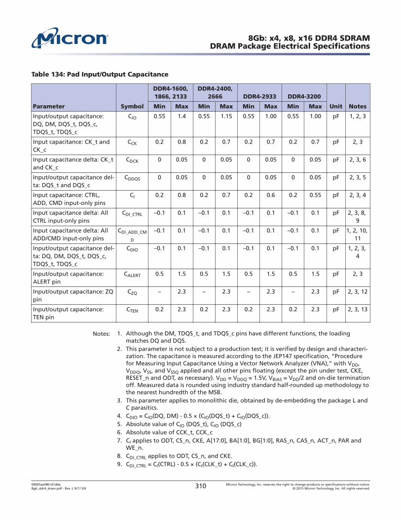
Table 134: Pad Input/Output Capacitance
Parameter Symbol
DDR4-1600,1866, 2133
DDR4-2400,2666 DDR4-2933 DDR4-3200
Unit NotesMin Max Min Max Min Max Min Max
Input/output capacitance:DQ, DM, DQS_t, DQS_c,TDQS_t, TDQS_c
CIO 0.55 1.4 0.55 1.15 0.55 1.00 0.55 1.00 pF 1, 2, 3
Input capacitance: CK_t andCK_c
CCK 0.2 0.8 0.2 0.7 0.2 0.7 0.2 0.7 pF 2, 3
Input capacitance delta: CK_tand CK_c
CDCK 0 0.05 0 0.05 0 0.05 0 0.05 pF 2, 3, 6
Input/output capacitance del-ta: DQS_t and DQS_c
CDDQS 0 0.05 0 0.05 0 0.05 0 0.05 pF 2, 3, 5
Input capacitance: CTRL,ADD, CMD input-only pins
CI 0.2 0.8 0.2 0.7 0.2 0.6 0.2 0.55 pF 2, 3, 4
Input capacitance delta: AllCTRL input-only pins
CDI_CTRL –0.1 0.1 –0.1 0.1 –0.1 0.1 –0.1 0.1 pF 2, 3, 8, 9
Input capacitance delta: AllADD/CMD input-only pins
CDI_ADD_CM
D
–0.1 0.1 –0.1 0.1 –0.1 0.1 –0.1 0.1 pF 1, 2, 10, 11
Input/output capacitance del-ta: DQ, DM, DQS_t, DQS_c,TDQS_t, TDQS_c
CDIO –0.1 0.1 –0.1 0.1 –0.1 0.1 –0.1 0.1 pF 1, 2, 3, 4
Input/output capacitance:ALERT pin
CALERT 0.5 1.5 0.5 1.5 0.5 1.5 0.5 1.5 pF 2, 3
Input/output capacitance: ZQpin
CZQ – 2.3 – 2.3 – 2.3 – 2.3 pF 2, 3, 12
Input/output capacitance:TEN pin
CTEN 0.2 2.3 0.2 2.3 0.2 2.3 0.2 2.3 pF 2, 3, 13
Notes: 1. Although the DM, TDQS_t, and TDQS_c pins have different functions, the loadingmatches DQ and DQS.
2. This parameter is not subject to a production test; it is verified by design and characteri-zation. The capacitance is measured according to the JEP147 specification, “Procedurefor Measuring Input Capacitance Using a Vector Network Analyzer (VNA),” with VDD,VDDQ, VSS, and VSSQ applied and all other pins floating (except the pin under test, CKE,RESET_n and ODT, as necessary). VDD = VDDQ = 1.5V, VBIAS = VDD/2 and on-die terminationoff. Measured data is rounded using industry standard half-rounded up methodology tothe nearest hundredth of the MSB.
3. This parameter applies to monolithic die, obtained by de-embedding the package L andC parasitics.
4. CDIO = CIO(DQ, DM) - 0.5 × (CIO(DQS_t) + CIO(DQS_c)).5. Absolute value of CIO (DQS_t), CIO (DQS_c)6. Absolute value of CCK_t, CCK_c7. CI applies to ODT, CS_n, CKE, A[17:0], BA[1:0], BG[1:0], RAS_n, CAS_n, ACT_n, PAR and
WE_n.8. CDI_CTRL applies to ODT, CS_n, and CKE.9. CDI_CTRL = CI(CTRL) - 0.5 × (CI(CLK_t) + CI(CLK_c)).
8Gb: x4, x8, x16 DDR4 SDRAMDRAM Package Electrical Specifications
09005aef861d1d4a8gb_ddr4_dram.pdf - Rev. L 9/17 EN 310 Micron Technology, Inc. reserves the right to change products or specifications without notice.
© 2015 Micron Technology, Inc. All rights reserved.
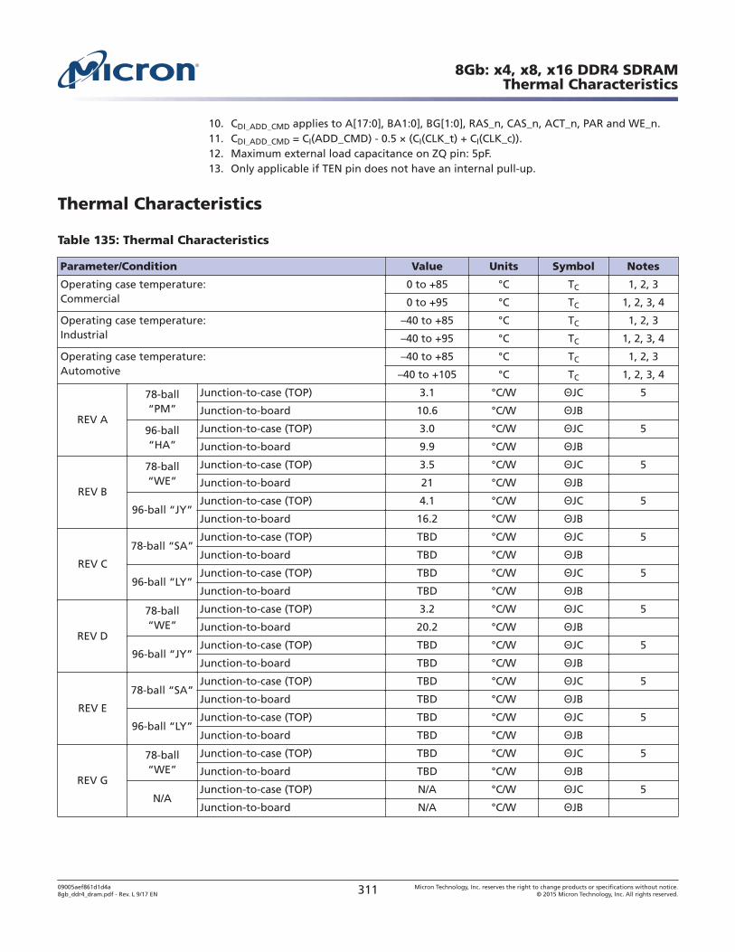
10. CDI_ADD_CMD applies to A[17:0], BA1:0], BG[1:0], RAS_n, CAS_n, ACT_n, PAR and WE_n.11. CDI_ADD_CMD = CI(ADD_CMD) - 0.5 × (CI(CLK_t) + CI(CLK_c)).12. Maximum external load capacitance on ZQ pin: 5pF.13. Only applicable if TEN pin does not have an internal pull-up.
Thermal Characteristics
Table 135: Thermal Characteristics
Parameter/Condition Value Units Symbol Notes
Operating case temperature:Commercial
0 to +85 °C TC 1, 2, 3
0 to +95 °C TC 1, 2, 3, 4
Operating case temperature:Industrial
–40 to +85 °C TC 1, 2, 3
–40 to +95 °C TC 1, 2, 3, 4
Operating case temperature:Automotive
–40 to +85 °C TC 1, 2, 3
–40 to +105 °C TC 1, 2, 3, 4
REV A
78-ball“PM”
Junction-to-case (TOP) 3.1 °C/W JC 5
Junction-to-board 10.6 °C/W JB
96-ball“HA”
Junction-to-case (TOP) 3.0 °C/W JC 5
Junction-to-board 9.9 °C/W JB
REV B
78-ball“WE”
Junction-to-case (TOP) 3.5 °C/W JC 5
Junction-to-board 21 °C/W JB
96-ball “JY”Junction-to-case (TOP) 4.1 °C/W JC 5
Junction-to-board 16.2 °C/W JB
REV C
78-ball “SA”Junction-to-case (TOP) TBD °C/W JC 5
Junction-to-board TBD °C/W JB
96-ball “LY”Junction-to-case (TOP) TBD °C/W JC 5
Junction-to-board TBD °C/W JB
REV D
78-ball“WE”
Junction-to-case (TOP) 3.2 °C/W JC 5
Junction-to-board 20.2 °C/W JB
96-ball “JY”Junction-to-case (TOP) TBD °C/W JC 5
Junction-to-board TBD °C/W JB
REV E
78-ball “SA”Junction-to-case (TOP) TBD °C/W JC 5
Junction-to-board TBD °C/W JB
96-ball “LY”Junction-to-case (TOP) TBD °C/W JC 5
Junction-to-board TBD °C/W JB
REV G
78-ball“WE”
Junction-to-case (TOP) TBD °C/W JC 5
Junction-to-board TBD °C/W JB
N/AJunction-to-case (TOP) N/A °C/W JC 5
Junction-to-board N/A °C/W JB
8Gb: x4, x8, x16 DDR4 SDRAMThermal Characteristics
09005aef861d1d4a8gb_ddr4_dram.pdf - Rev. L 9/17 EN 311 Micron Technology, Inc. reserves the right to change products or specifications without notice.
© 2015 Micron Technology, Inc. All rights reserved.
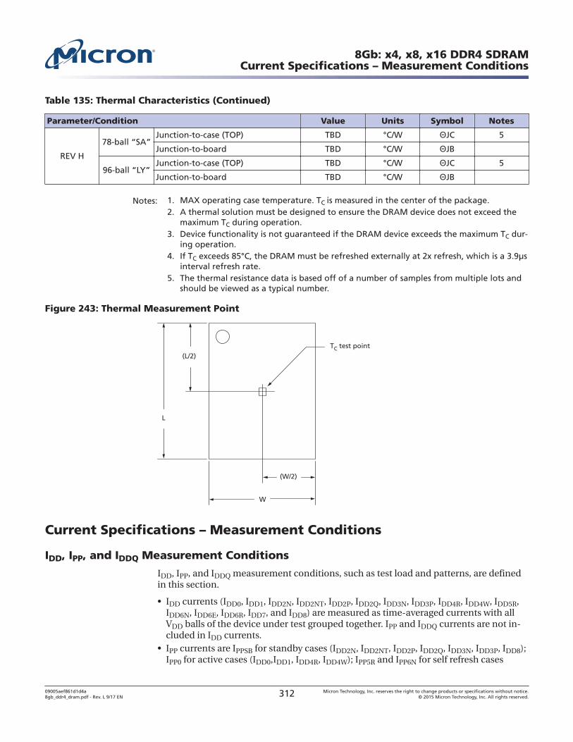
Table 135: Thermal Characteristics (Continued)
Parameter/Condition Value Units Symbol Notes
REV H
78-ball “SA”Junction-to-case (TOP) TBD °C/W JC 5
Junction-to-board TBD °C/W JB
96-ball “LY”Junction-to-case (TOP) TBD °C/W JC 5
Junction-to-board TBD °C/W JB
Notes: 1. MAX operating case temperature. TC is measured in the center of the package.2. A thermal solution must be designed to ensure the DRAM device does not exceed the
maximum TC during operation.3. Device functionality is not guaranteed if the DRAM device exceeds the maximum TC dur-
ing operation.4. If TC exceeds 85°C, the DRAM must be refreshed externally at 2x refresh, which is a 3.9μs
interval refresh rate.5. The thermal resistance data is based off of a number of samples from multiple lots and
should be viewed as a typical number.
Figure 243: Thermal Measurement Point
(L/2)
L
W
(W/2)
TC test point
Current Specifications – Measurement Conditions
IDD, IPP, and IDDQ Measurement Conditions
IDD, IPP, and IDDQ measurement conditions, such as test load and patterns, are definedin this section.
• IDD currents (IDD0, IDD1, IDD2N, IDD2NT, IDD2P, IDD2Q, IDD3N, IDD3P, IDD4R, IDD4W, IDD5R,IDD6N, IDD6E, IDD6R, IDD7, and IDD8) are measured as time-averaged currents with allVDD balls of the device under test grouped together. IPP and IDDQ currents are not in-cluded in IDD currents.
• IPP currents are IPPSB for standby cases (IDD2N, IDD2NT, IDD2P, IDD2Q, IDD3N, IDD3P, IDD8);IPP0 for active cases (IDD0,IDD1, IDD4R, IDD4W); IPP5R and IPP6N for self refresh cases
8Gb: x4, x8, x16 DDR4 SDRAMCurrent Specifications – Measurement Conditions
09005aef861d1d4a8gb_ddr4_dram.pdf - Rev. L 9/17 EN 312 Micron Technology, Inc. reserves the right to change products or specifications without notice.
© 2015 Micron Technology, Inc. All rights reserved.
(IDD6N, IDD6E, IDD6R), and IPP7. These have the same definitions as the IDD currents ref-erenced but are measured on the VPP supply.
• IDDQ currents (IDDQ2NT) are measured as time-averaged currents with VDDQ balls ofthe device under test grouped together. IDD current is not included in IDDQ currents.
Note: IDDQ values cannot be directly used to calculate the I/O power of the de-vice. They can be used to support correlation of simulated I/O power to actualI/O power. In DRAM module application, IDDQ cannot be measured separatelybecause VDD and VDDQ are using a merged-power layer in the module PCB.
The following definitions apply for IDD, IDDP and IDDQ measurements.
• “0” and “LOW” are defined as VIN VIL(AC)max
• “1” and “HIGH” are defined as VIN VIH(AC)min
• “Midlevel” is defined as inputs VREF = VDD/2• Timings used for IDD, IDDP and IDDQ measurement-loop patterns are provided in the
Current Test Definition and Patterns section.• Basic IDD, IPP, and IDDQ measurement conditions are described in the Current Test
Definition and Patterns section.• Detailed IDD, IPP, and IDDQ measurement-loop patterns are described in the Current
Test Definition and Patterns section.• Current measurements are done after properly initializing the device. This includes,
but is not limited to, setting:RON = RZQ/7 (34 ohm in MR1);Qoff = 0B (output buffer enabled in MR1);RTT(NOM) = RZQ/6 (40 ohm in MR1);RTT(WR) = RZQ/2 (120 ohm in MR2);RTT(Park) = disabled;TDQS feature disabled in MR1; CRC disabled in MR2; CA parity feature disabled inMR3; Gear-down mode disabled in MR3; Read/Write DBI disabled in MR5; DM disa-bled in MR5
• Define D = {CS_n, RAS_n, CAS_n, WE_n}: = {HIGH, LOW, LOW, LOW}; apply BG/BAchanges when directed.
• Define D_n = {CS_n, RAS_n, CAS_n, WE_n}: = {HIGH, HIGH, HIGH, HIGH}; apply in-vert of BG/BA changes when directed above.
Note: The measurement-loop patterns must be executed at least once before ac-tual current measurements can be taken.
8Gb: x4, x8, x16 DDR4 SDRAMCurrent Specifications – Measurement Conditions
09005aef861d1d4a8gb_ddr4_dram.pdf - Rev. L 9/17 EN 313 Micron Technology, Inc. reserves the right to change products or specifications without notice.
© 2015 Micron Technology, Inc. All rights reserved.
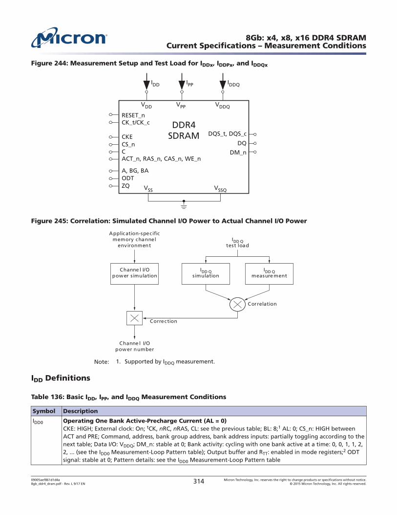
Figure 244: Measurement Setup and Test Load for IDDx, IDDPx, and IDDQx
IDD
CK_t/CK_c
CS_nCKE
ODT
VDD VDDQ
VSS VSSQ
RESET_n
ACT_n, RAS_n, CAS_n, WE_n
DQS_t, DQS_c
DQ
DM_n
ZQ
A, BG, BA
IDDQ
C
IPP
VPP
DDR4SDRAM
Figure 245: Correlation: Simulated Channel I/O Power to Actual Channel I/O Power
Application-spec ificmemory channel
environment
Channe l I/Opower simulation
IDD Qtest load
IDD Qsimulation
IDD Qmeasure ment
Correlation
Correction
Channe l I/Opower number
Note: 1. Supported by IDDQ measurement.
IDD Definitions
Table 136: Basic IDD, IPP, and IDDQ Measurement Conditions
Symbol Description
IDD0 Operating One Bank Active-Precharge Current (AL = 0)CKE: HIGH; External clock: On; tCK, nRC, nRAS, CL: see the previous table; BL: 8;1 AL: 0; CS_n: HIGH betweenACT and PRE; Command, address, bank group address, bank address inputs: partially toggling according to thenext table; Data I/O: VDDQ; DM_n: stable at 0; Bank activity: cycling with one bank active at a time: 0, 0, 1, 1, 2,2, ... (see the IDD0 Measurement-Loop Pattern table); Output buffer and RTT: enabled in mode registers;2 ODTsignal: stable at 0; Pattern details: see the IDD0 Measurement-Loop Pattern table
8Gb: x4, x8, x16 DDR4 SDRAMCurrent Specifications – Measurement Conditions
09005aef861d1d4a8gb_ddr4_dram.pdf - Rev. L 9/17 EN 314 Micron Technology, Inc. reserves the right to change products or specifications without notice.
© 2015 Micron Technology, Inc. All rights reserved.
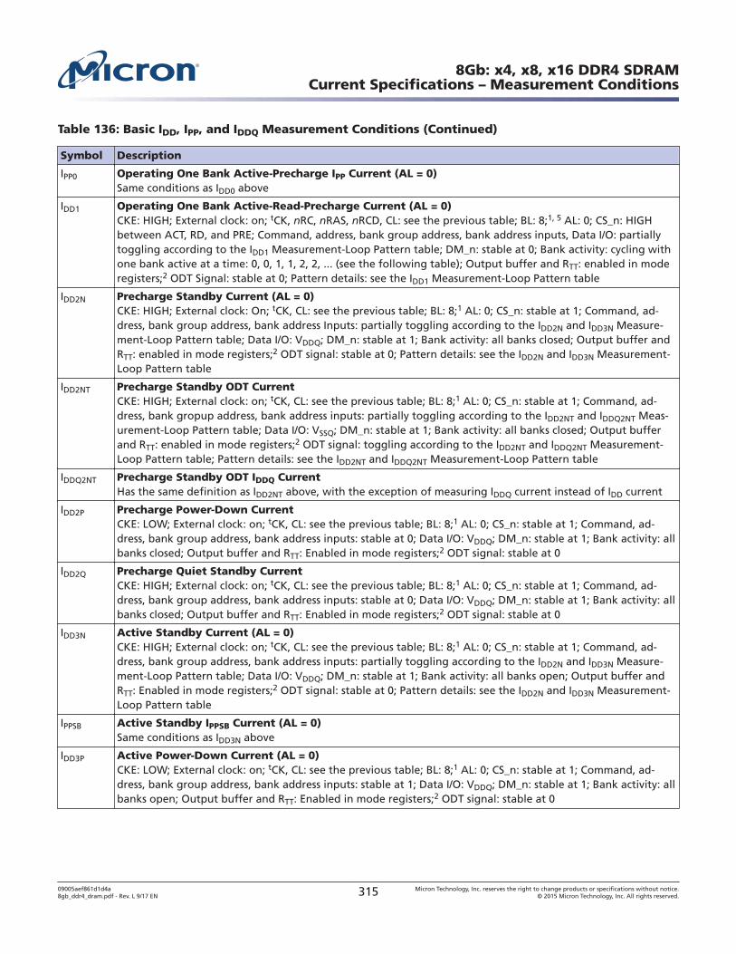
Table 136: Basic IDD, IPP, and IDDQ Measurement Conditions (Continued)
Symbol Description
IPP0 Operating One Bank Active-Precharge IPP Current (AL = 0)Same conditions as IDD0 above
IDD1 Operating One Bank Active-Read-Precharge Current (AL = 0)CKE: HIGH; External clock: on; tCK, nRC, nRAS, nRCD, CL: see the previous table; BL: 8;1, 5 AL: 0; CS_n: HIGHbetween ACT, RD, and PRE; Command, address, bank group address, bank address inputs, Data I/O: partiallytoggling according to the IDD1 Measurement-Loop Pattern table; DM_n: stable at 0; Bank activity: cycling withone bank active at a time: 0, 0, 1, 1, 2, 2, ... (see the following table); Output buffer and RTT: enabled in moderegisters;2 ODT Signal: stable at 0; Pattern details: see the IDD1 Measurement-Loop Pattern table
IDD2N Precharge Standby Current (AL = 0)CKE: HIGH; External clock: On; tCK, CL: see the previous table; BL: 8;1 AL: 0; CS_n: stable at 1; Command, ad-dress, bank group address, bank address Inputs: partially toggling according to the IDD2N and IDD3N Measure-ment-Loop Pattern table; Data I/O: VDDQ; DM_n: stable at 1; Bank activity: all banks closed; Output buffer andRTT: enabled in mode registers;2 ODT signal: stable at 0; Pattern details: see the IDD2N and IDD3N Measurement-Loop Pattern table
IDD2NT Precharge Standby ODT CurrentCKE: HIGH; External clock: on; tCK, CL: see the previous table; BL: 8;1 AL: 0; CS_n: stable at 1; Command, ad-dress, bank gropup address, bank address inputs: partially toggling according to the IDD2NT and IDDQ2NT Meas-urement-Loop Pattern table; Data I/O: VSSQ; DM_n: stable at 1; Bank activity: all banks closed; Output bufferand RTT: enabled in mode registers;2 ODT signal: toggling according to the IDD2NT and IDDQ2NT Measurement-Loop Pattern table; Pattern details: see the IDD2NT and IDDQ2NT Measurement-Loop Pattern table
IDDQ2NT Precharge Standby ODT IDDQ CurrentHas the same definition as IDD2NT above, with the exception of measuring IDDQ current instead of IDD current
IDD2P Precharge Power-Down CurrentCKE: LOW; External clock: on; tCK, CL: see the previous table; BL: 8;1 AL: 0; CS_n: stable at 1; Command, ad-dress, bank group address, bank address inputs: stable at 0; Data I/O: VDDQ; DM_n: stable at 1; Bank activity: allbanks closed; Output buffer and RTT: Enabled in mode registers;2 ODT signal: stable at 0
IDD2Q Precharge Quiet Standby CurrentCKE: HIGH; External clock: on; tCK, CL: see the previous table; BL: 8;1 AL: 0; CS_n: stable at 1; Command, ad-dress, bank group address, bank address inputs: stable at 0; Data I/O: VDDQ; DM_n: stable at 1; Bank activity: allbanks closed; Output buffer and RTT: Enabled in mode registers;2 ODT signal: stable at 0
IDD3N Active Standby Current (AL = 0)CKE: HIGH; External clock: on; tCK, CL: see the previous table; BL: 8;1 AL: 0; CS_n: stable at 1; Command, ad-dress, bank group address, bank address inputs: partially toggling according to the IDD2N and IDD3N Measure-ment-Loop Pattern table; Data I/O: VDDQ; DM_n: stable at 1; Bank activity: all banks open; Output buffer andRTT: Enabled in mode registers;2 ODT signal: stable at 0; Pattern details: see the IDD2N and IDD3N Measurement-Loop Pattern table
IPPSB Active Standby IPPSB Current (AL = 0)Same conditions as IDD3N above
IDD3P Active Power-Down Current (AL = 0)CKE: LOW; External clock: on; tCK, CL: see the previous table; BL: 8;1 AL: 0; CS_n: stable at 1; Command, ad-dress, bank group address, bank address inputs: stable at 1; Data I/O: VDDQ; DM_n: stable at 1; Bank activity: allbanks open; Output buffer and RTT: Enabled in mode registers;2 ODT signal: stable at 0
8Gb: x4, x8, x16 DDR4 SDRAMCurrent Specifications – Measurement Conditions
09005aef861d1d4a8gb_ddr4_dram.pdf - Rev. L 9/17 EN 315 Micron Technology, Inc. reserves the right to change products or specifications without notice.
© 2015 Micron Technology, Inc. All rights reserved.
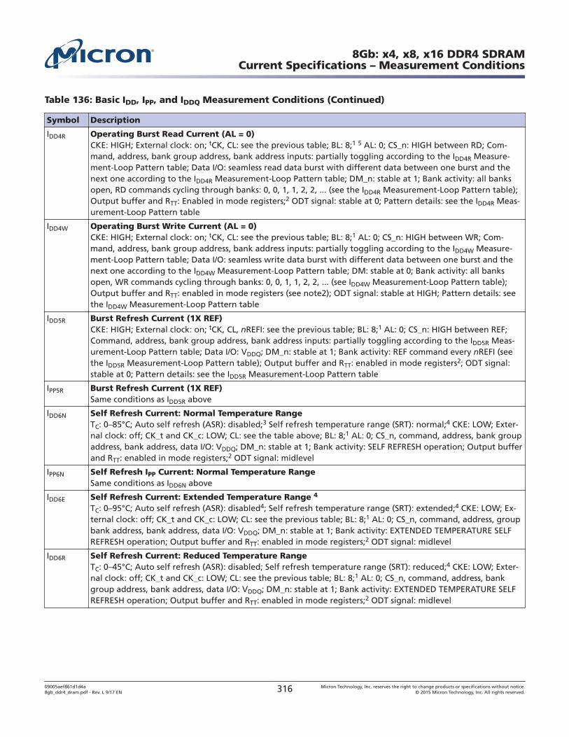
Table 136: Basic IDD, IPP, and IDDQ Measurement Conditions (Continued)
Symbol Description
IDD4R Operating Burst Read Current (AL = 0)CKE: HIGH; External clock: on; tCK, CL: see the previous table; BL: 8;1 5 AL: 0; CS_n: HIGH between RD; Com-mand, address, bank group address, bank address inputs: partially toggling according to the IDD4R Measure-ment-Loop Pattern table; Data I/O: seamless read data burst with different data between one burst and thenext one according to the IDD4R Measurement-Loop Pattern table; DM_n: stable at 1; Bank activity: all banksopen, RD commands cycling through banks: 0, 0, 1, 1, 2, 2, ... (see the IDD4R Measurement-Loop Pattern table);Output buffer and RTT: Enabled in mode registers;2 ODT signal: stable at 0; Pattern details: see the IDD4R Meas-urement-Loop Pattern table
IDD4W Operating Burst Write Current (AL = 0)CKE: HIGH; External clock: on; tCK, CL: see the previous table; BL: 8;1 AL: 0; CS_n: HIGH between WR; Com-mand, address, bank group address, bank address inputs: partially toggling according to the IDD4W Measure-ment-Loop Pattern table; Data I/O: seamless write data burst with different data between one burst and thenext one according to the IDD4W Measurement-Loop Pattern table; DM: stable at 0; Bank activity: all banksopen, WR commands cycling through banks: 0, 0, 1, 1, 2, 2, ... (see IDD4W Measurement-Loop Pattern table);Output buffer and RTT: enabled in mode registers (see note2); ODT signal: stable at HIGH; Pattern details: seethe IDD4W Measurement-Loop Pattern table
IDD5R Burst Refresh Current (1X REF)CKE: HIGH; External clock: on; tCK, CL, nREFI: see the previous table; BL: 8;1 AL: 0; CS_n: HIGH between REF;Command, address, bank group address, bank address inputs: partially toggling according to the IDD5R Meas-urement-Loop Pattern table; Data I/O: VDDQ; DM_n: stable at 1; Bank activity: REF command every nREFI (seethe IDD5R Measurement-Loop Pattern table); Output buffer and RTT: enabled in mode registers2; ODT signal:stable at 0; Pattern details: see the IDD5R Measurement-Loop Pattern table
IPP5R Burst Refresh Current (1X REF)Same conditions as IDD5R above
IDD6N Self Refresh Current: Normal Temperature RangeTC: 0–85°C; Auto self refresh (ASR): disabled;3 Self refresh temperature range (SRT): normal;4 CKE: LOW; Exter-nal clock: off; CK_t and CK_c: LOW; CL: see the table above; BL: 8;1 AL: 0; CS_n, command, address, bank groupaddress, bank address, data I/O: VDDQ; DM_n: stable at 1; Bank activity: SELF REFRESH operation; Output bufferand RTT: enabled in mode registers;2 ODT signal: midlevel
IPP6N Self Refresh IPP Current: Normal Temperature RangeSame conditions as IDD6N above
IDD6E Self Refresh Current: Extended Temperature Range 4
TC: 0–95°C; Auto self refresh (ASR): disabled4; Self refresh temperature range (SRT): extended;4 CKE: LOW; Ex-ternal clock: off; CK_t and CK_c: LOW; CL: see the previous table; BL: 8;1 AL: 0; CS_n, command, address, groupbank address, bank address, data I/O: VDDQ; DM_n: stable at 1; Bank activity: EXTENDED TEMPERATURE SELFREFRESH operation; Output buffer and RTT: enabled in mode registers;2 ODT signal: midlevel
IDD6R Self Refresh Current: Reduced Temperature RangeTC: 0–45°C; Auto self refresh (ASR): disabled; Self refresh temperature range (SRT): reduced;4 CKE: LOW; Exter-nal clock: off; CK_t and CK_c: LOW; CL: see the previous table; BL: 8;1 AL: 0; CS_n, command, address, bankgroup address, bank address, data I/O: VDDQ; DM_n: stable at 1; Bank activity: EXTENDED TEMPERATURE SELFREFRESH operation; Output buffer and RTT: enabled in mode registers;2 ODT signal: midlevel
8Gb: x4, x8, x16 DDR4 SDRAMCurrent Specifications – Measurement Conditions
09005aef861d1d4a8gb_ddr4_dram.pdf - Rev. L 9/17 EN 316 Micron Technology, Inc. reserves the right to change products or specifications without notice.
© 2015 Micron Technology, Inc. All rights reserved.
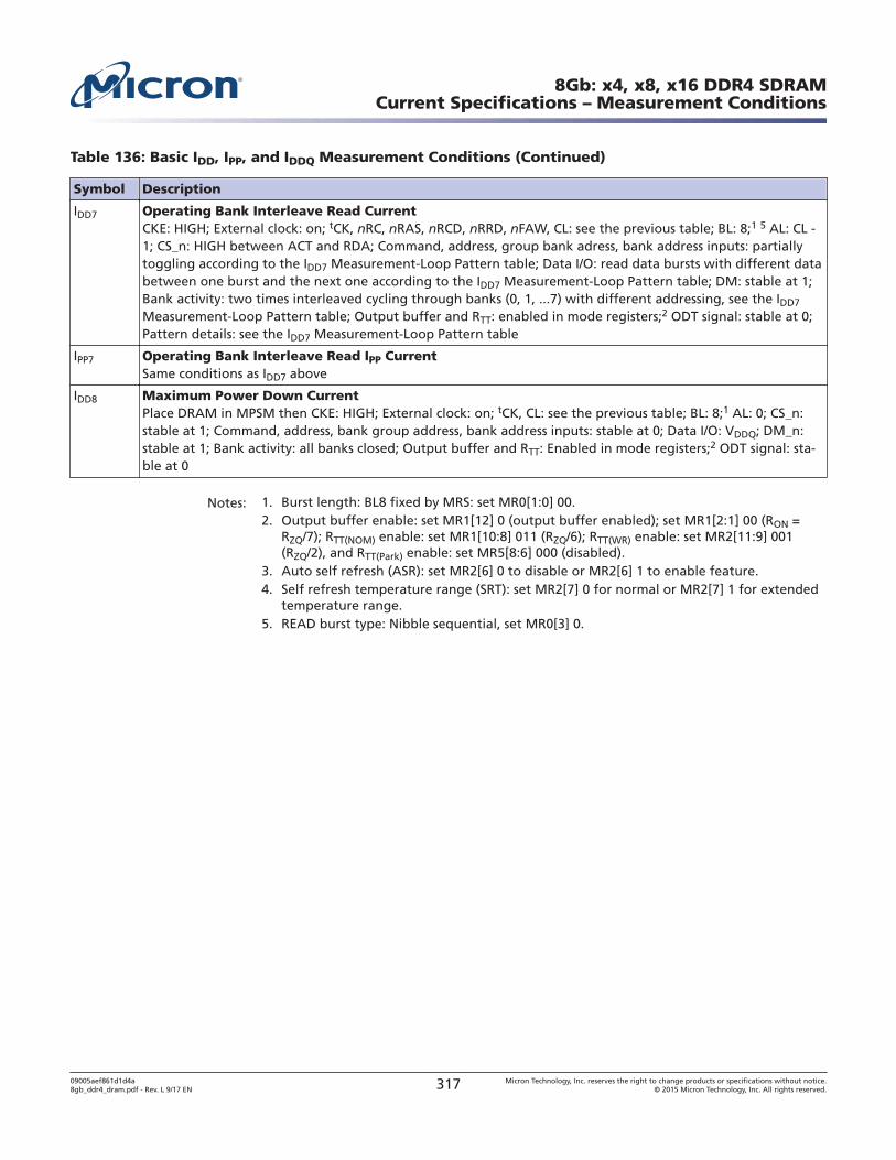
Table 136: Basic IDD, IPP, and IDDQ Measurement Conditions (Continued)
Symbol Description
IDD7 Operating Bank Interleave Read CurrentCKE: HIGH; External clock: on; tCK, nRC, nRAS, nRCD, nRRD, nFAW, CL: see the previous table; BL: 8;1 5 AL: CL -1; CS_n: HIGH between ACT and RDA; Command, address, group bank adress, bank address inputs: partiallytoggling according to the IDD7 Measurement-Loop Pattern table; Data I/O: read data bursts with different databetween one burst and the next one according to the IDD7 Measurement-Loop Pattern table; DM: stable at 1;Bank activity: two times interleaved cycling through banks (0, 1, ...7) with different addressing, see the IDD7
Measurement-Loop Pattern table; Output buffer and RTT: enabled in mode registers;2 ODT signal: stable at 0;Pattern details: see the IDD7 Measurement-Loop Pattern table
IPP7 Operating Bank Interleave Read IPP CurrentSame conditions as IDD7 above
IDD8 Maximum Power Down CurrentPlace DRAM in MPSM then CKE: HIGH; External clock: on; tCK, CL: see the previous table; BL: 8;1 AL: 0; CS_n:stable at 1; Command, address, bank group address, bank address inputs: stable at 0; Data I/O: VDDQ; DM_n:stable at 1; Bank activity: all banks closed; Output buffer and RTT: Enabled in mode registers;2 ODT signal: sta-ble at 0
Notes: 1. Burst length: BL8 fixed by MRS: set MR0[1:0] 00.2. Output buffer enable: set MR1[12] 0 (output buffer enabled); set MR1[2:1] 00 (RON =
RZQ/7); RTT(NOM) enable: set MR1[10:8] 011 (RZQ/6); RTT(WR) enable: set MR2[11:9] 001(RZQ/2), and RTT(Park) enable: set MR5[8:6] 000 (disabled).
3. Auto self refresh (ASR): set MR2[6] 0 to disable or MR2[6] 1 to enable feature.4. Self refresh temperature range (SRT): set MR2[7] 0 for normal or MR2[7] 1 for extended
temperature range.5. READ burst type: Nibble sequential, set MR0[3] 0.
8Gb: x4, x8, x16 DDR4 SDRAMCurrent Specifications – Measurement Conditions
09005aef861d1d4a8gb_ddr4_dram.pdf - Rev. L 9/17 EN 317 Micron Technology, Inc. reserves the right to change products or specifications without notice.
© 2015 Micron Technology, Inc. All rights reserved.
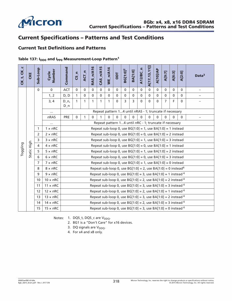
Current Specifications – Patterns and Test Conditions
Current Test Definitions and Patterns
Table 137: IDD0 and IPP0 Measurement-Loop Pattern1
CK
_t,
CK
_c
CK
E
Su
b-L
oo
p
Cycl
eN
um
ber
Co
mm
an
d
CS_n
AC
T_n
RA
S_n
/A16
CA
S_n
/A15
WE_n
/A14
OD
T
BG
[1:0
]2
BA
[1:0
]
A12/B
C_n
A[1
7,1
3,1
1]]
A[1
0]/
AP
A[9
:7]
A[6
:3]
A[2
:0]
Data3
Tog
glin
g
Stat
ic H
igh
0 0 ACT 0 0 0 0 0 0 0 0 0 0 0 0 0 0 –
1, 2 D, D 1 0 0 0 0 0 0 0 0 0 0 0 0 0 –
3, 4 D_n,D_n
1 1 1 1 1 0 3 3 0 0 0 7 F 0 –
... Repeat pattern 1...4 until nRAS - 1; truncate if necessary
nRAS PRE 0 1 0 1 0 0 0 0 0 0 0 0 0 0 –
... Repeat pattern 1...4 until nRC - 1; truncate if necessary
1 1 × nRC Repeat sub-loop 0, use BG[1:0] = 1, use BA[1:0] = 1 instead
2 2 × nRC Repeat sub-loop 0, use BG[1:0] = 0, use BA[1:0] = 2 instead
3 3 × nRC Repeat sub-loop 0, use BG[1:0] = 1, use BA[1:0] = 3 instead
4 4 × nRC Repeat sub-loop 0, use BG[1:0] = 0, use BA[1:0] = 1 instead
5 5 × nRC Repeat sub-loop 0, use BG[1:0] = 1, use BA[1:0] = 2 instead
6 6 × nRC Repeat sub-loop 0, use BG[1:0] = 0, use BA[1:0] = 3 instead
7 7 × nRC Repeat sub-loop 0, use BG[1:0] = 1, use BA[1:0] = 0 instead
8 8 × nRC Repeat sub-loop 0, use BG[1:0] = 2, use BA[1:0] = 0 instead4
9 9 × nRC Repeat sub-loop 0, use BG[1:0] = 3, use BA[1:0] = 1 instead 4
10 10 × nRC Repeat sub-loop 0, use BG[1:0] = 2, use BA[1:0] = 2 instead 4
11 11 × nRC Repeat sub-loop 0, use BG[1:0] = 3, use BA[1:0] = 3 instead 4
12 12 × nRC Repeat sub-loop 0, use BG[1:0] = 2, use BA[1:0] = 1 instead 4
13 13 × nRC Repeat sub-loop 0, use BG[1:0] = 3, use BA[1:0] = 2 instead 4
14 14 × nRC Repeat sub-loop 0, use BG[1:0] = 2, use BA[1:0] = 3 instead 4
15 15 × nRC Repeat sub-loop 0, use BG[1:0] = 3, use BA[1:0] = 0 instead 4
Notes: 1. DQS_t, DQS_c are VDDQ.2. BG1 is a "Don't Care" for x16 devices.3. DQ signals are VDDQ.4. For x4 and x8 only.
8Gb: x4, x8, x16 DDR4 SDRAMCurrent Specifications – Patterns and Test Conditions
09005aef861d1d4a8gb_ddr4_dram.pdf - Rev. L 9/17 EN 318 Micron Technology, Inc. reserves the right to change products or specifications without notice.
© 2015 Micron Technology, Inc. All rights reserved.
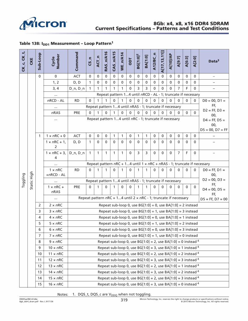
Table 138: IDD1 Measurement – Loop Pattern1
CK
_c,
CK
_t,
CK
E
Su
b-L
oo
p
Cycl
eN
um
ber
Co
mm
an
d
CS_n
AC
T_n
RA
S_n
/A16
CA
S_n
/A15
WE_n
/A14
OD
T
BG
[1:0
]2
BA
[1:0
]
A12/B
C_n
A[1
7,1
3,1
1]]
A[1
0]/
AP
A[9
:7]
A[6
:3]
A[2
:0]
Data3
Tog
glin
g
Stat
ic H
igh
0 0 ACT 0 0 0 0 0 0 0 0 0 0 0 0 0 0 –
1, 2 D, D 1 0 0 0 0 0 0 0 0 0 0 0 0 0 –
3, 4 D_n, D_n 1 1 1 1 1 0 3 3 0 0 0 7 F 0 –
... Repeat pattern 1...4 until nRCD - AL - 1; truncate if necessary
nRCD - AL RD 0 1 1 0 1 0 0 0 0 0 0 0 0 0 D0 = 00, D1 =FF,
D2 = FF, D3 =00,
D4 = FF, D5 =00,
D5 = 00, D7 = FF
... Repeat pattern 1...4 until nRAS - 1; truncate if necessary
nRAS PRE 0 1 0 1 0 0 0 0 0 0 0 0 0 0
... Repeat pattern 1...4 until nRC - 1; truncate if necessary
1 1 × nRC + 0 ACT 0 0 0 1 1 0 1 1 0 0 0 0 0 0 –
1 × nRC + 1,2
D, D 1 0 0 0 0 0 0 0 0 0 0 0 0 0 –
1 × nRC + 3,4
D_n, D_n 1 1 1 1 1 0 3 3 0 0 0 7 F 0 –
... Repeat pattern nRC + 1...4 until 1 × nRC + nRAS - 1; truncate if necessary
1 × nRC+nRCD - AL
RD 0 1 1 0 1 0 1 1 0 0 0 0 0 0 D0 = FF, D1 =00,
D2 = 00, D3 =FF,
D4 = 00, D5 =FF,
D5 = FF, D7 = 00
... Repeat pattern 1...4 until nRAS - 1; truncate if necessary
1 × nRC +nRAS
PRE 0 1 0 1 0 0 1 1 0 0 0 0 0 0
... Repeat pattern nRC + 1...4 until 2 × nRC - 1; truncate if necessary
2 2 × nRC Repeat sub-loop 0, use BG[1:0] = 0, use BA[1:0] = 2 instead
3 3 × nRC Repeat sub-loop 0, use BG[1:0] = 1, use BA[1:0] = 3 instead
4 4 × nRC Repeat sub-loop 0, use BG[1:0] = 0, use BA[1:0] = 1 instead
5 5 × nRC Repeat sub-loop 0, use BG[1:0] = 1, use BA[1:0] = 2 instead
6 6 × nRC Repeat sub-loop 0, use BG[1:0] = 0, use BA[1:0] = 3 instead
7 7 × nRC Repeat sub-loop 0, use BG[1:0] = 1, use BA[1:0] = 0 instead
8 9 × nRC Repeat sub-loop 0, use BG[1:0] = 2, use BA[1:0] = 0 instead 4
9 10 × nRC Repeat sub-loop 0, use BG[1:0] = 3, use BA[1:0] = 1 instead 4
10 11 × nRC Repeat sub-loop 0, use BG[1:0] = 2, use BA[1:0] = 2 instead 4
11 12 × nRC Repeat sub-loop 0, use BG[1:0] = 3, use BA[1:0] = 3 instead 4
12 13 × nRC Repeat sub-loop 0, use BG[1:0] = 2, use BA[1:0] = 1 instead 4
13 14 × nRC Repeat sub-loop 0, use BG[1:0] = 3, use BA[1:0] = 2 instead 4
14 15 × nRC Repeat sub-loop 0, use BG[1:0] = 2, use BA[1:0] = 3 instead 4
15 16 × nRC Repeat sub-loop 0, use BG[1:0] = 3, use BA[1:0] = 0 instead 4
Notes: 1. DQS_t, DQS_c are VDDQ when not toggling.
8Gb: x4, x8, x16 DDR4 SDRAMCurrent Specifications – Patterns and Test Conditions
09005aef861d1d4a8gb_ddr4_dram.pdf - Rev. L 9/17 EN 319 Micron Technology, Inc. reserves the right to change products or specifications without notice.
© 2015 Micron Technology, Inc. All rights reserved.
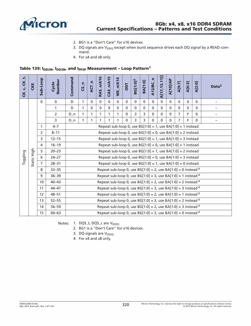
2. BG1 is a "Don't Care" for x16 devices.3. DQ signals are VDDQ except when burst sequence drives each DQ signal by a READ com-
mand.4. For x4 and x8 only.
Table 139: IDD2N, IDD3N, and IPP3P Measurement – Loop Pattern1
CK
_c,
CK
_t,
CK
E
Su
b-L
oo
p
Cycl
eN
um
ber
Co
mm
an
d
CS_n
AC
T_n
RA
S_n
/A16
CA
S_n
/A15
WE_n
/A14
OD
T
BG
[1:0
]2
BA
[1:0
]
A12/B
C_n
A[1
7,1
3,1
1]]
A[1
0]/
AP
A[9
:7]
A[6
:3]
A[2
:0]
Data3
Tog
glin
g
Stat
ic H
igh
0 0 D 1 0 0 0 0 0 0 0 0 0 0 0 0 0 –
1 D 1 0 0 0 0 0 0 0 0 0 0 0 0 0 –
2 D_n 1 1 1 1 1 0 3 3 0 0 0 7 F 0 –
3 D_n 1 1 1 1 1 0 3 3 0 0 0 7 F 0 –
1 4–7 Repeat sub-loop 0, use BG[1:0] = 1, use BA[1:0] = 1 instead
2 8–11 Repeat sub-loop 0, use BG[1:0] = 0, use BA[1:0] = 2 instead
3 12–15 Repeat sub-loop 0, use BG[1:0] = 1, use BA[1:0] = 3 instead
4 16–19 Repeat sub-loop 0, use BG[1:0] = 0, use BA[1:0] = 1 instead
5 20–23 Repeat sub-loop 0, use BG[1:0] = 1, use BA[1:0] = 2 instead
6 24–27 Repeat sub-loop 0, use BG[1:0] = 0, use BA[1:0] = 3 instead
7 28–31 Repeat sub-loop 0, use BG[1:0] = 1, use BA[1:0] = 0 instead
8 32–35 Repeat sub-loop 0, use BG[1:0] = 2, use BA[1:0] = 0 instead 4
9 36–39 Repeat sub-loop 0, use BG[1:0] = 3, use BA[1:0] = 1 instead 4
10 40–43 Repeat sub-loop 0, use BG[1:0] = 2, use BA[1:0] = 2 instead 4
11 44–47 Repeat sub-loop 0, use BG[1:0] = 3, use BA[1:0] = 3 instead 4
12 48–51 Repeat sub-loop 0, use BG[1:0] = 2, use BA[1:0] = 1 instead 4
13 52–55 Repeat sub-loop 0, use BG[1:0] = 3, use BA[1:0] = 2 instead 4
14 56–59 Repeat sub-loop 0, use BG[1:0] = 2, use BA[1:0] = 3 instead 4
15 60–63 Repeat sub-loop 0, use BG[1:0] = 3, use BA[1:0] = 0 instead 4
Notes: 1. DQS_t, DQS_c are VDDQ.2. BG1 is a "Don't Care" for x16 devices.3. DQ signals are VDDQ.4. For x4 and x8 only.
8Gb: x4, x8, x16 DDR4 SDRAMCurrent Specifications – Patterns and Test Conditions
09005aef861d1d4a8gb_ddr4_dram.pdf - Rev. L 9/17 EN 320 Micron Technology, Inc. reserves the right to change products or specifications without notice.
© 2015 Micron Technology, Inc. All rights reserved.
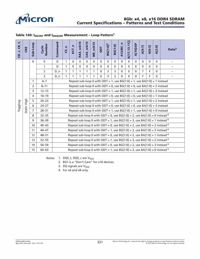
Table 140: IDD2NT and IDDQ2NT Measurement – Loop Pattern1
CK
_c,
CK
_t,
CK
E
Su
b-L
oo
p
Cycl
eN
um
ber
Co
mm
an
d
CS_n
AC
T_n
RA
S_n
/A16
CA
S_n
/A15
WE_n
/A14
OD
T
BG
[1:0
]2
BA
[1:0
]
A12/B
C_n
A[1
7,1
3,1
1]]
A[1
0]/
AP
A[9
:7]
A[6
:3]
A[2
:0]
Data3
Tog
glin
g
Stat
ic H
igh
0 0 D 1 0 0 0 0 0 0 0 0 0 0 0 0 0 –
1 D 1 0 0 0 0 0 0 0 0 0 0 0 0 0 –
2 D_n 1 1 1 1 1 0 3 3 0 0 0 7 F 0 –
3 D_n 1 1 1 1 1 0 3 3 0 0 0 7 F 0 –
1 4–7 Repeat sub-loop 0 with ODT = 1, use BG[1:0] = 1, use BA[1:0] = 1 instead
2 8–11 Repeat sub-loop 0 with ODT = 0, use BG[1:0] = 0, use BA[1:0] = 2 instead
3 12–15 Repeat sub-loop 0 with ODT = 1, use BG[1:0] = 1, use BA[1:0] = 3 instead
4 16–19 Repeat sub-loop 0 with ODT = 0, use BG[1:0] = 0, use BA[1:0] = 1 instead
5 20–23 Repeat sub-loop 0 with ODT = 1, use BG[1:0] = 1, use BA[1:0] = 2 instead
6 24–27 Repeat sub-loop 0 with ODT = 0, use BG[1:0] = 0, use BA[1:0] = 3 instead
7 28–31 Repeat sub-loop 0 with ODT = 1, use BG[1:0] = 1, use BA[1:0] = 0 instead
8 32–35 Repeat sub-loop 0 with ODT = 0, use BG[1:0] = 2, use BA[1:0] = 0 instead 4
9 36–39 Repeat sub-loop 0 with ODT = 1, use BG[1:0] = 3, use BA[1:0] = 1 instead 4
10 40–43 Repeat sub-loop 0 with ODT = 0, use BG[1:0] = 2, use BA[1:0] = 2 instead 4
11 44–47 Repeat sub-loop 0 with ODT = 1, use BG[1:0] = 3, use BA[1:0] = 3 instead 4
12 48–51 Repeat sub-loop 0 with ODT = 0, use BG[1:0] = 2, use BA[1:0] = 1 instead 4
13 52–55 Repeat sub-loop 0 with ODT = 1, use BG[1:0] = 3, use BA[1:0] = 2 instead 4
14 56–59 Repeat sub-loop 0 with ODT = 0, use BG[1:0] = 2, use BA[1:0] = 3 instead 4
15 60–63 Repeat sub-loop 0 with ODT = 1, use BG[1:0] = 3, use BA[1:0] = 0 instead 4
Notes: 1. DQS_t, DQS_c are VSSQ.2. BG1 is a "Don't Care" for x16 devices.3. DQ signals are VSSQ.4. For x4 and x8 only.
8Gb: x4, x8, x16 DDR4 SDRAMCurrent Specifications – Patterns and Test Conditions
09005aef861d1d4a8gb_ddr4_dram.pdf - Rev. L 9/17 EN 321 Micron Technology, Inc. reserves the right to change products or specifications without notice.
© 2015 Micron Technology, Inc. All rights reserved.
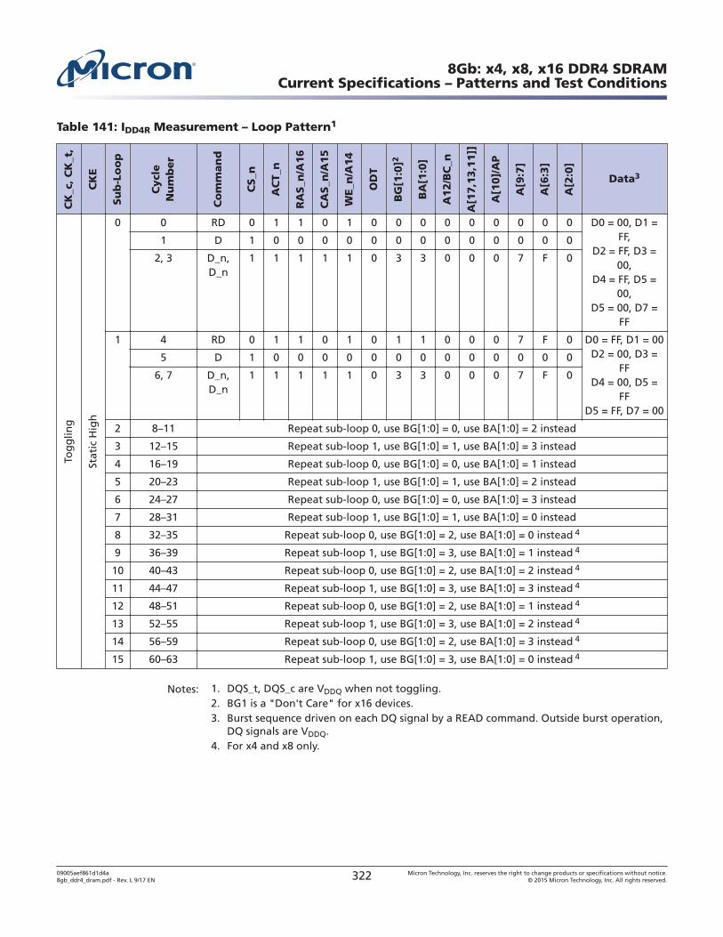
Table 141: IDD4R Measurement – Loop Pattern1
CK
_c,
CK
_t,
CK
E
Su
b-L
oo
p
Cycl
eN
um
ber
Co
mm
an
d
CS_n
AC
T_n
RA
S_n
/A16
CA
S_n
/A15
WE_n
/A14
OD
T
BG
[1:0
]2
BA
[1:0
]
A12/B
C_n
A[1
7,1
3,1
1]]
A[1
0]/
AP
A[9
:7]
A[6
:3]
A[2
:0]
Data3
Tog
glin
g
Stat
ic H
igh
0 0 RD 0 1 1 0 1 0 0 0 0 0 0 0 0 0 D0 = 00, D1 =FF,
D2 = FF, D3 =00,
D4 = FF, D5 =00,
D5 = 00, D7 =FF
1 D 1 0 0 0 0 0 0 0 0 0 0 0 0 0
2, 3 D_n,D_n
1 1 1 1 1 0 3 3 0 0 0 7 F 0
1 4 RD 0 1 1 0 1 0 1 1 0 0 0 7 F 0 D0 = FF, D1 = 00D2 = 00, D3 =
FFD4 = 00, D5 =
FFD5 = FF, D7 = 00
5 D 1 0 0 0 0 0 0 0 0 0 0 0 0 0
6, 7 D_n,D_n
1 1 1 1 1 0 3 3 0 0 0 7 F 0
2 8–11 Repeat sub-loop 0, use BG[1:0] = 0, use BA[1:0] = 2 instead
3 12–15 Repeat sub-loop 1, use BG[1:0] = 1, use BA[1:0] = 3 instead
4 16–19 Repeat sub-loop 0, use BG[1:0] = 0, use BA[1:0] = 1 instead
5 20–23 Repeat sub-loop 1, use BG[1:0] = 1, use BA[1:0] = 2 instead
6 24–27 Repeat sub-loop 0, use BG[1:0] = 0, use BA[1:0] = 3 instead
7 28–31 Repeat sub-loop 1, use BG[1:0] = 1, use BA[1:0] = 0 instead
8 32–35 Repeat sub-loop 0, use BG[1:0] = 2, use BA[1:0] = 0 instead 4
9 36–39 Repeat sub-loop 1, use BG[1:0] = 3, use BA[1:0] = 1 instead 4
10 40–43 Repeat sub-loop 0, use BG[1:0] = 2, use BA[1:0] = 2 instead 4
11 44–47 Repeat sub-loop 1, use BG[1:0] = 3, use BA[1:0] = 3 instead 4
12 48–51 Repeat sub-loop 0, use BG[1:0] = 2, use BA[1:0] = 1 instead 4
13 52–55 Repeat sub-loop 1, use BG[1:0] = 3, use BA[1:0] = 2 instead 4
14 56–59 Repeat sub-loop 0, use BG[1:0] = 2, use BA[1:0] = 3 instead 4
15 60–63 Repeat sub-loop 1, use BG[1:0] = 3, use BA[1:0] = 0 instead 4
Notes: 1. DQS_t, DQS_c are VDDQ when not toggling.2. BG1 is a "Don't Care" for x16 devices.3. Burst sequence driven on each DQ signal by a READ command. Outside burst operation,
DQ signals are VDDQ.4. For x4 and x8 only.
8Gb: x4, x8, x16 DDR4 SDRAMCurrent Specifications – Patterns and Test Conditions
09005aef861d1d4a8gb_ddr4_dram.pdf - Rev. L 9/17 EN 322 Micron Technology, Inc. reserves the right to change products or specifications without notice.
© 2015 Micron Technology, Inc. All rights reserved.
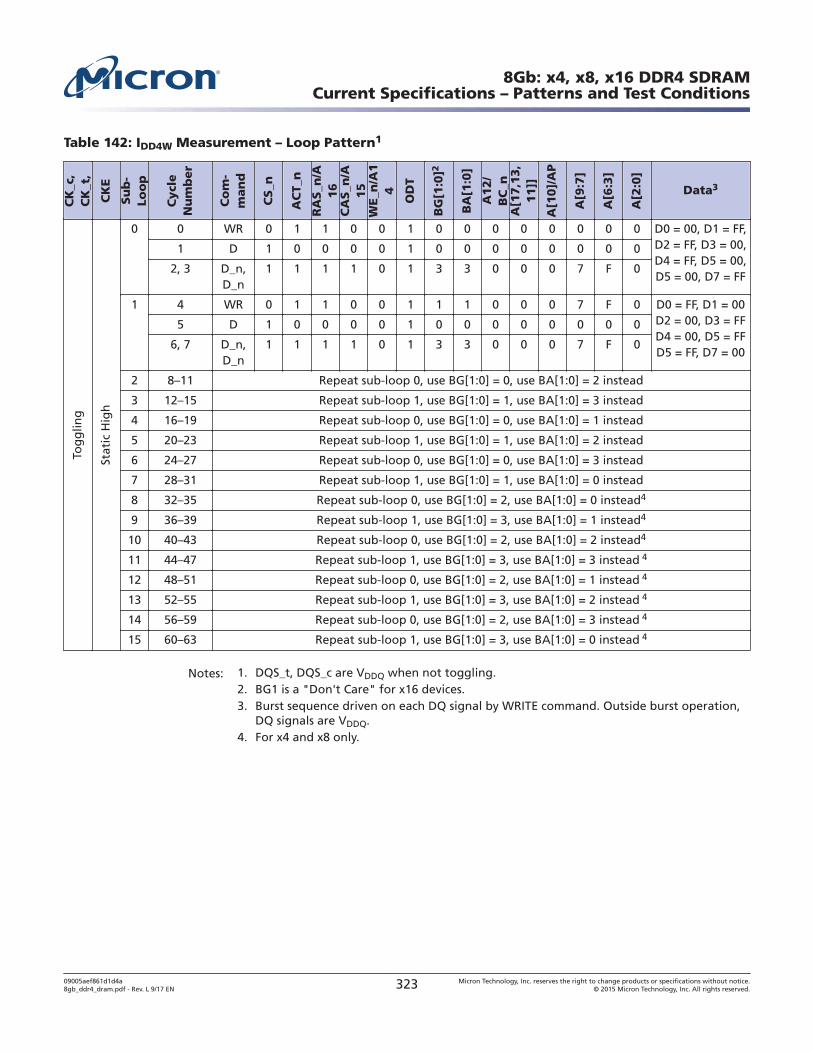
Table 142: IDD4W Measurement – Loop Pattern1
CK
_c,
CK
_t,
CK
E
Su
b-
Loo
p
Cycl
eN
um
ber
Co
m-
man
d
CS_n
AC
T_n
RA
S_n
/A16
CA
S_n
/A15
WE_n
/A1
4
OD
T
BG
[1:0
]2
BA
[1:0
]
A12/
BC
_nA
[17,1
3,
11]]
A[1
0]/
AP
A[9
:7]
A[6
:3]
A[2
:0]
Data3
Tog
glin
g
Stat
ic H
igh
0 0 WR 0 1 1 0 0 1 0 0 0 0 0 0 0 0 D0 = 00, D1 = FF,D2 = FF, D3 = 00,D4 = FF, D5 = 00,D5 = 00, D7 = FF
1 D 1 0 0 0 0 1 0 0 0 0 0 0 0 0
2, 3 D_n,D_n
1 1 1 1 0 1 3 3 0 0 0 7 F 0
1 4 WR 0 1 1 0 0 1 1 1 0 0 0 7 F 0 D0 = FF, D1 = 00D2 = 00, D3 = FFD4 = 00, D5 = FFD5 = FF, D7 = 00
5 D 1 0 0 0 0 1 0 0 0 0 0 0 0 0
6, 7 D_n,D_n
1 1 1 1 0 1 3 3 0 0 0 7 F 0
2 8–11 Repeat sub-loop 0, use BG[1:0] = 0, use BA[1:0] = 2 instead
3 12–15 Repeat sub-loop 1, use BG[1:0] = 1, use BA[1:0] = 3 instead
4 16–19 Repeat sub-loop 0, use BG[1:0] = 0, use BA[1:0] = 1 instead
5 20–23 Repeat sub-loop 1, use BG[1:0] = 1, use BA[1:0] = 2 instead
6 24–27 Repeat sub-loop 0, use BG[1:0] = 0, use BA[1:0] = 3 instead
7 28–31 Repeat sub-loop 1, use BG[1:0] = 1, use BA[1:0] = 0 instead
8 32–35 Repeat sub-loop 0, use BG[1:0] = 2, use BA[1:0] = 0 instead4
9 36–39 Repeat sub-loop 1, use BG[1:0] = 3, use BA[1:0] = 1 instead4
10 40–43 Repeat sub-loop 0, use BG[1:0] = 2, use BA[1:0] = 2 instead4
11 44–47 Repeat sub-loop 1, use BG[1:0] = 3, use BA[1:0] = 3 instead 4
12 48–51 Repeat sub-loop 0, use BG[1:0] = 2, use BA[1:0] = 1 instead 4
13 52–55 Repeat sub-loop 1, use BG[1:0] = 3, use BA[1:0] = 2 instead 4
14 56–59 Repeat sub-loop 0, use BG[1:0] = 2, use BA[1:0] = 3 instead 4
15 60–63 Repeat sub-loop 1, use BG[1:0] = 3, use BA[1:0] = 0 instead 4
Notes: 1. DQS_t, DQS_c are VDDQ when not toggling.2. BG1 is a "Don't Care" for x16 devices.3. Burst sequence driven on each DQ signal by WRITE command. Outside burst operation,
DQ signals are VDDQ.4. For x4 and x8 only.
8Gb: x4, x8, x16 DDR4 SDRAMCurrent Specifications – Patterns and Test Conditions
09005aef861d1d4a8gb_ddr4_dram.pdf - Rev. L 9/17 EN 323 Micron Technology, Inc. reserves the right to change products or specifications without notice.
© 2015 Micron Technology, Inc. All rights reserved.
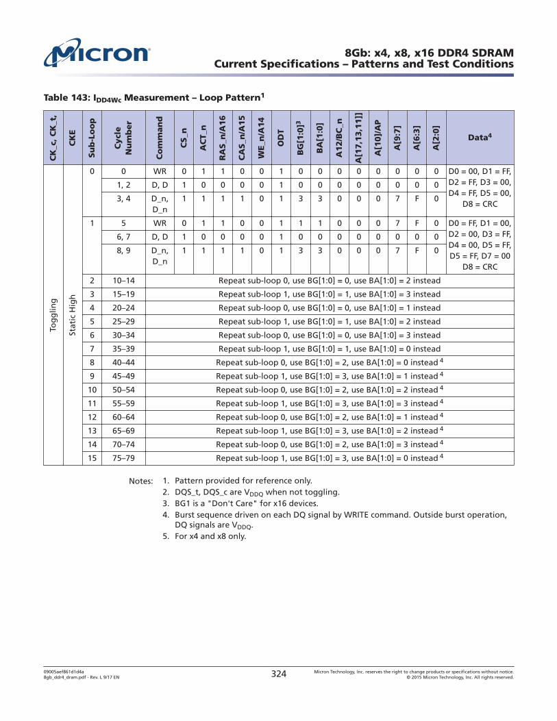
Table 143: IDD4Wc Measurement – Loop Pattern1
CK
_c,
CK
_t,
CK
E
Su
b-L
oo
p
Cycl
eN
um
ber
Co
mm
an
d
CS_n
AC
T_n
RA
S_n
/A16
CA
S_n
/A15
WE_n
/A14
OD
T
BG
[1:0
]3
BA
[1:0
]
A12/B
C_n
A[1
7,1
3,1
1]]
A[1
0]/
AP
A[9
:7]
A[6
:3]
A[2
:0]
Data4
Tog
glin
g
Stat
ic H
igh
0 0 WR 0 1 1 0 0 1 0 0 0 0 0 0 0 0 D0 = 00, D1 = FF,D2 = FF, D3 = 00,D4 = FF, D5 = 00,
D8 = CRC
1, 2 D, D 1 0 0 0 0 1 0 0 0 0 0 0 0 0
3, 4 D_n,D_n
1 1 1 1 0 1 3 3 0 0 0 7 F 0
1 5 WR 0 1 1 0 0 1 1 1 0 0 0 7 F 0 D0 = FF, D1 = 00,D2 = 00, D3 = FF,D4 = 00, D5 = FF,D5 = FF, D7 = 00
D8 = CRC
6, 7 D, D 1 0 0 0 0 1 0 0 0 0 0 0 0 0
8, 9 D_n,D_n
1 1 1 1 0 1 3 3 0 0 0 7 F 0
2 10–14 Repeat sub-loop 0, use BG[1:0] = 0, use BA[1:0] = 2 instead
3 15–19 Repeat sub-loop 1, use BG[1:0] = 1, use BA[1:0] = 3 instead
4 20–24 Repeat sub-loop 0, use BG[1:0] = 0, use BA[1:0] = 1 instead
5 25–29 Repeat sub-loop 1, use BG[1:0] = 1, use BA[1:0] = 2 instead
6 30–34 Repeat sub-loop 0, use BG[1:0] = 0, use BA[1:0] = 3 instead
7 35–39 Repeat sub-loop 1, use BG[1:0] = 1, use BA[1:0] = 0 instead
8 40–44 Repeat sub-loop 0, use BG[1:0] = 2, use BA[1:0] = 0 instead 4
9 45–49 Repeat sub-loop 1, use BG[1:0] = 3, use BA[1:0] = 1 instead 4
10 50–54 Repeat sub-loop 0, use BG[1:0] = 2, use BA[1:0] = 2 instead 4
11 55–59 Repeat sub-loop 1, use BG[1:0] = 3, use BA[1:0] = 3 instead 4
12 60–64 Repeat sub-loop 0, use BG[1:0] = 2, use BA[1:0] = 1 instead 4
13 65–69 Repeat sub-loop 1, use BG[1:0] = 3, use BA[1:0] = 2 instead 4
14 70–74 Repeat sub-loop 0, use BG[1:0] = 2, use BA[1:0] = 3 instead 4
15 75–79 Repeat sub-loop 1, use BG[1:0] = 3, use BA[1:0] = 0 instead 4
Notes: 1. Pattern provided for reference only.2. DQS_t, DQS_c are VDDQ when not toggling.3. BG1 is a "Don't Care" for x16 devices.4. Burst sequence driven on each DQ signal by WRITE command. Outside burst operation,
DQ signals are VDDQ.5. For x4 and x8 only.
8Gb: x4, x8, x16 DDR4 SDRAMCurrent Specifications – Patterns and Test Conditions
09005aef861d1d4a8gb_ddr4_dram.pdf - Rev. L 9/17 EN 324 Micron Technology, Inc. reserves the right to change products or specifications without notice.
© 2015 Micron Technology, Inc. All rights reserved.
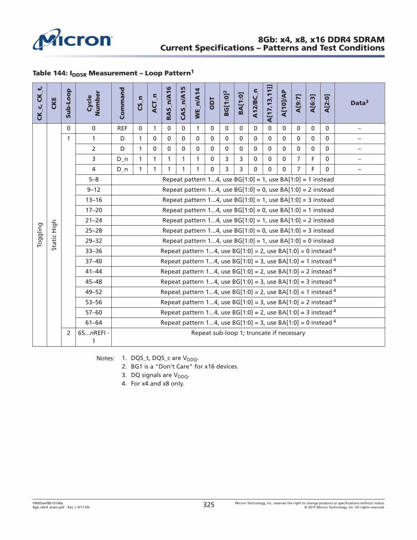
Table 144: IDD5R Measurement – Loop Pattern1
CK
_c,
CK
_t,
CK
E
Su
b-L
oo
p
Cycl
eN
um
ber
Co
mm
an
d
CS_n
AC
T_n
RA
S_n
/A16
CA
S_n
/A15
WE_n
/A14
OD
T
BG
[1:0
]2
BA
[1:0
]
A12/B
C_n
A[1
7,1
3,1
1]]
A[1
0]/
AP
A[9
:7]
A[6
:3]
A[2
:0]
Data3
Tog
glin
g
Stat
ic H
igh
0 0 REF 0 1 0 0 1 0 0 0 0 0 0 0 0 0 –
1 1 D 1 0 0 0 0 0 0 0 0 0 0 0 0 0 –
2 D 1 0 0 0 0 0 0 0 0 0 0 0 0 0 –
3 D_n 1 1 1 1 1 0 3 3 0 0 0 7 F 0 –
4 D_n 1 1 1 1 1 0 3 3 0 0 0 7 F 0 –
5–8 Repeat pattern 1...4, use BG[1:0] = 1, use BA[1:0] = 1 instead
9–12 Repeat pattern 1...4, use BG[1:0] = 0, use BA[1:0] = 2 instead
13–16 Repeat pattern 1...4, use BG[1:0] = 1, use BA[1:0] = 3 instead
17–20 Repeat pattern 1...4, use BG[1:0] = 0, use BA[1:0] = 1 instead
21–24 Repeat pattern 1...4, use BG[1:0] = 1, use BA[1:0] = 2 instead
25–28 Repeat pattern 1...4, use BG[1:0] = 0, use BA[1:0] = 3 instead
29–32 Repeat pattern 1...4, use BG[1:0] = 1, use BA[1:0] = 0 instead
33–36 Repeat pattern 1...4, use BG[1:0] = 2, use BA[1:0] = 0 instead 4
37–40 Repeat pattern 1...4, use BG[1:0] = 3, use BA[1:0] = 1 instead 4
41–44 Repeat pattern 1...4, use BG[1:0] = 2, use BA[1:0] = 2 instead 4
45–48 Repeat pattern 1...4, use BG[1:0] = 3, use BA[1:0] = 3 instead 4
49–52 Repeat pattern 1...4, use BG[1:0] = 2, use BA[1:0] = 1 instead 4
53–56 Repeat pattern 1...4, use BG[1:0] = 3, use BA[1:0] = 2 instead 4
57–60 Repeat pattern 1...4, use BG[1:0] = 2, use BA[1:0] = 3 instead 4
61–64 Repeat pattern 1...4, use BG[1:0] = 3, use BA[1:0] = 0 instead 4
2 65...nREFI -1
Repeat sub-loop 1; truncate if necessary
Notes: 1. DQS_t, DQS_c are VDDQ.2. BG1 is a "Don't Care" for x16 devices.3. DQ signals are VDDQ.4. For x4 and x8 only.
8Gb: x4, x8, x16 DDR4 SDRAMCurrent Specifications – Patterns and Test Conditions
09005aef861d1d4a8gb_ddr4_dram.pdf - Rev. L 9/17 EN 325 Micron Technology, Inc. reserves the right to change products or specifications without notice.
© 2015 Micron Technology, Inc. All rights reserved.
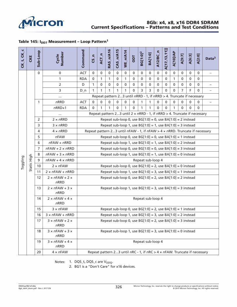
Table 145: IDD7 Measurement – Loop Pattern1
CK
_t,
CK
_c
CK
E
Su
b-L
oo
p
Cycl
eN
um
ber
Co
mm
an
d
CS_n
AC
T_n
RA
S_n
/A16
CA
S_n
/A15
WE_n
/A14
OD
T
BG
[1:0
]2
BA
[1:0
]
A12/B
C_n
A[1
7,1
3,1
1]]
A[1
0]/
AP
A[9
:7]
A[6
:3]
A[2
:0]
Data3
Tog
glin
g
Stat
ic H
igh
0 0 ACT 0 0 0 0 0 0 0 0 0 0 0 0 0 0 –
1 RDA 0 1 1 0 1 0 0 0 0 0 1 0 0 0
2 D 1 0 0 0 0 0 0 0 0 0 0 0 0 0 –
3 D_n 1 1 1 1 1 0 3 3 0 0 0 7 F 0 –
... Repeat pattern 2...3 until nRRD - 1, if nRRD > 4. Truncate if necessary
1 nRRD ACT 0 0 0 0 0 0 1 1 0 0 0 0 0 0 –
nRRD+1 RDA 0 1 1 0 1 0 1 1 0 0 1 0 0 0
... Repeat pattern 2...3 until 2 × nRRD - 1, if nRRD > 4. Truncate if necessary
2 2 × nRRD Repeat sub-loop 0, use BG[1:0] = 0, use BA[1:0] = 2 instead
3 3 × nRRD Repeat sub-loop 1, use BG[1:0] = 1, use BA[1:0] = 3 instead
4 4 × nRRD Repeat pattern 2...3 until nFAW - 1, if nFAW > 4 × nRRD. Truncate if necessary
5 nFAW Repeat sub-loop 0, use BG[1:0] = 0, use BA[1:0] = 1 instead
6 nFAW + nRRD Repeat sub-loop 1, use BG[1:0] = 1, use BA[1:0] = 2 instead
7 nFAW + 2 × nRRD Repeat sub-loop 0, use BG[1:0] = 0, use BA[1:0] = 3 instead
8 nFAW + 3 × nRRD Repeat sub-loop 1, use BG[1:0] = 1, use BA[1:0] = 0 instead
9 nFAW + 4 × nRRD Repeat sub-loop 4
10 2 × nFAW Repeat sub-loop 0, use BG[1:0] = 2, use BA[1:0] = 0 instead
11 2 × nFAW + nRRD Repeat sub-loop 1, use BG[1:0] = 3, use BA[1:0] = 1 instead
12 2 × nFAW + 2 ×nRRD
Repeat sub-loop 0, use BG[1:0] = 2, use BA[1:0] = 2 instead
13 2 × nFAW + 3 ×nRRD
Repeat sub-loop 1, use BG[1:0] = 3, use BA[1:0] = 3 instead
14 2 × nFAW + 4 ×nRRD
Repeat sub-loop 4
15 3 × nFAW Repeat sub-loop 0, use BG[1:0] = 2, use BA[1:0] = 1 instead
16 3 × nFAW + nRRD Repeat sub-loop 1, use BG[1:0] = 3, use BA[1:0] = 2 instead
17 3 × nFAW + 2 ×nRRD
Repeat sub-loop 0, use BG[1:0] = 2, use BA[1:0] = 3 instead
18 3 × nFAW + 3 ×nRRD
Repeat sub-loop 1, use BG[1:0] = 3, use BA[1:0] = 0 instead
19 3 × nFAW + 4 ×nRRD
Repeat sub-loop 4
20 4 × nFAW Repeat pattern 2...3 until nRC - 1, if nRC > 4 × nFAW. Truncate if necessary
Notes: 1. DQS_t, DQS_c are VDDQ.2. BG1 is a "Don't Care" for x16 devices.
8Gb: x4, x8, x16 DDR4 SDRAMCurrent Specifications – Patterns and Test Conditions
09005aef861d1d4a8gb_ddr4_dram.pdf - Rev. L 9/17 EN 326 Micron Technology, Inc. reserves the right to change products or specifications without notice.
© 2015 Micron Technology, Inc. All rights reserved.
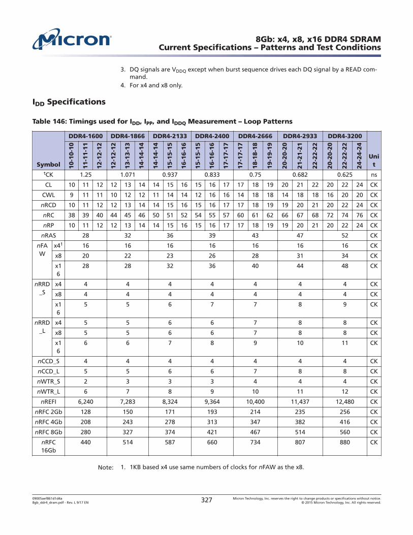
3. DQ signals are VDDQ except when burst sequence drives each DQ signal by a READ com-mand.
4. For x4 and x8 only.
IDD Specifications
Table 146: Timings used for IDD, IPP, and IDDQ Measurement – Loop Patterns
Symbol
DDR4-1600 DDR4-1866 DDR4-2133 DDR4-2400 DDR4-2666 DDR4-2933 DDR4-3200
Unit1
0-1
0-1
0
11-1
1-1
1
12-1
2-1
2
12-1
2-1
2
13-1
3-1
3
14-1
4-1
4
14-1
4-1
4
15-1
5-1
5
16-1
6-1
6
15-1
5-1
5
16-1
6-1
6
17-1
7-1
7
17-1
7-1
7
18-1
8-1
8
19-1
9-1
9
20-2
0-2
0
21-2
1-2
1
22-2
2-2
2
20-2
0-2
0
22-2
2-2
2
24-2
4-2
4
tCK 1.25 1.071 0.937 0.833 0.75 0.682 0.625 ns
CL 10 11 12 12 13 14 14 15 16 15 16 17 17 18 19 20 21 22 20 22 24 CK
CWL 9 11 11 10 12 12 11 14 14 12 16 16 14 18 18 14 18 18 16 20 20 CK
nRCD 10 11 12 12 13 14 14 15 16 15 16 17 17 18 19 19 20 21 20 22 24 CK
nRC 38 39 40 44 45 46 50 51 52 54 55 57 60 61 62 66 67 68 72 74 76 CK
nRP 10 11 12 12 13 14 14 15 16 15 16 17 17 18 19 19 20 21 20 22 24 CK
nRAS 28 32 36 39 43 47 52 CK
nFAW
x41 16 16 16 16 16 16 16 CK
x8 20 22 23 26 28 31 34 CK
x16
28 28 32 36 40 44 48 CK
nRRD_S
x4 4 4 4 4 4 4 4 CK
x8 4 4 4 4 4 4 4 CK
x16
5 5 6 7 7 8 9 CK
nRRD_L
x4 5 5 6 6 7 8 8 CK
x8 5 5 6 6 7 8 8 CK
x16
6 6 7 8 9 10 11 CK
nCCD_S 4 4 4 4 4 4 4 CK
nCCD_L 5 5 6 6 7 8 8 CK
nWTR_S 2 3 3 3 4 4 4 CK
nWTR_L 6 7 8 9 10 11 12 CK
nREFI 6,240 7,283 8,324 9,364 10,400 11,437 12,480 CK
nRFC 2Gb 128 150 171 193 214 235 256 CK
nRFC 4Gb 208 243 278 313 347 382 416 CK
nRFC 8Gb 280 327 374 421 467 514 560 CK
nRFC16Gb
440 514 587 660 734 807 880 CK
Note: 1. 1KB based x4 use same numbers of clocks for nFAW as the x8.
8Gb: x4, x8, x16 DDR4 SDRAMCurrent Specifications – Patterns and Test Conditions
09005aef861d1d4a8gb_ddr4_dram.pdf - Rev. L 9/17 EN 327 Micron Technology, Inc. reserves the right to change products or specifications without notice.
© 2015 Micron Technology, Inc. All rights reserved.
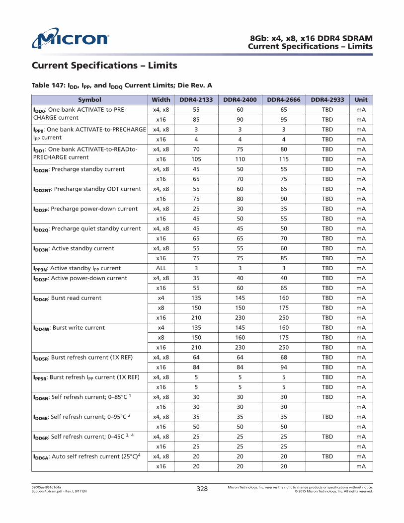
Current Specifications – Limits
Table 147: IDD, IPP, and IDDQ Current Limits; Die Rev. A
Symbol Width DDR4-2133 DDR4-2400 DDR4-2666 DDR4-2933 Unit
IDD0: One bank ACTIVATE-to-PRE-CHARGE current
x4, x8 55 60 65 TBD mA
x16 85 90 95 TBD mA
IPP0: One bank ACTIVATE-to-PRECHARGEIPP current
x4, x8 3 3 3 TBD mA
x16 4 4 4 TBD mA
IDD1: One bank ACTIVATE-to-READto-PRECHARGE current
x4, x8 70 75 80 TBD mA
x16 105 110 115 TBD mA
IDD2N: Precharge standby current x4, x8 45 50 55 TBD mA
x16 65 70 75 TBD mA
IDD2NT: Precharge standby ODT current x4, x8 55 60 65 TBD mA
x16 75 80 90 TBD mA
IDD2P: Precharge power-down current x4, x8 25 30 35 TBD mA
x16 45 50 55 TBD mA
IDD2Q: Precharge quiet standby current x4, x8 45 45 50 TBD mA
x16 65 65 70 TBD mA
IDD3N: Active standby current x4, x8 55 55 60 TBD mA
x16 75 75 85 TBD mA
IPP3N: Active standby IPP current ALL 3 3 3 TBD mA
IDD3P: Active power-down current x4, x8 35 40 40 TBD mA
x16 55 60 65 TBD mA
IDD4R: Burst read current x4 135 145 160 TBD mA
x8 150 150 175 TBD mA
x16 210 230 250 TBD mA
IDD4W: Burst write current x4 135 145 160 TBD mA
x8 150 160 175 TBD mA
x16 210 230 250 TBD mA
IDD5R: Burst refresh current (1X REF) x4, x8 64 64 68 TBD mA
x16 84 84 94 TBD mA
IPP5R: Burst refresh IPP current (1X REF) x4, x8 5 5 5 TBD mA
x16 5 5 5 TBD mA
IDD6N: Self refresh current; 0–85°C 1 x4, x8 30 30 30 TBD mA
x16 30 30 30 mA
IDD6E: Self refresh current; 0–95°C 2 x4, x8 35 35 35 TBD mA
x16 50 50 50 mA
IDD6R: Self refresh current; 0–45C 3, 4 x4, x8 25 25 25 TBD mA
x16 25 25 25 mA
IDD6A: Auto self refresh current (25°C)4 x4, x8 20 20 20 TBD mA
x16 20 20 20 mA
8Gb: x4, x8, x16 DDR4 SDRAMCurrent Specifications – Limits
09005aef861d1d4a8gb_ddr4_dram.pdf - Rev. L 9/17 EN 328 Micron Technology, Inc. reserves the right to change products or specifications without notice.
© 2015 Micron Technology, Inc. All rights reserved.
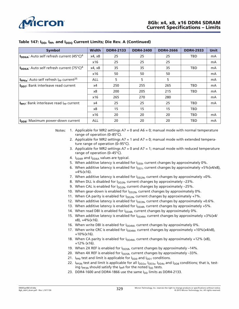
Table 147: IDD, IPP, and IDDQ Current Limits; Die Rev. A (Continued)
Symbol Width DDR4-2133 DDR4-2400 DDR4-2666 DDR4-2933 Unit
IDD6A: Auto self refresh current (45°C)4 x4, x8 25 25 25 TBD mA
x16 25 25 25 mA
IDD6A: Auto self refresh current (75°C)4 x4, x8 35 35 35 TBD mA
x16 50 50 50 mA
IPP6x: Auto self refresh IPP current25 ALL 5 5 5 mA
IDD7: Bank interleave read current x4 250 255 265 TBD mA
x8 200 205 215 TBD mA
x16 265 270 280 mA
IPP7: Bank interleave read IPP current x4 25 25 25 TBD mA
x8 15 15 15 TBD
x16 20 20 20 TBD mA
IDD8: Maximum power-down current ALL 20 20 20 TBD mA
Notes: 1. Applicable for MR2 settings A7 = 0 and A6 = 0; manual mode with normal temperaturerange of operation (0–85°C).
2. Applicable for MR2 settings A7 = 1 and A7 = 0; manual mode with extended tempera-ture range of operation (0–95°C).
3. Applicable for MR2 settings A7 = 0 and A7 = 1; manual mode with reduced temperaturerange of operation (0–45°C).
4. IDD6R and IDD6A values are typical.5. When additive latency is enabled for IDD0, current changes by approximately 0%.6. When additive latency is enabled for IDD1, current changes by approximately +5%(x4/x8),
+4%(x16).7. When additive latency is enabled for IDD2N, current changes by approximately +0%.8. When DLL is disabled for IDD2N, current changes by approximately –23%.9. When CAL is enabled for IDD2N, current changes by approximately –25%.
10. When gear-down is enabled for IDD2N, current changes by approximately 0%.11. When CA parity is enabled for IDD2N, current changes by approximately +7%.12. When additive latency is enabled for IDD3N, current changes by approximately +0.6%.13. When additive latency is enabled for IDD4R, current changes by approximately +5%.14. When read DBI is enabled for IDD4R, current changes by approximately 0%.15. When additive latency is enabled for IDD4W, current changes by approximately +3%(x4/
x8), +4%(x16).16. When write DBI is enabled for IDD4W, current changes by approximately 0%.17. When write CRC is enabled for IDD4W, current changes by approximately +10%(x4/x8),
+10%(x16).18. When CA parity is enabled for IDD4W, current changes by approximately +12% (x8),
+12% (x16).19. When 2X REF is enabled for IDD5R, current changes by approximately –14%.20. When 4X REF is enabled for IDD5R, current changes by approximately –33%.21. IPP0 test and limit is applicable for IDD0 and IDD1 conditions.22. IPP3N test and limit is applicable for all IDD2x, IDD3x, IDD4x and IDD8 conditions; that is, test-
ing IPP3N should satisfy the IPPs for the noted IDD tests.23. DDR4-1600 and DDR4-1866 use the same IDD limits as DDR4-2133.
8Gb: x4, x8, x16 DDR4 SDRAMCurrent Specifications – Limits
09005aef861d1d4a8gb_ddr4_dram.pdf - Rev. L 9/17 EN 329 Micron Technology, Inc. reserves the right to change products or specifications without notice.
© 2015 Micron Technology, Inc. All rights reserved.
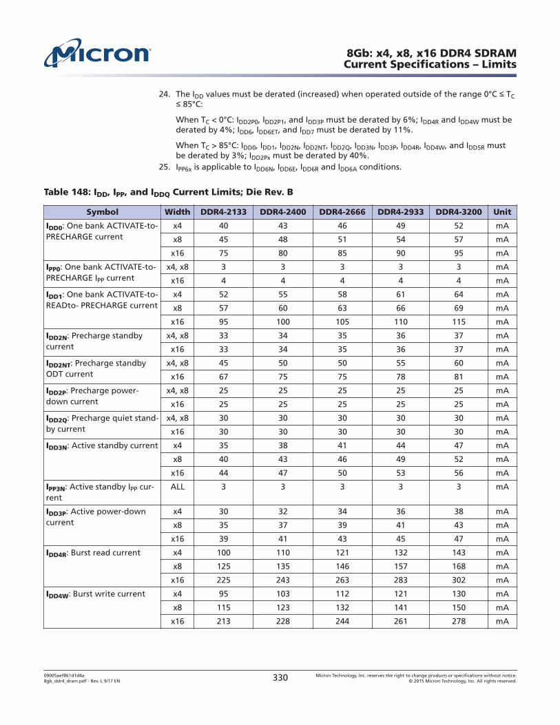
24. The IDD values must be derated (increased) when operated outside of the range 0°C TC 85°C:
When TC < 0°C: IDD2P0, IDD2P1, and IDD3P must be derated by 6%; IDD4R and IDD4W must bederated by 4%; IDD6, IDD6ET, and IDD7 must be derated by 11%.
When TC > 85°C: IDD0, IDD1, IDD2N, IDD2NT, IDD2Q, IDD3N, IDD3P, IDD4R, IDD4W, and IDD5R mustbe derated by 3%; IDD2Px must be derated by 40%.
25. IPP6x is applicable to IDD6N, IDD6E, IDD6R and IDD6A conditions.
Table 148: IDD, IPP, and IDDQ Current Limits; Die Rev. B
Symbol Width DDR4-2133 DDR4-2400 DDR4-2666 DDR4-2933 DDR4-3200 Unit
IDD0: One bank ACTIVATE-to-PRECHARGE current
x4 40 43 46 49 52 mA
x8 45 48 51 54 57 mA
x16 75 80 85 90 95 mA
IPP0: One bank ACTIVATE-to-PRECHARGE IPP current
x4, x8 3 3 3 3 3 mA
x16 4 4 4 4 4 mA
IDD1: One bank ACTIVATE-to-READto- PRECHARGE current
x4 52 55 58 61 64 mA
x8 57 60 63 66 69 mA
x16 95 100 105 110 115 mA
IDD2N: Precharge standbycurrent
x4, x8 33 34 35 36 37 mA
x16 33 34 35 36 37 mA
IDD2NT: Precharge standbyODT current
x4, x8 45 50 50 55 60 mA
x16 67 75 75 78 81 mA
IDD2P: Precharge power-down current
x4, x8 25 25 25 25 25 mA
x16 25 25 25 25 25 mA
IDD2Q: Precharge quiet stand-by current
x4, x8 30 30 30 30 30 mA
x16 30 30 30 30 30 mA
IDD3N: Active standby current x4 35 38 41 44 47 mA
x8 40 43 46 49 52 mA
x16 44 47 50 53 56 mA
IPP3N: Active standby IPP cur-rent
ALL 3 3 3 3 3 mA
IDD3P: Active power-downcurrent
x4 30 32 34 36 38 mA
x8 35 37 39 41 43 mA
x16 39 41 43 45 47 mA
IDD4R: Burst read current x4 100 110 121 132 143 mA
x8 125 135 146 157 168 mA
x16 225 243 263 283 302 mA
IDD4W: Burst write current x4 95 103 112 121 130 mA
x8 115 123 132 141 150 mA
x16 213 228 244 261 278 mA
8Gb: x4, x8, x16 DDR4 SDRAMCurrent Specifications – Limits
09005aef861d1d4a8gb_ddr4_dram.pdf - Rev. L 9/17 EN 330 Micron Technology, Inc. reserves the right to change products or specifications without notice.
© 2015 Micron Technology, Inc. All rights reserved.
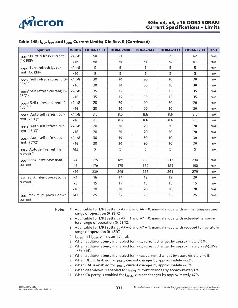
Table 148: IDD, IPP, and IDDQ Current Limits; Die Rev. B (Continued)
Symbol Width DDR4-2133 DDR4-2400 DDR4-2666 DDR4-2933 DDR4-3200 Unit
IDD5R: Burst refresh current(1X REF)
x4, x8 50 53 56 59 62 mA
x16 56 59 61 64 67 mA
IPP5R: Burst refresh IPP cur-rent (1X REF)
x4, x8 5 5 5 5 5 mA
x16 5 5 5 5 5 mA
IDD6N: Self refresh current; 0–85°C 1
x4, x8 30 30 30 30 30 mA
x16 30 30 30 30 30 mA
IDD6E: Self refresh current; 0–95°C 2
x4, x8 35 35 35 35 35 mA
x16 35 35 35 35 35 mA
IDD6R: Self refresh current; 0–45C 3, 4
x4, x8 20 20 20 20 20 mA
x16 20 20 20 20 20 mA
IDD6A: Auto self refresh cur-rent (25°C)4
x4, x8 8.6 8.6 8.6 8.6 8.6 mA
x16 8.6 8.6 8.6 8.6 8.6 mA
IDD6A: Auto self refresh cur-rent (45°C)4
x4, x8 20 20 20 20 20 mA
x16 20 20 20 20 20 mA
IDD6A: Auto self refresh cur-rent (75°C)4
x4, x8 30 30 30 30 30 mA
x16 30 30 30 30 30 mA
IPP6x: Auto self refresh IPP
current25ALL 5 5 5 5 5 mA
IDD7: Bank interleave readcurrent
x4 175 185 200 215 230 mA
x8 170 175 180 185 190 mA
x16 239 249 259 269 279 mA
IPP7: Bank interleave read IPP
currentx4 16 17 18 19 20 mA
x8 15 15 15 15 15 mA
x16 20 20 20 20 20 mA
IDD8: Maximum power-downcurrent
ALL 25 25 25 25 25 mA
Notes: 1. Applicable for MR2 settings A7 = 0 and A6 = 0; manual mode with normal temperaturerange of operation (0–85°C).
2. Applicable for MR2 settings A7 = 1 and A7 = 0; manual mode with extended tempera-ture range of operation (0–95°C).
3. Applicable for MR2 settings A7 = 0 and A7 = 1; manual mode with reduced temperaturerange of operation (0–45°C).
4. IDD6R and IDD6A values are typical.5. When additive latency is enabled for IDD0, current changes by approximately 0%.6. When additive latency is enabled for IDD1, current changes by approximately +5%(x4/x8),
+4%(x16).7. When additive latency is enabled for IDD2N, current changes by approximately +0%.8. When DLL is disabled for IDD2N, current changes by approximately –23%.9. When CAL is enabled for IDD2N, current changes by approximately –25%.
10. When gear-down is enabled for IDD2N, current changes by approximately 0%.11. When CA parity is enabled for IDD2N, current changes by approximately +7%.
8Gb: x4, x8, x16 DDR4 SDRAMCurrent Specifications – Limits
09005aef861d1d4a8gb_ddr4_dram.pdf - Rev. L 9/17 EN 331 Micron Technology, Inc. reserves the right to change products or specifications without notice.
© 2015 Micron Technology, Inc. All rights reserved.
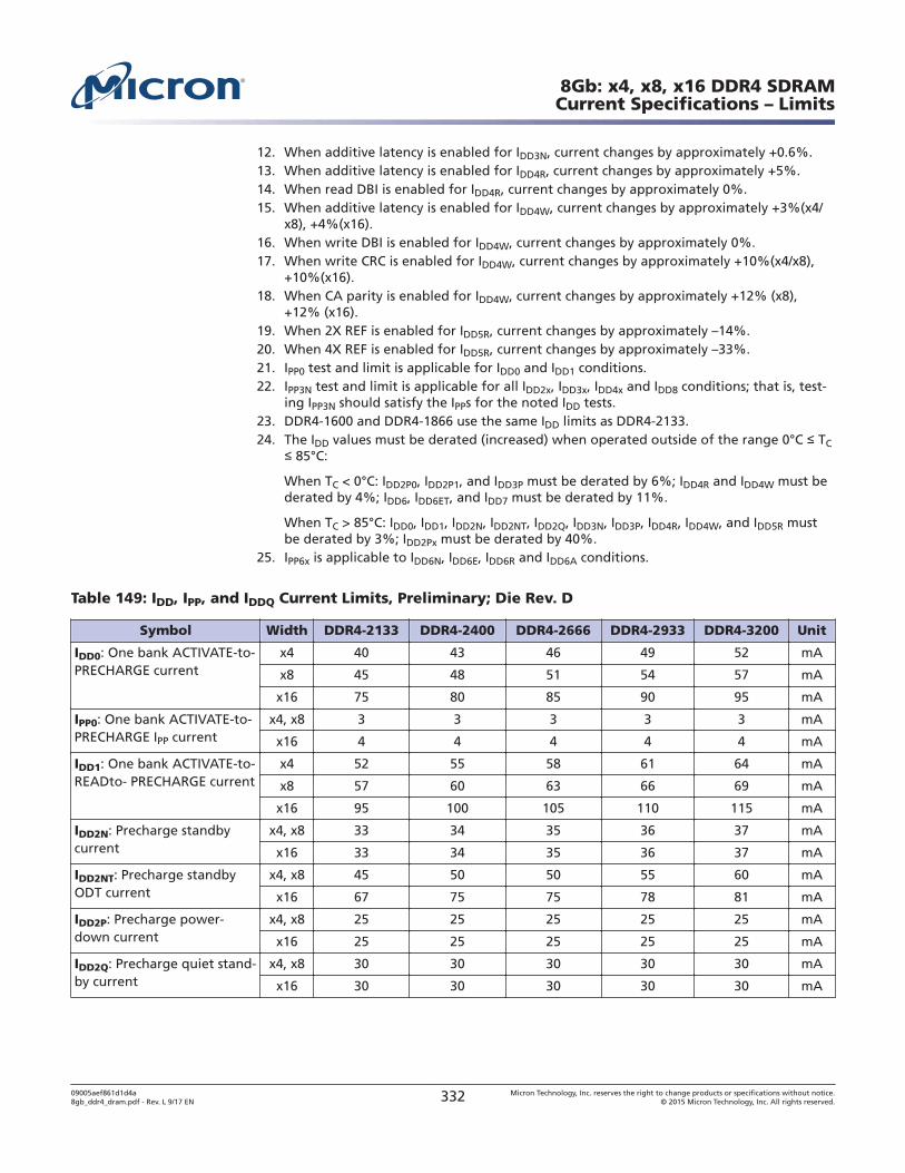
12. When additive latency is enabled for IDD3N, current changes by approximately +0.6%.13. When additive latency is enabled for IDD4R, current changes by approximately +5%.14. When read DBI is enabled for IDD4R, current changes by approximately 0%.15. When additive latency is enabled for IDD4W, current changes by approximately +3%(x4/
x8), +4%(x16).16. When write DBI is enabled for IDD4W, current changes by approximately 0%.17. When write CRC is enabled for IDD4W, current changes by approximately +10%(x4/x8),
+10%(x16).18. When CA parity is enabled for IDD4W, current changes by approximately +12% (x8),
+12% (x16).19. When 2X REF is enabled for IDD5R, current changes by approximately –14%.20. When 4X REF is enabled for IDD5R, current changes by approximately –33%.21. IPP0 test and limit is applicable for IDD0 and IDD1 conditions.22. IPP3N test and limit is applicable for all IDD2x, IDD3x, IDD4x and IDD8 conditions; that is, test-
ing IPP3N should satisfy the IPPs for the noted IDD tests.23. DDR4-1600 and DDR4-1866 use the same IDD limits as DDR4-2133.24. The IDD values must be derated (increased) when operated outside of the range 0°C TC
85°C:
When TC < 0°C: IDD2P0, IDD2P1, and IDD3P must be derated by 6%; IDD4R and IDD4W must bederated by 4%; IDD6, IDD6ET, and IDD7 must be derated by 11%.
When TC > 85°C: IDD0, IDD1, IDD2N, IDD2NT, IDD2Q, IDD3N, IDD3P, IDD4R, IDD4W, and IDD5R mustbe derated by 3%; IDD2Px must be derated by 40%.
25. IPP6x is applicable to IDD6N, IDD6E, IDD6R and IDD6A conditions.
Table 149: IDD, IPP, and IDDQ Current Limits, Preliminary; Die Rev. D
Symbol Width DDR4-2133 DDR4-2400 DDR4-2666 DDR4-2933 DDR4-3200 Unit
IDD0: One bank ACTIVATE-to-PRECHARGE current
x4 40 43 46 49 52 mA
x8 45 48 51 54 57 mA
x16 75 80 85 90 95 mA
IPP0: One bank ACTIVATE-to-PRECHARGE IPP current
x4, x8 3 3 3 3 3 mA
x16 4 4 4 4 4 mA
IDD1: One bank ACTIVATE-to-READto- PRECHARGE current
x4 52 55 58 61 64 mA
x8 57 60 63 66 69 mA
x16 95 100 105 110 115 mA
IDD2N: Precharge standbycurrent
x4, x8 33 34 35 36 37 mA
x16 33 34 35 36 37 mA
IDD2NT: Precharge standbyODT current
x4, x8 45 50 50 55 60 mA
x16 67 75 75 78 81 mA
IDD2P: Precharge power-down current
x4, x8 25 25 25 25 25 mA
x16 25 25 25 25 25 mA
IDD2Q: Precharge quiet stand-by current
x4, x8 30 30 30 30 30 mA
x16 30 30 30 30 30 mA
8Gb: x4, x8, x16 DDR4 SDRAMCurrent Specifications – Limits
09005aef861d1d4a8gb_ddr4_dram.pdf - Rev. L 9/17 EN 332 Micron Technology, Inc. reserves the right to change products or specifications without notice.
© 2015 Micron Technology, Inc. All rights reserved.
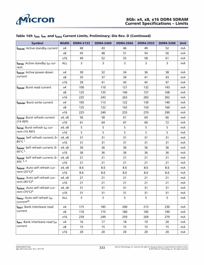
Table 149: IDD, IPP, and IDDQ Current Limits, Preliminary; Die Rev. D (Continued)
Symbol Width DDR4-2133 DDR4-2400 DDR4-2666 DDR4-2933 DDR4-3200 Unit
IDD3N: Active standby current x4 40 43 46 49 52 mA
x8 45 48 51 54 56 mA
x16 49 52 55 58 61 mA
IPP3N: Active standby IPP cur-rent
ALL 3 3 3 3 3 mA
IDD3P: Active power-downcurrent
x4 30 32 34 36 38 mA
x8 35 37 39 41 43 mA
x16 39 41 43 45 47 mA
IDD4R: Burst read current x4 100 110 121 132 143 mA
x8 125 135 146 157 168 mA
x16 225 243 263 283 302 mA
IDD4W: Burst write current x4 105 113 122 130 140 mA
x8 125 132 142 150 160 mA
x16 225 240 255 270 290 mA
IDD5R: Burst refresh current(1X REF)
x4, x8 56 58 61 64 66 mA
x16 61 64 67 69 72 mA
IPP5R: Burst refresh IPP cur-rent (1X REF)
x4, x8 5 5 5 5 5 mA
x16 5 5 5 5 5 mA
IDD6N: Self refresh current; 0–85°C 1
x4, x8 31 31 31 31 31 mA
x16 31 31 31 31 31 mA
IDD6E: Self refresh current; 0–95°C 2
x4, x8 36 36 36 36 36 mA
x16 36 36 36 36 36 mA
IDD6R: Self refresh current; 0–45C 3, 4
x4, x8 21 21 21 21 21 mA
x16 21 21 21 21 21 mA
IDD6A: Auto self refresh cur-rent (25°C)4
x4, x8 8.6 8.6 8.6 8.6 8.6 mA
x16 8.6 8.6 8.6 8.6 8.6 mA
IDD6A: Auto self refresh cur-rent (45°C)4
x4, x8 21 21 21 21 21 mA
x16 21 21 21 21 21 mA
IDD6A: Auto self refresh cur-rent (75°C)4
x4, x8 31 31 31 31 31 mA
x16 31 31 31 31 31 mA
IPP6x: Auto self refresh IPP
current26ALL 5 5 5 5 5 mA
IDD7: Bank interleave readcurrent
x4 175 185 200 215 230 mA
x8 170 175 180 185 190 mA
x16 239 249 259 269 279 mA
IPP7: Bank interleave read IPP
currentx4 16 17 18 19 20 mA
x8 15 15 15 15 15 mA
x16 20 20 20 20 20 mA
8Gb: x4, x8, x16 DDR4 SDRAMCurrent Specifications – Limits
09005aef861d1d4a8gb_ddr4_dram.pdf - Rev. L 9/17 EN 333 Micron Technology, Inc. reserves the right to change products or specifications without notice.
© 2015 Micron Technology, Inc. All rights reserved.
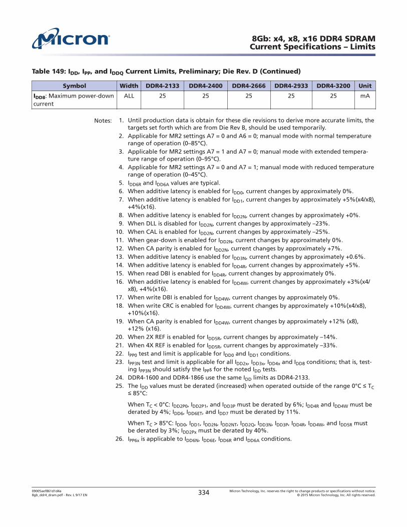
Table 149: IDD, IPP, and IDDQ Current Limits, Preliminary; Die Rev. D (Continued)
Symbol Width DDR4-2133 DDR4-2400 DDR4-2666 DDR4-2933 DDR4-3200 Unit
IDD8: Maximum power-downcurrent
ALL 25 25 25 25 25 mA
Notes: 1. Until production data is obtain for these die revisions to derive more accurate limits, thetargets set forth which are from Die Rev B, should be used temporarily.
2. Applicable for MR2 settings A7 = 0 and A6 = 0; manual mode with normal temperaturerange of operation (0–85°C).
3. Applicable for MR2 settings A7 = 1 and A7 = 0; manual mode with extended tempera-ture range of operation (0–95°C).
4. Applicable for MR2 settings A7 = 0 and A7 = 1; manual mode with reduced temperaturerange of operation (0–45°C).
5. IDD6R and IDD6A values are typical.6. When additive latency is enabled for IDD0, current changes by approximately 0%.7. When additive latency is enabled for IDD1, current changes by approximately +5%(x4/x8),
+4%(x16).8. When additive latency is enabled for IDD2N, current changes by approximately +0%.9. When DLL is disabled for IDD2N, current changes by approximately –23%.
10. When CAL is enabled for IDD2N, current changes by approximately –25%.11. When gear-down is enabled for IDD2N, current changes by approximately 0%.12. When CA parity is enabled for IDD2N, current changes by approximately +7%.13. When additive latency is enabled for IDD3N, current changes by approximately +0.6%.14. When additive latency is enabled for IDD4R, current changes by approximately +5%.15. When read DBI is enabled for IDD4R, current changes by approximately 0%.16. When additive latency is enabled for IDD4W, current changes by approximately +3%(x4/
x8), +4%(x16).17. When write DBI is enabled for IDD4W, current changes by approximately 0%.18. When write CRC is enabled for IDD4W, current changes by approximately +10%(x4/x8),
+10%(x16).19. When CA parity is enabled for IDD4W, current changes by approximately +12% (x8),
+12% (x16).20. When 2X REF is enabled for IDD5R, current changes by approximately –14%.21. When 4X REF is enabled for IDD5R, current changes by approximately –33%.22. IPP0 test and limit is applicable for IDD0 and IDD1 conditions.23. IPP3N test and limit is applicable for all IDD2x, IDD3x, IDD4x and IDD8 conditions; that is, test-
ing IPP3N should satisfy the IPPs for the noted IDD tests.24. DDR4-1600 and DDR4-1866 use the same IDD limits as DDR4-2133.25. The IDD values must be derated (increased) when operated outside of the range 0°C TC
85°C:
When TC < 0°C: IDD2P0, IDD2P1, and IDD3P must be derated by 6%; IDD4R and IDD4W must bederated by 4%; IDD6, IDD6ET, and IDD7 must be derated by 11%.
When TC > 85°C: IDD0, IDD1, IDD2N, IDD2NT, IDD2Q, IDD3N, IDD3P, IDD4R, IDD4W, and IDD5R mustbe derated by 3%; IDD2Px must be derated by 40%.
26. IPP6x is applicable to IDD6N, IDD6E, IDD6R and IDD6A conditions.
8Gb: x4, x8, x16 DDR4 SDRAMCurrent Specifications – Limits
09005aef861d1d4a8gb_ddr4_dram.pdf - Rev. L 9/17 EN 334 Micron Technology, Inc. reserves the right to change products or specifications without notice.
© 2015 Micron Technology, Inc. All rights reserved.
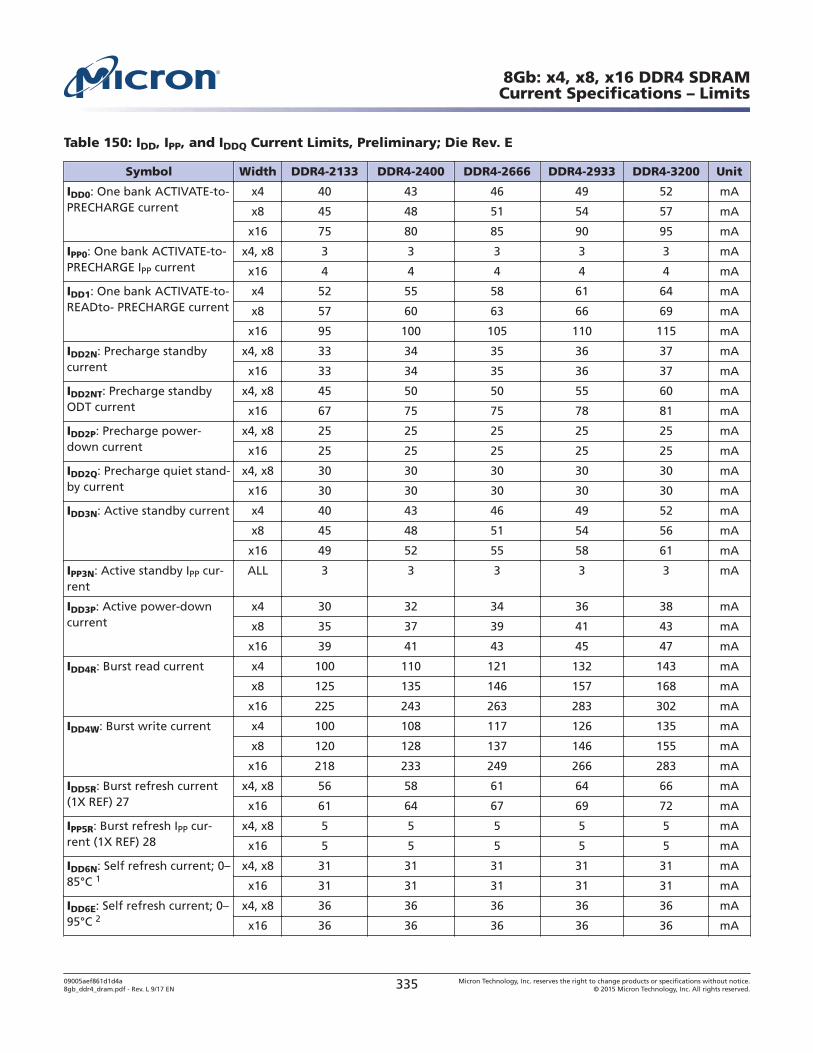
Table 150: IDD, IPP, and IDDQ Current Limits, Preliminary; Die Rev. E
Symbol Width DDR4-2133 DDR4-2400 DDR4-2666 DDR4-2933 DDR4-3200 Unit
IDD0: One bank ACTIVATE-to-PRECHARGE current
x4 40 43 46 49 52 mA
x8 45 48 51 54 57 mA
x16 75 80 85 90 95 mA
IPP0: One bank ACTIVATE-to-PRECHARGE IPP current
x4, x8 3 3 3 3 3 mA
x16 4 4 4 4 4 mA
IDD1: One bank ACTIVATE-to-READto- PRECHARGE current
x4 52 55 58 61 64 mA
x8 57 60 63 66 69 mA
x16 95 100 105 110 115 mA
IDD2N: Precharge standbycurrent
x4, x8 33 34 35 36 37 mA
x16 33 34 35 36 37 mA
IDD2NT: Precharge standbyODT current
x4, x8 45 50 50 55 60 mA
x16 67 75 75 78 81 mA
IDD2P: Precharge power-down current
x4, x8 25 25 25 25 25 mA
x16 25 25 25 25 25 mA
IDD2Q: Precharge quiet stand-by current
x4, x8 30 30 30 30 30 mA
x16 30 30 30 30 30 mA
IDD3N: Active standby current x4 40 43 46 49 52 mA
x8 45 48 51 54 56 mA
x16 49 52 55 58 61 mA
IPP3N: Active standby IPP cur-rent
ALL 3 3 3 3 3 mA
IDD3P: Active power-downcurrent
x4 30 32 34 36 38 mA
x8 35 37 39 41 43 mA
x16 39 41 43 45 47 mA
IDD4R: Burst read current x4 100 110 121 132 143 mA
x8 125 135 146 157 168 mA
x16 225 243 263 283 302 mA
IDD4W: Burst write current x4 100 108 117 126 135 mA
x8 120 128 137 146 155 mA
x16 218 233 249 266 283 mA
IDD5R: Burst refresh current(1X REF) 27
x4, x8 56 58 61 64 66 mA
x16 61 64 67 69 72 mA
IPP5R: Burst refresh IPP cur-rent (1X REF) 28
x4, x8 5 5 5 5 5 mA
x16 5 5 5 5 5 mA
IDD6N: Self refresh current; 0–85°C 1
x4, x8 31 31 31 31 31 mA
x16 31 31 31 31 31 mA
IDD6E: Self refresh current; 0–95°C 2
x4, x8 36 36 36 36 36 mA
x16 36 36 36 36 36 mA
8Gb: x4, x8, x16 DDR4 SDRAMCurrent Specifications – Limits
09005aef861d1d4a8gb_ddr4_dram.pdf - Rev. L 9/17 EN 335 Micron Technology, Inc. reserves the right to change products or specifications without notice.
© 2015 Micron Technology, Inc. All rights reserved.
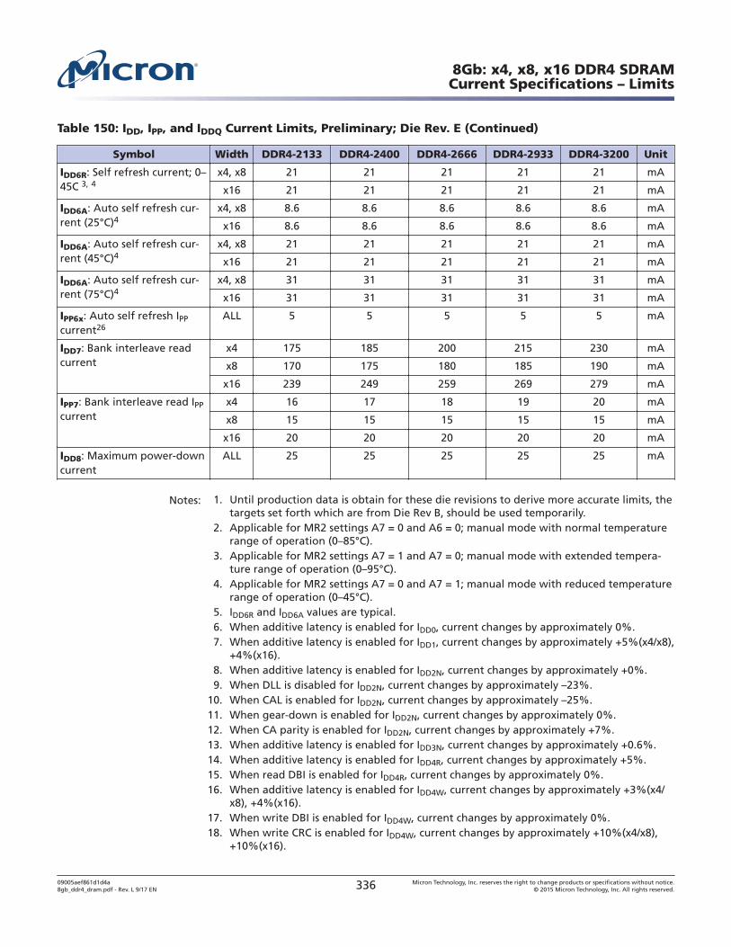
Table 150: IDD, IPP, and IDDQ Current Limits, Preliminary; Die Rev. E (Continued)
Symbol Width DDR4-2133 DDR4-2400 DDR4-2666 DDR4-2933 DDR4-3200 Unit
IDD6R: Self refresh current; 0–45C 3, 4
x4, x8 21 21 21 21 21 mA
x16 21 21 21 21 21 mA
IDD6A: Auto self refresh cur-rent (25°C)4
x4, x8 8.6 8.6 8.6 8.6 8.6 mA
x16 8.6 8.6 8.6 8.6 8.6 mA
IDD6A: Auto self refresh cur-rent (45°C)4
x4, x8 21 21 21 21 21 mA
x16 21 21 21 21 21 mA
IDD6A: Auto self refresh cur-rent (75°C)4
x4, x8 31 31 31 31 31 mA
x16 31 31 31 31 31 mA
IPP6x: Auto self refresh IPP
current26ALL 5 5 5 5 5 mA
IDD7: Bank interleave readcurrent
x4 175 185 200 215 230 mA
x8 170 175 180 185 190 mA
x16 239 249 259 269 279 mA
IPP7: Bank interleave read IPP
currentx4 16 17 18 19 20 mA
x8 15 15 15 15 15 mA
x16 20 20 20 20 20 mA
IDD8: Maximum power-downcurrent
ALL 25 25 25 25 25 mA
Notes: 1. Until production data is obtain for these die revisions to derive more accurate limits, thetargets set forth which are from Die Rev B, should be used temporarily.
2. Applicable for MR2 settings A7 = 0 and A6 = 0; manual mode with normal temperaturerange of operation (0–85°C).
3. Applicable for MR2 settings A7 = 1 and A7 = 0; manual mode with extended tempera-ture range of operation (0–95°C).
4. Applicable for MR2 settings A7 = 0 and A7 = 1; manual mode with reduced temperaturerange of operation (0–45°C).
5. IDD6R and IDD6A values are typical.6. When additive latency is enabled for IDD0, current changes by approximately 0%.7. When additive latency is enabled for IDD1, current changes by approximately +5%(x4/x8),
+4%(x16).8. When additive latency is enabled for IDD2N, current changes by approximately +0%.9. When DLL is disabled for IDD2N, current changes by approximately –23%.
10. When CAL is enabled for IDD2N, current changes by approximately –25%.11. When gear-down is enabled for IDD2N, current changes by approximately 0%.12. When CA parity is enabled for IDD2N, current changes by approximately +7%.13. When additive latency is enabled for IDD3N, current changes by approximately +0.6%.14. When additive latency is enabled for IDD4R, current changes by approximately +5%.15. When read DBI is enabled for IDD4R, current changes by approximately 0%.16. When additive latency is enabled for IDD4W, current changes by approximately +3%(x4/
x8), +4%(x16).17. When write DBI is enabled for IDD4W, current changes by approximately 0%.18. When write CRC is enabled for IDD4W, current changes by approximately +10%(x4/x8),
+10%(x16).
8Gb: x4, x8, x16 DDR4 SDRAMCurrent Specifications – Limits
09005aef861d1d4a8gb_ddr4_dram.pdf - Rev. L 9/17 EN 336 Micron Technology, Inc. reserves the right to change products or specifications without notice.
© 2015 Micron Technology, Inc. All rights reserved.
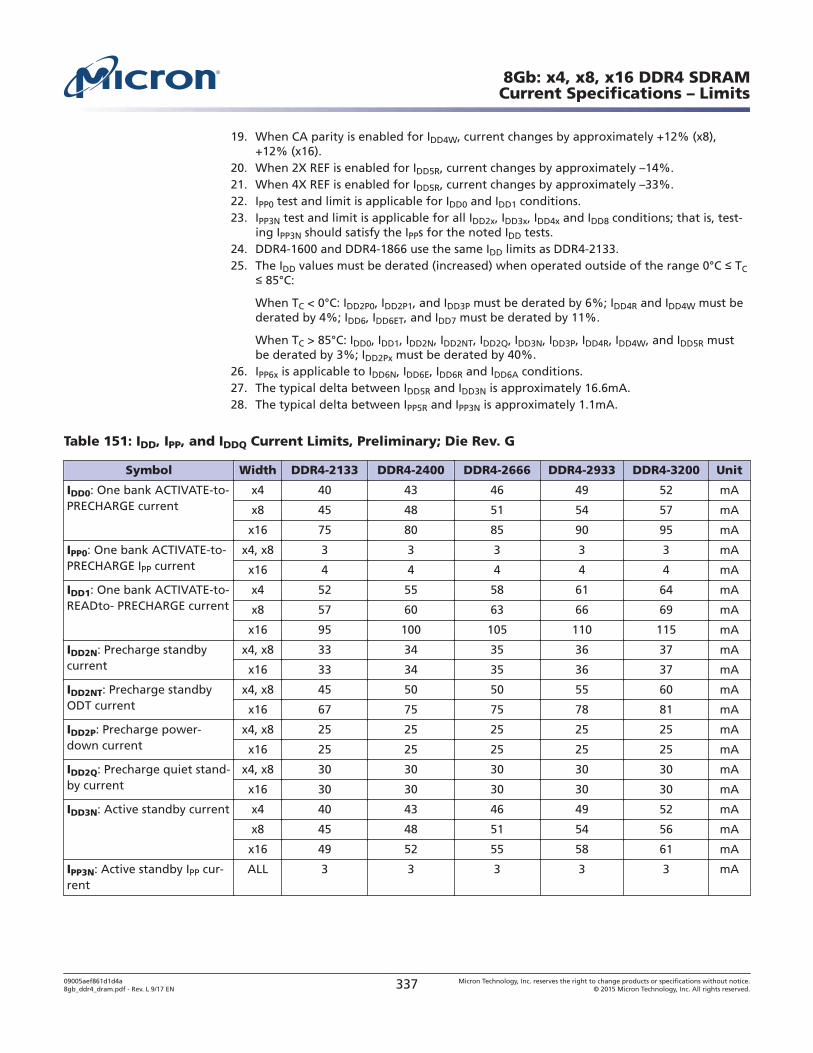
19. When CA parity is enabled for IDD4W, current changes by approximately +12% (x8),+12% (x16).
20. When 2X REF is enabled for IDD5R, current changes by approximately –14%.21. When 4X REF is enabled for IDD5R, current changes by approximately –33%.22. IPP0 test and limit is applicable for IDD0 and IDD1 conditions.23. IPP3N test and limit is applicable for all IDD2x, IDD3x, IDD4x and IDD8 conditions; that is, test-
ing IPP3N should satisfy the IPPs for the noted IDD tests.24. DDR4-1600 and DDR4-1866 use the same IDD limits as DDR4-2133.25. The IDD values must be derated (increased) when operated outside of the range 0°C TC
85°C:
When TC < 0°C: IDD2P0, IDD2P1, and IDD3P must be derated by 6%; IDD4R and IDD4W must bederated by 4%; IDD6, IDD6ET, and IDD7 must be derated by 11%.
When TC > 85°C: IDD0, IDD1, IDD2N, IDD2NT, IDD2Q, IDD3N, IDD3P, IDD4R, IDD4W, and IDD5R mustbe derated by 3%; IDD2Px must be derated by 40%.
26. IPP6x is applicable to IDD6N, IDD6E, IDD6R and IDD6A conditions.27. The typical delta between IDD5R and IDD3N is approximately 16.6mA.28. The typical delta between IPP5R and IPP3N is approximately 1.1mA.
Table 151: IDD, IPP, and IDDQ Current Limits, Preliminary; Die Rev. G
Symbol Width DDR4-2133 DDR4-2400 DDR4-2666 DDR4-2933 DDR4-3200 Unit
IDD0: One bank ACTIVATE-to-PRECHARGE current
x4 40 43 46 49 52 mA
x8 45 48 51 54 57 mA
x16 75 80 85 90 95 mA
IPP0: One bank ACTIVATE-to-PRECHARGE IPP current
x4, x8 3 3 3 3 3 mA
x16 4 4 4 4 4 mA
IDD1: One bank ACTIVATE-to-READto- PRECHARGE current
x4 52 55 58 61 64 mA
x8 57 60 63 66 69 mA
x16 95 100 105 110 115 mA
IDD2N: Precharge standbycurrent
x4, x8 33 34 35 36 37 mA
x16 33 34 35 36 37 mA
IDD2NT: Precharge standbyODT current
x4, x8 45 50 50 55 60 mA
x16 67 75 75 78 81 mA
IDD2P: Precharge power-down current
x4, x8 25 25 25 25 25 mA
x16 25 25 25 25 25 mA
IDD2Q: Precharge quiet stand-by current
x4, x8 30 30 30 30 30 mA
x16 30 30 30 30 30 mA
IDD3N: Active standby current x4 40 43 46 49 52 mA
x8 45 48 51 54 56 mA
x16 49 52 55 58 61 mA
IPP3N: Active standby IPP cur-rent
ALL 3 3 3 3 3 mA
8Gb: x4, x8, x16 DDR4 SDRAMCurrent Specifications – Limits
09005aef861d1d4a8gb_ddr4_dram.pdf - Rev. L 9/17 EN 337 Micron Technology, Inc. reserves the right to change products or specifications without notice.
© 2015 Micron Technology, Inc. All rights reserved.
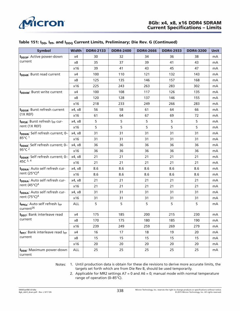
Table 151: IDD, IPP, and IDDQ Current Limits, Preliminary; Die Rev. G (Continued)
Symbol Width DDR4-2133 DDR4-2400 DDR4-2666 DDR4-2933 DDR4-3200 Unit
IDD3P: Active power-downcurrent
x4 30 32 34 36 38 mA
x8 35 37 39 41 43 mA
x16 39 41 43 45 47 mA
IDD4R: Burst read current x4 100 110 121 132 143 mA
x8 125 135 146 157 168 mA
x16 225 243 263 283 302 mA
IDD4W: Burst write current x4 100 108 117 126 135 mA
x8 120 128 137 146 155 mA
x16 218 233 249 266 283 mA
IDD5R: Burst refresh current(1X REF)
x4, x8 56 58 61 64 66 mA
x16 61 64 67 69 72 mA
IPP5R: Burst refresh IPP cur-rent (1X REF)
x4, x8 5 5 5 5 5 mA
x16 5 5 5 5 5 mA
IDD6N: Self refresh current; 0–85°C 1
x4, x8 31 31 31 31 31 mA
x16 31 31 31 31 31 mA
IDD6E: Self refresh current; 0–95°C 2
x4, x8 36 36 36 36 36 mA
x16 36 36 36 36 36 mA
IDD6R: Self refresh current; 0–45C 3, 4
x4, x8 21 21 21 21 21 mA
x16 21 21 21 21 21 mA
IDD6A: Auto self refresh cur-rent (25°C)4
x4, x8 8.6 8.6 8.6 8.6 8.6 mA
x16 8.6 8.6 8.6 8.6 8.6 mA
IDD6A: Auto self refresh cur-rent (45°C)4
x4, x8 21 21 21 21 21 mA
x16 21 21 21 21 21 mA
IDD6A: Auto self refresh cur-rent (75°C)4
x4, x8 31 31 31 31 31 mA
x16 31 31 31 31 31 mA
IPP6x: Auto self refresh IPP
current26ALL 5 5 5 5 5 mA
IDD7: Bank interleave readcurrent
x4 175 185 200 215 230 mA
x8 170 175 180 185 190 mA
x16 239 249 259 269 279 mA
IPP7: Bank interleave read IPP
currentx4 16 17 18 19 20 mA
x8 15 15 15 15 15 mA
x16 20 20 20 20 20 mA
IDD8: Maximum power-downcurrent
ALL 25 25 25 25 25 mA
Notes: 1. Until production data is obtain for these die revisions to derive more accurate limits, thetargets set forth which are from Die Rev B, should be used temporarily.
2. Applicable for MR2 settings A7 = 0 and A6 = 0; manual mode with normal temperaturerange of operation (0–85°C).
8Gb: x4, x8, x16 DDR4 SDRAMCurrent Specifications – Limits
09005aef861d1d4a8gb_ddr4_dram.pdf - Rev. L 9/17 EN 338 Micron Technology, Inc. reserves the right to change products or specifications without notice.
© 2015 Micron Technology, Inc. All rights reserved.
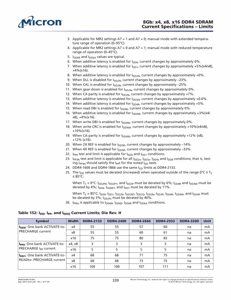
3. Applicable for MR2 settings A7 = 1 and A7 = 0; manual mode with extended tempera-ture range of operation (0–95°C).
4. Applicable for MR2 settings A7 = 0 and A7 = 1; manual mode with reduced temperaturerange of operation (0–45°C).
5. IDD6R and IDD6A values are typical.6. When additive latency is enabled for IDD0, current changes by approximately 0%.7. When additive latency is enabled for IDD1, current changes by approximately +5%(x4/x8),
+4%(x16).8. When additive latency is enabled for IDD2N, current changes by approximately +0%.9. When DLL is disabled for IDD2N, current changes by approximately –23%.
10. When CAL is enabled for IDD2N, current changes by approximately –25%.11. When gear-down is enabled for IDD2N, current changes by approximately 0%.12. When CA parity is enabled for IDD2N, current changes by approximately +7%.13. When additive latency is enabled for IDD3N, current changes by approximately +0.6%.14. When additive latency is enabled for IDD4R, current changes by approximately +5%.15. When read DBI is enabled for IDD4R, current changes by approximately 0%.16. When additive latency is enabled for IDD4W, current changes by approximately +3%(x4/
x8), +4%(x16).17. When write DBI is enabled for IDD4W, current changes by approximately 0%.18. When write CRC is enabled for IDD4W, current changes by approximately +10%(x4/x8),
+10%(x16).19. When CA parity is enabled for IDD4W, current changes by approximately +12% (x8),
+12% (x16).20. When 2X REF is enabled for IDD5R, current changes by approximately –14%.21. When 4X REF is enabled for IDD5R, current changes by approximately –33%.22. IPP0 test and limit is applicable for IDD0 and IDD1 conditions.23. IPP3N test and limit is applicable for all IDD2x, IDD3x, IDD4x and IDD8 conditions; that is, test-
ing IPP3N should satisfy the IPPs for the noted IDD tests.24. DDR4-1600 and DDR4-1866 use the same IDD limits as DDR4-2133.25. The IDD values must be derated (increased) when operated outside of the range 0°C TC
85°C:
When TC < 0°C: IDD2P0, IDD2P1, and IDD3P must be derated by 6%; IDD4R and IDD4W must bederated by 4%; IDD6, IDD6ET, and IDD7 must be derated by 11%.
When TC > 85°C: IDD0, IDD1, IDD2N, IDD2NT, IDD2Q, IDD3N, IDD3P, IDD4R, IDD4W, and IDD5R mustbe derated by 3%; IDD2Px must be derated by 40%.
26. IPP6x is applicable to IDD6N, IDD6E, IDD6R and IDD6A conditions.
Table 152: IDD, IPP, and IDDQ Current Limits; Die Rev. H
Symbol Width DDR4-2133 DDR4-2400 DDR4-2666 DDR4-2933 DDR4-3200 Unit
IDD0: One bank ACTIVATE-to-PRECHARGE current
x4 55 55 57 60 na mA
x8 55 55 60 61 na mA
x16 75 75 80 83 na mA
IPP0: One bank ACTIVATE-to-PRECHARGE IPP current
x4, x8 3 3 3 3 na mA
x16 5 5 5 5 na mA
IDD1: One bank ACTIVATE-to-READto- PRECHARGE current
x4 68 68 71 75 na mA
x8 68 68 73 75 na mA
x16 100 100 107 111 na mA
8Gb: x4, x8, x16 DDR4 SDRAMCurrent Specifications – Limits
09005aef861d1d4a8gb_ddr4_dram.pdf - Rev. L 9/17 EN 339 Micron Technology, Inc. reserves the right to change products or specifications without notice.
© 2015 Micron Technology, Inc. All rights reserved.
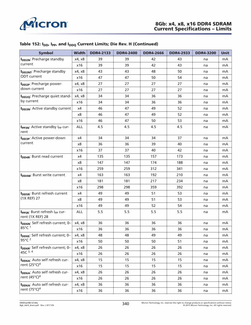
Table 152: IDD, IPP, and IDDQ Current Limits; Die Rev. H (Continued)
Symbol Width DDR4-2133 DDR4-2400 DDR4-2666 DDR4-2933 DDR4-3200 Unit
IDD2N: Precharge standbycurrent
x4, x8 39 39 42 43 na mA
x16 39 39 42 43 na mA
IDD2NT: Precharge standbyODT current
x4, x8 43 43 48 50 na mA
x16 47 47 50 54 na mA
IDD2P: Precharge power-down current
x4, x8 27 27 27 27 na mA
x16 27 27 27 27 na mA
IDD2Q: Precharge quiet stand-by current
x4, x8 34 34 36 36 na mA
x16 34 34 36 36 na mA
IDD3N: Active standby current x4 46 47 49 52 na mA
x8 46 47 49 52 na mA
x16 46 47 50 53 na mA
IPP3N: Active standby IPP cur-rent
ALL 4.5 4.5 4.5 4.5 na mA
IDD3P: Active power-downcurrent
x4 34 34 34 37 na mA
x8 36 36 39 40 na mA
x16 37 37 40 42 na mA
IDD4R: Burst read current x4 135 135 157 173 na mA
x8 147 147 174 188 na mA
x16 259 259 312 341 na mA
IDD4W: Burst write current x4 163 163 192 210 na mA
x8 181 181 217 234 na mA
x16 298 298 359 392 na mA
IDD5R: Burst refresh current(1X REF) 27
x4 49 49 51 53 na mA
x8 49 49 51 53 na mA
x16 49 49 52 54 na mA
IPP5R: Burst refresh IPP cur-rent (1X REF) 28
ALL 5.5 5.5 5.5 5.5 na mA
IDD6N: Self refresh current; 0–85°C 1
x4, x8 36 36 36 36 na mA
x16 36 36 36 36 na mA
IDD6E: Self refresh current; 0–95°C 2
x4, x8 48 48 49 49 na mA
x16 50 50 50 51 na mA
IDD6R: Self refresh current; 0–45C 3, 4
x4, x8 26 26 26 26 na mA
x16 26 26 26 26 na mA
IDD6A: Auto self refresh cur-rent (25°C)4
x4, x8 15 15 15 15 na mA
x16 15 15 15 15 na mA
IDD6A: Auto self refresh cur-rent (45°C)4
x4, x8 26 26 26 26 na mA
x16 26 26 26 26 na mA
IDD6A: Auto self refresh cur-rent (75°C)4
x4, x8 36 36 36 36 na mA
x16 36 36 36 36 na mA
8Gb: x4, x8, x16 DDR4 SDRAMCurrent Specifications – Limits
09005aef861d1d4a8gb_ddr4_dram.pdf - Rev. L 9/17 EN 340 Micron Technology, Inc. reserves the right to change products or specifications without notice.
© 2015 Micron Technology, Inc. All rights reserved.
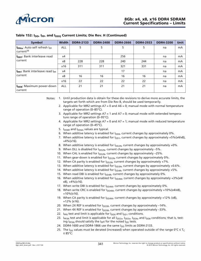
Table 152: IDD, IPP, and IDDQ Current Limits; Die Rev. H (Continued)
Symbol Width DDR4-2133 DDR4-2400 DDR4-2666 DDR4-2933 DDR4-3200 Unit
IPP6x: Auto self refresh IPP
current26ALL 5 5 5 5 na mA
IDD7: Bank interleave readcurrent
x4 256 na mA
x8 228 228 240 244 na mA
x16 311 311 321 331 na mA
IPP7: Bank interleave read IPP
currentx4 17 na mA
x8 16 16 16 16 na mA
x16 22 22 22 22 na mA
IDD8: Maximum power-downcurrent
ALL 21 21 21 21 na mA
Notes: 1. Until production data is obtain for these die revisions to derive more accurate limits, thetargets set forth which are from Die Rev B, should be used temporarily.
2. Applicable for MR2 settings A7 = 0 and A6 = 0; manual mode with normal temperaturerange of operation (0–85°C).
3. Applicable for MR2 settings A7 = 1 and A7 = 0; manual mode with extended tempera-ture range of operation (0–95°C).
4. Applicable for MR2 settings A7 = 0 and A7 = 1; manual mode with reduced temperaturerange of operation (0–45°C).
5. IDD6R and IDD6A values are typical.6. When additive latency is enabled for IDD0, current changes by approximately 0%.7. When additive latency is enabled for IDD1, current changes by approximately +5%(x4/x8),
+4%(x16).8. When additive latency is enabled for IDD2N, current changes by approximately +0%.9. When DLL is disabled for IDD2N, current changes by approximately –5%.
10. When CAL is enabled for IDD2N, current changes by approximately –25%.11. When gear-down is enabled for IDD2N, current changes by approximately 0%.12. When CA parity is enabled for IDD2N, current changes by approximately +7%.13. When additive latency is enabled for IDD3N, current changes by approximately +0.6%.14. When additive latency is enabled for IDD4R, current changes by approximately +5%.15. When read DBI is enabled for IDD4R, current changes by approximately 0%.16. When additive latency is enabled for IDD4W, current changes by approximately +3%(x4/
x8), +4%(x16).17. When write DBI is enabled for IDD4W, current changes by approximately 0%.18. When write CRC is enabled for IDD4W, current changes by approximately +10%(x4/x8),
+10%(x16).19. When CA parity is enabled for IDD4W, current changes by approximately +12% (x8),
+12% (x16).20. When 2X REF is enabled for IDD5R, current changes by approximately –14%.21. When 4X REF is enabled for IDD5R, current changes by approximately –33%.22. IPP0 test and limit is applicable for IDD0 and IDD1 conditions.23. IPP3N test and limit is applicable for all IDD2x, IDD3x, IDD4x and IDD8 conditions; that is, test-
ing IPP3N should satisfy the IPPs for the noted IDD tests.24. DDR4-1600 and DDR4-1866 use the same IDD limits as DDR4-2133.25. The IDD values must be derated (increased) when operated outside of the range 0°C TC
85°C:
8Gb: x4, x8, x16 DDR4 SDRAMCurrent Specifications – Limits
09005aef861d1d4a8gb_ddr4_dram.pdf - Rev. L 9/17 EN 341 Micron Technology, Inc. reserves the right to change products or specifications without notice.
© 2015 Micron Technology, Inc. All rights reserved.
When TC < 0°C: IDD2P0, IDD2P1, and IDD3P must be derated by 6%; IDD4R and IDD4W must bederated by 4%; IDD6, IDD6ET, and IDD7 must be derated by 11%.
When TC > 85°C: IDD0, IDD1, IDD2N, IDD2NT, IDD2Q, IDD3N, IDD3P, IDD4R, IDD4W, and IDD5R mustbe derated by 3%; IDD2Px must be derated by 40%.
26. IPP6x is applicable to IDD6N, IDD6E, IDD6R and IDD6A conditions.27. The typical delta between IDD5R and IDD3N is approximately 2.6mA at DDR4-2133, 2.0mA
at DDR4-2400, 1.5mA at DDR4-2666, and 0.9mA at DDR4-2933.28. The typical delta between IPP5R and IPP3N is approximately 1.0mA for DDR4-2133 through
DDR4-2933.
8Gb: x4, x8, x16 DDR4 SDRAMCurrent Specifications – Limits
09005aef861d1d4a8gb_ddr4_dram.pdf - Rev. L 9/17 EN 342 Micron Technology, Inc. reserves the right to change products or specifications without notice.
© 2015 Micron Technology, Inc. All rights reserved.
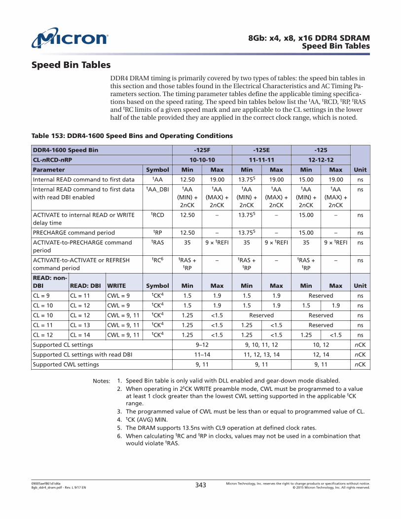
Speed Bin TablesDDR4 DRAM timing is primarily covered by two types of tables: the speed bin tables inthis section and those tables found in the Electrical Characteristics and AC Timing Pa-rameters section. The timing parameter tables define the applicable timing specifica-tions based on the speed rating. The speed bin tables below list the tAA, tRCD, tRP, tRASand tRC limits of a given speed mark and are applicable to the CL settings in the lowerhalf of the table provided they are applied in the correct clock range, which is noted.
Table 153: DDR4-1600 Speed Bins and Operating Conditions
DDR4-1600 Speed Bin -125F -125E -125
Unit
CL-nRCD-nRP 10-10-10 11-11-11 12-12-12
Parameter Symbol Min Max Min Max Min Max
Internal READ command to first data tAA 12.50 19.00 13.755 19.00 15.00 19.00 ns
Internal READ command to first datawith read DBI enabled
tAA_DBI tAA(MIN) +2nCK
tAA(MAX) +
2nCK
tAA(MIN) +2nCK
tAA(MAX) +
2nCK
tAA(MIN) +2nCK
tAA(MAX) +
2nCK
ns
ACTIVATE to internal READ or WRITEdelay time
tRCD 12.50 – 13.755 – 15.00 – ns
PRECHARGE command period tRP 12.50 – 13.755 – 15.00 – ns
ACTIVATE-to-PRECHARGE commandperiod
tRAS 35 9 × tREFI 35 9 × tREFI 35 9 × tREFI ns
ACTIVATE-to-ACTIVATE or REFRESHcommand period
tRC6 tRAS +tRP
– tRAS +tRP
– tRAS +tRP
– ns
READ: non-DBI READ: DBI WRITE Symbol Min Max Min Max Min Max Unit
CL = 9 CL = 11 CWL = 9 tCK4 1.5 1.9 1.5 1.9 Reserved ns
CL = 10 CL = 12 CWL = 9 tCK4 1.5 1.9 1.5 1.9 1.5 1.9 ns
CL = 10 CL = 12 CWL = 9, 11 tCK4 1.25 <1.5 Reserved Reserved ns
CL = 11 CL = 13 CWL = 9, 11 tCK4 1.25 <1.5 1.25 <1.5 Reserved ns
CL = 12 CL = 14 CWL = 9, 11 tCK4 1.25 <1.5 1.25 <1.5 1.25 <1.5 ns
Supported CL settings 9–12 9, 10, 11, 12 10, 12 nCK
Supported CL settings with read DBI 11–14 11, 12, 13, 14 12, 14 nCK
Supported CWL settings 9, 11 9, 11 9, 11 nCK
Notes: 1. Speed Bin table is only valid with DLL enabled and gear-down mode disabled.2. When operating in 2tCK WRITE preamble mode, CWL must be programmed to a value
at least 1 clock greater than the lowest CWL setting supported in the applicable tCKrange.
3. The programmed value of CWL must be less than or equal to programmed value of CL.4. tCK (AVG) MIN.5. The DRAM supports 13.5ns with CL9 operation at defined clock rates.6. When calculating tRC and tRP in clocks, values may not be used in a combination that
would violate tRAS.
8Gb: x4, x8, x16 DDR4 SDRAMSpeed Bin Tables
09005aef861d1d4a8gb_ddr4_dram.pdf - Rev. L 9/17 EN 343 Micron Technology, Inc. reserves the right to change products or specifications without notice.
© 2015 Micron Technology, Inc. All rights reserved.
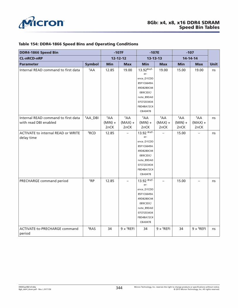
Table 154: DDR4-1866 Speed Bins and Operating Conditions
DDR4-1866 Speed Bin -107F -107E -107
Unit
CL-nRCD-nRP 12-12-12 13-13-13 14-14-14
Parameter Symbol Min Max Min Max Min Max
Internal READ command to first data tAA 12.85 19.00 13.92#ref-
er-
ence_D1CDD
85F1C6649A
49D8280C44
0B9C3DC/
note_89DA0
07CF2D3434
F8D48A72C4
CBA0478
19.00 15.00 19.00 ns
Internal READ command to first datawith read DBI enabled
tAA_DBI tAA(MIN) +2nCK
tAA(MAX) +
2nCK
tAA(MIN) +2nCK
tAA(MAX) +
2nCK
tAA(MIN) +2nCK
tAA(MAX) +
2nCK
ns
ACTIVATE to internal READ or WRITEdelay time
tRCD 12.85 – 13.92 #ref-
er-
ence_D1CDD
85F1C6649A
49D8280C44
0B9C3DC/
note_89DA0
07CF2D3434
F8D48A72C4
CBA0478
– 15.00 – ns
PRECHARGE command period tRP 12.85 – 13.92 #ref-
er-
ence_D1CDD
85F1C6649A
49D8280C44
0B9C3DC/
note_89DA0
07CF2D3434
F8D48A72C4
CBA0478
– 15.00 – ns
ACTIVATE-to-PRECHARGE commandperiod
tRAS 34 9 × tREFI 34 9 × tREFI 34 9 × tREFI ns
8Gb: x4, x8, x16 DDR4 SDRAMSpeed Bin Tables
09005aef861d1d4a8gb_ddr4_dram.pdf - Rev. L 9/17 EN 344 Micron Technology, Inc. reserves the right to change products or specifications without notice.
© 2015 Micron Technology, Inc. All rights reserved.
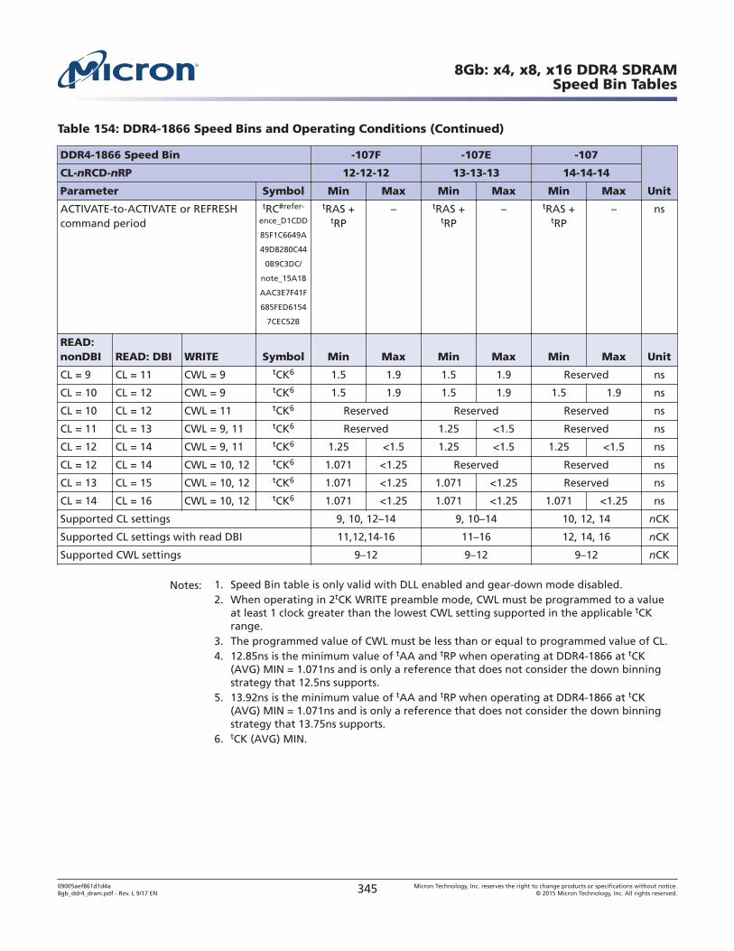
Table 154: DDR4-1866 Speed Bins and Operating Conditions (Continued)
DDR4-1866 Speed Bin -107F -107E -107
Unit
CL-nRCD-nRP 12-12-12 13-13-13 14-14-14
Parameter Symbol Min Max Min Max Min Max
ACTIVATE-to-ACTIVATE or REFRESHcommand period
tRC#refer-
ence_D1CDD
85F1C6649A
49D8280C44
0B9C3DC/
note_15A18
AAC3E7F41F
685FED6154
7CEC52B
tRAS +tRP
– tRAS +tRP
– tRAS +tRP
– ns
READ:nonDBI READ: DBI WRITE Symbol Min Max Min Max Min Max Unit
CL = 9 CL = 11 CWL = 9 tCK6 1.5 1.9 1.5 1.9 Reserved ns
CL = 10 CL = 12 CWL = 9 tCK6 1.5 1.9 1.5 1.9 1.5 1.9 ns
CL = 10 CL = 12 CWL = 11 tCK6 Reserved Reserved Reserved ns
CL = 11 CL = 13 CWL = 9, 11 tCK6 Reserved 1.25 <1.5 Reserved ns
CL = 12 CL = 14 CWL = 9, 11 tCK6 1.25 <1.5 1.25 <1.5 1.25 <1.5 ns
CL = 12 CL = 14 CWL = 10, 12 tCK6 1.071 <1.25 Reserved Reserved ns
CL = 13 CL = 15 CWL = 10, 12 tCK6 1.071 <1.25 1.071 <1.25 Reserved ns
CL = 14 CL = 16 CWL = 10, 12 tCK6 1.071 <1.25 1.071 <1.25 1.071 <1.25 ns
Supported CL settings 9, 10, 12–14 9, 10–14 10, 12, 14 nCK
Supported CL settings with read DBI 11,12,14-16 11–16 12, 14, 16 nCK
Supported CWL settings 9–12 9–12 9–12 nCK
Notes: 1. Speed Bin table is only valid with DLL enabled and gear-down mode disabled.2. When operating in 2tCK WRITE preamble mode, CWL must be programmed to a value
at least 1 clock greater than the lowest CWL setting supported in the applicable tCKrange.
3. The programmed value of CWL must be less than or equal to programmed value of CL.4. 12.85ns is the minimum value of tAA and tRP when operating at DDR4-1866 at tCK
(AVG) MIN = 1.071ns and is only a reference that does not consider the down binningstrategy that 12.5ns supports.
5. 13.92ns is the minimum value of tAA and tRP when operating at DDR4-1866 at tCK(AVG) MIN = 1.071ns and is only a reference that does not consider the down binningstrategy that 13.75ns supports.
6. tCK (AVG) MIN.
8Gb: x4, x8, x16 DDR4 SDRAMSpeed Bin Tables
09005aef861d1d4a8gb_ddr4_dram.pdf - Rev. L 9/17 EN 345 Micron Technology, Inc. reserves the right to change products or specifications without notice.
© 2015 Micron Technology, Inc. All rights reserved.
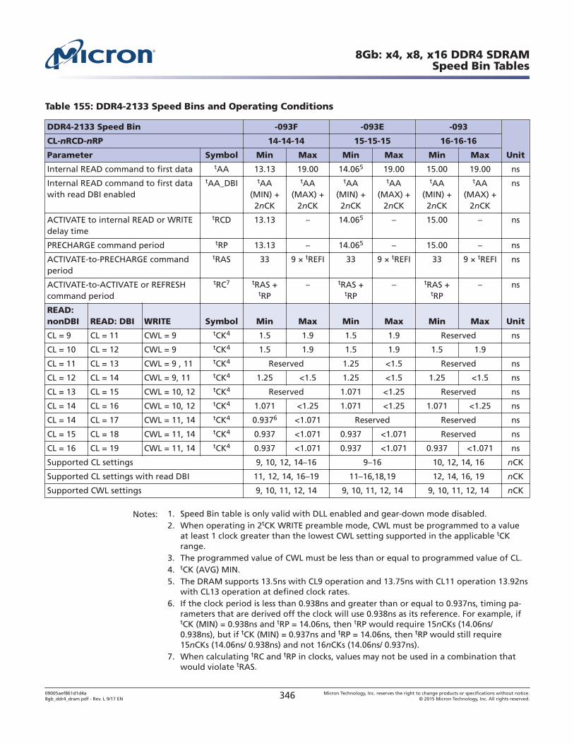
Table 155: DDR4-2133 Speed Bins and Operating Conditions
DDR4-2133 Speed Bin -093F -093E -093
Unit
CL-nRCD-nRP 14-14-14 15-15-15 16-16-16
Parameter Symbol Min Max Min Max Min Max
Internal READ command to first data tAA 13.13 19.00 14.065 19.00 15.00 19.00 ns
Internal READ command to first datawith read DBI enabled
tAA_DBI tAA(MIN) +2nCK
tAA(MAX) +
2nCK
tAA(MIN) +2nCK
tAA(MAX) +
2nCK
tAA(MIN) +2nCK
tAA(MAX) +
2nCK
ns
ACTIVATE to internal READ or WRITEdelay time
tRCD 13.13 – 14.065 – 15.00 – ns
PRECHARGE command period tRP 13.13 – 14.065 – 15.00 – ns
ACTIVATE-to-PRECHARGE commandperiod
tRAS 33 9 × tREFI 33 9 × tREFI 33 9 × tREFI ns
ACTIVATE-to-ACTIVATE or REFRESHcommand period
tRC7 tRAS +tRP
– tRAS +tRP
– tRAS +tRP
– ns
READ:nonDBI READ: DBI WRITE Symbol Min Max Min Max Min Max Unit
CL = 9 CL = 11 CWL = 9 tCK4 1.5 1.9 1.5 1.9 Reserved ns
CL = 10 CL = 12 CWL = 9 tCK4 1.5 1.9 1.5 1.9 1.5 1.9
CL = 11 CL = 13 CWL = 9 , 11 tCK4 Reserved 1.25 <1.5 Reserved ns
CL = 12 CL = 14 CWL = 9, 11 tCK4 1.25 <1.5 1.25 <1.5 1.25 <1.5 ns
CL = 13 CL = 15 CWL = 10, 12 tCK4 Reserved 1.071 <1.25 Reserved ns
CL = 14 CL = 16 CWL = 10, 12 tCK4 1.071 <1.25 1.071 <1.25 1.071 <1.25 ns
CL = 14 CL = 17 CWL = 11, 14 tCK4 0.9376 <1.071 Reserved Reserved ns
CL = 15 CL = 18 CWL = 11, 14 tCK4 0.937 <1.071 0.937 <1.071 Reserved ns
CL = 16 CL = 19 CWL = 11, 14 tCK4 0.937 <1.071 0.937 <1.071 0.937 <1.071 ns
Supported CL settings 9, 10, 12, 14–16 9–16 10, 12, 14, 16 nCK
Supported CL settings with read DBI 11, 12, 14, 16–19 11–16,18,19 12, 14, 16, 19 nCK
Supported CWL settings 9, 10, 11, 12, 14 9, 10, 11, 12, 14 9, 10, 11, 12, 14 nCK
Notes: 1. Speed Bin table is only valid with DLL enabled and gear-down mode disabled.2. When operating in 2tCK WRITE preamble mode, CWL must be programmed to a value
at least 1 clock greater than the lowest CWL setting supported in the applicable tCKrange.
3. The programmed value of CWL must be less than or equal to programmed value of CL.4. tCK (AVG) MIN.5. The DRAM supports 13.5ns with CL9 operation and 13.75ns with CL11 operation 13.92ns
with CL13 operation at defined clock rates.6. If the clock period is less than 0.938ns and greater than or equal to 0.937ns, timing pa-
rameters that are derived off the clock will use 0.938ns as its reference. For example, iftCK (MIN) = 0.938ns and tRP = 14.06ns, then tRP would require 15nCKs (14.06ns/0.938ns), but if tCK (MIN) = 0.937ns and tRP = 14.06ns, then tRP would still require15nCKs (14.06ns/ 0.938ns) and not 16nCKs (14.06ns/ 0.937ns).
7. When calculating tRC and tRP in clocks, values may not be used in a combination thatwould violate tRAS.
8Gb: x4, x8, x16 DDR4 SDRAMSpeed Bin Tables
09005aef861d1d4a8gb_ddr4_dram.pdf - Rev. L 9/17 EN 346 Micron Technology, Inc. reserves the right to change products or specifications without notice.
© 2015 Micron Technology, Inc. All rights reserved.
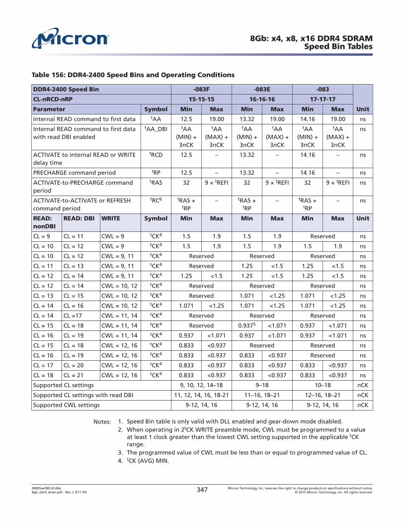
Table 156: DDR4-2400 Speed Bins and Operating Conditions
DDR4-2400 Speed Bin -083F -083E -083
Unit
CL-nRCD-nRP 15-15-15 16-16-16 17-17-17
Parameter Symbol Min Max Min Max Min Max
Internal READ command to first data tAA 12.5 19.00 13.32 19.00 14.16 19.00 ns
Internal READ command to first datawith read DBI enabled
tAA_DBI tAA(MIN) +3nCK
tAA(MAX) +
3nCK
tAA(MIN) +3nCK
tAA(MAX) +
3nCK
tAA(MIN) +3nCK
tAA(MAX) +
3nCK
ns
ACTIVATE to internal READ or WRITEdelay time
tRCD 12.5 – 13.32 – 14.16 – ns
PRECHARGE command period tRP 12.5 – 13.32 – 14.16 – ns
ACTIVATE-to-PRECHARGE commandperiod
tRAS 32 9 × tREFI 32 9 × tREFI 32 9 × tREFI ns
ACTIVATE-to-ACTIVATE or REFRESHcommand period
tRC6 tRAS +tRP
– tRAS +tRP
– tRAS +tRP
– ns
READ:nonDBI
READ: DBI WRITE Symbol Min Max Min Max Min Max Unit
CL = 9 CL = 11 CWL = 9 tCK4 1.5 1.9 1.5 1.9 Reserved ns
CL = 10 CL = 12 CWL = 9 tCK4 1.5 1.9 1.5 1.9 1.5 1.9 ns
CL = 10 CL = 12 CWL = 9, 11 tCK4 Reserved Reserved Reserved ns
CL = 11 CL = 13 CWL = 9, 11 tCK4 Reserved 1.25 <1.5 1.25 <1.5 ns
CL = 12 CL = 14 CWL = 9, 11 tCK4 1.25 <1.5 1.25 <1.5 1.25 <1.5 ns
CL = 12 CL = 14 CWL = 10, 12 tCK4 Reserved Reserved Reserved ns
CL = 13 CL = 15 CWL = 10, 12 tCK4 Reserved 1.071 <1.25 1.071 <1.25 ns
CL = 14 CL = 16 CWL = 10, 12 tCK4 1.071 <1.25 1.071 <1.25 1.071 <1.25 ns
CL = 14 CL =17 CWL = 11, 14 tCK4 Reserved Reserved Reserved ns
CL = 15 CL = 18 CWL = 11, 14 tCK4 Reserved 0.9375 <1.071 0.937 <1.071 ns
CL = 16 CL = 19 CWL = 11, 14 tCK4 0.937 <1.071 0.937 <1.071 0.937 <1.071 ns
CL = 15 CL = 18 CWL = 12, 16 tCK4 0.833 <0.937 Reserved Reserved ns
CL = 16 CL = 19 CWL = 12, 16 tCK4 0.833 <0.937 0.833 <0.937 Reserved ns
CL = 17 CL = 20 CWL = 12, 16 tCK4 0.833 <0.937 0.833 <0.937 0.833 <0.937 ns
CL = 18 CL = 21 CWL = 12, 16 tCK4 0.833 <0.937 0.833 <0.937 0.833 <0.937 ns
Supported CL settings 9, 10, 12, 14–18 9–18 10–18 nCK
Supported CL settings with read DBI 11, 12, 14, 16, 18-21 11–16, 18–21 12–16, 18–21 nCK
Supported CWL settings 9-12, 14, 16 9-12, 14, 16 9-12, 14, 16 nCK
Notes: 1. Speed Bin table is only valid with DLL enabled and gear-down mode disabled.2. When operating in 2tCK WRITE preamble mode, CWL must be programmed to a value
at least 1 clock greater than the lowest CWL setting supported in the applicable tCKrange.
3. The programmed value of CWL must be less than or equal to programmed value of CL.4. tCK (AVG) MIN.
8Gb: x4, x8, x16 DDR4 SDRAMSpeed Bin Tables
09005aef861d1d4a8gb_ddr4_dram.pdf - Rev. L 9/17 EN 347 Micron Technology, Inc. reserves the right to change products or specifications without notice.
© 2015 Micron Technology, Inc. All rights reserved.
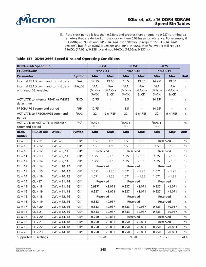
5. If the clock period is less than 0.938ns and greater than or equal to 0.937ns, timing pa-rameters that are derived off the clock will use 0.938ns as its reference. For example, iftCK (MIN) = 0.938ns and tRP = 14.06ns, then tRP would require 15nCKs (14.06ns/0.938ns), but if tCK (MIN) = 0.937ns and tRP = 14.06ns, then tRP would still require15nCKs (14.06ns/ 0.938ns) and not 16nCKs (14.06ns/ 0.937ns).
Table 157: DDR4-2666 Speed Bins and Operating Conditions
DDR4-2666 Speed Bin -075F -075E -075
Unit
CL-nRCD-nRP 17-17-17 18-18-18 19-19-19
Parameter Symbol Min Max Min Max Min Max
Internal READ command to first data tAA 12.75 19.00 13.5 19.00 14.255 19.00 ns
Internal READ command to first datawith read DBI enabled
tAA_DBI tAA(MIN) +3nCK
tAA(MAX) +
3nCK
tAA(MIN) +3nCK
tAA(MAX) +
3nCK
tAA(MIN) +3nCK
tAA(MAX) +
3nCK
ns
ACTIVATE to internal READ or WRITEdelay time
tRCD 12.75 – 13.5 – 14.255 – ns
PRECHARGE command period tRP 12.75 – 13.5 – 14.255 – ns
ACTIVATE-to-PRECHARGE commandperiod
tRAS 32 9 × tREFI 32 9 × tREFI 32 9 × tREFI ns
ACTIVATE-to-ACTIVATE or REFRESHcommand period
tRC7 tRAS +tRP
– tRAS +tRP
– tRAS +tRP
– ns
READ:nonDBI
READ: DBI WRITE Symbol Min Max Min Max Min Max Unit
CL = 9 CL = 11 CWL = 9 tCK4 1.5 1.9 1.5 1.9 Reserved ns
CL = 10 CL = 12 CWL = 9 tCK4 1.5 1.9 1.5 1.9 1.5 1.9 ns
CL = 10 CL = 12 CWL = 9, 11 tCK4 Reserved Reserved Reserved ns
CL = 11 CL = 13 CWL = 9, 11 tCK4 1.25 <1.5 1.25 <1.5 1.25 <1.5 ns
CL = 12 CL = 14 CWL = 9, 11 tCK4 1.25 <1.5 1.25 <1.5 1.25 <1.5 ns
CL = 12 CL = 14 CWL = 10, 12 tCK4 Reserved Reserved Reserved ns
CL = 13 CL = 15 CWL = 10, 12 tCK4 1.071 <1.25 1.071 <1.25 1.071 <1.25 ns
CL = 14 CL = 16 CWL = 10, 12 tCK4 1.071 <1.25 1.071 <1.25 1.071 <1.25 ns
CL = 14 CL =17 CWL = 11, 14 tCK4 Reserved Reserved Reserved ns
CL = 15 CL = 18 CWL = 11, 14 tCK4 0.9376 <1.071 0.937 <1.071 0.937 <1.071 ns
CL = 16 CL = 19 CWL = 11, 14 tCK4 0.937 <1.071 0.937 <1.071 0.937 <1.071 ns
CL = 15 CL = 18 CWL = 12, 16 tCK4 Reserved Reserved Reserved ns
CL = 16 CL = 19 CWL = 12, 16 tCK4 0.833 <0.937 Reserved Reserved ns
CL = 17 CL = 20 CWL = 12, 16 tCK4 0.833 <0.937 0.833 <0.937 0.833 <0.937 ns
CL = 18 CL = 21 CWL = 12, 16 tCK4 0.833 <0.937 0.833 <0.937 0.833 <0.937 ns
CL = 17 CL = 20 CWL = 14, 18 tCK4 0.750 <0.833 Reserved Reserved ns
CL = 18 CL = 21 CWL = 14, 18 tCK4 0.750 <0.833 0.750 <0.833 Reserved ns
CL = 19 CL = 22 CWL = 14, 18 tCK4 0.750 <0.833 0.750 <0.833 0.750 <0.833 ns
CL = 20 CL = 23 CWL = 14, 18 tCK4 0.750 <0.833 0.750 <0.833 0.750 <0.833 ns
Supported CL settings 9–20 9–20 10-–20 nCK
8Gb: x4, x8, x16 DDR4 SDRAMSpeed Bin Tables
09005aef861d1d4a8gb_ddr4_dram.pdf - Rev. L 9/17 EN 348 Micron Technology, Inc. reserves the right to change products or specifications without notice.
© 2015 Micron Technology, Inc. All rights reserved.
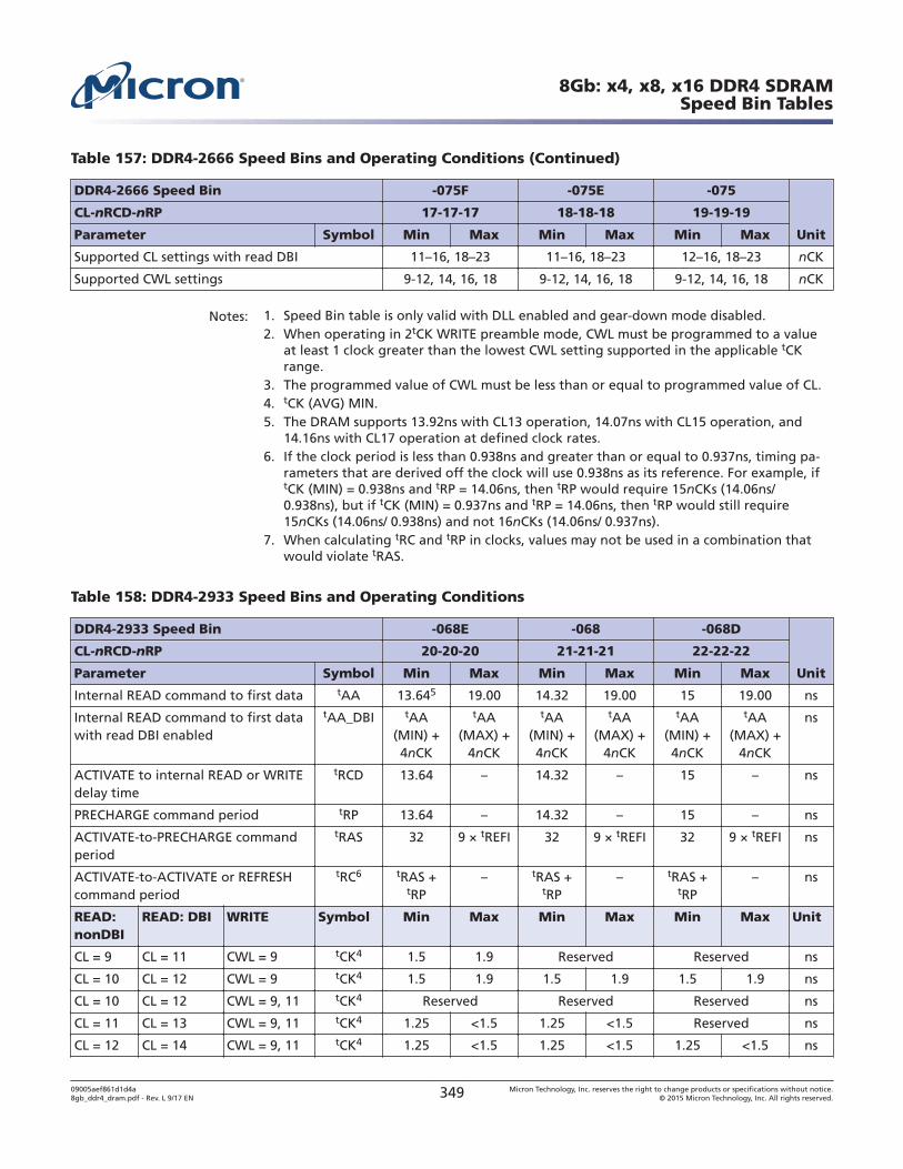
Table 157: DDR4-2666 Speed Bins and Operating Conditions (Continued)
DDR4-2666 Speed Bin -075F -075E -075
Unit
CL-nRCD-nRP 17-17-17 18-18-18 19-19-19
Parameter Symbol Min Max Min Max Min Max
Supported CL settings with read DBI 11–16, 18–23 11–16, 18–23 12–16, 18–23 nCK
Supported CWL settings 9-12, 14, 16, 18 9-12, 14, 16, 18 9-12, 14, 16, 18 nCK
Notes: 1. Speed Bin table is only valid with DLL enabled and gear-down mode disabled.2. When operating in 2tCK WRITE preamble mode, CWL must be programmed to a value
at least 1 clock greater than the lowest CWL setting supported in the applicable tCKrange.
3. The programmed value of CWL must be less than or equal to programmed value of CL.4. tCK (AVG) MIN.5. The DRAM supports 13.92ns with CL13 operation, 14.07ns with CL15 operation, and
14.16ns with CL17 operation at defined clock rates.6. If the clock period is less than 0.938ns and greater than or equal to 0.937ns, timing pa-
rameters that are derived off the clock will use 0.938ns as its reference. For example, iftCK (MIN) = 0.938ns and tRP = 14.06ns, then tRP would require 15nCKs (14.06ns/0.938ns), but if tCK (MIN) = 0.937ns and tRP = 14.06ns, then tRP would still require15nCKs (14.06ns/ 0.938ns) and not 16nCKs (14.06ns/ 0.937ns).
7. When calculating tRC and tRP in clocks, values may not be used in a combination thatwould violate tRAS.
Table 158: DDR4-2933 Speed Bins and Operating Conditions
DDR4-2933 Speed Bin -068E -068 -068D
Unit
CL-nRCD-nRP 20-20-20 21-21-21 22-22-22
Parameter Symbol Min Max Min Max Min Max
Internal READ command to first data tAA 13.645 19.00 14.32 19.00 15 19.00 ns
Internal READ command to first datawith read DBI enabled
tAA_DBI tAA(MIN) +4nCK
tAA(MAX) +
4nCK
tAA(MIN) +4nCK
tAA(MAX) +
4nCK
tAA(MIN) +4nCK
tAA(MAX) +
4nCK
ns
ACTIVATE to internal READ or WRITEdelay time
tRCD 13.64 – 14.32 – 15 – ns
PRECHARGE command period tRP 13.64 – 14.32 – 15 – ns
ACTIVATE-to-PRECHARGE commandperiod
tRAS 32 9 × tREFI 32 9 × tREFI 32 9 × tREFI ns
ACTIVATE-to-ACTIVATE or REFRESHcommand period
tRC6 tRAS +tRP
– tRAS +tRP
– tRAS +tRP
– ns
READ:nonDBI
READ: DBI WRITE Symbol Min Max Min Max Min Max Unit
CL = 9 CL = 11 CWL = 9 tCK4 1.5 1.9 Reserved Reserved ns
CL = 10 CL = 12 CWL = 9 tCK4 1.5 1.9 1.5 1.9 1.5 1.9 ns
CL = 10 CL = 12 CWL = 9, 11 tCK4 Reserved Reserved Reserved ns
CL = 11 CL = 13 CWL = 9, 11 tCK4 1.25 <1.5 1.25 <1.5 Reserved ns
CL = 12 CL = 14 CWL = 9, 11 tCK4 1.25 <1.5 1.25 <1.5 1.25 <1.5 ns
8Gb: x4, x8, x16 DDR4 SDRAMSpeed Bin Tables
09005aef861d1d4a8gb_ddr4_dram.pdf - Rev. L 9/17 EN 349 Micron Technology, Inc. reserves the right to change products or specifications without notice.
© 2015 Micron Technology, Inc. All rights reserved.
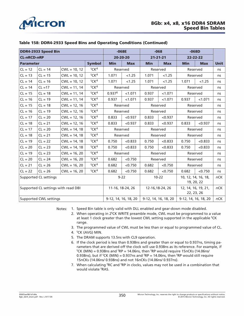
Table 158: DDR4-2933 Speed Bins and Operating Conditions (Continued)
DDR4-2933 Speed Bin -068E -068 -068D
Unit
CL-nRCD-nRP 20-20-20 21-21-21 22-22-22
Parameter Symbol Min Max Min Max Min Max
CL = 12 CL = 14 CWL = 10, 12 tCK4 Reserved Reserved Reserved ns
CL = 13 CL = 15 CWL = 10, 12 tCK4 1.071 <1.25 1.071 <1.25 Reserved ns
CL = 14 CL = 16 CWL = 10, 12 tCK4 1.071 <1.25 1.071 <1.25 1.071 <1.25 ns
CL = 14 CL =17 CWL = 11, 14 tCK4 Reserved Reserved Reserved ns
CL = 15 CL = 18 CWL = 11, 14 tCK4 0.9376 <1.071 0.937 <1.071 Reserved ns
CL = 16 CL = 19 CWL = 11, 14 tCK4 0.937 <1.071 0.937 <1.071 0.937 <1.071 ns
CL = 15 CL = 18 CWL = 12, 16 tCK4 Reserved Reserved Reserved ns
CL = 16 CL = 19 CWL = 12, 16 tCK4 Reserved Reserved Reserved ns
CL = 17 CL = 20 CWL = 12, 16 tCK4 0.833 <0.937 0.833 <0.937 Reserved ns
CL = 18 CL = 21 CWL = 12, 16 tCK4 0.833 <0.937 0.833 <0.937 0.833 <0.937 ns
CL = 17 CL = 20 CWL = 14, 18 tCK4 Reserved Reserved Reserved ns
CL = 18 CL = 21 CWL = 14, 18 tCK4 Reserved Reserved Reserved ns
CL = 19 CL = 22 CWL = 14, 18 tCK4 0.750 <0.833 0.750 <0.833 0.750 <0.833 ns
CL = 20 CL = 23 CWL = 14, 18 tCK4 0.750 <0.833 0.750 <0.833 0.750 <0.833 ns
CL = 19 CL = 23 CWL = 16, 20 tCK4 Reserved Reserved Reserved ns
CL = 20 CL = 24 CWL = 16, 20 tCK4 0.682 <0.750 Reserved Reserved ns
CL = 21 CL = 26 CWL = 16, 20 tCK4 0.682 <0.750 0.682 <0.750 Reserved ns
CL = 22 CL = 26 CWL = 16, 20 tCK4 0.682 <0.750 0.682 <0.750 0.682 <0.750 ns
Supported CL settings 9-22 10-22 10, 12, 14, 16, 18,19, 20, 22
nCK
Supported CL settings with read DBI 11-16, 18-24, 26 12-16,18-24, 26 12, 14, 16, 19, 21,22, 23, 26
nCK
Supported CWL settings 9-12, 14, 16, 18, 20 9-12, 14, 16, 18, 20 9-12, 14, 16, 18, 20 nCK
Notes: 1. Speed Bin table is only valid with DLL enabled and gear-down mode disabled.2. When operating in 2tCK WRITE preamble mode, CWL must be programmed to a value
at least 1 clock greater than the lowest CWL setting supported in the applicable tCKrange.
3. The programmed value of CWL must be less than or equal to programmed value of CL.4. tCK (AVG) MIN.5. The DRAM supports 13.5ns with CL9 operation.6. If the clock period is less than 0.938ns and greater than or equal to 0.937ns, timing pa-
rameters that are derived off the clock will use 0.938ns as its reference. For example, iftCK (MIN) = 0.938ns and tRP = 14.06ns, then tRP would require 15nCKs (14.06ns/0.938ns), but if tCK (MIN) = 0.937ns and tRP = 14.06ns, then tRP would still require15nCKs (14.06ns/ 0.938ns) and not 16nCKs (14.06ns/ 0.937ns).
7. When calculating tRC and tRP in clocks, values may not be used in a combination thatwould violate tRAS.
8Gb: x4, x8, x16 DDR4 SDRAMSpeed Bin Tables
09005aef861d1d4a8gb_ddr4_dram.pdf - Rev. L 9/17 EN 350 Micron Technology, Inc. reserves the right to change products or specifications without notice.
© 2015 Micron Technology, Inc. All rights reserved.
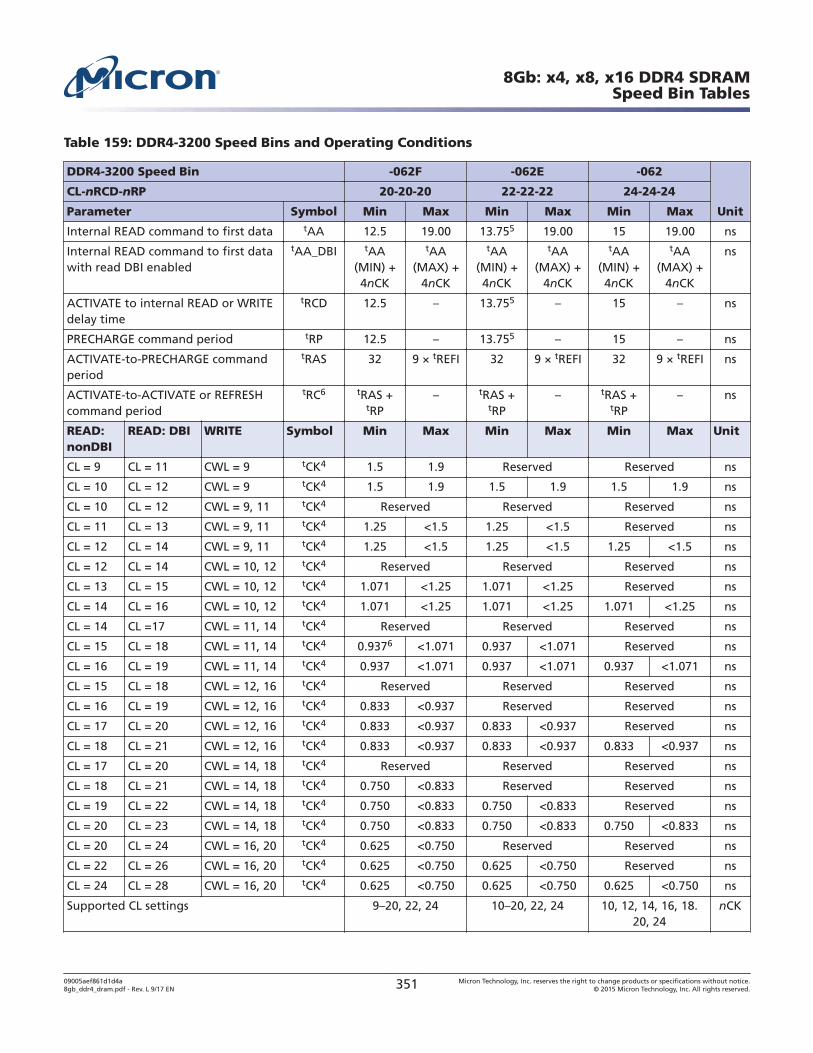
Table 159: DDR4-3200 Speed Bins and Operating Conditions
DDR4-3200 Speed Bin -062F -062E -062
Unit
CL-nRCD-nRP 20-20-20 22-22-22 24-24-24
Parameter Symbol Min Max Min Max Min Max
Internal READ command to first data tAA 12.5 19.00 13.755 19.00 15 19.00 ns
Internal READ command to first datawith read DBI enabled
tAA_DBI tAA(MIN) +4nCK
tAA(MAX) +
4nCK
tAA(MIN) +4nCK
tAA(MAX) +
4nCK
tAA(MIN) +4nCK
tAA(MAX) +
4nCK
ns
ACTIVATE to internal READ or WRITEdelay time
tRCD 12.5 – 13.755 – 15 – ns
PRECHARGE command period tRP 12.5 – 13.755 – 15 – ns
ACTIVATE-to-PRECHARGE commandperiod
tRAS 32 9 × tREFI 32 9 × tREFI 32 9 × tREFI ns
ACTIVATE-to-ACTIVATE or REFRESHcommand period
tRC6 tRAS +tRP
– tRAS +tRP
– tRAS +tRP
– ns
READ:nonDBI
READ: DBI WRITE Symbol Min Max Min Max Min Max Unit
CL = 9 CL = 11 CWL = 9 tCK4 1.5 1.9 Reserved Reserved ns
CL = 10 CL = 12 CWL = 9 tCK4 1.5 1.9 1.5 1.9 1.5 1.9 ns
CL = 10 CL = 12 CWL = 9, 11 tCK4 Reserved Reserved Reserved ns
CL = 11 CL = 13 CWL = 9, 11 tCK4 1.25 <1.5 1.25 <1.5 Reserved ns
CL = 12 CL = 14 CWL = 9, 11 tCK4 1.25 <1.5 1.25 <1.5 1.25 <1.5 ns
CL = 12 CL = 14 CWL = 10, 12 tCK4 Reserved Reserved Reserved ns
CL = 13 CL = 15 CWL = 10, 12 tCK4 1.071 <1.25 1.071 <1.25 Reserved ns
CL = 14 CL = 16 CWL = 10, 12 tCK4 1.071 <1.25 1.071 <1.25 1.071 <1.25 ns
CL = 14 CL =17 CWL = 11, 14 tCK4 Reserved Reserved Reserved ns
CL = 15 CL = 18 CWL = 11, 14 tCK4 0.9376 <1.071 0.937 <1.071 Reserved ns
CL = 16 CL = 19 CWL = 11, 14 tCK4 0.937 <1.071 0.937 <1.071 0.937 <1.071 ns
CL = 15 CL = 18 CWL = 12, 16 tCK4 Reserved Reserved Reserved ns
CL = 16 CL = 19 CWL = 12, 16 tCK4 0.833 <0.937 Reserved Reserved ns
CL = 17 CL = 20 CWL = 12, 16 tCK4 0.833 <0.937 0.833 <0.937 Reserved ns
CL = 18 CL = 21 CWL = 12, 16 tCK4 0.833 <0.937 0.833 <0.937 0.833 <0.937 ns
CL = 17 CL = 20 CWL = 14, 18 tCK4 Reserved Reserved Reserved ns
CL = 18 CL = 21 CWL = 14, 18 tCK4 0.750 <0.833 Reserved Reserved ns
CL = 19 CL = 22 CWL = 14, 18 tCK4 0.750 <0.833 0.750 <0.833 Reserved ns
CL = 20 CL = 23 CWL = 14, 18 tCK4 0.750 <0.833 0.750 <0.833 0.750 <0.833 ns
CL = 20 CL = 24 CWL = 16, 20 tCK4 0.625 <0.750 Reserved Reserved ns
CL = 22 CL = 26 CWL = 16, 20 tCK4 0.625 <0.750 0.625 <0.750 Reserved ns
CL = 24 CL = 28 CWL = 16, 20 tCK4 0.625 <0.750 0.625 <0.750 0.625 <0.750 ns
Supported CL settings 9–20, 22, 24 10–20, 22, 24 10, 12, 14, 16, 18.20, 24
nCK
8Gb: x4, x8, x16 DDR4 SDRAMSpeed Bin Tables
09005aef861d1d4a8gb_ddr4_dram.pdf - Rev. L 9/17 EN 351 Micron Technology, Inc. reserves the right to change products or specifications without notice.
© 2015 Micron Technology, Inc. All rights reserved.
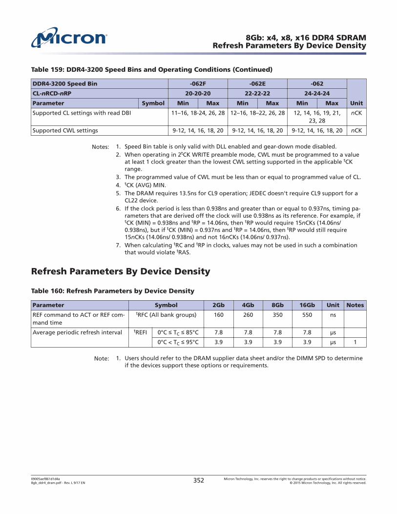
Table 159: DDR4-3200 Speed Bins and Operating Conditions (Continued)
DDR4-3200 Speed Bin -062F -062E -062
Unit
CL-nRCD-nRP 20-20-20 22-22-22 24-24-24
Parameter Symbol Min Max Min Max Min Max
Supported CL settings with read DBI 11–16, 18-24, 26, 28 12–16, 18–22, 26, 28 12, 14, 16, 19, 21,23, 28
nCK
Supported CWL settings 9-12, 14, 16, 18, 20 9-12, 14, 16, 18, 20 9-12, 14, 16, 18, 20 nCK
Notes: 1. Speed Bin table is only valid with DLL enabled and gear-down mode disabled.2. When operating in 2tCK WRITE preamble mode, CWL must be programmed to a value
at least 1 clock greater than the lowest CWL setting supported in the applicable tCKrange.
3. The programmed value of CWL must be less than or equal to programmed value of CL.4. tCK (AVG) MIN.5. The DRAM requires 13.5ns for CL9 operation; JEDEC doesn't require CL9 support for a
CL22 device.6. If the clock period is less than 0.938ns and greater than or equal to 0.937ns, timing pa-
rameters that are derived off the clock will use 0.938ns as its reference. For example, iftCK (MIN) = 0.938ns and tRP = 14.06ns, then tRP would require 15nCKs (14.06ns/0.938ns), but if tCK (MIN) = 0.937ns and tRP = 14.06ns, then tRP would still require15nCKs (14.06ns/ 0.938ns) and not 16nCKs (14.06ns/ 0.937ns).
7. When calculating tRC and tRP in clocks, values may not be used in such a combinationthat would violate tRAS.
Refresh Parameters By Device Density
Table 160: Refresh Parameters by Device Density
Parameter Symbol 2Gb 4Gb 8Gb 16Gb Unit Notes
REF command to ACT or REF com-mand time
tRFC (All bank groups) 160 260 350 550 ns
Average periodic refresh interval tREFI 0°C TC 85°C 7.8 7.8 7.8 7.8 μs
0°C < TC 95°C 3.9 3.9 3.9 3.9 μs 1
Note: 1. Users should refer to the DRAM supplier data sheet and/or the DIMM SPD to determineif the devices support these options or requirements.
8Gb: x4, x8, x16 DDR4 SDRAMRefresh Parameters By Device Density
09005aef861d1d4a8gb_ddr4_dram.pdf - Rev. L 9/17 EN 352 Micron Technology, Inc. reserves the right to change products or specifications without notice.
© 2015 Micron Technology, Inc. All rights reserved.
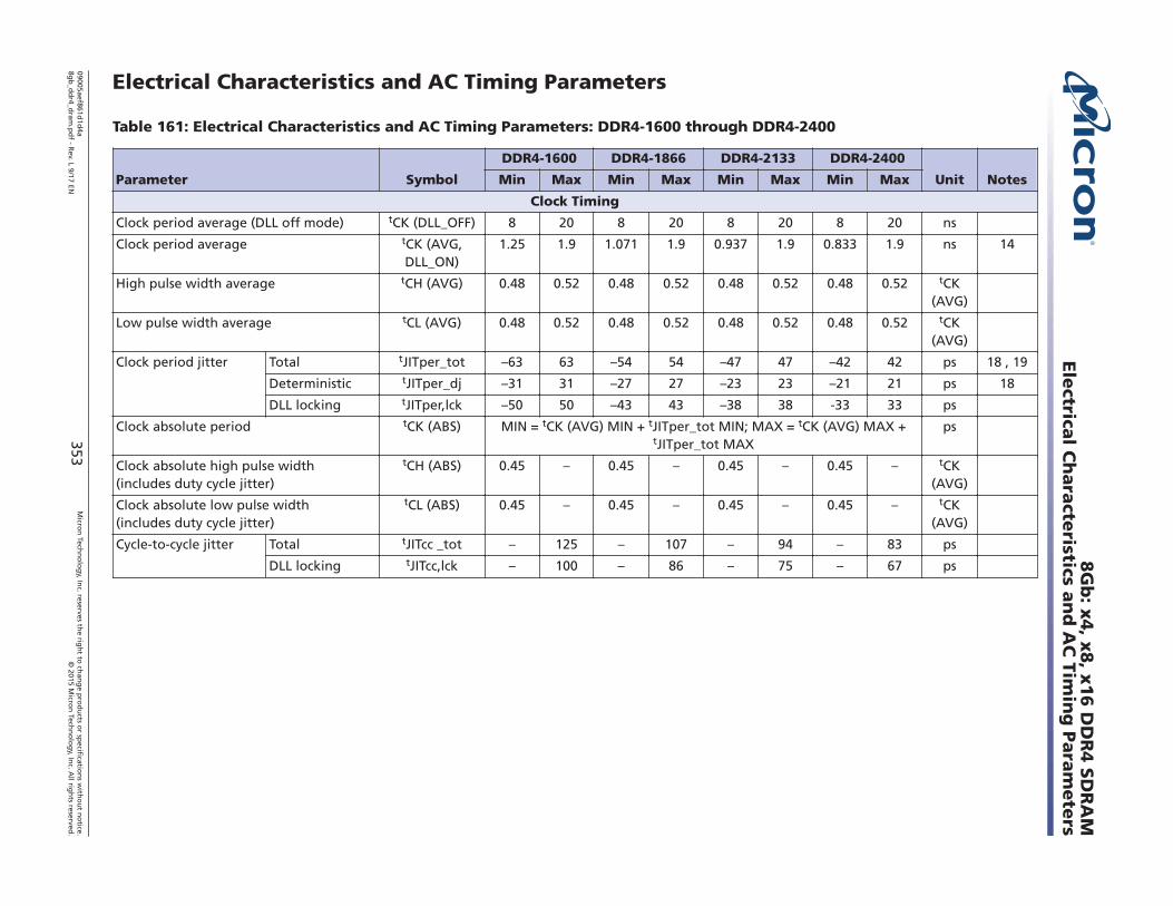
Electrical Characteristics and AC Timing Parameters
Table 161: Electrical Characteristics and AC Timing Parameters: DDR4-1600 through DDR4-2400
Parameter Symbol
DDR4-1600 DDR4-1866 DDR4-2133 DDR4-2400
Unit NotesMin Max Min Max Min Max Min Max
Clock Timing
Clock period average (DLL off mode) tCK (DLL_OFF) 8 20 8 20 8 20 8 20 ns
Clock period average tCK (AVG,DLL_ON)
1.25 1.9 1.071 1.9 0.937 1.9 0.833 1.9 ns 14
High pulse width average tCH (AVG) 0.48 0.52 0.48 0.52 0.48 0.52 0.48 0.52 tCK(AVG)
Low pulse width average tCL (AVG) 0.48 0.52 0.48 0.52 0.48 0.52 0.48 0.52 tCK(AVG)
Clock period jitter Total tJITper_tot –63 63 –54 54 –47 47 –42 42 ps 18 , 19
Deterministic tJITper_dj –31 31 –27 27 –23 23 –21 21 ps 18
DLL locking tJITper,lck –50 50 –43 43 –38 38 -33 33 ps
Clock absolute period tCK (ABS) MIN = tCK (AVG) MIN + tJITper_tot MIN; MAX = tCK (AVG) MAX +tJITper_tot MAX
ps
Clock absolute high pulse width(includes duty cycle jitter)
tCH (ABS) 0.45 – 0.45 – 0.45 – 0.45 – tCK(AVG)
Clock absolute low pulse width(includes duty cycle jitter)
tCL (ABS) 0.45 – 0.45 – 0.45 – 0.45 – tCK(AVG)
Cycle-to-cycle jitter Total tJITcc _tot – 125 – 107 – 94 – 83 ps
DLL locking tJITcc,lck – 100 – 86 – 75 – 67 ps
8G
b: x
4, x
8, x
16 D
DR
4 S
DR
AM
Ele
ctrical C
hara
cteristics a
nd
AC
Timin
g P
ara
mete
rs
09005aef861d1d
4a8g
b_d
dr4_d
ram.p
df - R
ev. L 9/17 EN353
Micro
n Tech
no
log
y, Inc. reserves th
e righ
t to ch
ang
e pro
du
cts or sp
ecification
s with
ou
t no
tice.©
2015 Micro
n Tech
no
log
y, Inc. A
ll righ
ts reserved.
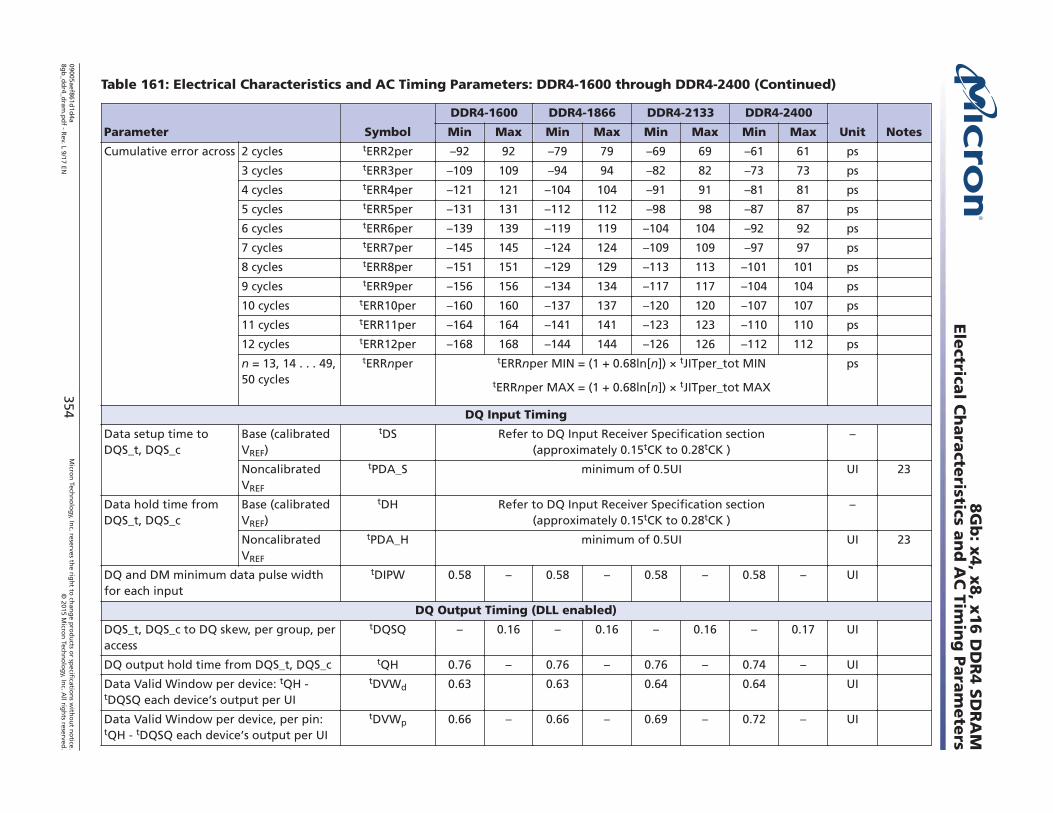
Table 161: Electrical Characteristics and AC Timing Parameters: DDR4-1600 through DDR4-2400 (Continued)
Parameter Symbol
DDR4-1600 DDR4-1866 DDR4-2133 DDR4-2400
Unit NotesMin Max Min Max Min Max Min Max
Cumulative error across 2 cycles tERR2per –92 92 –79 79 –69 69 –61 61 ps
3 cycles tERR3per –109 109 –94 94 –82 82 –73 73 ps
4 cycles tERR4per –121 121 –104 104 –91 91 –81 81 ps
5 cycles tERR5per –131 131 –112 112 –98 98 –87 87 ps
6 cycles tERR6per –139 139 –119 119 –104 104 –92 92 ps
7 cycles tERR7per –145 145 –124 124 –109 109 –97 97 ps
8 cycles tERR8per –151 151 –129 129 –113 113 –101 101 ps
9 cycles tERR9per –156 156 –134 134 –117 117 –104 104 ps
10 cycles tERR10per –160 160 –137 137 –120 120 –107 107 ps
11 cycles tERR11per –164 164 –141 141 –123 123 –110 110 ps
12 cycles tERR12per –168 168 –144 144 –126 126 –112 112 ps
n = 13, 14 . . . 49,50 cycles
tERRnper tERRnper MIN = (1 + 0.68ln[n]) × tJITper_tot MIN
tERRnper MAX = (1 + 0.68ln[n]) × tJITper_tot MAX
ps
DQ Input Timing
Data setup time toDQS_t, DQS_c
Base (calibratedVREF)
tDS Refer to DQ Input Receiver Specification section(approximately 0.15tCK to 0.28tCK )
–
NoncalibratedVREF
tPDA_S minimum of 0.5UI UI 23
Data hold time fromDQS_t, DQS_c
Base (calibratedVREF)
tDH Refer to DQ Input Receiver Specification section(approximately 0.15tCK to 0.28tCK )
–
NoncalibratedVREF
tPDA_H minimum of 0.5UI UI 23
DQ and DM minimum data pulse widthfor each input
tDIPW 0.58 – 0.58 – 0.58 – 0.58 – UI
DQ Output Timing (DLL enabled)
DQS_t, DQS_c to DQ skew, per group, peraccess
tDQSQ – 0.16 – 0.16 – 0.16 – 0.17 UI
DQ output hold time from DQS_t, DQS_c tQH 0.76 – 0.76 – 0.76 – 0.74 – UI
Data Valid Window per device: tQH -tDQSQ each device’s output per UI
tDVWd 0.63 0.63 0.64 0.64 UI
Data Valid Window per device, per pin:tQH - tDQSQ each device’s output per UI
tDVWp 0.66 – 0.66 – 0.69 – 0.72 – UI
8G
b: x
4, x
8, x
16 D
DR
4 S
DR
AM
Ele
ctrical C
hara
cteristics a
nd
AC
Timin
g P
ara
mete
rs
09005aef861d1d
4a8g
b_d
dr4_d
ram.p
df - R
ev. L 9/17 EN354
Micro
n Tech
no
log
y, Inc. reserves th
e righ
t to ch
ang
e pro
du
cts or sp
ecification
s with
ou
t no
tice.©
2015 Micro
n Tech
no
log
y, Inc. A
ll righ
ts reserved.
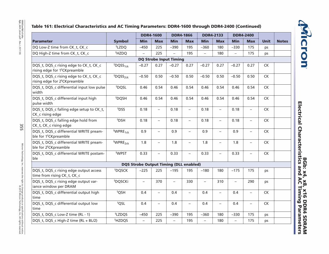
Table 161: Electrical Characteristics and AC Timing Parameters: DDR4-1600 through DDR4-2400 (Continued)
Parameter Symbol
DDR4-1600 DDR4-1866 DDR4-2133 DDR4-2400
Unit NotesMin Max Min Max Min Max Min Max
DQ Low-Z time from CK_t, CK_c tLZDQ –450 225 –390 195 –360 180 –330 175 ps
DQ High-Z time from CK_t, CK_c tHZDQ – 225 – 195 – 180 – 175 ps
DQ Strobe Input Timing
DQS_t, DQS_c rising edge to CK_t, CK_crising edge for 1tCKpreamble
tDQSS1ck –0.27 0.27 –0.27 0.27 –0.27 0.27 –0.27 0.27 CK
DQS_t, DQS_c rising edge to CK_t, CK_crising edge for 2tCKpreamble
tDQSS2ck –0.50 0.50 –0.50 0.50 –0.50 0.50 –0.50 0.50 CK
DQS_t, DQS_c differential input low pulsewidth
tDQSL 0.46 0.54 0.46 0.54 0.46 0.54 0.46 0.54 CK
DQS_t, DQS_c differential input highpulse width
tDQSH 0.46 0.54 0.46 0.54 0.46 0.54 0.46 0.54 CK
DQS_t, DQS_c falling edge setup to CK_t,CK_c rising edge
tDSS 0.18 – 0.18 – 0.18 – 0.18 – CK
DQS_t, DQS_c falling edge hold fromCK_t, CK_c rising edge
tDSH 0.18 – 0.18 – 0.18 – 0.18 – CK
DQS_t, DQS_c differential WRITE pream-ble for 1tCKpreamble
tWPRE1ck 0.9 – 0.9 – 0.9 – 0.9 – CK
DQS_t, DQS_c differential WRITE pream-ble for 2tCKpreamble
tWPRE2ck 1.8 – 1.8 – 1.8 – 1.8 – CK
DQS_t, DQS_c differential WRITE postam-ble
tWPST 0.33 – 0.33 – 0.33 – 0.33 – CK
DQS Strobe Output Timing (DLL enabled)
DQS_t, DQS_c rising edge output accesstime from rising CK_t, CK_c
tDQSCK –225 225 –195 195 –180 180 –175 175 ps
DQS_t, DQS_c rising edge output var-iance window per DRAM
tDQSCKi – 370 – 330 – 310 – 290 ps
DQS_t, DQS_c differential output hightime
tQSH 0.4 – 0.4 – 0.4 – 0.4 – CK
DQS_t, DQS_c differential output lowtime
tQSL 0.4 – 0.4 – 0.4 – 0.4 – CK
DQS_t, DQS_c Low-Z time (RL - 1) tLZDQS –450 225 –390 195 –360 180 –330 175 ps
DQS_t, DQS_c High-Z time (RL + BL/2) tHZDQS – 225 – 195 – 180 – 175 ps
8G
b: x
4, x
8, x
16 D
DR
4 S
DR
AM
Ele
ctrical C
hara
cteristics a
nd
AC
Timin
g P
ara
mete
rs
09005aef861d1d
4a8g
b_d
dr4_d
ram.p
df - R
ev. L 9/17 EN355
Micro
n Tech
no
log
y, Inc. reserves th
e righ
t to ch
ang
e pro
du
cts or sp
ecification
s with
ou
t no
tice.©
2015 Micro
n Tech
no
log
y, Inc. A
ll righ
ts reserved.
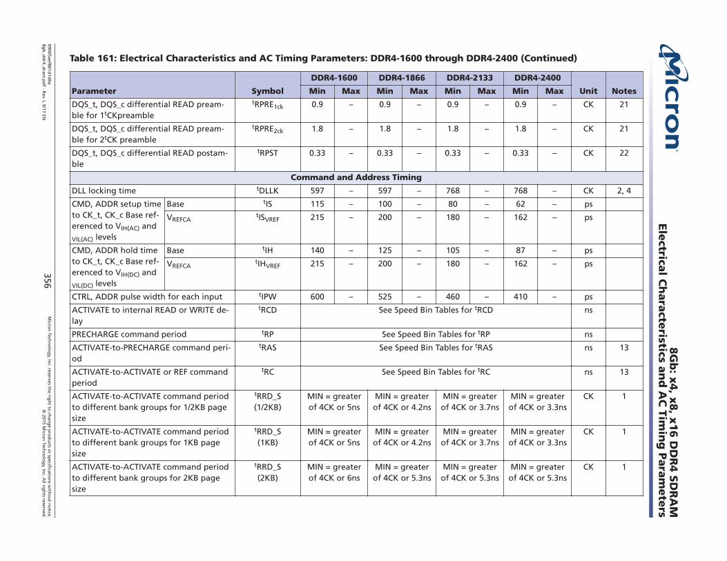
Table 161: Electrical Characteristics and AC Timing Parameters: DDR4-1600 through DDR4-2400 (Continued)
Parameter Symbol
DDR4-1600 DDR4-1866 DDR4-2133 DDR4-2400
Unit NotesMin Max Min Max Min Max Min Max
DQS_t, DQS_c differential READ pream-ble for 1tCKpreamble
tRPRE1ck 0.9 – 0.9 – 0.9 – 0.9 – CK 21
DQS_t, DQS_c differential READ pream-ble for 2tCK preamble
tRPRE2ck 1.8 – 1.8 – 1.8 – 1.8 – CK 21
DQS_t, DQS_c differential READ postam-ble
tRPST 0.33 – 0.33 – 0.33 – 0.33 – CK 22
Command and Address Timing
DLL locking time tDLLK 597 – 597 – 768 – 768 – CK 2, 4
CMD, ADDR setup timeto CK_t, CK_c Base ref-erenced to VIH(AC) and
VIL(AC) levels
Base tIS 115 – 100 – 80 – 62 – ps
VREFCAtISVREF 215 – 200 – 180 – 162 – ps
CMD, ADDR hold timeto CK_t, CK_c Base ref-erenced to VIH(DC) and
VIL(DC) levels
Base tIH 140 – 125 – 105 – 87 – ps
VREFCAtIHVREF 215 – 200 – 180 – 162 – ps
CTRL, ADDR pulse width for each input tIPW 600 – 525 – 460 – 410 – ps
ACTIVATE to internal READ or WRITE de-lay
tRCD See Speed Bin Tables for tRCD ns
PRECHARGE command period tRP See Speed Bin Tables for tRP ns
ACTIVATE-to-PRECHARGE command peri-od
tRAS See Speed Bin Tables for tRAS ns 13
ACTIVATE-to-ACTIVATE or REF commandperiod
tRC See Speed Bin Tables for tRC ns 13
ACTIVATE-to-ACTIVATE command periodto different bank groups for 1/2KB pagesize
tRRD_S(1/2KB)
MIN = greaterof 4CK or 5ns
MIN = greaterof 4CK or 4.2ns
MIN = greaterof 4CK or 3.7ns
MIN = greaterof 4CK or 3.3ns
CK 1
ACTIVATE-to-ACTIVATE command periodto different bank groups for 1KB pagesize
tRRD_S(1KB)
MIN = greaterof 4CK or 5ns
MIN = greaterof 4CK or 4.2ns
MIN = greaterof 4CK or 3.7ns
MIN = greaterof 4CK or 3.3ns
CK 1
ACTIVATE-to-ACTIVATE command periodto different bank groups for 2KB pagesize
tRRD_S(2KB)
MIN = greaterof 4CK or 6ns
MIN = greaterof 4CK or 5.3ns
MIN = greaterof 4CK or 5.3ns
MIN = greaterof 4CK or 5.3ns
CK 1
8G
b: x
4, x
8, x
16 D
DR
4 S
DR
AM
Ele
ctrical C
hara
cteristics a
nd
AC
Timin
g P
ara
mete
rs
09005aef861d1d
4a8g
b_d
dr4_d
ram.p
df - R
ev. L 9/17 EN356
Micro
n Tech
no
log
y, Inc. reserves th
e righ
t to ch
ang
e pro
du
cts or sp
ecification
s with
ou
t no
tice.©
2015 Micro
n Tech
no
log
y, Inc. A
ll righ
ts reserved.
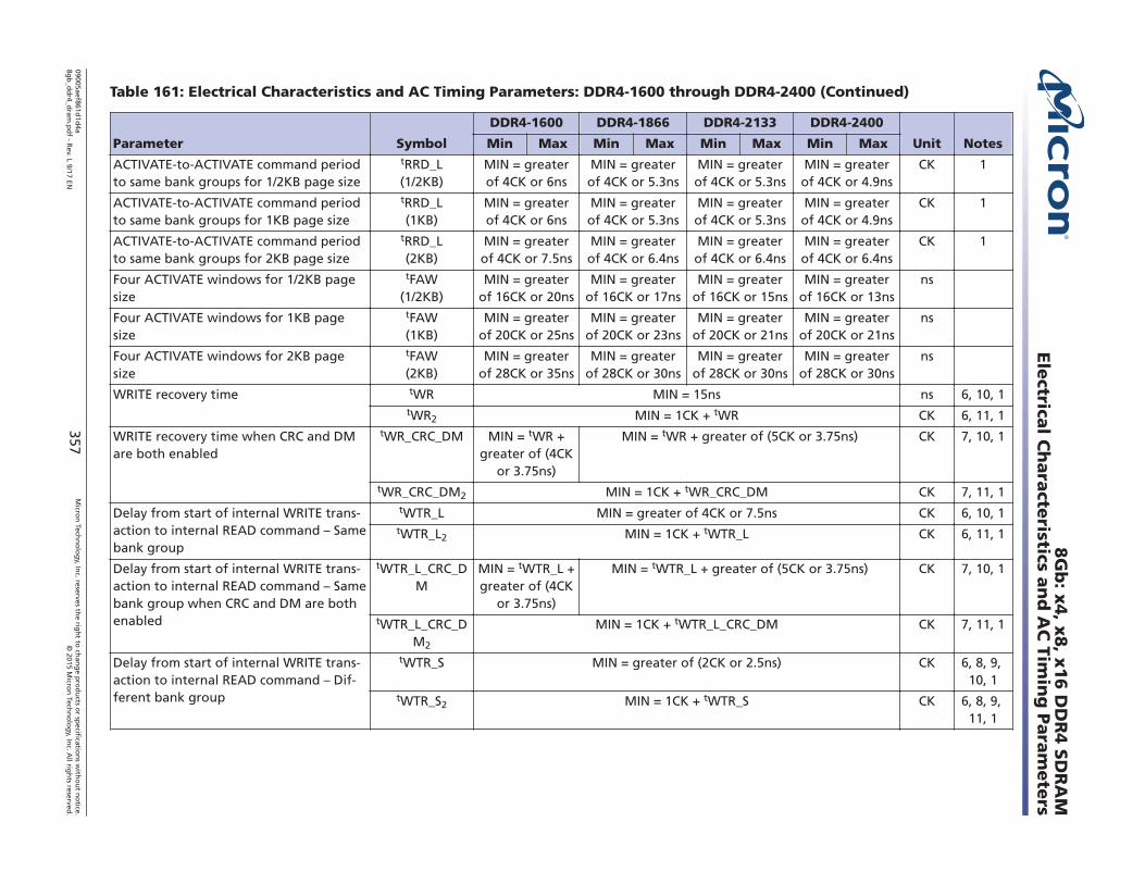
Table 161: Electrical Characteristics and AC Timing Parameters: DDR4-1600 through DDR4-2400 (Continued)
Parameter Symbol
DDR4-1600 DDR4-1866 DDR4-2133 DDR4-2400
Unit NotesMin Max Min Max Min Max Min Max
ACTIVATE-to-ACTIVATE command periodto same bank groups for 1/2KB page size
tRRD_L(1/2KB)
MIN = greaterof 4CK or 6ns
MIN = greaterof 4CK or 5.3ns
MIN = greaterof 4CK or 5.3ns
MIN = greaterof 4CK or 4.9ns
CK 1
ACTIVATE-to-ACTIVATE command periodto same bank groups for 1KB page size
tRRD_L(1KB)
MIN = greaterof 4CK or 6ns
MIN = greaterof 4CK or 5.3ns
MIN = greaterof 4CK or 5.3ns
MIN = greaterof 4CK or 4.9ns
CK 1
ACTIVATE-to-ACTIVATE command periodto same bank groups for 2KB page size
tRRD_L(2KB)
MIN = greaterof 4CK or 7.5ns
MIN = greaterof 4CK or 6.4ns
MIN = greaterof 4CK or 6.4ns
MIN = greaterof 4CK or 6.4ns
CK 1
Four ACTIVATE windows for 1/2KB pagesize
tFAW(1/2KB)
MIN = greaterof 16CK or 20ns
MIN = greaterof 16CK or 17ns
MIN = greaterof 16CK or 15ns
MIN = greaterof 16CK or 13ns
ns
Four ACTIVATE windows for 1KB pagesize
tFAW(1KB)
MIN = greaterof 20CK or 25ns
MIN = greaterof 20CK or 23ns
MIN = greaterof 20CK or 21ns
MIN = greaterof 20CK or 21ns
ns
Four ACTIVATE windows for 2KB pagesize
tFAW(2KB)
MIN = greaterof 28CK or 35ns
MIN = greaterof 28CK or 30ns
MIN = greaterof 28CK or 30ns
MIN = greaterof 28CK or 30ns
ns
WRITE recovery time tWR MIN = 15ns ns 6, 10, 1tWR2 MIN = 1CK + tWR CK 6, 11, 1
WRITE recovery time when CRC and DMare both enabled
tWR_CRC_DM MIN = tWR +greater of (4CK
or 3.75ns)
MIN = tWR + greater of (5CK or 3.75ns) CK 7, 10, 1
tWR_CRC_DM2 MIN = 1CK + tWR_CRC_DM CK 7, 11, 1
Delay from start of internal WRITE trans-action to internal READ command – Samebank group
tWTR_L MIN = greater of 4CK or 7.5ns CK 6, 10, 1tWTR_L2 MIN = 1CK + tWTR_L CK 6, 11, 1
Delay from start of internal WRITE trans-action to internal READ command – Samebank group when CRC and DM are bothenabled
tWTR_L_CRC_DM
MIN = tWTR_L +greater of (4CK
or 3.75ns)
MIN = tWTR_L + greater of (5CK or 3.75ns) CK 7, 10, 1
tWTR_L_CRC_DM2
MIN = 1CK + tWTR_L_CRC_DM CK 7, 11, 1
Delay from start of internal WRITE trans-action to internal READ command – Dif-ferent bank group
tWTR_S MIN = greater of (2CK or 2.5ns) CK 6, 8, 9, 10, 1
tWTR_S2 MIN = 1CK + tWTR_S CK 6, 8, 9, 11, 1
8G
b: x
4, x
8, x
16 D
DR
4 S
DR
AM
Ele
ctrical C
hara
cteristics a
nd
AC
Timin
g P
ara
mete
rs
09005aef861d1d
4a8g
b_d
dr4_d
ram.p
df - R
ev. L 9/17 EN357
Micro
n Tech
no
log
y, Inc. reserves th
e righ
t to ch
ang
e pro
du
cts or sp
ecification
s with
ou
t no
tice.©
2015 Micro
n Tech
no
log
y, Inc. A
ll righ
ts reserved.
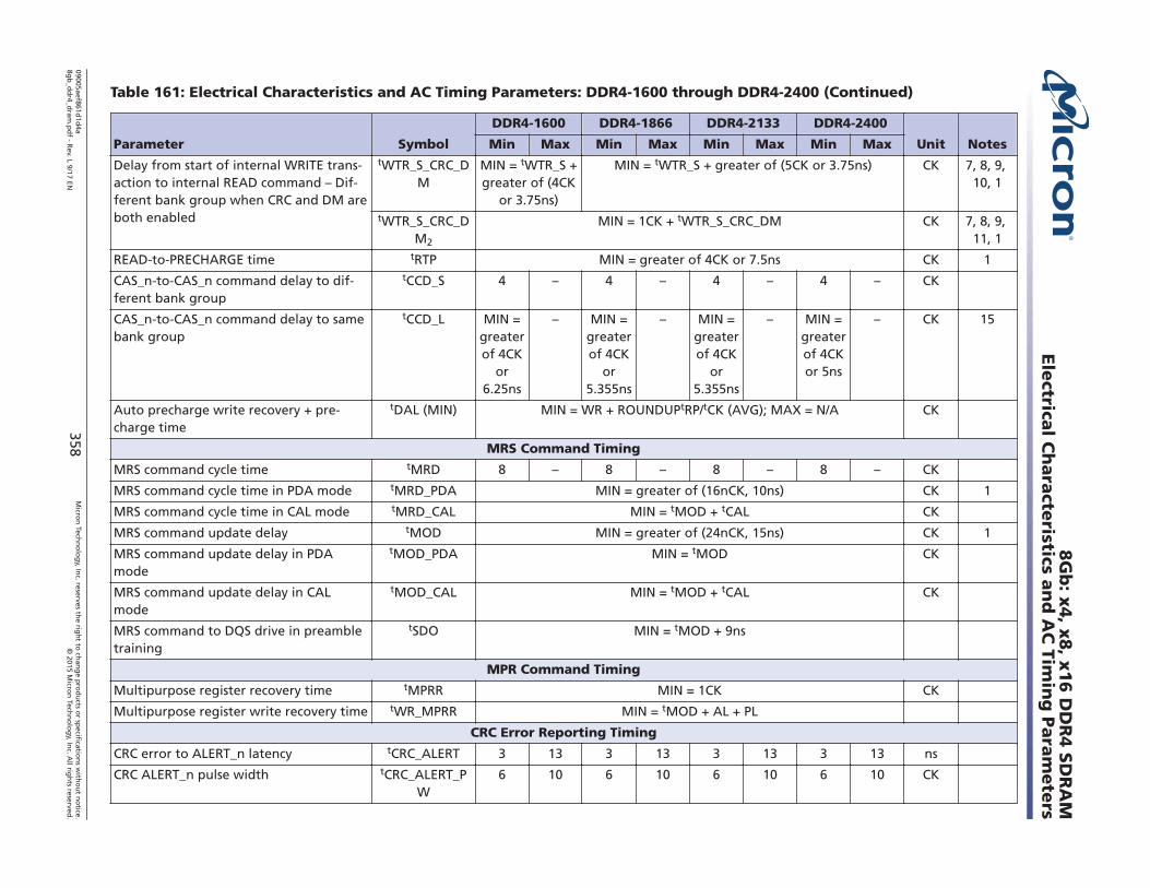
Table 161: Electrical Characteristics and AC Timing Parameters: DDR4-1600 through DDR4-2400 (Continued)
Parameter Symbol
DDR4-1600 DDR4-1866 DDR4-2133 DDR4-2400
Unit NotesMin Max Min Max Min Max Min Max
Delay from start of internal WRITE trans-action to internal READ command – Dif-ferent bank group when CRC and DM areboth enabled
tWTR_S_CRC_DM
MIN = tWTR_S +greater of (4CK
or 3.75ns)
MIN = tWTR_S + greater of (5CK or 3.75ns) CK 7, 8, 9, 10, 1
tWTR_S_CRC_DM2
MIN = 1CK + tWTR_S_CRC_DM CK 7, 8, 9, 11, 1
READ-to-PRECHARGE time tRTP MIN = greater of 4CK or 7.5ns CK 1
CAS_n-to-CAS_n command delay to dif-ferent bank group
tCCD_S 4 – 4 – 4 – 4 – CK
CAS_n-to-CAS_n command delay to samebank group
tCCD_L MIN =greaterof 4CK
or6.25ns
– MIN =greaterof 4CK
or5.355ns
– MIN =greaterof 4CK
or5.355ns
– MIN =greaterof 4CKor 5ns
– CK 15
Auto precharge write recovery + pre-charge time
tDAL (MIN) MIN = WR + ROUNDUPtRP/tCK (AVG); MAX = N/A CK
MRS Command Timing
MRS command cycle time tMRD 8 – 8 – 8 – 8 – CK
MRS command cycle time in PDA mode tMRD_PDA MIN = greater of (16nCK, 10ns) CK 1
MRS command cycle time in CAL mode tMRD_CAL MIN = tMOD + tCAL CK
MRS command update delay tMOD MIN = greater of (24nCK, 15ns) CK 1
MRS command update delay in PDAmode
tMOD_PDA MIN = tMOD CK
MRS command update delay in CALmode
tMOD_CAL MIN = tMOD + tCAL CK
MRS command to DQS drive in preambletraining
tSDO MIN = tMOD + 9ns
MPR Command Timing
Multipurpose register recovery time tMPRR MIN = 1CK CK
Multipurpose register write recovery time tWR_MPRR MIN = tMOD + AL + PL
CRC Error Reporting Timing
CRC error to ALERT_n latency tCRC_ALERT 3 13 3 13 3 13 3 13 ns
CRC ALERT_n pulse width tCRC_ALERT_PW
6 10 6 10 6 10 6 10 CK
8G
b: x
4, x
8, x
16 D
DR
4 S
DR
AM
Ele
ctrical C
hara
cteristics a
nd
AC
Timin
g P
ara
mete
rs
09005aef861d1d
4a8g
b_d
dr4_d
ram.p
df - R
ev. L 9/17 EN358
Micro
n Tech
no
log
y, Inc. reserves th
e righ
t to ch
ang
e pro
du
cts or sp
ecification
s with
ou
t no
tice.©
2015 Micro
n Tech
no
log
y, Inc. A
ll righ
ts reserved.
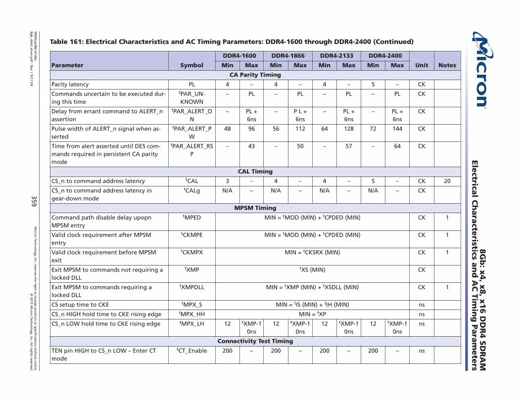
Table 161: Electrical Characteristics and AC Timing Parameters: DDR4-1600 through DDR4-2400 (Continued)
Parameter Symbol
DDR4-1600 DDR4-1866 DDR4-2133 DDR4-2400
Unit NotesMin Max Min Max Min Max Min Max
CA Parity Timing
Parity latency PL 4 – 4 – 4 – 5 – CK
Commands uncertain to be executed dur-ing this time
tPAR_UN-KNOWN
– PL – PL – PL – PL CK
Delay from errant command to ALERT_nassertion
tPAR_ALERT_ON
– PL +6ns
– P L +6ns
– PL +6ns
– PL +6ns
CK
Pulse width of ALERT_n signal when as-serted
tPAR_ALERT_PW
48 96 56 112 64 128 72 144 CK
Time from alert asserted until DES com-mands required in persistent CA paritymode
tPAR_ALERT_RSP
– 43 – 50 – 57 – 64 CK
CAL Timing
CS_n to command address latency tCAL 3 – 4 – 4 – 5 – CK 20
CS_n to command address latency ingear-down mode
tCALg N/A – N/A – N/A – N/A – CK
MPSM Timing
Command path disable delay upopnMPSM entry
tMPED MIN = tMOD (MIN) + tCPDED (MIN) CK 1
Valid clock requirement after MPSMentry
tCKMPE MIN = tMOD (MIN) + tCPDED (MIN) CK 1
Valid clock requirement before MPSMexit
tCKMPX MIN = tCKSRX (MIN) CK 1
Exit MPSM to commands not requiring alocked DLL
tXMP tXS (MIN) CK
Exit MPSM to commands requiring alocked DLL
tXMPDLL MIN = tXMP (MIN) + tXSDLL (MIN) CK 1
CS setup time to CKE tMPX_S MIN = tIS (MIN) + tIH (MIN) ns
CS_n HIGH hold time to CKE rising edge tMPX_HH MIN = tXP ns
CS_n LOW hold time to CKE rising edge tMPX_LH 12 tXMP-10ns
12 tXMP-10ns
12 tXMP-10ns
12 tXMP-10ns
ns
Connectivity Test Timing
TEN pin HIGH to CS_n LOW – Enter CTmode
tCT_Enable 200 – 200 – 200 – 200 – ns
8G
b: x
4, x
8, x
16 D
DR
4 S
DR
AM
Ele
ctrical C
hara
cteristics a
nd
AC
Timin
g P
ara
mete
rs
09005aef861d1d
4a8g
b_d
dr4_d
ram.p
df - R
ev. L 9/17 EN359
Micro
n Tech
no
log
y, Inc. reserves th
e righ
t to ch
ang
e pro
du
cts or sp
ecification
s with
ou
t no
tice.©
2015 Micro
n Tech
no
log
y, Inc. A
ll righ
ts reserved.
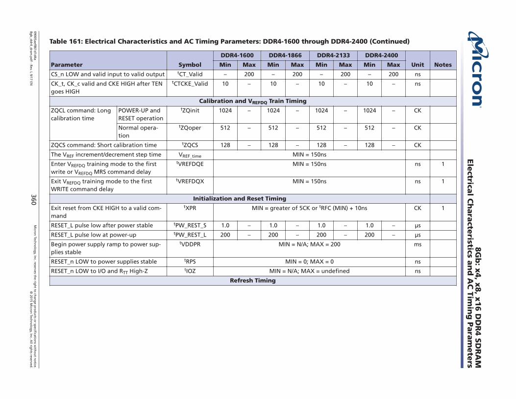
Table 161: Electrical Characteristics and AC Timing Parameters: DDR4-1600 through DDR4-2400 (Continued)
Parameter Symbol
DDR4-1600 DDR4-1866 DDR4-2133 DDR4-2400
Unit NotesMin Max Min Max Min Max Min Max
CS_n LOW and valid input to valid output tCT_Valid – 200 – 200 – 200 – 200 ns
CK_t, CK_c valid and CKE HIGH after TENgoes HIGH
tCTCKE_Valid 10 – 10 – 10 – 10 – ns
Calibration and VREFDQ Train Timing
ZQCL command: Longcalibration time
POWER-UP andRESET operation
tZQinit 1024 – 1024 – 1024 – 1024 – CK
Normal opera-tion
tZQoper 512 – 512 – 512 – 512 – CK
ZQCS command: Short calibration time tZQCS 128 – 128 – 128 – 128 – CK
The VREF increment/decrement step time VREF_time MIN = 150ns
Enter VREFDQ training mode to the firstwrite or VREFDQ MRS command delay
tVREFDQE MIN = 150ns ns 1
Exit VREFDQ training mode to the firstWRITE command delay
tVREFDQX MIN = 150ns ns 1
Initialization and Reset Timing
Exit reset from CKE HIGH to a valid com-mand
tXPR MIN = greater of 5CK or tRFC (MIN) + 10ns CK 1
RESET_L pulse low after power stable tPW_REST_S 1.0 – 1.0 – 1.0 – 1.0 – μs
RESET_L pulse low at power-up tPW_REST_L 200 – 200 – 200 – 200 – μs
Begin power supply ramp to power sup-plies stable
tVDDPR MIN = N/A; MAX = 200 ms
RESET_n LOW to power supplies stable tRPS MIN = 0; MAX = 0 ns
RESET_n LOW to I/O and RTT High-Z tIOZ MIN = N/A; MAX = undefined ns
Refresh Timing
8G
b: x
4, x
8, x
16 D
DR
4 S
DR
AM
Ele
ctrical C
hara
cteristics a
nd
AC
Timin
g P
ara
mete
rs
09005aef861d1d
4a8g
b_d
dr4_d
ram.p
df - R
ev. L 9/17 EN360
Micro
n Tech
no
log
y, Inc. reserves th
e righ
t to ch
ang
e pro
du
cts or sp
ecification
s with
ou
t no
tice.©
2015 Micro
n Tech
no
log
y, Inc. A
ll righ
ts reserved.
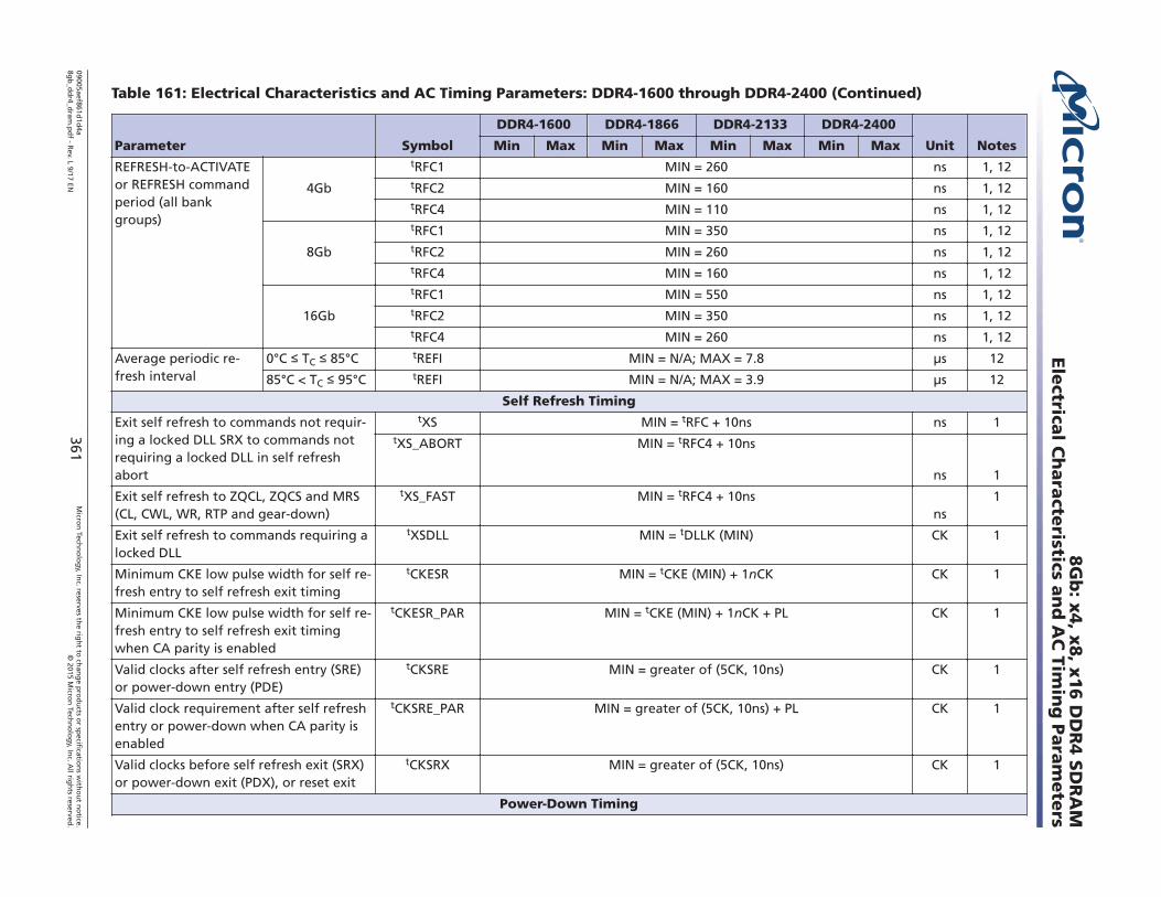
Table 161: Electrical Characteristics and AC Timing Parameters: DDR4-1600 through DDR4-2400 (Continued)
Parameter Symbol
DDR4-1600 DDR4-1866 DDR4-2133 DDR4-2400
Unit NotesMin Max Min Max Min Max Min Max
REFRESH-to-ACTIVATEor REFRESH commandperiod (all bankgroups)
4Gb
tRFC1 MIN = 260 ns 1, 12tRFC2 MIN = 160 ns 1, 12tRFC4 MIN = 110 ns 1, 12
8Gb
tRFC1 MIN = 350 ns 1, 12tRFC2 MIN = 260 ns 1, 12tRFC4 MIN = 160 ns 1, 12
16Gb
tRFC1 MIN = 550 ns 1, 12tRFC2 MIN = 350 ns 1, 12tRFC4 MIN = 260 ns 1, 12
Average periodic re-fresh interval
0°C TC 85°C tREFI MIN = N/A; MAX = 7.8 μs 12
85°C < TC 95°C tREFI MIN = N/A; MAX = 3.9 μs 12
Self Refresh Timing
Exit self refresh to commands not requir-ing a locked DLL SRX to commands notrequiring a locked DLL in self refreshabort
tXS MIN = tRFC + 10ns ns 1tXS_ABORT MIN = tRFC4 + 10ns
ns 1
Exit self refresh to ZQCL, ZQCS and MRS(CL, CWL, WR, RTP and gear-down)
tXS_FAST MIN = tRFC4 + 10nsns
1
Exit self refresh to commands requiring alocked DLL
tXSDLL MIN = tDLLK (MIN) CK 1
Minimum CKE low pulse width for self re-fresh entry to self refresh exit timing
tCKESR MIN = tCKE (MIN) + 1nCK CK 1
Minimum CKE low pulse width for self re-fresh entry to self refresh exit timingwhen CA parity is enabled
tCKESR_PAR MIN = tCKE (MIN) + 1nCK + PL CK 1
Valid clocks after self refresh entry (SRE)or power-down entry (PDE)
tCKSRE MIN = greater of (5CK, 10ns) CK 1
Valid clock requirement after self refreshentry or power-down when CA parity isenabled
tCKSRE_PAR MIN = greater of (5CK, 10ns) + PL CK 1
Valid clocks before self refresh exit (SRX)or power-down exit (PDX), or reset exit
tCKSRX MIN = greater of (5CK, 10ns) CK 1
Power-Down Timing
8G
b: x
4, x
8, x
16 D
DR
4 S
DR
AM
Ele
ctrical C
hara
cteristics a
nd
AC
Timin
g P
ara
mete
rs
09005aef861d1d
4a8g
b_d
dr4_d
ram.p
df - R
ev. L 9/17 EN361
Micro
n Tech
no
log
y, Inc. reserves th
e righ
t to ch
ang
e pro
du
cts or sp
ecification
s with
ou
t no
tice.©
2015 Micro
n Tech
no
log
y, Inc. A
ll righ
ts reserved.
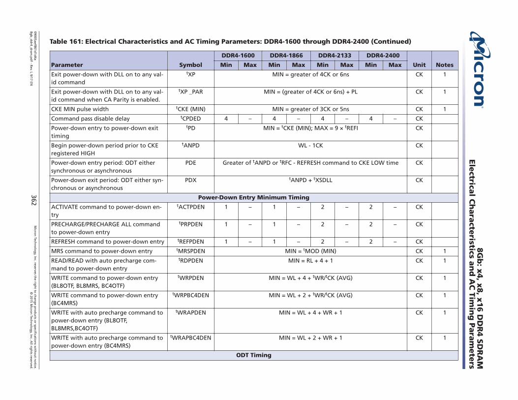
Table 161: Electrical Characteristics and AC Timing Parameters: DDR4-1600 through DDR4-2400 (Continued)
Parameter Symbol
DDR4-1600 DDR4-1866 DDR4-2133 DDR4-2400
Unit NotesMin Max Min Max Min Max Min Max
Exit power-down with DLL on to any val-id command
tXP MIN = greater of 4CK or 6ns CK 1
Exit power-down with DLL on to any val-id command when CA Parity is enabled.
tXP _PAR MIN = (greater of 4CK or 6ns) + PL CK 1
CKE MIN pulse width tCKE (MIN) MIN = greater of 3CK or 5ns CK 1
Command pass disable delay tCPDED 4 – 4 – 4 – 4 – CK
Power-down entry to power-down exittiming
tPD MIN = tCKE (MIN); MAX = 9 × tREFI CK
Begin power-down period prior to CKEregistered HIGH
tANPD WL - 1CK CK
Power-down entry period: ODT eithersynchronous or asynchronous
PDE Greater of tANPD or tRFC - REFRESH command to CKE LOW time CK
Power-down exit period: ODT either syn-chronous or asynchronous
PDX tANPD + tXSDLL CK
Power-Down Entry Minimum Timing
ACTIVATE command to power-down en-try
tACTPDEN 1 – 1 – 2 – 2 – CK
PRECHARGE/PRECHARGE ALL commandto power-down entry
tPRPDEN 1 – 1 – 2 – 2 – CK
REFRESH command to power-down entry tREFPDEN 1 – 1 – 2 – 2 – CK
MRS command to power-down entry tMRSPDEN MIN = tMOD (MIN) CK 1
READ/READ with auto precharge com-mand to power-down entry
tRDPDEN MIN = RL + 4 + 1 CK 1
WRITE command to power-down entry(BL8OTF, BL8MRS, BC4OTF)
tWRPDEN MIN = WL + 4 + tWR/tCK (AVG) CK 1
WRITE command to power-down entry(BC4MRS)
tWRPBC4DEN MIN = WL + 2 + tWR/tCK (AVG) CK 1
WRITE with auto precharge command topower-down entry (BL8OTF,BL8MRS,BC4OTF)
tWRAPDEN MIN = WL + 4 + WR + 1 CK 1
WRITE with auto precharge command topower-down entry (BC4MRS)
tWRAPBC4DEN MIN = WL + 2 + WR + 1 CK 1
ODT Timing
8G
b: x
4, x
8, x
16 D
DR
4 S
DR
AM
Ele
ctrical C
hara
cteristics a
nd
AC
Timin
g P
ara
mete
rs
09005aef861d1d
4a8g
b_d
dr4_d
ram.p
df - R
ev. L 9/17 EN362
Micro
n Tech
no
log
y, Inc. reserves th
e righ
t to ch
ang
e pro
du
cts or sp
ecification
s with
ou
t no
tice.©
2015 Micro
n Tech
no
log
y, Inc. A
ll righ
ts reserved.
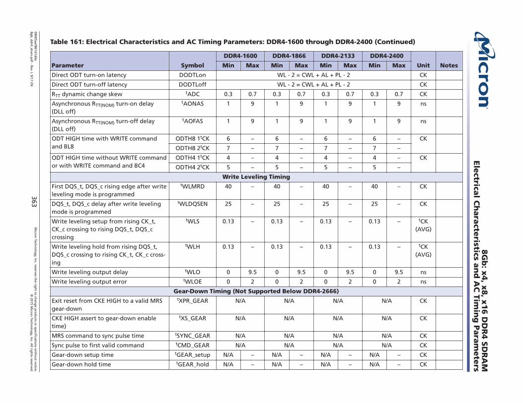
Table 161: Electrical Characteristics and AC Timing Parameters: DDR4-1600 through DDR4-2400 (Continued)
Parameter Symbol
DDR4-1600 DDR4-1866 DDR4-2133 DDR4-2400
Unit NotesMin Max Min Max Min Max Min Max
Direct ODT turn-on latency DODTLon WL - 2 = CWL + AL + PL - 2 CK
Direct ODT turn-off latency DODTLoff WL - 2 = CWL + AL + PL - 2 CK
RTT dynamic change skew tADC 0.3 0.7 0.3 0.7 0.3 0.7 0.3 0.7 CK
Asynchronous RTT(NOM) turn-on delay(DLL off)
tAONAS 1 9 1 9 1 9 1 9 ns
Asynchronous RTT(NOM) turn-off delay(DLL off)
tAOFAS 1 9 1 9 1 9 1 9 ns
ODT HIGH time with WRITE commandand BL8
ODTH8 1tCK 6 – 6 – 6 – 6 – CK
ODTH8 2tCK 7 – 7 – 7 – 7 –
ODT HIGH time without WRITE commandor with WRITE command and BC4
ODTH4 1tCK 4 – 4 – 4 – 4 – CK
ODTH4 2tCK 5 – 5 – 5 – 5 –
Write Leveling Timing
First DQS_t, DQS_c rising edge after writeleveling mode is programmed
tWLMRD 40 – 40 – 40 – 40 – CK
DQS_t, DQS_c delay after write levelingmode is programmed
tWLDQSEN 25 – 25 – 25 – 25 – CK
Write leveling setup from rising CK_t,CK_c crossing to rising DQS_t, DQS_ccrossing
tWLS 0.13 – 0.13 – 0.13 – 0.13 – tCK(AVG)
Write leveling hold from rising DQS_t,DQS_c crossing to rising CK_t, CK_c cross-ing
tWLH 0.13 – 0.13 – 0.13 – 0.13 – tCK(AVG)
Write leveling output delay tWLO 0 9.5 0 9.5 0 9.5 0 9.5 ns
Write leveling output error tWLOE 0 2 0 2 0 2 0 2 ns
Gear-Down Timing (Not Supported Below DDR4-2666)
Exit reset from CKE HIGH to a valid MRSgear-down
tXPR_GEAR N/A N/A N/A N/A CK
CKE HIGH assert to gear-down enabletime)
tXS_GEAR N/A N/A N/A N/A CK
MRS command to sync pulse time tSYNC_GEAR N/A N/A N/A N/A CK
Sync pulse to first valid command tCMD_GEAR N/A N/A N/A N/A CK
Gear-down setup time tGEAR_setup N/A – N/A – N/A – N/A – CK
Gear-down hold time tGEAR_hold N/A – N/A – N/A – N/A – CK
8G
b: x
4, x
8, x
16 D
DR
4 S
DR
AM
Ele
ctrical C
hara
cteristics a
nd
AC
Timin
g P
ara
mete
rs
09005aef861d1d
4a8g
b_d
dr4_d
ram.p
df - R
ev. L 9/17 EN363
Micro
n Tech
no
log
y, Inc. reserves th
e righ
t to ch
ang
e pro
du
cts or sp
ecification
s with
ou
t no
tice.©
2015 Micro
n Tech
no
log
y, Inc. A
ll righ
ts reserved.
Notes: 1. Maximum limit not applicable.2. tCCD_L and tDLLK should be programmed according to the value defined per operating
frequency.3. Although unlimited row accesses to the same row is allowed within the refresh period,
excessive row accesses to the same row over a long term can result in degraded opera-tion.
4. Data rate is greater than or equal to 1066 Mb/s.5. RFUcorr6. WRITE-to-READ when CRC and DM are both not enabled.7. WRITE-to-READ delay when CRC and DM are both enabled.8. The start of internal write transactions is defined as follows:
• For BL8 (fixed by MRS and on-the-fly): rising clock edge four clock cycles after WL• For BC4 (on-the-fly): rising clock edge four clock cycles after WL• For BC4 (fixed by MRS): rising clock edge two clock cycles after WL
9. For these parameters, the device supports tnPARAM [nCK] = RU{tPARAM [ns]/tCK (AVG)[ns]}, in clock cycles, assuming all input clock jitter specifications are satisfied.
10. When operating in 1tCK WRITE preamble mode.11. When operating in 2tCK WRITE preamble mode.12. When CA parity mode is selected and the DLLoff mode is used, each REF command re-
quires an additional "PL" added to tRFC refresh time.13. DRAM devices should be evenly addressed when being accessed. Disproportionate ac-
cesses to a particular row address may result in reduction of the product lifetime and/orreduction in data retention ability.
14. Applicable from tCK (AVG) MIN to tCK (AVG) MAX as stated in the Speed Bin tables.15. JEDEC specifies a minimum of five clocks.16. The maximum read postamble is bound by tDQSCK (MIN) plus tQSH (MIN) on the left
side and tHZ(DQS) MAX on the right side.17. The reference level of DQ output signal is specified with a midpoint as a widest part of
output signal eye, which should be approximately 0.7 × VDDQ as a center level of thestatic single-ended output peak-to-peak swing with a driver impedance of 34 ohms andan effective test load of 50 ohms to VTT = VDDQ.
18. JEDEC hasn't agreed upon the definition of the deterministic jitter; the user should fo-cus on meeting the total limit.
19. Spread spectrum is not included in the jitter specification values. However, the inputclock can accommodate spread-spectrum at a sweep rate in the range of 20–60 kHz withan additional 1% of tCK (AVG) as a long-term jitter component; however, the spreadspectrum may not use a clock rate below tCK (AVG) MIN.
20. The actual tCAL minimum is the larger of 3 clocks or 3.748ns/tCK; the table lists the ap-plicable clocks required at targeted speed bin.
21. The maximum READ preamble is bounded by tLZ(DQS) MIN on the left side and tDQSCK(MAX) on the right side. See figure in the Clock to Data Strobe Relationship section.Boundary of DQS Low-Z occur one cycle earlier in 2tCK toggle mode, which is illustratedin the READ Preamble section.
22. DQ falling signal middle-point of transferring from HIGH to LOW to first rising edge ofDQS differential signal cross-point.
23. The tPDA_S/tPDA_H parameters may use the tDS/tDH limits, respectively, if the signal isLOW the entire BL8.
8Gb: x4, x8, x16 DDR4 SDRAMElectrical Characteristics and AC Timing Parameters
09005aef861d1d4a8gb_ddr4_dram.pdf - Rev. L 9/17 EN 364 Micron Technology, Inc. reserves the right to change products or specifications without notice.
© 2015 Micron Technology, Inc. All rights reserved.
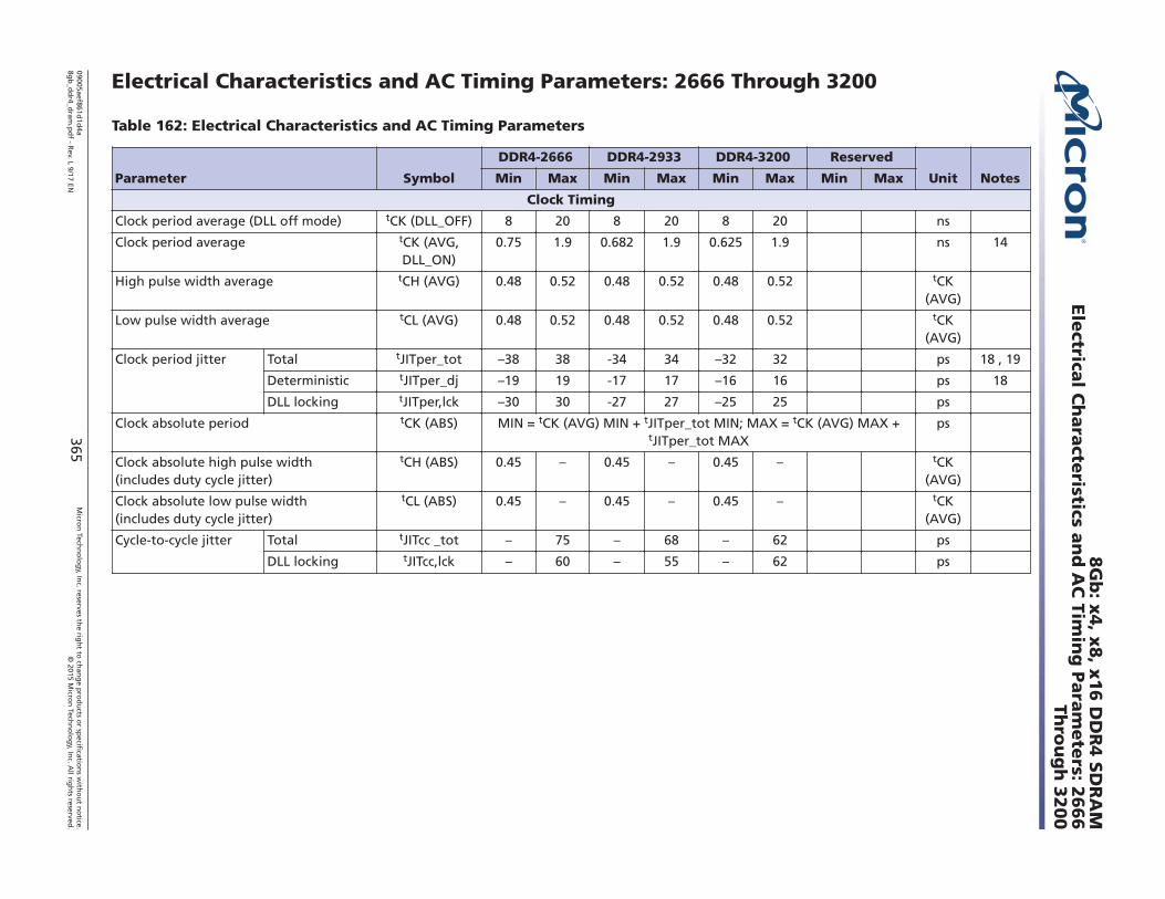
Electrical Characteristics and AC Timing Parameters: 2666 Through 3200
Table 162: Electrical Characteristics and AC Timing Parameters
Parameter Symbol
DDR4-2666 DDR4-2933 DDR4-3200 Reserved
Unit NotesMin Max Min Max Min Max Min Max
Clock Timing
Clock period average (DLL off mode) tCK (DLL_OFF) 8 20 8 20 8 20 ns
Clock period average tCK (AVG,DLL_ON)
0.75 1.9 0.682 1.9 0.625 1.9 ns 14
High pulse width average tCH (AVG) 0.48 0.52 0.48 0.52 0.48 0.52 tCK(AVG)
Low pulse width average tCL (AVG) 0.48 0.52 0.48 0.52 0.48 0.52 tCK(AVG)
Clock period jitter Total tJITper_tot –38 38 -34 34 –32 32 ps 18 , 19
Deterministic tJITper_dj –19 19 -17 17 –16 16 ps 18
DLL locking tJITper,lck –30 30 -27 27 –25 25 ps
Clock absolute period tCK (ABS) MIN = tCK (AVG) MIN + tJITper_tot MIN; MAX = tCK (AVG) MAX +tJITper_tot MAX
ps
Clock absolute high pulse width(includes duty cycle jitter)
tCH (ABS) 0.45 – 0.45 – 0.45 – tCK(AVG)
Clock absolute low pulse width(includes duty cycle jitter)
tCL (ABS) 0.45 – 0.45 – 0.45 – tCK(AVG)
Cycle-to-cycle jitter Total tJITcc _tot – 75 – 68 – 62 ps
DLL locking tJITcc,lck – 60 – 55 – 62 ps
8G
b: x
4, x
8, x
16 D
DR
4 S
DR
AM
Ele
ctrical C
hara
cteristics a
nd
AC
Timin
g P
ara
mete
rs: 2666
Thro
ug
h 3
200
09005aef861d1d
4a8g
b_d
dr4_d
ram.p
df - R
ev. L 9/17 EN365
Micro
n Tech
no
log
y, Inc. reserves th
e righ
t to ch
ang
e pro
du
cts or sp
ecification
s with
ou
t no
tice.©
2015 Micro
n Tech
no
log
y, Inc. A
ll righ
ts reserved.
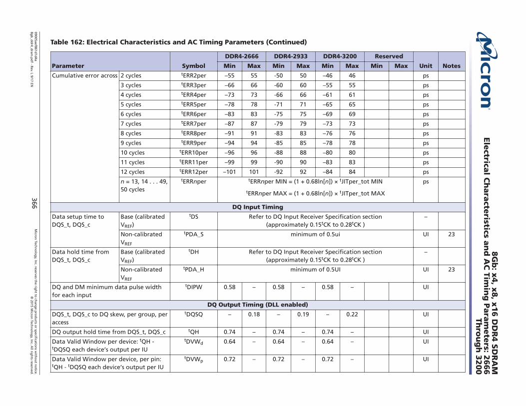
Table 162: Electrical Characteristics and AC Timing Parameters (Continued)
Parameter Symbol
DDR4-2666 DDR4-2933 DDR4-3200 Reserved
Unit NotesMin Max Min Max Min Max Min Max
Cumulative error across 2 cycles tERR2per –55 55 -50 50 –46 46 ps
3 cycles tERR3per –66 66 -60 60 –55 55 ps
4 cycles tERR4per –73 73 -66 66 –61 61 ps
5 cycles tERR5per –78 78 -71 71 –65 65 ps
6 cycles tERR6per –83 83 -75 75 –69 69 ps
7 cycles tERR7per –87 87 -79 79 –73 73 ps
8 cycles tERR8per –91 91 -83 83 –76 76 ps
9 cycles tERR9per –94 94 -85 85 –78 78 ps
10 cycles tERR10per –96 96 -88 88 –80 80 ps
11 cycles tERR11per –99 99 -90 90 –83 83 ps
12 cycles tERR12per –101 101 -92 92 –84 84 ps
n = 13, 14 . . . 49,50 cycles
tERRnper tERRnper MIN = (1 + 0.68ln[n]) × tJITper_tot MIN
tERRnper MAX = (1 + 0.68ln[n]) × tJITper_tot MAX
ps
DQ Input Timing
Data setup time toDQS_t, DQS_c
Base (calibratedVREF)
tDS Refer to DQ Input Receiver Specification section(approximately 0.15tCK to 0.28tCK )
–
Non-calibratedVREF
tPDA_S minimum of 0.5ui UI 23
Data hold time fromDQS_t, DQS_c
Base (calibratedVREF)
tDH Refer to DQ Input Receiver Specification section(approximately 0.15tCK to 0.28tCK )
–
Non-calibratedVREF
tPDA_H minimum of 0.5UI UI 23
DQ and DM minimum data pulse widthfor each input
tDIPW 0.58 – 0.58 – 0.58 – UI
DQ Output Timing (DLL enabled)
DQS_t, DQS_c to DQ skew, per group, peraccess
tDQSQ – 0.18 – 0.19 – 0.22 UI
DQ output hold time from DQS_t, DQS_c tQH 0.74 – 0.74 – 0.74 – UI
Data Valid Window per device: tQH -tDQSQ each device’s output per IU
tDVWd 0.64 – 0.64 – 0.64 – UI
Data Valid Window per device, per pin:tQH - tDQSQ each device’s output per IU
tDVWp 0.72 – 0.72 – 0.72 – UI
8G
b: x
4, x
8, x
16 D
DR
4 S
DR
AM
Ele
ctrical C
hara
cteristics a
nd
AC
Timin
g P
ara
mete
rs: 2666
Thro
ug
h 3
200
09005aef861d1d
4a8g
b_d
dr4_d
ram.p
df - R
ev. L 9/17 EN366
Micro
n Tech
no
log
y, Inc. reserves th
e righ
t to ch
ang
e pro
du
cts or sp
ecification
s with
ou
t no
tice.©
2015 Micro
n Tech
no
log
y, Inc. A
ll righ
ts reserved.
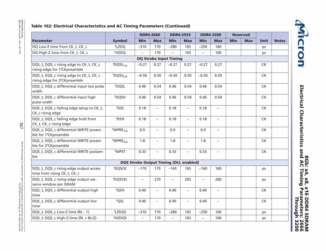
Table 162: Electrical Characteristics and AC Timing Parameters (Continued)
Parameter Symbol
DDR4-2666 DDR4-2933 DDR4-3200 Reserved
Unit NotesMin Max Min Max Min Max Min Max
DQ Low-Z time from CK_t, CK_c tLZDQ –310 170 –280 165 –250 160 ps
DQ High-Z time from CK_t, CK_c tHZDQ – 170 – 165 – 160 ps
DQ Strobe Input Timing
DQS_t, DQS_c rising edge to CK_t, CK_crising edge for 1tCKpreamble
tDQSS1ck –0.27 0.27 –0.27 0.27 –0.27 0.27 CK
DQS_t, DQS_c rising edge to CK_t, CK_crising edge for 2tCKpreamble
tDQSS2ck –0.50 0.50 –0.50 0.50 –0.50 0.50 CK
DQS_t, DQS_c differential input low pulsewidth
tDQSL 0.46 0.54 0.46 0.54 0.46 0.54 CK
DQS_t, DQS_c differential input highpulse width
tDQSH 0.46 0.54 0.46 0.54 0.46 0.54 CK
DQS_t, DQS_c falling edge setup to CK_t,CK_c rising edge
tDSS 0.18 – 0.18 – 0.18 – CK
DQS_t, DQS_c falling edge hold fromCK_t, CK_c rising edge
tDSH 0.18 – 0.18 – 0.18 – CK
DQS_t, DQS_c differential WRITE pream-ble for 1tCKpreamble
tWPRE1ck 0.9 – 0.9 – 0.9 – CK
DQS_t, DQS_c differential WRITE pream-ble for 2tCKpreamble
tWPRE2ck 1.8 – 1.8 – 1.8 – CK
DQS_t, DQS_c differential WRITE postam-ble
tWPST 0.33 – 0.33 – 0.33 – CK
DQS Strobe Output Timing (DLL enabled)
DQS_t, DQS_c rising edge output accesstime from rising CK_t, CK_c
tDQSCK –170 170 –165 165 –160 160 ps
DQS_t, DQS_c rising edge output var-iance window per DRAM
tDQSCKi – 270 – 265 – 260 ps
DQS_t, DQS_c differential output hightime
tQSH 0.40 – 0.40 – 0.40 – CK
DQS_t, DQS_c differential output lowtime
tQSL 0.40 – 0.40 – 0.40 – CK
DQS_t, DQS_c Low-Z time (RL - 1) tLZDQS –310 170 –280 165 –250 160 ps
DQS_t, DQS_c High-Z time (RL + BL/2) tHZDQS – 170 – 165 – 160 ps
8G
b: x
4, x
8, x
16 D
DR
4 S
DR
AM
Ele
ctrical C
hara
cteristics a
nd
AC
Timin
g P
ara
mete
rs: 2666
Thro
ug
h 3
200
09005aef861d1d
4a8g
b_d
dr4_d
ram.p
df - R
ev. L 9/17 EN367
Micro
n Tech
no
log
y, Inc. reserves th
e righ
t to ch
ang
e pro
du
cts or sp
ecification
s with
ou
t no
tice.©
2015 Micro
n Tech
no
log
y, Inc. A
ll righ
ts reserved.
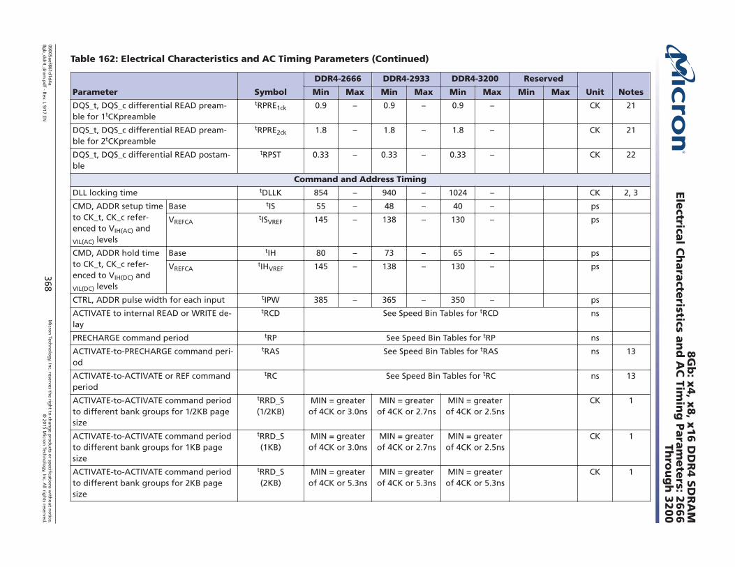
Table 162: Electrical Characteristics and AC Timing Parameters (Continued)
Parameter Symbol
DDR4-2666 DDR4-2933 DDR4-3200 Reserved
Unit NotesMin Max Min Max Min Max Min Max
DQS_t, DQS_c differential READ pream-ble for 1tCKpreamble
tRPRE1ck 0.9 – 0.9 – 0.9 – CK 21
DQS_t, DQS_c differential READ pream-ble for 2tCKpreamble
tRPRE2ck 1.8 – 1.8 – 1.8 – CK 21
DQS_t, DQS_c differential READ postam-ble
tRPST 0.33 – 0.33 – 0.33 – CK 22
Command and Address Timing
DLL locking time tDLLK 854 – 940 – 1024 – CK 2, 3
CMD, ADDR setup timeto CK_t, CK_c refer-enced to VIH(AC) and
VIL(AC) levels
Base tIS 55 – 48 – 40 – ps
VREFCAtISVREF 145 – 138 – 130 – ps
CMD, ADDR hold timeto CK_t, CK_c refer-enced to VIH(DC) and
VIL(DC) levels
Base tIH 80 – 73 – 65 – ps
VREFCAtIHVREF 145 – 138 – 130 – ps
CTRL, ADDR pulse width for each input tIPW 385 – 365 – 350 – ps
ACTIVATE to internal READ or WRITE de-lay
tRCD See Speed Bin Tables for tRCD ns
PRECHARGE command period tRP See Speed Bin Tables for tRP ns
ACTIVATE-to-PRECHARGE command peri-od
tRAS See Speed Bin Tables for tRAS ns 13
ACTIVATE-to-ACTIVATE or REF commandperiod
tRC See Speed Bin Tables for tRC ns 13
ACTIVATE-to-ACTIVATE command periodto different bank groups for 1/2KB pagesize
tRRD_S(1/2KB)
MIN = greaterof 4CK or 3.0ns
MIN = greaterof 4CK or 2.7ns
MIN = greaterof 4CK or 2.5ns
CK 1
ACTIVATE-to-ACTIVATE command periodto different bank groups for 1KB pagesize
tRRD_S(1KB)
MIN = greaterof 4CK or 3.0ns
MIN = greaterof 4CK or 2.7ns
MIN = greaterof 4CK or 2.5ns
CK 1
ACTIVATE-to-ACTIVATE command periodto different bank groups for 2KB pagesize
tRRD_S(2KB)
MIN = greaterof 4CK or 5.3ns
MIN = greaterof 4CK or 5.3ns
MIN = greaterof 4CK or 5.3ns
CK 1
8G
b: x
4, x
8, x
16 D
DR
4 S
DR
AM
Ele
ctrical C
hara
cteristics a
nd
AC
Timin
g P
ara
mete
rs: 2666
Thro
ug
h 3
200
09005aef861d1d
4a8g
b_d
dr4_d
ram.p
df - R
ev. L 9/17 EN368
Micro
n Tech
no
log
y, Inc. reserves th
e righ
t to ch
ang
e pro
du
cts or sp
ecification
s with
ou
t no
tice.©
2015 Micro
n Tech
no
log
y, Inc. A
ll righ
ts reserved.
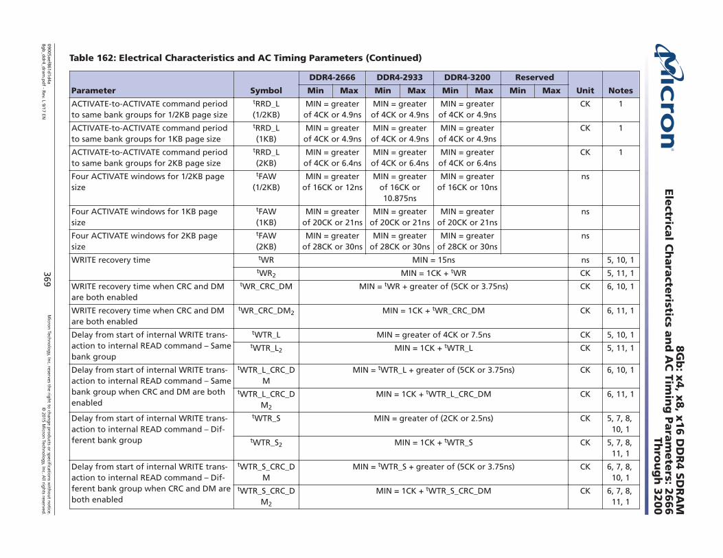
Table 162: Electrical Characteristics and AC Timing Parameters (Continued)
Parameter Symbol
DDR4-2666 DDR4-2933 DDR4-3200 Reserved
Unit NotesMin Max Min Max Min Max Min Max
ACTIVATE-to-ACTIVATE command periodto same bank groups for 1/2KB page size
tRRD_L(1/2KB)
MIN = greaterof 4CK or 4.9ns
MIN = greaterof 4CK or 4.9ns
MIN = greaterof 4CK or 4.9ns
CK 1
ACTIVATE-to-ACTIVATE command periodto same bank groups for 1KB page size
tRRD_L(1KB)
MIN = greaterof 4CK or 4.9ns
MIN = greaterof 4CK or 4.9ns
MIN = greaterof 4CK or 4.9ns
CK 1
ACTIVATE-to-ACTIVATE command periodto same bank groups for 2KB page size
tRRD_L(2KB)
MIN = greaterof 4CK or 6.4ns
MIN = greaterof 4CK or 6.4ns
MIN = greaterof 4CK or 6.4ns
CK 1
Four ACTIVATE windows for 1/2KB pagesize
tFAW(1/2KB)
MIN = greaterof 16CK or 12ns
MIN = greaterof 16CK or10.875ns
MIN = greaterof 16CK or 10ns
ns
Four ACTIVATE windows for 1KB pagesize
tFAW(1KB)
MIN = greaterof 20CK or 21ns
MIN = greaterof 20CK or 21ns
MIN = greaterof 20CK or 21ns
ns
Four ACTIVATE windows for 2KB pagesize
tFAW(2KB)
MIN = greaterof 28CK or 30ns
MIN = greaterof 28CK or 30ns
MIN = greaterof 28CK or 30ns
ns
WRITE recovery time tWR MIN = 15ns ns 5, 10, 1tWR2 MIN = 1CK + tWR CK 5, 11, 1
WRITE recovery time when CRC and DMare both enabled
tWR_CRC_DM MIN = tWR + greater of (5CK or 3.75ns) CK 6, 10, 1
WRITE recovery time when CRC and DMare both enabled
tWR_CRC_DM2 MIN = 1CK + tWR_CRC_DM CK 6, 11, 1
Delay from start of internal WRITE trans-action to internal READ command – Samebank group
tWTR_L MIN = greater of 4CK or 7.5ns CK 5, 10, 1tWTR_L2 MIN = 1CK + tWTR_L CK 5, 11, 1
Delay from start of internal WRITE trans-action to internal READ command – Samebank group when CRC and DM are bothenabled
tWTR_L_CRC_DM
MIN = tWTR_L + greater of (5CK or 3.75ns) CK 6, 10, 1
tWTR_L_CRC_DM2
MIN = 1CK + tWTR_L_CRC_DM CK 6, 11, 1
Delay from start of internal WRITE trans-action to internal READ command – Dif-ferent bank group
tWTR_S MIN = greater of (2CK or 2.5ns) CK 5, 7, 8, 10, 1
tWTR_S2 MIN = 1CK + tWTR_S CK 5, 7, 8, 11, 1
Delay from start of internal WRITE trans-action to internal READ command – Dif-ferent bank group when CRC and DM areboth enabled
tWTR_S_CRC_DM
MIN = tWTR_S + greater of (5CK or 3.75ns) CK 6, 7, 8, 10, 1
tWTR_S_CRC_DM2
MIN = 1CK + tWTR_S_CRC_DM CK 6, 7, 8, 11, 1
8G
b: x
4, x
8, x
16 D
DR
4 S
DR
AM
Ele
ctrical C
hara
cteristics a
nd
AC
Timin
g P
ara
mete
rs: 2666
Thro
ug
h 3
200
09005aef861d1d
4a8g
b_d
dr4_d
ram.p
df - R
ev. L 9/17 EN369
Micro
n Tech
no
log
y, Inc. reserves th
e righ
t to ch
ang
e pro
du
cts or sp
ecification
s with
ou
t no
tice.©
2015 Micro
n Tech
no
log
y, Inc. A
ll righ
ts reserved.
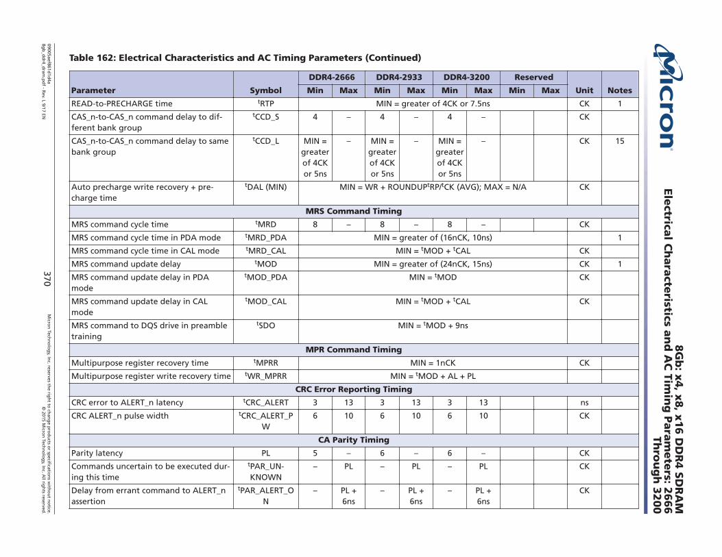
Table 162: Electrical Characteristics and AC Timing Parameters (Continued)
Parameter Symbol
DDR4-2666 DDR4-2933 DDR4-3200 Reserved
Unit NotesMin Max Min Max Min Max Min Max
READ-to-PRECHARGE time tRTP MIN = greater of 4CK or 7.5ns CK 1
CAS_n-to-CAS_n command delay to dif-ferent bank group
tCCD_S 4 – 4 – 4 – CK
CAS_n-to-CAS_n command delay to samebank group
tCCD_L MIN =greaterof 4CKor 5ns
– MIN =greaterof 4CKor 5ns
– MIN =greaterof 4CKor 5ns
– CK 15
Auto precharge write recovery + pre-charge time
tDAL (MIN) MIN = WR + ROUNDUPtRP/tCK (AVG); MAX = N/A CK
MRS Command Timing
MRS command cycle time tMRD 8 – 8 – 8 – CK
MRS command cycle time in PDA mode tMRD_PDA MIN = greater of (16nCK, 10ns) 1
MRS command cycle time in CAL mode tMRD_CAL MIN = tMOD + tCAL CK
MRS command update delay tMOD MIN = greater of (24nCK, 15ns) CK 1
MRS command update delay in PDAmode
tMOD_PDA MIN = tMOD CK
MRS command update delay in CALmode
tMOD_CAL MIN = tMOD + tCAL CK
MRS command to DQS drive in preambletraining
tSDO MIN = tMOD + 9ns
MPR Command Timing
Multipurpose register recovery time tMPRR MIN = 1nCK CK
Multipurpose register write recovery time tWR_MPRR MIN = tMOD + AL + PL
CRC Error Reporting Timing
CRC error to ALERT_n latency tCRC_ALERT 3 13 3 13 3 13 ns
CRC ALERT_n pulse width tCRC_ALERT_PW
6 10 6 10 6 10 CK
CA Parity Timing
Parity latency PL 5 – 6 – 6 – CK
Commands uncertain to be executed dur-ing this time
tPAR_UN-KNOWN
– PL – PL – PL CK
Delay from errant command to ALERT_nassertion
tPAR_ALERT_ON
– PL +6ns
– PL +6ns
– PL +6ns
CK
8G
b: x
4, x
8, x
16 D
DR
4 S
DR
AM
Ele
ctrical C
hara
cteristics a
nd
AC
Timin
g P
ara
mete
rs: 2666
Thro
ug
h 3
200
09005aef861d1d
4a8g
b_d
dr4_d
ram.p
df - R
ev. L 9/17 EN370
Micro
n Tech
no
log
y, Inc. reserves th
e righ
t to ch
ang
e pro
du
cts or sp
ecification
s with
ou
t no
tice.©
2015 Micro
n Tech
no
log
y, Inc. A
ll righ
ts reserved.
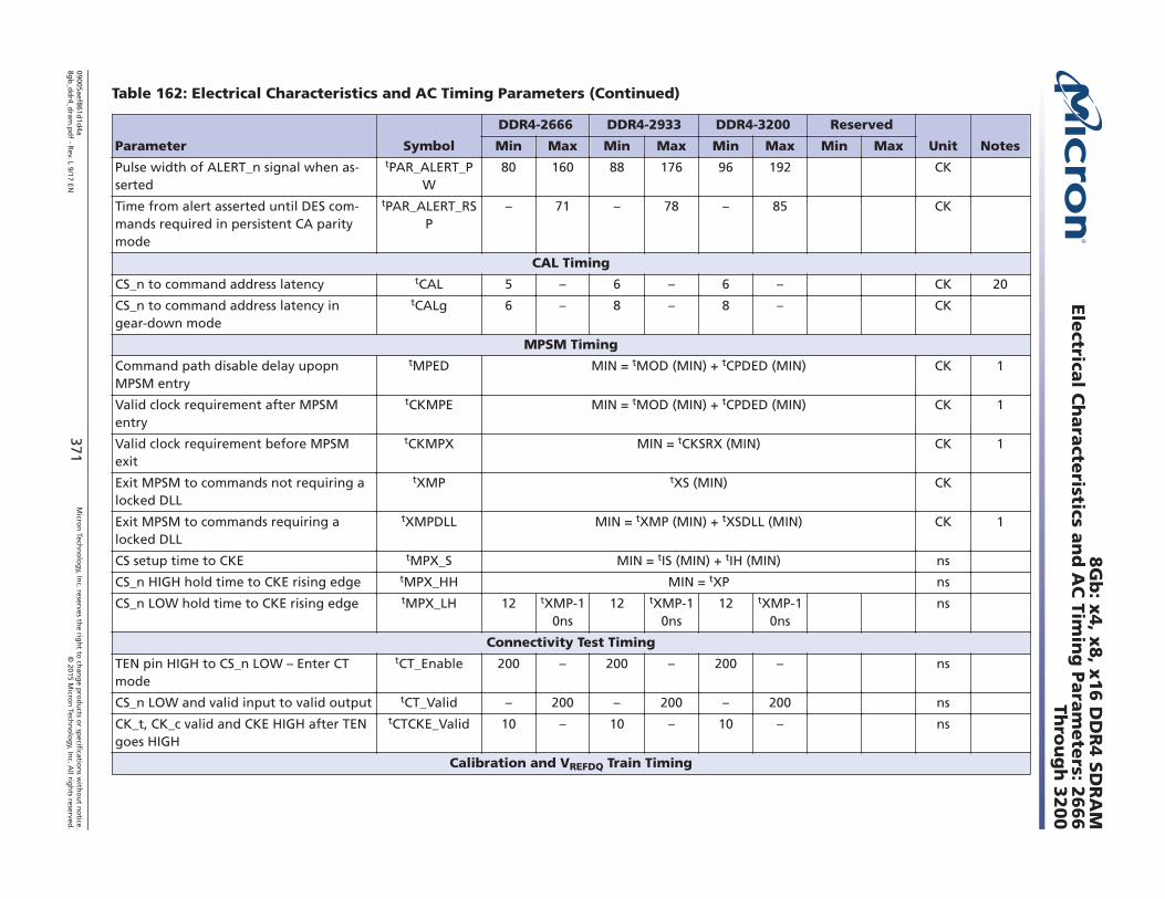
Table 162: Electrical Characteristics and AC Timing Parameters (Continued)
Parameter Symbol
DDR4-2666 DDR4-2933 DDR4-3200 Reserved
Unit NotesMin Max Min Max Min Max Min Max
Pulse width of ALERT_n signal when as-serted
tPAR_ALERT_PW
80 160 88 176 96 192 CK
Time from alert asserted until DES com-mands required in persistent CA paritymode
tPAR_ALERT_RSP
– 71 – 78 – 85 CK
CAL Timing
CS_n to command address latency tCAL 5 – 6 – 6 – CK 20
CS_n to command address latency ingear-down mode
tCALg 6 – 8 – 8 – CK
MPSM Timing
Command path disable delay upopnMPSM entry
tMPED MIN = tMOD (MIN) + tCPDED (MIN) CK 1
Valid clock requirement after MPSMentry
tCKMPE MIN = tMOD (MIN) + tCPDED (MIN) CK 1
Valid clock requirement before MPSMexit
tCKMPX MIN = tCKSRX (MIN) CK 1
Exit MPSM to commands not requiring alocked DLL
tXMP tXS (MIN) CK
Exit MPSM to commands requiring alocked DLL
tXMPDLL MIN = tXMP (MIN) + tXSDLL (MIN) CK 1
CS setup time to CKE tMPX_S MIN = tIS (MIN) + tIH (MIN) ns
CS_n HIGH hold time to CKE rising edge tMPX_HH MIN = tXP ns
CS_n LOW hold time to CKE rising edge tMPX_LH 12 tXMP-10ns
12 tXMP-10ns
12 tXMP-10ns
ns
Connectivity Test Timing
TEN pin HIGH to CS_n LOW – Enter CTmode
tCT_Enable 200 – 200 – 200 – ns
CS_n LOW and valid input to valid output tCT_Valid – 200 – 200 – 200 ns
CK_t, CK_c valid and CKE HIGH after TENgoes HIGH
tCTCKE_Valid 10 – 10 – 10 – ns
Calibration and VREFDQ Train Timing
8G
b: x
4, x
8, x
16 D
DR
4 S
DR
AM
Ele
ctrical C
hara
cteristics a
nd
AC
Timin
g P
ara
mete
rs: 2666
Thro
ug
h 3
200
09005aef861d1d
4a8g
b_d
dr4_d
ram.p
df - R
ev. L 9/17 EN371
Micro
n Tech
no
log
y, Inc. reserves th
e righ
t to ch
ang
e pro
du
cts or sp
ecification
s with
ou
t no
tice.©
2015 Micro
n Tech
no
log
y, Inc. A
ll righ
ts reserved.
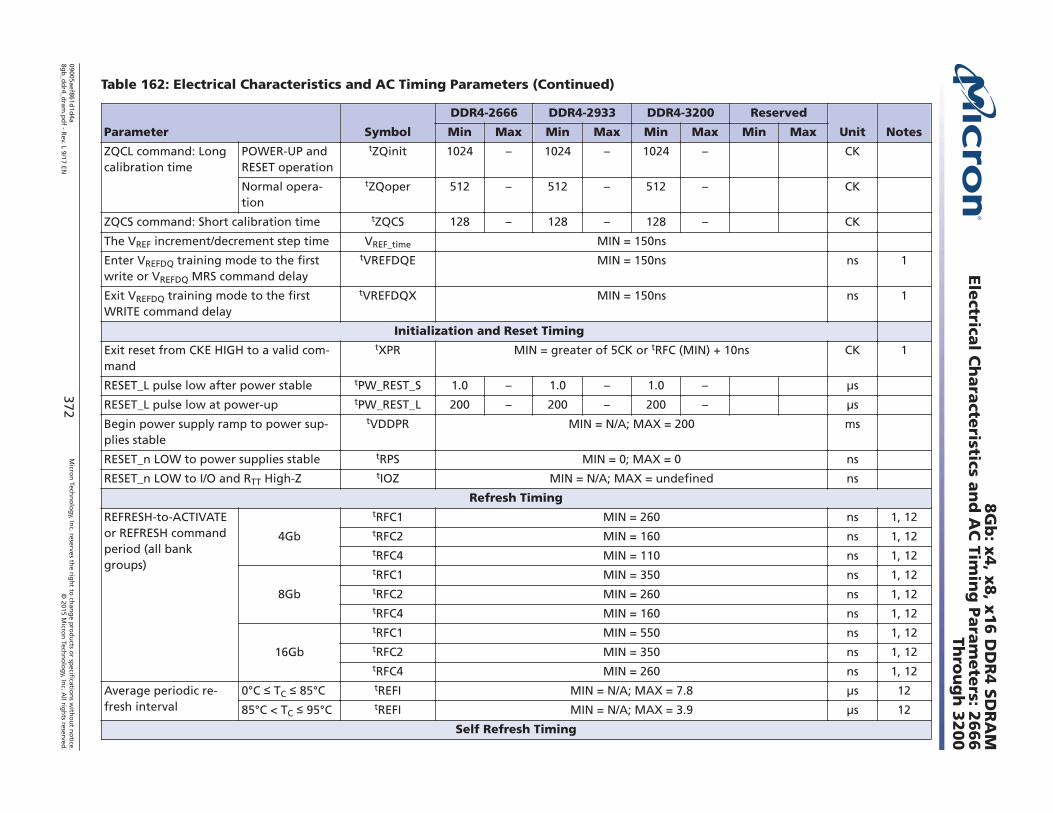
Table 162: Electrical Characteristics and AC Timing Parameters (Continued)
Parameter Symbol
DDR4-2666 DDR4-2933 DDR4-3200 Reserved
Unit NotesMin Max Min Max Min Max Min Max
ZQCL command: Longcalibration time
POWER-UP andRESET operation
tZQinit 1024 – 1024 – 1024 – CK
Normal opera-tion
tZQoper 512 – 512 – 512 – CK
ZQCS command: Short calibration time tZQCS 128 – 128 – 128 – CK
The VREF increment/decrement step time VREF_time MIN = 150ns
Enter VREFDQ training mode to the firstwrite or VREFDQ MRS command delay
tVREFDQE MIN = 150ns ns 1
Exit VREFDQ training mode to the firstWRITE command delay
tVREFDQX MIN = 150ns ns 1
Initialization and Reset Timing
Exit reset from CKE HIGH to a valid com-mand
tXPR MIN = greater of 5CK or tRFC (MIN) + 10ns CK 1
RESET_L pulse low after power stable tPW_REST_S 1.0 – 1.0 – 1.0 – μs
RESET_L pulse low at power-up tPW_REST_L 200 – 200 – 200 – μs
Begin power supply ramp to power sup-plies stable
tVDDPR MIN = N/A; MAX = 200 ms
RESET_n LOW to power supplies stable tRPS MIN = 0; MAX = 0 ns
RESET_n LOW to I/O and RTT High-Z tIOZ MIN = N/A; MAX = undefined ns
Refresh Timing
REFRESH-to-ACTIVATEor REFRESH commandperiod (all bankgroups)
4Gb
tRFC1 MIN = 260 ns 1, 12tRFC2 MIN = 160 ns 1, 12tRFC4 MIN = 110 ns 1, 12
8Gb
tRFC1 MIN = 350 ns 1, 12tRFC2 MIN = 260 ns 1, 12tRFC4 MIN = 160 ns 1, 12
16Gb
tRFC1 MIN = 550 ns 1, 12tRFC2 MIN = 350 ns 1, 12tRFC4 MIN = 260 ns 1, 12
Average periodic re-fresh interval
0°C TC 85°C tREFI MIN = N/A; MAX = 7.8 μs 12
85°C < TC 95°C tREFI MIN = N/A; MAX = 3.9 μs 12
Self Refresh Timing
8G
b: x
4, x
8, x
16 D
DR
4 S
DR
AM
Ele
ctrical C
hara
cteristics a
nd
AC
Timin
g P
ara
mete
rs: 2666
Thro
ug
h 3
200
09005aef861d1d
4a8g
b_d
dr4_d
ram.p
df - R
ev. L 9/17 EN372
Micro
n Tech
no
log
y, Inc. reserves th
e righ
t to ch
ang
e pro
du
cts or sp
ecification
s with
ou
t no
tice.©
2015 Micro
n Tech
no
log
y, Inc. A
ll righ
ts reserved.
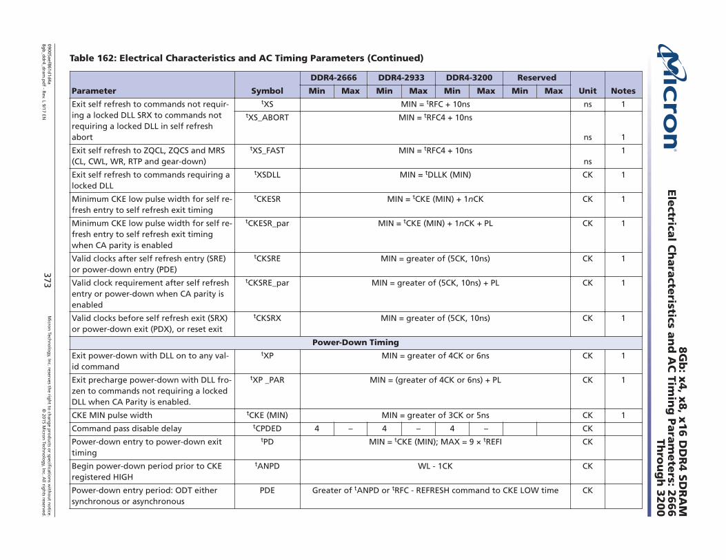
Table 162: Electrical Characteristics and AC Timing Parameters (Continued)
Parameter Symbol
DDR4-2666 DDR4-2933 DDR4-3200 Reserved
Unit NotesMin Max Min Max Min Max Min Max
Exit self refresh to commands not requir-ing a locked DLL SRX to commands notrequiring a locked DLL in self refreshabort
tXS MIN = tRFC + 10ns ns 1tXS_ABORT MIN = tRFC4 + 10ns
ns 1
Exit self refresh to ZQCL, ZQCS and MRS(CL, CWL, WR, RTP and gear-down)
tXS_FAST MIN = tRFC4 + 10nsns
1
Exit self refresh to commands requiring alocked DLL
tXSDLL MIN = tDLLK (MIN) CK 1
Minimum CKE low pulse width for self re-fresh entry to self refresh exit timing
tCKESR MIN = tCKE (MIN) + 1nCK CK 1
Minimum CKE low pulse width for self re-fresh entry to self refresh exit timingwhen CA parity is enabled
tCKESR_par MIN = tCKE (MIN) + 1nCK + PL CK 1
Valid clocks after self refresh entry (SRE)or power-down entry (PDE)
tCKSRE MIN = greater of (5CK, 10ns) CK 1
Valid clock requirement after self refreshentry or power-down when CA parity isenabled
tCKSRE_par MIN = greater of (5CK, 10ns) + PL CK 1
Valid clocks before self refresh exit (SRX)or power-down exit (PDX), or reset exit
tCKSRX MIN = greater of (5CK, 10ns) CK 1
Power-Down Timing
Exit power-down with DLL on to any val-id command
tXP MIN = greater of 4CK or 6ns CK 1
Exit precharge power-down with DLL fro-zen to commands not requiring a lockedDLL when CA Parity is enabled.
tXP _PAR MIN = (greater of 4CK or 6ns) + PL CK 1
CKE MIN pulse width tCKE (MIN) MIN = greater of 3CK or 5ns CK 1
Command pass disable delay tCPDED 4 – 4 – 4 – CK
Power-down entry to power-down exittiming
tPD MIN = tCKE (MIN); MAX = 9 × tREFI CK
Begin power-down period prior to CKEregistered HIGH
tANPD WL - 1CK CK
Power-down entry period: ODT eithersynchronous or asynchronous
PDE Greater of tANPD or tRFC - REFRESH command to CKE LOW time CK
8G
b: x
4, x
8, x
16 D
DR
4 S
DR
AM
Ele
ctrical C
hara
cteristics a
nd
AC
Timin
g P
ara
mete
rs: 2666
Thro
ug
h 3
200
09005aef861d1d
4a8g
b_d
dr4_d
ram.p
df - R
ev. L 9/17 EN373
Micro
n Tech
no
log
y, Inc. reserves th
e righ
t to ch
ang
e pro
du
cts or sp
ecification
s with
ou
t no
tice.©
2015 Micro
n Tech
no
log
y, Inc. A
ll righ
ts reserved.
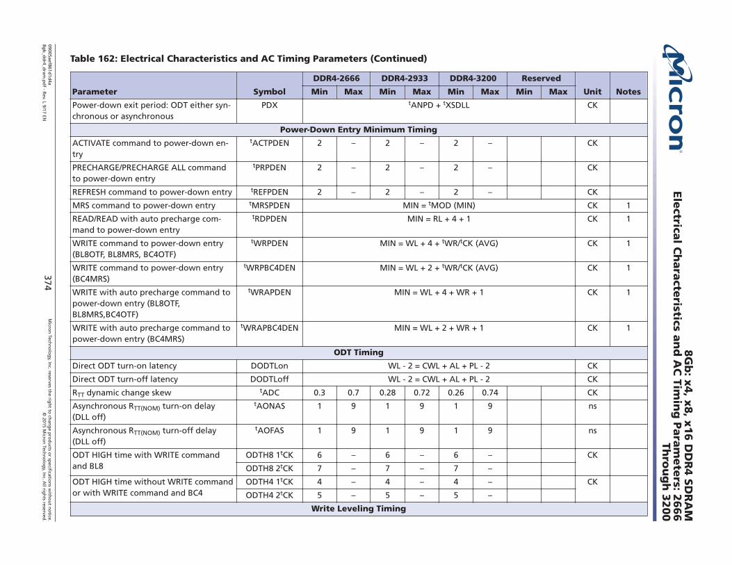
Table 162: Electrical Characteristics and AC Timing Parameters (Continued)
Parameter Symbol
DDR4-2666 DDR4-2933 DDR4-3200 Reserved
Unit NotesMin Max Min Max Min Max Min Max
Power-down exit period: ODT either syn-chronous or asynchronous
PDX tANPD + tXSDLL CK
Power-Down Entry Minimum Timing
ACTIVATE command to power-down en-try
tACTPDEN 2 – 2 – 2 – CK
PRECHARGE/PRECHARGE ALL commandto power-down entry
tPRPDEN 2 – 2 – 2 – CK
REFRESH command to power-down entry tREFPDEN 2 – 2 – 2 – CK
MRS command to power-down entry tMRSPDEN MIN = tMOD (MIN) CK 1
READ/READ with auto precharge com-mand to power-down entry
tRDPDEN MIN = RL + 4 + 1 CK 1
WRITE command to power-down entry(BL8OTF, BL8MRS, BC4OTF)
tWRPDEN MIN = WL + 4 + tWR/tCK (AVG) CK 1
WRITE command to power-down entry(BC4MRS)
tWRPBC4DEN MIN = WL + 2 + tWR/tCK (AVG) CK 1
WRITE with auto precharge command topower-down entry (BL8OTF,BL8MRS,BC4OTF)
tWRAPDEN MIN = WL + 4 + WR + 1 CK 1
WRITE with auto precharge command topower-down entry (BC4MRS)
tWRAPBC4DEN MIN = WL + 2 + WR + 1 CK 1
ODT Timing
Direct ODT turn-on latency DODTLon WL - 2 = CWL + AL + PL - 2 CK
Direct ODT turn-off latency DODTLoff WL - 2 = CWL + AL + PL - 2 CK
RTT dynamic change skew tADC 0.3 0.7 0.28 0.72 0.26 0.74 CK
Asynchronous RTT(NOM) turn-on delay(DLL off)
tAONAS 1 9 1 9 1 9 ns
Asynchronous RTT(NOM) turn-off delay(DLL off)
tAOFAS 1 9 1 9 1 9 ns
ODT HIGH time with WRITE commandand BL8
ODTH8 1tCK 6 – 6 – 6 – CK
ODTH8 2tCK 7 – 7 – 7 –
ODT HIGH time without WRITE commandor with WRITE command and BC4
ODTH4 1tCK 4 – 4 – 4 – CK
ODTH4 2tCK 5 – 5 – 5 –
Write Leveling Timing
8G
b: x
4, x
8, x
16 D
DR
4 S
DR
AM
Ele
ctrical C
hara
cteristics a
nd
AC
Timin
g P
ara
mete
rs: 2666
Thro
ug
h 3
200
09005aef861d1d
4a8g
b_d
dr4_d
ram.p
df - R
ev. L 9/17 EN374
Micro
n Tech
no
log
y, Inc. reserves th
e righ
t to ch
ang
e pro
du
cts or sp
ecification
s with
ou
t no
tice.©
2015 Micro
n Tech
no
log
y, Inc. A
ll righ
ts reserved.
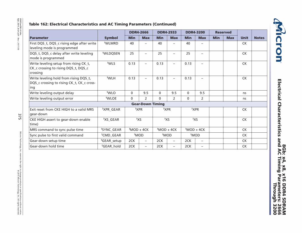
Table 162: Electrical Characteristics and AC Timing Parameters (Continued)
Parameter Symbol
DDR4-2666 DDR4-2933 DDR4-3200 Reserved
Unit NotesMin Max Min Max Min Max Min Max
First DQS_t, DQS_c rising edge after writeleveling mode is programmed
tWLMRD 40 – 40 – 40 – CK
DQS_t, DQS_c delay after write levelingmode is programmed
tWLDQSEN 25 – 25 – 25 – CK
Write leveling setup from rising CK_t,CK_c crossing to rising DQS_t, DQS_ccrossing
tWLS 0.13 – 0.13 – 0.13 – CK
Write leveling hold from rising DQS_t,DQS_c crossing to rising CK_t, CK_c cross-ing
tWLH 0.13 – 0.13 – 0.13 – CK
Write leveling output delay tWLO 0 9.5 0 9.5 0 9.5 ns
Write leveling output error tWLOE 0 2 0 2 0 2 ns
Gear-Down Timing
Exit reset from CKE HIGH to a valid MRSgear-down
tXPR_GEAR tXPR tXPR tXPR CK
CKE HIGH assert to gear-down enabletime)
tXS_GEAR tXS tXS tXS CK
MRS command to sync pulse time tSYNC_GEAR tMOD + 4CK tMOD + 4CK tMOD + 4CK CK
Sync pulse to first valid command tCMD_GEAR tMOD tMOD tMOD CK
Gear-down setup time tGEAR_setup 2CK – 2CK – 2CK – CK
Gear-down hold time tGEAR_hold 2CK – 2CK – 2CK – CK
8G
b: x
4, x
8, x
16 D
DR
4 S
DR
AM
Ele
ctrical C
hara
cteristics a
nd
AC
Timin
g P
ara
mete
rs: 2666
Thro
ug
h 3
200
09005aef861d1d
4a8g
b_d
dr4_d
ram.p
df - R
ev. L 9/17 EN375
Micro
n Tech
no
log
y, Inc. reserves th
e righ
t to ch
ang
e pro
du
cts or sp
ecification
s with
ou
t no
tice.©
2015 Micro
n Tech
no
log
y, Inc. A
ll righ
ts reserved.
Notes: 1. Maximum limit not applicable.2. tCCD_L and tDLLK should be programmed according to the value defined per operating
frequency.3. Data rate is greater than or equal to 1066 Mb/s.4. RFU.5. WRITE-to-READ when CRC and DM are both not enabled.6. WRITE-to-READ delay when CRC and DM are both enabled.7. The start of internal write transactions is defined as follows:
• For BL8 (fixed by MRS and on-the-fly): rising clock edge four clock cycles after WL• For BC4 (on-the-fly): rising clock edge four clock cycles after WL• For BC4 (fixed by MRS): rising clock edge two clock cycles after WL
8. For these parameters, the device supports tnPARAM [nCK] = RU{tPARAM [ns]/tCK (AVG)[ns]}, in clock cycles, assuming all input clock jitter specifications are satisfied.
9. Although unlimited row accesses to the same row is allowed within the refresh period,excessive row accesses to the same row over a long term can result in degraded opera-tion.
10. When operating in 1tCK WRITE preamble mode.11. When operating in 2tCK WRITE preamble mode.12. When CA parity mode is selected and the DLLoff mode is used, each REF command re-
quires an additional "PL" added to tRFC refresh time.13. DRAM devices should be evenly addressed when being accessed. Disproportionate ac-
cesses to a particular row address may result in reduction of the product lifetime and/orreduction in data retention ability.
14. Applicable from tCK (AVG) MIN to tCK (AVG) MAX as stated in the Speed Bin tables.15. JEDEC specifies a minimum of five clocks.16. The maximum read postamble is bound by tDQSCK (MIN) plus tQSH (MIN) on the left
side and tHZ(DQS) MAX on the right side.17. The reference level of DQ output signal is specified with a midpoint as a widest part of
output signal eye, which should be approximately 0.7 × VDDQ as a center level of thestatic single-ended output peak-to-peak swing with a driver impedance of 34 ohms andan effective test load of 50 ohms to VTT = VDDQ.
18. JEDEC hasn't agreed upon the definition of the deterministic jitter; the user should fo-cus on meeting the total limit.
19. Spread spectrum is not included in the jitter specification values. However, the inputclock can accommodate spread-spectrum at a sweep rate in the range of 20–60 kHz withan additional 1% of tCK (AVG) as a long-term jitter component; however, the spreadspectrum may not use a clock rate below tCK (AVG) MIN.
20. The actual tCAL minimum is the larger of 3 clocks or 3.748ns/tCK; the table lists the ap-plicable clocks required at targeted speed bin.
21. The maximum READ preamble is bounded by tLZ(DQS) MIN on the left side and tDQSCK(MAX) on the right side. See figure in Clock to Data Strobe Relationship. Boundary ofDQS Low-Z occur one cycle earlier in 2tCK toggle mode which is illustrated in READ Pre-amble.
22. DQ falling signal middle-point of transferring from HIGH to LOW to first rising edge ofDQS differential signal cross-point.
23. The tPDA_S/tPDA_H parameters may use the tDS/tDH limits, respectively, if the signal isLOW the entire BL8.
8Gb: x4, x8, x16 DDR4 SDRAMElectrical Characteristics and AC Timing Parameters: 2666
Through 3200
09005aef861d1d4a8gb_ddr4_dram.pdf - Rev. L 9/17 EN 376 Micron Technology, Inc. reserves the right to change products or specifications without notice.
© 2015 Micron Technology, Inc. All rights reserved.
Timing Parameter NotesNote 1: Actual value dependant upon measurement level definitions. Refer to the Meth-od for Calculating tWPRE Transitions and Endpoints and Method for Calculating tWPSTTransitions and Endpoints figures.
Note 2: Commands requiring a locked DLL are READ (and RAP) and synchronous ODTcommands.
Note 3. The MAX values are system dependent.
Note 4: WR as programmed in mode register.
Note 5: Value must be rounded up to the next higher integer value.
Note 6: No maximum cycle time limit aside from the need to satisfy the refresh interval,tREFI.
Note 7: For definition of RTT turn-on time, tAON, refer to the Timing Parameters table.
Note 8: For definition of RTT turn-off time, tAOF, refer to the Timing Parameters table.
Note 9: tWR is defined in ns. For calculation of tWRPDEN, it is necessary to round uptWR/tCK to the next integer.
Note 10: WR in clock cycles as programmed in MR0.
Note 11: The maximum read postamble is bound by tDQSCK (MIN) plus tQSH (MIN) onthe left side and tHZ(DQS) MAX on the right side. Refer to the Clock to Data Strobe Rela-tionship figure.
Note 12: Output timing deratings are relative to the SDRAM input clock. When the de-vice is derated with input clock jitter, this parameter needs to be derated by TBD.
Note 13: Value is only valid for RON34.
Note 14: Single-ended signal parameter.
Note 15: tREFI depends on TOPER.
Note 16: tIS (base) and tIH (base) values are for 1 V/ns CMD/ADD single-ended slewrate and 2 V/ns CK_t, CK_c differential slew rate. Note that for DQ and DM signals,VREF(DC) = VREFDQ(DC). For input-only pins, except RESET_n, VREF(DC) = VREFCA(DC).
Note 17: tDS (base) and tDH (base) values are for 1 V/ns DQ single-ended slew rate and2 V/ns DQS_t, DQS_c differential slew rate. Note that for DQ and DM signals, V REF(DC) =VREFDQ(DC). For input-only pins, except RESET_n, VREF(DC) = VREFCA(DC).
Note 18: Start of internal write transaction is defined as follows. For BL8 (fixed by MRSand on-the-fly), rising clock edge 4 clock cycles after WL. For BC4 (on-the-fly), risingclock edge 4 clock cycles after WL. For BC4 (fixed by MRS), rising clock edge 2 clock cy-cles after WL.
Note 19: The maximum read preamble is bound by tLZ(DQS) MIN on the left side andtDQSCK (MAX) on the right side. Refer to the Clock to Data Strobe Relationship figure.
Note 20: CKE is allowed to be registered LOW while operations such as row activation,precharge, auto precharge, or refresh are in progress, but the power-down IDD specifica-tion will not be applied until finishing those operations.
8Gb: x4, x8, x16 DDR4 SDRAMTiming Parameter Notes
09005aef861d1d4a8gb_ddr4_dram.pdf - Rev. L 9/17 EN 377 Micron Technology, Inc. reserves the right to change products or specifications without notice.
© 2015 Micron Technology, Inc. All rights reserved.
Note 21: Although CKE is allowed to be registered LOW after a REFRESH commandwhen tREFPDEN (MIN) is satisfied, there are cases where additional time, such astXSDLL (MIN) is also required. Refer to Power-Down Clarifications - Case 2.
Note 22: Defined between end of MPR read burst and MRS, which reloads MPR or disa-bles the MPR function.
Note 23: Users have commented that tXSF will not apply to all MRS commands. Theseparameters are still in discussion in JEDEC.
8Gb: x4, x8, x16 DDR4 SDRAMTiming Parameter Notes
09005aef861d1d4a8gb_ddr4_dram.pdf - Rev. L 9/17 EN 378 Micron Technology, Inc. reserves the right to change products or specifications without notice.
© 2015 Micron Technology, Inc. All rights reserved.
Clock SpecificationThe jitter specified is a random jitter meeting a Gaussian distribution. Input clocks vio-lating the MIN/MAX values may result in malfunction of the DDR4 SDRAM device.
Definition for tCK(AVG)tCK(AVG) is calculated as the average clock period across any consecutive 200-cyclewindow, where each clock period is calculated from rising edge to rising edge.
Definition for tCK(ABS)tCK(ABS) is defined as the absolute clock period as measured from one rising edge tothe next consecutive rising edge. tCK(ABS) is not subject to a production test.
Definition for tCH(AVG) and tCL(AVG)tCH(AVG) is defined as the average high pulse width as calculated across any consecu-tive 200 high pulses.
tCL(AVG) is defined as the average low pulse width as calculated across any consecutive200 low pulses.
Definition for tJIT(per) and tJIT(per,lck)tJIT(per) is defined as the largest deviation of any signal tCK from tCK(AVG).
tJIT(per) = MIN/MAX of {tCKi - tCK(AVG) where i = 1 to 200}.
tJIT(per) defines the single period jitter when the DLL is already locked.
tJIT(per,lck) uses the same definition for single period jitter, but only during the DLLlocking period.
tJIT(per) and tJIT(per,lck) are not subject to production test.
Definition for tJIT(cc) and tJIT(cc,lck)tJIT(cc) is defined as the absolute difference in clock period between two consecutiveclock cycles.
tJIT(cc) = MAX of |{tCKi +1 - tCKi}|.
tJIT(cc) defines the cycle to cycle jitter when the DLL is already locked.
tJIT(cc,lck) uses the same definition for cycle to cycle jitter, during the DLL locking peri-od only.
tJIT(cc) and tJIT(cc,lck) are not subject to production test.
Definition for tERR(nper)tERR is defined as the cumulative error across n multiple consecutive cycles fromtCK(AVG). tERR is not subject to a production test.
8Gb: x4, x8, x16 DDR4 SDRAMClock Specification
09005aef861d1d4a8gb_ddr4_dram.pdf - Rev. L 9/17 EN 379 Micron Technology, Inc. reserves the right to change products or specifications without notice.
© 2015 Micron Technology, Inc. All rights reserved.
Jitter NotesNote a: Unit tCK(AVG) represents the actual tCK(AVG) of the input clock under opera-tion. Unit nCK represents one clock cycle of the input clock, including the actual clockedges. Example: tMRD = 4 [nCK] means that if one MODE REGISTER SET command isregistered at Tm, another MODE REGISTER SET command may be registered at Tm + 4,even if (Tm + 4 - Tm) is (4 × tCK(AVG) + tERR (4 per) MIN).
Note b: These parameters are measured from a command/address signal (such as CKE,CS_n, RAS_n, CAS_n, WE_n, ODT, BA0, A0, or A1) transition edge to its respective clocksignal (CK_t/CK_c) crossing. The specification values are not affected by the amount ofclock jitter applied (for example, tJITper, tJITcc) because the setup and hold are relativeto the clock signal crossing that latches the command/address. That is, these parame-ters should be met whether clock jitter is present or not.
Note c: These parameters are measured from a data strobe signal (DQS_t[L/U],DQS_c[L/U]) crossing to its respective clock signal (CK_t, CK_c) crossing. The specifica-tion values are not affected by the amount of clock jitter applied (for example, tJITper,tJITcc) because these are relative to the clock signal crossing. That is, these parametersshould be met whether clock jitter is present or not.
Note d: These parameters are measured from a data signal (such as DM[L/U], DQ[L/U]0, or DQ[L/U]1) transition edge to its respective data strobe signal (DQS_t[L/U],DQS_c[L/U]) crossing.
Note e: For these parameters, the DDR4 SDRAM device supports tnPARAM [nCK] =RU[tPARAM [ns]/tCK(AVG) [ns]], which is in clock cycles, assuming all input clock jitterspecifications are satisfied. For example, the device will support tnRP = RU [tRP/tCK(AVG)], which is in clock cycles, if all input clock jitter specifications are met. Thismeans that for DDR4-800 6-6-6, tRP = 15ns, the device will support tnRP = RU[tRP/tCK(AVG)] = 6, as long as the input clock jitter specifications are met. For example, thePRECHARGE command at Tm and ACTIVE command at Tm + 6 is valid even if (Tm + 6 -Tm) is less than 15ns due to input clock jitter.
Note f: When the device is operated with input clock jitter, this parameter needs to bederated by the actual tERR(mper), act of the input clock, where 2 m 12 (output derat-ings are relative to the SDRAM input clock). For example, if the measured jitter into aDDR4-800 SDRAM has tERR(mper), act, MIN = –172ps and tERR(mper), act, MAX =+193ps, then tDQSCK, MIN(derated) = tDQSCK, MIN - tERR(mper), act, MAX = –400ps -193ps = –593ps and tDQSCK, MAX(derated) = tDQSCK, MAX - tERR(mper), act, MIN =400ps + 172ps = 572ps. Similarly, tLZ(DQ) for DDR4-800 derates to tLZ(DQ), MIN(derat-ed) = –800ps - 193ps = –993ps and tLZ(DQ), MAX(derated) = 400ps + 172ps = 572ps. Notethat tERR(mper), act, MIN is the minimum measured value of tERR(nper) where 2 n 12, and tERR(mper), act, MAX is the maximum measured value of tERR(nper) where 2 n 12.
Note g: When the device is operated with input clock jitter, this parameter needs to bederated by the actual tJIT(per), act of the input clock (output deratings are relative to theSDRAM input clock). For example, if the measured jitter into a DDR4-800 SDRAM hastCK(AVG), act = 2500ps, tJIT(per), act, MIN = –72ps and tJIT(per), act, MAX = +93ps, thentRPRE, MIN(derated) = tRPRE, MIN + tJIT(per), act, MIN = 0.9 × tCK(AVG), act + tJIT(per),act, MIN = 0.9 × 2500ps - 72ps = 2178ps. Similarly, tQH, MIN(derated) = tQH, MIN +tJIT(per), act, MIN = 0.38 × tCK(AVG), act + tJIT(per), act, MIN = 0.38 × 2500ps - 72ps =878ps.
8Gb: x4, x8, x16 DDR4 SDRAMJitter Notes
09005aef861d1d4a8gb_ddr4_dram.pdf - Rev. L 9/17 EN 380 Micron Technology, Inc. reserves the right to change products or specifications without notice.
© 2015 Micron Technology, Inc. All rights reserved.
Converting Time-Based Specifications to Clock-Based RequirementsSoftware algorithms for calculation of timing parameters are subject to potential round-ing errors when converting DRAM timing requirements to system clocks; for example, amemory clock with a nominal frequency of 933.33...3 MHz, or a clock period of1.071428571429...ns. Similarly, a system with a memory clock frequency of 1066.66...6MHz mathematically yields a clock period of 0.9375ns. It is unrealistic to represent alldigits after the decimal point exactly and some sort of rounding needs to be done.
DDR4 SDRAM SPD-based specifications use a minimum granularity for SPD-associatedtiming parameters of 1ps. Clock periods such as tCK (AVG) MIN are defined to the near-est picosecond. For example, 0.9375ns is stated as 937ps and 1.0714ns is stated as1071ps. Parameters such as tAA MIN, and tRCD MIN are specified in units of time(nanoseconds) and require mathematical computation to convert to system clocks(nCK). Rules for rounding allows optimization of device performance without violatingdevice parameters. These SPD algorithms rely on results that are within adjustment fac-tors on device testing and specification to avoid losing performance due to rounding er-rors when using SPD-based parameters.
Guidance converting SPD associated timing parameters to system clock requirements:
• Divide the time base specification (in ns) by the clock period (in ns).• Subtract an adjustment factor of 0.025. This is results in a –2.5% tCK adjustment fac-
tor.• The resultant is set to the next higher integer number of clocks.• nCK = ceiling [ (parameter in ns / application tCK in ns) - 0.025 ].Alternatively, the following algorithm provides the same results as above:
• Use integer math expressing timing specification and application clock period in pi-coseconds; scaling a nanosecond-based parameter value by 1000.
• Divide the picosecond-based parameter by the picoseconds based application clockperiod.
• Add an inverse adjustment factor of 97.4%.• Divide the result by 1000.• Truncate down to the next lower integer value.• nCK = truncate [ {(parameter in ps × 1000) / (application tCK in ps) + 974} / 1000 ].
Guidance converting nonSPD associated timing parameters to system clock require-ments:
• Divide the time base specification (in ns) and divided by the clock period (in ns).• The resultant is set to the next higher integer number of clocks.• nCK = ceiling [ (parameter in ns / application tCK in ns) ].
8Gb: x4, x8, x16 DDR4 SDRAMConverting Time-Based Specifications to Clock-Based Require-
ments
09005aef861d1d4a8gb_ddr4_dram.pdf - Rev. L 9/17 EN 381 Micron Technology, Inc. reserves the right to change products or specifications without notice.
© 2015 Micron Technology, Inc. All rights reserved.
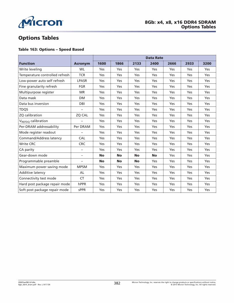
Options Tables
Table 163: Options – Speed Based
Function Acronym
Data Rate
1600 1866 2133 2400 2666 2933 3200
Write leveling WL Yes Yes Yes Yes Yes Yes Yes
Temperature controlled refresh TCR Yes Yes Yes Yes Yes Yes Yes
Low-power auto self refresh LPASR Yes Yes Yes Yes Yes Yes Yes
Fine granularity refresh FGR Yes Yes Yes Yes Yes Yes Yes
Multipurpose register MR Yes Yes Yes Yes Yes Yes Yes
Data mask DM Yes Yes Yes Yes Yes Yes Yes
Data bus inversion DBI Yes Yes Yes Yes Yes Yes Yes
TDQS – Yes Yes Yes Yes Yes Yes Yes
ZQ calibration ZQ CAL Yes Yes Yes Yes Yes Yes Yes
VREFDQ calibration – Yes Yes Yes Yes Yes Yes Yes
Per-DRAM addressability Per DRAM Yes Yes Yes Yes Yes Yes Yes
Mode register readout – Yes Yes Yes Yes Yes Yes Yes
Command/Address latency CAL Yes Yes Yes Yes Yes Yes Yes
Write CRC CRC Yes Yes Yes Yes Yes Yes Yes
CA parity – Yes Yes Yes Yes Yes Yes Yes
Gear-down mode – No No No No Yes Yes Yes
Programmable preamble – No No No Yes Yes Yes Yes
Maximum power saving mode MPSM Yes Yes Yes Yes Yes Yes Yes
Additive latency AL Yes Yes Yes Yes Yes Yes Yes
Connectivity test mode CT Yes Yes Yes Yes Yes Yes Yes
Hard post package repair mode hPPR Yes Yes Yes Yes Yes Yes Yes
Soft post package repair mode sPPR Yes Yes Yes Yes Yes Yes Yes
8Gb: x4, x8, x16 DDR4 SDRAMOptions Tables
09005aef861d1d4a8gb_ddr4_dram.pdf - Rev. L 9/17 EN 382 Micron Technology, Inc. reserves the right to change products or specifications without notice.
© 2015 Micron Technology, Inc. All rights reserved.
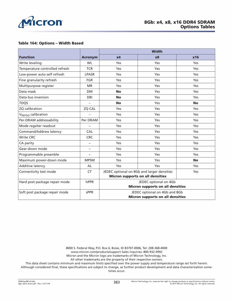
Table 164: Options – Width Based
Function Acronym
Width
x4 x8 x16
Write leveling WL Yes Yes Yes
Temperature controlled refresh TCR Yes Yes Yes
Low-power auto self refresh LPASR Yes Yes Yes
Fine granularity refresh FGR Yes Yes Yes
Multipurpose register MR Yes Yes Yes
Data mask DM No Yes Yes
Data bus inversion DBI No Yes Yes
TDQS – No Yes No
ZQ calibration ZQ CAL Yes Yes Yes
VREFDQ calibration – Yes Yes Yes
Per-DRAM addressability Per DRAM Yes Yes Yes
Mode regsiter readout – Yes Yes Yes
Command/Address latency CAL Yes Yes Yes
Write CRC CRC Yes Yes Yes
CA parity – Yes Yes Yes
Gear-down mode – Yes Yes Yes
Programmable preamble – Yes Yes Yes
Maximum power-down mode MPSM Yes Yes No
Additive latency AL Yes Yes Yes
Connectivity test mode CT JEDEC optional on 8Gb and larger densitiesMicron supports on all densities
Yes
Hard post package repair mode hPPR JEDEC optional on 4GbMicron supports on all densities
Soft post package repair mode sPPR JEDEC optional on 4Gb and 8GbMicron supports on all densities
8000 S. Federal Way, P.O. Box 6, Boise, ID 83707-0006, Tel: 208-368-4000www.micron.com/products/support Sales inquiries: 800-932-4992
Micron and the Micron logo are trademarks of Micron Technology, Inc.All other trademarks are the property of their respective owners.
This data sheet contains minimum and maximum limits specified over the power supply and temperature range set forth herein.Although considered final, these specifications are subject to change, as further product development and data characterization some-
times occur.
8Gb: x4, x8, x16 DDR4 SDRAMOptions Tables
09005aef861d1d4a8gb_ddr4_dram.pdf - Rev. L 9/17 EN 383 Micron Technology, Inc. reserves the right to change products or specifications without notice.
© 2015 Micron Technology, Inc. All rights reserved.


