Embed Size (px)
Citation preview
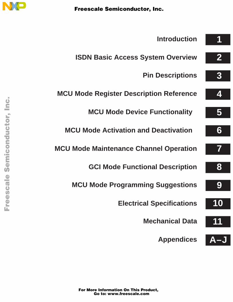
MCU Mode Maintenance Channel Operation 7
GCI Mode Functional Description 8
MCU Mode Activation and Deactivation 6
MCU Mode Device Functionality 5
MCU Mode Register Description Reference 4
Pin Descriptions 3
ISDN Basic Access System Overview 2
Introduction 1
Appendices A–J
Mechanical Data 11
Electrical Specifications 10
MCU Mode Programming Suggestions 9
Fre
esc
ale
Se
mic
on
du
cto
r, I
Freescale Semiconductor, Inc.
For More Information On This Product, Go to: www.freescale.com
nc
...

Fre
esc
ale
Se
mic
on
du
cto
r, I
Freescale Semiconductor, Inc.
For More Information On This Product, Go to: www.freescale.com
nc
...
All brand and product names appearing in this document are registered trademarks of their respective holders.
Motorola, Inc. 1998
Motorola reserves the right to make changes without further notice to any products herein. Motorola makes no warranty, representation or guarantee regardingthe suitability of its products for any particular purpose, nor does Motorola assume any liability arising out of the application or use of any product or circuit, andspecifically disclaims any and all liability, including without limitation consequential or incidental damages. “Typical” parameters which may be provided in Motoroladata sheets and/or specifications can and do vary in different applications and actual performance may vary over time. All operating parameters, including “Typicals”must be validated for each customer application by customer’s technical experts. Motorola does not convey any license under its patent rights nor the rights ofothers. Motorola products are not designed, intended, or authorized for use as components in systems intended for surgical implant into the body, or otherapplications intended to support or sustain life, or for any other application in which the failure of the Motorola product could create a situation where personal injuryor death may occur. Should Buyer purchase or use Motorola products for any such unintended or unauthorized application, Buyer shall indemnify and hold Motorolaand its officers, employees, subsidiaries, affiliates, and distributors harmless against all claims, costs, damages, and expenses, and reasonable attorney feesarising out of, directly or indirectly, any claim of personal injury or death associated with such unintended or unauthorized use, even if such claim alleges thatMotorola was negligent regarding the design or manufacture of the part. Motorola and are registered trademarks of Motorola, Inc. Motorola, Inc. is an EqualOpportunity/Affirmative Action Employer.
Fre
esc
ale
Se
mic
on
du
cto
r, I
Freescale Semiconductor, Inc.
For More Information On This Product, Go to: www.freescale.com
nc
...

Fre
esc
ale
Se
mic
on
du
cto
r, I
Freescale Semiconductor, Inc.
For More Information On This Product, Go to: www.freescale.com
nc
...
MC145572 Contents–iMOTOROLA
SECTION 1INTRODUCTION
1.1 INTRODUCTION 1–1. . . . . . . . . . . . . . . . . . . . . . . . . . . . . . . . . . . . . . . . . . . . . . . . . . . . . . . . . . . . . . . . . . . . 1.2 SUPPLEMENTAL DOCUMENTATION 1–1. . . . . . . . . . . . . . . . . . . . . . . . . . . . . . . . . . . . . . . . . . . . . . . . . . 1.3 FEATURES 1–2. . . . . . . . . . . . . . . . . . . . . . . . . . . . . . . . . . . . . . . . . . . . . . . . . . . . . . . . . . . . . . . . . . . . . . . . . 1.4 REVISIONS 1–2. . . . . . . . . . . . . . . . . . . . . . . . . . . . . . . . . . . . . . . . . . . . . . . . . . . . . . . . . . . . . . . . . . . . . . . . .
SECTION 2ISDN BASIC ACCESS SYSTEM OVERVIEW
2.1 ISDN REFERENCE MODEL 2–1. . . . . . . . . . . . . . . . . . . . . . . . . . . . . . . . . . . . . . . . . . . . . . . . . . . . . . . . . . 2.2 U–INTERFACE TRANSCEIVER ISDN APPLICATIONS 2–1. . . . . . . . . . . . . . . . . . . . . . . . . . . . . . . . . . . 2.3 NON–ISDN U–INTERFACE TRANSCEIVER APPLICATIONS 2–3. . . . . . . . . . . . . . . . . . . . . . . . . . . . .
SECTION 3PIN DESCRIPTIONS
3.1 INTRODUCTION 3–1. . . . . . . . . . . . . . . . . . . . . . . . . . . . . . . . . . . . . . . . . . . . . . . . . . . . . . . . . . . . . . . . . . . . 3.2 PIN DESCRIPTION QUICK REFERENCE 3–1. . . . . . . . . . . . . . . . . . . . . . . . . . . . . . . . . . . . . . . . . . . . . . 3.3 PIN DESCRIPTIONS 3–4. . . . . . . . . . . . . . . . . . . . . . . . . . . . . . . . . . . . . . . . . . . . . . . . . . . . . . . . . . . . . . . . . 3.3.1 Power Supply Pins 3–4. . . . . . . . . . . . . . . . . . . . . . . . . . . . . . . . . . . . . . . . . . . . . . . . . . . . . . . . . . . . . . . . 3.3.2 Mode Selection Pins 3–5. . . . . . . . . . . . . . . . . . . . . . . . . . . . . . . . . . . . . . . . . . . . . . . . . . . . . . . . . . . . . . . 3.3.3 Time Division Multiplex Data Interface Pins 3–6. . . . . . . . . . . . . . . . . . . . . . . . . . . . . . . . . . . . . . . . . . . 3.3.4 Control/Status Interface Pins 3–8. . . . . . . . . . . . . . . . . . . . . . . . . . . . . . . . . . . . . . . . . . . . . . . . . . . . . . . . 3.3.5 2B1Q Line Interface Pins 3–12. . . . . . . . . . . . . . . . . . . . . . . . . . . . . . . . . . . . . . . . . . . . . . . . . . . . . . . . . . . 3.3.6 Crystal Oscillator and Phase Locked Loop (PLL) Pins 3–12. . . . . . . . . . . . . . . . . . . . . . . . . . . . . . . . . . 3.3.7 Crystal Oscillator Description 3–13. . . . . . . . . . . . . . . . . . . . . . . . . . . . . . . . . . . . . . . . . . . . . . . . . . . . . . .
SECTION 4MCU MODE REGISTER DESCRIPTION REFERENCE
4.1 INTRODUCTION 4–1. . . . . . . . . . . . . . . . . . . . . . . . . . . . . . . . . . . . . . . . . . . . . . . . . . . . . . . . . . . . . . . . . . . . 4.2 REGISTER MAP 4–3. . . . . . . . . . . . . . . . . . . . . . . . . . . . . . . . . . . . . . . . . . . . . . . . . . . . . . . . . . . . . . . . . . . . 4.2.1 Register Index 4–3. . . . . . . . . . . . . . . . . . . . . . . . . . . . . . . . . . . . . . . . . . . . . . . . . . . . . . . . . . . . . . . . . . . . 4.2.2 Bit Description Legend 4–5. . . . . . . . . . . . . . . . . . . . . . . . . . . . . . . . . . . . . . . . . . . . . . . . . . . . . . . . . . . . . 4.3 NIBBLE REGISTERS 4–5. . . . . . . . . . . . . . . . . . . . . . . . . . . . . . . . . . . . . . . . . . . . . . . . . . . . . . . . . . . . . . . . 4.3.1 NR0: Reset and Power–Down Register 4–5. . . . . . . . . . . . . . . . . . . . . . . . . . . . . . . . . . . . . . . . . . . . . . 4.3.2 NR1: Activation Status Register 4–6. . . . . . . . . . . . . . . . . . . . . . . . . . . . . . . . . . . . . . . . . . . . . . . . . . . . 4.3.3 NR2: Activation Control Register 4–8. . . . . . . . . . . . . . . . . . . . . . . . . . . . . . . . . . . . . . . . . . . . . . . . . . . . 4.3.4 NR3: Interrupt Status Register 4–9. . . . . . . . . . . . . . . . . . . . . . . . . . . . . . . . . . . . . . . . . . . . . . . . . . . . . . 4.3.5 NR4: Interrupt Mask Register 4–9. . . . . . . . . . . . . . . . . . . . . . . . . . . . . . . . . . . . . . . . . . . . . . . . . . . . . . . 4.3.6 NR5: IDL2 Data Control Register 4–10. . . . . . . . . . . . . . . . . . . . . . . . . . . . . . . . . . . . . . . . . . . . . . . . . . . 4.3.7 R6: eoc Data Register 4–10. . . . . . . . . . . . . . . . . . . . . . . . . . . . . . . . . . . . . . . . . . . . . . . . . . . . . . . . . . . . . 4.4 BYTE REGISTERS 4–12. . . . . . . . . . . . . . . . . . . . . . . . . . . . . . . . . . . . . . . . . . . . . . . . . . . . . . . . . . . . . . . . . . 4.4.1 BR0: M4 Transmit Data Register 4–12. . . . . . . . . . . . . . . . . . . . . . . . . . . . . . . . . . . . . . . . . . . . . . . . . . . . 4.4.2 BR1: M4 Receive Data Register 4–12. . . . . . . . . . . . . . . . . . . . . . . . . . . . . . . . . . . . . . . . . . . . . . . . . . . . 4.4.3 BR2: M5/M6 Transmit Data Register 4–13. . . . . . . . . . . . . . . . . . . . . . . . . . . . . . . . . . . . . . . . . . . . . . . . 4.4.4 BR3: M5/M6 Receive Data Register 4–13. . . . . . . . . . . . . . . . . . . . . . . . . . . . . . . . . . . . . . . . . . . . . . . . . 4.4.5 BR4: febe Counter 4–14. . . . . . . . . . . . . . . . . . . . . . . . . . . . . . . . . . . . . . . . . . . . . . . . . . . . . . . . . . . . . . . . 4.4.6 BR5: nebe Counter 4–14. . . . . . . . . . . . . . . . . . . . . . . . . . . . . . . . . . . . . . . . . . . . . . . . . . . . . . . . . . . . . . .
Fre
esc
ale
Se
mic
on
du
cto
r, I
Freescale Semiconductor, Inc.
For More Information On This Product, Go to: www.freescale.com
nc
...
MC145572Contents–ii MOTOROLA
4.4.7 BR6: Loopback Control Register 4–15. . . . . . . . . . . . . . . . . . . . . . . . . . . . . . . . . . . . . . . . . . . . . . . . . . . . 4.4.8 BR7: IDL2 Configuration Register 4–17. . . . . . . . . . . . . . . . . . . . . . . . . . . . . . . . . . . . . . . . . . . . . . . . . . . 4.4.9 BR8: Transmit Framer and Mode Control Register 4–20. . . . . . . . . . . . . . . . . . . . . . . . . . . . . . . . . . . . 4.4.10 BR9: Maintenance Channel Configuration Register 4–21. . . . . . . . . . . . . . . . . . . . . . . . . . . . . . . . . . . 4.4.11 BR10: Overlay Select Register 4–24. . . . . . . . . . . . . . . . . . . . . . . . . . . . . . . . . . . . . . . . . . . . . . . . . . . . . 4.4.12 BR11: Activation State Register 4–25. . . . . . . . . . . . . . . . . . . . . . . . . . . . . . . . . . . . . . . . . . . . . . . . . . . . . 4.4.13 BR12: Activation State Test Register 4–26. . . . . . . . . . . . . . . . . . . . . . . . . . . . . . . . . . . . . . . . . . . . . . . . 4.4.14 BR13: Echo Canceller Test Register 4–27. . . . . . . . . . . . . . . . . . . . . . . . . . . . . . . . . . . . . . . . . . . . . . . . . 4.4.15 BR14: Test Register 4–28. . . . . . . . . . . . . . . . . . . . . . . . . . . . . . . . . . . . . . . . . . . . . . . . . . . . . . . . . . . . . . . 4.4.16 BR15: Revision Number Register 4–29. . . . . . . . . . . . . . . . . . . . . . . . . . . . . . . . . . . . . . . . . . . . . . . . . . . 4.4.17 BR15A: Baud Clock and Timing Test Register 4–29. . . . . . . . . . . . . . . . . . . . . . . . . . . . . . . . . . . . . . . . 4.5 OVERLAY REGISTERS 4–30. . . . . . . . . . . . . . . . . . . . . . . . . . . . . . . . . . . . . . . . . . . . . . . . . . . . . . . . . . . . . . 4.5.1 OR0: Dout B1 Timeslot Register 4–30. . . . . . . . . . . . . . . . . . . . . . . . . . . . . . . . . . . . . . . . . . . . . . . . . . . . 4.5.2 OR1: Dout B2 Timeslot Register 4–30. . . . . . . . . . . . . . . . . . . . . . . . . . . . . . . . . . . . . . . . . . . . . . . . . . . . 4.5.3 OR2: Dout D Timeslot Register 4–30. . . . . . . . . . . . . . . . . . . . . . . . . . . . . . . . . . . . . . . . . . . . . . . . . . . . . 4.5.4 OR3: Din B1 Timeslot Register 4–31. . . . . . . . . . . . . . . . . . . . . . . . . . . . . . . . . . . . . . . . . . . . . . . . . . . . . 4.5.5 OR4: Din B2 Timeslot Register 4–31. . . . . . . . . . . . . . . . . . . . . . . . . . . . . . . . . . . . . . . . . . . . . . . . . . . . . 4.5.6 OR5: Din D and GCI Timeslot Register 4–31. . . . . . . . . . . . . . . . . . . . . . . . . . . . . . . . . . . . . . . . . . . . . . 4.5.7 OR6: Timeslot and GCI Control Register 4–31. . . . . . . . . . . . . . . . . . . . . . . . . . . . . . . . . . . . . . . . . . . . . 4.5.8 OR7: Configuration Register 1 4–32. . . . . . . . . . . . . . . . . . . . . . . . . . . . . . . . . . . . . . . . . . . . . . . . . . . . . . 4.5.9 OR8: Configuration Register 2 4–33. . . . . . . . . . . . . . . . . . . . . . . . . . . . . . . . . . . . . . . . . . . . . . . . . . . . . . 4.5.10 OR9: Configuration Register 3 4–34. . . . . . . . . . . . . . . . . . . . . . . . . . . . . . . . . . . . . . . . . . . . . . . . . . . . . . 4.6 D CHANNEL AND DEBUG REGISTERS 4–35. . . . . . . . . . . . . . . . . . . . . . . . . . . . . . . . . . . . . . . . . . . . . . . 4.6.1 OR12: D Channel Data Register 4–35. . . . . . . . . . . . . . . . . . . . . . . . . . . . . . . . . . . . . . . . . . . . . . . . . . . . 4.6.2 OR13: Dump/Restore Test Register 4–35. . . . . . . . . . . . . . . . . . . . . . . . . . . . . . . . . . . . . . . . . . . . . . . . .
SECTION 5MCU MODE DEVICE FUNCTIONALITY
5.1 FUNCTIONAL OVERVIEW 5–1. . . . . . . . . . . . . . . . . . . . . . . . . . . . . . . . . . . . . . . . . . . . . . . . . . . . . . . . . . . 5.2 MC145472/MC14LC5472 COMPATIBILITY 5–2. . . . . . . . . . . . . . . . . . . . . . . . . . . . . . . . . . . . . . . . . . . . . 5.3 CONTROL INTERFACES 5–4. . . . . . . . . . . . . . . . . . . . . . . . . . . . . . . . . . . . . . . . . . . . . . . . . . . . . . . . . . . . . 5.3.1 SCP Mode 5–5. . . . . . . . . . . . . . . . . . . . . . . . . . . . . . . . . . . . . . . . . . . . . . . . . . . . . . . . . . . . . . . . . . . . . . . 5.3.1.1 Nibble Register Operation 5–6. . . . . . . . . . . . . . . . . . . . . . . . . . . . . . . . . . . . . . . . . . . . . . . . . . . . . . . . 5.3.1.2 Register R6 Operation 5–7. . . . . . . . . . . . . . . . . . . . . . . . . . . . . . . . . . . . . . . . . . . . . . . . . . . . . . . . . . . 5.3.1.3 Byte Register Operation 5–9. . . . . . . . . . . . . . . . . . . . . . . . . . . . . . . . . . . . . . . . . . . . . . . . . . . . . . . . . 5.3.2 PCP Mode 5–11. . . . . . . . . . . . . . . . . . . . . . . . . . . . . . . . . . . . . . . . . . . . . . . . . . . . . . . . . . . . . . . . . . . . . . . 5.3.2.1 PCP Nibble Register Operation 5–12. . . . . . . . . . . . . . . . . . . . . . . . . . . . . . . . . . . . . . . . . . . . . . . . . . . 5.3.2.2 PCP Register R6 Operation 5–13. . . . . . . . . . . . . . . . . . . . . . . . . . . . . . . . . . . . . . . . . . . . . . . . . . . . . . 5.3.2.3 PCP Byte Register Operation 5–14. . . . . . . . . . . . . . . . . . . . . . . . . . . . . . . . . . . . . . . . . . . . . . . . . . . . . 5.4 IDL2 TIME DIVISION BUS INTERFACE 5–15. . . . . . . . . . . . . . . . . . . . . . . . . . . . . . . . . . . . . . . . . . . . . . . . 5.4.1 Short Frame Operation 5–16. . . . . . . . . . . . . . . . . . . . . . . . . . . . . . . . . . . . . . . . . . . . . . . . . . . . . . . . . . . . . 5.4.2 Long Frame Operation 5–18. . . . . . . . . . . . . . . . . . . . . . . . . . . . . . . . . . . . . . . . . . . . . . . . . . . . . . . . . . . . . 5.4.3 GCI 2B+D Operation 5–19. . . . . . . . . . . . . . . . . . . . . . . . . . . . . . . . . . . . . . . . . . . . . . . . . . . . . . . . . . . . . . 5.4.4 Master and Slave Mode Operation 5–20. . . . . . . . . . . . . . . . . . . . . . . . . . . . . . . . . . . . . . . . . . . . . . . . . . 5.4.5 D Channel Port 5–20. . . . . . . . . . . . . . . . . . . . . . . . . . . . . . . . . . . . . . . . . . . . . . . . . . . . . . . . . . . . . . . . . . . 5.4.6 Timeslot Assigner 5–22. . . . . . . . . . . . . . . . . . . . . . . . . . . . . . . . . . . . . . . . . . . . . . . . . . . . . . . . . . . . . . . . . 5.4.7 Timeslot Selection 5–26. . . . . . . . . . . . . . . . . . . . . . . . . . . . . . . . . . . . . . . . . . . . . . . . . . . . . . . . . . . . . . . . . 5.4.8 IDL2 2B+D Data Alignment to U–Interface Superframe 5–27. . . . . . . . . . . . . . . . . . . . . . . . . . . . . . . . . 5.4.8.1 IDL2 Short Frame Mode Superframe Alignment 5–27. . . . . . . . . . . . . . . . . . . . . . . . . . . . . . . . . . . . . 5.4.8.2 IDL2 Long Frame Mode Superframe Alignment 5–27. . . . . . . . . . . . . . . . . . . . . . . . . . . . . . . . . . . . . 5.4.8.3 GCI 2B+D Mode Superframe Alignment 5–27. . . . . . . . . . . . . . . . . . . . . . . . . . . . . . . . . . . . . . . . . . . 5.4.9 Initial State of B1 and B2 Channels 5–30. . . . . . . . . . . . . . . . . . . . . . . . . . . . . . . . . . . . . . . . . . . . . . . . . . 5.5 FRAME SYNC TO U–INTERFACE PROPAGATION DELAYS 5–30. . . . . . . . . . . . . . . . . . . . . . . . . . . . .
Fre
esc
ale
Se
mic
on
du
cto
r, I
Freescale Semiconductor, Inc.
For More Information On This Product, Go to: www.freescale.com
nc
...
MC145572 Contents–iiiMOTOROLA
5.6 LOOPBACKS 5–30. . . . . . . . . . . . . . . . . . . . . . . . . . . . . . . . . . . . . . . . . . . . . . . . . . . . . . . . . . . . . . . . . . . . . . . 5.6.1 U–Interface Loopback 5–31. . . . . . . . . . . . . . . . . . . . . . . . . . . . . . . . . . . . . . . . . . . . . . . . . . . . . . . . . . . . . 5.6.2 IDL2 Interface Loopback 5–32. . . . . . . . . . . . . . . . . . . . . . . . . . . . . . . . . . . . . . . . . . . . . . . . . . . . . . . . . . . 5.6.3 Superframe Framer–to–Deframer Loopback 5–33. . . . . . . . . . . . . . . . . . . . . . . . . . . . . . . . . . . . . . . . . . 5.6.4 Superframe Framer–to–Deframer Loopbacks in Systems Having Multiple MC145572s 5–34. . . . . 5.6.5 External Analog Loopback 5–35. . . . . . . . . . . . . . . . . . . . . . . . . . . . . . . . . . . . . . . . . . . . . . . . . . . . . . . . . . 5.6.6 External Analog Loopbacks in Systems Having Multiple MC145572s 5–37. . . . . . . . . . . . . . . . . . . . .
SECTION 6MCU MODE ACTIVATION AND DEACTIVATION
6.1 INTRODUCTION 6–1. . . . . . . . . . . . . . . . . . . . . . . . . . . . . . . . . . . . . . . . . . . . . . . . . . . . . . . . . . . . . . . . . . . . 6.2 ACTIVATION SIGNALS FOR NT MODE 6–2. . . . . . . . . . . . . . . . . . . . . . . . . . . . . . . . . . . . . . . . . . . . . . . . 6.3 ACTIVATION SIGNALS FOR LT MODE 6–3. . . . . . . . . . . . . . . . . . . . . . . . . . . . . . . . . . . . . . . . . . . . . . . . 6.4 ACTIVATION INITIATION 6–3. . . . . . . . . . . . . . . . . . . . . . . . . . . . . . . . . . . . . . . . . . . . . . . . . . . . . . . . . . . . . 6.5 ACTIVATION OF U–INTERFACE BY NT 6–3. . . . . . . . . . . . . . . . . . . . . . . . . . . . . . . . . . . . . . . . . . . . . . . . 6.6 ACTIVATION OF U–INTERFACE BY LT 6–4. . . . . . . . . . . . . . . . . . . . . . . . . . . . . . . . . . . . . . . . . . . . . . . . 6.7 ACTIVATION INDICATION 6–4. . . . . . . . . . . . . . . . . . . . . . . . . . . . . . . . . . . . . . . . . . . . . . . . . . . . . . . . . . . . 6.8 NT DEACTIVATION PROCEDURES AND WARM START 6–5. . . . . . . . . . . . . . . . . . . . . . . . . . . . . . . . . 6.9 LT DEACTIVATION PROCEDURES 6–5. . . . . . . . . . . . . . . . . . . . . . . . . . . . . . . . . . . . . . . . . . . . . . . . . . . . 6.10 INITIAL STATE OF B1 AND B2 CHANNELS 6–5. . . . . . . . . . . . . . . . . . . . . . . . . . . . . . . . . . . . . . . . . . . . 6.11 ADDITIONAL NOTES 6–5. . . . . . . . . . . . . . . . . . . . . . . . . . . . . . . . . . . . . . . . . . . . . . . . . . . . . . . . . . . . . . . . 6.11.1 Maintenance Channel Bits 6–5. . . . . . . . . . . . . . . . . . . . . . . . . . . . . . . . . . . . . . . . . . . . . . . . . . . . . . . . . . 6.11.2 Indication of Transmit States and Repeater Applications 6–6. . . . . . . . . . . . . . . . . . . . . . . . . . . . . . . .
SECTION 7MCU MODE MAINTENANCE CHANNEL OPERATION
7.1 INTRODUCTION 7–1. . . . . . . . . . . . . . . . . . . . . . . . . . . . . . . . . . . . . . . . . . . . . . . . . . . . . . . . . . . . . . . . . . . . 7.2 EMBEDDED OPERATIONS SUBCHANNEL 7–2. . . . . . . . . . . . . . . . . . . . . . . . . . . . . . . . . . . . . . . . . . . . 7.3 M4 SUBCHANNEL AND DATA TRANSPARENCY 7–2. . . . . . . . . . . . . . . . . . . . . . . . . . . . . . . . . . . . . . . 7.4 M5 AND M6 CHANNELS 7–3. . . . . . . . . . . . . . . . . . . . . . . . . . . . . . . . . . . . . . . . . . . . . . . . . . . . . . . . . . . . . 7.5 febe AND nebe BITS 7–3. . . . . . . . . . . . . . . . . . . . . . . . . . . . . . . . . . . . . . . . . . . . . . . . . . . . . . . . . . . . . . . . . 7.6 FORCE CORRUPT crc 7–4. . . . . . . . . . . . . . . . . . . . . . . . . . . . . . . . . . . . . . . . . . . . . . . . . . . . . . . . . . . . . . . 7.7 MAINTENANCE CHANNEL INTERRUPTS AND UPDATES 7–7. . . . . . . . . . . . . . . . . . . . . . . . . . . . . . .
Fre
esc
ale
Se
mic
on
du
cto
r, I
Freescale Semiconductor, Inc.
For More Information On This Product, Go to: www.freescale.com
nc
...
MC145572Contents–iv MOTOROLA
SECTION 8GCI MODE FUNCTIONAL DESCRIPTION
8.1 FUNCTIONAL OVERVIEW 8–1. . . . . . . . . . . . . . . . . . . . . . . . . . . . . . . . . . . . . . . . . . . . . . . . . . . . . . . . . . . 8.2 INTERFACE SIGNALS 8–3. . . . . . . . . . . . . . . . . . . . . . . . . . . . . . . . . . . . . . . . . . . . . . . . . . . . . . . . . . . . . . . 8.3 GCI FRAME STRUCTURE 8–3. . . . . . . . . . . . . . . . . . . . . . . . . . . . . . . . . . . . . . . . . . . . . . . . . . . . . . . . . . . 8.3.1 Monitor Channel Operation 8–6. . . . . . . . . . . . . . . . . . . . . . . . . . . . . . . . . . . . . . . . . . . . . . . . . . . . . . . . . 8.3.2 Monitor Channel Messages and Commands 8–6. . . . . . . . . . . . . . . . . . . . . . . . . . . . . . . . . . . . . . . . . . 8.3.2.1 Monitor Channel Commands 8–6. . . . . . . . . . . . . . . . . . . . . . . . . . . . . . . . . . . . . . . . . . . . . . . . . . . . . 8.3.2.2 Monitor Channel Response Messages 8–10. . . . . . . . . . . . . . . . . . . . . . . . . . . . . . . . . . . . . . . . . . . . . 8.3.2.3 Monitor Channel Interrupt Indication Messages 8–10. . . . . . . . . . . . . . . . . . . . . . . . . . . . . . . . . . . . . 8.3.3 Command/Indicate Channel Operation 8–11. . . . . . . . . . . . . . . . . . . . . . . . . . . . . . . . . . . . . . . . . . . . . . . 8.4 GCI ACTIVATION AND DEACTIVATION TIME DIAGRAMS 8–12. . . . . . . . . . . . . . . . . . . . . . . . . . . . . . . 8.5 GCI MASTER AND SLAVE MODE OPERATION 8–19. . . . . . . . . . . . . . . . . . . . . . . . . . . . . . . . . . . . . . . . . 8.6 U–INTERFACE SUPERFRAME ALIGNMENT 8–19. . . . . . . . . . . . . . . . . . . . . . . . . . . . . . . . . . . . . . . . . . .
SECTION 9MCU MODE PROGRAMMING SUGGESTIONS
9.1 INTRODUCTION 9–1. . . . . . . . . . . . . . . . . . . . . . . . . . . . . . . . . . . . . . . . . . . . . . . . . . . . . . . . . . . . . . . . . . . . 9.2 ACTIVATION AND INITIALIZATION 9–1. . . . . . . . . . . . . . . . . . . . . . . . . . . . . . . . . . . . . . . . . . . . . . . . . . . . 9.2.1 NT Automatic eoc Mode Initialization and Activation 9–2. . . . . . . . . . . . . . . . . . . . . . . . . . . . . . . . . . . 9.2.2 NT Non–Automatic eoc Mode Initialization and Activation 9–4. . . . . . . . . . . . . . . . . . . . . . . . . . . . . . . 9.2.3 LT Mode Initialization and Activation 9–6. . . . . . . . . . . . . . . . . . . . . . . . . . . . . . . . . . . . . . . . . . . . . . . . . 9.3 TIMESLOT ASSIGNER PROGRAMMING EXAMPLE 9–8. . . . . . . . . . . . . . . . . . . . . . . . . . . . . . . . . . . . 9.4 GCI 2B+D MODE PROGRAMMING EXAMPLE 9–11. . . . . . . . . . . . . . . . . . . . . . . . . . . . . . . . . . . . . . . . . . 9.5 BLOCK ERROR RATIO CALCULATION USING febe/nebe COUNTERS 9–11. . . . . . . . . . . . . . . . . . . . 9.6 D CHANNEL COMMUNICATION VIA THE SERIAL OR PARALLEL CONTROL PORT 9–13. . . . . . . .
SECTION 10ELECTRICAL SPECIFICATIONS
10.1 ABSOLUTE MAXIMUM RATINGS 10–1. . . . . . . . . . . . . . . . . . . . . . . . . . . . . . . . . . . . . . . . . . . . . . . . . . . . . 10.2 RECOMMENDED OPERATING CONDITIONS 10–1. . . . . . . . . . . . . . . . . . . . . . . . . . . . . . . . . . . . . . . . . . 10.3 POWER CONSUMPTION 10–1. . . . . . . . . . . . . . . . . . . . . . . . . . . . . . . . . . . . . . . . . . . . . . . . . . . . . . . . . . . . 10.4 PERFORMANCE 10–1. . . . . . . . . . . . . . . . . . . . . . . . . . . . . . . . . . . . . . . . . . . . . . . . . . . . . . . . . . . . . . . . . . . . 10.5 DC ELECTRICAL CHARACTERISTICS 10–2. . . . . . . . . . . . . . . . . . . . . . . . . . . . . . . . . . . . . . . . . . . . . . . . 10.6 2B1Q INTERFACE ELECTRICAL CHARACTERISTICS 10–2. . . . . . . . . . . . . . . . . . . . . . . . . . . . . . . . . . 10.6.1 Pins TxP and TxN 10–2. . . . . . . . . . . . . . . . . . . . . . . . . . . . . . . . . . . . . . . . . . . . . . . . . . . . . . . . . . . . . . . . . 10.6.2 Pins RxP and RxN 10–2. . . . . . . . . . . . . . . . . . . . . . . . . . . . . . . . . . . . . . . . . . . . . . . . . . . . . . . . . . . . . . . . 10.7 IDL2 TIMING 10–3. . . . . . . . . . . . . . . . . . . . . . . . . . . . . . . . . . . . . . . . . . . . . . . . . . . . . . . . . . . . . . . . . . . . . . . . 10.7.1 IDL2 Master Short Frame Sync Timing, 8– and 10–Bit and TSAC Formats 10–3. . . . . . . . . . . . . . . . 10.7.2 IDL2 Slave Short Frame Sync Timing, 8– and 10–Bit Formats 10–5. . . . . . . . . . . . . . . . . . . . . . . . . . . 10.7.3 IDL2 Master Long Frame Sync, 8– and 10–Bit Formats 10–7. . . . . . . . . . . . . . . . . . . . . . . . . . . . . . . . 10.7.4 IDL2 Slave Long Frame Sync, 8– and 10–Bit Formats 10–8. . . . . . . . . . . . . . . . . . . . . . . . . . . . . . . . . 10.8 GCI TIMING 10–10. . . . . . . . . . . . . . . . . . . . . . . . . . . . . . . . . . . . . . . . . . . . . . . . . . . . . . . . . . . . . . . . . . . . . . . . 10.9 D–CHANNEL PORT TIMING 10–12. . . . . . . . . . . . . . . . . . . . . . . . . . . . . . . . . . . . . . . . . . . . . . . . . . . . . . . . . . 10.9.1 IDL2 (Master or Slave) Short Frame Sync 8–Bit Format, D Channel Port Timing 10–12. . . . . . . . . . . 10.9.2 IDL2 (Master or Slave) Short Frame Sync 10–Bit Format, D Channel Port Timing 10–14. . . . . . . . . . 10.9.3 IDL2 (Master or Slave) Long Frame Sync 8–Bit Format, D Channel Port Timing 10–16. . . . . . . . . . . 10.9.4 IDL2 (Master or Slave) Long Frame Sync 10–Bit Format, D Channel Port Timing 10–18. . . . . . . . . .
Fre
esc
ale
Se
mic
on
du
cto
r, I
Freescale Semiconductor, Inc.
For More Information On This Product, Go to: www.freescale.com
nc
...
MC145572 Contents–vMOTOROLA
10.10 SUPERFRAME TRANSMIT AND RECEIVE (SFAX/SFAR) TIMING 10–20. . . . . . . . . . . . . . . . . . . . . . . . 10.10.1 SFAX Input Timing in IDL2 (Master or Slave) Short Frame Mode 10–20. . . . . . . . . . . . . . . . . . . . . . . . 10.10.2 SFAX Input Timing in IDL2 (Master or Slave) Long Frame Mode 10–21. . . . . . . . . . . . . . . . . . . . . . . . . 10.10.3 SFAX/SFAR Output Timing in IDL2 (Master or Slave) Short Frame Mode 10–23. . . . . . . . . . . . . . . . . 10.10.4 SFAX/SFAR Output Timing in IDL2 (Master or Slave) Long Frame Mode 10–25. . . . . . . . . . . . . . . . . 10.11 PARALLEL CONTROL PORT TIMING 10–27. . . . . . . . . . . . . . . . . . . . . . . . . . . . . . . . . . . . . . . . . . . . . . . . . 10.11.1 Parallel Control Port Write Timing 10–27. . . . . . . . . . . . . . . . . . . . . . . . . . . . . . . . . . . . . . . . . . . . . . . . . . . 10.11.2 Parallel Control Port Read Timing 10–28. . . . . . . . . . . . . . . . . . . . . . . . . . . . . . . . . . . . . . . . . . . . . . . . . . . 10.12 SWITCHING CHARACTERISTICS FOR SCP INTERFACE 10–29. . . . . . . . . . . . . . . . . . . . . . . . . . . . . . . 10.13 SWITCHING CHARACTERISTICS FOR SYSCLK AND EYEDATA 10–31. . . . . . . . . . . . . . . . . . . . . . . . . 10.14 SWITCHING CHARACTERISTICS FOR CRYSTAL INPUT, CLKOUT, BUFXTAL,
AND FREQREF 10–32. . . . . . . . . . . . . . . . . . . . . . . . . . . . . . . . . . . . . . . . . . . . . . . . . . . . . . . . . . . . . . . . . . . . . 10.15 SWITCHING CHARACTERISTICS FOR BAUD CLOCKS 10–33. . . . . . . . . . . . . . . . . . . . . . . . . . . . . . . . .
SECTION 11MECHANICAL DATA
11.1 PIN ASSIGNMENTS 11–1. . . . . . . . . . . . . . . . . . . . . . . . . . . . . . . . . . . . . . . . . . . . . . . . . . . . . . . . . . . . . . . . . 11.2 PACKAGE DIMENSIONS 11–3. . . . . . . . . . . . . . . . . . . . . . . . . . . . . . . . . . . . . . . . . . . . . . . . . . . . . . . . . . . . .
APPENDIX AMC145572EVK ISDN U–INTERFACE TRANSCEIVER EVALUATION KIT
A.1 INTRODUCTION A–1. . . . . . . . . . . . . . . . . . . . . . . . . . . . . . . . . . . . . . . . . . . . . . . . . . . . . . . . . . . . . . . . . . . . A.2 FEATURES A–2. . . . . . . . . . . . . . . . . . . . . . . . . . . . . . . . . . . . . . . . . . . . . . . . . . . . . . . . . . . . . . . . . . . . . . . . . A.2.1 General A–2. . . . . . . . . . . . . . . . . . . . . . . . . . . . . . . . . . . . . . . . . . . . . . . . . . . . . . . . . . . . . . . . . . . . . . . . . . A.2.2 Hardware A–2. . . . . . . . . . . . . . . . . . . . . . . . . . . . . . . . . . . . . . . . . . . . . . . . . . . . . . . . . . . . . . . . . . . . . . . . A.2.3 Software A–3. . . . . . . . . . . . . . . . . . . . . . . . . . . . . . . . . . . . . . . . . . . . . . . . . . . . . . . . . . . . . . . . . . . . . . . . . A.3 BLOCK DIAGRAM A–3. . . . . . . . . . . . . . . . . . . . . . . . . . . . . . . . . . . . . . . . . . . . . . . . . . . . . . . . . . . . . . . . . . .
APPENDIX BCOMPONENT SOURCING
B.1 TRANSFORMER SOURCES B–1. . . . . . . . . . . . . . . . . . . . . . . . . . . . . . . . . . . . . . . . . . . . . . . . . . . . . . . . . . B.2 2B1Q INTERFACE TRANSFORMER SPECIFICATION B–1. . . . . . . . . . . . . . . . . . . . . . . . . . . . . . . . . . . B.3 MC145572 CRYSTAL SPECIFICATION B–2. . . . . . . . . . . . . . . . . . . . . . . . . . . . . . . . . . . . . . . . . . . . . . . . B.3.1 Pullable Crystal Specification for ISDN and Network Applications B–3. . . . . . . . . . . . . . . . . . . . . . . . B.4 CRYSTAL SOURCES B–3. . . . . . . . . . . . . . . . . . . . . . . . . . . . . . . . . . . . . . . . . . . . . . . . . . . . . . . . . . . . . . . . B.5 ISDN CALL CONTROL SOURCE CODE SUPPLIERS B–4. . . . . . . . . . . . . . . . . . . . . . . . . . . . . . . . . . . .
Fre
esc
ale
Se
mic
on
du
cto
r, I
Freescale Semiconductor, Inc.
For More Information On This Product, Go to: www.freescale.com
nc
...
MC145572Contents–vi MOTOROLA
APPENDIX CPRINTED CIRCUIT BOARD LAYOUT
C.1 INTRODUCTION C–1. . . . . . . . . . . . . . . . . . . . . . . . . . . . . . . . . . . . . . . . . . . . . . . . . . . . . . . . . . . . . . . . . . . . C.2 PRINTED CIRCUIT BOARD MOUNTING C–1. . . . . . . . . . . . . . . . . . . . . . . . . . . . . . . . . . . . . . . . . . . . . . . C.3 POWER SUPPLY, GROUND, AND NOISE CONSIDERATIONS C–1. . . . . . . . . . . . . . . . . . . . . . . . . . . C.4 OSCILLATOR LAYOUT GUIDELINES C–2. . . . . . . . . . . . . . . . . . . . . . . . . . . . . . . . . . . . . . . . . . . . . . . . . . C.5 2B1Q INTERFACE GUIDELINES C–2. . . . . . . . . . . . . . . . . . . . . . . . . . . . . . . . . . . . . . . . . . . . . . . . . . . . . . C.6 PACKAGE FOOTPRINTS FOR PRINTED CIRCUIT BOARDS C–4. . . . . . . . . . . . . . . . . . . . . . . . . . . . .
APPENDIX DEYE PATTERN GENERATOR
D.1 INTRODUCTION D–1. . . . . . . . . . . . . . . . . . . . . . . . . . . . . . . . . . . . . . . . . . . . . . . . . . . . . . . . . . . . . . . . . . . . D.2 DISCUSSION D–1. . . . . . . . . . . . . . . . . . . . . . . . . . . . . . . . . . . . . . . . . . . . . . . . . . . . . . . . . . . . . . . . . . . . . . . D.3 WINDOW DECODER LOGIC EQUATIONS D–5. . . . . . . . . . . . . . . . . . . . . . . . . . . . . . . . . . . . . . . . . . . . . D.4 AUTOMATIC SCALE UP COUNTER LOGIC EQUATIONS D–6. . . . . . . . . . . . . . . . . . . . . . . . . . . . . . . . D.5 AUTOMATIC SCALE DOWN COUNTER LOGIC EQUATIONS D–7. . . . . . . . . . . . . . . . . . . . . . . . . . . .
APPENDIX ELINE INTERFACE CIRCUIT COMPONENT VALUE CALCULATIONS
E.1 INTRODUCTION E–1. . . . . . . . . . . . . . . . . . . . . . . . . . . . . . . . . . . . . . . . . . . . . . . . . . . . . . . . . . . . . . . . . . . . E.2 CALCULATION OF TRANSMIT SERIES RESISTORS E–1. . . . . . . . . . . . . . . . . . . . . . . . . . . . . . . . . . . E.3 CALCULATION OF TRANSMIT NOISE FILTER CAPACITOR E–3. . . . . . . . . . . . . . . . . . . . . . . . . . . . . E.4 2B1Q LINE INTERFACE E–4. . . . . . . . . . . . . . . . . . . . . . . . . . . . . . . . . . . . . . . . . . . . . . . . . . . . . . . . . . . . . .
APPENDIX FAPPLICATIONS
F.1 INTRODUCTION F–1. . . . . . . . . . . . . . . . . . . . . . . . . . . . . . . . . . . . . . . . . . . . . . . . . . . . . . . . . . . . . . . . . . . .
APPENDIX GPERFORMANCE
G.1 INTRODUCTION G–1. . . . . . . . . . . . . . . . . . . . . . . . . . . . . . . . . . . . . . . . . . . . . . . . . . . . . . . . . . . . . . . . . . . .
APPENDIX HTEST AND DEBUG
H.1 HIGH–IMPEDANCE DIGITAL OUTPUT MODE H–1. . . . . . . . . . . . . . . . . . . . . . . . . . . . . . . . . . . . . . . . . . H.2 CONTROL OF TRANSMIT SIGNALS H–1. . . . . . . . . . . . . . . . . . . . . . . . . . . . . . . . . . . . . . . . . . . . . . . . . . H.3 CHARACTERIZATION OF THE PULLABLE CRYSTAL H–1. . . . . . . . . . . . . . . . . . . . . . . . . . . . . . . . . . .
APPENDIX IGLOSSARY OF TERMS AND ABBREVIATIONS
APPENDIX JSTANDARDS BODIES
Fre
esc
ale
Se
mic
on
du
cto
r, I
Freescale Semiconductor, Inc.
For More Information On This Product, Go to: www.freescale.com
nc
...
MC145572 Contents–viiMOTOROLA
Figure Title Page. . . . . . . . . . . . . . . . . . . . . . . . . . . . . . . . . . . . . . . . . . . . . . . . . . . . . . . . . . . . . . . . . . . . . . . . . . .
Figure 2–1. ISDN Reference Model 2–1. . . . . . . . . . . . . . . . . . . . . . . . . . . . . . . . . . . . . . . . . . . . . . . . . . . . . . . . . . Figure 2–2. MC145572 Typical ISDN Applications 2–2. . . . . . . . . . . . . . . . . . . . . . . . . . . . . . . . . . . . . . . . . . . . . Figure 2–3. Pair Gain Application, Central Office Terminal 2–3. . . . . . . . . . . . . . . . . . . . . . . . . . . . . . . . . . . . . . Figure 2–4. Pair Gain Application, Remote Terminal 2–3. . . . . . . . . . . . . . . . . . . . . . . . . . . . . . . . . . . . . . . . . . . . Figure 3–1. Method to Drive MC145572 with External Clock 3–13. . . . . . . . . . . . . . . . . . . . . . . . . . . . . . . . . . . . . Figure 4–1. IDL2 Interface Loopback Control Bits 4–16. . . . . . . . . . . . . . . . . . . . . . . . . . . . . . . . . . . . . . . . . . . . . . Figure 4–2. IDL2 Interface Loopback Logic Diagram 4–17. . . . . . . . . . . . . . . . . . . . . . . . . . . . . . . . . . . . . . . . . . . Figure 4–3. IDL2 Interface Timing in 8–Bit Master Mode 4–19. . . . . . . . . . . . . . . . . . . . . . . . . . . . . . . . . . . . . . . . Figure 4–4. IDL2 Interface Timing in 10–Bit Master Mode 4–19. . . . . . . . . . . . . . . . . . . . . . . . . . . . . . . . . . . . . . . Figure 5–1. MC145572 Functional Block Diagram 5–1. . . . . . . . . . . . . . . . . . . . . . . . . . . . . . . . . . . . . . . . . . . . . Figure 5–2. MCU Mode with SCP Configuration 5–5. . . . . . . . . . . . . . . . . . . . . . . . . . . . . . . . . . . . . . . . . . . . . . . Figure 5–3. SCP Nibble Registers 0 – 5, Write Operation 5–6. . . . . . . . . . . . . . . . . . . . . . . . . . . . . . . . . . . . . . Figure 5–4. SCP Nibble Registers 0 – 5, Read Operation 5–6. . . . . . . . . . . . . . . . . . . . . . . . . . . . . . . . . . . . . . Figure 5–5. SCP eoc Register R6 Write Operation Using Double 8–Bit Transfer 5–7. . . . . . . . . . . . . . . . . . . Figure 5–6. SCP eoc Register R6 Read Operation Using Double 8–Bit Transfer 5–7. . . . . . . . . . . . . . . . . . . Figure 5–7. SCP eoc Register R6 Write Operation Using Single 16–Bit Transfer 5–8. . . . . . . . . . . . . . . . . . . Figure 5–8. SCP eoc Register R6 Read Operation Using Single 16–Bit Transfer 5–8. . . . . . . . . . . . . . . . . . . Figure 5–9. SCP Byte Register Write Operation Using Double 8–Bit Transfer 5–9. . . . . . . . . . . . . . . . . . . . . . Figure 5–10. SCP Byte Register Read Operation Using Double 8–Bit Transfer 5–9. . . . . . . . . . . . . . . . . . . . . . Figure 5–11. SCP Byte Register Write Operation Using Single 16–Bit Transfer 5–10. . . . . . . . . . . . . . . . . . . . . Figure 5–12. SCP Byte Register Read Operation Using Single 16–Bit Transfer 5–10. . . . . . . . . . . . . . . . . . . . . Figure 5–13. MCU Mode with PCP Configuration 5–11. . . . . . . . . . . . . . . . . . . . . . . . . . . . . . . . . . . . . . . . . . . . . . . Figure 5–14. PCP Mode Nibble Register Write and Read Operations 5–12. . . . . . . . . . . . . . . . . . . . . . . . . . . . . . Figure 5–15. PCP Register R6 Write and Read Operations 5–13. . . . . . . . . . . . . . . . . . . . . . . . . . . . . . . . . . . . . . . Figure 5–16. PCP Byte Register Write Operation 5–14. . . . . . . . . . . . . . . . . . . . . . . . . . . . . . . . . . . . . . . . . . . . . . . Figure 5–17. IDL2 Interface Timing in Short Frame Master Mode, 8–Bit Frames 5–16. . . . . . . . . . . . . . . . . . . . Figure 5–18. IDL2 Interface Timing in Short Frame Master Mode, 10–Bit Frames 5–16. . . . . . . . . . . . . . . . . . . Figure 5–19. IDL2 Interface Timing in Short Frame Slave Mode, 8–Bit Frames 5–17. . . . . . . . . . . . . . . . . . . . . . Figure 5–20. IDL2 Interface Timing in Short Frame Slave Mode, 10–Bit Frames 5–17. . . . . . . . . . . . . . . . . . . . Figure 5–21. IDL2 Interface Timing in Long Frame, 8–Bit Frames 5–18. . . . . . . . . . . . . . . . . . . . . . . . . . . . . . . . . Figure 5–22. IDL2 Interface Timing in Long Frame, 10–Bit Frames 5–19. . . . . . . . . . . . . . . . . . . . . . . . . . . . . . . . Figure 5–23. IDL2 GCI 2B+D Data Formats 5–20. . . . . . . . . . . . . . . . . . . . . . . . . . . . . . . . . . . . . . . . . . . . . . . . . . . . Figure 5–24. D Channel Port Timing, IDL2 10–Bit Frames 5–21. . . . . . . . . . . . . . . . . . . . . . . . . . . . . . . . . . . . . . . . Figure 5–25. D Channel Port Timing, IDL2 8–Bit Frames 5–21. . . . . . . . . . . . . . . . . . . . . . . . . . . . . . . . . . . . . . . . . Figure 5–26. D Channel Port Timing, IDL2 GCI 2B+D Frames 5–21. . . . . . . . . . . . . . . . . . . . . . . . . . . . . . . . . . . . Figure 5–27. Timeslot Assigner Data Format Example 5–23. . . . . . . . . . . . . . . . . . . . . . . . . . . . . . . . . . . . . . . . . . . Figure 5–28. Timeslot Assigner Data Format Example, B2 Channel Not Enabled 5–24. . . . . . . . . . . . . . . . . . . . Figure 5–29. Timeslot Assigner Example with D Channel Port Enabled 5–25. . . . . . . . . . . . . . . . . . . . . . . . . . . . Figure 5–30. Timeslot Numbering 5–26. . . . . . . . . . . . . . . . . . . . . . . . . . . . . . . . . . . . . . . . . . . . . . . . . . . . . . . . . . . . . Figure 5–31. SFAR Timing 5–28. . . . . . . . . . . . . . . . . . . . . . . . . . . . . . . . . . . . . . . . . . . . . . . . . . . . . . . . . . . . . . . . . . . Figure 5–32. SFAX Timing 5–28. . . . . . . . . . . . . . . . . . . . . . . . . . . . . . . . . . . . . . . . . . . . . . . . . . . . . . . . . . . . . . . . . . . Figure 5–33. IDL2 GCI 2B+D Format Superframe Alignment Signal 5–29. . . . . . . . . . . . . . . . . . . . . . . . . . . . . . . Figure 5–34. U–Interface Loopback Block Diagram 5–31. . . . . . . . . . . . . . . . . . . . . . . . . . . . . . . . . . . . . . . . . . . . . Figure 5–35. IDL2 Interface Loopback Block Diagram 5–32. . . . . . . . . . . . . . . . . . . . . . . . . . . . . . . . . . . . . . . . . . . Figure 5–36. Superframe Framer–to–Deframer Loopback Block Diagram 5–33. . . . . . . . . . . . . . . . . . . . . . . . . .
Fre
esc
ale
Se
mic
on
du
cto
r, I
Freescale Semiconductor, Inc.
For More Information On This Product, Go to: www.freescale.com
nc
...
MC145572Contents–viii MOTOROLA
Figure Title Page. . . . . . . . . . . . . . . . . . . . . . . . . . . . . . . . . . . . . . . . . . . . . . . . . . . . . . . . . . . . . . . . . . . . . . . . . . .
Figure 5–37. External Analog Loopback Block Diagram 5–36. . . . . . . . . . . . . . . . . . . . . . . . . . . . . . . . . . . . . . . . . . Figure 6–1. ANSI U–Interface Transceiver Activation State Diagram 6–2. . . . . . . . . . . . . . . . . . . . . . . . . . . . . . Figure 7–1. Maintenance Channel Interrupt Timing 7–1. . . . . . . . . . . . . . . . . . . . . . . . . . . . . . . . . . . . . . . . . . . . . Figure 7–2. NT Mode Maintenance Channel Updates 7–5. . . . . . . . . . . . . . . . . . . . . . . . . . . . . . . . . . . . . . . . . . Figure 7–3. LT Mode Maintenance Channel Updates 7–6. . . . . . . . . . . . . . . . . . . . . . . . . . . . . . . . . . . . . . . . . . . Figure 8–1. MC145572 Configuration for GCI Operation 8–2. . . . . . . . . . . . . . . . . . . . . . . . . . . . . . . . . . . . . . . . Figure 8–2. Single Channel GCI Format 8–4. . . . . . . . . . . . . . . . . . . . . . . . . . . . . . . . . . . . . . . . . . . . . . . . . . . . . . Figure 8–3. Multiplexed GCI Format Example 8–5. . . . . . . . . . . . . . . . . . . . . . . . . . . . . . . . . . . . . . . . . . . . . . . . . Figure 8–4. Monitor Channel Access Protocol 8–7. . . . . . . . . . . . . . . . . . . . . . . . . . . . . . . . . . . . . . . . . . . . . . . . . Figure 8–5. Monitor Channel Protocol with Delay 8–7. . . . . . . . . . . . . . . . . . . . . . . . . . . . . . . . . . . . . . . . . . . . . . Figure 8–6. Monitor Channel Register Write Sequence 8–7. . . . . . . . . . . . . . . . . . . . . . . . . . . . . . . . . . . . . . . . . Figure 8–7. Monitor Channel Register Read Sequence 8–8. . . . . . . . . . . . . . . . . . . . . . . . . . . . . . . . . . . . . . . . . Figure 8–8. Monitor Channel Multiple Interrupt Indications Sequence 8–8. . . . . . . . . . . . . . . . . . . . . . . . . . . . . Figure 8–9. Time Diagram for Total Activation Initiated by the Network 8–12. . . . . . . . . . . . . . . . . . . . . . . . . . . . Figure 8–10. Time Diagram for Total Activation Initiated by the Terminal Equipment 8–13. . . . . . . . . . . . . . . . . Figure 8–11. Time Diagram for Deactivation (Always Initiated by the Network) 8–14. . . . . . . . . . . . . . . . . . . . . . Figure 8–12. Time Diagram of a U–Only Activation (Always Initiated by the Network) 8–14. . . . . . . . . . . . . . . . Figure 8–13. Time Diagram for a Transition from DSL–Only Activation to Total Activation Initiated by
the Network 8–15. . . . . . . . . . . . . . . . . . . . . . . . . . . . . . . . . . . . . . . . . . . . . . . . . . . . . . . . . . . . . . . . . . . . Figure 8–14. Time Diagram for a Transition from DSL–Only Activation to Total Activation Initiated by
the Terminal Equipment 8–15. . . . . . . . . . . . . . . . . . . . . . . . . . . . . . . . . . . . . . . . . . . . . . . . . . . . . . . . . . Figure 8–15. Time Diagram for a Transition from Total Activation to DSL–Only Activation
(Always Initiated by the Network) 8–16. . . . . . . . . . . . . . . . . . . . . . . . . . . . . . . . . . . . . . . . . . . . . . . . . Figure 8–16. Time Diagram for Activation with Loopback 2 (Always Initiated by the Network) 8–17. . . . . . . . . Figure 8–17. Time Diagram for Execution of Loopback 2 Once Link is Active
(Always Initiated by the Network) 8–18. . . . . . . . . . . . . . . . . . . . . . . . . . . . . . . . . . . . . . . . . . . . . . . . . Figure 8–18. NT Mode GCI State Diagram 8–20. . . . . . . . . . . . . . . . . . . . . . . . . . . . . . . . . . . . . . . . . . . . . . . . . . . . . Figure 8–19. LT Mode GCI State Diagram 8–22. . . . . . . . . . . . . . . . . . . . . . . . . . . . . . . . . . . . . . . . . . . . . . . . . . . . . Figure 9–1. 9–9. . . . . . . . . . . . . . . . . . . . . . . . . . . . . . . . . . . . . . . . . . . . . . . . . . . . . . . . . . . . . . . . . . . . . . . . . . . . . . . Figure 9–2. 9–10. . . . . . . . . . . . . . . . . . . . . . . . . . . . . . . . . . . . . . . . . . . . . . . . . . . . . . . . . . . . . . . . . . . . . . . . . . . . . . . Figure 9–3. Status Information Flow in a 4:1 Pair–Gain Application 9–13. . . . . . . . . . . . . . . . . . . . . . . . . . . . . . . Figure 10–1. IDL Short Frame Sync Master Timing, 8– and 10–Bit Formats and TSAC Formats 10–4. . . . . . . Figure 10–2. IDL Short Frame Sync Slave Timing, 8– and 10–Bit Formats 10–6. . . . . . . . . . . . . . . . . . . . . . . . . Figure 10–3. Long Frame Sync Master Timing, 8– and 10–Bit Formats 10–7. . . . . . . . . . . . . . . . . . . . . . . . . . . . Figure 10–4. Long Frame Sync Slave Timing, 8– and 10–Bit Formats 10–9. . . . . . . . . . . . . . . . . . . . . . . . . . . . . Figure 10–5. GCI Timing 10–11. . . . . . . . . . . . . . . . . . . . . . . . . . . . . . . . . . . . . . . . . . . . . . . . . . . . . . . . . . . . . . . . . . . . . Figure 10–6. IDL2 (Master or Slave) Short Frame Sync 8–Bit Format, D Channel Port Timing 10–13. . . . . . . . Figure 10–7. IDL2 (Master or Slave) Short Frame Sync 10–Bit Format, D Channel Port Timing 10–15. . . . . . . Figure 10–8. IDL2 (Master or Slave) Long Frame Sync 8–Bit Format, D Channel Port Timing 10–17. . . . . . . . . Figure 10–9. IDL2 (Master or Slave) Long Frame Sync 10–Bit Format, D Channel Port Timing 10–19. . . . . . . . Figure 10–10. SFAX Input Timing in IDL2 (Master or Slave) Short Frame Mode 10–20. . . . . . . . . . . . . . . . . . . . . . Figure 10–11. SFAX Input Timing in IDL2 (Master or Slave) Long Frame Mode 10–22. . . . . . . . . . . . . . . . . . . . . . Figure 10–12. SFAX/SFAR Output Timing in IDL2 Short Frame Mode (Master or Slave) 10–24. . . . . . . . . . . . . . . Figure 10–13. SFAX/SFAR Output Timing in IDL2 Long Frame Mode (Master or Slave) 10–26. . . . . . . . . . . . . . . Figure 10–14. Parallel Control Port Write Timing 10–27. . . . . . . . . . . . . . . . . . . . . . . . . . . . . . . . . . . . . . . . . . . . . . . . . Figure 10–15. Parallel Control Port Read Timing 10–28. . . . . . . . . . . . . . . . . . . . . . . . . . . . . . . . . . . . . . . . . . . . . . . . .
Fre
esc
ale
Se
mic
on
du
cto
r, I
Freescale Semiconductor, Inc.
For More Information On This Product, Go to: www.freescale.com
nc
...
MC145572 Contents–ixMOTOROLA
Figure Title Page. . . . . . . . . . . . . . . . . . . . . . . . . . . . . . . . . . . . . . . . . . . . . . . . . . . . . . . . . . . . . . . . . . . . . . . . . . .
Figure 10–16. SCP Interface Timing 10–30. . . . . . . . . . . . . . . . . . . . . . . . . . . . . . . . . . . . . . . . . . . . . . . . . . . . . . . . . . . . Figure 10–17. SYSCLK and EYEDATA Timing 10–31. . . . . . . . . . . . . . . . . . . . . . . . . . . . . . . . . . . . . . . . . . . . . . . . . . . Figure 10–18. Clock Timing 10–32. . . . . . . . . . . . . . . . . . . . . . . . . . . . . . . . . . . . . . . . . . . . . . . . . . . . . . . . . . . . . . . . . . . Figure 10–19. Baud Clock Timing 10–33. . . . . . . . . . . . . . . . . . . . . . . . . . . . . . . . . . . . . . . . . . . . . . . . . . . . . . . . . . . . . . Figure 10–20. Tx Superframe Sync Pulse Alignment 10–33. . . . . . . . . . . . . . . . . . . . . . . . . . . . . . . . . . . . . . . . . . . . . Figure 11–1. MC145572FN Pin Assignment 11–1. . . . . . . . . . . . . . . . . . . . . . . . . . . . . . . . . . . . . . . . . . . . . . . . . . . . Figure 11–2. MC145572PB Pin Assignment 11–2. . . . . . . . . . . . . . . . . . . . . . . . . . . . . . . . . . . . . . . . . . . . . . . . . . . . Figure 11–3. MC145572FN Mechanical Outline 11–3. . . . . . . . . . . . . . . . . . . . . . . . . . . . . . . . . . . . . . . . . . . . . . . . . Figure 11–4. MC145572PB Mechanical Outline 11–4. . . . . . . . . . . . . . . . . . . . . . . . . . . . . . . . . . . . . . . . . . . . . . . . . Figure A–1. Motorola Silicon Applications and the MC145572EVK A–2. . . . . . . . . . . . . . . . . . . . . . . . . . . . . . . Figure A–2. MC145572EVK Functional Block Diagram A–3. . . . . . . . . . . . . . . . . . . . . . . . . . . . . . . . . . . . . . . . . Figure B–1. Schematic Reference for U–Interface Transformer B–2. . . . . . . . . . . . . . . . . . . . . . . . . . . . . . . . . . Figure C–1. MC145572 Printed Circuit Board Footprint Dimensions C–3. . . . . . . . . . . . . . . . . . . . . . . . . . . . . . Figure C–2. MC145572 Suggested PCB Layout C–4. . . . . . . . . . . . . . . . . . . . . . . . . . . . . . . . . . . . . . . . . . . . . . . Figure D–1. 8–Bit Sample Window Positioned Over Bits D16:D9 D–2. . . . . . . . . . . . . . . . . . . . . . . . . . . . . . . . . Figure D–2. Manual Eye Pattern Decoder D–3. . . . . . . . . . . . . . . . . . . . . . . . . . . . . . . . . . . . . . . . . . . . . . . . . . . . . Figure D–3. Manual and Automatic Eye Pattern Decoder D–4. . . . . . . . . . . . . . . . . . . . . . . . . . . . . . . . . . . . . . . . Figure E–1. Line Interface Circuit Model E–1. . . . . . . . . . . . . . . . . . . . . . . . . . . . . . . . . . . . . . . . . . . . . . . . . . . . . . Figure E–2. Transmit Circuit Model E–2. . . . . . . . . . . . . . . . . . . . . . . . . . . . . . . . . . . . . . . . . . . . . . . . . . . . . . . . . . . Figure E–3. Transformer Model E–2. . . . . . . . . . . . . . . . . . . . . . . . . . . . . . . . . . . . . . . . . . . . . . . . . . . . . . . . . . . . . . Figure E–4. Calculated Line Interface Circuit E–3. . . . . . . . . . . . . . . . . . . . . . . . . . . . . . . . . . . . . . . . . . . . . . . . . . Figure E–5. Typical 2B1Q Line Interface Schematic E–4. . . . . . . . . . . . . . . . . . . . . . . . . . . . . . . . . . . . . . . . . . . . Figure F–1. U–Interface Repeater Using MC145572FN and MC68HC05P9 F–1. . . . . . . . . . . . . . . . . . . . . . . Figure F–2. Two–Chip NT1 F–2. . . . . . . . . . . . . . . . . . . . . . . . . . . . . . . . . . . . . . . . . . . . . . . . . . . . . . . . . . . . . . . . . Figure F–3. U–Terminal F–3. . . . . . . . . . . . . . . . . . . . . . . . . . . . . . . . . . . . . . . . . . . . . . . . . . . . . . . . . . . . . . . . . . . . Figure F–4. ISDN Smart NT1 Application with MC145572 and MC145574 in NT Terminal Mode F–4. . . . . Figure F–5. Remote Access Multi–Line Configuration No. 1 F–5. . . . . . . . . . . . . . . . . . . . . . . . . . . . . . . . . . . . . Figure F–6. Remote Access Multi–Line Configuration No. 2 F–6. . . . . . . . . . . . . . . . . . . . . . . . . . . . . . . . . . . . . Figure F–7. Multi–Line U Line Card F–7. . . . . . . . . . . . . . . . . . . . . . . . . . . . . . . . . . . . . . . . . . . . . . . . . . . . . . . . . . Figure G–1. Typical Line Interface Circuit G–1. . . . . . . . . . . . . . . . . . . . . . . . . . . . . . . . . . . . . . . . . . . . . . . . . . . . . Figure G–2. Typical Power Spectral Density G–2. . . . . . . . . . . . . . . . . . . . . . . . . . . . . . . . . . . . . . . . . . . . . . . . . . . Figure G–3. Typical Pulse Mask G–2. . . . . . . . . . . . . . . . . . . . . . . . . . . . . . . . . . . . . . . . . . . . . . . . . . . . . . . . . . . . . Figure G–4. Loop Performance Using Typical Line Interface Circuit G–3. . . . . . . . . . . . . . . . . . . . . . . . . . . . . . .
Fre
esc
ale
Se
mic
on
du
cto
r, I
Freescale Semiconductor, Inc.
For More Information On This Product, Go to: www.freescale.com
nc
...
MC145572Contents–x MOTOROLA
Table Title Page. . . . . . . . . . . . . . . . . . . . . . . . . . . . . . . . . . . . . . . . . . . . . . . . . . . . . . . . . . . . . . . . . . . . . . . . . . .
Table 3–1. Power Supply and Mode Selection Pins (See Sections 3.3.1 and 3.3.2) 3–2. . . . . . . . . . . . . . . . Table 3–2. Time Division Multiplex Interface Pins (See Section 3.3.3) 3–2. . . . . . . . . . . . . . . . . . . . . . . . . . . . Table 3–3. Digital Data Interface Pins (See Section 3.3.4) 3–3. . . . . . . . . . . . . . . . . . . . . . . . . . . . . . . . . . . . . . Table 3–4. 2B1Q Interface Pins (See Section 3.3.5) 3–4. . . . . . . . . . . . . . . . . . . . . . . . . . . . . . . . . . . . . . . . . . . Table 3–5. Phase Locked Loop and Clock Pins (See Section 3.3.6) 3–4. . . . . . . . . . . . . . . . . . . . . . . . . . . . . Table 3–6. Operation Mode as Indicated by Mode Input Pins 3–6. . . . . . . . . . . . . . . . . . . . . . . . . . . . . . . . . . . Table 3–7. GCI Timeslot Assignment as Set by S0 – S2 3–10. . . . . . . . . . . . . . . . . . . . . . . . . . . . . . . . . . . . . . . Table 4–1. Nibble Registers and R6 Map (NR0 – NR5; R6) 4–1. . . . . . . . . . . . . . . . . . . . . . . . . . . . . . . . . . . . Table 4–2. Byte Register Map (BR0 – BR15A) 4–2. . . . . . . . . . . . . . . . . . . . . . . . . . . . . . . . . . . . . . . . . . . . . . . Table 4–3. Overlay Register Map (OR0 – OR13) 4–3. . . . . . . . . . . . . . . . . . . . . . . . . . . . . . . . . . . . . . . . . . . . . . Table 4–4. Bit Read/Write Indicator 4–5. . . . . . . . . . . . . . . . . . . . . . . . . . . . . . . . . . . . . . . . . . . . . . . . . . . . . . . . . . Table 4–5. Register Bit Locations Within the Superframe LT → NT 4–11. . . . . . . . . . . . . . . . . . . . . . . . . . . . . . Table 4–6. Register Bit Locations Within the Superframe NT → LT 4–11. . . . . . . . . . . . . . . . . . . . . . . . . . . . . . Table 4–7. M4 Bit Definitions 4–12. . . . . . . . . . . . . . . . . . . . . . . . . . . . . . . . . . . . . . . . . . . . . . . . . . . . . . . . . . . . . . . Table 4–8. Frame Control Modes 4–20. . . . . . . . . . . . . . . . . . . . . . . . . . . . . . . . . . . . . . . . . . . . . . . . . . . . . . . . . . . Table 4–9. eoc Control Modes 4–21. . . . . . . . . . . . . . . . . . . . . . . . . . . . . . . . . . . . . . . . . . . . . . . . . . . . . . . . . . . . . . Table 4–10. Automatic eoc Processor Functions 4–22. . . . . . . . . . . . . . . . . . . . . . . . . . . . . . . . . . . . . . . . . . . . . . . Table 4–11. M4 Control Modes 4–23. . . . . . . . . . . . . . . . . . . . . . . . . . . . . . . . . . . . . . . . . . . . . . . . . . . . . . . . . . . . . . Table 4–12. M4 Dual Consecutive Modes Example 4–23. . . . . . . . . . . . . . . . . . . . . . . . . . . . . . . . . . . . . . . . . . . . . Table 4–13. M5/M6 Control Modes 4–24. . . . . . . . . . . . . . . . . . . . . . . . . . . . . . . . . . . . . . . . . . . . . . . . . . . . . . . . . . . Table 5–1. Mode Pin Breakout Summary and Comparison 5–3. . . . . . . . . . . . . . . . . . . . . . . . . . . . . . . . . . . . . Table 5–2. Pin Function per Mode and MC14LC5472 Comparison 5–4. . . . . . . . . . . . . . . . . . . . . . . . . . . . . . Table 5–3. IDL2 Interface Data Format Selection 5–15. . . . . . . . . . . . . . . . . . . . . . . . . . . . . . . . . . . . . . . . . . . . . . Table 5–4. IDL2 Interface Master Mode Clock Rate Selection 5–16. . . . . . . . . . . . . . . . . . . . . . . . . . . . . . . . . . . Table 5–5. Timeslot Assigner Registers 5–22. . . . . . . . . . . . . . . . . . . . . . . . . . . . . . . . . . . . . . . . . . . . . . . . . . . . . . Table 5–6. Maximum Number of Timeslots vs DCL Frequency 5–26. . . . . . . . . . . . . . . . . . . . . . . . . . . . . . . . . . Table 5–7. FIFO Delays Through the MC145572 5–30. . . . . . . . . . . . . . . . . . . . . . . . . . . . . . . . . . . . . . . . . . . . . . Table 6–1. NT Mode Activation Signals 6–2. . . . . . . . . . . . . . . . . . . . . . . . . . . . . . . . . . . . . . . . . . . . . . . . . . . . . . Table 6–2. LT Mode Activation Signals 6–3. . . . . . . . . . . . . . . . . . . . . . . . . . . . . . . . . . . . . . . . . . . . . . . . . . . . . . . Table 7–1. Transmitted crc Configuration 7–4. . . . . . . . . . . . . . . . . . . . . . . . . . . . . . . . . . . . . . . . . . . . . . . . . . . . Table 8–1. GCI Master Mode Clock Rate Selection 8–3. . . . . . . . . . . . . . . . . . . . . . . . . . . . . . . . . . . . . . . . . . . . Table 8–2. Multiplexed GCI Frame Configuration 8–3. . . . . . . . . . . . . . . . . . . . . . . . . . . . . . . . . . . . . . . . . . . . . . Table 8–3. Monitor Channel Commands 8–9. . . . . . . . . . . . . . . . . . . . . . . . . . . . . . . . . . . . . . . . . . . . . . . . . . . . . Table 8–4. Monitor Channel Response Messages 8–10. . . . . . . . . . . . . . . . . . . . . . . . . . . . . . . . . . . . . . . . . . . . . Table 8–5. Monitor Channel Interrupt Indication Messages 8–10. . . . . . . . . . . . . . . . . . . . . . . . . . . . . . . . . . . . . Table 8–6. C/I Channel Commands and Indications 8–11. . . . . . . . . . . . . . . . . . . . . . . . . . . . . . . . . . . . . . . . . . . Table B–1. U–Interface Transformer Vendors B–1. . . . . . . . . . . . . . . . . . . . . . . . . . . . . . . . . . . . . . . . . . . . . . . . . Table B–2. Electrical Specification for the U–Interface Transformer, North American ISDN B–2. . . . . . . . . . Table B–3. Crystal Vendors B–3. . . . . . . . . . . . . . . . . . . . . . . . . . . . . . . . . . . . . . . . . . . . . . . . . . . . . . . . . . . . . . . . Table B–4. ISDN Call Control Source Code Suppliers B–4. . . . . . . . . . . . . . . . . . . . . . . . . . . . . . . . . . . . . . . . . . Table E–5. 2B1Q Line Interface Component Values E–5. . . . . . . . . . . . . . . . . . . . . . . . . . . . . . . . . . . . . . . . . . .
Fre
esc
ale
Se
mic
on
du
cto
r, I
Freescale Semiconductor, Inc.
For More Information On This Product, Go to: www.freescale.com
nc
...
MC145572 1–1MOTOROLA
The MC145572 U–interface transceiver is a single chip device for the Integrated Services Digital Net-work Basic Access Interface that conforms to the American National Standard ANSI T1.601–1992.The device, which can be configured for LT (Line Termination) or NT (Network Termination) applica-tions, performs all necessary Layer 1 functions while utilizing 2B1Q line coding.
The MC145572 is a redesign of the MC145472 and MC14LC5472 U–interface transceivers. The inter-nal signal processing algorithms are the same as for the original MC145472 to maintain its industry–leading performance. The control and time division multiplex interfaces have been significantlyenhanced to serve the needs of the growing ISDN (Integrated Services Digital Network) marketplace.The use of the latest process technologies permits the MC145572 to be made available in 44–leadPLCC and TQFP packages.
The MC145572 is designed to be easily retrofit into existing MC145472/MC14LC5472 designs withminimal software and hardware changes. New designs can take advantage of enhanced digital inter-face features of the MC145572, such as the timeslot assigner and the availability of superframe align-ment signals. Software that implements analog loopbacks or Superframer–to–Deframer loopbacksmay have to be changed. See Section 5.6 .
The MC145572 can operate in many different modes. The control of these various modes is providedvia special purpose pins and the Serial Control Port (SCP) or the Parallel Control Port (PCP). TheSCP conforms to the Motorola Serial Control Peripheral Interface standard, an industry standard serialmicroprocessor interface. The PCP is a standard microprocessor bus port. The designer may choosebetween using the General Circuit Interface (GCI) or the Motorola Interchip Digital Link (IDL)–typetime division 2B+D data interface. A timeslot assigner is also provided on the MC145572.
The customer data crossing the U–reference point consists of two 64 kbps B channels and one16 kbps D channel in each direction. Maintenance and framing overhead is also included for a total160 kbps data (80 Kbaud signalling) rate.
The specifications for the pullable crystal have been relaxed.
In addition to descriptions of the ISDN network and basic MC145572 device functionality, this documentalso contains several appendices:
Appendix A, MC145572EVK ISDN U–Interface Transceiver Evaluation Kit , provides a brief over-view of the extremely versatile MC145572EVK, which is available to assist with design–in of theMC145572. All developers of MC145572–based products are strongly encouraged to make use ofthis inexpensive, but valuable tool.
Appendix B, Component Sourcing , lists specifications and potential sources for key external compo-nents such as line interface transformers.
Appendix C, Printed Circuit Board Layout , provides recommendations for the printed circuit board(PCB) layout.
Appendix D, Eye Pattern Generator , details design information to construct an eye pattern generator.
Appendix E, Line Interface Circuit Component Value Calculations , provides a design exampleon how to calculate component values for the line interface circuit.
Appendix F, Applications , provides an example of how to configure two MC145572 U–interface trans-ceivers as a repeater and how to connect MC14LC5540 ADPCM or MC14LC5480 PCM codecs forpair gain applications.
Fre
esc
ale
Se
mic
on
du
cto
r, I
Freescale Semiconductor, Inc.
For More Information On This Product, Go to: www.freescale.com
nc
...
MC1455721–2 MOTOROLA
Appendix G, Performance , shows graphs of typical line interface circuit performance.
Appendix H, Test and Debug, gives test and debug information on high impedance digital outputmode, control of transmit signals, and characterization of the pullable crystal.
Appendix I, Glossary of Terms and Abbreviations, contains terms found in this and other Motorolapublications concerned with Motorola Semiconductor Products for Communications.
Appendix J, Standards Bodies, gives a listing of major standards bodies, with contact information.
Every effort has been made to make this a complete and easy to use document; however, contactyour local sales office or the factory applications staff if you require any further assistance.
Information regarding the generic 2B1Q U–interface requirement is readily available in standards docu-ments such as ANSI T1.601–1992; and therefore, has not been included in this document. The U–inter-face equipment designer will find the ANSI document to be a useful reference.
Key features of the MC145572 U–interface transceiver include:
• Single Chip 2B1Q Echo Cancelling Adaptively Equalized Transceiver
• Conforms to ANSI T1.601–1992, Integrated Services Digital Network (ISDN)–Basic AccessInterface for Use on Metallic Loops for Application on the Network Side of the NT (Layer 1Specification), American National Standards Institute
• Compliant to ETSI ETR 080
• Warm Start Capability
• NT Synchronizes To and Operates With 80 kHz ± 32 ppm Received Signal from LT
• Supports Master, Slave, and Slave–Slave Timing Modes
• On–Chip FIFOs for Transmit and Receive Directions
• 2B+D Customer Data Provided by the Industry Standard IDL
• GCI
• Timeslot Assigner
• Control, Status, and Extended Maintenance Functions Provided through the SCP
• Microprocessor Bus Compatible Parallel Port Available as Pin Selectable Option
• On–Chip Conformance with Activation and Deactivation as Specified in ANSI T1.601
• Automatic Handling of Basic Maintenance Functions
• Automatic Internal Compliance with the Embedded Operations Channel (eoc) Protocol as Speci-fied in the American National Standard
• Complete Set of Loopbacks for Both the IDL– and U–Reference Point Directions
• Pin Selectable for LT or NT Applications
• On–Chip 2.5 V Transmit Driver Meeting 1992 Requirement
• 8 kHz Reference Frequency in LT Mode
• High Performance CMOS Process Technology
• 5 V Power Supply
This revision (Rev. 3) of the MC145572/D data book uses change bars to indicate significant changesor additions to the book with respect to Rev. 2. All references below pertain to MC145572/D, Rev. 3.
The following is a list of sections, figures, and tables with changes.
Sections:
1.1
1.4
Fre
esc
ale
Se
mic
on
du
cto
r, I
Freescale Semiconductor, Inc.
For More Information On This Product, Go to: www.freescale.com
nc
...
MC145572 1–3MOTOROLA
Sections, continued:
3.3.2 MCU/GCI:
3.3.2 PAR/SER:
3.3.4 TxBCLK:
3.3.4 RxBCLK:
3.3.4 SFAR:
3.3.4 SFAX:
3.3.4 S0:
3.3.6 FREQREF: LT Mode
3.3.6 FREQREF: NT Mode
4.5.6 OR5
5.6.3 Pseudo Code modified
5.6.4 Added new section on Superframe Framer–to–Deframer loopbacks in systems havingmultiple MC145572s
5.6.5 Was old Section 5.6.4. Modified code. Deleted old Section 5.6.5.
5.6.6 Added new section on external analog loopbacks in systems having multiple MC145572s
5.7 2B1Q Line Interface; moved to Appendix E
5.8 Crystal Oscillator; moved to Section 3.3.7
8.1
8.3.2.3
10.4
10.5
B.3
B.3.1
B.3.2 Deleted section
Figures:
3–1 Added FREQREF reference
4–5 Deleted figure; same as Figure 5–23
5–21
5–22
F–4 Added resistor line
F–5 Added FSX reference
F–6 Remote Access Multi–Line Configuration No. 2
F–7 Multi–Line U Line Card
Tables:
3–6 Changed values in PAR/SER column
8–3 Added NOP row
B–3 Deleted Part No. and Mode columns
NOTE
This revision (Rev. 3) was edited for consistency of information. No technical infor-mation was changed that was not marked with change bars.
Fre
esc
ale
Se
mic
on
du
cto
r, I
Freescale Semiconductor, Inc.
For More Information On This Product, Go to: www.freescale.com
nc
...

MC1455721–4 MOTOROLA
Fre
esc
ale
Se
mic
on
du
cto
r, I
Freescale Semiconductor, Inc.
For More Information On This Product, Go to: www.freescale.com
nc
...
MC145572 2–1MOTOROLA
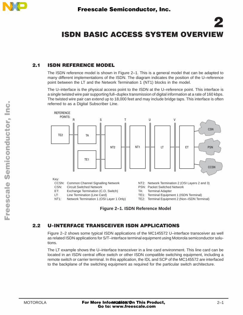
The ISDN reference model is shown in Figure 2–1. This is a general model that can be adapted tomany different implementations of the ISDN. The diagram indicates the position of the U–referencepoint between the LT and the Network Termination 1 (NT1) blocks in the model.
The U–interface is the physical access point to the ISDN at the U–reference point. This interface isa single twisted wire pair supporting full–duplex transmission of digital information at a rate of 160 kbps.The twisted wire pair can extend up to 18,000 feet and may include bridge taps. This interface is oftenreferred to as a Digital Subscriber Line.
Key:CCSN: Common Channel Signalling Network NT2: Network Termination 2 (OSI Layers 2 and 3)CSN: Circuit Switched Network PSN: Packet Switched NetworkET: Exchange Termination (C.O. Switch) TA: Terminal AdapterLT: Line Termination (Line Card) TE1: Terminal Equipment 1 (ISDN Terminal)NT1: Network Termination 1 (OSI Layer 1 Only) TE2: Terminal Equipment 2 (Non–ISDN Terminal)
Figure 2–1. ISDN Reference Model
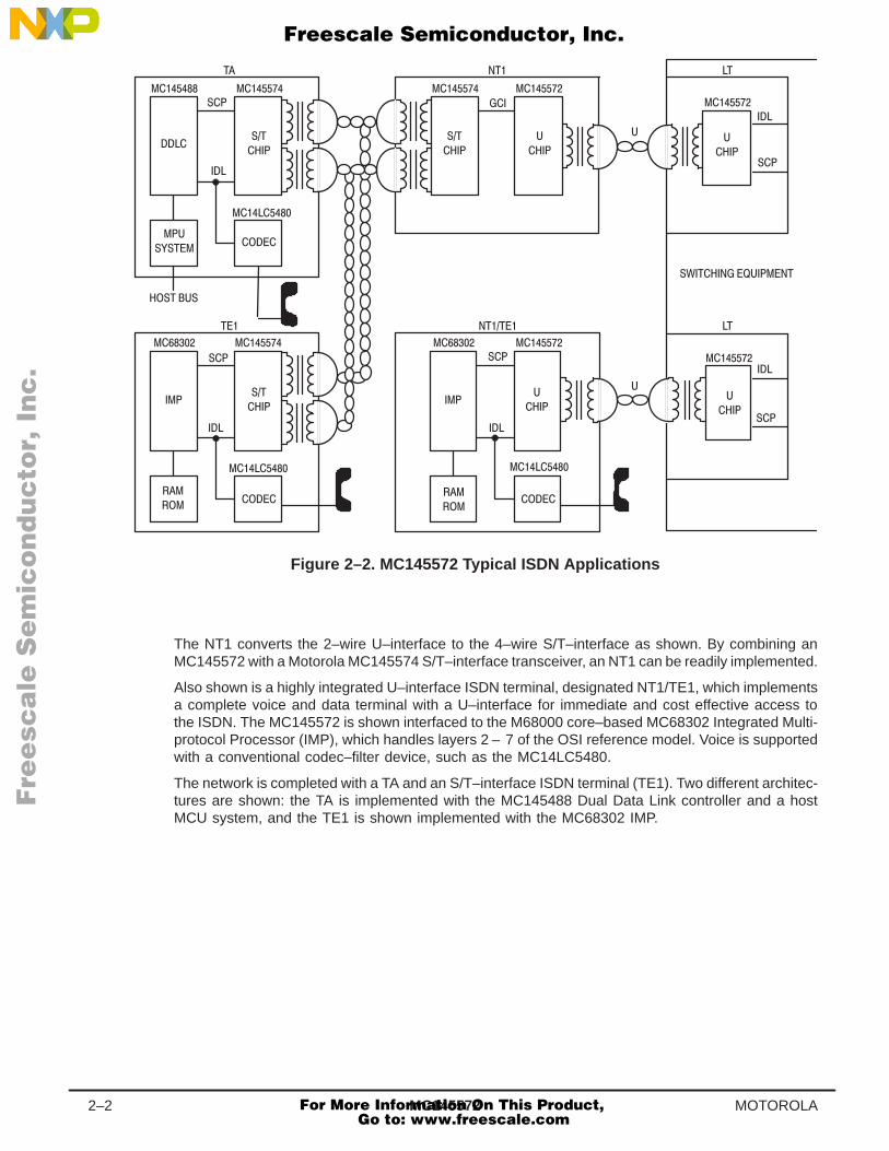
Figure 2–2 shows some typical ISDN applications of the MC145572 U–interface transceiver as wellas related ISDN applications for S/T–interface terminal equipment using Motorola semiconductor solu-tions.
The LT example shows the U–interface transceiver in a line card environment. This line card can belocated in an ISDN central office switch or other ISDN compatible switching equipment, including aremote switch or carrier terminal. In this application, the IDL and SCP of the MC145572 are interfacedto the backplane of the switching equipment as required for the particular switch architecture.
Fre
esc
ale
Se
mic
on
du
cto
r, I
Freescale Semiconductor, Inc.
For More Information On This Product, Go to: www.freescale.com
nc
...
MC1455722–2 MOTOROLA
Figure 2–2. MC145572 Typical ISDN Applications
The NT1 converts the 2–wire U–interface to the 4–wire S/T–interface as shown. By combining anMC145572 with a Motorola MC145574 S/T–interface transceiver, an NT1 can be readily implemented.
Also shown is a highly integrated U–interface ISDN terminal, designated NT1/TE1, which implementsa complete voice and data terminal with a U–interface for immediate and cost effective access tothe ISDN. The MC145572 is shown interfaced to the M68000 core–based MC68302 Integrated Multi-protocol Processor (IMP), which handles layers 2 – 7 of the OSI reference model. Voice is supportedwith a conventional codec–filter device, such as the MC14LC5480.
The network is completed with a TA and an S/T–interface ISDN terminal (TE1). Two different architec-tures are shown: the TA is implemented with the MC145488 Dual Data Link controller and a hostMCU system, and the TE1 is shown implemented with the MC68302 IMP.
Fre
esc
ale
Se
mic
on
du
cto
r, I
Freescale Semiconductor, Inc.
For More Information On This Product, Go to: www.freescale.com
nc
...
MC145572 2–3MOTOROLA
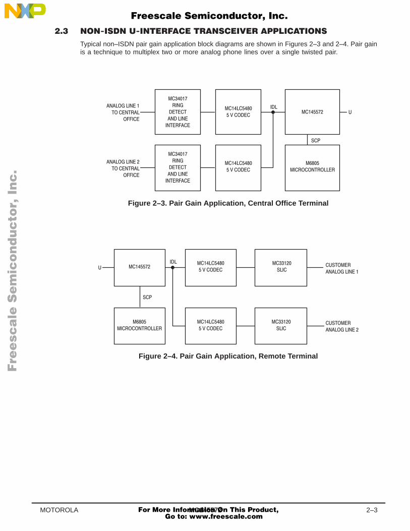
Typical non–ISDN pair gain application block diagrams are shown in Figures 2–3 and 2–4. Pair gainis a technique to multiplex two or more analog phone lines over a single twisted pair.
Figure 2–3. Pair Gain Application, Central Office Terminal
Figure 2–4. Pair Gain Application, Remote Terminal
Fre
esc
ale
Se
mic
on
du
cto
r, I
Freescale Semiconductor, Inc.
For More Information On This Product, Go to: www.freescale.com
nc
...

MC1455722–4 MOTOROLA
Fre
esc
ale
Se
mic
on
du
cto
r, I
Freescale Semiconductor, Inc.
For More Information On This Product, Go to: www.freescale.com
nc
...
MC145572 3–1MOTOROLA
This chapter describes the MC145572 pins and their operation. Additionally, quick reference tablesare provided. These tables are organized by the three major modes of operation and by packagetype.
The following tables (Tables 3–1 through 3–5) list the MC145572 pins in functional groups and providebrief pin descriptions. For more detailed information, refer to the section indicated in the table title.
Fre
esc
ale
Se
mic
on
du
cto
r, I
Freescale Semiconductor, Inc.
For More Information On This Product, Go to: www.freescale.com
nc
...
MC1455723–2 MOTOROLA
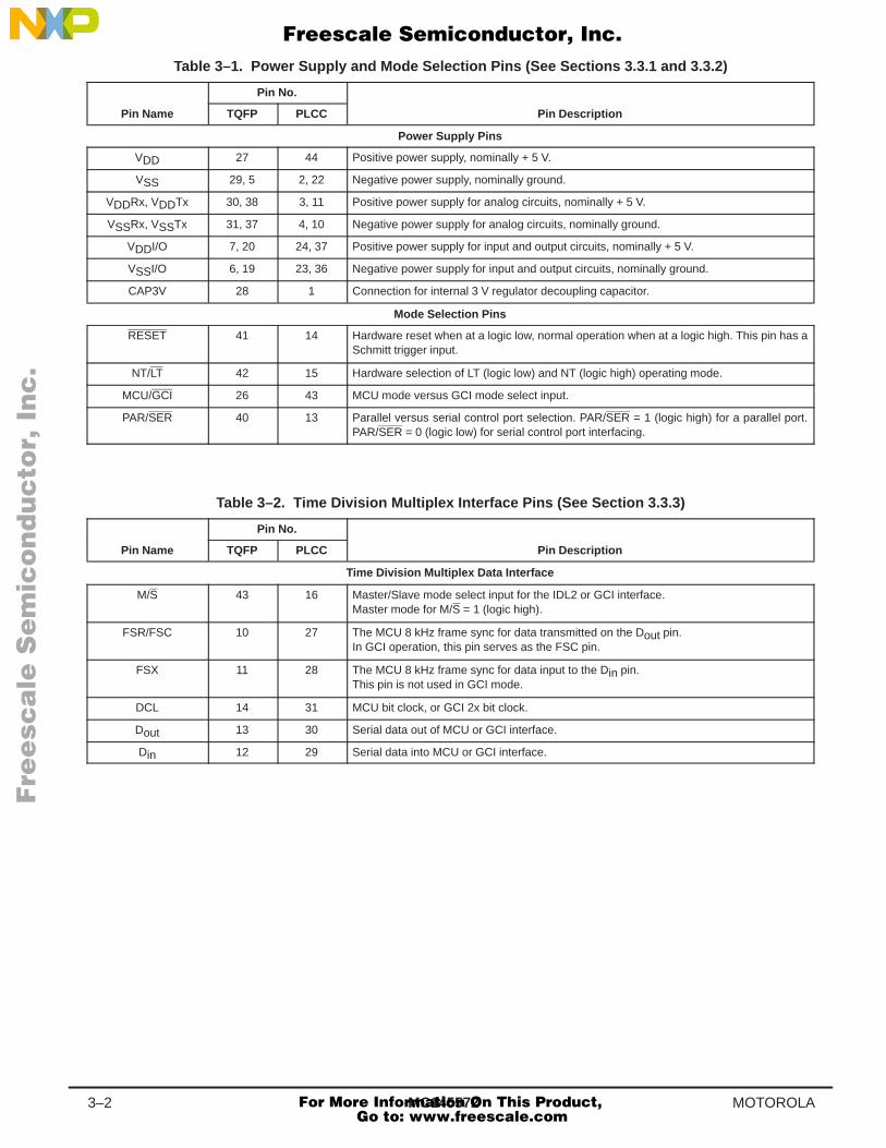
Table 3–1. Power Supply and Mode Selection Pins (See Sections 3.3.1 and 3.3.2)
Pin No.
Pin Name TQFP PLCC Pin Description
Power Supply Pins
VDD 27 44 Positive power supply, nominally + 5 V.
VSS 29, 5 2, 22 Negative power supply, nominally ground.
VDDRx, VDDTx 30, 38 3, 11 Positive power supply for analog circuits, nominally + 5 V.
VSSRx, VSSTx 31, 37 4, 10 Negative power supply for analog circuits, nominally ground.
VDDI/O 7, 20 24, 37 Positive power supply for input and output circuits, nominally + 5 V.
VSSI/O 6, 19 23, 36 Negative power supply for input and output circuits, nominally ground.
CAP3V 28 1 Connection for internal 3 V regulator decoupling capacitor.
Mode Selection Pins
RESET 41 14 Hardware reset when at a logic low, normal operation when at a logic high. This pin has aSchmitt trigger input.
NT/LT 42 15 Hardware selection of LT (logic low) and NT (logic high) operating mode.
MCU/GCI 26 43 MCU mode versus GCI mode select input.
PAR/SER 40 13 Parallel versus serial control port selection. PAR/SER = 1 (logic high) for a parallel port.PAR/SER = 0 (logic low) for serial control port interfacing.
Table 3–2. Time Division Multiplex Interface Pins (See Section 3.3.3)
Pin No.
Pin Name TQFP PLCC Pin Description
Time Division Multiplex Data Interface
M/S 43 16 Master/Slave mode select input for the IDL2 or GCI interface.Master mode for M/S = 1 (logic high).
FSR/FSC 10 27 The MCU 8 kHz frame sync for data transmitted on the Dout pin.In GCI operation, this pin serves as the FSC pin.
FSX 11 28 The MCU 8 kHz frame sync for data input to the Din pin.This pin is not used in GCI mode.
DCL 14 31 MCU bit clock, or GCI 2x bit clock.
Dout 13 30 Serial data out of MCU or GCI interface.
Din 12 29 Serial data into MCU or GCI interface.
Fre
esc
ale
Se
mic
on
du
cto
r, I
Freescale Semiconductor, Inc.
For More Information On This Product, Go to: www.freescale.com
nc
...
MC145572 3–3MOTOROLA
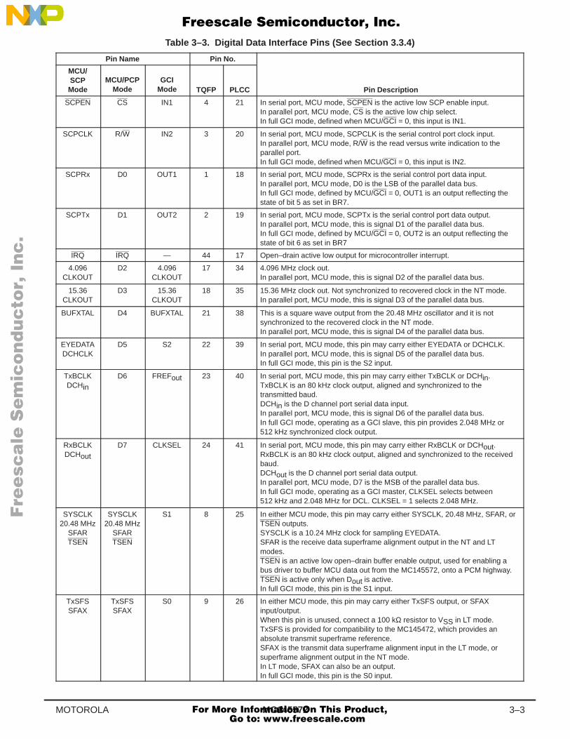
Table 3–3. Digital Data Interface Pins (See Section 3.3.4)
Pin Name Pin No.
MCU/SCPMode
MCU/PCPMode
GCIMode TQFP PLCC Pin Description
SCPEN CS IN1 4 21 In serial port, MCU mode, SCPEN is the active low SCP enable input.In parallel port, MCU mode, CS is the active low chip select.In full GCI mode, defined when MCU/GCI = 0, this input is IN1.
SCPCLK R/W IN2 3 20 In serial port, MCU mode, SCPCLK is the serial control port clock input.In parallel port, MCU mode, R/W is the read versus write indication to theparallel port.In full GCI mode, defined when MCU/GCI = 0, this input is IN2.
SCPRx D0 OUT1 1 18 In serial port, MCU mode, SCPRx is the serial control port data input.In parallel port, MCU mode, D0 is the LSB of the parallel data bus.In full GCI mode, defined by MCU/GCI = 0, OUT1 is an output reflecting thestate of bit 5 as set in BR7.
SCPTx D1 OUT2 2 19 In serial port, MCU mode, SCPTx is the serial control port data output.In parallel port, MCU mode, this is signal D1 of the parallel data bus.In full GCI mode, defined by MCU/GCI = 0, OUT2 is an output reflecting thestate of bit 6 as set in BR7
IRQ IRQ — 44 17 Open–drain active low output for microcontroller interrupt.
4.096CLKOUT
D2 4.096CLKOUT
17 34 4.096 MHz clock out.In parallel port, MCU mode, this is signal D2 of the parallel data bus.
15.36CLKOUT
D3 15.36CLKOUT
18 35 15.36 MHz clock out. Not synchronized to recovered clock in the NT mode.In parallel port, MCU mode, this is signal D3 of the parallel data bus.
BUFXTAL D4 BUFXTAL 21 38 This is a square wave output from the 20.48 MHz oscillator and it is notsynchronized to the recovered clock in the NT mode.In parallel port, MCU mode, this is signal D4 of the parallel data bus.
EYEDATADCHCLK
D5 S2 22 39 In serial port, MCU mode, this pin may carry either EYEDATA or DCHCLK.In parallel port, MCU mode, this is signal D5 of the parallel data bus.In full GCI mode, this pin is the S2 input.
TxBCLKDCHin
D6 FREFout 23 40 In serial port, MCU mode, this pin may carry either TxBCLK or DCHin.TxBCLK is an 80 kHz clock output, aligned and synchronized to thetransmitted baud.DCHin is the D channel port serial data input.In parallel port, MCU mode, this is signal D6 of the parallel data bus.In full GCI mode, operating as a GCI slave, this pin provides 2.048 MHz or512 kHz synchronized clock output.
RxBCLKDCHout
D7 CLKSEL 24 41 In serial port, MCU mode, this pin may carry either RxBCLK or DCHout.RxBCLK is an 80 kHz clock output, aligned and synchronized to the receivedbaud.DCHout is the D channel port serial data output.In parallel port, MCU mode, D7 is the MSB of the parallel data bus.In full GCI mode, operating as a GCI master, CLKSEL selects between512 kHz and 2.048 MHz for DCL. CLKSEL = 1 selects 2.048 MHz.
SYSCLK20.48 MHz
SFARTSEN
SYSCLK20.48 MHz
SFARTSEN
S1 8 25 In either MCU mode, this pin may carry either SYSCLK, 20.48 MHz, SFAR, orTSEN outputs.SYSCLK is a 10.24 MHz clock for sampling EYEDATA.SFAR is the receive data superframe alignment output in the NT and LTmodes.TSEN is an active low open–drain buffer enable output, used for enabling abus driver to buffer MCU data out from the MC145572, onto a PCM highway.TSEN is active only when Dout is active.In full GCI mode, this pin is the S1 input.
TxSFSSFAX
TxSFSSFAX
S0 9 26 In either MCU mode, this pin may carry either TxSFS output, or SFAXinput/output.When this pin is unused, connect a 100 kΩ resistor to VSS in LT mode.TxSFS is provided for compatibility to the MC145472, which provides anabsolute transmit superframe reference.SFAX is the transmit data superframe alignment input in the LT mode, orsuperframe alignment output in the NT mode.In LT mode, SFAX can also be an output.In full GCI mode, this pin is the S0 input.
Fre
esc
ale
Se
mic
on
du
cto
r, I
Freescale Semiconductor, Inc.
For More Information On This Product, Go to: www.freescale.com
nc
...
MC1455723–4 MOTOROLA
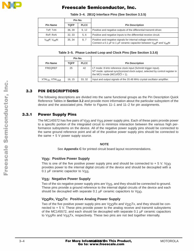
Table 3–4. 2B1Q Interface Pins (See Section 3.3.5)
Pin No.
Pin Name TQFP PLCC Pin Description
TxP, TxN 36, 39 9, 12 Positive and negative outputs of the differential transmit driver.
RxP, RxN 32, 33 5, 6 Positive and negative inputs to the differential receive circuit.
VrefP, VrefN 35, 34 8, 7 Positive and negative signals for internal voltage reference.Connect a 0.1 µF to 1 µF ceramic capacitor between VrefP and VrefN
Table 3–5. Phase Locked Loop and Clock Pins (See Section 3.3.6)
Pin No.
Pin Name TQFP PLCC Pin Description
FREQREF 25 42 LT mode: 8 kHz reference clock input (Schmitt trigger input).NT mode: optional synchronized clock output, selected by control register inthe MCU mode (MCU/GCI = 1).
XTALin, XTALout 16, 15 33, 32 Input and output signals of the 20.48 MHz crystal oscillator amplifier.
The following descriptions are divided into the same functional groups as the Pin Description QuickReference Tables in Section 3.2 and provide more information about the particular subsystem of thedevice and the associated pins. Refer to Figures 11–1 and 11–2 for pin assignments.
The MC145572 has five pairs of VDD and VSS power supply pins. Each of these pairs provide powerto a specific portion of the integrated circuit to minimize interaction between the various high per-formance subsystems on the device. All of the negative power supply pins should be connected tothe same ground reference point and all of the positive power supply pins should be connected tothe same + 5 V power supply source.
NOTE
See Appendix C for printed circuit board layout recommendations.
VDD: Positive Power SupplyThis is one of the five positive power supply pins and should be connected to + 5 V. VDDprovides power to the internal digital circuits of the device and should be decoupled with a0.1 µF ceramic capacitor to VSS.
VSS: Negative Power SupplyTwo of the six negative power supply pins are VSS, and they should be connected to ground.These pins provide a ground reference to the internal digital circuits of the device and eachshould be decoupled with separate 0.1 µF ceramic capacitors to VDD.
VDDRx, VDDTx: Positive Analog Power SupplyTwo of the five positive power supply pins are VDDRx and VDDTx, and they should be con-nected to + 5 V. These pins provide power to the analog receive and transmit subsystemsof the MC145572, and each should be decoupled with separate 0.1 µF ceramic capacitorsto VSSRx and VSSTx, respectively. These two pins are not tied together internally.
Fre
esc
ale
Se
mic
on
du
cto
r, I
Freescale Semiconductor, Inc.
For More Information On This Product, Go to: www.freescale.com
nc
...
MC145572 3–5MOTOROLA
VSSRx, VSSTx: Negative Analog Power SupplyTwo of the six negative power supply pins are VSSRx and VDDRx, and they should be con-nected to ground. These pins provide a ground reference to the analog receive and transmitsubsystems of the device, and each should be decoupled with separate 0.1 µF ceramiccapacitors to VDDRx and VDDTx, respectively.
VDDI/O: Positive Power Supply Input/OutputTwo of the five positive power supply pins are VSSI/O, and they should be connected to+ 5 V. These pins provide power to the digital input and output circuits of the device and eachshould be decoupled with a 0.1 µF ceramic capacitor to VSSI/O. These pins can also beconnected to 3.3 V to provide I/O compatibility with 3 V interface devices.
VSSI/O: Negative Power Supply Input/OutputTwo of the six negative power supply pins are VSSI/O, and they should be connected toground. These pins provide a ground reference to the digital input and output circuits of thedevice, each should be decoupled with a 0.1 µF ceramic capacitor to VDDI/O.
CAP3V: Core Logic Positive Power SupplyThis pin is tied to the internal core logic power supply. An external 0.1 µF to 1.0 µF decouplingcapacitor should be connected between this pin and ground. Applications requiring a 3 Vpower supply may source current from this pin. See Section 10.3, Electrical Specifications ,for more information on the limit of the source current. This output is at 5 V until reset isapplied to the MC145572.
These inputs define the mode of operation for the MC145572. More information on the function ofthe device in specific modes can be obtained from Chapter 5, MCU Mode Device Functionality andChapter 8, GCI Mode Functional Description .
RESET: Reset InputA logic 0 applied to this Schmitt trigger input pin holds the device in a hardware reset condi-tion. A logic 1 puts the device into the normal operating state. Register NR0(b3) providesa similar software reset function, thereby allowing control of this mode from the externalmicrocontroller. This pin must be held low for at least six 20.48 MHz clock periods.
CAUTION
Reset must be asserted until VDD is greater than 4.75 V and the oscillator is stable.
During a hardware reset condition, all SCP registers are reset to their default state, and thesignals output from the DCL and FSR pins when in the MCU Master mode are halted. Inaddition, the Tx driver is put into a low impedance state to terminate the U–interface and the2B1Q receiver is unable to detect the activation wake–up tone.
NT/LT: NT/LT Select InputA logic 1 applied to this pin puts the device into the NT mode and a logic 0 puts the deviceinto the LT mode. Note that Byte register 8, bit 0, also controls NT versus LT mode selection,thereby allowing software control of this mode.
Fre
esc
ale
Se
mic
on
du
cto
r, I
Freescale Semiconductor, Inc.
For More Information On This Product, Go to: www.freescale.com
nc
...
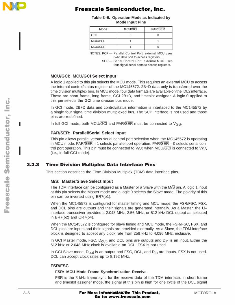
MC1455723–6 MOTOROLA
Table 3–6. Operation Mode as Indicated byMode Input Pins
Mode MCU/GCI PAR/SER
GCI 0 0
MCU/PCP 1 1
MCU/SCP 1 0
NOTES: PCP — Parallel Control Port, external MCU uses8–bit data port to access registers.
SCP — Serial Control Port, external MCU usesfour signal serial ports to access registers.
MCU/GCI: MCU/GCI Select InputA logic 1 applied to this pin selects the MCU mode. This requires an external MCU to accessthe internal control/status register of the MC145572. 2B+D data only is transferred over thetime division multiplex bus. In MCU mode, four data formats are available on the IDL2 interface.These are short frame, long frame, GCI 2B+D, and timeslot assigner. A logic 0 applied tothis pin selects the GCI time division bus mode.
In GCI mode, 2B+D data and control/status information is interfaced to the MC145572 bya single four signal time division multiplexed bus. The SCP interface is not used and thosepins are redefined.
In full GCI mode, both MCU/GCI and PAR/SER must be connected to VSS.
PAR/SER: Parallel/Serial Select InputThis pin allows parallel versus serial control port selection when the MC145572 is operatingin MCU mode. PAR/SER = 1 selects parallel port operation. PAR/SER = 0 selects serial con-trol port operation. This pin must be connected to VSS when MCU/GCI is connected to VSS(i.e., in full GCI mode).
This section describes the Time Division Multiplex (TDM) data interface pins.
M/S: Master/Slave Select InputThe TDM interface can be configured as a Master or a Slave with the M/S pin. A logic 1 inputat this pin selects the Master mode and a logic 0 selects the Slave mode. The polarity of thispin can be inverted using BR7(b1).
When the MC145572 is configured for master timing and MCU mode, the FSR/FSC, FSX,and DCL pins are outputs and their signals are generated internally. As a Master, the U–interface transceiver provides a 2.048 MHz, 2.56 MHz, or 512 kHz DCL output as selectedin BR7(b2) and OR7(b4).
When the MC145572 is configured for slave timing and MCU mode, the FSR/FSC, FSX, andDCL pins are inputs and their signals are provided externally. As a Slave, the TDM interfaceblock is designed to accept any clock rate from 256 kHz to 4.096 MHz, inclusive.
In GCI Master mode, FSC, Dout, and DCL pins are outputs and Din is an input. Either the512 kHz or 2.048 MHz clock is available on DCL. FSX is not used.
In GCI Slave mode, Dout is an output and FSC, DCL, and Din are inputs. FSX is not used.DCL can accept clock rates up to 8.192 MHz.
FSR/FSCFSR: MCU Mode Frame Synchronization Receive
FSR is the 8 kHz frame sync for the receive data of the TDM interface. In short frameand timeslot assigner mode, the signal at this pin is high for one cycle of the DCL signal
Fre
esc
ale
Se
mic
on
du
cto
r, I
Freescale Semiconductor, Inc.
For More Information On This Product, Go to: www.freescale.com
nc
...
MC145572 3–7MOTOROLA
and is rising edge aligned with the rising edge of the DCL signal. This pin is an input whenthe TDM interface is in Slave mode and an output in the Master mode as establishedby the M/S pin. See Figures 5–17 through 5–20.
When the MC145572 is in NT mode and M/S = 1, this output is phase locked to the signalreceived at the U–interface. As an LT in the Master mode, this output is derived directlyfrom the 20.48 MHz master clock. The frequency of the periodic FSR signal is 8 kHz. Asa Slave, the FSR signal must occur at an average rate of 8 kHz (125 µs interval) witha maximum phase deviation from a jitter–free sync of ± 48 µs.
In Master mode, FSR and FSX output the same waveform. In Slave mode, both FSR andFSX inputs must be driven by external circuitry. FSR and FSX inputs can be tied togetherin Slave mode and a common sync can be used to drive both inputs.
FSC: GCI Mode Frame Synchronization Receive
In full GCI mode and in GCI 2B+D mode, this pin serves as the FSC pin, and the signalis high for two cycles of the DCL signal and the rising edge is aligned with the rising edgeof the DCL signal. This pin is an input when the TDM interface is in Slave mode and anoutput in Master mode as established by the M/S pin. FSC indicates a superframeboundary by going high for one DCL clock. This happens once every 12 ms.
When the MC145572 is in NT mode and M/S = 1, this output is phase locked to the signalreceived at the U–interface.
As an LT in the Master mode, this output is derived directly from the 20.48 MHz masterclock. The frequency of the periodic FSR signal is 8 kHz.
As a Slave, the FSC signal must occur at an average rate of 8 kHz (125 µs interval) witha maximum phase deviation from a jitter free sync of ± 48 µs.
FSX: MCU Mode Frame Synchronization TransmitFSX is the 8 kHz frame sync for the transmit data of the MCU interface. This pin is not usedin the GCI mode. The formatting of FSX is mode dependent.
This pin is an input when the TDM interface is in the Slave mode and an output in Mastermode, as established by the M/S pin.
When the MC145572 is in NT mode and M/S = 1, this output is phase locked to the signalreceived at the U–interface. As an LT in the Master mode, this output is derived directly fromthe 20.48 MHz master clock. The frequency of the periodic FSR signal is 8 kHz. As a Slave,the FSX signal must occur at an average rate of 8 kHz (125 µs interval) with a maximum phasedeviation from a jitter free sync of ± 48 µs.
In Master mode, FSR and FSX output the same waveform. In Slave mode, both FSR andFSX inputs must be driven by external circuitry. FSR and FSX inputs can be tied togetherin the Slave mode and a common sync can be used to drive both inputs.
DCL: Data Clock Input/OutputThis pin is an input when the TDM interface is in the Slave mode and an output in the Mastermode, as established by the M/S pin.
As a timing master in the MCU–NT mode, this pin provides a 2.048 MHz, 512 kHz, or a2.56 MHz MCU clock output. This choice is programmed in BR7(b2) and OR7(b4). Also seeSection 5.4 .
When configured as a slave in MCU mode, this pin accepts any clock frequency from 256 kHzto 4.096 MHz, inclusive.
In GCI mode, this pin provides clock outputs 2.048 MHz or 512 kHz, as selected by CLKSEL.In GCI Slave mode, this pin accepts clock frequencies of 512 kHz to 8.192 MHz, inclusive.
In NT master timing of operation, recovered timing is conveyed over DCL by adjusting thewidth of the clock. The adjustment is made by the internal digital PLL and occurs during twoconsecutive 8 kHz frames, once per U–interface basic frame. The adjustment consists of
Fre
esc
ale
Se
mic
on
du
cto
r, I
Freescale Semiconductor, Inc.
For More Information On This Product, Go to: www.freescale.com
nc
...
MC1455723–8 MOTOROLA
adding or subtracting a single 20.48 MHz clock period during the high time of DCL. Sincethis occurs during two consecutive 8 kHz frames, the total adjustment is ± 97 ns, once everybasic frame. See Chapter 10, Electrical Specifications, for the locations of the timing adjust-ment.
Dout : Data Transmit OutputThis pin is the output for the 2B+D data received at the U–interface. The formatting of thedata is mode dependent. In GCI mode, Dout is an open drain output and must be connectedto VDD through a pullup resistor. In IDL–2 mode, Dout goes high impedance when the 2B+Dtransfer is complete. Refer to Chapter 5, MCU Mode Device Functionality and Chapter 8,GCI Mode Functional Description, for more information.
Din: Data Receive InputThis pin is the input for the 2B+D data to be transmitted at the U–interface. The formattingof the data is mode dependent. Refer to Chapter 5, MCU Mode Device Functionality andChapter 8, GCI Mode Functional Description, for more information. In GCI mode, Din mustbe connected to VDD through a 1.5 kΩ pull-up resistor.
These pins provide a digital transfer interface for the MC145572 when configured for MCU mode.In GCI mode, control and status information is provided over the GCI interface.
SCPEN/CS/IN1SCPEN Serial Control Port Enable Input
This pin, when held low, selects the SCP for the transfer of control, status, and M channeldata information into and out of the U–interface transceiver. SCPEN should be held lowfor 8 or 16 periods of the SCPCLK signal in order for information to be transferred intoor out of the MC145572. The SCP interface disregards any SCP operation that is notexactly 8 or 16 SCPCLK clock pulses in length. If the MC145572 is the only SCP devicein the system, this pin can be tied low and bursted SCP clock can be used to accessthe register.
CS Parallel Control Port Chip Select
In Parallel Control Port mode, this pin acts as an active low chip select input.
IN1: Input 1
In full GCI mode, defined when MCU/GCI = 0, this is an input bit. IN1 may be read viaBR7. In NT mode, IN1 is transmitted as PS1 in the M4 maintenance bits.
SCPCLK/R/W /IN2SCPCLK: Serial Control Port Clock Input
This is an input to the device used for clocking data into and out of the SCP interface.Data is clocked into the MC145572 from SCPRx on rising edges of SCPCLK. Data isshifted out of the MC145572 SCPTx pin on falling edges of SCPCLK. SCPCLK can beany frequency from 0 up to 4.096 MHz. An SCP transaction takes place when SCPENis brought low. Note that SCPCLK is ignored when SCPEN is high (i.e., it may becontinuous or it can operate in a burst mode). If the MC145572 is the only SCP deviceused, the SCPEN pin can be tied low and bursted clocks applied to SCPCLK.
R/W: Parallel Control Port Read/Write
In Parallel Control Port mode, this pin functions as read versus write indication, wherewrite is active low.
IN2: GCI Mode Input 2
IN2 may be read via BR7. In NT mode, IN2 is transmitted as PS2 in the M4 channelmaintenance bits.
Fre
esc
ale
Se
mic
on
du
cto
r, I
Freescale Semiconductor, Inc.
For More Information On This Product, Go to: www.freescale.com
nc
...
MC145572 3–9MOTOROLA
SCPRx/D0/OUT1SCPRx: Serial Control Port Receive InputSCPRx is used to input control, status, and M channel data information to the U–interfacetransceiver. Data is shifted into the MC145572 on rising edges of SCPCLK. SCPRx isignored when data is being shifted out of SCPTx or when SCPEN is high.
D0: Data 0In Parallel Control Port mode, this pin functions as bit 0, LSB, of the data bus.
OUT1: GCI Mode Output 1In full GCI mode, defined by MCU/GCI = 0, OUT1 is an output reflecting the state of thebit as set in BR7. OUT1 is also set high when the GCI Command/Indicate channelcommand LTD1 is active.
SCPTx/D1/OUT2SCPTx: Serial Control Port Transmit OutputSCPTx is used to output control, status, and M channel data information from theMC145572 U–interface transceiver. Data is shifted out of SCPTx on the falling edge ofSCPCLK, most significant bit first.
D1: Data 1In Parallel Control Port mode, this pin functions as bit 1 of the data bus.
OUT2: GCI Mode Output 2In full GCI mode, defined by MCU/GCI = 0, OUT2 is an output reflecting the state of thebit as set in BR7. OUT2 is also set high when the GCI Command/Indicate channelcommand LTD2 is active.
IRQ: Interrupt Request OutputThe IRQ pin is an active low, open drain output, used to signal an external microcontrollerthat an interrupt condition exists in the MC145572. On clearing the interrupt condition, thepin is returned to the high impedance state. See the description for Nibble Register 3, Sec-tion 4.3.4 , for descriptions of the sources of interrupt conditions.
4.096 CLKOUT/D24.096 CLKOUT: 4.096 MHz Buffered Clock OutputThis pin provides a buffered 4.096 MHz clock output that can be used for a microcontrollerclock. This clock is not locked to the recovered clock timing. This output can be disabledby writing a 1 to OR9(b0).
D2: Data 2In Parallel Control Port mode, this pin functions as bit 2 of the data bus.
15.36 CLKOUT/D315.36 CLKOUT: 15.36 MHz Buffered Clock OutputThis pin provides a buffered 15.36 MHz clock output that can be used for the MC145474/75and MC145574 S/T transceiver clocks. Register BR14(b0) or Register BR15A(b2) mustbe set to enable this output. This clock is a 20.48 MHz clock with every fourth clock cycleremoved. This clock is not locked to the recovered clock timing. This output can be disabledby writing a 1 to OR9(b1). This output can be cleanly transitioned to 10.24 MHz by writinga 1 to OR9(b3).
NOTEThis pin does not provide a 50% duty cycle output. It does provide a clock thatthe MC145474/75 and MC145574 can use. Figure 10–14 shows the timing ofthis signal.
Fre
esc
ale
Se
mic
on
du
cto
r, I
Freescale Semiconductor, Inc.
For More Information On This Product, Go to: www.freescale.com
nc
...
MC1455723–10 MOTOROLA
D3: Data 3
In Parallel Control Port mode, this pin functions as bit 3 of the data bus.
BUFXTAL/D4BUFXTAL: Buffered Crystal Output
BUFXTAL is the buffered square wave output from the 20.48 MHz oscillator. After reset,this signal is active. This output can be set to a high impedance state by setting OR9(b2)to a 1. This signal is available in both MCU/SCP and GCI modes of operation.
CAUTION
In NT mode operation, this signal is not phase locked to recovered timing.
D4: Data 4
In Parallel Control Port mode, this pin functions as bit 4 of the data bus.
EYEDATA/DCHCLK/D5/S2EYEDATA: Eye Pattern Data Output
Eye Pattern Data is a serial data output that provides a digital word once per received2B1Q baud. This data word represents the recovered 2B1Q received bauds and can beused to reconstruct a conventional eye pattern on an oscilloscope with the use of adigital–to–analog converter. Control bit BR15A(b0) must be set to a 1 to enable this pin.See Appendix D for applications information concerning this feature.
DCHCLK: D Channel Clock
DCHCLK is the D channel port clock output. It is enabled by setting D channel port enablein Init Group register OR8 (b0).
D5: Data 5
In Parallel Control Port mode, this pin functions as bit 5 of the data bus.
S2: GCI Mode Slot Selection 2
In full GCI mode, this pin is an input for the timeslot selection, S0 – S2. See Table 3–7for more information.
Table 3–7. GCI Timeslot Assignmentas Set by S0 – S2
GCI Timeslot S2 S1 S0
0 0 0 0
1 0 0 1
2 0 1 0
3 0 1 1
4 1 0 0
5 1 0 1
6 1 1 0
7 1 1 1
TxBCLK/DCH in /D6/FREFoutTxBCLK: Transmit Baud Clock Output
This 80 kHz clock indicates the timing of the transmitted 2B1Q bauds. Control bitsBR14(b0) or BR15A(b0) must be set to logic 1 to enable this signal.
Fre
esc
ale
Se
mic
on
du
cto
r, I
Freescale Semiconductor, Inc.
For More Information On This Product, Go to: www.freescale.com
nc
...
MC145572 3–11MOTOROLA
DCHin: D Channel Data In
DCHin is the D channel port serial input. It is enabled by setting D channel port enablein Init Group register OR8(b0).
D6: Data 6
In Parallel Control Port mode, this pin functions as bit 6 of the data bus.
FREFout : GCI Mode Locked Frequency Output
In full GCI mode, operating as a slave, this pin provides 2.048 MHz or 512 kHz synchro-nized clock output as selected by CLKSEL. When the MC145572 is configured as a GCItiming master, FREFout does not provide a clock since the clock is present on DCL. It isnot necessary to set any register bits to enable this output in GCI slave mode.
RxBCLK/DCH out /D7/CLKSELRxBCLK: Transmit Baud Clock Output
This 80 kHz clock indicates the timing of the received 2B1Q bauds. Control bits BR14(b0)or BR15A(b0) must be set to logic 1 to enable this signal.
DCHout : D Channel Data Out
DCHout is the D channel port serial output. It is enabled by setting D channel port enablein Init Group register OR8(b0).
D7: Data 7
In Parallel Control Port mode, this pin functions as bit 7 of the data bus.
CLKSEL: Clock Select
When operating as a GCI timing master in full GCI mode, CLKSEL selects between512 kHz and 2.048 MHz for DCL. CLKSEL = 1 selects 2.048 MHz.
When operating as a GCI timing slave in full GCI–NT mode, CLKSEL selects betweenphase locked 512 kHz and 2.048 MHz clocks appearing at FREFout.
SYSCLK/SFAR/TSEN /S1SYSCLK: System Clock Output
System Clock Output is a 10.24 MHz clock that is used to clock Eye Pattern Data. Controlbits BR14(b0) or BR15A(b0) must be set to a 1 to enable this signal. See Appendix Dfor applications information concerning this pin.
SFAR: Superframe Alignment Receive
SFAR provides a superframe alignment output signal in the NT and LT modes. This signalis only available when the MC145572 is in MCU mode. Setting OR8 (b1) enables thisoutput. This signal is one MCU clock wide and occurs during the DCL clock following FSR.See Section 5.4.7 . This pulse indicates the first 2B+D frame received from a U–interfacesuperframe.
TSEN: Open–Drain Buffer Enable Output
TSEN is an open–drain buffer enable output, used for enabling a bus driver to buffer TDMdata out from the MC145572 onto a PCM highway. When the MC145572 is configuredfor MCU mode, TSEN is active during the B1, B2, and D channel timeslots, regardlessof where they occur. When the MC145572 is configured for GCI 2B+D electrical–onlyinterfacing while in MCU mode, TSEN is active during the B1, B2, and D channel timeslotsonly. TSEN is also available when the MC145572 is configured for timeslot assigner opera-tion. When a separate D channel serial port option is enabled, TSEN is active only duringthe B1 and B2 channel timeslots. This pin is enabled when OR7(b5) = 1 or OR8(b3) = 1.
S1: GCI Mode Slot Selection 1
In full GCI mode, this pin is an input for the timeslot selection, S0 – S2.
Fre
esc
ale
Se
mic
on
du
cto
r, I
Freescale Semiconductor, Inc.
For More Information On This Product, Go to: www.freescale.com
nc
...
MC1455723–12 MOTOROLA
TxSFS/SFAX/S0TxSFS: Transmit Superframe Sync Output
This output pulses high, 8 bauds prior to the transmit sync word separating the first andsecond transmitted basic frames in a superframe. Control bits BR14(b0) and BR15A(b3)must both be set to a 1 to enable this pin. The TxSFS output is coincident with the TxBaud Clock.
TxSFS is provided for compatibility to the MC145472, which provides an absolute transmitsuperframe reference.
SFAX: Superframe Alignment Transmit
SFAX is the transmit superframe alignment input in the LT mode, or superframe alignmentoutput in the NT mode. SFAX is enabled by setting SFAX/SFAR Enable in Init Group registerOR8 (b1). SFAX may be configured as an output in LT mode by setting OR8 (b5). SeeSections 4.5.9 and 5.4.7. When GCI 2B+D mode is enabled, MCU/GCI = 1, and OR6(b3)= 1, the SFAX function is superceded by modulation of the FSC input. This pulse indicatesthe first 2B+D IDL frame transmitted onto the U–interface superframe.
WARNING
In MCU mode (MCU/GCI pin connected to VDD), this pin function becomes un-defined after a hardware or software reset. Most applications do not use anyof the features available at this pin. In such cases, a 10 kΩ resistor must beconnected between this pin and VSS. In the rare applications that enable anyof the functions available at this pin, the 10 kΩ resistor may not be required.This applies to both NT and LT mode operation.
S0: Slot Selection 0
In full GCI mode, this pin is an input for the timeslot selection, S0 – S2.
These pins form the 2B1Q interface of the MC145572 U–interface transceiver. Refer to AppendixE for information on the line interface. Refer to Appendix B for component sourcing.
TxP and TxN: Transmit Positive and Transmit Negative OutputsThese are the differential analog output pins of the transmit line driver.
RxP and RxN: Receive Positive and Receive Negative InputsThese are the differential analog input pins to the 2B1Q receiver.
Vref P and Vref N: Reference Voltage Positive and Reference VoltageConnect a 0.1 µF ceramic capacitor between these pins.
In LT mode, the MC145572 derives its 20.48 MHz master clock from a clock reference using an on–chipPLL with an 8 kHz clock reference applied to pin FREQREF.
In NT mode, no reference clock is required, since timing is recovered from the line. External circuitryis the same for both NT and LT modes.
FREQREF: Frequency ReferenceLT Mode: This Schmitt trigger digital input pin accepts the 8 kHz reference frequencyfor the analog phase locked loop in LT mode. Typically, this clock can be the same8 kHz synchronization input as connected to FSR or FSX. For ISDN central officeapplications, the frequency applied at this pin should be stable to ± 5 ppm to meet
Fre
esc
ale
Se
mic
on
du
cto
r, I
Freescale Semiconductor, Inc.
For More Information On This Product, Go to: www.freescale.com
nc
...
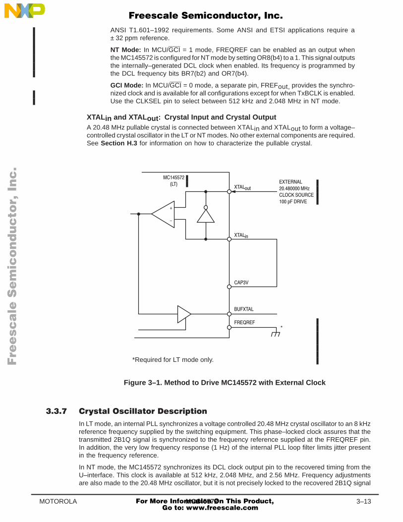
MC145572 3–13MOTOROLA
ANSI T1.601–1992 requirements. Some ANSI and ETSI applications require a± 32 ppm reference.
NT Mode: In MCU/GCI = 1 mode, FREQREF can be enabled as an output whenthe MC145572 is configured for NT mode by setting OR8(b4) to a 1. This signal outputsthe internally–generated DCL clock when enabled. Its frequency is programmed bythe DCL frequency bits BR7(b2) and OR7(b4).
GCI Mode: In MCU/GCI = 0 mode, a separate pin, FREFout, provides the synchro-nized clock and is available for all configurations except for when TxBCLK is enabled.Use the CLKSEL pin to select between 512 kHz and 2.048 MHz in NT mode.
XTALin and XTAL out : Crystal Input and Crystal OutputA 20.48 MHz pullable crystal is connected between XTALin and XTALout to form a voltage–controlled crystal oscillator in the LT or NT modes. No other external components are required.See Section H.3 for information on how to characterize the pullable crystal.
#
*
!
' "
# &)(
# $%
"
!#
*Required for LT mode only.
*
Figure 3–1. Method to Drive MC145572 with External Clock
In LT mode, an internal PLL synchronizes a voltage controlled 20.48 MHz crystal oscillator to an 8 kHzreference frequency supplied by the switching equipment. This phase–locked clock assures that thetransmitted 2B1Q signal is synchronized to the frequency reference supplied at the FREQREF pin.In addition, the very low frequency response (1 Hz) of the internal PLL loop filter limits jitter presentin the frequency reference.
In NT mode, the MC145572 synchronizes its DCL clock output pin to the recovered timing from theU–interface. This clock is available at 512 kHz, 2.048 MHz, and 2.56 MHz. Frequency adjustmentsare also made to the 20.48 MHz oscillator, but it is not precisely locked to the recovered 2B1Q signal
Fre
esc
ale
Se
mic
on
du
cto
r, I
Freescale Semiconductor, Inc.
For More Information On This Product, Go to: www.freescale.com
nc
...

MC1455723–14 MOTOROLA
at all times. This means that the BUFXTALout pin can not be used as a master clock source in applica-tions that require a synchronized clock. In NT mode, the U–interface transceiver can lock to 80 kbaud± 32 ppm receive signals.
A single 20.48 MHz pullable crystal must be connected between XTALin and XTALout pins of theMC145572. Refer to Appendix B for crystal specifications and sourcing information. The crystal speci-fied for the NT mode operation will operate in LT applications. The crystal specified for LT applicationswill not operate in NT applications. The reason is that the NT mode crystal has a tighter overall fre-quency tolerance than the LT mode crystal.
NOTE
Motorola continues to qualify several third party sources for the 20.48 MHz crystal. Contactyour local Motorola representative or Motorola factory applications staff for the latest in-formation regarding component sourcing.
Fre
esc
ale
Se
mic
on
du
cto
r, I
Freescale Semiconductor, Inc.
For More Information On This Product, Go to: www.freescale.com
nc
...
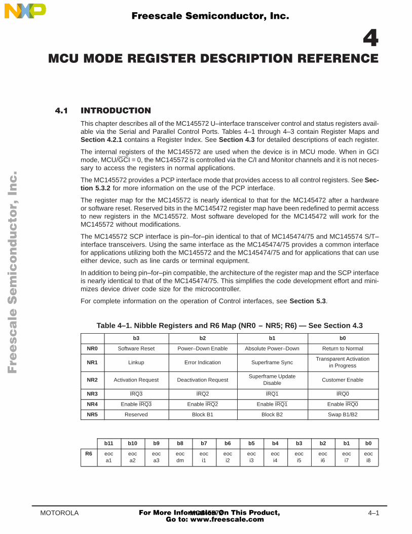
MC145572 4–1MOTOROLA
This chapter describes all of the MC145572 U–interface transceiver control and status registers avail-able via the Serial and Parallel Control Ports. Tables 4–1 through 4–3 contain Register Maps andSection 4.2.1 contains a Register Index. See Section 4.3 for detailed descriptions of each register.
The internal registers of the MC145572 are used when the device is in MCU mode. When in GCImode, MCU/GCI = 0, the MC145572 is controlled via the C/I and Monitor channels and it is not neces-sary to access the registers in normal applications.
The MC145572 provides a PCP interface mode that provides access to all control registers. See Sec-tion 5.3.2 for more information on the use of the PCP interface.
The register map for the MC145572 is nearly identical to that for the MC145472 after a hardwareor software reset. Reserved bits in the MC145472 register map have been redefined to permit accessto new registers in the MC145572. Most software developed for the MC145472 will work for theMC145572 without modifications.
The MC145572 SCP interface is pin–for–pin identical to that of MC145474/75 and MC145574 S/T–interface transceivers. Using the same interface as the MC145474/75 provides a common interfacefor applications utilizing both the MC145572 and the MC145474/75 and for applications that can useeither device, such as line cards or terminal equipment.
In addition to being pin–for–pin compatible, the architecture of the register map and the SCP interfaceis nearly identical to that of the MC145474/75. This simplifies the code development effort and mini-mizes device driver code size for the microcontroller.
For complete information on the operation of Control interfaces, see Section 5.3 .
Table 4–1. Nibble Registers and R6 Map (NR0 – NR5; R6) — See Section 4.3
b3 b2 b1 b0
NR0 Software Reset Power–Down Enable Absolute Power–Down Return to Normal
NR1 Linkup Error Indication Superframe SyncTransparent Activation
in Progress
NR2 Activation Request Deactivation RequestSuperframe Update
DisableCustomer Enable
NR3 IRQ3 IRQ2 IRQ1 IRQ0
NR4 Enable IRQ3 Enable IRQ2 Enable IRQ1 Enable IRQ0
NR5 Reserved Block B1 Block B2 Swap B1/B2
b11 b10 b9 b8 b7 b6 b5 b4 b3 b2 b1 b0
R6 eoca1
eoca2
eoca3
eocdm
eoci1
eoci2
eoci3
eoci4
eoci5
eoci6
eoci7
eoci8
Fre
esc
ale
Se
mic
on
du
cto
r, I
Freescale Semiconductor, Inc.
For More Information On This Product, Go to: www.freescale.com
nc
...
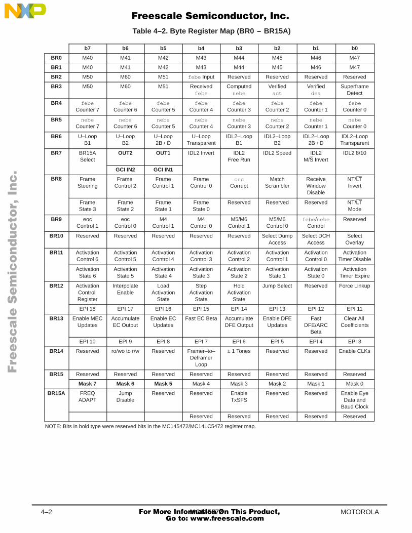
MC1455724–2 MOTOROLA
Table 4–2. Byte Register Map (BR0 – BR15A)
b7 b6 b5 b4 b3 b2 b1 b0
BR0 M40 M41 M42 M43 M44 M45 M46 M47
BR1 M40 M41 M42 M43 M44 M45 M46 M47
BR2 M50 M60 M51 febe Input Reserved Reserved Reserved Reserved
BR3 M50 M60 M51 Receivedfebe
Computednebe
Verifiedact
Verifieddea
SuperframeDetect
BR4 febeCounter 7
febeCounter 6
febeCounter 5
febeCounter 4
febeCounter 3
febeCounter 2
febeCounter 1
febeCounter 0
BR5 nebeCounter 7
nebeCounter 6
nebeCounter 5
nebeCounter 4
nebeCounter 3
nebeCounter 2
nebeCounter 1
nebeCounter 0
BR6 U–LoopB1
U–LoopB2
U–Loop2B+ D
U–LoopTransparent
IDL2–LoopB1
IDL2–LoopB2
IDL2–Loop2B+ D
IDL2–LoopTransparent
BR7 BR15ASelect
OUT2 OUT1 IDL2 Invert IDL2Free Run
IDL2 Speed IDL2M/S Invert
IDL2 8/10
GCI IN2 GCI IN1
BR8 FrameSteering
Frame Control 2
FrameControl 1
FrameControl 0
crcCorrupt
MatchScrambler
ReceiveWindowDisable
NT/LTInvert
FrameState 3
FrameState 2
FrameState 1
FrameState 0
Reserved Reserved Reserved NT/LTMode
BR9 eocControl 1
eocControl 0
M4Control 1
M4Control 0
M5/M6Control 1
M5/M6Control 0
febe /nebeControl
Reserved
BR10 Reserved Reserved Reserved Reserved Reserved Select DumpAccess
Select DCHAccess
SelectOverlay
BR11 ActivationControl 6
ActivationControl 5
ActivationControl 4
ActivationControl 3
ActivationControl 2
ActivationControl 1
ActivationControl 0
ActivationTimer Disable
ActivationState 6
ActivationState 5
ActivationState 4
ActivationState 3
ActivationState 2
ActivationState 1
ActivationState 0
ActivationTimer Expire
BR12 ActivationControl Register
InterpolateEnable
LoadActivation
State
StepActivation
State
HoldActivation
State
Jump Select Reserved Force Linkup
EPI 18 EPI 17 EPI 16 EPI 15 EPI 14 EPI 13 EPI 12 EPI 11
BR13 Enable MECUpdates
AccumulateEC Output
Enable ECUpdates
Fast EC Beta AccumulateDFE Output
Enable DFEUpdates
FastDFE/ARC
Beta
Clear All Coefficients
EPI 10 EPI 9 EPI 8 EPI 7 EPI 6 EPI 5 EPI 4 EPI 3
BR14 Reserved ro/wo to r/w Reserved Framer–to–Deframer
Loop
± 1 Tones Reserved Reserved Enable CLKs
BR15 Reserved Reserved Reserved Reserved Reserved Reserved Reserved Reserved
Mask 7 Mask 6 Mask 5 Mask 4 Mask 3 Mask 2 Mask 1 Mask 0
BR15A FREQADAPT
JumpDisable
Reserved Reserved EnableTxSFS
Reserved Reserved Enable EyeData and
Baud Clock
Reserved Reserved Reserved Reserved Reserved
NOTE: Bits in bold type were reserved bits in the MC145472/MC14LC5472 register map.
Fre
esc
ale
Se
mic
on
du
cto
r, I
Freescale Semiconductor, Inc.
For More Information On This Product, Go to: www.freescale.com
nc
...
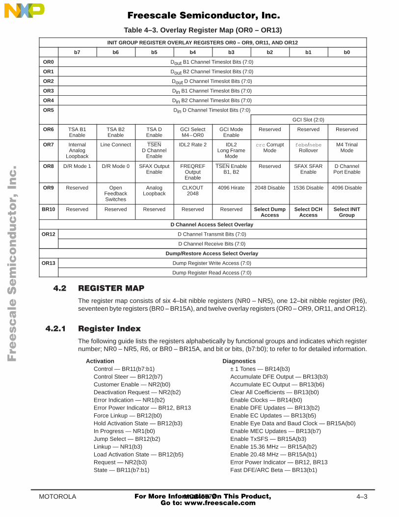
MC145572 4–3MOTOROLA
Table 4–3. Overlay Register Map (OR0 – OR13)
INIT GROUP REGISTER OVERLAY REGISTERS OR0 – OR9, OR11, AND OR12
b7 b6 b5 b4 b3 b2 b1 b0
OR0 Dout B1 Channel Timeslot Bits (7:0)
OR1 Dout B2 Channel Timeslot Bits (7:0)
OR2 Dout D Channel Timeslot Bits (7:0)
OR3 Din B1 Channel Timeslot Bits (7:0)
OR4 Din B2 Channel Timeslot Bits (7:0)
OR5 Din D Channel Timeslot Bits (7:0)
GCI Slot (2:0)
OR6 TSA B1Enable
TSA B2Enable
TSA DEnable
GCI SelectM4–OR0
GCI ModeEnable
Reserved Reserved Reserved
OR7 InternalAnalog
Loopback
Line Connect TSEND Channel
Enable
IDL2 Rate 2 IDL2Long Frame
Mode
crc CorruptMode
febe /nebeRollover
M4 TrinalMode
OR8 D/R Mode 1 D/R Mode 0 SFAX OutputEnable
FREQREFOutputEnable
TSEN EnableB1, B2
Reserved SFAX SFAREnable
D ChannelPort Enable
OR9 Reserved OpenFeedbackSwitches
AnalogLoopback
CLKOUT2048
4096 Hirate 2048 Disable 1536 Disable 4096 Disable
BR10 Reserved Reserved Reserved Reserved Reserved Select DumpAccess
Select DCHAccess
Select INITGroup
D Channel Access Select Overlay
OR12 D Channel Transmit Bits (7:0)
D Channel Receive Bits (7:0)
Dump/Restore Access Select Overlay
OR13 Dump Register Write Access (7:0)
Dump Register Read Access (7:0)
The register map consists of six 4–bit nibble registers (NR0 – NR5), one 12–bit nibble register (R6),seventeen byte registers (BR0 – BR15A), and twelve overlay registers (OR0 – OR9, OR11, and OR12).
The following guide lists the registers alphabetically by functional groups and indicates which registernumber; NR0 – NR5, R6, or BR0 – BR15A, and bit or bits, (b7:b0); to refer to for detailed information.
Activation DiagnosticsControl — BR11(b7:b1) ± 1 Tones — BR14(b3)Control Steer — BR12(b7) Accumulate DFE Output — BR13(b3)Customer Enable — NR2(b0) Accumulate EC Output — BR13(b6)Deactivation Request — NR2(b2) Clear All Coefficients — BR13(b0)Error Indication — NR1(b2) Enable Clocks — BR14(b0)Error Power Indicator — BR12, BR13 Enable DFE Updates — BR13(b2)Force Linkup — BR12(b0) Enable EC Updates — BR13(b5)Hold Activation State — BR12(b3) Enable Eye Data and Baud Clock — BR15A(b0)In Progress — NR1(b0) Enable MEC Updates — BR13(b7)Jump Select — BR12(b2) Enable TxSFS — BR15A(b3)Linkup — NR1(b3) Enable 15.36 MHz — BR15A(b2)Load Activation State — BR12(b5) Enable 20.48 MHz — BR15A(b1)Request — NR2(b3) Error Power Indicator — BR12, BR13State — BR11(b7:b1) Fast DFE/ARC Beta — BR13(b1)
Fre
esc
ale
Se
mic
on
du
cto
r, I
Freescale Semiconductor, Inc.
For More Information On This Product, Go to: www.freescale.com
nc
...
MC1455724–4 MOTOROLA
Activation (continued) Diagnostics (continued)Step Activation State — BR12(b4) Fast EC Beta — BR 13(b4)Superframe Sync — NR1(b1) Force Linkup — BR12(b0)Superframe Update Disable — NR2(b1) Freq Adapt — BR15A(b7)Timer Disable — BR11(b0) Jump Disable — BR15A(b6)Timer Expire — BR11(b0) Mask — BR15(b4:b0)Transparent — NR1(b0) ro/wo to r/w — BR14(b6)Verified act — BR3(b2), BR9(b5:b4) Superframe Detect — BR3(b0)Verified dea — BR3(b1), BR9(b5:b4) Select Dump Access — BR10(b2)Deactivation Select DCH Access — BR10(b1)
Request — NR2(b2) D Channel Access Overlay — OR12GCI Dump/Restore Access Overlay — OR13
IN/OUT — BR7(b6:b5) eocGCI Mode Enable — OR6 (b3) Control — BR9(b7:b6)
IDL2 act — BR3(b2)Timeslot Assigner Message — R6Dout B1 Timeslot — OR0 febeDout B2 Timeslot — OR1 Control — BR9(b1)Dout D Timeslot — OR2 Counter — BR4Din B1 Timeslot — OR3 Input — BR2(b4), BR9(b1)Din B2 Timeslot — OR4 Received — BR3(b4)Din D Timeslot — OR5 febe /nebe Rollover — OR7(b2)TSA Enable — OR6 (b7:b5) Maintenance8–Bit/10–Bit Mode — BR7(b0) act — BR3(b2)Block B1 — NR5(b2) crc Corrupt — BR8(b3)Block B2 — NR5(b1) dea — BR3(b1)Customer Enable — NR2(b0) eoc — See eocFree Run — BR7(b3) febe — See febeInvert — BR7(b4) M4 Trinal Mode — OR7(b0)Loopbacks — See Loopbacks M4 Control — BR9(b5:b4)Master/Slave Invert — BR7(b1) M4 Send — BR0Speed — BR7(b2) M4 Received — BR1Swap B1/B2 — NR5(b0) M5/M6 Control — BR9(b3:b2)B1 IDL2 Timeslot Enable — OR6(b7) M50 Received — BR3(b7)B2 IDL2 Timeslot Enable — OR6(b6) M50 Send — BR2(b7)D IDL2 Timeslot Enable — OR6(b5) M51 Received — BR3(b5)IDL2 Long Frame Mode — OR7(b3) M51 Send — BR2(b5)IDL2 Rate — OR7(b4) M60 Received — BR3(b6)
Interrupt M60 Send — BR2(b6)Enable — NR5 nebe — See nebeStatus — NR3 Return to Normal — NR0(b0)
Loopbacks Superframe Update Disable — NR2(b1)Framer–to–Deframer Loop — BR14(b4) Verified act — BR3(b2)IDL2–Loop 2B+D — BR6(b1) Verified dea — BR3(b1)IDL2–Loop B1 — BR6(b3) ModeIDL2–Loop B2 — BR6(b2) Absolute Power–Down — NR0(b1)IDL2–Loop Transparent — BR6(b1) NT/LT Invert Mode — BR8(b0)Match Scrambler — BR8(b2) NT/LT Mode — BR8(b0)Receive Window Disable — BR8(b1) Power–Down Enable — NR0(b2)U–Loop 2B+D — BR6(b5) Software Reset — NR0(b3)U–Loop B1 — BR6(b7) GCI 2B+D Mode — OR6(b3)U–Loop B2 — BR6(b6) Superframe FramerU–Loop Transparent — BR6(b4) Frame Control — BR8(b6:b4)Open Feedback Switch — OR9(b6) Frame State — BR8(b7:b4)Analog Loopback — OR9(b5) Frame Steering — BR8(b7)
nebeComputed — BR3(b3)Control — BR9(b1)Counter — BR5febe /nebe Rollover — OR7(b2)
Fre
esc
ale
Se
mic
on
du
cto
r, I
Freescale Semiconductor, Inc.
For More Information On This Product, Go to: www.freescale.com
nc
...
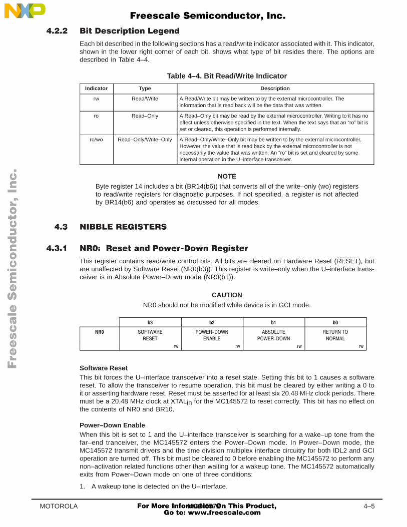
MC145572 4–5MOTOROLA
Each bit described in the following sections has a read/write indicator associated with it. This indicator,shown in the lower right corner of each bit, shows what type of bit resides there. The options aredescribed in Table 4–4.
Table 4–4. Bit Read/Write Indicator
Indicator Type Description
rw Read/Write A Read/Write bit may be written to by the external microcontroller. Theinformation that is read back will be the data that was written.
ro Read–Only A Read–Only bit may be read by the external microcontroller. Writing to it has noeffect unless otherwise specified in the text. When the text says that an “ro” bit isset or cleared, this operation is performed internally.
ro/wo Read–Only/Write–Only A Read–Only/Write–Only bit may be written to by the external microcontroller.However, the value that is read back by the external microcontroller is notnecessarily the value that was written. An “ro” bit is set and cleared by someinternal operation in the U–interface transceiver.
NOTE
Byte register 14 includes a bit (BR14(b6)) that converts all of the write–only (wo) registersto read/write registers for diagnostic purposes. If not specified, a register is not affectedby BR14(b6) and operates as discussed for all modes.
!!
This register contains read/write control bits. All bits are cleared on Hardware Reset (RESET), butare unaffected by Software Reset (NR0(b3)). This register is write–only when the U–interface trans-ceiver is in Absolute Power–Down mode (NR0(b1)).
CAUTION
NR0 should not be modified while device is in GCI mode.
Software ResetThis bit forces the U–interface transceiver into a reset state. Setting this bit to 1 causes a softwarereset. To allow the transceiver to resume operation, this bit must be cleared by either writing a 0 toit or asserting hardware reset. Reset must be asserted for at least six 20.48 MHz clock periods. Theremust be a 20.48 MHz clock at XTALin for the MC145572 to reset correctly. This bit has no effect onthe contents of NR0 and BR10.
Power–Down EnableWhen this bit is set to 1 and the U–interface transceiver is searching for a wake–up tone from thefar–end tranceiver, the MC145572 enters the Power–Down mode. In Power–Down mode, theMC145572 transmit drivers and the time division multiplex interface circuitry for both IDL2 and GCIoperation are turned off. This bit must be cleared to 0 before enabling the MC145572 to perform anynon–activation related functions other than waiting for a wakeup tone. The MC145572 automaticallyexits from Power–Down mode on one of three conditions:
1. A wakeup tone is detected on the U–interface.
Fre
esc
ale
Se
mic
on
du
cto
r, I
Freescale Semiconductor, Inc.
For More Information On This Product, Go to: www.freescale.com
nc
...
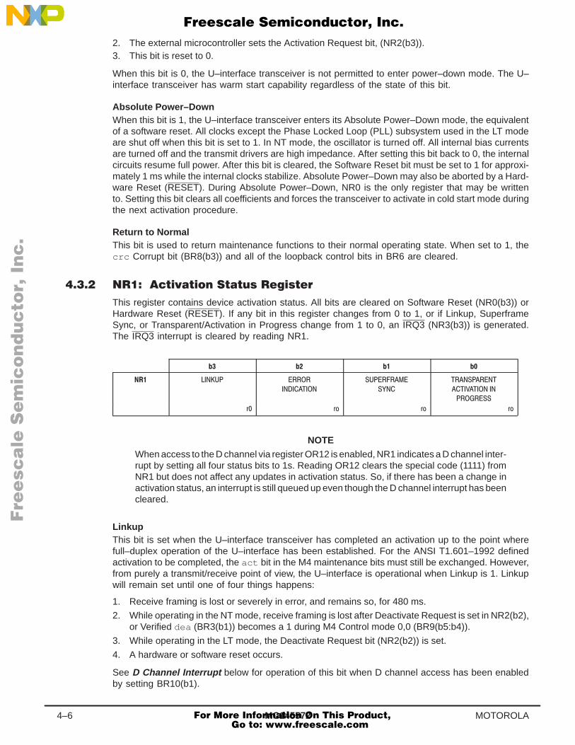
MC1455724–6 MOTOROLA
2. The external microcontroller sets the Activation Request bit, (NR2(b3)).3. This bit is reset to 0.
When this bit is 0, the U–interface transceiver is not permitted to enter power–down mode. The U–interface transceiver has warm start capability regardless of the state of this bit.
Absolute Power–DownWhen this bit is 1, the U–interface transceiver enters its Absolute Power–Down mode, the equivalentof a software reset. All clocks except the Phase Locked Loop (PLL) subsystem used in the LT modeare shut off when this bit is set to 1. In NT mode, the oscillator is turned off. All internal bias currentsare turned off and the transmit drivers are high impedance. After setting this bit back to 0, the internalcircuits resume full power. After this bit is cleared, the Software Reset bit must be set to 1 for approxi-mately 1 ms while the internal clocks stabilize. Absolute Power–Down may also be aborted by a Hard-ware Reset (RESET). During Absolute Power–Down, NR0 is the only register that may be writtento. Setting this bit clears all coefficients and forces the transceiver to activate in cold start mode duringthe next activation procedure.
Return to NormalThis bit is used to return maintenance functions to their normal operating state. When set to 1, thecrc Corrupt bit (BR8(b3)) and all of the loopback control bits in BR6 are cleared.
This register contains device activation status. All bits are cleared on Software Reset (NR0(b3)) orHardware Reset (RESET). If any bit in this register changes from 0 to 1, or if Linkup, SuperframeSync, or Transparent/Activation in Progress change from 1 to 0, an IRQ3 (NR3(b3)) is generated.The IRQ3 interrupt is cleared by reading NR1.
NOTEWhen access to the D channel via register OR12 is enabled, NR1 indicates a D channel inter-rupt by setting all four status bits to 1s. Reading OR12 clears the special code (1111) fromNR1 but does not affect any updates in activation status. So, if there has been a change inactivation status, an interrupt is still queued up even though the D channel interrupt has beencleared.
LinkupThis bit is set when the U–interface transceiver has completed an activation up to the point wherefull–duplex operation of the U–interface has been established. For the ANSI T1.601–1992 definedactivation to be completed, the act bit in the M4 maintenance bits must still be exchanged. However,from purely a transmit/receive point of view, the U–interface is operational when Linkup is 1. Linkupwill remain set until one of four things happens:
1. Receive framing is lost or severely in error, and remains so, for 480 ms.
2. While operating in the NT mode, receive framing is lost after Deactivate Request is set in NR2(b2),or Verified dea (BR3(b1)) becomes a 1 during M4 Control mode 0,0 (BR9(b5:b4)).
3. While operating in the LT mode, the Deactivate Request bit (NR2(b2)) is set.
4. A hardware or software reset occurs.
See D Channel Interrupt below for operation of this bit when D channel access has been enabledby setting BR10(b1).
Fre
esc
ale
Se
mic
on
du
cto
r, I
Freescale Semiconductor, Inc.
For More Information On This Product, Go to: www.freescale.com
nc
...
MC145572 4–7MOTOROLA
Error IndicationThis bit is set to 1 when a timer expires. Time–out sources are:
1. 15–second Activation Timer (BR11(b0)).
2. 480–ms loss of frame/signal.
3. Failure to get NT1 response to the TL signal (10 ms following the cessation of TL). (TL is 3 ms induration.)
Error Indication is always automatically reset prior to the next IRQ3. This is the result of either settingthe Activate Request bit in NR2(b3) or receiving a wakeup tone. Error Indication is not cleared byreading NR1.
See D Channel Interrupt below for operation of this bit when D channel access has been enabledby setting BR10(b1).
Superframe SyncThis bit is a 1 when the received superframe is being reliably detected. It transitions from 0 to 1 coin-cident with Linkup being set. Subsequently, if the superframe is lost, Superframe Sync returns to 0,and if Superframe Sync remains 0 for 480 ms, the U–interface transceiver will deactivate. While Super-frame Sync is 0, the received maintenance bits are unknown. IRQ2, IRQ1, and IRQ0 are not generatedwhile Superframe Sync is 0. The 2B+D data is blocked (forced to all 1s) when Superframe Sync is0.
See D Channel Interrupt below for operation of this bit when D channel access has been enabledby setting BR10(b1).
Transparent/Activation in ProgressThis bit has a dual purpose. When the transceiver is deactivated, this bit is 0. Whenever an activationbegins, this bit is internally set to a 1 and an IRQ3 is generated. When the activation process iscompleted, Linkup is set to 1 indicating success, and this bit remains set to 1, indicating that thereceiver and Superframe Deframer are ready to pass data transparently from the U–interface to theIDL2 interface. If the activation process fails, this bit is cleared and Error Indication is set to 1. When-ever Linkup is 1, this bit may be cleared, indicating that the receiver has detected a high error onthe U–interface. Under this condition, the receiver blocks received data (forcing the 2B+D data toall 1s) until the error returns to normal.
See D Channel Interrupt below for operation of this bit when D channel access has been enabledby setting BR10(b1).
NOTE
The received data is not transmitted on the IDL2 interface until Linkup is 1, Superframe Syncis 1, Transparent/Activation in Progress is 1, and either Customer Enable (see NR2(b0)) orVerified act (see BR3(b2)) is 1.
D Channel InterruptWhen access to the D channel register OR12 has been enabled by setting BR10(b1), the operationof the NR1 status bits is modified. A D channel available status is indicated by NR1(b3:b0) all beingset to 1s. Software must first do a check for NR1 = $F, then perform a check for status of the individualbits. The D channel interrupt is cleared by reading OR12.
Fre
esc
ale
Se
mic
on
du
cto
r, I
Freescale Semiconductor, Inc.
For More Information On This Product, Go to: www.freescale.com
nc
...
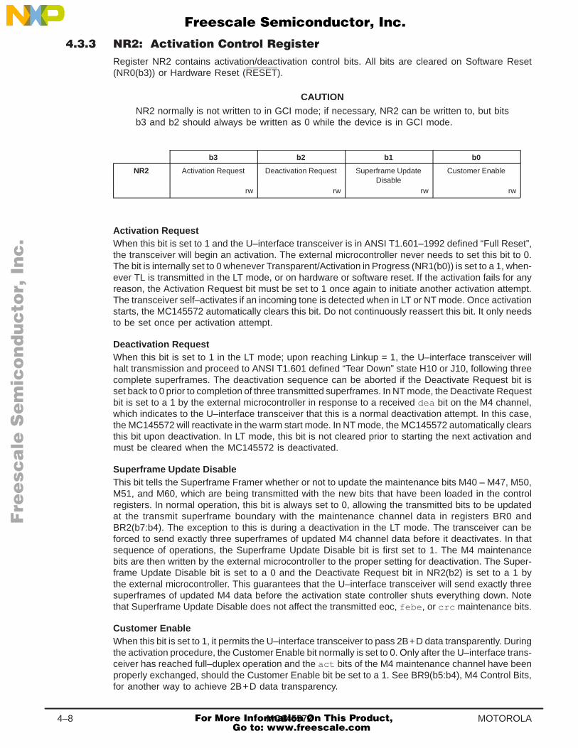
MC1455724–8 MOTOROLA
Register NR2 contains activation/deactivation control bits. All bits are cleared on Software Reset(NR0(b3)) or Hardware Reset (RESET).
CAUTIONNR2 normally is not written to in GCI mode; if necessary, NR2 can be written to, but bitsb3 and b2 should always be written as 0 while the device is in GCI mode.
b3 b2 b1 b0
NR2 Activation Request Deactivation Request Superframe UpdateDisable
Customer Enable
rw rw rw rw
Activation RequestWhen this bit is set to 1 and the U–interface transceiver is in ANSI T1.601–1992 defined “Full Reset”,the transceiver will begin an activation. The external microcontroller never needs to set this bit to 0.The bit is internally set to 0 whenever Transparent/Activation in Progress (NR1(b0)) is set to a 1, when-ever TL is transmitted in the LT mode, or on hardware or software reset. If the activation fails for anyreason, the Activation Request bit must be set to 1 once again to initiate another activation attempt.The transceiver self–activates if an incoming tone is detected when in LT or NT mode. Once activationstarts, the MC145572 automatically clears this bit. Do not continuously reassert this bit. It only needsto be set once per activation attempt.
Deactivation RequestWhen this bit is set to 1 in the LT mode; upon reaching Linkup = 1, the U–interface transceiver willhalt transmission and proceed to ANSI T1.601 defined “Tear Down” state H10 or J10, following threecomplete superframes. The deactivation sequence can be aborted if the Deactivate Request bit isset back to 0 prior to completion of three transmitted superframes. In NT mode, the Deactivate Requestbit is set to a 1 by the external microcontroller in response to a received dea bit on the M4 channel,which indicates to the U–interface transceiver that this is a normal deactivation attempt. In this case,the MC145572 will reactivate in the warm start mode. In NT mode, the MC145572 automatically clearsthis bit upon deactivation. In LT mode, this bit is not cleared prior to starting the next activation andmust be cleared when the MC145572 is deactivated.
Superframe Update DisableThis bit tells the Superframe Framer whether or not to update the maintenance bits M40 – M47, M50,M51, and M60, which are being transmitted with the new bits that have been loaded in the controlregisters. In normal operation, this bit is always set to 0, allowing the transmitted bits to be updatedat the transmit superframe boundary with the maintenance channel data in registers BR0 andBR2(b7:b4). The exception to this is during a deactivation in the LT mode. The transceiver can beforced to send exactly three superframes of updated M4 channel data before it deactivates. In thatsequence of operations, the Superframe Update Disable bit is first set to 1. The M4 maintenancebits are then written by the external microcontroller to the proper setting for deactivation. The Super-frame Update Disable bit is set to a 0 and the Deactivate Request bit in NR2(b2) is set to a 1 bythe external microcontroller. This guarantees that the U–interface transceiver will send exactly threesuperframes of updated M4 data before the activation state controller shuts everything down. Notethat Superframe Update Disable does not affect the transmitted eoc, febe , or crc maintenance bits.
Customer EnableWhen this bit is set to 1, it permits the U–interface transceiver to pass 2B+D data transparently. Duringthe activation procedure, the Customer Enable bit normally is set to 0. Only after the U–interface trans-ceiver has reached full–duplex operation and the act bits of the M4 maintenance channel have beenproperly exchanged, should the Customer Enable bit be set to a 1. See BR9(b5:b4), M4 Control Bits,for another way to achieve 2B+D data transparency.
Fre
esc
ale
Se
mic
on
du
cto
r, I
Freescale Semiconductor, Inc.
For More Information On This Product, Go to: www.freescale.com
nc
...
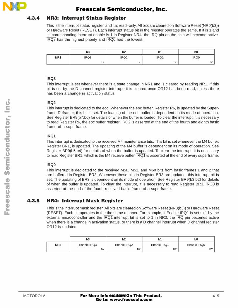
MC145572 4–9MOTOROLA
This is the interrupt status register, and it is read–only. All bits are cleared on Software Reset (NR0(b3))or Hardware Reset (RESET). Each interrupt status bit in the register operates the same. If it is 1 andits corresponding interrupt enable is 1 in Register NR4, the IRQ pin on the chip will become active.IRQ3 has the highest priority and IRQ0 has the lowest.
b3 b2 b1 b0
NR3 IRQ3 IRQ2 IRQ1 IRQ0ro ro ro ro
IRQ3This interrupt is set whenever there is a state change in NR1 and is cleared by reading NR1. If thisbit is set by the D channel register interrupt, it is cleared once OR12 has been read, unless therehas been a change in activation status.
IRQ2This interrupt is dedicated to the eoc. Whenever the eoc buffer, Register R6, is updated by the Super-frame Deframer, this bit is set. The loading of the eoc buffer is dependent on its mode of operation.See Register BR9(b7:b6) for details of when the buffer is loaded. To clear the interrupt, it is necessaryto read Register R6, the eoc buffer register. IRQ2 is asserted at the end of the fourth and eighth basicframe of a superframe.
IRQ1This interrupt is dedicated to the received M4 maintenance bits. This bit is set whenever the M4 buffer,Register BR1, is updated. The updating of the M4 buffer is dependent on its mode of operation. SeeRegister BR9(b5:b4) for details of when the buffer is updated. To clear the interrupt, it is necessaryto read Register BR1, which is the M4 receive buffer. IRQ1 is asserted at the end of every superframe.
IRQ0This interrupt is dedicated to the received M50, M51, and M60 bits from basic frames 1 and 2 thatare buffered in Register BR3. Whenever these bits in Register BR3 are updated, this interrupt bit isset. The updating of BR3 is dependent on its mode of operation. See Register BR9(b3:b2) for detailsof when the buffer is updated. To clear the interrupt, it is necessary to read Register BR3. IRQ0 isasserted at the end of the fourth received basic frame of a superframe.
This is the interrupt mask register. All bits are cleared on Software Reset (NR0(b3)) or Hardware Reset(RESET). Each bit operates in the the same manner. For example, if Enable IRQ1 is set to 1 by theexternal microcontroller and the IRQ1 interrupt bit is set to 1 in NR3, the IRQ pin becomes activewhen there is a change in activation status, or there is a D channel interrupt when D channel registerOR12 is updated.
b3 b2 b1 b0
NR4 Enable IRQ3 Enable IRQ2 Enable IRQ1 Enable IRQ0rw rw rw rw
Fre
esc
ale
Se
mic
on
du
cto
r, I
Freescale Semiconductor, Inc.
For More Information On This Product, Go to: www.freescale.com
nc
...
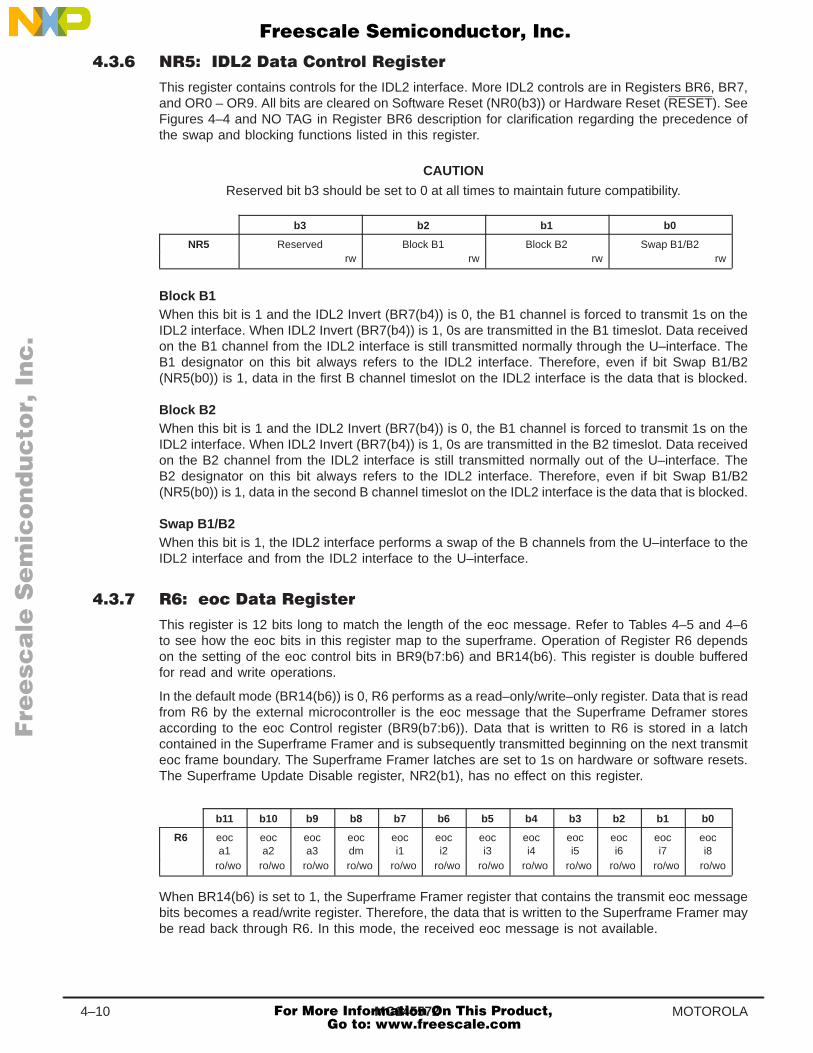
MC1455724–10 MOTOROLA
This register contains controls for the IDL2 interface. More IDL2 controls are in Registers BR6, BR7,and OR0 – OR9. All bits are cleared on Software Reset (NR0(b3)) or Hardware Reset (RESET). SeeFigures 4–4 and NO TAG in Register BR6 description for clarification regarding the precedence ofthe swap and blocking functions listed in this register.
CAUTION
Reserved bit b3 should be set to 0 at all times to maintain future compatibility.
b3 b2 b1 b0
NR5 Reserved Block B1 Block B2 Swap B1/B2rw rw rw rw
Block B1When this bit is 1 and the IDL2 Invert (BR7(b4)) is 0, the B1 channel is forced to transmit 1s on theIDL2 interface. When IDL2 Invert (BR7(b4)) is 1, 0s are transmitted in the B1 timeslot. Data receivedon the B1 channel from the IDL2 interface is still transmitted normally through the U–interface. TheB1 designator on this bit always refers to the IDL2 interface. Therefore, even if bit Swap B1/B2(NR5(b0)) is 1, data in the first B channel timeslot on the IDL2 interface is the data that is blocked.
Block B2When this bit is 1 and the IDL2 Invert (BR7(b4)) is 0, the B1 channel is forced to transmit 1s on theIDL2 interface. When IDL2 Invert (BR7(b4)) is 1, 0s are transmitted in the B2 timeslot. Data receivedon the B2 channel from the IDL2 interface is still transmitted normally out of the U–interface. TheB2 designator on this bit always refers to the IDL2 interface. Therefore, even if bit Swap B1/B2(NR5(b0)) is 1, data in the second B channel timeslot on the IDL2 interface is the data that is blocked.
Swap B1/B2When this bit is 1, the IDL2 interface performs a swap of the B channels from the U–interface to theIDL2 interface and from the IDL2 interface to the U–interface.
This register is 12 bits long to match the length of the eoc message. Refer to Tables 4–5 and 4–6to see how the eoc bits in this register map to the superframe. Operation of Register R6 dependson the setting of the eoc control bits in BR9(b7:b6) and BR14(b6). This register is double bufferedfor read and write operations.
In the default mode (BR14(b6)) is 0, R6 performs as a read–only/write–only register. Data that is readfrom R6 by the external microcontroller is the eoc message that the Superframe Deframer storesaccording to the eoc Control register (BR9(b7:b6)). Data that is written to R6 is stored in a latchcontained in the Superframe Framer and is subsequently transmitted beginning on the next transmiteoc frame boundary. The Superframe Framer latches are set to 1s on hardware or software resets.The Superframe Update Disable register, NR2(b1), has no effect on this register.
b11 b10 b9 b8 b7 b6 b5 b4 b3 b2 b1 b0
R6 eoca1
eoca2
eoca3
eocdm
eoci1
eoci2
eoci3
eoci4
eoci5
eoci6
eoci7
eoci8
ro/wo ro/wo ro/wo ro/wo ro/wo ro/wo ro/wo ro/wo ro/wo ro/wo ro/wo ro/wo
When BR14(b6) is set to 1, the Superframe Framer register that contains the transmit eoc messagebits becomes a read/write register. Therefore, the data that is written to the Superframe Framer maybe read back through R6. In this mode, the received eoc message is not available.
Fre
esc
ale
Se
mic
on
du
cto
r, I
Freescale Semiconductor, Inc.
For More Information On This Product, Go to: www.freescale.com
nc
...
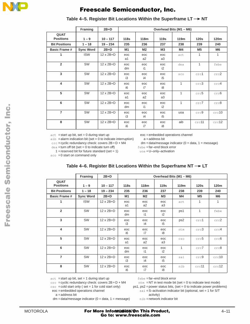
MC145572 4–11MOTOROLA
Table 4–5. Register Bit Locations Within the Superframe LT NT
Framing 2B+D Overhead Bits (M1 – M6)
QUATPositions 1 – 9 10 – 117 118s 118m 119s 119m 120s 120m
Bit Positions 1 – 18 19 – 234 235 236 237 238 239 240
Basic Frame # Sync Word 2B+D M1 M2 M3 M4 M5 M6
1 ISW 12 x 2B+D eoca1
eoca2
eoca3
act 1 1
2 SW 12 x 2B+D eocdm
eoci1
eoci2
dea 1 febe
3 SW 12 x 2B+D eoci3
eoci4
eoci5
sco crc 1 crc 2
4 SW 12 x 2B+D eoci6
eoci7
eoci8
1 crc 3 crc 4
5 SW 12 x 2B+D eoca1
eoca2
eoca3
1 crc 5 crc 6
6 SW 12 x 2B+D eocdm
eoci1
eoci2
1 crc 7 crc 8
7 SW 12 x 2B+D eoci3
eoci4
eoci5
uoa crc 9 crc 10
8 SW 12 x 2B+D eoci6
eoci7
eoci8
aib crc 11 crc 12
act = start up bit, set = 0 during start up eoc = embedded operations channelaib = alarm indication bit (set = 0 to indicate interruption) a = address bitcrc = cyclic redundancy check: covers 2B + D + M4 dm = data/message indicator (0 = data, 1 = message)dea = turn off bit (set = 0 to indicate turn off) febe = far–end block error
1 = reserved bit for future standard (set = 1) uoa = U–only–activationsco = 0 start on command only
Table 4–6. Register Bit Locations Within the Superframe NT LT
Framing 2B+D Overhead Bits (M1 – M6)
QUATPositions 1 – 9 10 – 117 118s 118m 119s 119m 120s 120m
Bit Positions 1 – 18 19 – 234 235 236 237 238 239 240
Basic Frame # Sync Word 2B+D M1 M2 M3 M4 M5 M6
1 ISW 12 x 2B+D eoca1
eoca2
eoca3
act 1 1
2 SW 12 x 2B+D eocdm
eoci1
eoci2
ps1 1 febe
3 SW 12 x 2B+D eoci3
eoci4
eoci5
ps2 crc 1 crc 2
4 SW 12 x 2B+D eoci6
eoci7
eoci8
ntm crc 3 crc 4
5 SW 12 x 2B+D eoca1
eoca2
eoca3
cso crc 5 crc 6
6 SW 12 x 2B+D eocdm
eoci1
eoci2
1 crc 7 crc 8
7 SW 12 x 2B+D eoci3
eoci4
eoci5
sai crc 9 crc 10
8 SW 12 x 2B+D eoci6
eoci7
eoci8
nib crc 11 crc 12
act = start up bit, set = 1 during start up febe = far–end block errorcrc = cyclic redundancy check: covers 2B + D + M4 ntm = NT in test mode bit (set = 0 to indicate test mode)cso = cold start only ( set = 1 for cold start only) ps1, ps2 = power status bits, (set = 0 to indicate power problems)eoc = embedded operations channel sai = S–activation indicator bit (optional, set = 1 for S/T
a = address bit activity)dm = data/message indicator (0 = data, 1 = message) nib = network indicator bit
Fre
esc
ale
Se
mic
on
du
cto
r, I
Freescale Semiconductor, Inc.
For More Information On This Product, Go to: www.freescale.com
nc
...
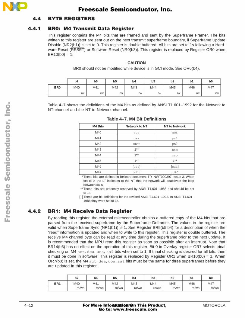
MC1455724–12 MOTOROLA
This register contains the M4 bits that are framed and sent by the Superframe Framer. The bitswritten to this register are sent out on the next transmit superframe boundary, if Superframe UpdateDisable (NR2(b1)) is set to 0. This register is double buffered. All bits are set to 1s following a Hard-ware Reset (RESET) or Software Reset (NR0(b3)). This register is replaced by Register OR0 whenBR10(b0) = 1.
CAUTIONBR0 should not be modified while device is in GCI mode. See OR6(b4).
b7 b6 b5 b4 b3 b2 b1 b0
BR0 M40 M41 M42 M43 M44 M45 M46 M47
rw rw rw rw rw rw rw rw
Table 4–7 shows the definitions of the M4 bits as defined by ANSI T1.601–1992 for the Network toNT channel and the NT to Network channel.
Table 4–7. M4 Bit Definitions
M4 Bits Network to NT NT to Network
M40 act act
M41 dea ps1
M42 sco* ps2
M43 1** ntm
M44 1** cso
M45 1** 1**
M46 [uoa ] [sai ]
M47 [aib ] nib ** These bits are defined in Bellcore document TR–NWT000397, Issue 3. Whenset to 0, the LT indicates to the NT that the network will deactivate the loopbetween calls.
** These bits are presently reserved by ANSI T1.601–1988 and should be setto 1s.
[ ] These are bit definitions for the revised ANSI T1.601–1992. In ANSI T1.601–1988 they were set to 1s.
By reading this register, the external microcontroller obtains a buffered copy of the M4 bits that areparsed from the received superframe by the Superframe Deframer. The values in the register arevalid when Superframe Sync (NR1(b1)) is 1. See Register BR9(b5:b4) for a description of when the“read” information is updated and when to write to this register. This register is double buffered. Thereceive M4 channel byte can be read at any time during the superframe prior to the next update. Itis recommended that the MPU read this register as soon as possible after an interrupt. Note thatBR14(b6) has no effect on the operation of this register. Bit 0 in Overlay register OR7 selects trinalchecking on M4 act , dea , uoa , sai bits when set to 1. If trinal checking is desired for all bits, thenit must be done in software. This register is replaced by Register OR1 when BR10(b0) = 1. WhenOR7(b0) is set, the M4 act , dea , uoa , sai bits must be the same for three superframes before theyare updated in this register.
b7 b6 b5 b4 b3 b2 b1 b0
BR1 M40 M41 M42 M43 M44 M45 M46 M47ro/wo ro/wo ro/wo ro/wo ro/wo ro/wo ro/wo ro/wo
Fre
esc
ale
Se
mic
on
du
cto
r, I
Freescale Semiconductor, Inc.
For More Information On This Product, Go to: www.freescale.com
nc
...
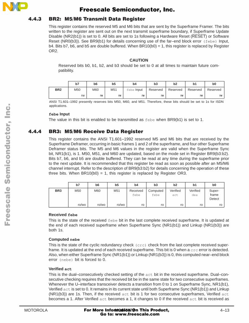
MC145572 4–13MOTOROLA
This register contains the reserved M5 and M6 bits that are sent by the Superframe Framer. The bitswritten to the register are sent out on the next transmit superframe boundary, if Superframe UpdateDisable (NR2(b1)) is set to 0. All bits are set to 1s following a Hardware Reset (RESET) or SoftwareReset (NR0(b3)). See BR9(b1) for details concerning use of the far–end block error (febe) Input,b4. Bits b7, b6, and b5 are double buffered. When BR10(b0) = 1, this register is replaced by RegisterOR2.
CAUTIONReserved bits b0, b1, b2, and b3 should be set to 0 at all times to maintain future com-patibility.
b7 b6 b5 b4 b3 b2 b1 b0
BR2 M50 M60 M51 febe Input Reserved Reserved Reserved Reserved
rw
ANSI T1.601–1992 presently reserves bits M50, M60, and M51. Therefore, these bits should be set to 1s for ISDNapplications.
febe InputThe value in this bit is enabled to be transmitted as febe when BR9(b1) is set to 1.
This register contains the ANSI T1.601–1992 reserved M5 and M6 bits that are received by theSuperframe Deframer, occurring in basic frames 1 and 2 of the superframe, and four other SuperframeDeframer status bits. The M5 and M6 values in the register are valid when the Superframe Syncbit, NR1(b1), is 1. M50, M51, and M60 are updated, based on the mode set in Register BR9(b3:b2).Bits b7, b6, and b5 are double buffered. They can be read at any time during the superframe priorto the next update. It is recommended that this register be read as soon as possible after an M5/M6channel interrupt. Refer to the description of BR9(b3:b2) for details concerning the operation of thesethree bits. When BR10(b0) = 1, this register is replaced by Register OR3.
b7 b6 b5 b4 b3 b2 b1 b0
BR3 M50 M60 M51 Receivedfebe
Computedfebe
Verifiedact
Verifieddea
Super-frameDetect
ro/wo ro/wo ro/wo ro ro ro ro ro
Received febe
This is the state of the received febe bit in the last complete received superframe. It is updated atthe end of each received superframe when Superframe Sync (NR1(b1)) and Linkup (NR1(b3)) areboth 1s.
Computed nebe
This is the state of the cyclic redundancy check (crc) check from the last complete received super-frame. It is updated at the end of each received superframe. This bit is 0 when a crc error is detected.Also, when either Superframe Sync (NR1(b1)) or Linkup (NR1(b3)) is 0, this computed near–end blockerror (nebe) bit is forced to 0.
Verified act
This is the dual–consecutively checked setting of the act bit in the received superframe. Dual–con-secutive checking requires that the received bit be in the same state for two consecutive superframes.Whenever the U–interface transceiver detects a transition from 0 to 1 on Superframe Sync, NR1(b1),Verified act is set to 0. It remains in its current state until both Superframe Sync (NR1(b1)) and Linkup(NR1(b3)) are 1s. Then, if the received act bit is 1 for two consecutive superframes, Verified actbecomes a 1. After Verified act becomes a 1, it changes to 0 if the received act bit is received as
Fre
esc
ale
Se
mic
on
du
cto
r, I
Freescale Semiconductor, Inc.
For More Information On This Product, Go to: www.freescale.com
nc
...
MC1455724–14 MOTOROLA
a 0 for two consecutive superframes. This bit is updated at the end of the first frame of each super-frame and is provided in this register for status only. See BR9(b5:b4) for more information regardingthis bit. When OR7(b0) is set, the M4 act and dea bits must be valid for three superframes beforeVerified act or Verified dea are updated.
Verified dea
This is the dual–consecutively checked, inverted setting of the dea bit, in the received superframe.Since the dea bit can only be received by an NT, this bit can only be 1 in the LT mode. Dual–consecutivechecking requires that the received bit is in the same state for two consecutive superframes. Wheneverthe U–interface transceiver detects a transition from 0 to 1 on Superframe Sync in NR1(b1), Verifieddea is set to 0. It remains in its current state until both Superframe Sync (NR1(b1)) and Linkup(NR1(b3)) are 1s. Then, if the received dea bit is 0 for two consecutive superframes, Verified deawill become 1. After Verified dea becomes 1, if the received dea bit is ever 1 for two consecutivesuperframes, then Verified dea will become a 0. This bit is updated at the end of the second basicframe of each superframe and is provided in this register for status only. See BR9(b5:b4) for moreinformation regarding this bit. When OR7(b0) is set, the M4 dea bit must be valid for three superframesbefore Verified dea is updated.
Superframe Detect This is the unmodified output of the Superframe Deframer’s superframe detection circuit. It is primarilyintended for diagnostic purposes.
febe
This register contains the current febe count. The counter is not cleared by a software or hardwarereset. The register can be preset to any value by writing to it. If the febe bit is active in a superframe,the counter will increment at the end of the received superframe. The counter will not increment unlessSuperframe Sync (NR1(b1)) and Linkup (NR1(b3)) are both 1s. If OR7(b1) is set, then the febe counterwill roll over from $FF to $00. The user software must take into account that if OR7(b1) is set, thecounter value read from BR4 might be less than the previous value, which means that the counterhas rolled over. The default setting for OR7(b1), after any hardware or software reset, produces thesame operation as the MC145472/MC14LC5472. This register is replaced by Register OR4 whenBR10(b0) = 1. When OR7(b1) is cleared, BR4 counts to $FF and does not roll over. This is the defaultconfiguration after any reset to maintain MC145472 compatibility.
b7 b6 b5 b4 b3 b2 b1 b0
BR4 febeCounter 7
febeCounter 6
febeCounter 5
febeCounter 4
febeCounter 3
febeCounter 2
febeCounter 1
febeCounter 0
rw rw rw rw rw rw rw rw
nebe
This register contains the current nebe count. A nebe occurs whenever the received crc messagedoes not match the computed crc or when Linkup (NR1(b3)) is 1 and Superframe Sync (NR1(b1))is 0. The Superframe Framer maintains the superframe timing to increment the nebe counter whenSuperframe Sync is 0. The counter is not cleared by a software or hardware reset. The register canbe preset to any value by writing to it.
When the Superframe Deframer detects a crc error in the received superframe, the counter is increm-ented at the end of that superframe. When OR7(b1) is set, then the febe counter rolls over from$FF to $00. The user software must take into account that if OR7(b1) is set, the counter value readfrom BR5 might be less than the previous value, which means that the counter has rolled over. Thedefault setting for OR7(b1), after any hardware or software reset, produces the same operation asthe MC145472/MC14LC5472. When BR10(b0) = 1, this register is replaced by Register OR5. When
Fre
esc
ale
Se
mic
on
du
cto
r, I
Freescale Semiconductor, Inc.
For More Information On This Product, Go to: www.freescale.com
nc
...
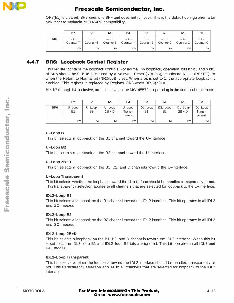
MC145572 4–15MOTOROLA
OR7(b1) is cleared, BR5 counts to $FF and does not roll over. This is the default configuration afterany reset to maintain MC145472 compatibility.
b7 b6 b5 b4 b3 b2 b1 b0
nebeCounter 7
nebeCounter 6
nebeCounter 5
nebeCounter 4
nebeCounter 3
nebeCounter 2
nebeCounter 1
nebeCounter 0
rw rw rw rw rw rw rw rw
This register contains the loopback controls. For normal (no loopback) operation, bits b7:b5 and b3:b1of BR6 should be 0. BR6 is cleared by a Software Reset (NR0(b3)), Hardware Reset (RESET), orwhen the Return to Normal bit (NR0(b0)) is set. When a bit is set to 1, the appropriate loopback isenabled. This register is replaced by Register OR6 when BR10(b0) = 1.
Bits b7 through b4, inclusive, are not set when the MC145572 is operating in the automatic eoc mode.
b7 b6 b5 b4 b3 b2 b1 b0
BR6 U–LoopB1
U–LoopB2
U–Loop2B + D
U–LoopTrans–parent
IDL–LoopB1
IDL–LoopB2
IDL–Loop2B + D
IDL–LoopTrans–parent
rw rw rw rw rw rw rw rw
U–Loop B1This bit selects a loopback on the B1 channel toward the U–interface.
U–Loop B2This bit selects a loopback on the B2 channel toward the U–interface.
U–Loop 2B+DThis bit selects a loopback on the B1, B2, and D channels toward the U–interface.
U–Loop TransparentThis bit selects whether the loopback toward the U–interface should be handled transparently or not.This transparency selection applies to all channels that are selected for loopback to the U–interface.
IDL2–Loop B1This bit selects a loopback on the B1 channel toward the IDL2 interface. This bit operates in all IDL2and GCI modes.
IDL2–Loop B2This bit selects a loopback on the B2 channel toward the IDL2 interface. This bit operates in all IDL2and GCI modes.
IDL2–Loop 2B+DThis bit selects a loopback on the B1, B2, and D channels toward the IDL2 interface. When this bitis set to 1, the IDL2–loop B1 and IDL2–loop B2 bits are ignored. This bit operates in all IDL2 andGCI modes.
IDL2–Loop TransparentThis bit selects whether the loopback toward the IDL2 interface should be handled transparently ornot. This transparency selection applies to all channels that are selected for loopback to the IDL2interface.
Fre
esc
ale
Se
mic
on
du
cto
r, I
Freescale Semiconductor, Inc.
For More Information On This Product, Go to: www.freescale.com
nc
...
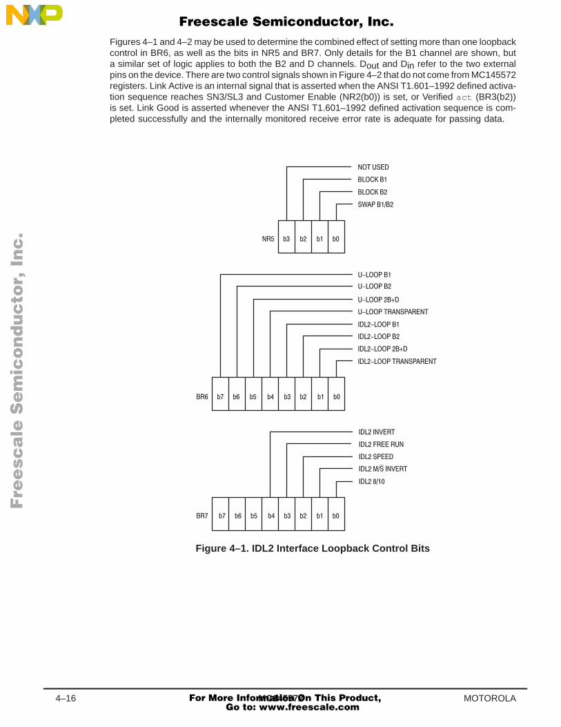
MC1455724–16 MOTOROLA
Figures 4–1 and 4–2 may be used to determine the combined effect of setting more than one loopbackcontrol in BR6, as well as the bits in NR5 and BR7. Only details for the B1 channel are shown, buta similar set of logic applies to both the B2 and D channels. Dout and Din refer to the two externalpins on the device. There are two control signals shown in Figure 4–2 that do not come from MC145572registers. Link Active is an internal signal that is asserted when the ANSI T1.601–1992 defined activa-tion sequence reaches SN3/SL3 and Customer Enable (NR2(b0)) is set, or Verified act (BR3(b2))is set. Link Good is asserted whenever the ANSI T1.601–1992 defined activation sequence is com-pleted successfully and the internally monitored receive error rate is adequate for passing data.
! ! ! !
! ! ! ! ! ! ! !
! ! ! ! ! ! ! !
Figure 4–1. IDL2 Interface Loopback Control Bits
Fre
esc
ale
Se
mic
on
du
cto
r, I
Freescale Semiconductor, Inc.
For More Information On This Product, Go to: www.freescale.com
nc
...
MC145572 4–17MOTOROLA
″
″
′
′
′
′″
″
′″
′″
′″ "!
Figure 4–2. IDL2 Interface Loopback Logic Diagram
This register contains IDL2 interface mode information. BR7 is cleared on Hardware Reset (RESET)or Software Reset (NR0(b3)). All bits in this register are read/write. This register is replaced by RegisterOR7 when BR10(b0) = 1.
b7 b6 b5 b4 b3 b2 b1 b0
BR7 BR15ASelect
OUT2wo
OUT1wo
IDL2Invert
IDL2Free Run
IDL2Speed
IDL2M/S Invert
IDL28/10
rwGCI IN2
roGCI IN1
ro rw rw rw rw rw
BR15A SelectWhen set to 1, this bit causes Register BR15A to be substituted for Register BR15 in the SCP registermap. After any reset, this bit is cleared to 0.
GCI IN2/OUT2This is a read–only/write–only bit. The write–only portion, OUT2, is cleared by hardware and softwareresets. In full GCI mode, entered by holding the pin MCU/GCI low, the state of OUT2 is driven ontoa GCI mode dedicated output pin. However, if the GCI C/I channel decodes the input command DISSto the MC145572, this same pin is forced high. When read (again, provided the MC145572 is in fullGCI mode), bit IN2 reflects the state of a GCI mode dedicated input pin. These pins may be usedfor any purpose in a GCI application. See Chapter 3, Device Description , for more information. GCIcommand LTD2 when active in LT mode or NTD2 when active in NT mode, sets OUT2 high.
Fre
esc
ale
Se
mic
on
du
cto
r, I
Freescale Semiconductor, Inc.
For More Information On This Product, Go to: www.freescale.com
nc
...
MC1455724–18 MOTOROLA
GCI IN1/OUT1This is a read–only/write–only bit. The write only portion, OUT1, is cleared by hardware and softwareresets. In full GCI mode, entered by holding the pin MCU/GCI low, the state of OUT1 is driven ontoa GCI mode dedicated output pin. When read (again, provided the MC145572 is in full GCI mode),bit IN1 reflects the state of a GCI mode dedicated input pin. These pins may be used for any purposein a GCI application. See Chapter 3, Device Description , for more information. GCI command LTD1when active in LT mode or NTD1 when active in NT mode, sets OUT1 high.
IDL2 InvertWhen set to 1, this bit forces the IDL2 interface to invert every bit just before it is transmitted on theDout pin and invert every bit that is received on Din.
IDL2 Free RunWhen set to 0, this bit forces the DCL and FSR/FSX outputs to run continuously when in the IDL2Master mode. When this bit is 1, the DCL and FSR/FSX stop when the U–interface transceiver isdeactivated. DCL and FSR/FSX will start operating when Superframe Sync in NR1(b1) becomes 1and halts when the U–interface transceiver enters the ANSI T1.601 defined “Tear Down” state.
IDL2 SpeedThis bit selects the DCL clock speed in the IDL2 Master mode. When this bit is 0, the clock rate is2.56 MHz. A 1 selects a rate of 2.048 MHz. This bit also sets the output clock rate for FREQREFor FREFout when in NT Slave mode. Also, see the description for OR7(b4).
IDL2 M/S InvertWhen this bit is 1, it inverts the polarity of the IDL2 Master/Slave pin. When this bit is 0 and IDL2Master is set high, the U–interface transceiver operates in the IDL2 Master mode.
IDL2 8/10This bit reorders the sequence of 2B+D data presented in the IDL2 data transfer. The two possibletransfer sequences are shown in Figures 4–3 and 4–4. A 1 selects the 8–bit mode and a 0 selectsthe 10–bit mode. In the 8–bit mode, the two B channels are provided sequentially, followed by thetwo D channel bits. In the 10–bit mode, one D channel bit follows each B channel byte. The abilityto swap the B channels, (NR5(b0)), applies to both of these modes. For further information aboutthe IDL2 interface, see Section 5.4 .
NOTE
If timeslot assignment mode is enabled via OR6 b(7), b(6), or b(5), then the IDL2 8/10control bit is ignored and B channel and D channel data is placed according to OR0 – OR5.
If GCI electrical mode is selected by setting OR6(b3) to a 1, the IDL2 interface transfersonly 2B+D data in the GCI timeslot locations as programmed in OR5(b2:b0).
Fre
esc
ale
Se
mic
on
du
cto
r, I
Freescale Semiconductor, Inc.
For More Information On This Product, Go to: www.freescale.com
nc
...
MC145572 4–19MOTOROLA
"!
Figure 4–3. IDL2 Interface Timing in 8–Bit Master Mode
"!
Figure 4–4. IDL2 Interface Timing in 10–Bit Master Mode
Fre
esc
ale
Se
mic
on
du
cto
r, I
Freescale Semiconductor, Inc.
For More Information On This Product, Go to: www.freescale.com
nc
...
MC1455724–20 MOTOROLA
This register contains controls used for test operations such as external loopbacks, Superframe Fram-er Control and State information, and NT/LT mode control. All write capable bits are cleared on aSoftware Reset (NR0(b3)) or Hardware Reset (RESET). Bits b7 – b4 and b0, are read–only/write–only.To read the write–only bits, it is necessary to set BR14(b6) to 1. When BR10(b0) = 1, this registeris replaced by Register OR8.
b7 b6 b5 b4 b3 b2 b1 b0
BR8 FrameSteering
FrameControl 2
FrameControl 1
FrameControl 0
crcCorrupt
MatchScrambler
ReceiveWindowDisable
NT/LTInvert
wo wo wo wo rw rw rw wo
FrameState 3
FrameState 2
FrameState 1
FrameState 0
Reserved Reserved Reserved NT/LTMode
ro ro ro ro ro
Frame SteeringWhen this bit is a 1, the Frame Control 2:0 bits take over control of the Superframe Framer’s modeof operation.
Frame Control 2:0These bits set the mode of operation for the Superframe Framer when the Frame Steering bit is 1.Table 4–8 shows the mode the Superframe Framer will go into, based on the three Frame Controlbits and the Frame Steering bit.
Table 4–8. Frame Control Modes
FrameSteering Frame Control 2:0 Superframe Framer Mode of Operation
b7 b6 b5 b4 NT LT
1 0 0 0 SN0 SL0
1 0 0 1 Six frames of 10 kHz tone followedby SN1
SL1
1 0 1 0 SN2 SL2
1 0 1 1 SN3 SL3
1 1 0 0 10 kHz tone
1 1 0 1 40 kHz tone
1 1 1 0 Generates a single quat every basic frame which alternates over all fourof the 2B1Q symbols.
1 1 1 1 Superframe Framer free runs the scrambler with no synchronizationwords.
0 Don’t Care The Superframe Framer output is determined by the state of theAutomatic Activation Controller.
Frame State 3:0These bits provide the external microcontroller with the current state of the U–interface transceiver’sSuperframe Framer, regardless of whether the Superframe Framer is being controlled by the externalmicrocontroller or internally by the Automatic Activation Controller. The meaning of Frame State 2:0maps directly onto the meaning of Frame Control 2:0. Frame State 3 is 0 at all times, except duringTN of an NT activation sequence. State transitions are always made on frame or superframe bound-aries.
crc CorruptWhen set to 1, this bit forces the transmitted crc to be inverted. It is used for eoc maintenance pro-cedures and to force an outgoing corrupt crc in digital loop carrier systems. As the transmit framer
Fre
esc
ale
Se
mic
on
du
cto
r, I
Freescale Semiconductor, Inc.
For More Information On This Product, Go to: www.freescale.com
nc
...
MC145572 4–21MOTOROLA
transmits the crc and this bit is set, the transmitted crc is inverted. This bit can be cleared or setat any time during transmission of a superframe. This bit functions the same as in the MC145472/MC14LC5472 after a Hardware Reset (RESET). When OR7(b2) is set to 1, the operation of this bitis modified so that the outgoing crc is only corrupted on the current superframe.
Match ScramblerWhen set to 1, this bit forces the descrambler and scrambler polynomials to match. This is used forexternal analog loopback and framer–to–deframer loopback.
Receive Window DisableWhen set to 1, this bit disables the search window placed around the received synchronization wordin the LT mode. When the receive window is disabled, the LT will synchronize to an incoming syn-chronization word that is located at any arbitrary point with respect to its transmitted synchronizationword. This allows the U–interface transceiver to use its own transmitted synchronization word for framedetection when operated in external analog loopback mode and framer–to–deframer loopback.
NT/LT InvertThis bit allows override control of the setting of the NT or LT operation of the U–interface transceiver’sexternal NT/LT mode pin. If this bit is 0 and the NT/LT pin is high, the device is in NT mode. Whenthis bit is then set to 1, the device will then be in the LT mode.
NT/LT ModeThis read–only bit reflects the current mode of the device. If 1, the U–interface transceiver is operatingin the NT mode.
This register contains mode control over the deframer’s updating of the received maintenance bits.The register is cleared on Software Reset (NR0(b3)) or Hardware Reset (RESET). When BR10(b0)= 1 this register is replaced by Register OR9.
CAUTIONSee Appendix C for printed circuit board layout recommendations.
b7 b6 b5 b4 b3 b2 b1 b0
BR9 eocControl 1
eocControl 0
M4Control 1
M4Control 0
M5/M6Control 1
M5/M6Control 0
febe /nebe
Control
Reserved
rw rw rw rw rw rw rw
eoc Control 1:0These bits control the eoc handling capability of the U–interface transceiver. Table 4–9 gives a briefdescription of each mode selected by the eoc Control bits. The eoc Trinal–Check mode (b7,b6 = 1,0)and the Automatic eoc Processor mode (b7,b6 = 0, “Don’t Care”) are described in the paragraphsfollowing Table 4–9. The default mode setting is 0,0; thereby selecting the Automatic eoc Processor.Regardless of the operating mode, every time R6 is loaded by the deframer, IRQ2 (NR3(b2)) is setto 1. Use the update on every frame mode (b7,b6 = 1,1) for digital loop carrier or proprietary ap-plications.
Table 4–9. eoc Control Modes
eoc Control 1:0
b7 b6 eoc Function Description
1 1 Update eoc register (R6) on every eoc frame (twice during each superframe). Recommendedfor Digital Loop Carrier applications.
1 0 Update eoc register (R6) after passing a trinal–check.
0 Don’t Care Update eoc register (R6) after passing a trinal–check and also invoke Automatic eocProcessor to operate when in NT mode.
Fre
esc
ale
Se
mic
on
du
cto
r, I
Freescale Semiconductor, Inc.
For More Information On This Product, Go to: www.freescale.com
nc
...
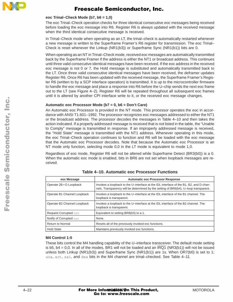
MC1455724–22 MOTOROLA
eoc Trinal–Check Mode (b7, b6 = 1,0)The eoc Trinal–Check operation checks for three identical consecutive eoc messages being receivedbefore loading the eoc message into R6. Register R6 is always updated with the received messagewhen the third identical consecutive message is received.
In Trinal–Check mode when operating as an LT, the trinal–check is automatically restarted whenevera new message is written to the Superframe Framer’s R6 register for transmission. The eoc Trinal–Check is reset whenever the Linkup (NR1(b3)) or Superframe Sync (NR1(b1)) bits are 0.
When operating as an NT in Trinal–Check mode, received eoc messages are automatically transmittedback by the Superframe Framer if the address is either the NT1 or broadcast address. This continuesuntil three valid consecutive identical messages have been received. If the eoc address in the receivedeoc message is not 0 or 7, the Hold message is substituted and automatically transmitted back tothe LT. Once three valid consecutive identical messages have been received, the deframer updatesRegister R6. Once R6 has been updated with the received message, the Superframe Framer’s Regis-ter R6 (written to by a SCP interface operation) is transmitted. It is up to the microcontroller firmwareto handle the eoc message and place a response into R6 before the U–chip sends the next eoc frameout to the LT (see Figure 4–2). Register R6 will be repeated throughout all subsequent eoc framesuntil it is altered by another CPI interface write to it, or the received eoc message changes.
Automatic eoc Processor Mode (b7 = 0, b6 = Don’t Care)An Automatic eoc Processor is provided in the NT mode. This processor operates the eoc in accor-dance with ANSI T1.601–1992. The processor recognizes eoc messages addressed to either the NT1or the broadcast address. The processor decodes the messages in Table 4–10 and then takes theaction indicated. If a properly addressed message is received that is not listed in the table, the “Unableto Comply” message is transmitted in response. If an improperly addressed message is received,the “Hold State” message is transmitted with the NT1 address. Whenever operating in this mode,the eoc Trinal–Check operation continues to function and R6 will be loaded with the eoc messagethat the Automatic eoc Processor decodes. Note that because the Automatic eoc Processor is anNT mode only function, selecting mode 0,0 in the LT mode is equivalent to mode 1,0.
Regardless of eoc mode, Register R6 will not be altered while Superframe Detect (BR3(b0)) is a 0.When the automatic eoc mode is enabled, bits in BR6 are not set when loopback messages are re-ceived.
Table 4–10. Automatic eoc Processor Functions
eoc Message Automatic eoc Processor Response
Operate 2B + D Loopback Invokes a loopback to the U–interface at the IDL interface of the B1, B2, and D chan-nels. Transparency will be determined by the setting of BR6(b4), U–loop transparent.
Operate B1 Channel Loopback Invokes a loopback to the U–interface at the IDL interface of the B1 channel. Theloopback is transparent.
Operate B2 Channel Loopback Invokes a loopback to the U–interface at the IDL interface of the B2 channel. Theloopback is transparent.
Request Corrupted crc Equivalent to setting BR8(b3) to a 1.
Notify of Corrupted crc None.
Return to Normal Resets all of the previously invoked eoc functions.
Hold State Maintains previously invoked eoc functions.
M4 Control 1:0These bits control the M4 handling capability of the U–interface transceiver. The default mode settingis b5, b4 = 0,0. In all of the modes, BR1 will not be loaded and an IRQ1 (NR3(b1)) will not be issuedunless both Linkup (NR1(b3)) and Superframe Sync (NR1(b1)) are 1s. When OR7(b0) is set to 1;uoa , act , sai , and dea bits in the M4 channel are trinal–checked. See Table 4–11.
Fre
esc
ale
Se
mic
on
du
cto
r, I
Freescale Semiconductor, Inc.
For More Information On This Product, Go to: www.freescale.com
nc
...
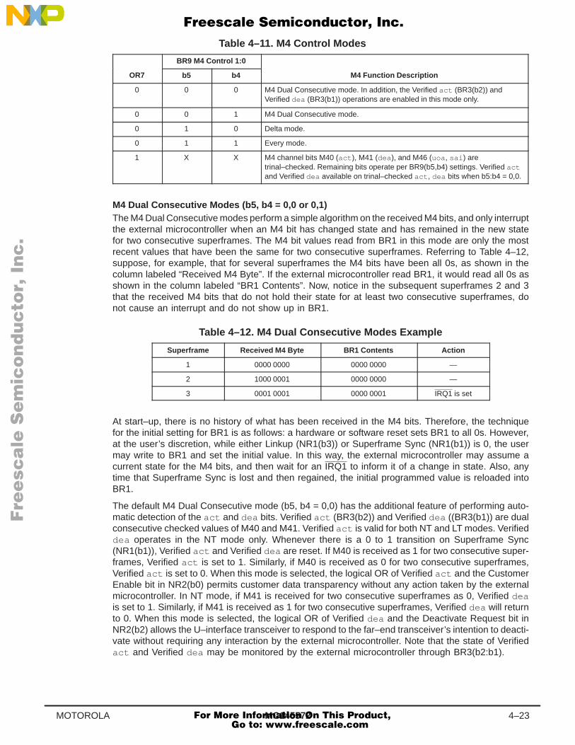
MC145572 4–23MOTOROLA
Table 4–11. M4 Control Modes
BR9 M4 Control 1:0
OR7 b5 b4 M4 Function Description
0 0 0 M4 Dual Consecutive mode. In addition, the Verified act (BR3(b2)) andVerified dea (BR3(b1)) operations are enabled in this mode only.
0 0 1 M4 Dual Consecutive mode.
0 1 0 Delta mode.
0 1 1 Every mode.
1 X X M4 channel bits M40 (act ), M41 (dea ), and M46 (uoa , sai ) aretrinal–checked. Remaining bits operate per BR9(b5,b4) settings. Verified actand Verified dea available on trinal–checked act , dea bits when b5:b4 = 0,0.
M4 Dual Consecutive Modes (b5, b4 = 0,0 or 0,1)The M4 Dual Consecutive modes perform a simple algorithm on the received M4 bits, and only interruptthe external microcontroller when an M4 bit has changed state and has remained in the new statefor two consecutive superframes. The M4 bit values read from BR1 in this mode are only the mostrecent values that have been the same for two consecutive superframes. Referring to Table 4–12,suppose, for example, that for several superframes the M4 bits have been all 0s, as shown in thecolumn labeled “Received M4 Byte”. If the external microcontroller read BR1, it would read all 0s asshown in the column labeled “BR1 Contents”. Now, notice in the subsequent superframes 2 and 3that the received M4 bits that do not hold their state for at least two consecutive superframes, donot cause an interrupt and do not show up in BR1.
Table 4–12. M4 Dual Consecutive Modes Example
Superframe Received M4 Byte BR1 Contents Action
1 0000 0000 0000 0000 —
2 1000 0001 0000 0000 —
3 0001 0001 0000 0001 IRQ1 is set
At start–up, there is no history of what has been received in the M4 bits. Therefore, the techniquefor the initial setting for BR1 is as follows: a hardware or software reset sets BR1 to all 0s. However,at the user’s discretion, while either Linkup (NR1(b3)) or Superframe Sync (NR1(b1)) is 0, the usermay write to BR1 and set the initial value. In this way, the external microcontroller may assume acurrent state for the M4 bits, and then wait for an IRQ1 to inform it of a change in state. Also, anytime that Superframe Sync is lost and then regained, the initial programmed value is reloaded intoBR1.
The default M4 Dual Consecutive mode (b5, b4 = 0,0) has the additional feature of performing auto-matic detection of the act and dea bits. Verified act (BR3(b2)) and Verified dea ((BR3(b1)) are dualconsecutive checked values of M40 and M41. Verified act is valid for both NT and LT modes. Verifieddea operates in the NT mode only. Whenever there is a 0 to 1 transition on Superframe Sync(NR1(b1)), Verified act and Verified dea are reset. If M40 is received as 1 for two consecutive super-frames, Verified act is set to 1. Similarly, if M40 is received as 0 for two consecutive superframes,Verified act is set to 0. When this mode is selected, the logical OR of Verified act and the CustomerEnable bit in NR2(b0) permits customer data transparency without any action taken by the externalmicrocontroller. In NT mode, if M41 is received for two consecutive superframes as 0, Verified deais set to 1. Similarly, if M41 is received as 1 for two consecutive superframes, Verified dea will returnto 0. When this mode is selected, the logical OR of Verified dea and the Deactivate Request bit inNR2(b2) allows the U–interface transceiver to respond to the far–end transceiver’s intention to deacti-vate without requiring any interaction by the external microcontroller. Note that the state of Verifiedact and Verified dea may be monitored by the external microcontroller through BR3(b2:b1).
Fre
esc
ale
Se
mic
on
du
cto
r, I
Freescale Semiconductor, Inc.
For More Information On This Product, Go to: www.freescale.com
nc
...
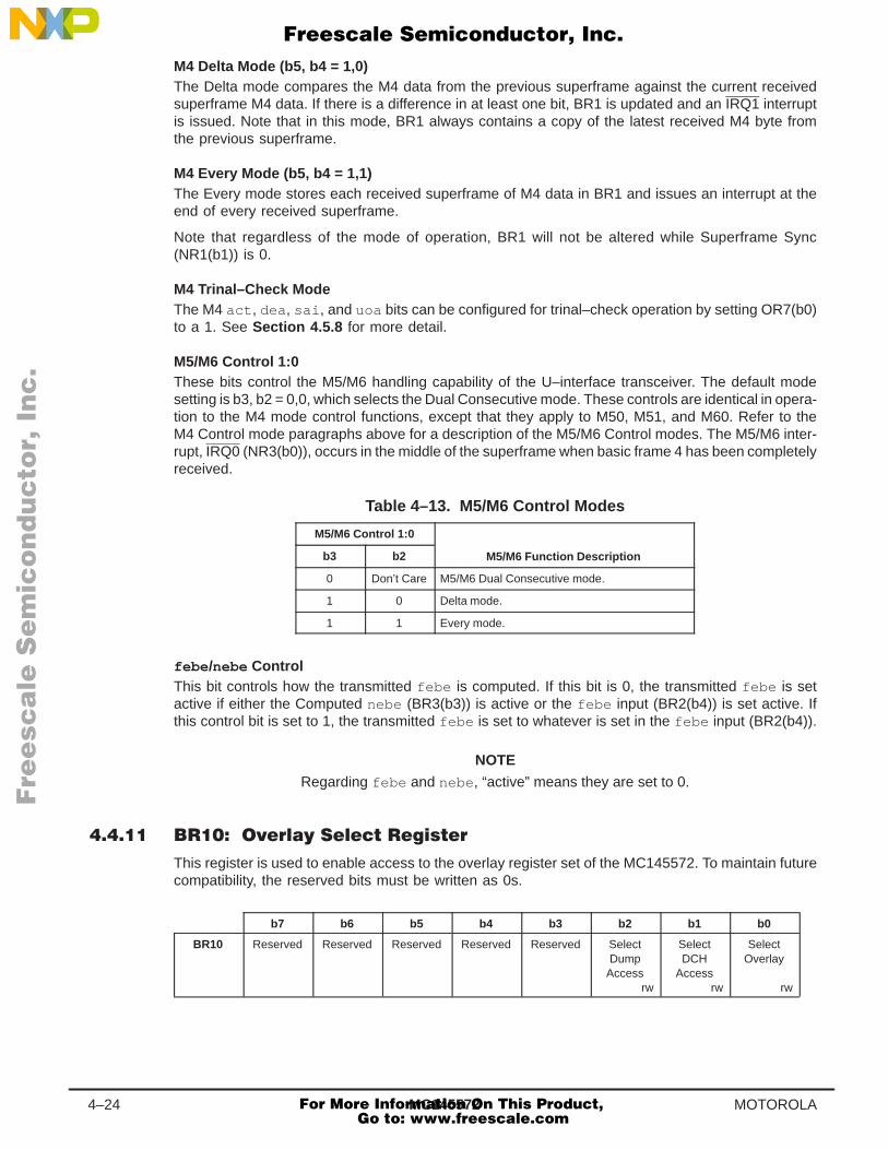
MC1455724–24 MOTOROLA
M4 Delta Mode (b5, b4 = 1,0)The Delta mode compares the M4 data from the previous superframe against the current receivedsuperframe M4 data. If there is a difference in at least one bit, BR1 is updated and an IRQ1 interruptis issued. Note that in this mode, BR1 always contains a copy of the latest received M4 byte fromthe previous superframe.
M4 Every Mode (b5, b4 = 1,1)The Every mode stores each received superframe of M4 data in BR1 and issues an interrupt at theend of every received superframe.
Note that regardless of the mode of operation, BR1 will not be altered while Superframe Sync(NR1(b1)) is 0.
M4 Trinal–Check ModeThe M4 act , dea , sai , and uoa bits can be configured for trinal–check operation by setting OR7(b0)to a 1. See Section 4.5.8 for more detail.
M5/M6 Control 1:0These bits control the M5/M6 handling capability of the U–interface transceiver. The default modesetting is b3, b2 = 0,0, which selects the Dual Consecutive mode. These controls are identical in opera-tion to the M4 mode control functions, except that they apply to M50, M51, and M60. Refer to theM4 Control mode paragraphs above for a description of the M5/M6 Control modes. The M5/M6 inter-rupt, IRQ0 (NR3(b0)), occurs in the middle of the superframe when basic frame 4 has been completelyreceived.
Table 4–13. M5/M6 Control Modes
M5/M6 Control 1:0
b3 b2 M5/M6 Function Description
0 Don’t Care M5/M6 Dual Consecutive mode.
1 0 Delta mode.
1 1 Every mode.
febe /nebe ControlThis bit controls how the transmitted febe is computed. If this bit is 0, the transmitted febe is setactive if either the Computed nebe (BR3(b3)) is active or the febe input (BR2(b4)) is set active. Ifthis control bit is set to 1, the transmitted febe is set to whatever is set in the febe input (BR2(b4)).
NOTE
Regarding febe and nebe , “active” means they are set to 0.
This register is used to enable access to the overlay register set of the MC145572. To maintain futurecompatibility, the reserved bits must be written as 0s.
b7 b6 b5 b4 b3 b2 b1 b0
BR10 Reserved Reserved Reserved Reserved Reserved SelectDump
Accessrw
SelectDCH
Accessrw
SelectOverlay
rw
Fre
esc
ale
Se
mic
on
du
cto
r, I
Freescale Semiconductor, Inc.
For More Information On This Product, Go to: www.freescale.com
nc
...
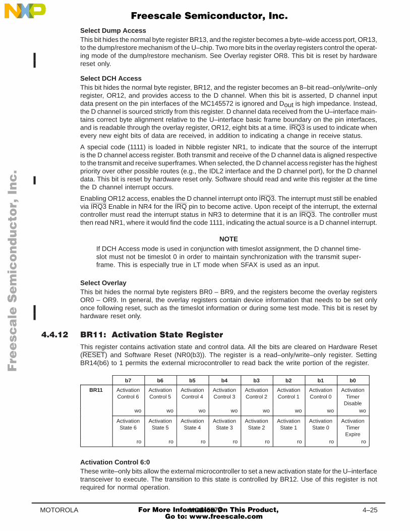
MC145572 4–25MOTOROLA
Select Dump AccessThis bit hides the normal byte register BR13, and the register becomes a byte–wide access port, OR13,to the dump/restore mechanism of the U–chip. Two more bits in the overlay registers control the operat-ing mode of the dump/restore mechanism. See Overlay register OR8. This bit is reset by hardwarereset only.
Select DCH AccessThis bit hides the normal byte register, BR12, and the register becomes an 8–bit read–only/write–onlyregister, OR12, and provides access to the D channel. When this bit is asserted, D channel inputdata present on the pin interfaces of the MC145572 is ignored and Dout is high impedance. Instead,the D channel is sourced strictly from this register. D channel data received from the U–interface main-tains correct byte alignment relative to the U–interface basic frame boundary on the pin interfaces,and is readable through the overlay register, OR12, eight bits at a time. IRQ3 is used to indicate whenevery new eight bits of data are received, in addition to indicating a change in receive status.
A special code (1111) is loaded in Nibble register NR1, to indicate that the source of the interruptis the D channel access register. Both transmit and receive of the D channel data is aligned respectiveto the transmit and receive superframes. When selected, the D channel access register has the highestpriority over other possible routes (e.g., the IDL2 interface and the D channel port), for the D channeldata. This bit is reset by hardware reset only. Software should read and write this register at the timethe D channel interrupt occurs.
Enabling OR12 access, enables the D channel interrupt onto IRQ3. The interrupt must still be enabledvia IRQ3 Enable in NR4 for the IRQ pin to become active. Upon receipt of the interrupt, the externalcontroller must read the interrupt status in NR3 to determine that it is an IRQ3. The controller mustthen read NR1, where it would find the code 1111, indicating the actual source is a D channel interrupt.
NOTEIf DCH Access mode is used in conjunction with timeslot assignment, the D channel time-slot must not be timeslot 0 in order to maintain synchronization with the transmit super-frame. This is especially true in LT mode when SFAX is used as an input.
Select OverlayThis bit hides the normal byte registers BR0 – BR9, and the registers become the overlay registersOR0 – OR9. In general, the overlay registers contain device information that needs to be set onlyonce following reset, such as the timeslot information or during some test mode. This bit is reset byhardware reset only.
This register contains activation state and control data. All the bits are cleared on Hardware Reset(RESET) and Software Reset (NR0(b3)). The register is a read–only/write–only register. SettingBR14(b6) to 1 permits the external microcontroller to read back the write portion of the register.
b7 b6 b5 b4 b3 b2 b1 b0
BR11 ActivationControl 6
ActivationControl 5
ActivationControl 4
ActivationControl 3
ActivationControl 2
ActivationControl 1
ActivationControl 0
ActivationTimer
Disablewo wo wo wo wo wo wo wo
ActivationState 6
ActivationState 5
ActivationState 4
ActivationState 3
ActivationState 2
ActivationState 1
ActivationState 0
ActivationTimerExpire
ro ro ro ro ro ro ro ro
Activation Control 6:0These write–only bits allow the external microcontroller to set a new activation state for the U–interfacetransceiver to execute. The transition to this state is controlled by BR12. Use of this register is notrequired for normal operation.
Fre
esc
ale
Se
mic
on
du
cto
r, I
Freescale Semiconductor, Inc.
For More Information On This Product, Go to: www.freescale.com
nc
...
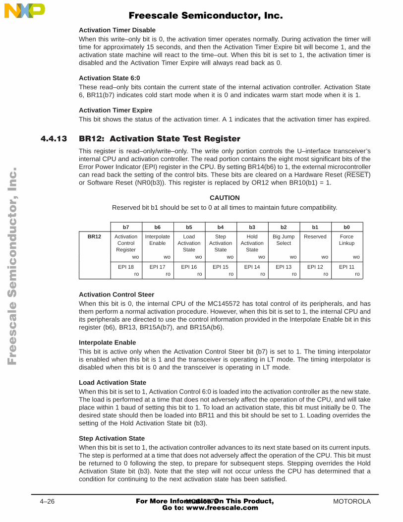
MC1455724–26 MOTOROLA
Activation Timer DisableWhen this write–only bit is 0, the activation timer operates normally. During activation the timer willtime for approximately 15 seconds, and then the Activation Timer Expire bit will become 1, and theactivation state machine will react to the time–out. When this bit is set to 1, the activation timer isdisabled and the Activation Timer Expire will always read back as 0.
Activation State 6:0These read–only bits contain the current state of the internal activation controller. Activation State6, BR11(b7) indicates cold start mode when it is 0 and indicates warm start mode when it is 1.
Activation Timer ExpireThis bit shows the status of the activation timer. A 1 indicates that the activation timer has expired.
This register is read–only/write–only. The write only portion controls the U–interface transceiver’sinternal CPU and activation controller. The read portion contains the eight most significant bits of theError Power Indicator (EPI) register in the CPU. By setting BR14(b6) to 1, the external microcontrollercan read back the setting of the control bits. These bits are cleared on a Hardware Reset (RESET)or Software Reset (NR0(b3)). This register is replaced by OR12 when BR10(b1) = 1.
CAUTIONReserved bit b1 should be set to 0 at all times to maintain future compatibility.
b7 b6 b5 b4 b3 b2 b1 b0
BR12 ActivationControlRegister
InterpolateEnable
LoadActivation
State
StepActivation
State
HoldActivation
State
Big JumpSelect
Reserved ForceLinkup
wo wo wo wo wo wo wo wo
EPI 18 EPI 17 EPI 16 EPI 15 EPI 14 EPI 13 EPI 12 EPI 11ro ro ro ro ro ro ro ro
Activation Control SteerWhen this bit is 0, the internal CPU of the MC145572 has total control of its peripherals, and hasthem perform a normal activation procedure. However, when this bit is set to 1, the internal CPU andits peripherals are directed to use the control information provided in the Interpolate Enable bit in thisregister (b6), BR13, BR15A(b7), and BR15A(b6).
Interpolate EnableThis bit is active only when the Activation Control Steer bit (b7) is set to 1. The timing interpolatoris enabled when this bit is 1 and the transceiver is operating in LT mode. The timing interpolator isdisabled when this bit is 0 and the transceiver is operating in LT mode.
Load Activation StateWhen this bit is set to 1, Activation Control 6:0 is loaded into the activation controller as the new state.The load is performed at a time that does not adversely affect the operation of the CPU, and will takeplace within 1 baud of setting this bit to 1. To load an activation state, this bit must initially be 0. Thedesired state should then be loaded into BR11 and this bit should be set to 1. Loading overrides thesetting of the Hold Activation State bit (b3).
Step Activation StateWhen this bit is set to 1, the activation controller advances to its next state based on its current inputs.The step is performed at a time that does not adversely affect the operation of the CPU. This bit mustbe returned to 0 following the step, to prepare for subsequent steps. Stepping overrides the HoldActivation State bit (b3). Note that the step will not occur unless the CPU has determined that acondition for continuing to the next activation state has been satisfied.
Fre
esc
ale
Se
mic
on
du
cto
r, I
Freescale Semiconductor, Inc.
For More Information On This Product, Go to: www.freescale.com
nc
...
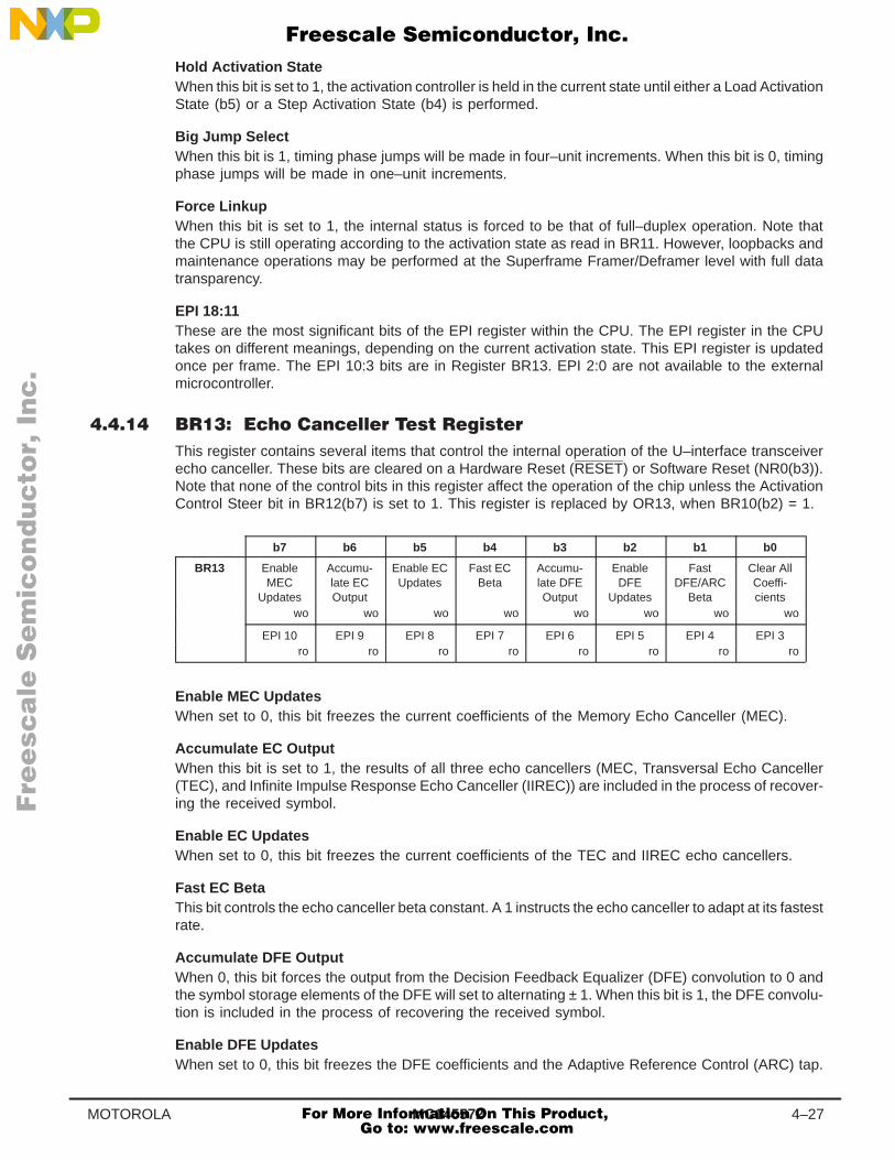
MC145572 4–27MOTOROLA
Hold Activation StateWhen this bit is set to 1, the activation controller is held in the current state until either a Load ActivationState (b5) or a Step Activation State (b4) is performed.
Big Jump SelectWhen this bit is 1, timing phase jumps will be made in four–unit increments. When this bit is 0, timingphase jumps will be made in one–unit increments.
Force LinkupWhen this bit is set to 1, the internal status is forced to be that of full–duplex operation. Note thatthe CPU is still operating according to the activation state as read in BR11. However, loopbacks andmaintenance operations may be performed at the Superframe Framer/Deframer level with full datatransparency.
EPI 18:11These are the most significant bits of the EPI register within the CPU. The EPI register in the CPUtakes on different meanings, depending on the current activation state. This EPI register is updatedonce per frame. The EPI 10:3 bits are in Register BR13. EPI 2:0 are not available to the externalmicrocontroller.
This register contains several items that control the internal operation of the U–interface transceiverecho canceller. These bits are cleared on a Hardware Reset (RESET) or Software Reset (NR0(b3)).Note that none of the control bits in this register affect the operation of the chip unless the ActivationControl Steer bit in BR12(b7) is set to 1. This register is replaced by OR13, when BR10(b2) = 1.
b7 b6 b5 b4 b3 b2 b1 b0
BR13 EnableMEC
Updates
Accumu-late ECOutput
Enable ECUpdates
Fast ECBeta
Accumu-late DFEOutput
EnableDFE
Updates
FastDFE/ARC
Beta
Clear AllCoeffi-cients
wo wo wo wo wo wo wo wo
EPI 10 EPI 9 EPI 8 EPI 7 EPI 6 EPI 5 EPI 4 EPI 3ro ro ro ro ro ro ro ro
Enable MEC UpdatesWhen set to 0, this bit freezes the current coefficients of the Memory Echo Canceller (MEC).
Accumulate EC OutputWhen this bit is set to 1, the results of all three echo cancellers (MEC, Transversal Echo Canceller(TEC), and Infinite Impulse Response Echo Canceller (IIREC)) are included in the process of recover-ing the received symbol.
Enable EC UpdatesWhen set to 0, this bit freezes the current coefficients of the TEC and IIREC echo cancellers.
Fast EC BetaThis bit controls the echo canceller beta constant. A 1 instructs the echo canceller to adapt at its fastestrate.
Accumulate DFE OutputWhen 0, this bit forces the output from the Decision Feedback Equalizer (DFE) convolution to 0 andthe symbol storage elements of the DFE will set to alternating ± 1. When this bit is 1, the DFE convolu-tion is included in the process of recovering the received symbol.
Enable DFE UpdatesWhen set to 0, this bit freezes the DFE coefficients and the Adaptive Reference Control (ARC) tap.
Fre
esc
ale
Se
mic
on
du
cto
r, I
Freescale Semiconductor, Inc.
For More Information On This Product, Go to: www.freescale.com
nc
...
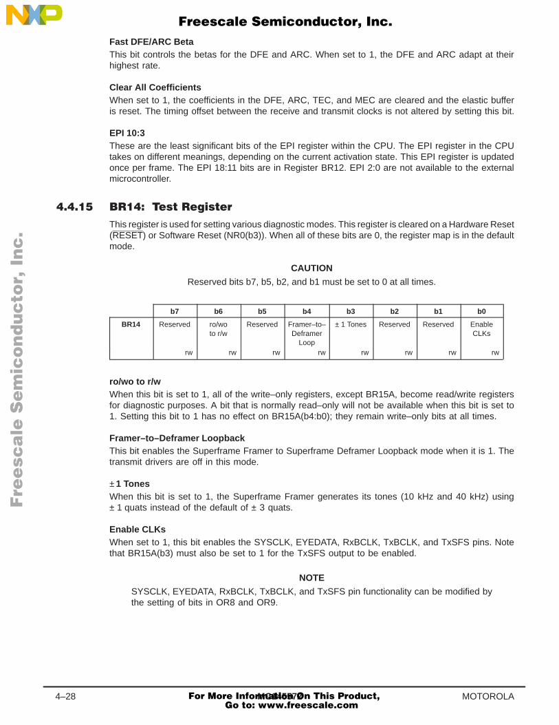
MC1455724–28 MOTOROLA
Fast DFE/ARC BetaThis bit controls the betas for the DFE and ARC. When set to 1, the DFE and ARC adapt at theirhighest rate.
Clear All CoefficientsWhen set to 1, the coefficients in the DFE, ARC, TEC, and MEC are cleared and the elastic bufferis reset. The timing offset between the receive and transmit clocks is not altered by setting this bit.
EPI 10:3These are the least significant bits of the EPI register within the CPU. The EPI register in the CPUtakes on different meanings, depending on the current activation state. This EPI register is updatedonce per frame. The EPI 18:11 bits are in Register BR12. EPI 2:0 are not available to the externalmicrocontroller.
This register is used for setting various diagnostic modes. This register is cleared on a Hardware Reset(RESET) or Software Reset (NR0(b3)). When all of these bits are 0, the register map is in the defaultmode.
CAUTION
Reserved bits b7, b5, b2, and b1 must be set to 0 at all times.
b7 b6 b5 b4 b3 b2 b1 b0
BR14 Reserved ro/woto r/w
Reserved Framer–to–Deframer
Loop
± 1 Tones Reserved Reserved EnableCLKs
rw rw rw rw rw rw rw rw
ro/wo to r/wWhen this bit is set to 1, all of the write–only registers, except BR15A, become read/write registersfor diagnostic purposes. A bit that is normally read–only will not be available when this bit is set to1. Setting this bit to 1 has no effect on BR15A(b4:b0); they remain write–only bits at all times.
Framer–to–Deframer LoopbackThis bit enables the Superframe Framer to Superframe Deframer Loopback mode when it is 1. Thetransmit drivers are off in this mode.
± 1 TonesWhen this bit is set to 1, the Superframe Framer generates its tones (10 kHz and 40 kHz) using± 1 quats instead of the default of ± 3 quats.
Enable CLKsWhen set to 1, this bit enables the SYSCLK, EYEDATA, RxBCLK, TxBCLK, and TxSFS pins. Notethat BR15A(b3) must also be set to 1 for the TxSFS output to be enabled.
NOTE
SYSCLK, EYEDATA, RxBCLK, TxBCLK, and TxSFS pin functionality can be modified bythe setting of bits in OR8 and OR9.
Fre
esc
ale
Se
mic
on
du
cto
r, I
Freescale Semiconductor, Inc.
For More Information On This Product, Go to: www.freescale.com
nc
...
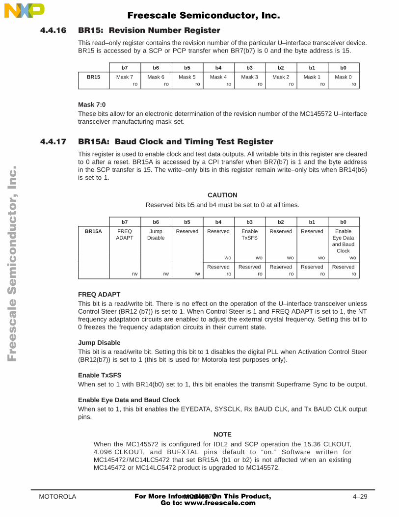
MC145572 4–29MOTOROLA
This read–only register contains the revision number of the particular U–interface transceiver device.BR15 is accessed by a SCP or PCP transfer when BR7(b7) is 0 and the byte address is 15.
b7 b6 b5 b4 b3 b2 b1 b0
BR15 Mask 7 Mask 6 Mask 5 Mask 4 Mask 3 Mask 2 Mask 1 Mask 0ro ro ro ro ro ro ro ro
Mask 7:0These bits allow for an electronic determination of the revision number of the MC145572 U–interfacetransceiver manufacturing mask set.
This register is used to enable clock and test data outputs. All writable bits in this register are clearedto 0 after a reset. BR15A is accessed by a CPI transfer when BR7(b7) is 1 and the byte addressin the SCP transfer is 15. The write–only bits in this register remain write–only bits when BR14(b6)is set to 1.
CAUTION
Reserved bits b5 and b4 must be set to 0 at all times.
b7 b6 b5 b4 b3 b2 b1 b0
BR15A FREQADAPT
JumpDisable
Reserved Reserved EnableTxSFS
Reserved Reserved EnableEye Dataand Baud
Clockwo wo wo wo wo
Reserved Reserved Reserved Reserved Reservedrw rw rw ro ro ro ro ro
FREQ ADAPTThis bit is a read/write bit. There is no effect on the operation of the U–interface transceiver unlessControl Steer (BR12 (b7)) is set to 1. When Control Steer is 1 and FREQ ADAPT is set to 1, the NTfrequency adaptation circuits are enabled to adjust the external crystal frequency. Setting this bit to0 freezes the frequency adaptation circuits in their current state.
Jump DisableThis bit is a read/write bit. Setting this bit to 1 disables the digital PLL when Activation Control Steer(BR12(b7)) is set to 1 (this bit is used for Motorola test purposes only).
Enable TxSFSWhen set to 1 with BR14(b0) set to 1, this bit enables the transmit Superframe Sync to be output.
Enable Eye Data and Baud ClockWhen set to 1, this bit enables the EYEDATA, SYSCLK, Rx BAUD CLK, and Tx BAUD CLK outputpins.
NOTE
When the MC145572 is configured for IDL2 and SCP operation the 15.36 CLKOUT,4.096 CLKOUT, and BUFXTAL pins default to “on.” Software written forMC145472/MC14LC5472 that set BR15A (b1 or b2) is not affected when an existingMC145472 or MC14LC5472 product is upgraded to MC145572.
Fre
esc
ale
Se
mic
on
du
cto
r, I
Freescale Semiconductor, Inc.
For More Information On This Product, Go to: www.freescale.com
nc
...
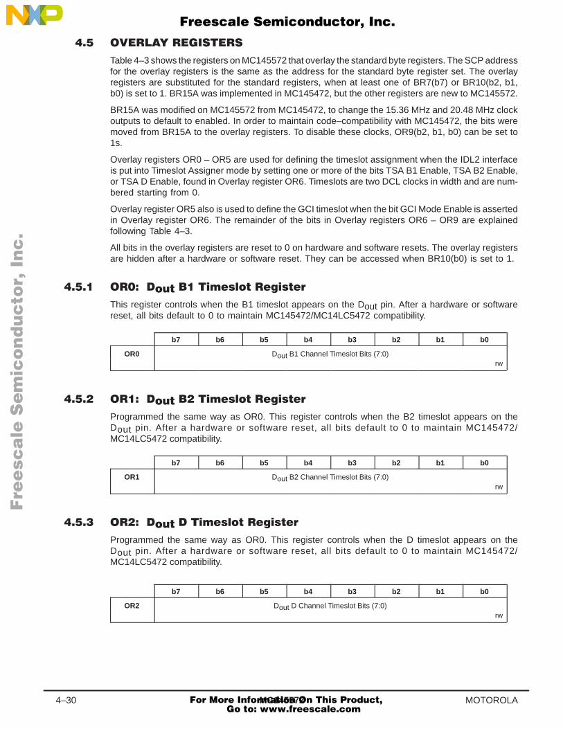
MC1455724–30 MOTOROLA
Table 4–3 shows the registers on MC145572 that overlay the standard byte registers. The SCP addressfor the overlay registers is the same as the address for the standard byte register set. The overlayregisters are substituted for the standard registers, when at least one of BR7(b7) or BR10(b2, b1,b0) is set to 1. BR15A was implemented in MC145472, but the other registers are new to MC145572.
BR15A was modified on MC145572 from MC145472, to change the 15.36 MHz and 20.48 MHz clockoutputs to default to enabled. In order to maintain code–compatibility with MC145472, the bits weremoved from BR15A to the overlay registers. To disable these clocks, OR9(b2, b1, b0) can be set to1s.
Overlay registers OR0 – OR5 are used for defining the timeslot assignment when the IDL2 interfaceis put into Timeslot Assigner mode by setting one or more of the bits TSA B1 Enable, TSA B2 Enable,or TSA D Enable, found in Overlay register OR6. Timeslots are two DCL clocks in width and are num-bered starting from 0.
Overlay register OR5 also is used to define the GCI timeslot when the bit GCI Mode Enable is assertedin Overlay register OR6. The remainder of the bits in Overlay registers OR6 – OR9 are explainedfollowing Table 4–3.
All bits in the overlay registers are reset to 0 on hardware and software resets. The overlay registersare hidden after a hardware or software reset. They can be accessed when BR10(b0) is set to 1.
This register controls when the B1 timeslot appears on the Dout pin. After a hardware or softwarereset, all bits default to 0 to maintain MC145472/MC14LC5472 compatibility.
b7 b6 b5 b4 b3 b2 b1 b0
OR0 Dout B1 Channel Timeslot Bits (7:0)rw
Programmed the same way as OR0. This register controls when the B2 timeslot appears on theDout pin. After a hardware or software reset, all bits default to 0 to maintain MC145472/MC14LC5472 compatibility.
b7 b6 b5 b4 b3 b2 b1 b0
OR1 Dout B2 Channel Timeslot Bits (7:0)rw
Programmed the same way as OR0. This register controls when the D timeslot appears on theDout pin. After a hardware or software reset, all bits default to 0 to maintain MC145472/MC14LC5472 compatibility.
b7 b6 b5 b4 b3 b2 b1 b0
OR2 Dout D Channel Timeslot Bits (7:0)rw
Fre
esc
ale
Se
mic
on
du
cto
r, I
Freescale Semiconductor, Inc.
For More Information On This Product, Go to: www.freescale.com
nc
...
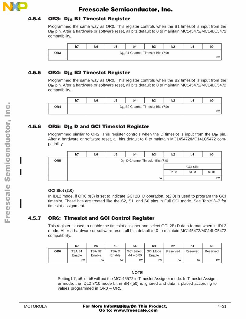
MC145572 4–31MOTOROLA
Programmed the same way as OR0. This register controls when the B1 timeslot is input from theDin pin. After a hardware or software reset, all bits default to 0 to maintain MC145472/MC14LC5472compatibility.
b7 b6 b5 b4 b3 b2 b1 b0
OR3 Din B1 Channel Timeslot Bits (7:0)rw
Programmed the same way as OR0. This register controls when the B2 timeslot is input from theDin pin. After a hardware or software reset, all bits default to 0 to maintain MC145472/MC14LC5472compatibility.
b7 b6 b5 b4 b3 b2 b1 b0
OR4 Din B2 Channel Timeslot Bits (7:0)rw
Programmed similar to OR2. This register controls when the D timeslot is input from the Din pin.After a hardware or software reset, all bits default to 0 to maintain MC145472/MC14LC5472 com-patibility.
b7 b6 b5 b4 b3 b2 b1 b0
OR5 Din D Channel Timeslot Bits (7:0)
GCI Slot
rw rw
GCI Slot (2:0)In IDL2 mode, if OR6 b(3) is set to indicate GCI 2B+D operation, b(2:0) is used to program the GCItimeslot. These bits are treated like the S2, S1, and S0 pins in Full GCI mode. See Table 3–7 fortimeslot assignment.
This register is used to enable the timeslot assigner and select GCI 2B+D data format when in IDL2mode. After a hardware or software reset, all bits default to 0 to maintain MC145472/MC14LC5472compatibility.
b7 b6 b5 b4 b3 b2 b1 b0
OR6 TSA B1Enable
TSA B2Enable
TSA DEnable
GCI SelectM4 – BR0
GCI ModeEnable
Reserved Reserved Reserved
rw rw rw rw rw rw rw rw
NOTE
Setting b7, b6, or b5 will put the MC145572 in Timeslot Assigner mode. In Timeslot Assign-er mode, the IDL2 8/10 mode bit in BR7(b0) is ignored and data is placed according tovalues programmed in OR0 – OR5.
Fre
esc
ale
Se
mic
on
du
cto
r, I
Freescale Semiconductor, Inc.
For More Information On This Product, Go to: www.freescale.com
nc
...
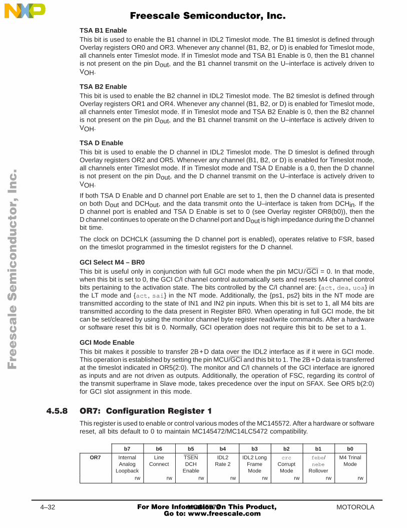
MC1455724–32 MOTOROLA
TSA B1 EnableThis bit is used to enable the B1 channel in IDL2 Timeslot mode. The B1 timeslot is defined throughOverlay registers OR0 and OR3. Whenever any channel (B1, B2, or D) is enabled for Timeslot mode,all channels enter Timeslot mode. If in Timeslot mode and TSA B1 Enable is 0, then the B1 channelis not present on the pin Dout, and the B1 channel transmit on the U–interface is actively driven toVOH.
TSA B2 EnableThis bit is used to enable the B2 channel in IDL2 Timeslot mode. The B2 timeslot is defined throughOverlay registers OR1 and OR4. Whenever any channel (B1, B2, or D) is enabled for Timeslot mode,all channels enter Timeslot mode. If in Timeslot mode and TSA B2 Enable is 0, then the B2 channelis not present on the pin Dout, and the B1 channel transmit on the U–interface is actively driven toVOH.
TSA D EnableThis bit is used to enable the D channel in IDL2 Timeslot mode. The D timeslot is defined throughOverlay registers OR2 and OR5. Whenever any channel (B1, B2, or D) is enabled for Timeslot mode,all channels enter Timeslot mode. If in Timeslot mode and TSA D Enable is a 0, then the D channelis not present on the pin Dout, and the D channel transmit on the U–interface is actively driven toVOH.
If both TSA D Enable and D channel port Enable are set to 1, then the D channel data is presentedon both Dout and DCHout, and the data transmit onto the U–interface is taken from DCHin. If theD channel port is enabled and TSA D Enable is set to 0 (see Overlay register OR8(b0)), then theD channel continues to operate on the D channel port and Dout is high impedance during the D channelbit time.
The clock on DCHCLK (assuming the D channel port is enabled), operates relative to FSR, basedon the timeslot programmed in the timeslot registers for the D channel.
GCI Select M4 – BR0This bit is useful only in conjunction with full GCI mode when the pin MCU/GCI = 0. In that mode,when this bit is set to 0, the GCI C/I channel control automatically sets and resets M4 channel controlbits pertaining to the activation state. The bits controlled by the C/I channel are: act , dea , uoa inthe LT mode and act , sai in the NT mode. Additionally, the ps1, ps2 bits in the NT mode aretransmitted according to the state of IN1 and IN2 pin inputs. When this bit is set to 1, all M4 bits aretransmitted according to the data present in Register BR0. When operating in full GCI mode, the bitcan be set/cleared by using the monitor channel byte register read/write commands. After a hardwareor software reset this bit is 0. Normally, GCI operation does not require this bit to be set to a 1.
GCI Mode EnableThis bit makes it possible to transfer 2B+D data over the IDL2 interface as if it were in GCI mode.This operation is established by setting the pin MCU/GCI and this bit to 1. The 2B+D data is transferredat the timeslot indicated in OR5(2:0). The monitor and C/I channels of the GCI interface are ignoredas inputs and are not driven as outputs. Additionally, the operation of FSC, regarding its control ofthe transmit superframe in Slave mode, takes precedence over the input on SFAX. See OR5 b(2:0)for GCI slot assignment in this mode.
This register is used to enable or control various modes of the MC145572. After a hardware or softwarereset, all bits default to 0 to maintain MC145472/MC14LC5472 compatibility.
b7 b6 b5 b4 b3 b2 b1 b0
OR7 InternalAnalog
Loopback
LineConnect
TSENDCH
Enable
IDL2Rate 2
IDL2 LongFrameMode
crcCorruptMode
febe /nebe
Rollover
M4 TrinalMode
rw rw rw rw rw rw rw rw
Fre
esc
ale
Se
mic
on
du
cto
r, I
Freescale Semiconductor, Inc.
For More Information On This Product, Go to: www.freescale.com
nc
...
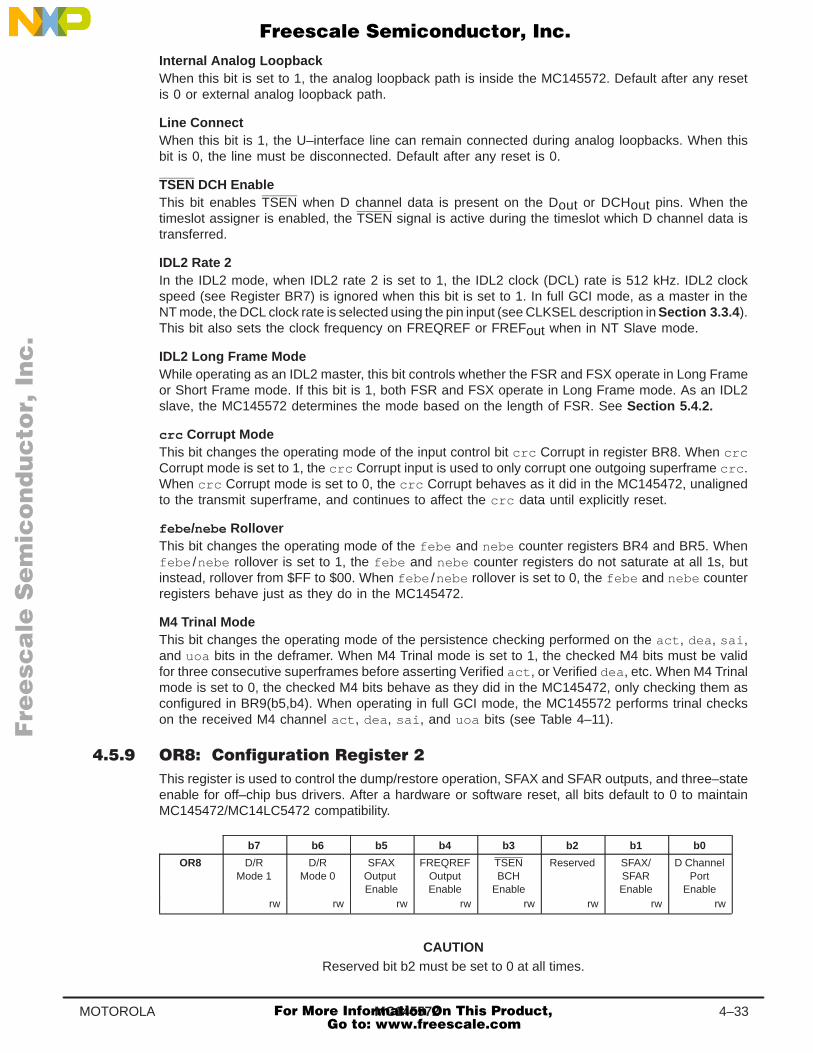
MC145572 4–33MOTOROLA
Internal Analog LoopbackWhen this bit is set to 1, the analog loopback path is inside the MC145572. Default after any resetis 0 or external analog loopback path.
Line ConnectWhen this bit is 1, the U–interface line can remain connected during analog loopbacks. When thisbit is 0, the line must be disconnected. Default after any reset is 0.
TSEN DCH EnableThis bit enables TSEN when D channel data is present on the Dout or DCHout pins. When thetimeslot assigner is enabled, the TSEN signal is active during the timeslot which D channel data istransferred.
IDL2 Rate 2In the IDL2 mode, when IDL2 rate 2 is set to 1, the IDL2 clock (DCL) rate is 512 kHz. IDL2 clockspeed (see Register BR7) is ignored when this bit is set to 1. In full GCI mode, as a master in theNT mode, the DCL clock rate is selected using the pin input (see CLKSEL description in Section 3.3.4 ).This bit also sets the clock frequency on FREQREF or FREFout when in NT Slave mode.
IDL2 Long Frame ModeWhile operating as an IDL2 master, this bit controls whether the FSR and FSX operate in Long Frameor Short Frame mode. If this bit is 1, both FSR and FSX operate in Long Frame mode. As an IDL2slave, the MC145572 determines the mode based on the length of FSR. See Section 5.4.2.
crc Corrupt ModeThis bit changes the operating mode of the input control bit crc Corrupt in register BR8. When crcCorrupt mode is set to 1, the crc Corrupt input is used to only corrupt one outgoing superframe crc .When crc Corrupt mode is set to 0, the crc Corrupt behaves as it did in the MC145472, unalignedto the transmit superframe, and continues to affect the crc data until explicitly reset.
febe /nebe RolloverThis bit changes the operating mode of the febe and nebe counter registers BR4 and BR5. Whenfebe /nebe rollover is set to 1, the febe and nebe counter registers do not saturate at all 1s, butinstead, rollover from $FF to $00. When febe /nebe rollover is set to 0, the febe and nebe counterregisters behave just as they do in the MC145472.
M4 Trinal ModeThis bit changes the operating mode of the persistence checking performed on the act , dea , sai ,and uoa bits in the deframer. When M4 Trinal mode is set to 1, the checked M4 bits must be validfor three consecutive superframes before asserting Verified act , or Verified dea , etc. When M4 Trinalmode is set to 0, the checked M4 bits behave as they did in the MC145472, only checking them asconfigured in BR9(b5,b4). When operating in full GCI mode, the MC145572 performs trinal checkson the received M4 channel act , dea , sai , and uoa bits (see Table 4–11).
This register is used to control the dump/restore operation, SFAX and SFAR outputs, and three–stateenable for off–chip bus drivers. After a hardware or software reset, all bits default to 0 to maintainMC145472/MC14LC5472 compatibility.
b7 b6 b5 b4 b3 b2 b1 b0
OR8 D/RMode 1
D/RMode 0
SFAXOutput Enable
FREQREFOutputEnable
TSENBCH
Enable
Reserved SFAX/SFAREnable
D ChannelPort
Enablerw rw rw rw rw rw rw rw
CAUTIONReserved bit b2 must be set to 0 at all times.
Fre
esc
ale
Se
mic
on
du
cto
r, I
Freescale Semiconductor, Inc.
For More Information On This Product, Go to: www.freescale.com
nc
...
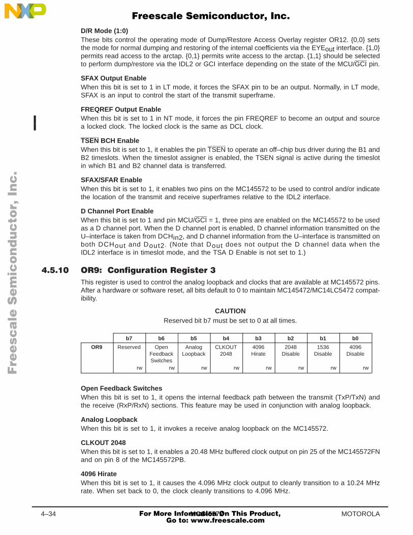
MC1455724–34 MOTOROLA
D/R Mode (1:0)These bits control the operating mode of Dump/Restore Access Overlay register OR12. 0,0 setsthe mode for normal dumping and restoring of the internal coefficients via the EYEout interface. 1,0permits read access to the arctap. 0,1 permits write access to the arctap. 1,1 should be selectedto perform dump/restore via the IDL2 or GCI interface depending on the state of the MCU/GCI pin.
SFAX Output EnableWhen this bit is set to 1 in LT mode, it forces the SFAX pin to be an output. Normally, in LT mode,SFAX is an input to control the start of the transmit superframe.
FREQREF Output EnableWhen this bit is set to 1 in NT mode, it forces the pin FREQREF to become an output and sourcea locked clock. The locked clock is the same as DCL clock.
TSEN BCH EnableWhen this bit is set to 1, it enables the pin TSEN to operate an off–chip bus driver during the B1 andB2 timeslots. When the timeslot assigner is enabled, the TSEN signal is active during the timeslotin which B1 and B2 channel data is transferred.
SFAX/SFAR EnableWhen this bit is set to 1, it enables two pins on the MC145572 to be used to control and/or indicatethe location of the transmit and receive superframes relative to the IDL2 interface.
D Channel Port EnableWhen this bit is set to 1 and pin MCU/GCI = 1, three pins are enabled on the MC145572 to be usedas a D channel port. When the D channel port is enabled, D channel information transmitted on theU–interface is taken from DCHin2, and D channel information from the U–interface is transmitted onboth DCHout and Dout2. (Note that Dout does not output the D channel data when theIDL2 interface is in timeslot mode, and the TSA D Enable is not set to 1.)
This register is used to control the analog loopback and clocks that are available at MC145572 pins.After a hardware or software reset, all bits default to 0 to maintain MC145472/MC14LC5472 compat-ibility.
CAUTIONReserved bit b7 must be set to 0 at all times.
b7 b6 b5 b4 b3 b2 b1 b0
OR9 Reserved OpenFeedbackSwitches
AnalogLoopback
CLKOUT2048
4096Hirate
2048Disable
1536Disable
4096Disable
rw rw rw rw rw rw rw rw
Open Feedback SwitchesWhen this bit is set to 1, it opens the internal feedback path between the transmit (TxP/TxN) andthe receive (RxP/RxN) sections. This feature may be used in conjunction with analog loopback.
Analog LoopbackWhen this bit is set to 1, it invokes a receive analog loopback on the MC145572.
CLKOUT 2048When this bit is set to 1, it enables a 20.48 MHz buffered clock output on pin 25 of the MC145572FNand on pin 8 of the MC145572PB.
4096 HirateWhen this bit is set to 1, it causes the 4.096 MHz clock output to cleanly transition to a 10.24 MHzrate. When set back to 0, the clock cleanly transitions to 4.096 MHz.
Fre
esc
ale
Se
mic
on
du
cto
r, I
Freescale Semiconductor, Inc.
For More Information On This Product, Go to: www.freescale.com
nc
...
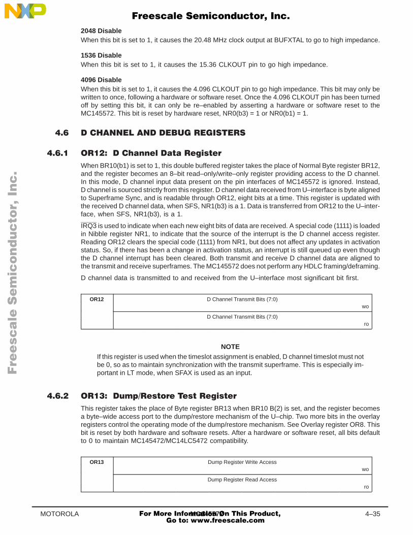
MC145572 4–35MOTOROLA
2048 DisableWhen this bit is set to 1, it causes the 20.48 MHz clock output at BUFXTAL to go to high impedance.
1536 DisableWhen this bit is set to 1, it causes the 15.36 CLKOUT pin to go high impedance.
4096 DisableWhen this bit is set to 1, it causes the 4.096 CLKOUT pin to go high impedance. This bit may only bewritten to once, following a hardware or software reset. Once the 4.096 CLKOUT pin has been turnedoff by setting this bit, it can only be re–enabled by asserting a hardware or software reset to theMC145572. This bit is reset by hardware reset, NR0(b3) = 1 or NR0(b1) = 1.
% $%#
When BR10(b1) is set to 1, this double buffered register takes the place of Normal Byte register BR12,and the register becomes an 8–bit read–only/write–only register providing access to the D channel.In this mode, D channel input data present on the pin interfaces of MC145572 is ignored. Instead,D channel is sourced strictly from this register. D channel data received from U–interface is byte alignedto Superframe Sync, and is readable through OR12, eight bits at a time. This register is updated withthe received D channel data, when SFS, NR1(b3) is a 1. Data is transferred from OR12 to the U–inter-face, when SFS, NR1(b3), is a 1.
IRQ3 is used to indicate when each new eight bits of data are received. A special code (1111) is loadedin Nibble register NR1, to indicate that the source of the interrupt is the D channel access register.Reading OR12 clears the special code (1111) from NR1, but does not affect any updates in activationstatus. So, if there has been a change in activation status, an interrupt is still queued up even thoughthe D channel interrupt has been cleared. Both transmit and receive D channel data are aligned tothe transmit and receive superframes. The MC145572 does not perform any HDLC framing/deframing.
D channel data is transmitted to and received from the U–interface most significant bit first.
OR12 D Channel Transmit Bits (7:0)wo
D Channel Transmit Bits (7:0)ro
NOTEIf this register is used when the timeslot assignment is enabled, D channel timeslot must notbe 0, so as to maintain synchronization with the transmit superframe. This is especially im-portant in LT mode, when SFAX is used as an input.
&"$%!# $% $%#
This register takes the place of Byte register BR13 when BR10 B(2) is set, and the register becomesa byte–wide access port to the dump/restore mechanism of the U–chip. Two more bits in the overlayregisters control the operating mode of the dump/restore mechanism. See Overlay register OR8. Thisbit is reset by both hardware and software resets. After a hardware or software reset, all bits defaultto 0 to maintain MC145472/MC14LC5472 compatibility.
OR13 Dump Register Write Accesswo
Dump Register Read Accessro
Fre
esc
ale
Se
mic
on
du
cto
r, I
Freescale Semiconductor, Inc.
For More Information On This Product, Go to: www.freescale.com
nc
...

MC1455724–36 MOTOROLA
Fre
esc
ale
Se
mic
on
du
cto
r, I
Freescale Semiconductor, Inc.
For More Information On This Product, Go to: www.freescale.com
nc
...
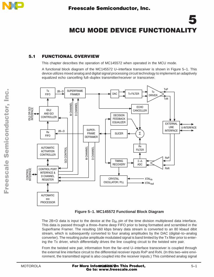
MC145572 5–1MOTOROLA
This chapter describes the operation of MC145572 when operated in the MCU mode.
A functional block diagram of the MC145572 U–interface transceiver is shown in Figure 5–1. Thisdevice utilizes mixed analog and digital signal processing circuit technology to implement an adaptivelyequalized echo cancelling full–duplex transmitter/receiver or transceiver.
Σ(
&
&
&
&
&
&
&
&
&
Σ∆
#
!"
#%$
Figure 5–1. MC145572 Functional Block Diagram
The 2B+D data is input to the device at the Din pin of the time division multiplexed data interface.This data is passed through a three–frame deep FIFO prior to being formatted and scrambled in theSuperframe Framer. The resulting 160 kbps binary data stream is converted to an 80 kbaud dibitstream, which is subsequently converted to four analog amplitudes by the DAC (digital–to–analogconverter). The resulting pulse amplitude modulated signal is band limited by the Tx filter prior to enter-ing the Tx driver, which differentially drives the line coupling circuit to the twisted wire pair.
From the twisted wire pair, information from the far–end U–interface transceiver is coupled throughthe external line interface circuit to the differential receiver inputs RxP and RxN. (In this two–wire envi-ronment, the transmitted signal is also coupled into the receiver inputs.) This combined analog signal
Fre
esc
ale
Se
mic
on
du
cto
r, I
Freescale Semiconductor, Inc.
For More Information On This Product, Go to: www.freescale.com
nc
...
MC1455725–2 MOTOROLA
is converted to a digital word in the Σ–∆ (sigma–delta) ADC (analog–to–digital converter). After filter-ing, an adaptively generated replica of the transmitted signal, calculated by the echo canceller, is sub-tracted from the combined signal leaving only the far–end signal. In addition, phase distortion presentin the far–end signal is corrected by the DFE. The resulting four–level signal is decoded by the slicerto produce a 160 kbps data stream. Timing information is also recovered from the far–end signal. TheSuperframe Deframer descrambles and disassembles the received superframes and passes thereceived 2B+D data through a three IDL frame deep FIFO to the IDL interface, where it is available atthe Dout pin of the time division multiplexed data interface.
The MC145572 permits the designer to select one of three options for control of the device and accessto its register set. When operating in MCU mode, the MC145572 can be configured for either SCPor PCP mode of operation. In SCP mode, control and status of the device is handled via the SCP,a standard four–wire serial microcontroller interface. In PCP mode, the MC145572 is configured toprovide an eight–bit wide data port with a chip select and read/write pin. In either case, the internalregister set of the MC145572 gives an external microcontroller access to the 4 kbps Maintenancechannel provided across the U–interface.
When the MC145572 is configured for GCI mode, the C/I channel of the GCI interface is used forcontrol and status messages. The GCI Monitor channel is used to send and receive Maintenancechannel messages. The Monitor channel also permits the internal registers of the MC145572 to beread from or written to, if it is desired to bypass the normal operation of the GCI interface.
The eoc portion of the M channel can be handled automatically with the internal Automatic eoc Pro-cessor. In addition, activation and deactivation of the MC145572 is handled by an Automatic ActivationController.
The MC145572 requires a single 20.48000 MHz pullable crystal connected between the XTALin andXTALout pins. No other external components are required for the crystal oscillator. Internal crystalpulling circuitry adjusts the crystal frequency in both LT and NT modes of operation.
Detailed descriptions of the various interfaces and user accessible sections are provided in thischapter.
After either a hardware or software reset, the MC145572 maintains basic pin function and registercompatibility with the MC14LC5472 U–interface transceiver when configured for MCU mode and usingthe SCP interface. There are differences between MC14LC5472 and MC145572 in exact signal re-quirements and outputs for these pins.
Most software written for MC14LC5472 will operate MC145572 without requiring any modifications.The MC145572 has an extended register set which provides access to the on–chip timeslot assigner,I/O pin configuration bits, D channel, and internal parameters of the device. The extended registersare accessed by setting bits in Register BR10 that were reserved bits for MC14LC5472. The newregisters then overlay the original registers and are referred to in this document as Overlay registersOR0 through OR9, OR12, and OR13. Register BR10 is common to both register sets, permitting soft-ware to switch between the basic register set and the overlay register set, as required. Tables 4–1,4–2, and 4–3 detail the register set of MC145527. See Chapter 4, Register Description, for detailson the register set.
Tables 5–1 and 5–2 contain the MC145572 pin function charts. The MC145572 requires a line interfacetransformer having a turns ratio of 1:1.25 where the 1.25 is on the tip and ring side of the transformer.The MC14LC5472 used a line interface transformer having a 1:2 turns ratio.
When operated in MCU mode with the SCP, MC145572 has clock outputs enabled on 15.36 CLKOUTand BUFXTAL pins after a hardware or software reset. On MC14LC5472, these clocks were disabledafter a hardware or software reset. Due to this change, the function of bits BR15A(b2, b1) have changedin MC145572. In MC14LC5472, these two bits enabled 15.36 CLKOUT and BUFXTAL outputs, respec-tively; when set to 1. In MC145572, these bits are reserved and writing a 1 to either of these bitsto enable a clock, leaves the clock(s) enabled. To disable one or both of these clocks, software mustset either bit b2 or bit b1 in Overlay register OR9.
Fre
esc
ale
Se
mic
on
du
cto
r, I
Freescale Semiconductor, Inc.
For More Information On This Product, Go to: www.freescale.com
nc
...
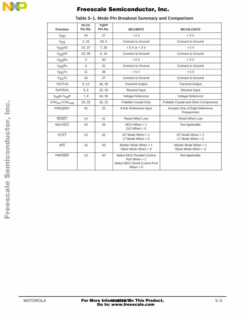
MC145572 5–3MOTOROLA
Table 5–1. Mode Pin Breakout Summary and ComparisonÁÁÁÁÁÁÁÁÁÁÁÁÁÁÁÁÁÁ
Function
ÁÁÁÁÁÁÁÁÁÁÁÁ
PLCCPin No.
ÁÁÁÁÁÁÁÁÁÁÁÁ
TQFPPin No.
ÁÁÁÁÁÁÁÁÁÁÁÁÁÁÁÁÁÁÁÁÁÁÁÁÁÁÁ
MC145572
ÁÁÁÁÁÁÁÁÁÁÁÁÁÁÁÁÁÁÁÁÁÁÁÁÁÁÁÁÁÁÁÁÁ
MC14LC5472
ÁÁÁÁÁÁÁÁÁÁÁÁ
VDD ÁÁÁÁÁÁÁÁ
44 ÁÁÁÁÁÁÁÁ
27 ÁÁÁÁÁÁÁÁÁÁÁÁÁÁÁÁÁÁ
+ 5 V ÁÁÁÁÁÁÁÁÁÁÁÁÁÁÁÁÁÁÁÁÁÁ
+ 5 V
ÁÁÁÁÁÁÁÁÁÁÁÁ
VSS ÁÁÁÁÁÁÁÁ
2, 22ÁÁÁÁÁÁÁÁ
29, 5 ÁÁÁÁÁÁÁÁÁÁÁÁÁÁÁÁÁÁ
Connect to Ground ÁÁÁÁÁÁÁÁÁÁÁÁÁÁÁÁÁÁÁÁÁÁ
Connect to Ground
ÁÁÁÁÁÁÁÁÁÁÁÁ
VDDI/O ÁÁÁÁÁÁÁÁ
24, 37ÁÁÁÁÁÁÁÁ
7, 20 ÁÁÁÁÁÁÁÁÁÁÁÁÁÁÁÁÁÁ
+ 5 V or + 3 V ÁÁÁÁÁÁÁÁÁÁÁÁÁÁÁÁÁÁÁÁÁÁ
+ 5 V
ÁÁÁÁÁÁÁÁÁÁÁÁ
VSSI/O ÁÁÁÁÁÁÁÁ
23, 36ÁÁÁÁÁÁÁÁ
6, 19 ÁÁÁÁÁÁÁÁÁÁÁÁÁÁÁÁÁÁ
Connect to Ground ÁÁÁÁÁÁÁÁÁÁÁÁÁÁÁÁÁÁÁÁÁÁ
Connect to Ground
ÁÁÁÁÁÁÁÁÁÁÁÁ
VDDRx ÁÁÁÁÁÁÁÁ
3 ÁÁÁÁÁÁÁÁ
30 ÁÁÁÁÁÁÁÁÁÁÁÁÁÁÁÁÁÁ
+ 5 V ÁÁÁÁÁÁÁÁÁÁÁÁÁÁÁÁÁÁÁÁÁÁ
+ 5 V
ÁÁÁÁÁÁÁÁÁÁÁÁ
VSSRx ÁÁÁÁÁÁÁÁ
4 ÁÁÁÁÁÁÁÁ
31 ÁÁÁÁÁÁÁÁÁÁÁÁÁÁÁÁÁÁ
Connect to Ground ÁÁÁÁÁÁÁÁÁÁÁÁÁÁÁÁÁÁÁÁÁÁ
Connect to Ground
ÁÁÁÁÁÁÁÁÁÁÁÁ
VDDTx ÁÁÁÁÁÁÁÁ
11 ÁÁÁÁÁÁÁÁ
38 ÁÁÁÁÁÁÁÁÁÁÁÁÁÁÁÁÁÁ
+ 5 V ÁÁÁÁÁÁÁÁÁÁÁÁÁÁÁÁÁÁÁÁÁÁ
+ 5 V
ÁÁÁÁÁÁÁÁÁÁÁÁ
VSSTx ÁÁÁÁÁÁÁÁ
10 ÁÁÁÁÁÁÁÁ
37 ÁÁÁÁÁÁÁÁÁÁÁÁÁÁÁÁÁÁ
Connect to Ground ÁÁÁÁÁÁÁÁÁÁÁÁÁÁÁÁÁÁÁÁÁÁ
Connect to Ground
ÁÁÁÁÁÁÁÁÁÁÁÁ
TxP/TxN ÁÁÁÁÁÁÁÁ
9, 12ÁÁÁÁÁÁÁÁ
36, 39ÁÁÁÁÁÁÁÁÁÁÁÁÁÁÁÁÁÁ
Transmit Output ÁÁÁÁÁÁÁÁÁÁÁÁÁÁÁÁÁÁÁÁÁÁ
Transmit Output
ÁÁÁÁÁÁÁÁÁÁÁÁ
RxP/RxN ÁÁÁÁÁÁÁÁ
5, 6 ÁÁÁÁÁÁÁÁ
32, 33ÁÁÁÁÁÁÁÁÁÁÁÁÁÁÁÁÁÁ
Receive Input ÁÁÁÁÁÁÁÁÁÁÁÁÁÁÁÁÁÁÁÁÁÁ
Receive Input
ÁÁÁÁÁÁÁÁÁÁÁÁ
VrefN /VrefP ÁÁÁÁÁÁÁÁ
7, 8 ÁÁÁÁÁÁÁÁ
34, 35ÁÁÁÁÁÁÁÁÁÁÁÁÁÁÁÁÁÁ
Voltage Reference ÁÁÁÁÁÁÁÁÁÁÁÁÁÁÁÁÁÁÁÁÁÁ
Voltage Reference
ÁÁÁÁÁÁÁÁÁÁÁÁ
XTALin /XTALoutÁÁÁÁÁÁÁÁ
33, 32ÁÁÁÁÁÁÁÁ
16, 15ÁÁÁÁÁÁÁÁÁÁÁÁÁÁÁÁÁÁ
Pullable Crystal Only ÁÁÁÁÁÁÁÁÁÁÁÁÁÁÁÁÁÁÁÁÁÁ
Pullable Crystal and Other Components
ÁÁÁÁÁÁÁÁÁÁÁÁÁÁÁÁÁÁ
FREQREF ÁÁÁÁÁÁÁÁÁÁÁÁ
42 ÁÁÁÁÁÁÁÁÁÁÁÁ
25 ÁÁÁÁÁÁÁÁÁÁÁÁÁÁÁÁÁÁÁÁÁÁÁÁÁÁÁ
8 kHz Reference Input ÁÁÁÁÁÁÁÁÁÁÁÁÁÁÁÁÁÁÁÁÁÁÁÁÁÁÁÁÁÁÁÁÁ
Accepts One of Eight ReferenceFrequencies
ÁÁÁÁÁÁÁÁÁÁÁÁ
RESET ÁÁÁÁÁÁÁÁ
14 ÁÁÁÁÁÁÁÁ
41 ÁÁÁÁÁÁÁÁÁÁÁÁÁÁÁÁÁÁ
Reset When Low ÁÁÁÁÁÁÁÁÁÁÁÁÁÁÁÁÁÁÁÁÁÁ
Reset When Low
ÁÁÁÁÁÁÁÁÁÁÁÁ
MCU/GCI ÁÁÁÁÁÁÁÁ
43 ÁÁÁÁÁÁÁÁ
26 ÁÁÁÁÁÁÁÁÁÁÁÁÁÁÁÁÁÁ
MCU When = 1GCI When = 0
ÁÁÁÁÁÁÁÁÁÁÁÁÁÁÁÁÁÁÁÁÁÁ
Not Applicable
ÁÁÁÁÁÁÁÁÁÁÁÁÁÁÁÁÁÁ
NT/LTÁÁÁÁÁÁÁÁÁÁÁÁ
15ÁÁÁÁÁÁÁÁÁÁÁÁ
42ÁÁÁÁÁÁÁÁÁÁÁÁÁÁÁÁÁÁÁÁÁÁÁÁÁÁÁ
NT Mode When = 1LT Mode When = 0
ÁÁÁÁÁÁÁÁÁÁÁÁÁÁÁÁÁÁÁÁÁÁÁÁÁÁÁÁÁÁÁÁÁ
NT Mode When = 1LT Mode When = 0
ÁÁÁÁÁÁÁÁÁÁÁÁÁÁÁÁÁÁ
M/S ÁÁÁÁÁÁÁÁÁÁÁÁ
16 ÁÁÁÁÁÁÁÁÁÁÁÁ
43 ÁÁÁÁÁÁÁÁÁÁÁÁÁÁÁÁÁÁÁÁÁÁÁÁÁÁÁ
Master Mode When = 1Slave Mode When = 0
ÁÁÁÁÁÁÁÁÁÁÁÁÁÁÁÁÁÁÁÁÁÁÁÁÁÁÁÁÁÁÁÁÁ
Master Mode When = 1Slave Mode When = 0
ÁÁÁÁÁÁÁÁÁÁÁÁÁÁÁÁÁÁÁÁÁÁÁÁ
PAR/SER ÁÁÁÁÁÁÁÁÁÁÁÁÁÁÁÁ
13 ÁÁÁÁÁÁÁÁÁÁÁÁÁÁÁÁ
40 ÁÁÁÁÁÁÁÁÁÁÁÁÁÁÁÁÁÁÁÁÁÁÁÁÁÁÁÁÁÁÁÁÁÁÁÁ
Select MCU Parallel ControlPort When = 1
Select MCU Serial Control PortWhen = 0
ÁÁÁÁÁÁÁÁÁÁÁÁÁÁÁÁÁÁÁÁÁÁÁÁÁÁÁÁÁÁÁÁÁÁÁÁÁÁÁÁÁÁÁÁ
Not Applicable
Fre
esc
ale
Se
mic
on
du
cto
r, I
Freescale Semiconductor, Inc.
For More Information On This Product, Go to: www.freescale.com
nc
...
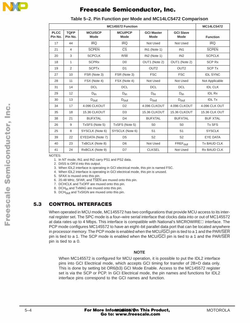
MC1455725–4 MOTOROLA
Table 5–2. Pin Function per Mode and MC14LC5472 ComparisonÁÁÁÁÁÁÁÁÁÁÁÁÁÁÁÁÁÁÁÁÁÁÁÁÁÁÁÁÁÁÁÁÁÁÁÁÁÁÁÁÁÁÁÁÁÁÁÁÁÁ
MC145572 FunctionÁÁÁÁÁÁÁÁÁÁÁÁ
MC14LC5472ÁÁÁÁÁÁÁÁÁÁÁÁ
PLCCPin No.
ÁÁÁÁÁÁÁÁÁ
TQFPPin No.
ÁÁÁÁÁÁÁÁÁÁÁÁÁÁÁÁÁÁ
MCU/SCPMode
ÁÁÁÁÁÁÁÁÁÁÁÁÁÁÁÁÁÁ
MCU/PCPMode
ÁÁÁÁÁÁÁÁÁÁÁÁÁÁÁ
GCI MasterMode
ÁÁÁÁÁÁÁÁÁÁÁÁÁÁÁÁÁÁ
GCI SlaveMode
ÁÁÁÁÁÁÁÁÁÁÁÁÁÁÁÁÁÁ
Function
ÁÁÁÁÁÁÁÁ
17 ÁÁÁÁÁÁ
44 ÁÁÁÁÁÁÁÁÁÁÁÁ
IRQ ÁÁÁÁÁÁÁÁÁÁÁÁ
IRQ ÁÁÁÁÁÁÁÁÁÁ
Not Used ÁÁÁÁÁÁÁÁÁÁÁÁ
Not Used ÁÁÁÁÁÁÁÁÁÁÁÁ
IRQ
ÁÁÁÁÁÁÁÁ
21 ÁÁÁÁÁÁ
4 ÁÁÁÁÁÁÁÁÁÁÁÁ
SCPEN ÁÁÁÁÁÁÁÁÁÁÁÁ
CS ÁÁÁÁÁÁÁÁÁÁ
IN1 (Note 1)ÁÁÁÁÁÁÁÁÁÁÁÁ
IN1 ÁÁÁÁÁÁÁÁÁÁÁÁ
SCPEN
ÁÁÁÁÁÁÁÁ
20 ÁÁÁÁÁÁ
3 ÁÁÁÁÁÁÁÁÁÁÁÁ
SCPCLK ÁÁÁÁÁÁÁÁÁÁÁÁ
R/W ÁÁÁÁÁÁÁÁÁÁ
IN2 (Note 1)ÁÁÁÁÁÁÁÁÁÁÁÁ
IN2 ÁÁÁÁÁÁÁÁÁÁÁÁ
SCPCLK
ÁÁÁÁÁÁÁÁ
18 ÁÁÁÁÁÁ
1 ÁÁÁÁÁÁÁÁÁÁÁÁ
SCPRx ÁÁÁÁÁÁÁÁÁÁÁÁ
D0 ÁÁÁÁÁÁÁÁÁÁ
OUT1 (Note 2)ÁÁÁÁÁÁÁÁÁÁÁÁ
OUT1 (Note 2) ÁÁÁÁÁÁÁÁÁÁÁÁ
SCP Rx
ÁÁÁÁÁÁÁÁ
19 ÁÁÁÁÁÁ
2 ÁÁÁÁÁÁÁÁÁÁÁÁ
SCPTx ÁÁÁÁÁÁÁÁÁÁÁÁ
D1 ÁÁÁÁÁÁÁÁÁÁ
OUT2 ÁÁÁÁÁÁÁÁÁÁÁÁ
OUT2 ÁÁÁÁÁÁÁÁÁÁÁÁ
SCP Tx
ÁÁÁÁÁÁÁÁ
27 ÁÁÁÁÁÁ
10 ÁÁÁÁÁÁÁÁÁÁÁÁ
FSR (Note 3) ÁÁÁÁÁÁÁÁÁÁÁÁ
FSR (Note 3) ÁÁÁÁÁÁÁÁÁÁ
FSC ÁÁÁÁÁÁÁÁÁÁÁÁ
FSC ÁÁÁÁÁÁÁÁÁÁÁÁ
IDL SYNC
ÁÁÁÁÁÁÁÁ
28 ÁÁÁÁÁÁ
11 ÁÁÁÁÁÁÁÁÁÁÁÁ
FSX (Note 4) ÁÁÁÁÁÁÁÁÁÁÁÁ
FSX (Note 4) ÁÁÁÁÁÁÁÁÁÁ
Not Used ÁÁÁÁÁÁÁÁÁÁÁÁ
Not Used ÁÁÁÁÁÁÁÁÁÁÁÁ
Not Applicable
ÁÁÁÁÁÁÁÁ
31 ÁÁÁÁÁÁ
14 ÁÁÁÁÁÁÁÁÁÁÁÁ
DCL ÁÁÁÁÁÁÁÁÁÁÁÁ
DCL ÁÁÁÁÁÁÁÁÁÁ
DCL ÁÁÁÁÁÁÁÁÁÁÁÁ
DCL ÁÁÁÁÁÁÁÁÁÁÁÁ
IDL CLK
ÁÁÁÁÁÁÁÁ
29 ÁÁÁÁÁÁ
12 ÁÁÁÁÁÁÁÁÁÁÁÁ
Din ÁÁÁÁÁÁÁÁÁÁÁÁ
Din ÁÁÁÁÁÁÁÁÁÁ
Din ÁÁÁÁÁÁÁÁÁÁÁÁ
Din ÁÁÁÁÁÁÁÁÁÁÁÁ
IDL Rx
ÁÁÁÁÁÁÁÁ
30 ÁÁÁÁÁÁ
13 ÁÁÁÁÁÁÁÁÁÁÁÁ
Dout ÁÁÁÁÁÁÁÁÁÁÁÁ
Dout ÁÁÁÁÁÁÁÁÁÁ
Dout ÁÁÁÁÁÁÁÁÁÁÁÁ
Dout ÁÁÁÁÁÁÁÁÁÁÁÁ
IDL Tx
ÁÁÁÁÁÁÁÁ
34 ÁÁÁÁÁÁ
17 ÁÁÁÁÁÁÁÁÁÁÁÁ
4.096 CLKOUTÁÁÁÁÁÁÁÁÁÁÁÁ
D2 ÁÁÁÁÁÁÁÁÁÁ
4.096 CLKOUTÁÁÁÁÁÁÁÁÁÁÁÁ
4.096 CLKOUT ÁÁÁÁÁÁÁÁÁÁÁÁ
4.096 CLK OUT
ÁÁÁÁÁÁÁÁ
35 ÁÁÁÁÁÁ
18 ÁÁÁÁÁÁÁÁÁÁÁÁ
15.36 CLKOUTÁÁÁÁÁÁÁÁÁÁÁÁ
D3 ÁÁÁÁÁÁÁÁÁÁ
15.36 CLKOUTÁÁÁÁÁÁÁÁÁÁÁÁ
15.36 CLKOUT ÁÁÁÁÁÁÁÁÁÁÁÁ
15.36 CLK OUT
ÁÁÁÁÁÁÁÁ
38 ÁÁÁÁÁÁ
21 ÁÁÁÁÁÁÁÁÁÁÁÁ
BUFXTAL ÁÁÁÁÁÁÁÁÁÁÁÁ
D4 ÁÁÁÁÁÁÁÁÁÁ
BUFXTAL ÁÁÁÁÁÁÁÁÁÁÁÁ
BUFXTAL ÁÁÁÁÁÁÁÁÁÁÁÁ
BUF XTAL
ÁÁÁÁÁÁÁÁ
26 ÁÁÁÁÁÁ
9 ÁÁÁÁÁÁÁÁÁÁÁÁ
TxSFS (Note 5)ÁÁÁÁÁÁÁÁÁÁÁÁ
TxSFS (Note 5) ÁÁÁÁÁÁÁÁÁÁ
S0 ÁÁÁÁÁÁÁÁÁÁÁÁ
S0 ÁÁÁÁÁÁÁÁÁÁÁÁ
Tx SFS
ÁÁÁÁÁÁÁÁ
25 ÁÁÁÁÁÁ
8 ÁÁÁÁÁÁÁÁÁÁÁÁ
SYSCLK (Note 6)ÁÁÁÁÁÁÁÁÁÁÁÁ
SYSCLK (Note 6)ÁÁÁÁÁÁÁÁÁÁ
S1 ÁÁÁÁÁÁÁÁÁÁÁÁ
S1 ÁÁÁÁÁÁÁÁÁÁÁÁ
SYSCLK
ÁÁÁÁÁÁÁÁ
39 ÁÁÁÁÁÁ
22 ÁÁÁÁÁÁÁÁÁÁÁÁ
EYEDATA (Note 7)ÁÁÁÁÁÁÁÁÁÁÁÁ
D5 ÁÁÁÁÁÁÁÁÁÁ
S2 ÁÁÁÁÁÁÁÁÁÁÁÁ
S2 ÁÁÁÁÁÁÁÁÁÁÁÁ
EYE DATA
ÁÁÁÁÁÁÁÁ
40 ÁÁÁÁÁÁ
23 ÁÁÁÁÁÁÁÁÁÁÁÁ
TxBCLK (Note 8)ÁÁÁÁÁÁÁÁÁÁÁÁ
D6 ÁÁÁÁÁÁÁÁÁÁ
Not Used ÁÁÁÁÁÁÁÁÁÁÁÁ
FREFout ÁÁÁÁÁÁÁÁÁÁÁÁ
Tx BAUD CLK
ÁÁÁÁÁÁÁÁ
41 ÁÁÁÁÁÁ
24 ÁÁÁÁÁÁÁÁÁÁÁÁ
RxBCLK (Note 9)ÁÁÁÁÁÁÁÁÁÁÁÁ
D7 ÁÁÁÁÁÁÁÁÁÁ
CLKSEL ÁÁÁÁÁÁÁÁÁÁÁÁ
Not Used ÁÁÁÁÁÁÁÁÁÁÁÁ
Rx BAUD CLK
NOTES:1. In NT mode, IN1 and IN2 carry PS1 and PS2 data.2. DISS is OR’d into this output.3. When IDL2 interface is operating in GCI electrical mode, this pin is named FSC.4. When IDL2 interface is operating in GCI electrical mode, this pin is unused.5. SFAX is muxed onto this pin.6. 20.48 MHz, SFAR, and TSEN are muxed onto this pin.7. DCHCLK and TxOFF are muxed onto this pin.8. DCHin and TxMAG are muxed onto this pin.9. DCHout and TxSIGN are muxed onto this pin.
When operated in MCU mode, MC145572 has two configurations that provide MCU access to its inter-nal register set. The SPC mode is a four–wire serial interface that clocks data into or out of MC145572at data rates up to 4 Mbps. This interface is compatible with National’s MICROWIRE interface. ThePCP mode configures MC145572 to have an eight–bit parallel data port that can be located anywherein processor memory. The PCP mode is enabled when the MCU/GCI pin is tied to a 1 and the PAR/SERpin is tied to a 1. The SCP mode is enabled when the MCU/GCI pin is tied to a 1 and the PAR/SERpin is tied to a 0.
NOTE
When MC145572 is configured for MCU operation, it is possible to put the IDL2 interfacepins into GCI Electrical mode, which accepts GCI timing for transfer of 2B+D data only.This is done by setting bit OR6(b3) GCI Mode Enable. Access to the MC145572 registerset is via the SCP or PCP. In GCI Electrical mode, the pin names and functions for IDL2interface pins correspond to the GCI names and function.
Fre
esc
ale
Se
mic
on
du
cto
r, I
Freescale Semiconductor, Inc.
For More Information On This Product, Go to: www.freescale.com
nc
...
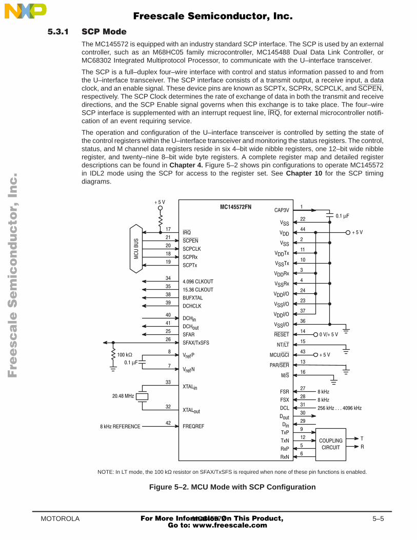
MC145572 5–5MOTOROLA
The MC145572 is equipped with an industry standard SCP interface. The SCP is used by an externalcontroller, such as an M68HC05 family microcontroller, MC145488 Dual Data Link Controller, orMC68302 Integrated Multiprotocol Processor, to communicate with the U–interface transceiver.
The SCP is a full–duplex four–wire interface with control and status information passed to and fromthe U–interface transceiver. The SCP interface consists of a transmit output, a receive input, a dataclock, and an enable signal. These device pins are known as SCPTx, SCPRx, SCPCLK, and SCPEN,respectively. The SCP Clock determines the rate of exchange of data in both the transmit and receivedirections, and the SCP Enable signal governs when this exchange is to take place. The four–wireSCP interface is supplemented with an interrupt request line, IRQ, for external microcontroller notifi-cation of an event requiring service.
The operation and configuration of the U–interface transceiver is controlled by setting the state ofthe control registers within the U–interface transceiver and monitoring the status registers. The control,status, and M channel data registers reside in six 4–bit wide nibble registers, one 12–bit wide nibbleregister, and twenty–nine 8–bit wide byte registers. A complete register map and detailed registerdescriptions can be found in Chapter 4. Figure 5–2 shows pin configurations to operate MC145572in IDL2 mode using the SCP for access to the register set. See Chapter 10 for the SCP timingdiagrams.
""
.
!.
"!
"!
"$!
')
*-,
$!.
#+%&
#+%&
$!')
$!*-,
(/
/
µ
#
#
#
#
#
#!.
# !.
#.
# .
#
#
#
#
#
µ
!
!!
# #
#
"
(/
(/
$
(/ (/
*-,
')
!.
!.
.
.
!
"
"!
NOTE: In LT mode, the 100 kΩ resistor on SFAX/TxSFS is required when none of these pin functions is enabled.
(Ω
Figure 5–2. MCU Mode with SCP Configuration
Fre
esc
ale
Se
mic
on
du
cto
r, I
Freescale Semiconductor, Inc.
For More Information On This Product, Go to: www.freescale.com
nc
...
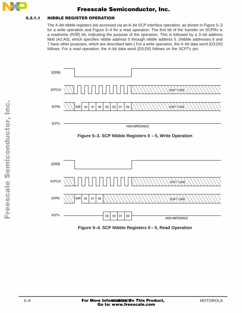
MC1455725–6 MOTOROLA
The 4–bit nibble registers are accessed via an 8–bit SCP interface operation, as shown in Figure 5–3for a write operation and Figure 5–4 for a read operation. The first bit of the transfer on SCPRx isa read/write (R/W) bit, indicating the purpose of the operation. This is followed by a 3–bit addressfield (A2:A0), which specifies nibble address 0 through nibble address 5. (Nibble addresses 6 and7 have other purposes, which are described later.) For a write operation, the 4–bit data word (D3:D0)follows. For a read operation, the 4–bit data word (D3:D0) follows on the SCPTx pin.
Figure 5–3. SCP Nibble Registers 0 – 5, Write Operation
Figure 5–4. SCP Nibble Registers 0 – 5, Read Operation
Fre
esc
ale
Se
mic
on
du
cto
r, I
Freescale Semiconductor, Inc.
For More Information On This Product, Go to: www.freescale.com
nc
...
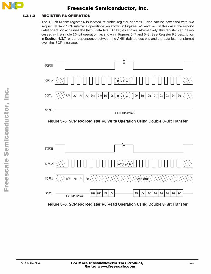
MC145572 5–7MOTOROLA
The 12–bit Nibble register 6 is located at nibble register address 6 and can be accessed with twosequential 8–bit SCP interface operations, as shown in Figures 5–5 and 5–6. In this case, the second8–bit operation accesses the last 8 data bits (D7:D0) as shown. Alternatively, this register can be ac-cessed with a single 16–bit operation, as shown in Figures 5–7 and 5–8. See Register R6 descriptionin Section 4.3.7 for correspondence between the ANSI defined eoc bits and the data bits transferredover the SCP interface.
Figure 5–5. SCP eoc Register R6 Write Operation Using Double 8 –Bit Transfer
Figure 5–6. SCP eoc Register R6 Read Operation Using Double 8 –Bit Transfer
Fre
esc
ale
Se
mic
on
du
cto
r, I
Freescale Semiconductor, Inc.
For More Information On This Product, Go to: www.freescale.com
nc
...
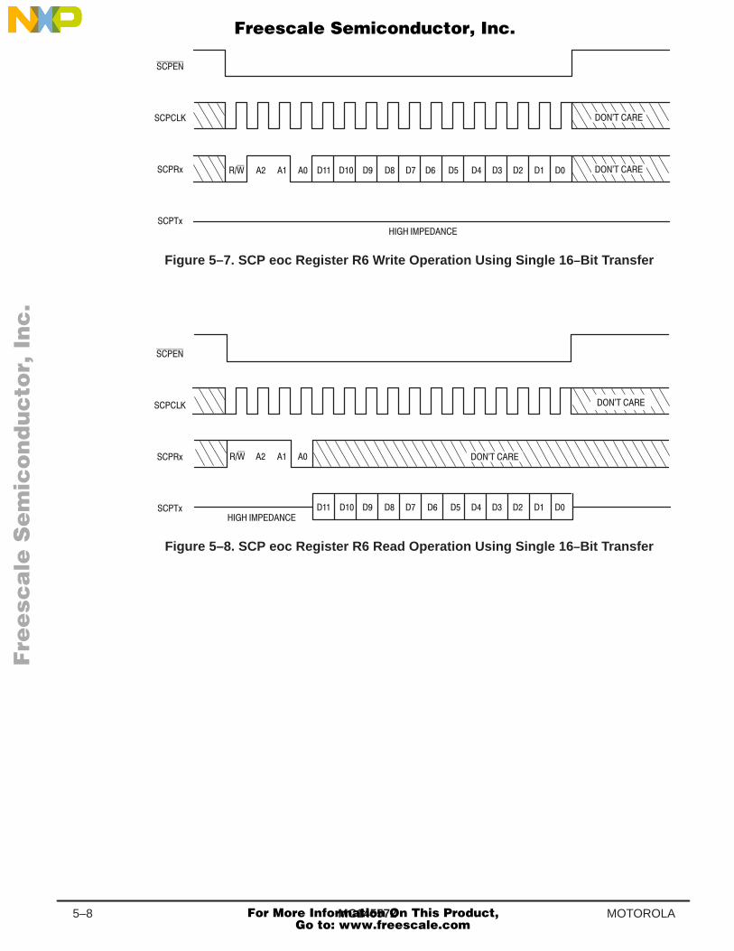
MC1455725–8 MOTOROLA
Figure 5–7. SCP eoc Register R6 Write Operation Using Single 16 –Bit Transfer
Figure 5–8. SCP eoc Register R6 Read Operation Using Single 16 –Bit Transfer
Fre
esc
ale
Se
mic
on
du
cto
r, I
Freescale Semiconductor, Inc.
For More Information On This Product, Go to: www.freescale.com
nc
...
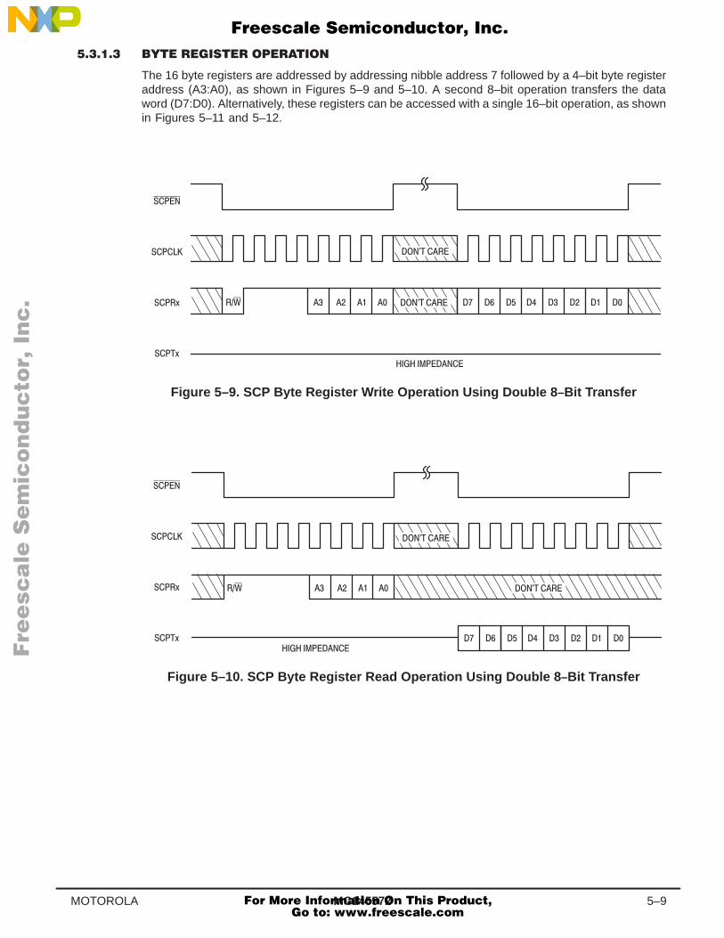
MC145572 5–9MOTOROLA
The 16 byte registers are addressed by addressing nibble address 7 followed by a 4–bit byte registeraddress (A3:A0), as shown in Figures 5–9 and 5–10. A second 8–bit operation transfers the dataword (D7:D0). Alternatively, these registers can be accessed with a single 16–bit operation, as shownin Figures 5–11 and 5–12.
Figure 5–9. SCP Byte Register Write Operation Using Double 8 –Bit Transfer
Figure 5–10. SCP Byte Register Read Operation Using Double 8 –Bit Transfer
Fre
esc
ale
Se
mic
on
du
cto
r, I
Freescale Semiconductor, Inc.
For More Information On This Product, Go to: www.freescale.com
nc
...
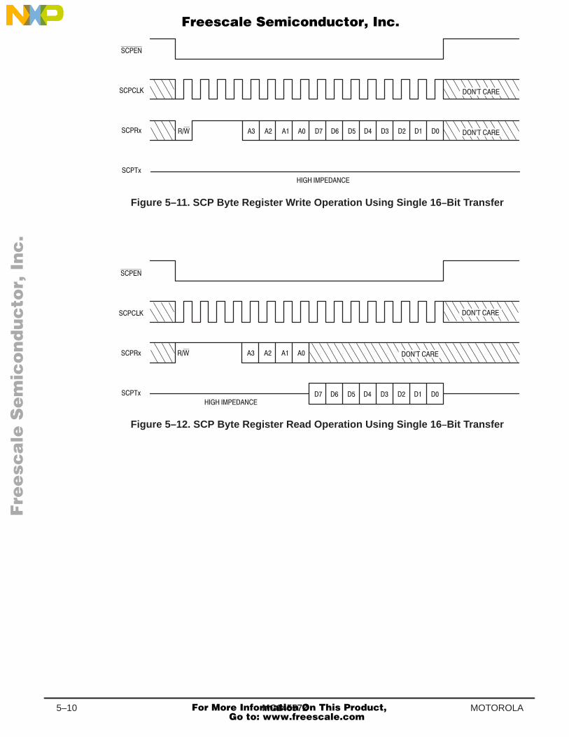
MC1455725–10 MOTOROLA
Figure 5–11. SCP Byte Register Write Operation Using Single 16 –Bit Transfer
Figure 5–12. SCP Byte Register Read Operation Using Single 16 –Bit Transfer
Fre
esc
ale
Se
mic
on
du
cto
r, I
Freescale Semiconductor, Inc.
For More Information On This Product, Go to: www.freescale.com
nc
...
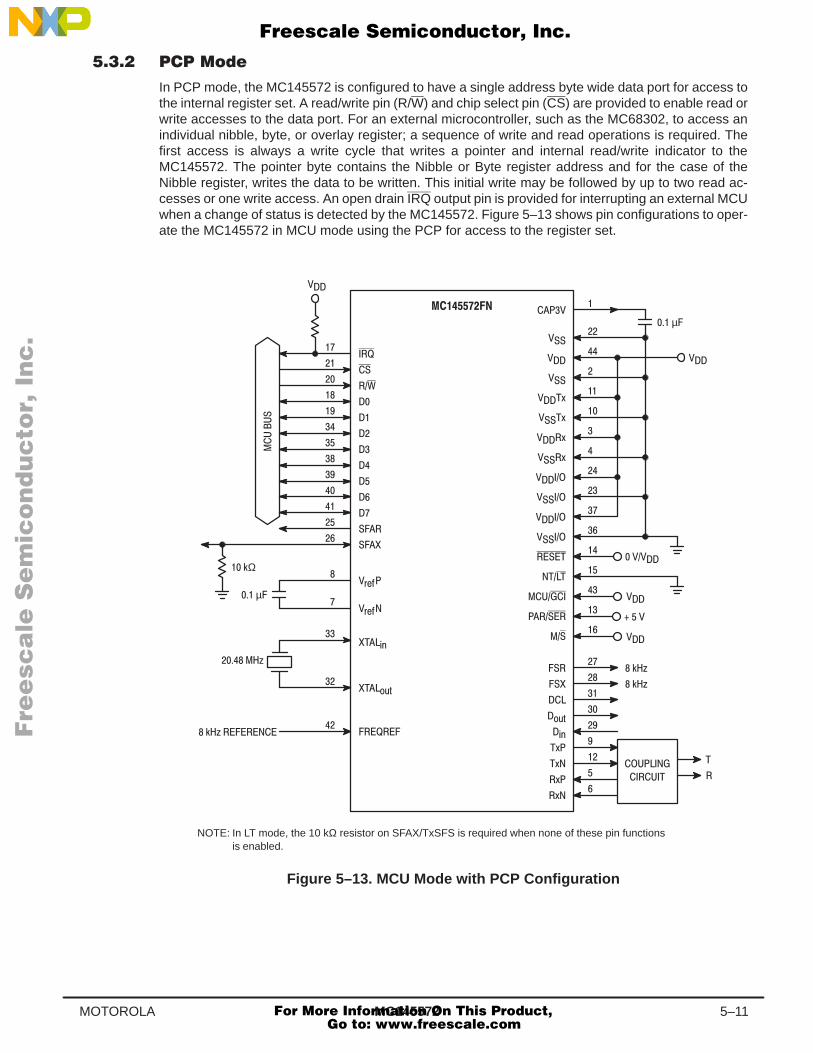
MC145572 5–11MOTOROLA
In PCP mode, the MC145572 is configured to have a single address byte wide data port for access tothe internal register set. A read/write pin (R/W) and chip select pin (CS) are provided to enable read orwrite accesses to the data port. For an external microcontroller, such as the MC68302, to access anindividual nibble, byte, or overlay register; a sequence of write and read operations is required. Thefirst access is always a write cycle that writes a pointer and internal read/write indicator to theMC145572. The pointer byte contains the Nibble or Byte register address and for the case of theNibble register, writes the data to be written. This initial write may be followed by up to two read ac-cesses or one write access. An open drain IRQ output pin is provided for interrupting an external MCUwhen a change of status is detected by the MC145572. Figure 5–13 shows pin configurations to oper-ate the MC145572 in MCU mode using the PCP for access to the register set.
!!
#
$
"+%&
"+%&
$ ')
$ *-,
(/
/
µ
"
"
"
"
"
" .
" .
".
".
"
"
"
"
"
µ
""
"
!
(/
(/
$
*-,
')
.
.
.
.
!
!
(Ω
NOTE: In LT mode, the 10 kΩ resistor on SFAX/TxSFS is required when none of these pin functionsis enabled.
"
"
Figure 5–13. MCU Mode with PCP Configuration
Fre
esc
ale
Se
mic
on
du
cto
r, I
Freescale Semiconductor, Inc.
For More Information On This Product, Go to: www.freescale.com
nc
...
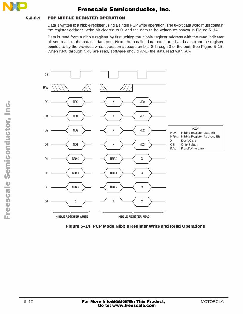
MC1455725–12 MOTOROLA
Data is written to a nibble register using a single PCP write operation. The 8–bit data word must containthe register address, write bit cleared to 0, and the data to be written as shown in Figure 5–14.
Data is read from a nibble register by first writing the nibble register address with the read indicatorbit set to a 1 to the parallel data port. Next, the parallel data port is read and data from the registerpointed to by the previous write operation appears on bits 0 through 3 of the port. See Figure 5–15.When NR0 through NR5 are read, software should AND the data read with $0F.
KEYNDx Nibble Register Data BitNRAx Nibble Register Address BitX Don’t CareCS Chip SelectR/W Read/Write Line
Figure 5–14. PCP Mode Nibble Register Write and Read Operations
Fre
esc
ale
Se
mic
on
du
cto
r, I
Freescale Semiconductor, Inc.
For More Information On This Product, Go to: www.freescale.com
nc
...
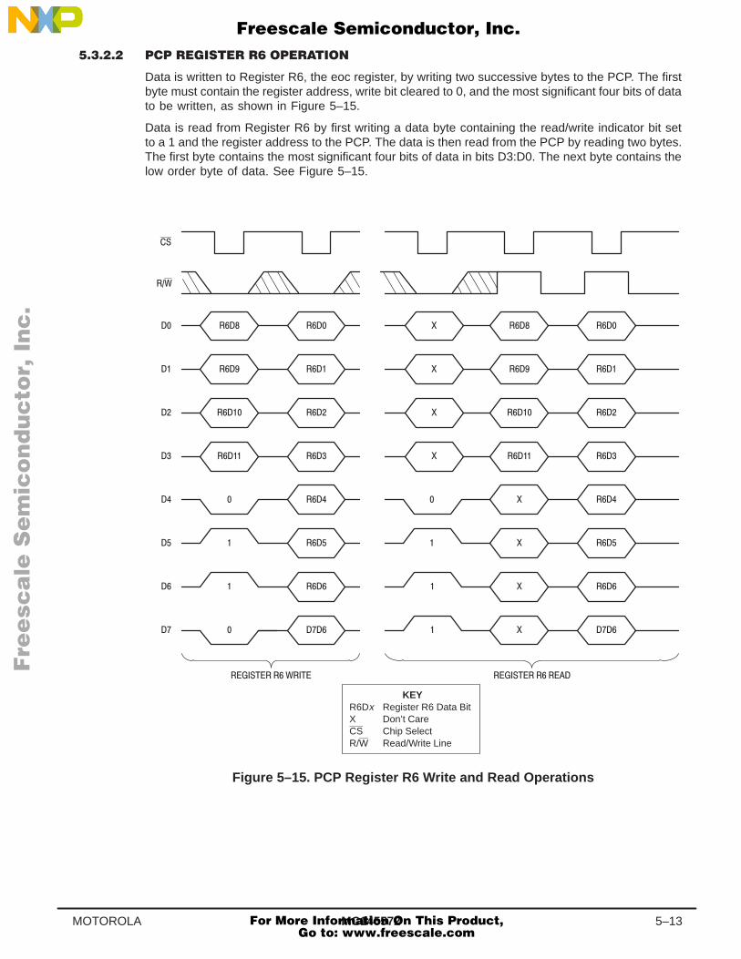
MC145572 5–13MOTOROLA
Data is written to Register R6, the eoc register, by writing two successive bytes to the PCP. The firstbyte must contain the register address, write bit cleared to 0, and the most significant four bits of datato be written, as shown in Figure 5–15.
Data is read from Register R6 by first writing a data byte containing the read/write indicator bit setto a 1 and the register address to the PCP. The data is then read from the PCP by reading two bytes.The first byte contains the most significant four bits of data in bits D3:D0. The next byte contains thelow order byte of data. See Figure 5–15.
KEYR6Dx Register R6 Data BitX Don’t CareCS Chip SelectR/W Read/Write Line
Figure 5–15. PCP Register R6 Write and Read Operations
Fre
esc
ale
Se
mic
on
du
cto
r, I
Freescale Semiconductor, Inc.
For More Information On This Product, Go to: www.freescale.com
nc
...
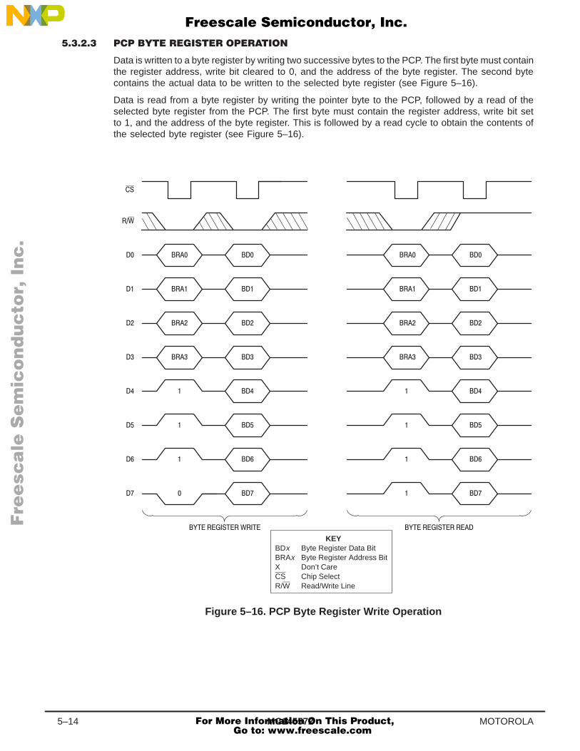
MC1455725–14 MOTOROLA
Data is written to a byte register by writing two successive bytes to the PCP. The first byte must containthe register address, write bit cleared to 0, and the address of the byte register. The second bytecontains the actual data to be written to the selected byte register (see Figure 5–16).
Data is read from a byte register by writing the pointer byte to the PCP, followed by a read of theselected byte register from the PCP. The first byte must contain the register address, write bit setto 1, and the address of the byte register. This is followed by a read cycle to obtain the contents ofthe selected byte register (see Figure 5–16).
KEYBDx Byte Register Data BitBRAx Byte Register Address BitX Don’t CareCS Chip SelectR/W Read/Write Line
Figure 5–16. PCP Byte Register Write Operation
Fre
esc
ale
Se
mic
on
du
cto
r, I
Freescale Semiconductor, Inc.
For More Information On This Product, Go to: www.freescale.com
nc
...
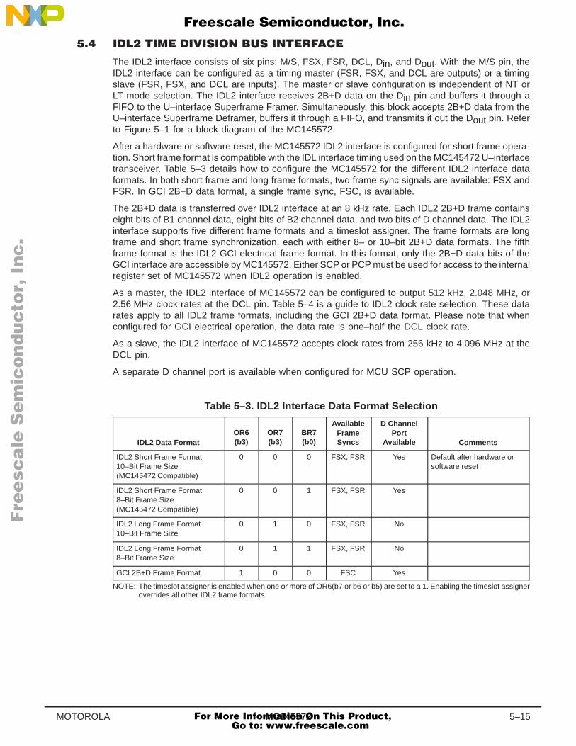
MC145572 5–15MOTOROLA
The IDL2 interface consists of six pins: M/S, FSX, FSR, DCL, Din, and Dout. With the M/S pin, theIDL2 interface can be configured as a timing master (FSR, FSX, and DCL are outputs) or a timingslave (FSR, FSX, and DCL are inputs). The master or slave configuration is independent of NT orLT mode selection. The IDL2 interface receives 2B+D data on the Din pin and buffers it through aFIFO to the U–interface Superframe Framer. Simultaneously, this block accepts 2B+D data from theU–interface Superframe Deframer, buffers it through a FIFO, and transmits it out the Dout pin. Referto Figure 5–1 for a block diagram of the MC145572.
After a hardware or software reset, the MC145572 IDL2 interface is configured for short frame opera-tion. Short frame format is compatible with the IDL interface timing used on the MC145472 U–interfacetransceiver. Table 5–3 details how to configure the MC145572 for the different IDL2 interface dataformats. In both short frame and long frame formats, two frame sync signals are available: FSX andFSR. In GCI 2B+D data format, a single frame sync, FSC, is available.
The 2B+D data is transferred over IDL2 interface at an 8 kHz rate. Each IDL2 2B+D frame containseight bits of B1 channel data, eight bits of B2 channel data, and two bits of D channel data. The IDL2interface supports five different frame formats and a timeslot assigner. The frame formats are longframe and short frame synchronization, each with either 8– or 10–bit 2B+D data formats. The fifthframe format is the IDL2 GCI electrical frame format. In this format, only the 2B+D data bits of theGCI interface are accessible by MC145572. Either SCP or PCP must be used for access to the internalregister set of MC145572 when IDL2 operation is enabled.
As a master, the IDL2 interface of MC145572 can be configured to output 512 kHz, 2.048 MHz, or2.56 MHz clock rates at the DCL pin. Table 5–4 is a guide to IDL2 clock rate selection. These datarates apply to all IDL2 frame formats, including the GCI 2B+D data format. Please note that whenconfigured for GCI electrical operation, the data rate is one–half the DCL clock rate.
As a slave, the IDL2 interface of MC145572 accepts clock rates from 256 kHz to 4.096 MHz at theDCL pin.
A separate D channel port is available when configured for MCU SCP operation.
Table 5–3. IDL2 Interface Data Format SelectionÁÁÁÁÁÁÁÁÁÁÁÁÁÁÁÁÁÁÁÁÁÁÁÁÁÁÁÁÁÁÁÁÁÁÁÁ
IDL2 Data Format
ÁÁÁÁÁÁÁÁÁÁÁÁ
OR6(b3)
ÁÁÁÁÁÁÁÁÁÁÁÁÁÁÁÁ
OR7(b3)
ÁÁÁÁÁÁÁÁÁÁÁÁ
BR7(b0)
ÁÁÁÁÁÁÁÁÁÁÁÁÁÁÁÁ
AvailableFrameSyncs
ÁÁÁÁÁÁÁÁÁÁÁÁÁÁÁÁÁÁÁÁ
D ChannelPort
Available
ÁÁÁÁÁÁÁÁÁÁÁÁÁÁÁÁÁÁÁÁÁÁÁÁÁÁÁÁÁÁÁÁ
Comments
ÁÁÁÁÁÁÁÁÁÁÁÁÁÁÁÁÁÁÁÁÁÁÁÁÁÁÁ
IDL2 Short Frame Format10–Bit Frame Size(MC145472 Compatible)
ÁÁÁÁÁÁÁÁÁ
0ÁÁÁÁÁÁÁÁÁÁÁÁ
0 ÁÁÁÁÁÁÁÁÁ
0 ÁÁÁÁÁÁÁÁÁÁÁÁ
FSX, FSRÁÁÁÁÁÁÁÁÁÁÁÁÁÁÁ
Yes ÁÁÁÁÁÁÁÁÁÁÁÁÁÁÁÁÁÁÁÁÁÁÁÁ
Default after hardware orsoftware reset
ÁÁÁÁÁÁÁÁÁÁÁÁÁÁÁÁÁÁÁÁÁÁÁÁÁÁÁ
IDL2 Short Frame Format8–Bit Frame Size(MC145472 Compatible)
ÁÁÁÁÁÁÁÁÁ
0ÁÁÁÁÁÁÁÁÁÁÁÁ
0 ÁÁÁÁÁÁÁÁÁ
1 ÁÁÁÁÁÁÁÁÁÁÁÁ
FSX, FSRÁÁÁÁÁÁÁÁÁÁÁÁÁÁÁ
Yes ÁÁÁÁÁÁÁÁÁÁÁÁÁÁÁÁÁÁÁÁÁÁÁÁÁÁÁÁÁÁÁÁÁ
ÁÁÁÁÁÁÁÁÁÁÁÁÁÁÁÁÁÁ
IDL2 Long Frame Format10–Bit Frame Size
ÁÁÁÁÁÁÁÁÁ
0ÁÁÁÁÁÁÁÁÁÁÁÁ
1ÁÁÁÁÁÁÁÁÁ
0ÁÁÁÁÁÁÁÁÁÁÁÁ
FSX, FSRÁÁÁÁÁÁÁÁÁÁÁÁÁÁÁ
NoÁÁÁÁÁÁÁÁÁÁÁÁÁÁÁÁÁÁÁÁÁÁÁÁÁÁÁÁÁÁÁÁÁ
ÁÁÁÁÁÁÁÁÁÁÁÁÁÁÁÁÁÁ
IDL2 Long Frame Format8–Bit Frame Size
ÁÁÁÁÁÁÁÁÁ
0ÁÁÁÁÁÁÁÁÁÁÁÁ
1 ÁÁÁÁÁÁÁÁÁ
1 ÁÁÁÁÁÁÁÁÁÁÁÁ
FSX, FSRÁÁÁÁÁÁÁÁÁÁÁÁÁÁÁ
No ÁÁÁÁÁÁÁÁÁÁÁÁÁÁÁÁÁÁÁÁÁÁÁÁÁÁÁÁÁÁÁÁÁ
ÁÁÁÁÁÁÁÁÁGCI 2B+D Frame Format ÁÁÁ
ÁÁÁ1ÁÁÁÁÁÁÁÁ
0 ÁÁÁÁÁÁ
0 ÁÁÁÁÁÁÁÁ
FSC ÁÁÁÁÁÁÁÁÁÁ
Yes ÁÁÁÁÁÁÁÁÁÁÁÁÁÁÁÁNOTE: The timeslot assigner is enabled when one or more of OR6(b7 or b6 or b5) are set to a 1. Enabling the timeslot assigner
overrides all other IDL2 frame formats.
Fre
esc
ale
Se
mic
on
du
cto
r, I
Freescale Semiconductor, Inc.
For More Information On This Product, Go to: www.freescale.com
nc
...
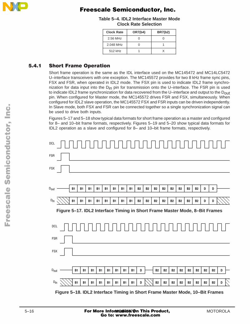
MC1455725–16 MOTOROLA
Table 5–4. IDL2 Interface Master ModeClock Rate Selection
ÁÁÁÁÁÁÁÁÁÁ
Clock Rate ÁÁÁÁÁÁÁÁÁÁ
OR7(b4) ÁÁÁÁÁÁÁÁ
BR7(b2)ÁÁÁÁÁÁÁÁÁÁ
2.56 MHzÁÁÁÁÁÁÁÁÁÁ
0ÁÁÁÁÁÁÁÁ
0ÁÁÁÁÁÁÁÁÁÁ
2.048 MHzÁÁÁÁÁÁÁÁÁÁ
0ÁÁÁÁÁÁÁÁ
1ÁÁÁÁÁÁÁÁÁÁ
512 kHz ÁÁÁÁÁÁÁÁÁÁ
1 ÁÁÁÁÁÁÁÁ
X
Short frame operation is the same as the IDL interface used on the MC145472 and MC14LC5472U–interface transceivers with one exception. The MC145572 provides for two 8 kHz frame sync pins,FSX and FSR, when operated in IDL2 mode. The FSX pin is used to indicate IDL2 frame synchro-nization for data input into the Din pin for transmission onto the U–interface. The FSR pin is usedto indicate IDL2 frame synchronization for data recovered from the U–interface and output to the Doutpin. When configured for Master mode, the MC145572 drives FSR and FSX, simultaneously. Whenconfigured for IDL2 slave operation, the MC145572 FSX and FSR inputs can be driven independently.In Slave mode, both FSX and FSR can be connected together so a single synchronization signal canbe used to drive both inputs.
Figures 5–17 and 5–18 show typical data formats for short frame operation as a master and configuredfor 8– and 10–bit frame formats, respectively. Figures 5–19 and 5–20 show typical data formats forIDL2 operation as a slave and configured for 8– and 10–bit frame formats, respectively.
ÉÉÉÉÉÉÉÉÉÉÉÉÉÉÉÉÉÉÉÉÉÉ
ÇÇÇÇÇÇ
ÇÇÇÇÇÇ
ÇÇÇÇÇÇÇÇÇÇÇÇÇÇÇÇÇÇÇÇÇÇ ÉÉÉÉÉÉÉÉÉÉÉ
ÉÉÉÉÉÉÉÉÉÉÉ
Figure 5–17. IDL2 Interface Timing in Short Frame Master Mode, 8–Bit Frames
ÇÇÇÇ
ÇÇÇÇÇÇ
ÇÇÇÇÇÇÇÇ
ÇÇÇÇ
ÇÇÇÇÇÇ
ÇÇÇÇ
ÇÇÇÇ
ÈÈÈÈ
ÈÈÈÈ
ÈÈÈÈÈÈ
ÈÈÈÈ
ÈÈÈÈ
ÈÈÈÈÈÈ
ÈÈÈÈÈÈÈÈ
ÇÇÇÇ
ÇÇÇÇÇÇ
ÇÇÇÇÇÇÇÇ
ÇÇÇÇ
ÇÇÇÇÇÇ
ÇÇÇÇ
ÇÇÇÇ
ÈÈÈÈ
ÈÈÈÈ
ÈÈÈÈÈÈ
ÈÈÈÈ
ÈÈÈÈ
ÈÈÈÈÈÈ
ÈÈÈÈÈÈÈÈ
ÇÇÇÇ
ÇÇÇÇ
ÇÇÇÇÇÇ
Figure 5–18. IDL2 Interface Timing in Short Frame Master Mode, 10–Bit Frames
Fre
esc
ale
Se
mic
on
du
cto
r, I
Freescale Semiconductor, Inc.
For More Information On This Product, Go to: www.freescale.com
nc
...
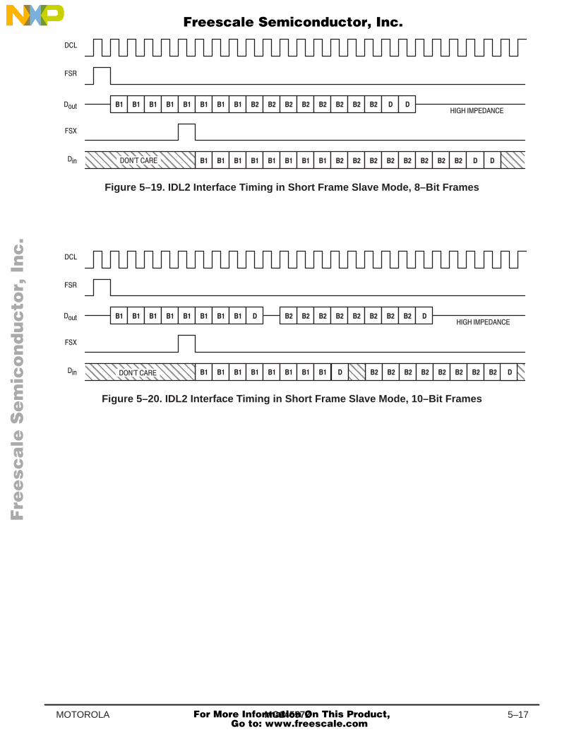
MC145572 5–17MOTOROLA
ÇÇÇÇ
ÇÇÇÇÇÇ
ÇÇÇÇÇÇÇÇÇÇÇÇ
ÇÇÇÇ
ÇÇÇÇ
ÇÇÇÇÇÇ
ÉÉÉÉÉÉÉÉ
ÉÉÉÉ
ÉÉÉÉ
ÉÉÉÉ
ÉÉÉÉÉÉ
ÉÉÉÉÉÉÉÉ
ÇÇÇÇÇÇ
ÇÇÇÇÇÇÇÇÇÇÇÇÇÇÇÇÇÇ
Figure 5–19. IDL2 Interface Timing in Short Frame Slave Mode, 8–Bit Frames
ÇÇÇÇ
ÇÇÇÇÇÇ
ÇÇÇÇÇÇÇÇÇÇÇÇ
ÇÇÇÇ
ÇÇÇÇ
ÇÇÇÇÇÇ
ÈÈÈÈÈÈÈÈ
ÈÈÈÈÈÈ
ÈÈÈÈÈÈÈÈ
ÈÈÈÈ
ÈÈÈÈ
ÇÇÇÇ
ÇÇÇÇ
ÇÇÇÇÇÇ
ÇÇÇÇÇÇÇÇ
ÇÇÇÇ
ÇÇÇÇ
ÇÇÇÇ
ÈÈÈÈ
ÈÈÈÈ
ÈÈÈÈ
ÈÈÈÈÈÈ
ÈÈÈÈÈÈÈÈÈÈÈÈ
ÈÈÈÈ
ÇÇÇÇÇÇ
ÇÇÇÇÇÇÇÇÇÇÇÇÇÇÇÇÇÇ
ÇÇÇÇ
ÈÈÈÈ
Figure 5–20. IDL2 Interface Timing in Short Frame Slave Mode, 10–Bit Frames
Fre
esc
ale
Se
mic
on
du
cto
r, I
Freescale Semiconductor, Inc.
For More Information On This Product, Go to: www.freescale.com
nc
...
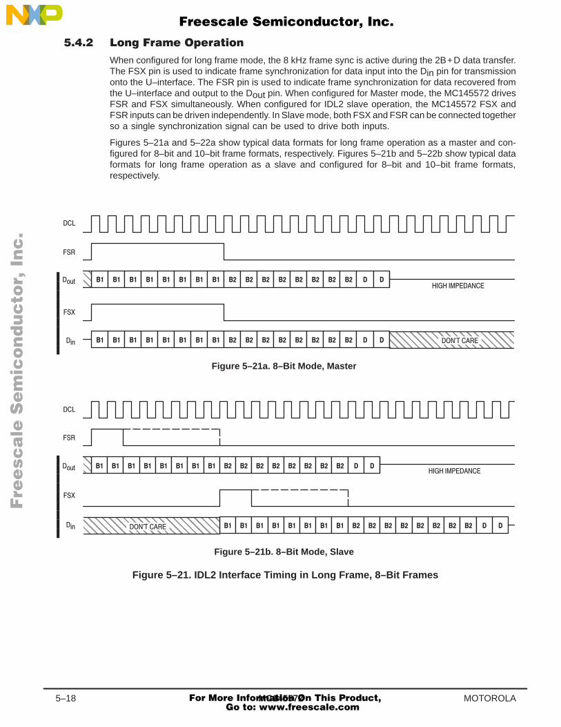
MC1455725–18 MOTOROLA
When configured for long frame mode, the 8 kHz frame sync is active during the 2B+D data transfer.The FSX pin is used to indicate frame synchronization for data input into the Din pin for transmissiononto the U–interface. The FSR pin is used to indicate frame synchronization for data recovered fromthe U–interface and output to the Dout pin. When configured for Master mode, the MC145572 drivesFSR and FSX simultaneously. When configured for IDL2 slave operation, the MC145572 FSX andFSR inputs can be driven independently. In Slave mode, both FSX and FSR can be connected togetherso a single synchronization signal can be used to drive both inputs.
Figures 5–21a and 5–22a show typical data formats for long frame operation as a master and con-figured for 8–bit and 10–bit frame formats, respectively. Figures 5–21b and 5–22b show typical dataformats for long frame operation as a slave and configured for 8–bit and 10–bit frame formats,respectively.
ÇÇÇÇ
ÇÇÇÇ
ÇÇÇÇÇÇ
ÇÇÇÇÇÇÇÇÇÇÇÇ
ÇÇÇÇ
ÇÇÇÇ
ÉÉÉÉÉÉ
ÉÉÉÉÉÉÉÉ
ÉÉÉÉ
ÉÉÉÉ
ÉÉÉÉ
ÉÉÉÉÉÉ
ÉÉÉÉ
ÇÇÇÇ
ÇÇÇÇ
ÇÇÇÇ
ÇÇÇÇÇÇ
ÇÇÇÇÇÇÇÇÇÇÇÇ
ÇÇÇÇ
ÇÇÇÇ
ÉÉÉÉÉÉ
ÉÉÉÉÉÉÉÉ
ÉÉÉÉ
ÉÉÉÉ
ÉÉÉÉ
ÉÉÉÉÉÉ
ÉÉÉÉ
Figure 5–21a. 8–Bit Mode, Master
ÇÇÇÇ
ÇÇÇÇ
ÇÇÇÇ
ÇÇÇÇÇÇ
ÇÇÇÇÇÇÇÇÇÇÇÇ
ÇÇÇÇ
ÉÉÉÉ
ÉÉÉÉ
ÉÉÉÉ
ÉÉÉÉÉÉ
ÉÉÉÉÉÉÉÉ
ÉÉÉÉ
ÉÉÉÉ
ÇÇÇÇ
ÇÇÇÇ
ÇÇÇÇ
ÇÇÇÇ
ÇÇÇÇÇÇ
ÇÇÇÇÇÇÇÇ
ÇÇÇÇ
ÇÇÇÇ
ÉÉÉÉ
ÉÉÉÉ
ÉÉÉÉÉÉ
ÉÉÉÉÉÉÉÉÉÉÉÉ
ÉÉÉÉ
ÉÉÉÉ
Figure 5–21b. 8–Bit Mode, Slave
ÇÇÇÇÇÇÇÇÇÇÇÇÇÇÇÇÇÇÇÇ
ÇÇÇÇÇÇÇÇÇÇÇÇÇÇÇÇÇÇÇÇÇÇ
Figure 5–21. IDL2 Interface Timing in Long Frame, 8–Bit Frames
Fre
esc
ale
Se
mic
on
du
cto
r, I
Freescale Semiconductor, Inc.
For More Information On This Product, Go to: www.freescale.com
nc
...
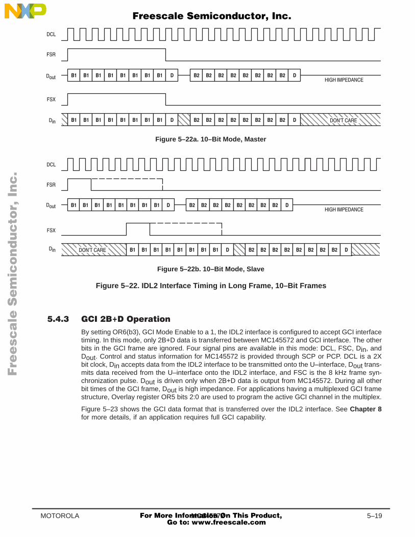
MC145572 5–19MOTOROLA
ÇÇÇÇÇÇÇÇÇÇÇÇÇÇÇÇÇÇÇÇÇÇÇÇÇÇÇ
ÇÇÇÇ
ÇÇÇÇÇÇ
Figure 5–22a. 10–Bit Mode, Master
Figure 5–22b. 10–Bit Mode, Slave
ÇÇÇÇÇÇ
ÇÇÇÇÇÇÇÇÇÇÇÇÇÇÇÇ
ÇÇÇÇÇÇÇÇ
Figure 5–22. IDL2 Interface Timing in Long Frame, 10–Bit Frames
By setting OR6(b3), GCI Mode Enable to a 1, the IDL2 interface is configured to accept GCI interfacetiming. In this mode, only 2B+D data is transferred between MC145572 and GCI interface. The otherbits in the GCI frame are ignored. Four signal pins are available in this mode: DCL, FSC, Din, andDout. Control and status information for MC145572 is provided through SCP or PCP. DCL is a 2Xbit clock, Din accepts data from the IDL2 interface to be transmitted onto the U–interface, Dout trans-mits data received from the U–interface onto the IDL2 interface, and FSC is the 8 kHz frame syn-chronization pulse. Dout is driven only when 2B+D data is output from MC145572. During all otherbit times of the GCI frame, Dout is high impedance. For applications having a multiplexed GCI framestructure, Overlay register OR5 bits 2:0 are used to program the active GCI channel in the multiplex.
Figure 5–23 shows the GCI data format that is transferred over the IDL2 interface. See Chapter 8for more details, if an application requires full GCI capability.
Fre
esc
ale
Se
mic
on
du
cto
r, I
Freescale Semiconductor, Inc.
For More Information On This Product, Go to: www.freescale.com
nc
...
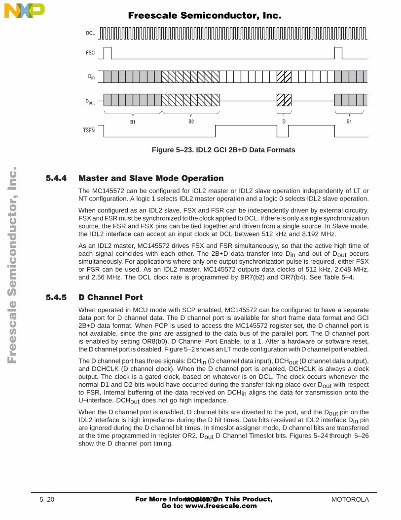
MC1455725–20 MOTOROLA
ÇÇÇÇÇÇÇÇÇÇÇÇÇÇÇÇÇÇÇÇÇÇÇÇÇÇ
ÉÉÉÉÉÉ
ÇÇÇÇÇÇÇÇÇÇÇÇÇÇÇÇÇÇÇÇÇÇÇÇÇÇ
ÉÉÉÉÉÉ
Figure 5–23. IDL2 GCI 2B+D Data Formats
The MC145572 can be configured for IDL2 master or IDL2 slave operation independently of LT orNT configuration. A logic 1 selects IDL2 master operation and a logic 0 selects IDL2 slave operation.
When configured as an IDL2 slave, FSX and FSR can be independently driven by external circuitry.FSX and FSR must be synchronized to the clock applied to DCL. If there is only a single synchronizationsource, the FSR and FSX pins can be tied together and driven from a single source. In Slave mode,the IDL2 interface can accept an input clock at DCL between 512 kHz and 8.192 MHz.
As an IDL2 master, MC145572 drives FSX and FSR simultaneously, so that the active high time ofeach signal coincides with each other. The 2B+D data transfer into Din and out of Dout occurssimultaneously. For applications where only one output synchronization pulse is required, either FSXor FSR can be used. As an IDL2 master, MC145572 outputs data clocks of 512 kHz, 2.048 MHz,and 2.56 MHz. The DCL clock rate is programmed by BR7(b2) and OR7(b4). See Table 5–4.
When operated in MCU mode with SCP enabled, MC145572 can be configured to have a separatedata port for D channel data. The D channel port is available for short frame data format and GCI2B+D data format. When PCP is used to access the MC145572 register set, the D channel port isnot available, since the pins are assigned to the data bus of the parallel port. The D channel portis enabled by setting OR8(b0), D Channel Port Enable, to a 1. After a hardware or software reset,the D channel port is disabled. Figure 5–2 shows an LT mode configuration with D channel port enabled.
The D channel port has three signals: DCHin (D channel data input), DCHout (D channel data output),and DCHCLK (D channel clock). When the D channel port is enabled, DCHCLK is always a clockoutput. The clock is a gated clock, based on whatever is on DCL. The clock occurs whenever thenormal D1 and D2 bits would have occurred during the transfer taking place over Dout with respectto FSR. Internal buffering of the data received on DCHin aligns the data for transmission onto theU–interface. DCHout does not go high impedance.
When the D channel port is enabled, D channel bits are diverted to the port, and the Dout pin on theIDL2 interface is high impedance during the D bit times. Data bits received at IDL2 interface Din pinare ignored during the D channel bit times. In timeslot assigner mode, D channel bits are transferredat the time programmed in register OR2, Dout D Channel Timeslot bits. Figures 5–24 through 5–26show the D channel port timing.
Fre
esc
ale
Se
mic
on
du
cto
r, I
Freescale Semiconductor, Inc.
For More Information On This Product, Go to: www.freescale.com
nc
...
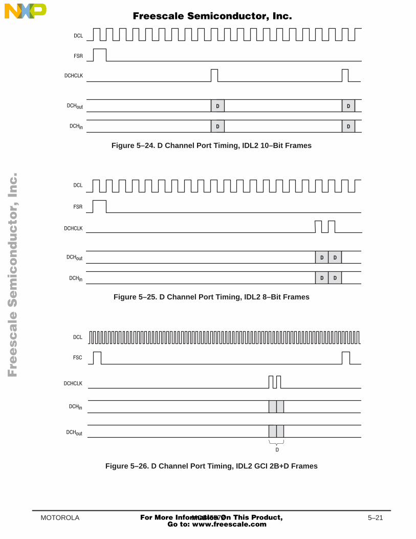
MC145572 5–21MOTOROLA
Figure 5–24. D Channel Port Timing, IDL2 10–Bit Frames
Figure 5–25. D Channel Port Timing, IDL2 8–Bit Frames
Figure 5–26. D Channel Port Timing, IDL2 GCI 2B+D Frames
Fre
esc
ale
Se
mic
on
du
cto
r, I
Freescale Semiconductor, Inc.
For More Information On This Product, Go to: www.freescale.com
nc
...
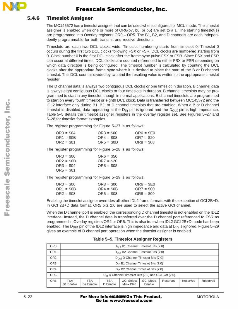
MC1455725–22 MOTOROLA
The MC145572 has a timeslot assigner that can be used when configured for MCU mode. The timeslotassigner is enabled when one or more of OR6(b7, b6, or b5) are set to a 1. The starting timeslot(s)are programmed into Overlay registers OR0 – OR5. The B1, B2, and D channels are each indepen-dently programmable for both transmit and receive directions.
Timeslots are each two DCL clocks wide. Timeslot numbering starts from timeslot 0. Timeslot 0occurs during the first two DCL clocks following FSX or FSR. DCL clocks are numbered starting from0. Clock number 0 is the first DCL clock after the frame sync pulse FSX or FSR. Since FSX and FSRcan occur at different times, DCL clocks are counted referenced to either FSX or FSR depending onwhich data direction is being configured. The timeslot number is calculated by counting the DCLclocks after the appropriate frame sync where it is desired to place the start of the B or D channeltimeslot. This DCL count is divided by two and the resulting value is written to the appropriate timeslotregister.
The D channel data is always two contiguous DCL clocks or one timeslot in duration. B channel datais always eight contiguous DCL clocks or four timeslots in duration. B channel timeslots may be pro-grammed to start in any timeslot, though in normal applications, B channel timeslots are programmedto start on every fourth timeslot or eighth DCL clock. Data is transferred between MC145572 and theIDL2 interface only during B1, B2, or D channel timeslots that are enabled. When a B or D channeltimeslot is disabled, data appearing at the Din pin is ignored and the Dout pin is high impedance.Table 5–5 details the timeslot assigner registers in the overlay register set. See Figures 5–27 and5–28 for timeslot format examples.
The register programming for Figure 5–27 is as follows:
OR0 = $04 OR3 = $00 OR6 = $E0OR1 = $0B OR4 = $08 OR7 = $20OR2 = $01 OR5 = $0D OR8 = $08
The register programming for Figure 5–28 is as follows:
OR0 = $00 OR6 = $50OR2 = $0D OR7 = $20OR3 = $04 OR8 = $08OR5 = $01
The register programming for Figure 5–29 is as follows:
OR0 = $00 OR3 = $00 OR6 = $E0OR1 = $0B OR4 = $0B OR7 = $00OR2 = $08 OR5 = $08 OR8 = $09
Enabling the timeslot assigner overrides all other IDL2 frame formats with the exception of GCI 2B+D.In GCI 2B+D data format, OR5 bits 2:0 are used to select the active GCI channel.
When the D channel port is enabled, the corresponding D channel timeslot is not enabled on the IDL2interface. Instead, the D channel data is transferred over the D channel port referenced to FSR asprogrammed in Overlay registers OR2 or OR5. This is also true when IDL2 GCI 2B+D mode has beenenabled. The Dout pin of the IDL2 interface is high impedance and data at Din is ignored. Figure 5–29gives an example of D channel port operation when the timeslot assigner is enabled.
Table 5–5. Timeslot Assigner Registers
OR0 Dout B1 Channel Timeslot Bits (7:0)
OR1 Dout B2 Channel Timeslot Bits (7:0)
OR2 Dout D Channel Timeslot Bits (7:0)
OR3 Din B1 Channel Timeslot Bits (7:0)
OR4 Din B2 Channel Timeslot Bits (7:0)
OR5 Din D Channel Timeslot Bits (7:0) and GCI Slot (2:0)
OR6 TSAB1 Enable
TSAB2 Enable
TSAD Enable
GCI SelectM4 – BR0
GCI ModeEnable
Reserved Reserved Reserved
Fre
esc
ale
Se
mic
on
du
cto
r, I
Freescale Semiconductor, Inc.
For More Information On This Product, Go to: www.freescale.com
nc
...
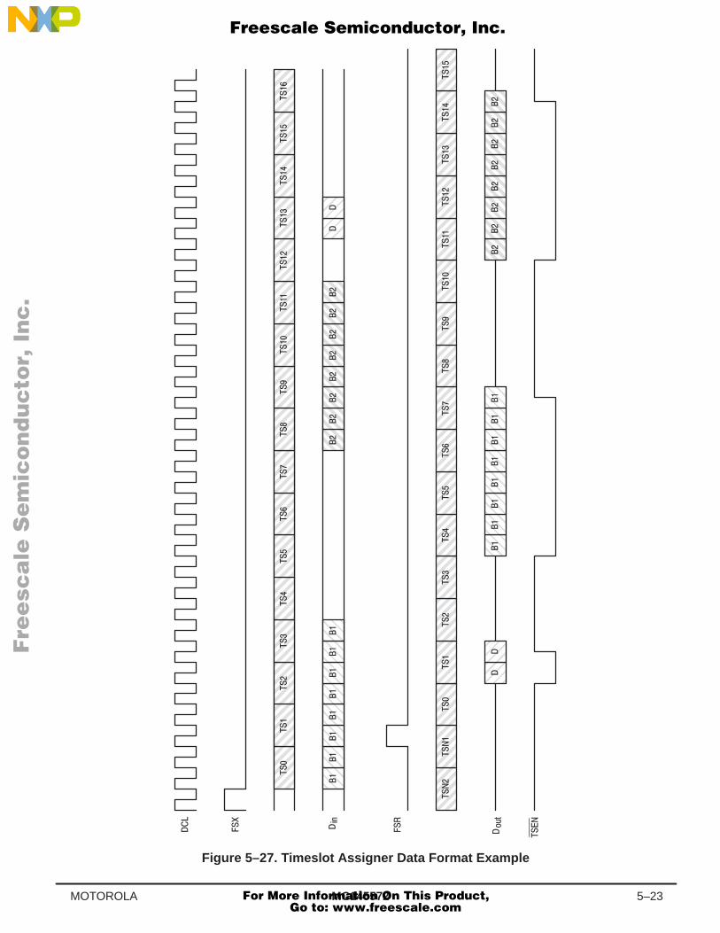
MC145572 5–23MOTOROLA
ÍÍÍÍÍÍ
ÍÍÍÍÍÍÍÍ
ÍÍÍÍÍÍ
ÍÍÍÍÍÍ
ÍÍÍÍÍÍÍÍ
ÍÍÍÍÍÍ
ÍÍÍÍÍÍ
ÍÍÍÍÍÍÍÍ
ÍÍÍÍÍÍ
ÍÍÍÍÍÍ
ÍÍÍÍÍÍÍÍ
ÍÍÍÍÍÍ
ÍÍÍÍÍÍ
ÍÍÍÍÍÍÍÍ
ÍÍÍÍÍÍ
ÍÍÍÍÍÍ
ÍÍÍÍÍÍÍÍ
ÇÇÇÇÇÇ
ÇÇÇÇÇÇ
ÇÇÇÇÇÇ
ÇÇÇÇÇÇÇÇÇ
ÇÇÇÇÇÇ
ÇÇÇÇÇÇ
ÇÇÇÇÇÇ
ÇÇÇÇÇÇ
ÈÈÈÈÈÈ
ÈÈÈÈÈÈ
ÈÈÈÈÈÈ
ÈÈÈÈÈÈ
ÈÈÈÈÈÈ
ÈÈÈÈÈÈÈÈÈ
ÈÈÈÈÈÈ
ÈÈÈÈÈÈ
ÉÉÉÉÉÉ
ÉÉÉÉÉÉÉÉÉ
ÍÍÍÍÍÍ
ÍÍÍÍÍÍ
ÍÍÍÍÍÍÍÍ
ÍÍÍÍÍÍ
ÍÍÍÍÍÍ
ÍÍÍÍÍÍÍÍ
ÍÍÍÍÍÍ
ÍÍÍÍÍÍ
ÍÍÍÍÍÍÍÍ
ÍÍÍÍÍÍ
ÍÍÍÍÍÍ
ÍÍÍÍÍÍÍÍ
ÍÍÍÍÍÍ
ÍÍÍÍÍÍ
ÍÍÍÍÍÍÍÍ
ÍÍÍÍÍÍ
ÍÍÍÍÍÍ
ÇÇÇÇ
ÇÇÇÇ
ÇÇÇÇ
ÇÇÇÇ
ÇÇÇÇÇÇ
ÇÇÇÇ
ÇÇÇÇ
ÇÇÇÇ
ÈÈÈÈ
ÈÈÈÈ
ÈÈÈÈÈÈ
ÈÈÈÈ
ÈÈÈÈ
ÈÈÈÈ
ÈÈÈÈ
ÈÈÈÈ
ÉÉÉÉ
ÉÉÉÉ
ÍÍÍÍÍÍÍÍ
Figure 5–27. Timeslot Assigner Data Format Example
Fre
esc
ale
Se
mic
on
du
cto
r, I
Freescale Semiconductor, Inc.
For More Information On This Product, Go to: www.freescale.com
nc
...
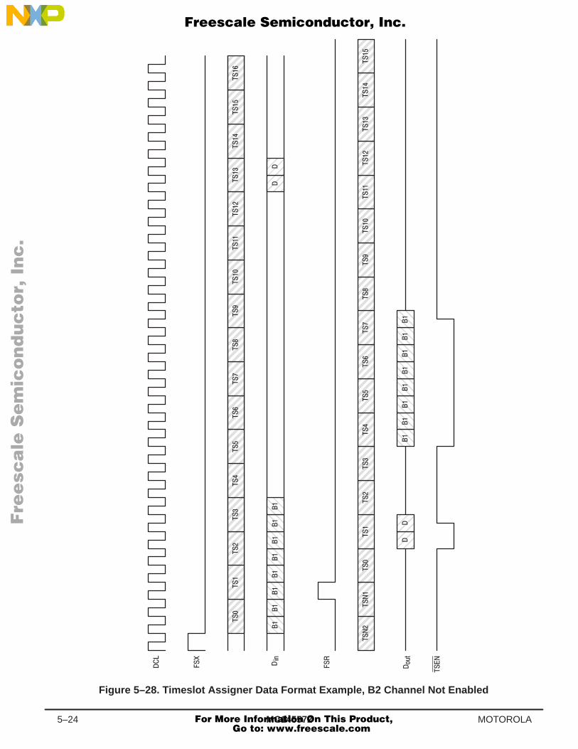
MC1455725–24 MOTOROLA
ÍÍÍÍÍÍ
ÍÍÍÍÍÍÍÍ
ÍÍÍÍÍÍ
ÍÍÍÍÍÍ
ÍÍÍÍÍÍÍÍ
ÍÍÍÍÍÍ
ÍÍÍÍÍÍ
ÍÍÍÍÍÍÍÍ
ÍÍÍÍÍÍ
ÍÍÍÍÍÍ
ÍÍÍÍÍÍÍÍ
ÍÍÍÍÍÍ
ÍÍÍÍÍÍ
ÍÍÍÍÍÍÍÍ
ÍÍÍÍÍÍ
ÍÍÍÍÍÍ
ÍÍÍÍÍÍÍÍ
ÇÇÇÇ
ÇÇÇÇ
ÇÇÇÇ
ÇÇÇÇÇÇ
ÇÇÇÇ
ÇÇÇÇ
ÇÇÇÇ
ÇÇÇÇ
ÉÉÉÉ
ÉÉÉÉÉÉ
ÍÍÍÍÍÍ
ÍÍÍÍÍÍ
ÍÍÍÍÍÍÍÍ
ÍÍÍÍÍÍ
ÍÍÍÍÍÍ
ÍÍÍÍÍÍÍÍ
ÍÍÍÍÍÍ
ÍÍÍÍÍÍ
ÍÍÍÍÍÍÍÍ
ÍÍÍÍÍÍ
ÍÍÍÍÍÍ
ÍÍÍÍÍÍÍÍ
ÍÍÍÍÍÍ
ÍÍÍÍÍÍ
ÍÍÍÍÍÍÍÍ
ÍÍÍÍÍÍ
ÍÍÍÍÍÍ
ÇÇÇÇ
ÇÇÇÇ
ÇÇÇÇ
ÇÇÇÇ
ÇÇÇÇÇÇ
ÇÇÇÇ
ÇÇÇÇ
ÇÇÇÇ
ÉÉÉÉ
ÉÉÉÉ
ÍÍÍÍÍÍÍÍ
Figure 5–28. Timeslot Assigner Data Format Example, B2 Channel Not Enabled
Fre
esc
ale
Se
mic
on
du
cto
r, I
Freescale Semiconductor, Inc.
For More Information On This Product, Go to: www.freescale.com
nc
...
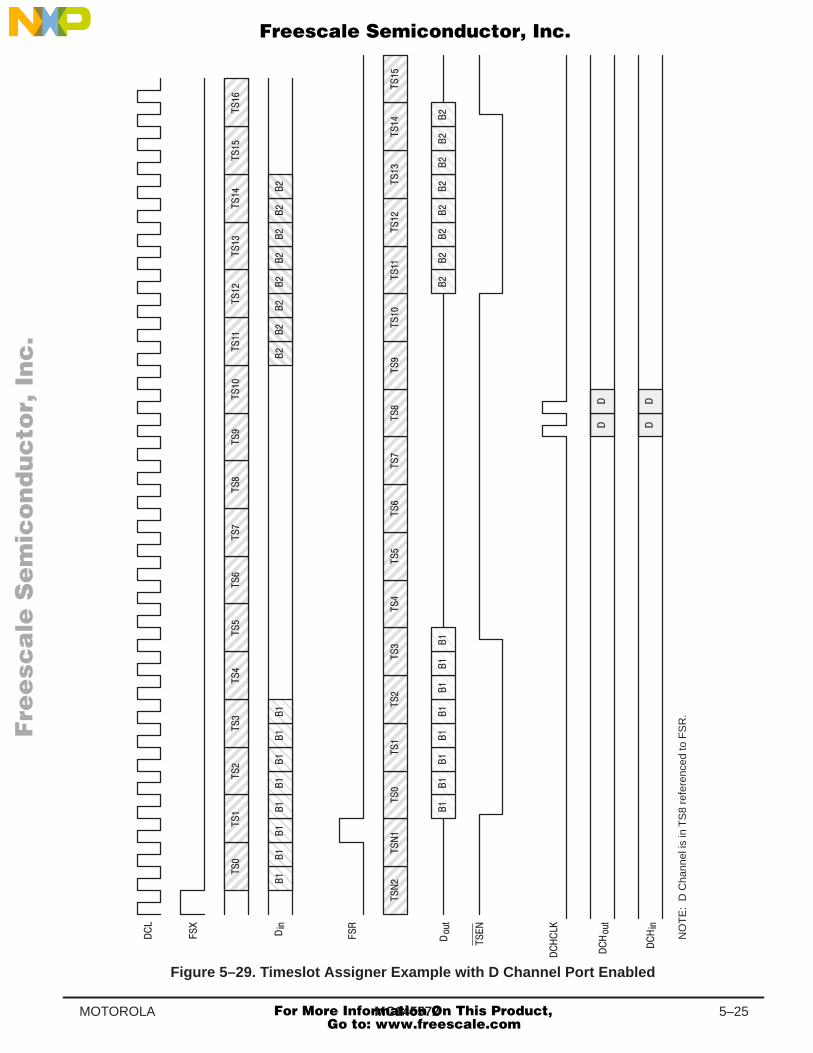
MC145572 5–25MOTOROLA
ÍÍÍÍÍÍÍÍÍ
ÍÍÍÍÍÍÍÍÍÍÍÍ
ÍÍÍÍÍÍÍÍÍ
ÍÍÍÍÍÍÍÍÍ
ÍÍÍÍÍÍÍÍÍÍÍÍ
ÍÍÍÍÍÍÍÍÍ
ÍÍÍÍÍÍÍÍÍ
ÍÍÍÍÍÍÍÍÍÍÍÍ
ÍÍÍÍÍÍÍÍÍ
ÍÍÍÍÍÍÍÍÍ
ÍÍÍÍÍÍÍÍÍÍÍÍ
ÍÍÍÍÍÍÍÍÍ
ÍÍÍÍÍÍÍÍÍ
ÍÍÍÍÍÍÍÍÍÍÍÍ
ÍÍÍÍÍÍÍÍÍ
ÍÍÍÍÍÍÍÍÍ
ÍÍÍÍÍÍÍÍÍÍÍÍ
ÇÇÇÇ
ÇÇÇÇ
ÇÇÇÇ
ÇÇÇÇÇÇ
ÇÇÇÇ
ÇÇÇÇ
ÇÇÇÇ
ÇÇÇÇ
ÈÈÈÈ
ÈÈÈÈ
ÈÈÈÈ
ÈÈÈÈ
ÈÈÈÈ
ÈÈÈÈÈÈ
ÈÈÈÈ
ÈÈÈÈ
ÍÍÍÍÍÍ
ÍÍÍÍÍÍ
ÍÍÍÍÍÍÍÍ
ÍÍÍÍÍÍ
ÍÍÍÍÍÍ
ÍÍÍÍÍÍÍÍ
ÍÍÍÍÍÍ
ÍÍÍÍÍÍ
ÍÍÍÍÍÍÍÍ
ÍÍÍÍÍÍ
ÍÍÍÍÍÍ
ÍÍÍÍÍÍÍÍ
ÍÍÍÍÍÍ
ÍÍÍÍÍÍ
ÍÍÍÍÍÍÍÍ
ÍÍÍÍÍÍ
ÍÍÍÍÍÍ
ÇÇÇÇÇÇ
ÇÇÇÇ
ÇÇÇÇ
ÇÇÇÇ
ÇÇÇÇ
ÇÇÇÇ
ÇÇÇÇÇÇ
ÇÇÇÇ
ÈÈÈÈ
ÈÈÈÈ
ÈÈÈÈÈÈ
ÈÈÈÈ
ÈÈÈÈ
ÈÈÈÈ
ÈÈÈÈ
ÈÈÈÈ
ÍÍÍÍÍÍÍÍ
Figure 5–29. Timeslot Assigner Example with D Channel Port Enabled
NO
TE
:D
Cha
nnel
is in
TS
8 re
fere
nced
to F
SR
.
Fre
esc
ale
Se
mic
on
du
cto
r, I
Freescale Semiconductor, Inc.
For More Information On This Product, Go to: www.freescale.com
nc
...
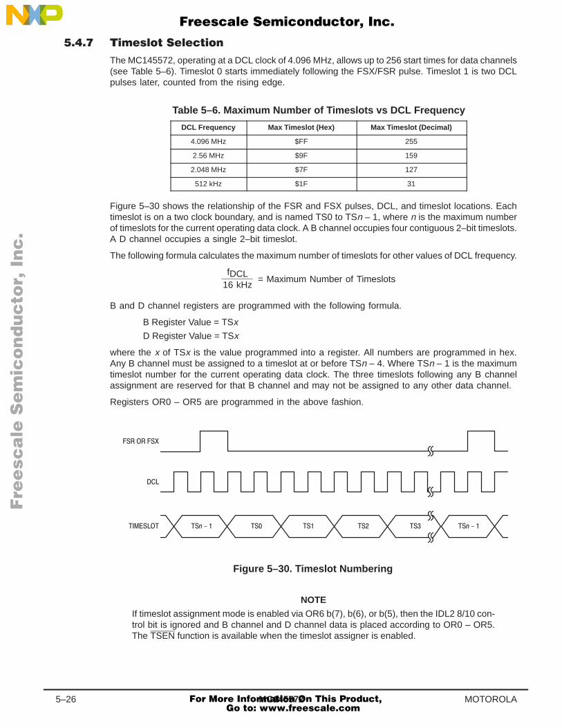
MC1455725–26 MOTOROLA
The MC145572, operating at a DCL clock of 4.096 MHz, allows up to 256 start times for data channels(see Table 5–6). Timeslot 0 starts immediately following the FSX/FSR pulse. Timeslot 1 is two DCLpulses later, counted from the rising edge.
Table 5–6. Maximum Number of Timeslots vs DCL Frequency
DCL Frequency Max Timeslot (Hex) Max Timeslot (Decimal)
4.096 MHz $FF 255
2.56 MHz $9F 159
2.048 MHz $7F 127
512 kHz $1F 31
Figure 5–30 shows the relationship of the FSR and FSX pulses, DCL, and timeslot locations. Eachtimeslot is on a two clock boundary, and is named TS0 to TSn – 1, where n is the maximum numberof timeslots for the current operating data clock. A B channel occupies four contiguous 2–bit timeslots.A D channel occupies a single 2–bit timeslot.
The following formula calculates the maximum number of timeslots for other values of DCL frequency.
= Maximum Number of TimeslotsfDCL
16 kHz
B and D channel registers are programmed with the following formula.
B Register Value = TSx
D Register Value = TSx
where the x of TSx is the value programmed into a register. All numbers are programmed in hex.Any B channel must be assigned to a timeslot at or before TSn – 4. Where TSn – 1 is the maximumtimeslot number for the current operating data clock. The three timeslots following any B channelassignment are reserved for that B channel and may not be assigned to any other data channel.
Registers OR0 – OR5 are programmed in the above fashion.
Figure 5–30. Timeslot Numbering
NOTE
If timeslot assignment mode is enabled via OR6 b(7), b(6), or b(5), then the IDL2 8/10 con-trol bit is ignored and B channel and D channel data is placed according to OR0 – OR5.The TSEN function is available when the timeslot assigner is enabled.
Fre
esc
ale
Se
mic
on
du
cto
r, I
Freescale Semiconductor, Inc.
For More Information On This Product, Go to: www.freescale.com
nc
...
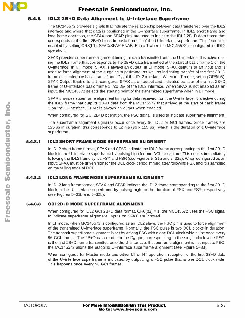
MC145572 5–27MOTOROLA
) #"!%$%) )& %)( *'( ($
The MC145572 provides signals that indicate the relationship between data transferred over the IDL2interface and where that data is positioned in the U–interface superframe. In IDL2 short frame andlong frame operation, the SFAX and SFAR pins are used to indicate the IDL2 2B+D data frame thatcorresponds to the first 2B+D block in basic frame 1 of the U–interface superframe. This feature isenabled by setting OR8(b1), SFAX/SFAR ENABLE to a 1 when the MC145572 is configured for IDL2operation.
SFAX provides superframe alignment timing for data transmitted onto the U–interface. It is active dur-ing the IDL2 frame that corresponds to the 2B+D data transmitted at the start of basic frame 1 on theU–interface. In NT mode, SFAX is always an output. In LT mode, SFAX defaults to an input and isused to force alignment of the outgoing superframe, as well as indicating transfer of the first 2B+Dframe of U–interface basic frame 1 into Din of the IDL2 interface. When in LT mode, setting OR8(b5),SFAX Output Enable to a 1, configures SFAX as an output and indicates transfer of the first 2B+Dframe of U–interface basic frame 1 into Din of the IDL2 interface. When SFAX is not enabled as aninput, the MC145572 selects the starting point of the transmitted superframe when in LT mode.
SFAR provides superframe alignment timing for data received from the U–interface. It is active duringthe IDL2 frame that outputs 2B+D data from the MC145572 that arrived at the start of basic frame1 on the U–interface. SFAR is always an output when enabled.
When configured for GCI 2B+D operation, the FSC signal is used to indicate superframe alignment.
The superframe alignment signal(s) occur once every 96 IDL2 or GCI frames. Since frames are125 µs in duration, this corresponds to 12 ms (96 x 125 µs), which is the duration of a U–interfacesuperframe.
In IDL2 short frame format, SFAX and SFAR indicate the IDL2 frame corresponding to the first 2B+Dblock in the U–interface superframe by pulsing high for one DCL clock time. This occurs immediatelyfollowing the IDL2 frame syncs FSX and FSR (see Figures 5–31a and 5–32a). When configured as aninput, SFAX must be driven high for the DCL clock period immediately following FSX and it is sampledon the falling edge of DCL.
In IDL2 long frame format, SFAX and SFAR indicate the IDL2 frame corresponding to the first 2B+Dblock in the U–interface superframe by pulsing high for the duration of FSX and FSR, respectively(see Figures 5–31b and 5–32b).
When configured for IDL2 GCI 2B+D data format, OR6(b3) = 1, the MC145572 uses the FSC signalto indicate superframe alignment. Inputs on SFAX are ignored.
In LT mode, when MC145572 is configured as an IDL2 slave, the FSC pin is used to force alignmentof the transmitted U–interface superframe. Normally, the FSC pulse is two DCL clocks in duration.The transmit superframe alignment is set by driving FSC with a one DCL clock wide pulse once every96 GCI frames. The 2B+D data read into the Din pin, corresponding to the single clock wide FSC,is the first 2B+D frame transmitted onto the U–interface. If superframe alignment is not input to FSC,the MC145572 aligns the outgoing U–interface superframe alignment (see Figure 5–33).
When configured for Master mode and either LT or NT operation, reception of the first 2B+D dataof the U–interface superframe is indicated by outputting a FSC pulse that is one DCL clock wide.This happens once every 96 GCI frames.
Fre
esc
ale
Se
mic
on
du
cto
r, I
Freescale Semiconductor, Inc.
For More Information On This Product, Go to: www.freescale.com
nc
...
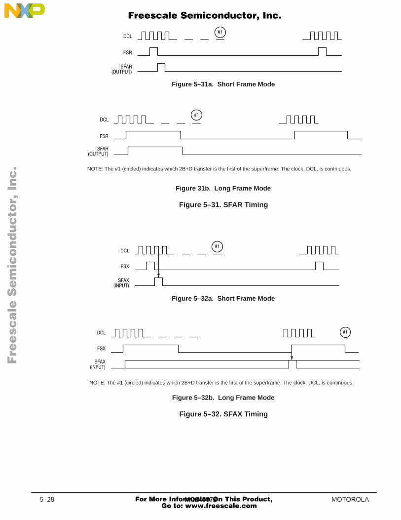
MC1455725–28 MOTOROLA
Figure 5–31a. Short Frame Mode
Figure 31b. Long Frame Mode
NOTE: The #1 (circled) indicates which 2B+D transfer is the first of the superframe. The clock, DCL, is continuous.
Figure 5–31. SFAR Timing
Figure 5–32a. Short Frame Mode
Figure 5–32b. Long Frame Mode
NOTE: The #1 (circled) indicates which 2B+D transfer is the first of the superframe. The clock, DCL, is continuous.
Figure 5–32. SFAX Timing
Fre
esc
ale
Se
mic
on
du
cto
r, I
Freescale Semiconductor, Inc.
For More Information On This Product, Go to: www.freescale.com
nc
...
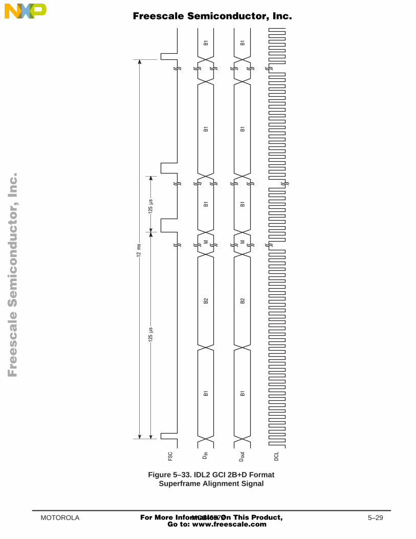
MC145572 5–29MOTOROLA
µ
Figure 5–33. IDL2 GCI 2B+D FormatSuperframe Alignment Signal
µ
Fre
esc
ale
Se
mic
on
du
cto
r, I
Freescale Semiconductor, Inc.
For More Information On This Product, Go to: www.freescale.com
nc
...
MC1455725–30 MOTOROLA
In NT mode, IDL2 slave operation, any superframe alignment information that may be present onFSC is ignored. ANSI T1.601 defines a 60 ± 2 baud turnaround at the NT. This means that the trans-mitted Superframe Sync word in the NT–configured MC145572 is delayed 60 bauds or 750 µs fromthe received Superframe Sync word. On an 18,000–foot loop, the total propagation delay in both direc-tions is approximately 6 bauds or 39 µs. This gives a worse case offset between the transmitted syncword at LT and the receive sync word at NT of approximately 790 µs or 6 IDL frames.
$"'"# '' % $ !$$#&
Upon initial activation, MC145572 transmits all 1s in the B and D channels onto the U–interface. Datatransparency is enabled by setting Customer Enable (NR2(b0)), when the M4 channel act bit is re-ceived as a 1. If the Verified act /dea mode is enabled, see BR9(b5,b4), then data transparency ontothe U–interface is automatically enabled when the M4 channel act bit is received as a 1.
Due to the MC145572 having separate FIFOs for receive and transmit directions, there is a propagationdelay between data being input into the IDL2 or GCI interfaces and that same data being transmittedonto the U–interface. Likewise, there is a delay between when data is received at the U–interfaceand is transmitted onto the IDL2 or GCI interfaces. Table 5–7 gives the minimum and maximum delaysfor both NT and LT modes of operation. For any given activation, the delay remains fixed, but thepropagation delay through the MC145572 will vary from activation to activation.
Table 5–7. FIFO Delays Through the MC145572
ÁÁÁÁÁÁÁÁÁÁÁÁÁÁÁÁÁÁÁÁÁÁÁÁÁÁÁÁÁÁ
Delay Path ÁÁÁÁÁÁÁÁ
Min ÁÁÁÁÁÁÁÁÁÁ
Max ÁÁÁÁÁÁÁÁ
Units
ÁÁÁÁÁÁÁÁÁÁÁÁÁÁÁÁÁÁÁÁÁÁÁÁÁÁÁÁÁÁ
NT Mode FSX to U–Interface Transmission Delay ÁÁÁÁÁÁÁÁ
196 ÁÁÁÁÁÁÁÁÁÁ
315 ÁÁÁÁÁÁÁÁ
µs
ÁÁÁÁÁÁÁÁÁÁÁÁÁÁÁÁÁÁÁÁÁÁÁÁÁÁÁÁÁÁ
NT Mode U–Interface to FSR Transmission Delay ÁÁÁÁÁÁÁÁ
281 ÁÁÁÁÁÁÁÁÁÁ
400 ÁÁÁÁÁÁÁÁ
µs
ÁÁÁÁÁÁÁÁÁÁÁÁÁÁÁÁÁÁÁÁÁÁÁÁÁÁÁÁÁÁ
LT Mode FSX to U–Interface Transmission Delay ÁÁÁÁÁÁÁÁ
184 ÁÁÁÁÁÁÁÁÁÁ
328 ÁÁÁÁÁÁÁÁ
µs
ÁÁÁÁÁÁÁÁÁÁÁÁÁÁÁÁÁÁÁÁÁÁÁÁÁÁÁÁÁÁ
LT Mode U–Interface to FSR Transmission Delay ÁÁÁÁÁÁÁÁ
281 ÁÁÁÁÁÁÁÁÁÁ
400 ÁÁÁÁÁÁÁÁ
µs
NOTE
The total end–to–end delay is the sum of the transmit FIFO delay in the originating trans-ceiver and the receive FIFO delay at the destination transceiver.
The MC145572 U–interface transceiver supports four different loopback types, each having variousmodes. The four types are: 1) U–Interface Loopback, 2) IDL2 Interface Loopback, 3) SuperframeFramer–to–Deframer Loopback, and 4) External Analog Loopback. Each of these loopback modesis selected by setting bits in the appropriate register(s). Any combination of loopbacks may be invoked,including simultaneous loopbacks toward the U–interface and toward the IDL2 interface. These loop-backs are available as transparent or non–transparent. “Transparent” means that a loopback passesthe data on through to the other side, as well as looping it back. “Non–transparent” means that thedata is blocked from being passed downstream and is replaced with the idle code (all 1s).
Fre
esc
ale
Se
mic
on
du
cto
r, I
Freescale Semiconductor, Inc.
For More Information On This Product, Go to: www.freescale.com
nc
...
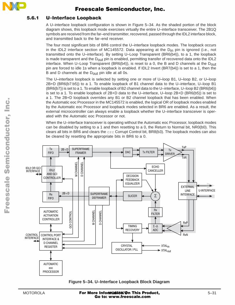
MC145572 5–31MOTOROLA
A U–interface loopback configuration is shown in Figure 5–34. As the shaded portion of the blockdiagram shows, this loopback mode exercises virtually the entire U–interface transceiver. The 2B1Qsymbols are received from the far–end transmitter, recovered, passed through the IDL2 interface block,and transmitted back to the far–end receiver.
The four most significant bits of BR6 control the U–interface loopback modes. The loopback occursin the IDL2 interface section of MC145572. Data appearing at the Din pin is ignored (i.e., nottransmitted onto the U–interface). By setting U–Loop Transparent (BR6(b4)), to a 1, the loopbackis made transparent and the Dout pin is enabled, permitting transfer of recovered data onto the IDL2interface. When U–Loop Transparent (BR6(b4)), is reset to a 0, the B and D channels at the Doutpin are forced to idle 1s when a loopback is enabled. If IDL2 Invert (BR7(b4)) is set to a 1, then theB and D channels at the Dout pin idle at all 0s.
The U–interface loopback is selected by setting one or more of U–loop B1, U–loop B2, or U–loop2B+D (BR6(b7:b5)) to a 1. To enable loopback of B1 channel data to the U–interface, U–loop B1(BR6(b7)) is set to a 1. To enable loopback of B2 channel data to the U–interface, U–loop B2 (BR6(b6))is set to a 1. To enable loopback of 2B+D data to the U–interface, U–loop 2B+D (BR6(b5)) is set toa 1. The 2B+D loopback overrides any B1 or B2 channel loopback that has been enabled. Whenthe Automatic eoc Processor in the MC145572 is enabled, the logical OR of loopback modes enabledby the Automatic eoc Processor and loopback modes selected in BR6 are enabled. As a result, theexternal microcontroller can always enable a loopback whether the U–interface transceiver is oper-ated with the Automatic eoc Processor or not.
When the U–interface transceiver is operating without the Automatic eoc Processor, loopback modescan be disabled by setting to a 1 and then resetting to a 0, the Return to Normal bit, NR0(b0). Thisclears all bits in BR6 and clears the crc Corrupt Control bit, BR8(b3). The loopback modes can alsobe cleared by resetting the appropriate bits in BR6 to a 0.
Σ(
&
&
&
&
&
&
&
&
&
Σ∆
#
!"
#%$
Figure 5–34. U–Interface Loopback Block Diagram
Fre
esc
ale
Se
mic
on
du
cto
r, I
Freescale Semiconductor, Inc.
For More Information On This Product, Go to: www.freescale.com
nc
...
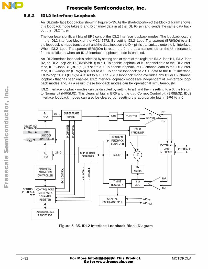
MC1455725–32 MOTOROLA
An IDL2 interface loopback is shown in Figure 5–35. As the shaded portion of the block diagram shows,this loopback mode takes B and D channel data in at the IDL Rx pin and sends the same data backout the IDL2 Tx pin.
The four least significant bits of BR6 control the IDL2 Interface loopback modes. The loopback occursin the IDL2 interface block of the MC145572. By setting IDL2–Loop Transparent (BR6(b0)) to a 1,the loopback is made transparent and the data input on the Din pin is transmitted onto the U–interface.When IDL2–Loop Transparent (BR6(b0)) is reset to a 0, the data transmitted on the U–interface isforced to idle 1s when an IDL2 interface loopback mode is enabled.
An IDL2 interface loopback is selected by setting one or more of the registers IDL2–loop B1, IDL2–loopB2, or IDL2–loop 2B+D (BR6(b3:b1)) to a 1. To enable loopback of B1 channel data to the IDL2 inter-face, IDL2–loop B1 (BR6(b3)) is set to a 1. To enable loopback of B2 channel data to the IDL2 inter-face, IDL2–loop B2 (BR6(b2)) is set to a 1. To enable loopback of 2B+D data to the IDL2 interface,IDL2–loop 2B+D (BR6(b1)) is set to a 1. The 2B+D loopback mode overrides any B1 or B2 channelloopback that has been enabled. IDL2 interface loopback modes are independent of U–interface loop-back modes and, as a result, these loopback modes can be operational simultaneously.
IDL2 interface loopback modes can be disabled by setting to a 1 and then resetting to a 0, the Returnto Normal bit (NR0(b0)). This clears all bits in BR6 and the crc Corrupt Control bit, (BR8(b3)). IDL2interface loopback modes can also be cleared by resetting the appropriate bits in BR6 to a 0.
Σ(
&
&
&
&
&
&
&
&
&
Σ∆
#
!"
#%$
!"
#%$
Figure 5–35. IDL2 Interface Loopback Block Diagram
Fre
esc
ale
Se
mic
on
du
cto
r, I
Freescale Semiconductor, Inc.
For More Information On This Product, Go to: www.freescale.com
nc
...
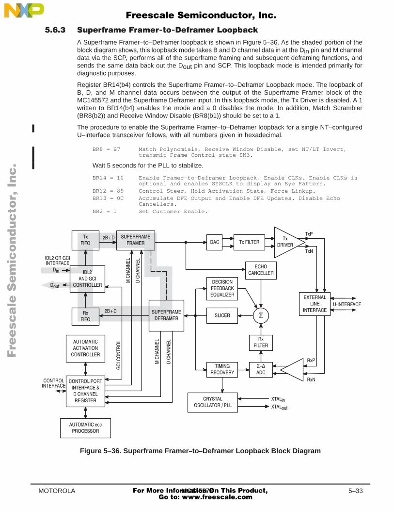
MC145572 5–33MOTOROLA
A Superframe Framer–to–Deframer loopback is shown in Figure 5–36. As the shaded portion of theblock diagram shows, this loopback mode takes B and D channel data in at the Din pin and M channeldata via the SCP, performs all of the superframe framing and subsequent deframing functions, andsends the same data back out the Dout pin and SCP. This loopback mode is intended primarily fordiagnostic purposes.
Register BR14(b4) controls the Superframe Framer–to–Deframer Loopback mode. The loopback ofB, D, and M channel data occurs between the output of the Superframe Framer block of theMC145572 and the Superframe Deframer input. In this loopback mode, the Tx Driver is disabled. A 1written to BR14(b4) enables the mode and a 0 disables the mode. In addition, Match Scrambler(BR8(b2)) and Receive Window Disable (BR8(b1)) should be set to a 1.
The procedure to enable the Superframe Framer–to–Deframer loopback for a single NT–configuredU–interface transceiver follows, with all numbers given in hexadecimal.
BR8 = B7 Match Polynomials, Receive Window Disable, set NT/LT Invert,transmit Frame Control state SN3.
Wait 5 seconds for the PLL to stabilize.
BR14 = 10 Enable Framer–to–Deframer Loopback, Enable CLKs. Enable CLKs is optional and enables SYSCLK to display an Eye Pattern.
BR12 = 89 Control Steer, Hold Activation State, Force Linkup.BR13 = 0C Accumulate DFE Output and Enable DFE Updates. Disable Echo
Cancellers.NR2 = 1 Set Customer Enable.
Σ(
&
&
&
&
&
&
&
&
&
Σ∆
!"
#%$
!"
#%$
#
Figure 5–36. Superframe Framer –to–Deframer Loopback Block Diagram
Fre
esc
ale
Se
mic
on
du
cto
r, I
Freescale Semiconductor, Inc.
For More Information On This Product, Go to: www.freescale.com
nc
...
MC1455725–34 MOTOROLA
The procedure to enable the Superframe Framer–to–Deframer loopback for a single LT–configuredU–interface transceiver follows, with all numbers given in hexadecimal.
NR0 = 8 Assert reset, not required.NR0 = 0 Deassert reset, not required.BR14 = 10 Enable Framer–to–Deframer Loopback, Enable CLKs. Enable CLKs is
optional and enables SYSCLK to display an Eye Pattern.BR8 = B6 Match Polynomials, Receive Window Disable, do not set NT/LT
Invert, transmit Frame Control state SL3.BR12 = 89 Control Steer, Hold Activation State, Force Linkup.BR13 = 0C Accumulate DFE Output and Enable DFE Updates. Disable Echo
Cancellers.NR2 = 1 Set Customer Enable.
To turn off the Superframe Framer–to–Deframer loopback.
BR14 = $00BR8 = $00BR12 = $00BR13 = $00
! # "!
This section describes how to enable the Superframer Framer–to–Deframer loopback in applicationswhere multiple MC145572s are normally operated in NT mode. A typical application is remote accessequipment having four to eight MC145572 devices connected to a single time division multiplex bus.This time division mutliplex bus is connected to either an MPC860MH or 68MH360. The purpose ofthis section is to ensure that the DCL and FSR signal timing to the MC145572 device on which theloopback is being performed is derived from that same MC145572.
In NT systems, the 20.48 MHz clocks of the individual MC145572s are not synchronized to each otherwhen all the transceivers are deactivated. Thus, when performing a Superframer Framer–to–Deframerloopback (or external analog loopback), a specific transceiver’s DCL and FSR/FSX signals must notbe traceable to another MC145572. This ensures that clock slips do not occur between the DCL/FSRsignals and the 20.48 MHz clock of the MC145572 device under test.
In LT mode configurations, this is normally not a problem, since all of the MC145572s have their20.48 MHz oscillators locked to system backplane timing. There will never be any clock slips.
Systems having multiple NT mode U transceivers on a TDM bus come in two types of architectures.
System Type No. 1: One U transceiver is configured as the TDM master and the others areconfigured as TDM slaves.
System Type No. 2: All U transceivers are configured as TDM slaves (M/S pin connected toVSS). One U transceiver is selected to provide a locked system clock from which is derived theDCL and FSR/FSX signals that are provided to all U transceivers. Typically in such systems,there is a mux that allows the locked clock to be selected from one of the U transceivers. Thisallows any transceiver to provide the master clock. The clock source can come from theFREQREF pin (see OR8(b4) description), BUFXTAL pin, or SYSCLK pin.
In either type of system architecture, the Superframe Framer–to–Deframer loopback can be doneon only one MC145572 at a time.
System Type No. 1: The transceiver on which the loopback test is performed is put into TDMmaster mode. This is done by connecting the M/S pin to VDD or setting BR7(b1) to a 1, in thecase of the M/S pin hardwired to VSS. The other MC145572s are put into slave mode.
System Type No. 2: Enable the mux to select its reference clock source from the transceiver onwhich the loopback test is being performed.
Fre
esc
ale
Se
mic
on
du
cto
r, I
Freescale Semiconductor, Inc.
For More Information On This Product, Go to: www.freescale.com
nc
...
MC145572 5–35MOTOROLA
Below is the procedure to perform the MC145572 Superframe Framer–to–Deframer loopback on theMC145572.
Make sure that there is a 10 kΩ pulldown resistor on the SFAX pin.
Set BR8(b0) = 1 to put the selected MC145572 into LT mode. (For devices with the NT/LT pinconnected to VDD.)
Set BR8(b0) = 0 to ensure the selected MC145572 is in LT mode. (For devices with the NT/LTpin connected to VSS.)
Wait 5 seconds for the MC145572 on–chip PLL to stabilize. Write the following data to theMC145572 registers.
BR14 = $10
BR8 = $B7
BR12 = $89
BR13 = $0C
NR2 = $01
Configure the IDL bus or timeslot assigner for the bus format required to send/receive data withthe MC145572.
The MC145572 is ready for the loopback test when NR1 reads as $0B.
To turn off the Superframe Framer–to–Deframer loopback.
BR14 = $00
BR8 = $00
BR12 = $00
BR13 = $00
An external analog loopback is shown in Figure 5–37. As the shaded portion of the block diagramshows, this loopback mode takes B and D channel data in at the Din pin, and transmits the data outthe Tx Driver pins. The 2B1Q signal passes through the external line interface circuitry and back intothe receiver input pins. The signal is then recovered and sent out the Dout pin. It is recommendedthat Tip and Ring be physically disconnected from the U–interface twisted wire pair. This is perhapsthe easiest way to assure that the transmitted signal is not properly terminated, resulting in very littletrans–hybrid loss. Do not use a 135–ohm termination resistor.
OR7 bits 6 and 7 can be used to modify operation of the analog loopback. In order to use them, theymust be set prior to setting OR9 (b5). These bits must be cleared after the analog loopback is turnedoff. These bits are cleared after any reset. See OR7 description for more details.
Since the entire 2B1Q superframe is being looped back, loopback data includes the 2B+D channelsand all of the M channels. For instance, data written by an external microcontroller to the eoc, M4,and M5/M6 registers (R6, BR0, and BR2), is looped back and can be read from the eoc, M4, andM5/M6 registers (R6, BR1, and BR3).
For both NT and LT applications, ensure that a 10 kΩ pulldown resistor is connected to SFAX pin.
Procedure to enable analog loopback when operating NT/LT pin is connected to VDD (NT mode).
BR8(b0) = 1 Put into LT mode.
Delay 5 seconds to allow PLL to stabilize.
BR10 = $01 Enable Overlay Register set.OR8 = $22 Enable SFAX pin as output (only required for applications that
do not have the 10 k Ω Pulldown Resistor).OR9 = $20 Enable Analog Loopback.BR10 = $00 Disable Overlay Register set.
Fre
esc
ale
Se
mic
on
du
cto
r, I
Freescale Semiconductor, Inc.
For More Information On This Product, Go to: www.freescale.com
nc
...
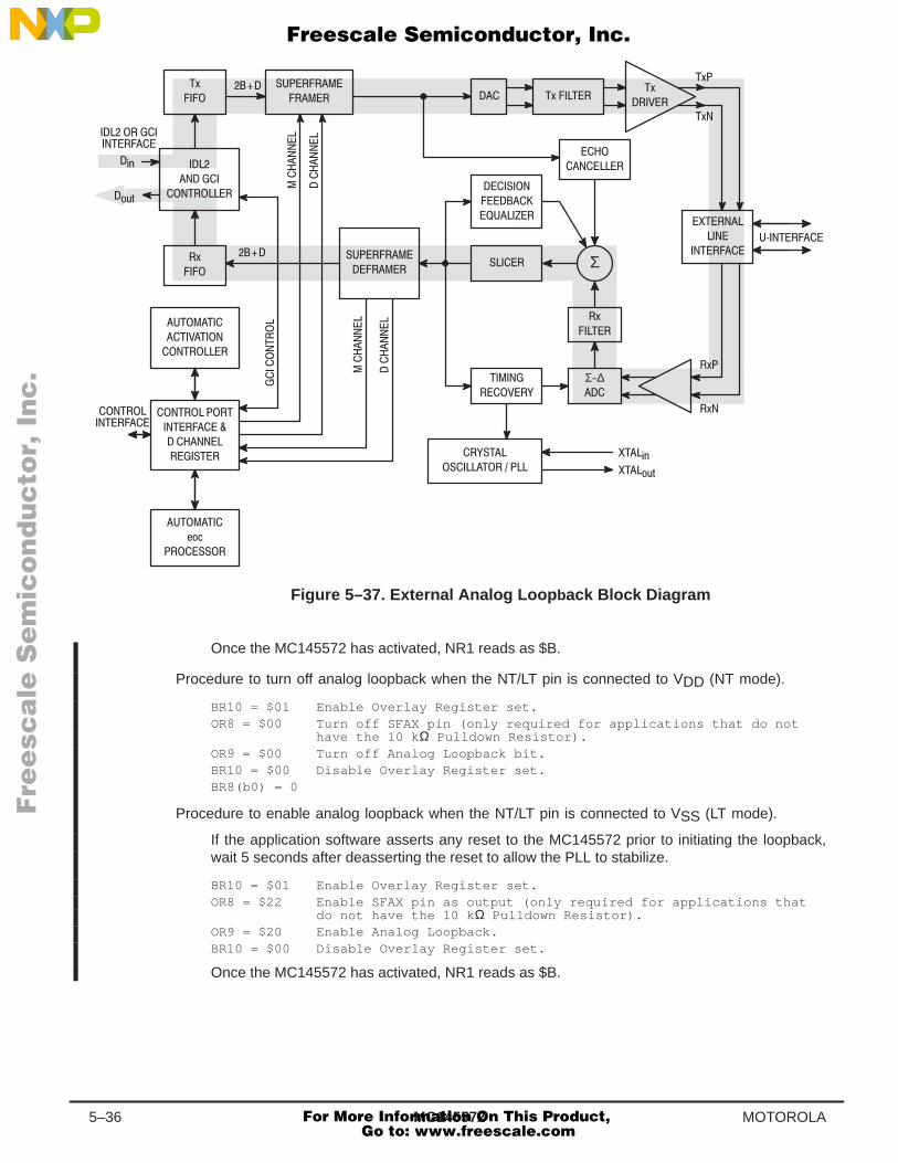
MC1455725–36 MOTOROLA
Σ(
&
&
&
&
&
&
&
&
&
Σ∆
#
!"
#%$
!"
#%$
Figure 5–37. External Analog Loop back Block Diagram
Once the MC145572 has activated, NR1 reads as $B.
Procedure to turn off analog loopback when the NT/LT pin is connected to VDD (NT mode).
BR10 = $01 Enable Overlay Register set.OR8 = $00 Turn off SFAX pin (only required for applications that do not
have the 10 k Ω Pulldown Resistor).OR9 = $00 Turn off Analog Loopback bit.BR10 = $00 Disable Overlay Register set.BR8(b0) = 0
Procedure to enable analog loopback when the NT/LT pin is connected to VSS (LT mode).
If the application software asserts any reset to the MC145572 prior to initiating the loopback,wait 5 seconds after deasserting the reset to allow the PLL to stabilize.
BR10 = $01 Enable Overlay Register set.OR8 = $22 Enable SFAX pin as output (only required for applications that
do not have the 10 k Ω Pulldown Resistor).OR9 = $20 Enable Analog Loopback.BR10 = $00 Disable Overlay Register set.
Once the MC145572 has activated, NR1 reads as $B.
Fre
esc
ale
Se
mic
on
du
cto
r, I
Freescale Semiconductor, Inc.
For More Information On This Product, Go to: www.freescale.com
nc
...
MC145572 5–37MOTOROLA
Procedure to turn off analog loopback when the NT/LT pin is connected to VSS (LT mode).
BR10 = $01 Enable Overlay Register set.OR8 = $00 Turn off SFAX pin (only required for applications that do not
have the 10 k Ω Pulldown Resistor).OR9 = $00 Turn off Analog Loopback bit.BR10 = $00 Disable Overlay Register set.
NOTE
In LT mode, the enabling/disabling of the SFAX pin is only required if the pin has not beentied to ground through a 10 kΩ resistor.
! "
Systems having multiple NT mode U transceivers on a TDM bus come in two types of architectures.
System Type No. 1: One U transceiver is configured as the TDM master and the others areconfigured as TDM slaves.
System Type No. 2: All U transceivers are configured as TDM slaves. One U transceiver isselected to provide a locked system clock from which is derived the DCL and FSR/FSX signalsthat are provided to all U transceivers. Typically, in these systems there is a mux that allowsthe locked clock to be selected from one of the U transceivers. This allows any transceiver toprovide the master clock. The clock source can come from the FREQREF pin (see OR8(b4)description), BUFXTAL pin, or SYSCLK pin. See Section 5.6.4 for further background material.
The external analog loopback can be done on only one MC145572 at a time.
System Type No. 1: The transceiver that the loopback test is performed on is put into mastermode. The others are put into slave mode.
System Type No. 2: Enable the mux to select its reference clock source from the transceiver onwhich the loopback test is being performed.
Procedure to perform the MC145572 external analog loopback while in NT slave mode.
Make sure that there is a 10 kΩ pulldown resistor on the SFAX pin.
Set BR8(b0) = 1, to put the selected MC145572 into LT mode.
Wait 5 seconds for the MC145572 on–chip PLL to stabilize.
BR10 = $01
OR9 = $20
BR10 = $00
NR2 = $01
Configure the IDL bus or timeslot assigner for the bus format required to send/receive data withthe MC145572.
The MC145572 is ready for loopback test when NR1 reads as $0B.
To turn off the loopback.
BR10 = $01
OR9 = $00
BR10 = $00
Fre
esc
ale
Se
mic
on
du
cto
r, I
Freescale Semiconductor, Inc.
For More Information On This Product, Go to: www.freescale.com
nc
...

MC1455725–38 MOTOROLA
Fre
esc
ale
Se
mic
on
du
cto
r, I
Freescale Semiconductor, Inc.
For More Information On This Product, Go to: www.freescale.com
nc
...
MC145572 6–1MOTOROLA
This chapter describes the activation and deactivation procedure for the MC145572. It is assumedthat MC145572 is configured for the IDL2 mode of operation. The material covered in this chapteris useful for all applications. It is strongly recommended that this chapter be read when the GCI modeoperation is to be used. Chapter 8 gives a detailed functional description of the GCI mode operationincluding the activation and deactivation time flow diagrams.
Activation or start–up is the process U–interface transceivers use to initiate a robust full–duplex com-munications channel. This process, which may be initiated from either the LT or NT mode U–interfacetransceiver, is a well–defined sequence of procedures during which the training of the equalizers andecho cancellers at each end of the transmission line takes place. Two types of activation, cold startor warm start, may occur. The MC145572 is capable of automatically supporting both types.
Deactivation is the process used to gracefully end communication between the U–interface trans-ceivers at each end of the transmission line. Only the LT mode U–interface transceiver may initiatea deactivation procedure.
ANSI T1.601–1992 defines ten activation signals, described in Tables 6–1 and 6–2, for the U–interfacetransceivers to use during the activation procedure. For instance, six basic frames of signal TN aretransmitted by the NT when it wants to wake up the LT or in response to the LT transmitting TL. Twobasic frames of signal TL are transmitted by the LT when it wants to wake up the NT. When the NTis in the fully operational mode, it transmits the signal known as SN3 and receives SL3 from the LTend. Conversely, when the LT is in fully operational mode, it transmits SL3 and receives SN3. Onlywhen the U–interface is fully activated, with the NT transmitting signal SN3 and the LT transmittingSL3, are the 2B+D channels of data capable of being transmitted over the U–interface.
ANSI T1.601–1992 defines the M4 channel act bit, see BR0(b7) and BR1(b7), which signals thefar–end U–interface transceiver that the near–end is capable of transparently passing 2B+D data.Figure 6–1 shows the activation diagram from the ANSI T1.601 specification. This figure can be usedin conjunction with this text to understand the activation sequence.
Fre
esc
ale
Se
mic
on
du
cto
r, I
Freescale Semiconductor, Inc.
For More Information On This Product, Go to: www.freescale.com
nc
...
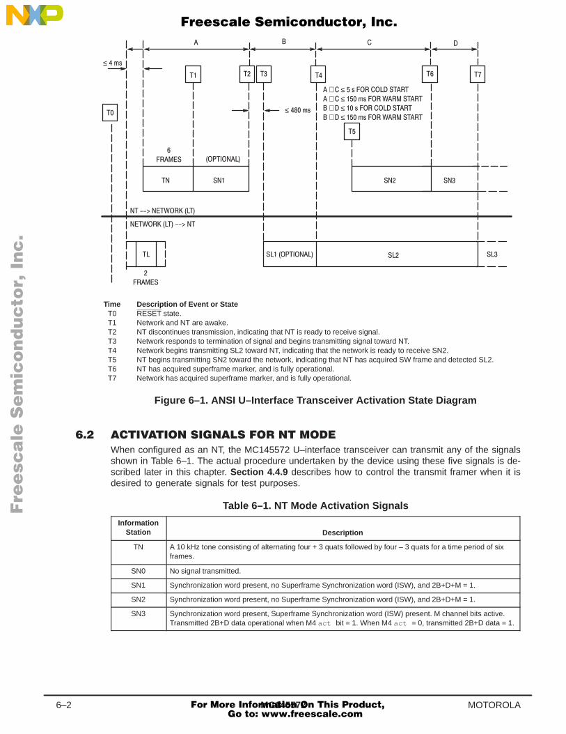
MC1455726–2 MOTOROLA
≤ !
+ ≤ ! + ≤ ! + ≤ ! + ≤ !
Time Description of Event or StateT0 RESET state.T1 Network and NT are awake.T2 NT discontinues transmission, indicating that NT is ready to receive signal.T3 Network responds to termination of signal and begins transmitting signal toward NT.T4 Network begins transmitting SL2 toward NT, indicating that the network is ready to receive SN2.T5 NT begins transmitting SN2 toward the network, indicating that NT has acquired SW frame and detected SL2.T6 NT has acquired superframe marker, and is fully operational.T7 Network has acquired superframe marker, and is fully operational.
≤ !
Figure 6–1. ANSI U–Interface Transceiver Activation State Diagram
When configured as an NT, the MC145572 U–interface transceiver can transmit any of the signalsshown in Table 6–1. The actual procedure undertaken by the device using these five signals is de-scribed later in this chapter. Section 4.4.9 describes how to control the transmit framer when it isdesired to generate signals for test purposes.
Table 6–1. NT Mode Activation Signals
ÁÁÁÁÁÁÁÁÁÁ
InformationStation
ÁÁÁÁÁÁÁÁÁÁÁÁÁÁÁÁÁÁÁÁÁÁÁÁÁÁÁÁÁÁÁÁÁÁÁÁÁÁÁÁÁÁÁÁÁÁÁÁÁÁÁÁDescriptionÁÁÁÁÁ
ÁÁÁÁÁÁÁÁÁÁ
TNÁÁÁÁÁÁÁÁÁÁÁÁÁÁÁÁÁÁÁÁÁÁÁÁÁÁÁÁÁÁÁÁÁÁÁÁÁÁÁÁÁÁÁÁÁÁÁÁÁÁÁÁÁÁÁÁÁÁÁÁÁÁÁÁÁÁÁÁÁÁÁÁÁÁÁÁÁÁ
A 10 kHz tone consisting of alternating four + 3 quats followed by four – 3 quats for a time period of sixframes.
ÁÁÁÁÁÁÁÁÁÁ
SN0 ÁÁÁÁÁÁÁÁÁÁÁÁÁÁÁÁÁÁÁÁÁÁÁÁÁÁÁÁÁÁÁÁÁÁÁÁÁÁÁÁÁÁÁÁÁÁÁÁÁÁÁÁ
No signal transmitted.ÁÁÁÁÁÁÁÁÁÁ
SN1 ÁÁÁÁÁÁÁÁÁÁÁÁÁÁÁÁÁÁÁÁÁÁÁÁÁÁÁÁÁÁÁÁÁÁÁÁÁÁÁÁÁÁÁÁÁÁÁÁÁÁÁÁ
Synchronization word present, no Superframe Synchronization word (ISW), and 2B+D+M = 1.ÁÁÁÁÁÁÁÁÁÁ
SN2 ÁÁÁÁÁÁÁÁÁÁÁÁÁÁÁÁÁÁÁÁÁÁÁÁÁÁÁÁÁÁÁÁÁÁÁÁÁÁÁÁÁÁÁÁÁÁÁÁÁÁÁÁ
Synchronization word present, no Superframe Synchronization word (ISW), and 2B+D+M = 1.ÁÁÁÁÁÁÁÁÁÁÁÁÁÁÁ
SN3 ÁÁÁÁÁÁÁÁÁÁÁÁÁÁÁÁÁÁÁÁÁÁÁÁÁÁÁÁÁÁÁÁÁÁÁÁÁÁÁÁÁÁÁÁÁÁÁÁÁÁÁÁÁÁÁÁÁÁÁÁÁÁÁÁÁÁÁÁÁÁÁÁÁÁÁÁÁÁ
Synchronization word present, Superframe Synchronization word (ISW) present. M channel bits active.Transmitted 2B+D data operational when M4 act bit = 1. When M4 act = 0, transmitted 2B+D data = 1.
Fre
esc
ale
Se
mic
on
du
cto
r, I
Freescale Semiconductor, Inc.
For More Information On This Product, Go to: www.freescale.com
nc
...
MC145572 6–3MOTOROLA
When configured as an LT, the MC145572 U–interface transceiver can transmit any of the signalsshown in Table 6–2. The actual procedure undertaken by the device using these five signals is de-scribed later in this chapter. Section 4.4.9 describes how to control the transmit framer when it isdesired to generate signals for test purposes.
Table 6–2. LT Mode Activation Signals
ÁÁÁÁÁÁÁÁÁÁ
InformationStation
ÁÁÁÁÁÁÁÁÁÁÁÁÁÁÁÁÁÁÁÁÁÁÁÁÁÁÁÁÁÁÁÁÁÁÁÁÁÁÁÁÁÁÁÁÁÁÁÁÁÁÁÁDescriptionÁÁÁÁÁ
ÁÁÁÁÁTLÁÁÁÁÁÁÁÁÁÁÁÁÁÁÁÁÁÁÁÁÁÁÁÁÁÁÁÁÁÁÁÁÁÁÁÁÁÁÁÁÁÁÁÁÁÁÁÁÁÁÁÁA 10 kHz tone consisting of alternating four + 3 quats followed by four – 3 quats for a time period of two frames.ÁÁÁÁÁ
ÁÁÁÁÁSL0ÁÁÁÁÁÁÁÁÁÁÁÁÁÁÁÁÁÁÁÁÁÁÁÁÁÁÁÁÁÁÁÁÁÁÁÁÁÁÁÁÁÁÁÁÁÁÁÁÁÁÁÁNo signal transmitted.ÁÁÁÁÁ
ÁÁÁÁÁSL1ÁÁÁÁÁÁÁÁÁÁÁÁÁÁÁÁÁÁÁÁÁÁÁÁÁÁÁÁÁÁÁÁÁÁÁÁÁÁÁÁÁÁÁÁÁÁÁÁÁÁÁÁSynchronization word present, no Superframe Synchronization word (ISW), and 2B+D+M = 1.ÁÁÁÁÁ
ÁÁÁÁÁSL2ÁÁÁÁÁÁÁÁÁÁÁÁÁÁÁÁÁÁÁÁÁÁÁÁÁÁÁÁÁÁÁÁÁÁÁÁÁÁÁÁÁÁÁÁÁÁÁÁÁÁÁÁSynchronization word present, Superframe Synchronization word (ISW) present, 2B+D = 0, and M = Normal.ÁÁÁÁÁ
ÁÁÁÁÁÁÁÁÁÁ
SL3ÁÁÁÁÁÁÁÁÁÁÁÁÁÁÁÁÁÁÁÁÁÁÁÁÁÁÁÁÁÁÁÁÁÁÁÁÁÁÁÁÁÁÁÁÁÁÁÁÁÁÁÁÁÁÁÁÁÁÁÁÁÁÁÁÁÁÁÁÁÁÁÁÁÁÁÁÁÁ
Synchronization word present, Superframe Synchronization word (ISW) present. M channel bits active.Transmitted 2B+D data operational when M4 act bit = 1. When M4 act = 0, transmitted 2B+D data = 0.
The MC145572 U–interface transceiver can be activated in either of two ways. The external microcon-troller can explicitly issue Activation Request (NR2(b3) = 1) or the transceiver detects an incoming10 kHz wake–up tone. An LT configured U–interface transceiver searches for an NT sending the TNwake–up tone. An NT configured U–interface transceiver searches for an LT sending the TL wake–uptone. In IDL2 mode, the Activation in Progress status bit (NR1(b0)) is set to a 1 when an incoming10 kHz wake–up tone is detected. In either case, Activation Request being set or a wake–up tonebeing detected, the U–interface transceiver proceeds with activation automatically and signals theresult of the activation to the external microcontroller by setting status bits in NR1 to $B.
An NT configured U–interface transceiver always initiates activation by sending a TN tone to the LT.This is done in response to the LT sending a TL or when the Activation Request bit (NR2(b3)) is setto a 1.
An LT configured U–interface transceiver initiates activation by sending the TL tone when the Activa-tion Request bit is set to a 1 by an external microcontroller. The NT U–interface transceiver respondsto the TL tone by sending a TN tone back to the LT U–interface transceiver. Otherwise, the LT U–inter-face transceiver waits for an unsolicited incoming TN tone from the NT U–interface transceiver andself–activates. Regardless of how activation is initiated, the LT U–interface transceiver automaticallyactivates from the point where it detects the incoming TN tone from the NT transceiver.
When configured for MCU mode, all appropriate maintenance channel registers should be initializedprior to setting Activation Request (NR2(b3)) or immediately after detecting Activation in Progress(NR1(b0)) = 1. In GCI mode, the MC145572 automatically initializes the maintenance channel regis-ters.
Some applications, such as U–repeaters, may require longer than 15 seconds of activation time. The15–second activation timer can be disabled by setting Activation Timer Disable (BR11(b0)) to a 1.
NT mode activation initiation is accomplished by setting Activation Request (NR2(b3)) to a 1. TheNT U–interface transceiver initiates activation of the U–interface by transmitting TN for a time periodof six frames (9 ms) toward the LT. At this time, the NT U–interface transceiver also sets Activationin Progress (NR1(b0)) to a 1. Transmission of TN is immediately followed by transmission of SN1while the echo cancellers are trained.
From Figure 6–1, it can be seen that the NT transceiver has a period of time during activation wherethe LT end is guaranteed to be quiet. This is to permit the MC145572 to train its echo cancellers duringthe transmission of SN1.
Fre
esc
ale
Se
mic
on
du
cto
r, I
Freescale Semiconductor, Inc.
For More Information On This Product, Go to: www.freescale.com
nc
...
MC1455726–4 MOTOROLA
After the MC145572 ends transmission of SN1 it waits up to 480 ms for LT to transmit a signal, SL1 orSL2. The MC145572 then recovers timing information and transmits SN2. When full duplex operationhas been achieved, bits NR1(b3, b1, b0) are each set to a 1 and SN3 is enabled for transmission. SN3is transmitted with only the maintenance channel bits active until transparent 2B+D transmission isenabled by setting Customer Enable (NR2(b0)) to a 1, or the M4 channel act bit has been receivedwhen the MC145572 is configured for the Verified act mode. See BR9(b5,b4) for more about Verifiedact.
If SN3 is not reached within 15 seconds, activation is automatically aborted, Error Indication (NR1(b2))is set to a 1, and bits NR1(b3, b1, b0) are each reset to a 0. The 15–second activation timer is startedwhen Activation in Progress (NR1(b0)) is set to a 1. The Activation Request bit (NR2(b3)) is internallyreset to a 0 when Activation in Progress (NR1(b0)) is set to a 1.
LT mode activation initiation is accomplished by setting Activation Request (NR2(b3)) to a 1. The LTinitiates activation of the U–interface by transmitting TL for a period of two frames (3 ms) toward NT.At this time, the LT U–interface transceiver also sets Activation in Progress (NR1(b0)) to a 1. AfterLT stops sending TL, the NT transmits TN and SN1 and trains its echo cancellers. The LT then waitsfor loss of the far–end signals, TN and SN1.
Loss of TN and SN1 reception is immediately followed by the LT transmission of SL1, while the LTend echo cancellers are trained. From Figure 6–1, it can be seen that the LT transceiver has a periodof time during activation where the NT end is guaranteed to be quiet. This is to permit the MC145572to train its echo cancellers during the transmission of SL1 and part of SL2. During SL2, the MC145572looks for a far–end signal. The MC145572 then recovers timing information and trains for full duplexoperation. When full duplex operation has been achieved, NR1(b3, b1, b0) are each set to a 1 andSL3 is transmitted with the M channel bits active. The 2B+D channels become active when CustomerEnable (NR2(b0)) is set to a 1.
If activation continues for more than 15 seconds it is aborted, Error Indication (NR1(b2)) is set to a1, and bits NR1(b3,b1,b0) are each reset to a 0. The 15–second activation timer is started when Activa-tion in Progress (NR1(b0)) is set to a 1. Activation Request (NR2(b3)) is internally reset to a 0 whenActivation in Progress (NR1(b0)) is set to a 1.
The Linkup status bit (NR1(b3)) is used to signify that the loop is active. With MC145572 configuredas an NT, this corresponds to NT transmitting SN3 and receiving SL3. With MC145572 configuredas an LT, this corresponds to LT transmitting SL3 and receiving SN3. When the U–interface is fullyactive, Superframe Sync (NR1(b1)) and Linkup (NR1(b3)) are set to a 1.
When the LT U–interface transceiver is activated and ready to pass 2B+D data, the M4 channel actbit should be set per ANSI T1.601–1992. This is done by setting BR0(b7) to a 1. Also, it is requiredthat Customer Enable (NR1(b0)) be set to a 1 when the M4 channel verified act /dea mode is notenabled. This must be done after activation from the receive RESET state. Refer to Section 4.4.10 ,for more details on Verified act /dea and control of M4 channel bits.
Whenever the MC145572 detects loss of Superframe Synchronization, NR1 becomes $8 and an in-terrupt is generated if enabled. This indicates that loss of Superframe Synchronization has beendetected. When Superframe Synchronization is lost for more than 480 ms, MC145572 always deac-tivates and sets NR1 = $4 error indication, and issues an interrupt if enabled. When the error conditioncausing loss of Superframe Synchronization goes away before 480 ms has elapsed, NR1 returns to$B and an interrupt is generated if enabled. It is not necessary to set Customer Enable (NR2(b0)) toa 1 when NR1 returns to $B.
The MC145572 continually monitors the error on its recovered signal. If the internally monitored errorrate becomes too large, MC145572 loses data transparency and NR1 changes to $A or $8 and issuesan interrupt. Note that loss of Superframe Synchronization always means that data transparency islost, but loss of data transparency does not always mean that Superframe Synchronization is lost.Also, note that loss of signal always means that Superframe Synchronization is lost. There is no time
Fre
esc
ale
Se
mic
on
du
cto
r, I
Freescale Semiconductor, Inc.
For More Information On This Product, Go to: www.freescale.com
nc
...
MC145572 6–5MOTOROLA
limit on how long NR1 may read as $A when data transparency is lost. There is a 480–ms time limiton NR1 reading as $8. ANSI T1.601 only indicates that U–interface transceivers must deactivate whenSuperframe Synchronization or receive signal is lost for more than 480 ms. If the error condition goesaway, NR1 returns to $B and an interrupt is generated, if enabled.
Loss of Superframe Synchronization may be due to a high internally detected error rate on recovereddata or the temporary loss of received signal.
ANSI T1.601 specifies that NT can not initiate deactivation. The MC145572 deactivates to a warmstart condition when Deactivation Request (NR2(b2)) is set to a 1 prior to LT deactivating the U–inter-face. This should be done in response to the M4 channel dea bit being received as 0 by NT when theloop is active. If Deactivation Request (NR2(b2)) is not set to a 1 before LT deactivates the U–inter-face, MC145572 deactivates to a cold start condition and gives an error indication interrupt. Deacti-vation Request is automatically set if the M4 maintenance bits are operated with automatic verificationof activation and deactivation. So when LT deactivates the line, NT deactivates to a warm start condi-tion. See BR9(b5:b4) and OR7(b0) for more information.
ANSI T1.601 specifies that only LT can deactivate the U–interface. This is done in the MC145572by setting Deactivation Request (NR2(b2)) to a 1.
Prior to deactivating, LT should notify NT of the pending deactivation by clearing the M4 channel deabit towards NT for at least three superframes. Then, deactivate LT by setting Deactivation Request(NR2(b2)) to a 1.
The MC145572, when configured as an LT, has a mode in which the M4 channel can be updated andsent for exactly three superframes before deactivation occurs. This is done in the following manner.Set Superframe Update Disable (NR2(b1)) to a 1 to disable maintenance channel updates. Reset theM4 channel dea bit (BR0(b6)) to a 0 to indicate that the LT initiated deactivation. Reset SuperframeUpdate Disable (NR2(b1)) to a 0 and simultaneously set Deactivation Request (NR2(b2)) to a 1 tore–enable maintenance channel updates and initiate deactivation. The LT U–interface transceiverthen updates the maintenance channel Superframe Framer bits and sends exactly three superframeswith the M4 channel dea bit reset to a 0. The U–interface transceiver then deactivates per ANSIT1.601–1992.
The MC145572 comes out of hardware or software reset with customer data disabled. This corre-sponds to Customer Enable (NR2(b0)) reset to 0. When the M4 channel Verified act /dea mode is notused, it is required that Customer Enable (NR1(b0)) be set to a 1, to enable data transparency whenNR1 becomes $B after initial activation. The B1, B2, and D channels transmitted on the IDL interfaceare automatically enabled after the MC145572 activates. Data on the B1 channel from the U–inter-face corresponds to data in the B1 channel timeslot on the IDL interface. Data on the B2 channel fromthe U–interface corresponds to data on the B2 channel timeslot on the IDL interface. The B1 and B2channel timeslots on the IDL interface can be swapped by setting Swap B1/B2 (NR5(b0)) to a 1.
"$"" ""! $#
The received eoc, M4, M5, and M6 channel bits are available in registers R6, BR1, and BR3 oncelinkup has been attained. The Customer Enable bit (NR2(b0)) affects only the two B channels andthe D channel. See BR0 – BR3 and BR9 descriptions for a full description of the maintenance channelbits and their control.
Fre
esc
ale
Se
mic
on
du
cto
r, I
Freescale Semiconductor, Inc.
For More Information On This Product, Go to: www.freescale.com
nc
...
MC1455726–6 MOTOROLA
BR8(b7:b4), Frame State 3 through Frame State 0, indicates the current state of the SuperframeFramer. In a U–interface repeater, it may be necessary to have NT continue transmitting SN2 untilLT–configured MC145572 receives SN3. Software must monitor the transmit state at least once everymillisecond to determine when NT starts transmitting SN2. When start of SN2 transmission is de-tected, write $A to BR8(b7:b4) to hold the transmit framer in SN2. Once LT indicates full activation, thetransmit framer can be allowed to proceed to SN3 by writing $0 to BR8(b7:b4).
It may also be necessary to disable the 15–second activation timer in repeater applications. This isdone by setting Activation Timer Disable (BR11(b0)) to a 1 prior to initiating activation or when Activationin Progress, NR1 = $1, is detected.
Fre
esc
ale
Se
mic
on
du
cto
r, I
Freescale Semiconductor, Inc.
For More Information On This Product, Go to: www.freescale.com
nc
...
MC145572 7–1MOTOROLA
When configured for MCU mode operation, the MC145572 provides a very flexible interface to the4 kbps maintenance channel (M channel), defined in ANSI T1.601–1992. The maintenance channelconsists of 48 bits sent by both the LT and NT configured U–interface transceivers during the courseof a superframe. These 48 bits are divided into 6 subchannels, designated M1 through M6, each con-sisting of 8 bits per superframe. The eoc consists of M1, M2, and M3. The overhead bits, such as crc ,febe , act , and dea , are contained in subchannels M4, M5, and M6.
An external microcontroller can read from or write to the maintenance channel via the SCP or PCPinterfaces. Interrupts to an external microcontroller can be enabled when an eoc, M4, M5, or M6 chan-nel register is updated. Maintenance channel registers can be configured to update when a new valueis detected between successive superframes, when a bit changes, or when two or three successivesuperframes of a new value are detected. The M4 channel act bit, BR1(b7), can also be configuredto automatically enable or disable customer data when in NT or LT mode of operation. The M4 chan-nel dea bit, BR1(b6), can also be configured to automatically issue a deactivation request in NT modeof operation. The maintenance channel registers are updated only when Superframe Sync, NR1(b1),is set to a 1.
Sections 7.5 and 7.6 provide information of interest to designers of LULT/LUNT (Line Unit Like–LT/Line Unit Like–NT1) type line cards for use in digital loop carrier systems using end–to–end perfor-mance monitoring.
See the BR9 description in Section 4.4.10 for more details on maintenance channel register opera-tions. Figure 7–1 shows the relationship between the received superframe and when the interrupt lineis asserted when the appropriate interrupts have been enabled.
The text in this chapter is based on an ANSI T1.601 compliant application. Due to the flexibility ofthe MC145572 register interface, it can easily be used in proprietary applications.
#%
NOTE: Since the eoc register, R6, is updated after basic frames 4 and 8, IRQ2 can occur at either location, or both,depending on the setting of BR9(B7:b6).
"$!
febe
"$!
nebe
Figure 7–1. Maintenance Channel Interrupt Timing
Fre
esc
ale
Se
mic
on
du
cto
r, I
Freescale Semiconductor, Inc.
For More Information On This Product, Go to: www.freescale.com
nc
...
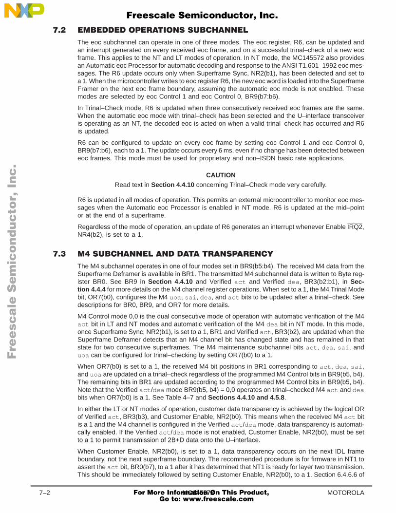
MC1455727–2 MOTOROLA
The eoc subchannel can operate in one of three modes. The eoc register, R6, can be updated andan interrupt generated on every received eoc frame, and on a successful trinal–check of a new eocframe. This applies to the NT and LT modes of operation. In NT mode, the MC145572 also providesan Automatic eoc Processor for automatic decoding and response to the ANSI T1.601–1992 eoc mes-sages. The R6 update occurs only when Superframe Sync, NR2(b1), has been detected and set toa 1. When the microcontroller writes to eoc register R6, the new eoc word is loaded into the SuperframeFramer on the next eoc frame boundary, assuming the automatic eoc mode is not enabled. Thesemodes are selected by eoc Control 1 and eoc Control 0, BR9(b7:b6).
In Trinal–Check mode, R6 is updated when three consecutively received eoc frames are the same.When the automatic eoc mode with trinal–check has been selected and the U–interface transceiveris operating as an NT, the decoded eoc is acted on when a valid trinal–check has occurred and R6is updated.
R6 can be configured to update on every eoc frame by setting eoc Control 1 and eoc Control 0,BR9(b7:b6), each to a 1. The update occurs every 6 ms, even if no change has been detected betweeneoc frames. This mode must be used for proprietary and non–ISDN basic rate applications.
CAUTIONRead text in Section 4.4.10 concerning Trinal–Check mode very carefully.
R6 is updated in all modes of operation. This permits an external microcontroller to monitor eoc mes-sages when the Automatic eoc Processor is enabled in NT mode. R6 is updated at the mid–pointor at the end of a superframe.
Regardless of the mode of operation, an update of R6 generates an interrupt whenever Enable IRQ2,NR4(b2), is set to a 1.
The M4 subchannel operates in one of four modes set in BR9(b5:b4). The received M4 data from theSuperframe Deframer is available in BR1. The transmitted M4 subchannel data is written to Byte reg-ister BR0. See BR9 in Section 4.4.10 and Verified act and Verified dea , BR3(b2:b1), in Sec-tion 4.4.4 for more details on the M4 channel register operations. When set to a 1, the M4 Trinal Modebit, OR7(b0), configures the M4 uoa , sai , dea , and act bits to be updated after a trinal–check. Seedescriptions for BR0, BR9, and OR7 for more details.
M4 Control mode 0,0 is the dual consecutive mode of operation with automatic verification of the M4act bit in LT and NT modes and automatic verification of the M4 dea bit in NT mode. In this mode,once Superframe Sync, NR2(b1), is set to a 1, BR1 and Verified act , BR3(b2), are updated when theSuperframe Deframer detects that an M4 channel bit has changed state and has remained in thatstate for two consecutive superframes. The M4 maintenance subchannel bits act , dea , sai , anduoa can be configured for trinal–checking by setting OR7(b0) to a 1.
When OR7(b0) is set to a 1, the received M4 bit positions in BR1 corresponding to act , dea , sai ,and uoa are updated on a trinal–check regardless of the programmed M4 Control bits in BR9(b5, b4).The remaining bits in BR1 are updated according to the programmed M4 Control bits in BR9(b5, b4).Note that the Verified act /dea mode BR9(b5, b4) = 0,0 operates on trinal–checked M4 act and deabits when OR7(b0) is a 1. See Table 4–7 and Sections 4.4.10 and 4.5.8.
In either the LT or NT modes of operation, customer data transparency is achieved by the logical ORof Verified act , BR3(b3), and Customer Enable, NR2(b0). This means when the received M4 act bitis a 1 and the M4 channel is configured in the Verified act /dea mode, data transparency is automati-cally enabled. If the Verified act /dea mode is not enabled, Customer Enable, NR2(b0), must be setto a 1 to permit transmission of 2B+D data onto the U–interface.
When Customer Enable, NR2(b0), is set to a 1, data transparency occurs on the next IDL frameboundary, not the next superframe boundary. The recommended procedure is for firmware in NT1 toassert the act bit, BR0(b7), to a 1 after it has determined that NT1 is ready for layer two transmission.This should be immediately followed by setting Customer Enable, NR2(b0), to a 1. Section 6.4.6.6 of
Fre
esc
ale
Se
mic
on
du
cto
r, I
Freescale Semiconductor, Inc.
For More Information On This Product, Go to: www.freescale.com
nc
...
MC145572 7–3MOTOROLA
ANSI T1.601–1992 indicates that data transparency may occur during the last superframe having itsact bit equal to 0 or during the first superframe having its act bit equal to 1.
In the NT mode of operation, the M4 dea bit is checked for a 0 and the logical OR of Verified dea ,BR3(b1), and deactivation Request, NR2(b2), ensures that the NT U–interface transceiver deactivatesin a controlled manner and will reactivate in warm start mode on a subsequent activation attempt.An interrupt is generated when BR1 is updated, if Enable IRQ1, NR4(b1), is set to a 1.
M4 Control mode 0,1 is the dual consecutive mode of operation. BR1 is updated when the SuperframeDeframer detects that an M4 subchannel bit has changed state and has remained in that state fortwo consecutive superframes and Superframe Sync, NR2(b1), is set to a 1. An interrupt is generatedat this time, if Enable IRQ1, NR4(b1), is set to a 1.
M4 Control mode 1,0 is the delta mode of operation. The M4 channel register is updated with newM4 channel data whenever any single bit changes between received M4 frames. An interrupt is gener-ated at this time, if Enable IRQ1, NR4(b1), is set to a 1.
M4 Control mode 1,1 updates the M4 channel register BR1 on every received superframe. In thismode, the Superframe Deframer does not check for a change in data between received M4 frames.An interrupt is generated at this time, if Enable IRQ1, NR4(b1), is set to a 1.
The M5 and M6 channels operate in the same modes as the M4 channel bits, except for the automaticverification mode. The received M5 and M6 data from the Superframe Deframer is available in BR2.See BR9 for details on the operating modes of the M5 and M6 channels. These channels are configuredas a pair. An interrupt is generated when BR2 is updated and Enable IRQ0, NR4(b0), is set to a 1.As defined by ANSI T1.601–1992, these are reserved maintenance channels and should be initializedto 1s. The M5 and M6 maintenance channels are available for proprietary applications which do nothave to comply with ANSI T1.601.
febe nebe
The MC145572 has extensive febe and nebe maintenance capabilities. The state of the receivedcomputed nebe and of the received febe is available through the register interface. Also, two indepen-dent febe and nebe counters are available for performance monitoring purposes.
The received febe from the last completed superframe is available in Received febe , BR3(b4). Itis updated at the end of each superframe when both Superframe Sync and Linkup, NR1(b3, b1), areset to a 1.
The febe /nebe Control bit, BR9(b1), controls operation of the transmitted febe status bit. WhenBR9(b1) is set to a 1, the transmitted febe bit is set to whatever is set in the febe input, BR2(b4).When BR9(b1) is reset to a 0, the transmitted febe is set active, if the computed nebe is active orif febe input, BR2(b4), is active. In this case, “active” means 0. BR9(b1) reset to 0 is the normal modeof operation and no intervention is required by an external MCU for the MC145572 to send the outgo-ing febe bit.
In NT and LT mode operation when BR9(b1) is set to a 1, BR2(b4) must be cleared to a 0 at theend of reception of basic frame 8 when it is desired to force an outgoing febe . BR2(b4) must beset to a 1 at the end of reception of basic frame 8 when no outgoing febe is required. Software shouldalways configure BR2(b4) for the correct outgoing febe once each superframe. In digital loop carrierapplications, this guarantees that there will be a one–to–one correspondence between the febestatus received from the digital carrier system and the febe transmitted on the U–interface. The febeis transmitted at the end of basic frame 2. See Figure 7–1 and Section 7.7 for interrupt timinginformation.
The computed nebe of the last completed superframe is available in Computed nebe , BR3(b3). Thisbit is set or cleared as a result of a crc of the last superframe received. This bit is updated at theend of each superframe. The Computed nebe is reset to a 0 when a crc error is detected, and isset to a 1 when no crc error is detected. When either Superframe Sync or Linkup, NR1(b3, b1), arereset to a 0, the Computed nebe bit is forced to a 0.
Fre
esc
ale
Se
mic
on
du
cto
r, I
Freescale Semiconductor, Inc.
For More Information On This Product, Go to: www.freescale.com
nc
...
MC1455727–4 MOTOROLA
The current febe count is maintained in BR4. The count in BR4 is incremented only when the re-ceived febe bit is detected active (0) at the end of the superframe. When OR7(b1) is a 0, the febecounter does not wrap around when the count reaches $FF. When OR7(b1) is a 1, the febe counterwraps around and continues counting from 0. Also, BR4 should be reset to 00 after Linkup is detectedduring activation. This is done by the external microcontroller writing 00 to BR4. The count is increm-ented when both Superframe Sync and Linkup in NR1(b1, b3) are set to a 1 and the received febebit is a 0. Received febe is available in BR3(b4) and is a 0 when active.
The current nebe count is maintained in BR5. The count in BR5 is incremented only when the Com-puted nebe bit is detected active (0) at the end of the superframe. The count is also incrementedonce per superframe during loss of synchronization, i.e., if Superframe Sync, NR2(b1), drops to a0 when Linkup, NR2(b3), is set to a 1. When OR7(b1) is a 0, the nebe counter does not wrap aroundwhen the count reaches $FF. When OR7(b1) is a 1, the nebe counter wraps around and continuescounting from 0. Also, BR5 should be reset to 00 after Linkup is detected during activation. This isdone by the external microcontroller writing 00 to BR5. The count is incremented when both Super-frame Sync and Linkup in NR1(b1, b3) are set to a 1 and when an error is detected in the receivedcrc . A Computed nebe is active when the received crc does not exactly match the calculated crcon the received superframe data. The Computed nebe is available in BR3(b3) and is a 0 when acrc error has been detected.
crc
The MC145572 provides a mechanism where the outgoing crc can be corrupted. The transmittedcrc is corrupted when BR8(b3) is set to a 1. The crc corruption is accomplished by inverting thetransmitted crc bits. See Table 7–1. The next two paragraphs are of particular interest to designersof digital loop carrier system LULT and LUNT type line cards.
In NT mode operation, when it is desired to corrupt the outgoing crc , BR8(b3) should be set at theend of reception of basic frame 4 and must be cleared at the end of reception of basic frame 8. Thisinverts the outgoing crc in transmitted basic frames 4, 5, 6, and 7 of the current transmitted super-frame. See Figure 7–2. When crc Corrupt mode, OR7(b2), is set to a 1, it is not necessary to clearBR8(b3), since it is cleared automatically at the end of the transmitted superframe. This guaranteesthat the corrupt crc will be transmitted only in the current superframe and that there will be a one–to–one correspondence between the corrupt crc status received from a digital carrier system and thecorrupt crc transmitted on the U–interface. See Section 7.7.
In LT mode operation, when it is desired to corrupt the outgoing crc , BR8(b3) should be set at theend of reception of basic frame 8 and must be cleared at the end of reception of basic frame 8. Thisinverts the outgoing crc in transmitted basic frames 1 through 8 of the current transmitted super-frame. See Figure 7–3. When crc Corrupt mode, OR7(b2), is set to a 1, it is not necessary to clearBR8(b3), since it is cleared automatically at the end of the transmitted superframe. This guaranteesthat the corrupt crc will be transmitted only in the current superframe and that there will be a one–to–one correspondence between the corrupt crc status received from a digital carrier system and thecorrupt crc transmitted on the U–interface. See Section 7.7.
Table 7–1. Transmitted crc Configuration
ÁÁÁÁÁÁÁÁÁÁ
BR8(b3)ÁÁÁÁÁÁÁÁÁÁ
OR9(b2)ÁÁÁÁÁÁÁÁÁÁÁÁÁÁÁÁÁÁÁÁÁÁÁÁÁÁÁÁÁÁÁÁÁÁÁÁÁÁÁÁ
Effect on Transmitted crc
ÁÁÁÁÁÁÁÁÁÁ
0 ÁÁÁÁÁÁÁÁÁÁ
X ÁÁÁÁÁÁÁÁÁÁÁÁÁÁÁÁÁÁÁÁÁÁÁÁÁÁÁÁÁÁÁÁÁÁÁÁÁÁÁÁ
No effect, transmitted crc is a good crc and far–end transceiver receivesit correctly. This is the default mode after any reset.
ÁÁÁÁÁÁÁÁÁÁÁÁÁÁÁÁÁÁÁÁ
1ÁÁÁÁÁÁÁÁÁÁÁÁÁÁÁÁÁÁÁÁ
0ÁÁÁÁÁÁÁÁÁÁÁÁÁÁÁÁÁÁÁÁÁÁÁÁÁÁÁÁÁÁÁÁÁÁÁÁÁÁÁÁÁÁÁÁÁÁÁÁÁÁÁÁÁÁÁÁÁÁÁÁÁÁÁÁÁÁÁÁÁÁÁÁÁÁÁÁÁÁÁÁ
Transmitted crc is continuously corrupted by inverting the crc symbols.This causes the far–end transceiver to detect crc errors. BR8(b3) must bereturned to a 0 to stop the transmission of bad crc s.
ÁÁÁÁÁÁÁÁÁÁ
1 ÁÁÁÁÁÁÁÁÁÁ
1 ÁÁÁÁÁÁÁÁÁÁÁÁÁÁÁÁÁÁÁÁÁÁÁÁÁÁÁÁÁÁÁÁÁÁÁÁÁÁÁÁ
Transmitted crc is corrupted only until the end of the current U–interfacesuperframe. Then BR8(b3) is cleared to 0.
Fre
esc
ale
Se
mic
on
du
cto
r, I
Freescale Semiconductor, Inc.
For More Information On This Product, Go to: www.freescale.com
nc
...
MC145572 7–5MOTOROLA
!
febe
! #%"
!
! #%"
!
nebe
! #%"
#%"
'
#%"
$&
$&
±
'
'
NOTE: Due to internal delays, the actual sync word marker on the TxP and TxN pins occurs 8 quats later than the TxSFS pulse.See Figure 10–20.
Figure 7–2. NT Mode Maintenance Channel Updates
Fre
esc
ale
Se
mic
on
du
cto
r, I
Freescale Semiconductor, Inc.
For More Information On This Product, Go to: www.freescale.com
nc
...
MC1455727–6 MOTOROLA
!
"
febe ! !
!
" $&#
!
"
!
" $&#
!
!
NOTE: Due to internal delays, the actual sync word marker on the TxP and TxN pins occurs 8 quats later than the TxSFS pulse.See Figure 10–20.
!
!
"
nebe ! !
!
" $&#
!
!
$&# !
( ! ! !
!
$&# !
!
! %'
! %'
!
(
(
Figure 7–3. LT Mode Maintenance Channel Updates
Fre
esc
ale
Se
mic
on
du
cto
r, I
Freescale Semiconductor, Inc.
For More Information On This Product, Go to: www.freescale.com
nc
...
MC145572 7–7MOTOROLA
The crc Corrupt mode bit, OR9(b2), modifies the operation of crc Corrupt, BR8(b3). When OR9(b2)is a 1, the operation of the crc Corrupt bit, BR8(b3), is modified so that a corrupt crc is transmittedonly to the end of the current U–interface superframe. Then BR8(b3) is cleared to a 0. If it is desiredto corrupt the transmitted crc again, then BR8(3) must be set to a 1 again. This is very useful fordigital loop carrier applications, since software does not have to clear BR8(b3) in order to guaranteea one–to–one correspondence between crc received from the digital loop carrier system and crc stransmitted onto the U–interface. For digital loop carrier applications, BR9(b1) is set to a 1 if it isdesired to have end–to–end performance monitoring. The outgoing febe should be updated at thesame time that the outgoing M4 channel register is updated. This update should be done for everysuperframe.
This section provides details on when interrupts are generated and when the internal SuperframeFramer reads maintenance channel registers to include their contents in the outgoing transmittedsuperframe. This information is particularly useful when designing LUNT and LULT line cards for digitalloop carrier systems. The basic frames and Quat positions are numbered as in the ANSI T1.601 specifi-cation. A Quat is the ANSI T1.601 term for the symbols transmitted over the U–interface. Basic framesare numbered from 1 through 8. The Quats in each basic frame are numbered from 1 through 120.
The M4, M5/M6, and eoc maintenance subchannels can be used for signalling in proprietary applica-tions. When the M4 or M5/M6 subchannels are configured to update on every received frame in thesubchannel, the update interval is 12 ms or once every superframe. The receive data interrupt forthe M5/M6 subchannel occurs at the end of basic frame 4. The receive data interrupt for the M4 channeloccurs at the end of the superframe or basic frame 8. See Figures 7–1, 7–2 and 7–3, and registerBR9 description for more details.
When the eoc subchannel is configured to update on every received eoc frame, the update intervalis 6 ms, or twice each superframe. The eoc receive data interrupt can occur at the end of basic frame4 or at the end of basic frame 8. See register description for BR9 for more details.
The receive and transmit registers for the maintenance channels are double buffered. Figure 7–2 indi-cates where maintenance channel registers are updated from the superframe received at NT. Fig-ure 7–2 also indicates the points where the U–interface transceiver transfers data from the mainte-nance channel registers into the transmitted superframe when the MC145572 is configured for NTmode. Figure 7–3 indicates where maintenance channel registers are updated from the superframereceived at the LT end of the loop. Figure 7–3 also indicates the points where the U–interface transceiv-er transfers data from the maintenance channel registers into the transmitted superframe when theMC145572 is configured for LT mode.
For digital loop carrier applications, maintenance channel registers R6, BR1, and BR3 must be pro-grammed to update on every received frame. Do not use trinal or dual consecutive checking. Thereason for this, is intermediate nodes need to do local processing of the eoc messages and musttransmit the messages upstream or downstream on a frame–by–frame basis. See explanations forByte register 9. Note that the eoc maintenance subchannel R6 is updated with a new received eocmessage twice each superframe. The MC145572 should be configured so that interrupts are generatedwhen BR1, BR3, and R6 are updated. See explanations for Nibble registers 3 and 4. The interruptfor BR3 (IRQ0) may not need to be enabled, since BR3 is updated at the same time as R6 at theend of a superframe. When an interrupt occurs, data can be read from the appropriate maintenancechannel register (BR1, BR3, or R6) and transmitted over the digital loop carrier system. At this time,the maintenance channel data that has been received from the digital loop carrier system can be writtento the registers for the outgoing superframe (BR0, BR2, or R6).
If the M4 channel and eoc interrupts are enabled to occur on the reception of every frame, it is possiblefor the software to determine if eoc interrupt has occurred at the end of basic frame 4 or at the endof basic frame 8. When eoc interrupt occurs at the end of basic frame 4, eoc interrupt status bit,NR3(b2), is set and M4 channel interrupt status bit, NR3(b1), is clear assuming that M4 channel regis-ter, BR1, was read immediately following the previous M4 channel interrupt. When eoc interrupt andM4 interrupts occur at the end of basic frame 8, both NR3(b2) and NR3(b1) are set.
The MC145572 does not provide any direct mechanism whereby an external microcontroller candetermine when registers, for outgoing maintenance data, can be updated. This timing must be
Fre
esc
ale
Se
mic
on
du
cto
r, I
Freescale Semiconductor, Inc.
For More Information On This Product, Go to: www.freescale.com
nc
...
MC1455727–8 MOTOROLA
derived from the interrupts generated when the receive maintenance subchannel registers areupdated. Figures 7–2 and 7–3 show the appropriate timings. It is possible to configure the TxSFS/SFAX/S0 pin as SFAX and use the pulse to generate a 12–ms periodic interrupt. Note though thatSFAX indicates the 2B+D frame in the IDL2 interface that will be transmitted onto the first 2B+Dposition in basic frame 1 of the U–interface superframe. Due to the internal FIFOs, it is not possibleto guarantee a fixed time between SFAX and the location of the superframe marker on the U–inter-face.
At the NT end, the ANSI T1.601 specification requires a turnaround delay of 60 ± 2 quats. TheMC145572 has a 60–quat turnaround time. This means that the transmitted Superframe Sync wordoccurs 60 quats later than the received Superframe Sync word. From an interrupt service routinepoint of view, updating BR0, BR2, and R6, the worst case time should be assumed to be 60 quats+ 117 quats = 177 quats, or 2.2 ms. The system software designer should allow extra margin to besafe. A quat is 12.5 µs in duration.
At the LT end of the loop, the received Superframe Sync word is 60 – 2 + 8 quats later than thetransmit Superframe Sync word. The 2–quat uncertainty comes from the ANSI T1.601 specificationfor NT turnaround time of 60 ± 2 quats on a 0 length loop. The + 8 figure includes worst case propa-gation delay on an 18,000–foot loop. From an interrupt service routine point of view, the worst caseassumption is that the receive Superframe Sync word occurs 68 quats after the transmitted Super-frame Sync word. For example, from Figure 7–3, the time between when R6 is updated with thereceive eoc data and when R6 must be updated with the transmitted eoc data, can be calculatedas follows: 117 – 68 = 49 quats or 612.5 µs. The system software designer should leave extra marginto be safe.
Fre
esc
ale
Se
mic
on
du
cto
r, I
Freescale Semiconductor, Inc.
For More Information On This Product, Go to: www.freescale.com
nc
...
MC145572 8–1MOTOROLA
The MC145572 is configurable for the General Circuit Interface or GCI operation. GCI is a time divi-sion multiplex bus, that combines the ISDN 2B+D data and control/status information onto four signalpins. There are two clocks per data bit and a single frame synchronization pulse, FSC.
In GCI mode, the MC145572 supports the full set of commands and indications over the Command/Indicate channel. The monitor channel is used for sending and receiving maintenance channel mes-sages and accessing the internal MC145572 registers.
As a GCI slave, the MC145572 accepts clock frequencies between 512 kHz and 8.192 MHz. As aGCI master, the MC145572 operates at either 512 kHz or 2.048 MHz. Figure 8–1 is a typical con-figuration for the MC145572 in GCI mode. The MC145572 is configured for GCI operation when theMCU/GCI pin is tied low. The PAR/SER pin must also be tied low.
Fre
esc
ale
Se
mic
on
du
cto
r, I
Freescale Semiconductor, Inc.
For More Information On This Product, Go to: www.freescale.com
nc
...
MC1455728–2 MOTOROLA
'
'$$
'
'$$
#$%
%%
&
!#$#
$
$)
/21
,.
%3!
%3
#3!
#3
'0*+!
&% $$
&%
#"
&%
&%
&)%
$
$
$
$
)%,.
)%/21
' '
#"#
-4
-4 … -4
&!
#&%
%
#
'
'$$
'$$
!'
! (#
$%%&$
%#
%$ %
$%
4
'#3
'$$#3
'%3
'$$%3
%3#/21
' $%#
' $'
' %
' %
µ
-Ω
µ
$ ' 4
' -4
'0*+
Figure 8–1. MC145572 Configuration for GCI Operation
Fre
esc
ale
Se
mic
on
du
cto
r, I
Freescale Semiconductor, Inc.
For More Information On This Product, Go to: www.freescale.com
nc
...
MC145572 8–3MOTOROLA
Table 8–1. GCI Master Mode ClockRate Selection
ÁÁÁÁÁÁÁÁÁÁÁÁÁÁÁÁ
Clock Rate ÁÁÁÁÁÁÁÁÁÁÁÁÁÁ
CLKSELÁÁÁÁÁÁÁÁÁÁÁÁÁÁÁÁ
512 kHz ÁÁÁÁÁÁÁÁÁÁÁÁÁÁ
0
ÁÁÁÁÁÁÁÁÁÁÁÁÁÁÁÁ
2.048 MHz ÁÁÁÁÁÁÁÁÁÁÁÁÁÁ
1
Seven signal pins are available for the time division multiplex bus interface in GCI mode.
• S2, S1, S0 — Used to select the active GCI channel in multiplexed GCI frames.
• DCL — 2x data clock.
• FSC — The 8 kHz frame synchronization pulse.
• Din — The MC145572 reads data from the GCI interface into this pin during the active GCI channelselected by S2, S1, S0.
• Dout — In GCI mode, this pin is an open drain output and must be pulled to VDD through a resistor.The MC145572 outputs data to the GCI interface from this pin during the active GCI channelselected by S2, S1, S0.
During all other GCI channels, if present, Dout is off. Din accepts data during the channel selectedby S0, S1, and S2. During other GCI channels, if present, Din ignores any data that is present.
The GCI interface supports two types of frame formats: the single GCI channel and the multiplexedGCI channel formats. A single GCI channel has the following subchannels: two B channels, Monitorchannel, ISDN D channel, Command/Indicate channel, and A and E bits. See Figure 8–2.
Referring to Figure 8–2, the two B channels are used to convey customer data between theMC145572 and other GCI devices. The Monitor channel bits are used to convey register and mainte-nance information between the MC145572 and other GCI devices. The D bits carry the ISDN basicaccess D channel. The Command/Indicate bits are used for activation and deactivation of theMC145572 and for control functions. The A and E bits are used as handshake signals during thetransfer of monitor channel messages.
A multiplexed GCI frame contains from two to eight GCI frames in each 125 µs period. Table 8–2summarizes the number of GCI frames that can be multiplexed into a 125 µs period. Figure 8–3shows how multiple GCI frames are multiplexed into a 125 µs period.
Table 8–2. Multiplexed GCI Frame Configuration
ÁÁÁÁÁÁÁÁÁÁÁÁ
ModeÁÁÁÁÁÁÁÁÁÁÁÁ
ClockÁÁÁÁÁÁÁÁÁÁÁÁÁÁÁÁÁÁÁÁ
Maximum GCI Framesin Multiplex
ÁÁÁÁÁÁÁÁÁÁÁÁ
GCI MasterÁÁÁÁÁÁÁÁÁÁÁÁ
512 kHzÁÁÁÁÁÁÁÁÁÁÁÁÁÁÁÁÁÁÁÁ
1ÁÁÁÁÁÁÁÁÁÁÁÁ
GCI MasterÁÁÁÁÁÁÁÁÁÁÁÁ
2.048 MHzÁÁÁÁÁÁÁÁÁÁÁÁÁÁÁÁÁÁÁÁ
4ÁÁÁÁÁÁÁÁÁÁÁÁ
GCI SlaveÁÁÁÁÁÁÁÁÁÁÁÁ
512 kHzÁÁÁÁÁÁÁÁÁÁÁÁÁÁÁÁÁÁÁÁ
1ÁÁÁÁÁÁÁÁÁÁÁÁ
GCI SlaveÁÁÁÁÁÁÁÁÁÁÁÁ
4.096 MHzÁÁÁÁÁÁÁÁÁÁÁÁÁÁÁÁÁÁÁÁ
8
Fre
esc
ale
Se
mic
on
du
cto
r, I
Freescale Semiconductor, Inc.
For More Information On This Product, Go to: www.freescale.com
nc
...
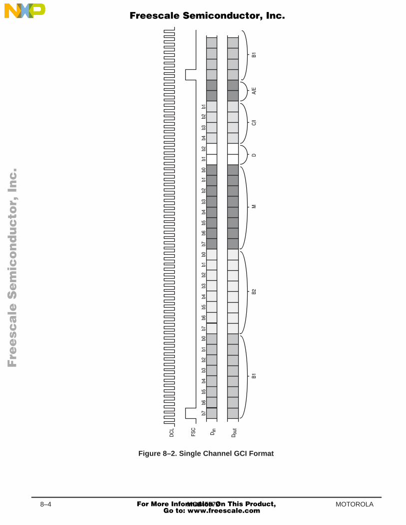
MC1455728–4 MOTOROLA
ÎÎÎÎ
ÎÎÎÎÎÎ
ÎÎ
ÎÎÎÎ
Figure 8–2. Single Channel GCI Format
Fre
esc
ale
Se
mic
on
du
cto
r, I
Freescale Semiconductor, Inc.
For More Information On This Product, Go to: www.freescale.com
nc
...
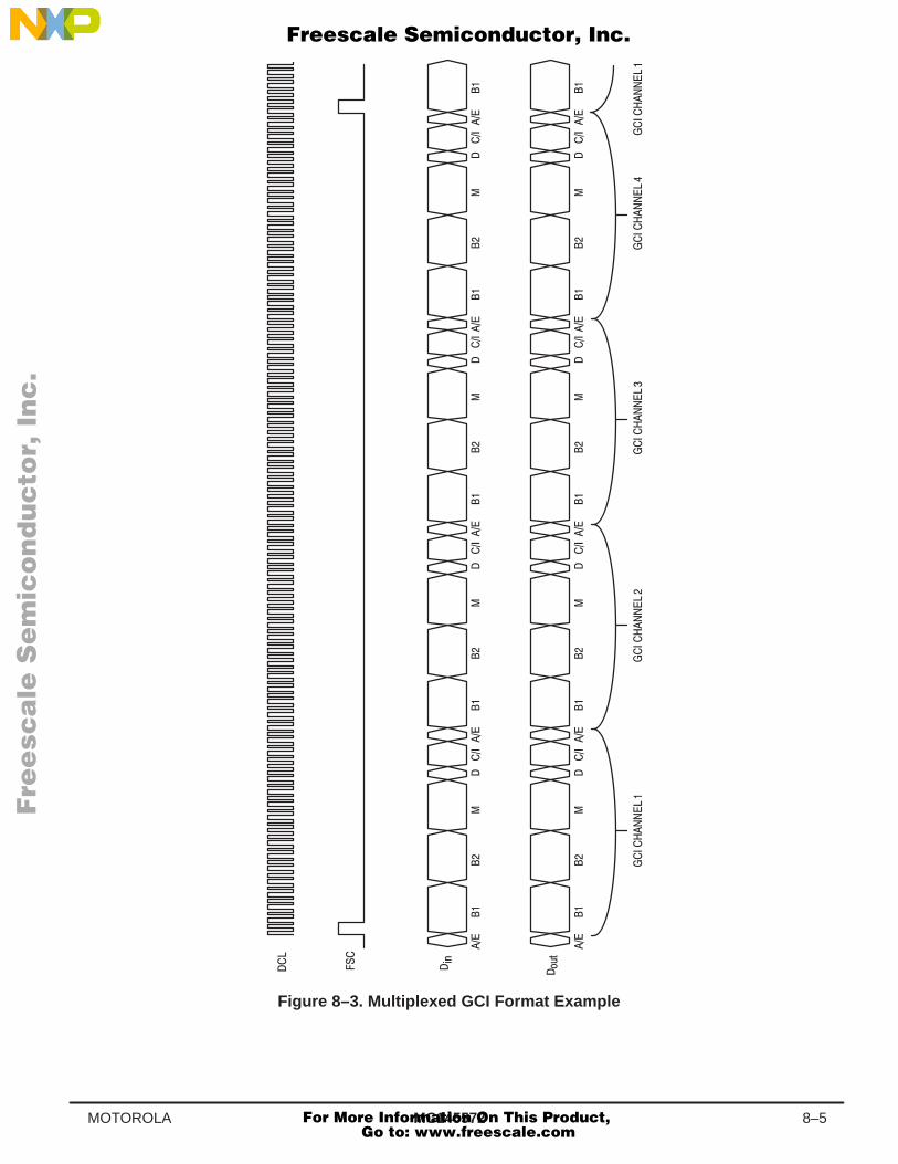
MC145572 8–5MOTOROLA
Figure 8–3. Multiplexed GCI Format Example
Fre
esc
ale
Se
mic
on
du
cto
r, I
Freescale Semiconductor, Inc.
For More Information On This Product, Go to: www.freescale.com
nc
...
MC1455728–6 MOTOROLA
! !
The Monitor channel is used to access the internal registers of the MC145572 in order to supportU–interface maintenance channel operations. All Monitor channel messages are two bytes in length.Each byte is sent twice to permit the receiving GCI device to verify data integrity. In ISDN applications,the Monitor channel is used for access to the U–interface maintenance messages.
The A and E bits in the GCI channel are used to control and acknowledge Monitor channel transfersbetween the MC145572 and another GCI device. When the Monitor channel is inactive, the A andthe E bit times from Dout are both high impedance. The A and E bits are active when they are drivento VSS during their respective bit times. Pull-up resistors are required on Din and Dout. The E bitindicates the transmission of a new Monitor channel byte. The A bit from the opposite direction isused to acknowledge the Monitor channel byte transfer.
An idle Monitor channel is indicated by both A and E bits being inactive for two GCI frames. The Aand E bits are high impedance when inactive. The Monitor channel data is $FF.
The originating GCI device transmits a byte onto the Monitor channel after receiving the A and E bitsequal to 1 for at least two consecutive GCI frames. The originating GCI device also sets its outgoingE bit to 0 in the same GCI frame as the byte that is transmitted. The transmitted byte is repeatedfor at least two GCI frames, or is repeated in subsequent GCI frames, until the MC145572 acknowl-edges receiving two consecutive GCI frames containing the same byte.
Once the MC145572 acknowledges the first byte, the sending device sets E to high impedance andtransmits the first frame of the second byte. Then, the second byte is repeated with the E bit low untilit is acknowledged. See Figures 8–4 through 8–8 for details of Monitor channel procedure.
The destination GCI device verifies that it has received the first byte by setting the A bit to 0 towardsthe originating GCI device for at least two GCI frames. Successive bytes are acknowledged by thereceiving device setting A to high impedance on the first instance of the next byte, followed by A beingcleared to 0 when the second instance of the byte is received.
The entire register set of the MC145572 can be accessed via the Monitor channel. All M4 channelactivity is automatically handled by the MC145572 when configured for GCI mode. The MC145572issues Monitor channel messages whenever the received eoc, M4, or M5/M6 messages receivedfrom the U–interface change, and appropriate dual–checking or trinal–checking of bits has beendone. In normal GCI operation it is not necessary to read or write the internal registers of theMC145572.
If the receiving GCI device does not receive the same Monitor channel byte in two consecutive GCIframes, it indicates this by leaving A = 0 until two consecutive identical bytes are received. The lastbyte of the sequence is indicated by the originating GCI device setting its E bit to a 1 for two succes-sive GCI frames. Figure 8–5 shows an example of an delayed GCI Monitor channel message.
!
The MC145572 supports three basic types of Monitor channel messages. The first group of mes-sages are commands that read or write the internal register set of the MC145572. See Chapter 4for a complete description of the MC145572 register set. The second group of messages areresponses from the MC145572. These responses are transmitted by the MC145572 after it receivesa register read or write command over the Monitor channel. The third group of Monitor channel mes-sages are interrupt indication messages. These are transmitted by the MC145572 whenever achange is detected in the Maintenance Channel Receive registers BR1, BR3, or R6.
A GCI device transmits Monitor channel commands to a receiving MC145572 to gain access to itsinternal register set. The receiving MC145572 then transmits a Monitor channel response messageonto the Monitor channel for commands that request data to be read from an internal register. Com-mands that write data to an internal MC145572 register are accepted and acted upon, but theMC145572 does not issue a response message. Monitor channel commands are given in Table 8–3.
The MC145572 acknowledges all messages it receives over the Monitor channel. If an invalid mes-sage is received, the MC145572 acknowledges it, but does not take any action.
Fre
esc
ale
Se
mic
on
du
cto
r, I
Freescale Semiconductor, Inc.
For More Information On This Product, Go to: www.freescale.com
nc
...
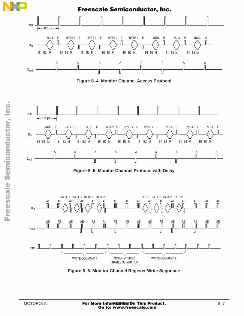
MC145572 8–7MOTOROLA
Figure 8–4. Monitor Channel Access Protocol
µ
Figure 8–5. Monitor Channel Protocol with Delay
µ
Figure 8–6. Monitor Channel Register Write Sequence
Fre
esc
ale
Se
mic
on
du
cto
r, I
Freescale Semiconductor, Inc.
For More Information On This Product, Go to: www.freescale.com
nc
...
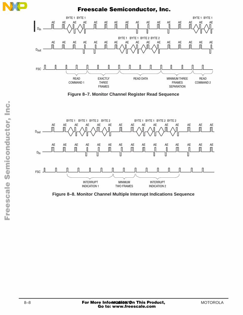
MC1455728–8 MOTOROLA
Figure 8–7. Monitor Channel Register Read Sequence
Figure 8–8. Monitor Channel Multiple Interrupt Indications Sequence
Fre
esc
ale
Se
mic
on
du
cto
r, I
Freescale Semiconductor, Inc.
For More Information On This Product, Go to: www.freescale.com
nc
...
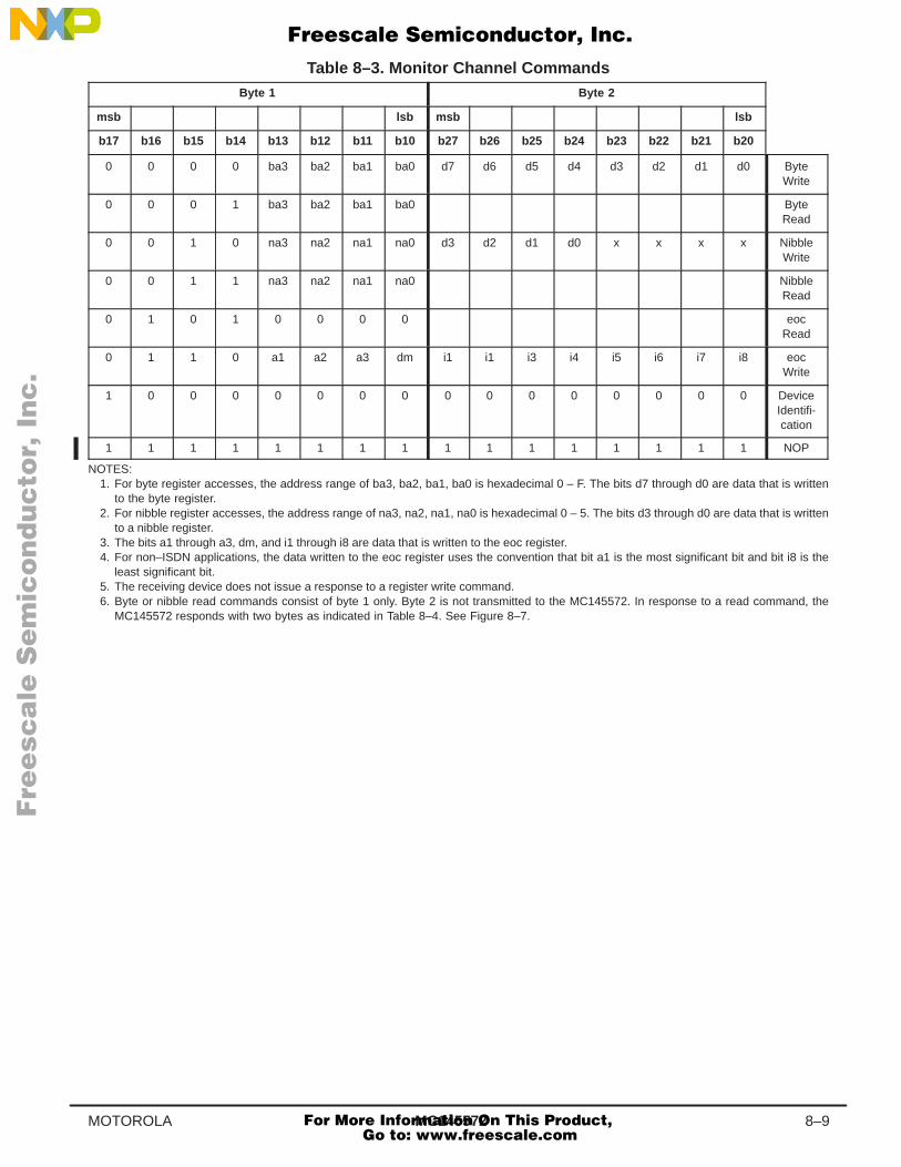
MC145572 8–9MOTOROLA
Table 8–3. Monitor Channel CommandsÁÁÁÁÁÁÁÁÁÁÁÁÁÁÁÁÁÁÁÁÁÁÁÁÁÁÁÁÁÁÁÁ
Byte 1 ÁÁÁÁÁÁÁÁÁÁÁÁÁÁÁÁÁÁÁÁÁÁÁÁÁÁÁÁÁÁÁÁ
Byte 2ÁÁÁÁÁÁ
msbÁÁÁÁÁÁÁÁÁÁÁÁÁÁÁÁÁÁÁÁÁÁÁÁÁÁÁÁÁÁÁÁÁÁÁÁÁÁÁÁ
lsbÁÁÁÁÁÁ
msbÁÁÁÁÁÁÁÁÁÁÁÁÁÁÁÁÁÁÁÁÁÁÁÁÁÁÁÁÁÁÁÁÁÁÁÁÁÁÁÁ
lsbÁÁÁÁÁÁ
b17ÁÁÁÁÁÁ
b16ÁÁÁÁÁÁ
b15ÁÁÁÁÁÁ
b14ÁÁÁÁÁÁ
b13ÁÁÁÁÁÁ
b12ÁÁÁÁ
b11ÁÁÁÁÁÁ
b10ÁÁÁÁÁÁ
b27ÁÁÁÁÁÁ
b26ÁÁÁÁÁÁ
b25ÁÁÁÁÁÁ
b24ÁÁÁÁÁÁ
b23ÁÁÁÁÁÁ
b22ÁÁÁÁ
b21ÁÁÁÁÁÁ
b20ÁÁÁÁÁÁÁÁÁ
0ÁÁÁÁÁÁÁÁÁ
0ÁÁÁÁÁÁÁÁÁ
0ÁÁÁÁÁÁÁÁÁ
0ÁÁÁÁÁÁÁÁÁ
ba3ÁÁÁÁÁÁÁÁÁ
ba2ÁÁÁÁÁÁ
ba1ÁÁÁÁÁÁÁÁÁ
ba0ÁÁÁÁÁÁÁÁÁ
d7ÁÁÁÁÁÁÁÁÁ
d6ÁÁÁÁÁÁÁÁÁ
d5ÁÁÁÁÁÁÁÁÁ
d4ÁÁÁÁÁÁÁÁÁ
d3ÁÁÁÁÁÁÁÁÁ
d2ÁÁÁÁÁÁ
d1ÁÁÁÁÁÁÁÁÁ
d0ÁÁÁÁÁÁÁÁÁÁÁÁ
ByteWrite
ÁÁÁÁÁÁÁÁÁ
0ÁÁÁÁÁÁÁÁÁ
0ÁÁÁÁÁÁÁÁÁ
0 ÁÁÁÁÁÁÁÁÁ
1 ÁÁÁÁÁÁÁÁÁ
ba3ÁÁÁÁÁÁÁÁÁ
ba2 ÁÁÁÁÁÁ
ba1ÁÁÁÁÁÁÁÁÁ
ba0ÁÁÁÁÁÁÁÁÁ
ÁÁÁÁÁÁÁÁÁ
ÁÁÁÁÁÁÁÁÁ
ÁÁÁÁÁÁÁÁÁ
ÁÁÁÁÁÁÁÁÁ
ÁÁÁÁÁÁÁÁÁ
ÁÁÁÁÁÁ
ÁÁÁÁÁÁÁÁÁ
ÁÁÁÁÁÁÁÁÁÁÁÁ
ByteRead
ÁÁÁÁÁÁ
0ÁÁÁÁÁÁ
0ÁÁÁÁÁÁ
1 ÁÁÁÁÁÁ
0 ÁÁÁÁÁÁ
na3ÁÁÁÁÁÁ
na2 ÁÁÁÁ
na1ÁÁÁÁÁÁ
na0ÁÁÁÁÁÁ
d3ÁÁÁÁÁÁ
d2ÁÁÁÁÁÁ
d1ÁÁÁÁÁÁ
d0 ÁÁÁÁÁÁ
x ÁÁÁÁÁÁ
x ÁÁÁÁ
xÁÁÁÁÁÁ
xÁÁÁÁÁÁÁÁ
NibbleWriteÁÁÁ
ÁÁÁÁÁÁ
0ÁÁÁÁÁÁÁÁÁ
0ÁÁÁÁÁÁÁÁÁ
1ÁÁÁÁÁÁÁÁÁ
1ÁÁÁÁÁÁÁÁÁ
na3ÁÁÁÁÁÁÁÁÁ
na2ÁÁÁÁÁÁ
na1ÁÁÁÁÁÁÁÁÁ
na0ÁÁÁÁÁÁÁÁÁ
ÁÁÁÁÁÁÁÁÁ
ÁÁÁÁÁÁÁÁÁ
ÁÁÁÁÁÁÁÁÁ
ÁÁÁÁÁÁÁÁÁ
ÁÁÁÁÁÁÁÁÁ
ÁÁÁÁÁÁ
ÁÁÁÁÁÁÁÁÁ
ÁÁÁÁÁÁÁÁÁÁÁÁ
NibbleRead
ÁÁÁÁÁÁÁÁÁ
0ÁÁÁÁÁÁÁÁÁ
1ÁÁÁÁÁÁÁÁÁ
0 ÁÁÁÁÁÁÁÁÁ
1 ÁÁÁÁÁÁÁÁÁ
0 ÁÁÁÁÁÁÁÁÁ
0 ÁÁÁÁÁÁ
0ÁÁÁÁÁÁÁÁÁ
0ÁÁÁÁÁÁÁÁÁ
ÁÁÁÁÁÁÁÁÁ
ÁÁÁÁÁÁÁÁÁ
ÁÁÁÁÁÁÁÁÁ
ÁÁÁÁÁÁÁÁÁ
ÁÁÁÁÁÁÁÁÁ
ÁÁÁÁÁÁ
ÁÁÁÁÁÁÁÁÁ
ÁÁÁÁÁÁÁÁÁÁÁÁ
eocRead
ÁÁÁÁÁÁÁÁÁ
0ÁÁÁÁÁÁÁÁÁ
1ÁÁÁÁÁÁÁÁÁ
1 ÁÁÁÁÁÁÁÁÁ
0 ÁÁÁÁÁÁÁÁÁ
a1 ÁÁÁÁÁÁÁÁÁ
a2 ÁÁÁÁÁÁ
a3ÁÁÁÁÁÁÁÁÁ
dmÁÁÁÁÁÁÁÁÁ
i1ÁÁÁÁÁÁÁÁÁ
i1ÁÁÁÁÁÁÁÁÁ
i3 ÁÁÁÁÁÁÁÁÁ
i4 ÁÁÁÁÁÁÁÁÁ
i5 ÁÁÁÁÁÁÁÁÁ
i6 ÁÁÁÁÁÁ
i7ÁÁÁÁÁÁÁÁÁ
i8ÁÁÁÁÁÁÁÁÁÁÁÁ
eocWrite
ÁÁÁÁÁÁÁÁÁ
1ÁÁÁÁÁÁÁÁÁ
0ÁÁÁÁÁÁÁÁÁ
0 ÁÁÁÁÁÁÁÁÁ
0 ÁÁÁÁÁÁÁÁÁ
0 ÁÁÁÁÁÁÁÁÁ
0 ÁÁÁÁÁÁ
0ÁÁÁÁÁÁÁÁÁ
0ÁÁÁÁÁÁÁÁÁ
0ÁÁÁÁÁÁÁÁÁ
0ÁÁÁÁÁÁÁÁÁ
0 ÁÁÁÁÁÁÁÁÁ
0 ÁÁÁÁÁÁÁÁÁ
0 ÁÁÁÁÁÁÁÁÁ
0 ÁÁÁÁÁÁ
0ÁÁÁÁÁÁÁÁÁ
0ÁÁÁÁÁÁÁÁÁÁÁÁ
DeviceIdentifi-cation
ÁÁÁÁÁÁ
1ÁÁÁÁÁÁ
1ÁÁÁÁÁÁ
1 ÁÁÁÁÁÁ
1 ÁÁÁÁÁÁ
1 ÁÁÁÁÁÁ
1 ÁÁÁÁ
1ÁÁÁÁÁÁ
1ÁÁÁÁÁÁ
1ÁÁÁÁÁÁ
1ÁÁÁÁÁÁ
1 ÁÁÁÁÁÁ
1 ÁÁÁÁÁÁ
1 ÁÁÁÁÁÁ
1 ÁÁÁÁ
1ÁÁÁÁÁÁ
1ÁÁÁÁÁÁÁÁ
NOP
NOTES:1. For byte register accesses, the address range of ba3, ba2, ba1, ba0 is hexadecimal 0 – F. The bits d7 through d0 are data that is written
to the byte register.2. For nibble register accesses, the address range of na3, na2, na1, na0 is hexadecimal 0 – 5. The bits d3 through d0 are data that is written
to a nibble register.3. The bits a1 through a3, dm, and i1 through i8 are data that is written to the eoc register.4. For non–ISDN applications, the data written to the eoc register uses the convention that bit a1 is the most significant bit and bit i8 is the
least significant bit.5. The receiving device does not issue a response to a register write command.6. Byte or nibble read commands consist of byte 1 only. Byte 2 is not transmitted to the MC145572. In response to a read command, the
MC145572 responds with two bytes as indicated in Table 8–4. See Figure 8–7.
Fre
esc
ale
Se
mic
on
du
cto
r, I
Freescale Semiconductor, Inc.
For More Information On This Product, Go to: www.freescale.com
nc
...
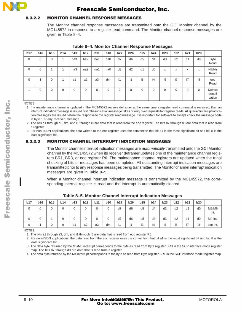
MC1455728–10 MOTOROLA
The Monitor channel response messages are transmitted onto the GCI Monitor channel by theMC145572 in response to a register read command. The Monitor channel response messages aregiven in Table 8–4.
Table 8–4. Monitor Channel Response Messages
ÁÁÁÁÁÁ
b17ÁÁÁÁÁÁ
b16ÁÁÁÁÁÁ
b15ÁÁÁÁÁÁ
b14ÁÁÁÁÁÁ
b13 ÁÁÁÁÁÁ
b12 ÁÁÁÁ
b11ÁÁÁÁÁÁ
b10ÁÁÁÁÁÁ
b27ÁÁÁÁÁÁ
b26ÁÁÁÁÁÁ
b25ÁÁÁÁÁÁ
b24ÁÁÁÁÁÁ
b23 ÁÁÁÁÁÁ
b22 ÁÁÁÁ
b21ÁÁÁÁÁÁ
b20ÁÁÁÁÁÁÁÁÁÁÁ
ÁÁÁ0ÁÁÁÁÁÁ
0ÁÁÁÁÁÁ
0 ÁÁÁÁÁÁ
1 ÁÁÁÁÁÁ
ba3ÁÁÁÁÁÁ
ba2 ÁÁÁÁ
ba1ÁÁÁÁÁÁ
ba0ÁÁÁÁÁÁ
d7ÁÁÁÁÁÁ
d6ÁÁÁÁÁÁ
d5ÁÁÁÁÁÁ
d4 ÁÁÁÁÁÁ
d3 ÁÁÁÁÁÁ
d2 ÁÁÁÁ
d1ÁÁÁÁÁÁ
d0ÁÁÁÁÁÁÁÁ
ByteReadÁÁÁ
ÁÁÁÁÁÁ
0ÁÁÁÁÁÁÁÁÁ
0ÁÁÁÁÁÁÁÁÁ
1ÁÁÁÁÁÁÁÁÁ
1ÁÁÁÁÁÁÁÁÁ
na3ÁÁÁÁÁÁÁÁÁ
na2ÁÁÁÁÁÁ
na1ÁÁÁÁÁÁÁÁÁ
na0ÁÁÁÁÁÁÁÁÁ
d3ÁÁÁÁÁÁÁÁÁ
d2ÁÁÁÁÁÁÁÁÁ
d1ÁÁÁÁÁÁÁÁÁ
d0ÁÁÁÁÁÁÁÁÁ
xÁÁÁÁÁÁÁÁÁ
xÁÁÁÁÁÁ
xÁÁÁÁÁÁÁÁÁ
xÁÁÁÁÁÁÁÁÁÁÁÁ
NibbleRead
ÁÁÁÁÁÁÁÁÁ
0ÁÁÁÁÁÁÁÁÁ
1ÁÁÁÁÁÁÁÁÁ
0ÁÁÁÁÁÁÁÁÁ
1ÁÁÁÁÁÁÁÁÁ
a1ÁÁÁÁÁÁÁÁÁ
a2ÁÁÁÁÁÁ
a3ÁÁÁÁÁÁÁÁÁ
dmÁÁÁÁÁÁÁÁÁ
i1ÁÁÁÁÁÁÁÁÁ
i1ÁÁÁÁÁÁÁÁÁ
i3ÁÁÁÁÁÁÁÁÁ
i4ÁÁÁÁÁÁÁÁÁ
i5ÁÁÁÁÁÁÁÁÁ
i6ÁÁÁÁÁÁ
i7ÁÁÁÁÁÁÁÁÁ
i8ÁÁÁÁÁÁÁÁÁÁÁÁ
eocRead
ÁÁÁÁÁÁÁÁÁ
1ÁÁÁÁÁÁÁÁÁ
0ÁÁÁÁÁÁÁÁÁ
0 ÁÁÁÁÁÁÁÁÁ
0 ÁÁÁÁÁÁÁÁÁ
0 ÁÁÁÁÁÁÁÁÁ
0 ÁÁÁÁÁÁ
0ÁÁÁÁÁÁÁÁÁ
0ÁÁÁÁÁÁÁÁÁ
0ÁÁÁÁÁÁÁÁÁ
0ÁÁÁÁÁÁÁÁÁ
0 ÁÁÁÁÁÁÁÁÁ
0 ÁÁÁÁÁÁÁÁÁ
0 ÁÁÁÁÁÁÁÁÁ
0 ÁÁÁÁÁÁ
0ÁÁÁÁÁÁÁÁÁ
0ÁÁÁÁÁÁÁÁÁÁÁÁ
DeviceIdentifi-cation
NOTES:1. If a maintenance channel is updated in the MC145572 receive deframer at the same time a register read command is received, then an
interrupt indication message is issued first. The indication message takes priority over requests for register reads. All queued interrupt indica-tion messages are issued before the response to the register read message. It is important for software to always check the message codein byte 1 of any received message.
2. The bits a1 through a3, dm, and i1 through i8 are data that is read from the eoc register. The bits d7 through d0 are data that is read froma register.
3. For non–ISDN applications, the data written to the eoc register uses the convention that bit a1 is the most significant bit and bit i8 is theleast significant bit.
The Monitor channel interrupt indication messages are automatically transmitted onto the GCI Monitorchannel by the MC145572 when its receiver deframer updates one of the maintenance channel regis-ters BR1, BR3, or eoc register R6. The maintenance channel registers are updated when the trinalchecking of bits or messages has been completed. All outstanding interrupt indication messages aretransmitted prior to any response messages being transmitted. The Monitor channel interrupt indicationmessages are given in Table 8–5.
When a Monitor channel interrupt indication message is transmitted by the MC145572, the corre-sponding internal register is read and the interrupt is automatically cleared.
Table 8–5. Monitor Channel Interrupt Indication MessagesÁÁÁÁÁÁb17ÁÁÁÁÁÁb16ÁÁÁÁÁÁb15ÁÁÁÁÁÁb14ÁÁÁÁÁÁb13ÁÁÁÁÁÁb12ÁÁÁÁb11ÁÁÁÁÁÁb10ÁÁÁÁÁÁb27ÁÁÁÁÁÁb26ÁÁÁÁÁÁb25ÁÁÁÁÁÁb24ÁÁÁÁÁÁb23ÁÁÁÁÁÁb22ÁÁÁÁb21ÁÁÁÁÁÁb20ÁÁÁÁÁÁÁÁÁÁÁ
ÁÁÁÁÁÁ
0ÁÁÁÁÁÁÁÁÁ
0ÁÁÁÁÁÁÁÁÁ
0ÁÁÁÁÁÁÁÁÁ
0ÁÁÁÁÁÁÁÁÁ
0ÁÁÁÁÁÁÁÁÁ
0ÁÁÁÁÁÁ
0ÁÁÁÁÁÁÁÁÁ
0ÁÁÁÁÁÁÁÁÁ
d7ÁÁÁÁÁÁÁÁÁ
d6ÁÁÁÁÁÁÁÁÁ
d5ÁÁÁÁÁÁÁÁÁ
d4ÁÁÁÁÁÁÁÁÁ
d3ÁÁÁÁÁÁÁÁÁ
d2ÁÁÁÁÁÁ
d1ÁÁÁÁÁÁÁÁÁ
d0ÁÁÁÁÁÁÁÁÁÁÁÁ
M5/M6int.
ÁÁÁÁÁÁ
0ÁÁÁÁÁÁ
0ÁÁÁÁÁÁ
1ÁÁÁÁÁÁ
0ÁÁÁÁÁÁ
0ÁÁÁÁÁÁ
0ÁÁÁÁ
0ÁÁÁÁÁÁ
0ÁÁÁÁÁÁ
d7ÁÁÁÁÁÁ
d6ÁÁÁÁÁÁ
d5ÁÁÁÁÁÁ
d4ÁÁÁÁÁÁ
d3ÁÁÁÁÁÁ
d2ÁÁÁÁ
d1ÁÁÁÁÁÁ
d0ÁÁÁÁÁÁÁÁ
M4 int.ÁÁÁÁÁÁ
0ÁÁÁÁÁÁ
1ÁÁÁÁÁÁ
0ÁÁÁÁÁÁ
0ÁÁÁÁÁÁ
a1ÁÁÁÁÁÁ
a2ÁÁÁÁ
a3ÁÁÁÁÁÁ
dmÁÁÁÁÁÁ
i1ÁÁÁÁÁÁ
i1ÁÁÁÁÁÁ
i3ÁÁÁÁÁÁ
i4ÁÁÁÁÁÁ
i5ÁÁÁÁÁÁ
i6ÁÁÁÁ
i7ÁÁÁÁÁÁ
i8ÁÁÁÁÁÁÁÁ
eoc int.
NOTES:1. The bits a1 through a3, dm, and i1 through i8 are data that is read from eoc register R6.2. For non–ISDN applications, the data read from the eoc register uses the convention that bit a1 is the most significant bit and bit i8 is the
least significant bit.3. The data byte returned by the M5/M6 interrupt corresponds to the byte as read from Byte register BR3 in the SCP interface mode register
map. The bits d7 through d0 are data that is read from a register.4. The data byte returned by the M4 interrupt corresponds to the byte as read from Byte register BR1 in the SCP interface mode register map.
Fre
esc
ale
Se
mic
on
du
cto
r, I
Freescale Semiconductor, Inc.
For More Information On This Product, Go to: www.freescale.com
nc
...
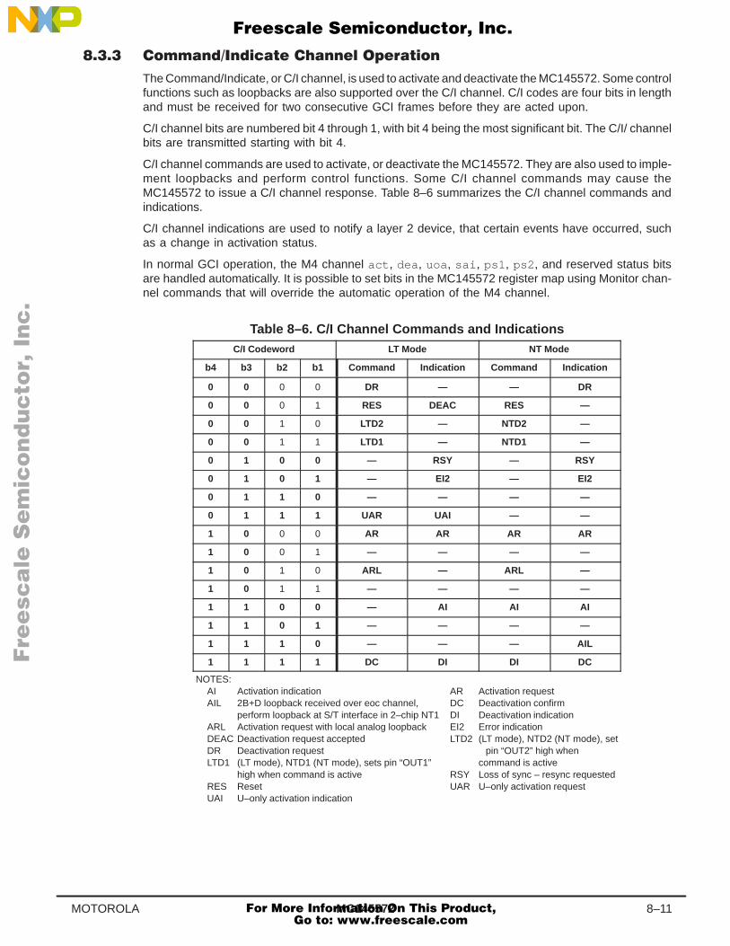
MC145572 8–11MOTOROLA
The Command/Indicate, or C/I channel, is used to activate and deactivate the MC145572. Some controlfunctions such as loopbacks are also supported over the C/I channel. C/I codes are four bits in lengthand must be received for two consecutive GCI frames before they are acted upon.
C/I channel bits are numbered bit 4 through 1, with bit 4 being the most significant bit. The C/I/ channelbits are transmitted starting with bit 4.
C/I channel commands are used to activate, or deactivate the MC145572. They are also used to imple-ment loopbacks and perform control functions. Some C/I channel commands may cause theMC145572 to issue a C/I channel response. Table 8–6 summarizes the C/I channel commands andindications.
C/I channel indications are used to notify a layer 2 device, that certain events have occurred, suchas a change in activation status.
In normal GCI operation, the M4 channel act , dea , uoa , sai , ps1 , ps2 , and reserved status bitsare handled automatically. It is possible to set bits in the MC145572 register map using Monitor chan-nel commands that will override the automatic operation of the M4 channel.
Table 8–6. C/I Channel Commands and IndicationsÁÁÁÁÁÁÁÁÁÁÁÁÁÁÁÁÁÁ
C/I Codeword ÁÁÁÁÁÁÁÁÁÁÁÁÁÁÁÁÁÁ
LT Mode ÁÁÁÁÁÁÁÁÁÁÁÁÁÁÁÁ
NT Mode
ÁÁÁÁÁÁ
b4ÁÁÁÁÁÁ
b3 ÁÁÁÁÁÁ
b2 ÁÁÁÁÁÁ
b1 ÁÁÁÁÁÁÁÁÁÁ
Command ÁÁÁÁÁÁÁÁÁÁ
Indication ÁÁÁÁÁÁÁÁ
CommandÁÁÁÁÁÁÁÁÁÁ
Indication
ÁÁÁÁÁÁ
0 ÁÁÁÁÁÁ
0 ÁÁÁÁÁÁ
0 ÁÁÁÁÁÁ
0 ÁÁÁÁÁÁÁÁÁÁ
DR ÁÁÁÁÁÁÁÁÁÁ
— ÁÁÁÁÁÁÁÁ
— ÁÁÁÁÁÁÁÁÁÁ
DRÁÁÁÁÁÁ
0 ÁÁÁÁÁÁ
0 ÁÁÁÁÁÁ
0 ÁÁÁÁÁÁ
1 ÁÁÁÁÁÁÁÁÁÁ
RES ÁÁÁÁÁÁÁÁÁÁ
DEAC ÁÁÁÁÁÁÁÁ
RES ÁÁÁÁÁÁÁÁÁÁ
—ÁÁÁÁÁÁ
0 ÁÁÁÁÁÁ
0 ÁÁÁÁÁÁ
1 ÁÁÁÁÁÁ
0 ÁÁÁÁÁÁÁÁÁÁ
LTD2 ÁÁÁÁÁÁÁÁÁÁ
— ÁÁÁÁÁÁÁÁ
NTD2 ÁÁÁÁÁÁÁÁÁÁ
—ÁÁÁÁÁÁ
0 ÁÁÁÁÁÁ
0 ÁÁÁÁÁÁ
1 ÁÁÁÁÁÁ
1 ÁÁÁÁÁÁÁÁÁÁ
LTD1 ÁÁÁÁÁÁÁÁÁÁ
— ÁÁÁÁÁÁÁÁ
NTD1 ÁÁÁÁÁÁÁÁÁÁ
—ÁÁÁÁÁÁ
0 ÁÁÁÁÁÁ
1 ÁÁÁÁÁÁ
0 ÁÁÁÁÁÁ
0 ÁÁÁÁÁÁÁÁÁÁ
— ÁÁÁÁÁÁÁÁÁÁ
RSY ÁÁÁÁÁÁÁÁ
— ÁÁÁÁÁÁÁÁÁÁ
RSYÁÁÁÁÁÁ
0 ÁÁÁÁÁÁ
1 ÁÁÁÁÁÁ
0 ÁÁÁÁÁÁ
1 ÁÁÁÁÁÁÁÁÁÁ
— ÁÁÁÁÁÁÁÁÁÁ
EI2 ÁÁÁÁÁÁÁÁ
— ÁÁÁÁÁÁÁÁÁÁ
EI2ÁÁÁÁÁÁ
0 ÁÁÁÁÁÁ
1 ÁÁÁÁÁÁ
1 ÁÁÁÁÁÁ
0 ÁÁÁÁÁÁÁÁÁÁ
— ÁÁÁÁÁÁÁÁÁÁ
— ÁÁÁÁÁÁÁÁ
— ÁÁÁÁÁÁÁÁÁÁ
—ÁÁÁÁÁÁ
0 ÁÁÁÁÁÁ
1 ÁÁÁÁÁÁ
1 ÁÁÁÁÁÁ
1 ÁÁÁÁÁÁÁÁÁÁ
UAR ÁÁÁÁÁÁÁÁÁÁ
UAI ÁÁÁÁÁÁÁÁ
— ÁÁÁÁÁÁÁÁÁÁ
—ÁÁÁÁÁÁ
1 ÁÁÁÁÁÁ
0 ÁÁÁÁÁÁ
0 ÁÁÁÁÁÁ
0 ÁÁÁÁÁÁÁÁÁÁ
AR ÁÁÁÁÁÁÁÁÁÁ
AR ÁÁÁÁÁÁÁÁ
AR ÁÁÁÁÁÁÁÁÁÁ
ARÁÁÁÁÁÁ
1 ÁÁÁÁÁÁ
0 ÁÁÁÁÁÁ
0 ÁÁÁÁÁÁ
1 ÁÁÁÁÁÁÁÁÁÁ
— ÁÁÁÁÁÁÁÁÁÁ
— ÁÁÁÁÁÁÁÁ
— ÁÁÁÁÁÁÁÁÁÁ
—ÁÁÁÁÁÁ
1 ÁÁÁÁÁÁ
0 ÁÁÁÁÁÁ
1 ÁÁÁÁÁÁ
0 ÁÁÁÁÁÁÁÁÁÁ
ARL ÁÁÁÁÁÁÁÁÁÁ
— ÁÁÁÁÁÁÁÁ
ARL ÁÁÁÁÁÁÁÁÁÁ
—ÁÁÁÁÁÁ
1 ÁÁÁÁÁÁ
0 ÁÁÁÁÁÁ
1 ÁÁÁÁÁÁ
1 ÁÁÁÁÁÁÁÁÁÁ
— ÁÁÁÁÁÁÁÁÁÁ
— ÁÁÁÁÁÁÁÁ
— ÁÁÁÁÁÁÁÁÁÁ
—ÁÁÁÁÁÁ
1 ÁÁÁÁÁÁ
1 ÁÁÁÁÁÁ
0 ÁÁÁÁÁÁ
0 ÁÁÁÁÁÁÁÁÁÁ
— ÁÁÁÁÁÁÁÁÁÁ
AI ÁÁÁÁÁÁÁÁ
AI ÁÁÁÁÁÁÁÁÁÁ
AIÁÁÁÁÁÁ
1 ÁÁÁÁÁÁ
1 ÁÁÁÁÁÁ
0 ÁÁÁÁÁÁ
1 ÁÁÁÁÁÁÁÁÁÁ
— ÁÁÁÁÁÁÁÁÁÁ
— ÁÁÁÁÁÁÁÁ
— ÁÁÁÁÁÁÁÁÁÁ
—ÁÁÁÁÁÁ
1 ÁÁÁÁÁÁ
1 ÁÁÁÁÁÁ
1 ÁÁÁÁÁÁ
0 ÁÁÁÁÁÁÁÁÁÁ
— ÁÁÁÁÁÁÁÁÁÁ
— ÁÁÁÁÁÁÁÁ
— ÁÁÁÁÁÁÁÁÁÁ
AILÁÁÁÁÁÁ
1 ÁÁÁÁÁÁ
1 ÁÁÁÁÁÁ
1 ÁÁÁÁÁÁ
1 ÁÁÁÁÁÁÁÁÁÁ
DC ÁÁÁÁÁÁÁÁÁÁ
DI ÁÁÁÁÁÁÁÁ
DI ÁÁÁÁÁÁÁÁÁÁ
DC
NOTES:AI Activation indication AR Activation requestAIL 2B+D loopback received over eoc channel, DC Deactivation confirm
perform loopback at S/T interface in 2–chip NT1 DI Deactivation indicationARL Activation request with local analog loopback EI2 Error indicationDEAC Deactivation request accepted LTD2 (LT mode), NTD2 (NT mode), setDR Deactivation request pin “OUT2” high whenLTD1 (LT mode), NTD1 (NT mode), sets pin “OUT1” command is active
high when command is active RSY Loss of sync – resync requestedRES Reset UAR U–only activation requestUAI U–only activation indication
Fre
esc
ale
Se
mic
on
du
cto
r, I
Freescale Semiconductor, Inc.
For More Information On This Product, Go to: www.freescale.com
nc
...
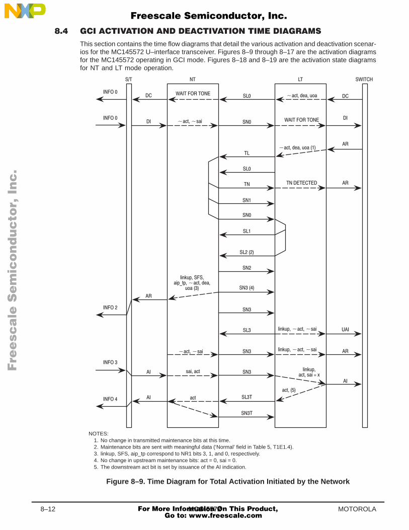
MC1455728–12 MOTOROLA
This section contains the time flow diagrams that detail the various activation and deactivation scenar-ios for the MC145572 U–interface transceiver. Figures 8–9 through 8–17 are the activation diagramsfor the MC145572 operating in GCI mode. Figures 8–18 and 8–19 are the activation state diagramsfor NT and LT mode operation.
ÎÎÎÎÎÎÎÎÎÎÎÎÎÎÎÎÎÎÎÎÎÎÎÎÎÎÎÎÎÎÎÎÎÎ
ÎÎÎÎÎÎÎÎÎÎÎÎÎÎÎÎÎÎÎÎÎÎÎÎÎÎÎÎÎÎÎÎÎÎÎÎÎÎÎÎÎÎÎÎÎÎÎÎÎÎÎÎÎÎÎÎÎÎÎÎÎÎÎÎÎÎÎÎÎÎÎÎÎÎÎÎÎÎÎÎÎÎÎÎÎÎÎÎÎÎÎÎÎÎÎÎÎÎÎÎÎÎÎÎÎÎÎÎÎÎÎÎÎÎÎÎÎÎÎÎÎÎÎÎÎÎÎÎÎÎÎÎÎÎÎÎÎÎÎÎÎÎÎÎÎÎÎÎÎÎÎÎÎÎÎÎÎÎÎÎÎÎÎÎÎÎÎÎÎÎÎÎÎÎÎÎÎÎÎÎÎÎÎÎÎÎÎÎÎÎÎÎÎÎÎÎÎÎÎÎÎÎÎÎ
ÎÎÎÎÎÎÎÎÎÎÎÎÎÎÎÎÎÎÎÎÎÎÎÎÎÎÎÎÎÎÎÎÎÎÎÎÎÎÎÎÎÎÎÎÎÎÎÎÎÎÎÎÎÎÎÎÎÎÎÎÎÎÎÎÎÎÎÎÎÎÎÎÎÎÎÎÎÎÎÎÎÎÎÎÎÎÎÎÎÎÎÎÎÎÎÎÎÎÎÎÎÎÎÎÎÎÎÎÎÎÎÎÎÎÎÎÎÎÎÎÎÎÎÎÎÎÎÎÎÎÎÎÎÎÎÎÎÎÎÎÎÎÎÎÎÎÎÎÎÎÎÎÎÎÎÎÎÎÎÎÎÎÎÎÎÎÎÎÎÎÎÎÎÎÎÎÎÎÎÎÎÎÎÎÎÎÎÎÎÎÎÎÎÎÎÎÎÎÎÎÎÎÎÎ
ÎÎÎÎÎÎÎÎÎÎÎÎÎÎÎÎÎÎÎÎÎÎÎÎÎÎÎÎÎÎÎÎÎÎ
'! (
(
#!$")&('!
( )%
('!
( )%
#!$")&( '! *
(
NOTES:1. No change in transmitted maintenance bits at this time.2. Maintenance bits are sent with meaningful data (‘Normal’ field in Table 5, T1E1.4).3. linkup, SFS, aip_tp correspond to NR1 bits 3, 1, and 0, respectively.4. No change in upstream maintenance bits: act = 0, sai = 0.5. The downstream act bit is set by issuance of the AI indication.
('! #!$")&('!
#!$")& !&(&(
)%
Figure 8–9. Time Diagram for Total Activation Initiated by the Network
Fre
esc
ale
Se
mic
on
du
cto
r, I
Freescale Semiconductor, Inc.
For More Information On This Product, Go to: www.freescale.com
nc
...
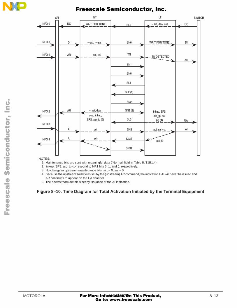
MC145572 8–13MOTOROLA
ÎÎÎÎÎÎÎÎÎÎÎÎÎÎÎÎÎÎÎÎÎÎÎÎ
ÎÎÎÎÎÎÎÎÎÎÎÎÎÎÎÎÎÎÎÎÎÎÎÎÎÎÎÎÎÎÎÎÎÎÎÎÎÎÎÎÎÎÎÎÎÎÎÎÎÎÎÎÎÎÎÎÎÎÎÎÎÎÎÎÎÎÎÎÎÎÎÎÎÎÎÎÎÎÎÎÎÎÎÎÎÎÎÎÎÎÎÎÎÎÎÎÎÎÎÎÎÎÎÎÎÎÎÎÎÎÎÎÎÎÎÎÎÎÎÎÎÎÎÎÎÎÎÎÎÎÎÎÎÎÎÎÎÎÎÎÎÎÎÎ
ÎÎÎÎÎÎÎÎÎÎÎÎÎÎÎÎÎÎÎÎÎÎÎÎÎÎÎÎÎÎÎÎÎÎÎÎÎÎÎÎÎÎÎÎÎÎÎÎÎÎÎÎÎÎÎÎÎÎÎÎÎÎÎÎÎÎÎÎÎÎÎÎÎÎÎÎÎÎÎÎÎÎÎÎÎÎÎÎÎÎÎÎÎÎÎÎÎÎÎÎÎÎÎÎÎÎÎÎÎÎÎÎÎÎÎÎÎÎÎÎÎÎÎÎÎÎÎÎÎÎÎÎÎÎÎÎÎÎÎÎÎÎÎÎ
ÎÎÎÎÎÎÎÎÎÎÎÎÎÎÎÎÎÎÎÎÎÎÎÎ
( )%
('!
( '!
)% #!$")&
!&(&
#!$")&
!&(& '!
( ( '! *
( (
NOTES:1. Maintenance bits are sent with meaningful data (‘Normal’ field in Table 5, T1E1.4).2. linkup, SFS, aip_tp correspond to NR1 bits 3, 1, and 0, respectively.3. No change in upstream maintenance bits: act = 0, sai = 0.4. Because the upstream sai bit was set by the (upstream) AR command, the indication UAI will never be issued and
AR continues to appear on the C/I channel.5. The downstream act bit is set by issuance of the AI indication.
(
Figure 8–10. Time Diagram for Total Activation Initiated by the Terminal Equipment
Fre
esc
ale
Se
mic
on
du
cto
r, I
Freescale Semiconductor, Inc.
For More Information On This Product, Go to: www.freescale.com
nc
...
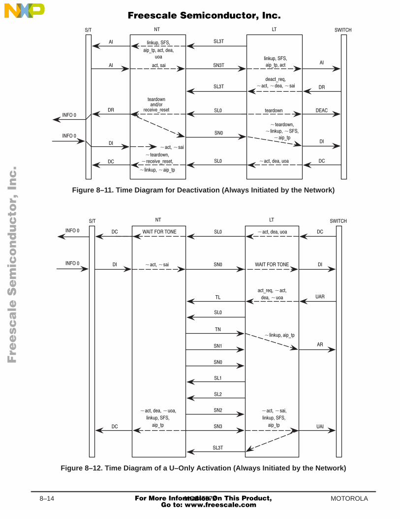
MC1455728–14 MOTOROLA
ÎÎÎÎÎÎÎÎÎÎÎÎÎÎÎÎÎÎÎÎÎÎÎÎÎÎÎÎÎÎ
ÎÎÎÎÎÎÎÎÎÎÎÎÎÎÎÎÎÎÎÎÎÎÎÎÎÎÎÎÎÎÎÎÎÎÎÎÎÎÎÎÎÎÎÎÎÎÎÎÎÎÎÎÎÎÎÎÎÎÎÎÎÎÎÎÎÎÎÎÎÎÎÎÎÎÎÎÎÎÎÎÎÎÎÎÎÎÎÎÎÎÎÎÎÎÎÎÎÎÎÎÎÎÎÎÎ
ÎÎÎÎÎÎÎÎÎÎÎÎÎÎÎÎÎÎÎÎÎÎÎÎÎÎÎÎÎÎÎÎÎÎÎÎÎÎÎÎÎÎÎÎÎÎÎÎÎÎÎÎÎÎÎÎÎÎÎÎÎÎÎÎÎÎÎÎÎÎÎÎÎÎÎÎÎÎÎÎÎÎÎÎÎÎÎÎÎÎÎÎÎÎÎÎÎÎÎÎÎÎÎÎÎ
ÎÎÎÎÎÎÎÎÎÎÎÎÎÎÎÎÎÎÎÎÎÎÎÎÎÎÎÎÎÎ
&!
!%! %
&!
% $
%#"
%$
%# ( #
#'#$% %# (
%$
%# (
&!
!%!
% & %# (
#'#$%
&!!%!
!%! %
&
Figure 8–11. Time Diagram for Deactivation (Always Initiated by the Network)
ÎÎÎÎÎÎÎÎÎÎÎÎÎÎÎÎÎÎÎÎÎÎÎÎÎÎÎÎÎÎÎÎÎÎÎÎÎÎÎÎÎÎÎÎÎÎÎÎ
ÎÎÎÎÎÎÎÎÎÎÎÎÎÎÎÎÎÎÎÎÎÎÎÎÎÎÎÎÎÎÎÎÎÎÎÎÎÎÎÎÎÎÎÎÎÎÎÎÎÎÎÎÎÎÎÎÎÎÎÎÎÎÎÎÎÎÎÎÎÎÎÎÎÎÎÎÎÎÎÎÎÎÎÎÎÎÎÎÎÎÎÎÎÎÎÎÎÎÎÎÎÎÎÎÎÎÎÎÎÎÎÎÎÎÎÎÎÎÎÎÎÎÎÎÎÎÎÎÎÎÎÎÎÎÎÎÎÎÎÎÎÎÎÎ
ÎÎÎÎÎÎÎÎÎÎÎÎÎÎÎÎÎÎÎÎÎÎÎÎÎÎÎÎÎÎÎÎÎÎÎÎÎÎÎÎÎÎÎÎÎÎÎÎÎÎÎÎÎÎÎÎÎÎÎÎÎÎÎÎÎÎÎÎÎÎÎÎÎÎÎÎÎÎÎÎÎÎÎÎÎÎÎÎÎÎÎÎÎÎÎÎÎÎÎÎÎÎÎÎÎÎÎÎÎÎÎÎÎÎÎÎÎÎÎÎÎÎÎÎÎÎÎÎÎÎÎÎÎÎÎÎÎÎÎÎÎÎÎÎ
ÎÎÎÎÎÎÎÎÎÎÎÎÎÎÎÎÎÎÎÎÎÎÎÎ
% &
%$
%#"%
&
% &
&!
!%!
&! !%!
%$
&!
!%!
Figure 8–12. Time Diagram of a U–Only Activation (Always Initiated by the Network)
Fre
esc
ale
Se
mic
on
du
cto
r, I
Freescale Semiconductor, Inc.
For More Information On This Product, Go to: www.freescale.com
nc
...
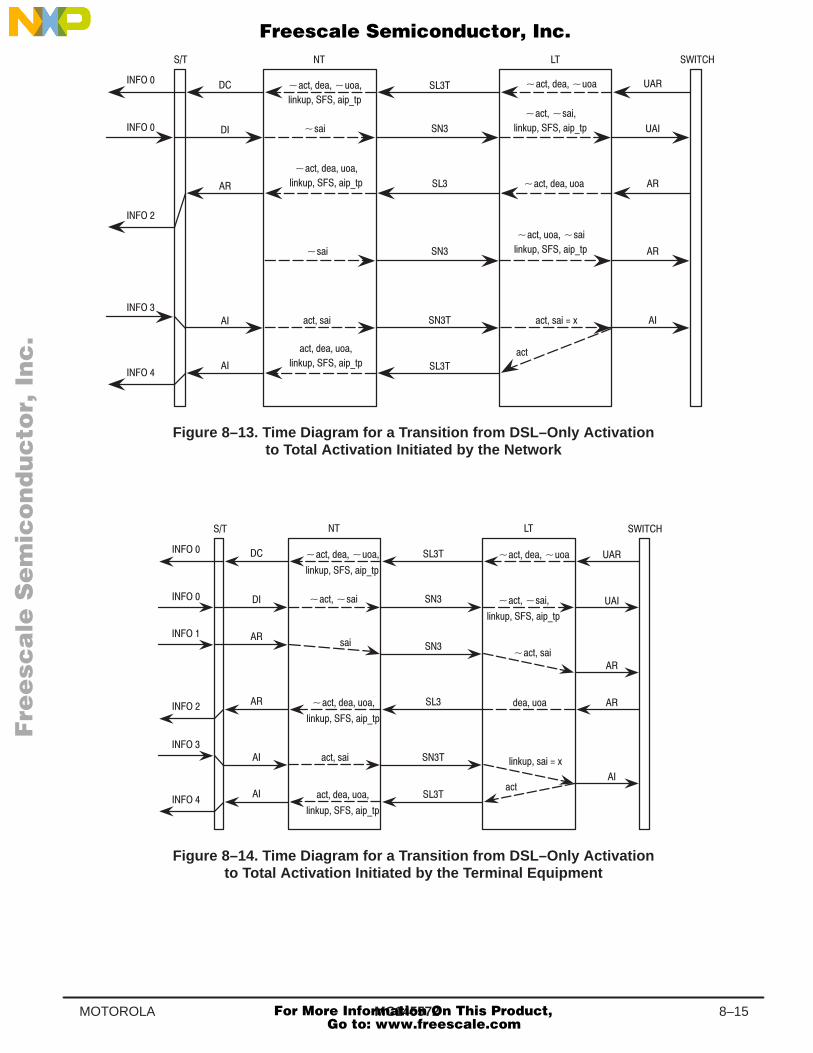
MC145572 8–15MOTOROLA
ÎÎÎÎÎÎÎÎÎÎÎÎÎÎÎÎÎÎÎÎÎÎÎÎÎÎÎÎÎÎÎÎÎÎ
ÎÎÎÎÎÎÎÎÎÎÎÎÎÎÎÎÎÎÎÎÎÎÎÎÎÎÎÎÎÎÎÎÎÎÎÎÎÎÎÎÎÎÎÎÎÎÎÎÎÎÎÎÎÎÎÎÎÎÎÎÎÎÎÎÎÎÎÎÎÎÎÎÎÎÎÎÎÎÎÎÎÎÎÎÎÎÎÎÎÎÎÎÎÎÎÎÎÎÎÎÎÎÎÎÎÎÎÎÎÎÎÎÎÎÎÎÎÎÎ
ÎÎÎÎÎÎÎÎÎÎÎÎÎÎÎÎÎÎÎÎÎÎÎÎÎÎÎÎÎÎÎÎÎÎÎÎÎÎÎÎÎÎÎÎÎÎÎÎÎÎÎÎÎÎÎÎÎÎÎÎÎÎÎÎÎÎÎÎÎÎÎÎÎÎÎÎÎÎÎÎÎÎÎÎÎÎÎÎÎÎÎÎÎÎÎÎÎÎÎÎÎÎ
ÎÎÎÎÎÎÎÎÎÎÎÎÎÎÎÎÎÎÎÎÎÎÎÎÎÎÎÎÎÎÎÎÎÎ
$ %!$ %!
%" "$"
$#
%" "$"
$ %!
$ %!
%" "$"
#
$ %!#
%" "$"
$ # $ # &
$ %!
%" "$"
#
$
Figure 8–13. Time Diagram for a Transition from DSL–Only Activationto Total Activation Initiated by the Network
ÎÎÎÎÎÎÎÎÎÎÎÎÎÎÎ
ÎÎÎÎÎÎÎÎÎÎÎÎÎÎÎÎÎÎÎÎÎÎÎÎÎÎÎÎÎÎÎÎÎÎÎÎÎÎÎÎÎÎÎÎÎÎÎÎÎÎÎÎÎÎÎÎÎÎÎÎÎÎÎÎÎÎÎÎÎÎÎÎÎÎÎ
ÎÎÎÎÎÎÎÎÎÎÎÎÎÎÎÎÎÎÎÎÎÎÎÎÎÎÎÎÎÎÎÎÎÎÎÎÎÎÎÎÎÎÎÎÎÎÎÎÎÎÎÎÎÎÎÎÎÎÎÎÎÎÎÎÎÎÎÎÎÎÎÎÎÎÎÎÎÎÎÎÎÎÎÎÎÎÎÎÎÎ
ÎÎÎÎÎÎÎÎÎÎÎÎÎÎÎ
$ %!$ %!
%" "$"
$#$#
%" "$"
#$ #
%!$ %!
%" "$"
$ # %" # &
$ %!
%" "$"
$
Figure 8–14. Time Diagram for a Transition from DSL–Only Activationto Total Activation Initiated by the Terminal Equipment
Fre
esc
ale
Se
mic
on
du
cto
r, I
Freescale Semiconductor, Inc.
For More Information On This Product, Go to: www.freescale.com
nc
...
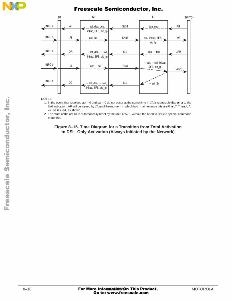
MC1455728–16 MOTOROLA
ÎÎÎÎÎÎÎÎÎÎÎÎÎÎÎÎÎÎÎÎÎÎÎÎÎÎÎÎ
ÎÎÎÎÎÎÎÎÎÎÎÎÎÎÎÎÎÎÎÎÎÎÎÎÎÎÎÎÎÎÎÎÎÎÎÎÎÎÎÎÎÎÎÎÎÎÎÎÎÎÎÎÎÎÎÎÎÎÎÎÎÎÎÎÎÎÎÎÎÎÎÎÎÎÎÎÎÎÎÎÎÎÎÎ
ÎÎÎÎÎÎÎÎÎÎÎÎÎÎÎÎÎÎÎÎÎÎÎÎÎÎÎÎÎÎÎÎÎÎÎÎÎÎÎÎÎÎÎÎÎÎÎÎÎÎÎÎÎÎÎÎÎÎÎÎÎÎÎÎÎÎÎÎÎÎÎÎÎÎÎÎÎÎÎÎÎÎÎÎ
ÎÎÎÎÎÎÎÎÎÎÎÎÎÎ
&"% &"
!&# #%#
% $ % !&#
#%#
&"% &"
!&# #%#
%$%$ !&#
#%#
% % &"
!&# #%#
NOTES:1. In the event that received act = 0 and sai = 0 do not occur at the same time in LT, it is possible that prior to the
UAI indication, AR will be issued by LT, until the moment in which both maintenance bits are 0 in LT. Then, UAIwill be issued, as shown.
2. The state of the act bit is automatically reset by the MC145572, without the need to issue a special commandto do this.
Figure 8–15. Time Diagram for a Transition from Total Activationto DSL–Only Activation (Always Initiated by the Network)
Fre
esc
ale
Se
mic
on
du
cto
r, I
Freescale Semiconductor, Inc.
For More Information On This Product, Go to: www.freescale.com
nc
...
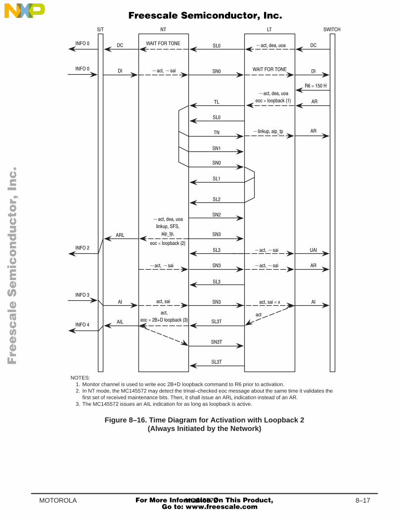
MC145572 8–17MOTOROLA
ÎÎÎÎÎÎÎÎÎÎÎÎÎÎÎÎÎÎÎÎÎÎÎÎÎÎÎÎÎÎÎÎÎÎÎÎÎÎÎÎÎÎÎÎÎÎÎÎÎÎÎÎÎÎÎÎÎÎÎÎÎÎÎÎÎÎÎÎ
ÎÎÎÎÎÎÎÎÎÎÎÎÎÎÎÎÎÎÎÎÎÎÎÎÎÎÎÎÎÎÎÎÎÎÎÎÎÎÎÎÎÎÎÎÎÎÎÎÎÎÎÎÎÎÎÎÎÎÎÎÎÎÎÎÎÎÎÎÎÎÎÎÎÎÎÎÎÎÎÎÎÎÎÎÎÎÎÎÎÎÎÎÎÎÎÎÎÎÎÎÎÎÎÎÎÎÎÎÎÎÎÎÎÎÎÎÎÎÎÎÎÎÎÎÎÎÎÎÎÎÎÎÎÎÎÎÎÎÎÎÎÎÎÎÎÎÎÎÎÎÎÎÎÎÎÎÎÎÎÎÎÎÎÎÎÎÎÎÎÎÎÎÎÎÎÎÎÎÎÎÎÎÎÎÎÎÎÎÎÎÎÎÎÎÎÎÎÎÎÎÎÎÎÎ
ÎÎÎÎÎÎÎÎÎÎÎÎÎÎÎÎÎÎÎÎÎÎÎÎÎÎÎÎÎÎÎÎÎÎÎÎÎÎÎÎÎÎÎÎÎÎÎÎÎÎÎÎÎÎÎÎÎÎÎÎÎÎÎÎÎÎÎÎÎÎÎÎÎÎÎÎÎÎÎÎÎÎÎÎÎÎÎÎÎÎÎÎÎÎÎÎÎÎÎÎÎÎÎÎÎÎÎÎÎÎÎÎÎÎÎÎÎÎÎÎÎÎÎÎÎÎÎÎÎÎÎÎÎÎÎÎÎÎÎÎÎÎÎÎÎÎÎÎÎÎÎÎÎÎÎÎÎÎÎÎÎÎÎÎÎÎÎÎÎÎÎÎÎÎÎÎÎÎÎÎÎÎÎÎÎÎÎÎÎÎÎÎÎÎÎÎÎÎÎÎÎÎÎÎ
ÎÎÎÎÎÎÎÎÎÎÎÎÎÎÎÎÎÎÎÎÎÎÎÎÎÎÎÎÎÎÎÎÎÎÎÎÎÎÎÎÎÎÎÎÎÎÎÎÎÎÎÎÎÎÎÎÎÎÎÎÎÎÎÎÎÎÎÎ
", + %
",
",+ %
", #$ -)
",+ %
", #$ -)
$)" '))*! "&
", + % .
NOTES:1. Monitor channel is used to write eoc 2B+D loopback command to R6 prior to activation.2. In NT mode, the MC145572 may detect the trinal–checked eoc message about the same time it validates the
first set of received maintenance bits. Then, it shall issue an ARL indication instead of an AR.3. The MC145572 issues an AIL indication for as long as loopback is active.
",+ % ",+ %
$)" '))*! "&
", #$ -)
'%(&-*
%*,*
",
$)" '))*! "&
'%(&-* %*,*
Figure 8–16. Time Diagram for Activation with Loopback 2(Always Initiated by the Network)
Fre
esc
ale
Se
mic
on
du
cto
r, I
Freescale Semiconductor, Inc.
For More Information On This Product, Go to: www.freescale.com
nc
...
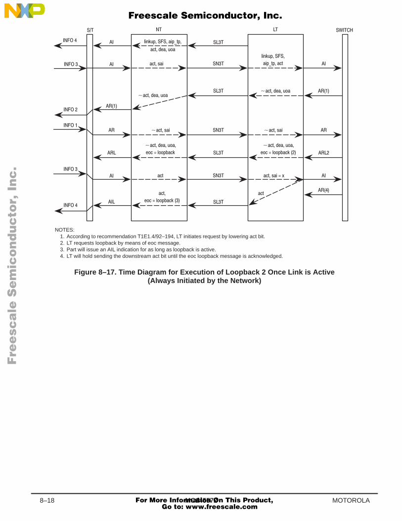
MC1455728–18 MOTOROLA
ÎÎÎÎÎÎÎÎÎÎÎÎÎÎÎÎÎÎÎÎÎÎÎÎÎÎÎÎÎÎÎÎÎÎÎÎÎÎ
ÎÎÎÎÎÎÎÎÎÎÎÎÎÎÎÎÎÎÎÎÎÎÎÎÎÎÎÎÎÎÎÎÎÎÎÎÎÎÎÎÎÎÎÎÎÎÎÎÎÎÎÎÎÎÎÎÎÎÎÎÎÎÎÎÎÎÎÎÎÎÎÎÎÎÎÎÎÎÎÎÎÎÎÎÎÎÎÎÎÎÎÎÎÎÎÎÎÎÎÎÎÎÎÎÎÎÎÎÎÎÎÎÎÎ
ÎÎÎÎÎÎÎÎÎÎÎÎÎÎÎÎÎÎÎÎÎÎÎÎÎÎÎÎÎÎÎÎÎÎÎÎÎÎÎÎÎÎÎÎÎÎÎÎÎÎÎÎÎÎÎÎÎÎÎÎÎÎÎÎÎÎÎÎÎÎÎÎÎÎÎÎÎÎÎÎÎÎÎÎÎÎÎÎÎÎÎÎÎÎÎÎÎÎÎÎÎÎÎÎÎÎÎÎÎÎÎÎÎÎÎÎÎÎÎÎÎÎÎÎÎÎÎÎÎÎÎÎÎ
ÎÎÎÎÎÎÎÎÎÎÎÎÎÎÎÎÎÎÎÎÎÎÎÎÎÎÎÎÎÎÎÎÎÎÎÎÎÎ
%" "$"
$ %!
%"
"$" $
$ %!$ %!
$ #
$ $ # &
$
! !!"
$ #
$
$ %!
! !!"
$ #
$ %!
! !!"
NOTES:1. According to recommendation T1E1.4/92–194, LT initiates request by lowering act bit.2. LT requests loopback by means of eoc message.3. Part will issue an AIL indication for as long as loopback is active.4. LT will hold sending the downstream act bit until the eoc loopback message is acknowledged.
Figure 8–17. Time Diagram for Execution of Loopback 2 Once Link is Active(Always Initiated by the Network)
Fre
esc
ale
Se
mic
on
du
cto
r, I
Freescale Semiconductor, Inc.
For More Information On This Product, Go to: www.freescale.com
nc
...
MC145572 8–19MOTOROLA
The MC145572 can be configured for GCI master or GCI slave operation independently of LT or NTconfiguration. When the pin M/S is pulled low to VSS, GCI slave operation is selected. When the pinM/S is pulled high to VDD, GCI master operation is selected. When configured as a slave, FSC isan input driven by external circuitry. FSC must be synchronized to the clock applied to DCL. Whenconfigured as a master, the MC145572 drives FSC as an output.
The MC145572 uses the FSC signal to indicate superframe alignment. In LT mode as a GCI slave,the FSC pin is used to force alignment of the transmitted U–interface superframe. Normally, the FSCpulse is two DCL clocks in duration. Alignment of the transmitted superframe can be forced by drivingFSC with a one DCL clock wide pulse, once every 96 GCI frames. The 2B+D data read into the Dinpin following the single clock wide FSC, corresponds to the first 2B+D transmitted onto the U–inter-face. If superframe alignment is not input to FSC, the MC145572 aligns the outgoing U–interfacesuperframe.
When configured for master mode and either LT or NT operation, reception of the first 2B+D datafrom the U–interface superframe is indicated by the MC145572 outputting a FSC pulse that is oneDCL clock wide. This happens once every 96 GCI frames.
In NT mode, IDL2 slave operation, any superframe alignment information that may be present onFSC is ignored. ANSI T1.601 defines when the NT transmitted superframe occurs with respect tothe received superframe.
WARNING
If FSC is to be used to set the alignment of the transmitted superframe in LT mode, it mustbe stable prior to activating the MC145572.
Fre
esc
ale
Se
mic
on
du
cto
r, I
Freescale Semiconductor, Inc.
For More Information On This Product, Go to: www.freescale.com
nc
...
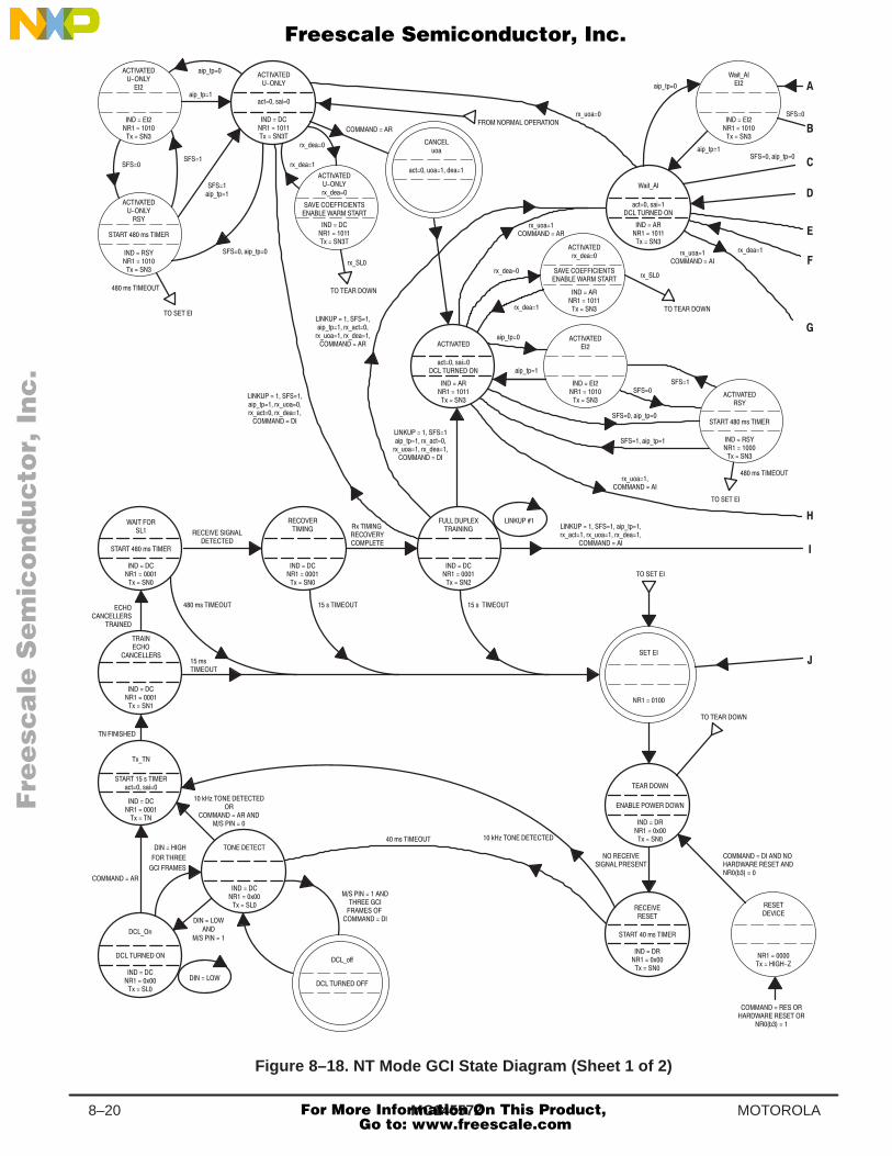
MC1455728–20 MOTOROLA
)/4(74
)/4(74
!#!"&
!9
$ !
*
!#
!9 '
$ ! *
# !
!! 16 !
9!9
# !
0: ! !! 16 !"!
!
(3..
!"
! !!
9!9
$
(2
!"
9!9
$
!
0: ! !!
!
!
!9(!
!9 !
!! 6 !)+7 6)/
!
!9
$!
!9
!! 16 !
9 !#&!
# !!
16 !"!
16!"!
)/4(74
)/4(74
! !
" )/4(74 59(83)59()+7 59(,-)
" )/4(74 59()+759(83) 59(,-)
! ! $
!#!"& &
!! 16 !
& !9
59(,-)
59(,-)
!#!"&
)+7 6)/
!9 !
#!
!9
!
59(83)
!#!"&59(,-)
# ! $ !!
!9 !
59(
6 !"!
83)
)+7 83) ,-)
$)/7(
!9
)/4(74
)/4(74
)/4(74
59(,-)59(83)
! ! $
! $
$ $
9!9
! !
!
16 !"!
! !
" )/4(7459()+7 59(83) 59(,-)
" " "%!
!9
6 !"!
)/4(74
)/4(74
59(83)
!#! &
!! 16 !
& !9
" )/4(74 59()+759(83) 59(,-)
!#!
)+7 6)/ !"
!9
!#!
!9
59(,-)
59(,-)
)/4(74
)/4(74
59(83)
! ! $
59(
!#!59(,-)
# ! $ !!
!9
$)/7(
)+7 6)/ !"
!9
Figure 8–18. NT Mode GCI State Diagram (Sheet 1 of 2)
16 !"!
Fre
esc
ale
Se
mic
on
du
cto
r, I
Freescale Semiconductor, Inc.
For More Information On This Product, Go to: www.freescale.com
nc
...
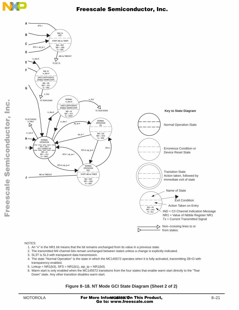
MC145572 8–21MOTOROLA
Key to State Diagram
Normal Operation State
Erroneous Condition orDevice Reset State
Transition StateAction taken, followed byimmediate exit of state
Name of State
Exit Condition
Action Taken on Entry
IND = C/I Channel Indication MessageNR1 = Value of Nibble Register NR1Tx = Current Transmitted Signal
Non–crossing lines to orfrom states.
NOTES:1. An “x” in the NR1 bit means that the bit remains unchanged from its value in a previous state.2. The transmitted M4 channel bits remain unchanged between states unless a change is explicitly indicated.3. SL3T is SL3 with transparent data transmission.4. The state “Normal Operation” is the state in which the MC145572 operates when it is fully activated, transmitting 2B+D with
transparency enabled.5. Linkup = NR1(b3), SFS = NR1(b1), aip_tp = NR1(b0).6. Warm start is only enabled when the MC145572 transitions from the four states that enable warm start directly to the “Tear
Down” state. Any other transition disables warm start.
Figure 8–18. NT Mode GCI State Diagram (Sheet 2 of 2)
$'*'
(,"#
$*
%)
,
%)
$*(,"#
,
(,
(,
(,"#
,
(,"#
(,"# $'*'
$'*'(,+&
!* ) $
,
$'*'
$'*'
%)
$'*'
%)
,
,
,,,,, ,
Fre
esc
ale
Se
mic
on
du
cto
r, I
Freescale Semiconductor, Inc.
For More Information On This Product, Go to: www.freescale.com
nc
...
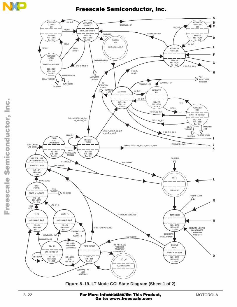
MC1455728–22 MOTOROLA
Figure 8–19. LT Mode GCI State Diagram (Sheet 1 of 2)
!#!"%
!7
'-2&52
'-2&52
!#!"%
" !7 !
')5 61' *+'
'-2&52
'-2&52
/4 !"!
! !
!! $
!!#!"%
-0.62 '-2&5237&')5 37&4'-
"
#!
!7
!
!
!7
4 !"!
4 !"!
$!
!! 4 !
!7
! !!
$! !
!! /4 !
!7
!
!7&!
')5 61' *+'
!7 !
$
&0
!"
7!7
"
61' !7&!
')5 61' *+'
!7 !
"
$
!
.8 ! !!
/4!"!
! !
!
! !!
7!7
&1,,
!"
/4 !"!
!
.8 ! !!
# !
!! /4 !
7!7
$ ! (
! $
7!7
#
!
! ! $
!
! !
-0.62 '-2&52 37&')5 37&4'-7
4 !"!
! ! $
"
! !
/4!"!
37&')5 37&4'-7-0.62 '-2&5237&')5 37&4'-
!#! %
!! /4 !
% !7
'-2&52
'-2&52
'-2&52
'-2&52
!!#!" !
!#!!#!
" !7
!7
"
!!#!"%
!#!$'-5 37&')5
!7
'-2&52
'-2&52
"
37&')5 37&4'-7
!#!$'-5 37&')5
!7
61'
')5 61' *+'
"
37&')537&4'-
!#!"% %
!! /4 !
% !7
Fre
esc
ale
Se
mic
on
du
cto
r, I
Freescale Semiconductor, Inc.
For More Information On This Product, Go to: www.freescale.com
nc
...
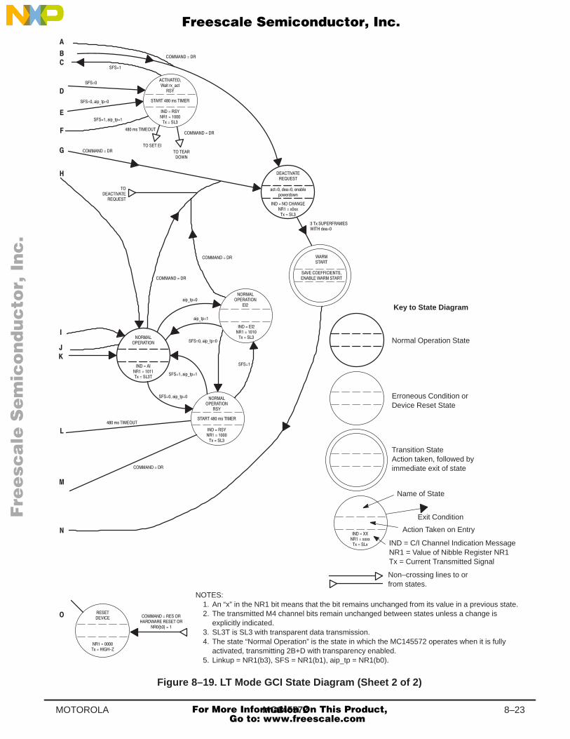
MC145572 8–23MOTOROLA
Key to State Diagram
Normal Operation State
Erroneous Condition orDevice Reset State
Transition StateAction taken, followed byimmediate exit of state
Name of State
Exit Condition
Action Taken on Entry
IND = C/I Channel Indication MessageNR1 = Value of Nibble Register NR1Tx = Current Transmitted Signal
Non–crossing lines to orfrom states.
"" 55555 5
NOTES:1. An “x” in the NR1 bit means that the bit remains unchanged from its value in a previous state.2. The transmitted M4 channel bits remain unchanged between states unless a change is
explicitly indicated.3. SL3T is SL3 with transparent data transmission.4. The state “Normal Operation” is the state in which the MC145572 operates when it is fully
activated, transmitting 2B+D with transparency enabled.5. Linkup = NR1(b3), SFS = NR1(b1), aip_tp = NR1(b0).
Figure 8–19. LT Mode GCI State Diagram (Sheet 2 of 2)
5 $
!
'
#
# 5
-2
-2
5
5
&+0%30
&+0%30
&+0%30
&+0%30
&+0%30
!
&+0%30
&+0%30
!&+3 15%&(3
#
-2
# 5
&(3 )*& *.&',*0/4*1)/4.
5555
5 ! )*&
!
!
-2
Fre
esc
ale
Se
mic
on
du
cto
r, I
Freescale Semiconductor, Inc.
For More Information On This Product, Go to: www.freescale.com
nc
...

MC1455728–24 MOTOROLA
Fre
esc
ale
Se
mic
on
du
cto
r, I
Freescale Semiconductor, Inc.
For More Information On This Product, Go to: www.freescale.com
nc
...
MC145572 9–1MOTOROLA
This chapter is a guide for writing software for the MC145572. It provides several pseudo–code exam-ples on how to initialize and activate the MC145572 U–interface transceiver. NT and LT initiatedactivation procedures are given, using both the automatic and non–automatic eoc modes. Thischapter also contains sample initialization routines for IDL–2 timeslot assignment procedures, GCIelectrical mode timeslot assignment, block error rate calculation, and non–ISDN D channel com-munications.
The MC145572 provides easy microcontroller read and write access to the Maintenance channel viathe SCP or PCP interface. This permits the Maintenance channel to be easily updated and changesin ANSI T1.601–1992 defined default values to be implemented simply by modifying software. Notethat there are many proprietary applications where the Maintenance channel can be used in anymanner whatsoever. For a discussion of the Maintenance channel, see Chapters 5 and 7 .
The MC145572 should be initialized before Activation Request, NR2(b2), is set to a 1, when Activa-tion in Progress (NR1(b0)) is first detected set to a 1, or when deactivation has been confirmed. Thisensures that the correct data appears on the maintenance channels when linkup is achieved and theU–interface is activated.
The Software Reset bit (NR0(b3)), need only be set to a 1, then reset to a 0, as part of the power–upinitialization routines.
The MC145572 should be initialized so that when it activates, the correct data is present on all ofthe maintenance channels at the time activation occurs. The ANSI T1.601–1992 specification indicatesthe default and operational data that should appear on these channels. A microcontroller write to thespecified register puts maintenance data onto the indicated U–interface maintenance channel. A micro-controller read of the specified register obtains maintenance data from the indicated U–interface main-tenance channel. These channels are:
• eoc Channel: This channel is accessed via register R6. It is used to convey eoc messages fromthe LT to the NT. The NT conveys its acknowledgment of eoc messages back to the LT on thischannel. Typically, this channel is used by the LT to send loopback and other maintenancemessages to the NT. See ANSI T1.601–1992 for currently defined eoc messages and other eocprocedures.
• M4 Maintenance Channel: Data is put on this channel by writing to BR0. Data is read from thischannel by reading BR1. This channel is used by the LT to signal its activation status to the NT.The LT also uses this channel to tell the NT when it is intending to deactivate the U–interface.The NT uses this channel to send its activation status to the LT. The NT also uses this channelto send its power supply status, its warm start capability, and if it is in a test mode, back to theLT. There are several reserved bits which the ANSI T1.601–1992 specification indicates shouldbe set to 1s.
• M5 and M6 Maintenance Channels: Data is put onto these channels by writing to BR2. Datais read from these channels by reading BR3. Currently all bits in these channels are defined byANSI T1.601–1992 as reserved and should be set to 1s.
Sample initialization routines are provided on how to initialize the MC145572 when operated in theLT or NT modes. Procedure NTINIT1 in Section 9.2.1 initializes the MC145572 for automatic eocoperation when configured as an NT. The corresponding sample high level embedded operations
Fre
esc
ale
Se
mic
on
du
cto
r, I
Freescale Semiconductor, Inc.
For More Information On This Product, Go to: www.freescale.com
nc
...
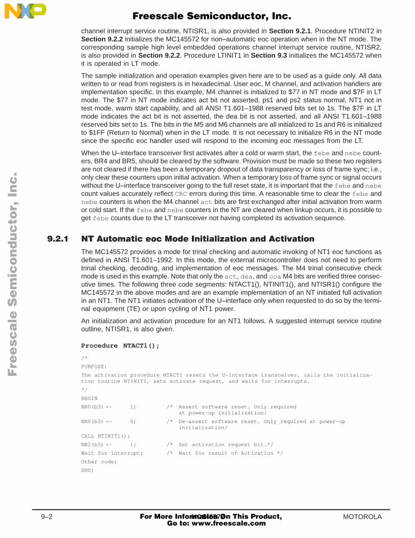
MC1455729–2 MOTOROLA
channel interrupt service routine, NTISR1, is also provided in Section 9.2.1 . Procedure NTINIT2 inSection 9.2.2 initializes the MC145572 for non–automatic eoc operation when in the NT mode. Thecorresponding sample high level embedded operations channel interrupt service routine, NTISR2,is also provided in Section 9.2.2 . Procedure LTINIT1 in Section 9.3 initializes the MC145572 whenit is operated in LT mode.
The sample initialization and operation examples given here are to be used as a guide only. All datawritten to or read from registers is in hexadecimal. User eoc, M channel, and activation handlers areimplementation specific. In this example, M4 channel is initialized to $77 in NT mode and $7F in LTmode. The $77 in NT mode indicates act bit not asserted, ps1 and ps2 status normal, NT1 not intest mode, warm start capability, and all ANSI T1.601–1988 reserved bits set to 1s. The $7F in LTmode indicates the act bit is not asserted, the dea bit is not asserted, and all ANSI T1.601–1988reserved bits set to 1s. The bits in the M5 and M6 channels are all initialized to 1s and R6 is initializedto $1FF (Return to Normal) when in the LT mode. It is not necessary to initialize R6 in the NT modesince the specific eoc handler used will respond to the incoming eoc messages from the LT.
When the U–interface transceiver first activates after a cold or warm start, the febe and nebe count-ers, BR4 and BR5, should be cleared by the software. Provision must be made so these two registersare not cleared if there has been a temporary dropout of data transparency or loss of frame sync; i.e.,only clear these counters upon initial activation. When a temporary loss of frame sync or signal occurswithout the U–interface transceiver going to the full reset state, it is important that the febe and nebecount values accurately reflect CRC errors during this time. A reasonable time to clear the febe andnebe counters is when the M4 channel act bits are first exchanged after initial activation from warmor cold start. If the febe and nebe counters in the NT are cleared when linkup occurs, it is possible toget febe counts due to the LT transceiver not having completed its activation sequence.
The MC145572 provides a mode for trinal checking and automatic invoking of NT1 eoc functions asdefined in ANSI T1.601–1992. In this mode, the external microcontroller does not need to performtrinal checking, decoding, and implementation of eoc messages. The M4 trinal consecutive checkmode is used in this example. Note that only the act , dea , and uoa M4 bits are verified three consec-utive times. The following three code segments: NTACT1(), NTINIT1(), and NTISR1() configure theMC145572 in the above modes and are an example implementation of an NT initiated full activationin an NT1. The NT1 initiates activation of the U–interface only when requested to do so by the termi-nal equipment (TE) or upon cycling of NT1 power.
An initialization and activation procedure for an NT1 follows. A suggested interrupt service routineoutline, NTISR1, is also given.
Procedure NTACT1();
/*
PURPOSE:
The activation procedure NTACT1 resets the U–interface transceiver, calls the initializa-tion routine NTINIT1, sets activate request, and waits for interrupts.
*/
BEGIN
NR0(b3) <– 1; /* Assert software reset. Only requiredat power–up initialization/
NR0(b3) <– 0; /* De–assert software reset. Only required at power–upinitialization/
CALL NTINIT1();
NR2(b3) <– 1; /* Set activation request bit.*/
Wait for interrupt; /* Wait for result of Activation */
Other code;
END;
Fre
esc
ale
Se
mic
on
du
cto
r, I
Freescale Semiconductor, Inc.
For More Information On This Product, Go to: www.freescale.com
nc
...
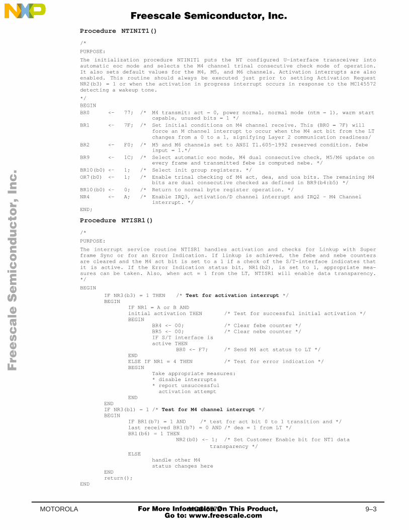
MC145572 9–3MOTOROLA
Procedure NTINIT1()
/*
PURPOSE:
The initialization procedure NTINIT1 puts the NT configured U–interface transceiver intoautomatic eoc mode and selects the M4 channel trinal consecutive check mode of operation.It also sets default values for the M4, M5, and M6 channels. Activation interrupts are alsoenabled. This routine should always be executed just prior to setting Activation RequestNR2(b3) = 1 or when the activation in progress interrupt occurs in response to the MC145572detecting a wakeup tone.
*/
BEGIN
BR0 <– 77; /* M4 transmit: act = 0, power normal, normal mode (ntm = 1), warm startcapable, unused bits = 1 */
BR1 <– 7F; /* Set initial conditions on M4 channel receive. This (BR0 = 7F) willforce an M channel interrupt to occur when the M4 act bit from the LTchanges from a 0 to a 1, signifying Layer 2 communication readiness/
BR2 <– F0; /* M5 and M6 channels set to ANSI T1.605–1992 reserved condition. febeinput = 1.*/
BR9 <– 1C; /* Select automatic eoc mode, M4 dual consecutive check, M5/M6 update onevery frame and transmitted febe is computed nebe. */
BR10(b0) <– 1; /* Select init group registers. */
OR7(b0) <– 1; /* Enable trinal checking of M4 act, dea, and uoa bits. The remaining M4bits are dual consecutive checked as defined in BR9(b4:b5) */
BR10(b0) <– 0; /* Return to normal byte register operation. */
NR4 <– A; /* Enable IRQ3, activation/D channel interrupt and IRQ2 – M4 Channelinterrupt. */
END;
Procedure NTISR1()
/*
PURPOSE:
The interrupt service routine NTISR1 handles activation and checks for Linkup with Superframe Sync or for an Error Indication. If linkup is achieved, the febe and nebe countersare cleared and the M4 act bit is set to a 1 if a check of the S/T–interface indicates thatit is active. If the Error Indication status bit, NR1(b2), is set to 1, appropriate mea-sures can be taken. Also, when act = 1 from the LT, NTISR1 will enable data transparency.*/
BEGIN
IF NR3(b3) = 1 THEN /* Test for activation interrupt */BEGIN
IF NR1 = A or B ANDinitial activation THEN /* Test for successful initial activation */BEGIN
BR4 <– 00; /* Clear febe counter */BR5 <– 00; /* Clear nebe counter */IF S/T interface isactive THEN
BR0 <– F7; /* Send M4 act status to LT */ENDELSE IF NR1 = 4 THEN /* Test for error indication */BEGIN
Take appropriate measures:* disable interrupts* report unsuccessful activation attempt
ENDENDIF NR3(b1) = 1 /* Test for M4 channel interrupt */BEGIN
IF BR1(b7) = 1 AND /* test for act bit 0 to 1 transition and */last received BR1(b7) = 0 AND /* dea = 1 from LT */BR1(b6) = 1 THEN
NR2(b0) <– 1; /* Set Customer Enable bit for NT1 data transparency */
ELSEhandle other M4status changes here
ENDreturn();
END
Fre
esc
ale
Se
mic
on
du
cto
r, I
Freescale Semiconductor, Inc.
For More Information On This Product, Go to: www.freescale.com
nc
...
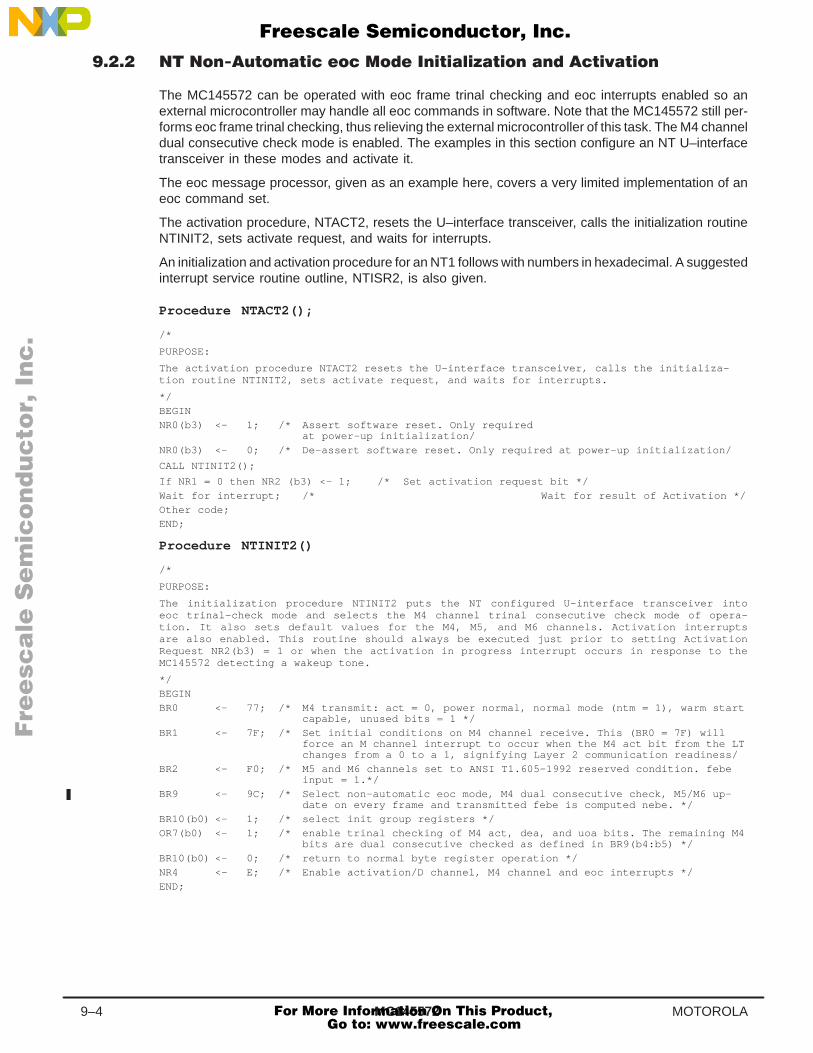
MC1455729–4 MOTOROLA
The MC145572 can be operated with eoc frame trinal checking and eoc interrupts enabled so anexternal microcontroller may handle all eoc commands in software. Note that the MC145572 still per-forms eoc frame trinal checking, thus relieving the external microcontroller of this task. The M4 channeldual consecutive check mode is enabled. The examples in this section configure an NT U–interfacetransceiver in these modes and activate it.
The eoc message processor, given as an example here, covers a very limited implementation of aneoc command set.
The activation procedure, NTACT2, resets the U–interface transceiver, calls the initialization routineNTINIT2, sets activate request, and waits for interrupts.
An initialization and activation procedure for an NT1 follows with numbers in hexadecimal. A suggestedinterrupt service routine outline, NTISR2, is also given.
Procedure NTACT2();
/*
PURPOSE:
The activation procedure NTACT2 resets the U–interface transceiver, calls the initializa-tion routine NTINIT2, sets activate request, and waits for interrupts.
*/
BEGIN
NR0(b3) <– 1; /* Assert software reset. Only requiredat power–up initialization/
NR0(b3) <– 0; /* De–assert software reset. Only required at power–up initialization/
CALL NTINIT2();
If NR1 = 0 then NR2 (b3) <– 1; /* Set activation request bit */
Wait for interrupt; /* Wait for result of Activation */
Other code;
END;
Procedure NTINIT2()
/*
PURPOSE:
The initialization procedure NTINIT2 puts the NT configured U–interface transceiver intoeoc trinal–check mode and selects the M4 channel trinal consecutive check mode of opera-tion. It also sets default values for the M4, M5, and M6 channels. Activation interruptsare also enabled. This routine should always be executed just prior to setting ActivationRequest NR2(b3) = 1 or when the activation in progress interrupt occurs in response to theMC145572 detecting a wakeup tone.
*/
BEGIN
BR0 <– 77; /* M4 transmit: act = 0, power normal, normal mode (ntm = 1), warm startcapable, unused bits = 1 */
BR1 <– 7F; /* Set initial conditions on M4 channel receive. This (BR0 = 7F) willforce an M channel interrupt to occur when the M4 act bit from the LTchanges from a 0 to a 1, signifying Layer 2 communication readiness/
BR2 <– F0; /* M5 and M6 channels set to ANSI T1.605–1992 reserved condition. febeinput = 1.*/
BR9 <– 9C; /* Select non–automatic eoc mode, M4 dual consecutive check, M5/M6 up-date on every frame and transmitted febe is computed nebe. */
BR10(b0) <– 1; /* select init group registers */
OR7(b0) <– 1; /* enable trinal checking of M4 act, dea, and uoa bits. The remaining M4bits are dual consecutive checked as defined in BR9(b4:b5) */
BR10(b0) <– 0; /* return to normal byte register operation */
NR4 <– E; /* Enable activation/D channel, M4 channel and eoc interrupts */
END;
Fre
esc
ale
Se
mic
on
du
cto
r, I
Freescale Semiconductor, Inc.
For More Information On This Product, Go to: www.freescale.com
nc
...
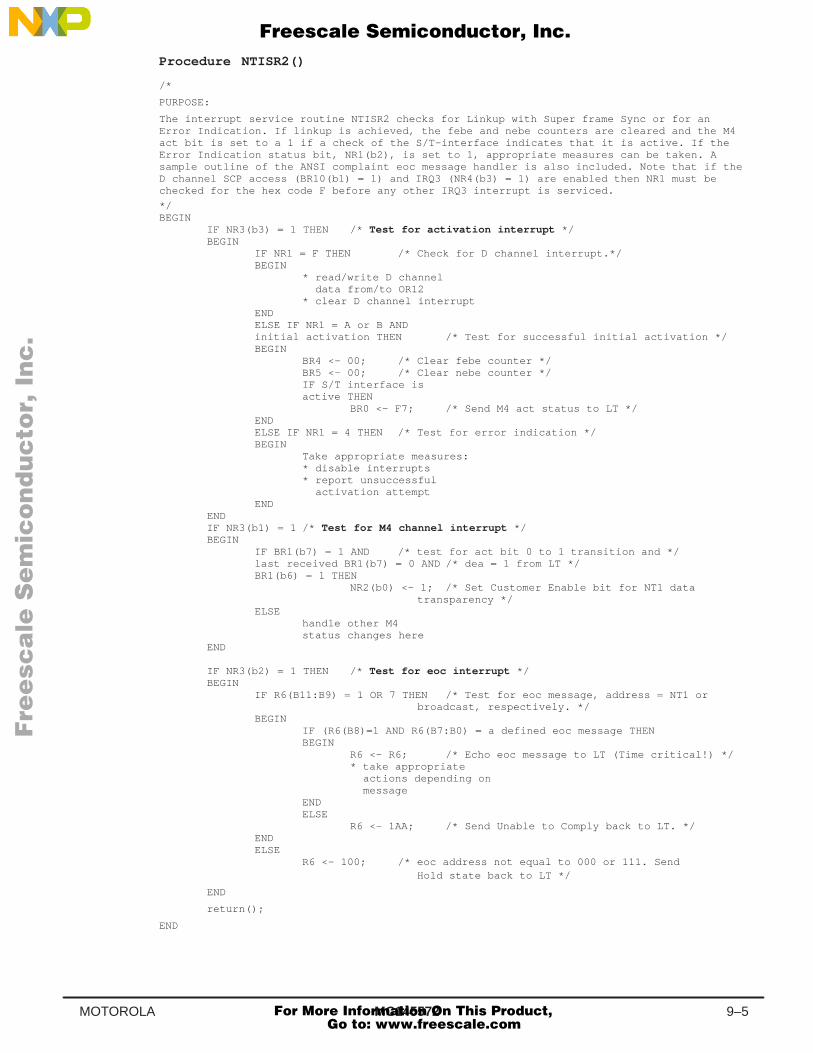
MC145572 9–5MOTOROLA
Procedure NTISR2()
/*
PURPOSE:
The interrupt service routine NTISR2 checks for Linkup with Super frame Sync or for anError Indication. If linkup is achieved, the febe and nebe counters are cleared and the M4act bit is set to a 1 if a check of the S/T–interface indicates that it is active. If theError Indication status bit, NR1(b2), is set to 1, appropriate measures can be taken. Asample outline of the ANSI complaint eoc message handler is also included. Note that if theD channel SCP access (BR10(b1) = 1) and IRQ3 (NR4(b3) = 1) are enabled then NR1 must bechecked for the hex code F before any other IRQ3 interrupt is serviced.
*/BEGIN
IF NR3(b3) = 1 THEN /* Test for activation interrupt */BEGIN
IF NR1 = F THEN /* Check for D channel interrupt.*/BEGIN
* read/write D channel data from/to OR12* clear D channel interrupt
ENDELSE IF NR1 = A or B ANDinitial activation THEN /* Test for successful initial activation */BEGIN
BR4 <– 00; /* Clear febe counter */BR5 <– 00; /* Clear nebe counter */IF S/T interface isactive THEN
BR0 <– F7; /* Send M4 act status to LT */ENDELSE IF NR1 = 4 THEN /* Test for error indication */BEGIN
Take appropriate measures:* disable interrupts* report unsuccessful activation attempt
ENDENDIF NR3(b1) = 1 /* Test for M4 channel interrupt */BEGIN
IF BR1(b7) = 1 AND /* test for act bit 0 to 1 transition and */last received BR1(b7) = 0 AND /* dea = 1 from LT */BR1(b6) = 1 THEN
NR2(b0) <– 1; /* Set Customer Enable bit for NT1 data transparency */
ELSEhandle other M4status changes here
END
IF NR3(b2) = 1 THEN /* Test for eoc interrupt */BEGIN
IF R6(B11:B9) = 1 OR 7 THEN /* Test for eoc message, address = NT1 or broadcast, respectively. */
BEGINIF (R6(B8)=1 AND R6(B7:B0) = a defined eoc message THENBEGIN
R6 <– R6; /* Echo eoc message to LT (Time critical!) */* take appropriate actions depending on message
ENDELSE
R6 <– 1AA; /* Send Unable to Comply back to LT. */ENDELSE
R6 <– 100; /* eoc address not equal to 000 or 111. Send Hold state back to LT */
END
return();
END
Fre
esc
ale
Se
mic
on
du
cto
r, I
Freescale Semiconductor, Inc.
For More Information On This Product, Go to: www.freescale.com
nc
...
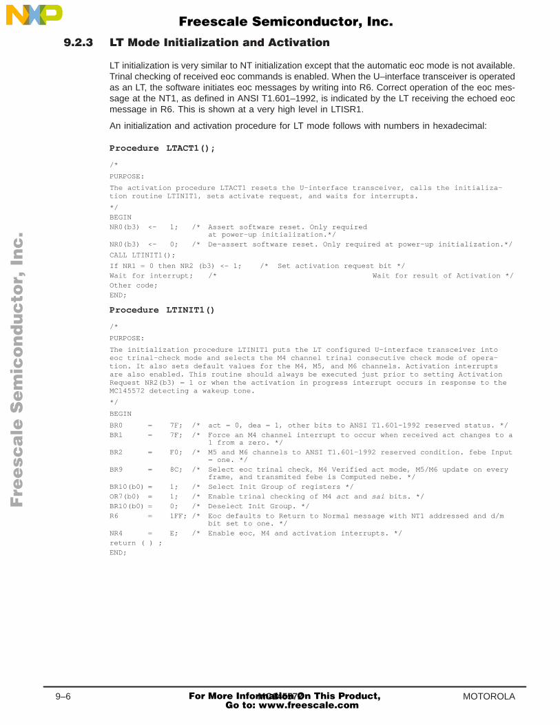
MC1455729–6 MOTOROLA
LT initialization is very similar to NT initialization except that the automatic eoc mode is not available.Trinal checking of received eoc commands is enabled. When the U–interface transceiver is operatedas an LT, the software initiates eoc messages by writing into R6. Correct operation of the eoc mes-sage at the NT1, as defined in ANSI T1.601–1992, is indicated by the LT receiving the echoed eocmessage in R6. This is shown at a very high level in LTISR1.
An initialization and activation procedure for LT mode follows with numbers in hexadecimal:
Procedure LTACT1();
/*
PURPOSE:
The activation procedure LTACT1 resets the U–interface transceiver, calls the initializa-tion routine LTINIT1, sets activate request, and waits for interrupts.
*/
BEGIN
NR0(b3) <– 1; /* Assert software reset. Only requiredat power–up initialization.*/
NR0(b3) <– 0; /* De–assert software reset. Only required at power–up initialization.*/
CALL LTINIT1();
If NR1 = 0 then NR2 (b3) <– 1; /* Set activation request bit */
Wait for interrupt; /* Wait for result of Activation */
Other code;
END;
Procedure LTINIT1()
/*
PURPOSE:
The initialization procedure LTINIT1 puts the LT configured U–interface transceiver intoeoc trinal–check mode and selects the M4 channel trinal consecutive check mode of opera-tion. It also sets default values for the M4, M5, and M6 channels. Activation interruptsare also enabled. This routine should always be executed just prior to setting ActivationRequest NR2(b3) = 1 or when the activation in progress interrupt occurs in response to theMC145572 detecting a wakeup tone.
*/
BEGIN
BR0 = 7F; /* act = 0, dea = 1, other bits to ANSI T1.601–1992 reserved status. */
BR1 = 7F; /* Force an M4 channel interrupt to occur when received act changes to a1 from a zero. */
BR2 = F0; /* M5 and M6 channels to ANSI T1.601–1992 reserved condition. febe Input= one. */
BR9 = 8C; /* Select eoc trinal check, M4 Verified act mode, M5/M6 update on everyframe, and transmited febe is Computed nebe. */
BR10(b0) = 1; /* Select Init Group of registers */
OR7(b0) = 1; /* Enable trinal checking of M4 act and sai bits. */
BR10(b0) = 0; /* Deselect Init Group. */
R6 = 1FF; /* Eoc defaults to Return to Normal message with NT1 addressed and d/mbit set to one. */
NR4 = E; /* Enable eoc, M4 and activation interrupts. */
return ( ) ;
END;
Fre
esc
ale
Se
mic
on
du
cto
r, I
Freescale Semiconductor, Inc.
For More Information On This Product, Go to: www.freescale.com
nc
...
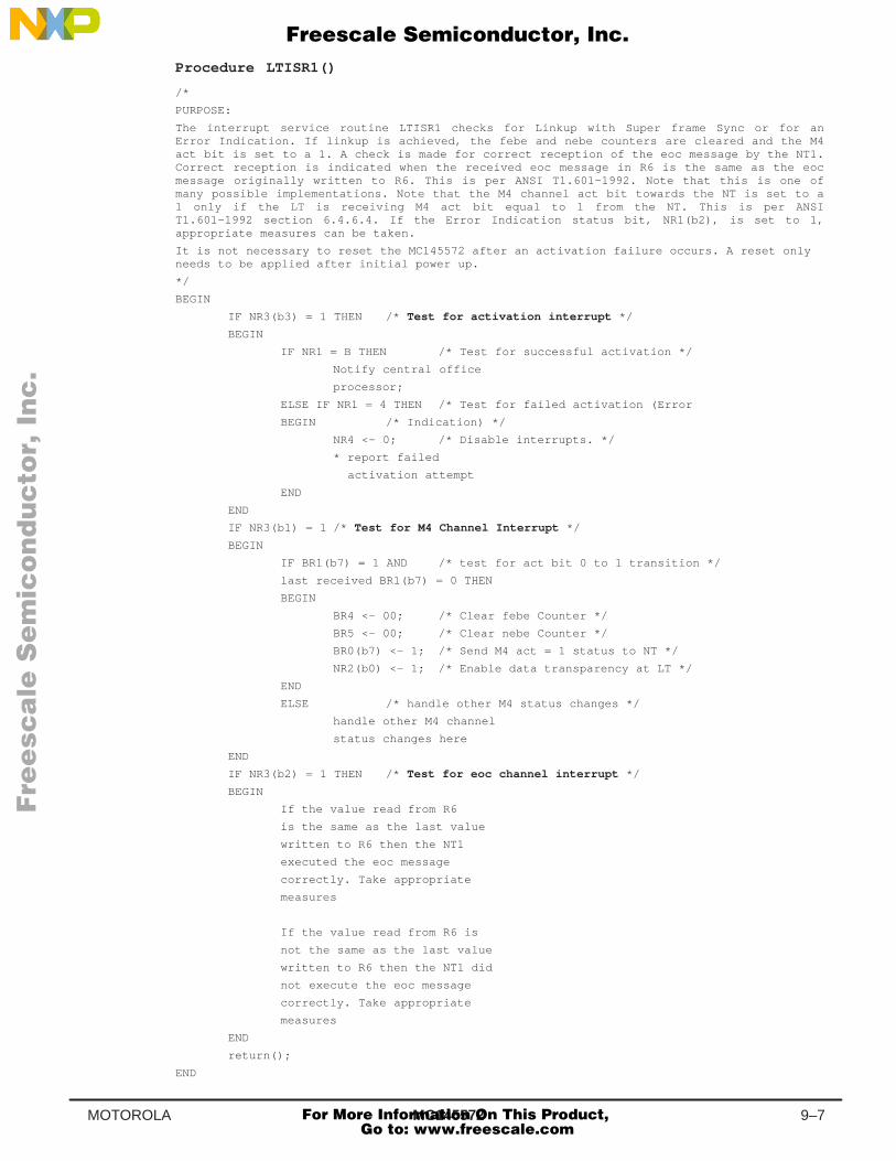
MC145572 9–7MOTOROLA
Procedure LTISR1()
/*
PURPOSE:
The interrupt service routine LTISR1 checks for Linkup with Super frame Sync or for anError Indication. If linkup is achieved, the febe and nebe counters are cleared and the M4act bit is set to a 1. A check is made for correct reception of the eoc message by the NT1.Correct reception is indicated when the received eoc message in R6 is the same as the eocmessage originally written to R6. This is per ANSI T1.601–1992. Note that this is one ofmany possible implementations. Note that the M4 channel act bit towards the NT is set to a1 only if the LT is receiving M4 act bit equal to 1 from the NT. This is per ANSIT1.601–1992 section 6.4.6.4. If the Error Indication status bit, NR1(b2), is set to 1,appropriate measures can be taken.
It is not necessary to reset the MC145572 after an activation failure occurs. A reset onlyneeds to be applied after initial power up.
*/
BEGIN
IF NR3(b3) = 1 THEN /* Test for activation interrupt */
BEGIN
IF NR1 = B THEN /* Test for successful activation */
Notify central office
processor;
ELSE IF NR1 = 4 THEN /* Test for failed activation (Error
BEGIN /* Indication) */
NR4 <– 0; /* Disable interrupts. */
* report failed
activation attempt
END
END
IF NR3(b1) = 1 /* Test for M4 Channel Interrupt */
BEGIN
IF BR1(b7) = 1 AND /* test for act bit 0 to 1 transition */
last received BR1(b7) = 0 THEN
BEGIN
BR4 <– 00; /* Clear febe Counter */
BR5 <– 00; /* Clear nebe Counter */
BR0(b7) <– 1; /* Send M4 act = 1 status to NT */
NR2(b0) <– 1; /* Enable data transparency at LT */
END
ELSE /* handle other M4 status changes */
handle other M4 channel
status changes here
END
IF NR3(b2) = 1 THEN /* Test for eoc channel interrupt */
BEGIN
If the value read from R6
is the same as the last value
written to R6 then the NT1
executed the eoc message
correctly. Take appropriate
measures
If the value read from R6 is
not the same as the last value
written to R6 then the NT1 did
not execute the eoc message
correctly. Take appropriate
measures
END
return();
END
Fre
esc
ale
Se
mic
on
du
cto
r, I
Freescale Semiconductor, Inc.
For More Information On This Product, Go to: www.freescale.com
nc
...
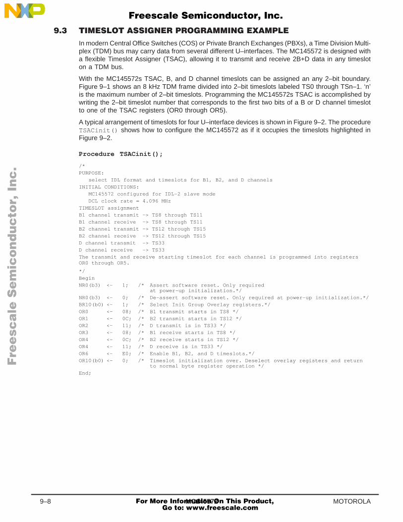
MC1455729–8 MOTOROLA
In modern Central Office Switches (COS) or Private Branch Exchanges (PBXs), a Time Division Multi-plex (TDM) bus may carry data from several different U–interfaces. The MC145572 is designed witha flexible Timeslot Assigner (TSAC), allowing it to transmit and receive 2B+D data in any timesloton a TDM bus.
With the MC145572s TSAC, B, and D channel timeslots can be assigned an any 2–bit boundary.Figure 9–1 shows an 8 kHz TDM frame divided into 2–bit timeslots labeled TS0 through TSn–1. ‘n’is the maximum number of 2–bit timeslots. Programming the MC145572s TSAC is accomplished bywriting the 2–bit timeslot number that corresponds to the first two bits of a B or D channel timeslotto one of the TSAC registers (OR0 through OR5).
A typical arrangement of timeslots for four U–interface devices is shown in Figure 9–2. The procedureTSACinit() shows how to configure the MC145572 as if it occupies the timeslots highlighted inFigure 9–2.
Procedure TSACinit();
/*
PURPOSE:
select IDL format and timeslots for B1, B2, and D channels
INITIAL CONDITIONS:
MC145572 configured for IDL–2 slave mode
DCL clock rate = 4.096 MHz
TIMESLOT assignment
B1 channel transmit –> TS8 through TS11
B1 channel receive –> TS8 through TS11
B2 channel transmit –> TS12 through TS15
B2 channel receive –> TS12 through TS15
D channel transmit –> TS33
D channel receive –> TS33
The transmit and receive starting timeslot for each channel is programmed into registersOR0 through OR5.
*/
Begin
NR0(b3) <– 1; /* Assert software reset. Only requiredat power–up initialization.*/
NR0(b3) <– 0; /* De–assert software reset. Only required at power–up initialization.*/
BR10(b0) <– 1; /* Select Init Group Overlay registers.*/
OR0 <– 08; /* B1 transmit starts in TS8 */
OR1 <– 0C; /* B2 transmit starts in TS12 */
OR2 <– 11; /* D transmit is in TS33 */
OR3 <– 08; /* B1 receive starts in TS8 */
OR4 <– 0C; /* B2 receive starts in TS12 */
OR4 <– 11; /* D receive is in TS33 */
OR6 <– E0; /* Enable B1, B2, and D timeslots.*/
OR10(b0) <– 0; /* Timeslot initialization over. Deselect overlay registers and returnto normal byte register operation */
End;
Fre
esc
ale
Se
mic
on
du
cto
r, I
Freescale Semiconductor, Inc.
For More Information On This Product, Go to: www.freescale.com
nc
...
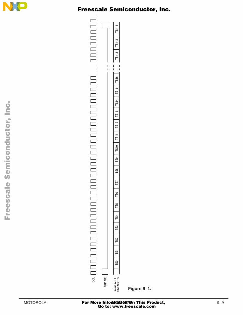
MC145572 9–9MOTOROLA
ÎÎÎÎÎÎÎÎÎÎÎÎÎÎÎÎÎÎÎÎÎÎÎÎÎÎÎÎÎÎÎÎÎÎÎÎÎÎÎÎÎÎÎÎÎÎÎÎÎÎÎÎÎÎÎÎÎÎÎÎÎÎÎÎÎÎÎÎÎÎÎÎÎÎÎÎÎÎÎÎÎÎÎÎÎÎ
ÎÎÎÎÎÎÎÎÎÎÎÎÎÎÎÎÎÎÎÎÎÎÎÎ
ÎÎ
ÎÎ
ÎÎÎÎÎÎÎÎÎÎÎÎÎÎÎÎÎ
Figure 9–1.
Fre
esc
ale
Se
mic
on
du
cto
r, I
Freescale Semiconductor, Inc.
For More Information On This Product, Go to: www.freescale.com
nc
...
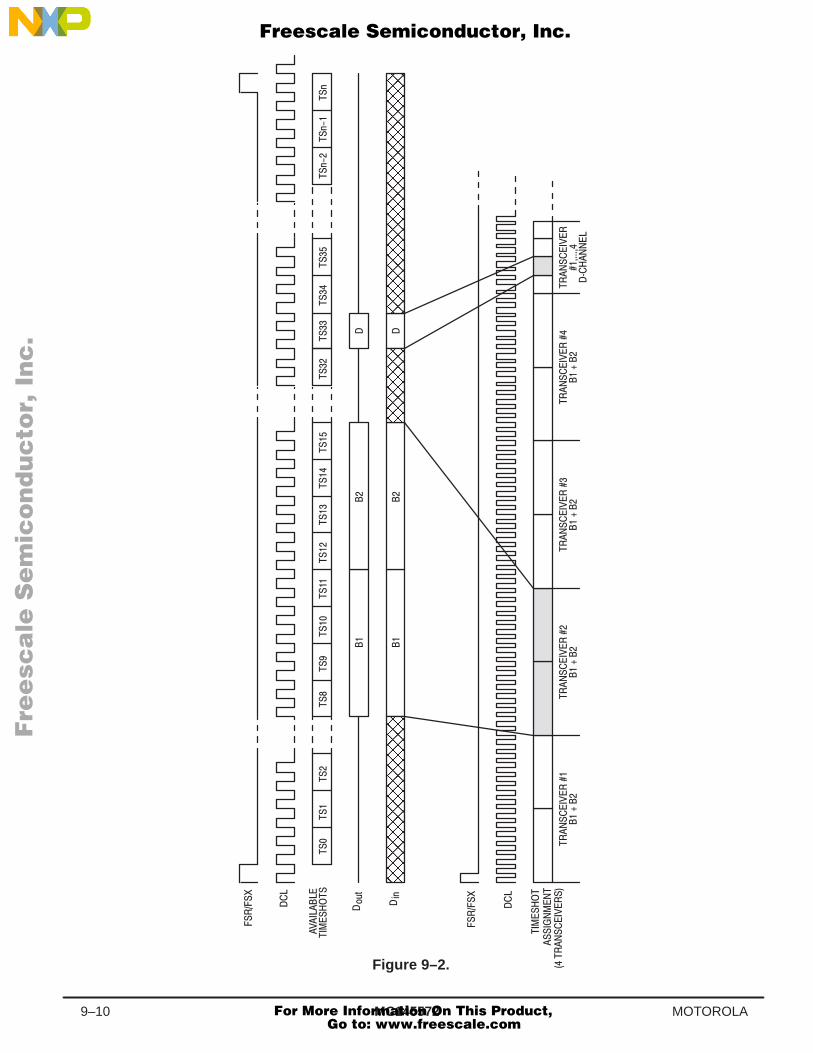
MC1455729–10 MOTOROLA
ÎÎÎÎÎÎÎÎÎÎÎÎÎÎÎÎÎÎÎÎÎ
ÎÎÎÎÎÎÎÎÎÎÎÎÎÎÎÎÎÎÎÎÎÎÎÎÎÎÎÎÎÎÎÎÎÎÎÎÎÎÎÎÎÎÎÎÎÎÎ
ÎÎÎÎÎ
ÎÎÎÎÎÎÎÎÎÎÎÎÎÎÎÎÎÎÎÎÎÎÎ
ÎÎ
ÎÎ
ÎÎÎÎÎÎÎÎÎÎÎÎÎÎÎÎÎÎ
ÎÎÎÎÎÎÎÎÎÎÎÎÎÎÎÎÎÎ
ÎÎÎÎÎÎÎÎÎÎÎÎÎÎÎÎ
ÎÎÎÎÎÎ
ÎÎÎÎÎÎÎÎÎÎÎÎÎÎÎÎÎÎ
ÎÎÎÎÎÎÎÎÎÎÎÎÎÎÎÎ
ÎÎÎÎÎÎ
ÏÏÏÏÏÏÏÏÏÏÏÏÏÏÏÏÏÏ
ÏÏÏÏÏÏÏÏÏÏÏÏÏÏÏÏÏÏÏÏÏÏÏÏÏÏ
ÏÏÏÏÏÏÏÏ
ÎÎÎÎÎÎÎÎÎÎ
ÎÎÎÎÎÎÎÎ
ÎÎÎÎÎÎÎÎ
ÎÎÎÎÎÎÎÎÎÎ
ÎÎÎÎÎÎÎÎ
ÎÎÎÎÎÎÎÎÎÎ
ÎÎÎÎ
ÎÎÎÎ
ÎÎÎÎ
! %
! %
! %
!
!
!
!
!
!
!
!
!
!
!
!
!
!
!
! "
! "
! "
! "
! "
)
#
"
! !
#
! !
!
! "
Figure 9–2.
$%
&('
Fre
esc
ale
Se
mic
on
du
cto
r, I
Freescale Semiconductor, Inc.
For More Information On This Product, Go to: www.freescale.com
nc
...
MC145572 9–11MOTOROLA
This example shows how to program the MC145572 when the GCI 2B+D format is selected insteadof IDL 8– and 10–bit modes. See Section 5.4.3 for a description of the GCI 2B+D mode.
Procedure GCI2B+Dinit();
/*
PURPOSE:
Program GCI timeslot in IDL–2 GCI 2B+D data format
INITIAL CONDITIONS:
MC145572 configured for IDL–2 slave mode
DCL clock rate = 4.096 MHz
Timeslot assignment:
When the DCL clock frequency = 4.096MHz there are 8 possible 32–bit GCI timeslots. In thisexample we will program the MC145572 to transmit and receive in the 4th GCI timeslot.
*/
BEGIN
NR0(b3) <– 1; /* Assert software reset. Only required at power–up initialization.*/
NR0(b3) <– 0; /* De–assert software reset. Only required at power–up initialization.*/
BR10(b0) <– 1; /* Select Init Group Overlay registers.*/
OR5 <– 03; /* Select the 4th GCI timeslot */
OR6(3) <– 1; /* Enable 4th GCI timeslot */
OR10(b0) <– 0; /* Timeslot initialization over. Deselect overlay registers and returnto normal byte register operation */
END;
febe nebe
This example shows how to use the MC145572 febe and nebe counters to calculate a BLock ErrorRatio (BLER). The BLER is a useful measure of the channel quality as well as a measure of thefar–end and near–end receiver’s performance. Using a timed interrupt, the procedures BLER_init andBLER_ISR determine the BLER by calculating the number of far–end and near–end block errors thatoccurred in the last 100 superframes. By subtracting the value of the febe /nebe counters read duringan interrupt from the value read in the previous interrupt, the error count over a specific time intervalcan easily be determined.
The MC145572 has febe and nebe status bits, as well as febe and nebe counters. BR3 containsthe status bits, BR4 is the febe counter and BR5 is the nebe counter. When a febe or nebe isdetected, the status bit is set and the counters are incremented. Section 7.5 describes the operationof the febe /nebe bits in detail. The MC145572 adds a febe /nebe counter rollover feature whichwas not available in the MC145472. When this feature is enabled, the febe /nebe counters willrollover from $FF to 00 instead of saturating at $FF. The interrupt period of this example has beenset to 1.2 seconds to guarantee that the febe /nebe counters do not roll over more than oncebetween interrupts.
Since the superframe period is 12 ms, 100 superframes will be transmitted or received in 1.2 se-conds. The 1.2–second interrupt can easily be implemented using the timer function on any MotorolaMC68HC05 series microcontroller. For greater accuracy, the BLER generated at each interrupt canbe summed over longer periods of time.
By reading BR4 and BR5 once per second it is easy to modify the above procedure to calculate errorseconds and error free seconds.
Fre
esc
ale
Se
mic
on
du
cto
r, I
Freescale Semiconductor, Inc.
For More Information On This Product, Go to: www.freescale.com
nc
...
MC1455729–12 MOTOROLA
Procedure BLER_init
/*
PURPOSE: BLER_init initializes the febe/nebe counters, enables febe/nebe rollover, and en-ables the 1.2 second interrupt. Initialization of the febe/nebe registers should be doneupon activation as shown in the NT and TE activation examples previously mentioned in thissection.
*/
BEGIN
BR4 <– 00; /* Clear febe counter.*/
BR5 <– 00; /* Clear nebe counter */
BR10(b0) <– 1; /* Enable init group registers */
OR7(b1) <– 1; /* Enable febe/nebe rollover */
BR10(b0) <– 0; /* Disable init group registers */
* program timer for 1.2 sec interrupt
* enable timer interrupt
END
Procedure BLER_ISR
/*
PURPOSE: BLER_ISR handles the 1.2 second timer interrupt. It calculates the current far endand near end block error rates and stores them in the memory locations: FE_BLER andNE_BLER. The febe/nebe values from the last interrupt are stored in the memory locations:last_febe and last_nebe. These memory locations should be initialized prior to enabling theinterrupt. If the result of subtracting the last febe/nebe from the current febe/nebe isnegative then the result is adjusted module 256.
OUTPUT:
FE_BLER : far end block error rate in errors/100 blocks
NE_BLER : near end block error rate in errors/100 blocks
last_febe : BR4 value recorded from previous interrupt
last_nebe : BR5 value recorded from previous interrupt
*/
BEGIN
IF BLER_timer_int THEN
BEGIN
febe <– BR4; /* store current febe */
FE_BLER <– febe – last_febe /* calculate far end BLER of last 1.2 sec */
IF FE_BLER <= 0 THEN /* test for febe counter rollover */
FE_BLER <– 256 – FE_BLER /* adjust far end BLER for counterrollover */
last_febe <– BR4 /* update last_febe */
nebe <– BR5; /* store current nebe */
NE_BLER <– nebe – last_nebe /* calculate near end BLER of last 1.2 sec */
IF NE_BLER <= 0 THEN /* test for nebe counter rollover */
NE_BLER <– 256 – NE_BLER /* adjust near end BLER for counter rollover */
last_nebe <– BR5 /* update last_nebe */
END
END
Fre
esc
ale
Se
mic
on
du
cto
r, I
Freescale Semiconductor, Inc.
For More Information On This Product, Go to: www.freescale.com
nc
...
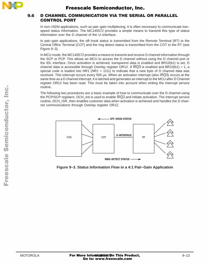
MC145572 9–13MOTOROLA
In non–ISDN applications, such as pair–gain multiplexing, it is often necessary to communicate low–speed status information. The MC145572 provides a simple means to transmit this type of statusinformation over the D channel of the U–interface.
In pair–gain applications, the off–hook status is transmitted from the Remote Terminal (RT) to theCentral Office Terminal (COT) and the ring detect status is transmitted from the COT to the RT (seeFigure 9–3).
In MCU mode, the MC145572 provides a means to transmit and receive D channel information throughthe SCP or PCP. This allows an MCU to access the D channel without using the D channel port orthe IDL interface. Once activation is achieved, transparent data is enabled and BR10(b1) is set, Dchannel data is accessible through Overlay register OR12. If IRQ3 is enabled and BR10(b1) = 1, aspecial code is loaded into NR1 (NR1 = 1111) to indicate that a new byte of D channel data wasreceived. This interrupt occurs every 500 µs. When an activation interrupt (also IRQ3) occurs at thesame time as a D channel interrupt, it is latched and generates an interrupt to the MCU after D Channelregister OR12 has been read. This must be taken into account when writing the interrupt serviceroutine.
The following two procedures are a basic example of how to communicate over the D channel usingthe PCP/SCP registers. DCH_init is used to enable IRQ3 and initiate activation. The interrupt serviceroutine, DCH_ISR, then enables customer data when activation is achieved and handles the D chan-nel communications through Overlay register OR12.
Figure 9–3. Status Information Flow in a 4:1 Pair–Gain Application
Fre
esc
ale
Se
mic
on
du
cto
r, I
Freescale Semiconductor, Inc.
For More Information On This Product, Go to: www.freescale.com
nc
...
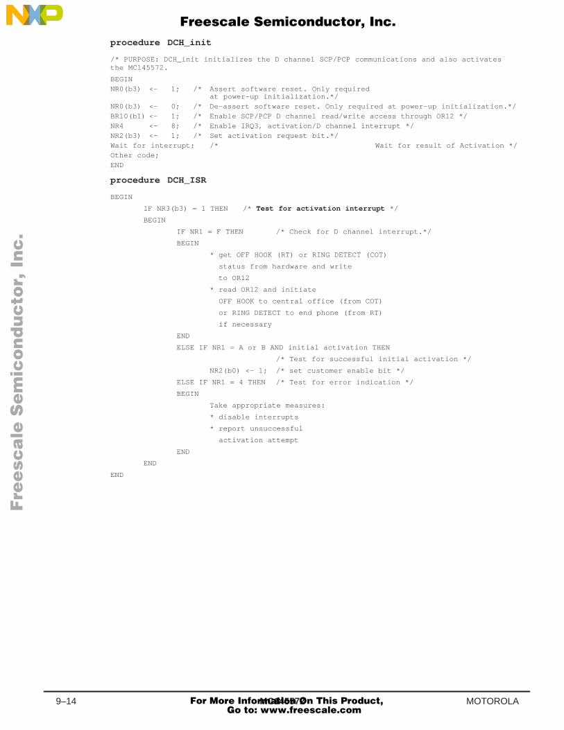
MC1455729–14 MOTOROLA
procedure DCH_init
/* PURPOSE: DCH_init initializes the D channel SCP/PCP communications and also activatesthe MC145572.
BEGIN
NR0(b3) <– 1; /* Assert software reset. Only requiredat power–up initialization.*/
NR0(b3) <– 0; /* De–assert software reset. Only required at power–up initialization.*/
BR10(b1) <– 1; /* Enable SCP/PCP D channel read/write access through OR12 */
NR4 <– 8; /* Enable IRQ3, activation/D channel interrupt */
NR2(b3) <– 1; /* Set activation request bit.*/
Wait for interrupt; /* Wait for result of Activation */
Other code;
END
procedure DCH_ISR
BEGIN
IF NR3(b3) = 1 THEN /* Test for activation interrupt */
BEGIN
IF NR1 = F THEN /* Check for D channel interrupt.*/
BEGIN
* get OFF HOOK (RT) or RING DETECT (COT)
status from hardware and write
to OR12
* read OR12 and initiate
OFF HOOK to central office (from COT)
or RING DETECT to end phone (from RT)
if necessary
END
ELSE IF NR1 = A or B AND initial activation THEN
/* Test for successful initial activation */
NR2(b0) <– 1; /* set customer enable bit */
ELSE IF NR1 = 4 THEN /* Test for error indication */
BEGIN
Take appropriate measures:
* disable interrupts
* report unsuccessful
activation attempt
END
END
END
Fre
esc
ale
Se
mic
on
du
cto
r, I
Freescale Semiconductor, Inc.
For More Information On This Product, Go to: www.freescale.com
nc
...
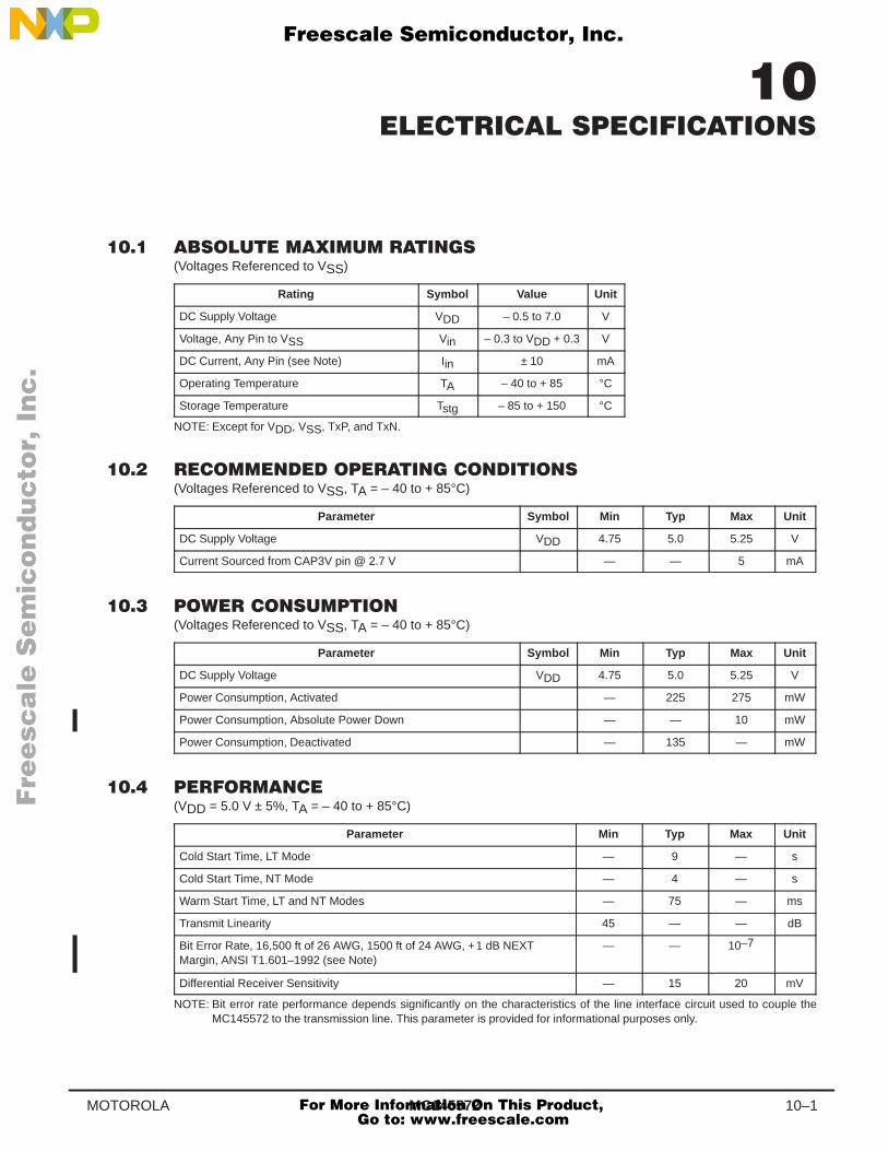
MC145572 10–1MOTOROLA
(Voltages Referenced to VSS)
Rating Symbol Value Unit
DC Supply Voltage VDD – 0.5 to 7.0 V
Voltage, Any Pin to VSS Vin – 0.3 to VDD + 0.3 V
DC Current, Any Pin (see Note) Iin ± 10 mA
Operating Temperature TA – 40 to + 85 °C
Storage Temperature Tstg – 85 to + 150 °C
NOTE: Except for VDD, VSS, TxP, and TxN.
(Voltages Referenced to VSS, TA = – 40 to + 85°C)
Parameter Symbol Min Typ Max Unit
DC Supply Voltage VDD 4.75 5.0 5.25 V
Current Sourced from CAP3V pin @ 2.7 V — — 5 mA
(Voltages Referenced to VSS, TA = – 40 to + 85°C)
Parameter Symbol Min Typ Max Unit
DC Supply Voltage VDD 4.75 5.0 5.25 V
Power Consumption, Activated — 225 275 mW
Power Consumption, Absolute Power Down — — 10 mW
Power Consumption, Deactivated — 135 — mW
(VDD = 5.0 V ± 5%, TA = – 40 to + 85°C)
Parameter Min Typ Max Unit
Cold Start Time, LT Mode — 9 — s
Cold Start Time, NT Mode — 4 — s
Warm Start Time, LT and NT Modes — 75 — ms
Transmit Linearity 45 — — dB
Bit Error Rate, 16,500 ft of 26 AWG, 1500 ft of 24 AWG, +1 dB NEXTMargin, ANSI T1.601–1992 (see Note)
— — 10–7
Differential Receiver Sensitivity — 15 20 mV
NOTE: Bit error rate performance depends significantly on the characteristics of the line interface circuit used to couple theMC145572 to the transmission line. This parameter is provided for informational purposes only.
Fre
esc
ale
Se
mic
on
du
cto
r, I
Freescale Semiconductor, Inc.
For More Information On This Product, Go to: www.freescale.com
nc
...
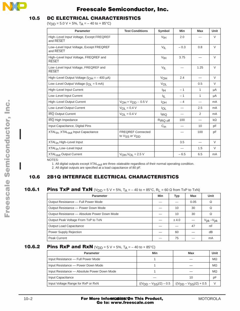
MC14557210–2 MOTOROLA
(VDD = 5.0 V + 5%, TA = – 40 to + 85°C)
Parameter Test Conditions Symbol Min Max Unit
High–Level Input Voltage, Except FREQREFand RESET
VIH 2.0 — V
Low–Level Input Voltage, Except FREQREFand RESET
VIL – 0.3 0.8 V
High–Level Input Voltage, FREQREF andRESET
VIH 3.75 — V
Low–Level Input Voltage, FREQREF andRESET
VIL — 1.25 V
High–Level Output Voltage (IOH = – 400 µA) VOH 2.4 — V
Low–Level Output Voltage (IOL = 5 mA) VOL 0.5 V
High–Level Input Current IIH – 1 1 µA
Low–Level Input Current IIL – 1 1 µA
High–Level Output Current VOH = VDD – 0.5 V IOH – 4 — mA
Low–Level Output Current VOL = 0.4 V IOL — 2.5 mA
IRQ Output Current VOL = 0.4 V IIRQ — 2 mA
IRQ High Impedance RIRQ off 100 — kΩ
Input Capacitance, Digital Pins Cin — 10 pF
XTALin, XTALout Input Capacitance FREQREF Connectedto VSS or VDD
— 100 pF
XTALin High–Level Input 3.5 — V
XTALin Low–Level Input — 1.5 V
XTALout Output Current VOH,VOL = 2.5 V – 6.5 6.5 mA
NOTES:1. All digital outputs except XTALout are three–stateable regardless of their normal operating condition.2. All digital outputs are specified at a load capacitance of 80 pF.
(VDD = 5 V + 5%, TA = – 40 to + 85°C, RL = 60 Ω from TxP to TxN)
Parameter Min Typ Max Unit
Output Resistance — Full Power Mode — — 0.05 Ω
Output Resistance — Power Down Mode — 10 30 Ω
Output Resistance — Absolute Power Down Mode — 10 30 Ω
Output Peak Voltage From TxP to TxN — ± 4.0 — Vpk –Vpk
Output Load Capacitance — — 47 nF
Power Supply Rejection — 60 — dB
Peak Current — 75 — mA
(VDD = 5 V + 5%, TA = – 40 to + 85°C)
Parameter Min Max Unit
Input Resistance — Full Power Mode 1 — MΩ
Input Resistance — Power Down Mode 1 — MΩ
Input Resistance — Absolute Power Down Mode 1 — MΩ
Input Capacitance — 10 pF
Input Voltage Range for RxP or RxN ((VDD – VSS)/2) – 0.5 ((VDD – VSS)/2) + 0.5 V
Fre
esc
ale
Se
mic
on
du
cto
r, I
Freescale Semiconductor, Inc.
For More Information On This Product, Go to: www.freescale.com
nc
...
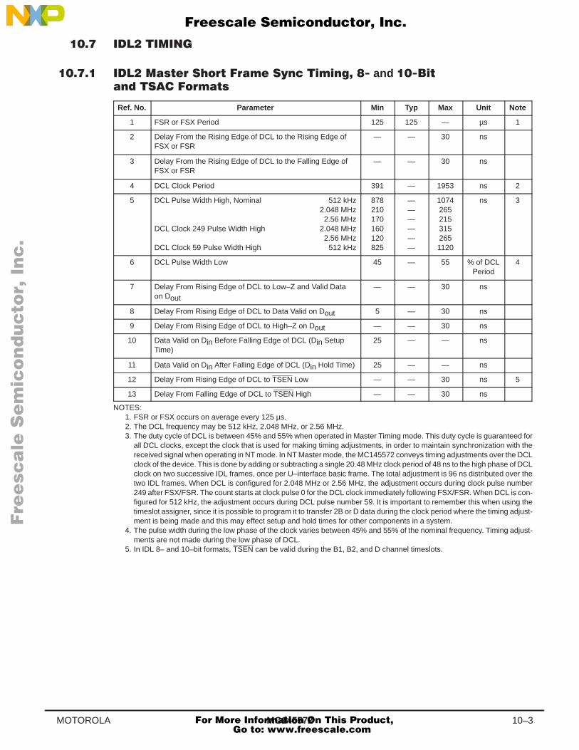
MC145572 10–3MOTOROLA
!" " # and " "!
Ref. No. Parameter Min Typ Max Unit Note
1 FSR or FSX Period 125 125 — µs 1
2 Delay From the Rising Edge of DCL to the Rising Edge ofFSX or FSR
— — 30 ns
3 Delay From the Rising Edge of DCL to the Falling Edge ofFSX or FSR
— — 30 ns
4 DCL Clock Period 391 — 1953 ns 2
5 DCL Pulse Width High, Nominal 512 kHz2.048 MHz2.56 MHz
DCL Clock 249 Pulse Width High 2.048 MHz2.56 MHz
DCL Clock 59 Pulse Width High 512 kHz
878210170160120825
——————
10742652153152651120
ns 3
6 DCL Pulse Width Low 45 — 55 % of DCLPeriod
4
7 Delay From Rising Edge of DCL to Low–Z and Valid Dataon Dout
— — 30 ns
8 Delay From Rising Edge of DCL to Data Valid on Dout 5 — 30 ns
9 Delay From Rising Edge of DCL to High–Z on Dout — — 30 ns
10 Data Valid on Din Before Falling Edge of DCL (Din SetupTime)
25 — — ns
11 Data Valid on Din After Falling Edge of DCL (Din Hold Time) 25 — — ns
12 Delay From Rising Edge of DCL to TSEN Low — — 30 ns 5
13 Delay From Falling Edge of DCL to TSEN High — — 30 ns
NOTES:1. FSR or FSX occurs on average every 125 µs.2. The DCL frequency may be 512 kHz, 2.048 MHz, or 2.56 MHz.3. The duty cycle of DCL is between 45% and 55% when operated in Master Timing mode. This duty cycle is guaranteed for
all DCL clocks, except the clock that is used for making timing adjustments, in order to maintain synchronization with thereceived signal when operating in NT mode. In NT Master mode, the MC145572 conveys timing adjustments over the DCLclock of the device. This is done by adding or subtracting a single 20.48 MHz clock period of 48 ns to the high phase of DCLclock on two successive IDL frames, once per U–interface basic frame. The total adjustment is 96 ns distributed over thetwo IDL frames. When DCL is configured for 2.048 MHz or 2.56 MHz, the adjustment occurs during clock pulse number249 after FSX/FSR. The count starts at clock pulse 0 for the DCL clock immediately following FSX/FSR. When DCL is con-figured for 512 kHz, the adjustment occurs during DCL pulse number 59. It is important to remember this when using thetimeslot assigner, since it is possible to program it to transfer 2B or D data during the clock period where the timing adjust-ment is being made and this may effect setup and hold times for other components in a system.
4. The pulse width during the low phase of the clock varies between 45% and 55% of the nominal frequency. Timing adjust-ments are not made during the low phase of DCL.
5. In IDL 8– and 10–bit formats, TSEN can be valid during the B1, B2, and D channel timeslots.
Fre
esc
ale
Se
mic
on
du
cto
r, I
Freescale Semiconductor, Inc.
For More Information On This Product, Go to: www.freescale.com
nc
...
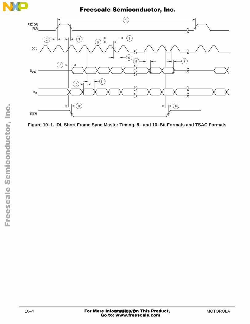
MC14557210–4 MOTOROLA
Figure 10–1. IDL Short Frame Sync Master Timing, 8– and 10–Bit Formats and TSAC Formats
Fre
esc
ale
Se
mic
on
du
cto
r, I
Freescale Semiconductor, Inc.
For More Information On This Product, Go to: www.freescale.com
nc
...
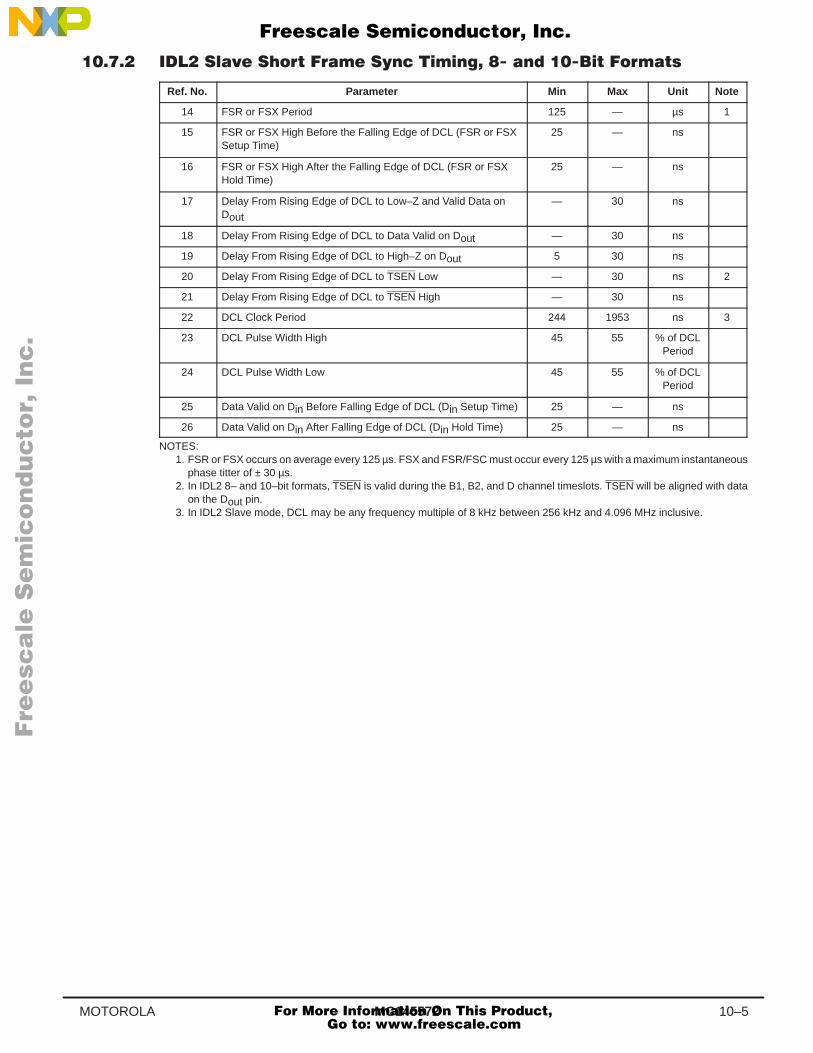
MC145572 10–5MOTOROLA
Ref. No. Parameter Min Max Unit Note
14 FSR or FSX Period 125 — µs 1
15 FSR or FSX High Before the Falling Edge of DCL (FSR or FSXSetup Time)
25 — ns
16 FSR or FSX High After the Falling Edge of DCL (FSR or FSXHold Time)
25 — ns
17 Delay From Rising Edge of DCL to Low–Z and Valid Data onDout
— 30 ns
18 Delay From Rising Edge of DCL to Data Valid on Dout — 30 ns
19 Delay From Rising Edge of DCL to High–Z on Dout 5 30 ns
20 Delay From Rising Edge of DCL to TSEN Low — 30 ns 2
21 Delay From Rising Edge of DCL to TSEN High — 30 ns
22 DCL Clock Period 244 1953 ns 3
23 DCL Pulse Width High 45 55 % of DCLPeriod
24 DCL Pulse Width Low 45 55 % of DCLPeriod
25 Data Valid on Din Before Falling Edge of DCL (Din Setup Time) 25 — ns
26 Data Valid on Din After Falling Edge of DCL (Din Hold Time) 25 — ns
NOTES:1. FSR or FSX occurs on average every 125 µs. FSX and FSR/FSC must occur every 125 µs with a maximum instantaneous
phase titter of ± 30 µs.2. In IDL2 8– and 10–bit formats, TSEN is valid during the B1, B2, and D channel timeslots. TSEN will be aligned with data
on the Dout pin.3. In IDL2 Slave mode, DCL may be any frequency multiple of 8 kHz between 256 kHz and 4.096 MHz inclusive.
Fre
esc
ale
Se
mic
on
du
cto
r, I
Freescale Semiconductor, Inc.
For More Information On This Product, Go to: www.freescale.com
nc
...
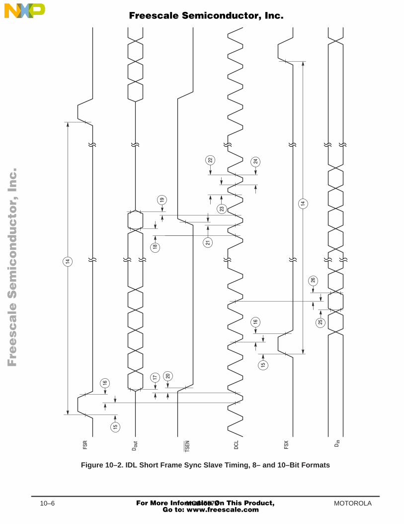
MC14557210–6 MOTOROLA
Figure 10–2. IDL Short Frame Sync Slave Timing, 8– and 10–Bit Formats
Fre
esc
ale
Se
mic
on
du
cto
r, I
Freescale Semiconductor, Inc.
For More Information On This Product, Go to: www.freescale.com
nc
...
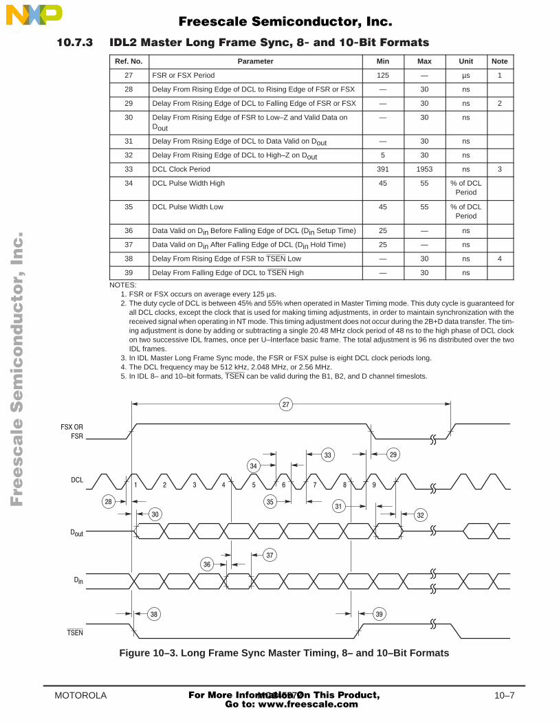
MC145572 10–7MOTOROLA
Ref. No. Parameter Min Max Unit Note
27 FSR or FSX Period 125 — µs 1
28 Delay From Rising Edge of DCL to Rising Edge of FSR or FSX — 30 ns
29 Delay From Rising Edge of DCL to Falling Edge of FSR or FSX — 30 ns 2
30 Delay From Rising Edge of FSR to Low–Z and Valid Data onDout
— 30 ns
31 Delay From Rising Edge of DCL to Data Valid on Dout — 30 ns
32 Delay From Rising Edge of DCL to High–Z on Dout 5 30 ns
33 DCL Clock Period 391 1953 ns 3
34 DCL Pulse Width High 45 55 % of DCLPeriod
35 DCL Pulse Width Low 45 55 % of DCLPeriod
36 Data Valid on Din Before Falling Edge of DCL (Din Setup Time) 25 — ns
37 Data Valid on Din After Falling Edge of DCL (Din Hold Time) 25 — ns
38 Delay From Rising Edge of FSR to TSEN Low — 30 ns 4
39 Delay From Falling Edge of DCL to TSEN High — 30 ns
NOTES:1. FSR or FSX occurs on average every 125 µs.2. The duty cycle of DCL is between 45% and 55% when operated in Master Timing mode. This duty cycle is guaranteed for
all DCL clocks, except the clock that is used for making timing adjustments, in order to maintain synchronization with thereceived signal when operating in NT mode. This timing adjustment does not occur during the 2B+D data transfer. The tim-ing adjustment is done by adding or subtracting a single 20.48 MHz clock period of 48 ns to the high phase of DCL clockon two successive IDL frames, once per U–Interface basic frame. The total adjustment is 96 ns distributed over the twoIDL frames.
3. In IDL Master Long Frame Sync mode, the FSR or FSX pulse is eight DCL clock periods long.4. The DCL frequency may be 512 kHz, 2.048 MHz, or 2.56 MHz.5. In IDL 8– and 10–bit formats, TSEN can be valid during the B1, B2, and D channel timeslots.
Figure 10–3. Long Frame Sync Master Timing, 8– and 10–Bit Formats
Fre
esc
ale
Se
mic
on
du
cto
r, I
Freescale Semiconductor, Inc.
For More Information On This Product, Go to: www.freescale.com
nc
...
MC14557210–8 MOTOROLA
Ref. No. Parameter Min Max Unit Note
40 FSR or FSX Period 125 — µs 1
41 FSR or FSX High Before the Falling Edge of DCL (FSR or FSXSetup Time)
25 — ns 2
42 FSR or FSX High After the Falling Edge of DCL (FSR or FSXHold Time)
25 — ns 2
43 FSR or FSX Low Before the Falling Edge of DCL 25 — ns 2
44 Delay From Rising Edge of FSR to Low–Z and Valid Data onDout
— 30 ns
45 Delay From Rising Edge of DCL to Data Valid on Dout — 30 ns
46 Delay From Rising Edge of DCL to High–Z on Dout 5 30 ns
47 Delay From Rising Edge of FSR to TSEN Low — 30 ns 3
48 Delay From Falling Edge of DCL to TSEN High — 30 ns
49 DCL Clock Period 244 1953 ns 4
50 DCL Pulse Width High 45 55 % of DCLPeriod
51 DCL Pulse Width Low 45 55 % of DCLPeriod
52 Data Valid on Din Before Falling Edge of DCL (Din Setup Time) 25 — ns
53 Data Valid on Din After Falling Edge of DCL (Din Hold Time) 25 — ns
NOTES:1. FSR or FSX occurs on average every 125 µs. FSX and FSR/FSC must occur every 125 µs with a maximum instantaneous
phase titter of ± 30 µs.2. FSR or FSX should be asserted for at least two DCL clock cycles and at most eight DCL clock cycles.3. In IDL 8– and 10–bit formats, TSEN is valid during the B1, B2, and D channel timeslots. TSEN will be aligned with data on
the Dout pin.4. In IDL Slave mode, DCL may be any frequency that is a multiple of 8 kHz and is between 256 kHz and 4.096 MHz inclusive.
Fre
esc
ale
Se
mic
on
du
cto
r, I
Freescale Semiconductor, Inc.
For More Information On This Product, Go to: www.freescale.com
nc
...
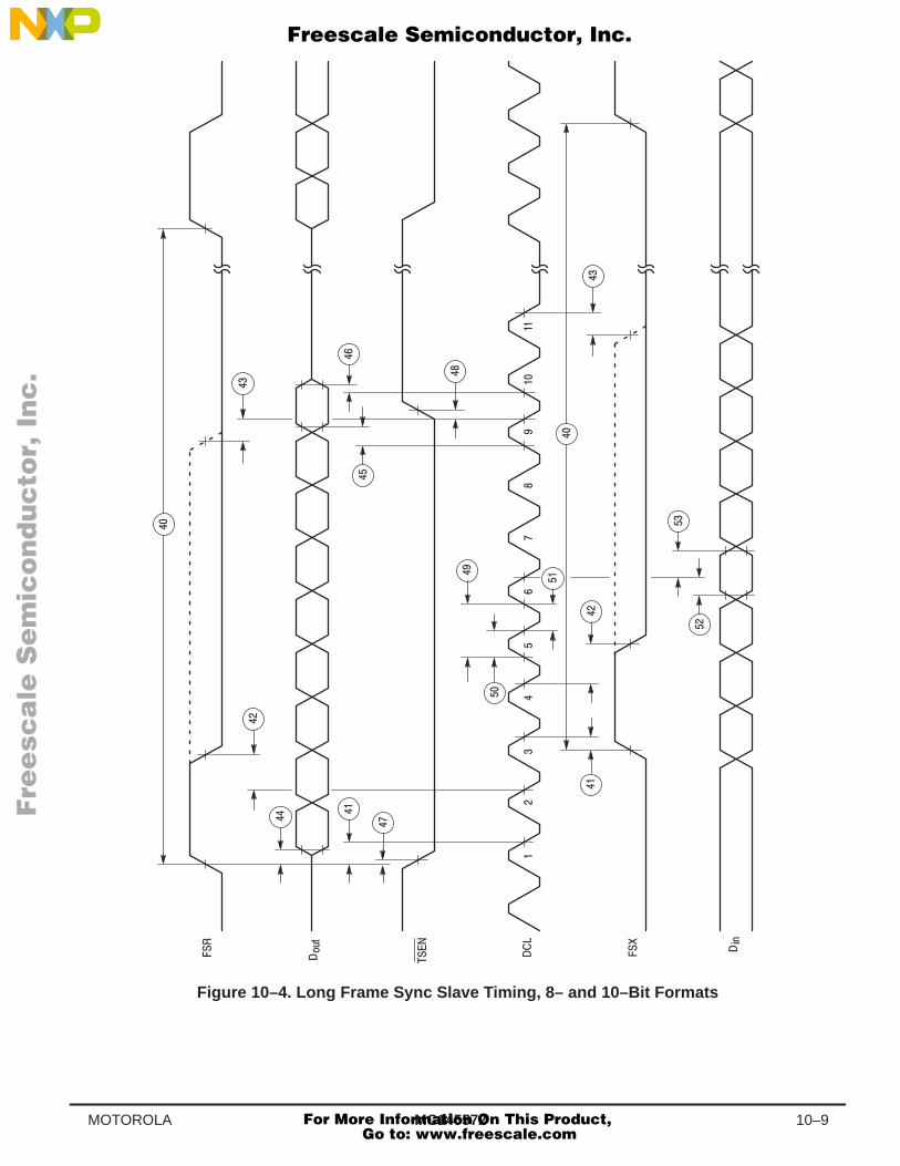
MC145572 10–9MOTOROLA
Figure 10–4. Long Frame Sync Slave Timing, 8– and 10–Bit Formats
Fre
esc
ale
Se
mic
on
du
cto
r, I
Freescale Semiconductor, Inc.
For More Information On This Product, Go to: www.freescale.com
nc
...
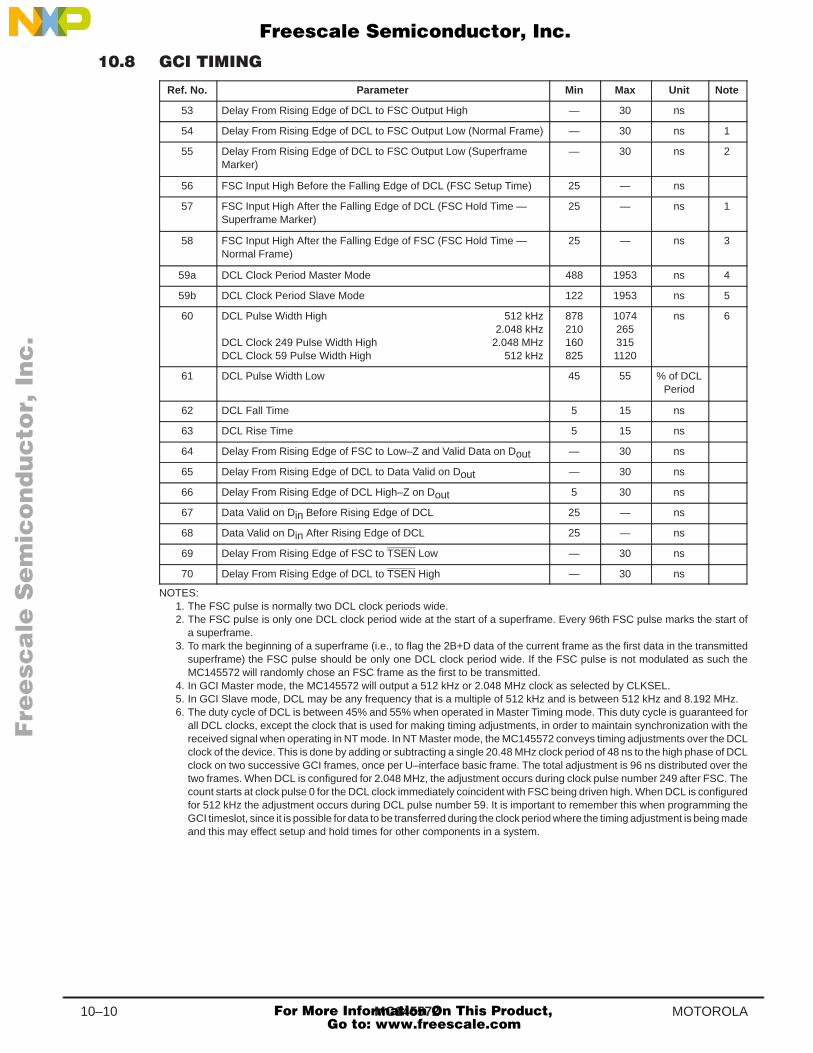
MC14557210–10 MOTOROLA
Ref. No. Parameter Min Max Unit Note
53 Delay From Rising Edge of DCL to FSC Output High — 30 ns
54 Delay From Rising Edge of DCL to FSC Output Low (Normal Frame) — 30 ns 1
55 Delay From Rising Edge of DCL to FSC Output Low (SuperframeMarker)
— 30 ns 2
56 FSC Input High Before the Falling Edge of DCL (FSC Setup Time) 25 — ns
57 FSC Input High After the Falling Edge of DCL (FSC Hold Time —Superframe Marker)
25 — ns 1
58 FSC Input High After the Falling Edge of FSC (FSC Hold Time —Normal Frame)
25 — ns 3
59a DCL Clock Period Master Mode 488 1953 ns 4
59b DCL Clock Period Slave Mode 122 1953 ns 5
60 DCL Pulse Width High 512 kHz2.048 kHz
DCL Clock 249 Pulse Width High 2.048 MHzDCL Clock 59 Pulse Width High 512 kHz
878210160825
10742653151120
ns 6
61 DCL Pulse Width Low 45 55 % of DCLPeriod
62 DCL Fall Time 5 15 ns
63 DCL Rise Time 5 15 ns
64 Delay From Rising Edge of FSC to Low–Z and Valid Data on Dout — 30 ns
65 Delay From Rising Edge of DCL to Data Valid on Dout — 30 ns
66 Delay From Rising Edge of DCL High–Z on Dout 5 30 ns
67 Data Valid on Din Before Rising Edge of DCL 25 — ns
68 Data Valid on Din After Rising Edge of DCL 25 — ns
69 Delay From Rising Edge of FSC to TSEN Low — 30 ns
70 Delay From Rising Edge of DCL to TSEN High — 30 ns
NOTES:1. The FSC pulse is normally two DCL clock periods wide.2. The FSC pulse is only one DCL clock period wide at the start of a superframe. Every 96th FSC pulse marks the start of
a superframe.3. To mark the beginning of a superframe (i.e., to flag the 2B+D data of the current frame as the first data in the transmitted
superframe) the FSC pulse should be only one DCL clock period wide. If the FSC pulse is not modulated as such theMC145572 will randomly chose an FSC frame as the first to be transmitted.
4. In GCI Master mode, the MC145572 will output a 512 kHz or 2.048 MHz clock as selected by CLKSEL.5. In GCI Slave mode, DCL may be any frequency that is a multiple of 512 kHz and is between 512 kHz and 8.192 MHz.6. The duty cycle of DCL is between 45% and 55% when operated in Master Timing mode. This duty cycle is guaranteed for
all DCL clocks, except the clock that is used for making timing adjustments, in order to maintain synchronization with thereceived signal when operating in NT mode. In NT Master mode, the MC145572 conveys timing adjustments over the DCLclock of the device. This is done by adding or subtracting a single 20.48 MHz clock period of 48 ns to the high phase of DCLclock on two successive GCI frames, once per U–interface basic frame. The total adjustment is 96 ns distributed over thetwo frames. When DCL is configured for 2.048 MHz, the adjustment occurs during clock pulse number 249 after FSC. Thecount starts at clock pulse 0 for the DCL clock immediately coincident with FSC being driven high. When DCL is configuredfor 512 kHz the adjustment occurs during DCL pulse number 59. It is important to remember this when programming theGCI timeslot, since it is possible for data to be transferred during the clock period where the timing adjustment is being madeand this may effect setup and hold times for other components in a system.
Fre
esc
ale
Se
mic
on
du
cto
r, I
Freescale Semiconductor, Inc.
For More Information On This Product, Go to: www.freescale.com
nc
...
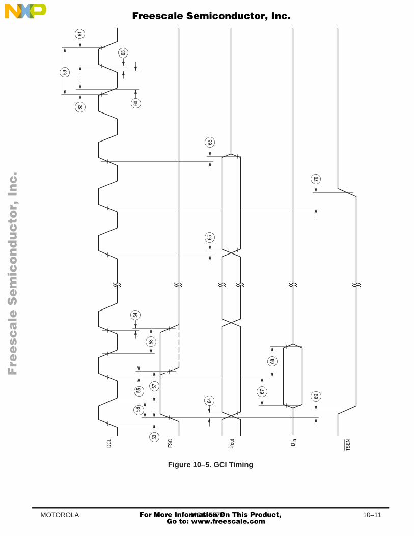
MC145572 10–11MOTOROLA
Figure 10–5. GCI Timing
Fre
esc
ale
Se
mic
on
du
cto
r, I
Freescale Semiconductor, Inc.
For More Information On This Product, Go to: www.freescale.com
nc
...
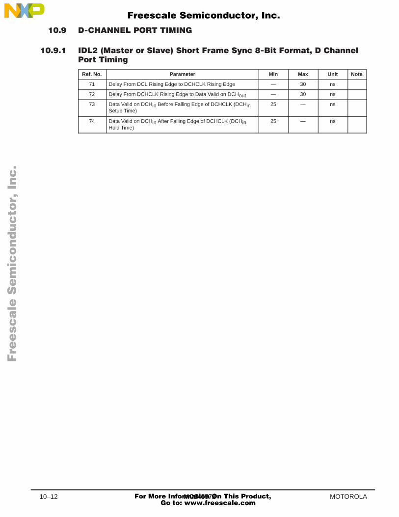
MC14557210–12 MOTOROLA
()' &' #* !&') '$ +% ") &'$) !%%#&') "$"%
Ref. No. Parameter Min Max Unit Note
71 Delay From DCL Rising Edge to DCHCLK Rising Edge — 30 ns
72 Delay From DCHCLK Rising Edge to Data Valid on DCHout — 30 ns
73 Data Valid on DCHin Before Falling Edge of DCHCLK (DCHinSetup Time)
25 — ns
74 Data Valid on DCHin After Falling Edge of DCHCLK (DCHinHold Time)
25 — ns
Fre
esc
ale
Se
mic
on
du
cto
r, I
Freescale Semiconductor, Inc.
For More Information On This Product, Go to: www.freescale.com
nc
...
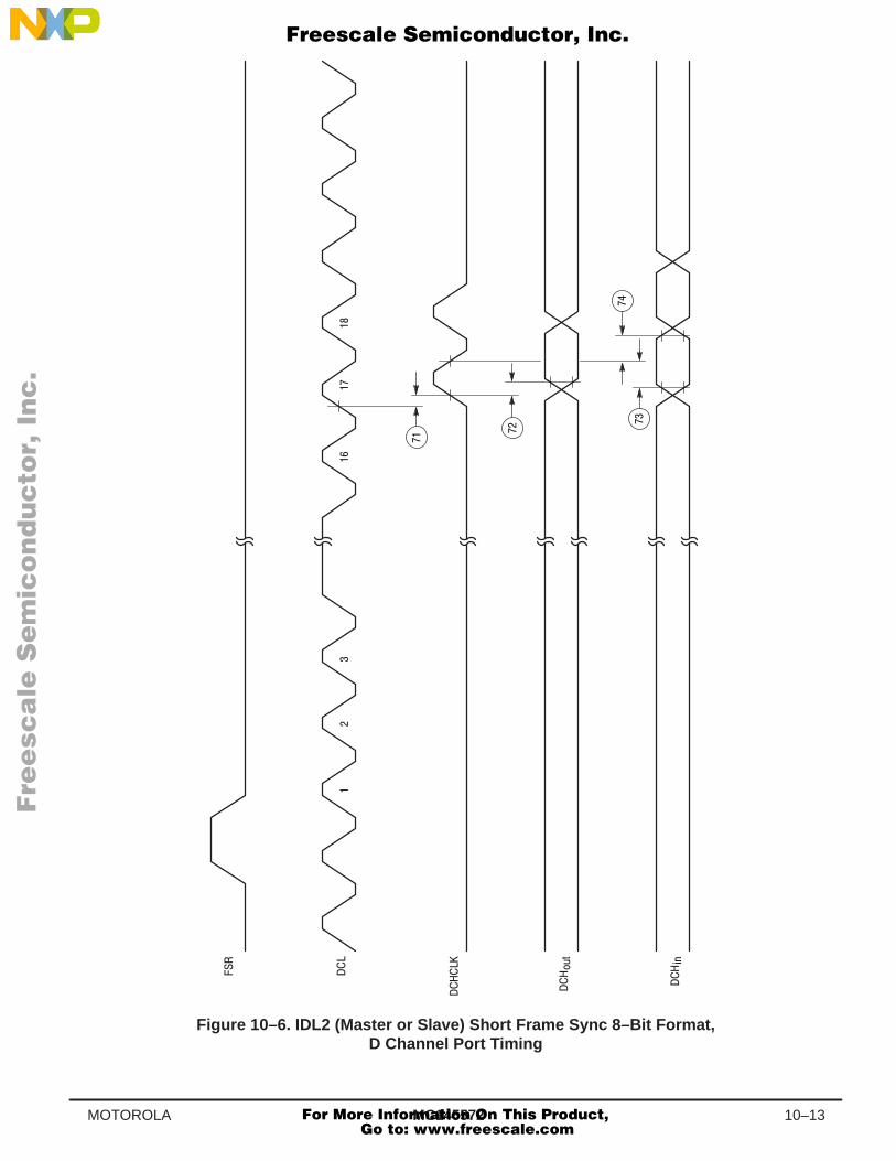
MC145572 10–13MOTOROLA
Figure 10–6. IDL2 (Master or Slave) Short Frame Sync 8–Bit Format,D Channel Port Timing
Fre
esc
ale
Se
mic
on
du
cto
r, I
Freescale Semiconductor, Inc.
For More Information On This Product, Go to: www.freescale.com
nc
...

MC14557210–14 MOTOROLA
! " ! # ! ! !
Ref. No. Parameter Min Max Unit Note
75 Delay From DCL Rising Edge to DCHCLK Rising Edge — 30 ns
76 Delay From DCHCLK Rising Edge to Data Valid on DCHout — 30 ns
77 Data Valid on DCHin Before Falling Edge of DCHCLK (DCHinSetup Time)
25 — ns
78 Data Valid on DCHin After Falling Edge of DCHCLK (DCHinHold Time)
25 — ns
Fre
esc
ale
Se
mic
on
du
cto
r, I
Freescale Semiconductor, Inc.
For More Information On This Product, Go to: www.freescale.com
nc
...
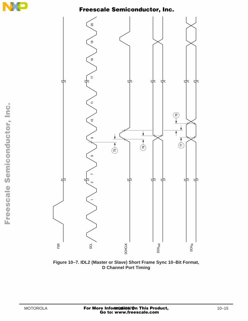
MC145572 10–15MOTOROLA
Figure 10–7. IDL2 (Master or Slave) Short Frame Sync 10–Bit Format,D Channel Port Timing
Fre
esc
ale
Se
mic
on
du
cto
r, I
Freescale Semiconductor, Inc.
For More Information On This Product, Go to: www.freescale.com
nc
...

MC14557210–16 MOTOROLA
"#! ! $ ! % # !# !#
Ref. No. Parameter Min Max Unit Note
79 Delay From DCL Rising Edge to DCHCLK Rising Edge — 30 ns
80 Delay From DCHCLK Rising Edge to Data Valid on DCHout — 30 ns
81 Data Valid on DCHin Before Falling Edge of DCHCLK (DCHinSetup Time)
25 — ns
82 Data Valid on DCHin After Falling Edge of DCHCLK (DCHinHold Time)
25 — ns
Fre
esc
ale
Se
mic
on
du
cto
r, I
Freescale Semiconductor, Inc.
For More Information On This Product, Go to: www.freescale.com
nc
...
MC145572 10–17MOTOROLA
Figure 10–8. IDL2 (Master or Slave) Long Frame Sync 8–Bit Format,D Channel Port Timing
Fre
esc
ale
Se
mic
on
du
cto
r, I
Freescale Semiconductor, Inc.
For More Information On This Product, Go to: www.freescale.com
nc
...

MC14557210–18 MOTOROLA
!" # $ " " "
Ref. No. Parameter Min Max Unit Note
83 Delay From DCL Rising Edge to DCHCLK Rising Edge — 30 ns
84 Delay From DCHCLK Rising Edge to Data Valid on DCHout — 30 ns
85 Data Valid on DCHin Before Falling Edge of DCHCLK (DCHinSetup Time)
25 — ns
86 Data Valid on DCHin After Falling Edge of DCHCLK (DCHinHold Time)
25 — ns
Fre
esc
ale
Se
mic
on
du
cto
r, I
Freescale Semiconductor, Inc.
For More Information On This Product, Go to: www.freescale.com
nc
...
MC145572 10–19MOTOROLA
Figure 10–9. IDL2 (Master or Slave) Long Frame Sync 10–Bit Format,D Channel Port Timing
Fre
esc
ale
Se
mic
on
du
cto
r, I
Freescale Semiconductor, Inc.
For More Information On This Product, Go to: www.freescale.com
nc
...
MC14557210–20 MOTOROLA
"$(' !" " &'% #% ) #%' %! #
Ref. No. Parameter Min Max Unit Note
91 FSX Period 125 — µs 1
92 SFAX Period 12.0 — ms 2
93 SFAX Input High Before Falling Edge of DCL (SFAX SetupTime)
25 — ns 3
94 SFAX Input High After Falling Edge of DCL (SFAX Hold Time) 25 — ns
NOTES:1. See Section 10.7 for FSX jitter requirements and specifications.2. SFAX must occur every 96 FSX 8 kHz frames.3. SFAX is sampled on the next DCL falling edge after FSX is asserted.
Figure 10–10. SFAX Input Timing in IDL2 (Master or Slave) Short Frame Mode
Fre
esc
ale
Se
mic
on
du
cto
r, I
Freescale Semiconductor, Inc.
For More Information On This Product, Go to: www.freescale.com
nc
...

MC145572 10–21MOTOROLA
Ref. No. Parameter Min Max Unit Note
95 Delay From Rising Edge of DCL to Rising Edge of FSR or FSX — 30 ns
96 FSR or FSX High Before the Falling Edge of DCL (FSR or FSXSetup Time)
25 — ns
97 FSR or FSX High After the Falling Edge of DCL (FSR or FSXHold Time)
25 — ns
98 FSX Period 125 — µs 1
99 SFAX Period 12.0 — ms 2
100 SFAX Input High Before Rising Edge of FSX (SFAX SetupTime)
25 — ns 3
101 SFAX Input High After Rising Edge of FSX (SFAX Hold Time) 25 — ns
NOTES:1. See Section 10. 7 for FSX jitter requirements and specifications.2. SFAX must occur every 96 FSX 8 kHz frames.3. SFAX is sampled on the rising edge of FSX.
Fre
esc
ale
Se
mic
on
du
cto
r, I
Freescale Semiconductor, Inc.
For More Information On This Product, Go to: www.freescale.com
nc
...
MC14557210–22 MOTOROLA
Figure 10–11. SFAX Input Timing in IDL2 (Master or Slave)Long Frame Mode
Fre
esc
ale
Se
mic
on
du
cto
r, I
Freescale Semiconductor, Inc.
For More Information On This Product, Go to: www.freescale.com
nc
...
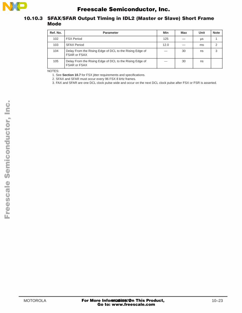
MC145572 10–23MOTOROLA
#"#" !" $ "
Ref. No. Parameter Min Max Unit Note
102 FSX Period 125 — µs 1
103 SFAX Period 12.0 — ms 2
104 Delay From the Rising Edge of DCL to the Rising Edge ofFSAR or FSAX
— 30 ns 3
105 Delay From the Rising Edge of DCL to the Rising Edge ofFSAR or FSAX
— 30 ns
NOTES:1. See Section 10.7 for FSX jitter requirements and specifications.2. SFAX and SFAR must occur every 96 FSX 8 kHz frames.3. FAX and SFAR are one DCL clock pulse wide and occur on the next DCL clock pulse after FSX or FSR is asserted.
Fre
esc
ale
Se
mic
on
du
cto
r, I
Freescale Semiconductor, Inc.
For More Information On This Product, Go to: www.freescale.com
nc
...
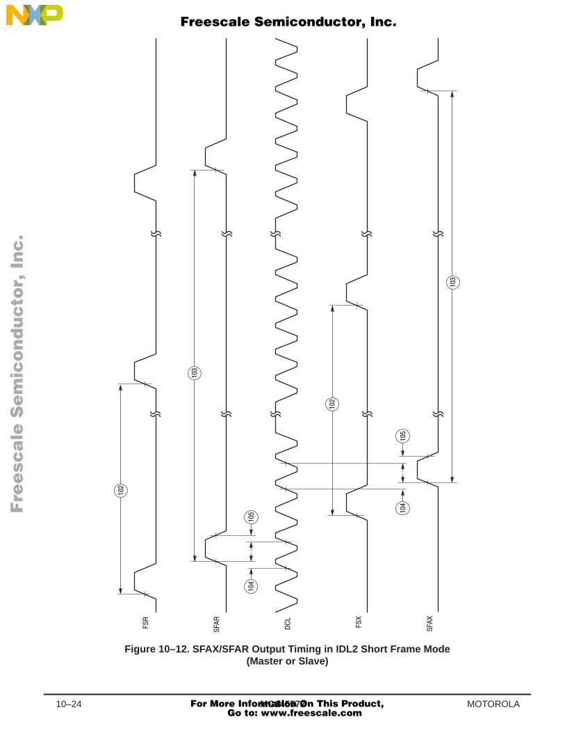
MC14557210–24 MOTOROLA
Figure 10–12. SFAX/SFAR Output Timing in IDL2 Short Frame Mode(Master or Slave)
Fre
esc
ale
Se
mic
on
du
cto
r, I
Freescale Semiconductor, Inc.
For More Information On This Product, Go to: www.freescale.com
nc
...

MC145572 10–25MOTOROLA
"!"! ! #
Ref. No. Parameter Min Max Unit Note
106 FSX or FSR Period 125 — µs 1
107 SFAX or SFAR Period 12.0 — ms 2
108 Delay From the Rising Edge of FSR or FSX to the Rising Edgeof SFAR or SFAX
— 30 ns 3
NOTES:1. See Section 10.7 for FSX jitter requirements and specifications.2. SFAX and SFAR must occur every 96 FSX 8 kHz frames.3. SFAX and SFAR occur coincident with FSX and FSR, respectively.
Fre
esc
ale
Se
mic
on
du
cto
r, I
Freescale Semiconductor, Inc.
For More Information On This Product, Go to: www.freescale.com
nc
...
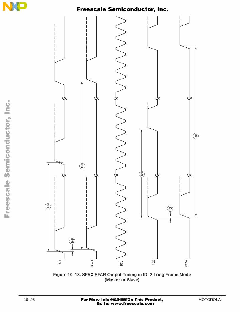
MC14557210–26 MOTOROLA
Figure 10–13. SFAX/SFAR Output Timing in IDL2 Long Frame Mode(Master or Slave)
Fre
esc
ale
Se
mic
on
du
cto
r, I
Freescale Semiconductor, Inc.
For More Information On This Product, Go to: www.freescale.com
nc
...
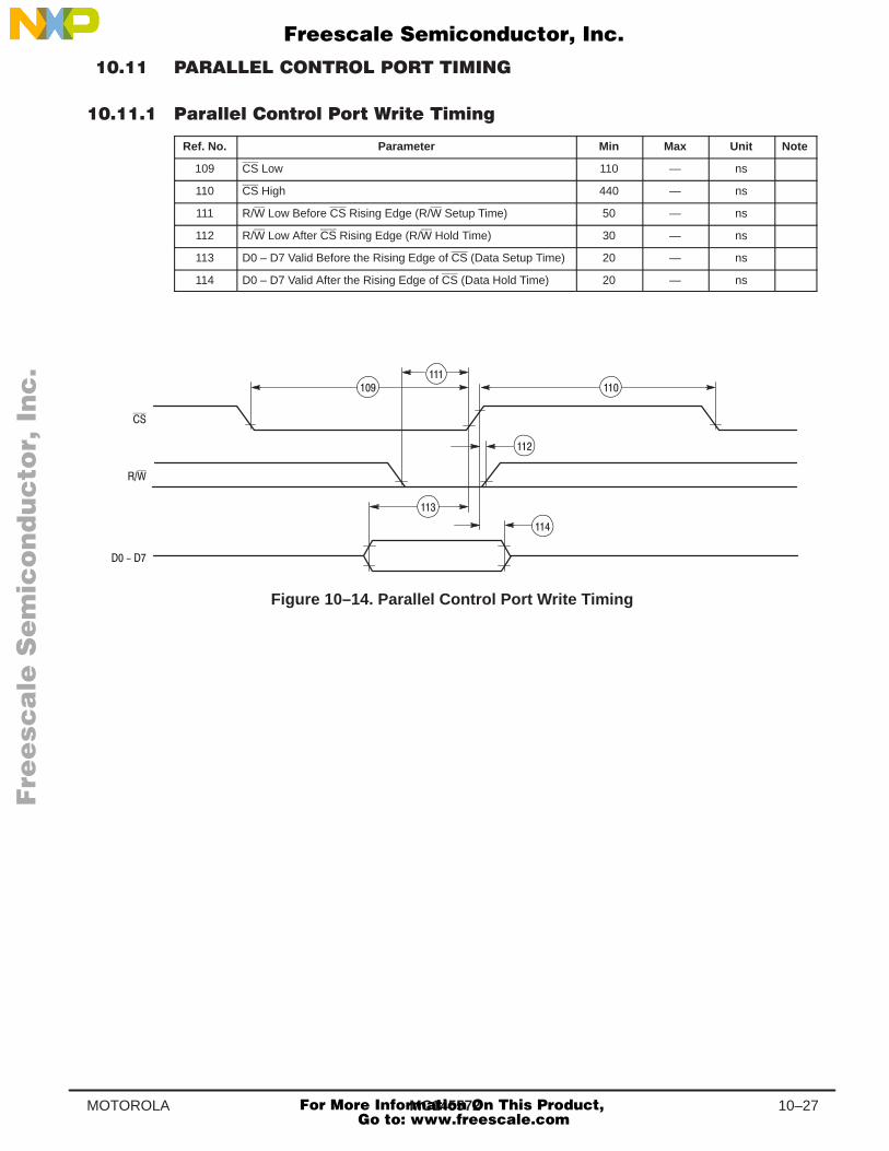
MC145572 10–27MOTOROLA
Ref. No. Parameter Min Max Unit Note
109 CS Low 110 — ns
110 CS High 440 — ns
111 R/W Low Before CS Rising Edge (R/W Setup Time) 50 — ns
112 R/W Low After CS Rising Edge (R/W Hold Time) 30 — ns
113 D0 – D7 Valid Before the Rising Edge of CS (Data Setup Time) 20 — ns
114 D0 – D7 Valid After the Rising Edge of CS (Data Hold Time) 20 — ns
Figure 10–14. Parallel Control Port Write Timing
Fre
esc
ale
Se
mic
on
du
cto
r, I
Freescale Semiconductor, Inc.
For More Information On This Product, Go to: www.freescale.com
nc
...
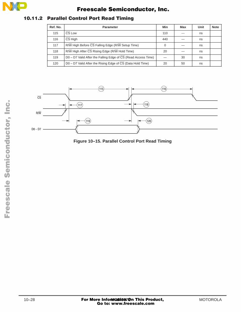
MC14557210–28 MOTOROLA
Ref. No. Parameter Min Max Unit Note
115 CS Low 110 — ns
116 CS High 440 — ns
117 R/W High Before CS Falling Edge (R/W Setup Time) 0 — ns
118 R/W High After CS Rising Edge (R/W Hold Time) 20 — ns
119 D0 – D7 Valid After the Falling Edge of CS (Read Access Time) — 30 ns
120 D0 – D7 Valid After the Rising Edge of CS (Data Hold Time) 20 50 ns
Figure 10–15. Parallel Control Port Read Timing
Fre
esc
ale
Se
mic
on
du
cto
r, I
Freescale Semiconductor, Inc.
For More Information On This Product, Go to: www.freescale.com
nc
...
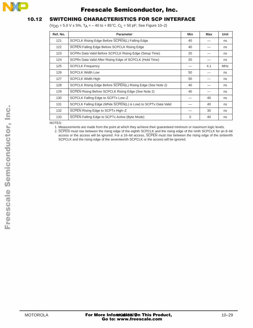
MC145572 10–29MOTOROLA
(VDD = 5.0 V ± 5%, TA = – 40 to + 85°C, CL = 50 pF; See Figure 10–2)
Ref. No. Parameter Min Max Unit
121 SCPCLK Rising Edge Before SCPEN(L) Falling Edge 40 — ns
122 SCPEN Falling Edge Before SCPCLK Rising Edge 40 — ns
123 SCPRx Data Valid Before SCPCLK Rising Edge (Setup Time) 20 — ns
124 SCPRx Data Valid After Rising Edge of SCPCLK (Hold Time) 20 — ns
125 SCPCLK Frequency — 4.1 MHz
126 SCPCLK Width Low 50 — ns
127 SCPCLK Width High 50 — ns
128 SCPCLK Rising Edge Before SCPEN(L) Rising Edge (See Note 2) 40 — ns
129 SCPEN Rising Before SCPCLK Rising Edge (See Note 2) 40 — ns
130 SCPCLK Falling Edge to SCPTx Low–Z — 40 ns
131 SCPCLK Falling Edge (While SCPEN(L) is Low) to SCPTx Data Valid — 40 ns
132 SCPEN Rising Edge to SCPTx High–Z — 30 ns
133 SCPEN Falling Edge to SCPTx Active (Byte Mode) 0 40 ns
NOTES:1. Measurements are made from the point at which they achieve their guaranteed minimum or maximum logic levels.2. SCPEN must rise between the rising edge of the eighth SCPCLK and the rising edge of the ninth SCPCLK for an 8–bit
access or the access will be ignored. For a 16–bit access, SCPEN must rise between the rising edge of the sixteenthSCPCLK and the rising edge of the seventeenth SCPCLK or the access will be ignored.
Fre
esc
ale
Se
mic
on
du
cto
r, I
Freescale Semiconductor, Inc.
For More Information On This Product, Go to: www.freescale.com
nc
...
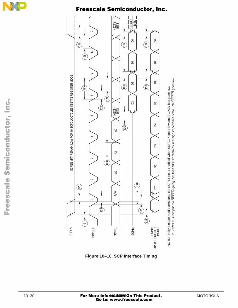
MC14557210–30 MOTOROLA
#
#
!
!
!
#
"
" ""
If S
CP
CLK
is lo
w p
rior
to S
CP
EN
goi
ng lo
w, t
hen
SC
PT
x re
mai
ns in
a h
igh
impe
danc
e st
ate
until
SC
PE
N g
oes
low
.N
OT
E:
In b
yte
mod
e re
ad o
pera
tions
, the
SC
PT
x pi
n is
ena
bled
whe
n S
CP
CLK
goe
s lo
w a
nd S
CP
EN
has
gon
e lo
w.
Figure 10–16. SCP Interface Timing
Fre
esc
ale
Se
mic
on
du
cto
r, I
Freescale Semiconductor, Inc.
For More Information On This Product, Go to: www.freescale.com
nc
...
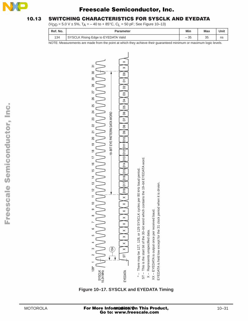
MC145572 10–31MOTOROLA
(VDD = 5.0 V ± 5%, TA = – 40 to + 85°C, CL = 50 pF; See Figure 10–13)
Ref. No. Parameter Min Max Unit
134 SYSCLK Rising Edge to EYEDATA Valid – 35 35 ns
NOTE: Measurements are made from the point at which they achieve their guaranteed minimum or maximum logic levels.
The
re m
ay b
e 12
7, 1
28, o
r 12
9 S
YS
CLK
cyc
les
per
80 k
Hz
baud
per
iod.
Thi
s is
the
star
t bit
of th
e 30
–bit
wor
d w
hich
con
tain
s th
e 19
–bit
EY
ED
ATA
wor
d.
Rep
rese
nts
unsp
ecifi
ed d
ata.
* –
ST
–
X –
!
"
!
!
EY
ED
ATA
is h
eld
low
exc
ept f
or th
e 31
clo
ck p
erio
d w
hen
it is
drv
ien.
EY
ED
ATA
is o
utpu
t onc
e pe
r re
ceiv
ed b
aud.
XX
–
Figure 10–17. SYSCLK and EYEDATA Timing
Fre
esc
ale
Se
mic
on
du
cto
r, I
Freescale Semiconductor, Inc.
For More Information On This Product, Go to: www.freescale.com
nc
...
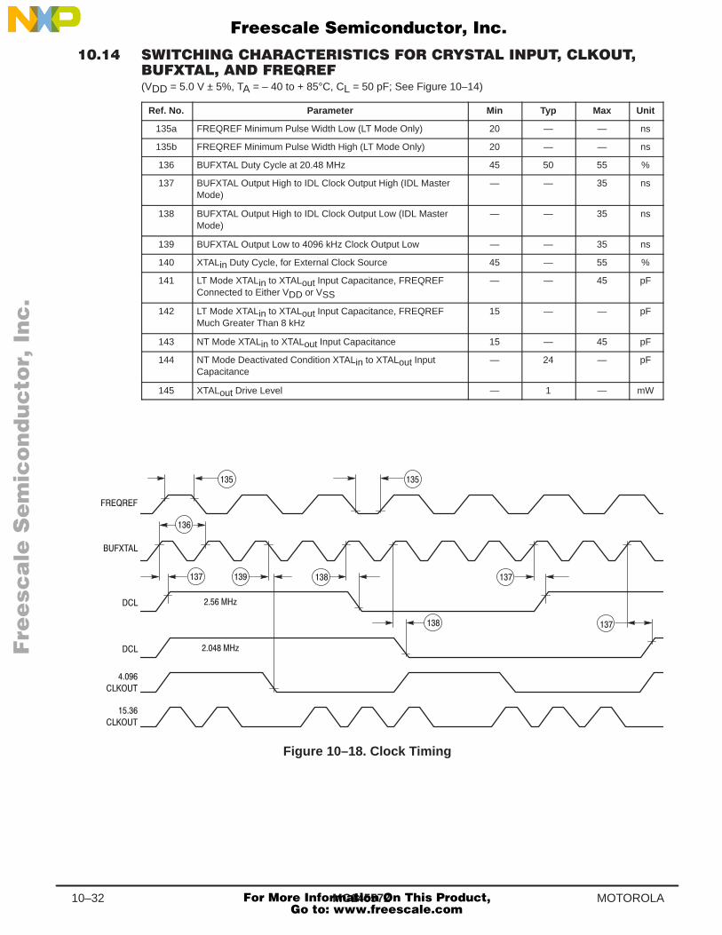
MC14557210–32 MOTOROLA
(VDD = 5.0 V ± 5%, TA = – 40 to + 85°C, CL = 50 pF; See Figure 10–14)
Ref. No. Parameter Min Typ Max Unit
135a FREQREF Minimum Pulse Width Low (LT Mode Only) 20 — — ns
135b FREQREF Minimum Pulse Width High (LT Mode Only) 20 — — ns
136 BUFXTAL Duty Cycle at 20.48 MHz 45 50 55 %
137 BUFXTAL Output High to IDL Clock Output High (IDL MasterMode)
— — 35 ns
138 BUFXTAL Output High to IDL Clock Output Low (IDL MasterMode)
— — 35 ns
139 BUFXTAL Output Low to 4096 kHz Clock Output Low — — 35 ns
140 XTALin Duty Cycle, for External Clock Source 45 — 55 %
141 LT Mode XTALin to XTALout Input Capacitance, FREQREFConnected to Either VDD or VSS
— — 45 pF
142 LT Mode XTALin to XTALout Input Capacitance, FREQREFMuch Greater Than 8 kHz
15 — — pF
143 NT Mode XTALin to XTALout Input Capacitance 15 — 45 pF
144 NT Mode Deactivated Condition XTALin to XTALout InputCapacitance
— 24 — pF
145 XTALout Drive Level — 1 — mW
Figure 10–18. Clock Timing
Fre
esc
ale
Se
mic
on
du
cto
r, I
Freescale Semiconductor, Inc.
For More Information On This Product, Go to: www.freescale.com
nc
...
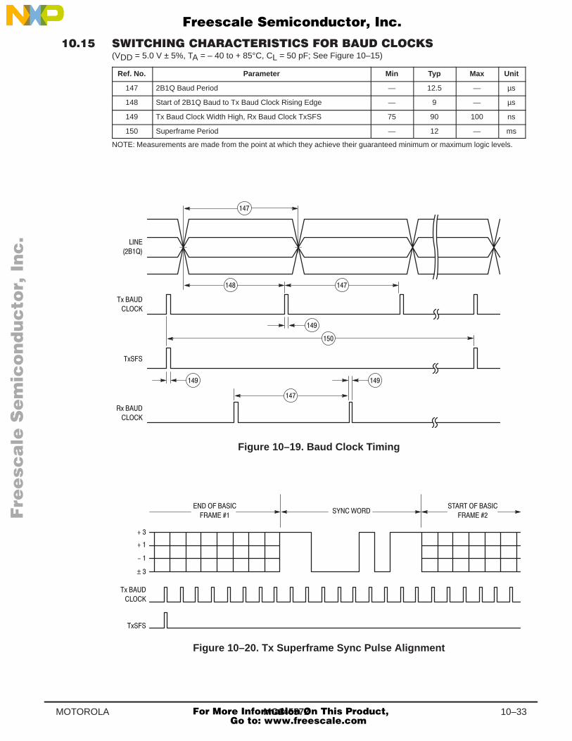
MC145572 10–33MOTOROLA
(VDD = 5.0 V ± 5%, TA = – 40 to + 85°C, CL = 50 pF; See Figure 10–15)
Ref. No. Parameter Min Typ Max Unit
147 2B1Q Baud Period — 12.5 — µs
148 Start of 2B1Q Baud to Tx Baud Clock Rising Edge — 9 — µs
149 Tx Baud Clock Width High, Rx Baud Clock TxSFS 75 90 100 ns
150 Superframe Period — 12 — ms
NOTE: Measurements are made from the point at which they achieve their guaranteed minimum or maximum logic levels.
#
#
#
Figure 10–19. Baud Clock Timing
#
#
±
" !
Figure 10–20. Tx Superframe Sync Pulse Alignment
Fre
esc
ale
Se
mic
on
du
cto
r, I
Freescale Semiconductor, Inc.
For More Information On This Product, Go to: www.freescale.com
nc
...

MC14557210–34 MOTOROLA
Fre
esc
ale
Se
mic
on
du
cto
r, I
Freescale Semiconductor, Inc.
For More Information On This Product, Go to: www.freescale.com
nc
...
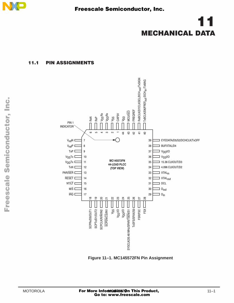
MC145572 11–1MOTOROLA
.
" .
" .
.
"+&'
"+&'
% .
!$
"
"
!
!
*-,
$ ()
()
"
.
.
"
".
".
"
"
"
!
#
"
%/
$
$ *-,
*-,
.!
.!
.$
*-,
()
.
.
.
.
Figure 11–1. MC145572FN Pin Assignment
Fre
esc
ale
Se
mic
on
du
cto
r, I
Freescale Semiconductor, Inc.
For More Information On This Product, Go to: www.freescale.com
nc
...
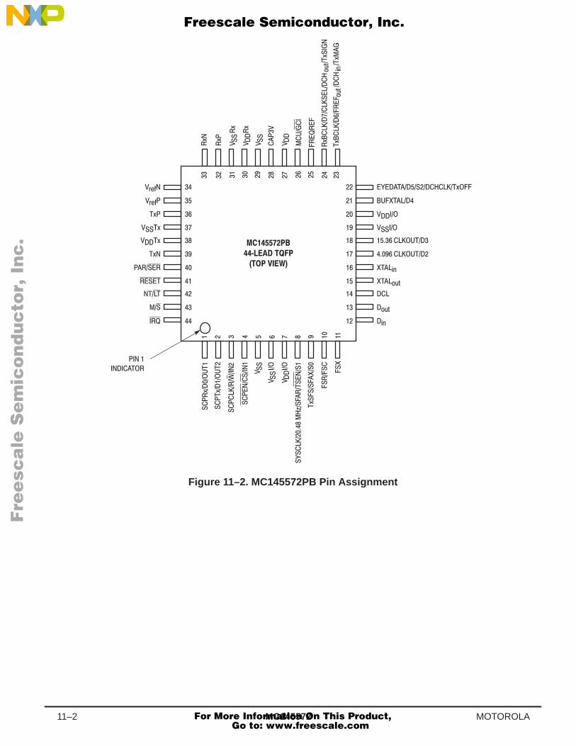
MC14557211–2 MOTOROLA
.
" .
" .
.
"+&'
"+&'
% .
!$
"
"
!
!
*-,
$ ()
()
.
.
"
"
"
!
$ *-,
"
"
#
"
%/
$
.!
.!
.$
*-,
*-,
()
.
.
.
.
".
".
Figure 11–2. MC145572PB Pin Assignment
Fre
esc
ale
Se
mic
on
du
cto
r, I
Freescale Semiconductor, Inc.
For More Information On This Product, Go to: www.freescale.com
nc
...
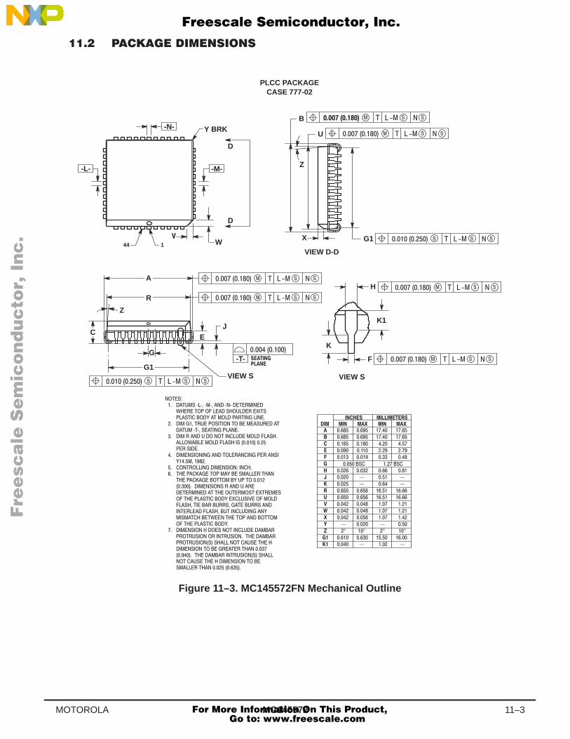
MC145572 11–3MOTOROLA
PLCC PACKAGECASE 777-02
# " "
# " "
# " ""
# " "
# " ""
-T-
# " "
# " "
*
°
*
*
°
*
"
-N- Y BRK
D
D
W
-M--L-
44 1
VIEW S
B
U
Z
G1X
VIEW D-D
H
K
F
VIEW S
G
C
Z
EJ
G1
K1
*
°
*
*
°
*
"
#" #$" )) )) )) #!
&! # "$! '#" "# ( # !#
#!$ "# # "$! ##$ )#) "#
! $ # $ "& " " ! "
" #! ! "(
#! " # # ( "! #
# ## ( $ # "" ! $ !#! # # $#!"# '#!" # "# ( '$"% " # ! $!!" # $!!" #! " $# $ ("# #& # # ## # "# (
" " # $ ! !#!$" ! #!$" # ! !#!$"" " # $" # " # !#! # # ! #!$"" "# $" # " # "! #
# " "
A
R
Figure 11–3. MC145572FN Mechanical Outline
Fre
esc
ale
Se
mic
on
du
cto
r, I
Freescale Semiconductor, Inc.
For More Information On This Product, Go to: www.freescale.com
nc
...
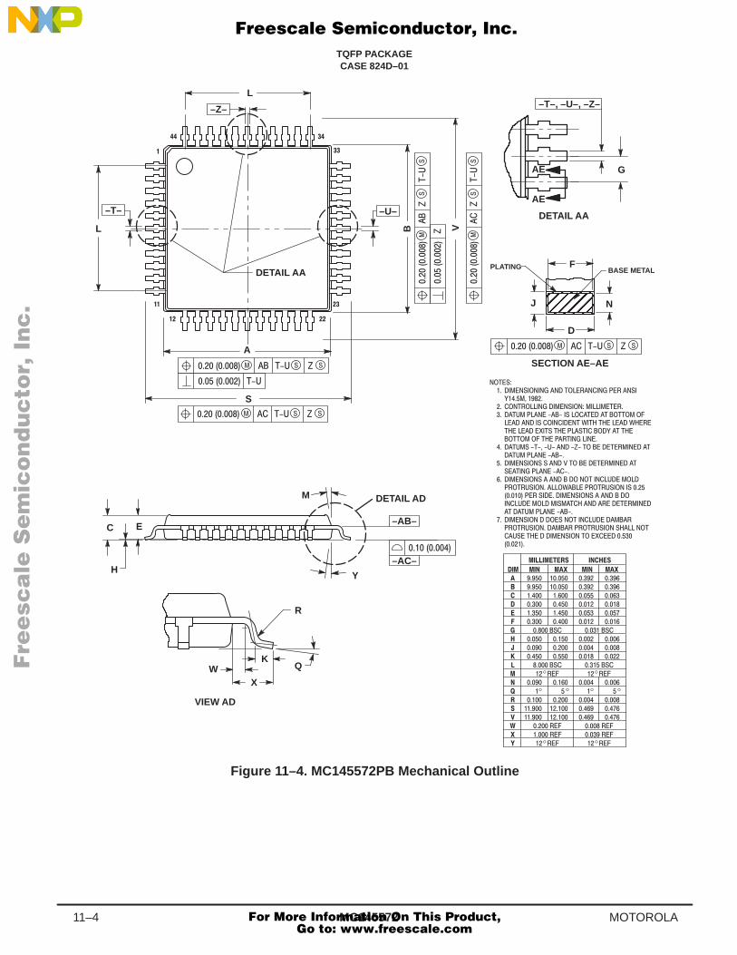
MC14557211–4 MOTOROLA
TQFP PACKAGECASE 824D–01
ÇÇÇÇÇÇÇÇÉÉÉÉÉÉÉÉ
"! ! " !'
" ! " "# ! " " "" ! " %" " % " &"! " !" ' " """ " "
"#! " # ( " " ""#
!! ! $ " " "!"
!! " # " #! % " #! ! ! !! # !" " " "#
! ! " # " #! " #! ! "#! " ! " &
DETAIL AA
–Z–
–T–
A
!"# ( !
"#
SB V
–U–
M
Y
E
H
C–AB–
DETAIL AD
KW
X
VIEW AD
–T–, –U–, –Z–
F
N
SECTION AE–AE
J
D
BASE METALPLATING
AE
AE
G
(
DETAIL AA
! !
! !
L
L
!"# ( !!
"#
(!
!"#
(!
–AC–
Q
!"# ( !
R
Figure 11–4. MC145572PB Mechanical Outline
Fre
esc
ale
Se
mic
on
du
cto
r, I
Freescale Semiconductor, Inc.
For More Information On This Product, Go to: www.freescale.com
nc
...
MC145572 A–1MOTOROLA
The MC145572EVK ISDN U–Interface Transceiver Evaluation Kit provides Motorola ISDN customersa convenient and efficient vehicle for evaluating the MC145572 ISDN U–interface transceiver. Theapproach taken to demonstrate the MC145572 ISDN U–interface transceiver is to provide the userwith a fully functional NT1 connected to an LT. An NT1 provides transparent 2B+D data transferbetween the U– and S/T–interfaces. In addition, it must also provide for network–initiated mainte-nance procedures. It does not, however, provide any interface to higher level protocols — this func-tionality is left to entities such as the NT2.
The MC145572EVK ISDN U–Interface Evaluation Kit can be physically and functionally separatedinto two “halves”. The left side of the card is the NT1, while the right side of the card is the LT. Alter-natively, it can be thought of as having both ends of the two wire U–interface, extending from thecustomer premise (NT1) to the digital switch line card (LT), on a single standalone evaluation board.
The kit provides the ability to interactively manipulate status registers in the MC145572 ISDN U–interface transceiver as well as in the MC145474/75 S/T–interface transceiver with the aid of an exter-nal terminal or PC. A unique combination of hardware and software features allows for standaloneor terminal activation of the U–interface and as such provides an excellent platform for NT1 and LThardware/software development.
The MC145572EVK ISDN U–Interface Evaluation Kit can be interfaced directly to the MC68302 Inte-grated Multiprotocol Processor Development System to aid in the hardware and software develop-ment of S/T– and U–interface terminal equipment.
Fre
esc
ale
Se
mic
on
du
cto
r, I
Freescale Semiconductor, Inc.
For More Information On This Product, Go to: www.freescale.com
nc
...
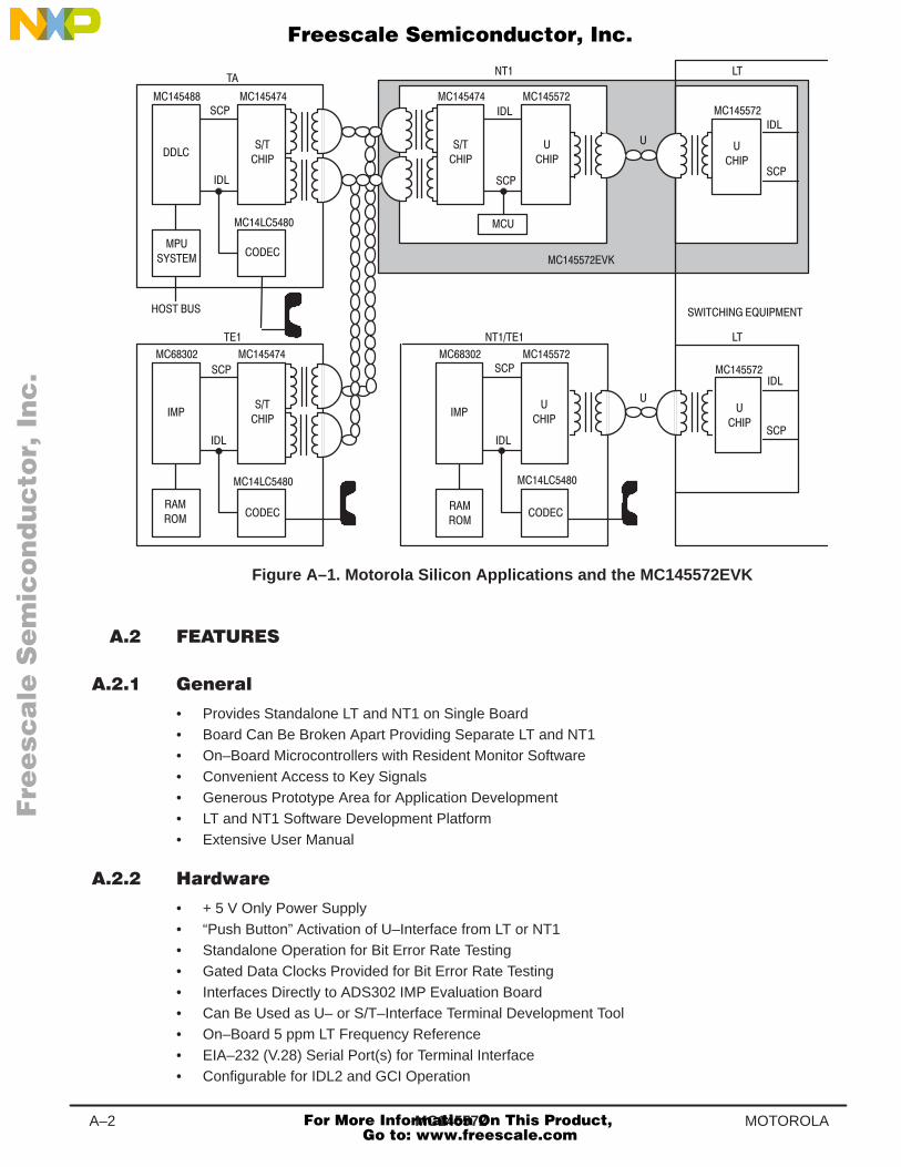
MC145572A–2 MOTOROLA
!
Figure A–1. Motorola Silicon Applications and the MC145572EVK
• Provides Standalone LT and NT1 on Single Board• Board Can Be Broken Apart Providing Separate LT and NT1• On–Board Microcontrollers with Resident Monitor Software• Convenient Access to Key Signals• Generous Prototype Area for Application Development• LT and NT1 Software Development Platform• Extensive User Manual
• + 5 V Only Power Supply• “Push Button” Activation of U–Interface from LT or NT1• Standalone Operation for Bit Error Rate Testing• Gated Data Clocks Provided for Bit Error Rate Testing• Interfaces Directly to ADS302 IMP Evaluation Board• Can Be Used as U– or S/T–Interface Terminal Development Tool• On–Board 5 ppm LT Frequency Reference• EIA–232 (V.28) Serial Port(s) for Terminal Interface• Configurable for IDL2 and GCI Operation
Fre
esc
ale
Se
mic
on
du
cto
r, I
Freescale Semiconductor, Inc.
For More Information On This Product, Go to: www.freescale.com
nc
...
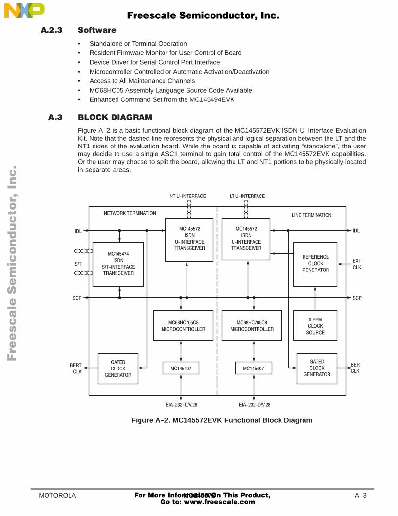
MC145572 A–3MOTOROLA
• Standalone or Terminal Operation• Resident Firmware Monitor for User Control of Board• Device Driver for Serial Control Port Interface• Microcontroller Controlled or Automatic Activation/Deactivation• Access to All Maintenance Channels• MC68HC05 Assembly Language Source Code Available• Enhanced Command Set from the MC145494EVK
Figure A–2 is a basic functional block diagram of the MC145572EVK ISDN U–Interface EvaluationKit. Note that the dashed line represents the physical and logical separation between the LT and theNT1 sides of the evaluation board. While the board is capable of activating “standalone”, the usermay decide to use a single ASCII terminal to gain total control of the MC145572EVK capabilities.Or the user may choose to split the board, allowing the LT and NT1 portions to be physically locatedin separate areas.
"
!
! !
#
!
!
Figure A–2. MC145572EVK Functional Block Diagram
Fre
esc
ale
Se
mic
on
du
cto
r, I
Freescale Semiconductor, Inc.
For More Information On This Product, Go to: www.freescale.com
nc
...

MC145572A–4 MOTOROLA
Fre
esc
ale
Se
mic
on
du
cto
r, I
Freescale Semiconductor, Inc.
For More Information On This Product, Go to: www.freescale.com
nc
...
MC145572 B–1MOTOROLA
This information is provided to assist in sourcing the various parts used in the application of theMC145572 U–interface transceiver. The detailed specifications for these parts are available from themanufacturer and information presented here is only as current as the printing of this document.Contact your local Motorola representative or the Motorola factory applications staff for the latestupdates on this information.
CAUTION
Motorola has conducted limited evaluation of third party components for use with theMC145572. This limited review suggests that the components included here appear to besuitable for applications using the MC145572. However, the evaluation did not include allspecifications or parameters that may be applicable to particular designs, and the vendorsincluded here represent only a partial list of component manufacturers. Motorola does notguarantee that these third party components will work in all applications. It is the responsi-bility of the equipment designer to verify that these components are suitable for theirintended application.
Table B–1 lists sourcing information for the transformers used in the MC145572 line interface circuit.
Table B–1. U–Interface Transformer Vendors
Manufacturer Part No.Package Dimensions
L x W x H Fax No. Contact/Phone No.
Midcom 671–7308 1.05″ x 0.92″ x 0.45″ (605) 886–4486 (605) 886–4385
Schott Corporation 671 46720 1.05″ x 0.92″ x 0.45″ (615) 885–0834 (615) 889–8800
APC 41018 19.6 mm x 25.1 mm x 13.2 mm
USA: (201) 368–1704UK: (44) 1634–290–591
USA: (201) 368–1750UK: (44) 1634–290–588
Pulse Engineering PE 68628 1.05″ x 0.92″ x 0.45″ (619) 674–8262 (619) 674–8100
Valor Electronics PT5062 0.82″ x 0.82″ x 0.675″ (619) 537–2525 (619) 537–2500
NOTES:1. See Caution note above.2. Part numbers subject to change.3. APC also manufactures line interface modules.
A list of third party vendors and current qualification status appear in Table B–1. The transformerreference schematic appears in Figure B–1. The specifications in Table B–2 apply to the design ofthe U–interface transformer.
Any transformer manufactured to this specification must be verified for compliant transmission perfor-mance. It is also suggested that transformers manufactured for use in loop powered systems berequired to remain within specification up to the maximum loop current which may be as high as60 mA.
Fre
esc
ale
Se
mic
on
du
cto
r, I
Freescale Semiconductor, Inc.
For More Information On This Product, Go to: www.freescale.com
nc
...
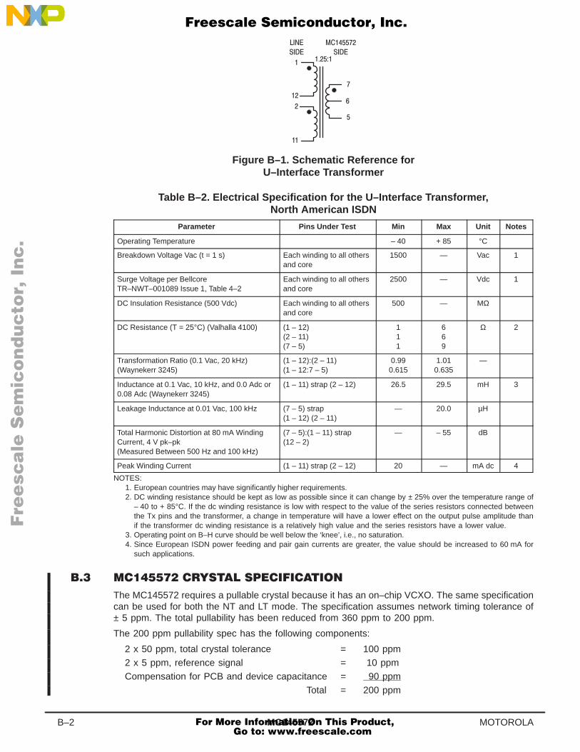
MC145572B–2 MOTOROLA
Figure B–1. Schematic Reference forU–Interface Transformer
Table B–2. Electrical Specification for the U–Interface Transformer,North American ISDN
Parameter Pins Under Test Min Max Unit Notes
Operating Temperature – 40 + 85 °C
Breakdown Voltage Vac (t = 1 s) Each winding to all othersand core
1500 — Vac 1
Surge Voltage per BellcoreTR–NWT–001089 Issue 1, Table 4–2
Each winding to all othersand core
2500 — Vdc 1
DC Insulation Resistance (500 Vdc) Each winding to all othersand core
500 — MΩ
DC Resistance (T = 25°C) (Valhalla 4100) (1 – 12)(2 – 11)(7 – 5)
111
669
Ω 2
Transformation Ratio (0.1 Vac, 20 kHz)(Waynekerr 3245)
(1 – 12):(2 – 11)(1 – 12:7 – 5)
0.990.615
1.010.635
—
Inductance at 0.1 Vac, 10 kHz, and 0.0 Adc or0.08 Adc (Waynekerr 3245)
(1 – 11) strap (2 – 12) 26.5 29.5 mH 3
Leakage Inductance at 0.01 Vac, 100 kHz (7 – 5) strap(1 – 12) (2 – 11)
— 20.0 µH
Total Harmonic Distortion at 80 mA WindingCurrent, 4 V pk–pk(Measured Between 500 Hz and 100 kHz)
(7 – 5):(1 – 11) strap(12 – 2)
— – 55 dB
Peak Winding Current (1 – 11) strap (2 – 12) 20 — mA dc 4
NOTES:1. European countries may have significantly higher requirements.2. DC winding resistance should be kept as low as possible since it can change by ± 25% over the temperature range of
– 40 to + 85°C. If the dc winding resistance is low with respect to the value of the series resistors connected betweenthe Tx pins and the transformer, a change in temperature will have a lower effect on the output pulse amplitude thanif the transformer dc winding resistance is a relatively high value and the series resistors have a lower value.
3. Operating point on B–H curve should be well below the ‘knee’, i.e., no saturation.4. Since European ISDN power feeding and pair gain currents are greater, the value should be increased to 60 mA for
such applications.
The MC145572 requires a pullable crystal because it has an on–chip VCXO. The same specificationcan be used for both the NT and LT mode. The specification assumes network timing tolerance of± 5 ppm. The total pullability has been reduced from 360 ppm to 200 ppm.
The 200 ppm pullability spec has the following components:
2 x 50 ppm, total crystal tolerance = 100 ppm2 x 5 ppm, reference signal = 10 ppmCompensation for PCB and device capacitance = 90 ppm
Total = 200 ppm
Fre
esc
ale
Se
mic
on
du
cto
r, I
Freescale Semiconductor, Inc.
For More Information On This Product, Go to: www.freescale.com
nc
...
MC145572 B–3MOTOROLA
$ !&"# # ! #%! #"
1. Operating frequency: 20.48 MHz
2. Crystal shunt capacitance: Co = 7.0 pF
3. Uncertainty at rated CL: ± 50 ppm over temperature, calibration, and 10–year aging
4. Equivalent series resistance: RS ≤ 20 ohms @ 1 mW drive
5. Crystal pull range:
a. ± 5 ppm signal 200 ppm minimum pullability over a CL range of 15 to 45 pF
b. ± 32 ppm signal 260 ppm minimum pullability over a CL range of 15 to 45 pF
c. ± 50 ppm signal 300 ppm minimum pullability over a CL range of 15 to 45 pF
6. Calibration load capacitance: 24 pF
NOTES:1. – 40 to + 85°C required for transmission applications.2. For room temperature, use 0 to 70°C.3. Explanation of item 5, crystal pull range. Crystal pullability must be specified to allow the MC145572 to lock to either a re-
ceived signal when operating in NT mode or lock to the 8 kHz FREQREF when operating in LT mode. The appropriate crystalpullability specification is dependent of the maximum expected signal or FREQREF tolerance in ppm. This will vary depend-ing on national network and application requirements. For example in North America, receive signals from the network areexpected to have a tolerance of less than 5 ppm. Hence, a crystal with either 200 or 260 ppm total pullability may be used.The ultimate choice is up to the equipment designer.
Table B–3 lists sourcing information for the crystals used in the MC145572.
Table B–3. Crystal Vendors
Manufacturer Contact Phone No. Contact Fax No.
ECLIPTEK (714) 433–1200 (714) 433–1234
Hy–Q International (606) 283–5000 (606) 283–0883
SaRonix (415) 856–6900 (415) 856–4732
Connor–Winfield (708) 851–4722 (708) 851–5040
Precision Devices (608) 831–4445 (608) 831–3343
NOTE: See Caution note on page B–1.
Fre
esc
ale
Se
mic
on
du
cto
r, I
Freescale Semiconductor, Inc.
For More Information On This Product, Go to: www.freescale.com
nc
...
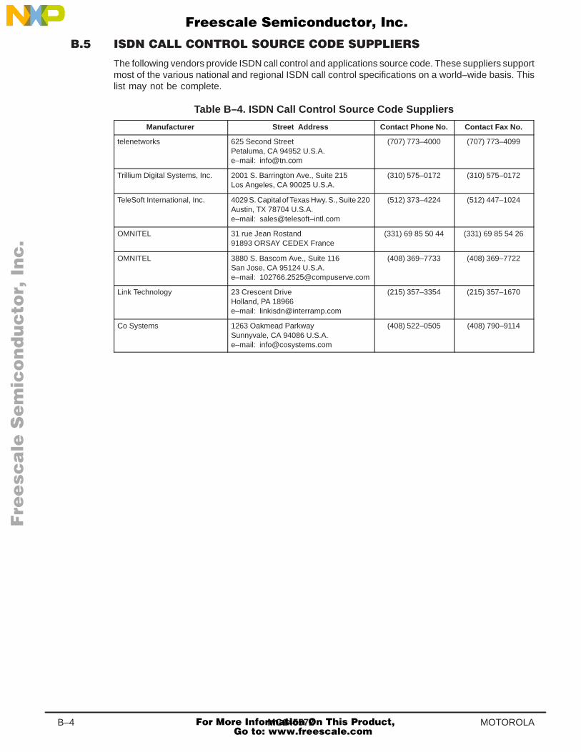
MC145572B–4 MOTOROLA
The following vendors provide ISDN call control and applications source code. These suppliers supportmost of the various national and regional ISDN call control specifications on a world–wide basis. Thislist may not be complete.
Table B–4. ISDN Call Control Source Code Suppliers
Manufacturer Street Address Contact Phone No. Contact Fax No.
telenetworks 625 Second StreetPetaluma, CA 94952 U.S.A.e–mail: [email protected]
(707) 773–4000 (707) 773–4099
Trillium Digital Systems, Inc. 2001 S. Barrington Ave., Suite 215Los Angeles, CA 90025 U.S.A.
(310) 575–0172 (310) 575–0172
TeleSoft International, Inc. 4029 S. Capital of Texas Hwy. S., Suite 220Austin, TX 78704 U.S.A.e–mail: sales@telesoft–intl.com
(512) 373–4224 (512) 447–1024
OMNITEL 31 rue Jean Rostand91893 ORSAY CEDEX France
(331) 69 85 50 44 (331) 69 85 54 26
OMNITEL 3880 S. Bascom Ave., Suite 116San Jose, CA 95124 U.S.A.e–mail: [email protected]
(408) 369–7733 (408) 369–7722
Link Technology 23 Crescent DriveHolland, PA 18966e–mail: [email protected]
(215) 357–3354 (215) 357–1670
Co Systems 1263 Oakmead ParkwaySunnyvale, CA 94086 U.S.A.e–mail: [email protected]
(408) 522–0505 (408) 790–9114
Fre
esc
ale
Se
mic
on
du
cto
r, I
Freescale Semiconductor, Inc.
For More Information On This Product, Go to: www.freescale.com
nc
...
MC145572 C–1MOTOROLA
The MC145572 is manufactured using high speed CMOS VLSI process technology to implement themixed signal processing functions required in the device. The U–interface transceiver has a highresolution sigma–delta ADC and a precision DAC, in addition to three high speed digital signal copro-cessors. The fully differential analog circuit design techniques used for this device result in superiorperformance for the ADC, DAC, and Tx Driver sections. Special attention was given to the designof the MC145572 to reduce sensitivity to noise, including power supply rejection and susceptibilityto radio frequency noise. This special attention to circuit design, results in an ADC with greater than84 dB dynamic range on the same monolithic chip as the digital signal coprocessors clocking at10.24 MHz, all of which operates on a single 5–V power supply. This device was designed to easethe task of PCB layout, but due to the wide analog dynamic range and high digital clock rate, specialcare should be taken during PCB layout to assure optimum transmission performance.
NOTEWhen laying out the PCB, do not run any digital signals through the line interface regionof the board. Switching noise from the digital signals can be coupled into the line interfaceand reduce performance, especially on long loops. Wire wrap is not recommended forprototyping.
The device should be soldered to the PC board for production manufacturing. If the device is to beused in a socket, it should be placed in a low parasitic pin capacitance socket of 1.5 pF or less.
This device is often used in digital switching equipment applications which require plugging the PCboard into a rack with power applied. This is referred to as “hot–rack insertion”. In these applications,care should be taken to limit the voltage on any pin from going positive relative to the VDD pins, ornegative relative to the VSS pins. One method to accomplish this is to extend the ground and powercontacts of the PCB connector so that power is applied prior to any other pins having voltage applied.The device has input protection on all pins and may source or sink a limited amount of current withoutdamage. See Section 10.1, Absolute Maximum Ratings, for more information concerning the cur-rent into or out of the device pins. Current limiting may be accomplished by series resistors betweenthe signal pins and the connector contacts.
The most important considerations for PCB layout deal with noise. This includes noise on the powersupply, noise generated by the digital circuitry on the device, and coupling digital signals into theanalog signals. The best PCB layout methods to prevent noise–induced problems are:
1. Keep digital signals as far away from analog signals as possible.
2. Use short, low inductance traces for the analog circuitry to reduce inductive, capacitive, andradio frequency noise sensitivities.
3. Use short, low inductance traces for digital circuitry to reduce inductive, capacitive, and radiofrequency radiated noise.
4. Bypass capacitors should be connected between the VDD and VSS pairs with minimal tracelength. These capacitors help supply the instantaneous currents of the digital circuitry, in addi-tion to decoupling the noise that may be generated by other sections of the device or othercircuitry on the power supply.
Fre
esc
ale
Se
mic
on
du
cto
r, I
Freescale Semiconductor, Inc.
For More Information On This Product, Go to: www.freescale.com
nc
...
MC145572C–2 MOTOROLA
5. Use short, wide, low inductance traces to connect all of the VSS ground pins together and,with one trace, connect all of the VSS ground pins to the power supply ground. Depending onthe application, a double sided PCB with a VSS ground plane under the device connecting allof the digital and analog VSS pins together would be a good grounding method. A multi–layerPCB with a ground plane connecting all of the digital and analog VSS pins together would bethe optimal ground configuration. These methods will result in the lowest resistance and thelowest inductance in the ground circuit. This is important to reduce voltage spikes in the groundcircuit resulting from the high speed digital current spikes. Suppressing these voltage spikeson the integrated circuit is the reason for multiple VSS ground leads.
6. Use short, wide, low inductance traces to connect all of the VDD power supply pins togetherand, with one trace, connect all of the VDD power supply pins to the 5–V power supply. De-pending on the application, a double sided PCB with VDD bypass capacitors to the VSS groundplane under the device, as described in item 5 above, may complete the low impedance cou-pling for the power supply. For a multi–layer PCB with a power plane, connecting all of thedigital and analog VDD pins to the power plane would be the optimal power distribution method.The integrated circuit layout and packaging considerations for the 5–V VDD power circuit areessentially the same as for the ground circuit.
7. Motorola recommends that a four layer board be used. It is possible to use a two layer boardbut special care must be taken. See Figure C–1.
8. The 20.48 MHz crystal must be located as close as possible to the MC145572 package. Thisis required to minimize parasitic capacitances between crystal traces and ground.
Figure C–1 shows a suggested board layout for a two layer board. This drawing is not done to scale.Trace vias are shown. Depending on the application, other pins may need to be connected to VDDor VSS. All bypass capacitors should be located as close as possible to the VSS/VDD pins. Thesuggested layout shows the power feed to the MC145572 coming from a common point. This isimportant in a two layer implementation. The 10 µF electrolytic capacitor is recommended to filterout any ripple or noise that may be on the board in a two layer application. Even though theMC145572 has very high power supply rejection, good power supply decoupling is recommended.
If a four layer board with full power and ground planes is used, the VDD and VSS pins can be con-nected directly to the appropriate plane by vias.
All traces must be as short as possible to reduce stray capacitance and inductance. The traces toXTALin and XTALout must be kept as short as possible with minimal width to keep stray capacitanceless than 1 pF. Other digital signals should not be routed near the crystal traces. Any passive compo-nents for the oscillator or PLL should have short leads and should be soldered to the PC board.Wherever possible the layout should be symmetrical, so the stray capacitances from each pin of thecrystal to ground are equal.
When a four layer board is used, do not route ground or power plane material underneath the20.48 MHz crystal oscillator circuitry. This is to minimize parasitic capacitances between the20.480 MHz oscillator traces and the power or ground plane. Excessive parasitic capacitance betweenthe traces and power/ground planes decreases the pull range of the 20.48 MHz oscillator.
The line interface into and out of the device is differential, implying symmetry. It is recommended thatthe layout of the 2B1Q interface be as symmetrical as possible to avoid any imbalances to this circuit.Do not run any digital traces through the line interface region of the printed circuit board.
Fre
esc
ale
Se
mic
on
du
cto
r, I
Freescale Semiconductor, Inc.
For More Information On This Product, Go to: www.freescale.com
nc
...
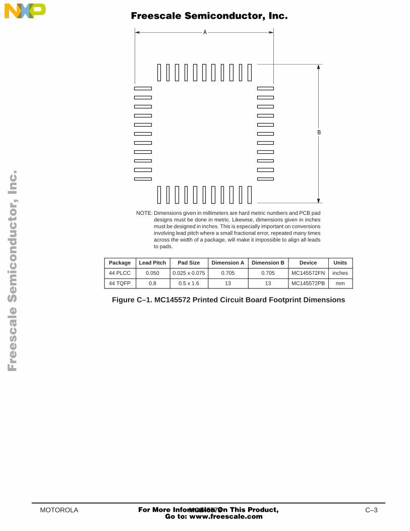
MC145572 C–3MOTOROLA
NOTE: Dimensions given in millimeters are hard metric numbers and PCB paddesigns must be done in metric. Likewise, dimensions given in inchesmust be designed in inches. This is especially important on conversionsinvolving lead pitch where a small fractional error, repeated many timesacross the width of a package, will make it impossible to align all leadsto pads.
ÁÁÁÁÁÁÁÁ
Package ÁÁÁÁÁÁÁÁ
Lead PitchÁÁÁÁÁÁÁÁÁÁ
Pad Size ÁÁÁÁÁÁÁÁÁÁ
Dimension A ÁÁÁÁÁÁÁÁ
Dimension BÁÁÁÁÁÁÁÁÁÁ
Device ÁÁÁÁÁÁÁÁ
Units
ÁÁÁÁÁÁÁÁ
44 PLCC ÁÁÁÁÁÁÁÁ
0.050 ÁÁÁÁÁÁÁÁÁÁ
0.025 x 0.075ÁÁÁÁÁÁÁÁÁÁ
0.705 ÁÁÁÁÁÁÁÁ
0.705 ÁÁÁÁÁÁÁÁÁÁ
MC145572FNÁÁÁÁÁÁÁÁ
inches
ÁÁÁÁÁÁÁÁ
44 TQFP ÁÁÁÁÁÁÁÁ
0.8 ÁÁÁÁÁÁÁÁÁÁ
0.5 x 1.6 ÁÁÁÁÁÁÁÁÁÁ
13 ÁÁÁÁÁÁÁÁ
13 ÁÁÁÁÁÁÁÁÁÁ
MC145572PBÁÁÁÁÁÁÁÁ
mm
Figure C–1. MC145572 Printed Circuit Board Footprint Dimensions
Fre
esc
ale
Se
mic
on
du
cto
r, I
Freescale Semiconductor, Inc.
For More Information On This Product, Go to: www.freescale.com
nc
...
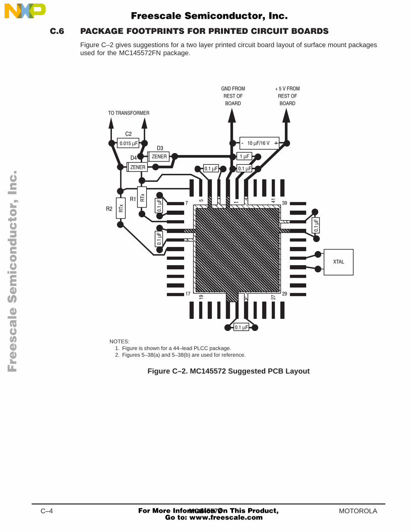
MC145572C–4 MOTOROLA
Figure C–2 gives suggestions for a two layer printed circuit board layout of surface mount packagesused for the MC145572FN package.
ÎÎÎÎÎÎÎÎÎÎÎÎÎÎÎÎÎÎÎÎÎÎÎÎÎÎÎÎÎÎÎÎÎÎÎÎÎÎÎÎÎÎÎÎÎÎÎÎÎÎÎÎÎÎÎÎÎÎÎÎÎÎÎÎÎÎÎÎÎÎÎÎÎÎÎÎÎÎÎÎÎÎÎÎÎÎÎÎÎÎÎÎÎÎÎÎÎÎÎÎÎÎÎÎÎÎÎÎÎÎÎÎÎÎÎÎÎÎÎÎÎ
ÏÏÏÏ
ÏÏÏÏÏÏ
ÏÏ
ÏÏÏÏÏÏ µ
ÏÏÏÏ
ÏÏÏÏ µ
ÏÏ
Ï ÏÏ
ÏÏ
ÏÏÏÏ
ÏÏ
ÏÏÏÏÏÏÏÏÏÏ
µ
ÌÌÌÌÌÌÌÌÌÌÌÌÌÌÌÌÌÌÌÌÌÌÌÌÌÌÌÌÌÌÌÌÌÌÌÌÌÌÌÌÌÌÌÌÌÌÌÌÌÌÌÌÌÌÌÌÌÌÌÌÌÌÌÌÌÌÌÌÌÌÌÌÌÌÌÌÌÌÌÌÌÌÌÌÌÌÌÌÌÌÌÌÌÌÌÌÌÌÌÌÌÌÌÌÌÌÌÌÌÌÌÌÌÌÌÌÌÌÌÌÌÌÌÌÌÌÌÌÌÌÌÌ
ÏÏÏÏÏÏ
ÏÏÏÏÏÏ
ÏÏÏÏÏÏÏÏÏ
ÏÏÏ
ÏÏÏÏÏÏ
µ
ÏÏÏÏÏÏÏÏÏÏÏÏ
NOTES:1. Figure is shown for a 44–lead PLCC package.2. Figures 5–38(a) and 5–38(b) are used for reference.
µ
µ
µ
µ
µ
Figure C–2. MC145572 Suggested PCB Layout
Fre
esc
ale
Se
mic
on
du
cto
r, I
Freescale Semiconductor, Inc.
For More Information On This Product, Go to: www.freescale.com
nc
...
MC145572 D–1MOTOROLA
The MC145572 can provide the recovered eye pattern on a received baud–by–baud basis as a serialdigital word once every 12.5 µs. Some applications may use this feature for monitoring performance.This appendix describes a circuit to receive the eye pattern word and convert it to an analog voltagefor display on an oscilloscope.
This appendix includes the schematics and PALASM 2 programmable logic equations to implementtwo versions of an eye pattern generator. One design requires manual scaling to the magnitude ofthe eye pattern data, while the other design automatically scales to optimize the limited dynamicrange of the DAC. The eye pattern generator takes the data available on the EYEDATA pin and theclocking from the SYSCLK pin and generates an analog eye pattern for display purposes. Note thatBR14(b0) must be set to a 1 to enable the EYEDATA and SYSCLK outputs.
The eye pattern data output from the MC145572 consists of the received 2B1Q quats after the echocancelling and DFE functions have been performed on the signal available at the RxP and RxN pins.The eye pattern data is output in digital form on the EYEDATA pin and is 19 bits long. It is in signextended two’s complement form. The eye pattern data generators described here use an 8–bit DAC(this is sufficient for acceptable display on an oscilloscope) to display the most significant 8 bits ofdata including the first sign bit, but not extended sign bits or less significant bits. The 8 bits are shiftedinto an 8–bit serial–to–parallel converter and are then latched into an Analog Device’s AD557 DAC.When the resulting 8–bit window is correctly placed over the 19–bit eye data word, a full scale(approximately 1 or 2 V peak–to–peak) eye pattern signal is output from the AD557 clearly showingthe 2B1Q quats. See Figure D–1 for an example of the 8–bit window positioned over a portion ofthe 19–bit eye data word. In this example, D16 happens to be the sign bit.
Two circuits are shown for decoding the eye pattern data available on the EYEDATA pin. The firstmethod provides for manual positioning of the 8–bit DAC data window over the 19–bit eye data word.The manual positioning schematic is shown in Figure D–2. The second method provides for auto-matic or manual positioning of the 8–bit DAC data window over the 19–bit eye data word. The auto-matic positioning schematic is shown in Figure D–3. Whenever the manual method is used, the DIPswitches can be changed to correctly position the 8–bit data window. Manual positioning capabilityis provided with the automatic positioning circuit, since there may be some conditions in which theautomatic positioner will not stabilize. DIP switches are shown but any convenient binary encodermay be used.
Fre
esc
ale
Se
mic
on
du
cto
r, I
Freescale Semiconductor, Inc.
For More Information On This Product, Go to: www.freescale.com
nc
...
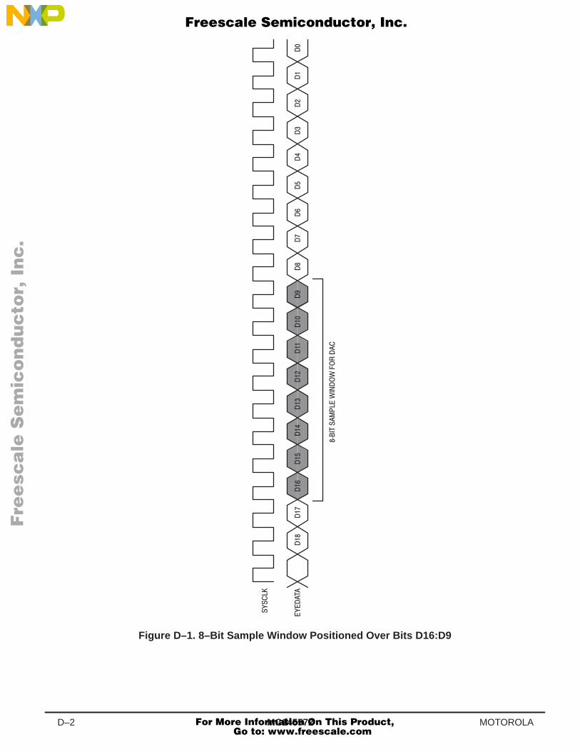
MC145572D–2 MOTOROLA
Figure D–1. 8–Bit Sample Window Positioned Over Bits D16:D9
Fre
esc
ale
Se
mic
on
du
cto
r, I
Freescale Semiconductor, Inc.
For More Information On This Product, Go to: www.freescale.com
nc
...
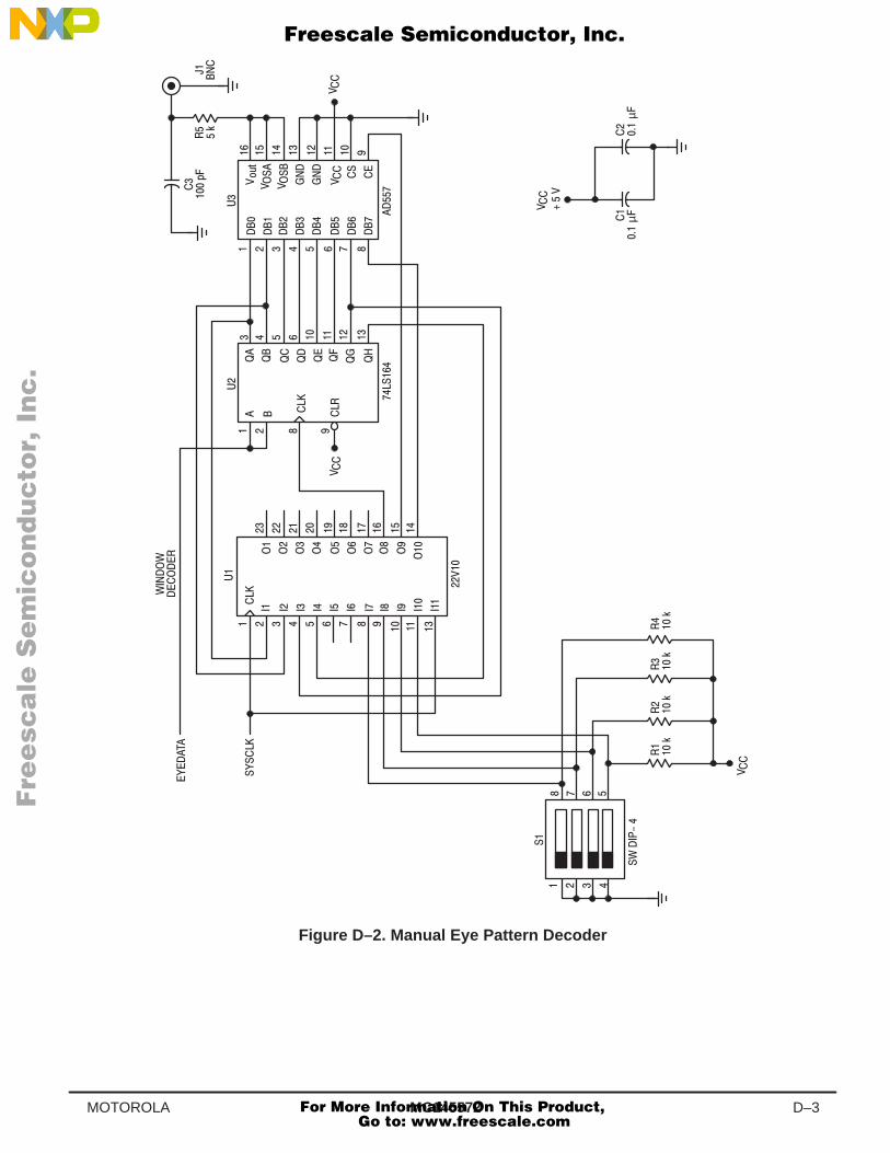
MC145572 D–3MOTOROLA
%!
%
$
#
#
#
#
#
&
&
&
&
µ
µ
#
#
"
"
"
$$
&
(
#'*)
#
#
Figure D–2. Manual Eye Pattern Decoder
Fre
esc
ale
Se
mic
on
du
cto
r, I
Freescale Semiconductor, Inc.
For More Information On This Product, Go to: www.freescale.com
nc
...
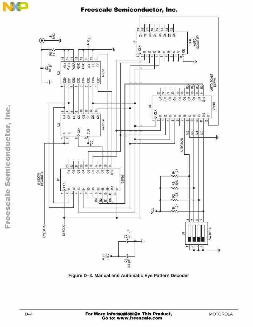
MC145572D–4 MOTOROLA
%
$
%
!
$
"
"
%
$
%),+
%"
%"
%
!
(
*
'#
"'"
&&
!
%
$
$#"
&
$#
"$
$
!
$#
"
"&
%
µ
µ
%
!(
!(
!(
!(
%
Figure D–3. Manual and Automatic Eye Pattern Decoder
Fre
esc
ale
Se
mic
on
du
cto
r, I
Freescale Semiconductor, Inc.
For More Information On This Product, Go to: www.freescale.com
nc
...
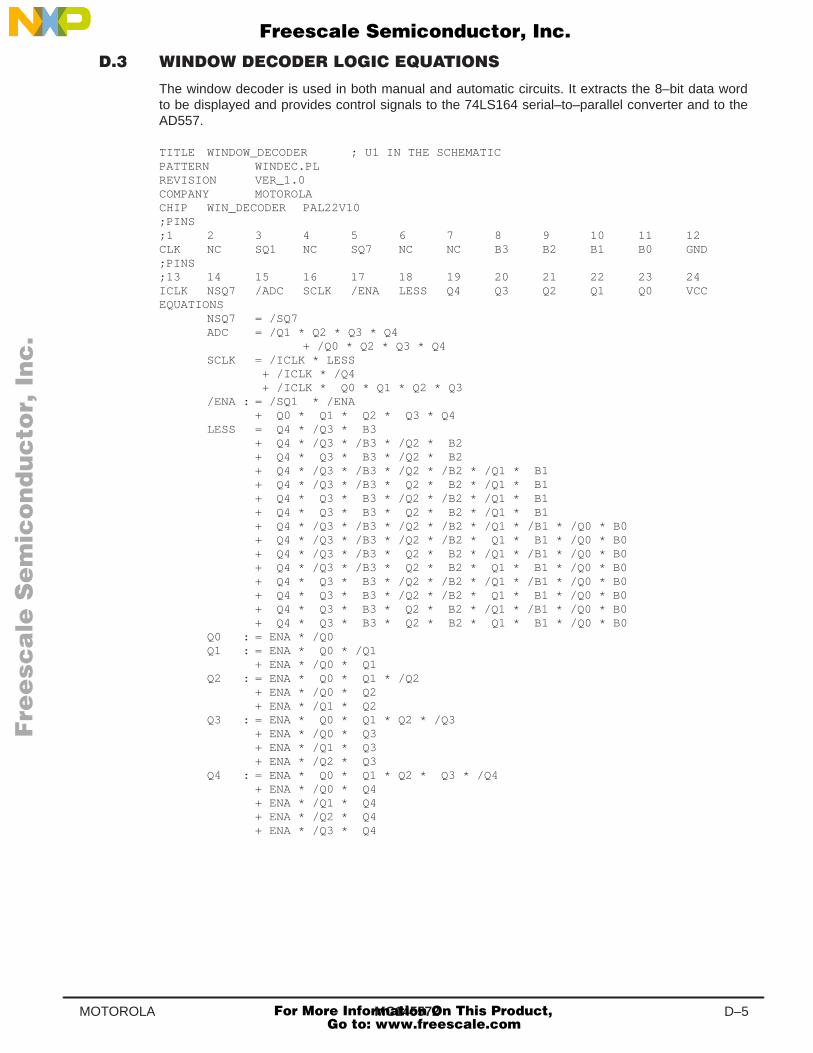
MC145572 D–5MOTOROLA
The window decoder is used in both manual and automatic circuits. It extracts the 8–bit data wordto be displayed and provides control signals to the 74LS164 serial–to–parallel converter and to theAD557.
TITLE WINDOW_DECODER ; U1 IN THE SCHEMATICPATTERN WINDEC.PLREVISION VER_1.0COMPANY MOTOROLACHIP WIN_DECODER PAL22V10;PINS;1 2 3 4 5 6 7 8 9 10 11 12CLK NC SQ1 NC SQ7 NC NC B3 B2 B1 B0 GND;PINS;13 14 15 16 17 18 19 20 21 22 23 24ICLK NSQ7 /ADC SCLK /ENA LESS Q4 Q3 Q2 Q1 Q0 VCCEQUATIONS
NSQ7 = /SQ7ADC = /Q1 * Q2 * Q3 * Q4
+ /Q0 * Q2 * Q3 * Q4 SCLK = /ICLK * LESS
+ /ICLK * /Q4 + /ICLK * Q0 * Q1 * Q2 * Q3
/ENA : = /SQ1 * /ENA + Q0 * Q1 * Q2 * Q3 * Q4LESS = Q4 * /Q3 * B3
+ Q4 * /Q3 * /B3 * /Q2 * B2+ Q4 * Q3 * B3 * /Q2 * B2+ Q4 * /Q3 * /B3 * /Q2 * /B2 * /Q1 * B1+ Q4 * /Q3 * /B3 * Q2 * B2 * /Q1 * B1+ Q4 * Q3 * B3 * /Q2 * /B2 * /Q1 * B1+ Q4 * Q3 * B3 * Q2 * B2 * /Q1 * B1+ Q4 * /Q3 * /B3 * /Q2 * /B2 * /Q1 * /B1 * /Q0 * B0+ Q4 * /Q3 * /B3 * /Q2 * /B2 * Q1 * B1 * /Q0 * B0+ Q4 * /Q3 * /B3 * Q2 * B2 * /Q1 * /B1 * /Q0 * B0+ Q4 * /Q3 * /B3 * Q2 * B2 * Q1 * B1 * /Q0 * B0+ Q4 * Q3 * B3 * /Q2 * /B2 * /Q1 * /B1 * /Q0 * B0+ Q4 * Q3 * B3 * /Q2 * /B2 * Q1 * B1 * /Q0 * B0+ Q4 * Q3 * B3 * Q2 * B2 * /Q1 * /B1 * /Q0 * B0+ Q4 * Q3 * B3 * Q2 * B2 * Q1 * B1 * /Q0 * B0
Q0 : = ENA * /Q0Q1 : = ENA * Q0 * /Q1
+ ENA * /Q0 * Q1Q2 : = ENA * Q0 * Q1 * /Q2
+ ENA * /Q0 * Q2+ ENA * /Q1 * Q2
Q3 : = ENA * Q0 * Q1 * Q2 * /Q3+ ENA * /Q0 * Q3+ ENA * /Q1 * Q3+ ENA * /Q2 * Q3
Q4 : = ENA * Q0 * Q1 * Q2 * Q3 * /Q4+ ENA * /Q0 * Q4+ ENA * /Q1 * Q4+ ENA * /Q2 * Q4+ ENA * /Q3 * Q4
Fre
esc
ale
Se
mic
on
du
cto
r, I
Freescale Semiconductor, Inc.
For More Information On This Product, Go to: www.freescale.com
nc
...
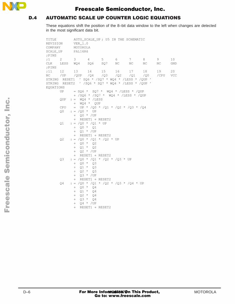
MC145572D–6 MOTOROLA
These equations shift the position of the 8–bit data window to the left when changes are detectedin the most significant data bit.
TITLE AUTO_SCALE_UP ; U5 IN THE SCHEMATICREVISION VER_1.0COMPANY MOTOROLASCALE_UP PAL16R6;PINS;1 2 3 4 5 6 7 8 9 10CLK LESS WQ4 SQ6 SQ7 NC NC NC NC GND;PINS;11 12 13 14 15 16 17 18 19 20NC /UP /QUP /Q4 /Q3 /Q2 /Q1 /Q0 /CPU VCCSTRING RESET1 ’ SQ6 * /SQ7 * WQ4 * /LESS * /QUP ’STRING RESET2 ’ /SQ6 * SQ7 * WQ4 * /LESS * /QUP ’EQUATIONS
UP = SQ6 * SQ7 * WQ4 * /LESS * /QUP+ /SQ6 * /SQ7 * WQ4 * /LESS * /QUP
QUP : = WQ4 * /LESS+ WQ4 * QUP
CPU = UP * /Q0 * /Q1 * /Q2 * /Q3 * /Q4Q0 : = /Q0 * UP
+ Q0 * /UP+ RESET1 + RESET2
Q1 : = /Q0 * /Q1 * UP+ Q0 * Q1+ Q1 * /UP+ RESET1 + RESET2
Q2 : = /Q0 * /Q1 * /Q2 * UP+ Q0 * Q2+ Q1 * Q2+ Q2 * /UP+ RESET1 + RESET2
Q3 : = /Q0 * /Q1 * /Q2 * /Q3 * UP+ Q0 * Q3+ Q1 * Q3+ Q2 * Q3+ Q3 * /UP+ RESET1 + RESET2
Q4 : = /Q0 * /Q1 * /Q2 * /Q3 * /Q4 * UP+ Q0 * Q4+ Q1 * Q4+ Q2 * Q4+ Q3 * Q4+ Q4 * /UP+ RESET1 + RESET2
Fre
esc
ale
Se
mic
on
du
cto
r, I
Freescale Semiconductor, Inc.
For More Information On This Product, Go to: www.freescale.com
nc
...
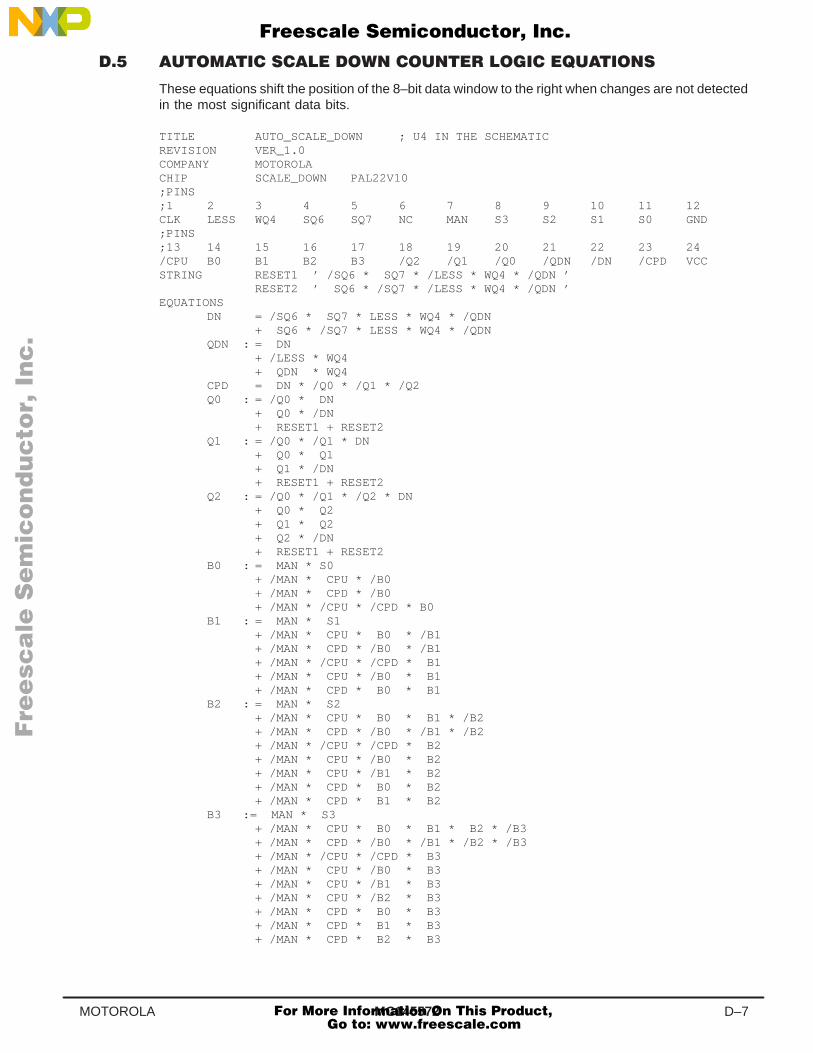
MC145572 D–7MOTOROLA
These equations shift the position of the 8–bit data window to the right when changes are not detectedin the most significant data bits.
TITLE AUTO_SCALE_DOWN ; U4 IN THE SCHEMATICREVISION VER_1.0COMPANY MOTOROLACHIP SCALE_DOWN PAL22V10;PINS;1 2 3 4 5 6 7 8 9 10 11 12CLK LESS WQ4 SQ6 SQ7 NC MAN S3 S2 S1 S0 GND;PINS;13 14 15 16 17 18 19 20 21 22 23 24/CPU B0 B1 B2 B3 /Q2 /Q1 /Q0 /QDN /DN /CPD VCCSTRING RESET1 ’ /SQ6 * SQ7 * /LESS * WQ4 * /QDN ’
RESET2 ’ SQ6 * /SQ7 * /LESS * WQ4 * /QDN ’EQUATIONS
DN = /SQ6 * SQ7 * LESS * WQ4 * /QDN+ SQ6 * /SQ7 * LESS * WQ4 * /QDN
QDN : = DN+ /LESS * WQ4+ QDN * WQ4
CPD = DN * /Q0 * /Q1 * /Q2Q0 : = /Q0 * DN
+ Q0 * /DN+ RESET1 + RESET2
Q1 : = /Q0 * /Q1 * DN+ Q0 * Q1+ Q1 * /DN+ RESET1 + RESET2
Q2 : = /Q0 * /Q1 * /Q2 * DN+ Q0 * Q2+ Q1 * Q2+ Q2 * /DN+ RESET1 + RESET2
B0 : = MAN * S0+ /MAN * CPU * /B0+ /MAN * CPD * /B0+ /MAN * /CPU * /CPD * B0
B1 : = MAN * S1+ /MAN * CPU * B0 * /B1+ /MAN * CPD * /B0 * /B1+ /MAN * /CPU * /CPD * B1+ /MAN * CPU * /B0 * B1+ /MAN * CPD * B0 * B1
B2 : = MAN * S2+ /MAN * CPU * B0 * B1 * /B2+ /MAN * CPD * /B0 * /B1 * /B2+ /MAN * /CPU * /CPD * B2+ /MAN * CPU * /B0 * B2+ /MAN * CPU * /B1 * B2+ /MAN * CPD * B0 * B2+ /MAN * CPD * B1 * B2
B3 := MAN * S3+ /MAN * CPU * B0 * B1 * B2 * /B3+ /MAN * CPD * /B0 * /B1 * /B2 * /B3+ /MAN * /CPU * /CPD * B3+ /MAN * CPU * /B0 * B3+ /MAN * CPU * /B1 * B3+ /MAN * CPU * /B2 * B3+ /MAN * CPD * B0 * B3+ /MAN * CPD * B1 * B3+ /MAN * CPD * B2 * B3
Fre
esc
ale
Se
mic
on
du
cto
r, I
Freescale Semiconductor, Inc.
For More Information On This Product, Go to: www.freescale.com
nc
...

MC145572D–8 MOTOROLA
Fre
esc
ale
Se
mic
on
du
cto
r, I
Freescale Semiconductor, Inc.
For More Information On This Product, Go to: www.freescale.com
nc
...
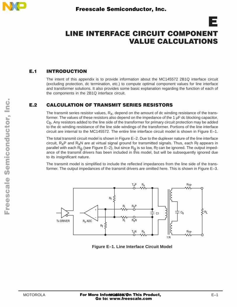
MC145572 E–1MOTOROLA
The intent of this appendix is to provide information about the MC145572 2B1Q interface circuit(excluding protection, dc termination, etc.) to compute optimal component values for line interfaceand transformer solutions. It also provides some basic explanation regarding the function of each ofthe components in the 2B1Q interface circuit.
The transmit series resistor values, Rx, depend on the amount of dc winding resistance of the trans-former. The values of these resistors also depend on the impedance of the 1 µF dc blocking capacitor,Cb. Any resistors added to the line side of the transformer for primary circuit protection may be addedto the dc winding resistance of the line side windings of the transformer. Portions of the line interfacecircuit are internal to the MC145572. The entire line interface circuit model is shown in Figure E–1.
The total transmit circuit model is shown in Figure E–2. Due to the duplexer nature of the line interfacecircuit, RxP and RxN are at virtual signal ground for transmitted signals. Thus, each Rf appears inparallel with each Rg (see Figure E–2), but since Rg is so low, Rf can be ignored. The output imped-ance of the transmit drivers has been included in this model, but will be subsequently ignored dueto its insignificant nature.
The transmit model is simplified to include the reflected impedances from the line side of the trans-former. The output impedances of the transmit drivers are omitted here. This is shown in Figure E–3.
Figure E–1. Line Interface Circuit Model
Fre
esc
ale
Se
mic
on
du
cto
r, I
Freescale Semiconductor, Inc.
For More Information On This Product, Go to: www.freescale.com
nc
...
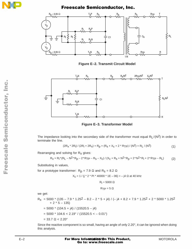
MC145572E–2 MOTOROLA
Ω
Ω
Figure E–2. Transmit Circuit Model
Figure E–3. Transformer Model
The impedance looking into the secondary side of the transformer must equal RL/(N2) in order toterminate the line.
(2Rx * 2Ri) / (2Ri + 2Rx) + Rp + (Rs + Xc + 2 * RTP) / (N2) = RL / (N2)
Rearranging and solving for Rx gives:
Rx = Ri* (RL – N2*Rp – 2*RTP – Rs – Xc) / (Xc + Rs + N2*Rp + 2*N2*Ri + 2*RTP – RL)
Substituting in values,
for a prototype transformer: Rp = 7.9 Ω and Rs = 8.2 Ω
Xc = 1 / (j * 2 * PI * 40000 * 1E – 06) = – j4 Ω at 40 kHz
Ri = 5000 Ω
RTP = 5 Ω
we get:
Rx = 5000 * (135 – 7.9 * 1.252 – 8.2 – 2 * 5 + j4) / (– j4 + 8.2 + 7.9 * 1.252 + 2 * 5000 * 1.252+ 2 * 5 – 135)
= 5000 * (104.5 + j4) / (15520.5 – j4)
= 5000 * 104.6 < 2.19° / (15520.5 < – 0.01°)
= 33.7 Ω < 2.20°
Since the reactive component is so small, having an angle of only 2.20°, it can be ignored when doingthis analysis.
(1)
(2)
Fre
esc
ale
Se
mic
on
du
cto
r, I
Freescale Semiconductor, Inc.
For More Information On This Product, Go to: www.freescale.com
nc
...
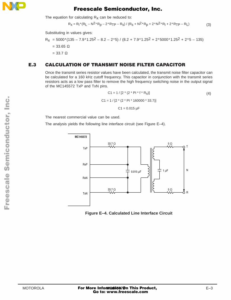
MC145572 E–3MOTOROLA
The equation for calculating Rx can be reduced to:
Rx = Ri* (RL – N2*Rp – 2*RTP – Rs) / (Rs + N2*Rp + 2*N2*Ri + 2*RTP – RL)
Substituting in values gives:
Rx = 5000*(135 – 7.9*1.252 – 8.2 – 2*5) / (8.2 + 7.9*1.252 + 2*5000*1.252 + 2*5 – 135)
= 33.65 Ω
= 33.7 Ω
Once the transmit series resistor values have been calculated, the transmit noise filter capacitor canbe calculated for a 160 kHz cutoff frequency. This capacitor in conjunction with the transmit seriesresistors acts as a low pass filter to remove the high frequency switching noise in the output signalof the MC145572 TxP and TxN pins.
C1 = 1 / [2 * (2 * PI * f * Rx)]
C1 = 1 / [2 * (2 * PI * 160000 * 33.7)]
C1 = 0.015 µF
The nearest commercial value can be used.
The analysis yields the following line interface circuit (see Figure E–4).
µ µ
Ω
Ω
Ω Ω
Figure E–4. Calculated Line Interface Circuit
(3)
(4)
Fre
esc
ale
Se
mic
on
du
cto
r, I
Freescale Semiconductor, Inc.
For More Information On This Product, Go to: www.freescale.com
nc
...
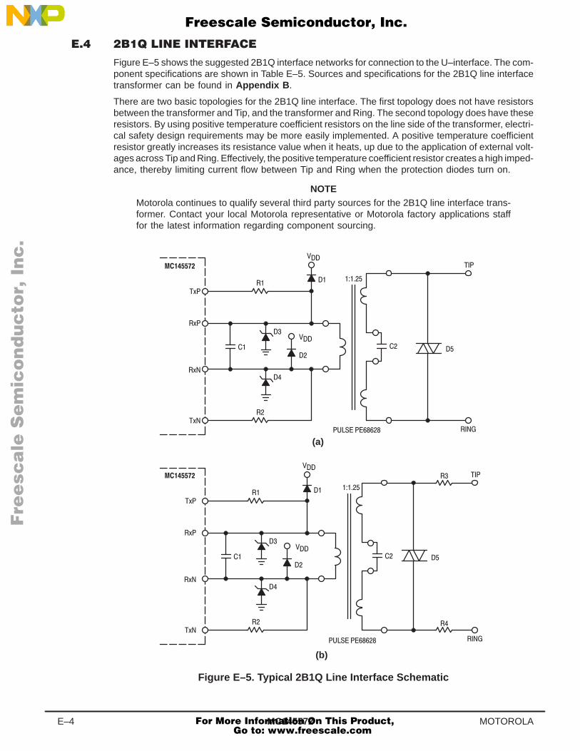
MC145572E–4 MOTOROLA
Figure E–5 shows the suggested 2B1Q interface networks for connection to the U–interface. The com-ponent specifications are shown in Table E–5. Sources and specifications for the 2B1Q line interfacetransformer can be found in Appendix B .
There are two basic topologies for the 2B1Q line interface. The first topology does not have resistorsbetween the transformer and Tip, and the transformer and Ring. The second topology does have theseresistors. By using positive temperature coefficient resistors on the line side of the transformer, electri-cal safety design requirements may be more easily implemented. A positive temperature coefficientresistor greatly increases its resistance value when it heats, up due to the application of external volt-ages across Tip and Ring. Effectively, the positive temperature coefficient resistor creates a high imped-ance, thereby limiting current flow between Tip and Ring when the protection diodes turn on.
NOTEMotorola continues to qualify several third party sources for the 2B1Q line interface trans-former. Contact your local Motorola representative or Motorola factory applications stafffor the latest information regarding component sourcing.
(a)
(b)
Figure E–5. Typical 2B1Q Line Interface Schematic
Fre
esc
ale
Se
mic
on
du
cto
r, I
Freescale Semiconductor, Inc.
For More Information On This Product, Go to: www.freescale.com
nc
...
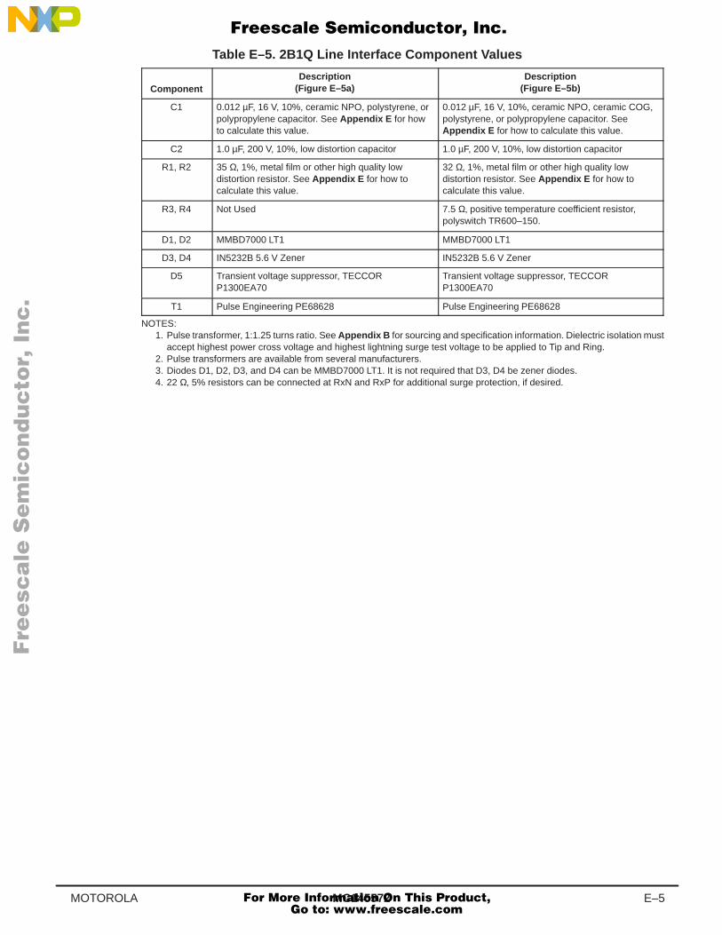
MC145572 E–5MOTOROLA
Table E–5. 2B1Q Line Interface Component ValuesÁÁÁÁÁÁÁÁÁÁÁÁÁÁÁ
Component
ÁÁÁÁÁÁÁÁÁÁÁÁÁÁÁÁÁÁÁÁÁÁÁÁÁÁÁÁÁÁÁÁÁÁÁÁÁÁÁÁÁÁ
Description(Figure E–5a)
ÁÁÁÁÁÁÁÁÁÁÁÁÁÁÁÁÁÁÁÁÁÁÁÁÁÁÁÁÁÁÁÁÁÁÁÁÁÁÁ
Description(Figure E–5b)
ÁÁÁÁÁÁÁÁÁÁÁÁÁÁÁ
C1 ÁÁÁÁÁÁÁÁÁÁÁÁÁÁÁÁÁÁÁÁÁÁÁÁÁÁÁÁÁÁÁÁÁÁÁÁÁÁÁÁÁÁ
0.012 µF, 16 V, 10%, ceramic NPO, polystyrene, orpolypropylene capacitor. See Appendix E for howto calculate this value.
ÁÁÁÁÁÁÁÁÁÁÁÁÁÁÁÁÁÁÁÁÁÁÁÁÁÁÁÁÁÁÁÁÁÁÁÁÁÁÁ
0.012 µF, 16 V, 10%, ceramic NPO, ceramic COG,polystyrene, or polypropylene capacitor. SeeAppendix E for how to calculate this value.
ÁÁÁÁÁÁÁÁÁÁ
C2ÁÁÁÁÁÁÁÁÁÁÁÁÁÁÁÁÁÁÁÁÁÁÁÁÁÁÁÁ
1.0 µF, 200 V, 10%, low distortion capacitorÁÁÁÁÁÁÁÁÁÁÁÁÁÁÁÁÁÁÁÁÁÁÁÁÁÁ
1.0 µF, 200 V, 10%, low distortion capacitorÁÁÁÁÁÁÁÁÁÁÁÁÁÁÁÁÁÁÁÁ
R1, R2ÁÁÁÁÁÁÁÁÁÁÁÁÁÁÁÁÁÁÁÁÁÁÁÁÁÁÁÁÁÁÁÁÁÁÁÁÁÁÁÁÁÁÁÁÁÁÁÁÁÁÁÁÁÁÁÁ
35 Ω, 1%, metal film or other high quality lowdistortion resistor. See Appendix E for how tocalculate this value.
ÁÁÁÁÁÁÁÁÁÁÁÁÁÁÁÁÁÁÁÁÁÁÁÁÁÁÁÁÁÁÁÁÁÁÁÁÁÁÁÁÁÁÁÁÁÁÁÁÁÁÁÁ
32 Ω, 1%, metal film or other high quality lowdistortion resistor. See Appendix E for how tocalculate this value.
ÁÁÁÁÁÁÁÁÁÁ
R3, R4 ÁÁÁÁÁÁÁÁÁÁÁÁÁÁÁÁÁÁÁÁÁÁÁÁÁÁÁÁ
Not Used ÁÁÁÁÁÁÁÁÁÁÁÁÁÁÁÁÁÁÁÁÁÁÁÁÁÁ
7.5 Ω, positive temperature coefficient resistor,polyswitch TR600–150.
ÁÁÁÁÁÁÁÁÁÁ
D1, D2ÁÁÁÁÁÁÁÁÁÁÁÁÁÁÁÁÁÁÁÁÁÁÁÁÁÁÁÁ
MMBD7000 LT1ÁÁÁÁÁÁÁÁÁÁÁÁÁÁÁÁÁÁÁÁÁÁÁÁÁÁ
MMBD7000 LT1ÁÁÁÁÁÁÁÁÁÁ
D3, D4ÁÁÁÁÁÁÁÁÁÁÁÁÁÁÁÁÁÁÁÁÁÁÁÁÁÁÁÁ
IN5232B 5.6 V ZenerÁÁÁÁÁÁÁÁÁÁÁÁÁÁÁÁÁÁÁÁÁÁÁÁÁÁ
IN5232B 5.6 V ZenerÁÁÁÁÁÁÁÁÁÁÁÁÁÁÁ
D5ÁÁÁÁÁÁÁÁÁÁÁÁÁÁÁÁÁÁÁÁÁÁÁÁÁÁÁÁÁÁÁÁÁÁÁÁÁÁÁÁÁÁ
Transient voltage suppressor, TECCORP1300EA70
ÁÁÁÁÁÁÁÁÁÁÁÁÁÁÁÁÁÁÁÁÁÁÁÁÁÁÁÁÁÁÁÁÁÁÁÁÁÁÁ
Transient voltage suppressor, TECCORP1300EA70
ÁÁÁÁÁÁÁÁÁÁ
T1 ÁÁÁÁÁÁÁÁÁÁÁÁÁÁÁÁÁÁÁÁÁÁÁÁÁÁÁÁ
Pulse Engineering PE68628 ÁÁÁÁÁÁÁÁÁÁÁÁÁÁÁÁÁÁÁÁÁÁÁÁÁÁ
Pulse Engineering PE68628
NOTES:1. Pulse transformer, 1:1.25 turns ratio. See Appendix B for sourcing and specification information. Dielectric isolation must
accept highest power cross voltage and highest lightning surge test voltage to be applied to Tip and Ring.2. Pulse transformers are available from several manufacturers.3. Diodes D1, D2, D3, and D4 can be MMBD7000 LT1. It is not required that D3, D4 be zener diodes.4. 22 Ω, 5% resistors can be connected at RxN and RxP for additional surge protection, if desired.
Fre
esc
ale
Se
mic
on
du
cto
r, I
Freescale Semiconductor, Inc.
For More Information On This Product, Go to: www.freescale.com
nc
...

MC145572E–6 MOTOROLA
Fre
esc
ale
Se
mic
on
du
cto
r, I
Freescale Semiconductor, Inc.
For More Information On This Product, Go to: www.freescale.com
nc
...
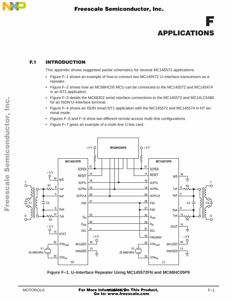
MC145572 F–1MOTOROLA
This appendix shows suggested partial schematics for several MC145572 applications.
• Figure F–1 shows an example of how to connect two MC145572 U–interface transceivers as arepeater.
• Figure F–2 shows how an MC68HC05 MCU can be connected to the MC145572 and MC145474in an NT1 application.
• Figure F–3 details the MC68302 serial interface connections to the MC145572 and MC14LC5480for an ISDN U–interface terminal.
• Figure F–4 shows an ISDN smart NT1 application with the MC145572 and MC145574 in NT ter-minal mode.
• Figures F–5 and F–6 show two different remote access multi–line configurations.
• Figure F–7 gives an example of a multi–line U line card.
)
)
$%
&('
)
#
*
"$%
)
)
"
$%
"&('
!
&('
)
)
)
)
!
!
#
*
"$%
"&('
!
)
)
)
! !
Figure F–1. U–Interface Repeater Using MC145572FN and MC68HC05P9
Fre
esc
ale
Se
mic
on
du
cto
r, I
Freescale Semiconductor, Inc.
For More Information On This Product, Go to: www.freescale.com
nc
...
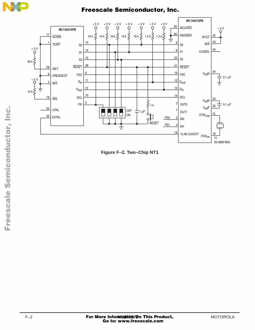
MC145572F–2 MOTOROLA
')
*-,
#
*-,
')
!
!
#
#
(
"
(
"
(
"
"+%&
"+%&
"+%&
# *-,
# ')
!
!
!
"
µ
µ
$
.
(
"
(
"
(
" "
(
"
(
"
(
µ
(
Figure F–2. Two–Chip NT1
Fre
esc
ale
Se
mic
on
du
cto
r, I
Freescale Semiconductor, Inc.
For More Information On This Product, Go to: www.freescale.com
nc
...
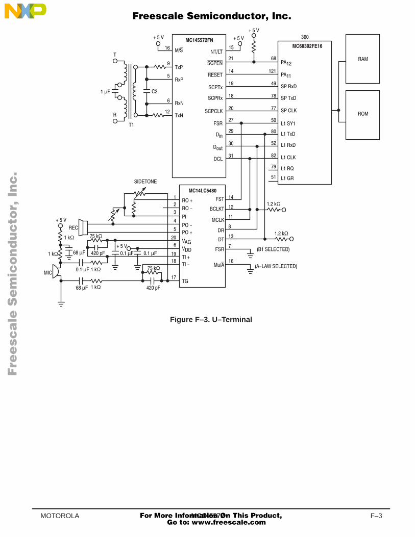
MC145572 F–3MOTOROLA
"
!"#
"#.
"!.
"
')
*-,
#.
" ##
$
"!
$
!.
µ
#
!
!.
#.
!
!
$
$
#
#
#
"#
#
!
#
"!
-
" !.
" #.
"
"&
#.
!.
!
!
!
!
"#
% "#
+
(Ω
"#
!
$
(Ω
µ
(Ω
(Ω
(Ω
µ
µ
+ µ µ (Ω
$
#
$
(Ω
(Ω
Figure F–3. U–Terminal
Fre
esc
ale
Se
mic
on
du
cto
r, I
Freescale Semiconductor, Inc.
For More Information On This Product, Go to: www.freescale.com
nc
...
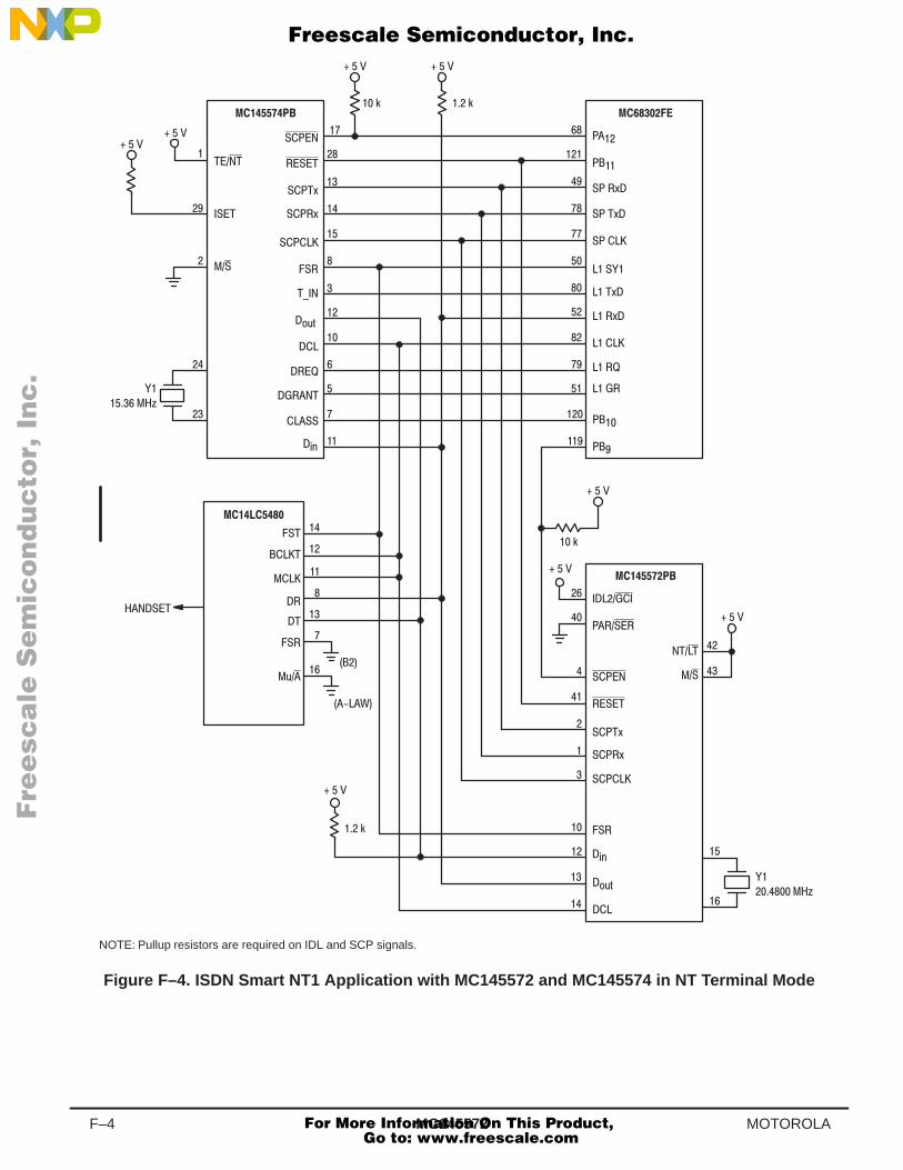
MC145572F–4 MOTOROLA
"
!"#
"#.
"!.
"
#'
+-,
$
"!
"#
#
!
#
"!
-
" !.
" #.
"
"&
#.
!.
!
!
%
$
(*
!
!#
""
##
"#
"
&
/
$
"#
$
!"!
"
!"#
"#.
"!.
"
"!
(*
+-,
$
$
"
##
&
/
NOTE: Pullup resistors are required on IDL and SCP signals.
)
$
)
)
$
)
Figure F–4. ISDN Smart NT1 Application with MC145572 and MC145574 in NT Terminal Mode
Fre
esc
ale
Se
mic
on
du
cto
r, I
Freescale Semiconductor, Inc.
For More Information On This Product, Go to: www.freescale.com
nc
...
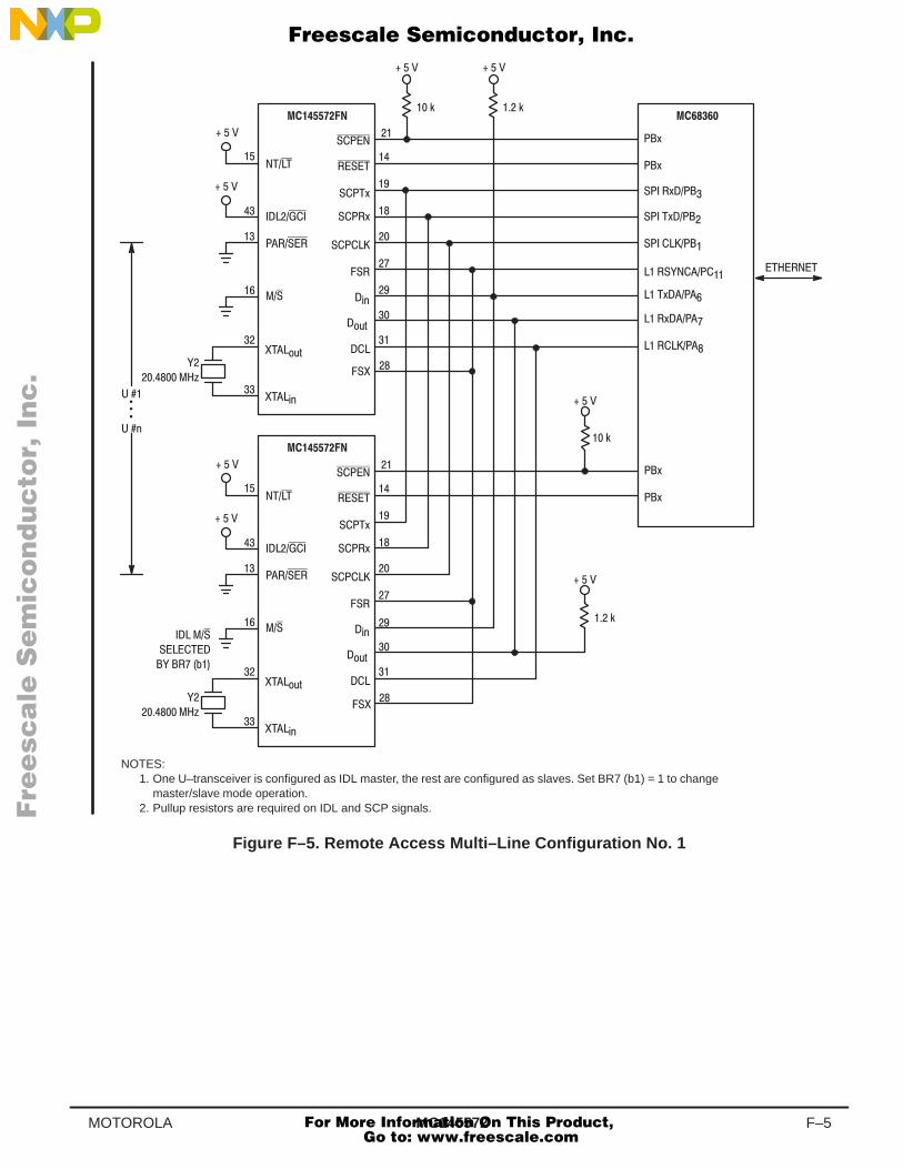
MC145572 F–5MOTOROLA
!
!"
!".
! .
!
+-,
$
!
.
.
! .
! ".
!
!&
".
.
$
(*
""
!
&
/
.
.
$
" "
$
!
%"+-,
%"(*
!
!"
!".
! .
!
+-,
$
!
(*
""
!
&
/
$
!
%"+-,
%"(*
)
$
)
#
# *
!
!"
& '
NOTES:1. One U–transceiver is configured as IDL master, the rest are configured as slaves. Set BR7 (b1) = 1 to change
master/slave mode operation.2. Pullup resistors are required on IDL and SCP signals.
!%
!%
•••
)
$
)
Figure F–5. Remote Access Multi–Line Configuration No. 1
Fre
esc
ale
Se
mic
on
du
cto
r, I
Freescale Semiconductor, Inc.
For More Information On This Product, Go to: www.freescale.com
nc
...
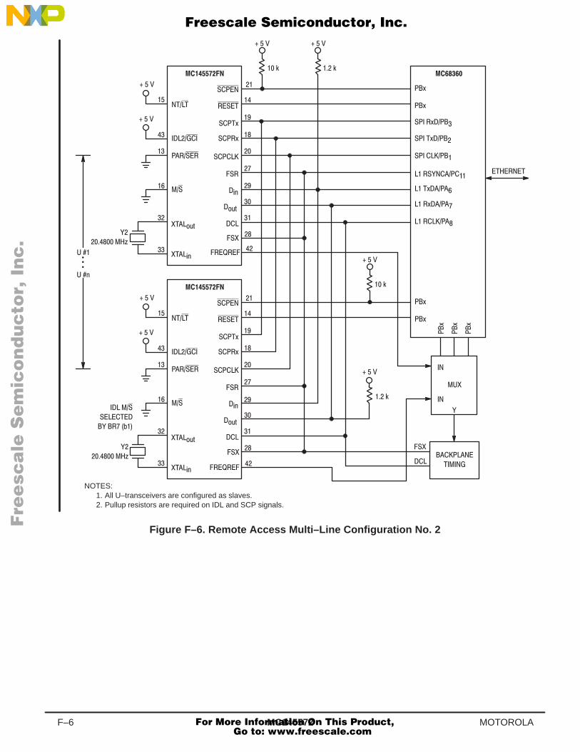
MC145572F–6 MOTOROLA
"
!"#
"#/
"!/
"
,.-
%
"!
/
/
" !/
" #/
"
!"'
#/
!/
!
%
)+
##
"
'
0
/
/
%
#!#
%
!"!
&#,.-
&#)+
"
!"#
"#/
"!/
"
,.-
%
"!
)+
##
"
'
0
%
!"!
&#,.-
&#)+
*
%
*
"
"#
' ! (
NOTES:1. All U–transceivers are configured as slaves.2. Pullup resistors are required on IDL and SCP signals.
"&
"&
! !
! !
/
/
/
"&
#
$&
'
$
$ +
•••
%
*
*
Figure F–6. Remote Access Multi–Line Configuration No. 2
Fre
esc
ale
Se
mic
on
du
cto
r, I
Freescale Semiconductor, Inc.
For More Information On This Product, Go to: www.freescale.com
nc
...
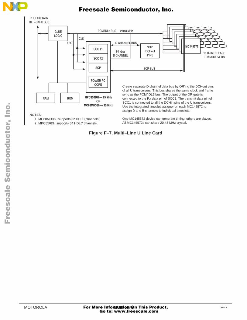
MC145572 F–7MOTOROLA
!
$#&'
+
%)(
"
, *
1. MC68MH360 supports 32 HDLC channels.2. MPC850DH supports 84 HDLC channels.
NOTES:
Create separate D channel data bus by OR’ing the DCHout pinsof all U transceivers. This bus shares the same clock and framesync as the PCM/IDL2 bus. The output of the OR gate isconnected to the Rx data pin of SCC1. The transmit data pin ofSCC1 is connected to all the DCHin pins of the U transceivers.Use the integrated timeslot assigner on each MC145572 toassign D and B channels to individual timeslots.
One MC145572 device can generate timing, others are slaves.All MC145572s can share 20.48 MHz crystal.
Figure F–7. Multi–Line U Line Card
Fre
esc
ale
Se
mic
on
du
cto
r, I
Freescale Semiconductor, Inc.
For More Information On This Product, Go to: www.freescale.com
nc
...

MC145572F–8 MOTOROLA
Fre
esc
ale
Se
mic
on
du
cto
r, I
Freescale Semiconductor, Inc.
For More Information On This Product, Go to: www.freescale.com
nc
...
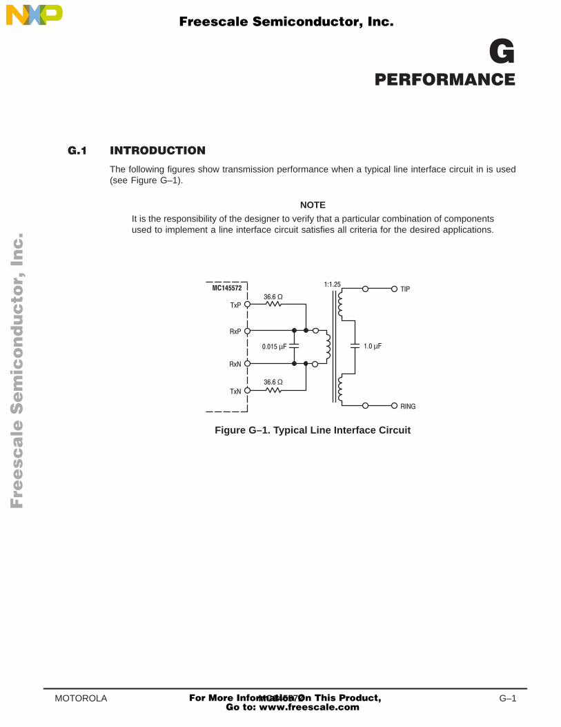
MC145572 G–1MOTOROLA
The following figures show transmission performance when a typical line interface circuit in is used(see Figure G–1).
NOTE
It is the responsibility of the designer to verify that a particular combination of componentsused to implement a line interface circuit satisfies all criteria for the desired applications.
µ
Ω
µ
Ω
Figure G–1. Typical Line Interface Circuit
Fre
esc
ale
Se
mic
on
du
cto
r, I
Freescale Semiconductor, Inc.
For More Information On This Product, Go to: www.freescale.com
nc
...
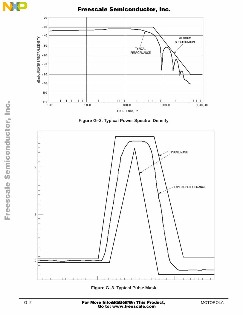
MC145572G–2 MOTOROLA
#!
!$ '
$
%&'" $
Figure G–2. Typical Power Spectral Density
!
$
Figure G–3. Typical Pulse Mask
Fre
esc
ale
Se
mic
on
du
cto
r, I
Freescale Semiconductor, Inc.
For More Information On This Product, Go to: www.freescale.com
nc
...
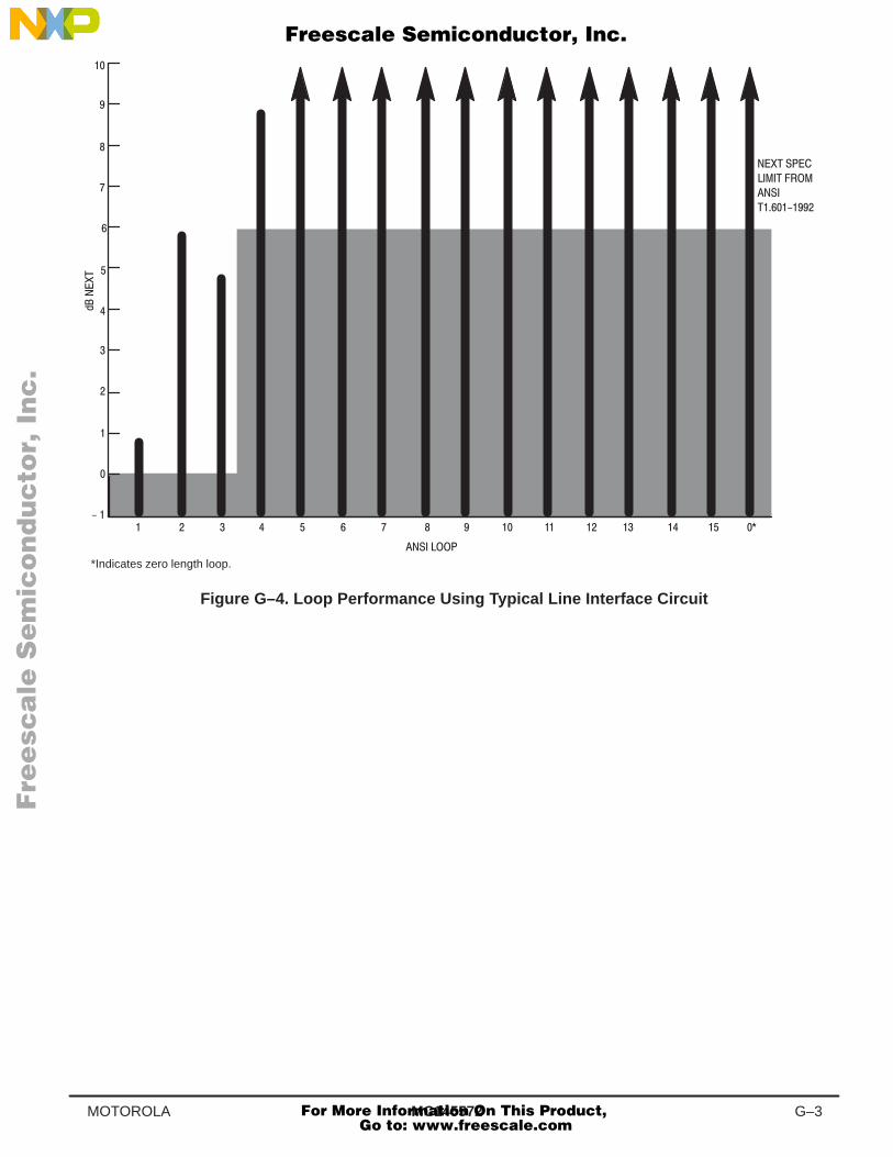
MC145572 G–3MOTOROLA
*Indicates zero length loop.
Figure G–4. Loop Performance Using Typical Line Interface Circuit
Fre
esc
ale
Se
mic
on
du
cto
r, I
Freescale Semiconductor, Inc.
For More Information On This Product, Go to: www.freescale.com
nc
...

MC145572G–4 MOTOROLA
Fre
esc
ale
Se
mic
on
du
cto
r, I
Freescale Semiconductor, Inc.
For More Information On This Product, Go to: www.freescale.com
nc
...
MC145572 H–1MOTOROLA
The MC145572 U–interface transceiver has the capability of forcing all outputs (both analog and digital)to the high impedance state. This feature, known as the Serial Control Port High Impedance DigitalOutput Mode (SCP HIDOM), is provided to allow in–circuit testing of other circuits or devices residenton the same PCB without requiring the removal of the MC145572.
The SCP HIDOM mode is entered by holding SCPEN low for a minimum of 33 consecutive risingedges of SCPCLK while SCPRx is high. If SCPEN goes high, or if SCPRx goes low, the device willexit the SCP HIDOM mode and return to normal operation.
The MC145572 permits an external microcontroller to take control of the transmit Superframe Framerby writing to control bits in Byte register 8. This is very useful for debugging prototypes, since theMC145572 can be forced to transmit a variety of signals regardless of the presence or lack of pres-ence, of a signal on the receive pins. Table 4–8 summarizes these signals and the control bits.
The MC145572 can be forced to transmit SL0, SL1, SL2, SL3, SN0, TN+ SN1, SN2, SN3, 10 kHzand 40 kHz tones, and alternating quats. See the description of BR8 in Section 4.4.9 for more details.
The MC145572 makes it very easy to measure the free running frequency of oscillation of the20.48 MHz crystal oscillator and to measure its frequency pullablility. This is done by using the20.48 MHz square wave signal on the BUFXTALout pin to drive a frequency counter. Make sure thatthis output has not been turned off. Never probe the crystal pins, since the capacitance of the probeintroduces severe errors in the measurement.
Also, the measured frequency must be verified against the make tolerance of the crystal at 25°C.Do not include the aging and temperature tolerances of the crystal when performing free runningfrequency checks at room temperature. If it is desired to verify operation of the crystal oscillator overtemperature, then the crystal temperature tolerance should be included. The MC145572 has a typicalcrystal load capacitance including board traces of about 24 pF. Note that individual board implemen-tations may change this figure slightly.
The free running frequency of oscillation of the 20.48 MHz oscillator can be characterized when theMC145572 is set to NT mode operation. In NT mode, the on–chip variable capacitance array is setfor the nominal center frequency point when the transceiver is deactivated. A frequency of 20.48 MHzplus or minus the tolerance is measured at BUFXTALout. It may be necessary to change the crystalcalibration load capacitance specification slightly in order to have the free running frequency ofoscillation meet the 20.48 MHz specification. The nominal crystal load capacitance is 24 pF.
The pullability of a crystal can be measured by putting the MC145572 into LT mode and changingthe frequency applied to the FREQREF input pin. Any external square wave clock source can be usedfor this, but do not use a clock that is generated by, or derived from, the MC145572 on which thetest is being performed, since this may cause the on–chip PLL to force the on–chip capacitance arrayto its mid–frequency point at all times.
To measure the pullability towards the low frequency direction, pull FREQREF to VDD or VSS. Thiscauses the on–chip PLL to attempt to pull the 20.48 MHz crystal towards dc. Since this is not possible,the MC145572 pulls the crystal as low in frequency as possible by driving the on–chip capacitance
Fre
esc
ale
Se
mic
on
du
cto
r, I
Freescale Semiconductor, Inc.
For More Information On This Product, Go to: www.freescale.com
nc
...
MC145572H–2 MOTOROLA
to its maximum value. Once the frequency of oscillation has stabilized, the negative direction pull-ability can be measured with a frequency counter at BUFXTALout. If a board is designed to have apull up resistor on FREQREF, then automatic test equipment can be programmed for the low frequen-cy measurement and to inject a high frequency clock for the high frequency measurement.
To measure the pullability towards the high frequency direction, FREQREF is driven with a squarewave signal that can be between 8001 Hz and 20 MHz. Note that 8001 Hz is + 1000 ppm, whichexceeds the pull range of the on–chip PLL. This causes the on–chip capacitance array to go to itsminimum value and thereby increases the frequency of the 20.48 MHz oscillator. Once the oscillatorhas stabilized, the frequency of oscillation is measured at BUFXTALout.
It is also possible to use the 4.096 CLKOUT pin to do these measurement, but it is necessary to relatethe pullability in ppm to 4096 kHz instead of 20.48 MHz.
Example 1: Free Running Frequency of Oscillation Measurement at Room Temperature
Configuration:
MC145572 in NT mode
Crystal specification is 20.48 MHz ± 15 ppm. See Section B.3.2.
Results:
BUFXTALout measures as 20,480,307.2 Hz
(( |20,480,307.2 Hz – 20,480,000 Hz|)*1,000,000 ppm) / 20,248,000 Hz = + 15 ppm
Example 2: Oscillator Pullability Measurement at Room Temperature
Crystal specification is ± 20.48 MHz with 360 ppm or ± 180 ppm pull between 15 and 45 pF. SeeSection B.3. In this example, 20,480,000 MHz is used as the nominal frequency. In a real life situationit may be desirable to use the actual measured free run frequency when measuring pullability.
Configuration 1:
MC145572 in LT mode
FREQREF connected to VSS
Results:
BUFXTALout measures as 20,475,801.6 Hz
(( |20,475,801.6 Hz – 20,480,000 Hz|)*1,000,000 ppm) / 20,248,000 Hz = – 205 ppm
Configuration 2:
MC145572 in LT mode
FREQREF connected to 4 MHz
Results:
BUFXTALout measures as 20,483,952.6 Hz
(( |20,483,952.6 Hz – 20,248,000 Hz| )*1,000,000 ppm) / 20,248,000 Hz = + 193 ppm
Conclusion:
Since 20.48 MHz + 193 ppm, – 205 ppm exceeds the ± 180 ppm minimum crystal pull range specifi-cation, the oscillator is working correctly.
Fre
esc
ale
Se
mic
on
du
cto
r, I
Freescale Semiconductor, Inc.
For More Information On This Product, Go to: www.freescale.com
nc
...

MC145572 I–1MOTOROLA
The list contains terms found in this and other Motorola publications concerned with Motorola Semiconductor Prod-ucts for Communications.
A–Law — A European companding/encoding law commonly used in PCM systems.
A/B Signaling — A special case of 8th–bit (LSB) signaling in a µ–law system that allows four logic states to be multiplexed withvoice on PCM channels.
A/D (analog–to–digital) converter (ADC) — A converter that uniquely represents all analog input values within a specified totalinput range by a limited number of digital output codes, each of them exclusively representing a fractional part of the total analoginput range.
Aliasing Noise — A distortion component that is created when frequencies present in a sampled signal are greater than one–half the sample rate.
Answer Back — A signal sent by receiving data–processing device in response to a request from a transmitting device, indicat-ing that the receiver is ready to accept or has received data.
Anti–Aliasing Filter — A filter (normally low pass) that band limits an input signal before sampling to prevent aliasing noise.
Asynchronous — A mode of data transmission in which the time occurrence of the bits within each character or block of char-acters relates to a fixed time frame, but the start of each character or block of characters is not related to this fixed time frame.
Attenuation — A decrease in magnitude of a communication signal.
Bandwidth — The information–carrying frequencies between the limiting frequencies of a communication line or channel.
Baseband — The frequency band occupied by information–bearing signals before combining with a carrier in the modulationprocess.
Baud — A unit of signaling speed equal to the number of discrete signal conditions or events per second. This refers to thephysical symbols/second used within a transmission channel.
Bit Rate — The speed at which data bits are transmitted over a communication path, usually expressed in bits per second. A9600 bps terminal is a 2400 baud system with 4 bits/baud.
Blocking — A condition in a switching system in which no paths or circuits are available to establish a connection to the calledparty even though it is not busy, resulting in a busy tone to the calling party.
BORS(C)HT — Battery, Overvoltage, Ringing, Supervision, (Codec), Hybrid, Test; the functions performed by a subscriber linecard in a telephone exchange.
Broadband — A transmission facility whose bandwidth is greater than that available on voice–grade facilities. (Also called wideband.)
C Message — A frequency weighting that evaluates the effects of noise based on its annoyance to the “typical” subscriber ofstandard telephone service or the effects of noise (background and impulse) on voice–grade data service.
Carrier — An analog signal of fixed amplitude and frequency that combines with an information–bearing signal by modulation toproduce an output signal suitable for transmission.
CCITT — Consultative Committee for International Telephone and Telegraph; an international standards group of EuropeanInternational Telecommunications Union.
CCSN — Common Channel Signaling Network.
Central Office (CO) — A main telephone office, usually within a few miles of a subscriber, that houses switching gear; common-ly capable of handling about 10,000 subscribers.
Channel Bank — Communication equipment commonly used for multiplexing voice–grade channels into a digital transmissionsignal (typically 24 channels in the U.S. and 30 channels in Europe).
Fre
esc
ale
Se
mic
on
du
cto
r, I
Freescale Semiconductor, Inc.
For More Information On This Product, Go to: www.freescale.com
nc
...
MC145572I–2 MOTOROLA
CIDCW — Calling Identity Delivery on Call Waiting; a subscriber feature which allows for the display of the time, date, number,and possible other information about the caller to the called party, while the called party is off–hook.
CLASS — Custom Local Area Signaling Service; a set of services, enhancements, provided to TELCO customers which mayinclude CND, CNAM, Message Waiting, and other features.
CLID — Calling Line IDentification; a subscriber feature which allows for the display of the time, date, number, and possibleother information about the caller to the called party.
CNAM — Calling Name Delivery; a subscriber feature which allows for the display of the time, date, number, and name of thecaller to the called party.
CND — Calling Number Delivery; a subscriber feature which allows for the display of the time, date, number, and possible otherinformation about the caller to the called party.
CODEC — COder–DECoder; the A/D and D/A function on a subscriber line card in a telephone exchange.
COFIDEC — COder–Filter–DECoder; the combination of a codec, the associated filtering, and voltage references required tocode and decode voice in a subscriber line card.
Common Mode Rejection — The ability of a device having a balanced input to reject a voltage applied simultaneously to bothdifferential–input terminals.
Companding — The process in which dynamic range compression of a signal is followed by expansion in accordance with agiven transfer characteristic (companding law) which is usually logarithmic.
Compander — A combination of a compressor at one point in a communication path for reducing the amplitude range of signals,followed by an expander at another point for restoring the original amplitude range, usually to improve the signal–to–noise ratio.
Conference Call — A call between three or more stations, in which each station can carry on a conversation simultaneously.
CPE — Customer Premise Equipment; this could be a POTS phone, answering machine, fax machine, or any number of otherdevices connected to the PSTN.
Crosspoint — The operating contacts or other low–impedance–path connection over which conversations can be routed.
Crosstalk — The undesired transfer of energy from one signal path to another.
CSN — Circuit Switched Network.
CTS — Clear to send; a control signal between a modem and a controller used to initiate data transmission over a communica-tion line.
CVSD — Continuous Variable Slope Delta (modulation); a simple technique to converting an analog signal (like voice) into aserial bit stream.
D3 — D3 channel bank; a specific generation of an AT&T 24–channel PCM terminal that multiplexes 24 voice channels into a1.544 MHz digital bit stream. The specifications associated with D3 channel banks are the basis for all PCM device specifi-cations.
D/A (digital–to–analog) converter (DAC) — A converter that represents a limited number of different digital input codes by acorresponding number of discrete analog output values.
Data Compression — A technique that provides for the transmission of fewer data bits than originally required without infor-mation loss. The receiving location expands the received data bits into the original bit sequence.
dB (decibel) — A power or voltage measurement unit, referred to another power or voltage. It is generally computed as:
10 x log (P1/P2) for power measurements, and
20 x log (V1/V2) for voltage measurements.
dBm — An indication of signal power. 1.0 mW across 600 Ω, or 0.775 volts rms, is defined as 0 dBm. Any other voltage level isconverted to dBm by:
dBm = 20 x log (Vrms/0.775), or
dBm = [20 x log (Vrms)] + 2.22.
dBmO — Signal power measured at a point in a standard test tone level at the same point.
i.e., dBmO = dBm = dBr
where dBr is the relative transmission level, or level relative to the point in the system defined as the zero transmission levelpoint.
Fre
esc
ale
Se
mic
on
du
cto
r, I
Freescale Semiconductor, Inc.
For More Information On This Product, Go to: www.freescale.com
nc
...

MC145572 I–3MOTOROLA
dBmOp — Relative power expressed in dBmp. (See dBmO and dBmp.)
dBmp — Indicates dBm measurement made with a psophometric weighting filter.
dBrn — Relative signal level expressed in decibels above reference noise, where reference noise is 1 pW. Hence, 0 dBrn =1 pW = – 90 dBm.
dBrnC — Indicates dBrn measurement made with a C–message weighting filter. (These units are most commonly used in theU.S., where psophometric weighting is rarely used.)
dBrnc0 — Noise measured in dBrnc referenced to zero transmission level.
Decoding — A process in which one of a set of reconstructed analog samples is generated from the digital character signalrepresenting a sample.
Delay Distortion — Distortion that occurs on communication lines due to the different propagation speeds of signals at differentfrequencies, measured in microseconds of delay relative to the delay at 1700 Hz. (This type of distortion does not affect voicecommunication, but can seriously impair data transmission.)
Delta Modulation — A simple digital coding technique that produces a serial bit stream corresponding to changes in analoginput levels; usually utilized in devices employing continuously variable–slope delta (CVSD) modulation.
Demodulator — A functional section of a modem that converts received analog line signals to digital form.
DN — Directory Number.
Digital Telephone — A telephone terminal that digitizes a voice signal for transmission and decodes a received digital signalback to a voice signal. (It will usually multiplex 64 kbps voice and separate data inputs at multiples of 8 kbps.)
Distortion — The failure to reproduce an original signal’s amplitude, phase, delay, etc. characteristics accurately.
DPSK — Differential Phase Shift Keying; a modulation technique for transmission where the frequency remains constant butphase changes will occur from 90°, 180°, and 290° to define the digital information.
DTMF — Dual Tone Multi–Frequency. It is the “tone dialing” system based on outputting two non–harmonic related frequenciessimultaneously to identify the number dialed. Eight frequencies have been assigned to the four rows and four columns of a typi-cal keypad.
Duplex — A mode of operation permitting the simultaneously two–way independent transmission of telegraph or data signals.
Echo — A signal that has been reflected or returned as a result of impedance mismatches, hybrid unbalance, or time delay.Depending upon the location of impedance irregularities and the propagation characteristics of a facility, echo may interfere withthe speaker/listener or both.
Echo Suppressor — A device used to minimize the effect of echo by blocking the echo return currents; typically a voice–oper-ated gate that allows communication one way at a time.
Encoder (PCM) — A device that performs repeated sampling, compression, and A/D conversion to change an analog signal toa serial stream of PCM samples representing the analog signal.
Equalizer — An electrical network in which phase delay or gain varies with frequency to compensate for an undesired amplitudeor phase characteristic in a frequency–dependent transmission line.
ET — Exchange Termination (CO Switch).
FDM — Frequency–Division Multiplex; a process that permits the transmission of two or more signals over a common path byusing a different frequency band for each signal.
Four Wire Circuit — The portion of a telephone, or central office, that operates on two pairs of wires. One pair is for the transmitpath (generally from the microphone), and one pair is for the receive path (generally from the receiver).
Frame — A set of consecutive digit timeslots in which the position of each digit slot can be identified by reference to a framealignment. The frame alignment signal does not necessarily occur, in whole or in part, in each frame.
Full Duplex — A mode of operation permitting simultaneous transmission of information between two locations in bothdirections.
Gain — The change in signal amplitude (increase or decrease) after passing through an amplifier, or other circuit stage. Usuallyexpressed in dB, an increase is a positive number, and a decrease is a negative number.
Gain Tracking Error — The variation of gain from a constant level (determined at 0 dBm input level) when measuring thedependence of gain on signal level by comparing the output signal to the input signal over a range of input signals.
Fre
esc
ale
Se
mic
on
du
cto
r, I
Freescale Semiconductor, Inc.
For More Information On This Product, Go to: www.freescale.com
nc
...
MC145572I–4 MOTOROLA
HDLC — High–Level Data Link Control; a CCITT standard data communication line protocol.
Half Duplex — A transmission system that permits communication in one direction at a time. CB ratios, with “push–to–talk”switches, and voice–activated speakerphones, are half duplex.
Handset — A rigid assembly providing both telephone transmitter and receiver in a form convenient for holding simultaneouslyto mouth and ear.
Hookswitch — A switch that connects the telephone circuit to the subscriber loop. The name derives from old telephones wherethe switch was activated by lifting the receiver off and onto a hook on the side of the phone.
Idle Channel Noise (ICN) — The total signal energy measured at the output of a device or channel under test when the input ofthe device or channel is grounded (often a wide–band noise measurement using a C–message weighting filter to band–limit theoutput noise).
Intermodulation — The modulation of the components of a complex wave by each other (in a nonlinear system).
Intermodulation Distortion — An analog line impairment when two frequencies interact to create an erroneous frequency, inturn distorting the data signal representation.
IRED — Infrared. Used as a wireless link for remote control or to transfer data.
ISDN — Integrated Services Digital Network; a communication network intended to carry digitized voice and data multiplexedonto the public network.
Jitter — A type of analog communication line distortion caused by abrupt, spurious signal variation from a reference timingposition, and capable of causing data transmission errors, particularly at high speeds. (The variation can be in amplitude, time,frequency, or phase.)
Key System — A miniature PABX that accepts 4 to 10 lines and can direct them to as many as 30 telsets.
Mu–Law — (µ–law) A companding law accepted as the North American standard for PCM based systems.
LAN — Local Area Network; a data–only communication network between data terminals using a standard interface to thenetwork.
Line — The portion of a circuit external to an apparatus that consists of the conductors connecting the apparatus to theexchange or connecting two exchanges.
Line Length Compensation — Also referred to as loop length compensation, it involves changing the gain of the transmit andreceive paths, within a telephone, to compensate for different signal levels at the end of different line lengths. A short line (closeto the CO) will attenuate signals less, and therefore less gain is needed. Compensation circuits generally use the loop current asan indication of the line length.
Longitudinal Balance — The common–mode rejection of a telephone circuit.
Loop — The loop formed by the two subscriber wires (Tip and Ring) connected to the telephone at one end, and the centraloffice (or PBX) at the other end. Generally it is a floating system, not referred to ground, or ac power.
Loopback — Directing signals back toward the source at some point along a communication path.
Loop Current — The dc current that flows through the subscriber loop. It is typically provided by the central office or PBX, andranges from 20 to 120 mA.
LT — Line Termination (Line Card).
MCU — MicroComputer Unit (also MicroController Unit).
MPU — MicroProcessor Unit.
Mu–Law — A companding/encoding law commonly used in U.S. (same as µ–law).
MUX — Multiplex or multiplexer.
Modem — MOdulator–DEModulator; a unit that modulates and demodulates digital information from a terminal or computer portto an analog carrier signal for passage over an analog line.
Multiplex — To simultaneously transmit two or more messages on a single channel.
NT1 — Network Termination 1 (OSI Layer 1 Only).
NT2 — Network Termination 2 (OSI Layers 2 and 3).
Off–Hook — The condition when the telephone is connected to the phone system, permitting loop current to flow. The centraloffice detects the dc current as an indication that the phone is busy.
Fre
esc
ale
Se
mic
on
du
cto
r, I
Freescale Semiconductor, Inc.
For More Information On This Product, Go to: www.freescale.com
nc
...

MC145572 I–5MOTOROLA
On–Hook — The condition when the telephone’s dc path is open, and no dc loop current flows. The central office regards anon–hook phone as available for ringing.
PABX — Private Automatic Branch Exchange; a customer–owned, switchable telephone system providing internal and/or exter-nal station–to–station dialing.
Pair — The two associated conductors that form part of a communication channel.
Pass–Band Filter — A filter used in communication systems that allows only the frequencies within a communication channelto pass, and rejects all frequencies outside the channel.
PBX — Private Branch Exchange; a class of service in standard Bell System terminology that typically provides the same ser-vice as PABX.
PCM — Pulse Code Modulation; a method of transmitting data in which signals are sampled and converted to digital words thatare then transmitted serially, typically as 8–bit words.
Phase Jitter — Abrupt, spurious variations in an analog line, generally caused by power and communication equipment alongthe line that shifts the signal phase relationship back and forth.
PLL — Phase–Locked Loop.
PLL Frequency Synthesizer — Phase–locked loop frequency synthesizer. A frequency synthesizer utilizing a closed loop, asopposed to DDS (direct digital synthesis) which is not a closed loop.
POTS — Plain Old Telephone Service.
Propagation Delay — The time interval between specified reference points on the input and output voltage waveforms.
Psophometric Weighting — A frequency weighting similar to C–Message weighting that is used as the standard for Europeantelephone system testing.
PSN — Packet Switched Network.
PSTN — Public Switched Telephone Network.
Pulse Dialer — A device that generates pulse trains corresponding to digits or characters used in impulse or loop–disconnectdialing.
Quantizing Noise — Signal–correlated noise generally associated with the quantizing error introduced by A/D and D/A conver-sions in digital transmission systems.
REN — Ringer Equivalence Number; an indication of the impedance, or loading factor, of a telephone bell or ringer circuit. AnREN of 1.0 equals about 8 kΩ. The Bell system typically permits a maximum of 5.0 REN (1.6 kΩ) on an individual subscriber line.A minimum REN of 0.2 (40 kΩ) is required by the Bell system.
Repeater — An amplifier and associated equipment used in a telephone circuit to process a signal and retransmit it.
Repertory Dialer — A dialer that stores a repertory of telephone numbers and dials any one of them automatically on request.
Ring — One of the two wires connecting the central office to a telephone. The name derives from the ring portion of the plugsused by operators (in older equipment) to make the connection. Ring is traditionally negative with respect to Tip.
RTS — Request To Send; an EIA–232 control signal between a modem and user’s digital equipment that initiates the data trans-mission sequence on a communication line.
Sampling Rate — The frequency at which the amplitude of an analog signal is gated into a coder circuit. The Nyquist samplingtheorem states that if a band–limited signal is sampled at regular intervals and at a rate equal to or greater than twice the highestfrequency of interest, the sample contains all the information of the original signal. The frequency band of interest in telephonyranges from 300 to 3400 Hz, so a sampling rate of 8 kHz provides dc to 4000 Hz reproduction.
SCU — Subscriber Channel Unit; the circuitry at a telephone exchange associated with an individual subscriber line or channel.
Sidetone — The sound fed back to the receiver as a result of speaking into the microphone. It is a natural consequence of the2–to–4 wire conversion system. Sidetone was recognized by Alexander Graham Bell as necessary for a person to be able tospeak properly while using a handset.
Signaling — The transmission of control or status information between switching systems in the form of dedicated bits or chan-nels of information inserted on trunks with voice data.
Signal–to–Distortion Ratio (S/D) — The ratio of the input signal level to the level of all components that are present when theinput signal (usually a 1.020 kHz sinusoid) is eliminated from the output signal (e.g., by filtering).
Fre
esc
ale
Se
mic
on
du
cto
r, I
Freescale Semiconductor, Inc.
For More Information On This Product, Go to: www.freescale.com
nc
...

MC145572I–6 MOTOROLA
SLIC — Subscriber Line Interface Circuit; a circuit that performs the 2–to–4 wire conversion, battery feed, line supervision, andcommon mode rejection at the central office (or PBX) end of the telephone line.
SOG Package — Small–Outline Gull–wing package; formerly SOIC with gull–wing leads. This package has leads which fold outfrom the body.
SOJ Package — Small–Outline J–lead package; formerly SOIC with J leads. This package has leads which are tucked underthe body.
Speech Network — A circuit that provides 2–to–4 wire conversion, i.e., connects the microphone and receiver (or the transmitand receive paths) to the Tip and Ring phone lines. Additionally it provides sidetone control, and in many cases, the dc loopcurrent interface.
Subscriber Line — The system consisting of the user’s telephone, the interconnecting wires, and the central office equipmentdedicated to that subscriber (also referred to as a loop).
Switchhook — A synonym for hookswitch.
Syn (Sync) — (1) A bit character used to synchronize a time frame in a time–division multiplexer. (2) A sequence used by asynchronous modem to perform bit synchronization or by a line controller for character synchronization.
Synchronous Modem — A modem that uses a derived clocking signal to perform bit synchronization with incoming data.
T1 Carrier — A PCM system operating at 1.544 MHz and carrying 24 individual voice–frequency channels.
TA — Terminal Adapter.
Talkdown — Missed signals in the presence of speech. Commonly used to describe the performance of a DTMF receiver whenit fails to recognize a valid DTMF tone due to cancellation of that tone by speech.
Talkoff — False detections caused by speech. Commonly used to describe the performance of a DTMF receiver when speech,emulating DTMF, causes the receiver to believe it has detected a valid DTMF tone.
Tandem Trunk — See trunk.
Telephone Exchange — A switching center for interconnecting the lines that service a specific area.
TE1 — Terminal Equipment 1 (ISDN Terminal).
TE2 — Terminal Equipment 2 (Non–ISDN Terminal).
TELETEX — A text communication service between entirely electronic workstations that will gradually replace TELEX with theintroduction of the digital network. (Not to be confused with teletext.)
TELETEXT — The name usually used for broadcast text (and graphics) for domestic television reception. (Not to be confusedwith teletex.)
Time–Division Multiplex — A process that permits the transmission of two or more signals over a common path by using adifferent time interval for each signal.
Tin Cans and String — A crude analog communications system commonly used to introduce voice communications tochildren.
Tip — One of the two wires connecting the central office to a telephone. The name derives from the tip of the plugs used byoperators (in older equipment) to make the connection. Tip is traditionally positive with respect to ring.
Tone Ringer — The modern solid state equivalent of the old electromechanical bell. It provides the sound when the central officealerts the subscriber that someone is calling. Ringing voltage is typically 80 – 90 volts rms, 20 Hz.
Trunk — A telephone circuit or channel between two central offices or switching entities.
TSAC — Timeslot Assigner Circuit; a circuit that determines when a CODEC will put its 8 bits of data on a PCM bit stream.
TSIC — Timeslot Interchange Circuit; a device that switches digital highways in PCM based switching systems; a “digital” cross-point switch.
Twist — The amplitude ratio of a pair of DTMF tones. (Because of transmission and equipment variations, a pair of tones thatoriginated equal in amplitude may arrive with a considerable difference in amplitude.)
Two Wire Circuit — Refers to the two wires connecting the central office to the subscriber’s telephone. Commonly referred to asTip and Ring, the two wires carry both transmit and receive signals in a differential manner.
UDLT — Universal Digital Loop Transceiver; a Motorola originated name for a voice/data transceiver circuit.
Fre
esc
ale
Se
mic
on
du
cto
r, I
Freescale Semiconductor, Inc.
For More Information On This Product, Go to: www.freescale.com
nc
...

MC145572 I–7MOTOROLA
VCO — Voltage–Controlled Oscillator. Input is a voltage; output is a sinusoidal waveform.
VCM — Voltage–Controlled Multivibrator. Input is a voltage; output is a square wave.
Voice Frequency — A frequency within that part of the audio range that is used for the transmission of speech of commercialquality (i.e., 300 – 3400 Hz).
Weighting Network — A network whose loss varies with frequency in a predetermined manner.
Fre
esc
ale
Se
mic
on
du
cto
r, I
Freescale Semiconductor, Inc.
For More Information On This Product, Go to: www.freescale.com
nc
...

MC145572I–8 MOTOROLA
Fre
esc
ale
Se
mic
on
du
cto
r, I
Freescale Semiconductor, Inc.
For More Information On This Product, Go to: www.freescale.com
nc
...
MC145572 J–1MOTOROLA
ANSI American National Standards Institute11 West 42nd StreetNew York, NY 10036USA
Bellcore Bell Communications ResearchCustomer Service60 New England AvenuePiscataway, NJ 08854–4196USAPhone: (201) 699–5800
CCITT Consultive Committee of the InternationalTelephone and TelegraphInternational Telecommunications UnionPlace Des NationsCH–1211 GenevaSwitzerlandPhone: (011) 4122 730 5851
EIA Electronic Industries Association1722 Eye Street, NWSuite 440Washington, DC 20006USAPhone (Headquarters): (202) 457–4936Phone (Standards): (202) 457–4966
ETSI European Telecommunications StandardsInstitute06921 Sophia Antipolis CedexFRANCEPhone: 33 92 94 42 00Fax: 33 93 65 47 16
IEEE Institute of Electrical and ElectronicsEngineersHeadquarters:
345 East 47th StreetNew York, NY 10017USAPhone (212) 705–7900
Standards Office:IEEE Service CenterPO Box 1331Piscataway, NJ 00855USAPhone: (201) 981–0060
TIA Telecommunications Industry Association2001 Pennsylvania Avenue, NWSuite 800Washington, DC 2006–1813USAPhone: (202) 457–5430Fax: (202 457–4939
Fre
esc
ale
Se
mic
on
du
cto
r, I
Freescale Semiconductor, Inc.
For More Information On This Product, Go to: www.freescale.com
nc
...

MC145572J–2 MOTOROLA
Fre
esc
ale
Se
mic
on
du
cto
r, I
Freescale Semiconductor, Inc.
For More Information On This Product, Go to: www.freescale.com
nc
...
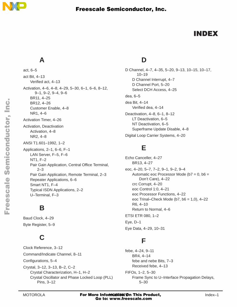
MC145572 Index–1MOTOROLA
Aact, 6–5
act Bit, 4–13Verified act, 4–13
Activation, 4–6, 4–8, 4–29, 5–30, 6–1, 6–6, 8–12,9–1, 9–2, 9–4, 9–6
BR11, 4–25BR12, 4–26Customer Enable, 4–8NR1, 4–6
Activation Timer, 4–26
Activation, DeactivationActivation, 4–8NR2, 4–8
ANSI T1.601–1992, 1–2
Applications, 2–1, 6–6, F–1LAN Server, F–5, F–6NT1, F–2Pair Gain Application, Central Office Terminal,
2–3Pair Gain Application, Remote Terminal, 2–3Repeater Applications, 6–6Smart NT1, F–4Typical ISDN Applications, 2–2U–Terminal, F–3
BBaud Clock, 4–29
Byte Register, 5–9
CClock Reference, 3–12
Command/Indicate Channel, 8–11
Configurations, 5–4
Crystal, 3–12, 3–13, B–2, C–2Crystal Characterization, H–1, H–2Crystal Oscillator and Phase Locked Loop (PLL)
Pins, 3–12
DD Channel, 4–7, 4–35, 5–20, 9–13, 10–15, 10–17,
10–19D Channel Interrupt, 4–7D Channel Port, 5–20Select DCH Access, 4–25
dea, 6–5
dea Bit, 4–14Verified dea, 4–14
Deactivation, 4–8, 6–1, 8–12LT Deactivation, 6–5NT Deactivation, 6–5Superframe Update Disable, 4–8
Digital Loop Carrier Systems, 4–20
EEcho Canceller, 4–27
BR13, 4–27
eoc, 4–20, 5–7, 7–2, 9–1, 9–2, 9–4Automatic eoc Processor Mode (b7 = 0, b6 =
Don’t Care), 4–22crc Corrupt, 4–20eoc Control 1:0, 4–21eoc Processor Functions, 4–22eoc Trinal–Check Mode (b7, b6 = 1,0), 4–22R6, 4–10Return to Normal, 4–6
ETSI ETR 080, 1–2
Eye, D–1
Eye Data, 4–29, 10–31
Ffebe, 4–24, 9–11
BR4, 4–14febe and nebe Bits, 7–3Received febe, 4–13
FIFOs, 1–2, 5–30Frame Sync to U–Interface Propagation Delays,
5–30
Fre
esc
ale
Se
mic
on
du
cto
r, I
Freescale Semiconductor, Inc.
For More Information On This Product, Go to: www.freescale.com
nc
...
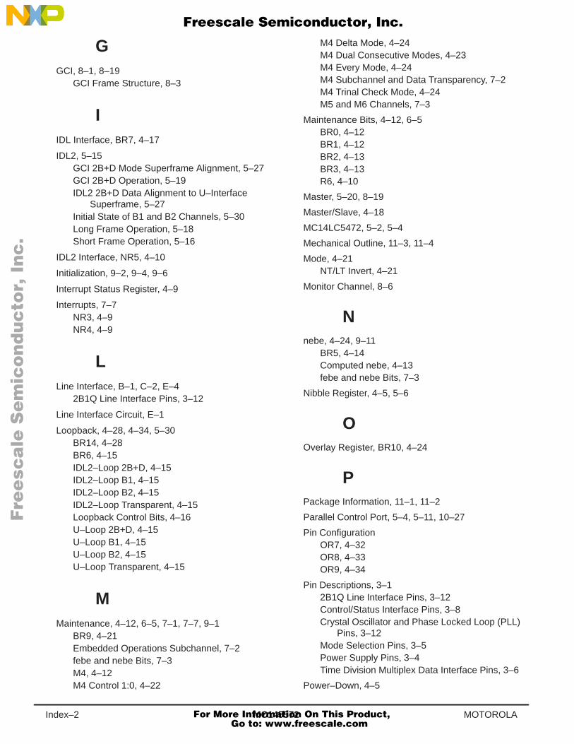
MC145572Index–2 MOTOROLA
GGCI, 8–1, 8–19
GCI Frame Structure, 8–3
IIDL Interface, BR7, 4–17
IDL2, 5–15GCI 2B+D Mode Superframe Alignment, 5–27GCI 2B+D Operation, 5–19IDL2 2B+D Data Alignment to U–Interface
Superframe, 5–27Initial State of B1 and B2 Channels, 5–30Long Frame Operation, 5–18Short Frame Operation, 5–16
IDL2 Interface, NR5, 4–10
Initialization, 9–2, 9–4, 9–6
Interrupt Status Register, 4–9
Interrupts, 7–7NR3, 4–9NR4, 4–9
LLine Interface, B–1, C–2, E–4
2B1Q Line Interface Pins, 3–12
Line Interface Circuit, E–1
Loopback, 4–28, 4–34, 5–30BR14, 4–28BR6, 4–15IDL2–Loop 2B+D, 4–15IDL2–Loop B1, 4–15IDL2–Loop B2, 4–15IDL2–Loop Transparent, 4–15Loopback Control Bits, 4–16U–Loop 2B+D, 4–15U–Loop B1, 4–15U–Loop B2, 4–15U–Loop Transparent, 4–15
MMaintenance, 4–12, 6–5, 7–1, 7–7, 9–1
BR9, 4–21Embedded Operations Subchannel, 7–2febe and nebe Bits, 7–3M4, 4–12M4 Control 1:0, 4–22
M4 Delta Mode, 4–24M4 Dual Consecutive Modes, 4–23M4 Every Mode, 4–24M4 Subchannel and Data Transparency, 7–2M4 Trinal Check Mode, 4–24M5 and M6 Channels, 7–3
Maintenance Bits, 4–12, 6–5BR0, 4–12BR1, 4–12BR2, 4–13BR3, 4–13R6, 4–10
Master, 5–20, 8–19
Master/Slave, 4–18
MC14LC5472, 5–2, 5–4
Mechanical Outline, 11–3, 11–4
Mode, 4–21NT/LT Invert, 4–21
Monitor Channel, 8–6
Nnebe, 4–24, 9–11
BR5, 4–14Computed nebe, 4–13febe and nebe Bits, 7–3
Nibble Register, 4–5, 5–6
OOverlay Register, BR10, 4–24
PPackage Information, 11–1, 11–2
Parallel Control Port, 5–4, 5–11, 10–27
Pin ConfigurationOR7, 4–32OR8, 4–33OR9, 4–34
Pin Descriptions, 3–12B1Q Line Interface Pins, 3–12Control/Status Interface Pins, 3–8Crystal Oscillator and Phase Locked Loop (PLL)
Pins, 3–12Mode Selection Pins, 3–5Power Supply Pins, 3–4Time Division Multiplex Data Interface Pins, 3–6
Power–Down, 4–5
Fre
esc
ale
Se
mic
on
du
cto
r, I
Freescale Semiconductor, Inc.
For More Information On This Product, Go to: www.freescale.com
nc
...
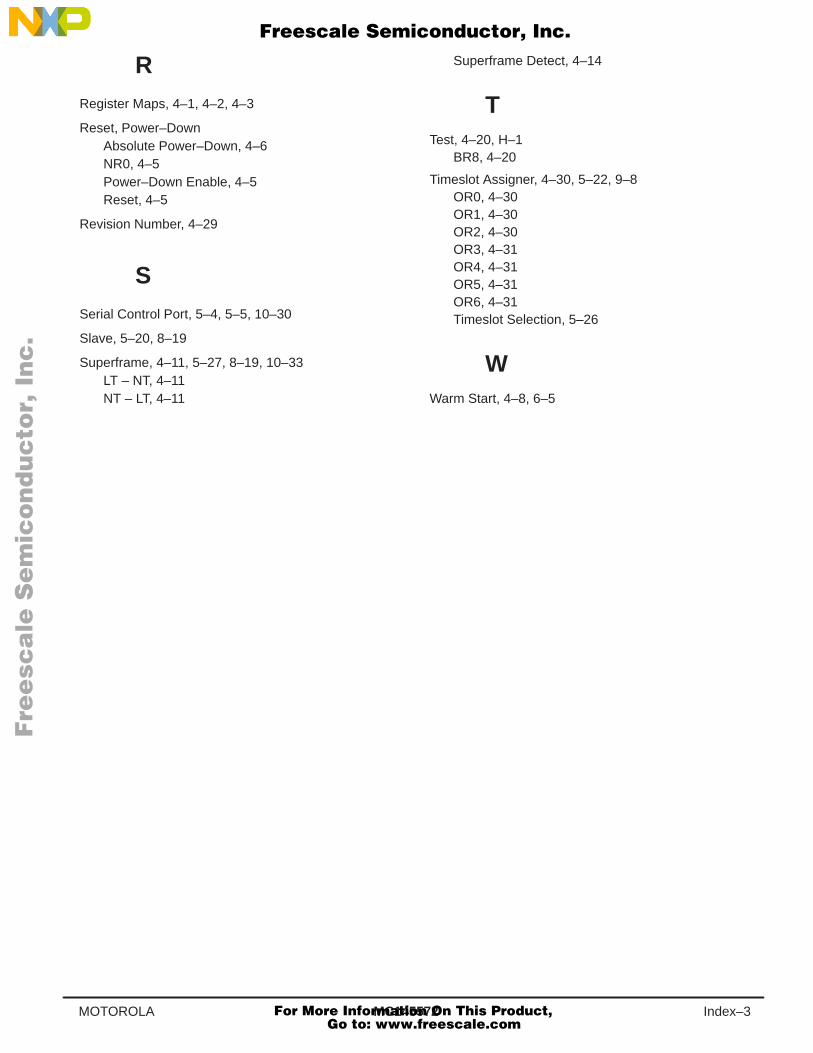
MC145572 Index–3MOTOROLA
RRegister Maps, 4–1, 4–2, 4–3
Reset, Power–DownAbsolute Power–Down, 4–6NR0, 4–5Power–Down Enable, 4–5Reset, 4–5
Revision Number, 4–29
SSerial Control Port, 5–4, 5–5, 10–30
Slave, 5–20, 8–19
Superframe, 4–11, 5–27, 8–19, 10–33LT – NT, 4–11NT – LT, 4–11
Superframe Detect, 4–14
TTest, 4–20, H–1
BR8, 4–20
Timeslot Assigner, 4–30, 5–22, 9–8OR0, 4–30OR1, 4–30OR2, 4–30OR3, 4–31OR4, 4–31OR5, 4–31OR6, 4–31Timeslot Selection, 5–26
WWarm Start, 4–8, 6–5
Fre
esc
ale
Se
mic
on
du
cto
r, I
Freescale Semiconductor, Inc.
For More Information On This Product, Go to: www.freescale.com
nc
...

MC145572Index–4 MOTOROLA
Fre
esc
ale
Se
mic
on
du
cto
r, I
Freescale Semiconductor, Inc.
For More Information On This Product, Go to: www.freescale.com
nc
...
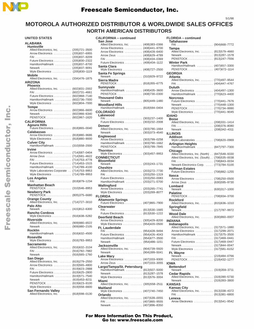
5/1/98
MOTOROLA AUTHORIZED DISTRIBUTOR & WORLDWIDE SALES OFFICESNORTH AMERICAN DISTRIBUTORS
UNITED STATES
ALABAMAHuntsville
Allied Electronics, Inc. (205)721–3500. . . . . . . . Arrow Electronics (205)837–6955. . . . . . . . . . . . FAI (205)837–9209. . . . . . . . . . . . . . . . . . . . . . . . . Future Electronics (205)830–2322. . . . . . . . . . . . Hamilton/Hallmark (205)837–8700. . . . . . . . . . . Newark (205)837–9091. . . . . . . . . . . . . . . . . . . . . Wyle Electronics (205)830–1119. . . . . . . . . . . . .
MobileAllied Electronics, Inc. (334)476–1875. . . . . . . .
ARIZONAPhoenix
Allied Electronics, Inc. (602)831–2002. . . . . . . . FAI (602)731–4661. . . . . . . . . . . . . . . . . . . . . . . . . Future Electronics (602)968–7140. . . . . . . . . . . . Hamilton/Hallmark (602)736–7000. . . . . . . . . . . Wyle Electronics (602)804–7000. . . . . . . . . . . . .
TempeArrow Electronics (602)966–6600. . . . . . . . . . . . Newark (602)966–6340. . . . . . . . . . . . . . . . . . . . . PENSTOCK (602)967–1620. . . . . . . . . . . . . . . . .
CALIFORNIAAgoura Hills
Future Electronics (818)865–0040. . . . . . . . . . . . Calabassas
Arrow Electronics (818)880–9686. . . . . . . . . . . . Wyle Electronics (818)880–9000. . . . . . . . . . . . .
Culver CityHamilton/Hallmark (310)558–2000. . . . . . . . . . .
IrvineArrow Electronics (714)587–0404. . . . . . . . . . . . Arrow Zeus (714)581–4622. . . . . . . . . . . . . . . . . FAI (714)753–4778. . . . . . . . . . . . . . . . . . . . . . . . . Future Electronics (714)453–1515. . . . . . . . . . . . Hamilton/Hallmark (714)789–4100. . . . . . . . . . . Wyle Laboratories Corporate (714)753–9953. . Wyle Electronics (714)789–9953. . . . . . . . . . . . .
Los AngelesFAI (818)879–1234. . . . . . . . . . . . . . . . . . . . . . . . .
Manhattan BeachPENSTOCK (310)546–8953. . . . . . . . . . . . . . . . .
Newberry ParkPENSTOCK (805)375–6680. . . . . . . . . . . . . . . . .
Orange CountyAllied Electronics, Inc. (714)727–3010. . . . . . . .
Palo AltoNewark (415)812–6300. . . . . . . . . . . . . . . . . . . . .
Rancho CordovaWyle Electronics (916)638–5282. . . . . . . . . . . . .
RiversideAllied Electronics, Inc. (909)980–6522. . . . . . . . Newark (909)980–2105. . . . . . . . . . . . . . . . . . . . .
RocklinHamilton/Hallmark (916)632–4500. . . . . . . . . . .
RosevilleWyle Electronics (916)783–9953. . . . . . . . . . . . .
SacramentoAllied Electronics, Inc. (916)632–3104. . . . . . . . FAI (916)782–7882. . . . . . . . . . . . . . . . . . . . . . . . . Newark (916)565–1760. . . . . . . . . . . . . . . . . . . . .
San DiegoAllied Electronics, Inc. (619)279–2550. . . . . . . . Arrow Electronics (619)565–4800. . . . . . . . . . . . FAI (619)623–2888. . . . . . . . . . . . . . . . . . . . . . . . . Future Electronics (619)625–2800. . . . . . . . . . . . Hamilton/Hallmark (619)571–7540. . . . . . . . . . . Newark (619)453–8211. . . . . . . . . . . . . . . . . . . . . PENSTOCK (619)623–9100. . . . . . . . . . . . . . . . . Wyle Electronics (619)558–6600. . . . . . . . . . . . .
San Fernando ValleyAllied Electronics, Inc. (818)598–0130. . . . . . . .
CALIFORNIA – continuedSan Jose
Allied Electronics, Inc. (408)383–0366. . . . . . . . Arrow Electronics (408)441–9700. . . . . . . . . . . . Arrow Electronics (408)428–6400. . . . . . . . . . . . Arrow Zeus (408)629–4789. . . . . . . . . . . . . . . . . FAI (408)434–0369. . . . . . . . . . . . . . . . . . . . . . . . . Future Electronics (408)434–1122. . . . . . . . . . . .
Santa ClaraWyle Electronics (408)727–2500. . . . . . . . . . . . .
Santa Fe SpringsNewark (310)929–9722. . . . . . . . . . . . . . . . . . . . .
Sierra MadrePENSTOCK (818)355–6775. . . . . . . . . . . . . . . . .
SunnyvaleHamilton/Hallmark (408)435–3600. . . . . . . . . . . PENSTOCK (408)730–0300. . . . . . . . . . . . . . . . .
Thousand OaksNewark (805)449–1480. . . . . . . . . . . . . . . . . . . . .
Woodland HillsHamilton/Hallmark (818)594–0404. . . . . . . . . . .
COLORADOLakewood
FAI (303)237–1400. . . . . . . . . . . . . . . . . . . . . . . . . Future Electronics (303)232–2008. . . . . . . . . . . .
DenverAllied Electronics, Inc. (303)790–1664. . . . . . . . Newark (303)373–4540. . . . . . . . . . . . . . . . . . . . .
EnglewoodArrow Electronics (303)799–0258. . . . . . . . . . . . Hamilton/Hallmark (303)790–1662. . . . . . . . . . . PENSTOCK (303)799–7845. . . . . . . . . . . . . . . . .
ThorntonWyle Electronics (303)457–9953. . . . . . . . . . . . .
CONNECTICUTBloomfield
Newark (203)243–1731. . . . . . . . . . . . . . . . . . . . . Cheshire
Allied Electronics, Inc. (203)272–7730. . . . . . . . FAI (203)250–1319. . . . . . . . . . . . . . . . . . . . . . . . . Future Electronics (203)250–0083. . . . . . . . . . . . Hamilton/Hallmark (203)271–5700. . . . . . . . . . .
WallingfordArrow Electronics (203)265–7741. . . . . . . . . . . . Wyle Electronics (203)269–8077. . . . . . . . . . . . .
FLORIDAAltamonte Springs
Future Electronics (407)865–7900. . . . . . . . . . . . Clearwater
FAI (813)530–1665. . . . . . . . . . . . . . . . . . . . . . . . . Future Electronics (813)530–1222. . . . . . . . . . . .
Deerfield BeachArrow Electronics (305)429–8200. . . . . . . . . . . . Wyle Electronics (954)420–0500. . . . . . . . . . . . .
Ft. LauderdaleFAI (954)428–9494. . . . . . . . . . . . . . . . . . . . . . . . . Future Electronics (954)426–4043. . . . . . . . . . . . Hamilton/Hallmark (954)677–3500. . . . . . . . . . . Newark (954)486–1151. . . . . . . . . . . . . . . . . . . . .
JacksonvilleAllied Electronics, Inc. (904)739–5920. . . . . . . . Newark (904)399–5041. . . . . . . . . . . . . . . . . . . . .
Lake MaryArrow Electronics (407)333–9300. . . . . . . . . . . . Arrow Zeus (407)333–3055. . . . . . . . . . . . . . . . .
Largo/Tampa/St. PetersburgHamilton/Hallmark (813)507–5000. . . . . . . . . . . Newark (813)287–1578. . . . . . . . . . . . . . . . . . . . . Wyle Electronics (813)576–3004. . . . . . . . . . . . .
MiamiAllied Electronics, Inc. (305)558–2511. . . . . . . .
MaitlandWyle Electronics (407)740–7450. . . . . . . . . . . . .
OrlandoAllied Electronics, Inc. (407)539–0055. . . . . . . . FAI (407)865–9555. . . . . . . . . . . . . . . . . . . . . . . . . Newark (407)896–8350. . . . . . . . . . . . . . . . . . . . .
FLORIDA – continuedTallahassee
FAI (904)668–7772. . . . . . . . . . . . . . . . . . . . . . . . . Tampa
Allied Electronics, Inc. (813)579–4660. . . . . . . . Newark (813)287–1578. . . . . . . . . . . . . . . . . . . . . PENSTOCK (813)247–7556. . . . . . . . . . . . . . . . .
Winter ParkHamilton/Hallmark (407)657–3300. . . . . . . . . . . PENSTOCK (407)672–1114. . . . . . . . . . . . . . . . .
GEORGIAAtlanta
Allied Electronics, Inc. (770)497–9544. . . . . . . . FAI (404)447–4767. . . . . . . . . . . . . . . . . . . . . . . . .
DuluthArrow Electronics (404)497–1300. . . . . . . . . . . . Hamilton/Hallmark (770)623–4400. . . . . . . . . . .
NorcrossFuture Electronics (770)441–7676. . . . . . . . . . . . Newark (770)448–1300. . . . . . . . . . . . . . . . . . . . . PENSTOCK (770)734–9990. . . . . . . . . . . . . . . . . Wyle Electronics (770)441–9045. . . . . . . . . . . . .
IDAHOBoise
Allied Electronics, Inc. (208)331–1414. . . . . . . . FAI (208)376–8080. . . . . . . . . . . . . . . . . . . . . . . . . Newark (208)342–4311. . . . . . . . . . . . . . . . . . . . .
ILLINOISAddison
Wyle Laboratories (708)620–0969. . . . . . . . . . . . Arlington Heights
Hamilton/Hallmark (847)797–7300. . . . . . . . . . . Chicago
Allied Electronics, Inc. (North) (847)548–9330. . Allied Electronics, Inc. (South) (708)535–0038. . FAI (708)843–0034. . . . . . . . . . . . . . . . . . . . . . . . . Newark Electronics Corp. (773)784–5100. . . . .
Hoffman EstatesFuture Electronics (708)882–1255. . . . . . . . . . . .
ItascaArrow Electronics (708)250–0500. . . . . . . . . . . . Arrow Zeus (630)595–9730. . . . . . . . . . . . . . . . .
LombardNewark (630)317–1000. . . . . . . . . . . . . . . . . . . . .
PalatinePENSTOCK (708)934–3700. . . . . . . . . . . . . . . . .
RockfordAllied Electronics, Inc. (815)636–1010. . . . . . . .
SpringfieldNewark (217)787–9972. . . . . . . . . . . . . . . . . . . . .
Wood DaleAllied Electronics, Inc. (630)860–0007. . . . . . . .
INDIANAIndianapolis
Allied Electronics, Inc. (317)571–1880. . . . . . . . Arrow Electronics (317)299–2071. . . . . . . . . . . . Hamilton/Hallmark (317)575–3500. . . . . . . . . . . FAI (317)469–0441. . . . . . . . . . . . . . . . . . . . . . . . . Future Electronics (317)469–0447. . . . . . . . . . . . Newark (317)844–0047. . . . . . . . . . . . . . . . . . . . . Wyle Electronics (317)581–6152. . . . . . . . . . . . .
Ft. WayneNewark (219)484–0766. . . . . . . . . . . . . . . . . . . . . PENSTOCK (219)432–1277. . . . . . . . . . . . . . . . .
IOWABettendorf
Newark (319)359–3711. . . . . . . . . . . . . . . . . . . . . Cedar Rapids
Allied Electronics, Inc. (319)390–5730. . . . . . . . Newark (319)393–3800. . . . . . . . . . . . . . . . . . . . .
KANSASKansas City
Allied Electronics, Inc. (913)338–4372. . . . . . . . FAI (913)381–6800. . . . . . . . . . . . . . . . . . . . . . . . .
LenexaArrow Electronics (913)541–9542. . . . . . . . . . . . .
Fre
esc
ale
Se
mic
on
du
cto
r, I
Freescale Semiconductor, Inc.
For More Information On This Product, Go to: www.freescale.com
nc
...
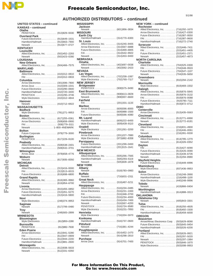
5/1/98
AUTHORIZED DISTRIBUTORS – continuedUNITED STATES – continuedKANSAS – continued
OlathePENSTOCK (913)829–9330. . . . . . . . . . . . . . . . .
Overland ParkFuture Electronics (913)649–1531. . . . . . . . . . . . Hamilton/Hallmark (913)663–7900. . . . . . . . . . . Newark (913)677–0727. . . . . . . . . . . . . . . . . . . . .
KENTUCKYLouisville
Allied Electronics, Inc. (502)452–2293. . . . . . . . Newark (502)423–0280. . . . . . . . . . . . . . . . . . . . .
LOUISIANANew Orleans
Allied Electronics, Inc. (504)466–7575. . . . . . . . MARYLAND
BaltimoreAllied Electronics, Inc. (410)312–0810. . . . . . . . FAI (410)312–0833. . . . . . . . . . . . . . . . . . . . . . . . .
ColumbiaArrow Electronics (301)596–7800. . . . . . . . . . . . Arrow Zeus (410)309–1541. . . . . . . . . . . . . . . . . Future Electronics (410)290–0600. . . . . . . . . . . . Hamilton/Hallmark (410)720–3400. . . . . . . . . . . PENSTOCK (410)290–3746. . . . . . . . . . . . . . . . . Wyle Electronics (410)312–4844. . . . . . . . . . . . .
HanoverNewark (410)712–6922. . . . . . . . . . . . . . . . . . . . .
MASSACHUSETTSBedford
Wyle Electronics (781)271–9953. . . . . . . . . . . . . Boston
Allied Electronics, Inc. (617)255–0361. . . . . . . . Arrow Electronics (508)658–0900. . . . . . . . . . . . FAI (508)779–3111. . . . . . . . . . . . . . . . . . . . . . . . . Newark 1–800–4NEWARK. . . . . . . . . . . . . . . . . .
BoltonFuture Corporate (978)779–3000. . . . . . . . . . . . .
BurlingtonPENSTOCK (617)229–9100. . . . . . . . . . . . . . . . .
PeabodyAllied Electronics, Inc. (508)538–2401. . . . . . . . Hamilton/Hallmark (508)532–3701. . . . . . . . . . .
WilmingtonArrow Zeus (978)658–4776. . . . . . . . . . . . . . . . .
WoburnNewark (617)935–8350. . . . . . . . . . . . . . . . . . . . .
MICHIGANDetroit
Allied Electronics, Inc. (313)416–9300. . . . . . . . FAI (313)513–0015. . . . . . . . . . . . . . . . . . . . . . . . . Future Electronics (616)698–6800. . . . . . . . . . . .
Grand RapidsAllied Electronics, Inc. (616)365–9960. . . . . . . . Newark (616)954–6700. . . . . . . . . . . . . . . . . . . . .
LivoniaArrow Electronics (810)455–0850. . . . . . . . . . . . Future Electronics (313)261–5270. . . . . . . . . . . . Hamilton/Hallmark (313)416–5800. . . . . . . . . . .
NoviWyle Electronics (248)374–9953. . . . . . . . . . . . .
SaginawNewark (517)799–0480. . . . . . . . . . . . . . . . . . . . .
TroyNewark (248)583–2899. . . . . . . . . . . . . . . . . . . . .
MINNESOTABloomington
Wyle Electronics (612)853–2280. . . . . . . . . . . . . . Burnsville
PENSTOCK (612)882–7630. . . . . . . . . . . . . . . . . . Eden Prairie
Arrow Electronics (612)941–5280. . . . . . . . . . . . FAI (612)947–0909. . . . . . . . . . . . . . . . . . . . . . . . . Future Electronics (612)944–2200. . . . . . . . . . . . Hamilton/Hallmark (612)881–2600. . . . . . . . . . .
MinneapolisAllied Electronics, Inc. (612)938–5633. . . . . . . . Newark (612)331–6350. . . . . . . . . . . . . . . . . . . . .
MISSISSIPPIJackson
Newark (601)956–3834. . . . . . . . . . . . . . . . . . . . . MISSOURI
Earth CityHamilton/Hallmark (314)770–6300. . . . . . . . . . .
St. LouisAllied Electronics, Inc. (314)240–9405. . . . . . . . Arrow Electronics (314)567–6888. . . . . . . . . . . . Future Electronics (314)469–6805. . . . . . . . . . . . FAI (314)542–9922. . . . . . . . . . . . . . . . . . . . . . . . . Newark (314)453–9400. . . . . . . . . . . . . . . . . . . . .
NEBRASKAOmaha
Allied Electronics, Inc. (402)697–0038. . . . . . . . Newark (402)592–2423. . . . . . . . . . . . . . . . . . . . .
NEVADALas Vegas
Allied Electronics, Inc. (702)258–1087. . . . . . . . Wyle Electronics (702)765–7117. . . . . . . . . . . . .
NEW JERSEYBridgewater
PENSTOCK (908)575–9490. . . . . . . . . . . . . . . . . East Brunswick
Allied Electronics, Inc. (908)613–0828. . . . . . . . Newark (908)937–6600. . . . . . . . . . . . . . . . . . . . .
FairfieldFAI (201)331–1133. . . . . . . . . . . . . . . . . . . . . . . . .
MarltonArrow Electronics (609)596–8000. . . . . . . . . . . . FAI (609)988–1500. . . . . . . . . . . . . . . . . . . . . . . . . Future Electronics (609)596–4080. . . . . . . . . . . .
Mt. LaurelHamilton/Hallmark (609)222–6400. . . . . . . . . . . Wyle Electronics (609)439–9110. . . . . . . . . . . . .
OradellWyle Electronics (201)261–3200. . . . . . . . . . . . .
PinebrookArrow Electronics (201)227–7880. . . . . . . . . . . . Wyle Electronics (973)882–8358. . . . . . . . . . . . .
ParsippanyFuture Electronics (201)299–0400. . . . . . . . . . . . Hamilton/Hallmark (201)515–1641. . . . . . . . . . .
NEW MEXICOAlbuquerque
Allied Electronics, Inc. (505)266–7565. . . . . . . . Hamilton/Hallmark (505)293–5119. . . . . . . . . . . Newark (505)828–1878. . . . . . . . . . . . . . . . . . . . .
NEW YORKAlbany
Newark (518)783–0983. . . . . . . . . . . . . . . . . . . . . Buffalo
Newark (716)631–2311. . . . . . . . . . . . . . . . . . . . . Great Neck
Allied Electronics, Inc. (516)487–5211. . . . . . . . Hauppauge
Allied Electronics, Inc. (516)234–0485. . . . . . . . Arrow Electronics (516)231–1000. . . . . . . . . . . . FAI (516)348–3700. . . . . . . . . . . . . . . . . . . . . . . . . Future Electronics (516)234–4000. . . . . . . . . . . . Hamilton/Hallmark (516)434–7400. . . . . . . . . . . Newark (516)567–4200. . . . . . . . . . . . . . . . . . . . . PENSTOCK (516)724–9580. . . . . . . . . . . . . . . . . Wyle Electronics (516)231–7850. . . . . . . . . . . . .
HenriettaWyle Electronics (716)334–5970. . . . . . . . . . . . .
KonkomaHamilton/Hallmark (516)737–0600. . . . . . . . . . .
PittsfordNewark (716)381–4244. . . . . . . . . . . . . . . . . . . . .
PoughkeepsieAllied Electronics, Inc. (914)452–1470. . . . . . . . Newark (914)298–2810. . . . . . . . . . . . . . . . . . . . .
PurchaseArrow Zeus (914)701–7400. . . . . . . . . . . . . . . . .
NEW YORK – continuedRochester
Allied Electronics, Inc. (716)292–1670. . . . . . . . Arrow Electronics (716)427–0300. . . . . . . . . . . . Future Electronics (716)387–9550. . . . . . . . . . . . FAI (716)387–9600. . . . . . . . . . . . . . . . . . . . . . . . . Hamilton/Hallmark (716)272–2740. . . . . . . . . . .
SyracuseAllied Electronics, Inc. (315)446–7411. . . . . . . . FAI (315)451–4405. . . . . . . . . . . . . . . . . . . . . . . . . Future Electronics (315)451–2371. . . . . . . . . . . . Newark (315)457–4873. . . . . . . . . . . . . . . . . . . . .
NORTH CAROLINACharlotte
Allied Electronics, Inc. (704)525–0300. . . . . . . . FAI (704)548–9503. . . . . . . . . . . . . . . . . . . . . . . . . Future Electronics (704)547–1107. . . . . . . . . . . . Newark (704)535–5650. . . . . . . . . . . . . . . . . . . . .
GreensboroNewark (910)294–2142. . . . . . . . . . . . . . . . . . . . .
MorrisvilleWyle Electronics (919)469–1502. . . . . . . . . . . . .
RaleighAllied Electronics, Inc. (919)876–5845. . . . . . . . Arrow Electronics (919)876–3132. . . . . . . . . . . . FAI (919)876–0088. . . . . . . . . . . . . . . . . . . . . . . . . Future Electronics (919)790–7111. . . . . . . . . . . . Hamilton/Hallmark (919)872–0712. . . . . . . . . . .
OHIOCenterville
Arrow Electronics (513)435–5563. . . . . . . . . . . . Cincinnati
Allied Electronics, Inc. (513)771–6990. . . . . . . . Newark (513)772–8181. . . . . . . . . . . . . . . . . . . . .
ClevelandAllied Electronics, Inc. (216)831–4900. . . . . . . . FAI (216)446–0061. . . . . . . . . . . . . . . . . . . . . . . . . Newark (216)391–9330. . . . . . . . . . . . . . . . . . . . .
ColumbusAllied Electronics, Inc. (614)785–1270. . . . . . . . Newark (614)326–0352. . . . . . . . . . . . . . . . . . . . .
DaytonFAI (513)427–6090. . . . . . . . . . . . . . . . . . . . . . . . . Future Electronics (513)426–0090. . . . . . . . . . . . Hamilton/Hallmark (513)439–6735. . . . . . . . . . . Newark (513)294–8980. . . . . . . . . . . . . . . . . . . . .
Mayfield HeightsFuture Electronics (216)449–6996. . . . . . . . . . . .
MiamisburgWyle Electronics (937)436–9953. . . . . . . . . . . . .
SolonArrow Electronics (216)248–3990. . . . . . . . . . . . Hamilton/Hallmark (216)498–1100. . . . . . . . . . . Wyle Electronics (440)248–9996. . . . . . . . . . . . .
ToledoNewark (419)866–0404. . . . . . . . . . . . . . . . . . . . .
WorthingtonHamilton/Hallmark (614)888–3313. . . . . . . . . . .
OKLAHOMAOklahoma City
Newark (405)843–3301. . . . . . . . . . . . . . . . . . . . . Tulsa
Allied Electronics, Inc. (918)250–4505. . . . . . . . FAI (918)492–1500. . . . . . . . . . . . . . . . . . . . . . . . . Hamilton/Hallmark (918)459–6000. . . . . . . . . . .
OREGONBeaverton
Arrow/Almac Electronics Corp. (503)629–8090. Future Electronics (503)645–9454. . . . . . . . . . . . Hamilton/Hallmark (503)526–6200. . . . . . . . . . .
PortlandAllied Electronics, Inc. (503)626–9921. . . . . . . . FAI (503)297–5020. . . . . . . . . . . . . . . . . . . . . . . . . Newark (503)297–1984. . . . . . . . . . . . . . . . . . . . . PENSTOCK (503)646–1670. . . . . . . . . . . . . . . . . Wyle Electronics (503)598–9953. . . . . . . . . . . . .
Fre
esc
ale
Se
mic
on
du
cto
r, I
Freescale Semiconductor, Inc.
For More Information On This Product, Go to: www.freescale.com
nc
...
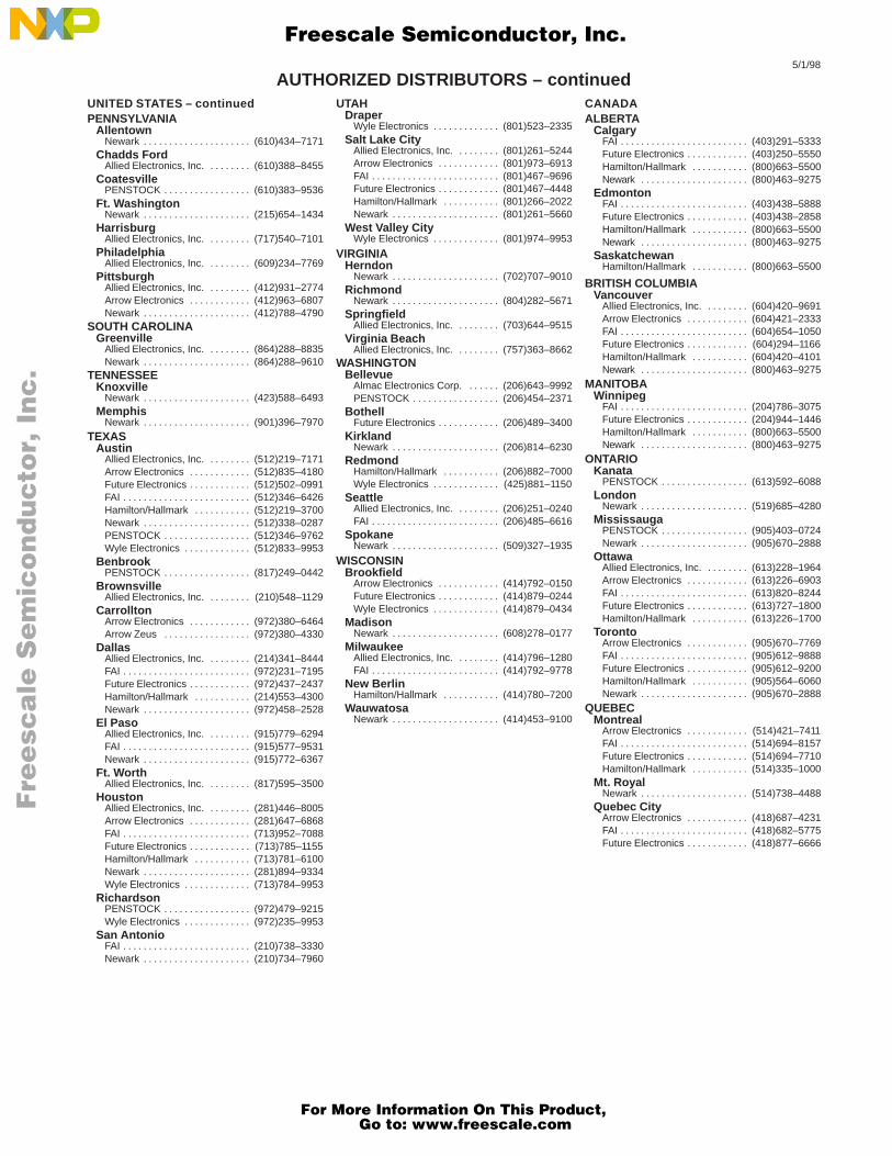
5/1/98
AUTHORIZED DISTRIBUTORS – continuedUNITED STATES – continuedPENNSYLVANIA
AllentownNewark (610)434–7171. . . . . . . . . . . . . . . . . . . . .
Chadds FordAllied Electronics, Inc. (610)388–8455. . . . . . . .
CoatesvillePENSTOCK (610)383–9536. . . . . . . . . . . . . . . . .
Ft. WashingtonNewark (215)654–1434. . . . . . . . . . . . . . . . . . . . .
HarrisburgAllied Electronics, Inc. (717)540–7101. . . . . . . .
PhiladelphiaAllied Electronics, Inc. (609)234–7769. . . . . . . .
PittsburghAllied Electronics, Inc. (412)931–2774. . . . . . . . Arrow Electronics (412)963–6807. . . . . . . . . . . . Newark (412)788–4790. . . . . . . . . . . . . . . . . . . . .
SOUTH CAROLINAGreenville
Allied Electronics, Inc. (864)288–8835. . . . . . . . Newark (864)288–9610. . . . . . . . . . . . . . . . . . . . .
TENNESSEEKnoxville
Newark (423)588–6493. . . . . . . . . . . . . . . . . . . . . Memphis
Newark (901)396–7970. . . . . . . . . . . . . . . . . . . . . TEXAS
AustinAllied Electronics, Inc. (512)219–7171. . . . . . . . Arrow Electronics (512)835–4180. . . . . . . . . . . . Future Electronics (512)502–0991. . . . . . . . . . . . FAI (512)346–6426. . . . . . . . . . . . . . . . . . . . . . . . . Hamilton/Hallmark (512)219–3700. . . . . . . . . . . Newark (512)338–0287. . . . . . . . . . . . . . . . . . . . . PENSTOCK (512)346–9762. . . . . . . . . . . . . . . . . Wyle Electronics (512)833–9953. . . . . . . . . . . . .
BenbrookPENSTOCK (817)249–0442. . . . . . . . . . . . . . . . .
BrownsvilleAllied Electronics, Inc. (210)548–1129. . . . . . . .
CarrolltonArrow Electronics (972)380–6464. . . . . . . . . . . . Arrow Zeus (972)380–4330. . . . . . . . . . . . . . . . .
DallasAllied Electronics, Inc. (214)341–8444. . . . . . . . FAI (972)231–7195. . . . . . . . . . . . . . . . . . . . . . . . . Future Electronics (972)437–2437. . . . . . . . . . . . Hamilton/Hallmark (214)553–4300. . . . . . . . . . . Newark (972)458–2528. . . . . . . . . . . . . . . . . . . . .
El PasoAllied Electronics, Inc. (915)779–6294. . . . . . . . FAI (915)577–9531. . . . . . . . . . . . . . . . . . . . . . . . . Newark (915)772–6367. . . . . . . . . . . . . . . . . . . . .
Ft. WorthAllied Electronics, Inc. (817)595–3500. . . . . . . .
HoustonAllied Electronics, Inc. (281)446–8005. . . . . . . . Arrow Electronics (281)647–6868. . . . . . . . . . . . FAI (713)952–7088. . . . . . . . . . . . . . . . . . . . . . . . . Future Electronics (713)785–1155. . . . . . . . . . . . Hamilton/Hallmark (713)781–6100. . . . . . . . . . . Newark (281)894–9334. . . . . . . . . . . . . . . . . . . . . Wyle Electronics (713)784–9953. . . . . . . . . . . . .
RichardsonPENSTOCK (972)479–9215. . . . . . . . . . . . . . . . . Wyle Electronics (972)235–9953. . . . . . . . . . . . .
San AntonioFAI (210)738–3330. . . . . . . . . . . . . . . . . . . . . . . . . Newark (210)734–7960. . . . . . . . . . . . . . . . . . . . .
UTAHDraper
Wyle Electronics (801)523–2335. . . . . . . . . . . . . Salt Lake City
Allied Electronics, Inc. (801)261–5244. . . . . . . . Arrow Electronics (801)973–6913. . . . . . . . . . . . FAI (801)467–9696. . . . . . . . . . . . . . . . . . . . . . . . . Future Electronics (801)467–4448. . . . . . . . . . . . Hamilton/Hallmark (801)266–2022. . . . . . . . . . . Newark (801)261–5660. . . . . . . . . . . . . . . . . . . . .
West Valley CityWyle Electronics (801)974–9953. . . . . . . . . . . . .
VIRGINIAHerndon
Newark (702)707–9010. . . . . . . . . . . . . . . . . . . . . Richmond
Newark (804)282–5671. . . . . . . . . . . . . . . . . . . . . Springfield
Allied Electronics, Inc. (703)644–9515. . . . . . . . Virginia Beach
Allied Electronics, Inc. (757)363–8662. . . . . . . . WASHINGTON
BellevueAlmac Electronics Corp. (206)643–9992. . . . . . PENSTOCK (206)454–2371. . . . . . . . . . . . . . . . .
BothellFuture Electronics (206)489–3400. . . . . . . . . . . .
KirklandNewark (206)814–6230. . . . . . . . . . . . . . . . . . . . .
RedmondHamilton/Hallmark (206)882–7000. . . . . . . . . . . Wyle Electronics (425)881–1150. . . . . . . . . . . . .
SeattleAllied Electronics, Inc. (206)251–0240. . . . . . . . FAI (206)485–6616. . . . . . . . . . . . . . . . . . . . . . . . .
SpokaneNewark (509)327–1935. . . . . . . . . . . . . . . . . . . . .
WISCONSINBrookfield
Arrow Electronics (414)792–0150. . . . . . . . . . . . Future Electronics (414)879–0244. . . . . . . . . . . . Wyle Electronics (414)879–0434. . . . . . . . . . . . .
MadisonNewark (608)278–0177. . . . . . . . . . . . . . . . . . . . .
MilwaukeeAllied Electronics, Inc. (414)796–1280. . . . . . . . FAI (414)792–9778. . . . . . . . . . . . . . . . . . . . . . . . .
New BerlinHamilton/Hallmark (414)780–7200. . . . . . . . . . .
WauwatosaNewark (414)453–9100. . . . . . . . . . . . . . . . . . . . .
CANADAALBERTA
CalgaryFAI (403)291–5333. . . . . . . . . . . . . . . . . . . . . . . . . Future Electronics (403)250–5550. . . . . . . . . . . . Hamilton/Hallmark (800)663–5500. . . . . . . . . . . Newark (800)463–9275. . . . . . . . . . . . . . . . . . . . .
EdmontonFAI (403)438–5888. . . . . . . . . . . . . . . . . . . . . . . . . Future Electronics (403)438–2858. . . . . . . . . . . . Hamilton/Hallmark (800)663–5500. . . . . . . . . . . Newark (800)463–9275. . . . . . . . . . . . . . . . . . . . .
SaskatchewanHamilton/Hallmark (800)663–5500. . . . . . . . . . .
BRITISH COLUMBIAVancouver
Allied Electronics, Inc. (604)420–9691. . . . . . . . Arrow Electronics (604)421–2333. . . . . . . . . . . . FAI (604)654–1050. . . . . . . . . . . . . . . . . . . . . . . . . Future Electronics (604)294–1166. . . . . . . . . . . . Hamilton/Hallmark (604)420–4101. . . . . . . . . . . Newark (800)463–9275. . . . . . . . . . . . . . . . . . . . .
MANITOBAWinnipeg
FAI (204)786–3075. . . . . . . . . . . . . . . . . . . . . . . . . Future Electronics (204)944–1446. . . . . . . . . . . . Hamilton/Hallmark (800)663–5500. . . . . . . . . . . Newark (800)463–9275. . . . . . . . . . . . . . . . . . . . .
ONTARIOKanata
PENSTOCK (613)592–6088. . . . . . . . . . . . . . . . . London
Newark (519)685–4280. . . . . . . . . . . . . . . . . . . . . Mississauga
PENSTOCK (905)403–0724. . . . . . . . . . . . . . . . . Newark (905)670–2888. . . . . . . . . . . . . . . . . . . . .
OttawaAllied Electronics, Inc. (613)228–1964. . . . . . . . Arrow Electronics (613)226–6903. . . . . . . . . . . . FAI (613)820–8244. . . . . . . . . . . . . . . . . . . . . . . . . Future Electronics (613)727–1800. . . . . . . . . . . . Hamilton/Hallmark (613)226–1700. . . . . . . . . . .
TorontoArrow Electronics (905)670–7769. . . . . . . . . . . . FAI (905)612–9888. . . . . . . . . . . . . . . . . . . . . . . . . Future Electronics (905)612–9200. . . . . . . . . . . . Hamilton/Hallmark (905)564–6060. . . . . . . . . . . Newark (905)670–2888. . . . . . . . . . . . . . . . . . . . .
QUEBECMontreal
Arrow Electronics (514)421–7411. . . . . . . . . . . . FAI (514)694–8157. . . . . . . . . . . . . . . . . . . . . . . . . Future Electronics (514)694–7710. . . . . . . . . . . . Hamilton/Hallmark (514)335–1000. . . . . . . . . . .
Mt. RoyalNewark (514)738–4488. . . . . . . . . . . . . . . . . . . . .
Quebec CityArrow Electronics (418)687–4231. . . . . . . . . . . . FAI (418)682–5775. . . . . . . . . . . . . . . . . . . . . . . . . Future Electronics (418)877–6666. . . . . . . . . . . .
Fre
esc
ale
Se
mic
on
du
cto
r, I
Freescale Semiconductor, Inc.
For More Information On This Product, Go to: www.freescale.com
nc
...
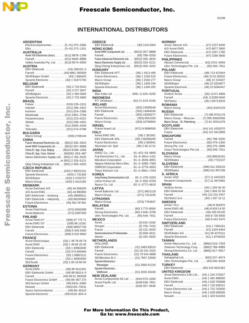
5/1/98
INTERNATIONAL DISTRIBUTORS
ARGENTINAElectrocomponentes (5–41) 375–3366. . . . . . . . Elko (5–41) 372–1101. . . . . . . . . . . . . . . . . . . . . . .
AUSTRALIA*#( !(&$#' )'( (61)2 9878–1299. . . . . Farnell (61)2 9645–8888. . . . . . . . . . . . . . . . . . . . Veltek Australia Pty. Ltd. (61)3 9574–9300. . . .
AUSTRIAEBV Elektronik (43) 189152–0. . . . . . . . . . . . . . . Farnell (49) 8961 393939. . . . . . . . . . . . . . . . . . . . SEI/Elbatex GmbH (43) 1 866420. . . . . . . . . . . . Spoerle Electronic (43) 1 31872700. . . . . . . . . . .
BELGIUMEBV Elektronik (32) 2 716 0010. . . . . . . . . . . . . Farnell (32) 3 227 3647. . . . . . . . . . . . . . . . . . . . . SEI/Belgium (32) 2 460 0560. . . . . . . . . . . . . . . . Spoerle Electronic (32) 2 725 4660. . . . . . . . . . .
BRAZILFuture (019) 235–1511. . . . . . . . . . . . . . . . . . . . . . Intertek (011) 266–2922. . . . . . . . . . . . . . . . . . . . . Karimex (011) 524–2366. . . . . . . . . . . . . . . . . . . . Masktrade (011) 3361–2766. . . . . . . . . . . . . . . . . Panamericana (011) 223–0222. . . . . . . . . . . . . . . Siletek (011) 536–4401. . . . . . . . . . . . . . . . . . . . . . Tec (011) 5505–2046. . . . . . . . . . . . . . . . . . . . . . . . Teleradio (011) 574–0788. . . . . . . . . . . . . . . . . . . .
BULGARIAMacro Group (359) 2708140. . . . . . . . . . . . . . . . .
CHINA)()& *# !(&$#' ( (852)2 305–3633. . *#( $"%$##(' ( (852)2 357–8888. . . . . # ! %% $&% # (86)10 8188–1566. . . . # ! %% $&% "# (86)592–553–487. . . . . Nanco Electronics Supply Ltd. (852) 2 765–3025.
or (852) 2 333–5121. . . . . . . . . . . . . . . . . . . . . . . . Qing Cheng Enterprises Ltd. (852) 2 493–4202. .
CZECH REPUBLICEBV Elektronik (420) 2 90022101. . . . . . . . . . . . Spoerle Electronic (420) 2 731355. . . . . . . . . . . . SEI/Elbatex (420) 2 4763707. . . . . . . . . . . . . . . . Macro Group (420) 2 3412182. . . . . . . . . . . . . . .
DENMARKArrow Denmark A/S (45) 44 508200. . . . . . . . . . A/S Avnet EMG (45) 44 880800. . . . . . . . . . . . . . EBV Elektronik – Soeborg (45) 39690511. . . . . . EBV Elektronik – Aabyhoej (45) 86250660. . . . . Future Electronics (45) 961 00 961. . . . . . . . . . .
ESTONIAArrow Field Eesti (372) 6503288. . . . . . . . . . . . . . Avnet Baltronic (372) 6397000. . . . . . . . . . . . . . .
FINLANDArrow Field OY (358) 97 775 71. . . . . . . . . . . . . Avnet EMG OY (358) 96 13181. . . . . . . . . . . . . . EBV Elektronik (358) 98557730. . . . . . . . . . . . . Farnell (358) 9 345 5400. . . . . . . . . . . . . . . . . . . . Future Electronics (358) 9 525 9950. . . . . . . . . .
FRANCEArrow Electronique (33) 1 49 78 49 78. . . . . . . . Avnet EMG (33) 1 49 65 25 00. . . . . . . . . . . . . . . EBV Elektronik (33) 1 40963000. . . . . . . . . . . . . Farnell (33) 474 659466. . . . . . . . . . . . . . . . . . . . . Future Electronics (33) 1 69821111. . . . . . . . . . . Newark (33) 1 30954060. . . . . . . . . . . . . . . . . . . . SEI/Scaib (33) 1 69 19 89 00. . . . . . . . . . . . . . . .
GERMANYAvnet EMG (49) 89 4511001. . . . . . . . . . . . . . . . . EBV Elektronik GmbH (49) 89 99114–0. . . . . . . Farnell (49) 89 61 393939. . . . . . . . . . . . . . . . . . . Future Electronics GmbH (49) 89–957 270. . . . SEI/Jermyn GmbH (49) 6431–5080. . . . . . . . . . Newark (49)2154–70011. . . . . . . . . . . . . . . . . . . . Sasco Semiconductor (49) 89–46110. . . . . . . . . Spoerle Electronic (49) 6103–304–0. . . . . . . . . .
GREECEEBV Elektronik (30) 13414300. . . . . . . . . . . . . . .
HONG KONG*#( $"%$##(' ( (852)2 357–8888. . . . . Farnell (65) 788–0200. . . . . . . . . . . . . . . . . . . . . . . )()& *# !(&$#' ( (852)2 305–3633. . #$ !(&$#' )%%!, ( (852)2 333–5121. . . . Qing Cheng Enterprises Ltd. (852)2 493–4202.
HUNGARYEBV Elektronik KFT (36) 1 4313 495. . . . . . . . . Future Electronics (36) 1 2240 510. . . . . . . . . . . Macro Group (36) 1 2030 277. . . . . . . . . . . . . . . SEI/Elbatex (36) 1 1409 194. . . . . . . . . . . . . . . . Spoerle Electronic (36) 1 1294 202. . . . . . . . . . .
INDIAMax India Ltd 0091 11 625–0250. . . . . . . . . . . . .
INDONESIAP.T. Ometraco (62) 21 619–6166. . . . . . . . . . . . .
IRELANDArrow Electronics (353) 14595540. . . . . . . . . . . EBV Elektronik (353) 14564034. . . . . . . . . . . . . Farnell (353) 18309277. . . . . . . . . . . . . . . . . . . . . Future Electronics (353) 6541330. . . . . . . . . . . . . Macro Group (353) 16766904. . . . . . . . . . . . . . .
ISRAELFuture Israel Ltd. (972) 9 9586555. . . . . . . . . . . .
ITALYAvnet EMG SRL (39) 2 381901. . . . . . . . . . . . . . EBV Elektronik SRL (39) 2 66096290. . . . . . . . . Future Electronics (39) 2 660941. . . . . . . . . . . . . Silverstar Ltd. SpA (39) 2 66 12 51. . . . . . . . . . .
JAPANAMSC Co., Ltd. 81–422–54–6800. . . . . . . . . . . . Fuji Electronics Co., Ltd. 81–3–3814–1411. . . . Marubun Corporation 81–3–3639–8951. . . . . . . Nippon Motorola Micro Elec. 81–3–3280–7300. OMRON Corporation 81–3–3779–9053. . . . . . . Tokyo Electron Ltd. 81–3–5561–7254. . . . . . . . .
KOREA )# +# "$#)($&' ( 82–2–278–5333. . Liteon Korea Ltd 82–2–650–9700. . . . . . . . . . . . Nasco Co. Ltd 82–2–3772–6810. . . . . . . . . . . . .
LATVIAAvnet Baltronic Ltd. (371) 8821118. . . . . . . . . . . Macro Group (371) 7313195. . . . . . . . . . . . . . . . .
LITHUANIAMacro Group (370) 7764937. . . . . . . . . . . . . . . . .
MALAYSIAFarnell (60) 3 773–8000. . . . . . . . . . . . . . . . . . . . . Strong Electronics (60) 4 656–3768. . . . . . . . . . . Ultro Technologies Pte. Ltd. (65) 545–7811. . . .
MEXICOAvnet (3) 632–0182. . . . . . . . . . . . . . . . . . . . . . . . . Dicopel (5) 705–7422. . . . . . . . . . . . . . . . . . . . . . . Future (3) 122–0043. . . . . . . . . . . . . . . . . . . . . . . . "$#)($&' &$'$#!' (5) 658–6011. . . . . . . Steren (5) 325–0925. . . . . . . . . . . . . . . . . . . . . . . .
NETHERLANDSHOLLANDEBV Elektronik (31) 3465 83010. . . . . . . . . . . . . Farnell (31) 30 241 2323. . . . . . . . . . . . . . . . . . . . Future Electronics (31) 76 544 4888. . . . . . . . . . SEI/Benelux B.V. (31) 7657 22500. . . . . . . . . . . . %$&! !(&$#'
)+# (31) 3060 91234. . . . . . . . . . . . . . . . . %$&! !(&$#'
!$*# (31) 4025 45430. . . . . . . . . . . . . . . . . . NEW ZEALAND
Arrow Components NZ Ltd (64)4 570–2260. . . Avnet Pacific Ltd (64)9 636–7801. . . . . . . . . . . . Farnell (64)9 357–0646. . . . . . . . . . . . . . . . . . . . .
NORWAYArrow Tahonic A/S (47) 2237 8440. . . . . . . . . . . A/S Avnet EMG (47) 6677 3600. . . . . . . . . . . . . . EBV Elektronik (47) 2267 1780. . . . . . . . . . . . . . Future Electronics (47) 2290 5800. . . . . . . . . . . .
PHILIPPINESAlexan Commercial (63) 2241–9493. . . . . . . . . Ultro Technologies Pte. Ltd (65) 545–7811. . . . .
POLANDEBV Elektronik (48) 713 422944. . . . . . . . . . . . . Future Electronics (48) 22 61 89202. . . . . . . . . . Macro Group (48) 22 224337. . . . . . . . . . . . . . . . SEI/Elbatex (48) 22 6254877. . . . . . . . . . . . . . . . Spoerle Electronic (48) 22 6060447. . . . . . . . . . .
PORTUGALAmitron Arrow (35) 11471 4806. . . . . . . . . . . . . . Farnell (44) 113289 0040. . . . . . . . . . . . . . . . . . . . SEI/Selco (35) 12973 8203. . . . . . . . . . . . . . . . . .
ROMANIAMacro Group (401) 6343129. . . . . . . . . . . . . . . . .
RUSSIAEBV Elektronik (7) 095 9761176. . . . . . . . . . . . . Macro Group – Moscow (7) 095 30600266. . . . . &$ &$)% ( (&')& (7) 81 25311476. . . . .
SCOTLANDEBV Elektronik (44) 141 4202070. . . . . . . . . . . . Future (44) 141 9413999. . . . . . . . . . . . . . . . . . . .
SINGAPOREFarnell (65) 788–0200. . . . . . . . . . . . . . . . . . . . . . . Future Electronics (65) 479–1300. . . . . . . . . . . . . Strong Pte. Ltd (65) 276–3996. . . . . . . . . . . . . . . Uraco Technologies Pte Ltd. (65) 545–7811. . . .
SLOVAKIAMacro Group (42) 89634181. . . . . . . . . . . . . . . . . SEI/Elbatex (42) 7722137. . . . . . . . . . . . . . . . . . .
SLOVENIAEBV Elektronik (386) 611 330216. . . . . . . . . . . . SEI/Elbatex (386) 611 957198. . . . . . . . . . . . . . .
S. AFRICAAvnet–ASD (27) 11 4442333. . . . . . . . . . . . . . . . Reutech Components (27) 11 3972992. . . . . . .
SPAINAmitron Arrow (34) 1 304 30 40. . . . . . . . . . . . . . EBV Elektronik (34) 1 804 32 56. . . . . . . . . . . . . Farnell (44) 113 231 0447. . . . . . . . . . . . . . . . . . . SEI/Selco S.A. (34) 1 637 10 11. . . . . . . . . . . . . .
SWEDENArrow–Th:s (46) 8 362970. . . . . . . . . . . . . . . . . . Avnet EMG AB (46) 8 629 14 00. . . . . . . . . . . . . EBV Elektronik (46) 405 92100. . . . . . . . . . . . . . Farnell (46) 8 730 5000. . . . . . . . . . . . . . . . . . . . . Future Electronics (46) 8 441 5470. . . . . . . . . . .
SWITZERLANDEBV Elektronik (41) 1 7456161. . . . . . . . . . . . . . Farnell (41) 1204 6464. . . . . . . . . . . . . . . . . . . . . . SEI/Elbatex AG (41) 56 4375111. . . . . . . . . . . . . Spoerle Electronic (41) 1 8746262. . . . . . . . . . . .
TAIWANAvnet–Mercuries Co., Ltd (886)2 516–7303. . . Solomon Technology Corp. (886)2 788–8989. . Strong Electronics Co. Ltd. (886)2 917–9917. .
THAILANDSahapiphat Ltd. (662) 237–9474. . . . . . . . . . . . . Ultro Technologies Pte. Ltd. (65) 540–8328. . . .
TURKEYEBV Elektronik (90) 216 4631352. . . . . . . . . . . .
UNITED KINGDOMArrow Electronics (UK) Ltd (44) 1 234 270027. . Avnet EMG (44) 1 462 488500. . . . . . . . . . . . . . . EBV Elektronik (44) 1 628 783688. . . . . . . . . . . Farnell (44) 1 132 636311. . . . . . . . . . . . . . . . . . . Future Electronics Ltd. (44) 1 753 763000. . . . . Macro Group (44) 1 628 606000. . . . . . . . . . . . . Newark (44) 1 420 543333. . . . . . . . . . . . . . . . . .
Fre
esc
ale
Se
mic
on
du
cto
r, I
Freescale Semiconductor, Inc.
For More Information On This Product, Go to: www.freescale.com
nc
...
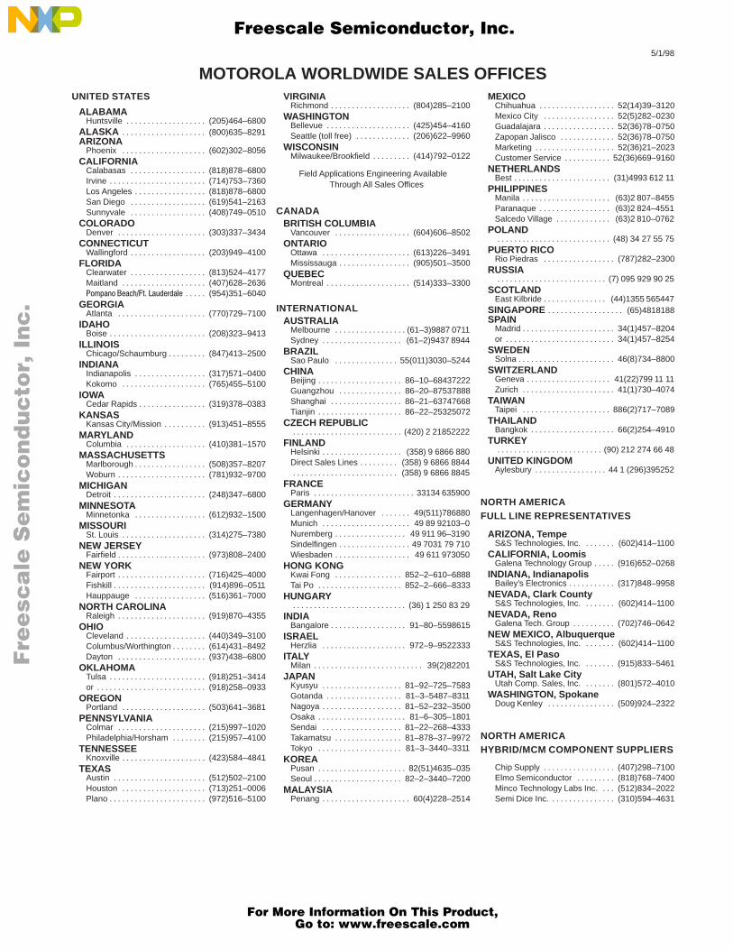
5/1/98
MOTOROLA WORLDWIDE SALES OFFICESUNITED STATES
ALABAMAHuntsville (205)464–6800. . . . . . . . . . . . . . . . . . .
ALASKA (800)635–8291. . . . . . . . . . . . . . . . . . . . ARIZONA
Phoenix (602)302–8056. . . . . . . . . . . . . . . . . . . . CALIFORNIA
Calabasas (818)878–6800. . . . . . . . . . . . . . . . . . Irvine (714)753–7360. . . . . . . . . . . . . . . . . . . . . . . Los Angeles (818)878–6800. . . . . . . . . . . . . . . . . San Diego (619)541–2163. . . . . . . . . . . . . . . . . . Sunnyvale (408)749–0510. . . . . . . . . . . . . . . . . .
COLORADODenver (303)337–3434. . . . . . . . . . . . . . . . . . . . .
CONNECTICUTWallingford (203)949–4100. . . . . . . . . . . . . . . . . .
FLORIDAClearwater (813)524–4177. . . . . . . . . . . . . . . . . . Maitland (407)628–2636. . . . . . . . . . . . . . . . . . . . (954)351–6040. . . . .
GEORGIAAtlanta (770)729–7100. . . . . . . . . . . . . . . . . . . . .
IDAHOBoise (208)323–9413. . . . . . . . . . . . . . . . . . . . . . .
ILLINOISChicago/Schaumburg (847)413–2500. . . . . . . . .
INDIANAIndianapolis (317)571–0400. . . . . . . . . . . . . . . . . Kokomo (765)455–5100. . . . . . . . . . . . . . . . . . . .
IOWACedar Rapids (319)378–0383. . . . . . . . . . . . . . . .
KANSASKansas City/Mission (913)451–8555. . . . . . . . . .
MARYLANDColumbia (410)381–1570. . . . . . . . . . . . . . . . . . .
MASSACHUSETTSMarlborough (508)357–8207. . . . . . . . . . . . . . . . . Woburn (781)932–9700. . . . . . . . . . . . . . . . . . . . .
MICHIGANDetroit (248)347–6800. . . . . . . . . . . . . . . . . . . . . .
MINNESOTAMinnetonka (612)932–1500. . . . . . . . . . . . . . . . .
MISSOURISt. Louis (314)275–7380. . . . . . . . . . . . . . . . . . . .
NEW JERSEYFairfield (973)808–2400. . . . . . . . . . . . . . . . . . . . .
NEW YORKFairport (716)425–4000. . . . . . . . . . . . . . . . . . . . . Fishkill (914)896–0511. . . . . . . . . . . . . . . . . . . . . . Hauppauge (516)361–7000. . . . . . . . . . . . . . . . .
NORTH CAROLINARaleigh (919)870–4355. . . . . . . . . . . . . . . . . . . . .
OHIOCleveland (440)349–3100. . . . . . . . . . . . . . . . . . . Columbus/Worthington (614)431–8492. . . . . . . . Dayton (937)438–6800. . . . . . . . . . . . . . . . . . . . .
OKLAHOMATulsa (918)251–3414. . . . . . . . . . . . . . . . . . . . . . . or (918)258–0933. . . . . . . . . . . . . . . . . . . . . . . . . .
OREGONPortland (503)641–3681. . . . . . . . . . . . . . . . . . . .
PENNSYLVANIAColmar (215)997–1020. . . . . . . . . . . . . . . . . . . . . Philadelphia/Horsham (215)957–4100. . . . . . . .
TENNESSEEKnoxville (423)584–4841. . . . . . . . . . . . . . . . . . . .
TEXASAustin (512)502–2100. . . . . . . . . . . . . . . . . . . . . . Houston (713)251–0006. . . . . . . . . . . . . . . . . . . . Plano (972)516–5100. . . . . . . . . . . . . . . . . . . . . . .
VIRGINIARichmond (804)285–2100. . . . . . . . . . . . . . . . . . .
WASHINGTONBellevue (425)454–4160. . . . . . . . . . . . . . . . . . . . Seattle (toll free) (206)622–9960. . . . . . . . . . . . .
WISCONSINMilwaukee/Brookfield (414)792–0122. . . . . . . . .
Field Applications Engineering AvailableThrough All Sales Offices
CANADABRITISH COLUMBIA
Vancouver (604)606–8502. . . . . . . . . . . . . . . . . . ONTARIO
Ottawa (613)226–3491. . . . . . . . . . . . . . . . . . . . . Mississauga (905)501–3500. . . . . . . . . . . . . . . . .
QUEBECMontreal (514)333–3300. . . . . . . . . . . . . . . . . . . .
INTERNATIONALAUSTRALIA
Melbourne (61–3)9887 0711. . . . . . . . . . . . . . . . . Sydney (61–2)9437 8944. . . . . . . . . . . . . . . . . . .
BRAZILSao Paulo 55(011)3030–5244. . . . . . . . . . . . . . .
CHINABeijing 86–10–68437222. . . . . . . . . . . . . . . . . . . . Guangzhou 86–20–87537888. . . . . . . . . . . . . . . Shanghai 86–21–63747668. . . . . . . . . . . . . . . . . Tianjin 86–22–25325072. . . . . . . . . . . . . . . . . . . .
CZECH REPUBLIC(420) 2 21852222. . . . . . . . . . . . . . . . . . . . . . . . . .
FINLANDHelsinki (358) 9 6866 880. . . . . . . . . . . . . . . . . . . Direct Sales Lines (358) 9 6866 8844. . . . . . . . .
(358) 9 6866 8845. . . . . . . . . . . . . . . . . . . . . . . . . FRANCE
Paris 33134 635900. . . . . . . . . . . . . . . . . . . . . . . . GERMANY
Langenhagen/Hanover 49(511)786880. . . . . . . Munich 49 89 92103–0. . . . . . . . . . . . . . . . . . . . . Nuremberg 49 911 96–3190. . . . . . . . . . . . . . . . . Sindelfingen 49 7031 79 710. . . . . . . . . . . . . . . . . Wiesbaden 49 611 973050. . . . . . . . . . . . . . . . . .
HONG KONGKwai Fong 852–2–610–6888. . . . . . . . . . . . . . . . Tai Po 852–2–666–8333. . . . . . . . . . . . . . . . . . . .
HUNGARY(36) 1 250 83 29. . . . . . . . . . . . . . . . . . . . . . . . . . .
INDIABangalore 91–80–5598615. . . . . . . . . . . . . . . . . .
ISRAELHerzlia 972–9–9522333. . . . . . . . . . . . . . . . . . . .
ITALYMilan 39(2)82201. . . . . . . . . . . . . . . . . . . . . . . . . .
JAPANKyusyu 81–92–725–7583. . . . . . . . . . . . . . . . . . . Gotanda 81–3–5487–8311. . . . . . . . . . . . . . . . . . Nagoya 81–52–232–3500. . . . . . . . . . . . . . . . . . . Osaka 81–6–305–1801. . . . . . . . . . . . . . . . . . . . . Sendai 81–22–268–4333. . . . . . . . . . . . . . . . . . . Takamatsu 81–878–37–9972. . . . . . . . . . . . . . . . Tokyo 81–3–3440–3311. . . . . . . . . . . . . . . . . . . .
KOREAPusan 82(51)4635–035. . . . . . . . . . . . . . . . . . . . . Seoul 82–2–3440–7200. . . . . . . . . . . . . . . . . . . . .
MALAYSIAPenang 60(4)228–2514. . . . . . . . . . . . . . . . . . . . .
MEXICOChihuahua 52(14)39–3120. . . . . . . . . . . . . . . . . . Mexico City 52(5)282–0230. . . . . . . . . . . . . . . . . Guadalajara 52(36)78–0750. . . . . . . . . . . . . . . . . Zapopan Jalisco 52(36)78–0750. . . . . . . . . . . . . Marketing 52(36)21–2023. . . . . . . . . . . . . . . . . . . Customer Service 52(36)669–9160. . . . . . . . . . .
NETHERLANDSBest (31)4993 612 11. . . . . . . . . . . . . . . . . . . . . . .
PHILIPPINESManila (63)2 807–8455. . . . . . . . . . . . . . . . . . . . . Paranaque (63)2 824–4551. . . . . . . . . . . . . . . . . Salcedo Village (63)2 810–0762. . . . . . . . . . . . .
POLAND(48) 34 27 55 75. . . . . . . . . . . . . . . . . . . . . . . . . . .
PUERTO RICORio Piedras (787)282–2300. . . . . . . . . . . . . . . . .
RUSSIA(7) 095 929 90 25. . . . . . . . . . . . . . . . . . . . . . . . . .
SCOTLANDEast Kilbride (44)1355 565447. . . . . . . . . . . . . . .
SINGAPORE (65)4818188. . . . . . . . . . . . . . . . . . SPAIN
Madrid 34(1)457–8204. . . . . . . . . . . . . . . . . . . . . . or 34(1)457–8254. . . . . . . . . . . . . . . . . . . . . . . . . .
SWEDENSolna 46(8)734–8800. . . . . . . . . . . . . . . . . . . . . . .
SWITZERLANDGeneva 41(22)799 11 11. . . . . . . . . . . . . . . . . . . . Zurich 41(1)730–4074. . . . . . . . . . . . . . . . . . . . . .
TAIWANTaipei 886(2)717–7089. . . . . . . . . . . . . . . . . . . . .
THAILANDBangkok 66(2)254–4910. . . . . . . . . . . . . . . . . . . .
TURKEY(90) 212 274 66 48. . . . . . . . . . . . . . . . . . . . . . . . .
UNITED KINGDOMAylesbury 44 1 (296)395252. . . . . . . . . . . . . . . . .
NORTH AMERICAFULL LINE REPRESENTATIVES
ARIZONA, TempeS&S Technologies, Inc. (602)414–1100. . . . . . .
CALIFORNIA, LoomisGalena Technology Group (916)652–0268. . . . .
INDIANA, IndianapolisBailey’s Electronics (317)848–9958. . . . . . . . . . .
NEVADA, Clark CountyS&S Technologies, Inc. (602)414–1100. . . . . . .
NEVADA, RenoGalena Tech. Group (702)746–0642. . . . . . . . . .
NEW MEXICO, AlbuquerqueS&S Technologies, Inc. (602)414–1100. . . . . . .
TEXAS, El PasoS&S Technologies, Inc. (915)833–5461. . . . . . .
UTAH, Salt Lake CityUtah Comp. Sales, Inc. (801)572–4010. . . . . . .
WASHINGTON, SpokaneDoug Kenley (509)924–2322. . . . . . . . . . . . . . . .
NORTH AMERICAHYBRID/MCM COMPONENT SUPPLIERS
Chip Supply (407)298–7100. . . . . . . . . . . . . . . . . Elmo Semiconductor (818)768–7400. . . . . . . . . Minco Technology Labs Inc. (512)834–2022. . . Semi Dice Inc. (310)594–4631. . . . . . . . . . . . . . .
Fre
esc
ale
Se
mic
on
du
cto
r, I
Freescale Semiconductor, Inc.
For More Information On This Product, Go to: www.freescale.com
nc
...

Fre
esc
ale
Se
mic
on
du
cto
r, I
Freescale Semiconductor, Inc.
For More Information On This Product, Go to: www.freescale.com
nc
...

Fre
esc
ale
Se
mic
on
du
cto
r, I
Freescale Semiconductor, Inc.
For More Information On This Product, Go to: www.freescale.com
nc
...

Fre
esc
ale
Se
mic
on
du
cto
r, I
Freescale Semiconductor, Inc.
For More Information On This Product, Go to: www.freescale.com
nc
...

Fre
esc
ale
Se
mic
on
du
cto
r, I
Freescale Semiconductor, Inc.
For More Information On This Product, Go to: www.freescale.com
nc
...
MCU Mode Maintenance Channel Operation7
GCI Mode Functional Description8
MCU Mode Activation and Deactivation6
MCU Mode Device Functionality5
MCU Mode Register Description Reference4
Pin Descriptions3
ISDN Basic Access System Overview2
Introduction1
AppendicesA–J
Mechanical Data11
Electrical Specifications10
MCU Mode Programming Suggestions9
Fre
esc
ale
Se
mic
on
du
cto
r, I
Freescale Semiconductor, Inc.
For More Information On This Product, Go to: www.freescale.com
nc
...