Embed Size (px)
Citation preview
2.6.2
ATTAINMENT OF
PROGRAMME
OUTCOMES (POs),
PROGRAM
SPECIFIC
OUTCOMES AND
COURSE
OUTCOMES (COs)
ATTAINMENT OF POs & COs BY EXAMINATION
SYSTEM (DIRECT METHOD)
B.Tech
COURSE NAME:-Analog Electronics
COURSE Code: - BEE0120A
Semester:-IV
Submitted by
Faculty- Ramandeep Gill
Assistant Professor of Electronics & Communication
Department, JECRC University
December, 2018
JECRC University, Jaipur
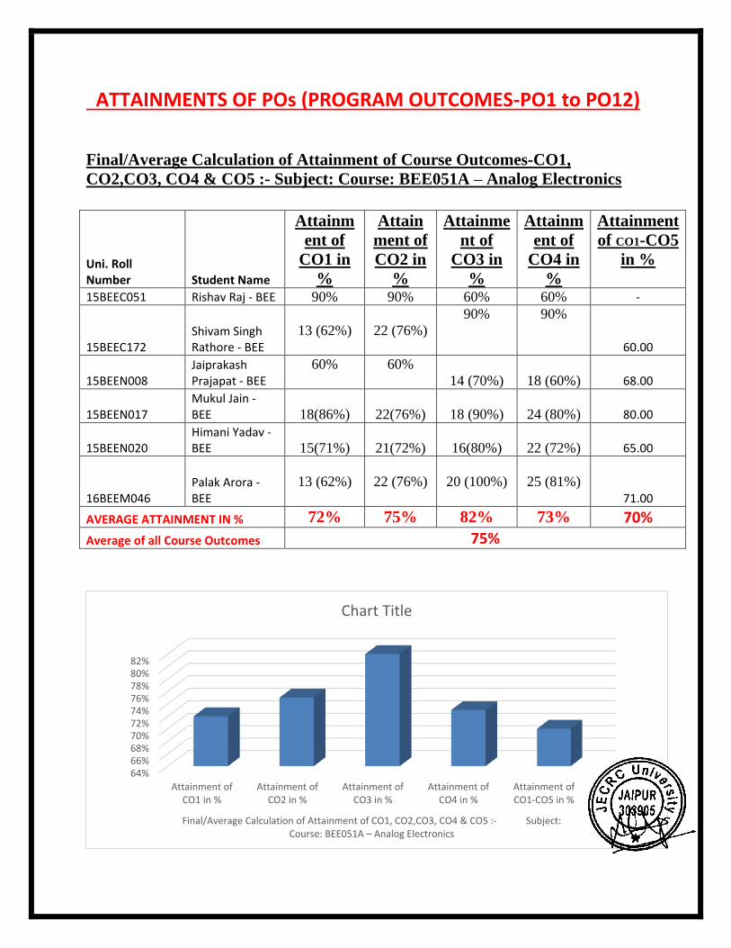
ATTAINMENTS OF POs (PROGRAM OUTCOMES-PO1 to PO12)
Uni. Roll Number Student Name
Attainm
ent of
CO1 in
%
Attain
ment of
CO2 in
%
Attainme
nt of
CO3 in
%
Attainm
ent of
CO4 in
%
Attainment
of CO1-CO5
in %
15BEEC051 Rishav Raj - BEE 90% 90% 60% 60% -
15BEEC172 Shivam Singh Rathore - BEE
13 (62%)
22 (76%)
90% 90%
60.00
15BEEN008 Jaiprakash Prajapat - BEE
60% 60%
14 (70%)
18 (60%) 68.00
15BEEN017 Mukul Jain - BEE
18(86%)
22(76%)
18 (90%)
24 (80%) 80.00
15BEEN020 Himani Yadav - BEE
15(71%)
21(72%)
16(80%)
22 (72%) 65.00
16BEEM046 Palak Arora - BEE
13 (62%)
22 (76%)
20 (100%)
25 (81%)
71.00
AVERAGE ATTAINMENT IN % 72% 75% 82% 73% 70%
Average of all Course Outcomes 75%
64%66%68%70%72%74%76%78%80%82%
Attainment ofCO1 in %
Attainment ofCO2 in %
Attainment ofCO3 in %
Attainment ofCO4 in %
Attainment ofCO1-CO5 in %
Final/Average Calculation of Attainment of CO1, CO2,CO3, CO4 & CO5 :- Subject: Course: BEE051A – Analog Electronics
Chart Title
Final/Average Calculation of Attainment of Course Outcomes-CO1,
CO2,CO3, CO4 & CO5 :- Subject: Course: BEE051A – Analog Electronics
Mapping & Attainment of Program Outcomes (POs) with COs. Of Subject:-
Analog Electronics
Course
Outcome
Program Outcomes
PO1 PO2 PO3 PO4 P05 PO6 PO7 PO
8
PO9 P010 P011 PO1
2
CO1 H H M M M H M
CO2 H H H M H M H M
CO3 H M H H
CO4 M H M H
CO5 M M H L H
Total
Weightag
e
11 7 8 2 3 8 2 3 6 5 7 8
%
Weightag
e
92% 78% 89% 67% 100
%
89% 67% 100
%
67% 83% 78% 89%
Final
Attainme
nt of POs
69% 59% 67% 50% 75
%
67% 50% 75
%
50% 62.5
%
58% 67%
H = Highly Related=Weightage= 3/3,M = Medium =Weightage =2/3, L = Low=Weightage= 1/3
0%
10%
20%
30%
40%
50%
60%
70%
80%
PO1 PO2 PO3 PO4 P05 PO6 PO7 PO8 PO9 P010 P011 PO12
Attainment of POs by Subject -Analog Electronics
METHODOLOGY/
SYSTEMATIC PROCESS
FOR ATTAINMENT OF
POs & COs
(Explained By taking one Subject)
Syllabus
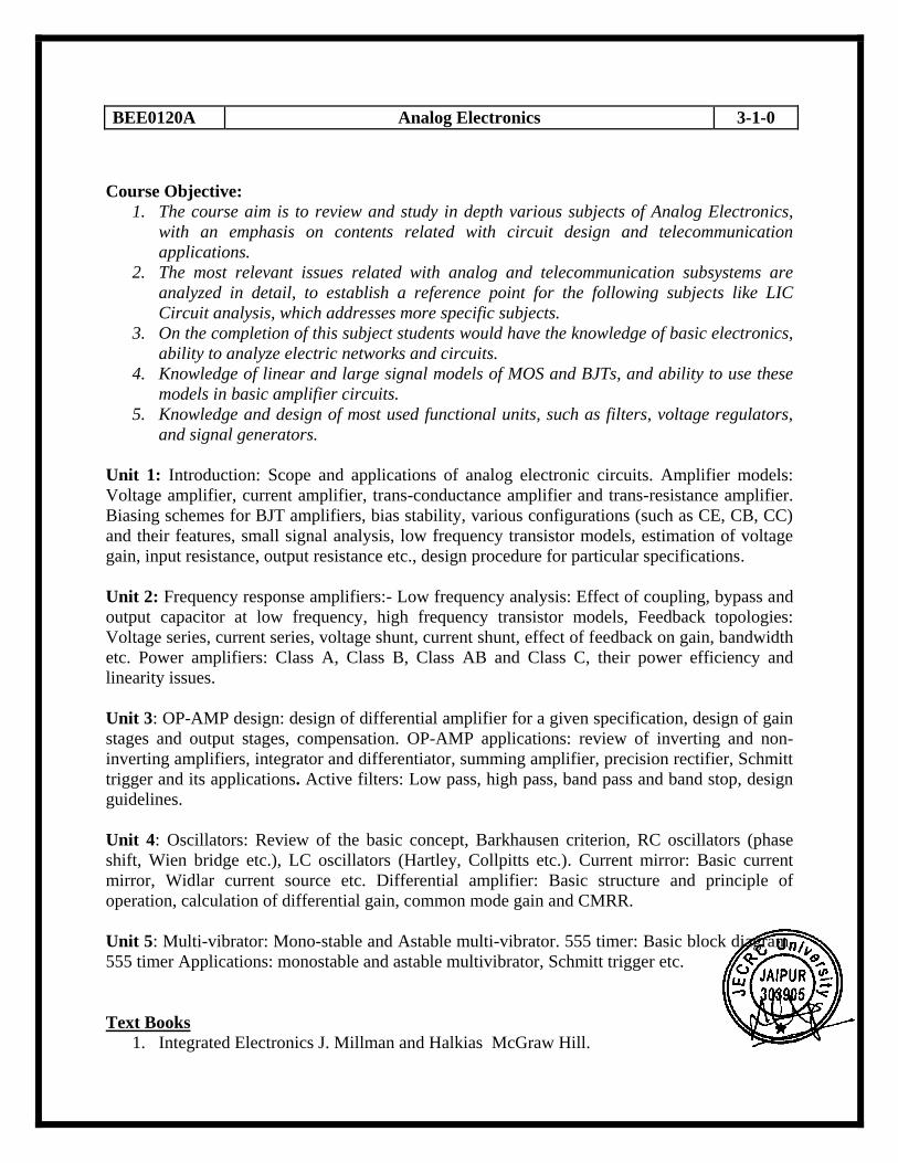
BEE0120A Analog Electronics 3-1-0
Course Objective:
1. The course aim is to review and study in depth various subjects of Analog Electronics,
with an emphasis on contents related with circuit design and telecommunication
applications.
2. The most relevant issues related with analog and telecommunication subsystems are
analyzed in detail, to establish a reference point for the following subjects like LIC
Circuit analysis, which addresses more specific subjects.
3. On the completion of this subject students would have the knowledge of basic electronics,
ability to analyze electric networks and circuits.
4. Knowledge of linear and large signal models of MOS and BJTs, and ability to use these
models in basic amplifier circuits.
5. Knowledge and design of most used functional units, such as filters, voltage regulators,
and signal generators.
Unit 1: Introduction: Scope and applications of analog electronic circuits. Amplifier models:
Voltage amplifier, current amplifier, trans-conductance amplifier and trans-resistance amplifier.
Biasing schemes for BJT amplifiers, bias stability, various configurations (such as CE, CB, CC)
and their features, small signal analysis, low frequency transistor models, estimation of voltage
gain, input resistance, output resistance etc., design procedure for particular specifications.
Unit 2: Frequency response amplifiers:- Low frequency analysis: Effect of coupling, bypass and
output capacitor at low frequency, high frequency transistor models, Feedback topologies:
Voltage series, current series, voltage shunt, current shunt, effect of feedback on gain, bandwidth
etc. Power amplifiers: Class A, Class B, Class AB and Class C, their power efficiency and
linearity issues.
Unit 3: OP-AMP design: design of differential amplifier for a given specification, design of gain
stages and output stages, compensation. OP-AMP applications: review of inverting and non-
inverting amplifiers, integrator and differentiator, summing amplifier, precision rectifier, Schmitt
trigger and its applications. Active filters: Low pass, high pass, band pass and band stop, design
guidelines.
Unit 4: Oscillators: Review of the basic concept, Barkhausen criterion, RC oscillators (phase
shift, Wien bridge etc.), LC oscillators (Hartley, Collpitts etc.). Current mirror: Basic current
mirror, Widlar current source etc. Differential amplifier: Basic structure and principle of
operation, calculation of differential gain, common mode gain and CMRR.
Unit 5: Multi-vibrator: Mono-stable and Astable multi-vibrator. 555 timer: Basic block diagram,
555 timer Applications: monostable and astable multivibrator, Schmitt trigger etc.
Text Books
1. Integrated Electronics J. Millman and Halkias McGraw Hill.

2. Microelectronic Circuits- “Adel S. Sedra, Kenneth Carless Smith” Oxford.
Reference Books:
1. Introduction to Operational Amplifier theory and applications, J.V. Wait, L.P. Huelsman
and GA Korn,McGraw Hill, 1992.
4
.
2. Analysis and Design of Analog Integrated Circuits, Paul R.Gray \& Robert G.Meyer,
John Wiley, 3rd Edition.
3. Op-amps and Linear Integrated Circuits-” Ramakant A. Gayakwad ” Prentice Hall. Micro
Course Outcomes (COs):
At the end of this course students will have:
CO1: Understand various transistor models and its configurations as amplifiers.
CO2: Understand the frequency response of amplifiers and study of power amplifiers
CO3: Study about the Operational amplifiers and its applications.
CO4: Designing of Oscillators and differential amplifiers.
CO5: Understand how Multivibrator works.
Program Outcomes (POs)
PO1. Design/development of solutions: Design solutions for complex engineering problems and design
system components or processes that meet the specified needs with appropriate consideration for the
public health and safety, and the cultural, societal, and environmental considerations.
PO2. Problem analysis: Identify, formulate, research literature, and analyze complex engineering
problems reaching substantiated conclusions using first principles of mathematics, natural sciences, and
engineering sciences. Minimization techniques.
PO3. Conduct investigations of complex problems: Use research-based knowledge and research methods
including design of experiments, analysis and interpretation of data, and synthesis of the information to
provide valid conclusions.
PO4. Modern tool usage: Create, select, and apply appropriate techniques, resources, and modern
engineering and IT tools including prediction and modeling to complex engineering activities with an
understanding of the limitations.
PO5. Design of sequential logic circuits. Minimization of hardware by applying different methods.
PO6. The engineer and society: Apply reasoning informed by the contextual knowledge to assess
societal, health, safety, legal and cultural issues and the consequent responsibilities relevant to the
professional engineering practice.

PO7. Environment and sustainability: Understand the impact of the professional engineering solutions in
societal and environmental contexts, Manual for Affiliated / Constituent Colleges NAAC for Quality and
Excellence in Higher Education 126 and demonstrate the knowledge of, and need for sustainable
development.
PO8. Ethics: Apply ethical principles and commit to professional ethics and responsibilities and norms of
the engineering practice.
PO9. Individual and team work: Function effectively as an individual, and as a member or leader in
diverse teams, and in multidisciplinary settings.
PO10. Communication: Communicate effectively on complex engineering activities with the engineering
community and with society at large, such as, being able to comprehend and write effective reports and
design documentation, make effective presentations, and give and receive clear instructions.
PO11. Project management and finance: Demonstrate knowledge and understanding of the engineering
and management principles and apply these to one’s own work, as a member and leader in a team, to
manage projects and in multidisciplinary environments.
PO12. Life-long learning: Recognize the need for, and have the preparation and ability to engage in
independent and life-long learning in the broadest context of technological change.
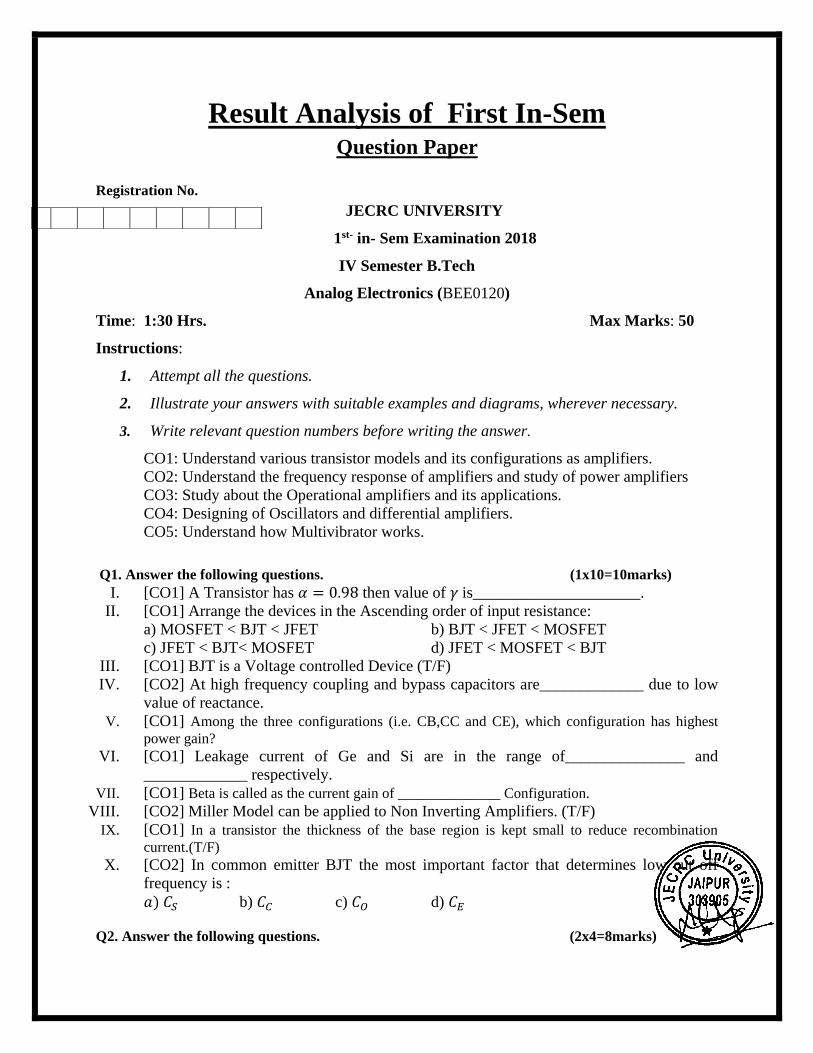
Result Analysis of First In-Sem Question Paper
Registration No.
JECRC UNIVERSITY
1st- in- Sem Examination 2018
IV Semester B.Tech
Analog Electronics (BEE0120)
Time: 1:30 Hrs. Max Marks: 50
Instructions:
1. Attempt all the questions.
2. Illustrate your answers with suitable examples and diagrams, wherever necessary.
3. Write relevant question numbers before writing the answer.
CO1: Understand various transistor models and its configurations as amplifiers.
CO2: Understand the frequency response of amplifiers and study of power amplifiers
CO3: Study about the Operational amplifiers and its applications.
CO4: Designing of Oscillators and differential amplifiers.
CO5: Understand how Multivibrator works.
Q1. Answer the following questions. (1x10=10marks)
I. [CO1] A Transistor has 𝛼 = 0.98 then value of 𝛾 is_____________________.
II. [CO1] Arrange the devices in the Ascending order of input resistance:
a) MOSFET < BJT < JFET b) BJT < JFET < MOSFET
c) JFET < BJT< MOSFET d) JFET < MOSFET < BJT
III. [CO1] BJT is a Voltage controlled Device (T/F)
IV. [CO2] At high frequency coupling and bypass capacitors are_____________ due to low
value of reactance.
V. [CO1] Among the three configurations (i.e. CB,CC and CE), which configuration has highest
power gain?
VI. [CO1] Leakage current of Ge and Si are in the range of_______________ and
_____________ respectively.
VII. [CO1] Beta is called as the current gain of ______________ Configuration.
VIII. [CO2] Miller Model can be applied to Non Inverting Amplifiers. (T/F)
IX. [CO1] In a transistor the thickness of the base region is kept small to reduce recombination
current.(T/F)
X. [CO2] In common emitter BJT the most important factor that determines low cut off
frequency is :
𝑎) 𝐶𝑆 b) 𝐶𝐶 c) 𝐶𝑂 d) 𝐶𝐸
Q2. Answer the following questions. (2x4=8marks)
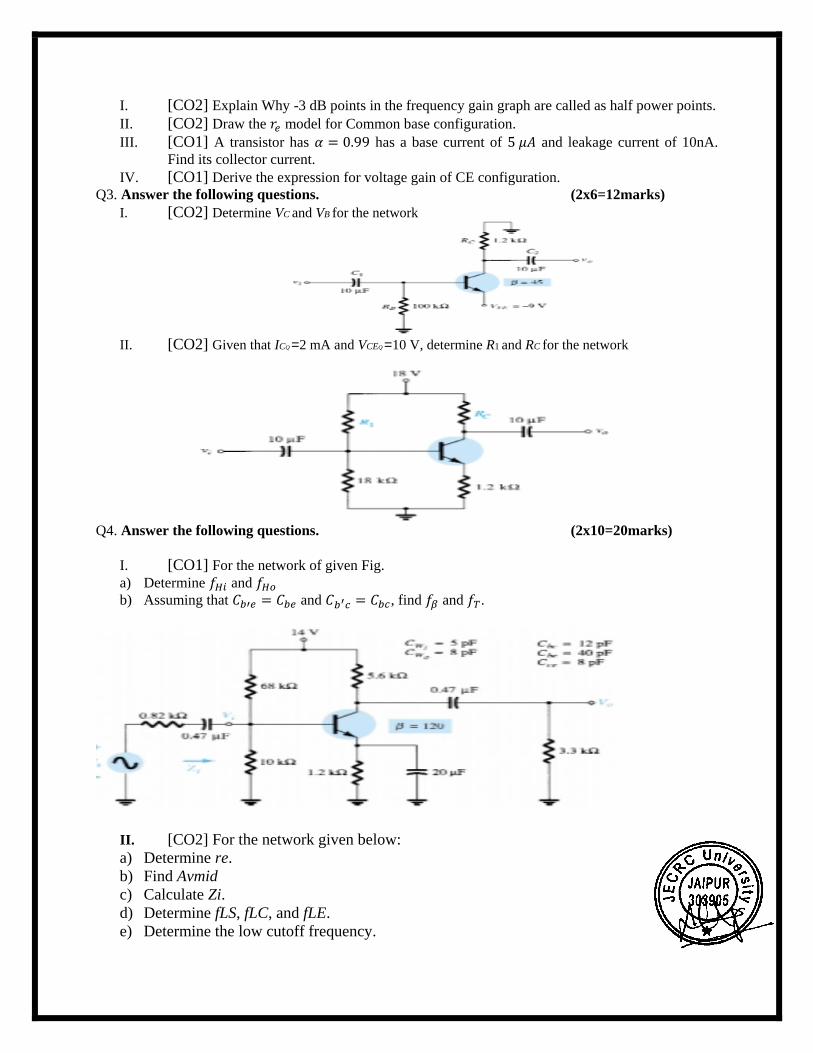
I. [CO2] Explain Why -3 dB points in the frequency gain graph are called as half power points.
II. [CO2] Draw the 𝑟𝑒 model for Common base configuration.
III. [CO1] A transistor has 𝛼 = 0.99 has a base current of 5 𝜇𝐴 and leakage current of 10nA.
Find its collector current.
IV. [CO1] Derive the expression for voltage gain of CE configuration.
Q3. Answer the following questions. (2x6=12marks)
I. [CO2] Determine VC and VB for the network
II. [CO2] Given that ICQ =2 mA and VCEQ =10 V, determine R1 and RC for the network
Q4. Answer the following questions. (2x10=20marks)
I. [CO1] For the network of given Fig.
a) Determine 𝑓𝐻𝑖 and 𝑓𝐻𝑜
b) Assuming that 𝐶𝑏′𝑒 = 𝐶𝑏𝑒 and 𝐶𝑏′𝑐 = 𝐶𝑏𝑐, find 𝑓𝛽 and 𝑓𝑇.
II. [CO2] For the network given below:
a) Determine re.
b) Find Avmid
c) Calculate Zi.
d) Determine fLS, fLC, and fLE.
e) Determine the low cutoff frequency.
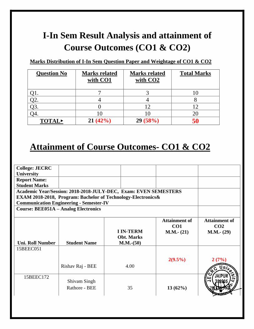
I-In Sem Result Analysis and attainment of
Course Outcomes (CO1 & CO2)
Marks Distribution of I-In Sem Question Paper and Weightage of CO1 & CO2
Question No Marks related
with CO1
Marks related
with CO2
Total Marks
Q1. 7 3 10
Q2. 4 4 8
Q3. 0 12 12
Q4. 10 10 20
TOTAL 21 (42%) 29 (58%) 50
Attainment of Course Outcomes- CO1 & CO2
College: JECRC
University
Report Name:
Student Marks
Academic Year/Session: 2018-2018-JULY-DEC, Exam: EVEN SEMESTERS
EXAM 2018-2018, Program: Bachelor of Technology-Electronics&
Communication Engineering - Semester-IV
Course: BEE051A – Analog Electronics
Uni. Roll Number Student Name
I IN-TERM
Obt. Marks
M.M.-(50)
Attainment of
CO1
M.M.- (21)
Attainment of
CO2
M.M.- (29)
15BEEC051
Rishav Raj - BEE 4.00
2(9.5%)
2 (7%)
15BEEC172
Shivam Singh
Rathore - BEE 35
13 (62%)
22 (76%)
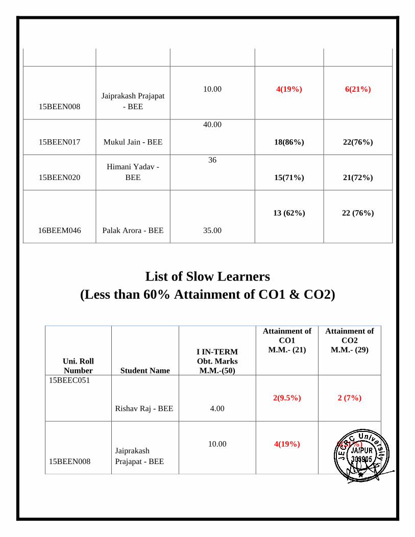
List of Slow Learners
(Less than 60% Attainment of CO1 & CO2)
15BEEN008
Jaiprakash Prajapat
- BEE
10.00
4(19%)
6(21%)
15BEEN017 Mukul Jain - BEE
40.00
18(86%)
22(76%)
15BEEN020
Himani Yadav -
BEE
36
15(71%)
21(72%)
16BEEM046 Palak Arora - BEE 35.00
13 (62%)
22 (76%)
Uni. Roll
Number Student Name
I IN-TERM
Obt. Marks
M.M.-(50)
Attainment of
CO1
M.M.- (21)
Attainment of
CO2
M.M.- (29)
15BEEC051
Rishav Raj - BEE 4.00
2(9.5%)
2 (7%)
15BEEN008
Jaiprakash
Prajapat - BEE
10.00
4(19%)
6(21%)
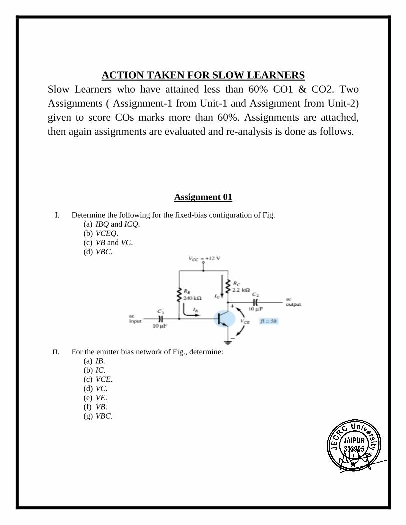
ACTION TAKEN FOR SLOW LEARNERS
Slow Learners who have attained less than 60% CO1 & CO2. Two
Assignments ( Assignment-1 from Unit-1 and Assignment from Unit-2)
given to score COs marks more than 60%. Assignments are attached,
then again assignments are evaluated and re-analysis is done as follows.
Assignment 01
I. Determine the following for the fixed-bias configuration of Fig.
(a) IBQ and ICQ.
(b) VCEQ.
(c) VB and VC.
(d) VBC.
II. For the emitter bias network of Fig., determine:
(a) IB.
(b) IC.
(c) VCE.
(d) VC.
(e) VE.
(f) VB.
(g) VBC.
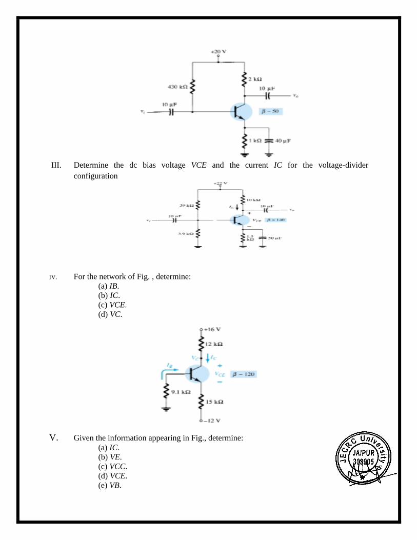
III. Determine the dc bias voltage VCE and the current IC for the voltage-divider
configuration
IV. For the network of Fig. , determine:
(a) IB.
(b) IC.
(c) VCE.
(d) VC.
V. Given the information appearing in Fig., determine:
(a) IC.
(b) VE.
(c) VCC.
(d) VCE.
(e) VB.
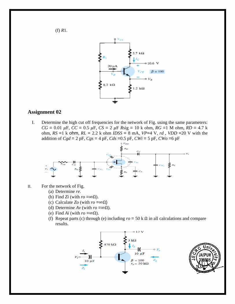
(f) R1.
Assignment 02
I. Determine the high cut off frequencies for the network of Fig. using the same parameters:
CG = 0.01 𝜇F, CC = 0.5 𝜇F, CS = 2 𝜇F Rsig = 10 k ohm, RG =1 M ohm, RD = 4.7 k
ohm, RS =1 k ohm, RL = 2.2 k ohm IDSS = 8 mA, VP=4 V, rd , VDD =20 V with the
addition of Cgd = 2 pF, Cgs = 4 pF, Cds =0.5 pF, CWi = 5 pF, CWo =6 pF
II. For the network of Fig.
(a) Determine re.
(b) Find Zi (with ro =∞Ω).
(c) Calculate Zo (with ro =∞Ω) (d) Determine Av (with ro =∞Ω).
(e) Find Ai (with ro =∞Ω).
(f) Repeat parts (c) through (e) including ro = 50 k Ω in all calculations and compare
results.
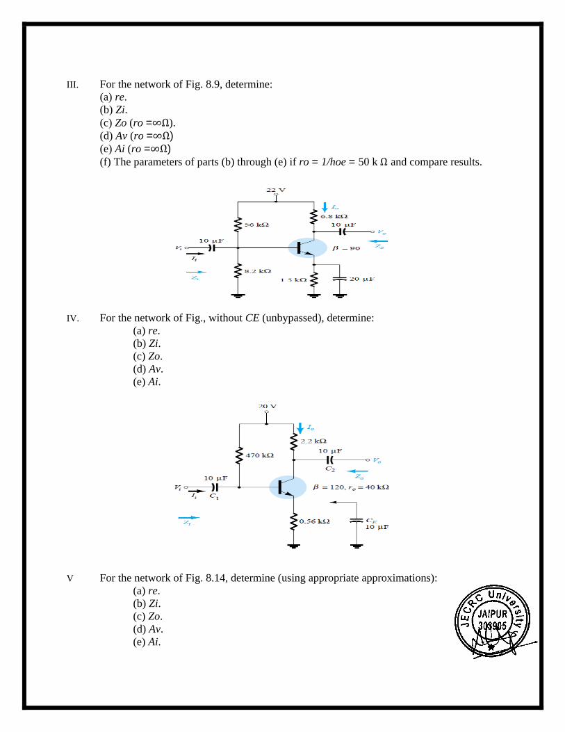
III. For the network of Fig. 8.9, determine:
(a) re.
(b) Zi.
(c) Zo (ro =∞Ω).
(d) Av (ro =∞Ω) (e) Ai (ro =∞Ω)
(f) The parameters of parts (b) through (e) if ro = 1/hoe = 50 k Ω and compare results.
IV. For the network of Fig., without CE (unbypassed), determine:
(a) re.
(b) Zi.
(c) Zo.
(d) Av.
(e) Ai.
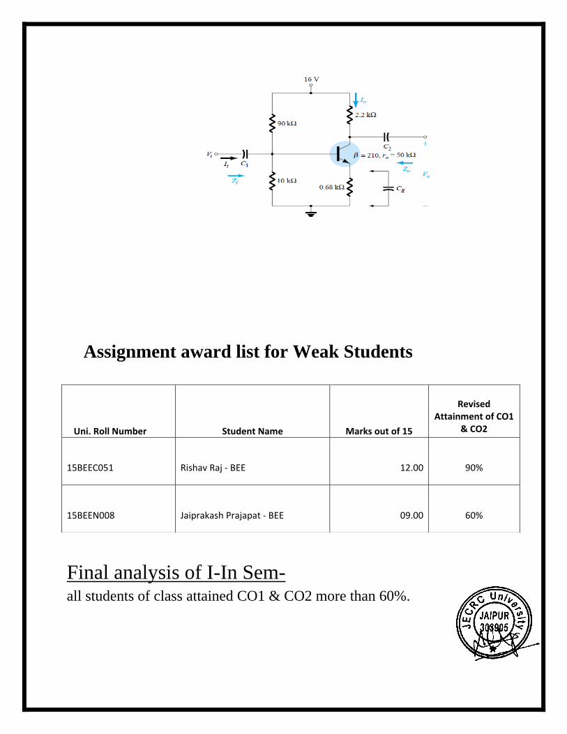
V For the network of Fig. 8.14, determine (using appropriate approximations):
(a) re.
(b) Zi.
(c) Zo.
(d) Av.
(e) Ai.
Assignment award list for Weak Students
Final analysis of I-In Sem- all students of class attained CO1 & CO2 more than 60%.
Uni. Roll Number Student Name Marks out of 15
Revised
Attainment of CO1 & CO2
15BEEC051 Rishav Raj - BEE 12.00
90%
15BEEN008 Jaiprakash Prajapat - BEE 09.00
60%
Result Analysis of Second In-Sem
Question Paper
Registration No.
JECRC UNIVERSITY
2nd- in- Sem Examination 2018
IV Semester B.Tech
Analog Electronics (BEE0120)
Time: 1:30 Hrs. Max Marks: 50
Instructions:
4. Attempt all the questions.
5. Illustrate your answers with suitable examples and diagrams, wherever necessary.
6. Write relevant question numbers before writing the answer.
CO1: Understand various transistor models and its configurations as amplifiers.
CO2: Understand the frequency response of amplifiers and study of power amplifiers
CO3: Study about the Operational amplifiers and its applications.
CO4: Designing of Oscillators and differential amplifiers.
CO5: Understand how Multivibrator works
Q1. Answer the following questions. (1x10=10marks)
I. [CO4] Which of the following class has maximum efficiency:
a) Class AB b) Class C c) Class D d) Class B
II. [CO4] For a trans-Conductance Amplifier the closed loop input resistance and output resistance are
respectively:
a) High, Low b) High, High c) Low, High e) Low, Low
III. [CO4] The current Amplifier configuration is also called as:
a) Series-Shunt b) Shunt-Shunt c) Series-Series d) Shunt-Series
IV. [CO4] A class C Amplifier is biased to operate for ___________ of the input cycle.
a) Less than 360 b) Less than 180 c) Less than 90 d) Less than 270
V. [CO3] The input to an OP-AMP differentiator is a triangular waveform, and then output waveform will be:
a) Square Wave b) Triangular Wave c) Parabolic Wave d) Sine Wave
VI. [CO4] If the differential voltage gain and common mode voltage gain of a differential amplifier are 48 dB
and 2 dB respectively, then its common mode rejection ratio:
a) 23dB b) 25dB c) 46dB d) 50dB
VII. [CO3] The Ideal OP-AMP has the following characteristics:
𝑎) 𝑅𝑖 = ∞, 𝐴 = ∞, 𝑅𝑜 = 0 b) 𝑅𝑖 = 0, 𝐴 = ∞, 𝑅𝑜 = 0
c) 𝑅𝑖 = ∞, 𝐴 = ∞, 𝑅𝑜 = ∞ d) 𝑅𝑖 = 0, 𝐴 = ∞, 𝑅𝑜 = ∞
VIII. [CO3] Differential Amplifier is said to be in______________ mode when same polarity of signals are
applied to both the input terminals.
IX. [CO3] In differential amplifier differential gain is large as compared to common mode gain (T//F).
X. [CO4] De-Sensitivity factor is given as:
𝑎) 𝐴
1+𝐴𝛽 b)
1
1+𝐴𝛽 c) 1 + 𝐴𝛽 d) 𝐴𝛽
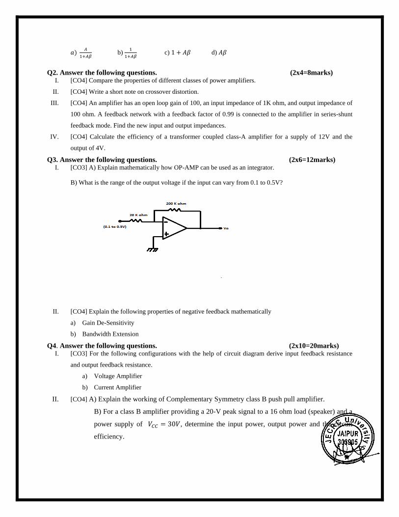
Q2. Answer the following questions. (2x4=8marks) I. [CO4] Compare the properties of different classes of power amplifiers.
II. [CO4] Write a short note on crossover distortion.
III. [CO4] An amplifier has an open loop gain of 100, an input impedance of 1K ohm, and output impedance of
100 ohm. A feedback network with a feedback factor of 0.99 is connected to the amplifier in series-shunt
feedback mode. Find the new input and output impedances.
IV. [CO4] Calculate the efficiency of a transformer coupled class-A amplifier for a supply of 12V and the
output of 4V.
Q3. Answer the following questions. (2x6=12marks) I. [CO3] A) Explain mathematically how OP-AMP can be used as an integrator.
B) What is the range of the output voltage if the input can vary from 0.1 to 0.5V?
II. [CO4] Explain the following properties of negative feedback mathematically
a) Gain De-Sensitivity
b) Bandwidth Extension
Q4. Answer the following questions. (2x10=20marks) I. [CO3] For the following configurations with the help of circuit diagram derive input feedback resistance
and output feedback resistance.
a) Voltage Amplifier
b) Current Amplifier
II. [CO4] A) Explain the working of Complementary Symmetry class B push pull amplifier.
B) For a class B amplifier providing a 20-V peak signal to a 16 ohm load (speaker) and a
power supply of 𝑉𝐶𝐶 = 30𝑉, determine the input power, output power and the circuit
efficiency.
II-In Sem Result Analysis and attainment of
Course Outcomes (CO3 & CO4)
Marks Distribution of I-In Sem Question Paper and Weightage of CO3 & CO4
Question No Marks related
with CO3
Marks related
with CO4
Total Marks
Q1. 4 6 10
Q2. 0 8 8
Q3. 6 6 12
Q4. 10 10 20
TOTAL 20 30 50
Attainment of Course Outcomes- CO3 & CO4
College: JECRC
University
Report Name:
Student Marks
Academic Year/Session: 2018-2018-JULY-DEC, Exam: EVEN SEMESTERS
EXAM 2018-2018, Program: Bachelor of Technology-Electronics&
Communication Engineering - Semester-IV
Course: BEE051A – Analog Electronics
Uni. Roll Number Student Name
I IN-TERM
Obt. Marks
M.M.-(50)
Attainment of
CO3
M.M.- (20)
Attainment of
CO4
M.M.- (30)
15BEEC051
Rishav Raj - BEE 4.00
2 (10%)
2 (7%)
15BEEC172
Shivam Singh
Rathore - BEE 21.00
8 (40%)
13 (43%)
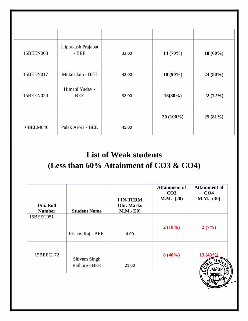
List of Weak students
(Less than 60% Attainment of CO3 & CO4)
15BEEN008
Jaiprakash Prajapat
- BEE 32.00
14 (70%)
18 (60%)
15BEEN017 Mukul Jain - BEE 42.00
18 (90%)
24 (80%)
15BEEN020
Himani Yadav -
BEE 38.00
16(80%)
22 (72%)
16BEEM046 Palak Arora - BEE 45.00
20 (100%)
25 (81%)
Uni. Roll
Number Student Name
I IN-TERM
Obt. Marks
M.M.-(50)
Attainment of
CO3
M.M.- (20)
Attainment of
CO4
M.M.- (30)
15BEEC051
Rishav Raj - BEE 4.00
2 (10%)
2 (7%)
15BEEC172
Shivam Singh
Rathore - BEE 21.00
8 (40%)
13 (43%)
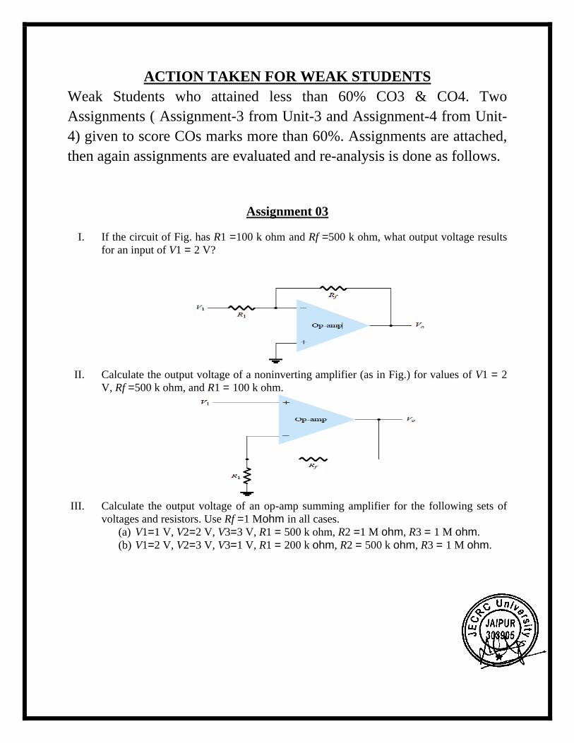
ACTION TAKEN FOR WEAK STUDENTS
Weak Students who attained less than 60% CO3 & CO4. Two
Assignments ( Assignment-3 from Unit-3 and Assignment-4 from Unit-
4) given to score COs marks more than 60%. Assignments are attached,
then again assignments are evaluated and re-analysis is done as follows.
Assignment 03
I. If the circuit of Fig. has R1 =100 k ohm and Rf =500 k ohm, what output voltage results
for an input of V1 = 2 V?
II. Calculate the output voltage of a noninverting amplifier (as in Fig.) for values of V1 = 2
V, Rf =500 k ohm, and R1 = 100 k ohm.
III. Calculate the output voltage of an op-amp summing amplifier for the following sets of
voltages and resistors. Use Rf =1 Mohm in all cases.
(a) V1=1 V, V2=2 V, V3=3 V, R1 = 500 k ohm, R2 =1 M ohm, R3 = 1 M ohm.
(b) V1=2 V, V2=3 V, V3=1 V, R1 = 200 k ohm, R2 = 500 k ohm, R3 = 1 M ohm.
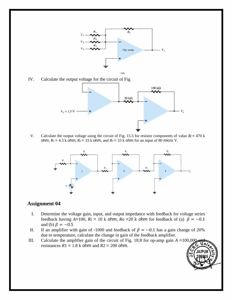
IV. Calculate the output voltage for the circuit of Fig
V. Calculate the output voltage using the circuit of Fig. 15.5 for resistor components of value Rf = 470 k
ohm, R1 = 4.3 k ohm, R2 = 33 k ohm, and R3 = 33 k ohm for an input of 80 micro V.
Assignment 04
I. Determine the voltage gain, input, and output impedance with feedback for voltage series
feedback having A=100, Ri = 10 k ohm, Ro =20 k ohm for feedback of (a) 𝛽 = −0.1
and (b) 𝛽 = −0.5
II. If an amplifier with gain of -1000 and feedback of 𝛽 = −0.1 has a gain change of 20%
due to temperature, calculate the change in gain of the feedback amplifier.
III. Calculate the amplifier gain of the circuit of Fig. 18.8 for op-amp gain A =100,000 and
resistances R1 = 1.8 k ohm and R2 = 200 ohm.
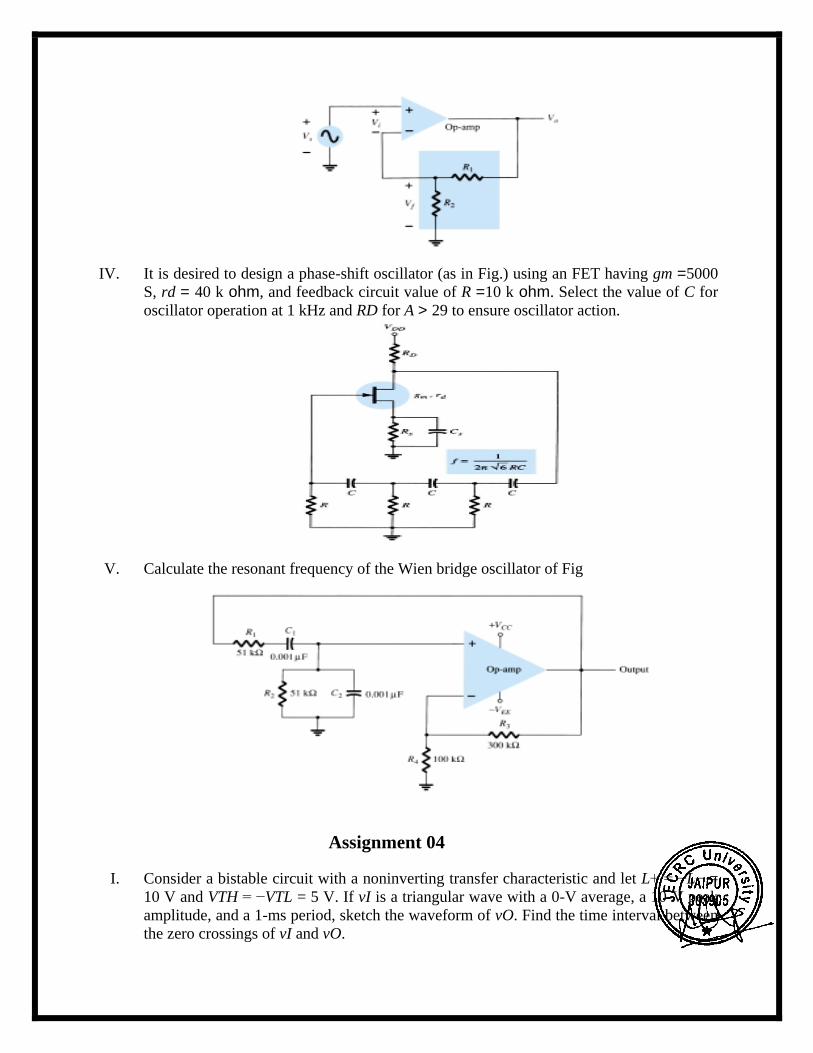
IV. It is desired to design a phase-shift oscillator (as in Fig.) using an FET having gm =5000
S, rd = 40 k ohm, and feedback circuit value of R =10 k ohm. Select the value of C for
oscillator operation at 1 kHz and RD for A > 29 to ensure oscillator action.
V. Calculate the resonant frequency of the Wien bridge oscillator of Fig
Assignment 04
I. Consider a bistable circuit with a noninverting transfer characteristic and let L+ = −L− =
10 V and VTH = −VTL = 5 V. If vI is a triangular wave with a 0-V average, a 10-V peak
amplitude, and a 1-ms period, sketch the waveform of vO. Find the time interval between
the zero crossings of vI and vO.
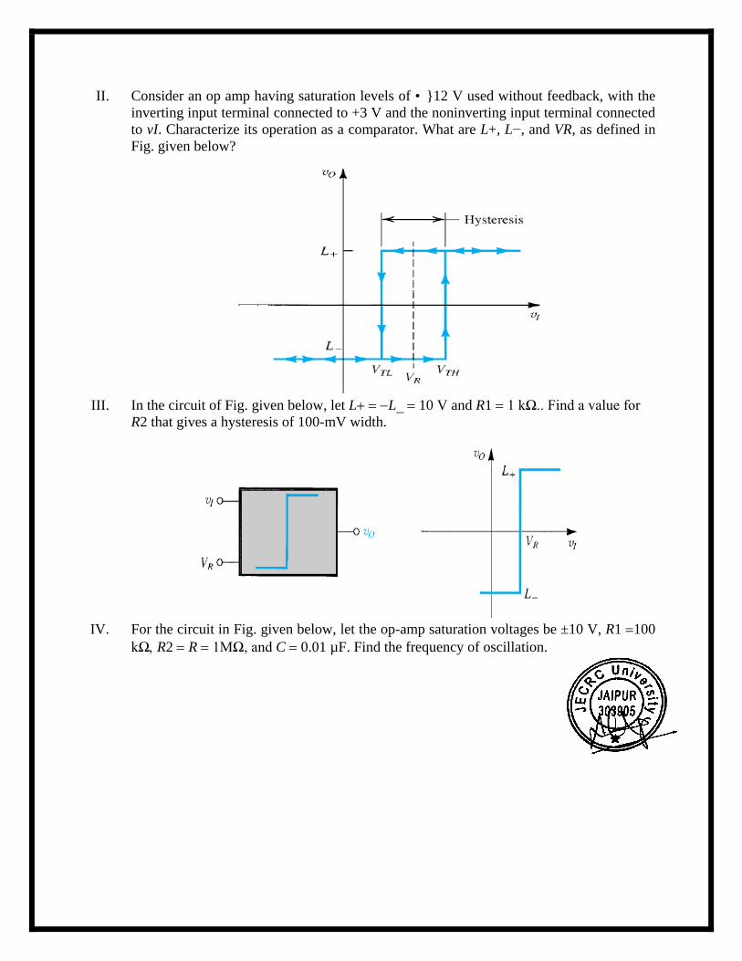
II. Consider an op amp having saturation levels of •12 V used without feedback, with the
inverting input terminal connected to +3 V and the noninverting input terminal connected
to vI. Characterize its operation as a comparator. What are L+, L−, and VR, as defined in
Fig. given below?
III. In the circuit of Fig. given below, let LL10 V and R1 1 kΩ.. Find a value for
R2 that gives a hysteresis of 100-mV width.
IV. For the circuit in Fig. given below, let the op-amp saturation voltages be ±10 V, R1 100
kΩR2 R 1MΩ, and C 0.01 µF. Find the frequency of oscillation.
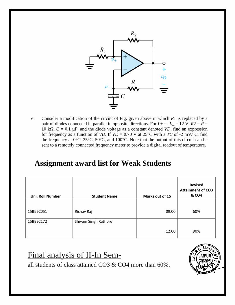
V. Consider a modification of the circuit of Fig. given above in which R1 is replaced by a
pair of diodes connected in parallel in opposite directions. For L+ = -L_ = 12 V, R2 = R =
10 kΩ, C = 0.1 µF, and the diode voltage as a constant denoted VD, find an expression
for frequency as a function of VD. If VD = 0.70 V at 25°C with a TC of -2 mV/°C, find
the frequency at 0°C, 25°C, 50°C, and 100°C. Note that the output of this circuit can be
sent to a remotely connected frequency meter to provide a digital readout of temperature.
Assignment award list for Weak Students
Final analysis of II-In Sem- all students of class attained CO3 & CO4 more than 60%.
Uni. Roll Number Student Name Marks out of 15
Revised
Attainment of CO3 & CO4
15BEEC051 Rishav Raj 09.00
60%
15BEEC172 Shivam Singh Rathore
12.00
90%
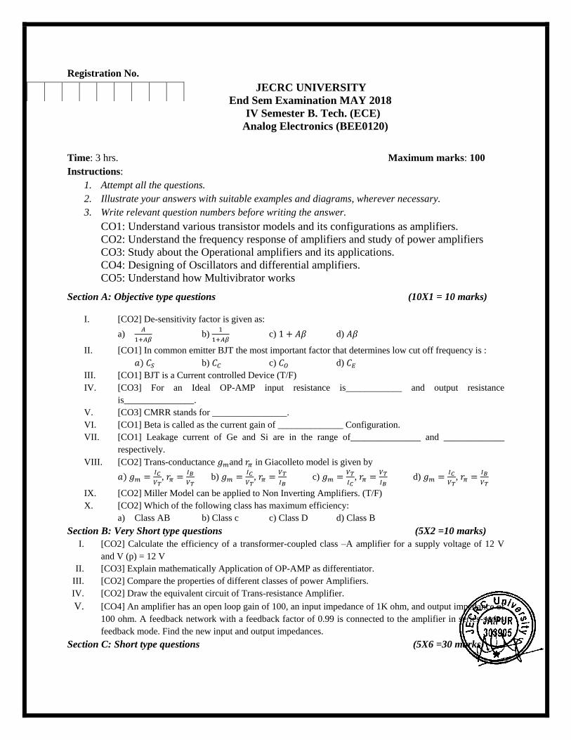
Registration No.
JECRC UNIVERSITY
End Sem Examination MAY 2018
IV Semester B. Tech. (ECE)
Analog Electronics (BEE0120)
Time: 3 hrs. Maximum marks: 100
Instructions:
1. Attempt all the questions.
2. Illustrate your answers with suitable examples and diagrams, wherever necessary.
3. Write relevant question numbers before writing the answer.
CO1: Understand various transistor models and its configurations as amplifiers.
CO2: Understand the frequency response of amplifiers and study of power amplifiers
CO3: Study about the Operational amplifiers and its applications.
CO4: Designing of Oscillators and differential amplifiers.
CO5: Understand how Multivibrator works
Section A: Objective type questions (10X1 = 10 marks)
I. [CO2] De-sensitivity factor is given as:
a) 𝐴
1+𝐴𝛽 b)
1
1+𝐴𝛽 c) 1 + 𝐴𝛽 d) 𝐴𝛽
II. [CO1] In common emitter BJT the most important factor that determines low cut off frequency is :
𝑎) 𝐶𝑆 b) 𝐶𝐶 c) 𝐶𝑂 d) 𝐶𝐸
III. [CO1] BJT is a Current controlled Device (T/F)
IV. [CO3] For an Ideal OP-AMP input resistance is____________ and output resistance
is_______________.
V. [CO3] CMRR stands for ________________.
VI. [CO1] Beta is called as the current gain of ______________ Configuration.
VII. [CO1] Leakage current of Ge and Si are in the range of_______________ and _____________
respectively.
VIII. [CO2] Trans-conductance 𝑔𝑚and 𝑟𝜋 in Giacolleto model is given by
𝑎) 𝑔𝑚 =𝐼𝐶
𝑉𝑇, 𝑟𝜋 =
𝐼𝐵
𝑉𝑇 b) 𝑔𝑚 =
𝐼𝐶
𝑉𝑇, 𝑟𝜋 =
𝑉𝑇
𝐼𝐵 c) 𝑔𝑚 =
𝑉𝑇
𝐼𝐶, 𝑟𝜋 =
𝑉𝑇
𝐼𝐵 d) 𝑔𝑚 =
𝐼𝐶
𝑉𝑇, 𝑟𝜋 =
𝐼𝐵
𝑉𝑇
IX. [CO2] Miller Model can be applied to Non Inverting Amplifiers. (T/F)
X. [CO2] Which of the following class has maximum efficiency:
a) Class AB b) Class c c) Class D d) Class B
Section B: Very Short type questions (5X2 =10 marks)
I. [CO2] Calculate the efficiency of a transformer-coupled class –A amplifier for a supply voltage of 12 V
and V (p) = 12 V
II. [CO3] Explain mathematically Application of OP-AMP as differentiator.
III. [CO2] Compare the properties of different classes of power Amplifiers.
IV. [CO2] Draw the equivalent circuit of Trans-resistance Amplifier.
V. [CO4] An amplifier has an open loop gain of 100, an input impedance of 1K ohm, and output impedance of
100 ohm. A feedback network with a feedback factor of 0.99 is connected to the amplifier in series-series
feedback mode. Find the new input and output impedances.
Section C: Short type questions (5X6 =30 marks)
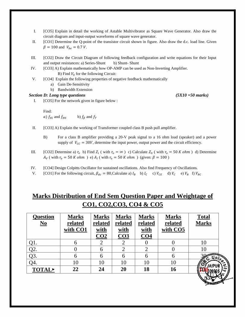
I. [CO5] Explain in detail the working of Astable Multivibrator as Square Wave Generator. Also draw the
circuit diagram and input-output waveforms of square wave generator.
II. [CO1] Determine the Q-point of the transistor circuit shown in figure. Also draw the d.c. load line. Given
𝛽 = 100 and 𝑉𝑏𝑒 = 0.7 𝑉.
III. [CO2] Draw the Circuit Diagram of following feedback configuration and write equations for their Input
and output resistances: a) Series-Shunt b) Shunt- Shunt
IV. [CO3] A) Explain mathematically how OP-AMP can be used as Non-Inverting Amplifier.
B) Find 𝑉0 for the following Circuit:
V. [CO4] Explain the following properties of negative feedback mathematically
a) Gain De-Sensitivity
b) Bandwidth Extension
Section D: Long type questions (5X10 =50 marks)
I. [CO5] For the network given in figure below :
Find:
𝑎) 𝑓𝐻𝑖 and 𝑓𝐻0 b) 𝑓𝛽 and 𝑓𝑇
II. [CO3] A) Explain the working of Transformer coupled class B push pull amplifier.
B) For a class B amplifier providing a 20-V peak signal to a 16 ohm load (speaker) and a power
supply of 𝑉𝐶𝐶 = 30𝑉, determine the input power, output power and the circuit efficiency.
III. [CO2] Determine a) 𝑟𝑒 b) Find 𝑍𝑖 ( with 𝑟𝑜 = ∞ ) c) Calculate 𝑍0 ( with 𝑟𝑜 = 50 𝐾 𝑜ℎ𝑚 ) d) Determine
𝐴𝑉 ( with 𝑟𝑜 = 50 𝐾 𝑜ℎ𝑚 ) e) 𝐴𝐼 ( with 𝑟𝑜 = 50 𝐾 𝑜ℎ𝑚 ) (given: 𝛽 = 100 )
IV. [CO4] Design Colpitts Oscillator for sustained oscillations. Also find Frequency of Oscillations.
V. [CO1] For the following circuit, 𝛽𝑑𝑐 = 80,Calculate a) 𝐼𝐵 b) 𝐼𝐶 c) 𝑉𝐶𝐸 d) 𝑉𝐶 e) 𝑉𝐵 f) 𝑉𝐵𝐶
Marks Distribution of End Sem Question Paper and Weightage of
CO1, CO2,CO3, CO4 & CO5
Question
No
Marks
related
with CO1
Marks
related
with
CO2
Marks
related
with
CO3
Marks
related
with
CO4
Marks
related
with CO5
Total
Marks
Q1. 6 2 2 0 0 10
Q2. 0 6 2 2 0 10
Q3. 6 6 6 6 6 30
Q4. 10 10 10 10 10 50
TOTAL 22 24 20 18 16 100
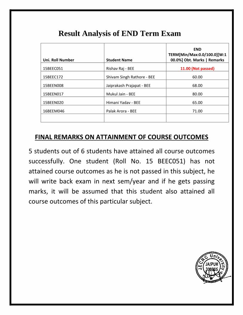
Result Analysis of END Term Exam
Uni. Roll Number Student Name
END TERM[Min/Max:0.0/100.0][W:1
00.0%] Obt. Marks | Remarks
15BEEC051 Rishav Raj - BEE 11.00 (Not passed)
15BEEC172 Shivam Singh Rathore - BEE 60.00
15BEEN008 Jaiprakash Prajapat - BEE 68.00
15BEEN017 Mukul Jain - BEE 80.00
15BEEN020 Himani Yadav - BEE 65.00
16BEEM046 Palak Arora - BEE 71.00
FINAL REMARKS ON ATTAINMENT OF COURSE OUTCOMES
5 students out of 6 students have attained all course outcomes
successfully. One student (Roll No. 15 BEEC051) has not
attained course outcomes as he is not passed in this subject, he
will write back exam in next sem/year and if he gets passing
marks, it will be assumed that this student also attained all
course outcomes of this particular subject.

ATTAINMENTS OF POs (PROGRAM OUTCOMES-PO1 to PO12)
Uni. Roll Number Student Name
Attainme
nt of
CO1 in
%
Attainm
ent of
CO2 in
%
Attainme
nt of
CO3 in
%
Attainm
ent of
CO4 in
%
Attainment
of CO1-CO5
in %
15BEEC051 Rishav Raj - BEE 90% 90% 60% 60% -
15BEEC172 Shivam Singh Rathore - BEE
13 (62%)
22 (76%)
90% 90%
60.00
15BEEN008 Jaiprakash Prajapat - BEE
60% 60%
14 (70%)
18 (60%) 68.00
15BEEN017 Mukul Jain - BEE
18(86%)
22(76%)
18 (90%)
24 (80%) 80.00
15BEEN020 Himani Yadav - BEE
15(71%)
21(72%)
16(80%)
22 (72%) 65.00
16BEEM046 Palak Arora - BEE
13 (62%)
22 (76%)
20 (100%)
25 (81%) 71.00
AVERAGE ATTAINMENT IN % 72% 75% 82% 73% 70%
Average of all Course Outcomes 75%
64%66%68%70%72%74%76%78%80%82%
Attainment ofCO1 in %
Attainment ofCO2 in %
Attainment ofCO3 in %
Attainment ofCO4 in %
Attainment ofCO1-CO5 in %
Final/Average Calculation of Attainment of CO1, CO2,CO3, CO4 & CO5 :- Subject: Course: BEE051A – Analog Electronics
Chart Title
Final/Average Calculation of Attainment of CO1, CO2,CO3, CO4 &
CO5 :- Subject: Course: BEE051A – Analog Electronics
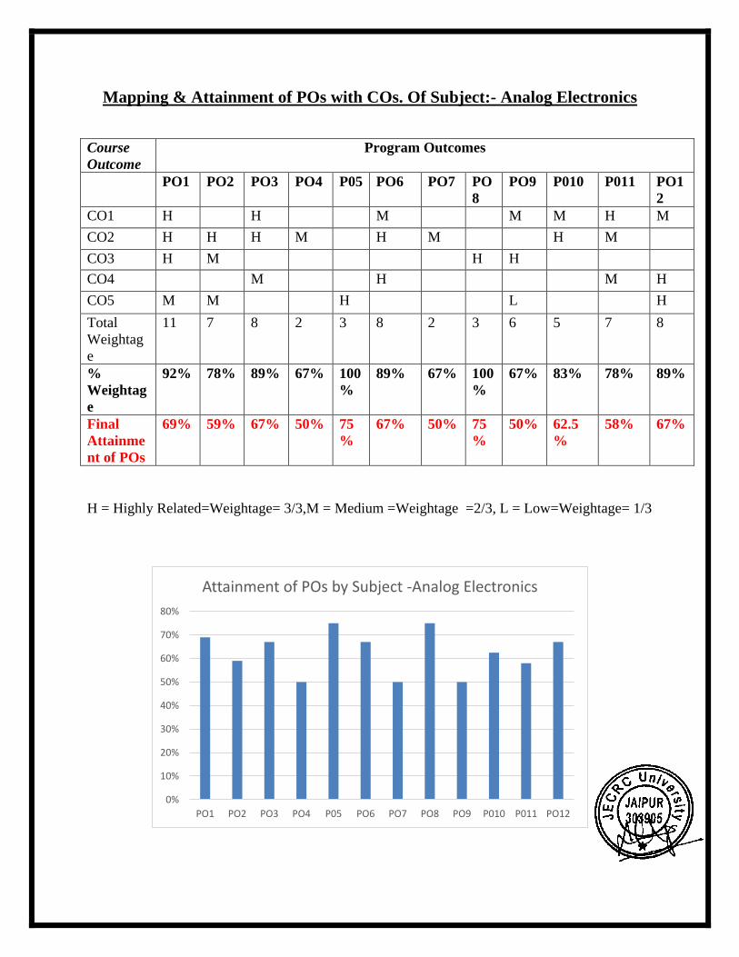
Mapping & Attainment of POs with COs. Of Subject:- Analog Electronics
Course
Outcome
Program Outcomes
PO1 PO2 PO3 PO4 P05 PO6 PO7 PO
8
PO9 P010 P011 PO1
2
CO1 H H M M M H M
CO2 H H H M H M H M
CO3 H M H H
CO4 M H M H
CO5 M M H L H
Total
Weightag
e
11 7 8 2 3 8 2 3 6 5 7 8
%
Weightag
e
92% 78% 89% 67% 100
%
89% 67% 100
%
67% 83% 78% 89%
Final
Attainme
nt of POs
69% 59% 67% 50% 75
%
67% 50% 75
%
50% 62.5
%
58% 67%
H = Highly Related=Weightage= 3/3,M = Medium =Weightage =2/3, L = Low=Weightage= 1/3
0%
10%
20%
30%
40%
50%
60%
70%
80%
PO1 PO2 PO3 PO4 P05 PO6 PO7 PO8 PO9 P010 P011 PO12
Attainment of POs by Subject -Analog Electronics


