Embed Size (px)
Citation preview
DfXEngineeringA Design for Cost approach to PCB Layout
www.dfxengineering.com

DesignForCostProcess
MaterialSelec+onandpartsize–DrivenbyMaterialType(costvs.performancetradeoffs),Sizerelatedtomastersheetsnotworkingpanelsandpre-pregselecIonopImizaIon(howdoesglassstyleaffectBOMcost,andStack-up/Construc+onType:ThisiswhereyouarefocusingwithyourquesIonsonbothhowarewerouIngoutofdevicesandhowmanydevicesarewetryingtoroutinasingleboard,canwedoitlessexpensivelybymakingseparatesmallerboards,whatinterconnectschemeisthebestcost.CpkOp+miza+onOnCapability:HerewereviewhowdotherouIngoftracechoicesdrivethefeaturesizerelaIvetothemarket’scapabilityat2.0Cpk,andisthereanalternatewaytomeetthattodrivefeaturesizetothecenterofthecapability.WhatistheguideforHDIvs.ConvenIonal.Ifwechoseabelow1.0CpkDesignfeatureisourdetecIonsystemadequateforthevolumeweareproducing.
ThedesignforcostprocesshasthreemajorareastofocusonforopImizingthecostfeaturesinadesign.Thesethreeareasshouldinteractrepeatedlytorefinetothebestcostvs.performancetradeoff
DfXEngineering,LLC,2016
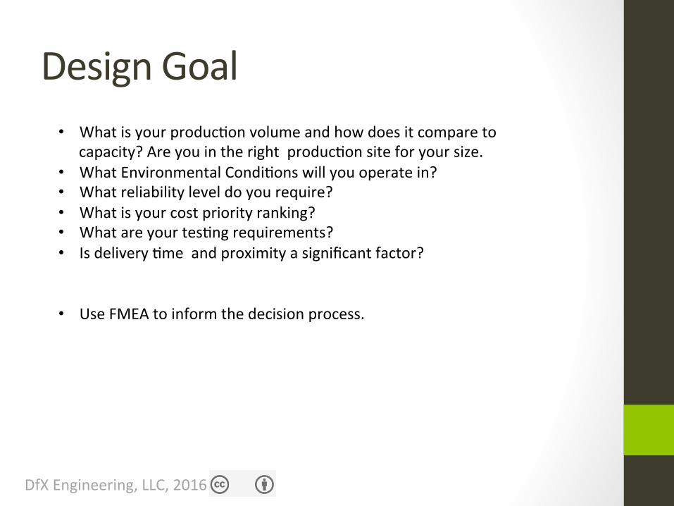
DesignGoal• WhatisyourproducIonvolumeandhowdoesitcompareto
capacity?AreyouintherightproducIonsiteforyoursize.• WhatEnvironmentalCondiIonswillyouoperatein?• Whatreliabilityleveldoyourequire?• Whatisyourcostpriorityranking?• WhatareyourtesIngrequirements?• IsdeliveryImeandproximityasignificantfactor?
• UseFMEAtoinformthedecisionprocess.
DfXEngineering,LLC,2016

RobustMarket
KnowyoursupplierscapabiliIes,andmaterialvendors
DfXEngineering,LLC,2016

MATERIALSELECTIONPerformance,Dkandsize

BOMCostAnalysisBasis
AsMaterialisthemostsignificantfactorinPCBwewilltalkaboutbuildingacostmodelfromthebasematerial,up.EarlyImespentintheareasofmaterialtype,andmaterialuIlizaIonwillpaythebiggestreturns.
Pre-preg FR4
Cost index %
1078/1086 1.2
1080 1,0
1067 1.75
106 2.35
2116 1.20
1501/1506 1.65
3313/2113 1.55
7628 1.25
DfXEngineering,LLC,2016
*Pricesshownareexamplesonlyandneedtobeupdatedtospecificcircumstances

1Ghz–DfResinRich,ResinPoor
0.000
0.005
0.010
0.015
0.020
0.025Std.Loss
UpperMidLoss LowLoss VeryLowLoss
MaterialSelecIonisMoreComplex
DfXEngineering,LLC,2016

4Ghz–DfResinRich,ResinPoor
0.000
0.005
0.010
0.015
0.020
0.025Std.Loss
UpperMidLoss LowLoss VeryLowLoss
MaterialSelecIonisMoreComplexVendorBaseandMaterialchoiceshavegrowndramaIcally.Knowyourneeds.
DfXEngineering,LLC,2016

8Ghz–DfResinRich,ResinPoor
0.000
0.005
0.010
0.015
0.020
0.025
0.030Std.Loss
UpperMidLoss LowLoss VeryLowLoss
MaterialSelecIonisMoreComplexAsMicrowaveJournalsays:FrequencyMaCers!
DfXEngineering,LLC,2016

MaterialSelecIonDecisionTree
TgDecisionPoint
KeyFactorConsidera+ons:• OverallThickness• AspectRaIo• AssemblycondiIons
includingrework• ReliabilityUsefulLife
Target
DkRange DfRange
KeyFactorConsidera+ons:• ImpedanceGoals• LayerConstraints• ResinContent(fill)• GlassStyles
KeyFactorConsidera+ons:• OperaIngFrequency• LossSensiIvity• CopperRoughness
Profile
PicktheBestFitineachofthesetofindtheidealmeaterialcost
DfXEngineering,LLC,2016

MaterialSelecIonCostImpactCostFactor
1X
2X
3X
150Tg
170Tg
>200Tg
3.7Dk
3.5Dk
<3.0Dk
STD
RTF
VLPorHVLP
CriIcalareasarereliability,yieldloss,andavailabilityAddiIonalConsideraIonofHalogenFreeorNot
0.011Df
0.009Df
<0.005Dk
0.006Df
DfXEngineering,LLC,2016

MaterialCostvPerformanceAnalysis
UIlizeanextensivematerialtesIngprogramtoprovideacomprehensivecostv.performanceanalysisspecifictoyourapplicaIon.
Mainvariablestoconsider,Tg,Dk,Df
0
1
2
3
4
5
6
LaminateCost
FinalPCBCost16L
FinalPCBCost20L
DfXEngineering,LLC,2016

MATERIALOPTIMIZATIONBestFitPanel
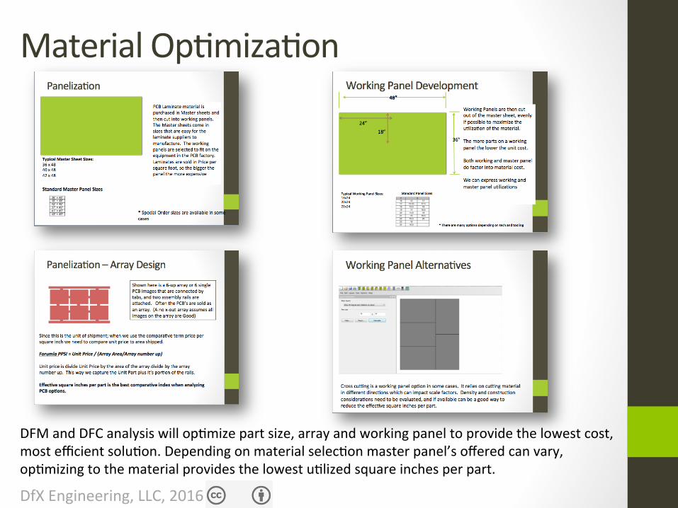
MaterialOpImizaIon
DFMandDFCanalysiswillopImizepartsize,arrayandworkingpaneltoprovidethelowestcost,mostefficientsoluIon.DependingonmaterialselecIonmasterpanel’sofferedcanvary,opImizingtothematerialprovidesthelowestuIlizedsquareinchesperpart.
DfXEngineering,LLC,2016
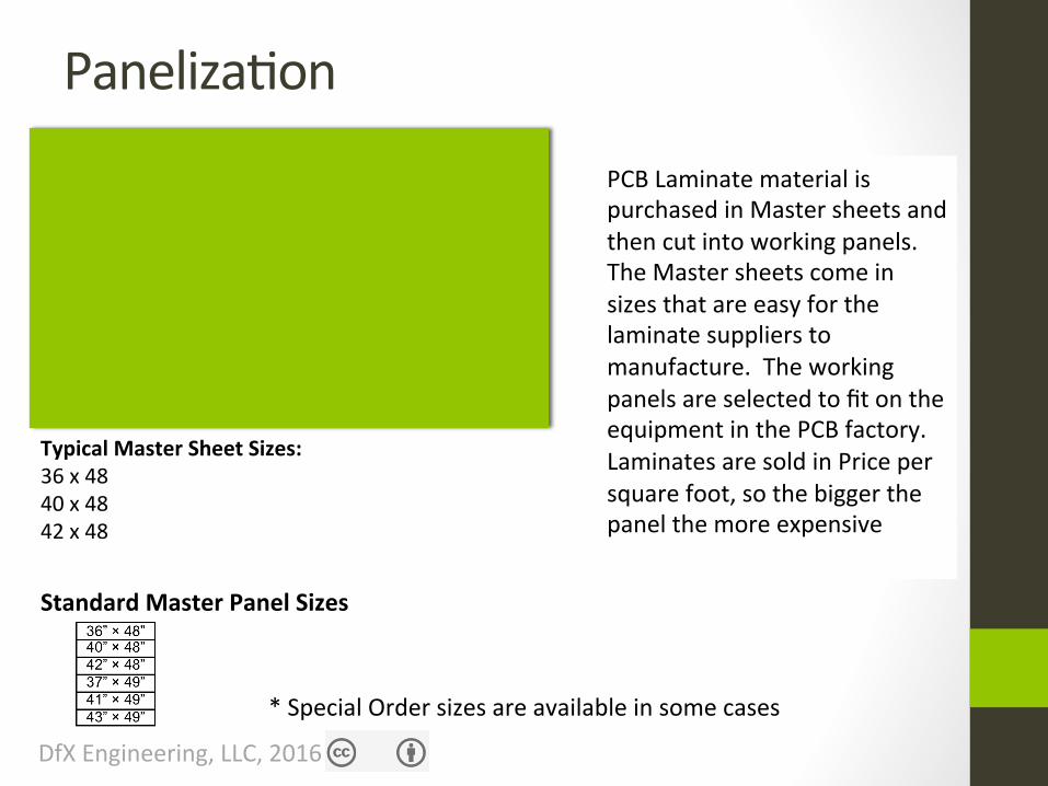
PanelU+liza+on
PCBLaminatematerialispurchasedinMastersheetsandthencutintoworkingpanels.TheMastersheetscomeinsizesthatareeasyforthelaminatesupplierstomanufacture.TheworkingpanelsareselectedtofitontheequipmentinthePCBfactory.LaminatesaresoldinPricepersquarefoot,sothebiggerthepanelthemoreexpensive
TypicalMasterSheetSizes:36x4840x4842x48
*SpecialOrdersizesareavailableinsomecases
StandardMasterPanelSizes
PanelizaIon
DfXEngineering,LLC,2016

PanelU+liza+on
TypicalWorkingPanelSizes:18x2420x2421x24
36”
24”
18”
48”
*Therearemanyop+onsdependingontechandtooling
StandardPanelSizes
WorkingPanelsarethencutoutofthemastersheet,evenlyifpossibletomaximizetheuIlizaIonofthematerial.Themorepartsonaworkingpanelthelowertheunitcost.Bothworkingandmasterpaneldofactorintomaterialcost.WecanexpressworkingandmasterpaneluIlizaIons
WorkingPanelDevelopment
DfXEngineering,LLC,2016

PanelU+liza+on-crosscuRng
CrosscunngisaworkingpanelopIoninsomecases.ItreliesoncunngmaterialindifferentdirecIonswhichcanimpactscalefactors.DensityandconstrucIonconsideraIonsneedtobeevaluated,andifavailablecanbeagoodwaytoreducetheeffecIvesquareinchesperpart.
WorkingPanelAlternaIves
DfXEngineering,LLC,2016

PPSI–PricePerSquareInch
.
Sincethisistheunitofshipment;whenweusethecomparaIvetermpricepersquareinchweneedtocompareunitpricetoareashipped.ForumlaPPSI=UnitPrice/(ArrayArea/Arraynumberup)UnitpriceisdivideUnitPricebytheareaofthearraydividebythearraynumberup.ThiswaywecapturetheUnitPartplusit’sporIonoftherails.Effec+vesquareinchesperpartisthebestcompara+veindexwhenanalyzingPCBop+ons.
Shownhereisa6-uparrayor6singlePCBImagesthatareconnectedbytabs,andtwoassemblyrailsareapached.OqenthePCB’saresoldasanarray.(Anox-outarrayassumesallimagesonthearrayareGood)
PanelizaIon–ArrayDesign
DfXEngineering,LLC,2016

PanelU+liza+on Inthisexampletheredboxesshow6PCB’sorPCBarrayspanelizedonan18x24.WewoulddividetheREDareabytheBLUEareatocalculatePaneluIlizaIonasapercentage.SincePCBlaborcostsareappliedtoworkingpanelsthemorepartsonapanelthelowertheunitcost.Numberupperworkingpanelisthenumberoftotal1upimagesontheworkingpanel(Arraynumberupxarray’sperWPNL)Wecanneverreach100%uIlizaIonbecauseweneed
spacebetweenpartsforcunngtoolstoseparatethem,weneedapanelbordertoapachtosomeelectroplaIngequipment,andweneedsomeroomfordestrucIvetesIngcoupons.ComparaIveanalysisshouldbeusedtoassessthequalityofyourpricinganddesigns.
24”
18”
PanelizaIon
DfXEngineering,LLC,2016
FUNCTIONANALYSISHowmanyfuncIonsareIedinoneboard

HowmanyFuncIons
Mainlogicboard
Processor
4G Wi-FiBT
PCBbudgetcombined
Processor
4G
Wi-FiBT
PCBbudgetseparate
CansizesandrouIngbeopImizedtobreakoutPCB’sintomoremanufacturablelowercostunitwithdifferentinterconnectscheme
camera camera
compare
DfXEngineering,LLC,2016

SameDeviceDesigns,DifferentCostConstrucIons
PCBbudgetcombined
Processor
4G
Wi-FiBT
PCBbudgetseparate
Mainlogicboard
Processor
4G Wi-FiBT
camera
cameracompare
TotalLayers=10HDI(2+6+2)NumberUp18x24=16(4”X5”)BOMCost=$20MaterialPartCost=$1.25
TotalLayers=10HDI(2+6+2)NumberUp18x24=44(2”x4”)
BOMCost=$20MaterialPartCost=$.23
MainBoard
TotalLayers=6HDI(2+2+2)NumberUp18x24=154BOMCost=$12MaterialPartCost=$.07
TotalLayers=4HDI(1+2+1)NumberUp18x24=300BOMCost=$10MaterialPartCost=$.02
4GCard AccCard(2X)
PCBBudgetSignificantlyReducedDfXEngineering,LLC,2016
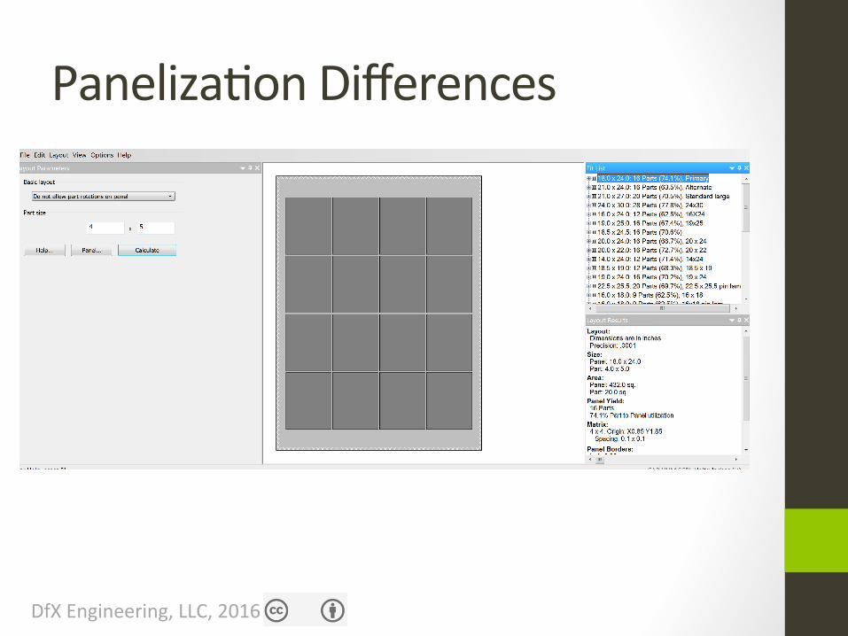
PanelizaIonDifferences
DfXEngineering,LLC,2016

PanelizaIonDifferences
DfXEngineering,LLC,2016

PanelizaIonDifferences
DfXEngineering,LLC,2016

PROCESSPARAMETERSELECTIONOpImizefeaturesforthecenternotthelimit

ReferencePlaneSelecIon
S
P
S
P
S
Split
RP
P
SelecIngtherightreferenceplanearrangementcanopImizefeaturesize.ConsiderreferenceplanestwolayersawayorlowerDkMaterialselecIontoimprovefeaturesize.Otherimportantstack-upconsideraIonsforbestmanufacturingcostare:• Balancedcoppercores• Goodref.distanceforL/W
OpIzaIon• ReducevariaIoninpre-preg
selecIontoavoidlayuperroryeildimpact.
DfXEngineering,LLC,2016

BOMCostAnalysis
DFM/DFCanalysiswillbreakdowneverylayerinthestack-upforcomparaIvecostanalysis.GlassStyle,coreconstrucIonandresincontentwillhavecostimpactontheBOMcost.CostfactorsdynamicallyadjustbasedonuseoverImeandnewmarketentrantslike1037,1027glasswillchangepricebasedonusage,soneedtomaintainconInualupdatesforImelycosInginyourmodel.
Pre-preg FR4
Cost index %
1078/1086 1.2
1080 1,0
1067 1.75
106 2.35
2116 1.20
1501/1506 1.65
3313/2113 1.55
7628 1.25
DfXEngineering,LLC,2016
*Pricesshownareexamplesonlyandneedtobeupdatedtospecificcircumstances

HDIvs.ConvenIonal
Inner Lam Drill PlateOuterEtchSES
SM/Finish Test
ConvenIonal
HDI
Inner Lam Drill PlateOuterEtchSES
Plate/Cufill SM/Finish TestLam LaserDrill
OuterEtchSES
Repeatfornumberofbuilduplayers
Inlowerlayercountboards,materialcanbe30-45%ofcostleavingthemajorityofpriceforprocessingcostandOH.HDIaddssignificantcriIcalsteps.AnalysisonBOMcostsavingsandfeaturesizeshouldbereviewedwhenselecIngHDI,targettosaveatleast2coresreducIonintotallayersorifdevicepitchabsolutelyrequiresitforrouIng.
DfXEngineering,LLC,2016

DeviceSelecIon
0.4mmPitch,0.0157”0.5mmPitch,0.0196”0.6mmPitch,0.0236”
MicroVia–HoleSize.004,Pad.010”,Copperfilledtogetfull.010padareaforsolderassembly.
.0057”rouIngSpace=1TrackrouIng48umat(0.0019”)traceandspace.0096”rouIngSpace=1TrackrouIngat75um.013”rouIngSpace=2TrackrouIngat65um
BestAspectRaIoonMVis1:1somaxdielectriconouterlayeris.004”.IfConvenIonaldrillingsmallestdrillis.008”andwillneed.018”padsize
DfXEngineering,LLC,2016

RouIngGuidelines
Source:HDIHandbook
DfXEngineering,LLC,2016

DecisionTreeForDesignChoices
FeatureSize 1.0Cpk 1.3Cpk 2.0Cpk
Linewidth(HDILayer)
45um 53um 63um
LineSpace 55um 65um 70um
AspectRaIo 0.9:1 0.8:1
Min.MechDrillSize
0.15mm(.006”)
0.20mm(.008”)
0.25mm(.010”)
MinCapturePadHDI
150um 180um 220um
MinCapturePadSTD
D+8 D+8 D+10
1:1
Understandthecri+calchangeoverpointsatyourfabrica+onsite
DfXEngineering,LLC,2016

CpkFeatureAnalysis
AllcriIcalfeaturesshouldbestaIsIcallyanalyzedandreviewedtoensureyieldperformanceismaximizedreducingoverallprocesscostandprovidinglongtermcostreducIonopportuniIes.
DfXEngineering,LLC,2016

SurfaceFinishConsideraIons
SurfaceFinish Cost Considera+ons Benefits
OSP 1 ShelfLifeLimits Flatness,easeofuse
ENIG 1.1 ProcessControls ConducIvity,flatness
ImmersionSilver 1.05 Environmental Cost,Flatness
ImmersionTin 1.2 Capacity Flatness
LFHASL 1.4 Capacity,Uniformity
Robust
ElectroplatedGold
2.0 BussScheme,Minimizearea
Bondability,Compressioncontacts
MajorConsideraIons:Assemblysitefamiliarity.Avoiddualsurfacefinish,compoundedeffectofcost,maskinganddefectrisk.
DfXEngineering,LLC,2016

PROCESSOVERVIEWFlowChartforcostopImizaIon

ProcessOverview
StartwithInterconnect
budget
ReviewmaterialselecIonfortype
andsizeopImizaIon
OpImizestack-upforBOMcost
OpImizefeaturesizeforCpkmanagement
andConstrucIontype
ReviewFuncIonsinagivenboard
design
DfXEngineering,LLC,2016

ProcessCostDriverDecisions• AddiIonalLaminaIonsversusaddiIonallayers• DrillSizeversusPadsizeopImizaIon• PadSizeversusTraceSizeopImizaIon• Movefinerlinestoinnernon-platedlayers• Doyouneedboththroughandmicrovias?Microviacountscanbeincreasedwithoutcostimpact.AvoidaddiIonalplaIngsteps.
• StackedorStaggeredVias(Filledornot)• MatchedGlassStylestoreduceLayupError,IncreaseEconomyofScale
DfXEngineering,LLC,2016

HIGHCOSTCHOICESPerformance,Dkandsize

HighCostChoices• VIPPO–AddiIonalStepsEpoxyFill,PlanarizaIon,DualplaIngpasses,masking
MulIpledrillingpassesforfilledandnon-filledholes.• SignalintegrityBenefits(NoDogbone),AssemblyLandIncrease,SupportedVia
withmaterialthatexpandsatsamerate.
TakecarefulconsideraIononadopIngthesedesignchoicesduetotheimpactoncost.AnalyzeandquanIfythebenefittojusIfythecost.
DfXEngineering,LLC,2016

HDITypesExplained
Source:HDIHandbookDfXEngineering,LLC,2016
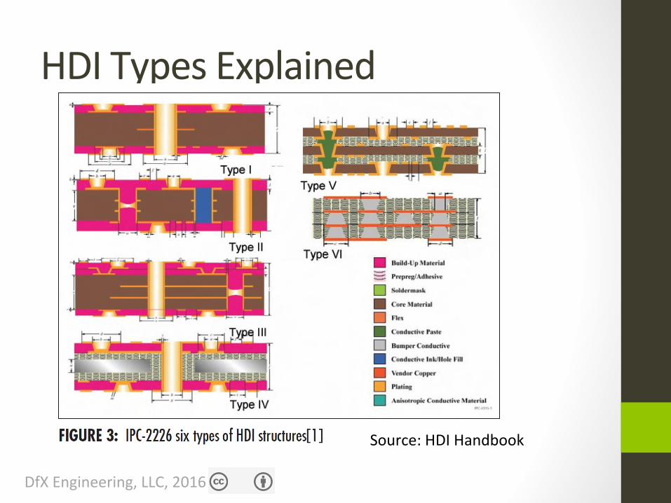
HDITypesExplained
DfXEngineering,LLC,2016
Source:HDIHandbook
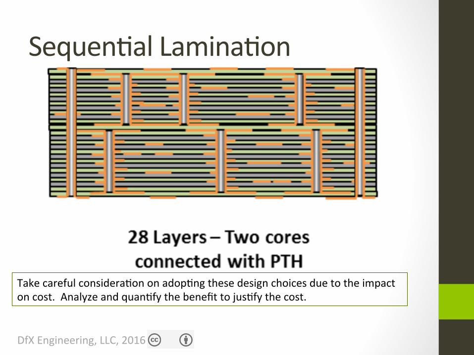
SequenIalLaminaIon
TakecarefulconsideraIononadopIngthesedesignchoicesduetotheimpactoncost.AnalyzeandquanIfythebenefittojusIfythecost.
DfXEngineering,LLC,2016

Back-Drilling
TakecarefulconsideraIononadopIngthesedesignchoicesduetotheimpactoncost.AnalyzeandquanIfythebenefittojusIfythecost.
DfXEngineering,LLC,2016

ProcessOverviewCostAdderimpactfromDesignChoices
DesignChoice AddedProcesses ApproximateCost
FactoronMFGcost
AddiIonalSTDLayer InnerLayerProcessing,RegistraIonBudget
8%
AddiIonalHDILayer AddiIonal,Lam,Laser,Plate
20%
DualSurfaceFinish Mask,Strip,Coat 15%(plusmetalareaCaclulaIon)
VIPPO EpoxyFill,PlanarizaIon,PlaIng
30%
SequenIalLaminaIon ThreeLaminaIonCyclesRegistraIon
50%
BackDrilling Drilling,Alignment,Cleaning
15%(basedonholecount)
DfXEngineering,LLC,2016