VLSI DesignV S es gLecture 12: Transistor Sizingg
ShaahinShaahin HessabiHessabiShaahinShaahin HessabiHessabiDepartment of Computer EngineeringDepartment of Computer Engineering
Sh if U i it f T h lSh if U i it f T h lSharif University of TechnologySharif University of TechnologyAdapted, with modifications, from Adapted, with modifications, from lecture notes prepared lecture notes prepared by by the the
book’s book’s author author (from Prentice Hall PTR)(from Prentice Hall PTR)
Modern VLSI Design 4e: Chapter 4 Sharif University of Technology Slide 1 of 26
Topics
Transistor sizing:Spice analysis.Logical effort.
Modern VLSI Design 4e: Chapter 4 Sharif University of Technology Slide 2 of 26
Transistor sizing
Not all gates need to have the same delay. Not all inputs to a gate need to have the same delay. Adjust transistor sizes to achieve desired delay Adjust transistor sizes to achieve desired delay.
Modern VLSI Design 4e: Chapter 4 Sharif University of Technology Slide 3 of 26
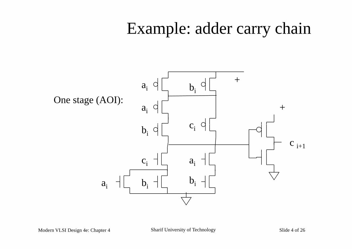
Example: adder carry chain
+ai bi( )
+ai
c
One stage (AOI):
cibic i+1
ci
b
ai
bbibiai
Modern VLSI Design 4e: Chapter 4 Sharif University of Technology Slide 4 of 26
Carry chain optimization
Connect four stages. Optimize delay through carry chain by selecting
transistor sizes.
Modern VLSI Design 4e: Chapter 4 Sharif University of Technology Slide 5 of 26
Case 1
W/L (in terms of , and not ) for all stages: nmos = 270/180 nm, W/ ( te s o , a d ot ) o a stages: os 70/ 80 ,pmos = 540/180 nm
Modern VLSI Design 4e: Chapter 4 Sharif University of Technology Slide 6 of 26
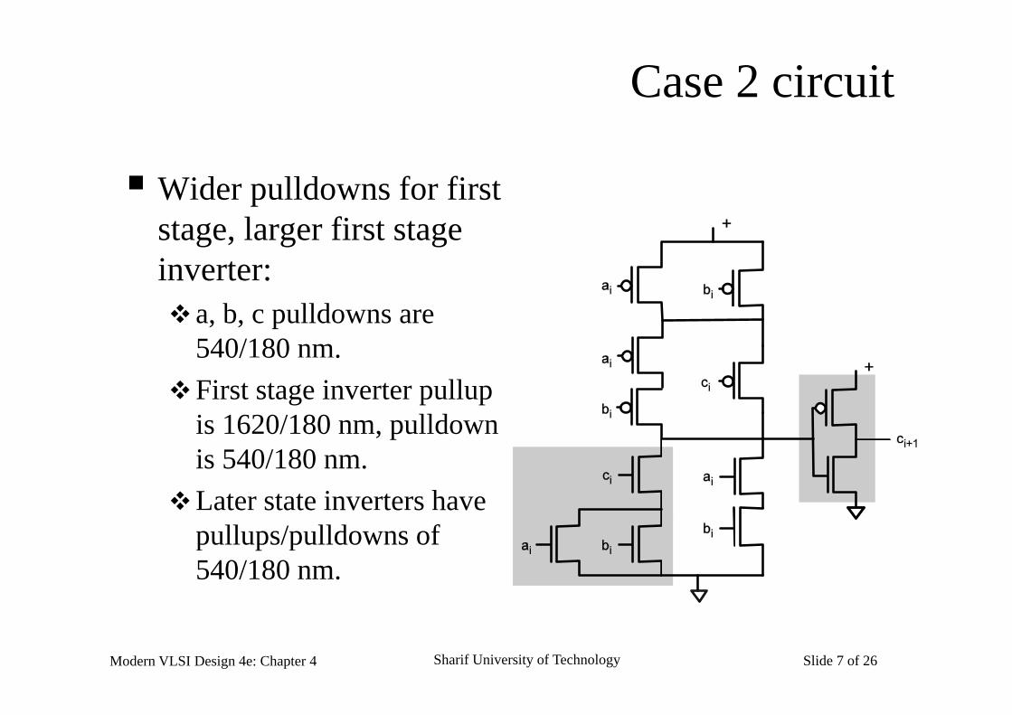
Case 2 circuit
Wider pulldowns for firstWider pulldowns for first stage, larger first stage inverter:inverter: a, b, c pulldowns are
540/180 nm.5 0/ 80 .First stage inverter pullup
is 1620/180 nm, pulldownpis 540/180 nm.
Later state inverters have pullups/pulldowns of 540/180 nm.
Modern VLSI Design 4e: Chapter 4 Sharif University of Technology Slide 7 of 26
Case 2
Modern VLSI Design 4e: Chapter 4 Sharif University of Technology Slide 8 of 26
Case 3 circuit
a b pulldowns are 270/180 nm a, b pulldowns are 270/180 nm. c pulldown is 1080/180 nm. First stage inverter pullup is 1620/180 nm, pulldown
is 540/180 nm. Later stage inverters have pullups of 1080/180 nm,
pulldowns of 540/180 nm.p
Modern VLSI Design 4e: Chapter 4 Sharif University of Technology Slide 9 of 26
Case 3
Modern VLSI Design 4e: Chapter 4 Sharif University of Technology Slide 10 of 26
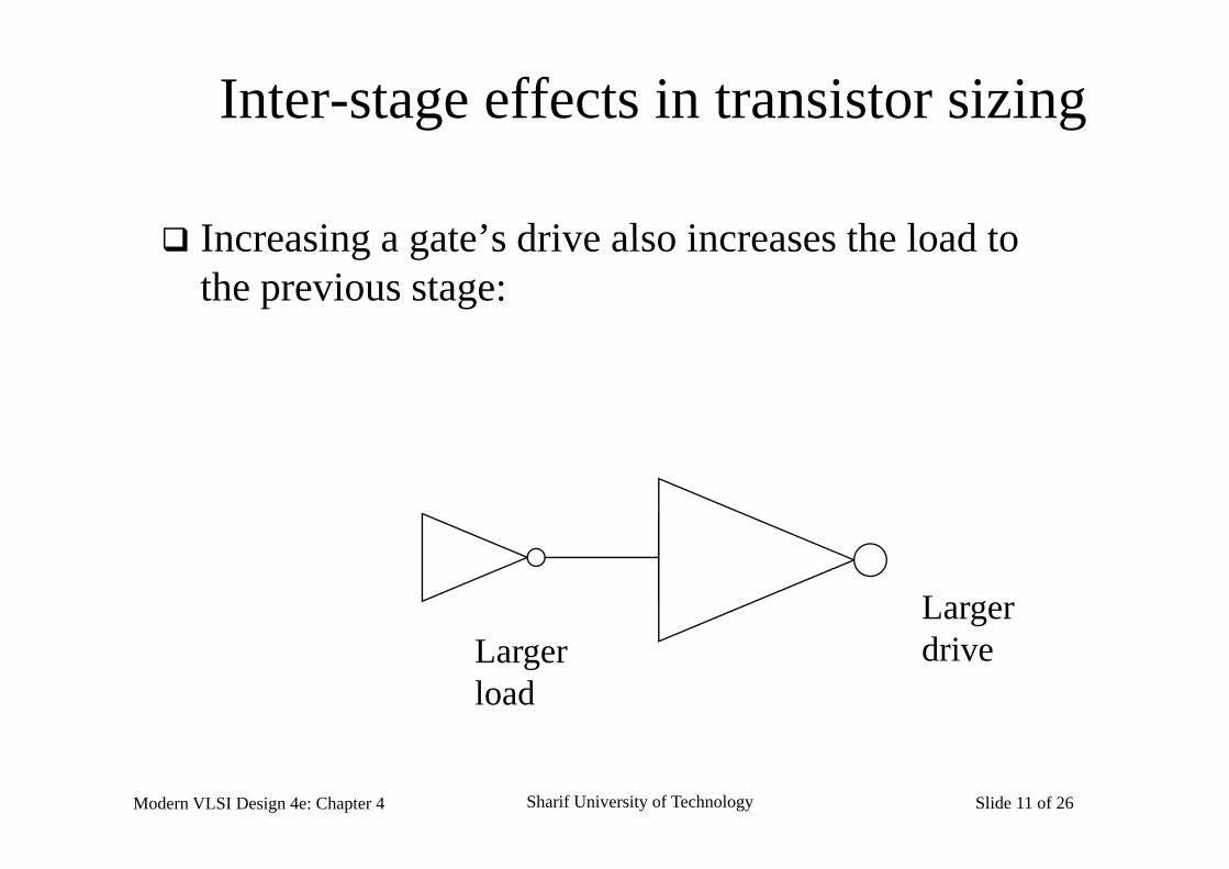
Inter-stage effects in transistor sizing
Increasing a gate’s drive also increases the load to Increasing a gate s drive also increases the load to the previous stage:
LargerdriveLarger
load
Modern VLSI Design 4e: Chapter 4 Sharif University of Technology Slide 11 of 26
Logical effort
Logical effort is a gate delay model that takes transistor sizes into account.
Allows us to optimize transistor sizes over pcombinational networks. Isn’t as accurate for circuits with reconvergent fanout.g
Modern VLSI Design 4e: Chapter 4 Sharif University of Technology Slide 12 of 26
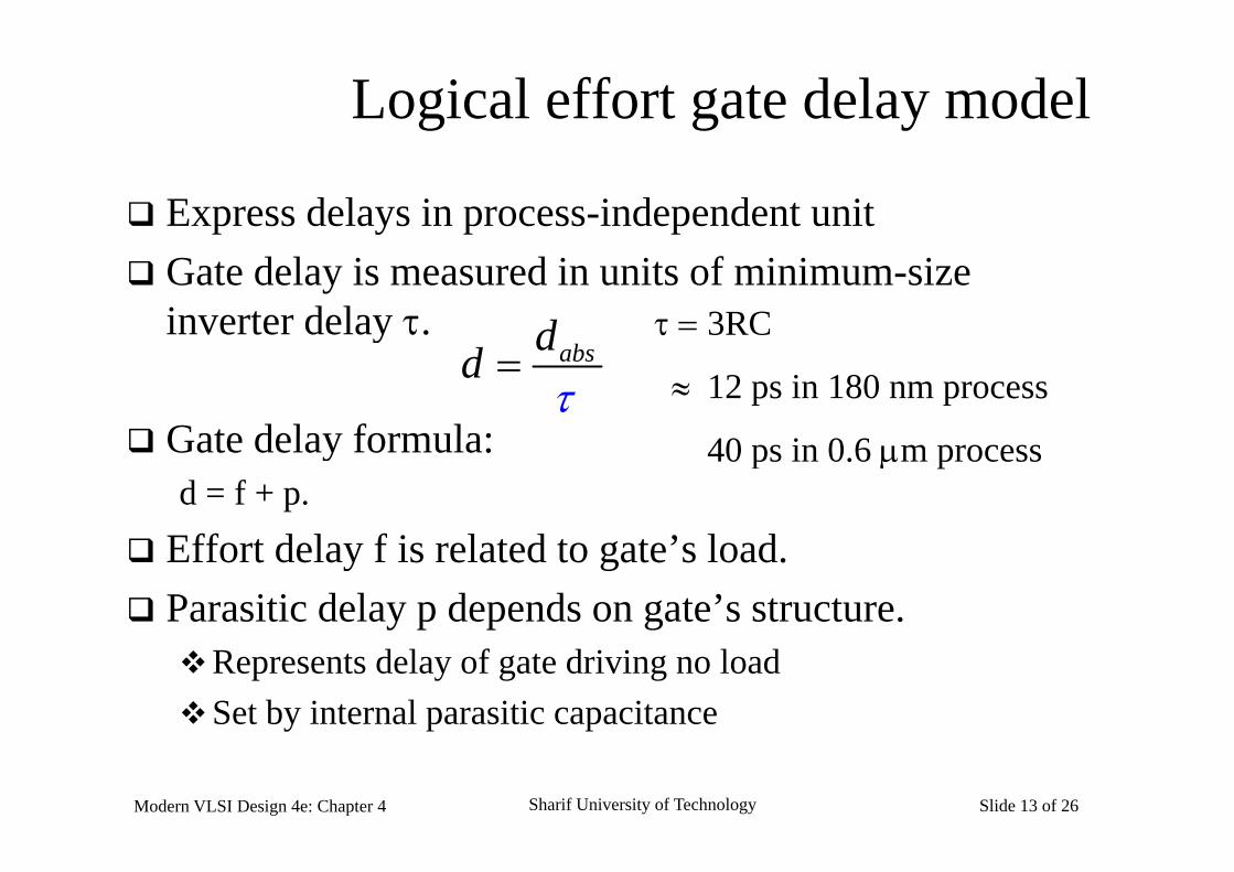
Logical effort gate delay model
Express delays in process-independent unit Gate delay is measured in units of minimum-size
inverter delay . d 3RC y
Gate delay formula:
absdd
12 ps in 180 nm process Gate delay formula:
d = f + p.
Eff d l f i l d ’ l d
40 ps in 0.6 m process
Effort delay f is related to gate’s load. Parasitic delay p depends on gate’s structure.Represents delay of gate driving no loadSet by internal parasitic capacitance
Modern VLSI Design 4e: Chapter 4 Sharif University of Technology Slide 13 of 26

Effort delay
Effort delay has two components: f = gh.
Electrical effort h is determined by gate’s load:y gh = Cout/Cin
Sometimes called fanoutSometimes called fanout
Logical effort g is determined by gate’s structure.Measures relative ability of gate to deliver currentMeasures relative ability of gate to deliver currentg 1 for inverter
Modern VLSI Design 4e: Chapter 4 Sharif University of Technology Slide 14 of 26
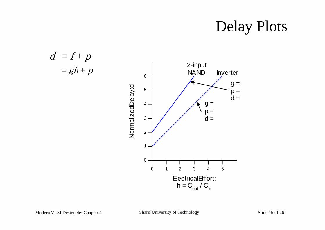
Delay Plots
d = f + p2 i t
= gh + p
: d
Inverter2-inputNAND
g =5
6
zed D
elay
g =p =
p =d =
4
5
Nor
mal
iz d =
2
3
0 1 2 3 4 5
0
1
Electrical Effort:h = Cout / Cin
0 1 2 3 4 5
Modern VLSI Design 4e: Chapter 4 Sharif University of Technology Slide 15 of 26
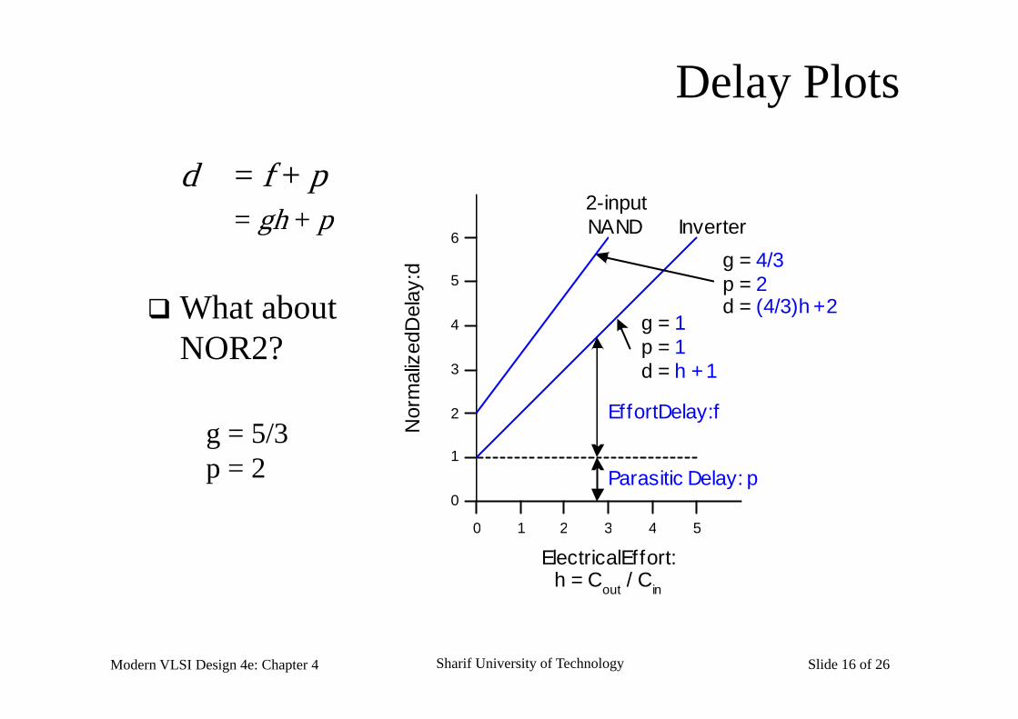
Delay Plots
d = f + p2 i t
= gh + p
: d
Inverter2-inputNAND
g = 4/325
6
What about NOR2? ze
d Del
ay
g = 1p = 1
p = 2d = (4/3)h + 2
4
5
O
Nor
mal
iz d = h + 1
Effort Delay: f2
3
g = 5/3Parasitic Delay: p
0 1 2 3 4 5
0
1g 5/3p = 2
Electrical Effort:h = Cout / Cin
0 1 2 3 4 5
Modern VLSI Design 4e: Chapter 4 Sharif University of Technology Slide 16 of 26
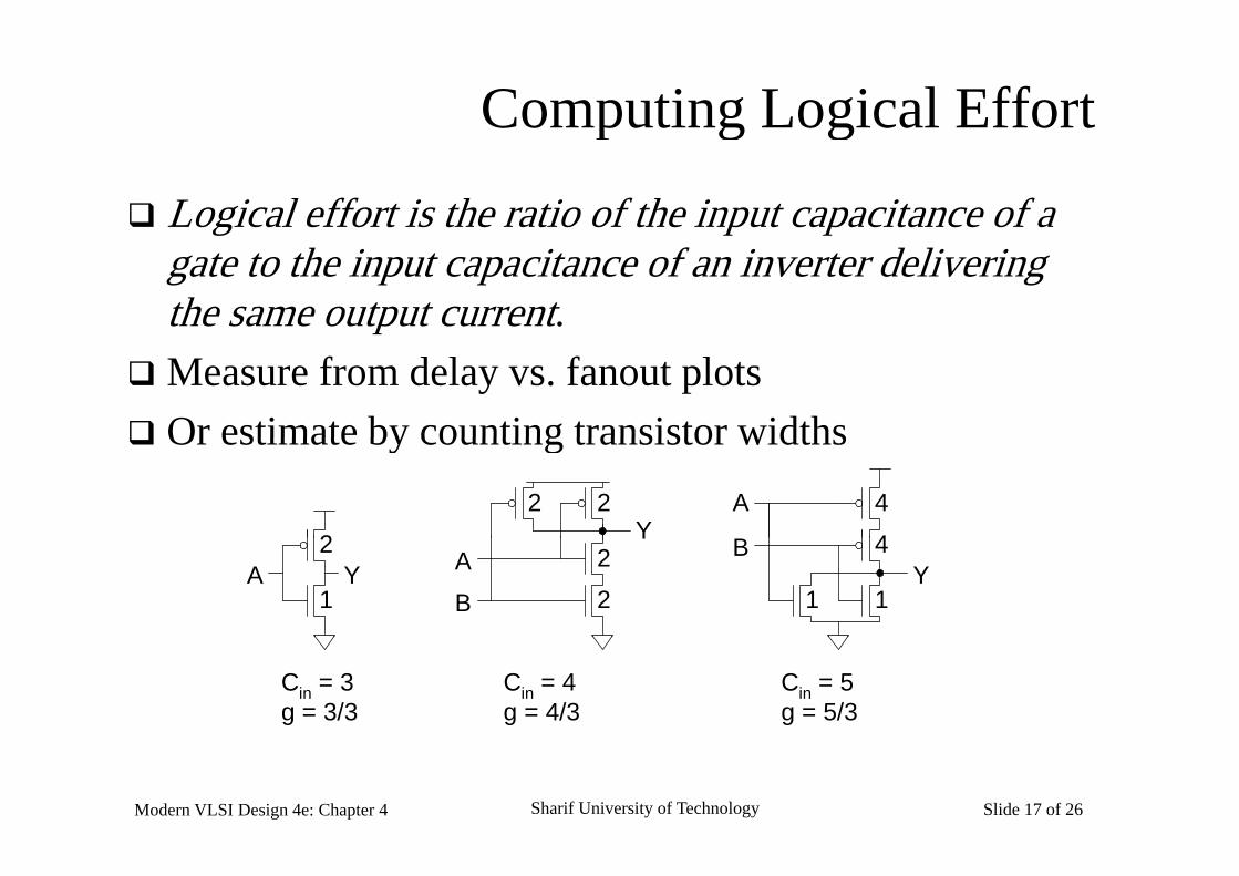
Computing Logical Effortp g g
Logical effort is the ratio of the input capacitance of a gate to the input capacitance of an inverter delivering the same output current.
Measure from delay vs. fanout plots Or estimate by counting transistor widths Or estimate by counting transistor widths
YA
2
2 2
4
4
A Y A
B
YB
Y1
2
1 1
2
2
4
Cin = 3g = 3/3
Cin = 4g = 4/3
Cin = 5g = 5/3
Modern VLSI Design 4e: Chapter 4 Sharif University of Technology Slide 17 of 26
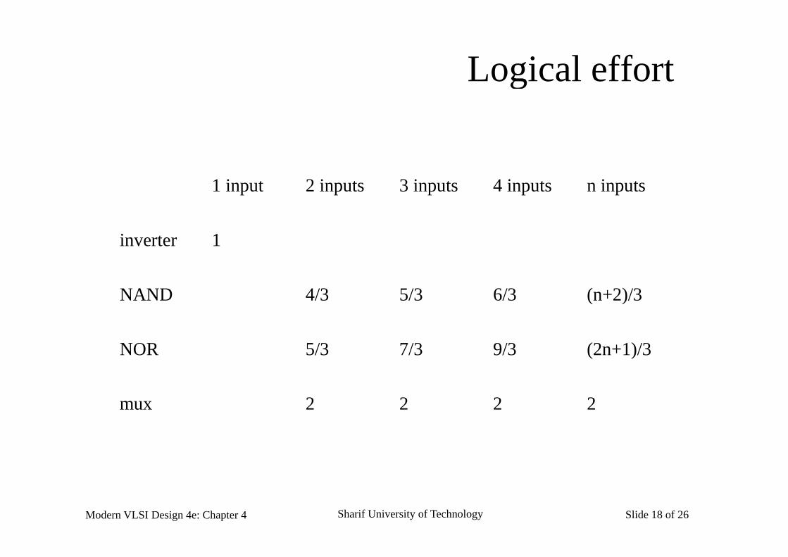
Logical effortg
1 input 2 inputs 3 inputs 4 inputs n inputs
inverter 1
NAND 4/3 5/3 6/3 (n+2)/3
NOR 5/3 7/3 9/3 (2n+1)/3
mux 2 2 2 2mux 2 2 2 2
Modern VLSI Design 4e: Chapter 4 Sharif University of Technology Slide 18 of 26
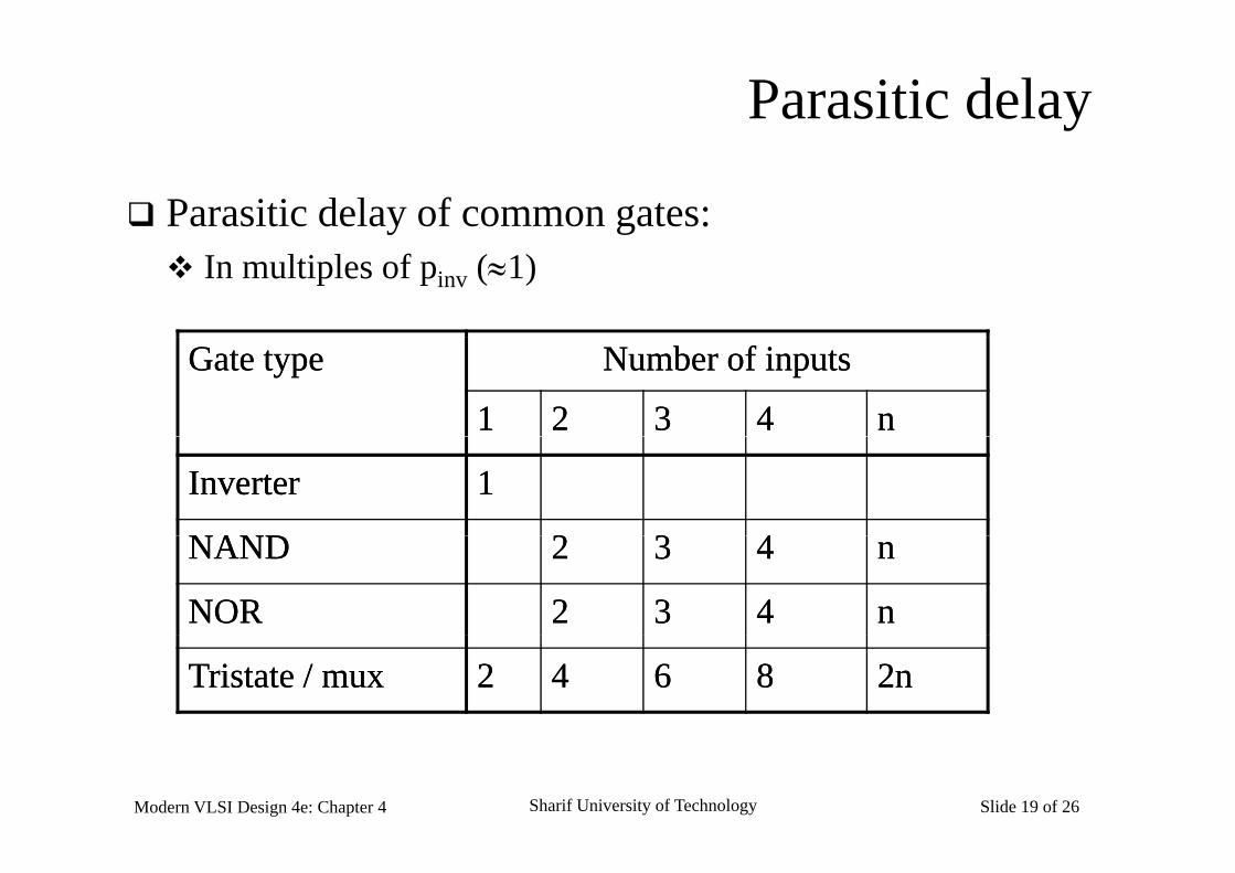
Parasitic delay
Parasitic delay of common gates: In multiples of pinv (1)
Gate typeGate type Number of inputsNumber of inputs
11 22 33 44 nn
InverterInverter 11
NANDNAND 22 33 44NANDNAND 22 33 44 nn
NORNOR 22 33 44 nn
Tristate / muxTristate / mux 22 44 66 88 22nn
Modern VLSI Design 4e: Chapter 4 Sharif University of Technology Slide 19 of 26
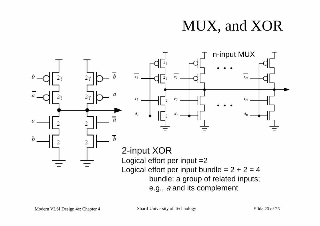
MUX, and XOR
n-input MUX
2-input XORLogical effort per input =2g p pLogical effort per input bundle = 2 + 2 = 4
bundle: a group of related inputs; e.g., a and its complement
Modern VLSI Design 4e: Chapter 4 Sharif University of Technology Slide 20 of 26
e.g., a and its complement
Logical effort along a path
Logical effort along a chain of gates:G = gi
Total electrical effort along path depends on ratio of g p pfirst and last stage capacitances:H = Cout/CinH Cout/Cin
Modern VLSI Design 4e: Chapter 4 Sharif University of Technology Slide 21 of 26
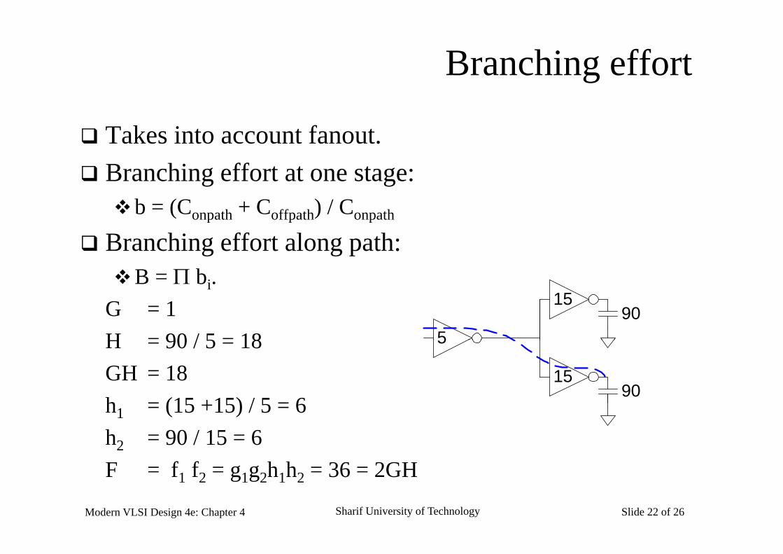
Branching effort
Takes into account fanout. Branching effort at one stage:b = (Conpath + Coffpath) / Conpathb (Conpath Coffpath) / Conpath
Branching effort along path:B = bB = bi.
G = 1H = 90 / 5 = 18 5
1590
H = 90 / 5 = 18GH = 18h (15 +15) / 5 6
5
1590
h1 = (15 +15) / 5 = 6h2 = 90 / 15 = 6F f f h h 36 2GH
Modern VLSI Design 4e: Chapter 4 Sharif University of Technology Slide 22 of 26
F = f1 f2 = g1g2h1h2 = 36 = 2GH
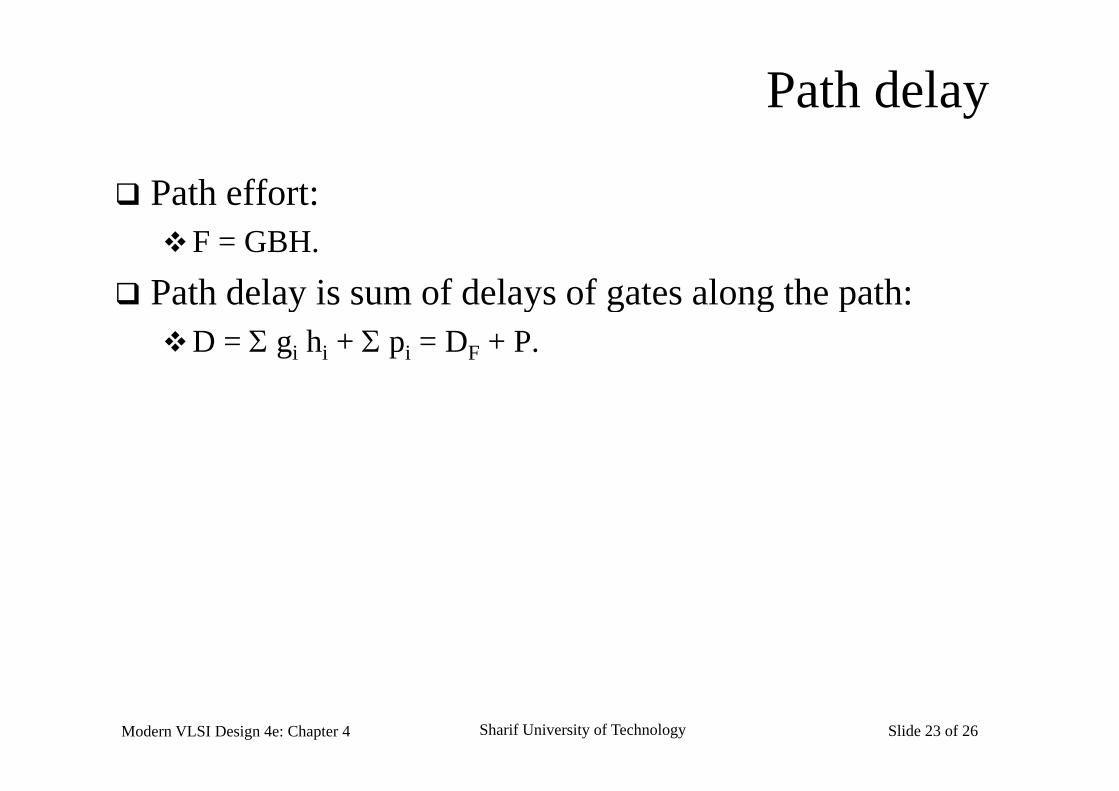
Path delay
Path effort:F = GBH.
Path delay is sum of delays of gates along the path:y y g g pD = gi hi + pi = DF + P.
Modern VLSI Design 4e: Chapter 4 Sharif University of Technology Slide 23 of 26
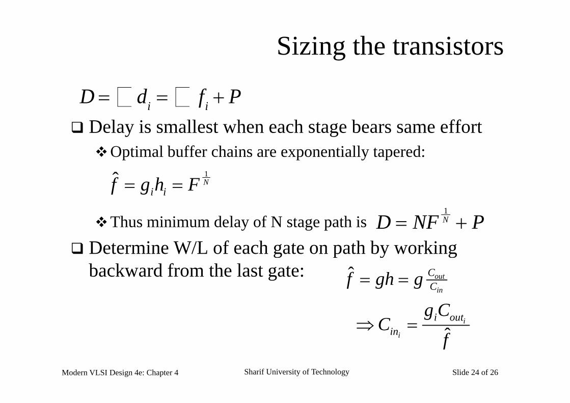
Sizing the transistors
D di fi P Delay is smallest when each stage bears same effortOptimal buffer chains are exponentially tapered:
i i
Optimal buffer chains are exponentially tapered:1ˆ N
i if g h F
Thus minimum delay of N stage path is
Determine W/L of each gate on path by working
1ND NF P
Determine W/L of each gate on path by working backward from the last gate: ˆ out
in
CCf gh g
ˆi
i
i outin
g CC
f
Modern VLSI Design 4e: Chapter 4 Sharif University of Technology Slide 24 of 26
f
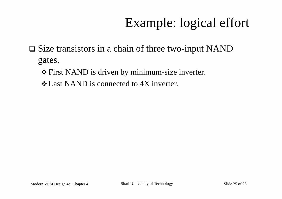
Example: logical effort
Size transistors in a chain of three two-input NAND gates.First NAND is driven by minimum-size inverter.Last NAND is connected to 4X inverter.
Modern VLSI Design 4e: Chapter 4 Sharif University of Technology Slide 25 of 26
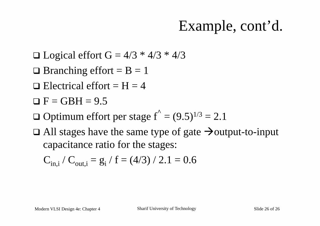
Example, cont’d.
Logical effort G = 4/3 * 4/3 * 4/3 Branching effort = B = 1 Electrical effort = H = 4 Electrical effort H 4 F = GBH = 9.5
O i ff f^ (9 5)1/3 2 1 Optimum effort per stage f = (9.5)1/3 = 2.1 All stages have the same type of gate output-to-input
capacitance ratio for the stages:Cin i / Cout i = gi / f = (4/3) / 2.1 = 0.6in,i out,i gi ( )
Modern VLSI Design 4e: Chapter 4 Sharif University of Technology Slide 26 of 26
Recommended