University of Toronto Department of Electrical and Computer Engineering
VLSI Design Methodology ECE1388F
Design Project 8-bit Self-timed Programmable Counter
University of Toronto Electronics Group Toronto, Ontario
Prepared By: Name: Ricky Yuen (ryuen@eecg)
Student ID: 971339500 Date: December 4, 2002

Table of Contents Table of Contents............................................................................................................................ ii List of Figures ................................................................................................................................ iii List of Tables ................................................................................................................................. iii 1.0 Introduction......................................................................................................................... 1 2.0 Specifications...................................................................................................................... 1 3.0 Circuit Design ..................................................................................................................... 2 4.0 Behavioural Level Simulation ............................................................................................ 3 5.0 Design Synthesis and Optimization .................................................................................... 4 6.0 Gate Level Simulation ........................................................................................................ 6 7.0 Importing to Cadence.......................................................................................................... 7 8.0 Layout Generation .............................................................................................................. 7 9.0 HSPICE Simulation ............................................................................................................ 9 10.0 LVS................................................................................................................................... 12 11.0 Conclusions....................................................................................................................... 12 12.0 References......................................................................................................................... 14 Appendix A: 8-bit Programmable Counter VHDL Code ............................................................. 15 Appendix B: 8-bit Programmable Counter Test Bench................................................................ 24 Appendix C: DRC evidence from Cadence .................................................................................. 27 Appendix D: Extraction Evidence from Cadence......................................................................... 29 Appendix E: Enlarged 8-bit Programmable Counter Circuit with Critical Path Highlighted ...... 31 Appendix F: Design Synthesis and Optimization Evidence ......................................................... 32 Appendix G: LVS Evidence from Cadence.................................................................................. 36
ii

List of Figures Figure 3-1 8-bit self-timed programmable counter......................................................................... 2 Figure 4-1 Behavioural simulation that shows reset and idle operations. ...................................... 3 Figure 4-2 Behavioural simulation that shows counting overflow................................................. 4 Figure 5-1 Schematic of Manchester stage after synthesis. ............................................................ 4 Figure 5-2 Schematic of Manchester adder after synthesis. ........................................................... 5 Figure 5-3 Schematic of programmable counter after synthesis. ................................................... 5 Figure 5-4 The critical path of the programmable counter. ............................................................ 6 Figure 6-1 Gate level simulation that shows reset and idle operations........................................... 6 Figure 6-2 Gate level simulation that shows counting overflow. ................................................... 7 Figure 7-1 Imported Cadence schematic view of the programmable counter with surrounding
pads. ........................................................................................................................................ 7 Figure 8-1 Layout of the 8-bit programmable counter. .................................................................. 8 Figure 9-1 Test bench used in Cadence for post-layout simulation................................................ 9 Figure 9-2 HSPICE simulation that shows counting operation. ................................................... 10 Figure 9-3 HSPICE simulation that shows reset operation. ......................................................... 10 Figure 9-4 HSPICE simulation that shows idle operation. ........................................................... 11 Figure 9-5 HSPICE simulation that shows current consumption for reset and counting
operations.............................................................................................................................. 12
List of Tables Table 1 Counter command implementation.................................................................................... 1 Table 2 The ports of the programmable counter............................................................................. 1 Table 3 Table showing the data obtained from Synopsys Design Analyzer. ................................. 6 Table 4 Table showing the setup of the input signals. .................................................................... 9 Table 5 Table showing the data obtained from Synopsys Design Analyzer. ............................... 13 Table 6 Table showing delay calculation...................................................................................... 13
iii

1.0 Introduction This is the design project in the VLSI Design Methodology course, ECE1388F. The purpose of this assignment is to design an 8-bit, self-timed programmable counter in standard 0.35um CMOS technology. The goal is to maximize the speed but minimizing the power and circuit area.
2.0 Specifications In this assignment, 0.35um Complementary Metal Oxide Semiconductor (CMOS) process will be used. The 8-bit self-timed programmable counter is to be powered by a 3.3V voltage supply and assumes a load capacitance of 100fF. The counter has three operations, which is encoded by a 2-bit command line. The specification can be found in Table 1.
Table 1 Counter command implementation.
Instruction Command Operation
RESET 00 Count = 0
INC 01 Count = Count + 1
IDLE 10, 11 Count = Count
The command is only valid when the request line is at logic 1 and the output of the counter is only valid when the acknowledge line is at logic 1. The input and output port of the programmable counter can be found in Table 2.
Table 2 The ports of the programmable counter.
Port name Direction
request input
command [2] input
acknowledge output
output [8] output
1

3.0 Circuit Design The 8-bit programmable counter is designed in VHDL. The source code can be found in the Appendix of the report. The block diagram for the programmable counter is shown in Figure 3-1.
Figure 3-1 8-bit self-timed programmable counter.
The adder is implemented as a Manchester adder. It is made up of 8 Manchester stages as described in [3]. One of the inputs to the adder is grounded and the ‘1’/’0’ input is implemented as a carry-in to the adder. The carry-in bit is set to one only when command = “01”.
In the circuit design, the multiplexer (MUX) and the register are merged. The reason is that a single register made up of resettable D-flip-flops can represent the logic. When the all zero input is selected from the MUX, it is equivalent to resetting the register.
The clock for the register is generated from the adderDone signal. When the adder finishes is dependent on the operand of the adder. For example, if the input to the adder is “00000010”, the adder will finish adding when the LSB is equal to one. Another example, if the input to the adder is “00000001”, the adder will finish adding when the second bit is equal to 1. That is, the right most zero bit after a chain of consecutive ones indicates when the adder is finish. By using this idea, the register will
2

be clocked whenever the adder finishes adding. Since the overhead in looking at the 4th, 5th, 6th, 7th zero and Cout bit is too big, they will be replaced by a fixed delay chain.
Acknowledge signal is generated by multiplexing two signals, i.e., request and registerDone. The acknowledge signal is equal to request signal when command is equal to ‘idle’ and equal to registerDone when the command is equal to ‘reset’ or ‘increment’.
4.0 Behavioural Level Simulation After the VHDL for the programmable counter is finished, the behavioural level simulation is preformed with the Synopsys vhdlsim tool. Expected delays in the signals are explicitly specified in the VHDL code to emulate the real circuit. The simulation result showing the operation of the programmable counter is shown in Figure 4-1. The figure shows the counter begins counting at 00. After one increment, the counter is put on idle mode for two cycles. At 130ns, the counter is reset and the result of the counter corresponded to the operation as shown.
In the simulation, the command is only set to increment mode when the request signal is at 1 and will be set back to idle mode when the request signal is 0. This will show the true delay of the programmable counter because the adder will not start adding before the request signal comes. This is true for all the subsequent simulations.
Figure 4-1 Behavioural simulation that shows reset and idle operations.
Figure 4-2 illustrates the overflow of the programmable counter. At 10350ns, the counter reaches FF. The next request signal overflowed the counter back to 00 as shown.
3

Figure 4-2 Behavioural simulation that shows counting overflow.
5.0 Design Synthesis and Optimization After the behavioural level simulation has proven the design to be functional, the VHDL version of the programmable counter is synthesized with Synopsys Design Analyzer. The design is synthesized in blocks, inverters (delay element), Manchester stage, registers, etc. The synthesized building blocks are set to don’t touch before the top-level programmable counter is synthesized. This will preserve the hierarchical of the design. The synthesized version of the Manchester stage is shown in Figure 5-1.
Figure 5-1 Schematic of Manchester stage after synthesis.
Eight of the Manchester stage shown in Figure 5-1 is cascaded into an 8-bit Manchester adder. The synthesis operation does nothing but just do the cascading because the Manchester stage are set to don’t touch. The Manchester adder schematic can be found in Figure 5-2.
4

Figure 5-2 Schematic of Manchester adder after synthesis.
The registers are made up of 8 resettable D-Flip-flop from the 0.35um CMOS standard cells. The top-level programmable counter is synthesized with all components set to don’t touch. The resultant schematic is shown in Figure 5-3. The long chain of small rectangles is the delay chain made up of inverters.
Figure 5-3 Schematic of programmable counter after synthesis.
The critical path (longest delay) of the programmable counter is analyzed by Synopsys and it is highlighted in Figure 5-4. It starts from the command input and ends at the acknowledge output. An enlarged version of the critical path diagram and the details about the analysis can be found in the Appendix.
5

Figure 5-4 The critical path of the programmable counter.
Table 3 shows the timing and area analysis obtained from Synopsys Design Analyzer. The critical path delay is 4.06ns and the total core area is 22538 um2.
Table 3 Table showing the data obtained from Synopsys Design Analyzer.
Analysis Value command[1] acknowledge (Critical Path) 4.06 ns Core Area 22538 um2
6.0 Gate Level Simulation The synthesized design is exported to a gate level VHDL file. The gate level design includes the true gate delay data from the 0.35um standard cells. The VHDL file is re-simulated with vhdlsim tool. The result is shown in Figure 6-1 and Figure 6-2. The gate level simulation is not successful in the first few trials due to delay of the logics in the design. Therefore, timing adjustments are made in each simulation. The acknowledge signal is tuned such that it only rises after the register output is settled.
Figure 6-1 Gate level simulation that shows reset and idle operations.
Again, in this simulation, the command line is set to idle mode when the request signal is at 0 to show the worst-case delay of the programmable counter.
6

Figure 6-2 Gate level simulation that shows counting overflow.
7.0 Importing to Cadence The synthesized design from Synopsys Design Analyzer is exported to a Verilog netlist and it is imported to Cadence. Since the Verilog file already has the IO pads included, it is impossible to generate the counter symbol with surrounding pads view as requested. Instead, the schematic of the imported programmable counter with the IO pads on the same level is shown in Figure 7-1. The square boxes at the right of the figure are the IO pads for the programmable counter.
Figure 7-1 Imported Cadence schematic view of the programmable counter with surrounding pads.
8.0 Layout Generation
After the design has proven to be functional by the gate level simulation, it is imported in the Silicon Ensemble tool for automatic layout generation. In the floor planning stage, the die size is limited to 1700um×1700um and the IO to core distance is increased to 260um for both the left/right and top/bottom. The resultant core utilization is increased to 80% to minimize the core area of the layout. The result of the layout is shown in Figure 8-1.
The DEF file from Silicon Ensemble is imported into Cadence for further verification. The abstract view is first converted to layout view. Design Rule Check (DRC) is preformed on the layout view. There are 2 types of errors that showed up. First, it complains about the nWell spacing is less than 1.00um, for example,
7

“48 NW.S.2 nwell spacing < 1.00”.
This error occurred at the IO pads area, and it is fixed by putting a layer of nWell to merge the separated nWell layers. Another type of error that showed up is related to the hot nWell, for example,
“850 OD.C.3 ndiff spacing to hot nwell < 2.60”.
It is fixed by putting VDD and VSS pins on the layout. At the end, the DRC is clean with no errors. The evident for the DRC can be found in the Appendix of the report.
Figure 8-1 Layout of the 8-bit programmable counter.
8

9.0 HSPICE Simulation After the DRC has been cleared the layout is extracted with parasitics. The extracted view is put into a test bench to perform post-layout simulation. The schematic for the test bench is shown in Figure 9-1. A typical load of 100fF is put at the output to emulate the real life situation. The request and command signal are driven by square pulse sources. Their setup is shown in Table 4 below.
Table 4 Table showing the setup of the input signals.
Source Voltage1 (V)
Voltage2 (V)
Delay (ns) Rise / Fall Time (ps)
Pulse Width (ns)
Period (ns)
Request 0.0 3.3 5 100 10 20 Command0 0.0 3.3 15 100 10 20 Command1 0.0 3.3 25 100 10 20
The setup of the input signals is made such that it resets the programmable counter in the first operation. Then, it will do an increment operation whenever the request signal is 1 and will go back to idle mode when the request signal is 0. This is consistent with the behavioural and gate level simulation as described before.
Figure 9-1 Test bench used in Cadence for post-layout simulation.
9

Figure 9-2 showed the normal counting operation of the programmable counter. Their delay is measured; however, it is too small to be shown on the diagram.
Figure 9-2 HSPICE simulation that shows counting operation.
Figure 9-3 shows the reset operation with the programmable counter. The delay associated with the delay operation is also measured to be about 4.3ns.
Figure 9-3 HSPICE simulation that shows reset operation.
10
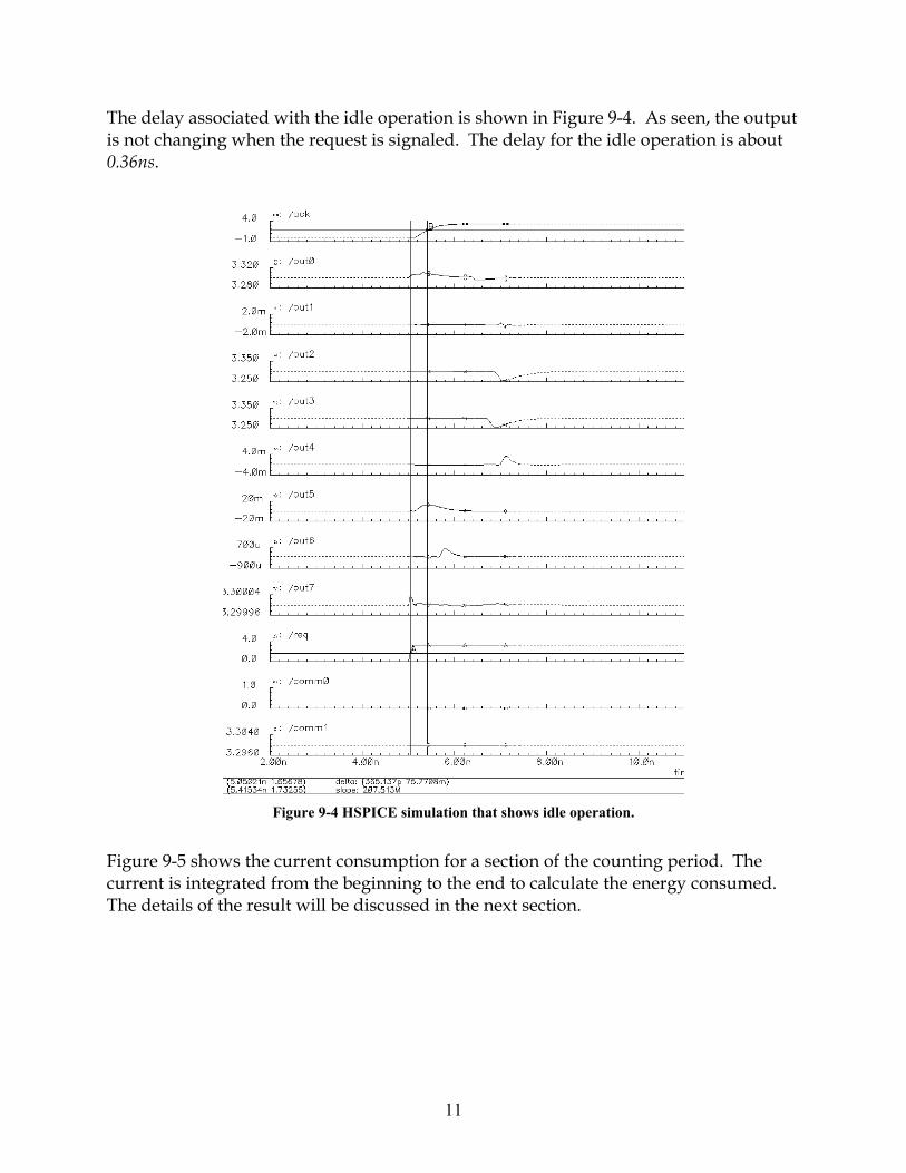
The delay associated with the idle operation is shown in Figure 9-4. As seen, the output is not changing when the request is signaled. The delay for the idle operation is about 0.36ns.
Figure 9-4 HSPICE simulation that shows idle operation.
Figure 9-5 shows the current consumption for a section of the counting period. The current is integrated from the beginning to the end to calculate the energy consumed. The details of the result will be discussed in the next section.
11

Figure 9-5 HSPICE simulation that shows current consumption for reset and counting operations.
10.0 LVS There are unsolvable problems occurred when performing LVS. Effort is made to try to resolve them; however, since there is no resolution posted, time is spent on other parts of the project. The error file for the LVS can be found in the Appendix. The post-layout simulation explained in previous section is another way to prove that the circuit is functional correctly.
11.0 Conclusions An 8-bit programmable counter is designed in VHDL. The design goes through behavioural, synthesis, and gate level simulation. The layout of the programmable counter is done by Silicon Ensemble. Post layout simulation is done in Cadence to verify the functionality of the design. The final performance specification can be seen below.
The test vectors are the same as the one used in behavioural, gate and HSPICE simulation. First, the counter is reset, and then it is allowed to count from 00 to FF and did the overflow operation. For the HSPICE simulation, a separate simulation is done on the idle operation. The programmable counter does not have a test vector that has command = increment while request signal is low; thus, the worst-case delay is simulated.
12

Design Analyzer:
Table 5 Table showing the data obtained from Synopsys Design Analyzer.
Analysis Value command[1] acknowledge (Critical Path) 4.06 ns Core Area 22538 um2
Cadence: The average delay calculation is calculated by measuring the first 25 transitions. As described in the circuit design section of the report, the acknowledge signal has a variable delay that is dependent on the operand of the adder. So the average delay can be calculated by only measuring the first 25 transitions. The calculation is shown in Table 6. The ‘x’ means don’t care. For example, ‘xxxxxx01’ can mean ‘10101001’ or ‘11111101’, etc, so it only looks at the second LSB of the operand. The count column shows the number of counting events that correspond to that particular transition type. The average counting delay is calculated to be 3.67ns. The delay associated with reset operation is 4.3ns and the delay associated with idle operation is 0.36ns.
Table 6 Table showing delay calculation.
Transition Delay (ns) Count xxxxxxx0 xxxxxxx1 3.32 128 xxxxxx01 xxxxxx10 3.75 64 xxxxx011 xxxxx100 4.18 32 xxxx0111 xxxx1000 4.6 16 xxx01111 xxx10000 Fixed delay
4.3 16
Average 3.67 Total = 256 The area of the design is measured in Cadence by measuring the layout of the programmable counter. By excluding the pads, the area of the design is 355um x 351um.
The energy of the design is measured by integrating the current consumption, shown in Figure 9-5 , in the simulation from 00 FF. The result is multiply by 3.3V to get the total energy consumed. The energy per counting event is calculated by dividing the total energy consumed by 256 (the number of counting events). The energy per counting event is calculated to be 0.148nJ.
13

Energy.Delay.Area product from Synopsys is equal to
22 6.135422253806.4148.0 umnsnJumnsnJ ••=××
Energy.Delay.Area product from Cadence is equal to
22 4.6768012460567.3148.0 umnsnJumnsnJ ••=××
The reason for such a difference is the area reported from Synopsys does not count the space for the power rings and the space required for place and route. Therefore, it is much less than the actual measured area from Cadence.
The design files are located at “/ali/r/r2/ryuen/ece1388f/project”.
12.0 References
1. Jan. M. Rabaey, Digital Integrated Circuits: A Design Perspective, Prentice Hall, United States of America, 1996.
2. VLSI User’s Manual 2002. 3. Weste and Eshraghian, Principles of CMOS VLSI Design, 2nd Edition, Addison Wesley,
United States of America, 1993.
14

Appendix A: 8-bit Programmable Counter VHDL Code library IEEE, wcells; use IEEE.std_logic_1164.all; use IEEE.std_logic_arith.all; use IEEE.std_logic_unsigned.all; use work.all; entity pcounter is port( command: in std_logic_vector(1 downto 0); request: in std_logic; acknowledge: out std_logic; output: out std_logic_vector(7 downto 0)); end pcounter; architecture pcounterArch of pcounter is component manAdder is port( a: in std_logic_vector(7 downto 0); b: in std_logic_vector(7 downto 0); cin: in std_logic; cout: out std_logic; s: out std_logic_vector(7 downto 0)); end component; component latch is port( din: in std_logic_vector(7 downto 0); clk: in std_logic; flag: in std_logic; reset: in std_logic; gReset: in std_logic; acknowledge: out std_logic; dout: out std_logic_vector(7 downto 0)); end component; component delayChain is port( inPort: in std_logic; outPort: out std_logic); end component; component oneBitResetLatch is port( d: in std_logic; clk: in std_logic; reset: in std_logic; q: out std_logic); end component; component wpadout
15

port( WORLD : out std_logic; IP : in std_logic); end component; component wpadin port( OP : out std_logic; WORLD : in std_logic); end component; -- Passive signals signal lowLogic: std_logic; signal highLogic: std_logic; signal busLow: std_logic_vector(7 downto 0); signal busOne: std_logic_vector(7 downto 0); signal acknowledgePrime: std_logic; -- Adder Signals signal adderOut: std_logic_vector(7 downto 0); signal addop: std_logic; -- Intermediate signal for adder operand signal addopb: std_logic; signal adderCout: std_logic; signal adderDone: std_logic; signal adderDonePrime: std_logic; signal adderReady: std_logic; signal highBit: std_logic; -- REG Signals signal regOut: std_logic_vector(7 downto 0); signal regIn: std_logic_vector(7 downto 0); signal regDone: std_logic; signal regDone_b: std_logic; signal regDoneb1: std_logic_vector(13 downto 0); signal regFlag: std_logic; signal regClk: std_logic; signal regClka: std_logic; signal regClkb: std_logic; signal regClk1: std_logic_vector(13 downto 1); signal regClkReset: std_logic; signal regClkPrime: std_logic; signal regClk_b: std_logic_vector(13 downto 0); -- Pad signals signal acknowledgeChip, requestChip: std_logic; signal commandChip: std_logic_vector (1 downto 0); signal outputChip: std_logic_vector (7 downto 0); begin ---------------------------------------------------------------- -- Pads -- request signal padIn0: wpadin port map(WORLD => request, OP => requestChip); -- command signal padIn1: wpadin port map(WORLD => command(0), OP => commandChip(0)); padIn2: wpadin port map(WORLD => command(1), OP => commandChip(1)); -- acknowledge signal
16

padOut0: wpadout port map(IP => acknowledgeChip, WORLD => acknowledge); -- output signal padOut1: wpadout port map(IP => outputChip(0), WORLD => output(0)); padOut2: wpadout port map(IP => outputChip(1), WORLD => output(1)); padOut3: wpadout port map(IP => outputChip(2), WORLD => output(2)); padOut4: wpadout port map(IP => outputChip(3), WORLD => output(3)); padOut5: wpadout port map(IP => outputChip(4), WORLD => output(4)); padOut6: wpadout port map(IP => outputChip(5), WORLD => output(5)); padOut7: wpadout port map(IP => outputChip(6), WORLD => output(6)); padOut8: wpadout port map(IP => outputChip(7), WORLD => output(7)); -- Passive logic signals lowLogic <= '0'; highLogic <= '1'; busLow <= "00000000"; busOne <= "00000001"; -- Command Decoding addOpb <= '1' when commandChip = "01" else '0'; addOp <= (addOpb and regDone) after 0.1 ns; -- Output of the counter outputChip <= regOut; -- Acknowledge Signal --acknowledge <= lowLogic when requestChip = lowLogic else -- Drop when requestChip drop -- --not(regDone) when commandChip(1) = '0' else -- INC Mode and RESET Mode -- Want to use an earlier signal -- adderDone when commandChip(1) = '0' else -- INC Mode and RESET Mode -- requestChip; -- IDLE Mode -- Changed to flipflop based acknowledge, trigger by adderDone regAck: oneBitResetLatch port map(d => highLogic, reset => requestChip, q => acknowledgePrime, clk => regDone_b); acknowledgeChip <= acknowledgePrime when commandChip(1) = lowLogic else requestChip; ---------------------------------------------------------------- -- Logic to determine if adder is done adderDone <= (requestChip AND adderReady) after 0.05 ns; adderReady <= adderOut(0) when regOut(0) = '0' else highBit; highBit <= adderOut(1) when regOut(1 downto 0) = "01" else adderOut(2) when regOut(2 downto 0) = "011" else adderOut(3) when regOut(3 downto 0) = "0111" else adderDonePrime; -- No gain already --adderOut(4) when regOut(4 downto 0) = "01111" else --adderOut(5) when regOut(5 downto 0) = "011111" else --adderOut(6) when regOut(6 downto 0) = "0111111" else --adderOut(7) when regOut(7 downto 0) = "01111111" else --adderCout when regOut(7 downto 0) = "11111111" else --lowLogic; ---------------------------------------------------------------- -- For delay
17

delay1: delayChain port map(inPort => requestChip, outPort => regClk_b(0)); delay2: delayChain port map(inPort => regClk_b(0), outPort => regClk1(1)); delaySig: for i in 1 to 12 generate delayi: delayChain port map(inPort => regClk1(i), outPort => regClk_b(i)); delayi1: delayChain port map(inPort => regClk_b(i), outPort => regClk1(i+1)); end generate; delay13: delayChain port map(inPort => regClk1(13), outPort => regClk_b(13)); delay14: delayChain port map(inPort => regClk_b(13), outPort => adderDonePrime); ---------------------------------------------------------------- -- Logic to register regIn <= adderOut; regFlag <= not(requestChip); -- Reset Mode regClkReset <= not(not(commandChip(0)) AND not(commandChip(1)) AND requestChip); --regClkPrime <= not(regClkb) when commandChip = "00" else regClka; -- No Delay regClkPrime <= not(regClkReset) when commandChip = "00" else adderDone; regFF: oneBitResetLatch port map(d => highLogic, reset => requestChip, q => regClk, clk => regClkPrime); -- Extra delay needed because of long falling delay for wpadout invertRegDone1: delayChain port map(inPort => regDone, outPort => regDoneb1(0)); invertRegDone2: delayChain port map(inPort => regDoneb1(0), outPort => regDoneb1(1)); invertRegDone: for i in 1 to 11 generate invertRegDonei: delayChain port map(inPort => regDoneb1(i), outPort => regDoneb1(i+1)); invertRegDonei1: delayChain port map(inPort => regDoneb1(i+1), outPort => regDoneb1(i+2)); end generate; invertRegDone4: delayChain port map(inPort => regDoneb1(13), outPort => regDone_b); ---------------------------------------------------------------- -- Components instantiation manAdder1: manAdder port map(a => regOut, b => busLow, cin => addOp, cout => adderCout, s => adderOut); latch1: latch port map(din => regIn, clk => regClk, dout => regOut, reset => requestChip, gReset => regClkReset, flag => regFlag, acknowledge => regDone); --------------------------------------------------------------- end pcounterArch; configuration CFG_pcounter of pcounter is
18

for pcounterArch for all: latch use entity work.latch(latchArch); end for; for all: manAdder use entity work.manAdder(manAdderArch); end for; for all: delayChain use entity work.delayChain(delayChainArch); end for; for all: oneBitResetLatch use entity work.oneBitResetLatch(oneBitResetLatchArch); end for; end for; end CFG_pcounter; library IEEE, wcells; use IEEE.std_logic_1164.all; use IEEE.std_logic_arith.all; use IEEE.std_logic_unsigned.all; use work.all; entity manAdder is port( a: in std_logic_vector(7 downto 0); b: in std_logic_vector(7 downto 0); cin: std_logic; cout: out std_logic; s: out std_logic_vector(7 downto 0)); end manAdder; architecture manAdderArch of manAdder is component manStage port( a: in std_logic; b: in std_logic; cin: in std_logic; cout: out std_logic; sum: out std_logic; prop: out std_logic); end component; signal lowLogic: std_logic; signal prop: std_logic_vector(7 downto 0); signal carryOut: std_logic_vector(7 downto 0); begin lowLogic <= '0'; adder0: manStage port map( a => a(0), b => lowLogic, sum => s(0), cout => carryOut(0), cin => cin, prop => prop(0)); adder: for i in 7 downto 1 generate adderi: manStage port map( a => a(i), b => lowLogic, sum => s(i), cout => carryOut(i), cin => carryOut(i-1), prop => prop(i)); end generate; cout <= carryOut(7);
19

end manAdderArch; configuration cfg_manAdder of manAdder is for manAdderArch for all: manStage use entity work.manStage(manStageArch); end for; end for; end cfg_manAdder; library IEEE, wcells; use IEEE.std_logic_1164.all; use IEEE.std_logic_arith.all; use IEEE.std_logic_unsigned.all; use work.all; entity latch is port( din: in std_logic_vector(7 downto 0); clk: in std_logic; flag: in std_logic; reset: in std_logic; gReset: in std_logic; acknowledge: out std_logic; dout: out std_logic_vector(7 downto 0)); end latch; architecture latchArch of latch is component oneBitResetLatch port( d: in std_logic; clk: in std_logic; reset: in std_logic; q: out std_logic); end component; component oneBitResetLatch_b port( d: in std_logic; clk: in std_logic; reset: in std_logic; q: out std_logic); end component; begin latch: for i in 7 downto 0 generate latchi: oneBitResetLatch port map( d => din(i), clk => clk, reset => gReset, q => dout(i)); end generate; latch8: oneBitResetLatch_b port map( d => flag, clk => clk, reset => reset, q => acknowledge); end latchArch; configuration cfg_latch of latch is
20

for latchArch for all: oneBitResetLatch use entity work.oneBitResetLatch(oneBitResetLatchArch); end for; for all: oneBitResetLatch_b use entity work.oneBitResetLatch_b(oneBitResetLatch_bArch); end for; end for; end cfg_latch; library IEEE; use IEEE.std_logic_1164.all; use IEEE.std_logic_arith.all; use IEEE.std_logic_unsigned.all; use work.all; entity oneBitResetLatch is port( d: in std_logic; clk: in std_logic; reset: in std_logic; q: out std_logic); end oneBitResetLatch; architecture oneBitResetLatchArch of oneBitResetLatch is begin process (clk, reset) begin if (reset = '0') then q <= '0'; elsif (clk'event and clk = '1') then q <= d; end if; end process; end oneBitResetLatchArch; library IEEE, wcells; use IEEE.std_logic_1164.all; use IEEE.std_logic_arith.all; use IEEE.std_logic_unsigned.all; use work.all; entity delayChain is port( inPort: in std_logic; outPort: out std_logic); end delayChain; architecture delayChainArch of delayChain is begin outPort <= not inPort; end delayChainArch;
21

library IEEE; use IEEE.std_logic_1164.all; use IEEE.std_logic_arith.all; use IEEE.std_logic_unsigned.all; use work.all; entity oneBitResetLatch_b is port( d: in std_logic; clk: in std_logic; reset: in std_logic; q: out std_logic); end oneBitResetLatch_b; architecture oneBitResetLatch_bArch of oneBitResetLatch_b is begin process (clk, reset) begin if (reset = '0') then q <= '1'; elsif (clk'event and clk = '1') then q <= d; end if; end process; end oneBitResetLatch_bArch; library IEEE, wcells; use IEEE.std_logic_1164.all; use IEEE.std_logic_arith.all; use IEEE.std_logic_unsigned.all; use work.all; entity manStage is port( a: in std_logic; b: in std_logic; cin: in std_logic; cout: out std_logic; sum: out std_logic; prop: out std_logic); end manStage; architecture manStageArch of manStage is signal gen: std_logic; signal propSig: std_logic; begin -- Generate signal gen <= a and b; -- Propagate signal propSig <= a or b;
22

prop <= propSig; -- Cn = Cn-1 if propagate signal is 1, else equal to generate signal cout <= cin when propSig = '1' else gen; -- Sum = cn-1 xor a xor b sum <= cin xor a xor b; end;
23

Appendix B: 8-bit Programmable Counter Test Bench library IEEE, wcells; use IEEE.std_logic_1164.all; use IEEE.std_logic_arith.all; use IEEE.std_logic_unsigned.all; use work.all; entity pcounter_tb is end pcounter_tb; architecture pcounter_tbArch of pcounter_tb is component pcounter is port( command: in std_logic_vector(1 downto 0); request: in std_logic; acknowledge: out std_logic; output: out std_logic_vector(7 downto 0)); end component; signal commandTest: std_logic_vector(1 downto 0); signal requestTest: std_logic; signal acknowledgeTest: std_logic; signal outputTest: std_logic_vector(7 downto 0); signal lowLogic, highLogic: std_logic; signal resetMode, incMode, idleMode: std_logic_vector(1 downto 0); begin pcounter1: pcounter port map(command => commandTest, request => requestTest, acknowledge => acknowledgeTest, output => outputTest); lowLogic <= '0'; highLogic <= '1'; resetMode <= "00"; incMode <= "01"; idleMode <= "10"; testProc: process begin -- 1ns requestTest <= lowLogic; commandTest <= "00"; wait for 10 ns; -- Command valid -- 4ns requestTest <= highLogic; wait for 10 ns; -- Command set
24

-- 5ns requestTest <= lowLogic; commandTest <= idleMode; wait for 10 ns; -- Command valid -- 6ns requestTest <= highLogic; commandTest <= incMode; wait for 10 ns; -- Command set -- 7ns requestTest <= lowLogic; commandTest <= idleMode; wait for 10 ns; -- Command valid -- 8ns requestTest <= highLogic; commandTest <= idleMode; wait for 10 ns; -- Command set -- 9ns requestTest <= lowLogic; commandTest <= idleMode; wait for 10 ns; -- Command valid -- 10ns requestTest <= highLogic; commandTest <= idleMode; wait for 10 ns; -- Command set -- 11ns requestTest <= lowLogic; wait for 10 ns; -- Command valid -- 12ns requestTest <= highLogic; commandTest <= incMode; wait for 10 ns; -- Command set -- 13ns requestTest <= lowLogic; commandTest <= idleMode; wait for 10 ns; -- Command valid -- 14ns requestTest <= highLogic; commandTest <= incMode; wait for 10 ns; -- Command set -- 15ns requestTest <= lowLogic; commandTest <= idleMode; wait for 10 ns;
25

-- Command valid -- 16ns requestTest <= highLogic; commandTest <= resetMode; wait for 10 ns; -- Command set -- 17ns requestTest <= lowLogic; commandTest <= idleMode; wait for 10 ns; -- Command valid -- 18ns requestTest <= highLogic; commandTest <= incMode; wait for 10 ns; for i in 1 to 600 loop requestTest <= lowLogic; commandTest <= idleMode; wait for 10 ns; requestTest <= highLogic; commandTest <= incMode; wait for 10 ns; end loop; wait; end process; end pcounter_tbArch; configuration CFG_pcounter_tb of pcounter_tb is for pcounter_tbArch --for all: pcounter use entity work.pcounter(pcounterArch); for all: pcounter use entity work.pcounter(SYN_pcounterArch); end for; end for; end CFG_pcounter_tb;
26

Appendix C: DRC evidence from Cadence \o DRC started at Tue Dec 3 01:27:42 2002 \o \o \o library: ece1388Project \o cell: pcounter \o view: layout \o Rules come from library cmosp35. \o Rules path is divaDRC.rul. \o Inclusion limit is set to 1000. \o Switches used: subShorting. \o Parsing drcExtractRules of "/nfs/vrg/cmc/cmc/kits/cmosp35.4.2/dfII_lib/cmosp35/divaDRC.rul"... \o info: If short location check is desired later on, the saveInterconnect \o statement is required. \o Optimizing rules... \o removing unused task: p2res = geomOr(p2hiR p2lowR) \o removing unused task: metal1By = geomGetPurpose("metal1" "boundary") \o removing unused task: implant = geomOr(nplus pplus) \o removing unused task: subDevices = geomCat(nmos ndiffres nwellres pnpVertical) \o removing unused task: met3AntennaM3 = geomCat(met3AntennaM3 via2AntennaM3) \o removing unused task: met3AntennaM3 = geomAndNot(metal3 ("metal3" "pin")) \o removing unused task: met2AntennaM3 = geomCat(met2AntennaM3 via2AntennaM3) \o removing unused task: met2AntennaM3 = geomCat(met2AntennaM3 viaAntennaM3) \o removing unused task: met2AntennaM3 = geomAndNot(metal2 ("metal2" "pin")) \o removing unused task: met1AntennaM3 = geomCat(met1AntennaM3 viaAntennaM3) \o removing unused task: met1AntennaM3 = geomCat(met1AntennaM3 contAntennaM3) \o removing unused task: met1AntennaM3 = geomAndNot(metal1 ("metal1" "pin")) \o removing unused task: poly1AntennaM3 = geomCat(poly1AntennaM1 contAntennaM3) \o removing unused task: poly1AntennaM3 = geomAndNot(poly1I ("poly1" "pin")) \o removing unused task: compAntennaM3 = geomCat(diff) \o removing unused task: via2AntennaM3 = geomCat(via23) \o removing unused task: viaAntennaM3 = geomCat(via12) \o removing unused task: contAntennaM3 = geomCat(contact) \o removing unused task: met2AntennaM2 = geomCat(met2AntennaM2 viaAntennaM2) \o removing unused task: met2AntennaM2 = geomAndNot(metal2 ("metal2" "pin")) \o removing unused task: met1AntennaM2 = geomCat(met1AntennaM2 viaAntennaM2) \o removing unused task: met1AntennaM2 = geomCat(met1AntennaM2 contAntennaM2) \o removing unused task: met1AntennaM2 = geomAndNot(metal1 ("metal1" "pin")) \o removing unused task: poly1AntennaM2 = geomCat(poly1AntennaM1 contAntennaM2) \o removing unused task: poly1AntennaM2 = geomAndNot(poly1I ("poly1" "pin")) \o removing unused task: compAntennaM2 = geomCat(diff) \o removing unused task: viaAntennaM2 = geomCat(via12) \o removing unused task: contAntennaM2 = geomCat(contact) \o removing unused task: met1AntennaM1 = geomCat(met1AntennaM1 contAntennaM1) \o removing unused task: met1AntennaM1 = geomAndNot(metal1 ("metal1" "pin")) \o removing unused task: poly1AntennaM1 = geomCat(poly1AntennaM1 contAntennaM1) \o removing unused task: poly1AntennaM1 = geomAndNot(poly1I ("poly1" "pin")) \o removing unused task: contAntennaM1 = geomAnd(poly1I contact) \o removing unused task: poly1AntennaPoly1 = geomAndNot(poly1I ("poly1" "pin")) \o removing unused task: nohmicI = geomAndNot(nohmic nohmicPnpBase) \o removing unused task: pnpVertical = geomCat(pnpBase) \o removing unused task: mosDevice = geomOr(nmos pmos) \o removing unused task: specresM3 = geomAnd(specres "metal3") \o removing unused task: specresM2 = geomAnd(specres "metal2") \o removing unused task: specresM1 = geomAnd(specres "metal1") \o removing unused task: analog = geomAndNot("analog" "drcex") \o removing unused task: nwellresM = geomAndNot("nwellres" "drcex")
27

\o removing unused task: ndiffresM = geomAndNot("ndiffres" "drcex") \o removing unused task: pdiffresM = geomAndNot("pdiffres" "drcex") \o removing unused task: p1resM = geomAndNot("p1res" "drcex") \o removing unused task: p2lowRM = geomAndNot("p2lowR" "drcex") \o removing unused task: p2hiRM = geomAndNot("p2hiR" "drcex") \o removing unused task: m3resM = geomAndNot("m3res" "drcex") \o removing unused task: m2resM = geomAndNot("m2res" "drcex") \o removing unused task: m1resM = geomAndNot("m1res" "drcex") \o removing unused task: diff = geomOr(ndiff pdiff) \o Running drclayout analysis \o Flat mode \o Full checking. \o DRC started.......Tue Dec 3 01:27:42 2002 \o completed ....Tue Dec 3 01:31:17 2002 \o CPU TIME = 00:03:15 TOTAL TIME = 00:03:35 \o ********* Summary of rule violation for cell "pcounter layout" ********* \o # errors Violated Rules \o 1050 VIA1.S.1 via12 spacing < 0.45 \o 1050 VIA1.W.1 via12 width != 0.50 \o 2100 Total errors found
28

Appendix D: Extraction Evidence from Cadence \o \o Extraction started at Tue Dec 3 12:21:18 2002 \o \o \o library: ece1388Project \o cell: pcounter \o view: layout \o Rules come from library cmosp35. \o Rules path is divaEXT.rul. \o Inclusion limit is set to 1000. \o Switches used: parasitics. \o Running layout extraction analysis \o flat mode \o Full checking. \o For layer p1res : \o 12 shapes encountered. \o 12 resistor ivpcell cmosp35 devices well formed. \o For layer specresM1 : \o 2 shapes encountered. \o 2 specresistor ivpcell cmosp35 devices well formed. \o For layer specresM2 : \o 5 shapes encountered. \o 5 specresistor ivpcell cmosp35 devices well formed. \o For layer specresM3 : \o 50 shapes encountered. \o 50 specresistor ivpcell cmosp35 devices well formed. \o For layer nmos : \o 927 shapes encountered. \o 927 nfet ivpcell cmosp35 devices well formed. \o For layer pmos : \o 959 shapes encountered. \o 959 pfet ivpcell cmosp35 devices well formed. \o 1494 pcapacitor ivpcell cmosp35 parasitics created. \o 241 pcapacitor ivpcell cmosp35 parasitics created. \o 21 pcapacitor ivpcell cmosp35 parasitics created. \o 351 pcapacitor ivpcell cmosp35 parasitics created. \o 383 pcapacitor ivpcell cmosp35 parasitics created. \o 0 pcapacitor ivpcell cmosp35 parasitics created. \o 0 pcapacitor ivpcell cmosp35 parasitics created. \o 619 pcapacitor ivpcell cmosp35 parasitics created. \o 0 pcapacitor ivpcell cmosp35 parasitics created. \o 65 pcapacitor ivpcell cmosp35 parasitics created. \o 70 pcapacitor ivpcell cmosp35 parasitics created. \o 483 pcapacitor ivpcell cmosp35 parasitics created. \o 538 pcapacitor ivpcell cmosp35 parasitics created. \o 422 pcapacitor ivpcell cmosp35 parasitics created. \o 368 pcapacitor ivpcell cmosp35 parasitics created. \o 870 pcapacitor ivpcell cmosp35 parasitics created. \o 0 pcapacitor ivpcell cmosp35 parasitics created. \o 200 pcapacitor ivpcell cmosp35 parasitics created. \o 125 pcapacitor ivpcell cmosp35 parasitics created. \o 172 pcapacitor ivpcell cmosp35 parasitics created. \o 24 pcapacitor ivpcell cmosp35 parasitics created. \o 43 pcapacitor ivpcell cmosp35 parasitics created. \o 172 pcapacitor ivpcell cmosp35 parasitics created. \o 152 pcapacitor ivpcell cmosp35 parasitics created. \o 301 pcapacitor ivpcell cmosp35 parasitics created.
29

\o 549 pcapacitor ivpcell cmosp35 parasitics created. \o 0 pcapacitor ivpcell cmosp35 parasitics created. \o 206 pcapacitor ivpcell cmosp35 parasitics created. \o 150 pcapacitor ivpcell cmosp35 parasitics created. \o 41 pcapacitor ivpcell cmosp35 parasitics created. \o 20 pcapacitor ivpcell cmosp35 parasitics created. \o 18 pcapacitor ivpcell cmosp35 parasitics created. \o 53 pcapacitor ivpcell cmosp35 parasitics created. \o 55 pcapacitor ivpcell cmosp35 parasitics created. \o WARNING: Terminal |command<0> in the layout is not present in the extracted view. \o WARNING: Terminal |command<1> in the layout is not present in the extracted view. \o WARNING: Terminal |request in the layout is not present in the extracted view. \o WARNING: Terminal output<0> in the layout is not present in the extracted view. \o WARNING: Terminal output<1> in the layout is not present in the extracted view. \o WARNING: Terminal output<2> in the layout is not present in the extracted view. \o WARNING: Terminal output<3> in the layout is not present in the extracted view. \o WARNING: Terminal output<4> in the layout is not present in the extracted view. \o WARNING: Terminal output<5> in the layout is not present in the extracted view. \o WARNING: Terminal output<6> in the layout is not present in the extracted view. \o WARNING: Terminal output<7> in the layout is not present in the extracted view. \o saving rep ece1388Project/pcounter/extracted \o Extraction started.......Tue Dec 3 12:21:18 2002 \o completed ....Tue Dec 3 12:24:36 2002 \o CPU TIME = 00:03:04 TOTAL TIME = 00:03:18 \o ********* Summary of rule violation for cell "pcounter layout" ********* \o \o Total errors found: 0 \r t \r t
30

Appendix E: Enlarged 8-bit Programmable Counter Circuit with Critical Path Highlighted
31

Appendix F: Design Synthesis and Optimization Evidence **************************************** Report : area Design : pcounter Version: 2000.05 Date : Tue Dec 3 03:10:56 2002 **************************************** Library(s) Used: wcells (File: /CMC/tools/synopsys/syn_2000.05/cmc/cmosp35/syn/wcells.db) Number of ports: 12 Number of nets: 90 Number of cells: 80 Number of references: 11 Combinational area: 17256.000000 Noncombinational area: 5282.000000 Net Interconnect area: undefined (Wire load has zero net area) Total cell area: 22538.000000 Total area: undefined 1 design_analyzer> Warning: In design 'pcounter', there are 3 submodules connected to power or ground. (LINT-30) Warning: In design 'pcounter', there is 1 submodule with pins connected to the same net. (LINT-30) Warning: In design 'manAdder', there are 8 ports not connected to any nets. (LINT-30) Warning: In design 'manAdder', there are 8 submodules connected to power or ground. (LINT-30) Information: Use the 'check_design' command for more information about warnings. (LINT-99) Information: Updating design information... (UID-85) Information: Timing loop detected. (OPT-150) latch1/latchi_3/q_reg/ck latch1/latchi_3/q_reg/q manAdder1/adderi_3/U25/ip1 manAdder1/adderi_3/U25/op manAdder1/adderi_3/U21/i1 manAdder1/adderi_3/U21/op manAdder1/adderi_3/U20/ip manAdder1/adderi_3/U20/op manAdder1/adderi_3/U19/ip2 manAdder1/adderi_3/U19/op U44/i0 U44/op U45/i1 U45/op U46/i1 U46/op U47/i1 U47/op U43/ip1 U43/op U37/ip2 U37/op regFF/q_reg/ck regFF/q_reg/q Information: Timing loop detected. (OPT-150) latch1/latchi_2/q_reg/ck latch1/latchi_2/q_reg/q manAdder1/adderi_2/U28/ip2 manAdder1/adderi_2/U28/op manAdder1/adderi_2/U29/ip1 manAdder1/adderi_2/U29/op manAdder1/adderi_3/U21/c manAdder1/adderi_3/U21/op manAdder1/adderi_3/U20/ip manAdder1/adderi_3/U20/op manAdder1/adderi_3/U19/ip2 manAdder1/adderi_3/U19/op U44/i0 U44/op U45/i1 U45/op U46/i1 U46/op U47/i1 U47/op U43/ip1 U43/op U37/ip2 U37/op regFF/q_reg/ck regFF/q_reg/q Warning: Disabling timing arc between pins 'ck' and 'q' on cell 'latch1/latchi_3/q_reg' to break a timing loop (OPT-314) Warning: Disabling timing arc between pins 'ck' and 'qb' on cell 'latch1/latchi_3/q_reg' to break a timing loop (OPT-314) Warning: Disabling timing arc between pins 'ck' and 'q' on cell 'latch1/latchi_2/q_reg'
32

to break a timing loop (OPT-314) Warning: Disabling timing arc between pins 'ck' and 'qb' on cell 'latch1/latchi_2/q_reg' to break a timing loop (OPT-314) Warning: Disabling timing arc between pins 'ck' and 'q' on cell 'latch1/latchi_1/q_reg' to break a timing loop (OPT-314) Warning: Disabling timing arc between pins 'ck' and 'qb' on cell 'latch1/latchi_1/q_reg' to break a timing loop (OPT-314) Warning: Disabling timing arc between pins 'ck' and 'q' on cell 'latch1/latchi_0/q_reg' to break a timing loop (OPT-314) Warning: Disabling timing arc between pins 'ck' and 'qb' on cell 'latch1/latchi_0/q_reg' to break a timing loop (OPT-314) Warning: Disabling timing arc between pins 'ck' and 'q' on cell 'regFF/q_reg' to break a timing loop (OPT-314) Warning: Disabling timing arc between pins 'ck' and 'qb' on cell 'regFF/q_reg' to break a timing loop (OPT-314) Performing power analysis through design. (low effort) Warning: There is no defined clock in the design. (PWR-80) Warning: There are sequential cells with no output activity annotation. (PWR-96) Warning: Sequential cell regAck/q_reg with no output activity annotation. (PWR-81) Warning: Sequential cell regFF/q_reg with no output activity annotation. (PWR-81) Warning: Sequential cell latch1/latchi_7/q_reg with no output activity annotation. (PWR-81) Warning: Sequential cell latch1/latchi_6/q_reg with no output activity annotation. (PWR-81) Warning: Sequential cell latch1/latchi_5/q_reg with no output activity annotation. (PWR-81) Warning: Sequential cell latch1/latchi_4/q_reg with no output activity annotation. (PWR-81) Warning: Sequential cell latch1/latchi_3/q_reg with no output activity annotation. (PWR-81) Warning: Sequential cell latch1/latchi_2/q_reg with no output activity annotation. (PWR-81) Warning: Sequential cell latch1/latchi_1/q_reg with no output activity annotation. (PWR-81) Warning: Sequential cell latch1/latchi_0/q_reg with no output activity annotation. (PWR-81) Warning: Sequential cell latch1/latch8/q_reg with no output activity annotation. (PWR-81) **************************************** Report : power -analysis_effort low Design : pcounter Version: 2000.05 Date : Tue Dec 3 03:11:01 2002 **************************************** Library(s) Used: wcells (File: /CMC/tools/synopsys/syn_2000.05/cmc/cmosp35/syn/wcells.db) Warning: The library cells used by your design are not characterized for internal power. (PWR-26) Operating Conditions: WORST Library: wcells Wire Load Model Mode: segmented
33

Design Wire Load Model Library ------------------------------------------------ pcounter conservative_8k wcells delayChain conservative_8k wcells oneBitResetLatch conservative_8k wcells manAdder conservative_8k wcells manStage conservative_8k wcells latch conservative_8k wcells oneBitResetLatch_b conservative_8k wcells Global Operating Voltage = 3.135 Power-specific unit information : Voltage Units = 1V Capacitance Units = 1.000000pf Time Units = 1ns Dynamic Power Units = 1mW (derived from V,C,T units) Leakage Power Units = Unitless Cell Internal Power = 0.0000 mW (0%) Net Switching Power = 39.3457 mW (100%) --------- Total Dynamic Power = 39.3457 mW (100%) Cell Leakage Power = 0.0000 1 design_analyzer> **************************************** Report : timing -path full -delay max -max_paths 5 Design : pcounter Version: 2000.05 Date : Tue Dec 3 03:11:01 2002 **************************************** Operating Conditions: WORST Library: wcells Wire Load Model Mode: segmented Startpoint: command[1] (input port) Endpoint: acknowledge (output port) Path Group: (none) Path Type: max Des/Clust/Port Wire Load Model Library ------------------------------------------------ pcounter conservative_8k wcells Point Incr Path ----------------------------------------------------------- input external delay 0.00 0.00 f command[1] (in) 0.00 0.00 f padIn2/OP (wpadin) 0.45 0.45 f U42/op (winv_1) 0.28 0.73 r U41/op (wmux2_2) 0.58 1.30 f padOut0/WORLD (wpadout) 2.75 4.06 f acknowledge (out) 0.00 4.06 f data arrival time 4.06 -----------------------------------------------------------
34

(Path is unconstrained) 1 design_analyzer>
35

Appendix G: LVS Evidence from Cadence Running simulation in directory: "/ali/r/r2/ryuen/ece1388f/cmosp35/LVS". Begin netlist: Dec 4 00:02:03 2002 view name list = ("auLvs" "extracted" "schematic") stop name list = ("auLvs") library name = "ece1388Project" cell name = "pcounter" view name = "extracted" globals lib = "basic" Running Artist Flat Netlisting ... End netlist: Dec 4 00:02:13 2002 Moving original netlist to extNetlist Removing parasitic components from netlist presistors removed: 0 pcapacitors removed: 0 pinductors removed: 0 pdiodes removed: 0 trans lines removed: 0 2323 nodes merged into 2323 nodes Begin netlist: Dec 4 00:02:14 2002 view name list = ("auLvs" "schematic") stop name list = ("auLvs") library name = "ece1388Project" cell name = "pcounter" view name = "schematic" globals lib = "basic" Running Artist Flat Netlisting ... global error: Cannot find switch master cell for instance q_reg in cellView (oneBitResetLatch_b schematic) from viewlist ' auLvs schematic' in library 'ece1388Project'. global error: Cannot find switch master cell for instance U18 in cellView (oneBitResetLatch_b schematic) from viewlist ' auLvs schematic' in library 'ece1388Project'. global error: Cannot find switch master cell for instance q_reg in cellView (oneBitResetLatch schematic) from viewlist ' auLvs schematic' in library 'ece1388Project'. global error: Cannot find switch master cell for instance U37 in cellView (pcounter schematic) from viewlist ' auLvs schematic' in library 'ece1388Project'. global error: Cannot find switch master cell for instance U43 in cellView (pcounter schematic) from viewlist ' auLvs schematic' in library 'ece1388Project'. global error: Cannot find switch master cell for instance U47 in cellView (pcounter schematic) from viewlist ' auLvs schematic' in library 'ece1388Project'. global error: Cannot find switch master cell for instance U45 in cellView (pcounter schematic) from viewlist ' auLvs schematic' in library 'ece1388Project'. global error: Cannot find switch master cell for instance U44 in cellView (pcounter schematic) from viewlist ' auLvs schematic' in library 'ece1388Project'. global error:
36

37
Cannot find switch master cell for instance U46 in cellView (pcounter schematic) from viewlist ' auLvs schematic' in library 'ece1388Project'. global error: Cannot find switch master cell for instance U41 in cellView (pcounter schematic) from viewlist ' auLvs schematic' in library 'ece1388Project'. global error: Cannot find switch master cell for instance U19 in cellView (manStage schematic) from viewlist ' auLvs schematic' in library 'ece1388Project'. global error: Cannot find switch master cell for instance U24 in cellView (manStage schematic) from viewlist ' auLvs schematic' in library 'ece1388Project'. global error: Cannot find switch master cell for instance U21 in cellView (manStage schematic) from viewlist ' auLvs schematic' in library 'ece1388Project'. global error: Cannot find switch master cell for instance U20 in cellView (manStage schematic) from viewlist ' auLvs schematic' in library 'ece1388Project'. global error: Cannot find switch master cell for instance U23 in cellView (manStage schematic) from viewlist ' auLvs schematic' in library 'ece1388Project'. global error: Cannot find switch master cell for instance U17 in cellView (manStage schematic) from viewlist ' auLvs schematic' in library 'ece1388Project'. global error: Cannot find switch master cell for instance U29 in cellView (manStage schematic) from viewlist ' auLvs schematic' in library 'ece1388Project'. global error: Cannot find switch master cell for instance U27 in cellView (manStage schematic) from viewlist ' auLvs schematic' in library 'ece1388Project'. global error: Cannot find switch master cell for instance U26 in cellView (manStage schematic) from viewlist ' auLvs schematic' in library 'ece1388Project'. global error: Cannot find switch master cell for instance U18 in cellView (manStage schematic) from viewlist ' auLvs schematic' in library 'ece1388Project'. global error: Cannot find switch master cell for instance U25 in cellView (manStage schematic) from viewlist ' auLvs schematic' in library 'ece1388Project'. global error: Cannot find switch master cell for instance U28 in cellView (manStage schematic) from viewlist ' auLvs schematic' in library 'ece1388Project'. global error: Cannot find switch master cell for instance U22 in cellView (manStage schematic) from viewlist ' auLvs schematic' in library 'ece1388Project'. global error: Cannot find switch master cell for instance U16 in cellView (manStage schematic) from viewlist ' auLvs schematic' in library 'ece1388Project'. global error: Cannot find switch master cell for instance U39 in cellView (pcounter schematic) from viewlist ' auLvs schematic' in library 'ece1388Project'. Maximum number of errors exceeded. Abort netlisting. *Error* simNetlistWithArgs: abort netlist si: Netlist did not complete successfully. End netlist: Dec 4 00:02:14 2002 Comparison program did not complete.
Recommended