Ultralow Power Energy Harvester PMUs with MPPT and Charge Management
Data Sheet ADP5091/ADP5092
Rev. A Document Feedback Information furnished by Analog Devices is believed to be accurate and reliable. However, no responsibility is assumed by Analog Devices for its use, nor for any infringements of patents or other rights of third parties that may result from its use. Specifications subject to change without notice. No license is granted by implication or otherwise under any patent or patent rights of Analog Devices. Trademarks and registered trademarks are the property of their respective owners.
One Technology Way, P.O. Box 9106, Norwood, MA 02062-9106, U.S.A. Tel: 781.329.4700 ©2016–2017 Analog Devices, Inc. All rights reserved. Technical Support www.analog.com
FEATURES Boost regulator with maximum power point tracking (MPPT)
with dynamic sensing or no sensing mode Hysteresis mode for best ultralight load efficiency Operating quiescent current of SYS pin (VIN > VCBP ≥ VMINOP): 510 nA Sleeping quiescent current of SYS pin (VCBP < VMINOP): 390 nA Input voltage operating range: 0.08 V to 3.3 V Fast cold start from 380 mV (typical) with charge pump Programmable shutdown point on MINOP pin based on the
input open circuit voltage (OCV) 150 mA regulated output from 1.5 V to 3.6 V Battery terminal charging threshold (2.2 V to 5.2 V) to
support charging storage elements Optional BACK_UP power path management Radio frequency (RF) transmission conducive to shutting
down the switcher temporarily via microcontroller unit (MCU) communication
APPLICATIONS Photovoltaic (PV) cell energy harvesting Thermoelectric generators (TEGs) energy harvesting Industrial monitoring Self powered wireless sensor devices Portable and wearable devices with energy harvesting
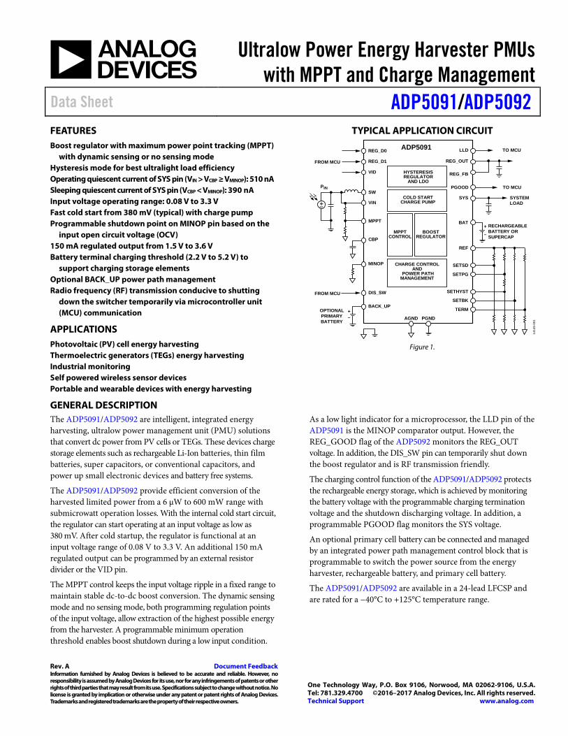
TYPICAL APPLICATION CIRCUIT
SW
VIN
BAT
SYS
TERM
PGOOD
SETHYST
MPPT
CBP
DIS_SW
SETSDMINOP
REF
BACK_UP
SYSTEMLOAD
OPTIONALPRIMARYBATTERY
SETBK
TO MCU
+–
+–
FROM MCU
REG_OUTREG_D1
VID
LLD TO MCUREG_D0
FROM MCU
COLD STARTCHARGE PUMP
ADP5091
MPPTCONTROL
BOOSTREGULATOR
CHARGE CONTROLAND
POWER PATHMANAGEMENT
HYSTERESISREGULATOR
AND LDOREG_FB
SETPG
PIN
RECHARGEABLEBATTERY ORSUPERCAP
AGND PGND
1414
5-00
1
Figure 1.
GENERAL DESCRIPTION The ADP5091/ADP5092 are intelligent, integrated energy harvesting, ultralow power management unit (PMU) solutions that convert dc power from PV cells or TEGs. These devices charge storage elements such as rechargeable Li-Ion batteries, thin film batteries, super capacitors, or conventional capacitors, and power up small electronic devices and battery free systems.
The ADP5091/ADP5092 provide efficient conversion of the harvested limited power from a 6 µW to 600 mW range with submicrowatt operation losses. With the internal cold start circuit, the regulator can start operating at an input voltage as low as 380 mV. After cold startup, the regulator is functional at an input voltage range of 0.08 V to 3.3 V. An additional 150 mA regulated output can be programmed by an external resistor divider or the VID pin.
The MPPT control keeps the input voltage ripple in a fixed range to maintain stable dc-to-dc boost conversion. The dynamic sensing mode and no sensing mode, both programming regulation points of the input voltage, allow extraction of the highest possible energy from the harvester. A programmable minimum operation threshold enables boost shutdown during a low input condition.
As a low light indicator for a microprocessor, the LLD pin of the ADP5091 is the MINOP comparator output. However, the REG_GOOD flag of the ADP5092 monitors the REG_OUT voltage. In addition, the DIS_SW pin can temporarily shut down the boost regulator and is RF transmission friendly.
The charging control function of the ADP5091/ADP5092 protects the rechargeable energy storage, which is achieved by monitoring the battery voltage with the programmable charging termination voltage and the shutdown discharging voltage. In addition, a programmable PGOOD flag monitors the SYS voltage.
An optional primary cell battery can be connected and managed by an integrated power path management control block that is programmable to switch the power source from the energy harvester, rechargeable battery, and primary cell battery.
The ADP5091/ADP5092 are available in a 24-lead LFCSP and are rated for a −40°C to +125°C temperature range.
ADP5091/ADP5092 Data Sheet
Rev. A | Page 2 of 28
TABLE OF CONTENTS Features .............................................................................................. 1 Applications ....................................................................................... 1 Typical Application Circuit ............................................................. 1 General Description ......................................................................... 1 Revision History ............................................................................... 2 Detailed Functional Block Diagram .............................................. 3 Specifications ..................................................................................... 4
Regulated Output Specifications ................................................ 6 Absolute Maximum Ratings ............................................................ 7
Thermal Resistance ...................................................................... 7 ESD Caution .................................................................................. 7
Pin Configurations and Function Descriptions ........................... 8 Typical Performance Characteristics ........................................... 10 Theory of Operation ...................................................................... 16
Fast Cold Start-Up Circuit (VSYS < VSYS_TH, VIN > VIN_COLD) ... 16 Main Boost Regulator (VBAT_TERM > VSYS > VSYS_TH) ..................... 16 VIN Open Circuit and MPPT .................................................. 16 Minimum Operation Threshold Function ............................. 17 Disabling Boost ........................................................................... 17 Regulated Output Working Mode ............................................ 17 REG_D0 and REG_D1 .............................................................. 17
Regulated Output Configuration ............................................. 17 REG_GOOD (ADP5092 Only) ................................................ 18 Energy Storage Charge Management ...................................... 18 Backup Storage Path................................................................... 18 Backup and BAT Selection Threshold ..................................... 19 Battery Overcharging Protection ............................................. 19 Battery Discharging Protection ................................................ 19 Power Good (PGOOD) ............................................................. 20 Power Path Working Flow......................................................... 20 Current-Limit and Short-Circuit Protection .............................. 20 Thermal Shutdown .................................................................... 21
Applications Information .............................................................. 23 Energy Harvester Selection ....................................................... 23 Energy Storage Element Selection ........................................... 23 Inductor Selection ...................................................................... 23 Capacitor Selection .................................................................... 24 Layout and Assembly Considerations ..................................... 24 Typical Application Circuits ..................................................... 25
Factory Programmable Options ................................................... 27 Outline Dimensions ....................................................................... 28
Ordering Guide .......................................................................... 28
REVISION HISTORY 5/2017—Rev. 0 to Rev. A Changes to Figure 2 .......................................................................... 3 Changes to Figure 7, Figure 10, Figure 7 Caption, and Figure 10 Caption ............................................................................................. 10 Changes to Figure 11 and Figure 11 Caption ............................. 11 Changed CP-24-10 to CP-24-14 .................................. Throughout Updated Outline Dimensions ....................................................... 28 Changes to Ordering Guide .......................................................... 28 7/2016—Revision 0: Initial Version
Data Sheet ADP5091/ADP5092
Rev. A | Page 3 of 28
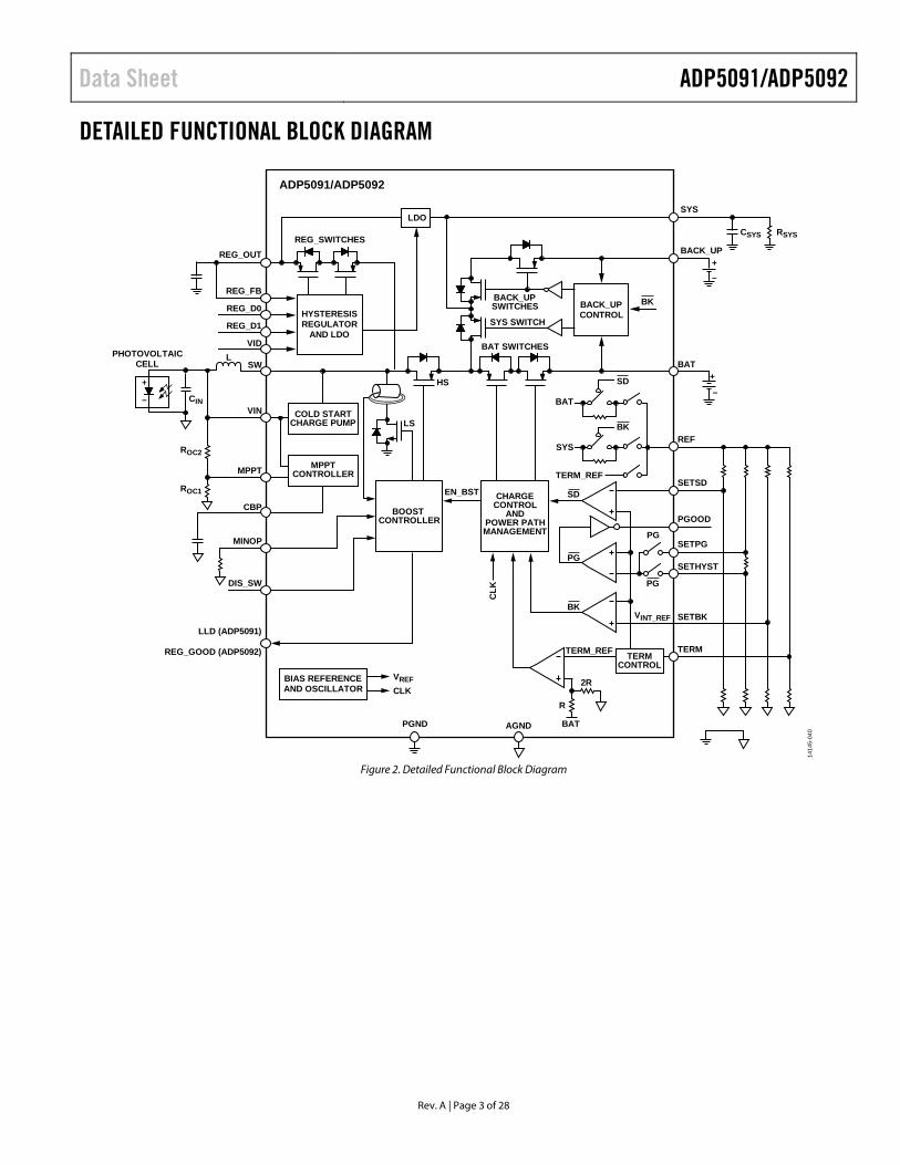
DETAILED FUNCTIONAL BLOCK DIAGRAM
BAT+
–HS
BAT SWITCHES
SYS SWITCH
BACK_UPSWITCHES
BACK_UP
BACK_UPCONTROL
SYS
BAT
SYSREF
SETSD
PGOOD
SETPG
SETHYST
VINT_REF
TERM
SETBK
SD
PG
CLK
TERM_REF
TERM_REF
EN_BST
SD
REG_OUT
L
LS
REG_SWITCHES
REG_FB
REG_D0
REG_D1
VID
SW
VIN
MPPT
CBP
DIS_SW
LLD (ADP5091)
REG_GOOD (ADP5092)
MINOP
+
–
MPPTCONTROLLER
COLD STARTCHARGE PUMP
PHOTOVOLTAICCELL
BOOSTCONTROLLER
PGND
CLK
ADP5091/ADP5092
AGND BAT
R
2R
CHARGECONTROL
ANDPOWER PATHMANAGEMENT
BIAS REFERENCEAND OSCILLATOR
1414
5-04
0
TERMCONTROL
ROC2
ROC1
HYSTERESISREGULATOR
AND LDO
LDO
+–
CSYS
VREF
RSYS
CIN
BK
BK
BK
PG
PG
Figure 2. Detailed Functional Block Diagram
ADP5091/ADP5092 Data Sheet
Rev. A | Page 4 of 28
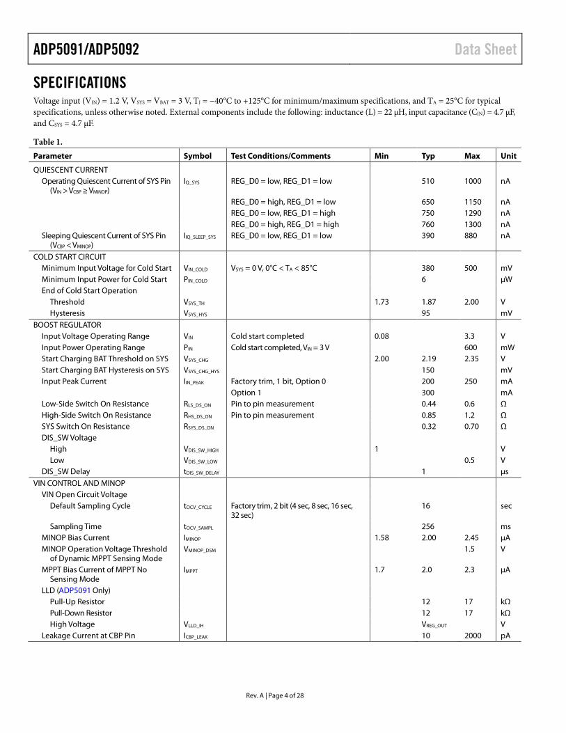
SPECIFICATIONS Voltage input (VIN) = 1.2 V, VSYS = VBAT = 3 V, TJ = −40°C to +125°C for minimum/maximum specifications, and TA = 25°C for typical specifications, unless otherwise noted. External components include the following: inductance (L) = 22 µH, input capacitance (CIN) = 4.7 µF, and CSYS = 4.7 µF.
Table 1. Parameter Symbol Test Conditions/Comments Min Typ Max Unit
QUIESCENT CURRENT Operating Quiescent Current of SYS Pin
(VIN > VCBP ≥ VMINOP) IQ_SYS REG_D0 = low, REG_D1 = low 510 1000 nA
REG_D0 = high, REG_D1 = low 650 1150 nA REG_D0 = low, REG_D1 = high 750 1290 nA REG_D0 = high, REG_D1 = high 760 1300 nA Sleeping Quiescent Current of SYS Pin
(VCBP < VMINOP) IIQ_SLEEP_SYS REG_D0 = low, REG_D1 = low 390 880 nA
COLD START CIRCUIT Minimum Input Voltage for Cold Start VIN_COLD VSYS = 0 V, 0°C < TA < 85°C 380 500 mV Minimum Input Power for Cold Start PIN_COLD 6 µW End of Cold Start Operation
Threshold VSYS_TH 1.73 1.87 2.00 V Hysteresis VSYS_HYS 95 mV
BOOST REGULATOR Input Voltage Operating Range VIN Cold start completed 0.08 3.3 V Input Power Operating Range PIN Cold start completed, VIN = 3 V 600 mW Start Charging BAT Threshold on SYS VSYS_CHG 2.00 2.19 2.35 V Start Charging BAT Hysteresis on SYS VSYS_CHG_HYS 150 mV Input Peak Current IIN_PEAK Factory trim, 1 bit, Option 0 200 250 mA Option 1 300 mA Low-Side Switch On Resistance RLS_DS_ON Pin to pin measurement 0.44 0.6 Ω High-Side Switch On Resistance RHS_DS_ON Pin to pin measurement 0.85 1.2 Ω SYS Switch On Resistance RSYS_DS_ON 0.32 0.70 Ω DIS_SW Voltage
High VDIS_SW_HIGH 1 V Low VDIS_SW_LOW 0.5 V
DIS_SW Delay tDIS_SW_DELAY 1 µs VIN CONTROL AND MINOP
VIN Open Circuit Voltage Default Sampling Cycle tOCV_CYCLE Factory trim, 2 bit (4 sec, 8 sec, 16 sec,
32 sec) 16 sec
Sampling Time tOCV_SAMPL 256 ms MINOP Bias Current IMINOP 1.58 2.00 2.45 µA MINOP Operation Voltage Threshold
of Dynamic MPPT Sensing Mode VMINOP_DSM 1.5 V
MPPT Bias Current of MPPT No Sensing Mode
IMPPT 1.7 2.0 2.3 µA
LLD (ADP5091 Only) Pull-Up Resistor 12 17 kΩ Pull-Down Resistor 12 17 kΩ High Voltage VLLD_IH VREG_OUT V
Leakage Current at CBP Pin ICBP_LEAK 10 2000 pA
Data Sheet ADP5091/ADP5092
Rev. A | Page 5 of 28
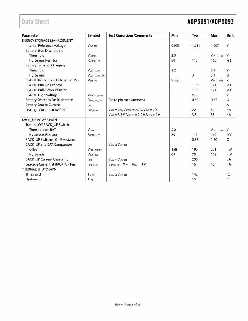
Parameter Symbol Test Conditions/Comments Min Typ Max Unit ENERGY STORAGE MANAGEMENT
Internal Reference Voltage VINT_REF 0.955 1.011 1.067 V Battery Stop Discharging
Threshold VSETSD 2.0 VBAT_TERM V Hysteresis Resistor RSETSD_HYS 80 115 160 kΩ
Battery Terminal Charging Threshold VBAT_TERM 2.2 5.2 V Hysteresis VBAT_TERM_HYS 3 3.1 %
PGOOD Rising Threshold at SYS Pin VSYS_PG VSETSD VBAT_TERM V PGOOD Pull-Up Resistor 11.6 17.0 kΩ PGOOD Pull-Down Resistor 11.6 17.0 kΩ PGOOD High Voltage VPGOOD_HIGH VSYS V Battery Switches On Resistance RBAT_SW_ON Pin to pin measurement 0.59 0.85 Ω Battery Source Current IBAT 1 A Leakage Current at BAT Pin IBAT_LEAK VBAT = 2 V, VSETSD = 2.2 V, VSYS = 2 V 22 50 nA VBAT = 3.3 V, VSETSD = 2.2 V, VSYS = 0 V 3.5 35 nA
BACK_UP POWER PATH Turning Off BACK_UP Switch
Threshold on BAT VSETBK 2.0 VBAT_TERM V Hysteresis Resistor RSETBK_HYS 80 115 160 kΩ
BACK_UP Switches On Resistance 0.85 1.20 Ω BACK_UP and BAT Comparator VSYS ≥ VSYS_TH
Offset VBKP_OFFSET 158 190 271 mV Hysteresis VBAT_HYS 68 75 108 mV
BACK_UP Current Capability IBKP VSYS < VSYS_TH 250 µA Leakage Current at BACK_UP Pin IBKP_LEAK VBACK_UP = VSYS = VBAT = 3 V 16 40 nA
THERMAL SHUTDOWN Threshold TSHDN VSYS ≥ VSYS_TH 142 °C Hysteresis THYS 15 °C
ADP5091/ADP5092 Data Sheet
Rev. A | Page 6 of 28
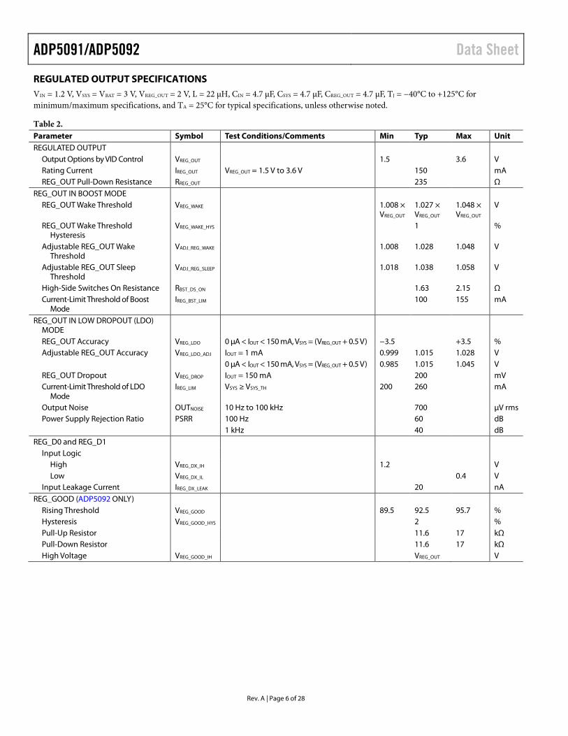
REGULATED OUTPUT SPECIFICATIONS VIN = 1.2 V, VSYS = VBAT = 3 V, VREG_OUT = 2 V, L = 22 µH, CIN = 4.7 µF, CSYS = 4.7 µF, CREG_OUT = 4.7 µF, TJ = −40°C to +125°C for minimum/maximum specifications, and TA = 25°C for typical specifications, unless otherwise noted.
Table 2. Parameter Symbol Test Conditions/Comments Min Typ Max Unit REGULATED OUTPUT
Output Options by VID Control VREG_OUT 1.5 3.6 V Rating Current IREG_OUT VREG_OUT = 1.5 V to 3.6 V 150 mA REG_OUT Pull-Down Resistance RREG_OUT 235 Ω
REG_OUT IN BOOST MODE REG_OUT Wake Threshold VREG_WAKE 1.008 ×
VREG_OUT 1.027 × VREG_OUT
1.048 × VREG_OUT
V
REG_OUT Wake Threshold Hysteresis
VREG_WAKE_HYS 1 %
Adjustable REG_OUT Wake Threshold
VADJ_REG_WAKE 1.008 1.028 1.048 V
Adjustable REG_OUT Sleep Threshold
VADJ_REG_SLEEP 1.018 1.038 1.058 V
High-Side Switches On Resistance RBST_DS_ON 1.63 2.15 Ω Current-Limit Threshold of Boost
Mode IREG_BST_LIM 100 155 mA
REG_OUT IN LOW DROPOUT (LDO) MODE
REG_OUT Accuracy VREG_LDO 0 µA < IOUT < 150 mA, VSYS = (VREG_OUT + 0.5 V) −3.5 +3.5 % Adjustable REG_OUT Accuracy VREG_LDO_ADJ IOUT = 1 mA 0.999 1.015 1.028 V 0 µA < IOUT < 150 mA, VSYS = (VREG_OUT + 0.5 V) 0.985 1.015 1.045 V REG_OUT Dropout VREG_DROP IOUT = 150 mA 200 mV Current-Limit Threshold of LDO
Mode IREG_LIM VSYS ≥ VSYS_TH 200 260 mA
Output Noise OUTNOISE 10 Hz to 100 kHz 700 µV rms Power Supply Rejection Ratio PSRR 100 Hz 60 dB
1 kHz 40 dB REG_D0 and REG_D1
Input Logic High VREG_DX_IH 1.2 V Low VREG_DX_IL 0.4 V
Input Leakage Current IREG_DX_LEAK 20 nA REG_GOOD (ADP5092 ONLY)
Rising Threshold VREG_GOOD 89.5 92.5 95.7 % Hysteresis VREG_GOOD_HYS 2 % Pull-Up Resistor 11.6 17 kΩ Pull-Down Resistor 11.6 17 kΩ High Voltage VREG_GOOD_IH VREG_OUT V
Data Sheet ADP5091/ADP5092
Rev. A | Page 7 of 28
ABSOLUTE MAXIMUM RATINGS Table 3.
Parameter Rating VIN, MPPT, CBP, MINOP −0.3 V to +3.6 V
DIS_SW, TERM, SETPG, SETSD, SETBK, PGOOD, SETHYST, REF, REG_D0, VID, REG_D1, LLD, REG_GOOD to AGND
−0.3 V to +6.0 V
SW, SYS, BAT, BACK_UP, REG_OUT, REG_FB to PGND
−0.3 V to +6.0 V
PGND to AGND −0.3 V to +0.3 V
Stresses at or above those listed under Absolute Maximum Ratings may cause permanent damage to the product. This is a stress rating only; functional operation of the product at these or any other conditions above those indicated in the operational section of this specification is not implied. Operation beyond the maximum operating conditions for extended periods may affect product reliability.
THERMAL RESISTANCE θJA is specified for the worst case conditions, that is, a device soldered in a circuit board for surface-mount packages.
Table 4. Package Type θJA θJC Unit 24-Lead LFCSP 58.7 36 °C/W
ESD CAUTION
ADP5091/ADP5092 Data Sheet
Rev. A | Page 8 of 28
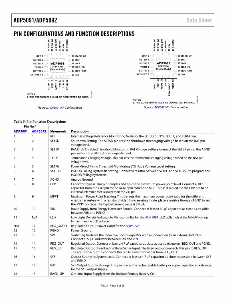
PIN CONFIGURATIONS AND FUNCTION DESCRIPTIONS
1414
5-00
2
21
3456
181716151413SETHYST
NOTES1. THE EXPOSED PAD MUST BE CONNECTED TO AGND.
SETPGTERM
SETBKSETSD
REF
SWREG_OUTREG_FBSYSBATBACK_UP
8 9 10 117C
BP
MPP
TVI
NLL
D12
PGN
D
AG
ND
20 1921VI
DPG
OO
D
MIN
OP
22D
IS_S
W23
REG
_D1
24R
EG_D
0
ADP5091TOP VIEW
(Not to Scale)
Figure 3. ADP5091 Pin Configuration
1414
5-00
3
21
3456
181716151413SETHYST
NOTES1. THE EXPOSED PAD MUST BE CONNECTED TO AGND.
SETPGTERM
SETBKSETSD
REF
SWREG_OUTREG_FBSYSBATBACK_UP
8 9 10 117C
BP
MPP
TVI
NR
EG_G
OO
D12
PGN
D
AG
ND
20 1921VI
DPG
OO
D
MIN
OP
22D
IS_S
W23
REG
_D1
24R
EG_D
0
ADP5092TOP VIEW
(Not to Scale)
Figure 4. ADP5092 Pin Configuration
Table 5. Pin Function Descriptions Pin No.1
Mnemonic Description ADP5091 ADP5092 1 1 REF Internal Voltage Reference Monitoring Node for the SETSD, SETPG, SETBK, and TERM Pins. 2 2 SETSD Shutdown Setting. The SETSD pin sets the shutdown discharging voltage based on the BAT pin
voltage level. 3 3 SETBK BACK_UP Disabled Threshold Monitoring BAT Voltage Setting. Connect the SETBK pin to the AGND
pin without the BACK_UP storage element. 4 4 TERM Termination Charging Voltage. This pin sets the termination charging voltage based on the BAT pin
voltage level. 5 5 SETPG Power-Good Rising Threshold Monitoring SYS Node Voltage Level Setting. 6 6 SETHYST PGOOD Falling Hysteresis Setting. Connect a resistor between SETPG and SETHYST to program the
PGOOD falling hysteresis. 7 7 AGND Analog Ground. 8 8 CBP Capacitor Bypass. This pin samples and holds the maximum power point level. Connect a 10 nF
capacitor from the CBP pin to the AGND pin. When the MPPT pin is disabled, tie the CBP pin to an external reference that is lower than the VIN pin.
9 9 MPPT Maximum Power Point Tracking. This pin sets the maximum power point ratio for the different energy harvesters with a resistor divider. In no sensing mode, place a resistor through AGND to set the MPPT voltage. The typical current value is 2.0 µA.
10 10 VIN Input Supply from Energy Harvester Source. Connect at least a 10 µF capacitor as close as possible between VIN and PGND.
11 N/A LLD Low Light Density Indicator to Microcontroller for the ADP5091. LLD pulls high at the MINOP voltage higher than the CBP voltage.
N/A 11 REG_GOOD Regulated Output Power Good for the ADP5092. 12 12 PGND Power Ground. 13 13 SW Switching Node for the Inductive Boost Regulator with a Connection to an External Inductor.
Connect a 22 µH inductor between SW and VIN. 14 14 REG_OUT Regulated Output. Connect at least a 4.7 µF capacitor as close as possible between REG_OUT and PGND. 15 15 REG_FB Regulated Output Feedback Voltage Sense Input. The fixed output connects this pin to REG_OUT.
The adjustable output connects this pin to a resistor divider from REG_OUT. 16 16 SYS Output Supply to System Load. Connect at least a 4.7 µF capacitor as close as possible between SYS
and PGND. 17 17 BAT SYS Output Supply Storage. This pin places the rechargeable battery or super capacitor as a storage
for the SYS output supply. 18 18 BACK_UP Optional Input Supply from the Backup Primary Battery Cell.
Data Sheet ADP5091/ADP5092
Rev. A | Page 9 of 28
Pin No.1 Mnemonic Description ADP5091 ADP5092
19 19 PGOOD Output Signal to Microcontroller. This pin maintains a pulled high level when SYS is higher than the SETPG threshold.
20 20 VID Voltage Configuration Pin for REG_OUT. This pin sets up to eight different regulated outputs tied low through a resistor to AGND. The output configuration details are in Table 7.
21 21 MINOP Minimum Operating Power. Place a resistor on MINOP to set the minimum operating input voltage level. The boost regulator starts switching when the CBP voltage exceeds the MINOP voltage. When the MINOP pin is floating, the IC operates in no sensing mode with a fixed MPPT level. Connect this pin through AGND to disable the MINOP function.
22 22 DIS_SW Control Signal from Microcontroller or RF Transceiver to Stop Switching Boost Charger. 23 23 REG_D1 Regulated Output Working Mode Set D1. Enable LDO mode by pulling this pin high. 24 24 REG_D0 Regulated Output Working Mode Set D0. Enable boost mode by pulling this pin high. EPAD Exposed Pad. The exposed pad must be connected to AGND. 1 N/A means not applicable.
ADP5091/ADP5092 Data Sheet
Rev. A | Page 10 of 28
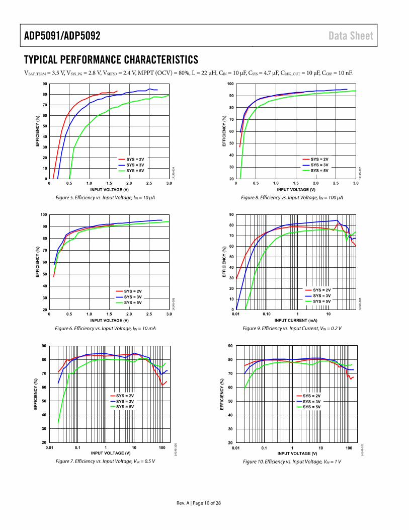
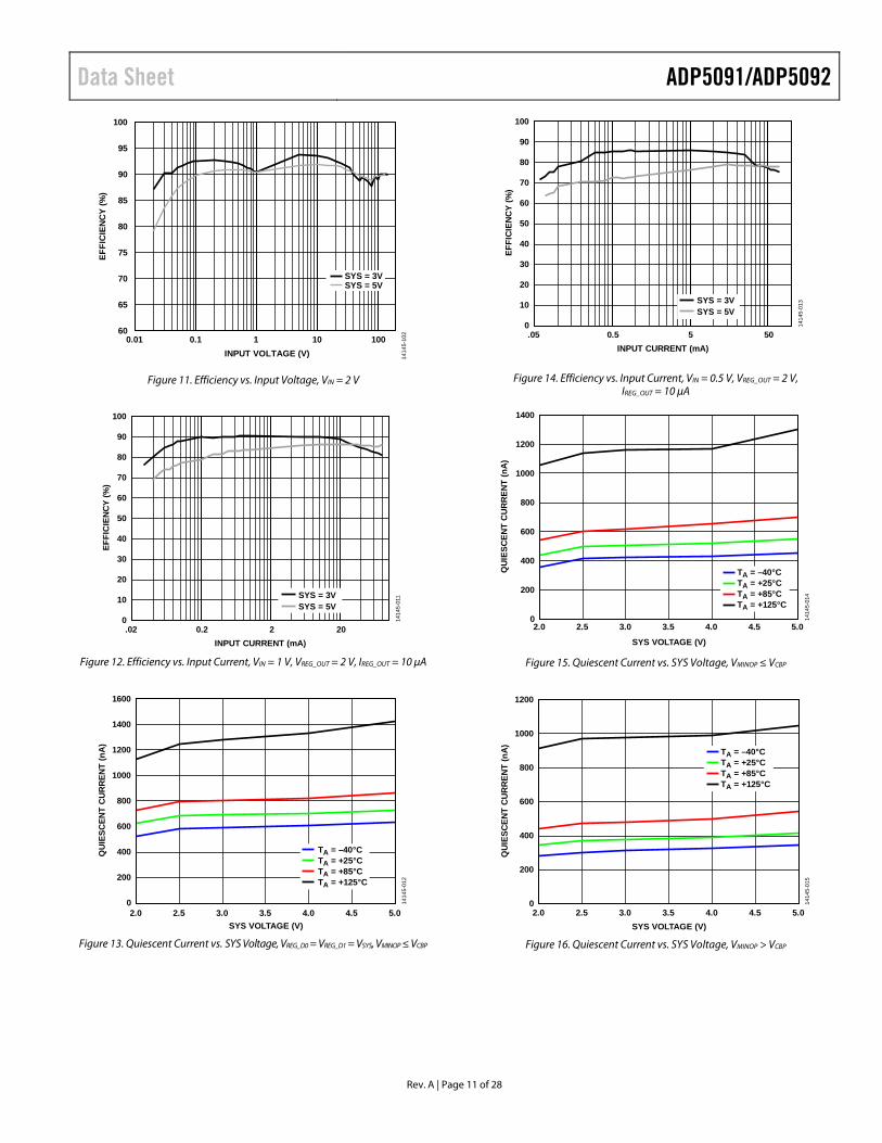
TYPICAL PERFORMANCE CHARACTERISTICS VBAT_TERM = 3.5 V, VSYS_PG = 2.8 V, VSETSD = 2.4 V, MPPT (OCV) = 80%, L = 22 μH, CIN = 10 μF, CSYS = 4.7 μF, CREG_OUT = 10 μF, CCBP = 10 nF.
0
10
20
30
40
50
60
70
80
90
EF
FIC
IEN
CY
(%
)
INPUT VOLTAGE (V)
SYS = 2V
SYS = 3V
SYS = 5V14
145-
004
0 0.5 1.0 1.5 2.0 2.5 3.0
Figure 5. Efficiency vs. Input Voltage, IIN = 10 μA
0 0.5 1.0 1.5 2.0 2.5 3.020
30
40
50
60
70
80
100
90
EF
FIC
IEN
CY
(%
)
INPUT VOLTAGE (V)
SYS = 2V
SYS = 3V
SYS = 5V
1414
5-00
5
Figure 6. Efficiency vs. Input Voltage, IIN = 10 mA
20
30
40
50
60
70
80
90
0.01 0.1 1 10 100
EF
FIC
IEN
CY
(%
)
INPUT VOLTAGE (V)
SYS = 2V
SYS = 3VSYS = 5V
1414
5-10
0
Figure 7. Efficiency vs. Input Voltage, VIN = 0.5 V
0 0.5 1.0 1.5 2.0 2.5 3.020
30
40
50
60
70
80
100
90
EF
FIC
IEN
CY
(%
)
INPUT VOLTAGE (V)
SYS = 2V
SYS = 3V
SYS = 5V
1414
5-00
7
Figure 8. Efficiency vs. Input Voltage, IIN = 100 μA
0.01 0.10 1 100
10
20
30
40
50
60
70
80
90
EF
FIC
IEN
CY
(%
)
INPUT CURRENT (mA)
SYS = 2V
SYS = 3V
SYS = 5V
1414
5-00
8
Figure 9. Efficiency vs. Input Current, VIN = 0.2 V
20
30
40
50
60
70
80
90
0.01 0.1 1 10 100
EF
FIC
IEN
CY
(%
)
INPUT VOLTAGE (V)
SYS = 2V
SYS = 3VSYS = 5V
1414
5-10
1
Figure 10. Efficiency vs. Input Voltage, VIN = 1 V
Data Sheet ADP5091/ADP5092
Rev. A | Page 11 of 28
60
65
70
75
80
85
90
95
100
0.01 0.1 1 10 100
EFFI
CIE
NC
Y (%
)
INPUT VOLTAGE (V)
SYS = 3VSYS = 5V
1414
5-10
2
Figure 11. Efficiency vs. Input Voltage, VIN = 2 V
0
10
20
30
40
50
60
70
80
90
100
.02 0.2 2 20
EFFI
CIE
NCY
(%)
INPUT CURRENT (mA)
1414
5-01
1SYS = 3VSYS = 5V
Figure 12. Efficiency vs. Input Current, VIN = 1 V, VREG_OUT = 2 V, IREG_OUT = 10 µA
0
200
400
600
800
1000
1200
1400
1600
2.0 2.5 3.0 3.5 4.0 4.5 5.0
QU
IESC
ENT
CU
RR
ENT
(nA
)
SYS VOLTAGE (V)
TA = –40°CTA = +25°CTA = +85°CTA = +125°C
1414
5-01
2
Figure 13. Quiescent Current vs. SYS Voltage, VREG_D0 = VREG_D1 = VSYS, VMINOP ≤ VCBP
0
10
20
30
40
50
60
70
80
90
100
.05 0.5 5 50
EFFI
CIE
NC
Y (%
)
INPUT CURRENT (mA)
SYS = 3VSYS = 5V
1414
5-01
3
Figure 14. Efficiency vs. Input Current, VIN = 0.5 V, VREG_OUT = 2 V, IREG_OUT = 10 µA
1414
5-01
4
0
200
400
600
800
1000
1200
1400
2.0 2.5 3.0 3.5 4.0 4.5 5.0
QU
IESC
ENT
CU
RR
ENT
(nA
)
SYS VOLTAGE (V)
TA = –40°CTA = +25°CTA = +85°CTA = +125°C
Figure 15. Quiescent Current vs. SYS Voltage, VMINOP ≤ VCBP
1414
5-01
5
0
200
400
600
800
1000
1200
2.0 2.5 3.0 3.5 4.0 4.5 5.0
QUI
ESCE
NT C
URRE
NT (n
A)
SYS VOLTAGE (V)
TA = –40°CTA = +25°CTA = +85°CTA = +125°C
Figure 16. Quiescent Current vs. SYS Voltage, VMINOP > VCBP
ADP5091/ADP5092 Data Sheet
Rev. A | Page 12 of 28
0
20
40
60
80
100
120
2.0 2.4 2.8 3.2 3.6 4.0 4.4 4.8 5.2
BA
CK
_UP
LEA
KA
GE
CU
RR
ENT
(nA
)
BACK_UP VOLTAGE (V)
TA = –40°C TA = +25°C TA = +85°CTA = +125°C
1414
5-01
6
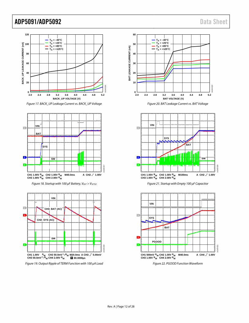
Figure 17. BACK_UP Leakage Current vs. BACK_UP Voltage
14
145-
017
CH1 1.00V BW CH2 1.00V BWCH3 1.00V BW CH4 2.00V BW
M40.0ms A CH2 1.00V
1
4
2
VIN
BAT
SYS
SW
Figure 18. Startup with 100 µF Battery, VBAT > VSETSD
1414
5-01
8
CH1 1.00V BWCH3 50.0mV BW CH4 2.00V BW
M20.0ms A CH3 5.00mV
1
3
4
VIN
CH2: SYS (AC)
CH3: BAT (AC)
SW
T 80.0000µsCH2 50.0mV BW
Figure 19. Output Ripple of TERM Function with 100 µA Load
0
10
20
30
40
50
60
2.0 2.4 2.8 3.2 3.6 4.0 4.4 4.8 5.2
BAT
LEA
KA
GE
CU
RR
ENT
(nA
)
BAT VOLTAGE (V)
TA = –40°C TA = +25°C TA = +85°CTA = +125°C
1414
5-01
9
Figure 20. BAT Leakage Current vs. BAT Voltage
1414
5-02
0
CH1 1.00V BW CH2 1.00V BWCH3 1.00V BW CH4 2.00V BW
M100ms A CH2 1.00V
1
4
2
VIN
SYS
BAT
SW
Figure 21. Startup with Empty 100 µF Capacitor
1414
5-02
1
CH1 500mV BW CH2 1.00V BWCH3 1.00V BW CH4 2.00V BW
M40.0ms A CH4 1.00V
1
4
3
VIN
SYS
BAT
PGOOD
Figure 22. PGOOD Function Waveform
Data Sheet ADP5091/ADP5092
Rev. A | Page 13 of 28
1414
5-02
2
CH1 500mV BW CH2 1.00V BWCH3 1.00V BW CH4 2.00V BW
M10.0ms A CH2 2.00V
1
4
3
VIN
SYS
BAT
SW
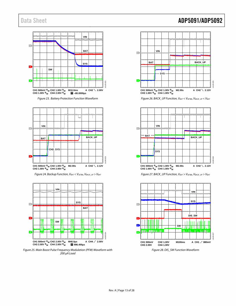
T –80.0000µs Figure 23. Battery Protection Function Waveform
14
145-
023
CH1 500mV BW CH2 1.00V BWCH3 1.00V BW CH4 2.00V BW
M2.00s A CH2 2.12V
1
43
VIN
CH2: SYS
BACK_UPBAT
Figure 24. Backup Function, VBAT < VSETBK, VBACK_UP > VBAT
1414
5-02
4
CH1 500mV BW CH2 2.00V BWCH3 2.00V BW CH4 2.00V BW
M40.0µs A CH4 2.00V
1
4
3
VIN
SYS
BAT
SW
T 996.400µs Figure 25. Main Boost Pulse Frequency Modulation (PFM) Waveform with
200 µA Load
1414
5-02
5
CH1 500mV BW CH2 1.00V BWCH3 1.00V BW CH4 1.00V BW
M2.00s A CH2 2.12V
1
3
VIN
SYS
BAT BACK_UP
Figure 26. BACK_UP Function, VBAT < VSETBK, VBACK_UP < VBAT
1414
5-02
6
CH1 500mV BW CH2 1.00V BWCH3 1.00V BW CH4 1.00V BW
M2.00s A CH2 2.12V
1
3
VIN
SYS
BACK_UPBAT
Figure 27. BACK_UP Function, VBAT > VSETBK, VBACK_UP > VBAT
1414
5-02
7
CH1 500mV CH2 1.00VCH3 2.00V CH4 1.00V
M100ms A CH1 880mV
1
3
2
4
VIN
SYS
SW
DIS_SW
Figure 28. DIS_SW Function Waveform
ADP5091/ADP5092 Data Sheet
Rev. A | Page 14 of 28
1414
5-02
8
CH1 500mV BW CH2 1.00V BWCH3 1.00V BW CH4 2.00V BW
M4.00s A CH2 2.12V
1
3
2
VIN
SYS
BAT
SW
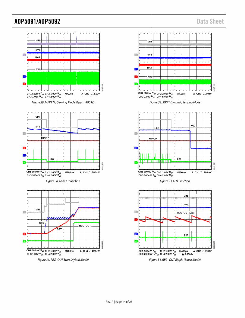
Figure 29. MPPT No Sensing Mode, RMPPT = 400 kΩ
14
145-
029
CH1 500mV BW CH2 1.00V BWCH4 2.00V BW
M100ms A CH1 780mV
1
4
3
2
VIN
SYS
MINOP
SW
CH3 500mV BW Figure 30. MINOP Function
1414
5-03
0
CH1 500mV BW CH2 1.00V BWCH4 2.00V BW
M400ms A CH4 220mV
1
4
3
VIN
SYS
BATREG_OUT
CH3 1.00V BW Figure 31. REG_OUT Start (Hybrid Mode)
1414
5-03
1
CH1 500mV BW CH2 2.00V BWCH4 5.00V BW
M4.00s A CH2 2.04V
1
2
4
3
VIN
SYS
BAT
SW
CH3 2.00V BW Figure 32. MPPT Dynamic Sensing Mode
1414
5-03
2
CH1 500mV BW CH2 1.00V BWCH4 2.00V BW
M400ms A CH1 780mV
1
2
4
LLD
MINOP
SW
CH3 500mV BW
VIN
Figure 33. LLD Function
1414
5-03
3
CH1 500mV BW CH2 1.00V BWCH3 20.0mV BW CH4 2.00V BW
M400µs A CH3 2.00V
1
4
3
2
VIN
REG_OUT (AC)
SYS
SW
T 0.0000s Figure 34. REG_OUT Ripple (Boost Mode)
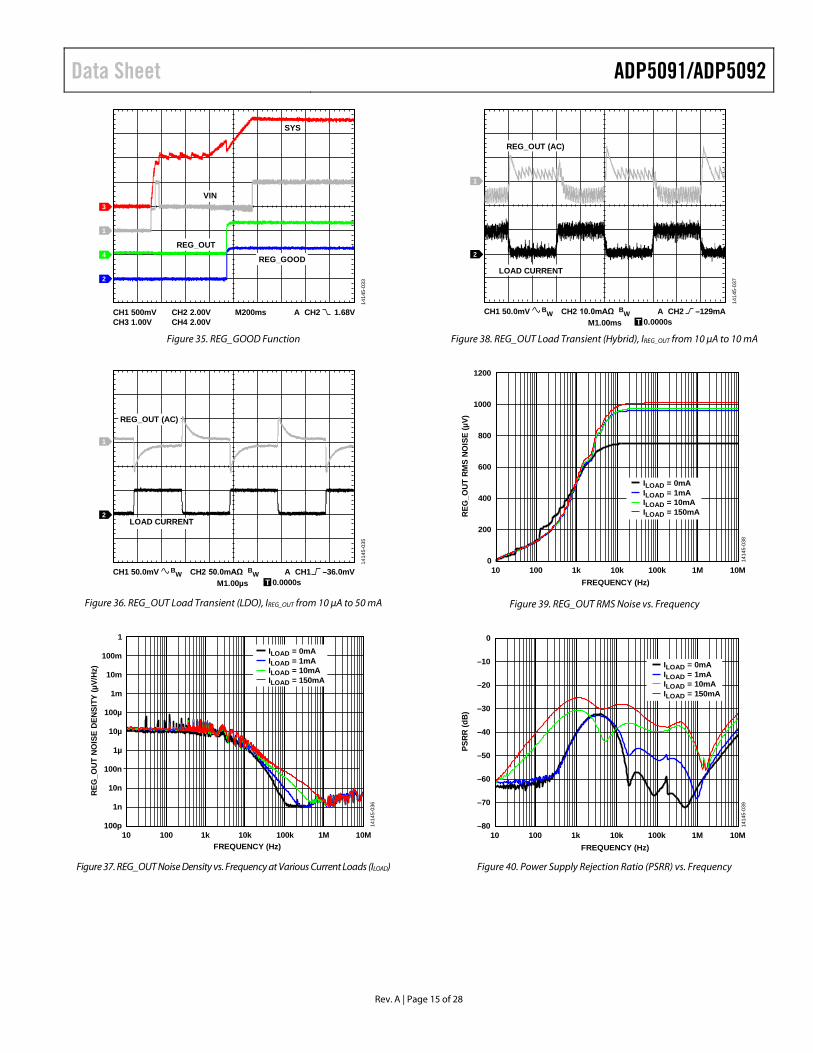
Data Sheet ADP5091/ADP5092
Rev. A | Page 15 of 28
1414
5-03
3
CH1 500mV CH2 2.00VCH3 1.00V CH4 2.00V
M200ms A CH2 1.68V
1
4
3
2
REG_OUT
REG_GOOD
SYS
VIN
Figure 35. REG_GOOD Function
14
145-
035
CH1 50.0mV BW CH2 50.0mAΩ BWM1.00µs
A CH1 –36.0mV
1
2
REG_OUT (AC)
LOAD CURRENT
T 0.0000s
Figure 36. REG_OUT Load Transient (LDO), IREG_OUT from 10 µA to 50 mA
100p
1n
10n
100n
1µ
10µ
100µ
1m
10m
100m
1
10 100 1k 10k 100k 1M 10M
REG
_OU
T N
OIS
E D
ENSI
TY (µ
V/H
z)
FREQUENCY (Hz)
ILOAD = 0mAILOAD = 1mAILOAD = 10mAILOAD = 150mA
1414
5-03
6
Figure 37. REG_OUT Noise Density vs. Frequency at Various Current Loads (ILOAD)
1414
5-03
7
CH1 50.0mV BW CH2 10.0mAΩ BWM1.00ms
A CH2 –129mA
1
2
REG_OUT (AC)
LOAD CURRENT
T 0.0000s Figure 38. REG_OUT Load Transient (Hybrid), IREG_OUT from 10 µA to 10 mA
0
200
400
600
800
1000
1200
REG
_OUT
RM
S NO
ISE
(µV)
FREQUENCY (Hz)
ILOAD = 0mAILOAD = 1mAILOAD = 10mAILOAD = 150mA
10 100 1k 10k 100k 1M 10M
1414
5-03
8
Figure 39. REG_OUT RMS Noise vs. Frequency
–80
–70
–60
–50
–40
–30
–20
–10
0
PSRR
(dB)
FREQUENCY (Hz)10 100 1k 10k 100k 1M 10M
1414
5-03
9
ILOAD = 0mAILOAD = 1mAILOAD = 10mAILOAD = 150mA
Figure 40. Power Supply Rejection Ratio (PSRR) vs. Frequency
ADP5091/ADP5092 Data Sheet
Rev. A | Page 16 of 28
THEORY OF OPERATION The ADP5091/ADP5092 are intelligent, integrated energy harvesting, ultralow power management solutions that include a cold start-up circuit, one synchronous main boost controller, and one regulated output hybrid controller with integrated switches, a charging controller with integrated switches, and backup power path switches. The main boost controller converts maximum power from low voltage, high impedance dc sources, such as PV cells, TEGs, and piezoelectric modules, to store energy in a rechargeable battery or capacitor with storage protection and provides power to the load. Another regulated output with automatic hysteresis boost/LDO mode, or pure LDO mode, is optimized to provide high efficiency across low output currents (10 μA), see Figure 14) to high currents of 200 mA. The ADP5091/ ADP5092 can also control an additional power path from a primary battery cell to the system. An external signal can temporarily stop the two boost circuits to prevent interference with RF transmission.
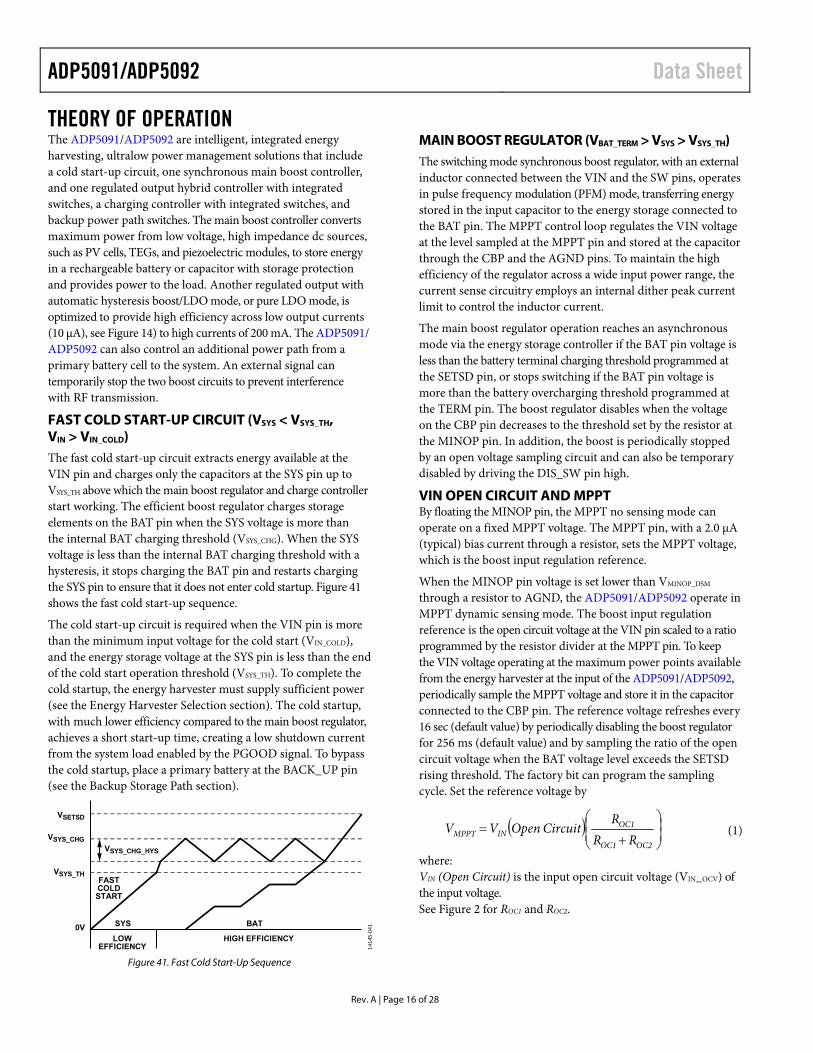
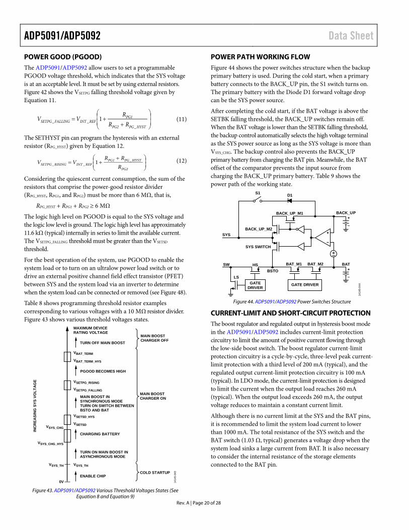
FAST COLD START-UP CIRCUIT (VSYS < VSYS_TH, VIN > VIN_COLD) The fast cold start-up circuit extracts energy available at the VIN pin and charges only the capacitors at the SYS pin up to VSYS_TH above which the main boost regulator and charge controller start working. The efficient boost regulator charges storage elements on the BAT pin when the SYS voltage is more than the internal BAT charging threshold (VSYS_CHG). When the SYS voltage is less than the internal BAT charging threshold with a hysteresis, it stops charging the BAT pin and restarts charging the SYS pin to ensure that it does not enter cold startup. Figure 41 shows the fast cold start-up sequence.
The cold start-up circuit is required when the VIN pin is more than the minimum input voltage for the cold start (VIN_COLD), and the energy storage voltage at the SYS pin is less than the end of the cold start operation threshold (VSYS_TH). To complete the cold startup, the energy harvester must supply sufficient power (see the Energy Harvester Selection section). The cold startup, with much lower efficiency compared to the main boost regulator, achieves a short start-up time, creating a low shutdown current from the system load enabled by the PGOOD signal. To bypass the cold startup, place a primary battery at the BACK_UP pin (see the Backup Storage Path section).
VSETSD
VSYS_CHG
VSYS_CHG_HYS
SYS BAT
FASTCOLDSTART
HIGH EFFICIENCYLOWEFFICIENCY
0V
VSYS_TH
1414
5-04
1
Figure 41. Fast Cold Start-Up Sequence
MAIN BOOST REGULATOR (VBAT_TERM > VSYS > VSYS_TH) The switching mode synchronous boost regulator, with an external inductor connected between the VIN and the SW pins, operates in pulse frequency modulation (PFM) mode, transferring energy stored in the input capacitor to the energy storage connected to the BAT pin. The MPPT control loop regulates the VIN voltage at the level sampled at the MPPT pin and stored at the capacitor through the CBP and the AGND pins. To maintain the high efficiency of the regulator across a wide input power range, the current sense circuitry employs an internal dither peak current limit to control the inductor current.
The main boost regulator operation reaches an asynchronous mode via the energy storage controller if the BAT pin voltage is less than the battery terminal charging threshold programmed at the SETSD pin, or stops switching if the BAT pin voltage is more than the battery overcharging threshold programmed at the TERM pin. The boost regulator disables when the voltage on the CBP pin decreases to the threshold set by the resistor at the MINOP pin. In addition, the boost is periodically stopped by an open voltage sampling circuit and can also be temporary disabled by driving the DIS_SW pin high.
VIN OPEN CIRCUIT AND MPPT By floating the MINOP pin, the MPPT no sensing mode can operate on a fixed MPPT voltage. The MPPT pin, with a 2.0 μA (typical) bias current through a resistor, sets the MPPT voltage, which is the boost input regulation reference.
When the MINOP pin voltage is set lower than VMINOP_DSM through a resistor to AGND, the ADP5091/ADP5092 operate in MPPT dynamic sensing mode. The boost input regulation reference is the open circuit voltage at the VIN pin scaled to a ratio programmed by the resistor divider at the MPPT pin. To keep the VIN voltage operating at the maximum power points available from the energy harvester at the input of the ADP5091/ADP5092, periodically sample the MPPT voltage and store it in the capacitor connected to the CBP pin. The reference voltage refreshes every 16 sec (default value) by periodically disabling the boost regulator for 256 ms (default value) and by sampling the ratio of the open circuit voltage when the BAT voltage level exceeds the SETSD rising threshold. The factory bit can program the sampling cycle. Set the reference voltage by
OC2OC1
OC1INMPPT RR
RCircuitOpenVV (1)
where: VIN (Open Circuit) is the input open circuit voltage (VIN_OCV) of the input voltage. See Figure 2 for ROC1 and ROC2.
Data Sheet ADP5091/ADP5092
Rev. A | Page 17 of 28
The typical MPPT ratio depends on the type of harvester. For example, it is 0.7 to 0.85 for PV cells, and 0.5 for TEGs. The sampling OCV rate is adjustable depending on the previously sampled OCV level. To disable the MPPT function, leave the MPPT pin floating and set the CBP pin to an external voltage reference lower than the VIN voltage.
MINIMUM OPERATION THRESHOLD FUNCTION By setting the MINOP pin voltage lower than the MINOP operation voltage range of the dynamic MPPT sensing mode (VMINOP_DSM) through a resistor to AGND, the minimum operation threshold function can disable the main boost regulator to prevent discharging the storage element when the energy generated by the harvester is less than the system consumption. When the voltage of the CBP pin decreases to the threshold set by the resistor at the MINOP pin, the boost regulator stops switching. The typical MINOP bias current is 2.00 µA. The minimum operation threshold function disables the MPPT function to achieve the sleeping quiescent current of 390 nA (typical). Disable this function by connecting the MINOP pin to the AGND pin.
The low light density (LLD) indicator (ADP5091 only) is the MINOP comparator output that signals the microprocessor to calculate the cycle with insufficient input energy in a certain period.
DISABLING BOOST For noise or electromagnetic interference (EMI) sensitive applications, pull the DIS_SW pin high to stop the boost switcher temporarily to prevent interference with RF circuits. Pull the DIS_SW pin low to resume the boost switching. The transition delay is 1 µs (typical).
REGULATED OUTPUT WORKING MODE The 150 mA regulated output of the ADP5091/ADP5092 not only operates in the hysteresis boost mode or the LDO mode but also operates in the hybrid mode in which the regulator can smoothly transition between these two modes automatically. After the BAT voltage exceeds the SETSD threshold or the SYS voltage is greater than SETPG threshold, the regulator can be enabled.
In hysteresis boost mode, the boost regulator in the ADP5091/ ADP5092 charges the output voltage slightly higher than its preset output voltage. When the output voltage increases until the output sense signal exceeds the hysteresis comparator upper threshold (the sleep threshold), the regulator enters sleep mode. In sleep mode, to allow a low quiescent current as well as high efficiency performance, the low-side and high-side switches and a majority of the circuitry are disabled.
During sleep mode, the output capacitor supplies the energy into the load, the output voltage decreases until it falls below the hysteresis comparator lower threshold (the wake threshold), and the boost regulator wakes up and generates the pulse-width modulation (PWM) pulses to charge the output again. The hysteresis mode allows the regulator to act as the keep alive power supply.
In LDO mode, the output generates power from the SYS pin with at least a small 4.7 µF ceramic output capacitor. Using new innovative design techniques, the LDO provides ultralow quiescent current and superior transient performance for digital and RF applications, and supports noise sensitive applications.
In hybrid mode, the VIN and SYS pins both extract energy to the REG_OUT pin. When the load power is lower than the input power, the regulator exits LDO mode and obtains the energy only from the input side.
REG_D0 AND REG_D1 The REG_D0 and REG_D1 pins allow flexible configuration of the working mode of the regulated output. Table 6 details the working mode configuration set by these two pins.
Table 6. Regulated Output Working Mode Configuration Working Mode REG_D0 REG_D1 Boost Disable Low Not applicable Boost Enable High Not applicable LDO Disable Not applicable Low LDO Enable Not applicable High
REGULATED OUTPUT CONFIGURATION The 150 mA regulated output of the ADP5091/ADP5092 is available in eight fixed output voltage options ranging from 1.5 V to 3.6 V by connecting one resistor through the VID pin to the AGND pin. Table 7 shows the output voltage options set by the VID pin.
Table 7. Output Voltage Options Set by the VID Pin VID Configuration Output Voltage Set by the VID Pin Short to Ground Programmed with external resistors Floating VOUT = 2.5 V RVID = 7 kΩ VOUT = 1.5 V RVID = 14 kΩ VOUT = 1.8 V RVID = 27.7 kΩ VOUT = 3.6 V RVID = 55.6 kΩ VOUT = 3.3 V RVID = 111 kΩ VOUT = 2.0 V RVID = 221 kΩ VOUT = 3.0 V RVID = 442 kΩ VOUT = 2.8 V
The external resistor divider or the VID pin can program the regulated output. The ratio of the two external resistors sets the adjustable output voltage range of 1.5 V to 3.6 V, as shown in Figure 47. The device acts as a servo to the output to maintain the voltage at the REG_FB pin at 1.0 V referenced to ground. The current in R1 is then equal to 1.0 V/R2, and the current in R1 is the current in R2 plus the REG_FB pin bias current. Calculate the output voltage by
VOUT = 1.02 V × (1 + R1/R2) (2)
where: VOUT = VREG_OUT. See Figure 47 for R1 and R2.
To minimize quiescent current, it is recommended to use large resistance values for R1 and R2.
ADP5091/ADP5092 Data Sheet
Rev. A | Page 18 of 28
REG_GOOD (ADP5092 ONLY) A logic high on the REG_GOOD pin indicates that the REG_OUT voltage is above 92.5% (typical) of its nominal output for a delay time greater than approximately 2 ms. The logic high level on REG_GOOD is equal to the REG_OUT voltage, and the logic low level is ground. When the REG_OUT voltage falls below a 2% hysteresis (typical) of the rising threshold, the REG_GOOD pin goes low. The logic high level has about 11.6 kΩ internally in series to limit the available current.
ENERGY STORAGE CHARGE MANAGEMENT Energy storage is connected to the BAT pin. The storage can be a rechargeable battery, super capacitor, or 100 µF or larger capacitor. The energy storage controller manages the charging and discharging operations, monitors the SYS pin voltage, and asserts the PGOOD signal high when it is above the threshold programmed at the SETPG pin.
When the BAT pin voltage exceeds the battery terminal charging threshold programmed at the TERM pin, the boost operation terminates to prevent battery overcharging. The battery terminal charging threshold is programmable from 2.2 V to 5.2 V. When the BAT voltage drops below the battery stop charging threshold level programmed at the SETSD pin, the switches between the BAT pin and the SYS pin are turned off to prevent a deep, destruc-tive battery discharge, and the boost operates in asynchronous mode. Although there is no current limit at the SYS and the BAT pins, it is recommended to limit the system load current to lower than 1000 mA. The large system load current generates a droop between the SYS pin and the rechargeable battery at the BAT pin, with consideration given to the resistance of the SYS switch, the BAT switch, and the rechargeable battery internal resistance.
When no input source is attached, discharge the SYS pin to ground before attaching a storage element to the BAT pin. After hot plugging a charged storage element, release the SYS pin because a SYS voltage that is less than the end of the cold start operation threshold (VSYS_TH) results in the BAT switch remaining off to protect the storage element until the SYS voltage reaches VSYS_TH. The BAT switches remaining off can also be described as store mode, a state with the lowest leakage (3.5 nA typical) that allows a long store period without discharging the storage element on BAT.
BACKUP STORAGE PATH The ADP5091/ADP5092 provide an optional backup storage energy path, an integrated backup controller, and two back to back power switches between the BACK_UP pin and the SYS pin. When the system operates at a condition where the harvested and stored energy is periodically insufficient, attach a backup energy storage element to the BACK_UP pin.
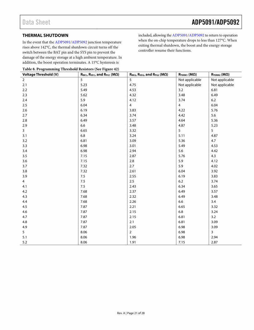
The backup controller enables when the SYS voltage exceeds the end of the cold start operation threshold (VSYS_TH). Before the BAT voltage lowers the SETBK threshold, the backup switches turn off. While the BAT voltage is less than the SETBK threshold, the switches status depends on the voltage level of the BACK_UP pin and the BAT pin. The internal BACK_UP_Mx and BACK_UP control circuit automatically determine the BACK_UP switches (BACK_UP_M1 and BACK_UP_M2) on/off status and selects the high voltage terminal as the power source of SYS. The 190 mV (typical) comparator input offset of the BAT pin prevents the input source and the BAT pin from charging the BACK_UP pin (see Figure 44).
In addition, the backup storage element can bypass the cold startup with inrush current protection circuitry. Nevertheless, the current capability is only 250 µA (typical) when plugging in the backup battery before completing the cold start. It is recom-mended to restrict the system load current from the SYS pin to ensure that the power path can enter normal operation status. Table 9 explains the power path working state. For long-term store mode, disconnect the backup storage element and then discharge SYS to ground.
Data Sheet ADP5091/ADP5092
Rev. A | Page 19 of 28
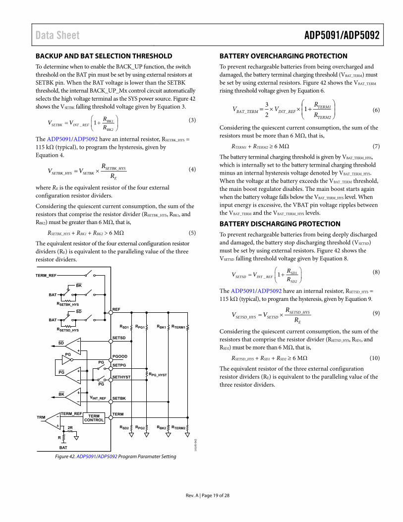
BACKUP AND BAT SELECTION THRESHOLD To determine when to enable the BACK_UP function, the switch threshold on the BAT pin must be set by using external resistors at SETBK pin. When the BAT voltage is lower than the SETBK threshold, the internal BACK_UP_Mx control circuit automatically selects the high voltage terminal as the SYS power source. Figure 42 shows the VSETBK falling threshold voltage given by Equation 3.
_ 1 BK1SETBK INT REF
BK2
RV V
R
(3)
The ADP5091/ADP5092 have an internal resistor, RSETBK_HYS = 115 kΩ (typical), to program the hysteresis, given by Equation 4.
SETBK_HYSSETBK_HYS SETBK
E
RV V
R (4)
where RE is the equivalent resistor of the four external configuration resistor dividers.
Considering the quiescent current consumption, the sum of the resistors that comprise the resistor divider (RSETBK_HYS, RBK1, and RBK2) must be greater than 6 MΩ, that is,
RSETBK_HYS + RBK1 + RBK2 > 6 MΩ (5)
The equivalent resistor of the four external configuration resistor dividers (RE) is equivalent to the paralleling value of the three resistor dividers.
BAT
BAT
TERM_REF
REF
SETBKVINT_REF
TERM
PG
PG
PG
BK
RSETBK_HYS
RSETSD_HYSRSD1
RPG_HYST
RPG1 RBK1 RTERM1
RSD2 RPG2 RBK2 RTERM2
SD
1414
5-04
2
TRMTERM_REF
BAT
R
2R
TERMCONTROL
SETSD
PGOOD
SETPG
SETHYST
BK
SD
PG
Figure 42. ADP5091/ADP5092 Program Paramater Setting
BATTERY OVERCHARGING PROTECTION To prevent rechargeable batteries from being overcharged and damaged, the battery terminal charging threshold (VBAT_TERM) must be set by using external resistors. Figure 42 shows the VBAT_TERM rising threshold voltage given by Equation 6.
TERM2
TERM1REFINTTERMBAT R
RVV 1
23
__ (6)
Considering the quiescent current consumption, the sum of the resistors must be more than 6 MΩ, that is,
RTERM1 + RTERM2 ≥ 6 MΩ (7)
The battery terminal charging threshold is given by VBAT_TERM_HYS, which is internally set to the battery terminal charging threshold minus an internal hysteresis voltage denoted by VBAT_TERM_HYS. When the voltage at the battery exceeds the VBAT_TERM threshold, the main boost regulator disables. The main boost starts again when the battery voltage falls below the VBAT_TERM_HYS level. When input energy is excessive, the VBAT pin voltage ripples between the VBAT_TERM and the VBAT_TERM_HYS levels.
BATTERY DISCHARGING PROTECTION To prevent rechargeable batteries from being deeply discharged and damaged, the battery stop discharging threshold (VSETSD) must be set by using external resistors. Figure 42 shows the VSETSD falling threshold voltage given by Equation 8.
_ 1 SD1SETSD INT REF
SD2
RV V
R
(8)
The ADP5091/ADP5092 have an internal resistor, RSETSD_HYS = 115 kΩ (typical), to program the hysteresis, given by Equation 9.
SETSD_HYSSETSD_HYS SETSD
E
RV V
R (9)
Considering the quiescent current consumption, the sum of the resistors that comprise the resistor divider (RSETSD_HYS, RSD1, and RSD2) must be more than 6 MΩ, that is,
RSETSD_HYS + RSD1 + RSD2 ≥ 6 MΩ (10)
The equivalent resistor of the three external configuration resistor dividers (RE) is equivalent to the paralleling value of the three resistor dividers.
ADP5091/ADP5092 Data Sheet
Rev. A | Page 20 of 28
POWER GOOD (PGOOD) The ADP5091/ADP5092 allow users to set a programmable PGOOD voltage threshold, which indicates that the SYS voltage is at an acceptable level. It must be set by using external resistors. Figure 42 shows the VSETPG falling threshold voltage given by Equation 11.
++=
HYSTPGPG2
PG1REFINTFALLINGSETPG RR
RVV
___ 1 (11)
The SETHYST pin can program the hysteresis with an external resistor (RPG_HYST) given by Equation 12.
++=
PG2
HYSTPGPG1REFINTRISINGSETPG R
RRVV _
__ 1 (12)
Considering the quiescent current consumption, the sum of the resistors that comprise the power-good resistor divider (RPG_HYST, RPG1, and RPG2) must be more than 6 MΩ, that is,
RPG_HYST + RPG1 + RPG2 ≥ 6 MΩ
The logic high level on PGOOD is equal to the SYS voltage and the logic low level is ground. The logic high level has approximately 11.6 kΩ (typical) internally in series to limit the available current. The VSETPG_FALLING threshold must be greater than the VSETSD threshold.
For the best operation of the system, use PGOOD to enable the system load or to turn on an ultralow power load switch or to drive an external positive channel field effect transistor (PFET) between SYS and the system load via an inverter to determine when the system load can be connected or removed (see Figure 48).
Table 8 shows programming threshold resistor examples corresponding to various voltages with a 10 MΩ resistor divider. Figure 43 shows various threshold voltages states.
0V
INC
REA
SIN
G S
YS V
OLT
AG
E
COLD STARTUP
MAIN BOOSTCHARGER ON
ENABLE CHIP
CHARGING BATTERY
VSYS_TH
VSYS_CHG
VSYS_CHG_HYS
VSYS_TH
TURN ON MAIN BOOST INASYNCHRONOUS MODE
VSETSD
VSETSD_HYS
MAIN BOOST INSYNCHRONOUS MODETURN ON SWITCH BETWEENBSTO AND BAT
VSETPG_FALLING
VSETPG_RISING
PGOOD BECOMES HIGH
VBAT_TERM_HYS
VBAT_TERM
MAIN BOOSTCHARGER OFF
MAXIMUM DEVICERATING VOLTAGE
TURN OFF MAIN BOOST
1414
5-04
3
Figure 43. ADP5091/ADP5092 Various Threshold Voltages States (See
Equation 8 and Equation 9)
POWER PATH WORKING FLOW Figure 44 shows the power switches structure when the backup primary battery is used. During the cold start, when a primary battery connects to the BACK_UP pin, the S1 switch turns on. The primary battery with the Diode D1 forward voltage drop can be the SYS power source.
After completing the cold start, if the BAT voltage is above the SETBK falling threshold, the BACK_UP switches remain off. When the BAT voltage is lower than the SETBK falling threshold, the backup control automatically selects the high voltage terminal as the SYS power source as long as the SYS voltage is more than VSYS_CHG. The backup control also prevents the BACK_UP primary battery from charging the BAT pin. Meanwhile, the BAT offset of the comparator prevents the input source from charging the BACK_UP primary battery. Table 9 shows the power path of the working state.
BAT+
–
+
–
BSTO
BACK_UPBACK_UP_M1
D1S1
BACK_UP_M2
SYS SWITCH
BAT_M1 BAT_M2HS
LS
SW
SYS
GATE DRIVERGATEDRIVER
1414
5-04
4
Figure 44. ADP5091/ADP5092 Power Switches Structure
CURRENT-LIMIT AND SHORT-CIRCUIT PROTECTION The boost regulator and regulated output in hysteresis boost mode in the ADP5091/ADP5092 includes current-limit protection circuitry to limit the amount of positive current flowing through the low-side boost switch. The boost regulator current-limit protection circuitry is a cycle-by-cycle, three-level peak current-limit protection with a third level of 200 mA (typical), and the regulated output current-limit protection circuitry is 100 mA (typical). In LDO mode, the current-limit protection is designed to limit the current when the output load reaches 260 mA (typical). When the output load exceeds 260 mA, the output voltage reduces to maintain a constant current limit.
Although there is no current limit at the SYS and the BAT pins, it is recommended to limit the system load current to lower than 1000 mA. The total resistance of the SYS switch and the BAT switch (1.03 Ω, typical) generates a voltage drop when the system load sinks a large current from BAT. It is also necessary to consider the internal resistance of the storage elements connected to the BAT pin.
Data Sheet ADP5091/ADP5092
Rev. A | Page 21 of 28
THERMAL SHUTDOWN In the event that the ADP5091/ADP5092 junction temperature rises above 142°C, the thermal shutdown circuit turns off the switch between the BAT pin and the SYS pin to prevent the damage of the energy storage at a high ambient temperature. In addition, the boost operation terminates. A 15°C hysteresis is
included, allowing the ADP5091/ADP5092 to return to operation when the on-chip temperature drops to less than 127°C. When exiting thermal shutdown, the boost and the energy storage controller resume their functions.
Table 8. Programming Threshold Resistors (See Figure 42) Voltage Threshold (V) RBK1, RSD1, and RPG1 (MΩ) RBK2, RSD2, and RPG2 (MΩ) RTERM1 (MΩ) RTERM2 (MΩ) 2 5 5 Not applicable Not applicable 2.1 5.23 4.75 Not applicable Not applicable 2.2 5.49 4.53 3.2 6.81 2.3 5.62 4.32 3.48 6.49 2.4 5.9 4.12 3.74 6.2 2.5 6.04 4 4 6.04 2.6 6.19 3.83 4.22 5.76 2.7 6.34 3.74 4.42 5.6 2.8 6.49 3.57 4.64 5.36 2.9 6.6 3.48 4.87 5.23 3 6.65 3.32 5 5 3.1 6.8 3.24 5.11 4.87 3.2 6.81 3.09 5.36 4.7 3.3 6.98 3.01 5.49 4.53 3.4 6.98 2.94 5.6 4.42 3.5 7.15 2.87 5.76 4.3 3.6 7.15 2.8 5.9 4.12 3.7 7.32 2.7 5.9 4.02 3.8 7.32 2.61 6.04 3.92 3.9 7.5 2.55 6.19 3.83 4 7.5 2.5 6.2 3.74 4.1 7.5 2.43 6.34 3.65 4.2 7.68 2.37 6.49 3.57 4.3 7.68 2.32 6.49 3.48 4.4 7.68 2.26 6.6 3.4 4.5 7.87 2.21 6.65 3.32 4.6 7.87 2.15 6.8 3.24 4.7 7.87 2.15 6.81 3.2 4.8 7.87 2.1 6.81 3.09 4.9 7.87 2.05 6.98 3.09 5 8.06 2 6.98 3 5.1 8.06 1.96 6.98 2.94 5.2 8.06 1.91 7.15 2.87
ADP5091/ADP5092 Data Sheet
Rev. A | Page 22 of 28
Table 9. Power Path Working State (See Figure 44) Backup Battery Power Condition1 Main Boost BAT_M1 BAT_M2 SYS Switch BACK_UP_M1 BACK_UP_M2 Without VSYS_CHG > VSYS > VSYS_TH,
VSETSD > VBAT Asynchronous Off Off On Off Off
VSYS > VSYS_CHG, VSETSD > VBAT Asynchronous On Off On Off Off VBAT_TERM > VBAT = VSYS > VSETSD Synchronous On On On Off Off VSYS > VSYS_TH, VBAT > VBAT_TERM Disabled On On On Off Off With VSYS_CHG > VSYS > VSYS_TH,
VSETSD > VBAT Asynchronous Off Off On Off Off
VSYS > VSYS_CHG, VSETSD > VBAT, VBACK_UP > VBAT
Asynchronous On Off Off On On
VSYS > VSYS_TH, VBAT > VSETSD, VBAT > VSETBK
Synchronous On On On Off Off
VSYS > VSYS_TH, VBAT > VSETSD, VBAT < VSETBK, VBACK_UP > VBAT
Synchronous On On Off On On
VSYS < VSYS_TH Disabled Off Off On Off Off 1 VBACK_UP is the voltage on the BACK_UP pin, and VSETBK is the threshold of the SETBK pin.
Data Sheet ADP5091/ADP5092
Rev. A | Page 23 of 28
APPLICATIONS INFORMATION The ADP5091/ADP5092 extract the energy from the VIN pin to charge the SYS and the BAT pins. This process occurs in three stages: cold start, asynchronous boost, and synchronous boost. This section describes the procedures for selecting the external components to maintain the energy transmission system with the layout and assembly considerations.
ENERGY HARVESTER SELECTION The energy harvester input source must provide a minimum level of power for cold start, asynchronous boost, and synchronous boost. To estimate the minimum input power required to complete the cold start using the following equation:
VIN × IIN × ηCOLD > VSYS_TH × ISYS_LOAD (13)
where: VIN is clamped to VIN_COLD = 380 mV (typical), which indicates the minimum input voltage for cold start. IIN is the input current. ηCOLD is the cold start efficiency, which is about 5% to 7%. (VSYS_TH is the end of cold start operation. ISYS_LOAD is the system load current of the SYS pin. Minimizing the system load accelerates the cold start. Programming the PGOOD threshold to enable the system load current is recommended.
After the ADP5091/ADP5092 complete the cold start, the MPPT function enables. To meet the average system load current, the input source must provide the boost regulator with enough power to fully charge the storage element while the system is in low power or sleep mode. To estimate the power required by the system, use the following equation:
VIN × IIN × ηBOOST > VBAT_TERM × (ISTR_LEAK + ISYS_LOAD) (14)
where: VIN is regulated to the MPPT pin voltage (MPPT ratio × OCV). IIN is the input current. ηBOOST is the boost regulator efficiency. See Figure 5 through Figure 12 in the Typical Performance Characteristics section for more information. VBAT_TERM is the battery terminal charging threshold (see Table 1). ISTR_LEAK is the storage element leakage current at the BAT pin. ISYS_LOAD is the average system load current of the SYS pin.
Table 10. Recommended Solar Cells Vendor Device Type Alta Devices GaAs Fujikura Dye sensitized solar cell Gcell Dye sensitized solar cell ElectricFilm Dye sensitized solar cell
ENERGY STORAGE ELEMENT SELECTION To protect the storage element from overcharging or overdis-charging, the storage element must be connected to the BAT pin and the system load tied to the SYS pin. The ADP5091/ADP5092 support many types of storage elements, such as rechargeable batteries, super capacitors, and conventional capacitors. A storage element with a 100 µF equivalent capacitance is required to filter the pulse currents of the PFM switching converter. The storage element capacity must provide the entire system load when the input source is no longer generating power.
If there is a high pulse current or the storage element has significant impedance, it may be necessary to increase the SYS capacitor from the 4.7 µF minimum, or add additional capacitance to the BAT pin to prevent a droop in the SYS voltage. Note that increasing the SYS capacitor causes the boost regulator to operate in the less efficient cold start stage for a longer period at startup. If the application is unable to accept the longer cold start time, place the additional capacitor parallel to the storage element. See the Capacitor Selection section for more information.
INDUCTOR SELECTION The boost regulator needs an appropriate inductor for proper operation. The inductor saturation current must be at least 30% higher than the expected peak inductor currents, as well as a low series resistance (DCR) to maintain high efficiency. The boost regulator internal control circuitry is designed to optimize the efficiency and control the switching behavior with a nominal inductance of 22 µH ± 20%. Table 11 lists some of the recommended inductors.
Table 11. Recommended Inductors Vendor Device No. L (µH) ISAT (A)1 IRMS (A)2 DCR (mΩ) Würth Elektronik 74437324220 22 2 1 470 744042220 22 0.6 0.88 255 Coilcraft LPS4018-223M 22 0.8 0.65 360 1 ISAT is the dc current that causes the 20% inductance drop from its value without current. 2 IRMS is the current that causes a 20°C rise from a 25°C ambient temperature.
ADP5091/ADP5092 Data Sheet
Rev. A | Page 24 of 28
CAPACITOR SELECTION Low leakage capacitors are required for ultralow power applications that are sensitive to the leakage current. Any leakage from the capacitors reduces efficiency, increases the quiescent current, and degrades the MPPT effectiveness.
Input Capacitor
A capacitor (CIN) connected to the VIN pin and the PGND pin stores energy from the input source. For the energy harvester, capacitive behavior dominates the source impedance. Scale the input capacitor according to the value of the output capacitance of the energy harvester; a minimum of 10 µF is recommended.
For the primary battery application, a larger capacitance helps to reduce the input voltage ripple and keeps the source current stable to extend the battery life.
SYS Capacitor
The ADP5091/ADP5092 require two capacitors to be connected between the SYS pin and the PGND pin. Connect a low ESR ceramic capacitor of at least 4.7 µF parallel to a high frequency, 0.1 µF bypass capacitor. Connect the bypass capacitor as close as possible between SYS and PGND.
REG_OUT Capacitor
The ADP5091/ADP5092 regulated output is designed for operation with small, space-saving ceramic capacitors but functions with the most commonly used capacitors as long as care is taken with regard to the effective series resistance (ESR) value. The ESR of the output capacitor affects stability of the LDO control loop. A minimum capacitance of 4.7 µF with an ESR of 1 Ω or less is recommended to ensure stability of the regulated output. Transient response to changes in load current is also affected by output capacitance. Using a larger value of output capacitance improves the transient response of the regulated output to large changes in load current.
CBP Capacitor
The operation of the MPPT pin depends on the sampled value of the OCV. The voltage stored on the CBP capacitor regulates to the VIN pin. This capacitor is sensitive to leakage because the holding period is around 16 sec. As the capacitor voltage drops due to leakage, the VIN regulation voltage also drops and
influences the effectiveness of MPPT. When the IC junction temperature exceeds 85°C, a larger capacitance is beneficial to the effectiveness of MPPT, and for a higher CPB pin leakage current. It is recommended to keep the same RC time constant of the MPPT resistors and CBP capacitor (up to 22 µF) as shown in the typical application circuit in Figure 45. Considering the time constant of the MPPT resistor divide and the CBP capacitor, a low leakage X7R or C0G 10 nF ceramic capacitor is recommended.
LAYOUT AND ASSEMBLY CONSIDERATIONS Carefully consider the printed circuit board (PCB) layout during the design of the switching power supply, especially at high peak currents and high switching frequency. Therefore, it is recommended to use wide and short traces for the main power path and the power ground paths. Place the input capacitors, output capacitors, inductor, and storage elements as close as possible to the IC. It is most important for the boost regulator to minimize the power path from output to ground. Therefore, place the output capacitor as close as possible between the SYS pin and the PGND pin. Keep a minimum power path from the input capacitor to the inductor from the VIN pin to the PGND pin. Place the input capacitor as close as possible between the VIN pin and the PGND pin, and place the inductor close to the VIN pin and the SW pin. It is best to use vias and bottom traces for connecting the inductors to their respective pins. To minimize noise pickup by the high impedance threshold setting nodes (REF, TERM, SETBK, SETSD, and SETPG), place the external resistors close to the IC with short traces.
The CBP capacitor must hold the MPPT voltage for 16 sec, because any leakage can degrade the MPPT effectiveness. During board assembly and cleaning, contaminants such as solder flux and residue may form parasitic resistance to ground, especially in humid environments with fast airflow. Contamination can significantly degrade the voltage regulation and change threshold levels set by the external resistors. Therefore, it is recommended that no ground planes be poured near the CBP capacitor or the threshold setting resistors. In addition, carefully clean the boards. If possible, clean ionic contamination with deionized water for the CBP capacitor and the threshold setting resistors.
Data Sheet ADP5091/ADP5092
Rev. A | Page 25 of 28
TYPICAL APPLICATION CIRCUITS
+
–
+
–
SENSOR
4.7µF
10µF
2V
10µF
22µHSOLARHARVESTER
4.7MΩ
CR20323V
225mAh
18MΩ
111kΩ
150kΩ
PGOOD
LLD
REG_OUT
REG_FB
SYS
BAT
REF
ADP5091
SETSD
SETPG
SETHYST
SETBK
TERM
MINOP
DIS_SW
BACK_UP
CBP10nF
MPPT
VIN
SW
FROM MCU
TO MCU
REG_D1
REG_D0
VID
PGNDAGND
PA-5R0H2240.22F
ADF7024(Rx/Tx)
MCU(ALWAYS ON)
1414
5-04
5
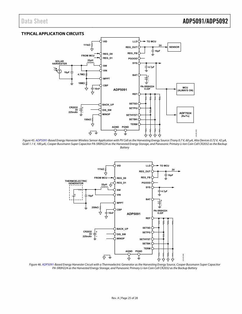
Figure 45. ADP5091-Based Energy Harvester Wireless Sensor Application with PV Cell as the Harvesting Energy Source (Trony 0.7 V, 60 μA, Alta Devices 0.72 V, 42 μA, Gcell 1.1 V, 100 μA), Cooper Bussmann Super Capacitor PA-5R0H224 as the Harvested Energy Storage, and Panasonic Primary Li-Ion Coin Cell CR2032 as the Backup
Battery
+
–
PA-5R0H2240.22F
4.7µF
10µF
2V
10µF
22µH
THERMOELECTRICGENERATOR
CR20323V
225mAh
250kΩ
111kΩ
PGOOD
LLD
REG_OUT
REG_FB
SYS
BAT
REF
ADP5091
SETSD
SETPG
SETHYST
SETBK
TERM
MINOP
DIS_SW
BACK_UP
CBP10nF
MPPT
VIN
SW
FROM MCU
TO MCU
REG_D1
REG_D0
VID
PGNDAGND
1414
5-04
6
+
+
–
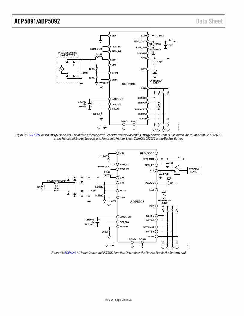
Figure 46. ADP5091-Based Energy Harvester Circuit with a Thermoelectric Generator as the Harvesting Energy Source, Cooper Bussmann Super Capacitor
PA-5R0H224 as the Harvested Energy Storage, and Panasonic Primary Li-Ion Coin Cell CR2032 as the Backup Battery
ADP5091/ADP5092 Data Sheet
Rev. A | Page 26 of 28
+
–
+
–
PA-5R0H2240.22F
4.7µF
10µF
2V
10µF
22µHPIEZOELECTRICHARVESTER
CR20323V
225mAh
10MΩ
10MΩ
10MΩR1
R2 10MΩ
200kΩ
PGOOD
LLD
REG_OUT
REG_FB
SYS
BAT
REFADP5091
SETSD
SETPG
SETHYST
SETBK
TERM
MINOP
DIS_SW
BACK_UP
CBP10nF
MPPT
VIN
SW
FROM MCU
TO MCU
REG_D1
REG_D0
VID
PGNDAGND
1414
5-04
7
Figure 47. ADP5091-Based Energy Harvester Circuit with a Piezoelectric Generator as the Harvesting Energy Source, Cooper Bussmann Super Capacitor PA-5R0H224
as the Harvested Energy Storage, and Panasonic Primary Li-Ion Coin Cell CR2032 as the Backup Battery
+
–
+
–
PA-5R0H2240.22F
4.7µF
1µF
SYS
SYSTEMLOAD
2V
10µFAC
TRANSFORMER
22µH
CR20323V
225mAh
14.7MΩ
6.34MΩ
111kΩ
20kΩ
REG_OUT
REG_FB
SYS
PGOOD
BAT
REFADP5092
SETSD
SETPG
SETHYST
SETBK
TERM
MINOP
DIS_SW
BACK_UP
CBP10nF
MPPT
VIN
SW
FROM MCUREG_D1
REG_D0
VID
PGNDAGND
1414
5-04
8
REG_GOOD
Figure 48. ADP5092 AC Input Source and PGOOD Function Determines the Time to Enable the System Load

Data Sheet ADP5091/ADP5092
Rev. A | Page 27 of 28
FACTORY PROGRAMMABLE OPTIONS To order a device with options other than the default options, contact a local Analog Devices, Inc., sales or distribution representative.
Table 12. Input Current-Limit Options Option Description Option 0 200 mA (default) Option 1 300 mA
Table 13. VIN Open Circuit Voltage Sampling Cycle Options Option Description Option 0 4 sec Option 1 8 sec Option 2 16 sec (default) Option 3 32 sec
ADP5091/ADP5092 Data Sheet
Rev. A | Page 28 of 28
OUTLINE DIMENSIONS
0.800.750.70
PK
G-0
03
99
4/5
111
0.50BSC
0.500.400.30
COMPLIANT TO JEDEC STANDARDS MO-220-WGGD-8
BOTTOM VIEWTOP VIEW
4.104.00 SQ3.90
0.05 MAX0.02 NOM
0.203 REF
COPLANARITY0.08
PIN 1INDICATOR
1
24
712
13
18
19
6
03-
09
-20
17-B
0.300.250.20
0.20 MIN
2.442.30 SQ2.16
EXPOSEDPAD
SEATINGPLANE
PIN 1INDIC ATOR AREA OPTIONS(SEE DETAIL A)
DETAIL A(JEDEC 95)
FOR PROPER CONNECTION OFTHE EXPOSED PAD, REFER TOTHE PIN CONFIGURATION ANDFUNCTION DESCRIPTIONSSECTION OF THIS DATA SHEET.
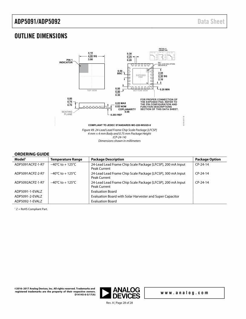
Figure 49. 24-Lead Lead Frame Chip Scale Package [LFCSP]
4 mm × 4 mm Body and 0.75 mm Package Height (CP-24-14)
Dimensions shown in millimeters
ORDERING GUIDE Model1 Temperature Range Package Description Package Option ADP5091ACPZ-1-R7 −40°C to + 125°C 24-Lead Lead Frame Chip Scale Package [LFCSP], 200 mA Input
Peak Current CP-24-14
ADP5091ACPZ-2-R7 −40°C to + 125°C 24-Lead Lead Frame Chip Scale Package [LFCSP], 300 mA Input Peak Current
CP-24-14
ADP5092ACPZ-1-R7 −40°C to + 125°C 24-Lead Lead Frame Chip Scale Package [LFCSP], 200 mA Input Peak Current
CP-24-14
ADP5091-1-EVALZ Evaluation Board ADP5091-2-EVALZ Evaluation Board with Solar Harvester and Super Capacitor ADP5092-1-EVALZ Evaluation Board 1 Z = RoHS Compliant Part.
©2016–2017 Analog Devices, Inc. All rights reserved. Trademarks and registered trademarks are the property of their respective owners. D14145-0-5/17(A)
Recommended