...
...
REXT
GND
OUT14
OUT1
OUT15
OUT0
TLC59116 OUT13A0-A3
R-EXT
VDD
RESET
SDA
SCL
RESET
SDA
SCL
MC
U
+5V
IN SHDN
GNDOUT
SENSE
+3.3V
+3.3V
Product
Folder
Sample &Buy
Technical
Documents
Tools &
Software
Support &Community
TLC59116SLDS157E –FEBRUARY 2008–REVISED DECEMBER 2014
TLC59116 16-Channel FM+ I2C-Bus Constant-Current LED Sink Driver1
1 Features• 16 LED Drivers (Each Output Programmable at • Supports Hot Insertion
Off, On, Programmable LED Brightness, or • Low Standby CurrentProgrammable Group Dimming and Blinking • 3.3-V or 5-V Supply VoltageMixed With Individual LED Brightness) • 5.5-V Tolerant Inputs
• 16 Constant-Current Output Channels • Offered in 28-Pin Thin Shrink Small-Outline• 256-Step (8-Bit) Linear Programmable Brightness Package (TSSOP) (PW) and 32-Pin Quad
Per LED Output Varying From Fully Off (Default) Flatpack No Lead (QFN)to Maximum Brightness Using a 97-kHz PWM • –40 °C to 85 °C OperationSignal
• 256-Step Group Brightness Control Allows 2 ApplicationsGeneral Dimming [Using a 190-Hz PWM Signal
• GamingFrom Fully Off to Maximum Brightness (Default)]• Small Signage• 256-Step Group Blinking With Frequency• Industrial EquipmentProgrammable From 24 Hz to 10.73 s and Duty
Cycle From 0% to 99.6%3 Description• Four Hardware Address Pins Allow 14 TLC59116The TLC59116 is an I2C bus controlled 16-channelDevices to Be Connected to Same I2C BusLED driver that is optimized for red/green/blue/amber• Four Software-Programmable I2C Bus Addresses (RGBA) color mixing and backlight application. Each(One LED Group Call Address and Three LED LED output has its own 8-bit resolution (256 steps)
Sub Call Addresses) Allow Groups of Devices to fixed-frequency individual PWM controller thatBe Addressed at Same Time in Any Combination operates at 97 kHz, with a duty cycle that is
adjustable from 0% to 99.6%.• Software Reset Feature (SWRST Call) AllowsDevice to Be Reset Through I2C Bus
Device Information(1)• Up to 14 Possible Hardware-Adjustable Individual
PART NUMBER PACKAGE BODY SIZE (NOM)I2C Bus Addresses Per Device, So That EachTSSOP (28) 9.70 mm × 4.40 mmDevice Can Be Programmed TLC59116VQFN (32) 5.00 mm × 5.00 mm• Open-Load and Overtemperature Detection Mode
(1) For all available packages, see the orderable addendum atto Detect Individual LED Errorsthe end of the datasheet.• Output State Change Programmable on
Acknowledge or Stop Command to Update TLC59116 Typical ApplicationOutputs Byte-by-Byte or All at Same Time (Defaultto Change on Stop)
• Output Current Adjusted Through an ExternalResistor
• Constant Output Current Range: 5 mA to 120 mA• Maximum Output Voltage: 17 V• 25-MHz Internal Oscillator Requires No External
Components• 1-MHz Fast-mode Plus (FMT) Compatible I2C Bus
Interface With 30-mA High-Drive Capability onSDA Output for Driving High-Capacitive Buses
• Internal Power-On Reset• Noise Filter on SCL and SDA Inputs• No Glitch on Power-Up• Active-Low Reset
1
An IMPORTANT NOTICE at the end of this data sheet addresses availability, warranty, changes, use in safety-critical applications,intellectual property matters and other important disclaimers. PRODUCTION DATA.

TLC59116SLDS157E –FEBRUARY 2008–REVISED DECEMBER 2014 www.ti.com
Table of Contents9.2 Functional Block Diagram ....................................... 121 Features .................................................................. 19.3 Feature Description................................................. 122 Applications ........................................................... 19.4 Device Functional Modes........................................ 153 Description ............................................................. 19.5 Register Maps ......................................................... 154 Revision History..................................................... 2
10 Application and Implementation........................ 235 Description (continued)......................................... 310.1 Application Information.......................................... 236 Pin Configuration and Functions ......................... 410.2 Typical Application ................................................ 287 Specifications......................................................... 6 11 Power Supply Recommendations ..................... 307.1 Absolute Maximum Ratings ...................................... 6
12 Layout................................................................... 307.2 Handling Ratings....................................................... 612.1 Layout Guidelines ................................................. 307.3 Recommended Operating Conditions ...................... 612.2 Layout Example .................................................... 307.4 Thermal Information .................................................. 612.3 Thermal Considerations ........................................ 317.5 Electrical Characteristics........................................... 7
13 Device and Documentation Support ................. 327.6 Timing Requirements ................................................ 813.1 Trademarks ........................................................... 327.7 Typical Characteristics .............................................. 913.2 Electrostatic Discharge Caution............................ 328 Parameter Measurement Information ................ 1013.3 Glossary ................................................................ 329 Detailed Description ............................................ 12
14 Mechanical, Packaging, and Orderable9.1 Overview ................................................................. 12 Information ........................................................... 32
4 Revision HistoryNOTE: Page numbers for previous revisions may differ from page numbers in the current version.
Changes from Revision D (June 2011) to Revision E Page
• Added Pin Configuration and Functions section, ESD Ratings table, Feature Description section, Device FunctionalModes, Application and Implementation section, Power Supply Recommendations section, Layout section, Deviceand Documentation Support section, and Mechanical, Packaging, and Orderable Information section .............................. 1
Changes from Revision C (June 2010) to Revision D Page
• Added Output Current vs Output Voltage Figure. .................................................................................................................. 9• Changed "SLEEP" to "OSC" in Mode Register 1 (MODE1) Table....................................................................................... 16• Added Bits 6 and 4 to the Mode Register 2 Bit Description Table. ...................................................................................... 16• Changed VALUES column in the Mode Register 2 Bit Description Table. .......................................................................... 16
2 Submit Documentation Feedback Copyright © 2008–2014, Texas Instruments Incorporated
Product Folder Links: TLC59116

TLC59116www.ti.com SLDS157E –FEBRUARY 2008–REVISED DECEMBER 2014
5 Description (continued)The individual PWM controller allows each LED to be set to a specific brightness value. An additional 8-bitresolution (256 steps) group PWM controller has both a fixed frequency of 190 Hz and an adjustable frequencybetween 24 Hz to once every 10.73 seconds, with a duty cycle that is adjustable from 0% to 99.6%. The groupPWM controller dims or blinks all LEDs with the same value.
Each LED output can be off, on (no PWM control), or set at its individual PWM controller value at both individualand group PWM controller values.
The TLC59116 operates with a supply voltage range of 3 V to 5.5 V and the outputs are 17 V tolerant. LEDs canbe directly connected to the TLC59116 device outputs.
Software programmable LED Group and three Sub Call I2C-bus addresses allow all or defined groups ofTLC59116 devices to respond to a common I2C-bus address, allowing for example, all the same color LEDs tobe turned on or off at the same time or marquee chasing effect, thus minimizing I2C-bus commands.
Four hardware address pins allow up to 14 devices on the same bus.
The Software Reset (SWRST) Call allows the master to perform a reset of the TLC59116 through the I2C-bus,identical to the Power-On Reset (POR) that initializes the registers to their default state causing the outputs to beset high (LED off). This allows an easy and quick way to reconfigure all device registers to the same condition.
Copyright © 2008–2014, Texas Instruments Incorporated Submit Documentation Feedback 3
Product Folder Links: TLC59116

RHB PACKAGE(TOP VIEW)
32 31 30 29 28 27 26 2524
23
22
21
20
19
18
17
9 10 11 12 13 15 16
A2
A3
OUT0
OUT1
OUT2
OUT3
GND
OUT4
RESET
GND
OUT15
OUT14
OUT13
OUT12
GND
OUT1114
1
2
3
4
5
6
7
8
A1
A0
RE
XT
NC
NC
VC
C
SD
A
SC
L
OU
T5
OU
T6
OU
T7
NC
NC
OU
T8
OU
T9
OU
T10
ExposedThermal Pad
PW PACKAGE
(TOP VIEW)
1
2
3
4
5
6
7
8
9
10
15
16
17
18
23
24
25
26
27
28REXT
A0
A1
A2
A3
OUT0
OUT1
OUT3
GND
VCC
SDA
SCL
RESET
GND
OUT15
OUT11
OUT10
OUT9
OUT8
11
12
13
14
OUT4
OUT5
OUT6
OUT7
19
20
21
22 OUT14
OUT13
OUT12
GND
OUT2
TLC59116SLDS157E –FEBRUARY 2008–REVISED DECEMBER 2014 www.ti.com
6 Pin Configuration and Functions
NC - No internal connectionIf used, the exposed thermal pad must be connected as a secondary ground.
Pin FunctionsPIN
I/O (1) DESCRIPTIONNAME PW NO. RHB NO.
REXT 1 30 I Input terminal used to connect an external resistor for setting up all output currentsA0 2 31 I Address input 0A1 3 32 I Address input 1A2 4 1 I Address input 2A3 5 2 I Address input 3OUT0 6 3 O Constant current output 0OUT1 7 4 O Constant current output 1OUT2 8 5 O Constant current output 2OUT3 9 6 O Constant current output 3GND 10 7 Ground
(1) I = input, O = output
4 Submit Documentation Feedback Copyright © 2008–2014, Texas Instruments Incorporated
Product Folder Links: TLC59116

TLC59116www.ti.com SLDS157E –FEBRUARY 2008–REVISED DECEMBER 2014
Pin Functions (continued)PIN
I/O (1) DESCRIPTIONNAME PW NO. RHB NO.
OUT4 11 8 O Constant current output 4OUT5 12 9 O Constant current output 5OUT6 13 10 O Constant current output 6OUT7 14 11 O Constant current output 7OUT8 15 14 O Constant current output 8OUT9 16 15 O Constant current output 9OUT10 17 16 O Constant current output 10OUT11 18 17 O Constant current output 11GND 19 18 GroundOUT12 20 19 O Constant current output 12OUT13 21 20 O Constant current output 13OUT14 22 21 O Constant current output 14OUT15 23 22 O Constant current output 15GND 24 23 GroundRESET 25 24 I Active-low reset inputSCL 26 25 I Serial clock inputSDA 27 26 I/O Serial data input/outputVCC 28 27 — Power supply
12, 13,NC — — No internal connection28, 29
Copyright © 2008–2014, Texas Instruments Incorporated Submit Documentation Feedback 5
Product Folder Links: TLC59116

TLC59116SLDS157E –FEBRUARY 2008–REVISED DECEMBER 2014 www.ti.com
7 Specifications
7.1 Absolute Maximum Ratingsover operating free-air temperature (unless otherwise noted) (1)
MIN MAX UNITVCC Supply voltage 0 7 VVI Input voltage –0.4 VCC + 0.4 VVO Output voltage –0.5 20 VIO Output current per channel 120 mATJ Junction temperature –40 150 °C
(1) Stresses beyond those listed under Absolute Maximum Ratings may cause permanent damage to the device. These are stress ratingsonly, which do not imply functional operation of the device at these or any other conditions beyond those indicated under RecommendedOperating Conditions. Exposure to absolute-maximum-rated conditions for extended periods may affect device reliability.
7.2 Handling RatingsMIN MAX UNIT
Tstg Storage temperature range –55 150 °CHuman body model (HBM), per ANSI/ESDA/JEDEC JS-001, all 1500pins (1)
V(ESD) Electrostatic discharge VCharged device model (CDM), per JEDEC specification 500JESD22-C101, all pins (2)
(1) JEDEC document JEP155 states that 500-V HBM allows safe manufacturing with a standard ESD control process.(2) JEDEC document JEP157 states that 250-V CDM allows safe manufacturing with a standard ESD control process.
7.3 Recommended Operating ConditionsAll unused inputs of the device must be held at VCC or GND to ensure proper device operation
MIN MAX UNITVCC Supply voltage 3 5.5 VVIH High-level input voltage SCL, SDA, RESET, A0, A1, A2, A3 0.7 × VCC VCC VVIL Low-level input voltage SCL, SDA, RESET, A0, A1, A2, A3 0 0.3 × VCC VVO Supply voltage to output pins OUT0 to OUT15 17 V
VCC = 3 V 20IOL Low-level output current sink SDA mA
VCC = 5 V 30IO Output current per channel OUT0 to OUT15 5 120 mATA Operating free-air temperature –40 85 °C
7.4 Thermal InformationTLC59116
THERMAL METRIC (1) PW RHB UNIT28 PINS 32 PINS
RθJA Junction-to-ambient thermal resistance 78 34.3RθJC(top) Junction-to-case (top) thermal resistance 18.8 26.3RθJB Junction-to-board thermal resistance 36 8.3
°C/WψJT Junction-to-top characterization parameter 0.5 0.4ψJB Junction-to-board characterization parameter 35.5 8.2RθJC(bot) Junction-to-case (bottom) thermal resistance n/a 3.3
(1) For more information about traditional and new thermal metrics, see the IC Package Thermal Metrics application report, SPRA953.
6 Submit Documentation Feedback Copyright © 2008–2014, Texas Instruments Incorporated
Product Folder Links: TLC59116

TLC59116www.ti.com SLDS157E –FEBRUARY 2008–REVISED DECEMBER 2014
7.5 Electrical CharacteristicsVCC = 3 V to 5.5 V, TA = –40 °C to 85 °C (unless otherwise noted)
PARAMETER TEST CONDITIONS MIN TYP (1) MAX UNITSCL, SDA, A0,Input / output leakageII A1, A2, A3, VI = VCC or GND ±0.3 μAcurrent RESET
Output leakage current OUT0 to OUT15 VO = 17 V, TJ = 25°C 0.5 μAVPOR Power-on reset voltage 2.5 V
VCC = 3 V, VOL = 0.4 V 20IOL Low-level output current SDA mA
VCC = 5 V, VOL = 0.4 V 30IO(1) Output current 1 OUT0 to OUT15 VO = 0.6 V, Rext = 720 Ω, CG = 0.992 (2) 26 mA
IO = 26 mA, VO = 0.6 V, Rext = 720 Ω,Output current error OUT0 to OUT15 ±8%TJ = 25°COutput channel to IO = 26 mA, VO = 0.6 V, Rext = 720 Ω,OUT0 to OUT15 ±6%channel current error TJ = 25°C
IO(2) Output current 2 OUT0 to OUT15 VO = 0.8 V, Rext = 360 Ω, CG = 0.992 (2) 52 mAIO = 52 mA, VO = 0.8 V, Rext = 360 Ω,Output current error OUT0 to OUT15 ±8%TJ = 25°C
Output channel to IO = 52 mA, VO = 0.8 V, Rext = 360 Ω,OUT0 to OUT15 ±6%channel current error TJ = 25°CVO = 1 V to 3 V, IO = 26 mA ±0.1IOUT vs Output current vs output OUT0 to OUT15 %/VVOUT voltage regulation VO = 3 V to 5.5 V, IO = 26 mA to 120 mA ±1
Threshold current 1 for 0.5 ×IOUT,Th1 OUT0 to OUT15 IOUT,target = 26 mAerror detection ITARGET%Threshold current 2 for 0.5 ×IOUT,Th2 OUT0 to OUT15 IOUT,target = 52 mAerror detection ITARGET%Threshold current 3 for 0.5 ×IOUT,Th3 OUT0 to OUT15 IOUT,target = 104 mAerror detection ITARGET%
TSD Overtemperature shutdown (3) 150 175 200 °CTHYS Restart hysteresis 15 °C
SCL, A0, A1,Ci Input capacitance VI = VCC or GND 5 pFA2, A3, RESETInput / outputCio SDA VI = VCC or GND 8 pFcapacitance
OUT0 to OUT15 = OFF, 25Rext = OpenOUT0 to OUT15 = OFF, 29Rext = 720 ΩOUT0 to OUT15 = OFF, 32Rext = 360 ΩOUT0 to OUT15 = OFF,ICC Supply current VCC = 5.5 V 37 mARext = 180 ΩOUT0 to OUT15 = ON, 29Rext = 720 ΩOUT0 to OUT15 = ON, 32Rext = 360 ΩOUT0 to OUT15 = ON, 37Rext = 180 Ω
(1) All typical values are at TA = 25 °C.(2) CG is the Current Gain and is defined in Table 12.(3) Specified by design
Copyright © 2008–2014, Texas Instruments Incorporated Submit Documentation Feedback 7
Product Folder Links: TLC59116

TLC59116SLDS157E –FEBRUARY 2008–REVISED DECEMBER 2014 www.ti.com
7.6 Timing RequirementsTA = –40 °C to 85 °C
STANDARD MODE FAST MODE FAST MODE PLUSI2C BUS I2C BUS I2C BUS UNIT
MIN MAX MIN MAX MIN MAXI2C INTERFACEfSCL SCL clock frequency (1) 0 100 0 400 0 1000 kHz
I2C bus free time between Stop andtBUF 4.7 1.3 0.5 μsStart conditionstHD;STA Hold time (repeated) Start condition 4 0.6 0.26 μs
Set-up time for a repeated StarttSU;STA 4.7 0.6 0.26 μsconditiontSU;STO Set-up time for Stop condition 4 0.6 0.26 μstHD;DAT Data hold time 0 0 0 nstVD;ACK Data valid acknowledge time (2) 0.3 3.45 0.1 0.9 0.05 0.45 μstVD;DAT Data valid time (3) 0.3 3.45 0.1 0.9 0.05 0.45 μstSU;DAT Data set-up time 250 100 50 nstLOW Low period of SCL clock 4.7 1.3 0.5 μstHIGH High period of SCL clock 4 0.6 0.26 μs
Fall time of both SDA and SCLtf 300 20+0.1Cb(6) 300 120 nssignals (4) (5)
Rise time of both SDA and SCLtr 1000 20+0.1Cb(6) 300 120 nssignals
Pulse width of spikes that must betSP 50 50 50 nssuppressed by the input filter (7)
RESETtW Reset pulse width 10 10 10 nstREC Reset recovery time 0 0 0 nstRESET Time to reset (8) (9) 400 400 400 ns
(1) Minimum SCL clock frequency is limited by the bus time-out feature, which resets the serial bus interface if either SDA or SCL is heldlow for a minimum of 25 ms. Disable bus time-out feature for dc operation.
(2) tVD;ACK = time for ACK signal from SCL low to SDA (out) low.(3) tVD;DAT = minimum time for SDA data out to be valid following SCL low.(4) A master device must internally provide a hold time of at least 300 ns for the SDA signal (refer to the VIL of the SCL signal) in order to
bridge the undefined region of the SCL falling edge.(5) The maximum tf for the SDA and SCL bus lines is specified at 300 ns. The maximum fall time (tf) for the SDA output stage is specified
at 250 ns. This allows series protection resistors to be connected between the SDA and the SCL pins and the SDA/SCL bus lineswithout exceeding the maximum specified tf.
(6) Cb = Total capacitance of one bus line in pF(7) Input filters on the SDA and SCL inputs suppress noise spikes less than 50 ns.(8) Resetting the device while actively communicating on the bus may cause glitches or errant Stop conditions.(9) Upon reset, the full delay will be the sum of tRESET and the RC time constant of the SDA bus.
8 Submit Documentation Feedback Copyright © 2008–2014, Texas Instruments Incorporated
Product Folder Links: TLC59116

0
25
50
75
100
125
150
0 2.01.0 3.0
Outp
ut C
urr
ent (m
A)
Output Voltage (V)
I = 120 mAO
I = 100 mAO
I = 80 mAO
I = 60 mAO
I = 40 mAO
I = 20 mAO
I = 5 mAO
0
20
40
60
80
100
120
140
R ( )ext W
0 1500 2500 3500500 1000 2000 3000 4000
Ou
tpu
t C
urr
en
t, I
(A)
out
TLC59116www.ti.com SLDS157E –FEBRUARY 2008–REVISED DECEMBER 2014
7.7 Typical Characteristics
Figure 1. IOUT,target vs Rext Figure 2. Output Current vs Output Voltage
Copyright © 2008–2014, Texas Instruments Incorporated Submit Documentation Feedback 9
Product Folder Links: TLC59116

SCL
SDA
Protocol
START
(S)Condition
Bit 7MSB(A7)
Bit 6(A6)
Bit 7(D1)
Bit 8(D0)
Acknowledge(A)
STOP Condition(P)
tBUF
tLOW 1/fSCL
tHD;STA TSU;STOtSU;DAT
tSU;STA
tHD;DAT tVD;DAT tVD;ACK
tHIGH
tf
tr
SDA
SCL
tBUF
tLOW
tr
tHD;STA
tHD;DAT
tf
tHIGHtSU;DAT Sr
tSU;DAT
tHD;STA tSP
tSU;STO
PP S
SDA
SCL
Start
ACK or Read Cycle
tW
tREC
RESET
30%
50%
tRESET
OUTn
50%
tRESET
TLC59116SLDS157E –FEBRUARY 2008–REVISED DECEMBER 2014 www.ti.com
8 Parameter Measurement Information
Figure 3. Reset Timing
Figure 4. Definition of Timing
NOTE: Rise and fall times refer to VIL and VIH.
Figure 5. I2C Bus Timing
10 Submit Documentation Feedback Copyright © 2008–2014, Texas Instruments Incorporated
Product Folder Links: TLC59116

Pulse
GeneratorDUT
VCC
Open
GNDRL
CL
VO
VCC
VI
RT
TLC59116www.ti.com SLDS157E –FEBRUARY 2008–REVISED DECEMBER 2014
Parameter Measurement Information (continued)
NOTE:• RL = Load resistance for SDA and SCL; should be >1 kΩ at 3-mA or lower current• CL = Load capacitance; includes jig and probe capacitance• RT = Termination resistance; should be equal to the output impedance (ZO) of the pulse generator
Figure 6. Test Circuit for Switching Characteristics
Copyright © 2008–2014, Texas Instruments Incorporated Submit Documentation Feedback 11
Product Folder Links: TLC59116

I C Bus Control2
OUT0 OUT1 OUT14 OUT15REXT
I/O Regulator
Output Driver and Error Detection
LED StateSelect Register
97 kHz GRPFRQRegister
24.3 kHz
190 kHz
PWM Register XBrightness Control
25-MHzOscillator
Power-OnReset Control
Input FilterSCL
SDA
A0 A1 A2 A3
RESET
VCC
GND
0 = Permanently off
1 = Permanently on
GRPPWMRegister
TLC59116SLDS157E –FEBRUARY 2008–REVISED DECEMBER 2014 www.ti.com
9 Detailed Description
9.1 OverviewThe TLC59116 is an I2C bus controlled 16-channel LED driver that is optimized for red/green/blue/amber (RGBA)color mixing and backlight application. Each LED output has its own 8-bit resolution (256 steps) fixed-frequencyindividual PWM controller that operates at 97 kHz, with a duty cycle that is adjustable from 0% to 99.6%. Theindividual PWM controller allows each LED to be set to a specific brightness value. An additional 8-bit resolution(256 steps) group PWM controller has both a fixed frequency of 190 Hz and an adjustable frequency between 24Hz to once every 10.73 seconds, with a duty cycle that is adjustable from 0% to 99.6%. The group PWMcontroller dims or blinks all LEDs with the same value.
9.2 Functional Block Diagram
9.3 Feature Description
9.3.1 Open-Circuit DetectionThe TLC59116 LED open-circuit detection compares the effective current level IOUT with the open load detectionthreshold current IOUT,Th. If IOUT is below the threshold IOUT,Th the TLC59116 detects an open load condition. Thiserror status can be read out as an error flag through the registers EFLAG1 and EFLAG2.
For open-circuit error detection, a channel must be on and the PWM must be off.
Table 1. Open-Circuit DetectionCONDITION OF OUTPUTSTATE OF OUTPUT PORT ERROR STATUS CODE MEANINGCURRENT
Off IOUT = 0 mA 0 Detection not possible
12 Submit Documentation Feedback Copyright © 2008–2014, Texas Instruments Incorporated
Product Folder Links: TLC59116

TLC59116www.ti.com SLDS157E –FEBRUARY 2008–REVISED DECEMBER 2014
Feature Description (continued)Table 1. Open-Circuit Detection (continued)
CONDITION OF OUTPUTSTATE OF OUTPUT PORT ERROR STATUS CODE MEANINGCURRENTIOUT < IOUT,Th
(1) 0 Open circuitOn
IOUT ≥ IOUT,Th(1) Channel n error status bit 1 Normal
(1) IOUT,Th = 0.5 × IOUT,target (typical)
9.3.2 Overtemperature Detection and ShutdownThe TLC59116 LED is equipped with a global overtemperature sensor and 16 individual channel-selectiveovertemperature sensors.• When the global sensor reaches the trip temperature, all output channels are shut down, and the error status
is stored in the internal Error Status register of every channel. After shutdown, the channels automaticallyrestart after cooling down, if the control signal (output latch) remains on. The stored error status is not resetafter cooling down and can be read out as the error status code in registers EFLAG1 and EFLAG2.
• When one of the channel-specific sensors reaches trip temperature, only the affected output channel is shutdown, and the error status is stored only in the internal Error Status register of the affected channel. Aftershutdown, the channel automatically restarts after cooling down, if the control signal (output latch) remainson. The stored error status is not reset after cooling down and can be read out as error status code inregisters EFLAG1 and EFLAG2.
For channel-specific overtemperature error detection, a channel must be on.
The error flags of open-circuit and overtemperature are ORed to set the EFLAG1 and EFLAG2 registers.
The error status code due to overtemperature is reset when the host writes 1 to bit 7 of the MODE2 register. Thehost must write 0 to bit 7 of the MODE2 register to enable the overtemperature error flag.
Table 2. Overtemperature Detection (1)
STATE OF OUTPUT PORT CONDITION ERROR STATUS CODE MEANINGTj < Tj,trip global 1 NormalOn
On → all channels Off Tj > Tj,trip global All error status bits = 0 Global overtemperatureTj < Tj,trip channel n 1 NormalOn
On → Off Tj > Tj,trip channel n Channel n error status bit = 0 Channel n overtemperature
(1) The global shutdown threshold temperature is approximately 170°C.
9.3.3 Power-On Reset (POR)When power is applied to VCC, an internal power-on reset holds the TLC59116 in a reset condition until VCCreaches VPOR. At this point, the reset condition is released and the TLC59116 registers, and I2C bus statemachine are initialized to their default states (all zeroes), causing all the channels to be deselected. Thereafter,VCC must be lowered below 0.2 V to reset the device.
9.3.4 External ResetA reset can be accomplished by holding the RESET pin low for a minimum of tW. The TLC59116 registers andI2C state machine are held in their default states until the RESET input is again high.
This input requires a pullup resistor to VCC if no active connection is used.
9.3.5 Software ResetThe Software Reset Call (SWRST Call) allows all the devices in the I2C bus to be reset to the power-up statevalue through a specific I2C bus command.
The SWRST Call function is defined as the following:1. A Start command is sent by the I2C bus master.2. The reserved SWRST I2C bus address 1101 011 with the R/W bit set to 0 (write) is sent by the I2C bus
Copyright © 2008–2014, Texas Instruments Incorporated Submit Documentation Feedback 13
Product Folder Links: TLC59116

N × 40 nswith N = 0 to 255(PWM register)
256 × 40 ns = 10.24 µs(97.6 kHz)
M × 256 × 2 × 40 nswith M = 0 to 255
(GRPPWM register)
Group Dimming Signal
507
1 2 3 4 5 6 7 8 9 10
11
12 508
509
510
511
512
1 2 3 4 5 6 7 8 9 10
256 × 2 × 256 × 40 ns = 5.24 ms (190.7 Hz)
Resulting Brightness + Group Dimming Signal
1 2 3 4 5 6 7 8
TLC59116SLDS157E –FEBRUARY 2008–REVISED DECEMBER 2014 www.ti.com
master.3. The TLC59116 device(s) acknowledge(s) after seeing the SWRST Call address 1101 0110 (D6h) only. If the
R/W bit is set to 1 (read), no acknowledge is returned to the I2C bus master.4. Once the SWRST Call address has been sent and acknowledged, the master sends two bytes with two
specific values (SWRST data byte 1 and byte 2):(a) Byte1 = A5h: the TLC59116 acknowledges this value only. If byte 1 is not equal to A5h, the TLC59116
does not acknowledge it.(b) Byte 2 = 5Ah: the TLC59116 acknowledges this value only. If byte 2 is not equal to 5Ah, the TLC59116
does not acknowledge it.
If more than two bytes of data are sent, the TLC59116 does not acknowledge any more.5. Once the correct two bytes (SWRST data byte 1 and byte 2 only) have been sent and correctly
acknowledged, the master sends a Stop command to end the SWRST Call. The TLC59116 then resets tothe default value (power-up value) and is ready to be addressed again within the specified bus free time(tBUF).
The I2C bus master may interpret a non-acknowledge from the TLC59116 (at any time) as a SWRST Call Abort.The TLC59116 does not initiate a reset of its registers. This happens only when the format of the Start Callsequence is not correct.
9.3.6 Individual Brightness Control With Group Dimming/BlinkingA 97-kHz fixed-frequency signal with programmable duty cycle (8 bits, 256 steps) is used to control the individualbrightness for each LED.
On top of this signal, one of the following signals can be superimposed (this signal can be applied to the fourLED outputs):• A lower 190-Hz fixed-frequency signal with programmable duty cycle (8 bits, 256 steps) provides a global
brightness control.• A programmable frequency signal from 24 Hz to 1/10.73 s (8 bits, 256 steps) provides a global blinking
control.
NOTE:• Minimum pulse width for LEDn brightness control is 40 ns.• Minimum pulse width for group dimming is 20.48 μs.• When M = 1 (GRPPWM register value), the resulting LEDn Brightness Control + Group Dimming signal has two
pulses of the LED Brightness Control signal (pulse width = n × 40 ns, with n defined in the PWMx register).• This resulting Brightness + Group Dimming signal shows a resulting control signal with M = 4 (8 pulses).
Figure 7. Brightness and Group Dimming Signals
14 Submit Documentation Feedback Copyright © 2008–2014, Texas Instruments Incorporated
Product Folder Links: TLC59116

TLC59116www.ti.com SLDS157E –FEBRUARY 2008–REVISED DECEMBER 2014
9.4 Device Functional Modes
9.4.1 ActiveActive mode occurs when one or more of the output channels is enabled.
9.4.2 StandbyStandby mode occurs when all output channels are disabled. Standby mode may be entered via I2C command orby pulling the RESET pin low.
9.5 Register MapsTable 3 describes the registers in the TLC59116.
Table 3. Register DescriptionsREGISTERNUMBER NAME ACCESS (1) DESCRIPTION
(HEX)00 MODE1 R/W Mode 101 MODE2 R/W Mode 202 PWM0 R/W Brightness control LED003 PWM1 R/W Brightness control LED104 PWM2 R/W Brightness control LED205 PWM3 R/W Brightness control LED306 PWM4 R/W Brightness control LED407 PWM5 R/W Brightness control LED508 PWM6 R/W Brightness control LED609 PWM7 R/W Brightness control LED70A PWM8 R/W Brightness control LED80B PWM9 R/W Brightness control LED90C PWM10 R/W Brightness control LED100D PWM11 R/W Brightness control LED110E PWM12 R/W Brightness control LED120F PWM13 R/W Brightness control LED1310 PWM14 R/W Brightness control LED1411 PWM15 R/W Brightness control LED1512 GRPPWM R/W Group duty cycle control13 GRPFREQ R/W Group frequency14 LEDOUT0 R/W LED output state 015 LEDOUT1 R/W LED output state 116 LEDOUT2 R/W LED output state 217 LEDOUT3 R/W LED output state 318 SUBADR1 R/W I2C bus subaddress 119 SUBADR2 R/W I2C bus subaddress 21A SUBADR3 R/W I2C bus subaddress 31B ALLCALLADR R/W LED All Call I2C bus address1C IREF R/W IREF configuration1D EFLAG1 R Error flags 11E EFLAG2 R Error flags 2
(1) R = read, W = write
Copyright © 2008–2014, Texas Instruments Incorporated Submit Documentation Feedback 15
Product Folder Links: TLC59116

TLC59116SLDS157E –FEBRUARY 2008–REVISED DECEMBER 2014 www.ti.com
9.5.1 Mode Register 1 (MODE1)Table 4 describes Mode Register 1.
Table 4. MODE1 – Mode Register 1 (Address 00h) Bit DescriptionBIT SYMBOL ACCESS (1) VALUE DESCRIPTION
0 (2) Register auto-increment disabled7 AI2 R
1 Register auto-increment enabled0 (2) Auto-increment bit 1 = 0
6 AI1 R1 Auto-increment bit 1 = 1
0 (2) Auto-increment bit 0 = 05 AI0 R
1 Auto-increment bit 0 = 10 Normal mode (3)
4 OSC R/W1 (2) Oscillator off.0 (2) Device does not respond to I2C bus subaddress 1.
3 SUB1 R/W1 Device responds to I2C bus subaddress 1.
0 (2) Device does not respond to I2C bus subaddress 2.2 SUB2 R/W
1 Device responds to I2C bus subaddress 2.0 (2) Device does not respond to I2C bus subaddress 3.
1 SUB3 R/W1 Device responds to I2C bus subaddress 3.0 Device does not respond to LED All Call I2C bus address.
0 ALLCALL R/W1 (2) Device responds to LED All Call I2C bus address.
(1) R = read, W = write(2) Default value(3) Requires 500 μs maximum for the oscillator to be up and running once OSC bit has been set to logic 1. Timings on LED outputs are not
ensured if PWMx, GRPPWM, or GRPFREQ registers are accessed within the 500-μs window.
NOTEThe OSC bit (Bit 4) must be set to 0 before any outputs will turn on. Proper operationrequires this bit to be 0. Setting the bit to a 1 will turn all channels off.
9.5.2 Mode Register 2 (MODE2)Table 5 describes Mode Register 2.
Table 5. MODE2 – Mode Register 2 (Address 01h) Bit DescriptionBIT SYMBOL ACCESS (1) VALUE DESCRIPTION
0 (2) Enable error status flag7 EFCLR R/W
1 Clear error status flag6 R 0 (2) Reserved
0 (2) Group control = dimming5 DMBLNK R/W
1 Group control = blinking4 R 0 (2) Reserved
0 (2) Outputs change on Stop command (3)3 OCH R/W
1 Outputs change on ACK2:0 R 000 (2) Reserved
(1) R = read, W = write(2) Default value(3) Change of the outputs at the Stop command allows synchronizing outputs of more than one TLC59116. Applicable to registers from 02h
(PWM0) to 17h (LEDOUT3) only.
16 Submit Documentation Feedback Copyright © 2008–2014, Texas Instruments Incorporated
Product Folder Links: TLC59116

TLC59116www.ti.com SLDS157E –FEBRUARY 2008–REVISED DECEMBER 2014
9.5.3 Brightness Control Registers 0 to 15 (PWM0 to PWM15)Table 6 describes Brightness Control Registers 0 to 15.
Table 6. PWM0 to PWM15 – Brightness Control Registers 0 to 15 (Address 02h to 11h) Bit DescriptionADDRESS REGISTER BIT SYMBOL ACCESS (1) VALUE DESCRIPTION
02h PWM0 7:0 IDC0[7:0] R/W 0000 0000 (2) PWM0 individual duty cycle03h PWM1 7:0 IDC1[7:0] R/W 0000 0000 (2) PWM1 individual duty cycle04h PWM2 7:0 IDC2[7:0] R/W 0000 0000 (2) PWM2 individual duty cycle05h PWM3 7:0 IDC3[7:0] R/W 0000 0000 (2) PWM3 individual duty cycle06h PWM4 7:0 IDC4[7:0] R/W 0000 0000 (2) PWM4 individual duty cycle07h PWM5 7:0 IDC5[7:0] R/W 0000 0000 (2) PWM5 individual duty cycle08h PWM6 7:0 IDC6[7:0] R/W 0000 0000 (2) PWM6 individual duty cycle09h PWM7 7:0 IDC7[7:0] R/W 0000 0000 (2) PWM7 individual duty cycle0Ah PWM8 7:0 IDC8[7:0] R/W 0000 0000 (2) PWM8 individual duty cycle0Bh PWM9 7:0 IDC9[7:0] R/W 0000 0000 (2) PWM9 individual duty cycle0Ch PWM10 7:0 IDC10[7:0] R/W 0000 0000 (2) PWM10 individual duty cycle0Dh PWM11 7:0 IDC11[7:0] R/W 0000 0000 (2) PWM11 individual duty cycle0Eh PWM12 7:0 IDC12[7:0] R/W 0000 0000 (2) PWM12 individual duty cycle0Fh PWM13 7:0 IDC13[7:0] R/W 0000 0000 (2) PWM13 individual duty cycle10h PWM14 7:0 IDC14[7:0] R/W 0000 0000 (2) PWM14 individual duty cycle11h PWM15 7:0 IDC15[7:0] R/W 0000 0000 (2) PWM15 individual duty cycle
(1) R = read, W = write(2) Default value
A 97-kHz fixed frequency signal is used for each output. Duty cycle is controlled through 256 linear steps from00h (0% duty cycle = LED output off) to FFh (99.6% duty cycle = LED output at maximum brightness). Applicableto LED outputs programmed with LDRx = 10 or 11 (LEDOUT0, LEDOUT1, LEDOUT2 and LEDOUT3 registers).
Duty cycle = IDCn[7:0] / 256 (1)
9.5.4 Group Duty Cycle Control Register (GRPPWM)Table 7 describes the Group Duty Cycle Control Register.
Table 7. GRPPWM – Group Brightness Control Register (Address 12h) Bit DescriptionADDRESS REGISTER BIT SYMBOL ACCESS (1) VALUE DESCRIPTION
12h GRPPWM 7:0 GDC0[7:0] R/W 1111 1111 (2) GRPPWM register
(1) R = read, W = write(2) Default value
When the DMBLNK bit (MODE2 register) is programmed with logic 0, a 190-Hz fixed-frequency signal issuperimposed with the 97-kHz individual brightness control signal. GRPPWM is then used as a global brightnesscontrol, allowing the LED outputs to be dimmed with the same value. The value in GRPFREQ is then a Don'tcare.
General brightness for the 16 outputs is controlled through 256 linear steps from 00h (0% duty cycle = LEDoutput off) to FFh (99.6% duty cycle = maximum brightness). This is applicable to LED outputs programmed withLDRx = 11 (LEDOUT0, LEDOUT1, LEDOUT2 and LEDOUT3 registers).
When DMBLNK bit is programmed with logic 1, the GRPPWM and GRPFREQ registers define a global blinkingpattern, where GRPFREQ defines the blinking period (from 24 Hz to 10.73 s) and GRPPWM defines the dutycycle (ON/OFF ratio in %).
Duty cycle = GDC0[7:0] / 256 (2)
Copyright © 2008–2014, Texas Instruments Incorporated Submit Documentation Feedback 17
Product Folder Links: TLC59116

TLC59116SLDS157E –FEBRUARY 2008–REVISED DECEMBER 2014 www.ti.com
9.5.5 Group Frequency Register (GRPFREQ)Table 8 describes the Group Frequency Register.
Table 8. GRPFREQ – Group Frequency Register (Address 13h) Bit DescriptionADDRESS REGISTER BIT SYMBOL ACCESS (1) VALUE DESCRIPTION
13h GRPFREQ 7:0 GFRQ[7:0] R/W 0000 0000 (2) GRPFREQ register
(1) R = read, W = write(2) Default value
GRPFREQ is used to program the global blinking period when the DMBLNK bit (MODE2 register) is equal to 1.Value in this register is a Don't care when DMBLNK = 0. This is applicable to LED output programmed withLDRx = 11 (LEDOUT0, LEDOUT1, LEDOUT2 and LEDOUT3 registers).
The blinking period is controlled through 256 linear steps from 00h (41 ms, frequency 24 Hz) to FFh (10.73 s).Global blinking period (seconds) = (GFRQ[7:0] + 1) / 24
9.5.6 LED Driver Output State Registers 0 to 3 (LEDOUT0 to LEDOUT3)Table 9 describes LED Driver Output State Registers 0 to 3.
Table 9. LEDOUT0 to LEDOUT3 – LED Driver Output State Registers 0 to 3 (Address 14h to 17h)Bit Description
ADDRESS REGISTER BIT SYMBOL ACCESS (1) VALUE DESCRIPTION7:6 LDR3[1:0] R/W 00 (2) LED3 output state control5:4 LDR2[1:0] R/W 00 (2) LED2 output state control
14h LEDOUT03:2 LDR1[1:0] R/W 00 (2) LED1 output state control1:0 LDR0[1:0] R/W 00 (2) LED0 output state control7:6 LDR7[1:0] R/W 00 (2) LED7 output state control5:4 LDR6[1:0] R/W 00 (2) LED6 output state control
15h LEDOUT13:2 LDR5[1:0] R/W 00 (2) LED5 output state control1:0 LDR4[1:0] R/W 00 (2) LED4 output state control7:6 LDR11[1:0] R/W 00 (2) LED11 output state control5:4 LDR10[1:0] R/W 00 (2) LED10 output state control
16h LEDOUT23:2 LDR9[1:0] R/W 00 (2) LED9 output state control1:0 LDR8[1:0] R/W 00 (2) LED8 output state control7:6 LDR15[1:0] R/W 00 (2) LED15 output state control5:4 LDR14[1:0] R/W 00 (2) LED14 output state control
17h LEDOUT33:2 LDR13[1:0] R/W 00 (2) LED13 output state control1:0 LDR12[1:0] R/W 00 (2) LED12 output state control
(1) R = read, W = write(2) Default value
LDRx = 00: LED driver x is off (default power-up state).
LDRx = 01: LED driver x is fully on (individual brightness and group dimming/blinking not controlled).
LDRx = 10: LED driver x is individual brightness can be controlled through its PWMx register.
LDRx = 11: LED driver x is individual brightness and group dimming/blinking can be controlled through its PWMxregister and the GRPPWM registers.
18 Submit Documentation Feedback Copyright © 2008–2014, Texas Instruments Incorporated
Product Folder Links: TLC59116
TLC59116www.ti.com SLDS157E –FEBRUARY 2008–REVISED DECEMBER 2014
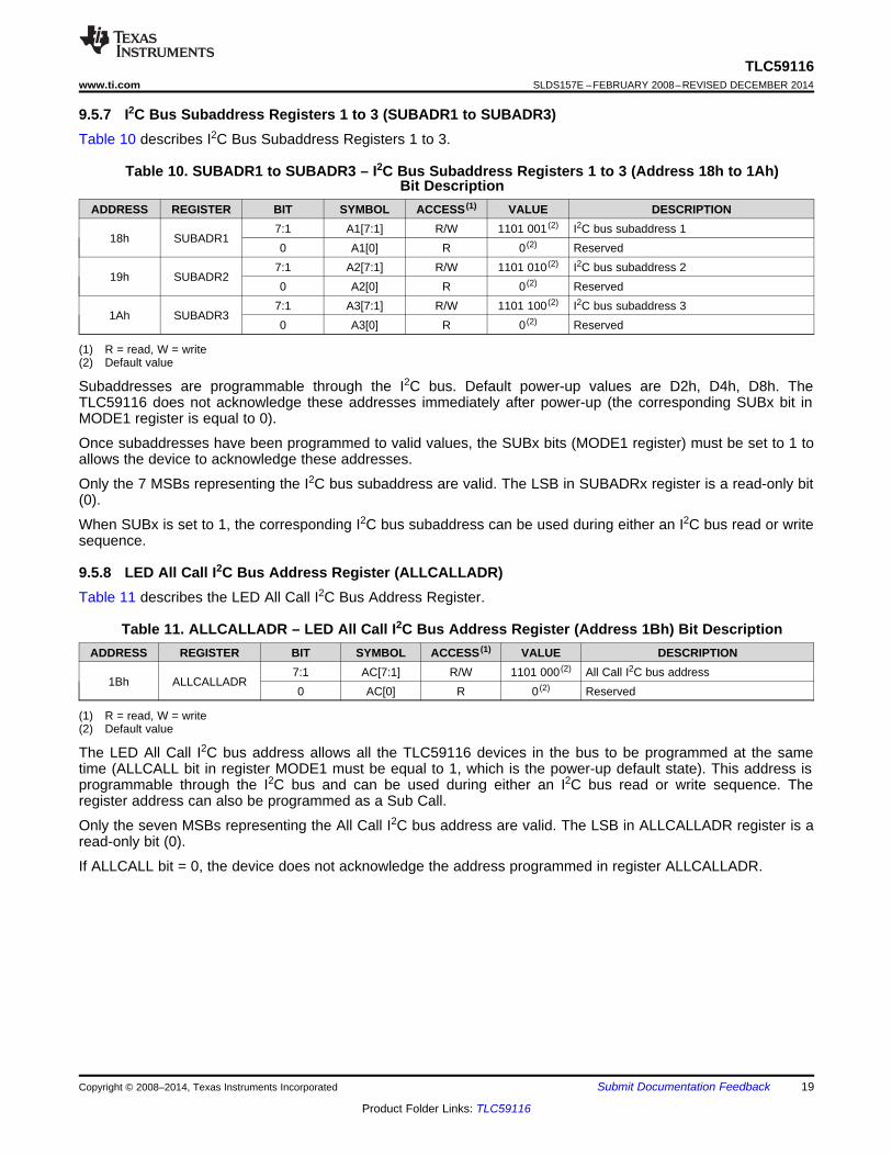
9.5.7 I2C Bus Subaddress Registers 1 to 3 (SUBADR1 to SUBADR3)Table 10 describes I2C Bus Subaddress Registers 1 to 3.
Table 10. SUBADR1 to SUBADR3 – I2C Bus Subaddress Registers 1 to 3 (Address 18h to 1Ah)Bit Description
ADDRESS REGISTER BIT SYMBOL ACCESS (1) VALUE DESCRIPTION7:1 A1[7:1] R/W 1101 001 (2) I2C bus subaddress 1
18h SUBADR10 A1[0] R 0 (2) Reserved
7:1 A2[7:1] R/W 1101 010 (2) I2C bus subaddress 219h SUBADR2
0 A2[0] R 0 (2) Reserved7:1 A3[7:1] R/W 1101 100 (2) I2C bus subaddress 3
1Ah SUBADR30 A3[0] R 0 (2) Reserved
(1) R = read, W = write(2) Default value
Subaddresses are programmable through the I2C bus. Default power-up values are D2h, D4h, D8h. TheTLC59116 does not acknowledge these addresses immediately after power-up (the corresponding SUBx bit inMODE1 register is equal to 0).
Once subaddresses have been programmed to valid values, the SUBx bits (MODE1 register) must be set to 1 toallows the device to acknowledge these addresses.
Only the 7 MSBs representing the I2C bus subaddress are valid. The LSB in SUBADRx register is a read-only bit(0).
When SUBx is set to 1, the corresponding I2C bus subaddress can be used during either an I2C bus read or writesequence.
9.5.8 LED All Call I2C Bus Address Register (ALLCALLADR)Table 11 describes the LED All Call I2C Bus Address Register.
Table 11. ALLCALLADR – LED All Call I2C Bus Address Register (Address 1Bh) Bit DescriptionADDRESS REGISTER BIT SYMBOL ACCESS (1) VALUE DESCRIPTION
7:1 AC[7:1] R/W 1101 000 (2) All Call I2C bus address1Bh ALLCALLADR
0 AC[0] R 0 (2) Reserved
(1) R = read, W = write(2) Default value
The LED All Call I2C bus address allows all the TLC59116 devices in the bus to be programmed at the sametime (ALLCALL bit in register MODE1 must be equal to 1, which is the power-up default state). This address isprogrammable through the I2C bus and can be used during either an I2C bus read or write sequence. Theregister address can also be programmed as a Sub Call.
Only the seven MSBs representing the All Call I2C bus address are valid. The LSB in ALLCALLADR register is aread-only bit (0).
If ALLCALL bit = 0, the device does not acknowledge the address programmed in register ALLCALLADR.
Copyright © 2008–2014, Texas Instruments Incorporated Submit Documentation Feedback 19
Product Folder Links: TLC59116

TLC59116SLDS157E –FEBRUARY 2008–REVISED DECEMBER 2014 www.ti.com
9.5.9 Output Gain Control Register (IREF)Table 12 describes the Output Gain Control Register.
Table 12. IREF – Output Gain Control Register (Address 1Ch) Bit DescriptionADDRESS REGISTER BIT SYMBOL ACCESS (1) VALUE DESCRIPTION
7 CM R/W 1 (2) High/low current multiplier1Ch IREF 6 HC R/W 1 (2) Subcurrent
5:0 CC[5:0] R/W 11 1111 (2) Current multiplier
(1) R = read, W = write(2) Default value
IREF determines the voltage gain (VG), which affects the voltage at the REXT terminal and indirectly thereference current (Iref) flowing through the external resistor at terminal REXT. Bit 0 is the Current Multiplier (CM)bit, which determines the ratio IOUT,target/Iref. Each combination of VG and CM sets a Current Gain (CG).• VG: the relationship between HC,CC[0:5] and the voltage gain is calculated as shown:
VG = (1 + HC) × (1 + D/64) / 4D = CC0 × 25 + CC1 × 24 + CC2 × 23 + CC3 × 22 + CC4 × 21 + CC5 × 20
Where HC is 1 or 0, and D is the binary value of CC[0:5]. So, the VG could be regarded as a floating-pointnumber with 1-bit exponent HC and 6-bit mantissa CC[0:5]. HC,CC[0:5] divides the programmable voltagegain (VG) into 128 steps and two sub-bands:
Low-voltage subband (HC = 0): VG = 1/4 to 127/256, linearly divided into 64 stepsHigh-voltage subband (HC = 1): VG = 1/2 to 127/128, linearly divided into 64 steps
• CM: In addition to determining the ratio IOUT,target/Iref, CM limits the output current range.High Current Multiplier (CM = 1): IOUT,target/Iref = 15, suitable for output current range IOUT = 10 mA to 120 mA.Low Current Multiplier (CM = 0): IOUT,target/Iref = 5, suitable for output current range IOUT = 5 mA to 40 mA
• CG: The total Current Gain is defined as:VREXT = 1.26 V × VGIref = VREXT/Rext, if the external resistor (Rext) is connected to ground.IOUT,target = Iref × 15 × 3CM – 1 = 1.26 V/Rext × VG × 15 × 3CM – 1 = (1.26 V/Rext × 15) × CGCG = VG × 3CM – 1
Therefore, CG = (1/12) to (127/128), divided into 256 steps.
Examples• IREF Code CM, HC, CC[0:5] = 1,1,111111
VG = 127/128 = 0.992 and CG = VG × 30 = VG = 0.992• IREF Code CM, HC, CC[0:5] = 1,1,000000
VG = (1 + 1) × (1 + 0/64)/4 = 1/2 = 0.5, and CG = 0.5• IREF Code CM, HC, CC[0:5] = 0,0,000000
VG = (1 + 0) × (1 + 0/64)/4 = 1/4, and CG = (1/4) × 3–1 = 1/12
After power-on, the default value of the Configuration Code CM, HC, CC[0:5] is 1,1,111111. Therefore,VG = CG = 0.992. The relationship between the Configuration Code and the Current Gain is shown in Figure 8.
20 Submit Documentation Feedback Copyright © 2008–2014, Texas Instruments Incorporated
Product Folder Links: TLC59116

1.00
0.00
0.50
0.25
0.75
Configuration Code (CM, HC, CC[0:5]) in Binary Format
Cu
rren
t G
ain
(C
G)
0,0
,000000
0,0
,010000
0,0
,100000
0,0
,110000
0,1
,000000
0,1
,010000
0,1
,100000
0,1
,110000
1,0
,000000
1,0
,010000
1,0
,100000
1,0
,110000
1,1
,100000
1,1
,110000
1,1
,000000
1,1
,010000
CM = 0 (Low Current Multiplier)
HC = 1 (HighVoltage SubBand)
HC = 0 (LowVoltage SubBand) HC = 1 (High
Voltage SubBand)
CM = 1 (High Current Multiplier)
HC = 0 (LowVoltage SubBand)
TLC59116www.ti.com SLDS157E –FEBRUARY 2008–REVISED DECEMBER 2014
Figure 8. Current Gain vs Configuration Code
9.5.10 Error Flags Registers (EFLAG1, EFLAG2)Table 13 describes Error Flags Registers 1 and 2.
Table 13. EFLAG1, EFLAG2 – Error Flags Registers (Address 1Dh and 1Eh) Bit DescriptionADDRESS REGISTER BIT SYMBOL ACCESS (1) VALUE (2) DESCRIPTION (3)
0 EFLAG1[0] 0 A 1 indicates an error - Channel 01 EFLAG1[1] 0 A 1 indicates an error - Channel 12 EFLAG1[2] 0 A 1 indicates an error - Channel 23 EFLAG1[3] 0 A 1 indicates an error - Channel 3
1Dh EFLAG1 R4 EFLAG1[4] 0 A 1 indicates an error - Channel 45 EFLAG1[5] 0 A 1 indicates an error - Channel 56 EFLAG1[6] 0 A 1 indicates an error - Channel 67 EFLAG1[7] 0 A 1 indicates an error - Channel 70 EFLAG1[0] 0 A 1 indicates an error - Channel 81 EFLAG1[1] 0 A 1 indicates an error - Channel 92 EFLAG1[2] 0 A 1 indicates an error - Channel 103 EFLAG1[3] 0 A 1 indicates an error - Channel 11
1Eh EFLAG2 R4 EFLAG1[4] 0 A 1 indicates an error - Channel 125 EFLAG1[5] 0 A 1 indicates an error - Channel 136 EFLAG1[6] 0 A 1 indicates an error - Channel 147 EFLAG1[7] 0 A 1 indicates an error - Channel 15
(1) R = read, W = write(2) Default value(3) At power-up, in order to initialize the Error Flags registers, the host must write 1 to bit 7 of the MODE2 register and then write 0 to bit 7
of the MODE2 register.
Copyright © 2008–2014, Texas Instruments Incorporated Submit Documentation Feedback 21
Product Folder Links: TLC59116

AI2 AI1 AI0 D4 D2D3 D1 D0
Auto-IncrementOptions
Register AddressAuto-IncrementFlag
TLC59116SLDS157E –FEBRUARY 2008–REVISED DECEMBER 2014 www.ti.com
9.5.11 Control RegisterFollowing the successful acknowledgment of the slave address, LED All Call address or LED Sub Call address,the bus master sends a byte to the TLC59116, which is stored in the Control register. The lowest five bits areused as a pointer to determine which register is accessed (D[4:0]). The highest three bits are used as auto-increment flag and auto-increment options (AI[2:0]).
Figure 9. Control Register
When the auto-increment flag is set (AI2 = logic 1), the five low order bits of the Control register are automaticallyincremented after a read or write. This allows the user to program the registers sequentially. Four different typesof auto-increment are possible, depending on AI1 and AI0 values.
Table 14. Auto-Increment OptionsAI2 AI1 AI0 DESCRIPTION0 0 0 No auto-increment1 0 0 Auto-increment for all registers. D[4:0] roll over to 0 0000 after the last register (1 1011) is accessed.
Auto-increment for individual brightness registers only. D[4:0] roll over to 0 0010 after the last register1 0 1 (1 0001) is accessed.Auto-increment for global control registers only. D[4:0] roll over to 1 0010 after the last register (1 0011) is1 1 0 accessed.Auto-increment for individual and global control registers only. D[4:0] roll over to 0 0010 after the last1 1 1 register (1 0011) is accessed.
NOTEOther combinations are not shown in Table 14. (AI[2:0] = 001, 010, and 011) are reservedand must not be used for proper device operation.
AI[2:0] = 000 is used when the same register must be accessed several times during a single I2C buscommunication, for example, changing the brightness of a single LED. Data is overwritten each time the registeris accessed during a write operation.
AI[2:0] = 100 is used when all the registers must be sequentially accessed, for example, power-up programming.
AI[2:0] = 101 is used when the four LED drivers must be individually programmed with different values during thesame I2C bus communication, for example, changing a color setting to another color setting.
AI[2:0] = 110 is used when the LED drivers must be globally programmed with different settings during the sameI2C bus communication, for example, global brightness or blinking change.
AI[2:0] = 111 is used when individually and global changes must be performed during the same I2C buscommunication, for example, changing color and global brightness at the same time.
Only the five least significant bits D[4:0] are affected by the AI[2:0] bits.
When the Control register is written, the register entry point determined by D[4:0] is the first register that will beaddressed (read or write operation), and can be anywhere between 0 0000 and 1 1011 (as defined in Table 3).When AI[2] = 1, the Auto-Increment flag is set and the rollover value at which the point where the registerincrement stops and goes to the next one is determined by AI[2:0]. See Table 14 for rollover values. Forexample, if the Control register = 1111 0100 (F4h), then the register addressing sequence will be (in hex):
22 Submit Documentation Feedback Copyright © 2008–2014, Texas Instruments Incorporated
Product Folder Links: TLC59116

1 1 0 A3 A1A2 A0
Slave Address
R/W
Fixed Hardware
Selectable
TLC59116www.ti.com SLDS157E –FEBRUARY 2008–REVISED DECEMBER 2014
14 → ... → 1B → 00 → ... → 13 → 02 → ... → 13 → 02 → ... as long as the master keeps sending or readingdata.
10 Application and Implementation
NOTEInformation in the following applications sections is not part of the TI componentspecification, and TI does not warrant its accuracy or completeness. TI’s customers areresponsible for determining suitability of components for their purposes. Customers shouldvalidate and test their design implementation to confirm system functionality.
10.1 Application Information
10.1.1 Device AddressFollowing a Start condition, the bus master must output the address of the slave it is accessing.
10.1.2 Regular I2C Bus Slave AddressThe I2C bus slave address of the TLC59116 is shown in Figure 10. To conserve power, no internal pullupresistors are incorporated on the hardware-selectable address pins, and they must be pulled high or low. Forbuffer management purposes, a set of sector information data should be stored.
Figure 10. Slave Address
The last bit of the address byte defines the operation to be performed. When set to logic 1, a read operation isselected. When set to logic 0, a write operation is selected.
10.1.3 LED All Call I2C Bus Address• Default power-up value (ALLCALLADR register): D0h or 1101 000• Programmable through I2C bus (volatile programming)• At power-up, LED All Call I2C bus address is enabled. TLC59116 sends an ACK when D0h (R/W = 0) or D1h
(R/W = 1) is sent by the master.
See LED All Call I2C Bus Address Register (ALLCALLADR) for more detail.
NOTEThe default LED All Call I2C bus address (D0h or 1101 000) must not be used as a regularI2C bus slave address, since this address is enabled at power-up. All the TLC59116devices on the I2C bus will acknowledge the address if it is sent by the I2C bus master.
10.1.4 LED Sub Call I2C Bus Address• Three different I2C bus addresses can be used• Default power-up values:
– SUBADR1 register: D2h or 1101 001– SUBADR2 register: D4h or 1101 010– SUBADR3 register: D8h or 1101 100
Copyright © 2008–2014, Texas Instruments Incorporated Submit Documentation Feedback 23
Product Folder Links: TLC59116

SDA
SCL
Data Line
Stable;
Data Valid
Change
of Data
Allowed
1 1 0 1 10 1 R/W
TLC59116SLDS157E –FEBRUARY 2008–REVISED DECEMBER 2014 www.ti.com
Application Information (continued)• Programmable through I2C bus (volatile programming)• At power-up, Sub Call I2C bus address is disabled. TLC59116 does not send an ACK when D2h (R/W = 0) or
D3h (R/W = 1) or D4h (R/W = 0) or D5h (R/W = 1) or D8h (R/W = 0) or D9h (R/W = 1) is sent by the master.
See I2C Bus Subaddress Registers 1 to 3 (SUBADR1 to SUBADR3) for more detail.
NOTEThe LED Sub Call I2C bus addresses may be used as regular I2C bus slave addresses iftheir corresponding enable bits are set to 0 in the MODE1 Register.
10.1.5 Software Reset I2C Bus AddressThe address shown in Figure 11 is used when a reset of the TLC59116 is performed by the master. Thesoftware reset address (SWRST Call) must be used with R/W = 0. If R/W = 1, the TLC59116 does notacknowledge the SWRST. See Software Reset for more detail.
Figure 11. Software Reset Address
NOTEThe Software Reset I2C bus address is reserved address and cannot be use as regularI2C bus slave address or as an LED All Call or LED Sub Call address.
10.1.6 Characteristics of the I2C BusThe I2C bus is for two-way two-line communication between different devices or modules. The two lines are aserial data line (SDA) and a serial clock line (SCL). Both lines must be connected to a positive supply via apullup resistor when connected to the output stages of a device. Data transfer may be initiated only when the busis not busy.
10.1.6.1 Bit TransferOne data bit is transferred during each clock pulse. The data on the SDA line must remain stable during the highperiod of the clock pulse as changes in the data line at this time will be interpreted as control signals (seeFigure 12).
Figure 12. Bit Transfer
10.1.6.2 Start and Stop ConditionsBoth data and clock lines remain high when the bus is not busy. A high-to-low transition of the data line while theclock is high is defined as the Start condition (S). A low-to-high transition of the data line while the clock is high isdefined as the Stop condition (P) (see Figure 13).
24 Submit Documentation Feedback Copyright © 2008–2014, Texas Instruments Incorporated
Product Folder Links: TLC59116

Data Output
by Transmitter
SCL From
Master
Start
Condition
S
1 2 8 9
Data Output
by Receiver
Clock Pulse for
Acknowledgment
NACK
ACK
SDA
SCL
Start Condition
S
Stop Condition
P
TLC59116www.ti.com SLDS157E –FEBRUARY 2008–REVISED DECEMBER 2014
Application Information (continued)
Figure 13. Start and Stop Conditions
10.1.6.3 AcknowledgeThe number of data bytes transferred between the Start and the Stop conditions from transmitter to receiver isnot limited. Each byte of eight bits is followed by one acknowledge bit. The acknowledge bit is a high level put onthe bus by the transmitter, whereas the master generates an extra acknowledge related clock pulse.
A slave receiver that is addressed must generate an acknowledge after the reception of each byte. Also a mastermust generate an acknowledge after the reception of each byte that has been clocked out of the slavetransmitter. The device that acknowledges has to pull down the SDA line during the acknowledge clock pulse, sothat the SDA line is stable low during the high period of the acknowledge related clock pulse; set-up time andhold time must be taken into account.
A master receiver must signal an end of data to the transmitter by not generating an acknowledge on the lastbyte that has been clocked out of the slave. In this event, the transmitter must leave the data line high to enablethe master to generate a Stop condition.
Figure 14. Acknowledge/Not Acknowledge on I2C Bus
Copyright © 2008–2014, Texas Instruments Incorporated Submit Documentation Feedback 25
Product Folder Links: TLC59116

Start Condition R/W
Auto-Increment On
ACK From Slave ACK From Slave
0A2A6 A5S A3A4 A1 A0 0 A 1000101 A A
PWM0 RegisterControl RegisterSlave Address
ACK From Slave
Auto-Increment On Brightness Registers Only
ACK From Slave
A P
PWM15 Register
Stop Condition
A
PWM14 Register
ACK From Slave
A
PWM1 Register
PWM0 Register Selection
ACK From Slave
A
PWM0 Register
ACK From Slave
A
PWMx Register
Start Condition R/W
Auto-Increment On
ACK From Slave ACK From Slave
0A21 1S A30 A1 A0 0 A 0000001 A A
MODE1 RegisterControl RegisterSlave Address
ACK From Slave
Auto-Increment On All Registers (see Note A)
ACK From Slave
A P
ALLCALLADR Register
Stop Condition
A
SUBADR3 Register
ACK From Slave
A
MODE2 Register
MODE1 Register Selection
Start Condition R/W
Auto-Increment Flag
ACK From Slave ACK From Slave
D0A21 1S A30 A1 A0 0 A D1D2D3D4XXX A A P
Control RegisterSlave Address
Stop Condition
ACK From Slave
Auto-Increment Options
TLC59116SLDS157E –FEBRUARY 2008–REVISED DECEMBER 2014 www.ti.com
Application Information (continued)
Figure 15. Write to a Specific Register
A. See Table 3 for register definitions.
Figure 16. Write to All Registers Using Auto-Increment
Figure 17. Multiple Writes to Individual Brightness Registers Using Auto-Increment
26 Submit Documentation Feedback Copyright © 2008–2014, Texas Instruments Incorporated
Product Folder Links: TLC59116

Start Condition R/W ACK From theFour Slaves
ACK From theFour Slaves
011 1S 10 0 1 0 A 0101XXX A A P
Control RegisterLED All Call I C Address2
Stop Condition
ACK From Slave
Start Condition R/W
Auto-Increment Flag
ACK From Slave ACK From Slave
1A2A6 A5S A3A4 A1 A0 0 A 1011XXX A A P
Control RegisterSlave Address
Stop Condition
ACK From Slave
Auto-Increment Options
Sequence A
Sequence B
ALLCALLADR Register Selection
New LED All Call I C Address(see Note B)
2
X1011011
LEDOUT0 Register Selection
00 1 10 1 0 1
The 16 LEDs are on at ACK (see Note C)LEDOUT0 Register (LED3 to 0 Fully On)
Start Condition R/W
Auto-Increment On
ACK From Slave ACK From Slave
0A2A6 A5S A3A4 A1 A0 0 A 0000001 A A
Slave AddressControl RegisterSlave Address
ACK From Slave
Auto-Increment On All Registers
ACK From Master
A
Data From PWM0 Register
A
Data From MODE2 Register
ACK From Master
A
Data From MODE1 Register
MODE1 Register Selection
ACK From Master
A
Data From ALLCALLADR Register
P
Stop Condition
NACK From Master
A
Data From Last Read Byte
A2A6 A5 A3A4 A1 A0
R/W
1
ACK From Master
A
Data From MODE1 Register
Sr
ACK From Master
TLC59116www.ti.com SLDS157E –FEBRUARY 2008–REVISED DECEMBER 2014
Application Information (continued)
Figure 18. Read All Registers Auto-Increment
A. In this example, several TLC59116 devices are used, and the same Sequence A is sent to each of them.B. The ALLCALL bit in the MODE1 register is equal to 1 for this example.C. The OCH bit in the MODE2 register is equal to 1 for this example.
Figure 19. LED All Call I2C Bus Address Programming and LED All Call Sequence
Copyright © 2008–2014, Texas Instruments Incorporated Submit Documentation Feedback 27
Product Folder Links: TLC59116

...
...
REXT
931Ω
GND
OUT14
OUT1
OUT15
OUT0
TLC59116 OUT13A0-A3
R-EXT
VDD
RESET
SDA
SCL
RESET
SDA
SCL
MC
U
+5V
IN SHDN
GNDOUT
SENSE
+3.3V
+3.3V
SDA
SCL
Slave
Master
Transmitter/
Receiver
Slave
Receiver
Slave
Transmitter/
Receiver
Master
Transmitter
Master
Transmitter/
Receiver
I C Bus
Multiplexer
2
TLC59116SLDS157E –FEBRUARY 2008–REVISED DECEMBER 2014 www.ti.com
Application Information (continued)10.1.7 System ConfigurationA device generating a message is a transmitter; a device receiving is the receiver. The device that controls themessage is the master and the devices that are controlled by the master are the slaves (see Figure 20).
Figure 20. System Configuration
10.1.8 Constant Current OutputIn LED display applications, TLC59116 provides nearly no current variations from channel to channel and fromdevice to device. While IOUT ≤ 52 mA, the maximum current skew between channels is less than ±6% and lessthan ±8% between devices.
10.2 Typical Application
Figure 21. TLC59116 Typical Application
10.2.1 Design RequirementsSet the LED current to 20mA using the REXT resistor.
28 Submit Documentation Feedback Copyright © 2008–2014, Texas Instruments Incorporated
Product Folder Links: TLC59116

TLC59116www.ti.com SLDS157E –FEBRUARY 2008–REVISED DECEMBER 2014
Typical Application (continued)10.2.2 Detailed Design Procedure
10.2.2.1 Adjusting Output CurrentTLC59116 scales up the reference current (Iref) set by the external resistor (Rext) to sink the output current (Iout) ateach output port. Table 12 shows the Configuration Code and discusses bits CM, HC, and CC[5:0]. The followingformulas can be used to calculate the target output current IOUT,target in the saturation region:
VREXT = 1.26 V × VG (3)Iref = VREXT/Rext, if another end of the external resistor Rext is connected to ground (4)IOUT,target = Iref × 15 × 3CM – 1 (5)
Where Rext is the resistance of the external resistor connected to the REXT terminal, and VREXT is the voltage ofREXT, which is controlled by the programmable voltage gain (VG), which is defined by the Configuration Code.
The Current Multiplier bit (CM) sets the ratio IOUT,target/Iref to 15 or 5 (sets the exponent "CM – 1" to either 0 or–1). After power-on, the default value of VG is 127/128 = 0.992, and the default value of CM is 1, so that the ratioIOUT,target/Iref = 15. Based on the default VG and CM:
VREXT = 1.26 V × 127/128 = 1.25 V (6)IOUT,target = (1.25 V/Rext) × 15 (7)
Therefore, the default current is approximately 20mA at 931 ohms.. The default relationship after power-onbetween IOUT,target and Rext is shown in Figure 1.
Figure 2 shows the output voltage versus the output current with several different resistor values on REXT. Thisshows the minimum voltage required at the device to have full VF across the LED. The VLED voltage must behigher than the VF plus the VOL of the driver. If the VLED is too high, more power will be dissipated in the driver.If this is the case, a resistor can be inserted in series with the LED to dissipate the excess power and reduce thethermal conditions on the driver.
If a single driver is used with LEDs that have different VF values, resistors can also be used in series with theLED to remove the excess power from the driver. In cases where not all outputs are being used, the unusedoutputs can be left floating without issue.
10.2.3 Application CurveFigure 22 shows 20 mA of LED current along with programmed PWM dimming.
Figure 22. LED Current Set to 20 mA Through REXT
Copyright © 2008–2014, Texas Instruments Incorporated Submit Documentation Feedback 29
Product Folder Links: TLC59116

TLC59116SLDS157E –FEBRUARY 2008–REVISED DECEMBER 2014 www.ti.com
11 Power Supply Recommendations
TLC59116 is designed to operate from a VCC range of 3 V to 5.5 V.
12 Layout
12.1 Layout GuidelinesThe I2C signals (SDA / SCL) should be kept away from potential noise sources.
The traces carrying power through the LEDS should be wide enough to the handle necessary current.
All LED current passes through the device and into the ground node. There must be a strong connectionbetween the device ground and the circuit board ground. For the RHB package, the thermal pad should beconnected to ground to help dissipate heat.
12.2 Layout Example
Figure 23. PW Layout Example
30 Submit Documentation Feedback Copyright © 2008–2014, Texas Instruments Incorporated
Product Folder Links: TLC59116

J(max) A
D(max)
JA
T TP
-=
Q
RE
XT
A0
A1
A2
A3
OUT0
OUT1
OUT2
OUT3
GND
OUT4
OU
T5
OU
T6
OU
T7
VC
C
SD
A
SC
L
RESET
GND
OUT15
OUT14
OUT13
OUT12
GND
OUT11
OU
T10
OU
T9
OU
T8
NC
NC
NC
NC
VIA to GND
To µC
To µC
To µC
TLC59116www.ti.com SLDS157E –FEBRUARY 2008–REVISED DECEMBER 2014
Layout Example (continued)
Figure 24. RHB Layout Example
The thermal relief vias are connected to the power pad of the RHB package shown in Figure 24.
12.3 Thermal ConsiderationsThe maximum IC junction temperature should be restricted to 150°C under normal operating conditions. Tocalculate the maximum allowable dissipation, PD(max) for a given ambient temperature, use the followingequation as a guideline:
where• PD(max) = maximum allowable power dissipation• TJ(max) = maximum allowable junction temperature (150°C for the TLC59116)• TA = ambient temperature of the device• ΘJA = junction to air thermal impedance. (8)
See Thermal Information section. This parameter is highly dependent upon board layout.
Power dissipation in the device is determined by the LED current and the voltage at the OUTx pins. For example,if the LED current is 50 mA continuous through each channel and the output voltage is 1 V on each channel,then the total power dissipation is 50 mA x 1 V x 16 ch = 0.8 W
Copyright © 2008–2014, Texas Instruments Incorporated Submit Documentation Feedback 31
Product Folder Links: TLC59116

TLC59116SLDS157E –FEBRUARY 2008–REVISED DECEMBER 2014 www.ti.com
13 Device and Documentation Support
13.1 TrademarksAll trademarks are the property of their respective owners.
13.2 Electrostatic Discharge CautionThese devices have limited built-in ESD protection. The leads should be shorted together or the device placed in conductive foamduring storage or handling to prevent electrostatic damage to the MOS gates.
13.3 GlossarySLYZ022 — TI Glossary.
This glossary lists and explains terms, acronyms, and definitions.
14 Mechanical, Packaging, and Orderable InformationThe following pages include mechanical, packaging, and orderable information. This information is the mostcurrent data available for the designated devices. This data is subject to change without notice and revision ofthis document. For browser-based versions of this data sheet, refer to the left-hand navigation.
32 Submit Documentation Feedback Copyright © 2008–2014, Texas Instruments Incorporated
Product Folder Links: TLC59116

PACKAGE OPTION ADDENDUM
www.ti.com 22-Jul-2014
Addendum-Page 1
PACKAGING INFORMATION
Orderable Device Status(1)
Package Type PackageDrawing
Pins PackageQty
Eco Plan(2)
Lead/Ball Finish(6)
MSL Peak Temp(3)
Op Temp (°C) Device Marking(4/5)
Samples
TLC59116IPWR ACTIVE TSSOP PW 28 2000 Green (RoHS& no Sb/Br)
CU NIPDAU Level-1-260C-UNLIM -40 to 85 Y59116
TLC59116IPWRG4 ACTIVE TSSOP PW 28 2000 Green (RoHS& no Sb/Br)
CU NIPDAU Level-1-260C-UNLIM -40 to 85 Y59116
TLC59116IRHBR ACTIVE VQFN RHB 32 3000 Green (RoHS& no Sb/Br)
CU NIPDAU Level-2-260C-1 YEAR -40 to 85 Y59116
(1) The marketing status values are defined as follows:ACTIVE: Product device recommended for new designs.LIFEBUY: TI has announced that the device will be discontinued, and a lifetime-buy period is in effect.NRND: Not recommended for new designs. Device is in production to support existing customers, but TI does not recommend using this part in a new design.PREVIEW: Device has been announced but is not in production. Samples may or may not be available.OBSOLETE: TI has discontinued the production of the device.
(2) Eco Plan - The planned eco-friendly classification: Pb-Free (RoHS), Pb-Free (RoHS Exempt), or Green (RoHS & no Sb/Br) - please check http://www.ti.com/productcontent for the latest availabilityinformation and additional product content details.TBD: The Pb-Free/Green conversion plan has not been defined.Pb-Free (RoHS): TI's terms "Lead-Free" or "Pb-Free" mean semiconductor products that are compatible with the current RoHS requirements for all 6 substances, including the requirement thatlead not exceed 0.1% by weight in homogeneous materials. Where designed to be soldered at high temperatures, TI Pb-Free products are suitable for use in specified lead-free processes.Pb-Free (RoHS Exempt): This component has a RoHS exemption for either 1) lead-based flip-chip solder bumps used between the die and package, or 2) lead-based die adhesive used betweenthe die and leadframe. The component is otherwise considered Pb-Free (RoHS compatible) as defined above.Green (RoHS & no Sb/Br): TI defines "Green" to mean Pb-Free (RoHS compatible), and free of Bromine (Br) and Antimony (Sb) based flame retardants (Br or Sb do not exceed 0.1% by weightin homogeneous material)
(3) MSL, Peak Temp. - The Moisture Sensitivity Level rating according to the JEDEC industry standard classifications, and peak solder temperature.
(4) There may be additional marking, which relates to the logo, the lot trace code information, or the environmental category on the device.
(5) Multiple Device Markings will be inside parentheses. Only one Device Marking contained in parentheses and separated by a "~" will appear on a device. If a line is indented then it is a continuationof the previous line and the two combined represent the entire Device Marking for that device.
(6) Lead/Ball Finish - Orderable Devices may have multiple material finish options. Finish options are separated by a vertical ruled line. Lead/Ball Finish values may wrap to two lines if the finishvalue exceeds the maximum column width.
Important Information and Disclaimer:The information provided on this page represents TI's knowledge and belief as of the date that it is provided. TI bases its knowledge and belief on informationprovided by third parties, and makes no representation or warranty as to the accuracy of such information. Efforts are underway to better integrate information from third parties. TI has taken and

PACKAGE OPTION ADDENDUM
www.ti.com 22-Jul-2014
Addendum-Page 2
continues to take reasonable steps to provide representative and accurate information but may not have conducted destructive testing or chemical analysis on incoming materials and chemicals.TI and TI suppliers consider certain information to be proprietary, and thus CAS numbers and other limited information may not be available for release.
In no event shall TI's liability arising out of such information exceed the total purchase price of the TI part(s) at issue in this document sold by TI to Customer on an annual basis.

TAPE AND REEL INFORMATION
*All dimensions are nominal
Device PackageType
PackageDrawing
Pins SPQ ReelDiameter
(mm)
ReelWidth
W1 (mm)
A0(mm)
B0(mm)
K0(mm)
P1(mm)
W(mm)
Pin1Quadrant
TLC59116IPWR TSSOP PW 28 2000 330.0 16.4 6.9 10.2 1.8 12.0 16.0 Q1
TLC59116IRHBR VQFN RHB 32 3000 330.0 12.4 5.3 5.3 1.5 8.0 12.0 Q2
PACKAGE MATERIALS INFORMATION
www.ti.com 22-Jul-2014
Pack Materials-Page 1

*All dimensions are nominal
Device Package Type Package Drawing Pins SPQ Length (mm) Width (mm) Height (mm)
TLC59116IPWR TSSOP PW 28 2000 367.0 367.0 38.0
TLC59116IRHBR VQFN RHB 32 3000 367.0 367.0 35.0
PACKAGE MATERIALS INFORMATION
www.ti.com 22-Jul-2014
Pack Materials-Page 2


IMPORTANT NOTICE
Texas Instruments Incorporated and its subsidiaries (TI) reserve the right to make corrections, enhancements, improvements and otherchanges to its semiconductor products and services per JESD46, latest issue, and to discontinue any product or service per JESD48, latestissue. Buyers should obtain the latest relevant information before placing orders and should verify that such information is current andcomplete. All semiconductor products (also referred to herein as “components”) are sold subject to TI’s terms and conditions of salesupplied at the time of order acknowledgment.TI warrants performance of its components to the specifications applicable at the time of sale, in accordance with the warranty in TI’s termsand conditions of sale of semiconductor products. Testing and other quality control techniques are used to the extent TI deems necessaryto support this warranty. Except where mandated by applicable law, testing of all parameters of each component is not necessarilyperformed.TI assumes no liability for applications assistance or the design of Buyers’ products. Buyers are responsible for their products andapplications using TI components. To minimize the risks associated with Buyers’ products and applications, Buyers should provideadequate design and operating safeguards.TI does not warrant or represent that any license, either express or implied, is granted under any patent right, copyright, mask work right, orother intellectual property right relating to any combination, machine, or process in which TI components or services are used. Informationpublished by TI regarding third-party products or services does not constitute a license to use such products or services or a warranty orendorsement thereof. Use of such information may require a license from a third party under the patents or other intellectual property of thethird party, or a license from TI under the patents or other intellectual property of TI.Reproduction of significant portions of TI information in TI data books or data sheets is permissible only if reproduction is without alterationand is accompanied by all associated warranties, conditions, limitations, and notices. TI is not responsible or liable for such altereddocumentation. Information of third parties may be subject to additional restrictions.Resale of TI components or services with statements different from or beyond the parameters stated by TI for that component or servicevoids all express and any implied warranties for the associated TI component or service and is an unfair and deceptive business practice.TI is not responsible or liable for any such statements.Buyer acknowledges and agrees that it is solely responsible for compliance with all legal, regulatory and safety-related requirementsconcerning its products, and any use of TI components in its applications, notwithstanding any applications-related information or supportthat may be provided by TI. Buyer represents and agrees that it has all the necessary expertise to create and implement safeguards whichanticipate dangerous consequences of failures, monitor failures and their consequences, lessen the likelihood of failures that might causeharm and take appropriate remedial actions. Buyer will fully indemnify TI and its representatives against any damages arising out of the useof any TI components in safety-critical applications.In some cases, TI components may be promoted specifically to facilitate safety-related applications. With such components, TI’s goal is tohelp enable customers to design and create their own end-product solutions that meet applicable functional safety standards andrequirements. Nonetheless, such components are subject to these terms.No TI components are authorized for use in FDA Class III (or similar life-critical medical equipment) unless authorized officers of the partieshave executed a special agreement specifically governing such use.Only those TI components which TI has specifically designated as military grade or “enhanced plastic” are designed and intended for use inmilitary/aerospace applications or environments. Buyer acknowledges and agrees that any military or aerospace use of TI componentswhich have not been so designated is solely at the Buyer's risk, and that Buyer is solely responsible for compliance with all legal andregulatory requirements in connection with such use.TI has specifically designated certain components as meeting ISO/TS16949 requirements, mainly for automotive use. In any case of use ofnon-designated products, TI will not be responsible for any failure to meet ISO/TS16949.
Products ApplicationsAudio www.ti.com/audio Automotive and Transportation www.ti.com/automotiveAmplifiers amplifier.ti.com Communications and Telecom www.ti.com/communicationsData Converters dataconverter.ti.com Computers and Peripherals www.ti.com/computersDLP® Products www.dlp.com Consumer Electronics www.ti.com/consumer-appsDSP dsp.ti.com Energy and Lighting www.ti.com/energyClocks and Timers www.ti.com/clocks Industrial www.ti.com/industrialInterface interface.ti.com Medical www.ti.com/medicalLogic logic.ti.com Security www.ti.com/securityPower Mgmt power.ti.com Space, Avionics and Defense www.ti.com/space-avionics-defenseMicrocontrollers microcontroller.ti.com Video and Imaging www.ti.com/videoRFID www.ti-rfid.comOMAP Applications Processors www.ti.com/omap TI E2E Community e2e.ti.comWireless Connectivity www.ti.com/wirelessconnectivity
Mailing Address: Texas Instruments, Post Office Box 655303, Dallas, Texas 75265Copyright © 2016, Texas Instruments Incorporated
Recommended