978-3-9815370-0-0/DATE13/©2013 EDAA
Threshold Voltage Distribution in MLC NAND Flash Memory: Characterization, Analysis, and Modeling
Yu Cai1, Erich F. Haratsch2, Onur Mutlu1 and Ken Mai1 1DSSC, Department of Electrical and Computer Engineering, Carnegie Mellon University, Pittsburgh, PA
2LSI Corporation, 1110 American Parkway NE, Allentown, PA 1{yucai, onur, kenmai}@andrew.cmu.edu, [email protected]
Abstract—With continued scaling of NAND flash memory process technology and multiple bits programmed per cell, NAND flash reliability and endurance are degrading. Understanding, characterizing, and modeling the distribution of the threshold voltages across different cells in a modern multi-level cell (MLC) flash memory can enable the design of more effective and efficient error correction mechanisms to combat this degradation. We show the first published experimental measurement-based characterization of the threshold voltage distribution of flash memory. To accomplish this, we develop a testing infrastructure that uses the read retry feature present in some 2Y-nm (i.e., 20-24nm) flash chips. We devise a model of the threshold voltage distributions taking into account program/erase (P/E) cycle effects, analyze the noise in the distributions, and evaluate the accuracy of our model. A key result is that the threshold voltage distribution can be modeled, with more than 95% accuracy, as a Gaussian distribution with additive white noise, which shifts to the right and widens as P/E cycles increase. The novel characterization and models provided in this paper can enable the design of more effective error tolerance mechanisms for future flash memories.
Index Terms— NAND Flash, Memory Reliability, Memory Signal Processing, Threshold Voltage Distribution, Read Retry
I. INTRODUCTION During the past decade, the capacity of NAND flash memory has
increased more than 1000 times as a result of aggressive process scaling and multi-level cell (MLC) technology. This continuous capacity increase has made flash economically viable for a wide variety of applications, ranging from consumer electronics to primary data storage systems. However, as flash density increases, NAND flash memory cells are more subject to various device and circuit level noise, leading to increasingly worse reliability and endurance. The P/E cycle endurance of MLC NAND flash memory has dropped from ~10k for 5x nm flash to around ~3k for current 2x nm flash [1]. The reliability and endurance are expected to continue to decrease when 1) more than two bits are programmed per cell, and 2) flash cells scale beyond 20nm technology generations. This trend is forcing flash memory designers to apply even stronger error correction codes (ECC) to tolerate the increasing error rates.
In NAND flash memory, the logical value a memory cell stores is determined by the voltage window in which the cell's threshold voltage lies. As cell size is scaled down and more bits per cell are stored, the threshold voltage window used to represent each value becomes smaller, leading to increased error rates in determining a cell's value. This is because process variations become more prevalent when the amount of charge stored in a flash cell reduces with feature size, leading to the threshold voltages of different cells storing the same value becoming significantly different. Hence, deciding what logical value a cell's threshold voltage corresponds to is increasingly difficult.
The most commonly-employed ECC mechanisms in flash memory today, BCH codes [2][3], make a hard decision on what value a threshold voltage corresponds to, i.e. they are hard-decoding error codes. This limits the scalability of such codes as the threshold voltage window used to represent values becomes smaller and the amount of charge stored in each flash cell reduces with smaller feature sizes. As recent research has shown, the error correction capability of BCH codes is diminishing to tolerate the raw bit error rate of flash cells, which increases exponentially with not only the technology generation but also the number of Program/Erase (P/E) cycles performed [4][5].
Flash designers are therefore examining the applicability of much more powerful ECC mechanisms. One promising alternative is soft-
decoding codes that represent the value stored in a cell as a probability distribution, e.g. low density parity check (LDPC) codes [6] that are employed in hard disks and that are known to reach near-Shannon-limit error correction capability [7][8]. LDPC and other similar soft-decoding codes can provide much stronger correction capability in the presence of significant noise (variation) in signals (threshold voltages) used to represent values present in different cells. The development of such strong ECC requires a strong understanding, characterization, and modeling of the distribution of threshold voltages across different cells in flash memory, which does not exist today. Such a characterization can also enable other potential improvements in flash memory reliability and lifetime. Unfortunately, to our knowledge, no such real-measurement-based characterization of flash memory threshold voltage distribution exists in public literature.
Our goal in this work is to characterize, analyze, and develop models for the threshold voltage distribution in flash memory cells. To accomplish this, we have developed a testing infrastructure that uses the read retry feature present in 2Y-nm (i.e., 20-24nm) flash chips, for the first time, to accurately identify the voltage associated with a value stored in a flash cell. Using a large number of such measurements of threshold voltages and rigorous statistical techniques to analyze the observed threshold voltages, we devise a model of threshold voltage distributions, which also takes into account the changes that happen to the distributions as the number of Program/Erase (P/E) cycles increase. We analyze the P/E-cycle dependence of the threshold voltage distributions, analyze the distortions and noise in the distributions due to P/E cycle dependence, and rigorously evaluate the accuracy of our models that predict the distortions. Developing new ECC techniques that leverage our characterization, understanding, and models is out of the scope of this paper, but we expect this to be an important area of future work.
To our knowledge, this is the first work that provides a real-measurement-based characterization of threshold voltage distribution of flash memory. Some previous flash modeling works [9][10] assumed particular threshold voltage distributions (based on intuition), but the characterization we provide in this work shows these assumed distributions do not accurately represent distributions obtained from real flash memories. Other works [4][11] have analyzed patterns in bit errors but did not characterize threshold voltage distributions, and are therefore complementary to this paper.
The major new empirical observations of this paper are: 1) The threshold voltage distribution of flash cells that store the same
value can be approximated, with reasonable accuracy, as a Gaussian distribution, although a Beta distribution is a better fit on average (Section IV-A). The threshold voltage distributions of flash cells in different locations are independent of each other whereas the distribution for the same memory cell is dependent on the past distributions for the same cell (Section IV-B).
2) Under ideal wear leveling, the flash cell can be modeled as an AWGN (Additive White Gaussian Noise) channel that takes the input (i.e., programmed) threshold voltage signal and outputs a threshold voltage signal with added Gaussian white noise (Section IV-C).
3) The threshold voltage distribution of flash cells that store the same value gets distorted (shifts to right and widens around the mean value) as the number of P/E cycles increases. This distortion can
1
be accurately modeled and predicted as an exponential function of the P/E cycles, with more than 95% accuracy (Section V).
We hope the new observations, characterization, and models provided in this paper will serve as building blocks that enable more effective error tolerance mechanisms for future flash memories.
II. SYSTEM IMPLEMENTATION FOR FLASH MEMORY THRESHOLD VOLTAGE CHARACTERIZATION
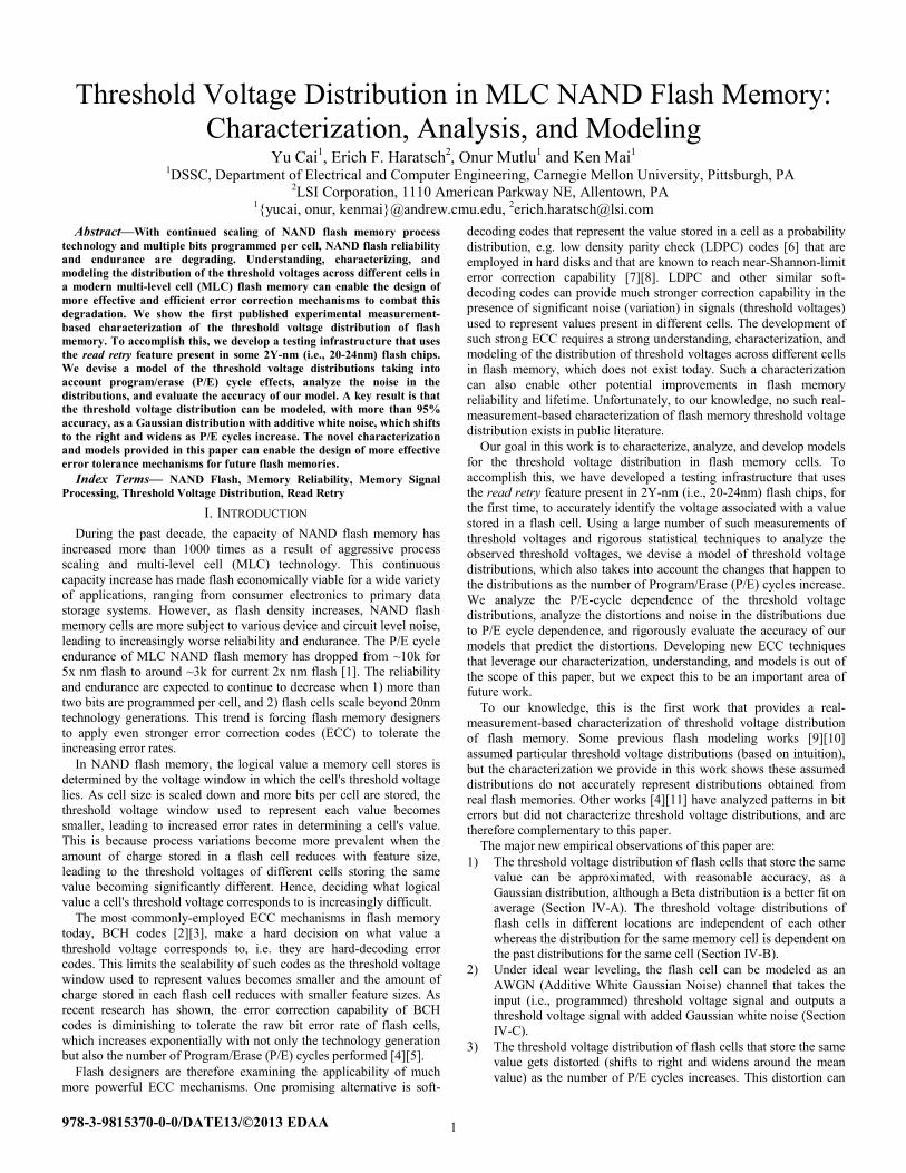
A. Read Retry Operation in Modern NAND Flash Memory Background: For n-bit multi-level cell (MLC) NAND flash memory,
the threshold voltage of each cell can be programmed to 2n separate states. Each state corresponds to a non-overlapping threshold voltage window. Cells programmed to the same n-bit value have their threshold voltages fall into the same window, but their exact threshold voltages could be different. The non-overlap space between the windows is called the distribution margin. For an n-bit MLC NAND flash memory, we use 2n-1 predefined read reference voltages to discriminate between the 2n possible cell states. These read reference voltages are located in the non-overlapping regions (i.e., distribution margins) of the threshold voltage windows. Each threshold voltage window is determined by an upper and a lower bound read reference voltage. During read operation, the cell’s threshold voltage is iteratively compared to predefined read reference voltages until the upper and lower bound read reference voltages are identified, thus determining the stored n-bit value.
Fig. 1 shows the mapping between the programmed logic values and the corresponding threshold voltage distributions for the 2-bit MLC 2Y-nm (i.e., 20-24 nm) NAND flash memory used in our characterization. The flash cell states can be classified as either erased (lowest threshold voltage, P0:11, indicating that the logical value is 11) or programmed (electrons present on the floating gate, P1:10, P2:00, P3:01). Note that the mapping of logical values to the cell states could be different between different flash manufacturers and product generations. The figure shows that the cells in a given programmed state (e.g., P1, which indicates a logical bit value of 10) have threshold voltages that fall into a distinct threshold voltage window (e.g., threshold voltage values between REF1 and REF2).
Fig. 1 Read retry feature of NAND flash memory
Read Retry: In past flash generations, the read reference voltage values were fixed at design time. However, when the threshold voltage distributions are distorted (e.g., due to P/E cycling, charge loss over time, or program interference from the programming of neighboring cells), the distributions can shift and distribution tails can enter the previously non-overlapping distribution margin regions, crossing the fixed read reference voltage levels [11]. As a result, a cell that stored one logical value can be misread as storing a different logical value (called a read error [4][11]). To combat such errors, a mechanism called read retry has been implemented in some flash memories below 30nm [12][13]. Read retry allows the read reference voltages to be dynamically adjusted to track changes in distributions. The basic idea is to retry the read with the adjusted reference levels such that read errors are decreased or even eliminated. Section II.B describes this in more detail and shows how we implement the read retry techniques in our FPGA-based testing system. B. System Implementation
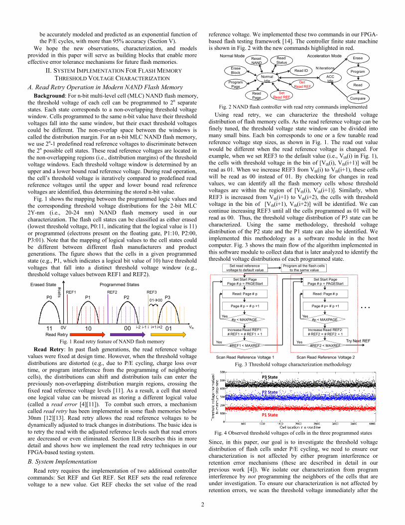
Read retry requires the implementation of two additional controller commands: Set REF and Get REF. Set REF sets the read reference voltage to a new value. Get REF checks the set value of the read
reference voltage. We implemented these two commands in our FPGA-based flash testing framework [14]. The controller finite state machine is shown in Fig. 2 with the new commands highlighted in red.
Fig. 2 NAND flash controller with read retry commands implemented
Using read retry, we can characterize the threshold voltage distribution of flash memory cells. As the read reference voltage can be finely tuned, the threshold voltage state window can be divided into many small bins. Each bin corresponds to one or a few tunable read reference voltage step sizes, as shown in Fig. 1. The read out value would be different when the read reference voltage is changed. For example, when we set REF3 to the default value (i.e., Vth(i) in Fig. 1), the cells with threshold voltage in the bin of [Vth(i), Vth(i+1)] will be read as 01. When we increase REF3 from Vth(i) to Vth(i+1), these cells will be read as 00 instead of 01. By checking for changes in read values, we can identify all the flash memory cells whose threshold voltages are within the region of [Vth(i), Vth(i+1)]. Similarly, when REF3 is increased from Vth(i+1) to Vth(i+2), the cells with threshold voltage in the bin of [Vth(i+1), Vth(i+2)] will be identified. We can continue increasing REF3 until all the cells programmed as 01 will be read as 00. Thus, the threshold voltage distribution of P3 state can be characterized. Using the same methodology, threshold voltage distribution of the P2 state and the P1 state can also be identified. We implemented this methodology as a software module in the host computer. Fig. 3 shows the main flow of the algorithm implemented in this software module to collect data that is later analyzed to identify the threshold voltage distributions of each programmed state.
Fig. 3 Threshold voltage characterization methodology
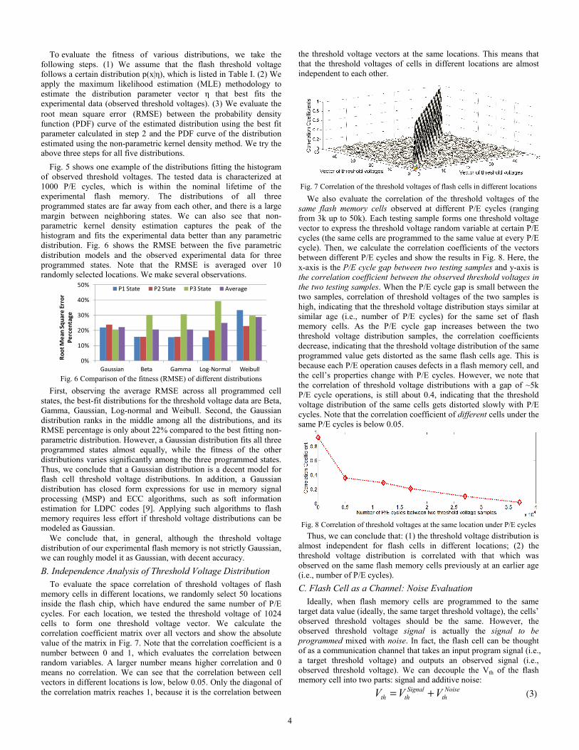
Fig. 4 Observed threshold voltages of cells in the three programmed states
Since, in this paper, our goal is to investigate the threshold voltage distribution of flash cells under P/E cycling, we need to ensure our characterization is not affected by either program interference or retention error mechanisms (these are described in detail in our previous work [4]). We isolate our characterization from program interference by not programming the neighbors of the cells that are under investigation. To ensure our characterization is not affected by retention errors, we scan the threshold voltage immediately after the
Vth11
#cells
10 00 01
REF1 REF2 REF3
0V
Erased State Programmed States
Read Retry
P1 P2 P3
ii-1 i+1i-2 i+2
01 00P0
NormalIdle
Reset NAND
Read ID
Read Status
EraseBlock
ProgramPage
ReadPage
SetRead REF
Get Read REF
ACCIdle
Erase
Program
Read
Compare
Normal Mode Acceleration Mode
N iterations
Program all the flash cellsto the same value
Set read reference voltage to default value
Read: Page # p
Page # p = # p +1
#p < MAXPAGEYes
Increase Read REF1:# REF1 = # REF1 + 1
Set Start PagePage # p = PAGEStart
#REF1 < MAXREFYes
Read: Page # p
Page # p= # p +1
#p < MAXPAGEYes
Increase Read REF2:# REF2 = # REF2 + 1
Set Start PagePage # p = PAGEStart
#REF2 < MAXREFYes Try Next REF
Scan Read Reference Voltage 1 Scan Read Reference Voltage 2
…
P3 State
P2 State
P1 State
2
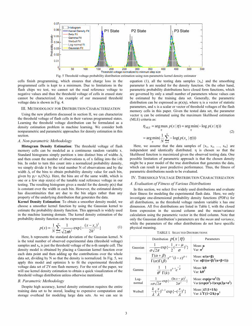
Fig. 5 Threshold voltage probability distribution estimation using non-parametric kernel density estimator
cells finish programming, which ensures that charge loss in the programmed cells is kept to a minimum. Due to limitations in the flash chips we test, we cannot set the read reference voltage to negative values and thus the threshold voltage of cells in erased state cannot be characterized. An example of our measured threshold voltage data is shown in Fig. 4.
III. METHODOLOGY FOR DISTRIBUTION CHARACTERIZATION Using the new platform discussed in section II, we can characterize
the threshold voltage of flash cells in their various programmed states. Learning the threshold voltage distribution can be formulated as a density estimation problem in machine learning. We consider both nonparametric and parametric approaches for density estimation in this section. A. Non-parametric Methodology
Histogram Density Estimation: The threshold voltage of flash memory cells can be modeled as a continuous random variable x. Standard histograms simply partition x into distinct bins of widths ∆i and then count the number of observations ni of x falling into the i-th bin. In order to turn this count into a normalized probability density, we simply divide it by the total number N of observations and by the width ∆i of the bins to obtain probability density value for each bin, given by pi= ni/(N∆i). Here, the bins are of the same width, which is one or a few step size(s) of the tunable read reference voltage in our testing. The resulting histogram gives a model for the density p(x) that is constant over the width in each bin. However, the estimated density has discontinuities that are due to the bin edges rather than any property of the underlying distribution that generates the data. Kernel Density Estimation: To obtain a smoother density model, we choose a smoother kernel function by using the Gaussian kernel to estimate the probability density function. This approach is widely used in the machine learning domain. The kernel density estimation of the probability density function can be expressed as:
}2
)(exp{211)( 2
2
12 h
xxhN
xp nN
n
−−= ∑= π
(1)
Here, h represents the standard deviation of the Gaussian kernel. N is the total number of observed experimental data (threshold voltage) samples and xn is just the threshold voltage of the n-th sample cell. The density model is obtained by placing a Gaussian kernel function over each data point and then adding up the contributions over the whole data set, dividing by N so that the density is normalized. In Fig. 5, we apply this model and optimize h to fit the experimental threshold voltage data set of 2Y-nm flash memory. For the rest of the paper, we will use kernel density estimation to obtain a quick visualization of the threshold voltage distribution unless otherwise mentioned. B. Parametric Methodology
Despite high accuracy, kernel density estimation requires the entire training data set to be stored, leading to expensive computation and storage overhead for modeling large data sets. As we can see in
equation (1), all the testing data samples {xn} and the smoothing parameter h are needed for the density function. On the other hand, parametric probability distributions have closed form functions, which are governed by only a small number of parameters whose values can be estimated by the training data set. Generally, the parametric distribution can be expressed as p(x|η), where η is a vector of statistic parameters, and x is a scalar or vector of threshold voltages of the flash memory cells in this paper. Given the tested data set, the parameter vector η can be estimated using the maximum likelihood estimation (MLE) criteria as:
)))|(log(1(minarg
))|(log(minarg)|(maxarg
1∑
=
−=
−==
N
nn
MLE
xpN
xpxp
η
ηηη
η
ηη (2)
Here, we assume that the data samples of {x1, x2, …, xN} are independent and identically distributed. η is chosen so that the likelihood function is maximized given the observed testing data. One possible limitation of parametric approach is that the chosen density might be a poor model of the true distribution that generates the data, which can result in poor predictive performance. Thus, the fitness of parametric distributions needs to be evaluated.
IV. THRESHOLD VOLTAGE DISTRIBUTION CHARACTERIZATION A. Evaluation of Fitness of Various Distributions
In this section, we select five widely used distributions and evaluate their fitness for modeling the experimental flash data. Here, we only investigate one-dimensional probability density functions (PDFs) for all distributions, as the threshold voltage random variable x has one dimension. All five distributions are listed in Table I, with the closed form expression in the second column and the mean/variance calculation using the parametric vector in the third column. Note that only the Gaussian distribution’s parameters are the mean and variance, while the parameters of the other distributions do not have specific physical meaning.
TABLE I. SELECTED DISTRIBUTIONS Distribution )|( ηxp Parameters
Gaussian })(21exp{
21 2
σμ
πσ−− x Mean: µ
Var: σ2
Beta 11 )1()()()( −− −
ΓΓ+Γ βα
βαβα xx Mean: α/(α+β)
Var: αβ/((α+β)2(α+β+1))
Gamma θ
θ
xk
k exk
−−
Γ1
)(11 Mean: kθ
Var: kθ2
Log-normal }
2)(lnexp{
21
2
2
σμ
πσ−− x
x Mean: exp(µ+σ2/2)
Var:(exp(σ2)-1)exp(2µ+σ2)
Weibull })(exp{)( 1 kk xxkλλλ
−− Mean: λΓ(1+1/k) Var: λ2Γ(1+2/k)-µ2
P1 State P2 State P3 State
3
Το evaluate the fitness of various distributions, we take the following steps. (1) We assume that the flash threshold voltage follows a certain distribution p(x|η), which is listed in Table I. (2) We apply the maximum likelihood estimation (MLE) methodology to estimate the distribution parameter vector η that best fits the experimental data (observed threshold voltages). (3) We evaluate the root mean square error (RMSE) between the probability density function (PDF) curve of the estimated distribution using the best fit parameter calculated in step 2 and the PDF curve of the distribution estimated using the non-parametric kernel density method. We try the above three steps for all five distributions.
Fig. 5 shows one example of the distributions fitting the histogram of observed threshold voltages. The tested data is characterized at 1000 P/E cycles, which is within the nominal lifetime of the experimental flash memory. The distributions of all three programmed states are far away from each other, and there is a large margin between neighboring states. We can also see that non-parametric kernel density estimation captures the peak of the histogram and fits the experimental data better than any parametric distribution. Fig. 6 shows the RMSE between the five parametric distribution models and the observed experimental data for three programmed states. Note that the RMSE is averaged over 10 randomly selected locations. We make several observations.
Fig. 6 Comparison of the fitness (RMSE) of different distributions
First, observing the average RMSE across all programmed cell states, the best-fit distributions for the threshold voltage data are Beta, Gamma, Gaussian, Log-normal and Weibull. Second, the Gaussian distribution ranks in the middle among all the distributions, and its RMSE percentage is only about 22% compared to the best fitting non-parametric distribution. However, a Gaussian distribution fits all three programmed states almost equally, while the fitness of the other distributions varies significantly among the three programmed states. Thus, we conclude that a Gaussian distribution is a decent model for flash cell threshold voltage distributions. In addition, a Gaussian distribution has closed form expressions for use in memory signal processing (MSP) and ECC algorithms, such as soft information estimation for LDPC codes [9]. Applying such algorithms to flash memory requires less effort if threshold voltage distributions can be modeled as Gaussian.
We conclude that, in general, although the threshold voltage distribution of our experimental flash memory is not strictly Gaussian, we can roughly model it as Gaussian, with decent accuracy. B. Independence Analysis of Threshold Voltage Distribution
To evaluate the space correlation of threshold voltages of flash memory cells in different locations, we randomly select 50 locations inside the flash chip, which have endured the same number of P/E cycles. For each location, we tested the threshold voltage of 1024 cells to form one threshold voltage vector. We calculate the correlation coefficient matrix over all vectors and show the absolute value of the matrix in Fig. 7. Note that the correlation coefficient is a number between 0 and 1, which evaluates the correlation between random variables. A larger number means higher correlation and 0 means no correlation. We can see that the correlation between cell vectors in different locations is low, below 0.05. Only the diagonal of the correlation matrix reaches 1, because it is the correlation between
the threshold voltage vectors at the same locations. This means that that the threshold voltages of cells in different locations are almost independent to each other.
Fig. 7 Correlation of the threshold voltages of flash cells in different locations
We also evaluate the correlation of the threshold voltages of the same flash memory cells observed at different P/E cycles (ranging from 3k up to 50k). Each testing sample forms one threshold voltage vector to express the threshold voltage random variable at certain P/E cycles (the same cells are programmed to the same value at every P/E cycle). Then, we calculate the correlation coefficients of the vectors between different P/E cycles and show the results in Fig. 8. Here, the x-axis is the P/E cycle gap between two testing samples and y-axis is the correlation coefficient between the observed threshold voltages in the two testing samples. When the P/E cycle gap is small between the two samples, correlation of threshold voltages of the two samples is high, indicating that the threshold voltage distribution stays similar at similar age (i.e., number of P/E cycles) for the same set of flash memory cells. As the P/E cycle gap increases between the two threshold voltage distribution samples, the correlation coefficients decrease, indicating that the threshold voltage distribution of the same programmed value gets distorted as the same flash cells age. This is because each P/E operation causes defects in a flash memory cell, and the cell’s properties change with P/E cycles. However, we note that the correlation of threshold voltage distributions with a gap of ~5k P/E cycle operations, is still about 0.4, indicating that the threshold voltage distribution of the same cells gets distorted slowly with P/E cycles. Note that the correlation coefficient of different cells under the same P/E cycles is below 0.05.
Fig. 8 Correlation of threshold voltages at the same location under P/E cycles
Thus, we can conclude that: (1) the threshold voltage distribution is almost independent for flash cells in different locations; (2) the threshold voltage distribution is correlated with that which was observed on the same flash memory cells previously at an earlier age (i.e., number of P/E cycles). C. Flash Cell as a Channel: Noise Evaluation
Ideally, when flash memory cells are programmed to the same target data value (ideally, the same target threshold voltage), the cells’ observed threshold voltages should be the same. However, the observed threshold voltage signal is actually the signal to be programmed mixed with noise. In fact, the flash cell can be thought of as a communication channel that takes an input program signal (i.e., a target threshold voltage) and outputs an observed signal (i.e., observed threshold voltage). We can decouple the Vth of the flash memory cell into two parts: signal and additive noise:
Noiseth
Signalthth VVV += (3)
0%
10%
20%
30%
40%
50%
Gaussian Beta Gamma Log-Normal Weibull
Roo
t Mea
n Sq
uare
Err
or
Perc
enta
ge
P1 State P2 State P3 State Average
4
The signal can be extracted as the mean of the observed Vth distribution, while the residual part of the Vth distribution after the mean is subtracted amounts to noise with mean value equal to zero.
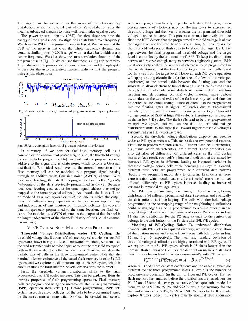
The power spectral density (PSD) function describes how the energy of the signal under investigation is distributed over frequency. We show the PSD of the program noise in Fig. 9. We can see that the PSD of the noise is flat over the whole frequency domain and contains similar power (<20dB range) within a fixed bandwidth at any center frequency. We also show the auto-correlation function of the program noise in Fig. 10. We can see that there is a high spike at zero. The flatness of the power spectral density function and the high spike at zero for the auto-correlation function indicate that the program noise is just white noise.
Fig. 9 Power spectral density function of program noise in frequency domain
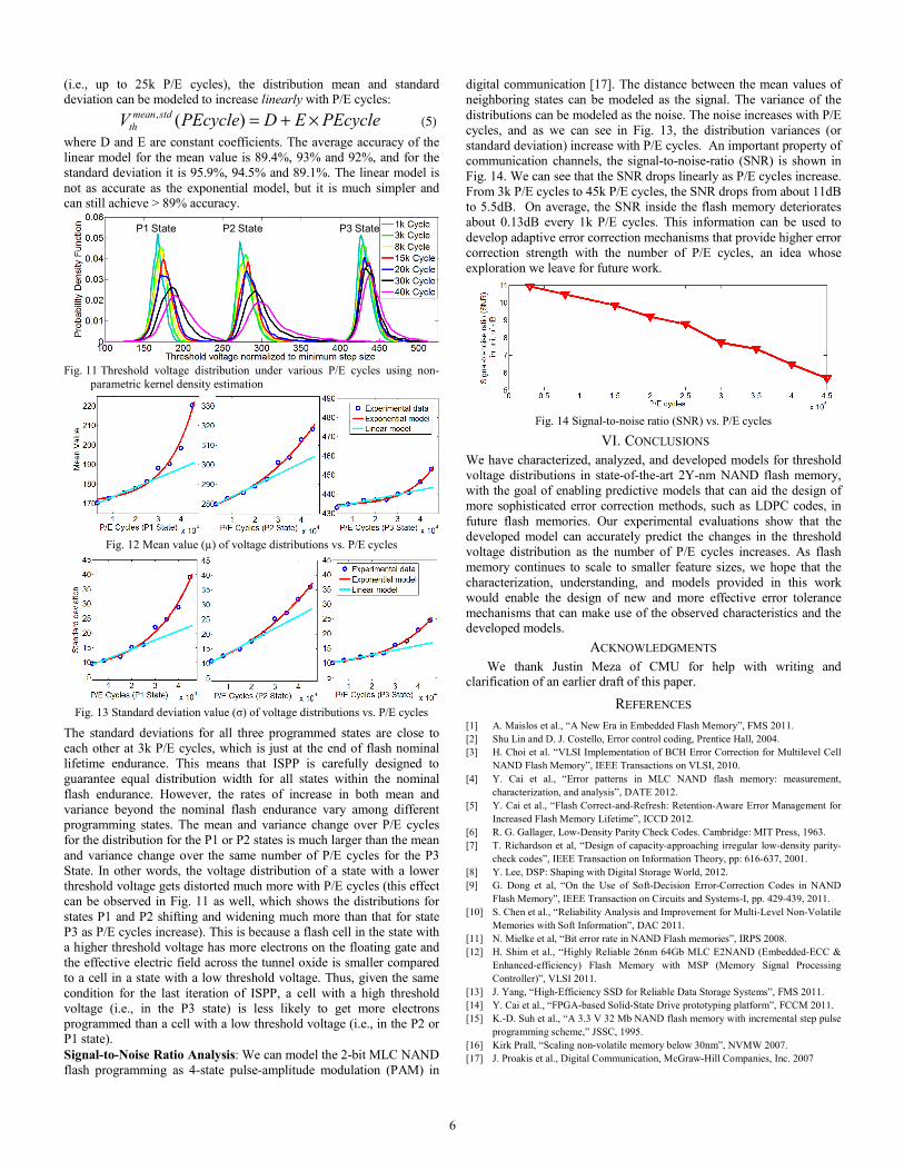
Fig. 10 Auto correlation function of program noise in time domain
In summary, if we consider the flash memory cell as a communication channel that passes a signal (i.e., the threshold voltage the cell is to be programmed to), we find that the program noise is additive to the signal and is white noise, which follows a Gaussian distribution. With ideal wear leveling, the program operation on a flash memory cell can be modeled as a program signal passing through an additive white Gaussian noise (AWGN) channel. With ideal wear leveling, the data that is programmed in a cell is logically independent of the data previously programmed in the cell (because ideal wear leveling ensures that the same logical address does not get mapped to the same physical address). As a result, the flash cell can be modeled as a memoryless channel, i.e. one in which the output threshold voltage is only dependent on the most recent input voltage and independent of past input/output threshold voltages. However, if data is repeatedly programmed to the same location, the flash cell cannot be modeled as AWGN channel as the output of the channel is no longer independent of the channel’s history of use (i.e., the channel has memory).
V. P/E-CYCLING NOISE MODELING AND PREDICTION Threshold Voltage Distributions under P/E Cycling: The
threshold voltage distributions of flash memory cells under various P/E cycles are shown in Fig. 11. Due to hardware limitations, we cannot set the read reference voltage to be negative to test the threshold voltage of cells in the erase state from the flash controller. Thus, we just show the distributions of cells in the three programmed states. Note that the nominal lifetime endurance of the tested flash memory is only 3k P/E cycles, and we explore the distributions up to 45k P/E cycles, which is about 15 times the flash lifetime. Several observations are in order.
First, the threshold voltage distribution shifts to the right systematically as P/E cycles increase. This can be explained from the intrinsic properties of flash programming operation. Flash memory cells are programmed using the incremental step pulse programming (ISPP) operation iteratively [15]. Before programming, ISPP sets certain target threshold voltages for the cells to be programmed based on the target programming data. ISPP can be divided into several
sequential program-and-verify steps. In each step, ISPP programs a certain amount of electrons into the floating gates to increase the threshold voltage and then verify whether the programmed threshold voltage is above the target. This process continues iteratively until the first time ISPP detects that the programmed threshold voltage is above the target level and then the iteration stops. Thus, ISPP can guarantee the threshold voltages of flash cells to be above the target level. The gap between the final programmed threshold voltage and the target level is controlled by the last iteration of ISPP. To keep the distribution narrow and reserve enough margins between neighboring states, ISPP must accurately control the number of electrons to be programmed in the last iteration so that the threshold voltage of the flash cells is not too far away from the target level. However, each P/E cycle operation will apply a strong electric field (at the level of a few million volts per centimeter) on the tunnel oxide between the floating gate and the substrate to allow electrons to tunnel through. Each time electrons pass through the tunnel oxide, some defects will remain due to electron trapping and de-trapping. As P/E cycles increase, more defects accumulate on the tunnel oxide of the flash memory cell and thus the properties of the oxide change. More electrons can be programmed into the floating gates at higher P/E cycles due to trap-assisted tunneling [16], given the same program pulse voltage. Threshold voltage control of ISPP at high P/E cycles is therefore not as accurate as that at low P/E cycles. The flash cells tend to be over-programmed at high P/E cycles, and we can see that the threshold voltage distribution shifts to the right (i.e., toward higher threshold voltages) systematically as P/E cycles increase.
Second, the threshold voltage distributions disperse and become wider as P/E cycles increase. This can be due to two potential reasons. First, due to process variation effects, different flash cells’ properties, e.g., tunnel oxide characteristics, are different. These properties can also get affected differently for different cells as the P/E cycles increase. As a result, each cell’s tolerance to defects that are caused by increased P/E cycles is different, leading to increased variation in threshold voltage across cells with increasing P/E cycles. Second, different flash cells are programmed with different data patterns (because we program random data to different flash cells in these experiments), which could cause different cells’ properties to get affected differently as P/E cycles increase, leading to increased variance in threshold voltage levels.
As P/E cycles increase, the margin between neighboring distributions (of different programmed states) decreases and eventually the distributions start overlapping. The cells with threshold voltage programmed in the overlapping range of the neighboring distributions could be misjudged as being programmed to a value other than the original targeted value and thus cause read errors. We can see in Fig. 11 that the distribution for the P2 state extends to the region that belongs to the distribution for the P3 state after 20k P/E cycles.
Modeling of P/E-Cycling Noise: To understand distribution changes with P/E cycles in a quantitative way, we show the correlation of distribution means and standard deviations with P/E cycles in Fig. 12 and Fig. 13 respectively. The mean and standard deviation of threshold voltage distributions are highly correlated with P/E cycles. If we explore up to 45k P/E cycles, which is 15 times longer than the nominal flash endurance (i.e., 3k), the distribution mean and standard deviation can be modeled to increase exponentially with P/E cycles:
PEcycleCstdmeanth eBAPEcycleV ××+=)(, (4)
where A, B and C are constant coefficients and the exact numbers are different for the three programmed states. PEcycle is the number of program/erase operations (in the unit of thousand P/E cycles) that the flash memory has endured before the distributions are tested. For the P1, P2 and P3 state, the average accuracy of the exponential model for mean value is 97.9%, 97.6% and 96.5%, while the accuracy for the standard deviation is 97.8%, 97.5% and 98.1% respectively. If we only explore 8 times longer P/E cycles than the nominal flash endurance
High spike at 0-lag point
5
(i.e., up to 25k P/E cycles), the distribution mean and standard deviation can be modeled to increase linearly with P/E cycles:
PEcycleEDPEcycleV stdmeanth ×+=)(, (5)
where D and E are constant coefficients. The average accuracy of the linear model for the mean value is 89.4%, 93% and 92%, and for the standard deviation it is 95.9%, 94.5% and 89.1%. The linear model is not as accurate as the exponential model, but it is much simpler and can still achieve > 89% accuracy.
Fig. 11 Threshold voltage distribution under various P/E cycles using non-
parametric kernel density estimation
Fig. 12 Mean value (µ) of voltage distributions vs. P/E cycles
Fig. 13 Standard deviation value (σ) of voltage distributions vs. P/E cycles
The standard deviations for all three programmed states are close to each other at 3k P/E cycles, which is just at the end of flash nominal lifetime endurance. This means that ISPP is carefully designed to guarantee equal distribution width for all states within the nominal flash endurance. However, the rates of increase in both mean and variance beyond the nominal flash endurance vary among different programming states. The mean and variance change over P/E cycles for the distribution for the P1 or P2 states is much larger than the mean and variance change over the same number of P/E cycles for the P3 State. In other words, the voltage distribution of a state with a lower threshold voltage gets distorted much more with P/E cycles (this effect can be observed in Fig. 11 as well, which shows the distributions for states P1 and P2 shifting and widening much more than that for state P3 as P/E cycles increase). This is because a flash cell in the state with a higher threshold voltage has more electrons on the floating gate and the effective electric field across the tunnel oxide is smaller compared to a cell in a state with a low threshold voltage. Thus, given the same condition for the last iteration of ISPP, a cell with a high threshold voltage (i.e., in the P3 state) is less likely to get more electrons programmed than a cell with a low threshold voltage (i.e., in the P2 or P1 state). Signal-to-Noise Ratio Analysis: We can model the 2-bit MLC NAND flash programming as 4-state pulse-amplitude modulation (PAM) in
digital communication [17]. The distance between the mean values of neighboring states can be modeled as the signal. The variance of the distributions can be modeled as the noise. The noise increases with P/E cycles, and as we can see in Fig. 13, the distribution variances (or standard deviation) increase with P/E cycles. An important property of communication channels, the signal-to-noise-ratio (SNR) is shown in Fig. 14. We can see that the SNR drops linearly as P/E cycles increase. From 3k P/E cycles to 45k P/E cycles, the SNR drops from about 11dB to 5.5dB. On average, the SNR inside the flash memory deteriorates about 0.13dB every 1k P/E cycles. This information can be used to develop adaptive error correction mechanisms that provide higher error correction strength with the number of P/E cycles, an idea whose exploration we leave for future work.
Fig. 14 Signal-to-noise ratio (SNR) vs. P/E cycles
VI. CONCLUSIONS We have characterized, analyzed, and developed models for threshold voltage distributions in state-of-the-art 2Y-nm NAND flash memory, with the goal of enabling predictive models that can aid the design of more sophisticated error correction methods, such as LDPC codes, in future flash memories. Our experimental evaluations show that the developed model can accurately predict the changes in the threshold voltage distribution as the number of P/E cycles increases. As flash memory continues to scale to smaller feature sizes, we hope that the characterization, understanding, and models provided in this work would enable the design of new and more effective error tolerance mechanisms that can make use of the observed characteristics and the developed models.
ACKNOWLEDGMENTS We thank Justin Meza of CMU for help with writing and
clarification of an earlier draft of this paper.
REFERENCES [1] A. Maislos et al., “A New Era in Embedded Flash Memory”, FMS 2011. [2] Shu Lin and D. J. Costello, Error control coding, Prentice Hall, 2004. [3] H. Choi et al. “VLSI Implementation of BCH Error Correction for Multilevel Cell
NAND Flash Memory”, IEEE Transactions on VLSI, 2010. [4] Y. Cai et al., “Error patterns in MLC NAND flash memory: measurement,
characterization, and analysis”, DATE 2012. [5] Y. Cai et al., “Flash Correct-and-Refresh: Retention-Aware Error Management for
Increased Flash Memory Lifetime”, ICCD 2012. [6] R. G. Gallager, Low-Density Parity Check Codes. Cambridge: MIT Press, 1963. [7] T. Richardson et al, “Design of capacity-approaching irregular low-density parity-
check codes”, IEEE Transaction on Information Theory, pp: 616-637, 2001. [8] Y. Lee, DSP: Shaping with Digital Storage World, 2012. [9] G. Dong et al, “On the Use of Soft-Decision Error-Correction Codes in NAND
Flash Memory”, IEEE Transaction on Circuits and Systems-I, pp. 429-439, 2011. [10] S. Chen et al., “Reliability Analysis and Improvement for Multi-Level Non-Volatile
Memories with Soft Information”, DAC 2011. [11] N. Mielke et al, “Bit error rate in NAND Flash memories”, IRPS 2008. [12] H. Shim et al., “Highly Reliable 26nm 64Gb MLC E2NAND (Embedded-ECC &
Enhanced-efficiency) Flash Memory with MSP (Memory Signal Processing Controller)”, VLSI 2011.
[13] J. Yang, “High-Efficiency SSD for Reliable Data Storage Systems”, FMS 2011. [14] Y. Cai et al., “FPGA-based Solid-State Drive prototyping platform”, FCCM 2011. [15] K.-D. Suh et al., “A 3.3 V 32 Mb NAND flash memory with incremental step pulse
programming scheme,” JSSC, 1995. [16] Kirk Prall, “Scaling non-volatile memory below 30nm”, NVMW 2007. [17] J. Proakis et al., Digital Communication, McGraw-Hill Companies, Inc. 2007
P1 State P2 State P3 State
6
Recommended


