Stereo, Low Power, 96 kHz, 24-Bit Audio Codec with Integrated PLL
Data Sheet ADAU1361
Rev. D Document Feedback Information furnished by Analog Devices is believed to be accurate and reliable. However, no responsibility is assumed by Analog Devices for its use, nor for any infringements of patents or other rights of third parties that may result from its use. Specifications subject to change without notice. No license is granted by implication or otherwise under any patent or patent rights of Analog Devices. Trademarks and registered trademarks are the property of their respective owners.
One Technology Way, P.O. Box 9106, Norwood, MA 02062-9106, U.S.A. Tel: 781.329.4700 ©2009–2018 Analog Devices, Inc. All rights reserved. Technical Support www.analog.com
FEATURES 24-bit stereo audio ADC and DAC: >98 dB SNR Sampling rates from 8 kHz to 96 kHz Low power: 7 mW record, 7 mW playback, 48 kHz at 1.8 V 6 analog input pins, configurable for single-ended or
differential inputs Flexible analog input/output mixers Stereo digital microphone input Analog outputs: 2 differential stereo, 2 single-ended stereo,
1 mono headphone output driver PLL supporting input clocks from 8 MHz to 27 MHz Analog automatic level control (ALC) Microphone bias reference voltage Analog and digital I/O: 1.8 V to 3.65 V I2C and SPI control interfaces Digital audio serial data I/O: stereo and time-division
multiplexing (TDM) modes Software-controllable clickless mute Software power-down 32-lead, 5 mm × 5 mm LFCSP −40°C to +85°C operating temperature range
APPLICATIONS Smartphones/multimedia phones Digital still cameras/digital video cameras Portable media players/portable audio players Phone accessories products
GENERAL DESCRIPTION The ADAU1361 is a low power, stereo audio codec that supports stereo 48 kHz record and playback at 14 mW from a 1.8 V analog supply. The stereo audio ADCs and DACs support sample rates from 8 kHz to 96 kHz as well as a digital volume control. The ADAU1361 is ideal for battery-powered audio and telephony applications.
The record path includes an integrated microphone bias circuit and six inputs. The inputs can be mixed and muxed before the ADC, or they can be configured to bypass the ADC. The ADAU1361 includes a stereo digital microphone input.
The ADAU1361 includes five high power output drivers (two differential and three single-ended), supporting stereo head-phones, an earpiece, or other output transducer. AC-coupled or capless configurations are supported. Individual fine level controls are supported on all analog outputs. The output mixer stage allows for flexible routing of audio.
The serial control bus supports the I2C and SPI protocols. The serial audio bus is programmable for I2S, left-/right-justified, and TDM modes. A programmable PLL supports flexible clock generation for all standard integer rates and fractional master clocks from 8 MHz to 27 MHz.
FUNCTIONAL BLOCK DIAGRAM
HP JACKDETECTION
REGULATOR
INPUTMIXERS
ALC
MICROPHONEBIAS PLL
LINN
LINP
LAUX
JACKDET/MICIN
RINP
RINN
RAUX
MICBIAS
LHP
LOUTN
LOUTP
ADAU1361
RHP
MONOOUT
ROUTP
ROUTN
CM
IOVD
D
DG
ND
DVD
DO
UT
AG
ND
AVD
D
AVD
D
AG
ND
OUTPUTMIXERS
DACDIGITALFILTERS
ADCDIGITALFILTERS
DAC
DACADC
ADC
SDA/COUT
I2C/SPICONTROL PORT
SERIAL DATAINPUT/OUTPUT PORTS
MCLK ADC_SDATA
BC
LK SCL/CCLK
ADDR1/CDATA
ADDR0/CLATCH
LRC
LK DAC_SDATA
0767
9-00
1
Figure 1.

ADAU1361 Data Sheet
Rev. D | Page 2 of 80
TABLE OF CONTENTS Features .............................................................................................. 1 Applications ....................................................................................... 1 General Description ......................................................................... 1 Functional Block Diagram .............................................................. 1 Revision History ............................................................................... 3 Specifications ..................................................................................... 4
Analog Performance Specifications ........................................... 4 Power Supply Specifications........................................................ 7 Typical Current Consumption .................................................... 8 Typical Power Management Measurements ............................. 9 Digital Filters ............................................................................... 10 Digital Input/Output Specifications......................................... 10 Digital Timing Specifications ................................................... 11 Digital Timing Diagrams........................................................... 12
Absolute Maximum Ratings .......................................................... 14 Thermal Resistance .................................................................... 14 ESD Caution ................................................................................ 14
Pin Configuration and Function Descriptions ........................... 15 Typical Performance Characteristics ........................................... 17 System Block Diagrams ................................................................. 20 Theory of Operation ...................................................................... 23 Startup, Initialization, and Power ................................................. 24
Power-Up Sequence ................................................................... 24 Power Reduction Modes ............................................................ 24 Digital Power Supply .................................................................. 24 Input/Output Power Supply ...................................................... 24 Clock Generation and Management ........................................ 24
Clocking and Sampling Rates ....................................................... 26
Core Clock ................................................................................... 26 Sampling Rates ............................................................................ 26 PLL ............................................................................................... 27
Record Signal Path ......................................................................... 29 Input Signal Paths ....................................................................... 29 Analog-to-Digital Converters ................................................... 31
Automatic Level Control (ALC) ................................................... 32 ALC Parameters .......................................................................... 32 Noise Gate Function .................................................................. 33
Playback Signal Path ...................................................................... 35 Output Signal Paths ................................................................... 35 Headphone Output .................................................................... 36 Pop-and-Click Suppression ...................................................... 37 Line Outputs ............................................................................... 37
Control Ports ................................................................................... 38 Burst Mode Writing and Reading ............................................ 38 I2C Port ........................................................................................ 38 SPI Port ........................................................................................ 41
Serial Data Input/Output Ports .................................................... 42 Applications Information .............................................................. 44
Power Supply Bypass Capacitors .............................................. 44 GSM Noise Filter ........................................................................ 44 Grounding ................................................................................... 44 Exposed Pad PCB Design ......................................................... 44
Control Registers ............................................................................ 45 Control Register Details ............................................................ 46
Outline Dimensions ....................................................................... 79 Ordering Guide .......................................................................... 79

Data Sheet ADAU1361
Rev. D | Page 3 of 80
REVISION HISTORY 8/2018—Rev. C to Rev. D Changed tSODM to tSOD, Table 7 ........................................................ 11 Changes to tSOD Parameter, Table 7 ............................................... 11 Changes to Figure 3 ......................................................................... 12 9/2010—Rev. B to Rev. C Changes to Figure 1 ........................................................................... 1 5/2010—Rev. A to Rev. B Changes to Burst Mode Writing and Reading Section .............. 38 Changes to Table 26 ........................................................................ 45 Change to Table 43 .......................................................................... 58 Added R67: Dejitter Control, 16,438 (0x4036) Section ............. 73 12/2009—Rev. 0 to Rev. A Changes to Features Section ............................................................ 1 Changes to General Description Section ....................................... 1 Changes to Table 1 ............................................................................ 6 Change to Table 5 ............................................................................ 10 Changes to Figure 6 ......................................................................... 13 Changes to Table 10 ........................................................................ 15 Changes to Captions of Figure 15, Figure 16, Figure 18, and Figure 19 ................................................................................... 18 Changes to Captions of Figure 21 and Figure 24 ........................ 19 Added Figure 22; Renumbered Sequentially ............................... 19 Change to Figure 25 ........................................................................ 20 Change to Figure 26 ........................................................................ 21 Change to Figure 27 ........................................................................ 22 Change to Theory of Operation Section ...................................... 23 Changes to Power Reduction Modes Section and Case 1: PLL Is Bypassed Section ................................................... 24 Changes to PLL Lock Acquisition Section ................................... 25 Changes to Core Clock Section ..................................................... 26
Changes to Input Signal Paths Section and Figure 31 ................ 29 Changes to Figure 32 and Figure 33 ............................................. 30 Changes to ADC Full-Scale Level Section ................................... 31 Change to Automatic Level Control (ALC) Section .................. 32 Changes to Output Signal Paths Section ...................................... 35 Changes to Headphone Output Section ....................................... 36 Changes to Jack Detection Section, Pop-and-Click Suppression Section, and Line Outputs Section ......................... 37 Changes to Control Ports Section and I2C Port Section ............ 38 Added Burst Mode Writing and Reading Section ...................... 38 Changes to SPI Port Section .......................................................... 41 Changes to Serial Data Input/Output Ports Section, Table 24, and Table 25 ..................................................................................... 42 Added Figure 56 .............................................................................. 42 Changes to Figure 60 and Figure 61 ............................................. 43 Changes to Table 26 ........................................................................ 45 Changes to R2: Digital Microphone/Jack Detection Control, 16,392 (0x4008) Section and Table 29 .......................................... 47 Changes to Table 35 ........................................................................ 52 Changes to Table 36 ........................................................................ 53 Changes to R15: Serial Port Control 0, 16,405 (0x4015) Section and Table 42 ....................................................................... 57 Change to Table 43 .......................................................................... 58 Changes to Table 44, R18: Converter Control 1, 16,408 (0x4018) Section, and Table 45 ..................................................... 59 Changes to Table 53, R27: Playback L/R Mixer Right (Mixer 6) Line Output Control, 16,417 (0x4021) Section, and Table 54... 65 Changes to Table 55, R29: Playback Headphone Left Volume Control, 16,419 (0x4023) Section, and Table 56 ......................... 66 Changes to R42: Jack Detect Pin Control, 16,433 (0x4031) Section and Table 69 ....................................................................... 73 1/2009—Revision 0: Initial Version

ADAU1361 Data Sheet
Rev. D | Page 4 of 80
SPECIFICATIONS Supply voltage (AVDD) = 3.3 V, TA = 25°C, master clock = 12.288 MHz (48 kHz fS, 256 × fS mode), input sample rate = 48 kHz, measurement bandwidth = 20 Hz to 20 kHz, word width = 24 bits, CLOAD (digital output) = 20 pF, ILOAD (digital output) = 2 mA, VIH = 2 V, VIL = 0.8 V, unless otherwise noted. Performance of all channels is identical, exclusive of the interchannel gain mismatch and interchannel phase deviation specifications.
ANALOG PERFORMANCE SPECIFICATIONS Specifications guaranteed at 25°C (ambient).
Table 1. Parameter Test Conditions/Comments Min Typ Max Unit ANALOG-TO-DIGITAL CONVERTERS ADC performance excludes mixers
and PGA
ADC Resolution All ADCs 24 Bits Digital Attenuation Step 0.375 dB Digital Attenuation Range 95 dB
INPUT RESISTANCE Single-Ended Line Input −12 dB gain 83 kΩ 0 dB gain 21 kΩ 6 dB gain 10.5 kΩ PGA Inverting Inputs −12 dB gain 84.5 kΩ 0 dB gain 53 kΩ 35.25 dB gain 2 kΩ PGA Noninverting Inputs All gains 105 kΩ
SINGLE-ENDED LINE INPUT Full-Scale Input Voltage (0 dB) Scales linearly with AVDD AVDD/3.3 V rms
AVDD = 1.8 V 0.55 (1.56) V rms (V p-p) AVDD = 3.3 V 1.0 (2.83) V rms (V p-p)
Dynamic Range 20 Hz to 20 kHz, −60 dB input With A-Weighted Filter (RMS) AVDD = 1.8 V 94 dB AVDD = 3.3 V 99 dB No Filter (RMS) AVDD = 1.8 V 91 dB AVDD = 3.3 V 96 dB
Total Harmonic Distortion + Noise −1 dBFS AVDD = 1.8 V −88 dB AVDD = 3.3 V −90 dB Signal-to-Noise Ratio
With A-Weighted Filter (RMS) AVDD = 1.8 V 94 dB AVDD = 3.3 V 99 dB No Filter (RMS) AVDD = 1.8 V 91 dB AVDD = 3.3 V 96 dB
Gain per Step 3 dB Total Gain Range −12 +6 dB Mute Attenuation −87 dB Interchannel Gain Mismatch 0.005 dB Offset Error 0 mV Gain Error −12 % Interchannel Isolation 68 dB Power Supply Rejection Ratio CM capacitor = 20 μF
100 mV p-p @ 217 Hz 65 dB 100 mV p-p @ 1 kHz 67 dB
Data Sheet ADAU1361
Rev. D | Page 5 of 80
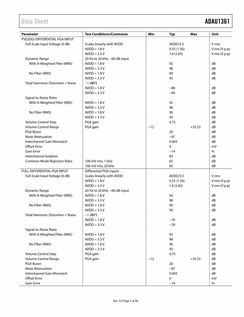
Parameter Test Conditions/Comments Min Typ Max Unit PSEUDO-DIFFERENTIAL PGA INPUT
Full-Scale Input Voltage (0 dB) Scales linearly with AVDD AVDD/3.3 V rms AVDD = 1.8 V 0.55 (1.56) V rms (V p-p) AVDD = 3.3 V 1.0 (2.83) V rms (V p-p) Dynamic Range 20 Hz to 20 kHz, −60 dB input
With A-Weighted Filter (RMS) AVDD = 1.8 V 92 dB AVDD = 3.3 V 98 dB No Filter (RMS) AVDD = 1.8 V 90 dB AVDD = 3.3 V 95 dB
Total Harmonic Distortion + Noise −1 dBFS AVDD = 1.8 V −88 dB AVDD = 3.3 V −89 dB Signal-to-Noise Ratio
With A-Weighted Filter (RMS) AVDD = 1.8 V 92 dB AVDD = 3.3 V 98 dB No Filter (RMS) AVDD = 1.8 V 90 dB AVDD = 3.3 V 95 dB
Volume Control Step PGA gain 0.75 dB Volume Control Range PGA gain −12 +35.25 dB PGA Boost 20 dB Mute Attenuation −87 dB Interchannel Gain Mismatch 0.005 dB Offset Error 0 mV Gain Error −14 % Interchannel Isolation 83 dB Common-Mode Rejection Ratio 100 mV rms, 1 kHz 65 dB
100 mV rms, 20 kHz 65 dB FULL DIFFERENTIAL PGA INPUT Differential PGA inputs
Full-Scale Input Voltage (0 dB) Scales linearly with AVDD AVDD/3.3 V rms AVDD = 1.8 V 0.55 (1.56) V rms (V p-p) AVDD = 3.3 V 1.0 (2.83) V rms (V p-p) Dynamic Range 20 Hz to 20 kHz, −60 dB input
With A-Weighted Filter (RMS) AVDD = 1.8 V 92 dB AVDD = 3.3 V 98 dB No Filter (RMS) AVDD = 1.8 V 90 dB AVDD = 3.3 V 95 dB
Total Harmonic Distortion + Noise −1 dBFS AVDD = 1.8 V −70 dB AVDD = 3.3 V −78 dB
Signal-to-Noise Ratio With A-Weighted Filter (RMS) AVDD = 1.8 V 92 dB AVDD = 3.3 V 98 dB No Filter (RMS) AVDD = 1.8 V 90 dB AVDD = 3.3 V 95 dB
Volume Control Step PGA gain 0.75 dB Volume Control Range PGA gain −12 +35.25 dB PGA Boost 20 dB Mute Attenuation −87 dB Interchannel Gain Mismatch 0.005 dB Offset Error 0 mV Gain Error −14 %

ADAU1361 Data Sheet
Rev. D | Page 6 of 80
Parameter Test Conditions/Comments Min Typ Max Unit Interchannel Isolation 83 dB Common-Mode Rejection Ratio 100 mV rms, 1 kHz 65 dB
100 mV rms, 20 kHz 65 dB MICROPHONE BIAS MBIEN = 1
Bias Voltage 0.65 × AVDD AVDD = 1.8 V, MBI = 1 1.17 V
AVDD = 3.3 V, MBI = 1 2.145 V 0.90 × AVDD AVDD = 1.8 V, MBI = 0 1.62 V
AVDD = 3.3 V, MBI = 0 2.97 V Bias Current Source AVDD = 3.3 V, MBI = 0, MPERF = 1 3 mA Noise in the Signal Bandwidth AVDD = 3.3 V, 1 kHz to 20 kHz MBI = 0, MPERF = 0 42 nV/√Hz MBI = 0, MPERF = 1 85 nV/√Hz MBI = 1, MPERF = 0 25 nV/√Hz MBI = 1, MPERF = 1 37 nV/√Hz
DIGITAL-TO-ANALOG CONVERTERS DAC performance excludes mixers and headphone amplifier
DAC Resolution All DACs 24 Bits Digital Attenuation Step 0.375 dB Digital Attenuation Range 95 dB
DAC TO LINE OUTPUT Full-Scale Output Voltage (0 dB) Scales linearly with AVDD AVDD/3.3 V rms AVDD = 1.8 V 0.50 (1.41) V rms (V p-p)
AVDD = 3.3 V 0.92 (2.60) V rms (V p-p) Analog Volume Control Step Line output volume control 0.75 dB Analog Volume Control Range Line output volume control −57 1 +6 dB Mute Attenuation −87 dB Dynamic Range 20 Hz to 20 kHz, −60 dB input, line
output mode
With A-Weighted Filter (RMS) AVDD = 1.8 V 96 dB AVDD = 3.3 V 101 dB No Filter (RMS) AVDD = 1.8 V 93.5 dB AVDD = 3.3 V 98 dB
Total Harmonic Distortion + Noise −1 dBFS, line output mode dB AVDD = 1.8 V −90 dB AVDD = 3.3 V −92 dB
Signal-to-Noise Ratio Line output mode With A-Weighted Filter (RMS) AVDD = 1.8 V 96 dB AVDD = 3.3 V 101 dB No Filter (RMS) AVDD = 1.8 V 93.5 dB AVDD = 3.3 V 98 dB
Power Supply Rejection Ratio CM capacitor = 20 μF 100 mV p-p @ 217 Hz 56 dB 100 mV p-p @ 1 kHz 70 dB Gain Error 3 % Interchannel Gain Mismatch 0.005 dB Offset Error 0 mV Interchannel Isolation 1 kHz, 0 dBFS input signal 100 dB
Data Sheet ADAU1361
Rev. D | Page 7 of 80
Parameter Test Conditions/Comments Min Typ Max Unit DAC TO HEADPHONE/EARPIECE
OUTPUT PO = output power per channel
Full-Scale Output Voltage (0 dB) Scales linearly with AVDD AVDD/3.3 V rms AVDD = 1.8 V 0.50 (1.41) V rms (V p-p) AVDD = 3.3 V 0.92 (2.60) V rms (V p-p) Total Harmonic Distortion + Noise −4 dBFS
16 Ω load AVDD = 1.8 V, PO = 6.4 mW −76 dB AVDD = 3.3 V, PO = 21.1 mW −82 dB
32 Ω load AVDD = 1.8 V, PO = 3.8 mW −82 dB AVDD = 3.3 V, PO = 10.6 mW −82 dB
Power Supply Rejection Ratio CM capacitor = 20 μF 100 mV p-p @ 217 Hz 56 dB 100 mV p-p @ 1 kHz 67 dB
Interchannel Isolation 1 kHz, 0 dBFS input signal, 32 Ω load, AVDD = 3.3 V
Referred to GND 73 dB Referred to CM (capless headphone
mode) 50 dB
REFERENCE Common-Mode Reference Output CM pin AVDD/2 V
POWER SUPPLY SPECIFICATIONS
Table 2. Parameter Test Conditions/Comments Min Typ Max Unit SUPPLIES
Voltage DVDDOUT 1.56 V AVDD 1.8 3.3 3.65 V IOVDD 1.63 3.3 3.65 V
Digital I/O Current (IOVDD = 1.8 V) 20 pF capacitive load on all digital pins Slave Mode fS = 48 kHz 0.25 mA
fS = 96 kHz 0.48 mA fS = 8 kHz 0.07 mA
Master Mode fS = 48 kHz 0.62 mA fS = 96 kHz 1.23 mA fS = 8 kHz 0.11 mA
Digital I/O Current (IOVDD = 3.3 V) 20 pF capacitive load on all digital pins Slave Mode fS = 48 kHz 0.48 mA
fS = 96 kHz 0.9 mA fS = 8 kHz 0.13 mA
Master Mode fS = 48 kHz 1.51 mA fS = 96 kHz 3 mA fS = 8 kHz 0.27 mA
Analog Current (AVDD) See Table 3

ADAU1361 Data Sheet
Rev. D | Page 8 of 80
TYPICAL CURRENT CONSUMPTION Master clock = 12.288 MHz, input sample rate = 48 kHz, input tone = 1 kHz, normal power management settings, ADC input @ −1 dBFS, DAC input @ 0 dBFS. For total power consumption, add the IOVDD current listed in Table 2.
Table 3.
Operating Voltage Audio Path Clock Generation Typical AVDD Current Consumption (mA)
AVDD = IOVDD = 3.3 V Record stereo differential to ADC Direct MCLK 5.24 Integer PLL 6.57
DAC stereo playback to line output (10 kΩ) Direct MCLK 5.55 Integer PLL 6.90
DAC stereo playback to headphone (16 Ω) Direct MCLK 55.5 Integer PLL 56.8
DAC stereo playback to headphone (32 Ω) Direct MCLK 30.9 Integer PLL 32.25
DAC stereo playback to capless headphone (32 Ω) Direct MCLK 56.75 Integer PLL 58
Record aux stereo bypass to line output (10 kΩ) Direct MCLK 1.9 Integer PLL 3.3
AVDD = IOVDD = 1.8 V Record stereo differential to ADC Direct MCLK 4.25 Integer PLL 5.55
DAC stereo playback to line output (10 kΩ) Direct MCLK 4.7 Integer PLL 5.7
DAC stereo playback to headphone (16 Ω) Direct MCLK 30.81 Integer PLL 32
DAC stereo playback to headphone (32 Ω) Direct MCLK 18.3 Integer PLL 19.5
DAC stereo playback to capless headphone (32 Ω) Direct MCLK 32.6 Integer PLL 33.7
Record aux stereo bypass to line output (10 kΩ) Direct MCLK 1.9 Integer PLL 3.07

Data Sheet ADAU1361
Rev. D | Page 9 of 80
TYPICAL POWER MANAGEMENT MEASUREMENTS Master clock = 12.288 MHz, integer PLL, input sample rate = 48 kHz, input tone = 1 kHz. Pseudo-differential input to ADCs, DACs to line output with 10 kΩ load. ADC input @ −1 dBFS, DAC input @ 0 dBFS. In Table 4, the mixer boost and power management conditions are set for MXBIAS[1:0], ADCBIAS[1:0], HPBIAS[1:0], and DACBIAS[1:0]. RBIAS[1:0] and PBIAS[1:0] do not have an extreme power saving mode and are therefore set for power saving mode in the extreme power saving rows in Table 4.
Table 4.
Operating Voltage Power Management Setting
Mixer Boost Setting
Typical AVDD Current Consumption (mA)
Typical ADC THD + N (dB)
Typical Line Output THD + N (dB)
AVDD = IOVDD = 3.3 V Normal (default) Normal operation 9.6 −91 −92.5 Boost Level 1 9.75 −91.5 −92.5
Boost Level 2 9.92 −91.5 −92.5 Boost Level 3 10.25 −91.5 −92.5
Extreme power saving Normal operation 7.09 −84.5 −87 Boost Level 1 7.19 −84.8 −87.1
Boost Level 2 7.29 −84.8 −87.1 Boost Level 3 7.49 −85 −87.1
Power saving Normal operation 7.67 −89.5 −90 Boost Level 1 7.77 −89.5 −90
Boost Level 2 7.86 −89.8 −90 Boost Level 3 8.07 −89.8 −90
Enhanced performance Normal operation 10.55 −91 −93.5 Boost Level 1 10.74 −91 −93.5
Boost Level 2 10.93 −91 −93.5 Boost Level 3 11.33 −91 −93.5
AVDD = IOVDD = 1.8 V Normal (default) Normal operation 8.1 −88 −91.2 Boost Level 1 8.26 −88 −91.2
Boost Level 2 8.41 −88 −91.2 Boost Level 3 8.73 −88 −91.2
Extreme power saving Normal operation 5.73 −85 −86 Boost Level 1 5.82 −85.4 −86
Boost Level 2 5.91 −85.5 −86 Boost Level 3 6.1 −85.5 −86
Power saving Normal operation 6.27 −86 −89.4 Boost Level 1 6.36 −86.1 −89.5
Boost Level 2 6.46 −86.3 −89.5 Boost Level 3 6.65 −86.3 −89.5
Enhanced performance Normal operation 9.01 −88 −91.5 Boost Level 1 9.2 −88 −91.5
Boost Level 2 9.38 −88 −91.5 Boost Level 3 9.76 −88 −91.5

ADAU1361 Data Sheet
Rev. D | Page 10 of 80
DIGITAL FILTERS
Table 5. Parameter Mode Factor Min Typ Max Unit ADC DECIMATION FILTER All modes, typ @ 48 kHz
Pass Band 0.4375 fS 21 kHz Pass-Band Ripple ±0.015 dB Transition Band 0.5 fS 24 kHz Stop Band 0.5625 fS 27 kHz Stop-Band Attenuation 67 dB Group Delay 22.9844/fS 479 µs
DAC INTERPOLATION FILTER Pass Band 48 kHz mode, typ @ 48 kHz 0.4535 fS 22 kHz 96 kHz mode, typ @ 96 kHz 0.3646 fS 35 kHz Pass-Band Ripple 48 kHz mode, typ @ 48 kHz ±0.01 dB 96 kHz mode, typ @ 96 kHz ±0.05 dB Transition Band 48 kHz mode, typ @ 48 kHz 0.5 fS 24 kHz 96 kHz mode, typ @ 96 kHz 0.5 fS 48 kHz Stop Band 48 kHz mode, typ @ 48 kHz 0.5465 fS 26 kHz 96 kHz mode, typ @ 96 kHz 0.6354 fS 61 kHz Stop-Band Attenuation 48 kHz mode, typ @ 48 kHz 69 dB 96 kHz mode, typ @ 96 kHz 68 dB Group Delay 48 kHz mode, typ @ 48 kHz 25/fS 521 µs
96 kHz mode, typ @ 96 kHz 11/fS 115 µs
DIGITAL INPUT/OUTPUT SPECIFICATIONS −40°C < TA < +85°C, IOVDD = 3.3 V ± 10%.
Table 6. Parameter Test Conditions/Comments Min Typ Max Unit INPUT SPECIFICATIONS
Input Voltage High (VIH) 0.7 × IOVDD V Input Voltage Low (VIL) 0.3 × IOVDD V Input Leakage
Pull-Ups/Pull-Downs Disabled IIH @ VIH = 3.3 V −0.17 +0.17 µA IIL @ VIL = 0 V −0.17 +0.17 µA IIL @ VIL = 0 V (MCLK pin) −13.5 −0.5 µA
Pull-Ups Enabled IIH @ VIH = 3.3 V −0.7 +0.7 µA IIL @ VIL = 0 V −13.5 −0.5 µA
Pull-Downs Enabled IIH @ VIH = 3.3 V 2.7 8.3 µA IIL @ VIL = 0 V −0.18 +0.18 µA
Input Capacitance 5 pF OUTPUT SPECIFICATIONS
Output Voltage High (VOH) IOH = 2 mA @ 3.3 V, 0.85 mA @ 1.8 V 0.8 × IOVDD V Output Voltage Low (VOL) IOL = 2 mA @ 3.3 V, 0.85 mA @ 1.8 V 0.1 × IOVDD V

Data Sheet ADAU1361
Rev. D | Page 11 of 80
DIGITAL TIMING SPECIFICATIONS −40°C < TA < +85°C, IOVDD = 3.3 V ± 10%.
Table 7. Digital Timing
Parameter Limit
Unit Description tMIN tMAX MASTER CLOCK
tMP 74 488 ns MCLK period, 256 × fS mode. tMP 37 244 ns MCLK period, 512 × fS mode. tMP 24.7 162.7 ns MCLK period, 768 × fS mode. tMP 18.5 122 ns MCLK period, 1024 × fS mode.
SERIAL PORT tBIL 5 ns BCLK pulse width low. tBIH 5 ns BCLK pulse width high. tLIS 5 ns LRCLK setup. Time to BCLK rising. tLIH 5 ns LRCLK hold. Time from BCLK rising. tSIS 5 ns DAC_SDATA setup. Time to BCLK rising. tSIH 5 ns DAC_SDATA hold. Time from BCLK rising. tSOD 50 ns ADC_SDATA delay. Time from BCLK falling in master or slave mode.
Full range of IOVDD. 25 ns ADC_SDATA delay. Time from BCLK falling in master or slave mode.
IOVDD = 3.3 V ± 10%. SPI PORT
fCCLK 10 MHz CCLK frequency. tCCPL 10 ns CCLK pulse width low. tCCPH 10 ns CCLK pulse width high. tCLS 5 ns CLATCH setup. Time to CCLK rising.
tCLH 10 ns CLATCH hold. Time from CCLK rising.
tCLPH 10 ns CLATCH pulse width high.
tCDS 5 ns CDATA setup. Time to CCLK rising. tCDH 5 ns CDATA hold. Time from CCLK rising. tCOD 50 ns COUT three-stated. Time from CLATCH rising.
I2C PORT fSCL 400 kHz SCL frequency. tSCLH 0.6 µs SCL high. tSCLL 1.3 µs SCL low. tSCS 0.6 µs Setup time; relevant for repeated start condition. tSCH 0.6 µs Hold time. After this period, the first clock is generated. tDS 100 ns Data setup time. tSCR 300 ns SCL rise time. tSCF 300 ns SCL fall time. tSDR 300 ns SDA rise time. tSDF 300 ns SDA fall time. tBFT 0.6 µs Bus-free time. Time between stop and start.
DIGITAL MICROPHONE RLOAD = 1 MΩ, CLOAD = 14 pF. tDCF 10 ns Digital microphone clock fall time. tDCR 10 ns Digital microphone clock rise time. tDDV 22 30 ns Digital microphone delay time for valid data. tDDH 0 12 ns Digital microphone delay time for data three-stated.

ADAU1361 Data Sheet
Rev. D | Page 12 of 80
DIGITAL TIMING DIAGRAMS
BCLK
LRCLK
DAC_SDATALEFT-JUSTIFIED
MODE
LSB
DAC_SDATAI2S MODE
DAC_SDATARIGHT-JUSTIFIED
MODE
tBIH
MSB MSB – 1
MSB
MSB
8-BIT CLOCKS(24-BIT DATA)
12-BIT CLOCKS(20-BIT DATA)
14-BIT CLOCKS(18-BIT DATA)
16-BIT CLOCKS(16-BIT DATA)
tLIS
tSIS
tSIH
tSIH
tSIS
tSIS
tSIH
tSIS
tSIH
tLIH
tBIL
0767
9-00
2
Figure 2. Serial Input Port Timing
0767
9-00
3
BCLK
LRCLK
ADC_SDATALEFT-JUSTIFIED
MODE
LSB
ADC_SDATAI2S MODE
ADC_SDATARIGHT-JUSTIFIED
MODE
tBIH
MSB MSB – 1
MSB
MSB
8-BIT CLOCKS(24-BIT DATA)
12-BIT CLOCKS(20-BIT DATA)
14-BIT CLOCKS(18-BIT DATA)
16-BIT CLOCKS(16-BIT DATA)
tSOD
tSOD
tSOD
tBIL
Figure 3. Serial Output Port Timing

Data Sheet ADAU1361
Rev. D | Page 13 of 80
CLATCH
CCLK
CDATA
COUT
tCLS
tCDS
tCDH
tCOD
tCCPH
tCCPL
tCLHtCLPH
0767
9-00
4
Figure 4. SPI Port Timing
tSCH
tSCLHtSCR
tSCLL tSCF
tDS
SDA
SCL
tSCH
tBFTtSCS
0767
9-00
5
Figure 5. I2C Port Timing
tDCF
tDDV tDDV
tDDH tDDH
CLK
DATA1/DATA2 DATA1 DATA1 DATA2DATA2
tDCR
0767
9-00
6
Figure 6. Digital Microphone Timing

ADAU1361 Data Sheet
Rev. D | Page 14 of 80
ABSOLUTE MAXIMUM RATINGS Table 8. Parameter Rating Power Supply (AVDD) −0.3 V to +3.65 V Input Current (Except Supply Pins) ±20 mA Analog Input Voltage (Signal Pins) −0.3 V to AVDD + 0.3 V Digital Input Voltage (Signal Pins) −0.3 V to IOVDD + 0.3 V Operating Temperature Range −40°C to +85°C Storage Temperature Range −65°C to +150°C
Stresses at or above those listed under Absolute Maximum Ratings may cause permanent damage to the product. This is a stress rating only; functional operation of the product at these or any other conditions above those indicated in the operational section of this specification is not implied. Operation beyond the maximum operating conditions for extended periods may affect product reliability.
THERMAL RESISTANCE θJA represents thermal resistance, junction-to-ambient; θJC repre-sents thermal resistance, junction-to-case. All characteristics are for a 4-layer board.
Table 9. Thermal Resistance Package Type θJA θJC Unit 32-Lead LFCSP 50.1 17 °C/W
ESD CAUTION
Data Sheet ADAU1361
Rev. D | Page 15 of 80
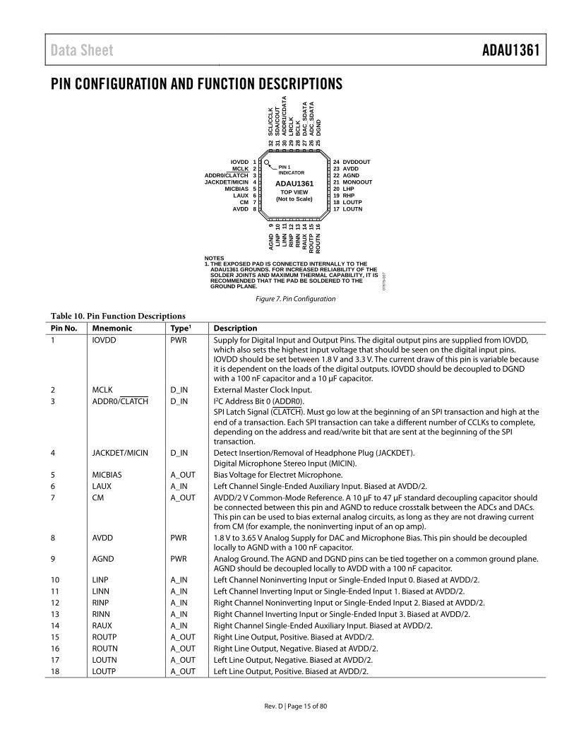
PIN CONFIGURATION AND FUNCTION DESCRIPTIONS
0767
9-00
7
AG
ND
LIN
PLI
NN
RIN
PR
INN
RA
UX
RO
UTP
RO
UTN
SCL/
CC
LKSD
A/C
OU
TA
DD
R1/
CD
ATA
LRC
LKB
CLK
DA
C_S
DA
TAA
DC
_SD
ATA
DG
ND
PIN 1INDICATOR
1IOVDD2MCLK3ADDR0/CLATCH4JACKDET/MICIN5MICBIAS6LAUX7CM8AVDD
24 DVDDOUT23 AVDD22 AGND21 MONOOUT20 LHP19 RHP18 LOUTP17 LOUTN
9 10 11 12 13 14 15 16
32 31 30 29 28 27 26 25
TOP VIEW(Not to Scale)
ADAU1361
NOTES1. THE EXPOSED PAD IS CONNECTED INTERNALLY TO THE
ADAU1361 GROUNDS. FOR INCREASED RELIABILITY OF THESOLDER JOINTS AND MAXIMUM THERMAL CAPABILITY, IT ISRECOMMENDED THAT THE PAD BE SOLDERED TO THEGROUND PLANE.
Figure 7. Pin Configuration
Table 10. Pin Function Descriptions Pin No. Mnemonic Type1 Description 1 IOVDD PWR Supply for Digital Input and Output Pins. The digital output pins are supplied from IOVDD,
which also sets the highest input voltage that should be seen on the digital input pins. IOVDD should be set between 1.8 V and 3.3 V. The current draw of this pin is variable because it is dependent on the loads of the digital outputs. IOVDD should be decoupled to DGND with a 100 nF capacitor and a 10 μF capacitor.
2 MCLK D_IN External Master Clock Input. 3 ADDR0/CLATCH D_IN I2C Address Bit 0 (ADDR0).
SPI Latch Signal (CLATCH). Must go low at the beginning of an SPI transaction and high at the end of a transaction. Each SPI transaction can take a different number of CCLKs to complete, depending on the address and read/write bit that are sent at the beginning of the SPI transaction.
4 JACKDET/MICIN D_IN Detect Insertion/Removal of Headphone Plug (JACKDET). Digital Microphone Stereo Input (MICIN).
5 MICBIAS A_OUT Bias Voltage for Electret Microphone. 6 LAUX A_IN Left Channel Single-Ended Auxiliary Input. Biased at AVDD/2. 7 CM A_OUT AVDD/2 V Common-Mode Reference. A 10 μF to 47 μF standard decoupling capacitor should
be connected between this pin and AGND to reduce crosstalk between the ADCs and DACs. This pin can be used to bias external analog circuits, as long as they are not drawing current from CM (for example, the noninverting input of an op amp).
8 AVDD PWR 1.8 V to 3.65 V Analog Supply for DAC and Microphone Bias. This pin should be decoupled locally to AGND with a 100 nF capacitor.
9 AGND PWR Analog Ground. The AGND and DGND pins can be tied together on a common ground plane. AGND should be decoupled locally to AVDD with a 100 nF capacitor.
10 LINP A_IN Left Channel Noninverting Input or Single-Ended Input 0. Biased at AVDD/2. 11 LINN A_IN Left Channel Inverting Input or Single-Ended Input 1. Biased at AVDD/2. 12 RINP A_IN Right Channel Noninverting Input or Single-Ended Input 2. Biased at AVDD/2. 13 RINN A_IN Right Channel Inverting Input or Single-Ended Input 3. Biased at AVDD/2. 14 RAUX A_IN Right Channel Single-Ended Auxiliary Input. Biased at AVDD/2. 15 ROUTP A_OUT Right Line Output, Positive. Biased at AVDD/2. 16 ROUTN A_OUT Right Line Output, Negative. Biased at AVDD/2. 17 LOUTN A_OUT Left Line Output, Negative. Biased at AVDD/2. 18 LOUTP A_OUT Left Line Output, Positive. Biased at AVDD/2.

ADAU1361 Data Sheet
Rev. D | Page 16 of 80
Pin No. Mnemonic Type1 Description 19 RHP A_OUT Right Headphone Output. Biased at AVDD/2. 20 LHP A_OUT Left Headphone Output. Biased at AVDD/2. 21 MONOOUT A_OUT Mono Output or Virtual Ground for Capless Headphone. Biased at AVDD/2 when set as mono
output. 22 AGND PWR Analog Ground. The AGND and DGND pins can be tied together on a common ground plane.
AGND should be decoupled locally to AVDD with a 100 nF capacitor. 23 AVDD PWR 1.8 V to 3.3 V Analog Supply for ADC, Output Driver, and Input to Digital Supply Regulator.
This pin should be decoupled locally to AGND with a 100 nF capacitor. 24 DVDDOUT PWR Digital Core Supply Decoupling Point. The digital supply is generated from an on-board
regulator and does not require an external supply. DVDDOUT should be decoupled to DGND with a 100 nF capacitor and a 10 μF capacitor.
25 DGND PWR Digital Ground. The AGND and DGND pins can be tied together on a common ground plane. DGND should be decoupled to DVDDOUT and to IOVDD with 100 nF capacitors and 10 μF capacitors.
26 ADC_SDATA D_OUT ADC Serial Output Data. 27 DAC_SDATA D_IN DAC Serial Input Data. 28 BCLK D_IO Serial Data Port Bit Clock. 29 LRCLK D_IO Serial Data Port Frame Clock. 30 ADDR1/CDATA D_IN I2C Address Bit 1 (ADDR1).
SPI Data Input (CDATA). 31 SDA/COUT D_IO I2C Data (SDA). This pin is a bidirectional open-collector input/output. The line connected to
this pin should have a 2 kΩ pull-up resistor. SPI Data Output (COUT). This pin is used for reading back registers and memory locations. It is three-state when an SPI read is not active.
32 SCL/CCLK D_IN I2C Clock (SCL). This pin is always an open-collector input when in I2C control mode. The line connected to this pin should have a 2 kΩ pull-up resistor. SPI Clock (CCLK). This pin can run continuously or be gated off between SPI transactions.
EP Exposed Pad Exposed Pad. The exposed pad is connected internally to the ADAU1361 grounds. For increased reliability of the solder joints and maximum thermal capability, it is recommended that the pad be soldered to the ground plane. See the Exposed Pad PCB Design section for more information.
1 A_IN = analog input, A_OUT = analog output, D_IN = digital input, D_IO = digital input/output, D_OUT = digital output, PWR = power.
Data Sheet ADAU1361
Rev. D | Page 17 of 80
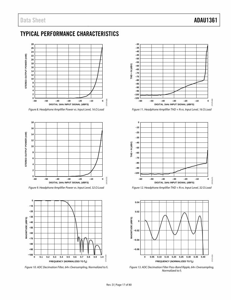
TYPICAL PERFORMANCE CHARACTERISTICS
0767
9-06
8
28
02468
101214161820222426
–60 0–10–20–30–40–50
STER
EO O
UTP
UT
POW
ER (m
W)
DIGITAL 1kHz INPUT SIGNAL (dBFS) Figure 8. Headphone Amplifier Power vs. Input Level, 16 Ω Load
0767
9-07
0
18
0
2
4
6
8
10
12
14
16
–60 0–10–20–30–40–50
STER
EO O
UTP
UT
POW
ER (m
W)
DIGITAL 1kHz INPUT SIGNAL (dBFS) Figure 9. Headphone Amplifier Power vs. Input Level, 32 Ω Load
−100
−90
−80
−70
−60
−50
−40
−30
−20
−10
0
0767
9-00
8
FREQUENCY (NORMALIZED TO fS)
MA
GN
ITU
DE
(dB
FS)
0 0.1 0.2 0.3 0.4 0.5 0.6 0.7 0.8 0.9 1.0
Figure 10. ADC Decimation Filter, 64× Oversampling, Normalized to fS
0767
9-06
9
–30
–105–100
–95–90–85–80–75–70–65–60–55–50–45–40–35
–60 0–10–20–30–40–50
THD
+ N
(dB
V)
DIGITAL 1kHz INPUT SIGNAL (dBFS) Figure 11. Headphone Amplifier THD + N vs. Input Level, 16 Ω Load
0767
9-07
1
0
–10
–20
–30
–40
–50
–60
–70
–80
–90
–100
–60 0–10–20–30–40–50
THD
+ N
(dB
V)
DIGITAL 1kHz INPUT SIGNAL (dBFS) Figure 12. Headphone Amplifier THD + N vs. Input Level, 32 Ω Load
0 0.05 0.10 0.20 0.30 0.400.15 0.25 0.35
−0.06
−0.04
−0.02
0
0.02
0.04
0767
9-00
9
FREQUENCY (NORMALIZED TO fS)
MA
GN
ITU
DE
(dB
FS)
Figure 13. ADC Decimation Filter Pass-Band Ripple, 64× Oversampling,
Normalized to fS

ADAU1361 Data Sheet
Rev. D | Page 18 of 80
−100
−90
−80
−70
−60
−50
−40
−30
−20
−10
0
0767
9-01
0
FREQUENCY (NORMALIZED TO fS)
MA
GN
ITU
DE
(dB
FS)
0.10 0.2 0.3 0.4 0.5 0.6 0.7 0.8 0.9 1.0
Figure 14. ADC Decimation Filter, 128× Oversampling, Normalized to fS
0−100
−90
−80
−70
−60
−50
−40
−30
−20
−10
0
0767
9-01
2
FREQUENCY (NORMALIZED TO fS)
MA
GN
ITU
DE
(dB
FS)
0.1 0.2 0.3 0.4 0.5 0.6 0.7 0.8 0.9 1.0
Figure 15. ADC Decimation Filter, 128× Oversampling, Double-Rate Mode,
Normalized to fS
−100
−90
−80
−70
−60
−50
−40
−30
−20
−10
0
0767
9-01
4
FREQUENCY (NORMALIZED TO fS)
MA
GN
ITU
DE
(dB
FS)
0 0.1 0.2 0.3 0.4 0.5 0.6 0.7 0.8 0.9 1.0
Figure 16. DAC Interpolation Filter, 64× Oversampling, Double-Rate Mode,
Normalized to fS
0 0.05 0.10 0.20 0.30 0.400.15 0.25 0.35 0.500.45−0.10
−0.08
−0.06
−0.04
−0.02
0
0.02
0.04
0.06
0.08
0.10
0767
9-01
1
FREQUENCY (NORMALIZED TO fS)
MA
GN
ITU
DE
(dB
FS)
Figure 17. ADC Decimation Filter Pass-Band Ripple, 128× Oversampling,
Normalized to fS
0 0.05 0.10 0.20 0.30 0.400.15 0.25 0.35
−0.06
−0.04
−0.02
0
0.02
0.04
0767
9-01
3
FREQUENCY (NORMALIZED TO fS)
MA
GN
ITU
DE
(dB
FS)
Figure 18. ADC Decimation Filter Pass-Band Ripple, 128× Oversampling,
Double-Rate Mode, Normalized to fS
0 0.05 0.10 0.20 0.30 0.400.15 0.25 0.35
−0.15
−0.20
−0.10
−0.05
0
0.05
0.15
0.20
0.1007
679-
015
FREQUENCY (NORMALIZED TO fS)
MA
GN
ITU
DE
(dB
FS)
Figure 19. DAC Interpolation Filter Pass-Band Ripple, 64× Oversampling,
Double-Rate Mode, Normalized to fS
Data Sheet ADAU1361
Rev. D | Page 19 of 80
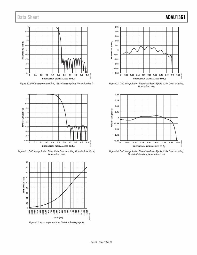
−100
−90
−80
−70
−60
−50
−40
−30
−20
−10
0
0767
9-01
6
FREQUENCY (NORMALIZED TO fS)
MA
GN
ITU
DE
(dB
FS)
0.10 0.2 0.3 0.4 0.5 0.6 0.7 0.8 0.9 1.0
Figure 20. DAC Interpolation Filter, 128× Oversampling, Normalized to fS
−100
−90
−80
−70
−60
−50
−40
−30
−20
−10
0
0767
9-01
8
FREQUENCY (NORMALIZED TO fS)
MA
GN
ITU
DE
(dB
FS)
0.10 0.2 0.3 0.4 0.5 0.6 0.7 0.8 0.9 1.0
Figure 21. DAC Interpolation Filter, 128× Oversampling, Double-Rate Mode, Normalized to fS
0
10
20
30
40
50
60
70
80
90
35.0
032
.75
30.5
028
.25
26.0
023
.75
21.5
019
.25
17.0
014
.75
12.5
010
.25
8.00
5.75
3.50
1.25
–1.0
0–3
.25
–5.5
0–7
.75
–10.
00–1
2.25
IMPE
DA
NC
E (k
Ω)
GAIN (dB)
0767
9-12
5
Figure 22. Input Impedance vs. Gain for Analog Inputs
0 0.05 0.10 0.20 0.30 0.400.15 0.25 0.35 0.500.45−0.05
−0.04
−0.03
−0.02
−0.01
0
0.01
0.02
0.03
0.04
0.05
0767
9-01
7
FREQUENCY (NORMALIZED TO fS)
MA
GN
ITU
DE
(dB
FS)
Figure 23. DAC Interpolation Filter Pass-Band Ripple, 128× Oversampling,
Normalized to fS
−0.20
−0.15
−0.10
−0.05
0
0.05
0.10
0.15
0.20
0 0.05 0.10 0.20 0.30 0.400.15 0.25 0.35
0767
9-01
9
FREQUENCY (NORMALIZED TO fS)
MA
GN
ITU
DE
(dB
FS)
Figure 24. DAC Interpolation Filter Pass-Band Ripple, 128× Oversampling,
Double-Rate Mode, Normalized to fS

ADAU1361 Data Sheet
Rev. D | Page 20 of 80
SYSTEM BLOCK DIAGRAMS
AVDDIOVDD AVDDDVDDOUT
LINN
RINN
RINP
LINP
JACKDETECTION
SIGNAL
LAUX
RAUX
LEFTMICROPHONE
RIGHTMICROPHONE
+
++
AUX RIGHT
AUX LEFT
JACKDET/MICIN
MCLK
AG
ND
AG
ND
DG
ND
ADC_SDATA
DAC_SDATA
LRCLK
BCLK
SERIAL DATA
CM
SYSTEMCONTROLLER
ADDR1/CDATA
SDA/COUT
SCL/CCLK
ADDR0/CLATCH
MICBIAS
LOUTP
LOUTN
LHP
MONOOUT
RHP
ROUTP
ROUTN
CAPLESSHEADPHONEOUTPUT
EARPIECESPEAKER
EARPIECESPEAKER
CLOCKSOURCE
THE INPUT CAPACITOR VALUE DEPENDS ON THEINPUT IMPEDANCE, WHICH VARIES WITH THEVOLUME SETTING.
ADAU1361
10µF
10µF
10µF
0.1µF
10µF
10µF
0.1µF
0.1µF
9.1pF
0.1µF
FROM VOLTAGEREGULATOR(1.8V TO 3.3V)
2kΩ
2kΩ
1kΩ
1kΩ
49.9Ω
0.1µF 10µF+
1.2nH
0767
9-04
5
10µF
10µF
10µF
10µF
Figure 25. System Block Diagram

Data Sheet ADAU1361
Rev. D | Page 21 of 80
AVDDIOVDD AVDDDVDDOUT
LINN
RINN
RINP
LINP
JACKDETECTION
SIGNAL
LAUX
RAUX
+
++
AUX RIGHT
AUX LEFT
CM
JACKDET/MICIN
MCLK
AG
ND
AG
ND
DG
ND
ADC_SDATA
DAC_SDATA
LRCLK
BCLK
SERIAL DATA
CM
SYSTEMCONTROLLER
ADDR1/CDATA
SDA/COUT
SCL/CCLK
ADDR0/CLATCH
MICBIAS
CLOCKSOURCE
THE INPUT CAPACITOR VALUE DEPENDS ON THEINPUT IMPEDANCE, WHICH VARIES WITH THEVOLUME SETTING.
ADAU1361
10µF
10µF
CM
10µF
10µF
10µF
0.1µF
10µF
10µF
0.1µF
0.1µF
9.1pF
0.1µF
FROM VOLTAGEREGULATOR(1.8V TO 3.3V)
1kΩ
1kΩ
49.9Ω
1.2nH
0767
9-07
2
VDD
GND
SINGLE-ENDEDANALOG
MICROPHONEOUTPUT
VDD
GND
SINGLE-ENDEDANALOG
MICROPHONEOUTPUT
LOUTP
LOUTN
LHP
MONOOUT
RHP
ROUTP
ROUTN
CAPLESSHEADPHONEOUTPUT
EARPIECESPEAKER
EARPIECESPEAKER
0.1µF 10µF+
Figure 26. System Block Diagram with Analog Microphones
ADAU1361 Data Sheet
Rev. D | Page 22 of 80
AVDDIOVDD AVDDDVDDOUT
LINN
RINN
RINP
LINP
LAUX
RAUX
+
++
AUX LEFT
MCLK
AG
ND
AG
ND
DG
ND
ADC_SDATA
DAC_SDATA
LRCLK
BCLK
SERIAL DATA
CM
SYSTEMCONTROLLER
ADDR1/CDATA
SDA/COUT
SCL/CCLK
ADDR0/CLATCH
MICBIAS
LOUTP
LOUTN
ROUTP
ROUTN
CLOCKSOURCE
ADAU1361
10µF
CM
10µF
0.1µF
10µF
10µF
10µF
0.1µF
0.1µF
0.1µF
0.1µF
0.1µF
9.1pF
22nF
REXT
0.1µF
FROM VOLTAGEREGULATOR(1.8V TO 3.3V)
1kΩ
AUX RIGHT
10µF
1kΩ
49.9Ω
BCLK
0.1µF 10µF+
1.2nH
0767
9-07
3
22nF
REXT
22nF
REXT
REXT
22nFINL+
INL–
INR+
INR–
OUTL+OUTL–
OUTR+OUTR–
SSM2306CLASS-D 2W
STEREO SPEAKERDRIVER
VDDVDD
GNDSD GND
2.5V TO 5.0V
RIGHTSPEAKER
LEFTSPEAKER
LHP
MONOOUT
RHP
CAPLESSHEADPHONE
OUTPUT
BCLK
JACKDET/MICIN
GNDL/R SELECT
DATAVDD
CLK
DIGITALMICROPHONE
GNDL/R SELECT
DATAVDD
CLK
DIGITALMICROPHONE
SHU
TDO
WN
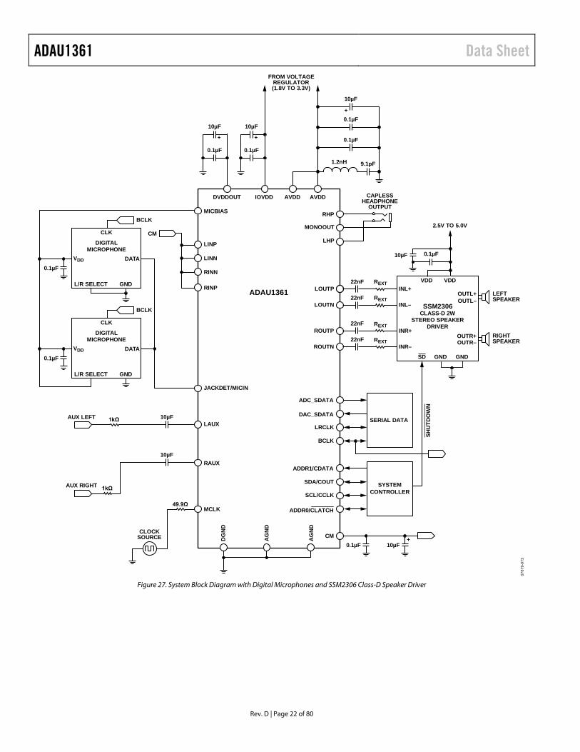
Figure 27. System Block Diagram with Digital Microphones and SSM2306 Class-D Speaker Driver

Data Sheet ADAU1361
Rev. D | Page 23 of 80
THEORY OF OPERATION The ADAU1361 is an audio codec that offers high quality audio, low power, and small package size. The stereo ADC and stereo DAC each have an SNR of at least +98 dB and a THD + N of at least −90 dB. The serial data port is compatible with I2S, left-justified, right-justified, and TDM modes for interfacing to digital audio data. The operating voltage range is 1.8 V to 3.65 V, with an on-board regulator generating the internal digital supply voltage.
The record signal path includes very flexible input configurations that can accept differential and single-ended analog microphone inputs as well as a digital microphone input. A microphone bias pin provides seamless interfacing to electret microphones. Input configurations can accept up to six single-ended analog signals or variations of stereo differential or stereo single-ended signals with two additional auxiliary single-ended inputs. Each input signal has its own programmable gain amplifier (PGA) for volume adjustment and can be routed directly to the playback path output mixers, bypassing the ADCs. An automatic level control (ALC) can also be implemented to keep the recording volume constant.
The ADCs and DACs are high quality, 24-bit Σ-Δ converters that operate at selectable 64× or 128× oversampling ratios. The base sampling rate of the converters is set by the input clock rate and can be further scaled with the converter control register settings. The converters can operate at sampling frequencies from 8 kHz to 96 kHz. The ADCs and DACs also include very fine-step digital volume controls.
The playback path allows input signals and DAC outputs to be mixed into various output configurations. Headphone drivers are available for a stereo headphone output, and the other output pins are capable of differentially driving an earpiece speaker. Capless headphone outputs are possible with the use of the mono output as a virtual ground connection. The stereo line outputs can be used as either single-ended or differential outputs and as an optional mix-down mono output.
The ADAU1361 can generate its internal clocks from a wide range of input clocks by using the on-board fractional PLL. The PLL accepts inputs from 8 MHz to 27 MHz.
The ADAU1361 is provided in a small, 32-lead, 5 mm × 5 mm LFCSP with an exposed bottom pad.
ADAU1361 Data Sheet
Rev. D | Page 24 of 80
STARTUP, INITIALIZATION, AND POWER This section describes the procedure for properly starting up the ADAU1361. The following sequence provides a high level approach to the proper initiation of the system.
1. Apply power to the ADAU1361. 2. Lock the PLL to the input clock (if using the PLL). 3. Enable the core clock. 4. Load the register settings.
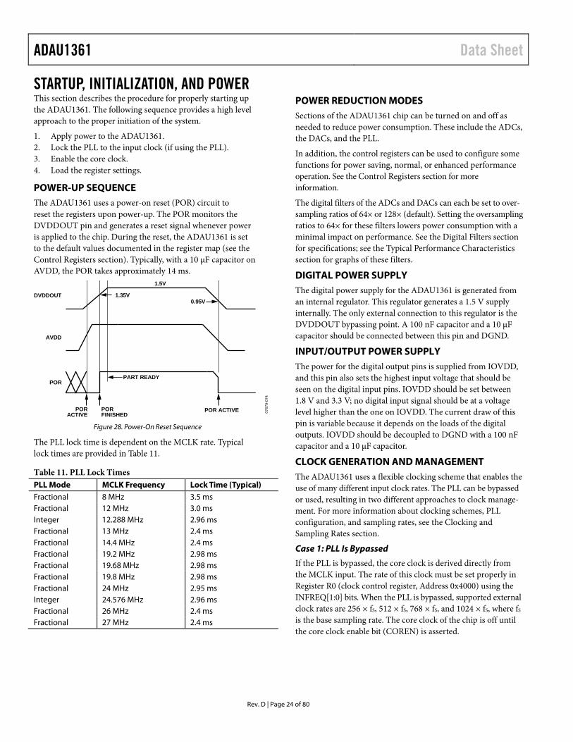
POWER-UP SEQUENCE The ADAU1361 uses a power-on reset (POR) circuit to reset the registers upon power-up. The POR monitors the DVDDOUT pin and generates a reset signal whenever power is applied to the chip. During the reset, the ADAU1361 is set to the default values documented in the register map (see the Control Registers section). Typically, with a 10 μF capacitor on AVDD, the POR takes approximately 14 ms.
0767
9-07
4
AVDD
PORPART READY
PORACTIVE
POR ACTIVE
DVDDOUT 1.35V0.95V
1.5V
PORFINISHED
Figure 28. Power-On Reset Sequence
The PLL lock time is dependent on the MCLK rate. Typical lock times are provided in Table 11.
Table 11. PLL Lock Times PLL Mode MCLK Frequency Lock Time (Typical) Fractional 8 MHz 3.5 ms Fractional 12 MHz 3.0 ms Integer 12.288 MHz 2.96 ms Fractional 13 MHz 2.4 ms Fractional 14.4 MHz 2.4 ms Fractional 19.2 MHz 2.98 ms Fractional 19.68 MHz 2.98 ms Fractional 19.8 MHz 2.98 ms Fractional 24 MHz 2.95 ms Integer 24.576 MHz 2.96 ms Fractional 26 MHz 2.4 ms Fractional 27 MHz 2.4 ms
POWER REDUCTION MODES Sections of the ADAU1361 chip can be turned on and off as needed to reduce power consumption. These include the ADCs, the DACs, and the PLL.
In addition, the control registers can be used to configure some functions for power saving, normal, or enhanced performance operation. See the Control Registers section for more information.
The digital filters of the ADCs and DACs can each be set to over-sampling ratios of 64× or 128× (default). Setting the oversampling ratios to 64× for these filters lowers power consumption with a minimal impact on performance. See the Digital Filters section for specifications; see the Typical Performance Characteristics section for graphs of these filters.
DIGITAL POWER SUPPLY The digital power supply for the ADAU1361 is generated from an internal regulator. This regulator generates a 1.5 V supply internally. The only external connection to this regulator is the DVDDOUT bypassing point. A 100 nF capacitor and a 10 μF capacitor should be connected between this pin and DGND.
INPUT/OUTPUT POWER SUPPLY The power for the digital output pins is supplied from IOVDD, and this pin also sets the highest input voltage that should be seen on the digital input pins. IOVDD should be set between 1.8 V and 3.3 V; no digital input signal should be at a voltage level higher than the one on IOVDD. The current draw of this pin is variable because it depends on the loads of the digital outputs. IOVDD should be decoupled to DGND with a 100 nF capacitor and a 10 μF capacitor.
CLOCK GENERATION AND MANAGEMENT The ADAU1361 uses a flexible clocking scheme that enables the use of many different input clock rates. The PLL can be bypassed or used, resulting in two different approaches to clock manage-ment. For more information about clocking schemes, PLL configuration, and sampling rates, see the Clocking and Sampling Rates section.
Case 1: PLL Is Bypassed
If the PLL is bypassed, the core clock is derived directly from the MCLK input. The rate of this clock must be set properly in Register R0 (clock control register, Address 0x4000) using the INFREQ[1:0] bits. When the PLL is bypassed, supported external clock rates are 256 × fS, 512 × fS, 768 × fS, and 1024 × fS, where fS is the base sampling rate. The core clock of the chip is off until the core clock enable bit (COREN) is asserted.
Data Sheet ADAU1361
Rev. D | Page 25 of 80
Case 2: PLL Is Used
The core clock to the entire chip is off during the PLL lock acquisition period. The user can poll the lock bit to determine when the PLL has locked. After lock is acquired, the ADAU1361 can be started by asserting the core clock enable bit (COREN) in Register R0 (clock control register, Address 0x4000). This bit enables the core clock to all the internal blocks of the ADAU1361.
PLL Lock Acquisition
During the lock acquisition period, only Register R0 (Address 0x4000) and Register R1 (Address 0x4002) are accessible through the control port. Because all other registers require a valid master clock for reading and writing, do not attempt to access any other register. Any read or write is prohibited until the core clock enable bit (COREN) and the lock bit are both asserted.
To program the PLL during initialization or reconfiguration of the clock setting, the following procedure must be followed:
1. Power down the PLL. 2. Reset the PLL control register. 3. Start the PLL. 4. Poll the lock bit. 5. Assert the core clock enable bit after the PLL lock
is acquired.
The PLL control register (Register R1, Address 0x4002) is a 48-bit register where all bits must be written with a single continuous write to the control port.

ADAU1361 Data Sheet
Rev. D | Page 26 of 80
CLOCKING AND SAMPLING RATES
0767
9-02
0
MCLK
AD
C_S
DA
TA
BC
LK
LR
CL
K
DA
C_S
DA
TA
INFREQ[1:0]
SERIAL DATAINPUT/OUTPUT
PORTADCs DACs
÷ X × (R + N/M)
R1: PLL CONTROL REGISTER
CLKSRC
R0: CLOCKCONTROL REGISTER
CORECLOCK
R17: CONVERTERCONTROL 0 REGISTER
256 × fS, 512 × fS,768 × fS, 1024 × fS
CONVSR[2:0]fS/0.5, 1, 1.5, 2, 3, 4, 6
Figure 29. Clock Tree Diagram
CORE CLOCK Clocks for the converters and serial ports are derived from the core clock. The core clock can be derived directly from MCLK or it can be generated by the PLL. The CLKSRC bit (Bit 3 in Register R0, Address 0x4000) determines the clock source.
The INFREQ[1:0] bits should be set according to the expected input clock rate selected by CLKSRC; this value also determines the core clock rate and the base sampling frequency, fS.
For example, if the input to CLKSRC = 49.152 MHz (from PLL), then
INFREQ[1:0] = 1024 × fS
fS = 49.152 MHz/1024 = 48 kHz
The PLL output clock rate is always 1024 × fS, and the clock control register automatically sets the INFREQ[1:0] bits to 1024 × fS when using the PLL. When using a direct clock, the INFREQ[1:0] frequency should be set according to the MCLK pin clock rate and the desired base sampling frequency.
Table 12. Clock Control Register (Register R0, Address 0x4000) Bits Bit Name Settings 3 CLKSRC 0: Direct from MCLK pin (default)
1: PLL clock [2:1] INFREQ[1:0] 00: 256 × fS (default)
01: 512 × fS 10: 768 × fS 11: 1024 × fS
0 COREN 0: Core clock disabled (default) 1: Core clock enabled
SAMPLING RATES The ADCs, DACs, and serial port share a common sampling rate that is set in Register R17 (Converter Control 0 register, Address 0x4017). The CONVSR[2:0] bits set the sampling rate as a ratio of the base sampling frequency.
Table 13 and Table 14 list the sampling rate divisions for common base sampling rates.
Table 13. 48 kHz Base Sampling Rate Divisions Base Sampling Frequency Sampling Rate Scaling Sampling Rate fS = 48 kHz fS/1 48 kHz
fS/6 8 kHz fS/4 12 kHz fS/3 16 kHz fS/2 24 kHz fS/1.5 32 kHz fS/0.5 96 kHz
Table 14. 44.1 kHz Base Sampling Rate Divisions Base Sampling Frequency Sampling Rate Scaling Sampling Rate fS = 44.1 kHz fS/1 44.1 kHz
fS/6 7.35 kHz fS/4 11.025 kHz fS/3 14.7 kHz fS/2 22.05 kHz fS/1.5 29.4 kHz fS/0.5 88.2 kHz

Data Sheet ADAU1361
Rev. D | Page 27 of 80
PLL The PLL uses the MCLK as a reference to generate the core clock. PLL settings are set in Register R1 (PLL control register, Address 0x4002). Depending on the MCLK frequency, the PLL must be set for either integer or fractional mode. The PLL can accept input frequencies in the range of 8 MHz to 27 MHz.
All six bytes in the PLL control register must be written with a single continuous write to the control port.
0767
9-02
1
MCLK ÷ X × (R + N/M)
TO PLLCLOCK DIVIDER
Figure 30. PLL Block Diagram
Integer Mode
Integer mode is used when the MCLK is an integer (R) multiple of the PLL output (1024 × fS).
For example, if MCLK = 12.288 MHz and fS = 48 kHz, then
PLL required output = 1024 × 48 kHz = 49.152 MHz
R = 49.152 MHz/12.288 MHz = 4
In integer mode, the values set for N and M are ignored.
Fractional Mode
Fractional mode is used when the MCLK is a fractional (R + (N/M)) multiple of the PLL output.
For example, if MCLK = 12 MHz and fS = 48 kHz, then
PLL required output = 1024 × 48 kHz = 49.152 MHz
R + (N/M) = 49.152 MHz/12 MHz = 4 + (12/125)
Common fractional PLL parameter settings for 44.1 kHz and 48 kHz sampling rates can be found in Table 16 and Table 17.
The PLL outputs a clock in the range of 41 MHz to 54 MHz, which should be taken into account when calculating PLL values and MCLK frequencies.
Table 15. PLL Control Register (Register R1, Address 0x4002) Bits Bit Name Description [47:32] M[15:0] Denominator of the fractional PLL: 16-bit binary number
0x00FD: M = 253 (default) [31:16] N[15:0] Numerator of the fractional PLL: 16-bit binary number
0x000C: N = 12 (default) [14:11] R[3:0] Integer part of PLL: four bits, only values 2 to 8 are valid
0010: R = 2 (default) 0011: R = 3 0100: R = 4 0101: R = 5 0110: R = 6 0111: R = 7 1000: R = 8
[10:9] X[1:0] PLL input clock divider 00: X = 1 (default) 01: X = 2 10: X = 3 11: X = 4
8 Type PLL operation mode 0: Integer (default) 1: Fractional
1 Lock PLL lock (read-only bit) 0: PLL unlocked (default) 1: PLL locked
0 PLLEN PLL enable 0: PLL disabled (default) 1: PLL enabled

ADAU1361 Data Sheet
Rev. D | Page 28 of 80
Table 16. Fractional PLL Parameter Settings for fS = 44.1 kHz (PLL Output = 45.1584 MHz = 1024 × fS) MCLK Input (MHz) Input Divider (X) Integer (R) Denominator (M) Numerator (N) R2: PLL Control Setting (Hex) 8 1 5 625 403 0x0271 0193 2901 12 1 3 625 477 0x0271 01DD 1901 13 1 3 8125 3849 0x1FBD 0F09 1901 14.4 2 6 125 34 0x007D 0022 3301 19.2 2 4 125 88 0x007D 0058 2301 19.68 2 4 1025 604 0x0401 025C 2301 19.8 2 4 1375 772 0x055F 0304 2301 24 2 3 625 477 0x0271 01DD 1B01 26 2 3 8125 3849 0x1FBD 0F09 1B01 27 2 3 1875 647 0x0753 0287 1B01
Table 17. Fractional PLL Parameter Settings for fS = 48 kHz (PLL Output = 49.152 MHz = 1024 × fS) MCLK Input (MHz) Input Divider (X) Integer (R) Denominator (M) Numerator (N) R2: PLL Control Setting (Hex) 8 1 6 125 18 0x007D 0012 3101 12 1 4 125 12 0x007D 000C 2101 13 1 3 1625 1269 0x0659 04F5 1901 14.4 2 6 75 62 0x004B 003E 3301 19.2 2 5 25 3 0x0019 0003 2B01 19.68 2 4 205 204 0x00CD 00CC 2301 19.8 2 4 825 796 0x0339 031C 2301 24 2 4 125 12 0x007D 000C 2301 26 2 3 1625 1269 0x0659 04F5 1B01 27 2 3 1125 721 0x0465 02D1 1B01
Table 18. Integer PLL Parameter Settings for fS = 48 kHz (PLL Output = 49.152 MHz = 1024 × fS) MCLK Input (MHz) Input Divider (X) Integer (R) Denominator (M) Numerator (N) R2: PLL Control Setting (Hex)1 12.288 1 4 Don’t care Don’t care 0xXXXX XXXX 2001 24.576 1 2 Don’t care Don’t care 0xXXXX XXXX 1001 1 X = don’t care.
Data Sheet ADAU1361
Rev. D | Page 29 of 80
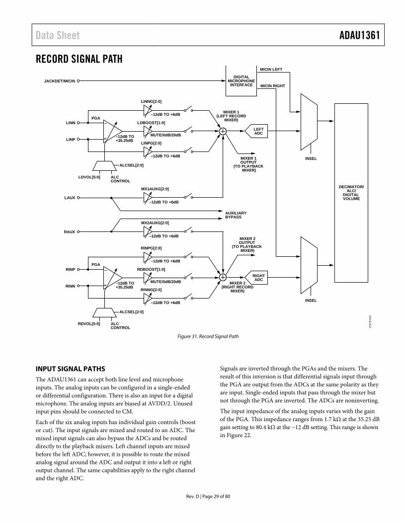
RECORD SIGNAL PATH
0767
9-02
2
LINP
LINN
LAUX
LEFTADC
RIGHTADC
JACKDET/MICIN
RAUX
MICIN LEFT
MICIN RIGHT
INSEL
INSELALCSEL[2:0]
ALCCONTROL
AUXILIARYBYPASS
MX1AUXG[2:0]
LDVOL[5:0]
LINNG[2:0]
LINPG[2:0]
LDBOOST[1:0]
MIXER 1(LEFT RECORD
MIXER)
MIXER 1OUTPUT
(TO PLAYBACKMIXER)
MIXER 2OUTPUT
(TO PLAYBACKMIXER)
–12dB TO +6dB
–12dB TO +6dB
MUTE/0dB/20dB
PGA
DECIMATOR/ALC/
DIGITALVOLUME
DIGITALMICROPHONE
INTERFACE
MIXER 2(RIGHT RECORD
MIXER)
–12dB TO +6dB
MX2AUXG[2:0]
–12dB TO +6dB
–12dB TO+35.25dB
RINN
RINP
ALCSEL[2:0]
ALCCONTROL
RDVOL[5:0]
RINPG[2:0]
RINNG[2:0]
RDBOOST[1:0]
–12dB TO +6dB
–12dB TO +6dB
MUTE/0dB/20dB
PGA
–12dB TO+35.25dB
Figure 31. Record Signal Path
INPUT SIGNAL PATHS The ADAU1361 can accept both line level and microphone inputs. The analog inputs can be configured in a single-ended or differential configuration. There is also an input for a digital microphone. The analog inputs are biased at AVDD/2. Unused input pins should be connected to CM.
Each of the six analog inputs has individual gain controls (boost or cut). The input signals are mixed and routed to an ADC. The mixed input signals can also bypass the ADCs and be routed directly to the playback mixers. Left channel inputs are mixed before the left ADC; however, it is possible to route the mixed analog signal around the ADC and output it into a left or right output channel. The same capabilities apply to the right channel and the right ADC.
Signals are inverted through the PGAs and the mixers. The result of this inversion is that differential signals input through the PGA are output from the ADCs at the same polarity as they are input. Single-ended inputs that pass through the mixer but not through the PGA are inverted. The ADCs are noninverting.
The input impedance of the analog inputs varies with the gain of the PGA. This impedance ranges from 1.7 kΩ at the 35.25 dB gain setting to 80.4 kΩ at the −12 dB setting. This range is shown in Figure 22.

ADAU1361 Data Sheet
Rev. D | Page 30 of 80
Analog Microphone Inputs
For microphone inputs, configure the part in either stereo pseudo-differential mode or stereo full differential mode.
The LINN and LINP pins are the inverting and noninverting inputs for the left channel, respectively. The RINN and RINP pins are the inverting and noninverting inputs for the right channel, respectively.
For a differential microphone input, connect the positive signal to the noninverting input of the PGA and the negative signal to the inverting input of the PGA, as shown in Figure 32. The PGA settings are controlled with Register R8 (left differential input volume control register, Address 0x400E) and Register R9 (right differential input volume control register, Address 0x400F). The PGA must first be enabled by setting the RDEN and LDEN bits.
0767
9-05
2
LEFTMICROPHONE
LEFTPGA LDBOOST[1:0]
MUTE/0dB/20dB–12dB TO
+35.25dB
RIGHTMICROPHONE
RIGHTPGA RDBOOST[1:0]
MUTE/0dB/20dB–12dB TO
+35.25dB
ADAU1361
LINP
LINN
RINN
MICBIAS
RINP
2kΩ
2kΩ
Figure 32. Stereo Differential Microphone Configuration
The PGA can also be used for single-ended microphone inputs. Connect LINP and/or RINP to the CM pin. In this configura-tion, the signal connects to the inverting input of the PGA, LINN and/or RINN, as shown in Figure 33.
0767
9-05
3
LEFTMICROPHONE
LEFTPGA LDBOOST[1:0]
MUTE/0dB/20dB–12dB TO
+35.25dB
RIGHTMICROPHONE
RIGHTPGA RDBOOST[1:0]
MUTE/0dB/20dB–12dB TO
+35.25dB
ADAU1361
LINN
LINP
RINP
MICBIAS
RINN
CM2kΩ
2kΩ
Figure 33. Stereo Single-Ended Microphone Configuration
Analog Line Inputs
Line input signals can be accepted by any analog input. It is possible to route signals on the RINN, RINP, LINN, and LINP pins around the differential amplifier to their own amplifier and to use these pins as single-ended line inputs by disabling the LDEN and RDEN bits (Bit 0 in Register R8, Address 0x400E, and Bit 0 in Register R9, Address 0x400F). Figure 34 depicts a stereo single-ended line input using the RINN and LINN pins.
The LAUX and RAUX pins are single-ended line inputs. They can be used together as a stereo single-ended auxiliary input, as shown in Figure 34. These inputs can bypass the input gain control, mixers, and ADCs to directly connect to the output playback mixers (see auxiliary bypass in Figure 31).
0767
9-05
4
ADAU1361
–12dB TO +6dB
LINNG[2:0]
LINNLEFT LINEINPUT
–12dB TO +6dB
RINNG[2:0]
RINNRIGHT LINEINPUT
LAUXLEFT AUXINPUT
RAUXRIGHT AUXINPUT
AUXILIARYBYPASS
Figure 34. Stereo Single-Ended Line Input with Stereo Auxiliary Bypass

Data Sheet ADAU1361
Rev. D | Page 31 of 80
Digital Microphone Input
When using a digital microphone connected to the JACKDET/ MICIN pin, the JDFUNC[1:0] bits in Register R2 (Address 0x4008) must be set to 10 to enable the microphone input and disable the jack detection function. The ADAU1361 must operate in master mode and source BCLK to the input clock of the digital microphone.
The digital microphone signal bypasses record path mixers and ADCs and is routed directly into the decimation filters. The digital microphone and ADCs share decimation filters and, therefore, both cannot be used simultaneously. The digital microphone input select bit, INSEL, can be set in Register R19 (ADC control register, Address 0x4019). Figure 35 depicts the digital microphone interface and signal routing.
0767
9-02
3
JDFUNC[1:0]
DIGITAL MICROPHONEINTERFACE
LEFTCHANNEL
RIGHTCHANNEL
TO JACKDETECTION
CIRCUIT
JACKDET/MICIN
RIGHTADC
LEFTADC
DECIMATORS
R19: ADC CONTROLINSEL
R2: DIGITAL MICROPHONE/JACK DETECTION
CONTROL
Figure 35. Digital Microphone Interface Block Diagram
Microphone Bias
The MICBIAS pin provides a voltage reference for electret analog microphones. The MICBIAS voltage is set in Register R10 (record microphone bias control register, Address 0x4010). In this register, the MICBIAS output can be enabled or disabled. Additional options include high performance operation and a gain boost. The gain boost provides two different voltage biases: 0.65 × AVDD or 0.90 × AVDD. When enabled, the high perfor-mance bit increases supply current to the microphone bias circuit to decrease rms input noise.
The MICBIAS pin can also be used to cleanly supply voltage to digital microphones or analog microphones with separate power supply pins.
ANALOG-TO-DIGITAL CONVERTERS The ADAU1361 uses two 24-bit Σ-Δ analog-to-digital con-verters (ADCs) with selectable oversampling ratios of 64× or 128× (selected by Bit 3 in Register R17, Address 0x4017).
ADC Full-Scale Level
The full-scale input to the ADCs (0 dBFS) depends on AVDD. At AVDD = 3.3 V, the full-scale input level is 1.0 V rms. This full-scale analog input outputs a digital signal at −1.38 dBFS. This gain offset is built into the ADAU1361 to prevent clipping. The full-scale input level scales linearly with the level of AVDD.
For single-ended and pseudo-differential signals, the full-scale value corresponds to the signal level at the pins, 0 dBFS.
The full differential full-scale input level is measured after the differential amplifier, which corresponds to −6 dBFS at each pin.
Signal levels above the full-scale value cause the ADCs to clip.
Digital ADC Volume Control
The digital ADC volume can be attenuated using Register R20 (left input digital volume register, Address 0x401A) and Register R21 (right input digital volume register, Address 0x401B).
High-Pass Filter
By default, a high-pass filter is used in the ADC path to remove dc offsets; this filter can be enabled or disabled in Register R19 (ADC control register, Address 0x4019). At fS = 48 kHz, the corner frequency of this high-pass filter is 2 Hz.
ADAU1361 Data Sheet
Rev. D | Page 32 of 80
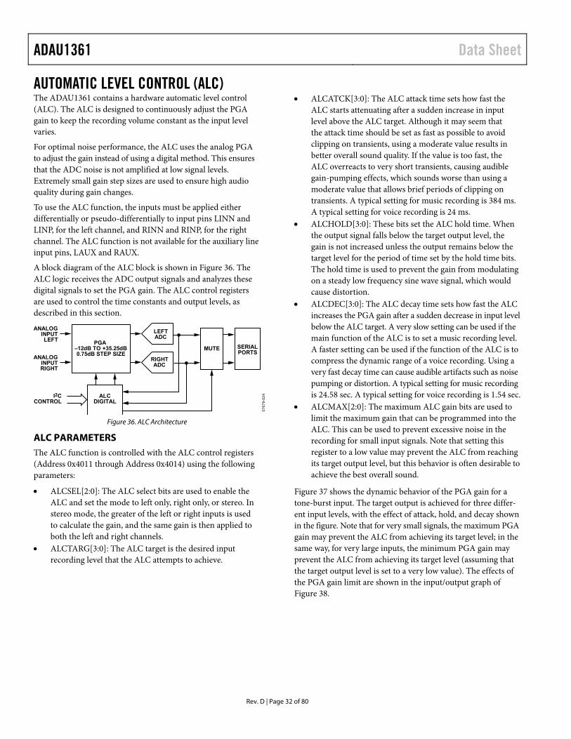
AUTOMATIC LEVEL CONTROL (ALC) The ADAU1361 contains a hardware automatic level control (ALC). The ALC is designed to continuously adjust the PGA gain to keep the recording volume constant as the input level varies.
For optimal noise performance, the ALC uses the analog PGA to adjust the gain instead of using a digital method. This ensures that the ADC noise is not amplified at low signal levels. Extremely small gain step sizes are used to ensure high audio quality during gain changes.
To use the ALC function, the inputs must be applied either differentially or pseudo-differentially to input pins LINN and LINP, for the left channel, and RINN and RINP, for the right channel. The ALC function is not available for the auxiliary line input pins, LAUX and RAUX.
A block diagram of the ALC block is shown in Figure 36. The ALC logic receives the ADC output signals and analyzes these digital signals to set the PGA gain. The ALC control registers are used to control the time constants and output levels, as described in this section.
0767
9-02
4
RIGHTADC
LEFTADC
MUTE SERIALPORTS
ALCDIGITAL
ANALOGINPUTLEFT
I2CCONTROL
ANALOGINPUTRIGHT
PGA–12dB TO +35.25dB0.75dB STEP SIZE
Figure 36. ALC Architecture
ALC PARAMETERS The ALC function is controlled with the ALC control registers (Address 0x4011 through Address 0x4014) using the following parameters:
ALCSEL[2:0]: The ALC select bits are used to enable the ALC and set the mode to left only, right only, or stereo. In stereo mode, the greater of the left or right inputs is used to calculate the gain, and the same gain is then applied to both the left and right channels.
ALCTARG[3:0]: The ALC target is the desired input recording level that the ALC attempts to achieve.
ALCATCK[3:0]: The ALC attack time sets how fast the ALC starts attenuating after a sudden increase in input level above the ALC target. Although it may seem that the attack time should be set as fast as possible to avoid clipping on transients, using a moderate value results in better overall sound quality. If the value is too fast, the ALC overreacts to very short transients, causing audible gain-pumping effects, which sounds worse than using a moderate value that allows brief periods of clipping on transients. A typical setting for music recording is 384 ms. A typical setting for voice recording is 24 ms.
ALCHOLD[3:0]: These bits set the ALC hold time. When the output signal falls below the target output level, the gain is not increased unless the output remains below the target level for the period of time set by the hold time bits. The hold time is used to prevent the gain from modulating on a steady low frequency sine wave signal, which would cause distortion.
ALCDEC[3:0]: The ALC decay time sets how fast the ALC increases the PGA gain after a sudden decrease in input level below the ALC target. A very slow setting can be used if the main function of the ALC is to set a music recording level. A faster setting can be used if the function of the ALC is to compress the dynamic range of a voice recording. Using a very fast decay time can cause audible artifacts such as noise pumping or distortion. A typical setting for music recording is 24.58 sec. A typical setting for voice recording is 1.54 sec.
ALCMAX[2:0]: The maximum ALC gain bits are used to limit the maximum gain that can be programmed into the ALC. This can be used to prevent excessive noise in the recording for small input signals. Note that setting this register to a low value may prevent the ALC from reaching its target output level, but this behavior is often desirable to achieve the best overall sound.
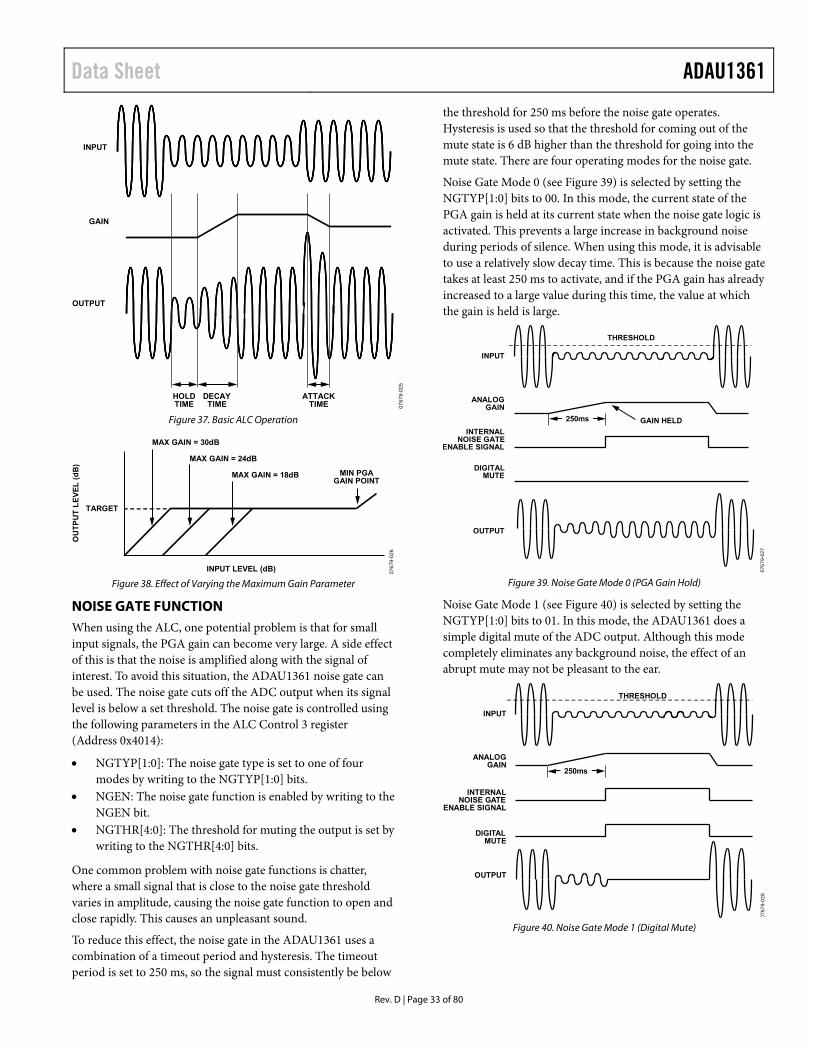
Figure 37 shows the dynamic behavior of the PGA gain for a tone-burst input. The target output is achieved for three differ-ent input levels, with the effect of attack, hold, and decay shown in the figure. Note that for very small signals, the maximum PGA gain may prevent the ALC from achieving its target level; in the same way, for very large inputs, the minimum PGA gain may prevent the ALC from achieving its target level (assuming that the target output level is set to a very low value). The effects of the PGA gain limit are shown in the input/output graph of Figure 38.
Data Sheet ADAU1361
Rev. D | Page 33 of 80
INPUT
GAIN
OUTPUT
DECAYTIME
ATTACKTIME
HOLDTIME 07
679-
025
Figure 37. Basic ALC Operation
INPUT LEVEL (dB)
TARGET
MIN PGAGAIN POINT
MAX GAIN = 18dB
MAX GAIN = 24dB
MAX GAIN = 30dB
OU
TP
UT
LE
VE
L (
dB
)
0767
9-02
6
Figure 38. Effect of Varying the Maximum Gain Parameter
NOISE GATE FUNCTION When using the ALC, one potential problem is that for small input signals, the PGA gain can become very large. A side effect of this is that the noise is amplified along with the signal of interest. To avoid this situation, the ADAU1361 noise gate can be used. The noise gate cuts off the ADC output when its signal level is below a set threshold. The noise gate is controlled using the following parameters in the ALC Control 3 register (Address 0x4014):
NGTYP[1:0]: The noise gate type is set to one of four modes by writing to the NGTYP[1:0] bits.
NGEN: The noise gate function is enabled by writing to the NGEN bit.
NGTHR[4:0]: The threshold for muting the output is set by writing to the NGTHR[4:0] bits.
One common problem with noise gate functions is chatter, where a small signal that is close to the noise gate threshold varies in amplitude, causing the noise gate function to open and close rapidly. This causes an unpleasant sound.
To reduce this effect, the noise gate in the ADAU1361 uses a combination of a timeout period and hysteresis. The timeout period is set to 250 ms, so the signal must consistently be below
the threshold for 250 ms before the noise gate operates. Hysteresis is used so that the threshold for coming out of the mute state is 6 dB higher than the threshold for going into the mute state. There are four operating modes for the noise gate.
Noise Gate Mode 0 (see Figure 39) is selected by setting the NGTYP[1:0] bits to 00. In this mode, the current state of the PGA gain is held at its current state when the noise gate logic is activated. This prevents a large increase in background noise during periods of silence. When using this mode, it is advisable to use a relatively slow decay time. This is because the noise gate takes at least 250 ms to activate, and if the PGA gain has already increased to a large value during this time, the value at which the gain is held is large.
INPUT
ANALOGGAIN
DIGITALMUTE
GAIN HELD
THRESHOLD
OUTPUT
INTERNALNOISE GATE
ENABLE SIGNAL
250ms
0767
9-02
7
Figure 39. Noise Gate Mode 0 (PGA Gain Hold)
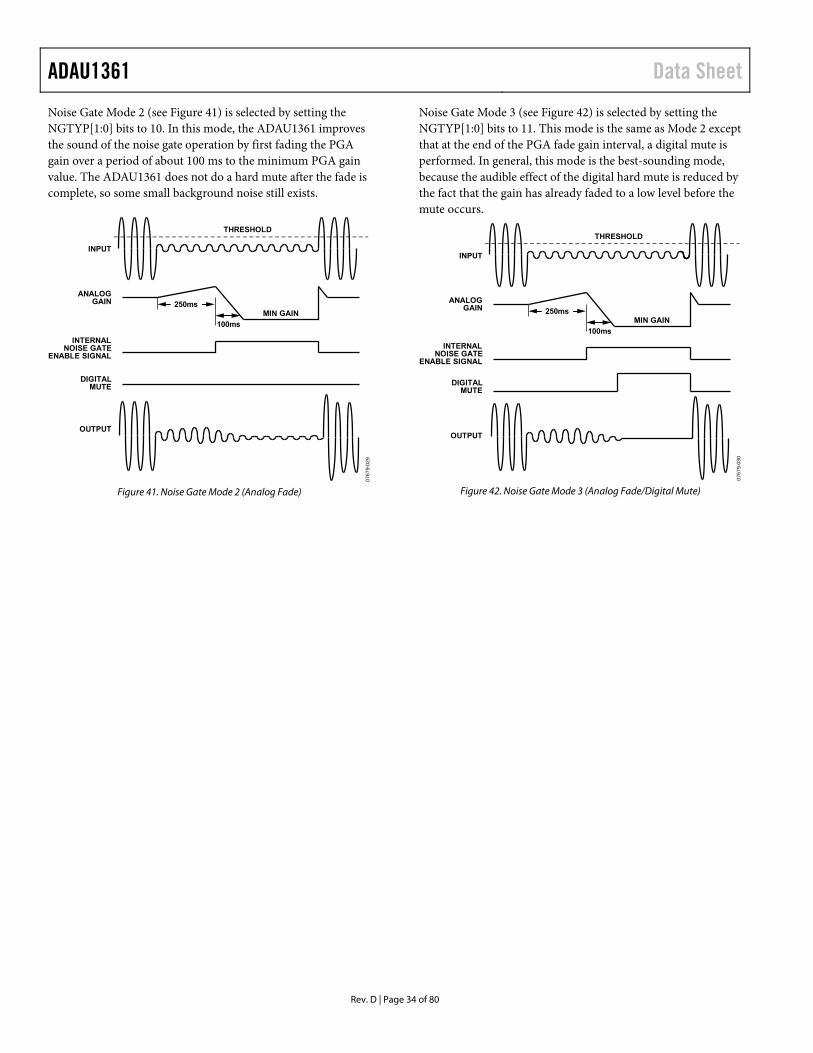
Noise Gate Mode 1 (see Figure 40) is selected by setting the NGTYP[1:0] bits to 01. In this mode, the ADAU1361 does a simple digital mute of the ADC output. Although this mode completely eliminates any background noise, the effect of an abrupt mute may not be pleasant to the ear.
THRESHOLD
INPUT
ANALOGGAIN
DIGITALMUTE
OUTPUT
INTERNALNOISE GATE
ENABLE SIGNAL
250ms07
679-
028
Figure 40. Noise Gate Mode 1 (Digital Mute)
ADAU1361 Data Sheet
Rev. D | Page 34 of 80
Noise Gate Mode 2 (see Figure 41) is selected by setting the NGTYP[1:0] bits to 10. In this mode, the ADAU1361 improves the sound of the noise gate operation by first fading the PGA gain over a period of about 100 ms to the minimum PGA gain value. The ADAU1361 does not do a hard mute after the fade is complete, so some small background noise still exists.
THRESHOLD
INPUT
ANALOGGAIN
DIGITALMUTE
OUTPUT
INTERNALNOISE GATE
ENABLE SIGNAL
250msMIN GAIN
100ms
0767
9-02
9
Figure 41. Noise Gate Mode 2 (Analog Fade)
Noise Gate Mode 3 (see Figure 42) is selected by setting the NGTYP[1:0] bits to 11. This mode is the same as Mode 2 except that at the end of the PGA fade gain interval, a digital mute is performed. In general, this mode is the best-sounding mode, because the audible effect of the digital hard mute is reduced by the fact that the gain has already faded to a low level before the mute occurs.
THRESHOLD
INPUT
ANALOGGAIN
DIGITALMUTE
OUTPUT
INTERNALNOISE GATE
ENABLE SIGNAL
MIN GAIN250ms
100ms
0767
9-03
0
Figure 42. Noise Gate Mode 3 (Analog Fade/Digital Mute)

Data Sheet ADAU1361
Rev. D | Page 35 of 80
PLAYBACK SIGNAL PATH
0767
9-03
1
MX3G2[3:0]
MX3AUXG[3:0]
–15dB TO +6dB
MX3LM
–15dB TO +6dB
MX3RM
MX3G1[3:0]
–15dB TO +6dB
RIGHT INPUT MIXER
LEFT DAC
LAUX LHP–57dB TO +6dB
LHPVOL[5:0]
RIGHT DAC
LEFT INPUT MIXER
MX4G2[3:0]
MX4AUXG[3:0]
–15dB TO +6dB
MX4LM
–15dB TO +6dB –57dB TO +6dB
–57dB TO +6dB
MX4RM
MX4G1[3:0]
–15dB TO +6dB
RIGHT INPUT MIXER
LEFT DAC
RAUX
RHPVOL[5:0]
ROUTVOL[5:0]
RHP
ROUTP
ROUTN
MONOOUT
MX6G4[1:0]
MX5G4[1:0]
(MONO MIXER)MIXER 7MX7[1:0]
MX6G3[1:0]
–57dB TO +6dB
MONOVOL[5:0]
RIGHT DAC
LEFT INPUT MIXER
MX5G3[1:0]–57dB TO +6dB
LOUTVOL[5:0]
LOUTP
LOUTN
MIXER 4(RIGHT
PLAYBACKMIXER)
MIXER 3(LEFT
PLAYBACKMIXER)
MIXER 5(LEFT L/RPLAYBACK
MIXER)
MIXER 6(RIGHT L/RPLAYBACK
MIXER)
–1
–1
Figure 43. Playback Signal Path
OUTPUT SIGNAL PATHS The outputs of the ADAU1361 can be configured as a variety of differential or single-ended outputs. All analog output pins are capable of driving headphone or earpiece speakers. There are selectable output paths for stereo signals or a downmixed mono output. The line outputs can drive a load of at least 10 kΩ or can be put into HP mode to drive headphones or earpiece speakers. The analog output pins are biased at AVDD/2.
With a 0 dBFS digital input and AVDD = 1.8 V, the full-scale output level is 500 mV rms; when AVDD = 3.3 V, the full-scale output level is 920 mV rms.
Signals are inverted through the mixers and volume controls. The result of this inversion is that the polarity of the differential outputs and the headphone outputs is preserved. The single-ended mono output is inverted. The DACs are noninverting.
Routing Flexibility
The playback path contains five mixers (Mixer 3 to Mixer 7) that perform the following functions:
• Mix signals from the record path and the DACs. • Mix or swap the left and right channels. • Mix a mono signal or generate a common-mode output.
Mixer 3 and Mixer 4 are dedicated to mixing signals from the record path and the DACs. Each of these two mixers can accept signals from the left and right DACs, the left and right input mixers, and the dedicated channel auxiliary input. Signals coming from the record path can be boosted or cut before the playback mixer.
For example, the MX4G2[3:0] bits set the gain from the output of Mixer 2 (right record channel) to the input of Mixer 4, hence the naming convention.
Signals coming from the DACs have digital volume attenu- ation controls set in Register R20 (left input digital volume register, Address 0x401A) and Register R21 (right input digital volume register, Address 0x401B).
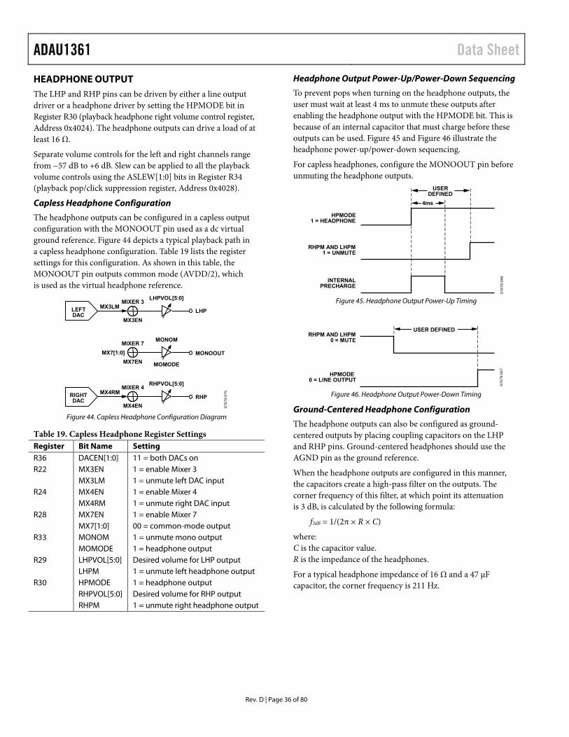
ADAU1361 Data Sheet
Rev. D | Page 36 of 80
HEADPHONE OUTPUT The LHP and RHP pins can be driven by either a line output driver or a headphone driver by setting the HPMODE bit in Register R30 (playback headphone right volume control register, Address 0x4024). The headphone outputs can drive a load of at least 16 Ω.
Separate volume controls for the left and right channels range from −57 dB to +6 dB. Slew can be applied to all the playback volume controls using the ASLEW[1:0] bits in Register R34 (playback pop/click suppression register, Address 0x4028).
Capless Headphone Configuration
The headphone outputs can be configured in a capless output configuration with the MONOOUT pin used as a dc virtual ground reference. Figure 44 depicts a typical playback path in a capless headphone configuration. Table 19 lists the register settings for this configuration. As shown in this table, the MONOOUT pin outputs common mode (AVDD/2), which is used as the virtual headphone reference.
0767
9-07
5
LHP
RHP
MONOOUT
MIXER 3MX3LM
LHPVOL[5:0]
MX3EN
MIXER 4MX4RM
RHPVOL[5:0]
MX4EN
MIXER 7
MX7[1:0]
MONOM
MOMODEMX7EN
LEFTDAC
RIGHTDAC
Figure 44. Capless Headphone Configuration Diagram
Table 19. Capless Headphone Register Settings Register Bit Name Setting R36 DACEN[1:0] 11 = both DACs on R22 MX3EN 1 = enable Mixer 3
MX3LM 1 = unmute left DAC input R24 MX4EN 1 = enable Mixer 4
MX4RM 1 = unmute right DAC input R28 MX7EN 1 = enable Mixer 7
MX7[1:0] 00 = common-mode output R33 MONOM 1 = unmute mono output
MOMODE 1 = headphone output R29 LHPVOL[5:0] Desired volume for LHP output
LHPM 1 = unmute left headphone output R30 HPMODE 1 = headphone output
RHPVOL[5:0] Desired volume for RHP output RHPM 1 = unmute right headphone output
Headphone Output Power-Up/Power-Down Sequencing
To prevent pops when turning on the headphone outputs, the user must wait at least 4 ms to unmute these outputs after enabling the headphone output with the HPMODE bit. This is because of an internal capacitor that must charge before these outputs can be used. Figure 45 and Figure 46 illustrate the headphone power-up/power-down sequencing.
For capless headphones, configure the MONOOUT pin before unmuting the headphone outputs.
4ms
USERDEFINED
0767
9-04
6
HPMODE1 = HEADPHONE
INTERNALPRECHARGE
RHPM AND LHPM1 = UNMUTE
Figure 45. Headphone Output Power-Up Timing
0767
9-04
7
HPMODE0 = LINE OUTPUT
RHPM AND LHPM0 = MUTE
USER DEFINED
Figure 46. Headphone Output Power-Down Timing
Ground-Centered Headphone Configuration
The headphone outputs can also be configured as ground-centered outputs by placing coupling capacitors on the LHP and RHP pins. Ground-centered headphones should use the AGND pin as the ground reference.
When the headphone outputs are configured in this manner, the capacitors create a high-pass filter on the outputs. The corner frequency of this filter, at which point its attenuation is 3 dB, is calculated by the following formula:
f3dB = 1/(2π × R × C)
where: C is the capacitor value. R is the impedance of the headphones.
For a typical headphone impedance of 16 Ω and a 47 μF capacitor, the corner frequency is 211 Hz.
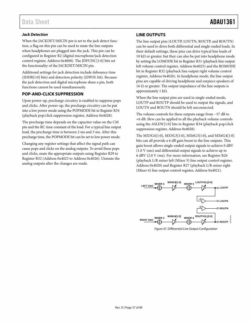
Data Sheet ADAU1361
Rev. D | Page 37 of 80
Jack Detection
When the JACKDET/MICIN pin is set to the jack detect func-tion, a flag on this pin can be used to mute the line outputs when headphones are plugged into the jack. This pin can be configured in Register R2 (digital microphone/jack detection control register, Address 0x4008). The JDFUNC[1:0] bits set the functionality of the JACKDET/MICIN pin.
Additional settings for jack detection include debounce time (JDDB[1:0] bits) and detection polarity (JDPOL bit). Because the jack detection and digital microphone share a pin, both functions cannot be used simultaneously.
POP-AND-CLICK SUPPRESSION Upon power-up, precharge circuitry is enabled to suppress pops and clicks. After power-up, the precharge circuitry can be put into a low power mode using the POPMODE bit in Register R34 (playback pop/click suppression register, Address 0x4028).
The precharge time depends on the capacitor value on the CM pin and the RC time constant of the load. For a typical line output load, the precharge time is between 2 ms and 3 ms. After this precharge time, the POPMODE bit can be set to low power mode.
Changing any register settings that affect the signal path can cause pops and clicks on the analog outputs. To avoid these pops and clicks, mute the appropriate outputs using Register R29 to Register R32 (Address 0x4023 to Address 0x4026). Unmute the analog outputs after the changes are made.
LINE OUTPUTS The line output pins (LOUTP, LOUTN, ROUTP, and ROUTN) can be used to drive both differential and single-ended loads. In their default settings, these pins can drive typical line loads of 10 kΩ or greater, but they can also be put into headphone mode by setting the LOMODE bit in Register R31 (playback line output left volume control register, Address 0x4025) and the ROMODE bit in Register R32 (playback line output right volume control register, Address 0x4026). In headphone mode, the line output pins are capable of driving headphone and earpiece speakers of 16 Ω or greater. The output impedance of the line outputs is approximately 1 kΩ.
When the line output pins are used in single-ended mode, LOUTP and ROUTP should be used to output the signals, and LOUTN and ROUTN should be left unconnected.
The volume controls for these outputs range from −57 dB to +6 dB. Slew can be applied to all the playback volume controls using the ASLEW[1:0] bits in Register R34 (playback pop/click suppression register, Address 0x4028).
The MX5G4[1:0], MX5G3[1:0], MX6G3[1:0], and MX6G4[1:0] bits can all provide a 6 dB gain boost to the line outputs. This gain boost allows single-ended output signals to achieve 0 dBV (1.0 V rms) and differential output signals to achieve up to 6 dBV (2.0 V rms). For more information, see Register R26 (playback L/R mixer left (Mixer 5) line output control register, Address 0x4020) and Register R27 (playback L/R mixer right (Mixer 6) line output control register, Address 0x4021).
0767
9-07
6
MIXER 3LEFT DAC
MX5G3[1:0] MIXER 5 LOUTVOL[5:0]
LOUTP
MIXER 4RIGHT DAC
MX6G4[1:0] MIXER 6 ROUTVOL[5:0]
ROUTP
ROUTN
LOUTN
–1
–1
Figure 47. Differential Line Output Configuration

ADAU1361 Data Sheet
Rev. D | Page 38 of 80
CONTROL PORTS The ADAU1361 can operate in one of two control modes:
• I2C control • SPI control
The ADAU1361 has both a 4-wire SPI control port and a 2-wire I2C bus control port. Both ports can be used to set the registers. The part defaults to I2C mode, but it can be put into SPI control mode by pulling the CLATCH pin low three times.
The control port is capable of full read/write operation for all addressable registers. The ADAU1361 must have a valid master clock in order to write to all registers except for Register R0 (Address 0x4000) and Register R1 (Address 0x4002).
All addresses can be accessed in both a single-address mode or a burst mode. The first byte (Byte 0) of a control port write contains the 7-bit chip address plus the R/W bit. The next two bytes (Byte 1 and Byte 2) together form the subaddress of the register location within the ADAU1361. This subaddress must be two bytes long because the memory locations within the ADAU1361 are directly addressable and their sizes exceed the range of single-byte addressing. All subsequent bytes (starting with Byte 3) contain the data. The number of bytes per word depends on the type of data that is being written.
The control port pins are multifunctional, depending on the mode in which the part is operating. Table 20 describes these multiple functions.
Table 20. Control Port Pin Functions Pin Name I2C Mode SPI Mode SCL/CCLK SCL: input clock CCLK: input clock SDA/COUT SDA: open-collector
input/output COUT: output
ADDR1/CDATA I2C Address Bit 1: input CDATA: input ADDR0/CLATCH I2C Address Bit 0: input CLATCH: input
BURST MODE WRITING AND READING Burst mode addressing, where the subaddresses are automatically incremented at word boundaries, can be used for writing large amounts of data to contiguous registers. This increment happens automatically after a single-word write or read unless a stop condi-tion is encountered (I2C) or CLATCH is brought high (SPI). A burst write starts like a single-word write, but following the first data-word, the data-word for the next immediate address can be written immediately without sending its two-byte address.
The registers in the ADAU1361 are one byte wide with the exception of the PLL control register, which is six bytes wide. The auto-increment feature knows the word length at each subaddress, so the subaddress does not need to be specified manually for each address in a burst write.
The subaddresses are auto-incremented by 1 following each read or write of a data-word, regardless of whether there is a valid register word at that address. Address holes in the register map can be written to or read from without consequence. In the ADAU1361, these address holes exist at Address 0x4001, Address 0x4003 to Address 0x4007, Address 0x402E, and Address 0x4032 to Address 0x4035. A single-byte write to these registers is ignored by the ADAU1361, and a read returns a single byte 0x00.
I2C PORT The ADAU1361 supports a 2-wire serial (I2C-compatible) microprocessor bus driving multiple peripherals. Two pins, serial data (SDA) and serial clock (SCL), carry information between the ADAU1361 and the system I2C master controller. In I2C mode, the ADAU1361 is always a slave on the bus, meaning that it cannot initiate a data transfer. Each slave device is recognized by a unique address. The address and R/W byte format is shown in Table 21. The address resides in the first seven bits of the I2C write. Bits[5:6] of the I2C address for the ADAU1361 are set by the levels on the ADDR1 and ADDR0 pins. The LSB of the address—the R/W bit—specifies either a read or write operation. Logic Level 1 corresponds to a read operation, and Logic Level 0 corresponds to a write operation.
Table 21. ADAU1361 I2C Address and Read/Write Byte Format Bit 0 Bit 1 Bit 2 Bit 3 Bit 4 Bit 5 Bit 6 Bit 7 0 1 1 1 0 ADDR1 ADDR0 R/W
The SDA and SCL pins should each have a 2 kΩ pull-up resistor on the line connected to it. The voltage on these signal lines should not be higher than IOVDD (1.8 V to 3.3 V).
Addressing
Initially, each device on the I2C bus is in an idle state and monitors the SDA and SCL lines for a start condition and the proper address. The I2C master initiates a data transfer by establishing a start condition, defined by a high-to-low transition on SDA while SCL remains high. This indicates that an address/ data stream follows. All devices on the bus respond to the start condition and shift the next eight bits (the 7-bit address plus the R/W bit) MSB first. The device that recognizes the transmitted address responds by pulling the data line low during the ninth clock pulse. This ninth bit is known as an acknowledge bit. All other devices withdraw from the bus at this point and return to the idle condition.

Data Sheet ADAU1361
Rev. D | Page 39 of 80
The R/W bit determines the direction of the data. A Logic 0 on the LSB of the first byte means that the master writes infor-mation to the peripheral, whereas a Logic 1 means that the master reads information from the peripheral after writing the subaddress and repeating the start address. A data transfer takes place until a stop condition is encountered. A stop condition occurs when SDA transitions from low to high while SCL is held high. Figure 48 shows the timing of an I2C write, and Figure 49 shows an I2C read.
Stop and start conditions can be detected at any stage during the data transfer. If these conditions are asserted out of sequence with normal read and write operations, the ADAU1361 immediately jumps to the idle condition. During a given SCL high period, the user should only issue one start condition, one stop condition,
or a single stop condition followed by a single start condition. If an invalid subaddress is issued by the user, the ADAU1361 does not issue an acknowledge and returns to the idle condition.
If the user exceeds the highest subaddress while in autoincrement mode, one of two actions is taken. In read mode, the ADAU1361 outputs the highest subaddress register contents until the master device issues a no acknowledge, indicating the end of a read. A no acknowledge condition is where the SDA line is not pulled low on the ninth clock pulse on SCL. If the highest subaddress location is reached while in write mode, the data for the invalid byte is not loaded into any subaddress register, a no acknowledge is issued by the ADAU1361, and the part returns to the idle condition.
R/W0
SCL
SDA
SDA(CONTINUED)
SCL(CONTINUED)
1 1 1
ADDR0ADDR1
0
START BYMASTER
FRAME 1CHIP ADDRESS BYTE
FRAME 2SUBADDRESS BYTE 1
FRAME 3SUBADDRESS BYTE 2
FRAME 4DATA BYTE 1
ACK BYADAU1361
ACK BYADAU1361
ACK BYADAU1361
ACK BYADAU1361
STOP BYMASTER
0767
9-03
2
Figure 48. I2C Write to ADAU1361 Clocking
R/W
SCL
SDA
SDA(CONTINUED)
SCL(CONTINUED)
SDA(CONTINUED)
SCL(CONTINUED)
START BYMASTER
FRAME 2SUBADDRESS BYTE 1
FRAME 3SUBADDRESS BYTE 2
FRAME 4CHIP ADDRESS BYTE
FRAME 1CHIP ADDRESS BYTE
FRAME 5READ DATA BYTE 1
ACK BYADAU1361
ACK BYADAU1361
ACK BYADAU1361
ACK BYADAU1361
STOP BYMASTER
ACK BYMASTER
REPEATEDSTART BY MASTER
R/W
0767
9-03
3
ADDR0
ADDR0ADDR1
ADDR1
0 1 1 1 0
0 1 1 1 0
Figure 49. I2C Read from ADAU1361 Clocking

ADAU1361 Data Sheet
Rev. D | Page 40 of 80
I2C Read and Write Operations
Figure 50 shows the format of a single-word write operation. Every ninth clock pulse, the ADAU1361 issues an acknowledge by pulling SDA low.
Figure 51 shows the format of a burst mode write sequence. This figure shows an example of a write to sequential single-byte registers. The ADAU1361 increments its subaddress register after every byte because the requested subaddress corresponds to a register or memory area with a 1-byte word length.
Figure 52 shows the format of a single-word read operation. Note that the first R/W bit is 0, indicating a write operation. This is because the subaddress still needs to be written to set up the internal address. After the ADAU1361 acknowledges the receipt of the subaddress, the master must issue a repeated start command followed by the chip address byte with the R/W bit set to 1 (read).
This causes the ADAU1361 SDA to reverse and begin driving data back to the master. The master then responds every ninth pulse with an acknowledge pulse to the ADAU1361.
Figure 53 shows the format of a burst mode read sequence. This figure shows an example of a read from sequential single-byte registers. The ADAU1361 increments its subaddress register after every byte because the requested subaddress corresponds to a register or memory area with a 1-byte word length. The ADAU1361 always decodes the subaddress and sets the auto-increment circuit so that the address increments after the appropriate number of bytes.
Figure 50 to Figure 53 use the following abbreviations: S = start bit P = stop bit AM = acknowledge by master AS = acknowledge by slave
S Chip address, R/W = 0
AS Subaddress high byte AS Subaddress low byte AS Data Byte 1 P
Figure 50. Single-Word I2C Write Format
S Chip address, R/W = 0
AS Subaddress high byte
AS Subaddress low byte
AS Data Byte 1
AS Data Byte 2
AS Data Byte 3
AS Data Byte 4
AS … P
Figure 51. Burst Mode I2C Write Format
S Chip address, R/W = 0
AS Subaddress high byte
AS Subaddress low byte
AS S Chip address, R/W = 1
AS Data Byte 1
P
Figure 52. Single-Word I2C Read Format
S Chip address, R/W = 0
AS Subaddress high byte
AS Subaddress low byte
AS S Chip address, R/W = 1
AS Data Byte 1
AM Data Byte 2
AM … P
Figure 53. Burst Mode I2C Read Format

Data Sheet ADAU1361
Rev. D | Page 41 of 80
SPI PORT By default, the ADAU1361 is in I2C mode, but it can be put into SPI control mode by pulling CLATCH low three times. This is done by performing three dummy writes to the SPI port (the ADAU1361 does not acknowledge these three writes). Beginning with the fourth SPI write, data can be written to or read from the IC. The ADAU1361 can be taken out of SPI mode only by a full reset initiated by power-cycling the IC.
The SPI port uses a 4-wire interface, consisting of the CLATCH, CCLK, CDATA, and COUT signals, and it is always a slave port. The CLATCH signal should go low at the beginning of a trans-action and high at the end of a transaction. The CCLK signal latches CDATA on a low-to-high transition. COUT data is shifted out of the ADAU1361 on the falling edge of CCLK and should be clocked into a receiving device, such as a microcontroller, on the CCLK rising edge. The CDATA signal carries the serial input data, and the COUT signal carries the serial output data. The COUT signal remains three-state until a read operation is requested. This allows other SPI-compatible peripherals to share the same readback line. All SPI transactions have the same basic format shown in Table 23. A timing diagram is shown in Figure 4. All data should be written MSB first.
Chip Address R/W
The LSB of the first byte of an SPI transaction is a R/W bit. This bit determines whether the communication is a read (Logic Level 1) or a write (Logic Level 0). This format is shown in Table 22.
Table 22. ADAU1361 SPI Address and Read/Write Byte Format Bit 0 Bit 1 Bit 2 Bit 3 Bit 4 Bit 5 Bit 6 Bit 7 0 0 0 0 0 0 0 R/W
Subaddress
The 16-bit subaddress word is decoded into a location in one of the registers. This subaddress is the location of the appropriate register. The MSBs of the subaddress are zero-padded to bring the word to a full 2-byte length.
Data Bytes
The number of data bytes varies according to the register being accessed. During a burst mode write, an initial subaddress is written followed by a continuous sequence of data for consecu-tive register locations.
A sample timing diagram for a single-word SPI write operation to a register is shown in Figure 54. A sample timing diagram of a single-word SPI read operation is shown in Figure 55. The COUT pin goes from being three-state to being driven at the beginning of Byte 3. In this example, Byte 0 to Byte 2 contain the addresses and R/W bit, and subsequent bytes carry the data.
Table 23. Generic Control Word Format Byte 0 Byte 1 Byte 2 Byte 3 Byte 41 chip_adr[6:0], R/W subaddr[15:8] subaddr[7:0] data data 1 Continues to end of data.
0767
9-03
8
CLATCH
CCLK
CDATA BYTE 0 BYTE 1 BYTE 2 BYTE 3
Figure 54. SPI Write to ADAU1361 Clocking (Single-Word Write Mode)
0767
9-03
9
CLATCH
CCLK
CDATA
COUT
BYTE 0 BYTE 1
HIGH-ZDATA
HIGH-Z
BYTE 2
Figure 55. SPI Read from ADAU1361 Clocking (Single-Word Read Mode)

ADAU1361 Data Sheet
Rev. D | Page 42 of 80
SERIAL DATA INPUT/OUTPUT PORTS The flexible serial data input and output ports of the ADAU1361 can be set to accept or transmit data in 2-channel format or in a 4-channel TDM stream to interface to external ADCs or DACs. Data is processed in twos complement, MSB first format. The left channel data field always precedes the right channel data field in 2-channel streams. In TDM mode, Slot 0 and Slot 1 are in the first half of the audio frame, and Slot 2 and Slot 3 are in the second half of the frame. The serial modes and the position of the data in the frame are set in Register R15 to Register R18 (serial port and converter control registers, Address 0x4015 to Address 0x4018).
If the PLL of the ADAU1361 is not used, the serial data clocks must be synchronous with the ADAU1361 master clock input. The LRCLK and BCLK pins are used to clock both the serial input and output ports. The ADAU1361 can be set as the master or the slave in a system. Because there is only one set of serial data clocks, the input and output ports must always be both master or both slave.
Register R15 and Register R16 (serial port control registers, Address 0x4015 and Address 0x4016) allow control of clock polarity and data input modes. The valid data formats are I2S, left-justified, right-justified (24-/20-/18-/16-bit), and TDM. In all modes except for the right-justified modes, the serial port inputs an arbitrary number of bits up to a limit of 24. Extra bits do not cause an error, but they are truncated internally.
The serial port can operate with an arbitrary number of BCLK transitions in each LRCLK frame. The LRCLK in TDM mode can be input to the ADAU1361 either as a 50% duty cycle clock or as a bit-wide pulse.
When the LRCLK is set as a pulse, a 47 pF capacitor should be connected between the LRCLK pin and ground (see Figure 56). This capacitor is necessary in both master and slave modes to properly align the LRCLK signal to the serial data stream.
0767
9-07
8
47pFLRCLK
ADAU1361
BCLK
Figure 56. LRCLK Capacitor Alignment, TDM Pulse Mode
In TDM mode, the ADAU1361 can be a master for fS up to 48 kHz. Table 24 lists the modes in which the serial output port can function.
Table 24. Serial Output Port Master/Slave Mode Capabilities
fS 2-Channel Modes (I2S, Left-Justified, Right-Justified) 4-Channel TDM
48 kHz Master and slave Master and slave 96 kHz Master and slave Slave
Table 25 describes the proper configurations for standard audio data formats.
Table 25. Data Format Configurations
Format LRCLK Polarity (LRPOL) LRCLK Mode (LRMOD)
BCLK Polarity (BPOL)
BCLK Cycles/Audio Frame (BPF[2:0])
Data Delay from LRCLK Edge (LRDEL[1:0])
I2S (see Figure 57)
Frame begins on falling edge 50% duty cycle Data changes on falling edge
32 to 64 Delayed from LRCLK edge by 1 BCLK
Left-Justified (see Figure 58)
Frame begins on rising edge 50% duty cycle Data changes on falling edge
32 to 64 Aligned with LRCLK edge
Right-Justified (see Figure 59)
Frame begins on rising edge 50% duty cycle Data changes on falling edge
32 to 64 Delayed from LRCLK edge by 8 or 16 BCLKs
TDM with Clock (see Figure 60)
Frame begins on falling edge 50% duty cycle Data changes on falling edge
64 to 128 Delayed from start of word clock by 1 BCLK
TDM with Pulse (see Figure 61)
Frame begins on rising edge Pulse Data changes on falling edge
64 to 128 Delayed from start of word clock by 1 BCLK

Data Sheet ADAU1361
Rev. D | Page 43 of 80
LRCLK
BCLK
SDATA MSB
LEFT CHANNEL
LSB MSB
RIGHT CHANNEL
LSB
1/fS 0767
9-04
0
Figure 57. I2S Mode—16 Bits to 24 Bits per Channel
LRCLKBCLK
SDATA
LEFT CHANNEL
MSB LSB MSB
RIGHT CHANNEL
LSB
0767
9-04
1
1/fS Figure 58. Left-Justified Mode—16 Bits to 24 Bits per Channel
LRCLKBCLK
SDATA
LEFT CHANNEL
MSB LSB MSB
RIGHT CHANNEL
LSB
0767
9-04
2
1/fS Figure 59. Right-Justified Mode—16 Bits to 24 Bits per Channel
LRCLK
BCLK
SDATA SLOT 0 SLOT 2
32 BCLKs
MSB MSB – 1 MSB – 2
128 BCLKs
SLOT 1 SLOT 3
LRCLK
BCLK
SDATA
0767
9-04
3
Figure 60. TDM 4 Mode
LRCLK
SLOT 0 SLOT 1 SLOT 2 SLOT 3
CH0
BCLK
SDATA
32 BCLKs
0767
9-04
4
MSB TDM
Figure 61. TDM 4 Mode with Pulse Word Clock

ADAU1361 Data Sheet
Rev. D | Page 44 of 80
APPLICATIONS INFORMATION POWER SUPPLY BYPASS CAPACITORS Each analog and digital power supply pin should be bypassed to its nearest appropriate ground pin with a single 100 nF capaci-tor. The connections to each side of the capacitor should be as short as possible, and the trace should stay on a single layer with no vias. For maximum effectiveness, locate the capacitor equi-distant from the power and ground pins or, when equidistant placement is not possible, slightly closer to the power pin. Thermal connections to the ground planes should be made on the far side of the capacitor.
Each supply signal on the board should also be bypassed with a single bulk capacitor (10 μF to 47 μF).
VDD GND
TO GND
TO VDD
CAPACITOR
0767
9-04
8
Figure 62. Recommended Power Supply Bypass Capacitor Layout
GSM NOISE FILTER In mobile phone applications, excessive 217 Hz GSM noise on the analog supply pins can degrade the audio quality. To avoid this problem, it is recommended that an L-C filter be used in series with the bypass capacitors for the AVDD pins. This filter should consist of a 1.2 nH inductor and a 9.1 pF capacitor in series between AVDD and ground, as shown in Figure 63.
0767
9-04
9
AVDD AVDD
0.1µF
0.1µF
9.1pF1.2nH
10µF
+
Figure 63. GSM Filter on the Analog Supply Pins
GROUNDING A single ground plane should be used in the application layout. Components in an analog signal path should be placed away from digital signals.
EXPOSED PAD PCB DESIGN The ADAU1361 has an exposed pad on the underside of the LFCSP. This pad is used to couple the package to the PCB for heat dissipation when using the outputs to drive earpiece or headphone loads. When designing a board for the ADAU1361, special consideration should be given to the following:
A copper layer equal in size to the exposed pad should be on all layers of the board, from top to bottom, and should connect somewhere to a dedicated copper board layer (see Figure 64).
Vias should be placed to connect all layers of copper, allowing for efficient heat and energy conductivity. For an example, see Figure 65, which has nine vias arranged in a 3 inch × 3 inch grid in the pad area.
0767
9-05
0
TOP
POWERGROUND
BOTTOM
COPPER SQUARESVIAS Figure 64. Exposed Pad Layout Example, Side View
0767
9-05
1
Figure 65. Exposed Pad Layout Example, Top View
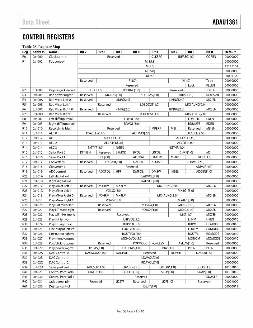
Data Sheet ADAU1361
Rev. D | Page 45 of 80
CONTROL REGISTERS Table 26. Register Map Reg Address Name Bit 7 Bit 6 Bit 5 Bit 4 Bit 3 Bit 2 Bit 1 Bit 0 Default
R0 0x4000 Clock control Reserved CLKSRC INFREQ[1:0] COREN 00000000
R1 0x4002 PLL control M[15:8] 00000000
M[7:0] 11111101
N[15:8] 00000000
N[7:0] 00001100
Reserved R[3:0] X[1:0] Type 00010000
Reserved Lock PLLEN 00000000
R2 0x4008 Dig mic/jack detect JDDB[1:0] JDFUNC[1:0] Reserved JDPOL 00000000
R3 0x4009 Rec power mgmt Reserved MXBIAS[1:0] ADCBIAS[1:0] RBIAS[1:0] Reserved 00000000
R4 0x400A Rec Mixer Left 0 Reserved LINPG[2:0] LINNG[2:0] MX1EN 00000000
R5 0x400B Rec Mixer Left 1 Reserved LDBOOST[1:0] MX1AUXG[2:0] 00000000
R6 0x400C Rec Mixer Right 0 Reserved RINPG[2:0] RINNG[2:0] MX2EN 00000000
R7 0x400D Rec Mixer Right 1 Reserved RDBOOST[1:0] MX2AUXG[2:0] 00000000
R8 0x400E Left diff input vol LDVOL[5:0] LDMUTE LDEN 00000000
R9 0x400F Right diff input vol RDVOL[5:0] RDMUTE RDEN 00000000
R10 0x4010 Record mic bias Reserved MPERF MBI Reserved MBIEN 00000000
R11 0x4011 ALC 0 PGASLEW[1:0] ALCMAX[2:0] ALCSEL[2:0] 00000000
R12 0x4012 ALC 1 ALCHOLD[3:0] ALCTARG[3:0] 00000000
R13 0x4013 ALC 2 ALCATCK[3:0] ALCDEC[3:0] 00000000
R14 0x4014 ALC 3 NGTYP[1:0] NGEN NGTHR[4:0] 00000000
R15 0x4015 Serial Port 0 DITHEN Reserved LRMOD BPOL LRPOL CHPF[1:0] MS 00000000
R16 0x4016 Serial Port 1 BPF[2:0] ADTDM DATDM MSBP LRDEL[1:0] 00000000
R17 0x4017 Converter 0 Reserved DAPAIR[1:0] DAOSR ADOSR CONVSR[2:0] 00000000
R18 0x4018 Converter 1 Reserved ADPAIR[1:0] 00000000
R19 0x4019 ADC control Reserved ADCPOL HPF DMPOL DMSW INSEL ADCEN[1:0] 00010000
R20 0x401A Left digital vol LADVOL[7:0] 00000000
R21 0x401B Right digital vol RADVOL[7:0] 00000000
R22 0x401C Play Mixer Left 0 Reserved MX3RM MX3LM MX3AUXG[3:0] MX3EN 00000000
R23 0x401D Play Mixer Left 1 MX3G2[3:0] MX3G1[3:0] 00000000
R24 0x401E Play Mixer Right 0 Reserved MX4RM MX4LM MX4AUXG[3:0] MX4EN 00000000
R25 0x401F Play Mixer Right 1 MX4G2[3:0] MX4G1[3:0] 00000000
R26 0x4020 Play L/R mixer left Reserved MX5G4[1:0] MX5G3[1:0] MX5EN 00000000
R27 0x4021 Play L/R mixer right Reserved MX6G4[1:0] MX6G3[1:0] MX6EN 00000000
R28 0x4022 Play L/R mixer mono Reserved MX7[1:0] MX7EN 00000000
R29 0x4023 Play HP left vol LHPVOL[5:0] LHPM HPEN 00000010
R30 0x4024 Play HP right vol RHPVOL[5:0] RHPM HPMODE 00000010
R31 0x4025 Line output left vol LOUTVOL[5:0] LOUTM LOMODE 00000010
R32 0x4026 Line output right vol ROUTVOL[5:0] ROUTM ROMODE 00000010
R33 0x4027 Play mono output MONOVOL[5:0] MONOM MOMODE 00000010
R34 0x4028 Pop/click suppress Reserved POPMODE POPLESS ASLEW[1:0] Reserved 00000000
R35 0x4029 Play power mgmt HPBIAS[1:0] DACBIAS[1:0] PBIAS[1:0] PREN PLEN 00000000
R36 0x402A DAC Control 0 DACMONO[1:0] DACPOL Reserved DEMPH DACEN[1:0] 00000000
R37 0x402B DAC Control 1 LDAVOL[7:0] 00000000
R38 0x402C DAC Control 2 RDAVOL[7:0] 00000000
R39 0x402D Serial port pad ADCSDP[1:0] DACSDP[1:0] LRCLKP[1:0] BCLKP[1:0] 10101010
R40 0x402F Control Port Pad 0 CDATP[1:0] CLCHP[1:0] SCLP[1:0] SDAP[1:0] 10101010
R41 0x4030 Control Port Pad 1 Reserved SDASTR 00000000
R42 0x4031 Jack detect pin Reserved JDSTR Reserved JDP[1:0] Reserved 00001000
R67 0x4036 Dejitter control DEJIT[7:0] 00000011

ADAU1361 Data Sheet
Rev. D | Page 46 of 80
CONTROL REGISTER DETAILS All registers except for the PLL control register are 1-byte write and read registers.
R0: Clock Control, 16,384 (0x4000)
Bit 7 Bit 6 Bit 5 Bit 4 Bit 3 Bit 2 Bit 1 Bit 0
Reserved CLKSRC INFREQ[1:0] COREN
Table 27. Clock Control Register Bits Bit Name Description 3 CLKSRC Clock source select.
0 = direct from MCLK pin (default). 1 = PLL clock.
[2:1] INFREQ[1:0] Input clock frequency. Sets the core clock rate that generates the core clock. If the PLL is used, this value is automatically set to 1024 × fS.
Setting Input Clock Frequency 00 256 × fS (default) 01 512 × fS 10 768 × fS 11 1024 × fS 0 COREN Core clock enable. Only the R0 and R1 registers can be accessed when this bit is set to 0 (core clock disabled).
0 = core clock disabled (default). 1 = core clock enabled.
R1: PLL Control, 16,386 (0x4002)
Byte Bit 7 Bit 6 Bit 5 Bit 4 Bit 3 Bit 2 Bit 1 Bit 0 0 M[15:8] 1 M[7:0] 2 N[15:8] 3 N[7:0] 4 Reserved R[3:0] X[1:0] Type 5 Reserved Lock PLLEN
Table 28. PLL Control Register Byte Bits Bit Name Description 0 [7:0] M[15:8] PLL denominator MSB. This value is concatenated with M[7:0] to make up a 16-bit number. 1 [7:0] M[7:0] PLL denominator LSB. This value is concatenated with M[15:8] to make up a 16-bit number. M[15:8] (MSB) M[7:0] (LSB) Value of M 00000000 00000000 0 … … … 00000000 11111101 253 (default) … … … 11111111 11111111 65,535 2 [7:0] N[15:8] PLL numerator MSB. This value is concatenated with N[7:0] to make up a 16-bit number. 3 [7:0] N[7:0] PLL numerator LSB. This value is concatenated with N[15:8] to make up a 16-bit number. N[15:8] (MSB) N[7:0] (LSB) Value of N 00000000 00000000 0 … … … 00000000 00001100 12 (default) … … … 11111111 11111111 65,535
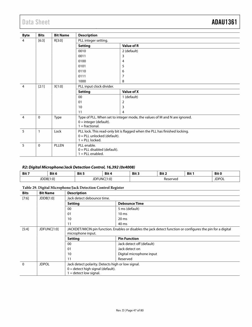
Data Sheet ADAU1361
Rev. D | Page 47 of 80
Byte Bits Bit Name Description 4 [6:3] R[3:0] PLL integer setting. Setting Value of R 0010 2 (default) 0011 3 0100 4 0101 5 0110 6 0111 7 1000 8 4 [2:1] X[1:0] PLL input clock divider. Setting Value of X 00 1 (default) 01 2 10 3 11 4 4 0 Type Type of PLL. When set to integer mode, the values of M and N are ignored.
0 = integer (default). 1 = fractional.
5 1 Lock PLL lock. This read-only bit is flagged when the PLL has finished locking. 0 = PLL unlocked (default). 1 = PLL locked.
5 0 PLLEN PLL enable. 0 = PLL disabled (default). 1 = PLL enabled.
R2: Digital Microphone/Jack Detection Control, 16,392 (0x4008)
Bit 7 Bit 6 Bit 5 Bit 4 Bit 3 Bit 2 Bit 1 Bit 0
JDDB[1:0] JDFUNC[1:0] Reserved JDPOL
Table 29. Digital Microphone/Jack Detection Control Register Bits Bit Name Description [7:6] JDDB[1:0] Jack detect debounce time.
[5:4] JDFUNC[1:0] JACKDET/MICIN pin function. Enables or disables the jack detect function or configures the pin for a digital microphone input.
0 JDPOL Jack detect polarity. Detects high or low signal. 0 = detect high signal (default). 1 = detect low signal.
Setting Debounce Time 00 5 ms (default) 01 10 ms 10 20 ms 11 40 ms
Setting Pin Function 00 Jack detect off (default) 01 Jack detect on 10 Digital microphone input 11 Reserved

ADAU1361 Data Sheet
Rev. D | Page 48 of 80
R3: Record Power Management, 16,393 (0x4009)
This register manages the power consumption for the record path. In particular, the current distribution for the mixer boosts, ADCs, record path mixers, and PGAs can be set to one of four modes. These settings are normal operation, power saving mode, enhanced performance mode, and extreme power saving mode. Each of these modes draws current from a central bias. Enhanced performance mode offers the highest performance with the trade-off of higher power consumption.
Bit 7 Bit 6 Bit 5 Bit 4 Bit 3 Bit 2 Bit 1 Bit 0
Reserved MXBIAS[1:0] ADCBIAS[1:0] RBIAS[1:0] Reserved
Table 30. Record Power Management Register Bits Bit Name Description [6:5] MXBIAS[1:0] Mixer amplifier bias boost. Sets the boost level for the bias current of the record path mixers. In some cases,
the boost level enhances the THD + N performance. Setting Boost Level 00 Normal operation (default) 01 Boost Level 1 10 Boost Level 2 11 Boost Level 3 [4:3] ADCBIAS[1:0] ADC bias control. Sets the bias current for the ADCs based on the mode of operation selected. Setting ADC Bias Control 00 Normal operation (default) 01 Extreme power saving 10 Enhanced performance 11 Power saving [2:1] RBIAS[1:0] Record path bias control. Sets the bias current for the PGAs and mixers in the record path. Setting Record Path Bias Control 00 Normal operation (default) 01 Reserved 10 Enhanced performance 11 Power saving

Data Sheet ADAU1361
Rev. D | Page 49 of 80
R4: Record Mixer Left (Mixer 1) Control 0, 16,394 (0x400A)
This register controls the gain of single-ended inputs for the left channel record path. The left channel record mixer is referred to as Mixer 1.
Bit 7 Bit 6 Bit 5 Bit 4 Bit 3 Bit 2 Bit 1 Bit 0
Reserved LINPG[2:0] LINNG[2:0] MX1EN
Table 31. Record Mixer Left (Mixer 1) Control 0 Register
Bits Bit Name Description [6:4] LINPG[2:0] Gain for a left channel single-ended input from the LINP pin, input to Mixer 1.
Setting Gain 000 Mute (default) 001 −12 dB 010 −9 dB 011 −6 dB 100 −3 dB 101 0 dB 110 3 dB 111 6 dB
[3:1] LINNG[2:0] Gain for a left channel single-ended input from the LINN pin, input to Mixer 1.
Setting Gain 000 Mute (default) 001 −12 dB 010 −9 dB 011 −6 dB 100 −3 dB 101 0 dB 110 3 dB 111 6 dB
0 MX1EN Left channel mixer enable in the record path. Referred to as Mixer 1. 0 = mixer disabled (default). 1 = mixer enabled.
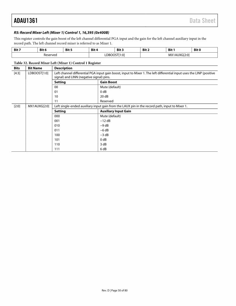
ADAU1361 Data Sheet
Rev. D | Page 50 of 80
R5: Record Mixer Left (Mixer 1) Control 1, 16,395 (0x400B)
This register controls the gain boost of the left channel differential PGA input and the gain for the left channel auxiliary input in the record path. The left channel record mixer is referred to as Mixer 1.
Bit 7 Bit 6 Bit 5 Bit 4 Bit 3 Bit 2 Bit 1 Bit 0
Reserved LDBOOST[1:0] MX1AUXG[2:0]
Table 32. Record Mixer Left (Mixer 1) Control 1 Register
Bits Bit Name Description [4:3] LDBOOST[1:0] Left channel differential PGA input gain boost, input to Mixer 1. The left differential input uses the LINP (positive
signal) and LINN (negative signal) pins.
Setting Gain Boost 00 Mute (default) 01 0 dB 10 20 dB 11 Reserved
[2:0] MX1AUXG[2:0] Left single-ended auxiliary input gain from the LAUX pin in the record path, input to Mixer 1.
Setting Auxiliary Input Gain 000 Mute (default) 001 −12 dB 010 −9 dB 011 −6 dB 100 −3 dB 101 0 dB 110 3 dB 111 6 dB

Data Sheet ADAU1361
Rev. D | Page 51 of 80
R6: Record Mixer Right (Mixer 2) Control 0, 16,396 (0x400C)
This register controls the gain of single-ended inputs for the right channel record path. The right channel record mixer is referred to as Mixer 2.
Bit 7 Bit 6 Bit 5 Bit 4 Bit 3 Bit 2 Bit 1 Bit 0
Reserved RINPG[2:0] RINNG[2:0] MX2EN
Table 33. Record Mixer Right (Mixer 2) Control 0 Register
Bits Bit Name Description [6:4] RINPG[2:0] Gain for a right channel single-ended input from the RINP pin, input to Mixer 2.
Setting Gain 000 Mute (default) 001 −12 dB 010 −9 dB 011 −6 dB 100 −3 dB 101 0 dB 110 3 dB 111 6 dB
[3:1] RINNG[2:0] Gain for a right channel single-ended input from the RINN pin, input to Mixer 2.
Setting Gain 000 Mute (default) 001 −12 dB 010 −9 dB 011 −6 dB 100 −3 dB 101 0 dB 110 3 dB 111 6 dB
0 MX2EN Right channel mixer enable in the record path. Referred to as Mixer 2. 0 = mixer disabled (default). 1 = mixer enabled.

ADAU1361 Data Sheet
Rev. D | Page 52 of 80
R7: Record Mixer Right (Mixer 2) Control 1, 16,397 (0x400D)
This register controls the gain boost of the right channel differential PGA input and the gain for the right channel auxiliary input in the record path. The right channel record mixer is referred to as Mixer 2.
Bit 7 Bit 6 Bit 5 Bit 4 Bit 3 Bit 2 Bit 1 Bit 0
Reserved RDBOOST[1:0] MX2AUXG[2:0]
Table 34. Record Mixer Right (Mixer 2) Control 1 Register
R8: Left Differential Input Volume Control, 16,398 (0x400E)
This register enables the differential path and sets the volume control for the left differential PGA input.
Bit 7 Bit 6 Bit 5 Bit 4 Bit 3 Bit 2 Bit 1 Bit 0
LDVOL[5:0] LDMUTE LDEN
Table 35. Left Differential Input Volume Control Register
Bits Bit Name Description [4:3] RDBOOST[1:0] Right channel differential PGA input gain boost, input to Mixer 2. The right differential input uses the RINP
(positive signal) and RINN (negative signal) pins.
Setting Gain Boost 00 Mute (default) 01 0 dB 10 20 dB 11 Reserved
[2:0] MX2AUXG[2:0] Right single-ended auxiliary input gain from the RAUX pin in the record path, input to Mixer 2.
Setting Auxiliary Input Gain 000 Mute (default) 001 −12 dB 010 −9 dB 011 −6 dB 100 −3 dB 101 0 dB 110 3 dB 111 6 dB
Bits Bit Name Description [7:2] LDVOL[5:0] Left channel differential PGA input volume control. The left differential input uses the LINP (positive signal) and
LINN (negative signal) pins. Each step corresponds to a 0.75 dB increase in gain. See Table 71 for a complete list of the volume settings.
Setting Volume 000000 −12 dB (default) 000001 −11.25 dB … … 010000 0 dB … … 111110 34.5 dB 111111 35.25 dB
1 LDMUTE Left differential input mute control. 0 = mute (default). 1 = unmute.
0 LDEN Left differential PGA enable. When enabled, the LINP and LINN pins are used as a full differential pair. When disabled, these two pins are configured as two single-ended inputs with the signals routed around the PGA. 0 = disabled (default). 1 = enabled.
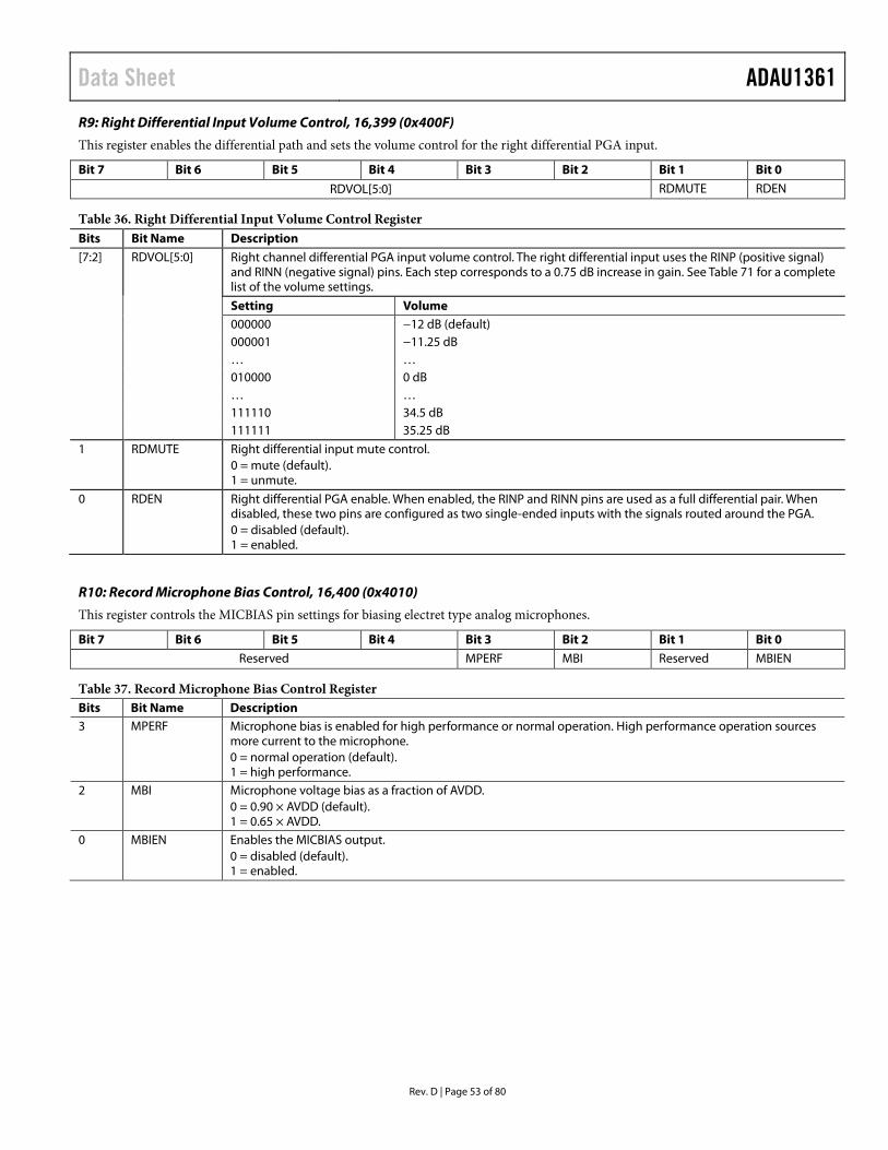
Data Sheet ADAU1361
Rev. D | Page 53 of 80
R9: Right Differential Input Volume Control, 16,399 (0x400F)
This register enables the differential path and sets the volume control for the right differential PGA input.
Bit 7 Bit 6 Bit 5 Bit 4 Bit 3 Bit 2 Bit 1 Bit 0
RDVOL[5:0] RDMUTE RDEN
Table 36. Right Differential Input Volume Control Register
R10: Record Microphone Bias Control, 16,400 (0x4010)
This register controls the MICBIAS pin settings for biasing electret type analog microphones.
Bit 7 Bit 6 Bit 5 Bit 4 Bit 3 Bit 2 Bit 1 Bit 0
Reserved MPERF MBI Reserved MBIEN
Table 37. Record Microphone Bias Control Register Bits Bit Name Description 3 MPERF Microphone bias is enabled for high performance or normal operation. High performance operation sources
more current to the microphone. 0 = normal operation (default). 1 = high performance.
2 MBI Microphone voltage bias as a fraction of AVDD. 0 = 0.90 × AVDD (default). 1 = 0.65 × AVDD.
0 MBIEN Enables the MICBIAS output. 0 = disabled (default). 1 = enabled.
Bits Bit Name Description [7:2] RDVOL[5:0] Right channel differential PGA input volume control. The right differential input uses the RINP (positive signal)
and RINN (negative signal) pins. Each step corresponds to a 0.75 dB increase in gain. See Table 71 for a complete list of the volume settings.
Setting Volume 000000 −12 dB (default) 000001 −11.25 dB … … 010000 0 dB … … 111110 34.5 dB 111111 35.25 dB
1 RDMUTE Right differential input mute control. 0 = mute (default). 1 = unmute.
0 RDEN Right differential PGA enable. When enabled, the RINP and RINN pins are used as a full differential pair. When disabled, these two pins are configured as two single-ended inputs with the signals routed around the PGA. 0 = disabled (default). 1 = enabled.

ADAU1361 Data Sheet
Rev. D | Page 54 of 80
R11: ALC Control 0, 16,401 (0x4011)
Bit 7 Bit 6 Bit 5 Bit 4 Bit 3 Bit 2 Bit 1 Bit 0
PGASLEW[1:0] ALCMAX[2:0] ALCSEL[2:0]
Table 38. ALC Control 0 Register
Bits Bit Name Description [7:6] PGASLEW[1:0] PGA volume slew time when the ALC is off. The slew time is the period of time that a volume increase or decrease
takes to ramp up or ramp down to the target volume set in Register R8 (left differential input volume control) and Register R9 (right differential input volume control).
Setting Slew Time 00 24 ms (default) 01 48 ms 10 96 ms 11 Off
[5:3] ALCMAX[2:0] The maximum ALC gain sets a limit to the amount of gain that the ALC can provide to the input signal. This protects small signals from excessive amplification.
Setting Maximum ALC Gain 000 −12 dB (default) 001 −6 dB 010 0 dB 011 6 dB 100 12 dB 101 18 dB 110 24 dB 111 30 dB
[2:0] ALCSEL[2:0] ALC select. These bits set the channels that are controlled by the ALC. When set to right only, the ALC responds only to the right channel input and controls the gain of the right PGA amplifier only. When set to left only, the ALC responds only to the left channel input and controls the gain of the left PGA amplifier only. When set to stereo, the ALC responds to the greater of the left or right channel and controls the gain of both the left and right PGA amplifiers. These bits must be off if manual control of the volume is desired.
Setting Channels 000 Off (default) 001 Right only 010 Left only 011 Stereo 100 Reserved 101 Reserved 110 Reserved 111 Reserved

Data Sheet ADAU1361
Rev. D | Page 55 of 80
R12: ALC Control 1, 16,402 (0x4012)
Bit 7 Bit 6 Bit 5 Bit 4 Bit 3 Bit 2 Bit 1 Bit 0
ALCHOLD[3:0] ALCTARG[3:0]
Table 39. ALC Control 1 Register
Bits Bit Name Description [7:4] ALCHOLD[3:0] ALC hold time. The ALC hold time is the amount of time that the ALC waits after a decrease in input level before
increasing the gain to achieve the target level. The recommended minimum setting is 21 ms (0011) to prevent distortion of low frequency signals. The hold time doubles with every 1-bit increase.
Setting Hold Time 0000 2.67 ms (default) 0001 5.34 ms 0010 10.68 ms 0011 21.36 ms 0100 42.72 ms 0101 85.44 ms 0110 170.88 ms 0111 341.76 ms 1000 683.52 ms 1001 1.367 sec 1010 2.7341 sec 1011 5.4682 sec 1100 10.936 sec 1101 21.873 sec 1110 43.745 sec 1111 87.491 sec
[3:0] ALCTARG[3:0] ALC target. The ALC target sets the desired ADC input level. The PGA gain is adjusted by the ALC to reach this target level. The recommended target level is between −16 dB and −10 dB to accommodate transients without clipping the ADC.
Setting ALC Target 0000 −28.5 dB (default) 0001 −27 dB 0010 −25.5 dB 0011 −24 dB 0100 −22.5 dB 0101 −21 dB 0110 −19.5 dB 0111 −18 dB 1000 −16.5 dB 1001 −15 dB 1010 −13.5 dB 1011 −12 dB 1100 −10.5 dB 1101 −9 dB 1110 −7.5 dB 1111 −6 dB

ADAU1361 Data Sheet
Rev. D | Page 56 of 80
R13: ALC Control 2, 16,403 (0x4013)
Bit 7 Bit 6 Bit 5 Bit 4 Bit 3 Bit 2 Bit 1 Bit 0
ALCATCK[3:0] ALCDEC[3:0]
Table 40. ALC Control 2 Register
Bits Bit Name Description [7:4] ALCATCK[3:0] ALC attack time. The attack time sets how fast the ALC starts attenuating after an increase in input level above
the target. A typical setting for music recording is 384 ms, and a typical setting for voice recording is 24 ms.
Setting Attack Time 0000 6 ms (default) 0001 12 ms 0010 24 ms 0011 48 ms 0100 96 ms 0101 192 ms 0110 384 ms 0111 768 ms 1000 1.54 sec 1001 3.07 sec 1010 6.14 sec 1011 12.29 sec 1100 24.58 sec 1101 49.15 sec 1110 98.30 sec 1111 196.61 sec
[3:0] ALCDEC[3:0] ALC decay time. The decay time sets how fast the ALC increases the PGA gain after a decrease in input level below the target. A typical setting for music recording is 24.58 seconds, and a typical setting for voice recording is 1.54 seconds.
Setting Decay Time 0000 24 ms 0001 48 ms 0010 96 ms 0011 192 ms 0100 384 ms 0101 768 ms 0110 1.54 sec 0111 3.07 sec 1000 6.14 sec 1001 12.29 sec 1010 24.58 sec 1011 49.15 sec 1100 98.30 sec 1101 196.61 sec 1110 393.22 sec 1111 786.43 sec
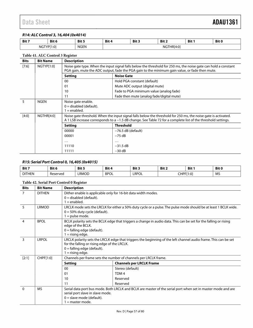
Data Sheet ADAU1361
Rev. D | Page 57 of 80
R14: ALC Control 3, 16,404 (0x4014)
Bit 7 Bit 6 Bit 5 Bit 4 Bit 3 Bit 2 Bit 1 Bit 0
NGTYP[1:0] NGEN NGTHR[4:0]
Table 41. ALC Control 3 Register
R15: Serial Port Control 0, 16,405 (0x4015)
Bit 7 Bit 6 Bit 5 Bit 4 Bit 3 Bit 2 Bit 1 Bit 0
DITHEN Reserved LRMOD BPOL LRPOL CHPF[1:0] MS
Table 42. Serial Port Control 0 Register Bits Bit Name Description 7 DITHEN Dither enable is applicable only for 16-bit data width modes.
0 = disabled (default). 1 = enabled.
5 LRMOD LRCLK mode sets the LRCLK for either a 50% duty cycle or a pulse. The pulse mode should be at least 1 BCLK wide. 0 = 50% duty cycle (default). 1 = pulse mode.
4 BPOL BCLK polarity sets the BCLK edge that triggers a change in audio data. This can be set for the falling or rising edge of the BCLK. 0 = falling edge (default). 1 = rising edge.
3 LRPOL LRCLK polarity sets the LRCLK edge that triggers the beginning of the left channel audio frame. This can be set for the falling or rising edge of the LRCLK. 0 = falling edge (default). 1 = rising edge.
[2:1] CHPF[1:0] Channels per frame sets the number of channels per LRCLK frame. Setting Channels per LRCLK Frame 00 Stereo (default) 01 TDM 4 10 Reserved 11 Reserved 0 MS Serial data port bus mode. Both LRCLK and BCLK are master of the serial port when set in master mode and are
serial port slave in slave mode. 0 = slave mode (default). 1 = master mode.
Bits Bit Name Description [7:6] NGTYP[1:0] Noise gate type. When the input signal falls below the threshold for 250 ms, the noise gate can hold a constant
PGA gain, mute the ADC output, fade the PGA gain to the minimum gain value, or fade then mute.
Setting Noise Gate 00 Hold PGA constant (default) 01 Mute ADC output (digital mute) 10 Fade to PGA minimum value (analog fade) 11 Fade then mute (analog fade/digital mute)
5 NGEN Noise gate enable. 0 = disabled (default). 1 = enabled.
[4:0] NGTHR[4:0] Noise gate threshold. When the input signal falls below the threshold for 250 ms, the noise gate is activated. A 1 LSB increase corresponds to a −1.5 dB change. See Table 72 for a complete list of the threshold settings.
Setting Threshold 00000 −76.5 dB (default) 00001 −75 dB … … 11110 −31.5 dB 11111 −30 dB

ADAU1361 Data Sheet
Rev. D | Page 58 of 80
R16: Serial Port Control 1, 16,406 (0x4016)
Bit 7 Bit 6 Bit 5 Bit 4 Bit 3 Bit 2 Bit 1 Bit 0
BPF[2:0] ADTDM DATDM MSBP LRDEL[1:0]
Table 43. Serial Port Control 1 Register
Bits Bit Name Description [7:5] BPF[2:0] Number of bit clock cycles per LRCLK audio frame.
Setting Bit Clock Cycles 000 64 (default) 001 32 010 48 011 128 100 Reserved 101 Reserved 110 Reserved 111 Reserved
4 ADTDM ADC serial audio data channel position in TDM mode. 0 = left first (default). 1 = right first.
3 DATDM DAC serial audio data channel position in TDM mode. 0 = left first (default). 1 = right first.
2 MSBP MSB position in the LRCLK frame. 0 = MSB first (default). 1 = LSB first.
[1:0] LRDEL[1:0] Data delay from LRCLK edge (in BCLK units).
Setting Delay (Bit Clock Cycles) 00 1 (default) 01 0 10 8 11 16

Data Sheet ADAU1361
Rev. D | Page 59 of 80
R17: Converter Control 0, 16,407 (0x4017)
Bit 7 Bit 6 Bit 5 Bit 4 Bit 3 Bit 2 Bit 1 Bit 0
Reserved DAPAIR[1:0] DAOSR ADOSR CONVSR[2:0]
Table 44. Converter Control 0 Register
R18: Converter Control 1, 16,408 (0x4018)
Bit 7 Bit 6 Bit 5 Bit 4 Bit 3 Bit 2 Bit 1 Bit 0
Reserved ADPAIR[1:0]
Table 45. Converter Control 1 Register
Bits Bit Name Description [6:5] DAPAIR[1:0] On-chip DAC serial data selection in TDM mode.
Setting Pair 00 First pair (default) 01 Second pair 10 Third pair 11 Fourth pair
4 DAOSR DAC oversampling ratio. This bit cannot be set for 64× when CONVSR[2:0] is set to 96 kHz. 0 = 128× (default). 1 = 64×.
3 ADOSR ADC oversampling ratio. This bit cannot be set for 64× when CONVSR[2:0] is set to 96 kHz. 0 = 128× (default). 1 = 64×.
[2:0] CONVSR[2:0] Converter sampling rate. The ADCs and DACs operate at the sampling rate set in this register. The converter rate selected is a ratio of the base sampling rate, fS. The base sampling rate is determined by the operating frequency of the core clock. The serial port mirrors the converter sampling rates set in this register.
Setting Sampling Rate Base Sampling Rate (fS = 48 kHz) 000 fS 48 kHz, base (default) 001 fS/6 8 kHz 010 fS/4 12 kHz 011 fS/3 16 kHz 100 fS/2 24 kHz 101 fS/1.5 32 kHz 110 fS/0.5 96 kHz 111 Reserved
Bits Bit Name Description [1:0] ADPAIR[1:0] On-chip ADC serial data selection in TDM mode.
Setting Pair 00 First pair (default) 01 Second pair 10 Third pair 11 Fourth pair

ADAU1361 Data Sheet
Rev. D | Page 60 of 80
R19: ADC Control, 16,409 (0x4019)
Bit 7 Bit 6 Bit 5 Bit 4 Bit 3 Bit 2 Bit 1 Bit 0
Reserved ADCPOL HPF DMPOL DMSW INSEL ADCEN[1:0]
Table 46. ADC Control Register Bits Bit Name Description 6 ADCPOL Invert input polarity.
0 = normal (default). 1 = inverted.
5 HPF ADC high-pass filter select. At 48 kHz, f3dB = 2 Hz. 0 = off (default). 1 = on.
4 DMPOL Digital microphone data polarity swap. 0 = invert polarity. 1 = normal (default).
3 DMSW Digital microphone channel swap. Normal operation sends the left channel on the rising edge of the clock and the right channel on the falling edge of the clock. 0 = normal (default). 1 = swap left and right channels.
2 INSEL Digital microphone input select. When asserted, the on-chip ADCs are off, BCLK is master at 128 × fS, and ADC_SDATA is expected to have left and right channels interleaved. 0 = digital microphone inputs off, ADCs enabled (default). 1 = digital microphone inputs enabled, ADCs off.
[1:0] ADCEN[1:0] ADC enable. Setting ADCs Enabled 00 Both off (default) 01 Left on 10 Right on 11 Both on
R20: Left Input Digital Volume, 16,410 (0x401A)
Bit 7 Bit 6 Bit 5 Bit 4 Bit 3 Bit 2 Bit 1 Bit 0
LADVOL[7:0]
Table 47. Left Input Digital Volume Register
Bits Bit Name Description [7:0] LADVOL[7:0] Controls the digital volume attenuation for left channel inputs from either the left ADC or the left digital micro-
phone input. Each bit corresponds to a 0.375 dB step with slewing between settings. See Table 73 for a complete list of the volume settings.
Setting Volume Attenuation 00000000 0 dB (default) 00000001 −0.375 dB 00000010 −0.75 dB … … 11111110 −95.25 dB 11111111 −95.625 dB
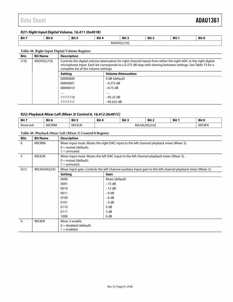
Data Sheet ADAU1361
Rev. D | Page 61 of 80
R21: Right Input Digital Volume, 16,411 (0x401B)
Bit 7 Bit 6 Bit 5 Bit 4 Bit 3 Bit 2 Bit 1 Bit 0
RADVOL[7:0]
Table 48. Right Input Digital Volume Register
R22: Playback Mixer Left (Mixer 3) Control 0, 16,412 (0x401C)
Bit 7 Bit 6 Bit 5 Bit 4 Bit 3 Bit 2 Bit 1 Bit 0
Reserved MX3RM MX3LM MX3AUXG[3:0] MX3EN
Table 49. Playback Mixer Left (Mixer 3) Control 0 Register
Bits Bit Name Description [7:0] RADVOL[7:0] Controls the digital volume attenuation for right channel inputs from either the right ADC or the right digital
microphone input. Each bit corresponds to a 0.375 dB step with slewing between settings. See Table 73 for a complete list of the volume settings.
Setting Volume Attenuation 00000000 0 dB (default) 00000001 −0.375 dB 00000010 −0.75 dB … … 11111110 −95.25 dB 11111111 −95.625 dB
Bits Bit Name Description 6 MX3RM Mixer input mute. Mutes the right DAC input to the left channel playback mixer (Mixer 3).
0 = muted (default). 1 = unmuted.
5 MX3LM Mixer input mute. Mutes the left DAC input to the left channel playback mixer (Mixer 3). 0 = muted (default). 1 = unmuted.
[4:1] MX3AUXG[3:0] Mixer input gain. Controls the left channel auxiliary input gain to the left channel playback mixer (Mixer 3).
Setting Gain 0000 Mute (default) 0001 −15 dB 0010 −12 dB 0011 −9 dB 0100 −6 dB 0101 −3 dB 0110 0 dB 0111 3 dB 1000 6 dB
0 MX3EN Mixer 3 enable. 0 = disabled (default). 1 = enabled.
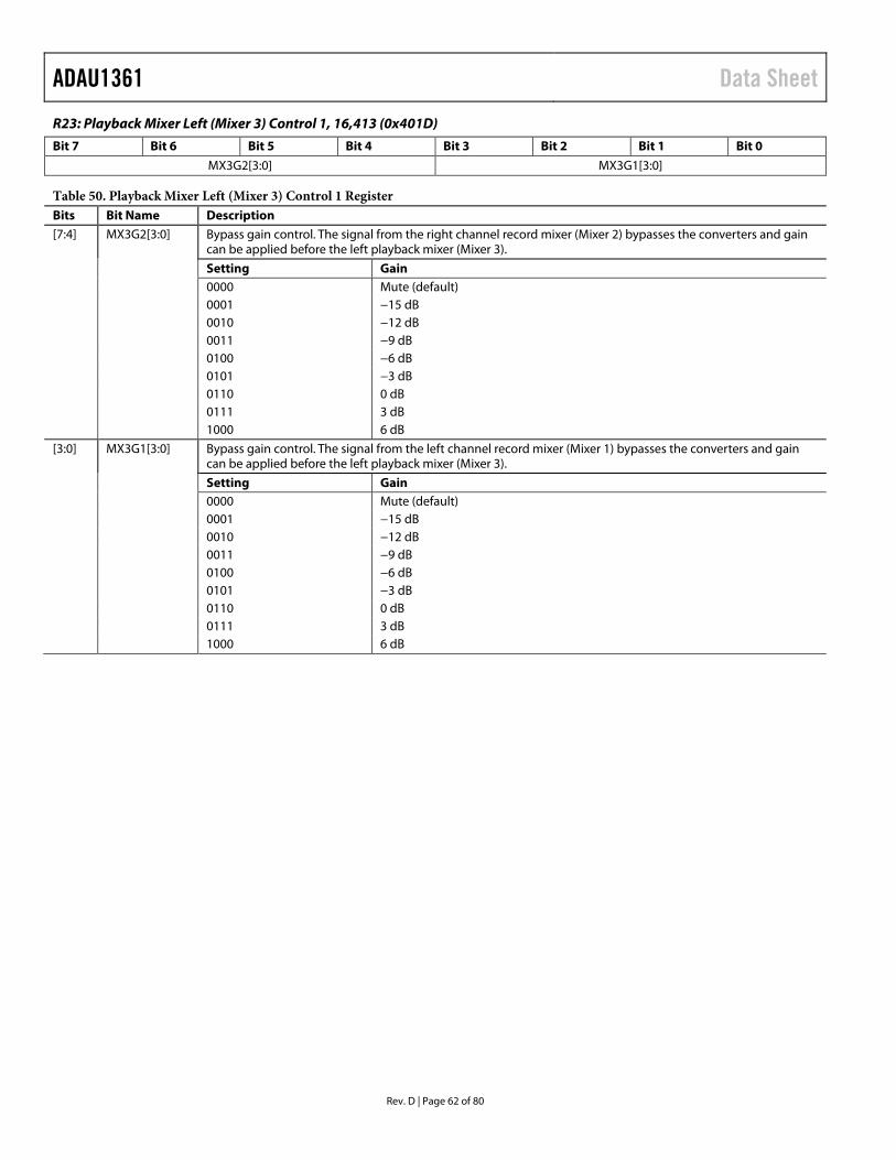
ADAU1361 Data Sheet
Rev. D | Page 62 of 80
R23: Playback Mixer Left (Mixer 3) Control 1, 16,413 (0x401D)
Bit 7 Bit 6 Bit 5 Bit 4 Bit 3 Bit 2 Bit 1 Bit 0
MX3G2[3:0] MX3G1[3:0]
Table 50. Playback Mixer Left (Mixer 3) Control 1 Register
Bits Bit Name Description [7:4] MX3G2[3:0] Bypass gain control. The signal from the right channel record mixer (Mixer 2) bypasses the converters and gain
can be applied before the left playback mixer (Mixer 3).
Setting Gain 0000 Mute (default) 0001 −15 dB 0010 −12 dB 0011 −9 dB 0100 −6 dB 0101 −3 dB 0110 0 dB 0111 3 dB 1000 6 dB
[3:0] MX3G1[3:0] Bypass gain control. The signal from the left channel record mixer (Mixer 1) bypasses the converters and gain can be applied before the left playback mixer (Mixer 3).
Setting Gain 0000 Mute (default) 0001 −15 dB 0010 −12 dB 0011 −9 dB 0100 −6 dB 0101 −3 dB 0110 0 dB 0111 3 dB 1000 6 dB
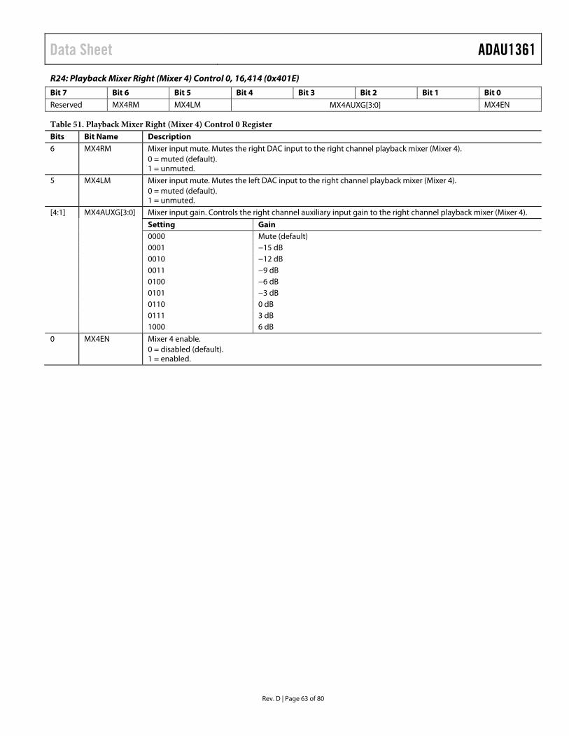
Data Sheet ADAU1361
Rev. D | Page 63 of 80
R24: Playback Mixer Right (Mixer 4) Control 0, 16,414 (0x401E)
Bit 7 Bit 6 Bit 5 Bit 4 Bit 3 Bit 2 Bit 1 Bit 0
Reserved MX4RM MX4LM MX4AUXG[3:0] MX4EN
Table 51. Playback Mixer Right (Mixer 4) Control 0 Register
Bits Bit Name Description 6 MX4RM Mixer input mute. Mutes the right DAC input to the right channel playback mixer (Mixer 4).
0 = muted (default). 1 = unmuted.
5 MX4LM Mixer input mute. Mutes the left DAC input to the right channel playback mixer (Mixer 4). 0 = muted (default). 1 = unmuted.
[4:1] MX4AUXG[3:0] Mixer input gain. Controls the right channel auxiliary input gain to the right channel playback mixer (Mixer 4).
Setting Gain 0000 Mute (default) 0001 −15 dB 0010 −12 dB 0011 −9 dB 0100 −6 dB 0101 −3 dB 0110 0 dB 0111 3 dB 1000 6 dB
0 MX4EN Mixer 4 enable. 0 = disabled (default). 1 = enabled.

ADAU1361 Data Sheet
Rev. D | Page 64 of 80
R25: Playback Mixer Right (Mixer 4) Control 1, 16,415 (0x401F)
Bit 7 Bit 6 Bit 5 Bit 4 Bit 3 Bit 2 Bit 1 Bit 0
MX4G2[3:0] MX4G1[3:0]
Table 52. Playback Mixer Right (Mixer 4) Control 1 Register
Bits Bit Name Description [7:4] MX4G2[3:0] Bypass gain control. The signal from the right channel record mixer (Mixer 2) bypasses the converters and gain
can be applied before the right playback mixer (Mixer 4).
Setting Gain 0000 Mute (default) 0001 −15 dB 0010 −12 dB 0011 −9 dB 0100 −6 dB 0101 −3 dB 0110 0 dB 0111 3 dB 1000 6 dB
[3:0] MX4G1[3:0] Bypass gain control. The signal from the left channel record mixer (Mixer 1) bypasses the converters and gain can be applied before the right playback mixer (Mixer 4).
Setting Gain 0000 Mute (default) 0001 −15 dB 0010 −12 dB 0011 −9 dB 0100 −6 dB 0101 −3 dB 0110 0 dB 0111 3 dB 1000 6 dB

Data Sheet ADAU1361
Rev. D | Page 65 of 80
R26: Playback L/R Mixer Left (Mixer 5) Line Output Control, 16,416 (0x4020)
Bit 7 Bit 6 Bit 5 Bit 4 Bit 3 Bit 2 Bit 1 Bit 0
Reserved MX5G4[1:0] MX5G3[1:0] MX5EN
Table 53. Playback L/R Mixer Left (Mixer 5) Line Output Control Register
R27: Playback L/R Mixer Right (Mixer 6) Line Output Control, 16,417 (0x4021)
Bit 7 Bit 6 Bit 5 Bit 4 Bit 3 Bit 2 Bit 1 Bit 0
Reserved MX6G4[1:0] MX6G3[1:0] MX6EN
Table 54. Playback L/R Mixer Right (Mixer 6) Line Output Control Register
Bits Bit Name Description [4:3] MX5G4[1:0] Mixer input gain boost. The signal from the right channel playback mixer (Mixer 4) can be enabled and boosted
in the playback L/R mixer left (Mixer 5).
Setting Gain Boost 00 Mute (default) 01 0 dB output (−6 dB gain on each of the two inputs) 10 6 dB output (0 dB gain on each of the two inputs) 11 Reserved
[2:1] MX5G3[1:0] Mixer input gain boost. The signal from the left channel playback mixer (Mixer 3) can be enabled and boosted in the playback L/R mixer left (Mixer 5).
Setting Gain Boost 00 Mute (default) 01 0 dB output (−6 dB gain on each of the two inputs) 10 6 dB output (0 dB gain on each of the two inputs) 11 Reserved
0 MX5EN Mixer 5 enable. 0 = disabled (default). 1 = enabled.
Bits Bit Name Description [4:3] MX6G4[1:0] Mixer input gain boost. The signal from the right channel playback mixer (Mixer 4) can be enabled and boosted
in the playback L/R mixer right (Mixer 6).
Setting Gain Boost 00 Mute (default) 01 0 dB output (−6 dB gain on each of the two inputs) 10 6 dB output (0 dB gain on each of the two inputs) 11 Reserved
[2:1] MX6G3[1:0] Mixer input gain boost. The signal from the left channel playback mixer (Mixer 3) can be enabled and boosted in the playback L/R mixer right (Mixer 6).
Setting Gain Boost 00 Mute (default) 01 0 dB output (−6 dB gain on each of the two inputs) 10 6 dB output (0 dB gain on each of the two inputs) 11 Reserved
0 MX6EN Mixer 6 enable. 0 = disabled (default). 1 = enabled.

ADAU1361 Data Sheet
Rev. D | Page 66 of 80
R28: Playback L/R Mixer Mono Output (Mixer 7) Control, 16,418 (0x4022)
Bit 7 Bit 6 Bit 5 Bit 4 Bit 3 Bit 2 Bit 1 Bit 0
Reserved MX7[1:0] MX7EN
Table 55. Playback L/R Mixer Mono Output (Mixer 7) Control Register
R29: Playback Headphone Left Volume Control, 16,419 (0x4023)
Bit 7 Bit 6 Bit 5 Bit 4 Bit 3 Bit 2 Bit 1 Bit 0
LHPVOL[5:0] LHPM HPEN
Table 56. Playback Headphone Left Volume Control Register
Bits Bit Name Description [2:1] MX7[1:0] L/R mono playback mixer (Mixer 7). Mixes the left and right playback mixers (Mixer 3 and Mixer 4) with either a
0 dB or 6 dB gain boost. Additionally, this mixer can operate as a common-mode output, which is used as the virtual ground in a capless headphone configuration.
Setting Gain Boost 00 Common-mode output (default) 01 0 dB output (−6 dB gain on each of the two inputs) 10 6 dB output (0 dB gain on each of the two inputs) 11 Reserved
0 MX7EN Mixer 7 enable. 0 = disabled (default). 1 = enabled.
Bits Bit Name Description [7:2] LHPVOL[5:0] Headphone volume control for left channel, LHP output. Each 1-bit step corresponds to a 1 dB increase in volume.
See Table 74 for a complete list of the volume settings.
Setting Volume 000000 −57 dB (default) … … 111001 0 dB … … 111111 6 dB
1 LHPM Headphone mute for left channel, LHP output (active low). 0 = mute. 1 = unmute (default).
0 HPEN Headphone output enable. 0 = disabled (default). 1 = enabled.

Data Sheet ADAU1361
Rev. D | Page 67 of 80
R30: Playback Headphone Right Volume Control, 16,420 (0x4024)
Bit 7 Bit 6 Bit 5 Bit 4 Bit 3 Bit 2 Bit 1 Bit 0
RHPVOL[5:0] RHPM HPMODE
Table 57. Playback Headphone Right Volume Control Register
R31: Playback Line Output Left Volume Control, 16,421 (0x4025)
Bit 7 Bit 6 Bit 5 Bit 4 Bit 3 Bit 2 Bit 1 Bit 0
LOUTVOL[5:0] LOUTM LOMODE
Table 58. Playback Line Output Left Volume Control Register
Bits Bit Name Description [7:2] RHPVOL[5:0] Headphone volume control for right channel, RHP output. Each 1-bit step corresponds to a 1 dB increase in
volume. See Table 74 for a complete list of the volume settings.
Setting Volume 000000 −57 dB (default) … … 111001 0 dB … … 111111 6 dB
1 RHPM Headphone mute for right channel, RHP output (active low). 0 = mute. 1 = unmute (default).
0 HPMODE RHP and LHP output mode. These pins can be configured for either line outputs or headphone outputs. 0 = line output (default). 1 = headphone output.
Bits Bit Name Description [7:2] LOUTVOL[5:0] Line output volume control for left channel, LOUTN and LOUTP outputs. Each 1-bit step corresponds to a 1 dB
increase in volume. See Table 74 for a complete list of the volume settings.
Setting Volume 000000 −57 dB (default) … … 111001 0 dB … … 111111 6 dB
1 LOUTM Line output mute for left channel, LOUTN and LOUTP outputs (active low). 0 = mute. 1 = unmute (default).
0 LOMODE Line output mode for left channel, LOUTN and LOUTP outputs. These pins can be configured for either line outputs or headphone outputs. To drive earpiece speakers, set this bit to 1 (headphone output). 0 = line output (default). 1 = headphone output.

ADAU1361 Data Sheet
Rev. D | Page 68 of 80
R32: Playback Line Output Right Volume Control, 16,422 (0x4026)
Bit 7 Bit 6 Bit 5 Bit 4 Bit 3 Bit 2 Bit 1 Bit 0
ROUTVOL[5:0] ROUTM ROMODE
Table 59. Playback Line Output Right Volume Control Register
R33: Playback Mono Output Control, 16,423 (0x4027)
Bit 7 Bit 6 Bit 5 Bit 4 Bit 3 Bit 2 Bit 1 Bit 0
MONOVOL[5:0] MONOM MOMODE
Table 60. Playback Mono Output Control Register
Bits Bit Name Description [7:2] ROUTVOL[5:0] Line output volume control for right channel, ROUTN and ROUTP outputs. Each 1-bit step corresponds to a 1 dB
increase in volume. See Table 74 for a complete list of the volume settings.
Setting Volume 000000 −57 dB (default) … … 111001 0 dB … … 111111 6 dB
1 ROUTM Line output mute for right channel, ROUTN and ROUTP outputs (active low). 0 = mute. 1 = unmute (default).
0 ROMODE Line output mode for right channel, ROUTN and ROUTP outputs. These pins can be configured for either line outputs or headphone outputs. To drive earpiece speakers, set this bit to 1 (headphone output). 0 = line output (default). 1 = headphone output.
Bits Bit Name Description [7:2] MONOVOL[5:0] Mono output volume control. Each 1-bit step corresponds to a 1 dB increase in volume. If MX7[1:0] in Register R28
is set for common-mode output, volume control is disabled. See Table 74 for a complete list of the volume settings.
Setting Volume 000000 −57 dB (default) … … 111001 0 dB … … 111111 6 dB
1 MONOM Mono output mute (active low). 0 = mute. 1 = unmute (default).
0 MOMODE Headphone mode enable. If MX7[1:0] in Register R28 is set for common-mode output for a capless headphone configuration, this bit should be set to 1 (headphone output). 0 = line output (default). 1 = headphone output.

Data Sheet ADAU1361
Rev. D | Page 69 of 80
R34: Playback Pop/Click Suppression, 16,424 (0x4028)
Bit 7 Bit 6 Bit 5 Bit 4 Bit 3 Bit 2 Bit 1 Bit 0
Reserved POPMODE POPLESS ASLEW[1:0] Reserved
Table 61. Playback Pop/Click Suppression Register Bits Bit Name Description 4 POPMODE Pop suppression circuit power saving mode. The pop suppression circuits charge faster in normal operation;
however, after they are charged, they can be put into low power operation. 0 = normal (default). 1 = low power.
3 POPLESS Pop suppression disable. The pop suppression circuits are enabled by default. They can be disabled to save power; however, disabling the circuits increases the risk of pops and clicks. 0 = enabled (default). 1 = disabled.
[2:1] ASLEW[1:0] Analog volume slew rate for playback volume controls. Setting Slew Rate 00 21.25 ms (default) 01 42.5 ms 10 85 ms 11 Off
R35: Playback Power Management, 16,425 (0x4029)
Bit 7 Bit 6 Bit 5 Bit 4 Bit 3 Bit 2 Bit 1 Bit 0
HPBIAS[1:0] DACBIAS[1:0] PBIAS[1:0] PREN PLEN
Table 62. Playback Power Management Register Bits Bit Name Description [7:6] HPBIAS[1:0] Headphone bias control. Setting Headphone Bias Control 00 Normal operation (default) 01 Extreme power saving 10 Enhanced performance 11 Power saving [5:4] DACBIAS[1:0] DAC bias control. Setting DAC Bias Control 00 Normal operation (default) 01 Extreme power saving 10 Enhanced performance 11 Power saving [3:2] PBIAS[1:0] Playback path channel bias control. Setting Playback Path Bias Control 00 Normal operation (default) 01 Reserved 10 Enhanced performance 11 Power saving 1 PREN Playback right channel enable.
0 = disabled (default). 1 = enabled.
0 PLEN Playback left channel enable. 0 = disabled (default). 1 = enabled.
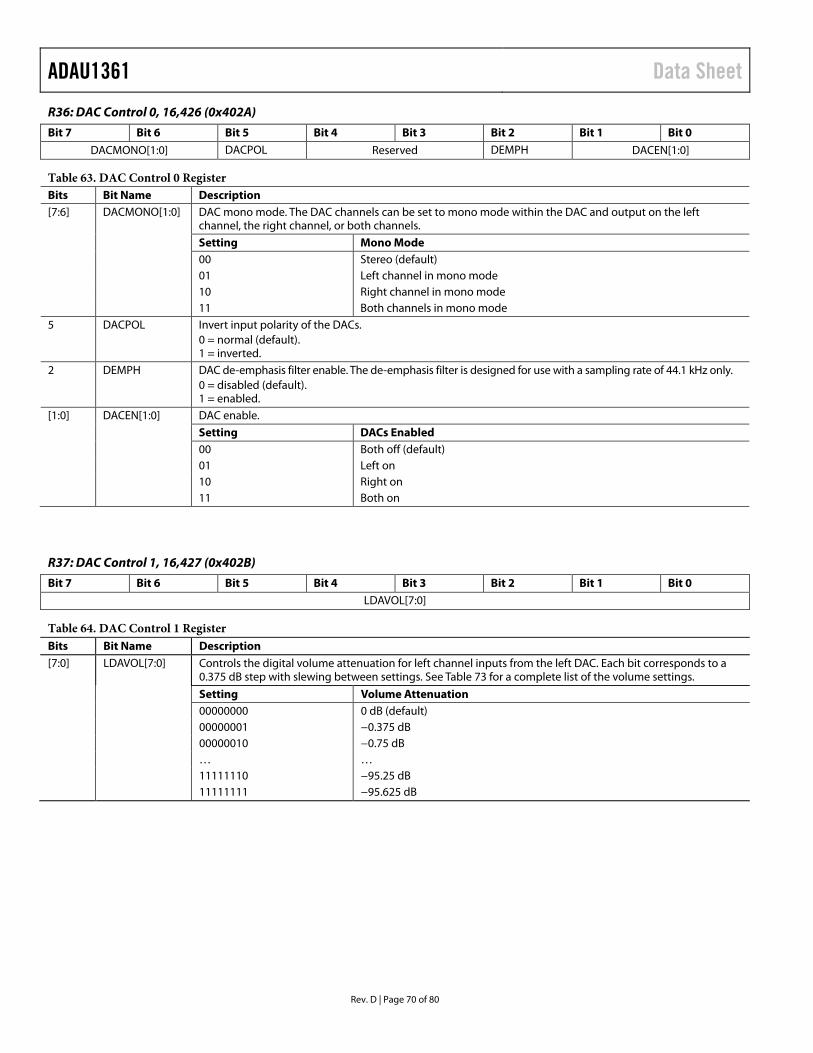
ADAU1361 Data Sheet
Rev. D | Page 70 of 80
R36: DAC Control 0, 16,426 (0x402A)
Bit 7 Bit 6 Bit 5 Bit 4 Bit 3 Bit 2 Bit 1 Bit 0
DACMONO[1:0] DACPOL Reserved DEMPH DACEN[1:0]
Table 63. DAC Control 0 Register Bits Bit Name Description [7:6] DACMONO[1:0] DAC mono mode. The DAC channels can be set to mono mode within the DAC and output on the left
channel, the right channel, or both channels. Setting Mono Mode 00 Stereo (default) 01 Left channel in mono mode 10 Right channel in mono mode 11 Both channels in mono mode 5 DACPOL Invert input polarity of the DACs.
0 = normal (default). 1 = inverted.
2 DEMPH DAC de-emphasis filter enable. The de-emphasis filter is designed for use with a sampling rate of 44.1 kHz only. 0 = disabled (default). 1 = enabled.
[1:0] DACEN[1:0] DAC enable. Setting DACs Enabled 00 Both off (default) 01 Left on 10 Right on 11 Both on
R37: DAC Control 1, 16,427 (0x402B)
Bit 7 Bit 6 Bit 5 Bit 4 Bit 3 Bit 2 Bit 1 Bit 0
LDAVOL[7:0]
Table 64. DAC Control 1 Register
Bits Bit Name Description [7:0] LDAVOL[7:0] Controls the digital volume attenuation for left channel inputs from the left DAC. Each bit corresponds to a
0.375 dB step with slewing between settings. See Table 73 for a complete list of the volume settings.
Setting Volume Attenuation 00000000 0 dB (default) 00000001 −0.375 dB 00000010 −0.75 dB … … 11111110 −95.25 dB 11111111 −95.625 dB

Data Sheet ADAU1361
Rev. D | Page 71 of 80
R38: DAC Control 2, 16,428 (0x402C)
Bit 7 Bit 6 Bit 5 Bit 4 Bit 3 Bit 2 Bit 1 Bit 0
RDAVOL[7:0]
Table 65. DAC Control 2 Register
R39: Serial Port Pad Control, 16,429 (0x402D)
The optional pull-up/pull-down resistors are nominally 250 kΩ. When enabled, these pull-up/pull-down resistors set the serial port signals to a defined state when the signal source becomes three-state.
Bit 7 Bit 6 Bit 5 Bit 4 Bit 3 Bit 2 Bit 1 Bit 0
ADCSDP[1:0] DACSDP[1:0] LRCLKP[1:0] BCLKP[1:0]
Table 66. Serial Port Pad Control Register
Bits Bit Name Description [7:0] RDAVOL[7:0] Controls the digital volume attenuation for right channel inputs from the right DAC. Each bit corresponds to a
0.375 dB step with slewing between settings. See Table 73 for a complete list of the volume settings.
Setting Volume Attenuation 00000000 0 dB (default) 00000001 −0.375 dB 00000010 −0.75 dB … … 11111110 −95.25 dB 11111111 −95.625 dB
Bits Bit Name Description [7:6] ADCSDP[1:0] ADC_SDATA pad pull-up/pull-down configuration.
Setting Configuration 00 Pull-up 01 Reserved 10 None (default) 11 Pull-down
[5:4] DACSDP[1:0] DAC_SDATA pad pull-up/pull-down configuration.
Setting Configuration 00 Pull-up 01 Reserved 10 None (default) 11 Pull-down
[3:2] LRCLKP[1:0] LRCLK pad pull-up/pull-down configuration.
Setting Configuration 00 Pull-up 01 Reserved 10 None (default) 11 Pull-down
[1:0] BCLKP[1:0] BCLK pad pull-up/pull-down configuration.
Setting Configuration 00 Pull-up 01 Reserved 10 None (default) 11 Pull-down

ADAU1361 Data Sheet
Rev. D | Page 72 of 80
R40: Control Port Pad Control 0, 16,431 (0x402F)
The optional pull-up/pull-down resistors are nominally 250 kΩ. When enabled, these pull-up/pull-down resistors set the control port signals to a defined state when the signal source becomes three-state.
Bit 7 Bit 6 Bit 5 Bit 4 Bit 3 Bit 2 Bit 1 Bit 0
CDATP[1:0] CLCHP[1:0] SCLP[1:0] SDAP[1:0]
Table 67. Control Port Pad Control 0 Register
R41: Control Port Pad Control 1, 16,432 (0x4030)
With IOVDD set to 3.3 V, the low and high drive strengths of the SDA/COUT pin are approximately 2.0 mA and 4.0 mA, respectively. With IOVDD set to 1.8 V, the low and high drive strengths are approximately 0.8 mA and 1.7 mA, respectively. The high drive strength mode may be useful for generating a stronger ACK pulse in I2C mode, if needed.
Bit 7 Bit 6 Bit 5 Bit 4 Bit 3 Bit 2 Bit 1 Bit 0
Reserved SDASTR
Table 68. Control Port Pad Control 1 Register
Bits Bit Name Description [7:6] CDATP[1:0] CDATA pad pull-up/pull-down configuration.
Setting Configuration 00 Pull-up 01 Reserved 10 None (default) 11 Pull-down
[5:4] CLCHP[1:0] CLATCH pad pull-up/pull-down configuration.
Setting Configuration 00 Pull-up 01 Reserved 10 None (default) 11 Pull-down
[3:2] SCLP[1:0] SCL/CCLK pad pull-up/pull-down configuration.
Setting Configuration 00 Pull-up 01 Reserved 10 None (default) 11 Pull-down
[1:0] SDAP[1:0] SDA/COUT pad pull-up/pull-down configuration.
Setting Configuration 00 Pull-up 01 Reserved 10 None (default) 11 Pull-down
Bits Bit Name Description 0 SDASTR SDA/COUT pin drive strength.
0 = low (default). 1 = high.

Data Sheet ADAU1361
Rev. D | Page 73 of 80
R42: Jack Detect Pin Control, 16,433 (0x4031)
With IOVDD set to 3.3 V, the low and high drive strengths of the JACKDET/MICIN pin are approximately 2.0 mA and 4.0 mA, respectively. With IOVDD set to 1.8 V, the low and high drive strengths are approximately 0.8 mA and 1.7 mA, respectively. The optional pull-up/ pull-down resistors are nominally 250 kΩ. When enabled, these pull-up/pull-down resistors set the input signals to a defined state when the signal source becomes three-state.
Bit 7 Bit 6 Bit 5 Bit 4 Bit 3 Bit 2 Bit 1 Bit 0
Reserved JDSTR Reserved JDP[1:0] Reserved
Table 69. Jack Detect Pin Control Register
R67: Dejitter Control, 16,438 (0x4036)
The dejitter control register allows the size of the dejitter window to be set, and also allows all dejitter circuits in the device to be activated or bypassed. Dejitter circuits protect against duplicate samples or skipped samples due to jitter from the serial ports in slave mode. Disabling and reenabling certain subsystems in the device—that is, the ADCs, serial ports, and DACs—during operation can cause the associated dejitter circuits to fail. As a result, audio data fails to be output to the next subsystem in the device.
When the serial ports are in master mode, the dejitter circuit can be bypassed by setting the dejitter window to 0. When the serial ports are in slave mode, the dejitter circuit can be reinitialized prior to outputting audio from the device, guaranteeing that audio is output to the next subsystem in the device. Any time that audio must pass through the ADCs, serial port, or DACs, the dejitter circuit can be bypassed and reset by setting the dejitter window size to 0. In this way, the dejitter circuit can be immediately reactivated, without a wait period, by setting the dejitter window size to the default value of 3.
Bit 7 Bit 6 Bit 5 Bit 4 Bit 3 Bit 2 Bit 1 Bit 0
DEJIT[7:0]
Table 70. Dejitter Control Register
Bits Bit Name Description 5 JDSTR JACKDET/MICIN pin drive strength.
0 = low (default). 1 = high.
[3:2] JDP[1:0] JACKDET/MICIN pad pull-up/pull-down configuration.
Setting Configuration 00 Pull-up 01 Reserved 10 None (default) 11 Pull-down
Bits Bit Name Description [7:0] DEJIT[7:0] Dejitter window size.
Window Size Core Clock Cycles 00000000 0 … … 00000011 3 (default) … … 00000101 5
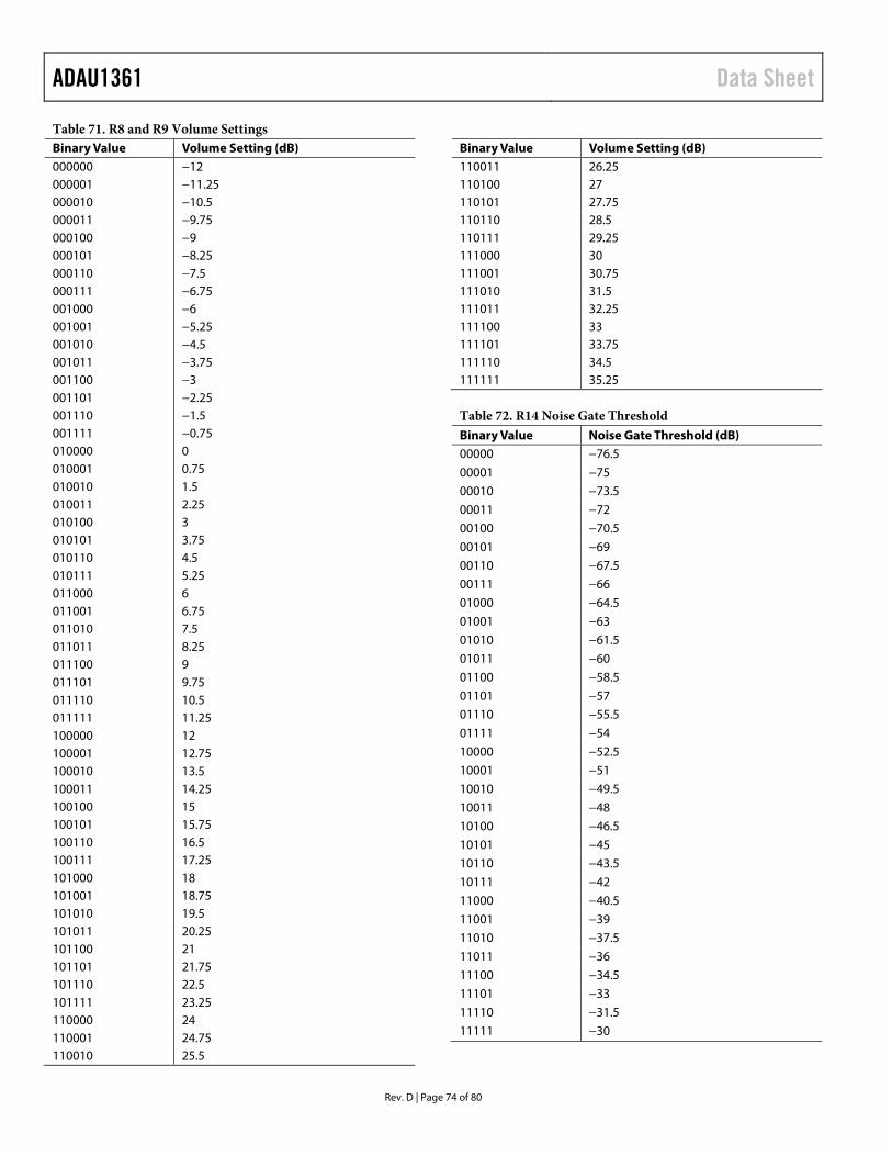
ADAU1361 Data Sheet
Rev. D | Page 74 of 80
Table 71. R8 and R9 Volume Settings Binary Value Volume Setting (dB) 000000 −12 000001 −11.25 000010 −10.5 000011 −9.75 000100 −9 000101 −8.25 000110 −7.5 000111 −6.75 001000 −6 001001 −5.25 001010 −4.5 001011 −3.75 001100 −3 001101 −2.25 001110 −1.5 001111 −0.75 010000 0 010001 0.75 010010 1.5 010011 2.25 010100 3 010101 3.75 010110 4.5 010111 5.25 011000 6 011001 6.75 011010 7.5 011011 8.25 011100 9 011101 9.75 011110 10.5 011111 11.25 100000 12 100001 12.75 100010 13.5 100011 14.25 100100 15 100101 15.75 100110 16.5 100111 17.25 101000 18 101001 18.75 101010 19.5 101011 20.25 101100 21 101101 21.75 101110 22.5 101111 23.25 110000 24 110001 24.75 110010 25.5
Binary Value Volume Setting (dB) 110011 26.25 110100 27 110101 27.75 110110 28.5 110111 29.25 111000 30 111001 30.75 111010 31.5 111011 32.25 111100 33 111101 33.75 111110 34.5 111111 35.25
Table 72. R14 Noise Gate Threshold Binary Value Noise Gate Threshold (dB) 00000 −76.5
00001 −75 00010 −73.5
00011 −72 00100 −70.5
00101 −69 00110 −67.5
00111 −66 01000 −64.5
01001 −63 01010 −61.5
01011 −60 01100 −58.5
01101 −57 01110 −55.5
01111 −54 10000 −52.5
10001 −51 10010 −49.5
10011 −48 10100 −46.5
10101 −45 10110 −43.5
10111 −42 11000 −40.5
11001 −39 11010 −37.5
11011 −36 11100 −34.5
11101 −33 11110 −31.5
11111 −30
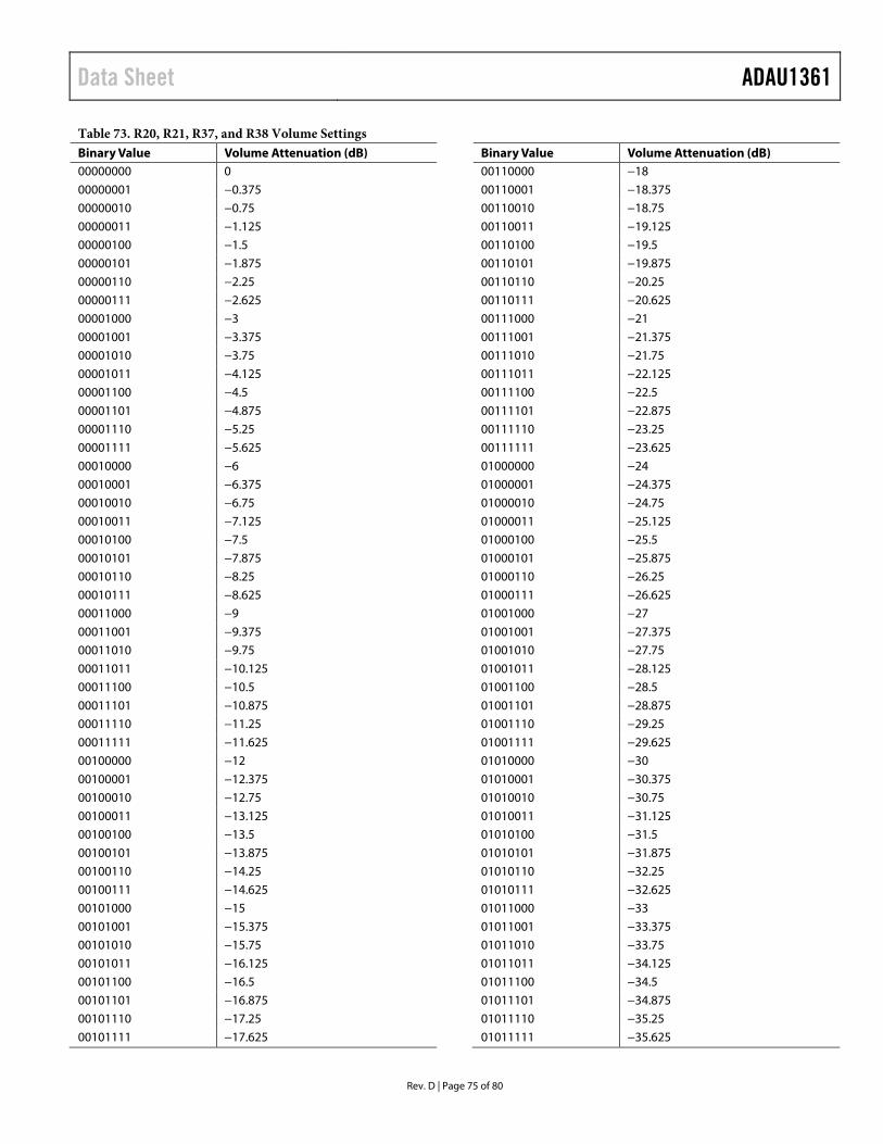
Data Sheet ADAU1361
Rev. D | Page 75 of 80
Table 73. R20, R21, R37, and R38 Volume Settings Binary Value Volume Attenuation (dB) 00000000 0
00000001 −0.375 00000010 −0.75
00000011 −1.125 00000100 −1.5
00000101 −1.875 00000110 −2.25
00000111 −2.625 00001000 −3
00001001 −3.375 00001010 −3.75
00001011 −4.125 00001100 −4.5
00001101 −4.875 00001110 −5.25
00001111 −5.625 00010000 −6
00010001 −6.375 00010010 −6.75
00010011 −7.125 00010100 −7.5
00010101 −7.875 00010110 −8.25
00010111 −8.625 00011000 −9
00011001 −9.375 00011010 −9.75
00011011 −10.125 00011100 −10.5
00011101 −10.875 00011110 −11.25
00011111 −11.625 00100000 −12
00100001 −12.375 00100010 −12.75
00100011 −13.125 00100100 −13.5
00100101 −13.875 00100110 −14.25
00100111 −14.625 00101000 −15
00101001 −15.375 00101010 −15.75
00101011 −16.125 00101100 −16.5
00101101 −16.875 00101110 −17.25
00101111 −17.625
Binary Value Volume Attenuation (dB) 00110000 −18
00110001 −18.375 00110010 −18.75
00110011 −19.125 00110100 −19.5
00110101 −19.875 00110110 −20.25
00110111 −20.625 00111000 −21
00111001 −21.375 00111010 −21.75
00111011 −22.125 00111100 −22.5
00111101 −22.875 00111110 −23.25
00111111 −23.625 01000000 −24
01000001 −24.375 01000010 −24.75
01000011 −25.125 01000100 −25.5
01000101 −25.875 01000110 −26.25
01000111 −26.625 01001000 −27
01001001 −27.375 01001010 −27.75
01001011 −28.125 01001100 −28.5
01001101 −28.875 01001110 −29.25
01001111 −29.625 01010000 −30
01010001 −30.375 01010010 −30.75
01010011 −31.125 01010100 −31.5
01010101 −31.875 01010110 −32.25
01010111 −32.625 01011000 −33
01011001 −33.375 01011010 −33.75
01011011 −34.125 01011100 −34.5
01011101 −34.875 01011110 −35.25
01011111 −35.625
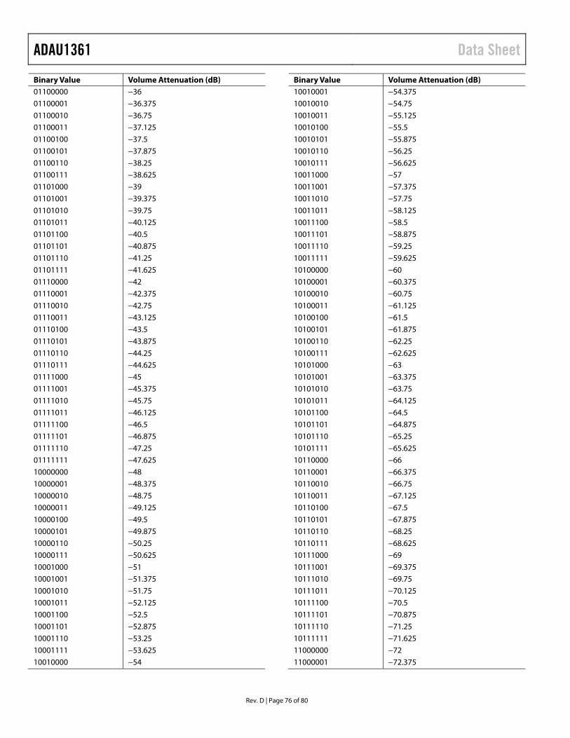
ADAU1361 Data Sheet
Rev. D | Page 76 of 80
Binary Value Volume Attenuation (dB) 01100000 −36 01100001 −36.375
01100010 −36.75 01100011 −37.125
01100100 −37.5 01100101 −37.875
01100110 −38.25 01100111 −38.625
01101000 −39 01101001 −39.375
01101010 −39.75 01101011 −40.125
01101100 −40.5 01101101 −40.875
01101110 −41.25 01101111 −41.625
01110000 −42 01110001 −42.375
01110010 −42.75 01110011 −43.125
01110100 −43.5 01110101 −43.875
01110110 −44.25 01110111 −44.625
01111000 −45 01111001 −45.375
01111010 −45.75 01111011 −46.125
01111100 −46.5 01111101 −46.875
01111110 −47.25 01111111 −47.625
10000000 −48 10000001 −48.375
10000010 −48.75 10000011 −49.125
10000100 −49.5 10000101 −49.875
10000110 −50.25 10000111 −50.625
10001000 −51 10001001 −51.375
10001010 −51.75 10001011 −52.125
10001100 −52.5 10001101 −52.875
10001110 −53.25 10001111 −53.625
10010000 −54
Binary Value Volume Attenuation (dB) 10010001 −54.375 10010010 −54.75
10010011 −55.125 10010100 −55.5
10010101 −55.875 10010110 −56.25
10010111 −56.625 10011000 −57
10011001 −57.375 10011010 −57.75
10011011 −58.125 10011100 −58.5
10011101 −58.875 10011110 −59.25
10011111 −59.625 10100000 −60
10100001 −60.375 10100010 −60.75
10100011 −61.125 10100100 −61.5
10100101 −61.875 10100110 −62.25
10100111 −62.625 10101000 −63
10101001 −63.375 10101010 −63.75
10101011 −64.125 10101100 −64.5
10101101 −64.875 10101110 −65.25
10101111 −65.625 10110000 −66
10110001 −66.375 10110010 −66.75
10110011 −67.125 10110100 −67.5
10110101 −67.875 10110110 −68.25
10110111 −68.625 10111000 −69
10111001 −69.375 10111010 −69.75
10111011 −70.125 10111100 −70.5
10111101 −70.875 10111110 −71.25
10111111 −71.625 11000000 −72
11000001 −72.375
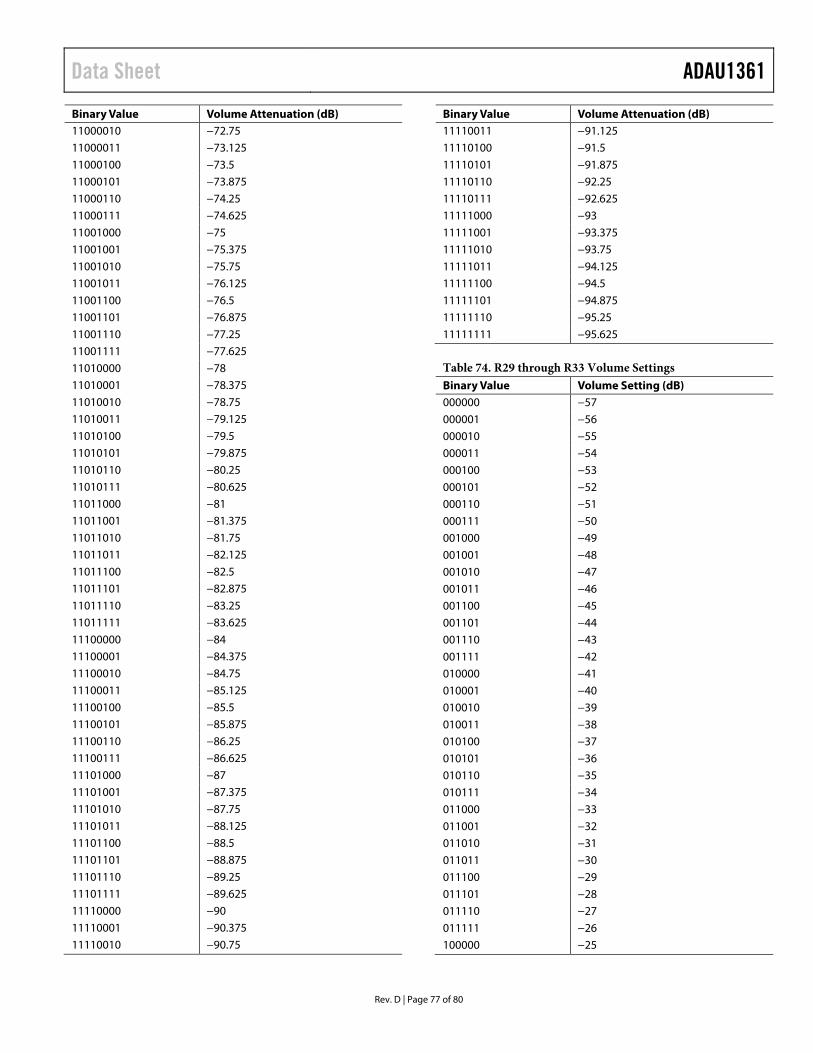
Data Sheet ADAU1361
Rev. D | Page 77 of 80
Binary Value Volume Attenuation (dB) 11000010 −72.75 11000011 −73.125
11000100 −73.5 11000101 −73.875
11000110 −74.25 11000111 −74.625
11001000 −75 11001001 −75.375
11001010 −75.75 11001011 −76.125
11001100 −76.5 11001101 −76.875
11001110 −77.25 11001111 −77.625
11010000 −78 11010001 −78.375
11010010 −78.75 11010011 −79.125
11010100 −79.5 11010101 −79.875
11010110 −80.25 11010111 −80.625
11011000 −81 11011001 −81.375
11011010 −81.75 11011011 −82.125
11011100 −82.5 11011101 −82.875
11011110 −83.25 11011111 −83.625
11100000 −84 11100001 −84.375
11100010 −84.75 11100011 −85.125
11100100 −85.5 11100101 −85.875
11100110 −86.25 11100111 −86.625
11101000 −87 11101001 −87.375
11101010 −87.75 11101011 −88.125
11101100 −88.5 11101101 −88.875
11101110 −89.25 11101111 −89.625
11110000 −90 11110001 −90.375
11110010 −90.75
Binary Value Volume Attenuation (dB) 11110011 −91.125 11110100 −91.5
11110101 −91.875 11110110 −92.25
11110111 −92.625 11111000 −93
11111001 −93.375 11111010 −93.75
11111011 −94.125 11111100 −94.5
11111101 −94.875 11111110 −95.25
11111111 −95.625
Table 74. R29 through R33 Volume Settings Binary Value Volume Setting (dB) 000000 −57
000001 −56 000010 −55
000011 −54 000100 −53
000101 −52 000110 −51
000111 −50 001000 −49
001001 −48 001010 −47
001011 −46 001100 −45
001101 −44 001110 −43
001111 −42 010000 −41
010001 −40 010010 −39
010011 −38 010100 −37
010101 −36 010110 −35
010111 −34 011000 −33
011001 −32 011010 −31
011011 −30 011100 −29
011101 −28 011110 −27
011111 −26 100000 −25

ADAU1361 Data Sheet
Rev. D | Page 78 of 80
Binary Value Volume Setting (dB) 100001 −24 100010 −23
100011 −22 100100 −21
100101 −20 100110 −19
100111 −18 101000 −17
101001 −16 101010 −15
101011 −14 101100 −13
101101 −12 101110 −11
101111 −10 110000 −9
110001 −8 110010 −7
110011 −6 110100 −5
110101 −4 110110 −3
110111 −2 111000 −1
111001 0 111010 1
111011 2 111100 3
111101 4 111110 5
111111 6

Data Sheet ADAU1361
Rev. D | Page 79 of 80
OUTLINE DIMENSIONS
COMPLIANT TO JEDEC STANDARDS MO-220-VHHD-2
0.300.230.18
0.20 REF
0.80 MAX0.65 TYP
0.05 MAX0.02 NOM
12° MAX
1.000.850.80
SEATINGPLANE
COPLANARITY0.08
132
89
2524
1617
0.500.400.30
3.50 REF
0.50BSC
PIN 1INDICATOR
TOPVIEW
5.00BSC SQ
4.75BSC SQ
3.653.50 SQ3.35
PIN 1INDICATOR
0.60 MAX0.60 MAX
0.25 MIN
EXPOSEDPAD
(BOTTOM VIEW)
1006
08-A
FOR PROPER CONNECTION OFTHE EXPOSED PAD, REFER TOTHE PIN CONFIGURATION ANDFUNCTION DESCRIPTIONSSECTION OF THIS DATA SHEET.
Figure 66. 32-Lead Lead Frame Chip Scale Package [LFCSP_VQ]
5 mm × 5 mm Body, Very Thin Quad (CP-32-4)
Dimensions shown in millimeters
ORDERING GUIDE Model1 Temperature Range Package Description Package Option ADAU1361BCPZ −40°C to +85°C 32-Lead Lead Frame Chip Scale Package [LFCSP_VQ] CP-32-4 ADAU1361BCPZ-R7 −40°C to +85°C 32-Lead Lead Frame Chip Scale Package [LFCSP_VQ], 7” Tape and Reel CP-32-4 ADAU1361BCPZ-RL −40°C to +85°C 32-Lead Lead Frame Chip Scale Package [LFCSP_VQ], 13” Tape and Reel CP-32-4 EVAL-ADAU1361Z Evaluation Board 1 Z = RoHS Compliant Part.

ADAU1361 Data Sheet
Rev. D | Page 80 of 80
NOTES
©2009–2018 Analog Devices, Inc. All rights reserved. Trademarks and registered trademarks are the property of their respective owners. D07679-0-8/18(D)
Recommended