Stereo, 24-Bit, 192 kHz,Multibit, Sigma-Delta DAC
AD1852
Rev. A Information furnished by Analog Devices is believed to be accurate and reliable. However, no responsibility is assumed by Analog Devices for its use, nor for any infringements of patents or other rights of third parties that may result from its use. Specifications subject to change without notice. No license is granted by implication or otherwise under any patent or patent rights of Analog Devices. Trademarks and registered trademarks are the property of their respective owners.
One Technology Way, P.O. Box 9106, Norwood, MA 02062-9106, U.S.A.Tel: 781.329.4700 www.analog.com Fax: 781.461.3113 ©2000–2009 Analog Devices, Inc. All rights reserved.
FEATURES 5 V stereo audio DAC system Accepts 16-bit/18-bit/20-bit/24-bit data Supports 24 bits, 192 kHz sample rate Accepts a wide range of sample rates including
32 kHz, 44.1 kHz, 48 kHz, 88.2 kHz, 96 kHz, and 192 kHz Multibit Σ-Δ modulator with perfect differential linearity
restoration for reduced idle tones and noise floor Data-directed scrambling DAC—least sensitive to jitter Differential output for optimum performance 117 dB signal-to-noise (not muted) at 48 kHz sample rate
(A-weighted mono) 114 dB signal-to-noise (not muted) at 48 kHz sample rate
(A-weighted stereo) 117 dB dynamic range (not muted) at 48 kHz sample rate
(A-weighted mono) 114 dB dynamic range (not muted) at 48 kHz sample rate
(A-weighted stereo) −105 dB THD+N (mono application circuit) −102 dB THD+N (stereo) 115 dB stop-band attenuation On-chip clickless volume control Hardware and software controllable clickless mute Serial (SPI) control for: serial mode, number of bits, sample
rate, volume, mute, de-emp Digital de-emphasis processing for 32 kHz, 44.1 kHz, 48 kHz
sample rates Clock autodivide circuit supports five master-clock frequencies Flexible serial data port with right-justified, left-justified,
I2S-compatible and DSP serial port modes 28-Lead SSOP plastic package
APPLICATIONS High end
DVDs, CDs, home theater systems, automotive, audio systems, sampling musical keyboards, digital mixing consoles, and digital audio effects processors
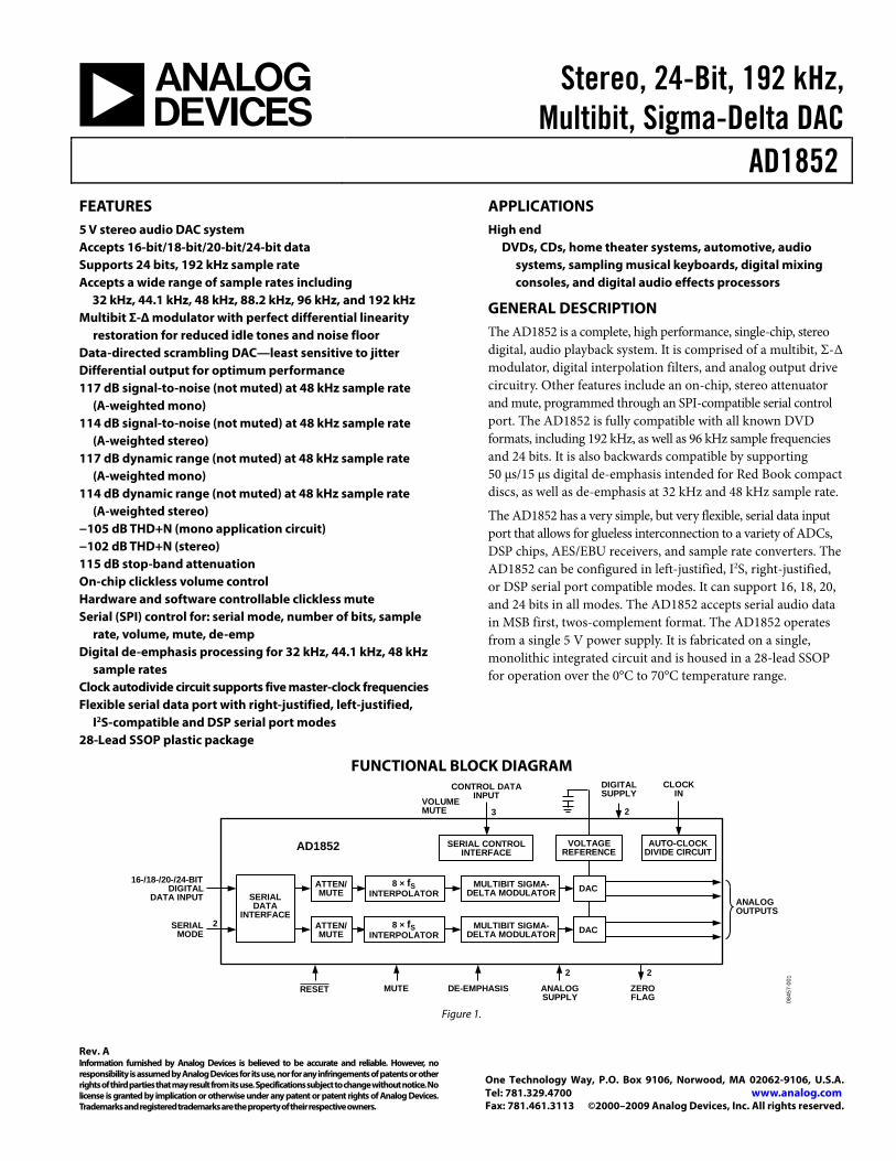
GENERAL DESCRIPTION The AD1852 is a complete, high performance, single-chip, stereo digital, audio playback system. It is comprised of a multibit, Σ-Δ modulator, digital interpolation filters, and analog output drive circuitry. Other features include an on-chip, stereo attenuator and mute, programmed through an SPI-compatible serial control port. The AD1852 is fully compatible with all known DVD formats, including 192 kHz, as well as 96 kHz sample frequencies and 24 bits. It is also backwards compatible by supporting 50 μs/15 μs digital de-emphasis intended for Red Book compact discs, as well as de-emphasis at 32 kHz and 48 kHz sample rate.
The AD1852 has a very simple, but very flexible, serial data input port that allows for glueless interconnection to a variety of ADCs, DSP chips, AES/EBU receivers, and sample rate converters. The AD1852 can be configured in left-justified, I2S, right-justified, or DSP serial port compatible modes. It can support 16, 18, 20, and 24 bits in all modes. The AD1852 accepts serial audio data in MSB first, twos-complement format. The AD1852 operates from a single 5 V power supply. It is fabricated on a single, monolithic integrated circuit and is housed in a 28-lead SSOP for operation over the 0°C to 70°C temperature range.
FUNCTIONAL BLOCK DIAGRAM
SERIALDATA
INTERFACE
8 × fSINTERPOLATOR
SERIAL CONTROLINTERFACE
AUTO-CLOCKDIVIDE CIRCUIT
VOLUMEMUTE
CONTROL DATAINPUT
3 2
DIGITALSUPPLY
CLOCKIN
ANALOGOUTPUTS
22
ZEROFLAG
ANALOGSUPPLY
DE-EMPHASISMUTE
2SERIALMODE
16-/18-/20-/24-BITDIGITAL
DATA INPUT
AD1852
MULTIBIT SIGMA-DELTA MODULATOR
ATTEN/MUTE
VOLTAGEREFERENCE
DAC
8 × fSINTERPOLATOR
MULTIBIT SIGMA-DELTA MODULATOR
ATTEN/MUTE DAC
RESET
0845
7-00
1
Figure 1.
AD1852
Rev. A | Page 2 of 20
TABLE OF CONTENTS Features .............................................................................................. 1
Applications ....................................................................................... 1
General Description ......................................................................... 1
Functional Block Diagram .............................................................. 1
Revision History ............................................................................... 2
Specifications ..................................................................................... 3
Analog Performance .................................................................... 3
Digital I/O (0°C to 70°C) ............................................................. 4
Temperature Range ...................................................................... 4
Power .............................................................................................. 4
Digital Filter Characteristics ....................................................... 4
Group Delay .................................................................................. 4
Digital Timing ............................................................................... 5
Absolute Maximum Ratings ............................................................ 6
Thermal Resistance ...................................................................... 6
ESD Caution .................................................................................. 6
Pin Configuration and Function Descriptions ............................. 7
Typical Performance Characteristics ..............................................9
Theory of Operation ...................................................................... 12
Serial Data Input Port ................................................................ 12
Serial Data Input Mode ............................................................. 12
Master Clock Autodivide Feature ............................................ 13
SPI Register Definitions ............................................................ 13
Register Addresses ...................................................................... 14
Volume Left and Volume Right Registers ............................... 14
SPI Timing................................................................................... 14
Mute ............................................................................................. 14
Control Register ......................................................................... 15
De-Emphasis ............................................................................... 15
Output Impedance ..................................................................... 15
Reset ............................................................................................. 15
Control Signals ........................................................................... 15
Outline Dimensions ....................................................................... 18
Ordering Guide .......................................................................... 18
REVISION HISTORY 11/09—Rev. 0 to Rev. A Changes to Format ............................................................. Universal Changes to Note 1 ............................................................................. 1 Changes to Table 2 ............................................................................ 3 Changes to Table 11 .......................................................................... 7 Changes to Register Addresses Section and Mute Section ....... 14 Changes to Figure 29 ...................................................................... 16 1/00—Revision 0: Initial Version
AD1852
Rev. A | Page 3 of 20
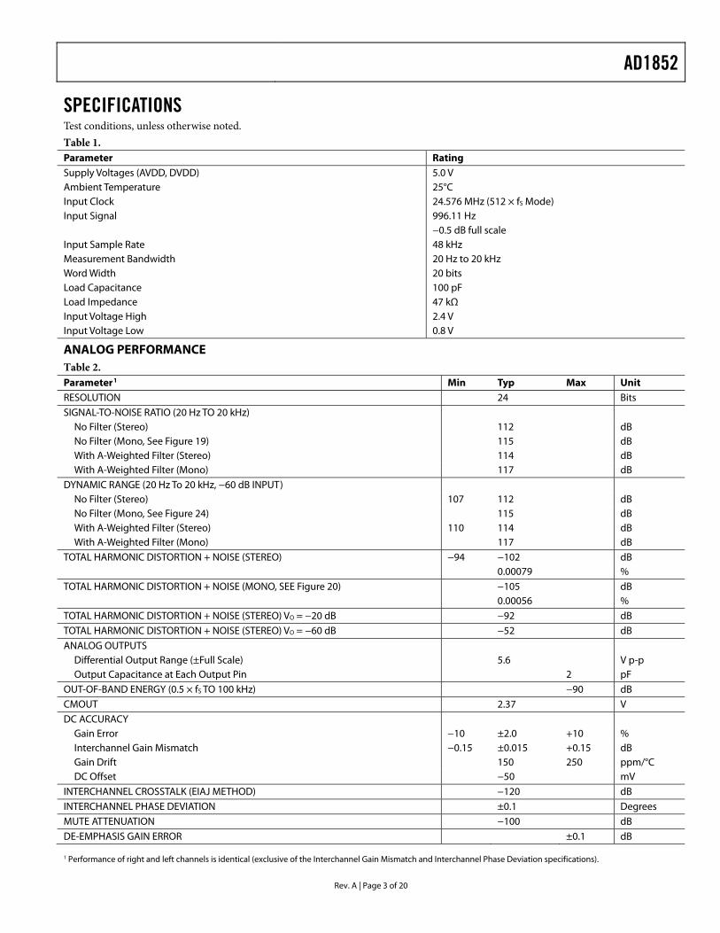
SPECIFICATIONS Test conditions, unless otherwise noted. Table 1. Parameter Rating Supply Voltages (AVDD, DVDD) 5.0 V Ambient Temperature 25°C Input Clock 24.576 MHz (512 × fS Mode) Input Signal 996.11 Hz −0.5 dB full scale Input Sample Rate 48 kHz Measurement Bandwidth 20 Hz to 20 kHz Word Width 20 bits Load Capacitance 100 pF Load Impedance 47 kΩ Input Voltage High 2.4 V Input Voltage Low 0.8 V
ANALOG PERFORMANCE Table 2. Parameter1 Min Typ Max Unit RESOLUTION 24 Bits SIGNAL-TO-NOISE RATIO (20 Hz TO 20 kHz)
No Filter (Stereo) 112 dB No Filter (Mono, See Figure 19) 115 dB With A-Weighted Filter (Stereo) 114 dB With A-Weighted Filter (Mono) 117 dB
DYNAMIC RANGE (20 Hz To 20 kHz, −60 dB INPUT) No Filter (Stereo) 107 112 dB No Filter (Mono, See Figure 24) 115 dB With A-Weighted Filter (Stereo) 110 114 dB With A-Weighted Filter (Mono) 117 dB
TOTAL HARMONIC DISTORTION + NOISE (STEREO) −94 −102 dB 0.00079 % TOTAL HARMONIC DISTORTION + NOISE (MONO, SEE Figure 20) −105 dB 0.00056 % TOTAL HARMONIC DISTORTION + NOISE (STEREO) VO = −20 dB −92 dB TOTAL HARMONIC DISTORTION + NOISE (STEREO) VO = −60 dB −52 dB ANALOG OUTPUTS
Differential Output Range (±Full Scale) 5.6 V p-p Output Capacitance at Each Output Pin 2 pF
OUT-OF-BAND ENERGY (0.5 × fS TO 100 kHz) −90 dB CMOUT 2.37 V DC ACCURACY
Gain Error −10 ±2.0 +10 % Interchannel Gain Mismatch −0.15 ±0.015 +0.15 dB Gain Drift 150 250 ppm/°C DC Offset −50 mV
INTERCHANNEL CROSSTALK (EIAJ METHOD) −120 dB INTERCHANNEL PHASE DEVIATION ±0.1 Degrees MUTE ATTENUATION −100 dB DE-EMPHASIS GAIN ERROR ±0.1 dB 1 Performance of right and left channels is identical (exclusive of the Interchannel Gain Mismatch and Interchannel Phase Deviation specifications).
AD1852
Rev. A | Page 4 of 20
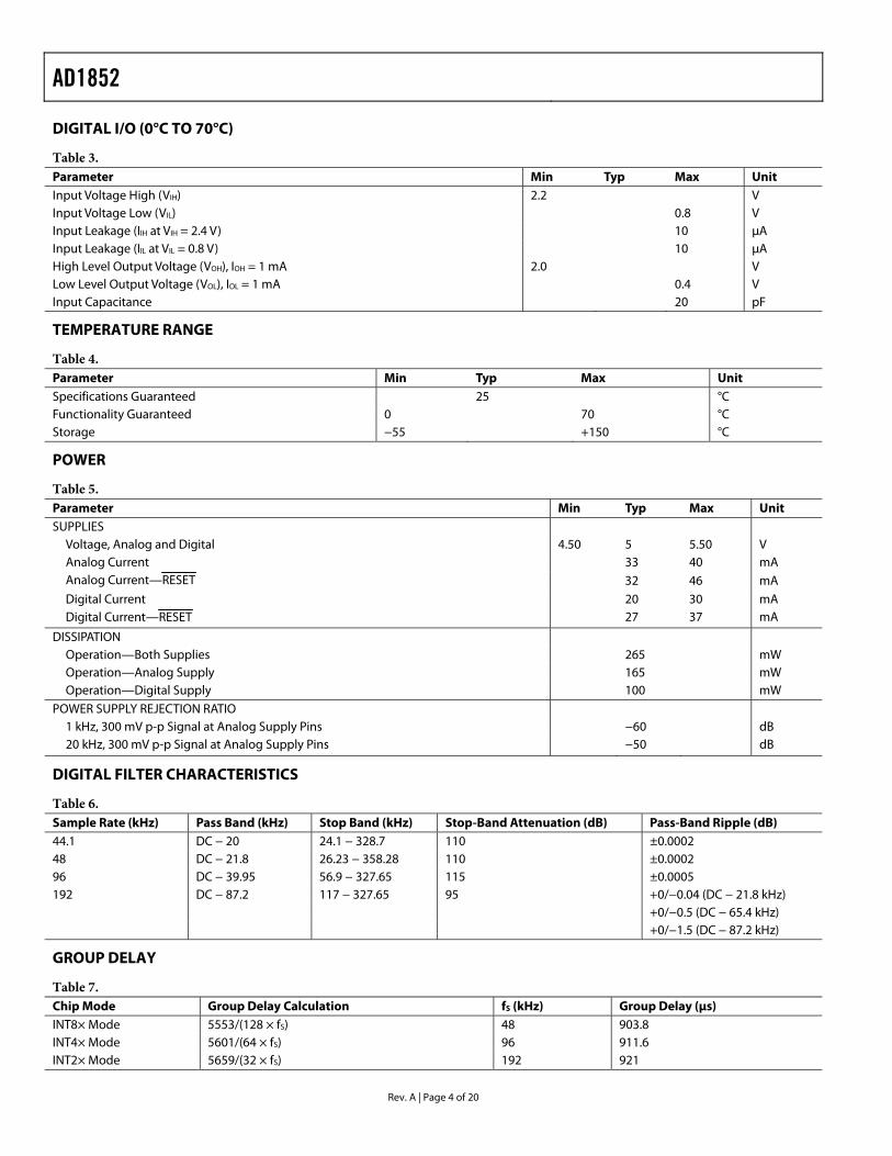
DIGITAL I/O (0°C TO 70°C)
Table 3. Parameter Min Typ Max Unit Input Voltage High (VIH) 2.2 V Input Voltage Low (VIL) 0.8 V Input Leakage (IIH at VIH = 2.4 V) 10 μA Input Leakage (IIL at VIL = 0.8 V) 10 μA High Level Output Voltage (VOH), IOH = 1 mA 2.0 V Low Level Output Voltage (VOL), IOL = 1 mA 0.4 V Input Capacitance 20 pF
TEMPERATURE RANGE
Table 4. Parameter Min Typ Max Unit Specifications Guaranteed 25 °C Functionality Guaranteed 0 70 °C Storage −55 +150 °C
POWER
Table 5. Parameter Min Typ Max Unit SUPPLIES
Voltage, Analog and Digital 4.50 5 5.50 V Analog Current 33 40 mA Analog Current—RESET 32 46 mA Digital Current 20 30 mA Digital Current—RESET 27 37 mA
DISSIPATION Operation—Both Supplies 265 mW Operation—Analog Supply 165 mW Operation—Digital Supply 100 mW
POWER SUPPLY REJECTION RATIO 1 kHz, 300 mV p-p Signal at Analog Supply Pins −60 dB 20 kHz, 300 mV p-p Signal at Analog Supply Pins −50 dB
DIGITAL FILTER CHARACTERISTICS
Table 6. Sample Rate (kHz) Pass Band (kHz) Stop Band (kHz) Stop-Band Attenuation (dB) Pass-Band Ripple (dB) 44.1 DC − 20 24.1 − 328.7 110 ±0.0002 48 DC − 21.8 26.23 − 358.28 110 ±0.0002 96 DC − 39.95 56.9 − 327.65 115 ±0.0005 192 DC − 87.2 117 − 327.65 95 +0/−0.04 (DC − 21.8 kHz) +0/−0.5 (DC − 65.4 kHz) +0/−1.5 (DC − 87.2 kHz)
GROUP DELAY
Table 7. Chip Mode Group Delay Calculation fS (kHz) Group Delay (μs) INT8× Mode 5553/(128 × fS) 48 903.8 INT4× Mode 5601/(64 × fS) 96 911.6 INT2× Mode 5659/(32 × fS) 192 921
AD1852
Rev. A | Page 5 of 20
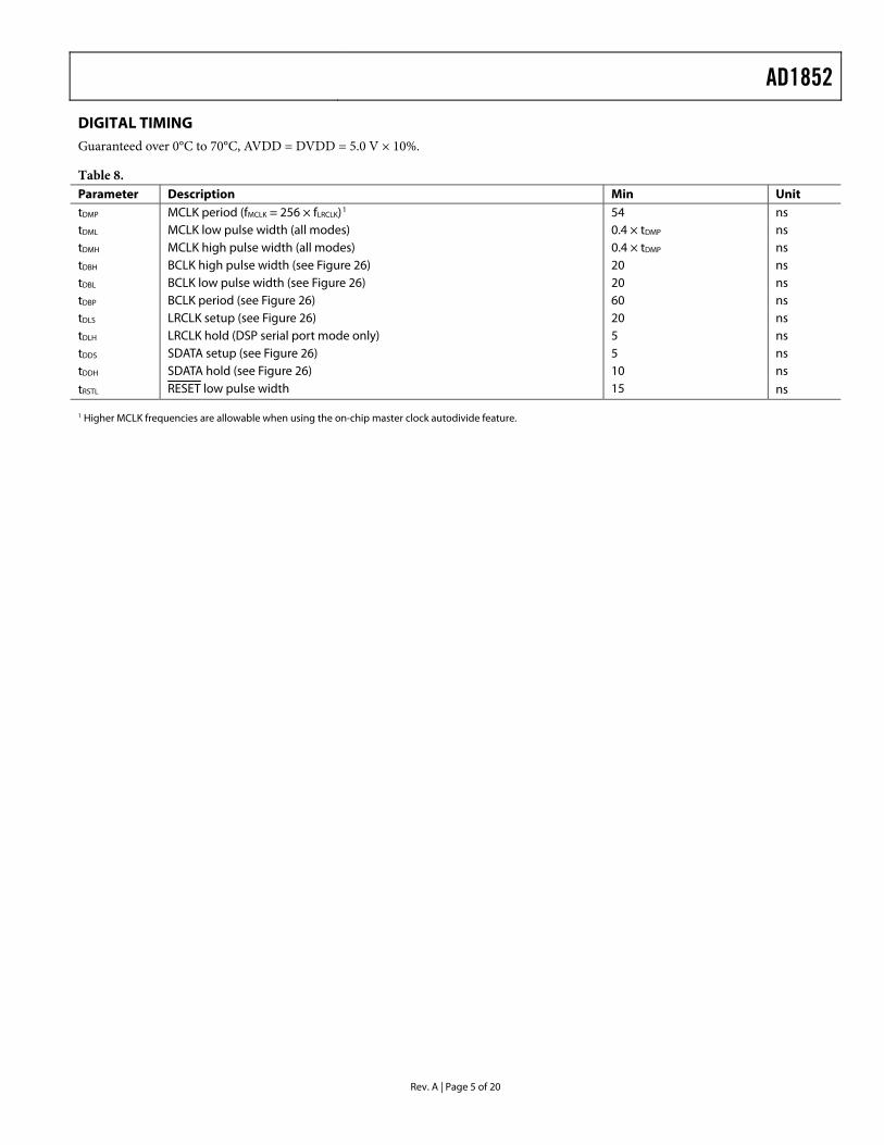
DIGITAL TIMING Guaranteed over 0°C to 70°C, AVDD = DVDD = 5.0 V × 10%.
Table 8. Parameter Description Min Unit tDMP MCLK period (fMCLK = 256 × fLRCLK)1 54 ns tDML MCLK low pulse width (all modes) 0.4 × tDMP ns tDMH MCLK high pulse width (all modes) 0.4 × tDMP ns tDBH BCLK high pulse width (see Figure 26) 20 ns tDBL BCLK low pulse width (see Figure 26) 20 ns tDBP BCLK period (see Figure 26) 60 ns tDLS LRCLK setup (see Figure 26) 20 ns tDLH LRCLK hold (DSP serial port mode only) 5 ns tDDS SDATA setup (see Figure 26) 5 ns tDDH SDATA hold (see Figure 26) 10 ns tRSTL RESET low pulse width 15 ns 1 Higher MCLK frequencies are allowable when using the on-chip master clock autodivide feature.
AD1852
Rev. A | Page 6 of 20
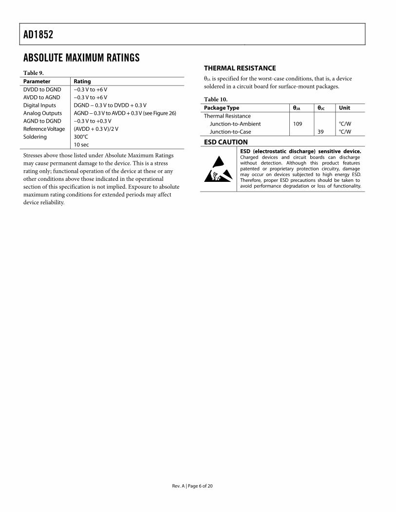
ABSOLUTE MAXIMUM RATINGS Table 9. Parameter Rating DVDD to DGND −0.3 V to +6 V AVDD to AGND −0.3 V to +6 V Digital Inputs DGND − 0.3 V to DVDD + 0.3 V Analog Outputs AGND − 0.3 V to AVDD + 0.3 V (see Figure 26) AGND to DGND −0.3 V to +0.3 V Reference Voltage (AVDD + 0.3 V)/2 V Soldering 300°C 10 sec
Stresses above those listed under Absolute Maximum Ratings may cause permanent damage to the device. This is a stress rating only; functional operation of the device at these or any other conditions above those indicated in the operational section of this specification is not implied. Exposure to absolute maximum rating conditions for extended periods may affect device reliability.
THERMAL RESISTANCE θJA is specified for the worst-case conditions, that is, a device soldered in a circuit board for surface-mount packages.
Table 10. Package Type θJA θJC Unit Thermal Resistance
Junction-to-Ambient 109 °C/W Junction-to-Case 39 °C/W
ESD CAUTION
AD1852
Rev. A | Page 7 of 20
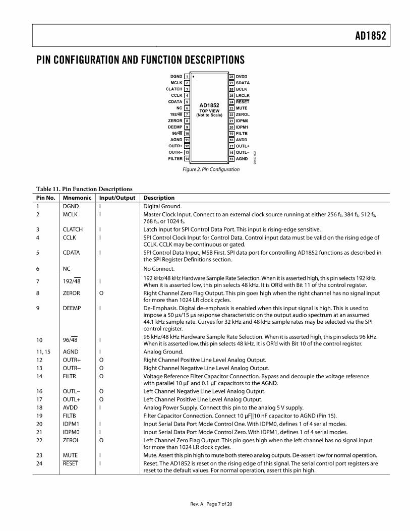
PIN CONFIGURATION AND FUNCTION DESCRIPTIONS
DGND 1
MCLK 2
CLATCH 3
CCLK 4
DVDD28
SDATA27
BCLK26
LRCLK25
CDATA 5
NC 6
192/48 7
RESET24
MUTE23
ZEROL22
ZEROR 8 IDPM021
DEEMP 9 IDPM120
96/48 10 FILTB19
AGND 11 AVDD18
OUTR+ 12 OUTL+17
OUTR– 13 OUTL–16
FILTER 14 AGND15
TOP VIEW(Not to Scale)
AD1852
0845
7-00
2
Figure 2. Pin Configuration
Table 11. Pin Function Descriptions Pin No. Mnemonic Input/Output Description 1 DGND I Digital Ground. 2 MCLK I Master Clock Input. Connect to an external clock source running at either 256 fS, 384 fS, 512 fS,
768 fS, or 1024 fS. 3 CLATCH I Latch Input for SPI Control Data Port. This input is rising-edge sensitive. 4 CCLK I SPI Control Clock Input for Control Data. Control input data must be valid on the rising edge of
CCLK. CCLK may be continuous or gated. 5 CDATA I SPI Control Data Input, MSB First. SPI data port for controlling AD1852 functions as described in
the SPI Register Definitions section.
6 NC No Connect.
7 192/48 I 192 kHz/48 kHz Hardware Sample Rate Selection. When it is asserted high, this pin selects 192 kHz. When it is asserted low, this pin selects 48 kHz. It is OR’d with Bit 11 of the control register.
8 ZEROR O Right Channel Zero Flag Output. This pin goes high when the right channel has no signal input for more than 1024 LR clock cycles.
9 DEEMP I De-Emphasis. Digital de-emphasis is enabled when this input signal is high. This is used to impose a 50 μs/15 μs response characteristic on the output audio spectrum at an assumed 44.1 kHz sample rate. Curves for 32 kHz and 48 kHz sample rates may be selected via the SPI control register.
10 96/48 I 96 kHz/48 kHz Hardware Sample Rate Selection. When it is asserted high, this pin selects 96 kHz. When it is asserted low, this pin selects 48 kHz. It is OR’d with Bit 10 of the control register.
11, 15 AGND I Analog Ground. 12 OUTR+ O Right Channel Positive Line Level Analog Output. 13 OUTR− O Right Channel Negative Line Level Analog Output. 14 FILTR O Voltage Reference Filter Capacitor Connection. Bypass and decouple the voltage reference
with parallel 10 μF and 0.1 μF capacitors to the AGND. 16 OUTL− O Left Channel Negative Line Level Analog Output. 17 OUTL+ O Left Channel Positive Line Level Analog Output. 18 AVDD I Analog Power Supply. Connect this pin to the analog 5 V supply. 19 FILTB Filter Capacitor Connection. Connect 10 μF||10 nF capacitor to AGND (Pin 15). 20 IDPM1 I Input Serial Data Port Mode Control One. With IDPM0, defines 1 of 4 serial modes. 21 IDPM0 I Input Serial Data Port Mode Control Zero. With IDPM1, defines 1 of 4 serial modes. 22 ZEROL O Left Channel Zero Flag Output. This pin goes high when the left channel has no signal input
for more than 1024 LR clock cycles. 23 MUTE I Mute. Assert this pin high to mute both stereo analog outputs. De-assert low for normal operation. 24 RESET I Reset. The AD1852 is reset on the rising edge of this signal. The serial control port registers are
reset to the default values. For normal operation, assert this pin high.
AD1852
Rev. A | Page 8 of 20
Pin No. Mnemonic Input/Output Description
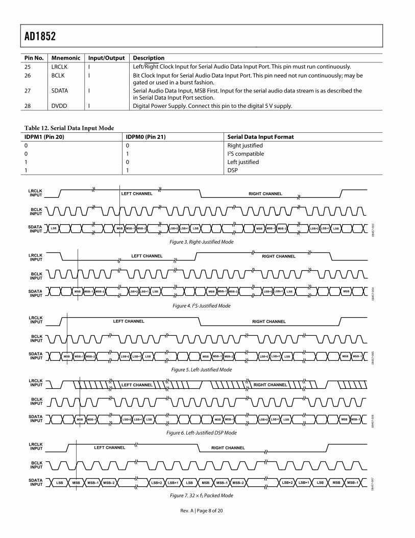
25 LRCLK I Left/Right Clock Input for Serial Audio Data Input Port. This pin must run continuously.
26 BCLK I Bit Clock Input for Serial Audio Data Input Port. This pin need not run continuously; may be gated or used in a burst fashion.
27 SDATA I Serial Audio Data Input, MSB First. Input for the serial audio data stream is as described the in Serial Data Input Port section.
28 DVDD I Digital Power Supply. Connect this pin to the digital 5 V supply.
Table 12. Serial Data Input Mode IDPM1 (Pin 20) IDPM0 (Pin 21) Serial Data Input Format 0 0 Right justified 0 1 I2S compatible 1 0 Left justified 1 1 DSP
LEFT CHANNEL RIGHT CHANNEL
LSBMSB–2 LSB+2 LSB+1MSB–1 MSB–2MSB–1MSB LSB+2 LSB+1 LSBMSBLSB
BCLKINPUT
SDATAINPUT
LRCLKINPUT
0845
7-00
3
Figure 3. Right-Justified Mode
MSB–2MSB–1MSB LSB+2 LSB+1 LSB
LEFT CHANNEL RIGHT CHANNEL
BCLKINPUT
SDATAINPUT
LRCLKINPUT
MSBLSBMSB–2 LSB+2 LSB+1MSB–1MSB
0845
7-00
4
Figure 4. I2S-Justified Mode
LEFT CHANNEL RIGHT CHANNEL
BCLKINPUT
SDATAINPUT
LRCLKINPUT
MSB–2MSB–1MSB LSB+2 LSB+1 LSB MSB MSB–1LSBMSB–2 LSB+2 LSB+1MSB–1MSB
0845
7-00
5
Figure 5. Left-Justified Mode
LEFT CHANNEL RIGHT CHANNEL
BCLKINPUT
SDATAINPUT
LRCLKINPUT
MSB–1MSB LSB+2 LSB+1 LSB MSB MSB–1LSBLSB+2 LSB+1MSB–1MSB
0845
7-00
6
Figure 6. Left-Justified DSP Mode
LEFT CHANNEL RIGHT CHANNEL
MSBLSBMSB–1 MSB–2 LSB+2 LSB+1 MSB–1 MSB–2 MSBLSBLSB+2 LSB+1 MSB–1LSB MSB
BCLKINPUT
SDATAINPUT
LRCLKINPUT
0845
7-00
7
Figure 7. 32 × fS Packed Mode
AD1852
Rev. A | Page 9 of 20
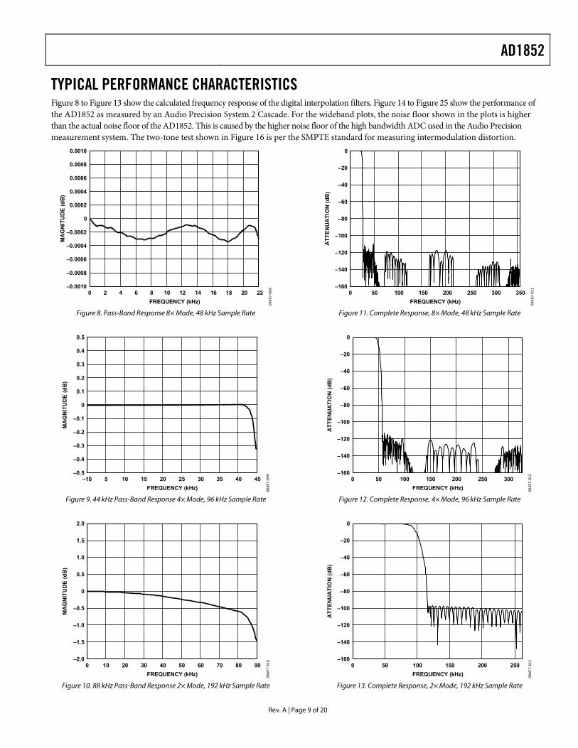
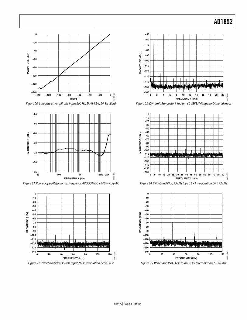
TYPICAL PERFORMANCE CHARACTERISTICS Figure 8 to Figure 13 show the calculated frequency response of the digital interpolation filters. Figure 14 to Figure 25 show the performance of the AD1852 as measured by an Audio Precision System 2 Cascade. For the wideband plots, the noise floor shown in the plots is higher than the actual noise floor of the AD1852. This is caused by the higher noise floor of the high bandwidth ADC used in the Audio Precision measurement system. The two-tone test shown in Figure 16 is per the SMPTE standard for measuring intermodulation distortion.
0.0010
0.0008
0.0006
0.0004
0.0002
0
–0.0002
–0.0004
–0.0006
–0.0008
–0.00100 2 4 6 8 10 12 14 16 18 20 22
MA
GN
ITU
DE
(dB
)
FREQUENCY (kHz) 0845
7-00
8
0
–160
–140
–120
–100
–80
–60
–40
–20
0 50 100 150 200 250 300 350
ATT
ENU
ATI
ON
(dB
)
FREQUENCY (kHz) 0845
7-01
1
Figure 8. Pass-Band Response 8× Mode, 48 kHz Sample Rate
Figure 11. Complete Response, 8× Mode, 48 kHz Sample Rate
0.5
0.4
0.3
0.2
0.1
0
–0.1
–0.2
–0.3
–0.4
–0.5–10 5 10 15 20 25 30 35 40 45
MA
GN
ITU
DE
(dB
)
FREQUENCY (kHz) 0845
7-00
9
0
–160
–140
–120
–100
–80
–60
–40
–20
0 50 100 150 200 250 300
ATT
ENU
ATI
ON
(dB
)
FREQUENCY (kHz) 0845
7-01
2
Figure 9. 44 kHz Pass-Band Response 4× Mode, 96 kHz Sample Rate
Figure 12. Complete Response, 4× Mode, 96 kHz Sample Rate
2.0
1.5
1.0
0.5
0
–0.5
–1.0
–1.5
–2.00 10 20 30 40 50 60 70 80 90
MA
GN
ITU
DE
(dB
)
FREQUENCY (kHz) 0845
7-01
0
0
–160
–140
–120
–100
–80
–60
–40
–20
0 50 100 150 200 250
ATT
ENU
ATI
ON
(dB
)
FREQUENCY (kHz) 0845
7-01
3
Figure 10. 88 kHz Pass-Band Response 2× Mode, 192 kHz Sample Rate
Figure 13. Complete Response, 2× Mode, 192 kHz Sample Rate

AD1852
Rev. A | Page 10 of 20
–50
–120
–110
–100
–90
–80
–70
–60
10 100 1k 10k 20k
MA
GN
ITU
DE
(dB
r)
FREQUENCY (Hz) 0845
7-01
4Figure 14. THD vs. Frequency Input @ −3 dBFS, SR 48 kHz
2
–12
–10
–8
–6
–4
–2
0
10 100 1k 10k 20k
MA
GN
ITU
DE
(dB
r)
FREQUENCY (Hz) 0845
7-01
5
Figure 15. Normal De-Emphasis Frequency Response Input @ −10 dBFS, SR 48 kHz
–10
–150
–130
–110
–90
–70
–50
–30
0 2 4 6 8 10 12 14 16 18 20 22
MA
GN
ITU
DE
(dB
r)
FREQUENCY (kHz) 0845
7-01
6
Figure 16. SMPTE/DIN 4:1 IMD 60 Hz/7 kHz @ 0 dBFS
0
–10
–20
–30
–40
–50
–60
–70
–80
–90
–110
–100
–120 0–20–40–60–80–100
MA
GN
ITU
DE
(dB
)
FREQUENCY (kHz) 0845
7-01
7
Figure 17. THD + N Ratio vs. Amplitude Input 1 kHz, SR 48 kS/s, 24-Bit
–90
–160
–150
–140
–130
–120
–110
–100
0 2 4 6 8 10 12 14 16 18 20 22
MA
GN
ITU
DE
(dB
r)
FREQUENCY (kHz) 0845
7-01
8
Figure 18. Noise Floor for Zero Input, SR 48 kHz
0–10–20–30–40–50–60–70–80–90
–100–110–120–130–140–150
0 2 4 6 8 10 12 14 16 18 20 22
MA
GN
ITU
DE
(dB
r)
FREQUENCY (kHz) 0845
7-01
9
Figure 19. Input 0 dBFS @ 1 kHz, BW 10 Hz to 22 kHz, SR 48 kHz
AD1852
Rev. A | Page 11 of 20
0
–140
–120
–100
–80
–60
–40
–20
–140 –20–40–60–80–100–120 0
MA
GN
ITU
DE
(dB
r)
(dBFS) 0845
7-02
0
–50
–160
–150
–140
–130
–120
–110
–100
–90
–80
–70
–60
0 2 4 6 8 10 12 14 16 18 20 22
MA
GN
ITU
DE
(dB
r)
FREQUENCY (kHz) 0845
7-02
3
Figure 20. Linearity vs. Amplitude Input 200 Hz, SR 48 kS/s, 24-Bit Word
Figure 23. Dynamic Range for 1 kHz @ −60 dBFS, Triangular Dithered Input
–64
–76
–74
–72
–70
–68
–66
10 100 1k 10k 20k
MA
GN
ITU
DE
(dB
r)
FREQUENCY (Hz) 0845
7-02
10
–160
–140–150
–130–120–110–100
–90–80–70–60–50–40–30–20–10
0 875706560555045403530252015105
MA
GN
ITU
DE
(dB
r)
FREQUENCY (kHz)0
0845
7-02
4
Figure 21. Power Supply Rejection vs. Frequency, AVDD 5 V DC + 100 mV p-p AC
Figure 24. Wideband Plot, 75 kHz Input, 2× Interpolation, SR 192 kHz
0
–140–130–120–110–100
–90–80–70–60–50–40–30–20–10
0 110080604020
MA
GN
ITU
DE
(dB
r)
FREQUENCY (kHz)20
0
–140–130–120–110–100
–90–80–70–60–50–40–30–20–10
0 110080604020
MA
GN
ITU
DE
(dB
r)
FREQUENCY (kHz)20
0845
7-02
5
0845
7-02
2
Figure 22. Wideband Plot, 15 kHz Input, 8× Interpolation, SR 48 kHz
Figure 25. Wideband Plot, 37 kHz Input, 4× Interpolation, SR 96 kHz
AD1852
Rev. A | Page 12 of 20
THEORY OF OPERATION SERIAL DATA INPUT PORT The flexible, serial data input port of the AD1852 accepts data in twos-complement, MSB-first format. The left channel data field always precedes the right channel data field. The serial mode is set by either using the external mode pins (IDPM0, Pin 21 and IDPM1, Pin 20) or the mode select bits (Bit 4 and Bit 5) in the SPI control register. To control the serial mode using the external mode pins, the SPI mode select bits should be set to zero (the default mode at power-up). To control the serial mode using the SPI mode select bits, the external mode control pins should be grounded.
In all modes, except for right-justified mode, the serial port accepts an arbitrary number of bits up to 24. Extra bits do not cause an error, but they are truncated internally. In right-justified mode, use Bit 8 and Bit 9 of the SPI control register to set the word length to 16 bits, 20 bits, or 24 bits. The default mode at power-up is 24-bit mode. When the SPI control port is not being used, the SPI pins (CLATCH, CCLK, and CDATA [Pin 3, Pin 4, and Pin 5]) should be tied low.
SERIAL DATA INPUT MODE The AD1852 uses two multiplexed input pins to control the mode configuration of the input data port mode (see Table 12).
Figure 3 shows the right-justified mode (16 bits shown). LRCLK is high for the left channel and low for the right channel. Data is valid on the rising edge of BCLK.
In normal operation, there are 64-bit clocks per frame (or 32 per half frame). When the SPI word length control bits (Bit 8 and Bit 9 in the SPI control register) are set to 24 bits (0:0), the serial port begins to accept data starting at the eighth bit clock pulse after the LRCLK transition. When the word length control bits are set to 20-bit mode, data is accepted starting at the 12th bit clock position. In 16-bit mode, data is accepted starting at the 16th bit clock position. These delays are independent of the number of bit clocks per frame, and therefore, other data formats are possible using the delay values previously described. For detailed timing, see Figure 26.
Figure 4 shows the I2S mode. LRCLK is low for the left channel and high for the right channel. Data is valid on the rising edge of BCLK. The MSB is left justified to an LRCLK transition but with a single BCLK period delay. The I2S mode can be used to accept any number of bits up to 24.
Figure 5 shows the left-justified mode. LRCLK is high for the left channel, and low for the right channel. Data is valid on the rising edge of BCLK. The MSB is left justified to an LRCLK transition, with no MSB delay. The left-justified mode can accept any word length up to 24 bits, and any number of bit clocks from two times the word length to 64-bit clocks per frame.
Figure 6 shows the DSP serial port mode. LRCLK must pulse high for at least one bit clock period before the MSB of the left channel is valid, and LRCLK must pulse high again for at least one bit clock period before the MSB of the right channel is valid. Data is valid on the falling edge of BCLK. The DSP serial port mode can be used with any word length up to 24 bits.
In this mode, it is the responsibility of the DSP to ensure that the left data is transmitted with the first LRCLK pulse and that synchronism is maintained from that point forward.
Note that the AD1852 is capable of a 32 × fS BCLK frequency packed mode, where the MSB is left justified to an LRCLK transition, and the LSB is right justified to the opposite LRCLK transition. LRCLK is high for the left channel and low for the right channel. Data is valid on the rising edge of BLCK. Packed mode can be used when the AD1852 is programmed in right-justified or left-justified mode. Packed mode is shown is Figure 7.

AD1852
Rev. A | Page 13 of 20
BCLK
LRCLK
SDATALEFT-JUSTIFIED
MODE
SDATAI2C-JUSTIFIED
MODE
SDATARIGHT-JUSTIFIED
MODELSB
tDBH tDBP
tDBL
tDLS
tDDS
tDDH
tDDS
tDDH
tDDS
tDDH
tDDS
tDDH
MSB MSB – 1
MSB
MSB
8-BIT CLOCKS(24-BIT DATA)
12-BIT CLOCKS(20-BIT DATA)
16-BIT CLOCKS(16-BIT DATA) 08
457-
026
Figure 26. Serial Data Port Timing
Table 13. Allowable MCLK Frequencies and Internal Delta Clock Rates Chip Mode Allowable Master Clock Frequencies Nominal Input Sample Rate (kHz) Internal Sigma-Delta Clock Rate INT 8× Mode 256 × fS, 384 × fS, 512 × fS, 768 × fS, 1024 × fS 48 128 × fS INT 4× Mode 128 × fS, 192 × fS, 256 × fS, 384 × fS, 512 × fS 96 64 × fS INT 2× Mode 64 × fS, 96 × fS, 128 × fS, 192 × fS, 256 × fS 192 32 × fS
D15 D14 D0
tCHD
tCLHtCLL
tCLSU
tCCL
tCCH
tCSU
CDATA
CCLK
CLATCH
0845
7-02
7
Figure 27. Serial Control Port Timing
MASTER CLOCK AUTODIVIDE FEATURE The AD1852 has a circuit that autodetects the relationship between the master clock and the incoming serial data and internally sets the correct divide ratio to run the interpolator and modulator. The allowable frequencies for each mode are shown in Table 13. Master clock should be synchronized with LRCLK; however, phase relation between master clock and LRCLK is not critical.
SPI REGISTER DEFINITIONS The SPI port allows flexible control of many chip parameters. It is organized around three registers: a left-channel volume register, a right-channel volume register, and a control register. Each write operation to the AD1852 SPI control port requires 16 bits of serial data in MSB-first format. The bottom two bits are used to select one of three registers, and the top 14 bits are then written to that register. This allows a write to one of the three registers in a single 16-bit transaction.
The SPI CCLK signal is used to clock in the data. The incoming data should change on the falling edge of this signal. At the end of the 16 CCLK periods, the CLATCH signal should rise to clock the data internally into the AD1852.
The serial control port timing is shown in Figure 27, and the SPI digital timing values are listed in Table 14.
Table 14. SPI Digital Timing Parameter Description Value tCCH CCLK high pulse width 40 ns tCCL CCLK low pulse width 40 ns tCSU CDATA setup time 10 ns tCHD CDATA hold time 10 ns tCLL CLATCH low pulse width 10 ns tCLH CLATCH high pulse width 10 ns tCLSU CLATCH setup time 4 × tMCLK
AD1852
Rev. A | Page 14 of 20
REGISTER ADDRESSES The lowest two bits of the 16-bit serial control data word are decoded as the address of the register into which the upper 14 bits are written. These bits are defined in Table 15.
Table 15. AD1852 Registers Bit 1 Bit 0 Register 0 0 Volume left 1 0 Volume right 0 1 Control register
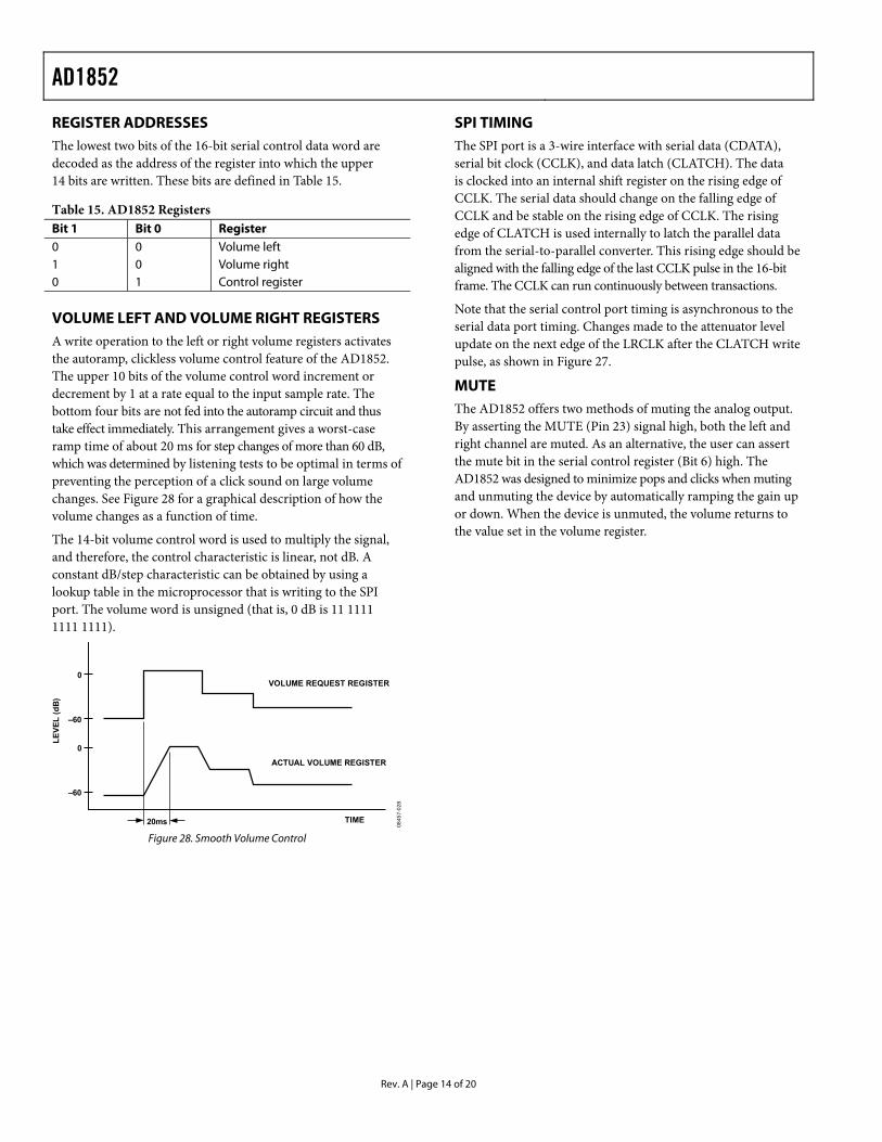
VOLUME LEFT AND VOLUME RIGHT REGISTERS A write operation to the left or right volume registers activates the autoramp, clickless volume control feature of the AD1852. The upper 10 bits of the volume control word increment or decrement by 1 at a rate equal to the input sample rate. The bottom four bits are not fed into the autoramp circuit and thus take effect immediately. This arrangement gives a worst-case ramp time of about 20 ms for step changes of more than 60 dB, which was determined by listening tests to be optimal in terms of preventing the perception of a click sound on large volume changes. See Figure 28 for a graphical description of how the volume changes as a function of time.
The 14-bit volume control word is used to multiply the signal, and therefore, the control characteristic is linear, not dB. A constant dB/step characteristic can be obtained by using a lookup table in the microprocessor that is writing to the SPI port. The volume word is unsigned (that is, 0 dB is 11 1111 1111 1111).
20ms TIME
–60
–60
0
0
LEVE
L (d
B)
VOLUME REQUEST REGISTER
ACTUAL VOLUME REGISTER
0845
7-02
8
Figure 28. Smooth Volume Control
SPI TIMING The SPI port is a 3-wire interface with serial data (CDATA), serial bit clock (CCLK), and data latch (CLATCH). The data is clocked into an internal shift register on the rising edge of CCLK. The serial data should change on the falling edge of CCLK and be stable on the rising edge of CCLK. The rising edge of CLATCH is used internally to latch the parallel data from the serial-to-parallel converter. This rising edge should be aligned with the falling edge of the last CCLK pulse in the 16-bit frame. The CCLK can run continuously between transactions.
Note that the serial control port timing is asynchronous to the serial data port timing. Changes made to the attenuator level update on the next edge of the LRCLK after the CLATCH write pulse, as shown in Figure 27.
MUTE The AD1852 offers two methods of muting the analog output. By asserting the MUTE (Pin 23) signal high, both the left and right channel are muted. As an alternative, the user can assert the mute bit in the serial control register (Bit 6) high. The AD1852 was designed to minimize pops and clicks when muting and unmuting the device by automatically ramping the gain up or down. When the device is unmuted, the volume returns to the value set in the volume register.
AD1852
Rev. A | Page 15 of 20
CONTROL REGISTER Table 16 shows the functions of the control register. The control register is addressed by having a 01 in the bottom two bits of the 16-bit SPI word. The top 14 bits are then used for the control register.
DE-EMPHASIS The AD1852 has a built-in, de-emphasis filter that can be used to decode CDs that have been encoded with the standard Red Book 50 μs/15 μs emphasis response curve. Three curves are available; one each for the 32 kHz, 44.1 kHz, and 48 kHz sampling rates. The external DEEMP pin (Pin 9) turns on the 44.1 kHz de-emphasis filter. The other filters may be selected by writing to Control Bit 2 and Control Bit 3 in the control register. If the SPI port is used to control the de-emphasis filter, the external DEEMP pin should be tied low.
OUTPUT IMPEDANCE The output impedance of the AD1852 is 65 Ω ± 30%.
RESET The AD1852 may be reset either by a dedicated hardware pin (RESET, Pin 24) or by software via the SPI control port. When reset is active, normal operation of the AD1852 is suspended, and the outputs assume midscale values. The AD1852 should always be reset at power up. The RESET function should be active for a minimum of 64 master clock periods. When the RESET function becomes inactive, normal operation continues after a delay equal to the group delay, plus three MCLK periods.
Using the RESET pin, the internal registers are set to their default values, when the RESET pin is active low. When RESET rises, the default operation is enabled. Alternatively, the internal registers can be reset to their default values by setting Bit 7 of the internal control register high. When Bit 7 is reset low, default operation continues. The software reset differs from the hardware reset because the soft reset does not affect the values stored in the SPI registers.
CONTROL SIGNALS The IDPM0 and IDPM1 control inputs are normally connected high or low to establish the operating state of the AD1852, as described in Table 12. They can be changed dynamically (and asynchronously to LRCLK and the master clock), but it is possible that a click or pop sound will result during the transition from one serial mode to another. If possible, the AD1852 should be placed in mute before such a change is made.
Table 16. Control Register Functions Bit Number Function Bit 11 INT 2× mode OR’d with Pin 7 (192/48); default = 0
Bit 10 INT 4× mode OR’d with Pin 10 (96/48); default = 0
Bit 9:8 Number of bits in right-justified serial mode 0:0 = 24 0:1 = 20 1:0 = 16 Default = 0:0 Bit 7 Reset; default = 0 Bit 6 Soft mute OR’d with pin; default = 0 Bit 5:4 Serial mode OR’d with mode pins; IDPM1:IDPM0 0:0 = right-justified 0:1 = I2S 1:0 = left-justified 1:1 = DSP mode Default = 0:0 Bit 3:2 De-emphasis filter select 0:0 = no filter 0:1 = 44.1 kHz filter 1:0 = 32 kHz filter 1:1 = 48 kHz filter Default = 0:0
AD1852
Rev. A | Page 16 of 20
U1AD1852JRS
96/48
192/48NC
SDATALRCLK
BCLK
MCLK
IDPM0IDPM1
DEEMP
MUTE
CLATCH
CCLK
CDATA
ZERORZEROL
RESET DGND AGND
OUTL+
OUTL–
OUTR+
OUTR–
FILTB
AVDDDVDD
C9220pFNP0
R91.96kΩ
R111.96kΩ
C10220pFNP0
R161.87kΩ
R101.96kΩ
R20200Ω J11
LEFTOUTC15
10nFNP0
U3BSSM2135R8
1.96kΩ
C141nFNP0
R171.87kΩ
C131nFNP0
C11220pFNP0
R131.96kΩ
R151.96kΩ
C12220pFNP0
R181.87kΩ
R141.96kΩ
R21200Ω J21
RIGHTOUTC18
10nFNP0
U3ASSM2135R12
1.96kΩ
C171nFNP0
R191.87kΩ
C161nFNP0
C5100nF
+AVCC
–AVCC
C6100nF
3RD ORDER LP BESSEL FILTERCORNER FREQUENCY: 75kHzGROUP DELAY: ~3.5µs
CLATCH
CCLK
CDATAZR
ZL
RESET
U2AHC04
U2BHC04
AGND
FB1600Z
FILTR
C810µF
C1100nF
C710µF
CR1ZEROLEFT
C4100nF
CR2ZERORIGHT
R6221Ω
R7221Ω1
3
2
4
C3100nF
DVDD
C2100nF
AVDD
MUTE
DEEMP
BCLKMCLK
SDATA
LRCLK
R410kΩ
R510kΩ
DVDD
I/FMODE
JP21
I/F MODE IDPM1 IDPM0RJ, 16-BIT 0 0I2S 0 1RJ, 20-BIT 1 0RJ, 24-BIT 1 1
DGND
JP11
MCLK/SR SEL
R310kΩ
R210kΩ
R110kΩ
DVDD
AD1852 STEREO DAC
OUTPUT BUFFERS AND LP FILTERS
ZL
ZR
MCLK/SR SELECTSELECT RATE 192/48 96/48SPDIF 44.1kHz TO 48kHz 0 0DIRECT 88.2kHz TO 96kHz 0 1DIRECT 176.4kHz TO 192kHz 1 0
0845
7-02
9
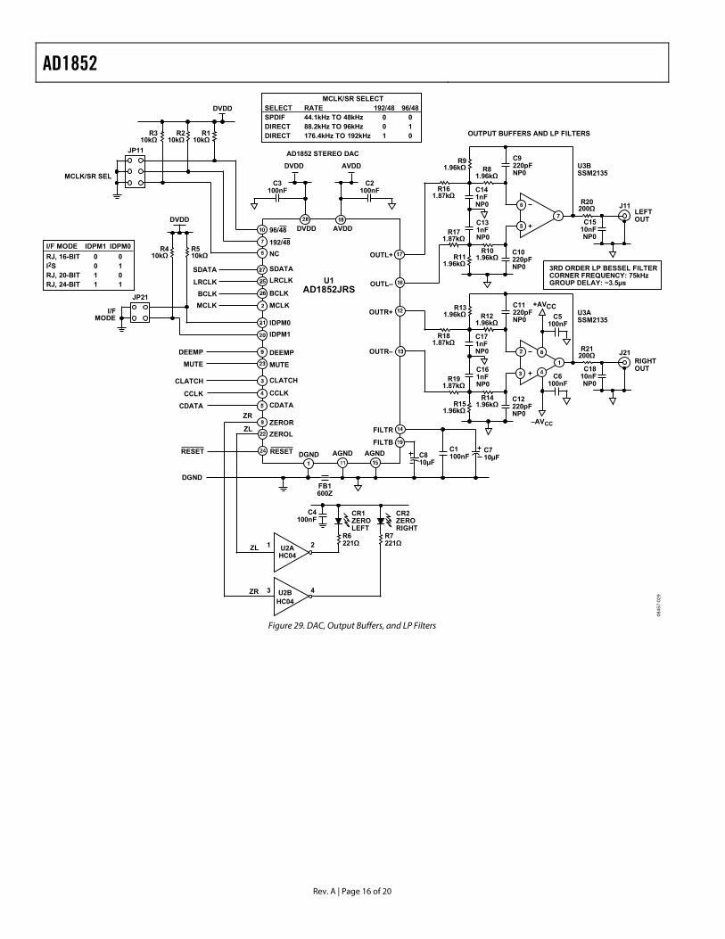
Figure 29. DAC, Output Buffers, and LP Filters

AD1852
Rev. A | Page 17 of 20
AD1852
R23.01kΩ
R131.00kΩ
R33.01kΩ
R141.00kΩ
R13.01kΩ
R43.01kΩ R6
3.01kΩ
C2270pF
R53.01kΩ C2
270pF
C71.5nF
R17549Ω
C52.2nF
R1953.6kΩ
1
0AD797
AD1852
R83.01kΩ
R151.00kΩ
R93.01kΩ
R161.00kΩ
R73.01kΩ
R103.01kΩ R12
3.01kΩ
C4270pF
R113.01kΩ C3
270pF
C91.5nF
R18549Ω
C62.2nF
R2053.6kΩ
1
0
AD797
SDATALRCLKBCLK
SDATALRCLKBCLK
L+
L–
R+
R–
L+
L–
R+
R–
0°
180°R
R
0°
180°L
L
MCLK
DATA SEPARATOROUTPUT
LRCLK
SDATA
LRCLK
LSDATA
RDATA
Ln Rn Ln+1 Rn+1 Ln+2 Rn+2
Ln Ln Ln+1 Ln+1 Ln+2
Rn Rn Rn+1 Rn+1 Rn+2 Rn+2
Ln+2
SDATA
LRCLK
BCLK
C101.5nF
C81.5nF
I2S LEFT/RIGHTDATA SEPARATOR
AND INVERTER
I2S INPUT TODATA SEPARATOR
0845
7-03
0
Figure 30. Mono Application Circuit
AD1852
Rev. A | Page 18 of 20
OUTLINE DIMENSIONS
COMPLIANT TO JEDEC STANDARDS MO-150-AH 0601
06-A
28 15
141
10.5010.209.90
8.207.807.40
5.605.305.00
SEATINGPLANE
0.05 MIN
0.65 BSC
2.00 MAX
0.380.22COPLANARITY
0.10
1.851.751.65
0.250.09
0.950.750.55
8°4°0°
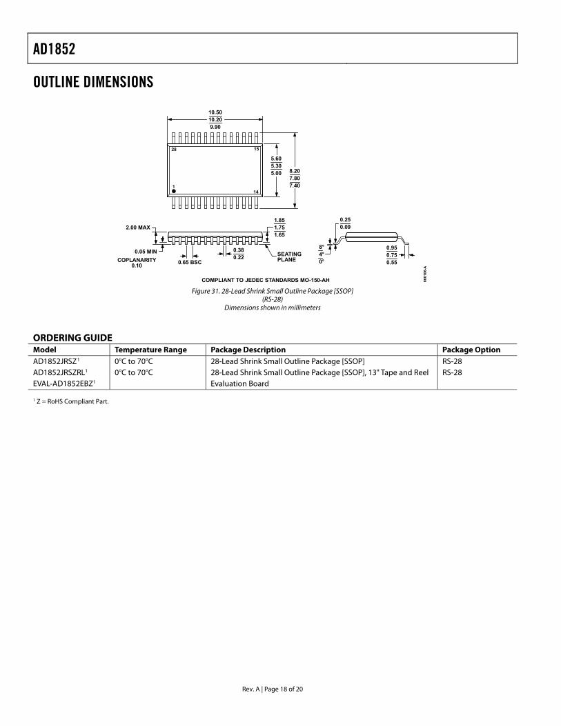
Figure 31. 28-Lead Shrink Small Outline Package [SSOP]
(RS-28) Dimensions shown in millimeters
ORDERING GUIDE Model Temperature Range Package Description Package Option AD1852JRSZ1 0°C to 70°C 28-Lead Shrink Small Outline Package [SSOP] RS-28 AD1852JRSZRL1 0°C to 70°C 28-Lead Shrink Small Outline Package [SSOP], 13" Tape and Reel RS-28 EVAL-AD1852EBZ1 Evaluation Board 1 Z = RoHS Compliant Part.

AD1852
Rev. A | Page 19 of 20
NOTES
AD1852
Rev. A | Page 20 of 20
NOTES
©2000–2009 Analog Devices, Inc. All rights reserved. Trademarks and registered trademarks are the property of their respective owners. D08457-0-11/09(A)
Recommended