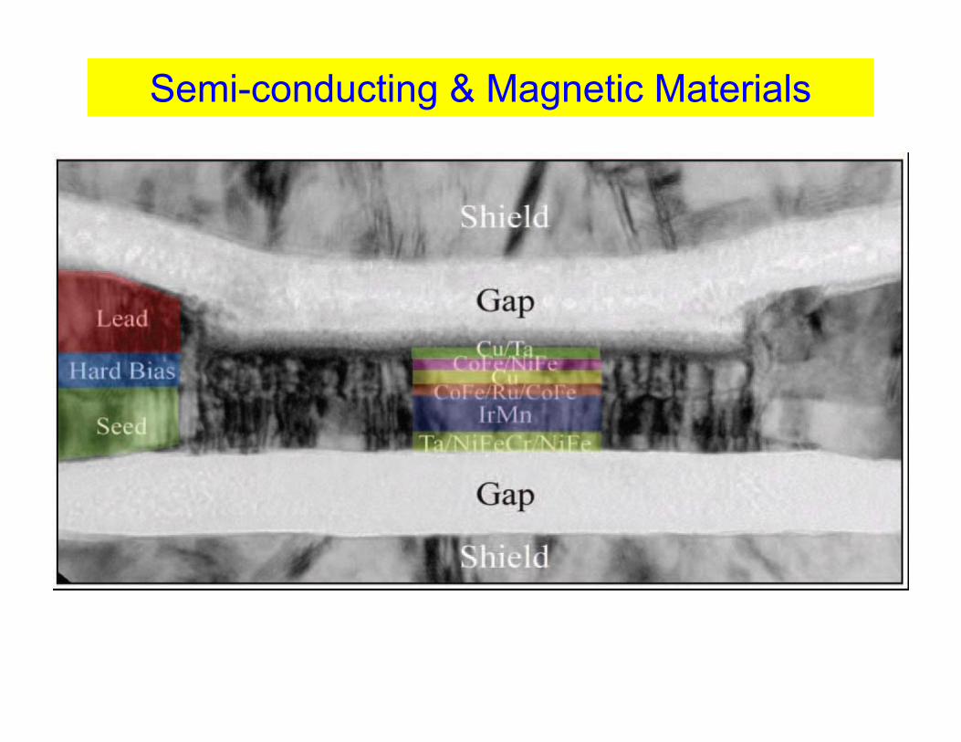
Semi-conducting & Magnetic Materials
1968 – Ampex Corporation Research department-Hired recent Ph.D. graduate from MIT – Robert P. Hunt-Initial assignment: -Find something new & useful in magnetic storage technology.-Shortly after, he invented the Magneto-resistive head (MRH).
At Ampex Research there also was Irving Wolf – inventor of the “Wolf” permalloy electroplating bath.
Bob asked Irving, Can you fabricate a “Magneto-resistive head?”Irving replied: “Sure, I’ll make it out of evaporated permalloy”
Serendipity: If Bob & Irving had not been in such close proximity, there would be no MRHs even today.Not only did the first MRHs use Permalloy, but, even today all Manufacturing companies use Permalloy as the sensor.
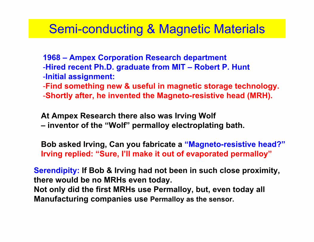
Semi-conducting & Magnetic MaterialsdH = 0.1Idl/R2 H is in oersteds, I is in amperes, l & R are in cms.
Consider a very straight, long conductor:
Integrating the above equation, we see that the magnetic field produced circles the conductor.
The magnetic field is tangential:- orthogonal to current direction &
radius vector, r.
Direction of the magnetic field is given by the right-hand rule.
Magnitude of the field is given by: H = 0.2I/r
Semi-conducting & Magnetic Materials
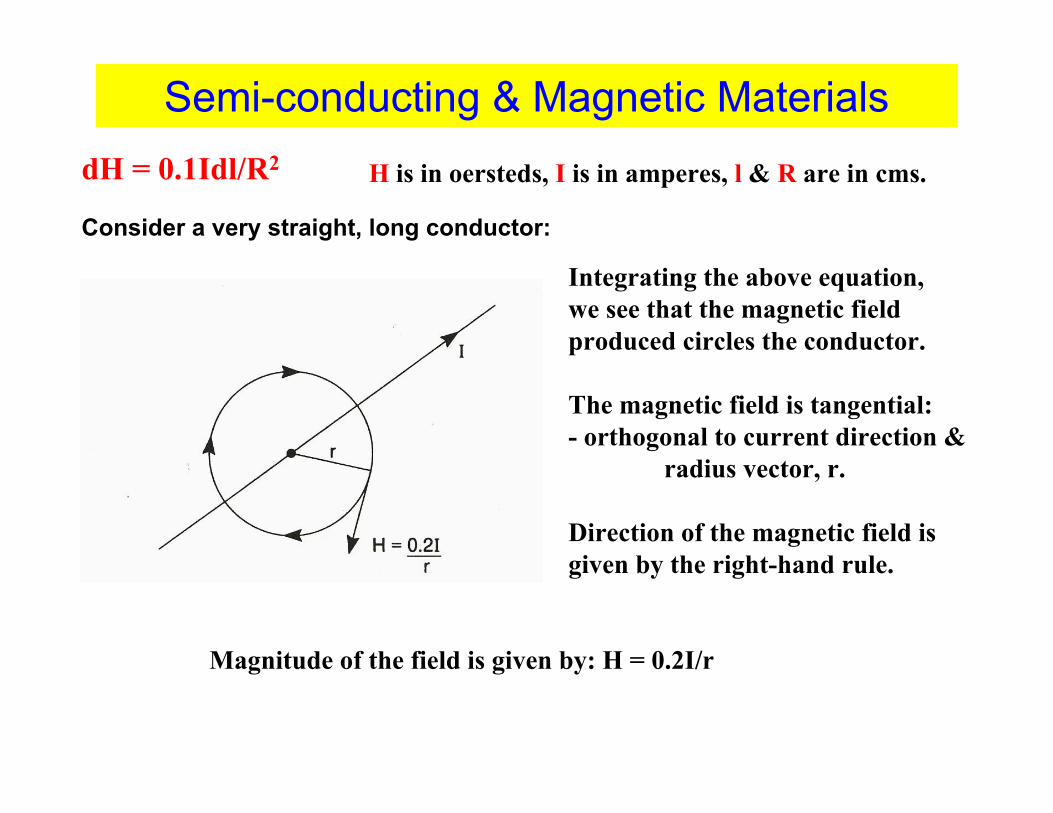
dH = 0.1Idl/R2 H is in oersteds, I is in amperes, l & R are in cms.
Suppose the conductor is coiled to form a solenoid:
Magnetic field inside a long solenoidis given by:
H = 0.4πN I /l
N is the number of turns, l is the solenoid length.
Let us now define the Magnetic Moment:
1 .4
H dVμπ ∫= μ is the magnetic moment in emu & V is
the volume in cc.
For any solenoid, μ = 0.1NIA, where A is the cross-sectional area of the solenoid.
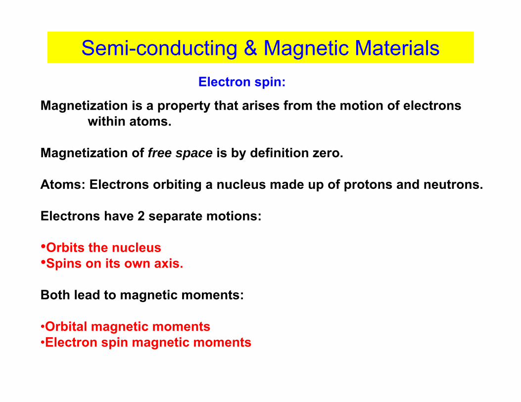
Semi-conducting & Magnetic MaterialsElectron spin:
Magnetization is a property that arises from the motion of electrons within atoms.
Magnetization of free space is by definition zero.
Atoms: Electrons orbiting a nucleus made up of protons and neutrons.
Electrons have 2 separate motions:
•Orbits the nucleus •Spins on its own axis.
Both lead to magnetic moments:
•Orbital magnetic moments•Electron spin magnetic moments

Semi-conducting & Magnetic MaterialsElectron spin:
Magnetic moments of a spinning electron is called Bohr’s magneton & its magnitude is given by:
4Beh
mμ
π= = 0.93 x 10 -20 emu
Where, e is the electron’s charge in emu (1.6 x 10 -20), h is Planck’s constant (6.6 x 10 -27)m is the electron’s mass in grams (9 x 10 -28)
Spinning electron has a quantum spin number,12
s =Can be oriented in in only 2 directions.

Semi-conducting & Magnetic MaterialsElectron spin:
Consider an atom of iron in free space: atomic number is 26, thus, 26 electrons
In shell 1s, 2s, 2p, 3s, 3p & 4s: total spin is zero: equal number of electrons spin up & down.
In shell, 3d, uncompensated spin moment of 4μB exists:5 spin up & 1 down.
When iron atoms condense to solid state, the electronic distribution changes:uncompensated spin moment lowers to 2.2μB
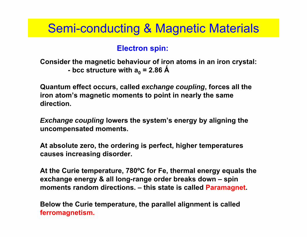
Semi-conducting & Magnetic MaterialsElectron spin:
Consider the magnetic behaviour of iron atoms in an iron crystal:- bcc structure with a0 = 2.86 Ǻ
Quantum effect occurs, called exchange coupling, forces all the iron atom’s magnetic moments to point in nearly the same direction.
Exchange coupling lowers the system’s energy by aligning the uncompensated moments.
At absolute zero, the ordering is perfect, higher temperatures causes increasing disorder.
At the Curie temperature, 780ºC for Fe, thermal energy equals the exchange energy & all long-range order breaks down – spin moments random directions. – this state is called Paramagnet.
Below the Curie temperature, the parallel alignment is called ferromagnetism.
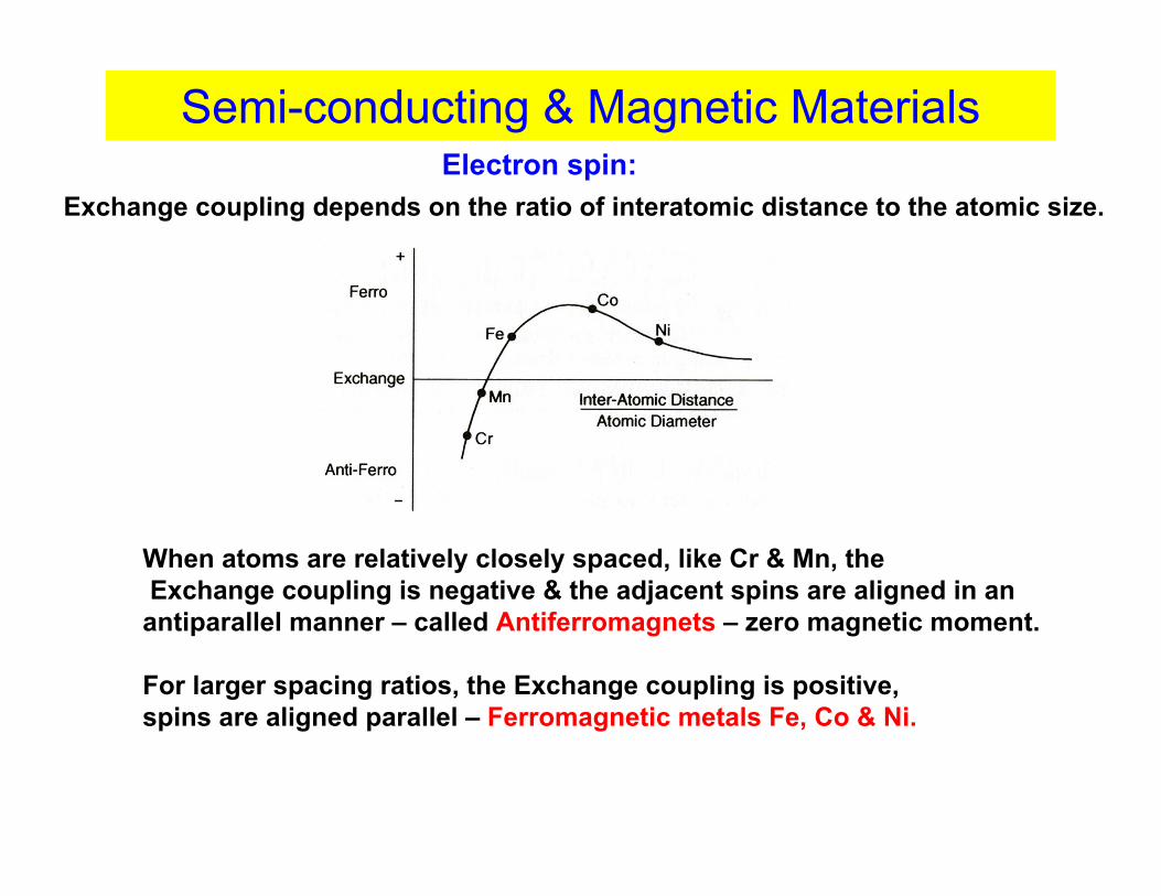
Semi-conducting & Magnetic MaterialsElectron spin:
Exchange coupling depends on the ratio of interatomic distance to the atomic size.
When atoms are relatively closely spaced, like Cr & Mn, theExchange coupling is negative & the adjacent spins are aligned in an antiparallel manner – called Antiferromagnets – zero magnetic moment.
For larger spacing ratios, the Exchange coupling is positive, spins are aligned parallel – Ferromagnetic metals Fe, Co & Ni.
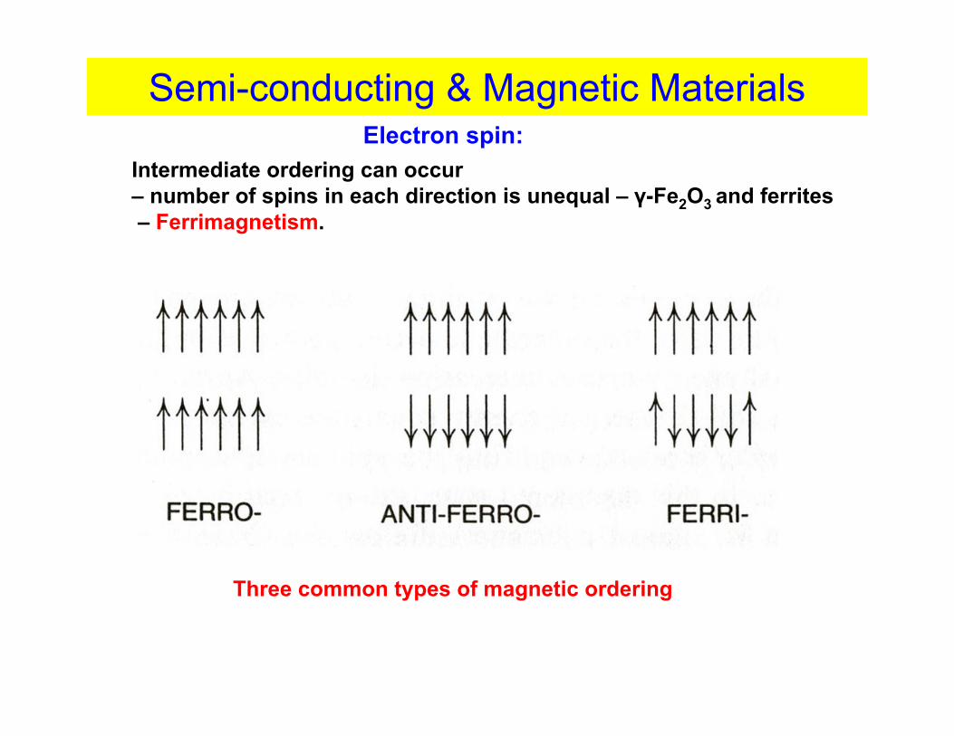
Semi-conducting & Magnetic MaterialsElectron spin:
Intermediate ordering can occur – number of spins in each direction is unequal – γ-Fe2O3 and ferrites– Ferrimagnetism.
Three common types of magnetic ordering
Semi-conducting & Magnetic MaterialsMagneto-Crystalline Anisotropy K:
Orientation of the net magnetic moment with respect to the crystal axes?
Ferromagnetic-ordered magnetic moments – aligned parallel to the body-centered cube edges.
In Fe, the cube edges are the easy, or lowest energy directionswhile the body diagonals are the hard, or highest energy, directions of the magnetic moment.
A measure of this energy difference is the Magneto-Crystalline Anisotropy K:
It is the energy required (ergs/cm2) to rotate the magnetic moments from the easy to the hard direction.

Semi-conducting & Magnetic MaterialsMagnetization M:
Consider a volume of iron that has several million atoms.
The magnetization is, by definition, the volume average of the atomic moments:
1
1 NM m
V∑=
V is the volume in ccm is the atomic moment in emuN is the number of atomic moments in the volume V.
M is in magnetic moment per unit volume (emu/cm3).
In a large enough magnetic field, the magnetization of all parts of the magnetic material is parallel.
At lower fields, magnetization subdivides into domains.
Within a single domain – magnetization is parallel & uniform - value is called saturation magnetization, Ms that depends on temperature.
At absolute zero, it is maximum and vanishes at the Curie temperature.

Semi-conducting & Magnetic MaterialsMagnetization M:
Calculation of Ms at 0ºK for bcc Fe:
Each Fe atom has 2.2 μB of magnetic moment.2 Fe atoms/unit cell, a0 = 2.86Ǻ.
38 3
2.2. .2( 0) 1700 /(2.86 10 )
BsM T emu cm
xμ
−= = =
At room temperature, Ms is only slightly reduced by thermal energy & pure Fe:
Ms = 1700 emu/cm3; 4πMs = 21,000 G & σs = 21.6 emu/g, where σs is called the specific saturation magnetization.
The value of 4πMs for other materials of interest:Co: 18,000 G Ni: 6000 GPermalloy (81Ni/19Fe): 12,500 G
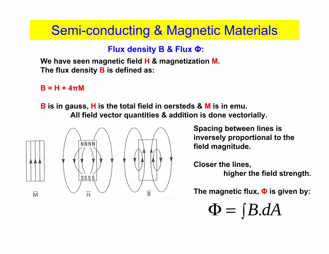
Semi-conducting & Magnetic MaterialsFlux density B & Flux Φ:
We have seen magnetic field H & magnetization M. The flux density B is defined as:
B = H + 4πM
B is in gauss, H is the total field in oersteds & M is in emu.All field vector quantities & addition is done vectorially.
Spacing between lines is inversely proportional to the field magnitude.
Closer the lines, higher the field strength.
The magnetic flux, Φ is given by:
.B dA∫Φ =
Semi-conducting & Magnetic Materials
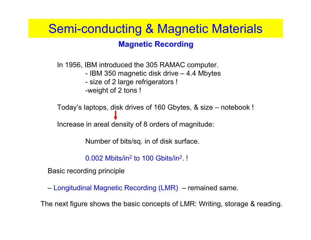
In 1956, IBM introduced the 305 RAMAC computer.- IBM 350 magnetic disk drive – 4.4 Mbytes- size of 2 large refrigerators !-weight of 2 tons !
Today’s laptops, disk drives of 160 Gbytes, & size – notebook !
Increase in areal density of 8 orders of magnitude:
Number of bits/sq. in of disk surface.
0.002 Mbits/in2 to 100 Gbits/in2. !
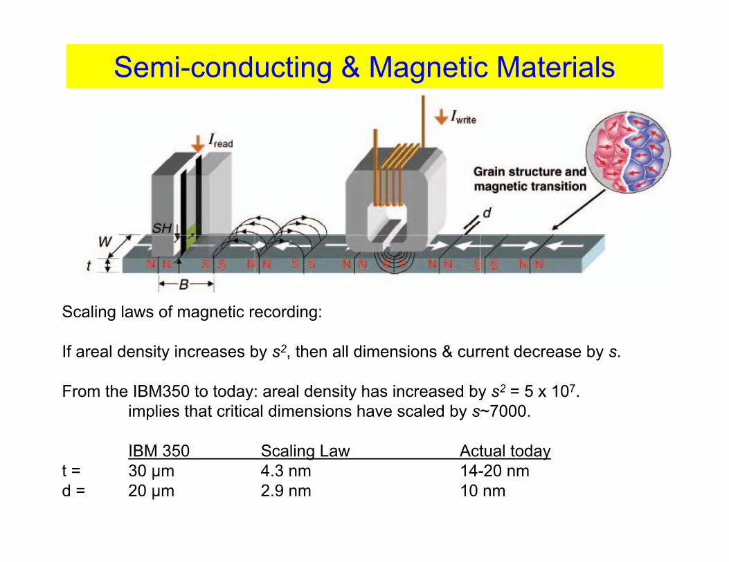
Basic recording principle
– Longitudinal Magnetic Recording (LMR) – remained same.
The next figure shows the basic concepts of LMR: Writing, storage & reading.
Magnetic Recording
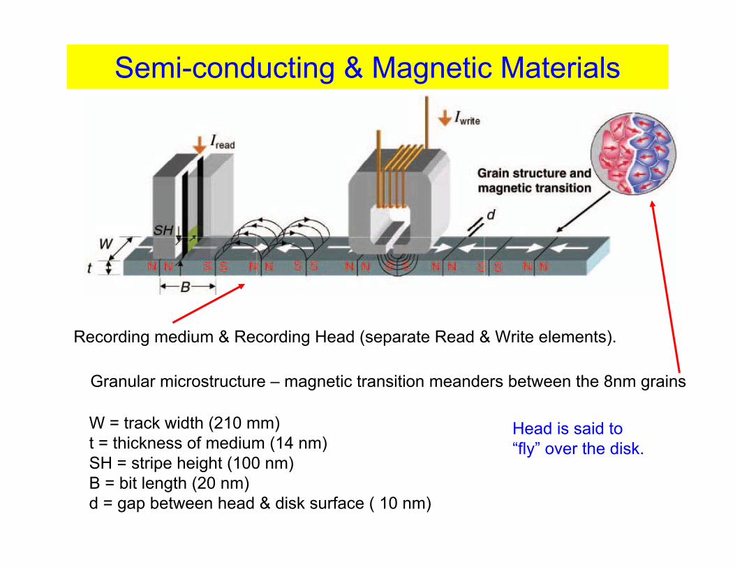
Semi-conducting & Magnetic Materials
Recording medium & Recording Head (separate Read & Write elements).
Granular microstructure – magnetic transition meanders between the 8nm grains
W = track width (210 mm)t = thickness of medium (14 nm)SH = stripe height (100 nm)B = bit length (20 nm)d = gap between head & disk surface ( 10 nm)
Head is said to “fly” over the disk.

Semi-conducting & Magnetic Materials
Inductive Write Head – miniature Electromagnet – time-varying current in a conductor wrapped around a ferromagnetic yoke
- provides a time-varying magnetic field in the gap of this yoke.-This field in turn, magnetizes regions of the disk as they pass under the gap.
Data is stored as horizontal magnetic patterns – ones and zeros correspond to the presence or absence of magnetic reversals.
Basic process of writing & storage has not changed, but the read process has changed dramatically.
Semi-conducting & Magnetic Materials
Scaling laws of magnetic recording:
If areal density increases by s2, then all dimensions & current decrease by s.
From the IBM350 to today: areal density has increased by s2 = 5 x 10⁷.implies that critical dimensions have scaled by s~7000.
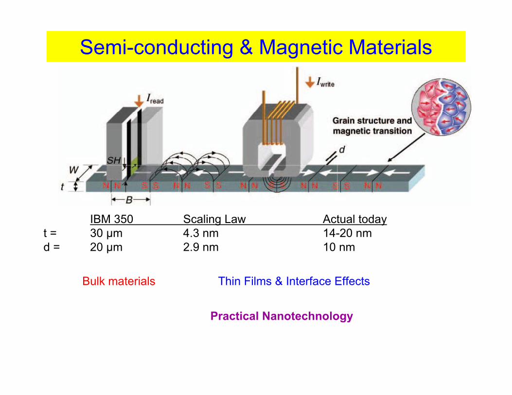
IBM 350 Scaling Law Actual todayt = 30 μm 4.3 nm 14-20 nmd = 20 μm 2.9 nm 10 nm
Semi-conducting & Magnetic Materials
IBM 350 Scaling Law Actual todayt = 30 μm 4.3 nm 14-20 nmd = 20 μm 2.9 nm 10 nm
Bulk materials Thin Films & Interface Effects
Practical Nanotechnology
Semi-conducting & Magnetic Materials
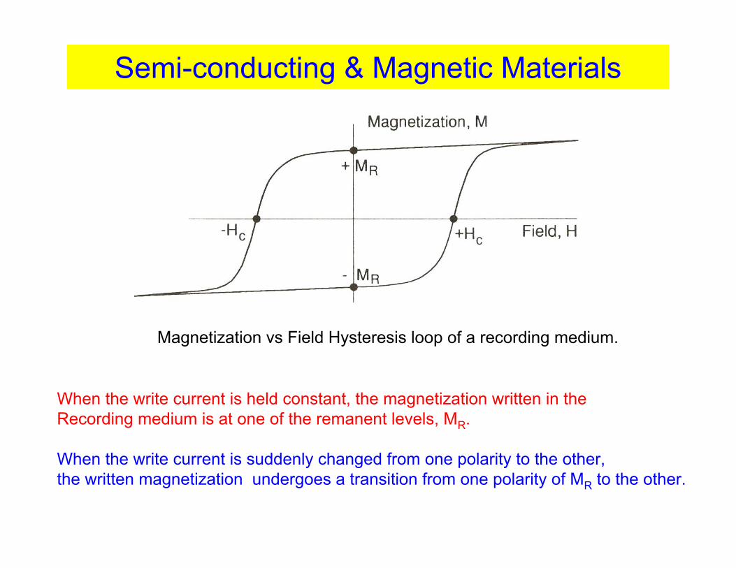
Magnetization vs Field Hysteresis loop of a recording medium.
When the write current is held constant, the magnetization written in the Recording medium is at one of the remanent levels, MR.
When the write current is suddenly changed from one polarity to the other, the written magnetization undergoes a transition from one polarity of MR to the other.
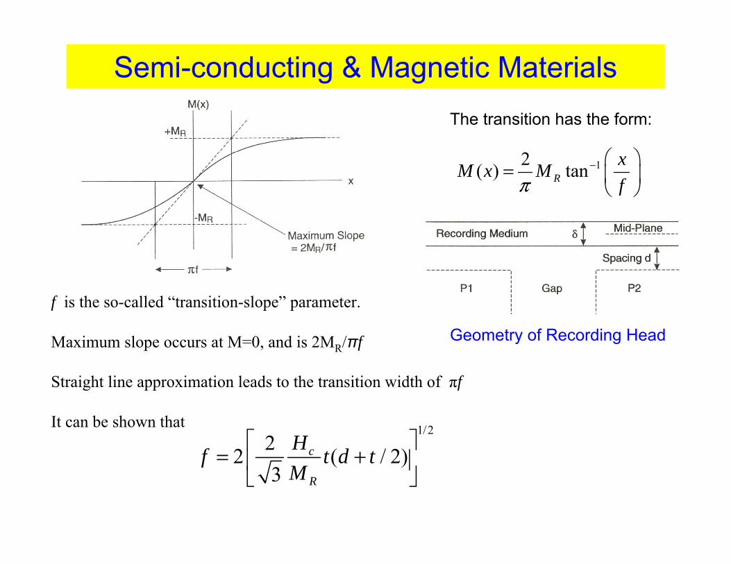
Semi-conducting & Magnetic MaterialsThe transition has the form:
12( ) tanRxM x Mfπ
− ⎛ ⎞= ⎜ ⎟
⎝ ⎠
f is the so-called “transition-slope” parameter.
Maximum slope occurs at M=0, and is 2MR/πf
Straight line approximation leads to the transition width of πf
It can be shown that 1/222 ( / 2)3
c
R
Hf t d tM
⎡ ⎤= +⎢ ⎥
⎣ ⎦
Geometry of Recording Head
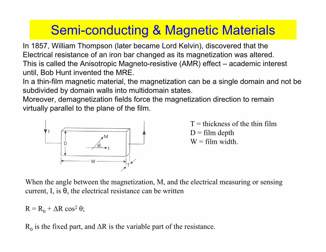
Semi-conducting & Magnetic MaterialsIn 1857, William Thompson (later became Lord Kelvin), discovered that the Electrical resistance of an iron bar changed as its magnetization was altered.This is called the Anisotropic Magneto-resistive (AMR) effect – academic interestuntil, Bob Hunt invented the MRE.In a thin-film magnetic material, the magnetization can be a single domain and not be subdivided by domain walls into multidomain states.Moreover, demagnetization fields force the magnetization direction to remainvirtually parallel to the plane of the film.
When the angle between the magnetization, M, and the electrical measuring or sensing current, I, is θ, the electrical resistance can be written
R = R0 + ΔR cos2 θ;
R0 is the fixed part, and ΔR is the variable part of the resistance.
T = thickness of the thin filmD = film depthW = film width.
Semi-conducting & Magnetic Materials
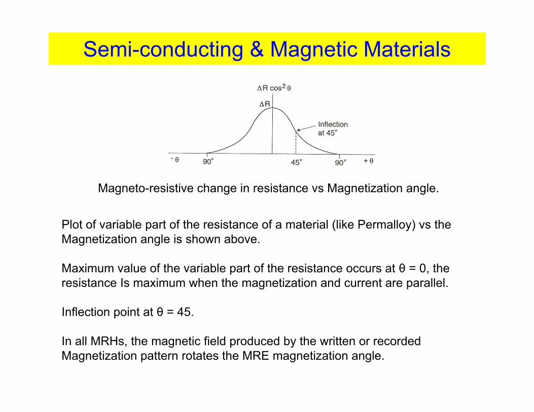
Magneto-resistive change in resistance vs Magnetization angle.
Plot of variable part of the resistance of a material (like Permalloy) vs the Magnetization angle is shown above.
Maximum value of the variable part of the resistance occurs at θ = 0, the resistance Is maximum when the magnetization and current are parallel.
Inflection point at θ = 45.
In all MRHs, the magnetic field produced by the written or recorded Magnetization pattern rotates the MRE magnetization angle.
Semi-conducting & Magnetic Materials
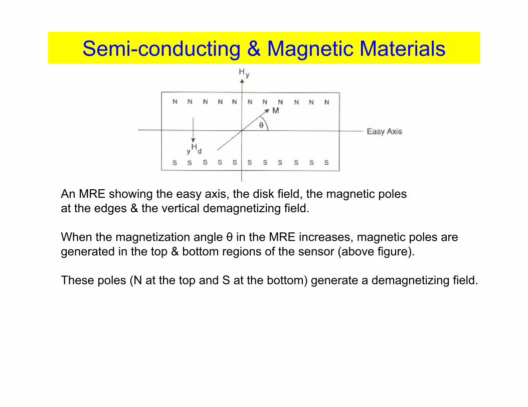
An MRE showing the easy axis, the disk field, the magnetic polesat the edges & the vertical demagnetizing field.
When the magnetization angle θ in the MRE increases, magnetic poles aregenerated in the top & bottom regions of the sensor (above figure).
These poles (N at the top and S at the bottom) generate a demagnetizing field.
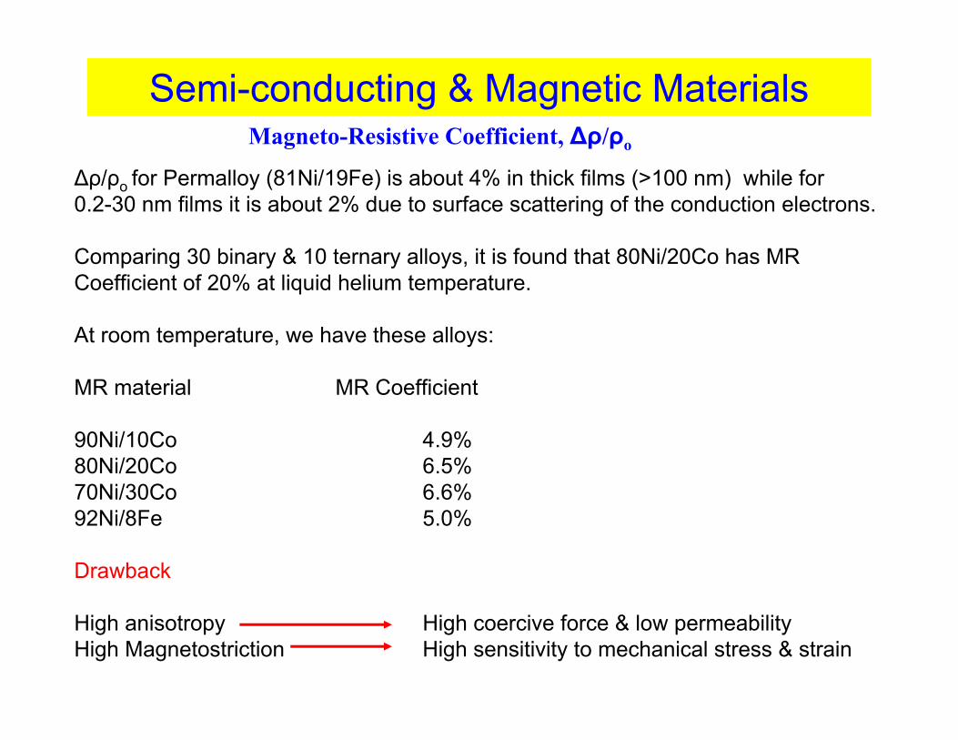
Semi-conducting & Magnetic MaterialsMagneto-Resistive Coefficient, Δρ/ρo
The electrical, R, of the MRE, in terms of resistivity, ρ, of the material, is:
R = ρW/TD
In magneto-resistive materials,
ρ = ρ 0 + Δ ρ cos2 θ;
ρo is the fixed part, and Δρ is the variable part of the resistance.
Magneto-Resistive Coefficient is defined as Δρ/ρo – serves as the figure of merit of the MR material.
-It is the maximum fractional change in the resistivity.
0 0
RR
ρρΔ Δ=
Semi-conducting & Magnetic MaterialsMagneto-Resistive Coefficient, Δρ/ρo
Δρ/ρo for Permalloy (81Ni/19Fe) is about 4% in thick films (>100 nm) while for 0.2-30 nm films it is about 2% due to surface scattering of the conduction electrons.
Comparing 30 binary & 10 ternary alloys, it is found that 80Ni/20Co has MR Coefficient of 20% at liquid helium temperature.
At room temperature, we have these alloys:
MR material MR Coefficient
90Ni/10Co 4.9%80Ni/20Co 6.5%70Ni/30Co 6.6%92Ni/8Fe 5.0%
Drawback
High anisotropy High coercive force & low permeability High Magnetostriction High sensitivity to mechanical stress & strain
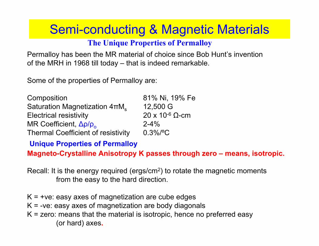
Semi-conducting & Magnetic MaterialsThe Unique Properties of Permalloy
Permalloy has been the MR material of choice since Bob Hunt’s invention of the MRH in 1968 till today – that is indeed remarkable.
Some of the properties of Permalloy are:
Composition 81% Ni, 19% FeSaturation Magnetization 4πMs 12,500 GElectrical resistivity 20 x 10-6 Ω-cmMR Coefficient, Δρ/ρo 2-4%Thermal Coefficient of resistivity 0.3%/ºCUnique Properties of Permalloy
Magneto-Crystalline Anisotropy K passes through zero – means, isotropic.
Recall: It is the energy required (ergs/cm2) to rotate the magnetic moments from the easy to the hard direction.
K = +ve: easy axes of magnetization are cube edgesK = -ve: easy axes of magnetization are body diagonalsK = zero: means that the material is isotropic, hence no preferred easy
(or hard) axes.

Semi-conducting & Magnetic MaterialsThe Unique Properties of Permalloy
Magneto-Crystalline Anisotropy K passes through zero – means, isotropic.
Recall: It is the energy required (ergs/cm2) to rotate the magnetic moments from the easy to the hard direction.
K = +ve: easy axes of magnetization are cube edgesK = -ve: easy axes of magnetization are body diagonalsK = zero: means that the material is isotropic, hence no preferred easy
(or hard) axes.
Anisotropy is due to spin-orbit coupling of the electron spins to the electronic structure of the material.
The greater the change in spin-orbit coupling energy with changes in magnetizationdirection, the greater the anisotropy.
Hexagonal structures like Co will have greater anisotropy than cubic ones like Ni & Fe.
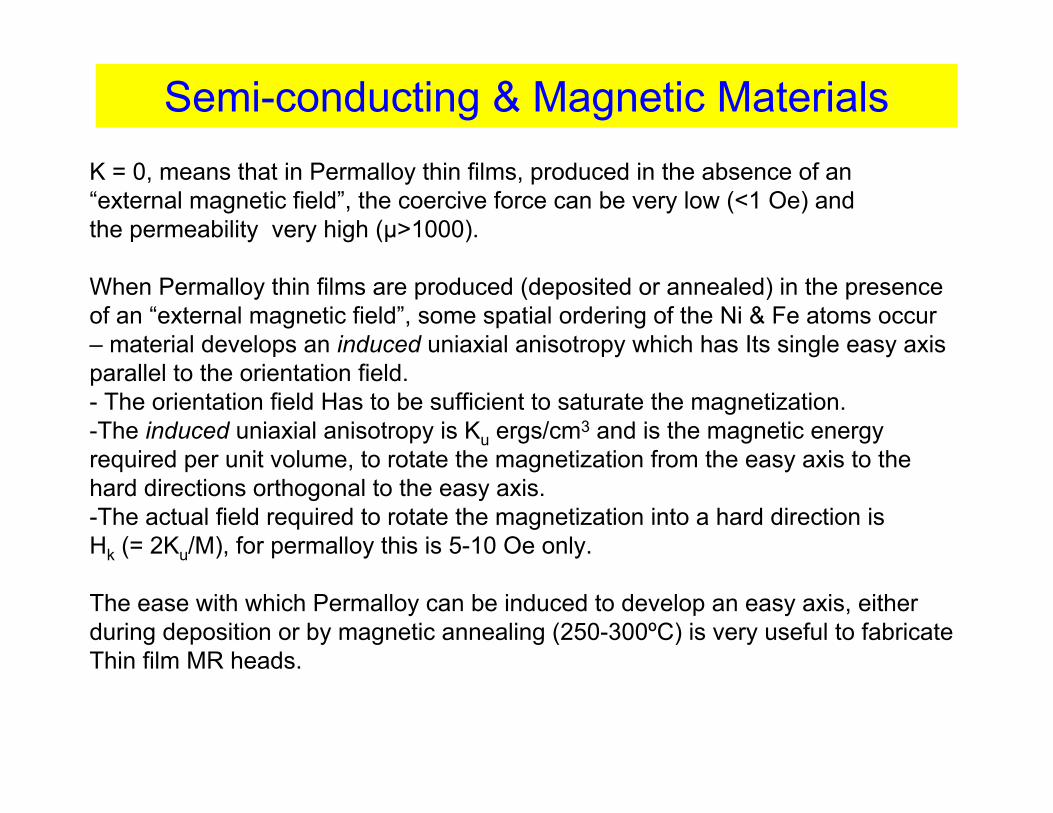
Semi-conducting & Magnetic MaterialsK = 0, means that in Permalloy thin films, produced in the absence of an “external magnetic field”, the coercive force can be very low (<1 Oe) andthe permeability very high (μ>1000).
When Permalloy thin films are produced (deposited or annealed) in the presence of an “external magnetic field”, some spatial ordering of the Ni & Fe atoms occur – material develops an induced uniaxial anisotropy which has Its single easy axis parallel to the orientation field.- The orientation field Has to be sufficient to saturate the magnetization.-The induced uniaxial anisotropy is Ku ergs/cm3 and is the magnetic energy required per unit volume, to rotate the magnetization from the easy axis to the hard directions orthogonal to the easy axis.-The actual field required to rotate the magnetization into a hard direction is Hk (= 2Ku/M), for permalloy this is 5-10 Oe only.
The ease with which Permalloy can be induced to develop an easy axis, eitherduring deposition or by magnetic annealing (250-300ºC) is very useful to fabricate Thin film MR heads.
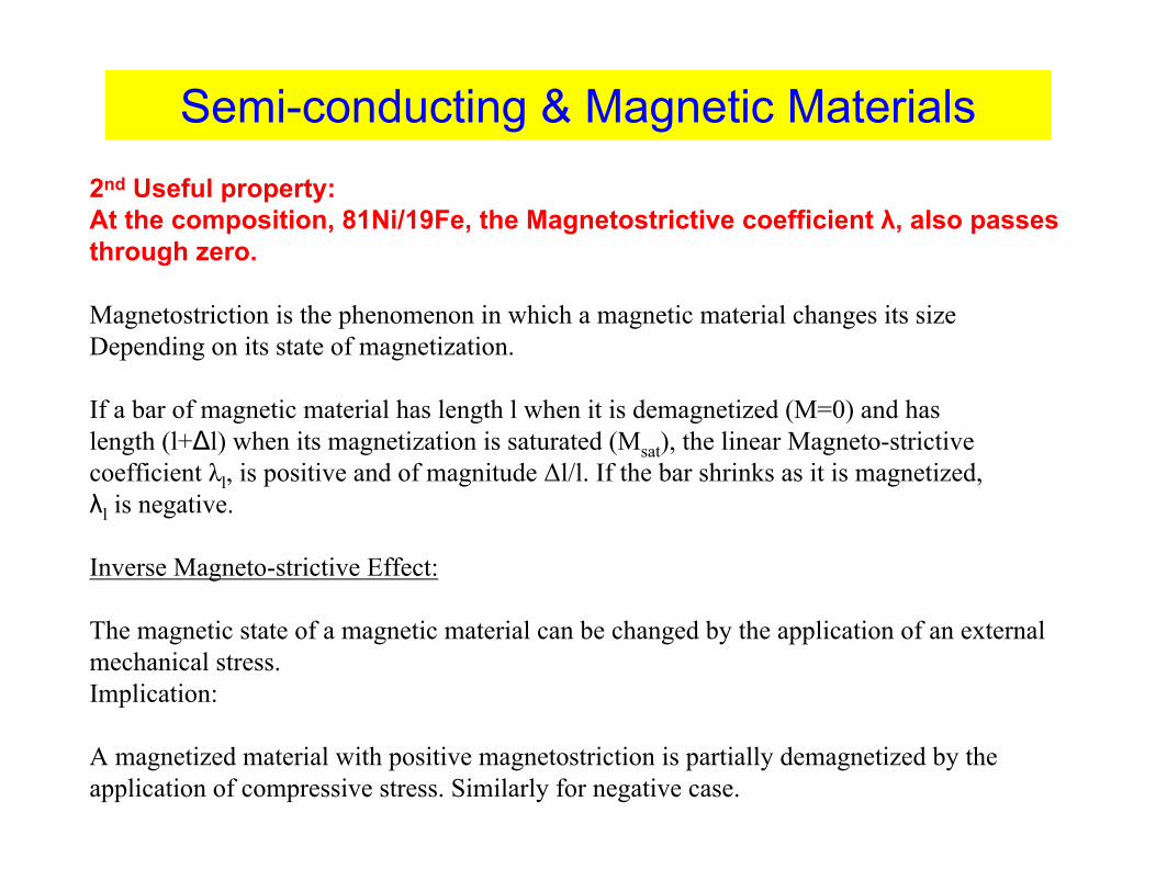
Semi-conducting & Magnetic Materials2nd Useful property:At the composition, 81Ni/19Fe, the Magnetostrictive coefficient λ, also passesthrough zero.
Magnetostriction is the phenomenon in which a magnetic material changes its sizeDepending on its state of magnetization.
If a bar of magnetic material has length l when it is demagnetized (M=0) and has length (l+Δl) when its magnetization is saturated (Msat), the linear Magneto-strictivecoefficient λl, is positive and of magnitude Δl/l. If the bar shrinks as it is magnetized,λl is negative.
Inverse Magneto-strictive Effect:
The magnetic state of a magnetic material can be changed by the application of an externalmechanical stress.Implication:
A magnetized material with positive magnetostriction is partially demagnetized by the application of compressive stress. Similarly for negative case.

Semi-conducting & Magnetic MaterialsMagnetostriction is another manifestation of spin-orbit coupling.
The greater the change in spin-orbit coupling energy with changes in atom-to-atom spacing, the greater the magnetostriction. It is therefore likely to be large when K is large e.g. Co.
Importance of zero Magnetostriction:
During thin film head fabrication, invariably, the thin films have built-in stresses.These stresses arise due to:(a) composition nonuniformities(b) composition gradients(c) differences in thermal expansion coefficients
Permalloy’s dominance in magnetic heads is therefore because at the same composition,we can have: K = 0 and λ = 0.

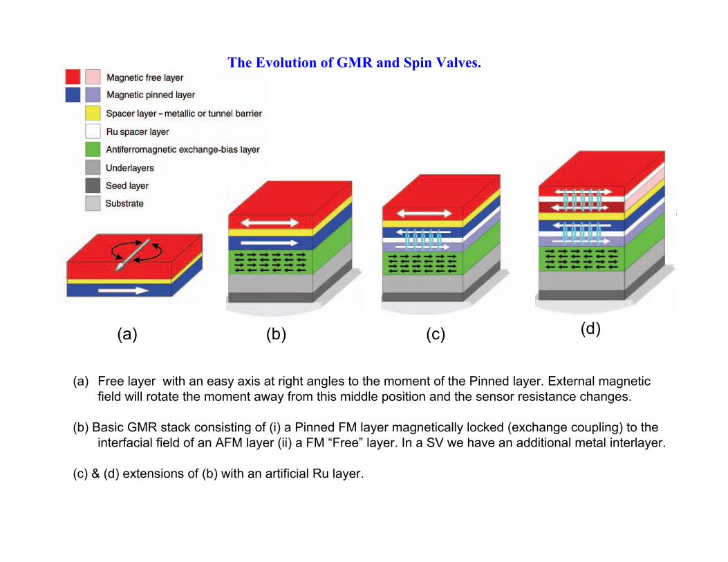
The Evolution of GMR and Spin Valves.
(a) (d)(c)(b)
(a) Free layer with an easy axis at right angles to the moment of the Pinned layer. External magnetic field will rotate the moment away from this middle position and the sensor resistance changes.
(b) Basic GMR stack consisting of (i) a Pinned FM layer magnetically locked (exchange coupling) to the interfacial field of an AFM layer (ii) a FM “Free” layer. In a SV we have an additional metal interlayer.
(c) & (d) extensions of (b) with an artificial Ru layer.

Semi-conducting & Magnetic Materials
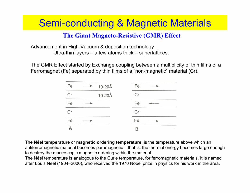
Semi-conducting & Magnetic MaterialsThe Giant Magneto-Resistive (GMR) Effect
Advancement in High-Vacuum & deposition technologyUltra-thin layers – a few atoms thick – superlattices.
The GMR Effect started by Exchange coupling between a multiplicity of thin films of a Ferromagnet (Fe) separated by thin films of a “non-magnetic” material (Cr).
The Néel temperature or magnetic ordering temperature, is the temperature above which an antiferromagnetic material becomes paramagnetic – that is, the thermal energy becomes large enough to destroy the macroscopic magnetic ordering within the material.The Néel temperature is analogous to the Curie temperature, for ferromagnetic materials. It is named after Louis Néel (1904–2000), who received the 1970 Nobel prize in physics for his work in the area.
Semi-conducting & Magnetic Materials
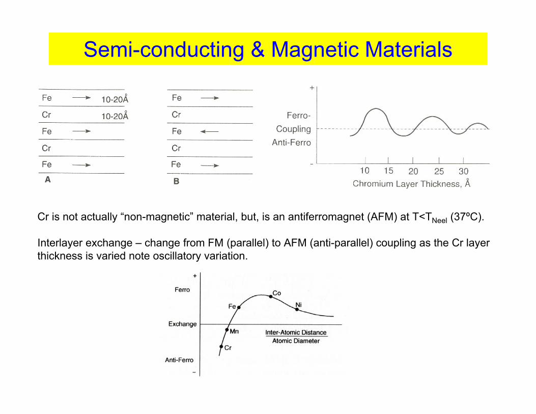
Cr is not actually “non-magnetic” material, but, is an antiferromagnet (AFM) at T<TNeel (37ºC).
Interlayer exchange – change from FM (parallel) to AFM (anti-parallel) coupling as the Cr layer thickness is varied note oscillatory variation.

Semi-conducting & Magnetic MaterialsMeasurement of electrical resistance is the key tool:
Where the exchange was antiferromagnetic, the resistance could be changed by applying a large magnetic field (10,000 Oe). Because the resistance change was very large (Δρ/ρ0 ≈ 40%), it was called the Giant Magneto-resistive effect (GMR).
The electrical resistance was high when the iron layer magnetization was antiparallel & low when they were forced by the external field, to be parallel.
The variation in the electrical resistance was found to be proportional to –cos β where β is the angle between the adjacent layer magnetizations.
Excitement about GMR – initially not useful for MRH designers !!!! WHY?
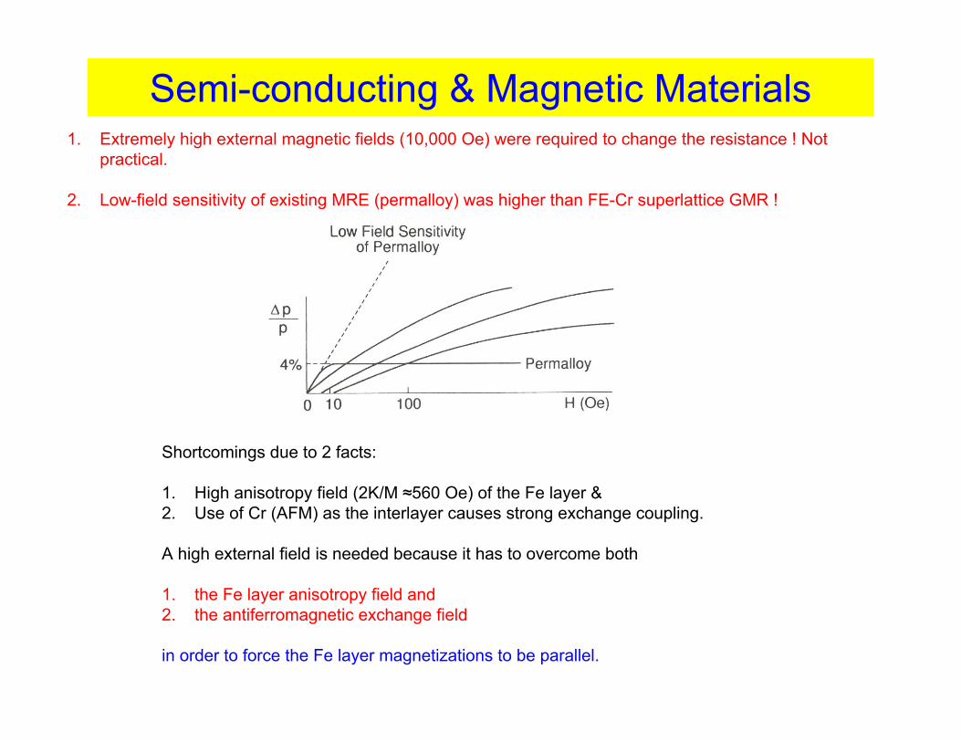
Semi-conducting & Magnetic Materials1. Extremely high external magnetic fields (10,000 Oe) were required to change the resistance ! Not
practical.
2. Low-field sensitivity of existing MRE (permalloy) was higher than FE-Cr superlattice GMR !
Shortcomings due to 2 facts:
1. High anisotropy field (2K/M ≈560 Oe) of the Fe layer & 2. Use of Cr (AFM) as the interlayer causes strong exchange coupling.
A high external field is needed because it has to overcome both
1. the Fe layer anisotropy field and 2. the antiferromagnetic exchange field
in order to force the Fe layer magnetizations to be parallel.
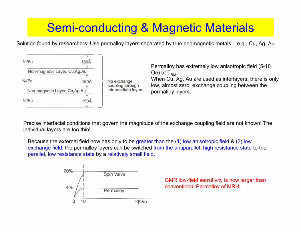
Semi-conducting & Magnetic MaterialsSolution found by researchers: Use permalloy layers separated by true nonmagnetic metals – e.g., Cu, Ag, Au.
Because the external field now has only to be greater than the (1) low anisotropic field & (2) low exchange field, the permalloy layers can be switched from the antiparallel, high resistance state to the parallel, low resistance state by a relatively small field.
Permalloy has extremely low anisotropic field (5-10 Oe) at TRM. When Cu, Ag, Au are used as interlayers, there is only low, almost zero, exchange coupling between the permalloy layers.
Precise interfacial conditions that govern the magnitude of the exchange coupling field are not known! The individual layers are too thin!
GMR low-field sensitivity is now larger than conventional Permalloy of MRH.
The Physics of the Giant Magneto-Resistive (GMR) Effect
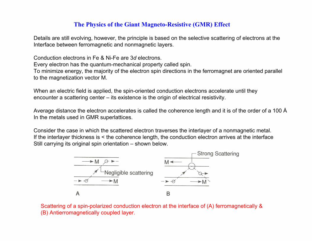
Details are still evolving, however, the principle is based on the selective scattering of electrons at theInterface between ferromagnetic and nonmagnetic layers.
Conduction electrons in Fe & Ni-Fe are 3d electrons. Every electron has the quantum-mechanical property called spin.To minimize energy, the majority of the electron spin directions in the ferromagnet are oriented parallel to the magnetization vector M.
When an electric field is applied, the spin-oriented conduction electrons accelerate until they encounter a scattering center – its existence is the origin of electrical resistivity.
Average distance the electron accelerates is called the coherence length and it is of the order of a 100 ÅIn the metals used in GMR superlattices.
Consider the case in which the scattered electron traverses the interlayer of a nonmagnetic metal.If the interlayer thickness is < the coherence length, the conduction electron arrives at the interface Still carrying its original spin orientation – shown below.
Scattering of a spin-polarized conduction electron at the interface of (A) ferromagnetically & (B) Antierromagnetically coupled layer.
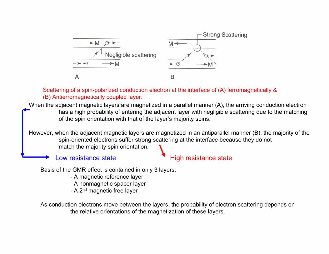
Scattering of a spin-polarized conduction electron at the interface of (A) ferromagnetically & (B) Antierromagnetically coupled layer.
When the adjacent magnetic layers are magnetized in a parallel manner (A), the arriving conduction electron has a high probability of entering the adjacent layer with negligible scattering due to the matching of the spin orientation with that of the layer’s majority spins.
However, when the adjacent magnetic layers are magnetized in an antiparallel manner (B), the majority of the spin-oriented electrons suffer strong scattering at the interface because they do notmatch the majority spin orientation.
Low resistance state High resistance state
Basis of the GMR effect is contained in only 3 layers:- A magnetic reference layer- A nonmagnetic spacer layer- A 2nd magnetic free layer
As conduction electrons move between the layers, the probability of electron scattering depends on the relative orientations of the magnetization of these layers.
Necessary conditions for Giant Magneto-Resistive (GMR) Effect
1. The two materials used in the superlattice must be immiscible – prevents interdiffusion – need sharp interface.
2. FM layers must have some mechanism, e.g. exchange coupling, that establishes antiferro (antiparallel) magnetization state in zero external field.
3. Interlayer of nonmagnetic material must be thinner than the conduction electron coherence length- these electrons must “remember” their spin orientation as they cross between the FM layers.- Coherence length ≈ 100 Å needs nonmagnetic interlayer thickness of a few tens of Å.
Attraction of GMR Heads lies in their greater sensitivity & higher total change in resistance.
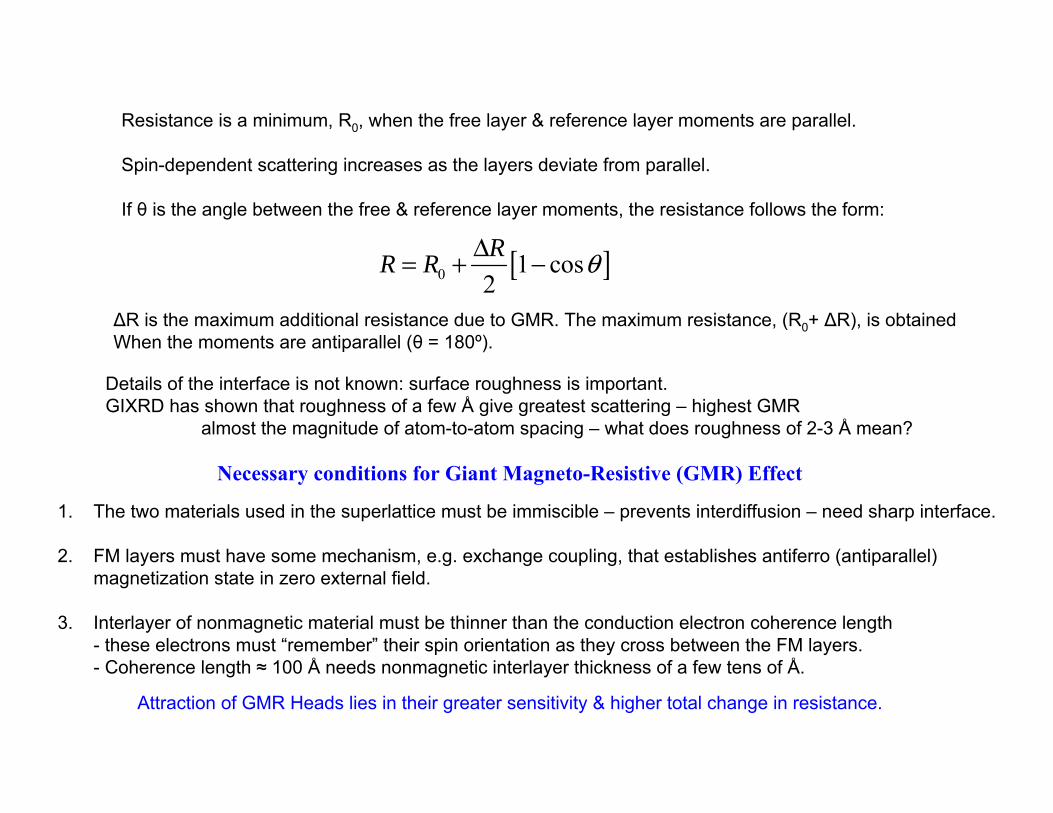
Resistance is a minimum, R0, when the free layer & reference layer moments are parallel.
Spin-dependent scattering increases as the layers deviate from parallel.
If θ is the angle between the free & reference layer moments, the resistance follows the form:
Details of the interface is not known: surface roughness is important.GIXRD has shown that roughness of a few Å give greatest scattering – highest GMR
almost the magnitude of atom-to-atom spacing – what does roughness of 2-3 Å mean?
[ ]0 1 cos2RR R θΔ= + −
ΔR is the maximum additional resistance due to GMR. The maximum resistance, (R0+ ΔR), is obtainedWhen the moments are antiparallel (θ = 180º).
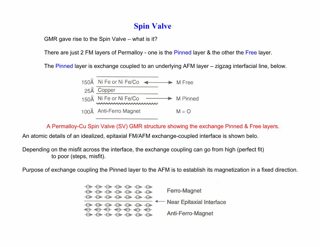
Spin ValveGMR gave rise to the Spin Valve – what is it?
There are just 2 FM layers of Permalloy - one is the Pinned layer & the other the Free layer.
The Pinned layer is exchange coupled to an underlying AFM layer – zigzag interfacial line, below.
A Permalloy-Cu Spin Valve (SV) GMR structure showing the exchange Pinned & Free layers.
An atomic details of an idealized, epitaxial FM/AFM exchange-coupled interface is shown belo.
Depending on the misfit across the interface, the exchange coupling can go from high (perfect fit) to poor (steps, misfit).
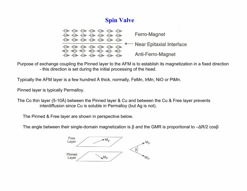
Purpose of exchange coupling the Pinned layer to the AFM is to establish its magnetization in a fixed direction.
Spin Valve
Purpose of exchange coupling the Pinned layer to the AFM is to establish its magnetization in a fixed direction- this direction is set during the initial processing of the head.
Typically the AFM layer is a few hundred Å thick, normally, FeMn, IrMn, NiO or PtMn.
Pinned layer is typically Permalloy.
The Co thin layer (5-10Å) between the Pinned layer & Cu and between the Cu & Free layer prevents interdiffusion since Cu is soluble in Permalloy (but Ag is not).
The Pinned & Free layer are shown in perspective below.
The angle between their single-domain magnetization is β and the GMR is proportional to –ΔR/2 cosβ
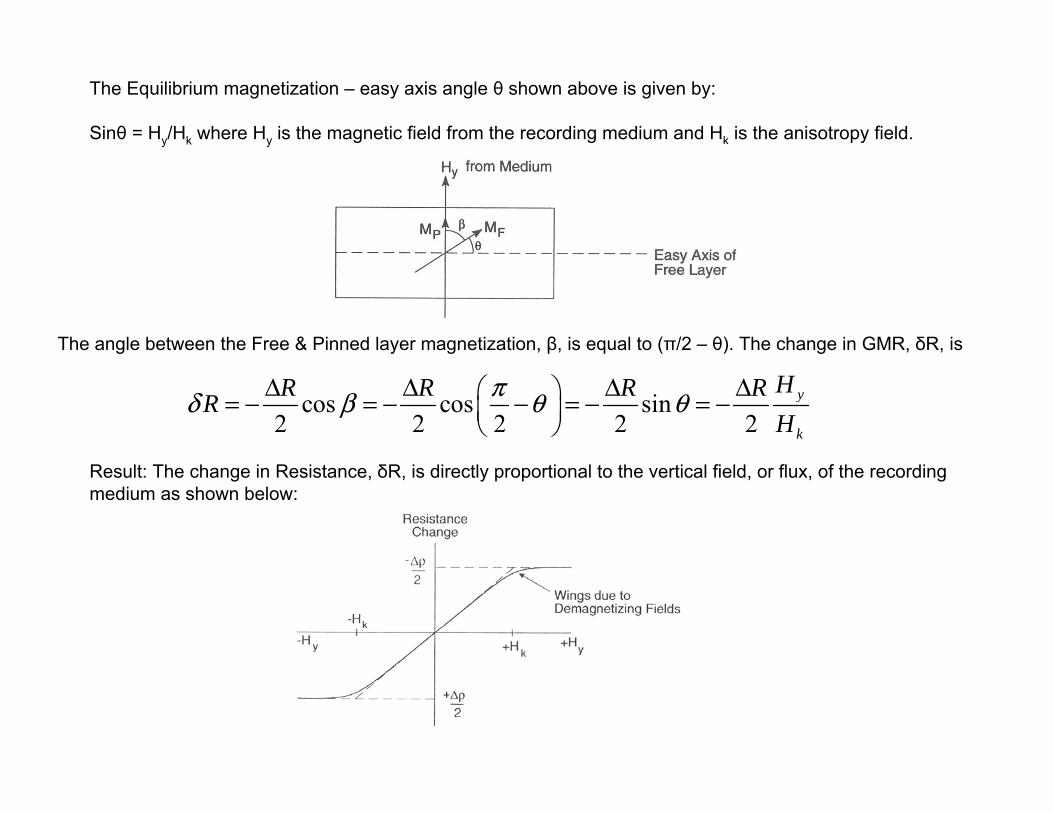
The Equilibrium magnetization – easy axis angle θ shown above is given by:
Sinθ = Hy/Hk where Hy is the magnetic field from the recording medium and Hk is the anisotropy field.
cos cos sin2 2 2 2 2
y
k
HR R R RRH
πδ β θ θΔ Δ Δ Δ⎛ ⎞= − = − − = − = −⎜ ⎟⎝ ⎠
Result: The change in Resistance, δR, is directly proportional to the vertical field, or flux, of the recording medium as shown below:
The angle between the Free & Pinned layer magnetization, β, is equal to (π/2 – θ). The change in GMR, δR, is
The Evolution of GMR and Spin Valves.
(a) (d)(c)(b)
(a) Free layer with an easy axis at right angles to the moment of the Pinned layer. External magnetic field will rotate the moment away from this middle position and the sensor resistance changes.
(b) Basic GMR stack consisting of (i) a Pinned FM layer magnetically locked (exchange coupling) to the interfacial field of an AFM layer (ii) a FM “Free” layer. In a SV we have an additional metal interlayer.
(c) & (d) extensions of (b) with an artificial Ru layer.
Semi-conducting & Magnetic Materials
Semi-conducting & Magnetic Materials
Recommended