rakesh asery
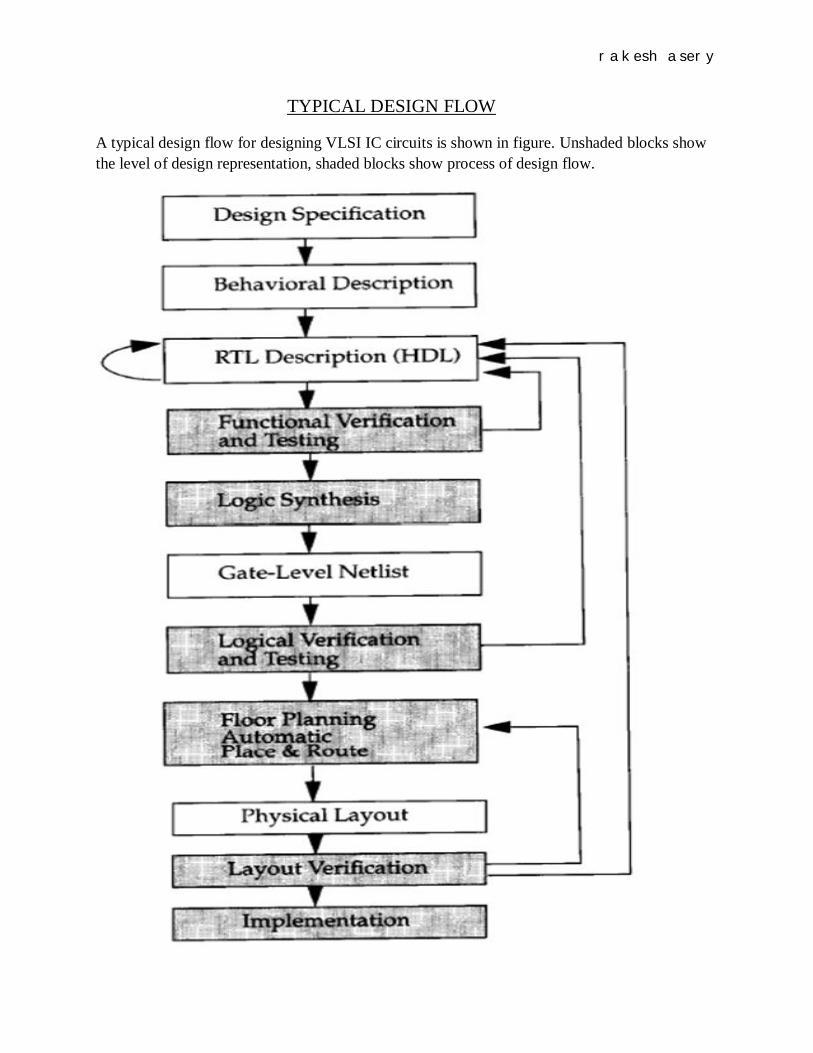
TYPICAL DESIGN FLOW
A typical design flow for designing VLSI IC circuits is shown in figure. Unshaded blocks show the level of design representation, shaded blocks show process of design flow.
rakesh asery
Experiment No:-[1] Aim: - To Design Half Adder using Verilog and simulate the same using Xilinx ISE Simulator.
TOOLS REQUIRED: - PC, Xilinx ISE.
THEORY: -
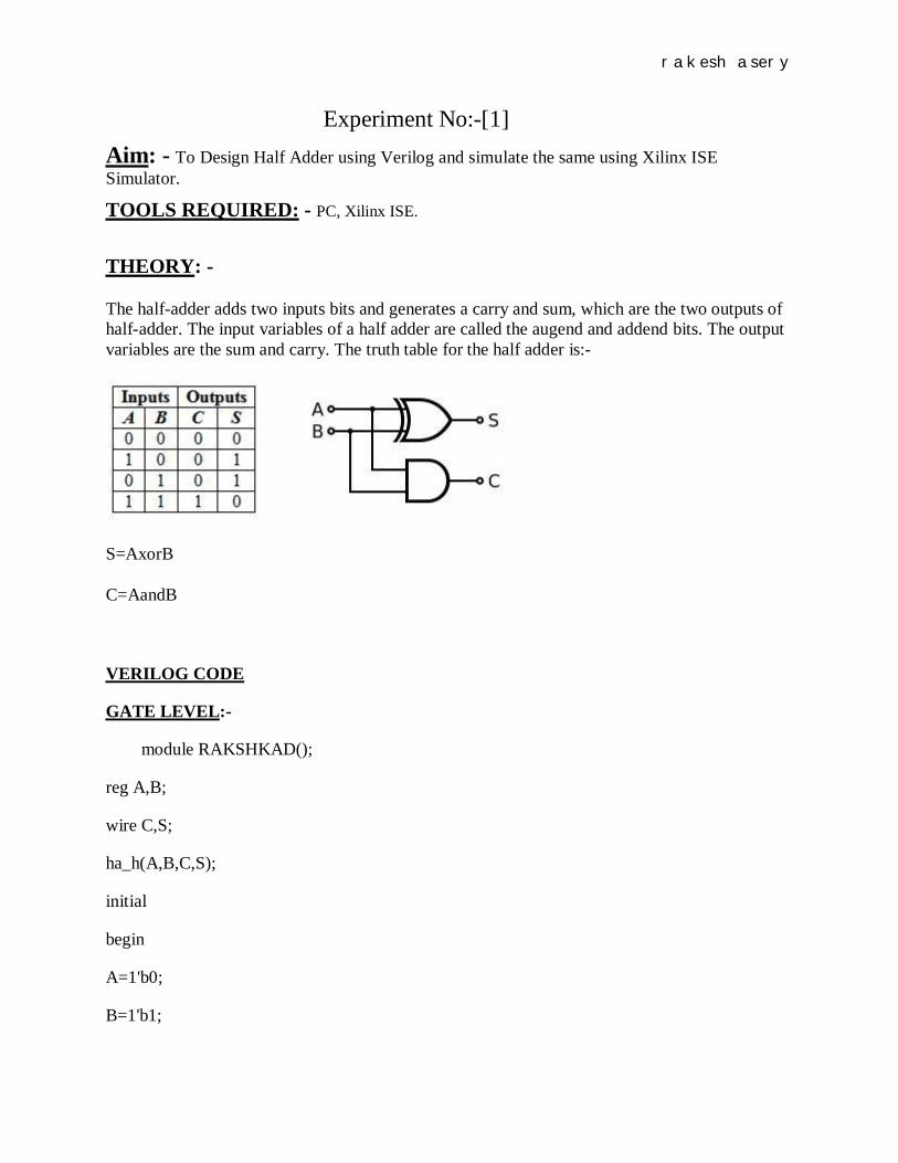
The half-adder adds two inputs bits and generates a carry and sum, which are the two outputs of half-adder. The input variables of a half adder are called the augend and addend bits. The output variables are the sum and carry. The truth table for the half adder is:-
S=AxorB
C=AandB
VERILOG CODE
GATE LEVEL:-
module RAKSHKAD();
reg A,B;
wire C,S;
ha_h(A,B,C,S);
initial
begin
A=1'b0;
B=1'b1;
rakesh asery
#10 b=1'b0;
#10 $finish;
end
endmodule
DATA FLOW:-
module RAKSHKADDER(A, B, S, C);
input A,B,S,C;
assign S=A^B;
assign C=A&B;
endmodule
BEHAVIORAL:-
module RAKSHKHALFBEADDER(a, b, sum, carry);
input a,b;
output sum, carry;
reg sum,carry;
always@(a,b)
case({a,b})
2'b00:begin sum = 1'b0;carry = 1'b0;end
2'b01:begin sum=1'b1;carry=1'b0;end
2'b10:begin sum=1'b1;carry=1'b0;end
2'b11:begin sum=1'b0;carry=1'b1;end
endcase
endmodule
rakesh asery
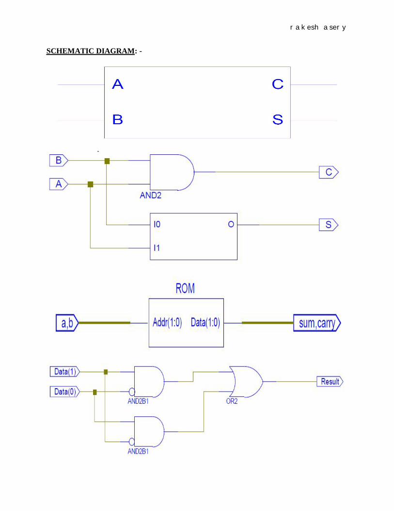
SCHEMATIC DIAGRAM: -
rakesh asery
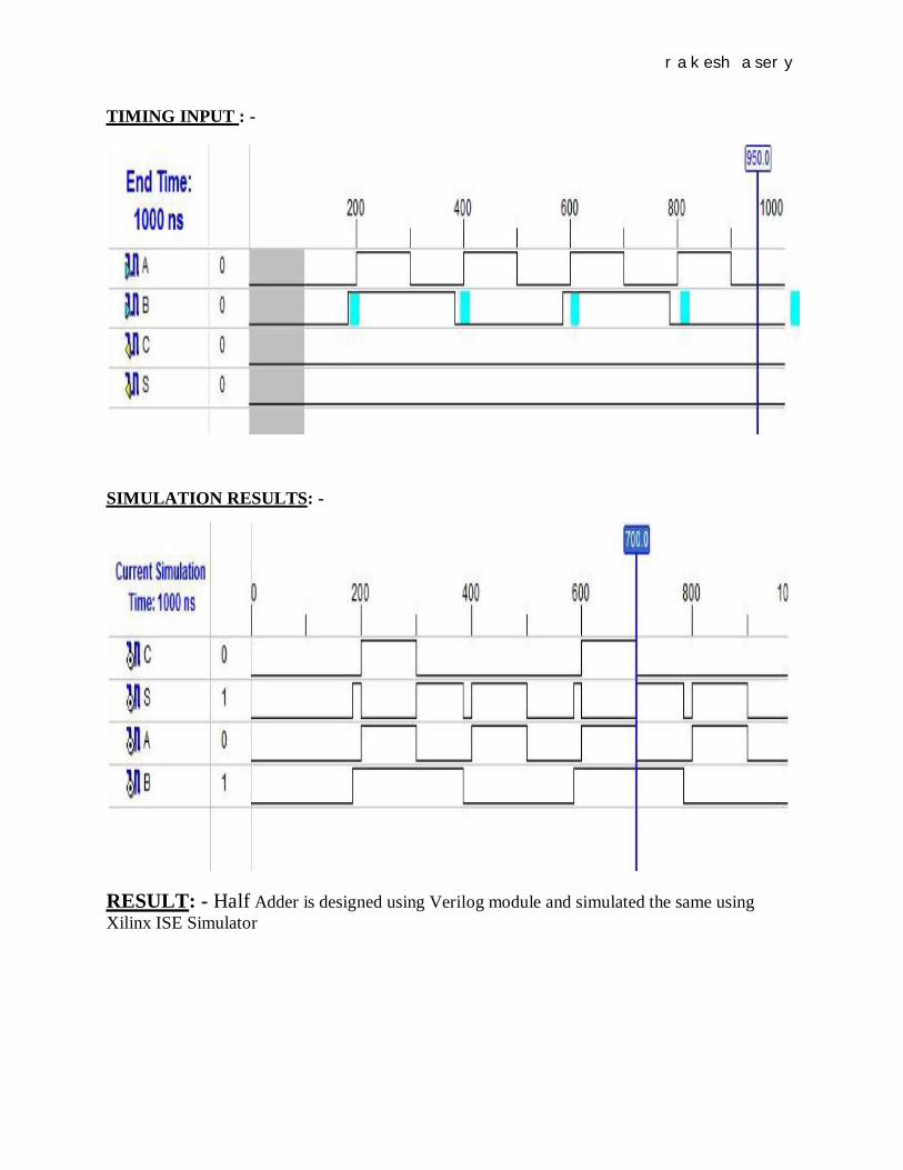
TIMING INPUT : -
SIMULATION RESULTS: -
RESULT: - Half Adder is designed using Verilog module and simulated the same using Xilinx ISE Simulator
rakesh asery
Experiment No:-[2]Aim: - To Design Multiplexer 4x1 using Verilog and simulate the same using Xilinx ISE Simulator
TOOLS REQUIRED: - PC, Xilinx ISE.
THEORY: -
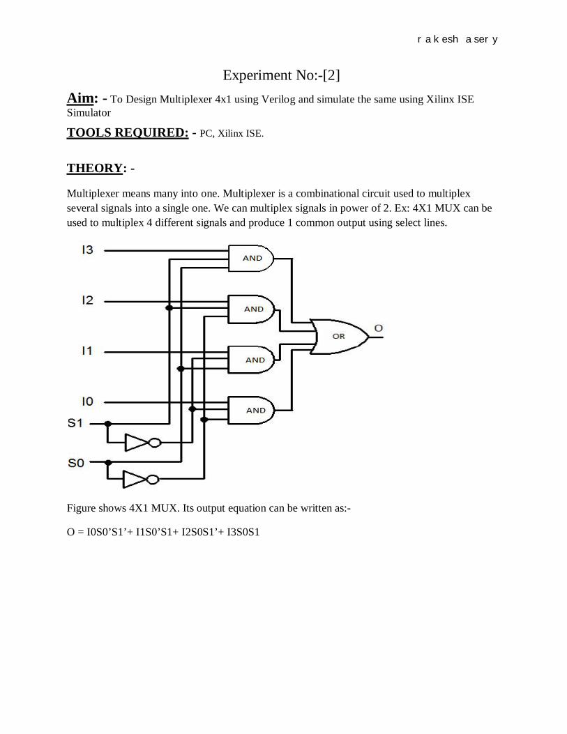
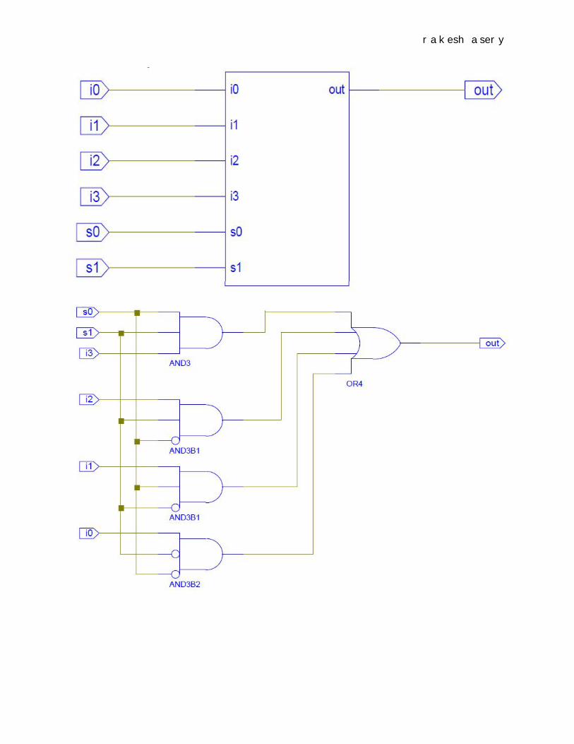
Multiplexer means many into one. Multiplexer is a combinational circuit used to multiplex several signals into a single one. We can multiplex signals in power of 2. Ex: 4X1 MUX can be used to multiplex 4 different signals and produce 1 common output using select lines.
Figure shows 4X1 MUX. Its output equation can be written as:-
O = I0S0’S1’+ I1S0’S1+ I2S0S1’+ I3S0S1
rakesh asery
VERILOG CODE
GATE LEVEL:-
module RAKESHMUX4X1(i0, i1, i2, i3, s0, s1, out);
input i0,i1,i2,i3,s0,s1;
output out;
wire y0,y1,y2,y3;
wire s1n,s0n;
not(s1n,s1);
not(s0n,s0);
and(y0,i0,s1n,s0n);
and(y1,i1,s1n,s0);
and(y2,i2,s1,s0n);
and(y3,i3,s1,s0);
or(out,y0,y1,y2,y3);
endmodule
DATA FLOW:-
module RAKSHKMUX(out,i0,i1,i2,i3,s0,s1);output out;input i0,i1,i2,i3,s0,s1; assign out=(~s1&~s0&i0); assign out=(~s1&s0&i1);assign out=(s1&~s0&i2);assign out=(s1&s0&i3); endmodule
rakesh asery
BEHAVIOURAL:-
module RAKSHKMUXR4x1(out, i0, i2, i3, i1, s0, s1);
output out;
input i0,i1,i2,i3,s0,s1;
reg out;
always@(i0 or i1 or i2 or i3 or s0 or s1)
case({s1,s0})
2'b00: out=i0;
2'b01: out=i1;
2'b10: out=i2;
2'b11: out=i3;
endcase
endmodule
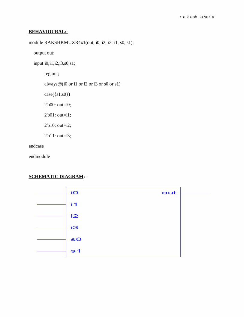
SCHEMATIC DIAGRAM: -
rakesh asery
rakesh asery
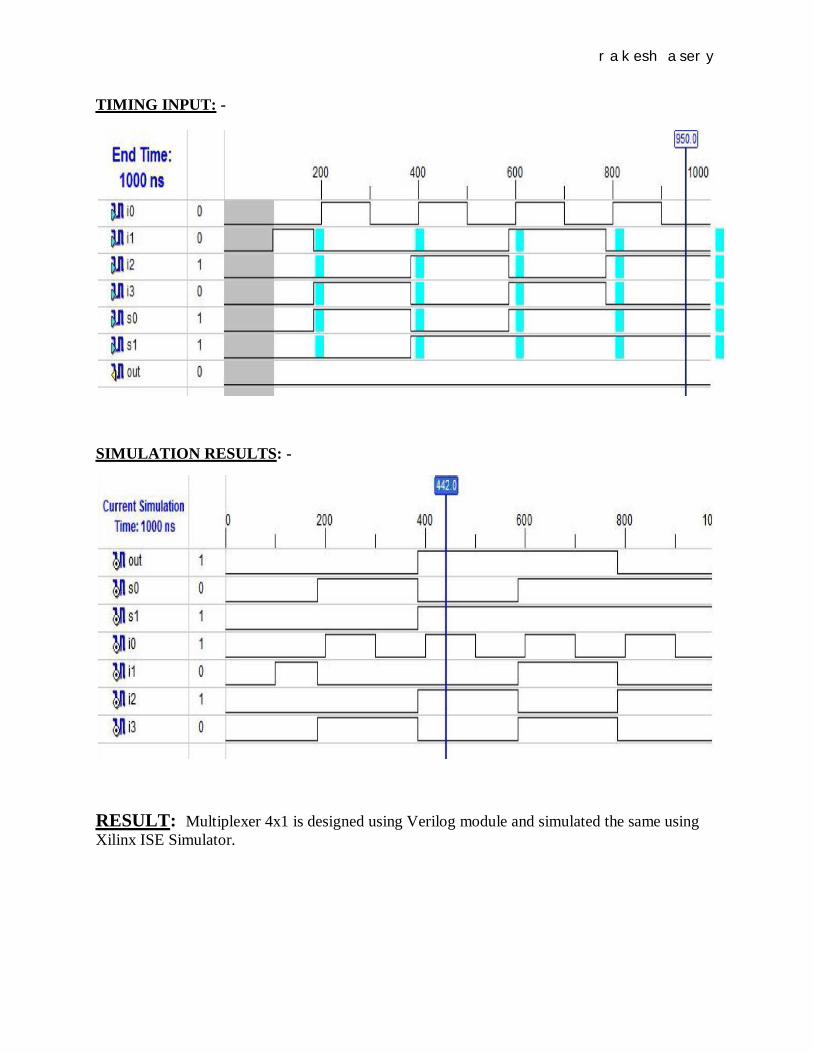
TIMING INPUT: -
SIMULATION RESULTS: -
RESULT: Multiplexer 4x1 is designed using Verilog module and simulated the same using Xilinx ISE Simulator.
rakesh asery
Experiment No:-[3] Aim: - To Design Full Adder using Verilog and simulate the same using Xilinx ISE Simulator.
TOOLS REQUIRED: - PC, Xilinx ISE.
THEORY: -
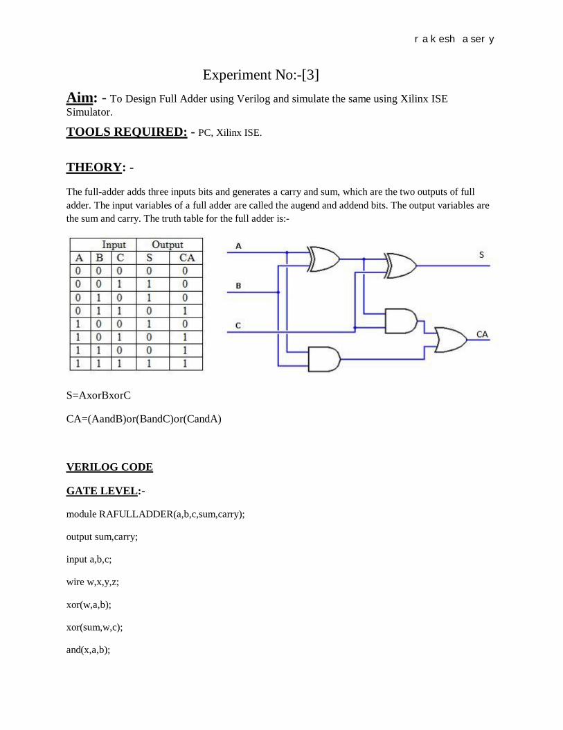
The full-adder adds three inputs bits and generates a carry and sum, which are the two outputs of full adder. The input variables of a full adder are called the augend and addend bits. The output variables are the sum and carry. The truth table for the full adder is:-
S=AxorBxorC
CA=(AandB)or(BandC)or(CandA)
VERILOG CODE
GATE LEVEL:-
module RAFULLADDER(a,b,c,sum,carry);
output sum,carry;
input a,b,c;
wire w,x,y,z;
xor(w,a,b);
xor(sum,w,c);
and(x,a,b);
rakesh asery
and(y,a,c);
and(z,b,c);
or(carry,x,y,z);
endmodule
DATA FLOW: -
module RAKSHKFULLADDER(a, b, c, sum, carry);
input a;
input b;
input c;
output sum;
output carry;
assign sum = a ^ b ^ c;
assign carry = (a&b) | (b&c) | (c&a);
endmodule
BEHAVIOURAL: - module fullbev(a, b, c, sum, carry);
input a;
input b;
input c;
output sum;
output carry;
reg sum,carry;
always@(a or b or c)
case({a,b,c})
3'b000:begin sum=0;carry=0;end

rakesh asery
3'b001:begin sum=1;carry=0;end
3'b010:begin sum=1;carry=0;end
3'b011:begin sum=0;carry=1;end
3'b100:begin sum=1;carry=0;end
3'b101:begin sum=0;carry=1;end
3'b110:begin sum=0;carry=1;end
3'b111:begin sum=1;carry=1;end
endcase
endmodule
SCHEMATIC DIAGRAM: -
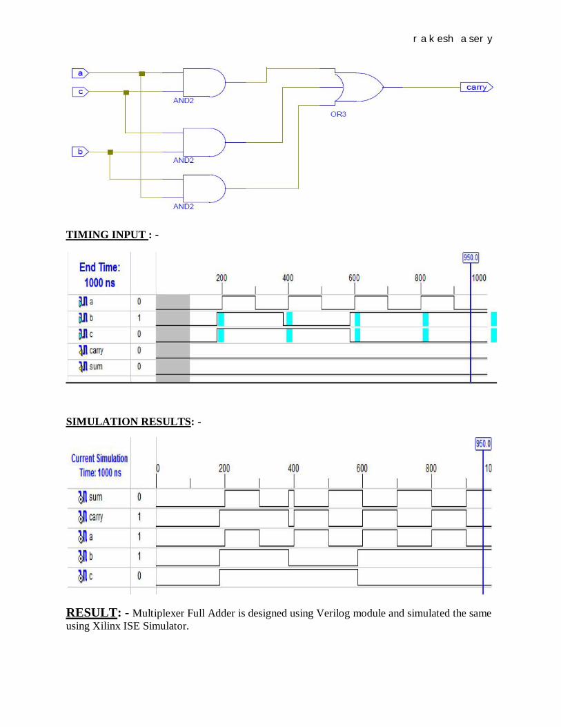
rakesh asery
TIMING INPUT : -
SIMULATION RESULTS: -
RESULT: - Multiplexer Full Adder is designed using Verilog module and simulated the same using Xilinx ISE Simulator.
rakesh asery
Experiment No:-[4a] Aim: - To Design D Flip-flop using Verilog and simulate the same using Xilinx ISE Simulator.
TOOLS REQUIRED: - PC, Xilinx ISE.
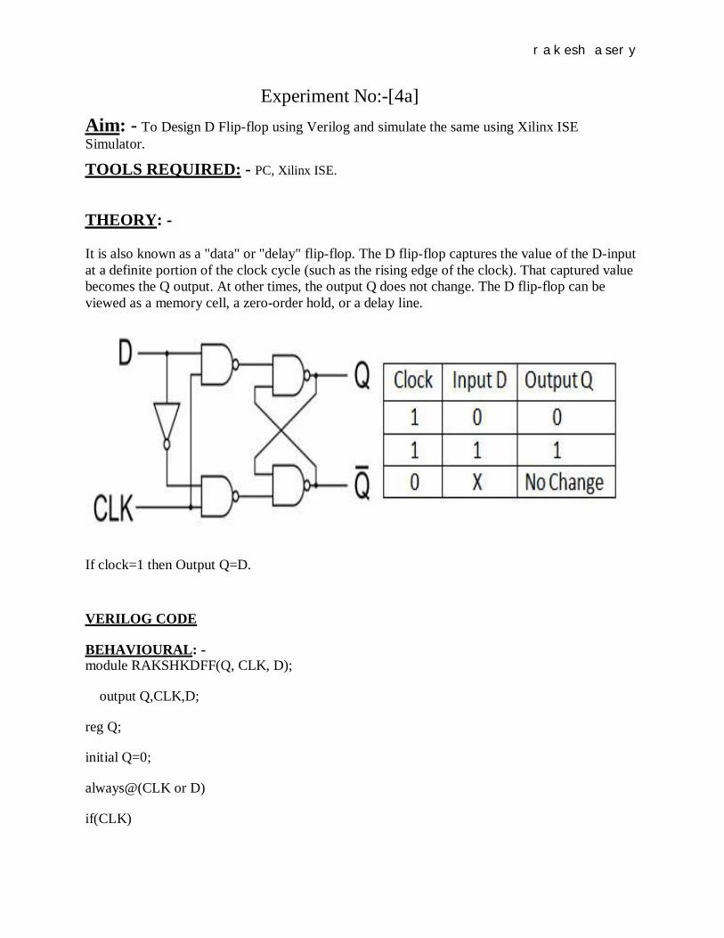
THEORY: -
It is also known as a "data" or "delay" flip-flop. The D flip-flop captures the value of the D-input at a definite portion of the clock cycle (such as the rising edge of the clock). That captured value becomes the Q output. At other times, the output Q does not change. The D flip-flop can be viewed as a memory cell, a zero-order hold, or a delay line.
If clock=1 then Output Q=D.
VERILOG CODE
BEHAVIOURAL: - module RAKSHKDFF(Q, CLK, D);
output Q,CLK,D;
reg Q;
initial Q=0;
always@(CLK or D)
if(CLK)
rakesh asery
begin
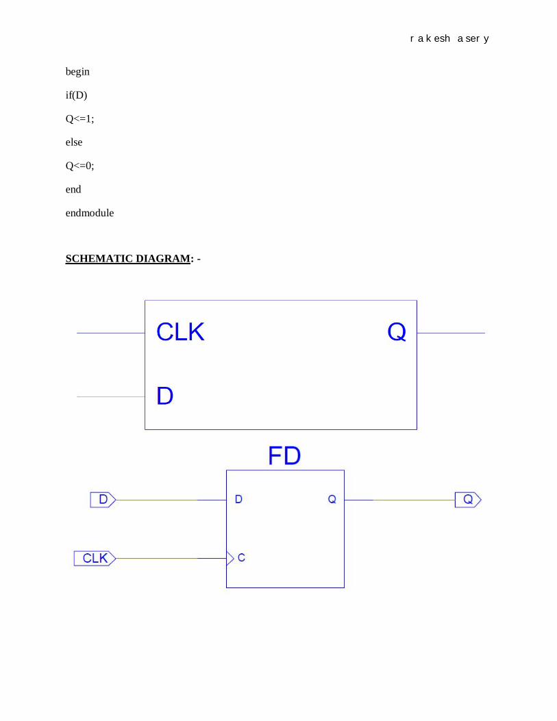
if(D)
Q<=1;
else
Q<=0;
end
endmodule
SCHEMATIC DIAGRAM: -
rakesh asery
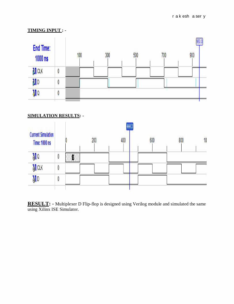
TIMING INPUT : -
SIMULATION RESULTS: -
RESULT: - Multiplexer D Flip-flop is designed using Verilog module and simulated the same using Xilinx ISE Simulator.
rakesh asery
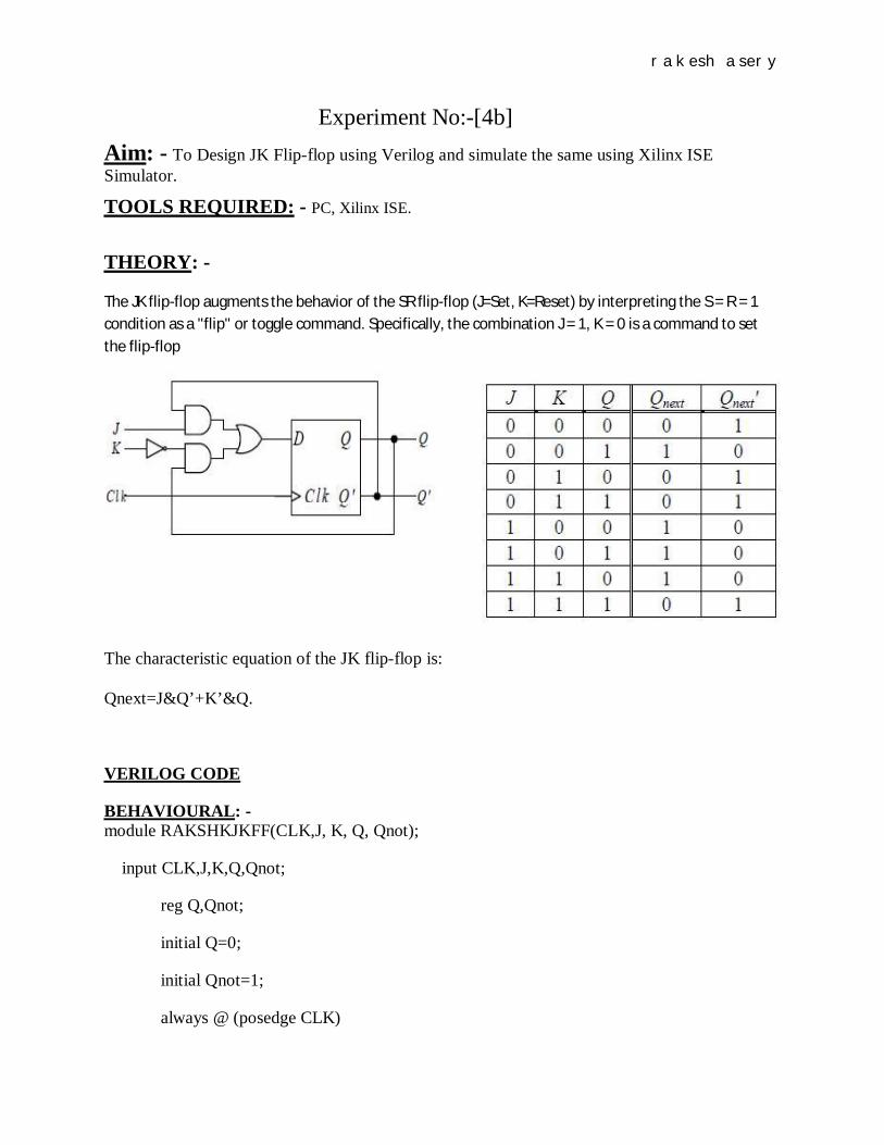
Experiment No:-[4b]Aim: - To Design JK Flip-flop using Verilog and simulate the same using Xilinx ISE Simulator.
TOOLS REQUIRED: - PC, Xilinx ISE.
THEORY: -
The JK flip-flop augments the behavior of the SR flip-flop (J=Set, K=Reset) by interpreting the S = R = 1 condition as a "flip" or toggle command. Specifically, the combination J = 1, K = 0 is a command to set the flip-flop
The characteristic equation of the JK flip-flop is:
Qnext=J&Q’+K’&Q.
VERILOG CODE
BEHAVIOURAL: - module RAKSHKJKFF(CLK,J, K, Q, Qnot);
input CLK,J,K,Q,Qnot;
reg Q,Qnot;
initial Q=0;
initial Qnot=1;
always @ (posedge CLK)
rakesh asery
case({J,K})
2'b 00:begin Q=Q; Qnot=Qnot; end
2'b 01:begin Q=0; Qnot=1; end
2'b 10:begin Q=1; Qnot=0; end
2'b 11:begin Q=~; Qnot=~Qnot; end
endcase
endmodule
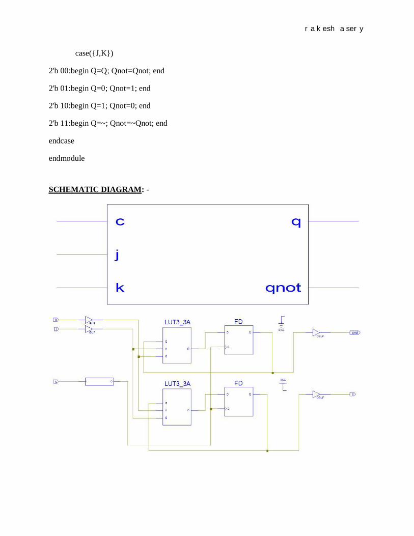
SCHEMATIC DIAGRAM: -
rakesh asery
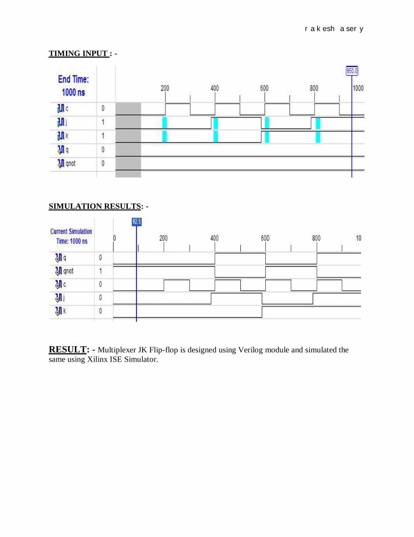
TIMING INPUT : -
SIMULATION RESULTS: -
RESULT: - Multiplexer JK Flip-flop is designed using Verilog module and simulated the same using Xilinx ISE Simulator.
rakesh asery
Experiment No:-[5]Aim: - To Design Counter using Verilog and simulate the same using Xilinx ISE Simulator.
TOOLS REQUIRED: - PC, Xilinx ISE.
THEORY: -
Counters are a specific type of sequential circuit. Like registers, the state, or the flip-flop values themselves, serves as the “output”. The output value increases by one on each clock cycle.
In electronics counters can be implemented quite easily using register-type circuits such as the flip-flop, and a wide variety of classifications exist:
Asynchronous (ripple) counter – changing state bits are used as clocks to subsequent state flip-flops Synchronous counter – all state bits change under control of a single clockDecade counter – counts through ten states per stage Up/down counter – counts both up and down, under command of a control inputRing counter – formed by a shift register with feedback connection in a ring Johnson counter – a twisted ring counterCascaded countermodulus counter.
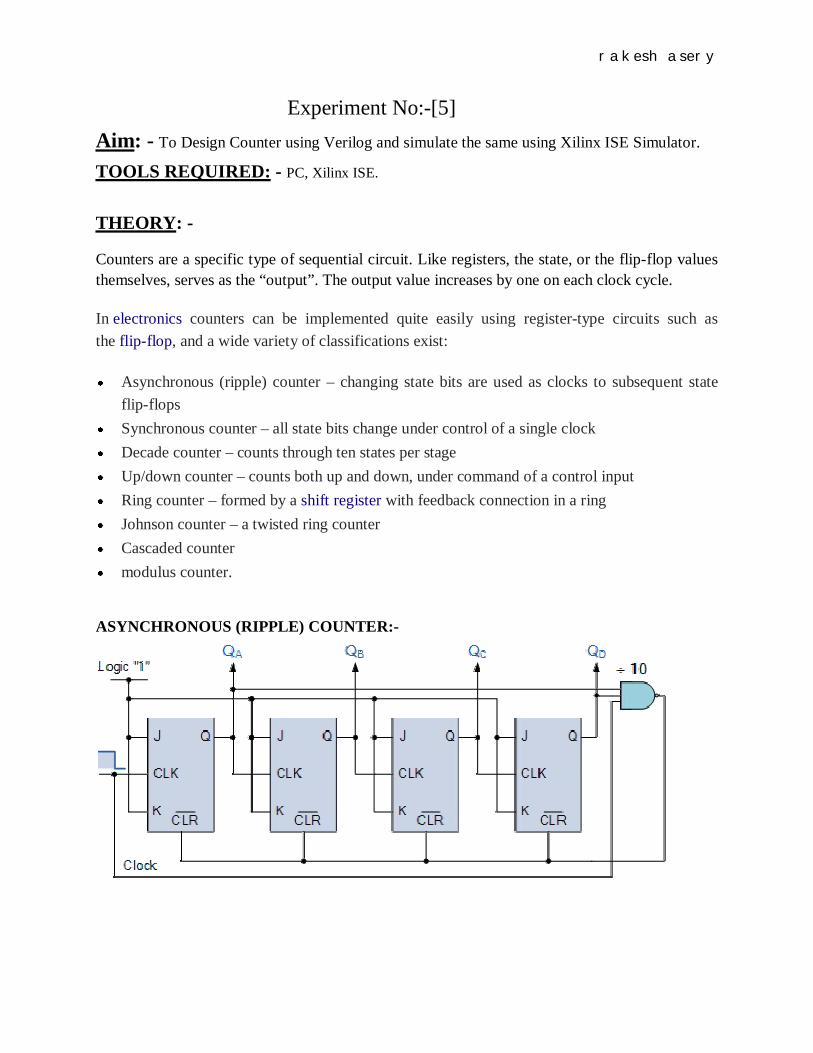
ASYNCHRONOUS (RIPPLE) COUNTER:-
rakesh asery
This type of asynchronous counter counts upwards on each leading edge of the input clock signal starting from 0000 until it reaches an output 1001 (decimal 9). Both outputs QA and QD are now equal to logic “1” and the output from the NAND gate changes state from logic “1” to a logic “0” level and whose output is also connected to the CLEAR ( CLR ) inputs of all the J-K Flip-flops. This signal causes all of the Q outputs to be reset back to binary 0000 on the count of 10. Once QAand QD are both equal to logic “0” the output of the NAND gate returns back to a logic level “1” and the counter restarts again from 0000. We now have a decade or Modulo-10 counter.
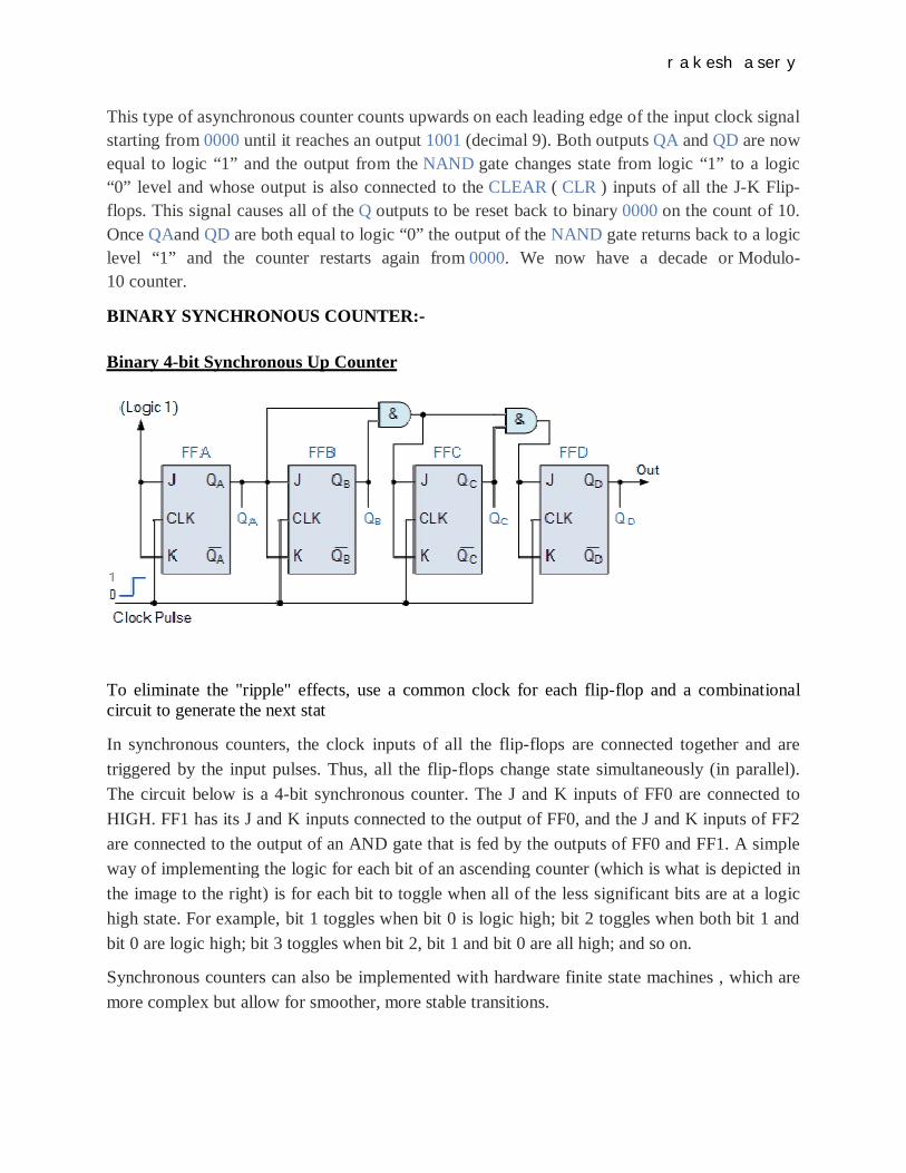
BINARY SYNCHRONOUS COUNTER:-
Binary 4-bit Synchronous Up Counter
To eliminate the "ripple" effects, use a common clock for each flip-flop and a combinational circuit to generate the next stat
In synchronous counters, the clock inputs of all the flip-flops are connected together and are triggered by the input pulses. Thus, all the flip-flops change state simultaneously (in parallel). The circuit below is a 4-bit synchronous counter. The J and K inputs of FF0 are connected to HIGH. FF1 has its J and K inputs connected to the output of FF0, and the J and K inputs of FF2 are connected to the output of an AND gate that is fed by the outputs of FF0 and FF1. A simple way of implementing the logic for each bit of an ascending counter (which is what is depicted in the image to the right) is for each bit to toggle when all of the less significant bits are at a logic high state. For example, bit 1 toggles when bit 0 is logic high; bit 2 toggles when both bit 1 and bit 0 are logic high; bit 3 toggles when bit 2, bit 1 and bit 0 are all high; and so on.
Synchronous counters can also be implemented with hardware finite state machines , which are more complex but allow for smoother, more stable transitions.
rakesh asery
VERILOG CODE
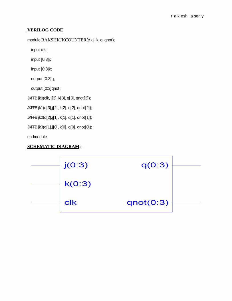
module RAKSHKJKCOUNTER(clk,j, k, q, qnot);
input clk;
input [0:3]j;
input [0:3]k;
output [0:3]q;
output [0:3]qnot;
JKFFB jk0(clk, j[3], k[3], q[3], qnot[3]);
JKFFB jk1(q[3],j[2], k[2], q[2], qnot[2]);
JKFFB jk2(q[2],j[1], k[1], q[1], qnot[1]);
JKFFB jk3(q[1],j[0], k[0], q[0], qnot[0]);
endmodule
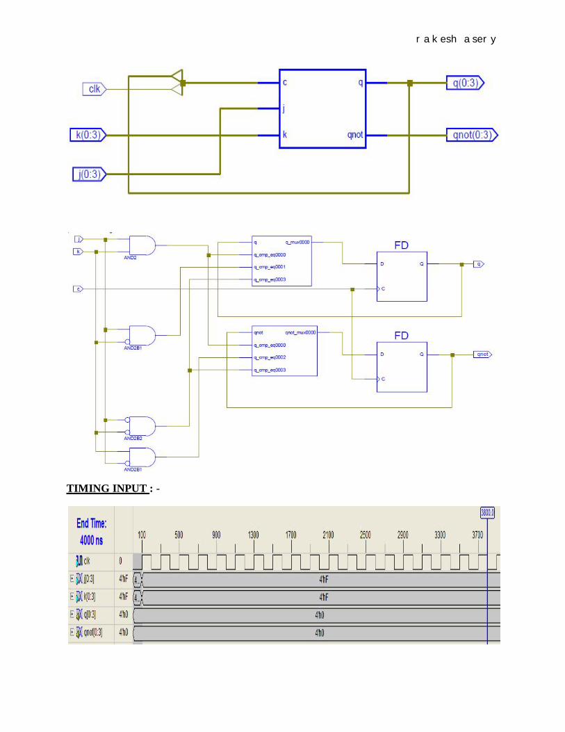
SCHEMATIC DIAGRAM: -
rakesh asery
TIMING INPUT : -
rakesh asery
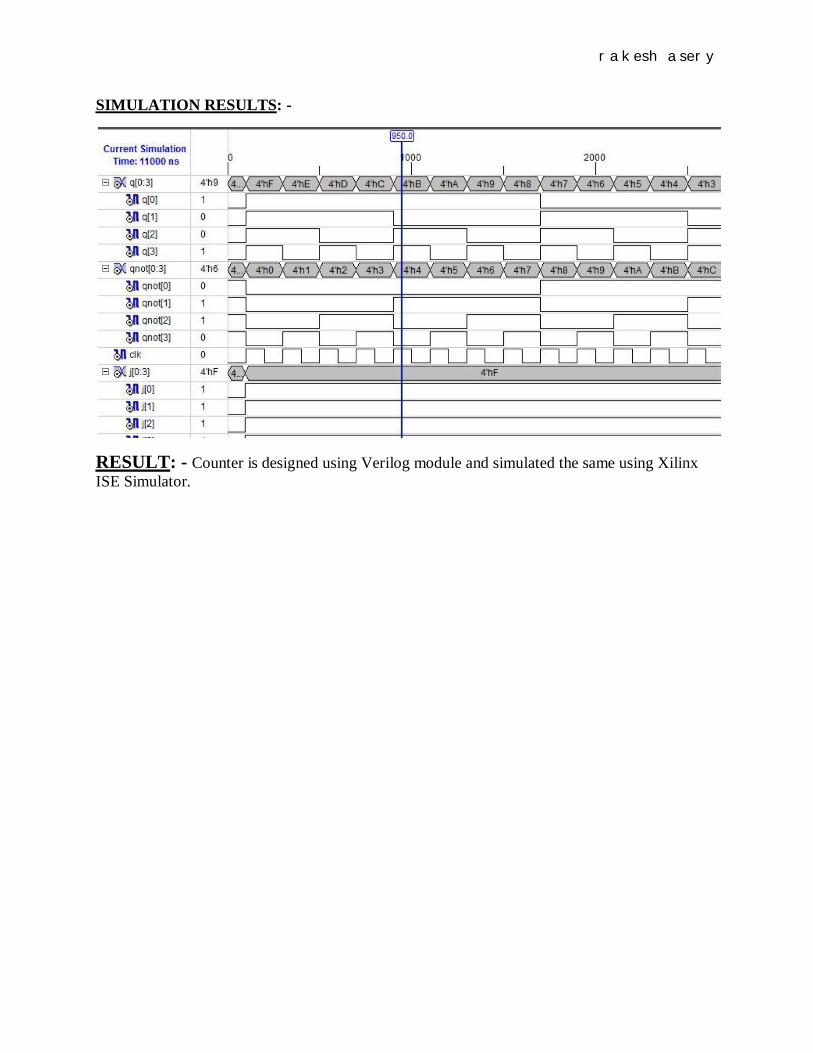
SIMULATION RESULTS: -
RESULT: - Counter is designed using Verilog module and simulated the same using Xilinx ISE Simulator.
rakesh asery
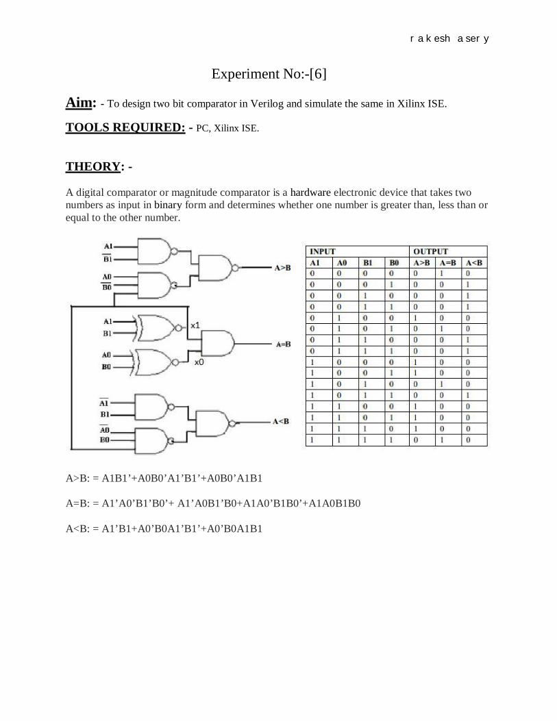
Experiment No:-[6]
Aim: - To design two bit comparator in Verilog and simulate the same in Xilinx ISE.
TOOLS REQUIRED: - PC, Xilinx ISE.
THEORY: -
A digital comparator or magnitude comparator is a hardware electronic device that takes two numbers as input in binary form and determines whether one number is greater than, less than or equal to the other number.
A>B: = A1B1’+A0B0’A1’B1’+A0B0’A1B1
A=B: = A1’A0’B1’B0’+ A1’A0B1’B0+A1A0’B1B0’+A1A0B1B0
A<B: = A1’B1+A0’B0A1’B1’+A0’B0A1B1
rakesh asery
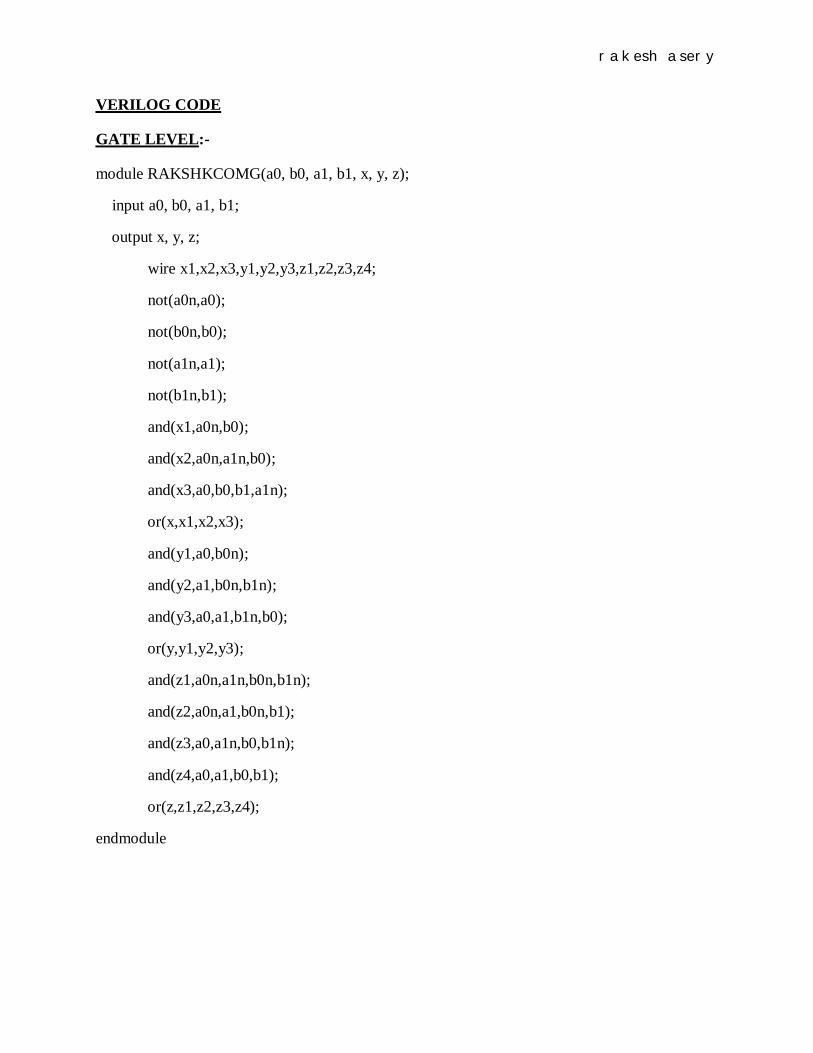
VERILOG CODE
GATE LEVEL:-
module RAKSHKCOMG(a0, b0, a1, b1, x, y, z);
input a0, b0, a1, b1;
output x, y, z;
wire x1,x2,x3,y1,y2,y3,z1,z2,z3,z4;
not(a0n,a0);
not(b0n,b0);
not(a1n,a1);
not(b1n,b1);
and(x1,a0n,b0);
and(x2,a0n,a1n,b0);
and(x3,a0,b0,b1,a1n);
or(x,x1,x2,x3);
and(y1,a0,b0n);
and(y2,a1,b0n,b1n);
and(y3,a0,a1,b1n,b0);
or(y,y1,y2,y3);
and(z1,a0n,a1n,b0n,b1n);
and(z2,a0n,a1,b0n,b1);
and(z3,a0,a1n,b0,b1n);
and(z4,a0,a1,b0,b1);
or(z,z1,z2,z3,z4);
endmodule
rakesh asery
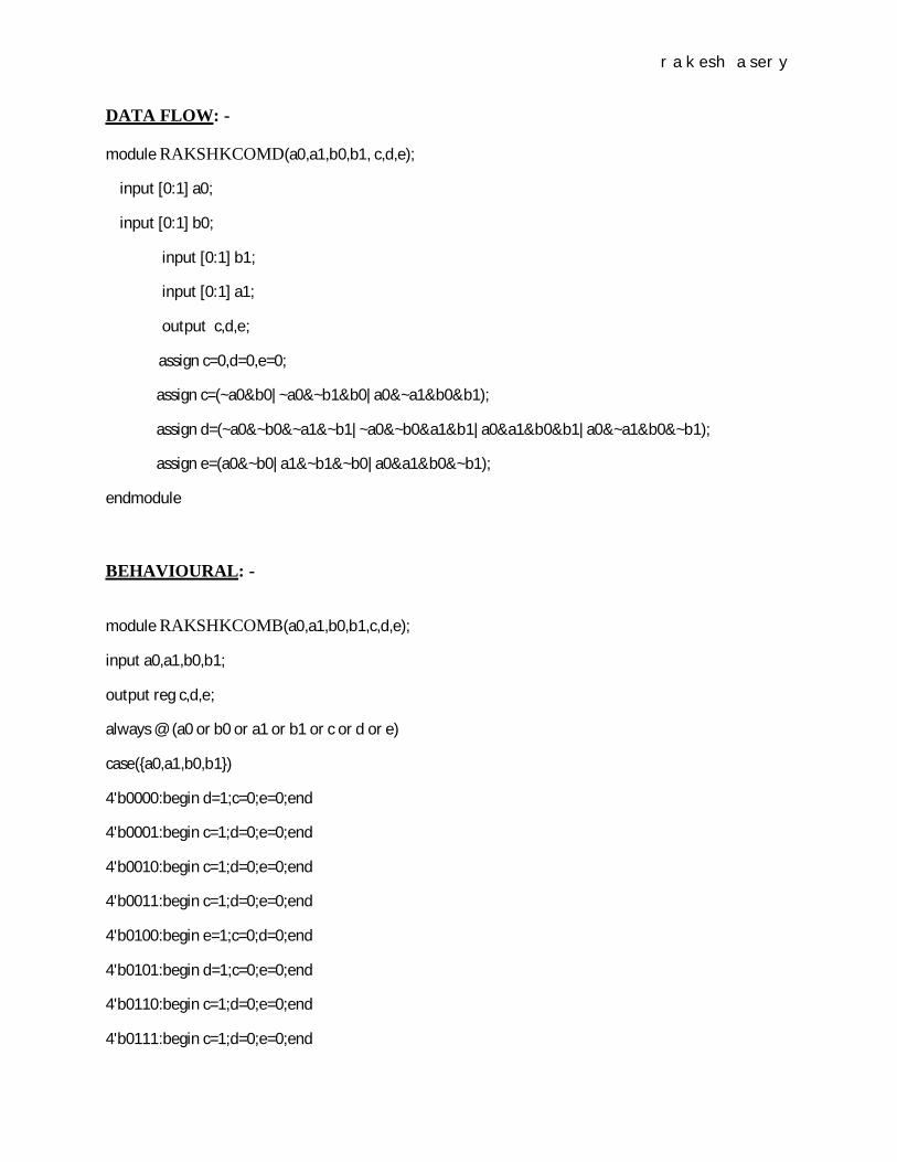
DATA FLOW: -
module RAKSHKCOMD(a0,a1,b0,b1, c,d,e);
input [0:1] a0;
input [0:1] b0;
input [0:1] b1;
input [0:1] a1;
output c,d,e;
assign c=0,d=0,e=0;
assign c=(~a0&b0|~a0&~b1&b0|a0&~a1&b0&b1);
assign d=(~a0&~b0&~a1&~b1|~a0&~b0&a1&b1|a0&a1&b0&b1|a0&~a1&b0&~b1);
assign e=(a0&~b0|a1&~b1&~b0|a0&a1&b0&~b1);
endmodule
BEHAVIOURAL: -
module RAKSHKCOMB(a0,a1,b0,b1,c,d,e);
input a0,a1,b0,b1;
output reg c,d,e;
always @ (a0 or b0 or a1 or b1 or c or d or e)
case({a0,a1,b0,b1})
4'b0000:begin d=1;c=0;e=0;end
4'b0001:begin c=1;d=0;e=0;end
4'b0010:begin c=1;d=0;e=0;end
4'b0011:begin c=1;d=0;e=0;end
4'b0100:begin e=1;c=0;d=0;end
4'b0101:begin d=1;c=0;e=0;end
4'b0110:begin c=1;d=0;e=0;end
4'b0111:begin c=1;d=0;e=0;end
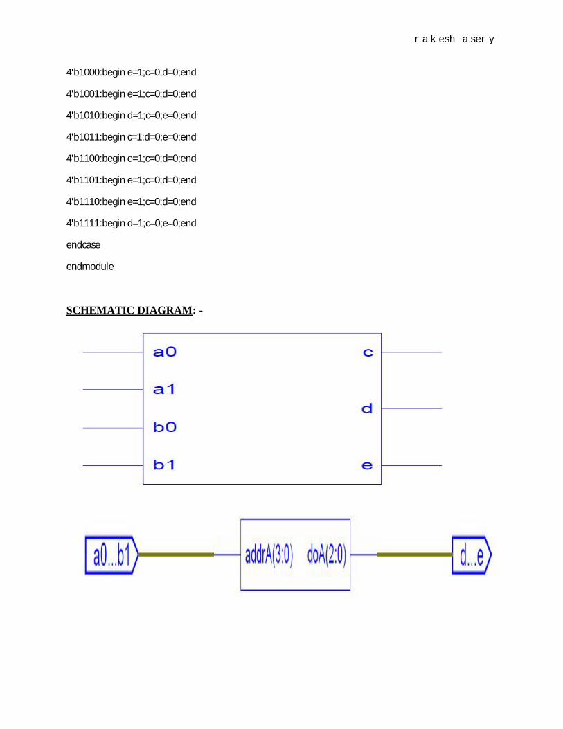
rakesh asery
4'b1000:begin e=1;c=0;d=0;end
4'b1001:begin e=1;c=0;d=0;end
4'b1010:begin d=1;c=0;e=0;end
4'b1011:begin c=1;d=0;e=0;end
4'b1100:begin e=1;c=0;d=0;end
4'b1101:begin e=1;c=0;d=0;end
4'b1110:begin e=1;c=0;d=0;end
4'b1111:begin d=1;c=0;e=0;end
endcase
endmodule
SCHEMATIC DIAGRAM: -
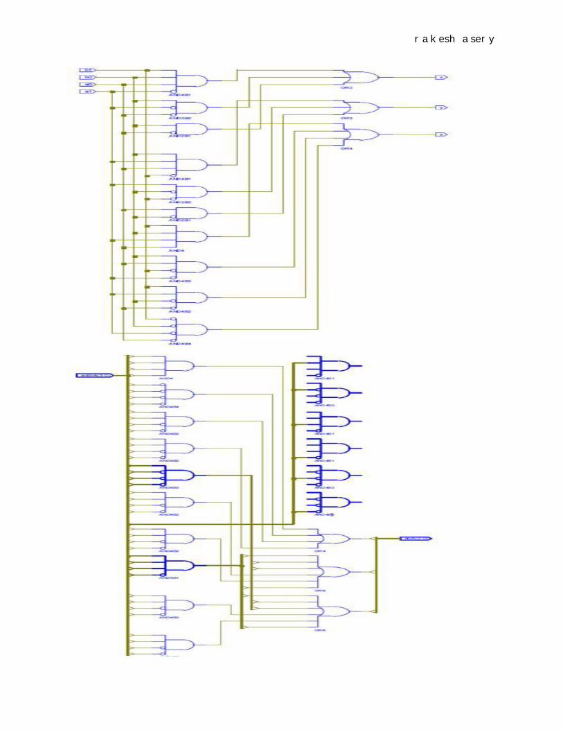
rakesh asery
rakesh asery
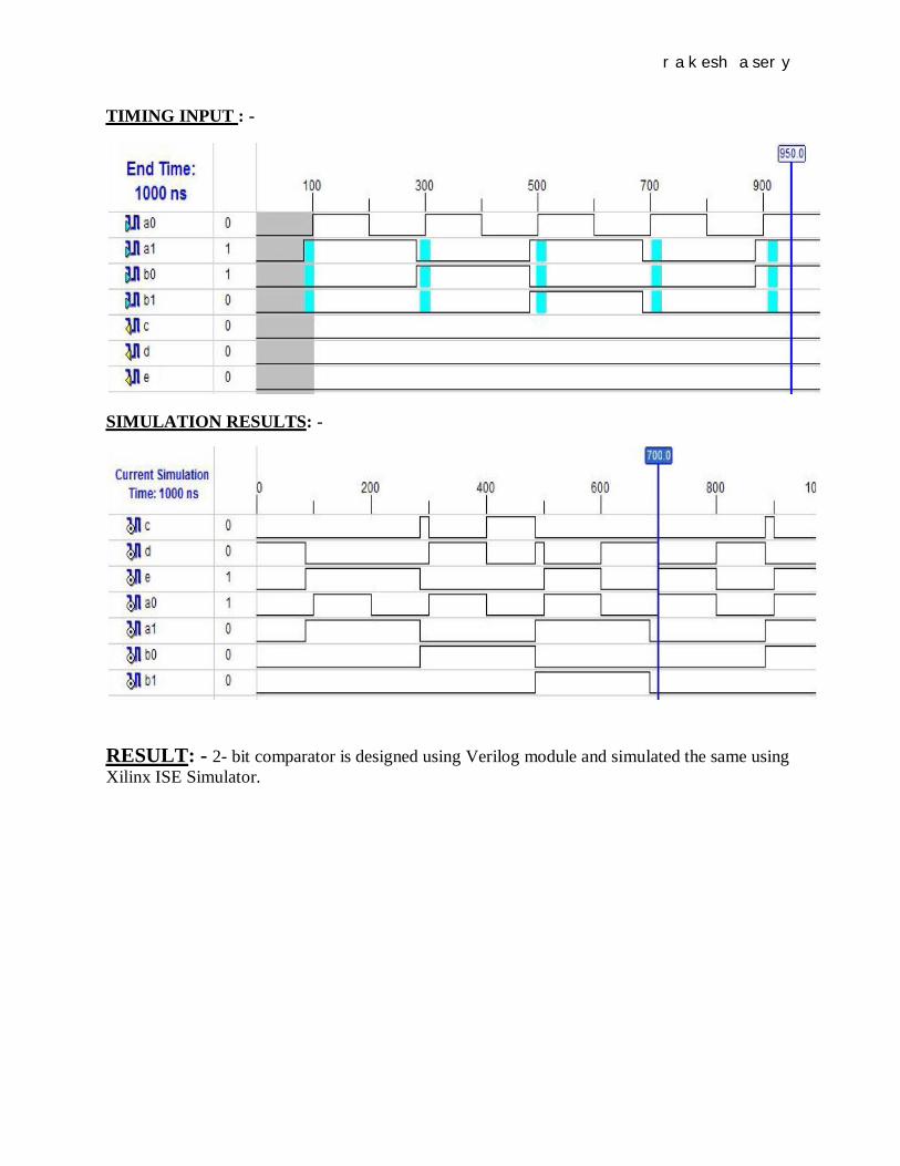
TIMING INPUT : -
SIMULATION RESULTS: -
RESULT: - 2- bit comparator is designed using Verilog module and simulated the same using Xilinx ISE Simulator.
rakesh asery
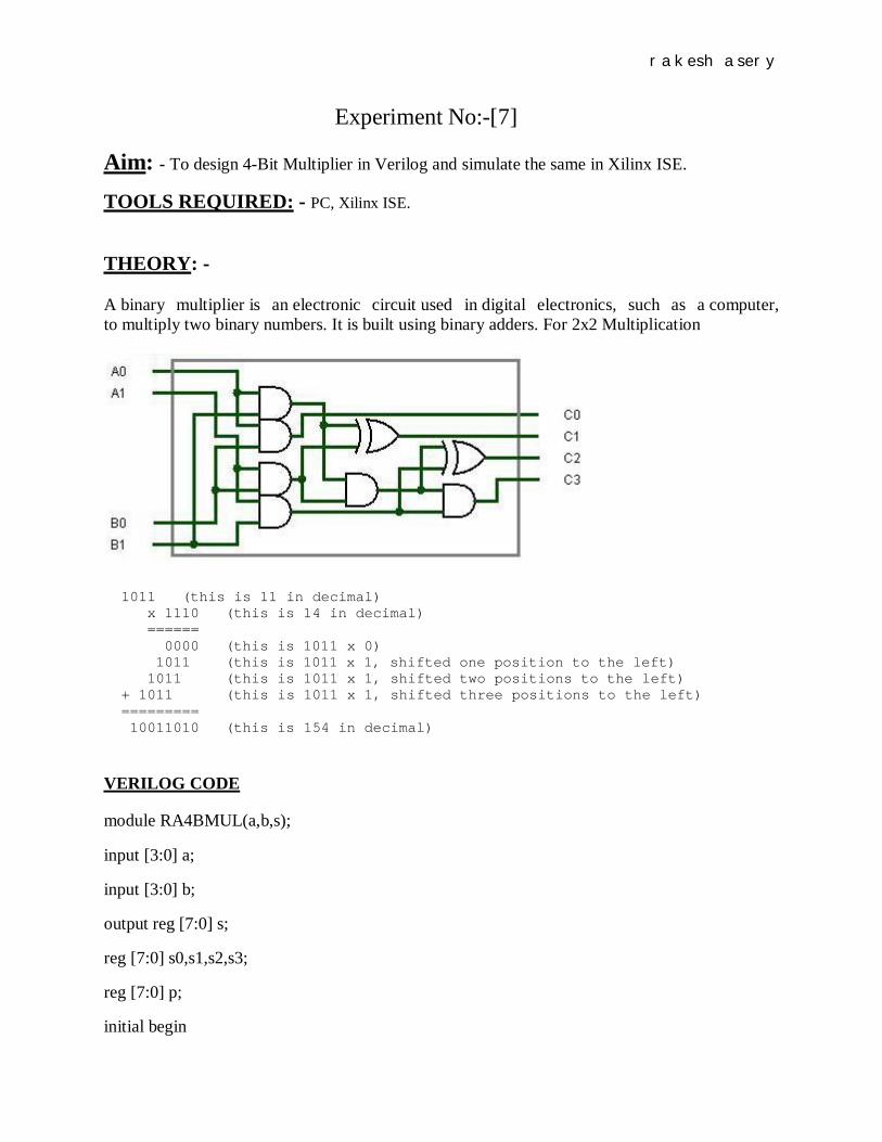
Experiment No:-[7]
Aim: - To design 4-Bit Multiplier in Verilog and simulate the same in Xilinx ISE.
TOOLS REQUIRED: - PC, Xilinx ISE.
THEORY: -
A binary multiplier is an electronic circuit used in digital electronics, such as a computer, to multiply two binary numbers. It is built using binary adders. For 2x2 Multiplication
1011 (this is 11 in decimal)x 1110 (this is 14 in decimal)======0000 (this is 1011 x 0)1011 (this is 1011 x 1, shifted one position to the left) 1011 (this is 1011 x 1, shifted two positions to the left)
+ 1011 (this is 1011 x 1, shifted three positions to the left) =========10011010 (this is 154 in decimal)
VERILOG CODE
module RA4BMUL(a,b,s);
input [3:0] a;
input [3:0] b;
output reg [7:0] s;
reg [7:0] s0,s1,s2,s3;
reg [7:0] p;
initial begin

rakesh asery
s0=8'b0; s1=8'b0; s2=8'b0; s3=8'b0;
p=8'b0;
end
always @(a or b)
begin
if(b[0]==0)
p=p+s0;
else
s0=a;
p=p+s0;
s0=8'b0;
if(b[1]==0)
begin
p=p+s1;
end
else
begin
s1=a<<1;
p=p+s1;
s1=8'b0;
end
if(b[2]==0)
begin
p=p+s2;
end
else
begin
rakesh asery
s2=a<<2;
p=p+s2;
s2=8'b0;
end
if(b[3]==0)
begin
p=p+s3;
end
else
begin
s3=a<<3;
p=p+s3;
s3=8'b0;
end
s=p;
p=8'b0;
end
endmodule
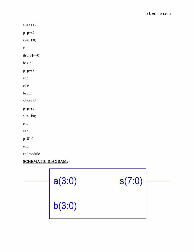
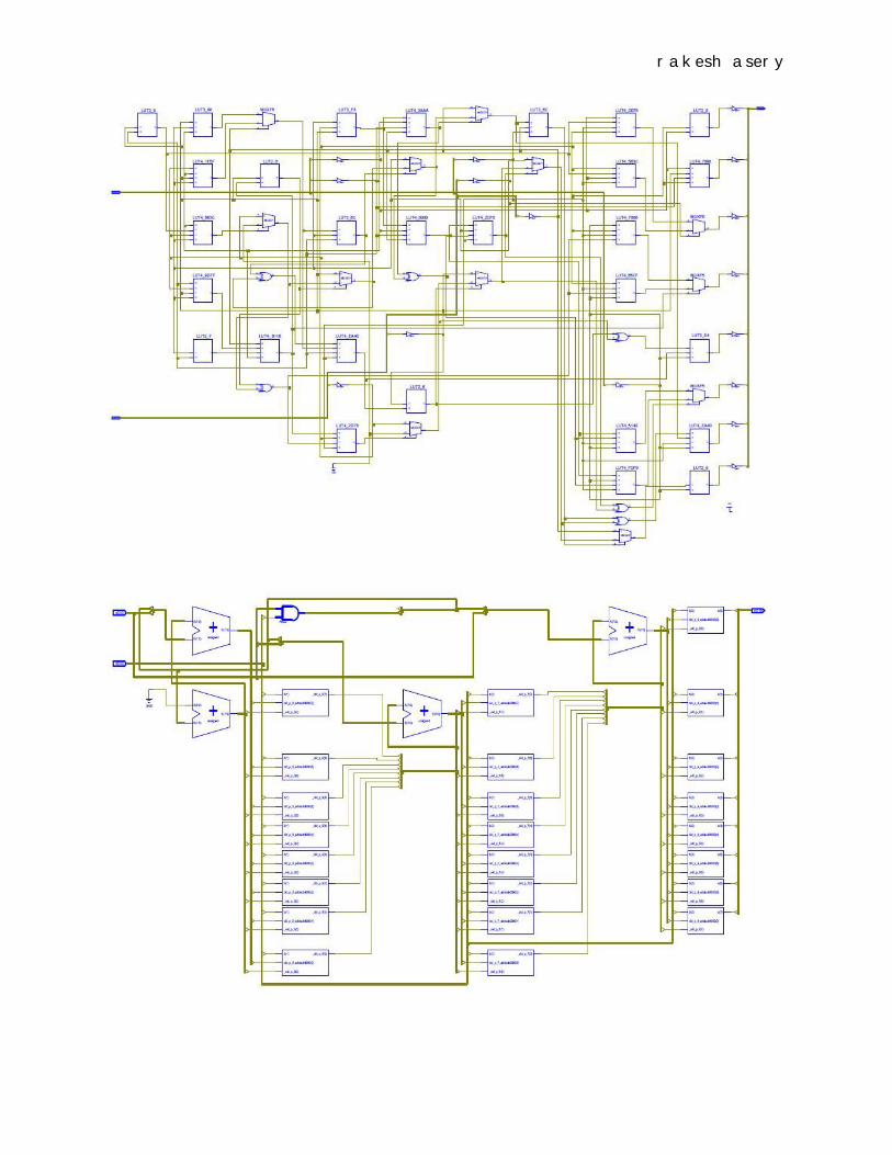
SCHEMATIC DIAGRAM: -
rakesh asery
rakesh asery
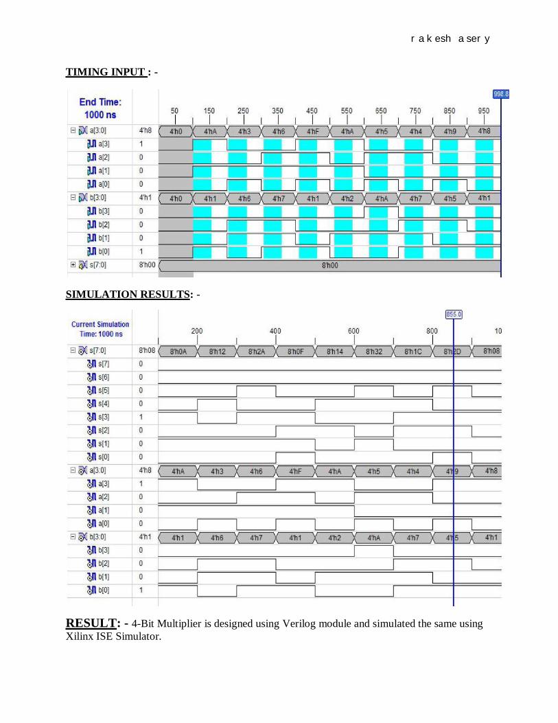
TIMING INPUT : -
SIMULATION RESULTS: -
RESULT: - 4-Bit Multiplier is designed using Verilog module and simulated the same using Xilinx ISE Simulator.
Recommended


![Parallel VLSI CAD Algorithmszhuofeng/EE5900Spring2012... · Parallel VLSI CAD Algorithms Lecture 1 Introduction ... Various IEEE journal and conference papers: IEEE[1] Various IEEE](https://img.dokumen.tips/doc/110x75/5e88f1299475ec1f5a74fb96/parallel-vlsi-cad-algorithms-zhuofengee5900spring2012-parallel-vlsi-cad-algorithms.jpg)